analog and digital communications lecture notes b.tech (ii ...
139
ANALOG AND DIGITAL COMMUNICATIONS LECTURE NOTES B.TECH (II YEAR – II SEM) (2021-2022) Prepared by Mrs.P.Swetha, Assistant Professor Mr.CH.Kiran Kumar, Assistant Professor Department of Electronics and Communication Engineering MALLA REDDY COLLEGE OF ENGINEERING & TECHNOLOGY (Autonomous Institution – UGC, Govt. of India) Recognized under 2(f) and 12 (B) of UGC ACT 1956 (Affiliated to JNTUH, Hyderabad, Approved by AICTE - Accredited by NBA & NAAC – ‘A’ Grade - ISO 9001:2015 Certified) Maisammaguda, Dhulapally (Post Via. Kompally), Secunderabad – 500100, Telangana State, India
-
Upload
khangminh22 -
Category
Documents
-
view
1 -
download
0
Transcript of analog and digital communications lecture notes b.tech (ii ...

ANALOG AND DIGITAL COMMUNICATIONS
LECTURE NOTES
B.TECH (II YEAR – II SEM)
(2021-2022)
Prepared by Mrs.P.Swetha, Assistant Professor
Mr.CH.Kiran Kumar, Assistant Professor
Department of Electronics and Communication Engineering
MALLA REDDY COLLEGE OF ENGINEERING & TECHNOLOGY
(Autonomous Institution – UGC, Govt. of India) Recognized under 2(f) and 12 (B) of UGC ACT 1956
(Affiliated to JNTUH, Hyderabad, Approved by AICTE - Accredited by NBA & NAAC – ‘A’ Grade - ISO 9001:2015 Certified) Maisammaguda, Dhulapally (Post Via. Kompally), Secunderabad – 500100, Telangana State, India

B.Tech (Electronics & Communication Engineering) R-20
Malla Reddy College of Engineering and Technology (MRCET)
MALLA REDDY COLLEGE OF ENGINEERING AND TECHNOLOGY II Year B.Tech. ECE- II Sem L/T/P/C
3/-/-/3
(R20A0406) ANALOG & DIGITAL COMMUNICATIONS
COURSE OBJECTIVES:
1) To analyze and design various continuous wave Amplitude modulation and demodulation
techniques.
2) To understand the concept of Angle modulation and demodulation, and the effect of noise
on it.
3) To attain the knowledge about the functioning of different AM, FM Transmitters and
Receivers.
4) To analyze and design the various Pulse Modulation Techniques (Analog and Digital Pulse
modulation)
5) To understand the concepts of Digital Modulation Technique, Baseband transmission and
Optimum Receiver.
UNIT – I
Amplitude Modulation: Need for modulation, Amplitude Modulation - Time and frequency
domain description, single tone modulation, power relations in AM waves, Generation of AM
waves -Switching modulator, Detection of AM Waves - Envelope detector, DSBSC
modulation - time and frequency domain description, Generation of DSBSC Waves -
Balanced Modulators, Coherent detection of DSB-SC Modulated waves, COSTAS Loop,
SSB modulation - time and frequency domain description, frequency discrimination and
Phase discrimination methods for generating SSB, Demodulation of SSB Waves, Vestigial
side band modulation.
UNIT - II
Angle Modulation: Basic concepts of Phase Modulation, Frequency Modulation: Single tone
Frequency modulation, Narrow band FM, Wide band FM, Spectrum Analysis of Sinusoidal
FM Wave using Bessel functions, Constant Average Power, Transmission bandwidth of FM
Wave - Generation of FM Signal- Armstrong Method, Direct method- Reactance Modulator,
Detection of FM Signal: Balanced slope detector, Phase locked loop, Comparison of FM and
AM., Concept of Pre-emphasis and de-emphasis.
UNIT - III
Transmitters: Classification of Transmitters, AM Transmitters, FM Transmitters
Receivers: Radio Receiver - Receiver Types - Tuned radio frequency receiver,
Superhetrodyne receiver, RF section and Characteristics - Frequency changing and tracking,
Intermediate frequency, Image frequency, AGC, Amplitude limiting, FM Receiver,
Comparison of AM and FM Receivers.
UNIT - IV
Pulse Modulation: Types of Pulse modulation- PAM, PWM and PPM. Comparison of FDM
with TDM.
B.Tech (Electronics & Communication Engineering) R-20
Malla Reddy College of Engineering and Technology (MRCET)
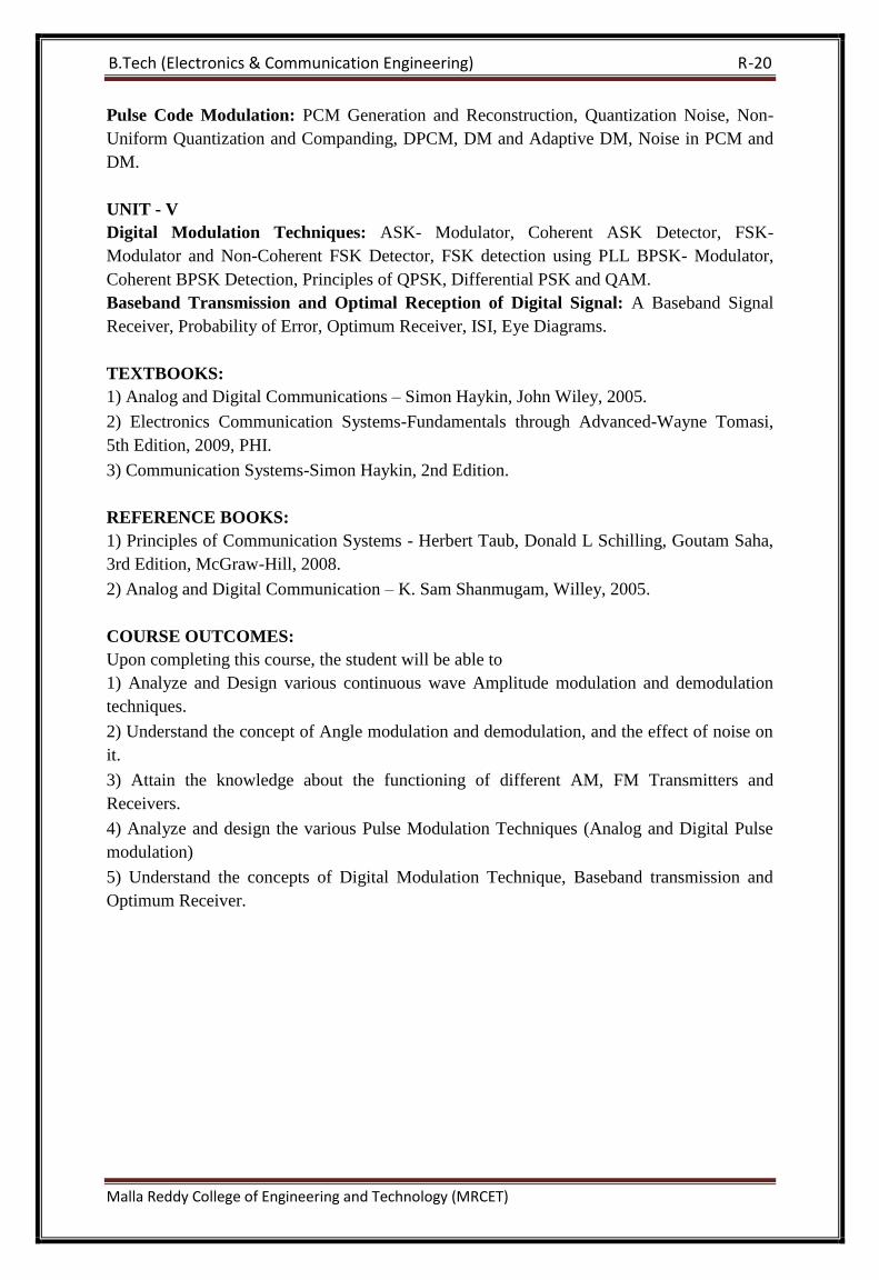
Pulse Code Modulation: PCM Generation and Reconstruction, Quantization Noise, Non-
Uniform Quantization and Companding, DPCM, DM and Adaptive DM, Noise in PCM and
DM.
UNIT - V
Digital Modulation Techniques: ASK- Modulator, Coherent ASK Detector, FSK-
Modulator and Non-Coherent FSK Detector, FSK detection using PLL BPSK- Modulator,
Coherent BPSK Detection, Principles of QPSK, Differential PSK and QAM.
Baseband Transmission and Optimal Reception of Digital Signal: A Baseband Signal
Receiver, Probability of Error, Optimum Receiver, ISI, Eye Diagrams.
TEXTBOOKS:
1) Analog and Digital Communications – Simon Haykin, John Wiley, 2005.
2) Electronics Communication Systems-Fundamentals through Advanced-Wayne Tomasi,
5th Edition, 2009, PHI.
3) Communication Systems-Simon Haykin, 2nd Edition.
REFERENCE BOOKS:
1) Principles of Communication Systems - Herbert Taub, Donald L Schilling, Goutam Saha,
3rd Edition, McGraw-Hill, 2008.
2) Analog and Digital Communication – K. Sam Shanmugam, Willey, 2005.
COURSE OUTCOMES:
Upon completing this course, the student will be able to
1) Analyze and Design various continuous wave Amplitude modulation and demodulation
techniques.
2) Understand the concept of Angle modulation and demodulation, and the effect of noise on
it.
3) Attain the knowledge about the functioning of different AM, FM Transmitters and
Receivers.
4) Analyze and design the various Pulse Modulation Techniques (Analog and Digital Pulse
modulation)
5) Understand the concepts of Digital Modulation Technique, Baseband transmission and
Optimum Receiver.

UNIT-I
AMPLITUDE MODULATION
Introduction to Communication System
Communication is the process by which information is exchanged between individuals
through a medium.
Communication can also be defined as the transfer of information from one point in space
and time to another point.
The basic block diagram of a communication system is as follows.
Transmitter: Couples the message into the channel using high frequency signals.
Channel: The medium used for transmission of signals
Modulation: It is the process of shifting the frequency spectrum of a signal to a
frequency range in which more efficient transmission can be achieved.
Receiver: Restores the signal to its original form.
Demodulation: It is the process of shifting the frequency spectrum back to the
original baseband frequency range and reconstructing the original form.
Modulation:
Modulation is a process that causes a shift in the range of frequencies in a signal.
• Signals that occupy the same range of frequencies can be separated.
• Modulation helps in noise immunity, attenuation - depends on the physical medium.
The below figure shows the different kinds of analog modulation schemes that are available
Modulation is operation performed at the transmitter to achieve efficient and reliable
information transmission.
For analog modulation, it is frequency translation method caused by changing the appropriate
quantity in a carrier signal.
It involves two waveforms:
A modulating signal/baseband signal – represents the message.
A carrier signal – depends on type of modulation.
•Once this information is received, the low frequency information must be removed from the
high frequency carrier. •This process is known as “Demodulation”.
Need for Modulation:
Baseband signals are incompatible for direct transmission over the medium so,
modulation is used to convey (baseband) signals from one place to another.
Allows frequency translation:
o Frequency Multiplexing
o Reduce the antenna height
o Avoids mixing of signals
o Narrowbanding
Efficient transmission
Reduced noise and interference
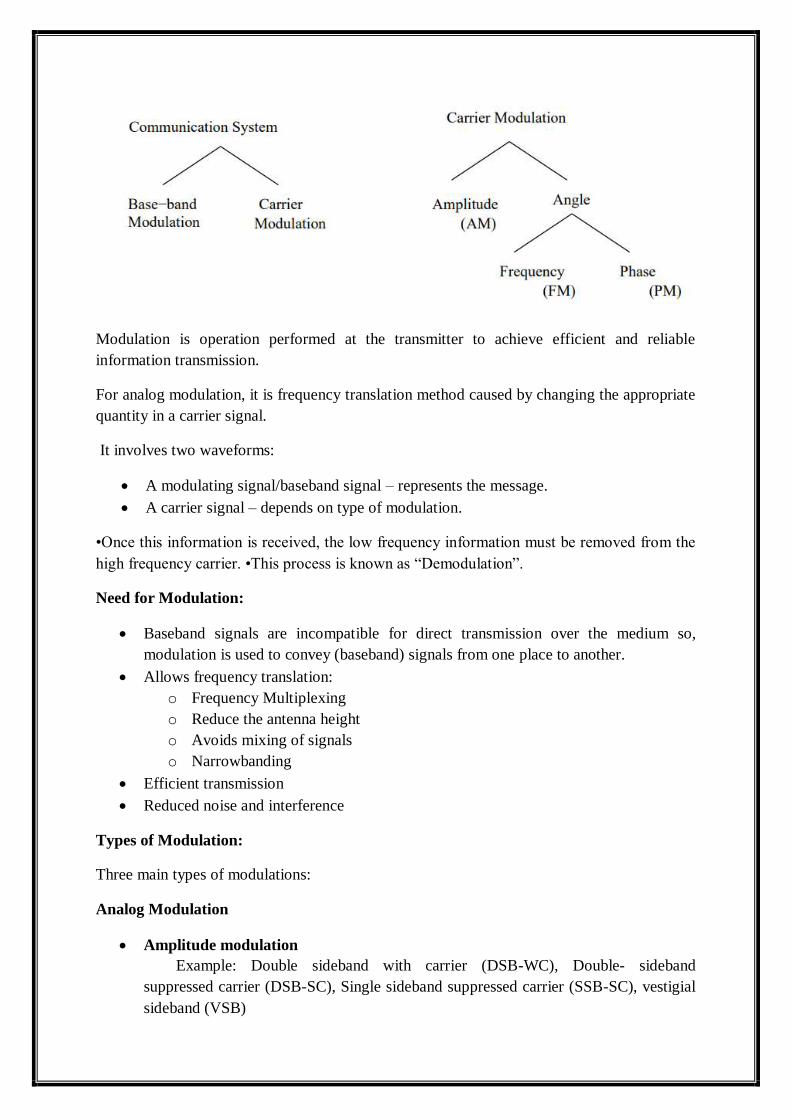
Types of Modulation:
Three main types of modulations:
Analog Modulation
Amplitude modulation
Example: Double sideband with carrier (DSB-WC), Double- sideband
suppressed carrier (DSB-SC), Single sideband suppressed carrier (SSB-SC), vestigial
sideband (VSB)
Angle modulation (frequency modulation & phase modulation)
Example: Narrow band frequency modulation (NBFM), Wideband frequency
modulation (WBFM), Narrowband phase modulation (NBPM), Wideband phase
modulation (NBPM)
Pulse Modulation
Carrier is a train of pulses
Example: Pulse Amplitude Modulation (PAM), Pulse width modulation (PWM) ,
Pulse Position Modulation (PPM)
Digital Modulation
Modulating signal is analog
o Example: Pulse Code Modulation (PCM), Delta Modulation (DM), Adaptive
Delta Modulation (ADM), Differential Pulse Code Modulation (DPCM),
Adaptive Differential Pulse Code Modulation (ADPCM) etc.
Modulating signal is digital (binary modulation)
o Example: Amplitude shift keying (ASK), frequency Shift Keying (FSK),
Phase Shift Keying (PSK) etc
Amplitude Modulation (AM)
Amplitude Modulation is the process of changing the amplitude of a relatively high
frequency carrier signal in accordance with the amplitude of the modulating signal
(Information).
The carrier amplitude varied linearly by the modulating signal which usually consists of a
range of audio frequencies. The frequency of the carrier is not affected.
Application of AM - Radio broadcasting, TV pictures (video), facsimile transmission
Frequency range for AM - 535 kHz – 1600 kHz
Bandwidth - 10 kHz
Various forms of Amplitude Modulation
• Conventional Amplitude Modulation (Alternatively known as Full AM or Double
Sideband Large carrier modulation (DSBLC) /Double Sideband Full Carrier (DSBFC)
• Double Sideband Suppressed carrier (DSBSC) modulation
• Single Sideband (SSB) modulation
• Vestigial Sideband (VSB) modulation

Time Domain and Frequency Domain Description
It is the process where, the amplitude of the carrier is varied proportional to that of the
message signal.
Let m (t) be the base-band signal, m (t) ←→ M (ω) and c (t) be the carrier, c(t) = Ac
cos(ωct). fc is chosen such that fc >> W, where W is the maximum frequency component of
m(t). The amplitude modulated signal is given by
s(t) = Ac [1 + kam(t)] cos(ωct)
Fourier Transform on both sides of the above equation
S(ω) = π Ac/2 (δ(ω − ωc) + δ(ω + ωc)) + kaAc/ 2 (M(ω − ωc) + M(ω + ωc))
ka is a constant called amplitude sensitivity.
kam(t) < 1 and it indicates percentage modulation.
Amplitude modulation in time and frequency domain
Single Tone Modulation:
Consider a modulating wave m(t ) that consists of a single tone or single frequency
component given by
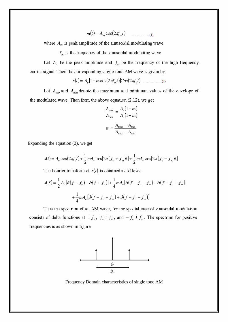
Expanding the equation (2), we get
Frequency Domain characteristics of single tone AM
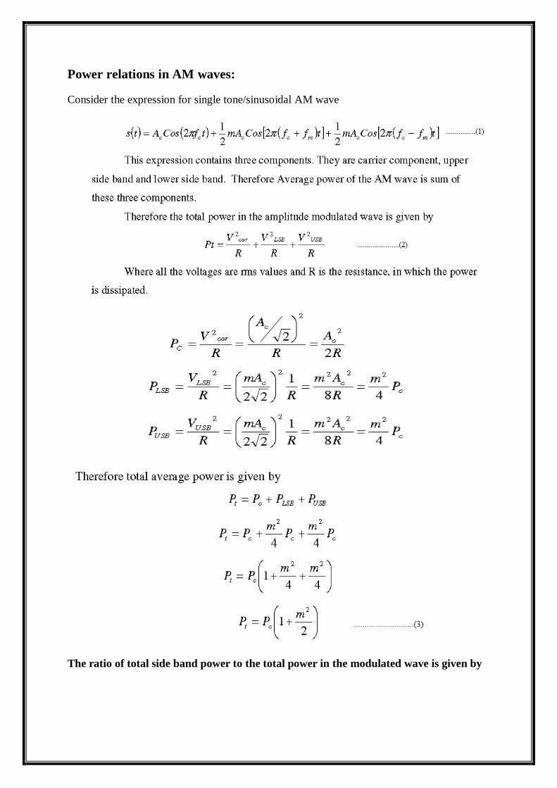
Power relations in AM waves:
Consider the expression for single tone/sinusoidal AM wave
The ratio of total side band power to the total power in the modulated wave is given by

This ratio is called the efficiency of AM system
Generation of AM waves:
Two basic amplitude modulation principles are discussed. They are square law modulation
and switching modulator.
Switching Modulator
Switching Modulator
The total input for the diode at any instant is given by
When the peak amplitude of c(t) is maintained more than that of information
signal, the operation is assumed to be dependent on only c(t) irrespective of m(t).
When c(t) is positive, v2=v1since the diode is forward biased. Similarly, when
c(t) is negative, v2=0 since diode is reverse biased. Based upon above operation,
switching response of the diode is periodic rectangular wave with an amplitude unity
and is given by

The required AM signal centred at fc can be separated using band pass filter.
The lower cut off-frequency for the band pass filter should be between w and fc-w
and the upper cut-off frequency between fc+w and 2fc. The filter output is given by
the equation
Detection of AM waves
Demodulation is the process of recovering the information signal (base band) from the
incoming modulated signal at the receiver. There are two methods, they are Square law
Detector and Envelope Detector
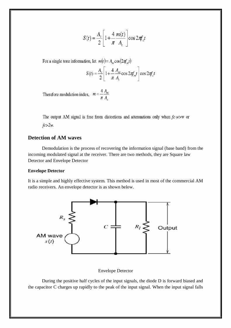
Envelope Detector
It is a simple and highly effective system. This method is used in most of the commercial AM
radio receivers. An envelope detector is as shown below.
Envelope Detector
During the positive half cycles of the input signals, the diode D is forward biased and
the capacitor C charges up rapidly to the peak of the input signal. When the input signal falls

below this value, the diode becomes reverse biased and the capacitor C discharges through
the load resistor RL.
The discharge process continues until the next positive half cycle. When the input
signal becomes greater than the voltage across the capacitor, the diode conducts again and the
process is repeated.
The charge time constant (rf+Rs)C must be short compared with the carrier period,
the capacitor charges rapidly and there by follows the applied voltage up to the positive peak
when the diode is conducting.That is the charging time constant shall satisfy the condition,
Where ‘W’ is band width of the message signal. The result is that the capacitor voltage or
detector output is nearly the same as the envelope of AM wave.
Advantages and Disadvantages of AM:
Advantages of AM:
Generation and demodulation of AM wave are easy.
AM systems are cost effective and easy to build.
Disadvantages:
AM contains unwanted carrier component, hence it requires more
transmission power.
The transmission bandwidth is equal to twice the message
bandwidth.
To overcome these limitations, the conventional AM system is modified at the cost of
increased system complexity. Therefore, three types of modified AM systems are discussed.
DSBSC (Double Side Band Suppressed Carrier) modulation:
In DSBC modulation, the modulated wave consists of only the upper and lower side
bands. Transmitted power is saved through the suppression of the carrier wave, but the
channel bandwidth requirement is the same as before.
SSBSC (Single Side Band Suppressed Carrier) modulation: The SSBSC modulated wave
consists of only the upper side band or lower side band. SSBSC is suited for transmission of
voice signals. It is an optimum form of modulation in that it requires the minimum
transmission power and minimum channel band width. Disadvantage is increased cost and
complexity.
VSB (Vestigial Side Band) modulation: In VSB, one side band is completely passed
and just a trace or vestige of the other side band is retained. The required channel bandwidth
is therefore in excess of the message bandwidth by an amount equal to the width of the
vestigial side band. This method is suitable for the transmission of wide band signals.
DSB-SC MODULATION
DSB-SC Time domain and Frequency domain Description:
DSBSC modulators make use of the multiplying action in which the modulating
signal multiplies the carrier wave. In this system, the carrier component is eliminated and
both upper and lower side bands are transmitted. As the carrier component is suppressed, the
power required for transmission is less than that of AM.
Consequently, the modulated signal s(t) under goes a phase reversal , whenever the message
signal m(t) crosses zero as shown below.
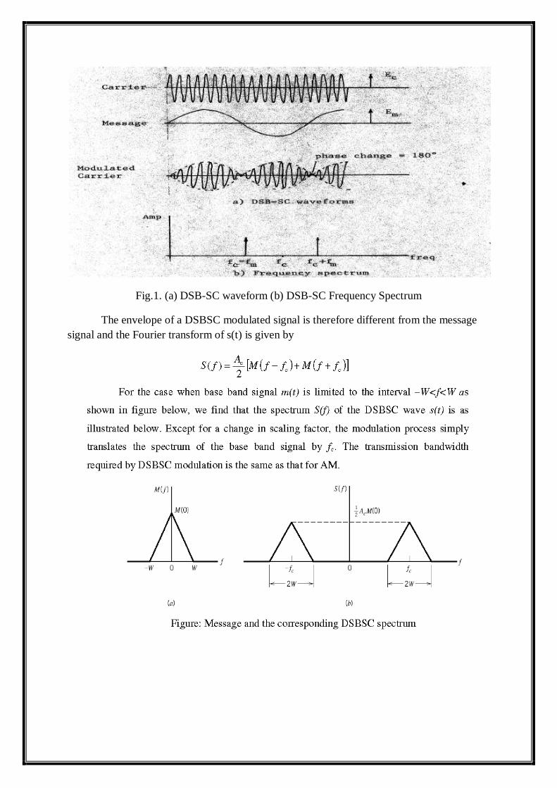
Fig.1. (a) DSB-SC waveform (b) DSB-SC Frequency Spectrum
The envelope of a DSBSC modulated signal is therefore different from the message
signal and the Fourier transform of s(t) is given by

Generation of DSBSC Waves:
Balanced Modulator (Product Modulator)
A balanced modulator consists of two standard amplitude modulators arranged in
a balanced configuration so as to suppress the carrier wave as shown in the following
block diagram. It is assumed that the AM modulators are identical, except for the sign
reversal of the modulating wave applied to the input of one of them. Thus, the output of
the two modulators may be expressed as,
Hence, except for the scaling factor 2ka, the balanced modulator output is equal to
the product of the modulating wave and the carrier.
Ring Modulator
Ring modulator is the most widely used product modulator for generating DSBSC wave and
is shown below.

The four diodes form a ring in which they all point in the same direction. The
diodes are controlled by square wave carrier c(t) of frequency fc, which is applied
longitudinally by means of two center-tapped transformers. Assuming the diodes are
ideal, when the carrier is positive, the outer diodes D1 and D2 are forward biased where
as the inner diodes D3 and D4 are reverse biased, so that the modulator multiplies the
base band signal m(t) by c(t). When the carrier is negative, the diodes D1 and D2 are
reverse biased and D3 and D4 are forward, and the modulator multiplies the base band
signal –m(t) by c(t).
Thus the ring modulator in its ideal form is a product modulator for
square wave carrier and the base band signal m(t). The square wave carrier can be
expanded using Fourier series as
From the above equation it is clear that output from the modulator consists
entirely of modulation products. If the message signal m(t) is band limited to the
frequency band − w < f < w, the output spectrum consists of side bands centred at fc.
Detection of DSB-SC waves:
Coherent Detection:
The message signal m(t) can be uniquely recovered from a DSBSC wave s(t) by
first multiplying s(t) with a locally generated sinusoidal wave and then low pass filtering the
product as shown.
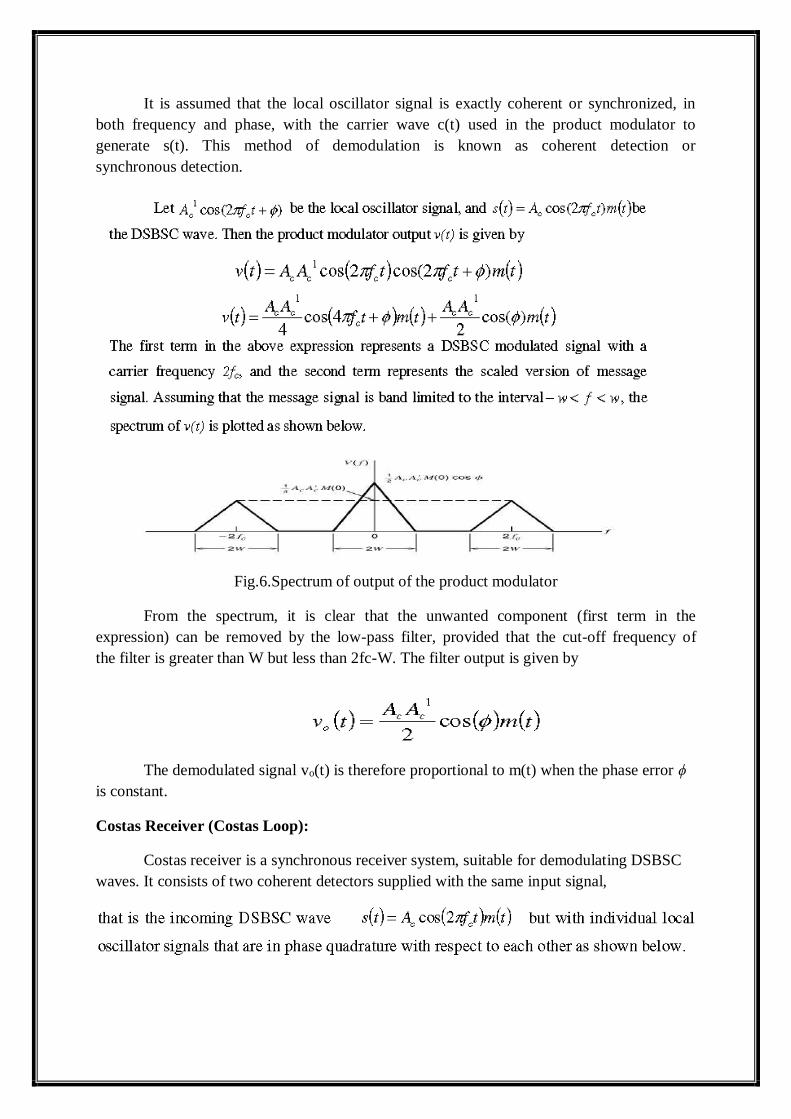
It is assumed that the local oscillator signal is exactly coherent or synchronized, in
both frequency and phase, with the carrier wave c(t) used in the product modulator to
generate s(t). This method of demodulation is known as coherent detection or
synchronous detection.
Fig.6.Spectrum of output of the product modulator
From the spectrum, it is clear that the unwanted component (first term in the
expression) can be removed by the low-pass filter, provided that the cut-off frequency of
the filter is greater than W but less than 2fc-W. The filter output is given by
The demodulated signal vo(t) is therefore proportional to m(t) when the phase error ϕ
is constant.
Costas Receiver (Costas Loop):
Costas receiver is a synchronous receiver system, suitable for demodulating DSBSC
waves. It consists of two coherent detectors supplied with the same input signal,
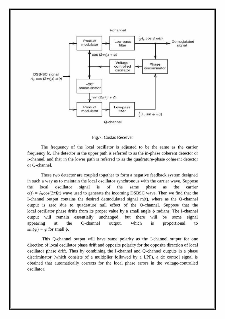
Fig.7. Costas Receiver
The frequency of the local oscillator is adjusted to be the same as the carrier
frequency fc. The detector in the upper path is referred to as the in-phase coherent detector or
I-channel, and that in the lower path is referred to as the quadrature-phase coherent detector
or Q-channel.
These two detector are coupled together to form a negative feedback system designed
in such a way as to maintain the local oscillator synchronous with the carrier wave. Suppose
the local oscillator signal is of the same phase as the carrier
c(t) = Accos(2πfct) wave used to generate the incoming DSBSC wave. Then we find that the
I-channel output contains the desired demodulated signal m(t), where as the Q-channel
output is zero due to quadrature null effect of the Q-channel. Suppose that the
local oscillator phase drifts from its proper value by a small angle ϕ radians. The I-channel
output will remain essentially unchanged, but there will be some signal
appearing at the Q-channel output, which is proportional to
sin(𝜙) ≈ 𝜙 for small ϕ.
This Q-channel output will have same polarity as the I-channel output for one
direction of local oscillator phase drift and opposite polarity for the opposite direction of local
oscillator phase drift. Thus by combining the I-channel and Q-channel outputs in a phase
discriminator (which consists of a multiplier followed by a LPF), a dc control signal is
obtained that automatically corrects for the local phase errors in the voltage-controlled
oscillator.

Introduction of SSB-SC
Standard AM and DSBSC require transmission bandwidth equal to twice the message
bandwidth. In both the cases spectrum contains two side bands of width W Hz,
each. But the upper and lower sides are uniquely related to each other by the virtue of
their symmetry about the carrier frequency. That is, given the amplitude and phase
spectra of either side band, the other can be uniquely determined. Thus if only one side
band is transmitted, and if both the carrier and the other side band are suppressed at the
transmitter, no information is lost. This kind of modulation is called SSBSC and spectral
comparison between DSBSC and SSBSC is shown in the figures 1 and 2.
Frequency Domain Description
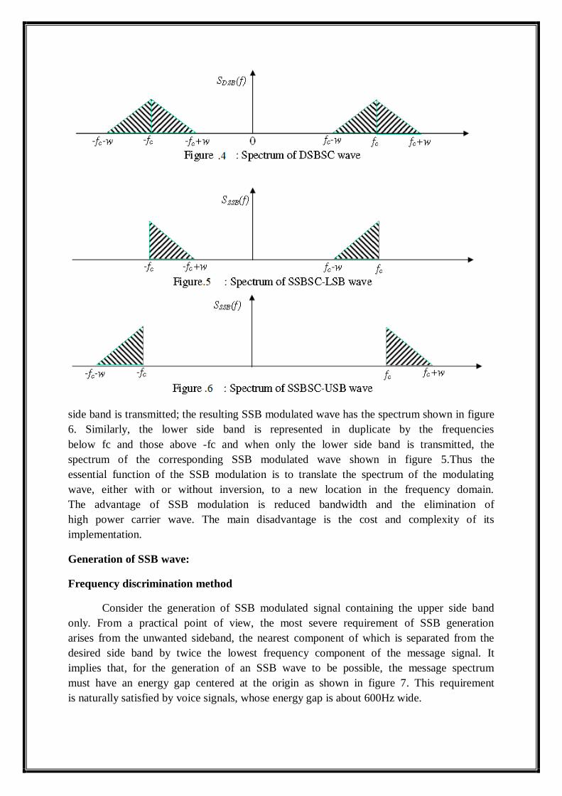
side band is transmitted; the resulting SSB modulated wave has the spectrum shown in figure
6. Similarly, the lower side band is represented in duplicate by the frequencies
below fc and those above -fc and when only the lower side band is transmitted, the
spectrum of the corresponding SSB modulated wave shown in figure 5.Thus the
essential function of the SSB modulation is to translate the spectrum of the modulating
wave, either with or without inversion, to a new location in the frequency domain.
The advantage of SSB modulation is reduced bandwidth and the elimination of
high power carrier wave. The main disadvantage is the cost and complexity of its
implementation.
Generation of SSB wave:
Frequency discrimination method
Consider the generation of SSB modulated signal containing the upper side band
only. From a practical point of view, the most severe requirement of SSB generation
arises from the unwanted sideband, the nearest component of which is separated from the
desired side band by twice the lowest frequency component of the message signal. It
implies that, for the generation of an SSB wave to be possible, the message spectrum
must have an energy gap centered at the origin as shown in figure 7. This requirement
is naturally satisfied by voice signals, whose energy gap is about 600Hz wide.

The frequency discrimination or filter method of SSB generation consists of a
product modulator, which produces DSBSC signal and a band-pass filter to extract the
desired side band and reject the other and is shown in the figure 8.
Application of this method requires that the message signal satisfies two conditions:
1. The message signal m(t) has no low-frequency content. Example: speech, audio, music.
2. The highest frequency component W of the message signal m(t) is much less than the
carrier frequency fc.
Then, under these conditions, the desired side band will appear in a non-overlapping
interval in the spectrum in such a way that it may be selected by an appropriate filter.
In designing the band pass filter, the following requirements should be satisfied:
1.The pass band of the filter occupies the same frequency range as the spectrum of the
desired SSB modulated wave.
2. The width of the guard band of the filter, separating the pass band from the stop
band, where the unwanted sideband of the filter input lies, is twice the lowest frequency
component of the message signal.
When it is necessary to generate an SSB modulated wave occupying a frequency band
that is much higher than that of the message signal, it becomes very difficult to design an
appropriate filter that will pass the desired side band and reject the other. In such a situation
it is necessary to resort to a multiple-modulation process so as to ease the filtering
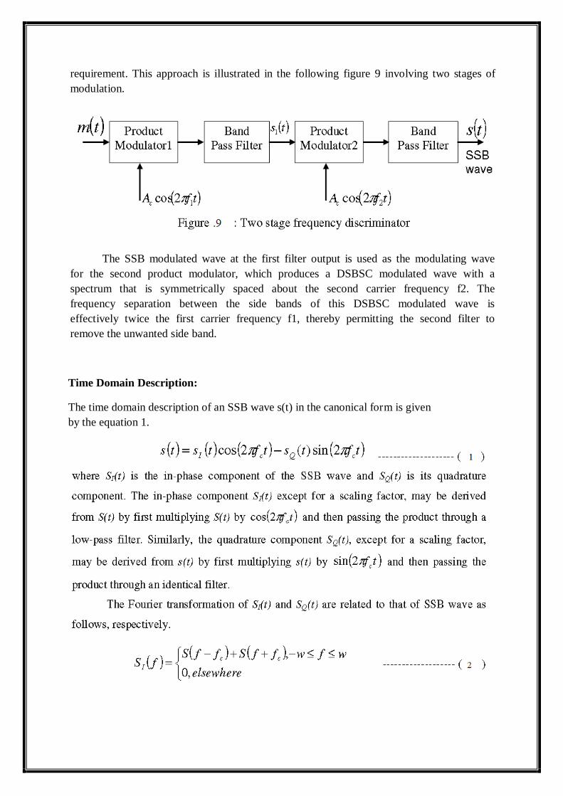
requirement. This approach is illustrated in the following figure 9 involving two stages of
modulation.
The SSB modulated wave at the first filter output is used as the modulating wave
for the second product modulator, which produces a DSBSC modulated wave with a
spectrum that is symmetrically spaced about the second carrier frequency f2. The
frequency separation between the side bands of this DSBSC modulated wave is
effectively twice the first carrier frequency f1, thereby permitting the second filter to
remove the unwanted side band.
Time Domain Description:
The time domain description of an SSB wave s(t) in the canonical form is given
by the equation 1.


Following the same procedure, we can find the canonical representation for an SSB
wave
s(t) obtained by transmitting only the lower side band is given by
Phase discrimination method for generating SSB wave:
Time domain description of SSB modulation leads to another method of SSB
generation using the equations 9 or 10. The block diagram of phase discriminator
is as shown in figure 15.

The phase discriminator consists of two product modulators I and Q, supplied
with carrier waves in-phase quadrature to each other. The incoming base band signal m(t)
is applied to product modulator I, producing a DSBSC modulated wave that contains
reference phase sidebands symmetrically spaced about carrier frequency fc.
The Hilbert transform mˆ (t) of m (t) is applied to product modulator Q, producing a
DSBSC modulated that contains side bands having identical amplitude spectra to those of
modulator I, but with phase spectra such that vector addition or subtraction of the two
modulator outputs results in cancellation of one set of side bands and reinforcement of
the other set.
The use of a plus sign at the summing junction yields an SSB wave with
only the lower side band, whereas the use of a minus sign yields an SSB wave with only
the upper side band. This modulator circuit is called Hartley modulator.
Demodulation of SSB Waves:

Introduction to Vestigial Side Band Modulation
Vestigial sideband is a type of Amplitude modulation in which one side band is
completely passed along with trace or tail or vestige of the other side band. VSB is a
compromise between SSB and DSBSC modulation. In SSB, we send only one side
band, the Bandwidth required to send SSB wave is w. SSB is not appropriate way of
modulation when the message signal contains significant components at extremely low
frequencies. To overcome this VSB is used.
Vestigial Side Band (VSB) modulation is another form of an amplitude-modulated
signal in which a part of the unwanted sideband (called as vestige, hence the name vestigial
sideband) is allowed to appear at the output of VSB transmission system.
The AM signal is passed through a sideband filter before the transmission of SSB
signal. The design of sideband filter can be simplified to a greater extent if a part of the other
sideband is also passed through it. However, in this process the bandwidth of VSB system is
slightly increased.
Generation of VSB Modulated Signal
VSB signal is generated by first generating a DSB-SC signal and then passing it
through a sideband filter which will pass the wanted sideband and a part of unwanted
sideband. Thus, VSB is so called because a vestige is added to SSB spectrum.
The below figure depicts functional block diagram of generating VSB modulated
signal
Figure: Generation of VSB Modulated Signal
A VSB-modulated signal is generated using the frequency discrimination method, in
which firstly a DSB-SC modulated signal is generated and then passed through a sideband-
suppression filter. This type of filter is a specially-designed bandpass filter that distinguishes
VSB modulation from SSB modulation.the cutoff portion of the frequency response of this
filter around the carrier frequency exhibits odd symmetry, that is, (fc-fv)≤|f|≤(fc+fv).
Accordingly the bandwidth of the VSB signal is given as
BW=(fm+fv) Hz
Where fm is the bandwidth of the modulating signal or USB, and fv is the bandwidth of
vestigial sideband (VSB)
Time domain description of VSB Signal
Mathematically, the VSB modulated signal can be described in the time-domain as
s(t)= m(t) Ac cos(2πfct) ± mQ(t) Ac sin(2πfct)
where m(t) is the modulating signal, mQ(t) is the component of m(t) obtained by passing the
message signal through a vestigial filter, Ac cos(2πfct) is the carrier signal, and Ac sin(2πfct)
is the 90o phase shift version of the carrier signal.
The ± sign in the expression corresponds to the transmission of a vestige of the upper-
sideband and lower-sideband respectively. The Quadrature component is required to partially
reduce power in one of the sidebands of the modulated wave s(t) and retain a vestige of the
other sideband as required.
Frequency domain representation of VSB Signal
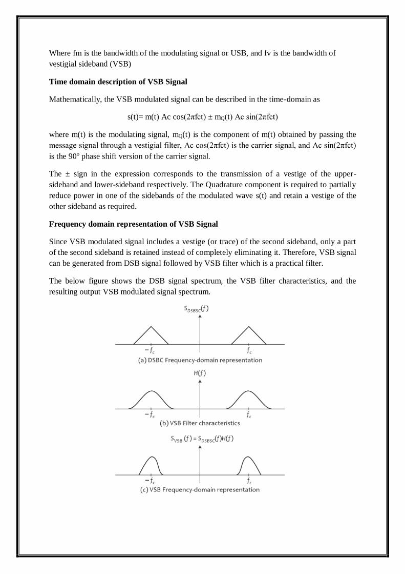
Since VSB modulated signal includes a vestige (or trace) of the second sideband, only a part
of the second sideband is retained instead of completely eliminating it. Therefore, VSB signal
can be generated from DSB signal followed by VSB filter which is a practical filter.
The below figure shows the DSB signal spectrum, the VSB filter characteristics, and the
resulting output VSB modulated signal spectrum.
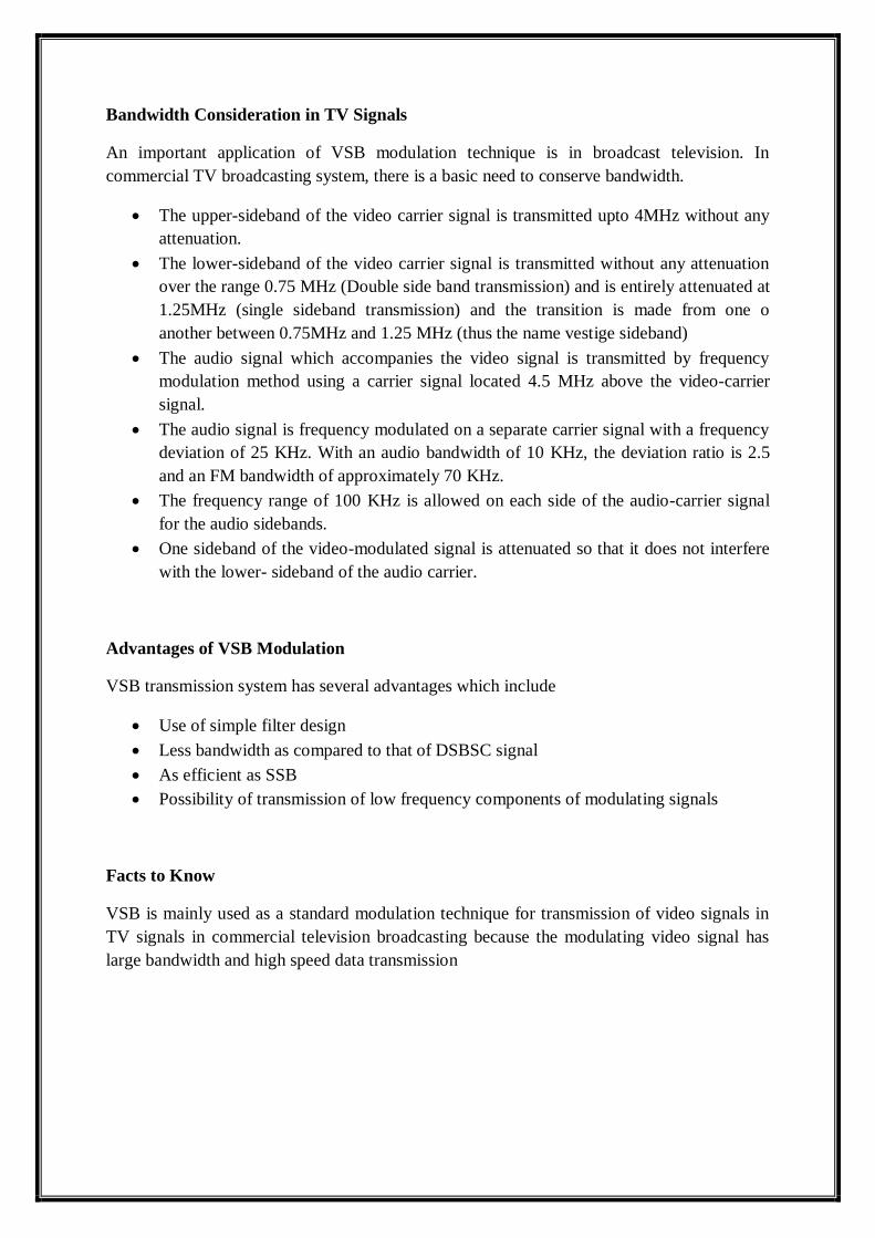
Bandwidth Consideration in TV Signals
An important application of VSB modulation technique is in broadcast television. In
commercial TV broadcasting system, there is a basic need to conserve bandwidth.
The upper-sideband of the video carrier signal is transmitted upto 4MHz without any
attenuation.
The lower-sideband of the video carrier signal is transmitted without any attenuation
over the range 0.75 MHz (Double side band transmission) and is entirely attenuated at
1.25MHz (single sideband transmission) and the transition is made from one o
another between 0.75MHz and 1.25 MHz (thus the name vestige sideband)
The audio signal which accompanies the video signal is transmitted by frequency
modulation method using a carrier signal located 4.5 MHz above the video-carrier
signal.
The audio signal is frequency modulated on a separate carrier signal with a frequency
deviation of 25 KHz. With an audio bandwidth of 10 KHz, the deviation ratio is 2.5
and an FM bandwidth of approximately 70 KHz.
The frequency range of 100 KHz is allowed on each side of the audio-carrier signal
for the audio sidebands.
One sideband of the video-modulated signal is attenuated so that it does not interfere
with the lower- sideband of the audio carrier.
Advantages of VSB Modulation
VSB transmission system has several advantages which include
Use of simple filter design
Less bandwidth as compared to that of DSBSC signal
As efficient as SSB
Possibility of transmission of low frequency components of modulating signals
Facts to Know
VSB is mainly used as a standard modulation technique for transmission of video signals in
TV signals in commercial television broadcasting because the modulating video signal has
large bandwidth and high speed data transmission
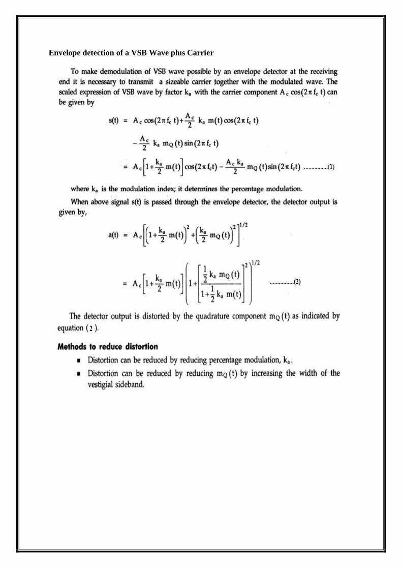
Envelope detection of a VSB Wave plus Carrier

Comparison of AM Techniques:
Applications of different AM systems:
Amplitude Modulation: AM radio, Short wave radio broadcast
DSB-SC: Data Modems, Color TV’s color signals.
SSB: Telephone
VSB: TV picture signals

UNIT-II
ANGLE MODULATION
Introduction
There are two forms of angle modulation that may be distinguished – phase modulation and
frequency modulation
Basic Definitions: Phase Modulation (PM) and Frequency Modulation (FM)
Let θi(t) denote the angle of modulated sinusoidal carrier, which is a function of the message.
The resulting angle-modulated wave is expressed as
𝒔(𝒕) = 𝑨𝒄𝒄𝒐𝒔[𝜽𝒊(𝒕)] … … … … … (𝟏)
Where Ac is the carrier amplitude. A complete oscillation occurs whenever θi(t) changes by
2π radians. If θi(t) increases monotonically with time, the average frequency in Hz, over an
interval from t to t+∆t, is given by
𝒇∆𝒕(𝒕) =𝜽𝒊(𝒕 + ∆𝒕) − 𝜽𝒊(𝒕)
𝟐𝝅∆𝒕… … … … … (𝟐)
Thus the instantaneous frequency of the angle-modulated wave s(t) is defined as
𝒇𝒊(𝒕) = 𝐥𝐢𝐦∆𝒕→𝟎
𝒇∆𝒕(𝒕)
𝒇𝒊(𝒕) = 𝐥𝐢𝐦∆𝒕→𝟎
[𝜽𝒊(𝒕 + ∆𝒕) − 𝜽𝒊(𝒕)
𝟐𝝅∆𝒕]
𝒇𝒊(𝒕) =𝟏
𝟐𝝅
𝒅𝜽𝒊(𝒕)
𝒅𝒕… … … … … . (𝟑)
Thus, according to equation (1), the angle modulated wave s(t) is interpreted as a rotating
Phasor of length Ac and angle θi(t). The angular velocity of such a Phasor is dθi(t)/dt, in
accordance with equ (3).In the simple case of an unmodulated carrier, the angle θi(t) is
𝜽𝒊(𝒕) = 𝟐𝝅𝒇𝒄𝒕 + ∅𝒄
And the corresponding Phasor rotates with a constant angular velocity equal to 2πfc.The
constant ϕc is the value of 𝜃𝑖(𝑡) at t=0.
There are an infinite number of ways in which the angle 𝜃𝑖(𝑡) may be varied in some manner
with the baseband signal.
But the 2 commonly used methods are Phase modulation and Frequency modulation.
Phase Modulation (PM) is that form of angle modulation in which the angle 𝜃𝑖(𝑡) is varied
linearly with the baseband signal m(t), as shown by

𝜽𝒊(𝒕) = 𝟐𝝅𝒇𝒄𝒕 + 𝒌𝒑𝒎(𝒕) … … … … … … . . (𝟒)
The term 𝟐𝝅𝒇𝒄𝒕 represents the angle of the unmodulated carrier, and the constant 𝒌𝒑
represents the phase sensitivity of the modulator, expressed in radians per volt.
The phase-modulated wave s(t) is thus described in time domain by
𝒔(𝒕) = 𝑨𝒄𝐜𝐨 𝐬[𝟐𝝅𝒇𝒄𝒕 + 𝒌𝒑𝒎(𝒕)] … … … … … (𝟓)
Frequency Modulation (FM) is that form of angle modulation in which the instantaneous
frequency fi(t) is varied linearly with the baseband signal m(t), as shown by
𝒇𝒊(𝒕) = 𝒇𝒄 + 𝒌𝒇𝒎(𝒕) … … … … … … . (𝟔)
The term fc represents the frequency of the unmodulated carrier, and the constant kf
represents the frequency sensitivity of the modulator, expressed in hertz per volt.
Integrating equ.(6) with respect to time and multiplying the result by 2π, we get
𝜽𝒊(𝒕) = 𝟐𝝅𝒇𝒄𝒕 + 𝟐𝝅𝒌𝒇 ∫ 𝒎(𝒕)𝒕
𝟎
𝒅𝒕 … … … … … . (𝟕)
Where, for convenience it is assumed that the angle of the unmodulated carrier wave is zero
at t=0. The frequency modulated wave is therefore described in the time domain by
𝒔(𝒕) = 𝑨𝒄 𝐜𝐨𝐬 [ 𝟐𝝅𝒇𝒄𝒕 + 𝟐𝝅𝒌𝒇 ∫ 𝒎(𝒕)𝒕
𝟎
𝒅𝒕] … … … … … … . . (𝟖)
Relationship between PM and FM
Comparing equ (5) with (8) reveals that an FM wave may be regarded as a PM wave in which
the modulating wave is ∫ 𝑚(𝑡)𝑑𝑡𝑡
0 in place of m(t).
A PM wave can be generated by first differentiating m(t) and then using the result as the
input to a frequency modulator.
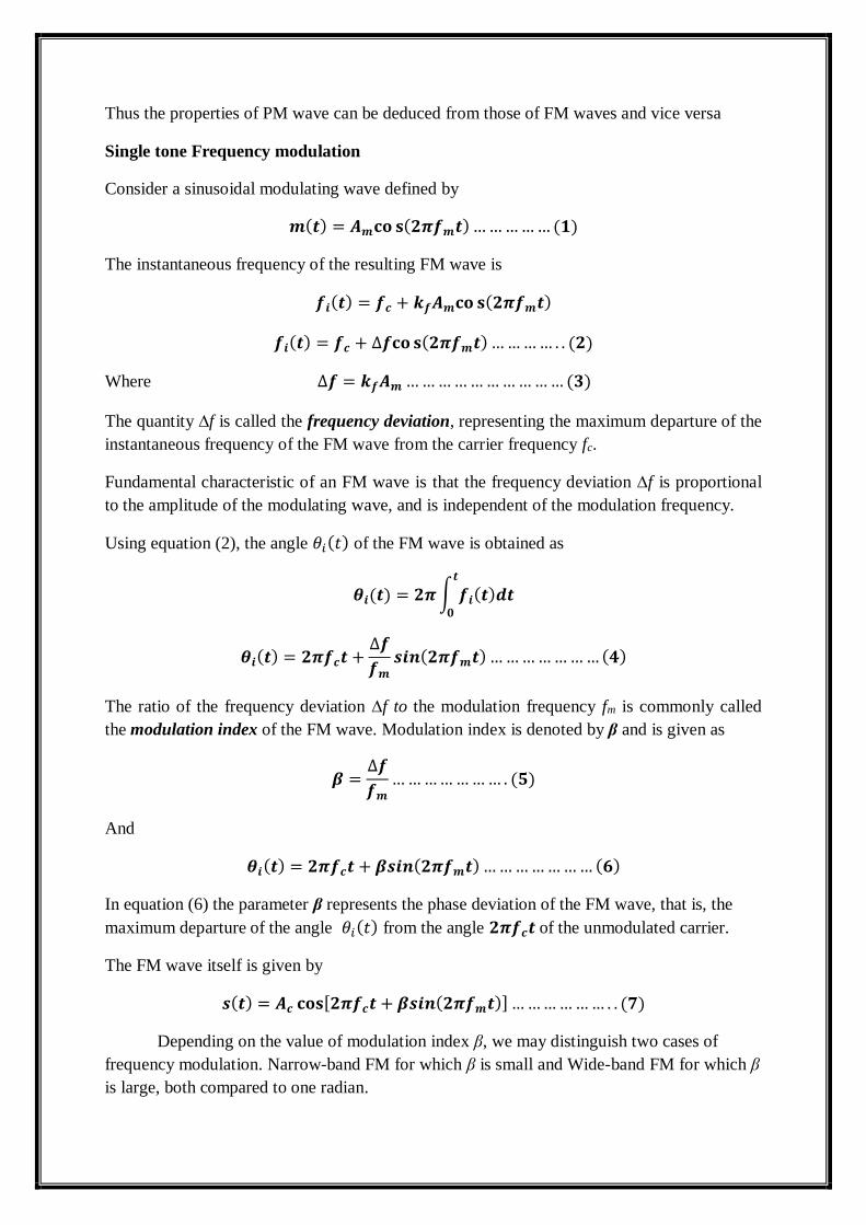
Thus the properties of PM wave can be deduced from those of FM waves and vice versa
Single tone Frequency modulation
Consider a sinusoidal modulating wave defined by
𝒎(𝒕) = 𝑨𝒎𝐜𝐨 𝐬(𝟐𝝅𝒇𝒎𝒕) … … … … … (𝟏)
The instantaneous frequency of the resulting FM wave is
𝒇𝒊(𝒕) = 𝒇𝒄 + 𝒌𝒇𝑨𝒎𝐜𝐨 𝐬(𝟐𝝅𝒇𝒎𝒕)
𝒇𝒊(𝒕) = 𝒇𝒄 + ∆𝒇𝐜𝐨 𝐬(𝟐𝝅𝒇𝒎𝒕) … … … … . . (𝟐)
Where ∆𝒇 = 𝒌𝒇𝑨𝒎 … … … … … … … … … … (𝟑)
The quantity ∆f is called the frequency deviation, representing the maximum departure of the
instantaneous frequency of the FM wave from the carrier frequency fc.
Fundamental characteristic of an FM wave is that the frequency deviation ∆f is proportional
to the amplitude of the modulating wave, and is independent of the modulation frequency.
Using equation (2), the angle 𝜃𝑖(𝑡) of the FM wave is obtained as
𝜽𝒊(𝒕) = 𝟐𝝅 ∫ 𝒇𝒊(𝒕)𝒅𝒕𝒕
𝟎
𝜽𝒊(𝒕) = 𝟐𝝅𝒇𝒄𝒕 +∆𝒇
𝒇𝒎𝒔𝒊𝒏(𝟐𝝅𝒇𝒎𝒕) … … … … … … … (𝟒)
The ratio of the frequency deviation ∆f to the modulation frequency fm is commonly called
the modulation index of the FM wave. Modulation index is denoted by β and is given as
𝜷 =∆𝒇
𝒇𝒎… … … … … … … . (𝟓)
And
𝜽𝒊(𝒕) = 𝟐𝝅𝒇𝒄𝒕 + 𝜷𝒔𝒊𝒏(𝟐𝝅𝒇𝒎𝒕) … … … … … … … (𝟔)
In equation (6) the parameter β represents the phase deviation of the FM wave, that is, the
maximum departure of the angle 𝜃𝑖(𝑡) from the angle 𝟐𝝅𝒇𝒄𝒕 of the unmodulated carrier.
The FM wave itself is given by
𝒔(𝒕) = 𝑨𝒄 𝐜𝐨𝐬[𝟐𝝅𝒇𝒄𝒕 + 𝜷𝒔𝒊𝒏(𝟐𝝅𝒇𝒎𝒕)] … … … … … … . . (𝟕)
Depending on the value of modulation index β, we may distinguish two cases of
frequency modulation. Narrow-band FM for which β is small and Wide-band FM for which β
is large, both compared to one radian.
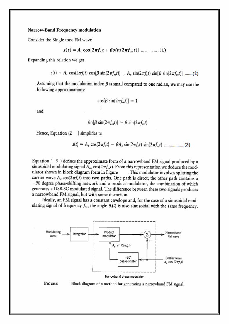
Narrow-Band Frequency modulation
Consider the Single tone FM wave
𝒔(𝒕) = 𝑨𝒄 𝐜𝐨𝐬[𝟐𝝅𝒇𝒄𝒕 + 𝜷𝒔𝒊𝒏(𝟐𝝅𝒇𝒎𝒕)] … … … … . (𝟏)
Expanding this relation we get

Wide band frequency Modulation
The spectrum of the signle-tone FM wave of equation
𝒔(𝒕) = 𝑨𝒄 𝐜𝐨𝐬[𝟐𝝅𝒇𝒄𝒕 + 𝜷𝒔𝒊𝒏(𝟐𝝅𝒇𝒎𝒕)] … … … … . (𝟏)
For an arbitrary vale of the modulation index 𝜷 is to be determined.
An FM wave produced by a sinusoidal modulating wave as in equation (1) is by itself
nonperiodic, unless the carrier frequency fc is an integral multiple of the modualtion
frequency fm. Rewriting the equation in the form
�̃�(𝑡) is periodic function of time,with a fundamental frequency equal to the modulation
frequency fm. �̃�(𝑡) in the form of complex Fourier series is as follows

The integral on the RHS of equation (7) is recognizedasthe nth order Bessel Function of the
first kind and argument 𝜷. This function is commonly denoted by the symbol Jn(𝜷), that is
Equ. (12) is the Fourier series representation of the single-tone FM wave s(t) for an arbitrary
value of 𝜷.
The discrete spectrum of s(t) is obtained by taking the Fourier transform of both sides of
equation (12); thus
In the figure below, we have plotted the Bessel function Jn(𝜷) versus the modulation index 𝜷
for different positive integer value of n.

Properties of Bessel Function
Thus using equations (13) through (16) and the curves in the above figure, following
observations are made

Spectrum Analysis of Sinusoidal FM Wave using Bessel functions

The above figure shows the Discrete amplitude spectra of an FM signal, normalized with
respect to the carrier amplitude, for the case of sinusoidal modulation of varying frequency
and fixed amplitude. Only the spectra for positive frequencies are shown.
Transmission Bandwidth of FM waves
This relation is known as Carson’s rule.

Generation of FM Signal
Direct methods for FM generation
Reactance modulator:
Indirect Method for WBFM Generation (ARMSTRONG’S Method):
Effect of frequency multiplication on a NBFM signal
Detection of FM Signal
Balanced Slope Detector
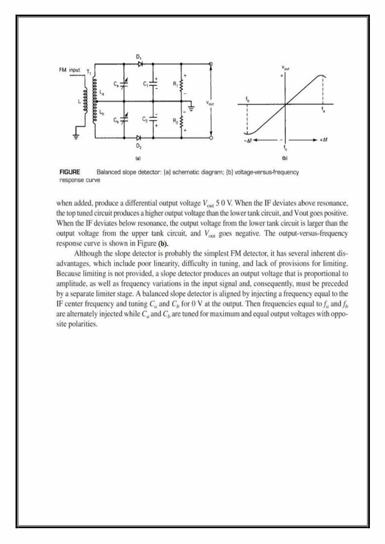
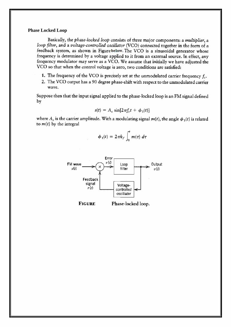
Phase Locked Loop

PRE-EMPHASIS AND DE-EMPHASIS NETWORKS
In FM, the noise increases linearly with frequency. By this, the higher frequency
components of message signal are badly affected by the noise. To solve this problem, we
can use a pre-emphasis filter of transfer function Hp(ƒ) at the transmitter to boost the higher
frequency components before modulation. Similarly, at the receiver, the de-emphasis filter
of transfer function Hd(ƒ)can be used after demodulator to attenuate the higher frequency
components thereby restoring the original message signal.
The pre-emphasis network and its frequency response are shown in Figure (a) and
(b) respectively. Similarly, the counter part for de-emphasis network is shown in Figure
below.

Figure (a) Pre-emphasis network. (b) Frequency response of pre-emphasis network.
Figure (a) De-emphasis network. (b) Frequency response of De-emphasis network.
Comparison of AM and FM
S.NO AMPLITUDE MODULATION FREQUENCY MODULATION
1. Band width is very small which is one of
the biggest advantage
It requires much wider channel (7 to 15
times) as compared to AM.
2. The amplitude of AM signal varies
depending on modulation index.
The amplitude of FM signal is constant
and independent of depth of the
modulation. 3. Area of reception is large The area of reception is small since it is
limited to line of sight.
4. Transmitters are relatively simple &
cheap.
Transmitters are complex and hence
expensive.
5. The average power in modulated wave is
greater than carrier power. This added
power is provided by modulating source.
The average power in frequency
modulated wave is same as contained in
un-modulated wave.
6. More susceptible to noise interference and
has low signal to noise ratio, it is more
difficult to eliminate effects of noise.
Noise can be easily minimized amplitude
variations can be eliminated by using
limiter.
7. It is not possible to operate without
interference.
It is possible to operate several
independent transmitters on same
frequency.
8. The maximum value of modulation index
= 1, otherwise over-modulation would
result in distortions.
No restriction is placed on modulation
index.
UNIT-III
TRANSMITTERS AND RECEIVERS
Radio Transmitters
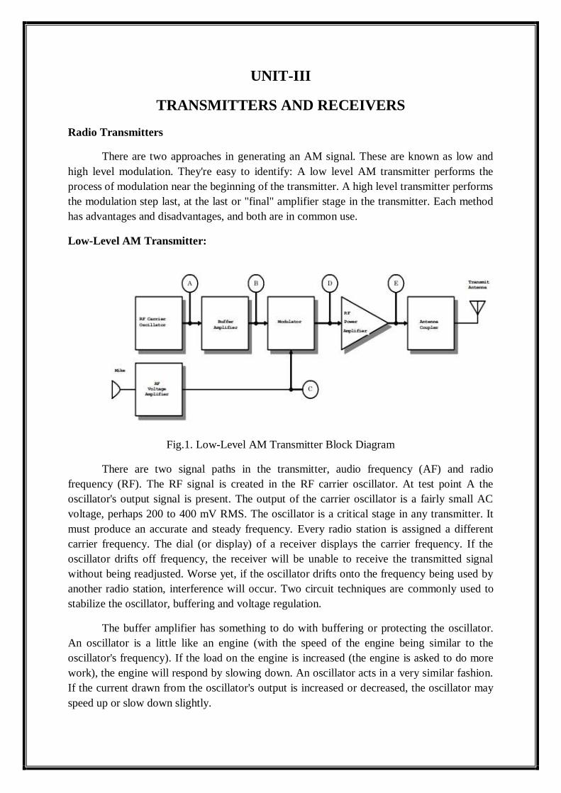
There are two approaches in generating an AM signal. These are known as low and
high level modulation. They're easy to identify: A low level AM transmitter performs the
process of modulation near the beginning of the transmitter. A high level transmitter performs
the modulation step last, at the last or "final" amplifier stage in the transmitter. Each method
has advantages and disadvantages, and both are in common use.
Low-Level AM Transmitter:
Fig.1. Low-Level AM Transmitter Block Diagram
There are two signal paths in the transmitter, audio frequency (AF) and radio
frequency (RF). The RF signal is created in the RF carrier oscillator. At test point A the
oscillator's output signal is present. The output of the carrier oscillator is a fairly small AC
voltage, perhaps 200 to 400 mV RMS. The oscillator is a critical stage in any transmitter. It
must produce an accurate and steady frequency. Every radio station is assigned a different
carrier frequency. The dial (or display) of a receiver displays the carrier frequency. If the
oscillator drifts off frequency, the receiver will be unable to receive the transmitted signal
without being readjusted. Worse yet, if the oscillator drifts onto the frequency being used by
another radio station, interference will occur. Two circuit techniques are commonly used to
stabilize the oscillator, buffering and voltage regulation.
The buffer amplifier has something to do with buffering or protecting the oscillator.
An oscillator is a little like an engine (with the speed of the engine being similar to the
oscillator's frequency). If the load on the engine is increased (the engine is asked to do more
work), the engine will respond by slowing down. An oscillator acts in a very similar fashion.
If the current drawn from the oscillator's output is increased or decreased, the oscillator may
speed up or slow down slightly.
Buffer amplifier is a relatively low-gain amplifier that follows the oscillator. It has a
constant input impedance (resistance). Therefore, it always draws the same amount of current
from the oscillator. This helps to prevent "pulling" of the oscillator frequency. The buffer
amplifier is needed because of what's happening "downstream" of the oscillator. Right after
this stage is the modulator. Because the modulator is a nonlinear amplifier, it may not have a
constant input resistance -- especially when information is passing into it. But since there is a
buffer amplifier between the oscillator and modulator, the oscillator sees a steady load
resistance, regardless of what the modulator stage is doing.
Voltage Regulation: An oscillator can also be pulled off frequency if its power
supply voltage isn't held constant. In most transmitters, the supply voltage to the oscillator is
regulated at a constant value. The regulated voltage value is often between 5 and 9 volts;
zener diodes and three-terminal regulator ICs are commonly used voltage regulators. Voltage
regulation is especially important when a transmitter is being powered by batteries or an
automobile's electrical system. As a battery discharges, its terminal voltage falls. The DC
supply voltage in a car can be anywhere between 12 and 16 volts, depending on engine RPM
and other electrical load conditions within the vehicle.
Modulator: The stabilized RF carrier signal feeds one input of the modulator stage.
The modulator is a variable-gain (nonlinear) amplifier. To work, it must have an RF carrier
signal and an AF information signal. In a low-level transmitter, the power levels are low in
the oscillator, buffer, and modulator stages; typically, the modulator output is around 10 mW
(700 mV RMS into 50 ohms) or less.
AF Voltage Amplifier: In order for the modulator to function, it needs an
information signal. A microphone is one way of developing the intelligence signal, however,
it only produces a few millivolts of signal. This simply isn't enough to operate the modulator,
so a voltage amplifier is used to boost the microphone's signal. The signal level at the output
of the AF voltage amplifier is usually at least 1 volt RMS; it is highly dependent upon the
transmitter's design. Notice that the AF amplifier in the transmitter is only providing a
voltage gain, and not necessarily a current gain for the microphone's signal. The power levels
are quite small at the output of this amplifier; a few mW at best.
RF Power Amplifier: At test point D the modulator has created an AM signal by
impressing the information signal from test point C onto the stabilized carrier signal from test
point B at the buffer amplifier output. This signal (test point D) is a complete AM signal, but
has only a few milliwatts of power. The RF power amplifier is normally built with several
stages. These stages increase both the voltage and current of the AM signal. We say that
power amplification occurs when a circuit provides a current gain. In order to accurately
amplify the tiny AM signal from the modulator, the RF power amplifier stages must be
linear. You might recall that amplifiers are divided up into "classes," according to the
conduction angle of the active device within. Class A and class B amplifiers are considered to
be linear amplifiers, so the RF power amplifier stages will normally be constructed using one
or both of these type of amplifiers. Therefore, the signal at test point E looks just like that of
test point D; it's just much bigger in voltage and current.

Antenna Coupler: The antenna coupler is usually part of the last or final RF power
amplifier, and as such, is not really a separate active stage. It performs no amplification, and
has no active devices. It performs two important jobs: Impedance matching and filtering. For
an RF power amplifier to function correctly, it must be supplied with a load resistance equal
to that for which it was designed.
The antenna coupler also acts as a low-pass filter. This filtering reduces the amplitude
of harmonic energies that may be present in the power amplifier's output. (All amplifiers
generate harmonic distortion, even "linear" ones.) For example, the transmitter may be tuned
to operate on 1000 kHz. Because of small nonlinearities in the amplifiers of the transmitter,
the transmitter will also produce harmonic energies on 2000 kHz (2nd harmonic), 3000 kHz
(3rd harmonic), and so on. Because a low-pass filter passes the fundamental frequency (1000
kHz) and rejects the harmonics, we say that harmonic attenuation has taken place.
High-Level AM Transmitter:
Fig.2. High-Level AM Transmitter Block Diagram
The high-level transmitter of Figure 9 is very similar to the low-level unit. The RF
section begins just like the low-level transmitter; there is an oscillator and buffer amplifier.
The difference in the high level transmitter is where the modulation takes place. Instead of
adding modulation immediately after buffering, this type of transmitter amplifies the
unmodulated RF carrier signal first. Thus, the signals at points A, B, and D in Figure 9 all
look like unmodulated RF carrier waves. The only difference is that they become bigger in
voltage and current as they approach test point D.
The modulation process in a high-level transmitter takes place in the last or final
power amplifier. Because of this, an additional audio amplifier section is needed. In order to
modulate an amplifier that is running at power levels of several watts (or more), comparable
power levels of information are required. Thus, an audio power amplifier is required. The
final power amplifier does double-duty in a high-level transmitter. First, it provides power
gain for the RF carrier signal, just like the RF power amplifier did in the low-level
transmitter. In addition to providing power gain, the final PA also performs the task of
modulation. The final power amplifier in a high-level transmitter usually operates in class C,
which is a highly nonlinear amplifier class.
Comparison:
Low Level Transmitters
Can produce any kind of modulation; AM, FM, or PM.
Require linear RF power amplifiers, which reduce DC efficiency and increases
production costs.
High Level Transmitters
Have better DC efficiency than low-level transmitters, and are very well suited for
battery operation.
Are restricted to generating AM modulation only.
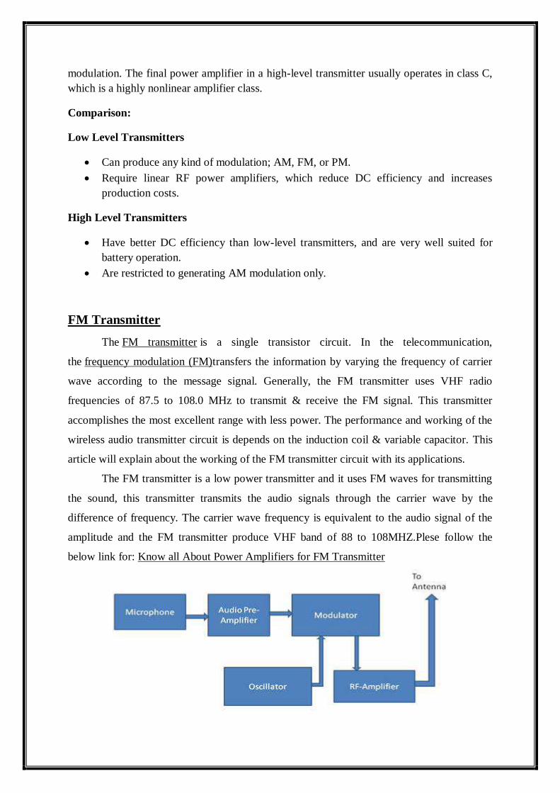
FM Transmitter
The FM transmitter is a single transistor circuit. In the telecommunication,
the frequency modulation (FM)transfers the information by varying the frequency of carrier
wave according to the message signal. Generally, the FM transmitter uses VHF radio
frequencies of 87.5 to 108.0 MHz to transmit & receive the FM signal. This transmitter
accomplishes the most excellent range with less power. The performance and working of the
wireless audio transmitter circuit is depends on the induction coil & variable capacitor. This
article will explain about the working of the FM transmitter circuit with its applications.
The FM transmitter is a low power transmitter and it uses FM waves for transmitting
the sound, this transmitter transmits the audio signals through the carrier wave by the
difference of frequency. The carrier wave frequency is equivalent to the audio signal of the
amplitude and the FM transmitter produce VHF band of 88 to 108MHZ.Plese follow the
below link for: Know all About Power Amplifiers for FM Transmitter

Working of FM Transmitter Circuit
The following circuit diagram shows the FM transmitter circuit and the required electrical and
electronic components for this circuit is the power supply of 9V, resistor, capacitor, trimmer
capacitor, inductor, mic, transmitter, and antenna. Let us consider the microphone to understand the
sound signals and inside the mic there is a presence of capacitive sensor. It produces according to the
vibration to the change of air pressure and the AC signal.
The formation of the oscillating tank circuit can be done through the transistor of 2N3904 by
using the inductor and variable capacitor. The transistor used in this circuit is an NPN
transistor used for general purpose amplification. If the current is passed at the inductor L1
and variable capacitor then the tank circuit will oscillate at the resonant carrier frequency of
the FM modulation. The negative feedback will be the capacitor C2 to the oscillating tank
circuit.
To generate the radio frequency carrier waves the FM transmitter circuit requires an
oscillator. The tank circuit is derived from the LC circuit to store the energy for oscillations.
The input audio signal from the mic penetrated to the base of the transistor, which modulates
the LC tank circuit carrier frequency in FM format. The variable capacitor is used to change
the resonant frequency for fine modification to the FM frequency band. The modulated signal
from the antenna is radiated as radio waves at the FM frequency band and the antenna is
nothing but copper wire of 20cm long and 24 gauge. In this circuit the length of the antenna
should be significant and here you can use the 25-27 inches long copper wire of the antenna.
Application of FM Transmitter
The FM transmitters are used in the homes like sound systems in halls to fill the sound
with the audio source.
These are also used in the cars and fitness centres.
The correctional facilities have used in the FM transmitters to reduce the prison noise in
common areas.
Advantages of the FM Transmitters
The FM transmitters are easy to use and the price is low
The efficiency of the transmitter is very high
It has a large operating range
This transmitter will reject the noise signal from an amplitude variation.
Receivers
Introduction to Radio Receivers:
In radio communications, a radio receiver (receiver or simply radio) is an electronic
device that receives radio waves and converts the information carried by them to a usable
form.
Types of Receivers:
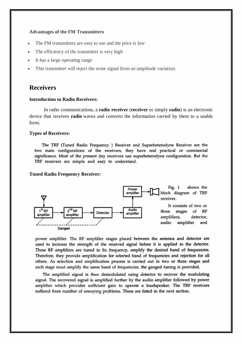
Tuned Radio Frequency Receiver:
Problems in TRF Receivers:
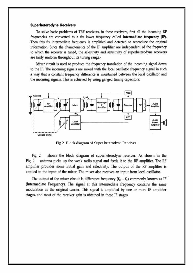
Fig.2. Block diagram of Super heterodyne Receiver.
Characteristics of Radio Receiver:
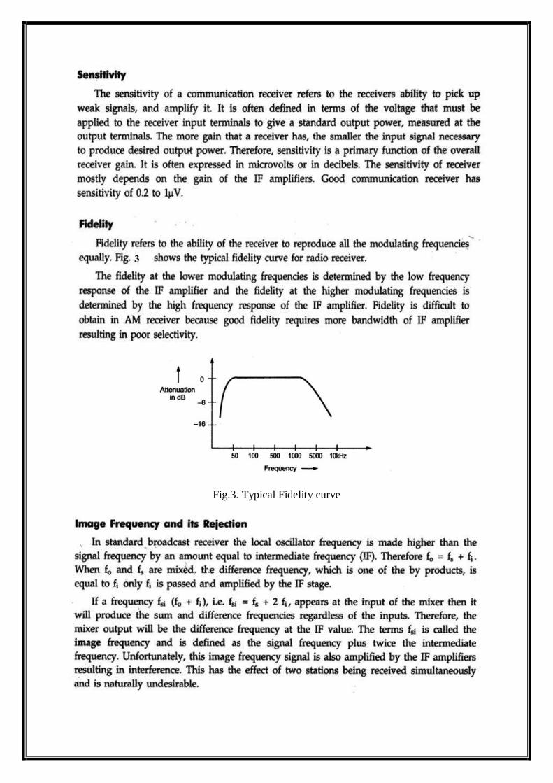
Fig.3. Typical Fidelity curve
Blocks in Super heterodyne Receiver:
Basic principle
o Mixing
o Intermediate frequency of 455 KHz
o Ganged tuning
RF section
o Tuning circuits – reject interference and reduce noise figure
o Wide band RF amplifier
Local Oscillator
o 995 KHz to 2105 KHz
o Tracking
IF amplifier
o Very narrow band width Class A amplifier – selects 455 KHz only
o Provides much of the gain
o Double tuned circuits
Detector
o RF is filtered to ground
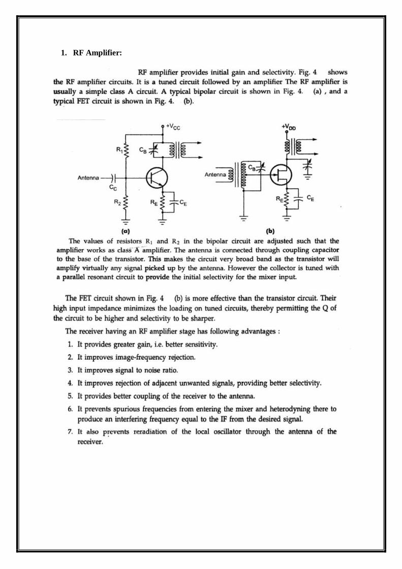
1. RF Amplifier:
2. Mixer
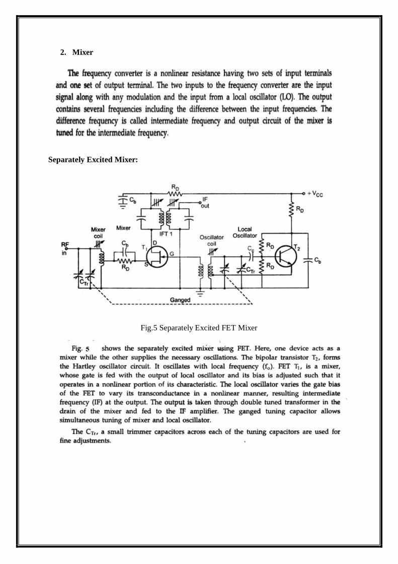
Separately Excited Mixer:
Fig.5 Separately Excited FET Mixer

Self Excited Mixer:
Fig.6. Self Excited Mixer
3. Tracking
4. Local Oscillator
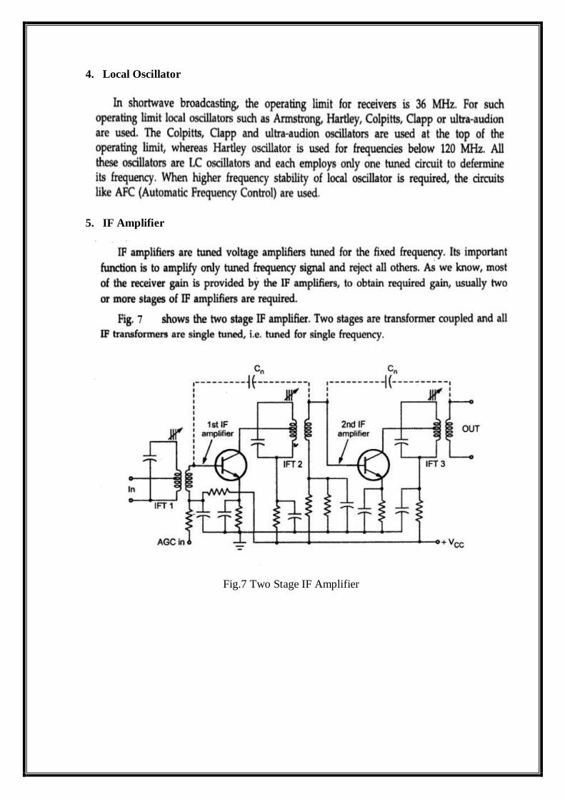
5. IF Amplifier
Fig.7 Two Stage IF Amplifier

Choice of Intermediate Frequency:
6. Automatic Gain Control
Fig.8. Simple AGC circuit

Fig.9. Delayed AGC circuit
Fig.10. Response of receiver with various AGC circuits.
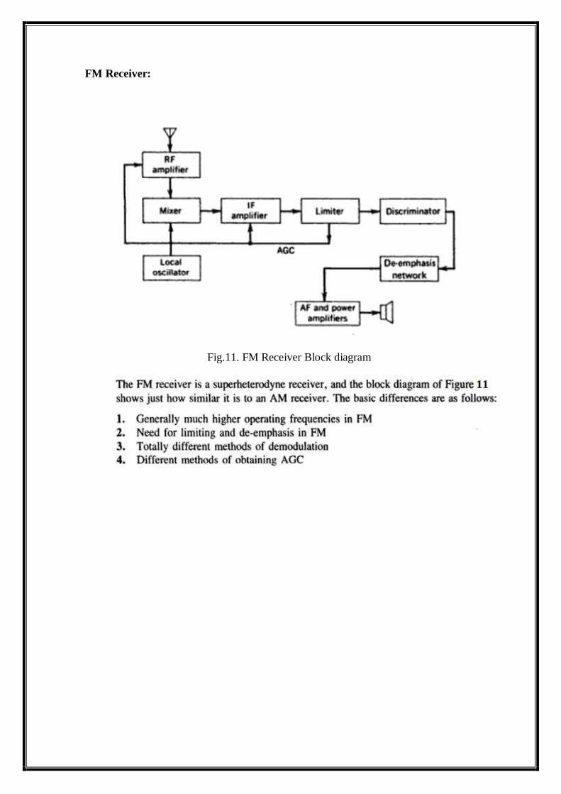
FM Receiver:
Fig.11. FM Receiver Block diagram

Comparisons with AM Receivers
Amplitude Limiter:


UNIT-IV
PULSE MODULATION
Introduction:
Pulse Modulation
Carrier is a train of pulses
Example: Pulse Amplitude Modulation (PAM), Pulse width modulation (PWM) ,
Pulse Position Modulation (PPM)
Types of Pulse Modulation:
The immediate result of sampling is a pulse-amplitude modulation (PAM) signal
PAM is an analog scheme in which the amplitude of the pulse is proportional to the
amplitude of the signal at the instant of sampling
Another analog pulse-forming technique is known as pulse-duration modulation
(PDM). This is also known as pulse-width modulation (PWM)
Pulse-position modulation is closely related to PDM
Pulse Amplitude Modulation:
In PAM, amplitude of pulses is varied in accordance with instantaneous value of
modulating signal.
PAM Generation:
The carrier is in the form of narrow pulses having frequency fc. The uniform
sampling takes place in multiplier to generate PAM signal. Samples are placed Ts sec
away from each other.

Figure PAM Modulator
The circuit is simple emitter follower.
In the absence of the clock signal, the output follows input.
The modulating signal is applied as the input signal.
Another input to the base of the transistor is the clock signal.
The frequency of the clock signal is made equal to the desired carrier pulse train
frequency.
The amplitude of the clock signal is chosen the high level is at ground level(0v) and
low level at some negative voltage sufficient to bring the transistor in cutoff region.
When clock is high, circuit operates as emitter follower and the output follows in the
input modulating signal.
When clock signal is low, transistor is cutoff and output is zero.
Thus the output is the desired PAM signal.
PAM Demodulator:
The PAM demodulator circuit which is just an envelope detector followed by a
second order op-amp low pass filter (to have good filtering characteristics) is as
shown below
Figure PAM Demodulator
Pulse Width Modulation:
In this type, the amplitude is maintained constant but the width of each pulse is varied
in accordance with instantaneous value of the analog signal.
In PWM information is contained in width variation. This is similar to FM.
In pulse width modulation (PWM), the width of each pulse is made directly
proportional to the amplitude of the information signal.
Pulse Position Modulation:
In this type, the sampled waveform has fixed amplitude and width whereas the
position of each pulse is varied as per instantaneous value of the analog signal.
PPM signal is further modification of a PWM signal.
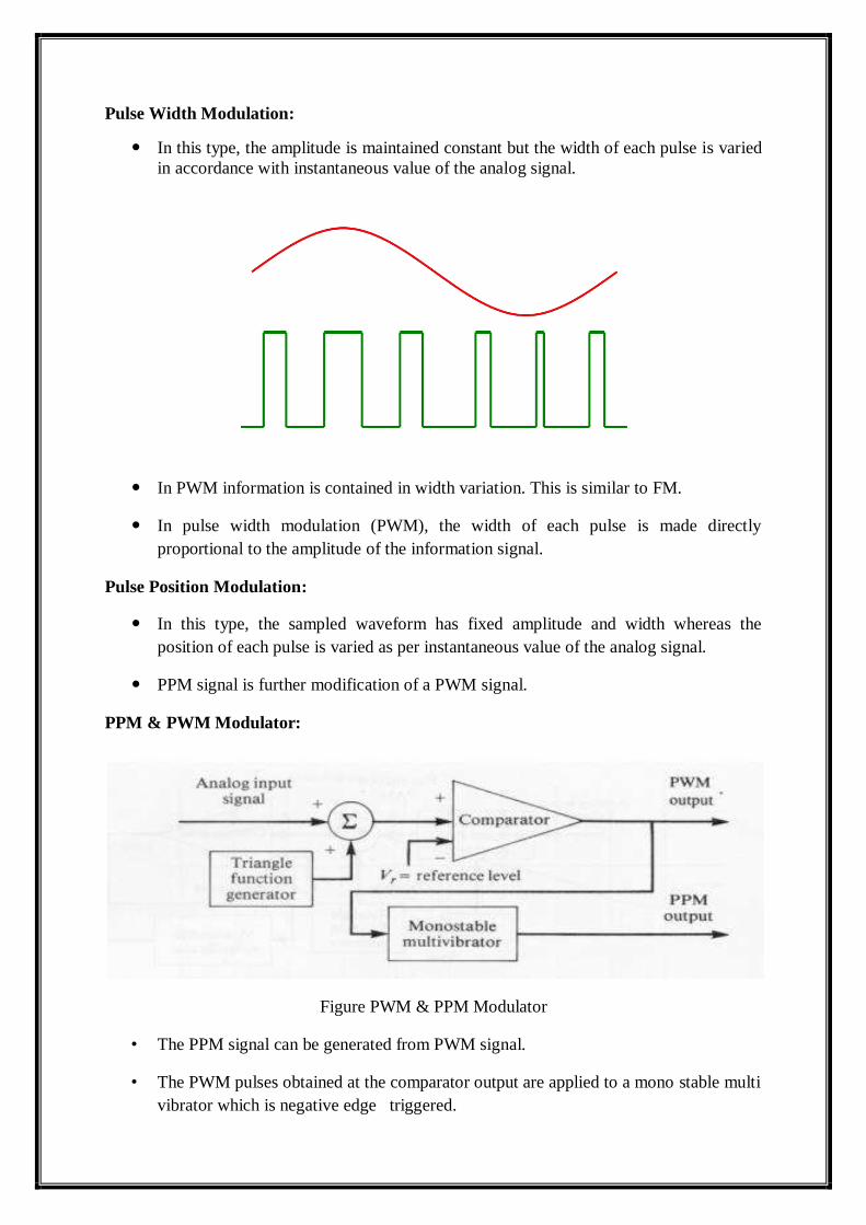
PPM & PWM Modulator:
Figure PWM & PPM Modulator
• The PPM signal can be generated from PWM signal.
• The PWM pulses obtained at the comparator output are applied to a mono stable multi
vibrator which is negative edge triggered.
• Hence for each trailing edge of PWM signal, the monostable output goes high. It
remains high for a fixed time decided by its RC components.
• Thus as the trailing edges of the PWM signal keeps shifting in proportion with the
modulating signal, the PPM pulses also keep shifting.
• Therefore all the PPM pulses have the same amplitude and width. The information is
conveyed via changing position of pulses.
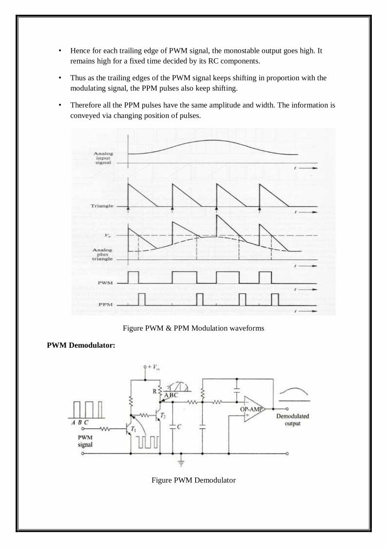
Figure PWM & PPM Modulation waveforms
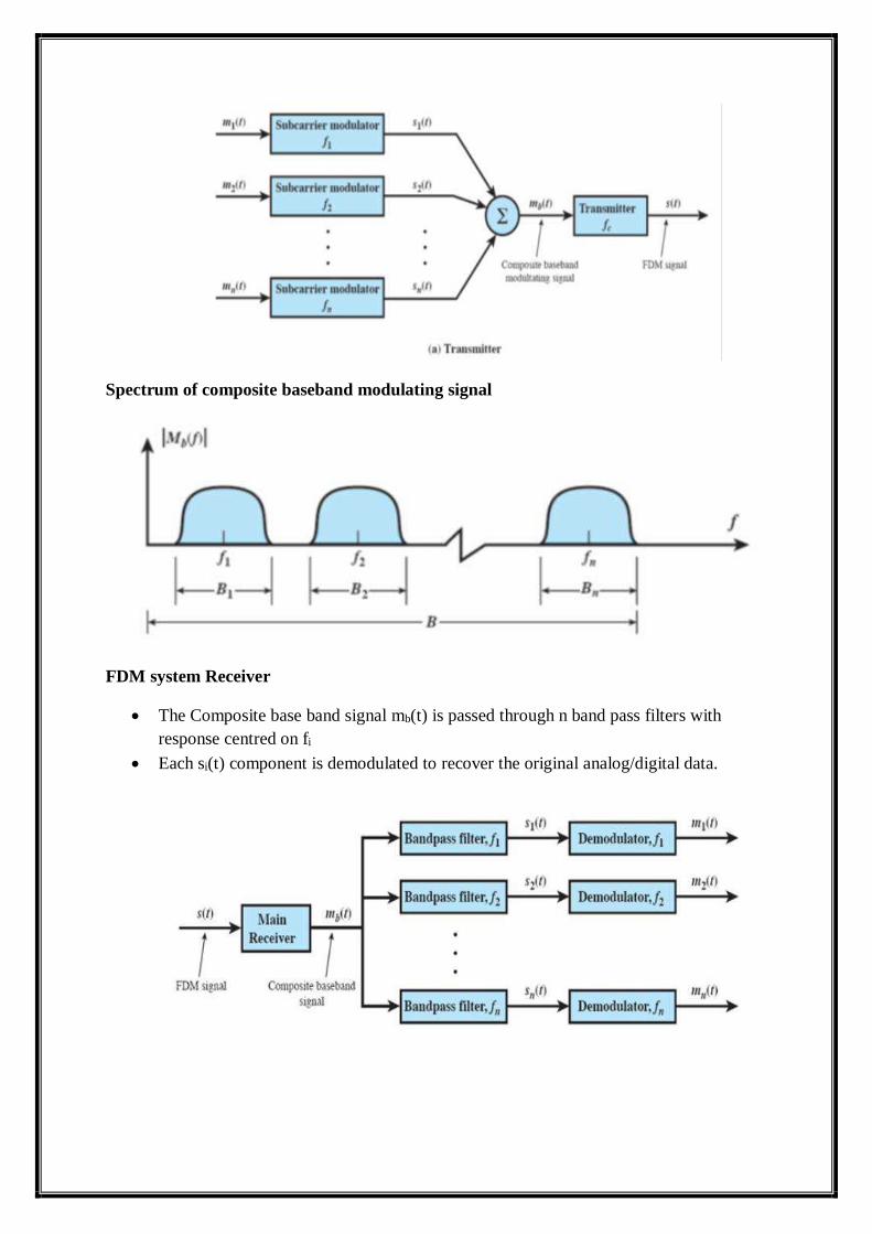
PWM Demodulator:
Figure PWM Demodulator

Transistor T1 works as an inverter.
During time interval A-B when the PWM signal is high the input to transistor T2 is
low.
Therefore, during this time interval T2 is cut-off and capacitor C is charged through
an R-C combination.
During time interval B-C when PWM signal is low, the input to transistor T2 is high,
and it gets saturated.
The capacitor C discharges rapidly through T2. The collector voltage of T2 during B-
C is low.
Thus, the waveform at the collector of T2is similar to saw-tooth waveform whose
envelope is the modulating signal.
Passing it through 2nd order op-amp Low Pass Filter, gives demodulated signal.
PPM Demodulator:
Figure PPM Demodulator
The gaps between the pulses of a PPM signal contain the information regarding the
modulating signal.
During gap A-B between the pulses the transistor is cut-off and the capacitor C gets
charged through R-C combination.
During the pulse duration B-C the capacitor discharges through transistor and the
collector voltage becomes low.
Thus, waveform across collector is saw-tooth waveform whose envelope is the
modulating signal.
Passing it through 2nd order op-amp Low Pass Filter, gives demodulated signal.

Multiplexing
Multiplexing is the set of techniques that allows the simultaneous transmission of multiple
signals across a single common communications channel.
Multiplexing is the transmission of analog or digital information from one or more sources to
one or more destination over the same transmission link.
Although transmissions occur on the same transmitting medium, they do not necessarily
occupy the same bandwidth or even occur at the same time.
Frequency Division Multiplexing
Frequency division multiplexing (FDM) is a technique of multiplexing which means
combining more than one signal over a shared medium. In FDM, signals of different
frequencies are combined for concurrent transmission.
In FDM, the total bandwidth is divided to a set of frequency bands that do not
overlap. Each of these bands is a carrier of a different signal that is generated and modulated
by one of the sending devices. The frequency bands are separated from one another by strips
of unused frequencies called the guard bands, to prevent overlapping of signals.
The modulated signals are combined together using a multiplexer (MUX) in the
sending end. The combined signal is transmitted over the communication channel, thus
allowing multiple independent data streams to be transmitted simultaneously. At the
receiving end, the individual signals are extracted from the combined signal by the process of
demultiplexing (DEMUX).
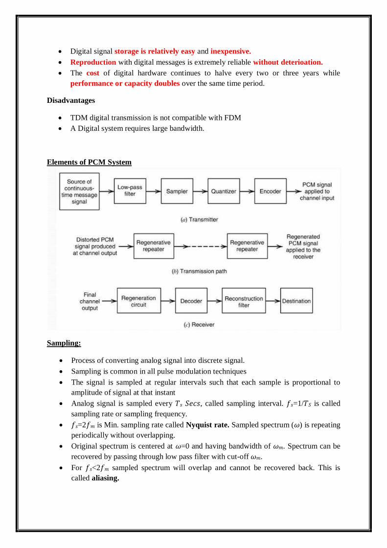
FDM system Transmitter
Analog or digital inputs: mi (t); i = 1,2,....n
Each input modulates a subcarrier of frequency fi; i=1, 2,.... n
Signals are summed to produce a composite baseband signal denoted as mb(t)
fi is chosen such that there is no overlap.
Spectrum of composite baseband modulating signal
FDM system Receiver
The Composite base band signal mb(t) is passed through n band pass filters with
response centred on fi
Each si(t) component is demodulated to recover the original analog/digital data.

Time Division Multiplexing
TDM technique combines time-domain samples from different message signals (sampled at
same rate) and transmits them together across the same channel.
The multiplexing is performed using a commutator (switch). At the receiver a decommutator
(switch) is used in synchronism with the commutator to demultiplex the data.
The input signals, all band limited to fm (max) by the LPFs are sequentially sampled at the
transmitter by a commutator.
The Switch makes one complete revolution in Ts,(1/fs) extracting one sample from each
input. Hence the output is a PAM waveform containing the individual message sampled
periodically interlaced in time.
A set of pulses consisting of one sample from each input signal is called a frame.
At the receiver the de-commutator separates the samples and distributes them to a bank of
LPFs, which in turn reconstruct the original messages.
Synchronizing is provided to keep the de-commutator in step with the commutator.

Elements of Digital Communication Systems
Figure Elements of Digital Communication Systems
1. Information Source and Input Transducer:
The source of information can be analog or digital, e.g. analog: audio or video
signal, digital: like teletype signal. In digital communication the signal produced by
this source is converted into digital signal which consists of 1′s and 0′s. For this we
need a source encoder.
2. Source Encoder:
In digital communication we convert the signal from source into digital signal
as mentioned above. The point to remember is we should like to use as few binary
digits as possible to represent the signal. In such a way this efficient representation of
the source output results in little or no redundancy. This sequence of binary digits is
called information sequence.
Source Encoding or Data Compression: the process of efficiently converting
the output of whether analog or digital source into a sequence of binary digits is
known as source encoding.
3. Channel Encoder:
The information sequence is passed through the channel encoder. The purpose
of the channel encoder is to introduce, in controlled manner, some redundancy in the
binary information sequence that can be used at the receiver to overcome the effects
of noise and interference encountered in the transmission on the signal through the
channel.
For example take k bits of the information sequence and map that k bits to
unique n bit sequence called code word. The amount of redundancy introduced is

measured by the ratio n/k and the reciprocal of this ratio (k/n) is known as rate of code
or code rate.
4. Digital Modulator:
The binary sequence is passed to digital modulator which in turns convert the
sequence into electric signals so that we can transmit them on channel (we will see
channel later). The digital modulator maps the binary sequences into signal wave
forms , for example if we represent 1 by sin x and 0 by cos x then we will transmit sin
x for 1 and cos x for 0. ( a case similar to BPSK)
5. Channel:
The communication channel is the physical medium that is used for
transmitting signals from transmitter to receiver. In wireless system, this channel
consists of atmosphere , for traditional telephony, this channel is wired , there are
optical channels, under water acoustic channels etc.We further discriminate this
channels on the basis of their property and characteristics, like AWGN channel etc.
6. Digital Demodulator:
The digital demodulator processes the channel corrupted transmitted
waveform and reduces the waveform to the sequence of numbers that represents
estimates of the transmitted data symbols.
7. Channel Decoder:
This sequence of numbers then passed through the channel decoder which
attempts to reconstruct the original information sequence from the knowledge of the
code used by the channel encoder and the redundancy contained in the received data
Note: The average probability of a bit error at the output of the decoder is a
measure of the performance of the demodulator – decoder combination.
8. Source Decoder:
At the end, if an analog signal is desired then source decoder tries to decode
the sequence from the knowledge of the encoding algorithm. And which results in the
approximate replica of the input at the transmitter end.
9. Output Transducer:
Finally we get the desired signal in desired format analog or digital.
Advantages of digital communication
Can withstand channel noise and distortion much better as long as the noise and the
distortion are within limits.
Regenerative repeaters prevent accumulation of noise along the path.
Digital hardware implementation is flexible.
Digital signals can be coded to yield extremely low error rates, high fidelity and
well as privacy.
Digital communication is inherently more efficient than analog in realizing the
exchange of SNR for bandwidth.
It is easier and more efficient to multiplex several digital signals.
Digital signal storage is relatively easy and inexpensive.
Reproduction with digital messages is extremely reliable without deterioation.
The cost of digital hardware continues to halve every two or three years while
performance or capacity doubles over the same time period.
Disadvantages
TDM digital transmission is not compatible with FDM
A Digital system requires large bandwidth.
Elements of PCM System
Sampling:
Process of converting analog signal into discrete signal.
Sampling is common in all pulse modulation techniques
The signal is sampled at regular intervals such that each sample is proportional to
amplitude of signal at that instant
Analog signal is sampled every 𝑇𝑠 𝑆𝑒𝑐𝑠, called sampling interval. 𝑓𝑠=1/𝑇𝑆 is called
sampling rate or sampling frequency.
𝑓𝑠=2𝑓𝑚 is Min. sampling rate called Nyquist rate. Sampled spectrum (𝜔) is repeating
periodically without overlapping.
Original spectrum is centered at 𝜔=0 and having bandwidth of 𝜔𝑚. Spectrum can be
recovered by passing through low pass filter with cut-off 𝜔𝑚.
For 𝑓𝑠<2𝑓𝑚 sampled spectrum will overlap and cannot be recovered back. This is
called aliasing.

Sampling methods:
Ideal – An impulse at each sampling instant.
Natural – A pulse of Short width with varying amplitude.
Flat Top – Uses sample and hold, like natural but with single amplitude value.
Fig. 4 Types of Sampling
Sampling of band-pass Signals:
A band-pass signal of bandwidth 2fm can be completely recovered from its samples.
Min. sampling rate =2×𝐵𝑎𝑛𝑑𝑤𝑖𝑑𝑡ℎ
=2×2𝑓𝑚=4𝑓𝑚
Range of minimum sampling frequencies is in the range of 2×𝐵𝑊 𝑡𝑜 4×𝐵𝑊
Instantaneous Sampling or Impulse Sampling:
Sampling function is train of spectrum remains constant impulses throughout
frequency range. It is not practical.
Natural sampling:
The spectrum is weighted by a sinc function.
Amplitude of high frequency components reduces.
Flat top sampling:
Here top of the samples remains constant.
In the spectrum high frequency components are attenuated due sinc pulse roll off.
This is known as Aperture effect.
If pulse width increases aperture effect is more i.e. more attenuation of high frequency
components.

PCM Generator

Transmission BW in PCM

PCM Receiver
Quantization
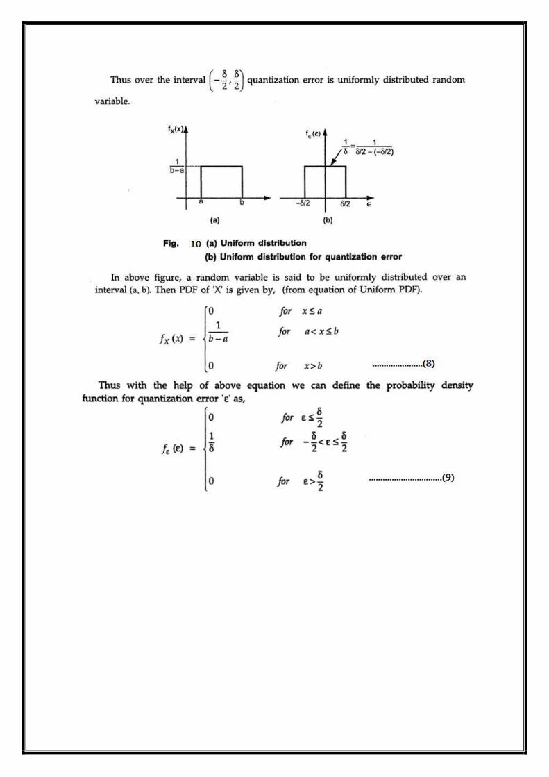
The quantizing of an analog signal is done by discretizing the signal with a number of
quantization levels.
Quantization is representing the sampled values of the amplitude by a finite set of
levels, which means converting a continuous-amplitude sample into a discrete-time
signal
Both sampling and quantization result in the loss of information.
The quality of a Quantizer output depends upon the number of quantization levels
used.
The discrete amplitudes of the quantized output are called as representation levels or
reconstruction levels.
The spacing between the two adjacent representation levels is called a quantum or
step-size.
There are two types of Quantization
o Uniform Quantization
o Non-uniform Quantization.
The type of quantization in which the quantization levels are uniformly spaced is
termed as a Uniform Quantization.
The type of quantization in which the quantization levels are unequal and mostly the
relation between them is logarithmic, is termed as a Non-uniform Quantization.
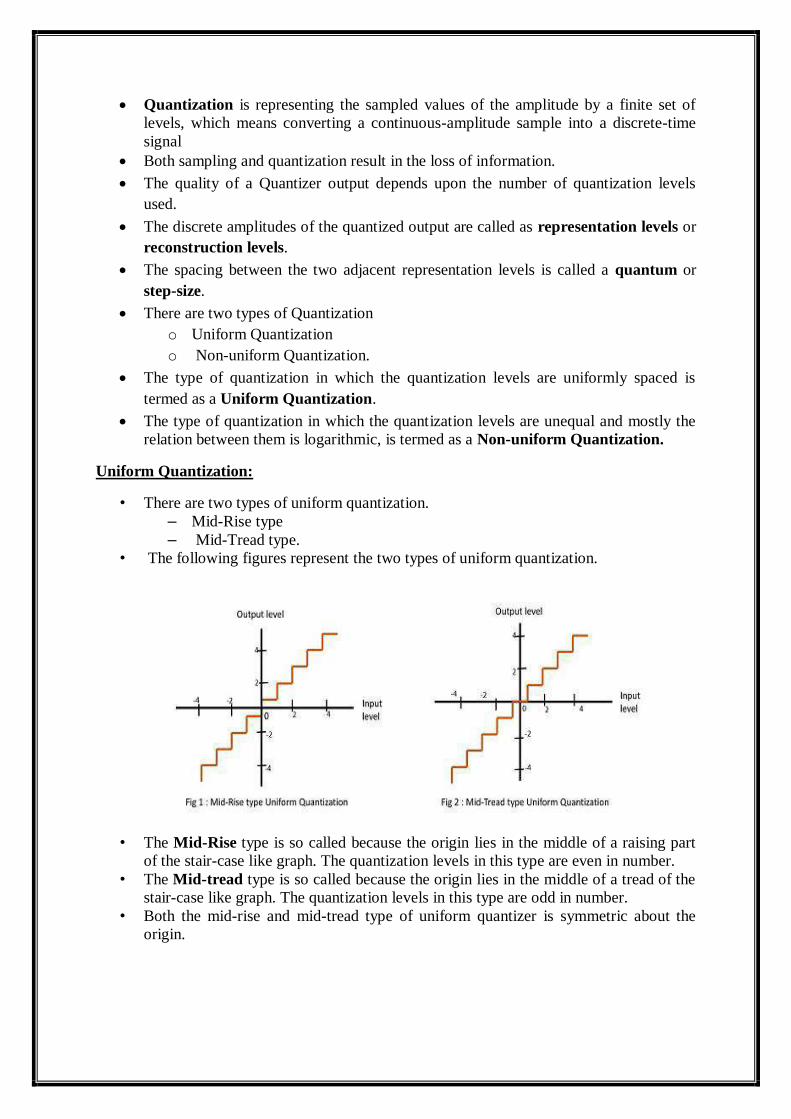
Uniform Quantization:
• There are two types of uniform quantization.
– Mid-Rise type
– Mid-Tread type.
• The following figures represent the two types of uniform quantization.
• The Mid-Rise type is so called because the origin lies in the middle of a raising part
of the stair-case like graph. The quantization levels in this type are even in number.
• The Mid-tread type is so called because the origin lies in the middle of a tread of the
stair-case like graph. The quantization levels in this type are odd in number.
• Both the mid-rise and mid-tread type of uniform quantizer is symmetric about the
origin.

Quantization Noise and Signal to Noise ratio in PCM System

Derivation of Maximum Signal to Quantization Noise Ratio for Linear Quantization:

Non-Uniform Quantization:
In non-uniform quantization, the step size is not fixed. It varies according to certain
law or as per input signal amplitude. The following fig shows the characteristics of Non
uniform quantizer.
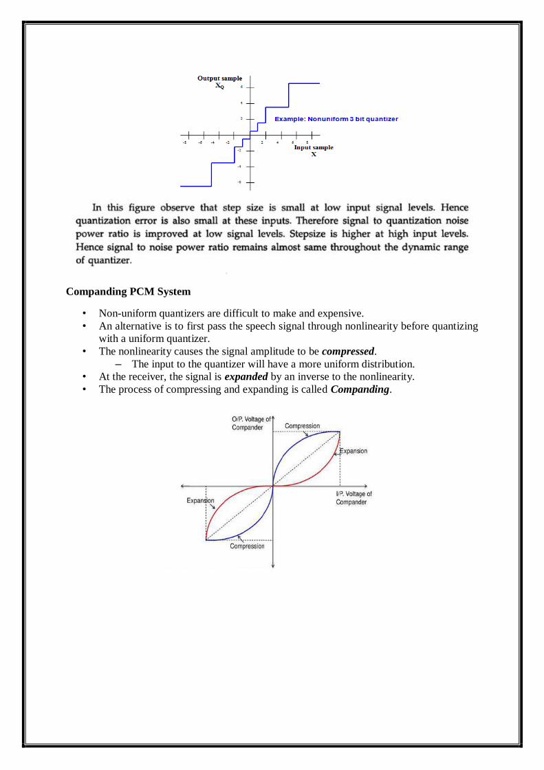
Companding PCM System
• Non-uniform quantizers are difficult to make and expensive.
• An alternative is to first pass the speech signal through nonlinearity before quantizing
with a uniform quantizer.
• The nonlinearity causes the signal amplitude to be compressed.
– The input to the quantizer will have a more uniform distribution.
• At the receiver, the signal is expanded by an inverse to the nonlinearity.
• The process of compressing and expanding is called Companding.


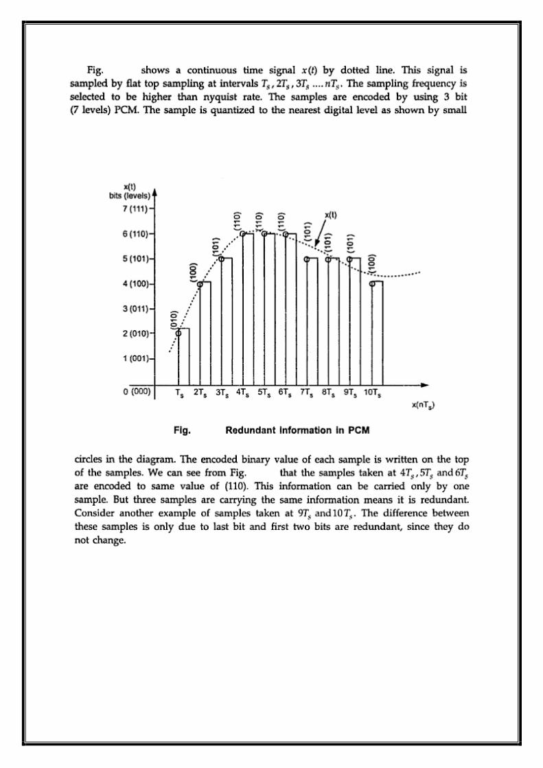
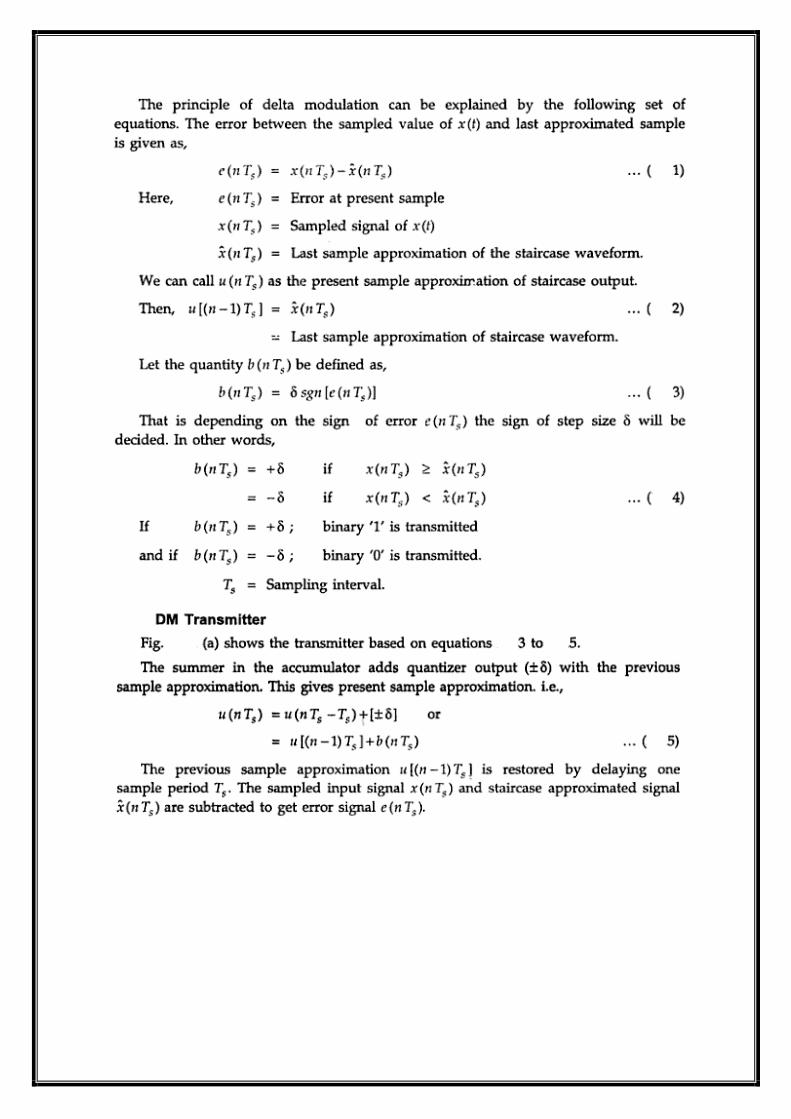
Differential Pulse Code Modulation (DPCM)
Redundant Information in PCM


Introduction to Delta Modulation
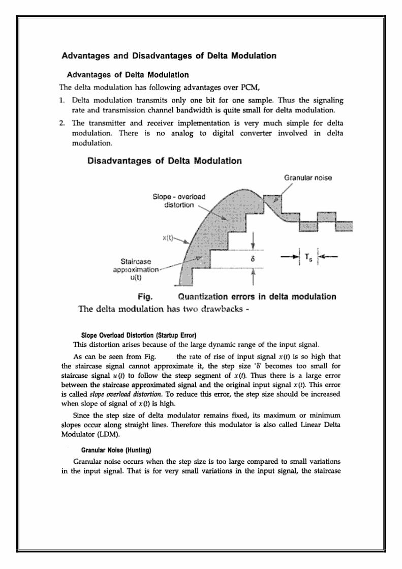


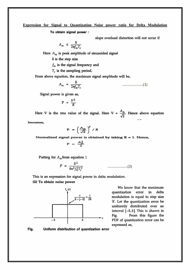
Condition for Slope overload distortion occurrence
Slope overload distortion will occur if
Expression for Signal to Quantization Noise power ratio for Delta Modulation


UNIT-V
DIGITAL MODULATION TECHNIQUES
Introduction
There are basically two types of transmission of Digital Signals
Baseband data transmission
The digital data is transmitted over the channel directly. There is no carrier or
any modulation. Suitable for transmission over short distances.
Pass band data transmission
The digital data modulates high frequency sinusoidal carrier. Suitable for
transmission over longer distances.
Types of Pass band Modulation
The digital data can modulate phase, frequency or amplitude of carrier. This gives rise
to three basic techniques:
Phase Shift Keying (PSK): The digital data modulates the phase of the carrier.
Frequency Shift Keying(FSK): The digital data modulates the frequency of the
carrier.
Amplitude Shift Keying (ASK): The digital modulates the amplitude of the carrier.
Digital Modulation Techniques

Types of Reception for Pass band Transmission
Two Types of methods for detection of pass band signals
Coherent (Synchronous) Detection: The local carrier generated at the receiver is
phase locked with the carrier at the transmitter. Hence called Synchronous Detection.
Non Coherent (Envelope) Detection: The receiver carrier need not be phase locked
with the transmitter carrier. It is called Envelope detection. It is simple but it has
higher probability of error.
Requirements of Pass band Transmission Scheme
Maximum Data transmission rate
Minimum Probability of symbol error
Minimum Transmitted power
Minimum Channel Bandwidth
Maximum resistance to interfering signals
Minimum circuit complexity
Advantages of Pass band Transmission over Baseband transmission
Long Distance Transmission
Analog Channels, can be used for Transmission
Multiplexing techniques can be used for BW conservation.
Problems such as ISI and crosstalk are absent
Pass band transmission can take place over wireless channels also.
Introduction
In digital modulation, an analog carrier signal is modulated by a discrete signal.
Digital modulation can be considered as digital-to-analog and the corresponding
demodulation is considered as analog-to-digital conversion.
In Digital communications, the modulating wave consists of binary data and the
carrier is sinusoidal wave.

Amplitude Shift Keying (On-Off Keying)
In this there is only one unit energy carrier and it is switched on or off depending
upon the Binary sequence.
ASK waveform may be represented as
Signal s(t) contains some complete cycles of carrier frequency (fc).
Hence the ASK waveform looks like an On-Off of the signal. Therefore it is also
known as the On-Off Keying(OOK)
Generation of ASK Signal
ASK signal may be generated by simply applying the incoming binary data and the
sinusoidal carrier to the 2 inputs of a product modulator.
The resulting output will be the ASK waveform.
Modulation causes the shift of the baseband signal spectrum.
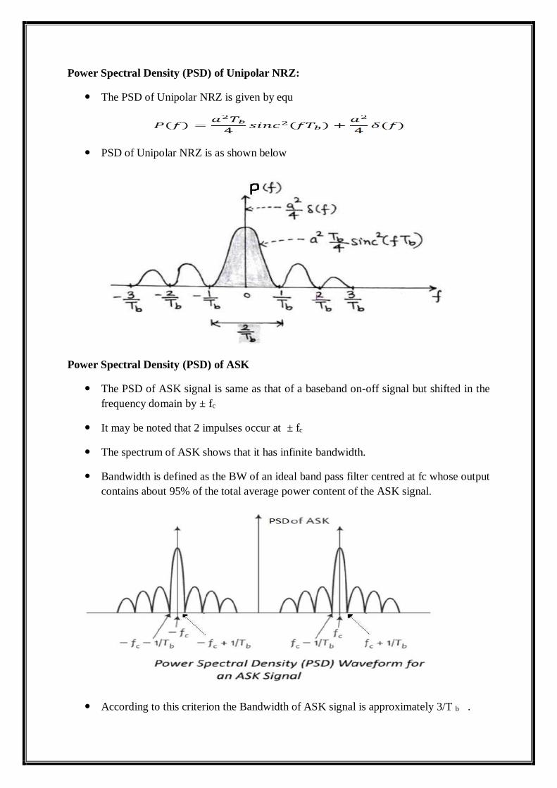
Power Spectral Density (PSD) of Unipolar NRZ:
The PSD of Unipolar NRZ is given by equ
PSD of Unipolar NRZ is as shown below
Power Spectral Density (PSD) of ASK
The PSD of ASK signal is same as that of a baseband on-off signal but shifted in the
frequency domain by ± fc
It may be noted that 2 impulses occur at ± fc
The spectrum of ASK shows that it has infinite bandwidth.
Bandwidth is defined as the BW of an ideal band pass filter centred at fc whose output
contains about 95% of the total average power content of the ASK signal.
According to this criterion the Bandwidth of ASK signal is approximately 3/T b .
Demodulation of ASK
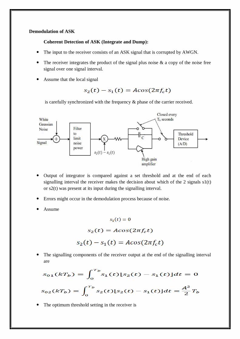
Coherent Detection of ASK (Integrate and Dump):
The input to the receiver consists of an ASK signal that is corrupted by AWGN.
The receiver integrates the product of the signal plus noise & a copy of the noise free
signal over one signal interval.
Assume that the local signal
is carefully synchronized with the frequency & phase of the carrier received.
Output of integrator is compared against a set threshold and at the end of each
signalling interval the receiver makes the decision about which of the 2 signals s1(t)
or s2(t) was present at its input during the signalling interval.
Errors might occur in the demodulation process because of noise.
Assume
The signalling components of the receiver output at the end of the signalling interval
are
The optimum threshold setting in the receiver is
The receiver decodes the kth transmitted bit as 1 if the output at the kth signalling
interval is greater than Vth , as a ‘0’ otherwise.
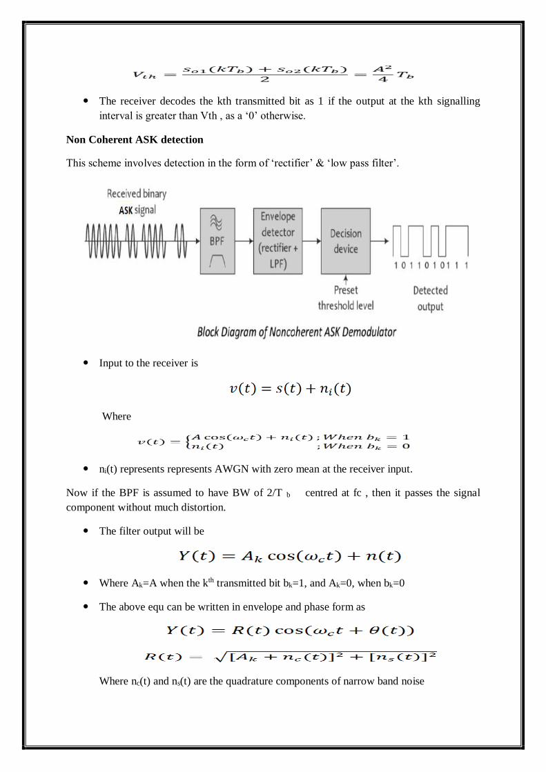
Non Coherent ASK detection
This scheme involves detection in the form of ‘rectifier’ & ‘low pass filter’.
Input to the receiver is
Where
ni(t) represents represents AWGN with zero mean at the receiver input.
Now if the BPF is assumed to have BW of 2/T b centred at fc , then it passes the signal
component without much distortion.
The filter output will be
Where Ak=A when the kth transmitted bit bk=1, and Ak=0, when bk=0
The above equ can be written in envelope and phase form as
Where nc(t) and ns(t) are the quadrature components of narrow band noise
Advantages and Disadvantages of ASK
Advantages
Simple to design, easy to generate and detect.
Requires low Bandwidth
Requires less energy to transmit the binary data.
Disadvantages
Susceptible to sudden amplitude variations due to noise and interference.
Applications of ASK
Mostly used for very low-speed data rate (upto 1200bps) requirements on voice grade
lines in telemetry applications.
Used to transmit digital data over optical fibre for LED –based optical transmitters.
Wireless infrared transmissions using a directed beam or diffuse light in wireless
LANs applications.
Frequency Shift Keying
In Binary FSK, the frequency of the carrier is shifted according to the binary symbol.
Phase unaffected.
That is there are 2 different frequency signals according to binary symbols.
Let there be a frequency shift by Ω.
If b(t)=1, then
b(t)=0, then
Hence there is increase or decrease in frequency by Ω.
Conversion table for BFSK representation

FSK equ can be written as
Hence if symbol ‘1’ is to be transmitted then the carrier frequency will be
If the symbol ‘0’ is to be transmitted then the carrier frequency will be
Thus
Generation of BFSK
PH(t) is same as b(t) and PL(t) is inverted version of b(t)
PH(t) and PL(t) are Unipolar signals.
The level shifter converts ‘+1’ to √𝑃𝑠𝑇𝑏 and the zero level is unaffected.
Further there are product modulators after the level shifters.
The two carrier signals φ1(t) or φ2(t) are used which are orthogonal to each other. fH-
fL=2fb
The adder then adds the 2 signals coming from the multipliers, but outputs from the
multipliers are not possible at the same time. This is because PH(t) and PL(t) are
complementary to each other.
PSD of BFSK Signal
BFSK signal s(t) can be written as
Let us convert those coefficients in bipolar form as follows
Here 𝑃𝐻′ (𝑡) and 𝑃𝐿
′ (𝑡) will be bipolar, alternating between +1 and -1, and
complementary.
Now s(t) can be written as
The below equation is used to find the PSD of BFSK Signal

PSD and BW of BFSK Signal
Coherent Detection of BFSK Signal
The incoming FSK signal is multiplied by a recovered carrier signal that has the exact
same frequency and phase as the transmitter reference. However, the two transmitted
frequencies (the mark and space frequencies) are not generally continuous; it is not practical
to reproduce a local reference that is coherent with both of them. Consequently, coherent
FSK detection is seldom used.
Non-coherent Detection of BFSK Signal
The FSK input signal is simultaneously applied to the inputs of both band pass filters
(BPFs) through a power splitter. The respective filter passes only the mark or only the space
frequency on to its respective envelope detector. The envelope detectors, in turn, indicate the
total power in each pass band, and the comparator responds to the larger of the two powers.
This type of FSK detection is referred to as non coherent detection.

Detection of BFSK signal using PLL
Advantages and Disadvantages of FSK
Advantages
It is less susceptible to errors than ASK.
Better noise immunity than ASK.
Peak frequency offset is constant and always at its maximum.
The highest fundamental frequency is equal to half the information bit rate.
Relatively easy to implement.
Disadvantages
Not efficient in terms of transmission bandwidth requirement
It has poorer error performance than PSK or QAM.
Applications of FSK
Used in low-speed modems (up to 1200bps) over analog voice-band telephone lines.
Finds applications in pager systems, HF radio tele-type transmission systems, and
LANs using coaxial cables.
Binary Phase Shift Keying
Principle of BPSK
In BPSK the binary symbol ‘1’ and ‘0’ modulate the phase of the carrier.
Let the carrier be
‘A’ represents peak of the sinusoidal carrier
When the symbol is changed, then phase of the carrier is changed by 180o
Consider, for symbol ‘1’
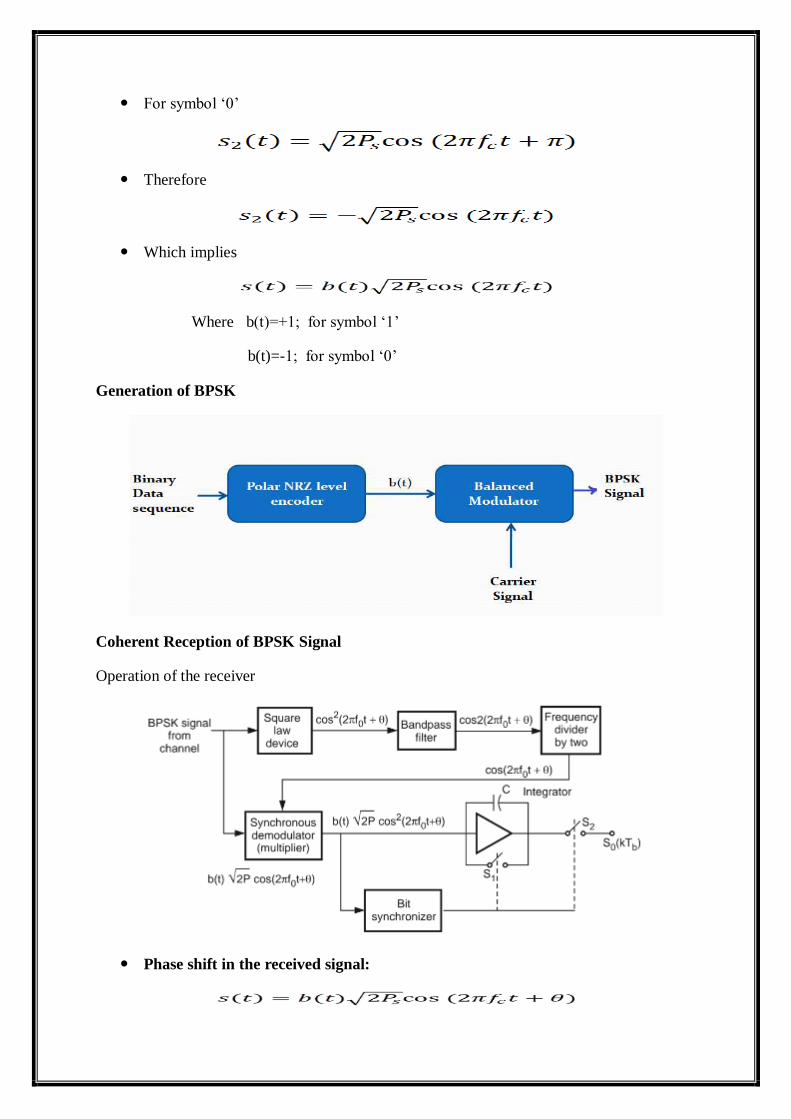
For symbol ‘0’
Therefore
Which implies
Where b(t)=+1; for symbol ‘1’
b(t)=-1; for symbol ‘0’
Generation of BPSK
Coherent Reception of BPSK Signal
Operation of the receiver
Phase shift in the received signal:

The signal undergoes the phase change depending upon the time delay from
transmitter to receiver. Let the phase shift be
Square Law device:
From the received signal carrier is separated. Since it is coherent detection.
The output of square law device
Band Pass Filter:
The signal is passed through band pass filter with centre frequency 2fc.
BPF removes DC level and its output is
Frequency Divider:
The signal is passed through a frequency divider by 2.
Therefore at the output of the frequency divider we get the carrier signal
whose frequency is fc i.e.,
Synchronous Demodulator:
The synchronous demodulator multiplies the input signal & the recovered
carrier.
Therefore at the output of multiplier we get
Bit synchronizer and integrator:
The above signal is applied to the bit synchronizer & integrator.
The integrator integrates the signal over one bit period. The bit synchronizer
takes care of starting and end times of a bit.
At the end of the bit duration the bit synchronizer closes switch s2 temporarily
connecting the output of integrator to the decision device.
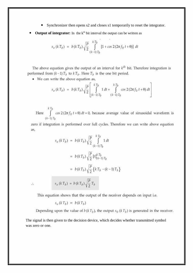
Synchronizer then opens s2 and closes s1 temporarily to reset the integrator.
Output of integrator: In the kth bit interval the output can be written as
The signal is then given to the decision device, which decides whether transmitted symbol
was zero or one.

PSD of BPSK
PSD of polar NRZ baseband signal b(t)=+1 or -1
Power spectral density of BPSK signal
Inter channel interference and ISI
Inter channel interference avoided by filtering.
Because of filtering phase distortion takes place resulting in ISI.
ISI can be reduced to some extent by using equalizers at the receiver.
Equalizers have reverse effect to the filters adverse effects.
Differential Phase Shift Keying
DPSK is an alternative form of digital modulation where the binary input information
is contained in the difference between two successive signalling elements rather than
the absolute phase.
With DPSK, it is not necessary to recover a phase coherent carrier.
Instead a received signalling element is delayed by one signalling element time slot
and then compared with the next received signalling element.
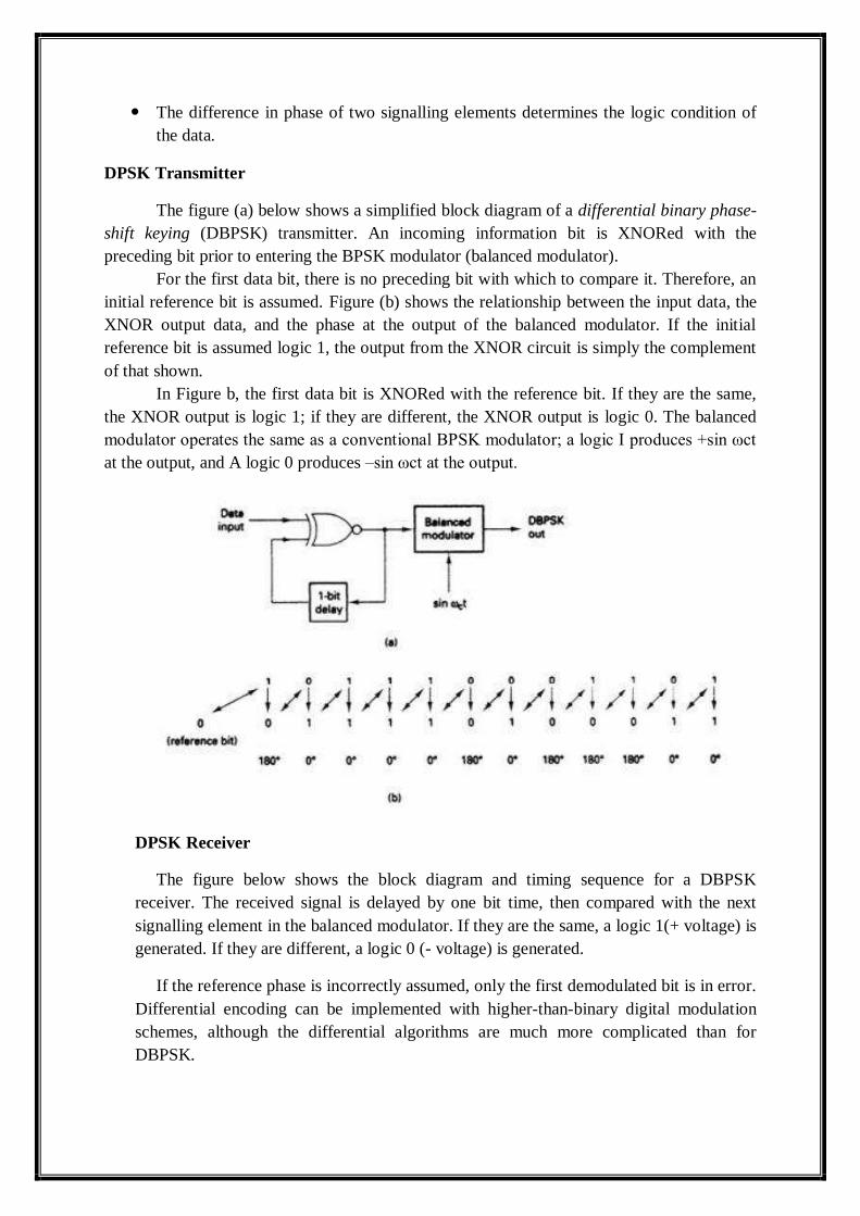
The difference in phase of two signalling elements determines the logic condition of
the data.
DPSK Transmitter
The figure (a) below shows a simplified block diagram of a differential binary phase-
shift keying (DBPSK) transmitter. An incoming information bit is XNORed with the
preceding bit prior to entering the BPSK modulator (balanced modulator).
For the first data bit, there is no preceding bit with which to compare it. Therefore, an
initial reference bit is assumed. Figure (b) shows the relationship between the input data, the
XNOR output data, and the phase at the output of the balanced modulator. If the initial
reference bit is assumed logic 1, the output from the XNOR circuit is simply the complement
of that shown.
In Figure b, the first data bit is XNORed with the reference bit. If they are the same,
the XNOR output is logic 1; if they are different, the XNOR output is logic 0. The balanced
modulator operates the same as a conventional BPSK modulator; a logic I produces +sin ωct
at the output, and A logic 0 produces –sin ωct at the output.
DPSK Receiver
The figure below shows the block diagram and timing sequence for a DBPSK
receiver. The received signal is delayed by one bit time, then compared with the next
signalling element in the balanced modulator. If they are the same, a logic 1(+ voltage) is
generated. If they are different, a logic 0 (- voltage) is generated.
If the reference phase is incorrectly assumed, only the first demodulated bit is in error.
Differential encoding can be implemented with higher-than-binary digital modulation
schemes, although the differential algorithms are much more complicated than for
DBPSK.

Advantages
Simplicity of circuit.
No carrier recovery circuit needed.
BW requirement of DPSK (fb) is reduced compared to that of BPSK (2fb).
Disadvantages
Disadvantage of DBPSK is, that it requires between 1 dB and 3 dB more signal-to-
noise ratio to achieve the same bit error rate as that of absolute PSK.
Quadrature Phase Shift Keying (QPSK)
This is the phase shift keying technique, in which the sine wave carrier takes four
phase reversals such as 45°, 135°, -45°, and -135°.
If these kinds of techniques are further extended, PSK can be done by eight or sixteen
values also, depending upon the requirement. The following figure represents the QPSK
waveform for two bits input, which shows the modulated result for different instances of
binary inputs.
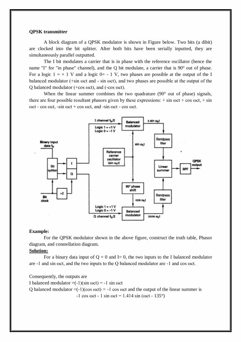
QPSK transmitter
A block diagram of a QPSK modulator is shown in Figure below. Two bits (a dibit)
are clocked into the bit splitter. After both bits have been serially inputted, they are
simultaneously parallel outputted.
The I bit modulates a carrier that is in phase with the reference oscillator (hence the
name "I" for "in phase" channel), and the Q bit modulate, a carrier that is 90° out of phase.
For a logic 1 = + 1 V and a logic 0= - 1 V, two phases are possible at the output of the I
balanced modulator (+sin ωct and - sin ωct), and two phases are possible at the output of the
Q balanced modulator (+cos ωct), and (-cos ωct).
When the linear summer combines the two quadrature (90° out of phase) signals,
there are four possible resultant phasors given by these expressions: + sin ωct + cos ωct, + sin
ωct - cos ωct, -sin ωct + cos ωct, and -sin ωct - cos ωct.
Example:
For the QPSK modulator shown in the above figure, construct the truth table, Phasor
diagram, and constellation diagram.
Solution:
For a binary data input of Q = 0 and I= 0, the two inputs to the I balanced modulator
are -1 and sin ωct, and the two inputs to the Q balanced modulator are -1 and cos ωct.
Consequently, the outputs are
I balanced modulator =(-1)(sin ωct) = -1 sin ωct
Q balanced modulator =(-1)(cos ωct) = -1 cos ωct and the output of the linear summer is
-1 cos ωct - 1 sin ωct = 1.414 sin (ωct - 135°)
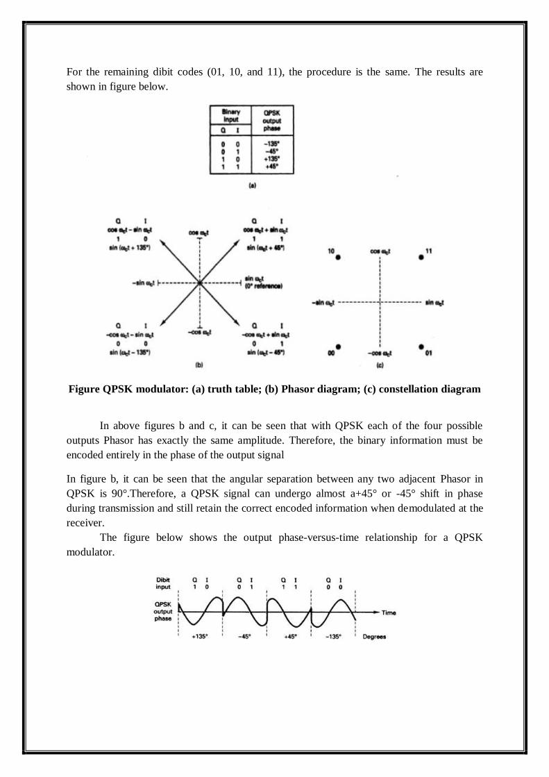
For the remaining dibit codes (01, 10, and 11), the procedure is the same. The results are
shown in figure below.
Figure QPSK modulator: (a) truth table; (b) Phasor diagram; (c) constellation diagram
In above figures b and c, it can be seen that with QPSK each of the four possible
outputs Phasor has exactly the same amplitude. Therefore, the binary information must be
encoded entirely in the phase of the output signal
In figure b, it can be seen that the angular separation between any two adjacent Phasor in
QPSK is 90°.Therefore, a QPSK signal can undergo almost a+45° or -45° shift in phase
during transmission and still retain the correct encoded information when demodulated at the
receiver.
The figure below shows the output phase-versus-time relationship for a QPSK
modulator.
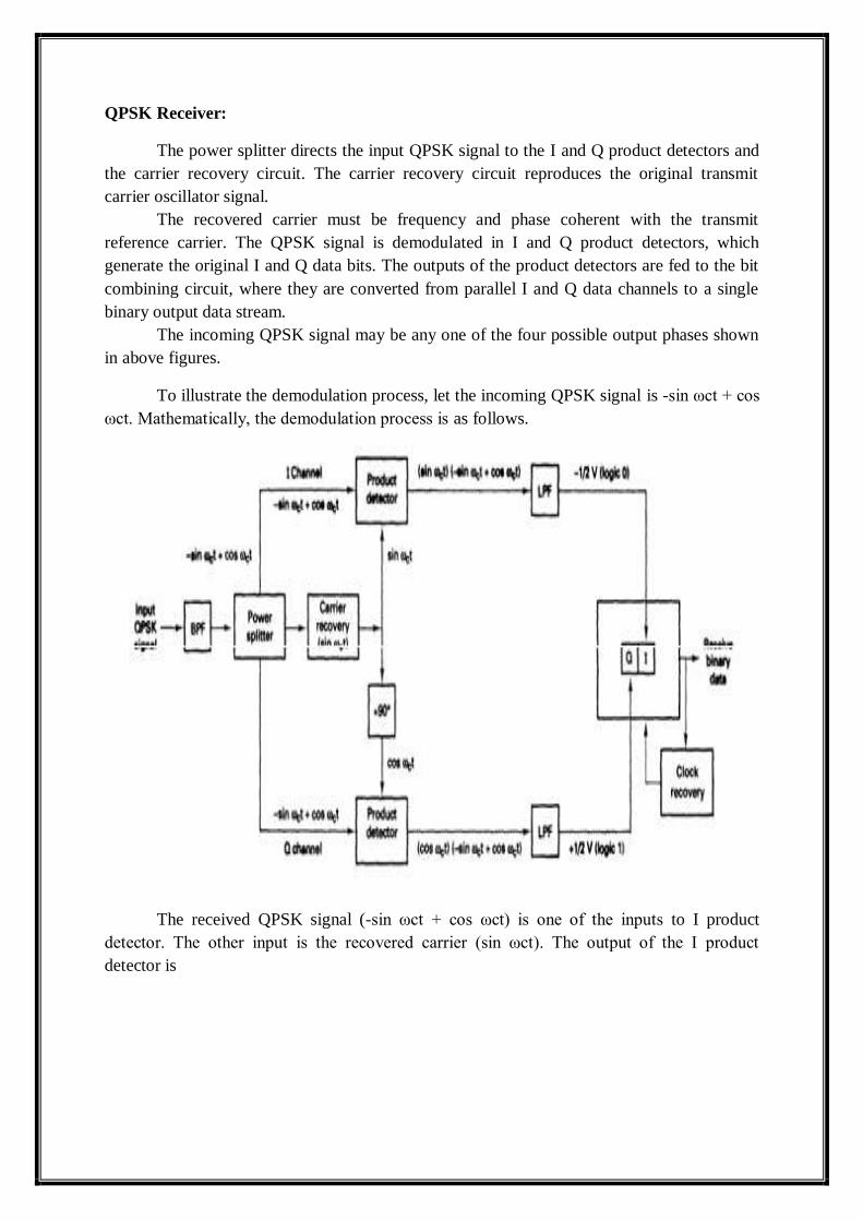
QPSK Receiver:
The power splitter directs the input QPSK signal to the I and Q product detectors and
the carrier recovery circuit. The carrier recovery circuit reproduces the original transmit
carrier oscillator signal.
The recovered carrier must be frequency and phase coherent with the transmit
reference carrier. The QPSK signal is demodulated in I and Q product detectors, which
generate the original I and Q data bits. The outputs of the product detectors are fed to the bit
combining circuit, where they are converted from parallel I and Q data channels to a single
binary output data stream.
The incoming QPSK signal may be any one of the four possible output phases shown
in above figures.
To illustrate the demodulation process, let the incoming QPSK signal is -sin ωct + cos
ωct. Mathematically, the demodulation process is as follows.
The received QPSK signal (-sin ωct + cos ωct) is one of the inputs to I product
detector. The other input is the recovered carrier (sin ωct). The output of the I product
detector is

Again, the received QPSK signal (-sin ωct + cos ωct) is one of the inputs to the Q
product detector. The other input is the recovered carrier shifted 90° in phase (cos ωct). The
output of the Q product detector is
The demodulated I and Q bits (0 and 1, respectively) correspond to the constellation diagram
and truth table for the QPSK modulator shown in Figure.
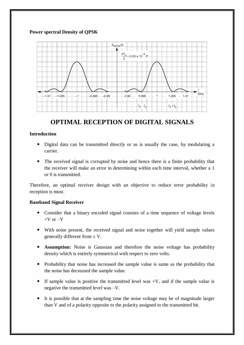
Power spectral Density of QPSK
OPTIMAL RECEPTION OF DIGITAL SIGNALS
Introduction
Digital data can be transmitted directly or as is usually the case, by modulating a
carrier.
The received signal is corrupted by noise and hence there is a finite probability that
the receiver will make an error in determining within each time interval, whether a 1
or 0 is transmitted.
Therefore, an optimal receiver design with an objective to reduce error probability in
reception is must.
Baseband Signal Receiver
Consider that a binary encoded signal consists of a time sequence of voltage levels
+V or –V
With noise present, the received signal and noise together will yield sample values
generally different from ± V.
Assumption: Noise is Gaussian and therefore the noise voltage has probability
density which is entirely symmetrical with respect to zero volts.
Probability that noise has increased the sample value is same as the probability that
the noise has decreased the sample value.
If sample value is positive the transmitted level was +V, and if the sample value is
negative the transmitted level was –V.
It is possible that at the sampling time the noise voltage may be of magnitude larger
than V and of a polarity opposite to the polarity assigned to the transmitted bit.
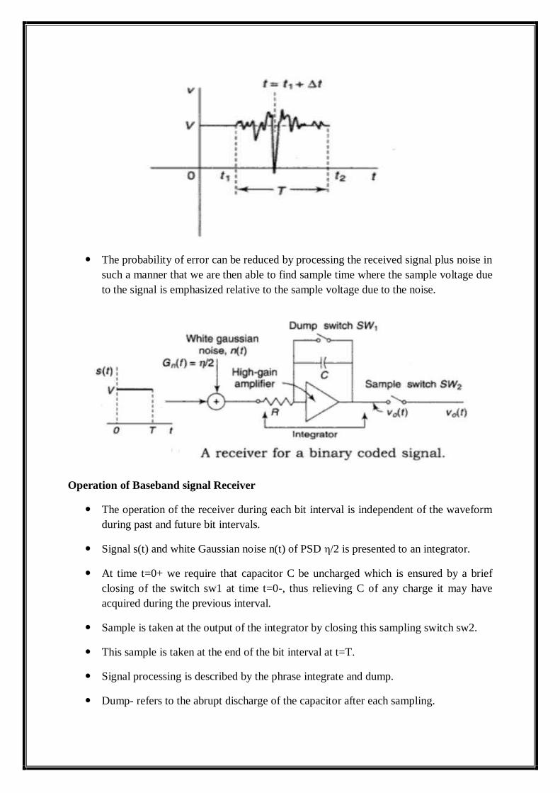
The probability of error can be reduced by processing the received signal plus noise in
such a manner that we are then able to find sample time where the sample voltage due
to the signal is emphasized relative to the sample voltage due to the noise.
Operation of Baseband signal Receiver
The operation of the receiver during each bit interval is independent of the waveform
during past and future bit intervals.
Signal s(t) and white Gaussian noise n(t) of PSD η/2 is presented to an integrator.
At time t=0+ we require that capacitor C be uncharged which is ensured by a brief
closing of the switch sw1 at time t=0-, thus relieving C of any charge it may have
acquired during the previous interval.
Sample is taken at the output of the integrator by closing this sampling switch sw2.
This sample is taken at the end of the bit interval at t=T.
Signal processing is described by the phrase integrate and dump.
Dump- refers to the abrupt discharge of the capacitor after each sampling.

Peak Signal to RMS Noise output Voltage Ratio
The integrator yields an output which is the integral of its input multiplied by 1/RC.
Using τ=RC, we have
no(T) has a gaussian probability density.
The output of the integrator, before the sampling switch is
𝒗𝒐(𝒕) = 𝒔𝒐(𝒕) + 𝒏𝒐(𝒕)
The signal output so(t) is a ramp, in each bit interval of duration T. At the end of the
interval the ramp attains the voltage so(T) which is +VT/τ or VT/τ, depending on
whether the bit is 1 or 0
At the end of each interval the switch SW1 closes momentarily to discharge the
capacitor so that so(t) drops to zero.

The noise no(t) also starts each interval with no(0)=0 and has the random value no(T)
at the end of each interval.
The sampling switch SW2 closes briefly just before the closing of SW1 and hence
reads the voltage
𝒗𝒐(𝑻) = 𝒔𝒐(𝑻) + 𝒏𝒐(𝑻)
The output signal voltage to be as large as possible in comparison with the noise
voltage.
Hence a figure of merit of interest is the signal-to-noise ratio
SNR increases with increasing bit duration T and it depends on V2T which is the
normalized energy of the bit signal.
The integrator filters the signal and noise such that the signal voltage increases
linearly with time, while the standard deviation (rms value) of the noise increases
more slowly, as .
Thus the integrator enhances the signal relative to the noise, and this enhancement
increases with time.
Probability of Error (Pe) of Integrate-and-dump receiver
Function of a receiver: To distinguish the bit 1 from the bit 0 in the presence of
noise.
A most important characteristic is the probability that an error will be made in such a
determination.
The probability density of the noise sample no(T) is Gaussian and hence appears as
follows
The density is therefore given by
Where 𝝈𝒐𝟐 , the variance, is 𝝈𝒐
𝟐 = 𝒏𝒐𝟐(𝑻)̅̅ ̅̅ ̅̅ ̅̅ given by equ.
Suppose that during some bit interval the input signal voltage is held at, say –V.
Then, at the sample time, the signal sample voltage is
while the noise sample is no(T)
If no (T) is positive and larger in magnitude than VT/τ, the total sample voltage
𝒗𝒐(𝑻) = 𝒔𝒐(𝑻) + 𝒏𝒐(𝑻)
will be positive. Such a positive sample voltage will result in an error.
The probability of such a misinterpretation, that is, the probability that
is given by the area of the shaded region in the figure.
The probability of error is given by
Defining, 𝒙 ≡𝒏𝒐(𝑻)
√𝟐𝝈𝒐⁄ , and using above equ.
In which Es=V2T, is the signal energy of a bit.
If the signal voltage were held instead at +V during some bit interval, then it is clear
from the symmetry of the situation that the probability of error would again be given
by Pe in the above equ.

The probability of error Pe is plotted below
Pe decreases rapidly as Es/η increases. The maximum value of Pe is ½.
Thus, even if the signal is entirely lost in the noise so that any determination of the
receiver is a sheer guess, the receiver cannot be wrong more than half the time on the
average.
Optimum Receiver for both Baseband and Pass band
Assume that the received signal is a binary waveform.
One binary bit is represented by a signal waveform s1(t) which persists for time T,
while the other bit is represented by the waveform s2(t)which also lasts for an interval.
In the case of transmission of baseband, s1(t)=+V, while s2(t)=-V.
For other modulation systems, different waveforms are transmitted. Example:
PSK signalling: s1(t) = A cos (ωct)
s2(t) = - A cos (ωct)
FSK signalling: s1(t)= A cos (ωc+Ω)t
s2(t)= A cos(ωc-Ω)t
As shown in the above figure, the input, which s1(t) or s2(t), is corrupted by the
addition of noise n(t).
The noise is Gaussian and has a spectral density G(f).

The signal & noise are filtered and then sampled at the end of each bit interval.
The output sample is either Vo(T)=s01(T)+n0(T)
(or)
Vo(T)=s02(T)+n0(T)
Assumption: Immediately after each sample, every energy storing element in the
filter will be discharged.
In the absence of noise the output sample would be V0(T)=s01 (T) or s02(T).
When noise is present to minimize the probability of error one should assume that
s1(t) has been transmitted if V0(T) is closer to s01(T) than to s02(T), similarly it is
assumed s2(t) has been transmitted if V0 (T) is closer to s02(T).
Decision boundary is midway between s01(T) and s02(T).
Example: For the Integrate and Dump system, where
and
the decision boundary is Vo(T)=0.
Decision boundary is
Example: Suppose that s01(T) > s02(T) and that s2(t) was transmitted.
If at the sampling time, the noise n0(T) is positive and larger in magnitude than the
voltage difference,
an error will have been made .
That is , an error will result if
Hence the probability of error is

Substituting, 𝒙 ≡𝒏𝒐(𝑻)
√𝟐𝝈𝒐⁄ , then
The complimentary error function is monotonically decreasing function of its
argument.
Pe decreases as the difference s01(T)-s02(T) becomes larger and as the rms noise
voltage σo becomes smaller.
The optimum filter, then, is the filter which maximizes the ratio
Eye Diagrams/Eye Patterns
The quality of digital transmission systems are evaluated using the bit error rate. Degradation
of quality occurs in each process modulation, transmission, and detection.
The eye pattern is experimental method that contains all the information concerning the
degradation of quality. Therefore, careful analysis of the eye pattern is important in analyzing
the degradation mechanism.
Eye patterns can be observed using an oscilloscope. The received wave is applied to the
vertical deflection plates of an oscilloscope and the saw tooth wave at a rate equal to
transmitted symbol rate is applied to the horizontal deflection plates, resulting display is eye
pattern as it resembles human eye.
• The interior region of eye pattern is called eye opening.
We get superposition of successive symbol intervals to produce eye pattern as shown below.
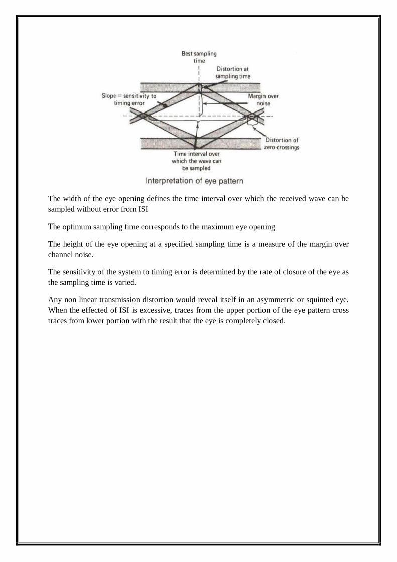
The width of the eye opening defines the time interval over which the received wave can be
sampled without error from ISI
The optimum sampling time corresponds to the maximum eye opening
The height of the eye opening at a specified sampling time is a measure of the margin over
channel noise.
The sensitivity of the system to timing error is determined by the rate of closure of the eye as
the sampling time is varied.
Any non linear transmission distortion would reveal itself in an asymmetric or squinted eye.
When the effected of ISI is excessive, traces from the upper portion of the eye pattern cross
traces from lower portion with the result that the eye is completely closed.