Reconfigurable Discrete-time Analog FIR filters for Wideband ...
Upload
khangminh22Category
view
0download
0
HAL Id: tel-03279780https://pastel.archives-ouvertes.fr/tel-03279780
Submitted on 6 Jul 2021
HAL is a multi-disciplinary open accessarchive for the deposit and dissemination of sci-entific research documents, whether they are pub-lished or not. The documents may come fromteaching and research institutions in France orabroad, or from public or private research centers.
L’archive ouverte pluridisciplinaire HAL, estdestinée au dépôt et à la diffusion de documentsscientifiques de niveau recherche, publiés ou non,émanant des établissements d’enseignement et derecherche français ou étrangers, des laboratoirespublics ou privés.
Wideband Analog-to-Digital Converter (ADC) designfor power amplifiers linearization
Kelly Tchambake yapti
To cite this version:Kelly Tchambake yapti. Wideband Analog-to-Digital Converter (ADC) design for power amplifierslinearization. Electronics. Université Paris Saclay (COmUE), 2019. English. NNT : 2019SACLT047.tel-03279780

Thes
ede
doct
orat
NN
T:2
019S
AC
LT04
7
Wideband Analog-to-Digital ConverterDesign For Power Amplifiers Linearization
These de doctorat de l’Universite Paris-Saclaypreparee a Telecom Paris
Ecole doctorale n580 Sciences et Technologies de l’information et de laCommunication (STIC)
Specialite de doctorat : Reseaux, Information et Communications
These presentee et soutenue a Paris, le 30 Aout 2019, par
KELLY TCHAMBAKE
Composition du Jury :
Dominique DalletProfesseur, Universite de Bordeaux Rapporteur
Marie-Minerve LoueratChargee de Recherche HDR, CNRS-Sorbonne Universite Rapporteur
Herve BarthemelyProfesseur, Universite de Toulon Examinateur
Caroline Lelandais-PerraultMaıtre de Conference, Centrale-Supellec Examinateur
Patricia DesgreysProfesseur, Telecom Paris Directeur de these
Chadi JabbourMaıtre de Conference, Telecom Paris Co-directeur de these
Dang-Kien PhamIngenieur de Recherche, Telecom Paris Invite


Résumé
De nos jours, la consommation d’énergie devient un des principaux défis à surmonterdans le développement des réseaux de communications mobiles. L’amplificateur depuissance est le composant le plus gourmand en consommation d’énergie dans lesstations de base. L’arrivée de la cinquième génération de téléphonie mobile avecses bandes de communication plus larges et ses modulations complexes augmenteencore plus les contraintes sur l’amplificateur de puissance. Pour palier ce problème,il est courant de faire appel à des techniques de pré-distorsion qui permettent defaire fonctionner l’amplificateur de puissance avec un meilleur rendement énergé-tique. Une contrainte importante dans la mise en oeuvre de cette technique est lanumérisation de la sortie de l’amplificateur qui, dû aux non-linéarités, s’étale surun spectre significativement plus large que le signal utile, environ 5 fois en pratiquevoire plus.
Habituellement, pour cette opération de numérisation, un Convertisseur AnalogiqueNumérique (CAN) du type pipeline est utilisé car il permet d’obtenir des résolu-tions supérieures à 10 bits sur une bande de plusieurs dizaines voire centaines deMHz. Cependant, sa consommation d’énergie élevée pousse à explorer d’autrespistes. L’architecture "Multi Stage Noise Band Cancellation" (MSNBC) à base demodulateurs Delta Sigma a l’avantage de réaliser des dynamiques différentes parsous bande et est ainsi un candidat de choix pour le CAN de la boucle de retour destechniques de pré-distortion.
L’objectif de ce travail est de démontrer la faisabilité de l’architecture MSNBCqui jusqu’à présent a été uniquement étudiée au niveau système. Pour atteindrecet objectif, plusieurs études ont été menées sur des aspects spécifiques de cettearchitecture tels que l’implémentation de l’annulation du signal primaire à l’entréedes modulateurs secondaires et l’impact du retard de boucle sur sa qualité, le choixde la fréquence centrale des modulateurs primaire et secondaires, et la conceptiondes filtres numériques pour l’annulation du bruit de quantification.
Ces études nous ont permis de proposer une architecture adaptée pour la numéri-sation d’un signal de bande RF 20 MHz avec des résolutions différentes par sous

bande. Une architecture Zéro-IF temps continu avec un modulateur primaire dusecond ordre et un modulateur secondaire du quatrième ordre avec des quantifica-teurs 4 bits a été adoptée. Cette architecture a été implémentée en une technologieCMOS 65 nm. Les simulations électrique du MSNBC 2-4 avec un signal LTE ontpermis d’obtenir 84.5 dB de SNDR dans la bande principale et 29.2 dB dans labande adjacente contenant les produits d’intermodulation.

Abstract
Power consumption is nowadays one of the main challenges to overcome in the de-velopment of mobile communications networks. The power amplifier (PA) is themost power hungry component in base transceiver stations. The upcoming fifthgeneration of mobile telephony with wider communication bands and complex mod-ulations further increases the constraints on the PA. To overcome this problem, it iscommon to use pre-distortion techniques that enable the power amplifier to operatewith greater linearity and efficiency. An important constraint in the implementa-tion of this technique is the digitization of the output of the amplifier which, due tonon-linearities, spreads over a significantly wider spectrum than the initial signal,about 5 times in practice or even more.
Pipeline Analog-to-Digital Converters (ADCs) are commonly used for this op-eration because it allows resolutions of greater than 10 bits to be obtained over aband of several tens or even hundreds of MHz. However, its high energy consump-tion pushes to find a better solution. The "Multi Stage Noise Band Cancellation"(MSNBC) architecture based on Delta Sigma modulators has the advantage of real-izing different dynamics per subband and is thus a prime candidate for the feedbackloop ADC of predistortion techniques.
The purpose of this work is to demonstrate the feasibility of the MSNBC ar-chitecture that has so far only been studied at the system level. To achieve thisobjective, several studies have been carried out on specific aspects of this architec-ture. This includes the implementation of the cancellation of the primary signalat the input of the secondary modulators and the impact of the loop delay on itsquality, the choice of the center frequency of the primary and secondary modulators,and the design of the digital filters for quantization noise cancellation.
Our investigations allowed us to propose a suitable architecture to digitize a 20MHz RF band signal with different resolutions per subband. A continuous timeZero-IF architecture with a second-order primary modulator and a fourth-ordersecondary modulator with 4-bit quantizers was adopted. This architecture has beenimplemented in a 65 nm CMOS technology. Transistor level simulations of the

2-4 MSNBC architecture simulations with an LTE test signal resulted in 84.5 dBSNDR in the main band and 29.2 dB in the adjacent band which contains theintermodulation products.

Contents
Résumé 3
Abstract 5
List of Abbreviations 9
Introduction 13
I From DPD to ADC Specifications 17I.1 Power Amplifier . . . . . . . . . . . . . . . . . . . . . . . . . . . . . . 17
I.1.1 State-of-the-Art of PAs Used in BTS . . . . . . . . . . . . . . 18I.1.2 Linearization Techniques . . . . . . . . . . . . . . . . . . . . . 22
I.2 Digital Predistortion Technique . . . . . . . . . . . . . . . . . . . . . 23I.2.1 DPD Implementation . . . . . . . . . . . . . . . . . . . . . . . 23I.2.2 ADC Implementation Trade-offs . . . . . . . . . . . . . . . . . 25
I.3 ADC Specifications for DPD . . . . . . . . . . . . . . . . . . . . . . . 27I.3.1 Mixer I/Q Imbalance . . . . . . . . . . . . . . . . . . . . . . . 27I.3.2 Fullband Nonlinear Feedback Path . . . . . . . . . . . . . . . 28I.3.3 Subband ADC Requirements . . . . . . . . . . . . . . . . . . . 29
I.4 Conclusion . . . . . . . . . . . . . . . . . . . . . . . . . . . . . . . . . 31
II Analog-to-Digital Converters State-Of-The-Art 33II.1 A/D Conversion . . . . . . . . . . . . . . . . . . . . . . . . . . . . . . 33
II.1.1 Sampling and Quantization . . . . . . . . . . . . . . . . . . . 33II.1.2 Performance Metrics . . . . . . . . . . . . . . . . . . . . . . . 37II.1.3 ADC Architectures . . . . . . . . . . . . . . . . . . . . . . . . 39
II.2 Basics of Σ∆ ADCs . . . . . . . . . . . . . . . . . . . . . . . . . . . . 41II.2.1 Design Parameters . . . . . . . . . . . . . . . . . . . . . . . . 46II.2.2 NTF Implementation: Continuous Time vs. Discrete Time . . 47II.2.3 Single Loop and Cascade Architectures . . . . . . . . . . . . . 49
7

8 Contents
II.3 Σ∆ ADC State-Of-The-Art . . . . . . . . . . . . . . . . . . . . . . . 52II.4 Conclusion . . . . . . . . . . . . . . . . . . . . . . . . . . . . . . . . . 55
IIIMSNBC System Level Specifications 57III.1 The MSNBC Architecture . . . . . . . . . . . . . . . . . . . . . . . . 57
III.1.1 Mode of Operation . . . . . . . . . . . . . . . . . . . . . . . . 57III.1.2 Degrees of Freedom / Key Design Parameters . . . . . . . . . 61
III.2 Impact of Non-Idealities . . . . . . . . . . . . . . . . . . . . . . . . . 61III.2.1 Loop Filter . . . . . . . . . . . . . . . . . . . . . . . . . . . . 62III.2.2 Digital-to-Analog Converters . . . . . . . . . . . . . . . . . . . 67III.2.3 The Clock Signal . . . . . . . . . . . . . . . . . . . . . . . . . 71
III.3 MSNBC Architectural Design Choice . . . . . . . . . . . . . . . . . . 74III.3.1 Zero IF vs. Low IF . . . . . . . . . . . . . . . . . . . . . . . . 74III.3.2 STF Choices . . . . . . . . . . . . . . . . . . . . . . . . . . . . 80III.3.3 Signal Scaling . . . . . . . . . . . . . . . . . . . . . . . . . . . 83
III.4 The MSNBC: Top level design . . . . . . . . . . . . . . . . . . . . . . 84III.4.1 Design Parameters . . . . . . . . . . . . . . . . . . . . . . . . 84III.4.2 2-4 MSNBC vs. 0-4 MSNBC . . . . . . . . . . . . . . . . . . . 85
III.5 Conclusion . . . . . . . . . . . . . . . . . . . . . . . . . . . . . . . . . 87
IVMSNBC Transistor Level Design And Measurements 89IV.1 Transistor Level Design . . . . . . . . . . . . . . . . . . . . . . . . . . 89
IV.1.1 Sub-blocks Design . . . . . . . . . . . . . . . . . . . . . . . . . 92IV.1.2 Simulation Results . . . . . . . . . . . . . . . . . . . . . . . . 100
IV.2 MSNBC Measurements . . . . . . . . . . . . . . . . . . . . . . . . . . 105
Conclusion 107
Publications 109

9

10 List of Abbreviations
List of Abbreviations
3GPP 3rd Generation Partnership ProjectACLR Adjacent Channel Leakage Power RatioACPR Adjacent Channel Power RatioADC Analog-to-Digital ConverterAM Amplitude ModulationBP Band-PassBTS Base Transceiver StationBW BandWidthCDMA Code Division Multiple AccessCIFB Cascade-of-Integrators Feedback FormCIFF Cascade-of-Integrators Feedforward FormCMOS Complementary Metal Oxide SemiconductorCT Continuous-TimeDAC Digital-to-Analog ConverterDE Drain EfficiencyDEM Dynamic Element MatchingDPD Digital PredistortionDR Dynamic RangeDSP Digital Signal ProcessingDT Discrete-TimeDWA Data Weight AveragingEER Enveloppe Elimination and RestorationELD Excess Loop DelayeMBB enhanced Mobile BroadBandENOB Effective Number Of BitsET Envelope TrackingEVM Error Vector MagnitudeFBD Frequency Band DecompositionFOM Figure Of MeritGBW Gain BandWidth (product)

List of Abbreviations 11
IBN In-Band NoiseICT Information and Communication TechnologyIM InterModulationIoT Internet-of-ThingsISI Inter-Symbol InterferencesLIF Low Intermediate FrequencyLSB Least Significant BitLTE Long Term EvolutionLUT Look-Up TableMASH Multi-stAge Noise SHapingMSNBC Multi-Stage Noise Band CancellationNCF Noise Cancellation FilterNRZ Non-Return-to-ZeroNTF Noise Transfer FunctionOBO Output Back OffOFDM Orthogonal Frequency-Division Multiple-AccessOOBG Out-Of-Band GainOSR Oversampling RatioOTA Operational Transconductance AmplifierPA Power AmplifierPAE Power Added EfficiencyPAPR Peak-to-Average Power RatioPSD Power Spectral DensityPVT Process Voltage and TemperatureRF Radio FrequencyRSTF Residual Signal Transfer FunctionRZ Return-to-ZeroSAR Successive-Approximation-RegistersSDR Signal to Distortion RatioSNDR Signal to Noise and Distortion RatioSNR Signal to Noise RatioSPI Serial-to-Parallel InterfaceSQNR Signal to Quantization Noise RatioSTF Signal Transfer FunctionUMTS Universal Mobile Telecommunications SystemWCDMA Wideband Code Division Multiple AccessZIF Zero Intermediate Frequency

12 List of Abbreviations

Introduction
The world of Information and Communication Technology (ICT) is nowadays dom-inated by telecommunications, mobile Internet and many wireless applications.1
In order to understand the rise to prominence of telecommunications and mobileinternet, it is useful to briefly review the evolution of the various network technolo-gies. Starting with the late 1980s, the 2G network was first rolled out. Its keyattributes included digital encryption of telephone conversations and the enablingof rapid wireless penetration rates. Essentially, the advent of the 2G network actedas a catalyst for the mobile data services such as text messages, i.e. SMS. In theensuing two decades, the 2G was replaced by the 3G and then 4G telecommuni-cation network. The key advantages of the new networks include fast informationtransfer rate and mobile broadband access to mobile phones to name but a few.The implications for the business world were far-reaching. For instance, telephonecompanies started offering services such as MMS, video calls and mobile TV tech-nologies. Other businesses seize these advantages to introduce disruptive innovation.For instance, the ride-hailing mobile application Uber has taken advantage of theopportunities available thanks to the 4G network to really disrupt the taxi industry.In a similar vein, Netflix leveraged the improved speed of data transfer to introducetheir offering, which changed the paradigm in the media industry.
As I embark on this thesis, there are growing talks of the 4G being replaced bythe 5G network. The Fifth Generation (5G) mobile networks will see the initialdeployment around 2020, promising wireless download speed of 10Gbps for eMBB(enhanced Mobile Broadband) [2], and subsequently enabling billions of wirelessconnected devices for IoT (Internet-of-Things), autonomous driving, remote surgery.According to the World Economic Forum, the 5G holds the promise of sparking aprofound digital transformation. Figure 1 [3] gives an overview of the different areaswhere the 5G technology can make a noticeable impact. For instance, its low latencypotential will be very important for the industry on high-frequency/algorithmic
1About 2 − 3% of the world-wide energy consumption is for ICT, which causes about 3% ofthe total CO2 emissions [1].
13

14 Introduction
trading. Its reliability could transform the health care industry by enabling surgeonsto remotely carry out complicated procedures on patients.
Figure 1: 5G mobile network applications
The usage cost of mobile services is likely to increase, and, in particular, theenergy consumption might grow with the number of Base Transceivers Stations(BTS) and data centers in the network. Hence, as the demand for ICT servicesrises, higher and higher energy consumption is expected for mobile radio networks.
In order to preserve the environment, cellular network operators try to deployvarious strategies to reduce energy consumption. BTS consume about 85% of thetotal energy of the network [4]. Their power consumption depending on the size,the coverage area and the technology used. The main axes of finding out efficientways to reduce the energy consumed are: the optimization of hardware, the usageof renewable energy sources and the smart usage of resources through power savingmodels and efficient algorithms.
For hardware optimization, the power is consumed by the following components:
• The rectifier transforms the signal from AC to DC. The efficiency of the rec-tifier is about 92% for a conventional rectifier and about 97% for the case oflatest products, for amperage loads between 40− 90% [5].
• The Baseband Digital Signal Processing Circuit is considered as having a con-stant power consumption. This power is dissipated as heat and has to beremoved, e.g., by the cooling system.

Introduction 15
• The PA is a device that magnifies the amplitude of a signal. Radio-frequency(RF) PAs, such as the one used in cellular BTSs and broadcast transmitters,has an efficiency about 15%. The excess energy is transformed into heat.
• The feeder is the cabling system connecting the BTS to the antenna. Inconventional BTSs, antennas and equipments are a few meters apart, andconnected through a coaxial cable or Remote Radio Heads (RRH). Its efficiencyapproaches 1 when using RRH, and 0.5 when using coaxial cabling [4].
• The cooling system to keep the temperature of most components of the BTSwithin specified design limits. Air conditioners, free ventilation, forced-aircooling and heat exchangers are often the choice for radio sites. Such coolingrequires as much power as one third of the heat power generated inside theBTS [6].
Given the efficiency of each of those components, a useful manner to optimizethe hardware power consumption of a base station is to focus on the componentwith the lowest power efficiency, the PA.
In order to save energy and achieve high efficiency, PAs need to operate in thesaturation region [7]. However, PAs exhibit high nonlinear distortion in that region,and this creates problems related to preserving high signal quality. The main trendsin the design of wireless transmitters remains to provide enhanced transmitter func-tionalities with Digital Signal Processing (DSP) by using linearization techniques.There are a number of linearization techniques to improve the linearity of the poweramplifiers and which enable, at the same time, to improve the efficiency. One ofthem, the digital predistortion (DPD), is of particular interest because it benefitsfrom the technical advances of the digital part and communications systems increas-ingly use digital modulation.
Its implementation, in current and future emission chains, is a relatively lowextra cost in the digital part, however it requires a measurement of the distortiongenerated by the amplifier and thus, a possibly dedicated, feedback path to convertthe distorted analog RF signal to digital domain. In this system the analog-to-digital converter which is in charge of the measurement of the distorted signal mustmeet the requirements on the signal resolution and bandwidth. These needs arequite challenging in the context of digital predistortion and, in addition, here too,its energy consumption must be as minimum as possible.
Latest communication systems use relatively wide bandwidths. The distortedsignal contains unwanted signals called intermodulation products, and is charac-terized by a spectrum P times wider than the original, where P is the considered

16 Introduction
intermodulation order. In practice, we aim at digitizing at least intermodulationproducts of order 5. In addition, these signals are centered at a high transmissionfrequency. We realize that in this type of application, which is the digital predis-tortion, validating the sampling theorem establishes the frequency converter to veryhigh values if we do not reduce the center frequency of the signal to a low value.Second, the resolution conversion of these distorted signals must be very high: be-cause, on the one hand, multi-carrier signals have very high dynamics and on theother hand, the distortions may be small changes in the original signal. Varioustechniques are used to increase the performance of Analog-to-Digital Converters(ADC) as time-interleaving often used with pipelined ADCs or the parallelizationof processing such as processing with decomposition into smaller frequency bands.Among the various converters, Σ∆ modulators architectures are of particular inter-est: a high accuracy can be achieved for band-pass signals centered around highfrequency with few components. Despite a strong limitation of the converter band-widths due to their operating principle based on over-sampling, recent literaturereports some circuits whose bandwidths allow to consider a possible use for broad-band telecommunication applications. The purpose of this thesis is to develop andprove at silicon level an ADC for the measurement of the signal in the feedback pathof DPD in base stations transceivers.
The remainder of the thesis proceeds as follows:
• Chapter 1 presents the architectures of PAs used in base station transceiversand their design constraints. It discusses several linearization techniques in-cluding digital predistortion. The proposed ADC specifications are then de-fined.
• Chapter 2 discusses the choice of the ADC type. It contains a discussion ofthe state-of-the-art Σ∆ ADCs and key ADC design parameters are explained.
• Chapter 3 shows the high level design choices and degrees of freedom of ourproposed ADC. The chapter elaborates on the choice of architecture and an-alyzes the impact of non-idealities of the selected architecture. This chapterconcludes with high level simulations results .
• Chapter 4 explains the choices made for the transistor level design of theproposed ADC. It contains a discussion of the floor plan, transistor level sim-ulations as well as measurements results of the ADC.

Chapter I
From DPD to ADC Specifications
In typical mobile communications BTS, the Power Amplifier consumes 50-80% of thetotal power consumption [8]. With the increasing demand for higher data transferrates in new communication standards, the situation gets worse. Therefore, the PAneeds to be more power efficient.
I.1 Power Amplifier
From that total DC power consumed, typically only approximately 30% is convertedinto useful transmitted RF signals [9]. The main challenge in producing a highefficiency power amplifier in such applications is the high peak to average powerratio (PAPR) of the RF signal, which in some cases is in excess of 10 dB [8].
This is because the PA needs to be efficient not only at peak power but alsoat average power levels several dB’s below where the PA would spend most of itstime operating. As the demand for higher bandwidth increases, more complicatedand dynamic modulation schemes are used, driving the signal PAPR increasinglyhigher. From a PA design standpoint, this puts a lot of pressure on the PA designcommunity to provide solutions that continually improve PA efficiency and to reactto the advancements in spectrally-efficient schemes, while respecting the stringentlinearity requirements implicit in new wireless standards.
The 3G/4G wireless services not only have complicated modulations which re-duce the Error Vector Magnitude (EVM) tolerance for systems, but also bring in non-constant-amplitude waveforms. The PAPR for the amplitude of EDGE, WCDMAand CDMA2000 is 3.2-5 dB. [10] Furthermore, new spectrally efficient protocolsemployed in 4G communication systems utilize orthogonal frequency-division mul-tiplexing (OFDM). These OFDM signals have even high PAPRs on their amplitudewaveforms. The uplink PAPR of LTE is in the order of 7.5 dB [10] and >10 dB,
17

18 Chapter I. From DPD to ADC Specifications
respectively.
GSM EDGE UMTS CDMA2000 LTEMax Power (dBm) 35 29 26 25 25Min Power (dBm) 7 7 -48 -48 -40
PAPR (dB) 0 3.4 3.4 3.5-5 6-8EVM limit - 9% 17.5% - 12.5%
ACLR1 (dBc) 20 20 33 28 44.2ACLR2 (dBc) 60 60 43 43 44.2
Table I.1: Uplink Transmitters Requirements for PAs
Table I.1 contains some of the most relevant uplink transmitter performanceparameters for 2G GSM, 3G WCDMA/CDMA 2000, and 4G LTE/WiMAX. Asaturated or switching PA can deliver a maximum output power of 35 dBm and anefficiency of >60% at this power level for GSM (an industry benchmark). The mainimpact of EDGE is to introduce an amplitude component to the modulation scheme(8PSK). Maximum output power is reduced to 29 dBm, partly in recognition of thecrest factor of 3.2 dB and partly due to the need to use a linear amplifier with reducedefficiency. Power control range is still a modest 22 dB. The industry-driven targetfigure for PAs used for EDGE signals is 45%. As far as WCDMA and CDMA2000are concerned, the challenge for efficiency recovery is similar to EDGE despite theapparent threat from an increased power-control in the range of 75 dB. Fortunately,power budgets in the transmitter are such that worthwhile efficiency enhancementonly applies to the top 20 dB dynamic range.
Unlike constant-amplitude modulations such as GSM, the non-constant-amplitudemodulated signals with the inherent high PAPR and wide bandwidth require highlylinear PAs having very low signal distortion. One way for the PA to satisfy thestringent linearity requirements is to back off from its compression region. This is amajor bottleneck for realizing highly efficient mobile transmitters.
I.1.1 State-of-the-Art of PAs Used in BTS
The efficiency of a PA, or drain efficiency (DE), is defined as the ratio of the funda-mental output power to the DC supplied power. Another metric that is often usedis power added efficiency (PAE) which takes into account the gain of the PA, and isdefined as the ratio of the difference between output and input fundamental powerover the DC supplied power. For a PA with high gain, DE and PAE will be similar,but if the PA gain goes below for example 10 dB, the DE and PAE difference would

I.1. Power Amplifier 19
be more than 10% [11].
Figure I.1: Power Added Efficiency of a PA
Figure I.1 shows the efficiency of a typical 1-stage common-emitter SiGe PA. ThePAE reaches the peak value at saturation power, but drops dramatically at back-offthat depends on different PAPR values and different linearity specifications. Thisis opposed to saturated PAs that work with constant-amplitude signals but exhibithigh efficiency.
Several techniques have been developed in improving PA efficiency. The basis ofthese techniques is the reduction of the overlapping region between the current andthe voltage at the device current generator plane by reducing the conduction angle,as well as increasing the drive level to an optimum point [12].
While high-efficiency PA modes yield promising efficiency gains, they are onlyefficient near peak power when the device starts to go into compression. However,when the PA operates below peak power under output back-off (OBO) conditions,the efficiency drops significantly. Signals with high PAPR such as LTE andWCDMApresent a challenge to a PA in maintaining efficient operation over dynamic range,as the PA spends most of its time in output back-off.
Therefore, in this backed-off region of operation, a different solution is neededto maintain the same efficiency performance achieved at peak power. The 5G wave-forms with high PAPR will degrade PA’s efficiency at power back-off, making bothDoherty PA and supply-modulated PA (envelope tracking (ET), envelope elimina-tion and restoration (EER)) very attractive for efficiency enhancement of 5G PAdesign.

20 Chapter I. From DPD to ADC Specifications
Envelope Tracking PA
The envelope tracking technique modulates a device’s DC supply according tothe input envelope magnitude to improve the efficiency during output back-off. Theapproach evolved from the EER amplifier technique of Kahn [13]. In ET, an envelopeamplifier is used to bias the drain of the RF PA based on the input envelope signalas shown in Figure I.2. The envelope information is obtained either through anenvelope detector on the input path or digitally from baseband processing. Itsrelationship with the drain bias voltage is defined by an envelope shaping functionto generate the desired ET system-level efficiency shown in Figure I.2. The overallefficiency of an ET PA is calculated as the product of the efficiency of the RF PA andthe envelope amplifier. Therefore to improve the ET PA efficiency, careful designconsiderations must be given to both amplifiers.
Figure I.2: Enveloppe Tracking PA
One constraint to implement ET in macro base stations is the lack of efficient,linear and sufficiently wide-band high-power supply modulators [14]. This limita-tion is mainly due to the trade-off between the transistor breakdown voltage and itsswitching speed, hence ET implementations tend to be limited to low power appli-cations such as mobile phones [15]. A simplified version of ET called the averagepower tracking (APT) is widely used for mobile phones PA’s where the supply volt-age is changed slowly. However with the advancement of low-power modulators, acomplete ET system is emerging as the future trend, especially with ET’s ability towork over extended bandwidths and accommodate multi-band operation [16]. Theother issue with the ET supply modulator is that it can potentially be a source ofdistortion for the RF PA. It therefore makes sense that much of the ET researchfocus is around the ET supply modulator, for example in [17],[18].

I.1. Power Amplifier 21
Recent works in this field have further improved efficiency numbers or higherfrequency of operation. A GaN HEMT operating in class-E is used in [19] in anET system at 2.6GHz. With the RF PA having a drain efficiency of 74% and theET modulator at 92% efficiency, the overall ET efficiency was 60% when a 6.5 dBPAPR 10MHz LTE signal was applied producing a 40W average output power. In[20] an ET PA utilizing a GaN device operating in inverse class-F at 880MHz wasable to produce a PAE of 53% at 7.4W output power for a 6.6 dB PAPR 20MHzLTE signal. A higher bandwidth was achieved in [21] where an X-band GaN MMICPA was used in ET for a 60MHz LTE signal with 6.6 dB PAPR. With the RFPA operating in class-E at 9.23GHz, the overall PAE achieved was 35% at 1.1Waverage output power.
Doherty PA
The Doherty architecture was first introduced by William H. Doherty in 1936 toimprove the PA efficiency in amplitude modulation (AM) broadcasting applications[22]. The basic form of a Doherty PA consists of a carrier amplifier, typically biasedin class-AB, and a peaking amplifier biased in class-C as shown in Figure I.3. Thisclassical structure can maintain high-efficiency operation over 6 dB OBO using theconcept of load modulation [23].
Figure I.3: Doherty PA
The high-efficiency output range can theoretically be extended further up to12 dB OBO using a 3-way [24] or even 18 dB for a 4-way Doherty [23]. An asymmetricDoherty amplifier, where the peaking device is larger than the carrier device isalso used to extend the high-efficiency region as for example up to 12 dB OBO as

22 Chapter I. From DPD to ADC Specifications
demonstrated in [25], with only a 7%-point drop over the dynamic range. Theapplication of an "envelope tracking" technique on the gate bias of the peakingdevice was presented in [26] to address load modulation issues that are causing thedip in the high efficiency region. The work in [27] tackles this by applying ET onthe drain bias of the peaking device, and a relatively flat high efficiency performancewas achieved over 18 dB of dynamic range in a simulation environment. Howeverthe analysis did not include a fabricated hardware and the efficiency of the drainsupply modulator was not considered.
The main limitation of Doherty PA is the narrow bandwidth introduced by theuse of the quarter wavelength combining transformer. This presents a challenge in4G LTE where not only the bandwidth is wider, but with carrier aggregation, PA’sideally need to accommodate multiple-bands. Research focusing on extending thebandwidth of a Doherty PA is ongoing and recent examples include [28] which iscapable of handling a 100MHz instantaneous bandwidth, and [29] where a 1.5 -2.14GHz design was developed corresponding to a 35% fractional bandwidth.
In [30], a multiband Doherty was designed and fabricated for 1.9, 2.14, and2.16GHz obtaining a 60% PAE at 6 dB OBO. In a more recent study, a quad-band Doherty PA was developed at 0.96, 1.5, 2.14, and 2.16GHz, although with arelatively lower PAE at 6 dB OBO, ranging from 20 to 43% [31]. There are alsopatented wideband and multiband Doherty PA’s as shown in [32].
Doherty is currently the architecture of choice for base station power amplifiers[23], mainly because of its relative simplicity in comparison with other highly efficientsolutions such as ET.
I.1.2 Linearization Techniques
The design of the power amplification stage is driven by a linearity and power effi-ciency tradeoff. Doherty and ET power amplifiers have a high efficiency and oper-ate in compression or even saturation. Consequently, it produces signal distortions.Thus, the need for some form of linearization is essential.
"Linearization" is a process which enables linear amplification of a signal in thepresence of nonlinear components, by canceling the distortion introduced by thosecomponents. There are 3 main techniques to improve linearity of power amplifiers:feedback, feed forward and predistortion.
Table I.2 compares those techniques in terms of size, bandwidth, efficiency andharmonic distortion cancellation. Depending on the application and the requirementof a system, one technique is preferred to another.
The feedback technique has moderate linearity results and is simple to imple-

I.2. Digital Predistortion Technique 23
Technique Cancellation Bandwidth Efficiency SizeFeedback Low Low Medium Medium
Feedforward High High Low LargePredistortion Medium High/Medium High Small
Table I.2: Comparison of PAs linearization techniques
ment. Moreover, this technique decreases the gain of the system, and there are somestability issues to deal with. Its narrow band of operation, makes it not suitable for4G/5G mobile standard.
The concept of feedforward systems is simple, but its hardware implementationis quite costly.
Feedforward methods exhibit a good linearization performance with a high sta-bility and wideband signal capability. The feedforward technique is historically lesspopular and is mostly applied in base stations. However, it has low efficiency andhigh complexity resulting in the big size of the circuit and high cost.
For example, feedforward is mainly used in base station transceivers instead ofPA handsets because of its high cost. However, with all the progress made in thedigital field and the need to integrate and miniaturize systems, DPD is used in manyapplications nowadays.
State-of-the-art power amplification systems often use a Doherty PA for highefficiency at output power backoff, and a digital predistorter to restore the requiredlinearity performance. Digital predistortion is currently the preferred linearizationtechnique and is widely used for applications with, typically, up to 20MHz band-width. [33]
I.2 Digital Predistortion Technique
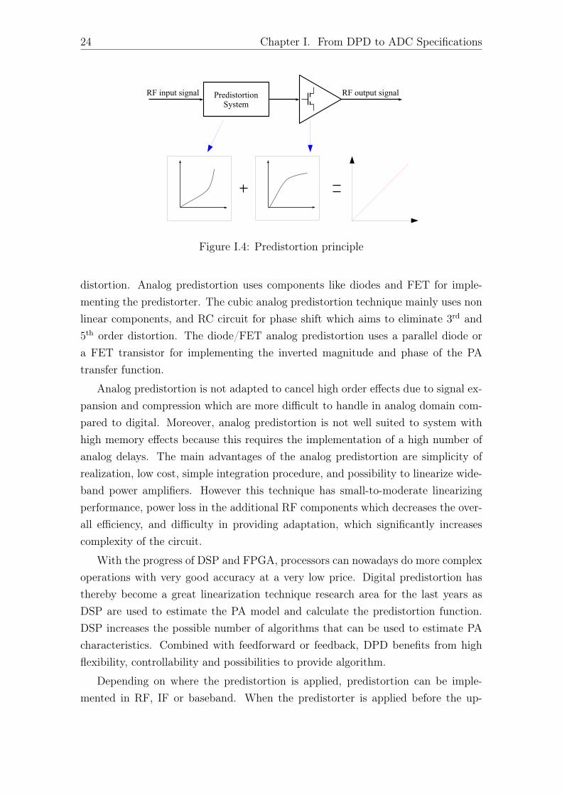
Predistortion is the most popular linearization technique of power amplifiers to-day. This technique consists in applying the inverse characteristics of a PA to theinput signal before feeding it to the PA, so that the cascade behaves as a linearamplification system, as presented in Figure I.4. Thus, this inverse function calledPredistorter compensates for AMAM and AMPM distortions.
I.2.1 DPD Implementation
The predistortion function can be implemented with analog components, or DSPoperations and digital components. Then we talk about Analog and Digital pre-
24 Chapter I. From DPD to ADC Specifications
Figure I.4: Predistortion principle
distortion. Analog predistortion uses components like diodes and FET for imple-menting the predistorter. The cubic analog predistortion technique mainly uses nonlinear components, and RC circuit for phase shift which aims to eliminate 3rd and5th order distortion. The diode/FET analog predistortion uses a parallel diode ora FET transistor for implementing the inverted magnitude and phase of the PAtransfer function.
Analog predistortion is not adapted to cancel high order effects due to signal ex-pansion and compression which are more difficult to handle in analog domain com-pared to digital. Moreover, analog predistortion is not well suited to system withhigh memory effects because this requires the implementation of a high number ofanalog delays. The main advantages of the analog predistortion are simplicity ofrealization, low cost, simple integration procedure, and possibility to linearize wide-band power amplifiers. However this technique has small-to-moderate linearizingperformance, power loss in the additional RF components which decreases the over-all efficiency, and difficulty in providing adaptation, which significantly increasescomplexity of the circuit.
With the progress of DSP and FPGA, processors can nowadays do more complexoperations with very good accuracy at a very low price. Digital predistortion hasthereby become a great linearization technique research area for the last years asDSP are used to estimate the PA model and calculate the predistortion function.DSP increases the possible number of algorithms that can be used to estimate PAcharacteristics. Combined with feedforward or feedback, DPD benefits from highflexibility, controllability and possibilities to provide algorithm.
Depending on where the predistortion is applied, predistortion can be imple-mented in RF, IF or baseband. When the predistorter is applied before the up-

I.2. Digital Predistortion Technique 25
conversion, we talk about baseband predistortion. When the signal is up-convertedbefore being predistorted, it is an RF predistorter and when it is between two up-conversion, it is called intermediate frequency (IF) predistortion.
Figure I.5: Main components of a DPD system
A simplified DPD architecture in Figure I.5 allows us to identify conceptuallythe main subsystem components of a DPD system:
• Components in the transmission and acquisition paths: mixers and the PA.
• Data Converters: the ADC and DAC.
• DSP and control system: digital hardware for the predistorter.
Each of the subsystems contributes to the design targets which are evaluatedin terms of linearity, dynamic range, bandwidth, power consumption and hardwarecost. However, new communications bandwidths lead to high design constraints onthe ADC.
I.2.2 ADC Implementation Trade-offs
Although it already seems to be a well-established technique at the current stage,DPD is still facing new challenges. New issues are coming with recent modulationschemes and multi-band scenarios presenting higher PAPR leading to higher orderof non-linearity for the PA. This trend has a large impact on DPD design in manyaspects, not the least of which is the wide band signal to be processed [34]. DSPsand Data converters are highly impacted by this evolution because the number ofcoefficients required to model the PA inverse transfer characteristic increases andat least 5 or 7 times the original signal bandwidth have to be processed which is ahuge band. Generally, the DPD system contains ADCs to sample the PA outputand feed it back to the DPD, in which the transmission path and acquisition pathare both based on direct conversion structure.

26 Chapter I. From DPD to ADC Specifications
One issue relating to ADC in the acquisition path is the resolution. Beforetraining the DPD model, the output signal of the PA is digitized. The number ofquantization bits depends on the actual system requirement. In order to have a noisefloor at −80 dBc, a 14-bit ADC is needed. Designing a 14-bit ADC is challengingand costly [35] for the considered bandwidth (hundreds of MHz). It is thereforedesirable to reduce the resolution; however, this is not a straightforward task, sincereducing the resolution of ADC is equivalent to increasing the noise floor of thefeedback signal, which is critical to the accuracy of DPD modeling. Liu et al. [36]proposed a method to reduce the ADC dynamic range, but a minimum 8-bit ADC isrequired to achieve linearization performance comparable to the conventional DPD.
Besides the resolution, the main issue relating to ADC in DPD implementation isthe bandwidth requirement of the feedback path that is used to capture the outputsignal from the PA for the purpose of model extraction. In DPD, the bandwidth ofthe feedback path usually requires five times the signal bandwidth. For an acqui-sition path that is based on direct conversion structure, for instance, the samplingrate of the ADCs should be at least 500MHz if an LTE-Advanced signal is applied.The existing and forthcoming data converter technologies could hardly meet thisrequirement.
Some solutions have been proposed to reduce the signal bandwidth requirement.The band-limited method was proposed in [37], but requires an extra bandpassfilter in the RF transmit chain that is difficult and costly to design. The analogaliased sampling method in [38] can reduce the sampling rate, but it needs additionalanalog aliasing operation. The spectral-extrapolation-based algorithm was reportedin [34], and a forward model was first carried out and then DPD coefficients canbe estimated. In [39], a two-stage DPD, i.e., a static nonlinear box cascaded witha dynamic weak nonlinear box, was proposed to decrease the feedback bandwidth.All the methods mentioned above require the acquisition bandwidth not narrowerthan the signal bandwidth.
There have been substantial research efforts over the past 20 years with respect todeveloping efficient and elaborate DPD techniques for various single-band transmis-sion schemes where linearization for the whole transmit band is essentially pursued.These conventional DPD approaches take as their inputs the full composite transmitband, and we thus refer to these DPD approaches as full-band DPD.
I.3. ADC Specifications for DPD 27
I.3 ADC Specifications for DPD
The feedback path of a DPD system can be considered as a direct conversion receiver(DCR). DCRs suffer from RF and baseband impairments such as I/Q imbalance andnonlinear distortions [40]. In order to set the design parameters for the ADC in thefull-band DPD feedback path, we will successively consider different nonlinear effectsand evaluate their impact on DPD correction.
For this study, the correction performance are simulated using a 20MHz mono-carrier LTE signal. This signal is distorted using the memory polynomial PA modelproposed in [41]. The linearization of this system is achieved with a memory poly-nomial model identified by a least-square method [41]. The nonlinear order of theinverse model is set to 9 and its memory depth is 3 in order to provide 55 dB adjacentchannel power ratio and 0.2 % error vector magnitude when all blocks in the feed-back path are ideally linear and there is no quantization error. This configurationexhibits some margins compared to the standard specifications.
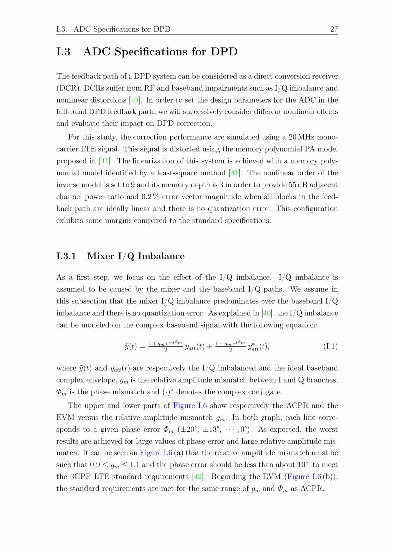
I.3.1 Mixer I/Q Imbalance
As a first step, we focus on the effect of the I/Q imbalance. I/Q imbalance isassumed to be caused by the mixer and the baseband I/Q paths. We assume inthis subsection that the mixer I/Q imbalance predominates over the baseband I/Qimbalance and there is no quantization error. As explained in [40], the I/Q imbalancecan be modeled on the complex baseband signal with the following equation:
y(t) = 1 + gm e−jΦm
2yatt(t) + 1− gm ejΦm
2y∗att(t), (I.1)
where y(t) and yatt(t) are respectively the I/Q imbalanced and the ideal basebandcomplex envelope, gm is the relative amplitude mismatch between I and Q branches,Φm is the phase mismatch and (·)∗ denotes the complex conjugate.
The upper and lower parts of Figure I.6 show respectively the ACPR and theEVM versus the relative amplitude mismatch gm. In both graph, each line corre-sponds to a given phase error Φm (±20°, ±13°, · · · , 0°). As expected, the worstresults are achieved for large values of phase error and large relative amplitude mis-match. It can be seen on Figure I.6 (a) that the relative amplitude mismatch must besuch that 0.9 ≤ gm ≤ 1.1 and the phase error should be less than about 10° to meetthe 3GPP LTE standard requirements [42]. Regarding the EVM (Figure I.6 (b)),the standard requirements are met for the same range of gm and Φm as ACPR.

28 Chapter I. From DPD to ADC Specifications
30
35
40
45
50
55
AC
PR
(d
B)
0.7 0.8 0.9 1 1.1 1.2 1.3
Relative amplitude mismatch gm
0
5
10
15
20
25
EV
M (
%)
Φm
= ± 20 deg
Φm
= ± 13 deg
Φm
= ± 7 deg
Φm
= 0 deg
(a)
(b)
Figure I.6: DPD performance in terms of ACPR (a) and EVM (b) vs I/Q mismatch:simulation results
I.3.2 Fullband Nonlinear Feedback Path
The effect of a nonlinear distortion generated in the feedback path is now considered.This distortion may be caused by compression in the active blocks of the feedbackpath. We assume that distortions are modeled by a 3rd order nonlinearity andthat higher orders nonlinearities have minor effects. As mentioned in [40], thisnonlinearity can be modeled on the complex baseband signal by:
yBB(t) = yatt(t) + α([y∗att(t)]
2 + 3 y2att(t)
)y∗att(t), (I.2)
where α is the nonlinearity coefficient. We define the fullband signal to distortionratio (SDR) as:
SDR =Pmean yatt(t)
Pmean
α([y∗att(t)]
2 + 3 y2att(t)
)y∗att(t)
, (I.3)
Figure I.7 shows the ACPR and EVM of the linearized PA output obtainedby simulation. As long as the distortions generated by the feedback path are lowenough (SDR ≥ 55 dB), correction performance are maximum. For SDR ≤ 55 dB,the ACPR drops. The EVM is less sensitive to this 3rd order nonlinearity as itremains constant for a wider range of distortion level: its effect is significant forSDR ≤ 40 dB. In order to cope with circuit non idealities, the target linearity ofthe ADC is set to 60 dB.

I.3. ADC Specifications for DPD 29
Fullband SDR (dB)10 20 30 40 50 60 70 80
AC
PR
(d
B)
20
30
40
50
60
EV
M (
%)
0
10
20
30
40
Figure I.7: DPD performance in terms of ACPR and EVM vs nonlinearity of thefeedback path
I.3.3 Subband ADC Requirements
The non-linearity study presented above assumed that a full-band single ADC isused to digitize the signal in the feedback path of the DPD. This ADC needs tohave a high dynamic range in M × BW bandwidth in order to capture both highpower signals and low power distortion signals (IMD products).
Subband DPD [43] is particularly attractive as it relaxes the design of the ADC.With the subband approach, as presented in Figure I.8, the main signal band andadjacent bands will have different DR requirements.
DRSingle ADC
DRMain ADC
DRAdj ADC-1
DRAdj ADC-2
Required Noise Level for a multi-band ADCRequired Noise Level for a single ADC
SignalSignal
Distorted
M ·BwBw
Original
Figure I.8: Single ADC vs. multi-band ADC
The digitization is performed with several ADCs, one for the main signal and

30 Chapter I. From DPD to ADC Specifications
one for each subband. This architecture provides new degrees of freedom such asthe possibility of having different quantization noise level for each subband. TheADC dimensioning is now studied assuming a multi-band ADC.
48 50 52 54 56 58 60 62 64 66
SNR Principal (dB)
46
48
50
52
54
56
58
AC
PR
(dB
)
48 50 52 54 56 58 60 62 64 66
SNR Principal (dB)
0.1
0.2
0.3
0.4
0.5
0.6
0.7
0.8
0.9
EV
M (
%)
SNR Adj = 4.9 dB
SNR Adj = 7.1 dB
SNR Adj = 8.4 dB
SNR Adj = 10.2 dB
SNR Adj = 12 dB
SNR Adj = 15.6 dB
(a) (b)
Figure I.9: DPD performance in terms of ACPR and EVM vs. subband quantizationSNR; ACPR without DPD: 30 dB ; EVM without DPD: 4.3 %
The difference in DR requirements can be achieved by setting different quanti-zation step sizes for the modulator quantizer in each subband. The effect of thissubband quantization on the linearization results is simulated and ACPR and EVMare shown in Figure I.9. The x-axis is the SNR in the principal subband, whichcorresponds to the ideal 20MHz transmit band and each colored line represents aspecific SNR in the 20MHz adjacent subband.
As expected, the higher the SNR, the better the ACPR and EVM. The ACPRis independent of principal subband SNRs between 48 and 66 dB for adjacent sub-band SNR greater than 10.2 dB. The EVM has a similar characteristic for adjacentsubband SNRs greater than 12 dB.
By considering the input signal peak-to-average power ratio in these simulationresults, the minimum performance of a multi-band ADC is set to 60 dB SNR in theprincipal subband and 22 dB SNR in the adjacent subband. 1
1The SNR in the adjacent subband may seem low. However the power of the signal in thissubband is very low. For sake of clarity, the detailed spectrum decomposition is not discussedhere.

I.4. Conclusion 31
I.4 Conclusion
In this chapter, we saw several techniques to solve the linearity and efficiency trade-off of RF power amplifiers in base station transceivers. DPD is an attractive lin-earization technique which is nowadays extensively used. Non-linearities in thefeedback path of DPD alter the signal used for the PA inverse model computation.Simulations show that for some distorsion levels, DPD is not significantly affectedand for high distorsion levels, DPD performance are reduced because the extractedPD model is erroneous. In case of a full-band DPD for LTE applications, the feed-back ADC should at least have 60 dB SNR in M × BW with M is the highestsignificant nonlinear order at the output of the PA and BW the input signal band-width. For a sub-band DPD approach the main sub-band ADC should at least have60 dB SNR and adjacent sub-bands should have 22 dB SNR.
With these requirements, several ADC architectures can be used to digitize theattenuated output of the PA in a DPD system.

32 Chapter I. From DPD to ADC Specifications

Chapter II
Analog-to-Digital ConvertersState-Of-The-Art
An Analog-to-Digital Converter transforms real world signals like temperature, volt-age, light intensity into a digital signal. This digital signal can thus be easily com-puted, processed or stored. In DPD for example, digital signals are required toestimate the Power Amplifier model and apply predistortion algorithms. Thus, theaccuracy of the analog-to-digital converter is crucial as it affects the PA model cal-culation.
II.1 A/D Conversion
Analog signals are converted in the digital domain with two functions: samplingand quantization.
II.1.1 Sampling and Quantization
Analog signals are continuous both in time and amplitude and their spectrum con-tains non-zero tones in a finite frequency band as an effect of their continuity in am-plitude. The analog-to-digital conversion requires the analog input signal to firstlybe sampled by a sample-and-hold which transforms it into an analog, discrete-timesignal, only changing its amplitude at periodic intervals. Because sampling intro-duces instantaneous amplitude changes in the analog signal, the spectrum of thesampled signal has infinite bandwidth, by replicating the input signal spectrumaround the multiples of the sampling frequency. A bandwidth constraint on theanalog input should then be taken into account.
According to the Nyquist Theorem, to prevent information loss, a signal must
33

34 Chapter II. Analog-to-Digital Converters State-Of-The-Art
be sampled at a minimum rate of fN = 2 BW , often referred to as the Nyquist fre-quency. Sampling with frequencies lower than fN introduces aliasing which changesthe image of input signal spectrum in the sampled signal. Aliasing defines the over-lapping of the input signal spectrum with the first replica of itself introduced bysampling at 2 ·fN . On the basis of this criterion, ADCs in which analog input signalis sampled at the minimum rate (fs = fN) are called Nyquist rate ADCs. Con-versely, ADCs in which fs > fN are called oversampling ADCs. How much fasterthan required the input signal is sampled is expressed in terms of the oversamplingratio (OSR), defined as
OSR =fs
2 ·BW (II.1)
The oversampling process influences the anti-aliasing filter (AAF) requirementsof the ADC as showed in Figure II.1. In Nyquist-rate ADCs, the input signalbandwidth BW coincides with fs/2, aliasing will occur if the input signal containsfrequency components above fs/2. High-order analog AAFs are thus required toimplement sharp transition bands capable of removing out-of-band components withno attenuation of the signal band.
Figure II.1: AAF requirements
Given that fs/2 > BW in oversampling ADCs, the replicas of the input signalspectrum that are created by the sampling process are farther apart than in Nyquist-rate ADCs. Thus, frequency components of the input signal in the range [BW, fs−BW ] do not alias within the signal band, so that the filter transition band can besmoother. This greatly reduces the order required for the AAF and simplifies itsdesign.

II.1. A/D Conversion 35
The quantization operation consists in sampling the signal in the amplitudedomain as presented in Figure II.2. Input amplitudes within the full-scale (FS)input range [−XFS/2,+XFS/2] are rounded to 1 out of the 2N (where N is theresolution of the quantizer) different output levels, which are usually encoded intoa binary digital representation.
Figure II.2: N-bit quantization operation
If these levels are equally spaced, the quantizer is said to be uniform and theseparation between adjacent output levels is defined as the quantization step
∆ =YFS
2N − 1(II.2)
where YFS stands for the full-scale output range. The quantizer operation thusinherently generates a rounding error that is a nonlinear function of the input. Ifq(n) is kept within the range [−XFS/2,+XFS/2], the quantization error e(n) isbounded within [−∆/2,+∆/2]. Assuming q(n) changes randomly from sample tosample within the range [−∆/2,+∆/2], e(n) will also be uncorrelated from sampleto sample. Under these requirements, the quantization error can be viewed as arandom process with a uniform probability distribution in the range [−∆/2,+∆/2].The power emerging from the quantization error can thus be computed as
e2 = σ2e =
∫ −∞+∞
e2PDF (e)de =1
∆
∫ −fs/2
+fs/2
e2de =∆2
12(II.3)

36 Chapter II. Analog-to-Digital Converters State-Of-The-Art
The former assumption implies that, the power of the quantization error will alsobe uniformly distributed in the range [−fs/2,+fs/2], yielding to:
e2 =
∫ −∞+∞
SE(f)df = SE
∫ −fs/2
+fs/2
df =∆2
12(II.4)
Therefore, the power spectral density (PSD) of the quantization error in therange [−fs/2; +fs/2]
SE =∆2
12fs(II.5)
On the basis of this approximation of the quantization error to a white noise,the performance of ideal ADCs can be easily evaluated.
Figure II.3: Quantization noise in Nyquist and oversampled ADCs
For a Nyquist ADC, all the quantization noise power falls inside the signal bandand passes to the ADC output as part of the input signal itself as illustrated in Fig-ure II.3. Conversely, if an oversampled signal is quantized, because fs > 2BW , onlya fraction of the total quantization noise power lies within the signal band. The in-band noise power (IBN) caused by the quantization process in an ideal oversamplingADC is thus,
IBN =
∫ −BW
+BW
SE(f)df =
∫ −fs/2
+fs/2
∆2
12fsdf =
∆2
12OSR(II.6)
so that the larger the OSR, the smaller the IBN.

II.1. A/D Conversion 37
Data converters are all evaluated by some performance metrics which allows tocompare them and helps to select the appropriate converter for a given specification.
II.1.2 Performance Metrics
Most Analog-to-Digital Converters performance metrics are obtained by translatingthe output signal of the ADC in the frequency domain. The most commonly useddynamic performance are expressed with Signal-to-Noise Ratio (SNR), Total Har-monic Distortion (THD), Signal-to-Noise plus Distortion Ratio (SNDR), DynamicRange (DR), Spurious Free Dynamic Range (SFDR).
Those metrics are illustrated in a signal spectrum in Figure II.4, where exem-plarily a flat noise floor with a one tone signal and its harmonics are illustrated.
Figure II.4: SNR
• The signal-to-noise ratio of a converter is the ratio of the signal power tothe noise power at the output of the converter, specified for a certain inputamplitude and bandwidth.
• The signal-to-noise and distortion ratio is the ratio of the signal power to thenoise and all distortion power components. Thus, the corresponding spectraare obtained by applying a signal at fsig ≤ fB/3 to include at least the secondand third harmonic inside the band of interest.

38 Chapter II. Analog-to-Digital Converters State-Of-The-Art
• The dynamic range is the ratio between the maximum signal power and min-imum detectable signal power within a specified bandwidth. It is the rootmean squared value of the maximum amplitude input sinusoidal signal.
• The spurious free dynamic range is defined as the ratio of the signal power tothe power of the strongest spectral tone. Its importance strongly depends onthe application, since it dominates the resulting ADC linearity.
• Total harmonic distortion is the ratio of the sum of the signal power of allharmonic frequencies above the fundamental frequency to the power of thefundamental frequency. The xth harmonic itself is the ratio between the signalpower and the power of the distortion component at the xth harmonic of thesignal frequency.
It should be noted that these performance parameters are all relative numbers.Information about the (maximum) input power is needed for a complete qualifica-tion.
Because one parameter is sometimes not enough to compare ADCs, Figure OfMerits (FOM) combine several ADC parameters such as speed, bandwidth, conver-sion resolution, power consumption to compare ADCs. Two FOMs are widely usedin ADC literature.
The Walden FOM [44] illustrates the power efficiency of an ADC with the fol-lowing expression:
FOMW =P
2BW × 2ENOB, (II.7)
where P is the power consumption of the ADC, BW denotes the ADC’s band-width and ENOB its Effective Number Of Bits. The Walden FOM is expressedin picojoules per conversion-step (pJ/conv). In addition to the Walden Figure ofMerit, ADCs can also be compared using the Shreier FOM [45].
FOMS = SNDR(dB) + 10 log10(BW
P) (II.8)
If FOMS is rewritten in linear form and inverted, it is then proportional to
P
BW × 22×ENOB(II.9)
Equations (II.8) and (II.9) account for the fact that due to thermal noise lim-itations, achieving twice the conversion accuracy requires 4 times increase of the

II.1. A/D Conversion 39
power consumption. Shreier FOM is still standard in literature and is better to useto compare ADCs with same resolution.
II.1.3 ADC Architectures
Analog-to-Digital Converters cover many applications depending on the require-ments of the system regarding speed or power consumption. Depending on thetargeted application, different ADC architectures such as Flash ADC, Sigma DeltaADC, Pipeline ADC, SAR ADC for example can be used.
The flash topology is the typical choice for high-speed, low-resolution converters.Flash ADCs achieve the highest sampling rates by comparing, in parallel, the ana-log input to every transition voltage, producing the output in one period with nofeedback required between conversions; however, exploiting parallelism to increasespeed in this manner requires the number of comparators to double the resolution ofthe converter in bits. Some techniques like interpolating [46] and folding [47] flashADCs can reduce the number of preamplifiers and latches, respectively, but the gen-eral exponential growth of comparators remains a fundamental problem with thistopology [48]. The widest range of applications of this type of converter is video sig-nal processing. They are used in video tape compression, digital video transmission,radar signal analysis in particular. These applications require conversion speeds inthe range of 50MHz to 1GHz or beyond.
The SAR ADC is generally used for medium-high resolution, medium-low fre-quency operation. By determining the digital output one bit at a time, SAR ADCsonly make b comparisons for a b-bit converter but require at least b+1 clock periodsto produce the output, much slower than the flash topology. Although SAR ADCshave also been applied to high-resolution commercial products, the requirements oftrimming/calibration procedures and the use of high supply voltage to maximize theSNR increase the production cost and power consumption [49]. The resolution of aSAR ADC is typically limited by several factors: the non-linearity due to digital-to-analog converter mismatch, the comparator noise and the size of the capacitorto decrease kT/C noise. By time-interleaving SAR ADCs [50], high speed can beachieved without sacrificing the SAR’s inherent low power.
In a pipeline ADC, different stages are cascaded and the number of stages tobe cascaded depends on the resolution needed at the output. The pipeline ADCneeds L clock periods to perform the conversion, where L is the resolution of theADC. However, as L voltage values are simultaneously being converted, a new digi-tal code is presented at each clock period. This digital code will be delayed in timefrom the sampling instant of a value proportional to the ADC resolution [51]. Most

40 Chapter II. Analog-to-Digital Converters State-Of-The-Art
commonly used applications of Pipeline ADCs include high quality video systems,healthcare, radio base stations, radar systems, Ethernet, cable modems, high perfor-mance digital communication system. The accuracy requirement for a pipeline ADCdecreases from first stage to the last stage. The first stage must be more accuratethan the later stages. The main limitations of this type of converter is the fairlycomplex logic, a sample-and hold circuit on every stage and the nonlinearity of theamplifiers, which must have a good match to get a linear conversion.
Flash, SAR and pipeline ADC architectures are considered as Nyquist data con-verters. The maximum frequency of the signal in this kind of converters is approx-imately half the sampling frequency. Sigma Delta ADCs are oversampled ADCs.For oversampled conversion, the maximum signal bandwidth is low compared to thesampling frequency. Thus, those converters are used for small signal bandwidth, butcan achieve high resolution.
Σ∆ converters are based on the principle of oversampling and noise-shaping of agiven input signal. Noise shaping is combined with oversampling to further improvethe conversion resolution N at the same sampling speed fs and with the same numberof ADC bits n. This is accomplished by high-pass filtering the quantization noise todisplace most of its power from low frequencies where the input signal spectrum isplaced to higher frequencies close to fs/2. The amount of quantization noise powerstill left inside the signal bandwidth depends on the exact filtering applied in termsof filter order and cut-off frequency. In Σ∆ modulators, the inherent loop filter hasthe particularity to reject the quantization noise away from the desired band, andtherefore contributes to increase the overall modulator resolution. Σ∆ convertersthus offer high resolution, high integration, low power conversion and low cost.
Table II.1 compares ADC architectures presented in terms of speed, resolution,size and power consumption. For a given technology, the flash ADC achieves thefastest sampling rate among various single-channel ADC architectures. However, itssize and high power consumption of this architecture make it unsuitable for highbandwidth and low power consumption applications.
Flash ADC SAR ADC Pipeline ADC Sigma Delta ADCSpeed High Low-Medium Medium-High Low
Resolution Low Medium-High Medium-High HighSize High Low Medium Medium
Power cons. High Medium High Low
Table II.1: ADC architectures comparison

II.2. Basics of Σ∆ ADCs 41
SAR ADCs have a relatively low power consumption compared to other archi-tectures. This is because no amplifiers is needed in this ADC architecture. PipelineADCs are well suited for wide bandwidth and medium resolution applications, butconsume a lot of power. They are in fact widely used in the feedback path of BTSdigital predistortion. The Σ∆ architecture is an excellent candidate for DPD be-cause of its trade-off between power consumption and high resolution. However, asΣ∆ converters are typically used for small bandwidth applications like audio whichrequires 20 kHz bandwidth, techniques to enable wider bandwidth operation likeparallelism can be used to cope with large telecommunications signal requirements.
Several approaches to achieve high speed and high resolution ADCs have beenproposed in the literature. One approach is to extend the resolution of a Nyquistrate ADC such as a pipelined converter by calibrating the converter [52]. Thebandwidth can then be further extended by time-interleaving pipeline converters[53]. The previous two solutions will considerably increase the power consumptionof the DPD system. Another approach is to use a very high resolution convertersuch as a Σ∆ ADC for relatively low bandwidth signals and extend the bandwidthby reducing the oversampling ratio [54].
For our application, we can take advantage of the information on the form of thesignal in order to choose the ADC architecture. In the following sections, we focuson Σ∆ converters architectures for our feedback DPD ADC.
II.2 Basics of Σ∆ ADCs
Sigma-Delta Analog-to-Digital Converters exploit oversampling, noise shaping, anddigital signal filtering to generate a high-resolution digitized output. As presentedin Section II.1.1 oversampling allows to spread the quantization noise in a widerbandwidth. Figure II.5 illustrates the three aforementionned techniques. In a typicalNyquist-rate N-bit ADC, the quantization error is considered as a noise and tobe uniformly distributed within the Nyquist band of DC to fs/2, where fs is thesampling rate Figure II.5-A.
Applying the technique of oversampling to the same N-bit ADC, which is sam-pling at a higher rate by a factor of OSR, the same amount of rms quantizationnoise is found in the system, but the noise is now distributed over the wider band-width of DC to OSR fs Figure II.5-B. By applying a digital low-pass filter (LPF)to the output, much of the quantization noise can be removed without affecting thedesired signal. Therefore, a high-resolution AD conversion can be achieved by usingan otherwise low-resolution ADC.

42 Chapter II. Analog-to-Digital Converters State-Of-The-Art
Figure II.5: Output spectra of Nyquist, oversampled and Σ∆ ADCs
The main drawback of oversampling is that in order to lower the in-band quan-tization noise such that an N-bit increase in resolution is achieved, the system mustbe oversampled by a factor of 22 · N . In other words, oversampling achieves a 0.5-bit increase per doubling of OSR. This is impractical to achieve high resolutionsas high-speed systems are difficult to design and lead to high power consumption.To keep the oversampling factor at a reasonable value while achieving very highresolution, the technique of noise shaping, which is shaping the quantization noisesuch that most of it resides outside the signal passband of interest, comes in handy.The technique is illustrated in Figure II.5-C, and is the main concept behind all Σ∆
converters since it is the Σ∆ modulator in such converters that allow achieving thenoise-shaping characteristic.
A Σ∆ ADC has three major components:
• an anti-aliasing filter which band limits the analog input signal to avoid alias-ing during its subsequent sampling. As illustrated previously, oversampling

II.2. Basics of Σ∆ ADCs 43
considerably relaxes the attenuation requirements of the AAF, so that smoothtransition bands are usually sufficient compared to Nyquist rate ADCs.
• a Σ∆ modulator in which the oversampling and quantization of the band-limited analog signal take place. The quantization noise of the embeddedB-bit quantizer is shaped in the frequency domain by placing an appropriateloop filter before it and closing a negative feedback loop around them. Low-resolution quantizers, with B typically in the range 1 to 5 bits, are sufficientfor obtaining small IBN and high accuracy in the A/D conversion.
• a decimation filter in which a high-selectivity digital filter sharply removesthe out-of-band spectral content of the output and thus most of the shapedquantization noise. The decimator also reduces the data rate from Fs down tothe Nyquist frequency, while increasing the word length from B to N bits topreserve resolution.
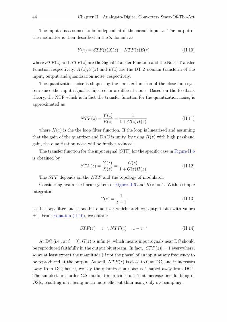
We will now focus on the basics of a Σ∆ modulator as it is the block thatinfluences the most the ADC performance. As illustrated in Figure II.6, a Σ∆
modulator is made of a loop transfer function, a clocked quantizer and feedbackdigital-to-analog converters.
Assuming that the quantizer can be modeled with a linear additive white noisemodel, the modulator is modeled as the two-input (x and e) one-output (y) linearsystem illustrated in Figure II.6. The loop filter has two sections, a forward filterG(z) and a feedback filter H(z). The input signal X(z) is applied and comparedwith the signal fed back by H(z), filtered through G(z) and quantized to give thedigital output. The quantization introduces an error E(z) which is modeled as input-signal-independent and directly added to the output, in the quantizer (representedas a summation point).
Figure II.6: Linear model of a Σ∆ modulator
44 Chapter II. Analog-to-Digital Converters State-Of-The-Art
The input e is assumed to be independent of the circuit input x. The output ofthe modulator is then described in the Z-domain as
Y (z) = STF (z)X(z) +NTF (z)E(z) (II.10)
where STF (z) and NTF (z) are the Signal Transfer Function and the Noise TransferFunction respectively. X(z), Y (z) and E(z) are the DT Z-domain transform of theinput, output and quantization noise, respectively.
The quantization noise is shaped by the transfer function of the close loop sys-tem since the input signal is injected in a different node. Based on the feedbacktheory, the NTF which is in fact the transfer function for the quantization noise, isapproximated as
NTF (z) =Y (z)
E(z)=
1
1 +G(z)H(z)(II.11)
where H(z) is the the loop filter function. If the loop is linearized and assumingthat the gain of the quantizer and DAC is unity, by using H(z) with high passbandgain, the quantization noise will be further reduced.
The transfer function for the input signal (STF) for the specific case in Figure II.6is obtained by
STF (z) =Y (z)
X(z)=
G(z)
1 +G(z)H(z)(II.12)
The STF depends on the NTF and the topology of modulator.
Considering again the linear system of Figure II.6 and H(z) = 1. With a simpleintegrator
G(z) =1
z − 1(II.13)
as the loop filter and a one-bit quantizer which produces output bits with values±1. From Equation (II.10), we obtain:
STF (z) = z−1, NTF (z) = 1− z−1 (II.14)
At DC (i.e., at f = 0), G(z) is infinite, which means input signals near DC shouldbe reproduced faithfully in the output bit stream. In fact, |STF (z)| = 1 everywhere,so we at least expect the magnitude (if not the phase) of an input at any frequency tobe reproduced at the output. As well, NTF (z) is close to 0 at DC, and it increasesaway from DC; hence, we say the quantization noise is "shaped away from DC".The simplest first-order Σ∆ modulator provides a 1.5-bit increase per doubling ofOSR, resulting in it being much more efficient than using only oversampling.

II.2. Basics of Σ∆ ADCs 45
By designing a higher order loop filter, the portion of in-band noise can be furtherreduced. In the case of a low pass filter, the generalized simplest expression of theNTF is given by:
NTF (z) = (1− z−1)L (II.15)
where L is the order of the loop filter. Figure II.7 illustrates the cases where Lis set to 1, 2 and 3. By increasing the order of the modulator, the noise is more
Figure II.7: NTFs obtained with 1st, 2nd and 3rd order loop filters
rejected away from the low frequencies. The relation between the SNR of a SigmaDelta ADC, the loop gain, the total quantization noise power and the samplingfrequency is expressed as:
SNRmax = 10 log10
1.5(N + 1)OSRN+1
πN+ 6.02(B − 1) (II.16)
where N is the order of the loop filter, OSR is the oversampling ratio and B is theresolution of the quantizer and feedback DACs. To achieve for example 60 dB SNR,several set of parameters can be selected. Increasing these parameters improves theresolution of the Σ∆ ADC assuming the overall system is stable.
Out-Of-Band Gain (OOBG) and Stability
The out-of-band gain (OOBG) of a modulator is defined as the gain at thefrequency Fs/2. The higher order NTF magnitudes are increasing 6 dB/order atFs/2 and need to be limited to ensure stability. High OOBG may cause overloadingof the quantizer and consequently make an unusable modulator. In order to increasestability, the reduction of the loop gain is done by properly adjusting internal scaling

46 Chapter II. Analog-to-Digital Converters State-Of-The-Art
stage. Stability is guaranteed if the internal modulator states or equivalently theintegrator outputs are bounded over time. To ensure stable operation, the input levelneeds to be less or equal to the full scale of the first feedback DAC. In higher-ordersingle-bit Σ∆ modulators, this input range is few dBs below the DAC full scale. Thisstable range is mainly determined by the NTF and the number of quantizer bits. Astability condition for single-bit modulators widely in use is the Lee’s Criterion [55]:
|NTFMAX | ≤ 1.5 (II.17)
whereNTFMAX is the maximummagnitude over all frequencies. A NTF with theOOBG set at 1.5 suffers significantly in terms of in-band noise suppression comparedto the ideal NTF. Also as the order of the modulator increases, the performancestarts to saturate and the desired performance boost due to higher order filters,loses its leverage. However, the introduction of multi-bit quantization enables higherorder systems to be stable even with a large OOBG.
II.2.1 Design Parameters
When designing a Σ∆ modulator several high level parameters need to be fixed.Table II.2 gathers some of those parameters.
Criteria ClassificationThe order of the loop filter 1 to 5
The NTF characteristic Low passBandpass
The loop filter circuitry Discrete timeContinuous time
The number of bits in a quantizer Single-bitMulti-bit
The number of quantizers employed Single loopCascaded
Table II.2: Σ∆ modulators classification
Each of those criteria is discussed in the following sections.
Oversampling ratio, modulator order and quantizer resolution
Generally, the order of H(z) (which must be strictly proper to ensure causality)is the maximum power of z in the denominator. It is possible to use a second-,third-, or even higher-order H(z) as a loop filter; generally, a converter of order

II.2. Basics of Σ∆ ADCs 47
L is built as a cascade of L integrators usually surrounded with feedforward andfeedback coefficients.
Oversampling is beneficial for improving the measured signal-to-noise ratio. Thisis true if the quantization noise inside the signal band is white, as it is in a traditionalADC: doubling the OSR (i.e., increasing it by an octave) halves the bandwidth, andhence the noise power, so that SNR improves by 3 dB. The SNR in an order-L Σ∆
modulator improves by 6L+ 3 dB per octave of oversampling [56] because the noiseis shaped by the loop filter. Thus, a high-order modulator is desirable because ofthe huge increase in converter DR obtained from a doubling of the OSR.
Not surprisingly, using a high-order modulator has drawbacks. First, the stabilityof the overall system with H(z) above order two becomes conditional: input signalswhose amplitudes are below but close to full scale (to be defined later) can causeoverload at the output of the integrators closer to the quantizer, which degrades DR[57]. As well, the placement of the poles and zeros of H(z) becomes a complicatedproblem, though many solutions have been proposed in the literature [58], [56].Furthermore, the technology in which the circuit is implemented and the circuitarchitecture itself will limit the maximum-achievable sampling rate and hence, limitthe OSR. Finally, the design of the decimator increases in complexity and area forlarger oversampling ratios.
It is possible to replace the single-bit quantizer with a multibit quantizer, e.g.,a flash converter [59]. This has three major benefits: it improves the overall Σ∆
modulator resolution, it decreases constraints on the decimation filter and it tends tomake higher-order modulators more stable. Furthermore, nonidealities in the quan-tizer (e.g., slightly misplaced levels or hysteresis) don’t degrade performance muchbecause the quantizer is preceded by several high-gain integrators, hence the input-referred error is small [60]. Its two major drawbacks are the increase in complexityof a multibit vs. a one-bit quantizer, and that the feedback DAC nonidealities aredirectly input-referred so that a slight error in one DAC level reduces converter per-formance substantially. There exist methods known as dynamic element matchingtechniques to compensate for multibit DAC level errors [61]. These aren’t neededin a single-bit design because one-bit quantizers are inherently linear [57].
II.2.2 NTF Implementation: Continuous Time vs. Discrete
Time
In Σ∆ modulators, the sampling operation can be done at two different places asdepicted in Figure II.8:

48 Chapter II. Analog-to-Digital Converters State-Of-The-Art
• before the adder block, it is called Discrete Time Σ∆ modulator
• between the loop filter and the quantizer, we then call them Continuous timeΣ∆ modulator.
Figure II.8: Continuous time and Discrete time Σ∆ architectures
DT Σ∆ modulator can be implemented with switched-capacitor (SC) [62] orswitched current (SI) [63] circuits. Those circuits have a maximum clock rate limitedby op amp bandwidths and by the fact that circuit waveforms need several timeconstants (i.e., clock periods) to settle. For a Σ∆ modulator built in a process withmaximum transistor speed fT , the maximum clock rate of an SC modulator is on theorder of fT . Furthermore, large glitches appear on op amp virtual ground nodes ofDT modulators due to switching transients. Another issue of DT domain is aliasing:signals separated by a multiple of the sampling frequency are indistinguishable.
DT Σ∆ modulators thus require a separate filter at their inputs to sufficientlyattenuate aliases. It is possible to build the loop filter as a continuous-time (CT)circuit (s), for example with transconductors and integrators [64]. The circuit tech-niques to build CT integrators rely on integrating a current proportional with theinput signal on a capacitor and read the output voltage. A simple, passive RC filtercannot be used to implement the desired transfer function since its pole is not atDC. With passive filters, a design method which takes into account this pole shifthas to be employed to map the desired NTF to the target loop topology.
Assuming the input signal is largely oversampled, the CT ADC in Figure II.8can be designed to be equivalent with the DT-based version if, for an identical inputx(t) during a clock cycle, w(t) presented to the quantizer at the end of the current

II.2. Basics of Σ∆ ADCs 49
clock cycle is identical with the one in the DT version, denoted as w(k) for t = kTs
[65],
wDT [k] = wCT (k)|t=kTs (II.18)
To satisfy this condition, the impulse response of the filters connecting the input tothe quantizer and the DAC output to the quantizer should have the same impulseresponse in the DT and the CT variants,
Z−1[HDT (z)
]= L−1
[RDAC(s) ·HCT (s)
](t)|t=kTs (II.19)
where HDT (z) is the equivalent loop filter transfer function in Z-domain, RDAC(s)
and HCT (s), respectively, the Laplace transfer functions of the DAC response andof the loop filter. Z−1 and L−1 are the inverse transform of each domain, the firstone resulting in an inherently sampled signal and the second one in a continuoussignal that is sampled at the instants t = nTs.
With the equations above satisfied, the time-domain signal sampled by the quan-tizer is identical in the DT and the CT designs, and, ideally, time-domain simulationresults obtained for the DT loop also apply to the CT loop. This is a major ad-vantage since behavioral time-domain simulations for CT loops typically take moretimes for processing compared to DT loops.
There are different architectures for Σ∆ ADCs and classification is usually basedon the number of modulators and the circuit realization of the loop filter. In general,Σ∆ ADCs are grouped as single-stage or multi-stage architectures.
II.2.3 Single Loop and Cascade Architectures
Single-stage Σ∆ ADCs are characterized by the presence of single quantizer in theirarchitectures. Based on the loop filter configuration, there are two generalized single-stage topologies: the cascade of integrators or resonators with feed forward (CRFF)and with feedback (CRFB) [45]. Assuming a 4th order DT Σ∆ ADC for example,Figure II.9 shows two different architectures.
In CRFF architecture all the output of the integrators feed forward to the inputof the quantizer and there is an additional path directly from input to the quan-tizer. In CRFB, Figure II.10 instead of feed-forward paths, there are feedback pathsbetween integrators and DACs. Coefficients ai in the feedback path of the digital-to-analog converter determine the noise transfer function and are required to obtaina stable operation of the converter. Coefficients gi are introduced to obtain zeros at

50 Chapter II. Analog-to-Digital Converters State-Of-The-Art
Figure II.9: CRFF architecture
Figure II.10: CRFB architecture
a signal frequency in the passband of the converter. In this manner an increase indynamic range over the passband is obtained. ci coefficients determine the gain ofthe integrator stages. Both architectures have enough degree of freedom to controlthe desired STF and NTF, and both have their own advantages and drawbacks.
In CRFF, synchronization issues are minimum since there is only one feedbackDAC. The input signal is directly passed to the input of the quantizer through b5
path in CRFF making the swing of the internal nodes between integrators smallerand relaxing the linearity requirement of the filters. However, the design of the adderin front of the quantizer in CRFF is a challenge especially in the application withhigh sampling frequency. The adder is connected to several resistive and capacitiveloads but the bandwidth requirement is extremely large to prevent excessive loopdelay. In addition, with non-ideal integrators in the ADCs, the out-band blockerrejection is minimized in CRFF due to the b1 feedforward path.
Compared to the Σ∆ modulator using CRFB topology, the modulator usingCRFF architecture requires only one feedback DAC, which can reduce the powerconsumption and area. On the other hand, the STF(z) of Σ∆ modulator using CIFFtopology shows out-of band peaking and in some cases results in loop instability ifthere exists large out-of band interferences.

II.2. Basics of Σ∆ ADCs 51
Cascade Architectures
In order to perform high order modulator with high stability, low order modula-tors are cascaded. Most of them are composed of modulators of order 1 to 3. Eachmodulator processes a portion of the quantization noise of the previous modulatorand digital reprocessing is performed on the outputs. This gives a better accuracyin the useful band. There are several cascade architectures. Among those architec-tures, the most common is the Multi stAge noise SHaping (MASH) [66]structureFigure II.11 .
Figure II.11: Dicrete Time MASH architecture
The MASH architecture is to digitize the difference between the input of thequantizer and the output of the DAC at each clock pulse. Thus each modulatorprocesses the quantization error made by the previous stage.For DT implementations, the required cancellation noise filters T1(z) and T2(z) areeasily derived so that the noise contribution of each stage is null except for the lastmodulator of the chain:
S(z) =T1(z)G1(z)H1(z)
1 +H1(z)X(z)+
(T1(z)
1 +H1(z)− T2(z)G2(z)H2(z)
1 +H2(z)
)N1(z)+
T2(z)
1 +H2(z)N2(z)
(II.20)
T1(z)
1 +H1(z)−T2(z)G2(z)H2(z)
1 +H2(z)= 0 ⇔ T1(z)
T2(z)=G2(z)H2(z) (1 +H1(z))
1 +H2(z)(II.21)
In the case of CT implementations, this filter identification requires to take intoaccount additional information. Therefore the hardware complexity is increased andthe circuit is more prone to mismatches. The derivation of the noise cancellation

52 Chapter II. Analog-to-Digital Converters State-Of-The-Art
filters consists in writing the exact transfer functions achieved all along the cascadedmodulator.
II.3 Σ∆ ADC State-Of-The-Art
We saw in Chapter 1 that in order to perform DPD, the feedback ADC should haveat least 60 dB SNR in the bandwidth of interest. In the case of a 20MHz LTE signal,assuming we capture up to the third non-linearity order, this leads to an SNR ofat least 60 dB in 100MHz bandwidth. Table II.3 compares performance of few Σ∆
modulators. Some of those modulators have their performance close to our ADCspecifications for DPD. The architectures of [67], [68], [69] and [43] have a bandclose to or equal to 20MHz and consume between 8.5 and 20mW with a single loop.Assuming that each channel has a similar consumption, this would correspond toa total consumption between 42.5 and 100mW. [70] and [71] have Σ∆ modulatorswith respectively 125 and 150MHz band and consume 256 and 550mW. Their highperformance can be achieved thanks to high oversampling ratios.
Year FoM Techno Area BW SNDR Quant Order P Fs[J/step] [nm] [mm2] [MHz] [dB] [mW] [MHz]
2006 [72] 122f 130 1.2 20 74 4b 3 20 6402011 [73] 704.7f 45 0.9 125 65 4b 3 256 40002012 [67] 190.4f 45 0.49 60 60.5 1b 3 750 60002012 [70] 0.19p 40 0.4 20 70 1b 6 20 32002012 [74] 0.8p 65 5.5 150 - 17 l1 6 550 40002013 [68] 207f 90 0.266 61.7 50 4b 3 20.6 10002014 [71] 0.38p 65 0.2 24 58 9 l 4 12 8002014 [75] 697.3f 28 0.9 53 71.8 17 l 0-3 235 32002014 [69] 88f 90 0.19 25 67.5 4b 3 8.5 5002015 [76] 177f 28 0.34 50 74.9 15/7 l 3-1 80.4 18002015 [43] 74.2f 20 0.1 80 67.5 3b 4 23 2184
Table II.3: State-of-the-art CT Σ∆ ADCs
Cascaded architectures are used to achieve better performance by maintainingthe stability of modulators. [75] and [76] are cascaded architectures having approx-imately 50MHz bandwidth and consuming respectively 235 and 80.4mW. However,cascaded ADCs such as MASH or Sturdy MASH (SMASH) [77] are sensitive toprocess, voltage and temperature variations.
In order to increase the signal bandwidth that the modulator can deal with, avariety of methods can be used such as using higher sampling frequency, increasing

II.3. Σ∆ ADC State-Of-The-Art 53
the order of the modulator and the number of quantizer bits. However, each ofthem has a price and is restricted by technology deployed. Using above mentionedmethods to increase OSR make the design of the modulator more complicated andmay cause stability problem which require to be dealt with carefully. Furthermore,low power consumption is required to decrease the overall DPD power consumption.
Another efficient and attractive way to increase the OSR, is to consider the time-interleaving technique where parallelism can be incorporated in ADCs in order toincrease the effective sampling rate [78], [79], [80], [81]. This approach is a practicalsolution that does not necessitate state of art technologies. A time-interleaved Σ∆
modulator can be a good solution for this problem, since the signal bandwidth of themodulator can be simply extended by adding more channels instead of increasingthe sampling clock frequency. The most simplistic parallel TI Σ∆ ADC can beconstructed by placing Σ∆ ADCs in parallel and applying the input signal to all ofthe channels simultaneously.
Figure II.12: Block diagram of a parallel ADC [54]
As shown in Figure II.12, the outputs from all of the channels are then digitallyrecombined to create the overall output.
Even though the two-channel TI modulator is the simplest form, the circuit-level implementation using the above approaches still has drawbacks due to severalpractical limitations that are discussed in the following sections. Furthermore, time-interleaving requires calibration technique to cope with mismatch between channels.

54 Chapter II. Analog-to-Digital Converters State-Of-The-Art
The above show that TI Σ∆ modulators is not a simple circuit implementation, lowpower consumption, and high area efficiency solution for a DPD system.
Another approach to combine Σ∆ in parallel is to use the frequency band de-composition architecture [82] [83] [84]. In this architecture, each channel consists ofa bandpass Σ∆ modulator with a quantization null at a different frequency. Thus,each channel passes oneM th of the signal frequency band when there areM channels
The frequency-band-decomposition (FBD) ADC is derived from the concept offilter banks [54].
Figure II.13: FBD ADC
Each channel converts a band of frequencies and, when the outputs are recom-bined, the overall system is all-pass. An example of the FBD architecture is illus-trated in Figure II.13. The Σ∆ modulator on each channel has been broken up intothe signal path and the quantization noise path. As shown in the figure, the quan-tization noise filter is determined by the bandpass Σ∆ modulator on each channeland thus is different on each channel. Following each Σ∆ modulator is a digitalfilter that passes a band of frequencies corresponding to the null in the quantizationnoise filter. The signal path consists of a simple delay which corresponds to thegroup delay of the Σ∆ modulator. Since the quantization noise among differentchannels is uncorrelated, the total power of the quantization noise is the sum of thequantization noise power of each channel. The high sensitivity to central frequenciesof modulators is the main drawback of the FBD technique. An extended FBD pro-posed in [83] decreases the impact of manufacturing variations. However, it requiresa digital calibration.
The architecture of the Multi Stage Noise Band Cancellation (MSNBC) ADC ispresented in Figure II.14.

II.4. Conclusion 55
Figure II.14: MSNBC ADC architecture [85]
The signal to digitize is assumed to be made up of a band of high power andlow power adjacent bands as shown in Figure I.8 centered at Fc0. Σ∆0 modulatordigitizes the high power main band. Then, the output of the modulator consists ofthat part of the signal and the shaped quantization noise. The signal u, which isthe attenuated main signal and shaped quantization noise, is digitized in adjacentchannels with Fc1A and Fc1B. Combining the outputs of Σ∆0 and Σ∆1A and Σ∆1B
subtract quantization noise of Σ∆0 in adjacent channels.
II.4 Conclusion
ADC requirements for DPD obtained in Chapter 1 added to a study of state-of-the-art, allowed us to select architecture in this chapter. We saw that pipeline ADCs arecommonly used in the feedback path of BTS DPD systems. They can digitize widebandwidth signals but consume a lot of power. Σ∆ ADCs combine oversamplingand noise shaping techniques to push quantization noise out of the band of interestand improve the SNR. They are extensively used in audio applications, where thesignal bandwidth signals is low. Therefore in order to take advantage of the energyefficiency of Σ∆ ADCs and use them for wide bandwidth applications, they shouldbe combined with techniques such as time-interleaving and parallelization. TheMSNBC architecture is particularly attractive for subband DPD given that theshape of the signal at the output of the PA is known and the use of bandpass Σ∆
converters avoid using complex analog filters.

56 Chapter II. Analog-to-Digital Converters State-Of-The-Art
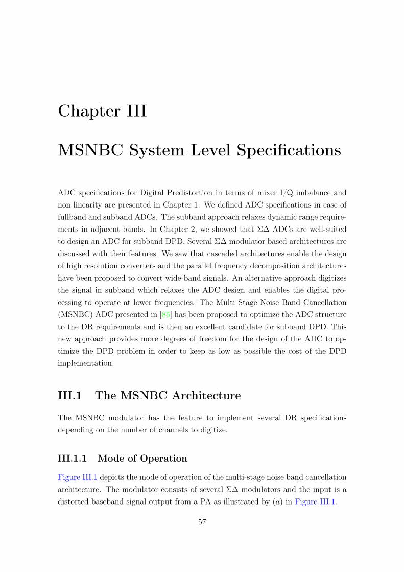
Chapter III
MSNBC System Level Specifications
ADC specifications for Digital Predistortion in terms of mixer I/Q imbalance andnon linearity are presented in Chapter 1. We defined ADC specifications in case offullband and subband ADCs. The subband approach relaxes dynamic range require-ments in adjacent bands. In Chapter 2, we showed that Σ∆ ADCs are well-suitedto design an ADC for subband DPD. Several Σ∆ modulator based architectures arediscussed with their features. We saw that cascaded architectures enable the designof high resolution converters and the parallel frequency decomposition architectureshave been proposed to convert wide-band signals. An alternative approach digitizesthe signal in subband which relaxes the ADC design and enables the digital pro-cessing to operate at lower frequencies. The Multi Stage Noise Band Cancellation(MSNBC) ADC presented in [85] has been proposed to optimize the ADC structureto the DR requirements and is then an excellent candidate for subband DPD. Thisnew approach provides more degrees of freedom for the design of the ADC to op-timize the DPD problem in order to keep as low as possible the cost of the DPDimplementation.
III.1 The MSNBC Architecture
The MSNBC modulator has the feature to implement several DR specificationsdepending on the number of channels to digitize.
III.1.1 Mode of Operation
Figure III.1 depicts the mode of operation of the multi-stage noise band cancellationarchitecture. The modulator consists of several Σ∆ modulators and the input is adistorted baseband signal output from a PA as illustrated by (a) in Figure III.1.
57

58 Chapter III. MSNBC System Level Specifications
Figure III.1: MSNBC modulator operating mode
The primary modulator Σ∆0 is centered at Fc0 and digitizes the high power cen-tral subband of bandwidth BW . Modulators Σ∆1A and Σ∆1B, respectively centeredat Fc0 +BW and Fc0−BW digitize the first adjacent subbands of bandwidth BW .Second adjacent subbands are digitized by Σ∆2A and Σ∆2B modulators centered atFc0 ± 2BW .
The discrete-time linear model of the output signal of Σ∆0, is:
S0(z) = STF0(z)Y (z) +NTF0(z)N0(z) (III.1)
with STF0 and NTF0 respectively the signal and noise transfer functions of Σ∆0,and N0 its quantization noise. This signal is shown in Figure III.1 (b). Due toquantization noise, S0 is not adapted to accurately predistort the input signal of thePA and adjacent channels should be digitized for an accurate DPD. Assuming forthe sake of simplicity a unitary STF in the band of operation, the signal U defined byU(z) = Y (z)− S0(z) can be seen as a negative version of Σ∆0 shaped quantizationnoise. The residual signal transfer function (RSTF) defined as
RSTF (z) = 1− STF (z) (III.2)
is introduced for this architecture. This function represents the cancellation of Y inU .
S0 is subtracted to the continuous time input signal and fed to Σ∆1A and Σ∆1B.Assuming that there is no gain between the two stages, the output of secondary

III.1. The MSNBC Architecture 59
modulators can be modeled as:
YD1A(z) = STF1A(z) (Y (z)RSTF (z)−N0(z)NTF0(z))
+N1A(z)NTF1A(z) (III.3)
Figure III.1 (d) illustrates YD1A, the output of Σ∆1A made of U and Σ∆1A shapedquantization noise. Figure III.1 (e) the results of the addition of S0 and YD1A. Thisis expressed as following:
S1A(z) = Y (z) (STF0(z) + STF1A(z)RSTF (z))
+N0(z)NTF0(z) (1− STF1A(z))
+N1A(z)NTF1A(z) (III.4)
We furthermore assume that the STF of Σ∆1A is equal to 1. Thus, the RSTFvanishes and Equation (III.4) is expressed as:
S1A|STFi=1(z) = Y (z) +N1A(z)NTF1A(z) (III.5)
Adding the output of Σ∆0 to the Σ∆1A cancels out the noise of the primary modu-lator in the adjacent bandwidth as shown in Equation (III.4).
This leads to an improvement of the signal-to-noise ratio in this subband. Thesame principle applies to other adjacent modulators and enables to improve theSNR. Then, the signal in the adjacent band can be selected using a digital signalprocessing as if one had used a dedicated Σ∆ M but without the use of an analogfilter.
General case: STF (z) 6= 1
In the previous paragraph, the mode of operation of the MSNBC architectureand linear model were depicted by presuming that the STF is equal to 1. This is canbe easily achieved in discrete time modulator, but is not always the case especiallyfor continuous time modulators.
When the assumption on the unitary STF is not valid, Noise Cancellation Filters(NCF) should be applied to the output of the primary and secondary modulatorsbefore performing the sum of those signals. The NCFs allow to achieve the rightnoise suppression we will have to process the output of each modulator.

60 Chapter III. MSNBC System Level Specifications
Figure III.2 portrays the structure of the General MSNBC architecture whichincludes noise cancellation filters.
Figure III.2: The general MSNBC Architecture
The Z-transform of the output signal of Σ∆1A can be expressed as:
YD1A(z) = STF1A(z) (X(z)RSTF (z)−N0(z)NTF0(z)) +N1A(z)NTF1A(z)
(III.6)Summing S0(z) and YD1A(z) leads to:
S1A = NCFD1A(z) · S0(z) +NCFN
1A(z) · Y1A(z) (III.7)
Expanding the expression of YD1A(z):
S1A = X(z)(NCFD
1A(z) · STF0(z) +NCFN1A(z) ·RSTF (z) · STF1A(z)
)+NTF0(z) ·N0(z)
(NCFD
1A(z)−NCFN1A(z)STF1A(z)
)+NCFN
1A(z) ·NTF1A(z) ·N1A(z) (III.8)
We then deduce from Equation (III.8) that N0(z) is be suppressed if:
NCFN1A(z)
NCFD1A(z)
=1
STF1A(z)(III.9)

III.2. Impact of Non-Idealities 61
We define:
NCFN1A(z) = Numerator
(1
STF1A(z)
)(III.10)
NCFD1A(z) = Denominator
(1
STF1A(z)
)(III.11)
Thus, NCF expressions depend only on the STF of the secondary modulator.
III.1.2 Degrees of Freedom / Key Design Parameters
Given the mode of operation presented above, several degrees of freedom can impactthe design of the MSNBC modulator. The first and key design parameter is thecenter frequency Fc0 of the primary modulator, as first adjacent modulators will becentered at Fc0 ± BW . In fact depending on the frequency at which the signal isdown-converted by the mixer, one might need that the center frequency is at a LowIntermediate Frequency (LIF) or at an Intermediate frequency (IF).
The quantizer of secondary modulators is important as well. As presented inthe mode of operation, the signal sent to the second modulator U is the shapedquantization noise of the first modulator. This means that the rms voltage of thissignal is low compared to the rms voltage of the input signal of the first modulator.Thus, two options are offered for adjacent modulators: on the one hand, the inputsignal can be scaled so that an identical quantizer as the one in the first modulatorcan be used. This means that a gain should be applied to the shaped quantizationnoise before being digitized by the adjacent modulator. On the other hand, the signalis not scaled, thus, the reference voltage of the quantizer of secondary modulatorsis decreased.
The following section explains in more details design choices for the MSNBC.
III.2 Impact of Non-Idealities
For wide-band and medium-resolution applications, continuous-time modulators arepreferred over discrete time modulators because of their better energy efficiency andinherent anti-aliasing filter. However, design constraints that were not consideredin discrete time must be taken into account.
A CT Σ∆ modulator consists of three major building blocks: a continuous-timeloop filter H(s), a clocked internal quantizer (ADC) and a continuous-time feedbackDAC. Due to variations during the IC manufacturing process and through circuitimperfections, each of these components deviates from its ideal behavior. Thus,

62 Chapter III. MSNBC System Level Specifications
the first classification of errors is their originating building block. Furthermore, thedeteriorating influence of the different errors on the ideal modulator behavior can beused to specify two categories of non-idealities: those, which alter the ideal STF andNTF function by altering their poles and zeros, and aside the non-idealities whichintroduce noise or distortion into the system.
In order to present a clearly arranged summary of the influence of non-idealitieson continuous-time Σ∆ modulators, it is important to identify the errors by theiroriginating building block. Table III.1 gather some of those non-idealities.
Block Non-ideality Impact
Integrator Op-amp
Finite Gain Noise floor, stabilityFinite Gain bandwidth Noise floor, distortions
Finite Slewrate Quantization noise, distortionsThermal and Flicker noise Noise floor
Gain Time constant mismatch Noise shaphing, stability
Quantizer Metastability Stability, Noise, distortionsHysteresis Noise floor
DACDelay Stability, Noise floor
Unequal rising and falling times Noise floor, distortionsNon-linearity Noise and distortions
Clock Random clock jitter NoiseAccumulated jitter Skirt around signal
Table III.1: Non-idealities in CT Σ∆ modulators
The impact of those non-idealities is studied for the case of the MSNBC archi-tecture.
III.2.1 Loop Filter
The loop filter transfer function is the main performance determining part in aΣ∆ modulator, because it defines the noise-transfer function and therewith thequantization noise-shaping behavior. Principally, the complete loop filter usuallyconsists of several first-order filters, which are commonly arranged in a feedback orforward architecture. Taking CT Σ∆ modulators into consideration, the single filtersare realized using either RC-integrator or gmC-integrator or even LC-resonators forbandpass noise shaping. Without loss of generality, in the following active RC-integrators are considered because they have higher linearity performance and betterrobustness over Process Voltage and Temperature (PVT) variations compared togm-C integrators.

III.2. Impact of Non-Idealities 63
As shown in Table III.1, the loop filter has imperfections mainly derived fromthe variation of the time constant, gain, product gain band and slewrate finiteoperational amplifiers, mismatch coefficients and noise.
Finite Gain and Gain-bandwidth
One of the most well-studied non ideal effects in Σ∆ modulators is that of finiteDC gain of the operational amplifiers. An ideal integrator can be modeled by thefollowing function:
Hideal(s) =1
s.Ts(III.12)
From Equation (III.12), for a frequency-independent, but finite amplifier gainADC , the transfer function of an RC-integrator can be derived to:
HADCRC (s) =
11
ADC+ s ∗RC (III.13)
In the case of single-loop Σ∆ modulation, the DC gain of the incorporated ampli-fiers should be in the range of the oversampling ratio Adc ≈ OSR of the modulator[86]. This requirement keeps every part of the in-band noise proportional to the idealnoise shaping suppression. In contrast to single-loop architectures, multi loop Σ∆
modulators suffer tremendously from integrator leakage. This is due to the principleof noise cancellation of the lower stages by the higher loops in the cascade. Theseare designed to eliminate the ideal quantization noise from the previous stages, butthey are not able to also reject the non ideal noise components. Thus, these nonideal parts of the quantization noise leak into the overall output.
The impact of finite DC gain is studied for an 2-4 MSNBC. Simulations areperformed with VerilogA model of integrator and by using the relation in Equa-tion (III.12) for ideal integrators and Equation (III.13) for the cases called realintegrators. We assume for those simulations that all integrators have the same DCgain. Results are presented in Figure III.3. Figure at the top present the impactof DC gain variations on SNR1_prim, which corresponds to the SNR in the primaryband of the reconstructed signal S1(z). The figure at the bottom is the impact ofDC gain variations on SNR1_adj, which is the SNR in the adjacent band of thereconstructed signal S1(z). The impact is studied for two cases: one assuming aunitary STF in Σ∆0 (STF0) and the other with a filtering STF0. As expectedDC gain do not impact performance of an architecture with ideal integrators. Weobserve however a degradation of the SNR in the primary and adjacent channels

64 Chapter III. MSNBC System Level Specifications
when the gain of integrators are lower than 40 dB. For DC gain greater than 40 dBperformance of ideal and real integrator are the same for SNR1_prim and SNR1_adj.Furthermore, the type of STF is not critical for DC gain variations.
10 20 30 40 50 60 70 80
DC Gain (dB)
55
60
65
70
75
80
85
90
SN
R (
dB
)
Impact of DC Gain on SNR1_prim
performance
Ideal integrators and Unity STF0
ReaI integrators and Unity STF0
Ideal integrators and Filtering STF0
ReaI integrators and Filtering STF0
10 20 30 40 50 60 70 80
DC Gain (dB)
5
10
15
20
25
30
SN
R (
dB
)
Impact of DC Gain on SNR1_adj
performance
Ideal integrators and Unity STF0
Ideal integrators and Filtering STF0
ReaI integrators and Filtering STF0
ReaI integrators and Unity STF0
Figure III.3: Effects of finite DC gain on SNR
Another important cause of non-ideal behavior are errors due to the integra-tor dynamics; here, the first influence to consider is a finite gain-bandwidth prod-uct (GBW) of the operational amplifiers in the integrators, which introduces non-dominant poles into the integrator transfer function.
Finite GBW is known from DT modulator implementations to cause distortionand increased in-band noise. The requirements can actually be very high: Boserfound that in many sampled-data analog filters, the unity-gain bandwidth of the

III.2. Impact of Non-Idealities 65
OpAmps has to be at least an order of magnitude higher than the sampling rate; inDT Σ∆ modulators, this is somewhat relaxed.
In contrast, CT implementations are claimed throughout the published literatureto work with much lower GBW of the OpAmps. This has been largely attributed tothe lack of the high-current peaks of switched capacitor implemented DT circuits.
The impact of finite Gain Bandwidth product is studied for an 2-4 MSNBCmodulator. The transfer function of an RC-integrator with finite gain-bandwidthGBW can be derived to:
HGBWRC (s) =
1
s ∗RC ∗GBW
GBW+ 1RC
sGBW+ 1
RC
+ 1(III.14)
Results are presented in Figure III.4. In this simulation, all integrators have thesame GBW. Simulations are performed with VerilogA model of integrator and byusing the relation in Equation (III.12) for ideal integrators and Equation (III.14) forthe cases called real integrators. We assume for those simulations that all integratorshave the same GBW. As expected again, the higher the gain bandwidth product,the better the performance of the modulator. Ideal and real integrator show thesame performance for when GBW in Hz or rad/s, is greater than 2πFs.
A straightforward solution to compensate for finite DC gain and GBW is to tunethe passive components. However this requires a large and accurate capacitor arrayfor every integrator, thus increasing the core area of the circuit enormously.
Time constant variations
Variations of the integrator gain, determined by the scaling coefficients are a wellknown non-ideal characteristic of single-loop and even more of cascaded Σ∆ mod-ulators. In DT modulators implemented in SC technique, the integrator gains aremapped into capacitor ratios, which are intrinsically precise and variations lowerthan 0.1% are typical. In contrast, in CT Σ∆ modulators, integrator gains aremapped into resistor-capacitor products, which are known to largely vary overprocess, temperature, etc.; process variations of the absolute component values of10− 20% are not unusual, which increases the possible variation of the RC-productto more than 30%. Therefore this error is a major one to investigate.
The impact of Time constant variations is studied for an 2-4 MSNBC. Thetransfer function of an RC-integrator with time-constant variation can be derivedto:

66 Chapter III. MSNBC System Level Specifications
10-1 100 101
Normalized GBW (GBW/2 Fs)
60
65
70
75
80
85
90
SN
R (
dB
)
Impact of GBW on SNR1_prim
performance
Ideal integrators and Unity STF0
ReaI integrators and Unity STF0
Ideal integrators and Filtering STF0
ReaI integrators and Filtering STF0
10-1 100 101
Normalized GBW (GBW/2 Fs)
-20
-15
-10
-5
0
5
10
15
20
25
30
SN
R (
dB
)
Impact of GBW on SNR1_adj
performance
Ideal integrators and Unity STF0
ReaI integrators and Unity STF0
Ideal integrators and Filtering STF0
ReaI integrators and Filtering STF0
Figure III.4: Effects of finite Gain - Bandwidth on SNR
H∆RCRC (s) =
1
s ∗RC(1 + ∆RC)(III.15)
Simulations are performed with VerilogA model of integrator and by using therelation in Equation (III.12) for ideal integrators and Equation (III.15) for the casescalled real integrators. We assume for those simulations that all integrators havethe same RC variation. Results are presented in Figure III.5.
RC time constant variation has an impact on the SNR. As shown in Figure III.5a 10% variation of the SQNR reduces the SQNR by 5 dB.

III.2. Impact of Non-Idealities 67
-40 -30 -20 -10 0 10 20 30 40
RC (%)
78
80
82
84
86
88
90
SN
R (
dB
)
Impact of time constant variations on SNR1_prim
performance
Ideal integrators and Unity STF0
ReaI integrators and Unity STF0
Ideal integrators and Filtering STF0
ReaI integrators and Filtering STF0
-40 -30 -20 -10 0 10 20 30 40
RC (%)
-20
-15
-10
-5
0
5
10
15
20
25
30
SN
R (
dB
)
Impact of time constant variations on SNR1_adj
performance
Ideal integrators and Unity STF0
ReaI integrators and Unity STF0
Ideal integrators and Filtering STF0
ReaI integrators and Filtering STF0
Figure III.5: Effects of RC variations on SNR
III.2.2 Digital-to-Analog Converters
DelayFor an ideal modulator, the steps of quantizing and converting digital to analogsignals are instantaneous. However, in the real case, there is a processing time dueto the transition time of the transistors. This delay, called excess loop delay, greatlyaffects the performance of modulators and can make them unstable. As a result,several delay compensation techniques have emerged. The method proposed by[87] makes it possible to design a loop filter identical to the filter without delay bycompensating for a delay up to a clock period. This compensation is to the detriment

68 Chapter III. MSNBC System Level Specifications
of an additional amplifier and DAC that results in increased power consumption.[72] enhances the previous technique using a digital differentiator and gets rid ofthe use of the additional amplifier. [88] suggests a compensation by modifying theintegrators, [89] a residual delay compensation by modifying the last integrator and[90] a purely digital compensation.
Among those techniques, [72] is simple to implement and does not have a bigimpact on the STF. Moreover, since this method restricts us to compensate fordelays τd such that τeld + τd ≤ Ts, we choose to compensate for delays of up to halfa delay clock period.
0 0.1 0.2 0.3 0.4 0.5
Ts
55
60
65
70
75
80
85
90
SN
R (
dB
)
Impact of delay on SNR1_prim
Ideal Unit
ELD Cl Unit
ELD FF Unit
Delayed Unit
Ideal Filt
ELD Cl Filt
ELD FF Filt
Delayed Filt
0 0.1 0.2 0.3 0.4 0.5
Ts
-50
-40
-30
-20
-10
0
10
20
30
SN
R (
dB
)
Impact of delay on SNR1_adj
Ideal Unit
ELD Cl Unit
ELD FF Unit
Delayed Unit
Ideal Filt
ELD Cl Filt
ELD FF Filt
Delayed Filt
Figure III.6: Effect of loop delay on the SQNR
Figure III.6 shows the influence of the loop delay on the converter and the effectof the compensation of the same delay on SNRY 0_pri and SNRS1_adj. For thsosesimulations 2 STF cases are studied: in one case the STFs are unitary in all modula-tors, and in the other cases the STFs are filtering. For each STF case, the impact ofdelay is studied for the ideal integrator without delay as in Equation (III.12), withdelay, with classical and feedforward delay compensation techniques.
It follows that the modulator becomes unstable for a delay greater than 0.35Ts

III.2. Impact of Non-Idealities 69
and that the classical and feedforward ELD compensation technique used perfectlycorrects this delay up to Ts/2.
Unequal rising and falling times and mismatch
At the opposite of DT modulators, CT modulators are affected by inter-symbolinterference (ISI). ISI is an error which shows up during transition of DAC elementsand can be caused by asymmetric on and off switching. ISI error is problematic forhigh speed CT modulators as it increases with sampling frequency.
An analog approach to reduce ISI error is to use return-to-zero (RZ) coding inDACs. However, it increases sensitivity to clock jitter compared to non-return-to-zero (NRZ) coding. RZ coding also reduces the output signal amplitude for the sametotal DAC power, and introduces large discontinuities in the output waveform. Thisin turn increases the linearity and slew rate requirements of the output filter [91].
In addition to ISI, DACs and more generally analog components suffer from mis-match. Two transistors or capacitors, for example, that are ideally supposed to beidentical suffer from mismatch due to process variations. Dynamic Element Match-ing (DEM) algorithms can be used to handle mismatch errors of DACs. Amongthose techniques Data Weight Averaging (DWA) is fairly easy to implement. Thepurpose of the DWA is to use the maximum number of unit current cell in order toaverage the static mismatch error over time. However, DWA increases the switchingactivity of the DAC. Thus, for a DAC suffering from inter-symbol interference, DWAdegrades performance.
The ISI error model presented in [91] was implemented in Matlab with theMSNBC architecture. For those simulations, all DACs are assumed to have differentrising and falling times. For a current quantizer value Y [n] = 4 and a previous valueY [n−1] = 3, thermometric and DWA encoders as presented in Figure III.7 are usedto estimate the states of the quantizer output.
Figure III.8 explains the methodology used to estimate analog errors in theMatlab code.
Thus, the number of changed and unchanged states are calculated and totalerror is added to the ideal signal. This methodology is applied to a 2-4 MSNBCmodulator. The primary modulator is a second order lowpass modulator and thesecondary modulator is a fourth order bandpass modulator centered at Fc = 20MHz.The input signal is at Fin = 2.5MHz and the sampling frequency is Fs = 640MHz.Several cases are studied in Figure III.9 and Figure III.10:
• Case 1: no mismatch, DWA OFF

70 Chapter III. MSNBC System Level Specifications
Figure III.7: Quantizer output with the thermometric code and normal DWA
Figure III.8: Method used to calculate errors
• Case 2: 1% mismatch, DWA OFF
• Case 3: 1% mismatch, DWA ON
Figure III.9 illustrates Case 1. When tr = tf , the SNR in the primary band ofS0 SNRpri_S0 and the SNR in the adjacent band of S1, SNRadj_S1 are constant over10% variation. When tr 6= tf , performance are degraded as the difference is high.

III.2. Impact of Non-Idealities 71
0 0.001 0.002 0.003 0.004 0.005 0.006 0.007 0.008 0.009 0.0155
60
65
70
75
80
85
tr
SN
R p
rin
c
tf=0.9tr
tf=0.92tr
tf=0.94tr
tf=0.96tr
tf=0.98tr
tf=tr
tf=1.02tr
tf=1.04tr
tf=1.06tr
tf=1.08tr
tf=1.1tr
0 0.001 0.002 0.003 0.004 0.005 0.006 0.007 0.008 0.009 0.01−50
−40
−30
−20
−10
0
10
20
30
tr
SN
R a
dj
tf=0.9tr
tf=0.92tr
tf=0.94tr
tf=0.96tr
tf=0.98tr
tf=tr
tf=1.02tr
tf=1.04tr
tf=1.06tr
tf=1.08tr
tf=1.1tr
Figure III.9: Impact of rising and falling times on the MSNBC performance
Case 2 and 31 are presented in Figure III.10. Those results proves the impactof DWA on a system with 1% DAC mismatch. The left plots are SNRpri_S0 andSNRadj_S1 values without DWA. SNRpri_S0 is 30 dB less compare to Case 1, wherethere is no mismatch.
The right plots represent Case 3. We can see that DWA improves SNRpri_S0
values, but performance is rapidly degraded compared to those obtained in Case 1.We decide not to use DWA and to take care of mismatch in the design by using bigsize components.
III.2.3 The Clock Signal
Clock jitter, i.e., statistical variations of the sampling frequency, depends on thepurity of the clock source. Typically, Σ∆ modulators were found to be rathertolerant to timing jitter. However, continuous-time modulators are affected more
1The same legend is used for all cases

72 Chapter III. MSNBC System Level Specifications
0 0.001 0.002 0.003 0.004 0.005 0.006 0.007 0.008 0.009 0.0130
40
50
60
70
80
90
tr
SN
R p
rin
c
0 0.001 0.002 0.003 0.004 0.005 0.006 0.007 0.008 0.009 0.0130
40
50
60
70
80
90
tr
SN
R p
rin
c
0 0.001 0.002 0.003 0.004 0.005 0.006 0.007 0.008 0.009 0.01−50
−40
−30
−20
−10
0
10
20
30
tr
SN
R a
dj
0 0.001 0.002 0.003 0.004 0.005 0.006 0.007 0.008 0.009 0.01−50
−40
−30
−20
−10
0
10
20
30
tr
SN
R a
dj
Figure III.10: Impact of DWA on performance of a MSNBC with 1% DAC mis-match. Left figures are results with mismatch and DWA OFF, and right figures areresults with mismatch and DWA ON
severely by clock jitter than their discrete-time counterparts, as shown manifold inthe published literature.
The difference of clock jitter influence on DT and CT Σ∆ modulators appearssince both feature different sources of clock jitter errors in the modulator loop.Suppose nonuniform sampling takes place, the decision of the quantizer in DT mod-ulators remains correct in first-order approximation, because the integrators aredesigned to settle to a given accuracy within half the sampling period. Therefore,the performance degradation due to clock jitter is primarily caused by errors inthe front-end S/H circuit, where jitter caused sampling misalignment produces anequivalent amplitude error that degrades the SNR.
A CT implementation faces two error sources due to clock jitter: first, similar tothe sampling errors in the DT modulator, the sampled internal quantizer is proneto jitter affected sampling errors. But these errors enter the system at the pointof maximum error suppression, i.e., at the quantizer, and hence may be neglected
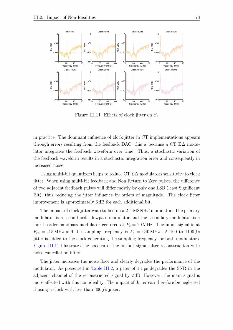
III.2. Impact of Non-Idealities 73
0 20 40 60−150
−100
−50
0
Frequency (MHz)
PS
D (
dB
)
Jitter=0fs
0 20 40 60−150
−100
−50
0
Frequency (MHz)
PS
D (
dB
)
Jitter=100fs
0 20 40 60−150
−100
−50
0
Frequency (MHz)
PS
D (
dB
)
Jitter=300fs
0 20 40 60−150
−100
−50
0
Frequency (MHz)
PS
D (
dB
)
Jitter=500fs
0 20 40 60−150
−100
−50
0
Frequency (MHz)
PS
D (
dB
)
Jitter=700fs
0 20 40 60−150
−100
−50
0
Frequency (MHz)
PS
D (
dB
)
Jitter=900fs
0 20 40 60−150
−100
−50
0
Frequency (MHz)
PS
D (
dB
)
Jitter=1000fs
0 20 40 60−150
−100
−50
0
Frequency (MHz)
PS
D (
dB
)
Jitter=1100fs
Figure III.11: Effects of clock jitter on S1
in practice. The dominant influence of clock jitter in CT implementations appearsthrough errors resulting from the feedback DAC: this is because a CT Σ∆ modu-lator integrates the feedback waveform over time. Thus, a stochastic variation ofthe feedback waveform results in a stochastic integration error and consequently inincreased noise.
Using multi-bit quantizers helps to reduce CT Σ∆ modulators sensitivity to clockjitter. When using multi-bit feedback and Non Return to Zero pulses, the differenceof two adjacent feedback pulses will differ mostly by only one LSB (least SignificantBit), thus reducing the jitter influence by orders of magnitude. The clock jitterimprovement is approximately 6 dB for each additional bit.
The impact of clock jitter was studied on a 2-4 MSNBC modulator. The primarymodulator is a second order lowpass modulator and the secondary modulator is afourth order bandpass modulator centered at Fc = 20MHz. The input signal is atFin = 2.5MHz and the sampling frequency is Fs = 640MHz. A 100 to 1100 fs
jitter is added to the clock generating the sampling frequency for both modulators.Figure III.11 illustrates the spectra of the output signal after reconstruction withnoise cancellation filters.
The jitter increases the noise floor and clearly degrades the performance of themodulator. As presented in Table III.2, a jitter of 1.1 ps degrades the SNR in theadjacent channel of the reconstructed signal by 2 dB. However, the main signal ismore affected with this non ideality. The impact of Jitter can therefore be neglectedif using a clock with less than 300 fs jitter.

74 Chapter III. MSNBC System Level Specifications
Jitter S0 S1
0 92.39 27.29100 fs 88.42 26.30300 fs 80.43 27.20500 fs 77.34 26.02700 fs 73.95 24.53900 fs 72.22 24.261000 fs 71.16 25.151100 fs 70.35 25.12
Table III.2: SNR vs. clock jitter
III.3 MSNBC Architectural Design Choice
Before jumping into the design of the CT MSNBC ADC, several design choicesshould be made.
III.3.1 Zero IF vs. Low IF
The MSNBC modulator consists of several Σ∆ modulators with different centerfrequencies: Fc0, Fc0 ± BW and Fc0 ± 2BW . Thus, two implementations of thismodulator are possible: at an intermediate frequency (IF ) with Fc0 = FS/4 forexample, where FS is the sampling frequency of the modulator, or at zero IF withFc0 = 0Hz.
Figure III.12 illustrates the Low IF and Zero IF MSNBC archtectures. Thechoice of one design compared to the other depends on specifications.
Figure III.12: In-phase path of the CT zero IF MSNBC architecture

III.3. MSNBC Architectural Design Choice 75
Modulator characteristics
First, in a zero IF architecture, the NTF complex conjugate zeros are closer toeach other, which improves significantly the SNR. The direct impact can be seen onthe order as well as the resolution of the quantizer of the first modulator. We haveto fix the order, out-of-band gain, and quantizer resolution for all modulators. Thezero IF architecture requires to design less different modulators compared to the IFarchitecture which needs as many different modulators as subbands to digitize.
As presented in Figure III.12, each identical (I/Q) path of a zero IF MSNBCmodulator is made of a lowpass modulator and two bandpass modulators.
For this case, Matlab simulations were run to find optimal values for those threeΣ∆ modulators parameters. The sampling frequency used is set to FS = 640MHzand adjacent modulators are centered at ±20MHz. The proximity of NTF zerosimproves the signal to noise ratio as well as distortions.
1.4 1.6 1.8 2 2.2 2.4 2.6 2.8 350
60
70
80
90
100
Hinf_0
SN
R (
dB
)
SNR0 , BW = 20 MHz
3 bits, ordre 4
4 bits, ordre 4
5 bits, ordre 4
3 bits, ordre 6
4 bits, ordre 6
5 bits, ordre 6
(a)
1.4 1.6 1.8 2 2.2 2.4 2.6 2.8 3
−10
0
10
20
30
40
Hinf_1A
SN
R (
dB
)
SNR1A
, BW=20MHz
3 bits, ordre 4
4 bits, ordre 4
5 bits, ordre 4
3 bits, ordre 6
4 bits, ordre 6
5 bits, ordre 6
(b)
Figure III.13: Impact of loop filter order and quantizer resolution on SNR0 andSNR1A performance for a bandpass primary modulator with Fc0 = FS/4
For the the LIF case where the central frequency is at Fc0 = FS/4, Matlabsimulations were also carried out to extract key modulators parameters to meet per-

76 Chapter III. MSNBC System Level Specifications
formance specifications. Figure III.13 presents the impact of the modulator order,OOBG and quantizer resolution on the SNR. The sampling frequency used is setto FS = 640MHz and the input signal is centered at Fc0 = 140MHz. Adjacentmodulators are centered at 120 and 160MHz. As presented in Figure III.14, severalsimulations with different cases of quantizer orders in the secondary modulator wereperformed. Top figures represent the SNR in the main bandwidth, bottom figuresrepresent SNR in adjacent bandwidth. We can see that the primary modulatorshould at least be a fourth order modulator with 4-bit quantizer to meet our specifi-cations. Adjacent modulators should be sixth order modulator with 4-bit quantizerfor this LIF case.
Figure III.15 presents simulation results of a 2-4 ZIF MSNBC configuration. Dif-ferent cases of quantizer orders are performed. Thanks to those results, the primarymodulator of the ZIF architecture should at least be a second order modulator with4-bit quantizer to meet specifications. Adjacent modulators with 20MHz bandwidthcan at least be fourth order modulator with 4-bit quantizers.

III.3. MSNBC Architectural Design Choice 77
1.5
22
.53
3.5
45
0
60
70
80
90
10
0
11
0
Ou
t−o
f−b
an
d g
ain
Σ∆
1A
SNR (dB)
BP
MS
NB
C 4
−4
3b
its−
3b
its
3b
its−
4b
its
3b
its−
5b
its
1.5
22
.53
3.5
45
0
60
70
80
90
10
0
11
0
Ou
t−o
f−b
an
d g
ain
Σ∆
1A
SNR (dB)
BP
MS
NB
C 4
−4
4b
its−
3b
its
4b
its−
4b
its
4b
its−
5b
its
1.5
22
.53
3.5
45
0
60
70
80
90
10
0
11
0
Ou
t−o
f−b
an
d g
ain
Σ∆
1A
SNR (dB)
BP
MS
NB
C 4
−4
5b
its−
3b
its
5b
its−
4b
its
5b
its−
5b
its
1.5
22
.53
3.5
4−
100
10
20
30
40
Ou
t−o
f−b
an
d g
ain
Σ∆
1A
SNR (dB)
BP
MS
NB
C 4
−4
3b
its−
3b
its
3b
its−
4b
its
3b
its−
5b
its
1.5
22
.53
3.5
4−
100
10
20
30
40
Ou
t−o
f−b
an
d g
ain
Σ∆
1A
SNR (dB)
BP
MS
NB
C 4
−4
4b
its−
3b
its
4b
its−
4b
its
4b
its−
5b
its
1.5
22
.53
3.5
4−
100
10
20
30
40
Ou
t−o
f−b
an
d g
ain
Σ∆
1A
SNR (dB)
BP
MS
NB
C 4
−4
5b
its−
3b
its
5b
its−
4b
its
5b
its−
5b
its
FigureIII.1
4:Im
pact
ofqu
antizerresolution
son
SNR
1Ape
rforman
ceforLIFMSN
BC
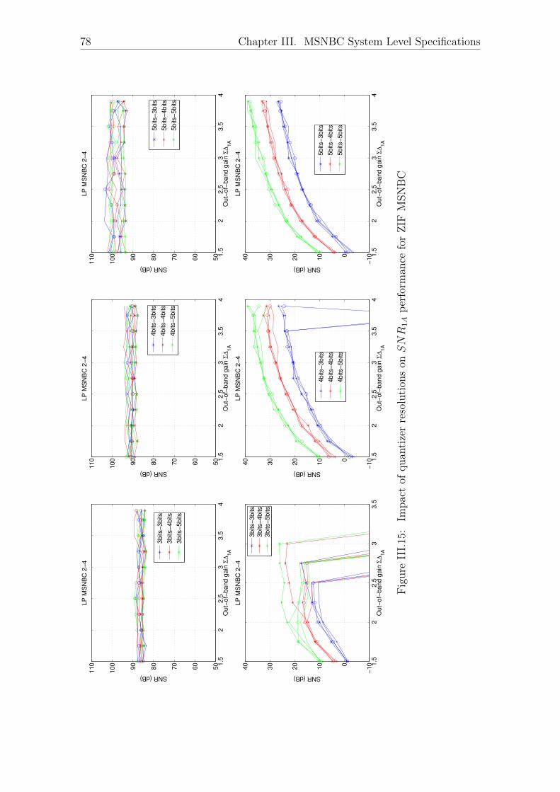
78 Chapter III. MSNBC System Level Specifications
1.5
22
.53
3.5
45
0
60
70
80
90
10
0
11
0
Ou
t−o
f−b
an
d g
ain
Σ∆
1A
SNR (dB)
LP
MS
NB
C 2
−4
3b
its−
3b
its
3b
its−
4b
its
3b
its−
5b
its
1.5
22
.53
3.5
45
0
60
70
80
90
10
0
11
0
Ou
t−o
f−b
an
d g
ain
Σ∆
1A
SNR (dB)
LP
MS
NB
C 2
−4
4b
its−
3b
its
4b
its−
4b
its
4b
its−
5b
its
1.5
22
.53
3.5
45
0
60
70
80
90
10
0
11
0
Ou
t−o
f−b
an
d g
ain
Σ∆
1A
SNR (dB)
LP
MS
NB
C 2
−4
5b
its−
3b
its
5b
its−
4b
its
5b
its−
5b
its
1.5
22
.53
3.5
−1
00
10
20
30
40
Ou
t−o
f−b
an
d g
ain
Σ∆
1A
SNR (dB)
LP
MS
NB
C 2
−4
3b
its−
3b
its
3b
its−
4b
its
3b
its−
5b
its
1.5
22
.53
3.5
4−
100
10
20
30
40
Ou
t−o
f−b
an
d g
ain
Σ∆
1A
SNR (dB)
LP
MS
NB
C 2
−4
4b
its−
3b
its
4b
its−
4b
its
4b
its−
5b
its
1.5
22
.53
3.5
4−
100
10
20
30
40
Ou
t−o
f−b
an
d g
ain
Σ∆
1A
SNR (dB)
LP
MS
NB
C 2
−4
5b
its−
3b
its
5b
its−
4b
its
5b
its−
5b
its
FigureIII.1
5:Im
pact
ofqu
antizerresolution
son
SNR
1Ape
rforman
ceforZIFMSN
BC

III.3. MSNBC Architectural Design Choice 79
Impact of delay
Another important aspect in MSNBC modulators is the delay. The delay of theloop filter alters the RSTF and thus limits the cancelation of the input signal atnode U . Moreover, since a CT modulator implementation has been chosen for themodulators, the architecture is sensitive to Excess loop delay (ELD). This delay hasbeen widely studied over the past and several methods have been proposed to dealwith this non ideality. In [92] some compensation methods are compared. Whilethose techniques will maintain the STF and SNR performance of a modulator, theymay degrade the RSTF. Figure III.16 compares the RSTF of a 4th order lowpassmodulator to the RSTF of a 4th order bandpass modulator centered at Fs/4. Foreach implementation, two cases are presented: the ideal modulator without ELDand the modulator with ELD and the classical compensation [92]. It can be seenthat ELD compensation considerably impacts the RSTF of the bandpass modulator.The signal attenuation around DC is close to 44 dB for the ideal and the ELDcompensated lowpass modulator. However, for the bandpass modulator, the RSTFnotch located at Fs/4 is shifted because of the delay. The attenuation around Fs/4drops from 36 to 5 dB. Thus, a better RSTF is achieved with the zero IF CTMSNBCcompared to the IF CT MSNBC.
0 0.2 0.4−50
−40
−30
−20
−10
0
10
Normalized frequency (Fc0/F
s)
ST
F (
dB
)
0 0.1 0.2 0.3 0.4−50
−40
−30
−20
−10
0
10
Normalized frequency (Fc0/F
s)
RS
TF
(dB
)
BP_Ideal
BP_ELD
LP_Ideal
LP_ELD
BP_Ideal
BP_ELD
LP_Ideal
LP_ELD
Figure III.16: ELD effect on RSTF
Mismatch between the I and Q path which will degrade the performance of DPDin the zero IF architecture. In addition to I/Q mismatch, flicker noise will have a

80 Chapter III. MSNBC System Level Specifications
great impact on the Zero IF architecture compare to the Low IF one given that thefrequency of the LIF is far from DC compared to ZIF frequencies.
Given the pros and cons of the ZIF and LIF architectures, the ZIF architectureis suitable for our application.
III.3.2 STF Choices
In Section III.1, the mode of operation of the MSNBC architecture is presented.However, for the sake of simplicity, all signal transfer functions were assumed tobe equal to 1, and this not always the case, especially for CT systems. The choiceof having a unity STF in the band of operation is thus a design choice for themodulator.
In the case of a CIFB modulator, a unitary STF in the band of operation canbe obtained by choosing bi = ai and b(n + 1) = 1, where 1 ≤ i ≤ n and n is themodulator order. However, the STF has an out-of-band gain of 10 dB as shown inFigure III.17. This OOBG of the STF can saturate the quantizer in case of out ofband signal.
By choosing the modulator coefficients such that (b1 = a1 et b2:n+1 = 0) a filteringSTF is implemented. In this case, out of band signals are attenuated and the gainis unity in the band of operation. However, the cancellation of the main signal isdegraded. Furthermore, in this case, in order to obtain the right noise suppression,the output of each modulator will have to be digitally processed. This is performedby Noise Cancellation Filters (NCF).
Designing Σ∆0 with a filtering STF however degrades the RSTF. For instance,on Figure III.17 for an input signal at 2.5MHz, the signal fed to the secondarymodulator is attenuated by 26.3 dB when using a unitary STF and by 19.2 dB witha filtering STF.
ELD impact on the STF
We previously showed that excess loop delay affects the MSNBC performance.This is even more important as the MSNBC architecture relies on the RSTF. Severaltechniques to compensate for this delay exist [87], [88] , [89], [90]. Those techniquesaim to create an unchanged noise transfer function as presented in Figure III.18.
However, when implementing those compensation techniques, the STF of themodulator is changed. This change should be taken into account in the calculation ofthe NCF to an optimal cancellation of the primary modulator noise in S1A. Detailedcalculation of NCFs in presence of ELD compensation are presented below:

III.3. MSNBC Architectural Design Choice 81
0 0.1 0.2 0.3 0.4 0.5−50
−40
−30
−20
−10
0
10
Frequence normalisee (Fc0/F
S)
Mo
du
le (
dB
)
STF0filt
RSTF0filt
STF0unit
RSTF0unit
Figure III.17: STF and RSTF comparison
Figure III.18: Fourth order modulator with classical ELD compensation

82 Chapter III. MSNBC System Level Specifications
Assum
inga4t
horderCIF
Bmod
ulator,withNRZ
DACsan
ddigitaldiffe
rentiatorELD
compe
nsation,
theou
tput
Y1A
(z)is
expressedas
:
Y1A
(z)
=N
1A
(z)
1+Z[ L−1
〈H4(s
)〉 |t=
kTS
] z−1/2−Z[ L−1
〈RDAC
45(s
)G(s
)〉 |t=
kTS
] z−1
+Z[ L−1
〈b41c 4
1c 4
2c 4
3c 4
4G
4(s
)U(s
)〉 |t=
kTS
]1
+Z[ L−1
〈H4(s
)〉 |t=
kTS
] z−1/2−Z[ L−1
〈RDAC
45(s
)G(s
)〉 |t=
kTS
] z−1
(III.16)
Where
U(s
)=b 1X
(s)−R
DAC
21(s
)·L⟨ y 0[n
]⟩ (s)·e
sTd/2
(III.17)
H4(s
)=c 4
1c 4
2c 4
3c 4
4G
4(s
)RDAC
41(s
)+c 4
2c 4
3c 4
4G
3(s
)RDAC
42(s
)+c 4
3c 4
4G
2(s
)RDAC
43(s
)+c 4
4G
(s)R
DAC
44(s
)(III.18)
S1A
(z)
=NCF
D 1A
(z)·Y
0(z
)+NCF
N 1A
(z)·Y
1A
(z)
(III.19)

III.3. MSNBC Architectural Design Choice 83
Performance analysis of the reconstructed signal was done when the correct NCFswere not used. Figure III.19 compares the SNR in the adjacent channel after recon-struction and by using NCFs which take ELD into account. 2 cases are presented:in one case, NCFs estimated assuming no ELD are used to reconstruct the signal,in other cases NCFs calculated assuming ELD compensation are used.
10−1
100
101
102
−200
−180
−160
−140
−120
−100
−80
−60
−40
−20
0
Frequency (MHz)
DS
P (
dB
)
Out S0ncfth
: 87.094 37.188
Out S0ncf : 83.469 36.290Out S0ncf : 80.991 25.675 Out S0ncf
th : 86.921 29.010
NCF no ELD real
NCF no ELD ideal
NCF ELD class ideal
NCF ELD class real
Figure III.19: Fourth order modulator with classical ELD compensation
We can see that using the NCFs improves the SNR in the adjacent channel.Furthermore the use of an accurate model leads to a better signal to noise ratio.
III.3.3 Signal Scaling
The quantizer of secondary modulators is important as well. As demonstrated inthe mode of operation, the signal sent to the second modulator is the shaped quan-tization noise of the first modulator, which is in fact noise. This means that theamplitude of this signal is low compared to the amplitude of the input signal of thefirst modulator. Thus, two options are offered for adjacent modulators:
• On the one hand, the input signal can be scaled so that an identical quantizeras the one in the first modulator can be used. This means that a gain should beapplied to the shaped quantization noise before being digitized by the adjacentmodulator.
• On the other hand, the signal is not scaled, thus, the reference voltage ofQTZsec is decreased.

84 Chapter III. MSNBC System Level Specifications
We choose to scale the signal at the input of the second modulator and use the samequantizer in both modulator. However, the RSTF should be approximated carefullyas a bad scaling will result in saturation of the adjacent modulator.
III.4 The MSNBC: Top level design
The MSNBC modulator has the feature to implement several DR specifications perband, hence relax adjacent ADCs requirements for signals with specific spectralcomposition. The shaped quantization noise of the primary modulator is removedby summing the outputs of Σ∆0 and Σ∆1A and by using NCFs to compensate fornon unitary STFs. Thus the SNR of the primary channel is improved in the mainchannel as well as the adjacent one.
III.4.1 Design Parameters
We proved in Chapter 1 that at least 50 and 12 dB SNR are required respectively forΣ∆0 and Σ∆1A/ Σ∆1B in order to maintain the ACPR as in an ideal feedback path.Nevertheless, it is important to include margins to those specifications to compensatefor non-idealities and noise. As the signal to quantization noise (SQNR) is 10 dBunder our noise budget, an extra 10 dB margin is added to previous requirements.
Several ADC parameters should be set according to the needed resolutions: theoversampling ratio, orders of modulators and quantizers number of bits. To estimatethose parameters, continuous time simulations are done with Matlab and CadenceSpectre. A modified version of the Delta Sigma Toolbox [93] is used to generate thecoefficients of Σ∆ modulators. Those values are extracted to simulate the schematicof the zero IF CT MSNBC modulator of Figure III.12. The modulator consists ofideal blocks implemented in VerilogA. Because the zero IF CT MSNBC modulatorhas two identical paths, only results of the in-phase path are presented. All Σ∆
modulators have the continuous time feedback cascaded form. The reason for thischoice is to avoid a peak in the signal transfer function as in the feedforward form.The STF of all modulators is assumed to be 0 dB in bands of operation. UnitarySTFs prevent using noise cancellation filters.
The test signal used is the sum of three sine waves representing the mono carrier20MHz LTE signal and non-linearities in each adjacent channel. A sine wave is usedinstead of a real 20MHz LTE signal to simplify SNR calculations. In section III, theinitial ACPR in 20MHz bandwidth is 30 dBc. For the following simulations, the am-plitude of first adjacent subband non-linearity is set to −50 dBc because the systemis more stringent when non-linearity amplitudes are low. To meet requirements, 2nd

III.4. The MSNBC: Top level design 85
0 20 40 60
−150
−100
−50
0
DS
P (
dB
)
Y
I
0 20 40 60
−150
−100
−50
0
S
0I
0 20 40 60
−150
−100
−50
0
Frequency (MHz)
S
1I
0 20 40 60
−150
−100
−50
0
Frequency (MHz)
DS
P (
dB
)
U
I
Figure III.20: MSNBC signals spectra
and 4th order modulators with 4-bits quantizers are used, and the sampling frequencyis 640MHz. Figure III.20 presents the Power Spectrum Density (PSD) of signalsversus the frequency. As expected, the main signal is not completely cancelled inUI , but attenuated by 38 dB. This is because the output signal of the modulatoris slightly delayed compared to the input signal. The SQNR of S0 first subband isimproved by 20 dB. The modulator achieves 86.7 dB SQNR in the main bandwidthand 30.5 dB in the first adjacent channel of S1I .
III.4.2 2-4 MSNBC vs. 0-4 MSNBC
We saw in Chapter I that in order to perform a proper DPD, the feedback ADCshould have 60 dB SNR in the main channel and 20 dB SNR in the adjacent channel.We need an ADC architecture that improves the SNR in adjacent channels. Twooptions are therefore possible with the MSNBC architecture.
We can have a high precision design of the primary modulator, and take thesignal of the main bandwidth at the output of Σ∆0. Another option, on the otherhand, is to relax design constraints in the primary modulator and take the mainsignal after adding the outputs of both modulators. We can then have a 2-4 or a 0-4MSNC as illustrated in Figure III.21. In the 0-4 MSNBC, the input signal is directlydigitized by a 4-bit quantizer. The output signal of the quantizer is then convertedin the analog domain with a DAC and subtracted to the input signal before beingfed to the adjacent modulator.
A comparison of top level simulation results of the two MSNBC configurations

86 Chapter III. MSNBC System Level Specifications
Figure III.21: 2-4 and 0-4 MSNBC schematics
is presented in Figure III.22. For those simulations the STFs of all modulators areunitary. Thus, no NCFs where used before summing Σ∆0 and Σ∆1’s outputs. TheSNRs of Y 024 and Y 004 in the main channel are respectively 88 and 45 dB. However,after addition, S124 and S104 both have 73 dB in the main channel. The differenceis however noticeable in the adjacent channel. Their performance are respectively38.1 and 35.4 dB for S124 and S104.
As will be shown in Chapter IV, non-idealities of the primary modulator arecompensated in the secondary modulator in the case where Σ∆1 doesn’t have aunitary STF and where NCFs are used. This option is however not available in theMASH architecture and will trade analog design constraints into digital filter designconstraints. The MASH architecture requires a good matching of the NTF. Thisis achievable for Discrete Time modulators. For continuous time Σ∆ modulators,

III.5. Conclusion 87
100 102
Frequency (MHz)
-180
-160
-140
-120
-100
-80
-60
-40
-20
0
DS
P (
dB
)
SNR Primary channel Adjacent channel
Y024
: 88.065 21.4369
Y004
: 45.3007 -2.5865
Y02-4 MSNBC
Y00-4 MSNBC
100 102
Frequency (MHz)
-180
-160
-140
-120
-100
-80
-60
-40
-20
0
DS
P (
dB
)
SNR Primary channel Adjacent channel
S124
: 73.0576 38.1959
S104
: 73.5782 35.4753
S12-4 MSNBC
S10-4 MSNBC
Figure III.22: 2-4 and 0-4 MSNBC top level simulation results
whereas some CT MASH ADCs exist, non-idealities make the matching of the NTFworse.
In order to compare the 2-4 and 0-4 MSNBC architectures, we have decided toimplement both of them on silicon. A switch will be added to by-pass the firstmodulator and enable the change between the 2-4 and the 0-4 architectures.
III.5 Conclusion
In this chapter, we presented the mode of operation of the MSNBC ADC as wellas top level design choices. The impact of non-idealities specific to the MSNBCwere investigated. Our investigation leads us to design a flexible architecture wherewe can either choose to be on a 2-4 or a 0-4 topology. Thus, the first modulatorcan either be a second order continuous time Sigma Delta modulator with a 4-bitquantizer or a 0-order modulator with a 4-bit quantizer. The adjacent modulator isa 4th order CT modulator with a 4-bit quantizer. Given that all modulators need a4-bit quantizer, we decide to use the same quantizer and to scale the signal at theinput of Σ∆1. Integrators should have at least 40 dB gain and 2πFs gain-bandwidth

88 Chapter III. MSNBC System Level Specifications
product. Integrator capacitors are tuned to stay in a maximum of ±10% RC timeconstant variations. Classical ELD compensation of up to 0.5 Ts is implemented ineach modulator. Both modulators will have filtering STFs and we will need to useNCFs to compensate for non unitary STF in the secondary modulator. DACs willhave NRZ topology. Because the combination of ISI and DWA highly degrades SNRperformance, we decided not to implement DWA. Mismatch will be taken care inthe design by using large size components.

Chapter IV
MSNBC Transistor Level DesignAnd Measurements
In Chapter III, we defined some system level parameters of the MSNBC. We sawas instance that our Σ∆ modulator will be implemented in continuous time witha CIFB form. Modulators will be made of RC integrators where amplifiers shouldhave at least 40 dB DC gain and a Gain-bandwidth product at least equal to 4Fs inorder to meet our performance requirements. Table IV.1 gathers key parameters ofour modulators.
Parameter Σ∆0 modulator Σ∆1 modulatorOSR 16 32
Modulator order 2 4Architecture CIFBDAC pulse Non-Returm to ZeroQuantizer 4 bits
Table IV.1: CIFB parameters
The goal of this chapter is to go one level down in the design process and justifyour transistor level design and layout choices, and present simulations and measure-ment results.
IV.1 Transistor Level Design
The 65nm CMOS bulk process of ST microelectronics is used to implement theMSNBC. This single poly process uses a type P substrate and offers several front-end options such as low threshold voltage transistors, MIM capacitors, high-sheet
89

90 Chapter IV. MSNBC Transistor Level Design And Measurements
resistors or deep N-well that are all free of charge through MPW runs. Deep N-well is extensively used in this design as it allows isolating the P-WELL of NMOStransistors from the substrate, which enables connecting the source terminal to thesubstrate of NMOS transistors to reduce modulation of the threshold voltage bythe substrate noise. As PMOS transistors are realized within an N-well, they areinherently isolated from the substrate.
Modulators analog blocks are implemented with fully differential circuits to min-imize the common mode noise and reduce even-order harmonic distortion. To savepower consumption, analog circuits are powered with 1.2V supply, whereas digitalcells used 1V supply voltage.
The mapping of modulators coefficients into resistors and capacitors value isnow studied. In order to obtain this number, the thermal noise budget should beestimated.
SNRdB = Psignal_dB − Pnoise_dB
If Psignal_princ_dB =-6 dB and ACPR =50 dB. Then Psignal_adj_dB =-56 dB. Thetarget SNR of the primary modulator is :
SNRCIFB21 = 60 dB
The total power of noise is then:
Pnoise_CIFB2 = −66 dB
Which corresponds to:Pnoise_CIFB2 = 251.2nV 2
We then consider that thermal noise contribution is half the total noise. Thus,
PThermal_noise_CIFB2 = 125nV 2
Same calculations are done with the secondary modulator.
SNRCIFB4 = 20 dB
Assuming a perfect cancellation of the main signal at the input of the secondarymodulator, the total noise power is:
Pnoise_CIFB4 = −76 dB
1Given that the primary modulator is a second order CIFB modulator, we call it CIFB2

IV.1. Transistor Level Design 91
Pnoise_CIFB4 = 25.1nV 2
Again, we consider that thermal noise contributes to half the total noise. Then,
PThermal_noise_CIFB4 = 12.5nV 2 (IV.1)
The thermal noise from the second modulator comes from the first operationalamplifier, the first DAC and resistors R1 and Rg1. Those resistors represent theinput coefficients b1 and g1 of a CIFB modulator, as presented in Figure IV.1.
Figure IV.1: CIFB schematic
This is approximated with the following equation:
Pthermal_noise = BW (8KTRg1 + 8KTR1 +8KTγ
gmop
+ 16KTγR1VrefVgtDAC
) (IV.2)
What we want is to meet the following requirement:
Pthermal_noise ≤ 12.5nV 2
After simplification, we have:
Rg1 +R1 +γ
gmop
+2γR1VrefVgtDAC
≤ 18.3KΩ (IV.3)
where BW is the signal bandwidth, K is Boltzman’s constant, T is the absolutetemperature, γ is the transistor thermal noise constant, gmop is the transconductanceof the input transistor of opamp1, VgtDAC is the overdrive voltage of the first DACand Vref is the reference voltage of the quantizer.
92 Chapter IV. MSNBC Transistor Level Design And Measurements
Modulators coefficients are obtained with the relationship:
ai =1
RiCiFs(IV.4)
Thus, R1 and Rg1 expressions can be replaced in
1
c1b1C1Fs+
c2
c1g1C1Fs+
γ
gmop
+2γR1VrefVgtDAC
≤ 18.3KΩ
We obtain equations giving the maximum values of the first resistor and capacitorof the second modulator. However, as the noise requirement is more stringent forthe secondary modulator, these are chosen as maximum values of input resistor andcapacitor of both modulators of the MSNBC. We assume that,
• OTA GBW = 4Fs
• DCgain = 45 dB
andGBW =
gmop
2πC1
(IV.5)
We thus obtain:
1
C1Fs(
1
c1b1
+c2
c1g1
+γ
8π+
2γVrefc1b1VgtDAC
) ≤ Rmax (IV.6)
1
RmaxFs(
1
c1b1
+c2
c1g1
+γ
8π+
2γVrefc1b1VgtDAC
) ≤ C1 (IV.7)
The final MSNBC modulator consists of a second order CIFB modulator whichis the primary modulator, a fourth order CIFB modulator as a secondary and bi-asing circuits to generate voltage and current references. Main sub-blocks of CIFBmodulators are detailed below.
IV.1.1 Sub-blocks Design
Some existing blocks available in our research team were re-used and adapted forour proposed ADC. Thus, the design of this MSNBC is not optimized for a powerconsumption point of view as the first target is to have a silicon proof of concept.
Loop filter

IV.1. Transistor Level Design 93
The loop filters of each CIFB2 and CIFB4 are made of integrators are builtaround Operational Transconductance Amplifier (OTA)-RC rather than Gm-C cells,because they have higher linearity performance and better robustness over PVT vari-ations. Furthermore, the virtual ground of the integrator provides a low impedancenode that facilitates the connection of a current-steering DAC. Feed-in and feedbackcoefficients are implemented with resistance ratio. Passives that implement feed-inand feedforward coefficients are sized to meet the matching requirement of 1%. Thenoise floor of the modulator is dominated by the thermal noise and the flicker noiseof the front-end that is composed of the input resistors, OTA21 and the unitarycurrent cells of the main DAC.
Thermal noise is set by the resistor value and a scaling factor whose value dependson the ratio of the reference voltage of the quantizer to the overdrive voltage of thecurrent cells in the main DAC. In this design, the overdrive voltage of the currentcells is set to 1/4 of the supply voltage to optimize noise and matching performance.
The finite GBW induced voltage swing at the virtual ground of the first OTA21is the main source of distortion in the front end. Lowering the GBW increases thevoltage swing at the virtual ground of OTA21. Moreover, even if the finite-GBW-induced phase shift through the loop filter is rigorously compensated by tuningcomponents values, the robustness of the modulator stability against PVT variationscannot be guaranteed with a high yield.
Figure IV.2: OTA schematic [94]

94 Chapter IV. MSNBC Transistor Level Design And Measurements
As shown in Figure IV.2, the main integrator embeds a 4-stage amplifier thatachieves a GBW and a phase margin of 3.9GHz and 88 ° respectively which ensureslow-distortion and low phase-shift against PVT variations. Each transconductancestage has its own common-mode feedback circuit that ensures an optimal operatingpoint for the differential path. The power consumption of the common-mode feed-back circuits represent one-third of whole amplifier power budget. The last stage(gm4) uses minimum length devices to increase the phase margin while consuminglow power. The OTA21 consumes 20mA. OTA21 performance is summarized inTable IV.2.
Parameter Value UnitDC Gain 45 dB
Open-loop GBW 2.56 GHzLoad capacitor 1508 fFPhase margin 90 °
Input referred noise density@10KHz 10 nV/
√Hz
@10MHz 3.2 nV/√Hz
Offset (3σ) ±2 mVSupply 1.2 V
Power consumption 24 mW
Table IV.2: First integrator parameters
RC calibration is used to compensate for the shifting of the RC time-constantthat can vary by more than ±35% in this process. The feedback capacitor of eachintegrator are tuned to the ideal value with different accuracies.
In order to save design and layout time, OTA22, OTA41, OTA42, OTA43 andOTA44 are similar to OTA21. DC gain are mostly the same for all those integra-tors. However, given that the capacitive load varies, the unity gain bandwidth andphase margin are not the same for all integrators. Table IV.3 gathers the MSNBCcomponent values.
R resistors are the one used to implement bi and ci coefficients of Σ∆ modulators.Rg allows to create NTF notches in the secondary modulator. However, they increasethermal noise when used at the input of the modulator. We decided not to havea notch in the primary modulator in order to meet our thermal noise requirement.As first integrators are critical, higher precision are used for their time constantcalibration compared to other integrators.

IV.1. Transistor Level Design 95
Σ∆0 Σ∆1
Position 1 2 1 2 3 4Rg (Ω) - - 21017 52552R (Ω) 2000 2109 2000 5937 2723.5 2723
Cap int (fF) 1508 477.5 2009.6 499.1 532.5 500.4Cap fix (fF) 980.2 310.375 1306.2 324.4 346.1 325.3Cap unit (fF) 16.7/22.1 22.2/22.1 22.3/22.1 23.3/22.1 24.8/22.1 23.3/22.1Precision 6 bits 4 bits 6 bits 4 bits 4 bits 4 bits
Table IV.3: Component values
Quantizer
The quantizer is a 4-bit flash ADC. It consists of 15 comparators which convertthe output of the loop filter into a thermometric code plus two comparators todetect saturation. A voltage buffer provides a copy of a voltage reference to aresistive ladder which generates the threshold voltages VREF [i] for the comparators.The schematic of one comparator slice is detailed in Figure IV.3
Figure IV.3: Comparator schematic [94]
A front-end CMOS switch disconnects each comparator from the loop filter dur-ing the offset calibration procedure that is done after the power-up of the ADC IC.In normal mode (calibration off) the on-state resistance of the switch, together withthe input capacitance of the quantizer create a pole whose value is set well beyond

96 Chapter IV. MSNBC Transistor Level Design And Measurements
the sampling frequency of the modulator in order to preserve its stability. The noiseand distortion requirement of the switch are greatly relaxed as they are shaped bythe 5th-order loop filter preceding the quantizer. For each comparator, the offsetvalue is estimated by a feedback loop which consists of a counter/integrator anda current-steering DAC. For each DAC code, the output of the comparator is in-tegrated over several fractions of the clock period to reduce the influence of noise.When the mean value of the comparator output is equal to or greater than zero,then the counter stops and leaves the output current of the DAC at a value thatcompensates the offset voltage. After calibration, the residual offset is boundedwithin one DAC’s LSB.
The preamplifier is a double-differential amplifier with a PMOS load and a reset-ting switch for faster overload recovery. It uses a non-switching load, which stronglyminimizes the kickback noise on the loop filter output and the reference ladder.
Parameter Value UnitSampling Frequency 640 MHz
Full scale 0.8 VResolution 4 bitsOffset (3σ)
Before calibration 80 mVAfter calibration ≤ 5 mV
SupplyAnalog 1.2 VDigital 1 V
Power consumptionAnalog 1.8 mWDigital 2.3 mW
Table IV.4: Quantizer parameters
Design parameters of quantizers are gathered in Table IV.4.
DACs
Multi-bit feedback DACs are not inherently linear and generate errors due to themismatch between the unit-DAC elements. As the feedback DACs are placed afterthe quantizer in a CT Σ∆ modulator, the non-linearity coming from the DACs isnot shaped by the loop filter. Hence, it is directly reinserted in the main modulatorpath, increasing the in-band noise-floor and reducing the SNR.
The current steering architecture is widely used for high-speed DAC applications.

IV.1. Transistor Level Design 97
The main advantages of this architecture are the power efficient, an easy implemen-tation (which requires only digital CMOS processes), a guaranteed monotonicity, agood matching, and the glitches that do not contribute to nonlinearity (when us-ing thermometer coding). To minimize performance degradation, as presented inChapter 2, feedback DAC element mismatch should at least be 2%. The matchingbetween each one of these current sources is primordial to assure good performanceof the continuous-time Σ∆ modulator.
Pelgrom states mismatch as a "process that causes time-independent randomvariations in physical quantities of identically designed devices" [95]. For current-steering DAC applications, this denotes that each current source in the array pro-duces a current that deviates slightly from the desired current, Iref . Hence, to reachthe required specifications, the current sources should be designed in such a way thatrandom variations do not affect the performance of the current-steering DAC. FromPelgrom’s matching estimation [95], it is possible to determine the minimum gate-area for the unit current source. For a (σI/I) of 2%, the obtained (WL)min is about6 µm2.
The architecture of one of the 15 unit current cells of DAC21 is shown in Fig-ure IV.4. It consists of a regulated cascode current source with a pair of NMOS.The boosting amplifier is a single-stage common-source amplifier whose GBW isoptimized to boost the output impedance of the DAC over a wide frequency range.
The switches are sized small to minimize the delay and the output capacitance ofthe current cell. The gates of switches are driven by high-crossing point buffers thatensure that one transistor is always in the on-state and biased in saturation, allowinga double cascode configuration which further improves the output resistance of theDAC. A careful design of the clock distribution circuit and true single-phase clock(TSPC) flip-flops (FF) that drive DAC switches has led to an additive jitter value ofonly 137 fs rms. This value leaves enough margin for the jitter of the clock-source.The current cell drivers are implemented with only two PMOS transistors ratherthan four which reduce the propagation delay between the FF and the DAC output.
An impedance value higher than 400MΩ is obtained up to the band edge (40MHz)which makes the distortion mechanism due to finite GBW of opamp1 negligiblewithin the signal bandwidth. Table IV.5 presents the parameters values used in thisdesign.
The value of DACs currents reference are gathered in Table IV.6. DAC currentcells are extracted using the following relationship for an RC-integrator:
aiVREF =IDAC × Ts
C(IV.8)

98 Chapter IV. MSNBC Transistor Level Design And Measurements
Figure IV.4: DAC unit current cell schematic [94]
Parameter Value UnitCell current 25 µA
Number of cells 15 VMatching 2 %SupplyAnalog 1.2 VDigital 1 V
Power consumptionAnalog 0.18 mWDigital 0.5 mW
Table IV.5: DAC parameters
with ai the DAC feedback coefficient, Ts the sampling period, VREF the refer-ence voltage and C the capacitor. Except from DAC45, all DACs have the samearchitecture as DAC21. Given that the reference current changed, the ratio of thearea is adjusted to meet the mismatch constraint previously obtained.

IV.1. Transistor Level Design 99
Σ∆0 Σ∆1
Position 1 2 3 1 2 3 4 5Iref (µA) 25 49.99 23.45 10/3 10/3 10 40 18.71
Table IV.6: DAC parameters
Floorplan
To achieve a good resolution and linearity of the MSNBC, a great deal of cautionshould be taken in the layout design to reduce the effects of parasitics, mismatchand noise coupling from digital blocks to analog blocks.
The layout and chip micrograph of the MSNBC modulator are presented inFigure IV.5, which labels some major blocks.
The analog and digital blocks are separated to avoid disturbances. Main inputpins are located at the left of chip, whereas output pins as well as output buffersare located at the right of the chip. Biasing voltages and currents are placed at thecenter of the chip, closed to integrators. DACs from the CIFB2 are located at thetop of the chip, close to INT21 and 22. DACs 41, 42, 43, 44 and 45 are placed at thebottom of the circuit, close to CIFB4 integrators. DAC40 is placed close to DAC21and INT21 to generate the shaped quantization noise and to avoid the impact ofparasitics resistor in the RSTF. Given that quantizers of both modulators have thesame reference voltage and the same resolution, they shared the same resistor ladderto save area.
The MSNBC prototype was fabricated in 65nm 1P7M CMOS process throughthe Multi Project Wafer program of the CMP. The active die area is 3.25mm2 (1.804mm x 1.804 mm). Digital blocks were isolated in a deep N-well to reduce the couplingwith the analog blocks through the substrate.
The power supplies are routed in several metal layers to reduce the power linesequivalent resistance and consequently the voltage loss. To improve the isolationbetween analog and digital blocks, some design techniques such as shielding andguard ring were used. Also, the power supply lines of analog and digital blocks arephysically separated. The circuit also includes a Serial-to-Parellel Interface (SPI) togenerate static signals to control capacitors, calibration and to switch between the2-4 and the 0-4 MSNBC modes.

100 Chapter IV. MSNBC Transistor Level Design And Measurements
Figure IV.5: MSNBC Layout floor plan and die picture
IV.1.2 Simulation Results
Simulations of the MSNBC at the transistor level are performed in Cadence. Thetestbench consists of the 2-4 / 0-4 MSNBC circuits and output buffers.
The sum of two sine waves are used to represent the test signal: one at Fin1 =

IV.1. Transistor Level Design 101
1.9MHz with 0.67V amplitude to represent the main signal, and a second sinewave at Fin2 = 20MHz to model the non-linearities at the output of the PA. Thenon-linearities amplitude are set to illustrate a system with 50 dBc ACPR. Thusthe amplitude of those non-linearities are set to 3.1mV. The sampling frequency isFs = 640MHz. Signal is assumed to be a 20MHz LTE signal. Thus, Σ∆0 linearizes10MHz bandwidth and Σ∆1 20MHz. Each modulator implements a digital differ-entiator technique to compensate for ELD up to 0.5× Ts. The reference voltage ofthe quantizer is 0.8V, and both primary and secondary modulators have filteringSTFs.
The primary and secondary modulators are first tested standalone by simulationto check their functionality. The same signal is applied at the input of both mod-ulators. No scaling is performed at the input of the adjacent modulator. Resultsin Figure IV.6, show the output spectra of both modulators. Both results have nonlinearities that degrades their performance compare to high level simulations andDAC mismatch is not added in this simulation.
10−1
100
101
102
−140
−120
−100
−80
−60
−40
−20
0
Frequency (MHz)
DS
P (
dB
)
SNRresults Primary channel Adjacent channelOut Y0 : 56.2 5.68Out Y1 : 58.2 17.1
PSD_Y0REAL_QTZ_no_CAL
PSD_Y1REAL_QTZ_no_CAL
Figure IV.6: CIFB2 and CIFB4 results
The test signal is then applied to the MSNBC modulator. The output spectraof the ADC are presented in Figure IV.7. The black, green, blue and red curvesrespectively represent the output of the first modulator, the output of the secondmodulator the reconstructed signal without and with the NCFs. The output of thefirst modulator exhibits high odd orders non linearities. This is because the OTAused in the loop filter operates close to saturation. Because the input frequency ofthe signal is low, those non-linearities are in the band of interest. Thus, the SNR is55 dB in the main channel and 6.3 dB in the adjacent channel.
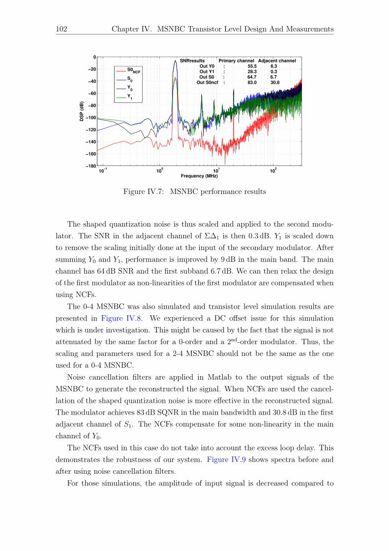
102 Chapter IV. MSNBC Transistor Level Design And Measurements
10−1
100
101
102
−180
−160
−140
−120
−100
−80
−60
−40
−20
0
Frequency (MHz)
DS
P (
dB
)
SNRresults Primary channel Adjacent channelOut Y0 : 55.5 6.3Out Y1 : 28.3 0.3Out S0 : 64.7 6.7
Out S0ncf : 83.0 30.8
S0NCF
S0
Y0
Y1
Figure IV.7: MSNBC performance results
The shaped quantization noise is thus scaled and applied to the second modu-lator. The SNR in the adjacent channel of Σ∆1 is then 0.3 dB. Y1 is scaled downto remove the scaling initially done at the input of the secondary modulator. Aftersumming Y0 and Y1, performance is improved by 9 dB in the main band. The mainchannel has 64 dB SNR and the first subband 6.7 dB. We can then relax the designof the first modulator as non-linearities of the first modulator are compensated whenusing NCFs.
The 0-4 MSNBC was also simulated and transistor level simulation results arepresented in Figure IV.8. We experienced a DC offset issue for this simulationwhich is under investigation. This might be caused by the fact that the signal is notattenuated by the same factor for a 0-order and a 2nd-order modulator. Thus, thescaling and parameters used for a 2-4 MSNBC should not be the same as the oneused for a 0-4 MSNBC.
Noise cancellation filters are applied in Matlab to the output signals of theMSNBC to generate the reconstructed the signal. When NCFs are used the cancel-lation of the shaped quantization noise is more effective in the reconstructed signal.The modulator achieves 83 dB SQNR in the main bandwidth and 30.8 dB in the firstadjacent channel of S1. The NCFs compensate for some non-linearity in the mainchannel of Y0.
The NCFs used in this case do not take into account the excess loop delay. Thisdemonstrates the robustness of our system. Figure IV.9 shows spectra before andafter using noise cancellation filters.
For those simulations, the amplitude of input signal is decreased compared to

IV.1. Transistor Level Design 103
10-1 100 101 102
Frequency (MHz)
-180
-160
-140
-120
-100
-80
-60
-40
-20
0
DS
P (
dB
)
S0NCF
S0
Y0
Y1
Figure IV.8: 0-4 MSNBC transistor level simulation results
10−1
100
101
102
−180
−160
−140
−120
−100
−80
−60
−40
−20
0
Frequency (MHz)
DS
P (
dB
)
SNRresults Primary channel Adjacent channelOut Y0 : 55.5 6.3
Out S0ncf : 83.0 30.8
S0NCF
Y0
Figure IV.9: MSNBC spectra before and after using NCFs
the previous set of parameters. The purpose is to decrease the impact of OTAs nonlinearities. The process is changed but the temperature is the same. Simulationresults are presented in Figure IV.10.

104 Chapter IV. MSNBC Transistor Level Design And Measurements
10−1
100
101
102
−150
−100
−50
0
Frequency (MHz)
DS
P (
dB
)
Y0 with process variations
FF
FS
SF
SS
TT
10−1
100
101
102
−180
−160
−140
−120
−100
−80
−60
−40
−20
0
Frequency (MHz)
DS
P (
dB
)
S0NCF
with process variations
FF
FS
SF
SS
TT
Figure IV.10: Output spectra of the 2-4 MSNBC at different process nodes
Decreasing the input amplitude improved the SNR performance in the mainband of Y0. Furthermore, the reconstructed signal also have better performanceas the NCFs calculation takes into account ELD. Performance are showed in TableTable IV.7.
FF FS SF SS TTSNR Y0_princ (dB) 47.4 46.7 61.5 64.8 60.1SNR Y0_adj (dB) 6.49 4.64 8.88 9.45 8.91
SNR S0_NCF_princ (dB) 76.6 76.4 85.1 86.2 85.3SNR S0_NCF_adj (dB) 35.5 33.1 35.2 35.4 36.4
Table IV.7: Impact of process variation on the MSNBC
For the typical process, the reconstructed signal achieves 85.5 dB SQNR in themain bandwidth and 36.4 dB in the first subband. This performance is degraded

IV.2. MSNBC Measurements 105
when NMOS transistors are in the Fast corner. The SNR in the main channel of S0
drops by 9 dB. In the adjacent channel however, performance is almost unchangedacross corners.
The designed MSNBC ADC performance thus meet initial specifications at thetransistor level simulations. Those simulation results are then compared to mea-surement results of the chip.
IV.2 MSNBC Measurements
• Measurements results, test bench, power consumption
• Compare simulations and measurements
• Explain results

106 Chapter IV. MSNBC Transistor Level Design And Measurements

Conclusion
Digital predistortion is nowadays a common technique to cope with the linearity-efficiency trade-off of power amplifiers in base transceiver stations. This technique ishighly preferred because of its efficiency, but also it takes advantage of the advancein digital signal processing. As the demand in bandwidth is always growing, theADC in the feedback path becomes a bottleneck of DPD implementation. For a100MHz signal for example, the ADC should digitize up to 700MHz to include PAnon-linearities. Pipeline ADCs are commonly used for this application, but theytend to consume a lot of power. Subband DPD is a new technique to relax thefeedback ADC design. The multi stage noise band cancellation architecture madeof Σ∆ modulators is an excellent candidate to address the wide bandwidth highresolution and low power consumption trade-off of this application. The MSNBCarchitecture is particularly attractive as it relaxes dynamic range constraints perband.
A continuous time implementation of the MSNBC modulator is preferred to adiscrete time implementation because of the high speed requirement. This is atthe price of several considerations that need to be tackled before the design. Astudy of the MSNBC non-idealities leads to two possible implementations: a zeroIF implementation, where the first modulator is a low pass type and its bandwidthconstraint is halved, and a low IF implementation with a bandpass modulator asprimary modulator. System level simulations results lead us to design an MSNBCmade of two modulators:
• A second order CIFB modulator with 4-bit quantizer
• A fourth order CIFB modulator with 4-bit quantizer
Non-idealities related to continuous time Σ∆ modulators as well as imperfectionsspecific to the MSNBC architecture were investigated. In order to test several con-figurations, the circuit is made reconfigurable. It can be setup to implement theinitial 2-4 MSNBC but it can also implement a 0-4 MSNBC. The 0-4 topology isexpected to consume less power and to require a smaller area but will require highly
107

108 Conclusion
accurate decimation filters, compared to a 2-4 MSNBC. Moreover, the fact thatnon-linearities of the primary modulator are compensated in the main bandwidthchannel allows to relax design constraints in the primary modulator.
The purpose of this thesis is to demonstrate the feasibility of the MSNBC ar-chitecture that has so far only been studied at the system level. In order to savedesign time, some previously designed blocks have been re-used and adapted to ourspecifications. As a proof of concept, an MSNBC with two modulators was designedin a 65 nm CMOS technology. Transistor level simulations of the MSNBC show thesignal attenuation at the input of the second modulator is effective but lower com-pared to systems level simulations. We obtained more than 20 dB attenuation of themain signal at the transistor level. Furthermore, the SNR in the adjacent channelhas been improved by 24 dB, which means that the shaped quantization noise of theprimary modulator has been cancelled in the adjacent channel. Results also provedthat using the accurate NCFs leads to better SNR in the adjacent channel. Finally,simulations over process variations shows that performance in the subband are morerobust compared to performance in the main channel.
Future work
This thesis, presents a proof of concept of this new type of converter. The logicalsteps that would follow this work should focus on an optimized implementation ofthe modulator in order to prove the saving in power consumption compared to ADCwith same specifications and to make a final choice on the 2-4 and 0-4 architectures.The design of OTA should also be improved because non linearities of the OTAsdegrades our performance in the main channel. The additional step forward is thedesign of decimation filter in order to have the overall ADC power consumption.
The current MSNBC is designed with two modulators. An area of improvementis to have a reconfigurable architecture of the MSNBC which will be made of adjacentmodulators. Those adjacent modulators could be switched on and off depending onthe highest non linearity order needed to characterize the power amplifier in DPD.
Finally, reconfigurability of the MSNBC can furthermore be achieved with modu-lators with variable center frequencies. The proposed future works should also takeadvantage of scaling technology nodes and be implemented in lowest technologynodes like 28nm FDSOI.

Bibliography
[1] Vincenzo Mancuso and Sara Alouf. Reducing costs and pollution in cellularnetworks. IEEE Communications Magazine, 49(8):63–71, 2011.
[2] Sesia Stefania, Toufik Issam, and Baker Matthew. LTE, the UMTS long termevolution: from theory to practice. A John Wiley and Sons, Ltd, 6:136–144,2009.
[3] Guangyi Liu and Dajie Jiang. 5G: Vision and requirements for mobile com-munication system towards year 2020. Chinese Journal of Engineering, 2016,2016.
[4] Angelos Chatzipapas, Sara Alouf, and Vincenzo Mancuso. On the minimizationof power consumption in base stations using on/off power amplifiers. In 2011IEEE Online Conference on Green Communications, pages 18–23. IEEE, 2011.
[5] Minoru Etoh, Tomoyuki Ohya, and Yuji Nakayama. Energy consumption issueson mobile network systems. In 2008 International Symposium on Applicationsand the Internet, pages 365–368. IEEE, 2008.
[6] Lei Guan and Anding Zhu. Green communications: Digital predistortion forwideband RF power amplifiers. IEEE Microwave Magazine, 15(7):84–99, 2014.
[7] D. Y. C. Lie, J. C. Mayeda, and J. Lopez. Highly efficient 5G linear poweramplifiers (PA) design challenges. In 2017 International Symposium on VLSIDesign, Automation and Test (VLSI-DAT), pages 1–3, April 2017.
[8] Luis M Correia, Dietrich Zeller, Oliver Blume, Dieter Ferling, Ylva Jading,István Gódor, Gunther Auer, and Liesbet Van Der Perre. Challenges andenabling technologies for energy aware mobile radio networks. IEEE Commu-nications Magazine, 48(11), 2010.
[9] George Koutitas and Panagiotis Demestichas. A review of energy efficiency intelecommunication networks. Telfor journal, 2(1):2–7, 2010.
109

110 Bibliography
[10] Bumman Kim, Jinsung Choi, Daehyun Kang, and Dongsu Kim. Envelopetracking technique for multimode PA operation. In 2009 European MicrowaveConference (EuMC), pages 429–432. IEEE, 2009.
[11] Murat Eron, Bumman Kim, Frederick Raab, Robert Caverly, and JosephStaudinger. The head of the class. IEEE Microwave Magazine, 12(7):S16–S33,2011.
[12] Steve C Cripps. RF Power Amplifiers for Wireless Communications, (ArtechHouse Microwave Library (Hardcover)). Artech House, Inc., 2006.
[13] Leonard R Kahn. Single-sideband transmission by envelope elimination andrestoration. Proceedings of the IRE, 40(7):803–806, 1952.
[14] Zhancang Wang. Envelope tracking power amplifiers for wireless communica-tions. Artech House, 2014.
[15] Peter Asbeck and Zoya Popovic. ET comes of age: Envelope tracking for higher-efficiency power amplifiers. IEEE Microwave Magazine, 17(3):16–25, 2016.
[16] Bumman Kim. Advanced linear PA architectures for handset applications. InWireless Symposium (IWS), 2013 IEEE International, pages 1–1. IEEE, 2013.
[17] Kim Bumman, Moon Junghwan, and Kim Ildu. Efficiently amplified. IEEEMicrowave Magazine, 11(5):87–100, 2010.
[18] Zhancang Wang. Demystifying envelope tracking: Use for high-efficiency poweramplifiers for 4G and beyond. IEEE microwave magazine, 16(3):106–129, 2015.
[19] H Tango, T Hashinaga, K Totani, H Kuriyama, Y Hamada, and T Asaina. A60% efficient envelope tracking power amplifier for 40W, 2.6 GHz LTE base sta-tion with in/output harmonic tuning. In Microwave Symposium Digest (IMS),2013 IEEE MTT-S International, pages 1–4. IEEE, 2013.
[20] Youjiang Liu, Chan-Sei Yoo, John Fairbanks, Jonmei Yan, Donald Kimball, andPeter Asbeck. A 53% PAE envelope tracking GaN power amplifier for 20MHzbandwidth LTE signals at 880MHz. In Power Amplifiers for Wireless and RadioApplications (PAWR), 2016 IEEE Topical Conference on, pages 30–32. IEEE,2016.
[21] Paul T Theilmann, Jonmei J Yan, Cuong Vu, Jeong-Sun Moon, Harris P Moyer,and Donald F Kimball. A 60MHz bandwidth high efficiency X-band envelope

Bibliography 111
tracking power amplifier. In Compound Semiconductor Integrated Circuit Sym-posium (CSICS), 2013 IEEE, pages 1–4. IEEE, 2013.
[22] William H Doherty. A new high efficiency power amplifier for modulated waves.Proceedings of the Institute of Radio Engineers, 24(9):1163–1182, 1936.
[23] Raymond Pengelly, Christian Fager, and Mustafa Ozen. Doherty’s legacy: ahistory of the Doherty power amplifier from 1936 to the present day. IEEEMicrowave Magazine, 17(2):41–58, 2016.
[24] Frederick H Raab. Efficiency of Doherty RF power-amplifier systems. IEEEtransactions on Broadcasting, pages 77–83, 1987.
[25] Masaya Iwamoto, Aracely Williams, Pin-Fan Chen, Andre G Metzger,Lawrence E Larson, and Peter M Asbeck. An extended Doherty amplifier withhigh efficiency over a wide power range. IEEE Transactions on MicrowaveTheory and Techniques, 49(12):2472–2479, 2001.
[26] Ildu Kim and Bumman Kim. A 2.655 GHz 3-stage Doherty power amplifierusing envelope tracking technique. In Microwave Symposium Digest (MTT),2010 IEEE MTT-S International, pages 1496–1499. IEEE, 2010.
[27] Mury Thian and Peter Gardner. Envelope-tracking-based Doherty power am-plifier. International Journal of Electronics, 97(5):525–530, 2010.
[28] Chuanhui Ma, Wensheng Pan, Shihai Shao, Chaojin Qing, and Youxi Tang.A wideband Doherty power amplifier with 100 MHz instantaneous bandwidthfor LTE-advanced applications. IEEE Microwave and Wireless ComponentsLetters, 23(11):614–616, 2013.
[29] Khaled Bathich, Asdesach Z Markos, and Georg Boeck. A wideband GaNDoherty amplifier with 35% fractional bandwidth. In Microwave Conference(EuMC), 2010 European, pages 1006–1009. IEEE, 2010.
[30] AM Mahmoud Mohamed, Slim Boumaiza, and Raafat R Mansour. Reconfig-urable Doherty power amplifier for multifrequency wireless radio systems. IEEETrans. Microw. Theory Techn, 61(4):1588–1598, 2013.
[31] Xuan Anh Nghiem, Junqing Guan, Thomas Hone, and Renato Negra. Design ofconcurrent multiband Doherty power amplifiers for wireless applications. IEEEtransactions on Microwave Theory and Techniques, 61(12):4559–4568, 2013.

112 Bibliography
[32] Andrei Grebennikov and Senad Bulja. High-efficiency Doherty power amplifiers:Historical aspect and modern trends. Proceedings of the IEEE, 100(12):3190–3219, 2012.
[33] Fadhel M Ghannouchi and Oualid Hammi. Behavioral modeling and predistor-tion. IEEE Microwave Magazine, 10(7):52–64, 2009.
[34] Yuelin Ma, Yasushi Yamao, Yoshihiko Akaiwa, and Koji Ishibashi. Widebanddigital predistortion using spectral extrapolation of band-limited feedback sig-nal. IEEE Transactions on Circuits and Systems I: Regular Papers, 61(7):2088–2097, 2014.
[35] Haoyu Wang, Gang Li, Chongbin Zhou, Wei Tao, Falin Liu, and Anding Zhu.1-bit observation for direct-learning-based digital predistortion of RF power am-plifiers. IEEE Transactions on Microwave Theory and Techniques, 65(7):2465–2475, 2017.
[36] Ying Liu, Xin Quan, Shihai Shao, and Youxi Tang. Digital predistortion archi-tecture with reduced ADC dynamic range. Electronics Letters, 52(6):435–437,2016.
[37] Chao Yu, Lei Guan, Erni Zhu, and Anding Zhu. Band-limited Volterra series-based digital predistortion for wideband RF power amplifiers. IEEE Transac-tions on Microwave Theory and Techniques, 60(12):4198–4208, 2012.
[38] Lei Ding, Fernando Mujica, and Zigang Yang. Digital predistortion using directlearning with reduced bandwidth feedback. In Microwave Symposium Digest(IMS), 2013 IEEE MTT-S International, pages 1–3. IEEE, 2013.
[39] Oualid Hammi, Andrew Kwan, Souheil Bensmida, Kevin A Morris, and Fad-hel M Ghannouchi. A digital predistortion system with extended correctionbandwidth with application to LTE-A nonlinear power amplifiers. IEEE Trans-actions on Circuits and Systems I: Regular Papers, 61(12):3487–3495, 2014.
[40] M. Grimm, M. Allen, J. Marttila, M. Valkama, and R. Thoma. Joint Mitigationof Nonlinear RF and Baseband Distortions in Wideband Direct-Conversion Re-ceivers. IEEE Transactions on Microwave Theory and Techniques, 62(1):166–182, Jan 2014.
[41] Lei Ding, G.T. Zhou, D.R. Morgan, Zhengxiang Ma, J.S. Kenney, JaehyeongKim, and C.R. Giardina. A robust digital baseband predistorter constructed
Bibliography 113
using memory polynomials. IEEE Transactions on Communications, 52(1):159–165, Jan 2004.
[42] 3GPP. TS 36.104 - E-UTRA BS Radio Transmission and Reception.
[43] S. Ho, Chi-Lun Lo, Jiayun Ru, and Jialin Zhao. A 23 mW, 73 dB DynamicRange, 80 MHz BW Continuous-Time Delta-Sigma Modulator in 20 nm CMOS.Solid-State Circuits, IEEE Journal of, 50(4):908–919, April 2015.
[44] Robert H Walden. Analog-to-digital converter survey and analysis. IEEE Jour-nal on selected areas in communications, 17(4):539–550, 1999.
[45] R. Schreier and R.C. Temes. Understanding Delta-Sigma Data Converters. InUnderstanding Delta-Sigma Data Converters, 2005.
[46] Michel Steyaert, Raf Roovers, and Jan Craninckx. A 100 MHz 8 bit CMOS in-terpolating A/D converter. In Proceedings of IEEE Custom Integrated CircuitsConference-CICC’93, pages 28–1. IEEE, 1993.
[47] Robert Taft, Chris Menkus, Maria Rosaria Tursi, Ols Hidri, and Valerie Pons.A 1.8 V 1.6 GS/s 8b self-calibrating folding ADC with 7.26 ENOB at Nyquistfrequency. In 2004 IEEE International Solid-State Circuits Conference (IEEECat. No. 04CH37519), pages 252–526. IEEE, 2004.
[48] Brian P Ginsburg and Anantha P Chandrakasan. Dual time-interleaved succes-sive approximation register ADCs for an ultra-wideband receiver. IEEE Journalof Solid-State Circuits, 42(2):247–257, 2007.
[49] Yun-Shiang Shu, Liang-Ting Kuo, and Tien-Yu Lo. An oversampling SARADC with DAC mismatch error shaping achieving 105 dB SFDR and 101 dBSNDR over 1 kHz BW in 55 nm CMOS. IEEE Journal of Solid-State Circuits,51(12):2928–2940, 2016.
[50] Dieter Draxelmayr. A 6b 600MHz 10mW ADC array in digital 90nm CMOS.In 2004 IEEE International Solid-State Circuits Conference (IEEE Cat. No.04CH37519), pages 264–527. IEEE, 2004.
[51] Jian Lv, Longcheng Que, Linhai Wei, Zhijun Meng, and Yun Zhou. A lowpower and small area digital self-calibration technique for pipeline ADC. AEU-International Journal of Electronics and Communications, 83:52–57, 2018.

114 Bibliography
[52] Daihong Fu, Ken Dyer, S Lewis, and P Hurst. Digital background calibration ofa 10 b 40 M sample/s parallel pipelined ADC. In 1998 IEEE International Solid-State Circuits Conference. Digest of Technical Papers, ISSCC. First Edition(Cat. No. 98CH36156), pages 140–141. IEEE, 1998.
[53] Cormac SG Conroy, David W Cline, and Paul R Gray. An 8-b 85-MS/s parallelpipeline A/D converter in 1-µm CMOS. IEEE Journal of Solid-State Circuits,28(4):447–454, 1993.
[54] Aria Eshraghi and Terri S Fiez. A comparative analysis of parallel delta-sigmaADC architectures. IEEE Transactions on Circuits and Systems I: RegularPapers, 51(3):450–458, 2004.
[55] KC-H Chao, Shujaat Nadeem, Wai L Lee, and Charles G Sodini. A higherorder topology for interpolative modulators for oversampling A/D converters.IEEE Transactions on circuits and systems, 37(3):309–318, 1990.
[56] James C Candy and Gabor C Temes. Oversampling delta-sigma data converters:theory, design and simulation. IEEE Press„ 1992.
[57] Richard Schreier. An empirical study of high-order single-bit delta-sigma mod-ulators. IEEE Transactions on Circuits and Systems II: Analog and DigitalSignal Processing, 40(8):461–466, 1993.
[58] L Risbo. Σ Modulators-Stability and Design Optimization. PhD thesis, PhDdissertation, Technical University of Denmark, 1994.
[59] Robert W Adams. Design and implementation of an audio 18-bit analog-to-digital converter using oversampling techniques. Journal of the Audio Engi-neering Society, 34(3):153–166, 1986.
[60] Max W Hauser. Circuits and technology considerations for MOS delta-sigmaA/D converters. IEEE Proc. ISCAS’86, pages 1310–1315, 1986.
[61] Ian Galton. Why dynamic-element-matching DACs work. IEEE Transactionson Circuits and Systems II: Express Briefs, 57(2):69–74, 2010.
[62] M. R. Miller and C. S. Petrie. A multibit sigma-delta ADC for multimodereceivers. IEEE Journal of Solid-State Circuits, 38(3):475–482, March 2003.
[63] S. Lee and C. Cheng. A Low-Voltage and Low-Power Adaptive Switched-Current Sigma Delta ADC for Bio-Acquisition Microsystems. IEEE Transac-tions on Circuits and Systems I: Regular Papers, 53(12):2628–2636, Dec 2006.

Bibliography 115
[64] J. F. Jensen, G. Raghavan, A. E. Cosand, and R. H. Walden. A 3.2-GHz second-order delta-sigma modulator implemented in InP HBT technology. IEEE Jour-nal of Solid-State Circuits, 30(10):1119–1127, Oct 1995.
[65] James A Cherry and W Martin Snelgrove. Excess loop delay in continuous-timedelta-sigma modulators. IEEE Transactions on Circuits and Systems II: analogand digital signal processing, 46(4):376–389, 1999.
[66] A. Gharbiya and D. A. Johns. A 12-bit 3.125 MHz Bandwidth 0?3 MASH Delta-Sigma Modulator. IEEE Journal of Solid-State Circuits, 44(7):2010–2018, July2009.
[67] V. Srinivasan, V. Wang, P. Satarzadeh, B. Haroun, and M. Corsi. A 20mW61dB SNDR (60MHz BW) 1b 3rd-order continuous-time delta-sigma modulatorclocked at 6GHz in 45nm CMOS. In Solid-State Circuits Conference Digest ofTechnical Papers (ISSCC), 2012 IEEE International, pages 158–160, Feb 2012.
[68] J.G. Kauffman, Chao Chu, J. Becker, and M. Ortmanns. A 67dB DR 50MHzBW CT Delta Sigma modulator achieving 207 fJ/conv. In Solid-State CircuitsConference (A-SSCC), 2013 IEEE Asian, pages 401–404, Nov 2013.
[69] J.G. Kauffman, P. Witte, M. Lehmann, J. Becker, Y. Manoli, and M. Ortmanns.A 72 dB DR, CT ∆Σ Modulator Using Digitally Estimated, Auxiliary DACLinearization Achieving 88 fJ/conv-step in a 25 MHz BW. Solid-State Circuits,IEEE Journal of, 49(2):392–404, Feb 2014.
[70] J. Harrison, M. Nesselroth, R. Mamuad, A. Behzad, A. Adams, and S. Avery.An LC bandpass ∆Σ ADC with 70dB SNDR over 20MHz bandwidth usingCMOS DACs. In Solid-State Circuits Conference Digest of Technical Papers(ISSCC), 2012 IEEE International, pages 146–148, Feb 2012.
[71] Hyungil Chae, Jaehun Jeong, G. Manganaro, and M.P. Flynn. A 12 mWLow Power Continuous-Time Bandpass ∆Σ Modulator With 58 dB SNDR and24 MHz Bandwidth at 200 MHz IF. Solid-State Circuits, IEEE Journal of,49(2):405–415, Feb 2014.
[72] G. Mitteregger, C. Ebner, S. Mechnig, T. Blon, C. Holuigue, and E. Romani.A 20-mW 640-MHz CMOS Continuous-Time Σ∆ ADC With 20-MHz SignalBandwidth, 80-dB Dynamic Range and 12-bit ENOB. Solid-State Circuits,IEEE Journal of, 41(12):2641–2649, Dec 2006.

116 Bibliography
[73] M. Bolatkale, L.J. Breems, R. Rutten, and K.A.A. Makinwa. A 4 GHzContinuous-Time ∆Σ ADC With 70 dB DR and - 74 dBFS THD in 125 MHzBW. Solid-State Circuits, IEEE Journal of, 46(12):2857–2868, Dec 2011.
[74] H. Shibata, R. Schreier, Wenhua Yang, A. Shaikh, D. Paterson, T.C. Caldwell,D. Alldred, and Ping Wing Lai. A DC-to-1 GHz Tunable RF ∆Σ ADC Achiev-ing DR=74 dB and BW=150 MHz at f0=450 MHz Using 550 mW. Solid-StateCircuits, IEEE Journal of, 47(12):2888–2897, Dec 2012.
[75] Yunzhi Dong, W. Yang, R. Schreier, A. Sheikholeslami, and S. Korrapati. AContinuous-Time 0-3 MASH ADC Achieving 88 dB DR With 53 MHz BW in28 nm CMOS. Solid-State Circuits, IEEE Journal of, 49(12):2868–2877, Dec2014.
[76] Do-Yeon Yoon, S. Ho, and Hae-Seung Lee. A Continuous-Time Sturdy-MASH∆Σ Modulator in 28 nm CMOS. Solid-State Circuits, IEEE Journal of,50(12):2880–2890, Dec 2015.
[77] Nima Maghari, Sunwoo Kwon, and Un-Ku Moon. 74 dB SNDR multi-loopsturdy-MASH delta-sigma modulator using 35 dB open-loop opamp gain. IEEEJournal of Solid-State Circuits, 44(8):2212–2221, 2009.
[78] Ahmed Gharbiya and David A Johns. Combining multipath and single-pathtime-interleaved delta-sigma modulators. IEEE Transactions on Circuits andSystems II: Express Briefs, 55(12):1224–1228, 2008.
[79] Mucahit Kozak and Izzet Kale. Novel topologies for time-interleaved delta-sigma modulators. IEEE Transactions on Circuits and Systems II: Analog andDigital Signal Processing, 47(7):639–654, 2000.
[80] Ramin Khoini-Poorfard, Lysander B Lim, and David A Johns. Time-interleavedoversampling A/D converters: Theory and practice. IEEE Transactions onCircuits and Systems II: Analog and Digital Signal Processing, 44(8):634–645,1997.
[81] Kye-Shin Lee, Sunwoo Kwon, and Franco Maloberti. A power-efficient two-channel time-interleaved Σ∆ modulator for broadband applications. IEEEJournal of Solid-State Circuits, 42(6):1206–1215, 2007.
[82] RF Cormier, Terry L Sculley, and Roberto H Bamberger. Combining sub-band decomposition and sigma delta modulation for wideband A/D conver-

Bibliography 117
sion. In Proceedings of IEEE International Symposium on Circuits and Systems-ISCAS’94, volume 5, pages 357–360. IEEE, 1994.
[83] Philippe Benabes, Ali Beydoun, and Mohamad Javidan. Frequency-Band-Decomposition converters using continuous-time Sigma-Delta A/D modulators.In 2009 Joint IEEE North-East Workshop on Circuits and Systems and TAISAConference, pages 1–4. IEEE, 2009.
[84] Antoine Bonnetat, Han Le Duc, Ali Beydoun, Dominique Dallet, GuillaumeFerre, Jean-Michel Hode, Patricia Desgreys, and Chadi Jabbour. Time or Fre-quency Interleaved Analog-to-Digital Converters. In Digitally Enhanced MixedSignal Systems, pages 181–235. The Institution of Engineering and Technology,2019.
[85] D.-K.G. Pham, P. Desgreys, P. Loumeau, and T. Ridgers. Multi-stage noiseband cancellation Sigma Delta modulator for digitisation of distorted signals.Electronics Letters, 48(10):560–562, 2012.
[86] Maurits Ortmanns and Friedel Gerfers. Continuous-time sigma-delta A/Dconversion: fundamentals, performance limits and robust implementations.Springer, 2006.
[87] J.A. Cherry and W.M. Snelgrove. Excess loop delay in continuous-time delta-sigma modulators. Circuits and Systems II: Analog and Digital Signal Process-ing, IEEE Transactions on, 46(4):376–389, Apr 1999.
[88] M. Vadipour, C. Chen, A. Yazdi, M. Nariman, T. Li, P. Kilcoyne, andH. Darabi. A 2.1mW/3.2mW delay-compensated GSM/WCDMA ∆Σ analog-digital converter. In VLSI Circuits, 2008 IEEE Symposium on, pages 180–181,June 2008.
[89] Chen-Yen Ho, Cong Liu, Chi-Lun Lo, Hung-Chieh Tsai, Tze-Chien Wang, andYu-Hsin Lin. A 4.5mW CT self-coupled ∆Σ modulator with 2.2MHz BW and90.4dB SNDR using residual ELD compensation. In Solid- State Circuits Con-ference - (ISSCC), 2015 IEEE International, pages 1–3, Feb 2015.
[90] P. Fontaine, A.N. Mohieldin, and A. Bellaouar. A low-noise low-voltage CT∆Σ modulator with digital compensation of excess loop delay. In Solid-StateCircuits Conference, 2005. Digest of Technical Papers. ISSCC. 2005 IEEE In-ternational, pages 498–613 Vol. 1, Feb 2005.

118 Bibliography
[91] Arindam Sanyal and Nan Sun. Dynamic Element Matching Techniques forStatic and Dynamic Errors in Continuous-Time Multi-Bit ∆Σ Modulators.IEEE Journal on Emerging and Selected Topics in Circuits and Systems,5(4):598–611, 2015.
[92] M. Keller, A. Buhmann, J. Sauerbrey, M. Ortmanns, and Y. Manoli. A Compar-ative Study on Excess-Loop-Delay Compensation Techniques for Continuous-Time Sigma Delta Modulators. Circuits and Systems I: Regular Papers, IEEETransactions on, 55(11):3480–3487, Dec 2008.
[93] R. Schreier. The Delta-Sigma Toolbox v. 7.3, 2009.
[94] Hussein Fakhoury. Conception de modulateurs Delta-Sigma Passe-bas à tempscontinu en technologie CMOS pour des applications large bande et haute réso-lution. PhD thesis, Télécom ParisTech, 2014.
[95] Marcel JM Pelgrom, Aad CJ Duinmaijer, and Anton PG Welbers. Matchingproperties of MOS transistors. IEEE Journal of solid-state circuits, 24(5):1433–1439, 1989.


Université Paris-SaclayEspace Technologique / Immeuble DiscoveryRoute de l’Orme aux Merisiers RD 128 / 91190 Saint-Aubin, France
Titre : Conception d’un Convertisseur Analogique Numérique (CAN) large bande pour la linéarisationd’amplificateurs de puissanceMots clés : CAN, Sigma Delta, MSNBC, Pré-distorsion, linéarisation, amplificateurRésumé : De nos jours, la consommationd’énergie devient un des principaux défis à sur-monter dans le développement des réseaux decommunications mobiles. L’amplificateur de puis-sance est le composant le plus gourmand en éner-gie dans les stations de base. La cinquième gé-nération de téléphonie mobile de part ses largesbandes de communication et ses modulationscomplexes augmente encore plus les contraintessur l’amplificateur de puissance. Pour palier ceproblème, il est courant de faire appel à des tech-niques de pré-distorsion. Une contrainte impor-tante dans la mise en oeuvre de cette techniqueest la numérisation de la sortie de l’amplificateurqui, dû aux non-linéarités, s’étale sur un spectresignificativement plus large que le signal utile, en-viron 5 fois en pratique voire plus.Habituellement, pour cette opération de numéri-sation, un Convertisseur Analogique Numérique(CAN) du type pipeline est utilisé car il permetd’obtenir des résolutions supérieures à 10 bits surune bande de plusieurs dizaines voire centainesde MHz. Cependant, sa consommation d’éner-
gie élevée pousse à explorer d’autres pistes. L’ar-chitecture "Multi Stage Noise Band Cancellation"(MSNBC) à base de modulateurs Delta Sigma al’avantage de réaliser des dynamiques différentespar sous bande et est ainsi un candidat de choixpour le CAN de la boucle de retour des techniquesde pré-distortion.L’objectif de ce travail est de démontrer la faisabi-lité de l’architecture MSNBC qui jusqu’à présent aété uniquement étudiée au niveau système. Cesétudes nous ont permis de proposer une architec-ture adaptée pour la numérisation d’un signal debande RF 20 MHz avec des résolutions différentespar sous bande. Une architecture Zéro-IF tempscontinu avec un modulateur primaire du secondordre et un modulateur secondaire du quatrièmeordre avec des quantificateurs 4 bits a été adoptée.Cette architecture a été implémentée en une tech-nologie CMOS 65 nm. Les simulations électriquedu MSNBC 2-4 avec un signal LTE ont permisd’obtenir 84.5 dB de SNDR dans la bande princi-pale et 29.2 dB dans la bande adjacente contenantles produits d’intermodulation.
Title : Wideband Analog-to-Digital Converter Design For Power Amplifiers LinearizationKeywords : ADC, Sigma Delta, MSNBC, DPD, Linearization, Power amplifierSummary : Power consumption is nowadaysone of the main challenges to overcome in thedevelopment of mobile communications networks.The power amplifier (PA) is the most power hun-gry component in base transceiver stations. Theupcoming fifth generation of mobile telephony withwider communication bands and complex modu-lations further increases the constraints on the PA.To overcome this problem, it is common to use pre-distortion techniques that enable the power ampli-fier to operate with greater linearity and efficiency.An important constraint in the implementation ofthis technique is the digitization of the output ofthe amplifier which, due to non-linearities, spreadsover a significantly wider spectrum than the initialsignal, about 5 times in practice or even more.Pipeline Analog-to-Digital Converters (ADCs) arecommonly used for this operation because it al-lows resolutions of greater than 10 bits to be ob-tained over a band of several tens or even hun-dreds of MHz. However, its high energy consump-
tion pushes to find a better solution. The "MultiStage Noise Band Cancellation" (MSNBC) archi-tecture based on Delta Sigma modulators has theadvantage of realizing different dynamics per sub-band and is thus a prime candidate for the feed-back loop ADC of predistortion techniques.The purpose of this work is to demonstrate the fea-sibility of the MSNBC architecture that has so faronly been studied at the system level. Our investi-gations allowed us to propose a suitable architec-ture to digitize a 20 MHz RF band signal with dif-ferent resolutions per subband. A continuous timeZero-IF architecture with a second-order primarymodulator and a fourth-order secondary modula-tor with 4-bit quantizers was adopted. This archi-tecture has been implemented in a 65 nm CMOStechnology. Transistor level simulations of the 2-4MSNBC architecture simulations with an LTE testsignal resulted in 84.5 dB SNDR in the main bandand 29.2 dB in the adjacent band which containsthe intermodulation products.
Copyright © 2022 FDOKUMEN