Fully-Integrated Ultra-Wideband Radar System for Medical ...
145
Fully-Integrated Ultra-Wideband Radar System for Medical Imaging by Shengkai Gao A thesis submitted in partial fulfillment of the requirements for the degree of Doctor of Philosophy in Integrated Circuits and Systems Department of Electrical and Computer Engineering University of Alberta © Shengkai Gao, 2021
-
Upload
khangminh22 -
Category
Documents
-
view
1 -
download
0
Transcript of Fully-Integrated Ultra-Wideband Radar System for Medical ...

Fully-Integrated Ultra-Wideband Radar System for Medical Imaging
by
Shengkai Gao
A thesis submitted in partial fulfillment of the requirements for the degree of
Doctor of Philosophy
in
Integrated Circuits and Systems
Department of Electrical and Computer EngineeringUniversity of Alberta
© Shengkai Gao, 2021
Abstract
Ultra-wideband (UWB) technology has attracted the attention of the industry and re-
search community since the 3.1-10.6 GHz band spectral regulation was declassified for
commercial use by the Federal Communications Commission (FCC) in 2002. UWB
technology has positioned itself as a promising candidate for implementing short-
range high-data-rate wireless communication systems, wireless sensor networks, and
high-resolution radar/imaging systems because of the availability of large 7.5-GHz
bandwidth, simple transceiver architecture, low power consumption, and robustness
against narrowband interference. For the widespread adoption of UWB technology in
wireless communication and radar systems, it is essential to develop fully-integrated
cost-effective low-power UWB transceivers. Among all the fabrication methods, the
complementary metal-oxide-semiconductor (CMOS) process stands out as a technol-
ogy for implementing UWB circuits with low cost, low power consumption, and a
high level of integration. As CMOS technology advances with higher transit fre-
quency (fT ) but lower normal operation voltage, the maximum energy available from
a single UWB pulse is further limited. Thus the design of long-range UWB transceiver
systems becomes more and more challenging.
The objective of this thesis is to implement a single-chip, meter-range UWB radar
system in CMOS technology. Like a narrowband transceiver system, the transmission
and detection range of the UWB system is positively related to the power (ampli-
tude) of the transmitted signal. The first part of the research focuses on designing a
UWB transmitter with high amplitude and low complexity. Implemented in 65-nm
CMOS technology, two UWB transmitters capable of generating UWB pulses with a
ii
peak-to-peak amplitude (Vpp) more than two times the supply voltage are presented.
Shifting the UWB signal synthesis to the digital domain using trapezoidal waves,
the first design requires only a simple low-loss passive filter to conform to the UWB
spectral regulations. The second design seeks to generate a higher output amplitude
utilizing a wideband passive amplification technique. The second part of the research
concentrates on the design and implementation of a correlation-based UWB radar
receiver which is composed of a UWB single-ended-to-differential low-noise ampli-
fier, a delay-locked loop with a minimum delay step of 20 ps and a period of 5.12
ns, a local replica generator that has the same structure as the first transmitter de-
sign, and a multiplier-based analog correlator. Reported simulation results verify the
performance of the proposed UWB receiver and its building blocks.
iii

Preface
This thesis is an original work by Shengkai Gao.
Chapter 3.1 of this thesis has been published as S. Gao and K. Moez, “A 2.12-V
Vpp 11.67-pJ/pulse Fully Integrated UWB Pulse Generator in 65-nm CMOS Technol-
ogy,” IEEE Transactions on Circuits and Systems I: Regular Papers, vol. 67, no. 3,
pp. 1058–1068, 2019.
Chapter 3.2 of this thesis has been published as S. Gao and K. Moez, “A High-
Voltage UWB Pulse Generator Using Passive Amplification in 65-nm CMOS,” IEEE
Transactions on Circuits and Systems I: Regular Papers, vol. 67, no. 12, pp. 5530–5539,
2020.
iv

Acknowledgements
This thesis would not have been possible without the support and encouragement
of many people. First of all, I would like to express my gratitude to my supervisor
Prof. Kambiz Moez for providing me the valuable opportunity to pursue the PhD
degree at University of Alberta. I appreciate his patience and guidance throughout
the years.
I would like to thank Prof. Masum Hossain and Prof. Bruce Cockburn for being
on my supervisory committee. I am grateful for their valuable feedback and insightful
suggestions on my thesis. I would also like to acknowledge Prof. Douglas Barlage,
Prof. Vien Van, and Prof. Elise Fear from University of Calgary for serving as my
exam committee members. Thank you for their great comments and advice.
I would like to thank the China Scholarship Council for providing financial sup-
port. I would also like to thank CMC Microsystems for providing EDA tools and
support for chip fabrication.
I would like to thank the support from former and current members of the research
group: Samin Ebrahim Sorkhabi, Mohammad Amin Karami, Parvaneh Saffari, Ali
Basaligheh, and Alireza Saberkari. My thanks also go to Bowen Yan, Xinmiao Fu,
and Mengnan Zhao for being valued friends.
Last but not least, I would like to thank my parents for their unconditional love and
continuous support. My special thanks to my wife, Fan Xia, for her love, company,
and support. Thank you for coming into my life. The appreciation is beyond any
words of mine.
v

Table of Contents
1 Introduction 1
1.1 Medical Imaging of Breast Cancer . . . . . . . . . . . . . . . . . . . . 2
1.2 Ultra-Wideband Technology . . . . . . . . . . . . . . . . . . . . . . . 4
1.3 UWB Medical Imaging . . . . . . . . . . . . . . . . . . . . . . . . . . 7
1.4 Thesis Overview . . . . . . . . . . . . . . . . . . . . . . . . . . . . . . 10
2 UWB Transmitter and Receiver Topologies 13
2.1 UWB Pulse Generation Structures . . . . . . . . . . . . . . . . . . . 14
2.1.1 Digitally-Delayed Impulse Combination . . . . . . . . . . . . . 15
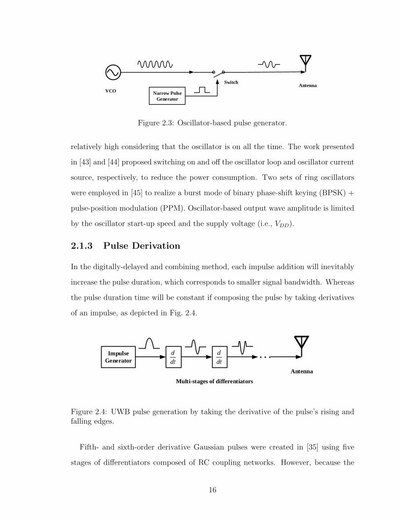
2.1.2 Oscillator-Based Pulse Generator . . . . . . . . . . . . . . . . 15
2.1.3 Pulse Derivation . . . . . . . . . . . . . . . . . . . . . . . . . 16
2.1.4 Spectrum Filtering . . . . . . . . . . . . . . . . . . . . . . . . 17
2.2 Consideration of UWB Pulse Generation . . . . . . . . . . . . . . . . 17
2.3 UWB Receiver Structures . . . . . . . . . . . . . . . . . . . . . . . . 20
2.3.1 Energy Envelope Detection . . . . . . . . . . . . . . . . . . . 20
2.3.2 Cross-Correlation Detection . . . . . . . . . . . . . . . . . . . 21
2.3.3 Auto-Correlation Detection . . . . . . . . . . . . . . . . . . . 22
2.3.4 Direct Sampling Detection . . . . . . . . . . . . . . . . . . . . 24
2.3.5 Sub-Sampling Detection . . . . . . . . . . . . . . . . . . . . . 25
2.4 Consideration of UWB Signal Detection . . . . . . . . . . . . . . . . 26
3 UWB Transmitters 27
vi

3.1 A High-Amplitude UWB Pulse Generator with Spectrum Controlled
by Digital Synthesis . . . . . . . . . . . . . . . . . . . . . . . . . . . . 27
3.1.1 Digital Synthesis of the Input UWB Pulse . . . . . . . . . . . 27
3.1.2 Trapezoidal-Wave-Driven Power Amplifier Circuit Analysis . . 32
3.1.3 Circuit Implementation and MOSFET Sizing . . . . . . . . . . 41
3.1.4 Measurement Results . . . . . . . . . . . . . . . . . . . . . . . 43
3.2 A High-Voltage UWB Pulse Generator using Passive Amplification in
65-nm CMOS . . . . . . . . . . . . . . . . . . . . . . . . . . . . . . . 47
3.2.1 Ultra-Wideband Passive Amplification . . . . . . . . . . . . . 48
3.2.2 Proposed UWB Pulse Generator Design . . . . . . . . . . . . 50
3.2.3 Measurement results . . . . . . . . . . . . . . . . . . . . . . . 66
3.3 Conclusion . . . . . . . . . . . . . . . . . . . . . . . . . . . . . . . . . 69
4 UWB Receiver and Radar System 70
4.1 UWB Radar System Structure . . . . . . . . . . . . . . . . . . . . . . 70
4.2 Ultra-Wideband Low-Noise Amplifier . . . . . . . . . . . . . . . . . . 72
4.3 Local Template UWB Signal Generator . . . . . . . . . . . . . . . . . 82
4.4 Delay-Locked Loop Design . . . . . . . . . . . . . . . . . . . . . . . . 84
4.4.1 Phase/frequency Detector . . . . . . . . . . . . . . . . . . . . 84
4.4.2 Charge Pump . . . . . . . . . . . . . . . . . . . . . . . . . . . 90
4.4.3 Voltage-Controlled Delay Line Design . . . . . . . . . . . . . . 97
4.4.4 Transfer Function of the DLL . . . . . . . . . . . . . . . . . . 107
4.5 Correlator Design . . . . . . . . . . . . . . . . . . . . . . . . . . . . . 109
4.6 UWB radar system implementation and simulation . . . . . . . . . . 112
4.7 Summary . . . . . . . . . . . . . . . . . . . . . . . . . . . . . . . . . 116
5 Conclusions 118
5.1 Summary of Contributions . . . . . . . . . . . . . . . . . . . . . . . . 118
5.2 Future Work . . . . . . . . . . . . . . . . . . . . . . . . . . . . . . . . 120
vii

Bibliography 122
viii

List of Tables
3.1 Zeros created in the wave spectrum for N = 0, 1, 2, 3. . . . . . . . . 30
3.2 Summary of performance and comparison with previously reported
UWB pulse generators. . . . . . . . . . . . . . . . . . . . . . . . . . . 47
3.3 Component values of the proposed passive network. . . . . . . . . . . 63
3.4 Summary of performance and comparison with previously reported
UWB pulse generators. . . . . . . . . . . . . . . . . . . . . . . . . . . 68
4.1 Power consumption summary of the sub-circuits in the proposed UWB
radar system. . . . . . . . . . . . . . . . . . . . . . . . . . . . . . . . 116
ix

List of Figures
1.1 FCC regulation for an indoor environment. . . . . . . . . . . . . . . . 5
1.2 Time domain narrowband and UWB signals and the corresponding
spectrum in the frequency domain. . . . . . . . . . . . . . . . . . . . 5
1.3 Microwave imaging by analyzing the signal transmitted through the
breast. . . . . . . . . . . . . . . . . . . . . . . . . . . . . . . . . . . . 8
1.4 Microwave imaging by analyzing the signal reflected from the breast. 9
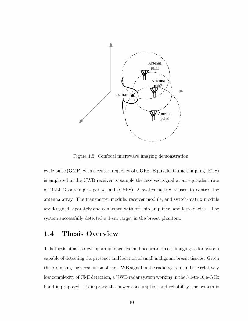
1.5 Confocal microwave imaging demonstration. . . . . . . . . . . . . . . 10
1.6 Cross-correlation UWB radar system block diagram. . . . . . . . . . 11
1.7 Cross-correlation detection demonstration. . . . . . . . . . . . . . . . 11
2.1 The signal is UWB signal if fH − fL > 0.2 (fH+fL)2
. . . . . . . . . . . . 13
2.2 Digitally-delayed positive- and negative-peak impulse combination. . 15
2.3 Oscillator-based pulse generator. . . . . . . . . . . . . . . . . . . . . . 16
2.4 UWB pulse generation by taking the derivative of the pulse’s rising
and falling edges. . . . . . . . . . . . . . . . . . . . . . . . . . . . . . 16
2.5 UWB pulse generation by spectrum filtering. . . . . . . . . . . . . . . 17
2.6 (a) Transmit-receive system, and (b) transmit-reflect-receive system. . 18
2.7 Energy detection block diagram. . . . . . . . . . . . . . . . . . . . . . 20
2.8 Cross-correlation receiver block diagram. . . . . . . . . . . . . . . . . 21
2.9 (a) Auto-correlation receiver block diagram, and (b) time domain sig-
nals of path1 and path2. . . . . . . . . . . . . . . . . . . . . . . . . . 23
2.10 (a) Direct sampling detection, and (b) time domain signals. . . . . . . 24
x

2.11 Sub-sampling detection technique. . . . . . . . . . . . . . . . . . . . . 25
3.1 Time-domain signal and normalized spectrum. (a) A step signal, (b)
single trapezoidal wave, and (c) two consecutive trapezoidal waves. . 28
3.2 PSD of two trapezoidal waves and a single trapezoidal wave (50 ns
repetition period). . . . . . . . . . . . . . . . . . . . . . . . . . . . . 31
3.3 Two consecutive trapezoidal waves with varying τr. (a) Time-domain
signal, and (b) normalized spectrum. . . . . . . . . . . . . . . . . . . 31
3.4 (a) Trapezoidal wave driven circuit, and (b) equivalent circuit. . . . . 32
3.5 VGS(t), VDS(t) and IDS(t) for L1=1µH. (a) Time-domain signal, and
(b) normalized spectrum. . . . . . . . . . . . . . . . . . . . . . . . . . 34
3.6 VGS(t), VDS(t) and IDS(t) for L1=1.5 nH. (a) Time-domain signal, and
(b) normalized spectrum. . . . . . . . . . . . . . . . . . . . . . . . . . 36
3.7 (a) Equivalent RLC circuit, and (b) damping with varying L1. . . . 38
3.8 (a) IDS(t) with varying load inductance, (b) triangular shape IDS(t)
assumption, (c) output spectrum with varying load inductance (τr=30
ps), and (d) Output spectrum with a 1.5-nH load inductor and varying
τr. . . . . . . . . . . . . . . . . . . . . . . . . . . . . . . . . . . . . . 39
3.9 (a) Proposed pulse generator circuit, (b) network frequency response,
and (c) signal flow. . . . . . . . . . . . . . . . . . . . . . . . . . . . . 42
3.10 IDS(t) with different MOSFET widths. . . . . . . . . . . . . . . . . . 43
3.11 Microphotograph of the fabricated chip. . . . . . . . . . . . . . . . . 43
3.12 On-wafer output measurement setup. . . . . . . . . . . . . . . . . . . 44
3.13 Time-domain simulation and measurement of the output pulse. . . . . 45
3.14 Spectrum simulation and measurement of the output pulse. . . . . . . 45
3.15 Breakdown time tBD versus oxide voltage Vox for 2.2-nm oxide thickness
tox. . . . . . . . . . . . . . . . . . . . . . . . . . . . . . . . . . . . . . 46
3.16 Passive amplification demonstration. . . . . . . . . . . . . . . . . . . 48
xi

3.17 UWB pulse generator block diagram. . . . . . . . . . . . . . . . . . . 51
3.18 (a) Pulse generator with RFC and DC block capacitor, (b) OFF and
ON state of the circuit. . . . . . . . . . . . . . . . . . . . . . . . . . . 52
3.19 (a) VDS(t) with varying load resistance RL (width of MOSFET is 320
µm), (b) normalized spectrum of VRL, (c) single pulse energy E1, and
(d) single pulse energy located from 3.1 to 10.6 GHz E2. . . . . . . . 54
3.20 (a) Pulse generator with finite inductor and a parallel capacitor, (b)
OFF and ON state of the circuit. . . . . . . . . . . . . . . . . . . . . 56
3.21 Wideband matching in a Smith chart. . . . . . . . . . . . . . . . . . . 57
3.22 Impedance matching when M1 is ON. . . . . . . . . . . . . . . . . . . 58
3.23 Impedance matching when M1 is OFF. . . . . . . . . . . . . . . . . . 59
3.24 Second-order passive network model. . . . . . . . . . . . . . . . . . . 59
3.25 Schematic of the proposed pulse generator. . . . . . . . . . . . . . . . 61
3.26 ZIN and Z′IN of the proposed matching network. . . . . . . . . . . . . 62
3.27 Butterworth 3rd-order bandpass filter. . . . . . . . . . . . . . . . . . 62
3.28 Time domain signals with the proposed matching network and the
3rd-order Butterworth bandpass filter. . . . . . . . . . . . . . . . . . 63
3.29 Spectrum of the output signals with the proposed matching network
and the 3rd-order Butterworth bandpass filter. . . . . . . . . . . . . . 64
3.30 (a) Layout of the 4×200-fF capacitor, (b) layout of the 800-fF capac-
itor, (c) Momentum simulated capacitance of the two capacitors, and
(d) Momentum simulated quality factor. . . . . . . . . . . . . . . . . 65
3.31 Chip microphotograph. . . . . . . . . . . . . . . . . . . . . . . . . . . 66
3.32 Measurement setup. . . . . . . . . . . . . . . . . . . . . . . . . . . . . 66
3.33 Time domain waveform measurement. . . . . . . . . . . . . . . . . . . 67
3.34 Measured power spectral density results. . . . . . . . . . . . . . . . . 67
4.1 UWB radar system block diagram. . . . . . . . . . . . . . . . . . . . 71
xii
4.2 N -stage cascaded devices chain. . . . . . . . . . . . . . . . . . . . . . 72
4.3 (a) First stage of the LNA, and (b) simplified circuit model. . . . . . 73
4.4 Noise contributed by (a) R1, and (b) M1n,1p. . . . . . . . . . . . . . . 75
4.5 Schematic of the proposed LNA. . . . . . . . . . . . . . . . . . . . . . 76
4.6 LNA gain demonstration. . . . . . . . . . . . . . . . . . . . . . . . . 76
4.7 Transformer model circuit. . . . . . . . . . . . . . . . . . . . . . . . . 77
4.8 (a) Transformer structure, (b) coupling coefficient k simulation result,
(c) self-inductances of Lp and Ls, and (d) quality factor Q of the sec-
ondary winding. . . . . . . . . . . . . . . . . . . . . . . . . . . . . . . 79
4.9 S11 of the proposed LNA. . . . . . . . . . . . . . . . . . . . . . . . . 81
4.10 Voltage gain the of the LNA. . . . . . . . . . . . . . . . . . . . . . . 81
4.11 Noise figure of the LNA. . . . . . . . . . . . . . . . . . . . . . . . . . 81
4.12 (a) UWB transmitter and local template generator circuits, (b) new
delay control circuit, and (c) signal flow of local template generator
including integration-window generator. . . . . . . . . . . . . . . . . . 82
4.13 PFD circuit. . . . . . . . . . . . . . . . . . . . . . . . . . . . . . . . . 85
4.14 Timing diagram of the PFD. . . . . . . . . . . . . . . . . . . . . . . . 85
4.15 PFD design in [66] . . . . . . . . . . . . . . . . . . . . . . . . . . . . 86
4.16 PFD correct lock and harmonic false lock. . . . . . . . . . . . . . . . 87
4.17 PFD stuck false lock. . . . . . . . . . . . . . . . . . . . . . . . . . . . 88
4.18 Correct stuck false lock by resetting at the falling edge of CLKref . . . 88
4.19 Proposed PFD with false lock prevention. . . . . . . . . . . . . . . . 89
4.20 (a) Charge pump circuit with the PFD block and load capacitor, and
(b) waveform with phase difference and locked state. . . . . . . . . . 90
4.21 (a) “Drain-switched” charge pump circuit, and (b) charge pump cur-
rent matching characteristic. . . . . . . . . . . . . . . . . . . . . . . . 92
4.22 (a) Charge pump circuit with improved current mismatch from [71],
and (b) charge pump current matching characteristic. . . . . . . . . . 93
xiii
4.23 Charge pump with transit current mismatch and possible solution. . . 94
4.24 Proposed charge pump with improved current mismatch. . . . . . . . 95
4.25 Current matching of the sourcing and sinking current. . . . . . . . . . 96
4.26 Transit waveforms of the sourcing and sinking current with and without
C1. . . . . . . . . . . . . . . . . . . . . . . . . . . . . . . . . . . . . . 96
4.27 M -stage delay chain. . . . . . . . . . . . . . . . . . . . . . . . . . . . 98
4.28 (a) Inverter MOSFET circuit, and (b) the corresponding switch models
when VIN is “LOW” and “HIGH”. . . . . . . . . . . . . . . . . . . . 99
4.29 Composition of load capacitance CL at VOUT . . . . . . . . . . . . . . 99
4.30 Voltage control delay line with multiplexer. . . . . . . . . . . . . . . . 102
4.31 Simulation result of TV CDL varying with Vctrl. . . . . . . . . . . . . . 104
4.32 (a) DLL design with single-chain 256-stage VCDL, and (b) DLL design
with 16×16 coarse-and-fine step control. . . . . . . . . . . . . . . . . 105
4.33 (a) DLL model, and (b) DLL response. . . . . . . . . . . . . . . . . . 108
4.34 (a) Correlator model, (b) integrator implemented with low pass filter,
(c) integrator implemented with integration window controlled by switch.109
4.35 Correlator topology. . . . . . . . . . . . . . . . . . . . . . . . . . . . . 111
4.36 System signal flow (assuming the propagation time is less than 5.12 ns).113
4.37 Layout of the UWB radar system. . . . . . . . . . . . . . . . . . . . . 114
4.38 (a) Simulated local template signal and RF1 signal (one output from
the transformer), (b) zoomed local template signal and RF1 signal with
duration about 6×TV CDL, (c) the difference of the output signals from
the correlator. . . . . . . . . . . . . . . . . . . . . . . . . . . . . . . . 115
xiv
Abbreviations
ADC analog-to-digital converter.
BPM bi-phase modulation.
BPSK binary phase-shift keying.
CMI confocal microwave imaging.
CMOS complementary metal-oxide-semiconductor.
CS common source.
DAC digital-to-analog converter.
DLL delay-locked loop.
EIRP effective isotropic radiated power.
EIT electrical impedance tomography.
ETS equivalent-time sampling.
FBW fractional bandwidth.
FCC Federal Communications Commission.
FSPL free-space path loss.
GMP Gaussian monocycle pulse.
xv
GSPS Giga samples per second.
IFFT Inverse Fourier transform.
ITU International Telecommunication Union.
KCL Kirchhoff’s current law.
KVL Kirchhoff’s voltage law.
LNA low-noise amplifier.
LO local oscillator.
NF noise figure.
PDK process design kit.
PFD phase/frequency detector.
PLL phase-locked loop.
PPM pulse-position modulation.
PRF pulse repetition frequency.
PSD power spectral density.
RFIC radio-frequency integrated circuit.
SFCW Stepped-Frequency Continuous-Wave.
SNR signal-to-noise ratio.
SRF self-resonant frequency.
TF transformer.
xvi

UWB Ultra-wideband.
VNA Vector Network Analyzer.
VSWR voltage standing wave ratio.
xvii

Chapter 1
Introduction
Currently, medical imaging of the human body is performed at specialized laborato-
ries equipped with extremely sophisticated and expensive imaging instruments. The
current practice is that a physician refers a patient for imaging if any health problem
is suspected. The complexity of the referral process, scheduling, and possible risks
involved in certain imaging methods prevent the frequent screening of the patients for
possible health problems that may go unnoticed for a long time. The late detection
of health issues, particularly cancer, significantly reduces the chance of treating the
disease.
The availability of a medical imaging device that can be readily deployed on-
demand in the physician’s office is highly beneficial for early diagnosis of diseases,
particularly cancer. The desired imaging device should have the following character-
istics:
• its frequent use must not introduce any health risks to the patient, physician,
and others
• it must be portable and have a small form factor
• the device must be produced at low cost for widespread adoption
• must produce images with acceptable range accuracy
• it must be easy to operate
1
• does not create any discomfort for the patients
• preferably should be battery-operated not require access to electricity
This dissertation focuses on developing an integrated imaging system that can
satisfy all the requirements described above. The proposed imaging system will focus
on imaging of the breast for the early detection of breast cancer. Microwave imaging
is chosen because it is among the safest imaging modalities, not imposing any health
risk if frequently used, as described in Section 1.1. Ultra-wideband radar technology
is employed because of its low complexity and low power consumption, as explained
in Section 1.3. The imaging system will be integrated in CMOS technology for low
implementation cost and small form factor.
1.1 Medical Imaging of Breast Cancer
According to the global cancer statistics 2018, breast cancer is the most commonly
diagnosed cancer and the leading cause of cancer death in women worldwide [1]. In
2020, a projected 27,400 females will receive a diagnosis of breast cancer in Canada,
accounting for 24.9% of all new cancer cases in women [2]. Attributed to early detec-
tion and improved treatment, breast cancer mortality has been decreasing steadily
since the 1990s in the US, Canada, and many European countries, and the five-year
net survival for breast cancer of over 85% has been reached [3].
Mammography, X-ray imaging of the breast, is the primary screening technique for
breast cancer diagnosis. However, mammography involves low-dose ionizing radiation
of the tissue that may introduce health risks with frequent testing [4][5]. Especially
for young women, the health risk of repeated exposure may outweigh the benefits of
regular mammography. The screening results of women in their 40s in [5] revealed a
false positive rate of about 12%. Furthermore, mammography is uncomfortable for
some women because it requires the breast to be compressed between two plates to
achieve the desired tissue uniformity.
2

The key to every cancer detection technique lies in the existence of a contrast in
the properties of healthy and cancerous tissue. For instance, mammography com-
pares the density of the healthy breast and malignant tissues and their corresponding
transparency of X-rays. The sharp contrast in electromagnetic properties between
healthy and cancerous breast tissues has inspired microwave engineers to work on
using non-ionizing electromagnetic waves to image the breast to detect cancer. While
the dielectric permittivity of cancerous and healthy tissues of other body organs differ
negligibly according to reports, the permittivity of breast tumors is at least three times
higher than that of surrounding healthy tissues [6][7][8][9][10]. This sharp contrast in
permittivity makes microwave imaging an attractive method to detect breast cancer,
with the promise of better sensitivity and higher reliability compared to conventional
imaging methods. The main advantage of Microwave Imaging over mammography
is the elimination of any health risk because the body is only exposed to low-power
non-ionizing microwave signals (usually thousands of times less than cell phone ra-
diation). Therefore, doctors can comfortably prescribe microwave imaging for breast
screening to detect cancer at very early stages.
Research over the past decades has demonstrated the achievability of applying
microwave imaging in the field of breast cancer detection [11][12][13][14][15]. The
system developed in [16][17] has shown great results and is undergoing clinical trials.
The system performance, however, is limited by the low level of integration with
bulky size and more induced loss. By integrating the major circuitry of the microwave
imaging system on a single chip, system miniaturization can extensively improve the
reliability and reduce the cost.
An integrated microwave imaging radar system in CMOS technology for breast
cancer detection was first proposed in [18]. The presented integrated circuit can
directly connect to the antennas to avoid using a complex switching network and an
expensive Vector Network Analyzer (VNA) in measurement. The Stepped-Frequency
Continuous-Wave (SFCW) approach is employed in the system to sweep the 2-to-
3
16-GHz band with a frequency step size of 90 MHz. The oscillator has to precisely
generate all the frequencies within the band. The system works in the frequency
domain like a narrowband system at each frequency step; the time-domain waveform
is then retrieved by performing an inverse Fourier transform (IFFT). The system is
able to detect the tumor target with a resolution of 3 mm.
An eight-channel wide-bandwidth 10-MHz electrical impedance tomography (EIT)
integrated system is presented in [19] that detects breast cancer by exploiting the
electrical characteristics. Wideband operation is needed because the cancer cells have
greater impedance changes than the normal cells, as the frequency increases. Small
noise level and phase error are important for high accurate detection and to ensure
small artifacts in image reconstruction. The system successfully detects a small-size
target object of 0.5 cm.
1.2 Ultra-Wideband Technology
The origin of ultra-wideband (UWB) technology can be traced back to the 1960s when
non-sinusoidal radio research started to appear in scientific journals [20][21]. Since
then, the UWB technique had been actively researched and hundreds of papers have
been published. However, it was not until 2002, when the Federal Communications
Commission (FCC) established spectrum regulations for unlicensed UWB applica-
tions from 3.1 to 10.6 GHz [22] (regulation for indoor environment shown in Fig. 1.1),
that rapid growth started to occur in the development of UWB applications such
as penetration radar, through-wall imaging, high-data-rate UWB communication,
and medical imaging. Another force behind the explosive development of the UWB
applications is the availability of low-cost radio-frequency integrated circuit (RFIC)
implementations utilizing complementary metal-oxide-semiconductor (CMOS) tech-
nology. By integrating the digital, analog, and RF components on a single chip, a
UWB wireless system can be designed with low cost and high reliability.
UWB technology is attractive in both wireless communication and radar systems
4

Figure 1.1: FCC regulation for an indoor environment.
Time Domain
...
UWB signal
Narrowband
Signal
Frequency Domain
Figure 1.2: Time domain narrowband and UWB signals and the corresponding spec-trum in the frequency domain.
due to the superior advantage of large bandwidth. Different from a narrowband signal,
which concentrates its energy in a small frequency range, a UWB signal distributes
the signal power over a wide spectrum, thus obtaining very low power spectral density
(PSD) at each in-band frequency (Fig. 1.2). This leads to a low interference with other
existing narrowband radios, even with a considerable amount of total signal power,
thus making possible the coexistence of different systems sharing the same operating
frequency range.
5

In a wireless communication system, bit-rate performance is another motivation
that promotes continuous exploration in the UWB technique. As revealed from Shan-
non’s formula [23]
C = B · log2(1 +S
N), (1.1)
where C is the channel capacity (upper bound on bit rate), B is the channel band-
width, and S/N is the signal-to-noise ratio (SNR) of the system, higher bit rates can
be achieved with either wider signal bandwidth and/or larger signal power. But it is
more efficient to increase the channel capacity by increasing the bandwidth since the
SNR and bit rate have a logarithmic relationship.
When it comes to radar and imaging systems, UWB technology exploits the ben-
efits of the ultra-wide bandwidth by using ultra-short duration pulses in the time
domain, making high spatial resolution possible. The free-space range resolution
(resolution along the direction of signal transmission, assuming that the reflected
signals do not overlap) of a pulse radar system can be expressed as
R =c · τ2
, (1.2)
where c is the speed of light (signal transmission speed in free space), and τ is the
pulse duration, which is roughly equal to the reciprocal of signal bandwidth. As can
be noted from Eq. (1.2), a larger signal bandwidth is preferred for a system aiming for
high resolution. As an example, a UWB radar system working within the 3.1-to-10.6
GHz band reaches a range resolution of about 2 cm in free space. Noting that the
signal propagation speed is a function of medium permittivity ϵ and permeability µ
as
c, =1
√ϵ · µ
=1
√ϵ0ϵr · µ0µr
=c
√ϵr · µr
, (1.3)
where ϵr and µr are the relative permittivity and relative permeability of the medium,
generally, a higher range resolution can be obtained for applications applied in non-air
environments. Another feature worth mentioning is the signal penetration capabil-
6

ity. Although it is feasible to pursue large bandwidth resources toward high center
frequencies in the millimeter-wave band, the loss induced by the medium also rises
with increasing frequency, which limits the depth of the detection. In addition, the
transceiver circuitry at higher frequencies is usually more complex, which increases
the cost.
Traditionally, UWB applications have been mostly used in military communication
or radar applications and have been designed with lumped or distributed circuits us-
ing discrete diodes [24][25] and/or transmission lines [26], which have the drawbacks
of bulky size and high loss. RFICs in GaAs or silicon bipolar technology provide a
compact and more reliable solution but they are too expensive for the commercial
market. Benefiting from the continuously-shrinking channel length of CMOS tech-
nology, tremendous improvement has been achieved in the intrinsic speed of MOS
transistor (the transit frequency (fT ) of 65-nm CMOS technology now reaches over
200 GHz), which makes it an ideal solution for cost-effective UWB implementations.
As CMOS technology is widely used to implement digital parts of wireless systems, it
is highly desirable that the radio-frequency circuits can also be designed in the same
technology, which enables the development of single-chip solutions. With a higher
level of integration, a more compact design can be achieved with enhanced reliability
and robustness.
1.3 UWB Medical Imaging
The approaches of microwave breast imaging can generally be divided into two classes
depending on the acquirement of transmitted or reflected scattered signals. The
first approach is based on tomographic imaging. Similar to X-rays, the magnitude
and/or phase of a transmitted microwave signal varies differently when passed through
healthy and cancerous tissues. The dielectric profile of the breast can thus be obtained
by analyzing the properties of the signal transmitted through the breast (Fig. 1.3). To
accurately reconstruct the breast image, the measured analog signals are converted to
7

Breast
Antenna1
Antenna2
Figure 1.3: Microwave imaging by analyzing the signal transmitted through thebreast.
digital signals using high-speed analog-to-digital converters (ADCs). The converted
signals need to be further processed in the digital domain using high-performance
microprocessors (or computers) to extract the signal information. In addition to
the digital signal processing, algorithms [27][28][29] are needed to solve the inverse
scattering problem, which may greatly increase the demand for computation power.
The second approach is based on radar utilizing reflected signals (Fig. 1.4). The
basic underlying procedure is to illuminate the breast with microwaves and then lo-
cate the strong scatterers in the breast by measuring the transmitted and reflected
microwave signals. Confocal microwave imaging (CMI) [11][12][13][30] is the most
prominent approach that utilizes UWB pulses for breast cancer detection. When a
wideband signal, condensed in the time domain, traveling within a medium reaches a
boundary between two materials with different dielectric constants, some of the signal
power will be reflected back to the source with a signal shape similar to the transmit-
8

Antenna
pair
Breast
Figure 1.4: Microwave imaging by analyzing the signal reflected from the breast.
ted signal. The advantage of using an impulse-like (wideband) signal is that the delay
between the transmitted and reflected signals can be simply found by measuring the
time delay between the peaks of the signals, their crossings of certain levels, and their
cross-correlation. In this method, the time delay between the transmitted signal and
the reflected signal at the receiving antenna is measured to determine the distance of
the scattering element from the respective antenna, identifying a sphere for the possi-
ble location of the tumor. If at least three antennas are used, as shown in Fig. 1.5, the
location of the tumor can be found at the intersection of these spheres. This approach
avoids computation-demanding signal processing and complex image-reconstruction
algorithms by simply identifying the presence and location of significant scattering
elements (tumor) in the breast.
In [31], a UWB radar-based breast cancer detection system with CMOS circuits
employing confocal algorithm is described. In the UWB signal generator, up-pulses
and down-pulses are digitally generated and combined to compose a Gaussian mono-
9
Tumor
Antenna
pair1
Antenna
pair2
Antenna
pair3
Figure 1.5: Confocal microwave imaging demonstration.
cycle pulse (GMP) with a center frequency of 6 GHz. Equivalent-time sampling (ETS)
is employed in the UWB receiver to sample the received signal at an equivalent rate
of 102.4 Giga samples per second (GSPS). A switch matrix is used to control the
antenna array. The transmitter module, receiver module, and switch-matrix module
are designed separately and connected with off-chip amplifiers and logic devices. The
system successfully detected a 1-cm target in the breast phantom.
1.4 Thesis Overview
This thesis aims to develop an inexpensive and accurate breast imaging radar system
capable of detecting the presence and location of small malignant breast tissues. Given
the promising high resolution of the UWB signal in the radar system and the relatively
low complexity of CMI detection, a UWB radar system working in the 3.1-to-10.6-GHz
band is proposed. To improve the power consumption and reliability, the system is
10

realized in a standard CMOS process. The imaging radar system includes three major
parts: the antenna array design, radar circuitry design, and image-reconstruction
algorithm design. In this thesis, we only focus on the second part by investigating
the design of a low-cost fully-integrated 3.1-to-10.6-GHz band UWB radar in CMOS
technology.
Tumor
UWB Signal
Generator
Local Template
Generator
Programmable
Delay Generator
Reference
ClockTx
Rx
Cross Correlation
Receiver
Time Delay
between
Tx and Rx
Max
amplitude
Figure 1.6: Cross-correlation UWB radar system block diagram.
Transmitted
Signal
Reflected
Signal
Local
Template
Signal Cross
Correlation
Time
T T T
Figure 1.7: Cross-correlation detection demonstration.
The block diagram of the proposed UWB radar system for detecting breast cancer is
shown in Fig. 1.6. The radar system uses a cross-correlation receiver topology. In the
transmitter part of the system, a pulse generator is used for successive generation of
11
UWB pulses, followed by a transmitting antenna. In the receiver part of the system, a
programmable delay generator is used to trigger the local template generator, which
produces a delayed replica of the transmitted UWB signal. The delayed replica is
first multiplied with the amplified reflected-signal from the breast, then the result is
integrated to produce the cross-correlation of the signals. This process is repeated
by the programmable delay generator, producing successive delays by sweeping the
tissue within the breast. If there is a significant scatterer within the breast, the cross-
correlation of the two signals peaks (Fig. 1.7) at the time delay that corresponds
to the distance of the scatterer to the antenna. Since the output of the correlator
maximizes when the reflected UWB signal aligns with the local template, the key
challenge then is to produce the smallest possible time shift in order to increase the
resolution of the imaging system.
In the following chapters, the design and implementation of a fully-integrated UWB
radar system in a 65-nm CMOS technology will be presented.
In Chapter 2, the commonly employed methods of UWB pulse generation and
detection are introduced. The considerations of selecting the UWB transmitter and
receiver structures are also discussed. In Chapter 3, two UWB pulse generator designs
capable of producing high-amplitude UWB pulses are described. Chapter 4 presents
the design details of each block in the UWB receiver with simulation results. Finally,
conclusions and future work are discussed in Chapter 5.
12

Chapter 2
UWB Transmitter and ReceiverTopologies
According to the FCC and the International Telecommunication Union (ITU), UWB
is defined as electromagnetic radiation with a bandwidth exceeding the lesser of 500
MHz or 20% of the arithmetic center frequency [32], as depicted in Fig. 2.1. Corre-
sponding to the two different definitions, the design approaches of the UWB system
are also divided into two paths.
fHfL (fL+fH)/2
Spectrum
Frequency
Figure 2.1: The signal is UWB signal if fH − fL > 0.2 (fH+fL)2
.
The first path slices the 3.1-to-10.6-GHz band into multiple sub-bands, each with
a bandwidth of about 500 MHz [33]. The benefit of this path is that the circuit
design can make use of the mature narrowband carrier-based design concepts and
topologies with an expanded working bandwidth. This approach is only employed in
13
UWB communication systems.
The second path looks from the angle of impulse radio, which exhibits large band-
width in frequency and short duration in the time domain. Generally, the receiver of
impulse radio only needs to detect the existence of the impulse signal. Thus the UWB
transceiver system of this path can employ a much simpler circuit topology with low
power consumption. This approach is widely employed in UWB radar systems. This
project mainly focuses on the second path to implementing a 3.1-to-10.6-GHz impulse-
based UWB radar system that features low complexity, low power consumption, and
long detection range.
Other than bandwidth, parameters such as pulse amplitude, pulse shape, and
power spectral density also contribute to defining a UWB pulse. In this chapter, the
methods of generating UWB pulses will be presented, followed by a review of the
topology of UWB receivers. The topology choices and considerations of the UWB
transmitter and receiver employed in this research are also discussed.
2.1 UWB Pulse Generation Structures
Several methods can be employed to generate UWB pulses. From a time-domain
perspective, pulses such as high-order Gaussian pulses [34][35] are popular as its
spectrum can satisfy the FCC limitations without extra filters. From a frequency-
domain perspective, a UWB signal can be generated by passing a broadband signal
through a bandpass filter, which blocks the out-of-band frequency components of the
input signal [36]. In the design of UWB radar systems, bandwidth and amplitude
are considered the most important parameters. As mentioned in Chapter 1, RFIC
design in CMOS technology offers low cost, low-power consumption, and compact
form factor. It also enables the development of single-chip solutions integrating RF
front-end with the digital part of the system. Generally, the techniques employed for
the design of CMOS pulse generators can be grouped in the following categories.
14

2.1.1 Digitally-Delayed Impulse Combination
Positive Peak
Generator
Negative Peak
Generator
Delay
Pulse Edge
Combiner
Delay
Delay Delay
. . .
. . . Antenna
Figure 2.2: Digitally-delayed positive- and negative-peak impulse combination.
As CMOS technology is most widely used in digital circuit design, it is feasible
to produce UWB signals digitally. As shown in Fig. 2.2, several digitally-generated
short pulses can be delayed and combined to create UWB pulses.
Triangular pulses were generated and combined in [37] to compose an envelope-
sampled raised-cosine pulse to have a similar spectrum distribution. Instead of passing
the combined signal through a power amplifier, multiple independent parallel power
amplifiers were employed in [38][39] to compose a pulse with Gaussian-shape envelope.
[40] proposed impulse generator cells that can be easily controlled with a data signal to
get inverse symmetrical pulses for bi-phase modulation (BPM). A digitally-combined
wave has good flexibility but lacks the ability to drive the antenna load with high
output power, even after power amplification, as the output amplitude is limited by
VDD to avoid distortion of the waveform.
2.1.2 Oscillator-Based Pulse Generator
As depicted in Fig. 2.3, an oscillator is capable of generating a narrow-band sinusoidal
signal; however, it can be turned into a wideband signal generator if its output signal
is modulated with another narrow pulse.
A mixer was used in [41] to up-convert a triangular wave (triangular/trapezoidal
wave in [42]) to create a carrier-based UWB pulse. The total power consumption is
15
Narrow Pulse
Generator
VCO
AntennaSwitch
Figure 2.3: Oscillator-based pulse generator.
relatively high considering that the oscillator is on all the time. The work presented
in [43] and [44] proposed switching on and off the oscillator loop and oscillator current
source, respectively, to reduce the power consumption. Two sets of ring oscillators
were employed in [45] to realize a burst mode of binary phase-shift keying (BPSK) +
pulse-position modulation (PPM). Oscillator-based output wave amplitude is limited
by the oscillator start-up speed and the supply voltage (i.e., VDD).
2.1.3 Pulse Derivation
In the digitally-delayed and combining method, each impulse addition will inevitably
increase the pulse duration, which corresponds to smaller signal bandwidth. Whereas
the pulse duration time will be constant if composing the pulse by taking derivatives
of an impulse, as depicted in Fig. 2.4.
Impulse
Generator
Multi-stages of differentiators
. . .
Antenna
Figure 2.4: UWB pulse generation by taking the derivative of the pulse’s rising andfalling edges.
Fifth- and sixth-order derivative Gaussian pulses were created in [35] using five
stages of differentiators composed of RC coupling networks. However, because the
16
highpass filter itself is a voltage divider, amplitude losses are also introduced during
each derivative. Although an amplifier was added after each differentiator, it could
only work in the triode region to avoid affecting the functionality of the differentiator.
Thus this method is not a good candidate for high amplitude design either.
2.1.4 Spectrum Filtering
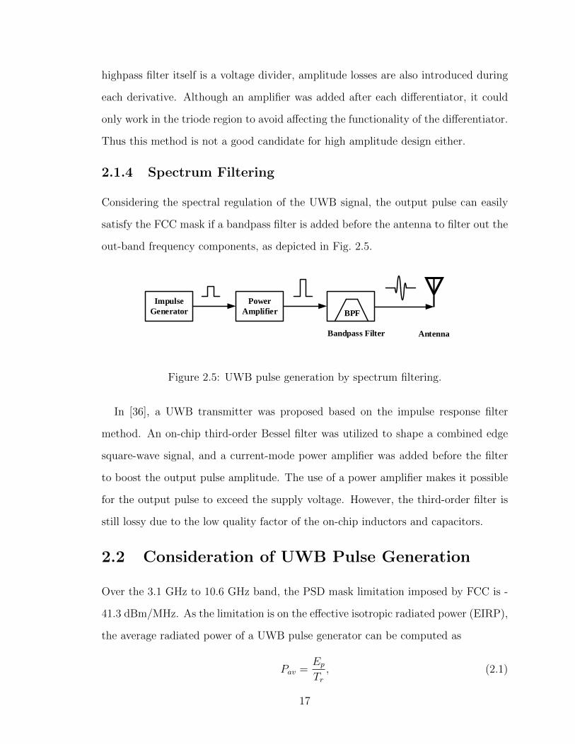
Considering the spectral regulation of the UWB signal, the output pulse can easily
satisfy the FCC mask if a bandpass filter is added before the antenna to filter out the
out-band frequency components, as depicted in Fig. 2.5.
Impulse
Generator
Power
Amplifier BPF
Bandpass Filter Antenna
Figure 2.5: UWB pulse generation by spectrum filtering.
In [36], a UWB transmitter was proposed based on the impulse response filter
method. An on-chip third-order Bessel filter was utilized to shape a combined edge
square-wave signal, and a current-mode power amplifier was added before the filter
to boost the output pulse amplitude. The use of a power amplifier makes it possible
for the output pulse to exceed the supply voltage. However, the third-order filter is
still lossy due to the low quality factor of the on-chip inductors and capacitors.
2.2 Consideration of UWB Pulse Generation
Over the 3.1 GHz to 10.6 GHz band, the PSD mask limitation imposed by FCC is -
41.3 dBm/MHz. As the limitation is on the effective isotropic radiated power (EIRP),
the average radiated power of a UWB pulse generator can be computed as
Pav =Ep
Tr
, (2.1)
17

where Ep is the energy of a single pulse, and Tr is the pulse repetition period. Note
that the average power of a UWB signal is proportional to the energy of a single
pulse and the pulse repetition frequency (PRF), which is equal to 1/Tr. To utilize
the most of the limited link power budget, the generated UWB pulse should achieve
the maximum allowed PSD. As the power limitation is on the average signal power,
the PSD can be increased with either higher PRF or higher transmitted energy of
a single pulse generated at lower PRF. In data transmission designs, a high-data-
rate UWB transceiver requires a high PRF proportional to the data rate, the energy
of each transmitted pulse has to be limited for FCC mask compliance limiting the
transmission range. On the contrary, the performance of a low-data-rate (low PRF)
UWB system is usually limited by the maximum pulse energy available from the
UWB transmitter. A meter-range transmission can be achieved if sufficient output
power can be produced by the UWB transmitter.
Transmitter
Antenna
Receiver
Antenna
d
(a)
Transmitter
Antenna
Receiver
Antenna
Object
d
(b)
Figure 2.6: (a) Transmit-receive system, and (b) transmit-reflect-receive system.
For a transmit-receive system, as shown in Fig. 2.6a, to achieve a certain signal-to-
18

noise ratio at the receiving antenna, the transmitted power has to be increased with
the transmission range to compensate for the free-space path loss (FSPL) given as
[46]
FSPL =Pt
Pr
=1
GtGr
(4πdf
c)2, (2.2)
where Pt and Pr are the power delivered to the transmit antenna and received at
the receive antenna respectively, Gt and Gr are the directivities of the transmitting
and receiving antennas, respectively, d is the signal traveling distance, f is the signal
frequency, c is the speed of light. Thus the peak-to-peak voltage (Vpp) in a narrow-
band transceiver has to increase proportionally to the transmission range since Pt(∝
V 2pp) ∝ d2. As a UWB signal can be seen as a set of narrow band signals traveling at
the same time, the relationship between Vpp and d should maintain consistent.
For a transmit-reflect-receive system, as depicted in Fig. 2.6b, the maximum range
with a pulsed signal for a certain SNR is
dmax = [P
′tGtGrλ
2στ
(4π)3kTsL · SNR]14 , (2.3)
where P′t is the peak transmitted power, λ is the wavelength of the signal center
frequency, τ is the duration of the transmitted signal, kTs denotes the noise power
density at the receiving antenna, L is the antenna loss, and σ is the radar cross section,
which is defined as the ratio of the power reflected back to the receiving antenna to
the power density incident on the target.
As can be noted, for both types of systems, the detection range increases with
higher output power from the UWB transmitters. From another perspective, the
performance of the UWB radar system can be better with the same detection range
if the UWB transmitter can produce higher output power.
As CMOS technology advances towards the nano-scale, pursuing higher transit
frequencies and lower power consumption in the digital circuit by reducing the supply
voltage, UWB pulse generator designs with high output amplitude become more
19
challenging. Although power amplifiers or buffer stages are usually employed in the
UWB transmitter to enhance the ability to drive the load antenna, the transmitted
power is still limited by the low supply voltage (1 V or less in the advanced CMOS
processes) in most cases. Of all the five methods mentioned in the previous section,
the spectrum-filtering method is promising in high amplitude design, however, the
required high-order bandpass filter is lossy and hard to implement.
In the next chapter, two high-voltage UWB pulse generator designs capable of
producing UWB pulses with Vpp beyond the supply voltage will be described. In the
first design, we present a high-amplitude UWB pulse generator with low complex-
ity by shifting the majority of the pulse shaping effort to the digital domain using
trapezoidal waves. The second design introduces an alternative method to produce
high-amplitude UWB signals using wideband passive amplification.
2.3 UWB Receiver Structures
Various methods can be employed to detect or revive a UWB signal in the time do-
main. Depending on the environment of the application, the receiver can be designed
to detect the existence of the UWB signal by peak-amplitude or energy detection,
or to reproduce the UWB pulse with both amplitude and phase information. In this
section, five common methods of detecting a UWB pulse are presented.
2.3.1 Energy Envelope Detection
(·)2
Antenna BPF Squarer Integrator Decision
Output
Figure 2.7: Energy detection block diagram.
20

As shown in Fig. 2.7, energy envelope detectors can be used to detect the presence
of a UWB signal. After a bandpass filter for channel selection, the received signal is
first squared by a squarer, which is usually implemented by a diode or a MOSFET
working in the saturation region. The signal energy can then be collected with an
integrator. Finally, the decision is made by comparing the signal after the integrator
with a reference voltage. Although the circuit structure is simple to implement, this
type of pulse detection has very limited performance since it detects all the in-band
energy irrespective of the pulse type or shape. Any signal with sufficient energy can
create a false alarm at the output. This makes this type of pulse detector unfeasible,
especially for a low-power UWB signal case where the transmitted pulse coexists with
other licensed and unlicensed narrowband/wideband signals.
2.3.2 Cross-Correlation Detection
Antenna LNA
Multiplier Integrator Decision
Template
Generator
Sync and
Delay Circuit
Correlator
Output
Figure 2.8: Cross-correlation receiver block diagram.
Fig. 2.8 depicts the block diagram of a cross-correlation receiver. As can be seen,
the major difference between an energy detection receiver and a cross-correlation
receiver is that a multiplier with a template generator is employed instead of the
squarer. The core cross-correlation receiver consists of a template signal generator, a
multiplier, and an integrator. Instead of taking the square, the received signal is first
multiplied with the generated template signal, which has the same waveform as the
21

transmitted signal, and then fed to an integrator. The output level of the correlator
(integrator) depends on how well the received signal matches with the generated
template in both time and shape. Thus for optimum detection performance, the
template signal has to have the same shape as the received signal and be shifted with
a small precise time step.
Since an optimum output only happens when the received signal has the same
shape (same spectral properties, in another perspective) as the local template signal,
the correlator actually acts like a signal filter. It thus can be expected that the receiver
will be more robust to noise and other in-band interference signals. In practice, the
receiver performance can be slightly degraded due to the uncertainty of the received
signal shape, which can be changed by factors such as frequency-based channel loss
and antenna transfer function.
2.3.3 Auto-Correlation Detection
Following a similar principle, the block diagram of an auto-correlation receiver is
depicted in Fig. 2.9a. Instead of multiplying the received signal with a locally gen-
erated template signal, the received signal is multiplied with a delayed version of
“itself”. Thus the shape difference of the two multiplying signals is minimized. Com-
pared with the cross-correlation receiver, the auto-correlation receiver has a simpler
detection structure without the need of a local template generator. Generally, the
auto-correlation receiver is less immune to channel interference with the exception
of under a low-SNR system [47], where the received signal suffers significant shape
distortion.
As can be seen from Fig. 2.9b, the second UWB pulse (path1) of the two-consecutive
pulses received from the antenna is multiplied with the delayed version of the first
pulse (path2). Thus a maximum output occurs when the delay td produced at the
receiver is equal to the time gap between the two UWB signals. Unlike a narrow-
band scenario, where a delay can be easily implemented with the RC delay circuit, a
22

Antenna LNA
Multiplier Integrator Decision
Delay td
Output
path1
path2
(a)
td
path1
path2
(b)
Figure 2.9: (a) Auto-correlation receiver block diagram, and (b) time domain signalsof path1 and path2.
transmission line will be needed to provide equal delays for all in-band frequencies.
As a rough estimation, a delay of 1 ns would require a 30-cm transmission line, which
makes it impractical for on-chip implementation. In addition, two-consecutive UWB
pulses in one transmission will limit the maximum power of each UWB pulse to be
half of the FCC limitation, which results in a smaller detection range. In [48], a com-
bination of an ADC and a digital-to-analog converter (DAC) was proposed to delay
and reconstruct the first pulse. However, it is only applicable when the radar system
works at relatively low frequencies. Moreover, the circuit consumes more power with
added complexity.
23

Antenna LNA
ADC
Sampling
Clock
Digital Signal
Processing
(a)
Pulse repetition period Tr
Received
Signal
Ts
Tw
Sampling
Clock
Output
Signal
. . .
. . .
(b)
Figure 2.10: (a) Direct sampling detection, and (b) time domain signals.
2.3.4 Direct Sampling Detection
Other than detecting the presence of a UWB signal by sensing its energy, a receiver
can also detect a UWB signal with digital signal processing. With an ADC to directly
sample the UWB signal, the receiver can reproduce the UWB signal with both the
phase and amplitude information, as shown in Fig. 2.10.
However, to directly digitize a UWB signal and preserve the signal information at
the same time, the sampling frequency (1/Ts) of the ADC has to be as least two times
the highest in-band frequency, according to the Nyquist–Shannon sampling theorem
[49]. Considering a UWB signal occupying the full 3.1-to-10.6-GHz bandwidth, the
sampling rate of ADC has to be at least 21.2 GSPS. Building an ADC with such a
24
high sampling frequency is both difficult and power-hungry.
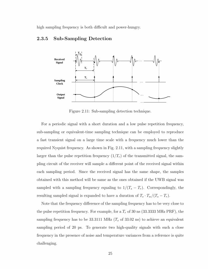
2.3.5 Sub-Sampling Detection
Tr
Received
Signal. . .
Ts
Tw
. . .
. . .
. . .
Sampling
Clock
Output
Signal
Figure 2.11: Sub-sampling detection technique.
For a periodic signal with a short duration and a low pulse repetition frequency,
sub-sampling or equivalent-time sampling technique can be employed to reproduce
a fast transient signal on a large time scale with a frequency much lower than the
required Nyquist frequency. As shown in Fig. 2.11, with a sampling frequency slightly
larger than the pulse repetition frequency (1/Tr) of the transmitted signal, the sam-
pling circuit of the receiver will sample a different point of the received signal within
each sampling period. Since the received signal has the same shape, the samples
obtained with this method will be same as the ones obtained if the UWB signal was
sampled with a sampling frequency equaling to 1/(Ts − Tr). Correspondingly, the
resulting sampled signal is expanded to have a duration of Ts · Tw/(Ts − Tr).
Note that the frequency difference of the sampling frequency has to be very close to
the pulse repetition frequency. For example, for a Tr of 30 ns (33.3333 MHz PRF), the
sampling frequency has to be 33.3111 MHz (Ts of 33.02 ns) to achieve an equivalent
sampling period of 20 ps. To generate two high-quality signals with such a close
frequency in the presence of noise and temperature variances from a reference is quite
challenging.
25

2.4 Consideration of UWB Signal Detection
As discussed in Section 2.2, other than the bandwidth, the complexity and output
power are two main focuses in the design of UWB transmitters. Of all the receiver
structures presented in Section 2.3, energy detection is susceptible to in-band interfer-
ence, the auto-correlation method is not practical because the on-chip transmission
line occupies a significant silicon area, direct sampling is also not practical as the
in-band frequency is up to 10.6 GHz. Thus cross-correlation and sub-sampling detec-
tion methods are the two promising approaches for signal detection for the proposed
UWB radar system. For receiver systems employing ADCs, the accuracy of detecting
malignant tissues is limited by the speed of the ADCs required to convert the reflected
signals from the analog domain to the digital domain. Although the sub-sampling
approach can equivalently provide a high sampling rate with low-speed ADCs, the
ADCs are still needed to be designed with high resolution to accurately reconstruct
the received waveform. The implementation is usually much more complicated com-
pared with cross-correlation detection.
26
Chapter 3
UWB Transmitters
3.1 A High-Amplitude UWB Pulse Generator with
Spectrum Controlled by Digital Synthesis
We present a high-amplitude UWB pulse generator with low complexity by shifting
majority of the pulse shaping effort to the digital domain using trapezoidal waves that
can be implemented easily using delay cells and logic gates. The synthesized signal is
capable of driving the 50-Ω load after being passed through a power amplifier, which
boosts the signal amplitude beyond the supply voltage.
To understand the synthesis technique, the spectrum characteristic of a digitally
synthesized UWB waveform is analyzed first in Section 3.1.1, and then a new UWB
pulse generator with simplified output network design is discussed in Section 3.1.2.
The final circuit implementation is presented in Section 3.1.3. Section 3.1.4 demon-
strates the measurement results in a standard 65-nm CMOS technology and compares
the performance with other reported UWB pulse generators.
3.1.1 Digital Synthesis of the Input UWB Pulse
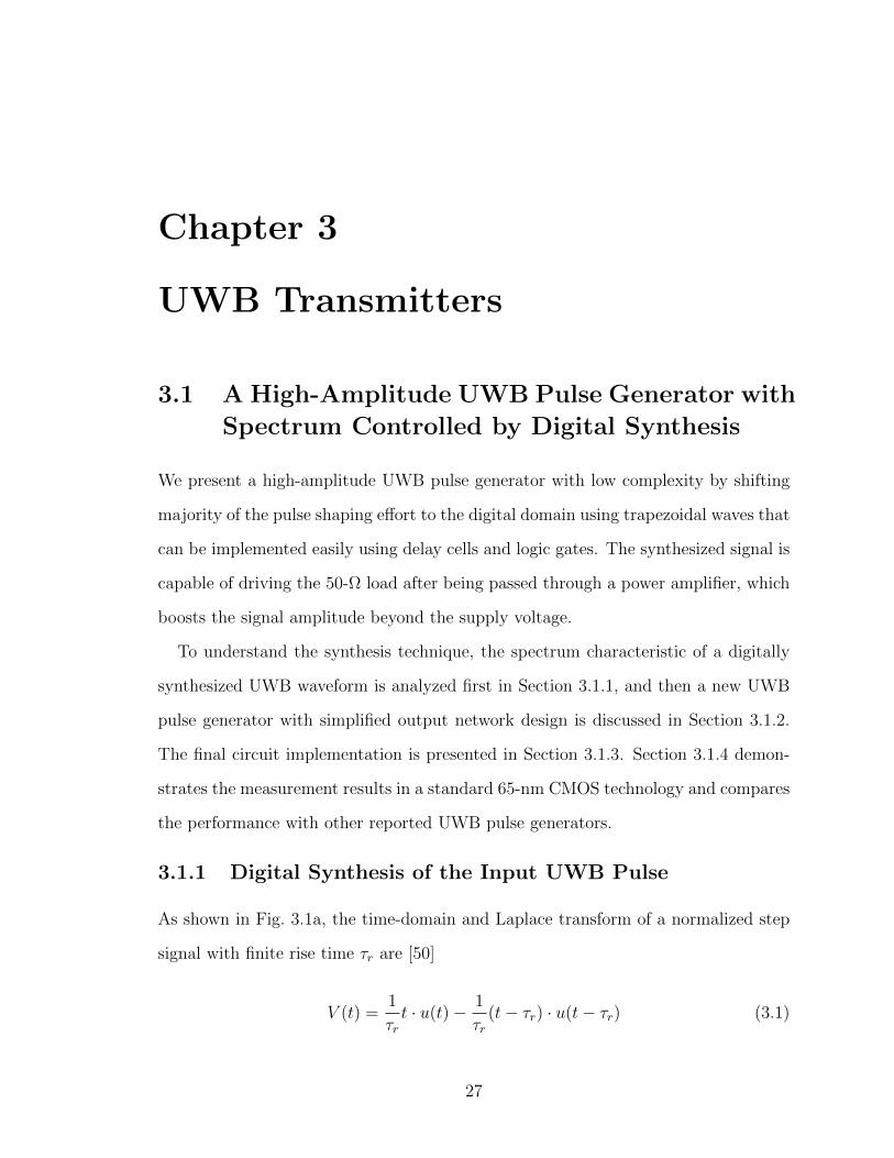
As shown in Fig. 3.1a, the time-domain and Laplace transform of a normalized step
signal with finite rise time τr are [50]
V (t) =1
τrt · u(t)− 1
τr(t− τr) · u(t− τr) (3.1)
27
(a)
(b)
(c)
Figure 3.1: Time-domain signal and normalized spectrum. (a) A step signal, (b)single trapezoidal wave, and (c) two consecutive trapezoidal waves.
and
V (s) =1
τrs2(1− e−sτr), (3.2)
where u(t) is the unit step function. The amplitude of V (s) equals zero at frequencies
ω = 2πN/τr (where N is an integer), which means that notches appear periodically in
the spectrum of the step signal at frequencies that are related to τr. For example, the
notches created in the spectrum by setting τr = 30 ps are drawn in Fig. 3.1a. Note
28

that the step signal is kept high for a relatively long duration (e.g., 100 ns) after the
rising edge, and the spectrum is obtained after removing the DC component using a
50-MHz highpass filter.
Noting that the locations of the notches in the spectrum can be controlled by τr,
this raises the possibility of eliminating the use of a high-order filter by setting the
notch frequencies at the start and end frequency point of the passband spectrum. So
it is worth analyzing the relationship between pulse shape parameters (i.e., rise/fall
time, duration time) and the spectral characteristic of a finite-slope square pulse
(i.e., trapezoidal pulse), which can be easily generated using digital CMOS circuit.
Previous research work treats the generated edge-combining pulse as a perfect square
pulse [36][43], which is a reasonable assumption when the pulse width τw is much larger
than τr (τf ). However, in order to satisfy the ultra-wide bandwidth requirement, the
total pulse duration usually has to be at the sub-nano second level, in which cases,
τw will be close to or even smaller than τr (τf ). Therefore, a trapezoidal wave is a
more accurate description of the signal for theoretical analysis. Fig. 3.1b shows the
normalized time-domain signal of an ideal trapezoidal wave. Assuming that τr and τf
have the same value for simplicity, the time-domain signal equation and its Laplace
Transform can be written as
V (t) =1
τrt · u(t)− 1
τr(t− τr) · u(t− τr)
− 1
τr(t− τr − τw) · u(t− τr − τw)
+1
τr(t− 2τr − τw) · u(t− 2τr − τw)
(3.3)
and
V (s) =1
τrs2(1− e−sτr)[1− e−s(τr+τw)]. (3.4)
The terms e−sτr and e−s(τr+τw) lead Eq. (3.4) to zeros at frequencies ω = 2πN/τr
and 2πN/(τr+τw) (N is an integer). Compared to the step signal, the zeros are
determined by both τr and τw instead of only τr. However, it is not possible to set the
29
first two notches at around 3.1 GHz and 10.6 GHz due to its periodicity. For example,
if 1/(τr+τw) is set to be 3.1 GHz, then (τr+τw) would be equal to 322 ps, however,
the following notches generated will appear at 6.2 GHz and 9.3 GHz for N = 2 and
3, respectively. The normalized spectrum for a τr of 122 ps and τw of 200 ps, as an
example, is shown in Fig. 3.1b. Up to 20 GHz, the notches created by τr are only at
8.2 GHz and 16.4 GHz. To locate two notch frequencies at 3.1 GHz and 10.6 GHz
or nearby, another trapezoidal wave with the same parameters is added to include
the pulse gap time, τd, as another variable to the design as depicted in Fig. 3.1c.
Similarly, the notch frequencies created by two consecutive trapezoidal waves can be
calculated as 2πN/τr, 2π N/(τr+τw) and (2πN+π)/(2τr+τw+τd).
With a transit frequency of over 200 GHz, it is feasible to implement a 30-ps rising
and falling edge trapezoidal wave in 65-nm CMOS technology. If we set τr = τf =
30 ps, τw = 35 ps ,and τd = 20 ps, notch frequencies calculated for N ≤ 3 are listed
in Table 3.1 with the corresponding spectrum simulation results plotted in Fig. 3.1c.
Note that the simulation results agree well with the calculation results. Also note
that, although it is possible to set the first and second notch frequency at 3.5 GHz
and 10.5 GHz, respectively (by setting (2τr + τw + τd) = 143 ps), locating a -10-dB
cutoff frequency at 10.6 GHz requires designing a waveform with a notch frequency
higher than 10.6 GHz. If the second notch is created at 13 GHz, the first notch will
appear at 4.3 GHz, according to Table 3.1.
Table 3.1: Zeros created in the wave spectrum for N = 0, 1, 2, 3.
N = 0 N = 1 N = 2 N = 3
Nτr
N/A 33.3 GHz 66.7 GHz 100 GHz
N(τr+τw) N/A 15.38 GHz 30.77 GHz 46.15 GHz
(N+0.5)(2τr+τw+τd)
4.35 GHz 13.04 GHz 21.74 GHz 30.43 GHz
The reader may argue that a single trapezoidal wave could also be designed to
create the first notch at the upper cutoff frequency, but the magnitude of the spectrum
30
0 5 10 15 20 25 30Frequency (GHz)
0
0.2
0.4
0.6
PS
D (
V2 /H
z)
Two trapezoidal waves Single trapezoidal wave
Figure 3.2: PSD of two trapezoidal waves and a single trapezoidal wave (50 ns repe-tition period).
0 0.05 0.1 0.15 0.2 0.25 0.3
Time [ns]
0
0.5
1
1.5
Am
plit
ude [V
]
r=10ps
r=20ps
r=30ps
r=40ps
95ps 20ps
r+
w
(a)
Lower
Amplitude
(b)
Figure 3.3: Two consecutive trapezoidal waves with varying τr. (a) Time-domainsignal, and (b) normalized spectrum.
31

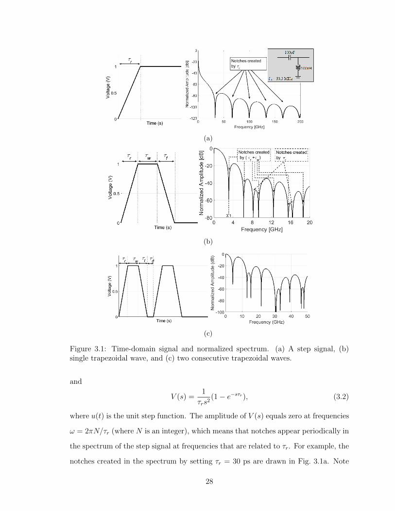
within the UWB band is much smaller than that of the two trapezoidal waves resulting
in much lower output power, as shown in Fig. 3.2. Furthermore, even if the notch is
set at 3.1 GHz, a highpass filter is still needed to filter out the spectrum below 3.1
GHz, in other words, the first notch still simplifies the output filter design.
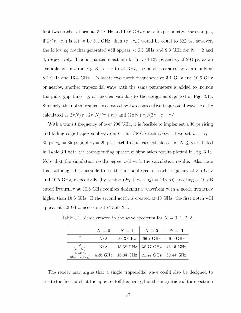
Although the first two notches in the spectrum are controlled only by (2τr + τw + τd)
(see Table 3.1), it is still important to set τr to a proper value. One can see in Fig. 3.3
that when varying τr from 40 ps to 10 ps, the first notch created by (τr + τw) will
move toward a lower frequency and even become lower than the second notch created
by (2τr + τw + τd), which reduces the signal bandwidth. However, the first (τr + τw)
notch can also benefit the design when τr is 30 to 40 ps: the notch will suppress the
out-of-band spectrum amplitude between 15 GHz and 20 GHz, as shown in Fig. 3.3b.
In the next section, it will be proved that the spectral characteristics of the two
trapezoidal waves can be preserved after passing them through a nonlinear power
amplifier.
3.1.2 Trapezoidal-Wave-Driven Power Amplifier Circuit Anal-ysis
As the digital circuit producing the described trapezoidal waveform cannot directly
drive a 50-Ω load, it is necessary to boost the amplitude by adding a power am-
L1
C1
Rload
M1
IRloadIL
IDS
VDD
VIN
(a)
VGSRloadIDS
+
-
D
S
G
(b)
Figure 3.4: (a) Trapezoidal wave driven circuit, and (b) equivalent circuit.
32

plifier in between the signal generator and the load. As it is important to preserve
the spectral characteristics of the generated trapezoidal waveform, it is necessary to
investigate what the output current shape of a MOSFET would look like if driven by
this waveform in order to find the spectral correspondence between the input and the
output signals.
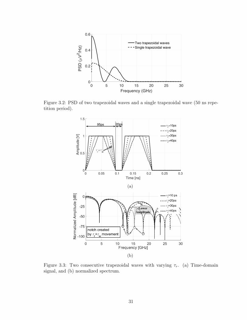
Fig. 3.4a shows a simple power amplifier stage. M1 is driven by a trapezoidal
voltage source with the same parameters as the example in the previous section. L1
and C1 are set to be 1 µH and 1 µF to block the AC signal from the power supply and
bypass the DC to the load respectively. Rload is set to be 50 Ω. The input waveform
VGS(t), drain-source voltage VDS(t), and drain-source current IDS(t) are depicted in
Fig. 3.5a. From 0 to t1, before VGS(t) reaches the threshold voltage Vth, M1 is in
the cutoff region and IDS(t) equals to 0. From t1 to t2, VGS(t) - Vth ≤ VDS(t), M1
operates in the saturation region and IDS(t) can be written as
IDS(t) =1
2k
′W
L[VGS(t)− Vth]
2, (3.5)
where W and L are the width and length of M1, k′equals to µnCox.
As the load inductor L1 can be seen as an open circuit and capacitor C1 can be seen
as a short circuit over the frequency band of interest, the equivalent circuit model is
shown in Fig. 3.4b. Although the BSIM4 MOS model was used in the simulation, a
simplified model is shown here for two reasons. The amplifier works mostly as a switch
in large signal mode, but a current source rather than a switch is more appropriate to
represent the relationship between IDS(t) and VGS(t). The parasitic capacitors will
slow down the rise/fall time of the trapezoidal wave, but they will be ignored at this
stage for simplicity. Since all the current comes from the load resistor Rload, IDS(t)
can also be expressed as
IDS(t) = IRload(t) ≈ VDD − VDS(t)
Rload
. (3.6)
Hence, we can conclude from Eqs. (3.5) and (3.6) that from t1 to t2, IDS(t) ∝
33

0 0.05 0.1 0.15 0.2 0.25 0.3Time (ns)
0
0.5
1
1.5
Voltage
(V)
VGS
VDS
0 0.05 0.1 0.15 0.2 0.25 0.3
Time (ns)
0
5
10
15
20
25
Curr
ent
(mA
) I
DS
t1
t2
t3
t3
't2
'
2r+
w+
d
(a)
0 10 20 30 40 50
Frequency (GHz)
-100
-80
-60
-40
-20
0
Norm
aliz
ed A
mplit
ude
(dB
)
VGS
VDS
0 10 20 30 40 50
Frequency (GHz)
-100
-80
-60
-40
-20
0
Norm
aliz
ed A
mplit
ude
(dB
)
IDS
(b)
Figure 3.5: VGS(t), VDS(t) and IDS(t) for L1=1µH. (a) Time-domain signal, and (b)normalized spectrum.
−VDS(t) ∝ [VGS(t) − Vth]2. In fact, since VDS(t) drops as VGS(t) rises, a much more
linear relationship between IDS(t) and VGS(t) can be observed from Fig. 3.5a due to
MOSFET channel length modulation.
34

After t2, where VGS - Vth = VDS, M1 goes from the saturation region into the triode
region. So IDS(t) can then be written as
IDS(t) = k′W
L[VGS(t)− Vth]VDS(t). (3.7)
As M1 can only draw current from Rload, IDS(t) reaches its maximum during
the transition between the two regions. Due to the opposite trends of VDS(t) and
VGS(t), IDS(t) represents a much slower slope from t2 to t′2 and t
′3 to t3 according
to Eq. (3.7). From t′2 to t
′3, VGS(t) reaches its maximum (i.e., VDD) and VDS(t)
remains at its minimum VDS,min(≈ 0V ). IDS,max can be derived from Eq. (3.6) as
(VDD−VDS,min)/Rload ≈ 20mA.
At t3, M1 goes back to the saturation region again and cuts off immediately after as
VGS(t) decreases (the subthreshold region is ignored here for simplicity). According
to Eqs. (3.5) and (3.6), the trans-characteristic of this stage is the same as that of t1
to t2. The same response would be expected during the second trapezoidal wave.
The analysis above indicates that each trapezoidal wave of −VDS(t) or IDS(t) can
be seen as a narrower but sharper version of VGS(t) (shorter τr because no current
will flow through M1 before VGS(t) reaches Vth, and longer τw due to the slower slope
when M1 is in triode region), while the total delay time between the two trapezoidal
waves remains constant. Hence, the notches determined by τr will be shifted to higher
frequencies while the ones created by (2τr + τw + τd) remain the same. As mentioned
earlier, the first two notches in the spectrum are both determined by (2τr + τw + τd),
thus the changes of the notch positions are of less interest. The Fourier transforms of
VDS(t) and IDS(t) are shown in Fig. 3.5b to confirm the above analysis. The spectrum
of VGS(t) is also shown for comparison purposes.
One concern in a practical design is that a large inductor (e.g., 100 nH) cannot
be effectively implemented on chip as it exhibits a very low quality factor and low
self-resonant frequency (SRF), beyond which it will behave as a a capacitor rather
than an inductor. The time-domain signals and corresponding spectrum with a more
35
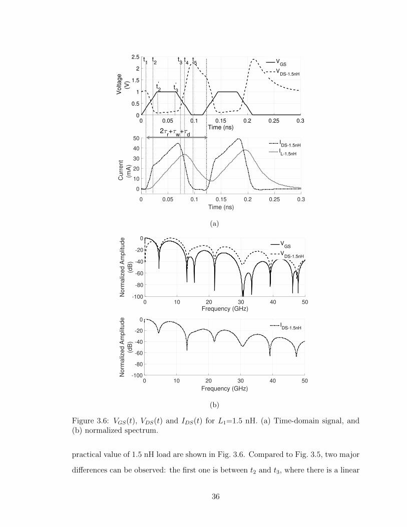
0 0.05 0.1 0.15 0.2 0.25 0.3
Time (ns)
0
0.5
1
1.5
2
2.5
Vo
lta
ge
(V)
VGS
VDS-1.5nH
0 0.05 0.1 0.15 0.2 0.25 0.3
Time (ns)
0
10
20
30
40
50
Cu
rre
nt
(mA
)
IL-1.5nH
t1
IDS-1.5nH
t2
t5
t4
t3
t3
't2
'
2r+
w+
d
(a)
0 10 20 30 40 50
Frequency (GHz)
-100
-80
-60
-40
-20
0
No
rma
lize
d A
mp
litu
de
(dB
)
VGS
VDS-1.5nH
0 10 20 30 40 50
Frequency (GHz)
-100
-80
-60
-40
-20
0
No
rma
lize
d A
mp
litu
de
(dB
)
IDS-1.5nH
(b)
Figure 3.6: VGS(t), VDS(t) and IDS(t) for L1=1.5 nH. (a) Time-domain signal, and(b) normalized spectrum.
practical value of 1.5 nH load are shown in Fig. 3.6. Compared to Fig. 3.5, two major
differences can be observed: the first one is between t2 and t3, where there is a linear
36

increase for IDS(t); the second difference is that there is an obvious above-VDD value
for VDS(t) and an exponential drop after that. As the value of L1 is set to be 1.5 nH,
its current no longer remains constant and constitutes a portion of IDS(t) according
to Kirchhoff’s current law (KCL) as
IDS(t) = IRload(t) + IL(t). (3.8)
From t2 to t′3, the current drawn from Rload is still IDS,max while the current from
L1 can be expressed as
IL(t) =1
L1
∫(VDD − VDS,min)dt≈
VDD
L1
t, (3.9)
which explains the linear rise of IDS(t) if substituted in Eq. (3.8).
With inductor current flowing through M1, VDS(t) increases even faster after t3
compared with Fig. 3.5. At t4, VDS(t) equals to VDD, IRload(t) drops to zero while
IL(t) reaches its maximum.
From t4 to t5 where IDS(t) drops to zero, as IL(t) drops much slower than IDS(t),
part of the current flows through Rload pushing VDS(t) over VDD, which explains the
above-VDD peak. During this stage, the trans-characteristic is also linear and can be
proved as follows.
From t3 to t5, M1 operates in the saturation region (the subthreshold region is
ignored here for simplicity). Applying KCL at the drain node of M1 and substituting
all the current equations, for t3 to t5 we can get
k′
2
W
L[VGS(t)− Vth]
2 =
∫−VDD+VDS(t)
L1
dt+ I0 +VDD−VDS(t)
Rload
, (3.10)
where I0 is the initial inductor current at t3. Taking the derivative on both sides of
Eq. (3.10) and substituting VGS(t) = - (1/τr)t+C (C is a constant), we obtain
k′
τ 2r
W
Lt− k
′
τr
W
L(C − Vth) =
VDS(t)
L1
− V′DS(t)
Rload
− VDD
L1
. (3.11)
37
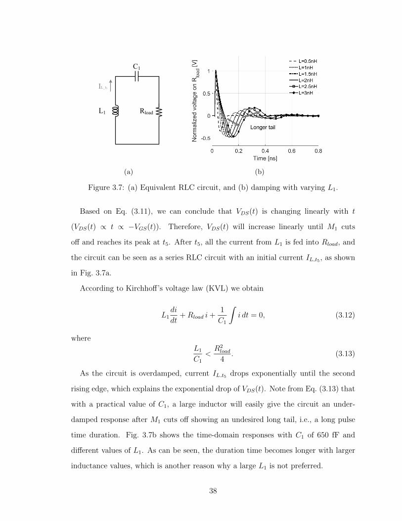
L1
C1
Rload
IL_t5
(a) (b)
Figure 3.7: (a) Equivalent RLC circuit, and (b) damping with varying L1.
Based on Eq. (3.11), we can conclude that VDS(t) is changing linearly with t
(VDS(t) ∝ t ∝ −VGS(t)). Therefore, VDS(t) will increase linearly until M1 cuts
off and reaches its peak at t5. After t5, all the current from L1 is fed into Rload, and
the circuit can be seen as a series RLC circuit with an initial current IL t5 , as shown
in Fig. 3.7a.
According to Kirchhoff’s voltage law (KVL) we obtain
L1di
dt+Rload i+
1
C1
∫i dt = 0, (3.12)
where
L1
C1
<R2
load
4. (3.13)
As the circuit is overdamped, current IL t5 drops exponentially until the second
rising edge, which explains the exponential drop of VDS(t). Note from Eq. (3.13) that
with a practical value of C1, a large inductor will easily give the circuit an under-
damped response after M1 cuts off showing an undesired long tail, i.e., a long pulse
time duration. Fig. 3.7b shows the time-domain responses with C1 of 650 fF and
different values of L1. As can be seen, the duration time becomes longer with larger
inductance values, which is another reason why a large L1 is not preferred.
38
0 0.05 0.1 0.15 0.2 0.25 0.3Time (ns)
0
50
100
Cu
rre
nt
(mA
)
L=0.1nH
L=0.5nH
L=1nH
L=1.5nH
L=2nH
L=2.5nH
L=3nH
(a)
0 Time 0
0.5
1
No
rma
lize
d A
mp
litu
de
r dr+
w
(b)
0 5 10 15 20 25 30Frequency (GHz)
-90
-80
-70
-60
-50
-40
Am
plit
ude (
dB
) L=0.1n
L=0.5n
L=1n
L=1.5n
L=2n
L=2.5n
L=3n
12.8 dB
(c)
0 5 10 15 20 25 30Frequency (GHz)
-80
-60
-40
Am
plit
ude (
dB
)
r=30ps
r=35ps
r=40ps12.8 dB
(d)
Figure 3.8: (a) IDS(t) with varying load inductance, (b) triangular shape IDS(t)assumption, (c) output spectrum with varying load inductance (τr=30 ps), and (d)Output spectrum with a 1.5-nH load inductor and varying τr.
Although the waveforms of IDS(t) and VDS(t) in Fig. 3.6a look different from VGS(t)
compared with Fig. 3.5a, it can be noted that not only is the waveform edge still linear,
39
the rise/fall time also remains the same. Most importantly, (2τr + τw + τd) remains
almost the same, which means the first two notch frequencies will not be affected.
Moreover, the above-VDD part of VDS(t) due to a low-load inductance is beneficial for
high-amplitude design. The Fourier transform of the signals plotted in Fig. 3.6b also
verifies the analysis.
One concern that can be noted from Fig. 3.6b is that the third notch is attenuated
with a smaller load inductance. The waveform of IDS(t) with different values of load
inductance are depicted in Fig. 3.8a to reveal the cause. As can be seen, although the
amplitude and shape of IDS(t) is high and close to an ideal trapezoidal wave when
the inductor is small (e.g., 0.1 nH), the output amplitude is low (Fig. 3.8c) since most
of the current comes from the inductor instead of Rload. As the inductor becomes
larger (e.g., 0.5 nH), the rising slope of IL(t) becomes close to 1/τr, IDS(t) can be
approximated as a triangular wave with a rise time of (τr + τw) and a fall time of τr,
as shown in Fig. 3.8b. The Laplace Transform of IDS(t) becomes
I(s) =1
τ 2r s2· e−s(2τr+τw) · [τre
s(2τr+τw) − (2τr + τw)esτr + τr + τw]⏞ ⏟⏟ ⏞
term1
·[1 + e−s(2τr+τw+τd)]⏞ ⏟⏟ ⏞term2
.(3.14)
The first notch created by term1 in Eq. (3.14) is at around 200 GHz, thus the notch
frequencies created up to 20 GHz are only determined by term2 and can be calculated
as (2πN + π)/(2τr + τw + τd). The notch created by (τr + τw) in the trapezoidal case
vanishes when it becomes a triangular wave. IDS(t) turns from a triangular wave
into more like a trapezoidal wave as the load inductance increases, and the spectral
amplitude in the 13 GHz to 20 GHz band also decreases as expected. Considering the
damping, output amplitude and out-of-band notch suppression, a load inductance of
1.5 nH is chosen in the design. As can be seen from Figs. 3.8c and 3.8d, a minimum
of 12.8 dB lower amplitude can be achieved with a 1.5 nH load when τr varies from
30 ps to 40 ps.
40

To this point, it has been shown that it is possible to control the spectrum notches
of the output wave simply by adjusting the time factors of the trapezoidal input
signal.
3.1.3 Circuit Implementation and MOSFET Sizing
It is worth mentioning from Table 3.1 that the frequency components from DC to
the first notch could not be eliminated no matter what values are set for τr, τw and
τd. However, it still allows for the use of a simple highpass or bandstop filter at the
output, instead of a complex bandpass filter network, if the zero frequency could be
set properly such that the upper -10-dB bandwidth point is positioned at 10.6 GHz
through adjusting the trapezoidal wave shape at the input stage.
To achieve minimum loss, an LC circuit that resonates at 1.7 GHz is added after
C1 in parallel across the signal line as a bandstop filter to suppress the low frequency
components, as shown in Fig. 3.9a. The digital synthesized trapezoidal wave is gener-
ated simply by combining a rising and falling edge through a NOR gate. Two sets of
identical trapezoidal waves are created by two branches with different delays. MOS
varactors have been added to adjust the capacitance between the two stages of in-
verters to get proper values of τd through Vctrl 1 and τw through Vctrl 2, respectively.
Buffers are designed with gradually increased sizes to provide the driving capability
for M2a and M2b and achieve a τr about 35 ps. C1 is set to be 650 fF in the actual
design to filter out the DC and part of the low frequency components. The simulation
result for the loss of the network composed of L1, C1, L2 and C2 is shown in Fig. 3.9b,
the loss is less than 1 dB at frequencies from 4.5 GHz to 10.6 GHz to achieve a high
output amplitude. Fig. 3.9c shows the signal flow of the proposed circuit.
Finally, to obtain a high output voltage while maintaining high efficiency, setting
the MOSFET size properly is critical. On one hand, the MOSFET has to be large
enough to be capable of conducting enough current when it is on. On the other hand,
the MOSFET can not be too large as the large parasitic capacitance will increase the
41
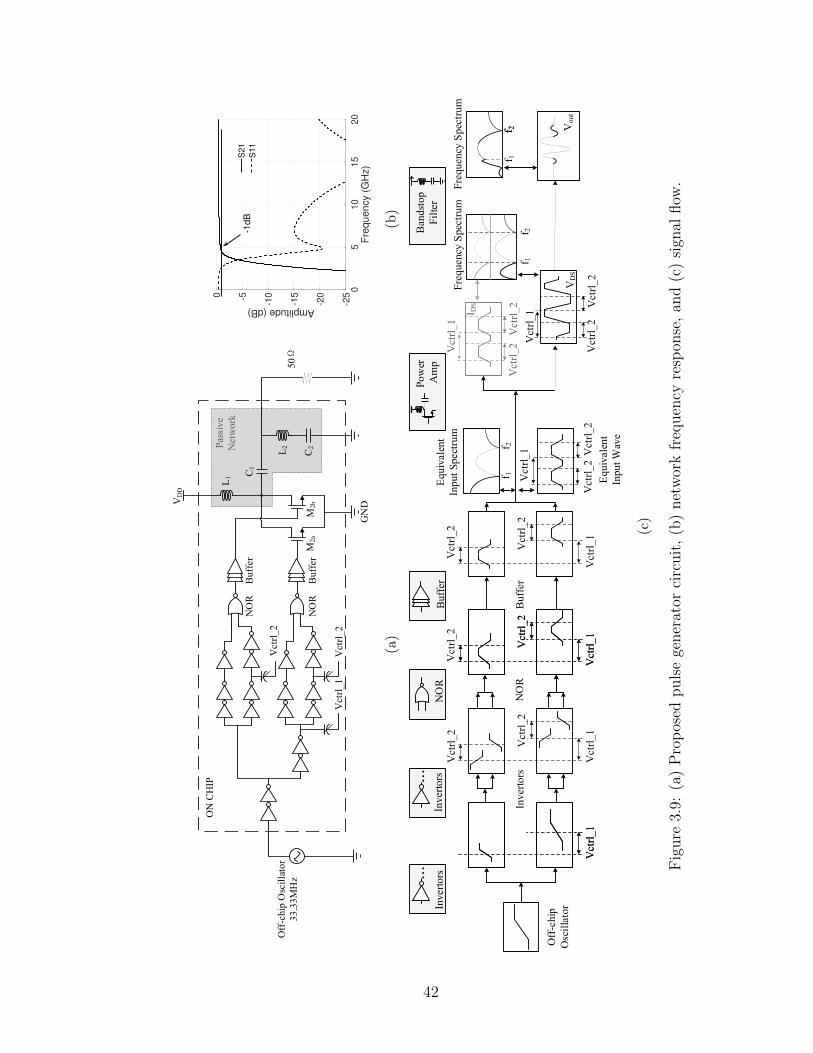
C1
L2
C2
50
L1
Vctr
l_2
Vctr
l_2
Vctr
l_1
M2b
M2a
ON
CH
IP
Bu
ffer
Bu
ffer
NO
R
NO
R
Off
-ch
ip O
scil
lato
r
33
.33
MH
z
VD
D
GN
D
Pass
ive
Netw
ork
(a)
05
10
15
20
Fre
que
ncy (
GH
z)
-25
-20
-15
-10-50
Amplitude (dB)
S21
S11
-1d
B
(b)
Off
-ch
ip
Osc
illa
tor
Vctr
l_1
Vctr
l_2
Vctr
l_2
Inv
ert
ors
Vctr
l_1
Inv
ert
ors
Inv
ert
ors
NO
R
NO
R
Vctr
l_1
Vctr
l_1
Vctr
l_2
Vctr
l_2
Vctr
l_1
Vctr
l_2
Vctr
l_1
Vctr
l_2
Vctr
l_2
Bu
ffer
Po
wer
Am
p
Bu
ffer
I DS
Vctr
l_1
Vctr
l_2
Vctr
l_2
VD
S
Fre
qu
en
cy S
pec
tru
m
f 1f 2
f 1f 2
Eq
uiv
ale
nt
Inp
ut
Sp
ect
rum
...
...
Ban
dst
op
Fil
ter
Vout
f 2
Fre
qu
en
cy S
pec
tru
m
f 1f 2
Eq
uiv
ale
nt
Inp
ut
Wav
e
Vctr
l_1 V
ctr
l_2
Vctr
l_2
Vctr
l_2
Vctr
l_2
Vctr
l_1
(c)
Figure
3.9:
(a)Proposed
pulsegenerator
circuit,(b)networkfrequency
respon
se,an
d(c)sign
alflow
.
42
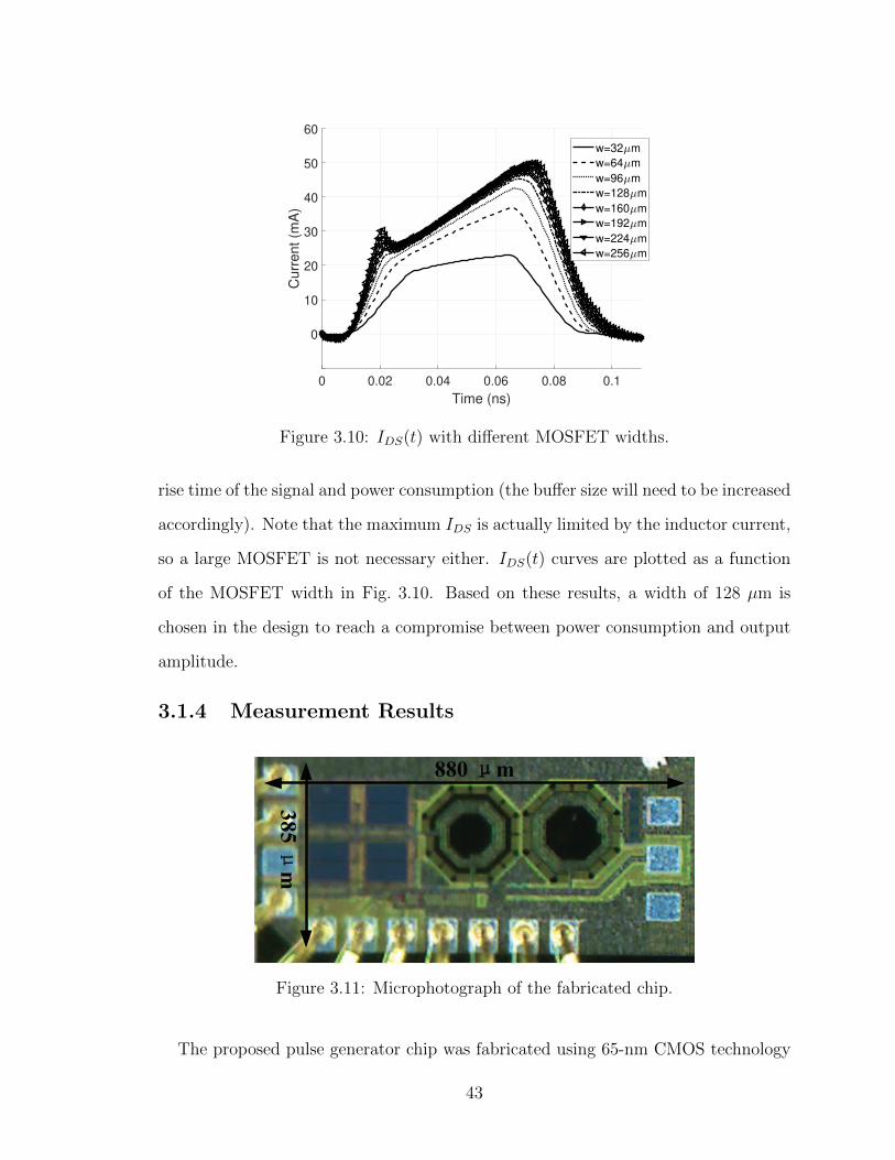
0 0.02 0.04 0.06 0.08 0.1
Time (ns)
0
10
20
30
40
50
60
Cu
rre
nt
(mA
)
w=32 m
w=64 m
w=96 m
w=128 m
w=160 m
w=192 m
w=224 m
w=256 m
Figure 3.10: IDS(t) with different MOSFET widths.
rise time of the signal and power consumption (the buffer size will need to be increased
accordingly). Note that the maximum IDS is actually limited by the inductor current,
so a large MOSFET is not necessary either. IDS(t) curves are plotted as a function
of the MOSFET width in Fig. 3.10. Based on these results, a width of 128 µm is
chosen in the design to reach a compromise between power consumption and output
amplitude.
3.1.4 Measurement Results
880 m
385
m
Figure 3.11: Microphotograph of the fabricated chip.
The proposed pulse generator chip was fabricated using 65-nm CMOS technology
43
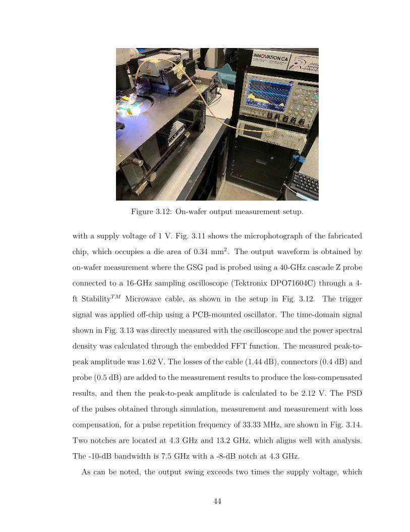
Figure 3.12: On-wafer output measurement setup.
with a supply voltage of 1 V. Fig. 3.11 shows the microphotograph of the fabricated
chip, which occupies a die area of 0.34 mm2. The output waveform is obtained by
on-wafer measurement where the GSG pad is probed using a 40-GHz cascade Z probe
connected to a 16-GHz sampling oscilloscope (Tektronix DPO71604C) through a 4-
ft StabilityTM Microwave cable, as shown in the setup in Fig. 3.12. The trigger
signal was applied off-chip using a PCB-mounted oscillator. The time-domain signal
shown in Fig. 3.13 was directly measured with the oscilloscope and the power spectral
density was calculated through the embedded FFT function. The measured peak-to-
peak amplitude was 1.62 V. The losses of the cable (1.44 dB), connectors (0.4 dB) and
probe (0.5 dB) are added to the measurement results to produce the loss-compensated
results, and then the peak-to-peak amplitude is calculated to be 2.12 V. The PSD
of the pulses obtained through simulation, measurement and measurement with loss
compensation, for a pulse repetition frequency of 33.33 MHz, are shown in Fig. 3.14.
Two notches are located at 4.3 GHz and 13.2 GHz, which aligns well with analysis.
The -10-dB bandwidth is 7.5 GHz with a -8-dB notch at 4.3 GHz.
As can be noted, the output swing exceeds two times the supply voltage, which
44
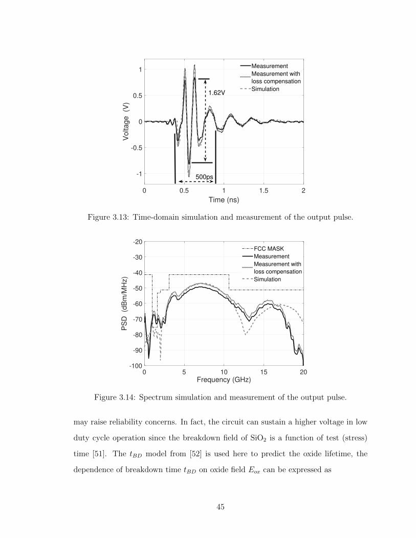
0 0.5 1 1.5 2
Time (ns)
-1
-0.5
0
0.5
1
Voltage (V
)
Measurement
Measurement with
loss compensation
Simulation
500ps
1.62V
Figure 3.13: Time-domain simulation and measurement of the output pulse.
0 5 10 15 20
Frequency (GHz)
-100
-90
-80
-70
-60
-50
-40
-30
-20
PS
D (d
Bm
/MH
z)
FCC MASK
Measurement
Measurement with
loss compensation
Simulation
Figure 3.14: Spectrum simulation and measurement of the output pulse.
may raise reliability concerns. In fact, the circuit can sustain a higher voltage in low
duty cycle operation since the breakdown field of SiO2 is a function of test (stress)
time [51]. The tBD model from [52] is used here to predict the oxide lifetime, the
dependence of breakdown time tBD on oxide field Eox can be expressed as
45
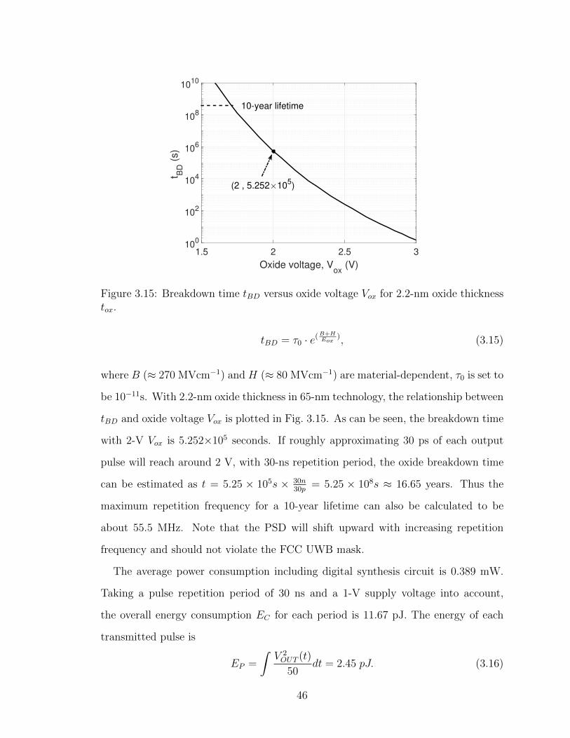
1.5 2 2.5 3
Oxide voltage, Vox
(V)
100
102
104
106
108
1010
t BD
(s)
10-year lifetime
(2 , 5.252 105)
Figure 3.15: Breakdown time tBD versus oxide voltage Vox for 2.2-nm oxide thicknesstox.
tBD = τ0 · e(B+HEox
), (3.15)
where B (≈ 270 MVcm−1) and H (≈ 80 MVcm−1) are material-dependent, τ0 is set to
be 10−11s. With 2.2-nm oxide thickness in 65-nm technology, the relationship between
tBD and oxide voltage Vox is plotted in Fig. 3.15. As can be seen, the breakdown time
with 2-V Vox is 5.252×10⁵ seconds. If roughly approximating 30 ps of each output
pulse will reach around 2 V, with 30-ns repetition period, the oxide breakdown time
can be estimated as t = 5.25 × 105s × 30n30p
= 5.25 × 10⁸s ≈ 16.65 years. Thus the
maximum repetition frequency for a 10-year lifetime can also be calculated to be
about 55.5 MHz. Note that the PSD will shift upward with increasing repetition
frequency and should not violate the FCC UWB mask.
The average power consumption including digital synthesis circuit is 0.389 mW.
Taking a pulse repetition period of 30 ns and a 1-V supply voltage into account,
the overall energy consumption EC for each period is 11.67 pJ. The energy of each
transmitted pulse is
EP =
∫V 2OUT (t)
50dt = 2.45 pJ. (3.16)
46
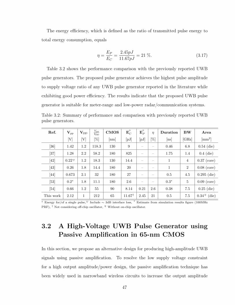
The energy efficiency, which is defined as the ratio of transmitted pulse energy to
total energy consumption, equals
η =EP
EC
=2.45pJ
11.67pJ= 21 %. (3.17)
Table 3.2 shows the performance comparison with the previously reported UWB
pulse generators. The proposed pulse generator achieves the highest pulse amplitude
to supply voltage ratio of any UWB pulse generator reported in the literature while
exhibiting good power efficiency. The results indicate that the proposed UWB pulse
generator is suitable for meter-range and low-power radar/communication systems.
Table 3.2: Summary of performance and comparison with previously reported UWBpulse generators.
Ref. Vpp VDDVpp
VDDCMOS E
⋄C E
⋄P η Duration BW Area
[V] [V] [%] [nm] [pJ] [pJ] [%] [ns] [GHz] [mm2]
[36] 1.42 1.2 118.3 130 9 – – 0.46 6.8 0.54 (die)
[37] 1.28 2.2 58.2 180 825 – – 1.75 1.4 0.4 (die)
[42] 0.22 1.2 18.3 130 14.4 – – 1 4 0.37 (core)
[43] 0.26 1.8 14.4 180 20 – – 1 2 0.08 (core)
[44] 0.673 2.1 32 180 27 – – 0.5 4.5 0.295 (die)
[53] 0.2∗ 1.8 11.1 180 2.6 – – 0.3∗ 5 0.09 (core)
[54] 0.66 1.2 55 90 8.14 0.21 2.6 0.38 7.5 0.25 (die)
This work 2.12 1 212 65 11.67† 2.45 21 0.5 7.5 0.34∓ (die)
⋄ Energy for/of a single pulse, Include ∼ 3dB interface loss, * Estimate from simulation results figure (100MHz
PRF), † Not considering off-chip oscillator, ∓ Without on-chip oscillator.
3.2 A High-Voltage UWB Pulse Generator using
Passive Amplification in 65-nm CMOS
In this section, we propose an alternative design for producing high-amplitude UWB
signals using passive amplification. To resolve the low supply voltage constraint
for a high output amplitude/power design, the passive amplification technique has
been widely used in narrowband wireless circuits to increase the output amplitude
47

through impedance transformation produced by the matching network. To apply this
technique to the design of UWB pulse generators, the design of a low-loss matching
network is highly challenging as it requires matching the load to the highly nonlinear
output impedance of the power MOSFET over the entire 3.1-10.6 GHz UWB band.
In addition, a portion of UWB pulse energy is produced from the energy stored in the
load inductor after the transistor turns off requiring that the matching network also
efficiently passes this energy to the load. The working state of the power amplifier is
divided into two stages (OFF and ON) and analyzed separately. Seeking to match on
both states, a two-section wideband matching network is designed that further boosts
the output amplitude, achieving a peak-to-peak amplitude close to three times of the
supply voltage.
This section is organized as follows. Section 3.2.1 describes the passive amplifica-
tion technique and its compromise in the wideband case. Section 3.2.2 discusses input
waveform considerations, working states of the power amplifier, matching network de-
sign considering both states, and the proposed UWB pulse generator topology. In
Section 3.2.3, the experiment results are presented.
3.2.1 Ultra-Wideband Passive Amplification
Because of the low operating and breakdown voltage of the transistors, the passive
amplification technique has been used extensively in narrowband transmitter designs
to produce the high output voltage swing required for delivering Watt-level power to
the antenna. Using an impedance matching network in between the power amplifier
Figure 3.16: Passive amplification demonstration.
48
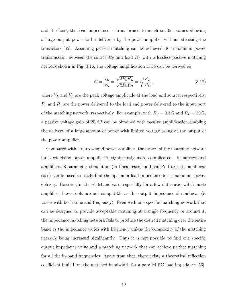
and the load, the load impedance is transformed to much smaller values allowing
a large output power to be delivered by the power amplifier without stressing the
transistors [55]. Assuming perfect matching can be achieved, for maximum power
transmission, between the source RS and load RL with a lossless passive matching
network shown in Fig. 3.16, the voltage amplification ratio can be derived as
G =VL
VS
=
√2PLRL√2PSRS
=
√RL
RS
, (3.18)
where VL and VS are the peak voltage amplitude at the load and source, respectively.
PL and PS are the power delivered to the load and power delivered to the input port
of the matching network, respectively. For example, with RS = 0.5Ω and RL = 50Ω,
a passive voltage gain of 20 dB can be obtained with passive amplification enabling
the delivery of a large amount of power with limited voltage swing at the output of
the power amplifier.
Compared with a narrowband power amplifier, the design of the matching network
for a wideband power amplifier is significantly more complicated. In narrowband
amplifiers, S-parameter simulation (in linear case) or Load-Pull test (in nonlinear
case) can be used to easily find the optimum load impedance for a maximum power
delivery. However, in the wideband case, especially for a low-data-rate switch-mode
amplifier, these tools are not compatible as the output impedance is nonlinear (it
varies with both time and frequency). Even with one specific matching network that
can be designed to provide acceptable matching at a single frequency or around it,
the impedance matching network fails to produce the desired matching over the entire
band as the impedance varies with frequency unless the complexity of the matching
network being increased significantly. Thus it is not possible to find one specific
output impedance value and a matching network that can achieve perfect matching
for all the in-band frequencies. Apart from that, there exists a theoretical reflection
coefficient limit Γ on the matched bandwidth for a parallel RC load impedance [56]
49

∫ ∞
0
ln1
|Γ(ω)|dω ≤ π
RLC, (3.19)
from which it can be concluded that perfect impedance matching is not achievable
for a non-zero bandwidth and that out-of-band mismatch also plays a role on the
in-band matching performance. Assuming a flat reflection response over the required
frequency bandwidth ∆ω and Γ(ω)=1 for all the out-of-band frequencies, the in-band
reflection coefficient Γ∆ω can be derived from Eq. (3.19) as
Γ∆ω = exp(−π
∆ωRLC). (3.20)
Then the ideal passive amplification ratio in a wideband case (assuming the same
group delay over the frequency band) can be approximated as
G∆ω =
√2(1− Γ∆ω
2)PSRL√2PSRS
=
√(1− exp( −2π
∆ωRLC))RL
RS
. (3.21)
Note that although the passive amplification ratio G∆ω decreases with increasing
bandwidth, the signal will still be amplified when ∆ω < 2πRLC ln(1−RS/RL)
in the ideal
case (Γ∆ω <√
1− RS
RLin the non-ideal or non-perfect matching case).
In the next section, a high output amplitude UWB pulse generator employing a
power amplifier and a wideband matching network is discussed. A passive matching
network consisting of a parallel LC load and a two-section matching network is pro-
posed in the design to implement a wideband nonlinear impedance matching. With
passive amplification, the peak-to-peak amplitude of the output pulse can exceed 3
times of the supply voltage in simulation.
3.2.2 Proposed UWB Pulse Generator Design
Power Amplifier Topology and Input Waveform Parameters
Fig. 3.17 shows the proposed UWB pulse generator topology. It consists of a trape-
zoidal waveform generator, a driver stage, a switch-mode MOSFET power amplifier,
and a passive matching network. As no bias current will be introduced and the voltage
50

Trigger
Signal
MOSFET
SwitchLoad
Power
Supply
Passive Matching
Network
Trapezoidal
waveform
generatorDriver
Figure 3.17: UWB pulse generator block diagram.
across the MOSFET will stay low when it is conducting current, the switch amplifier
is chosen to achieve both high efficiency and high amplitude.
In general, wideband filtering/impedance matching is designed either with high
order or with multiple sections to achieve a steep band slope/low quality factor.
Problems accompanied with large number of passive components can be high cost,
large size, high complexity, and high loss. Thus the simplicity of the matching network
is one of the main concerns in this design.
One way to ease the output network design is to shift the pulse shaping effort to
the input waveform design. In [16], two consecutive trapezoidal waves are employed
as the input signal to locate the notches of the output spectrum around both the low
and high cutoff frequency of the passing band, thus only a simple bandstop filter is
needed to the conform its output spectrum to the UWB regulations.
In this work, we utilize passive amplification to enhance the output signal levels
through impedance transformation. It is critical that the impedance transformation
be achieved by a low-loss matching network capable of matching the nonlinear output
impedance of the transistor over the entire band to the greatly extent possible. To
reduce the complexity of output matching network, a single trapezoidal wave is used
to create a notch at the upper cutoff frequency. The notch locations of one trapezoidal
wave can be derived from its Laplace Transform as
51

V (s) =1
τrs2(1− e−sτr)[1− e−s(τr+τw)], (3.22)
where τr and τw are the trapezoidal wave rise (fall) time and width, respectively. The
first notch appears at ω = 2π/(τr + τw), which is obtained by equating Eq. (3.22) to
zero and in turn equating e−s(τr+τw) to 1. A single trapezoidal wave with a 40-ps τr
and a 50-ps τw is used in this design. The first notch in its spectrum can be calculated
to be 11.1 GHz. This notch is shifted slightly higher in the output spectrum due to
the threshold voltage and nonlinearity of the MOSFET which makes (τr + τw) of
IDS(t) slightly smaller.
Switch-Mode Power Amplifier Output Impedance
To design a proper wideband matching network at the output of the power amplifier,
it is necessary to have an accurate estimation of the output impedance of the power
MOSFET. Since the output impedance of the MOSFET changes dramatically within
the working period as its input signal variation is large, one way to estimate the
effective output impedance is to find an optimum load impedance that maximizes the
power transferred from the MOSFET to the load over the entire cycle. With a single
trapezoidal wave as the input signal, a simple switch-mode power amplifier with an
RF-choke inductor L0 (100 nH) and a DC-block capacitor C0 (1 µF) are used to
(a) (b)
Figure 3.18: (a) Pulse generator with RFC and DC block capacitor, (b) OFF andON state of the circuit.
52
estimate the optimum load impedance, as shown in Fig. 3.18a. Fig. 3.18b shows the
OFF and ON state of the power amplifier. As can be noted, current flows through
the load only when the MOSFET is ON and during the transition between the ON
and OFF state of the transistor. Note that the later state is ignored here for the
simplicity of theoretical analysis. Although the output impedance of the MOSFET
can be modeled as a resistor in parallel with a capacitor (accounting for the parasitic
capacitors of the MOSFET) when M1 is ON, a purely resistive load RL is used as the
test load for two reasons:
• The reactance of the intrinsic capacitor is usually much larger compared to the
ON-resistance of the MOSFET and thus will barely change the total impedance.
For example, the reactance of a 200-fF capacitor at 7 GHz is -j113.7 Ω which
can be ignored when the resistance of the MOSFET is usually less than 10 Ω,
and
• Any added passive component that has a reactance that varies with frequency
will make the design of the matching network more complicated.
Under these considerations, the output impedance of the MOSFET is estimated
as the same value of RL, to which a maximum power is transferred during one full
ON-and-OFF cycle (same as the power transferred when the MOSFET is ON and
during transition).
As the spectral characteristic of the output pulse is controlled by the input trape-
zoidal wave, it can be expected that the output pulses should have the same shape but
different amplitudes with different RL. When the transistor is ON, the drain-source
current IDS(t) can be written as
IDS(t) = IL0(t) + IRL(t)
=1
L0
∫(VDD−VDS(t))dt+
VDD−VDS(t)
RL
exp(− t
τ),
(3.23)
where τ = RLC0. Since L0 (→ ∞) serves as a RF-choke inductor and C0 (→ ∞)
53

0 0.1 0.2
Time (ns)
0
0.2
0.4
0.6
0.8
1
1.2
Voltage (
V)
RL = 1
RL = 2.5
RL = 4
RL = 7
RL = 10
RL = 13
RL = 16
(a)
0 10 20 30 40 50
Frequency (GHz)
-50
-40
-30
-20
-10
0
Norm
aliz
ed A
mplit
ude (
dB
)
3.1 10.6
E1
E2
(b)
0 5 10 15 20R
L ( )
0
2.5
5
7.5
10
12.5
15
E1 (
pJ)
w=80 m
w=160 m
w=240 m
w=320 m
w=400 m
w=480 m
w=560 m
w=640 m
(c)
0 5 10 15 20R
L ( )
0
1
2
3
4
5
6
7
E2 (
pJ)
w=80 m
w=160 m
w=240 m
w=320 m
w=400 m
w=480 m
w=560 m
w=640 m
(d)
Figure 3.19: (a) VDS(t) with varying load resistance RL (width of MOSFET is 320µm), (b) normalized spectrum of VRL
, (c) single pulse energy E1, and (d) single pulseenergy located from 3.1 to 10.6 GHz E2.
serves as a DC-block capacitor, 1/L0 ≈ 0 and τ ≈ ∞. Eq. (3.23) can be simplified as
IDS(t) = IRL(t) =
VDD − VDS(t)
RL
. (3.24)
With different load impedances, the MOSFET can work in either the saturation or
linear regions. With the realistic NMOS model from the process design kit (PDK), the
VDS(t) of M1 (320 µm width) with varying RL is shown as an example in Fig. 3.19a.
When RL is small (e.g. 1 Ω), M1 can withdraw current to its capability working in
saturation region. However, when RL is large (e.g., 16 Ω), the current is limited by
RL, which will force M1 to work in the triode region. Taking the triode region as an
example, IDS(t) can be expressed as
IDS(t) = kVDS(t), (3.25)
54
where k = µnCoxWL(VGS − VTH), µn is the electron mobility, Cox is the gate oxide
capacitance, W and L are the width and length of the MOSFET, and VTH is the
threshold voltage.
As IRL(t) = IDS(t), substituting Eq. (3.25) into Eq. (3.24), the load current IRL
can be expressed as
IRL=
kVDD
1 + kRL
. (3.26)
The output power at the load can be obtained as
PRL= I2RL
RL =(kVDD)
2
1RL
+ 2k + k2RL
, (3.27)
which is maximized as PRL= kV 2
DD/4 when the denominator reaches its minimum
at RL = 1/k. A similar analysis can be applied when M1 works in saturation re-
gion. Since it is difficult to decide the working region of the MOSFET from just the
mathematical equations, the output energy within one period (E1) corresponding to
different load impedances RL and MOSFET widths are shown in Fig. 3.19c. As can
be seen, the optimum RL for maximum output power delivery becomes smaller as
the MOSFET width (∝ k) increases. The maximum PRLis also proportional to k
as expected. Taking a 320-µm MOSFET width as an example, the optimum load
impedance Ropt should be about 5 Ω to deliver a 7 pJ/period output energy. As
shown in Fig. 3.19d, the energy located within 3.1 GHz to 10.6 GHz band also has
the same trend which also verifies that, with the same input trapezoidal wave, the
output spectral shapes are the same (Fig. 3.19b) with different RL.
Power Amplifier Load Analysis and Matching Network Design
In practice, an RF choke is bulky in size and lossy because of its large electrical series
resistance. Using a finite load inductor, on the other hand, is beneficial as it can
be integrated on-chip reducing the overall size and cost of the system. Furthermore,
similar with the design of a class-E amplifier, the finite load inductor also serves as
55

(a) (b)
Figure 3.20: (a) Pulse generator with finite inductor and a parallel capacitor, (b)OFF and ON state of the circuit.
part of the matching network, which allows a larger load impedance for the same
output power than that for an RF choke [57].
The power amplifier circuit with a finite load inductor is shown in Fig. 3.20a. The
load is composed of a finite inductor L1 and a parallel capacitor C1, which represents
the sum of intrinsic MOSFET capacitor and external capacitor added to the load
network. With C1 and L1 resonating at the center of the frequency band of interest,
L1 can be designed in pH level with a high self-resonant frequency, a high quality
factor and low loss. Unlike the case with RF choke (Fig. 3.18b), it can be noted
from Fig. 3.20b that the finite inductor L1 continues to conduct current to the 50-Ω
load after the MOSFET cuts off. Thus, in addition to matching the 50-Ω load to the
optimum load impedance Ropt during the MOSFET ON stage, consideration needs
to be paid to account for the matching during the OFF stage.
To obtain a matching network with a bandwidth of 7.5 GHz and a center frequency
of 6.85 GHz, the quality factor of the matching network can be calculated as Q =
6.85/7.5 = 0.91. To get a more intuitive idea of how to decide on the initial values for
components of the matching network, a Smith chart with a characteristic impedance
Zo of 5 Ω as an example is shown in Fig. 3.21. The constant circle of Q equal to 0.9 is
drawn corresponding to the quality factor limit of the matching circuit. Since adding
56
Figure 3.21: Wideband matching in a Smith chart.
inductors and capacitors can be reflected as rotating along the Z or Y circles in the
Smith chart, plus the fact that the matching curve from 50 Ω to 5 Ω has to be within
the constant Q circle, the ranges for the values of the passive components added in
the matching network can be easily decided. To estimate the matching performance,
the constant circles of Voltage Standing Wave Ratio (VSWR) equal to 2 and 4 are
also shown in Fig. 3.21. As can be seen, without considering L1 and C1 and all other
design constraints, the best matching performance for a two-section matching net-
work is at node A. Although a better matching performance of VSWR < 2 can be
reached in theory at node B with a three-section matching network, the extra losses
introduced by the parasitic resistance of the added components can counteract its
benefit. Furthermore, with other design constraints that will be discussed later, the
matching performance with three-section matching network can be degraded dramat-
ically. A high-order matching network will also significantly increase the complexity
of the circuit design. Thus, although the matching is “non-perfect”, a two-section
matching network seems to be the simplest design that achieves wideband matching
57

Figure 3.22: Impedance matching when M1 is ON.
over the 3.1-10.6 GHz band. A bandpass-type two-section matching network is chosen
for the design, as shown in Fig. 3.22.
The values of L1 and C1 can be first estimated from the following equation
1
2π√L1C1
≈ 6.85 GHz. (3.28)
The total input impedance of the matching network (including the load) when the
MOSFET is ON can be derived as
ZIN = ((RL ∥jωL3 +1
jωC3
)∥ 1
jωC2
+ jωL2)∥1
jωC1
∥jωL1
= RL1, C1, L2, C2, L3, C3, ω
+ jXL1, C1, L2, C2, L3, C3, ω.
(3.29)
As can be noted, both the real part Real(ZIN) and imaginary part Imag(ZIN) are a
function of L1, C1, L2, C2, L3, C3 and ω. During this stage, the circuit is well matched
if
Real(ZIN)≈Ropt and Imag(ZIN)≈0. (3.30)
When the MOSFET is OFF, the output waveform is decided by the natural re-
sponse of the network. During this stage, the energy stored in L1 is delivered to the
load. From a matching perspective of view, the network should resonate at all the
frequencies of interest, which means that the imaginary part of Z′IN , as shown in
Fig. 3.23, should cancel the reactance of L1
58

Figure 3.23: Impedance matching when M1 is OFF.
Figure 3.24: Second-order passive network model.
Imag(Z′
IN) = Imag[((RL ∥jωL3 +1
jωC3
)∥ 1
jωC2
+
jωL2)∥1
jωC1
]
= −jωL1, for 3.1 ∼ 10.6 GHz.
(3.31)
Under this approximation, the network can be modeled as a second-order passive
network with an initial inductor current of I1, as shown in Fig. 3.24. To obtain an
output waveform with as short a duration as possible, the circuit should be critically
damped or over-damped by
Real(Z′IN)
2L1
≥ ω, for 3.1 ∼ 10.6 GHz. (3.32)
Thus a small load inductor is preferred according to Eq. (3.32). Take L1 of 250 pH
as an example, the Real(Z′IN) needs to be at least 33 Ω to satisfy Eq. (3.32) considering
the maximum in-band frequency of 10.6 GHz. Also ZIN can be recalculated by
substituting Eq. (3.31) into Eq. (3.29) as
59

ZIN = Z′
IN ∥jωL1
= [Real(Z′
IN)− jωL1]∥jωL1
=ω2L1
2
Real(Z′IN)
+ jωL1, for 3.1 ∼ 10.6 GHz.
(3.33)
Then Eq. (3.30) can be rewritten according to Eq. (3.33) as
ω2L12
Real(Z′IN)
≈Ropt and jωL1≈0. (3.34)
Note from Eq. (3.34) that although it is possible to tune the Real(ZIN) to be equal
to Ropt at one or several frequencies, Real(ZIN) still varies since it is a function of
frequency. Furthermore, even if a good real-part matching could be achieved for the
whole frequency band, the Imag(ZIN), which varies from j4.8 Ω to j16.6 Ω (from 3.1 to
10.6 GHz), can not be set to 0. In another words, Eqs. (3.28), (3.30)∼(3.32) and the
best achievable matching point A in Fig. 3.21 can not be satisfied simultaneously. The
matching performances for when the MOSFET is ON, OFF and the pulse duration
have to trade off with one another.
To obtain the values for the six passive components, six equations will be needed for
mathematical calculation. This can be done by solving the simultaneous equations
composed of Eqs. (3.29) and (3.31) at multiple in-band frequencies. But the pure
mathematical solution can be inaccurate because parameters such as the -10 dB
cut-off frequencies and characteristics like in-band spectral flatness can not be fully
defined by the equations. Also the matching network must be designed such that the
output signal spectrum conforms to the FCC mask. A more feasible way is to first
start with the initial values of C2, L2, C3, and L3 from the Smith chart (Fig. 3.21)
and initial estimates of L1 and C1 from Eq. (3.28), then try to solve the simultaneous
equations composed of Eqs. (3.29) and (3.31) with those initial values, and finally
adjust the values with Eqs. (3.32) and (3.34) as the optimization goals. With a few
iterations, the values of each component can be found. However, the final values
should be tuned considering all the constraints and according to both the spectral
regulation and time-domain performance.
60
M1a
Trigger
SignalM1b
Trapezoidal Wave Generator
Driver
VC
1.2V
bias
Vc
MOSFET
Switch
VDS
Matching
Network
C1
L2
C2 50Ω
L1
C3
L3
ON CHIP
Figure 3.25: Schematic of the proposed pulse generator.
Circuit Implementation and Performance Simulation
The schematic diagram of the proposed UWB pulse generator circuit is depicted in
Fig. 3.25. The trapezoidal wave is generated through a NOR gate which combines
a rising and a falling edge with a delay time that is controlled by VC . A driver
stage consisting of six inverters is added after to increase the driving capability. The
circuit in this design aims to generate a UWB pulse with a peak-to-peak amplitude
of three times the supply voltage, the peak current conducted by the MOSFET must
reach hundred-mA levels. Since the maximum current of the circuit is mainly limited
by the size of the transistor, a MOSFET width of 320 µm is chosen for the power
amplifier to produce the required current. Thus the optimum impedance Ropt should
be 5 Ω according to the analysis in Section 3.2.2. With a wideband and non-perfect
matching at the drain node of the MOSFET, the voltage amplification ratio will be
less than√RL/RS as mentioned in Section 3.2.1, and the peak voltage of VDS(t),
which appears when the input voltage VGS(t) drops to 0 from VDD, can be more than
2 times of VDD. To enhance the reliability of the design, two cascode MOSFETs
with a width of 640 µm are used. A maximum tolerable DC voltage of 1.2 V, which
can be implemented by a DC-DC converter circuit in the future design, is applied
to the gate of cascode common-gate MOSFET M1b, as shown in Fig. 3.25. Thus
the maximum voltage experienced by the MOSFET can be reduced from VDS to
61
0 5 10 15 20Frequency (GHz)
-40
30
-20
-10
0
10
20
Impedance (
) -j L1
Imag(ZIN' )
Real(ZIN' )
0 5 10 15 20Frequency (GHz)
-20
-10
0
10
20
30
Impedance (
)Imag(Z
IN)
Real(ZIN
)
Figure 3.26: ZIN and Z′IN of the proposed matching network.
Figure 3.27: Butterworth 3rd-order bandpass filter.
VDS − 1.2. Excluding the effect of the parasitics, ideal inductors and capacitors are
used in the simulation of this section. The values of the passive components are listed
in Table 3.3 and the corresponding values of Z′IN and ZIN are shown in Fig. 3.26.
As can be seen, the Imag(Z′IN) matches well with -jωL1 from 5 GHz to 8 GHz. Note
that imaginary matching is implemented in a smaller bandwidth to fulfill a -10-dB
bandwidth from 3.1 GHz to 10.6 GHz. The Real(Z′IN) varies in between 5 to 10 Ω
while the Real(ZIN) varies from 8 to 30 Ω.
To further compare the performance of the proposed matching circuit, a 3.1-GHz
to 10.6-GHz 3rd-order Butterworth bandpass filter designed from 5 Ω to 50 Ω with
the same input and power amplifier circuit is shown in Fig. 3.27. The values of the
components in the filter network are also shown in Table 3.3. The time domain
62

Table 3.3: Component values of the proposed passive network.
Proposed passive network
L1 C1 L2 C2 C3 L3
0.25 nH 1.5 pF 0.56 nH 335 fF 670 fF 1.69 nH
3rd-order Butterworth bandpass filter
L1b C1b C2b L2b C3b L3b
0.36 nH 2.35 pF 5.392 pF 0.157 nH 7.028 pF 0.12 nH
0 1 2 3Time (ns)
-3
-1.5
0
1.5
3
Am
plitu
de (
V)
Proposed matching networkV
load
VDS
0 5 10 15Time (ns)
-1-0.5
00.5
1
Am
plitu
de (
V)
3rd-order Butterworth filter
Vload
Figure 3.28: Time domain signals with the proposed matching network and the 3rd-order Butterworth bandpass filter.
waveform and normalized spectrum of the output signals are shown in Fig. 3.28 and
Fig. 3.29, respectively. As can be seen, with ideal passive components, the output
peak-to-peak voltage of the proposed pulse generator is about 4.5 V and the pulse
duration is about 500 ps. The peak-to-peak voltage of VDS is about 3.1 V (maximum
of 3.2 V and minimum of 0.1 V), thus a voltage gain of 1.45 (<√RL/RS =
√10) is
obtained which agrees with the previous discussion. The maximum voltage difference
experienced by the cascode MOSFET (M1b) is 2 V instead of 3.2 V, which improves
the reliability of the circuit. The output waveform of the pulse generator with the
63
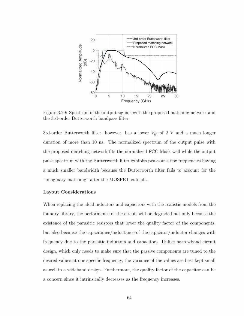
0 5 10 15 20 25 30
Frequency (GHz)
-80
-60
-40
-20
0
20
No
rma
lize
d A
mp
litu
de
(dB
)
3rd-order Butterworth filter
Proposed matching network
Normalized FCC Mask
Figure 3.29: Spectrum of the output signals with the proposed matching network andthe 3rd-order Butterworth bandpass filter.
3rd-order Butterworth filter, however, has a lower Vpp of 2 V and a much longer
duration of more than 10 ns. The normalized spectrum of the output pulse with
the proposed matching network fits the normalized FCC Mask well while the output
pulse spectrum with the Butterworth filter exhibits peaks at a few frequencies having
a much smaller bandwidth because the Butterworth filter fails to account for the
“imaginary matching” after the MOSFET cuts off.
Layout Considerations
When replacing the ideal inductors and capacitors with the realistic models from the
foundry library, the performance of the circuit will be degraded not only because the
existence of the parasitic resistors that lower the quality factor of the components,
but also because the capacitance/inductance of the capacitor/inductor changes with
frequency due to the parasitic inductors and capacitors. Unlike narrowband circuit
design, which only needs to make sure that the passive components are tuned to the
desired values at one specific frequency, the variance of the values are best kept small
as well in a wideband design. Furthermore, the quality factor of the capacitor can be
a concern since it intrinsically decreases as the frequency increases.
64

(a) (b)
0 5 10 15 20 25 30
Frequency (GHz)
800
1000
1500
2000
2500
C (
fF)
4 X 200 fF capacitor
1 X 800 fF capacitor
(c)
0 5 10 15 20 25 30
Frequency (GHz)
1
10
100
Q-v
alu
e
4 X 200 fF capacitor
1 X 800 fF capacitor
(d)
Figure 3.30: (a) Layout of the 4×200-fF capacitor, (b) layout of the 800-fF capaci-tor, (c) Momentum simulated capacitance of the two capacitors, and (d) Momentumsimulated quality factor.
To gain a better understanding of the effects to the characteristic of a MIM capaci-
tor by different capacitor sizes, both the layout models of a 4×200-fF and a 1×800-fF
MIM capacitor were simulated in ADS momentum as an example to obtain the ca-
pacitance and quality factor, as shown in Fig. 3.30. As can be noted that, with the
4-parallel capacitor, not only the variance of the capacitance within the 3.1 GHz to
10.6 GHz band is smaller, the quality factor is also much higher. The parallel struc-
ture has four times the metal connection width compared with the single capacitor
structure having better reliability when conducting large peak current. Thus capaci-
tors C1 and C3 in the circuit are designed with a 4-parallel and a 2-parallel structure
for the aforementioned reasons.
65
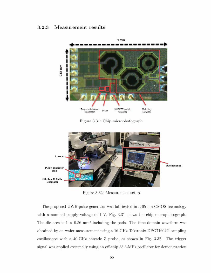
3.2.3 Measurement results
Figure 3.31: Chip microphotograph.
Figure 3.32: Measurement setup.
The proposed UWB pulse generator was fabricated in a 65-nm CMOS technology
with a nominal supply voltage of 1 V. Fig. 3.31 shows the chip microphotograph.
The die area is 1 × 0.56 mm2 including the pads. The time domain waveform was
obtained by on-wafer measurement using a 16-GHz Tektronix DPO71604C sampling
oscilloscope with a 40-GHz cascade Z probe, as shown in Fig. 3.32. The trigger
signal was applied externally using an off-chip 33.3-MHz oscillator for demonstration
66
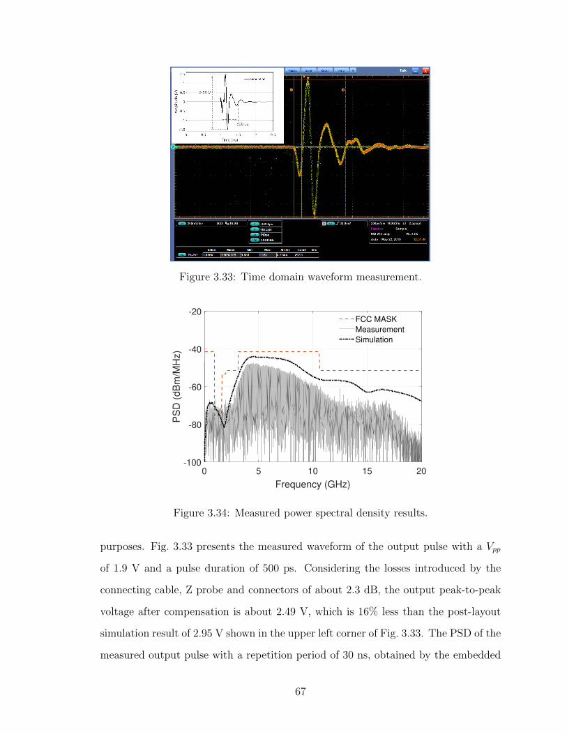
Figure 3.33: Time domain waveform measurement.
0 5 10 15 20
Frequency (GHz)
-100
-80
-60
-40
-20
PS
D (
dB
m/M
Hz)
FCC MASK
Measurement
Simulation
Figure 3.34: Measured power spectral density results.
purposes. Fig. 3.33 presents the measured waveform of the output pulse with a Vpp
of 1.9 V and a pulse duration of 500 ps. Considering the losses introduced by the
connecting cable, Z probe and connectors of about 2.3 dB, the output peak-to-peak
voltage after compensation is about 2.49 V, which is 16% less than the post-layout
simulation result of 2.95 V shown in the upper left corner of Fig. 3.33. The PSD of the
measured output pulse with a repetition period of 30 ns, obtained by the embedded
67
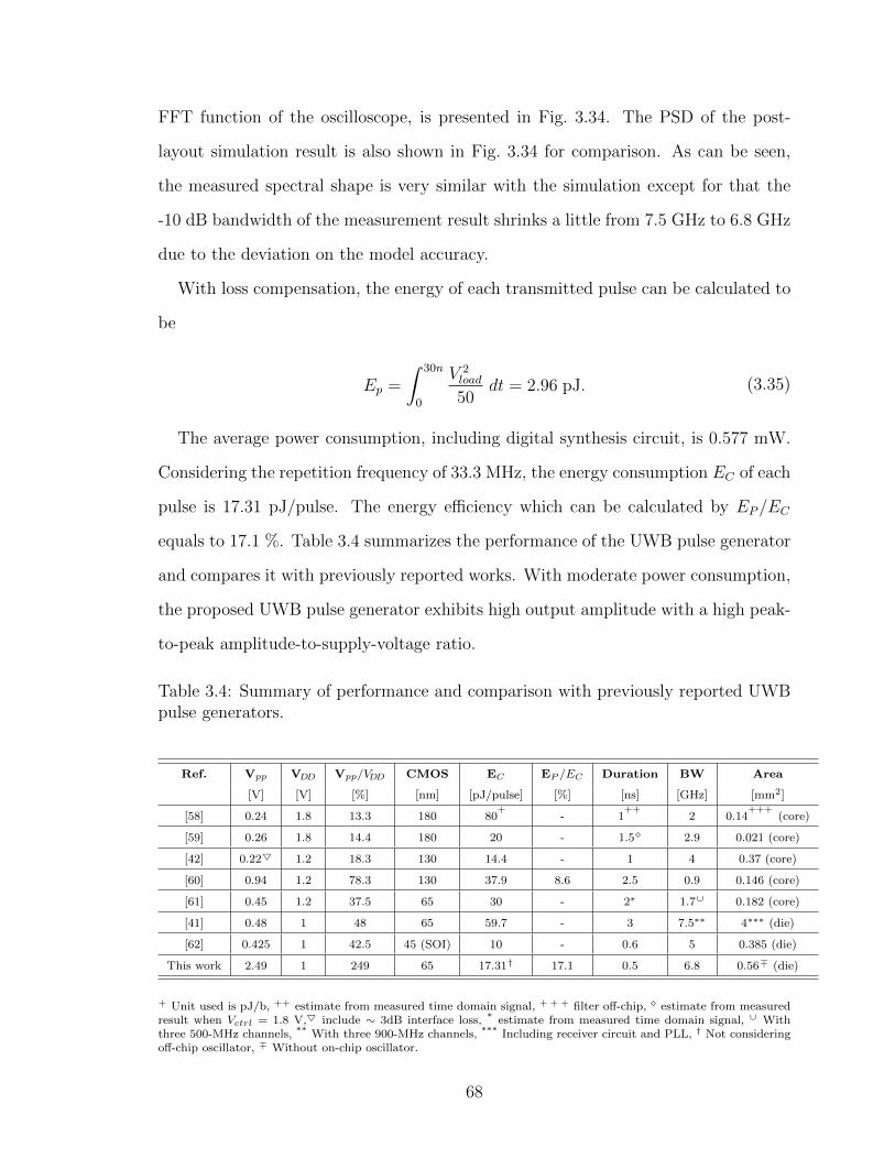
FFT function of the oscilloscope, is presented in Fig. 3.34. The PSD of the post-
layout simulation result is also shown in Fig. 3.34 for comparison. As can be seen,
the measured spectral shape is very similar with the simulation except for that the
-10 dB bandwidth of the measurement result shrinks a little from 7.5 GHz to 6.8 GHz
due to the deviation on the model accuracy.
With loss compensation, the energy of each transmitted pulse can be calculated to
be
Ep =
∫ 30n
0
V 2load
50dt = 2.96 pJ. (3.35)
The average power consumption, including digital synthesis circuit, is 0.577 mW.
Considering the repetition frequency of 33.3 MHz, the energy consumption EC of each
pulse is 17.31 pJ/pulse. The energy efficiency which can be calculated by EP/EC
equals to 17.1 %. Table 3.4 summarizes the performance of the UWB pulse generator
and compares it with previously reported works. With moderate power consumption,
the proposed UWB pulse generator exhibits high output amplitude with a high peak-
to-peak amplitude-to-supply-voltage ratio.
Table 3.4: Summary of performance and comparison with previously reported UWBpulse generators.
Ref. Vpp VDD Vpp/VDD CMOS EC EP /EC Duration BW Area
[V] [V] [%] [nm] [pJ/pulse] [%] [ns] [GHz] [mm2]
[58] 0.24 1.8 13.3 180 80+
- 1++
2 0.14+++
(core)
[59] 0.26 1.8 14.4 180 20 - 1.5⋄ 2.9 0.021 (core)
[42] 0.22 1.2 18.3 130 14.4 - 1 4 0.37 (core)
[60] 0.94 1.2 78.3 130 37.9 8.6 2.5 0.9 0.146 (core)
[61] 0.45 1.2 37.5 65 30 - 2∗ 1.7∪ 0.182 (core)
[41] 0.48 1 48 65 59.7 - 3 7.5∗∗ 4∗∗∗ (die)
[62] 0.425 1 42.5 45 (SOI) 10 - 0.6 5 0.385 (die)
This work 2.49 1 249 65 17.31† 17.1 0.5 6.8 0.56∓ (die)
+ Unit used is pJ/b, ++ estimate from measured time domain signal, + + + filter off-chip, ⋄ estimate from measuredresult when Vctrl = 1.8 V, include ∼ 3dB interface loss, * estimate from measured time domain signal, ∪ Withthree 500-MHz channels, ** With three 900-MHz channels, *** Including receiver circuit and PLL, † Not consideringoff-chip oscillator, ∓ Without on-chip oscillator.
68

3.3 Conclusion
This chapter presents two new UWB pulse generators focused on high output ampli-
tude. These two circuits employ the spectrum filtering method with inductor-loaded
power amplifiers to generate high-power UWB signals.
The first proposed design seeks to migrate the majority of the spectrum shaping
effort to the input signal design to simplify the output network, which brings the
benefits of lower loss and more compact size. Two consecutive trapezoidal waves are
chosen as the input signals since the first two notches of the corresponding spectrum
can be successfully set nearby both 3.1 GHz and 10.6 GHz. It is analyzed and veri-
fied that the locations of notches are not affected after amplification. Including the
load, the output network of the proposed design contains only four passive compo-
nents. The second proposed design focuses on the output network by replacing the
lossy filter network with a wideband matching network. It is found that, in order to
successfully achieve passive amplification, the power amplifier needs to be matched
both when the MOSFET is ON and OFF. Besides the load inductor and capacitor,
a two-section matching network is employed. Both the designs were physically im-
plemented and tested in TSMC 65-nm CMOS technology. The measurement results
show that the proposed UWB pulse generators are capable of generating UWB signals
with amplitude over two times of the supply voltage.
69
Chapter 4
UWB Receiver and Radar System
In this chapter, a UWB radar system will be introduced and discussed. As explained
in Chapter 2, for the UWB receiver structure, the correlation-based method is at-
tractive because of its high detection performance and low design complexity. The
auto-correlation method is impractical for a fully-integrated system design because
a transmission line is usually needed to produce the true-time delay, which would
occupy a significant silicon area. The cross-correlation method is employed in the
proposed UWB receiver design. In the sections next, the structure and sub-circuits
of the cross-correlation based 3.1-to-10.6-GHz UWB receiver will be described first,
followed by the simulation results of the whole UWB radar system. The UWB radar
system is fully implemented in TSMC 65-nm CMOS technology.
4.1 UWB Radar System Structure
The architecture of the proposed UWB radar system is shown in Fig. 4.1. In the
receiver, the UWB signal reflected by the detected object (tumor) is first amplified
by an ultra-wideband low-noise amplifier (LNA). The signal then goes through a
multiplier, which multiplies the amplified signal with a local template signal for signal
detection. An integrator follows next and outputs a low-frequency signal off-chip to
the oscilloscope for object identification. Since the detection resolution of the UWB
radar system is directly related to how small the time step that the template signal can
70

Receiver
Antenna
Template
Generator
Voltage Control Delay Line
Phase
Frequency
Detector
Charge
Pump
Vcont
Off-chip
Reference
Signal
Multiplexer
. . .
MultiplierLow-Noise
Amplifier Integrator
Oscillscope
Transmitter
Antenna
Delay-Locked Loop
Frequency
Divider
UWB Pulse
Generator
UWB
RECEIVER
UWB
TRANSMITTER
Trigger
Signal
ON CHIP
Object
Figure 4.1: UWB radar system block diagram.
be shifted, a high-resolution delay-locked loop (DLL) is designed to generate multi-
phase clock signals with accurate stage delays. A multiplexer is added to output one
of the clock signals from the DLL to trigger the local template generator. The sweep
resolution of the UWB radar system is determined by the minimum step size of the
voltage-controlled delay line (VCDL). To maintain a synchronized trigger source for
both the UWB transmitter and receiver, the off-chip reference signal source is shared
71

by the transmitter and the receiver. To obtain optimum performance of the UWB
radar system, the pulse repetition period of the transmitted signal has to utilize the
most of the link margin without exceeding the FCC mask. A frequency divider is
added before the UWB pulse generator to convert from the reference frequency to
the trigger frequency needed by the transmitter.
4.2 Ultra-Wideband Low-Noise Amplifier
F3, G3F2, G2F1, G1Si, Ni So, NoFN, GN...
Figure 4.2: N -stage cascaded devices chain.
According to Friis’ formula [63], the noise factor of a N -stage cascaded devices
(Fig. 4.2) can be calculated as
Ftotal = F1 +F2 − 1
G1
+F3 − 1
G1G2
+FN − 1
G1G2 · · ·GN−1
, (4.1)
where Fn and Gn (n = 1, 2, ..., N) are the noise factor and power gain of the nth stage
in the cascaded chain, respectively. The noise factor F of a system can be defined as
the input signal-to-noise ratio over that of the output as
F =SNRi
SNRo
=Si/Ni
So/No
= 1 +Nadd
G ·Ni
, (4.2)
where Nadd represents the noise introduced by the components inside the system, Si
(So) and Ni (No) are the signal power and noise power at the input (output) of the
system, respectively.
It can be noted from Eq. (4.1) that the total noise factor of the chain is mainly
determined by the first stage since the noise factor of the remaining stages are atten-
uated by the gain of the previous stages.
As the first component interfacing with the antenna in the receiver chain, the
LNA is important, especially under the circumstance when the received signal is
72

relatively weak. Besides the requirements of high gain and low noise figure (NF), the
LNA designed for a UWB system has to possess wide bandwidth so that the received
signal can be amplified with minimum shape distortion in the time domain. Since the
fT of the 65-nm CMOS technology reaches over 200 GHz, resistive-feedback common
source (CS) LNA topology is a good candidate with the merits of wide bandwidth,
high gain, and compact in size [55]. Here, we analyze the input matching, gain, and
noise figure of the resistive-feedback LNA to understand the tradeoffs in the LNA
design.
M1n
M1p
R1Cc
Vout
Rs
Vin
+
-
(a)
M1n,1p
R1
Vout
Rs
Vin
+
-
+
-VGS GmVGS RO
Rin
Vx
(b)
Figure 4.3: (a) First stage of the LNA, and (b) simplified circuit model.
Fig. 4.3a shows the circuit of a resistive-feedback CS LNA circuit, where Rs rep-
resents the 50-Ω antenna source impedance, Cctrl is the coupling capacitor, M1n and
M1p are the common-source MOSFETs, and R1 is the feedback resistor. First, for
simplicity, we assign
73

Ro = ro,M1n ∥ ro,M1p , (4.3)
where ro,M1n and ro,M1p are the output impedance of the M1n and M1p, respectively,
and
Gm = gm,M1n + gm,M1p , (4.4)
where gm,M1n and gm,M1n are the transconductance of M1n and M1p, respectively.
Assuming GmR1 ≫ 1 and GmRo ≫ 1, the input impedance and gain of the LNA can
be derived from the simplified circuit model depicted in Fig. 4.3b as
Rin =Ro +R1
1 +GmRo
≈ 1
Gm
+R1
GmRo
, (4.5)
and
Vout
Vin
=Vout
Vx
· Vx
Vin
=(1−GmR1) ·Ro
R1 +Rs +Ro +GmRsRo
. (4.6)
Note that the parasitic capacitors have been neglected for simplicity. Then we
let Rs = Rin assuming perfect impedance matching, Eq. (4.6) can be rewritten by
replacing Rs with Rin from Eq. (4.5) as
Vout
Vin
=Vout
Vx
· Vx
Vin
=(1−GmR1) ·Ro
2(R1 +Ro)≈ − 1
2( 1GmRo
+ 1GmR1
). (4.7)
In terms of the noise performance, the output impedance of the LNA can first be
derived from Fig. 4.4b as
Rout =(Rs +R1)Ro
Rs +R1 +Ro +GmRsRo
≈ Ro +R1 +GmRoR1
2Gm(Ro +R1)≈ RoR1
2(Ro +R1). (4.8)
Then the noise contribution of R1 and M1n,1p can be derived from Fig. 4.4a and
Fig. 4.4b, respectively, as
V 2n,out R1
= 4kTR1, (4.9)
where k is Boltzmann’s constant, T is the absolute temperature, and
74

M1n,1p
R1
V2n,out_R1
Rs
+
-VGS GmVGS RO
4kTR1
+-
(a)
M1n,1p
R1
V2n,out_MOS
Rs
+
-VGS GmVGS RO
Rout
4kTγGm
(b)
Figure 4.4: Noise contributed by (a) R1, and (b) M1n,1p.
V 2n,out MOS = 4kTγGm ·R2
out = kTγGm(RoR1
Ro +R1
)2. (4.10)
The noise figure of the LNA can be calculated as
NF = 1 +V 2n,out R1
+ V 2n,out MOS
4kTRs · (Vout
Vin)2
= 1 + 4(1
GmR1
+1
GmRo
) + γ · Ro
Ro +R1
. (4.11)
It can be noted from Eq. (4.11) that larger Gm and R1 are preferred to obtain a
low noise performance. In practice, the value of R1 is limited up to a few hundred
ohms as the LNA has to match to the 50-Ω antenna from Eq. (4.5). The limitation
of R1 also leads to a limited gain of the LNA from Eq. (4.7). To further increase the
gain of the LNA, and to utilize a differential signal for a better performance of the
UWB receiver, a three-stage ultra-wideband LNA is proposed, as shown in Fig. 4.5.
The first stage employs a resistive-feedback CS amplifier which provides good input
impedance matching, low added noise, and moderate gain. An inductor-loaded am-
plifier is employed as the third stage to enhance the gain at the higher end of the
75

M1n
M1p
R1
M2n
M2p
R2
M3n
M3p
RL
T1
1 : 1CL
Cc
Cpad
Lbond
Cp
From
Antenna
VB
Cs
RF1
RF2
ON CHIP
RB
Figure 4.5: Schematic of the proposed LNA.
Stage1
Gain
FreqfL fH
Gain
FreqfL fH FreqfL fH
Gain
FreqfL fH
Gain
Stage2 Stage3+ +
Total Gain
Figure 4.6: LNA gain demonstration.
passband. The load inductor is implemented by a 1-to-1 transformer (TF) which con-
verts the single-ended UWB signal to a differential signal with no extra cost. Since
it is critical to preserve the time-domain characteristic (waveform) of the received
UWB signal in the UWB receiver design, the LNA must have a flat gain over the
frequency of interest. A resistor RL is added in series with the primary winding of
the transformer to trade the gain amplitude for gain flatness. Since the LNA outputs
differential signals to the gates of the MOSFETs in the multiplier, the center tap
of the secondary turn is employed to conveniently provide the required bias voltage.
76

CL and Cs are the bypass capacitors for the primary and secondary windings of the
transformer, respectively. As noted in the resistive-feedback LNA analysis, the gain
of the amplifier is limited by the upper limit of the feedback resistance due to in-
put matching. To improve the gain flatness of the LNA, another resistive-feedback
amplifier is added as the second stage to improve the gain at the lower end of the
passband. The gain of each stage is demonstrated in Fig. 4.6. With the feedback
resistor, the first two stages are able to be self-biased while the bias of the third stage
is provided by the second stage. The PMOS-to-NMOS size ratio is the same for all
three stages and is designed such that the bias voltage is about VDD/2 to obtain good
linearity. To make a more practical implementation, the design of the LNA considers
the effect of the GSG pad and bonding wire by adopting the parasitic capacitance
(approximately 25 fF) and inductance (approximately 800 pH ∼ 1 nH) into the input
matching network.
TF model
Lp
M
1 : 1
CF
RL
. .Ls
Vout
+
- Vin
.
.+
-
Rs
Vs
Zin
Figure 4.7: Transformer model circuit.
Some considerations in the design of the transformer can be revealed from a simple
transformer model circuit, as shown in Fig. 4.7, where Lp and Ls represent, respec-
tively, the self-inductances of the primary and secondary windings of the transformer,
M and CF are the mutual inductance and coupling capacitance between the primary
and secondary windings, respectively. Assuming Lp = Ls = L for the 1-to-1 trans-
former model, the transfer function from Vin to Vout can be derived as [55]
77
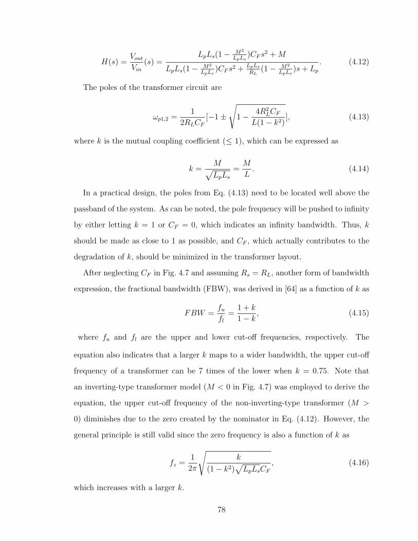
H(s) =Vout
Vin
(s) =LpLs(1− M2
LpLs)CF s
2 +M
LpLs(1− M2
LpLs)CF s2 +
LpLs
RL(1− M2
LpLs)s+ Lp
. (4.12)
The poles of the transformer circuit are
ωp1,2 =1
2RLCF
[−1±
√1− 4R2
LCF
L(1− k2)], (4.13)
where k is the mutual coupling coefficient (≤ 1), which can be expressed as
k =M√LpLs
=M
L. (4.14)
In a practical design, the poles from Eq. (4.13) need to be located well above the
passband of the system. As can be noted, the pole frequency will be pushed to infinity
by either letting k = 1 or CF = 0, which indicates an infinity bandwidth. Thus, k
should be made as close to 1 as possible, and CF , which actually contributes to the
degradation of k, should be minimized in the transformer layout.
After neglecting CF in Fig. 4.7 and assuming Rs = RL, another form of bandwidth
expression, the fractional bandwidth (FBW), was derived in [64] as a function of k as
FBW =fufl
=1 + k
1− k, (4.15)
where fu and fl are the upper and lower cut-off frequencies, respectively. The
equation also indicates that a larger k maps to a wider bandwidth, the upper cut-off
frequency of a transformer can be 7 times of the lower when k = 0.75. Note that
an inverting-type transformer model (M < 0 in Fig. 4.7) was employed to derive the
equation, the upper cut-off frequency of the non-inverting-type transformer (M >
0) diminishes due to the zero created by the nominator in Eq. (4.12). However, the
general principle is still valid since the zero frequency is also a function of k as
fz =1
2π
√k
(1− k2)√
LpLsCF
, (4.16)
which increases with a larger k.
78
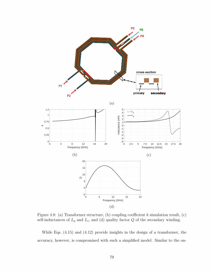
(a)
0 4 8 12 16 20Frequency (GHz)
0
0.25
0.5
0.75
1
1.2
k
(b)
0 2.5 5 7.5 10 12.5 15 17.5 20Frequency (GHz)
-5-4-32
-1012345
Indu
ctan
ce (
nH)
Ls
Lp
(c)
0 5 10 15 20Frequency (GHz)
-5
0
5
10
15
20
Q
(d)
Figure 4.8: (a) Transformer structure, (b) coupling coefficient k simulation result, (c)self-inductances of Lp and Ls, and (d) quality factor Q of the secondary winding.
While Eqs. (4.15) and (4.12) provide insights in the design of a transformer, the
accuracy, however, is compromised with such a simplified model. Similar to the on-
79
chip inductor design, the transformer also faces the issue of self-resonance due to
the capacitive coupling to the substrate and the inter-winding parasitic capacitance.
Electromagnetic simulation software such as HFSS and ADS Momentum is usually
needed to investigate the performances of the transformer with good accuracy.
There are three commonly used transformer structures: tapped TF, interleaved
TF, and stacked TF. The stacked structure features the highest coupling coefficient
k but has the largest CF . To reduce CF , a two-turn staggered structure [65] is
employed in this design, as depicted in Fig. 4.8a. The metal width and space of both
the primary and secondary windings are set to be the same (4 µm). By staggering
the two windings, the overlap capacitance is minimized with only a slightly degraded
coupling coefficient.
The simulation result of the coupling coefficient is depicted in Fig. 4.8b along with
the self-inductance shown in Fig. 4.8c. As can be seen, the designed transformer
obtains a coupling factor k of 0.77 to 0.85 from 3.1 to 10.6 GHz. The windings both
have two turns with similar diameter, the winding self-inductances over the band of
interest are almost the same. The transformer obtains a self-resonant frequency of
16.3 GHz, which is well above 10.6 GHz. Since the quality factor of the primary
winding is not a concern in this design, the secondary winding is implemented with
the top ultra-thick metal (M9) in the 65-nm 1P9M process. As can be seen from
Fig. 4.8d, the quality factor of the secondary winding is larger than 10 from 3.1 to
10.6 GHz.
The post-layout simulation result of S11, from 3.1 to 10.6 GHz, is less than -10
dB, which indicates good input matching, as shown in Fig. 4.9. The differential gains
S21 and S31 of the LNA are depicted in Fig. 4.10. As can be seen, the gains of the
two paths are balanced with a flat in-band gain response. The maximum voltage gain
for each path is about 16.3 dB, while the maximum difference in the 3.1-to-10.6-GHz
band is about 1.2 dB. As shown in Fig. 4.11, the noise figure for the entire band of
interest is about 3.4 to 3.7 dB.
80

0 3 6 9 10.6 12 15 18Frequency (GHz)
-20
-15
-10
-5
0
S11
(dB
)
Figure 4.9: S11 of the proposed LNA.
0 3 6 9 10.6 12 15 18Frequency (GHz)
0
5
10
15
20
Gai
n (d
B)
S21
S31
Figure 4.10: Voltage gain the of the LNA.
0 3 6 9 10.6 12 15 18Frequency (GHz)
3
4
5
6
7
8
NF
(dB
)
Figure 4.11: Noise figure of the LNA.
81

4.3 Local Template UWB Signal Generator
C1
L2
C2 50Ω
L1
Vctrl_2
Vctrl_2
Vctrl_1
M2bM2a
Buffer
Buffer
NOR
NOR
Trigger
Signal
VDD
GND
To Multiplier
VLO
NOR
Delay-Control
Circut
Vint
Transmitter
To Antenna
Local Template
Generator
Integration-Window Generator
Vctrl_3
Path 1
Path 2
Delay-Control
Circut
Vctrl_0
From
DLL
(a)
Vdelay
INOUT
(b) Trigger
Signal
Vctrl_1
Vctrl_2
Vctrl_2
Vctrl_1Vctrl_1
VLO
Equivalent
Input Wave
Path 1
Path 2
Integration-Window
Generator
Vctrl_2
Vctrl_1
Vctrl_2
InvertersDelay-
control
Circuit
NOR Buffer
Vctrl_3 Vctrl_3
Vint
Path1
Path2
(c)
Figure 4.12: (a) UWB transmitter and local template generator circuits, (b) new delaycontrol circuit, and (c) signal flow of local template generator including integration-window generator.
The advantage of the correlation-based receiver over others is that the receiver
can distinguish the transmitted signal from other in-band signals received by the
antenna. The principle behind this is similar to that of a narrowband receiver, where
the received signal is down-converted to baseband by the local oscillator (LO). Since
the LO and the carrier signal share the same frequency, the other signals are ignored
82

(filtered) by the narrow bandpass filter centered at the baseband. As the transmitted
UWB signal in this research does not have a carrier, the “filtering” process, in this
case, is accomplished by the local template generator which generates a UWB signal
with the same shape as the transmitted one.
Of the two UWB pulse generators introduced in Chapter 3, the first design (Sec-
tion 3.1) is utilized as the UWB transmitter for the UWB radar system due to its
compact size and simpler structure. The transmitter circuit is redrawn here with a
few modifications, as shown inside the dashed box in Fig. 4.12a. In the original trans-
mitter, MOS varactors are used to adjust the delay between the inverters to control
the width of the trapezoidal waves, the three delay cells (dark-gray box including a
MOS varactor and two inverters) are replaced with the delay-control circuit, as shown
in Fig. 4.12b. Compared to the MOS varactor method, the new delay-control circuit
has a wider tuning range by employing PMOS current source to control the delay of
the two inverters. Although the UWB transmitter and the receiver circuit share the
same reference clock signal, the actual triggering time for the transmitter and local
template generator can be different due to the different signal path lengths. For mea-
surement calibration purpose, a delay unit controlled by Vctrl 0 is added between the
DLL and the local template generator to adjust the propagation time of the trigger
signal, as depicted in Fig. 4.12a.
The modified UWB transmitter is then reused in the UWB receiver as the lo-
cal template generator with two modifications, as shown in the dash-dotted box in
Fig. 4.12a. Different from the UWB transmitter, the MOSFET sizes of the switch
amplifier are modified to generate a UWB signal with about 1-V Vpp instead of 2.12
V. An integration-window generator is added to produce a square (trapezoidal) signal
to control the integration time of the integrator, which will be further discussed in the
correlator section. The window generator employs the same idea of generating the
trapezoidal waves. Two falling edges from path1 and path2 are utilized, delayed, and
combined with a NOR gate to make sure the start time of the integration window is
83
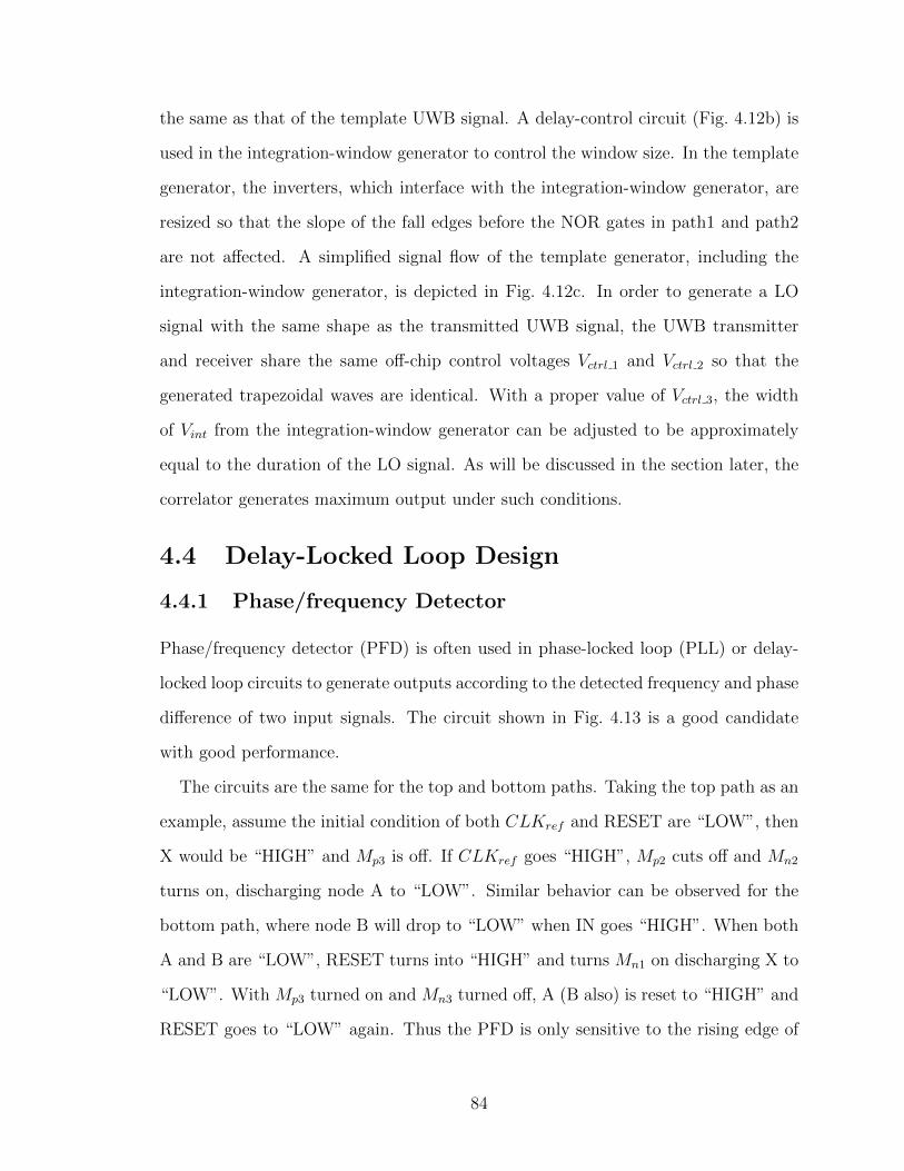
the same as that of the template UWB signal. A delay-control circuit (Fig. 4.12b) is
used in the integration-window generator to control the window size. In the template
generator, the inverters, which interface with the integration-window generator, are
resized so that the slope of the fall edges before the NOR gates in path1 and path2
are not affected. A simplified signal flow of the template generator, including the
integration-window generator, is depicted in Fig. 4.12c. In order to generate a LO
signal with the same shape as the transmitted UWB signal, the UWB transmitter
and receiver share the same off-chip control voltages Vctrl 1 and Vctrl 2 so that the
generated trapezoidal waves are identical. With a proper value of Vctrl 3, the width
of Vint from the integration-window generator can be adjusted to be approximately
equal to the duration of the LO signal. As will be discussed in the section later, the
correlator generates maximum output under such conditions.
4.4 Delay-Locked Loop Design
4.4.1 Phase/frequency Detector
Phase/frequency detector (PFD) is often used in phase-locked loop (PLL) or delay-
locked loop circuits to generate outputs according to the detected frequency and phase
difference of two input signals. The circuit shown in Fig. 4.13 is a good candidate
with good performance.
The circuits are the same for the top and bottom paths. Taking the top path as an
example, assume the initial condition of both CLKref and RESET are “LOW”, then
X would be “HIGH” and Mp3 is off. If CLKref goes “HIGH”, Mp2 cuts off and Mn2
turns on, discharging node A to “LOW”. Similar behavior can be observed for the
bottom path, where node B will drop to “LOW” when IN goes “HIGH”. When both
A and B are “LOW”, RESET turns into “HIGH” and turns Mn1 on discharging X to
“LOW”. With Mp3 turned on and Mn3 turned off, A (B also) is reset to “HIGH” and
RESET goes to “LOW” again. Thus the PFD is only sensitive to the rising edge of
84
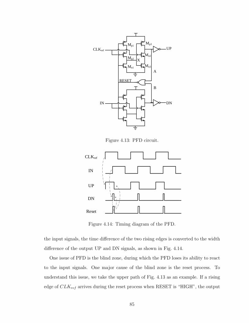
UPCLKref
IN DN
Mp1
Mp2
Mn1
RESET
A
B
X
Mn3
Mn2
Mp3
Figure 4.13: PFD circuit.
CLKref
IN
UP
DN
Reset
Figure 4.14: Timing diagram of the PFD.
the input signals, the time difference of the two rising edges is converted to the width
difference of the output UP and DN signals, as shown in Fig. 4.14.
One issue of PFD is the blind zone, during which the PFD loses its ability to react
to the input signals. One major cause of the blind zone is the reset process. To
understand this issue, we take the upper path of Fig. 4.13 as an example. If a rising
edge of CLKref arrives during the reset process when RESET is “HIGH”, the output
85

Delay Cell
UPCLKref
IN DN
Delay Cell
RESET
Figure 4.15: PFD design in [66].
sate of A will not change to “LOW” because X is still discharged and kept “LOW”
by Mn1. Thus the PFD will fail to sense the rising edge and may output wrong phase
information. The issue is more severe as the operating frequency gets higher while
the reset process occupies a larger portion of the clock period. To solve the problem,
[66] proposed to reduce the effect of the reset process by adding a delay cell to shift
the rising edge after the falling edge of the RESET signal (Fig. 4.15). It pointed out
that the delay time has to be less than the time period from the rising edge of the
latter input clock to the falling edge of the RESET signal to ensure proper operation.
The pre-charging time for the parasitic capacitances also contributes to the blind
zone [67], but the influence depends on the transistor size of the charge pump and the
input frequency. As the reset time only occupies a small portion of the clock period
in this research, the details are not discussed here.
Another issue of the PFD or the DLL circuit is the false lock problem. Generally,
there are two types of false lock named harmonic lock and stuck false lock. The causes
of both are essentially due to the same reason that the PFD can not distinguish be-
tween the rising edges of the reference clock signal. Under the correct lock condition,
86
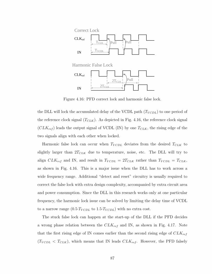
CLKref
IN2TCLK
2TCLK
CLKref
IN
TCLK
Pull
Harmonic False Lock
Correct Lock
Pull Pull
TVCDL
Figure 4.16: PFD correct lock and harmonic false lock.
the DLL will lock the accumulated delay of the VCDL path (TV CDL) to one period of
the reference clock signal (TCLK). As depicted in Fig. 4.16, the reference clock signal
(CLKref ) leads the output signal of VCDL (IN) by one TCLK , the rising edge of the
two signals align with each other when locked.
Harmonic false lock can occur when TV CDL deviates from the desired TCLK to
slightly larger than 2TCLK due to temperature, noise, etc. The DLL will try to
align CLKref and IN, and result in TV CDL = 2TCLK rather than TV CDL = TCLK ,
as shown in Fig. 4.16. This is a major issue when the DLL has to work across a
wide frequency range. Additional “detect and reset” circuitry is usually required to
correct the false lock with extra design complexity, accompanied by extra circuit area
and power consumption. Since the DLL in this research works only at one particular
frequency, the harmonic lock issue can be solved by limiting the delay time of VCDL
to a narrow range (0.5·TV CDL to 1.5·TV CDL) with no extra cost.
The stuck false lock can happen at the start-up of the DLL if the PFD decides
a wrong phase relation between the CLKref and IN, as shown in Fig. 4.17. Note
that the first rising edge of IN comes earlier than the second rising edge of CLKref
(TV CDL < TCLK), which means that IN leads CLKref . However, the PFD falsely
87
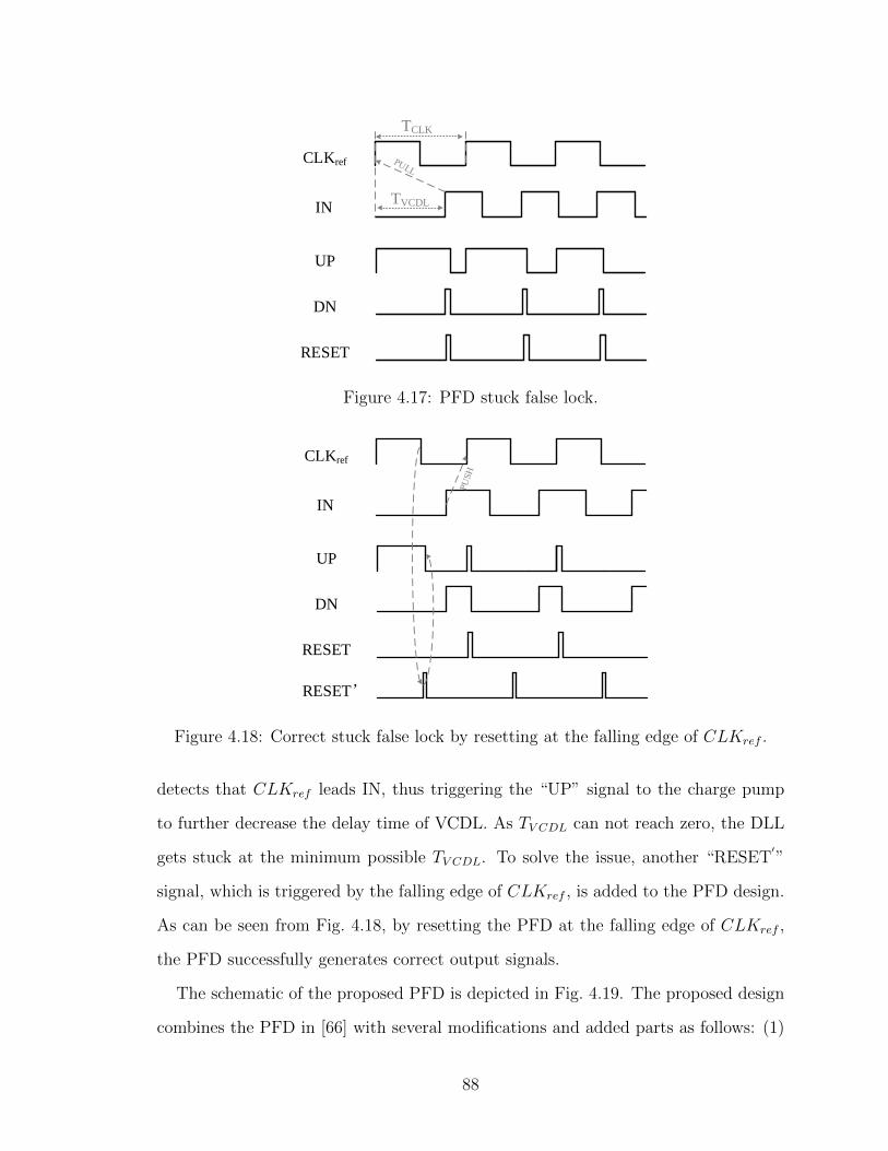
CLKref
IN
UP
DN
RESET
TVCDL
TCLK
Figure 4.17: PFD stuck false lock.
CLKref
IN
UP
DN
RESET
RESET’
Figure 4.18: Correct stuck false lock by resetting at the falling edge of CLKref .
detects that CLKref leads IN, thus triggering the “UP” signal to the charge pump
to further decrease the delay time of VCDL. As TV CDL can not reach zero, the DLL
gets stuck at the minimum possible TV CDL. To solve the issue, another “RESET′”
signal, which is triggered by the falling edge of CLKref , is added to the PFD design.
As can be seen from Fig. 4.18, by resetting the PFD at the falling edge of CLKref ,
the PFD successfully generates correct output signals.
The schematic of the proposed PFD is depicted in Fig. 4.19. The proposed design
combines the PFD in [66] with several modifications and added parts as follows: (1)
88

UPCLKref
IN DN
...X 5
...X 4
A
A
B
B
C
D1
D2
E1
E2
Figure 4.19: Proposed PFD with false lock prevention.
two-stage inverters (labelled “A” in Fig. 4.19) are used as the delay cell to reduce the
blind zone of the PFD; (2) a narrow pulse generator (labelled “C”) is used to generate
the extra reset signal (RESET′) at the falling edge of CLKref ; (3) a set of PMOS
and NMOS transistors (labelled “B”) are added to compose a NOR gate for the two
reset signals; (4) two buffers (labelled “E1” and “E2”) with different transistor sizes
are added to accommodate the unequal loading seen at the two inputs of the PFD;
(5) two output buffers (labelled “D1” and “D2”) are inserted to interface with the
charge pump to provide sufficient driving capability. The upper output of the PFD
is inverted by “D1” to drive a PMOS transistor in the charge pump and the bottom
path maintains its polarity to drive a NMOS transistor with “D2”. A transmission
gate is used in D2 to ensure that the two paths have the same delay time. It should
also be noted that although another blind zone is introduced by the extra “RESET′
signal, its duration (about 50 ps) is quite short compared with TCLK (5.12 ns), thus
it will hardly affect the functionality of the PFD.
89

4.4.2 Charge Pump
The charge pump and phase/frequency detector (phase detector) combination circuit
has been widely used in various PLL and DLL applications [68][69][70]. Through
sourcing or sinking current from the load capacitor, the charge pump converts the
phase information sensed by the PFD to the control voltage of the VCDL.
UP
DN
Cctrl
Vctrl
I1
I2
PFD
CLKref
IN
Charge Pump
ON
OFF
ON
OFF
(a)
UP
DN
Vctrl
UP
DN
Vctrl
t
tslope1
slope2
TCLK
T
Locked State
With Phase Difference
Tm
(b)
Figure 4.20: (a) Charge pump circuit with the PFD block and load capacitor, and(b) waveform with phase difference and locked state.
90
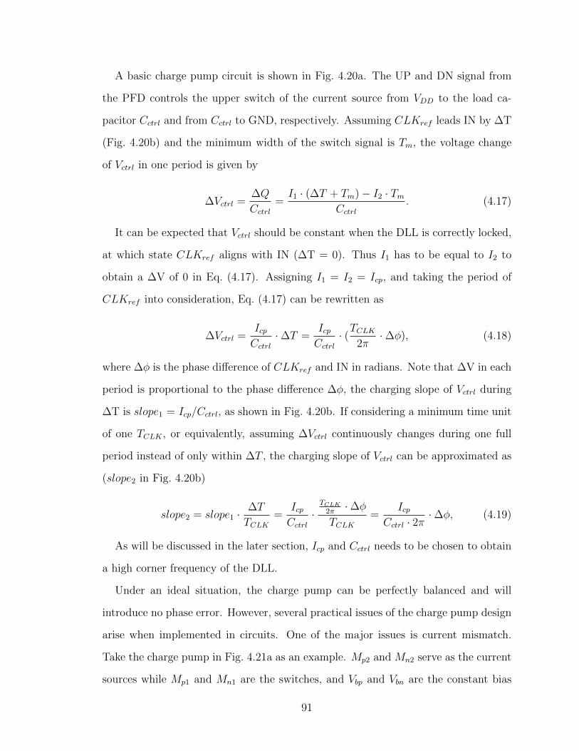
A basic charge pump circuit is shown in Fig. 4.20a. The UP and DN signal from
the PFD controls the upper switch of the current source from VDD to the load ca-
pacitor Cctrl and from Cctrl to GND, respectively. Assuming CLKref leads IN by ∆T
(Fig. 4.20b) and the minimum width of the switch signal is Tm, the voltage change
of Vctrl in one period is given by
∆Vctrl =∆Q
Cctrl
=I1 · (∆T + Tm)− I2 · Tm
Cctrl
. (4.17)
It can be expected that Vctrl should be constant when the DLL is correctly locked,
at which state CLKref aligns with IN (∆T = 0). Thus I1 has to be equal to I2 to
obtain a ∆V of 0 in Eq. (4.17). Assigning I1 = I2 = Icp, and taking the period of
CLKref into consideration, Eq. (4.17) can be rewritten as
∆Vctrl =IcpCctrl
·∆T =IcpCctrl
· (TCLK
2π·∆ϕ), (4.18)
where ∆ϕ is the phase difference of CLKref and IN in radians. Note that ∆V in each
period is proportional to the phase difference ∆ϕ, the charging slope of Vctrl during
∆T is slope1 = Icp/Cctrl, as shown in Fig. 4.20b. If considering a minimum time unit
of one TCLK , or equivalently, assuming ∆Vctrl continuously changes during one full
period instead of only within ∆T , the charging slope of Vctrl can be approximated as
(slope2 in Fig. 4.20b)
slope2 = slope1 ·∆T
TCLK
=IcpCctrl
·TCLK
2π·∆ϕ
TCLK
=Icp
Cctrl · 2π·∆ϕ, (4.19)
As will be discussed in the later section, Icp and Cctrl needs to be chosen to obtain
a high corner frequency of the DLL.
Under an ideal situation, the charge pump can be perfectly balanced and will
introduce no phase error. However, several practical issues of the charge pump design
arise when implemented in circuits. One of the major issues is current mismatch.
Take the charge pump in Fig. 4.21a as an example. Mp2 and Mn2 serve as the current
sources while Mp1 and Mn1 are the switches, and Vbp and Vbn are the constant bias
91
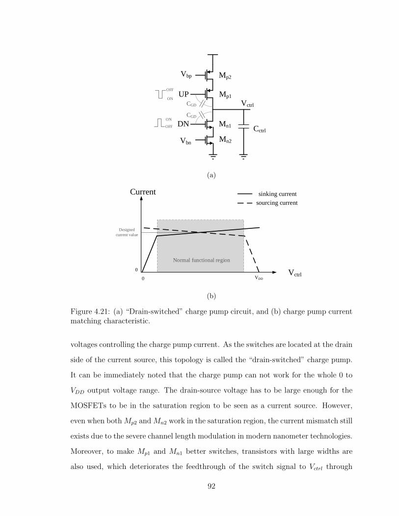
UP
DNCctrl
Vctrl
ON
OFF
ON
OFF
Mp2
Mp1
Mn1
Mn2
Vbp
Vbn
CGD
CGD
(a)
0
0
VDD
Current
Vctrl
Designed
current value
Normal functional region
sinking current
sourcing current
(b)
Figure 4.21: (a) “Drain-switched” charge pump circuit, and (b) charge pump currentmatching characteristic.
voltages controlling the charge pump current. As the switches are located at the drain
side of the current source, this topology is called the “drain-switched” charge pump.
It can be immediately noted that the charge pump can not work for the whole 0 to
VDD output voltage range. The drain-source voltage has to be large enough for the
MOSFETs to be in the saturation region to be seen as a current source. However,
even when bothMp2 andMn2 work in the saturation region, the current mismatch still
exists due to the severe channel length modulation in modern nanometer technologies.
Moreover, to make Mp1 and Mn1 better switches, transistors with large widths are
also used, which deteriorates the feedthrough of the switch signal to Vctrl through
92
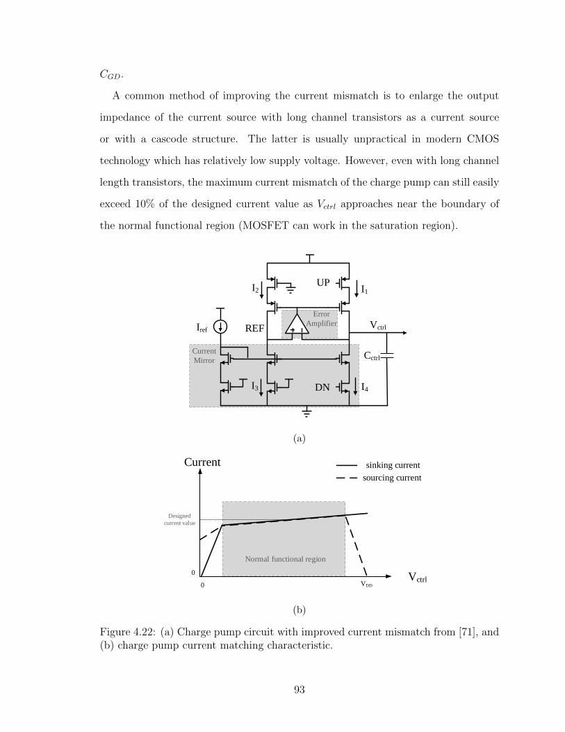
CGD.
A common method of improving the current mismatch is to enlarge the output
impedance of the current source with long channel transistors as a current source
or with a cascode structure. The latter is usually unpractical in modern CMOS
technology which has relatively low supply voltage. However, even with long channel
length transistors, the maximum current mismatch of the charge pump can still easily
exceed 10% of the designed current value as Vctrl approaches near the boundary of
the normal functional region (MOSFET can work in the saturation region).
UP
Cctrl
DN
REF VctrlIref
I1I2
Current
Mirror
Error
Amplifier
I3 I4
(a)
0
0
VDD
Current
Vctrl
Designed
current value
Normal functional region
sinking current
sourcing current
(b)
Figure 4.22: (a) Charge pump circuit with improved current mismatch from [71], and(b) charge pump current matching characteristic.
93
To solve the current mismatch problem, [71] proposed a design with improved
current matching characteristics, as shown in Fig. 4.22a. In the design, the switches
were placed in series with the source of the current sources, thus it is called a “source-
switched” topology. The current source in source-switched structure inherently has
higher output impedance with source degeneration if assuming with the same cur-
rent source sizes and switch sizes. Moreover, the feedthrough of the switch is also
suppressed by the current source before the charge pump output. In addition to the
topology advantages, an error amplifier was employed to further enhance the current
matching performance by enforcing the constraint that the voltage at node REF fol-
lows (equals to) Vctrl. Combining with the current mirror, the design was able to
make I1 = I2 when the UP is “LOW” and I3 = I4 when the DN is “HIGH”. Since
I3 = I4, the charge pump achieved I1 = I4 regardless of Vctrl. The current match-
ing characteristic is shown in Fig. 4.22b, although the charge pump current deviates
from the designed current value as Vctrl changes, the current matching was greatly
improved.
UP
Cctrl
DN
REFVctrlIref
X
Y
Q
S
CGS1
CGS2
CGS3
Camp
Figure 4.23: Charge pump with transit current mismatch and possible solution.
Considering the merit of the charge pump topology in Fig. 4.22a, it is adopted in
the DLL design in this research. However, it was also found that although the charge
94

pump exhibits excellent current matching in DC static state, the current mismatch
still exists in transit analysis. The reason for such a mismatch was due to the bias
voltage variation of the current source. For instance, as can be seen from Fig. 4.23,
when the UP signal is “LOW” to open the top switch, the voltage jump of node Q will
cause a jump at node X through CGS1. Due to the finite output impedance of the error
amplifier and the relatively large capacitance composed of Camp (output capacitance
of the error amplifier), CGS1, and CGS3, the time constant at node X can be relatively
large, which results in a slow voltage rise and fall at node X. Consequently, the
charging current features a slow response. A similar problem occurs at node Y of the
bottom section. However, as the two nodes see different impedances and capacitances,
the difference between the sourcing and sinking current can be quite large.
UP
Cctrl
DN
Vctrl
C1Iref
VIN- VIN+
VOUT
Vbias
Figure 4.24: Proposed charge pump with improved current mismatch.
One way to solve the issue is by adding another capacitor to suppress the voltage
variation, as demonstrated in the dashed box in Fig. 4.23. However, two capacitors
have to be added between node X and VDD and between node Y and GND, respec-
tively. What is more, the added capacitors have to be quite large to take effect, which
occupies a substantial chip area. We propose a way to suppress the voltage variation
of the two nodes at the same time by adding a capacitor C1 between them, as shown
in Fig. 4.24. The basic idea here is that since the voltages of the two nodes change in
95
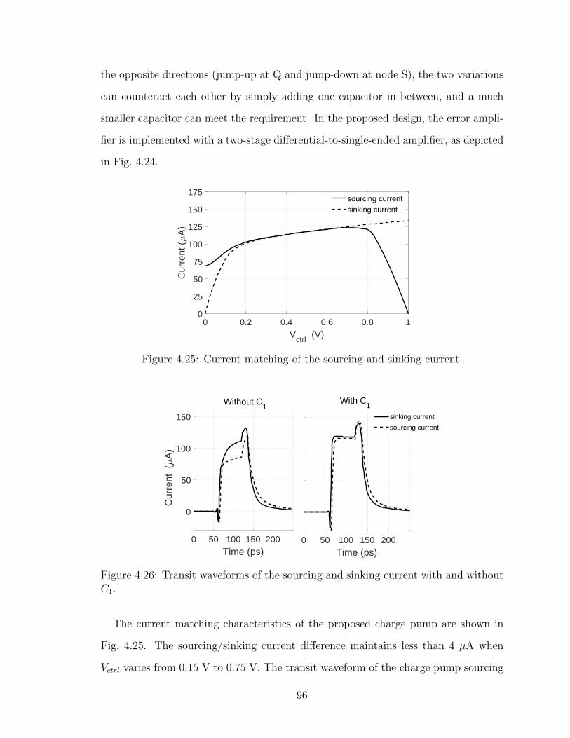
the opposite directions (jump-up at Q and jump-down at node S), the two variations
can counteract each other by simply adding one capacitor in between, and a much
smaller capacitor can meet the requirement. In the proposed design, the error ampli-
fier is implemented with a two-stage differential-to-single-ended amplifier, as depicted
in Fig. 4.24.
0 0.2 0.4 0.6 0.8 1V
ctrl (V)
0
25
50
75
100
125
150
175C
urre
nt (
A)
sourcing currentsinking current
Figure 4.25: Current matching of the sourcing and sinking current.
0 50 100 150 200Time (ps)
0
50
100
150
Cur
rent
(A
)
0 50 100 150 200Time (ps)
sinking current
sourcing current
With C1Without C
1
Figure 4.26: Transit waveforms of the sourcing and sinking current with and withoutC1.
The current matching characteristics of the proposed charge pump are shown in
Fig. 4.25. The sourcing/sinking current difference maintains less than 4 µA when
Vctrl varies from 0.15 V to 0.75 V. The transit waveform of the charge pump sourcing
96
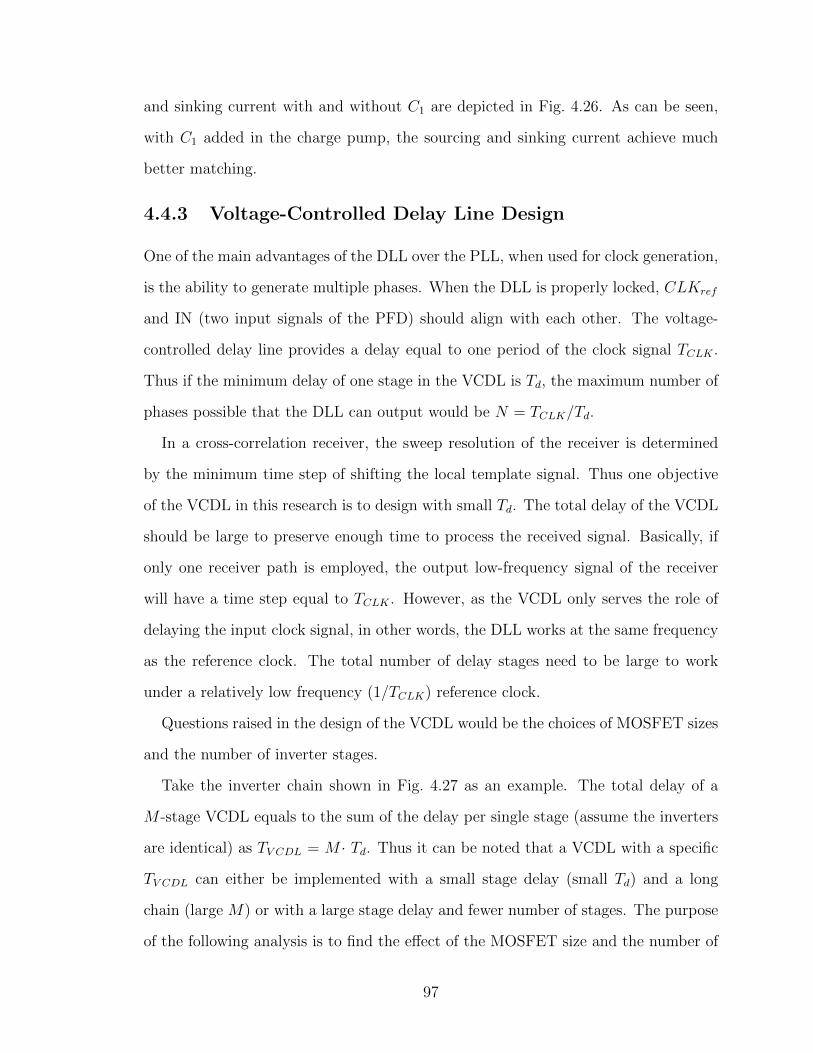
and sinking current with and without C1 are depicted in Fig. 4.26. As can be seen,
with C1 added in the charge pump, the sourcing and sinking current achieve much
better matching.
4.4.3 Voltage-Controlled Delay Line Design
One of the main advantages of the DLL over the PLL, when used for clock generation,
is the ability to generate multiple phases. When the DLL is properly locked, CLKref
and IN (two input signals of the PFD) should align with each other. The voltage-
controlled delay line provides a delay equal to one period of the clock signal TCLK .
Thus if the minimum delay of one stage in the VCDL is Td, the maximum number of
phases possible that the DLL can output would be N = TCLK/Td.
In a cross-correlation receiver, the sweep resolution of the receiver is determined
by the minimum time step of shifting the local template signal. Thus one objective
of the VCDL in this research is to design with small Td. The total delay of the VCDL
should be large to preserve enough time to process the received signal. Basically, if
only one receiver path is employed, the output low-frequency signal of the receiver
will have a time step equal to TCLK . However, as the VCDL only serves the role of
delaying the input clock signal, in other words, the DLL works at the same frequency
as the reference clock. The total number of delay stages need to be large to work
under a relatively low frequency (1/TCLK) reference clock.
Questions raised in the design of the VCDL would be the choices of MOSFET sizes
and the number of inverter stages.
Take the inverter chain shown in Fig. 4.27 as an example. The total delay of a
M -stage VCDL equals to the sum of the delay per single stage (assume the inverters
are identical) as TV CDL = M · Td. Thus it can be noted that a VCDL with a specific
TV CDL can either be implemented with a small stage delay (small Td) and a long
chain (large M) or with a large stage delay and fewer number of stages. The purpose
of the following analysis is to find the effect of the MOSFET size and the number of
97

stages on Td and the noise performance of the VCDL.
In terms of the size of MOSFETs, let us use simple CMOS inverters as the delay
cells in the VCDL, as shown in Fig. 4.28a. The external load of the inverter, such as
the multiplexer, is ignored for now for simplicity purposes. The corresponding switch
models of one inverter stage when the input voltage VIN is “LOW” and “HIGH”
are shown in Fig. 4.28b. When VIN is “LOW”, the PMOS can be modeled as an
equivalent resistor Reqp which conducts current to the load capacitor CL with a current
of Icp. The NMOS is in the cutoff region and modeled as a switch in the OFF
position. The opposite case occurs when VIN is “HIGH”, the NMOS is modeled as an
equivalent resistor Reqn discharging CL while PMOS is modeled as a switch in OFF
state. Thus the inverter stage can be treated as a first-order linear RC-network, and
the propagation delay can be approximated as
Td = 0.69CL(Reqn +Reqp
2), (4.20)
In practice, the value of the equivalent resistor changes during wave propagation
as the MOSFET will go through both the triode and saturation region. Assuming
PMOS and NMOS are sized to have equal equivalent resistance as Reqp = Reqn =
Req, the average on-resistance of the MOSFET can be expressed as
Req = Reqn =1
VDD/2
∫ VDD
VDD/2
V
Idsat(1 + λV )dV ≈ 3
4
VDD
Idsat(1− 7
9λVDD), (4.21)
......
DnDn-1 Dn+1
Td
TVCDL
M-stage Delay Chain
Figure 4.27: M -stage delay chain.
98

NMOS CL
Reqp
Ip
PMOS
CLReqn
In
VIN VOUT
VIN is“HIGH”VIN is“LOW”
(a) (b)
Figure 4.28: (a) Inverter MOSFET circuit, and (b) the corresponding switch modelswhen VIN is “LOW” and “HIGH”.
where λ is the channel-length modulation factor. Idsat is the MOSFET current when
working in saturation region, and can be expressed as
Idsat = µnCoxW
L((VDD − Vth)Vdsat −
V 2dsat
2), (4.22)
thus it can be noted from Eqs. (4.21) and (4.22) that
Req ∝1
W/L. (4.23)
VOUT... ...CGDp0
CGDn0
CDBp0
CDBn0
Cw
CGp1
CGn1
Figure 4.29: Composition of load capacitance CL at VOUT .
Then what remains next is to find the value of the load capacitance CL. The load
capacitance is the sum of all the capacitances seen from VOUT to GND (or VDD). As
99
shown in Fig. 4.29, generally it is composed of in-stage gate-drain capacitance (CGDp0,
CGDn0), in-stage gate-bulk capacitance (CDBp0, CDBn0), interconnecting-wire capaci-
tance (Cw), and the fanout gate capacitance from the next stage (CGp1, CGn1), which
includes the channel capacitance, gate-drain overlap capacitance and gate-source over-
lap capacitance. For simplicity, the wire capacitance and the gate-bulk capacitance
are ignored here as the former relates to the layout structure while the latter depends
on VOUT and is quite nonlinear. As the overlap capacitance is proportional to the
gate width W and the channel capacitance is proportional to the product of the gate
width and length, the load capacitance CL can then be approximated as
CL = A ·W +B ·WL, (4.24)
where A and B are constant numbers. Note that although B actually varies as the
MOSFET works in different regions, it is approximated here as an constant number,
which indicates an average value. Thus the relation between the stage delay Td and
MOSFET width can be found by substituting Eq. (4.23) and Eq. (4.24) into Eq. (4.20)
as
Td ∝1
W/L· (A ·W +B ·WL) = A · L+B · L2. (4.25)
It was shown in [72] that if the input period of the delay line is equal to the period
of the corresponding ring oscillator (when closing the loop by connecting the input
to the output of the delay line), then the white noise and flicker noise of M -stage
inverters can be expressed as
SΦ,white,DL =π2
2I2D· [SI,NMOS(f) + SI,PMOS(f)] +
2kTπ2
IDVDD
, (4.26)
and
SΦ,1/f,DL =π2
4MI2D· [S 1
f,NMOS(f) + S 1
f,PMOS(f)], (4.27)
100

where ID is the drain current of the MOSFET at operating point |VGS| = VDD and
|VDS| = VDD/2 (assuming same ID for the NMOS and PMOS), k is the Boltzmann
constant, T is the absolute temperature, and SI(f) and S 1f(f) are the thermal and
flicker noise current spectrum (two-sided) of the transistors that can be expressed as
SI(f) = 2kTγgm, (4.28)
and
S 1f(f) =
K
2WLCoxf· g2m, (4.29)
where γ is the excess noise coefficient, gm is the transconductance of the MOSFET,
and K is a process-dependent parameter. Assuming equal γ and gm for NMOS and
PMOS, Eq. (4.26) and Eq. (4.27) can be rewritten as
SΦ,white,DL =2kTγgmπ
2
I2D+
2kTπ2
IDVDD
, (4.30)
and
SΦ,1/f,DL =g2mπ
2
8MLCoxfI2D· [KNMOS
WNMOS
+KPMOS
WPMOS
]. (4.31)
Assuming a MOSFET working in saturation region under the operating point of
|VGS| = VDD and |VDS| = VDD/2, we have the transconductance and drain current
expression as
gm = µCoxW
L(VDD − Vth) ∝
W
L, (4.32)
and
ID =1
2µCox
W
L(VDD − Vth)
2 ∝ W
L. (4.33)
Hence we can obtain from Eq.(4.30), and Eq.(4.31) that
SΦ,white,DL ∝ L
W, (4.34)
101
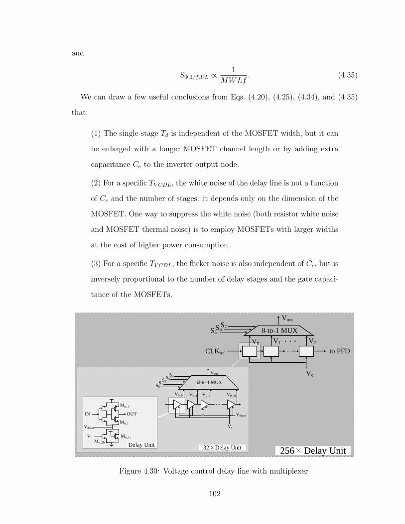
and
SΦ,1/f,DL ∝ 1
MWLf. (4.35)
We can draw a few useful conclusions from Eqs. (4.20), (4.25), (4.34), and (4.35)
that:
(1) The single-stage Td is independent of the MOSFET width, but it can
be enlarged with a longer MOSFET channel length or by adding extra
capacitance Ce to the inverter output node.
(2) For a specific TV CDL, the white noise of the delay line is not a function
of Ce and the number of stages: it depends only on the dimension of the
MOSFET. One way to suppress the white noise (both resistor white noise
and MOSFET thermal noise) is to employ MOSFETs with larger widths
at the cost of higher power consumption.
(3) For a specific TV CDL, the flicker noise is also independent of Ce, but is
inversely proportional to the number of delay stages and the gate capaci-
tance of the MOSFETs.
...
CLKref to PFD
Vc
V0_0 V0_1 V0_2 V0_31
Vc
IN OUT Vdrain
Vdrain
32-to-1 MUX
Vout
Delay Unit
8-to-1 MUX
Vout
...
Vc
. . .
S0S1
S4S3S2
S7S6S5
V0 V1 V7
32 Delay Unit 256 Delay Unit
Mn_1a
Mn_1b
Mn_1
Mp_1
Figure 4.30: Voltage control delay line with multiplexer.
102
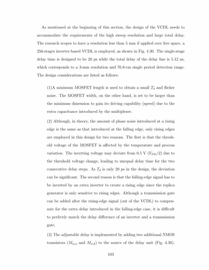
As mentioned at the beginning of this section, the design of the VCDL needs to
accommodate the requirements of the high sweep resolution and large total delay.
The research scopes to have a resolution less than 5 mm if applied over free space, a
256-stages inverter-based VCDL is employed, as shown in Fig. 4.30. The single-stage
delay time is designed to be 20 ps while the total delay of the delay line is 5.12 ns,
which corresponds to a 3-mm resolution and 76.8-cm single period detection range.
The design considerations are listed as follows:
(1)A minimum MOSFET length is used to obtain a small Td and flicker
noise. The MOSFET width, on the other hand, is set to be larger than
the minimum dimension to gain its driving capability (speed) due to the
extra capacitance introduced by the multiplexer.
(2) Although, in theory, the amount of phase noise introduced at a rising
edge is the same as that introduced at the falling edge, only rising edges
are employed in this design for two reasons. The first is that the thresh-
old voltage of the MOSFET is affected by the temperature and process
variation. The inverting voltage may deviate from 0.5 V (VDD/2) due to
the threshold voltage change, leading to unequal delay time for the two
consecutive delay steps. As Td is only 20 ps in the design, the deviation
can be significant. The second reason is that the falling-edge signal has to
be inverted by an extra inverter to create a rising edge since the replica
generator is only sensitive to rising edges. Although a transmission gate
can be added after the rising-edge signal (out of the VCDL) to compen-
sate for the extra delay introduced in the falling-edge case, it is difficult
to perfectly match the delay difference of an inverter and a transmission
gate.
(3) The adjustable delay is implemented by adding two additional NMOS
transistors (Mn1a and Mn1b) to the source of the delay unit (Fig. 4.30).
103
0 0.2 0.4 0.6 0.8 1
Vctrl
(V)
4.5
5
5.5
6
6.5
TV
CD
L (
ns)
Figure 4.31: Simulation result of TV CDL varying with Vctrl.
The control voltage Vctrl of the VCDL is applied to the Mn1b to control the
delay time by modifying the current of the two inverters. As mentioned
previously in the design of the PFD, the delay time of the VCDL needs
to be smaller than 1.5·TCLK to avoid the false-lock problem. This is
implemented here by connecting the gate of Mn1a to VDD to avoid cutting
off the current of the delay unit when Vc = 0, thus limiting the maximum
possible TV CDL of the delay line. The post-layout simulation result of
TV CDL varying with Vctrl is shown in Fig. 4.31. As Vctrl changes from 0.15
V to 0.75 V, TV CDL varies from 4.53 ns to 6.43 ns, which is within the
desired range.
(4) In addition to limiting the slowest delay of the VCDL, it is also impor-
tant to make sure that the VCDL can transmit fast enough as the desired
delay per inverter is only 10 ps. It should be noted that the inverters
are slowed down by the added transistors even when Vctrl = VDD because
Vdrain would always be larger than 0, or it is equivalent to think that the
inverters work under a lower VDD. Note that the VCDL can not properly
lock under Vctrl = VDD due to the limited working range of the charge
pump (Fig. 4.25). Instead of using both NMOS and PMOS to control
104

the delay unit, which has the virtue of symmetric output waveform, only
NMOS (Mn1a, Mn1b) is employed in this design to save the voltage head-
room and ensure the speed of the delay unit. One issue still exists even
with only NMOS is that the MOSFET size (Mn1b) has to be quite large to
obtain a low-enough Vdrain. To resolve such an issue, the VCDL is divided
into eight groups, inside of which the Vdrain node of the delay unit are
connected together. In this way, a more compact design can be obtained.
Before moving to the next section, it is worth mentioning a few more considerations
regarding the number of stages and structure in the design of the VCDL. It is clear
...D2D1
20 ps
TVCDL(5.12 ns)
D256
PFDCharge
Pump
CLKref
(a)
...DF2DF1
Td_F
(20 ps)
TVCDL_F(320 ps)
DF16
PFD_F
Charge
Pump_F
...
DC2DC1 DC16
PFD_C
Charge
Pump_C
CLKref
( = TVCDL_C = 5.12 ns)
MUXC
Td_C
(320 ps)
Coarse DLL (16 stages) Fine DLL (16 stages)
(b)
Figure 4.32: (a) DLL design with single-chain 256-stage VCDL, and (b) DLL designwith 16×16 coarse-and-fine step control.
105
from Eqs. (4.34) and (4.35) that the white noise of the VCDL is independent of
the number of delay stages while the flicker noise decreases with more stages. But
how about the power consumption and circuit area comparing to the type of VCDL
with coarse-and-fine step control? Considering the two designs shown in Fig. 4.32 as
examples. Both two examples have the same total delay of 5.12 ns and minimum delay
step of 20 ps. The first DLL example (Fig. 4.32a) is the structure that is employed in
the research, where the VCDL is composed of 256 stages of delay cells. The second
DLL example (Fig. 4.32b) is a cascade design with a 16-by-16 coarse-and-fine phase
division. The reference clock signal (CLKref ) is first divided into 16 different phases
with a delay step of 320 ps. Then the coarse signals are chosen by the multiplexer
(MUXC) to work as the reference signals for the fine DLL to generate 16 fine delays.
It would be difficult to quantitatively evaluate which design is better without the
practical design. Thus the two designs are only intuitively discussed and compared
here.
As for the circuit area, the former design has 256 stages of delay cells, while the
latter design has only 64 stages, which is three quarters less. The former design
needs an 8-bit multiplexer to forward the selected signal to the output, while the
latter design requires two 4-bit multiplexers. If both are implemented with 2-to-1
multiplexers, the multiplexer in the latter design takes about one-eighth of the area
compared with the 8-bit multiplexer in the former design. However, two sets of PFDs
and charge pumps (including the output capacitor) are employed in the latter design
while the former only needs one. As the capacitors usually occupy a significant area,
plus that extra area will be needed if the delay cells of the coarse DLL adopts extra
capacitors or varactors to adjust the stage delay Td C , the circuit area of the two cases
can be similar.
As for the power consumption, let us first assume that the delay cells (D1, ...,
D256) of the former example are identical with the delay cells in the fine DLL of the
second example (DF1, ..., DF16) since the single-stage delay time is 20 ps for both.
106

Then we can know from the design of a ring oscillator that the VCDL in the first
example has the same power consumption as the VCDL F in the fine DLL of the
latter design (power consumption is independent of the number of stages of a ring
oscillator). The PFD and charge pump of the former design basically has the same
power consumption as the ones (PFD C and charge pump C) in the coarse DLL of the
latter design as they work at the same frequency. As such, the power consumption of
the latter design would be larger than the former one with extra power consumed by
the coarse delay line (VCDL C), and the PFD F and charge pump F of the fine DLL.
As for the noise performance, besides the aforementioned white noise and flicker
noise of the VCDL, what has not been mentioned is that the PFD and charge pump
also contribute to the phase noise of the DLL. For example, the phase noise of the
PFD will modulate the width of the UP and DOWN pulses, which causes a mismatch
between the sourcing and sinking current in the charge pump. Assuming that the
PFD and charge pump introduce a phase error Φe into the DLL, which corresponds
to a period difference of Φe/(2π · TV CDL) seconds compared with the ideal case. For
an ideal M -stage VCDL, the delay error of a single delay stage (Te) can be calculated
as
Te =Φe
2π· TV CDL
M. (4.36)
As can be noted, a larger number of stages of VCDL is also beneficial to suppress
the phase noise introduced by the PFD and charge pump. As such, the former design
topology is employed in this research according to the reasons mentioned above.
4.4.4 Transfer Function of the DLL
Now that the sub-circuits of the DLL have been introduced, the design considerations
of each part are discussed. It is worth deriving the transfer function of the DLL loop
(Fig. 4.32a) to get the capacitance value of the charge pump load and finalize the
DLL design.
107
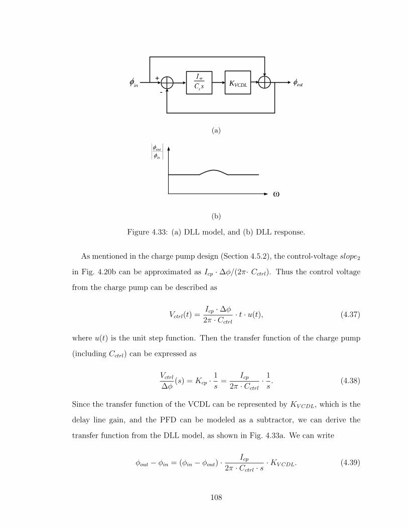
KVCDL
-
+
(a)
ω
(b)
Figure 4.33: (a) DLL model, and (b) DLL response.
As mentioned in the charge pump design (Section 4.5.2), the control-voltage slope2
in Fig. 4.20b can be approximated as Icp · ∆ϕ/(2π· Cctrl). Thus the control voltage
from the charge pump can be described as
Vctrl(t) =Icp ·∆ϕ
2π · Cctrl
· t · u(t), (4.37)
where u(t) is the unit step function. Then the transfer function of the charge pump
(including Cctrl) can be expressed as
Vctrl
∆ϕ(s) = Kcp ·
1
s=
Icp2π · Cctrl
· 1s. (4.38)
Since the transfer function of the VCDL can be represented by KV CDL, which is the
delay line gain, and the PFD can be modeled as a subtractor, we can derive the
transfer function from the DLL model, as shown in Fig. 4.33a. We can write
ϕout − ϕin = (ϕin − ϕout) ·Icp
2π · Cctrl · s·KV CDL. (4.39)
108
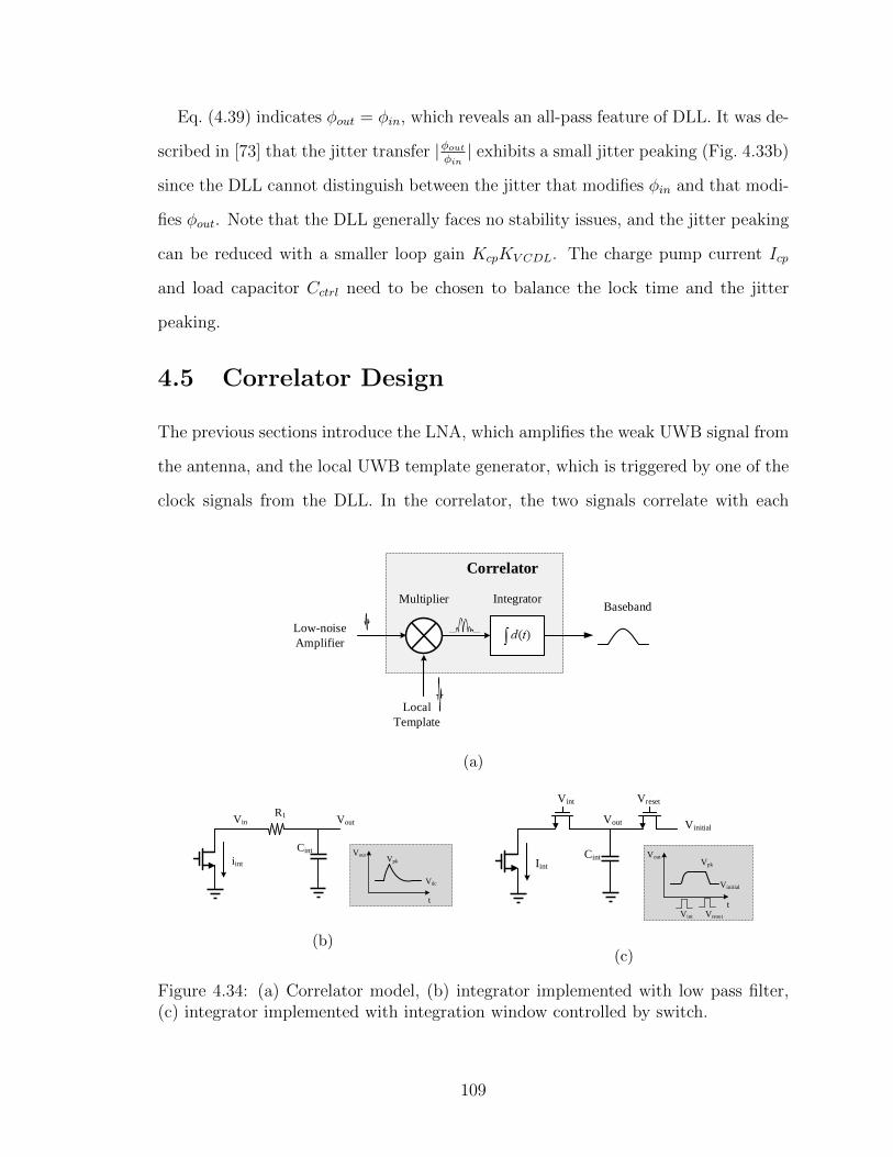
Eq. (4.39) indicates ϕout = ϕin, which reveals an all-pass feature of DLL. It was de-
scribed in [73] that the jitter transfer |ϕout
ϕin| exhibits a small jitter peaking (Fig. 4.33b)
since the DLL cannot distinguish between the jitter that modifies ϕin and that modi-
fies ϕout. Note that the DLL generally faces no stability issues, and the jitter peaking
can be reduced with a smaller loop gain KcpKV CDL. The charge pump current Icp
and load capacitor Cctrl need to be chosen to balance the lock time and the jitter
peaking.
4.5 Correlator Design
The previous sections introduce the LNA, which amplifies the weak UWB signal from
the antenna, and the local UWB template generator, which is triggered by one of the
clock signals from the DLL. In the correlator, the two signals correlate with each
Multiplier Integrator
Correlator
Low-noise
Amplifier
Local
Template
Baseband
(a)
R1
Cint
VoutVin
iint
t
Vout
Vdc
Vpk
(b)
Cint
Vout
Iint
t
Vout
Vinitial
Vpk
Vint Vreset
Vinitial
Vint Vreset
(c)
Figure 4.34: (a) Correlator model, (b) integrator implemented with low pass filter,(c) integrator implemented with integration window controlled by switch.
109

other and generate a low-frequency (baseband) signal which contains the distance or
location information that needs to be extracted in the baseband signal processing.
Generally, a correlator is composed of a multiplier and an integrator, as shown in
Fig. 4.34a. This can be implied from the mathematical equation
f ∗ g(τ) =∫ ∞
−∞f(t− τ)g(t)dt, (4.40)
where f(t) and g(t) are the two input signals of the correlator, and τ is the dis-
placement. As can be noted from Eq. (4.40), the output magnitude of the correlator
reaches its maximum when the two input signals of the multiplier have the same
shape and are exactly aligned with each other. This points out two essential design
considerations of the correlation-based receiver that: (1) the shape of the local tem-
plate signal needs to be as close to the received signal as possible to obtain optimum
performance, and (2) the local template signal needs to be shifted in a very small
time step to locate the position (delay time) the transmitted signal in order to have
high accuracy and sweep resolution.
One way to implement the integrator is with a low-pass filter, as shown in Fig. 4.34b.
As the transfer function of the low-pass filter can be expressed as
H(s) =1
s/ω0 + 1, (4.41)
where ω0 = 1/(R1Cint) is the corner frequency of the filter. When signal frequency ω
is much higher than ω0, Eq. (4.41) can be simplified as
H(s) ≈ 1
s/ω0
=1
jωR1Cint
, (4.42)
which is the same as the transfer function of an integrator. To satisfy that ω ≫ ω0,
Cint usually needs to be very large. With a large Cint, a waveform similar to charging
and then discharging a capacitor can usually be observed for this type of integrator,
as shown in Fig. 4.34b. One drawback for the integrator can be observed from the
waveform is that the integrator can not hold the integration value, Vout starts to
110
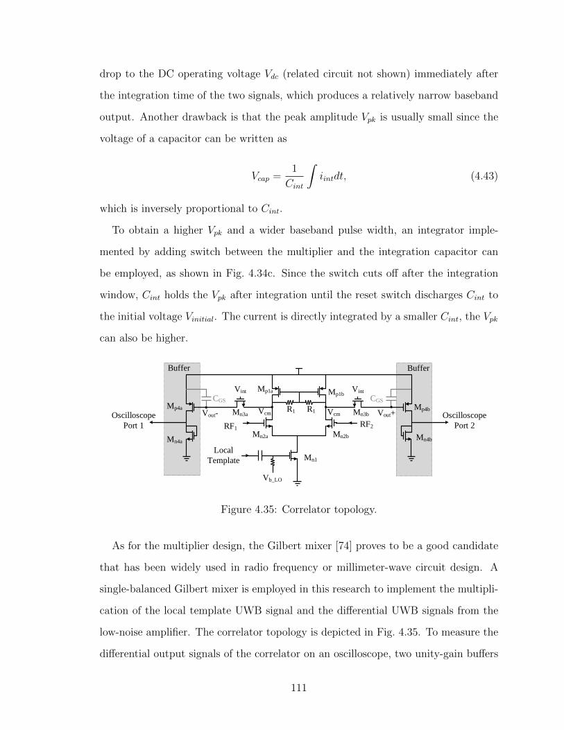
drop to the DC operating voltage Vdc (related circuit not shown) immediately after
the integration time of the two signals, which produces a relatively narrow baseband
output. Another drawback is that the peak amplitude Vpk is usually small since the
voltage of a capacitor can be written as
Vcap =1
Cint
∫iintdt, (4.43)
which is inversely proportional to Cint.
To obtain a higher Vpk and a wider baseband pulse width, an integrator imple-
mented by adding switch between the multiplier and the integration capacitor can
be employed, as shown in Fig. 4.34c. Since the switch cuts off after the integration
window, Cint holds the Vpk after integration until the reset switch discharges Cint to
the initial voltage Vinitial. The current is directly integrated by a smaller Cint, the Vpk
can also be higher.
Buffer
Vint
Vb_LO
Local
Template
RF1RF2
Vint
CGS
Oscilloscope
Port 1
CGS
Oscilloscope
Port 2
Buffer
Mn1
Mn2a Mn2b
Mp1a Mp1b
R1 R1Mn3a Mn3b
Mn4bMn4a
Mp4a Mp4bVcm Vcm Vout+Vout-
Figure 4.35: Correlator topology.
As for the multiplier design, the Gilbert mixer [74] proves to be a good candidate
that has been widely used in radio frequency or millimeter-wave circuit design. A
single-balanced Gilbert mixer is employed in this research to implement the multipli-
cation of the local template UWB signal and the differential UWB signals from the
low-noise amplifier. The correlator topology is depicted in Fig. 4.35. To measure the
differential output signals of the correlator on an oscilloscope, two unity-gain buffers
111
composed of Mp4a (Mp4b) and Mn4a (Mn4b) are added after the correlator to drive the
oscilloscope. To obtain a high Vpk, the design adopts CGS of Mp4a and Mp4b as the
integration capacitors Cint with no extra capacitance added. The integration-window
signal comes from the local template generator, as described in Section 4.3. Note
that during each time when the switches (Mn3a and Mn3b) are ON, the output volt-
age (Vout) will be pulled back to the common DC voltage Vcm before the switches,
which is similar to resetting Vout to Vinitial. The reset paths can thus be eliminated,
and Vout can have a pulse width of about one period of the DLL clock signal. Since
Cint is quite small in the proposed correlator, which means that Cint can be quickly
discharged, it is critical that the integration window be no wider than the UWB
pulse duration. In the simulation, the integration window size is adjusted to be a
little narrower than the UWB pulse width for optimum performance.
4.6 UWB radar system implementation and sim-
ulation
As mentioned at the beginning of this chapter, to utilize the most of the 3.1-to-10.6-
GHz link margin without violating the FCC limitation, the pulse repetition period
of the transmitted UWB signal should be limited to about 30 ns, which is about
six times larger than the period of the DLL clock signal. Since the output clock
signal of the DLL is periodic, the trigger frequency of the transmitter is adjusted
to be 1/6 of the DLL reference frequency with a frequency divider to accommodate
the conflict. Under this condition, the detection range of the UWB receiver is also
extended to be six times longer with the same sweep resolution. The signal flow of
the UWB radar system is demonstrated in Fig. 4.36. The layout of the UWB radar
system is shown in Fig. 4.37 with an area of about 1.1 mm2. Assuming a 40-dB
loss for the transmitted UWB signal (including the gain of the antennas and the loss
introduced by signal transmission in air, cable and signal reflection) and a changing
rate of every 6×5.12 ns for the multiplexer control voltage, the simulation results
112
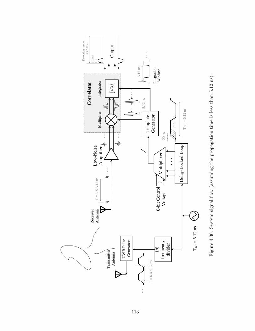
Tem
pla
te
Gen
era
tor
Mu
ltip
lex
er
. .
.
Mu
ltip
lier
Lo
w-N
ois
e
Am
pli
fier
Inte
gra
tor
Outp
ut
. . .
8-b
it C
on
tro
l
Vo
ltag
e
+ -
Co
rrel
ato
r
Dela
y-L
ock
ed
Lo
op
. .
.
Inte
gra
tio
n
Win
do
w
5.1
2 n
s
6 X
5.1
2 n
s
Det
ecti
on
ran
ge
Tre
f =
5.1
2 n
s
1/6
frequ
ency
div
ider
T =
6 X
5.1
2 n
s
. .
.
TD
LL =
5.1
2 n
s
20
ps
T =
6 X
5.1
2 n
s
. .
.
5.1
2 n
s
. . .
Tra
nsm
itte
r
An
ten
na
UW
B P
uls
e
Gen
erato
r
. .
.
. .
.
Rece
iver
An
ten
na
. . .
5.1
2 n
s
Figure
4.36:System
sign
alflow
(assumingthepropagationtimeisless
than
5.12
ns).
113

Figure 4.37: Layout of the UWB radar system.
of the local template signal and the RF1 after the LNA are shown in Fig. 4.38a.
A zoomed section of the two signals with a duration about six times of TV CDL is
shown in Fig. 4.38b. The difference of the two low-frequency output signals from the
correlator is depicted in Fig. 4.38c. As can be seen, a maximum positive pulse can be
successfully identified. The corresponding transmission time of the UWB signal thus
can be obtained, according to the control voltage of the multiplexer, to calculate the
distance between the antennas and the scatterer.
Table 4.1 summarizes the power consumption of the sub-circuits in the proposed
UWB radar system. It can be noted that the LNA consumes the most power in
the UWB receiver circuit. Although the UWB transmitter and the local template
generator utilize the same topology (with minor modifications), the latter has a higher
power consumption because of the higher trigger frequency.
114

0 200 400 600 800 1000Time (ns)
-0.9-0.6-0.3
00.30.60.9
Vol
tage
(V
)
Local template signal
0 200 400 600 800 1000Time (ns)
0.55
0.65
0.75
Vol
tage
(V
)RF
1 signal
(a)
-0.9-0.6-0.3
00.30.60.9
Vol
tage
(V
)
Local template signal
0.55
0.65
0.75
Vol
tage
(V
)
RF1 signal
(b)
0 100 200 300 400 500 600 700 800 900 1000
Time (ns)
-0.1
-0.05
0
0.05
0.1
Vol
tage
(V
)
MAX
(c)
Figure 4.38: (a) Simulated local template signal and RF1 signal (one output from thetransformer), (b) zoomed local template signal and RF1 signal with duration about6×TV CDL, (c) the difference of the output signals from the correlator.
115

Table 4.1: Power consumption summary of the sub-circuits in the proposed UWBradar system.
UWB Transmitter
UWB Radar Receiver
LNA LocalTemplateGenerator
DLL Correlator
0.3 mW 9.3 mW 0.67 mW 3.2 mW 4.2 mW∗
* Include the power consumption of the correlator 0.2 mW and buffer stage 4 mW.
In the measurement stage, calibrations have to be undertaken before applying
the radar system for breast cancer detection. First, the width τw and delay τd of
the input two consecutive trapezoidal waves have to be properly set to make sure
that the transmitted UWB signal satisfies the FCC mask. Second, the width of the
integration window has to be tuned to obtain an optimum output amplitude when
the received UWB signal aligns with the local template. Third, the difference of the
propagation time between the transmitted UWB signal and the local template has
to be compensated to ensure that the first tap of the DLL (00000000 control voltage
for the multiplexer) works at a proper distance. Finally, the range accuracy needs to
be calibrated in air by shifting the target precisely and calibrating the corresponding
measurement results.
4.7 Summary
This chapter presents the design of a UWB radar system. The UWB pulse generator
proposed in Chapter 3.1 is reused as the UWB transmitter. In the UWB receiver
design, a three-stage, single-ended to differential, UWB LNA is first described. Em-
ploying a resistive-feedback CS structure, from 3.1 to 10.6 GHz, the proposed LNA
achieves inband gain of 15.7 ± 0.6 dB for both paths, less than -10 dB S11, and 3.55
± 0.15 dB NF. The local template generator is presented next. Same structure of the
UWB transmitter (with modifications) is employed since the local template signal is
desired to obtain the same waveform as the transmitted signal. Then the DLL, which
116
is designed to generate multiple-phase signals with small step size, is introduced.
The DLL circuit contains three sub-circuits: PFD, charge pump, and VCDL. A PFD
circuit is proposed to resolve the false lock problem with an additional reset signal
at the falling edge of the reference clock. In the proposed charge pump design, the
transit current matching performance is improved by adding a capacitor, between the
gates of the sourcing and sinking current sources, to counteract the voltage jump. In
the proposed VCDL design, a 256-stage current-starved inverters chain with a 8-bit
multiplexer is employed. The step size and period of the DLL are 20 ps and 5.12 ns,
respectively, which correspond to a sweep resolution of 3 mm and single-period sweep
range of 76.8 cm in air. Finally, a single-balanced Gilbert mixer is employed as the
multiplier. With a switch-capacitor integrator, the correlator can hold the outputs
on the capacitor, which benefits the correlator with low-frequency output signals.
The system simulation results show that the UWB radar system can successfully
obtain the transmission time of the UWB signal. The single-chip UWB radar sys-
tem circuit, including the UWB transmitter and the cross-correlation receiver, was
implemented in TSMC 65-nm technology with an area of about 1.1 mm2.
117

Chapter 5
Conclusions
This dissertation has focused on the design of a fully-integrated UWB radar system
that is capable of working as a microwave imaging system for the detection of breast
tumors. Through the development of the proposed UWB imaging system, several
contributions have been made by introducing advanced circuit-level techniques to
enhance the performance of the UWB radars, as detailed in Section 5.1. The future
steps for completing the design of the proposed UWB imaging systems are listed in
Section 5.2.
5.1 Summary of Contributions
In Chapter 2, commonly used topologies of UWB pulse generators (transmitters)
and UWB receivers in CMOS technology are described and discussed. For a pulse
radar system with a specific working range, the SNR at the receiver antenna can be
enhanced by increasing the transmitted power. To achieve better performance, the
UWB transmitter designs focused on high output power and low complexity. Among
the commonly used methods of UWB signal detection, cross-correlation detection was
chosen as the receiver topology due to its immunity to interference, low complexity,
and high resolution.
As CMOS technology advances towards nano-scale dimensions pursuing higher
transit frequencies and lower power consumption in digital circuits by reducing the
118

supply voltage, designing UWB pulse generators that achieve high output amplitude
becomes more challenging. Chapter 3 presents two single-chip, high-voltage UWB
pulse generator designs in 65-nm CMOS technology.
In the first design [75], the UWB signal is synthesized with two consecutive trape-
zoidal waves using digital circuitry so that it produces spectral notches at the desired
lower and higher frequencies. To drive a 50-Ω load, the signal is fed to an inductor-
loaded power amplifier, which boosts the amplitude of the signal beyond the supply
voltage while preserving the spectral features of the generated signal. Then the am-
plified signal is passed through a simple output network, which requires only four
passive components including the load inductor. The simple output network does not
attenuate the UWB signal noticeably as opposed to the high-order filters required in
the conventional designs. The proposed UWB pulse generator achieved a peak-to-
peak amplitude of 2.12 V, which is 212% of the supply voltage. It was reused in the
design of the UWB radar system for breast cancer detection.
In the second design [76], the passive amplification technique is extended from the
narrowband to the wideband case demonstrating that a wideband signal still can be
passively amplified, although with a smaller gain than the case of a narrowband signal.
In the proposed UWB pulse generator design, a trapezoidal waveform is used as the
input to the switch-mode power amplifier to produce the desired spectral notch in
the output spectrum. A passive amplification network, including the finite inductor
load, is designed to achieve impedance matching when the MOSFET of the power
amplifier is both ON and OFF. However, a tradeoff has to be made to balance the
matching performance at the two states. The proposed pulse generator achieved a
249% pulse peak-to-peak amplitude to supply voltage ratio; the highest among UWB
pulse generators reported in the literature to the date of this publication.
Chapter 4 presents the design of a fully integrated cross-correlation UWB receiver
in CMOS technology. The receiver is comprised of an ultra-wideband LNA, a lo-
cal template UWB signal generator, a DLL (composed of PFD, charge pump, and
119

VCDL), and a cross-correlator (including a multiplier and an integrator). The de-
signed LNA achieves a wide bandwidth of 3.1-10.6 GHz, low NF, and a high and flat
inband gain. The local template generator is designed to generate a UWB signal the
same as the transmitted one. The PFD design is focused on solving the false lock
problem while the charge pump provides better matching between the sourcing and
sinking currents. The VCDL is designed to generate multiple signals with a small
step size and large period. The correlator design is focused on high output ampli-
tude and low output frequency. Since the sweep resolution of the cross-correlation
receiver is directly related to the time step of shifting the local template signal, an
inverter-chain VCDL is adopted in the delay-locked loop design to provide a step size
of 20 ps and a period of 5.12 ns. The same UWB transmitter topology (with minor
modifications) is employed in the local template generator to produce a replica of
the transmitted signal. To achieve better performance, the UWB receiver adopts a
differential structure. A transformer is employed in the design of the LNA to convert
the received single-ended UWB signal to differential signals. Single-balanced Gilbert
mixer and switch-capacitor integrator are utilized to cross-correlate the received UWB
signal with the local template. The UWB receiver is designed and integrated with the
transmitter circuit into a single chip occupying an area of 1.1 mm2. The simulation
results demonstrate that the UWB radar system can successfully identify the signal
transmission time from the low-frequency output signals.
5.2 Future Work
The research has been focused on implementing the radar circuit part of the UWB
imaging system. The other two parts, including the antenna array design and the
image-reconstruction algorithm, are the next steps to work on.
In the design of the UWB radar circuitry, the antenna has been assumed to be
an ideal 50-Ω resistor. However, in practice the impedance of a wideband antenna
changes with frequency. The varying resistance and reactance of the antenna have
120

to be considered in the system design to obtain optimum performance. Antenna-
and-circuit co-simulation will be needed to accommodate the antenna impedance and
other uncertainties introduced by the components outside the chip, such as PCB
board losses and parasitics.
The functionality of a simple UWB radar system, which includes the radar in-
tegrated circuit, the co-designed single antenna pair, and the image-reconstruction
algorithm, will first be verified. The simple radar system will then be applied to im-
age a breast model with an array of antenna pairs working as the UWB radar imaging
system. The breast model will be constructed using a material with dielectric prop-
erties similar to fatty breast tissue. A sphere-shaped object with dielectric constant
several times larger than the surrounding material, simulating a tumor, will be in-
serted in the breast model. The proposed imaging system will be used to reconstruct
the image of the breast model to verify its functionality. Assuming the imaging of
the breast model is a success, further plans will be laid out for clinical trials for UWB
imaging of the human breast.
121

Bibliography
[1] F. Bray, J. Ferlay, I. Soerjomataram, R. L. Siegel, L. A. Torre, and A. Jemal,“Global cancer statistics 2018: GLOBOCAN estimates of incidence and mor-tality worldwide for 36 cancers in 185 countries,” CA: A Cancer Journal forClinicians, vol. 68, no. 6, pp. 394–424, 2018.
[2] D. R. Brenner, H. K. Weir, A. A. Demers, L. F. Ellison, C. Louzado, A. Shaw,D. Turner, R. R. Woods, and L. M. Smith, “Projected estimates of cancer inCanada in 2020,” Cmaj, vol. 192, no. 9, E199–E205, 2020.
[3] C. Allemani, T. Matsuda, V. Di Carlo, R. Harewood, M. Matz, M. Niksic, A.Bonaventure, M. Valkov, C. J. Johnson, J. Esteve, et al., “Global surveillance oftrends in cancer survival 2000–14 (CONCORD-3): analysis of individual recordsfor 37 513 025 patients diagnosed with one of 18 cancers from 322 population-based registries in 71 countries,” The Lancet, vol. 391, no. 10125, pp. 1023–1075,2018.
[4] L. L. Humphrey, M. Helfand, B. K. Chan, and S. H. Woolf, “Breast cancerscreening: a summary of the evidence for the US Preventive Services TaskForce,” Annals of Internal Medicine, vol. 137, no. 5 Part 1, pp. 347–360, 2002.
[5] A. L. Siu, “Screening for breast cancer: US Preventive Services Task Force rec-ommendation statement,” Annals of Internal Medicine, vol. 164, no. 4, pp. 279–296, 2016.
[6] S. Gabriel, R. Lau, and C. Gabriel, “The dielectric properties of biologicaltissues: II. Measurements in the frequency range 10 Hz to 20 GHz,” Physics inMedicine & Biology, vol. 41, no. 11, p. 2251, 1996.
[7] A. J. Surowiec, S. S. Stuchly, J. R. Barr, and A. Swarup, “Dielectric proper-ties of breast carcinoma and the surrounding tissues,” IEEE Transactions onBiomedical Engineering, vol. 35, no. 4, pp. 257–263, 1988.
[8] W. T. Joines, Y. Zhang, C. Li, and R. L. Jirtle, “The measured electrical prop-erties of normal and malignant human tissues from 50 to 900 MHz,” MedicalPhysics, vol. 21, no. 4, pp. 547–550, 1994.
[9] A. Campbell and D. Land, “Dielectric properties of female human breast tissuemeasured in vitro at 3.2 GHz,” Physics in Medicine & Biology, vol. 37, no. 1,p. 193, 1992.
122
[10] A. Martellosio, M. Pasian, M. Bozzi, L. Perregrini, A. Mazzanti, F. Svelto, P. E.Summers, G. Renne, L. Preda, and M. Bellomi, “Dielectric properties charac-terization from 0.5 to 50 GHz of breast cancer tissues,” IEEE Transactions onMicrowave Theory and Techniques, vol. 65, no. 3, pp. 998–1011, 2016.
[11] E. C. Fear and M. A. Stuchly, “Microwave system for breast tumor detection,”IEEE Microwave and Guided Wave Letters, vol. 9, no. 11, pp. 470–472, 1999.
[12] X. Li and S. C. Hagness, “A confocal microwave imaging algorithm for breastcancer detection,” IEEE Microwave and Wireless Components Letters, vol. 11,no. 3, pp. 130–132, 2001.
[13] E. C. Fear, X. Li, S. C. Hagness, and M. A. Stuchly, “Confocal microwaveimaging for breast cancer detection: Localization of tumors in three dimen-sions,” IEEE Transactions on Biomedical Engineering, vol. 49, no. 8, pp. 812–822, 2002.
[14] A. E. Souvorov, A. E. Bulyshev, S. Y. Semenov, R. H. Svenson, A. G. Nazarov,Y. E. Sizov, and G. P. Tatsis, “Microwave tomography: A two-dimensionalNewton iterative scheme,” IEEE Transactions on Microwave Theory and Tech-niques, vol. 46, no. 11, pp. 1654–1659, 1998.
[15] T. M. Grzegorczyk, P. M. Meaney, P. A. Kaufman, K. D. Paulsen, et al., “Fast3-D tomographic microwave imaging for breast cancer detection,” IEEE Trans-actions on Medical Imaging, vol. 31, no. 8, pp. 1584–1592, 2012.
[16] M. Klemm, J. A. Leendertz, D. Gibbins, I. J. Craddock, A. Preece, and R. Ben-jamin, “Microwave radar-based differential breast cancer imaging: Imaging inhomogeneous breast phantoms and low contrast scenarios,” IEEE Transactionson Antennas and Propagation, vol. 58, no. 7, pp. 2337–2344, 2010.
[17] T Henriksson, M Klemm, D Gibbins, J Leendertz, T Horseman, A. Preece, RBenjamin, and I. Craddock, “Clinical trials of a multistatic UWB radar forbreast imaging,” in 2011 Loughborough Antennas & Propagation Conference,IEEE, 2011, pp. 1–4.
[18] M. Bassi, M. Caruso, M. S. Khan, A. Bevilacqua, A.-D. Capobianco, and A. Ne-viani, “An integrated microwave imaging radar with planar antennas for breastcancer detection,” IEEE Transactions on Microwave Theory and Techniques,vol. 61, no. 5, pp. 2108–2118, 2013.
[19] J. Lee, S. Gweon, K. Lee, S. Um, K.-R. Lee, K. Kim, J. Lee, and H.-J. Yoo,“A 9.6 mW/Ch 10 MHz Wide-bandwidth Electrical Impedance TomographyIC with Accurate Phase Compensation for Breast Cancer Detection,” in 2020IEEE Custom Integrated Circuits Conference (CICC), IEEE, 2020, pp. 1–4.
[20] H. F. Harmuth, “Applications of Walsh functions in communications,” IEEESpectrum, vol. 6, no. 11, pp. 82–91, 1969.
[21] G. F. Ross, “The transient analysis of certain TEM mode four-port networks,”IEEE Transactions on Microwave Theory and Techniques, vol. 14, no. 11, pp. 528–542, 1966.
123

[22] D. Washington, “First report and order revision of Part 15 of the commission’srule regarding ultra-wideband transmission system FCC 02-48,” Federal Com-munications Commission, 2002.
[23] D. A. Bell, Information theory and its engineering applications. Pitman Pub-lishing, 1968.
[24] Y. Y. Ruai, Y. Konishi, S. T. Allen, M. Reddy, and M. J. Rodwell, “A traveling-wave resonant tunnel diode pulse generator,” IEEE Microwave and GuidedWave Letters, vol. 4, no. 7, pp. 220–222, 1994.
[25] J. Han and C. Nguyen, “A new ultra-wideband, ultra-short monocycle pulsegenerator with reduced ringing,” IEEE Microwave and Wireless ComponentsLetters, vol. 12, no. 6, pp. 206–208, 2002.
[26] M. J. Rodwell, M. Kamegawa, R. Yu, M. Case, E. Carman, and K. S. Gi-boney, “GaAs nonlinear transmission lines for picosecond pulse generation andmillimeter-wave sampling,” IEEE Transactions on Microwave Theory and Tech-niques, vol. 39, no. 7, pp. 1194–1204, 1991.
[27] N. Joachimowicz, C. Pichot, and J.-P. Hugonin, “Inverse scattering: An iter-ative numerical method for electromagnetic imaging,” IEEE Transactions onAntennas and Propagation, vol. 39, no. 12, pp. 1742–1753, 1991.
[28] P. Kosmas and C. M. Rappaport, “Time reversal with the FDTD method formicrowave breast cancer detection,” IEEE Transactions on Microwave Theoryand Techniques, vol. 53, no. 7, pp. 2317–2323, 2005.
[29] T. Rubæk, P. M. Meaney, P. Meincke, and K. D. Paulsen, “Nonlinear mi-crowave imaging for breast-cancer screening using Gauss–Newton’s method andthe CGLS inversion algorithm,” IEEE Transactions on Antennas and Propaga-tion, vol. 55, no. 8, pp. 2320–2331, 2007.
[30] S. C. Hagness, A. Taflove, and J. E. Bridges, “Two-dimensional FDTD analysisof a pulsed microwave confocal system for breast cancer detection: Fixed-focusand antenna-array sensors,” IEEE Transactions on Biomedical Engineering,vol. 45, no. 12, pp. 1470–1479, 1998.
[31] H. Song, H. Kono, Y. Seo, A. Azhari, J. Somei, E. Suematsu, Y. Watarai, T.Ota, H. Watanabe, Y. Hiramatsu, et al., “A radar-based breast cancer detectionsystem using CMOS integrated circuits,” IEEE Access, vol. 3, pp. 2111–2121,2015.
[32] ITU-R SM.1755-0, “Characteristics of ultra-wideband technology,” 2006.
[33] A. Batra, J. Balakrishnan, G. R. Aiello, J. R. Foerster, and A. Dabak, “Designof a multiband OFDM system for realistic UWB channel environments,” IEEETransactions on Microwave theory and techniques, vol. 52, no. 9, pp. 2123–2138,2004.
[34] H. Kim, D Park, and Y Joo, “All-digital low-power CMOS pulse generator forUWB system,” Electronics Letters, vol. 40, no. 24, pp. 1534–1535, 2004.
124
[35] M. Reja, Z Hameed, K Moez, and S Shamsadini, “Compact CMOS IR-UWBtransmitter using variable-order Gaussian pulse generator,” Electronics Letters,vol. 49, no. 16, pp. 1038–1040, 2013.
[36] S. Bourdel, Y. Bachelet, J. Gaubert, R. Vauche, O. Fourquin, N. Dehaese, andH. Barthelemy, “A 9-pJ/pulse 1.42-Vpp OOK CMOS UWB pulse generator forthe 3.1–10.6-GHz FCC band,” IEEE Transactions on Microwave Theory andTechniques, vol. 58, no. 1, pp. 65–73, 2010.
[37] T. Norimatsu, R. Fujiwara, M. Kokubo, M. Miyazaki, A. Maeki, Y. Ogata, S.Kobayashi, N. Koshizuka, and K. Sakamura, “A UWB-IR transmitter with dig-itally controlled pulse generator,” IEEE Journal of Solid-State Circuits, vol. 42,no. 6, pp. 1300–1309, 2007.
[38] G. de Streel, F. Stas, T. Gurne, F. Durant, C. Frenkel, A. Cathelin, and D. Bol,“SleepTalker: A ULV 802.15. 4a IR-UWB transmitter SoC in 28-nm FDSOIachieving 14 pJ/b at 27 Mb/s with channel selection based on adaptive FBB anddigitally programmable pulse shaping,” IEEE Journal of Solid-State Circuits,vol. 52, no. 4, pp. 1163–1177, 2017.
[39] N. Andersen, K. Granhaug, J. A. Michaelsen, S. Bagga, H. A. Hjortland, M. R.Knutsen, T. S. Lande, and D. T. Wisland, “A 118-mW pulse-based radar SoCin 55-nm CMOS for non-contact human vital signs detection,” IEEE Journalof Solid-State Circuits, vol. 52, no. 12, pp. 3421–3433, 2017.
[40] V. V. Kulkarni, M. Muqsith, K. Niitsu, H. Ishikuro, and T. Kuroda, “A 750Mb/s, 12 pJ/b, 6-to-10 GHz CMOS IR-UWB transmitter with embedded on-chip antenna,” IEEE Journal of Solid-State Circuits, vol. 44, no. 2, pp. 394–403,2009.
[41] N.-S. Kim and J. M. Rabaey, “A high data-rate energy-efficient triple-channelUWB-based cognitive radio,” IEEE Journal of Solid-State Circuits, vol. 51,no. 4, pp. 809–820, 2016.
[42] Y. Ying, X. Bai, and F. Lin, “A 1-Gb/s 6–10-GHz, Filterless, Pulsed UWBTransmitter With Symmetrical Waveform Analysis and Generation,” IEEETransactions on Very Large Scale Integration (VLSI) Systems, vol. 26, no. 6,pp. 1171–1182, 2018.
[43] M. J. Zhao, B. Li, and Z. H. Wu, “20-pJ/pulse 250 Mbps low-complexity CMOSUWB transmitter for 3–5 GHz applications,” IEEE Microwave and WirelessComponents Letters, vol. 23, no. 3, pp. 158–160, 2013.
[44] S. Sim, D.-W. Kim, and S. Hong, “A CMOS UWB pulse generator for 6–10 GHzapplications,” IEEE Microwave and Wireless Components Letters, vol. 19, no. 2,pp. 83–85, 2009.
[45] R. Dong, H. Kanaya, and R. K. Pokharel, “A CMOS Ultrawideband Pulse Gen-erator for 3–5 GHz Applications,” IEEE Microwave and Wireless ComponentsLetters, vol. 27, no. 6, pp. 584–586, 2017.
125

[46] H. T. Friis, “A note on a simple transmission formula,” Proceedings of the IRE,vol. 34, no. 5, pp. 254–256, 1946.
[47] H. Yuan, X. Hu, and Y. Ling, “New symbol synchronization algorithms forOFDM systems based on IEEE 802.11 a,” in 2008 6th IEEE International Con-ference on Industrial Informatics, IEEE, 2008, pp. 186–191.
[48] M. Lee, S. Beck, K. Lim, and J. Laskar, “Analog auto-correlation based receiverarchitecture for radar systems,” in 2010-Milcom 2010 Military CommunicationsConference, IEEE, 2010, pp. 842–845.
[49] C. E. Shannon, “Communication in the presence of noise,” Proceedings of theIRE, vol. 37, no. 1, pp. 10–21, 1949.
[50] R. Thai-Singama, F. Du-Burck, and M. Piette, “Demonstration of a low-costultrawideband transmitter in the 3.1–10.6-GHz band,” IEEE Transactions onCircuits and Systems II: Express Briefs, vol. 59, no. 7, pp. 389–393, 2012.
[51] C. Hu, Modern Semiconductor Devices for Integrated Circuits. Prentice HallUpper Saddle River, NJ, 2010, vol. 2.
[52] K. F. Schuegraf and C. Hu, “Reliability of thin SiO2,” Semiconductor Scienceand Technology, vol. 9, no. 5, p. 989, 1994.
[53] M. Shen, Y.-Z. Yin, H. Jiang, T. Tian, O. K. Jensen, and J. H. Mikkelsen,“A 0.76-pJ/pulse 0.1–1 Gpps microwatt IR-UWB CMOS pulse generator withadaptive PSD control using a limited monocycle precharge technique,” IEEETransactions on Circuits and Systems II: Express Briefs, vol. 62, no. 8, pp. 806–810, 2015.
[54] F. Zito, D. Pepe, and D. Zito, “UWB CMOS monocycle pulse generator,”IEEE Transactions on Circuits and Systems I: Regular Papers, vol. 57, no. 10,pp. 2654–2664, 2010.
[55] B. Razavi and R. Behzad, RF microelectronics. Prentice Hall New York, 2012,vol. 2.
[56] R. M. Fano, “Theoretical limitations on the broadband matching of arbitraryimpedances,” Journal of the Franklin Institute, vol. 249, no. 1, pp. 57–83, 1950.
[57] C. Yoo and Q. Huang, “A common-gate switched 0.9-W class-E power ampli-fier with 41% PAE in 0.25-µm CMOS,” IEEE Journal of Solid-State Circuits,vol. 36, no. 5, pp. 823–830, 2001.
[58] T. Matic, L. Sneler, and M. Herceg, “An Energy Efficient Multi-User Asyn-chronous Wireless Transmitter for Biomedical Signal Acquisition,” IEEE Trans-actions on Biomedical Circuits and Systems, vol. 13, no. 4, pp. 619–630, 2019.
[59] K. Ture, A. Devos, F. Maloberti, and C. Dehollain, “Area and power efficientultra-wideband transmitter based on active inductor,” IEEE Transactions onCircuits and Systems II: Express Briefs, vol. 65, no. 10, pp. 1325–1329, 2018.
126
[60] Z. Zhang, Y. Li, G. Wang, and Y. Lian, “The Design of an Energy-Efficient IR-UWB Transmitter With Wide-Output Swing and Sub-Microwatt Leakage Cur-rent,” IEEE Transactions on Circuits and Systems II: Express Briefs, vol. 65,no. 10, pp. 1485–1489, 2018.
[61] K. Na, H. Jang, H. Ma, Y. Choi, and F. Bien, “A 200-Mb/s data rate 3.1–4.8-GHz IR-UWB all-digital pulse generator with DB-BPSK modulation,” IEEETransactions on Circuits and Systems II: Express Briefs, vol. 62, no. 12, pp. 1184–1188, 2015.
[62] X. An, J. Wagner, and F. Ellinger, “An Efficient Ultrawideband Pulse Transmit-ter With Automatic On-Off Functionality for Primary Radar Systems,” IEEEMicrowave and Wireless Components Letters, 2020.
[63] H. T. Friis, “Noise figures of radio receivers,” Proceedings of the IRE, vol. 32,no. 7, pp. 419–422, 1944.
[64] J. R. Long, “Monolithic transformers for silicon RF IC design,” IEEE Journalof Solid-State Circuits, vol. 35, no. 9, pp. 1368–1382, 2000.
[65] A. Zolfaghari, A. Chan, and B. Razavi, “Stacked inductors and transformersin CMOS technology,” IEEE Journal of Solid-State Circuits, vol. 36, no. 4,pp. 620–628, 2001.
[66] G.-Y. Tak, S.-B. Hyun, T. Y. Kang, B. G. Choi, and S. S. Park, “A 6.3-9-GHzCMOS fast settling PLL for MB-OFDM UWB applications,” IEEE Journal ofSolid-State Circuits, vol. 40, no. 8, pp. 1671–1679, 2005.
[67] W.-H. Chen, M. E. Inerowicz, and B. Jung, “Phase frequency detector withminimal blind zone for fast frequency acquisition,” IEEE Transactions on Cir-cuits and Systems II: Express Briefs, vol. 57, no. 12, pp. 936–940, 2010.
[68] J. G. Maneatis, “Low-jitter process-independent DLL and PLL based on self-biased techniques,” IEEE Journal of Solid-state Circuits, vol. 31, no. 11, pp. 1723–1732, 1996.
[69] O.-C. Chen and R.-B. Sheen, “A power-efficient wide-range phase-locked loop,”IEEE Journal of Solid-State Circuits, vol. 37, no. 1, pp. 51–62, 2002.
[70] S. L. Gierkink, “Low-spur, low-phase-noise clock multiplier based on a combi-nation of PLL and recirculating DLL with dual-pulse ring oscillator and self-correcting charge pump,” IEEE Journal of Solid-state Circuits, vol. 43, no. 12,pp. 2967–2976, 2008.
[71] J.-S. Lee, M.-S. Keel, S.-I. Lim, and S. Kim, “Charge pump with perfect currentmatching characteristics in phase-locked loops,” Electronics Letters, vol. 36,no. 23, pp. 1907–1908, 2000.
[72] A. Homayoun and B. Razavi, “Relation between delay line phase noise and ringoscillator phase noise,” IEEE Journal of Solid-State Circuits, vol. 49, no. 2,pp. 384–391, 2013.
127
[73] M.-J. Lee, W. J. Dally, T. Greer, H.-T. Ng, R. Farjad-Rad, J. Poulton, andR. Senthinathan, “Jitter transfer characteristics of delay-locked loops-theoriesand design techniques,” IEEE Journal of Solid-State Circuits, vol. 38, no. 4,pp. 614–621, 2003.
[74] B. Gilbert, “A precise four-quadrant multiplier with subnanosecond response,”IEEE Journal of Solid-State Circuits, vol. 3, no. 4, pp. 365–373, 1968.
[75] S. Gao and K. Moez, “A 2.12-V Vpp 11.67-pJ/pulse Fully Integrated UWBPulse Generator in 65-nm CMOS Technology,” IEEE Transactions on Circuitsand Systems I: Regular Papers, vol. 67, no. 3, pp. 1058–1068, 2019.
[76] S. Gao and K. Moez, “A High-Voltage UWB Pulse Generator Using PassiveAmplification in 65-nm CMOS,” IEEE Transactions on Circuits and SystemsI: Regular Papers, vol. 67, no. 12, pp. 5530–5539, 2020.
128