OFDM Ultra Wideband Transceiver System 2013
284
Universidad Politécnica de Madrid Departamento de Automática, Ingeniería Electrónica e Informática Industrial Escuela Técnica Superior de Ingenieros Industriales Centro de Electrónica Industrial Design and Validation of an Optimized MB- OFDM Ultra Wideband Transceiver System Autor: Guixuan Liang Máster en Ingeniería en Diseño de Circuitos Integrados por la Hong Kong University of Science and Technology Directores: Teresa Riesgo Alcaide Doctora Ingeniera Industrial por la Universidad Politécnica de Madrid Jorge Portilla Berrueco Doctor en Ingeniería Electrónica por la Universidad Politécnica de Madrid 2013
-
Upload
khangminh22 -
Category
Documents
-
view
3 -
download
0
Transcript of OFDM Ultra Wideband Transceiver System 2013

Universidad Politécnica de Madrid
Departamento de Automática, Ingeniería
Electrónica e Informática Industrial
Escuela Técnica Superior de Ingenieros Industriales
Centro de Electrónica Industrial
Design and Validation of an Optimized MB-OFDM Ultra Wideband Transceiver System
Autor: Guixuan Liang
Máster en Ingeniería en Diseño de Circuitos Integrados por la Hong Kong University of Science and Technology
Directores: Teresa Riesgo Alcaide Doctora Ingeniera Industrial por la
Universidad Politécnica de Madrid Jorge Portilla Berrueco Doctor en Ingeniería Electrónica por la
Universidad Politécnica de Madrid
2013


Summary
In recent years, the Wireless Visual Sensor Network (WVSN) has drawn great interest
in wireless communication research area. They enable a wealth of new applications
such as building security control, image sensing, and target localization. However,
nowadays wireless communication protocols (ZigBee, Wi-Fi, and Bluetooth for
example) cannot fully satisfy the demands of high data rate, low power consumption,
short range, and high robustness requirements. New communication protocol is highly
desired for such kind of applications. The Ultra Wideband (UWB) wireless
communication protocol, which has increased in importance for high data rate wireless
communication field, are emerging as an important topic for WVSN research.
UWB has emerged as a technology that offers great promise to satisfy the growing
demand for low-cost, high-speed digital wireless indoor and home networks. The large
bandwidth available, the potential for high data rate transmission, and the potential for
low complexity and low power consumption, along with low implementation cost, all
present a unique opportunity for UWB to become a widely adopted radio solution for
future Wireless Personal Area Network (WPAN) applications.
UWB is defined as any transmission that occupies a bandwidth of more than 20% of its
center frequency, or more than 500 MHz. In 2002, the Federal Communications
Commission (FCC) has mandated that UWB radio transmission can legally operate in
the range from 3.1 to 10.6 GHz at a transmitter power of -41.3 dBm/Hz. Under the
FCC guidelines, the use of UWB technology can provide enormous capacity over short
communication ranges. Considering Shannon’s capacity equations, increasing the
channel capacity requires linear increasing in bandwidth, whereas similar channel
capacity increases would require exponential increases in transmission power. In
recent years, several different UWB developments has been widely studied in different
area, among which, the MB-OFDM UWB wireless communication protocol is
considered to be the leading choice and has recently been adopted in the ISO/IEC
standard for WPANs.
By combing the OFDM modulation and data transmission using frequency hopping
techniques, the MB-OFDM UWB system is able to support various data rates, ranging
from 55 to 480 Mbps, over distances up to 10 meters. The MB-OFDM technology is
expected to consume very little power and silicon area, as well as provide low-cost
solutions that can satisfy consumer market demands.
To fulfill these expectations, MB-OFDM UWB research and development have to cope
with several challenges, which consist of high-sensitivity synchronization, low-
complexity constraints, strict power limitations, scalability, and flexibility. Such
challenges require state-of-the-art digital signal processing expertise to develop
systems that could fully take advantages of the UWB spectrum and support future
indoor wireless applications.
This thesis focuses on fully optimization for the MB-OFDM UWB digital baseband
transceiver system, aiming at researching and designing a wireless communication
subsystem for the Wireless Visual Sensor Networks (WVSNs) application. The inherent
high complexity of the FFT/IFFT processor and synchronization system, and high
operation frequency for all processing elements, becomes the bottleneck for low power
MB-OFDM based UWB digital baseband system hardware design and implementation.
The proposed transceiver system targets low power and low complexity under the
premise of high performance. Optimizations are made at both algorithm and
architecture level for each element of the transceiver system. The low-power hardware-
efficient structures are firstly proposed for those core computation modules, i.e., the
mixed-radix algorithm based pipelined architecture is proposed for the Fast Fourier
Transform (FFT/IFFT) processor, and the cost-speed balanced Viterbi Decoder (VD)
module is developed, in the aim of lowering the power consumption and increasing
the processing speed. In addition, a low complexity sign-bit correlation based symbol
timing synchronization scheme is presented so as to detect and synchronize the OFDM
packets robustly and accurately. Moreover, several state-of-the-art technologies are
used for developing other processing subsystems and an entire MB-OFDM digital
baseband transceiver system is integrated.
The target device for the proposed transceiver system is Xilinx Virtex 5 XC5VLX110T
FPGA board. In order to validate the proposed transceiver system in the FPGA board,
a unified algorithm-architecture-circuit hardware/software co-design environment for
complex FPGA system development is presented in this work. The main objective of
the proposed strategy is to find an efficient methodology for designing a configurable
optimized FPGA system by using as few efforts as possible in system verification
procedure, so as to speed up the system development period. The presented co-design
methodology has the advantages of easy to use, covering all steps from algorithm
proposal to hardware verification, and widely spread for almost all kinds of FPGA
developments.
Because only the digital baseband transceiver system is developed in this thesis, the
validation of transmitting signals through wireless channel in real communication
environments still requires the analog front-end and RF components. However, by
using the aforementioned hardware/software co-simulation methodology, the
transmitter and receiver digital baseband systems get the opportunity to communicate
with each other through the channel models, which are proposed from the IEEE

802.15.3a research group, established in MATLAB. Thus, by simply adjust the
characteristics of each channel model, e.g. mean excess delay and center frequency, we
can estimate the transmission performance of the proposed transceiver system through
different communication situations.
The main contributions of this thesis are:
A novel mixed radix 128-point FFT algorithm by using multipath pipelined architecture is proposed. The complex multipliers for each processing stage are designed by using modified shift-add architectures. The system word-length and twiddle word-length are compared and selected based on Signal to Quantization Noise Ratio (SQNR) and power analysis.
IFFT processor performance is analyzed under different Block Floating Point (BFP) arithmetic situations for overflow control, so as to find out the perfect architecture of IFFT algorithm based on the proposed FFT processor.
An innovative low complex timing synchronization and compensation scheme, which consists of Packet Detector (PD) and Timing Offset Estimation (TOE) functions, for MB-OFDM UWB receiver system is employed. By simplifying the cross-correlation and maximum likelihood functions to sign-bit only, the computational complexity is significantly reduced.
A 64 state soft-decision Viterbi Decoder system by using high speed radix-4 Add-Compare-Select architecture is proposed. Two-pointer Even algorithm is also introduced into the Trace Back unit in the aim of hardware-efficiency.
Several state-of-the-art technologies are integrated into the complete baseband transceiver system, in the aim of implementing a highly-optimized UWB communication system.
An improved design flow is proposed for complex system implementation which can be used for general Field-Programmable Gate Array (FPGA) designs. The design method not only dramatically reduces the time for functional verification, but also provides automatic analysis such as errors and output delays for the implemented hardware systems.
A virtual communication environment is established for validating the proposed MB-OFDM transceiver system. This methodology is proved to be easy for usage and convenient for analyzing the digital baseband system without analog frontend under different communication environments.
This PhD thesis is organized in six chapters. In the chapter 1 a brief introduction to the
UWB field, as well as the related work, is done, along with the motivation of MB-
OFDM system development. In the chapter 2, the general information and requirement
of MB-OFDM UWB wireless communication protocol is presented. In the chapter 3, the
architecture of the MB-OFDM digital baseband transceiver system is presented. The
design of the proposed algorithm and architecture for each processing element is
detailed in this chapter. Design challenges of such system involve trade-off discussions
among design complexity, power consumption, hardware cost, system performance,
and some other aspects. All these factors are analyzed and discussed. In the chapter 4,
the hardware/software co-design methodology is proposed. Each step of this design
flow will be detailed by taking some examples that we met during system
development. Then, taking advantages of this design strategy, the Virtual
Communication procedure is carried out so as to test and analyze the proposed
transceiver architecture. Experimental results from the co-simulation and synthesis
report of the implemented FPGA system are given in the chapter 5. The chapter 6
includes conclusions and future work, as well as the results derived from this PhD
work.

Resumen
Esta tesis está incluida dentro del campo del campo de Multiband Orthogonal
Frequency Division Multiplexing Ultra Wideband (MB-OFDM UWB), el cual ha
adquirido una gran importancia en las comunicaciones inalámbricas de alta tasa de
datos en la última década.
UWB surgió con el objetivo de satisfacer la creciente demanda de conexiones
inalámbricas en interiores y de uso doméstico, con bajo coste y alta velocidad. La
disponibilidad de un ancho de banda grande, el potencial para alta velocidad de
transmisión, baja complejidad y bajo consumo de energía, unido al bajo coste de
implementación, representa una oportunidad única para que UWB se convierta en una
solución ampliamente utilizada en aplicaciones de Wireless Personal Area Network
(WPAN).
UWB está definido como cualquier transmisión que ocupa un ancho de banda de más
de 20% de su frecuencia central, o más de 500 MHz. En 2002, la Comisión Federal de
Comunicaciones (FCC) definió que el rango de frecuencias de transmisión de UWB
legal es de 3.1 a 10.6 GHz, con una energía de transmisión de -41.3 dBm/Hz. Bajo las
directrices de FCC, el uso de la tecnología UWB puede aportar una enorme capacidad
en las comunicaciones de corto alcance. Considerando las ecuaciones de capacidad de
Shannon, incrementar la capacidad del canal requiere un incremento lineal en el ancho
de banda, mientras que un aumento similar de la capacidad de canal requiere un
aumento exponencial en la energía de transmisión. En los últimos años, s diferentes
desarrollos del UWB han sido extensamente estudiados en diferentes áreas, entre los
cuales, el protocolo de comunicaciones inalámbricas MB-OFDM UWB está considerado
como la mejor elección y ha sido adoptado como estándar ISO/IEC para los WPANs.
Combinando la modulación OFDM y la transmisión de datos utilizando las técnicas de
salto de frecuencia, el sistema MB-OFDM UWB es capaz de soportar tasas de datos con
que pueden variar de los 55 a los 480 Mbps, alcanzando una distancia máxima de hasta
10 metros. Se esperara que la tecnología MB-OFDM tenga un consumo energético muy
bajo copando un are muy reducida en silicio, proporcionando soluciones de bajo coste
que satisfagan las demandas del mercado.
Para cumplir con todas estas expectativas, el desarrollo y la investigación del MB-
OFDM UWB deben enfrentarse a varios retos, como son la sincronización de alta
sensibilidad, las restricciones de baja complejidad, las estrictas limitaciones energéticas,
la escalabilidad y la flexibilidad. Tales retos requieren un procesamiento digital de la
señal de última generación, capaz de desarrollar sistemas que puedan aprovechar por

completo las ventajas del espectro UWB y proporcionar futuras aplicaciones
inalámbricas en interiores.
Esta tesis se centra en la completa optimización de un sistema de transceptor de banda
base MB-OFDM UWB digital, cuyo objetivo es investigar y diseñar un subsistema de
comunicación inalámbrica para la aplicación de las Redes de Sensores Inalámbricas
Visuales. La complejidad inherente de los procesadores FFT/IFFT y el sistema de
sincronización así como la alta frecuencia de operación para todos los elementos de
procesamiento, se convierten en el cuello de la botella para el diseño y la
implementación del sistema de UWB digital en base de banda basado en MB-OFDM de
baja energía.
El objetivo del transceptor propuesto es conseguir baja energía y baja complejidad bajo
la premisa de un alto rendimiento. Las optimizaciones están realizadas tanto a nivel
algorítmico como a nivel arquitectural para todos los elementos del sistema.
Una arquitectura hardware eficiente en consumo se propone en primer lugar para
aquellos módulos correspondientes a núcleos de computación. Para el procesado de la
Transformada Rápida de Fourier (FFT/IFFT), se propone un algoritmo mixed-radix,
basado en una arquitectura con pipeline y se ha desarrollado un módulo de
Decodificador de Viterbi (VD) equilibrado en coste-velocidad con el objetivo de reducir
el consumo energético e incrementar la velocidad de procesamiento. También se ha
implementado un correlador signo-bit simple basado en la sincronización del tiempo
de símbolo es presentado. Este correlador es usado para detectar y sincronizar los
paquetes de OFDM de forma robusta y precisa.
Para el desarrollo de los subsitemas de procesamiento y realizar la integración del
sistema completo se han empleado tecnologías de última generación. El dispositivo
utilizado para el sistema propuesto es una FPGA Virtex 5 XC5VLX110T del fabricante
Xilinx. La validación el propuesta para el sistema transceptor se ha implementado en
dicha placa de FPGA. En este trabajo se presenta un algoritmo, y una arquitectura,
diseñado con filosofía de co-diseño hardware/software para el desarrollo de sistemas
de FPGA complejos. El objetivo principal de la estrategia propuesta es de encontrar
una metodología eficiente para el diseño de un sistema de FPGA configurable
optimizado con el empleo del mínimo esfuerzo posible en el sistema de procedimiento
de verificación, por tanto acelerar el periodo de desarrollo del sistema. La metodología
de co-diseño presentada tiene la ventaja de ser fácil de usar, contiene todos los pasos
desde la propuesta del algoritmo hasta la verificación del hardware, y puede ser
ampliamente extendida para casi todos los tipos de desarrollos de FPGAs.
En este trabajo se ha desarrollado sólo el sistema de transceptor digital de banda base
por lo que la comprobación de señales transmitidas a través del canal inalámbrico en

los entornos reales de comunicación sigue requiriendo componentes RF y un front-end
analógico. No obstante, utilizando la metodología de co-simulación
hardware/software citada anteriormente, es posible comunicar el sistema de
transmisor y el receptor digital utilizando los modelos de canales propuestos por IEEE
802.15.3a, implementados en MATLAB. Por tanto, simplemente ajustando las
características de cada modelo de canal, por ejemplo, un incremento del retraso y de la
frecuencia central, podemos estimar el comportamiento del sistema propuesto en
diferentes escenarios y entornos.
Las mayores contribuciones de esta tesis son:
Se ha propuesto un nuevo algoritmo 128-puntos base mixto FFT usando la
arquitectura pipeline multi-ruta. Los complejos multiplicadores para cada
etapa de procesamiento son diseñados usando la arquitectura modificada shift-
add. Los sistemas word length y twiddle word length son comparados y
seleccionados basándose en la señal para cuantización del SQNR y el análisis de
energías.
El desempeño del procesador IFFT es analizado bajo diferentes situaciones
aritméticas de bloques de punto flotante (BFP) para el control de
desbordamiento, por tanto, para encontrar la arquitectura perfecta del
algoritmo IFFT basado en el procesador FFT propuesto.
Para el sistema de receptor MB-OFDM UWB se ha empleado una
sincronización del tiempo innovadora, de baja complejidad y esquema de
compensación, que consiste en funciones de Detector de Paquetes (PD) y
Estimación del Offset del tiempo. Simplificando el cross-correlation y
maximizar las funciones probables solo a sign-bit, la complejidad
computacional se ve reducida significativamente.
Se ha propuesto un sistema de decodificadores Viterbi de 64 estados de
decisión-débil usando velocidad base-4 de arquitectura suma-compara-
selecciona. El algoritmo Two-pointer Even también es introducido en la unidad
de rastreador de origen con el objetivo de conseguir la eficiencia en el hardware.
Se han integrado varias tecnologías de última generación en el completo
sistema transceptor basebanda , con el objetivo de implementar un sistema de
comunicación UWB altamente optimizado.
Un diseño de flujo mejorado es propuesto para el complejo sistema de
implementación, el cual puede ser usado para diseños de Cadena de puertas de
campo programable general (FPGA). El diseño mencionado no sólo reduce
dramáticamente el tiempo para la verificación funcional, sino también provee

un análisis automático como los errores del retraso del output para el sistema
de hardware implementado.
Un ambiente de comunicación virtual es establecido para la validación del
propuesto sistema de transceptores MB-OFDM. Este método es provisto para
facilitar el uso y la conveniencia de analizar el sistema digital de basebanda sin
parte frontera analógica bajo diferentes ambientes de comunicación.
Esta tesis doctoral está organizada en seis capítulos. En el primer capítulo se encuentra
una breve introducción al campo del UWB, tanto relacionado con el proyecto como la
motivación del desarrollo del sistema de MB-OFDM. En el capítulo 2, se presenta la
información general y los requisitos del protocolo de comunicación inalámbrica MB-
OFDM UWB. En el capítulo 3 se habla de la arquitectura del sistema de transceptor
digital MB-OFDM de banda base . El diseño del algoritmo propuesto y la arquitectura
para cada elemento del procesamiento está detallado en este capítulo. Los retos de
diseño del sistema que involucra un compromiso de discusión entre la complejidad de
diseño, el consumo de energía, el coste de hardware, el desempeño del sistema, y otros
aspectos. En el capítulo 4, se ha descrito la co-diseñada metodología de
hardware/software. Cada parte del flujo del diseño será detallado con algunos
ejemplos que se ha hecho durante el desarrollo del sistema. Aprovechando esta
estrategia de diseño, el procedimiento de comunicación virtual es llevado a cabo para
probar y analizar la arquitectura del transceptor propuesto. Los resultados
experimentales de la co-simulación y el informe sintético de la implementación del
sistema FPGA son reflejados en el capítulo 5. Finalmente, en el capítulo 6 se incluye las
conclusiones y los futuros proyectos, y también los resultados derivados de este
proyecto de doctorado.
I
Index
Index .................................................................................................................................. I
Index of Figures ............................................................................................................. V
Index of Tables ............................................................................................................. XI
List of Acronyms ....................................................................................................... XIII
1. Introduction ............................................................................................................ 1
1.1. Motivation and Background .......................................................................... 1
1.2. Overview of UWB ........................................................................................... 4
1.2.1 History of UWB ....................................................................................... 4
1.2.2 Advantages of UWB ............................................................................... 8
1.2.3 UWB applications .................................................................................... 9
1.2.4 Why MB-OFDM UWB? ........................................................................ 13
1.2.4.1 Interference ...................................................................................................... 14
1.2.4.2 Robustness ....................................................................................................... 14
1.2.4.3 Performance ..................................................................................................... 15
1.2.4.4 Complexity ....................................................................................................... 15
1.2.4.5 Conclusion ....................................................................................................... 16
1.2.5 Challenges for MB-OFDM UWB ......................................................... 18
1.3. FPGA Design and Validation Methodology ............................................. 21
1.4. Present work .................................................................................................. 23
1.4.1 Main goals .............................................................................................. 23
1.4.2 Design methodology ............................................................................. 24
1.4.3 Contributions ......................................................................................... 26
1.5. Content and organization of the thesis ...................................................... 27
2. MB-OFDM UWB System Description ............................................................. 29
2.1. Introduction ................................................................................................... 29
2.2. General description ....................................................................................... 30
2.2.1 MAC general description of MB-OFDM standard ........................... 30
II
2.2.2 PHY general description of MB-OFDM standard ............................ 31
2.2.3 Signal model of Multiband OFDM UWB........................................... 34
2.3. Description of the signals ............................................................................. 36
2.4. Physical Layer Convergence Protocol (PLCP) sublayer .......................... 38
2.4.1 PLCP Protocol Data Unit (PPDU) ....................................................... 38
2.4.2 OFDM modulation ................................................................................ 40
2.5. Conclusions .................................................................................................... 41
3. Transceiver Architecture of MB-OFDM UWB System ................................. 43
3.1. Introduction ................................................................................................... 43
3.2. Overview of the MB-OFDM UWB system ................................................ 47
3.3. FFT/IFFT processor ...................................................................................... 51
3.3.1 Introduction ........................................................................................... 51
3.3.2 FFT Algorithms...................................................................................... 52
3.3.2.1 Radix-2 Algorithms ........................................................................................ 53
3.3.2.2 Radix-4 Algorithms ........................................................................................ 56
3.3.2.3 Radix-2m Algorithm ........................................................................................ 57
3.3.3 Different FFT Architectures ................................................................. 58
3.3.4 MB-OFDM modulation ........................................................................ 61
3.3.5 Overview of FFT in MB-OFDM UWB ................................................ 65
3.3.5.1 Evaluations of FFT processor ........................................................................ 65
3.3.5.2 Related Works ................................................................................................. 67
3.3.6 Proposed FFT Processor ....................................................................... 68
3.3.6.1 Proposed mixed-radix FFT algorithm ......................................................... 69
3.3.6.2 Architecture of the proposed FFT processor .............................................. 72
3.3.6.3 Architecture Pre-check in SIMULINK ........................................................ 82
3.3.6.4 Overflow Control and Word-length Decision ........................................... 88
3.3.6.5 Experimental Results of Final Implementation ......................................... 97
3.3.7 Proposed IFFT Processor ...................................................................... 99
3.3.7.1 IFFT Algorithm ................................................................................................ 99
3.3.7.2 BFP Consideration ........................................................................................ 101
3.3.8 Conclusions and Contributions ......................................................... 112
3.4. Synchronization ........................................................................................... 113
3.4.1 Introduction ......................................................................................... 113
3.4.2 Synchronization Issues ....................................................................... 114
III
3.4.2.1 Effect of timing offset ................................................................................... 115
3.4.2.2 Effect of Carrier Frequency Offset (CFO) ................................................. 117
3.4.2.3 Effect of Sampling Frequency Offset ......................................................... 117
3.4.3 Timing synchronization scheme ....................................................... 118
3.4.3.1 Traditional timing synchronization algorithms ...................................... 119
3.4.3.2 Proposed timing synchronization scheme ............................................... 122
3.4.4 Carrier Frequency Offset (CFO) estimation/correction ................ 134
3.4.4.1 CFO estimation/correction algorithm ...................................................... 134
3.4.4.2 CFO estimation/compensation architecture and implementation ...... 135
3.4.5 Sampling Frequency Synchronization ............................................. 137
3.4.5.1 SFO compensation algorithm ..................................................................... 138
3.4.5.2 SFO compensation architecture and implementation ............................ 139
3.4.6 Conclusions and contributions .......................................................... 141
3.5. Viterbi Decoder ........................................................................................... 142
3.5.1 Introduction ......................................................................................... 142
3.5.2 Convolutional encoding and puncturing for MB-OFDM system 143
3.5.3 Overview of Viterbi Decoder (VD) system ...................................... 145
3.5.3.1 Structure of VD system ................................................................................ 145
3.5.3.2 Related works ................................................................................................ 149
3.5.4 Proposed Viterbi Decoder architecture ............................................ 150
3.5.4.1 Branch Metric Unit (BMU) .......................................................................... 150
3.5.4.2 Add-Compare-Select Unit (ACSU) ............................................................ 153
3.5.4.3 Trace Back Unit (TBU) ................................................................................. 160
3.5.4.4 Whole Viterbi Decoder (VD) structure ..................................................... 163
3.5.4.5 Experimental results .................................................................................... 165
3.5.5 Conclusions and contributions .......................................................... 166
3.6. Integrate the complete MB-OFDM transceiver system .......................... 167
3.6.1 Introduction ......................................................................................... 167
3.6.2 Other blocks for MB-OFDM system ................................................. 168
3.6.2.1 Data Scrambler/Descrambler ..................................................................... 168
3.6.2.2 Interleaver/Deinterleaver ........................................................................... 171
3.6.2.3 Constellation Mapper/Soft Demapper ..................................................... 176
3.6.2.4 Channel Estimation and Equalization ...................................................... 186
3.6.2.5 Control system and data flow .................................................................... 192
3.6.3 Conclusions and contributions .......................................................... 205
IV
3.7. Chapter final conclusions and original contributions ............................ 205
4. Hardware-in-the-loop Co-simulation Methodology ................................... 209
4.1. Introduction ................................................................................................. 209
4.2. Implementation and Verification Process ................................................ 212
4.2.1 Algorithm and architecture proposal and verification .................. 217
4.2.2 RTL implementation and synthesis .................................................. 218
4.2.3 Hardware co-simulation process ...................................................... 221
4.3. Virtual Communication environment ...................................................... 223
4.4. Chapter final conclusions and original contributions ............................ 225
5. Experimental Results ......................................................................................... 227
5.1. General introduction ................................................................................... 227
5.2. UWB wireless channel models .................................................................. 227
5.3. Simulation environment ............................................................................. 233
5.4. Implementation results ............................................................................... 235
5.4.1 Transmission BER performance ........................................................ 235
5.4.2 Synthesis result .................................................................................... 237
5.5. Chapter final conclusions and original contributions ............................ 240
6. Conclusions and Future works ........................................................................ 241
6.1. Conclusions .................................................................................................. 241
6.2. Future work ................................................................................................. 244
6.3. Publications .................................................................................................. 246
Complete bibliography of the doctoral thesis .................................................. 249

V
Index of Figures
Figure 1.1 UWB spectral mask for indoor communication systems [Yang’04] ...... 7
Figure 1.2 Spectrum of UWB and existing narrowband systems
[Siriwongpairat’07] ................................................................................................. 7
Figure 1.3 Wireless USB application for PCs [Inno-Logic’12]................................. 10
Figure 1.4 HDTV signal transmission by using UWB technology [Mitsubishi’07]
................................................................................................................................. 11
Figure 1.5 Home/Office entertainment system combining UWB and wireless
LAN [Inno-Logic’12] ............................................................................................. 11
Figure 1.6 Design challenge and tradeoff point for MB-OFDM UWB system
implementation ..................................................................................................... 21
Figure 1.7 Design methodology for this thesis ......................................................... 25
Figure 2.1 Architectural reference model .................................................................. 30
Figure 2.2 Diagram of the band group allocation [ISO/IEC 26907’09] ................. 32
Figure 2.3 Example of time-frequency coding for the MB-OFDM systems .......... 33
Figure 2.4 Compare of the transmitter spectrum by using CP and ZP ................. 34
Figure 2.5 UWB multiband OFDM spectrum ........................................................... 35
Figure 2.6 Format of one MB-OFDM symbol ............................................................ 37
Figure 2.7 PPDU structure ........................................................................................... 38
Figure 2.8 Systematic Reed-Solomon encoder .......................................................... 39
Figure 2.9 CCITT CRC-16 block diagram .................................................................. 40
Figure 3.1 MB-OFDM physical layer .......................................................................... 44
Figure 3.2 Structure of MB-OFDM Transmitter (Tx) system .................................. 48
Figure 3.3 Structure of MB-OFDM Receiver (Rx) system ........................................ 50
Figure 3.4 Cooley-Tukey Butterfly processing.......................................................... 54
Figure 3.5 Modified radix-2 butterfly processing ..................................................... 55
Figure 3.6 Signal flow of radix-22 algorithm processing ......................................... 57
Figure 3.7 Signal flow of Radix-23 algorithm processing ........................................ 58
Figure 3.8 Single Memory Architecture ..................................................................... 58
Figure 3.9 Dual Memory Architecture ....................................................................... 59
Figure 3.10 Cached-memory architecture .................................................................. 59

VI
Figure 3.11 (a) MDC scheme; (b) SDF scheme .......................................................... 60
Figure 3.12 Subcarrier Frequency Allocation [ISO/IEC 26907’09] ......................... 62
Figure 3.13 IFFT subcarriers mapping ....................................................................... 65
Figure 3.14 Signal Flow of proposed FFT algorithm ................................................ 71
Figure 3.15 Block diagram of proposed four-parallel-path 128-point mix-radix FFT
processor .................................................................................................................. 73
Figure 3.16 Modified Complex Multiplier ....................................................................... 75
Figure 3.17 Twiddle factor of 64 can be divided into eight regions ....................... 76
Figure 3.18 Architecture of TCM_1 ............................................................................ 80
Figure 3.19 Architecture of TCM_2 ............................................................................ 81
Figure 3.20 Architecture of TCM_3 ............................................................................ 81
Figure 3.21 System Architecture simulation in SIMULINK .......................................... 83
Figure 3.22 Four Butterfly units in Module 1 ............................................................ 84
Figure 3.23 Butterfly unit (BU2) .................................................................................. 84
Figure 3.24 Four parallel radix-22 subsystem in Module 2 ...................................... 85
Figure 3.25 Block diagram of radix-22 subsystem .................................................... 85
Figure 3.26 SIMULINK model of Module 4 .............................................................. 86
Figure 3.27 Generated Input Sequence ...................................................................... 87
Figure 3.28 (a) Output of Embedded MATLAB FFT function, ............................... 87
Figure 3.29 Output SQNR (dB) of proposed FFT processor ................................... 88
Figure 3.30 Transmitter to receiver in view of FFT/IFFT ........................................ 89
Figure 3.31 Radix-2 butterfly unit ............................................................................... 89
Figure 3.32 SQNR of Proposed FFT (IOWL=SWL=TWL=8 bits) ........................... 91
Figure 3.33 SQNR of Proposed FFT (IOWL=SWL=TWL=9 bits) ........................... 91
Figure 3.34 SQNR of Proposed FFT (IOWL=SWL=TWL=10 bits) ......................... 92
Figure 3.35 SQNR of Proposed FFT (IOWL=SWL=TWL=11 bits) ......................... 92
Figure 3.36 SQNR of Proposed FFT (IOWL=SWL=TWL=12 bits) ......................... 93
Figure 3.37 SQNR of Proposed FFT (IOWL=6 SWL=11 TWL=11 bits) ................. 93
Figure 3.38 SQNR of Proposed FFT (IOWL=SWL=10 TWL=8 bits) ...................... 94
Figure 3.39 Architecture of TWD1 .............................................................................. 96
Figure 3.40 Architecture of TWD2 ................................................................................. 96
Figure 3.41 SQNR of proposed FFT processor for hardware implementation .... 97
Figure 3.42 Block diagram of IFFT by using FFT processor .................................. 100
Figure 3.43 SQNR for shift right AFTER BU ........................................................... 103

VII
Figure 3.44 Waveform of shift after BU compared with embedded IFFT function
............................................................................................................................... 104
Figure 3.45 SQNR for shift right BEFORE BU ......................................................... 105
Figure 3.46 SQNR for shift right stage 1 BEFORE and other stages AFTER ...... 106
Figure 3.47 SQNR stage 1 BEFORE and other stages AFTER, ROUNDING the
number .................................................................................................................. 107
Figure 3.48 Stage 1 ROUNDING for negative number and other stages AFTER
............................................................................................................................... 108
Figure 3.49 Stage 1 ROUNDING for all number and other stages AFTER ......... 109
Figure 3.50 Waveform of best simulation situation compared with embedded
IFFT function ....................................................................................................... 110
Figure 3.51 SQNR of different scale down method: a. Scale down the signals
before calculation; b. Stage 1 scale down before processing, other stages
after; c. Round up the results for all stages based on (b); d. Round up the
negative signals only for Stage 1 based on (b); e. Round up all signals only
for Stage 1 based on (b). ..................................................................................... 111
Figure 3.52 Synchronization errors in OFDM based baseband signals ............... 115
Figure 3.53 Scenarios of FFT window location ....................................................... 116
Figure 3.54 Proposed timing synchronization work flow ..................................... 123
Figure 3.55 Block diagram of proposed Packet Detector algorithm .................... 124
Figure 3.56 Output waveforms of CC and PD algorithms at 10 dB SNR CM1
channel .................................................................................................................. 125
Figure 3.57 Waveform of detecting standard MB-OFDM preamble sequences. 126
Figure 3.58 Proposed Timing Offset Estimation algorithm .................................. 129
Figure 3.59 RTL implementation for PD by using System generator block ....... 130
Figure 3.60 Simulation environment for experimental test of proposed timing
synchronization algorithm ................................................................................. 131
Figure 3.61 Performance comparison in terms of Psync in CM1 ......................... 132
Figure 3.62 Performance comparison in terms of Psync in CM2 ........................ 132
Figure 3.63 Architecture of CFO estimation and compensation block ................ 136
Figure 3.64 Architecture of complex multiplier for delay-correlation: (a)
traditional method; (b) modified method ........................................................ 137
Figure 3.65 Architecture of Sampling Frequency Synchronization block ........... 140
VIII
Figure 3.66 Convolutional encoder: rate R=1/3, constraint length K=7 ............. 144
Figure 3.67 Block diagram of the Viterbi Decoder system .................................... 146
Figure 3.68 Add-Compare-Select Model ................................................................. 147
Figure 3.69 Radix-2 butterfly units ........................................................................... 148
Figure 3.70 Radix-4 butterfly units ........................................................................... 149
Figure 3.71 A radix-4 butterfly and its corresponding two step radix-2 butterfly
................................................................................................................................ 151
Figure 3.72 The branch symmetry of a radix-4 butterfly ....................................... 152
Figure 3.73 Four-way radix-4 ACSU for state 0 ...................................................... 154
Figure 3.74 Modulo comparison of normalized metrics........................................ 156
Figure 3.75 Two-way add-compare subsystem ...................................................... 157
Figure 3.76 Modified Comparison rule .................................................................... 159
Figure 3.77 Trellis diagram of two-step radix-4 procedure .................................. 160
Figure 3.78 Trace back order for 3-pointer even method ...................................... 162
Figure 3.79 Memory operations for 2-pointer even algorithm ............................. 163
Figure 3.80 Proposed two-step 64-state radix-4 Viterbi Decoder ......................... 164
Figure 3.81 Block diagram of the side-stream scrambler ...................................... 169
Figure 3.82 Scrambler simulation waveform .......................................................... 170
Figure 3.83 Various stages of the bit interleaver for MB-OFDM UWB system .. 171
Figure 3.84 Data flow for Symbol Interleaver ......................................................... 173
Figure 3.85 Implementation of Symbol Interleaver for 53.3 Mbps data rate ...... 173
Figure 3.86 Data flow for Tone Interleaver .............................................................. 174
Figure 3.87 Implementation of Tone Interleaver for 53.3 Mbps data rate ........... 175
Figure 3.88 Data flow for Cyclic Shifter ................................................................... 176
Figure 3.89 Cyclic Shifter Operation ......................................................................... 176
Figure 3.90 QPSK constellation bit encoding .......................................................... 177
Figure 3.91 Architecture of soft output QPSK demapper with TDS symbol
combining ............................................................................................................. 180
Figure 3.92 QPSK soft demapper output waveforms ............................................ 181
Figure 3.93 DCM constellation mapping process: (a) mapping for yk; (b)
mapping for yk+50 ................................................................................................. 183
Figure 3.94 Channel estimation procedure .............................................................. 188
Figure 3.95 Estimation results of Channel Estimation sequence in frequency-
domain .................................................................................................................. 189

IX
Figure 3.96 Implementation of one-tap ZF equalizer by using Xilinx System
Generator .............................................................................................................. 191
Figure 3.97 Waveform of restored OFDM symbol after channel equalization .. 191
Figure 3.98 Data processing flow of 200 bits PLCP Header .................................. 193
Figure 3.99 Processing flow when using global clock ........................................... 195
Figure 3.100 Proposed processing flow after retiming .......................................... 196
Figure 3.101 Simulation waveforms of the MB-OFDM transmitter system ....... 198
Figure 3.102 Clock island architecture ..................................................................... 199
Figure 3.103 Procedures for removing pilot/DC/guard subcarriers and ZP for
53.3 MHz transmission mode ............................................................................ 200
Figure 3.104 Format and transmission order of the 128 subcarriers .................... 201
Figure 3.105 Control signal for FFT processor and buffers ................................... 202
Figure 3.106 Output sequences of the FFT processor for proposed MB-OFDM
receiver ................................................................................................................. 202
Figure 3.107 Data flow for averaging the 100 data subcarriers for 53.3 and 80
Mbps mode .......................................................................................................... 203
Figure 3.108 Data flow for averaging data, de-time-domain-spreading,
demapper, and deinterleaver process .............................................................. 204
Figure 4.1 Co-Design Environment for FPGA development ................................ 214
Figure 4.2 Design and Implementation workflow of proposed methodology .. 216
Figure 4.3 Simulation environment by combining ModelSim with SIMULINK 220
Figure 4.4 Virtual Communication Environment for MB-OFDM system
verification ........................................................................................................... 224
Figure 5.1 Virtual Communication environment by using CM1-CM4 channel
models ................................................................................................................... 232
Figure 5.2 OFDM symbols transmitted through CM1 to CM4 ............................. 233
Figure 5.3 Photograph of FPGA verification prototype ........................................ 235
Figure 5.4 BER performance of proposed MB-OFDM transceiver ....................... 236
Figure 5.5 Power consumption distribution for proposed Rx system ................. 238
Figure 5.6 Hardware cost distribution for proposed Rx system .......................... 239
Figure 6.1 ASIC for MB-OFDM wireless communication system ........................ 245

X

XI
Index of Tables
Table 1-1 Specifications Comparison of MB-OFDM UWB and IR UWB
techniques for WPAN ........................................................................................... 17
Table 1-2 Comparison summary of MB-OFDM UWB and IR UWB techniques
[Nikookar’09] ......................................................................................................... 17
Table 3-1 Mapping table for twiddle factor in different region .............................. 76
Table 3-2 Scheduling of the twiddle factor, 64 , where x is the value shown in
the table .................................................................................................................. 77
Table 3-3 Scheduling of the twiddle factor after mapping ...................................... 77
Table 3-4 Scheduling of the region after mapping ................................................... 78
Table 3-5 Time Schedule for TCM_1, TCM_2 and TCM_3 ...................................... 79
Table 3-6 Coefficient Table ........................................................................................... 79
Table 3-7 Control signals in TCM_1 ........................................................................... 80
Table 3-8 Control signals in TCM_2 ........................................................................... 81
Table 3-9 Control signals in TCM_3 ........................................................................... 82
Table 3-10 Output SQNR summary table .................................................................. 95
Table 3-11 8 bits binary of the coefficients and decomposition (for TCM_1 and 3)
................................................................................................................................. 95
Table 3-12 8 bits Binary value of the coefficients and decomposition (for TCM_2)
................................................................................................................................. 96
Table 3-13 Decomposition of Twiddle factor 64 in power of 2 ........................ 97
Table 3-14 Comparison synthesis results of the FFT processor .............................. 98
Table 3-15 Comparison of the 128-point FFT architecture ...................................... 99
Table 3-16 Timing offset MSE of proposed algorithm and its comparison with
MSTS [Shahbazian’11] and FTA [Yak’05] in CM1 .......................................... 133
Table 3-17 Timing offset MSE of proposed algorithm and its comparison with
MSTS [Shahbazian’11] and FTA [Yak’05] in CM2 .......................................... 133
Table 3-18 Synchronization probability of the proposed timing synchronization
scheme in different channels ............................................................................. 133

XII
Table 3-19 Data rate VS Coding rate ........................................................................ 145
Table 3-20 Soft-bit symbol input representation ..................................................... 147
Table 3-21 Comparison of hardware performance for different ACSU .............. 165
Table 3-22 Synthesis report for proposed VD implementation ............................ 166
Table 3-23 Scrambler Seed Selection ......................................................................... 170
Table 3-24 Parameters for the Interleaver/Deintereleaver ................................... 172
Table 3-25 Synthesis report comparison for different implementation
methodologies ..................................................................................................... 197
Table 5-1 IEEE UWB Channel model parameters .................................................. 231
Table 5-2 Main Features of Virtex-5 XC5VLX110T FPGA ..................................... 234
Table 5-3 Summary of Resource Usage of XC5VLX110T FPGA ........................... 237

XIII
List of Acronyms
AC Auto-Correlation
ACS Add-Compare-Select
ACSU Add-Compare-Select Unit
ADC Analog to Digital Converter
ASIC Application Specific Integrated Circuit
AWGN Additive White Gaussian Noise
BEE Berkeley Emulation Engine
BER Bit Error Rate
BFP Block Floating Point
BM Branch Metrics
BMU Branch Metric Unit
BT-PD Band-Tracking Packet Detector
BU Butterfly Unit
BW Bandwidth
CBFP Convergent Block Floating Point
CC Cross-Correlation
CFO Carrier Frequency Offset
CIR Channel Impulse Response
CM Channel Model
CMOS Complementary Metal-Oxide Semiconductor
CP Cyclic Prefix
XIV
CPE Common Phase Error
CSI Channel State Information
CSS Chirp Spread Spectrum
DAC Digital to Analog Converter
DC Direct Current
DCM Dual-Carrier Modulation
DFE Decision Feedback Equalizer
DFT Discrete Fourier Transform
DIT Decimation-In-Time
DSSS Direct-Sequence Spread Spectrum
DUT Design Under Test
ELA Embedded Logic Analyzer
FCC Federal Communications Commission
FCS Frame Check Sequence
FDS Frequency-Domain Spreading
FEC Forward Error Correction
FFI Fixed Frequency Interleaving
FFT Fast Fourier Transform
FM-UWB Frequency Modulation Ultra Wideband
FPGA Field Programmable Gate Array
FSM Finite State Machine
FTA First significant multipath components via Threshold comparison
of Adjacent samples
GPS Global Positioning System
GR Golden Reference
HCS Header Check Sequence

XV
HDL Hardware Description Language
ICI Inter-Carrier-Interference
IDFT Inverse Discrete Fourier Transform
IEEE Institute of Electrical and Electronic Engineers
IFFT Inverse Fast Fourier Transform
IOWL Input/Output Word Length
IR-UWB Impulse Radio Ultra Wideband
ISI Inter Symbol Interference
JTAG Joint Test Action Group
LFSR Linear-Feedback Shift Register
LIFO Last-In First-Out
LLS Linear Least Squares
LO Local Oscillation
LOS Line-of-Sight
LS Lease Squares
LSB Least Significant Bit
LSE Least-Square Error
LTI Linear Time-Invariant
LUT Look-Up-Table
MAC Media Access Control
MB-OFDM Multiband Orthogonal Frequency Division Multiplexing
MC-UWB Multi-Carrier Ultra Wideband
MDC Multi-path Delay Commutator
MIMO Multiple-Input Multiple-Output
ML Maximum Likelihood

XVI
MMSE Minimum Mean Square Error
MSB Most Significant Bit
MSE Mean-Squared Error
MSTS Modified Symbol Timing Synchronization
NBI Narrowband Interference
NCO Numerically Controlled Oscillator
NLOS Non-Line-of-Sight
OFDM Orthogonal Frequency Division Multiplexing
P/S Parallel to Serial
PARP Peak-to-Average Power Ratio
PC Personal Computer
PCI Peripheral Component Interconnect
PD Packet Detector
PHY Physical
PLCP Physical Layer Service Access Point
PN Pseudorandom Noise
PP Partial Product
PPDU PLCP Protocol Data Unit
PRBS Pseudo-Random Binary Sequence
PSD Power Spectral Density
PSDU PHY Service Data Unit
Psync Probability of Timing Synchronization
PWL Processing Word-Length
QPSK Quaternary Phase Shift Keying
RAM Radom Access Memory
XVII
ROM Read Only Memory
RCFO Residual CFO
RE Register Exchange
RF Radio Frequency
RMS Root Mean Square
RTL Register Transfer Level
Rx Receiver
S/P Serial to Parallel
SAP Service Access Point
SDF Single-path Delay Feedback
SFO Sampling Frequency Offset
SFS Sampling Frequency Synchronization
SMART Secure, Mobile visual sensor networks ArchiTecture
SMU State Metric Unit
SNR Signal to Noise Ratio
SQNR Signal to Quantization Noise Ratio
S-V Saleh-Valenzuela
SWL System Word Length
TB Trace Back
TBU Trace Back Unit
TDS Time-Domain Spreading
TFC Time-Frequency Code
TOE Timing Offset Estimation
TV Television
TW Twiddle Factors

XVIII
TWL Twiddle Word Length
Tx Transmitter
USB Universal Serial Bus
UWB Ultra Wideband
VD Viterbi Decoder
VHDL Very High Speed Integrated Circuit Hardware Description
Language
VLSI Very Large Scale Integration
WPAN Wireless Personal Area Network
WSN Wireless Sensor Network
WVSN Wireless Visual Sensor Networks
XSG Xilinx System Generator
ZF Zero-Forcing
ZP Zero Prefix

Chapter 1 Introduction
1
1. Introduction
1.1. Motivation and Background
Ultra Wideband (UWB) radio is a fast emerging technology with uniquely
attractive features inviting major advances in wireless communications,
networking, radar, imaging, and positioning systems. Just as its name, by using
a huge bandwidth (3.6 – 10.1 GHz) at the noise floor, UWB radios can operate
using low-power ultra-short information bearing pulses. In recent years, due to
the advantages of providing satisfactory data transmission rate (from hundreds
of Mbps to tens of Gbps) in short range (tens of meters), many researchers has
committed to a host of exciting UWB applications, such as short-range very
high-speed broadband access to the Internet, covert communication links,
localization at centimeter-level accuracy, high-resolution ground penetrating
radar, through-wall imaging, precision navigation and asset tracking and so on.
UWB characterizes transmission systems with instantaneous spectral occupancy
in excess of 500 MHz or a fractional bandwidth of more than 20% (the UWB
systems with center frequency higher than 2.5 GHz need to have a -10 dB
bandwidth of at least 500 MHz, while the center frequency lower than 2.5 GHz
should have fractional bandwidth of at least 20%). Such systems relay on ultra-
short (nanosecond scale) waveforms that can be free of sine-wave carriers and
therefore do not require impulse frequency processing because they can operate
at baseband. This certain advantage gives us an opportunity to implement and
test the UWB system in a less complex method, as baseband system
development is usually considered to be much faster and more efficient for
implementing and optimizing than impulse processing system development,
besides, the development cost for UWB systems is also decreased a lot.
The huge bandwidth and the strong potential for very high speed wireless
communications is the most attractive point for UWB. Besides, with the

Design and Validation of an Optimized High-performance MB-OFDM Ultra Wideband Transceiver System
2
properties of low cost, low power consumption, and high robustness in different
kind of transmission environments, lots of researchers have pay attention to the
development of UWB protocol for the Wireless Personal Area Network (WPAN)
applications.
As the UWB bandwidth is very wide, it is possible for the transceiver system to
use the “ill-defined” spectral characteristics and frequencies, which do not
require excessive calibration and accuracy at the transmitter and the receiver. By
minimizing the time needed to calibrate the transceiver, the overall power
consumption of the UWB communication system is reduced. Meanwhile, the
large bandwidth property allows using of energy efficient resonant circuits and
increasing the current consumption to reach sufficient gain for the signal. The
communication links are also very robust due to wide bandwidth, especially in
dense echoed and interfered communication environments. As frequency is
actually the only source of diversity for those applications in small devices by
using a single antenna. Multipath fading can be mitigated in communication
links using wideband signals and the selection of an appropriate frequency band
is a way to avoid interferences. The main limitation of UWB communication is
the presence of in-band interferences that can easily saturated the UWB receiver
front-end.
Different kinds of standards have been proposed according to several different
theories, among which, the Multiband Orthogonal Frequency Division
Multiplexing (MB-OFDM) standard is considered to be the leading choice for
UWB communication system development, as a result of its benefits of power
efficient, low design cost, and high transmission data rate (from 55 Mbps to 480
Mbps). It is especially suitable for the research work of this thesis, design of a
wireless communication subsystem for the Wireless Sensor Network (WSN) that
has the high definition video signal transmission capability. Because almost all
of the baseband processing elements of MB-OFDM system are implemented by
using basic digital systems that can be efficiently implemented and tested on the
FPGA development boards.
But, in order to develop a highly optimized digital baseband structure on the
FPGA board, and make it meet the requirement of MB-OFDM UWB
Chapter 1 Introduction
3
communication standard, there are still lots of challenges that this work should
face in this work.
First of all, the power consumption is the main bottleneck for Wireless Sensor
Network (WSN) developments, because the lifetime of each node of the WSN
should be as long as possible so as to ensure the robustness and coverage of the
sensor network. The power consumption of wireless communication subsystem
plays a very important role for enhance the lifetime of the networks, because
each activity of the sensor network should be carried out by communicating
with other nodes, and the commands from the gate nodes are also transmitted
through wireless channels. Therefore, in order to get a sensor network that has
very long lifetime, the power consumptions of the wireless communication
subsystem should be as low as possible.
Secondly, as large bandwidth and very high processing frequency is used for
MB-OFDM UWB communication system, lots of processing elements with
inherent high complexity are needed for processing the transmitted data
sequences and synchronizing the baseband signals. In order to fit the developed
system to the FPGA board, the low complex structure of each element is more
preferable so as to decrease the hardware resources usage. The implementation
complexity also related with power consumption of the whole communication
system, basically speaking, the more complex the digital system is, the more
power it will consume.
Last, but not the least, a very important index for evaluating a wireless
communication system is the robustness and accuracy. A high performance
wireless communication system should be firstly very robust in different
communication environments, with acceptable high transmission accuracy.
Especially for the very high processing frequency of MB-OFDM baseband
system, the robustness and the accuracy become more urgent. Improving these
two indexes so as to develop a high performance UWB communication system is
the other challenge of this thesis. But decreasing the complexity and power
consumption of the processing elements often comes with sacrifice the
robustness and accuracy, therefore finding the optimal tradeoff point among
these three factors is very important for the specified WSN application.
Design and Validation of an Optimized High-performance MB-OFDM Ultra Wideband Transceiver System
4
According to the discussion above, this work interests in researching and
developing a digital baseband system according to the MB-OFDM UWB wireless
communication protocol. The main purpose of this work is to implement a
highly optimized, high performance baseband system on the FPGA board that
suitable for the WSN application. This work focus on low power, low complex
algorithm and structure development, while still maintain the high accuracy and
robustness property for the UWB communication protocol.
1.2. Overview of UWB
In this section, a short history of the birth of Ultra Wideband (UWB) technique is
introduced first, the advantages of UWB communication technology is also
discussed, along with the potential applications for UWB system is given in the
following. Then the reason why this PhD thesis select Multiband Orthogonal
Frequency Division Multiplexing (MB-OFDM) proposal among the two major
protocols for UWB will be given. At last, the main challenges for development
and optimization for MB-OFDM UWB system will be discussed.
1.2.1 History of UWB
UWB history is generally perceived to start after 1960 with the development of
Linear Time Invariant System description via impulse stimuli. On the contrary,
UWB transmissions history is much longer and can go back to the end of 19th
century, when the wireless communication technology was born [Nikookar’09].
At that time, telegraphy was already wide-spread but it was suffering because of
the long wired connections which were difficult to be built and maintained,
especially in case of river crossing. Transatlantic cables were settled down using
insulation but the maintenance was extremely expensive and time consuming.
The history of wireless communications can be considered to start at the end of
19th century with the work carried by Guglielmo Marconi. First wireless
transmitters were exploiting spark gaps, resulting in very large bandwidth
radio-frequency signals.

Chapter 1 Introduction
5
From late 19th century, wireless world was about to start. In 1873, Jamses Clerk
Maxwell published his pioneering “Treatise on Electricity and Magnetism”
reporting the basis equation for the travelling of electromagnetic waves. In 1886,
the German physicist Heinrich Rudolf Hertz proved Maxwell’s concept. This is
considered to be the start point for radio history. Hertz built two spark gap
generators, each one coupled with an antenna. Producing a spark on the first, a
gap was created also on the second generator which was at a certain distance. As
a physicist, he was only interested in proving Maxwell’s concept and he did not
realize the enormous potential of spark gap transmissions.
Then after Hertz, Guglielmo Marconi made a deep study on Hertz’s theory on
spark gap oscillator, and he built the first wireless transmitter in the history.
Marconi took spark gap transmission from a physicist laboratory to the real
world: the first operating radio link was operating in June 1896.
Time went to December of 1901, when the famous “S” transmission across the
Atlantic proved the feasibility of the transatlantic wireless link [Nikookar’09].
A new interest in radio technology started again with contributions in the late
1960s with works by Henning F. Harmuth, Paul van Etten, and Robbins. In 1962,
Ross begun to describe the response of microwave networks for the transient
regime through their response at an impulse stimulus. At that time, Linear Time-
Invariant (LTI) systems where characterized by the more conventional mean of a
swept frequency response. Ross started to describe an LTI system in terms of its
response to an impulse signal. The output signal to any input signal with
arbitrary waveform could be uniquely determined via the convolution integral
of the input with the impulsive response.
However during this time, the wireless communication systems were still
lacking sensible receivers. The invention of a short pulse receiver to replace the
time-domain oscilloscopes by Robbins in 1972 has become a turn point. After
that, in 1973, Ross filled a patent named “Transmission and reception system for
generating and receiving base-band pulse duration pulse signals without
distortion for short base-band communication system”, this is considered to be
the first modern UWB communication system.

Design and Validation of an Optimized High-performance MB-OFDM Ultra Wideband Transceiver System
6
During the 1980s, UWB technology was referred alternately to as impulse
carrier-free or baseband. The term “Ultra Wideband” was first used by the U. S.
Department of Defense in 1989. At that time, UWB theory and many hardware
apparatus had experienced almost 30 years of development. Before 1989, Sperry
had filed over 50 patents in the field covering UWB receivers, transmitter and
pulse generation. Applications ranged from radars, communication systems to
positioning systems, liquid level sensing, altimetry, vehicle collision avoidance
and positioning systems. However, much of the early work in the UWB field
occurred in the military or was funded by the U. S. government within classified
programs. Then by the late 1990s, UWB technology had become more
commercialized and its development had greatly accelerated.
Nowadays, UWB signals can be from the original time-domain Impulse Radio
(IR-UWB) transceivers to various UWB transmission techniques, among which,
the Multi-Carrier UWB (MC-UWB), Multi-Band Orthogonal Frequency Division
Multiplexing (MB-OFDM) UWB, and Frequency Modulation UWB (FM-UWB)
are the strongest candidates for future UWB communication systems.
A substantial change in UWB history occurred in February 2002, when the U. S.
Federal Communications Commission (FCC) issued UWB rulings that provided
the first radiation limitations for UWB transmission and permitted the operation
of UWB devices on an unlicensed basis [Federal’02]. Figure 1.1 illustrates the
UWB spectral mask for indoor communications under Part 15 of the FCC’s rules.
According to the spectral mask, the Power Spectrum Density (PSD) of a UWB
signal measure in the 1 MHz bandwidth must not exceed -41.3 dBm, which
complies with the Part 15 general emission limits for successful control of radio
interference. For particularly sensitive bands such as the Global Positioning
System (GPS) band (0.96 to 1.61 GHz), the PSD limit is much lower. As shown in
Figure 1.2, such ruling allows UWB devices to overlay existing narrowband
systems while ensuring sufficient attenuation to limit adjacent channel
interference.

Chapter 1 Introduction
7
Figure 1.1 UWB spectral mask for indoor communication systems [Yang’04]
Figure 1.2 Spectrum of UWB and existing narrowband systems [Siriwongpairat’07]
A major missed milestone in the standardization process for UWB was on 2006.
After nearly three years of wrangling over which physical layer should form the
basis of an IEEE standard (802.15.3a), the involved parties have given up. At a
meeting in Hawaii on January 19th, 2006, the IEEE committee 802.15.3a, which
Design and Validation of an Optimized High-performance MB-OFDM Ultra Wideband Transceiver System
8
was tasked with developing a standard, voted unanimously to disband. The two
opposing groups issued a joint statement on January 20th, where they agree to
let the market decide which UWB Physical (PHY) layer will become the “de
facto” standard.
One group, which is the so called UWB Forum, is proposing the direct-sequence
UWB while a second, WiMedia Alliance proposed Multi-Carrier UWB (MC-
UWB).
However some important standardization activities did not disband and
produced their final output and the following were published: [Batra’04],
[ECMA-368’08], [ECMA-369’08], [ISO/IEC 26907’09], [ISO/IEC 26908’09].
1.2.2 Advantages of UWB
Due to its nature, UWB radios come with unique benefits that are attractive for
radar and communication applications. The principal advantages of UWB can be
summarized as follows [Kaiser’05]:
Potential for high data rates
Extensive multipath diversity
Potential small size and processing power together with low
equipment cost
High-precision ranging and localization at the centimeter level
The extremely large bandwidth occupied by UWB gives the potential of very
high theoretical capacity, yielding very high data rates. This can be seen by
considering the Shannon’s capacity equation in (1) [Proakis’01].
1 1
Where C is the maximum channel capacity, B is the signal bandwidth, S is the
signal power, and N is the noise power. Shannon’s equation shows that the
capacity can be improved by increasing the signal bandwidth or the signal
power. Moreover, it shows that increasing channel capacity requires linear
increases in bandwidth, while similar channel capacity increases would require

Chapter 1 Introduction
9
exponential increases in power. Thus, from Shannon’s equation it can be seen
that UWB system has a great potential for high-speed wireless communications.
By transmitting the information with ultrashort-duration waves, UWB signals
have low susceptibility to multipath interference. Multipath interference occurs
when a modulated signal arrives at a receiver from different paths. Combining
signals at the receiver can result in distortion of the signal received. The
ultrashort duration of UWB waveforms gives rise to a fine resolution of reflected
pulses at the receiver. As a result, UWB transmissions can resolve many paths,
and are thus rich in multipath diversity.
The low complexity and low cost of UWB systems arises from the carrier-free
nature of the signal transmission. Specifically, due to its ultra wide bandwidth,
the UWB signal may span a frequency commonly used as a carrier frequency.
This eliminates the need for an additional Radio Frequency (RF) mixing stage as
required in conventional radio technology. Such an omission of up/down-
conversion processes and RF components allows the entire UWB transceiver to
be integrated with a single CMOS implementation. Single-chip CMOS
integration of a UWB transceiver contributes directly to low cost, small chip size,
and low power consumption.
The ultrashort duration of UWB waveforms gives rise to the potential ability to
provide high-precision ranging and localization. Together with good material
penetration properties, UWB signals offer opportunities for short-range radar
applications such as rescue and anticrime operations as well as in surveying and
in the mining industry.
1.2.3 UWB applications
The ability for transmission data at a very high rate of UWB can enable a wide
variety of applications in wireless communications, networking, radar imaging,
and localization systems. For wireless communications, the use of UWB
technology under the FCC guidelines [Federal’02] offers significant potential for
the deployment of two basic communications systems:

Design and Validation of an Optimized High-performance MB-OFDM Ultra Wideband Transceiver System
10
1) High-data-rate short-range communications: high-data-rate
wireless personal area networks;
2) Low-data-rate and location tracking: sensor, positioning, and
identification networks.
The high-data-rate WPANs can be defined as networks with a medium density of
active devices per room (around 5 to 10) transmitting at data rates ranging from
100 to 500 Mbps within a distance of 10m. The ultra wide bandwidth of UWB
enables various WPAN applications, such as wireless Universal Serial Bus (USB)
connectivity for Personal Computers (PCs) and PC peripherals, as shown in
Figure 1.3; high-quality real-time video and audio transmission, as shown in
Figure 1.4; file exchange among storage systems and cable replacement for home
entertainment systems, as shown in Figure 1.5.
UWB UWB
Figure 1.3 Wireless USB application for PCs [Inno-Logic’12]
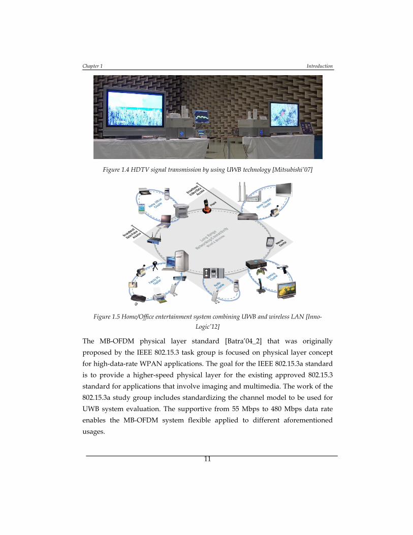
Chapter 1 Introduction
11
Figure 1.4 HDTV signal transmission by using UWB technology [Mitsubishi’07]
Figure 1.5 Home/Office entertainment system combining UWB and wireless LAN [Inno-
Logic’12]
The MB-OFDM physical layer standard [Batra’04_2] that was originally
proposed by the IEEE 802.15.3 task group is focused on physical layer concept
for high-data-rate WPAN applications. The goal for the IEEE 802.15.3a standard
is to provide a higher-speed physical layer for the existing approved 802.15.3
standard for applications that involve imaging and multimedia. The work of the
802.15.3a study group includes standardizing the channel model to be used for
UWB system evaluation. The supportive from 55 Mbps to 480 Mbps data rate
enables the MB-OFDM system flexible applied to different aforementioned
usages.
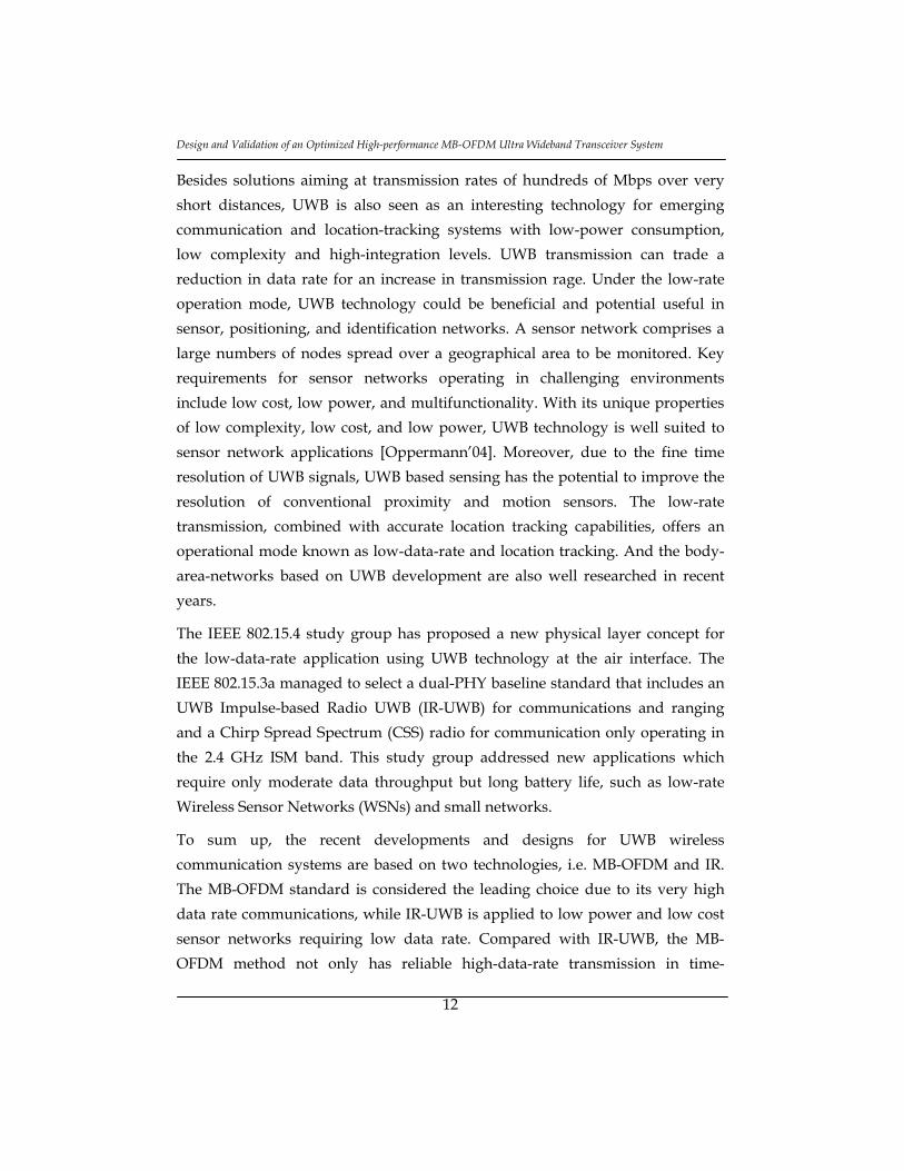
Design and Validation of an Optimized High-performance MB-OFDM Ultra Wideband Transceiver System
12
Besides solutions aiming at transmission rates of hundreds of Mbps over very
short distances, UWB is also seen as an interesting technology for emerging
communication and location-tracking systems with low-power consumption,
low complexity and high-integration levels. UWB transmission can trade a
reduction in data rate for an increase in transmission rage. Under the low-rate
operation mode, UWB technology could be beneficial and potential useful in
sensor, positioning, and identification networks. A sensor network comprises a
large numbers of nodes spread over a geographical area to be monitored. Key
requirements for sensor networks operating in challenging environments
include low cost, low power, and multifunctionality. With its unique properties
of low complexity, low cost, and low power, UWB technology is well suited to
sensor network applications [Oppermann’04]. Moreover, due to the fine time
resolution of UWB signals, UWB based sensing has the potential to improve the
resolution of conventional proximity and motion sensors. The low-rate
transmission, combined with accurate location tracking capabilities, offers an
operational mode known as low-data-rate and location tracking. And the body-
area-networks based on UWB development are also well researched in recent
years.
The IEEE 802.15.4 study group has proposed a new physical layer concept for
the low-data-rate application using UWB technology at the air interface. The
IEEE 802.15.3a managed to select a dual-PHY baseline standard that includes an
UWB Impulse-based Radio UWB (IR-UWB) for communications and ranging
and a Chirp Spread Spectrum (CSS) radio for communication only operating in
the 2.4 GHz ISM band. This study group addressed new applications which
require only moderate data throughput but long battery life, such as low-rate
Wireless Sensor Networks (WSNs) and small networks.
To sum up, the recent developments and designs for UWB wireless
communication systems are based on two technologies, i.e. MB-OFDM and IR.
The MB-OFDM standard is considered the leading choice due to its very high
data rate communications, while IR-UWB is applied to low power and low cost
sensor networks requiring low data rate. Compared with IR-UWB, the MB-
OFDM method not only has reliable high-data-rate transmission in time-
Chapter 1 Introduction
13
dispersive or frequency-selective channels without having complex time-domain
channel equalizer, but also provides high spectral efficiency.
1.2.4 Why MB-OFDM UWB?
The FCC defines UWB as any signal that occupies at least 500 MHz of
bandwidth in the 7.5 GHz spectrum between 3.1 and 10.6 GHz. However, there
is no restriction on signal generation techniques to occupy the available UWB
spectrum. Multiband approaches were proposed in [Batra’04] [Saberinia’03]
[Foerster’03] [Batra’04_2], in which the UWB frequency band is divided into
several subbands. Each subband occupies a bandwidth of at least 500 MHz in
compliance with FCC regulations. By interleaving the symbols across subbands,
multiband UWB can maintain the transmitter power as if a large GHz
bandwidth were being utilized. The advantage is that the multiband approach
allows the information to be processed over a much smaller bandwidth
compared to the 7.5 GHz made available to UWB systems, thereby reducing
overall design complexity as well as improving spectral flexibility and
worldwide compliance. In order to capture the multipath energy efficiently, the
OFDM technique has been used to modulate the information in each subband.
As introduced above, the MB-OFDM was one of the two leading proposals for
UWB physical layer design. One of the remarkable advantages of the MB-OFDM
system is that the multiband design of the OFDM systems allows the technology
to cope with local regulations by dynamically turning off some carriers to
comply with local rules of operation on the allocated spectrum. By avoiding
interferer’s bands, it is also possible to simplify the design of the system.
MB-OFDM technology promises to deliver data rates of about 110 Mbps at a
distance of 10 m. For the UWB wireless sensor applications, which the required
data is often very low, the coverage might be much larger than 10 m for MB-
OFDM approach. The MB-OFDM may require higher power levels when
compared to the IR technology. MB-OFDM technique is robust to multipath
which is present in the wireless channels. By using this technology and limiting
the transmitting symbols to QPSK constellation, the resolution of the Analog-to-

Design and Validation of an Optimized High-performance MB-OFDM Ultra Wideband Transceiver System
14
Digital Converter (ADC) and Digital-to-Analog Converter (DAC) and the
internal precision of the digital baseband, especially the FFT, can be lowered.
In this section, a comparison of the IR-UWB and MB-OFDM UWB techniques
will be made in terms of interference from other wireless communication
systems, robustness to multipath, performance, and system computational
complexity for the WPAN applications is done.
1.2.4.1 Interference
Because the MB-OFDM has the possibility to turn off some carriers that may
interfere, or to be interfered, with other systems, the MB-OFDM has the
advantages of interference and coexistence with other radio services. Due to this
flexibility in spectrum, MB-OFDM also increases the robustness against
frequency selective fading. However, MB-OFDM may very sensitive to Inter-
Carrier Interference (ICI), and if subcarriers’ orthogonality is lost, it can result in
performance degradation.
The spectral densities of IR transmitted signals can be made lower in comparison
to MB-OFDM signals, by spreading the information over larger bandwidth.
Thus, for the IR signals, the probability of interception decreases, which is useful
for military applications, as well as interference to narrowband victim receivers
[Molisch’05]. Also, spreading signals over larger bandwidths increases the
immunity to narrowband interference and ensures good multiple access
capabilities [Zhao’02] [Ramirez’01]. However, compared with MB-OFDM
approach, it is difficult for IR based systems to deal with interferers because of
the very wide bandwidth. The IR UWB signals are very narrow in time and
therefore, very difficult to intercept as they are also “noise-like”.
1.2.4.2 Robustness
MB-OFDM presents high robustness against multipath because of usage of Zero
Prefix (ZP, which will be explained later in Chapter 2) in dealing with Inter
Symbol Interference (ISI) and Inter-Carrier Interference (ICI). Nonetheless, in
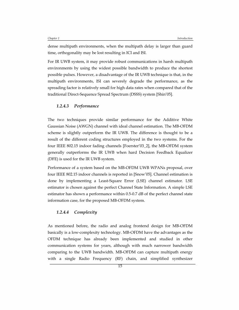
Chapter 1 Introduction
15
dense multipath environments, when the multipath delay is larger than guard
time, orthogonality may be lost resulting in ICI and ISI.
For IR UWB system, it may provide robust communications in harsh multipath
environments by using the widest possible bandwidth to produce the shortest
possible pulses. However, a disadvantage of the IR UWB technique is that, in the
multipath environments, ISI can severely degrade the performance, as the
spreading factor is relatively small for high data rates when compared that of the
traditional Direct-Sequence Spread Spectrum (DSSS) system [Shin’05].
1.2.4.3 Performance
The two techniques provide similar performance for the Additive White
Gaussian Noise (AWGN) channel with ideal channel estimation. The MB-OFDM
scheme is slightly outperform the IR UWB. The difference is thought to be a
result of the different coding structures employed in the two systems. For the
four IEEE 802.15 indoor fading channels [Foerster’03_2], the MB-OFDM system
generally outperforms the IR UWB when hard Decision Feedback Equalizer
(DFE) is used for the IR UWB system.
Performance of a system based on the MB-OFDM UWB WPANs proposal, over
four IEEE 802.15 indoor channels is reported in [Snow’05]. Channel estimation is
done by implementing a Least-Square Error (LSE) channel estimator. LSE
estimator is chosen against the perfect Channel State Information. A simple LSE
estimator has shown a performance within 0.5-0.7 dB of the perfect channel state
information case, for the proposed MB-OFDM system.
1.2.4.4 Complexity
As mentioned before, the radio and analog frontend design for MB-OFDM
basically is a low-complexity technology. MB-OFDM have the advantages as the
OFDM technique has already been implemented and studied in other
communication systems for years, although with much narrower bandwidth
comparing to the UWB bandwidth. MB-OFDM can capture multipath energy
with a single Radio Frequency (RF) chain, and simplified synthesizer

Design and Validation of an Optimized High-performance MB-OFDM Ultra Wideband Transceiver System
16
architectures may relax band switching time requirements. Besides, compared to
the IR technique, the MB-OFDM systems do not need to process an extremely
large bandwidth. Besides, the longer duration of OFDM symbol makes it less
sensitive to timing synchronization error than IR UWB.
In the IR, the complexity in antennas design and challenges in building RF
circuits, such as achieving high-speed analog-to-digital and digital-to-analog
converters, and processing a very large bandwidth, are difficult issues.
Compared with MB-OFDM, IR techniques need more complex timing
synchronization to achieve an acceptable performance.
However, the complexity of the OFDM system in MB-OFDM varies
logarithmically with the FFT size, and thus the MB-OFDM transmitter systems
require relatively large computational power due to the use of FFT/IFFT. But as
the synchronization blocks are much simpler than that of the IR system, the
complexity of the receiver systems is less complex than that of the IR system.
Because most of the times, the receiver system plays a more important role in
both performance and power consumption, the MB-OFDM transceiver systems
has some advantages against the IR UWB systems.
More importantly for this work, as most of the processing elements in MB-
OFDM UWB system are implemented by using digital processing blocks, it
makes the design of the analog-frontend elements much easier, whereas the IR
UWB protocol should deal with the signals more in the analog point. This makes
the development and research cost for MB-OFDM system much lower than that
of IR system, and the implementation period much shorter. This is because in
nowadays system development and research procedure, the digital integrated
circuit can be implemented in a more efficient way when compared with analog
circuit designs.
1.2.4.5 Conclusion
From the discussion above, a summary of the comparison can be made between
IR and MB-OFDM techniques. Table 1-1 summarizes the specifications of MB-
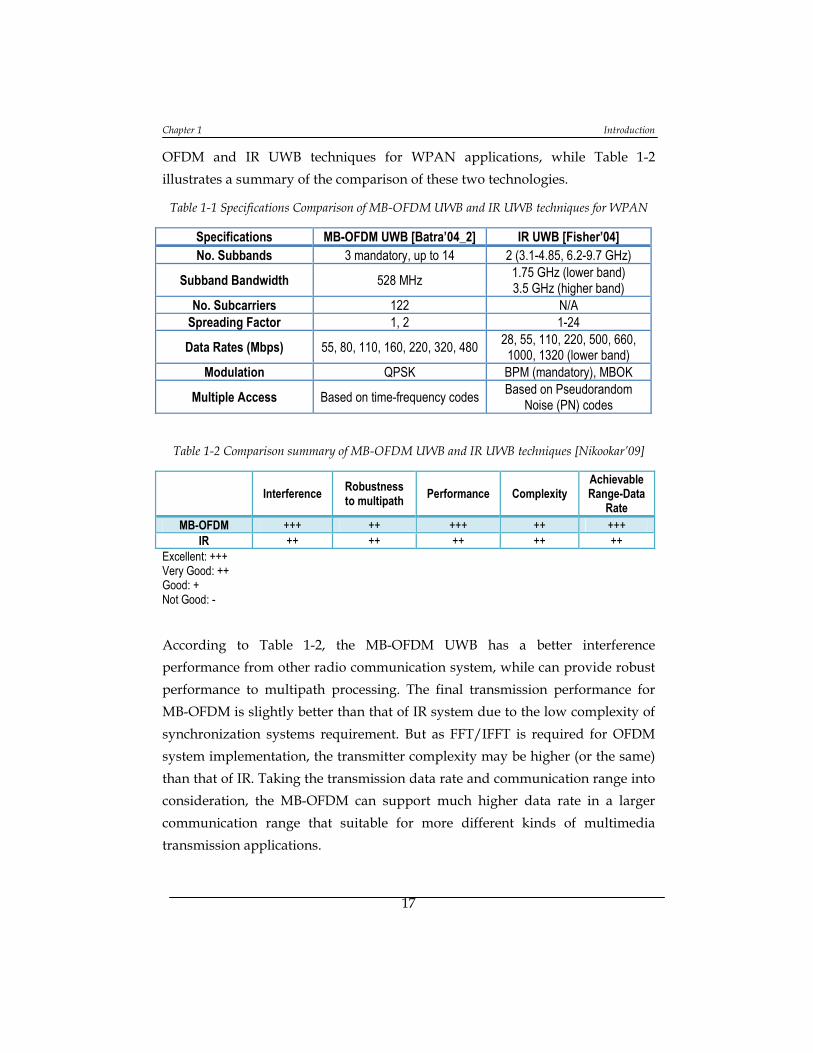
Chapter 1 Introduction
17
OFDM and IR UWB techniques for WPAN applications, while Table 1-2
illustrates a summary of the comparison of these two technologies.
Table 1-1 Specifications Comparison of MB-OFDM UWB and IR UWB techniques for WPAN
Specifications MB-OFDM UWB [Batra’04_2] IR UWB [Fisher’04] No. Subbands 3 mandatory, up to 14 2 (3.1-4.85, 6.2-9.7 GHz)
Subband Bandwidth 528 MHz 1.75 GHz (lower band) 3.5 GHz (higher band)
No. Subcarriers 122 N/A Spreading Factor 1, 2 1-24
Data Rates (Mbps) 55, 80, 110, 160, 220, 320, 480 28, 55, 110, 220, 500, 660, 1000, 1320 (lower band)
Modulation QPSK BPM (mandatory), MBOK
Multiple Access Based on time-frequency codes Based on Pseudorandom
Noise (PN) codes
Table 1-2 Comparison summary of MB-OFDM UWB and IR UWB techniques [Nikookar’09]
Interference Robustness to multipath
Performance Complexity Achievable Range-Data
Rate MB-OFDM +++ ++ +++ ++ +++
IR ++ ++ ++ ++ ++ Excellent: +++ Very Good: ++ Good: + Not Good: -
According to Table 1-2, the MB-OFDM UWB has a better interference
performance from other radio communication system, while can provide robust
performance to multipath processing. The final transmission performance for
MB-OFDM is slightly better than that of IR system due to the low complexity of
synchronization systems requirement. But as FFT/IFFT is required for OFDM
system implementation, the transmitter complexity may be higher (or the same)
than that of IR. Taking the transmission data rate and communication range into
consideration, the MB-OFDM can support much higher data rate in a larger
communication range that suitable for more different kinds of multimedia
transmission applications.

Design and Validation of an Optimized High-performance MB-OFDM Ultra Wideband Transceiver System
18
For design and research purpose, the OFDM system has already been studied
and applied by other communication system for years, thus makes the MB-
OFDM system easier to replace the existing communication systems and easier
to understand. This gives the MB-OFDM a higher compatibility with other
applications. Besides, the MB-OFDM is more focused on the digital baseband
system development when IR is more attractive to the RF and analog researchers.
Based on the background of the research interest, along with those advantages
that provided by the MB-OFDM UWB system, the MB-OFDM approach
becomes the best choice for the required Wireless Visual Sensor Networks
(WVSNs) application.
1.2.5 Challenges for MB-OFDM UWB
Although the MB-OFDM UWB technology has several attractive properties that
make it a promising technology for future short-range wireless communications
and many other applications, some challenges must be overcome to fulfill these
expectations.
The transmitter power level of UWB signals is strictly limited for UWB devices
coexist peacefully with other wireless systems. Such strict power limitation
poses significant challenges when designing UWB systems. One major challenge
is to achieve the performance desired at an adequate transmission range using
limited transmitter power. Another challenge is to design UWB waveforms that
efficiently utilize the bandwidth and power allowed by the FCC spectral mask.
Moreover, to ensure that the transmitter power level satisfies the spectral mask,
adequate characterization and optimization of transmission techniques (e.g.,
adaptive power control, duty cycle optimization) may be required.
When taking a close look at the MB-OFDM UWB digital baseband transceiver
system implementations, the challenges mainly come from the inherent
computational complexity, high processing frequency, and requirements of low
cost, low power and good performance. Among which, as mentioned before, the
FFT/IFFT processor block, which works as the core processing element for the
OFDM modulation system, has brought large design complexity to both the
transmitter and receiver systems. In practical systems, the performance and

Chapter 1 Introduction
19
power consumption of the FFT/IFFT processor will decide the performance of
the entire MB-OFDM transceiver system. Because the ultrashort duration of each
UWB signals, the traditional FFT/IFFT processor architecture cannot meet the
requirements of MB-OFDM system on speed, area, and power consumptions
considerations. Moreover, the high processing speed causes the design and
realization of other blocks, e.g., Viterbi Decoder (VD) system, very difficult, as
for either portable devices or WVSNs application, both the cost and power
consumption should be taken into account.
For any OFDM based system, time synchronization is a critical and
indispensable step. Timing error can break the orthogonality of the OFDM
subcarriers and introduce Inter Symbol Interference (ISI) as well as Inter-Carrier
Interference (ICI), which degrade the performance of the system dramatically.
MB-OFDM is, however, more sensitive to the timing and frequency offsets and
RF phase noise due to its narrowband subcarriers. The accuracy of the
synchronization scheme will have a very large effect on the performance of the
MB-OFDM receiver system. However, the difficulties on synchronization by
using those ultrashort duration signals will lead to high design complexity, thus
power consumptions.
Although there are already several communication systems that using the
OFDM technology, the MB-OFDM UWB system has some major differences
compared with traditional OFDM scheme:
1) MB-OFDM symbols are not continuously sent on one frequency
band but interleaved over different subbands across both time and
frequency;
2) Multiple access is enabled by the uses of frequency hopping
sequences over the set of subbands;
3) MB-OFDM provides both frequency diversity and multiple access
capability.
Therefore, in the MB-OFDM UWB system, channel estimation is a critical factor
for an OFDM receiver. Generally, the MB-OFDM UWB systems provide
relatively high data rates and are considered to save transmission power by
implementing continuous modulation rather than differential modulation. Thus,

Design and Validation of an Optimized High-performance MB-OFDM Ultra Wideband Transceiver System
20
coherent detection is necessary in receiver, which means, before modulation, an
accurate estimation and compensation of the Channel Impulse Response (CIR) is
required.
Another design challenge in MB-OFDM UWB is the impact of Narrowband
Interference (NBI) to the UWB receiver. This is because UWB is operating in
coexistence with other licensed users, such as the UWB frequency band overlaps
with that of IEEE 802.11a wireless local area networks (WLANs). Hence, the
interference from the narrowband system will degrade the performance of the
UWB transmission.
Other design challenges include scalable system architecture and spectrum
flexibility. The MB-OFDM UWB potential applications include both high-rate
applications and lower-rate applications. Thus, the UWB transceiver must be
able to support a wide range of data rates. Furthermore, the unlicensed nature of
the UWB spectrum makes it essential for UWB devices to coexist with devices
that share the same spectrum. However, it is challenging to design UWB systems
with spectrum flexibility that allows UWB devices to coexist effectively with
other wireless technologies and to meet potentially different regulatory
requirements in different regions of the world.
According to these, for development and research of the MB-OFDM based UWB
communication system, finding the optimal tradeoff point among the power
consumption, hardware implementation complexity, speed, and transmission
performance will become the main challenge in this work. Figure 1.6 shows the
factors that researchers should take into account when facing the MB-OFDM
UWB system implementations.

Chapter 1 Introduction
21
Figure 1.6 Design challenge and tradeoff point for MB-OFDM UWB system implementation
1.3. FPGA Design and Validation Methodology
The technological development has produced a significant increase of the
integration density that is causing more and more parts of a complex system to
be included inside the main core. Traditional approaches to implement and
validate a complex function or algorithm on Application Specific Integrated
Circuit (ASIC) or Field Programmable Gate Array (FPGA) will consume large
amount of design effort through the development processing. It is said that
during the whole process of FPGA design, verification will take up 70% to 80%
of the time in the design cycle [Ding’11]. Things will get even worse for the high
complex signal processing system developments, such as digital baseband
system of MB-OFDM UWB protocol, because not only the inserting and
collecting huge amount of transmission data sequences are not convenient and
efficient, but also localization the fail functions inside an entire FPGA
implementation is very hard and sometimes not accurate. For system
performance analyzing, monitoring the waveforms of the FPGA implementation
usually spends lots of effort especially for wireless communication system, and
it is also hard for the researchers to detect the errors, not even say calculating the

Design and Validation of an Optimized High-performance MB-OFDM Ultra Wideband Transceiver System
22
Bit Error Rate (BER). Therefore, an efficient debugging and validation
methodology for complex FPGA system development is high demanded, while
this new methodology must have the potential of analyzing the system
performance automatically.
Some may say using system level design method (such as using System C or
System Verilog) will save lots of design efforts, therefore more efficient for signal
processing system development, but this is only suitable for algorithm
validation or prototyping. In order to get a highly optimized architecture for
system development, optimization should be made through different design
levels for a processing element, from algorithm and system level (high level)
proposal to Register Transfer Level (RTL) design. Especially for those
implementations targeting at low power consumption and low system
complexity, which are usually carried out in the RTL rather than system level, a
through-level design method will be of great help.
Traditional approaches also involve creating a design and translating between
multiple design descriptions: an abstract algorithm is analyzed and optimized in
MATLAB or C code; then it is mapped onto an architecture using behavioral or
structural description; then those descriptions in MATLAB or C code, as well as
the test vectors, are translated for use in a logic analysis system and mapped into
an ASIC or FPGA for hardware testing. The problem of this kind of design
method involves translating the floating point descriptions of the system to
fixed-point descriptions, which has a great possibility to affect the accuracy of
the system and may bring further errors for the final hardware implementation.
Furthermore, each translating step, whether manual or automated, requires
additional verification efforts to confirm that the original design has been
preserved [Markovic’07]. More importantly, the translated descriptions usually
are hard to read and understand, not even say to modify if further optimizations
are needed. This dramatically reduced the visibility into the basic
implementation and architecture of the hardware system. Thus, new design
methodology is required to support fully visibility of the hardware
implementation, and provide reliable accurate performance for final hardware
system.

Chapter 1 Introduction
23
According to the discussion above, in order to efficiently implement and
validate the target MB-OFDM UWB baseband transceiver system, a suitable
FPGA design methodology is required so as to face the challenges come from the
complex debugging and validation procedure.
1.4. Present work
1.4.1 Main goals
This doctoral thesis aims at designing and implementing a communication
subsystem based on the MB-OFDM UWB wireless communication protocol.
The target communication system should have the ability to support real-time
video signal transmission so as the sensor nodes can be applied to the Wireless
Visual Sensor Networks application.
The MB-OFDM UWB wireless communication protocol has been chosen as the
best candidate for the design of the communication subsystem, due to the
advantages of low-power consumption, high energy efficient, and high
transmission data rate properties. Besides, as most of the baseband elements are
processed by using digital signals, it is better suited for FPGA development.
However, the natural design complexity of the MB-OFDM UWB caused by Fast
Fourier Transform/Inverse Fast Fourier Transform (FFT/IFFT) processor and
high processing frequency makes the design and implementation of MB-OFDM
baseband system in the FPGA board very difficult compared with other
subsystems. Moreover, although the MB-OFDM UWB communication protocol
is considered to be a low-power consumption solution, the battery lifetime is still
not long enough for wireless sensor nodes applications. Therefore, researching
and finding the low-power, low-complexity, while still maintain the high-speed,
high-performance algorithms and architectures for each processing element of
the MB-OFDM scheme becomes the main goal for this thesis. In order to achieve
this goal, several steps need to be followed.
First, before system development, we should first have global knowledge of the
MB-OFDM UWB specifications. This requires deep study and analysis of the

Design and Validation of an Optimized High-performance MB-OFDM Ultra Wideband Transceiver System
24
OFDM system and UWB technology. Several state-of-the-art theories for digital
circuit implementations and system constraints are also important for
optimization tasks of the baseband communication system.
Second, based on the knowledge, optimizations and modifications on both
algorithm and architecture of the MB-OFDM baseband system should be made
according to the specifications. Lots of works have been done related with
processing architecture optimization, synchronization, channel estimation and
so on. Therefore, those state-of-the-art algorithms and architectures should be
analyzed and compared.
Furthermore, the improvement space should be analyzed and the algorithms
and architectures for each processing element should be further optimized so as
to lower the power and increase the processing speed, more importantly,
suitable for the required application and target FPGA platform implementation.
Finally, the optimized elements should be integrated together so as to form an
MB-OFDM digital baseband transceiver system that can transmit different kind
of signals through the networks.
1.4.2 Design methodology
In order to efficiently debug and validate the MB-OFDM baseband system
architecture, this thesis proposed a whole new hardware/software co-design
methodology for complex FPGA system development, which is shown in Figure
1.7. Each step of this process is enumerated as:

Chapter 1 Introduction
25
Figure 1.7 Design methodology for this thesis
1) Propose the algorithm and implementation architecture based on
the MB-OFDM UWB communication protocol specification
2) Modeling and verifying the proposed algorithm and architecture in
MATLAB simulation environment by using SIMULINK blocks. The
simulation results of the modeled blocks will be compared with the
embedded MATLAB functions so as to estimate and analyze the
system’s overall performance for different processing elements.
3) The proposed system will then be implemented and realized in the
Register Transfer Level (RTL) by using either System Generator
from Xilinx or Verilog HDL code, according to the design
difficulties. The cross-platform simulation procedure combined
with MATLAB and ModelSim will be used for functional
verification for the RTL implementation.
4) Finally, the Hardware-in-the-loop co-simulation methodology will
be used for real-time FPGA hardware validation and simulation
process. The performance of the transceiver is also analyzed during
this procedure.
Design and Validation of an Optimized High-performance MB-OFDM Ultra Wideband Transceiver System
26
This software/hardware co-design methodology is used for the entire
development procedures of the proposed MB-OFDM UWB digital baseband
transceiver system, and is proved to be suitable for most of the FPGA based,
complex digital system designs.
1.4.3 Contributions
This work focuses on implementing and optimizing the MB-OFDM UWB digital
baseband system based on the ISO/IEC 26907:2009(E) standard [ISO/IEC
26907’09]. The main contribution of the work is the implementation of an energy
efficient, robust, and high-performance MB-OFDM digital baseband system.
And the second contribution of this thesis is validating the proposed transceiver
architecture in the FPGA board through an effort-efficient co-design
methodology. With more details, the following list shows the particular
contributions of this thesis:
A novel mixed radix 128-point FFT algorithm by using multipath
pipelined architecture is proposed. The complex multipliers for each
processing stage are designed by using modified shift-add
architectures. The system word-length and twiddle word-length are
compared and selected based on Signal to Quantization Noise Ratio
(SQNR) and power analysis.
IFFT processor performance is analyzed under different Block
Floating Point (BFP) arithmetic situations for overflow control, so as
to find out the best architecture of IFFT algorithm based on the
proposed FFT processor.
An innovative low complex timing synchronization and
compensation scheme, which consists of Packet Detector (PD) and
Timing Offset Estimation (TOE) functions, for MB-OFDM UWB
receiver system is proposed. By simplifying the cross-correlation and
maximum likelihood functions to sign-bit only, the computational
complexity is significantly reduced.
A 64 state soft-decision Viterbi Decoder system by using high speed
Chapter 1 Introduction
27
radix-4 Add-Compare-Select architecture is proposed. Two-pointer
Even algorithm is also introduced into the Trace Back unit in the aim
of hardware-efficiency.
Several state-of-the-art technologies are integrated into the complete
baseband transceiver system, in the aim of implementing a highly-
optimized UWB communication system.
An improved design flow is proposed for complex system
implementation which can be used for Field-Programmable Gate
Array (FPGA) designs. The design method not only dramatically
reduces the time for functional verification, but also provides
automatic analysis such as errors and output delays for the
implemented hardware systems. It allows the reuse of test benches
from the algorithm description to the final FPGA implementation.
A virtual communication environment is established for validating
the proposed MB-OFDM transceiver system. This methodology is
proved to be easy for usage and convenient for analyzing the digital
baseband system without analog frontend under different
communication environments.
The transceiver system is implemented in a Xilinx Virtex 5 FPGA integrated in
an XUPV5-LX110T board. Experimental results are analyzed under the 53.3
Mbps and 106.7 Mbps data rate modes with very low Bit Error Rate (BER). The
proposed design has the potential to be applied for Wireless Visual Sensor
Networks.
1.5. Content and organization of the thesis
This document is organized as follows:
In Chapter 0, the general information of MB-OFDM UWB communication
protocol is provided. The signal model of MB-OFDM is a combine of OFDM
technology and multipath technology, therefore, the OFDM symbols should be
transmitted through a frequency selective channel environment. The Physical

Design and Validation of an Optimized High-performance MB-OFDM Ultra Wideband Transceiver System
28
(PHY) layer and Media Access Control (MAC) layer general information will
also be described. As PHY header and MAC header should be encoded and
added in front of each transmitted packets, and preamble sequences are
necessary for wireless communication systems, the Physical Layer Service
Access Point (PLCP) sublayer is also introduced in this chapter.
The transceiver architecture, as well as the optimizations that this work has done
that contributes to the implementation of MB-OFDM UWB digital baseband
system, is the topic of Chapter 3. The transmission and receiving functions will
be described in pair so as to help better understanding of the global structure of
the transceiver system. The main contributions of this work are the design and
optimization of those critical processing elements, etc., FFT/IFFT processor,
synchronization scheme, Viterbi Decoder. Several low-power, low-complex
algorithms and architectures have been proposed so as to integrate a highly
optimized baseband transceiver system implemented in the FPGA board at the
end.
In order to efficiently validate and analyze the proposed baseband structure in
the FPGA, a hardware/software co-design methodology is proposed and
introduced in Chapter 0. The proposed design flow covers all the steps for a
general digital system development based on FPGA, from
algorithm/architecture proposal, to hardware validation.
Based on the design and validation method described in Chapter 0, a Virtual
Communication environment, by connecting the transmitter and receiver system
through the UWB channel models built in MATLAB/SIMULINK, is established
for testing the proposed MB-OFDM digital baseband transceiver system in
different communication environments. The experimental results from such
testing methodology are shown in Chapter 5.
The conclusion of the thesis and future work are drawn in Chapter 6.

Chapter 2 MB-OFDM UWB System Description
29
2. MB-OFDM UWB System Description
2.1. Introduction
The general knowledge of Multiband Orthogonal Frequency Division
Multiplexing Ultra Wideband (MB-OFDM UWB) system is illustrated in this
chapter.
The architecture of a complete wireless communication system is shown in
Figure 2.1 [ISO/IEC 26907’09]. It generally contains two major layers: Media
Access Control (MAC) Layer and Physical (PHY) Layer. MAC layer acts as the
interface between the network layer and the PHY layer, while the PHY layer is
the lowest layer for communication system, and provides the logical data
structure and transmission functions. The MAC layer is usually implemented by
using a microprocessor, and it is not the task in this thesis. This document only
focuses on the PHY layer design and optimizations, while leaves MAC layer
development in the future work.

Design and Validation of an Optimized High-performance MB-OFDM Ultra Wideband Transceiver System
30
Figure 2.1 Architectural reference model
The MAC and PHY layer structure and basic functions will be explained first in
this chapter, and then the signal model of MB-OFDM UWB transmission will be
given. At the end of this chapter, the format and structure of each MB-OFDM
signal packet, as well as the OFDM modulation for each packet, will be
introduced so as to better understand the baseband processing procedure of the
MB-OFDM system.
2.2. General description
2.2.1 MAC general description of MB-OFDM standard
The MAC service is provided by means of the MAC Service Access Point (MAC
SAP) to a single MAC service client, usually a higher layer protocol or
adaptation layer. In the UWB MB-OFDM standard, the MAC sublayer is
represented by a device address.
The MAC sublayer in turn relies on the service provided by the PHY layer via
the PHY Service Access Point (PHY SAP). The MAC protocol applies between
MAC sublayer peers. Each individual MAC sublayer is associated with a volatile
abbreviated address called a DevAddr, which is a locally generated 16-bit value.

Chapter 2 MB-OFDM UWB System Description
31
The MAC sublayer is associated with a single PHY layer via PHY SAP. The
MAC sublayer requires the following features provided by the PHY.
Frame transmission in both single frame and burst mode
Frame reception for both single frame and burst mode transmission
PLCP header error indication for both PHY and MAC header structures
Clear channel assessment for estimation of medium activity
Range measurement timestamps if MAC range measurement is
supported.
The MAC sublayer takes charge of communication between cooperating devices
within radio range on a single channel using the PHY, acts like a channel access
mechanism, power manager, communication secure system, and measuring the
distance between two devices, etc. Coordination of devices within radio range is
achieved by the exchange of beacon frames. Periodic beacon transmission
enables device discovery, supports dynamic network organization, and provides
support for mobility.
2.2.2 PHY general description of MB-OFDM standard
The MB-OFDM UWB standard specifies the Physical (PHY) layer for Wireless
Personal Area Network (WPAN) which utilizes the unlicensed 3.1-10.6 GHz
frequency band [ECMA-368’08]. According to the specification, UWB can
support data rate of 53.3 Mbps, 81 Mbps, 106.7 Mbps, 160 Mbps, 200 Mbps, 320
Mbps, 400 Mbps, and 480 Mbps, among which, 53.3 Mbps, 106.7 Mbps, and 200
Mbps transmission mode shall be mandatory.
The UWB spectrum is divided into 14 bands, each with a bandwidth of 528 MHz.
The first 12 bands are then grouped into four band groups that consisting of
three bands each, while the last two bands are grouped into a fifth band group.
The sixth band group is defined within the spectrum of the first four, consistent
with usage within worldwide spectrum regulations. For a well developed UWB
transmission system, at least one of the band groups shall be supported. The

Design and Validation of an Optimized High-performance MB-OFDM Ultra Wideband Transceiver System
32
relationship between centre frequency, fc, and band number, nb, is given by the
following equation (1).
2904 528 1, … , 14. 1
The six band groups, as well as the center frequency of each band, are defined in
Figure 2.2.
Figure 2.2 Diagram of the band group allocation [ISO/IEC 26907’09]
For MB-OFDM specification, a total number of 110 sub-carriers, consisting of 100
data sub-carriers and 10 guard sub-carriers, are used per band to transmit the
information. In addition, 12 pilot sub-carriers allow for coherent detection. MB-
OFDM system uses frequency-domain spreading, time-domain spreading, and
Forward Error Correction (FEC) coding to vary the transmission data rates.
Convolutional code with coding rates of 1/3, 1/2, 5/8, and 3/4 are used for FEC
structure. The various coding rates are derived from the rate R=1/3
convolutional code by employing “puncturing” methodology.
Time-Frequency Code (TFC) is then used for spreading the coded OFDM data
into different frequency bands. The TFC defines the transmission styles, whether
to transmit the signal over three bands within one band group, or interleave the
data over two bands, or just transmit the information on a signal band. The
supportive of two bands and fixed band transmission for MB-OFDM system
should be mandatory as required by the standard. Figure 2.3 illustrates this
procedure for three of the fourteen possible subbands. Considering transmission
over time, the first OFDM symbol is transmitted on subband 1, the second
OFDM symbol on subband 2, the third OFDM symbol on the subband 3 and this

Chapter 2 MB-OFDM UWB System Description
33
repetition continues over time. In practice, the frequency-time codes that specify
the frequency repetition over time may different to the one presented in Figure
2.3. Furthermore, multiple access is specified by different time-frequency codes.
Figure 2.3 Example of time-frequency coding for the MB-OFDM systems
A Zero Prefix (ZP) is inserted before each OFDM symbol. The length of the ZP
needs to be chosen to minimize the impact of Inter-Carrier-Interference (ICI) and
maximize the collected multipath energy, while keeping the overhead due to the
ZP small. For MB-OFDM standard, the Zero Prefix (ZP) is used instead of Cyclic
Prefix (CP) as traditional OFDM communication systems, because using ZP the
power back off at the receiver can be avoided. The Power Spectral Density (PSD)
of OFDM signal using CP has ripples (resulting in transmit power back off of
about 1.5 dB). While the ZP provides no ripples in the power spectral density
and accordingly no power back off is needed. Figure 2.4 compares the
transmitter spectrum for using CP and ZP separately [Gharpurey’08].

Design and Validation of an Optimized High-performance MB-OFDM Ultra Wideband Transceiver System
34
Figure 2.4 Compare of the transmitter spectrum by using CP and ZP
As it can be seen in Figure 2.4, the transmitter spectrum shape will be flat by
using ZP instead of CP. Therefore, the design of receiver system will be much
easier.
2.2.3 Signal model of Multiband OFDM UWB
The Multiband Orthogonal Frequency Division Multiplexing (MB-OFDM) is a
UWB technology which uses the OFDM method. MB-OFDM combines the
OFDM technique with the multi-band approach. The Transceiver architectures
for MB-OFDM systems are similar to the conventional wireless OFDM systems,
while the main differences for MB-OFDM are in the use of Time-Frequency
Codes (TFC) to specify center frequencies for the transmission of each OFDM
symbol.
Consider a MB-OFDM UWB system with the available UWB spectrum divided
into S subbands. Each subband occupies a Bandwidth (BW) > 500 MHz and the
OFDM has N subcarriers, as shown in Figure 2.5. At each OFDM symbol period,
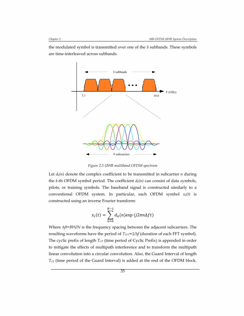
Chapter 2 MB-OFDM UWB System Description
35
the modulated symbol is transmitted over one of the S subbands. These symbols
are time-interleaved across subbands.
3.1 10.6F (GHz)
S subbands
N subcarriers
Figure 2.5 UWB multiband OFDM spectrum
Let dk(n) denote the complex coefficient to be transmitted in subcarrier n during
the k-th OFDM symbol period. The coefficient dk(n) can consist of data symbols,
pilots, or training symbols. The baseband signal is constructed similarly to a
conventional OFDM system. In particular, each OFDM symbol xk(t) is
constructed using an inverse Fourier transform:
exp 2 ∆
Where ∆ft=BW/N is the frequency spacing between the adjacent subcarriers. The
resulting waveforms have the period of TFFT=1/∆f (duration of each FFT symbol).
The cyclic prefix of length TCP (time period of Cyclic Prefix) is appended in order
to mitigate the effects of multipath interference and to transform the multipath
linear convolution into a circular convolution. Also, the Guard Interval of length
TGI (time period of the Guard Interval) is added at the end of the OFDM block.

Design and Validation of an Optimized High-performance MB-OFDM Ultra Wideband Transceiver System
36
The guard interval is used to provide more flexibility in the implementation. For
instance, it can be used to provide sufficient time for switching between bands,
to relax the analog transmitter and receiver filters, to relax filter specifications for
adjacent channel rejection, or to help reduce the Peak-to-Average Power Ratio
(PARP). The symbol duration becomes TSYM=TFFT+TCP+TGI. The Radio Frequency
(RF) signal transmitted can be modeled as:
exp 2
The carrier frequency, fk, specifies the subband, in which the signal is transmitted
during the k-th OFDM symbol duration. These carrier frequency sequences are
based on time-frequency codes, which are assigned uniquely to various users so
as to minimize the multiple access interference.
2.3. Description of the signals
The transmitted signals can be described using a complex baseband signal
notation. The Radio Frequency (RF) transmitted signal is related to the complex
baseband signal as shown in (2).
exp 2 2
Where Re(.) represents the real part of a complex variable, sk(t) is the complex
baseband signal of the k-th OFDM symbol and is nonzero over the interval from
0 to TSYM, N is the number of OFDM symbols, TSYM is the symbol interval, and fk
is the center frequency for the k-th band. The exact structure of the k-th OFDM
symbol depends on its location within the packet, as in equation (3).
, 0
,
, (3)
Where spreamble,k(t) describes the k-th symbol of the preamble, sheader,k(t) describes
the k-th symbol of the header, sdata,n(t) is the k-th symbol of the Physical Service
Data Unit (PSDU), Npreamble is the number of the symbols in the preamble, Nheader is
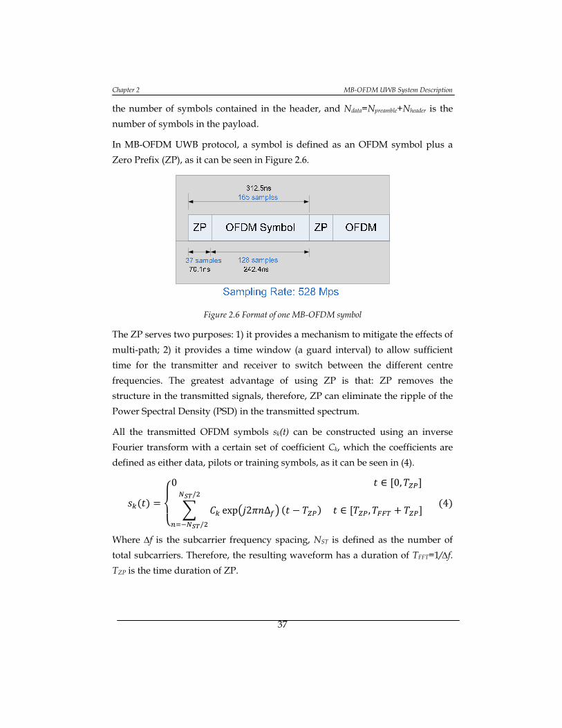
Chapter 2 MB-OFDM UWB System Description
37
the number of symbols contained in the header, and Ndata=Npreamble+Nheader is the
number of symbols in the payload.
In MB-OFDM UWB protocol, a symbol is defined as an OFDM symbol plus a
Zero Prefix (ZP), as it can be seen in Figure 2.6.
Figure 2.6 Format of one MB-OFDM symbol
The ZP serves two purposes: 1) it provides a mechanism to mitigate the effects of
multi-path; 2) it provides a time window (a guard interval) to allow sufficient
time for the transmitter and receiver to switch between the different centre
frequencies. The greatest advantage of using ZP is that: ZP removes the
structure in the transmitted signals, therefore, ZP can eliminate the ripple of the
Power Spectral Density (PSD) in the transmitted spectrum.
All the transmitted OFDM symbols sk(t) can be constructed using an inverse
Fourier transform with a certain set of coefficient Ck, which the coefficients are
defined as either data, pilots or training symbols, as it can be seen in (4).
0 ∈ 0,
exp 2 ∆ ∈ ,
/
/
4
Where ∆f is the subcarrier frequency spacing, NST is defined as the number of
total subcarriers. Therefore, the resulting waveform has a duration of TFFT=1/∆f.
TZP is the time duration of ZP.

Design and Validation of an Optimized High-performance MB-OFDM Ultra Wideband Transceiver System
38
2.4. Physical Layer Convergence Protocol (PLCP) sublayer
2.4.1 PLCP Protocol Data Unit (PPDU)
During the transmission, the Physical Service Data Unit (PSDU) shall be
provided with a Physical Layer Convergence Protocol (PLCP) preamble and
PLCP header to create the PLCP Protocol Data Unit (PPDU). At the receiver, the
PLCP preamble and PLCP header serve as support in the demodulation,
decoding, and delivery of the PSDU.
The PLCP Protocol Data Unit (PPDU) format is defined in Figure 2.7. The three
parts are listed in the order of transmission.
Figure 2.7 PPDU structure
The PLCP preamble is sent first at the transmitter system side, which can be
further divided into packet/frame synchronization sequence (time-domain
portion), and a channel estimation sequence (frequency-domain portion). The
purpose of adding PLCP preamble is to support packet detection, timing
synchronization, carrier frequency offset recovery, sampling frequency
synchronization, and channel estimation for the MB-OFDM receiver system. A
unique preamble sequence shall be assigned to each Time-Frequency Code
(TFC).
The PLCP header is used to convey necessary information about both the PHY
and the MAC to decode the PSDU at the receiver part. A complete PLCP header
includes PHY header, MAC header, Header Check Sequence (HCS), tail bits, and
Reed-Solomon parity bits. Additional tail bits are also added between the PHY
header and MAC header, HCS and Reed-Solomon parity bits, and at the end of

Chapter 2 MB-OFDM UWB System Description
39
the PLCP header, by the means of returning the convolutional encoder to the
“zero” state.
The Reed-Solomon parity bits are added in order to improve the robustness of
the PLCP header. The Reed-Solomon outer code for PLCP header shall use the
systematic of (23, 17) to improve upon the robustness of the R=1/3, K=7 inner
convolutional code.
The Reed-Solomon code is defined over Galois Field GF(28) with a primitive
polynomial p(z)=z8+z4+z3+z2+1, where α is the root of the polynomial p(z). For
brevity, this Galois Field is denoted as F. As notation, the element
M=b7z7+b6z6+b5z5+b4z4+b3z3+b2z2+b1z+b0, where M belongs to F and has the
following binary representation b7b6b5b4b3b2b1b0, where b7 is the Most Significant
Bit (MSB) and b0 is the Least Significant Bit (LSB).
The generator polynomial is obtained by shortening a systematic (255, 249)
Reed-Solomon code, which is specified by the generator polynomial of (5) below:
126 4 158 58 49 117 5
where g(x) is the generator polynomial over F, x belongs to F and the coefficients
are given in decimal notation. The shortening operation pre-appends 232 zero
elements to the incoming 17 octet message. The structure of Reed-Solomon
encoder is shown in Figure 2.8.
0g 1g 2g 3g 4g 5g
0Z
0q
1Z
1q
2Z
2q
3Z
3q
4Z
4q
5Z
5q
Figure 2.8 Systematic Reed-Solomon encoder
The CCITT CRC-16 Header Check Sequence (HCS) shall be the ones
complement of the remainder generated by the modulo-2 division of the
combined PHY and MAC headers by the polynomial of x16+x12+x5+1. The HCS

Design and Validation of an Optimized High-performance MB-OFDM Ultra Wideband Transceiver System
40
bits shall be processed in the transmit order. The HCS block is used to protect
the PHY header and MAC header, the schematic of the processing order is
shown in Figure 2.9, in which, the registers shall be initialized to all ONEs for
processing.
0X15X
Figure 2.9 CCITT CRC-16 block diagram
The PSDU part is formed by concatenating the frame payload with the Frame
Check Sequence (FCS), tail bits, and finally pad bits, which are inserted in order
to align the data stream on the boundary of the symbol interleaver. The
combined PSDU part should then be scrambled and six tail bits should be
produced by replacing the six scrambled “ZERO” bits with six non-scrambled
“ZERO bits.”
For transmission the entire PPDU packet, the Least Significant Bit (LSB) of a byte
shall be the first bit transmitted.
2.4.2 OFDM modulation
The format of each OFDM symbol for different transmission data rate modes
will be described in detail in Section 3.3.4.
An OFDM symbol rdata, k(t) in MB-OFDM system is defined as

Chapter 2 MB-OFDM UWB System Description
41
, , exp 2 ∆
, exp 2 ∆
/
/
6
Where NSD is the number of data subcarriers, NST is the number of total
subcarriers, and the function MD[I] defines a mapping from the indices 0 to 99 to
the logical frequency offset indices -56 to 56, excluding the locations reserved
for the pilot subcarriers, guard subcarriers and the DC subcarrier. Function Pk is
a pseudorandom Linear-Feedback Shift Register (LFSR) sequence with the
length of 127, k=0 shall correspond to the first OFDM symbol following the
PLCP preamble (i.e., the first OFDM symbol following the channel estimation
symbols).
For data rates of 53.3 Mbps, 80 Mbps, 106.7 Mbps, and 200 Mbps, a time-domain
spreading operation shall be performed with a spreading factor TSF=2. The
time-domain spreading operation consists of transmitting the same information
over two OFDM symbols. These two OFDM symbols are transmitted over
different sub-bands to obtain frequency diversity format improvements. The
repeated version of this OFDM symbol, represented asS′ n , shall be obtained
in the time domain as follows:
,
, 7
Where k=0 shall correspond to the first OFDM symbol following the PLCP
preamble and the values of the index k are OFDM symbol numbers before time
spreading.
2.5. Conclusions
The basic theory of MB-OFDM UWB wireless communication protocol has been
introduced in this chapter. The specification, general requirement, and functions
of PHY and MAC layers are illustrated according to the UWB standard. The
signals of each OFDM symbol can be generated by using IFFT algorithm; ZP
Design and Validation of an Optimized High-performance MB-OFDM Ultra Wideband Transceiver System
42
signals are added in front of OFDM symbol to form an entire MB-OFDM packet.
The format of each PLCP layer has been explained, and OFDM modulation, as
well as the format of each symbol, transmission requirements, time-domain
spreading, etc. is also discussed in this chapter. The following sections will focus
on the hardware implementation and system modification for the whole MB-
OFDM UWB digital baseband system based on the requirement and
specifications given by the UWB standard.

Chapter 3 Transceiver Architecture of MB-OFDM UWB System
43
3. Transceiver Architecture of MB-OFDM
UWB System
3.1. Introduction
As the general information and system specifications for UWB communication
protocols have been introduced in the previous chapters, the main original
contribution of this work, which is implementing and optimizing the digital
baseband transceiver system for MB-OFDM UWB system, is illustrated in this
chapter.
The Transmitter (Tx) and Receiver (Rx) digital baseband processing functions as
well as the hardware implementation architecture will be described in detail
based on the MB-OFDM UWB standard [ISO/IEC 26907’09] in this chapter.
Figure 3.1 shows the framework of the MB-OFDM physical layer. The basic
functions for MB-OFDM digital baseband signal processing include scrambling,
convolutional encoding, interleaving, constellation mapping, OFDM modulation,
and time-domain spreading etc. The preamble sequences, which are used for
timing and frequency synchronization at Rx part, will be added in front of each
transmitted packet. Frequency hopping techniques are used when transmitting
signals among different channels. As it can be seen, MB-OFDM is the
combination of OFDM modulation and frequency hopping.

Design and Validation of an Optimized High-performance MB-OFDM Ultra Wideband Transceiver System
44
Figure 3.1 MB-OFDM physical layer
The inherent high complexity, high processing frequency, and requirements of
low cost, low power and good performance make the implementation of MB-
OFDM baseband transceiver quite a challenging work. The FFT/IFFT processor
pair, which is the most complex part, works as the core processing element for
the entire MB-OFDM transceiver system. In practical systems, the performance
of MB-OFDM physical layer highly depends on the speed and power
consumption of the FFT/IFFT processor pair. Therefore, the optimization of the
existing FFT/IFFT architecture should be the most critical task for MB-OFDM
transceiver system design. Timing synchronization algorithm is another
important part for avoiding packet loss and ISI effect, lowering the
computational complexity as well as the power consumption, while still
maintaining certain value of accuracy becomes a big challenge for
synchronization scheme design. At the receiver side, the Viterbe algorithm is
recommended to decode the convolutional codes because of its optimal
decoding performance. However, the high processing frequency requirement of
MB-OFDM baseband system meets the bottleneck imposed by the recursive
Add-Compare-Select (ACS) iteration, which prevents conventional pupelining
techniques as a result of nonlinear feedback loop. Therefore, the throughput and
the ability to support the very high speed transmission of Viterbi Decoder (VD)
is other important factor to be taken into consideration.
The first challenge comes from the power consumption caused from the critical
processing elements, such as FFT/IFFT processor and Viterbe Decoder. Low-
power hardware-efficient algorithms and architectures have been extensively
Chapter 3 Transceiver Architecture of MB-OFDM UWB System
45
studied for years in UWB systems regarding the FFT/IFFT model and VD.
Several parallel data-path pipelined FFT processors for UWB applications have
been developed. Using mixed-radix algorithm and Single-path Delay Feedback
(SDF) architecture is the common solution, while trying to reduce and simplify
the usage of complex multipliers is the main contribution, but additional
optimizations are still necessary, especially for those low power high speed
complex multiplier developments. The speed and power consumption
bottleneck of Viterbi Decoder related with Add-Compare-Select Units is the
other interest point that should pay attention to.
The other big challenge of designing MB-OFDM UWB baseband systems is its
sensitivity to the time offset as it has difficulties to meet the strict time limits,
which are short due to high data rate. Efficient and accurate packet detection
and timing synchronization can avoid or alleviate packet loss and Inter Symbol
Interference (ISI), which destroys the orthogonality of the OFDM subcarriers and
degrades the system performance. There are several works on timing
synchronization systems [Fan’12] [Shahbazian’11] [Yak’05] [Kim’08] [Fan’09],
but they either consume large hardware resources or have rather high
computational complexity.
The mismatch in local oscillator between transmitter and receiver will cause the
effect of Carrier Frequency Offset (CFO), which will lead to Inter Carrier
Interference (ICI), Doppler Effect on phase shift and degradation in Signal to
Noise Ratio (SNR). Therefore, to ensure performance of the receiver system, CFO
estimation and compensation also plays an important role. Traditionally, the
work in [Moose’94] used pilot symbols for CFO estimation in frequency domain.
The algorithm in [Schmidl’97] estimated CFO by obtaining the phase difference
between two halves in a preamble in time domain. The work in [Morelli’99]
improved the traditional algorithm by considering a training symbol composed
of more than two identical parts, while [Minn’03] extended [Morelli’99] by
employing a Best Linear Unbiased Estimator (BLUE) to improve noise
performance. However, most of the previous research only focuses on the
algorithm aspect for traditional OFDM systems, the performances cannot satisfy
the high speed, low power requirements of MB-OFDM system. Furthermore,
Sampling Frequency Offset (SFO) and Common Phase Error (CPE) estimation
Design and Validation of an Optimized High-performance MB-OFDM Ultra Wideband Transceiver System
46
for frequency synchronization in frequency domain are required by using the
pilot subcarrier information added to each transmitted OFDM symbol.
The MB-OFDM UWB systems have the following distinctive characteristics if
compared to conventional OFDM systems:
1) Different channel responses and channel energies across different bands
2) Different carrier frequency offsets across different bands
3) The use of ZP instead of conventional CP for saving transmitting power
4) The interplay between the timing and frequency hopping (a mismatched
timing point at the receiver will yield a mismatched frequency hopping
and hence a significant performance degradation)
These characteristics provide diverse components as well as additional design
constraints for the channel estimation and equalization blocks in order to
mitigate hostile channel effects on the received signals. The Channel Estimation
and Equalization functions will be discussed in this chapter.
According to the discussion above, in this thesis, a low complexity, energy
efficient, and robust digital baseband transceiver system for MB-OFDM UWB
communication protocol is proposed and tested to be suitable for the MB-OFDM
UWB applications. The main objectives for the system architecture
implementation can be enumerated as follows:
Propose a novel 128-point FFT/IFFT algorithm and architecture
for MB-OFDM UWB application, in the aim of lowering the
power consumption while increasing the system performance.
Find a low complex synchronization and compensation scheme
to ensure robust and accurate packet detection and
synchronization for the receiver system.
Implement a high processing speed Viterbi Decoder system.
Employ state-of-the-art techniques for high performance
frequency synchronization and Channel
Estimation/Equalization blocks.

Chapter 3 Transceiver Architecture of MB-OFDM UWB System
47
Integrate the complete digital baseband transceiver system
based on the MB-OFDM UWB physical standard, design
suitable control logics so as to combine all the required
processing elements together.
Particularly, the present work aims at the implementation of an entire and
standalone transmitter-receiver MB-OFDM digital baseband system with a low-
power, high-speed performance, that can be utilized for different transmission
data rate modes in different channel models that specified by IEEE 802.15.3a
Channel Modeling Sub-committee [Foerster’03_2].
The processing elements will be introduced in pair for both transmitter and
receiver system in this chapter, and will be started from those most important
elements on both sides. This chapter is organized as follows: The general
structures of the transmitter and receiver digital baseband systems, specified by
the ISO/IEC standard, are introduced in Section 3.2. The actions of the 128-point
FFT/IFFT processor pair, which used as the OFDM modulator in MB-OFDM
UWB system, are introduced in Section 3.3, along with the proposed low-power,
high-performance FFT/IFFT processor architecture. The synchronization issues
related with both timing offset and frequency offset will be discussed in Section
3.4, and then, based on the discussion, the proposed low-complex Timing
Synchronization Scheme is explained, flowing the frequency synchronization
frames in both time-domain and frequency-domain. The proposed 2-steps radix-
4 Viterbi Decoder system that is used for decoding those received signals is
introduced in Section 3.5. After that, the integration of a complete MB-OFDM
transceiver baseband system by employing several state-of-the-art technologies,
as well as design of the control logic, will be given in Section 3.6. Finally, the
conclusions and contributions will be drawn in Section 3.7.
3.2. Overview of the MB-OFDM UWB system
In this section, the general signal processing procedure and functions of
standard MB-OFDM UWB baseband system is described. The digital baseband
system is divided into two different parts: Transmitter (Tx) and Receiver (Rx).
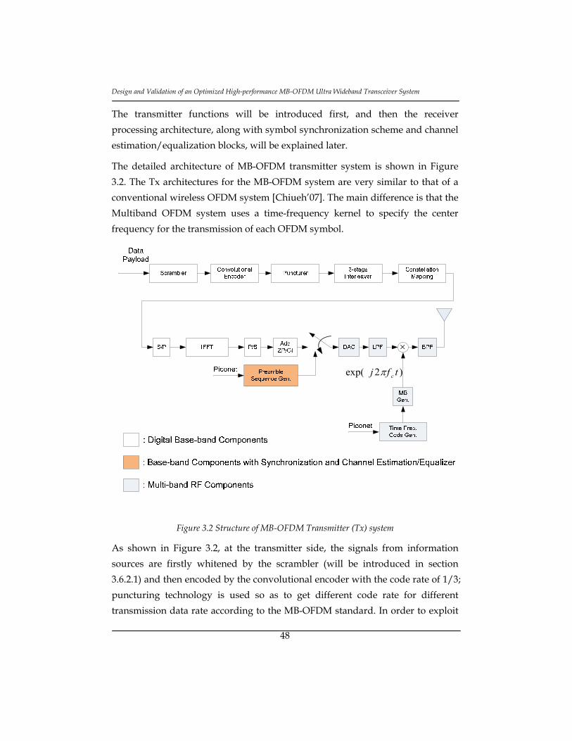
Design and Validation of an Optimized High-performance MB-OFDM Ultra Wideband Transceiver System
48
The transmitter functions will be introduced first, and then the receiver
processing architecture, along with symbol synchronization scheme and channel
estimation/equalization blocks, will be explained later.
The detailed architecture of MB-OFDM transmitter system is shown in Figure
3.2. The Tx architectures for the MB-OFDM system are very similar to that of a
conventional wireless OFDM system [Chiueh’07]. The main difference is that the
Multiband OFDM system uses a time-frequency kernel to specify the center
frequency for the transmission of each OFDM symbol.
)2exp( tfj c
Figure 3.2 Structure of MB-OFDM Transmitter (Tx) system
As shown in Figure 3.2, at the transmitter side, the signals from information
sources are firstly whitened by the scrambler (will be introduced in section
3.6.2.1) and then encoded by the convolutional encoder with the code rate of 1/3;
puncturing technology is used so as to get different code rate for different
transmission data rate according to the MB-OFDM standard. In order to exploit

Chapter 3 Transceiver Architecture of MB-OFDM UWB System
49
time-frequency diversity and combat multi-path fading, the coded bits are
further interleaved by using the 3-step interleaver function according to the
same preferred time frequency pattern. Then, the resulting binary serial
sequence will be mapped into constellation points according to the Gray-coding,
where Quadrature Phase-Shift Keying (QPSK) and Dual-Carrier Modulation
(DCM) constellation mapper are used according to the data rate mode. Then, the
stream of complex symbols is mapped onto the coefficients of IFFT processor
with a size of 128 points, which contains 100 data subcarriers; 12 pilots
uniformly inserted into the OFDM symbol; 10 guard subcarriers, with 5 on either
edge of the OFDM symbol occupied band; and 6 DC signals. After performing
the IFFT, a Zero Prefix (ZP) with length of 37 (as specified by the ISO/IEC
standard [ISO/IEC 26907’09]) is appended to eliminate Inter Symbol
Interference (ISI) and capture sufficient multipath energy to minimize the impact
of Inter-Carrier Interference (ICI). A time-frequency kernel is used to specify the
centre frequency for transmission of each OFDM symbol [ISO/IEC 26907’09].
Time-domain spreading shall be used for lower data rate transmission modes in
order to improve frequency diversity.
Before transmitting each data packet, as in most of the wireless communication
protocols, the preamble sequences should be added in front, so as the receiver
can detect and estimate the upcoming data packets. Two different kinds of
preamble sequence are defined by MB-OFDM standard: standard PLCP
preamble and burst PLCP preamble. The preamble is defined to be a real
baseband signal, which shall be inserted into the real portion of the complex
baseband signal prior to each transmitted packet. The standard preamble
contains 21 packet synchronization symbols, 3 frame synchronization symbols
and 6 channel estimation symbols. The packet and frame synchronization
symbols are transmitted by using time-domain sequences, whereas channel
estimation symbols are using frequency-domain sequences, because they are
picked up by different elements in the receiver system so as for different usage.
On the other hand, the receiving progress plays the inverse function of
transmission, but with additional synchronization and channel estimation blocks,
as shown in Figure 3.3.

Design and Validation of an Optimized High-performance MB-OFDM Ultra Wideband Transceiver System
50
Figure 3.3 Structure of MB-OFDM Receiver (Rx) system
The upcoming signals will be converted into digital signal by ADC at a very
high speed. Then, the timing synchronization function is firstly carried out by
using the Packet Detector and Timing Offset Estimation blocks, which is in
charge of detecting each packet and estimate the possible timing offset. CFO is
also estimated and compensated during this procedure by using those preamble
sequences in time-domain. Channel estimation and equalization is carried out by
using the channel estimation symbols. Then the pilot subcarriers that been
inserted to each OFDM symbol are picked up from the frequency-domain
packets, and used for sampling frequency synchronization function for final fine
frequency synchronization procedure. As using soft-bits decoding will increase
the system SNR performance around 3 dB [Lin’04] [Moon’05], the soft-bit
demapping, de-interleaver, de-puncture, and Viterbi decoder will be used for
the proposed receiver baseband system. Then, by using the same scrambler
element as transmitter, the decoded signals are resumed to the original bit
sequences on the receiver side.
As it can be seen from the description above, compared with transmitter, the
receiver system is much more complex than the transmitter caused by the
additional synchronization elements.
The FFT/IFFT processor pair, which takes charge of transforming the OFDM
symbol between time-domain and frequency-domain, works as the core

Chapter 3 Transceiver Architecture of MB-OFDM UWB System
51
processing element for the entire MB-OFDM transceiver system, and is usually
considered to be the most complex model. In practical systems, the performance
of MB-OFDM physical layer will highly depend on the speed and power
consumption of the FFT/IFFT processing pair. Therefore, optimization of the
existing FFT/IFFT architecture should be the most critical task for MB-OFDM
transceiver system design. Efficient and accurate synchronization algorithm is
another important issue for avoiding packet loss and ISI effect, lower the
computational complexity as well as the power consumption, while still
maintaining certain value of accuracy becomes a big challenge for
synchronization scheme design. The throughput and the ability to support the
very high speed transmission of Viterbi Decoder is another important factor that
to be taken into consideration.
Therefore, the sections below will focus on optimization for each processing
elements in both algorithm and architecture level, so as to get a power and
hardware efficient architecture for MB-OFDM system development at the end.
The explanation of each proposed sub-structure will be given below.
3.3. FFT/IFFT processor
3.3.1 Introduction
As mentioned above, in MB-OFDM systems, FFT and IFFT processors transform
the signals between the time-domain and the frequency-domain and occupy a
large portion of the circuit area as well as the power consumption. Recent
advances in semiconductor processing technology have enabled dedicated FFT
processors in applications such as telecommunications, specifically in OFDM
communication systems. Conventionally, direct implementation of N-point
Discrete Fourier Transform (DFT) requires a complexity that is O(N2). The
Cooley-Tukey Fast Fourier Transform (FFT) algorithm [Cooley’65] achieves a
huge complexity saving over direct implementation and requires only O(NlogN)
computations. Even with the reduction in complexity, circuit implementation of
the Cooley-Tukey FFT algorithm is still both computation and communication
intensive, which makes the FFT/IFFT processor one of the models that having

Design and Validation of an Optimized High-performance MB-OFDM Ultra Wideband Transceiver System
52
high computational complexity in the physical layer of the MB-OFDM UWB
system. Besides, the specified execution time of the 128-point FFT/IFFT in UWB
system is only 312.5 ns [ISO/IEC 26907’09], which means a very high speed
FFT/IFFT processor should be develop for MB-OFDM application. Therefore, if
employing the traditional approach, a great deal of power consumption and
hardware resources cost of the FFT/IFFT processor will be needed to meet the
strict specifications of the MB-OFDM UWB standard.
In the following, the MB-OFDM modulation method along with subcarrier
mapping will be firstly introduced. The basic information of several traditional
FFT/IFFT algorithms and architectures are followed. Then a novel mixed radix
128-point FFT/IFFT algorithm, which is one of the main contributions of this
thesis, is presented in this thesis, and multipath pipelined 128-point FFT
architecture is designed. The proposed FFT/IFFT algorithm will be first
introduced and then the proposed FFT/IFFT architectures will be described.
Comparisons and analysis of the proposed algorithm will be made at the end of
this subsection.
3.3.2 FFT Algorithms
Before implementation of the FFT/IFFT processor for the MB-OFDM UWB
communication system, let's first make a short review of the FFT/IFFT algorithm
and architecture.
As it is well known, for a given sequence x(n) with length of N, the Discrete
Fourier Transform (DFT) is defined as (1).
0, 1, … , 1 1
Where x(n) is a time-domain sequence and X(k) is a frequency-domain sequence,
and both are complex values. And is the twiddle factor as (2):
/ cos 2 / 2 / 2
To compute an N-point DFT in a traditional way by definition, the complexity of
arithmetic operations is O(N2). Fortunately FFT algorithms provide more
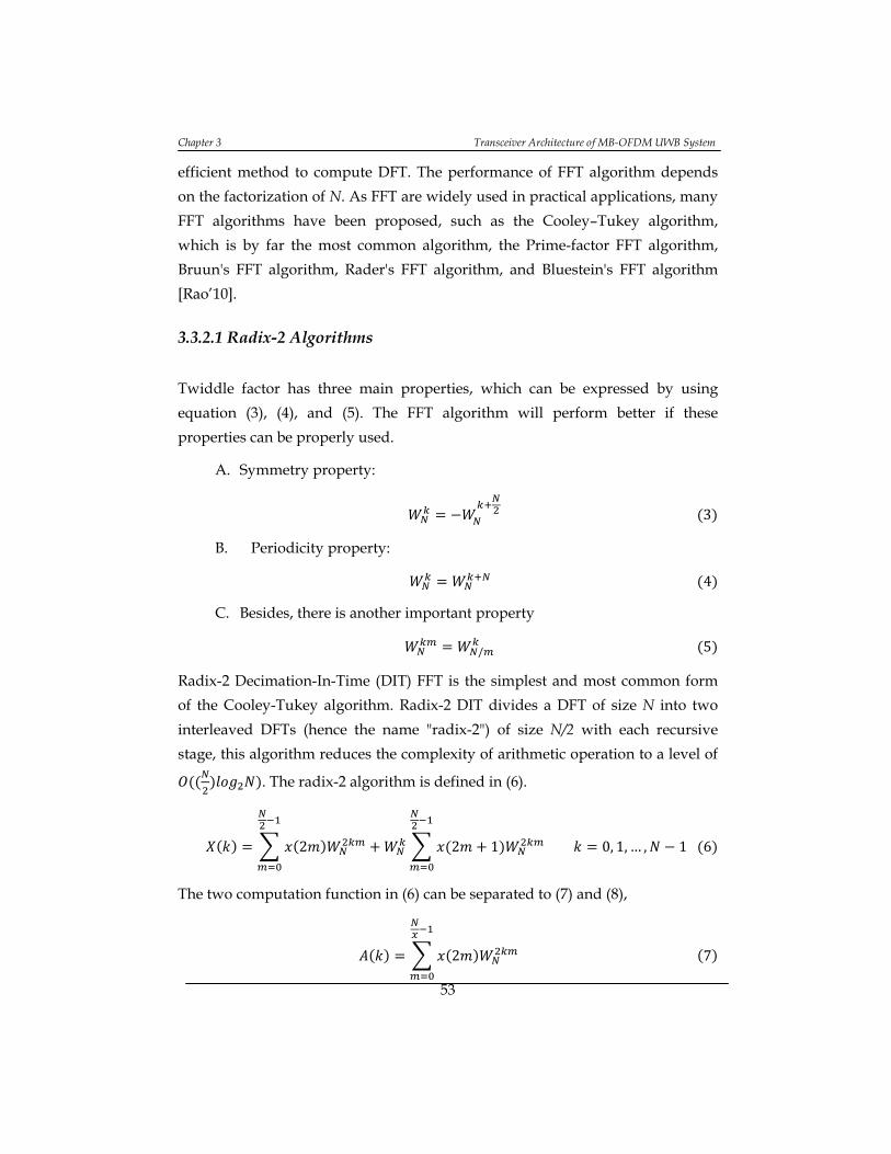
Chapter 3 Transceiver Architecture of MB-OFDM UWB System
53
efficient method to compute DFT. The performance of FFT algorithm depends
on the factorization of N. As FFT are widely used in practical applications, many
FFT algorithms have been proposed, such as the Cooley–Tukey algorithm,
which is by far the most common algorithm, the Prime-factor FFT algorithm,
Bruun's FFT algorithm, Rader's FFT algorithm, and Bluestein's FFT algorithm
[Rao’10].
3.3.2.1 Radix-2 Algorithms
Twiddle factor has three main properties, which can be expressed by using
equation (3), (4), and (5). The FFT algorithm will perform better if these
properties can be properly used.
A. Symmetry property:
3
B. Periodicity property:
4
C. Besides, there is another important property
/ 5
Radix-2 Decimation-In-Time (DIT) FFT is the simplest and most common form
of the Cooley-Tukey algorithm. Radix-2 DIT divides a DFT of size N into two
interleaved DFTs (hence the name "radix-2") of size N/2 with each recursive
stage, this algorithm reduces the complexity of arithmetic operation to a level of
. The radix-2 algorithm is defined in (6).
2 2 1 0, 1, … , 1 6
The two computation function in (6) can be separated to (7) and (8),
2 7
Design and Validation of an Optimized High-performance MB-OFDM Ultra Wideband Transceiver System
54
2 1 8
Thus, introducing A(k) and B(k) into (6), it can be rewritten it as (9).
2
2 2
2
9
As a result, the most rudimentary butterfly unit function can be obtained
through (9) (Cooley-Tukey butterfly), which is shown in Figure 3.4:
)(kA
)(kB kNW
kNW
)(kX
)2
(N
kX
Figure 3.4 Cooley-Tukey Butterfly processing
One thing that should be noticed is that, the radix-2 algorithm can only be used
when the number of samples N can be represented by a power of two.
Otherwise, mixed-radix or other algorithms should be used.
However, there is another way to organize the data based on radix-2 algorithm.
According to equations (6) and (9), we can obtain (10).
2 0, 1, … , 1 10
And based on this equation, it is noticed that
22
0, 1, … ,2
1 11

Chapter 3 Transceiver Architecture of MB-OFDM UWB System
55
2 12
0, 1, … ,2
1 12
Let
,
, 2 13
According to equation (11), (12) and (13), the modified radix-2 algorithm divides
the output results into odd and even number, instead, according to this theory,
the modified butterfly function is shown in Figure 3.5.
),( mrA
),( mrBm
NW
)2( rX
)12( rX
Figure 3.5 Modified radix-2 butterfly processing
Taking a look at the computation complexity, considering a sequence with the
length of N, this radix-2 algorithm requires S=log2N stages, with N/2 butterflies
per stage. Each butterfly requires one complex multiplier and two adders.
Therefore, the total cost of the algorithm, is thus the computational cost of radix-
2 DIF FFT, will be (N/2)log2N complex multiplies and N log2N adders.
In order to further speed up the DFT processing, higher radix algorithms have
been widely studied. The parallelization strategy is used so as in each processing
step, more calculations can be done, thus less stages of computation are needed.
This is extremely important for the large points DFT processing. But as a tradeoff,
the complexity of each processing stage will increase significantly due to the
parallelization. In the following subsections, the radix-4 and radix-2m algorithms,
which are the most popular algorithms, will be introduced.

Design and Validation of an Optimized High-performance MB-OFDM Ultra Wideband Transceiver System
56
3.3.2.2 Radix-4 Algorithms
The radix-4 FFT recursively partitions a DFT into four quarter-length DFTs.
Compared with radix-2 algorithms, the radix-4 algorithm has the advantage of
greatly reducing the total computational cost. In this section the radix-4
algorithm which employs two radix-2 butterflies to represent one radix-4
butterfly function, called radix-22 algorithm is discussed.
It can be noticed that, in order to employ the radix-4 algorithm, N should be the
power of four instead of two. For example, given a sequence with length N, by
using radix-4 algorithm, the shortest FFT in the expression can always be
presented as equation (14):
, 0, 1, 2, 3 14
According to radix-22 algorithm, parameters n and k should be divided into two
separate parts as shown in (15) and (16).
2 , 0, 1 15
2 , 0, 1 16
Substitute expression (15) and (16) into (14), we will have (17)
2 2 17
Both stage 1 and stage 2 in equation (17) are 2-point FFT functions. Therefore,
the calculation can be represented by using two radix-2 butterflies. The signal
flow representing the operation for radix-22 algorithm is depicted in Figure 3.6.

Chapter 3 Transceiver Architecture of MB-OFDM UWB System
57
)0(x
)2(x 1
)1(x
)3(xj1
1
1
)0(X
)2(X
)1(X
)3(X
Figure 3.6 Signal flow of radix-22 algorithm processing
To determine the total computational cost of the radix-4 FFT, it can be seen that
there are S=log4N stages for and N-point radix-4 FFT processor, each with
butterflies per stage. There are three complex multipliers and eight adders per
butterfly unit. Thus, the total computational cost of the radix-22 FFT algorithm is
complex multiplies and 2Nlog4N adders. Compared with radix-2 FFTs,
the radix-4 FFTs require only 75% as many complex multiplies as the radix-2
FFTs while the number of adders is remain the same.
3.3.2.3 Radix-2m Algorithm
As discussed in previous sections, the radix-2 butterfly function has simplified
the structure of data flow for calculating FFT. However, simply use radix-2
algorithm will lead to many extra twiddle factor multiplications between each
stage. As a result, higher radix can be introduced, such as radix-4, radix-8, and
radix-16 algorithms, to reduce the twiddle factor multiplications. Besides, a
radix-n algorithm can be represented as radix-2m algorithm if n is a power of two.
For example, radix-8 algorithm can be represented by radix-23, Figure 3.7 shows
the data flow of the radix-23 algorithm. But it should be noticed that, when the
radix is higher than 4, increasing the computational radix will dramatically
increase the computational complexity as well as the difficulties for hardware
implementation. Because lots of memory resources are required for restoring
those partial products within each processing procedure, beside, the control

Design and Validation of an Optimized High-performance MB-OFDM Ultra Wideband Transceiver System
58
logics are also difficult to be realized. Therefore, radix-2 and radix-22 algorithms
are more popular nowadays.
28W
18W
38W
14W
14W
Figure 3.7 Signal flow of Radix-23 algorithm processing
3.3.3 Different FFT Architectures
A variety of FFT architectures have been studied in the past few years. S. Magar
et al. [Magar’88] introduces the Recursive Dual Memory Architecture and Single
Memory Recursive systems. The simplest memory-system architecture is the
single-memory architecture, as it can be seen in Figure 3.8, in which a memory of
at least N words is connected to a processor by a bidirectional data bus. In
general, data are read from and write to the memory once for each stage of the
FFT processing.
Figure 3.8 Single Memory Architecture
The dual-memory architecture places two memories of size N/2 on separate
buses connected to a processor, as shown in Figure 3.9. Data begin in one

Chapter 3 Transceiver Architecture of MB-OFDM UWB System
59
memory and transfer from one bank of memory to another several times until
the transform comes to the end during the entire process.
Figure 3.9 Dual Memory Architecture
Cached-memory architecture [Bass’99] is similar to the single-memory
architecture except that an additional small cache memory resides between the
processor and main memory, as shown in Figure 3.10.
Figure 3.10 Cached-memory architecture
According to the results of [He’98], the use of cache architecture have two key
advantages over other two approaches:
1) Increased speed: since smaller memories are faster than larger ones
(more than 2.6 times greater than the previous ones)
2) Increased energy efficiency: since smaller memories require lower energy
per access and typically can be located nearer to the data path (16 times
more energy efficient)
Therefore, the cached-memory architecture is considered to be a better option.
In [He’98], pipeline architecture is used for implement the FFT processor.
Pipelined FFT processor is a class of architectures for applications of specific
real-time DFT computation which utilizing fast algorithms. It is characterized by
non-stopping processing on a clock frequency the same as the input data
sampling frequency. A lower clock frequency is a clear advantage for pipeline
architectures, when either a high throughput processing or a low power solution
is sought. In addition, pipeline structure is highly regular, which can be easily
scaled and parameterized when Hardware Description Language (HDL) is used
in the design. It is also flexible when forward inverse transforms of different
lengths are to be computed within one single chip.
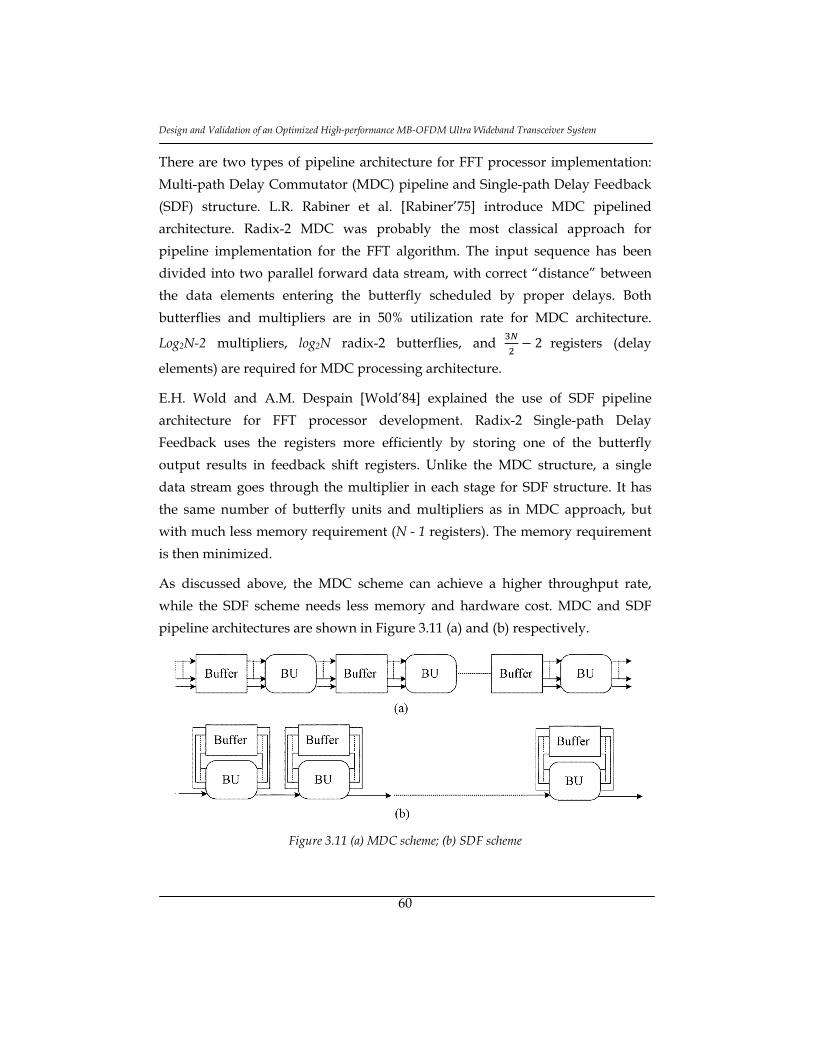
Design and Validation of an Optimized High-performance MB-OFDM Ultra Wideband Transceiver System
60
There are two types of pipeline architecture for FFT processor implementation:
Multi-path Delay Commutator (MDC) pipeline and Single-path Delay Feedback
(SDF) structure. L.R. Rabiner et al. [Rabiner’75] introduce MDC pipelined
architecture. Radix-2 MDC was probably the most classical approach for
pipeline implementation for the FFT algorithm. The input sequence has been
divided into two parallel forward data stream, with correct “distance” between
the data elements entering the butterfly scheduled by proper delays. Both
butterflies and multipliers are in 50% utilization rate for MDC architecture.
Log2N-2 multipliers, log2N radix-2 butterflies, and 2 registers (delay
elements) are required for MDC processing architecture.
E.H. Wold and A.M. Despain [Wold’84] explained the use of SDF pipeline
architecture for FFT processor development. Radix-2 Single-path Delay
Feedback uses the registers more efficiently by storing one of the butterfly
output results in feedback shift registers. Unlike the MDC structure, a single
data stream goes through the multiplier in each stage for SDF structure. It has
the same number of butterfly units and multipliers as in MDC approach, but
with much less memory requirement (N - 1 registers). The memory requirement
is then minimized.
As discussed above, the MDC scheme can achieve a higher throughput rate,
while the SDF scheme needs less memory and hardware cost. MDC and SDF
pipeline architectures are shown in Figure 3.11 (a) and (b) respectively.
Figure 3.11 (a) MDC scheme; (b) SDF scheme

Chapter 3 Transceiver Architecture of MB-OFDM UWB System
61
3.3.4 MB-OFDM modulation
According to the structure of the OFDM symbols organized for UWB
communication [ISO/IEC 26907’09], the discrete-time signal, sn[k], shall be
created by taking the Inverse Discrete Fourier Transform (IDFT) of the stream of
complex frequency values as follows:
1, exp
2, exp
j2pM I kN
C , I expj2pM I kN
Where
k=[0, NFFT-1], n=[Nsync, Npacket-1]
ND is the number of data subcarriers, NG is the number of guard subcarriers, NP
is the number of pilot subcarriers, NFFT is the number of total subcarriers, and
CD,n[I], CG,n[I], CP,n[I] are the complex numbers placed on the Ith data, guard and
pilot subcarriers of the nth OFDM symbol, Nsync is the number of symbols in the
PLCP preamble, and Npacket is the total number of symbols in the packet
respectively.
The functions MD[I], MG[I] and MP[I] define a mapping from the indexes [0, ND-
1], [0,NG-1] and [0, NP-1] to the logical frequency subcarriers [-NT/2, NT/2]
excluding 0 respectively. The exact definitions for the mapping functions MD[I],
MG[I] and MP[I]are given below:
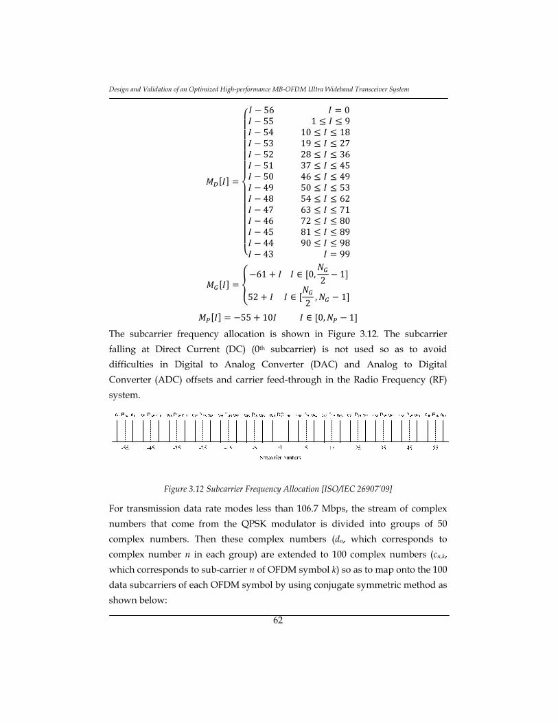
Design and Validation of an Optimized High-performance MB-OFDM Ultra Wideband Transceiver System
62
56 0551 95410 185319 275228 365137 455046 494950 534854 624763 714672 804581 894490 9843 99
61 ∈ 0,2
1
52 ∈2, 1
55 10 ∈ 0, 1
The subcarrier frequency allocation is shown in Figure 3.12. The subcarrier
falling at Direct Current (DC) (0th subcarrier) is not used so as to avoid
difficulties in Digital to Analog Converter (DAC) and Analog to Digital
Converter (ADC) offsets and carrier feed-through in the Radio Frequency (RF)
system.
Figure 3.12 Subcarrier Frequency Allocation [ISO/IEC 26907’09]
For transmission data rate modes less than 106.7 Mbps, the stream of complex
numbers that come from the QPSK modulator is divided into groups of 50
complex numbers. Then these complex numbers (dn, which corresponds to
complex number n in each group) are extended to 100 complex numbers (cn,k,
which corresponds to sub-carrier n of OFDM symbol k) so as to map onto the 100
data subcarriers of each OFDM symbol by using conjugate symmetric method as
shown below:

Chapter 3 Transceiver Architecture of MB-OFDM UWB System
63
, 0, 1, … , 49, 0, 1, … , 1
,∗ 0, 1, … , 49, 0, 1, … , 1
Where NSYM denotes the number of OFDM symbols in the MAC frame body, tail
bits, and pad bits.
The main purpose of taking this strategy is to force the IFFT input signals of
lower data rate modes to be conjugate symmetric. Besides, by further using
Time-Domain Spreading method to spread each symbol by a factor of two, the
final transmitted data sequence will get a spreading gain equals to four.
Therefore, according to the function of IFFT process, the imaginary part of the
output results from IFFT process will stay at ‘0’ for the entire OFDM symbol,
which means only the real part of the signals are needed to be transmitted. Then
the analog section of transmitter system can be simplified when the input signal
just contain real part. Only the “I” portion of DAC and mixers are necessary,
furthermore, only half the analog die size of a complete “I/Q” transmitter is
required for low data rate transmission modes. On the other hand, for the
receiver system, the ADC and the synchronization scheme for each symbol will
also be simplified by using this data structure. In addition, less energy is spent
for transmitting only the real part of each OFDM symbol.
For transmission data rates that are equal or higher than 106.7 Mbps, the stream
of complex number is divided into groups of 100 complex numbers directly to
form the data subcarriers for an OFDM symbol.
, 0, 1, … , 99, 0, 1, … , 1
Then, the pilot subcarriers are required for estimating the frequency offset at the
receiver side. In each OFDM symbol, twelve of the subcarriers are dedicated to
pilot signals in order to make coherent detection robust against frequency offsets
and phase noise. These pilot signals shall be added in the positions numbered as
–55, –45, –35, –25, –15 –5, 5, 15, 25, 35, 45, and 55. The contribution due to the
pilot subcarriers for the kth OFDM symbol is given by the Inverse Fast Fourier
Transform (IFFT) of the sequence Pn below, which is further QPSK modulated by
a pseudo-random binary sequence pl to prevent the generation of spectral lines.

Design and Validation of an Optimized High-performance MB-OFDM Ultra Wideband Transceiver System
64
1
√2 15, 45
1
√2 5, 25, 35,55
0
For transmission modes with data rates less than 106.67 Mbps:
, ,∗ 5, 15, 25, 35, 45, 55
For 106.7 Mbps and all higher rate transmission modes:
, , 5, 15, 25, 35, 45, 55
Then, besides these 112 samples, ten subcarriers are dedicated to guard
subcarriers or guard tones. The guard subcarriers can be used for carious
purposes, including relaxing the specs on transmit and receive filters. The
magnitude level of the guard tones is not specified other than the definition
below, and implementations can use reduced power for these subcarriers if
desired. The guard subcarriers shall be located in the subcarriers of –61, –60, …,
–57, and 57, 58, …, 61. The same Linear-Feedback Shift Register (LFSR) sequence
pl, which is used to scramble the pilot subcarriers, will be used to generate the
modulating data for the guard subcarriers. The guard subcarrier sample
definition for the nth subcarrier of the kth symbol is given as follows:
, , , 0,1,2,3,4; 57 ; 95
, , , 0,1,2,3,4; 61 ;
Where k=0 shall correspond to the first OFDM symbol following the PLCP preamble (i.e., the first OFDM symbol following the channel estimation sequence).
The mapping of each subcarrier to the 128-point FFT processor can be shown in
Figure 3.13.

Chapter 3 Transceiver Architecture of MB-OFDM UWB System
65
Figure 3.13 IFFT subcarriers mapping
3.3.5 Overview of FFT in MB-OFDM UWB
According to the MB-OFDM UWB standard, each OFDM symbol consists of 128
subcarriers and 37 Zero Prefix samples. Therefore, the FFT processor of the MB-
OFDM UWB system conducts a 128-point FFT operation, where the sampling
frequency is 528 MHz and the subcarrier frequency spacing is 4.125 MHz.
Although the FFT processing period is only 242.42 ns, the 128-point FFT
operation is allowed to be performed within 312.5 ns (410 Msps) because a
length-37 Zero Prefix duration (70.08 ns) is added after each OFDM symbol.
3.3.5.1 Evaluations of FFT processor
The measurements for FFT processor in MB-OFDM UWB system including
accuracy, power consumption, processing rate and hardware cost. In this section,
the measurements and the conditions which can affect the performance of the
FFT processor so as to help us developing a low power and high performance
FFT processor for MB-OFDM UWB applications are discussed.
Design and Validation of an Optimized High-performance MB-OFDM Ultra Wideband Transceiver System
66
3.3.5.1.1 Accuracy
Besides the communication channel and environments, which have a very
strong effects on the accuracy of the FFT performance, the word-length to
represent each sample that is used for processing hardware elements will also
affect the accuracy of FFT processor a lot.
Many works have been done on discussing the word-length effects on the
computational accuracy of UWB system. In [Lin’05] and [Cho’10_2], researchers
employ MATLAB fix-point toolbox to simulate the relation between SNR and
the internal word-length of the FFT/IFFT processor, both obtain the same
decision in choosing internal word-length of 10 bits for both the real and
imaginary parts of each OFDM sample. In [Sherratt’05], the authors discuss the
bit-length in the aspect of system level, in their opinion, there are two
parameters in FFT/IFFT processor that can affect the Bit Error Rate (BER)
performance of UWB system. These two parameters are external FFT data and
internal FFT precision. The authors simulate the BER by using different external
FFT data and different internal precision in 4 Channel models of UWB, and their
conclusion is 6-bit external FFT data and 11-bit internal FFT precision gives the
same order of performance as implementing floating-point. In [Insalata’07], the
authors separate the parameters into Input/Output Word Length (IOWL),
System Word Length (SWL), and Twiddle Word Length (TWL). Their final
decision is IOWL=6 bits, SWL=8 bits and TWL=4 bits. The output SQNR by
doing this is 29.3 dB, which is believed to be satisfied for UWB system
application.
As the word-length will also define the power consumption, hardware resources
usage, as well as the computational complexity of the whole FFT processor, we
will also make a discussion on choosing the most appropriate word length for
the proposed algorithm.
Chapter 3 Transceiver Architecture of MB-OFDM UWB System
67
3.3.5.1.2 Processing Rate
A minimum processing rate of 410 Msps must be supported by the FFT
processor in MB-OFDM UWB system. Processing rate of the FFT processor is
often decided by the structure of the processor, such as pipelined or in parallel,
multipath delay or singlepath delay. These different structures may result in
huge differences in throughput and other performance of the FFT processor. The
different structures will be discussed in the following section. Besides, accuracy
also affects the processing rate. As the accuracy increases, more bits are needed
to represent the data, more calculations are needed, and thus processing time
will increase as well. Moreover, the working frequency will decrease.
3.3.5.1.3 Hardware cost and power consumption
Hardware cost is usually measured by number of logic gates and chip area after
system synthesis. A well developed FFT algorithm will help to reduce the
complexity of computational models and circuits. Besides, even with the same
FFT algorithm, hardware cost and power consumptions might be quite different
by using different hardware architectures.
Reducing accuracy and processing rate will also reduce the power consumption.
If we want to obtain an overall good performance in the FFT processor, carefully
trade-off decision between accuracy and hardware cost should be made.
3.3.5.2 Related Works
There are a lot of works focusing on FFT model for MB-OFDM UWB system,
therefore variant algorithms and architectures are developed. Since 128 is not a
power of 4, 8 or 16, the 128-point FFT is often realized by using mixed-radix
algorithms so as to speed up the procedure.
Y. W. Lin et al. [Lin’05] proposed a mixed radix FFT algorithm, which uses
radix-2 and radix-64 algorithms. Moreover, they divided the radix-64 FFT into
two radix-8 FFT stages, and then realized the radix-8 FFT by using 3 radix-2
stages as discussed in section 3.3.2.3. The authors used four-parallel-path SDF

Design and Validation of an Optimized High-performance MB-OFDM Ultra Wideband Transceiver System
68
pipelined architecture for hardware implementation. By using 180 nm CMOS
technology library, the maximum processing frequency of the proposed FFT
chip reaches 250 MHz, the throughput rate can reach up to 1 Gsample/s with
the power dissipation of 175 mW.
S. Cho et al. [Cho’10] used a modified radix-24 algorithm and a radix-23
algorithm to significantly reduce the numbers of complex constant multipliers. It
also uses four-parallel-path pipelined architecture as in [Lin’05]. The simulation
results indicate that the FFT processor can also support a throughput up to 1
Gsample/s, but with a power dissipation of 112 mW by using 180 nm CMOS
technology library.
Z. Wang et al. [Wang’06] propose a two-stage radix-22 and radix-32 FFT
algorithm, they use radix-25 algorithm instead of radix-32, four-parallel-path
pipelines are used only for the second processing stage.
S. Qiao et al. [Qiao’07] proposed radix-2 and radix-64 FFT algorithm as
[Magar’88], however, they developed a non-Cooley-Tukey radix-8 unit in order
to save hardware cost. The experimental result shows the throughput rate is
409.6 Msample/s with area saved by 20% to 63% compared to that of radix-2
SDF architecture.
A. Cortes et al. [Cortes’06] proposed a software for generating the FFT cores for
OFDM applications. The presented generator is able to generate different modes
of FFT/IFFT processors according to the user’s specifications. The tool is user-
friendly and provides the ability to compare and analyze different FFT/IFFT
architectures, so as the users can select the most suitable design according to the
requirements.
3.3.6 Proposed FFT Processor
In this section, one of the most important original contributions of this thesis,
which is design of a low power, high speed FFT processor for MB-OFDM
UWB application, will be described in detail. A novel mixed radix 128-point FFT
algorithm is presented in this PhD thesis, and multipath pipelined architecture is
designed.
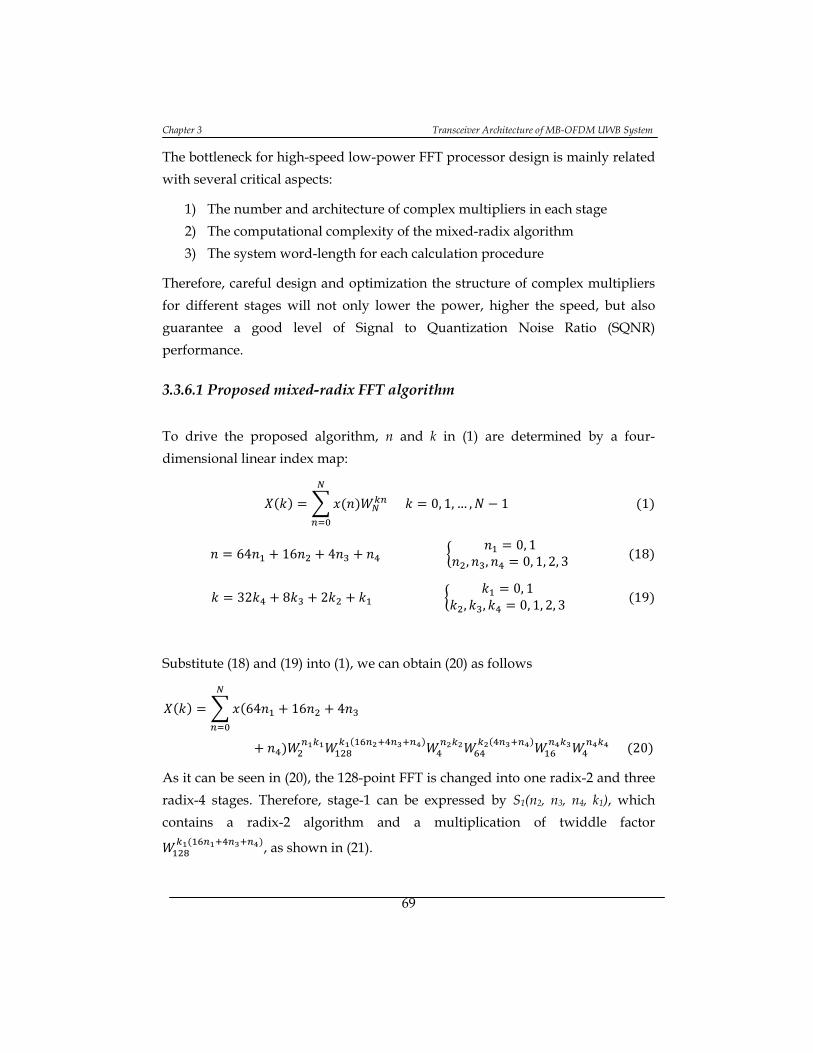
Chapter 3 Transceiver Architecture of MB-OFDM UWB System
69
The bottleneck for high-speed low-power FFT processor design is mainly related
with several critical aspects:
1) The number and architecture of complex multipliers in each stage
2) The computational complexity of the mixed-radix algorithm
3) The system word-length for each calculation procedure
Therefore, careful design and optimization the structure of complex multipliers
for different stages will not only lower the power, higher the speed, but also
guarantee a good level of Signal to Quantization Noise Ratio (SQNR)
performance.
3.3.6.1 Proposed mixed-radix FFT algorithm
To drive the proposed algorithm, n and k in (1) are determined by a four-
dimensional linear index map:
0, 1, … , 1 1
64 16 4 0, 1
, , 0, 1, 2, 3 18
32 8 2 0, 1
, , 0, 1, 2, 3 19
Substitute (18) and (19) into (1), we can obtain (20) as follows
64 16 4
20
As it can be seen in (20), the 128-point FFT is changed into one radix-2 and three
radix-4 stages. Therefore, stage-1 can be expressed by S1(n2, n3, n4, k1), which
contains a radix-2 algorithm and a multiplication of twiddle factor
, as shown in (21).
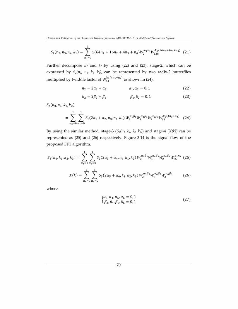
Design and Validation of an Optimized High-performance MB-OFDM Ultra Wideband Transceiver System
70
, , , 64 16 4 21
Further decompose n2 and k2 by using (22) and (23), stage-2, which can be
expressed by S2(n3, n4, k1, k2), can be represented by two radix-2 butterflies
multiplied by twiddle factor of W as shown in (24).
2 , 0, 1 22
2 , 0, 1 23
, , ,
2 , , , 24
By using the similar method, stage-3 (S3(n4, k1, k2, k3)) and stage-4 (X(k)) can be
represented as (25) and (26) respectively. Figure 3.14 is the signal flow of the
proposed FFT algorithm.
, , , 2 , , , 25
2 , , , 26
where
, , , 0, 1, , , 0, 1 27

Chapter 3 Transceiver Architecture of MB-OFDM UWB System
71
jjj
j
jj
jj
jj
jj
j
jjj
jj
jj
jj
jj
jj
jj
j
jjj
j
j
j
j
j
j
j
j
j
j
j
j
j
j
j
j
j
j
j
j
j
j
j
j
j
j
j
j
j
j
j
j
128W 64W 16W
jjjjjjjjjjjjjjjjjjjjjjjjjjjjjjjj
jjjjjjjjjjjjjjjjjjjjjjjjjjjjjjjj
Figure 3.14 Signal Flow of proposed FFT algorithm
Design and Validation of an Optimized High-performance MB-OFDM Ultra Wideband Transceiver System
72
3.3.6.2 Architecture of the proposed FFT processor
According to the proposed algorithm, a four-parallel-path SDF pipelined
processor architecture is proposed in this thesis. The block diagram of the
proposed architecture is given in Figure 3.15.
Module 1 to 4 represents to stage-1 to stage-4 in signal flow respectively. The
function of Module 1 is to realize the radix-2 FFT algorithm, while Modules 2
to 4 realize the radix-22 FFT algorithm.
As discussed above, the processing word length will have a great effect on the
accurate of the FFT architecture, therefore, three types of word lengths are
defined for the proposed system so as to discuss the word-length effect on the
proposed FFT architecture: Input/Output Word-Length (IOWL), System Word-
Length (SWL) and Twiddle Word-Length (TWL). The word length selection has
been based on a detailed analysis so as to get suitable Signal to Quantization
Noise Ratio (SQNR) for the proposed FFT processor, while maintaining the
word length for each processing elements in minimum values.

Chapter 3 Transceiver Architecture of MB-OFDM UWB System
73
Figure 3.15 Block diagram of proposed four-parallel-path 128-point mix-radix FFT processor

Design and Validation of an Optimized High-performance MB-OFDM Ultra Wideband Transceiver System
74
Module 1 architecture
The Module 1 is implemented by using radix-2 butterfly architecture.
Module 1 consists of four register files (each can store 16 pieces of complex data),
two complex Booth’s multipliers, four radix-2 Butterfly Units (BUs), two Read
Only Memory (ROM) and some multiplexers. The function of ROM is to restore
the Twiddle Factors (TWs) for W . Only 1/8 periods of the cosine
and sine waveforms are stored in the ROM for the proposed Module 1 structure,
while the other 7/8 values is generated by using these 1/8 values. Because the
cosin and sin functions have the periodical property.
During the first 16 clock cycles, the first 64 input data (x(n) to x(n+63)) are
restored in the register file according to the input order. Then from the 17th clock
cycle, the BUs begin to execute the complex addition and subtraction between
x(n) and x(n+64) during the next 16 clock cycles. At this point, all the 128 points
have been processed by the radix-2 BUs. The results of addition (x(i)) will then
be fed to Module 2 directly as no multiplications are needed for those signals
according to the proposed algorithm, while the results of subtraction (y(i)) are
firstly multiplied by the corresponding TWs and then stored into the register
files before they are sent to Module 2.
Four complex multipliers are needed in the four-parallel-path approach to
implement the radix-2 FFT algorithm, thus the utilization rate of the complex
multiplier is only 50% because no multiplications are needed for the addition
results. However, in the proposed architecture of this thesis, as Module 2 needs
32 clock cycles to process x(i) (will be illustrated later), the complex multiplier
can be shared for four paths separately during these 32 cycles by using the
folding technology with a folding factor of two. The detailed operation is
described below.
When y(i) are generated from BUs, two paths of y(i), y(0) and y(1), are multiplied
by the appropriated twiddle factors first, while y(2) and y(3) are feeding to the
register files directly. 16 clock cycles later, other two paths, y(2) and y(3), are
picked out for multiplication, and then be fed to Module 2 at the same time with
the multiplication results of y(0) and y(1). By using this rescheduling
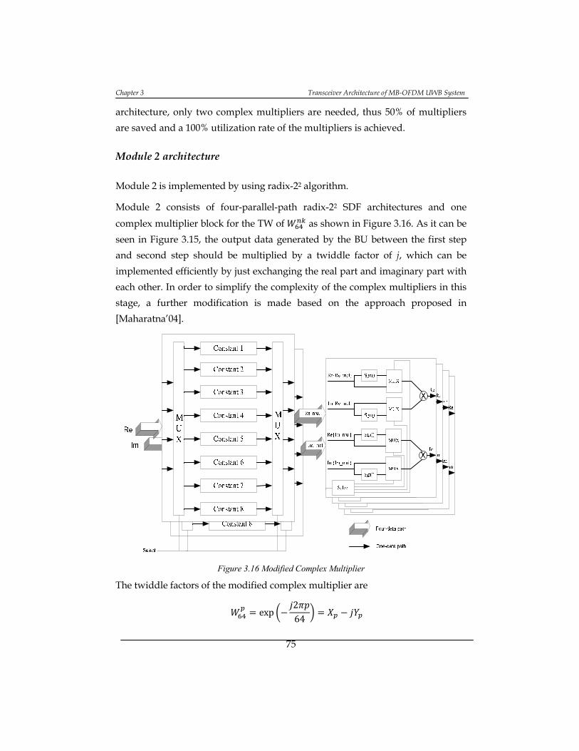
Chapter 3 Transceiver Architecture of MB-OFDM UWB System
75
architecture, only two complex multipliers are needed, thus 50% of multipliers
are saved and a 100% utilization rate of the multipliers is achieved.
Module 2 architecture
Module 2 is implemented by using radix-22 algorithm.
Module 2 consists of four-parallel-path radix-22 SDF architectures and one
complex multiplier block for the TW of as shown in Figure 3.16. As it can be
seen in Figure 3.15, the output data generated by the BU between the first step
and second step should be multiplied by a twiddle factor of j, which can be
implemented efficiently by just exchanging the real part and imaginary part with
each other. In order to simplify the complexity of the complex multipliers in this
stage, a further modification is made based on the approach proposed in
[Maharatna’04].
Figure 3.16 Modified Complex Multiplier
The twiddle factors of the modified complex multiplier are
exp264

Design and Validation of an Optimized High-performance MB-OFDM Ultra Wideband Transceiver System
76
Where
cos 2 /64
sin 2 /64
and p is from 0 to 45.
The 64 twiddle factors can be divided into eight regions as shown in Figure 3.17.
Region A consists of values with p from 0 to 8, the values in other seven regions
can be represented by transforming the data of region A according to Table 3-1.
Therefore, through the mapping method, only nine sets of constant values are
needed. In practice, only eight sets of constant values are necessary to be
implemented in region A, since the first pair of constant values (1, 0) is trivial. In
addition, these constant values can be realized more efficiently by using 8-bit
shift-add multipliers [Maharatna’04].
Figure 3.17 Twiddle factor of 64 can be divided into eight regions
Table 3-1 Mapping table for twiddle factor in different region
Region Real Imaginary
A (p=x*) Xp -Yp
B (p=16-x) Yp -Xp
C (p=x-16) -Yp -Xp
D (p=32-x) -Xp -Yp
E (p=x-32) -Xp Yp
F (p=48-x) -Yp Xp

Chapter 3 Transceiver Architecture of MB-OFDM UWB System
77
The Table 3-2 shows the schedule of the twiddle factors for the four paths. The
table only shows 16 clock cycles because the values of twiddle factors are
repeated every 16 cycles for the proposed algorithm. After mapping according to
Table 3-1, the results of the coefficient value and corresponding regions are
shown in Table 3-3 and Table 3-4. It can be clearly seen from Table 3-3 that the
twiddle factor of four paths in each time slot has different values, except for the
first 4 cycles, during which no multiplications are needed. As it can be seen from
the block diagram of the complex multiplier in Figure 3.16, when the inputs
come in the first module of the optimized multiplier, the four paths data are
mapped into different complex constant multipliers according to the schedule in
Table 3-3. After the multiplications, the regions are selected at the second
module according to Table 3-4 and Table 3-1. By using the modified complex
multiplier, the system is much simpler, efficient in time and energy as only few
registers and adders are needed for hardware implementation according to the
structure.
Table 3-2 Scheduling of the twiddle factor, , where x is the value shown in the table
Path No. Value of x
1 0 0 0 0 0 8 16 24 0 12 24 36 0 4 8 12
2 0 0 0 0 2 10 18 26 3 15 27 39 1 5 9 13
3 0 0 0 0 4 12 20 28 6 18 30 42 2 6 10 14
4 0 0 0 0 6 14 22 30 9 21 33 45 3 7 11 15
Table 3-3 Scheduling of the twiddle factor after mapping
Path No. Schedule of twiddle factor value
1 0 0 0 0 0 8 0 8 0 4 8 4 0 4 8 4
2 0 0 0 0 2 6 2 6 3 1 5 7 1 5 7 3
3 0 0 0 0 4 4 4 4 6 2 2 6 2 6 6 2
4 0 0 0 0 6 2 6 2 7 5 1 3 3 7 5 1
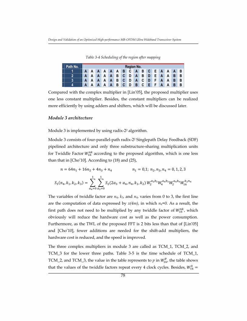
Design and Validation of an Optimized High-performance MB-OFDM Ultra Wideband Transceiver System
78
Table 3-4 Scheduling of the region after mapping
Path No. Region No. 1 A A A A A A B C A B C E A A A B 2 A A A A A B C D A B D E A A B B 3 A A A A A B C D A C D F A A B B 4 A A A A A B C D B C E F A A B B
Compared with the complex multiplier in [Lin’05], the proposed multiplier uses
one less constant multiplier. Besides, the constant multipliers can be realized
more efficiently by using adders and shifters, which will be discussed later.
Module 3 architecture
Module 3 is implemented by using radix-22 algorithm.
Module 3 consists of four-parallel-path radix-22 Singlepath Delay Feedback (SDF)
pipelined architecture and only three substructure-sharing multiplication units
for Twiddle Factor according to the proposed algorithm, which is one less
than that in [Cho’10]. According to (18) and (25),
64 16 4 0,1; , , 0, 1, 2, 3
, , , 2 , , ,
The variables of twiddle factor are n4, k3, and n4, varies from 0 to 3, the first line
are the computation of data expressed by x(4m), in which n4=0. As a result, the
first path does not need to be multiplied by any twiddle factor of , which
obviously will reduce the hardware cost as well as the power consumption.
Furthermore, as the TWL of the proposed FFT is 2 bits less than that of [Lin’05]
and [Cho’10], fewer additions are needed for the shift-add multipliers, the
hardware cost is reduced, and the speed is improved.
The three complex multipliers in module 3 are called as TCM_1, TCM_2, and
TCM_3 for the lower three paths. Table 3-5 is the time schedule of TCM_1,
TCM_2, and TCM_3, the value in the table represents to p in , the table shows
that the values of the twiddle factors repeat every 4 clock cycles. Besides,

Chapter 3 Transceiver Architecture of MB-OFDM UWB System
79
1, which is trivial multiplication, therefore only 3 twiddle factors should be
implemented in each multipliers. According to Table 3-5, the coefficients that are
needed to represent all the twiddle factors can be calculated in each multiplier.
Table 3-6 is the coefficient table which shows that TCM_1 and TCM_3 require
three coefficients, whereas TCM_2 needs only one coefficient.
Table 3-5 Time Schedule for TCM_1, TCM_2 and TCM_3
TCM_1 0 2 3 1
TCM_2 0 4 6 2
TCM_3 0 6 9 3
Table 3-6 Coefficient Table
TCM_1 cos ,cos ,sin4 8 8
TCM_2 cos4
TCM_3 cos ,cos ,sin4 8 8
The architecture of TCM1 is shown in Figure 3.18. TCM1_S1 controls whether to
exchange the real part with the imaginary part at the input, acts as the twiddle
factor of j. TWD1 in Figure 3.18 is the coefficient multiplier which multipliers the
input by , , , at the same time, the three outputs are selected by
control signal TCM1_S2. Finally, the computed results are selected by TCM1_S3.
The control signals corresponding to twiddle values for TCM_1 are listed in Table
3-7. The TWD1 multiplier is realized by using the proposed shift-add sharing
architecture, which will be discussed later.

Design and Validation of an Optimized High-performance MB-OFDM Ultra Wideband Transceiver System
80
Figure 3.18 Architecture of TCM_1
Table 3-7 Control signals in TCM_1
p TCM1_S1 TCM1_S2 TCM1_S3
0 0 X 0
2 0 1 1
3 1 0 2
1 0 0 3
The structure of TCM_2 is presented in Figure 3.19. TWD2 multiplies the inputs
by coefficient , TCM2_S is in charge of selecting the output results based on
the twiddle factor schedule. Table 3-8 shows the control signal for TCM2_S. The
detailed structure of TWD2 will also be discussed later.

Chapter 3 Transceiver Architecture of MB-OFDM UWB System
81
Figure 3.19 Architecture of TCM_2
Table 3-8 Control signals in TCM_2
P TCM2_S
0 0
4 1
6 2
2 3
The architecture of TCM_3 at the fourth line is depicted in Figure 3.20, with the
structure similar as TCM_1. Three different coefficients are also needed for this
path. Table 3-9 shows the assignment of control signals for each multiplexer
(TCM3_S1, S2 and S3).
Figure 3.20 Architecture of TCM_3

Design and Validation of an Optimized High-performance MB-OFDM Ultra Wideband Transceiver System
82
Table 3-9 Control signals in TCM_3
TWD exponent TCM3_S1 TCM3_S2 TCM3_S3
0 0 X 0
6 0 1 1
9 0 0 2
3 1 0 3
According to the figures above, it is clear to see that TCM_2 costs less hardware
than TCM_1 and TCM_3, as less twiddle factor multiplications are needed.
Module 4 architecture
Module 4 is also implemented by using radix-22 algorithm.
The architecture of module 4 is different from that of module 2 and module 3. As
the variables of this module are n4, k4, the four outputs of module 3 with
different n4 should be reorganized in different data path in order to operate as
radix-22 algorithm. Therefore, module 4 has two stages of radix-2 Butterfly Units
(BUs), only one twiddle factor of ‘j’ is needed which can be implemented by
exchanging the real part and imaginary part of the incoming complex data.
3.3.6.3 Architecture Pre-check in SIMULINK
In order to ensure that the proposed algorithm as well as the designed
architecture is correct and suitable for MB-OFDM system application, the
SIMULINK of MATLAB [MathWorks] is used in this thesis to build and verify
the proposed architecture before the final hardware implementation. Figure 3.21
is the system block diagram which consists of a data generator block, module 1,
module 2, module 3, module 4 and a check module for verifying the processing
results according to the proposed system architecture as illustrated above.
Furthermore, all the blocks that used for building this block diagram are using
the fixed-point tool box provided by SIMULINK library.

Chapter 3 Transceiver Architecture of MB-OFDM UWB System
83
In Figure 3.21, mul_64 and mul_16 are the complex multipliers in module 2 and
module 3 respectively. The integer delay modules are the control signals indicate
when a module is executed. As it can be seen from the output results, at the 32nd
clock cycle, the first group of data is obtained. Then 32 clock cycles later, all the
128 samples within one OFDM symbol are collected, means one entire OFDM
symbol has been successfully processed. Thus total 64 clock cycles are necessary
to simulate the entire 128-point check sequence.
Figure 3.21 System Architecture simulation in SIMULINK
The four-parallel-path butterfly units that are built for module 1 are shown in
Figure 3.22, the structure of radix21, radix22, radix23 and radix24 are the same as
radix-2 BU. The BU processing is molded by using the state-flow block provided
by SIMULINK library, which is very convenient to use and easy to understand,
as it can be seen in Figure 3.23.
When the enable signal is not valid (‘0’ in this situation), the radix-2 BU directly
assign the values of inputs to its outputs. Otherwise, it acts as a radix-2 butterfly
unit.

Design and Validation of an Optimized High-performance MB-OFDM Ultra Wideband Transceiver System
84
Figure 3.22 Four Butterfly units in Module 1
Figure 3.23 Butterfly unit (BU2)
The four-parallel-path radix-22 modules in module 2 are shown in Figure 3.24,
with the detailed structure is shown in Figure 3.25, which is exactly the same as
the module 2 in Figure 3.15. Figure 3.26 is the architecture of Module 4.

Chapter 3 Transceiver Architecture of MB-OFDM UWB System
85
Figure 3.24 Four parallel radix-22 subsystem in Module 2
Figure 3.25 Block diagram of radix-22 subsystem

Design and Validation of an Optimized High-performance MB-OFDM Ultra Wideband Transceiver System
86
Figure 3.26 SIMULINK model of Module 4
The data generator block in Figure 3.21 takes charge of generating the test
sequences for the proposed FFT architecture. In order to ensure that the
proposed FFT processor is suitable for the MB-OFDM system, the random
OFDM symbol simulation sequence has exactly the same property with that
specified by the MB-OFDM UWB standard. Figure 3.27 is a generated OFDM
frame of 128 point long. The verification procedure is done by comparing the
output results, collected by the ‘check’ block in Figure 3.21, with the results
provided by embedded FFT function in MATLAB. Total number of 42 groups of
OFDM symbols has been generated automatically for testing the proposed
architecture. Once the results of the proposed FFT processor are the same with
that of the embedded FFT function, which means the proposed FFT algorithm as
well as the architecture is correct. Figure 3.28 (a) is the result computed by
embedded FFT function in MATLAB, and (b) is the result computed by the
proposed architecture. Figure 3.29 shows the error of the proposed architecture
compared with the embedded MATLAB FFT function. Figure 3.29 indicates that
the error of the proposed algorithm has an order of 10-16, which is very small. As
a result, it’s demonstrated that the proposed FFT architecture in this thesis is
correct.

Chapter 3 Transceiver Architecture of MB-OFDM UWB System
87
Figure 3.27 Generated Input Sequence
(a)
(b)
Figure 3.28 (a) Output of Embedded MATLAB FFT function,
(b) Output of the proposed FFT architecture

Design and Validation of an Optimized High-performance MB-OFDM Ultra Wideband Transceiver System
88
Figure 3.29 Output SQNR (dB) of proposed FFT processor
3.3.6.4 Overflow Control and Word-length Decision
As it has been discussed before, when implementing the 128-point FFT
algorithm on hardware, not only the bit length but also the way dealing with
overflow will affect the processing accuracy, computing complexity and
hardware resource usage of the FFT/IFFT processor. Therefore, proper bit
length and overflow arithmetic into account must be taken when making the
hardware implementation of the proposed processor. The work in [Lin’05],
[Cho’10] and [Sherratt’05] do not mention how to handle overflow problem
either the bit-length for integer part and fractional part, while paper [Insalata’07]
discusses about Block Floating Point (BFP) and Convergent BFP (CBFP)
arithmetic to handle the overflow for the FFT processor. Armstrong, J. et al.
[Armstrong’04] propose a novel method to obtain a better accuracy. In this
section the overflow control and word-length decision that is made for the
proposed FFT processor will be discussed.

Chapter 3 Transceiver Architecture of MB-OFDM UWB System
89
3.3.6.4.1 Overflow Control
For the MB-OFDM systems, the OFDM modulation is done by using IFFT
processor on the transmitter side, while FFT acts as a de-OFDM-modulator on
the receiver side. The data will be transformed through time-domain and
frequency-domain through this procedure. Figure 3.30 is the signal flow of
transmitter and receiver in view of FFT and IFFT for MB-OFDM system:
)(nQ )(kq )(' kq )(' nQ
Figure 3.30 Transmitter to receiver in view of FFT/IFFT
As introduced before, the first stage of FFT processor operates the radix-2
algorithm which can be explained by Figure 3.31.
)( kq
)2
(N
kq
a
b
Figure 3.31 Radix-2 butterfly unit
Accordingly, we have:
21 ∗ ∗ 1 ∗ 1 ∗ 28
21 ∗ ∗ 1 ∗ 1 ∗ 29
Therefore,
2 ∗ 2 ∗, 0,1, …,2
2 30
2 ∗ 2 1 ∗, 0,1, …,2
2 31
At this point, the maximum value for both real part and imaginary part of a and
b can be estimated as follows:

Design and Validation of an Optimized High-performance MB-OFDM Ultra Wideband Transceiver System
90
max max2
1 1 32
max max2
1 1 33
Therefore, according to the expressions of (32) and (33), overflow will not
happen at stage 1 for the proposed FFT algorithm. By using the similar method,
it can be concluded that with acceptable AWGN, overflow will not happen in all
the stages of the FFT processor for the MB-OFDM receiver system. But on the
other hand, IFFT processor will suffer the overflow errors a lot. Therefore, the
BFP algorithm for IFFT at transmitter is chosen to control overflow (will be
discussed in section 3.3.7), while FFT at the receiver does not need to control
overflow.
3.3.6.4.2 Word-Length Decision
To properly choose the word length for the proposed FFT architecture, the fix-
point toolbox of MATLAB is used to simulate the already built SIMULINK
architecture.
First of all, a data package is generated. It contains 18 different OFDM symbols
according to [ISO/IEC 26907’09], and then it is expanded to 36 symbols as time-
domain spreading is required, 6 channel estimation symbols are also added in
front. To experimental simulate the receiver system, the data packet is computed
using the embedded IFFT MATLAB function, then the outputs will be the input
stream of the FFT architecture. Secondly, by varying internal word length from 8
to 11 bits, different output SQNR performances for the proposed FFT processor
can be obtained. Figure 3.32 to Figure 3.36 show the SQNRs when
IOWL=SWL=TWL ranging from 8 to 12.
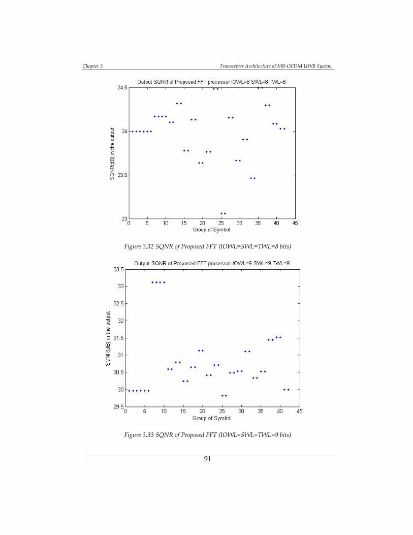
Chapter 3 Transceiver Architecture of MB-OFDM UWB System
91
Figure 3.32 SQNR of Proposed FFT (IOWL=SWL=TWL=8 bits)
Figure 3.33 SQNR of Proposed FFT (IOWL=SWL=TWL=9 bits)

Design and Validation of an Optimized High-performance MB-OFDM Ultra Wideband Transceiver System
92
Figure 3.34 SQNR of Proposed FFT (IOWL=SWL=TWL=10 bits)
Figure 3.35 SQNR of Proposed FFT (IOWL=SWL=TWL=11 bits)
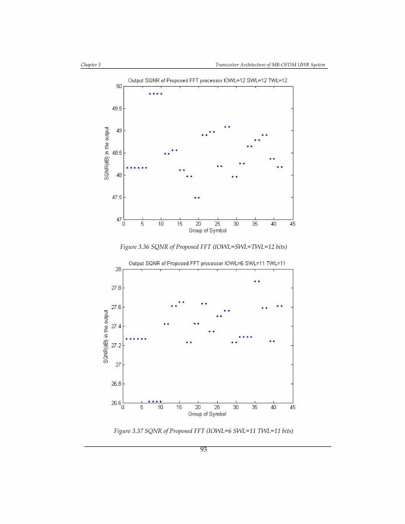
Chapter 3 Transceiver Architecture of MB-OFDM UWB System
93
Figure 3.36 SQNR of Proposed FFT (IOWL=SWL=TWL=12 bits)
Figure 3.37 SQNR of Proposed FFT (IOWL=6 SWL=11 TWL=11 bits)

Design and Validation of an Optimized High-performance MB-OFDM Ultra Wideband Transceiver System
94
Figure 3.38 SQNR of Proposed FFT (IOWL=SWL=10 TWL=8 bits)
As it can be seen from the figures, the SQNRs are different with each other
because the structures of the symbols are different. The average SQNR increases
as the word length increases. The simulation result of IOWL=6, SWL=TWL=11
as [Sherratt’05] is shown in Figure 3.37, the average SQNR is 27.4 dB, which
means the BER of UWB communication system is good enough when the SQNR
is more than 27.4 dB. This is a trade-off between system accuracy and hardware
cost. In [Insalata’07], the SQNR reaches 35 dB when internal bit length equals to
10. According to the simulation based on the proposed architecture, the SQNR
will reach up to 36.7 dB when the processing bit length equals to 10 bits. Besides,
as discussed by [Sherratt’05], the module next to OFDM requires at least 12 bits
to give the same order of performance as implementing of floating-point, keep
the IOWL and SWL as 10 bits, but reduce the TWL to 8 bits to lower the SQNR,
as it can be seen in Figure 3.38, the average SQNR is then 34.1 dB provided by
the proposed FFT processor, which still satisfies the UWB requirement. Table
3-10 summarizes the simulation results for different word lengths.

Chapter 3 Transceiver Architecture of MB-OFDM UWB System
95
Table 3-10 Output SQNR summary table
IOWL,SWL,TWL(bit) 8,8,8 9,9,9 10,10,10 11,11,11 12,12,12 6,11,11 10,10,8
Worst output SQNR (dB) 23 30.6 35.6 41.5 47.5 26.6 33.3
Best output SQNR (dB) 24.5 33.1 38.4 44 49.9 27.9 34.7
Average SQNR (dB) 24.0 30.8 36.7 42.6 48.5 27.4 34.1
Once the word length and overflow control arithmetic are decided, the proposed
architecture of the coefficient multipliers (TWD1 and TWD2) can be designed for
module 3. The MATLAB fix-point tool box is used to compute the 8 bits binary
value for those coefficients in TWD1 and TWD2, Table 3-11 shows the 2’s
complement values of the coefficients for TWD1 in TCM_1 and TCM_3. It is
noticed that the binary values of a, b and c have some parts in common, that can
be used to reduce the hardware cost. The binary values are decomposed to find
the sharing parts. The architecture of TWD1 is shown in Figure 3.39. As it can be
seen, the sharing architecture in TWD1 uses 6 shifters and 5 adders, however if
the coefficient multipliers are built separately, the hardware cost will be twice as
much as that of the proposed sharing architecture.
Table 3-11 8 bits binary of the coefficients and decomposition (for TCM_1 and 3)
Coefficients 2’s complement 2’s complement decomposition
8cos
a 01110110
00110110
01000000
8sin
b 00110001
00110000
00000001
4cos
c 01011011
00011011
01000000

Design and Validation of an Optimized High-performance MB-OFDM Ultra Wideband Transceiver System
96
Figure 3.39 Architecture of TWD1
As TWD2 only consists of one coefficient multiplier, the decomposition method would be different from that of TWD1, Table 3-12 shows the decomposition for the coefficient of cos .
Figure 3.40 is the architecture of TWD2, which is implemented by using 4
shifters and 3 adders.
Table 3-12 8 bits Binary value of the coefficients and decomposition (for TCM_2)
Coefficients 2’s complement 2’s complement decomposition
4 01011011
01011010
00000001
4cos
y
Figure 3.40 Architecture of TWD2
The eight constant multipliers in CM2 are also realized by using shifters and
adders, Table 3-13 is the decomposition of those constants in terms of power of 2.
Compared with traditional multiplier architecture, the add-shift methodology
has the advantage of both low power consumption and high processing speed.

Chapter 3 Transceiver Architecture of MB-OFDM UWB System
97
Table 3-13 Decomposition of Twiddle factor in power of 2
Real part Imaginary part
Const 1 721 754 222
Const 2 621 743 222
Const 3 64 221 752 222
Const 4 64 221 732 222
Const 5 7321 2222 51 221
Const 6 653 2221 7651 2222
Const 7 7621 2222 731 222
Const 8 752 2221 752 2221
3.3.6.5 Experimental Results of Final Implementation
After the algorithm, architecture proposal, and final word-length decision for
each block, a manually optimized implementation in by using Verilog HDL code
for the proposed FFT processor has been obtained. By using the proposed
Hardware-in-the-loop co-simulation methodology (will be explained in Chapter
0), the hardware model is verified and the output SQNRs of different input data
are calculated, with the average SQNR of 34 dB. The SQNR of real FPGA
implementation is shown in Figure 3.41.
Figure 3.41 SQNR of proposed FFT processor for hardware implementation

Design and Validation of an Optimized High-performance MB-OFDM Ultra Wideband Transceiver System
98
In order to compare the implementation result of proposed FFT processor with
previous ones in [Lin’05] and [Cho’10], at the end, by using Synopsys tools, the
proposed FFT architecture is synthesized using the UMCL130E 0.13 µm CMOS
technology with a supply voltage of 1.32 V. Table 3-14 compares the
implementation results of the proposed FFT processor with two of the existing
works. It indicates that the proposed FFT processor can support a data processing
rate of 1 Gsample/s with power dissipation of only 43.79 mW at 250 MHz
processing frequency. In order to compare the power consumption with [Lin’05]
and [Cho’10], which use 0.18 µm technology, the power consumption might be
multiplied by a factor of around 1.4, thus is 61 mW, which saves around 65% and
50% of energy respectively.
Table 3-14 Comparison synthesis results of the FFT processor
Algorithm Proposed algorithm
Y. W. Lin et al. [Lin’05]
Sang-In Cho et al. [Cho’10]
CMOS Technology Library (nm) 130 180 180 Working Frequency(MHz) 250 250 250
Equivalent 2*1Nand Gate Count 80,424 N/A 80,100 Dynamic Power (mW) 43.79 175 112
Table 3-15 compares the hardware complexity of the proposed FFT architecture
with the architectures proposed in [Lin’05] and [Cho’10]. In the proposed
architecture, only 3 trivial multipliers are needed, their complexities are reduced
because of the property of data stream and the sharing structure is employed. As
a result, the hardware cost of the three trivial multipliers is 40% of [Cho’10] and
63.7% of [Lin’05]. CM2 not only uses less constant complex multiplier than that
of [Lin’05], but also the word-length of the twiddle factor is two bits less. Besides,
the multipliers at stage 1 employ Booth’s algorithm, thus the hardware cost of
nontrivial multipliers is 75% of [Lin’05].

Chapter 3 Transceiver Architecture of MB-OFDM UWB System
99
Table 3-15 Comparison of the 128-point FFT architecture
Algorithm Proposed algorithm
Sang-In Cho et al. [Cho’10]
Y. W. Lin et al. [Lin’05]
Architecture radix-2, 2×radix-22 modified radix-24, radix-23 radix-2, 2×radix-23
No. of complex registers 124 124 124 No. of nontrivial
multipliers 4×0.55+2×0.58 4×0.6 2+4×0.62
No. of trivial multipliers 2×1.5+1×0.82 4×1.97+2×0.82 6
No. of complex adders 48 48 48 Throughput rate (R: clock rate) 4R 4R 4R
3.3.7 Proposed IFFT Processor
3.3.7.1 IFFT Algorithm
As is known to all, the IFFT of an N-point sequence, X(k), where k=0,1, … ,N-1, is
defined as
1 34
If take the complex conjugate of (34) expressed as (35), the equation (36) can be
obtained as
∗ 1 ∗ 35
1 ∗
∗
36
According to (36), the IFFT function is the conjugate of the FFT function with the
conjugate input sequence of ∗ , and then divided by N. Figure 3.42 is the
architecture of the IFFT processor by using the FFT processor:

Design and Validation of an Optimized High-performance MB-OFDM Ultra Wideband Transceiver System
100
U
U
Figure 3.42 Block diagram of IFFT by using FFT processor
This architecture of IFFT gives us a possibility of design an IFFT processor by
using the already designed FFT architecture and adding some simple control
logic. However, due to the differences in properties of input data between FFT
and IFFT, the BFP algorithm should be used to control the overflow for IFFT
processor, as discussed in previous section. The overflow problem for an IFFT
processor can be analyzed as follows.
According to the format of OFDM symbols introduced for the input of IFFT, the
range of output data can be estimated. In MB-OFDM UWB transmitter system,
the QPSK modulator is mostly used for normalizing the amplitude of its output
data, therefore, at the input of IFFT we have the input signal with the value for
real and imaginary part of:
| | | |1
√2 37
According to the data structure of OFDM symbol, there are 6 zeros in IFFT input,
at least two pairs of pilot have the opposite signs in both real and imaginary
parts, to find the maximum value for real and imaginary parts for the output
results, (38) and (39) can be got.
128 ∙ 128 ∙128 6 2
√2 38
128 ∙ 128 ∙ 84 39
The value of 84 can be represented in binary by using a 8 bits width signal,
which means the output of the IFFT module needs at least 8 integer bits to keep

Chapter 3 Transceiver Architecture of MB-OFDM UWB System
101
a good precision. Then overflow is likely to happen if there isn’t any control for
each module in the proposed IFFT processor is made. Besides, it should be
noticed that the overflow happens only because of the adders in the IFFT
processor. Multiplications will not cause the overflow errors because all the
twiddle factors have the values that are less than one.
In order to avoid such kind of errors caused by overflow, while still maintain the
IOWL and SWL unchanged, the Block Floating Point (BFP) algorithm is
introduced into the proposed IFFT processor. BFP arithmetic associates an
exponent to data such that a single System Word-Length (SWL) value can be
used for the whole architecture [Insalata’07]. Output data at each stage are
scaled down (right shift) by a factor of four in radix-4 stages and by a factor of
two in the optional radix-2 stage. The exponent field is implicit because the
number of total shifts occurred is known which is related to the number of
stages in the architecture.
In the proposed architecture, 7 stages of radix-2 BU are used to calculate IFFT
function, the BFP arithmetic can be employed to scale down the results of each
stage by a factor of two (right shifting 1 bit). Then at the end, the output results
will not need to be divided by 128 again because 128=27. By doing this, the
overflow problem will also not occur. On the contrary, when the possibility of
overflow is low, the BFP will reduce the accuracy of IFFT processing. The work
in [Armstrong’04] proposed a new technique to scale results during processing,
which is achieved by use scaling factors of 1 and 0.5 at alternate stages, although
it obtain better accuracy than BFP algorithm, it is strongly depend on the
structure of OFDM symbol. Therefore, based on the proposed IFFT processor in
the present work, an analysis on the effect of scaling down the signals on either
input or output port, and whether to round up the results after right shifting
was made based on the BFP arithmetic.
3.3.7.2 BFP Consideration
When implementing BFP arithmetic into the proposed IFFT processor, several
factors should be taken into account. Such as, should shift right the signal before
or after each radix-2 Butterfly Unit (BU) procedure? Should rounding up the
Design and Validation of an Optimized High-performance MB-OFDM Ultra Wideband Transceiver System
102
number after right shifting be considered? Should these facts be taken into
account for all the four steps, or just for some of them? Which factor has
strongest effect for IFFT processor? In order to analyze the effects of BFP in
different situations, several experimental tests were made for the proposed IFFT
hardware implementation. Six different shifting strategies have been considered
and simulated, and the experimental results are shown below. The six shifting
strategies are listed and named as follows:
1) Shift right AFTER BU processing: The processing results of each BU will
be shifted right by one bit after each BU computation.
2) Shift right BEFORE BU processing: The signals will be shifted right by
one bit before each BU function.
3) Stage 1 BEFORE and other stages AFTER: The input signals will be
shifted right by one bit before the BU elements in stage 1 of the proposed
structure; while for the other three stages (stage 2 to stage 4), the results
of each BU will be shifted right by one bit after BU processing.
4) Stage 1 BEFORE and other stages AFTER, ROUNDING the number:
Based on the strategy of (3), all the shifted numbers (no matter before or
after BU processing) will be rounded up.
5) Stage 1 ROUNDING for negative number and other stages AFTER:
Based on the strategy of (3), further testing will be based on rounding up
the negative signals after right-shifting only in Stage 1.
6) Stage 1 ROUNDING for all number and other stages AFTER: Based on
(4), this time all the numbers (both negative and positive) will be
rounded up for Stage 1 processing after right-shifting.
The results and discussion of these five strategies are shown below.
3.3.7.2.1 Shift right AFTER BU processing
The first strategy takes into consider is right shift the radix-2 BUs’ output results
by one bit (divide by 2) after each BU element. This should be the most common
strategy when researchers considering using BFP arithmetic. By using this
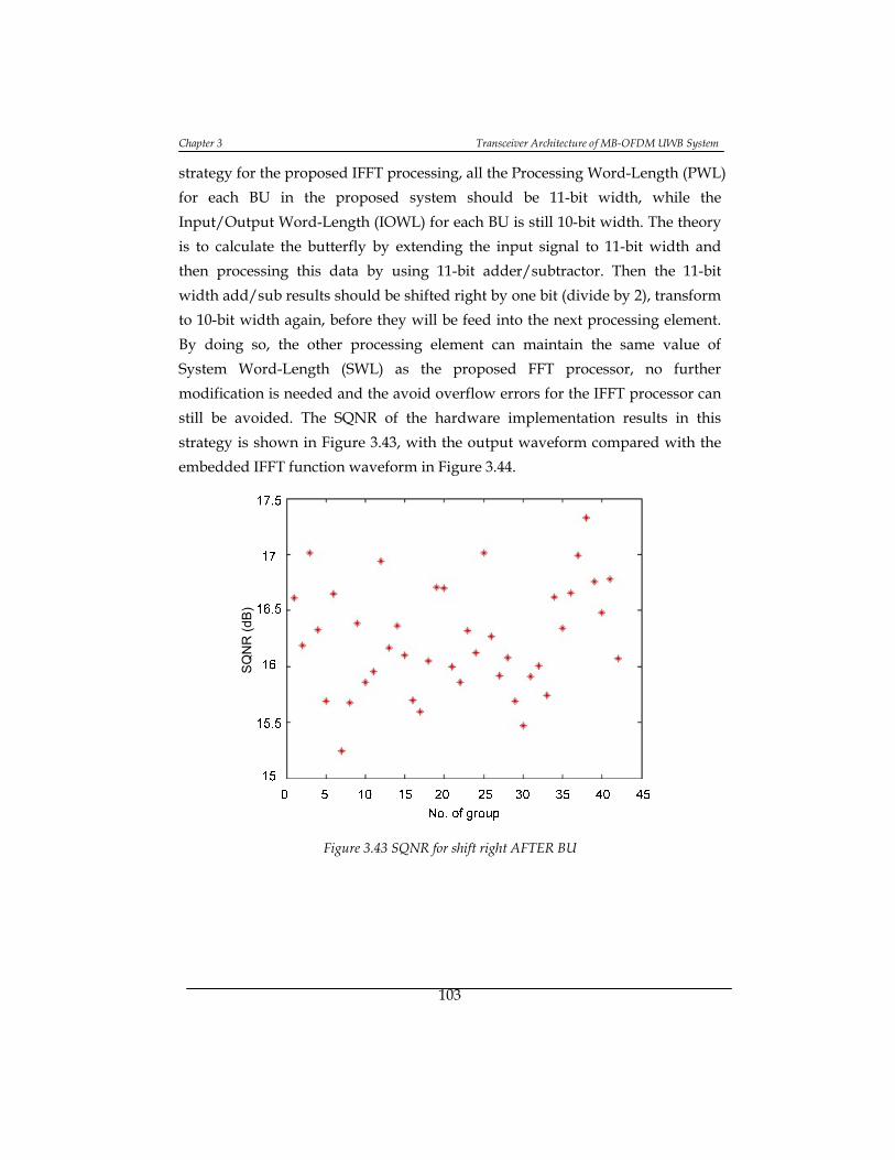
Chapter 3 Transceiver Architecture of MB-OFDM UWB System
103
strategy for the proposed IFFT processing, all the Processing Word-Length (PWL)
for each BU in the proposed system should be 11-bit width, while the
Input/Output Word-Length (IOWL) for each BU is still 10-bit width. The theory
is to calculate the butterfly by extending the input signal to 11-bit width and
then processing this data by using 11-bit adder/subtractor. Then the 11-bit
width add/sub results should be shifted right by one bit (divide by 2), transform
to 10-bit width again, before they will be feed into the next processing element.
By doing so, the other processing element can maintain the same value of
System Word-Length (SWL) as the proposed FFT processor, no further
modification is needed and the avoid overflow errors for the IFFT processor can
still be avoided. The SQNR of the hardware implementation results in this
strategy is shown in Figure 3.43, with the output waveform compared with the
embedded IFFT function waveform in Figure 3.44.
SQ
NR
(d
B)
Figure 3.43 SQNR for shift right AFTER BU
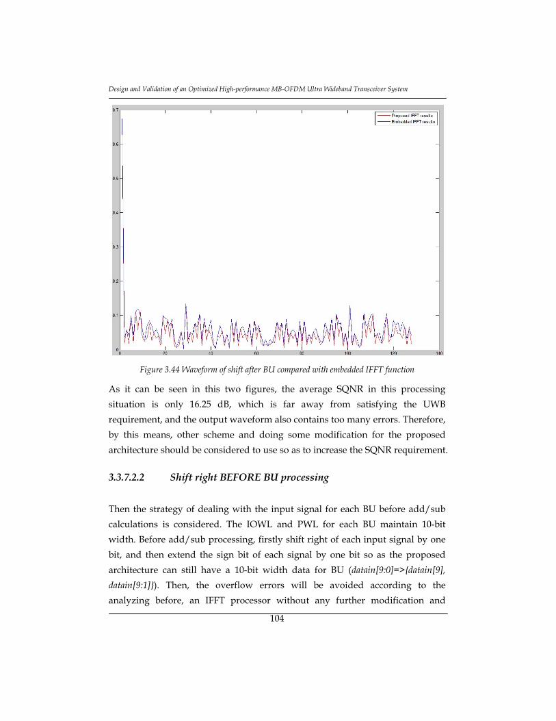
Design and Validation of an Optimized High-performance MB-OFDM Ultra Wideband Transceiver System
104
Figure 3.44 Waveform of shift after BU compared with embedded IFFT function
As it can be seen in this two figures, the average SQNR in this processing
situation is only 16.25 dB, which is far away from satisfying the UWB
requirement, and the output waveform also contains too many errors. Therefore,
by this means, other scheme and doing some modification for the proposed
architecture should be considered to use so as to increase the SQNR requirement.
3.3.7.2.2 Shift right BEFORE BU processing
Then the strategy of dealing with the input signal for each BU before add/sub
calculations is considered. The IOWL and PWL for each BU maintain 10-bit
width. Before add/sub processing, firstly shift right of each input signal by one
bit, and then extend the sign bit of each signal by one bit so as the proposed
architecture can still have a 10-bit width data for BU (datain[9:0]=>datain[9],
datain[9:1]). Then, the overflow errors will be avoided according to the
analyzing before, an IFFT processor without any further modification and
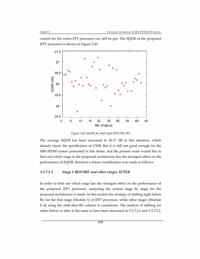
Chapter 3 Transceiver Architecture of MB-OFDM UWB System
105
control for the entire FFT processor can still be got. The SQNR of the proposed
IFFT processor is shown in Figure 3.45.
Figure 3.45 SQNR for shift right BEFORE BU
The average SQNR has been increased to 26.17 dB in this situation, which
already meets the specification of UWB. But it is still not good enough for the
MB-OFDM system presented in this thesis, and the present work would like to
find out which stage in the proposed architecture has the strongest affect on the
performance of SQNR, therefore a future modification was made as follows.
3.3.7.2.3 Stage 1 BEFORE and other stages AFTER
In order to find out which stage has the strongest effect on the performance of
the proposed IFFT processor, analyzing the system stage by stage for the
proposed architecture is made. In this section the strategy of shifting right before
BU for the first stage (Module 1) of IFFT processor, while other stages (Module
2~4) using the shift-after-BU scheme is considered. The method of shifting for
either before or after is the same as have been discussed in 3.3.7.2.1 and 3.3.7.2.2.

Design and Validation of an Optimized High-performance MB-OFDM Ultra Wideband Transceiver System
106
By doing this, the SQNR performance for the IFFT hardware implementation is
shown in Figure 3.46.
Figure 3.46 SQNR for shift right stage 1 BEFORE and other stages AFTER
As it can be seen in Figure 3.46, by only changing the processing order for stage
1, an average SQNR of 26.79 dB is get, which is also better than the performance
in 3.3.7.2.1. This means the proposed architecture strongly depends on the
performance of the first stage, other stages have weaker affect on the entire
SQNR of the whole system. By this means, if further optimization is needed for
the IFFT processor to get a better performance, modifying the first stage should
be the main task.
3.3.7.2.4 Stage 1 BEFORE and other stages AFTER, ROUNDING the
number
Then, the next step takes into consideration is whether rounding the results after
each right-shift is necessary, and what kind of effect will rounding have for the
given architecture. Besides, by only shift right the signal, the results for shifting
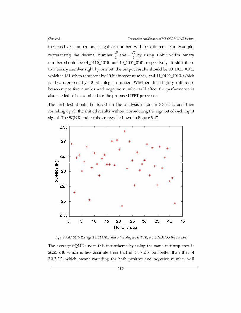
Chapter 3 Transceiver Architecture of MB-OFDM UWB System
107
the positive number and negative number will be different. For example,
representing the decimal number √ and √ by using 10-bit width binary
number should be 01_0110_1010 and 10_1001_0101 respectively. If shift these
two binary number right by one bit, the output results should be 00_1011_0101,
which is 181 when represent by 10-bit integer number, and 11_0100_1010, which
is -182 represent by 10-bit integer number. Whether this slightly difference
between positive number and negative number will affect the performance is
also needed to be examined for the proposed IFFT processor.
The first test should be based on the analysis made in 3.3.7.2.2, and then
rounding up all the shifted results without considering the sign bit of each input
signal. The SQNR under this strategy is shown in Figure 3.47.
Figure 3.47 SQNR stage 1 BEFORE and other stages AFTER, ROUNDING the number
The average SQNR under this test scheme by using the same test sequence is
26.25 dB, which is less accurate than that of 3.3.7.2.3, but better than that of
3.3.7.2.2, which means rounding for both positive and negative number will
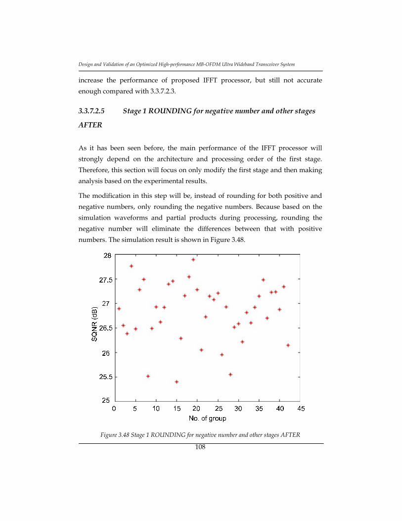
Design and Validation of an Optimized High-performance MB-OFDM Ultra Wideband Transceiver System
108
increase the performance of proposed IFFT processor, but still not accurate
enough compared with 3.3.7.2.3.
3.3.7.2.5 Stage 1 ROUNDING for negative number and other stages
AFTER
As it has been seen before, the main performance of the IFFT processor will
strongly depend on the architecture and processing order of the first stage.
Therefore, this section will focus on only modify the first stage and then making
analysis based on the experimental results.
The modification in this step will be, instead of rounding for both positive and
negative numbers, only rounding the negative numbers. Because based on the
simulation waveforms and partial products during processing, rounding the
negative number will eliminate the differences between that with positive
numbers. The simulation result is shown in Figure 3.48.
Figure 3.48 Stage 1 ROUNDING for negative number and other stages AFTER

Chapter 3 Transceiver Architecture of MB-OFDM UWB System
109
The average SQNR is 26.81 dB in this simulation strategy, which increases the
SQNR performance by a tiny little number when compared with that of 3.3.7.2.3.
This also proves the importance of the performance of the first stage for the
entire IFFT processor.
3.3.7.2.6 Stage 1 ROUNDING for all number and other stages
AFTER
The last test and analysis will be based on the results of 3.3.7.2.5, instead,
rounding both the positive and negative numbers in the first stage. The
simulation result is shown in Figure 3.49.
Figure 3.49 Stage 1 ROUNDING for all number and other stages AFTER
As it can be seen from this figure, the average SQNR value is 26.82 dB. Although
the average SQNR in this situation shows better average results, but compared
with Figure 3.48, the maximum SQNR value that can be get in this simulation
scheme is lower than that of 3.3.7.2.5, which means for different input sequences
with different properties, the IFFT architecture has to be chosen from this two

Design and Validation of an Optimized High-performance MB-OFDM Ultra Wideband Transceiver System
110
different schemes so as to get the best performance. This should be a trade-off
between performance and computational complexity. The output waveform of
the best situation compared with the embedded IFFT function waveform is
shown in Figure 3.50.
Figure 3.50 Waveform of best simulation situation compared with embedded IFFT function
In order to compare the last five strategies of BFP arithmetic in a more obvious
way, the five different scale-down strategies are compared by using boxplot in
Figure 3.51.

Chapter 3 Transceiver Architecture of MB-OFDM UWB System
111
Figure 3.51 SQNR of different scale down method: a. Scale down the signals before calculation; b.
Stage 1 scale down before processing, other stages after; c. Round up the results for all stages
based on (b); d. Round up the negative signals only for Stage 1 based on (b); e. Round up all
signals only for Stage 1 based on (b).
Besides considering the accuracy performance, taking the power consumption
and computational complexity into account, scale down the data before
calculation will consume less power because less SWL is needed inside each
butterfly units; rounding up the results will spend additional logics, which will
bring extra costs on both hardware and power.
The Xilinx synthesis report shows that, around 4.5% more power would be cost
in choice (e) when compare with choice (d) in Figure 3.51, but with only 0.01 dB
increases in the average SQNR. Therefore, according to these analyses as well as
the specifications of MB-OFDM UWB standard, the choice (d), which scales
down signals at input port and rounds up the negative Partial Products (PPs) for
the first stage, whereas the PPs are scaled down after butterfly unit for the rest
stages, becomes the best candidate as a result of trade-off among accuracy,

Design and Validation of an Optimized High-performance MB-OFDM Ultra Wideband Transceiver System
112
hardware resources usage and power consumption for the entire IFFT processor
system.
3.3.8 Conclusions and Contributions
In this section a low-power, high-performance 128-point FFT/IFFT architecture
for MB-OFDM UWB digital baseband communication system is presented, the
architecture employs four-parallel-path SDF pipelined architecture to implement
modified mixed-radix algorithms: radix-2 and radix-22. Thanks to the algorithm,
it is possible to significantly reduce the number (around 25%) and complexity
(around 20%) of the complex multipliers. The power consumption of the whole
system has been reduced by around 50% compared with that of previous works.
The word lengths for each processing element are chosen carefully, and tested
by using fix-point tool box in SIMULINK. Different word lengths for IOWL,
SWL and TWL are simulated, so as to help to choose the architecture of complex
multipliers properly according to the accuracy and hardware cost.
During the design process, overflow control problem is discussed for both FFT
and IFFT architectures. As the IFFT processor in transmitter system requires
overflow control, BFP algorithm is employed, and at the receiver part, overflow
is not likely to happen. In order to achieve high accuracy for the IFFT processor,
six different shift and rounding-number strategies are discussed and compared.
The implementation results indicate that the throughput rate of the proposed
FFT processor with 10-bit IOWL, SWL and 8-bit twiddle factor word-length can
support 1 Gsample/s with a power consumption of 43.79 mW at 250 MHz by
using 0.13 µm CMOS technology. This means that the proposed FFT/IFFT
system is suitable for high data rate processing applications with very low
power consumption.
Chapter 3 Transceiver Architecture of MB-OFDM UWB System
113
3.4. Synchronization
3.4.1 Introduction
The synchronization issue is inevitable in all signal transmission systems. In
digital transmission systems, although the bit streams are inherently discrete-
time, all physical media, such as radio channels or transmission lines, are
continuous-time in nature. In wireless communications, most physical
transmission media are inefficient in transmitting baseband signals.
Consequently, the digital baseband transmitted signal has to be converted to a
continuous-time waveform and then modulated by a higher-frequency carrier
signal. After the modulated signal passes through the physical media, several
inverse processing procedures, including sampling/digitization and
demodulation, are applied.
In wireless communication receivers, coherent demodulation needs to make use
of a Local Oscillation (LO) signal that has exactly the same carrier frequency and
phase as the carrier signal contained in the received signal. Furthermore,
accurate sampling clock frequency and phase allow the demodulator to recover
the transmitted digital data more effectively. Unfortunately, the receiver is
unsynchronized with the transmitter most of the time and thus does not have
matching timing reference from which the carrier signal and the sampling clock
signal can be regenerated. As is often the case, the receiver derives its LO and
clock signals from a controlled oscillator. As such, oscillator mismatch causes
carrier frequency/phase error and clock frequency/phase error. In reality, the
controlled oscillator not only cannot maintain a stable frequency/phase in its
output signal, but also suffers from time-varying phase noise. Even with perfect
oscillator matching, the unknown propagation delay between the transmitter
and the receiver introduces additional phase offset in the LO and the clock
signals. Besides, the Doppler Effect due to relative motion between the
transmitter and the receiver imposes additional frequency shift in the received
signal. All these unavoidable impairments undermine the demodulator
performance and can even render the demodulator useless if they are not

Design and Validation of an Optimized High-performance MB-OFDM Ultra Wideband Transceiver System
114
properly tackled. OFDM communication systems, based on the orthogonality
among subcarrier signals, are more vulnerable to these synchronization errors
than conventional signal-carrier communications.
Synchronization technique has been extensively studied for years. Although
UWB system can leverage on successful experiences of OFDM, it cannot use the
traditional synchronization technology directly due to the distinct features. In
IEEE 802.15.3a standard, the specified emission power spectral density is -42
dBm/MHz, which is extremely small compared with other wireless systems. It
indicates that timing synchronization for UWB system should be robust in high
noise environment. In addition, to satisfy 528 Msps throughput, the UWB
baseband receiver system should be designed in parallel architecture. The
inherent high complexity, the requirements of high performance, high speed,
low cost and low power consumption make the design of synchronization blocks
for UWB quite a challenge work.
In this section the synchronizations errors will be discussed first and explain of
their respective effect on the receiver system performance degradation. Then a
proposed low-complexity fine timing synchronization scheme for the MB-OFDM
UWB system will be introduced. Finally, the Carrier Frequency Offset (CFO)
estimation and Sampling Frequency Synchronization for synchronizing the
frequency of received signals in both time and frequency domain will be
explained.
3.4.2 Synchronization Issues
The possible synchronization errors in OFDM based baseband signals are shown
in Figure 3.52, which includes four different errors as follow:
(1) Carrier Frequency Offset (CFO), ∆ , causes the received complex
baseband signal to rotate at a frequency of ∆ .
(2) Carrier phase error, ∅ , introduces an additional phase rotation
term in the received complex baseband signal.
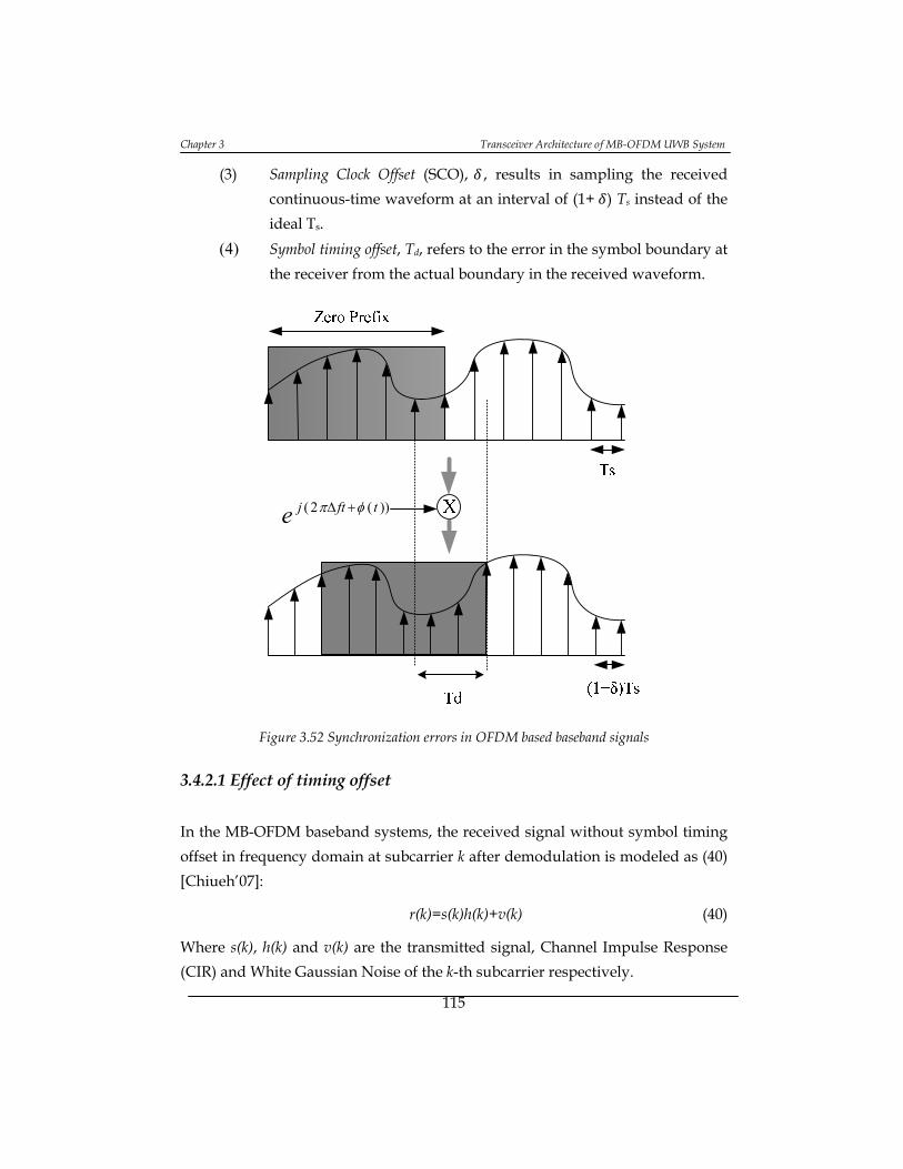
Chapter 3 Transceiver Architecture of MB-OFDM UWB System
115
(3) Sampling Clock Offset (SCO), , results in sampling the received
continuous-time waveform at an interval of (1+ ) Ts instead of the
ideal Ts.
(4) Symbol timing offset, Td, refers to the error in the symbol boundary at
the receiver from the actual boundary in the received waveform.
))(2( tftje
Figure 3.52 Synchronization errors in OFDM based baseband signals
3.4.2.1 Effect of timing offset
In the MB-OFDM baseband systems, the received signal without symbol timing
offset in frequency domain at subcarrier k after demodulation is modeled as (40)
[Chiueh’07]:
r(k)=s(k)h(k)+v(k) (40)
Where s(k), h(k) and v(k) are the transmitted signal, Channel Impulse Response
(CIR) and White Gaussian Noise of the k-th subcarrier respectively.
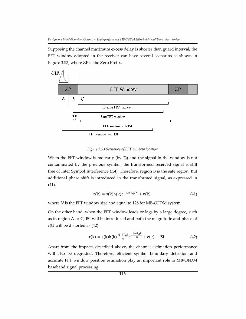
Design and Validation of an Optimized High-performance MB-OFDM Ultra Wideband Transceiver System
116
Supposing the channel maximum excess delay is shorter than guard interval, the
FFT window adopted in the receiver can have several scenarios as shown in
Figure 3.53, where ZP is the Zero Prefix.
Figure 3.53 Scenarios of FFT window location
When the FFT window is too early (by Td) and the signal in the window is not
contaminated by the previous symbol, the transformed received signal is still
free of Inter Symbol Interference (ISI). Therefore, region B is the safe region. But
additional phase shift is introduced in the transformed signal, as expressed in
(41).
r k s k h k e π / v k (41)
where N is the FFT window size and equal to 128 for MB-OFDM system.
On the other hand, when the FFT window leads or lags by a large degree, such
as in region A or C, ISI will be introduced and both the magnitude and phase of
r(k) will be distorted as (42)
r k s k h k| |
eπ
v k ISI (42)
Apart from the impacts described above, the channel estimation performance
will also be degraded. Therefore, efficient symbol boundary detection and
accurate FFT window position estimation play an important role in MB-OFDM
baseband signal processing.
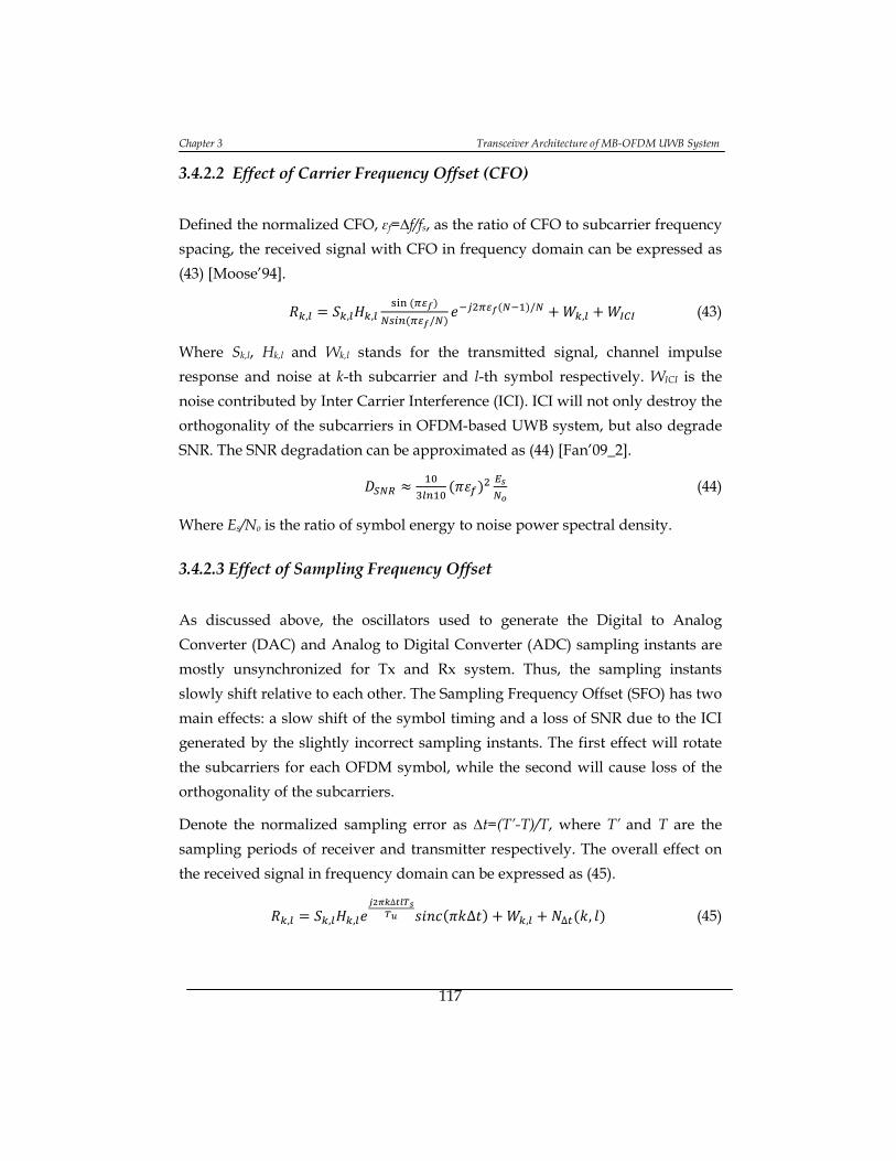
Chapter 3 Transceiver Architecture of MB-OFDM UWB System
117
3.4.2.2 Effect of Carrier Frequency Offset (CFO)
Defined the normalized CFO, ɛf=∆f/fs, as the ratio of CFO to subcarrier frequency
spacing, the received signal with CFO in frequency domain can be expressed as
(43) [Moose’94].
, , ,
//
, (43)
Where Sk,l, Hk,l and Wk,l stands for the transmitted signal, channel impulse
response and noise at k-th subcarrier and l-th symbol respectively. WICI is the
noise contributed by Inter Carrier Interference (ICI). ICI will not only destroy the
orthogonality of the subcarriers in OFDM-based UWB system, but also degrade
SNR. The SNR degradation can be approximated as (44) [Fan’09_2].
(44)
Where Es/No is the ratio of symbol energy to noise power spectral density.
3.4.2.3 Effect of Sampling Frequency Offset
As discussed above, the oscillators used to generate the Digital to Analog
Converter (DAC) and Analog to Digital Converter (ADC) sampling instants are
mostly unsynchronized for Tx and Rx system. Thus, the sampling instants
slowly shift relative to each other. The Sampling Frequency Offset (SFO) has two
main effects: a slow shift of the symbol timing and a loss of SNR due to the ICI
generated by the slightly incorrect sampling instants. The first effect will rotate
the subcarriers for each OFDM symbol, while the second will cause loss of the
orthogonality of the subcarriers.
Denote the normalized sampling error as ∆t=(T’-T)/T, where T’ and T are the
sampling periods of receiver and transmitter respectively. The overall effect on
the received signal in frequency domain can be expressed as (45).
, , ,
∆
∆ , ∆ , (45)

Design and Validation of an Optimized High-performance MB-OFDM Ultra Wideband Transceiver System
118
Where Ts and Tu are the duration of the total symbol and the useful data
respectively; Wk,l is the Additive White Gaussian Noise (AWGN); and ∆ , is
the interference due to the SFO. The power of ∆ , is approximated by (46).
∆ ∆ (46)
As it can be seen, the degradation grows as the square of the produce of the
sampling frequency offset ∆ and the subcarrier index k, which means the
outermost subcarriers are most severely affected if sampling frequency offset
happens. The degradation can also be expressed directly by SNR loss as (47)
[Pollet’95].
10 1 ∆ (47)
The MB-OFDM UWB system does not have a large number of subcarriers and
the value of ∆ is also quite small. So ∆ ≪ 1, and the interference caused by
SFO can usually be ignored. However, the term showing the amount of rotation
angle experienced by the different subcarriers will lead to serious problems.
Since the rotated angle depends on both the subcarrier index and symbol index,
the angle is the largest for the outermost subcarrier and increases with the
consecutive symbols. Although ∆ is very small, with the increasing of the
symbol index, the phase shift will eventually corrupt the demodulation. In this
case, tracking SFO is necessary for MB-OFDM receiver system design.
3.4.3 Timing synchronization scheme
Timing synchronization scheme can be divided into two parts: packet detection,
which takes charge of detecting the upcoming packet through different channels
and timing offset estimation/compensation, which is responsible for finding the
exact boundary of FFT window for each detected OFDM symbol. Several
approaches for both packet detection and timing offset estimation for MB-OFDM
based UWB system have been proposed in the literature. The Cross-Correlation
(CC) for packet detection has been proposed in [Hazy’97] and [Tufvesson’99],
which is known to be more robust in situation of low SNR. But CC is sensitive to
frequency offset and multiband. Therefore, for MB-OFDM based UWB system
Chapter 3 Transceiver Architecture of MB-OFDM UWB System
119
lots of modified CC algorithms have been proposed. Band-Tracking Packet
Detector (BT-PD) algorithm [Lai’07] simplified the CC algorithm by using the
sign-bit of preamble coefficients, while in [Fan’09] a more robust packet detector
is discussed. The computational complexity is dramatically reduced as only sign
bits are used, but the structure in [Fan’09] will cause large hardware resources
consumption as a large amount of memory is needed for hardware
implementation. Fine timing offset synchronization algorithms are proposed in
[Shahbazian’11] [Yak’05] [Suresh’10] [Sen’08], all of them are based on a similar
idea, by comparing the correlation energy of received signals with a
predetermined threshold, or utilizing a Maximum Likelihood (ML) function to
estimate the timing offset. Although they can provide accurate timing offset
estimation, the computational complexity is rather high. Besides, none of them
mentioned the experimental results based on real hardware implementation.
In this work, an innovative low complexity timing synchronization and
compensation scheme for MB-OFDM UWB receiver system is proposed. It
contains Packet Detector (PD) and Timing Offset Estimation (TOE) functions.
Time domain sequences are used to synchronize the received packets. By
simplifying the CC and ML functions to sign-bit only, the computational
complexity for timing synchronization is significantly reduced.
3.4.3.1 Traditional timing synchronization algorithms
In resent research, four traditional algorithms are commonly used for both
coarse and fine timing synchronization scheme, which includes Auto-
Correlation (AC), Maximum Likelihood (ML), Minimum Mean Square Error
(MMSE), and Cross-Correlation (CC) algorithm.
3.4.3.1.1 Auto-Correlation
The AC algorithm is proposed in [Schmidl’97], which is used for coarse timing
synchronization. This method is considered to be quite straightforward. It
searches for the repetition in the received signal with a correlator and a
maximum searcher. The timing metric for AC is defined as (48).

Design and Validation of an Optimized High-performance MB-OFDM Ultra Wideband Transceiver System
120
∑ ∗
∑ | | 48
Where L is the repetition interval length, rn is the received signal in time domain,
and * is the conjugated operation. The estimated time index of the maximum
M(n) can be expressed as (49).
max 49
If the maximum M(n) is over the threshold, the packet is detected and the
estimated timing index is the symbol boundary. The function for AC is simple,
but with a big disadvantage. When the correlation window moves away from
the repeated period, the power of timing metric M(n) may not fall off as
expected, especially in low Signal to Noise Ratio (SNR) situations. Large symbol
boundary detection errors may happen according to this fact.
3.4.3.1.2 Maximum Likelihood
The work in [Coulson’01] improves the performance of AC by proposed a ML
algorithm, which can be expressed as (50) and (51).
2 ∗ | | | | 50
where
≜∗
| | | |
11 /
51
And is the Signal to Noise Ratio (SNR). The estimated symbol boundary is
derived by searching the maximum output of ML function. As it can be seen
above, the computational complexity of ML is quite high because of the
hardware for estimating ρ. Besides, error in SNR estimation often renders it less
reliable than other methods.

Chapter 3 Transceiver Architecture of MB-OFDM UWB System
121
3.4.3.1.3 Minimum Mean Square Error (MMSE)
MMSE metric is equivalent to a special case of the ML metric when ρ equals to 1.
The timing estimation performance for MMSE is almost the same as ML, which
improves the timing uncertainty related to the received signal power fluctuation
in the AC algorithm. The principle of MMSE is to search the minimum output of
the metric in (52).
| | | | 2 ∗ 52
3.4.3.1.4 Cross-Correlation
Instead of correlating the noisy received waveform with a delayed version of the
noisy received waveform, the receiver can correlate the received noisy signal
with the ‘clean’ preamble waveform using a matched filter [Fort’03]. Cross-
Correlation (CC) is the mechanism for fine timing synchronization. The optimal
timing can be obtained by first computing the CC function as (53).
∗ 53
Where Q is the length of the preamble and ck is the preamble coefficients. Then
find the location at which its maximum magnitude occurs as (54).
max| | 54
The CC algorithm can fit into the low SNR situation.
According to the introduction above of all those four algorithms, it can be seen
that the AC, ML, and MMSE algorithms are just used for coarse detection, while
CC is for fine boundary detection. But the first three methods can provide a
robust detection in multipath situation, while CC is robust in low SNR situations.
By taking all the discussion into the design consideration, a new timing
synchronization scheme for MB-OFDM UWB applications is proposed in this
thesis.

Design and Validation of an Optimized High-performance MB-OFDM Ultra Wideband Transceiver System
122
3.4.3.2 Proposed timing synchronization scheme
Two basic functions are taking into consideration for the proposed fine timing
synchronization scheme: Packet Detection (PD) and Timing Offset Estimation
(TOE), for the packet-based MB-OFDM system. The periodicity property of the
preambles is utilized. A very low complexity and power efficient algorithm is
proposed for synchronizing the received time-domain signals, while considering
the distinctive features of the MB-OFDM system. This scheme assumes that the
receiver knows which preamble the transmitter uses but not the arrival time of
the preamble.
The whole timing synchronization scheme has the work flow as shown in Figure
3.54. The PD block will first take charge of detecting the upcoming OFDM
symbols that ‘floating’ in the air by detecting the energy of each suspected
packet. Although the proposed PD algorithm can provide an accurate starting
point for each FFT window, the provided OFDM symbol still may contain a
small value of timing offset, Td, which may cause degradation of the SNR. Thus,
in order to further eliminate this timing offset and provide the exact boundary of
the OFDM symbol, the TOE function is carried out so as to estimate the value of
Td and compensate for each received symbol. Then the symbols with very
accurate starting points will be feed into the FFT processor for further process.

Chapter 3 Transceiver Architecture of MB-OFDM UWB System
123
Figure 3.54 Proposed timing synchronization work flow
The design challenge for such work mainly comes from finding the perfect
trade-off point between the power consumption and the accuracy of detection.
Not like other blocks in Rx implementation, the PD element will always be
turned on for listening to the channel and waiting for the symbols. Therefore the
energy spent on detecting packets should be as low as possible to ensure the low
power performance for the whole Rx system. Meanwhile, as discussed above, an
accuracy detection and synchronization will affect the Rx system performance a
lot in several aspects. To find a low power, while still maintain the high accuracy
performance algorithm and structure becomes the main target for the proposed
synchronization scheme.
3.4.3.2.1 Packet Detector (PD)
As CC is proved to be the most straightforward and low complexity algorithm,
the proposed PD structure will be based on the traditional CC algorithm.
The block diagram of proposed packet detector is illustrated in Figure 3.55. In the
figure, Qd denotes the signs of received signals, while Ck (k=0, 1… 127) are the
signs of preamble coefficients. The whole structure is a modified version of

Design and Validation of an Optimized High-performance MB-OFDM Ultra Wideband Transceiver System
124
[Fan’09], in the aim to reduce the hardware resources usage. The algorithm can
be expressed as flow.
1Z
0C1C 2C
1Z 1Z
127C
NZ
)(dCC
2
)(dm
dThd
dQ
Figure 3.55 Block diagram of proposed Packet Detector algorithm
The CC output between Ck and Qd is calculated first as (55).
∗ 55
By truncating preamble coefficients and received signal to sign-bit only in the
proposed structure, the complex multipliers can be implemented by using a few
logic gates. Compared with traditional CC algorithm, the hardware complexity
as well as the power consumption will be reduced significantly. Then, in the
second stage, instead of calculating the auto-correlation as in [Fan’09], the delay-
correlation of each received signal is calculated to accumulate the energy for
each received packet in (56).

Chapter 3 Transceiver Architecture of MB-OFDM UWB System
125
56
In order to further make the whole PD system more robust against the noise and
increasing the resolution of detected energy in the waveform, the square
function is employed as (57) to eliminate the noise interference. The output of
the proposed packet detector can be derived as
| | 57
At the output port of PD, if this output energy is over a threshold value Th
defined according to statistic method, the packet is assumed to be detected.
Otherwise, the system continues fetching the output of until the conditions
are met. The detection waveform of traditional CC algorithm compared with
proposed PD algorithm for MB-OFDM symbol in CM1 channel, which is
specified by IEEE 802.15.3 channel modeling sub-committee, is shown in Figure
3.56, the SNR for simulation is set to be 10 dB.
Sample Index
Proposed PD
glitches
Figure 3.56 Output waveforms of CC and PD algorithms at 10 dB SNR CM1 channel
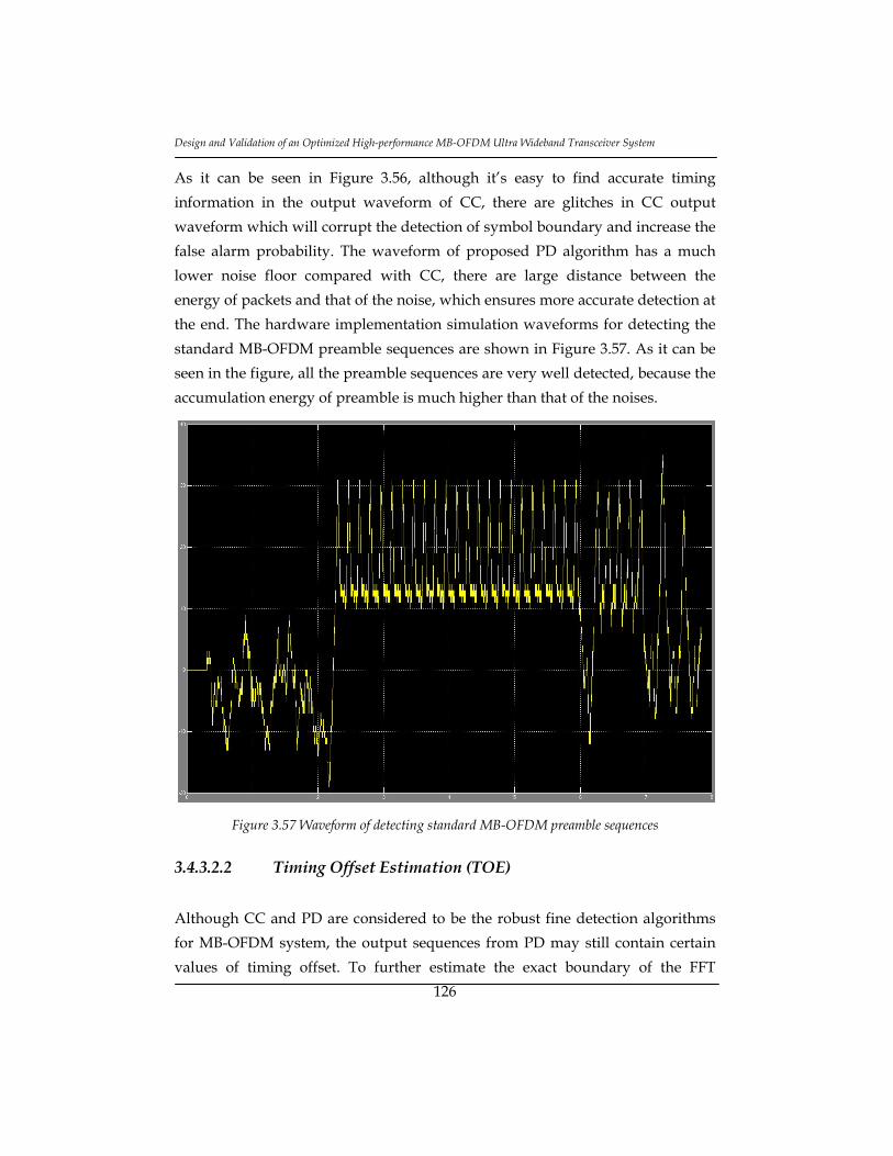
Design and Validation of an Optimized High-performance MB-OFDM Ultra Wideband Transceiver System
126
As it can be seen in Figure 3.56, although it’s easy to find accurate timing
information in the output waveform of CC, there are glitches in CC output
waveform which will corrupt the detection of symbol boundary and increase the
false alarm probability. The waveform of proposed PD algorithm has a much
lower noise floor compared with CC, there are large distance between the
energy of packets and that of the noise, which ensures more accurate detection at
the end. The hardware implementation simulation waveforms for detecting the
standard MB-OFDM preamble sequences are shown in Figure 3.57. As it can be
seen in the figure, all the preamble sequences are very well detected, because the
accumulation energy of preamble is much higher than that of the noises.
Figure 3.57 Waveform of detecting standard MB-OFDM preamble sequences
3.4.3.2.2 Timing Offset Estimation (TOE)
Although CC and PD are considered to be the robust fine detection algorithms
for MB-OFDM system, the output sequences from PD may still contain certain
values of timing offset. To further estimate the exact boundary of the FFT

Chapter 3 Transceiver Architecture of MB-OFDM UWB System
127
window and compensate this timing offset, a modified sign-bit based Timing
Offset Estimation (TOE) scheme is proposed based on the ML metric algorithm.
Once the MB-OFDM symbol is detected, the sequences after the detected time
instant will be fed into the TOE module. Using the estimated time instant
provided by PD as a reference for the detected symbol, TOE responses for
finding the exact boundary, which is the first sample, of each symbol. The
proposed method is described below.
Compared with that of [Shahbazian’11], the ML estimation method is
considered in the present work and derive the following low-complexity cross-
correlation function (58) by using only the sign bits of the 128 samples of the
received signal and the 128 sign bits of the preamble that are specified by the
MB-OFDM standard.
∗ 58
Where represents the timing offset of the current MB-OFDM symbol and *
denotes the complex conjugate operation. The peak value of the cross-correlation
function (58) can be identified by utilizing the following low-complexity ML-
based decision timing metric [Jogansson’00].
| | | | 59
Defining symNo as the index of a packet/frame synchronization MB-OFDM
symbol and as the starting point of that symbol, which is the time
instant provided by the PD. The boundary estimation is started from the first
sample of the first MB-OFDM symbol, i.e., symNo = 1 and = 1. Then,
the cross-correlation is performed between the signs of the first 128 samples of
the received signal and the 128 signs of the preambles. Due to the modified S-V
channel model of MB-OFDM system, the first arriving path may not be the
strongest one. As a result, by only using the conventional cross-correlation
function, a delayed multipath component with stronger amplitude than the first
one will be located and, hence, it will cause misdetection [Shahbazian’11]. To
correctly estimate the position of the first arriving path, the moving average of
over a window of size NC is taken, where most of the channel
Design and Validation of an Optimized High-performance MB-OFDM Ultra Wideband Transceiver System
128
energy is concentrated. The sum of the first NC cross correlation values starting
from is calculated below:
60
This could be replaced by the following recursive equation as given below in
(61).
′ 1
′ 61
In the above equation, NC is considered as the maximum delay spread of the
multipath channel. Equation (61) should be calculated for all the samples in each
MB-OFDM symbol. The exact symbol boundary is selected with the maximum
value as in (62).
′ , ′ 1 ,… , ′
127 62
Since transmission channel varies in time, timing offset of each symbol is
different from others. To find the more accurate timing offset values for all the
received OFDM symbols, the calculated timing offset for Ng symbols should then
be averaged. The detailed flowchart of the proposed algorithm is shown in
Figure 3.58. If the detected boundary offset is within the zero prefix
period, the timing offset estimation is done. It means that the estimated symbol
boundary offset falls into the Inter Symbol Interference-free (ISI-free) zone, in
which all subcarriers experience the same phase shift, which can be easily
eliminated at the receiver. Otherwise, the subcarriers will experience the ISI that
will significantly degrade the system performance, which means that failed
estimation is performed. Once the successful detection and estimation is made,
the FFT processor will use the provided information to process each OFDM
symbol from the right boundary position.

Chapter 3 Transceiver Architecture of MB-OFDM UWB System
129
)(0 symNo
)(0 symNo
128)()(
1
symNosymNo
symNosymNo
g
gd N
NsymNosymNosymNoT
))(...)1()(( 000
?gNsymNo
Figure 3.58 Proposed Timing Offset Estimation algorithm
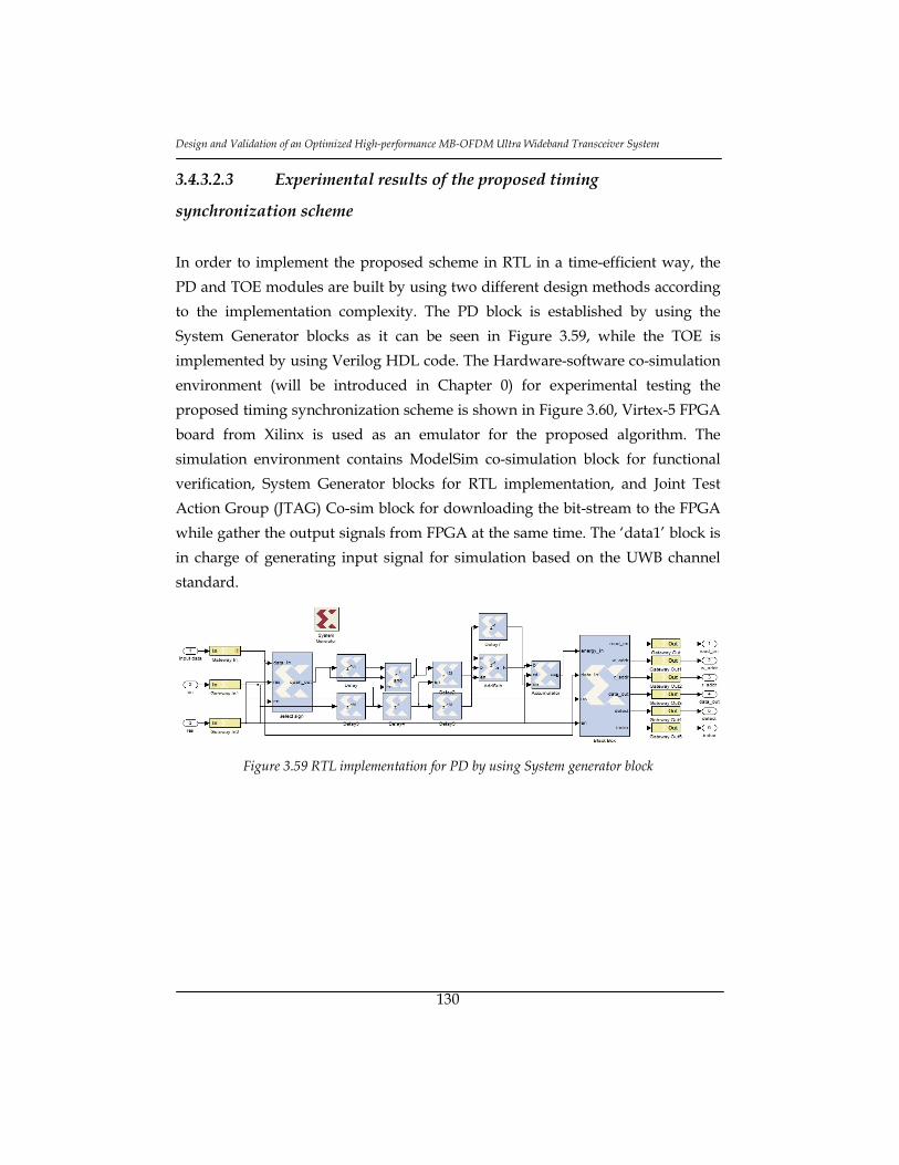
Design and Validation of an Optimized High-performance MB-OFDM Ultra Wideband Transceiver System
130
3.4.3.2.3 Experimental results of the proposed timing
synchronization scheme
In order to implement the proposed scheme in RTL in a time-efficient way, the
PD and TOE modules are built by using two different design methods according
to the implementation complexity. The PD block is established by using the
System Generator blocks as it can be seen in Figure 3.59, while the TOE is
implemented by using Verilog HDL code. The Hardware-software co-simulation
environment (will be introduced in Chapter 0) for experimental testing the
proposed timing synchronization scheme is shown in Figure 3.60, Virtex-5 FPGA
board from Xilinx is used as an emulator for the proposed algorithm. The
simulation environment contains ModelSim co-simulation block for functional
verification, System Generator blocks for RTL implementation, and Joint Test
Action Group (JTAG) Co-sim block for downloading the bit-stream to the FPGA
while gather the output signals from FPGA at the same time. The ‘data1’ block is
in charge of generating input signal for simulation based on the UWB channel
standard.
Figure 3.59 RTL implementation for PD by using System generator block
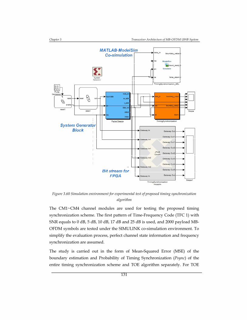
Chapter 3 Transceiver Architecture of MB-OFDM UWB System
131
Figure 3.60 Simulation environment for experimental test of proposed timing synchronization
algorithm
The CM1~CM4 channel modules are used for testing the proposed timing
synchronization scheme. The first pattern of Time-Frequency Code (TFC 1) with
SNR equals to 0 dB, 5 dB, 10 dB, 17 dB and 25 dB is used, and 2000 payload MB-
OFDM symbols are tested under the SIMULINK co-simulation environment. To
simplify the evaluation process, perfect channel state information and frequency
synchronization are assumed.
The study is carried out in the form of Mean-Squared Error (MSE) of the
boundary estimation and Probability of Timing Synchronization (Psync) of the
entire timing synchronization scheme and TOE algorithm separately. For TOE

Design and Validation of an Optimized High-performance MB-OFDM Ultra Wideband Transceiver System
132
system, NC and Ng are considered to be 8 and 10 respectively. The performance of
proposed TOE algorithm is compared with that of Modified Symbol Timing
Synchronization (MSTS) [Shahbazian’11] and First significant multipath
components via Threshold comparison of Adjacent samples (FTA) [Yak’05] in
Figure 3.61 (CM1) and Figure 3.62 (CM2) at different SNR situations by means of
Psync, while the MSE performance comparison in both channels are listed in
Table 3-16 and Table 3-17. Numerical results for the Psync metrics of the whole
timing synchronization scheme are listed in Table 3-18.
Figure 3.61 Performance comparison in terms of Psync in CM1
Figure 3.62 Performance comparison in terms of Psync in CM2

Chapter 3 Transceiver Architecture of MB-OFDM UWB System
133
Table 3-16 Timing offset MSE of proposed algorithm and its comparison with MSTS
[Shahbazian’11] and FTA [Yak’05] in CM1
SNR (dB) TOE MSTS FAT
17 0.23 0.28 0.36
10 0.27 0.31 >>10
0 6.38 7 >>10
Table 3-17 Timing offset MSE of proposed algorithm and its comparison with MSTS
[Shahbazian’11] and FTA [Yak’05] in CM2
SNR (dB) TOE MSTS FAT
17 4.16 5.5 9
10 4.35 6.2 >>10
0 19.74 23 >>10
Table 3-18 Synchronization probability of the proposed timing synchronization scheme in
different channels
SNR(dB) CM1 CM2 CM3 CM4
25 99.06% 98.01% 98.00% 96.57%
17 97.60% 94.29% 89.19% 84.98%
10 93.09% 90.69% 83.53% 75.32%
5 60.96% 56.76% 46.85% 32.73%
0 53.45% 52.50% 42.64% 25.39%

Design and Validation of an Optimized High-performance MB-OFDM Ultra Wideband Transceiver System
134
Referring to the listed results, it can be observed that the proposed TOE
algorithm outperforms the FTA and MSTS algorithm for the entire region of
SNR. The MSE performance has also been improved a lot for the proposed
scheme, as the detected boundary of PD is already very close to the exact time
instance of the starting point for that symbol. But as it can be seen in Table 3-18,
the accuracy of the whole timing synchronization scheme dropped a lot when
SNR is lower than 5 dB. This is considered to be the main drawback of the
proposed scheme. That’s because the base sequence has a more ideal correlation
property than the signs of the base sequence, especially in low SNR condition.
But the performance still satisfies the requirements of MB-OFDM UWB standard.
Taking computational complexity into account, as only sign-bit is used for both
proposed PD and TOE algorithms, the complex multipliers and other functions
used during calculation can be implemented by using just a few simple logic
gates. Therefore, compared with traditional CC and ML algorithms, the
computational complexity as well as the power consumption of the proposed
timing synchronization scheme is dramatically reduced.
3.4.4 Carrier Frequency Offset (CFO) estimation/correction
3.4.4.1 CFO estimation/correction algorithm
The most straightforward frequency synchronization algorithm for CFO
estimation/correction is by using the delay correlation function. CFO can be
estimated by the phase difference between two symbols. The most popular
algorithm for estimate the offset for each symbol can be derived as (63)
[Moose’94].
2∗ 63
Where D is the interval length between two correlated signals, L is the sliding
window length. For MB-OFDM UWB application, there are different CFOs in
different bands, so in order to estimate the CFO for each transmission channel,
the two delay-correlated symbols should be in the same transmission band.

Chapter 3 Transceiver Architecture of MB-OFDM UWB System
135
Accordingly, the value of D should be equal to 165 or 495, which depends on the
Time Frequency Code (TFC) that used for transmission. For TFC 1 and 2, D is
equal to 495 (165×3), while for TFC 3~7, D is equal to 165. According to the
conventional algorithm, the system will have the best estimation performance
when L is equal to the FFT window size, which equals to128 as specified by MB-
OFDM standard.
The compensation algorithm for CFO correction can be expressed as flow:
64
Where M is the number of samplers in each OFDM symbol, for MB-OFDM, its
value is 165.
3.4.4.2 CFO estimation/compensation architecture and implementation
The design of frequency synchronizer is divided into two parts. The first part is to
estimate the phase difference between two preambles by delay correlation and
arctangent calculation. The second part is to compensate the signals by
multiplying a complex rotation vector. In this part, the phase accumulator and
sin/cos generator are involved.
The architecture for CFO estimation and compensation that used in this work is
shown in Figure 3.63. The Delay_Correlation block takes charge of calculating the
delay-correlation between the input data and the old data restored in the
memory. The depth of the memory (165 or 495) depends on the TFC used as
described above. The Correlation_Accumulation block responsible for summing
up the correlation results, and export the accumulation results at specified point.
For the proposed MB-OFDM receiver system, the results should be exported
every 128 clock cycles, and output the accumulation results of totally 16 OFDM
symbols. The accumulation result will then be used for estimating the phase
error for each particular channel. The Estimation_Phase block will take the
accumulation results and compute the arctan value for each result, then sum up
all the 16 arctan values and calculate the average phase value for each received
sample. After that, the average phase value will be fed into the
Coefficient_Estimation module, which is used to calculate the sin and cos value for

Design and Validation of an Optimized High-performance MB-OFDM Ultra Wideband Transceiver System
136
each input phase. These values will be used by the Compensation block for
compensate the rest received data that needs to be compensated.
*()165Z
15
0i
cSumPhaseAc
128Z
Figure 3.63 Architecture of CFO estimation and compensation block
For efficiently implemented the CFO estimation/compensation block, the
modified complex multiplier and Cordic algorithm [Caro’09] are used for the
implementation in this thesis. The complex multiplier that used for calculating
the delay-correlation is designed with the schematic as shown in Figure 3.64 (b),
while the cos/sin and arctan processing block is implemented by using the high-
speed parallel-processing Cordic processor that provided by Xilinx System
Generator (XSG) [Xilinx’09_2] [Xilinx’11_2]. Compared with the traditional
architecture of complex multiplier in Figure 3.64 (a), the modified structure uses
one less multiplier and three more adders. When taking the word-length of
proposed MB-OFDM into consideration (10-bit long), the hardware resources
usage as well as the power consumption for the modified structure has been
slightly reduced.
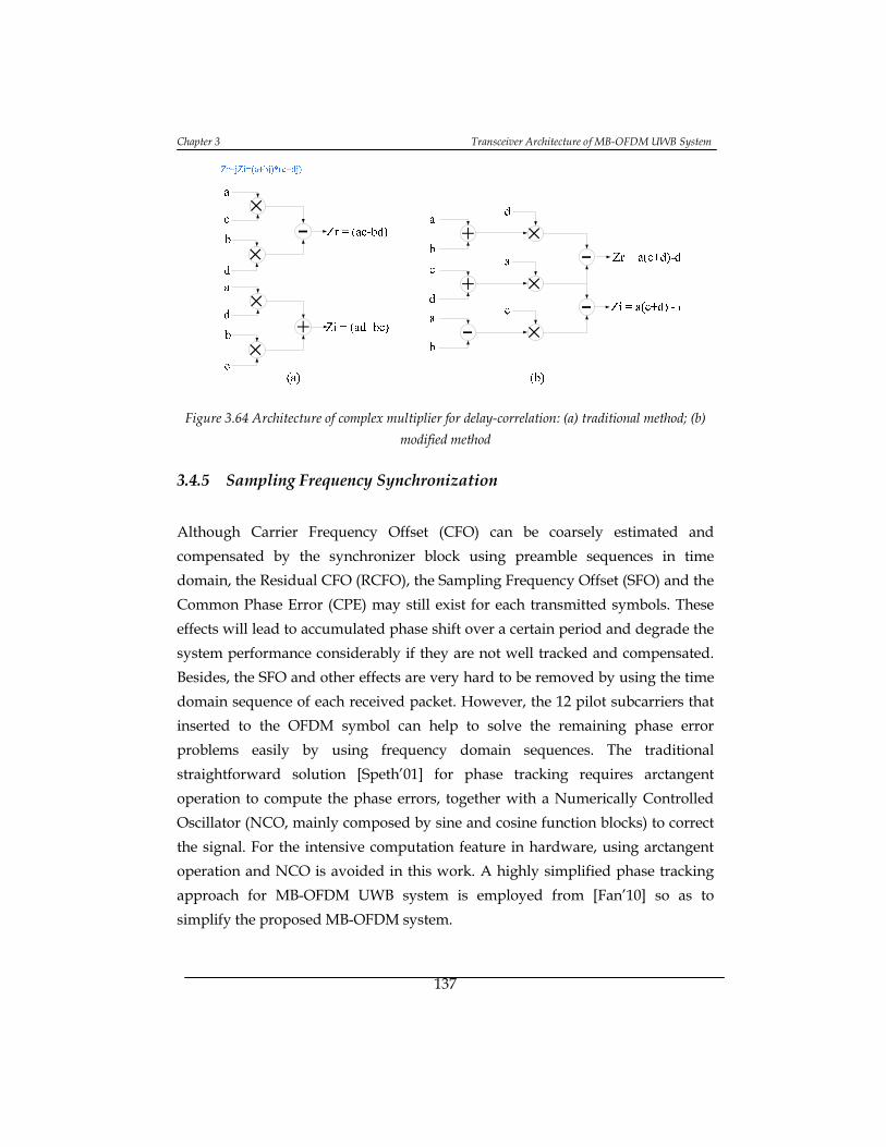
Chapter 3 Transceiver Architecture of MB-OFDM UWB System
137
Figure 3.64 Architecture of complex multiplier for delay-correlation: (a) traditional method; (b)
modified method
3.4.5 Sampling Frequency Synchronization
Although Carrier Frequency Offset (CFO) can be coarsely estimated and
compensated by the synchronizer block using preamble sequences in time
domain, the Residual CFO (RCFO), the Sampling Frequency Offset (SFO) and the
Common Phase Error (CPE) may still exist for each transmitted symbols. These
effects will lead to accumulated phase shift over a certain period and degrade the
system performance considerably if they are not well tracked and compensated.
Besides, the SFO and other effects are very hard to be removed by using the time
domain sequence of each received packet. However, the 12 pilot subcarriers that
inserted to the OFDM symbol can help to solve the remaining phase error
problems easily by using frequency domain sequences. The traditional
straightforward solution [Speth’01] for phase tracking requires arctangent
operation to compute the phase errors, together with a Numerically Controlled
Oscillator (NCO, mainly composed by sine and cosine function blocks) to correct
the signal. For the intensive computation feature in hardware, using arctangent
operation and NCO is avoided in this work. A highly simplified phase tracking
approach for MB-OFDM UWB system is employed from [Fan’10] so as to
simplify the proposed MB-OFDM system.

Design and Validation of an Optimized High-performance MB-OFDM Ultra Wideband Transceiver System
138
3.4.5.1 SFO compensation algorithm
Conventionally, SFO can be estimated by computing a slope from the plot of
pilot subcarrier differences versus pilot subcarrier indices. Recently, joint
estimation of CFO and SFO has also been studied extensively, such as the Linear
Least Squares (LLS) algorithm [Liu’02] and joint weighted least squares
algorithm [Tsai’05]. But all of them have to calculate arctangent, sine, and cosine
functions, which are quite complicated in hardware implementation. The
algorithm presented in [Troya’07] simplifies the hardware cost significantly
compared with the traditional approaches. Based on this, [Fan’10] proposed a
novel phase tracking method for UWB system. It not only has low complexity,
but also improves the performance. The employed algorithm can be
summarized as follow.
The received signal with residual phase distortion in frequency domain after
removing the channel noise can be modeled as (65).
, , , , exp ∅ , , exp 65
Where Pk,l is the phase distortion vector and ∅ , is the residual phase error, α is
the slope of the phase distortion and is contributed by SFO, and βl is the
intercept of phase distortion and is caused by RCFO of symbol number l.
Considering the condition of | | ≪ 1, where k is the subcarrier index and k ∈ [-
55, 55] as specified by MB-OFDM standard, the first order approximation can be
made as
1,
Then the phase distortion in (65) can be written as (66).
, ∙ ∙ 66
Four parameters are of interests in this equation and should be calculated for
sampling frequency synchronization: , , ∙ and ∙ .
According to the algorithm, the first two parameters can be easily calculated by
using (67).
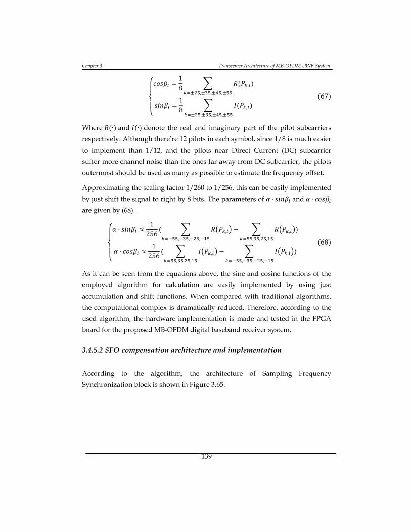
Chapter 3 Transceiver Architecture of MB-OFDM UWB System
139
18 ,
, , ,
18 ,
, , ,
67
Where ∙ and ∙ denote the real and imaginary part of the pilot subcarriers
respectively. Although there’re 12 pilots in each symbol, since 1/8 is much easier
to implement than 1/12, and the pilots near Direct Current (DC) subcarrier
suffer more channel noise than the ones far away from DC subcarrier, the pilots
outermost should be used as many as possible to estimate the frequency offset.
Approximating the scaling factor 1/260 to 1/256, this can be easily implemented
by just shift the signal to right by 8 bits. The parameters of ∙ and ∙
are given by (68).
∙1256 ,
, , ,,
, , ,
∙1256 ,
, , ,
,
, , ,
68
As it can be seen from the equations above, the sine and cosine functions of the
employed algorithm for calculation are easily implemented by using just
accumulation and shift functions. When compared with traditional algorithms,
the computational complex is dramatically reduced. Therefore, according to the
used algorithm, the hardware implementation is made and tested in the FPGA
board for the proposed MB-OFDM digital baseband receiver system.
3.4.5.2 SFO compensation architecture and implementation
According to the algorithm, the architecture of Sampling Frequency
Synchronization block is shown in Figure 3.65.

Design and Validation of an Optimized High-performance MB-OFDM Ultra Wideband Transceiver System
140
()
()
ll j sincos
ll j sin4cos4
Figure 3.65 Architecture of Sampling Frequency Synchronization block
After going through the FFT processor, the guard subcarriers (10-tones) and
DC/NULL tones (6-tones) of each OFDM symbol are removed first. Then the
remaining 112 subcarriers, including 12 pilot subcarriers and 100 data
subcarriers, are feed into Sampling Frequency Synchronization (SFS) block to
estimate and recover the frequency offset for each received symbol in frequency
domain.
The Sampling Frequency Synchronization (SFS) block will pick up the 12 pilot
subcarriers from the received signals according to the specified position. Then
the 12 pilots and 100 data are restored in Pilot Buffer and Data Buffer in the
structure separately. According to the used algorithm, the 8 pilot subcarriers at
the position of -25, -35, -45, -55, 55, 45, 35, 25, which are the outermost pilots, are
summed up and right-shifted (divide by 8 and 256 respectively) so as to get the
required four parameters of , , ∙ and ∙ in the simplified
way.
Then the values of and 4 ∙ 4 ∙ from Phase Error
Estimator are feed into the Accumulator module, which takes charge of
calculating the Pk,l in (66).

Chapter 3 Transceiver Architecture of MB-OFDM UWB System
141
As the values of parameters and are very small, the frequency
offset differences between each received sample are also very small. Hence, the
phase errors contributed by SFO on four parallel paths from FFT processor can
be approximately considered as the same and rewritten as /4 and
/4 ([k/4] ∈ [-12, 12]). Calculating the parameters of 4 and
4 instead of and can further simplify the architecture of
phase tracking block, as only 1/4 of the parameters are needed to be computed.
This is especially for the four-parallel-path processing method of the proposed
MB-OFDM receiver architecture, as all the four paths can share the same
parameter value instead of using four different parameters for four different
paths.
According to the UWB specification, the first four data subcarrier after pilots is
D(i, 56), D(i, 54), D(i, 53), and D(i, 52). Therefore initially, the register Reg in
Figure 3.65 contains the estimated value multiplied by -12. After that the value
from the adder will be restored in the Reg. By using this method, after 25 clock
cycles, all the 100 data subcarriers will be compensated. After this, the left 100
data subcarriers should be free of frequency offset, and hence are ready for the
following processing blocks.
3.4.6 Conclusions and contributions
In this work, an innovative timing synchronization scheme for MB-OFDM based
UWB system is proposed. The two parts of the proposed scheme, Packet Detector
(PD) and Timing Offset Estimation (TOE) algorithm provide a robust detection
performance and can complete packet and symbol boundary detection in a short
time with high accuracy. When compared with the existing algorithms, only the
sign bits of synchronization sequence are utilized for computing the correlations
for both PD and TOE blocks. This makes the computational complexity
significantly reduced while the performance of synchronization remains at a high
level.
The modified Carrier Frequency Offset (CFO) estimation/compensation, as well
as an efficient low complexity Sampling Frequency Synchronization (SFS) scheme
for MB-OFDM application, is also introduced into the proposed receiver
Design and Validation of an Optimized High-performance MB-OFDM Ultra Wideband Transceiver System
142
baseband system implementation. Compared with the traditional methods, these
state-of-the-art technologies are considered to be more suitable for the proposed
four-parallel-path receiver architecture, and have the advantages of low power,
low computational complexity, and high accuracy, which meet the specifications
of MB-OFDM UWB system very well.
The entire synchronization scheme is implemented in the Xilinx Virtex 5 FPGA
board. The experimental results from different UWB channel modules indicate
that the proposed synchronization scheme is suitable for MB-OFDM system
development.
3.5. Viterbi Decoder
3.5.1 Introduction
In the MB-OFDM UWB system, the rate R=1/3 convolutional codes are selected
as channel codes. By employing “puncturing” technology, the punctured
convolutional codes could correct transmission errors as well as provide various
data rates and code rates with different error-correcting capabilities. The Viterbi
algorithm is recommended to decode the convolutional codes because of its near
optimal decoding performance.
The major challenges of implementing a high-speed Viterbi Decoder (VD) are
the fundamental speed bottleneck imposed by the recursive Add-Compare-
Select (ACS) iteration, which prevents conventional pipelining techniques. To
break the ACS bottleneck, some decoder architectures have been well proposed
and studied in [Fettweis’90] [Parhi’04] [Goo’08]. These studies involve solving
the timing constraints by retiming the critical path, introducing sliding block
architecture, and high-radix algorithms.
In this thesis, a two-step radix-4 architecture, which is responsible for calculating
two steps of 64-stage radix-4 Branch Metrics (BM) within one clock cycle, is
proposed. The proposed VD system has the four-parallel-path processing
architecture, which is more suitable for the proposed MB-OFDM digital
baseband system. The working frequency is therefore 528/4=132 MHz, which

Chapter 3 Transceiver Architecture of MB-OFDM UWB System
143
will dramatically reduce the dynamic power consumption for real hardware
implementation. By employing those state-of-the-art technologies and radix-4
algorithms, the ACS units and Trace Back (TB) units are well developed to
support very high data rate applications. Final implementation result shows that
the proposed VD architecture can support a maximum working frequency of
152.5 MHz on the Xilinx XUPV5-LX110T Evaluation Platform.
This section is organized as follows. The coding and puncturing implementation
will be described based on the MB-OFDM UWB physical standard. Then the
theoretical study of convolutional encoding and Viterbi Decoding will be
introduced. Then the propose 64-state soft-decision VD system by using a high
speed radix-4 ACS architecture is presented. Experimental results along with the
conclusions will be drawn at the end of this subsection.
3.5.2 Convolutional encoding and puncturing for MB-OFDM system
According to the standard, the scrambled data sequence should be feed into the
sub-system of convolutional encoder at the transmitter side. All communications
channels are subject to errors introduced as a result of additive Gaussian noise in
their environment. Data perturbations cannot be eliminated but their effect can
be minimized by the use of Forward Error Correction (FEC) techniques in the
transmitted data stream and decoders in the receiving system that detect and
correct bits in error. The purpose of FEC is to improve the capacity of a channel
by adding some carefully designed redundant information to the data being
transmitted through the channel. The process of adding this redundant
information is known as channel coding. Covolutional coding and block coding
are the two major forms of channel coding. The advantages of convolutional
codes over block coding for telecom/datacom applications are: [Edwards’90]
With soft-decision data, convolutionally encoded system gain
degrades gracefully as the error rate increases. Block coding
correct errors up to a point. After which the gain drops off
rapidly.

Design and Validation of an Optimized High-performance MB-OFDM Ultra Wideband Transceiver System
144
Convolutional codes are decoded after an arbitrary length of
data, while block coding introduce latency by requiring
reception of an entire data block before decoding begins.
Convolutional codes do not require block synchronization.
Convolutional codes are linear codes that have additional structure in the
generator matrix so that the encoding operation can be viewed as a filtering, or
convolution, operation. Convolutional codes are widely used in applications that
require good performance with low implementation cost. A convolutional
encoder may be viewed as nothing more than a set of digital filters, linear, time-
invariant systems, with the code sequence being the interleaved data of the filter
outputs. The convolutional codes have memory that uses previous bits to encode
or decode following bits, and is denoted by (n, k, L), where n is the length of
input bits, k is the length of output bits, and L is the code memory depth.
The structure of convolutional encoder is usually a Finite State Machine (FSM)
which processing information bits in a serial manner. Thus the generated code is
a function of input and the states of the FSM. For MB-OFDM system, the
convolutional encoder should use the most common rate of R=1/3 for wireless
communication protocols, with the generator polynomials of g0=1338, g1=1658,
and g2=1718, as defined in Figure 3.66. The bit denoted as “A” shall be the first
bit generated by the encoder, followed by the bit “B”, and finally, by the bit
denoted as “C”. As it can be seen in the figure, total number of 64 different
stages would happen, therefore on the contrary, a 64 stages VD system should
be implemented on the receiver side.
Figure 3.66 Convolutional encoder: rate R=1/3, constraint length K=7
Chapter 3 Transceiver Architecture of MB-OFDM UWB System
145
According to the MB-OFDM UWB standard, different communication data rate
should have different coding rate, as listed in Table 3-19.
Table 3-19 Data rate VS Coding rate
Data Rate (Mb/s) Coding Rate (R) 53.3, 106.7 1/3
80, 160, 320 1/2 200, 400 5/8
480 3/4
In order to simply the system and try to make the transceiver structure reusable
for all different transmission data rate mode, especially the reusable structure for
decoder system, the puncturing technology is introduced into the MB-OFDM
digital baseband system. By using puncturing method, the same decoder system
can be used for all data rate mode regarding of how many bits have been
punctured, thus puncturing considerably increases the flexibility of the
communication system without significantly increasing its complexity.
Puncturing is a procedure for omitting some of the encoded bits at the
transmitter and inserting a dummy zero metric into the decoder at the receiver
in place of the omitted bits. By doing this, the number of transmitted bits is
reduced, while increasing the coding rate at the same time. The puncturing
pattern for MB-OFDM system has been defined in [ISO/IEC 26907’09]. Because
the punctured bits do not provide any information to the decoder, the
convulutional code with higher code rate performs poorer in data-correcting
capability, so it is employed in more favorable wireless environment to achieve
higher coding efficiency and data rates [Xu’07].
3.5.3 Overview of Viterbi Decoder (VD) system
3.5.3.1 Structure of VD system
Given the noisy observations of the encoding finite state process, the Viterbi
algorithm is used to estimate the most likely encoding state sequence from
which the decoded sequence can be easily derived. Practically, a VD is built up
from three subsequent units: a Branch Metric Unit (BMU), a State Metric Unit

Design and Validation of an Optimized High-performance MB-OFDM Ultra Wideband Transceiver System
146
(SMU), and a Trace Back Unit (TBU). The basic structure of VD system is shown
in Figure 3.67.
0ACS
1ACS
2ACS
12 kACS
Figure 3.67 Block diagram of the Viterbi Decoder system
The BMU calculates the branch metrics of , , which is the metric of the
transition from state i to state s at time n. Then the branch metrics are fed into the
ACS units to update the state metrics for state s. At time instance n+1, the
state metrics can be computed recursively by using (69).
min , 0, 1, … , 2 69
A state metrics is the minimum (for some algorithms is the maximum) of
intermediate state metrics, which are the summations of the branch metrics and
the state metrics at the previous time instance. This accumulation and
comparison process for each state metric is called Add-Compare-Select (ACS)
function, which can be shown as Figure 3.68.
Chapter 3 Transceiver Architecture of MB-OFDM UWB System
147
iSM
0iBM
jSM
0jBM
Figure 3.68 Add-Compare-Select Model
For calculating the branch metrics, two different local distances representations
are used depending on the received data type. If the data is represented by a
signal bit, it is referred to as hard-decision data and the Hamming distance
measures are used. When the data is received by multiple bits, it is referred to as
soft-decision data and Euclidean distance measures are more frequently used for
traditional methods. According to the
researches before, the use of soft-decision inputs can provide up to 2.2 dB more
SNR at the same bit-error level [Hendrix’02]. This is because the received data
contains some information on the reliability of the data. The values of soft-bits
and their significance for a 3-bit quantized input data is shown in Table 3-20.
Table 3-20 Soft-bit symbol input representation
Soft-bit Value Significance
011 Strongest “0” 010 Strong “0” 001 Weak “0” 000 Weakest “0” 111 Weakest “1” 110 Weak “1” 101 Strong “1” 100 Strongest “1”
The actual decoding of symbols into the original data is accomplished by tracing
the maximum likelihood path backwards through the trellis. Up to a limit, a

Design and Validation of an Optimized High-performance MB-OFDM Ultra Wideband Transceiver System
148
longer sequence results in a more accurate reconstruction of the trellis. After a
number of symbols equal to about four or five times the constraint length, little
accuracy is gained by additional inputs [Michelson’85]. The trace back function
starts from a final state that is either known or estimated to be correct.
3.5.3.1.1 Radix-2 butterfly
Based on the trellis diagram, the implementation of VD can be performed by
decomposing the trellis into a set of radix-2 butterfly as shown in Figure 3.69.
The butterfly contains a pair of origin and destination states, and four state
transitions. Each state transition is identified by the origin state yx and the
destination state xz, where y denotes the bit shifted out of the shift register; z
denotes the current input bit, and x denotes the common state bits. The branch
word of the state transition is denoted as bxyz. The radix-2 butterfly has some
inherent branch symmetry, which can be used to simplify the implementation of
the VD. The branch symmetry of the radix-2 butterfly is:
70
00 xb
10 x
b
01 xb
11 xb
Figure 3.69 Radix-2 butterfly units
3.5.3.1.2 Radix-4 butterfly
The radix-4 butterfly is applied to the VD design to increase the decoding speed
of the VD. The two stage radix-2 trellis can be merged to one stage radix-4 trellis
by rearranging the states appropriately [Hsu’07]. Notably, each branch of a
radix-4 butterfly has 4-bit branch words, and corresponds to two input bits.
Merging the trellis does not affect the selection of the most likely path, since a
Chapter 3 Transceiver Architecture of MB-OFDM UWB System
149
one-to-one mapping exists between the shortest path in the radix-4 trellis and
the original radix-2 trellis. Each radix-4 butterfly in the radix-4 trellis has four
origin and destination states, and 16 branches, as shown in Figure 3.70. Each
state transition is identified by the origin state y1y2x and the destination state
xz1z2, where y1y2 denote the bits shifted out of the shift register, z1z2 denote the
two input bits, and x denotes the common state bits.
Figure 3.70 Radix-4 butterfly units
Compared with radix-2 butterfly processing, two iterations of the radix-2 trellis
are processed in a single radix-4 trellis iteration. Therefore, the iteration delay
can be reduced by a maximum factor of 2. However, the two fold speedup
cannot be achieved in practice due to the higher computational complexity of the
radix-4 butterfly module. The radix-4 butterfly needs more complicated
comparators and more branch metric computation than the radix-2 butterfly unit
for hardware implementations. Besides, the power consumption caused by those
additional logics is also very high, especially for high frequency VD applications.
3.5.3.2 Related works
Recently, there have been lots of studies on high-speed Viterbi Decoder systems,
as well as its application towards the MB-OFDM UWB developments.
In [Fettweis’90], the M-step look-ahead technique is utilized. It is known to be a
high speed algorithm for elimination of feedback operation. With the M-step
Design and Validation of an Optimized High-performance MB-OFDM Ultra Wideband Transceiver System
150
look ahead, one iteration in the ACS unit is equivalent to M iterations in the
nonlook-ahead implementation. However, as M is increased, the power
consumption will also increase a lot, therefore M has the limitation to be only
two.
Least Significant Bit (LSB) first computation is useful for accumulation operation,
but Most Significant Bit (MSB) first computation is more suitable for compare
and selection operations in the ACS unit. An ACS structure combining MSB-first
compare-select with carry-propagation-free addition was proposed based on
redundant number representation in [Parhi’04].
A high-speed low-complexity two bit-level pipelined VD architecture for MB-
OFDM UWB system is proposed in [Goo’08]. The MSB-first ACS unit combined
with two bit-level structure is used to reduce the critical path of the ACS unit.
Although the architecture can support all data rate mode for MB-OFDM system,
the architecture is still very complex. Besides, the serial processing architecture
cannot be fully implemented for the proposed four-parallel-path digital
baseband system.
3.5.4 Proposed Viterbi Decoder architecture
In this thesis, a 64 state soft-decision VD system by using high speed radix-4
ACS unit architecture is presented. The proposed VD system can support
different data rate (from 53.5 Mbps to 480 Mbps) for MB-OFDM UWB system
when implemented onto the FPGA board. As the bottleneck for high speed VD
implementation mainly comes from the ACS units, the work will focus on
optimization of the ACS units as well as lower the computational complexity
first, then the TB architecture will also be discussed so as to get a power and
hardware efficient VD system for MB-OFDM digital baseband system at the end.
3.5.4.1 Branch Metric Unit (BMU)
For the proposed VD system, in order to increase the accuracy against noises, the
soft-decision algorithm is used. The 3-bit quantized signals will be feed into the

Chapter 3 Transceiver Architecture of MB-OFDM UWB System
151
BMU for calculating the branch metrics for each path. The radix-4 algorithm is
used in the aim of further speed up the VD processing.
Although the branch symmetry of a radix-2 butterfly module cannot be applied
to a radix-4 butterfly module, the branch symmetry of a radix-4 butterfly still can
be obtained by the branch symmetry of a radix-2 butterfly in (70) [Hsu’07].
According to the algorithm, two steps of radix-2 butterfly functions can be
combined to form a radix-4 butterfly step, as it can be seen in Figure 3.71.
According to the figure, the branch word b00x00 in the radix-4 butterfly is
combined from the branch words b00x0 at the first stage and b0x00 at the second
stage in the radix-2 butterfly function, and is given by b00x00=b00x0b0x00. Similarly,
the branch b10x01 in the radix-4 butterfly is combined from the branch b10x0 at the
first stage and b0x01 at the second stage in radix-2 algorithm, and can be
expressed by b10x01=b10x0b0x01. The branches b00x00 and b10x01 are taken herein as
examples to show how to obtain the branch symmetry in a radix-4 butterfly. As
shown in Figure 3.71, the branches b00x0 and b10x0 in the first stage belong to the
same radix-2 butterfly, and have the relationship of according to
(70). The branches b0x00 and b0x01 in the second stage belong to the same radix-2
butterfly, and have the relationship of . Therefore, the relationship
between branches b00x00 and b10x01 can be written by (71), which means that the
radix-4 algorithm also has the symmetry property.
71
000xb 000xb
010 x
b
010
xb
0000 xb
0110 xb
Figure 3.71 A radix-4 butterfly and its corresponding two step radix-2 butterfly

Design and Validation of an Optimized High-performance MB-OFDM Ultra Wideband Transceiver System
152
According to the example above, the branch symmetry of each radix-4 butterfly
branch can be similarly obtained as (72).
72
According to the symmetry, only eight branch metrics in radix-4 algorithm need
to be computed instead of calculating all the 16 branch metrics, as it can be seen
in Figure 3.72. Therefore, compared with traditional radix-4 algorithms, the
proposed architecture only contains nearly half of the computational logics,
which means nearly half of the hardware resources as well as the power
consumptions can be saved by using this radix-4 symmetry property.
Figure 3.72 The branch symmetry of a radix-4 butterfly
Chapter 3 Transceiver Architecture of MB-OFDM UWB System
153
Besides taking the advantage of the symmetry property, in order to further
simplify the calculations for each branch metric, the uniform distance
measurement method is used for the proposed VD system. According to the
uniform distance measurement method, the metrics are calculated equal to the
symbol itself when compared with logic-0 and equal to its one’s complement
when compared with logic-1 [Heller’71]. Compared with calculating the
Euclidean distance as traditional, the employed method will significantly reduce
the computational complexity as no multiplication functions are needed, only
one short word-length adder is needed for each branch metric calculations. Thus
the power consumption as well as the hardware resources usage is reduced.
3.5.4.2 Add-Compare-Select Unit (ACSU)
In order to increase the speed and simplify the structure for ACSU, an efficient
radix-4 ACS architecture is proposed in this work. Figure 3.73 is the block
diagram of the four-way ACSU when taking state 0 as an example.
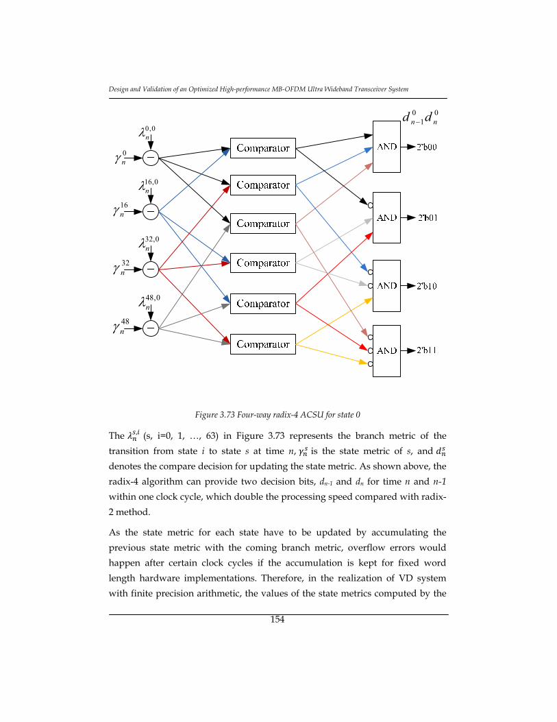
Design and Validation of an Optimized High-performance MB-OFDM Ultra Wideband Transceiver System
154
0,0n
0,16n
0,32n
0,48n
0n
16n
32n
48n
001 nn dd
Figure 3.73 Four-way radix-4 ACSU for state 0
The , (s, i=0, 1, …, 63) in Figure 3.73 represents the branch metric of the
transition from state i to state s at time n, is the state metric of s, and
denotes the compare decision for updating the state metric. As shown above, the
radix-4 algorithm can provide two decision bits, dn-1 and dn for time n and n-1
within one clock cycle, which double the processing speed compared with radix-
2 method.
As the state metric for each state have to be updated by accumulating the
previous state metric with the coming branch metric, overflow errors would
happen after certain clock cycles if the accumulation is kept for fixed word
length hardware implementations. Therefore, in the realization of VD system
with finite precision arithmetic, the values of the state metrics computed by the

Chapter 3 Transceiver Architecture of MB-OFDM UWB System
155
ACSU recursion must remain within a finite numerical range to avoid
catastrophic overflow and underflow situations. A traditional method to solve
this problem is to subtract the minimum state metric value before processing for
each state when updating the state metrics. This method will introduce
additional subtraction function to the ACSU, which will also cost additional
power consumption. Besides, the method to find or estimate the minimum value
of the state metrics is also complicated, as if the value is not the minimum one or
not accurate enough, additional errors of underflow would happen. Therefore,
finding a proper but simply method to avoid overflow and underflow for ACS
units would be the main challenge for a high speed ACSU implementation.
In Very Large Scale Integration (VLSI) implementation of the normalization
techniques, the two most desirable properties are locality and uniformity. Metric
normalization is considered local if it is accomplished within each ACS without
information from other ACS. It is considered uniform if the ACS operation is not
interrupted to perform metric normalization. Locality minimizes the global
signal communications and hence reduces the wiring area. Uniformity not only
simplifies the control but also minimizes the variety of required functional units.
Moreover, a non-uniform technique usually reduces the achievable data rate.
The Modulo Normalization method and Modified Comparison rule proposed in
[Shung’90] is introduced into the proposed VD system so as to simplify the
architecture of ACSU.
In the modular arithmetic, the metric for state s is replaced by the normalized
metric according to (73).
, ≡2
2 73
Where C is a chosen modulus value. The procedure to normalize the state metric
can be explained by using Figure 3.74.

Design and Validation of an Optimized High-performance MB-OFDM Ultra Wideband Transceiver System
156
1
2
1 2
Figure 3.74 Modulo comparison of normalized metrics
The quantities can be put as positions on the circumference of a circle with
the diameter of , with at the angle of . Note that the normalized metrics
should satisfy the situation of , and the difference of the state
metrics should satisfy the situation of | | . The normalized metrics are
obtained by wrapping the real line around the circle, with the real number 0
mapped to the point at angle 0 on the circle, and the direction of increasing real
numbers corresponding to counterclockwise motion around the circle. Let α be
the angle swept out by counterclockwise motion along the arc from the
projection to , then if and only if α<π.
The proposition can be interpreted in less mathematical terms by thinking of the
state metrics as “runners in a race”. Assuming two different runners, and ,
are running on the circle in Figure 3.74. Each runner will run a certain distance
in a fixed time (one clock cycle), but the difference of distance between them
during this fixed time is less than half of the circumference. So at all time, both
runners are running in one half of the circumference. Therefore, no matter how
long the two runners have run, it is always very obviously to see which runner is
in leading position.

Chapter 3 Transceiver Architecture of MB-OFDM UWB System
157
By understanding the theory, next step should be how to implement the ACSU.
The modular arithmetic can be implemented by using 2’s complementary adders
and subtractors. In particular, a subtractor is used in place of a comparator as in
a normal ACSU. This is based on the observations that:
(1) 2’s complementary subtraction produces the angle between
and , which is α
(2) if | |
The sign bit (equals to 1 if α>π, 0 otherwise) can be used to drive the multiplexer
to perform the selection. However, the subtractor will limit the processing speed,
especially for low word-length calculations, besides, the power consumption is
still high. In order to further simplify the compare logic so as to speed up the
progress and save power consumptions, the modified comparison rule in
[Shung’90] is used for the presented thesis.
The structure of the modified comparator in this thesis is shown in Figure 3.75.
As it can be seen, the MSB of each signal is separated from the rest of the bits,
then the structure is simplified compared with traditional 2’s complementary
subtractors and has a faster processing speed. The function of this comparator is
described as follow.
0,1in
0,2in
1in
2in
),( 21 y
Figure 3.75 Two-way add-compare subsystem

Design and Validation of an Optimized High-performance MB-OFDM Ultra Wideband Transceiver System
158
Let , denote the logical result of the comparison of the state metric
and , and have the relation of (74).
,1,0,
74
Let , … , and , … , be the 2’s complementary
representations of the normalized metrics and , or can be expressed by
using (75).
∑ 2
∑ 2 75
Therefore, and represent the MSB, which is the sign bit, of and .
Then let , or can be expressed by using (76), which is the rest of
the bits except the MSB.
∑ 2
∑ 2 76
Then satisfy the situation of (77).
, 0
2, 0
77
Given Figure 3.76 as an example, assuming that and have opposite sign.
Then the function of y( , ) has the value of (78).
,1,
0, 78
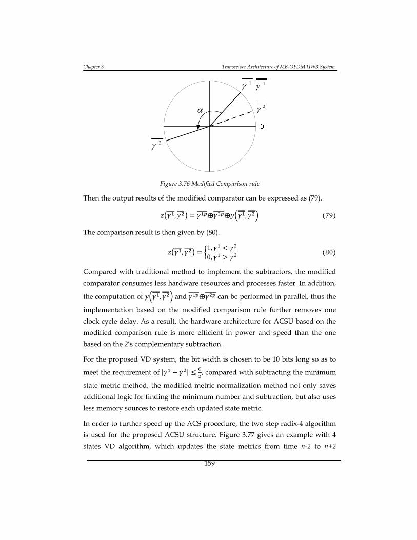
Chapter 3 Transceiver Architecture of MB-OFDM UWB System
159
1
2
1
2
Figure 3.76 Modified Comparison rule
Then the output results of the modified comparator can be expressed as (79).
, ⨁ ⨁ , 79
The comparison result is then given by (80).
,1,0,
80
Compared with traditional method to implement the subtractors, the modified
comparator consumes less hardware resources and processes faster. In addition,
the computation of , and ⨁ can be performed in parallel, thus the
implementation based on the modified comparison rule further removes one
clock cycle delay. As a result, the hardware architecture for ACSU based on the
modified comparison rule is more efficient in power and speed than the one
based on the 2’s complementary subtraction.
For the proposed VD system, the bit width is chosen to be 10 bits long so as to
meet the requirement of | | , compared with subtracting the minimum
state metric method, the modified metric normalization method not only saves
additional logic for finding the minimum number and subtraction, but also uses
less memory sources to restore each updated state metric.
In order to further speed up the ACS procedure, the two step radix-4 algorithm
is used for the proposed ACSU structure. Figure 3.77 gives an example with 4
states VD algorithm, which updates the state metrics from time n-2 to n+2

Design and Validation of an Optimized High-performance MB-OFDM Ultra Wideband Transceiver System
160
directly. The two step algorithm supports processing 4 soft-bit input signals
within one clock cycle, therefore it’ll reduce the system frequency to 528/4=132
MHz for MB-OFDM application. This solves the problem of high dynamic
power consumption and design complexity resulting from high processing
frequency. Furthermore, it gives the proposed VD system the possibility of
supporting even higher throughput applications. Compared with radix-8 VD
algorithm [Nakamura’99], the two-step radix-4 algorithm is much simpler to be
implemented and easier to be understood.
)(0 n
)(1 n
)(2 n
)(3 n
)2(0 n
)2(1 n
)2(2 n
)2(3 n
)2(0 n
)2(1 n
)2(2 n
)2(3 n
Figure 3.77 Trellis diagram of two-step radix-4 procedure
3.5.4.3 Trace Back Unit (TBU)
In the Viterbi Decoder system, there are two known memory organization
techniques for the storage of survivor sequences from which the decoded
information sequence is retrieved, namely Register Exchange (RE) method and
Trace Back (TB) method. In the literature, the RE technique is acceptable for
trellises with only a small number of states, whereas the TB approach is
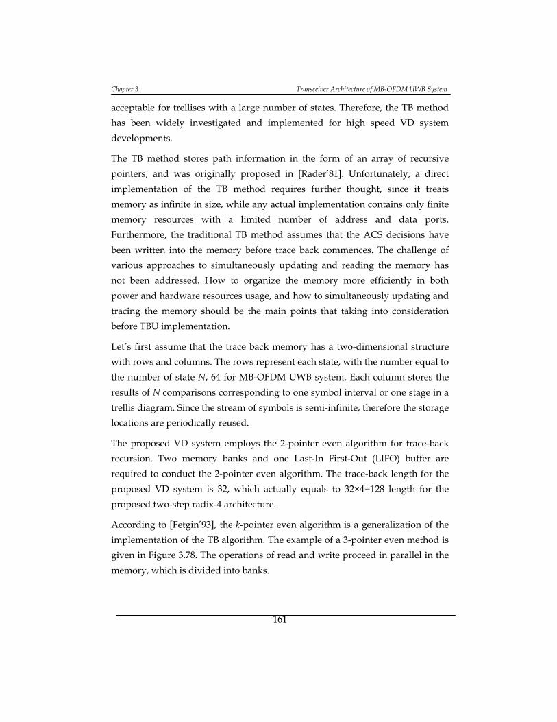
Chapter 3 Transceiver Architecture of MB-OFDM UWB System
161
acceptable for trellises with a large number of states. Therefore, the TB method
has been widely investigated and implemented for high speed VD system
developments.
The TB method stores path information in the form of an array of recursive
pointers, and was originally proposed in [Rader’81]. Unfortunately, a direct
implementation of the TB method requires further thought, since it treats
memory as infinite in size, while any actual implementation contains only finite
memory resources with a limited number of address and data ports.
Furthermore, the traditional TB method assumes that the ACS decisions have
been written into the memory before trace back commences. The challenge of
various approaches to simultaneously updating and reading the memory has
not been addressed. How to organize the memory more efficiently in both
power and hardware resources usage, and how to simultaneously updating and
tracing the memory should be the main points that taking into consideration
before TBU implementation.
Let’s first assume that the trace back memory has a two-dimensional structure
with rows and columns. The rows represent each state, with the number equal to
the number of state N, 64 for MB-OFDM UWB system. Each column stores the
results of N comparisons corresponding to one symbol interval or one stage in a
trellis diagram. Since the stream of symbols is semi-infinite, therefore the storage
locations are periodically reused.
The proposed VD system employs the 2-pointer even algorithm for trace-back
recursion. Two memory banks and one Last-In First-Out (LIFO) buffer are
required to conduct the 2-pointer even algorithm. The trace-back length for the
proposed VD system is 32, which actually equals to 32×4=128 length for the
proposed two-step radix-4 architecture.
According to [Fetgin’93], the k-pointer even algorithm is a generalization of the
implementation of the TB algorithm. The example of a 3-pointer even method is
given in Figure 3.78. The operations of read and write proceed in parallel in the
memory, which is divided into banks.

Design and Validation of an Optimized High-performance MB-OFDM Ultra Wideband Transceiver System
162
Figure 3.78 Trace back order for 3-pointer even method
The memory is divided into 6 memory banks, each of size T/2 columns. Each
read pointer is used to perform the trace back operation in 2 memory banks, and
the decode read in one memory bank. A new trace back front will start from the
fixed state, such as all zeros or the state with the minimum state metric, in each T
stages. And a new decode front is started at a locating determined by the trace
back pointer derived in the previous stage. Then a simple LIFO structure is
sufficient to perform the bit order reversal. Each LIFO stack must be T/2 in depth.
During the decoding of one memory bank, decoded bits are pushed on one stack,
while the bits stored on the other stack are popped. Then with the aim of further
simplify the TBU structure, the 2-pointer even algorithm is implemented for the

Chapter 3 Transceiver Architecture of MB-OFDM UWB System
163
TBU implementation. Figure 3.79 shows the order of writing and reading
memory banks for the employed 2-pointer algorithm.
Figure 3.79 Memory operations for 2-pointer even algorithm
As it can be seen in Figure 3.79, the writing and reading operations can perform
in parallel and no conflict will happen during the whole trace back processing.
The 2-pointer even algorithm is considered to be more simple and hardware-
efficient than the register exchange algorithm and the 3-pointer algorithm
[Fetgin’93].
3.5.4.4 Whole Viterbi Decoder (VD) structure
Figure 3.80 illustrates the whole structure of the proposed two-step radix-4 VD
architecture. Four 3-bit soft decision input signals are feed into two Branch

Design and Validation of an Optimized High-performance MB-OFDM Ultra Wideband Transceiver System
164
Metric Units (BMUs) in parallel. By taking the advantages of branch symmetry
of radix-4 butterfly, only half of the branch metrics need to be computed, while
the other half can be derived from the computed branches. As a result, although
one more BMU is implemented in the proposed VD system, the entire power
consumption almost remains the same compared with traditional BMU
architectures.
2n
nInput
3nInput
1nInput
2nInput
n
n
2n
2n
2nd3nd
1nd nd
Figure 3.80 Proposed two-step 64-state radix-4 Viterbi Decoder
The processing flow of the proposed VD system can be explained as follow. The
BMU 1 and BMU 2 take charge of calculating the branch metrics for each branch
of the trellis diagram. According to Figure 3.80, the BMU1 will provide the
branch metric information for the time instance from n-2 to n, whereas the BMU
2 will provide the branch metrics from n to n+2. Then the two groups of branch
metrics will be feed into two different modified 4-way radix-4 ACSUs for
updating the state metrics for each state.
ACSU 1 responsible for adding the state metrics with the branch metrics from
BMU 1. The updated state metrics at time instance n from ACSU 1 will then be
feed into ACSU 2 for calculating state metrics for time instance of n+2, while the
two bits comparison results (for time n-3 and n-2) will go to the memory banks
waiting for tracing back function. The ACSU 2 operates the same as ACSU 1, but
provides the state metrics for time n+2 and the decision results for time n-1 and
n. The new state metric values ( ) during this clock cycle will then be stored

Chapter 3 Transceiver Architecture of MB-OFDM UWB System
165
in the registers and acting as the old state metric values ( ) for the next clock
cycle processing.
Four bits of decision results from both ACSU 1 and ACSU 2 are written into the
TBU memory banks. The trace back procedure will be executed after 32 clock
cycles, with the starting point fixed at all zero state. As the order of the track
back results should be reversed, a simply LIFO structure is added at the end of
TBU. Then the decoded output values will be pushed out for the other models of
MB-OFDM system to process. The proposed VD structure can provide four bits
of decoded results in each clock cycle, which is four times faster than the radix-2
algorithm and twice the speed of radix-4 architecture. Furthermore, the
proposed VD system can be fixed into the four-parallel-path structure of
proposed MB-OFDM digital baseband system very well.
3.5.4.5 Experimental results
The proposed ACS architecture is implemented and tested on the Xilinx XUPV5-
LX110T Evaluation Platform with a Virtex 5 FPGA on it. The hardware
performances of proposed two-step radix-4 ACS unit are compared with several
different radix ACS implementations in Table 3-21. The number of logic gates is
based on the 2×1 NAND gate, and the power consumption of the proposed
ACSU is estimated by using xPower Analyzer from Xilinx Tools.
Table 3-21 Comparison of hardware performance for different ACSU
Radix-2 Pipelined
radix-4
Two-step
radix-2 Radix-4 Proposed
No. of gates 31,906 241,410 53,353 83,702 88,070
Speed
(MHz) 528 264 132
Maximum
speed (MHz) 277 292 164 244 174
Power (mW) 106.8 307.2 94.5 172.8 217.2
Technology 0.18 µm CMOS technology FPGA

Design and Validation of an Optimized High-performance MB-OFDM Ultra Wideband Transceiver System
166
As it can be seen in Table 3-21, compared with traditional radix-4
implementations, the proposed two-step radix-4 architecture consumes 5%
more hardware resources, but the throughput rate is doubled. As the proposed
ACSU can support the maximum working frequency of 174 MHz, it can be
used for MB-OFDM baseband system development, and has the potential to
support the even higher data rate applications.
By implementing the VD system on the same FPGA board, it can support
maximum 152.5 MHz working frequency, which can be used for 610 Mbps
decode mode. Table 3-22 illustrates the system performances based on the
synthesis report provided by Xilinx Timing and xPower Analyzer. The power
consumption is provided when the proposed VD system is working at 132 MHz
clock frequency.
Table 3-22 Synthesis report for proposed VD implementation
FPGA Board Xilinx Virtex 5 XC5VLX110T
Working Frequency 132 MHz
Maximum Working Frequency 152.509 MHz
Power Consumption 315.53 mW
No. of 2×1 NAND Gates 127,365
3.5.5 Conclusions and contributions
The convolutional encoder and Viterbi Decoder processing that used for MB-
OFDM baseband system implementation has been introduced in this section. In
order to improve the speed and power consumption performances, a 64 states
soft decision VD system by using high speed radix-4 ACSU architecture is
presented. The proposed VD system can support different data rate (from 53.5
Mbps to 480 Mbps) MB-OFDM UWB system when implemented in the FPGA
board.
As the bottleneck for high speed VD system development is mainly related with
ACSU design, therefore the work presented in this section focuses on the

Chapter 3 Transceiver Architecture of MB-OFDM UWB System
167
modification and optimization of high speed radix-4 algorithms. By employing
the modified Modulo Normalization algorithm, the VD system is possible to use
only a 10-bits width memory banks to restore each of the 64 state metrics, with
the advantage of avoiding errors caused by overflow or underflow during the
updating process for state metrics. A simplified comparator circuit for the ACS
unit is also presented in this work. When compared with other structures, the
proposed ACSU has the advantages of high speed processing and low power
consumptions.
The Two Pointer Even algorithm is employed for efficiently realizing the Trace
Back Unit for the proposed VD system. Compared with traditional register
exchange strategy, the 2-pointer even algorithm can be implemented more
power and hardware efficiently, while it support writing and reading memory
banks in parallel and avoiding the conflicts.
Although two BMUs and ACSUs are used for the proposed VD structure, by
taking the advantage of symmetry properties for radix-4 Viterbi algorithm, only
half of the branch metrics are needed to be calculated. Thus the entire power
consumption almost remains the same compared with traditional BMU
architectures.
The experimental result shows the potential of the proposed VD system to be
used for any MB-OFDM transmission mode.
3.6. Integrate the complete MB-OFDM transceiver system
3.6.1 Introduction
As presented in Figure 3.2 and Figure 3.3, apart from the blocks presented above,
several other functions are still necessary for integration of an entire MB-OFDM
UWB digital baseband transceiver system. This section of the paper will give a
brief introduction of each function. As several elements are appear in pair for Tx
and Rx system with inversed function, such as interleaver/deinterleaver,
mapper/demapper, spreading/despreading and so on, thus each element will
be introduced in pair for both Tx and Rx system development.

Design and Validation of an Optimized High-performance MB-OFDM Ultra Wideband Transceiver System
168
For efficiently implement each function in hardware so as to lower the power
consumption, several state-of-the-art algorithms and architectures are employed
from other works. The clock island technology and re-timing strategy are used
during the integrating of the Tx system, as some part of the system has different
working frequency from others. The signal flow after each processing element
will also be discussed and demonstrated in this section.
Compared with Tx system, Rx system has more complex architecture due to
synchronization and channel estimation functions. Some state-of-the-art
techniques for estimating the channel response and equalize the estimated
channel will be introduced in this section.
The complete integration of the MB-OFDM transceiver system is given at the
end of this section.
3.6.2 Other blocks for MB-OFDM system
3.6.2.1 Data Scrambler/Descrambler
In telecommunication system, the scrambler is a device that transposes or inverts
signals or otherwise encodes a message at the transmitter to make the message
unintelligible at the receiver. The performance of data transmission systems
must be independent of the specific bit sequence being transmitted. If allowed to
occur, repeated bit sequences can cause wide variations in the received power
level as well as difficulties for adaptive equalization and clock recovery. Besides,
the Hamming distance between two strings of bits, generated by the
convolutional encoder, is greater if the input sequences are uncorrelated. Since
all these problems are eliminated if the bit sequence is “random” (has no
discernible pattern), many wireless communication systems employ a data
scrambler to produce a pseudorandom sequence for any given input bit
sequence. The scrambler usually takes the form of a shift register with feedback
connections, while the descrambler is a feed-forward-connected shift register.
In MB-OFDM UWB systems, a side-stream scrambler shall be used to whiten all
the transmitted data, and only portions of the Physical Layer Service Access
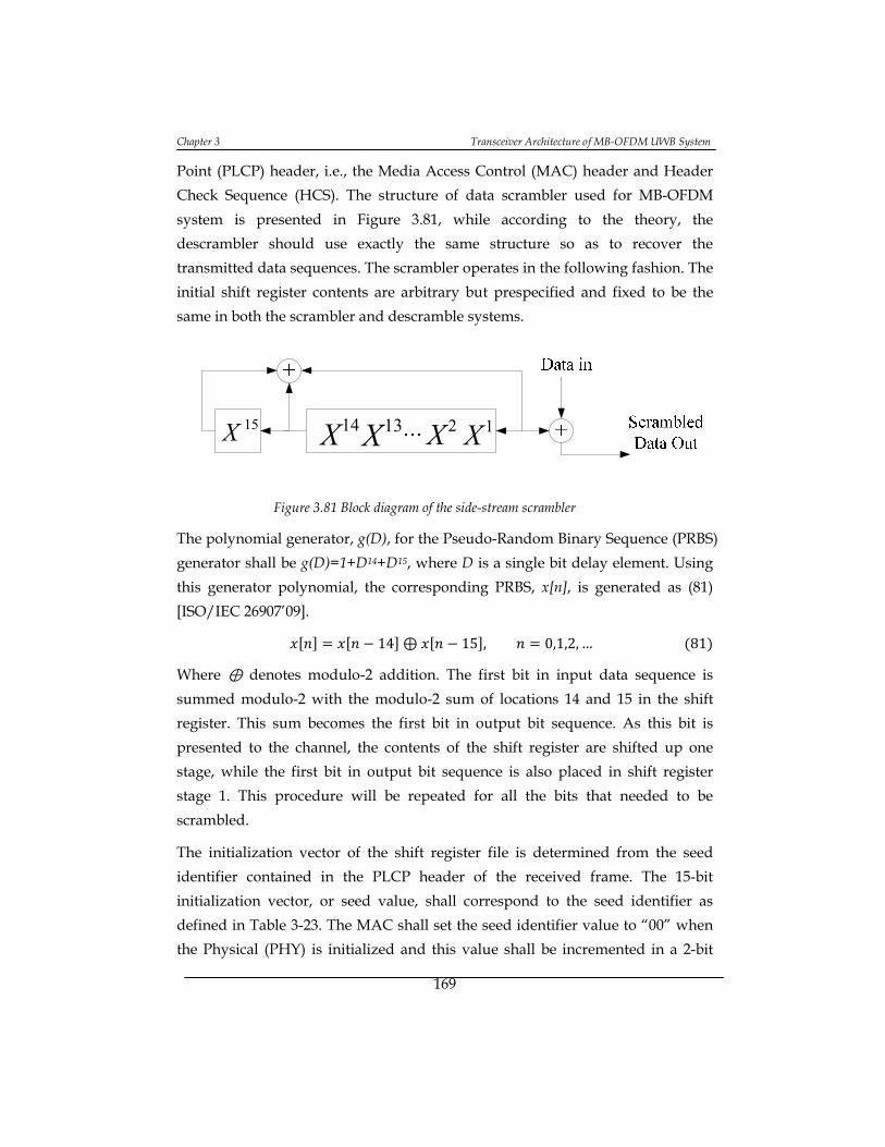
Chapter 3 Transceiver Architecture of MB-OFDM UWB System
169
Point (PLCP) header, i.e., the Media Access Control (MAC) header and Header
Check Sequence (HCS). The structure of data scrambler used for MB-OFDM
system is presented in Figure 3.81, while according to the theory, the
descrambler should use exactly the same structure so as to recover the
transmitted data sequences. The scrambler operates in the following fashion. The
initial shift register contents are arbitrary but prespecified and fixed to be the
same in both the scrambler and descramble systems.
15X 14X 13X 2X 1X
Figure 3.81 Block diagram of the side-stream scrambler
The polynomial generator, g(D), for the Pseudo-Random Binary Sequence (PRBS)
generator shall be g(D)=1+D14+D15, where D is a single bit delay element. Using
this generator polynomial, the corresponding PRBS, x[n], is generated as (81)
[ISO/IEC 26907’09].
14 ⊕ 15 , 0,1,2, … 81
Where ⊕ denotes modulo-2 addition. The first bit in input data sequence is
summed modulo-2 with the modulo-2 sum of locations 14 and 15 in the shift
register. This sum becomes the first bit in output bit sequence. As this bit is
presented to the channel, the contents of the shift register are shifted up one
stage, while the first bit in output bit sequence is also placed in shift register
stage 1. This procedure will be repeated for all the bits that needed to be
scrambled.
The initialization vector of the shift register file is determined from the seed
identifier contained in the PLCP header of the received frame. The 15-bit
initialization vector, or seed value, shall correspond to the seed identifier as
defined in Table 3-23. The MAC shall set the seed identifier value to “00” when
the Physical (PHY) is initialized and this value shall be incremented in a 2-bit

Design and Validation of an Optimized High-performance MB-OFDM Ultra Wideband Transceiver System
170
rollover counter for each frame sent by the PHY. Note that all consecutive
packets, including retransmissions, shall be sent with a different initial seed
value for MB-OFDM UWB system.
Table 3-23 Scrambler Seed Selection
Seed Identifier
(S1, S2)
Seed Value
Xint=xi[-1]xi[-2]…xi[-15]
PRBS Output First 16 bits
x[0]x[1]…x[15]
00 0011 1111 1111 111 0000 0000 0000 1000
01 0111 1111 1111 111 0000 0000 0000 0100
10 1011 1111 1111 111 0000 0000 0000 1110
11 1111 1111 1111 111 0000 0000 0000 0010
The simulation waveform of one testing data input sequence processed by the
data scrambler is shown in Figure 3.82. Along with the scrambler output
sequence, the shift register contents can also be seen in this figure.
Figure 3.82 Scrambler simulation waveform
By inspection of the scrambled output sequence, it can be seen clearly that
output sequence is very different from data input sequence. Whether output
sequence has any special randomness properties is not immediately evident.
The descrambler at receiver side has exactly the same structure as the scrambler,
while the seed value for each packet is transmitted as the 23th and 24th bits in the

Chapter 3 Transceiver Architecture of MB-OFDM UWB System
171
PHY Header sequence. By using the seed value from PHY Header, the
descrambler block takes charge of recovering the decoded data sequences to the
original information that have been transmitted.
3.6.2.2 Interleaver/Deinterleaver
Interleaving is a key component of many digital communication systems
involving Forward Error Correction (FEC) coding. Interleaving the encoded
symbols provides a form of time diversity to guard against correlated channel
noise such as localized corruption or bursts errors or fading. The interleaver
rearranges input data such that consecutive data are spaced apart. At the
receiver end, the interleaved data is arranged back into the original sequence by
the deinterleaver. As a result of interleaving, correlated noise introduced in the
transmission channel appears to be statistically independent at the receiver and
thus allows better error correction.
For MB-OFDM systems, the coded bits from convolutional encoder are then
interleaved prior to modulation by using three steps of interleaving technologies.
The three distinct interleaver stages are defined in Figure 3.83.
][ ia ][iaS ][iaT ][ ib
Figure 3.83 Various stages of the bit interleaver for MB-OFDM UWB system
The performance of each stage is given as follow:
1) Symbol Interleaving, which permutes the bits across 6
consecutive OFDM symbols, enables the PHY to exploit
frequency diversity within a band group.
2) Intra-symbol Tone Interleaving, which permutes the bits across
the data subcarriers within an OFDM symbol, exploits
frequency diversity across subcarriers and provides robustness
against narrow-band interferers.
3) Intra-symbol Cyclic Shifter, which cyclically shift the bits in
successive OFDM symbols by deterministic amounts, enables

Design and Validation of an Optimized High-performance MB-OFDM Ultra Wideband Transceiver System
172
modes that employ time-domain spreading and the Fixed
Frequency Interleaving (FFI) modes to better exploit frequency
diversity.
The deinterleaver blocks at the receiver side performs the inverse operations but
in inverse order (Cyclic Deshifter, Tone Deinterleaver, Symbol Deinterleaver)
after the modulation to obtain the original bit stream.
The additional parameters needed by the interleavers and deinterleavers
correspond to the values indicated in ISO/IEC 26907 standard [ISO/IEC
26907’09] are listed in Table 3-24 as a function of the data rate.
Table 3-24 Parameters for the Interleaver/Deintereleaver
Data
Rate
(Mbps)
Time
Domain
Spreading
Factor (NTDS)
Coded
Bits/
OFDM
Symbol
(NCBPS)
Tone
Interleaver
Block Size
(NTint)
Cyclic
Interleaver
Shift (NCYC)
Coded
Bits/ 6
OFDM
Symbol
(NCBP6S)
53.3 2 100 10 33 300
80 2 100 10 33 300
106.7 2 200 20 66 600
160 2 200 20 66 600
200 2 200 20 66 600
320 1 200 20 33 1200
400 1 200 20 33 1200
480 1 200 20 33 1200
3.6.2.2.1 Symbol Interleaver/Deinterleaver
The symbol interleaving operation is performed by first grouping the coded bits
into blocks of NCBP6S bits (corresponding to 6 “on-air” OFDM symbols). By using
a block interleaver of size NCBPS by 6/NTDS, the coded bits are permuted. Let the
sequences a[i] and aS[i] represent the input and output bits of the symbol block
interleaver respectively, where i = 0, …, NCBP6S-1. The output of symbol
interleaver is mathematically given by (82).
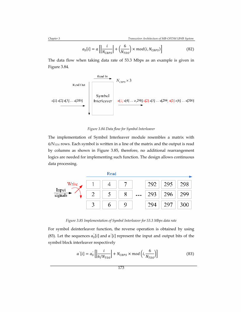
Chapter 3 Transceiver Architecture of MB-OFDM UWB System
173
6, 82
The data flow when taking data rate of 53.3 Mbps as an example is given in
Figure 3.84.
3CBPSN
Figure 3.84 Data flow for Symbol Interleaver
The implementation of Symbol Interleaver module resembles a matrix with
6/NTDS rows. Each symbol is written in a line of the matrix and the output is read
by columns as shown in Figure 3.85, therefore, no additional rearrangement
logics are needed for implementing such function. The design allows continuous
data processing.
Figure 3.85 Implementation of Symbol Interleaver for 53.3 Mbps data rate
For symbol deinterleaver function, the reverse operation is obtained by using
(83). Let the sequences ′ and ′ represent the input and output bits of the
symbol block interleaver respectively
′ ′6/
,6
83

Design and Validation of an Optimized High-performance MB-OFDM Ultra Wideband Transceiver System
174
Corresponding to (83), the data flow of symbol deinterleaver is the reverse of
Figure 3.84, while the implementation for this deinterleaver has the same
architecture as Figure 3.85, but with NCBPS rows instead, or we can just replace
the write and read pointer with each other in Figure 3.85 so as to get the symbol
deinterleaver implementation.
3.6.2.2.2 Tone Interleaver/Deinterleaver
The output of the symbol block interelaver is then passed through a tone block
interlever. The outputs of the symbol block interelaver are grouped together into
blocks of NCBPS bits and then permuted using a regular block interleaver of size
NTint×10. Let the sequences aS[i] and aT[i] represent the input and output bits of
the tone interleaver, where i=0, …, NCBPS-1. The output sequences of the tone
interleaver are given by the relationship of (84).
10 , 84
Also take the data rate mode of 53.3 Mbps as an example, the data flow for tone
interleaver is given in Figure 3.86.
1010/ CBPSN
]300[]...2[]1[ SSS aaa ]300[]...220[]210[]292[]...212[]202[]291[]...211[]201[
]200[]...120[]110[]192[]...112[]102[]191[]...111[]101[
]100[]...20[]10[]92[]...12[]2[]91[]...11[]1[
SSSSSSSSS
SSSSSSSSS
SSSSSSSSS
aaaaaaaaa
aaaaaaaaa
aaaaaaaaa
Figure 3.86 Data flow for Tone Interleaver
Similar to the Symbol Interleaver, the Tone Interleaver implements a matrix to
make the operation. Each symbol is written in a line of the matrix and the output
is read by columns, as shown in Figure 3.87. As the example is given for 53.3
Mbps transmission mode, the input sequences are divided into 3 groups, with
100 samples each.

Chapter 3 Transceiver Architecture of MB-OFDM UWB System
175
Figure 3.87 Implementation of Tone Interleaver for 53.3 Mbps data rate
The Tone Deinterleaver function is illustrated in (85). And the implementation
for Tone deinterleaver is also implemented by replacing the read and write
pointer with each other based on the structure in Figure 3.87.
′ ′10
, 10 85
3.6.2.2.3 Cyclic shifter/deshifter
The output results of the tone interleaver will be sent to an intra-symbol cyclic
shifter, which consists of a different cyclic shift for each block of NCBPS bits within
the span of the symbol interleaver defined above. Let the sequences aT[i] and aC[i]
represent the input and output bits of the cyclic shifter, where i=0, …, NCBP6S-1.
The output of the cyclic shifter is given by the following relationship.
, 86
Where / .
The cyclic shifter data flow is given in Figure 3.88, the data rate mode of 53.3
Mbps is given as an example.

Design and Validation of an Optimized High-performance MB-OFDM Ultra Wideband Transceiver System
176
]300[]...2[]1[ TTT aaa ]266[]...201[]300[]299[]...268[]267[
]133[]...101]200[]199[]...135[]134[
]100[]...99[]...2[]1[
TTTTTT
TTTTTT
Tttt
aaaaaa
aaaaaa
aaaa
Figure 3.88 Data flow for Cyclic Shifter
The resulting operation is illustrated in Figure 3.89, where X corresponded to an
index value. For a data rate of 53.3 Mbps, X corresponds to the following values:
1st Symbol: X=0 (no shift).
2nd Symbol: X=33.
3rd Symbol: X=66.
Figure 3.89 Cyclic Shifter Operation
The Cyclic Deshifter function is illustrated in (87) so as to reorganize the
received sequence to the original order.
′ ′ 21, 87
3.6.2.3 Constellation Mapper/Soft Demapper
The constellation mapping is the technique for mapping the coded and
interleaved binary data sequence onto a complex constellation. According to the
MB-OFDM standard, the data rate modes that lower than 200 Mbps (including
200 Mbps), the binary data shall be mapped onto a Quadrature Phase Shift
Keying (QPSK) constellation, whereas the data rates that higher than 320 Mbps

Chapter 3 Transceiver Architecture of MB-OFDM UWB System
177
(including 320 Mbps), the binary data shall be mapped onto a multi-dimensional
constellation using a Dual-Carrier Modulation (DCM) technique.
3.6.2.3.1 QPSK mapper
QPSK constellation mapping is used when data rate is 200 Mbps or lower
combing with Frequency-Domain Spreading (FDS) and Time-Domain Spreading
(TDS) techniques. The FDS and TDS modes are not only used to create the
varied data rates, but also maximize frequency diversity and improve the
performance. The binary coded and interleaved input data are divided into
groups of two bits, and then mapped in one of the four Gray coded QPSK
costellation points, as shown in Figure 3.90. By mapping two bits per symbol,
the output symbol values d[k] are normalized by a normalization factor of KMOD
= 1/√2 to have constant average symbol power, as given in (88).
Figure 3.90 QPSK constellation bit encoding
2 2 1 2 2 1 1 88

Design and Validation of an Optimized High-performance MB-OFDM Ultra Wideband Transceiver System
178
Where k=0, 1, 2, …, n. n=49 is used when FDS is enable, otherwise n=99. And
b[2k] determines the I value of the complex data, and b[2k+1] determines the Q
value.
3.6.2.3.2 Dual QPSK soft-demapper
Soft bit decision is used to demap the QPSK to maximize the post-QPSK
baseband processing. However, a soft bit based receiver will consume more
memory in the deinterleaver and increase the computational complexity of the
Viterbi Decoder. The soft-QPSK demapper process can improve WPAN receiver
performance where each input complex number for the demapper outputs two
soft bits being the symbol likelihood. The demapping process can be simply the
process of outputting real part (I value) and then the imaginary part (Q value) of
the input symbol for the first and second soft bit respectively. For a given code
bit, a positive soft bit with large possible magnitude may indicate more
confidence in ‘1’ being sent for the code bit, while a negative soft bit with large
possible magnitude may indicate more confidence in ‘0’ being sent for the code
bit, and a soft bit of zero may indicate equal likelihood of ‘0’ or ‘1’ being sent for
the code bit.
As frequency hopping is defined in MB-OFDM UWB standard, each time
diversity pair in the TDS is transmitted over a different frequency band and
therefore has independent channel fading characteristics. Therefore, it is a very
small possibility that both the main and spread OFDM symbols in different
frequency bands have deep fades on the same subcarriers. Thus, the receiver
may decide to select and decode one received OFDM symbol or combine the two
symbols to maximize performance. Since the duration of an OFDM symbol is
fixed, the receiver may implement a single serial decoding path for each symbol
pair, or have two parallel decoding paths clocked at half the serial rate. After the
equalization, the data from both main and spread OFDM symbols will be sent to
be demodulated by QPSK. Since QPSK soft demapper is used for a pair of main
and spread QPSK symbols, the receiver must implement soft decision for the
soft bit decoding. For two one-dimensional points (x1, y1) and (x2, y2), traditional,
the Euclidean distance should be computed as in (89). Let’s define and as

Chapter 3 Transceiver Architecture of MB-OFDM UWB System
179
the signals after equalization process for the main symbol and spread symbol
respectively. The spread decision can be selected from calculating the Euclidean
symbol distance between the corresponding QPSK constellation point to a main
QPSK symbol, , or a spread QPSK symbol, , and then output the symbol
that has the shorter distance. The Euclidean distance for , denote as dm, and
the distance for , denotes as ds are calculated in (90) and (91).
89
90
91
Where k=0, 1, …, 99, and Sn is the reference signal for one of the four
constellation points. Then the soft values of and are used as the
demapper output results after deciding the Euclidean distance, as given in (92)
and (93).
, 92
, 93
The equal gain combing scheme can be employed to combine the spread
sequence whether before the QPSK demapper or after QPSK demapper. Thus, in
order to decrease the computational complexity due to Euclidean distance
calculation, a simplified dual soft bit QPSK demapper is introduced into the
proposed MB-OFDM baseband receiver system as in [Sherratt’07].
The demapping process can be made implicit into the symbol combining scheme
such that for soft output soft(2k) and soft(2k+1) and input main and spread
symbols, then the QPSK decoding and TDS symbol merging process can be
simply reduced to (94) and (95). The overall likelihood of a large signal to noise
ratio value is increased, thereby increasing more reliability for Viterbi Decoder
input. This equal gain combing scheme not only has better soft decoding
performance than the spread decision, but also has much lower computation
complexity, as no multiplication and comparison functions are needed in this
low complexity demapper progress.
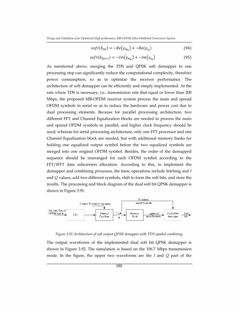
Design and Validation of an Optimized High-performance MB-OFDM Ultra Wideband Transceiver System
180
~ ~ 94
~ ~ 95
As mentioned above, merging the TDS and QPSK soft demapper to one
processing step can significantly reduce the computational complexity, therefore
power consumption, so as to optimize the receiver performance. The
architecture of soft demapper can be efficiently and simply implemented. At the
rate where TDS is necessary, i.e., transmission rate that equal or lower than 200
Mbps, the proposed MB-OFDM receiver system process the main and spread
OFDM symbols in serial so as to reduce the hardware and power cost due to
dual processing elements. Because for parallel processing architecture, two
different FFT and Channel Equalization blocks are needed to process the main
and spread OFDM symbols in parallel, and higher clock frequency should be
used; whereas for serial processing architecture, only one FFT processor and one
Channel Equalization block are needed, but with additional memory banks for
holding one equalized output symbol before the two equalized symbols are
merged into one original OFDM symbol. Besides, the order of the demapped
sequence should be rearranged for each OFDM symbol according to the
FFT/IFFT data subcarriers allocation. According to this, to implement the
demapper and combining processes, the basic operations include fetching and I
and Q values, add two different symbols, shift to form the soft bits, and store the
results. The processing and block diagram of the dual soft bit QPSK demapper is
shown in Figure 3.91.
Figure 3.91 Architecture of soft output QPSK demapper with TDS symbol combining
The output waveforms of the implemented dual soft bit QPSK demapper is
shown in Figure 3.92. The simulation is based on the 106.7 Mbps transmission
mode. In the figure, the upper two waveforms are the I and Q part of the

Chapter 3 Transceiver Architecture of MB-OFDM UWB System
181
equalized main and spread OFDM symbol sequences, it should be noted that
after channel equalization, the 12 pilot subcarriers, 10 guard subcarriers, and 6
DC subcarriers that inserted to each OFDM symbol have already been removed
or picked out for the usage such as frequency synchronization and channel
estimation, therefore only 100 data subcarriers are left for demapping,
deinterleaving, and decoding. The lower two waveforms are the soft demapping
output result sequence, soft(2k) and soft(2k+1), by using the dual soft demapper
algorithm. The order of the 100 soft bits is rearranged according to the OFDM
modulation assignment in the waveform. As shown by the results, most of the
soft bits are demapped as strongest ‘1’ or ‘0’, whereas some of them are
considered to be weak ‘0’ and ‘1’ as a result of channel fading and the affects of
noise.
Figure 3.92 QPSK soft demapper output waveforms
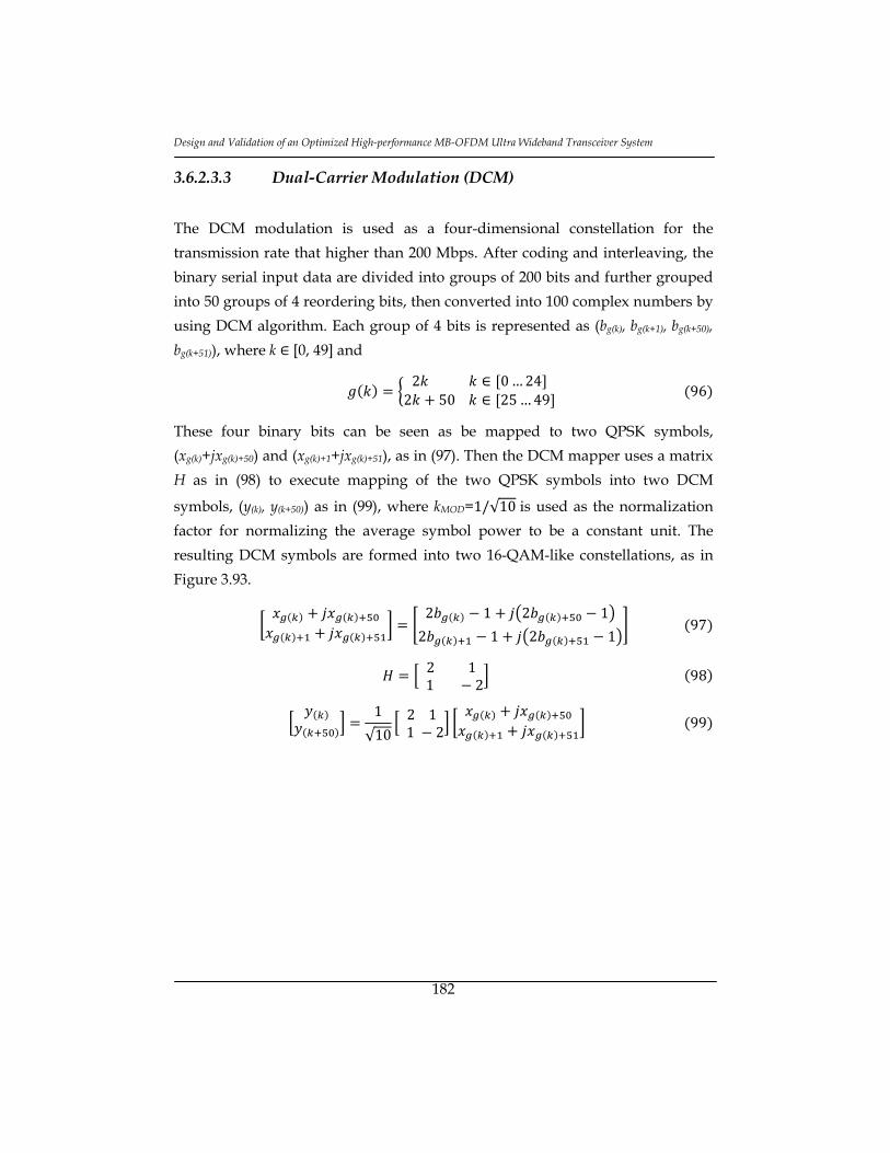
Design and Validation of an Optimized High-performance MB-OFDM Ultra Wideband Transceiver System
182
3.6.2.3.3 Dual-Carrier Modulation (DCM)
The DCM modulation is used as a four-dimensional constellation for the
transmission rate that higher than 200 Mbps. After coding and interleaving, the
binary serial input data are divided into groups of 200 bits and further grouped
into 50 groups of 4 reordering bits, then converted into 100 complex numbers by
using DCM algorithm. Each group of 4 bits is represented as (bg(k), bg(k+1), bg(k+50),
bg(k+51)), where k ∈ [0, 49] and
2 ∈ 0…242 50 ∈ 25…49 96
These four binary bits can be seen as be mapped to two QPSK symbols,
(xg(k)+jxg(k)+50) and (xg(k)+1+jxg(k)+51), as in (97). Then the DCM mapper uses a matrix
H as in (98) to execute mapping of the two QPSK symbols into two DCM
symbols, (y(k), y(k+50)) as in (99), where kMOD=1/√10 is used as the normalization
factor for normalizing the average symbol power to be a constant unit. The
resulting DCM symbols are formed into two 16-QAM-like constellations, as in
Figure 3.93.
2 1 2 1
2 1 2 1 97
211 2
98
1
√10211 2
99
Chapter 3 Transceiver Architecture of MB-OFDM UWB System
183
][ ky Q
][ky I
]50[ kyQ
]50[ ky I
Figure 3.93 DCM constellation mapping process: (a) mapping for yk; (b) mapping for yk+50
Information on a single tone is unreliable if a channel has deep fade. If the tone
is completely attenuated by the multipath channel, the information will be
completely lost. As it has been discussed above, the probability of two tones
experiencing a channel deep fade is extremely small if the two tones with the
same information are separated by a large bandwidth. Frequency diversity is
used in the DCM by mapping the same information but with different forms
onto two different tones at different channel frequencies with a large bandwidth
separation. The two resulting DCM symbols are allocated into two individual
OFDM data subcarriers with 50 subcarriers separation to achieve frequency
diversity. Therefore, 100 DCM symbols are feed into the 128 points IFFT block to
form one OFDM symbol with additional pilot, guard, and DC subcarriers. Each
OFDM subcarrier occupies a bandwidth of 528/128=4.125 MHz. Thus, the
bandwidth between the two individual OFDM data subcarriers related to the
two complex numbers (I(k), Q(k)) and (I(k+50), Q(k+50)) is at least 200 MHz, which
offers good frequency diversity gain against channel deep fading.
3.6.2.3.4 DCM demapping
The DCM demapper uses two separate subcarriers concurrently to decode the
symbol pair. If one symbol within one subcarrier is lost or degraded, it can be
detected, even recovered by the DCM demapper. It is required to repeatedly

Design and Validation of an Optimized High-performance MB-OFDM Ultra Wideband Transceiver System
184
execute demapping of the two received DCM symbols to output groups of 200
soft bits. The soft bits from the DCM demapper are then sent to soft decoding.
The DCM demapper shall demap two equalized complex numbers (IR(k), QR(k))
and (IR(k+50), QR(k+50)) that previously transmitted on two different subcarriers
back to two related DCM symbols by using the DCM mixing matrix. Then the
DCM demapper outputs the corresponding real part and imaginary part as a
group of 4 soft bits, as described in (100)-(103). However, the performance of
DCM demapping can remain the same without using the factor of √10/5, which
is hard to be implement for hardware system design. The group of 4 soft bits
applying two Channel State Information (CSI) values is from two corresponding
data subcarriers in an OFDM symbol, as described in (104)-(107).
√10 25
100
√10 25
101
√10 25
102
√10 25
103
2 min , 104
2 min , 105
2 min , 106
2 min , 104
The more reliable soft bit values that are given to Viterbi Decoder system, the
more accurately the binary bits can be decoded. The Maximum Likelihood (ML)
algorithm offers finding parameters to obtain the most probable emitted
symbols [Oberg’01]. The DCM symbols are transmitted at different amplitudes
and phases (I and Q values). The real part or the imaginary part in the two DCM
symbols is always fixed with data pairs being -3 and +1, -1 and -3, +1 and +3, +3
and -1. In this work, the large probable soft bit value can be obtained from the

Chapter 3 Transceiver Architecture of MB-OFDM UWB System
185
two received DCM symbols with an appropriate parameter θ, as described in
(105)-(108). The DCM symbol pair, yR(k) and yR(k+50), is received from the channel
equalization.
2 105
2 106
2 107
2 108
In order to find the appropriate parameter θ, two conditions need to be satisfied.
1) In perfect situation, the received I and Q values are feed to the
DCM demapper, applying θ to equations (105)-(108) to make the
soft magnitude sufficiently large;
2) A symbol in the DCM symbol pair is transmitted with a large
magnitude I (or Q), while another symbol in the DCM symbol pair
is transmitted with a small magnitude I (or Q). The signal with
smaller power can be more easily corrupted. Suppose the small
magnitude I (or Q) in a DCM symbol is received as inverted, while
the large magnitude I (or Q) in another DCM symbol is received as
uncorrupted. In this case, a maximum θ is required to retain the
sign of the soft bit value; otherwise using a larger θ can make the
sign of the soft bit value inverted, which causes errors for the soft
bit decoding.
The θ is set to be 1.5 as a threshold value according to the two conditions
above. The ML soft bit is generated with the appropriate factor and CSI aided
technique as described in the following:
3 min , 109
3 min , 110
3 min , 111
3 min , 112

Design and Validation of an Optimized High-performance MB-OFDM Ultra Wideband Transceiver System
186
3.6.2.4 Channel Estimation and Equalization
Channel Estimation system is another important element for baseband receiver
system development. In order to mitigate hostile channel effects on the received
signal, accurate channel estimation is required to provide information for further
processing of the received signals. Two different types of channel estimation
algorithm are basically used for nowadays communication systems, i.e., non-
data-aided and data-aided. The non-data-aided channel estimators estimate
channel response by statistics of the received signals. Thus, no reference or
training signals are needed so as to increase the transmission efficiency.
However, in this kind of estimation strategies, large scale of data must be
collected in order to obtain reliable estimation, because there isn’t any
information that can be used on the receiver side related with the transmitted
signals before processing. The systems that use data-aided channel estimators
will provide defined reference or training signals to the transmitted sequences.
Therefore, by comparing the same defined training signals that restored on the
receiver side with that of the transmitted training signals, the receiver can
estimate the channel response rapidly and accurately. As sufficient number of
training signals should be inserted to the transmitted packets, the transmission
efficiency will be affected for the data-aided strategies.
OFDM has been known to be quite spectral efficient over frequency-selective
fading channels. By dividing a frequency-selective-faded signal band into a large
number of narrow-band flat-fading sub channels, high-rate transmission is then
achieved by using a compact constellation on each subcarrier. For MB-OFDM
UWB communication protocol, the data-aided estimation scheme is used so as to
get an accurate estimation on the channel response. For standard PLCP
preamble transmission, 6 Channel Estimation Sequences are added in front of
each transmitted packet, which are used as reference and training signals for the
channel estimator on the receiver system. Then the estimated channel response
is sent to the channel equalizer block, so that the fading effect and co-channel
interference of each transmitted signal can be removed and the original
transmitted signal can be restored.

Chapter 3 Transceiver Architecture of MB-OFDM UWB System
187
3.6.2.4.1 Channel Estimation
As defined in MB-OFDM standard, the 6 channel estimating sequences in PLCP
preamble are used by the receiver side to estimate impulse response of the
transmission channel, commonly termed the Channel State Information (CSI).
The estimation process can be executed as a dynamic estimation in the
frequency-domain for data reliability in each subcarrier position. The potentially
CSI is usually different from each OFDM data subcarriers, thus, the more CSI
measurement that can be taken, the more reliable the CSI estimation is in the
presence of thermal noise offering better decoding result.
The Lease Squares (LS) Estimation algorithm is used for the proposed MB-
OFDM baseband communication system implementation. LS channel estimator
is a Maximum Likelihood (ML) estimator, which is considered has very low
implementation complexity, thus makes LS one of the popular methods for the
OFDM based system channel estimation without using any knowledge of the
statistics for the channel. Although some reports say that the drawback of LS
estimator is that its performance, especially under low SNR situations, is greatly
influenced by the noise, the work in [Li’06] has shown that LS estimation has
similar performance very close to Minimum Mean Squared Error (MMSE)
algorithm.
At the receiver system, the demodulated OFDM signal after FFT, Y, can be
expressed in matrix notation as (113).
113
Where X is the matrix of transmitted signals, h is the time domain channel
impulse response, I is the ISI and ICI effects, W is the Additive White Gaussian
Noise (AWGN) with zero mean and variance N0, F is the DFT matrix, and H=F‧h
is the channel frequency response. Here,
0 , 1 , … , 1 114
0 , 1 , … , 1 115
0 , 1 , … , 1 116
0 , 1 ,… , 1 117
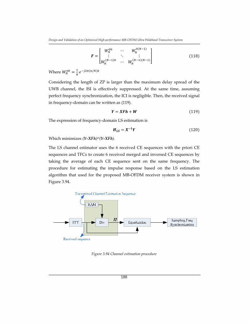
Design and Validation of an Optimized High-performance MB-OFDM Ultra Wideband Transceiver System
188
⋯⋮ ⋱ ⋮
⋯ 118
Where /
Considering the length of ZP is larger than the maximum delay spread of the
UWB channel, the ISI is effectively suppressed. At the same time, assuming
perfect frequency synchronization, the ICI is negligible. Then, the received signal
in frequency-domain can be written as (119).
119
The expression of frequency-domain LS estimation is
120
Which minimizes (Y-XFh)H(Y-XFh).
The LS channel estimator uses the 6 received CE sequences with the priori CE
sequences and TFCs to create 6 received merged and inversed CE sequences by
taking the average of each CE sequence sent on the same frequency. The
procedure for estimating the impulse response based on the LS estimation
algorithm that used for the proposed MB-OFDM receiver system is shown in
Figure 3.94.
Figure 3.94 Channel estimation procedure
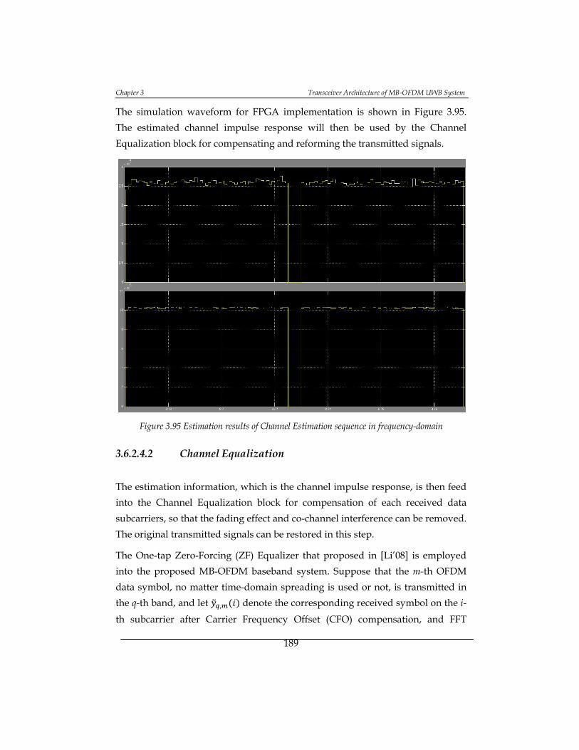
Chapter 3 Transceiver Architecture of MB-OFDM UWB System
189
The simulation waveform for FPGA implementation is shown in Figure 3.95.
The estimated channel impulse response will then be used by the Channel
Equalization block for compensating and reforming the transmitted signals.
Figure 3.95 Estimation results of Channel Estimation sequence in frequency-domain
3.6.2.4.2 Channel Equalization
The estimation information, which is the channel impulse response, is then feed
into the Channel Equalization block for compensation of each received data
subcarriers, so that the fading effect and co-channel interference can be removed.
The original transmitted signals can be restored in this step.
The One-tap Zero-Forcing (ZF) Equalizer that proposed in [Li’08] is employed
into the proposed MB-OFDM baseband system. Suppose that the m-th OFDM
data symbol, no matter time-domain spreading is used or not, is transmitted in
the q-th band, and let , denote the corresponding received symbol on the i-
th subcarrier after Carrier Frequency Offset (CFO) compensation, and FFT
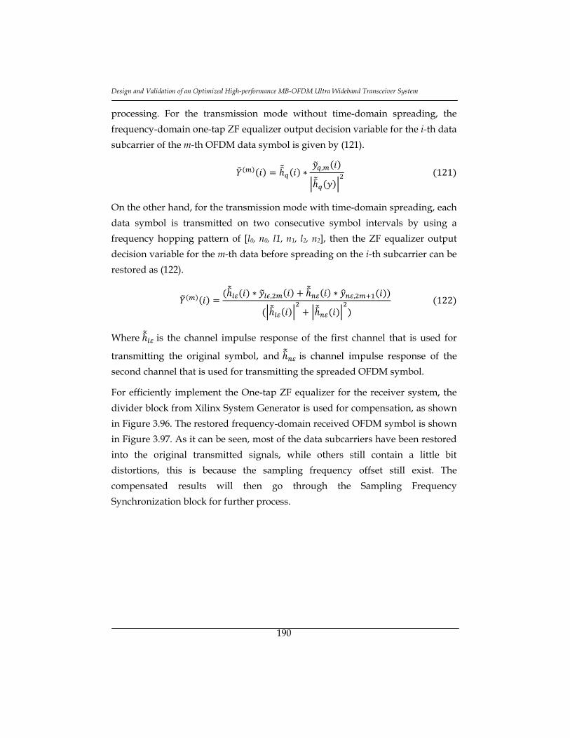
Design and Validation of an Optimized High-performance MB-OFDM Ultra Wideband Transceiver System
190
processing. For the transmission mode without time-domain spreading, the
frequency-domain one-tap ZF equalizer output decision variable for the i-th data
subcarrier of the m-th OFDM data symbol is given by (121).
∗ , 121
On the other hand, for the transmission mode with time-domain spreading, each
data symbol is transmitted on two consecutive symbol intervals by using a
frequency hopping pattern of [l0, n0, l1, n1, l2, n2], then the ZF equalizer output
decision variable for the m-th data before spreading on the i-th subcarrier can be
restored as (122).
∗ , ∗ , 122
Where is the channel impulse response of the first channel that is used for
transmitting the original symbol, and is channel impulse response of the
second channel that is used for transmitting the spreaded OFDM symbol.
For efficiently implement the One-tap ZF equalizer for the receiver system, the
divider block from Xilinx System Generator is used for compensation, as shown
in Figure 3.96. The restored frequency-domain received OFDM symbol is shown
in Figure 3.97. As it can be seen, most of the data subcarriers have been restored
into the original transmitted signals, while others still contain a little bit
distortions, this is because the sampling frequency offset still exist. The
compensated results will then go through the Sampling Frequency
Synchronization block for further process.

Chapter 3 Transceiver Architecture of MB-OFDM UWB System
191
Figure 3.96 Implementation of one-tap ZF equalizer by using Xilinx System Generator
Figure 3.97 Waveform of restored OFDM symbol after channel equalization

Design and Validation of an Optimized High-performance MB-OFDM Ultra Wideband Transceiver System
192
3.6.2.5 Control system and data flow
For the MB-OFDM digital baseband system design, as pilot subcarriers, NULL
(DC) subcarriers, and guard subcarriers needed to be inserted into each group of
data subcarriers at the transmitter side, and removed at receiver side, the
unbalanced data rate at input and output port would happen, i.e., less data is
feed into the transmitter system while more data after processing will appear at
the output port due to inserting, whereas on the other hand, more data is sent to
the receiver side but less processing results at the end due to removing. To
properly inserting and removing those subcarriers at the right location and right
time so as to flow the OFDM symbol format, several control logics should be
added. Besides, the time-domain spreading will further led to more unbalanced
data rate for both sides of the transceiver system.
3.6.2.5.1 Retiming and Clock island for Transmitter system
For the proposed MB-OFDM system, the clock island and retiming
methodologies are used to solve the unbalance problem results from inserting
and removing, besides, as not all the processing elements are working at very
high processing speed (frequency), the dynamic power consumptions for the
whole system will be reduced as well. Because 53.3 Mbps transmission mode is
mandatory for transmitting the PLCP Header packets, the 53.3 Mbps mode will
be given as an example for introducing the control logics. The other data rate
mode is controlled by using similar strategy but different processing frequency.
According to the MB-OFDM standard, 200 bits data are needed to form each
PLCP Header. After HCS processing, encoded by Reed-Solomon encoder, and
scrambler, the 200 bits PLCP Header should be send to encoding procedure.
Then the data processing flow of the PLCP Header can be given as Figure 3.98.

Chapter 3 Transceiver Architecture of MB-OFDM UWB System
193
Figure 3.98 Data processing flow of 200 bits PLCP Header

Design and Validation of an Optimized High-performance MB-OFDM Ultra Wideband Transceiver System
194
As it can be seen in the figure, after the convolutional encoder with the code rate
of 1/3, 600 bits are formed as coded data subcarriers. Then the 3-step interleaver
system will process all these 600 bits by the group of NCBP6S (300 for 53.3 Mbps
transmission mode), and the QPSK modulator will map these 600 bits into
groups of two bits and get 300 complex numbers at the end. For 53.3 Mbps mode,
as each OFDM symbol contains 50 data subcarriers, i.e. complex numbers, these
300 complex number will be divided into 6 groups and waiting to insert the pilot,
DC, and guard subcarriers to each group. After processing each 128 complex
numbers, which is formed of 100 data subcarriers (50 original complex numbers
and 50 conjugated numbers), 12 pilot subcarriers, 6 DC subcarriers, and 10 guard
subcarriers, the 128 processing results will be added 37 Zero Prefix (ZP) signals
so as to form one OFDM symbol of 165 data. Therefore, at this point, 6 OFDM
symbols should be formed. Furthermore, as time-domain spreading is necessary
for data rate lower or equal to 200 Mbps transmission rate, therefore, totally
6×2=12 OFDM symbols will be transmitted for each 200 bits PLCP Header
sequence.
For the proposed MB-OFDM transmitter architecture, the 600 bits encoded bits
are throughout by groups of 3 bits, therefore, 200 clock cycles are needed at this
stage. Then the interleaver will process all the 600 bits within one clock cycle. 300
clock cycles are needed for the QPSK mapper to form the 300 complex numbers.
As the proposed IFFT processor is implemented by using 4-path-parallel
architecture, therefore, a Serial to Parallel (S/P) buffer should be added before
IFFT processor. Then 32 clock cycles are required by the IFFT processor to deal
with each 128 complex numbers, 32×6=192 clock cycles in total are needed for
processing all the 200 bits of each PLCP Header packet. Then a Parallel to Serial
(P/S) buffer will reform the 4-path-parallel data stream into serial sequences so
as for adding ZP conveniently, i.e. 128+37=165 clock cycles for each OFDM
symbol and 165×6=990 cycles are necessary. Furthermore, after time-domain
spreading, the cycles needed are then doubled to 1980 cycles for transmitting
each 200 bits PLCP Header packet.
According to the discussion above, if the transmitter system use the same clock
frequency, 528 MHz as required, for both input and output signals of the S/P

Chapter 3 Transceiver Architecture of MB-OFDM UWB System
195
module before IFFT processor, 50 clock cycles are needed to restore one symbol
while 128 clock cycles are needed to feed one symbol out. The unbalance input
and output rate will course a big problem if a very big memory bank is not used
to restore all the data subcarrier that waiting to be processed. The procedure of
adding ZP will also lead to such problem, as 128 input clock cycles are needed to
restore the input whereas 165 cycles are needed to feed them out. The time-
domain spreading has the factor of unbalancing the input and output clock
cycles from 165 input cycle to 330 output cycles, which means another big
memory bank is also necessary to restore each result from the IFFT processor
and waiting to be sent out at the right time. The structure of the transmitter
system that using an global clock, with the frequency of 528 MHz, is shown in
Figure 3.99.
Figure 3.99 Processing flow when using global clock
As both real part and imaginary part of each complex number are represented
by 10 bits, for the architecture above should use two very large memory banks to
avoid overflow problems due to unbalanced data flow. This is not so efficient for
hardware resource usage, meanwhile, as all processing elements are working at
the same frequency, the dynamic power consumption will be also very high. To
solve both the above problems, the clock island and retiming methodologies are
employed.
As analyzed above, instead of making the already encoded data sequences
waiting in the memory banks, they can come to the IFFT processor in a slower
speed, and the best situation is that they can come to the IFFT processor at the
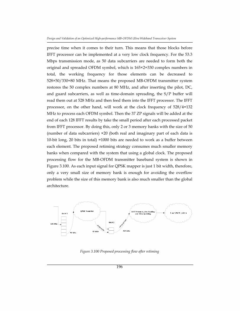
Design and Validation of an Optimized High-performance MB-OFDM Ultra Wideband Transceiver System
196
precise time when it comes to their turn. This means that those blocks before
IFFT processor can be implemented at a very low clock frequency. For the 53.3
Mbps transmission mode, as 50 data subcarriers are needed to form both the
original and spreaded OFDM symbol, which is 165×2=330 complex numbers in
total, the working frequency for those elements can be decreased to
528×50/330=80 MHz. That means the proposed MB-OFDM transmitter system
restores the 50 complex numbers at 80 MHz, and after inserting the pilot, DC,
and guard subcarriers, as well as time-domain spreading, the S/P buffer will
read them out at 528 MHz and then feed them into the IFFT processor. The IFFT
processor, on the other hand, will work at the clock frequency of 528/4=132
MHz to process each OFDM symbol. Then the 37 ZP signals will be added at the
end of each 128 IFFT results by take the small period after each processed packet
from IFFT processor. By doing this, only 2 or 3 memory banks with the size of 50
(number of data subcarriers) ×20 (both real and imaginary part of each data is
10-bit long, 20 bits in total) =1000 bits are needed to work as a buffer between
each element. The proposed retiming strategy consumes much smaller memory
banks when compared with the system that using a global clock. The proposed
processing flow for the MB-OFDM transmitter baseband system is shown in
Figure 3.100. As each input signal for QPSK mapper is just 1 bit width, therefore,
only a very small size of memory bank is enough for avoiding the overflow
problem while the size of this memory bank is also much smaller than the global
architecture.
Figure 3.100 Proposed processing flow after retiming

Chapter 3 Transceiver Architecture of MB-OFDM UWB System
197
The comparison results of the hardware resources usage after synthesis by using
Xilinx tools is shown in Table 3-25. According to the synthesis results, the global
clock architecture will use 12% more flip flop pairs and 30% more Look-Up-
Table (LUT) compared with the proposed retiming architecture. Besides, 3 more
Block RAM memory banks should also be used as buffers among those
processing elements, while no Block RAM resources are needed for the proposed
architecture.
Table 3-25 Synthesis report comparison for different implementation methodologies
Implementation Method Global Clock Retiming Clock
No. of LUT Flip Flop pairs 19515 17150
No. with an unused LUT 7092 4972
No. Block RAM 3 N/A
FPGA Device 5vlx110tff1136-3
Therefore, by using this retiming architecture for implementing the transmitter
system, the proposed architecture can not only save lots of memory resources
usage, but also save some power consumption as several blocks are working at a
very low frequency, while it still meets the timing specification provided by the
MB-OFDM UWB standard. Moreover, it makes the whole system much easier to
be implemented onto the FPGA board used in this work, as the constraint for
critical path is much lower and the control logics are also simpler.
Based on the retiming architecture, the proposed transmitted system is
implemented by combining all the elements using Verilog HDL code in Register
Transfer Level (RTL). The simulation waveforms of the transmitter system are
shown in Figure 3.101.

Design and Validation of an Optimized High-performance MB-OFDM Ultra Wideband Transceiver System
198
Figure 3.101 Simulation waveforms of the MB-OFDM transmitter system
It can be seen that the processing elements are divided into several islands that
using different clock frequency. Thus, by using the clock island methodology as
shown in Figure 3.102, each island can be controlled with unique clock
frequency more efficiently and conveniently. By using the clock enable signal to
control different island, some part of the system can be put into ‘sleep’ mode or
‘stand by’ mode when they are not called on duty, when still keep the other part
at ‘weak up’ mode for processing. The flexible control ability will save the
processing power consumption for the proposed MB-OFDM transmitter system
when few data is needed for transmission.

Chapter 3 Transceiver Architecture of MB-OFDM UWB System
199
Figure 3.102 Clock island architecture
3.6.2.5.2 Control system for Receiver system
The receiver system plays the inverse function as transmitter system. The
inserted pilot/DC/guard subcarriers, as well as the time-domain spreading
symbols, should be removed, because only the data subcarriers in the original
OFDM symbols are needed to recover the transmitted data sequences. But not
like the transmission function, different subcarriers should be picked up by
using different elements at receiver side, because they have different actions on
providing information such as frequency offset and channel response. Therefore,
removing these subcarriers will involve several other functions, such as
compensation and estimation.
Also take the 53.3 MHz transmission mode as example, before the QPSK (or
DCM) demapper, all the guard interval, Zero Prefix (ZP), pilot subcarriers and
guard subcarriers should be removed, left only the useful data subcarriers. As
mentioned before, one MB-OFDM symbol contains 128 subcarriers for FFT/IFFT
processor and 37 ZP for eliminating ISI and minimizing the impact of Inter-
Carrier-Interference (ICI). The 128 subcarriers consists of 100 data tones, 12 pilot
tones, 10 guard tones and 6 NULL (DC) signals. After the removing process,
only the 100 data tones should be left for the rest signal processing step.

Design and Validation of an Optimized High-performance MB-OFDM Ultra Wideband Transceiver System
200
As mentioned in Section 4.5, the 12 pilot subcarriers are picked up by the
Sampling Frequency Synchronization block for estimating the frequency offset
and compensate the data subcarriers in frequency-domain. Therefore the pilot
subcarriers should be removed after the frequency synchronization. But before
the Sampling Frequency Synchronization block, all the other unnecessary sub
tones, i.e. guard/DC/ZP, should be removed. The work flow for removing all
the subcarriers is shown in Figure 3.103.
Figure 3.103 Procedures for removing pilot/DC/guard subcarriers and ZP for 53.3 MHz
transmission mode
Firstly, for the 53.3 MHz mode, two OFDM symbols (consists of 330 samples in
total) are restored in a Block RAM memory. One of them is the original OFDM
symbol and another one is the spreaded symbol if timing spreading is used. The
positions where pilot/DC/guard subcarriers and 37 ZP signals will be ignored
when reading those two OFDM symbols out of the memory. The remaining 112
samples will be fed into the Sampling Frequency Synchronization block for
synchronize the frequency offset in frequency-domain. A memory bank that
restores all those 224 samples for both OFDM symbol will be implemented in
this block. The 12 pilot subcarriers of each symbol will be picked up during this
procedure for estimate and compensate the frequency offset for the rest 100 data

Chapter 3 Transceiver Architecture of MB-OFDM UWB System
201
subcarriers. Then the 100 compensated data subcarriers are gathered. If the
conjugate symmetry method is used to form these 100 data subcarriers, then
only 50 data signals are transmitted in each OFDM symbol, which means the
first 50 data is the original samples while the second 50 data is the conjugate
symmetry signals. In order to enhance the accuracy of the proposed receiver
system, these two groups of data signals should be averaged and get the original
50 data samples at the end. The data subcarriers will then be used by the
demapper and the following sub-modules to recover the transmitted signal
sequences. The format of the 128 subcarriers that formed from 50 data samples,
as well as the transmission order is shown in Figure 3.104.
_ _ ∗
1 DC _ 1 ~ _ 56 5 Guard Pilot
5 DC
5 Guard Pilot _ 56 ~ _ 1
Figure 3.104 Format and transmission order of the 128 subcarriers
Before transform the received signal from time-domain to frequency-domain by
using FFT processor, the 37 ZP signals should be removed first. Same like the
IFFT processor, the FFT processor also works at the 132 MHz clock frequency,
and totally 79 clock cycles are needed for processing each OFDM symbol (32
clock cycles are needed for inserting the 128 subcarriers into the FFT processor,
15 clock cycles for processing each OFDM symbol, the first 4 processing results
will be feed out in the 16 clock cycle, the 32 clock cycles are necessary for output
the entire 128 samples in frequency domain). Therefore, in order to make the
system easier to control, the proposed MB-OFDM system uses a block RAM
element to restore 8 OFDM symbols (165×8=1320 samples), then after removing
the ZP for all these 8 symbols, a total number of 1024 samples will be fed into the
FFT processor continually. The left 296 clock cycles (1320-1024=296), which is
caused by removing 8 ZPs and equals to 74 processing cycles for FFT processor
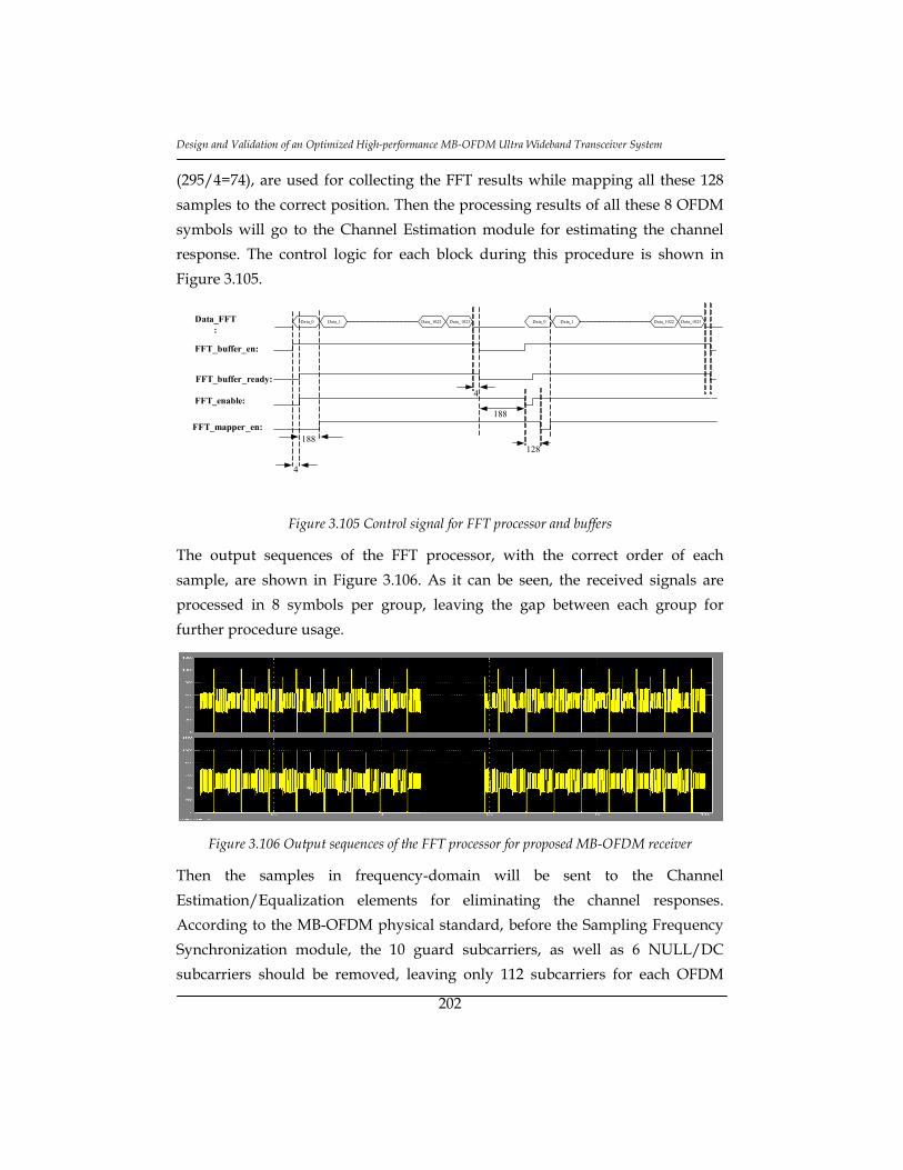
Design and Validation of an Optimized High-performance MB-OFDM Ultra Wideband Transceiver System
202
(295/4=74), are used for collecting the FFT results while mapping all these 128
samples to the correct position. Then the processing results of all these 8 OFDM
symbols will go to the Channel Estimation module for estimating the channel
response. The control logic for each block during this procedure is shown in
Figure 3.105.
Data_0 Data_1 Data_1022 Data_1023 Data_0 Data_1 Data_1022 Data_1023Data_FFT:
FFT_buffer_en:
FFT_buffer_ready:
FFT_enable:
FFT_mapper_en:
4
188
4
188
128
Figure 3.105 Control signal for FFT processor and buffers
The output sequences of the FFT processor, with the correct order of each
sample, are shown in Figure 3.106. As it can be seen, the received signals are
processed in 8 symbols per group, leaving the gap between each group for
further procedure usage.
Figure 3.106 Output sequences of the FFT processor for proposed MB-OFDM receiver
Then the samples in frequency-domain will be sent to the Channel
Estimation/Equalization elements for eliminating the channel responses.
According to the MB-OFDM physical standard, before the Sampling Frequency
Synchronization module, the 10 guard subcarriers, as well as 6 NULL/DC
subcarriers should be removed, leaving only 112 subcarriers for each OFDM
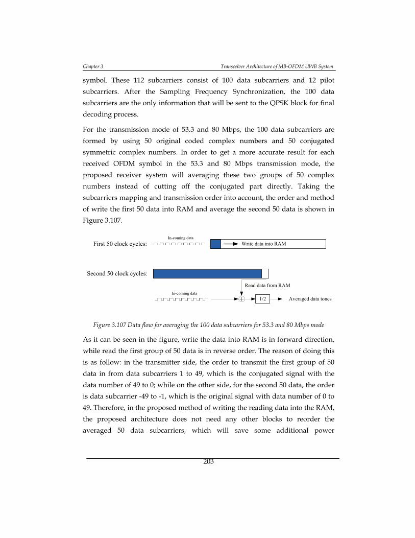
Chapter 3 Transceiver Architecture of MB-OFDM UWB System
203
symbol. These 112 subcarriers consist of 100 data subcarriers and 12 pilot
subcarriers. After the Sampling Frequency Synchronization, the 100 data
subcarriers are the only information that will be sent to the QPSK block for final
decoding process.
For the transmission mode of 53.3 and 80 Mbps, the 100 data subcarriers are
formed by using 50 original coded complex numbers and 50 conjugated
symmetric complex numbers. In order to get a more accurate result for each
received OFDM symbol in the 53.3 and 80 Mbps transmission mode, the
proposed receiver system will averaging these two groups of 50 complex
numbers instead of cutting off the conjugated part directly. Taking the
subcarriers mapping and transmission order into account, the order and method
of write the first 50 data into RAM and average the second 50 data is shown in
Figure 3.107.
Write data into RAMIn-coming data
First 50 clock cycles:
Second 50 clock cycles:
In-coming data
+
Read data from RAM
1/2 Averaged data tones
Figure 3.107 Data flow for averaging the 100 data subcarriers for 53.3 and 80 Mbps mode
As it can be seen in the figure, write the data into RAM is in forward direction,
while read the first group of 50 data is in reverse order. The reason of doing this
is as follow: in the transmitter side, the order to transmit the first group of 50
data in from data subcarriers 1 to 49, which is the conjugated signal with the
data number of 49 to 0; while on the other side, for the second 50 data, the order
is data subcarrier -49 to -1, which is the original signal with data number of 0 to
49. Therefore, in the proposed method of writing the reading data into the RAM,
the proposed architecture does not need any other blocks to reorder the
averaged 50 data subcarriers, which will save some additional power

Design and Validation of an Optimized High-performance MB-OFDM Ultra Wideband Transceiver System
204
consumption and hardware logics. Then the averaged data can be directly sent
to the soft demapper block.
As has been introduced in section 6.2.3, the de-time-domain-spreading block is
implemented inside the QPSK/DCM demapper module, therefore, no further
blocks are need for processing the spreaded OFDM symbols. The order and
processing stages from averaging the 50 data subcarriers, de-time-domain-
spreading, soft QPSK demapper, and the deinterleaver for each group of 8
OFDM symbols is shown in Figure 3.108.
Figure 3.108 Data flow for averaging data, de-time-domain-spreading, demapper, and
deinterleaver process
As far as the control logic and systems have been developed for both transmitter
and receiver system, the entire MB-OFDM digital baseband transceiver system is
integrated by combining all the already implemented sub-system together. The
structure of the final developed transceiver system compliances with the MB-

Chapter 3 Transceiver Architecture of MB-OFDM UWB System
205
OFDM UWB standard [ISO/IEC 26907’09] strictly. The validation process for the
whole system, final implementation in the FPGA board, and the experimental
results will be presented in the following chapters.
3.6.3 Conclusions and contributions
In this section, the other elements that are defined by the MB-OFDM standard
are discussed and implemented by employing many different state-of-the-art
architectures and algorithms. The structure of each element for both transmitter
and receiver system is high optimized so as to decrease the cost on either power
consumption or hardware resources.
Finally, in order to integrate the entire transceiver digital baseband system, the
control logic is discussed and developed by considering the properties of
different processing elements. The clock island and retiming methodology is
employed which is proved to be both hardware and power efficient.
The final integrated transceiver system has the property of low computational
complexity, low power consumption, and high performance, which can be used
for MB-OFDM UWB communication applications.
3.7. Chapter final conclusions and original contributions
The proposed architecture for MB-OFDM UWB digital baseband transceiver
system is introduced in this chapter. In order to get a highly optimized structure,
modifications are made in different processing elements with different
technologies. The FFT/IFFT processor, timing synchronization blocks, and
Viterbi Decoder systems are taken into consideration, because these subsystems
are acting as the core elements for the entire transceiver system.
A novel mixed radix 128-point FFT algorithm by combining modified radix-2
and radix-22 algorithms together is proposed for the MB-OFDM baseband
system development. A low-power, high throughput FFT processor is built.
Thanks to the algorithm, the number and complexity of the complex multipliers
are able to be significantly reduced in different processing stages. The power

Design and Validation of an Optimized High-performance MB-OFDM Ultra Wideband Transceiver System
206
consumption of the whole system has been reduced by around 50% compared
with that of existing works. The implementation results indicate that the
throughput rate of the proposed FFT processor with 10-bit Input/Output Word-
Length (IOWL), System Word-Length (SWL) and 8-bit twiddle factor word-
length can support maximum 1 Gsample/s with a power consumption of 43.79
mW at 250 MHz processing frequency by using 0.13 μm CMOS technology.
Then, as the MB-OFDM system is sensitive to the timing offset, an innovative
timing synchronization scheme is proposed by using the standardized preamble
sequences for MB-OFDM system. The two parts of the proposed scheme, Packet
Detector (PD) and Timing Offset Estimation (TOE) algorithm provide a robust
detection performance and can complete packet and symbol boundary detection
in a short time with high accuracy. When compared with the existing algorithms,
only the sign bits of synchronization sequence are used for computing the
correlations for both PD and TOE blocks. This makes the computational
complexity significantly reduced while the performance of synchronization
remains at a high level. The low complexity, high accurate frequency
synchronization scheme is also introduced into the proposed MB-OFDM system.
The frequency synchronization process should be made in both time-domain
and frequency-domain, in order to fully eliminate the frequency offset, and
increase the robustness and accuracy for the entire receiver system.
In order to speed up the decoding procedure for the receiver system, a power
efficient two-stage 64-state radix-4 Viterbi Decoder (VD) architecture is also
proposed in this work. The high speed, low complexity 4-way Add-Compare-
Select Unit (ACSU) is used so as to increase the throughput of the VD system.
The modulo normalization algorithm if employed to further decrease the
hardware resources usage for the proposed ACSUs. Then at the output port, 2-
pointer even algorithm is implemented for the trace back unit. Implementation
results showed that the proposed VD with relatively low hardware complexity
and power consumption can support various data rates for the MB-OFDM UWB
transmission applications.
Several other state-of-the-art architecture and algorithms for optimization of
different subsystems for other processing stages are also discussed and

Chapter 3 Transceiver Architecture of MB-OFDM UWB System
207
introduced into the proposed MB-OFDM transceiver system, such as the
memory reorder structure for the soft deinterleaver system, soft demapper
processor, low complexity Channel Estimation/Equalization system. The design
of the control logics are presented according to the different properties of the
different elements. The clock island and retiming methodology is used for
controlling different processing stages.
Finally, by combing all the processing elements as presented above, the entire
MB-OFDM digital baseband transceiver system is integrated according to the
ISO/IEC standard.

Design and Validation of an Optimized High-performance MB-OFDM Ultra Wideband Transceiver System
208

Chapter 4 Hardware-in-the-loop Co-simulation Methodology
209
4. Hardware-in-the-loop Co-simulation
Methodology
4.1. Introduction
As the entire baseband transceiver system has been proposed and implemented,
the next procedure should be validate and analyze and proposed architecture by
using real hardware devices, FPGA in this work. But as discussed above,
traditional verification process for hardware development will cost lots of design
effort. Therefore an efficient hardware validation methodology is highly desired
in the presented work. In this chapter, the other contribution of this work, a
hardware/software co-design methodology will be introduced.
Traditional approaches for implementing digital processing system in a FPGA or
ASIC involve creating a design and translating between multiple design
descriptions: an abstract algorithm is analyzed and optimized in MATLAB or C,
or any other languages; then it is mapped onto an architecture using behavioral
or structural description; in the process, a fixed-point description replaces a
floating point version of the design; it is partitioned into various design fabrics
and mapped into an FPGA or ASIC; the design is checked for equivalence
between different descriptions; and the test vectors are once again translated for
use in a logic analysis system for final hardware testing. Each translation step,
whether manual or automated, requires additional verification to confirm that
the original design has been preserved.
In system level design, logic errors need to be eliminated early in the design
process to avoid costly hardware re-spins. Unfortunately, logic verification using

Design and Validation of an Optimized High-performance MB-OFDM Ultra Wideband Transceiver System
210
simulation is often too slow and not so convenient for complex system
development. Monitoring and analyzing the output signals from hardware
implementation by using oscilloscope will also cost lots of effort for complex
system development, and it is usually hard to debug the system errors. Complex
digital system development requires shorter verification time and efficient
debug method.
Nowadays, because of the benefits of reduced time-to-market and high
reconfigurability, FPGAs have been widely applied in different VLSI systems,
used either as emulators for ASIC design or as an important part of the
embedded system. Meanwhile, as the FPGA designs are getting more complex,
the verification of the design is becoming a great challenge. During the whole
process of FPGA development, verification will take up 70% to 80% of the time
in the design cycle if using traditional method. Therefore, suitable design
methodology for such kind of complex system is highly desired. A good FPGA
design verification methodology should have four main benefits:
1) time efficient while maintaining the accuracy of the proposed algorithm
2) widely spread for almost all kinds of FPGA developments
3) covering all steps from algorithm proposal to hardware verification
4) high utilizing rate of hardware resources
Several approaches for FPGA design and verification have been studied by
researchers. In [Han’11], a MATLAB based design flow for RTL development is
presented. The main idea is to use .m file and C code to implement the algorithm
at system level, and then convert them into Hardware Description Language
(HDL) code automatically by using Precision-C. Although it is a good
methodology for high level system design, it involves data type converting from
floating-point to fixed-point during translation from m-code to C-code, which
may produce an unpredictable accuracy loss for complex signal processing
systems. In [Markovic’07], FPGAs are used as low-cost emulators for testing
ASICs. By communicating among PC, FPGA and ASIC, it enables system
designer with a visibility through several layers of design hierarchy down to
circuit level to select the optimal architecture. Besides, they developed a

Chapter 4 Hardware-in-the-loop Co-simulation Methodology
211
Berkeley Emulation Engine (BEE) Platform Studio for in-circuit verification of
the algorithm and final ASIC, but the platform is restricted to special Xilinx
FPGAs, hence is not useful for low-end FPGA developments. Moreover, the
platform is designed for internal use, thus it cannot be widely spread to all
designers. [Virjo’07] compares three different abstraction level design
approaches for IP core development. A cooperation method between Xilinx
System Generator (XSG) and MATLAB is proposed for function and structure
verification. However, the development process does not close the hardware
loop for final hardware validation. In [Chen’10], a run-time debugging method
is introduced for FPGA co-simulation, which provides 100% observability for
Design Under Test (DUT) in FPGAs. The method connects the entire probing
signal directly to a Peripheral Component Interconnect-extended (PCI-extended)
wire bus, which will obviously consume large amount of hardware resources
and extend the period for system simulation and synthesize.
In modern FPGA debug method, Embedded Logic Analyzer (ELA) is widely
used [Knittel’08] [Mavroidis’09]. ELA samples internal signals if only a
predefined condition is met, so controllability is added to FPGA while design
still executes at or close to normal speed. However, any modification to selected
signals or trigger conditions often needs design recompilation. To avoid
recompilation, a bitstream instrumentation method for ELA is described in
[Graham’01]. But it requires ELA designed to be bitstream-modifiable, which
lacks flexibility. Recently, ELA debug in high-level design, such as for MATLAB
SIMULINK, is discussed by researchers in [Camera’08].
Therefore, in our work, in order to verify the proposed algorithms and hardware
architectures for the entire MB-OFDM hardware implementation on FPGA
board, an improved design flow is proposed for complex FPGA system
implementation that can be used for general FPGA designs. The main idea of the
proposed design flow is to combine several very powerful digital system
development tools together to get a co-design environment, different analysis
and verification processes for different design steps will take place in the best
suited design environment, but sharing some common elements, such as data
generator, output results collection and analysis blocks, data buffers, etc..
MATLAB, which is one of the most powerful mathematic tools, is selected for

Design and Validation of an Optimized High-performance MB-OFDM Ultra Wideband Transceiver System
212
algorithm proposal and validation step; by using the socket of
MATLAB/SIMULINK environment, the SIMULINK can be connected with
ModelSim, which is the main simulation tool for HDL code development, so as
to see the waveform in both MATLAB and ModelSim environments; then Xilinx
System Generator is also connected to SIMULINK simulation environment to
execute the communication between host PC and Design Under Test (DUT) that
implemented in FPGA boards.
By doing so, the proposed flow ensures to cover every step in system
development, which consists of algorithm proposal and validation, architecture
proposal and verification, RTL system design and analyzing, functional co-
simulation and synthesis, and hardware-in-the-loop co-simulation, debugging
and verification. The method has been tested and proved to be efficient and
suitable for the MB-OFDM based UWB digital baseband system design and
verification. A virtual communication platform and validation frame work has
been established for verifying the digital baseband communication system based
on this proposed hardware-in-the-loop co-simulation methodology.
4.2. Implementation and Verification Process
Teams of engineers are needed to design and develop million-gate FPGA
devices with high pin-count packages. These fine-grid components are difficult
to fully debug in the laboratory while time-to-market considerations often
restrict board test and system verification efforts.
How can the functionality of complex FPGA devices be verified maintaining
their time-to-market advantage? For this level of complexity, a new strategy for
code verification is required; it is no longer adequate to merely simulate at the
module level and inspect the waveforms. A properly-executed, chip level
verification strategy will provide maximum code coverage within a minimum
amount of time. The goal of the strategy presented below is to provide a simple
but thorough chip-level verification process which does not conflict with
modern time-to-market requirements.

Chapter 4 Hardware-in-the-loop Co-simulation Methodology
213
The most common FPGA verification problem is often lack of planning. If
verification is an afterthought or a quick test bench simulation, significant design
problems may remain undiscovered until board or system test. The longer
problems go undetected, the more time is generally required to resolve them;
efforts to recreate and debug a design issue in the lab can result in significant
costs and launch delays. Even worse is the discovery of a latent design issue in
the field.
It is obviously best to catch these problems during the development stage with a
concentrated verification effort. A reasonable benchmark is that the verification
effort should be equivalent in time to the design effort. This may be difficult to
initially justify, but the delays caused by having to resolve design issues in the
lab or field, as well as fine-grid signal accessibility limitations, make it a cost-
effective target. The extra benefit of a Hardware Description Language (HDL)
test bench written at the chip level is that it can be used for verification at
multiple stages: behavioral, post synthesis, and gate simulation. A HDL auto test
bench is also easier to control, maintain and reuse, and ultimately offers the best
compromise between absolute design integrity and practical time-to-market
considerations.
Therefore, the real hardware verification progress after finish writing HDL code
is very important for FPGA development. Although you may already get blocks
that can perform perfectly according to the simulation results provided by some
simulation tools, ModelSim for example, there still going to have some
functional errors or problems during the hardware implementation process. For
example, the real hardware clock cannot be a perfect one compared with that
provided by simulators, a re-timing and re-design of the control logics is usually
needed by the fact of this. A good method with an efficient verification tool is
needed so as to speed up the whole verification process. In the following
paragraphs, an efficient co-simulation method that allows FPGA communicate
with the PC will be discussed, so that the designers can directly watch the
processing results provided by FPGA on the PC monitors.
In order to efficiently implement complex systems on FPGAs, the co-design
environment that is established in this work is shown in Figure 4.1.

Design and Validation of an Optimized High-performance MB-OFDM Ultra Wideband Transceiver System
214
Figure 4.1 Co-Design Environment for FPGA development
The main idea is to connect Host PC with FPGA by using JTAG line or Ethernet,
so as the PC can communicate with FPGA directly. In simulation process, PC
will automatically generate test data streams and send them to the DUT that is
implemented in a FPGA board. Then the Design Under Test (DUT) processing
results will be feedback to PC through JTAG or Ethernet. PC will then take
charge of automatically collecting the output results from FPGA, and analyze
whether the functions that are implemented in the FPGA board meet the
requirements, further analyses related with system performance will also take
place in the PC co-simulation environment. The detailed workflow is conformed
of three steps for the proposed hardware-in-the-loop co-simulation methodology
(Figure 4.2).
1) Propose Algorithm and Architecture: algorithm is proposed or chosen in this
stage, and then system architecture is designed according to proposed
algorithm and given specifications. Modules represent the proposed
algorithm and architecture are built and verified by
MATLAB/SIMULINK. Functionality analysis should be made in this
stage. Golden Reference (GR) module, which can be used as reference for
RTL design, is obtained after algorithm verification.
2) Implementation and synthesis: RTL HDL coding is carried out according to
the structure of GR. Moreover, the module operation, considering gate
delay, is tested in a co-simulation environment by connecting SIMULINK

Chapter 4 Hardware-in-the-loop Co-simulation Methodology
215
with ModelSim (or other HDL simulators supported by SIMULINK).
Both function simulation and timing simulation shall be tested by post-
P&R (Placement and Routing) simulation through simulator. RTL
performance (time delay, errors, etc.) can be analyzed efficiently in this
step.
3) Hardware verification: the design is then synthesized and downloaded to
the configured FPGA. Hardware-in-the-loop co-simulation is carried out
by combining SIMULINK with Xilinx System Generator (XSG) so as to
execute hardware co-debugging and co-verification. By connecting FPGA
to PC, the results generated by real hardware are fully collected by
SIMULINK for further analysis. Some probes may also be connected to
external buses in order to monitor those critical signals. Coding process
will be repeated if any error happens. The hardware performance of
proposed system is obtained at the end.

Design and Validation of an Optimized High-performance MB-OFDM Ultra Wideband Transceiver System
216
Propose Algorithm
Design Architecture
Build proposed Architecture in SIMULINK
Golden Reference
HDL Code Program
Synthesis and Download on FPGA
Hardware in the Loop Co-simulation
Embedded MATLAB Function
Functional co-simulation
N
Y
Y
Y
Y
N
N
N
Step 1: Algorithm and Architecture proposal
Step 2: Implementation and synthesis
Go to STEP 2
Finished
Step 3: Hardware verification
Verified?
Verified?
Verified?
Verified?
Figure 4.2 Design and Implementation workflow of proposed methodology
Details of each design step will be described respectively in the following.
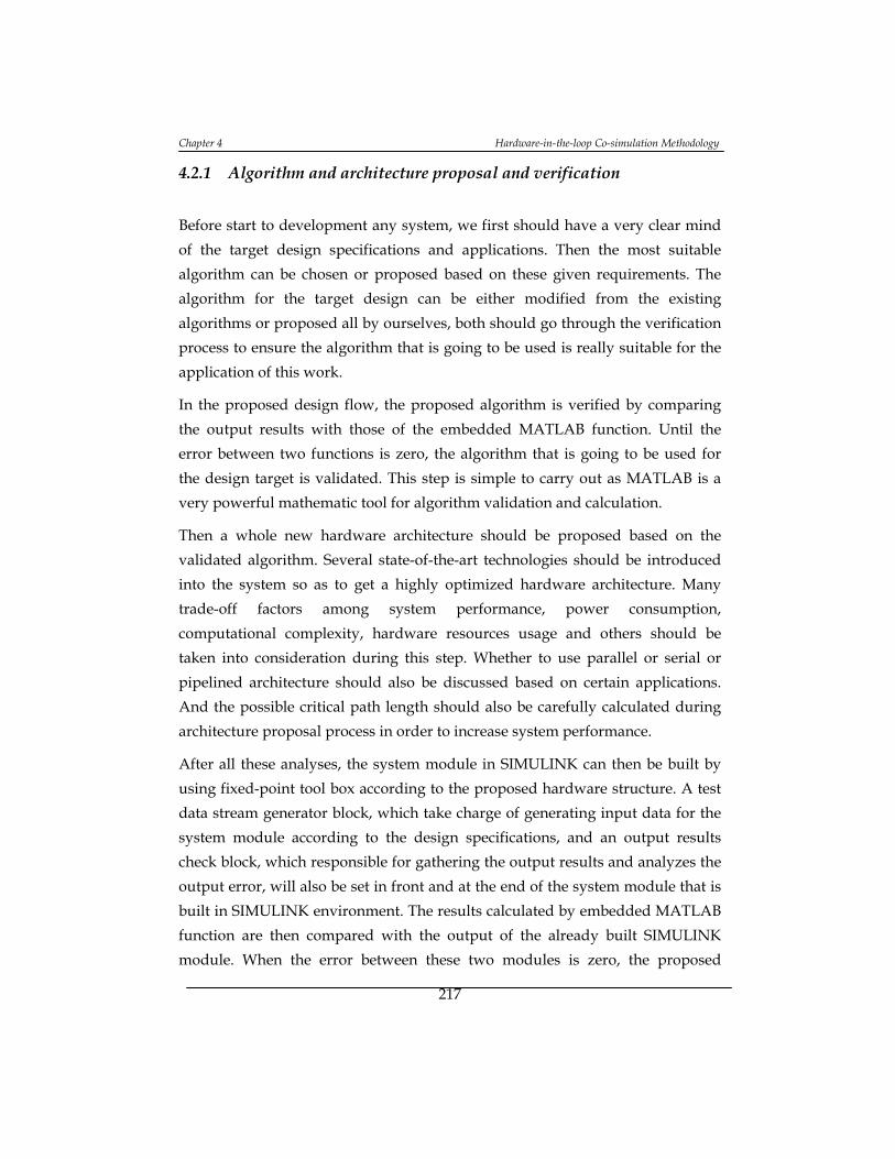
Chapter 4 Hardware-in-the-loop Co-simulation Methodology
217
4.2.1 Algorithm and architecture proposal and verification
Before start to development any system, we first should have a very clear mind
of the target design specifications and applications. Then the most suitable
algorithm can be chosen or proposed based on these given requirements. The
algorithm for the target design can be either modified from the existing
algorithms or proposed all by ourselves, both should go through the verification
process to ensure the algorithm that is going to be used is really suitable for the
application of this work.
In the proposed design flow, the proposed algorithm is verified by comparing
the output results with those of the embedded MATLAB function. Until the
error between two functions is zero, the algorithm that is going to be used for
the design target is validated. This step is simple to carry out as MATLAB is a
very powerful mathematic tool for algorithm validation and calculation.
Then a whole new hardware architecture should be proposed based on the
validated algorithm. Several state-of-the-art technologies should be introduced
into the system so as to get a highly optimized hardware architecture. Many
trade-off factors among system performance, power consumption,
computational complexity, hardware resources usage and others should be
taken into consideration during this step. Whether to use parallel or serial or
pipelined architecture should also be discussed based on certain applications.
And the possible critical path length should also be carefully calculated during
architecture proposal process in order to increase system performance.
After all these analyses, the system module in SIMULINK can then be built by
using fixed-point tool box according to the proposed hardware structure. A test
data stream generator block, which take charge of generating input data for the
system module according to the design specifications, and an output results
check block, which responsible for gathering the output results and analyzes the
output error, will also be set in front and at the end of the system module that is
built in SIMULINK environment. The results calculated by embedded MATLAB
function are then compared with the output of the already built SIMULINK
module. When the error between these two modules is zero, the proposed
Design and Validation of an Optimized High-performance MB-OFDM Ultra Wideband Transceiver System
218
architecture is well verified. The verified SIMULINK modusle is called as
Golden Reference (GR) for further usage.
Signal word length for different sub-module will also be selected and analyzed
during this step. Signal word length in hardware design is quite important, as it
not only determines power and hardware resources consumption, but also
determines the accuracy of a system. MATLAB provides a fixed-point toolbox,
which helps us directly analyze the effects of different word length for the
proposed GR module, such as the analyses that we’ve done for the proposed
FFT/IFFT processor design in chapter 3.3.6 and chapter 3.3.7. With the help of
GR, it is unnecessarily to waste time generating different versions of HDL
modules with different word lengths, as changing the word length in the
SIMULINK modules is more conveniently. The comparison and decision are
obtained directly and efficiently by using MATLAB/SIMULINK modules.
Compared with [Han’11], the proposed method is more accurate in functional
analyses.
The usage of GR has several benefits in the following aspects:
1) Time for building the GR is much shorter than HDL coding.
2) It indicates the Minimum Time Delay of each block for the
hardware architecture, which can be used later to determine the
control system and signals for HDL model.
3) The designers are able to choose internal word lengths properly
and efficiently for HDL model.
4) GR provides output results which will be used to compare with
those generated by HDL model.
After GR validation and analyzing, the next step in the proposed design flow
should be RTL implementation and synthesis.
4.2.2 RTL implementation and synthesis
This step consists of developing the system module at RTL by using Verilog
HDL (or VHDL) following the usual methodology for digital system design.
Although the HDL code can be generated automatically from SIMULINK

Chapter 4 Hardware-in-the-loop Co-simulation Methodology
219
module, the manually written HDL module allows designers to maintain the
entire control over the module internal architecture and obtain an efficient
structure, which greatly reduces the output error and makes the further
optimization much easier. Meanwhile, for the sake of saving modeling period
for GR, lots of embedded MATLAB functions are introduced into the state-flow
module, it's hard for SIMULINK HDL Coder to convert them into HDL code
directly. Besides, in order to make the design of this work more suitable for the
target FPGA, some IP cores provided by XILINX tools are introduced, so as to
save handwriting time and optimize the whole system in a high level way. In
order to lower the power and hardware resources consumption while still
maintain the high performance of the proposed hardware implementation,
several state-of-the-art technologies should also be introduced into the RTL
design process. Such as during the RTL development process for the proposed
FFT processor, the Single-path Delay Feedback (SDF) pipelined structure is
employed, the substructure-sharing multiplication units and shift-add structure
are also used to modify the complex multipliers in different modules. Some
others, such as folding and re-timing technologies are used as well. By doing so,
a highly modified lower-power, high-performance system is implemented at the
end.
The verification process of very complex system design is of great challenge.
Traditionally, it's carried out by writing test bench files in simulator
environment, such as ModelSim, to support HDL code simulations. However,
writing test bench file manually for complex module, especially the wireless
communication system and video signal processing system, is a very tough
work, because such kind of system usually needs a large scale of test data input
streams for simulation and functional analyzing. Moreover, it is difficult to
process large quantity of complex output results not even mention observing the
system performance holistically by only monitoring the output waveforms
provided by simulators such as ModelSim or Isim.
An alternative solution has been explored in this work in order to make
functional verification more efficient: SIMULINK provides the interface between
SIMULINK and ModelSim by using socket or shared memory with a third-party
tool. Therefore, by connecting SIMULINK and ModelSim together, exactly the

Design and Validation of an Optimized High-performance MB-OFDM Ultra Wideband Transceiver System
220
same data generate module in GR can be used for HDL system verification
process, which makes us free from writing test bench file and ensure us focus on
the design and analyze. By connecting SIMULINK and ModelSim together, the
output waveforms are shown in the ModelSim simulator and collected by
SIMULINK at the same time, as shown in Figure 4.3. By using the same check
module as GR, the process results are able to be compared conveniently with
those of GR to check whether HDL processing is correct or not. Besides the
functional verification, the timing simulation can be also carried out by using
ModelSim to make program closer to the true state of running.
Figure 4.3 Simulation environment by combining ModelSim with SIMULINK
The performance analyses, such as Signal to Quantization Noise Ratio (SQNR),
Bit Error Rate (BER), Mean Square Error (MSE) and so on, are also calculated by
using the same module as that for the GR, so as to save the efforts to analyze the
HDL functions manually. Sometimes it may be found that the performances of
HDL model reduced a little bit when compared with GR function, for example,
the SQNR performance of HDL module of the proposed FFT processor is 1 dB
lower than that of the SIMULINK module. This is reasonable: even though fixed-
point tool box of MATLAB is used for determining the word length, it still
automatically rounds the results of adders and multipliers when processing the

Chapter 4 Hardware-in-the-loop Co-simulation Methodology
221
up-coming signals. For example, in SIMULINK fixed-point rounding system, 3.4
is considered as 3 but 3.6 is rounded to 4, while in HDL block both of them are
truncated to 3. This effect results in the HDL module less accurate than the fixed-
point GR model, but the accuracy of modeling processing is still high enough to
support the proposed system development.
After HDL code functional verification process, the HDL code will be
synthesized and transformed into bitstream which can be downloaded to the
FPGA board. The final hardware implementation validation process will be
carried out at this point.
4.2.3 Hardware co-simulation process
The HDL code is verified for use and the synthesis report is obtained from
synthesis tools for certain types of FPGA boards. However, downloading the
bitstream to FPGA is often more complex than expected.
Many facts in hardware running process will affect the behavior of the
architectures downloaded to FPGA devices. For example, the raising edge of real
clock signal may contain jitters, or the rising time of the clock signal may be very
slow due to heavy load factors. But most of the time not all the signals inside
FPGA can be observed in real time, which makes it difficult to debug and find
solutions when certain error happens. How can the functionality of complex
FPGA devices be verified while still maintain their time-to-market advantage
becomes a big challenge at this step. The hardware-in-the-loop co-simulation
methodology presented below is to provide a simple but thorough chip-level
verification that fulfills modern time-to-market requirements.
The chip level verification methodology is realized by connecting the
SIMULINK models and FPGA board (support almost all Xilinx FPGA families)
with the help of Xilinx System Generator (XSG). XSG compilation targets
automatically create a bitstream and associate it to a block in SIMULINK
[Xilinx’10]. Again the same data-generate module from SIMULINK that being
used to verify the HDL code also works as the input signal for this hardware-in-
the-loop co-simulation procedure. As mentioned before, the hardware input test
Design and Validation of an Optimized High-performance MB-OFDM Ultra Wideband Transceiver System
222
data stream from data-generate module will be sent to the FPGA
implementation through JTAG or Ethernet for signal processing, then the
hardware output results will be fed back to SIMULINK so as to be compared
with the results of the GR on a per clock cycle basis and make further analysis.
By doing this, the Host PC and FPGA are connected together and with the
ability to communicate with each other.
In order to monitor partially important parameters inside the FPGA, some ‘test’
output ports is assigned in the HDL codes. These ports work like ‘probes’ that
fetch output the netlist signals from the FPGA to the ‘scopes’ in the SIMULINK
model. By guarding these probes through the whole co-simulation process
properly, a very clear idea about what is the possible problem for functional
errors in the hardware implementation can be obtained, and then figure out the
solutions much more efficiently than traditional method. On the other hand,
whenever the probes are required to switch from one signal to another, just
simply modify the HDL code on the map of output signals. By using these
probes properly, even more information from inside the FPGA, such as real
delay time for each processing blocks, processing order for parallel architecture,
partial products values, and so on, can be obtained efficiently and conveniently.
The clock frequency of the FPGA board can be changed from one to another,
controlled by SIMULINK co-simulation environment, which enables us to
analyze the functions and performance inside FPGA in different processing
speeds. Compared with [Chen’10], probes are much easier to implement and
more flexible. Furthermore, as it’s not necessary to oversee each small signal
inside the FPGA, only those very important ones are needed, large hardware
resources are saved by doing so.
This hardware-in-the-loop hardware/software co-simulation environment
supports simulations where parts of the design are implemented in the
hardware and the rest in the software; or executes a complete FPGA emulation
in real-time. This flexible simulation approach makes the whole hardware co-
simulation easier to control, and allows us to verify each sub-module separately.
For example, when just a small subsystem included in one huge development is
needed to be verified, just this small part of the system can be synthesized and
Chapter 4 Hardware-in-the-loop Co-simulation Methodology
223
downloaded to FPGA, and connect it with other blocks that employed from GR
directly. This will give us an opportunity to analyze each small part of the
implementation separately. Once each sub-system is validated, all of them can
then be combined together to form a whole system, and validate it again on
FPGA board. Through this method, the SQNR and other performance of the real
hardware are obtained fast and conveniently.
When the hardware module is verified, a final synthesis report for the HDL
codes will be generated by the help of Design Compiler and other tools so as to
analyze the ASIC performance of the proposed system. Power consumptions
and other information for FPGA develop can also be generated by the help of
Xilinx tools at the end.
4.3. Virtual Communication environment
Another big advantage of employing the aforementioned fast co-simulation
methodologies for a MB-OFDM UWB digital baseband system design is: once
both the Receiver (Rx) and Transmitter (Tx) blocks are verified, they can
virtually communicate with each other through a transmission channel model
built in SIMULINK. The virtual communication environment is shown in Figure
4.4.
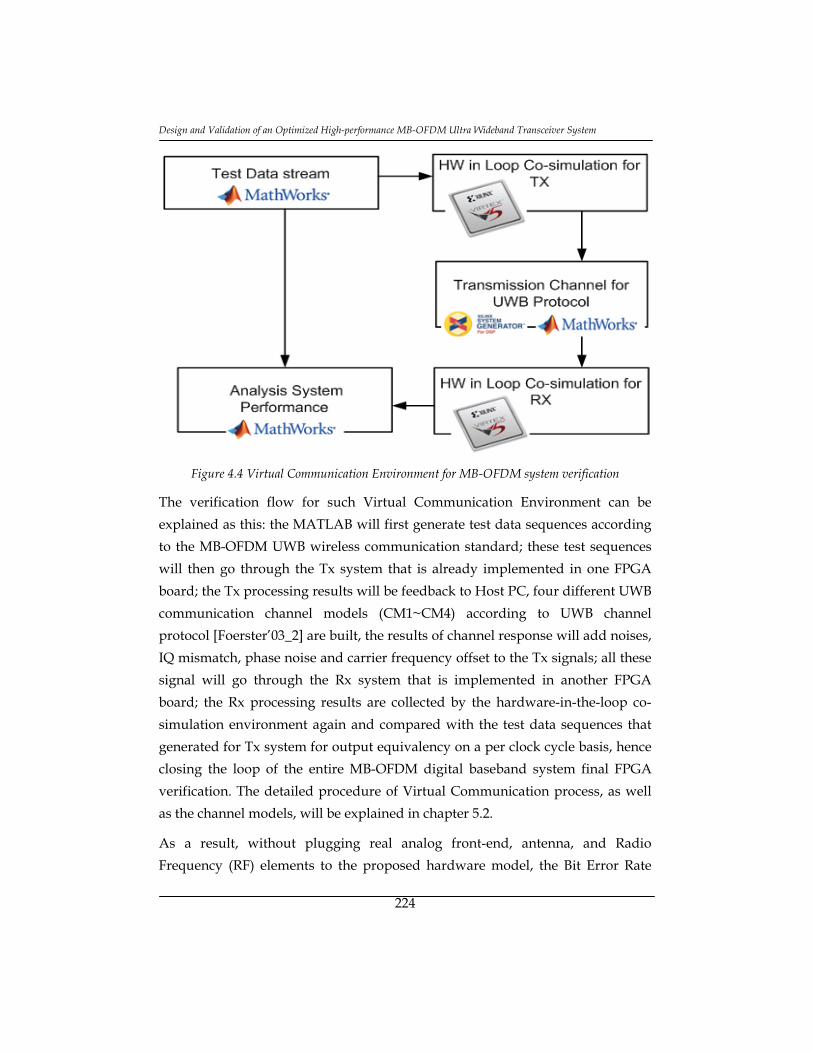
Design and Validation of an Optimized High-performance MB-OFDM Ultra Wideband Transceiver System
224
Figure 4.4 Virtual Communication Environment for MB-OFDM system verification
The verification flow for such Virtual Communication Environment can be
explained as this: the MATLAB will first generate test data sequences according
to the MB-OFDM UWB wireless communication standard; these test sequences
will then go through the Tx system that is already implemented in one FPGA
board; the Tx processing results will be feedback to Host PC, four different UWB
communication channel models (CM1~CM4) according to UWB channel
protocol [Foerster’03_2] are built, the results of channel response will add noises,
IQ mismatch, phase noise and carrier frequency offset to the Tx signals; all these
signal will go through the Rx system that is implemented in another FPGA
board; the Rx processing results are collected by the hardware-in-the-loop co-
simulation environment again and compared with the test data sequences that
generated for Tx system for output equivalency on a per clock cycle basis, hence
closing the loop of the entire MB-OFDM digital baseband system final FPGA
verification. The detailed procedure of Virtual Communication process, as well
as the channel models, will be explained in chapter 5.2.
As a result, without plugging real analog front-end, antenna, and Radio
Frequency (RF) elements to the proposed hardware model, the Bit Error Rate

Chapter 4 Hardware-in-the-loop Co-simulation Methodology
225
(BER) is still be able to be estimated, speed, etc. of the whole MB-OFDM system
performance. As all the process can be performed in MATLAB/SIMULINK
environment, the developing cost for the digital baseband system is reduced
while large amount of develop time is saved.
4.4. Chapter final conclusions and original contributions
In this chapter, a whole new hardware validation methodology for complex
FPGA system development has been introduced. The proposed
Hardware/Software co-simulation environment combines several power design
tools, such as MATLAB, ModelSim, Xilinx tools, together to ensure the proposed
methodology always uses the most suitable and efficient tools for each step
during complex system implementations. Generally, the proposed method can
be summarized as:
1) Given an algorithm, verify it in MATLAB/SIMULINK or other
high level design tools
2) Design hardware architecture based on the algorithm and verify
the design by using SIMULINK block sets
3) Build the HDL architecture and co-simulate the HDL code
running between SIMULINK and HDL simulators
4) Synthesis the HDL code and download it to FPGA devices, the
execute hardware-in-the-loop co-debugging processing
The introduced methodology contains verifications from algorithm level to
hardware level. The methodology has been employed into the design process of
FFT/IFFT processor, timing synchronization block, Viterbi Decoder and other
blocks, as well as the verification and debugging step for the entire MB-OFDM
digital baseband system, indicates it facilitates the design and verification of
very complex hardware architecture. The design method not only dramatically
reduces the time for verification, but also provides other information such as
the errors, output delays, etc. Thus, this efficient method ensures designers
focus on the design and optimization of the algorithms and architectures,
rather than waste time on system debugging process, which is usually

Design and Validation of an Optimized High-performance MB-OFDM Ultra Wideband Transceiver System
226
considered to be the most time-consuming step for hardware system
development.
Based on this hardware-in-the-loop design methodology, a Virtual
Communication Environment is established for validating only the digital
baseband system of wireless communication protocols without using any analog
frontend. The automatic generating and gathering signals for both Tx and Rx
digital baseband systems make the whole verification process much easier and
more efficiently.
Chapter 5 Experimental Results
227
5. Experimental Results
5.1. General introduction
The proposed MB-OFDM UWB digital baseband system has been implemented,
and the introduced hardware-in-the-loop co-design methodology will be used
for debugging and analyzing the aforementioned transceiver architecture.
Since the transmitter and receiver implementation covered in Chapter 3 consists
only the digital baseband system of the Physical (PHY) layer, analysis of their
performance under wireless communication environments requires modeling of
the wireless channels, so as the experimental tests can be carried out in different
communication situations. These channel models will be used by the Virtual
Communication simulation process, and will act as the transmission medium
between the transmitter and receiver baseband system.
In this chapter, the information on the test channel environment will be
provided first, and then the performance of the proposed MB-OFDM baseband
system will be discussed and analyzed under different channel models, the
implementation results and synthesis reports of the transceiver system based on
FPGA implementation will also be shown, and finally the conclusions are drawn
at the end.
5.2. UWB wireless channel models
The goal of the channel model is to capture both the path loss and multipath
characteristics of typical environments where the UWB communication devices
are expected to operate.
The IEEE 802.15.3a task group has produced a set of statistical UWB channel
models [Foerster’03_2] based on the Saleh-Valenzuela (S-V) approach [Saleh’87].
An S-V channel model is often used in UWB studies since the tremendous
bandwidth of an UWB signal means that environmental reflections will not
Design and Validation of an Optimized High-performance MB-OFDM Ultra Wideband Transceiver System
228
necessarily result in Rayleigh fading at the receiver since the individual paths
can be recovered.
Several parameters have to be taken into account for modeling the UWB channel
environments. The multipath components arrive at the receiver in groups, which
are called clusters, with Poisson distribution. The path, or called ray by some
researchers, within each cluster also arrives with Poisson distribution. The
channel impulse response is given by (1).
1
where
L is the number of clusters
M is the number of paths within a cluster
αn,l is the multipath gain of the n-th path corresponding to l-th cluster
Tl is the delay of l-th cluster
τn,l is the time delay of n-th ray of the l-th cluster
The amplitude fading is defined as
αn,l=Pn,lζlβn,l
where
Pn,l is the sign of the coefficient, and takes ±1 with equal probability and
accounts for signal inversions due to reflections
ζl is the fading associated with the l-th cluster
βn,l is the fading associated with the n-th ray of the l-th cluster
The envelope of amplitude fading αn,l is lognormally distributed with the mean
µn,l and the variance . Using the model defined in (2).
, Ω / , / 2
where Ω0 is the mean power of the first path of the first cluster at delay 0 of the
first cluster. Parameters Г and ϒ are the cluster and ray decay constants
Chapter 5 Experimental Results
229
respectively. According to this model, the mean of the channel fading is given by
(3).
,
10 Ω10Γ 10 , /
101020
3
where σ1=σ2=3.3941 dB. Since the clusters and rays within each cluster arrive
according to Poisson process, the inter arrival times of the clusters and rays
follow the exponential distributions as (4).
| Λ
, , , 4
where is the cluster arrival rate and λ is the ray arrival rate.
Parameter X in (1) is the shadowing which can be modeled by lognormal
distribution. The IEEE 802.15.3a research group considers 4 different channel
models, called CM1~CM4, for UWB communication environment
[Foerster’03_2]. The existence of such standard channel models allows different
UWB proposals to be evaluated against a common set of conditions that include
both Line-of-Sight (LOS) and Non-Line-of-Sight (NLOS) cases.
In CM1, the transmit-receive antenna separation is 0-4 m and the situation is
LOS. The CM2 is NLOS, and the transmit-receive separation is within 4 m. The
channel model CM3 is for NLOS, with the transmit-receive separation of 4-10 m.
The channel model CM4 is for NLOS extreme multipath with Root Mean Square
(RMS) delay spread above 25 ns [Foerster’03_2].
The parameters defined in above equations are found by trying to match
important characteristics of the channel. Since it’s difficult to match all possible
channel characteristics, the main characteristics of the channel that are used to
derive the above model parameters were chosen to be the following:
Mean excess delay, τm;
RMS delay spread, τrms;
Number of multipath components (defined as the number of multipath
arrival that are within 10 dB of the peak multipath arrival);

Design and Validation of an Optimized High-performance MB-OFDM Ultra Wideband Transceiver System
230
Power decay profile.
Since the model parameters are difficult to match to the average power
reduction profile, the main channel characteristics that are used to determine the
model parameters are the first three above. Table 5-1 lists some initial model
parameters for the channel models from CM1 to CM4 that were found through
measurement data.
The IEEE 802.15.3a group provides these channel models in the form of
MATLAB data files. Each file contains a series of duplets, namely a sample time
and amplitude, which provide a real-valued continuous-time amplitude of the
arriving signal.
These MATLAB channel models are perfect for this work, because the hardware-
in-the-loop co-simulation environment of this thesis is established by connecting
the implemented FPGA board with PCs through MATLAB. Thus, before
sending each transmitted packet into the Rx system through the interface
between MATLAB and FPGA, we can let them first go through the four different
channel models instead of sending them directly. By doing so, the channel
response signals that have the properties similar to real RF signals will be
generated and restored. Then the Rx system will “listen” to these “RF” signals
and try to get the transmitted packets through this communication environment.
The so called Virtual Communication method is illustrated in Figure 5.1.

Chapter 5 Experimental Results
231
Table 5-1 IEEE UWB Channel model parameters
Target Channel Characteristics CM 1 CM 2 CM 3 CM 4
LOS/NLOS LOS NLOS NLOS NLOS
Tx-Rx Separation (m) 0-4 0-4 4-10
Mean excess delay (nsec) (τm) 5.05 10.38 14.18
RMS delay (nsec) (τrms) 5.28 8.03 14.28 25
Model Parameters CM 1 CM 2 CM 3 CM 4
(1/nsec) 0.0233 0.4 0.0667 0.0667
(1/nsec) 2.5 0.5 2.1 2.1
7.1 5.5 14.00 24.00
4.3 6.7 7.9 12
σ1 (dB) 3.3941 3.3941 3.3941 3.3941
σ2 (dB) 3.3941 3.3941 3.3941 3.3941
Model Characteristics CM 1 CM 2 CM 3 CM 4
Mean excess delay (nsec) (τm) 5.0 9.9 15.9 30.1
RMS delay (nsec) (τrms) 5 8 15 25
Channel energy mean (dB) -0.4 -0.5 0.0 0.3
Channel energy std (dB) 2.9 3.1 3.1 2.7

Design and Validation of an Optimized High-performance MB-OFDM Ultra Wideband Transceiver System
232
Figure 5.1 Virtual Communication environment by using CM1-CM4 channel models
Besides the channel response effect, the Additional White Gaussian Noise is also
added to each transmission “channels”, to make the Virtual Communication
environment closer to reality. IEEE has defined 100 complex baseband models
for each channel family, therefore, during the simulation, the communication
environment will be switched randomly among these 100 models. This means
that each packet experiences a different channel and thereby allows us to
simulate a frequency-selective slowly-fading environment. Figure 5.2 shows the
waveforms of the transmitted OFDM symbols through all the four different
channel models (only the real part of the complex symbols are shown here) and
the SNR of each channel model for simulation is set to be 10 dB in this case.

Chapter 5 Experimental Results
233
Figure 5.2 OFDM symbols transmitted through CM1 to CM4
5.3. Simulation environment
For analyzing the system performance of the entire MB-OFDM baseband
transceiver system, this thesis didn't implement or modeled any Media Access
Control (MAC) layer. Thus, the Tx and Rx systems will communicate with each
other continuously so as to just validate the baseband system’s performance.
As no MAC layer is used for simulation, the MAC Header and PHY Header will
be generated randomly through the using of StateFlow in SIMULINK
environment. The ISO/IEC standard book [ISO/IEC 26907’09] also provides an
Example encoding of a PHY packet for the researchers to validate and analyze
the implemented baseband system. Thus, the testing sequences that are sent
through the Tx system will be based on the format provided by the ISO/IEC
standard, and final analysis of the performance will be executed by comparing
the Rx processing results with that of the transmitted sequences automatically
with the help of the hardware-in-the-loop co-simulation methodology.

Design and Validation of an Optimized High-performance MB-OFDM Ultra Wideband Transceiver System
234
Because the goal of this thesis is to design and implement a real-time MB-OFDM
UWB baseband system that would be able to operate in a contemporary FPGA
device that has the reconfigurability property, the specific FPGA device that
used for testing is the Virtex-5 XC5VLX110T embedded in the Xilinx XUPV5-
LX110T Evaluation Platform [Xilinx’09] [Xilinx’11]. The key parameters for this
FPGA device are shown in Table 5-2.
Table 5-2 Main Features of Virtex-5 XC5VLX110T FPGA
Number of Slices 17,280
Block RAM Blocks(in 18 kb blocks) 296
Maximum Clock Frequency (MHz) 550
DSP48E Slices (each with 25×18 multiplier,
an adder and an accumulator) 64
PowerPC Processor Blocks N/A
Total I/O Banks 20
As shown above, the maximum speed of the Virtex-5 device is 550 MHz. Then it
can support the specified working frequency of MB-OFDM UWB system, which
is 528 MHz. By using the control logic, different clock enable signals with
different frequencies can be generated for different processing elements of the
proposed MB-OFDM transceiver system.
The XC5VLX110T is one of the largest Virtex-5 FPGAs, containing over 17
thousand slices, with each slice containing four Look-Up-Tables (LUTs) and four
flip-flops. The high number of slices was necessary given the need to pipeline
the FFT/IFFT architecture of the transceiver and other complex blocks, as well as
the goal that there be sufficient free resources to allow experimentation with
different configurations and parameters.
The Virtex-5 FPGA also provides large number of dedicated hardware
multipliers that provide very high-speed 25-bit by 18-bit multiplication.
Although most multiplications are replaced with additions/subtractions and
shifters by using the proposed RTL structure, the Booth multiplications in Fast
Fourier Transform/Inverse Fast Fourier Transform (FFT/IFFT) processor, the
Carrier Frequency Offset (CFO) compensation, Sampling Frequency Offset (SFO)
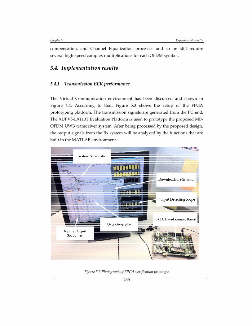
Chapter 5 Experimental Results
235
compensation, and Channel Equalization processes and so on still require
several high-speed complex multiplications for each OFDM symbol.
5.4. Implementation results
5.4.1 Transmission BER performance
The Virtual Communication environment has been discussed and shown in
Figure 4.4. According to that, Figure 5.3 shows the setup of the FPGA
prototyping platform. The transmission signals are generated from the PC end.
The XUPV5-LX110T Evaluation Platform is used to prototype the proposed MB-
OFDM UWB transceiver system. After being processed by the proposed design,
the output signals from the Rx system will be analyzed by the functions that are
built in the MATLAB environment.
Figure 5.3 Photograph of FPGA verification prototype

Design and Validation of an Optimized High-performance MB-OFDM Ultra Wideband Transceiver System
236
The Bit Error Rate (BER) performance of the proposed transceiver by FPGA
measurement is illustrated in Figure 5.4. The 53.3 Mbps and 106.7 Mbps
transmission rates are tested under the channel environment of CM1 and CM4.
The first pattern of Timing Frequency Code (TFC 1) with SNR from 0 dB to 30
dB is used, and 10,000 bits are transmitted and received for measuring the BER
performance under the testing environment.
Compared with 53.3 Mbps transmission mode, the 106.7 Mbps mode has a SNR
degradation of around 2 dB in both channels models. The transmission errors
increase a lot when SNR drops to 10 dB. When referring to Table 3-18, it can be
seen that the timing synchronization probability has a very strong effect on the
BER performance for the whole system. As the synchronization probability is
almost 100% when SNR is higher than 15 dB for CM1, the BER performance
tends to be steady. And when the SNR is lower than 10 dB, the probability of
synchronization for the proposed synchronization scheme dropped a lot, the
BER also increases a lot.
Figure 5.4 BER performance of proposed MB-OFDM transceiver

Chapter 5 Experimental Results
237
5.4.2 Synthesis result
By using the Xilinx ISE Design Suit 12.1 and xPower Analyzer from Xilinx tools,
the Tx and Rx system are synthesized. The hardware utilization for both Tx and
Rx system is shown in Table 5-3. All the timing constraints, the most stringent of
which is the FFT/IFFT and Viterbi Decoder processing time, are met.
Table 5-3 Summary of Resource Usage of XC5VLX110T FPGA
Transmitter Receiver
Number of DSP48Es 8 12% 21 33%
Number of Slices 5,839 33% 16,465 95%
Number of Slice Registers 14,451 20% 42,326 61%
Number of Block RAM/FIFO 2 1% 17 11%
Number of Slice LUTs 24,188 35% 56,065 81%
Number of External IOBs 24 3% 612 95%
Number of BUFG/BUFGCTRLs 10 31% 10 31%
Number of LUT Flip Flop Pairs 61,167 61,167
Power Consumption 241.88 mW 449.68 mW
Clock Frequency 132 MHz
Max Frequency 137.088 MHz
The estimated logic gate count is around 500 K in total. As the proposed
baseband system has the parallel factor of four for those critical elements
(FFT/IFFT, VD, demapper, deinterleaver, etc.), the 528 Msps throughput is
achieved by using 132 MHz clock frequency. According to the Xilinx xPower
Analyzer, the estimated post synthesis Tx and Rx power consumptions are
241.88 mW and 449.68 mW respectively at 132 MHz frequency, omitting the
energy consumed related with FPGA standing by. The differences of hardware
resources usage indicate the receiver system has a much higher design
complexity than that of transmitter system. The additional power consumption
of receiver system mainly comes from the synchronization processes for both
timing and frequency, and Channel Estimation/Equalization blocks. Extra

Design and Validation of an Optimized High-performance MB-OFDM Ultra Wideband Transceiver System
238
energy consumption caused by longer processing word-length for Rx is another
reason, as soft-bits are used for demapper, de-interleaver, de-puncture, and
Viterbi Decoder systems so as to increase the system robustness and accuracy.
On the Tx side, almost all the power consumptions and hardware resources
usage are come from the IFFT processor (more than 90%), thus no distribution
discussion for transmitter system will be made.
But on the Rx side, the additional processing elements, such as synchronization
blocks, Channel Estimation/Equalization block, and Viterbi Decoder, also cost
large amount of power consumption and hardware resources. The power
consumption distribution and hardware cost distribution of the proposed
receiver system are shown in Figure 5.5 and Figure 5.6 respectively.
Figure 5.5 Power consumption distribution for proposed Rx system

Chapter 5 Experimental Results
239
Figure 5.6 Hardware cost distribution for proposed Rx system
As it can be seen in Figure 5.5 and Figure 5.6, the FFT processor occupies a great
proportion on both aspects, which denotes the important role that the FFT
processor plays in the Rx system. Timing synchronization scheme, which
contains both Packet Detector and Timing Offset Estimation blocks, also takes a
large proportion, especially in the hardware cost distribution. This is a result of
the use of RAMs for buffering the input sequences and restoring the preamble
sequences. Channel Estimation/Equalization block consumes large power
consumption, because of the usage of wide word-length complex divider and
complex multiplier processors for estimating and compensating the channel
response. Although the Viterbi Decoder (VD) system spends only 8% of the total
power consumption, but 23% hardware resources are needed, this mainly comes
from the proposed VD structure uses two Branch Metric Units (BMUs) and State
Metric Units (SMUs) (although they consume less power than traditional
architecture), and the TBU has a large bank of memory. The Carrier Frequency
Offset (CFO) block takes around 10% proportion on both aspects, whereas the
Sampling Frequency Synchronization system just takes around 5%. Thus,
according to the distribution on both power consumption and hardware cost,
future works will focus on the optimizations for Channel
Design and Validation of an Optimized High-performance MB-OFDM Ultra Wideband Transceiver System
240
Estimation/Equalization block and CFO system so as to further optimize the
performance of the proposed receiver architecture.
5.5. Chapter final conclusions and original contributions
In this chapter, the UWB channel models for four different communication
situations (CM1~CM4), proposed by the IEEE 802.15.3a research group, are
discussed and introduced into the presented Virtual Communication procedure,
with the aim of validating the proposed MB-OFDM UWB digital baseband
transceiver system in different communication environments.
The simulation results show that the Bit Error Rate (BER) performance of the
proposed transceiver system can reach up to below 0.1% in CM1 channel
model, and around 1% in CM4 channel model, while the SNR is higher than
10 dB.
For system synthesis result, the Xilinx Virtex 5 XC5VLX110T FPGA board is
selected for the implementation of the proposed MB-OFDM baseband structure.
The power consumption and hardware cost distributions are discussed so as to
help us analyze the performance of each block in the baseband system. All the
timing constraints are met according to the synthesis report provided from
Xilinx ISE Design Suit 12.1.
Chapter 6 Conclusions and Future Works
241
6. Conclusions and Future works
6.1. Conclusions
A high-performance MB-OFDM Ultra Wideband transceiver system has been
presented in this thesis. The proposed UWB Physical (PHY) layer has met all
three of its primary goals, namely:
1. Digital logic architectures for MB-OFDM baseband transceiver system
was optimized and developed;
2. All digital aspects of the proposed UWB PHY were implemented and
validated in a FPGA board;
3. Complexity and expected real-world performance were simulated and
analyzed through the Virtual Communication simulation procedure.
The thesis focuses on the communication system implementation and validation
tasks for the WVSNs development. As high transmission rate and low power
consumption abilities are required for the design goals, meanwhile, the
reconfigurability based on FPGA development is a potential application
technique, the MB-OFDM digital baseband system finally became the best
candidates for these goals.
The basic information for MB-OFDM UWB communication protocol based on
the ISO/IEC standard has been shown. The multiband technology and PHY
general requirements, such as the band group and Time-frequency code are
illustrated so as to understand the theory of MB-OFDM technology. The formats
of the PHY header, MAC header, as well as the transmission packet are
explained, before the implementation procedure carried out. Having the clear
mind of the general requirements before development can help the developers
grasp the function of each element in the physical layer.
The function and action of each required element are shown in pair for the
Transmitter (Tx) and Receiver (Rx) system respectively. Those critical processing

Design and Validation of an Optimized High-performance MB-OFDM Ultra Wideband Transceiver System
242
subsystems on both Tx and Rx sides are picked up for optimizations one by one.
According to the different properties and effects of different processing elements,
the optimizations are made through different considerations. The FFT/IFFT
processing pair is highly optimized by using the proposed mix-radix algorithm
as well as power efficient architectures for complex multipliers of each stage; the
sign-bit only strategy for timing synchronization not only improves the
detection probability but also dramatically reduces the computational
complexity; the high speed ACS units along with the two-step radix-4 algorithm
ensures the high throughput property for proposed Viterbi Decoder block.
Moreover, several other state-of-the-art algorithms and architectures are also
introduced so as to develop a highly optimized MB-OFDM digital baseband
transceiver system on FPGAs. Compared with Tx system, Rx system has a more
complex architecture due to high accurate synchronization and channel
estimation requirements. After the optimization for each component, the
proposed baseband transceiver is integrated and implemented in the Xilinx
XUPV5-LX110T Evaluation Platform.
In order to test the proposed algorithms and architectures in the FPGA board, a
Hardware-in-the-loop design methodology is proposed. The contribution
related with this part of the work mainly comes from combining all the popular
customize digital system design tools together, so that they can cooperate with
each other to help the developers test and validate the proposed system in both
software and hardware more efficiently. The proposed methodology ensures the
most suitable tools be used for different validation procedures, such as the
MATLAB is used for verify those proposed algorithms, ModelSim is used for
RTL code simulations, and System Generator is used as emulator for FPGA tests.
By using the proposed co-design methodology, as well as employing the UWB
channel models from IEEE 802.15.3a research group, the proposed MB-OFDM
UWB digital baseband transceiver system is tested and analyzed through the
Virtual Communication method. The experimental results of the proposed
architecture in Chapter 3 are shown in Chapter 5. The implemented MB-OFDM
system shows the ability to support different throughput modes according to the
MB-OFDM UWB specification, with the power consumption of 241.88 mW and

Chapter 6 Conclusions and Future Works
243
449.68 mW for Tx and Rx respectively at 132 MHz working frequency. The
proposed implementation gives a robust, low complexity and energy efficient
solution for practical applications.
As a summary, the contributions of this thesis are the following:
A novel mixed radix 128-point FFT algorithm by using multipath pipelined
architecture is proposed. The complex multipliers for each processing stage
are designed by using modified shift-add architectures. The system word-
length and twiddle word-length are compared and selected based on Signal
to Quantization Noise Ratio (SQNR) and power analysis.
IFFT processor performance is analyzed under different Block Floating Point
(BFP) arithmetic situations for overflow control, so as to find out the perfect
architecture of IFFT algorithm based on the proposed FFT processor.
An innovative low complex timing synchronization and compensation
scheme, which consists of Packet Detector (PD) and Timing Offset
Estimation (TOE) functions, for MB-OFDM UWB receiver system is
employed. By simplifying the cross-correlation and maximum likelihood
functions to sign-bit only, the computational complexity is significantly
reduced.
A 64 state soft-decision Viterbi Decoder system by using high speed radix-4
Add-Compare-Select architecture is proposed. Two-pointer Even algorithm
is also introduced into the Trace Back unit in the aim of hardware-efficiency.
Several state-of-the-art technologies are integrated into the complete
baseband transceiver system, in the aim of implementing a highly-optimized
UWB communication system.
An improved design flow is proposed for complex system implementation
which can be used for general Field-Programmable Gate Array (FPGA)
designs. The design method not only dramatically reduces the time for
functional verification, but also provides automatic analysis such as errors
and output delays for the implemented hardware systems.
A virtual communication environment is established for validating the

Design and Validation of an Optimized High-performance MB-OFDM Ultra Wideband Transceiver System
244
proposed MB-OFDM transceiver system. This methodology is proved to be
easy for usage and convenient for analyzing the digital baseband system
without analog frontend under different communication environments.
6.2. Future work
There are still various challenges that wait for developing a fully functional
wireless communication system based on MB-OFDM UWB protocol.
First of all, the different integrated systems developed in this work have to be
merged in a single FPGA board. But due to the lack of usable slices resources,
this could be only resolved by additional design and optimization efforts. Based
on the synthesis report of the proposed structure, the Channel
Estimation/Equalization subsystem is the next block that we should pay
attention to. But decreasing the complexity of any one of the subsystems will
also have a negative impact on the performance of the receiver system.
Optimizations should be made based on a comprehensive trade-off discussion.
Secondly, from a wireless communication system point of view, the developed
transceiver system still lacks of analog front-end and RF elements. This part of
work is beyond our knowledge and ability in existing situation. Finding some
research institutes that focus on RF and analog system development for UWB, or
wireless communication systems, and cooperating the proposed digital
baseband system of this thesis with their existing RF system would be the best
solution for us to extend the knowledge related with this aspect. Finally, when
all the required elements (Tx, Rx, RF, MAC, etc.) are designed and ready to be
used, a final ASIC (or System On Chip (SOC)) will be implemented, as shown in
Figure 6.1.

Chapter 6 Conclusions and Future Works
245
Figure 6.1 ASIC for MB-OFDM wireless communication system
Thirdly, the afore presented hardware/software co-design/co-simulation
environment can only support the co-simulation for one FPGA board, this
makes the real-time communication between Tx and Rx system impossible,
because the proposed Tx and Rx have to be implemented in two different FPGA
boards due to the hardware complexity.
Next step should be the methodology that makes the transceiver system
changing among the different communication data rate modes automatically
based on the data that needed to be transmitted. For example, during idle time
or small amount of signals are required to be transmitted, the transceiver system
should be configured to the 53.3 Mbps communication mode so as to save power
consumption, while during the period that large packets needed to be
transmitted in a short time, the higher data rate modes are called to take charge.
This part research is focused on efficient power control and bandwidth usage.
The switching function involves design of the control logic, the discussion of
how frequently should the switch function take place, and reconfigurable
technology.
Last, but not least, the Multiple-Input Multiple-Output (MIMO) technology has
recently attract much attention for MB-OFDM based UWB communication
system development, aiming at further enlarge the data rates to more than 1
Gbps so as to support future wireless applications. MIMO communication can
exploit diversity to improve the channel capacity and error performance for
wireless communications without increasing channel bandwidth. Hence, the
MIMO UWB communication is a promising solution for future WPAN
applications. The study of MIMO can be obtained based on the proposed MB-

Design and Validation of an Optimized High-performance MB-OFDM Ultra Wideband Transceiver System
246
OFDM UWB communication system, with further space-time-frequency coding
and spatial multiplexing knowledge.
6.3. Publications
This section shows the complete list of publications resulting from this thesis,
directly or indirectly.
• G. Liang, D. He, E. de la Torre, T. Riesgo, “Low-power, high-speed FFT
processor for MB-OFDM UWB application”, SPIE’11 Microtechnologies-
VLSI Circuits and Systems, Prague, Apr. 2011.
• W. Li, J. Portilla, F. Moreno, G. Liang, T. Riesgo, “IMPROVING TARGET
LOCALIZATION ACCURACY OF WIRELESS VISUAL SENSOR
NETWORKS”, 37th Annual Conference on IEEE Industrial Electronics Society
(IECON’11), pp. 3814-3819, Melbourne, Nov. 2011.
• D. He, G. Liang, J. Portilla, T. Riesgo, “A Novel Method for Radio
Propagation Simulation Based on Automatic 3D Environment
Reconstruction”, 6th European Conference on Antennas and Propagation
(EUCAP’12), pp. 1445-1449, Prague, Mar. 2012.
• G. Liang, D. He, J. Portilla, T. Riesgo, “A HARDWARE IN THE LOOP
DESIGN METHODOLOGY FOR FPGA SYSTEM AND ITS
APPLICATION TO COMPLEX FUNCTIONS”, IEEE International
Symposium on VLSI Design, Automation, and Test (VLSI-DAT’12), pp. 1-4,
Hsinchu, Apr. 2012.
• G. Liang, J. Portilla, T. Riesgo, “Low-complexity Timing Synchronization
Scheme for MB-OFDM UWB Receiver Based on Sign-bit”, IEEE
International Conference on Ultra-Wideband (ICUWB’12), pp. 311- 315,
Syracuse, New York, Sep. 2012, Best student paper Nominated.
• G. Liang, D. He, J. Portilla, T. Riesgo, “Functional Validation of MB-
OFDM System Using HW-in the loop”, Design of Circuit and Integrated
Systems (DCIS’12), Avignon, France, Nov. 2012.
Chapter 6 Conclusions and Future Works
247
• D. He, G. Liang, J. Portilla, T. Riesgo, “A Novel Method for Radio
Propagation Simulation Based on Automatic 3D Environment
Reconstruction”, Radioengineering Journal, vol. 21, no. 4, pp. 985-992, Dec.
2012.
• G. Liang, J. Portilla, T. Riesgo, “High speed Radix-4 soft-decision Viterbi
Decoder for MB-OFDM UWB system”, SPIE’13 Microtechnologies-VLSI
Circuits and Systems, Grenoble, France, Apr. 2013.
• G. Liang, D. He, J. Portilla, T. Riesgo, “Design of a High-performance
Baseband Transceiver for MB-OFDM UWB System Based on FPGA”,
IEEE Transactions on Circuits and Systems I: Regular Papers, submitted for
review.

Design and Validation of an Optimized High-performance MB-OFDM Ultra Wideband Transceiver System
248
Complete bibliography of the doctoral thesis
249
Complete bibliography of the doctoral thesis
[Armstrong’04] J. Armstrong, H. A. Suraweera, S. Brewer, R. Slaviero, “Effect of rounding
and saturation in fixed-point DSP implementation of IFFT and FFT for
OFDM applications”, The Embedded Signal Processing Conference (GSPx
2004), Sep. 2004.
[Bass’99] B. M. Bass, “A Low-power, high-performance, 1024-point FFT processor”,
IEEE J. Solid-State Circuits, vol.34, no. 3, pp. 380-387, Mar. 1999.
[Batra’04] A. Batra et al., “Design of a multiband OFDM system for realistic UWB
channel environments”, IEEE Trans. Microwave Theory Tech., vol. 52, no. 9,
pp. 2123-2138, Sep. 2004.
[Batra’04_2] A. Batra et al., “Multi-Band OFDM Physical Layer Proposal for IEEE 802.15
Task Group 3a”, IEEE P802.15-03/268r3, 2004.
[Black’97] P. J. Black, T. H.-Y. Meng, “A 1-Gb/s, Four-State, Sliding Block Viterbi
Decoder”, IEEE J. Solid-State Circuits, vol. 32, no. 6, pp. 797–805, Jun. 1997.
[Camera’08] K. Camera, R. W. Brodersen, “An integrated debugging environment for
FPGA computing platforms”, Field Programmable Logic and Applications,
2008. FPL 2008. International Conference on, Sep. 2008.
[Caro’09] D. Caro, N. Petra, A. G. M. Steollo, “Digital synthesizer/mixer with hybrid
CORDIC-multiplier architecture: error analysis and optimization”, IEEE
Trans. Circuits Syst. I. Reg. Papers, vol. 56, No. 2, pp. 364-373, Feb. 2009.
[Chen’10] X. Chen et al., “A Run-Time RTL Debugging Methodology for FPGA-based
Co-Simulation”, ICCCAS, pp. 891-895, 2010.
[Chiueh’07] T. Chiueh, P. Tsai, “OFDM Baseband Receiver Design for Wireless
Communications”, John Wiley & Sons (Asia) Pte Ltd, 2007.
[Cho’10] S. I. Cho, K. M. Kang, “A Low-Complexity 128-point Mixed-Radix FFT
Processor for MB-OFDM UWB Systems”, ETRI Journal, vol. 32, no. 1, pp. 1–
10, Feb. 2010.
[Cooley’65] J. W. Colley, J. W. Tukey, “An Algorithm for the Machine Calculation of
Complex Fourier Series”, Math. Comp. vol. 19, pp. 297-301, 1965.
[Cortes’06] A. Cortes, I. Velez, J. F. Sevillano, A. Irizar, “An Approach to Simplify the
Design of IFFT/FFT Cores for OFDM Systems”, IEEE Trans. Consumer
Electronics, vol. 52, no. 1, pp. 26-32, Feb. 2006.

Design and Validation of an Optimized High-performance MB-OFDM Ultra Wideband Transceiver System
250
[Coulson’01] A. J. Coulson, “Maximum likelihood synchronization for OFDM using a pilot
symbol: algorithms”, IEEE Journal on Selected Areas in Communications, vol.
19, no. 12, pp. 2486-2494, Dec. 2001.
[Ding’11] Z. Ding, Y. Wang, X. Zou, “The methods of FPGA software verification”,
IEEE CSAE’11, vol. 3, pp. 86-89, Shanghai, Jun. 2011.
[ECMA-368’08] “High Rate Ultra Wideband PHY and MAC Standard”, Standard ECMA -
368, 3rd Edition, Dec. 2004.
[ECMA-369’08] “MAC-PHY Interface for ECMA-368”, Standard ECMA - 369, 3rd Edition,
Dec. 2004.
[Edwards’90] G. Edwards, “Forward Error Correction Encoding and Decoding”, Stanford
Telecom Application Note 108, 1990.
[Fan’09] W. Fan, C. S. Choy, “Robust and Low Complexity Packet Detector Design for
MB-OFDM UWB”, IEEE ISCAS, pp. 693–696, Taipei, May. 2009.
[Fan’09_2] W. Fan, C. S. Choy, “Power efficient and High Speed Frequency
Synchronizer Design for MB-OFDM UWB”, IEEE ICUWB 2009, pp. 669-673,
Sep. 2009.
[Fan’10] W. Fan, C. S. Choy, “Efficient and Low Complexity Phase Tracking Method
for MB-OFDM UWB Receiver”, IEEE 53rd MWSCAS, pp. 221-224, Aug. 2010.
[Fan’12] W. Fan, C. S. Choy, “Robust, Low-Complexity, and Energy Efficient
Downlink Baseband Receiver Design for MB-OFDM UWB System”, IEEE
Trans. Circuits Syst. I. Reg. Papers, vol. 59, no. 2, pp. 399–408, Feb. 2012.
[Federal’02] Federal Communications Commission, “Revision of Part 15 of the
commission’s rules regarding ultra-wideband transmission systems, first
report and order”, ET-Docket 98-153, FCC, Washington, DC, Feb. 2002.
[Fetgin’93] G. Fetgin, P. G. Gulak, “Architectural Tradeoffs for Survivor Sequence
Memory Management in Viterbi Decoders”, IEEE Trans. Commun., vol. 41,
no. 3, 1993.
[Fettweis’90] G, Fettweis, H. Meyr, “High-Rate Viterbi Processor: A Systolic Array
Solution”, IEEE J. Sel. Areas Comm., vol. 8, no. 8, 1990.
[Feygin’93] G. Feygin, P. G. Gulak, “Architectural Tradeoffs for Survivor Sequence
Memory Management in Viterbi Decoders”, IEEE Trans. Commun., vol.41,
no. 3, pp. 425–429, Mar. 1993.
[Fisher’04] R. Fisher, R. Kohno, “DS-UWB Physical Layer Submission to 802.15 Task
Group 3a”, IEEE P802.15-04/0137r3, Jul. 2004.

Complete bibliography of the doctoral thesis
251
[Foerster’03] J. R. Foerster et al., “Intel CFP presentation for UWB PHY”, IEEE P802.15-
02/490, Nov. 2003.
[Foerster’03_2] J. Foerster, “Channel modeling sub-committee report final”, IEEE Document
IEEE P802.15-02/490r1-SG3a, 2003.
[Fort’03] A. Fort, J. W. Werjers, V. Derudder et al., “A performance and complexity
comparison of auto-correlation and cross-correlation for OFDM burst
synchronization”, Proceedings of IEEE Int. Conference on Acoustics, Speech,
and Signal Processing, pp. 341-344, 2003.
[Gharpurey’08] R. Gharpurey, P. Kinget, “Ultra Wideband: Circuits, Transceivers and
Systems”, Springer, Series on integrated circuits and systems, ISSN 1558-9412,
2008.
[Goo’08] Y. J. Goo, H. Lee, “Two bit-level pipelined viterbi decoder for high-
performance UWB applications”, IEEE ISCAS, pp. 1012–1015, Seattle, May.
2008.
[Graham’01] P. Graham, B. Nelson and B. Hutchings, “Instrumenting Bitstreams for
Debugging FPGA Circuits”, proceedings of the IEEE Symposium on Field-
Programmable Custom Computing Machines, Apr. 2001.
[Han’11] J. Han, “Application of MATLAB for FPGA Design”, AIMSEC, pp. 5451-5454,
Zhengzhou, 2011.
[Hazy’97] L. Hazy, M. El-Tanany, “Synchronization of OFDM systems over frequency
selective fading channels”, IEEE Proceedings of Conference, vol. 3, pp. 2094-
2098, May. 1997.
[He’98] S. He, M. Torkelson, “Designing pipeline FFT processor for OFDM
(de)modulation”, in Proc. URSI Int. Symp. Signals, Systems, and Electronics,
vol. 29, pp. 257-262, Oct. 1998.
[Heller’71] J. A. Heller, I. M. Jacobs, “Viterbi decoding for satellite and space
communication”, IEEE Trans. Commun. Technol., vol. COM-19, pp. 835-848,
1971.
[Hendrix’02] H. Hendrix, “Viterbi Decoding Techniques for the TMS320C54x DSP
Generation”, Texas Instruments Application Report, SPRA071A, Jan. 2002.
[Hsu’07] C. Y. Hsu, T. S. Kou, Y. H. Hsu, “Low complexity radix-4 butterfly design for
the soft-decision Viterbi decoder”, ELSEVIER Microprocessors and
Microsystems, vol. 31, pp. 529-536, 2007.
[Inno-Logic’12] Inno-Logic, “Wireless USB–An Overview”, http://www.inno-
logic.com/resources/6.php.

Design and Validation of an Optimized High-performance MB-OFDM Ultra Wideband Transceiver System
252
[Insalata’07] N. E. L’Insalata, S. Saponara, L. Fanucci, P. Terreni, “Automatic Generation
of Low-Complexity FFT/IFFT Cores for Multi-Band OFDM Systems”, 10th
Euromicro Conf. Digital System Design Architectures, Methods and Tools,
pp. 361–368, Pisa, Aug. 2007.
[ISO/IEC 26907’09] “Information technology-Telecommunications and information exchange
between systems-High-rate ultra-wideband PHY and MAC standard”,
ISO/IEC 26907:2009(E), 2009.
[ISO/IEC 26908’09] “Information technology-Telecommunications and information exchange
between systems-MAC-PHY Interface for ISO/IEC 26907”, ISO/IEC
26908:2009, 2009.
[ISO/IEC 7498’94] “Information Technology-Open Systems Interconnection-Basic Reference
Model: The Basic Model”, ISO/IEC 7498-1:1994.
[Jogansson’00] S. Jogansson, M. Nilsson, P. Nilsson, “An OFDM timing synchronization
ASIC”, Proceedings of IEEE ICECS, pp. I. 324-327, Dec. 2000.
[Kaiser’05] T. Kaiser, ED., “UWB Communications Systems: A Comprehensive
Overview”, EURASIP Series on Signal Processing and Communications,
Hindawi Publishing, New York, 2005.
[Kim’08] H. W. Kim, K. Kang, D. Ahn, “ML Estimation of Time and Frequency Offset
using Antenna Diversity in OFDM Systems”, IEEE ICCE, pp. 1–2, Las Vegas,
Jan. 2008.
[Knittel’08] G. Knittel, S. Mayer, C. Rothlaender, “Integrating Logic Analyzer
Functionality into VHDL Designs”, Reconfigurable Computing and FPGAs,
2008, ReConFig’08. International Conference on, Dec. 2008.
[Lai’07] J. Lai, A. Wu, W. Chen, “A systematic Design Approach to the band-Tracking
Packet Detector in OFDM-Based Ultra Wideband Systems”, IEEE Trans. On
vehicular tenology, vol. 56, no. 6, pp. 3791-3806, Nov. 2007.
[Li’06] C. Li, G. Zheng, Y. Zhu, “A Study of Channel Estimation in Multi-Band
OFDM UWB Systems”, Auswireless Conference, 2006.
[Li’08] Y. Li, H. Minn, R. M. A. P. Rajatheva, “Synchronization, Channel Estimation,
and Equalization in MB-OFDM Systems”, IEEE Transactions on Wireless
Communications, vol. 7, no. 11, pp. 4341-4352, 2008.
[Lin’04] S. Lin, D. J. Costello, “Error Control Coding: Fundamentals and
Applications”, Prentice-Hall Series, 2004.
[Lin’05] Y. W. Lin, H. Y. Liu, C. Y. Lee, “A 1-GS/s FFT/IFFT processor for UWB
applications”, IEEE J. Solid-State Circuits, vol. 40, no. 8, pp. 1726–1735, Aug.
2005.
Complete bibliography of the doctoral thesis
253
[Liu’02] S. Y. Liu, W. J. Chong, “A study of joint tracking algorithms of carriers
frequency offset and sampling clock offset for OFDM-based WLANs”,
Proceedings of IEEE Int. Conference on Communications, Circuits and
Systems and West Sino Expositions, pp. 109-133, 2002.
[Magar’88] S. Magar, S. Shen, G. Luikuo, M. Fleming, and R. Aguilar, “An application
specific DSP chip set for 100 MHz data rates”, in Proc. Int. Conf. Acoustics,
Speech, and Signal Processing, vol. 4, pp. 1989-1992, Apr. 1988.
[Maharatna’04] K. Maharatna, E. Grass, U. Jagdhold, “A 64-point Fourier transform chip for
high-speed wireless LAN application using OFDM”, IEEE Journal of Solid-
State Circuit, 39(3), pp. 484-493, 2004.
[Markovic’07] D. Markovic et al., “ASIC Design and Verification in an FPGA Environment”,
California, IEEE 2007 CICC, pp. 737-740, 2007.
[MathWorks] http://www.mathworks.es/products/simulink/
[Mavroidis’09] I. Mavroidis, I. papaefstathiou, “Accelerating emulation and providing full
chip observability and controllability”, Design & Test of Computers, IEEE,
Dec. 2009.
[Michelson’85] A. M. Michelson, A. H. Levesque, “Error-Control Techniques for Digital
Communications”, John Wiley & Sons, 1985.
[Minn’03] H. Minn, V. K. Bhargava, K. B. Letaief, “A Robust Timing and Frequency
Synchronization for OFDM Systems”, IEEE Trans. Wireless Comm., vol. 2, pp.
822-839, Jul. 2003.
[Mireles’01] F. Ramirez-Mireles, “Performance of Ultrawideband SSMA using Time
Hopping and M-ary PPM”, IEEE Journal in Selected Areas in
Communications, vol. 19, no. 6, pp. 1186-1196, Jun. 2001.
[Mitsubishi’07] Mitsubishi Electric Research Laboratories, “HDTV Transmission over UWB”,
http://www.merl.com/areas/uwbhdtv/, Sep. 2007.
[Molisch’05] A. Molisch et al. “A low-cost Time-Hopping Impulse Radio system for high
data rate transmission”, EURASIP Journal on Applied Signal Processing 2005,
pp. 397-412, 2005.
[Moon’05] T. K. Moon, “Error Correction Coding-Mathematical Methods and
Algorithms”, Wiley Interscience, 2005.
[Moose’94] P. H. Moose, “A Technique for Orthogonal Frequency Division Multiplexing
Frequency Offset Correction”, IEEE Trans. Comm., vol. 42, no. 10, pp. 2908-
2914, Oct. 1994.

Design and Validation of an Optimized High-performance MB-OFDM Ultra Wideband Transceiver System
254
[Morelli’99] M. Morelli, U. Mengali, “An improved frequency offset estimator for OFDM
applications”, IEEE Comm. Letter, vol. 3, pp. 75-77, Mar. 1999.
[Nakamura’99] E. B. Nakamura, G. T. Uehara, C. W. P. Chu, S. Lin, “A 755 Mb/s Viterbi
Decoder for RM (64, 35, 8) Subcode”, IEEE ISSCC 1999, pp. 342-345, San
Francisco, 1999.
[Nikookar’09] H. Nikookar, R. Prasad, “Introduction to Ultra Wideband for Wireless
Communications”, Springer, ISBN: 978-1-4020-6632-0.
[Oberg’01] T. Oberg, “Modulation, Detection and Coding”, John Wiley & Sons, 2001.
[Oppermann’04] I. Oppermann et al., “UWB wireless sensor networks: UWEN-a practical
example”, IEEE Commun. Mag., vol. 42, no. 12, pp. 27-32, Dec. 2004.
[Parhi’04] K. K. Parhi, “An Improved Pipelined MSB-First Add-Compare Select Unit
Structure for Viterbi Decoders”, IEEE Trans. Circuits Syst. I. Reg., vol. 51, no.
3, 2004.
[Pollet’95] T. Pollet, M. V. Bladel, M. Moeneclaey, “BER sensitivity of OFDM systems to
carrier frequency offset and Wiener phase noise”, IEEE Trans. Commun. Vol.
43, no. 2, pp. 191-193, Mar. 1995.
[Proakis’01] J. G. Proakis, “Digital Communications”, 4th ed., McGraw-Hill, New York,
2001.
[Qiao’07] S. Qiao, Y. Hei, B. Wu, Y. Zhou, “An Area and Power Efficient FFT Processor
for UWB Systems”, Proc. IEEE WICOM, pp. 582-585, Sep. 2007.
[Rabiner’75] L. R. Rabiner, B. Gold, “Theory and Application of Digital Signal Processing”,
Prentice-Hall, Inc., 1975.
[Rader’81] C. M. Rader, “Memory management in a viterbi algorithm”, IEEE Trans.
Commun., vol. 29, pp. 1399-1401, Sep. 1981.
[Rao’10] K. R. Rao, D. N. Kim, J. J. Hwang, “Fast Fourier Transform: Algorithms And
Applications”, Springer, ISBN 978-1-4020-6628-3, 2010.
[Saberinia’03] E. Saberinia, A. H. Tewfik, “Pulsed and non-pulsed OFDM ultra wideband
wireless personal area networks”, Proc. IEEE Conf. Ultra Wideband Syst.
Technol., pp. 275-279, Nov. 2003.
[Saleh’87] A. Saleh, R. Valenzuela, “A statistical model for indoor multipath radio
propagation channels”, IEEE J. Select Areas Commun., vol. SAC-5, pp. 128-
137, Feb. 1987.
[Schmidl’97] T. M. Schmidl, D. C. Cox, “Robust frequency and timing synchronization for
OFDM”, IEEE Trans. Commun. Vol. 45, no. 12, pp. 1613-1621, Dec. 1997.

Complete bibliography of the doctoral thesis
255
[Sen’08] D. Sen, S. Chakrabarti, R. Kumar, “A Multi-Band Timing Estimation and
compensation Scheme for Ultra-Wideband Communications”, IEEE
GLOBECOM 2008, pp. 1-5, Nov. 2008.
[Shahbazian’11] R. Shahbazian, B. Abolhassani, “A New symbol Timing Synchronization
Scheme for Multi Band OFDM Ultra Wideband (MB-OFDM UWB) systems”,
2011 International Conf. Computer Communication and Management, pp.
534–539, Sydney, May. 2011.
[Sherratt’05] R. S. Sherratt, S. Makino, “Numerical Precision Requirements on the
Multiband Ultra-Wideband System for Practical Consumer Electronic
Devices”, IEEE Trans. Consumer Electronics, vol. 51, no. 2, pp. 386–392, May.
2005.
[Sherratt’07] R. S. Sherratt, R. Yang, “A Dual QPSK Soft-demapper for Multiband OFDM
Exploiting Timing-Domain Spreading and Guard Interval Diversity”, IEEE
Trans. Consumer Electronics, vol. 53, no. 1, pp. 46–49, Feb. 2007.
[Shin’05] O. Shin, S. Ghassemzadeh, L. Greenstein, V. Tarokh, “Performance
evaluation of MB-OFDM and DS-UWB systems for Wireless Personal Area
Networks”, 2005 IEEE International Conference on Ultra-Wideband, pp. 214-
219, Sep. 2005.
[Shung’90] C. B. Shung, P. H. Siegel, G. Ungerboeck, and H. K. Thapar, “VLSI
Architectures for Metric Normalization in the Viterbi Algorithm”, IEEE
SUPERCOMM/ICC’90, vol. 4, pp. 1723-1728, Atlanta, Apr. 1990.
[Siriwongpairat’07] W. Pam Siriwongpairat, K. J. Ray Liu, “Ultra-Wideband Communications
Systems: Multiband OFDM Approach”, Wiley Series in Telecommunications
& Signal Processing, John Wiley & Sons, INC., 2007.
[Snow’05] C. Snow, L. Lampe, R. Schober, “Performance analysis of Multiband OFDM
for UWB communication”, 2005 IEEE International Conference on
Communications, vol. 4, pp. 2573-2578, May. 2005.
[Speth’01] M. Speth, S. Fechtel, G. Fock et al., “Optimum Receiver Design for OFDM-
Based Broadband transmission-Part II: A Case Study”, IEEE Trans. Commun.,
vol. 49, no. 4, pp. 517-578, Apr. 2001.
[Suresh’10] M. Suresh, D. Mouli, M. Prasath, V. Abhaikumar and S. Thiruvengadam,
“Symbol timing estimation in multiband OFDM based ultra wideband
system”, IEEE International Conference on Signal Processing and
Communications, pp. 1-4, 2010.
[Troya’07] A. Troya, K. Maharatna, M. Krstic, “Efficient inner receiver design for
OFDM-based WLAN systems: algorithms and architecture”, IEEE

Design and Validation of an Optimized High-performance MB-OFDM Ultra Wideband Transceiver System
256
Transactions on Wireless Communications, vol. 6, no. 4, pp. 1374-1385, Apr.
2007.
[Tsai’05] P-Y. Tsai, H-Y. Kang, T-D. Chiueh, “Joint weighted least squares estimation
of carrier frequency offset and timing offset for OFDM systems over
multipath fading channel”, IEEE Transactions on Vehicular Technology, vol.
54, no. 1, pp. 211-224, Jan. 2005.
[Tufvesson’99] F. Tufvesson, O. Edfors, M. Faulkner, “Time and frequency synchronization
for OFDM using PN-sequency preambles”, IEEE Peoceedings of Vehicular
Technology Conference, vol. 4, pp. 2203-2207, Sep. 1999.
[Virjo’07] J. Virjo et al., “Design of a FFT/IFFT module as an IP core suitable for
embedded systems”, SIES’07, pp. 337-340, Lisbon, 2007.
[Wang’06] Z. Wang, L. G. Yeo, W. Li, Y. Yan, Y. Ting, M. Tomisawa, “A Novel FFT
processor for OFDM UWB systems”, Proc. IEEE APCCAS, pp. 374-377, Dec.
2006.
[Wold’84] E. H. Wold, A. M. Despain, “Pipeline and parallel-pipeline FFT processors for
VLSI implementation”, IEEE Trans. Comput, C-33(5):414-426., May. 1984.
[Xilinx’09] “Virtex-5 Family Overview”, Xilinx, Product Specification, DS100 (v 5.0), Feb.
2009.
[Xilinx’09_2] “System Generator for DSP: User Guide”, Xilinx, UG640 (v 11.4), Dec. 2009.
[Xilinx’10] “System Generator for DSP, User’s Guide v 12.2”, Xilinx Inc, 2010.
[Xilinx’11] “ML505/ML506/ML507 Evaluation Platform-User Guide”, Xilinx, UG347 (v
3.1.2), May. 2011.
[Xilinx’11_2] “System Generator for DSP: Getting Started Guide”, Xilinx, UG639 (v 13.1),
Mar. 2011.
[Xu’07] Z. Xu, J. Ren, X. J. Wang, F. Ye, “Implementation of Folded Sliding Block
Viterbi Decoders for MB-OFDM UWB Communication System”, IEEE ISCAS
2007, pp. 2574-2577, May. 2007.
[Yak’05] C. W. Yak, Z. Lei, S. Chattong, T. T. Tjhung, “Timing Synchronization for
Ultra-Wideband (UWB) Multi-Band OFDM systems”, IEEE 62nd Vehicular
Technology Conference, pp. 1599–1603, Dallas, Sep. 2005.
[Yang’04] L. Yang, G. B. Giannakis, “Ultra-Wideband Communications: An Idea Whose
Time Has Come”, IEEE Signal Processing Magazine, 1054-5888/04, Nov. 2004.
[Zhao’02] L. Zhao, A. Haimovich, “Performance of Ultra-Wideband communications in
the presence of interference”, IEEE Journal in selected Area in
Communications, vol. 20, no. 9, pp. 1684, Dec. 2002.