SP505 WAN Multi-Mode Serial Transceiver - MaxLinear
36
Rev. 7/9/03 SP505 Multi–Mode Serial Transceiver © Copyright 2003 Sipex Corporation The SP505 is a monolithic device that supports eight (8) popular serial interface standards for DTE to DCE connectivity. The SP505 is fabricated using a low power BiCMOS process technology, and incorporates a Sipex patented (5,306,954) charge pump allowing +5V only operation. Seven (7) drivers and seven (7) receivers can be configured via software for any of the above interface modes at any time. The SP505 requires no additional external components for compliant operation for all of the eight (8) modes of operation. All necessary termination is integrated within the SP505 and is switchable when V.35 drivers, V.35 receivers, and V.11 receivers are used. The SP505 can operate as either a DTE or DCE. Additional features with the SP505 include internal loopback that can be initiated in either single-ended or differential modes. While in loopback mode, driver outputs are internally connected to receiver inputs creating an internal signal path convenient for diagnostic testing. This eliminates the need for an external loopback plug. The SP505 also includes a latch enable pin with the driver and receiver address decoder. Tri-state ability for the driver and receiver outputs is controlled by supplying a 4-bit word into the address decoder. Seven (7) drivers and one (1) receiver in the SP505 include separate enable pins for added convenience. The SP505 is ideal for WAN serial ports in networking equipment such as routers, switches, DSU/CSU's, and other access devices. SP505 WAN Multi-Mode Serial Transceiver DESCRIPTION... ■ +5V Only Operation ■ Seven (7) Drivers and Seven (7) Receivers ■ Driver and Receiver Tri-state Control ■ Internal Transceiver Termination Resistors for V.11 and V.35 Protocols ■ Loopback Self-Test Mode ■ Software Selectable Protocol Selection ■ Interface Modes Supported: ✓ RS-232 (V.28) ✓ X.21/RS-422 (V.11) ✓ EIA-530 (V.10 & V.11) ✓ EIA-530A (V.10 & V.11) ✓ RS-449 (V.10 & V.11) ✓ V.35 (V.35 & V.28) ✓ V.36 (V.10 & V.11) ✓ RS-485 (un-terminated V.11) ■ Improved ESD Tolerance for Analog I/Os ■ High Differential Transmission Rates ➥ SP505A - 10Mbps ➥ SP505B - over 16Mbps ■ Compliant to NET1/2 and TBR2 Physical Layer Requirements (TUV Test Report NET2/052101/98) (TUV Test Report CTR2/052101/98) EIA-530 WAN V.35 ®
-
Upload
khangminh22 -
Category
Documents
-
view
3 -
download
0
Transcript of SP505 WAN Multi-Mode Serial Transceiver - MaxLinear

1Rev. 7/9/03 SP505 Multi–Mode Serial Transceiver © Copyright 2003 Sipex Corporation
The SP505 is a monolithic device that supports eight (8) popular serial interface standards for DTE toDCE connectivity. The SP505 is fabricated using a low power BiCMOS process technology, andincorporates a Sipex patented (5,306,954) charge pump allowing +5V only operation. Seven (7) driversand seven (7) receivers can be configured via software for any of the above interface modes at any time.The SP505 requires no additional external components for compliant operation for all of the eight (8)modes of operation. All necessary termination is integrated within the SP505 and is switchable whenV.35 drivers, V.35 receivers, and V.11 receivers are used. The SP505 can operate as either a DTE or DCE.
Additional features with the SP505 include internal loopback that can be initiated in either single-endedor differential modes. While in loopback mode, driver outputs are internally connected to receiver inputscreating an internal signal path convenient for diagnostic testing. This eliminates the need for an externalloopback plug. The SP505 also includes a latch enable pin with the driver and receiver address decoder.Tri-state ability for the driver and receiver outputs is controlled by supplying a 4-bit word into the addressdecoder. Seven (7) drivers and one (1) receiver in the SP505 include separate enable pins for addedconvenience. The SP505 is ideal for WAN serial ports in networking equipment such as routers,switches, DSU/CSU's, and other access devices.
SP505
WAN Multi-Mode Serial Transceiver
DESCRIPTION...
+5V Only Operation Seven (7) Drivers and Seven (7) Receivers Driver and Receiver Tri-state Control Internal Transceiver Termination Resistors for
V.11 and V.35 Protocols Loopback Self-Test Mode Software Selectable Protocol Selection Interface Modes Supported:
RS-232 (V.28) X.21/RS-422 (V.11)
EIA-530 (V.10 & V.11) EIA-530A (V.10 & V.11)
RS-449 (V.10 & V.11) V.35 (V.35 & V.28)
V.36 (V.10 & V.11) RS-485 (un-terminated V.11)
Improved ESD Tolerance for Analog I/Os High Differential Transmission Rates
SP505A - 10Mbps SP505B - over 16Mbps
Compliant to NET1/2 and TBR2 PhysicalLayer Requirements(TUV Test Report NET2/052101/98)(TUV Test Report CTR2/052101/98)
EIA-530
WAN
V.35
®
2
Rev. 7/9/03 SP505 Multi–Mode Serial Transceiver © Copyright 2003 Sipex Corporation
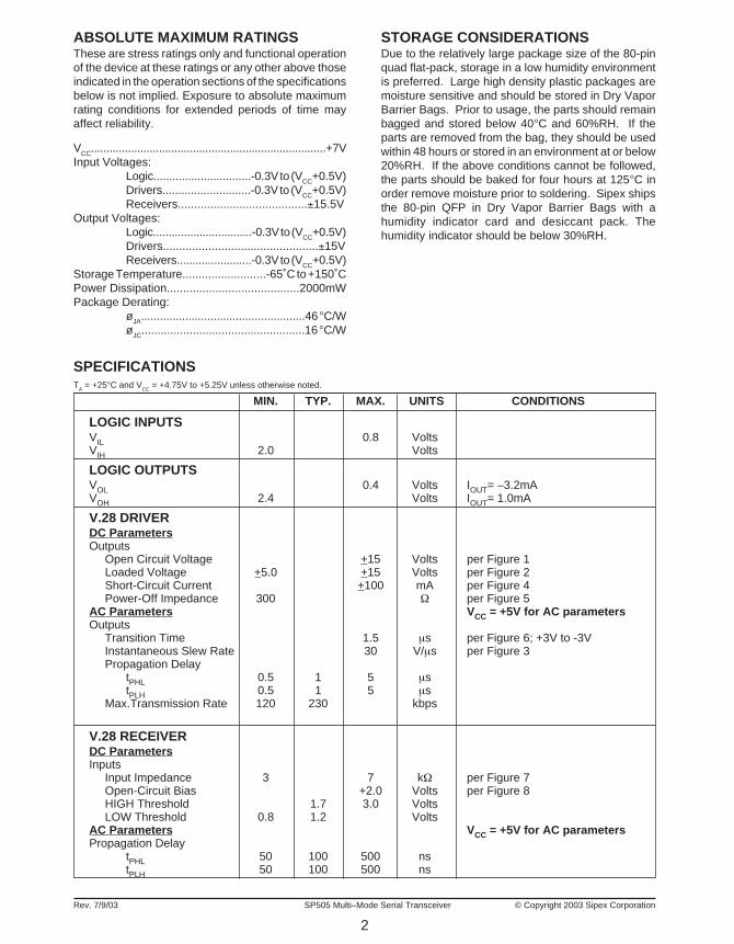
SPECIFICATIONST
A = +25°C and V
CC = +4.75V to +5.25V unless otherwise noted.
MIN. TYP. MAX. UNITS CONDITIONS
LOGIC INPUTSVIL 0.8 VoltsVIH 2.0 Volts
LOGIC OUTPUTSVOL 0.4 Volts IOUT= –3.2mAVOH 2.4 Volts IOUT= 1.0mA
V.28 DRIVERDC ParametersOutputs
Open Circuit Voltage +15 Volts per Figure 1Loaded Voltage +5.0 +15 Volts per Figure 2Short-Circuit Current +100 mA per Figure 4Power-Off Impedance 300 Ω per Figure 5
AC Parameters VCC = +5V for AC parametersOutputs
Transition Time 1.5 µs per Figure 6; +3V to -3VInstantaneous Slew Rate 30 V/µs per Figure 3Propagation Delay
tPHL 0.5 1 5 µstPLH 0.5 1 5 µs
Max.Transmission Rate 120 230 kbps
V.28 RECEIVERDC ParametersInputs
Input Impedance 3 7 kΩ per Figure 7Open-Circuit Bias +2.0 Volts per Figure 8HIGH Threshold 1.7 3.0 VoltsLOW Threshold 0.8 1.2 Volts
AC Parameters VCC = +5V for AC parametersPropagation Delay
tPHL 50 100 500 nstPLH 50 100 500 ns
ABSOLUTE MAXIMUM RATINGSThese are stress ratings only and functional operationof the device at these ratings or any other above thoseindicated in the operation sections of the specificationsbelow is not implied. Exposure to absolute maximumrating conditions for extended periods of time mayaffect reliability.
VCC............................................................................+7VInput Voltages:
Logic...............................-0.3V to (VCC+0.5V)Drivers............................-0.3V to (VCC+0.5V)Receivers........................................±15.5V
Output Voltages:Logic................................-0.3V to (VCC+0.5V)Drivers................................................±15VReceivers........................-0.3V to (VCC+0.5V)
Storage Temperature..........................-65˚C to +150˚CPower Dissipation.........................................2000mWPackage Derating:
øJA....................................................46 °C/WøJC...................................................16 °C/W
STORAGE CONSIDERATIONSDue to the relatively large package size of the 80-pinquad flat-pack, storage in a low humidity environmentis preferred. Large high density plastic packages aremoisture sensitive and should be stored in Dry VaporBarrier Bags. Prior to usage, the parts should remainbagged and stored below 40°C and 60%RH. If theparts are removed from the bag, they should be usedwithin 48 hours or stored in an environment at or below20%RH. If the above conditions cannot be followed,the parts should be baked for four hours at 125°C inorder remove moisture prior to soldering. Sipex shipsthe 80-pin QFP in Dry Vapor Barrier Bags with ahumidity indicator card and desiccant pack. Thehumidity indicator should be below 30%RH.

3Rev. 7/9/03 SP505 Multi–Mode Serial Transceiver © Copyright 2003 Sipex Corporation
SPECIFICATIONSTA = +25°C and VCC = +4.75V to +5.25V unless otherwise noted.
MIN. TYP. MAX. UNITS CONDITIONS
V.28 RECEIVER (continued)AC Parameters (cont.)
Max.Transmission Rate 120 230 kbps
V.10 DRIVERDC ParametersOutputs
Open Circuit Voltage +4.0 +6.0 Volts per Figure 9Test-Terminated Voltage 0.9VOC Volts per Figure 10Short-Circuit Current +150 mA per Figure 11Power-Off Current +100 µA per Figure 12
AC Parameters VCC = +5V for AC parametersOutputs
Transition Time 200 ns per Figure 13; 10% to 90%Propagation Delay
tPHL 50 100 500 nstPLH 50 100 500 ns
Max.Transmission Rate 120 kbps
V.10 RECEIVERDC ParametersInputs
Input Current –3.25 +3.25 mA per Figures 14 and 15Input Impedance 4 kΩSensitivity +0.3 Volts
AC Parameters VCC = +5V for AC parametersPropagation Delay
tPHL 50 120 250 nstPLH 50 120 250 ns
Max.Transmission Rate 120 kbps
V.11 DRIVERDC ParametersOutputs
Open Circuit Voltage +5.0 Volts per Figure 16Test Terminated Voltage +2.0 Volts per Figure 17
0.5VOC 0.67VOC VoltsBalance +0.4 Volts per Figure 17Offset +3.0 Volts per Figure 17Short-Circuit Current +150 mA per Figure 18Power-Off Current +100 µA per Figure 19
AC Parameters VCC = +5V for AC parametersOutputs
Transition Time 20 ns per Figures 21 and 36; 10% to 90%Propagation Delay
tPHL 50 85 110 ns per Figures 33 and 36, CL = 50pFtPLH 50 85 110 ns per Figures 33 and 36, CL = 50pF
Differential Skew 10 20 ns per Figures 33 and 36, CL = 50pFMax.Transmission Rate per Figure 33, CL = 50pF
SP505ACF 10 12 Mbps fIN = 5MHzSP505BCF 16.4 18 Mbps fIN = 8.2MHz
V.11 RECEIVERDC ParametersInputs
Common Mode Range –7 +7 VoltsSensitivity +0.3 Volts

4
Rev. 7/9/03 SP505 Multi–Mode Serial Transceiver © Copyright 2003 Sipex Corporation
SPECIFICATIONSTA = +25°C and VCC = +4.75V to +5.25V unless otherwise noted.
MIN. TYP. MAX. UNITS CONDITIONS
V.11 RECEIVER (continued)DC Parameters (cont.)Input Current –3.25 +3.25 mA per Figure 20 and 22Current w/ 100Ω Termination +60.75 mA per Figure 23 and 24Input Impedance 4 kΩAC Parameters VCC = +5V for AC parametersPropagation Delay tPHL 80 110 130 ns per Figures 33 and 38; CL = 50pF tPLH 80 110 130 ns per Figures 33 and 38; CL = 50pFDifferential Skew 20 ns per Figure 33; CL = 50pFMax.Transmission Rate per Figure 33; CL = 50pF
SP505ACF 10 12 Mbps fIN = 5MHzSP505BCF 16.4 18 Mbps fIN = 8.2MHz
V.35 DRIVERDC ParametersOutputs
Open Circuit Voltage +1.20 Volts per Figure 16Test Terminated Voltage +0.44 +0.66 Volts per Figure 25Offset +0.6 Volts per Figure 25Source Impedance 50 150 Ω per Figure 27; ZS = V2/V1 x 50ΩShort-Circuit Impedance 135 165 Ω per Figure 28
AC Parameters VCC = +5V for AC parametersOutputs
Transition Time 30 40 ns per Figure 29; 10% to 90%Propagation Delay
tPHL 50 90 110 ns per Figures 33 and 36; CL = 20pFtPLH 50 90 110 ns per Figures 33 and 36; CL = 20pF
Differential Skew 20 30 ns per Figures 33 and 36; CL = 20pFMax.Transmission Rate per Figure 33; CL = 20pF
SP505ACF 10 12 Mbps fIN = 5MHzSP505BCF 16.4 18 Mbps fIN = 8.2MHz
V.35 RECEIVERDC ParametersInputs
Sensitivity +80 mVSource Impedance 90 110 Ω per Figure 30; ZS = V2/V1 x 50ΩShort-Circuit Impedance 135 165 Ω per Figure 31
AC Parameters VCC = +5V for AC parametersPropagation Delay tPHL 80 110 130 ns per Figures 33 and 38; CL = 20pF tPLH 80 110 130 ns per Figures 33 and 38; CL = 20pFDifferential Skew 20 ns per Figure 33; CL = 20pFMax.Transmission Rate per Figure 33; CL = 20pF
SP505ACF 10 12 Mbps fIN = 5MHzSP505BCF 16.4 18 Mbps fIN = 8.2MHz
TRANSCEIVER LEAKAGE CURRENTSDriver Output 3-State Current 100 500 µA per Figure 32; Drivers disabledRcvr Output 3-State Current 1 10 µA DECX = 0000, 0.4V ≤ VO ≤ 2.4V

5Rev. 7/9/03 SP505 Multi–Mode Serial Transceiver © Copyright 2003 Sipex Corporation
OTHER AC CHARACTERISTICSTA = +25°C and VCC = +5.0V unless otherwise noted.
PARAMETER MIN. TYP. MAX. UNITS CONDITIONS
DRIVER DELAY TIME BETWEEN ACTIVE MODE AND TRI-STATE MODE
RS-232/V.28tPZL; Tri-state to Output LOW 0.70 5.0 µs CL = 100pF, Fig. 34 & 40; S1
closedtPZH; Tri-state to Output HIGH 0.40 2.0 µs CL = 100pF, Fig. 34 & 40; S2
closedtPLZ; Output LOW to Tri-state 0.20 2.0 µs CL = 100pF, Fig. 34 & 40; S1
closedtPHZ; Output HIGH to Tri-state 0.40 2.0 µs CL = 100pF, Fig. 34 & 40; S2
closedRS-423/V.10tPZL; Tri-state to Output LOW 0.15 2.0 µs CL = 100pF, Fig. 34 & 40; S1
closedtPZH; Tri-state to Output HIGH 0.20 2.0 µs CL = 100pF, Fig. 34 & 40; S2
closedtPLZ; Output LOW to Tri-state 0.20 2.0 µs CL = 100pF, Fig. 34 & 40; S1
closedtPHZ; Output HIGH to Tri-state 0.15 2.0 µs CL = 100pF, Fig. 34 & 40; S2
closedRS-422/V.11tPZL; Tri-state to Output LOW 2.80 10.0 µs CL = 100pF, Fig. 34 & 37; S1
closedtPZH; Tri-state to Output HIGH 0.10 2.0 µs CL = 100pF, Fig. 34 & 37; S2
closedtPLZ; Output LOW to Tri-state 0.10 2.0 µs CL = 15pF, Fig. 34 & 37; S1
closedtPHZ; Output HIGH to Tri-state 0.10 2.0 µs CL = 15pF, Fig. 34 & 37; S2
closedV.35tPZL; Tri-state to Output LOW 2.60 10.0 µs CL = 100pF, Fig. 34 & 37; S1
closedtPZH; Tri-state to Output HIGH 0.10 2.0 µs CL = 100pF, Fig. 34 & 37; S2
closedtPLZ; Output LOW to Tri-state 0.10 2.0 µs CL = 15pF, Fig. 34 & 37; S1
closedtPHZ; Output HIGH to Tri-state 0.15 2.0 µs CL = 15pF, Fig. 34 & 37; S2
closed
RECEIVER DELAY TIME BETWEEN ACTIVE MODE AND TRI-STATE MODE
RS-232/V.28tPZL; Tri-state to Output LOW 0.12 2.0 µs CL = 100pF, Fig. 35 & 38; S1
closedtPZH; Tri-state to Output HIGH 0.10 2.0 µs CL = 100pF, Fig. 35 & 38; S2
closedtPLZ; Output LOW to Tri-state 0.10 2.0 µs CL = 100pF, Fig. 35 & 38; S1
closedtPHZ; Output HIGH to Tri-state 0.10 2.0 µs CL = 100pF, Fig. 35 & 38; S2
closedRS-423/V.10tPZL; Tri-state to Output LOW 0.10 2.0 µs CL = 100pF, Fig. 35 & 38; S1
closedtPZH; Tri-state to Output HIGH 0.10 2.0 µs CL = 100pF, Fig. 35 & 38; S2
closedtPLZ; Output LOW to Tri-state 0.10 2.0 µs CL = 100pF, Fig. 35 & 38; S1
closedtPHZ; Output HIGH to Tri-state 0.10 2.0 µs CL = 100pF, Fig. 35 & 38; S2
closed

6
Rev. 7/9/03 SP505 Multi–Mode Serial Transceiver © Copyright 2003 Sipex Corporation
POWER REQUIREMENTS
PARAMETER MIN. TYP. MAX. UNITS CONDITIONS
VCC 4.75 5.00 5.25 Volts
ICC (No Mode Selected) 30 mA All ICC values are with VCC = +5V,(V.28/RS-232) 60 mA T = +25oC, all drivers are loaded to(V.11/RS-422) 300 mA their specified maximum load and all(RS-449) 250 mA drivers are active at their maximum(V.35) 105 mA specified data transmission rates.EIA-530 260 mAEIA-530A 250 mAV.36 65 mA
OTHER AC CHARACTERISTICS (Continued)TA = +25°C and VCC = +5.0V unless otherwise noted.
PARAMETER MIN. TYP. MAX. UNITS CONDITIONSRS-422/V.11tPZL; Tri-state to Output LOW 0.10 2.0 µs CL = 100pF, Fig. 35 & 39; S1
closedtPZH; Tri-state to Output HIGH 0.10 2.0 µs CL = 100pF, Fig. 35 & 39; S2
closedtPLZ; Output LOW to Tri-state 0.10 2.0 µs CL = 15pF, Fig. 35 & 39; S1
closedtPHZ; Output HIGH to Tri-state 0.10 2.0 µs CL = 15pF, Fig. 35 & 39; S2
closedV.35tPZL; Tri-state to Output LOW 0.10 2.0 µs CL = 100pF, Fig. 35 & 39; S1
closedtPZH; Tri-state to Output HIGH 0.10 2.0 µs CL = 100pF, Fig. 35 & 39; S2
closedtPLZ; Output LOW to Tri-state 0.10 2.0 µs CL = 15pF, Fig. 35 & 39; S1
closedtPHZ; Output HIGH to Tri-state 0.10 2.0 µs CL = 15pF, Fig. 35 & 39; S2
closed
TRANSCEIVER TO TRANSCEIVER SKEW (per Figures 33, 36, 38)
V.28 Driver 100 ns | (tphl )Tx1 – (tphl )Tx6,7 |
100 ns | (tplh )Tx1 – (tplh )Tx6,7 |
V.28 Receiver 20 ns | (tphl )Rx1 – (tphl )Rx2,7 |
20 ns | (tphl )Rx1 – (tphl )Rx2,7 |
V.11 Driver 2 ns | (tphl )Tx1 – (tphl )Tx6,7 |
2 ns | (tplh )Tx1 – (tplh )Tx6,7 |
V.11 Receiver 3 ns | (tphl )Rx1 – (tphl )Rx2,7 |
3 ns | (tphl )Rx1 – (tphl )Rx2,7 |
V.10 Driver 5 ns | (tphl )Tx2 – (tphl )Tx3,4,5 |
5 ns | (tplh )Tx2 – (tplh )Tx3,4,5 |
V.10 Receiver 5 ns | (tphl )Rx2 – (tphl )Rx3,4,5 |
5 ns | (tphl )Rx2 – (tphl )Rx3,4,5 |
V.35 Driver 4 ns | (tphl )Tx1 – (tphl )Tx6,7 |
4 ns | (tplh )Tx1 – (tplh )Tx6,7 |
V.35 Receiver 6 ns | (tphl )Rx1 – (tphl )Rx2,7 |6 ns | (tphl )Rx1 – (tphl )Rx2,7 |

7Rev. 7/9/03 SP505 Multi–Mode Serial Transceiver © Copyright 2003 Sipex Corporation
A
VOC
C
A
VT
C
3kΩ
A
VT
C
7kΩ Oscilloscope
Scope used for slew ratemeasurement.
A
Isc
C
A
C
VCC = 0V
±2V
Ix
A
C
3kΩ 2500pF Oscilloscope
Figure 1. V.28 Driver Output Open Circuit Voltage Figure 2. V.28 Driver Output Loaded Voltage
Figure 3. V.28 Driver Output Slew Rate Figure 4. V.28 Driver Output Short-Circuit Current
Figure 6. V.28 Driver Output Rise/Fall TimesFigure 5. V.28 Driver Output Power-Off Impedance
TEST CIRCUITS...

8
Rev. 7/9/03 SP505 Multi–Mode Serial Transceiver © Copyright 2003 Sipex Corporation
Figure 7. V.28 Receiver Input Impedance
A
C
Iia
±15V
A
C
Voc
Figure 8. V.28 Receiver Input Open Circuit Bias
A
VOC3.9kΩ
C
A
Vt450Ω
C
A
C
±0.25V
VCC = 0V
Ix
A
Isc
C
Figure 9. V.10 Driver Output Open-Circuit Voltage Figure 10. V.10 Driver Output Test Terminated Voltage
Figure 12. V.10 Driver Output Power-Off CurrentFigure 11. V.10 Driver Output Short-Circuit Current

9Rev. 7/9/03 SP505 Multi–Mode Serial Transceiver © Copyright 2003 Sipex Corporation
Figure 13. V.10 Driver Output Transition Time Figure 14. V.10 Receiver Input Current
A
450Ω
C
Oscilloscope
A
C
Iia
±10V
+3.25mA
–3.25mA
+10V+3V
–3V–10V
Maximum Input Currentversus Voltage
V.10 RECEIVER
Figure 15. V.10 Receiver Input IV Graph Figure 16. V.11 and V.35 Driver Output Open-CircuitVoltage
A
B
VOC3.9kΩ
VOCA
VOCB
C
A
B
VT
50Ω
VOS
C
50Ω
A
B
C
Isa
Isb
Figure 17. V.11 Driver Output Test Terminated Voltage Figure 18. V.11 Driver Output Short-Circuit Current

10
Rev. 7/9/03 SP505 Multi–Mode Serial Transceiver © Copyright 2003 Sipex Corporation
A
B
C
Ixa
±0.25V
A
B
C
Ixb
±0.25V
VCC = 0V
VCC = 0V
A
B
C
Iia
±10V
C
Iib
±10V
A
B
+3.25mA
–3.25mA
+10V+3V
–3V–10V
Maximum Input Currentversus Voltage
V.11 RECEIVER
Figure 19. V.11 Driver Output Power-Off Current Figure 20. V.11 Receiver Input Current
Figure 21. V.11 Driver Output Rise/Fall Time Figure 22. V.11 Receiver Input IV Graph
A
B
50Ω
C
50Ω
50Ω VE
Oscilloscope

11Rev. 7/9/03 SP505 Multi–Mode Serial Transceiver © Copyright 2003 Sipex Corporation
A
B
C
Iia
±6V
C
Iib
±6V
A
B
100Ω to150Ω
100Ω to150Ω
i [mA] = V [V] / 0.1
+6V+3V
–3V–6V
Maximum Input Currentversus Voltage
V.11 RECEIVERw/ Optional Cable Termination
(100Ω to 150Ω) i [mA] = V [V] / 0.1
i [mA] = (V [V] – 3) / 4.0
i [mA] = (V [V] – 3) / 4.0
Figure 23. V.11 Receiver Input Current w/ Termination
Figure 24. V.11 Receiver Input Graph w/ Termination
Figure 25. V.35 Driver Output Test Terminated Voltage
Figure 26. V.35 Driver Output Offset Voltage Figure 27. V.35 Driver Output Source Impedance
A
B
50Ω
C
50Ω
VT
VOS
A
B
V2
50Ω
C
24kHz, 550mVp-pSine Wave
V1
A
B
50Ω
C
50Ω
VT
VOS

12
Rev. 7/9/03 SP505 Multi–Mode Serial Transceiver © Copyright 2003 Sipex Corporation
Figure 32. Driver Output Leakage Current Test Figure 33. Driver/Receiver Timing Test Circuit
Figure 30. V.35 Receiver Input Source Impedance
Figure 29. V.35 Driver Output Rise/Fall Time
Figure 31. V.35 Receiver Input Short-Circuit Impedance
Figure 28. V.35 Driver Output Short-Circuit Impedance
A
B
C
ISC
±2V
A
B
C
50Ω
Oscilloscope
50Ω
50Ω
A
B
C
Isc
±2V
CL1
15pF
ROUT
A
B
A
B
TIN
CL2
fIN (50% Duty Cycle, 2.5VP-P
)
A
B
V2
50Ω
C
24kHz, 550mVp-pSine Wave
V1
A
B
IZSC
Logic “1”
±15V
0 0 0 0
DEC3 DEC2 DEC1 DEC0
VCC = +5V
VCC
Any one of the two conditions for disabling the driver.

13Rev. 7/9/03 SP505 Multi–Mode Serial Transceiver © Copyright 2003 Sipex Corporation
Figure 34. Driver Timing Test Load Circuit Figure 35. Receiver Timing Test Load Circuit
500Ω
CL
OutputUnder
Test
S1
S2
VCC1KΩ
1KΩCRL
ReceiverOutput S1
S2
Test PointVCC
Figure 36. Driver Propagation Delays
Figure 37. Driver Enable and Disable Times
+3V
0VDECX
5V
VOL
A, B0V
1.5V 1.5V
tZL
tZH
f = 1MHz; tR ≤ 10ns; tF ≤ 10ns
VOH
A, B 2.3V
2.3V
tLZ
tHZ
0.5V
0.5V
Output normally LOW
Output normally HIGH
TXENABLE
Figure 38. Receiver Propagation Delays
+3V
0V
DRIVERINPUT
B
A
DRIVEROUTPUT
VO+DIFFERENTIALOUTPUT
VA – VB
0VVO–
1.5V 1.5V
tPLH
tR tF
f > 5MHz; tR < 10ns; tF < 10ns
VO1/2VO 1/2VO
tPHL
tDPLH tDPHL
tSKEW = SKEW = | tDPLH - tDPHL |
VOH
VOL
RECEIVER OUT (VOH - VOL)/2 (VOH - VOL)/2
tPLH
f > 5MHz; tR < 10ns; tF < 10ns
OUTPUT
V0D2+
V0D2–A – B 0V 0V
tPHL
INPUT
tSKEW = | tPHL - tPLH |

14
Rev. 7/9/03 SP505 Multi–Mode Serial Transceiver © Copyright 2003 Sipex Corporation
Figure 39. Receiver Enable and Disable Times
+3V
0V
DECX
5V
0V
1.5V 1.5V
tZL
tZH
f = 1MHz; tR ≤ 10ns; tF ≤ 10ns
RECEIVER OUT 1.5V
1.5V
tLZ
tHZ
0.5V
0.5V
Output normally LOW
Output normally HIGH
VIL
VIH
RECEIVER OUT
RCVRENABLE
+3V
0VDECX or Tx_Enable 1.5V 1.5V
tZL
f = 60kHz; tR < 10ns; tF < 10ns
TOUT
tLZ
Output LOW
0V
+3V
0V
VOH
1.5V 1.5V
tZH
f = 60kHz; tR < 10ns; tF < 10ns
TOUTVOH – .5V
tHZOutput HIGH
0V
DECX or Tx_Enable
VOH – .5V
VOL – .5VVOL – .5VVOL
Figure 40. V.28 (RS-232) and V.10 (RS-423) Driver Enable and Disable Times

15Rev. 7/9/03 SP505 Multi–Mode Serial Transceiver © Copyright 2003 Sipex Corporation
Figure 41. Typical V.28 Driver Output Waveform Figure 42. Typical V.10 Driver Output Waveform
- 0V
- 0V
- 0V
- 0V
- 0V
- 0V
- 0V
- 0V
Figure 43. Typical V.11 Driver Output Waveform Figure 44. Typical V.35 Driver Output Waveform
INPUT
OUTPUT
INPUT
AOUT
BOUT
DIFFOUT

16
Rev. 7/9/03 SP505 Multi–Mode Serial Transceiver © Copyright 2003 Sipex Corporation
PINOUT…
PIN ASSIGNMENTS…CLOCK AND DATA GROUPPin 1 — RxD — Receive Data; TTL output,sourced from RD(a) and RD(b) inputs.
Pin 14 — TxD — TTL input ; transmit datasource for SD(a) and SD(b) outputs.
Pin 15 — TxC — Transmit Clock; TTL input forTT driver outputs.
Pin 20 — RxC — Receive Clock; TTL outputsourced from RT(a) and RT(b) inputs.
Pin 22 — ST — Send Timing; TTL input; sourcefor ST(a) and ST(b) outputs.
Pin 37 — RT(a) — Receive Timing; analoginput, inverted; source for RxC.
Pin 38 — RT(b) — Receive Timing; analoginput, non-inverted; source for RxC.
Pin 42 — ST(a) — Send Timing; analog output,inverted; sourced from ST.
Pin 44 — ST(b) — Send Timing; analog output,non-inverted; sourced from ST.
Pin 59 — SD(b) — Analog Out — Send data,non-inverted; sourced from TxD.
Pin 61 — SD(a) — Analog Out — Send data,inverted; sourced from TxD.
Pin 63 — TT(a) — Analog Out — TerminalTiming, inverted; sourced from TxC
Pin 65 — TT(b) — Analog Out — TerminalTiming, non–inverted; sourced from TxC.
Pin 70 — RD(a) — Receive Data, analog input;inverted; source for RxD.
Pin 71 — RD(b) — Receive Data; analog input;non-inverted; source for RxD.
Pin 76 — SCT(a) — Serial Clock Transmit;analog input, inverted; source for SCT.
Pin 77 — SCT(b) — Serial Clock Transmit:analog input, non–inverted; source for SCT
Pin 79 — SCT — Serial Clock Transmit; TTLoutput; sources from SCT(a) and SCT(b) inputs.
CONTROL LINE GROUPPin 13 — DTR — Data Terminal Ready; TTLinput; source for TR(a) and TR(b) outputs.
Pin 16 — RTS — Ready To Send; TTL input;source for RS(a) and RS(b) outputs.
Pin 17 — RL — Remote Loopback; TTL input;source for RL(a) and RL(b) outputs.
Pin 19 — DCD— Data Carrier Detect; TTLoutput; sourced from RR(a) and RR(b) inputs.
Pin 21 — RI — Ring In; TTL output; sourcedfrom IC(a) and IC(b) inputs.
Pin 24 — LL — Local Loopback; TTL input;source for LL(a) and LL(b) outputs.
Pin 35 — RR(a)— Receiver Ready; analoginput, inverted; source for DCD.
Pin 36 — RR(b)— Receiver Ready; analoginput, non-inverted; source for DCD.
Pin 39 — IC(a)— Incoming Call; analog input,inverted; source for RI.
Pin 40 — IC(b)— Incoming Call; analoginput,non-inverted; source for RI.
RxD 1
SDEN 2
TREN 3
RSEN 4
LLEN 5
TTEN 6
SCTEN 7
LATCH 8
DEC3 9
DEC2 10
DEC1 11
DEC0 12
DTR 13
TxD 14
TxC 15
RTS 16
RL 17
RLEN 18
DCD 19
RxC 20
RI
21
ST
22
STE
N 2
3
LL 2
4
VC
C 2
5
C1+
26
VD
D 2
7
C2+
28
GN
D 2
9
C1–
30
C2–
31
VS
S 3
2
VC
C 3
3
GN
D 3
4
RR
(a)
35
RR
(b)
36
RT(
a) 3
7
RT(
b) 3
8
IC(a
) 39
IC(b
) 40
60 GND
59 SD(b)
58 TR(a)
57 GND
56 TR(b)
55 VCC
54 RS(a)
53 GND
52 RS(b)
51 LL(a)
50 GND
49 LL(b)
48 VCC
47 RL(a)
46 GND
45 RL(b)
44 ST(b)
43 GND
42 ST(a)
41 VCC
80 C
TS
79 S
CT
78 D
SR
77
SC
T(b)
76 S
CT(
a)
75 G
ND
74 V
CC
73 V
CC
72 G
ND
71 R
D(b
)
70 R
D(a
)
69 D
M(b
)
68 D
M(a
)
67 C
S(b
)
66 C
S(a
)
65 T
T(b)
64 G
ND
63 T
T(a)
62 V
CC
61 S
D(a
)
SP505
17Rev. 7/9/03 SP505 Multi–Mode Serial Transceiver © Copyright 2003 Sipex Corporation
Pin 7 — SCTEN — Enables SCT receiver;active high; TTL input.
Pin 8 — LATCH — Latch control for decoderbits (pins 9-12), active low. Logic high inputwill make decoder transparent.
Pins 12–9 — DEC0 – DEC3 — Transmitter andreceiver decode register; configures transmitterand receiver modes; TTL inputs.
Pin 18 — RLEN — Enables RL driver; activelow; TTL input.
Pin 23 — STEN — Enables ST driver; activelow; TTL input.
POWER SUPPLIESPins 25, 33, 41, 48, 55, 62, 73, 74 — VCC — +5Vinput.
Pins 29, 34, 43, 46, 50, 53, 57, 60, 64, 72, 75 —GND — Ground.
Pin 27 — VDD +10V Charge Pump Capacitor —Connects from VDD to VCC. Suggested capaci-tor size is 22µF, 16V.
Pin 32 — VSS –10V Charge Pump Capacitor —Connects from ground to VSS. Suggested ca-pacitor size is 22µF, 16V.
Pins 26 and 30 — C1+ and C1
– — Charge PumpCapacitor — Connects from C1
+ to C1–. Sug-
gested capacitor size is 22µF, 16V.
Pins 28 and 31 — C2+ and C2
– — Charge PumpCapacitor — Connects from C2
+ to C2–. Sug-
gested capacitor size is 22µF, 16V.
Pin 45 — RL(b) — Remote Loopback; analogoutput, non-inverted; sourced from RL.
Pin 47 — RL(a) — Remote Loopback; analogoutput inverted; sourced from RL.
Pin 49— LL(b) — Local Loopback; analogoutput, non-inverted; sourced from LL.
Pin 51 — LL(a) — Local Loopback; analogoutput, inverted; sourced from LL.
Pin 52 — RS(b) — Ready To Send; analogoutput, non-inverted; sourced from RTS.
Pin 54 — RS(a) — Ready To Send; analogoutput, inverted; sourced from RTS.
Pin 56 — TR(b) — Terminal Ready; analogoutput, non-inverted; sourced from DTR.
Pin 58 — TR(a) — Terminal Ready; analogoutput, inverted; sourced from DTR.
Pin 66 — CS(a)— Clear To Send; analog input,inverted; source for CTS.
Pin 67 — CS(b)— Clear To Send; analog input,non-inverted; source for CTS.
Pin 68 — DM(a)— Data Mode; analog input,inverted; source for DSR.
Pin 69 — DM(b)— Data Mode; analog input,non-inverted; source for DSR
Pin 78 — DSR— Data Set Ready; TTL output;sourced from DM(a), DM(b) inputs.
Pin 80 — CTS— Clear To Send; TTL output;sourced from CS(a) and CS(b) inputs.
CONTROL REGISTERSPins 2 — SDEN — Enables TxD driver, activelow; TTL input.
Pins 3 — TREN — Enables DTR driver, activelow; TTL input.
Pins 4 — RSEN — Enables RTS driver, activelow; TTL input.
Pins 5 — LLEN — Enables LL driver, activelow; TTL input.
Pin 6 — TTEN — Enables TT driver, activelow; TTL input.

18
Rev. 7/9/03 SP505 Multi–Mode Serial Transceiver © Copyright 2003 Sipex Corporation
A typical +10V charge pump would requireexternal clamping such as 5V zener diodes onVDD and VSS to ground. The +5V output hassymmetrical levels as in the +10V output. The+5V is used in the following modes where RS-423 (V.10) are used: RS-449, EIA-530, EIA-530A and V.36.
Phase 1 (±10V)— VSS charge storage — During this phase ofthe clock cycle, the positive side of capacitorsC1 and C2 are initially charged to +5V. Cl
+ isthen switched to ground and the charge on C1
– istransferred to C2
–. Since C2+ is connected to
+5V, the voltage potential across capacitor C2 isnow 10V.
Phase 1 (±5V)— VSS & VDD charge storage and transfer —With the C1 and C2 capacitors initially chargedto +5V, Cl
+ is then switched to ground and thecharge on C1
– is transferred to the VSS storagecapacitor. Simultaneously the C2
– is switched toground and 5V charge on C2
+ is transferred tothe VDD storage capacitor.
FEATURES…The SP505 is a highly integrated serial trans-ceiver that allows software control of its inter-face modes. Similar to the SP504, the SP505offers the same hardware interface modes forRS-232 (V.28), RS-422A (V.11), RS-449, RS-485, V.35, EIA-530 and includes V.36 and EIA-530A. The interface mode selection is done viaa 4–bit switch for the drivers and receivers. TheSP505 is fabricated using low–power BiCMOSprocess technology, and incorporates a Sipex–patented (5,306,954) charge pump allowing +5Vonly operation. Each device is packaged in an80–pin JEDEC Quad FlatPack package.
The SP505 is ideally suited for wide area net-work connectivity based on the interface modesoffered and the driver and receiver configura-tions. The SP505 has seven (7) independentdrivers and seven (7) independent receivers. InV.35 mode, the SP505 includes the necessarycomponents and termination resistors internalwithin the device for compliant V.35 operation.
THEORY OF OPERATIONThe SP505 is made up of five separate circuitblocks — the charge pump, drivers, receivers,decoder and switching array. Each of thesecircuit blocks is described in more detail below.
Charge–PumpThe SP505 charge pump is based on the SP504design where Sipex's patented charge pumpdesign (5,306,954) uses a four–phase voltageshifting technique to attain symmetrical 10Vpower supplies. The charge pump still requiresexternal capacitors to store the charge. In addi-tion the SP504 charge pump supplies +10V or+5V on VSS and VDD depending on the mode ofoperation. There is a free–running oscillatorthat controls the four phases of the voltageshifting. A description of each phase follows.
The SP505 charge pump is used for RS-232where the output voltage swing is typically+10V and also used for RS-423. However, RS-423 requires the voltage swing on the driveroutput be between +4V to +6V during an open-circuit (no load). The charge pump would needto be regulated down from +10V to +5V.
VCC = +5V
–5V
–5V
+5VVDD Storage Capacitor
C1 C2
C4+
+ +–
––
VSS Storage Capacitor
C3
+–
Figure 46. Charge Pump Phase 1 for +5V.
VCC = +5V
+5VVDD Storage Capacitor
C1 C2
C4+
+ +–
––
VSS Storage Capacitor
C3
+––5V
Figure 45. Charge Pump Phase 1 for +10V.

19Rev. 7/9/03 SP505 Multi–Mode Serial Transceiver © Copyright 2003 Sipex Corporation
Phase 2 (±10V)— VSS transfer — Phase two of the clock con-nects the negative terminal of C2 to the VSSstorage capacitor and the positive terminal of C2to ground, and transfers the generated –l0V orthe generated –5V to C3. Simultaneously, thepositive side of capacitor C 1 is switched to +5Vand the negative side is connected to ground.
Phase 2 (±5V)— VSS & VDD charge storage — C1
+ is recon-nected to VCC to recharge the C1 capacitor. C2
+
is switched to ground and C2– is connected to C3.
The 5V charge from Phase 1 is now transferredto the VSS storage capacitor. VSS receives acontinuous charge from either C1 or C2. Withthe C1 capacitor charged to 5V, the cycle beginsagain.
Phase 3 — VDD charge storage — The third phase of theclock is identical to the first phase — the chargetransferred in C1 produces –5V in the negativeterminal of C1, which is applied to the negativeside of capacitor C2. Since C2
+ is at +5V, thevoltage potential across C2 is l0V. For the 5Voutput, C2
+ is connected to ground so that thepotential on C2 is only +5V.
Phase 4 — VDD transfer — The fourth phase of theclock connects the negative terminal of C2 toground and transfers the generated l0V or thegenerated 5V across C2 to C4, the VDD storagecapacitor. Again, simultaneously with this, thepositive side of capacitor C1 is switched to +5Vand the negative side is connected to ground,and the cycle begins again.
Since both VDD and VSS are separately gener-ated from VCC in a no–load condition, VDD andVSS will be symmetrical. Older charge pumpapproaches that generate V– from V+ will showa decrease in the magnitude of V– compared toV+ due to the inherent inefficiencies in thedesign.
The clock rate for the charge pump typicallyoperates at 15kHz. The external capacitors mustbe a minimum of 22µF with a 16V breakdownrating.
External Power SuppliesFor applications that do not require +5V only,external supplies can be applied at the V+ andV– pins. The value of the external supply volt-ages must be no greater than +l0.5V. The toler-ance should be +5% from +10V. The currentdrain for the supplies is used for RS-232 and RS-423 drivers. For the RS-232 driver, the currentrequirement will be 3.5mA per driver. The RS-423 driver worst case current drain will be11mA per driver. Power sequencing is requiredfor the SP505. The supplies must be sequencedaccordingly: +10V, +5V and –10V. It is impor-tant to prevent VSS from starting up before VCCor VDD.
Figure 47. Charge Pump Phase 2 for +10V.
Figure 49. Charge Pump Phase 3.
VCC = +5V
–10V
VDD Storage Capacitor
C1 C2
C4+
+ +–
––
VSS Storage Capacitor
C3
+–
VCC = +5V
–5V
–5V
+5VVDD Storage Capacitor
C1 C2
C4+
+ +–
––
VSS Storage Capacitor
C3
+–
Figure 50. Charge Pump Phase 4.
Figure 48. Charge Pump Phase 2 for +5V.
VCC = +5V
VDD Storage Capacitor
C1 C2
C4+
+ +–
––
VSS Storage Capacitor
C3
+––5V
VCC = +5V
+10VVDD Storage Capacitor
C1 C2
C4+
+ +–
––
VSS Storage Capacitor
C3
+–

20
Rev. 7/9/03 SP505 Multi–Mode Serial Transceiver © Copyright 2003 Sipex Corporation
requirements of ±1.5V minimum differentialoutput levels with a 54Ω load. The driver isdesigned to operate over a common mode rangeof +12V to -7V, which follows the RS-485specification. This also covers the +7V to -7Vcommon mode range for V.11 (RS-422) re-quirements. The V.11 drivers are used in RS-449, EIA-530, EIA-530A and V.36 modes asCategory I signals which are used for clock anddata signals.
V.35 DriversThe fourth type of driver is the V.35 driver.These drivers were specifically designed to com-ply with the requirements of V.35. Unique tothe industry, the Sipex's V.35 driver architec-ture used in the SP505 does not need externaltermination resistors to operate and comply withV.35. This simplifies existing V.35 implemen-tations that use external termination schemes.The V.35 drivers can produce +0.55V driveroutput signals with minimum deviation (maxi-mum 20%) given an equivalent load of 100Ω.With the help of internal resistor networks, thedrivers achieve the 50Ω to 150Ω source imped-ance and the 135Ω to 165Ω short-circuit imped-ance for V.35. The V.35 driver is disabled andtransparent when the decoder is in all othermodes. All of the differential drivers; V.11 (RS-422) and V.35, can operate over 10Mbps.
Driver Enable and InputAll the drivers in the SP505 contain individualenable lines which can tri-state the driver out-puts when a logic "1" is applied. This simplifieshalf-duplex configurations for some applica-tions and also provides simpler DTE/DCEflexibility with one integrated circuit.
The driver inputs are both TTL or CMOScompatible. Each driver input should have apull-down or pull-up resistor so that the outputwill be at a defined state. Unused driver inputsshould not be left floating.
ReceiversThe SP505 has seven (7) independent receiverswhich can be programmed for the differentinterface modes. Control for the mode selectionis done via a 4–bit control word, which is thesame as the driver's 4-bit control word.Like the drivers, the receivers are prearrangedfor the specific requirements of the synchronous
DriversThe SP505 has seven (7) enhanced independentdrivers. Control for the mode selection is donevia a four–bit control word. The drivers areprearranged such that for each mode of opera-tion, the relative position and functionality ofthe drivers are set up to accommodate the se-lected interface mode. As the mode of the driv-ers is changed, the electrical characteristics willchange to support the requirements of clock,data, and control line signal levels. Table 1shows the mode of each driver in the differentinterface modes that can be selected.
There are four basic types of driver circuits —V.28, V.11, V.10 and V.35.
V.28 DriversThe V.28 drivers output single–ended signalswith a minimum of +5V (with 3kΩ & 2500pFloading), and can operate to at least 120kbpsunder full load. Since the SP505 uses a chargepump to generate the RS-232 output rails, thedriver outputs will never exceed +10V. TheV.28 drivers are used in RS-232 mode for allsignals, and also in V.35 mode where four (4)drivers are used as the control line signals (DTR,RTS, LL, and RL).
V.10 DriversThe V.10 (RS-423) drivers are also single–ended signals which produce open circuit VOLand VOH measurements of +4.0V to +6.0V.When terminated with a 450Ω load to ground,the driver output will not deviate more than 10%of the open circuit value. This is in complianceof the ITU V.10 specification. The V.10 driversare used in RS-449, EIA-530, EIA-530A andV.36 modes as Category II signals from each oftheir corresponding specifications.
V.11 DriversThe third type of driver is a V.11 (RS-422) typedifferential driver. Due to the nature of differ-ential signaling, the drivers are more immune tonoise as opposed to single-ended transmissionmethods. The advantage is evident over highspeeds and long transmission lines. The strengthof the driver outputs can produce differentialsignals that can maintain typically +2.2V differ-ential output levels with a load of 100Ω. Thesignal levels and drive capability of these driv-ers allow the drivers to also support RS-485

21Rev. 7/9/03 SP505 Multi–Mode Serial Transceiver © Copyright 2003 Sipex Corporation
serial interface. As the operating mode of thereceivers is changed, the electrical characteris-tics will change to support the requirements ofclock, data, and control line receivers. Table 2shows the mode of each receiver in the differentinterface modes that can be selected.
There are three basic types of receiver circuits— V.28, V.10, and V.11.
V.28 ReceiversThe V.28 receiver is single–ended and acceptsV.28 signals from the V.28 driver. The V.28receiver has an operating voltage range of +15Vand can receive signals down to +3V. The inputsensitivity complies with RS-232 and V.28 speci-fications at +3V. The input impedance is 3kΩ to7kΩ in accordance to RS-232 and V.28 over a+15V input range. The receiver output pro-duces a TTL/CMOS signal with a +2.4V mini-mum for a logic "1" and a +0.8V maximum fora logic "0". V.28 receivers are used in RS-232mode for all data, clock and control signals.They are also used in V.35 mode for control linesignals: CTS, DSR, LL, and RL. The V.28receivers can operate to at least 120kbps.
V.10 ReceiversThe V.10 receivers are also single–ended aswith the V.28 receivers but have an input thresh-old as low as +200mV. The input impedance isguaranteed to be greater than 4KΩ, with anoperating voltage range of +7V. The V.10 re-ceivers can operate to at least 120kbps. V.10receivers are used in RS-449, EIA-530, EIA-530A and V.36 modes as Category II signals asindicated by their corresponding specifications.
V.11 ReceiversThe third type of receiver is a differential whichsupports V.11 and RS-485 signals. This re-ceiver has a typical input impedance of 10kΩand a typical differential threshold of +200mV,which complies with the V.11 specification.Since the characteristics of the V.11 receiversare actually subsets of RS-485, the V.11 receiv-ers can accept RS-485 signals. However, thesereceivers cannot support 32-transceivers on thesignal bus due to the lower input impedance asspecified in the RS-485 specification. Threereceivers (RxD, RxC, and SCT) include a typi-cal 120Ω cable termination resistor across the Aand B inputs. The resistor for the three receivers
is switched on when the SP505 is configured ina mode which uses V.11 receivers. The V.11cable termination resistor is switched off whenthe receiver is disabled or in another operatingmode not using V.11 receivers. The V.11 re-ceivers are used in X.21, RS-449, EIA-530,EIA-530A and V.36 as Category I signals forreceiving clock, data, and some control linesignals not covered by Category II V.10 circuits.The differential receivers can receive signalsover 10Mbps.
V.35 ReceiverThe V.11 receivers are also used for the V.35mode. Unlike the older implementations ofdifferential receivers used for V.35, the SP505contains an internal resistor termination net-work that ensures a V.35 input impedance of100Ω (+10Ω) and a short-circuit impedance of150Ω (+15Ω). The traditional V.35 implemen-tations required external termination resistors toachieve the proper V.35 impedances. The inter-nal network is connected via low on-resistanceFET switches when the decoder is changed toV.35 mode. These FET switches can acceptinput signals of up to +15V without any forwardbiasing and other parasitic affects. The V.35termination resistor network is switched offwhen the receiver is disabled either by the de-coder or receiver enable pin. The terminationnetwork is transparent when all other modes areselected. The V.35 receivers can operate over10Mbps.
Receiver Enable and OutputOnly one receiver includes an enable line. TheSCTEN input for the SCT receiver can enable ortri-state the output of the receiver. When the pinis at a logic "0", the receiver output is highimpedance and any input termination internalconnected is switched off. The inputs will be atapproximately 10kΩ during tri-state.
V.11 TERMINATIONMODE [0100] V.35 MODE
RIN [a]
RIN [b]To Non-InvertingInput of Receiver
To Inverting Inputof Receiver
rON = 20Ω rON = 1Ω
51Ω
51Ω124Ω
rON = 1Ω
Figure 51. Simplified RIN
Termination Circuit

22
Rev. 7/9/03 SP505 Multi–Mode Serial Transceiver © Copyright 2003 Sipex Corporation
All receivers include a fail-safe feature thatoutputs a logic "1" when the receiver inputs areopen. The differential receivers allocated fordata and clock signals (RxD, RxC, and SCT)have advanced fail-safe that outputs a logic "1"when the inputs are either open, shorted, orterminated. Other discrete or integrated imple-mentations require external pull-up and pull-down resistors to define the receiver outputstate. For single-ended V.28 receivers, there areinternal 5kΩ pull-down resistors on the inputswhich produces a logic high ("1") at the receiveroutputs. The single-ended V.10 receivers pro-duce a logic LOW ("0") on the output when theinputs are open. This is due to an internal pull-up device connected to the input. The differen-tial receivers have the same internal pull-updevice on the non-inverting input which pro-duces a logic HIGH ("1") at the receiver output,representing an "OFF" state to the HDLC con-troller. The three differential receivers whenconfigured in V.35 mode (RxD, RxC & SCT)will also include fail-safe even when the internaltermination resistor network is connected andthe inputs are either shorted or floating.
DecoderThe SP505 has the ability to change the inter-face mode of the drivers or receivers via a 4–bitswitch. The decoder for the drivers and receiv-ers can be latched through a control pin.
The control word can be latched either high orlow to write the appropriate code into the SP505.The codes shown in Tables 1 and 2 are the onlyspecified, valid modes for the SP505. Unde-fined codes may represent other interface modesnot specified (consult the factory for more infor-mation). The drivers and receivers are con-trolled with the data bits labeled DEC3–DEC0.All of the drivers outputs and receiver outputscan be put into tri-state mode by writing 0000 tothe driver decode switch. All internal termina-tion networks are switched off during this mode.Individual tri-state capability is possible for alldrivers through each driver's own enable controlinput. The SCT receiver also contains an indi-vidual enable input. When this control pin isdisabled (logic "0"), the V.11 and V.35 inputtermination is deactivated. The 0000 decoderword will override the enable control line for theone receiver (SCT).
The SP505 contains internal loopback capabili-ties for self-diagnostic tests. Loopback is en-abled through the decoder. To initiate single-ended mode loopback, the decoder word is 1010.To initiate differential mode loopback, the de-coder word is 1011. The minimum transmissionrates into the SP505 under loopback conditionsare 120kbps for single-ended mode and 5Mbpsfor differential mode. The driver outputs are tri-stated and the receiver inputs are disabled dur-ing loopback. The receiver input impedanceduring loopback is approximately 10kΩ.
The SP505 is equipped with a latch control forthe four (4) decoder bits. The latch control pinis pin 8 of the SP505. The latch control is activelow, a logic low on pin 8 will latch the decodersignals. A logic "1" on pin 8 will force the latchto be transparent to the user. A pulse width of atleast 30ns is required to latch the decoder for thenext mode. The resultant output is typically600ns after the latch control pin is toggledassuming that the decoder word is set.
NET1/2 & TBR2 European CompliancyAs with all of Sipex's previous multi-protocolserial transceiver ICs, the drivers and receivershave been designed to meet all the requirementsto NET1/2. The SP505 is internally tested to allthe NET1/2 physical layer testing parametersand the ITU Series V specifications.
With the emergence of ETSI TBR2 (TechnicalBasis for Regulation) document now in place asan alternative for European compliancy, Sipexhas tested the SP505 to TBR2 specifications toensure "CE" approval for either testing method.
The SP505 was externally tested by TUVTelecom Services, Division of TUV Rheinland,and passed both NET1/2 and TBR2 require-ments. Test reports (NET2/052101/98 for NET1/2 and CTR2/
05101/98 for TBR2) can be furnished upon request.
Please note that although the SP505 adheres toNET1/2 testing; any complex or unusual con-figuration should be double-checked to ensureNET compliance. Consult factory for details.

23Rev. 7/9/03 SP505 Multi–Mode Serial Transceiver © Copyright 2003 Sipex Corporation
SP505 Receiver Mode Selection
SP505 Driver Mode Selection
Pin Label
RD(a)
RD(b)
RT(a)
RT(b)
CS(a)
CS(b)
DM(a)
DM(b)
RR(a)
RR(b)
IC(a)
IC(b)
SCT(a)
SCT(b)
Pin Label Mode: RS232 V.35 RS422 RS449 EIA530 EIA-530A V.36
0000 0010 1110 0100 0101 1100 1101 1111 0110
SD(a) tri-state V.28 V.35– V.11– V.11– V.11–
SD(b) V.35+ V.11+ V.11+ V.11+
TR(a) tri-state V.28 V.11– V.11– V.11– V.10
TR(b) tri-state tri-state tri-state V.11+ V.11+ V.11+ tri-state
RS(a) tri-state V.28 V.11– V.11– V.11–
RS(b) tri-state tri-state tri-state V.11+ V.11+ V.11+
RL(a) tri-state V.28 V.11– V.11– V.10
RL(b) tri-state
tri-state
tri-state V.11+ V.11+ tri-state
LL(a) tri-state V.28 V.11– V.11– V.10
LL(b) tri-state tri-state tri-state V.11+ V.11+ tri-state
ST(a) tri-state V.28 V.35– V.11– V.11– V.11–
ST(b) V.35+ V.11+ V.11+ V.11+
TT(a) tri-state V.28 V.35– V.11– V.11– V.11–
TT(b) V.35+ V.11+ V.11+ V.11+tri-state tri-state
tri-state
tri-statetri-state
tri-state
V.28
V.28
V.28
V.28
V.11–
V.11+
V.11–
V.11+
V.11–
V.11+
tri-state
V.11–
V.11+
V.11–
V.11+
V.10
V.11–
V.11+
V.11–
V.11+
V.11–
V.11+
V.11–
V.11+
V.11–
V.11+
V.10
tri-state
V.10
tri-state
V.11–
V.11+
V.10
tri-state
V.10
tri-state
V.10
tri-state
V.11–
V.11+
V.11–
V.11+
Mode: RS232 V.35 RS422 w/ Term. RS422 RS449 EIA530 EIA-530A V.36
0000 0010 1110 0100 0101 1100 1101 1111 0110
V.28 V.35– V.11– V.11– V.11–
V.35+ V.11+ V.11+ V.11+
V.28 V.11– V.11– V.11–
V.11+ V.11+ V.11+
V.28 V.11– V.11– V.11–
V.11+ V.11+ V.11+
V.28 V.11– V.11–
V.11+ V.11+
V.28 V.11– V.11–
V.11+ V.11+
V.28 V.11– V.11–
V.11+ V.11+
V.28 V.35– V.11– V.11– V.11–
V.35+ V.11+ V.11+ V.11+
V.28
V.28
V.28
V.11–
V.11+
V.11–
V.11+
V.11–
V.11+
V.10
V.10
V.10
>10kΩ to GND
>10kΩ to GND
>10kΩ to GND
>10kΩ to GND
>10kΩ to GND
>10kΩ to GND
>10kΩ to GND
>10kΩ to GND
>10kΩ to GND
>10kΩ to GND
>10kΩ to GND
>10kΩ to GND
>10kΩ to GND
>10kΩ to GND
>10kΩ to GND
>10kΩ to GND
>10kΩ to GND >12kΩ to GND
>10kΩ to GND
>10kΩ to GND
>10kΩ to GND
>10kΩ to GND
>10kΩ to GND
>10kΩ to GND
>10kΩ to GND
>10kΩ to GND
>10kΩ to GND
V.11–
V.11+
V.11–
V.11+
>10kΩ to GND >10kΩ to GND
V.10V.10
>10kΩ to GND
V.10
>10kΩ to GND
V.10
V.11–
V.11+
V.11–
V.11+
V.11–
V.11+
>10kΩ to GND
V.10
V.35–
V.35+
V.28
>10kΩ to GND
V.11–
V.11+
3 0DEC – DEC
3 0DEC – DEC
120Ω
120Ω
120Ω
RS422 w/ Term.
120Ω
120Ω
120Ω
V.11–
V.11+
V.11–
V.11+
120Ω
120Ω
120Ω
V.11–
V.11+
V.11–
V.11+
V.11–
V.11+
120Ω
120Ω
120Ω
V.11–
V.11+
V.11–
V.11+
V.11–
V.11+12
0Ω12
0Ω12
0Ω
Table 1. SP505 Driver Decoder Table
Table 2. SP505 Receiver Decoder Table

24
Rev. 7/9/03 SP505 Multi–Mode Serial Transceiver © Copyright 2003 Sipex Corporation
Figure 52. SP505 Typical Operating Circuit
RD(a) 70
RxD 1
RD(b) 71RT(a) 37
RxC 20
RT(b) 38CS(a) 66
CTS 80
CS(b) 67
DM(a) 68
DSR 78
DM (b) 69
RR(a) 35
DCD 19
RR(b) 36
IC(a) 39
RI 21
IC(b) 40
SCT(a) 76
SCT 79
SCTEN 7SCT(b) 77
14 TxD
61 SD(a)
59 SD(b)
2 SDEN
22 ST
42 ST(a)
44 ST(b)
23 STEN
15 TxC
63 TT(a)
65 TT(b)
6 TTEN
13 DTR
58 TR(a)
56 TR(b)
3 TREN
16 RTS
54 RS(a)
52 RS(b)
4 RSEN
17 RL
47 RL(a)
45 RL(b)
18 RLEN
24 LL
51 LL(a)
49 LL(b)
5 LLEN
22µF22µF
1N5819
VCC VDD C1- C2-
VSS
C1+ C2+22µF
+5V
10µF2725 26 312830
22µF
32
9
10
11
12
MO
DE
X
0
1
0
0
RS-422 Mode Input Word
A B
Charge Pump
A — Receiver Tri-State circuitry,V.11, & V.35 terminationresistor circuitry (RxD,RxC & SCT).
B — Driver Tri-State circuitry &V.35 termination circuitry(TxD, TxC & ST).
SP505
(SEE PINOUT ASSIGNMENTS FOR GROUND PINS)
8
DE
CO
DE
R L
AT
CH
LATCH
(SEE PINOUT FOR VCC PINS)

25Rev. 7/9/03 SP505 Multi–Mode Serial Transceiver © Copyright 2003 Sipex Corporation
Figure 53. Mode Diagram — RS-232
MODE: RS-232 (V.28)DRIVER/RECEIVER
DEC3 DEC2 DEC1 DEC0
IC(a) 39
RI 21
SCTEN 7
RECEIVERS DRIVERS
0 0 1 0
24 LL
51 LL(a)
5 LLEN
13 DTR
58 TR(a)
3 TREN
DM(a) 68
DSR 78
16 RTS
54 RS(a)
4 RSEN
17 RL
47 RL(a)
18 RLEN
RR(a) 35
DCD 19
CS(a) 66
CTS 80
RD(a) 70
RxD 1
RT(a) 37
RxC 20
SCT(a) 76
SCT 79
14 TxD
61 SD(a)
2 SDEN
15 TxC
63 TT(a)
6 TTEN
22 ST
42 ST(a)
23 STEN
26
Rev. 7/9/03 SP505 Multi–Mode Serial Transceiver © Copyright 2003 Sipex Corporation
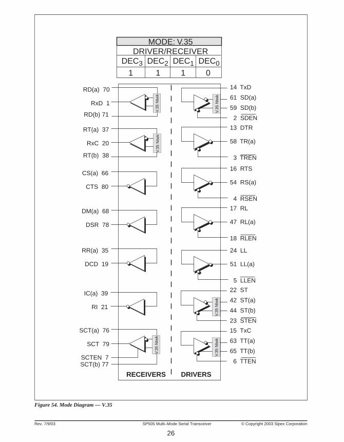
Figure 54. Mode Diagram — V.35
MODE: V.35DRIVER/RECEIVER
DEC3 DEC2 DEC1 DEC0
RD(a) 70
RxD 1
RT(a) 37
RxC 20
IC(a) 39
RI 21
SCT(a) 76
SCT 79
SCTEN 7SCT(b) 77
15 TxC
63 TT(a)
65 TT(b)
6 TTEN
RECEIVERS DRIVERS
22 ST
42 ST(a)
44 ST(b)
23 STEN
RT(b) 38
RD(b) 71
1 1 1 0
24 LL
51 LL(a)
5 LLEN
14 TxD
61 SD(a)
59 SD(b)
2 SDEN
13 DTR
58 TR(a)
3 TREN
DM(a) 68
DSR 78
16 RTS
54 RS(a)
4 RSEN
17 RL
47 RL(a)
18 RLEN
RR(a) 35
DCD 19
CS(a) 66
CTS 80
V.35
Ntw
k
V.35
Ntw
k
V.35
Ntw
k
V.35
Ntw
kV.
35 N
twk
V.35
Ntw
k

27Rev. 7/9/03 SP505 Multi–Mode Serial Transceiver © Copyright 2003 Sipex Corporation
Figure 55. Mode Diagram — RS-422
MODE: RS-422 [w/ termination]
DRIVER/RECEIVERDEC3 DEC2 DEC1 DEC0
RD(a) 70
RxD 1
RT(a) 37
RxC 20
SCT(a) 76
SCT 79
SCTEN 7SCT(b) 77
15 TxC
63 TT(a)
65 TT(b)
6 TTEN
RECEIVERS DRIVERS
22 ST
42 ST(a)
44 ST(b)
23 STEN
CS(a) 66
CTS 80
RR(a) 35
DCD 19
RR(b) 36
CS(b) 67
RT(b) 38
RD(b) 71
0 1 0 0
24 LL
51 LL(a)
49 LL(b)
5 LLEN
14 TxD
61 SD(a)
59 SD(b)
2 SDEN
13 DTR
58 TR(a)
56 TR(b)
3 TREN
16 RTS
54 RS(a)
52 RS(b)
4 RSEN
17 RL
47 RL(a)
45 RL(b)
18 RLEN
IC(a) 39
RI 21
IC(b) 40
DM(a) 68
DSR 78
DM(b) 69
12
0Ω
12
0Ω
12
0Ω

28
Rev. 7/9/03 SP505 Multi–Mode Serial Transceiver © Copyright 2003 Sipex Corporation
Figure 56. Mode Diagram — RS-449
MODE: RS-449DRIVER/RECEIVER
DEC3 DEC2 DEC1 DEC0
RD(a) 70
RxD 1
RT(a) 37
RxC 20
IC(a) 39
RI 21
SCT(a) 76
SCT 79
SCTEN 7SCT(b) 77
15 TxC
63 TT(a)
65 TT(b)
6 TTEN
RECEIVERS DRIVERS
22 ST
42 ST(a)
44 ST(b)
23 STEN
CS(a) 66
CTS 80
RR(a) 35
DCD 19
RR(b) 36
CS(b) 67
RT(b) 38
RD(b) 71
1 1 0 0
24 LL
51 LL(a)
5 LLEN
14 TxD
61 SD(a)
59 SD(b)
2 SDEN
13 DTR
58 TR(a)
56 TR(b)
3 TREN
16 RTS
54 RS(a)
52 RS(b)
4 RSEN
DM(a) 68
DSR 78
DM(b) 69
17 RL
47 RL(a)
18 RLEN
120Ω
120Ω
120Ω

29Rev. 7/9/03 SP505 Multi–Mode Serial Transceiver © Copyright 2003 Sipex Corporation
Figure 57. Mode Diagram — RS-422 w/o termination
MODE: RS-422 [no termination]
DRIVER/RECEIVERDEC3 DEC2 DEC1 DEC0
RD(a) 70
RxD 1
RT(a) 37
RxC 20
SCT(a) 76
SCT 79
SCTEN 7SCT(b) 77
15 TxC
63 TT(a)
65 TT(b)
6 TTEN
RECEIVERS DRIVERS
22 ST
42 ST(a)
44 ST(b)
23 STEN
CS(a) 66
CTS 80
RR(a) 35
DCD 19
RR(b) 36
CS(b) 67
RT(b) 38
RD(b) 71
0 1 0 1
24 LL
51 LL(a)
49 LL(b)
5 LLEN
14 TxD
61 SD(a)
59 SD(b)
2 SDEN
13 DTR
58 TR(a)
56 TR(b)
3 TREN
16 RTS
54 RS(a)
52 RS(b)
4 RSEN
17 RL
47 RL(a)
45 RL(b)
18 RLEN
IC(a) 39
RI 21
IC(b) 40
DM(a) 68
DSR 78
DM(b) 69

30
Rev. 7/9/03 SP505 Multi–Mode Serial Transceiver © Copyright 2003 Sipex Corporation
Figure 58. Mode Diagram — EIA-530
24 LL
51 LL(a)
5 LLEN
120Ω
MODE: EIA-530DRIVER/RECEIVER
DEC3 DEC2 DEC1 DEC0
RD(a) 70
RxD 1
RT(a) 37
RxC 20
IC(a) 39
RI 21
SCT(a) 76
SCT 79
SCTEN 7SCT(b) 77
15 TxC
63 TT(a)
65 TT(b)
6 TTEN
RECEIVERS DRIVERS
22 ST
42 ST(a)
44 ST(b)
23 STEN
CS(a) 66
CTS 80
RR(a) 35
DCD 19
RR(b) 36
CS(b) 67
RT(b) 38
RD(b) 71
1 1 0 1
14 TxD
61 SD(a)
59 SD(b)
2 SDEN
16 RTS
54 RS(a)
52 RS(b)
4 RSEN
17 RL
47 RL(a)
45 RL(b)
18 RLEN
DM(a) 68
DSR 78
DM(b) 69
120Ω
120Ω
13 DTR
58 TR(a)
56 TR(b)
3 TREN

31Rev. 7/9/03 SP505 Multi–Mode Serial Transceiver © Copyright 2003 Sipex Corporation
Figure 59. Mode Diagram — EIA-530A
MODE: EIA-530ADRIVER/RECEIVER
DEC3 DEC2 DEC1 DEC0
RD(a) 70
RxD 1
RT(a) 37
RxC 20
IC(a) 39
RI 21
SCT(a) 76
SCT 79
SCTEN 7SCT(b) 77
15 TxC
63 TT(a)
65 TT(b)
6 TTEN
RECEIVERS DRIVERS
22 ST
42 ST(a)
44 ST(b)
23 STEN
CS(a) 66
CTS 80
RR(a) 35
DCD 19
RR(b) 36
CS(b) 67
RT(b) 38
RD(b) 71
1 1 1 1
24 LL
51 LL(a)
5 LLEN
14 TxD
61 SD(a)
59 SD(b)
2 SDEN
16 RTS
54 RS(a)
52 RS(b)
4 RSEN
17 RL
47 RL(a)
45 RL(b)
18 RLEN
13 DTR
58 TR(a)
3 TREN
DM(a) 68
DSR 78
120Ω
120Ω
120Ω

32
Rev. 7/9/03 SP505 Multi–Mode Serial Transceiver © Copyright 2003 Sipex Corporation
Figure 60. Mode Diagram — V.36
MODE: V.36DRIVER/RECEIVER
DEC3 DEC2 DEC1 DEC0
RD(a) 70
RxD 1
RT(a) 37
RxC 20
IC(a) 39
RI 21
SCT(a) 76
SCT 79
SCTEN 7SCT(b) 77
15 TxC
63 TT(a)
65 TT(b)
6 TTEN
RECEIVERS DRIVERS
22 ST
42 ST(a)
44 ST(b)
23 STEN
RT(b) 38
RD(b) 71
0 1 1 0
24 LL
51 LL(a)
5 LLEN
14 TxD
61 SD(a)
59 SD(b)
2 SDEN
13 DTR
58 TR(a)
3 TREN
DM(a) 68
DSR 78
16 RTS
54 RS(a)
4 RSEN
17 RL
47 RL(a)
18 RLEN
RR(a) 35
DCD 19
CS(a) 66
CTS 80
120Ω
120Ω
120Ω

33Rev. 7/9/03 SP505 Multi–Mode Serial Transceiver © Copyright 2003 Sipex Corporation
LOOPBACK MODE...The SP505 is equipped with two loopbackmodes. Single-ended loopback internallyconnects V.28 driver outputs to V.28 receiverinputs. The signal path is non-inverting and willsupport data rates up to 120kbps. The propaga-tion delay times are as specified in the electricalspecifications. To initiate a single-endedloopback, the code "1010" should be written tothe driver decoder. Differential loopback isimplemented by applying "1011" to the driverdecoder. This internally connects V.11 driver
outputs to V.11 receiver inputs. The signal pathagain is non-inverting; the differential loopbackdata rate can be at least 5Mbps.
Under loopback conditions the receiver decoderis disabled. While the SP505 is in either single-ended or differential loopback mode, the driveroutputs are tri-stated and the receiver inputs aredisabled.
Mode Driver Output Receiver Input Driver Receiver non-inverting inverting non-inverting inverting Input Output
Loopback tri-state tri-state >10KΩ to GND >10KΩ to GND active active
tri-state tri-state >10KΩ to GND >10KΩ to GND active active
Power down clamped tri-state tri-state >10KΩ to GND >10KΩ to GND inactive at ±0.6V
Tri-state tri-state tri-state >10KΩ to GND >10KΩ to GND inactive tri-state
DEC=1010
DEC=1011
VCC=VDD=VSS=0V
DEC=0000
MODE: Differential LoopbackDRIVER/RECEIVER
DEC3 DEC2 DEC1 DEC0
RD(a) 70
RxD 1
RT(a) 37
RxC 20
SCT(a) 76
SCT 79
SCTEN 7SCT(b) 77
15 TxC
63 TT(a)
65 TT(b)
6 TTEN
RECEIVERS DRIVERS
22 ST
42 ST(a)
44 ST(b)
23 STEN
CS(a) 66
CTS 80
RR(a) 35
DCD 19
RR(b) 36
CS(b) 67
RT(b) 38
RD(b) 71
1 0 1 1
24 LL
51 LL(a)
49 LL(b)
5 LLEN
14 TxD
61 SD(a)
59 SD(b)
2 SDEN
13 DTR
58 TR(a)
56 TR(b)
3 TREN
16 RTS
54 RS(a)
52 RS(b)
4 RSEN
17 RL
47 RL(a)
45 RL(b)
18 RLEN
IC(a) 39
RI 21
IC(b) 40
DM(a) 68
DSR 78
DM(b) 69
IC(a) 39
RI 21
SCTEN 7
RECEIVERS DRIVERS
1 0 1 0
24 LL
51 LL(a)
5 LLEN
13 DTR
58 TR(a)
3 TREN
DM(a) 68
DSR 78
16 RTS
54 RS(a)
4 RSEN
17 RL
47 RL(a)
18 RLEN
RR(a) 35
DCD 19
CS(a) 66
CTS 80
RD(a) 70
RxD 1
RT(a) 37
RxC 20
SCT(a) 76
SCT 79
14 TxD
61 SD(a)
2 SDEN
15 TxC
63 TT(a)
6 TTEN
22 ST
42 ST(a)
23 STEN
MODE: Single-Ended Loopback
DRIVER/RECEIVERDEC3 DEC2 DEC1 DEC0

34
Rev. 7/9/03 SP505 Multi–Mode Serial Transceiver © Copyright 2003 Sipex Corporation
80 PIN MQFP (MS-022 BC)
b e
SeatingPlane
A1
AA
L1
5°-16°
0° MIN.
0°–7°
5°-16°
L
A2
0.30" RAD. TYP.
0.20" RAD. TYP.c
PIN 1
E1
D1
D
CLE
CL
D2
E2
DIMENSIONSMinimum/Maximum
(mm)
SYMBOL
A
A1
A2
b
D
D1
D2
E
E1
E2
e
N
80–PIN MQFPJEDEC MS-22
(BEC) Variation
MIN NOM MAX
2.45
0.00 0.25
1.80 2.00 2.20
0.22 0.40
17.20 BSC
14.00 BSC
12.35 REF
17.20 BSC
14.00 BSC
12.35 REF
0.65 BSC
80
COMMON DIMENTIONS
SYMBL MIN NOM MAX
c 0.11 23.00
L 0.73 0.88 1.03
L1 1.60 BASIC
PACKAGE: 80 PIN MQFP

35Rev. 7/9/03 SP505 Multi–Mode Serial Transceiver © Copyright 2003 Sipex Corporation
80 PIN LQFP
CL
b e
L
11° - 13°
0° Min
11° - 13°
0°–7°
0.2 RAD MAX.
0.08 RAD MIN.
DIMENSIONSMinimum/Maximum
(mm)
SYMBOL
A
A1
A2
b
D
D1
e
E
E1
N
80-PIN LQFPJEDEC MS-026(BEC) Variation
MIN NOM MAX
1.60
0.05 0.15
1.35 1.40 1.45
0.22 0.32 0.38
16.00 BSC
14.00 BSC
0.65 BSC
16.00 BSC
14.00 BSC
80
c
L1
A2
COMMON DIMENTIONS
SYMBL MIN NOM MAX
c 0.11 23.00
L 0.45 0.60 0.75
L1 1.00 BASIC
SeatingPlane
A1
AA
PIN 1
E1
D1
D
CLE
PACKAGE: 80 PIN LQFP

36
Rev. 7/9/03 SP505 Multi–Mode Serial Transceiver © Copyright 2003 Sipex Corporation
ORDERING INFORMATIONModel Temperature Range Package TypesSP505ACF ........................................................................ 0°C to +70°C ...................................................... 80–pin JEDEC (BE-2 Outline) MQFPSP505BCF ........................................................................ 0°C to +70°C ...................................................... 80–pin JEDEC (BE-2 Outline) MQFPSP505ACM ....................................................................... 0°C to +70°C ....................................................... 80–pin JEDEC (BE-2 Outline) LQFPSP505BCM ....................................................................... 0°C to +70°C ....................................................... 80–pin JEDEC (BE-2 Outline) LQFP
Sipex Corporation reserves the right to make changes to any products described herein. Sipex does not assume any liability arising out of theapplication or use of any product or circuit described hereing; neither does it convey any license under its patent rights nor the rights of others.
Corporation
ANALOG EXCELLENCESipex Corporation
Headquarters andSales Office233 South Hillview DriveMilpitas, CA 95035TEL: (408) 934-7500FAX: (408) 935-7600
Sales Office22 Linnell CircleBillerica, MA 01821TEL: (978) 667-8700FAX: (978) 670-9001e-mail: [email protected]
Please consult the factory for pricing and availability on a Tape-On-Reel option.


![Yackety yack [serial]](https://static.fdokumen.com/doc/165x107/6328fdedcedd78c2b50e548e/yackety-yack-serial.jpg)