A Novel Wideband 140 GHz Gyrotron Amplifier - DSpace@MIT
156
A Novel Wideband 140 GHz Gyrotron Amplifier by Colin D. Joye M.S. (EECS), Massachusetts Institute of Technology (2004) B.S. (ECE), Villanova University (2002) Submitted to the Department of Electrical Engineering and Computer Science in partial fulfillment of the requirements for the degree of Doctor of Philosophy in Electrical Engineering at the MASSACHUSETTS INSTITUTE OF TECHNOLOGY September 2008 c Massachusetts Institute of Technology 2008. All rights reserved. Author .............................................................. Department of Electrical Engineering and Computer Science August 1, 2008 Certified by .......................................................... Richard J. Temkin Senior Research Scientist, Department of Physics Thesis Supervisor Certified by .......................................................... Jagadishwar R. Sirigiri Research Scientist, Plasma Science and Fusion Center Thesis Supervisor Accepted by ......................................................... Professor Terry P. Orlando Chairman, Committee on Graduate Students Department of Electrical Engineering and Computer Science
-
Upload
khangminh22 -
Category
Documents
-
view
2 -
download
0
Transcript of A Novel Wideband 140 GHz Gyrotron Amplifier - DSpace@MIT
A Novel Wideband 140 GHz Gyrotron Amplifier
by
Colin D. Joye
M.S. (EECS), Massachusetts Institute of Technology (2004)
B.S. (ECE), Villanova University (2002)
Submitted to theDepartment of Electrical Engineering and Computer Science
in partial fulfillment of the requirements for the degree of
Doctor of Philosophy in Electrical Engineering
at the
MASSACHUSETTS INSTITUTE OF TECHNOLOGY
September 2008
c© Massachusetts Institute of Technology 2008. All rights reserved.
Author . . . . . . . . . . . . . . . . . . . . . . . . . . . . . . . . . . . . . . . . . . . . . . . . . . . . . . . . . . . . . .Department of Electrical Engineering and Computer Science
August 1, 2008
Certified by. . . . . . . . . . . . . . . . . . . . . . . . . . . . . . . . . . . . . . . . . . . . . . . . . . . . . . . . . .Richard J. Temkin
Senior Research Scientist, Department of PhysicsThesis Supervisor
Certified by. . . . . . . . . . . . . . . . . . . . . . . . . . . . . . . . . . . . . . . . . . . . . . . . . . . . . . . . . .Jagadishwar R. Sirigiri
Research Scientist, Plasma Science and Fusion CenterThesis Supervisor
Accepted by . . . . . . . . . . . . . . . . . . . . . . . . . . . . . . . . . . . . . . . . . . . . . . . . . . . . . . . . .Professor Terry P. Orlando
Chairman, Committee on Graduate StudentsDepartment of Electrical Engineering and Computer Science

2
A Novel Wideband 140 GHz Gyrotron Amplifier
by
Colin D. Joye
M.S. (EECS), Massachusetts Institute of Technology (2004)
B.S. (ECE), Villanova University (2002)
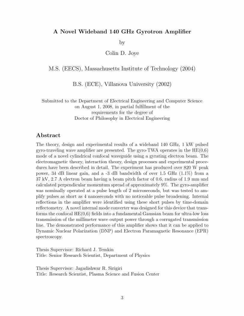
Submitted to the Department of Electrical Engineering and Computer Scienceon August 1, 2008, in partial fulfillment of the
requirements for the degree ofDoctor of Philosophy in Electrical Engineering
Abstract
The theory, design and experimental results of a wideband 140 GHz, 1 kW pulsedgyro-traveling wave amplifier are presented. The gyro-TWA operates in the HE(0,6)mode of a novel cylindrical confocal waveguide using a gyrating electron beam. Theelectromagnetic theory, interaction theory, design processes and experimental proce-dures have been described in detail. The experiment has produced over 820 W peakpower, 34 dB linear gain, and a -3 dB bandwidth of over 1.5 GHz (1.1%) from a37 kV, 2.7 A electron beam having a beam pitch factor of 0.6, radius of 1.9 mm andcalculated perpendicular momentum spread of approximately 9%. The gyro-amplifierwas nominally operated at a pulse length of 2 microseconds, but was tested to am-plify pulses as short as 4 nanoseconds with no noticeable pulse broadening. Internalreflections in the amplifier were identified using these short pulses by time-domainreflectometry. A novel internal mode converter was designed for this device that trans-forms the confocal HE(0,6) fields into a fundamental Gaussian beam for ultra-low losstransmission of the millimeter wave output power through a corrugated transmissionline. The demonstrated performance of this amplifier shows that it can be applied toDynamic Nuclear Polarization (DNP) and Electron Paramagnetic Resonance (EPR)spectroscopy.
Thesis Supervisor: Richard J. TemkinTitle: Senior Research Scientist, Department of Physics
Thesis Supervisor: Jagadishwar R. SirigiriTitle: Research Scientist, Plasma Science and Fusion Center
3

4

Acknowledgments
A great deal of my academic, personal and spiritual development I attribute to my
time at MIT. While in Cambridge, I took up interest in musical instruments from
around the world, even taking lessons on drums from India and Nigeria. I learned
Korean and married my wonderful wife, Hyun Young (”Heidi”), from Busan, South
Korea. Together, we traveled to Korea, Japan, Slovakia, Austria, Czech-Republic,
Mexico, and the Philippines. I led and co-led a few Bible studies on campus. I
maintained the historic pipe organ at the First Korean Church of Cambridge where
we both taught Sunday school, tuned its over 1,300 pipes, and held a concert and
seminar. I developed my abilities to improvise in the jazz style on the piano. I took up
an interest in photography. But most importantly, I committed myself to a body of
work worthy of the title Doctor of Philosophy that has taught me skills that transfer
to many aspects of life, in addition to giving me a career direction.
I am most grateful to my Lord and Savior, Jesus Christ, without whom all of
my labor is without meaning. Throughout all of my difficult days at MIT, many of
which started before 5:00 AM with prayer, God was the only one I could turn to for
my daily strength. My whole existence belongs to God and for His grace and mercy,
I am eternally thankful. I pray that the MIT Graduate Christian Fellowship might
continue to enrich the lives of grad students for decades to come.
Secondly, I’d like to thank my parents, Dr. Donald and Claudia Joye, who edu-
cated my brothers (Gavin and Chris) and I for twelve years each at home so we could
learn the values and virtues not taught in the schools. They sacrificed much of their
time and comfort to help us and several hundred other homeschooling families bring
their children up in the way they thought was best. I’d also like to thank Heidi’s
parents, Yong Won and Eun Sook Kang for their unceasing prayers during this time.
From my lab, I’m deeply grateful to my advisor, Dr. Rick Temkin, for walking
with me through thick and thin, as well as Dr. Jagadishwar Sirigiri who provided
much help on this project and is gifted with the ability to make things work and Dr.
Michael Shapiro for his skills and insights in electromagnetics and mode conversion.
5

6

Contents
1 Introduction 21
1.1 Millimeter Wave Applications . . . . . . . . . . . . . . . . . . . . . . 21
1.1.1 Available MMW Sources . . . . . . . . . . . . . . . . . . . . . 24
1.2 Spectroscopy at MIT . . . . . . . . . . . . . . . . . . . . . . . . . . . 24
1.2.1 Gyrotron-based DNP Experiments . . . . . . . . . . . . . . . 25
1.2.2 Short-pulse DNP/NMR Spectroscopy . . . . . . . . . . . . . . 26
1.3 Overview of Gyro-Devices . . . . . . . . . . . . . . . . . . . . . . . . 27
1.3.1 Gyrotron Oscillator . . . . . . . . . . . . . . . . . . . . . . . . 29
1.3.2 Gyro-TWA . . . . . . . . . . . . . . . . . . . . . . . . . . . . 30
1.3.3 Gyroklystron . . . . . . . . . . . . . . . . . . . . . . . . . . . 33
1.3.4 Gyrotwystron . . . . . . . . . . . . . . . . . . . . . . . . . . . 34
1.3.5 Gyro-BWO . . . . . . . . . . . . . . . . . . . . . . . . . . . . 34
1.4 Motivations for the Gyro-TWA . . . . . . . . . . . . . . . . . . . . . 35
1.4.1 Novel Features of this Design . . . . . . . . . . . . . . . . . . 36
1.4.2 Fundamentals of the Gyro-TWA Operation . . . . . . . . . . . 36
1.5 Thesis Outline . . . . . . . . . . . . . . . . . . . . . . . . . . . . . . . 39
2 Confocal Waveguide 41
2.1 Electromagnetic Methods . . . . . . . . . . . . . . . . . . . . . . . . 42
2.2 Theory of Confocal Waveguide . . . . . . . . . . . . . . . . . . . . . . 43
2.2.1 Gaussian Beams in a Spherical Resonator . . . . . . . . . . . 47
2.2.2 Gaussian Beams in a Cylindrical Confocal Resonator . . . . . 47
2.2.3 Loss Rate Estimation in Confocal Waveguides . . . . . . . . . 53
7

2.2.4 General Curved Mirror Resonator Stability . . . . . . . . . . . 54
2.3 Discussion . . . . . . . . . . . . . . . . . . . . . . . . . . . . . . . . . 56
3 Theory of Gyro-devices 57
3.1 Linear Dispersion Relation . . . . . . . . . . . . . . . . . . . . . . . . 59
3.2 Linear Theory . . . . . . . . . . . . . . . . . . . . . . . . . . . . . . . 61
3.3 Kinetic Theory . . . . . . . . . . . . . . . . . . . . . . . . . . . . . . 64
3.4 Instabilities . . . . . . . . . . . . . . . . . . . . . . . . . . . . . . . . 66
3.4.1 BWO Instability . . . . . . . . . . . . . . . . . . . . . . . . . 67
3.4.2 Absolute Instability . . . . . . . . . . . . . . . . . . . . . . . . 68
3.4.3 Feedback Instabilities . . . . . . . . . . . . . . . . . . . . . . . 71
3.5 Discussion . . . . . . . . . . . . . . . . . . . . . . . . . . . . . . . . . 72
4 Gyro-Amplifier Experiment 73
4.1 Scope of Experiment . . . . . . . . . . . . . . . . . . . . . . . . . . . 73
4.2 System Components . . . . . . . . . . . . . . . . . . . . . . . . . . . 74
4.2.1 The Superconducting Magnet . . . . . . . . . . . . . . . . . . 75
4.2.2 Electron Gun . . . . . . . . . . . . . . . . . . . . . . . . . . . 75
4.2.3 Sources of Velocity Spread . . . . . . . . . . . . . . . . . . . . 78
4.2.4 Power Supply . . . . . . . . . . . . . . . . . . . . . . . . . . . 79
4.2.5 Tube Assembly . . . . . . . . . . . . . . . . . . . . . . . . . . 80
4.2.6 Interaction Circuit . . . . . . . . . . . . . . . . . . . . . . . . 84
4.3 Measurement Tools . . . . . . . . . . . . . . . . . . . . . . . . . . . . 86
4.4 Experimental Results . . . . . . . . . . . . . . . . . . . . . . . . . . . 88
4.4.1 Saturated Characteristics . . . . . . . . . . . . . . . . . . . . . 88
4.4.2 Linear Gain . . . . . . . . . . . . . . . . . . . . . . . . . . . . 91
4.4.3 Short Pulses . . . . . . . . . . . . . . . . . . . . . . . . . . . . 92
4.4.4 Backward Wave Oscillations . . . . . . . . . . . . . . . . . . . 94
4.5 Analysis of Data . . . . . . . . . . . . . . . . . . . . . . . . . . . . . 95
4.6 The Spectrometer System . . . . . . . . . . . . . . . . . . . . . . . . 96
4.6.1 The RF Source . . . . . . . . . . . . . . . . . . . . . . . . . . 96
8

4.6.2 New Power Supply . . . . . . . . . . . . . . . . . . . . . . . . 98
4.7 Conclusions . . . . . . . . . . . . . . . . . . . . . . . . . . . . . . . . 99
5 Mode Convertor Design 101
5.1 Mode convertor structure . . . . . . . . . . . . . . . . . . . . . . . . . 101
5.2 Gaussian Optics . . . . . . . . . . . . . . . . . . . . . . . . . . . . . . 102
5.2.1 Propagation Matrices . . . . . . . . . . . . . . . . . . . . . . . 103
5.3 The Perpendicular Plane . . . . . . . . . . . . . . . . . . . . . . . . . 105
5.4 The Parallel Plane . . . . . . . . . . . . . . . . . . . . . . . . . . . . 108
5.4.1 Dimpled Launcher Design . . . . . . . . . . . . . . . . . . . . 110
5.5 Results of Simulation . . . . . . . . . . . . . . . . . . . . . . . . . . . 112
5.6 Discussion . . . . . . . . . . . . . . . . . . . . . . . . . . . . . . . . . 113
6 Conclusions 115
6.1 Recommendations . . . . . . . . . . . . . . . . . . . . . . . . . . . . . 116
6.1.1 Internal Mode Converter . . . . . . . . . . . . . . . . . . . . . 116
6.1.2 New MIG design . . . . . . . . . . . . . . . . . . . . . . . . . 116
6.1.3 Improved Input Coupler . . . . . . . . . . . . . . . . . . . . . 116
6.1.4 Power Supply . . . . . . . . . . . . . . . . . . . . . . . . . . . 118
A Gaussian Beams in a Spherical Resonator 119
B Derivation of bunching mechanism 123
B.1 Azimuthal vs. Axial Bunching . . . . . . . . . . . . . . . . . . . . . . 123
B.1.1 Bunching Summary . . . . . . . . . . . . . . . . . . . . . . . . 127
B.2 Energy Extraction Examples . . . . . . . . . . . . . . . . . . . . . . . 127
B.3 Picture of Energy Transfer . . . . . . . . . . . . . . . . . . . . . . . . 130
B.4 Conclusions . . . . . . . . . . . . . . . . . . . . . . . . . . . . . . . . 133
C Electron Gun Performance Maps 135
9

10

List of Figures
1-1 Recent advances in vacuum electron device technology showing gyro-
devices pushing the frontier to higher power and higher frequency.
(Courtesy of Bruce Danly, NRL) . . . . . . . . . . . . . . . . . . . . 23
1-2 Common gyro-device cavity profiles with an electron beam: (a) gy-
rotron oscillator; (b) gyro-TWT; (c) gyroklystron. . . . . . . . . . . . 30
1-3 (left) Geometry of the electron beam showing guiding center beam
radius rg and Larmor radii rL. (right) Confocal interaction geometry
showing mirror aperture half-width a, radii of curvature Rc and mirror
separation L⊥ with power contours for the HE06 mode superimposed.
Transverse electric field vectors are also shown. The electron beam
interacts primarily with the second and fourth maxima. . . . . . . . . 32
1-4 A sketch of the gyro-amplifier showing the locations of (a) the cath-
ode of the MIG-type electron gun, (b) external copper gun coil, (c)
superconducting magnets, (d) cavity circuit, (e) collector and output
waveguide, (f) input waveguide, (g) output window, and (h) vacuum
ion pump. . . . . . . . . . . . . . . . . . . . . . . . . . . . . . . . . . 38
2-1 (a) Cylindrical geometry, (b) curved cylindrical mirror geometry, where
two mirrors with radius of curvature Rc and aperture size a are sep-
arated by L⊥. (c) Spherical mirror geometry. Rb is the radius of the
electron beam. Note the coordinate systems. . . . . . . . . . . . . . 43
11

2-2 The dispersion relation for (a) cylindrical geometry showing many
of the lowest order modes, with the TE03 mode operating around
140 GHz, and (b) the corresponding confocal modes with HE06 around
140 GHz (degenerate modes not shown). The doppler-shifted beam
resonance lines are shown for the fundamental harmonic s=1. . . . . . 44
2-3 Theoretical power contours in dB of the membrane function for (a) the
HE06 mode and (b) the HE02 mode in the same waveguide overlaid
with electric field vectors. The HE02 mode leaks out much more due
to its much larger footprint on the mirrors. . . . . . . . . . . . . . . . 52
2-4 Comparison of loss rate at 140 GHz for Rc = L⊥ = 6.9 mm between
theory (solid) and HFSS simulation (dash). . . . . . . . . . . . . . . . 55
2-5 Stable and unstable regions of a resonator of curved mirrors in the
optical regime. . . . . . . . . . . . . . . . . . . . . . . . . . . . . . . . 55
3-1 (left) Geometry of the electron beam showing guiding center beam
radius rg and Larmor radii rL. (right) Confocal interaction geometry
showing mirror aperture half-width a, radii of curvature Rc and mirror
separation L⊥ with power contours for the HE06 mode superimposed.
Transverse electric field vectors are also shown. The electron beam
interacts primarily with the second and fourth maxima. . . . . . . . . 58
3-2 Linear growth rate calculation based on the linear dispersion relation
for the parameters shown. Velocity spreads were not included. A
growth rate of at least 2.5 dB/cm is needed for the amplifier. . . . . 63
3-3 A nonlinear confocal simulation at 30 kV predicting a gain of over
50 dB and a bandwidth of around 4 GHz for various velocity spread
conditions. . . . . . . . . . . . . . . . . . . . . . . . . . . . . . . . . . 65
3-4 A nonlinear confocal simulation at 40 kV predicting a gain of over
50 dB and a bandwidth of around 6 to 7 GHz for various velocity
spread and α conditions. . . . . . . . . . . . . . . . . . . . . . . . . . 66
12

3-5 Calculated BWO oscillation start current thresholds versus circuit length
under the conditions shown for various mirror apertures a. The dot
indicates that a 2 A beam current limits the circuit length to about
7.5 cm or less at 30 kV. . . . . . . . . . . . . . . . . . . . . . . . . . 69
3-6 Plots of the roots of D(w, kz) = 0 for a lossy circuit with rcav = 3.62mm
for the TE03 mode with 30 kV, α = 0.75 and B0/Bg = 0.997. For
I0 = 25 A: (a) Real part of kz, (b) Imaginary part of kz, (c) estimated
growth rate. (d-f) for 30 A. The circles indicate where the key roots
split and merge. . . . . . . . . . . . . . . . . . . . . . . . . . . . . . . 70
4-1 Front end system components: (a) Tunable EIK source, (b) Circulator,
(c) Attenuator #1, (d) -20 dB coupler, (e) Attenuator #3, (f) Forward
diode, (g) Attenuator #2, (h) Reflected diode, (i) Circular uptaper. . 74
4-2 Block diagram of the front end of the gyro-amplifier experiment. . . . 75
4-3 The predicted magnetic field profile shown at the rated maximum field
strength of 6.2 T. The ±0.5% uniform field length is 28 cm and the
field falls off as roughly Bz ∼ 1/z4 in the vicinity of the cathode, which
is located at z = −55 cm. . . . . . . . . . . . . . . . . . . . . . . . . 76
4-4 (top) Comparison of Bz cathode magnetic field and magnetic com-
pression (magnified by 100x) vs. current Igun in the external gun coil.
(bottom) Axial magnetic field profile used by EGUN for several values
of Igun, including a data curve from Magnex showing perfect agreement
with Igun = 0A. In this plot, z = 1.61 cm is the cathode position. . . 77
4-5 The theoretical electron guiding center trajectories assuming adiabatic
compression following the magnetic field profile. The beam radius in
the circuit is rb = 1.9mm. In this plot, z = 0 cm refers to the center
of the magnetic flat field. . . . . . . . . . . . . . . . . . . . . . . . . . 78
4-6 Typical oscilloscope traces of the cathode voltage and total beam cur-
rent at the full voltage of 37 kV. The voltage pulse is flat to within 1%
for a 4 µs pulse. . . . . . . . . . . . . . . . . . . . . . . . . . . . . . . 80
13

4-7 A schematic of the power supply transformer tank, including the resis-
tive tap divider that supplies the mod-anode voltage. . . . . . . . . . 81
4-8 A cutaway view of the tube showing (a) Input overmoded TE11 wave-
guide, (b) miter bend, (c) downtaper, (d) amplifier circuit, (e) electron
beam, (f) beam tunnel and alpha-probe location, (g) nonlinear upta-
per, (h) collector/output waveguide, (i) output window. . . . . . . . . 82
4-9 F-band VNA measurement of the window transmission. The window
was placed between two horns for normal incidence. . . . . . . . . . . 82
4-10 Calculation of window reflection versus frequency in the TE03 mode
for the case of a single 0.1290” thick window, and for two windows
separated by distance d. The double window can be used to widen
bandwidth at 140 GHz, or can be made transparent at arbitrary fre-
quencies around 125-130 GHz. . . . . . . . . . . . . . . . . . . . . . . 83
4-11 A photo of the amplifier circuit prior to installation. The amplifier
consists of three 7 cm amplifier sections separated by two 2 cm severs. 84
4-12 MMW field pattern at the end of the 1.85 m long, 0.5” I.D. copper
waveguide showing a clean TE11 mode at the input to the tube. The
pyroelectric camera sensor is 0.5” x 0.5”. . . . . . . . . . . . . . . . . 85
4-13 Output diagnostics: (a) Tunable double disc window fixture, (b) Down-
taper, (c) Calorimeter, (d) Horn, polarization twist and attenuator, (e)
Output diode. Not shown: Frequency system picks up stray radiation
2 m away. . . . . . . . . . . . . . . . . . . . . . . . . . . . . . . . . . 86
4-14 Measured peak output power (markers) and simulations (curves) at
38.5 kV, 2.5 A. The simulation fit is best for α = 0.54, δvz/vz = 3.55%.
The experimental bandwidth has been measured at over 1.5 GHz. . . 89
4-15 Measured peak output power (markers) and simulations (curves) at
37.7 kV, 2.7 A. The simulation fit is best for α = 0.57, δvz/vz = 4.0%.
The experimental power has been measured at over 820 W. . . . . . . 90
14

4-16 Saturation characteristics. (top) Flattening of output power. (bottom)
Gain saturation. The -3 dB point occurs for about 0.1 W of power
coupled into the circuit. . . . . . . . . . . . . . . . . . . . . . . . . . 91
4-17 Linear Gain of the gyro-amplifier compared to simulation at 34.7 kV . 92
4-18 Diagram of estimated system group delays as an aid in mapping TDR
measurements. Uncertainty is generally about 1 ns. The waveforms
are measured by three video diodes: Forward, Reflected and Output. 93
4-19 Measured TDR traces at 139.63 GHz. The input power is detected by
the forward diode at (a). The first reflected signal (b) is from the input
window, and a second reflection (d) is due to the internal downtaper.
The output diode measures the main pulse (c) followed by two echoes
(e) and (f) that are due to trapped power in the input transmission line. 94
4-20 Start current threshold for the HE05 backward wave oscillations as a
function of magnetic field. . . . . . . . . . . . . . . . . . . . . . . . . 95
4-21 Phase stable, frequency multiplying diode transceiver system employ-
ing a 4-phase pulse-forming network. (Courtesy of T. Maly, MIT Fran-
cis Bitter Magnet Laboratory.) . . . . . . . . . . . . . . . . . . . . . . 97
4-22 A proposed timing diagram for the transceiver system. (Courtesy of
T. Maly, MIT Francis Bitter Magnet Laboratory.) . . . . . . . . . . . 98
5-1 Dimensions and features in the parallel plane of a flat 2-D version of
the mode convertor, shown with a logarithmic scale of the electric field. 102
5-2 Incidence angle planes on a curved mirror: (a) The k-vector is in the
same plane as the radius of curvature, (b) k is perpendicular to the Rc
plane. . . . . . . . . . . . . . . . . . . . . . . . . . . . . . . . . . . . 103
5-3 Gaussian beam propagation with finite kz: (a) Gaussian beam waist
w0, (b) propagates in z-direction. (c) Equivalent lens system from the
midplane to one bounce and back to the midplane. . . . . . . . . . . 105
15

5-4 Equivalent mirror system of the perpendicular plane with focal lengths
fm, confocal parameters bm, and lengths Lm. The coordinate along the
path of the beam is ζ. The vertical dotted line indicates the location
of the beam waist. . . . . . . . . . . . . . . . . . . . . . . . . . . . . 106
5-5 Traces of R(ζ) and w(ζ) along the beam trajectory for the perpendicu-
lar plane (above) and parallel plane (below). The vertical dash-dotted
lines indicate the location of the dimples or mirrors along with their
radii of curvature in each plane. For the parallel plane, a Gaussian fit
to a rectangle of the launcher length was used. Labels starting with D
refer to dimples, and M to mirrors. . . . . . . . . . . . . . . . . . . . 109
5-6 The matching efficiency between a free-space Gaussian beam and a
fundamental HE11 hybrid mode in a corrugated waveguide is plotted
against the ratio of the beam waist w and the waveguide radius a. The
optimal efficiency is 98.1% for w = 0.645a. . . . . . . . . . . . . . . . 111
5-7 HFSS 3-D simulation of the final mode converter design with two dim-
ples and two mirrors. The complex magnitude of the electric field
pattern is shown to eliminate time dependence. This design achieved
a simulated insertion loss of under 2 dB. . . . . . . . . . . . . . . . . 112
5-8 HFSS simulation of (a) the output electric field beam shape, and (b)
corresponding phase. The black circle represents the best location for
the 12.7 mm diameter corrugated waveguide. The beam waist is about
4.2 mm in both planes. The phase variation is about ±15o over the
central region of the beam. . . . . . . . . . . . . . . . . . . . . . . . . 113
6-1 An HFSS simulation of a three-mirror quasi-optical input coupler to
convert the HE11 mode to the confocal HE06 mode. Simulated inser-
tion loss is under 2 dB. . . . . . . . . . . . . . . . . . . . . . . . . . . 117
B-1 Results of the electron motion code showing that gain (positive effi-
ciency) is possible with relativistic effects included. (a) Showing loss
after about 12 cyclotron orbits; (b) Showing gain after 25 orbits. . . . 128
16

B-2 (a) Initial electron phases. (b) Evolution after 13 cycles. Electron
trajectories shown as continuous lines. . . . . . . . . . . . . . . . . . 129
B-3 (c) After 17 cycles, the electrons are in phase with each other and in
the correct phase with the E-field to transfer their energy to the E-
field. (d) After 27 cycles, 50% of the beam energy is transferred to the
E-field. . . . . . . . . . . . . . . . . . . . . . . . . . . . . . . . . . . . 131
B-4 (a) The average electron phase (θe1+θe2)/2 and E-field phase evolution,
(b) the efficiency and Phase Convolution,Υ(t). . . . . . . . . . . . . . 132
C-1 The axial position of the tube is defined by the variable ZGUN , con-
veniently measured from the inner surfaces of the oil tank to the 2-D
translation stage. Dimensions are in inches. . . . . . . . . . . . . . . 136
C-2 Gun coil current = -20 A. Contour plots of (a) optimal perpendicular
velocity spread, and (b) corresponding parallel velocity spread, (c) al-
pha value, (d) alpha spread (in percent), (e) guiding center radius, (f)
average Larmor radius, (g) Mod-anode voltage Tap number, and (h)
corresponding Mod-anode voltage. . . . . . . . . . . . . . . . . . . . . 138
C-3 Gun coil current = 0 A. Contour plots of (a) optimal perpendicular
velocity spread, and (b) corresponding parallel velocity spread, (c) al-
pha value, (d) alpha spread (in percent), (e) guiding center radius, (f)
average Larmor radius, (g) Mod-anode voltage Tap number, and (h)
corresponding Mod-anode voltage. . . . . . . . . . . . . . . . . . . . . 139
C-4 Gun coil current = +20 A. Contour plots of (a) optimal perpendicular
velocity spread, and (b) corresponding parallel velocity spread, (c) al-
pha value, (d) alpha spread (in percent), (e) guiding center radius, (f)
average Larmor radius, (g) Mod-anode voltage Tap number, and (h)
corresponding Mod-anode voltage. . . . . . . . . . . . . . . . . . . . . 140
17

C-5 Gun coil current = +40 A. Contour plots of (a) optimal perpendicular
velocity spread, and (b) corresponding parallel velocity spread, (c) al-
pha value, (d) alpha spread (in percent), (e) guiding center radius, (f)
average Larmor radius, (g) Mod-anode voltage Tap number, and (h)
corresponding Mod-anode voltage. . . . . . . . . . . . . . . . . . . . . 141
C-6 Gun coil current = +60 A. Contour plots of (a) optimal perpendicular
velocity spread, and (b) corresponding parallel velocity spread, (c) al-
pha value, (d) alpha spread (in percent), (e) guiding center radius, (f)
average Larmor radius, (g) Mod-anode voltage Tap number, and (h)
corresponding Mod-anode voltage. . . . . . . . . . . . . . . . . . . . . 142
18

List of Tables
1.1 MIT Gyrotrons for DNP . . . . . . . . . . . . . . . . . . . . . . . . . 25
1.2 Gyro-TWT Achievements . . . . . . . . . . . . . . . . . . . . . . . . 33
1.3 Gyro-TWT Specifications . . . . . . . . . . . . . . . . . . . . . . . . 36
2.1 Loss rate example, Rc = 6.9 mm, a = 2.5 mm . . . . . . . . . . . . . 54
4.1 System Components . . . . . . . . . . . . . . . . . . . . . . . . . . . 74
4.2 Specifications and Achievements . . . . . . . . . . . . . . . . . . . . . 100
5.1 Design Parameters. . . . . . . . . . . . . . . . . . . . . . . . . . . . . 109
B.1 ODE solution values . . . . . . . . . . . . . . . . . . . . . . . . . . . 128
19

20

Chapter 1
Introduction
1.1 Millimeter Wave Applications
The entire electromagnetic spectrum encompasses an astounding amount of modern-
day technologies. From the inception of AM radio (around 1 MHz) and television
receivers (100s MHz) in the early twentieth century to the rise of the cellular phone
in the 1990s (900 MHz to 2.4 GHz), and more recently to wireless personal networks
(60 GHz), the generation, transmission and detection of electromagnetic waves has
grown to lead a ubiquitous role in our daily lives. We use infrared lasers to transmit
information over vast distances via fiber-optic cable at extremely high data rates, and
X-ray security scanners are mandatory at virtually every airport in the world.
Until recently, there has been a paucity of sources capable of generating electro-
magnetic power from about 100 GHz to 100 THz. This phenomenon has been known
as the terahertz (THz) gap. Across the electromagnetic spectrum there has been
virtually no deficiency of sources except in this range. Recently, as sources and tech-
niques became available, it became clear that a large number of potential applications
were hidden exactly in those missing bands. The band from approximately 30 GHz
to 300 GHz is known as the millimeter wave (MMW) band because the wavelength
of the electromagnetic wave is on the order of a millimeter. Likewise, sub-millimeter
waves occupy the band from 300 GHz to perhaps a few THz.
One can now imagine a dental imaging device that could provide a harmless
21

alternative to X-rays using THz radiation, or “T-rays” [1, 2]. Such an imaging method
would break through the traditional practice of taking an X-ray photo and later
following it by a procedure; instead, a procedure could be performed while THz
imaging simultaneously reveals the actual progress on a monitor. THz technology is
now being used to inspect critical components for defects in NASA systems [3]. It
has also been done with MMW [4].
An order of magnitude improvement in resolution was reported for the MIT
Lincoln Labs Haystack ultra-wideband satellite imaging radar after the addition of
94 GHz gyro-amplifier tubes [5], clearly illustrating the potential for high power MMW
devices in long range imaging applications.
Airport security systems utilizing everything from MMW to infrared are becom-
ing more popular alternatives to pat-searching and give much more information than
the metal detector. L-3 Communications released a MMW scanner capable of re-
vealing hidden weapons in under 2.5 seconds [6]. Many other MMW-based security
systems have been developed for stand-off weapons detection [7], and for biological
and chemical agent detection [8].
Wide bandwidth satellite communications are dominated by high-efficiency Trav-
eling Wave Tube (TWT) vacuum electron devices [9, 10]. At higher frequencies, not
only is more bandwidth available, but the dimensions of the antenna required decrease
in proportion to the wavelength, leading to smaller, more efficient satellites. In the
MMW range, there is moderate atmospheric absorption in general above 35 GHz [11],
with transparent windows at 94 GHz and 220 GHz [12]. Higher frequencies in the
THz suffer from strong absorption due to water, so the MMW frequency range may
well be the final frontier as far as satellite communications are concerned.
Research has exploded into fields such as radar [13], target tracking, imaging [14],
cloud physics [15, 16], spectroscopy experiments utilizing Dynamic Nuclear Polariza-
tion (DNP) [17, 18, 19], ceramics sintering [20], biomedical applications [21], and the
military Active Denial System [22]. A gyrotron operating with a pulsed 21 T magnet
has recently broken the 1 THz frequency barrier using the second harmonic of the
cyclotron frequency [23].
22

Ave
rage
Pow
er (
W)
107
106
105
104
103
102
10
1
10-1
10-2101.1 100 1,000 10,000 100,000
Frequency (GHz)
SIT
BJT
FET
IMPATT
FocusedCC - TWT
Gridded TubeKlystron
CFA Gyrotron
PPM FocusedHelix TWT
FEL
BWOFEL
VacuumDevices
Solid StateDevices
10 cm0.1 m 1.0 cm 1.0 mm 0.1 mm 10.0 µ
FET
BJT
(Single Devices )
2
4
1 3
5
1. Fujitsu - GaAs MESFET
2. Cree - SiC MESFET
3. Toshiba - GaAs MESFET
4. Raytheon - GaAs PHEMT
5. TRW - GaAs PHEMT
Figure 1-1: Recent advances in vacuum electron device technology showing gyro-devices pushing the frontier to higher power and higher frequency. (Courtesy ofBruce Danly, NRL)
23

1.1.1 Available MMW Sources
Fig. 1-1 is a graph showing the frontiers of available source technologies in terms of the
average output power and frequency [24]. Among the competitors for the microwave
band are conventional microwave tubes such as klystrons, magnetrons, traveling wave
tubes (TWTs), backward-wave oscillators (BWOs) and other linear beam slow-wave
devices. In the millimeter band, the competition thins out, leaving only gyro-devices
to push the frontier curve into the THz gap at higher average power. BWO’s have
successfully demonstrated 10’s of milliwatts of peak output power in the 600-650 GHz
range recently [25], which is a very promising advance, but still orders of magnitude
below what a gyro-device could be capable of producing. Non-relativistic orotrons [26]
and even some solid state devices [27] are capable of producing small amounts of
power at the millimeter wavelengths, but currently produce only very small amounts
of radiation at the sub-millimeter wavelengths. Accelerator-based relativistic sources,
such as relativistic orotrons, have also been used to produce very high peak power
millimeter-wave and THz radiation for ultra-short pulse applications [28], but are
limited to low average powers. The large size and high complexity of these kinds of
sources are likely to limit them to specialized facilities.
1.2 Spectroscopy at MIT
The MIT Francis Bitter Magnet Laboratory (FBML) has been a world leader in
Dynamic Nuclear Polarization enhanced Nuclear Magnetic Resonance (DNP/NMR),
Electron Paramagnetic Resonance (EPR) and other spectroscopy techniques [29].
Moderate power continuous-wave (CW) gyrotron oscillators have been used to polar-
ize the electrons in a solution containing free radicals [30]. The electron polarization
is transferred to the nucleus and results in signal-to-noise enhancement factors of
50-400 [31, 32].
24

Table 1.1: MIT Gyrotrons for DNP
Source 140 GHz [33, 34] 250 GHz [19] 460 GHz [36]
CW Power 14 W 8 W 16 WOperating mode TE0,3,1 TE0,3,2 TE11,2,1
Beam voltage 12.2 kV 12.2 kV 13.0 kVBeam Current 32 mA 25 mA 100 mAMagnetic Field 5.12 T 9.16 T 8.42 T
1.2.1 Gyrotron-based DNP Experiments
The current DNP/NMR 140 GHz test bed at the FBML consists of a 140 GHz fixed-
frequency gyrotron oscillator, waveguides, a DNP probe and another superconducting
magnet. The gyrotron delivers up to approximately 14 W in the TE01 mode at the
gyrotron output. This power is transformed to the TE11 mode by a snake mode
converter before it propagates down straight copper pipes [33, 34]. Two 90o miter
bends exist before the oversized waveguide is tapered down to fundamental waveguide.
The total losses were measured previously to be approximately 6.4 dB with theoretical
losses totaling 3.7 dB [35]. At the probe, approximately 1 to 2 watts of power is
delivered into the sample.
In addition to this 140 GHz gyrotron oscillator, a second gyrotron oscillator oper-
ating at 250 GHz (380 MHz nuclear frequency) has been in operation since 1998 [37],
with hundreds of hours of non-stop CW operation time to date. This gyrotron is
also used to run NMR spectroscopy experiments. The 250 GHz gyrotron oscillator
operates in the fundamental TE03 mode at 9.2 T from a 12 to 16 kV electron beam,
and is capable of generating up to 25 W CW at 250 GHz at an efficiency of 4% [19].
A 460 GHz, second harmonic gyrotron oscillator [36, 38, 39] has been rebuilt for
better performance and preliminary measurements indicate that it is now capable of
over 16 W CW power from a 13 kV, 100 mA beam with very stable operation in the
TE11,2 mode. It uses an 8.4 T magnetic field at the second cyclotron harmonic to save
construction costs on the superconducting magnet. It will be used for sub-millimeter
wavelength spectroscopy experiments with a 700 MHz nuclear frequency. A table of
the operating parameters of these three gyrotrons is given in Table 1.1.
25

1.2.2 Short-pulse DNP/NMR Spectroscopy
Modeled after these DNP/NMR experiments that use a gyrotron oscillator, a new
short-pulse EPR experiment will be installed utilizing the 140 GHz gyro-TWT am-
plifier described in this thesis. A series of amplifiers is envisioned at 250 GHz and
460 GHz following the success of the 140 GHz EPR system, thus scalability is a de-
sirable feature of this work. This amplifier should deliver 100 W in the form of a
fundamental HE11 mode into a low-loss corrugated waveguide line. The amplifier
features ease of frequency tunability, where previously only a single frequency was
possible, and it also allows for wide-band, nanosecond-scale short pulses to be sent
to the samples for short pulse EPR measurements.
High magnetic fields are needed in spectroscopy to efficiently separate chemical
shifts, but this means the spectra of the radical solutions can easily be several hundred
MHz wide. A short pulse of 1 ns allows the entire enhanced radical spectrum to be
measured at once. Additionally, it is estimated that such a 1 ns pulse will achieve
polarization an order of magnitude faster than CW radiation techniques, thus 2-D
chemical shift maps become rather easy to generate. A pulsed experiment using a
MMW amplifier permits phase, frequency, pulse duration and amplitude modulations,
giving new dimensions of control to the spectroscopy.
Current pulsed EPR is performed at the FBML using a 30 mW IMPATT diode,
but to achieve enhancement, the pulse length is 50 ns, too broad to capture the
entire radical spectrum by itself. By decreasing the pulse length and lowering the
spectrometer cavity Q, wider bandwidth pulses are generated, but this requires an
increase in pulse power. It is estimated that approximately 100 W at 1 ns will achieve
the desired effects at 140 GHz. So far, only a gyro-amplifier is capable of meeting
these goals. No amplifier is presently available commercially or otherwise to fulfill
these needs, therefore it is the aim of this thesis to provide such a device.
There is another device called the Extended Interaction Klystron (EIK) that is
capable of generating peak powers of up to 50 W at even 220 GHz, but these devices
generally suffer from limited average power and lifetimes estimated at only 1,000
26

hours, whereas the gyrotron lifetime is expected to exceed 100,000 hours. The EIK is
also not scalable to the higher frequencies of 250 GHz and 460 GHz and is therefore
not an attractive solution compared to the legacy of the gyro-amplifier. Thus the
gyro-amplifier is chosen as the best solution for this application.
1.3 Overview of Gyro-Devices
The gyro-Traveling Wave Amplifier (gyro-TWA) is a high frequency vacuum electron
device used to amplify millimeter wavelength electromagnetic waves to higher power
levels. The gyro-TWA is part of a larger class of gyro-devices that utilize the electron
cyclotron resonance maser (CRM) instability to extract energy from helically gyrating
electrons in a cavity supporting a particular electromagnetic mode. The possibility
of an electron beam interacting with an electromagnetic wave to produce gain was
known by the end of the 1950s, laying the foundation for all gyro-devices [40, 41, 42].
In particular, the gyrotron oscillator research that has been going on since the 1970s
has focused primarily on applications for plasma heating in the millimeter band range
of 28 GHz to 170 GHz, at power levels typically greater than hundreds of kilowatts and
up to tens of megawatts [43]. The recent demonstration of a gyro-amplifier capable of
10 kW average power (92 kW peak power) at 33 dB gain [44] has fueled development
of these devices, particularly for radar applications.
In gyro-devices, a weakly relativistic (γ . 1.25) electron beam gives up energy
to millimeter-wave (MMW) electromagnetic fields in the cavities where the electrons
emit or absorb radiation as they experience forces from the electromagnetic fields.
The term fast wave comes about because the phase velocity of the electromagnetic
wave in the interaction structure is faster than the speed of light. In this regime,
the cavity structures are typically several wavelengths in each dimension and the
energy is extracted from the perpendicular component of the electron momentum.
In contrast, the interaction structure of the slow wave device keeps the MMW phase
velocity below the speed of light by features a fraction of a wavelength in size so that
the electrons travel in near synchronism with the MMW fields. When this happens,
27

electromagnetic radiation is emitted by interaction with the parallel component of the
electron’s velocity instead of the perpendicular component. The tiny features required
to slow the MMW phase velocity severely restrict the allowable power density. In
both slow wave and fast wave devices, the transverse dimensions of the interaction
structure scale inversely with frequency, which limits the power that can be safely
generated in the structure due to the increased ohmic losses. Fast wave devices can,
however, operate in higher order modes very efficiently. This allows the dimensions
of the interaction structures to be larger, making it possible to generate higher power
while limiting the thermal losses in the structure. The efficiency of slow wave devices
is generally poor at higher order modes and thus the fast wave devices have a distinct
advantage at the millimeter wave frequencies and above.
In the typical gyro-device, an electron beam is emitted from an indirectly heated
cathode and guided along a precision magnetic field through a single cavity, series of
cavities, or a long gyro-TWA section. The electron beam consists of many electrons
gyrating around the magnetic field lines in a small helix with a cyclotron frequency
near the operating frequency of the device (or a integral multiple harmonic thereof) as
they traverse the tube from the cathode side of the tube to the collector side. These
small helicies are densely packed around the azimuth of a larger hollow annular beam.
If the Larmor orbits of the electrons are smaller than the guiding center radius
(average radius of the hollow annulus), then the device is called a small orbit device.
On the other hand, if the Larmor radius is greater than or equal to the guiding center
radius, the device is said to be a large orbit device. A small orbit beam can be easily
generated by a Magnetron Injection Gun (MIG); and this is the type of beam being
utilized in this work. The generation of a large orbit beam is more complicated and
is usually achieved by imparting a kick to a linear beam by either a magnetic cusp
or a microwave kicker [45]. Such devices are theoretically capable of higher efficiency
and operation at high harmonics [46], but the generation of the electron beam poses
significant challenges.
Energy is extracted in the gyrotron interaction by the relativistic cyclotron reso-
nance maser instability in which the weakly relativistic electrons are phase bunched
28

in the azimuthal direction due the MMW fields. The bunches grow in the presence of
the interaction circuit, and if the operating frequency is slightly higher than the cy-
clotron frequency of the electrons, the bunches end up in the decelerating phase of the
electromagnetic fields and give up energy to them [47]. Only the transverse energy is
extracted from the electron beam during a CRM fast wave interaction, hence an elec-
tron beam with significant transverse energy is chosen in a gyrotron device. Typically
the pitch factor, the ratio of the transverse velocity to the longitudinal velocity of an
electron beam varies from 0.5 to 2.0 and is given the symbol α. At α-values below
0.5, there is simply not enough energy available to overcome losses; while at values
above 2.0, the electron beam tends to reflect due to a lack of axial energy, which is
needed to overcome the steep magnetic hill caused by the beam compression.
At the end of the interaction, the beam has lost a significant amount of its original
energy to the MMW fields in the cavities and is collected by a thermally cooled
collector. In the case that the duty cycle of the device is very low, it is not necessary
to cool the collector. The remaining amplified MMW fields are extracted from the
tube and sent through waveguides to the desired application. The particular variation
of the interaction circuit falls into several categories [48]:
1.3.1 Gyrotron Oscillator
The gyrotron oscillator consists of a short cylindrical resonant cavity section bounded
on either side by a downtaper and uptaper (Fig. 1-2a). The downtaper functions to
prevent the electromagnetic power from leaking toward the electron gun region. The
energy is extracted from the uptaper section and often sent through an internal mode
converter to transform the complicated high order mode into a fundamental Gaussian
beam for low loss transmission in high power gyrotrons [49]. High power gyrotrons
usually operate in a high order mode, such as the TE22,6 mode so that a larger cavity
and electron beam diameter may be used. The larger cavity reduces the problem of
ohmic heating of the cavity walls, and the larger electron beam reduces the problem
of space charge associated with high beam currents [50]. The gyrotron oscillator is
generally not tunable over a wide range due to the high Q-factor of the cavity. Due
29

Resonator
Amplifier cavity
Drift spaceResonator
Figure 1-2: Common gyro-device cavity profiles with an electron beam: (a) gyrotronoscillator; (b) gyro-TWT; (c) gyroklystron.
to the large number of modes an overmoded gyrotron cavity can support, however,
there has been interest in step-tunable gyrotrons [51, 52].
1.3.2 Gyro-TWA
The gyro-TWA amplifies MMW via a focused electron beam traveling through an
interaction circuit that supports a specific electromagnetic mode. It is the fast wave
extension of the traveling wave tube (TWT), which is a slow wave device used for
generating microwaves. The gyro-TWA (also referred to as a gyro-TWT or gyro-
TWTA) is known for its wide bandwidth, moderate efficiency and ability to provide
high power in a frequency band that is out of reach for both slow wave and laser
devices
Gyro-TWAs (Fig. 1-2b) are capable of very high gain and large bandwidth due
to a near matching of the waveguide mode and cyclotron mode and because the
group velocity is very close to the electron beam velocity. The interaction structure
30

is most simply a waveguide with no resonant structures, so the bandwidth can be
quite large. Velocity spread in the electron beam is typically the limiting factor
for how long a structure can be. The gyro-TWT often suffers from problems with
instabilities and self-oscillation due to spurious backward waves, although the more
recent use of heavily-loaded, lossy TWT waveguides was found to be a good way
of controlling these problems [53, 54, 55]. Gyro-TWTs have not been built at very
low beam voltages because gain, bandwidth and output power reduce rapidly with
decreasing beam power.
This gyro-TWA experiment makes use of a diffractive loss mechanism to stabilize
against oscillations while completely avoiding the need for expensive, fragile and often
temperature-sensitive lossy ceramic materials. The geometry of the confocal system
is shown in Fig. 1-3. The large gap on either side of the waveguide lowers the total
Q by diffraction, allowing the amplifier to be stabilized without ceramic loading. In
addition, the diffractive losses from the open sidewalls suppresses lower-order modes.
Thus the confocal structure in a gyro-TWA allows operation in higher-order modes
without mode competition. This in turn allows the use of an interaction structure
with larger transverse dimensions and hence higher power handling capability. The
all-copper circuit is very attractive for devices that must run in CW mode and, in
principle, it could be tuned mechanically in vacuum. On the down side, part of the
annular electron beam sees no RF fields, so efficiency is lower than the full cylindrical
gyro-TWA (that is, until a confocal electron gun is built!). The confocal gyro-TWA
was first successfully demonstrated at MIT and achieved 30 kW output power and
29 dB gain at 70 kV and 4 A [56, 57].
The current state of the art for gyro-TWAs is shown in Table 1.2 for fundamental
devices. Several advances in the gyro-TWA field include: A wide bandwidth W-
band gyro-TWT [58], an ultra-high gain W-band lossy wall gyro-TWT [59], the use
of helically corrugated interaction circuits to widen bandwidth and increase output
power [60], theory for a vane-loaded gyro-TWT [61], and an ultra-high bandwidth Ka-
band gyro-TWT [62]. A 30 kW confocal gyro-amplifier at 140 GHz was demonstrated
at MIT by Dr. J. Sirigiri [57], which achieved 29 dB gain and over 2 GHz bandwidth
31

Guiding centers
Electron Orbit
o
Y
X
V⊥⊥⊥⊥
r rg
rL
Rc
L⊥
2*a
Figure 1-3: (left) Geometry of the electron beam showing guiding center beam ra-dius rg and Larmor radii rL. (right) Confocal interaction geometry showing mirroraperture half-width a, radii of curvature Rc and mirror separation L⊥ with powercontours for the HE06 mode superimposed. Transverse electric field vectors are alsoshown. The electron beam interacts primarily with the second and fourth maxima.
32

Table 1.2: Gyro-TWT Achievements
Source Mode V0[kv] I0[A] Po[kW] eff f0[GHz] BW [GHz] gain[dB]CPI [58] TE01 30 1.8 1.5 3% 95 7.3 (7.4%) >43UCD [59] TE01 91 7.0 140 22% 94 >2 (2%) 61NRL [62] TE01 33 1.6 6 11% 35 11 (33%) 20NRL [63] TE01 70 3.2 1.5% 35 0.7 (2%) 42
NTHU [64, 65] TE11 100 3.5 93 26.5% 35 3.0 (8.6%) 70MIT, 2003 [57] HE06 70 4.0 30 12% 140 2.3 (1.6%) 29
MIT, 2008 HE06 37 2.7 0.82 1% 140 1.5 (1.1%) 34
from a 70 kV, 4 A electron beam. The present work builds on that success, but faces
major new challenges since the amplifier must operate at lower beam power (37 kV,
2.7 A versus 70 kV, 4 A), while still providing high bandwidth and gain.
1.3.3 Gyroklystron
A gyroklystron consists of a series of nearly isolated prebuncher cavities, each of
which bunches the electrons such that gain occurs in each cavity (Fig. 1-2c). In
theory, the gyroklystron can have as much as 18 dB of power gain per cavity in the
linear regime [66], lending gyroklystron devices to relatively short circuits. A small
RF signal is coupled into the first cavity, then amplified in each cavity and finally
extracted at the end. Gyroklystrons typically have very good linearity, less sensitivity
to velocity spread and can have fairly wide bandwidth even at low beam voltages.
Since the gyroklystron typically has a more narrow bandwidth than the gyro-TWT,
it is also less noisy. This device, however, is more difficult to build, since several
cavities have to be tuned very accurately and the alignment of the cavities with the
electron beam can be difficult. Furthermore, the drift spaces, where ideally no fields
exist, are susceptible to a plethora of modes and resonances in practice.
A common method for adjusting the Q factor of each cavity in the gyroklystron
is to use lossy ceramics. However, other possibilities exist, such as lossy tunable slots
in the cavity that would lower the Q by diffracting some power out. Large slots
could be used in the drift sections to allow the fields to leak out and be absorbed by
larger lossy ceramics. Lossy ceramics have been readily characterized at 35 GHz and
33

94 GHz, but there is little data available at 140 GHz or higher frequencies.
The gyroklystron could be a good choice for a low-voltage tube, because the
gyroklystron provides a series of cavities that can be tuned to different resonant
frequencies to widen the bandwidth at the expense of amplifier gain, a method known
as stagger tuning [67]. The cluster cavity [68] technique can theoretically widen the
bandwidth without losing gain if the cavities are uncoupled, but this has yet to
be achieved in practice. Some recent gyroklystron design advances and variations
include a dual-cavity coaxial gyroklystron [69], a third-harmonic gyroklystron [70],
and sub-millimeter second-harmonic designs [71]. In addition, many advances have
been made in the theory of gyroklystrons, such as the optimization of gyroklystron
efficiency [66], AC space charge analysis [72], the effects of penultimate cavity position
and tuning [73], the theory of stagger tuning [74], and the calculation of phase shifts
in gyroklystron amplifiers [75].
1.3.4 Gyrotwystron
A gyrotwystron is a hybrid device consisting of a gyroklystron section followed by a
gyro-TWT section. Utilizing this configuration rather than a plain gyroklystron alone,
higher bandwidth can be achieved. Another version is the inverted gyrotwystron,
where the traveling wave section appears first. The gyrotwystron is typically more
susceptible to oscillations than the gyroklystron. A W-band, 5-section gyrotwystron
operating in the TE01 mode was recently demonstrated [76].
1.3.5 Gyro-BWO
In a gyro-BWO, the output frequency is directly adjusted by the operation voltage,
but higher magnetic fields are required for the gyro-BWO than for other gyro-devices
because of a negative Doppler shift, making the gyro-BWO less desirable at very high
frequencies. Gyro-BWOs also suffer from a relatively low efficiency and low output
power. A gyro-BWO would not likely be capable of meeting the requirements for
nanosecond-scale pulses due to the difficulties associated with switching high voltage
34

electron beams on and off at such short timescales.
1.4 Motivations for the Gyro-TWA
Since the gyro-TWA being described in this thesis will be incorporated into short-
pulse electron paramagnetic resonance (EPR) spectroscopy measurements, it is im-
portant that it be capable of amplifying nanosecond-scale short pulses. The short-
pulse capability requires a fairly wide bandwidth and a high amount of phase stabil-
ity [77]. The gyro-TWA is inherently capable of wide bandwidth, high gain, short
pulses and high phase stability. The phase stability performance of a gyro-TWA is
limited almost entirely by the flatness of the voltage pulse that the power supply can
generate. In addition, this amplifier is the first in a series of amplifiers proposed at
successively higher frequency as upgrades to the current oscillator-based 140, 250 and
460 GHz systems. The operating principle of this amplifier is scalable to higher fre-
quencies, whereas other approaches, such as slow-wave devices, would not be able to
scale with frequency at the required power levels and thus not meet the needs of the
system. The prime candidate for meeting all of these requirements is the gyro-TWA.
A table of the requirements is given in Table 1.3.
There are significant challenges presented in the demonstration of this amplifier.
First, no gyro-amplifiers have been built at this frequency to achieve a gain of 40 dB
or more from a low-power electron beam. Gain, bandwidth, and efficiency are all ad-
versely affected by low beam voltage and current, and for this reason it is not a trivial
task to meet the requirements at low beam power. Second, the use of a high-order
mode brings with it several new challenges including mode competition, oscillations,
and problems with misalignment; but it also brings the ability to filter out unwanted
modes, tune in vacuum and stabilize the amplifier without ceramic absorbers. In
principle, this all-copper structure could run in continuous-wave (CW) mode because
there are no lossy absorbers. Ceramic absorbers are prone to overheating in high
power applications and to shifts in their electrical properties as they heat up. An
overmoded, all-copper amplifier is therefore an extremely attractive solution for high
35

Table 1.3: Gyro-TWT Specifications
Maximum output power >100 W peakMinimum pulse width 1 nsMinimum Bandwidth 1 GHz
Saturated gain 40 dB
power and high frequency applications. In addition, there is limited ceramic absorber
characterization at 140 GHz and above, requiring a trial-and-error process of finding
and measuring the right materials before the design process can even begin. The abil-
ity to create an amplifier devoid of lossy ceramics completely sidesteps these difficult
issues.
1.4.1 Novel Features of this Design
The physics challenges associated with the construction of the gyro-TWA are main-
taining high gain and wide bandwidth at the lowest possible electron beam voltage
and current. The desire to use low voltage is driven in part by power supply simplicity
and lab safety, and in part to maintain efficiency at reasonable levels in the 1 kW
output power range. In particular, high gain is difficult to achieve due to feedback
oscillations, resonances in the transmission lines and electromagnetic losses in the sys-
tem. Amplifier stability is important to ensure that future EPR measurements run
smoothly. Modern techniques such as loading the amplifier walls with ceramic ab-
sorbers [64] are not available due to a lack of materials characterization at frequencies
as high as 140 GHz, adding to the challenge of stabilizing the amplifier. Short pulses
present several hurdles due resonances and echoes that must be kept to a minimum.
1.4.2 Fundamentals of the Gyro-TWA Operation
A sketch of the essential components in this gyro-TWA is shown in Fig. 1-4. At one
extreme of the vacuum tube, an indirectly heated cathode ring in the electron gun
emits an annular beam of electrons by thermionic emission. The electrons adiabati-
cally spiral around the magnetic field lines created by the magnet. The Larmor radius
36

of this spiral is determined by the local axial magnetic field and the relativistic mass
of the electrons. The electrons are initially randomly distributed in phase over the
range (0, 2π) and are assumed to produce a uniform current density over the area of
the annular ring, which has a radius of approximately 1.9 mm in the center of the
magnet.
The interaction circuit consists of a long region supporting an electromagnetic
mode to interact with the electron beam. The operating mode and electron beam
geometry were shown in Fig. 1-3. In addition, the circuit is stabilized against self-
oscillations by a diffractive loss mechanism. As the electron beam enters the beginning
of this circuit, the electric field produces a force on the electrons as they spiral around
the magnetic field lines. This force not only changes the phase of the electrons as their
orbits are slowed down and sped up, but it alters the perpendicular momentum of the
electrons in a relativistic manner, resulting in a non-uniformly distributed electron
density through the process of bunching. In this process, a majority of electrons
are made to gyrate coherently thus driving the fluctuating current density term in
Maxwell’s equations and efficiently transferring energy from the electrons to MMW
fields.
As the electron beam travels down the long interaction circuit, this bunching effect
grows, amplifying the electric fields. A beam that is more highly bunched becomes a
larger source of fluctuating current and hence gives up more of its energy to MMW.
Eventually, the electrons lose so much energy by loss of relativistic mass that their
cyclotron frequency shifts and they no longer interact. Energy is no longer efficiently
extracted from the beam and nonlinear saturation has set in. However, if the beam
is allowed to evolve too long, or if the bunching process is forced too strongly, an
overbunching may result in which the electrons again take energy from the fields in
the circuit, resulting in a dramatic efficiency drop.
Finally, the spent electron beam is collected by a copper collector pipe, where
the beam dissipates on a smooth wall. Since the average power is very low, no
water cooling is needed. The MMW power propagates out of the interaction circuit
and travels down the cylindrical collector pipe in a TE03-like mode, and then passes
37

(a)
(b)
(c)
(d)
(f) (g)
(h)
(e)
Figure 1-4: A sketch of the gyro-amplifier showing the locations of (a) the cathodeof the MIG-type electron gun, (b) external copper gun coil, (c) superconductingmagnets, (d) cavity circuit, (e) collector and output waveguide, (f) input waveguide,(g) output window, and (h) vacuum ion pump.
38

through the glass output window. Ultimately, an internal mode converter allows
the operating mode to be converted into a Gaussian beam suitable for transmission
through an oversized, low-loss corrugated waveguide to the EPR spectrometer system.
1.5 Thesis Outline
In the following chapters, I present the theoretical basis for this work, the results
of the experiment and the conclusions. The focus is primarily on the cavity circuit
and the mode converter, since these are the main components that require careful
consideration in this project. In chapter 2, I introduce the theory of gyro-devices with
emphasis on thorough electromagnetic mode theory as it applies to the confocal gyro-
TWA. In chapter 3, the interaction of the electron beam is described in terms of linear
and nonlinear theories. Instabilities are addressed and calculated. The experimental
results are presented and analyzed in chapter 4, including in-depth descriptions of
every major piece of the system. In chapter 5, the mode converter theory and design
techniques are presented. The thesis concludes in chapter 6.
39

40

Chapter 2
Confocal Waveguide
In a gyro-device, an electron beam gyrating with relativistic cyclotron frequency
Ωcyc = eB0/m0γ is guided through an interaction circuit that supports a certain elec-
tromagnetic mode structure. The electron beam is guided by a strong axial magnetic
flux density B0 = B0z that also causes the electrons to gyrate at cyclotron frequency
Ωcyc. Though B0 is in fact the magnetic flux density, it is commonly referred to
as simply “the magnetic field” in literature. The millimeter-wave electromagnetic
field components, E and H, have a frequency ω such that ω ≈ sΩcyc and alter the
momentum of the electron for cyclotron harmonic s according to the Lorentz force
equation:dp
dt= qE + qv × (B0 + B) (2.1)
with q = −e, p = γm0v, where γ is the relativistic constant,
γ =1
(1 − β2⊥ − β2
z )1/2
(2.2)
where β⊥ = v⊥/c and βz = vz/c.
The weakly relativistic electrons (γ < 1.1 in this experiment) can transfer their
energy to the millimeter-wave (MMW) fields depending on whether they lead or lag
the phase of the fields. Therefore, for efficient coupling, the frequency of the supported
MMW mode structure is important, as well as the position of the field maxima in
41

relation to the thin, annular electron beam position.
2.1 Electromagnetic Methods
For gyro-amplifier devices, by far the most common circuit shape is a cylindrical
waveguide supporting a low order transverse electric (TE) mode, such as the TE01
mode. Increasingly, these cylindrical waveguides are being loaded with either by a
continuous application of absorber [65], or by ceramic loads applied periodically to
induce a smooth resistive loss [78], or aperiodically to act as severs. Figure 2-1 shows
the cylindrical and curved mirror traveling wave geometries that have been explored in
literature. The cylindrical waveguide supports TE-modes according to the following
dispersion relation,
k2 = k2r + k2
z
k =ω
c
kr =νmp
Rw
where νmp is the pth solution to the Bessel function of the first kind J ′m(νmp) = 0
and Rw is the radius of the waveguide. This dispersion relation is plotted in Fig 2-
2(a) along with the electron beam resonance line, which contains the Doppler-shifted
cyclotron frequency ω = kzvz + sΩcyc, where vz is the axial electron velocity, and s is
the harmonic number. In this figure, the TE03 operating mode was chosen in analogy
to the confocal HE06 mode, with Rw = 3.62 mm, γ = 1.059 and B0/Bg = 0.997,
where the magnetic field that just grazes the operating mode line is
Bg =m0
e
γ
γz
ωcut (2.3)
where γz = (1−β2z )
−1/2, and ωcut = krc is the cutoff frequency of the waveguide. In the
regions where these lines intersect, there is the possibility of an efficient interaction.
42

L⊥Rc
a
x
yRbRb
Rw
x
z
y
Rs
a
Figure 2-1: (a) Cylindrical geometry, (b) curved cylindrical mirror geometry, wheretwo mirrors with radius of curvature Rc and aperture size a are separated by L⊥. (c)Spherical mirror geometry. Rb is the radius of the electron beam. Note the coordinatesystems.
2.2 Theory of Confocal Waveguide
In most amplifier circuits, it is desirable to limit the gain such that self-oscillations
are avoided. In a gyro-amplifier, this is certainly no exception. The method of
adding distributed loss to the circuit may be employed to stabilize the circuit against
oscillations. Confocal waveguide can be constructed to have distributed loss by means
of diffraction without the use of absorbers. The same mechanism can be used to
filter out unwanted interaction modes, thus reducing the problems of the gyro-BWO
oscillations. In applications where a pure Gaussian beam output is required, the mode
converter design is simplified since the fields in the confocal waveguide are already
Gaussian in one plane.
The geometries of three curved mirror systems are shown in Fig 2-1, namely,
(a) cylindrical waveguide, (b) cylindrical confocal mirrors producing a 1-D Gaussian
beam, and (c) a spherical confocal resonator supporting a 2-D Gaussian beam. The
system of interest here is (b), the cylindrical confocal one where two mirrors of equal
radii of curvature Rc are separated by the distance L⊥. The half-width of the mirror,
a, is called the aperture of the mirror and is related to the Fresnel diffraction param-
eter as CF = k⊥a2/L⊥, where k⊥ is the transverse wavenumber. The Gaussian beam
in a spherical resonator system has been well studied [79, 80].
The fields in this quasi-optical structure can be approximated as follows. Starting
43

(a)
(b)
Figure 2-2: The dispersion relation for (a) cylindrical geometry showing many of thelowest order modes, with the TE03 mode operating around 140 GHz, and (b) thecorresponding confocal modes with HE06 around 140 GHz (degenerate modes notshown). The doppler-shifted beam resonance lines are shown for the fundamentalharmonic s=1.
44

from Maxwell’s Equations in Cartesian coordinates and assuming only TE modes
propagating in the z-direction (thus Ez ≈ 0), the membrane equations for E and H
become, at fixed z [81]:
Hz = Ψ(x, y) (2.4)
Hx =jkz
k2⊥
∂
∂xΨ(x, y) (2.5)
Hy =jkz
k2⊥
∂
∂yΨ(x, y) (2.6)
Ez = 0 (2.7)
Ex =jωµ0
k2⊥
∂
∂yΨ(x, y) (2.8)
Ey =−jωµ0
k2⊥
∂
∂xΨ(x, y). (2.9)
For a rectangular waveguide, the membrane function is Ψ(x, y) = cos kxx cos kyy, with
k2⊥ = k2
x+k2y. For cylindrical waveguide with R =
√
x2 + y2 and φ = arctan (y/x), the
membrane function is Ψ(R, φ) = Jm(k⊥R)ejmφ . Now we will derive the membrane
function Ψ(x, y) for the cylindrical confocal waveguide (L⊥ = Rc).
We can write the complex E and H fields in terms of the vector potential A and
scalar potential Φ, assuming free space permeability µ = µ0 [82],
µ0H = ∇× A (2.10)
E = −jωA −∇Φ (2.11)
We relate A and Φ by Gauss’s electric law and by choice of the Lorentz gauge,
Φ =j
ωµ0ε0
∇ · A. (2.12)
Introducing these into Maxwell’s equations, we find that A and Φ are uncoupled and
45

independently obey the wave equation,
∇2A + ω2µ0εA = 0 (2.13)
∇2Φ + ω2µ0εΦ = 0. (2.14)
Therefore, we can conveniently suppose that A is polarized along some direction,
for example x (we are assuming the direction of Poynting propagation is in the z-
direction),
A = xu00(x, y, z)e−jkz (2.15)
where u00 stands for the fundamental paraxial solution. We find that the H fields
can be written in the following form, using Eqn 2.10,
µ0H =
y
[
−jku00 +∂u00
∂z
]
− z∂u00
∂y
e−jkz. (2.16)
We can invoke the paraxial approximation to limit the size of a free space beam by
assuming that the beam does not expand too rapidly. This allows us to discard the
∂u00/∂z terms and therefore the solution does not exactly satisfy Maxwell’s equations.
A rigorous Gaussian beam-like solution that does satisfy Maxwell’s equations for the
spherical confocal cavity case has been carried out elsewhere [83].
Under the paraxial approximation, the E and H fields then become,
µ0H =
[
−jkyu00 − z∂u00
∂y
]
e−jkz (2.17)
E =
[
−jωxu00 − zω
k
∂u00
∂x
]
e−jkz (2.18)
assuming,
kz =√
k2 − k2x − k2
y ' k −k2
x + k2y
2k= k − 2
kw20
. (2.19)
and the resulting paraxial wave equation (PWE) is,
∇2⊥u − 2jk
∂u
∂z= 0 (2.20)
46

where ∇⊥ denotes gradient in the transverse x-y plane for a Gaussian beam in a
spherical resonator. For a 1-D Gaussian beam in a cylindrical confocal resonator, we
have a simpler PWE,∂2u
∂x2− 2jk
∂u
∂y= 0 (2.21)
where now the gradient term is only in the x-direction, and the propagation is now
in the y-direction, assuming kz = 0.
2.2.1 Gaussian Beams in a Spherical Resonator
The derivation of Gaussian beam propagation in a spherical resonator can be found
in Appendix A.
2.2.2 Gaussian Beams in a Cylindrical Confocal Resonator
Now we go back to Fig. 2-1(b) and review the coordinate system. Here we will form
a 1-D Gaussian beam in the x-direction and develop a standing wave pattern in the
y-direction. The wave will be guided in the z-direction according to kz.
The solution to Eqn 2.21 can be found by the Fresnel Integral by convolution of
the source amplitude distribution u0(x0, y0) with the Fresnel Kernel for a 1-D source,
h(x, y) =
√
j
λyexp
(
−jkx2
2y
)
(2.22)
which is itself a solution to the PWE. Since the PWE is invariant to translation
in the y-coordinate, another solution can be written h(x, y − y0, z). Without loss
of generality, we analytically continue y into the complex plane by the substitution
y → (y+jb), multiply those terms through by (y−jb)/(y−jb) and write the solution,
u0(x, y) =
√2
4√
π
1
w(y)exp
[
j1
2φ(y)
]
exp
[
− x2
w2(y)
]
exp
[
−jkx2
2R(y)
]
. (2.23)
47

where the term in front is a normalization, such that, for all y,
∫ ∞
−∞
dx|u0(x, y)|2 = 1. (2.24)
Comparing the Fresnel Kernels for a spherical system (App. A) to that of the cylindri-
cal system in Eqn 2.22, we see that there is a square root on the multiplying constant
that effectively contributes a factor of 1/2 to the first phase term in Eqn 2.23. The
definitions of w, R and φ are the same as for the Gaussian beam in a spherical
resonator,
w2(y) = w20
[
1 +
(
2y
kw20
)2]
(2.25)
1
R(y)=
y
y2 + (kw20/2)2
(2.26)
tan φ(y) =2y
kw20
(2.27)
These equations define a Gaussian beam traveling in the +y direction with phase
front radius of curvature R(y), phase φ(y) and beam waist w(y) at the point where
the electric field has fallen to 1/e of its maximum amplitude. It should be noted that
others, particularly in Russia (and previous MIT theses [57, 84]), have defined w0 to
be the point where the intensity falls to 1/e (and hence the electric field falls to e−1/2).
The two are related by w20(E) = 2w2
0(I), where the E and I denote the electric field
notation and intensity notation, respectively. Here, the more conventional electric
field notation used by Boyd [79, 80], Haus [82] and others is used.
The minimum beam waist is given by
w0 =
√
2b
k(2.28)
which can be solved for the confocal parameter, b = kw20/2 = πw2
0/λ.
For now, we replace k in the equations with k⊥ to define the wavenumber in the
x, y-plane leaving the waves to be guided in the z-direction according to k2 = k2z +k2
⊥.
For the derivation of the membrane function, we will essentially set kz = 0 and replace
48

k with our new k⊥ that we are about to define. Propagation with non-zero kz is treated
in Sec. 5.1 on the mode converter design.
To calculate k⊥, we refer back to Fig. 2-1(b) and can use Eqns 2.25-2.26 to match
the radius of curvature of the phase fronts R(y) to the radius of curvature of the top
mirror Rc located at y = L⊥/2,
R
(
y =L⊥
2
)
=L⊥
2
[
1 +
(
kw20
L⊥
)2]
= Rc
Solving for w20,
w20 =
L⊥
k
√
2Rc − L⊥
L⊥
(2.29)
The beam radius at the mirror surface y = L⊥/2 is then,
w
(
y =L⊥
2
)
= w0
[
1 +
(
L⊥
kw20
)2]1/2
=
√
2Rc
k
(
L⊥
2Rc − L⊥
)1/4
(2.30)
To obtain n standing wave peaks between the curved mirrors, we counter-propagate
two Gaussian beams in the ±y-direction and superimpose them in or out of phase,
noting that w(−y) = w(y), R(−y) = −R(y) and φ(−y) = −φ(y),
u0(x, y)e−jky + u0(x,−y)e+jky =
=2√
24√
π
1
w(y)exp
[
− x2
w2(y)
]
cos
[
1
2φ(y) − ky − kx2
2R(y)
]
(2.31)
u0(x, y)e−jky − u0(x,−y)e+jky =
= j2√
24√
π
1
w(y)exp
[
− x2
w2(y)
]
sin
[
1
2φ(y) − ky − kx2
2R(y)
]
(2.32)
In order to create a resonant structure out of these two beams, we simply place curved
mirrors at the nulls defined by,
kx2
2R(z)= const. (2.33)
49

The resonance condition on the cos term of Eqn. 2.31 requires an integral number of
round trip wavelengths to be satisfied. We evaluate the argument of this cos term at
x = 0, y = L⊥/2 and plug in for φ(y) with Eqn. 2.29,
k⊥y − 1
2φ(y) = k⊥
L⊥
2− 1
2arctan
√
L⊥
2Rc − L⊥
= qπ (2.34)
where q is an integer describing the number of maxima in the y-direction from the
midplane (y = 0) to the mirror. We use n = 2q to denote the total number of
variations between a pair of confocal mirrors for the HE0n mode. The resulting
general wavenumber is, after simplifying the arctan to arcsin,
k⊥ =π
L⊥
(
n +1
πarcsin
√
L⊥
2Rc
)
(2.35)
which also agrees with the derivation by Nakahara [85], following Gorbau [86]. This
equation also satisfies Eqn. 2.32, valid when n is odd. For the confocal case (L⊥ = Rc),
this reduces further to simply,
k⊥ =π
L⊥
(
n +1
4
)
(2.36)
But we can have m variations in the x-direction as well in the more general HEmn
mode (the m-dependence is missing in our equation for k⊥ here since we evaluated
at x = 0). As we will see in Sec 2.2.3, modes with m > 0 are not confined well
in the waveguide and are thus filtered out, hence this may be all the k⊥ we really
need. Modes with m ≥ 1 are difficult to excite due to the null in the electric field
down the center plane of the waveguide. For the sake of completeness, Weinstein [87]
describes the more general resonator consisting of two identical cylindrical mirrors
with radius of curvature Rc facing each other with maximum separation L⊥ = 2l and
n standing wave variations between the mirrors. The complex frequency ω = ck of
the two-dimensional modes is given by,
2kl = πn + χ (2.37)
50

where, for large integer n,
χ = (2m + 1)α + 2πp, m = 0, 1, 2, . . .
α = arcsin
√
l
Rc
p = p′ − jp′′
where ∆ = 2πp′ is a small additional phase shift, and Λ = 4πp′′ is a measure of the
diffraction losses. The full general equation for k⊥ for the HEmn mode becomes,
k⊥ =π
L⊥
(
n +2m + 1
πarcsin
√
L⊥
2Rc
+∆
π
)
− jΛ
2L⊥
(2.38)
For the special confocal case with Rc = L⊥ = 2l, this equation reduces to simply,
k⊥ =π
Rc
(
n +m
2+
1
4
)
− jΛ
2Rc
= k⊥r + jk⊥i (2.39)
where the complex component Λ describing the loss is related to the radial wavefunc-
tion in prolate spherical coordinates, R(1)0,m(ξ1, ξ2) as,
Λ = 2 ln
[
√
π
2CF
1
R(1)0,m(CF , 1)
]
(2.40)
where CF = ka2/L⊥ is the Fresnel diffraction parameter. The radial wavefunction in
prolate spherical coordinates comes from a solution of the integral equation result-
ing from the application of Huygens’ Principle to the recurrence of the electric field
patterns on the mirrors. This homogenous Fredholm integral equation of the second
kind is written for the confocal case as,
f(x) =
√
CF
2πej(χ−π/4)
∫ 1
−1
e−jCF xx′
f(x′)dx′
R(1)0,m(CF , x) =
f(x)
A
where A is a constant evaluated as x → ∞. Loss can be understood in terms of an
51

(a) (b)
Figure 2-3: Theoretical power contours in dB of the membrane function for (a) theHE06 mode and (b) the HE02 mode in the same waveguide overlaid with electric fieldvectors. The HE02 mode leaks out much more due to its much larger footprint onthe mirrors.
equivalent infinite series of identical focusing lenses, where the transverse dimension
of each lens is too small to capture all of the incident power, so power is lost on each
successive step. For modes with m = 0, the power is concentrated at the center of
the lens, so only the weak edges are attenuated. For modes with m > 0, the bulk
of the power is near the edge of the mirror and thus easily lost. For modes of low
order n, the effective “footprint” of the mode on the mirror is relatively large, so
more power is lost at the edges when compared to modes with large n, which have
a smaller footprint. Figure 2-3 shows a plot of the theoretical membrane functions
of Eqn. 2.41 for the HE06 and HE02 modes for the same waveguide to illustrate this
footprint concept. Thus the confocal system effectively filters out modes with m > 0
as well as modes with lower n values.
As a consequence of Eqn 2.39, The HEmn modes are degenerate according to
m/2 + n = const, hence the HE06 mode is degenerate with five others, namely, the
HE25, HE44, HE63, HE82, and HE10,1 modes. As we will see in Sec. 2.2.3, the m > 0
modes are essentially filtered out of an open structure with small aperture a, leaving
only the lowest order HE06 mode.
52

For the membrane function Ψ(x, y), we now have the standing wave Eqns 2.31
and 2.32. If we place the mirrors confocally at L⊥ = Rc, and set z = 0, we can write
the membrane function for confocal waveguide as,
Ψ(x, y) =
√
w0
w(y)exp
[
− x2
w2(y)
]
·
Re
exp[
−j k⊥x2
2R(y)
]
f(y)
, n = 2, 4, 6, . . .
Im
exp[
−j k⊥x2
2R(y)
]
f(y)
, n = 3, 5, 7, . . .
(2.41)
where the profile f(y) has n peaks in the standing wave distribution in the y-direction,
f(y) = exp
[
j
(
k⊥y − 1
2arctan
2y
Rc
)]
(2.42)
where k⊥(n) is defined in Eqn 2.39. Figure 2-3(a) shows the resulting electric fields for
the HE06 using Eqns 2.4 through 2.9 and 2.41. Higher order modes with m 6= 0 can
be obtained by counter-propagating two Hermite-Gaussian beams in an analogous
way to the spherical solutions in Appendix A.
2.2.3 Loss Rate Estimation in Confocal Waveguides
Since the transverse wavenumber k⊥ is complex according to Eqn 2.39, there is the
possibility of intentionally diffracting some portion of the power out of the waveguide
in order to stabilize against oscillations. Assuming the fields are guided in the z-
direction according to exp (−jkzz), we can write the loss rate in dB/cm for the
confocal waveguide of aperture a and Rc = L⊥ as,
LossRate = −0.0869kzi (2.43)
kzi = Im
√
(w
c
)2
− k2⊥
(2.44)
where k⊥ = k⊥r + jk⊥i as before. To reduce the computational complexity of eval-
uating the radial wavefunction in prolate spherical coordinates, a series of fits were
53

Table 2.1: Loss rate example, Rc = 6.9 mm, a = 2.5 mm
Mode Frequency Loss Rate InteractionHE06 140 GHz -1 dB/cm ForwardHE15 128.8 -20 BWOHE24 117.6 -54 BWOHE05 117.6 -2 BWO
performed for the lowest order m-modes (see [88], Chap. 11),
log10(Λ) = −0.0069C2F − 0.7088CF + 0.5443, m = 0 (2.45)
log10(Λ) = −0.0226C2F − 0.4439CF + 1.0820, m = 1 (2.46)
log10(Λ) = −0.0363C2F − 0.1517CF + 1.0075, m = 2 (2.47)
where k⊥i = Λ/2Rc. As an example of the loss rates encountered by various modes,
Table 2.1 gives a comparison of several modes for Rc = 6.9 mm and a = 2.35 mm in a
confocal waveguide at 140 GHz. Clearly, the HEmn modes with index m > 0 are not
supported in this structure, effectively eliminating them as possible interaction modes.
The HE05 mode with a low loss rate, on the other hand, is far from its calculated
cutoff frequency of 114 GHz and therefore is not easily susceptible to backward wave
oscillations, but must be considered anyway. Figure 2-4 shows the calculated loss rate
versus frequency for the HE06 mode compared to a simulation in the electromagnetic
simulation code HFSS by Ansoft, Inc. [89]. The agreement is very good and tends to
diverge more only at very small apertures where edge diffraction dominates and the
fields are no longer approximately Gaussian.
2.2.4 General Curved Mirror Resonator Stability
In this subsection, we will show the regions of stability for a general curved mirror
system assuming first an optical regime. In general, we can have two mirrors with
radius of curvature R1 and R2 (using the definition of R(y) in Eqn. 2.26), and position
54

Figure 2-4: Comparison of loss rate at 140 GHz for Rc = L⊥ = 6.9 mm betweentheory (solid) and HFSS simulation (dash).
Figure 2-5: Stable and unstable regions of a resonator of curved mirrors in the opticalregime.
55

z1 and z2 separated by distance d such that,
R1 =z1
z21 + b2
R2 =z2
z22 + b2
d = z2 − z1
If we solve R1 and R2 for z1 and z2 (quadratic equations) and substitute into d, we
can square the resulting equations and solve for the confocal parameter, b that defines
the Gaussian beam,
b2 =1
16
R21R
22 − 4[d − (R1 + R2)/2]2 − (R2
1 + R22)
[d − (R1 + R2)/2]2(2.48)
For a Gaussian beam, b must be real, so the numerator must be greater than 0. This
condition implies stability boundaries parameterized by the equation,
0 ≤(
1 − d
R1
) (
1 − d
R2
)
≤ 1 (2.49)
which leads to the plot in Fig 2-5, ignoring diffraction and loss. The regions of
stability and instability are blurred when diffraction and loss are included. It has
been shown in the literature that the confocal case (R1 = R2 = d) is the minimal loss
configuration even though it is on the boundary between stability and instability [87].
2.3 Discussion
I have derived the equations for the electromagnetic fields in the confocal waveguide
system and for the wavenumber in a general curved cylindrical resonator system. The
confocal interaction circuit proves to be mode selective and can stabilize the amplifier
by allowing a controllable amount of diffractive loss. The loss rate theory is consistent
with simulations and is used to show that potential backward HEmn wave oscillations
with m > 0 are very heavily attenuated. In the next chapter, the interaction of the
electron beam with these electromagnetic fields is described in detail.
56

Chapter 3
Theory of Gyro-devices
We now have a complete description of the fields in the confocal structure given by
Eqns 2.4 through 2.9, 2.39 and 2.41. As for the electron beam, Fig 3-1 shows the
geometry of the electron orbit in the transverse plane. The electrons gyrate around
the guiding center position rg, which is equal to the average beam radius rb, and have
a Larmor radius of rL and cyclotron frequency Ωcyc given by
Ωcyc =eB0
m0γ=
v⊥rL
(3.1)
Here, it is helpful to note that the cyclotron frequency can be held constant for changes
in magnetic field by compensating γ, which is a function of beam voltage (Eqn. 2.2).
Another interpretation is that as the relativistic electron energy (in the form of γ)
increases at constant magnetic field due to the presence of synchronized millimeter-
wave (MMW) fields, the electron’s cyclotron frequency decreases slightly, causing a
slip in phase that enables the electron to gain energy from the wave. This view is
important because the electrons must take energy from the MMW as a precondition
to bunching, the process whereby electrons evenly distributed azimuthally are forced
to form a single group or “bunch” of charge; and bunching must form before energy
extraction can occur. Appendix B contains a derivation of the bunching mechanisms
along with a discussion of the kinematics involved in the process. A brief summary
is presented here.
57

Guiding centers
Electron Orbit
o
Y
X
V⊥⊥⊥⊥
r rg
rL
Rc
L⊥
2*a
Figure 3-1: (left) Geometry of the electron beam showing guiding center beam ra-dius rg and Larmor radii rL. (right) Confocal interaction geometry showing mirroraperture half-width a, radii of curvature Rc and mirror separation L⊥ with powercontours for the HE06 mode superimposed. Transverse electric field vectors are alsoshown. The electron beam interacts primarily with the second and fourth maxima.
58

The electron motion is governed by the Lorentz force Eqn 2.1, repeated here for
clarity,dp
dt= −e
[
E + v × (B0 + B)]
where p = γm0v is the relativistic momentum. The change of electron energy can be
written,dε
dt= q(E · v) (3.2)
where ε = γm0c2. Because we are dealing with modes that are predominantly trans-
verse E-fields (Ez ≈ 0 and H⊥ is small), there is essentially no change in the axial
velocity of the electrons due to the interaction. A proof of this situation is given
in Appendix B. The amplification is due to extraction and interaction of only the
perpendicular energy of the electrons.
Due to the small size of the Larmor radius with respect to the field patterns in
the waveguide, the electric field over a Larmor radius is approximately constant in
space and, without loss of generality, can be assumed a convenient form, for example,
E = xE0 exp(jωt). Then two gyrating electrons opposite a guiding center from each
other (∆φ = 180, where φ is defined in Fig. 3-1) experience the same force F = qE,
slowing one electron while accelerating the other. This tends to bunch the electrons
together resulting in an oscillating current J that drives the ∇×H term in Ampere’s
law of Maxwell’s equations.
3.1 Linear Dispersion Relation
Detailed derivations of the Doppler-shifted dispersion relation for a cylindrical wave-
guide are presented for both TE− and TM−modes in [90] (MKS units), and for
the gyro-TWT and gyro-CARM amplifiers in [91] (CGS units). Taking a form that
59

includes wall losses by skin depth δ,
D(ω, kz) =ω2
c2− k2
z − k2mn
[
1 − (1 + j)
(
1 +m2
ν2mn − m2
ω2
ω2cut
)
δ
rw
]
− 16π2e2
mec2r2wKmn
∫ rmaxw
0
rg drg
∫ ∞
0
p⊥ dp⊥
∫ ∞
−∞
dpzf0
γ
·∞
∑
s=−∞
[−β2⊥0(ω
2 − k2zc
2)Hsm(kmnrg0, kmnrL0)
(ω − kzvz0 − sΩcyc)2
+(ω − kzvz0)Tsm(kmnrg0, kmnrL0) − kmnv⊥0Usm(kmnrg0, kmnrL0)
ω − kzvz0 − sΩcyc
]
= 0, (3.3)
where ω is the operating frequency, ωcut = kmnc is the cutoff frequency for the TEmn
mode (kmn = k⊥ used earlier), and rmaxw ≈ rg + rL is the outer edge of the electron
locations. For the cylindrical TEmn mode,
Kmn = J2m(νmn)
(
1 − m2
ν2mn
)
, (3.4)
where Jm is the m-th order Bessel function of the First Kind of order m, J ′m(νmn) = 0,
and
Hsm(x, y) = J2s−m(x)J ′ 2
s (y)
Tsm(x, y) = 2Hsm(x, y) + yJ ′s(y)
2J2s−m(x)J ′′
s (y) − Js(y)
·[
1
xJs−m(x)J ′
s−m(x) + J ′ 2s−m(x) + Js−m(x)J ′′
s−m(x)
]
Usm(x, y) = −1
2yJ ′
s(y)
Js−1(y)[J2s−m−1(x) − J2
s−m(x)]
+ Js+1(y)[J2s−m+1(x) − J2
s−m(x)]
,
where x and y are the arbitrary arguments of the functions and s is the cyclotron
harmonic number. Finally, f0 is the zeroth-order perturbation term in the relativistic
7-dimensional Vlasov equation,
∂
∂tf + v · ∂
∂xf − e [E + v × (B0z + B)] · ∂
∂pf = 0 (3.5)
60

where x is the spatial vector, p is the momentum vector, and t is time. The Vlasov
equation is linearized according to small signal assumptions, such that f(x,p, t) =
f0(x,p) + f1(x,p, t). Considering the electron orbit in Fig. 3-1, f0 can be further
reduced to,
f0 = f0(rg, p⊥, pz). (3.6)
For a thin, hollow electron beam with zero guiding center spread, we have a fairly
simple zeroth order term,
f0 =Nb
2πrg0
δ(rg − rg0)1
2πp⊥0
δ(p⊥ − p⊥0)δ(pz − pz0). (3.7)
For zero velocity spread, the dispersion relation in Eqn. 3.3 is reduced to,
D(ω, kz) =ω2
c2− k2
z − k2mn
[
1 − (1 + j)
(
1 +m2
ν2mn + m2
ω2
ω2cut
)
δ
rw
]
− 4
r2wKmn
Ib
IA
[−β2⊥0(ω
2 − k2zc
2)Hsm(kmnrg0, kmnrL0)
(ω − kzvz0 − sΩcyc)2
+(ω − kzvz0)Tsm(kmnrg0, kmnrL0) − kmnv⊥0Usm(kmnrg0, kmnrL0)
ω − kzvz0 − sΩcyc
]
= 0, (3.8)
where Ib is the DC beam current in Amperes, and IA = 17.05βz0γ0 kA is the Alfven
current.
Methods for including a Gaussian velocity spread to the dispersion relation have
also been published [91]. To include velocity spread in the linear dispersion relation
(Eqn. 3.3), a Gaussian momentum spread is introduced,
f0 =Nb
2πrg0
δ(rg − rg0)g(p⊥, pz) (3.9)
g(p⊥, pz) = Aδ(γ − γ0)exp
[−(pz − pz0)
2(∆pz)2
]
. (3.10)
3.2 Linear Theory
The linear growth rate for a gyro-TWT can be estimated from the dispersion relation
by assuming that the fields grow axially as exp(2|kzi|z), where kzi is the dominant
61

i-th complex root of the dispersion relation equation D(ω, kzi) = 0, subject to the
condition that the beam current is below the oscillation start current threshold, that
is, Ib < Ic.
Using the generalized formalism of Nusinovich [92], we can develop a linear theory
without deriving the full dispersion relation for a confocal structure. First we define
a few normalized parameters,
∆ =1
βz
(
1 − h
kβz −
sΩcyc
ω
)
(3.11)
b =h
k
β2⊥
2βz
(
1 − h
kβz
)−1
(3.12)
µ =β2⊥
2βz
1 − (h/k)2
1 − (h/k)βz
(3.13)
where h =√
k2 − k2⊥ is the axial wavenumber and s is the cyclotron harmonic.
Assuming the fields grow as exp(−iΓζ), where ζ = kz is the normalized length,
the TWT equation can be written,
Γ3 − ∆Γ2 − I ′0(s − b)Γ + (µ − ∆b)I ′
0 = 0, (3.14)
where the normalized current I ′0 = [ξs−1/(s − 1)!2s]2I0 with ξ = κ(p⊥0/µ) and µ =
eH0/m0cω. The variable I0 is then written in terms of the actual DC electron beam
current I,
I0 =e|I|m0c3
c2
ωkNs
1 − (h/k)βz
κγ0β2z0
|Ls|2, (3.15)
where κ = k⊥/k, and the coupling coefficient is,
Ls =
[
1
κ
(
∂
∂X+ j
s
|s|∂
∂Y
)]|s|
Ψ(X,Y ) = ejsφ
[
1
κ
(
∂
∂R+
j
R
∂
∂φ
)]|s|
Ψ(R, φ) (3.16)
with the transformations X = R cos(φ) and Y = R sin(φ) for cylindrical coordinates.
Here Ψ(X,Y ) is the membrane function that was defined at the end of Section 2.2.2.
62

HE0630 kVV0
2AI0
0.75
4.94TB0
6.9mmL⊥
6.9mmRc
2.846mm-1
k⊥
HE06Mode
Figure 3-2: Linear growth rate calculation based on the linear dispersion relation forthe parameters shown. Velocity spreads were not included. A growth rate of at least2.5 dB/cm is needed for the amplifier.
The norm Ns can be written,
Ns =
∫
S⊥
Es × H∗s− Hs × E∗
s · z0dS⊥ =
kh
k2⊥
√
πL3⊥
2k⊥
, (3.17)
for confocal waveguide.
Using this series of relations, Eqn 3.14 can be solved to give an estimate of the
linear growth rate for a given set of operating parameters. Figure 3-2 shows a simula-
tion result of the linear growth rate of a confocal amplifier for a given set of operating
parameters, excluding velocity spreads. The linear theory predicts growth rates of
over 3 dB/cm for an aperture size of a = 2.5 mm and L⊥ = Rc = 6.9 mm, at 30 kV,
2 A, α = 0.75 and B0 = 4.94 T. To reach 50 dB gain with a 25 cm structure, the gain
rate must be around 2.5 dB/cm (including severs), so this result looks promising.
63

3.3 Kinetic Theory
The details of the single particle theory were worked out by Yulpatov [93] and later
generalized by Nusinovich [92, 94]. Methods for introducing Gaussian velocity spread
to the kinetic equations have been published [95]. The following is a set of self-
consistent equations for a gyro-TWT for a single-mode interaction by a thin beam in
an arbitrary waveguide with an azimuthally symmetric hollow beam beam,
dw
dζ= −2
(1 − w)s/2
1 − bwRe
F ′ exp(−jθs)
(3.18)
dθs
dζ=
1
1 − bw
[
µw − ∆ − s(1 − w)s
2−1Im
F ′ exp(−jθs)]
(3.19)
dF ′
dζ= −I ′
0
1
π
∫ 2π
0
(1 − w)s/2
1 − bwexp(jθs)dθ0. (3.20)
The slowly-varying electron phase is θ = sφ−ωt+hz, where φ is the electron position
defined in Fig. 3-1. A full derivation of the conversion to slow-time scale variables is
given as an appendix in [65]. The primed variables are defined,
F ′ =ξs−1
(s − 1)!2sF
I ′0 =
(
ξs−1
(s − 1)!2s
)2
I0
where I0 is defined in Eqn 3.15, b was defined in Eqn 3.12, ξ = κ(p⊥0/µ), and the
normalized energy of the electrons is
w = 21 − (h/k)βz0
β2⊥0
γ0 − γ
γ0
.
The electron phase for harmonic s is given by θs, and F is the normalized wave
amplitude that includes the arbitrary waveguide factor Ln,
F =1 − (h/k)βz0
κγ0βz0β⊥0
eA
m0cω|Ln|
64

4.4 GHz
3.9 GHz
10 mWPin
2 dB/cmLoss rate
2.4 mma
6.9 mmL⊥ = Rc
0.998B0/Bg
1.9 mmRb
0.75
2 AI0
30 kVV0
HE06Mode
Figure 3-3: A nonlinear confocal simulation at 30 kV predicting a gain of over 50 dBand a bandwidth of around 4 GHz for various velocity spread conditions.
where A is the amplitude of the electromagnetic field in
E = Re A(z)E(r⊥) exp[i(ωt − hz)] .
Using the set of equations defined above, a code has been written [57] to evolve
the nonlinear differential equations at each location in z including velocity spread
effects. A result of the simulation is shown in Fig. 3-3 for a given set of operating
parameters. The simulation assumes three 7 cm amplifier sections separated by two
severs. The 7 cm amplifier length limit is taken from the BWO calculation (Sec. 3.4.1)
for a 2 A beam current. The severs are simply very narrow mirror apertures that
are predicted in HFSS to have over 30 dB electromagnetic loss at 140 GHz. The
nonlinear simulation in Fig. 3-3 shows that, for the operating parameters given, gains
of over 50 dB would be possible with bandwidths near 4 GHz, if the total parallel
velocity spread could be maintained below 2.3 % (approx. 5 % perpendicular spread).
Clearly, velocity spread is critical to the performance of the amplifier. Variations in
mirror alignment and spacing L⊥ could not be simulated in this version of the code.
During the initial experiment, it was found that the best operating parameters
65

7.6 GHz
5.9 GHz
10 mWPin
2 dB/cmLoss rate
2.4 mma
7.05 mmL⊥ = Rc
0.998B0/Bg
1.9 mmRb
3 AI0
40 kVV0
HE06Mode
Figure 3-4: A nonlinear confocal simulation at 40 kV predicting a gain of over 50 dBand a bandwidth of around 6 to 7 GHz for various velocity spread and α conditions.
were obtained at closer to 40 kV. At 40-45 kV, the electron gun is predicted to have
an α-value of 0.7 to 0.75. In addition, the interaction circuit is changed slightly to
Rc = L⊥ = 7.05 mm to maintain the proper synchronism condition, and the current
is increased to keep the perveance of the beam constant, that is, I1/V3/21 = I2/V
3/22 .
Fig. 3-4 shows the predicted nonlinear power output at 40 kV for several values
of velocity spread. The gain is again near 50 dB, but the bandwidth is predicted
to be significantly larger than at 30 kV, even in linear theory, assuming the input
coupler has no limiting effect on the power coupled into the circuit. This increase
in bandwidth is due to the fact that it is easier to maintain synchronism over wide
bandwidth at higher voltages.
3.4 Instabilities
There are three general types of instabilities that need to be addressed in a gyro-
amplifier: Absolute instabilities, backward wave oscillation (BWO) instabilities, and
reflected power instabilities. The case of the reflective instability is analogous to
allowing a positive feedback path in an analog amplifier circuit. It can be minimized
66

by eliminating reflections traveling in the backward direction, i.e., minimizing sharp
angles or flat surfaces that could reflect or diffract power back toward the input.
The BWO instabilities arise from interactions with Doppler-shifted backward
propagating modes at the fundamental or harmonics of the operation frequency [96]
first being treated by Wachtel and Wachtel [97] in the linear regime. BWO frequen-
cies can be estimated from the waveguide dispersion relation and beam resonance line
intersections for negative kz values, as in Fig. 2-2. The BWO has also been analyzed
in the saturated regime [98], and for tapered magnetic fields and waveguide cross sec-
tion [99]. BWO instabilities can be reduced by employing a mode selective structure
such that the backward propagating modes are heavily attenuated. As we have shown
in Sec. 2.2.3, the confocal structure can effectively filter out many of these unwanted
backward wave modes.
The absolute instability is a function of the electron beam to electromagnetic
wave coupling in the device. Above the critical threshold for absolute instability, the
wave amplitude grows in time (complex frequency, ω), as opposed to the convective
instability, which grows in space (complex wavenumber, k), assuming the waves prop-
agate according to exp[j(ωt − kz)]. Adding loss to the circuit, via severs, absorbers,
etc., reduces the susceptibility to absolute and reflective oscillations. The threshold
for absolute instability is generally obtained from complex roots of the fourth-order
dispersion relation [53].
3.4.1 BWO Instability
The BWO oscillation occurs due to a backward waveguide mode synchronous with a
cyclotron beam mode, setting up an internal feedback mechanism. The BWO starting
conditions are usually estimated via 2-D root search of the dispersion relation of the
device for frequency and wavenumber [65]. It is known that the oscillation starting
conditions become more sensitive near cutoff (kz ≈ 0), and are a function of the
matching conditions at the output [96].
The BWO threshold was calculated using the formalism developed in the above
sections. By the substitutions I ′0 → −I ′
0 and b → −b in Eqn. 3.14, the BWO equation
67

can be written in the form,
γ2(γ − ∆) − 1 = 0 (3.21)
where γ = Γ/(I ′0µ)1/3, and ∆ = ∆/(I ′
0µ)1/3. The term linear in γ has been omitted
because it is negligibly small. The conditions for oscillation occur when the three
roots of Eqn. 3.21 cause the corresponding three waves to sum to zero at the end of
the BWO tube, equivalent to giving rise to an infinite gain. For the case of a lossless
BWO with velocity spread neglected, the solutions for critical oscillation threshold
reduce to [100],
(kL)(I ′0µ)1/3 = 1.98
∆(I ′0µ)−1/3 = 1.52
Figure 3-5 shows the critical oscillation start current versus the length of the circuit
for the confocal case with a variety of mirror aperture sizes a. The start current is
proportional to approximately 1/L3, where L is the length of the circuit.
3.4.2 Absolute Instability
An absolute instability calculation method can be found in [91], where the linear
dispersion relation of Eqn. 3.8 with a cold beam (no velocity spread) can be solved
for the roots ωn, n = 1, 2, 3. Velocity spread can be neglected because it will only
raise the start current value, leading to a possible false sense of security.
Absolute instability roots form a saddle point that obeys the following conditions,
D(ωn, kzn) = 0
δD
δkz
∣
∣
∣
∣
ωn,kzn
= 0
68

• Rc = L⊥ = 6.9 mm
• V0 = 30 kV
• = 0.7
• Rb = 1.9 mm
• B0/Bg = 0.998
Figure 3-5: Calculated BWO oscillation start current thresholds versus circuit lengthunder the conditions shown for various mirror apertures a. The dot indicates that a2 A beam current limits the circuit length to about 7.5 cm or less at 30 kV.
The analytic expression for the saddle point can be written as,
ωs =ωc
1 + 8β2z0
B0
Bg
+
[
8β2z0
(
1 − B20
B2g
)
+ 64β4z0
]1/2
kzs =kmn
4βz0
(
ωs
ωc
− B0
Bg
)
for δ = 0, and ignoring Tsm and Usm in Eqn. 3.8. The kzs roots in the saddle point
split from a double root into two roots for ω = ωs + iσ as σ → ∞, providing a
convenient graphical method for determining the onset of instability. In Fig. 3-6, the
real and imaginary roots of kz are plotted for the TE03 cylindrical waveguide mode at
30 kV with α = 0.75 at two different beam current values: 25 A below the absolute
instability threshold, and 32 A above the threshold. Note that two of the real kz
roots merge in going from Fig. 3-6(a) to Fig. 3-6(d), while the imaginary parts split
from (b) to (e), indicating that the actual saddle point for the onset of oscillation is
somewhere in between 25 A and 32 A.
69

(a) (b) (c)
(d) (e) (f)
Figure 3-6: Plots of the roots of D(w, kz) = 0 for a lossy circuit with rcav = 3.62mmfor the TE03 mode with 30 kV, α = 0.75 and B0/Bg = 0.997. For I0 = 25 A: (a) Realpart of kz, (b) Imaginary part of kz, (c) estimated growth rate. (d-f) for 30 A. Thecircles indicate where the key roots split and merge.
70

While the absolute instability may be of legitimate concern in short, high power
devices that have low losses, it is clear that the starting current is very high at over
25 A in the TE03 circuit, and therefore is not important compared to the backward
wave oscillation thresholds described above. The confocal HE06 and cylindrical TE03
modes both have three electric field variations from the center of the waveguide to
the mirror surfaces, and the electron beam has been positioned to interact with the
intermediate maxima in both cases. Since the HE06 confocal circuit is more lossy
than the closed TE03 cylindrical one, an even higher absolute instability start current
for the confocal system can be expected.
3.4.3 Feedback Instabilities
A critical factor in the stability of an amplifier such as the gyro-TWA is limiting
back-reflected power. A wave that is reflected backward into the circuit may easily
trigger a feedback oscillation depending on the frequency and phase.
Typical features that could cause a reflection include sharp or sudden changes
in the waveguide profile, downtapers to the electromagnetic fields, flat surfaces that
might reflect or focus power in the backward direction, windows, and even mirrors
or other materials placed outside of the vacuum tube itself. Such candidates for
reflection must be avoided at all cost since even a reflection of -30 dB could limit the
gain of the device to 30 dB due to the onset of oscillation. Feedback oscillations are
extremely difficult to predict in simulation in the most relevant cases, like windows,
because they require one to model the entire vacuum tube, which may be hundreds
of even thousands of wavelengths long.
Some possible solutions to preventing feedback include Brewster windows, double-
disc output windows, addition of MMW absorbing lining material inside the vacuum
jacket to reduce stray radiation, and elimination of all surfaces perpendicular to the
Poynting vector flows. In the actual experiment (Chap. 4), the addition of a double
disc window greatly reduced oscillations and allowed regions of higher gain to be
accessed.
71

3.5 Discussion
In this chapter, the interaction theory for the confocal structure has been described
in detail. A linear dispersion relation including velocity spread has been introduced,
and a linear theory showed that growth rates of 3 to 4 dB/cm could be realized in the
confocal amplifier circuit. A nonlinear theory has been used to show that gain of up to
50 dB and bandwidths of up to 4 GHz or more are possible for a confocal circuit with
ideal alignment and low velocity spreads. In addition, the tradeoff between backward
oscillation start current and circuit interaction length was investigated along with a
simple means for stabilizing the amplifier by varying the mirror aperture size, a. It
was found that a 7 cm circuit would be stable for up to 2 A of beam current, and this
led to a three-stage amplifier design verified in nonlinear simulation. It was shown
that the absolute instability is not of concern for this kind of circuit.
72

Chapter 4
Gyro-Amplifier Experiment
In this chapter, I describe the 140 GHz confocal gyro-TWT amplifier experiment
in detail and analyze the experimental results. This confocal amplifier circuit was
fabricated as an amplifier with three 7 cm stages with Rc = 6.90 mm and a loss
rate of approximately 2 dB/cm to stabilize against backward wave oscillations. The
collector tube functions as an output waveguide for the TE03 mode, bypassing the
lengthy mode converter design and fabrication process.
4.1 Scope of Experiment
The drive power for the amplifier experiment was supplied by a 140 GHz Extended
Interaction Klystron (EIK) capable of generating pulses from about 4 ns full-width,
half-maximum (FWHM) up to 2 µs in duration, at up to 150 W over the frequency
range 139.2 GHz to 142 GHz. This source was not capable of generating pulses under
4 ns FWHM, so it was not possible to test the amplifier down to 1 ns or below. These
pulses were passed through a simple diagnostic system before being injected into the
amplifier. A photo of this system is shown in Fig. 4-1, and the corresponding block
diagram is shown in detail in Fig. 4-2. The corresponding parts are cataloged by
manufacturer part number and serial number in Table 4.1. The main power supply
was a discrete transmission line-based modulator built at MIT capable of 5 µs pulses
at up to about 45 kV (break down limit without oil) and easily several amps of current
73

(a)
(b) (c)
(d)
(e)
(f)
(g)
(h)
(i)
Figure 4-1: Front end system components: (a) Tunable EIK source, (b) Circulator,(c) Attenuator #1, (d) -20 dB coupler, (e) Attenuator #3, (f) Forward diode, (g)Attenuator #2, (h) Reflected diode, (i) Circular uptaper.
with a repetition rate of up to around 10 Hz. It also supplies the heater current for
the electron gun.
4.2 System Components
In this section, the major components involved in the experiment are described in
detail.
Table 4.1: System Components
Part Manufacturer Model SerialNumber
Attenuator # 1 Hughes 45737H-1200 029
Attenuator # 2 MRI ATVF-00 103
Attenuator # 3 Hughes 45728H-1000 084
-20 dB coupler Custom Microwave – –
Forward Diode – HFD08P 2K09102
Reflected Diode – HFD07P 2K112135
Output Diode Pacific Millimeter WD 613
Output Attenuator Dorado VA-10 20104
74

Varian EIK 139.2 – 142 GHz
5ns – 2usLo
ad
-20dB coupler
Att 2 Att 3
Att 1
For
war
dD
iode
Ref
lect
edD
iode
Uptaper 0.5ӯ Smooth walled Waveguide
To tubeinput window
WR
8WR8 to WR6WR8
WR8 WR6
To scope
Drivepower
WR
8
WR
8 WR8 to circ
Figure 4-2: Block diagram of the front end of the gyro-amplifier experiment.
4.2.1 The Superconducting Magnet
The high precision superconducting magnet for this experiment was obtained from
Magnex Scientific, LLC. The maximum field strength is 6.2 T with a ±0.5% uniform
length of 28 cm. The magnet has a horizontal 12.7 cm diameter, room-temperature
bore with a flange at one end for mounting the external, copper gun coil. A unique
feature of this magnet is that it is actively shielded such that the magnetic field falls
off as Bz ∼ 1/z4 in the vicinity of the cathode. Fig. 4-3 shows the predicted magnetic
field profile along with the fall-off exponent of the field strength.
4.2.2 Electron Gun
A Varian VUW-8140 double-anode electron gun was used in this experiment. The
electron gun was centered in the external copper gun coil, used for adjusting the
gun performance and for beam focusing. This gun was designed for operation at
65 kV, but simulations predicted reasonable operation at 30 kV. The simulations
were performed using EGUN version EGN2w, a 32-bit Windows/DOS command-line
executable program [101]. Figure 4-4 shows magnetic compression and axial field
profiles for several settings of gun coil current. The gun coil produces a maximum
of 0.11 T at 250 A, though it is typically used at under ±60 A in the experiment.
Figure 4-5 shows the theoretical electron guiding centers assuming an adiabatically
75

Figure 4-3: The predicted magnetic field profile shown at the rated maximum fieldstrength of 6.2 T. The ±0.5% uniform field length is 28 cm and the field falls off asroughly Bz ∼ 1/z4 in the vicinity of the cathode, which is located at z = −55 cm.
76

Figure 4-4: (top) Comparison of Bz cathode magnetic field and magnetic compression(magnified by 100x) vs. current Igun in the external gun coil. (bottom) Axial magneticfield profile used by EGUN for several values of Igun, including a data curve fromMagnex showing perfect agreement with Igun = 0A. In this plot, z = 1.61 cm is thecathode position.
compressed electron beam.
During the experimental optimization, however, it was discovered that the best
operating points were obtained at higher voltages, above 35 kV. As an aid, contour
maps of the electron gun performance generated by EGUN for a variety of gun coil
currents are shown in Appendix C. These maps show that higher voltage in the range
of 40-45 kV is required to achieve α-values of 0.7 to 0.75 at low velocity spreads.
The original gun operating point was chosen at 30 kV, with an intended operating
point of α = 0.75 and expected perpendicular optical velocity spread of δv⊥/v⊥ ≈2% (for a total velocity spread of approximately 6%). It was then found that the
best operating parameters gravitated toward higher voltage. Eventually, the best
operating point was found at around 38 kV at 2.7 A, α ≈ 0.55 (for a tuned mirror
spacing of L⊥ = 6.82 mm), but it seems that this value was reached more because
the perpendicular velocity spread found a local minimum rather than the α value
77

Figure 4-5: The theoretical electron guiding center trajectories assuming adiabaticcompression following the magnetic field profile. The beam radius in the circuit isrb = 1.9mm. In this plot, z = 0 cm refers to the center of the magnetic flat field.
actually being optimal. According to nonlinear simulations, higher α values in the
range of 0.7 to 0.75 are required for high gain and high peak output power, and it
has been observed in the experiment that velocity spread has a profound effect on
the gain and bandwidth. It is estimated that the actual total perpendicular velocity
spread in the experiment is in the range of 8% to 10%.
The voltage supply for the mod-anode on the electron gun is provided by a series
of taps on a resistor voltage divider. The mod-anode voltage VMA is related to the
cathode voltage Vk and the tap number NTAP (valid to within ±0.3 % accuracy) by,
VMA
Vk
= −0.00496NTAP + 0.790 (4.1)
4.2.3 Sources of Velocity Spread
It is important to remember that EGUN predicts only the optical velocity spread
(designated by a subscripted “O” below). The total velocity spread can be estimated
by including thermal spread (“T”), roughness (“R”), and alignment (“A”), assuming
the sources are statistically independent. Estimates for thermal and roughness values
78

were given by Tsimring [102]:
(
δv⊥v⊥
)
T
=
[
KTc
mo
Fm
γo
]1/21
v⊥o
(4.2)
(
δv⊥v⊥
)
R
= 0.4
[
2eEcR
mo
Fm
γo
]1/21
v⊥o
(4.3)
where K is Boltzmann’s constant, Tc is the cathode temperature in Kelvin, R is the
radius of a small hemispherical bump characteristic of the cathode roughness, and Fm
is the magnetic compression. The spreads are estimates of the standard deviations of
the velocities such that the average spread width would be given by ±(δv⊥/v⊥).
These velocity spreads due to optical, thermal, roughness effects and misalignment
combine orthogonally,
(
δv⊥v⊥
)
total
=
[
(
δv⊥v⊥
)2
O
+
(
δv⊥v⊥
)2
T
+
(
δv⊥v⊥
)2
R
+
(
δv⊥v⊥
)2
A
+ . . .
]1/2
(4.4)
Generally, one can expect the total spread to be at least double that of the optical
spread when the roughness and thermal spreads are included. The total perpendicular
spread of 8% might be assumed under the best electron gun operating conditions
for this experiment. It has been estimated that surface roughness is the dominant
contribution to total velocity spread and can account for as much as 6% of the total
spread [103].
4.2.4 Power Supply
The power supply consists of a 12-element L/C transmission line Pulse Forming Net-
work (PFN) charged by a high voltage Spellman power supply and triggered by a
thyristor. The voltage is stepped up through a 6:1 turns ratio short pulse high volt-
age transformer. In the series PFN configuration, the flat top pulse length is about
4 µs with a ±1% voltage flat top. The PFN can be configured in parallel for a shorter
pulse (about 1.5 µs to 2 µs), which may be advantageous to reach higher pulse rates,
but noise on the front edge of the pulse tended to cause oscillations at high gain.
79

Figure 4-6: Typical oscilloscope traces of the cathode voltage and total beam currentat the full voltage of 37 kV. The voltage pulse is flat to within 1% for a 4 µs pulse.
Figure 4-6 shows some typical pulse traces from the modulator supply in the 4 µs
configuration with a 20 MHz bandwidth limit on the scope and an additional external
filter circuit on the current trace with a cutoff frequency of 5 MHz.
In Fig. 4-7, a schematic of the power supply transformer tank is shown, featuring
the resistive voltage divider that is used to supply the voltage for the mod-anode
terminal of the electron gun. The mod-anode voltage is given as a function of the
Tap number in Eqn. 4.1.
4.2.5 Tube Assembly
A cutaway view of the tube assembly is show in Fig. 4-8. The power enters through a
side-facing 0.5” diameter, 0.1290” thick window made of Corning 7940 optical glass,
which is designed to be transparent at 140 GHz. The millimeter wave (MMW) power
then propagates into an overmoded 0.5” diameter copper smooth-walled waveguide
in the TE11 mode. Near the input of the amplifier, a downtaper guides the MMW
input into a short section of fundamental WR8 waveguide with a 90 H-plane bend.
After the amplification in the HE06 mode, the power is converted through a nonlinear
80

Figure 4-7: A schematic of the power supply transformer tank, including the resistivetap divider that supplies the mod-anode voltage.
uptaper into a TE03-like mode.
The electron beam enters the tube from the left side of the figure, passes through
an alpha-probe, followed by the amplifier circuit. The spent electron beam is finally
collected on the collector pipe, which doubles as the output waveguide.
The output window is a 0.1290” thick Corning 7940 glass window. The window
was measured on the F-band (90-147 GHz) Vector Network Analyzer (VNA) to be
transparent at 140 GHz and 116 GHz, but a strong reflection of around 30% at
128 GHz is also present. Figure 4-9 shows the transmission of the window as measured.
The theoretical fit [104] to εr is around 3.82, which matches the given value of 3.825.
A spare input window was used to create a tunable double-disc output window that
reduced parasitic oscillations at 125-129 GHz, thus allowing higher gain at 140 GHz.
Using a recursive algorithm for calculating arbitrary etalon structures [105], a script
was written to calculate the reflection of an arbitrary interface or series of interfaces for
a given incident MMW wave. Figure 4-10 shows reflectivity versus frequency for the
case of a single output window and several configurations of a double output window.
81

1.5m
Figure 4-8: A cutaway view of the tube showing (a) Input overmoded TE11 wave-guide, (b) miter bend, (c) downtaper, (d) amplifier circuit, (e) electron beam, (f)beam tunnel and alpha-probe location, (g) nonlinear uptaper, (h) collector/outputwaveguide, (i) output window.
Figure 4-9: F-band VNA measurement of the window transmission. The window wasplaced between two horns for normal incidence.
82

HE05BWO
HE51BWO
HE06Amp
vac
vac
vac
win
dow
win
dow
kk⊥
kz
d
1 2 3 4 5
Figure 4-10: Calculation of window reflection versus frequency in the TE03 mode forthe case of a single 0.1290” thick window, and for two windows separated by distanced. The double window can be used to widen bandwidth at 140 GHz, or can be madetransparent at arbitrary frequencies around 125-130 GHz.
The double window can either be used to widen the bandwidth at 140 GHz, with a
concomitant increase in reflectivity at 125-130 GHz, or it can be used to arbitrarily
tune transparency in the 125-130 GHz range while maintaining good transmission
at 116 GHz (HE05 mode BWO) and 140 GHz (HE06 mode forward wave). As it
turned out in the experiment, strong oscillations in the 125-130 GHz band were
observed at beam current above 2.5 A until the double window was included. It is
important to have low reflection from any surface downstream of the amplifier to
prevent oscillations by feedback. In the experiment, a spacing d of approximately
1.2 mm was needed to reduce feedback oscillations around 125 to 129 GHz in order
to access higher gain.
83

Figure 4-11: A photo of the amplifier circuit prior to installation. The amplifierconsists of three 7 cm amplifier sections separated by two 2 cm severs.
4.2.6 Interaction Circuit
A photo of the finished interaction circuit prior to installation is shown in Fig. 4-
11. The amplifier consists of three 7 cm long interaction circuits separated by two
2 cm quasi-optical severs. The severs are made by simply narrowing down the mirror
aperture such that the MMW power leaks out completely by diffraction. An α-probe
ring provides an estimate of the α-value [106], but the measurement has very high
error for low α-values.
While the shimming was being performed for this version of the circuit, a bead-pull
technique was used to verify that the six variations in the HE06 mode were indeed
being excited. This test was performed by sliding a thin rod of pencil lead across the
confocal waveguide cross section in the vicinity of the input coupler. During this test,
it was noted that the bandwidth of the perturbation extended only 1.5 GHz, instead of
the 5 GHz predicted by an HFSS simulation. Measurement of perpendicular spacing
of the whole amplifier circuit were performed using a precision caliper designed for
measuring internal curved surfaces. The measurement revealed significant irregularity
in the tuning of the first amplifier section on the order of ±30µm that could not be
84

Figure 4-12: MMW field pattern at the end of the 1.85 m long, 0.5” I.D. copperwaveguide showing a clean TE11 mode at the input to the tube. The pyroelectriccamera sensor is 0.5” x 0.5”.
corrected by mere shims. The largest spacing error occurred at the location of input
waveguide, because the input waveguide was soldered in place after the circuit was
machined and was not perfectly coplanar with the mirror curvature. This resulted
in a small resonant volume near the coupler and a sharp reduction of coupling. This
could be corrected by mounting the input waveguide before the mirror surface is
machined. Ultimately, these irregularities led to a narrowing of coupling bandwidth
and a reduction of gain due to non-uniform tuning. The last two sections of the
amplifier measured within ∆L⊥ ≈ 10µm.
The MMW field pattern was measured at the end of the copper input transmission
line using the PyroCam III from Spiricon, Inc. [107]. Figure 4-12 shows this mode
pattern to be slightly elliptical, as expected.
85

(d)(c)
(b) (a)
(e)
Figure 4-13: Output diagnostics: (a) Tunable double disc window fixture, (b) Down-taper, (c) Calorimeter, (d) Horn, polarization twist and attenuator, (e) Output diode.Not shown: Frequency system picks up stray radiation 2 m away.
4.3 Measurement Tools
Photo 4-13 shows the diagnostics mounted at the output of the tube. The power exits
the vacuum through a tunable double-disc window followed by a slight downtaper to
focus the fields on the 1” calorimeter head. The angle of the calorimeter head prevents
the power from reflecting straight back into the tube and also allows the output diode
to measure the pulse shape concurrent with the power measurement. In addition to
the simultaneous power and pulse shape measurements, the stray power reflected from
the calorimeter was simultaneously measured on the frequency system.
A Scientech model 360-001 (serial number 2213) 1” calorimeter was used in con-
junction with a Scientech model 362 (serial number 2181) meter box for accurate
measurement of the MMW power. The meter has set ranges going down to the 1 mW
scale and independent adjustments for each scale. The calorimeter was calibrated at
each power setting using the built-in resistive heater along with a volt-meter and
current-meter to get an accurate reading of the power applied to the resistor. Each
86

setting was calibrated according to the user manual over a wide range of applied power
to ensure linearity and this gave a calibration factor to each power scale. In addition,
it was assumed that approximately 85 % of the incident power was absorbed in the
MMW bands, which is a fairly conservative value. For power measurement, the pulse
rate was typically set at around 5 Hz, rather than around 2 Hz in normal operation.
A plastic bag placed over the output diagnostics eliminates power fluctuations due to
air currents.
For the system configuration in Fig. 4-2, the forward diode was calibrated for
input power by removing the copper transmission line and inserting the calorimeter.
This calibration gave an accurate measure of the power into the copper waveguide. To
keep the diode power to a reasonable level under all circumstances, Attenuator # 3
in Fig. 4-2 was used to limit the incident power such that the diode signal was always
around the 10 mV level. Attenuator # 3 was calibrated on the VNA for both loss and
frequency, and a MATLAB script was implemented to accurately translate the peak
diode signal into an input power level for any given frequency and attenuator setting.
The diode was finally loaded with a 50 Ω resistor for fast transient response below
1 ns, and to eliminate reflections caused by mismatches at the ends of the coax cables.
The reflected diode detector was not calibrated and was only used as an indication
of reflections and backward wave oscillations.
For the output side of the system, the output diode was used primarily to mon-
itor pulse shape, but could also be calibrated for power at a given frequency. The
peak diode signal varied as a strong function of angle and distance from the output
window as well as polarization. As a consequence, the peak values also varied with
frequency, so recalibration was required at each frequency for an accurate absolute
power measurement. This diode was also loaded with a 50 Ω resistor for fast response.
A heterodyning receiver system was used for the frequency measurement. Since
the system was very sensitive, it could easily be located 2 m from the magnet and
pick up stray radiation scattered from the calorimeter head. Routine frequency mea-
surement accuracy is within 1 MHz.
87

4.4 Experimental Results
The experiment achieved over 1.5 GHz of bandwidth, over 820 W consistently, and up
to 34 dB linear gain from the interaction circuit. The characteristics of the amplifier
are presented and analyzed below.
The experiment went through several phases of tuning where the perpendicular
spacing L⊥ was adjusted before settling on the final results presented here. Initially,
the spacing was adjusted by shimming the circuit until the S11 value on the VNA gave
a strong dip near 140 GHz, indicating good coupling. HFSS simulations, however,
predicted a broadband dip in S11 that could not be found through shimming. On
further investigation, it was found that the irregularities in the first section of the
amplifier produced a resonant cavity that, when modeled in HFSS, produced distinct
sharp dips in S11 not unlike what was observed on the VNA. Even deviations as small
as 20 − 30µm were enough to impact the coupling efficiency significantly. Finally,
a perturbation technique was employed instead to ensure the MMW were reaching
several centimeters into the first amplifier section in the correct frequency range.
4.4.1 Saturated Characteristics
Since the input source was capable of generating power on the order of 100 W, cor-
responding to approximately 10 W coupling into the amplifier circuit, it was not
difficult to measure saturated characteristics. It was even possible to overdrive the
amplifier such that the output power decreased for further increases in input power.
Fig. 4-14 shows a 1.5 GHz bandwidth measurement, produced at 38.5 kV, 2.5 A,
and a 5.05 T magnetic field. The simulation results matched the data best for those
operating parameters assuming an input power of 0.65 W, α = 0.54, parallel velocity
spread of 3.55% (approximately 11 % perpendicular velocity spread). To mimic the
bandwidth limiting effect of the coupler, the input power was Gaussian distributed
with a mean of 140 GHz and FWHM of about 1.5 GHz, as observed during the
perturbation measurement on the VNA. The simulation used amplifier mirror spac-
ings L⊥ of 6.83 mm, 6.81 mm, and 6.82 mm for the first, second and third amplifier
88

1.54 GHz
Figure 4-14: Measured peak output power (markers) and simulations (curves) at38.5 kV, 2.5 A. The simulation fit is best for α = 0.54, δvz/vz = 3.55%. Theexperimental bandwidth has been measured at over 1.5 GHz.
sections, respectively, an estimated average of the spacings measured before the am-
plifier was installed in the tube. The simulation code was not able to handle the
complex arbitrary irregularities in the first amplifier circuit. In the experiment, the
measured output power peaked at 570 W, which matches with this simulation. In
addition, there is a slight ripple effect noticeable on the measured data that is due to
resonances in the input transmission line (discussed in Sec. 4.4.3).
The estimated power arriving at the amplifier input coupler flange based on net-
work analyzer measurements is approximately 10 W, indicating that the electromag-
netic coupling from this flange into the confocal amplifier circuit may be less efficient
than expected. The ideal coupler assumes that there is no misalignment or variation
in L⊥ with the z-coordinate. Simulations in HFSS put the insertion loss figure at
around 4 dB for an ideal structure, whereas to fit the data, a loss of around 10 dB
is assumed. In the experiment, the irregularities in the first amplifier section are
the order of ±30 µm in the immediate area of the coupler, as mentioned previously,
and have a strong effect on the mode structure and therefore the coupling efficiency.
89

0.84 GHz
Figure 4-15: Measured peak output power (markers) and simulations (curves) at37.7 kV, 2.7 A. The simulation fit is best for α = 0.57, δvz/vz = 4.0%. The experi-mental power has been measured at over 820 W.
It is not surprising, given these irregularities, that the coupling efficiency would be
adversely affected.
With a slight adjustment of operating parameters to 37.7 kV, 2.70 A, 5.05 T
magnetic field, and adjustment of the gun coil, the high power curve in Fig. 4-15 was
produced. For α = 0.57, an input power of 1.5 W, and a parallel velocity spread of
4.0%, the simulation agrees well with the experiment. The slightly higher alpha value
used for this simulation is consistent with measured values as the gun coil current was
changed between the operating parameters. The measured bandwidth was 0.8 GHz for
this operating point and agrees reasonably well with the simulation, with a departure
above 140 GHz possibly due to unfavorable velocity spread characteristics at the
different cathode voltage.
The saturation characteristics can be seen in Fig. 4-16, where output power and
gain are plotted versus input power at 139.63 GHz. The input power is an estimate
from the known losses in the waveguide and simulation of the coupler performance.
Saturation begins to set in at around 0.1 W of power coupled into the circuit, and
90

Figure 4-16: Saturation characteristics. (top) Flattening of output power. (bottom)Gain saturation. The -3 dB point occurs for about 0.1 W of power coupled into thecircuit.
the peak power is reached for an input power of about 10 W.
4.4.2 Linear Gain
Linear gain is generally the most difficult to measure since it depends on measure-
ments of both output power and input power. The best method for measuring the
gain was to measure relatively high output power (100’s of Watts) in the saturated
regime at high input power at a given frequency in order to calibrate a video detec-
tor diode to the calorimeter. Then the input power was reduced until the output
diode signal was small. Along with the calibration for the forward diode power, this
gave accurate gain values at a given frequency. When the frequency is changed, how-
ever, this process has to be repeated, since the output diode calibration may depend
on frequency and certainly depends on its position with respect to the output win-
dow. Figure 4-17 shows the measured linear gain versus frequency for V0 = 34.7 kV ,
I0 = 2.7 A, α = 0.6, B0 = 5.05 T .
91

Figure 4-17: Linear Gain of the gyro-amplifier compared to simulation at 34.7 kV .
The presence of ripple on the linear gain can be explained: The input transmission
line contains a downtaper and uptaper on each end of a roughly 3 m stretch of 0.5”
I.D. copper waveguide. Trapped power resonates at a multitude of frequencies, and
the effect can be readily seen of sharply rising and falling reflected diode signal as
one sweeps through the frequency range. Thus the input power varies significantly
with frequency, leading to an apparent ripple in gain. This variance with frequency
is readily apparent while observing the reflected diode signal. In addition, there may
be some resonant reflections from the output window due to higher order modes in
the output waveguide.
4.4.3 Short Pulses
While the EIK was not capable of generating pulses under 4 ns, it was still found
that the short pulses could be used for time-domain reflectometry. In order to make
sense of the TDR signals, it was necessary to estimate the propagation delays for
each section of the amplifier system. Figure 4-18 shows detailed timing estimations
92

CouplingBlock
5.0cm
Fund. WR8
Dow
ntap
er#1
1.86m
TE11 a=6.35mm
Dow
ntap
er#2
Win
dow
Inpu
t
mite
r
66cm
TE11 6.35mm
8.7cm
Fund. WR8
Am
p in
. cou
p.
Sev
er #
17cm
1st
amp HE06
7cm
2nd
amp HE06
7cm
3rd
amp HE06S
ever
#2
Tra
ns.(
)
O
15cm
Nonlin. Uptaper0.3” àààà 1.2”
74cm
Collect. TE03~ a=1.25”
8cm
Free space
Out
put W
indo
w
13cm-< 18cm~<
WR10
Hor
n
Out
put D
iode
15.5cm
Fund. WR8
Fwd diode
12.2cm
Fund. WR8
Refl. diode
1.84m
Coax
Scopech.3
Scopech.4
1.69m
Coax
Scopech.2
4.14m
Coax
Vg=0.2547 m/ns
Td=0.6 ns
0.197 9.35 ns
0.2983
2.2 ns
0.2547
0.3 ns 0.251
0.6 ns
0.2979
2.5 ns
0.300
0.3 ns
0.272
0.5-0.7Vg(amp) = 0.047 Td(amps) = 4.5 ns
Vbeam(sev) = 0.08 Td(sevs) = 0.5 ns
Total: Td(ckt) = 5.0 ns
Vg=0.2547 m/ns Td=0.6 ns
0.200 8.45 ns
Vg=0.2547 m/ns Td=0.5 ns
Vg=0.199 m/ns Td=20.8 ns
Input to Output Delay: 10.6 ns
0.2983
6.2 ns
Figure 4-18: Diagram of estimated system group delays as an aid in mapping TDRmeasurements. Uncertainty is generally about 1 ns. The waveforms are measured bythree video diodes: Forward, Reflected and Output.
based on group velocity for each subassembly of the whole experiment. Uncertainty is
approximately 1 ns. The electrical length of the coaxial cables was measured to within
a fraction of a nanosecond by setting the oscilloscope to trigger on the negative edge
with a 50 Ω input impedance. Then the cable was charged by momentarily touching a
T-joint attached to the oscilloscope with a 1.5 V battery. Upon release of the battery,
the cable discharges in two steps, and the width of the 0.75 V step is the round trip
delay.
Figure 4-19 shows measured signals from the forward, reflected and output diodes
at 139.63 GHz for a 200 W output pulse. The reflected diode signal delay and input-
to-output delays exactly match up to confirm that the echoes are coming from the
overmoded input transmission line. The echoes are only seen at some frequencies.
Short pulses in the range of 4 to 5 ns have been generated at power levels exceed-
ing 400 W. Statistically, the amplifier did not show any pulse broadening due to
93

Figure 4-19: Measured TDR traces at 139.63 GHz. The input power is detected bythe forward diode at (a). The first reflected signal (b) is from the input window, anda second reflection (d) is due to the internal downtaper. The output diode measuresthe main pulse (c) followed by two echoes (e) and (f) that are due to trapped powerin the input transmission line.
bandwidth limitations, but subtle reflections at some frequencies appeared to slightly
broaden the pulse by about 0.5 ns or so. An example of such a reflection-broadened
event is visible on the rising edge of the output diode curve in Fig. 4-19(c) where a
“shoulder” can be seen, and may be due to a slight chirp in the rise of the EIK pulse.
4.4.4 Backward Wave Oscillations
Fig. 4-20 shows the measured start current and oscillation frequency for the HE05
backward wave mode at around 117 GHz. The start current threshold was measured
by decreasing the electron beam current at each magnetic field until the oscillation
disappeared. The minimum start current is only around 300 mA, but it occurs at a
detuned magnetic field of 4.7 T and does not oscillate at the higher magnetic field of
around 5.05 T in the amplifier regime.
94

Figure 4-20: Start current threshold for the HE05 backward wave oscillations as afunction of magnetic field.
4.5 Analysis of Data
The data illuminated several important factors that could be corrected in the next
version of the tube. First, the measured BWO oscillation frequencies and EGUN sim-
ulations agreed that the α-value was somewhere between 0.5 to 0.6, which is signifi-
cantly lower than the design value of 0.7 to 0.75. According to nonlinear simulations,
a higher α value would be important for achieving higher gain and power.
Second, the measured bandwidth of 1.5 GHz maximum was in line with the band-
width of the input coupler as estimated by the perturbation technique. HFSS predicts
over 5 GHz bandwidth easily for a wider mirror aperture and confocal (Rc = L⊥)
system, and nonlinear simulations of the gyro-TWA predicted bandwidth on the or-
der of 4 to 6 GHz. Therefore, it is concluded that the input coupler is limiting the
bandwidth of the gyro-TWA.
Third, the combination of the downtaper and uptaper pair on the input trans-
mission line caused numerous standing wave resonances that reduced input power
sharply at a multitude of frequencies. In fact, an average 4 dB insertion loss was
95

measured on the input transmission line, mostly due to the downtaper. In addition,
the coupling loss of the input power from the WR8 waveguide to the actual circuit
is around 4-5 dB according to HFSS simulations of an ideal coupler, but in fitting
the data, it seems the coupling loss is closer to 10 dB (the irregularities could not
be modeled rigorously in HFSS). A three-mirror quasi-optical input transmission line
based on Gaussian optics was designed in HFSS that allows the coupling loss to drop
to below 2 dB.
Fourth, in fitting the data to theory, the velocity spreads appear to be higher
than anticipated. Since this electron gun was designed to operate at 65 kV, the beam
quality is not optimized for operation at 30 to 40 kV. A modern electron gun design
should have perpendicular optical velocity spreads of 1% or less and total velocity
spreads of under about 6%. This electron gun is predicted to have a minimum per-
pendicular optical velocity spread of about 3% and, according to how the simulations
fit the experimental data, it seems to have a total of more like 9% spread, although
it does depend on the operating parameters. In a very long circuit such as this one,
having a low velocity spread is even more critical.
Finally, it was found that reflections from the output window at frequencies in the
range of 125-130 GHz led to oscillations that prevented the amplifier from reaching
higher regions of gain. The double-disc window helped very much in this regard, but
slightly restricts the bandwidth of the window, according to electromagnetic theory.
4.6 The Spectrometer System
The actual spectrometer system will ultimately require a precision MMW pulse gen-
eration system and a highly stable, low ripple power supply. Both of these items are
discussed below.
4.6.1 The RF Source
The low-power RF source must be able to supply at least 100 mW with a band-
width of greater than 1 GHz at a center frequency of 140 GHz. The source should
96

Figure 4-21: Phase stable, frequency multiplying diode transceiver system employinga 4-phase pulse-forming network. (Courtesy of T. Maly, MIT Francis Bitter MagnetLaboratory.)
also be capable of generating short pulses and must be very phase stable. Possible
systems include a highly phase stable, frequency multiplying diode and a 4-phase
pulse-forming network. These components, along with the system shown in Fig. 4-
21 essentially comprise a high-performance radar system. In this system, pulses are
generated by mixing a phase-controlled signal at 10 GHz with a 130 GHz source to
generate 140 GHz stable short pulses down to 1 ns. These short pulses are amplified
by the gyro-TWA described in this thesis, and the resulting high-power short pulses
are sent to the spectrometer probe. The echo is received along the bottom channel
by a down-mixing and phase detection network.
To protect the sensitive receiver from the high power gyro-amplifier, the timing
sequence in Fig. 4-22 is proposed using several high-speed MMW switches. In this
diagram, the blanking gate S1 prevents power coming out of the gyro-TWA from
traveling to the spectrometer, but opens for enough time to send a high-power MMW
97

Figure 4-22: A proposed timing diagram for the transceiver system. (Courtesy of T.Maly, MIT Francis Bitter Magnet Laboratory.)
pulse sequence into the probe. The receiver protection switch S3 blocks power from
the sensitive receiver while the high-power pulses are being generated. This protection
switch opens to receive the echo from the spectrometer. Several electrically-controlled
prototype silicon switches have been tested to date, but even the fastest rise times
are too slow at 4-8 ns. The final switches must be faster than 1 ns and, in particular,
S1 must be able to handle high pulsed power in an overmoded waveguide system.
4.6.2 New Power Supply
To maintain zero-drive stability at high gain, it is very important to have a power
supply with low voltage ripple and high stability of the voltage level. Since the gain
of the amplifier is usually limited by the presence of oscillations, it is important to
be able to set the voltage close to the oscillation threshold without crossing that
threshold. In addition to the low ripple requirement, the droop of the pulse must
be very low in order to maintain the phase stability requirements for electron spin
resonance experiments. It is estimated that the voltage ripple and droop must be
below ±0.1% to meet the strictest requirements.
98

Due to ripple on the present power supply, it was difficult to reach high gain
because oscillations often appeared on the voltage ripples. These voltage ripples
seem to be due to L/C resonances because they did not change shot-to-shot. The
present power supply was a built at MIT a very long time ago and was not designed
for ultra-high stability and regulation, but it was sufficient to prove this gyro-TWA
experiment.
4.7 Conclusions
The gyro-amplifier experiment using this amplifier interaction circuit succeeded in
producing over 820 W peak power, a linear gain of 34 dB, and a saturated bandwidth
of over 1.5 GHz. Furthermore, short pulses down to 4 ns at several hundred watts
and over 20 dB gain have been produced with no noticeable pulse broadening. The
short pulse tests revealed that trapped power in the input waveguide system causes
echoes. This same transmission line is responsible for causing resonant fluctuations
in the power available to the amplifier circuit. Table 4.2 compares the required
specifications to the achieved values.
During the experiment, the best operating points gravitated toward higher volt-
ages, ending up at 38 kV. These trends seems to agree well with EGUN simulations
showing a reduction in perpendicular velocity spread as well as an increase in α at
higher voltages. This result is not entirely unexpected, since the electron gun was
originally designed to operate at 65 kV. Through EGUN simulations and experimen-
tally measured backward wave oscillation frequencies, it was determined that α is
between 0.5-0.6 at the voltage of 38 kV. Simulations show that α must be increased
toward 0.7 or more in order to reach higher gain and output power.
The input coupler was measured to have a bandwidth of only 1.5 GHz due to
irregularities in the coupling aperture, limiting the overall bandwidth of the amplifier.
The simulation of the input coupler predicts a bandwidth of over 5 GHz.
Armed with these observations, a new version of the experiment is designed for an
operating point of 40 to 45 kV and α = 0.75. Consequently, the confocal parameters
99

Table 4.2: Specifications and Achievements
Parameter Required Achieved
Maximum output power >100 W peak >820 W peakMinimum pulse width 1 ns below 4 ns∗
Minimum Bandwidth 1 GHz >1.5 GHzSaturated gain 40 dB 34 dB
(∗The minimum pulse width capability of the source)
must change to Rc = L⊥ = 7.05 mm to maintain synchronism properly. The input
coupler has been redesigned for lower loss and is fabricated in a way that is less
susceptible to errors.
100

Chapter 5
Mode Convertor Design
In this chapter, the design of the quasi-optical mode convertor will be discussed in
detail. The purpose of the mode convertor is to carry the power out of the gyro-
amplifier in an efficient way by transforming the operating mode into a Gaussian
beam, which is preferred for transporting the beam long distances with low loss.
5.1 Mode convertor structure
Fig. 5-1 shows the general shape of the mode convertor along with dimension names
used in the Ansoft HFSS [89] simulation. The electric field phase is shown at one
specific point in time. The mode converter starts with an uptaper section to reduce
the very high bounce angle to closer to 50 degrees. Then there is a series of dimples
in the parallel plane to focus the fields into a beam. Finally, two mirrors move the
beam off-axis, away from the electron beam, and guide it to a corrugated output
waveguide.
Due to the transverse curvature Rc of the confocal waveguide, the fields are al-
ready Gaussian in the plane perpendicular (⊥) to the z-axis, reducing the design
to a Gaussian optics problem. In the parallel plane (||), we use a dimpled launcher
design [108, 109] to focus the fields into a Gaussian-like pattern and then correct
the resulting beam with two mirrors. Because these two planes are independent and
solved using different methods, they are treated separately here.
101

Figure 5-1: Dimensions and features in the parallel plane of a flat 2-D version of themode convertor, shown with a logarithmic scale of the electric field.
5.2 Gaussian Optics
In chapter 2, the formalism for Gaussian beams was covered in detail. Here we
extend that formalism to Gaussian optics by parameterizing the Gaussian beam by
the complex q-parameter, defined as,
1
q≡ 1
R− j
b(5.1)
This parameter allows us to keep track of the characteristics of the Gaussian beam
as it passes through a series of mirrors.
102

Rc k
Rc k
(a) (b)
Figure 5-2: Incidence angle planes on a curved mirror: (a) The k-vector is in thesame plane as the radius of curvature, (b) k is perpendicular to the Rc plane.
5.2.1 Propagation Matrices
It can be shown that the transformation law of the q parameter is equivalent to a
bilinear transform on q of the following form [82],
q′ =Aq + B
Cq + D(5.2)
where q′ is the new value after undergoing a transformation of the original value q.
The values A,B,C and D can be put into a convenient matrix form and cascaded
together using matrix multiplication.
For propagation through free space, the parameter q undergoes the following trans-
formation:
A B
C D
=
1 d
0 1
(5.3)
where d is the distance of propagation. This results in the simple transformation
q′ = q + d.
For a curved mirror with radius Rc, the phase front of the beam incident at angle
α in Fig. 5-2 is altered according to the following transformation,
A B
C D
=
1 0
− 2R
1
(5.4)
103

where R = Rc cos α for the case when the incident k is parallel to (in the plane of)
the radius of curvature Rc, and R = Rc/ cos α for the case when k is perpendicular
to the radius of curvature. The focal length of the mirror is simply f = R/2.
At this point, we revisit the confocal derivation of Sec. 2.2.2 where we derived the
membrane function and take a look at propagation with non-zero kz. Fig. 5-3 is a
diagram of the situation. Here we see that the path length Lb between the midplane
and mirror is no longer equal to half the mirror spacing L⊥/2, but is Lb = L⊥/2 cos α.
The beam is incident on the curved mirror with an angle of α perpendicular to
the curvature of radius, hence R = Rc/ cos α. We want to show that the beam
replicates itself after the bounce if the radius of curvature is chosen properly. The
initial Gaussian beam waist is q and the final is q′. Since these are at the beam waist,
the radius of curvature of the phase fronts are flat, R = R′ = ∞, and hence the initial
parameter is simply 1/q = −j/b. To propagate a Gaussian beam through an inclined
mirror and free space, we can cascade the series of matrices together to get q′. The
ABCD-matrix system of Fig. 5-3 can then be written as follows,
A B
C D
=
1 Lb
0 1
1 0
− 1f
1
1 Lb
0 1
=
1 − Lb
fLb
(
2 − Lb
f
)
− 1f
1 − Lb
f
=
0 f
− 1f
0
where we have used the fact that, for confocal waveguide,
Lb =L⊥
2 cos α=
R0
2 cos α
f =R0
2 cos α= Lb
and thus the q-parameter becomes,
q′ =0 + f
−q/f + 0= −f 2
q(5.5)
104

2w0 L⊥
R0
q q’
Lb Lb
f(a) (b)
(c)
y
x
Lby
z
L⊥/2
q q’
Lb
B
R0
Figure 5-3: Gaussian beam propagation with finite kz: (a) Gaussian beam waist w0,(b) propagates in z-direction. (c) Equivalent lens system from the midplane to onebounce and back to the midplane.
Setting q′ = q to replicate, we arrive at the condition q2 = −f 2 implying f = b =
R0/2 will result in a Gaussian beam which replicates itself every time it crosses the
midplane. This is the same result as analyzing only in the transverse plane with
kz = 0 because the cos α-terms along with k = k⊥/ cos α and Lb = L⊥/ cos α cancel
out.
For the mode converter, this type of matrix system would be very complicated,
but theoretically we could restrict the final q′ given the initial q by ensuring that
Rout,⊥ = Rout,|| = ∞, and wout,⊥ = wout,|| at the output of the mode convertor to
obtain a round Gaussian beam that matches with a corrugated output waveguide.
5.3 The Perpendicular Plane
The perpendicular plane is a solvable Gaussian optics problem. The only difficulty
is the uptaper that is used to reduce the very high bounce angle in the confocal
105

f1 b1
L1
Dim
ple
#1
f2 b2
L2
Dim
ple
#2
f3 b3
L3
Dim
ple
#3
f4 b4
L4
Mirr
or #
1
f5 b5
L5
Mirr
or #
2
b0
L0
Str
aigh
tse
ctio
n
q() q0 q’=jb 5
f0
L0
Figure 5-4: Equivalent mirror system of the perpendicular plane with focal lengthsfm, confocal parameters bm, and lengths Lm. The coordinate along the path of thebeam is ζ. The vertical dotted line indicates the location of the beam waist.
section because it would introduce some non-Gaussian mode conversion. As an ap-
proximation, assuming the weak angle of the uptaper does not introduce too much
mode conversion, we can assume the fields are approximately Gaussian in the straight
section of Fig. 5-4 and start from there. First, we need to know the bounce angle in
between the mirrors. For that, we simply calculate the Brillioun angle,
θB = arcsink⊥
k(5.6)
with α + θB = π/2 being the angle of incidence on the mirror (Fig. 5-3). From the
chapter on curved mirror systems,
k⊥ =π
L⊥
(
n +1
πarcsin
√
L⊥
2Rc
)
(5.7)
We can reduce the perpendicular plane to a series of lenses and distances using
Gaussian optics. Fig. 5-4 shows the equivalent system of mirrors from the second
straight section which is nearly confocal, through the three dimples and two mirrors
to the output, at which point the final beam should have infinite radius of curvature.
We calculate the q-parameter in the nearly confocal region of L0 by assuming the
106

q-parameter replicates itself in the midplane on every bounce,
q′ =Aq + B
Cq + D= q (5.8)
Solving this equation for q results in a quadratic equation,
q =A − D
2C± 1
C
√
(
A + D
2
)2
− 1 (5.9)
where AD−BC = 1 has been used because the determinant of the ABCD-matrix is
unity for mirrors and for propagation in free space. The ABCD-matrix for the region
of L0 is,
A B
C D
=
1 L0
0 1
1 0
− 1f0
1
1 L0
0 1
=
1 − L0
f0
L0
(
2 − L0
f0
)
− 1f0
1 − L0
f0
where L0 = L⊥/(2 cos α) and f0 = Rc/(2 cos α), and Rc is the radius of curvature of
the mirror surface. Note that A = D, so the equation for q reduces to,
q0 = −√
A2 − 1
C= −j
√1 − A2
C= jL0
√
2f0
L0
− 1 = jb0 (5.10)
Now that we have b0 at the midplane, we can cascade all the matrices together for
the mirror system to calculate q′ = jb5, the final beam waist,
A B
C D
=
1 L0
0 1
∏
m=1,2,...5
1 0
− 1fm
1
1 Lm
0 1
where the∏
operator indicates cascaded matrix multiplication of the remaining
matrices. For this system, the distances between the dimples are the same, hence
2L0 = L1 = L2. Using the values for radii of curvature in Table 5.1, the radius
of curvature of the phase fronts and the beam waist have been calculated along the
beam in the ζ direction in Fig. 5-5 using the known equations [110] for propagating
107

from an aperture of radius of curvature R0,
w(z) = w0
[
(
1 +z
R0
)2
+
(
2z
kw20
)2]1/2
(5.11)
R(z) = z
(
1 + zR0
)2
+(
2zkw2
0
)2
zR0
(
1 + zR0
)
+(
2zkw2
0
)2
(5.12)
where z = 0 is at the aperture. R0 is a negative value obtained from the lens equation
with a reversed sign,1
R0
= −(
1
F− 1
Rinc
)
(5.13)
where Rinc is the phase front radius of curvature before passing through the lens.
The beam is first calculated in the nearly confocal section assuming the q-parameter
replicates itself at the midplane as above. This value is propagated up to the first
dimple, mirrored and propagated using Eqns 5.11 and 5.12 using the fact that the
beam waist at the mirror surface must be continuous: w(ζ0 − ε) = w(ζ0 + ε), where ζ0
is the mirror location and ε is a very small number. Since the mirror is by definition
altering the phase front radius of curvature, R(ζ) need not be continuous at the mirror
surface.
For the parallel plane of Fig. 5-5, a rough approximation was made in order to use
Gaussian optics. It was assumed that the fields were launched into the first dimple
with a rectangular distribution. This rectangle was fit to a Gaussian in order to apply
Gaussian optics. In practice, this approximation did not agree with HFSS simulations
due to the presence of mode conversion from the uptaper and from the focusing effect
of the dimples, so 2-D electromagnetic simulations were performed instead for the
parallel plane.
5.4 The Parallel Plane
The fields in the parallel plane require focusing to be formed into the Gaussian beam.
A series of circular dimples in the curved waveguide gradually focuses the beam into
108

Figure 5-5: Traces of R(ζ) and w(ζ) along the beam trajectory for the perpendicularplane (above) and parallel plane (below). The vertical dash-dotted lines indicate thelocation of the dimples or mirrors along with their radii of curvature in each plane.For the parallel plane, a Gaussian fit to a rectangle of the launcher length was used.Labels starting with D refer to dimples, and M to mirrors.
Table 5.1: Design Parameters.
Region input uptaper 0 D1 D2 D3 M1 M2 Outputz 10 20 30 40 48 55 74 75 114
R⊥ 6.9 - 7.29 7.7 8.4 9.4 30 30 ∞w0,⊥ 1.6 - 1.7 1.8 1.8 1.9 3 12 2.5R|| - - - 30 25 20 30 40 ∞w0,|| - - - - 1.5 - 9 15 2.0
109

a pair of mirrors before the mode conversion is complete. This mode conversion
problem is very difficult to solve using Gaussian optics due to the uptaper section
and the fact that the fields are not Gaussian when they exit the uptaper.
In the parallel plane, the beam is essentially launched into the dimple by a cut in
the nearly confocal waveguide. An attempt to was made to approximate the launched
beam as a plane wave that is converted to a Gaussian beam after the first dimple,
but the result did not agree with simulations in HFSS, due to the complex mode
conversion interactions in the uptaper. It proved to be much faster and easier to use
HFSS in 2-D for the initial design. Fig. 5-1, shown at the beginning of this section,
illustrates how the electric fields are transformed from from the HE06 at the far left,
and then gradually focused into a fundamental Gaussian beam with a single variation
across the phase front. Actually, the beam is already tightly focused after dimple #2,
so dimple #3 is not necessary for the parallel plane.
5.4.1 Dimpled Launcher Design
Most of the dimple design was performed in HFSS in planar 2-D waveguide for the
parallel plane, because of the much simplified mesh and quicker solution times. In
planar waveguide, however, the transverse wavenumber k⊥ goes as the number of
variations, n, instead of as n + 1/4 in confocal. This can be understood mathemat-
ically by setting Rc → ∞ in Eqn. 5.7. Thus the perpendicular dimension L⊥ of the
waveguide section was reduced by a factor of n/(n + 1/4) with n = 6 for the HE06
mode. Each dimple was designed to focus the beam a little bit, and by adding the
dimples in order, a tightly focused beam was created. Using the 2-D system, an
accurate design can be generated very quickly.
Finally, the whole design of the mode converter is made into a 3-D HFSS sim-
ulation, remembering to adjust L⊥ back to the proper value for finite Rc. The key
dimensions are parameterized to facilitate further optimization. 3-D models easily
take several hours to simulate even with 32 GB of RAM on an 8-core processor. To
refine the simulation, it is useful to optimize one component at a time, starting from
the first dimple, gradually adding downstream components back in until the whole
110

Figure 5-6: The matching efficiency between a free-space Gaussian beam and a fun-damental HE11 hybrid mode in a corrugated waveguide is plotted against the ratioof the beam waist w and the waveguide radius a. The optimal efficiency is 98.1% forw = 0.645a.
converter has been refined. It is very difficult to calculate parameters such as the
beam radius of curvature and beam waist from HFSS field solutions at a plane, and
even more difficult to plot R(ζ) and w(ζ). It was helpful, however, to look at the
phase of the electric field at key planes to locate the beam waist and then fit the
simulation to extract an approximate beam waist value. The variation in the phase
at the output plane should be zero, and the waist should be circular. In addition,
the output beam waist of the free-space Gaussian beam should match to the radius
of the corrugated waveguide supporting the fundamental HE11 hybrid mode. The
matching efficiency can be calculated by the following expression,
η =|∫ a
0J0
(
ξ11a
r)
· exp (− r2
w2 )2πrdr|2∫ a
0J2
0
(
ξ11a
r)
2πrdr ·∫ ∞
0exp (−2r2
w2 )2πrdr, (5.14)
where ξ11 ≈ 2.405 is the first root of J0(ξ1n) = 0 because J0(ξ) = J ′1(ξ) + J1(ξ)/ξ.
Fig. 5-6 shows a plot of η(w/a). The maximum theoretical efficiency is approximately
98.1% and occurs when w = 0.645a. For a 12.7 mm (0.5”) diameter corrugated output
waveguide, this corresponds to a needed Gaussian beam waist of 4.1 mm.
111

Dimple #1
Dimple #2
Mirror #1
Mirror #2
Output plane
ConfocalSection
UptaperSection
Figure 5-7: HFSS 3-D simulation of the final mode converter design with two dimplesand two mirrors. The complex magnitude of the electric field pattern is shown toeliminate time dependence. This design achieved a simulated insertion loss of under2 dB.
5.5 Results of Simulation
After refining many parameters of the mode converter simulations, a reasonable design
was finished using only two dimples and two mirrors. Fig. 5-7 shows the complex
magnitude of the electric field patterns in the midplane of the mode converter. Small
amounts of stray radiation leak out of the structure and account for the insertion loss
of under 2 dB. A portion of this insertion loss is due to diffraction from the fictitious
input coupler needed to excite the HE06 confocal mode.
The simulated free-space Gaussian output beam for the mode converter is shown
in Fig. 5-8. The beam does display some low-level formation of beamlets, but the
strongest one is about 8 dB down in power. The phase is well controlled at the center
of the waveguide and is flat to within ±15o. The resulting beam waist is about 4.2 mm
in both planes, which matches with the theoretical optimum of a 4.1 mm beam waist
for a 12.7 mm diameter corrugated waveguide. The beam waist is the radius where
112

Figure 5-8: HFSS simulation of (a) the output electric field beam shape, and (b)corresponding phase. The black circle represents the best location for the 12.7 mmdiameter corrugated waveguide. The beam waist is about 4.2 mm in both planes.The phase variation is about ±15o over the central region of the beam.
the electric field falls to -8.69 dB of the peak value.
5.6 Discussion
In this chapter, I introduced the ABCD-matrix formalism and the q-parameter for-
malism for analyzing Gaussian beam systems. I described in detail how the mode
converter was designed using the ABCD-matrices in the perpendicular plane, and us-
ing 2-D electromagnetic simulations for the more difficult parallel plane. The HFSS
simulations showed under 2 dB insertion loss in the full 3-D simulation, and the re-
sulting beam waist of 4.2 mm was very close to the theoretical optimum waist of
4.1 mm for a 12.7 mm diameter corrugated waveguide.
113

114

Chapter 6
Conclusions
This novel gyro-traveling wave amplifier experiment has successfully demonstrated a
linear gain of 34 dB, output powers of over 820 W, and a saturated bandwidth of over
1.5 GHz. In addition, although the experiments were nominally carried out at a 2 µs
pulse length, it has been shown to amplify pulses as short as 4 ns, the limit of the
present source, with no noticeable pulse broadening. These nanosecond-scale pulses
were used to diagnose the system by a novel time-domain reflectometry technique.
This unique method provided valuable insights to the nature of echoes, resonances,
and reflections in the system, which could be pinpointed inside of the vacuum tube
without the need to ever open the vacuum vessel.
I presented a detailed analysis of the theory of the confocal waveguide in Chap. 2.
The interaction theory of the electromagnetic waves and the electron beam were
described in Chap 3, and included linear theory, an analysis of instabilities, and
nonlinear simulations that directed the design of the amplifier circuit.
The gyro-TWA experiment was described in Chap. 4, including thorough infor-
mation on each major piece of the system, contour maps of the predicted electron
gun performance, and a full characterization of group delay for each electromagnetic
section of the amplifier. The amplifier performance was measured in terms of output
power, bandwidth, gain and short pulse capability, and the results matched well to
simulations.
In Chap. 5, I presented a detailed study of the theory, methods and design of an
115

internal mode converter that would enable the gyro-TWA vacuum tube to radiate a
pure mode suitable for ultra-low loss transmission via corrugated waveguide.
6.1 Recommendations
These recommendations are provided to offer my perspective on the key features I
believe could most significantly enhance the performance of this gyro-TWA device.
Some of these suggestions, such as the new electron gun, would take considerable time
and money to deploy. On the other hand, the internal mode converter has already
been designed, modeled in 3-D, and even reduced to shop drawings, and the power
supply has received a bidder.
6.1.1 Internal Mode Converter
An internal mode converter has been designed in Chap. 5 and simulations indicate
an insertion loss of under 2 dB, a phase front flatness within ±15o of the output
free-space Gaussian beam, and a beam waist of 4.2 mm matching to the theoretical
optimum for a 12.7 mm diameter corrugated waveguide.
6.1.2 New MIG design
Since this Varian VUW-8140 triode electron gun was designed for optimum perfor-
mance at 65 kV, it would be very beneficial to design a build a new electron gun capa-
ble of less than 1% optical velocity spread, and making full use of modern techniques
to reduce surface roughness, the dominant source of non-optical velocity spread. Sim-
ulations predict that if the total perpendicular velocity spread is below 5%, the gain
could be as high as 55 dB.
6.1.3 Improved Input Coupler
A major issue with the current experimental setup is the overmoded input transmis-
sion line. Since the transmission line has downtapers at both ends, it easily traps
116

Mirror #1
Mirror #2
Mirror #3
HE01 mode input from corrugated waveguide
Confocal Amplifier Section
Figure 6-1: An HFSS simulation of a three-mirror quasi-optical input coupler toconvert the HE11 mode to the confocal HE06 mode. Simulated insertion loss is under2 dB.
power and causes resonances in the line. These resonances are clearly visible as the
frequency is swept. In addition, the reflections from the downtapers cause echoes
that were visible during nanosecond-scale pulse testing (Sec. 4.4.3). It also appears
that, due to fabrication irregularities in the input coupler and first amplifier section,
the coupling loss is significantly higher than predicted (Sec. 4.5). A quasi-optical in-
put launcher could be implemented to drastically reduce insertion loss and eliminate
trapped power resonances and echoes.
In Fig. 6-1, a quick three-mirror launcher system was simulated to couple the fun-
damental HE11 mode of a corrugated waveguide into a confocal waveguide supporting
the HE06 mode. The estimated insertion loss for this system was less than 2 dB, as
compared to 4 dB predicted for the current input coupler using WR-8 waveguide.
117

Due to the relative insensitivity of Gaussian optics to frequency, the bandwidth of
this coupler could easily exceed 5 GHz. Once the power is coupled into the corru-
gated waveguide using this quasi-optical technique, it diffracts out of the confocal
waveguide to be lost and does not reflect back into the corrugated waveguide, solving
the problem of resonances and trapped power.
6.1.4 Power Supply
To maintain zero-drive stability at high gain, it is very important to have a power
supply with low voltage ripple and high stability of the voltage level. Since the gain
of the amplifier is usually limited by the presence of oscillations, it is important to
be able to set the voltage close to the oscillation threshold without crossing that
threshold. In addition to the low ripple requirement, the droop of the pulse must
be very low in order to maintain the phase stability requirements for electron spin
resonance experiments. It is estimated that the voltage ripple and droop must be
below ±0.1% to meet the strictest requirements.
118

Appendix A
Gaussian Beams in a Spherical
Resonator
The solution to Eqn 2.20 can be found by the Fresnel Integral by convolution of the
source amplitude distribution u0(x0, y0) with the Fresnel Kernel for 2-D source,
h(x, y, z) =j
λzexp
(
−jkx2 + y2
2z
)
(A.1)
which is itself a solution to the Paraxial Wave Equation. Since the PWE is invariant
to translation in the z-coordinate, another solution can be written h(x, y, z − z0). By
analytic continuation, we arrive at an interesting solution with z0 = jb. It is the
fundamental Gaussian beam, u00(x, y, z),
u00(x, y, z) =j
λ(z + jb)exp
[
−jkx2 + y2
2(z + jb)
]
. (A.2)
By multiplying the complex terms through by (z − jb)/(z − jb), this solution can be
rewritten to expose characteristics of the Gaussian beam,
u00(x, y, z) =
√
2
π
1
w(z)exp[jφ(z)] exp
[
−x2 + y2
w2(z)
]
exp
[
− jk
2R(z)(x2 + y2)
]
. (A.3)
119

In this solution, the constant and 1/w(z) terms in front constitute a normalization
such that, for all z,∫ ∞
−∞
dx
∫ ∞
−∞
dy|u00(x, y, z)|2 = 1. (A.4)
The first exponential term in Eqn A.3 is a phase shift term, the second exponential
is the beam profile, and the last exponential term represents the radius of the phase
fronts, where
w2(z) =2b
k
(
1 +z2
b2
)
(A.5)
1
R(z)=
z
z2 + b2(A.6)
tan φ(z) =z
b(A.7)
These equations define a Gaussian beam traveling in the +z direction with phase
front radius of curvature R(z), phase φ(z) and beam waist w(z) at the point where
the electric field has fallen to 1/e of its maximum amplitude. It should be noted that
others, particularly in Russia (and previous MIT theses [84] [57]), have defined w0 to
be the point where the intensity falls to 1/e (and hence the electric field falls to e−1/2).
The two are related by w20(E) = 2w2
0(I), where the E and I denote the electric field
notation and intensity notation, respectively. Here, the more conventional electric
field notation used by Boyd [79] [80], Haus [82] and others is used. The minimum
beam waist is given by
w0 =
√
2b
k(A.8)
where b = kw20/2 = πw2
0/λ is the confocal parameter and can be found by use of
Eqn A.6 at the mirror surface. We can rewrite Eqns A.5-A.7 in more convenient
120

terms of the minimum beam waist w0 (with λ/π = 2/k) as
w2(z) = w20
[
1 +
(
2z
kw20
)2]
(A.9)
1
R(z)=
z
z2 + (kw20/2)2
(A.10)
tan φ(z) =2z
kw20
(A.11)
The validity of the paraxial approximation as a Gaussian beam is conditional on
1
bk=
λ2
2π2w20
¿ 1. (A.12)
Higher order modes in a confocal mirror system require the use of angular wavefunc-
tions in prolate spherical coordinates, but for Gaussian beams, they can be approxi-
mated near the center of the mirror using Hermite polynomials Hη(ξ). Using Haus’s
form [82],
umn(x, y, z) =Cmn
√
1 + z2
b2
ψm
(√2x
w(z)
)
ψn
(√2y
w(z)
)
exp
[
− jk
2R(z)(x2 + y2)
]
ej(m+n+1)φ(z)
(A.13)
where ψ(ξ) = Hm(ξ) exp(−ξ2/2) and Hη(ξ) is a Hermite polynomial, the lowest orders
of which are,
H0(ξ) = 1, H1(ξ) = 2ξ, H2(ξ) = 4ξ2 − 2. (A.14)
and normalizing constant,
Cmn =
(
2
w20π · 2m+nm!n!
)1/2
. (A.15)
To obtain standing wave peaks in even and odd numbers of q, the number of vari-
ations between the mirrors, we counter-propagate two Gaussian beams and superim-
pose them in or out of phase respectively, noting that w(−y) = w(y), R(−y) = −R(y)
121

and φ(−y) = −φ(y),
u00(x, y, z)e−jkz + u00(x, y,−z)e+jkz =
2
√
2
π
1
w(z)exp
[
−x2 + y2
w2(z)
]
cos
[
φ(z) − kz − k(x2 + y2)
2R(z)
]
(A.16)
u00(x, y, z)e−jkz − u00(x, y,−z)e+jkz =
2j
√
2
π
1
w(z)exp
[
−x2 + y2
w2(z)
]
sin
[
φ(z) − kz − k(x2 + y2)
2R(z)
]
. (A.17)
In order to create a resonant structure out of these two beams, we simply place curved
mirrors at the nulls defined by,
k(x2 + y2)
2R(z)= const. (A.18)
Again, this analysis is for a spherical resonator supporting a 2-D Gaussian beam. We
can now find these modes by setting the phase terms to qπ, and solving for k,
k =π
L⊥
[
q +1 + m + n
2
(
1 − 4
πarctan
Rs − L⊥
Rs + L⊥
)]
(A.19)
which for a confocal system with spherical radius Rs equal to separation L⊥ becomes,
k =π
L⊥
(
q +1 + m + n
2
)
. (A.20)
122

Appendix B
Derivation of bunching mechanism
This document is a follow-up to questions proceeding from the Research Qualifying
Exam administered on 11/10/04. In this document, I attempt to (i) show that the
azimuthal bunching mechanism does indeed dominate over axial bunching, (ii) show
that no gain is possible in this regime unless relativity is included in the model and
(iii) give a pictorial description of the energy transfer process.
B.1 Azimuthal vs. Axial Bunching
Both azimuthal bunching (Cyclotron Resonance Maser Instability) and axial bunching
(Weibel Instability) are simultaneously present in such systems of gyrating electrons,
except in the cases of zero external magnetic field or infinite wavelength. For a given
operating regime, one instability dominates over the other: When the phase velocity
is greater than the speed of light, azimuthal bunching dominates and vice versa.
Starting with a linearized, relativistic Vlasov equation for the electrons (ion dy-
namics and collisions are neglected) and assuming the distribution function commonly
used for monochromatic electrons in cyclotron maser studies,
f0 =1
2πp⊥δ(p⊥ − p⊥0)δ(pz) (B.1)
where δ(t) is the Dirac delta function, the following dispersion relation can be de-
123

rived [111] for the case of a relativistic electron beam,
ω2 − k2zc
2 =ω2
p
γ0
[
ω
ω − Ωe/γ0
− β2⊥0(ω
2 − k2zc
2)
2(ω − Ωe/γ0)2
]
(B.2)
where ωp =√
(4πne2/m) is the plasma frequency and n is the particle density per unit
volume, Ωe = eB0/me is the non-relativistic cyclotron frequency, β⊥0 = p⊥0/γ0mc and
the relativistic mass factor is,
γ0 =
(
1 −v2⊥0 + v2
‖0
c2
)−1/2
Similarly, in the non-relativistic limit, the dispersion relation in Eqn. B.2 reduces
to,
ω2 − k2zc
2 = ω2p
[
ω
ω − Ωe
+k2
zv2⊥0
2(ω − Ωe)2
]
(B.3)
with v⊥0 = β⊥0c.
Consider an electron spiraling around a magnetic field line and moving in the z-
direction with velocity vz in electromagnetic wave fields that vary as exp(−iωt+ikzz).
The Doppler-shifted cyclotron frequency can be defined,
ΩD = kzvz + Ωe/γ0 (B.4)
where ΩD is the effective cyclotron frequency seen by the propagating wave.
For a small change in time ∆t, the change in ΩD is,
∆ΩD = kz∆vz + Ωe
(
1
γ0 + ∆γ− 1
γ0
)
(B.5a)
' kz∆vz − Ωe∆γ/γ20 (B.5b)
The first term on the right-hand side of the equation is due to axial bunching (∆vz)
and the second term is due to azimuthal bunching (∆γ).
Using the relativistic Lorentz equation of motion for the electrons, it can shown
124

that, for the axial instability we have,
∆vzez '−e
γ0mcv⊥ × B1∆t (B.6)
and for the azimuthal instability we have,
∆γ ' −e
mc2v⊥ · E1∆t (B.7)
and the change in Doppler shifted cyclotron frequency contains both mechanisms,
∆ΩD =−ek2
z
γ0m
(
1 − ωΩe
γ0k2zc
2
)
v⊥ · E1∆t (B.8)
where E1 is the electric field of the propagating wave and B1 has been eliminated by
Maxwell’s equations.
If we consider two electrons orbiting on the same guiding center with the same
initial momentum, but 180-degrees apart in Larmor space, we can see from Eqn. B.8
that since they have oppositely directed velocity components initially, ∆ΩD is of
opposite sign for both electrons. If one electron gains in phase due to the electric
field, the other slips in phase angle, and hence they tend to bunch toward each other.
Also, since ω and Ωe are of the same sign, the terms in parenthesis tend to offset one
another. Furthermore, the azimuthal bunching mechanism dominates when
ωΩe
γ0k2zc
2> 1 (B.9)
and the axial mechanism dominates when
ωΩe
γ0k2zc
2< 1 (B.10)
In these two equations, γ0 is only one of the factors determining which mechanism
dominates. This shows that it is not only the electron energy that is the criterion
for choosing the azimuthal bunching model or axial bunching model. The criterion is
based on Eqns. B.9 and B.10. Furthermore, in the electron phase space, synchronism
125

condition is required to keep the bunched electrons in the energy extracting phase of
the electric field. This condition can be expressed as ω ≈ Ωe/γ0, hence, the above
conditions reduce to,
ω2/k2z > c2 (B.11)
in the fast wave region where azimuthal bunching dominates and
ω2/k2z < c2 (B.12)
when the slow wave axial mechanism dominates.
In gyro-devices, such as gyrotrons and gyroklystrons, the cyclotron frequency is
very close to waveguide cutoff, and hence we let kz ≈ 0. Going back to Eqns. B.2
and B.3, we can plug kz ≈ 0 and solve for ω. When can do this for the relativistic
case (Eqn. B.2) by neglecting the first term on the RHS, since we’ve stipulated that
ω − Ωe/γ0 ' 0 and thus the double pole in the second term dominates. We find a
solution for ω as,
ω ' Ωe
γ0
± iβ⊥0ωp√
2γ0
(B.13)
where the “+” term results in an instability that grows with time. Now if we let
kz ≈ 0 in the non-relativistic dispersion relation in Eqn. B.3, we get, via the quadratic
formula, a stable solution that has only real ω for all real Ωe and ωp. Thus a purely
non-relativistic interaction ultimately cannot result in gain when kz ≈ 0, as it is for
weakly relativistic gyro-devices.
Furthermore, we can see that axial bunching will be weak if a TE0p mode is excited
in the cavity. In this case we would have,
Hz = J0(k⊥r)eikzz (B.14a)
Hr = ikz
k⊥
J1(k⊥r)eikzz (B.14b)
and since the only term that depends on B = µ0H in the equation of motion contains
the term v×(B0ez +B1), then the axial bunching is due only to the Hr contribution,
126

which is zero in the limit kz → 0.
B.1.1 Bunching Summary
So far, we have shown that for a gyro-device where the phase velocity is greater than
the speed of light, the azimuthal bunching mechanism dominates. We have also shown
that the cyclotron resonance maser instability is absent in the non-relativistic model.
B.2 Energy Extraction Examples
Now we will look at explaining the transfer of energy from the electron beam to the
RF fields via example. First we’ll again prove that there is no possibility of net gain
in the non-relativistic model for the case of azimuthal bunching and then give an
example that shows net gain is possible in the relativistic model.
Let’s start with the equation of motion (in MKS),
md
dtγv = qE1 + qv×(B0ez + B1) (B.15)
where B0 is the constant axial magnetic field. Here, we will assume that B1 can be
neglected since it only leads to the axial bunching, which we’ve shown is negligible.
Let’s first consider the case of the non-relativistic limit γ → 1, and let Ey = E0sin(ωt)
be linearly polarized in the y-direction. Then we have,
md
dtvx = qvyB0 (B.16a)
md
dtvy = qEy − qvxB0 (B.16b)
md
dtvz = 0 (B.16c)
With Ey = 0, the electrons simply spiral around the magnetic field lines. Now let
v⊥ ≡ vx + ivy be the complex velocity and the equations reduce to,
(
d
dt+ iΩ
)
v⊥ = iqEy
m(B.17)
127

Figure B-1: Results of the electron motion code showing that gain (positive efficiency)is possible with relativistic effects included. (a) Showing loss after about 12 cyclotronorbits; (b) Showing gain after 25 orbits.
Table B.1: ODE solution values
Variable Value Noteγ0 1.029 Relativistic factor
α0 = β⊥0/βz0 1.5 Pitch factorE0 5 × 10⁷ V/m RF electric field strengthω 2π × 143.5 GHz RF frequency
Ωe/γ0 2π × 140 GHz Cyclotron frequencyB0 5.14 T Static magnetic field
where Ω = qB0/m is the signed non-relativistic cyclotron frequency. We can easily
solve this differential equation and obtain,
v⊥(t) = v⊥0e−iΩt +
qE0/m
Ω2 − ω2(iω cos ωt + Ω sin ωt − iωe−iΩt) (B.18)
The resulting particle energy mv2⊥(t), however will be larger than or equal to
its initial energy when averaged over the initial phase angles of the electrons. This
implies that the electrons cannot give up more energy than they receive from the
beam, and hence no net gain is possible. In fact, if Ω = ω, the electrons continually
take energy from the beam and spiral with growing Larmor radii, as in a cyclotron
particle accelerator.
128

Figure B-2: (a) Initial electron phases. (b) Evolution after 13 cycles. Electron tra-jectories shown as continuous lines.
Including relativity in Eqn. B.15, we obtain a nonlinear relativistic correction term
in the ODE that goes as 1/γ,
d
dtv⊥ =
1
γ(t)
q
m
[
iEy − iB0v⊥ − E0 sin ωt
c2Im(v⊥)v⊥
]
(B.19)
where γ(t) = [1 − β2⊥(t) − β2
z ]−1/2 is the relativistic evolution. This ODE can be
solved numerically to show that, under certain conditions, gain can occur. A code
was written to solve this equation and a result is shown in Fig. B-1. The parameters
chosen are shown in Tab. B.1. The same code was then used to test the non-relativistic
equation, and after trying many different parameters, only zero and negative gain were
observed, as expected. The perpendicular efficiency is calculated in terms of the total
particle energy and is defined to be,
η⊥ = 1 −∑
β2⊥n(t)γn(t)
∑
β2⊥0mγ0m
(B.20)
where n and m are the particle indices. It is a measure of how much beam energy
has been converted to electromagnetic energy.
129
B.3 Picture of Energy Transfer
The simplest picture of the electron beam to E-field energy transfer is to view the
electron bunch as a current source J = qNv driving the curl of the RF magnetic
fields in the cavity. The interaction is necessarily more complex than this because a
uniform distribution of gyrating electrons produces only a static magnetic field; for
a given electron, an electron of opposite phase can be found that cancels out the
fluctuation. In order to achieve energy transfer, the electrons must first be bunched
into an azimuthally asymmetric electron distribution so that this current density
fluctuates with a frequency near that of the electric fields.
As the relativistic mass of the electrons changes, so does the electron cyclotron
frequency, so frequency mismatch and phase evolution are key concepts here. In this
non-self consistent model (following Eqn. B.19), we can consider these systems as
having independent phases that must line up to produce gain.
Consider two electrons with equal initial perpendicular normalized velocity β⊥0
that start with opposite phase in the Larmor orbit (Fig. B-2a). An electric field
is initially pointing in the −y direction and varies as cos ωt. Electron #1 feels the
F = qE force trying to slow it down. Meanwhile, electron #2 gains energy by the
same force.
About 13 cycles of the electric field later, Fig. B-2b is produced showing that
electron #1 has lost momentum (orbit is smaller than initially) and electron #2 has
gained momentum (orbit is larger than initially). The equation for the cyclotron
frequency is given by,
ωcyc = Ωe/γ =eB0
γme
=v⊥rL
(B.21)
where rL is the Larmor radius. Electron #1 is effectively pushing against the E-field
and loses energy, hence ωcyc = v⊥/rL increases. Electron #1 has gained in phase, but
lost momentum and electron #2 has fallen behind in phase, but gained momentum.
At this point, the beginning of phase bunching can be seen, but the bunch is about
90 out of phase with respect to the E-field, so the instantaneous energy transfer
of the system is zero. So far, we have only taken energy out of the E-fields, so the
130

Figure B-3: (c) After 17 cycles, the electrons are in phase with each other and in thecorrect phase with the E-field to transfer their energy to the E-field. (d) After 27cycles, 50% of the beam energy is transferred to the E-field.
efficiency is negative. It should be noted that this loss of energy from the E-field is
required to form the azimuthal bunch if the electrons are initially unbunched, but the
energy required is small in the linear regime. If one electron gains a small amount of
energy ∆v, and the other loses the same amount, then,
(v + ∆v)2 + (v − ∆v)2 = 2v2 + 2(∆v)2,
where the (∆v)2 portion is taken from the electric field energy.
Just a few cycles later (Fig. B-3c), due to the electric field frequency being slightly
higher than the cyclotron frequency, the phase of the E-field is now lined up with the
evolving electron bunch such that the net force F = qE now opposes both electrons,
and hence energy is being transferred to the E-field. Finally, after 27 cycles, Fig. B-3d
shows that 50% of the initial beam energy has been transferred to the E-field.
We can get a clearer picture of this phase evolution if we plot it against time.
Fig. B-4a shows that the average of the electron phases cancel out the possibility of
gain for t < 20 ps since they start out of phase in Larmor space. Due to the relativistic
nature of this process, the electrons slowly slip in phase with respect to one another
131

Figure B-4: (a) The average electron phase (θe1 + θe2)/2 and E-field phase evolution,(b) the efficiency and Phase Convolution,Υ(t).
and with respect to the electric field, and all three phases line up nicely around 130 ps.
This point corresponds to the maximum growth of efficiency according to,
d
dtε = qE · v (B.22)
where the particle energy ε is then decreasing.
In Fig. B-4b, I have plotted the efficiency and a “Phase Convolution” term that
represents the correlation of the phases over a period T ,
Υ(t) =
[
θe1 + θe2
2arg E
]
? Rect
(
t
T
)
(B.23)
where θe1 and θe2 are the phases of the two particles, the argE is the phase angle
of the E-field, “?” denotes convolution, and Rect(ξ) is the rectangle function, which
is unitary for |ξ| < 1/2 and zero otherwise. I have also applied a smoothing low pass
filter to this function in the plot. When this Phase Convolution term Υ is negative,
132

there is net loss in the interaction (energy is being transferred to the particles), and
where it is positive, there is a net gain.
In Fig. B-4, both decay and growth of the efficiency are present, so this brings
up the question whether it is possible to essentially shift the whole efficiency curve
upward such that there is no point of negative efficiency. Indeed, this is possible. It
can be done by evolving the electron phases up to the point of minimum efficiency
(around -28% at t = 90 ps in this example) and by using the momentum and phase
information of the electrons at that point as the initial conditions. This is the idea
behind the gyroklystron - that the cavities preceding the final cavity bunch the beam
over a wide range of frequencies such that no further bunching is needed in the final
cavity. This way, energy transfer occurs in such a way that energy is only given to
the E-fields.
B.4 Conclusions
In this document, I have shown that (i) the azimuthal bunching mechanism does
indeed dominate over axial bunching, (ii) no gain is possible in this regime unless
relativity is included in the model and (iii) alignment of electron and E-field phases
is required for gain to occur. The E-field phase must catch the decelerating phase of
the electron orbit for this gain to occur. A simple example was also studied that was
modeled completely on the basis of the equations of motion. This example resulted
in a positive electronic efficiency when relativity was included and no gain without
relativity included.
133

134

Appendix C
Electron Gun Performance Maps
It was found during the experiment that the best performance was obtained at volt-
ages closer to 40 kV, which seemed to be correlated to higher α-values and lower
velocity spreads. A collection of simple MATLAB scripts were devised to automati-
cally run the EGUN gun optics code hundreds of times to obtain maps of gun opera-
tion for fixed gun coil current. The simulations were performed using EGUN version
EGN2w, a 32-bit Windows/DOS command-line executable program [101]. Due to
the restriction of 50 point coils maximum for modeling the total magnetic field, the
main magnetic field was modeled using 33 point coils and the gun coil was modeled
using 17 point coils. It was found that using too few point coils for the gun coil, or
using point coils that were too large in radius resulted in large inaccuracies in the
total magnetic field profile. The velocity spreads at the amplifier entrance position
were calculated over a range of axial tube position, cathode voltage, and mod-anode
tap voltage at each fixed gun coil value. From these values, the optimal (lowest)
velocity spread was selected for each mod-anode voltage, providing useful contour
maps of gun performance and the parameters necessary to reach the optimal values.
The maps are shown below in Figs. C-2 to C-6, corresponding to gun coil currents of
-20 A, +0 A, +20 A, +40 A, and +60 A respectively.
These contour maps are plotted against cathode voltage and axial tube position.
The axial tube position is set by the distance ZGUN , which is conveniently measured
as shown in Fig. C-1.
135

Figure C-1: The axial position of the tube is defined by the variable ZGUN , conve-niently measured from the inner surfaces of the oil tank to the 2-D translation stage.Dimensions are in inches.
136

The objective of the electron gun contour maps is to easily locate the best operat-
ing regime for the electron gun. The key parameters are the α-value and the velocity
spread. In addition, the optimal beam guiding radius, Rguide is about 1.9 mm for the
HE06 mode in this waveguide, and should be kept below 2 mm to avoid hitting the
beam scraper and alpha-probe. In general, these maps show that higher α-values are
associated with higher cathode voltages and with smaller beam radii (higher mag-
netic field compression). For Figs. C-2 and C-3, the α-values are generally too low,
and the beam guiding radius is larger than optimal. In Figs. C-4 and C-5 between
40-45 kV on the cathode, the α-values between 0.7 and 0.8 are readily attainable at
low perpendicular and parallel velocity spreads. In addition, the beam radii, while
slightly larger than optimal, are in the right range. In Fig. C-6, the α-values are
starting to climb high enough that backward wave oscillations are likely at nominal
current. Therefore, it is expected that the best performance will be obtained for a
cathode voltage of 40 to 45 kV, a gun coil current of about 20 to 40 A and a tube
axial position ZGUN between about 138 and 142 mm.
137

Figure C-2: Gun coil current = -20 A. Contour plots of (a) optimal perpendicularvelocity spread, and (b) corresponding parallel velocity spread, (c) alpha value, (d)alpha spread (in percent), (e) guiding center radius, (f) average Larmor radius, (g)Mod-anode voltage Tap number, and (h) corresponding Mod-anode voltage.
138

Figure C-3: Gun coil current = 0 A. Contour plots of (a) optimal perpendicularvelocity spread, and (b) corresponding parallel velocity spread, (c) alpha value, (d)alpha spread (in percent), (e) guiding center radius, (f) average Larmor radius, (g)Mod-anode voltage Tap number, and (h) corresponding Mod-anode voltage.
139

Figure C-4: Gun coil current = +20 A. Contour plots of (a) optimal perpendicularvelocity spread, and (b) corresponding parallel velocity spread, (c) alpha value, (d)alpha spread (in percent), (e) guiding center radius, (f) average Larmor radius, (g)Mod-anode voltage Tap number, and (h) corresponding Mod-anode voltage.
140

Figure C-5: Gun coil current = +40 A. Contour plots of (a) optimal perpendicularvelocity spread, and (b) corresponding parallel velocity spread, (c) alpha value, (d)alpha spread (in percent), (e) guiding center radius, (f) average Larmor radius, (g)Mod-anode voltage Tap number, and (h) corresponding Mod-anode voltage.
141

Figure C-6: Gun coil current = +60 A. Contour plots of (a) optimal perpendicularvelocity spread, and (b) corresponding parallel velocity spread, (c) alpha value, (d)alpha spread (in percent), (e) guiding center radius, (f) average Larmor radius, (g)Mod-anode voltage Tap number, and (h) corresponding Mod-anode voltage.
142

References
[1] D. Arnone, C. Ciesla, A. Corchia, S. Egusa, M. Pepper, J. Chamberlain,
C. Bezant, E. Linfield, R. Clothier, and N. Khammo, “Applications of tera-
hertz (THz) technology to medical imaging,” Proceedings of the SPIE - The
International Society for Optical Engineering, vol. 3828, pp. 209 – 19, 1999.
[2] C. Longbottom, D. A. Crawley, B. E. Cole, D. D. Arnone, V. P. Wallace, and
M. Pepper, “Potential uses of terahertz pulse imaging in dentistry: Caries and
erosion detection,” Lasers in Dentistry VIII, vol. 4610, no. 1, pp. 109–112, 2002.
[3] “Terahertz imaging brings new capabilities to QC applications,” Laser Focus
World (USA), vol. 41, no. 7, pp. 109 – 12, 2005/07.
[4] N. Karpowicz, H. Zhong, J. Xu, K.-I. Lin, J.-S. Hwang, and X.-C. Zhang,
“Non-destructive sub-THz CW imaging,” Terahertz and Gigahertz Electronics
and Photonics IV, vol. 5727, no. 1, pp. 132–142, 2005.
[5] M. Kempkes, T. Hawkey, M. Gaudreau, and R. Phillips, “W-band transmitter
upgrade for the Haystack ultra wideband satellite imaging radar (HUSIR),”
2006 IEEE International Vacuum Electronics Conference held jointly with
2006 IEEE International Vacuum Electron Sources (IEEE Cat. No.06EX1278),
pp. 2–3, 2006.
[6] L-3 Communications, “ProVision: Active Whole-Body Imaging,” Fact
sheet: http://www.dsxray.com/pdf/ProVision%5fFactSheetJUN08.pdf, Web
page: http://www.dsxray.com/products/mmwave.htm, 2008.
143

[7] D. Zimdars, J. White, S. Williamson, and G. Stuk, “High-speed time domain
terahertz security imaging,” Proceedings of the SPIE - The International Society
for Optical Engineering, vol. 5790, no. 1, pp. 131 – 6, 2005.
[8] M. Choi, A. Bettermann, and D. van der Weide, “Biological and chemical sens-
ing with electronic THz techniques,” Proceedings of the SPIE - The Interna-
tional Society for Optical Engineering, vol. 5268, no. 1, pp. 27 – 35, 2003.
[9] W. Menninger, R. Benton, X. Zhai, K. Ching, S. Aldana-Gutierrez, and
W. McGeary, “High efficiency, 250 W - 300 W S-band and 100 W K-band trav-
eling wave tubes for satellite communications,” 2007 8th IEEE International
Vacuum Electronics Conference (IVEC 2007), pp. 63 – 4, 2007.
[10] T. Machida, T. Kanamoto, K. Tomikawa, and K. Tsutaki, “Development of Ka-
band 500 W peak power helix TWT,” 2007 8th IEEE International Vacuum
Electronics Conference (IVEC 2007), pp. 25 – 6, 2007.
[11] L. Lake, “Millimetric waveband frequency planning,” Electronics and Commu-
nication Engineering Journal, vol. 3, pp. 171–174, Aug 1991.
[12] F. Ulaby, “Absorption in the 220 GHz atmospheric window,” Antennas and
Propagation, IEEE Transactions on, vol. 21, pp. 266–269, Mar 1973.
[13] B. G. Danly, M. Blank, J. P. Calame, S. Cooke, B. Levush, W. Manheimer,
A. McCurdy, K. T. Nguyen, D. E. Pershing, J. Petillo, R. K. Parker, T. A.
Hargreaves, A. Theiss, R. B. True, K. L. Felch, T. S. Chu, H. Jory, P. Borchard,
W. G. Lawson, and T. M. Antonsen, “Development of a W-band gyroklystron
for radar applications,” 22nd Int. Conf Infrared and Millimeter Waves, VA,
1997.
[14] K. Mizuno, Y. Wagatsuma, H. Warashina, K. Sawaya, H. Sato, S. Miyanaga,
and Y. Yamanaka, “Millimeter-wave imaging technologies and their applica-
tions,” 2007 8th IEEE International Vacuum Electronics Conference (IVEC
2007), pp. 13–14, 2007.
144

[15] A. V. Gaponov-Grekhov and V. L. Granatstein, Applications of high-power
microwaves. Boston: Artech House, 1994.
[16] K. L. Felch, B. G. Danly, H. R. Jory, K. E. Kreischer, W. Lawson, B. Levush,
and R. J. Temkin, “Characteristics and applications of fast-wave gyrodevices,”
Proc. IEEE, vol. 87, pp. 752–781, 1999.
[17] L. R. Becerra, G. J. Gerfin, R. J. Temkin, D. J. Singel, and R. G. Griffin,
“Dynamic nuclear polarization with a cyclotron resonance maser at 5 tesla,”
Physical Review Letters, vol. 71, no. 21, pp. 3561–3564, 1993.
[18] G. Bar, M. Bennati, T. Nguyen, J. Ge, J. Stubbe, and R. G. Griffin, “High
frequency (140 GHz) time domain EPR and ENDOR spectroscopy: The tyrosyl
radical-diiron cofactor in ribonucleotide reductase from yeast,” Journal of the
American Chemical Society, vol. 123, no. 15, pp. 3569–3576, 2001.
[19] V. S. Bajaj, M. K. Hornstein, K. E. Kreischer, J. R. Sirigiri, P. P. Woskov,
M. L. Mak-Jurkauskas, J. Herzfeld, R. J. Temkin, and R. G. Griffin, “250 GHz
CW gyrotron oscillator for dynamic nuclear polarization in biological solid state
NMR,” Journal of Magnetic Resonance, vol. 189, no. 2, pp. 251 – 279, 2007.
[20] D. Lewis III, M. A. Imam, A. W. Fliflet, R. W. Bruce, L. K. Kurihara, A. K.
Kinkead, M. Lombardi, and S. H. Gold, “Recent advances in microwave and
millimeter-wave processing of materials,” Materials Science Forum, pp. 3249 –
3254, 2007.
[21] T. Tatsukawa, A. Doi, M. Teranaka, H. Takashima, F. Goda, T. Idehara,
T. Kanemaki, S. Nishizawa, and T. Namba, “Characteristics of a teflon rod
antenna for millimeter- and submillimeter-wave irradiation on living bodies,”
Jpn. J. Appl. Phys. 1, Regul. Pap. Short Notes Rev. Pap. (Japan), vol. 42,
no. 11, pp. 7147 – 7150, 2003.
[22] S. Cauffman, M. Blank, K. Felch, P. Borchard, P. Cahalan, and H. Jory, “Initial
testing of a 95 GHz, 2.5 MW gyrotron,” Infrared and Millimeter Waves, 2007
145
and the 2007 15th International Conference on Terahertz Electronics. IRMMW-
THz. Joint 32nd International Conference on, pp. 94–95, Sept. 2007.
[23] L. Agusu, H. Tsuchiya, H. Mori, T. Idehara, T. Saito, I. Ogawa, and S. Mitsudo,
“The experimental results and theoretical analysis of a THz gyrotron using a
21 T pulse magnet at FIR FU,” Eighth IEEE International Vacuum Electronics
Conference, Kitakyushu, Japan, vol. 07EX1526, pp. 1–2, 15-17 May, 2007.
[24] V. L. Granatstein, R. K. Parker, and C. M. Armstrong, “Vacuum electronics at
the dawn of the twenty-first century,” Proceedings of the IEEE, vol. 87, no. 5,
pp. 702–716, 1999.
[25] J. Tucek, K. Kreischer, D. Gallagher, and R. Mihailovich, “A compact, high
power 0.65 THz source,” Ninth IEEE International Vacuum Electronics Con-
ference, Monterey, CA, vol. CFP08VAM-PRT, pp. 16–17, April 22-24, 2008.
[26] V. Bratman, V. Gintsburg, Y. Grishin, B. Dumesh, F. Rusin, and A. Fedo-
tov, “Pulsed wideband orotrons of millimeter and submillimeter waves,” Radio-
physics and Quantum Electronics, vol. 49, no. 11, pp. 866 – 71, 2006.
[27] V. Radisic, X. Mei, W. Deal, W. Yoshida, P. Liu, J. Uyeda, M. Barsky,
L. Samoska, A. Fung, T. Gaier, and R. Lai, “Demonstration of sub-millimeter
wave fundamental oscillators using 35-nm InP HEMT technology,” IEEE Mi-
crowave and Wireless Components Letters, vol. 17, no. 3, pp. 223 – 5, 2007.
[28] C. Toth, J. van Tilborg, C. G. R. Geddes, G. Fubiani, C. B. Schroeder,
E. Esarey, J. Faure, G. Dugan, and W. P. Leemans, “Powerful pulsed THz radia-
tion from laser-accelerated relativistic electron bunches,” vol. 5448, pp. 491–504,
SPIE, 2004.
[29] T. Maly, G. T. Debelouchina, V. S. Bajaj, K.-N. Hu, C.-G. Joo, M. L. Mak-
Jurkauskas, J. R. Sirigiri, P. C. A. Van Der Wel, J. Herzfeld, R. J. Temkin, and
R. G. Griffin, “Dynamic nuclear polarization at high magnetic fields,” Journal
of Chemical Physics, vol. 128, no. 5, pp. 052211 –, 2008.
146

[30] S.-T. Han, R. G. Griffin, K.-N. Hu, C.-G. Joo, C. D. Joye, I. Mastovsky,
M. A. Shapiro, J. R. Sirigiri, R. J. Temkin, A. C. Torrezan, and P. P. Woskov,
“Continuous-wave submillimeter-wave gyrotrons,” Proceedings of SPIE - The
International Society for Optical Engineering, vol. 6373, pp. 63730 –, 2006.
[31] K.-N. Hu, C. Song, H.-H. Yu, T. M. Swager, and R. G. Griffin, “High-frequency
dynamic nuclear polarization using biradicals: A multifrequency EPR lineshape
analysis,” The Journal of Chemical Physics, vol. 128, no. 5, p. 052302, 2008.
[32] V. Bajaj, C. Farrar, M. Hornstein, I. Mastovsky, J. Vieregg, J. Bryant, B. Elena,
K. Kreischer, R. Temkin, and R. Griffin, “Dynamic nuclear polarization at
9T using a novel 250 GHz gyrotron microwave source,” Journal of Magnetic
Resonance, vol. 160, no. 2, pp. 85 – 90, 2003.
[33] C. D. Joye, R. G. Griffin, M. K. Hornstein, K.-N. Hu, K. E. Kreischer, M. Rosay,
M. A. Shapiro, J. R. Sirigiri, R. J. Temkin, and P. P. Woskov, “Operational
characteristics of a 14-W 140-GHz gyrotron for dynamic nuclear polarization,”
IEEE Trans. Plasma Sci., vol. 34, no. 3, pp. 518–23, 2006.
[34] S.-T. Han, R. G. Griffin, K.-N. Hu, C.-G. Joo, C. D. Joye, J. R. Sirigiri, R. J.
Temkin, A. C. Torrezan, and P. P. Woskov, “Spectral characteristics of a 140-
ghz long-pulsed gyrotron,” IEEE Transactions on Plasma Science, vol. 35, no. 3,
pp. 559 – 564, 2007.
[35] M. Hornstein, “Design of a 460 GHz second harmonic gyrotron oscillator for
use in dynamic nuclear polarization,” Master’s thesis, Massachusetts Institute
of Technology, Elec. Engrg. and Comp. Sci., 2001.
[36] A. C. Torrezan, S.-T. Han, M. A. Shapiro, J. R. Sirigiri, and R. J. Temkin,
“CW operation of a tunable 330/460 GHz gyrotron for enhanced nuclear mag-
netic resonance,” Infrared and Millimeter Waves Conference, September, 2008.
Submitted for publication.
147

[37] K. E. Kreischer, C. Farrar, R. Griffin, and R. Temkin, “The use of a 250 GHz
gyrotron in a DNP/NMR spectrometer,” Proc. 23rd Int. Conf. Infrared Mil-
limeter Waves, pp. 341–357, 1998.
[38] M. K. Hornstein, V. S. Bajaj, R. G. Griffin, and R. J. Temkin, “Continuous-
wave operation of a 460-GHz second harmonic gyrotron oscillator,” IEEE Trans-
actions on Plasma Science, vol. 34, pp. 524–533, 2006.
[39] M. Hornstein, A continuous wave second harmonic gyrotron oscillator at
460 GHz. PhD thesis, Massachusetts Institute of Technology, Elec. Engrg.
and Comp. Sci. Dept., 2005.
[40] R. Q. Twiss, “Radiation transfer and the possibility of negative absorption in
radio astronomy,” Aust. J. Phys., vol. 11, pp. 567–579, 1958.
[41] R. H. Pantell, “Electron beam interaction with fast waves,” Proc. of Symposium
on Millimeter Waves, Brooklyn, NY, March 31-April 3, pp. 301–311, 1959.
[42] A. V. Gaponov and V. K. Yulpatov, “Interaction of electron beams with elec-
tromagnetic fields in resonators,” Radiotekhn, I Elektron., vol. 7, pp. 631–642,
1962.
[43] V. L. Granatstein, B. Levush, B. G. Danly, and R. K. Parker, “A quarter
century of gyrotron research and development,” IEEE Transactions on Plasma
Science, vol. 25, no. 6, pp. 1322–1335, 1997.
[44] M. Blank, B. G. Danly, B. Levush, K. T. Nguyen, D. E. Pershing, K. Felch,
B. James, P. Borchard, P. Cahalan, T. Chu, H. Jory, and J. Calame, “Devel-
opment and demonstration of high-average power w-band gyro-amplifiers for
radar applications,” IEEE Transactions on Plasma Science, vol. 30, no. 3 I,
pp. 865 – 875, 2002.
[45] V. Bratman, Y. Kalynov, V. Manuilov, and S. Samsonov, “Submillimeter-wave
large-orbit gyrotron,” Radiophysics and Quantum Electronics, vol. 48, no. 10-
11, pp. 731 – 736, 2005.
148

[46] D. B. McDermott, N. C. Luhmann, Jr., A. Kupiszewski, and H. R. Jory, “Small-
signal theory of a large-orbit electron-cyclotron harmonic maser,” Physics of
Fluids, vol. 26, no. 7, pp. 1936–1941, 1983.
[47] V. L. Granatstein and I. Alexeff, High power microwave sources. Boston: Artech
House, 1987. and references therein.
[48] M. V. Kartikeyan, E. Borie, and M. K. A. Thumm, Gyrotrons. New York:
Springer, 2004.
[49] K. Felch, M. Blank, P. Borchard, T. S. Chu, J. Feinstein, H. Jory, J. Lorbeck,
C. Loring, Y. Mizuhara, J. Neilson, R. Schumacher, and R. Temkin, “Long-pulse
and CW tests of a 110-GHz gyrotron with an internal, quasi-optical converter,”
Plasma Science, IEEE Transactions on, vol. 24, no. 3, pp. 558–569, June 1996.
[50] K. E. Kreischer, B. G. Danly, J. B. Schutkeker, and R. J. Temkin, “The design
of megawatt gyrotrons,” IEEE Transactions on Plasma Science, vol. PS-13,
no. 6, pp. 364–373, 1985.
[51] K. Koppenburg, A. Arnold, G. Dammertz, H. O. Prinz, M. Thumm, and
X. Yang, “Recent results of the step-tunable 105-140 GHz, 1 MW gyrotron
development at Forschungszentrum Karlsruhe,” Infrared and Millimeter Waves
and 13th International Conference on Terahertz Electronics, 2005. IRMMW-
THz 2005. The Joint 30th International Conference on, vol. 1, pp. 291–292 vol.
1, 19-23 Sept. 2005.
[52] S. Cauffman, “Preliminary design of a 105-140 GHz step-tunable 1 MW gy-
rotron,” Eighth IEEE International Vacuum Electronics Conference (IVEC
2007), Kitakyushu, Japan, vol. 07EX1526, pp. 255 – 256, 2007.
[53] K. R. Chu, L. R. Barnett, H. Y. Chen, S. H. Chen, C. Wang, Y. S. Yeh, Y. C.
Tsai, T. T. Yang, and T. Y. Dawn, “Stabilizing of absolute instabillities in
gyrotron traveling-wave amplifier,” Phys. Rev. Lett., vol. 74, pp. 1103–1106,
1995.
149

[54] M. Garven, J. Calame, B. Danly, K. Nguyen, B. Levush, F. Wood, and D. Per-
shing, “A gyrotron-traveling-wave tube amplifier experiment with a ceramic
loaded interaction region,” IEEE Transactions on Plasma Science, vol. 30, no. 3,
pp. 885 – 893, 2002.
[55] M. Blank, P. Borchard, S. Cauffman, and K. Felch, “Development and demon-
stration of a broadband W-band gyro-TWT amplifier,” Int. Conf. Infrared and
Millimeter Waves Joint with Int. Conf. THz Elec., pp. 652–3, 2005.
[56] J. Sirigiri, M. Shapiro, and R. Temkin, “A high power 140 GHz quasioptical
gyro-TWT,” IEEE International Conference on Plasma Science, p. 257, 2003.
[57] J. Sirigiri, A Novel Wideband Gyrotron Traveling Wave Amplifier. PhD thesis,
Massachusetts Institute of Technology, Elec. Engrg. and Comp. Sci. Dept., 2003.
[58] M. Blank, P. Borchard, S. Cauffman, and K. Felch, “Demonstration of a broad-
band W-band gyro-TWT amplifier,” Vacuum Electronics Conference, 2006 held
Jointly with 2006 IEEE International Vacuum Electron Sources., IEEE Inter-
national, pp. 459–460, 25-27 April 2006.
[59] L. Barnett, W. Tsai, H. Hsu, N. Luhmann Jr., C. Chiu, K. Pao, and K. Chu,
“140 kW W-band TE01 ultra high gain gyro-TWT amplifier,” 2006 IEEE In-
ternational Vacuum Electronics Conference held jointly with 2006 IEEE Inter-
national Vacuum Electron Sources, IVEC/IVESC 2006, pp. 461 – 462, 2006.
[60] V. L. Bratman, G. G. Denisov, S. V. Samsonov, A. W. Cross, A. D. R. Phelps,
and W. Xe, “High-efficiency wideband gyro-TWTs and gyro-BWOs with heli-
cally corrugated waveguides,” Radiophysics and Quantum Electronics, vol. 50,
no. 2, pp. 95 – 107, 2007.
[61] G. Singh, M. V. Kartikeyan, and G. S. Park, “Gain and bandwidth analysis
of a vane-loaded gyro-TWT,” International Journal of Infrared and Millimeter
Waves, vol. 27, no. 3, pp. 333–342, 2006.
150

[62] G. Park, S. Park, R. Kyser, C. Armstrong, A. Ganguly, and R. Parker, “Broad-
band operation of a Ka-band tapered gyro-traveling wave amplifier,” Plasma
Science, IEEE Transactions on, vol. 22, no. 5, pp. 536–543, Oct 1994.
[63] L. R. Barnett, J. M. Baird, Y. Y. Lau, K. R. Chu, and V. L. Granatstein, “A
high gain single stage gyrotron traveling wave amplifier,” IEDM Tech. Dig.,
pp. 314–317, 1980.
[64] K. R. Chu, H. Y. Chen, C. L. Hung, T. H. Chang, L. R. Barnett, S. H. Chen,
and T. T. Yang, “Ultrahigh gain gyrotron traveling-wave amplifier,” Phys. Rev.
Lett., vol. 81, pp. 4760–4763, 1998.
[65] K. R. Chu, H. Y. Chen, C. L. Hung, T. H. Chang, L. R. Barnett, S. H. Chen,
T. T. Yang, and D. Dialetis, “Theory and experiment of ultrahigh gain gyrotron
traveling-wave amplifier,” IEEE Trans. Plas. Sci., vol. 27, pp. 391–404, 1999.
[66] T. M. Tran, B. G. Danly, K. E. Kreischer, J. B. Schutkeker, and R. J. Temkin,
“Optimization of gyroklystron efficiency,” Physics of Fluids, vol. 29, no. 4,
pp. 1274–1281, 1986.
[67] G. S. Nusinovich, B. Levush, and B. Danly, “Gain and bandwidth in stagger-
tuned gyroklystrons and gyrotwystrons,” IEEE Transactions on Plasma Sci-
ence, vol. 27, no. 2, pp. 422–428, 1999.
[68] G. S. Nusinovich, T. M. Antonsen, Jr., H. Guo, and V. L. Granatstein, “Theory
of clustered-cavity gyroklystrons,” Physics of Plasmas, vol. 9, no. 9, pp. 4032–
4039, 2002.
[69] X. Xu, W. Lawson, C. Liu, J. Cheng, B. Hogan, V. L. Granatstein, and
M. Reiser, “Design of a new concept cavity for high power gyroklystrons,”
IEEE International Conference on Plasma Science, vol. 3P27, p. 198ff, 1998.
[70] J. D. McNally, D. B. McDermott, Q. S. Wang, F. V. Hartemann, and N. C. Luh-
mann, Jr., “High performance, 70 kV third-harmonic smooth-bore gyroklystron
151

amplifier,” IEEE Transactions on Plasma Science, vol. 22, no. 5, pp. 932–938,
1994.
[71] G. S. Nusinovich, M. T. Walter, M. Kremer, M. E. Read, and D. Boehme,
“Submillimeter-wave gyroklystron: theory and design,” IEEE Transactions on
Plasma Science, vol. 28, no. 3, pp. 936–944, 2000.
[72] P. E. Latham, “AC space-charge effects in gyroklystron amplifiers,” IEEE
Transactions on Plasma Science, vol. 18, no. 3, pp. 273–285, 1990.
[73] E. V. Zasypkin, M. A. Moiseev, E. V. Sokolov, and V. K. Yulpatov, “Effect of
penultimate cavity position and tuning on three-cavity gyroklystron amplifier
performance,” International Journal of Electronics, vol. 78, no. 2, pp. 423–433,
1995.
[74] G. S. Nusinovich, B. Levush, and B. Danly, “Theory of multi-beam stagger-
tuned gyroklystrons,” IEEE Transactions on Plasma Science, vol. 26, pp. 475–
481, 1998.
[75] G. S. Park, V. L. Granatstein, P. E. Latham, C. M. Armstrong, A. K. Ganguly,
and S. Y. Park, “Phase stability of gyroklystron amplifier,” IEEE Trans. Plas.
Sci., vol. 19, no. 4, pp. 632–640, 1991.
[76] M. Blank, P. Cahalan, K. Felch, B. Danly, B. Levush, D. Pershing, K. Nguyen,
and J. Calame, “Demonstration of a wide-band 94 GHz gyrotwystron amplifier,”
IEEE International Conference on Plasma Science, p. 256, 2003.
[77] A. Kesar and E. Jerby, “Phase and gain measurements in a distributed-loss
cyclotron-resonance maser amplifier,” Physical Review E, vol. 65, p. 036503ff,
2001.
[78] J. Calame, M. Garven, B. Danly, B. Levush, and K. Nguyen, “Gyrotron-
traveling wave-tube circuits based on lossy ceramics,” Electron Devices, IEEE
Transactions on, vol. 49, pp. 1469–1477, Aug 2002.
152

[79] G. D. Boyd and J. P. Gordon, “Confocal multimode resonator for millimeter
through optical wavelength masers,” The Bell System Technical Journal, vol. 40,
pp. 489–508, 1961.
[80] G. D. Boyd and H. Kogelnik, “Generalized confocal resonator theory,” The Bell
System Technical Journal, pp. 1347–1369, July, 1962.
[81] G. S. Nusinovich, Introduction to the Physics of Gyrotrons. Baltimore, MD:
The Johns Hopkins University Press, 2004.
[82] H. A. Haus, Waves and Fields in optoelectronics. Englewood Cliffs, NJ, 07632:
Prentice-Hall, 1984. ISBN 0-13-946053-5.
[83] P. Varga and P. Torok, “Exact and approximate solutions of Maxwell’s equa-
tions for a confocal cavity,” Optics Letters, vol. 21, no. 11, pp. 1523–1525, 1996.
[84] W. Hu, K. E. Kreischer, M. Shapiro, and R. J. Temkin, “Preliminary mea-
surement of a novel 140 GHz gyro-TWT amplifier,” IEEE Conference Record
- Abstracts. 1997 IEEE International Conference on Plasma Science, p. 225,
1997.
[85] T. Nakahara and N. Kurauchi, “Guided beam waves between parallel concave
reflectors,” IEEE Trans. on Microwave Theory and Techniques, vol. MTT-15,
no. 2, pp. 66–71, 1967.
[86] G. Gorbau and F. Schwering, “On the guided propagation of electromagnetic
wave beams,” IRE Trans. on Antennas and Propagation, vol. AP-9, pp. 248–
156, 1961.
[87] L. A. Weinstein, Open Resonators and Open Waveguides. Boulder, CO: The
Golem Press, 1969.
[88] R. J. Barker, N. C. Luhmann, J. H. Booske, and G. S. Nusinovich, Modern
Microwave and Millimeter-Wave Power Electronics. Wiley-IEEE Press, 2005.
153

[89] High Frequency Structure Simulator (HFSS). Version 11.0, Ansoft Corporation,
Pittsburg, PA, 2007.
[90] A. W. Fliflet, “Linear and non-linear theory of the Doppler-shifted cyclotron
resonance maser based on TE and TM waveguide modes,” Int. Journ. Electron-
ics, vol. 61, no. 6, pp. 1049–1080, 1986.
[91] K. R. Chu and A. T. Lin, “Gain and bandwidth of the gyro-TWT and CARM
amplifiers,” IEEE Trans. Plas. Sci., vol. 16, no. 2, pp. 90–104, 1988.
[92] G. S. Nusinovich and H. Li, “Theory of gyro-travelling-wave tubes at cyclotron
harmonics,” Int. Journ. Electronics, vol. 72, no. 5 and 6, pp. 895–907, 1992.
[93] V. K. Yulpatov, “Nonlinear theory of the interaction between a periodic electron
beam and an electromagnetic wave,” Radiophysics and Quantum Electronics,
vol. 10, pp. 471–476, 1967.
[94] G. S. Nusinovich and H. Li, “Large-signal theory of gyro-traveling wave tubes
at cyclotron harmonics,” IEEE Transactions on Plasma Science, vol. 20, no. 3,
pp. 170–175, 1992.
[95] O. Dumbrajs and J. P. T. Koponen, “Generalized gyrotron theory with inclusion
of electron velocity and energy spreads,” Physics of Plasmas, vol. 6, no. 6,
pp. 2618–2621, 1999.
[96] C. S. Kou, “Starting oscillation conditions for gyrotron backward wave oscilla-
tors,” Physics of Plasmas, vol. 1, no. 9, pp. 3093–3099, 1994.
[97] J. M. Wachtel and E. J. Wachtel, “Backward wave oscillation in the gyrotron,”
Appl. Phys. Lett., vol. 37, no. 12, pp. 1059–1061, 1980.
[98] S. H. Chen, K. R. Chu, and T. H. Chu, “Saturated behavior of the gyrotron
backward-wave oscillator,” Phys. Rev. Lett., vol. 85, pp. 2633–2636, 2000.
154
[99] G. S. Nusinovich and O. Dumbrajs, “Theory of gyro-backward wave oscillators
with tapered magnetic field and waveguide cross section,” IEEE Transactions
on Plasma Science, vol. 24, no. 3, pp. 620–629, 1996.
[100] H. R. Johnson, “Backward-wave oscillators,” Proc. of the Inst. of Radio Engi-
neers, vol. 43, pp. 684–687, 1955.
[101] W. B. Hermannsfeldt, “EGUN - an electron optics and gun design program,”
Technical report SLAC-331, UC-28, Stanford Linear Accelerator Center, Octo-
ber 1988.
[102] S. E. Tsimring, “On the spread of velocities in helical electron beams,” Radio-
physics of Quantum Electronics, vol. 15, pp. 952–961, 1972.
[103] C. J. Edgecomb, Gyrotron Oscillators. Taylor and Francis, Inc., 1993.
[104] M. Born and E. Wolf, Principles of Optics. Cambridge University Press, 1999.
ISBN: 978-0521642224.
[105] J. A. Kong, Electromagnetic Wave Theory. Cambridge, MA, 02139: EMW
Publishing, 2000. ISBN 0-9668143-9-8.
[106] W. C. Guss, T. L. Grimm, K. E. Kreischer, J. T. Polevoy, and R. J. Temkin,
“Velocity ratio measurements of a gyrotron electron beam,” American Institute
of Physics, vol. 69, no. 7, pp. pp3789–3795, 1991.
[107] Pyrocam III. Model PY-III-C-B, Spiricon Inc., Logan, UT, 2001.
[108] G. G. Denisov, A. N. Kuftin, V. I. Malygin, N. P. Venediftov, D. V. Vino-
gradov, and V. E. Zapevalov, “110 GHz gyrotron with built-in high-efficiency
converter,” International Journal of Electronics, vol. 72, no. 5, pp. 1079–1091,
1992.
[109] J. Neilson, “Optimal synthesis of quasi-optical launchers for high-power gy-
rotrons,” IEEE Transactions on Plasma Science, vol. 34, no. 3, pp. 635–641,
2006.
155

[110] M. A. Shapiro and S. N. Vlasov, “Study of combined transmission line for high
power wave generated by a gyrotron in the millimetre wavelength range,” Int.
J. Electronics, vol. 72, no. 5, pp. 1127–1133, 1992.
[111] K. R. Chu and J. L. Hirshfield, “Comparative study of the axial and azimuthal
bunching mechanisms in electromagnetic cyclotron instabilities,” Phys. Fluids,
vol. 21, no. 3, pp. 461–466, 1978.
156