A 1.8-GHz LC VCO With 1.3-GHz Tuning Range and Digital ...
27
IEEE JOURNAL OF SOLID-STATE CIRCUITS, VOL. 40, NO. 4, APRIL 2005 909 A 1.8-GHz LC VCO With 1.3-GHz Tuning Range and Digital Amplitude Calibration Axel D. Berny, Student Member, IEEE, Ali M. Niknejad, Member, IEEE, and Robert G. Meyer, Fellow, IEEE Abstract—A 1.8-GHz LC VCO designed in a 0.18- m CMOS process achieves a very wide tuning range of 73% and measured phase noise of 123.5 dBc/Hz at a 600-kHz offset from a 1.8-GHz carrier while drawing 3.2 mA from a 1.5-V supply. The impacts of wideband operation on start-up constraints and phase noise are discussed. Tuning range is analyzed in terms of fundamental dimensionless design parameters yielding useful design equations. An amplitude calibration technique is used to stabilize perfor- mance across the wide band of operation. This amplitude control scheme not only consumes negligible power and area without degrading the phase noise, but also proves to be instrumental in sustaining the VCO performance in the upper end of the frequency range. Index Terms—Amplitude calibration, band-switching, VCO, phase noise, RF CMOS, tuning range, wideband VCO. I. INTRODUCTION V OLTAGE-CONTROLLED oscillators (VCOs) are essen- tial building blocks of modern communication systems. The VCO performance in terms of phase noise and tuning range determines basic performance characteristics of a transceiver. The current trend toward multiband multistandard transceivers and broadband systems has generated interest in VCOs that simultaneously achieve very wide tuning range and low phase noise performance [1]–[9]. Whereas relaxation oscillators easily achieve very wide tuning range (i.e., 100% or more), their poor phase noise performance disqualifies them in many of today’s wireless and wireline applications. Because LC VCOs have been successfully used in narrowband wireless transceivers, there is a growing interest in extending their tuning range. Recently, several wideband CMOS LC VCOs have been demonstrated using a variety of techniques [1]–[4]. The high intrinsic of inversion- or accumula- tion-type MOS varactors supports a very wide tuning range and their is sufficiently high that good phase noise performance can be maintained [3]. However in practice, the overall phase noise performance is also highly dependent on the tuning sensitivity of the VCO, since noise from preceding stages of the frequency synthesizer is inevitably injected into the VCO control input. Hence, aside from achieving a high tuning range, practical wideband VCO solutions must also control the tuning sensitivity. Furthermore since the tank amplitude Manuscript received September 3, 2004; revised December 1, 2004. This work was supported by the U.S. Army Research Office under Grant DAAD19-00-1-0550. The authors are with the Department of Electrical Engineering and Com- puter Science, University of California, Berkeley, CA 94720-1770 USA (e-mail: [email protected]). Digital Object Identifier 10.1109/JSSC.2004.842851 of most LC VCOs to first order changes with the square of frequency, practical implementations must provide some way to stabilize this parameter. Conventional amplitude control schemes use continuous feedback methods and have been successfully demonstrated [9]–[11]. Their crucial and effective role in stabilizing the oscillation amplitude comes at the cost of added complexity and a noise penalty due to the presence of additional noise contributors that feed back to the oscillator [9]–[11]. Section II discusses basic aspects of wideband LC VCO design, drawing attention to the frequency dependence of well-known parameters. In Section III, tuning range is ana- lyzed, yielding equations that quantify design tradeoffs between tuning range and the overall tank quality factor. Section IV covers circuit design details of the VCO core. Section V presents experimental results, which demonstrate the effective- ness of the proposed solution. II. DESIGN CONSIDERATIONS FOR WIDEBAND LC VCOS A. Fundamental Start-Up Constraint The equivalent parallel tank impedance at resonance is a strong function of the oscillation frequency and inductance , and is given by (1) where the overall tank quality factor is assumed to be dom- inated by inductor losses characterized here by the physical se- ries resistance of the coil, which eventually becomes a func- tion of frequency due to skin/proximity effects and substrate eddy current induced losses. The above equation is valid as long as the capacitive elements of the tank have a significantly higher than the inductor, which may not hold true at very high fre- quencies. In the work presented, (1) is valid in its simplest form over the targeted range of operation. In any oscillator, the most fundamental design criterion con- sists of satisfying start-up conditions. In tunable LC oscilla- tors, these conditions are themselves a function of frequency [5]. For the generic LC oscillator shown in Fig. 1, such condi- tions are satisfied if the pair of complex conjugate poles of the small-signal (initial) loop-gain transfer function lie in the RHP, which occurs when the magnitude of the loop-gain is greater than unity (2) 0018-9200/$20.00 © 2005 IEEE
-
Upload
khangminh22 -
Category
Documents
-
view
6 -
download
0
Transcript of A 1.8-GHz LC VCO With 1.3-GHz Tuning Range and Digital ...
IEEE JOURNAL OF SOLID-STATE CIRCUITS, VOL. 40, NO. 4, APRIL 2005 909
A 1.8-GHz LC VCO With 1.3-GHz Tuning Rangeand Digital Amplitude Calibration
Axel D. Berny, Student Member, IEEE, Ali M. Niknejad, Member, IEEE, and Robert G. Meyer, Fellow, IEEE
Abstract—A 1.8-GHz LC VCO designed in a 0.18- m CMOSprocess achieves a very wide tuning range of 73% and measuredphase noise of 123.5 dBc/Hz at a 600-kHz offset from a 1.8-GHzcarrier while drawing 3.2 mA from a 1.5-V supply. The impactsof wideband operation on start-up constraints and phase noiseare discussed. Tuning range is analyzed in terms of fundamentaldimensionless design parameters yielding useful design equations.An amplitude calibration technique is used to stabilize perfor-mance across the wide band of operation. This amplitude controlscheme not only consumes negligible power and area withoutdegrading the phase noise, but also proves to be instrumental insustaining the VCO performance in the upper end of the frequencyrange.
Index Terms—Amplitude calibration, band-switching,VCO, phase noise, RF CMOS, tuning range, wideband VCO.
I. INTRODUCTION
VOLTAGE-CONTROLLED oscillators (VCOs) are essen-tial building blocks of modern communication systems.
The VCO performance in terms of phase noise and tuning rangedetermines basic performance characteristics of a transceiver.The current trend toward multiband multistandard transceiversand broadband systems has generated interest in VCOs thatsimultaneously achieve very wide tuning range and low phasenoise performance [1]–[9]. Whereas relaxation oscillatorseasily achieve very wide tuning range (i.e., 100% or more),their poor phase noise performance disqualifies them in manyof today’s wireless and wireline applications. Because LCVCOs have been successfully used in narrowband wirelesstransceivers, there is a growing interest in extending theirtuning range. Recently, several wideband CMOS LC VCOshave been demonstrated using a variety of techniques [1]–[4].The high intrinsic of inversion- or accumula-tion-type MOS varactors supports a very wide tuning range andtheir is sufficiently high that good phase noise performancecan be maintained [3]. However in practice, the overall phasenoise performance is also highly dependent on the tuningsensitivity of the VCO, since noise from preceding stagesof the frequency synthesizer is inevitably injected into theVCO control input. Hence, aside from achieving a high tuningrange, practical wideband VCO solutions must also controlthe tuning sensitivity. Furthermore since the tank amplitude
Manuscript received September 3, 2004; revised December 1, 2004.This work was supported by the U.S. Army Research Office under GrantDAAD19-00-1-0550.
The authors are with the Department of Electrical Engineering and Com-puter Science, University of California, Berkeley, CA 94720-1770 USA (e-mail:[email protected]).
Digital Object Identifier 10.1109/JSSC.2004.842851
of most LC VCOs to first order changes with the square offrequency, practical implementations must provide some wayto stabilize this parameter. Conventional amplitude controlschemes use continuous feedback methods and have beensuccessfully demonstrated [9]–[11]. Their crucial and effectiverole in stabilizing the oscillation amplitude comes at the costof added complexity and a noise penalty due to the presenceof additional noise contributors that feed back to the oscillator[9]–[11].
Section II discusses basic aspects of wideband LC VCOdesign, drawing attention to the frequency dependence ofwell-known parameters. In Section III, tuning range is ana-lyzed, yielding equations that quantify design tradeoffs betweentuning range and the overall tank quality factor. Section IVcovers circuit design details of the VCO core. Section Vpresents experimental results, which demonstrate the effective-ness of the proposed solution.
II. DESIGN CONSIDERATIONS FOR WIDEBAND LC VCOS
A. Fundamental Start-Up Constraint
The equivalent parallel tank impedance at resonance is astrong function of the oscillation frequency and inductance
, and is given by
(1)
where the overall tank quality factor is assumed to be dom-inated by inductor losses characterized here by the physical se-ries resistance of the coil, which eventually becomes a func-tion of frequency due to skin/proximity effects and substrateeddy current induced losses. The above equation is valid as longas the capacitive elements of the tank have a significantly higher
than the inductor, which may not hold true at very high fre-quencies. In the work presented, (1) is valid in its simplest formover the targeted range of operation.
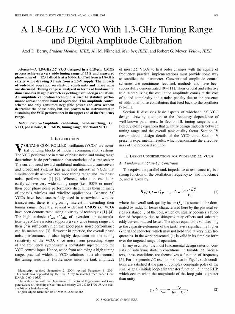
In any oscillator, the most fundamental design criterion con-sists of satisfying start-up conditions. In tunable LC oscilla-tors, these conditions are themselves a function of frequency[5]. For the generic LC oscillator shown in Fig. 1, such condi-tions are satisfied if the pair of complex conjugate poles of thesmall-signal (initial) loop-gain transfer function lie in the RHP,which occurs when the magnitude of the loop-gain is greaterthan unity
(2)
0018-9200/$20.00 © 2005 IEEE
910 IEEE JOURNAL OF SOLID-STATE CIRCUITS, VOL. 40, NO. 4, APRIL 2005
Fig. 1. Generic LC oscillator.
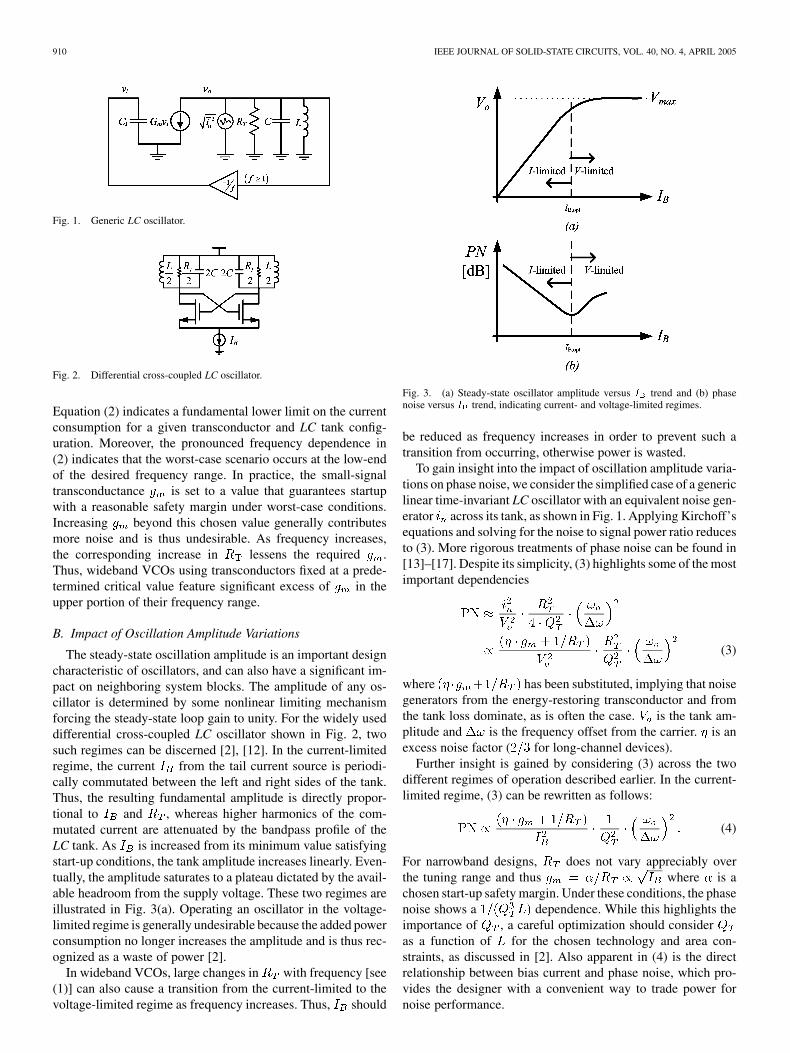
Fig. 2. Differential cross-coupled LC oscillator.
Equation (2) indicates a fundamental lower limit on the currentconsumption for a given transconductor and LC tank config-uration. Moreover, the pronounced frequency dependence in(2) indicates that the worst-case scenario occurs at the low-endof the desired frequency range. In practice, the small-signaltransconductance is set to a value that guarantees startupwith a reasonable safety margin under worst-case conditions.Increasing beyond this chosen value generally contributesmore noise and is thus undesirable. As frequency increases,the corresponding increase in lessens the required .Thus, wideband VCOs using transconductors fixed at a prede-termined critical value feature significant excess of in theupper portion of their frequency range.
B. Impact of Oscillation Amplitude Variations
The steady-state oscillation amplitude is an important designcharacteristic of oscillators, and can also have a significant im-pact on neighboring system blocks. The amplitude of any os-cillator is determined by some nonlinear limiting mechanismforcing the steady-state loop gain to unity. For the widely useddifferential cross-coupled LC oscillator shown in Fig. 2, twosuch regimes can be discerned [2], [12]. In the current-limitedregime, the current from the tail current source is periodi-cally commutated between the left and right sides of the tank.Thus, the resulting fundamental amplitude is directly propor-tional to and , whereas higher harmonics of the com-mutated current are attenuated by the bandpass profile of theLC tank. As is increased from its minimum value satisfyingstart-up conditions, the tank amplitude increases linearly. Even-tually, the amplitude saturates to a plateau dictated by the avail-able headroom from the supply voltage. These two regimes areillustrated in Fig. 3(a). Operating an oscillator in the voltage-limited regime is generally undesirable because the added powerconsumption no longer increases the amplitude and is thus rec-ognized as a waste of power [2].
In wideband VCOs, large changes in with frequency [see(1)] can also cause a transition from the current-limited to thevoltage-limited regime as frequency increases. Thus, should
Fig. 3. (a) Steady-state oscillator amplitude versus I trend and (b) phasenoise versus I trend, indicating current- and voltage-limited regimes.
be reduced as frequency increases in order to prevent such atransition from occurring, otherwise power is wasted.
To gain insight into the impact of oscillation amplitude varia-tions on phase noise, we consider the simplified case of a genericlinear time-invariant LC oscillator with an equivalent noise gen-erator across its tank, as shown in Fig. 1. Applying Kirchoff’sequations and solving for the noise to signal power ratio reducesto (3). More rigorous treatments of phase noise can be found in[13]–[17]. Despite its simplicity, (3) highlights some of the mostimportant dependencies
(3)
where has been substituted, implying that noisegenerators from the energy-restoring transconductor and fromthe tank loss dominate, as is often the case. is the tank am-plitude and is the frequency offset from the carrier. is anexcess noise factor ( for long-channel devices).
Further insight is gained by considering (3) across the twodifferent regimes of operation described earlier. In the current-limited regime, (3) can be rewritten as follows:
(4)
For narrowband designs, does not vary appreciably overthe tuning range and thus where is achosen start-up safety margin. Under these conditions, the phasenoise shows a dependence. While this highlights theimportance of , a careful optimization should consideras a function of for the chosen technology and area con-straints, as discussed in [2]. Also apparent in (4) is the directrelationship between bias current and phase noise, which pro-vides the designer with a convenient way to trade power fornoise performance.

BERNY et al.: A 1.8-GHz LC VCO WITH 1.3-GHz TUNING RANGE AND DIGITAL AMPLITUDE CALIBRATION 911
In the voltage-limited regime, (3) can be rewritten as follows:
(5)
where due to the excessive signal amplitude bringingthe transconductor into its resistive region, which degrades theoverall tank quality factor . In a narrowband design wherethe voltage-limited regime is reached by increasing , (5) in-dicates that the phase noise must degrade since the amplitudesaturates to while the transconductor noise keeps rising.The fact that decreases as well typically exacerbates thisphase noise degradation. Fig. 3(b) shows a typical scenario ofPN versus . The boundary between the two regimes of oper-ation represents the optimum point for achieving lowest phasenoise. Increasing beyond this point not only wastes power,but also degrades the phase noise.
While the above observations yield important insights fornarrowband designs, frequency dependences must be taken intoaccount in order to assess similar characteristics for widebandVCOs. Here, we restrict the analysis to the current-limitedregime since it is the preferred region of operation, as discussedabove. Again starting from (3), a phase noise expression high-lighting its frequency dependence is derived assuming a fixedcurrent and
(6)
Equation (6) reveals a somewhat counter-intuitive result: phasenoise tends to improve as frequency increases. Even in caseswhere grows linearly with frequency (equivalent to a flat-tening of with frequency), (6) shows that phase noise is rel-atively constant with frequency. The reason why phase noisedoes not degrade with its classical dependence is that the tankamplitude in this particular topology basically grows with .However, (6) only applies in the current-limited regime. Wide-band designs operated with fixed experience significant am-plitude growth as frequency increases, which eventually bringsthe VCO into the voltage-limited regime where phase noise isknown to degrade. Furthermore, the optimal point for lowestphase noise indicated in Fig. 3(b) cannot be held across fre-quency.
Amplitude variations in wideband VCOs cause several addi-tional second order effects which may be of concern, dependingon the application. One such effect is the effective reductionof the varactor’s capacitive range and the asso-ciated reduction in the overall tuning sensitivity. Fig. 4 showsa periodic-steady-state (PSS) SpectreRF simulation of a typ-ical MOS varactor - curve for different values of oscillationamplitude. Although the corresponding reduction of the tuningrange is easy to account for and compensate, amplitude-depen-dent variations of the tuning sensitivity need to be addressed inthe design of the frequency synthesizer. Other effects generallyconsist of how amplitude variations affect neighboring blocks inthe system. One such example would be a mixer, where the con-version gain would vary if the VCO amplitude changes widely.Another example would be a prescaler (or divider) that inter-faces to the VCO.
Fig. 4. Periodic-steady state simulation of varactor capacitance versus Vfor two different tank amplitudes.
Overall, amplitude variations in wideband VCOs not onlycause detrimental variations in the phase noise performanceover frequency, but also impact the functionality of neighboringblocks. Thus, it can be concluded that providing a way tocontrol the oscillation amplitude dependence on frequency ishighly desirable.
C. Amplitude Control Scheme
As discussed in the previous sections, the tank impedancevariations present in truly wideband designs significantly affectthe VCO operation and can no longer be ignored. Methods toaddress this issue typically consist of some form of amplitudecontrol. A conventional method of controlling the amplitude ofa VCO is by means of an automatic amplitude control (AAC)loop [10], [11], where a continuous-time feedback loop pro-vides very accurate control of the oscillation amplitude and atthe same time ensures startup conditions are met. As in all feed-back systems, great care must be taken to ensure that the loopremains stable under all operating conditions. Furthermore, thepresence of additional noise generators in the loop can signifi-cantly degrade the phase noise performance.
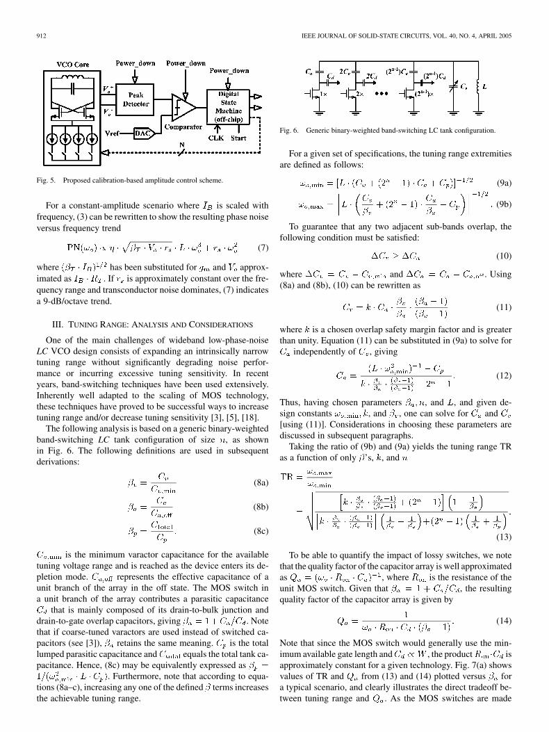
In this work, we propose an alternative amplitude controlscheme to alleviate the deficiencies inherent in the conventionalapproach. Instead of a continuous feedback loop, a calibrationapproach is used as shown in Fig. 5. The VCO amplitude isfirst peak detected and compared to a programmable referencevoltage setting the desired amplitude. The output of the com-parator is analyzed by a simple digital state machine that decideswhether to update the programmable bias current of the VCO orto end calibration. This method has the advantage of being ac-tive only during calibration. Thus, the steady-state phase noiseperformance of the VCO is not affected. Furthermore, the open-loop nature of this calibration method eliminates any concernsof instability. In addition, the power consumed by calibrationcircuits is negligible since they are powered off as soon as cali-bration ends. While a constant-amplitude versus frequency cal-ibration is most obvious, the fully programmable nature of thismethod can be exploited to implement more intricate applica-tion-specific calibration scenarios.
912 IEEE JOURNAL OF SOLID-STATE CIRCUITS, VOL. 40, NO. 4, APRIL 2005
Fig. 5. Proposed calibration-based amplitude control scheme.
For a constant-amplitude scenario where is scaled withfrequency, (3) can be rewritten to show the resulting phase noiseversus frequency trend
(7)
where has been substituted for and approx-imated as . If is approximately constant over the fre-quency range and transconductor noise dominates, (7) indicatesa 9-dB/octave trend.
III. TUNING RANGE: ANALYSIS AND CONSIDERATIONS
One of the main challenges of wideband low-phase-noiseLC VCO design consists of expanding an intrinsically narrowtuning range without significantly degrading noise perfor-mance or incurring excessive tuning sensitivity. In recentyears, band-switching techniques have been used extensively.Inherently well adapted to the scaling of MOS technology,these techniques have proved to be successful ways to increasetuning range and/or decrease tuning sensitivity [3], [5], [18].
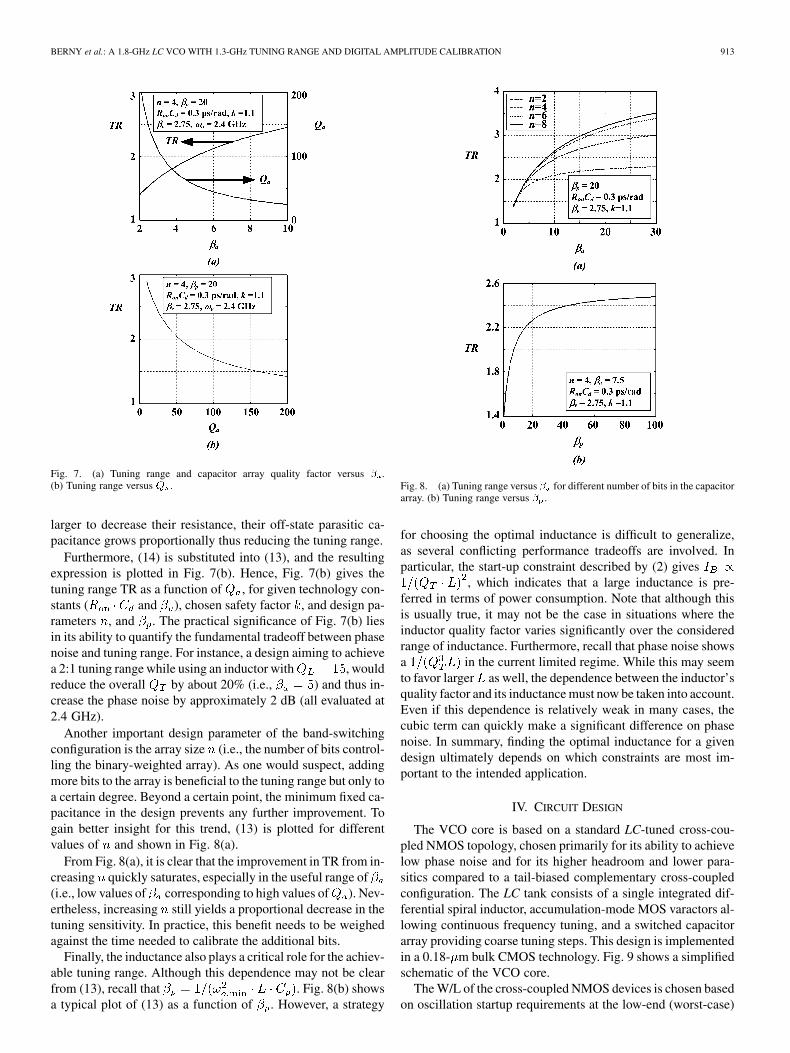
The following analysis is based on a generic binary-weightedband-switching LC tank configuration of size , as shownin Fig. 6. The following definitions are used in subsequentderivations:
(8a)
(8b)
(8c)
is the minimum varactor capacitance for the availabletuning voltage range and is reached as the device enters its de-pletion mode. represents the effective capacitance of aunit branch of the array in the off state. The MOS switch ina unit branch of the array contributes a parasitic capacitance
that is mainly composed of its drain-to-bulk junction anddrain-to-gate overlap capacitors, giving . Notethat if coarse-tuned varactors are used instead of switched ca-pacitors (see [3]), retains the same meaning. is the totallumped parasitic capacitance and equals the total tank ca-pacitance. Hence, (8c) may be equivalently expressed as
. Furthermore, note that according to equa-tions (8a–c), increasing any one of the defined terms increasesthe achievable tuning range.
Fig. 6. Generic binary-weighted band-switching LC tank configuration.
For a given set of specifications, the tuning range extremitiesare defined as follows:
(9a)
(9b)
To guarantee that any two adjacent sub-bands overlap, thefollowing condition must be satisfied:
(10)
where and . Using(8a) and (8b), (10) can be rewritten as
(11)
where is a chosen overlap safety margin factor and is greaterthan unity. Equation (11) can be substituted in (9a) to solve for
independently of , giving
(12)
Thus, having chosen parameters , and , and given de-sign constants , and , one can solve for and[using (11)]. Considerations in choosing these parameters arediscussed in subsequent paragraphs.
Taking the ratio of (9b) and (9a) yields the tuning range TRas a function of only ’s, , and
(13)
To be able to quantify the impact of lossy switches, we notethat the quality factor of the capacitor array is well approximatedas , where is the resistance of theunit MOS switch. Given that , the resultingquality factor of the capacitor array is given by
(14)
Note that since the MOS switch would generally use the min-imum available gate length and , the product isapproximately constant for a given technology. Fig. 7(a) showsvalues of TR and from (13) and (14) plotted versus fora typical scenario, and clearly illustrates the direct tradeoff be-tween tuning range and . As the MOS switches are made
BERNY et al.: A 1.8-GHz LC VCO WITH 1.3-GHz TUNING RANGE AND DIGITAL AMPLITUDE CALIBRATION 913
Fig. 7. (a) Tuning range and capacitor array quality factor versus .(b) Tuning range versus Q .
larger to decrease their resistance, their off-state parasitic ca-pacitance grows proportionally thus reducing the tuning range.
Furthermore, (14) is substituted into (13), and the resultingexpression is plotted in Fig. 7(b). Hence, Fig. 7(b) gives thetuning range TR as a function of , for given technology con-stants ( and ), chosen safety factor , and design pa-rameters , and . The practical significance of Fig. 7(b) liesin its ability to quantify the fundamental tradeoff between phasenoise and tuning range. For instance, a design aiming to achievea 2:1 tuning range while using an inductor with , wouldreduce the overall by about 20% (i.e., ) and thus in-crease the phase noise by approximately 2 dB (all evaluated at2.4 GHz).
Another important design parameter of the band-switchingconfiguration is the array size (i.e., the number of bits control-ling the binary-weighted array). As one would suspect, addingmore bits to the array is beneficial to the tuning range but only toa certain degree. Beyond a certain point, the minimum fixed ca-pacitance in the design prevents any further improvement. Togain better insight for this trend, (13) is plotted for differentvalues of and shown in Fig. 8(a).
From Fig. 8(a), it is clear that the improvement in TR from in-creasing quickly saturates, especially in the useful range of(i.e., low values of corresponding to high values of ). Nev-ertheless, increasing still yields a proportional decrease in thetuning sensitivity. In practice, this benefit needs to be weighedagainst the time needed to calibrate the additional bits.
Finally, the inductance also plays a critical role for the achiev-able tuning range. Although this dependence may not be clearfrom (13), recall that . Fig. 8(b) showsa typical plot of (13) as a function of . However, a strategy
Fig. 8. (a) Tuning range versus for different number of bits in the capacitorarray. (b) Tuning range versus .
for choosing the optimal inductance is difficult to generalize,as several conflicting performance tradeoffs are involved. Inparticular, the start-up constraint described by (2) gives
, which indicates that a large inductance is pre-ferred in terms of power consumption. Note that although thisis usually true, it may not be the case in situations where theinductor quality factor varies significantly over the consideredrange of inductance. Furthermore, recall that phase noise showsa in the current limited regime. While this may seemto favor larger as well, the dependence between the inductor’squality factor and its inductance must now be taken into account.Even if this dependence is relatively weak in many cases, thecubic term can quickly make a significant difference on phasenoise. In summary, finding the optimal inductance for a givendesign ultimately depends on which constraints are most im-portant to the intended application.
IV. CIRCUIT DESIGN
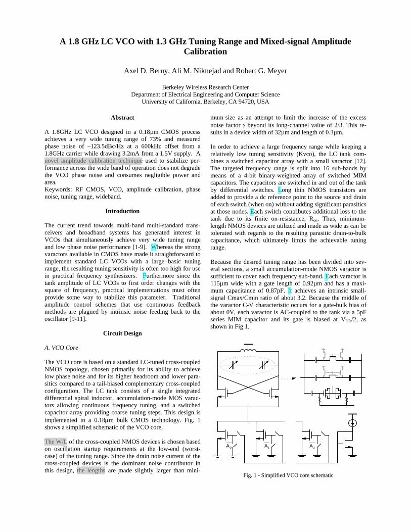
The VCO core is based on a standard LC-tuned cross-cou-pled NMOS topology, chosen primarily for its ability to achievelow phase noise and for its higher headroom and lower para-sitics compared to a tail-biased complementary cross-coupledconfiguration. The LC tank consists of a single integrated dif-ferential spiral inductor, accumulation-mode MOS varactors al-lowing continuous frequency tuning, and a switched capacitorarray providing coarse tuning steps. This design is implementedin a 0.18- m bulk CMOS technology. Fig. 9 shows a simplifiedschematic of the VCO core.
The W/L of the cross-coupled NMOS devices is chosen basedon oscillation startup requirements at the low-end (worst-case)

914 IEEE JOURNAL OF SOLID-STATE CIRCUITS, VOL. 40, NO. 4, APRIL 2005
Fig. 9. Simplified VCO core schematic.
of the tuning range. Since the drain noise current of the cross-coupled devices is the dominant noise contributor in this design,the lengths are made larger than minimum-size to limit short-channel induced excess noise. This results in a device width of32 m and length of 0.3 m.
In order to achieve a large frequency range while keeping arelatively low tuning sensitivity , the LC tank combinesa switched capacitor array with a small varactor. The targetedfrequency range is split into 16 sub-bands by means of a 4-bitbinary-weighted array of switched MIM capacitors. The capac-itors are switched in and out of the tank by differential switches.Long thin NMOS transistors are added to provide a dc referencepoint to the source and drain of each switch (when on) withoutadding significant parasitics at those nodes. Each switch con-tributes additional loss to the tank due to its finite resistance,
. Thus, minimum-length NMOS devices are utilized andmade as wide as can be tolerated with regards to the resultingparasitic drain-to-bulk capacitance, which ultimately limits theachievable tuning range.
Because the desired tuning range has been divided into sev-eral sections, a small accumulation-mode NMOS varactor issufficient to cover each frequency sub-band. Each varactor is115 m wide with a gate length of 0.92 m and has a max-imum capacitance of 0.87 pF. It achieves an intrinsic small-signal ratio of about 3.2. Because the middle of thevaractor - characteristic occurs for a gate-bulk bias of about0 V, each varactor is ac-coupled to the tank via a 5-pF seriesMIM capacitor and its gate is biased at , as shown inFig. 9.
V. EXPERIMENTAL RESULTS
This VCO was fabricated in a commercially available0.18- m CMOS process. The tank inductor was realized asa 5.6-nH differential spiral on a 2- m-thick top metal layerachieving a measured (single-ended) ranging from about 7.5to 9 over the VCO frequency range. The VCO was measuredon a test board built on standard FR4 material. The die wasglued directly onto the PC board with conductive silver epoxyand wirebonds were used to connect all inputs and outputs. A
Fig. 10. Phase noise at 1.2, 1.8, and 2.4 GHz for a core power consumption of10, 4.8, and 2.6 mW, respectively.
Fig. 11. Measured frequency tuning range.
buffer is included on-chip to facilitate driving a 50- environ-ment. An on-chip balun converts the differential buffer outputinto a single-ended signal compatible with the measurementapparatus. Biased with 8.5 mA, the buffer delivers a nominaloutput power of about 12 dBm at 1.8 GHz.
Phase noise measurements were performed on a HP8563Espectrum analyzer running the phase noise measurement option.Fig. 10 shows the measured and simulated phase noise at thelower, middle, and upper ends of the tuning range running at acore power consumption of 10, 4.8, and 2.6 mW, respectively.Measurements show good agreement with simulations. Beyondoffset frequencies of about 1 MHz, the measurement is limitedby the noise floor of the spectrum analyzer.
A very wide tuning range of 73% is achieved with a controlvoltage tuned from 0 to 1.5 V. The VCO tuning range is illus-trated in Fig. 11, showing all 16 overlapping frequency sub-bands. The measured frequency range is 1.14–2.46 GHz witha maximum tuning sensitivity of 270 MHz/V.
Fig. 12 shows the measured buffer output voltage waveformduring amplitude calibration runs at 1.4, 1.8, and 2.2 GHz for aVCO differential tank amplitude programmed to 1.1 V. The cal-ibration begins by setting the bias current to its maximum value.The current source control bits are decremented until the com-parator toggles low, indicating that the VCO output is now lowerthan the programmed reference level. Fig. 12 also captures thetransition from voltage-limited to current-limited regime at 1.8and 2.2 GHz, where the voltage amplitude responds noticeablyslower to the decreasing bias current during the first several cal-ibration cycles. Faster and more elaborate calibration routines

BERNY et al.: A 1.8-GHz LC VCO WITH 1.3-GHz TUNING RANGE AND DIGITAL AMPLITUDE CALIBRATION 915
Fig. 12. Measured amplitude calibration runs at 1.4, 1.8, and 2.2 GHz.
Fig. 13. Measured phase noise at 100-kHz offset and core power consumptionversus frequency for calibrated and uncalibrated cases.
can easily be implemented by modifying the digital state ma-chine. The time required to run the calibration routine is at most
, where is the number of current source controlbits and is the time needed to complete a single cali-bration cycle, here dominated by the settling time of the peakdetector ( 100 ns). Hence, a conservative of about600 ns was used as a proof of concept and does not representthe actual minimum settling time needed for this implementa-tion. This amplitude control scheme features a basic tradeoff be-tween amplitude accuracy and speed. This implementation uses
, providing amplitude control from to inincrements of and a worst-case calibrationrun time of .1 Alternatively, could be increasedto improve accuracy at the expense of a longer calibration time.If is large, the errors introduced by the peak detector andcomparator offset may be comparable to the quantization errorand may need to be considered. In many applications, the cal-ibration time can be tolerated and a calibration can be initiatedevery time the synthesizer is tuned to a new frequency, withoutadding significant overhead to the overall settling time. Alter-natively, a full set of calibrations (for each frequency sub-band)can be run at power-on and the results stored as a look up tablein memory.
Fig. 13 shows the phase noise performance across the VCOfrequency range for calibrated and uncalibrated scenarios. In theuncalibrated case, the bias current is set just high enough to sat-isfy start-up requirements at the low-end of the tuning range and
1V and V are the minimum and maximum desired tank amplitudesettings, respectively.
Fig. 14. FOM versus frequency for calibrated and uncalibrated cases.
Fig. 15. Die photograph.
remains constant. At the upper-end of the tuning range, this re-sults in a tank amplitude that is too large and considerably de-grades phase noise, as discussed in Section II. In the calibratedcase, the bias current is effectively scaled down with frequencyto maintain the tank amplitude approximately constant, helpingto sustain the phase noise performance over the upper-end of thetuning range. The 9-dB/octave trend predicted by (7) is consis-tent with the measurements.
Fig. 14 casts the data provided in Fig. 13 as a power-fre-quency-tuning-normalized (PFTN) figure of merit (FOM), in-troduced in [2], for calibrated and uncalibrated scenarios. Thecombination of lower phase noise and lower power consump-tion for the calibrated scenario yield a significantly improvedFOM in the upper half of the frequency range.
A photograph of the VCO die is shown in Fig. 15. The totalchip area including bondpads is 1.7 mm . Table I summarizesthe VCO performance.
916 IEEE JOURNAL OF SOLID-STATE CIRCUITS, VOL. 40, NO. 4, APRIL 2005
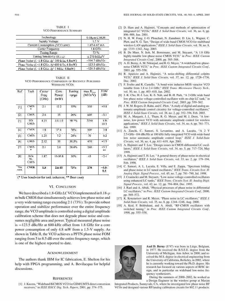
TABLE IVCO PERFORMANCE SUMMARY
TABLE IIVCO PERFORMANCE COMPARISON OF RECENTLY PUBLISHED
WIDEBAND VCOS
VI. CONCLUSION
We have described a 1.8-GHz LC VCO implemented in 0.18-m bulk CMOS that simultaneously achieves low phase noise anda very wide tuning range exceeding 2:1 (73%). To provide robustoperation and stabilize performance over the entire frequencyrange, the VCO amplitude is controlled using a digital amplitudecalibration scheme that does not degrade phase noise and con-sumes negligible area and power. Typical measured phase noiseis 123.5 dBc/Hz at 600-kHz offset from 1.8 GHz for a corepower consumption of only 4.8 mW from a 1.5-V supply. Asshown in Table II, the VCO achieves a PFTN phase noise FOMranging from 5 to 8.5 dB over the entire frequency range, whichis one of the highest reported to date.
ACKNOWLEDGMENT
The authors thank IBM for IC fabrication, E. Shelton for hishelp with FPGA programming, and A. Bevilacqua for helpfuldiscussions.
REFERENCES
[1] J. Kucera, “Wideband BiCMOS VCO for GSM/UMTS direct conversionreceivers,” in IEEE ISSCC Dig. Tech. Papers, 2001, pp. 374–375.
[2] D. Ham and A. Hajimiri, “Concepts and methods of optimization ofintegrated LC VCOs,” IEEE J. Solid-State Circuits, vol. 36, no. 6, pp.896–909, Jun. 2001.
[3] N. H. W. Fong, J.-O. Plouchart, N. Zamdmer, D. Liu, L. Wagner, C.Plett, and N. G. Tarr, “Design of wide-band CMOS VCO for multibandwireless LAN applications,” IEEE J. Solid-State Circuits, vol. 38, no. 8,pp. 1333–1342, Aug. 2003.
[4] B. De Muer, N. Itoh, M. Borremans, and M. Steyaert, “A 1.8 GHzhighly-tunable low-phase-noise CMOS VCO,” in Proc. IEEE CustomIntegrated Circuits Conf., 2000, pp. 585–588.
[5] A. D. Berny, A. M. Niknejad, and R. G. Meyer, “A wideband low-phase-noise CMOS VCO,” in Proc. IEEE Custom Integrated Circuits Conf.,2003, pp. 555–558.
[6] R. Aparicio and A. Hajimiri, “A noise-shifting differential colpittsVCO,” IEEE J. Solid-State Circuits, vol. 37, no. 12, pp. 1728–1736,Dec. 2002.
[7] F. Svelto and R. Castello, “A bond-wire inductor-MOS varactor VCOtunable from 1.8 to 2.4 GHz,” IEEE Trans. Microwave Theory Tech.,vol. 50, no. 1, pp. 403–410, Jan. 2002.
[8] J.-K. Cho, H.-I. Lee, K.-S. Nah, and B.-H. Park, “A 2-GHz wide bandlow phase noise voltage-controlled oscillator with on-chip LC tank,” inProc. IEEE Custom Integrated Circuits Conf., 2003, pp. 559–562.
[9] J. W. M. Rogers, D. Rahn, and C. Plett, “A study of digital and analog au-tomatic-amplitude control circuitry for voltage-controlled oscillators,”IEEE J. Solid-State Circuits, vol. 38, no. 2, pp. 352–356, Feb. 2003.
[10] M. A. Margarit, J. L. Tham, R. G. Meyer, and M. J. Deen, “A low-noise, low-power VCO with automatic amplitude control for wirelessapplications,” IEEE J. Solid-State Circuits, vol. 34, no. 6, pp. 761–771,Jun. 1999.
[11] A. Zanchi, C. Samori, S. Levantino, and A. Lacaita, “A 2 V2.5-GHz–104 dBc/Hz at 100 kHz fully-integrated VCO with wide-bandlow noise automatic amplitude control loop,” IEEE J. Solid-StateCircuits, vol. 36, no. 4, pp. 611–619, Apr. 2001.
[12] A. Hajimiri and T. Lee, “Design issues in CMOS differential LC oscil-lators,” IEEE J. Solid-State Circuits, vol. 34, no. 5, pp. 717–724, May1999.
[13] A. Hajimiri and T. H. Lee, “A general theory of phase noise in electricaloscillators,” IEEE J. Solid-State Circuits, vol. 33, no. 2, pp. 179–194,Feb. 1998.
[14] C. Samori, A. L. Lacaita, E. Villa, and E. Zappa, “Spectrum foldingand phase noise in LC tuned oscillators,” IEEE Trans. Circuits Syst. II:Analog Digit. Signal Process., vol. 45, no. 7, pp. 781–790, Jul. 1998.
[15] J. Craninckx and M. Steyaert, “Low-noise voltage-controlled oscillatorsusing enhanced LC-tanks,” IEEE Trans. Circuits Syst. II: Analog Digit.Signal Process., vol. 42, no. 12, pp. 794–804, Dec. 1995.
[16] J. Rael and A. Abidi, “Physical processes of phase noise in differentialLC oscillators,” in Proc. IEEE Custom Integrated Circuits Conf., 2000,pp. 569–572.
[17] K. Kouznetsov and R. Meyer, “Phase noise in LC oscillators,” IEEE J.Solid-State Circuits, vol. 35, no. 8, pp. 1244–1248, Aug. 2000.
[18] A. Kral, F. Behbahani, and A. Abidi, “RF-CMOS oscillators withswitched tuning,” in Proc. IEEE Custom Integrated Circuits Conf.,1998, pp. 555–558.
Axel D. Berny (S’97) was born in Liège, Belgium,in 1977. He received the B.S.E.E. degree from theUniversity of Michigan, Ann Arbor, in 2000, and re-ceived the M.S. degree in electrical engineering fromthe University of California, Berkeley, in 2002, wherehe is currently working toward the Ph.D. degree. Hisresearch has focused on various aspects of RFIC de-sign, and in particular on wideband low-noise fre-quency synthesizers.
During the summers of 2000–2002, he worked asa Design Engineer in the wireless group at Maxim
Integrated Products, Sunnyvale, CA, where he investigated low phase noise RFVCOs and designed various RF/analog calibration circuits for 802.11 products.
A 1.8 GHz LC VCO with 1.3 GHz Tuning Range and Mixed-signal Amplitude Calibration
Axel D. Berny, Ali M. Niknejad and Robert G. Meyer
Berkeley Wireless Research Center
Department of Electrical Engineering and Computer Science University of California, Berkeley, CA 94720, USA
Abstract
A 1.8GHz LC VCO designed in a 0.18µm CMOS process achieves a very wide tuning range of 73% and measured phase noise of –123.5dBc/Hz at a 600kHz offset from a 1.8GHz carrier while drawing 3.2mA from a 1.5V supply. A novel amplitude calibration technique used to stabilize per-formance across the wide band of operation does not degrade the VCO phase noise and consumes negligible power and area. Keywords: RF CMOS, VCO, amplitude calibration, phase noise, tuning range, wideband.
Introduction
The current trend towards multi-band multi-standard trans-ceivers and broadband systems has generated interest in VCOs that simultaneously achieve very wide tuning range and low phase noise performance [1-9]. Whereas the strong varactors available in CMOS have made it straightforward to implement standard LC VCOs with a large basic tuning range, the resulting tuning sensitivity is often too high for use in practical frequency synthesizers. Furthermore since the tank amplitude of LC VCOs to first order changes with the square of frequency, practical implementations must often provide some way to stabilize this parameter. Traditional amplitude control schemes that use continuous feedback methods are plagued by intrinsic noise feeding back to the oscillator [9-11].
Circuit Design
A. VCO Core The VCO core is based on a standard LC-tuned cross-coupled NMOS topology, chosen primarily for its ability to achieve low phase noise and for its higher headroom and lower para-sitics compared to a tail-biased complementary cross-coupled configuration. The LC tank consists of a single integrated differential spiral inductor, accumulation-mode MOS varac-tors allowing continuous frequency tuning, and a switched capacitor array providing coarse tuning steps. This design is implemented in a 0.18µm bulk CMOS technology. Fig. 1 shows a simplified schematic of the VCO core. The W/L of the cross-coupled NMOS devices is chosen based on oscillation startup requirements at the low-end (worst-case) of the tuning range. Since the drain noise current of the cross-coupled devices is the dominant noise contributor in this design, the lengths are made slightly larger than mini-
mum-size as an attempt to limit the increase of the excess noise factor γ beyond its long-channel value of 2/3. This re-sults in a device width of 32µm and length of 0.3µm. In order to achieve a large frequency range while keeping a relatively low tuning sensitivity (Kvco), the LC tank com-bines a switched capacitor array with a small varactor [12]. The targeted frequency range is split into 16 sub-bands by means of a 4-bit binary-weighted array of switched MIM capacitors. The capacitors are switched in and out of the tank by differential switches. Long thin NMOS transistors are added to provide a dc reference point to the source and drain of each switch (when on) without adding significant parasitics at those nodes. Each switch contributes additional loss to the tank due to its finite on-resistance, Ron. Thus, minimum-length NMOS devices are utilized and made as wide as can be tolerated with regards to the resulting parasitic drain-to-bulk capacitance, which ultimately limits the achievable tuning range. Because the desired tuning range has been divided into sev-eral sections, a small accumulation-mode NMOS varactor is sufficient to cover each frequency sub-band. Each varactor is 115µm wide with a gate length of 0.92µm and has a maxi-mum capacitance of 0.87pF. It achieves an intrinsic small-signal Cmax/Cmin ratio of about 3.2. Because the middle of the varactor C-V characteristic occurs for a gate-bulk bias of about 0V, each varactor is AC-coupled to the tank via a 5pF series MIM capacitor and its gate is biased at VDD/2, as shown in Fig.1.
Fig. 1 - Simplified VCO core schematic
0A 1A 3A
tianjun
Underline
tianjun
Underline
tianjun
Underline
tianjun
Underline
tianjun
Underline
tianjun
Underline
tianjun
Highlight
tianjun
Highlight
tianjun
Highlight
tianjun
Underline
tianjun
Underline
tianjun
Underline
tianjun
Underline
tianjun
Underline
tianjun
Underline
tianjun
Text Box
和互补交叉耦合的结构相比
tianjun
Underline
tianjun
Underline
tianjun
Underline
tianjun
Highlight
tianjun
Highlight
tianjun
Squiggly
tianjun
Squiggly
tianjun
Text Box
交叉耦合器件尺寸选取原则
tianjun
Underline
tianjun
Highlight
tianjun
Highlight
tianjun
Squiggly
tianjun
Squiggly
tianjun
Squiggly
tianjun
Squiggly
tianjun
Highlight
tianjun
Highlight
tianjun
Underline
tianjun
Squiggly
tianjun
Squiggly

Fig. 2 - Amplitude calibration system.
. Amplitude Control
dependence of the equivalent LC tank pedance causes large variations in start-up requirements at
avoiding an egradation. o allow for greater prototyping flexibility, the state-machine
This VCO was fabr available 0.18µm MOS process. The tank inductor was realized as a 5.6nH
rformed on a HP8563E ectrum analyzer running the phase noise personality option.
with a control oltage tuned from 0 to 1.5V. The VCO tuning range is
uring amplitude calibration runs at 1.4, 1.8, and 2.2GHz for
B The strong frequency imopposite ends of the tuning range. Thus, setting the bias cur-rent to ensure start-up at the lower frequencies (worst-case) results in a significant waste of power at the upper end of the tuning range. Furthermore, correspondingly large variations in tank amplitude and potential degradation of phase noise are undesirable. To alleviate this effect, this VCO uses the am-plitude control scheme shown in Fig. 2. The VCO output is fed through a capacitive divider stage for isolation and sub-sequently measured by a peak detector. The peak detector dc output is compared against a reference programmable by means of a simple 3-bit DAC. Depending on the state of the comparator output, a digital state-machine adjusts a 4-bit bi-nary-weighted current source feeding the VCO core or de-termines that calibration has finished and latches the current source control bits. Once calibration ends, all calibration cir-cuits are powered down to effectively break the loop, thereby
Fig. 3 - Phase Noise at 1.2, 1.8, and 2.4GHz for a core power consumption of 10, 4.8, and 2.6mW, respectively
Fig. 4 - Measured frequency tuning range.
y steady-state spurs or phase noise d
Tis implemented off-chip using an FPGA.
Experimental Results
icated in a commercially Cdifferential spiral on a 2-µm thick top metal layer achieving a measured Q ranging from about 7.5 to 9 over the VCO fre-quency range. The VCO was measured on a test board built on standard FR4 material. The die was glued directly onto the PC board with conductive silver epoxy and wirebonds were used to connect all inputs and outputs. A buffer is included on-chip to facilitate driving a 50Ω environment. An on-chip balun converts the differential buffer output into a single-ended signal compatible with the measurement apparatus. Biased with 8.5mA, the buffer delivers a nominal output power of about –12dBm at 1.8GHz. Phase noise measurements were pespFig. 3 shows the measured phase noise at the lower, middle, and upper ends of the tuning range running at a core power consumption of 10, 4.8, and 2.6mW, respectively. Beyond offset frequencies of about 1MHz, the measurement is limited by the noise floor of the spectrum analyzer. A very wide tuning range of 73% is achieved villustrated in Fig. 4, showing all 16 overlapping frequency sub-bands. The measured frequency range is 1.14-2.47GHz with a maximum tuning sensitivity (Kvco) of 270MHz/V. Fig. 5 shows the measured buffer output voltage waveformda VCO differential tank amplitude programmed to 1.1V. The calibration begins by setting the bias current to its maximum value. The current source control bits are decremented until the comparator toggles low, indicating that the VCO output is now lower than the programmed reference level. Faster and
1.1
1.3
1.5
1.7
1.9
2.1
2.3
0 0.3 0.6 0.9 1.2 1.
2.5
5
Vtune (V)
Freq
uenc
y (G
Hz)
Kvcomax= 270MHz/V
104
105
106
107-140
-130
-120
-110
-100
-90
-80
-70
-60
Phas
e N
oise
(dB
c/H
z)
Frequency Offset (Hz)
fo = 2.4GHz, 2.6mW
fo = 1.8GHz, 4.8mW fo = 1.2GHz, 10mW
tianjun
Highlight
tianjun
Highlight
tianjun
Underline
tianjun
Underline
tianjun
Underline
tianjun
Text Box
需要进行幅度控制的原因及控制方法
tianjun
Highlight
tianjun
Highlight
tianjun
Underline
tianjun
Underline
tianjun
Highlight
tianjun
Underline
tianjun
Underline
tianjun
Highlight
tianjun
Highlight
tianjun
Underline
tianjun
Underline
tianjun
Underline
tianjun
Highlight
tianjun
Highlight
tianjun
Highlight
tianjun
Underline
tianjun
Underline
tianjun
Underline
tianjun
Underline
tianjun
Highlight
tianjun
Highlight
tianjun
Underline
tianjun
Highlight

more elaborate calibration routines can easily been imple-mented by modifying the digital state machine. The time re-quired to run the calibration routine is at most 2N*TCYCLE, where N is the number of current source control bits and TCYCLE is the time needed to complete a single calibration cycle, here dominated by the settling time of the peak detector (sub-100ns). Hence, a conservative TCYCLE of about 600ns was used as a proof of concept and does not represent the actual minimum settling time needed for this implementation. This amplitude control scheme features a basic trade-off between amplitude accuracy and speed. This implementation uses N=4, providing amplitude control from Vo,min to Vo,max in increments of (Vo,max-Vo,min)/16 and a worst-case calibration run time of 16*TCYCLE
1. In many applications, the calibration time can be tolerated and a calibration can be initiated every time the synthesizer is tuned to a new frequency, without adding significant overhead to the overall settling time. Alter-natively, a full-set of calibrations (for each frequency sub-band) can be run at power-on and the results stored as a look up table in memory.
Fig. 5 – Measured amplitude calibration runs at 1.4, 1.8 and 2.2GHz.
Fig. 6 - Measured phase noise at 100kHz offset and core power consumption vs. frequency for calibrated and uncalibrated cases.
Fig. 7 - FOM vs. frequency for calibrated and uncalibrated cases.
Ffrequency range for calibrated and uncalibrated scenarios. In
provided in Fig. 6 as a power-frequency-ning-normalized (PFTN) figure of merit (FOM), introduced
n in Fig. 8. The total hip area including bondpads is 1.7mm2. Table II summarizes
TABLE I – Performance Com arison of Recently Published
Wideband VCOs
Ref Tech Center Freq. Power
ng range
max Kvco (MHz/V)
FOM (dB)
1 Vo,min and Vo,max are the minimum and maximum desired tank amplitude settings, respectively.
ig. 6 shows the phase noise performance across the VCO
the uncalibrated case, the bias current is set just high enough to satisfy start-up requirements at the low-end of the tuning range and remains constant. At the upper-end of the tuning range, this results in a tank amplitude that is too large and considerably degrades phase noise2. In the calibrated case, the bias current is effectively scaled down with frequency to maintain the tank amplitude approximately constant, helping to sustain the phase noise performance over the upper-end of the tuning range. Fig. 7 casts the data tuin [2], for calibrated and uncalibrated scenarios. The combi-nation of lower phase noise and lower power consumption for the calibrated scenario yield a significantly improved FOM in the upper half of the frequency range. A photograph of the VCO die is showcthe VCO performance.
p
Core Tuni
(GHz)
(mW) [1] CMOS
* 2.1 12.2 35% 330 +5.8
[2] CMOS 2.6 10 26% 600 –3.1 [3] SOI
CMOS 4.33 2 .0-3.0 58.7% 2250 +5.9-
10.3 [4] CMOS 1.8 32.4 28% 500 –3.8 [5] CMOS 1.25 7.2 28% 70 –0.2 [6] CMOS 2.12 10 30.5% 450 +1.9 [7] CMOS
* 2.1 2.0 28.6% 260 +5.7
** [8] SiGe
Bicmos 1.87 14-30.8 30% 45 +2-4
This work
CMOS 1.8 2.6-10 73% 270 +5.0-8.5
0.0
2.0
4.0
6.0
8.0
10.0
12.0
1.2E+09 1.4E+09 1.6E+09 1.8E+09 2.0E+09 2.2E+09 2.4E+09
Frequency (Hz)
Pow
er D
issi
patio
n (m
W)
-114
-112
-110
-108
-106
-104
-102
-100
-98
-96
-94
Phas
e N
oise
@ 1
00kH
z of
fset
(dB
c/H
z)
Pd - calibrated
Pd - uncalibrated
L100kHz - uncalibrated
L100kHz - calibrated
-4.0
-2.0
0.0
2.0
4.0
6.0
8.0
1.1E+09 1.3E+09 1.5E+09 1.7E+09 1.9E+09 2.1E+09 2.3E+09 2.5E+09
Frequency (Hz)
FOM
(dB
)
(* Uses bondwire for tank inductors, ** Best case)
2 VCO current source and cross-coupled devices are pushed into the triode region, adding significant loss to the LC tank.
10.0
uncalibrated
calibrated
⎛ ⎞⎛ ⎞⎜ ⎟⎜ ⎟
⎝ ⎠⎝ ⎠o,max o,min
2
d
f fFOM = 10log
∆f
-kT× - L ∆f
P
tianjun
Underline
tianjun
Squiggly
tianjun
Highlight
tianjun
Highlight
tianjun
Underline
tianjun
Highlight
tianjun
Highlight
tianjun
Underline
tianjun
Highlight
tianjun
Highlight

Conclusion
plemented in 18µm bulk CMOS tha sly achieves low phase
his research was supported by Army Research
Office under Grant The authors thank
] J. Kucera, “Wideband BiCMOS VCO for GSM/UMTS Direct
Conversion Receivers”, ISS s, 2001, pp. 374-375. [2] D. Ham, A. Hajimiri, “Concepts and Methods of Optimization of
p. 1333-1342, Aug. 2003.
Techniques, vol. 50, no. 1, pp. 403-410, Jan. 2002.
.2,
ns”, IEEE J. Solid-State Circuits, vol. 34,
1] A. Zanchi, C. Samori, S. Levantino, and A. Lacaita, “A 2V 2.5-Hz –104dBc/Hz at 100kHz Fully-Integrated VCO with Wide-Band ow Noise Automatic Amplitude Control Loop”, IEEE J. Solid-
TABLE II – VCO Performance Summary
Technology 0.18µm CMOS
We have described a 1.8GHz LC VCO im0.n
t simultaneouoise and a very wide tuning range exceeding 2:1 (73%). To
provide robust operation and stabilize performance over the entire frequency range, the VCO amplitude is controlled using a novel mixed-signal amplitude calibration scheme that does not degrade phase noise and consumes negligible area and power. Typical measured phase noise is –123.5dBc/Hz at 600kHz offset from 1.8GHz for a core power consumption of only 4.8mW from a 1.5V supply. As shown in Table I, the VCO achieves a power-frequency-tuning-normalized phase noise FOM ranging from 5 to 8.5dB over the entire frequency range, which is one of the highest reported to date.
Acknowledgments
T the U.S. DAAD19-00-1-0550.
IBM for IC fabrication, Eric S elton for his help with FPGA programming, and Andrea Bevilacqua for helpful discussions.
References
h
[1CC Dig. Tech Paper
Integrated LC VCOs,” IEEE J. Solid-State Circuits, vol. 36, no. 6, pp. 896-909, Jun. 2001. [3] N. H.W. Fong et al., “Design of Wide-Band CMOS VCO for Multiband Wireless LAN Applications,” IEEE J. Solid-State Circuits, vol. 38, no. 8, p[4] B. De Muer, N. Itoh, M. Borremans, M. Steyaert, “A 1.8 GHz highly-tunable low-phase-noise CMOS VCO”, IEEE Custom Integrated Circuits Conf., 2000, pp. 585-588. [5] A. D. Berny, A. M. Niknejad, R. G. Meyer, “A Wideband Low-Phase-Noise CMOS VCO”, IEEE Custom Integrated Circuits Conf., 2003, pp. 555-558. [6] R. Aparicio, A. Hajimiri, “A Noise-Shifting Differential Colpitts VCO”, IEEE J. Solid-State Circuits, vol. 37, no.12, pp.1728-1736, Dec. 2002. [7] F. Svelto, R. Castello, “A Bond-Wire Inductor-MOS Varactor VCO Tunable From 1.8 to 2.4 GHz”, IEEE Trans, on Microwave Theory and [8] J-K Cho, H-I Lee, K-S N, B-H Park, “A 2-GHz Wide Band Low Phase Noise Voltage-Controlled Oscillator with On-Chip LC tank”, IEEE Custom Integrated Circuits Conf., 2003, pp. 559-562. [9] J. W.M. Rogers, D. Rahn, and C. Plett, “A Study of Digital and Analog Automatic-Amplitude Control Circuitry for Voltage-Controlled Oscillators,” IEEE J. Solid-State Circuits, vol. 38, nopp.352-356, Feb. 2003. [10] M. A. Margarit, J. L. Tham, R. G. Meyer, and M. J. Deen, “A Low-Noise, Low-Power VCO with Automatic Amplitude Control for Wireless Applicationo.6, pp.761-771, Jun. 1999.
[1GLState Circuits, vol. 36, no.4, pp.611-619, Apr. 2001. [12] A. Kral, F. Behbahani, A. Abidi, “RF-CMOS Oscillators with Switched Tuning”, IEEE Custom Integrated Circuits Conf., 1998, pp. 555-558.
Supply Voltage 1.5 V Current Consumption (VCO core) 1.67-6.67 mA
Ce y nter Frequenc 1.8 GHz Tuning Range 73 %
Tuning Sensitivity (KVCO) ≤ 270 MHz/V Phase Noise (fo Hz, 4.8mW) –=1.8 GHz, ∆f=100 k 1 z 04.7 dBc/HPhase Noise (fo=1 kHz, 4.8mW) –123 /Hz .8 GHz, ∆f=600 .5 dBcPhase Nois .8mW) e (fo=1.8 GHz, ∆f=1 MHz, 4 –126.5 dBc/Hz
Fig. 8 - Die photograph.
VCO Core
O/P Buffer
Peak Det. & Comp.
tianjun
Underline
A Wideband Low-Phase-Noise CMOS VCO Axel D. Berny, Ali M. Niknejad and Robert G. Meyer
Berkeley Wireless Research Center
Department of Electrical Engineering and Computer Science University of California, Berkeley, CA 94720 Abstract A CMOS VCO has been designed and fabricated in a commercial 0.25µm CMOS process. Using a combination of switched binary-weighted capacitors and standard varactors, this VCO achieves a 28% tuning range with a control voltage ranging from 0-2 V, while maintaining a tuning sensitivity of less than 75 MHz/V over its entire frequency range. Compact choke inductors are used in place of resistors to provide a low noise bias point to the varactors. The choke inductors achieve more than 90 nH of effective inductance while consuming a die area of only 92 x 92 µm2. The measured single-sided phase noise is –127 dBc/Hz at a 600 kHz offset from a 1.24 GHz carrier when the VCO core is drawing 3.6 mA from a 2 V supply. Introduction Voltage controlled oscillators (VCOs) are essential building blocks of modern communication systems. The VCO performance in terms of phase noise, tuning range, and power dissipation determines many of the basic performance characteristics of a transceiver. The current trend to utilize multi-band multi-standard receivers and also very wideband systems is driving the effort to create new VCO topologies with wide tuning range, low phase noise, and low power consumption. Whereas relaxation oscillators easily achieve very wide tuning range (i.e. 100% or more), their poor phase noise performance disqualifies them in most of today’s wireless and wireline applications. Because LC VCOs have been successful in narrowband wireless transceivers, there is a growing interest to extend their tuning range. Recently, several wideband CMOS LC VCOs have been demonstrated using a variety of techniques [1-4]. The high intrinsic Cmax/Cmin of inversion- or accumulation-type MOS varactors supports a very wide tuning range and their Q is sufficiently high that good phase noise performance can be maintained. However in practice, the overall phase noise performance is also highly dependent on the tuning sensitivity of the VCO, since noise from preceding stages of the frequency synthesizer is inevitably injected onto the VCO control input. Hence, aside from achieving a high raw tuning range, practical wideband VCO solutions must properly limit the overall VCO tuning sensitivity.
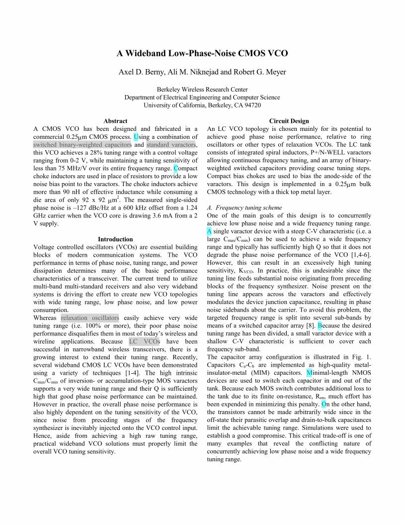
Circuit Design An LC VCO topology is chosen mainly for its potential to achieve good phase noise performance, relative to ring oscillators or other types of relaxation VCOs. The LC tank consists of integrated spiral inductors, P+/N-WELL varactors allowing continuous frequency tuning, and an array of binary-weighted switched capacitors providing coarse tuning steps. Compact bias chokes are used to bias the anode-side of the varactors. This design is implemented in a 0.25µm bulk CMOS technology with a thick top metal layer. A. Frequency tuning scheme One of the main goals of this design is to concurrently achieve low phase noise and a wide frequency tuning range. A single varactor device with a steep C-V characteristic (i.e. a large Cmax/Cmin) can be used to achieve a wide frequency range and typically has sufficiently high Q so that it does not degrade the phase noise performance of the VCO [1,4-6]. However, this can result in an excessively high tuning sensitivity, KVCO. In practice, this is undesirable since the tuning line feeds substantial noise originating from preceding blocks of the frequency synthesizer. Noise present on the tuning line appears across the varactors and effectively modulates the device junction capacitance, resulting in phase noise sidebands about the carrier. To avoid this problem, the targeted frequency range is split into several sub-bands by means of a switched capacitor array [8]. Because the desired tuning range has been divided, a small varactor device with a shallow C-V characteristic is sufficient to cover each frequency sub-band. The capacitor array configuration is illustrated in Fig. 1. Capacitors Ca-Cb are implemented as high-quality metal-insulator-metal (MIM) capacitors. Minimal-length NMOS devices are used to switch each capacitor in and out of the tank. Because each MOS switch contributes additional loss to the tank due to its finite on-resistance, Ron, much effort has been expended in minimizing this penalty. On the other hand, the transistors cannot be made arbitrarily wide since in the off-state their parasitic overlap and drain-to-bulk capacitances limit the achievable tuning range. Simulations were used to establish a good compromise. This critical trade-off is one of many examples that reveal the conflicting nature of concurrently achieving low phase noise and a wide frequency tuning range.
tianjun
Underline
tianjun
Highlight
tianjun
Highlight
tianjun
Squiggly
tianjun
Squiggly
tianjun
Highlight
tianjun
Highlight
tianjun
Underline
tianjun
Underline
tianjun
Underline
tianjun
Underline
tianjun
Underline
tianjun
Underline
tianjun
Highlight
tianjun
Highlight
tianjun
Underline
tianjun
Underline
tianjun
Cross-Out
tianjun
Cross-Out
tianjun
Underline
tianjun
Underline
tianjun
Underline
tianjun
Cross-Out
tianjun
Cross-Out
tianjun
Underline
tianjun
Highlight
tianjun
Highlight
tianjun
Underline
tianjun
Cross-Out
tianjun
Cross-Out
tianjun
Highlight
tianjun
Highlight
tianjun
Underline
4W/L 2W/L W/L
CbCa2Ca4Ca
CvLc
Vtune
B1 B0B2rc
Csubrsub
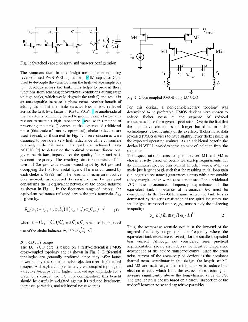
Fig. 1: Switched capacitor array and varactor configuration. The varactors used in this design are implemented using reverse-biased P+/N-WELL junctions. MIM capacitor Cb is used to decouple the varactor from the high voltage amplitude that develops across the tank. This helps to prevent these junctions from reaching forward-bias conditions during large voltage peaks, which would degrade the tank Q and result in an unacceptable increase in phase noise. Another benefit of adding Cb is that the finite varactor loss is now reflected across the tank by a factor of (Cb+Cv)2/Cb
2. The anode-side of the varactor is commonly biased to ground using a large-value resistor to sustain a high impedance. Because this method of preserving the tank Q comes at the expense of additional noise (this trade-off can be optimized), choke inductors are used instead, as illustrated in Fig. 1. These structures were designed to provide a very high inductance while consuming relatively little die area. This goal was achieved using ASITIC [9] to determine the optimal structure dimensions, given restrictions imposed on the quality factor and self-resonant frequency. The resulting structure consists of 11 turns of 3.6 µm wide traces spaced apart by 0.4 µm and occupying the first four metal layers. The area consumed by each choke is 92x92 µm2. The benefits of using an inductive bias network as opposed to resistors can be analyzed considering the Π-equivalent network of the choke inductor as shown in Fig. 1. In the frequency range of interest, the equivalent resistance reflected across the tank terminals, Req, is given by:
( ) ( ) 2eq o c o c sub o sub(ω ) ω 1 ωR r j L r j C n= + + ⋅ (1)
where
'b v b( )n C C C= + and
'vC ≅ vC since for the intended
use of the choke inductor c voω >> 1/ L C⋅ .
B. VCO core design The LC VCO core is based on a fully-differential PMOS cross-coupled topology and is shown in Fig. 2. Differential topologies are generally preferred since they offer better power supply and substrate noise rejection over single-ended designs. Although a complementary cross-coupled topology is attractive because of its higher tank voltage amplitude for a given bias current and LC tank configuration, this benefit should be carefully weighted against its reduced headroom, increased parasitics, and additional noise sources.
M3
M1 M2
M4
IB
LLVtune
Vsupply
C CrL rL
Fig. 2: Cross-coupled PMOS-only LC VCO For this design, a non-complementary topology was determined to be preferable. PMOS devices were chosen to reduce flicker noise at the expense of reduced transconductance for a given aspect ratio. Despite the fact that the conductive channel is no longer buried as in older technologies, close scrutiny of the available flicker noise data revealed PMOS devices to have slightly lower flicker noise in the expected operating regimes. As an additional benefit, the device N-WELL provides some amount of isolation from the substrate. The aspect ratio of cross-coupled devices M1 and M2 is chosen strictly based on oscillation startup requirements, for the minimum expected bias current. In other words, W/L1,2 is made just large enough such that the resulting initial loop gain (i.e. negative resistance) guarantees startup with a reasonable safety margin under worst-case conditions. For a wideband VCO, the pronounced frequency dependence of the equivalent tank impedance at resonance, RT, must be considered. In the low-GHz regime where the tank loss is dominated by the series resistance of the spiral inductors, the small-signal transconductance, gm, must satisfy the following inequality:
( )2
m T oL1 ωg R r L≥ ≅ ⋅ (2)
Thus, the worst-case scenario occurs at the low-end of the targeted frequency range (i.e. the frequency where the equivalent tank resistance is lowest), for the smallest expected bias current. Although not considered here, practical implementation should also address the negative temperature dependence of the device transconductance. Since the drain noise current of the cross-coupled devices is the dominant thermal noise contributor in this design, the lengths of M1 and M2 are made larger than minimum-size to reduce hot-electron effects, which limit the excess noise factor γ to increase significantly above the long-channel value of 2/3. The gate length is chosen based on a careful inspection of the tradeoff between noise and capacitive parasitics.
tianjun
Underline
tianjun
Cross-Out
tianjun
Cross-Out
tianjun
Highlight
tianjun
Highlight
tianjun
Highlight
tianjun
Underline
tianjun
Underline
tianjun
Cross-Out
tianjun
Cross-Out
tianjun
Underline
tianjun
Underline
tianjun
Underline
tianjun
Underline
tianjun
Underline
tianjun
Underline
tianjun
Underline
tianjun
Cross-Out
tianjun
Cross-Out
tianjun
Squiggly
tianjun
Squiggly
tianjun
Line
tianjun
Cross-Out
tianjun
Cross-Out
tianjun
Text Box
scrutiny n. 详查
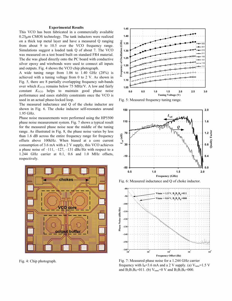
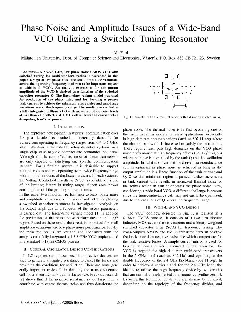
Experimental Results This VCO has been fabricated in a commercially available 0.25µm CMOS technology. The tank inductors were realized on a thick top metal layer and have a measured Q ranging from about 9 to 10.5 over the VCO frequency range. Simulations suggest a loaded tank Q of about 7. The VCO was measured on a test board built on standard FR4 material. The die was glued directly onto the PC board with conductive silver epoxy and wirebonds were used to connect all inputs and outputs. Fig. 4 shows the VCO chip photograph. A wide tuning range from 1.06 to 1.40 GHz (28%) is achieved with a tuning voltage from 0 to 2 V. As shown in Fig. 5, there are 8 partially overlapping frequency sub-bands over which KVCO remains below 75 MHz/V. A low and fairly constant KVCO helps to maintain good phase noise performance and eases stability constraints once the VCO is used in an actual phase-locked loop. The measured inductance and Q of the choke inductor are shown in Fig. 6. The choke inductor self-resonates around 1.95 GHz. Phase noise measurements were performed using the HP5500 phase noise measurement system. Fig. 7 shows a typical result for the measured phase noise near the middle of the tuning range. As illustrated in Fig. 8, the phase noise varies by less than 1.6 dB across the entire frequency range for frequency offsets above 100kHz. When biased at a core current consumption of 3.6 mA with a 2 V supply, this VCO achieves a phase noise of –111, –127, –131 dBc/Hz with respect to a 1.244 GHz carrier at 0.1, 0.6 and 1.0 MHz offsets, respectively.
VCO core
chokes
output buffer
Fig. 4: Chip photograph.
1.05
1.10
1.15
1.20
1.25
1.30
1.35
1.40
1.45
0.0 0.5 1.0 1.5 2.0 2.5 3.0
000
001
010
011
100
101
110
111
Tuning Voltage (V)
Freq
uenc
y of
Osc
illat
ion
(GH
z)
Fig. 5: Measured frequency tuning range.
-50
-10
30
70
110
150
0.5 1.0 1.5 2.00.0
0.4
0.8
1.2
1.6
2.0
Frequency (GHz)
L eff (n
H)
Qua
lity
Fact
or
Leff
Q
Fig. 6: Measured inductance and Q of choke inductor.
104
105
106
107
108-160
-150
-140
-130
-120
-110
-100
-90
-80
Phas
e N
oise
(dB
c/H
z)
Frequency Offset (Hz)
Vtune = 1.5 V, B2B1B0=011
Vtune = 0.0 V, B2B1B0=000
Fig. 7: Measured phase noise for a 1.244 GHz carrier frequency with IB=3.6 mA and a 2 V supply. (a) Vtune=1.5 V and B2B1B0=011. (b) Vtune=0 V and B2B1B0=000.
tianjun
Underline
tianjun
Underline
tianjun
Underline
tianjun
Underline
tianjun
Underline

-135
-130
-125
-120
-115
-110
-105
1.10 1.15 1.20 1.25 1.30 1.35 1.40Frequency of Oscillation (GHz)
Phas
e N
oise
(dB
c/H
z) L(∆f=100 kHz)
L(∆f=1 MHz)
Fig. 8: Phase noise measured at 0.1 and 1.0 MHz offsets from the carrier with Vtune=1.5 V, IB=3.6 mA and a 2 V supply. As can be seen from Fig. 7, even for the case where the tuning voltage is set to 0 V and the VCO is operated at the upper end of the tuning range (B2B1B0=000) where the tank amplitude is largest (since the equivalent tank impedance is highest at that point), the phase noise degrades by less than 2 dB for offsets greater than 100 kHz. Applications that require lower phase noise can achieve this by providing the VCO core with a higher bias current, as long as the VCO stays in the current-limited regime [1]. However, care must be taken to avoid forward-biasing the varactors, as discussed earlier. Restricting Vtune from 0.5 to 2.0 V only incurs a marginal penalty on the tuning range, which decreases from 28% to 26%. Table 1 summarizes the VCO performance.
Technology 0.25µm CMOS Supply Voltage 2 V
Current Consumption (VCO core) 3.6 mA Center Frequency 1.25 GHz
Tuning Range 28 % Tuning Sensitivity (KVCO) ≤ 75 MHz/V
Phase Noise (fo=1.244 GHz, ∆f=100 kHz) –111 dBc/Hz Phase Noise (fo=1.244 GHz, ∆f=600 kHz) –127 dBc/Hz Phase Noise (fo=1.244 GHz, ∆f=1 MHz) –131 dBc/Hz
Table 1: VCO performance summary
The VCO performance summarized above can be compared to previously published VCO by means of a figure of merit (FOM), as defined in [1] and repeated here for convenience:
2
,max ,min10 log o of fFOM
f
kT
P=
∆
−⋅ − ∆
L f (3)
where fo is the carrier frequency, ∆f is the frequency offset, P is the power consumed by the VCO core, and L∆f is the
phase noise measured at an offset ∆f from the carrier. This results in a FOM of about –0.6 dB. Table 2 shows how this number compares to some other notable published VCOs implemented in bulk CMOS. With the exception of [3], the FOM for our VCO compares favorably to the others listed in Table 2. The design presented in [3] uses bondwires in place of integrated spiral inductors.
Reference Center Freq. (GHz)
Power (mW)
Tuning range FOM (dB)
[1] 2.6 10 26% –3.1 [2] 1.8 32.4 28% –3.8 [3] 2.1 12.2 35% +5.8 [4] 1.30 12 28% –10.3 [5] 5.8 5 14% –10.6 [6] 5.15 7.2 21% –1.1 [7] 2.33 6 14% –13.2
This work 1.25 7.2 28% –0.2
Table 2: VCO Performance Comparison
Acknowledgment This research was supported by the U.S. Army Research Office under Grant DAAD19-00-1-0550. The authors would like to thank IBM Corporation for chip fabrication, and particularly to John Rizzo and Bryan McDonald for their consistent help and support. They would like to acknowledge Vladimir Petkov and Jinwen Xiao of UC Berkeley for their help with wire bonding. The authors would also like to thank Agilent Technologies for inviting us on-site to use their phase noise measurement system, and in particular to Lucia Cascio for taking so much of her time to help us perform our measurements. References [1] D. Ham, A. Hajimiri, “Concepts and Methods of Optimization of Integrated LC VCOs,” IEEE J. Solid-State Circuits, vol. 36, pp. 896-909, June 2001. [2] B. De Muer, N. Itoh, M. Borremans, M. Steyaert, “A 1.8 GHz highly-tunable low-phase-noise CMOS VCO”, IEEE Custom Integrated Circuits Conf., 2000, pp. 585-588. [3] J. Kucera, “Wideband BiCMOS VCO for GSM/UMTS Direct Conversion Receivers”, ISSCC Dig. Tech. Papers, 2001, pp. 374-375. [4] F. Svelto, S Deantoni, R. Castello, “A 1.3 GHz Low-Phase Noise Fully Tunable CMOS LC VCO”, IEEE J. Solid-State Circuits, vol. 35, pp. 356-361, March 2000. [5] J. Bhattacharjee, D. Mukherjee, E. Gebara, E. Nuttinck, J. Laskar, “A 5.8 GHz Fully Integrated Low Power Low Phase Noise CMOS LC VCO for WLAN Applications”, IEEE RFIC Symp., pp. 585-588, 2002. [6] S. Levantino, et al, “Frequency Dependence on Bias Current in 5-GHz CMOS VCOs: Impact on Tuning Range and Flicker Noise Upconversion”, IEEE J. Solid-State Circuits, vol. 37, pp. 1003-1011, August 2002. [7] J. Craninckx, M. Steyaert, “A 1.8-GHz Low-Phase-Noise CMOS VCO Using Optimized Hollow Spiral Inductors,” IEEE J. Solid-State Circuits, vol. 32, pp. 736-744, May 1997. [8] A. Kral, F. Behbahani, A. Abidi, “RF-CMOS Oscillators with Switched Tuning”, IEEE Custom Integrated Circuits Conf., 1998, pp. 555-558. [9] A.M. Niknejad and R. G. Meyer, “Analysis, Design, and Optimization of Spiral Inductors and Transformers for Si RF ICs,” IEEE J. Solid-State Circuits, vol. 33, pp. 1470-1481, Oct 1998.
tianjun
Underline
tianjun
Underline
Phase Noise and Amplitude Issues of a Wide-BandVCO Utilizing a Switched Tuning Resonator
Ali FardMalardalen University, Dept. of Computer Science and Electronics, Vasteras, P.O. Box 883 SE-721 23, Sweden
Abstract— A 3.5-5.3 GHz, low phase noise CMOS VCO withswitched tuning for multi-standard radios is presented in thispaper. Design of low phase noise and small amplitude variationsacross the operating frequency is shown to be important aspectsin wide-band VCOs. An analytic expression for the outputamplitude of the VCO is derived as a function of the switchedcapacitor resonator Q. The linear-time variant model was usedfor prediction of the phase noise and for deciding a propertank current to achieve the minimum phase noise and amplitudevariations across the frequency range. The results are verified ina fully integrated 0.18µm VCO with measured phase noise levelsof less than -115 dBc/Hz at 1 MHz offset from the carrier whiledissipating 6 mW of power.
I. INTRODUCTION
The explosive development in wireless communication overthe past decade has resulted in increasing demands fortransceivers operating in frequency ranges from 0.9 to 6 GHz.Much attention is dedicated to integrate entire systems on asingle chip so as to yield compact and economical solutions.Although this is cost effective, most of these transceiversare only capable of satisfying one specific communicationstandard. For a flexible system, it is desirable to supportmultiple radio standards operating over a wide frequency rangewith minimal amounts of duplicate hardware. In such systems,the Voltage Controlled Oscillator (VCO) is identified as oneof the limiting factors in tuning range, silicon area, powerconsumption and the primary source of noise.In this paper two important performance aspects, phase noiseand amplitude variations, of a wide-band VCO employinga switched capacitor resonator is investigated. Analysis onthe output amplitude as a function of the circuit parametersis carried out. The linear-time variant model [1] is adoptedfor prediction of the phase noise performance in the 1/f2
region. Based on these results the circuit is optimized for smallamplitude variations and low phase noise performance. Finallythe measured results are verified and confirmed with theanalysis on a fully integrated 3.5-5.3 GHz VCO implementedin a standard 0.18µm CMOS process.
II. GENERAL OSCILLATOR DESIGN CONSIDERATIONS
In LC-type resonator based oscillators, active devices areused to generate a negative resistance to cancel the losses andproviding the conditions for oscillation. There are some gen-erally important trade-offs in deciding the transconductancecell for a given LC-tank quality factor (Q). Previous research[2] shows that if the negative resistance is too large it maycontribute with excess thermal noise and thus deteriorate the
Fig. 1. Simplified VCO circuit schematic with a discrete switched tuning.
phase noise. The thermal noise is in fact becoming one ofthe main issues in modern wireless applications, especiallyin high data rate communications (such as 802.11 a/g) wherethe channel bandwidth is increased to satisfy the restrictions.These requirements puts high demands on the VCO phasenoise performance at high frequency offsets (i.e. 1/f2 region)where the noise is dominated by the tank Q and the oscillationamplitude. In [2] it is shown that for a given transconductancecell an optimum in phase noise is achieved as long as theoutput amplitude is a linear function of the tank current andQ. Once this minimum region is passed, further incrementsin tank current only results in increased thermal noise ofthe actives which in turn deteriorates the phase noise. Now,considering a wide-band VCO, a different challenge is presentsince the transconductance cell may not easily be optimized,due to the variations of Q across the frequency range.
III. WIDE-BAND VCO DESIGN
The VCO topology, depicted in Fig. 1, is realized in a0.18µm CMOS process. It consists of a two-turn circularinductor, MOS accumulation varactors and a binary weightedswitched capacitor array (SCA) for frequency tuning. Thecross-coupled NMOS and PMOS transistor pairs in positivefeedback provide a negative resistance which compensate forthe tank resistive losses. A simple current mirror is used forbiasing purpose and sets the current in the resonator. TheVCO is targeted for high data rate multi-band transceiversin the 5 GHz band (such as 802.11a) and operating at thedouble frequency of the 2.4 GHz ISM-band (802.11 b/g). Inorder to achieve a carrier signal for the 2.4 GHz band, theidea is to utilize the high frequency divide-by-two circuitsthat are normally implemented in a frequency synthesizer [3].By using this technique, quadrature signals may be obtained,depending on the topology of the frequency divider, and
26910-7803-8834-8/05/$20.00 ©2005 IEEE.
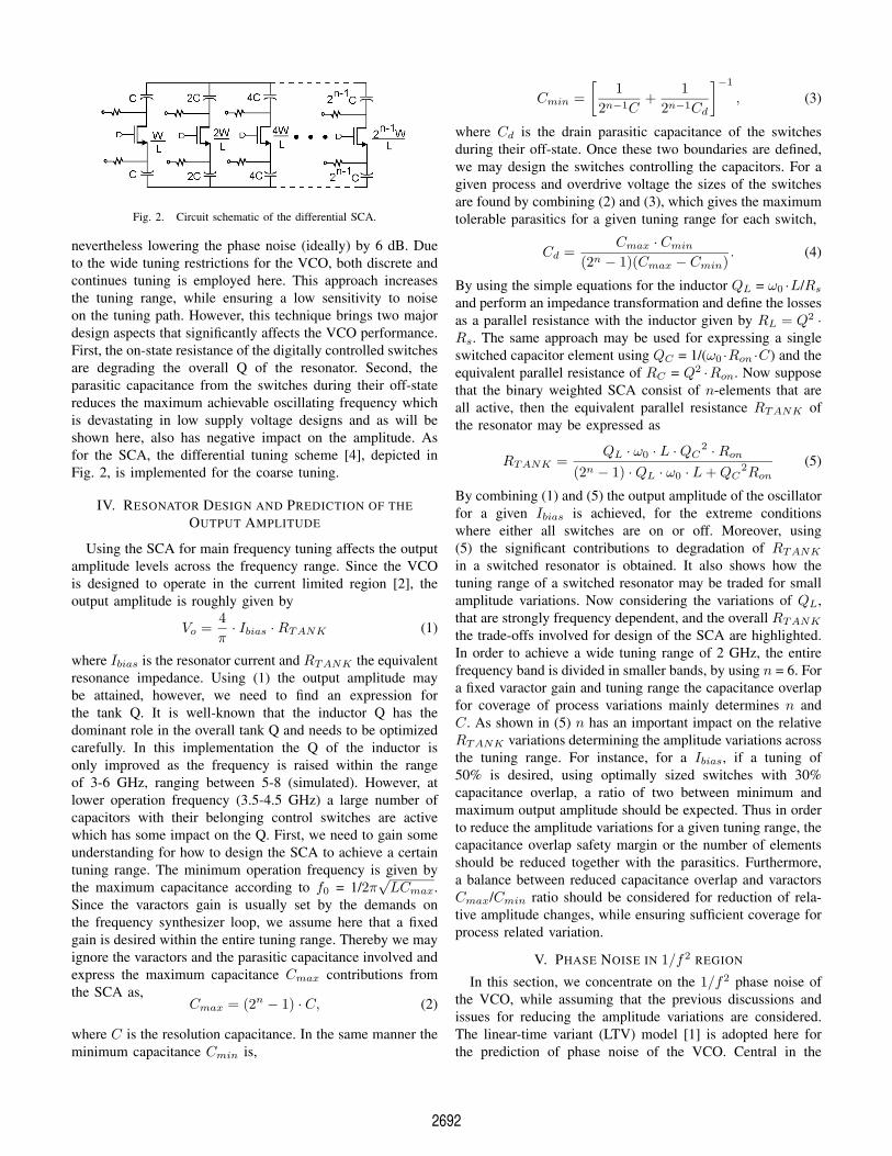
Fig. 2. Circuit schematic of the differential SCA.
nevertheless lowering the phase noise (ideally) by 6 dB. Dueto the wide tuning restrictions for the VCO, both discrete andcontinues tuning is employed here. This approach increasesthe tuning range, while ensuring a low sensitivity to noiseon the tuning path. However, this technique brings two majordesign aspects that significantly affects the VCO performance.First, the on-state resistance of the digitally controlled switchesare degrading the overall Q of the resonator. Second, theparasitic capacitance from the switches during their off-statereduces the maximum achievable oscillating frequency whichis devastating in low supply voltage designs and as will beshown here, also has negative impact on the amplitude. Asfor the SCA, the differential tuning scheme [4], depicted inFig. 2, is implemented for the coarse tuning.
IV. RESONATOR DESIGN AND PREDICTION OF THE
OUTPUT AMPLITUDE
Using the SCA for main frequency tuning affects the outputamplitude levels across the frequency range. Since the VCOis designed to operate in the current limited region [2], theoutput amplitude is roughly given by
Vo =4π· Ibias · RTANK (1)
where Ibias is the resonator current and RTANK the equivalentresonance impedance. Using (1) the output amplitude maybe attained, however, we need to find an expression forthe tank Q. It is well-known that the inductor Q has thedominant role in the overall tank Q and needs to be optimizedcarefully. In this implementation the Q of the inductor isonly improved as the frequency is raised within the rangeof 3-6 GHz, ranging between 5-8 (simulated). However, atlower operation frequency (3.5-4.5 GHz) a large number ofcapacitors with their belonging control switches are activewhich has some impact on the Q. First, we need to gain someunderstanding for how to design the SCA to achieve a certaintuning range. The minimum operation frequency is given bythe maximum capacitance according to f0 = 1/2π
√LCmax.
Since the varactors gain is usually set by the demands onthe frequency synthesizer loop, we assume here that a fixedgain is desired within the entire tuning range. Thereby we mayignore the varactors and the parasitic capacitance involved andexpress the maximum capacitance Cmax contributions fromthe SCA as,
Cmax = (2n − 1) · C, (2)
where C is the resolution capacitance. In the same manner theminimum capacitance Cmin is,
Cmin =[
12n−1C
+1
2n−1Cd
]−1
, (3)
where Cd is the drain parasitic capacitance of the switchesduring their off-state. Once these two boundaries are defined,we may design the switches controlling the capacitors. For agiven process and overdrive voltage the sizes of the switchesare found by combining (2) and (3), which gives the maximumtolerable parasitics for a given tuning range for each switch,
Cd =Cmax · Cmin
(2n − 1)(Cmax − Cmin). (4)
By using the simple equations for the inductor QL = ω0 ·L/Rs
and perform an impedance transformation and define the lossesas a parallel resistance with the inductor given by RL = Q2 ·Rs. The same approach may be used for expressing a singleswitched capacitor element using QC = 1/(ω0 ·Ron ·C) and theequivalent parallel resistance of RC = Q2 ·Ron. Now supposethat the binary weighted SCA consist of n-elements that areall active, then the equivalent parallel resistance RTANK ofthe resonator may be expressed as
RTANK =QL · ω0 · L · QC
2 · Ron
(2n − 1) · QL · ω0 · L + QC2Ron
(5)
By combining (1) and (5) the output amplitude of the oscillatorfor a given Ibias is achieved, for the extreme conditionswhere either all switches are on or off. Moreover, using(5) the significant contributions to degradation of RTANK
in a switched resonator is obtained. It also shows how thetuning range of a switched resonator may be traded for smallamplitude variations. Now considering the variations of QL,that are strongly frequency dependent, and the overall RTANK
the trade-offs involved for design of the SCA are highlighted.In order to achieve a wide tuning range of 2 GHz, the entirefrequency band is divided in smaller bands, by using n = 6. Fora fixed varactor gain and tuning range the capacitance overlapfor coverage of process variations mainly determines n andC. As shown in (5) n has an important impact on the relativeRTANK variations determining the amplitude variations acrossthe tuning range. For instance, for a Ibias, if a tuning of50% is desired, using optimally sized switches with 30%capacitance overlap, a ratio of two between minimum andmaximum output amplitude should be expected. Thus in orderto reduce the amplitude variations for a given tuning range, thecapacitance overlap safety margin or the number of elementsshould be reduced together with the parasitics. Furthermore,a balance between reduced capacitance overlap and varactorsCmax/Cmin ratio should be considered for reduction of rela-tive amplitude changes, while ensuring sufficient coverage forprocess related variation.
V. PHASE NOISE IN 1/f2 REGION
In this section, we concentrate on the 1/f2 phase noise ofthe VCO, while assuming that the previous discussions andissues for reducing the amplitude variations are considered.The linear-time variant (LTV) model [1] is adopted here forthe prediction of phase noise of the VCO. Central in the
2692

LTV model is the impulse sensitive function (ISF), which isa measure of the phase perturbation caused by an impulseinjected into the circuit at any time during an oscillationperiod. The ISF is a dimension less periodic function thatdescribes the conversion of noise sources to an excess phaseat output of the oscillator. In [1] extensive analysis shows thatthe phase noise of an oscillator in the 1/f2 region may begiven by,
L(∆ω) = 10 log
∑ i2n∆f · Γ2
rms
2q2max∆ω2
, (6)
where i2n/∆f is the total mean square noise current spectraldensity per hertz of the noise sources present, qmax is themaximum charge swing across the equivalent capacitance inthe output node, ∆ω is the offset angular frequency fromthe carrier, Γrms is the rms value of the ISF (Γ). TheISF may be obtained numerically by using time domainsimulations. However, in [5] a closed-form expression for theISF associated with the tank resistance (ΓR,N ) was derivedunder very ideal circumstances,
ΓR,N =sin ω0t
N, (7)
where N is the number of phases in the oscillator (N = 2 fora differential). Using the well-known expression for the noisecontributions of the effective tank resistance, given by
i2n,tank
∆f=
4kT
RTANK(8)
where k is the Boltzmanns constant and T is the temperature,we may find the closed formulation for the phase noise causedby RTANK [5]. Combining Eq. (6)-(8) we may express thephase noise generated by RTANK for a given frequency andoscillation amplitude. Ideally, the main noise contributionsin 1/f2 region is dominated by the tank generated noise.However, in practice, the transconductance cell also contributewith significant amount of noise. The noise power density of
the transistorsi2n,device
∆f may be modelled as,
i2n,device
∆f=
i2d,nmos
∆f+
i2d,pmos
∆f(9)
wherei2d,mos
∆f is the channel induced noise of the MOS tran-sistors. These noise sources may be described by,
i2d,mos
∆f= 4kTγgm, (10)
where γ is the device noise coefficient. In general the activenoise sources are cyclostationary due to the time-variant natureof the oscillator. Therefore [1] defines an effective ISF thatboth contains the stationary and the time duration of thepresence of the noise source given by,
Γrms,eff (φ) = Γrms(φ) · α(φ) (11)
where α(φ) represents the cyclostationary noise function. Inorder to simplify the analysis the tail current transistor is
replaced with an ideal current source, and the total noisecontribution is calculated using the above derived equations.For the cyclostationary noise sources, time domain simulationmay be performed by injecting a perturbation into the oscil-lator over a single oscillation cycle and measuring the excessphase shift. The amount of charge injected must be carefullydetermined in such a manner so that the linearity assumptionof the system is satisfied. The results obtained using the LTV-model may easily be verified with the spectreRF simulations,where it is also possible to find the noise contributions NLfrom each element in the circuit. By taking into account allthe noise contributions, the phase noise may be expressed asthe ratio between the noise power and oscillation amplitude,
L(∆ω) = 10 log(∑
NLV 2
o /2
). (12)
As suggested in [5], combining Eq. (6) and (12), we may findthe noise contribution of a certain noise component accordingto,
NL =i2n∆f · Γ2
rms
4C2∆ω2. (13)
The above derivation is used for verification of the calculatednoise sources with spectreRF simulations. Finally, it is possibleto determine the biasing conditions and sizing of the activesfor proper oscillation across the entire frequency band, withregards on the tank Q variations. It was observed that thelowest phase noise performance could be achieved by finding aratio between the PMOS and NMOS transistors that minimizedtheir relative noise contributions and also satisfying the startupconditions. Furthermore, in order to minimize the relativeamplitude variations, the bias current was chosen so that theVCO is operated in the current-limited region [2] for a largefrequency range and in the ”weak” voltage limited region onlyat the top frequency band. This is satisfied for a tank current of4 mA from 1.5 V supply voltage, and a PMOS to NMOS ratioof approximately 3. Under these bias conditions the relativenoise contributions from the tank are near 44%, the NMOSpair contributions are 20%, and the PMOS pair contribute withalmost 36% of the total noise at 1 MHz offset at 5 GHz carrierfrequency. The calculated phase noise levels are -118 - -121dBc/Hz at 1 MHz offset along the frequency range. Thesecalculations agree within 2 dBc/Hz to the complete schematicsimulations including buffers and the tail current mirror.
VI. MEASUREMENTS
Measurements on the prototype circuits have been per-formed on a gold plated FR4 PCB to which the die, depictedin Fig. 3, is wire-bonded to. The frequency characteristicsand output power was measured using a Rhode & SchwarzFSEM30 spectrum analyzer and for the phase noise mea-surements a PN9000 system was used. The VCO is able tooperate within 1.8 GHz frequency band, ranging between 3.5to 5.3 GHz. The output power was as predicted in simulationsincreased as the bias current was increased up to 6 mA.Several phase noise measurements were performed at differentcarrier frequencies all indicating that the optimum bias point
2693

Fig. 3. Chip photo of the 0.85 x 0.55 mm 0.18µm CMOS VCO.
Fig. 4. Measured phase noise from 3.8 GHz carrier consuming 6 mW.
is around 3.5-4 mA from 1.5 V supply, which are in goodagreement with the calculations and simulations. As for theoutput amplitude, the lowest variations was obtained for a tankcurrent larger than 5 mA. Meanwhile for this bias current thephase noise was slightly degraded at the top frequency bandand only marginally improved at frequencies below 4.5 GHz,since the VCO is operated in the voltage-limited region atthe top frequency band. One other significant source for thedegradation of phase noise at the top frequency band for largebias currents, could be tracked to the AM-PM conversion,indicating that there is still a strong impact from the varactors.This effect is less dominant on the lower operation frequenciessince additional MIM capacitors, by means of the SCA,reduces the gain of the varactors and also the oscillationamplitude. Thus, as a compromise a bias current of 4 mAwas chosen, providing with acceptable phase noise levelsand amplitude variations of ≈ 40% across the tuning range.Figure 4, 5 and 6 shows the entire single-sideband phase noisefor a 3.8, 4.5 and 5.3 GHz carrier respectively. The phase noiseat 1 MHz offset is -115 dBc/Hz or less across the operationfrequency. These measurements agree within 3 dBc to theschematic simulations.
VII. CONCLUSIONS
A highly flexible wide-band CMOS VCO, utilizing switchedtuning was presented. The implementation aspects, in partic-ular amplitude and phase noise, was analyzed and verifiedagainst simulations. It highlights the important issues andtrade-offs for the design of wide-band VCOs. Moreover, dis-cussions on proper the tank current for reduction of amplitudevariations and low phase noise has been addressed. The resultswere demonstrated in a 6 mW VCO with 1.8 GHz tuningrange, displaying phase noise levels of less than -115 dBc/Hzat 1 MHz offset, suited for high data rate multi-standard radios.
Fig. 5. Measured phase noise at 4.5 GHz.
Fig. 6. Measured phase noise at 5.3 GHz.
VIII. ACKNOWLEDGMENT
This study is supported by Acreo AB within the SoCWareprogram and funded partially by NorFA. The author is gratefulto Note Norrtalje AB for the bonding and to Rohde &Schwarz for providing with a spectrum analyzer. A specialthanks to Dr. H. Sjoland, F. Tillman and N. Troedsson, Dept.of Electroscience, Lund University for their help with thephase noise measurements and to Dr. P. Andreani, TechnicalUniversity of Denmark, for fruitful and inspiring conversationson VCOs.
REFERENCES
[1] A. Hajimiri and T.H. Lee, A General Theory of Phase Noise in ElectricalOscillators, IEEE Journal of Solid-State Circuits, Vol. 33, No. 2February 1998.
[2] D. Ham and A. Hajimiri, Concepts and Methods in Optimization ofIntegrated LC VCOs, IEEE Journal of Solid-State Circuits, Vol. 36,No. 6 June 2001.
[3] A. Fard, T. Johnson and D. Aberg Design of a Dual-Band 5/2.4 GHzCMOS VCO for 802.11 a/b/g WLAN Transceivers, Proc. of IEEEAsia-Pacific Conf. on Circuits and Systems, Dec 2004, Taiwan
[4] H. Sjoland, Improved Switched Tuning of Differential CMOS VCOs,IEEE Transactions on Circuits and Systems, Analog and Digital SignalProcessing, Vol. 49, No. 5. May 2002
[5] P. Andreani and X. Wang, On the phase-noise and phase-error perfor-mances of multiphase LC CMOS VCOs, IEEE Journal of Solid-StateCircuits, Vol. 39, no. 11 November 2004.
2694
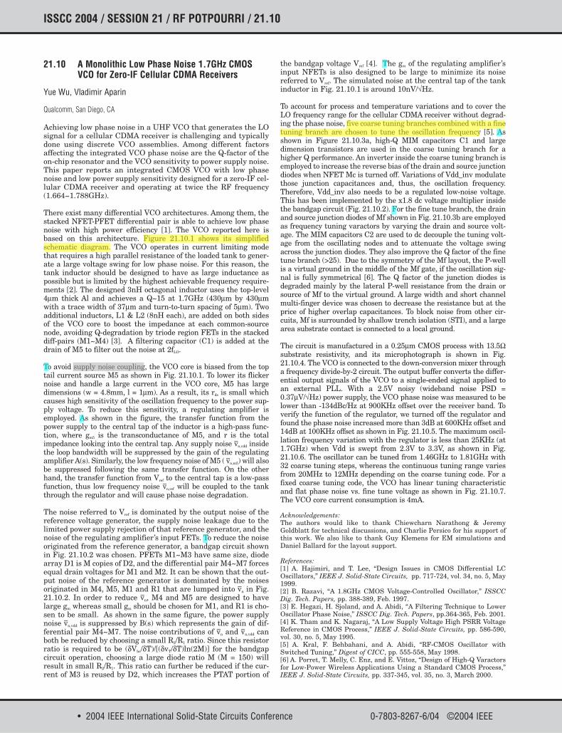
• 2004 IEEE International Solid-State Circuits Conference 0-7803-8267-6/04 ©2004 IEEE
ISSCC 2004 / SESSION 21 / RF POTPOURRI / 21.10
21.10 A Monolithic Low Phase Noise 1.7GHz CMOS VCO for Zero-IF Cellular CDMA Receivers
Yue Wu, Vladimir Aparin
Qualcomm, San Diego, CA
Achieving low phase noise in a UHF VCO that generates the LOsignal for a cellular CDMA receiver is challenging and typicallydone using discrete VCO assemblies. Among different factorsaffecting the integrated VCO phase noise are the Q-factor of theon-chip resonator and the VCO sensitivity to power supply noise.This paper reports an integrated CMOS VCO with low phasenoise and low power supply sensitivity designed for a zero-IF cel-lular CDMA receiver and operating at twice the RF frequency(1.664~1.788GHz).
There exist many differential VCO architectures. Among them, thestacked NFET-PFET differential pair is able to achieve low phasenoise with high power efficiency [1]. The VCO reported here isbased on this architecture. Figure 21.10.1 shows its simplifiedschematic diagram. The VCO operates in current limiting modethat requires a high parallel resistance of the loaded tank to gener-ate a large voltage swing for low phase noise. For this reason, thetank inductor should be designed to have as large inductance aspossible but is limited by the highest achievable frequency require-ments [2]. The designed 3nH octagonal inductor uses the top-level4µm thick Al and achieves a Q~15 at 1.7GHz (430µm by 430µmwith a trace width of 37µm and turn-to-turn spacing of 5µm). Twoadditional inductors, L1 & L2 (8nH each), are added on both sidesof the VCO core to boost the impedance at each common-sourcenode, avoiding Q-degradation by triode region FETs in the stackeddiff-pairs (M1~M4) [3]. A filtering capacitor (C1) is added at thedrain of M5 to filter out the noise at 2fLO.
To avoid supply noise coupling, the VCO core is biased from the toptail current source M5 as shown in Fig. 21.10.1. To lower its flickernoise and handle a large current in the VCO core, M5 has largedimensions (w = 4.8mm, l = 1µm). As a result, its rds is small whichcauses high sensitivity of the oscillation frequency to the power sup-ply voltage. To reduce this sensitivity, a regulating amplifier isemployed. As shown in the figure, the transfer function from thepower supply to the central tap of the inductor is a high-pass func-tion, where gm5 is the transconductance of M5, and r is the totalimpedance looking into the central tap. Any supply noise v
_n,vdd inside
the loop bandwidth will be suppressed by the gain of the regulatingamplifier A(s). Similarly, the low frequency noise of M5 ( v
_n,m5) will also
be suppressed following the same transfer function. On the otherhand, the transfer function from Vref to the central tap is a low-passfunction, thus low frequency noise v
_n,ref will be coupled to the tank
through the regulator and will cause phase noise degradation.
The noise referred to Vref is dominated by the output noise of thereference voltage generator, the supply noise leakage due to thelimited power supply rejection of that reference generator, and thenoise of the regulating amplifier’s input FETs. To reduce the noiseoriginated from the reference generator, a bandgap circuit shownin Fig. 21.10.2 was chosen. PFETs M1~M3 have same size, diodearray D1 is M copies of D2, and the differential pair M4~M7 forcesequal drain voltages for M1 and M2. It can be shown that the out-put noise of the reference generator is dominated by the noisesoriginated in M4, M5, M1 and R1 that are lumped into v
_n in Fig.
21.10.2. In order to reduce v_
n, M4 and M5 are designed to havelarge gm whereas small gm should be chosen for M1, and R1 is cho-sen to be small. As shown in the same figure, the power supplynoise v
_n,vdd is suppressed by B(s) which represents the gain of dif-
ferential pair M4~M7. The noise contributions of v_
n and v_
n,vdd canboth be reduced by choosing a small R2/R1 ratio. Since this resistorratio is required to be (δVbe/δT)/[(δvT/δT)ln(2M)] for the bandgapcircuit operation, choosing a large diode ratio M (M = 150) willresult in small R2/R1. This ratio can further be reduced if the cur-rent of M3 is reused by D2, which increases the PTAT portion of
the bandgap voltage Vref [4]. The gm of the regulating amplifier’sinput NFETs is also designed to be large to minimize its noisereferred to Vref. The simulated noise at the central tap of the tankinductor in Fig. 21.10.1 is around 10nV/√Hz.
To account for process and temperature variations and to cover theLO frequency range for the cellular CDMA receiver without degrad-ing the phase noise, five coarse tuning branches combined with a finetuning branch are chosen to tune the oscillation frequency [5]. Asshown in Figure 21.10.3a, high-Q MIM capacitors C1 and largedimension transistors are used in the coarse tuning branch for ahigher Q performance. An inverter inside the coarse tuning branch isemployed to increase the reverse bias of the drain and source junctiondiodes when NFET Mc is turned off. Variations of Vdd_inv modulatethose junction capacitances and, thus, the oscillation frequency.Therefore, Vdd_inv also needs to be a regulated low-noise voltage.This has been implemented by the x1.8 dc voltage multiplier insidethe bandgap circuit (Fig. 21.10.2). For the fine tune branch, the drainand source junction diodes of Mf shown in Fig. 21.10.3b are employedas frequency tuning varactors by varying the drain and source volt-age. The MIM capacitors C2 are used to dc decouple the tuning volt-age from the oscillating nodes and to attenuate the voltage swingacross the junction diodes. They also improve the Q factor of the finetune branch (>25). Due to the symmetry of the Mf layout, the P-wellis a virtual ground in the middle of the Mf gate, if the oscillation sig-nal is fully symmetrical [6]. The Q factor of the junction diodes isdegraded mainly by the lateral P-well resistance from the drain orsource of Mf to the virtual ground. A large width and short channelmulti-finger device was chosen to decrease the resistance but at theprice of higher overlap capacitances. To block noise from other cir-cuits, Mf is surrounded by shallow trench isolation (STI), and a largearea substrate contact is connected to a local ground.
The circuit is manufactured in a 0.25µm CMOS process with 13.5Ωsubstrate resistivity, and its microphotograph is shown in Fig.21.10.4. The VCO is connected to the down-conversion mixer througha frequency divide-by-2 circuit. The output buffer converts the differ-ential output signals of the VCO to a single-ended signal applied toan external PLL. With a 2.5V noisy (wideband noise PSD =0.37µV/√Hz) power supply, the VCO phase noise was measured to belower than -134dBc/Hz at 900KHz offset over the receiver band. Toverify the function of the regulator, we turned off the regulator andfound the phase noise increased more than 3dB at 600KHz offset and14dB at 100KHz offset as shown in Fig. 21.10.5. The maximum oscil-lation frequency variation with the regulator is less than 25KHz (at1.7GHz) when Vdd is swept from 2.3V to 3.3V, as shown in Fig.21.10.6. The oscillator can be tuned from 1.46GHz to 1.81GHz with32 coarse tuning steps, whereas the continuous tuning range variesfrom 20MHz to 12MHz depending on the coarse tuning code. For afixed coarse tuning code, the VCO has linear tuning characteristicand flat phase noise vs. fine tune voltage as shown in Fig. 21.10.7.The VCO core current consumption is 4mA.
Acknowledgements:The authors would like to thank Chiewcharn Narathong & JeremyGoldblatt for technical discussions, and Charlie Persico for his support ofthis work. We also like to thank Guy Klemens for EM simulations andDaniel Ballard for the layout support.
References:[1] A. Hajimiri, and T. Lee, “Design Issues in CMOS Differential LCOscillators,” IEEE J. Solid-State Circuits, pp. 717-724, vol. 34, no. 5, May1999.[2] B. Razavi, “A 1.8GHz CMOS Voltage-Controlled Oscillator,” ISSCCDig. Tech. Papers, pp. 388-389, Feb. 1997.[3] E. Hegazi, H. Sjoland, and A. Abidi, “A Filtering Technique to LowerOscillator Phase Noise,” ISSCC Dig. Tech. Papers, pp.364-365, Feb. 2001.[4] K. Tham and K. Nagaraj, “A Low Supply Voltage High PSRR VoltageReference in CMOS Process,” IEEE J. Solid-State Circuits, pp. 586-590,vol. 30, no. 5, May 1995.[5] A. Kral, F. Behbahani, and A. Abidi, “RF-CMOS Oscillator withSwitched Tuning,” Digest of CICC, pp. 555-558, May 1998.[6] A. Porret, T. Melly, C. Enz, and E. Vittoz, “Design of High-Q Varactorsfor Low-Power Wireless Applications Using a Standard CMOS Process,”IEEE J. Solid-State Circuits, pp. 337-345, vol. 35, no. 3, March 2000.
tianjun
Squiggly
tianjun
Squiggly
tianjun
Underline
tianjun
Squiggly
tianjun
Highlight
tianjun
Squiggly
tianjun
Underline
tianjun
Squiggly
tianjun
Underline
tianjun
Cross-Out
tianjun
Cross-Out
tianjun
Cross-Out
tianjun
Cross-Out
tianjun
Cross-Out
tianjun
Line
tianjun
Highlight
tianjun
Cross-Out
tianjun
Highlight
tianjun
Cross-Out
tianjun
Cross-Out
tianjun
Underline
tianjun
Highlight
tianjun
Cross-Out
tianjun
Cross-Out
tianjun
Cross-Out
tianjun
Squiggly
tianjun
Squiggly
tianjun
Squiggly
tianjun
Underline
tianjun
Highlight
tianjun
Cross-Out
tianjun
Underline
tianjun
Underline
tianjun
Cross-Out
tianjun
Squiggly
tianjun
Squiggly
tianjun
Squiggly
tianjun
Squiggly
tianjun
Underline
tianjun
Cross-Out
tianjun
Cross-Out
tianjun
Highlight
tianjun
Highlight
tianjun
Highlight
tianjun
Squiggly
tianjun
Cross-Out
tianjun
Cross-Out
tianjun
Highlight
tianjun
Underline
tianjun
Cross-Out
tianjun
Cross-Out
tianjun
Cross-Out
tianjun
Cross-Out
tianjun
Underline
tianjun
Line
tianjun
Underline
tianjun
Underline
tianjun
Underline
tianjun
Underline
tianjun
Underline
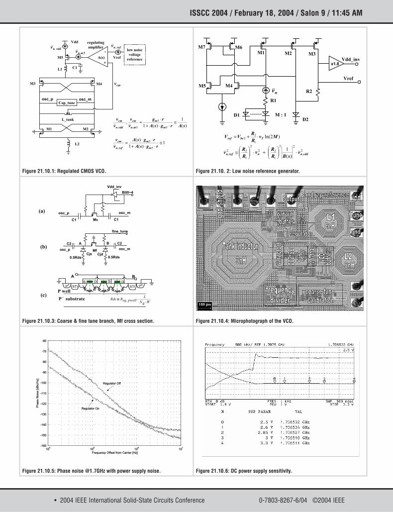
• 2004 IEEE International Solid-State Circuits Conference 0-7803-8267-6/04 ©2004 IEEE
ISSCC 2004 / February 18, 2004 / Salon 9 / 11:45 AM
Figure 21.10.1: Regulated CMOS VCO. Figure 21.10. 2: Low noise reference generator.
Figure 21.10.3: Coarse & fine tune branch, Mf cross section.
Figure 21.10.5: Phase noise @1.7GHz with power supply noise. Figure 21.10.6: DC power supply sensitivity.
Figure 21.10.4: Microphotograph of the VCO.
! "#"$
%"
&'($)
*
++
,
%
-
$/$2
#2
()
(/)
(&)
Figure 21.10.7: Oscillation frequency & phase noise vs. fine tune voltage.
• 2004 IEEE International Solid-State Circuits Conference 0-7803-8267-6/04 ©2004 IEEE

RF-CMOS Oscillators with Switched Tuning A. Kral, F. Behbahani, and A. A. Abidi
Electrical Engineering Department University of California
Los Angeles, CA 90095-1 594
Fully integrated CMOS oscillators are of great interest for use in single-chip wireless transceivers. In most oscillator circuits reported to date that operate in the 0.9 to 2 GHz frequency range, an integrated spiral inductor sets the frequency. It is generally believed that an LC oscillator, even when it uses a low-Q inductor, displays a lower phase noise than a ring oscillator. However, due to the absence of a good varactor compatible with CMOS technology, the integrated LC oscillator suffers from a very limited tuning range. Although this tuning range may encompass the limited frequency agility re- quired in an RF oscillator, for instance to span the modulation bandwidth in a transmitter, it will seldom cover the much larger lot-to-lot process variations manifest as spre,nds of up to 20% in capacitance. Fortunately, the self-inductance of a metal spiral does not suffer spreads, because it depends on a precise number of turns and on the geometry of metal traces which is little affected by fluctuations in lithography.
how to design RF CMOS oscillators with a wide enough tuning range to reliably cover process variations, without compromising current drain or phase noise. Prototypes were developed in the 0.6-pm MOSIS CMOS process to oscillate at up to 1.8 GHz with a sub-3V supply. The tuning method exploits digital capabilities and MOS analog switches.
This work itddresses the practical problem of
On-Chip Components for Tuning Capacitors A CMOS oscillai or may be continuously tuned with two possible voltage-dependent capacitors: the voltage-dependent junction capacitor at the source or drain diffusion; 'or the voltage-dependent MOS capacitor (a MOSFET with source and drain shorted). Now in a MOS oscillator the capacitor in the resonant circuit is subject to large signal swings, on the order of i he supply voltage. Thus, depending on its amplitude, the oscillation probes different
Research supported by DARPA, Rockwell International, Harris Semiconductor, Motorola, Ericsson, Toshiba, and the State of California MICRO Program.
regions of the MOS capacitor's small-signal C-V characteristic, from inversion, through depletion, into accumulation (Figure 1). The average capaci- tance it experiences varies with the bias Vcs-Vt. The frequency of oscillation depends on the average capacitance, while the effect of the varying incremen- tal capacitance across a cycle is to distort the oscillat- ing waveform into a non-sinusoid. This distortion is usually small, and in any case unimportant in this application.
to junction capacitor tuning we have described in previous work [l]. The control voltage on the MOS capacitor may be swept across the full power supply with no fear of forward bias. Also, in a junction capacitor the spreading resistance in the substrate or well is set by junction size and doping, whereas in a MOS capacitor it depends on the region of operation at any instant of time. In accumulation, it is a spreading resistance in the substrate to ground; in depletion, it is this spreading resistance in series with a small capacitor; and in inversion, it is the resistance of the MOSFET channel, which is much lower than the spreading resistance, even at a modest VGS-Vt.
The oscillator current drain is lowered by using as large a load impedance as is possible at the oscillation frequency. Assuming the inductor domi- nates the quality factor, Q, of this LC tuned circuit load, this is tantamount to tuning the oscillator with the largest possible inductor. However, as the induc- tance of a metal spiral is made larger, its self- capacitance increases as well, eventually causing the inductor to self-resonate below the target oscillation frequency, here 1.8 GHz. Therefore, spiral structures with the lowest self-capacitance per unit inductance were investigated.
The three levels of metal available in this process make it possible to fabricate a useful multi-layer spiral inductor [2,3], whose inductance per unit area, owing to solenoid-like properties, rises almost quadratically with the number of layers. Although there is substantial capacitance between the turns in
MOS capacitor tuning is used here, as opposed
Mu It i- laye r Inductors
26.1 . I 0-7803-4292-5/97/$10.00 C 1998 IEEE
555 IEEE 1998 CUSTOM INTEGRATED CIRCUITS CONFERENCE

the closest layers of such a spiral (Figure 3), the capacitance to substrate experiences the largest signal voltage. Without resorting to selective removal of the substrate underlying the inductor [4], three- layer inductors of about 10 nH may be realized for use at 2 GHz.
This inductor suffers mainly from the loss due to the resistance of the metal windings, but also due to substrate losses caused by displacement currents flowing in the substrate spreading resistance, and due to eddy currents induced in the heavily doped substrate under the 6-pm thick epi layer. A laminated grounded polysilicon shield plate is placed under all the inductors to prevent the displacement currents from flowing into the substrate 151. A simple four- element model (Figure 2) is found to accurately fit the complex impedance of standalone test inductors measured with a Picoprobe@ across 0.8 to 5 GHz. The quality factor, Q, of any inductor at a certain frequency may be deduced from the model. For instance, at 1.5 GHz the Q of the 13.1 nH inductor is 2.9.
Random voltage fluctuations on the control terminal of a VCO modulate its frequency and induce phase noise [6]. The larger the VCO modula- tion index Kv (Hz/V), the higher the induced phase noise. This gives rise to a dichotomy, because as mentioned in the Introduction a large Kvis benefi- cial to encompass process spreads; however, it will also raise the phase noise. This leads to the concept of switch-selected tuning elements in a VCO.
Switch-Selected Tuning & Results Principle The frequency of the RF VCO in a wireless trans- ceiver is either set by a synthesizer PLL to some fixed value (as in the receiver, and often in the transmitter), or it is directly modulated by the baseband data across a small fractional range (some- times in a transmitter). Thus, one way to resolve the conflicting requirements described above is to switch in tuning elements from an array such that a stag- gered but overlapping series of VCO characteristics is obtained, each with low Kv but together covering the desired range (Figure 3). A mixed analog-digital PLL must tune this VCO, first by digitally selecting the appropriate tuning element, and then fine-tuning the frequency with the analog output of a phase- frequency detector. ,
The overlap regions are sufficiently wide to accommodate the modulation bandwidth, if this VCO is to be used in a transmitter. Thus during continuous modulation the tuning element will never have to be switched. Also, the overlap region must
encompass statistical fluctuations across an array of tuning elements fabricated on-chip (which are much lower than process spreads).
An LC oscillator may be tuned by connecting some combination of MOS capacitors selected from a weighted array across a fixed inductor. Each capaci- tor may be tuned continuously with an analog voltage, and together the array defines the desired piecewise V-f characteristic (Figure 3). The challenge here is to build a satisfactory RF switch which will select the capacitors. The switch resistance must be sufficiently low to not degrade the capacitor Q. This implies a FET with a large W/L ratio whose large junction capacitance will now parasitically load the capacitor array when the FET is turned OFF, and compress the available spread in capacitance.
array of doughnut-shaped sub-FETs (Figure 4), whose gate encloses the drain junction. The drain junction capacitance is 20% lower than in a conven- tional interdigitated FET, but the source capacitance is larger. However, this is unimportant in the in- tended use because the source is grounded (Figure 4). The switch is used to connect a fixed linear capacitor (poly on thin oxide over N+ diffusion) in parallel with a tunable MOS capacitor. The measured tuning range is 1.34 GHz f6% (Figure 5), which verifies that the ("itched) MOSFET drain capacitance is not so large that it swamps out the discrete capacitor being connected. The measured phase noise remains almost the same when the RF switch is ON or OFF, which shows that its resistance does not degrade resonator Q. In the transition region when the switch is partly ON, it severely lowers the capacitor Q and the phase noise is 12 dB worse. Of course, the switch will never be used in this way. The current drain rises slightly at the lower fre- quency.
and its drain junction capacitance will change with the drain voltage. Over the rail-to-rail oscillation amplitude, the average resistance is 80R and the average drain capacitance is 40 fF.
an RF oscillator with an array of switched capacitors.
While a series MOSFET is able to select a capacitor without degrading resonator Q, when used in series with an inductor it adds a much larger relative loss. However, one of an array of independent oscillators may be selected with a MOSFET switch connected to a common-mode point outside the oscillator loop
Switched Tu n in g Cap ac i t o rs
In this prototype, the RF switch consists of an
Both the ON resistance of the MOSFET switch
This prototype shows the feasibility of tuning
Switched Tuning Inductors
nn mj. l . 2 556
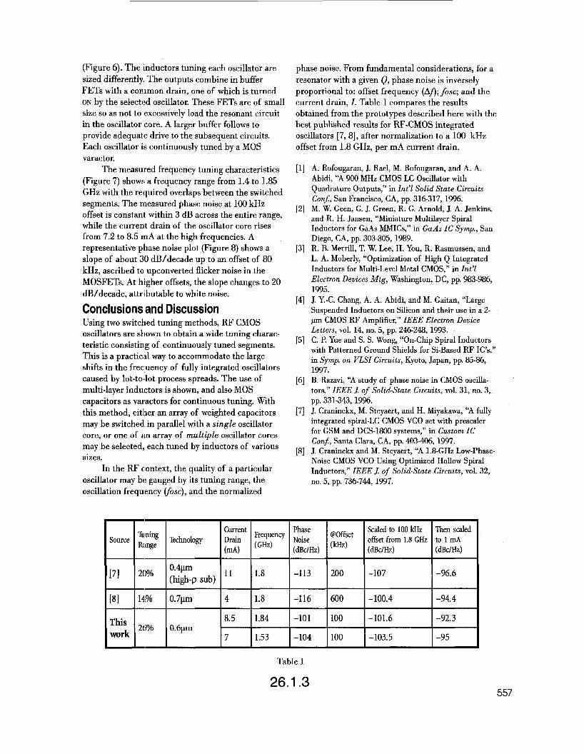
(Figure 6). The inductors tuning each oscillator are sized differently. The outputs combine in buffer FETs with a common drain, one of which is turned ON by the selected oscillator. These FETs are of small size so as not to excessively load the resonant circuit in the oscillator core. A larger buffer follows to provide adequate drive to the subsequent circuits. Each oscillator is continuously tuned by a MOS varactor.
The measured frequency tuning characteristics (Figure 7) show:; a frequency range from 1.4 to 1.85 GHz with the required overlaps between the switched segments. The measured phase noise at 100 kHz offset is constant within 3 dB across the entire range, while the current drain of the oscillator core rises from 7.2 to 8.5 rnA at the high frequencies. A representative phase noise plot (Figure 8) shows a slope of about 30 dB/decade up to an offset of 80 kHz, ascribed to upconverted flicker noise in the MOSFETs. At higher offsets, the slope changes to 20 dB/decade, attributable to white noise.
Conclusions and Discussion Using two switched tuning methods, RF CMOS oscillators are shown to obtain a wide tuning charac- teristic consisting of continuously tuned segments. This is a practical way to accommodate the large shifts in the frequency of fully integrated oscillators caused by lot-to.lot process spreads. The use of multi-layer inductors is shown, and also MOS capacitors as varactors for continuous tuning. With this method, either an array of weighted capacitors may be switched in parallel with a single oscillator core, or one of an array of mult$e oscillator cores may be selected, each tuned by inductors of various sizes.
oscillator may bc gauged by its tuning range, the oscillation frequency (fbc), and the normalized
In the RF context, the quality of a particular
phase noise. From fundamental considerations, for a resonator with a given Q, phase noise is inversely proportional to: offset frequency (AA; fosc; and the current drain, I. Table 1 compares the results obtained from the prototypes described here with the best published results for RF-CMOS integrated oscillators [7,8], after normalization to a 100 kHz offset from 1.8 GHz, per mA current drain.
A. Rofougaran, J. Rael, M. Rofougaran, and A. A. Abidi, “A 900 MHz CMOS LC Oscillator with Quadrature Outputs,” in Int’l Solid State Circuits Conj, San Francisco, CA, pp. 316-317, 1996. M. W. Geen, G. J. Green, R. G. Arnold, J. A. Jenkins, and R. H. Jansen, “Miniature Multilayer Spiral Inductors for GaAs MMICs,” in GaAs IC Symp., San Diego, CA, pp. 303-305, 1989. R. B. Merrill, T. W. Lee, H. You, R. Rasmussen, and L. A. Moberly, “Optimization of High Q Integrated Inductors for Multi-Level Metal CMOS,” in Int’l Electron Devices Mtg, Washington, DC, pp. 983-986, 1995. J. Y.-C. Chang, A. A. Abidi, and M. Gaitan, “Large Suspended Inductors on Silicon and their use in a 2- pm CMOS RF Amplifier,” IEEE Electron Device Letters, vol. 14, no. 5, pp. 246-248, 1993. C. P. Yue and S. S. Wong, “On-Chip Spiral Inductors with Patterned Ground Shields for Si-Based RF IC’s,” in Symp. on VLSI Circuits, Kyoto, Japan, pp. 85-86, 1997. B. Razavi, “A study of phase noise in CMOS oscilla- tors,” IEEE J; of Solid-State Circuits, vol. 31, no. 3,
J. Craninckx, M. Steyaert, and H. Miyakawa, “A fully integrated spiral-LC CMOS VCO set with prescaler for GSM and DCS-1800 systems,” in Custom IC Con$, Santa Clara, CA, pp. 403-406, 1997. J. Craninckx and M. Steyaert, “A 1.8-GHz Low-Phase- Noise CMOS VCO Using Optimized Hollow Spiral Inductors,” IEEE J; of Solid-State Circuits, vol. 32, no. 5, pp. 736-744, 1997.
pp. 331-343, 1996.
Table 1
26.1 -3 557

4 cs-s
Figure 1: MOS capacitor presents an average capaci- tance to a large signal that varies with bias.
1.43
3 1.39 5;
1.35
2 1.31
N
3 U
U
1.27
0 1 2 3 Switch FETVG,V
Figure 5: Measured tuning range with fixed switched capacitor. Three measured values of SSB phase noise indBc/Hz at 100 kHz offset are given, as well as the supply current.
combined output. Figure 2: Multi-layer spiral inductor and +15 two-terminal circuit model. Examples of model parameters: 13.1nH, Rs=37Q 203fF, 14Q or 8.7nH, Rs=28Q,171fF, 2SsZ>.
, ,".- I "c
Figure 3,: Principle of switched tuning element to cover a wide frequency range.
P c
Figure 4: Oscillator tuned with switched capacitor; layout of RF switch FET
0 1 2 3 MOS Cao Vc,V
Figure 7: Measured frequenci-tuning characteristics of array. Continuous tuning is with MOS capacitor, discrete steps by selecting oscillators with different inductors. Phase noise at 100 kHz offset shown.
10' lo2 io3 io4 10' lo6 Offset Frequency,Hz
Figure 8: Typical measured actual phase noise plot.
26.1.4 558