Characterization of 300 GHz Wireless Channel on a Computer ...
13
1 Characterization of 300 GHz Wireless Channel on a Computer Motherboard Seunghwan Kim, Student Member, IEEE and Alenka Zaji´ c, Senior Member, IEEE Abstract— This paper presents characterization of 300 GHz wireless channel on a computer motherboard, where several different measurement scenarios have been considered. Results indicate that the presence of the ground plane and/or vertical parallel-plate structures in the channel introduce multipath that, if constructively superimposed, may create a path loss lower than free-space propagation path loss. Additionally, it has been found that a few centimeters of vertical misalignment between the transmitter and receiver result in a path loss greater than 5 dB. Furthermore, the results indicate that vertical components such as a Dual In-line Memory Modules (DIMM) with reflectio coefficien close to one for all incident angles can be used to create Directed non-line-of-sight (DNLoS) links with wide coherence bandwidth. Finally, for LoS propagation obstructed by large objects, such as a heatsink, the path loss exponent of 1.77 is found, while the rotating fan causes periodic fading in the received power indicating that channel equalization techniques will be needed to overcome deep fades. All these results indicate that optimal communications can be achieved by carefully positioning the antennas with respect to the motherboard layout. Index Terms— Chip-to-chip wireless channels, THz commu- nications, channel sounding, channel measurements, channel characterization. I. I NTRODUCTION Data communication between computer components, such as processor and memory within a computer system, currently relies on metal wires and a transition to optical waveguides is expected in the future. While optics promise much higher bandwidth (and thus improved computing performance), both wires and optics suffer from significan challenges in terms of assembly cost, airfl w, service time, and overall cost, etc. [1]- [3]. For system components, the number of pins or optical interfaces that a small chip package can have is limited, and sophisticated connections can also make component insertion (e.g. during assembly) and removal (e.g. to replace a failed component) more time-consuming and costly [4]- [6]. Wireless communication can alleviate such cable man- agement, serviceability, and packaging constraints [7]- [24]. Integration of wireless transceivers and antennas into the chip package would provide communication bandwidth without adding pins or fibe connectors to the chip package. A key Manuscript received November 6, 2015; revised April 4, 2016; revised July 20 2016, accepted September 18, 2016. Seunghwan Kim and Alenka Zaji´ c are with the School of Electrical and Computer Engineering, Georgia Institute of Technology, Atlanta, GA 30332 USA (e-mail: [email protected]; [email protected]) This work has been supported by NSF grant 1318934. The views and finding in this paper are those of the authors and do not necessarily reflec the views of NSF. Color versions of one or more of the figure in this paper are available online at http://ieeexplore.ieee.org. challenge for wireless communication is that the required data rates in existing systems are already in the hundreds of gigabits per second. For example, a computer in a typical high- performance cluster gets 56 Gbits/s through an InfiniBan FDR X4 link [25], and this is expected [26] to improve to 100 Gbits/s this year (InfiniBan EDR) and to 200 Gbits/s in 2017 (InfiniBan HDR). Achieving such per-link data rates is unlikely to be feasible for wireless communication at mm- Wave frequencies. As an example, WiGig [27] uses 60 GHz frequency range to provide up to 7 Gbits/s using OFDM, 64- QAM, and sophisticated coding. Terahertz (THz) wireless communications have two key advantages that can be combined to achieve the required data rates [28]. First, the usable frequency band around each frequency is much larger, so each channel can have a much higher data rate. This alone can increase data rates to several tens of Gbits/s, but spatial multiplexing is still needed to reach Tbits/s data rates. Fortunately, THz frequencies allow smaller antennas and antenna spacing, which provides for more communication channels within the same array aperture within a chip package. Finally, THz wireless communications offer some potential advantages relative to free-space optical communication because it also allows wireless communication within a system where free-space optical faces the problem of getting out of and into the chip package. To enable chip-to-chip THz wireless communications, it is imperative to understand propagation mechanisms that govern communication in the unique propagation environment of a computer system (motherboard) at these high frequencies. While measurements on the computer motherboard have been reported at lower frequencies [16]- [19], to the best of our knowledge, no channel measurements in the computer moth- erboard environment at 300 GHz have been reported in the open literature. As the firs step toward characterizing 300 GHz chip-to-chip channel on a motherboard, we have performed measurements in fi e different scenarios: Line-of-Sight (LoS) in the presence of a large ground plane (i.e. motherboard), a LoS with the height difference between the transmitter (T x ) and the receiver (R x ) (e.g., link between the processor and memory), a Reflected-Non-Line-of-Sigh (RNLoS) link via reflectio off the surfaces of vertically inserted components (e.g., link between Dual In-line Memory Modules (DIMM’s) or graphic/sound cards), an obstructed LoS (OLoS) scenario where the EM waves travel through the metal parallel-plate structures (i.e. between two DIMM’s), and finall , no LoS (NLoS) scenarios with a heatsink and a rotating fan as obstructions. The contributions of this paper are: Digital Object Identifier: 10.1109/TAP.2016.2620598 1558-2221 c 2016 IEEE. Personal use is permitted, but republication/redistribution requires IEEE permission. See http://www.ieee.org/publications standards/publications/rights/index.html for more information.
-
Upload
khangminh22 -
Category
Documents
-
view
3 -
download
0
Transcript of Characterization of 300 GHz Wireless Channel on a Computer ...
1
Characterization of 300 GHz Wireless Channel on aComputer Motherboard
Seunghwan Kim, Student Member, IEEE and Alenka Zajic, Senior Member, IEEE
Abstract—This paper presents characterization of 300 GHzwireless channel on a computer motherboard, where severaldifferent measurement scenarios have been considered. Resultsindicate that the presence of the ground plane and/or verticalparallel-plate structures in the channel introduce multipath that,if constructively superimposed, may create a path loss lowerthan free-space propagation path loss. Additionally, it has beenfound that a few centimeters of vertical misalignment betweenthe transmitter and receiver result in a path loss greater than5 dB. Furthermore, the results indicate that vertical componentssuch as a Dual In-line Memory Modules (DIMM) with reflectiocoefficien close to one for all incident angles can be used to createDirected non-line-of-sight (DNLoS) links with wide coherencebandwidth. Finally, for LoS propagation obstructed by largeobjects, such as a heatsink, the path loss exponent of 1.77 is found,while the rotating fan causes periodic fading in the receivedpower indicating that channel equalization techniques will beneeded to overcome deep fades. All these results indicate thatoptimal communications can be achieved by carefully positioningthe antennas with respect to the motherboard layout.
Index Terms—Chip-to-chip wireless channels, THz commu-nications, channel sounding, channel measurements, channelcharacterization.
I. INTRODUCTION
Data communication between computer components, suchas processor and memory within a computer system, currentlyrelies on metal wires and a transition to optical waveguidesis expected in the future. While optics promise much higherbandwidth (and thus improved computing performance), bothwires and optics suffer from significan challenges in termsof assembly cost, airfl w, service time, and overall cost, etc.[1]- [3]. For system components, the number of pins or opticalinterfaces that a small chip package can have is limited, andsophisticated connections can also make component insertion(e.g. during assembly) and removal (e.g. to replace a failedcomponent) more time-consuming and costly [4]- [6].
Wireless communication can alleviate such cable man-agement, serviceability, and packaging constraints [7]- [24].Integration of wireless transceivers and antennas into the chippackage would provide communication bandwidth withoutadding pins or fibe connectors to the chip package. A key
Manuscript received November 6, 2015; revised April 4, 2016; revised July20 2016, accepted September 18, 2016.
Seunghwan Kim and Alenka Zajic are with the School of Electrical andComputer Engineering, Georgia Institute of Technology, Atlanta, GA 30332USA (e-mail: [email protected]; [email protected])
This work has been supported by NSF grant 1318934. The views andfinding in this paper are those of the authors and do not necessarily reflecthe views of NSF.
Color versions of one or more of the figure in this paper are availableonline at http://ieeexplore.ieee.org.
challenge for wireless communication is that the requireddata rates in existing systems are already in the hundreds ofgigabits per second. For example, a computer in a typical high-performance cluster gets 56 Gbits/s through an InfiniBanFDR X4 link [25], and this is expected [26] to improve to100 Gbits/s this year (InfiniBan EDR) and to 200 Gbits/s in2017 (InfiniBan HDR). Achieving such per-link data ratesis unlikely to be feasible for wireless communication at mm-Wave frequencies. As an example, WiGig [27] uses 60 GHzfrequency range to provide up to 7 Gbits/s using OFDM, 64-QAM, and sophisticated coding.
Terahertz (THz) wireless communications have two keyadvantages that can be combined to achieve the requireddata rates [28]. First, the usable frequency band around eachfrequency is much larger, so each channel can have a muchhigher data rate. This alone can increase data rates to severaltens of Gbits/s, but spatial multiplexing is still needed toreach Tbits/s data rates. Fortunately, THz frequencies allowsmaller antennas and antenna spacing, which provides formore communication channels within the same array aperturewithin a chip package. Finally, THz wireless communicationsoffer some potential advantages relative to free-space opticalcommunication because it also allows wireless communicationwithin a system where free-space optical faces the problem ofgetting out of and into the chip package.
To enable chip-to-chip THz wireless communications, it isimperative to understand propagation mechanisms that governcommunication in the unique propagation environment of acomputer system (motherboard) at these high frequencies.While measurements on the computer motherboard have beenreported at lower frequencies [16]- [19], to the best of ourknowledge, no channel measurements in the computer moth-erboard environment at 300 GHz have been reported in theopen literature. As the firs step toward characterizing 300 GHzchip-to-chip channel on a motherboard, we have performedmeasurements in fi e different scenarios: Line-of-Sight (LoS)in the presence of a large ground plane (i.e. motherboard), aLoS with the height difference between the transmitter (Tx)and the receiver (Rx) (e.g., link between the processor andmemory), a Reflected-Non-Line-of-Sigh (RNLoS) link viareflectio off the surfaces of vertically inserted components(e.g., link between Dual In-line Memory Modules (DIMM’s)or graphic/sound cards), an obstructed LoS (OLoS) scenariowhere the EM waves travel through the metal parallel-platestructures (i.e. between two DIMM’s), and finall , no LoS(NLoS) scenarios with a heatsink and a rotating fan asobstructions.
The contributions of this paper are:Digital Object Identifier: 10.1109/TAP.2016.2620598
1558-2221 c© 2016 IEEE. Personal use is permitted, but republication/redistribution requires IEEE permission.See http://www.ieee.org/publications standards/publications/rights/index.html for more information.
2
1) Analyzed path loss measurements in the computer moth-erboard environment. The results show that the pres-ence of the ground plane or parallel-plate structures inthe channel introduces multipaths, whose constructivesuperposition can result in path loss lower than free-space propagation path loss. Therefore, optimal chip-to-chip communications can be achieved by carefullypositioning the antennas with respect to the motherboardlayout with the tolerance of few wevelengths (i.e., <
10λ = 1 cm).2) Devised parameters for the single-slope path loss model
for the considered LoS and NLoS scenarios. It is foundthat a LoS channel on a computer motherboard with afew centimeters of height difference between the Tx andthe Rx (e.g. processor-memory link) has a negative pathloss exponent of −4.63 with negligible shadowing. Also,the results show that the NLoS links with a heatsink asobstruction has the path loss exponent of 1.77.
3) Analyzed the power delay profile (PDP) and the result-ing rms delay spread τrms , the mean excess delay τm ,and the coherence bandwidth Bc. For RNLoS links,the back side of a DIMM has been found to be anexcellent reflectin surface with the widest coherencebandwidth achieved for specular reflectio (i.e. receiverangle equals transmitter angle). On the other hand, forthe component side, the coherence bandwidth is only athird of the back side’s, and specular reflectio does notnecessarily ensure widest coherence bandwidth due tothe high surface roughness and material inhomogeneity.For the fan-obstructed NLoS link, it is found that therotating blades periodically block the signal, creatingfading dips that are separated by 3.2 ms in the measuredreceived power. The result indicates that a synchroniza-tion technique is needed for this particular scinario, suchthat signal bit sequences can be delayed during the timesof deep fades.
4) Analyzed reflectio coefficient of the reflectin surfacesfor RNLoS environment. It is found that the DIMM’sback side has a high reflectio coefficien close to 1for all incident angles, while its component side has areflectio coefficien that fluctuate between 0.2 and 0.9with different incident angles.
The remainder of this paper is organized as follows: Sec-tion II briefl describes the equipment and the antennas used inthe measurements. Section III describes in detail the fi e mea-surement scenarios, and Section IV presents the measurementresults and analysis of the measured data for each scenario.Finally, Section V provides concluding remarks.
II. MEASUREMENT SETUP
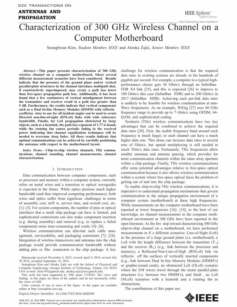
The measurement setup consists of the N5224A PNA vectornetwork analyzer (VNA), the VDI transmitter (Tx210) andthe VDI receiver (Rx148). The N5224A PNA VNA providesinput signal in the range 10 MHz-20 GHz. In the VDI Tx210transmitter, the terahertz-range carrier signal starts out as a25 GHz signal, which is generated by a Herley-CTI phase-locked dielectric resonator oscillator (DPRO with 100 MHz
Fig. 1. A block diagram of the measurement system .
TABLE IMEASUREMENT PARAMETERS.
reference crystal oscillator) [29]. This signal is amplifie andits frequency is doubled using Norden N08-1975 [30], andthen its frequency is tripled using VDI WR6.5X3 [31]. Thissignal is then fed to a sub-harmonic mixer (WR2.8SHM) thatplays a dual role of doubling the carrier frequency and mixingit with the baseband signal (10 MHz–20 GHz, delivered bythe VNA) [32]. The terahertz-range signal is then transmittedby the high-gain horn antenna in the range 280-320 GHz.At the receiver side, the same components are used to down-convert the signal, except that the DPRO is tuned to 24.2 GHz.This results in a down-conversion of the received signal to anintermediate frequency (IF) of 9.6 GHz. The upper sidebandof the down-converted signal is then recorded by the VNA inthe frequency range of 9.6-29.6 GHz. A block diagram of themeasurement system is shown in Fig 1, with all measurementparameters summarized in Table I. Note that the input signalpower, Pin, is the power input to the transmitter (Tx) module,not the Tx antenna.
The antenna used in the measurement is a pyramidal hornwith gain that varies from 22 to 23 dBi from 300 GHz to320 GHz, respectively. Both Tx and Rx antennas are verticallypolarized and mounted about 1.5 cm above the ground. Thetheoretical half power beam-widths (HPBW) are about 10◦ inazimuth and elevation. Also, the largest physical dimensionof the horn aperture is 4.6 mm, which define the far-fiel boundary to be 4.23 cm at 300 GHz according to theFraunhofer distance.
3
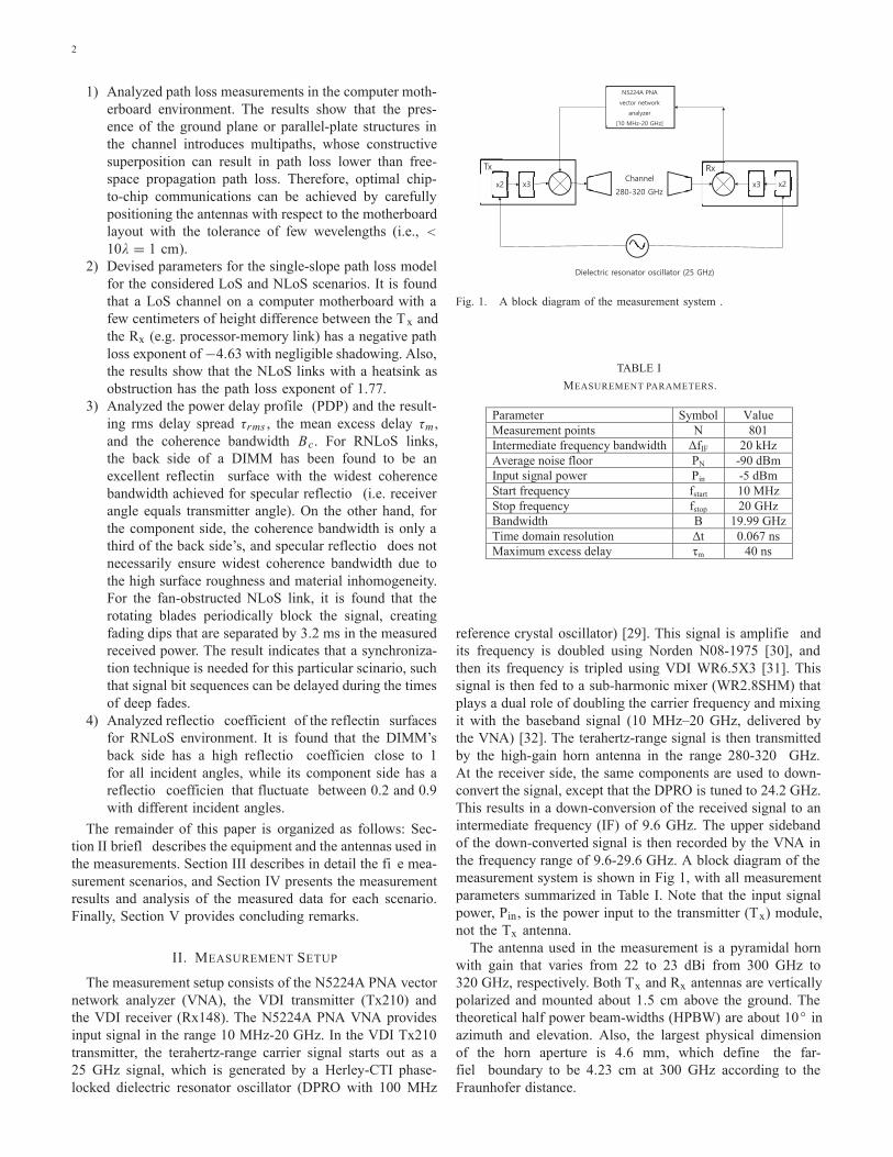
Fig. 2. LoS CPU-AGP link (A-B), RNLoS link with DIMM as reflectinsurface (C-D), and OLoS link through parallel-plate structures (E-F) on amotherboard.
III. MEASUREMENT SCENARIOS
In this measurement campaign, fi e different scenarios havebeen considered:
1) Line-of-Sight (LoS) in the presence of a large groundplane
2) LoS with the height difference between the transmitter(Tx) and the receiver (Rx)
3) Reflected-Non-Line-of-Sigh (RNLoS) link via reflection off the surfaces of vertically inserted components
4) Obstructed-LoS (OLoS) scenario where the EM wavestravel through the metal parallel-plate structures
5) NLoS scenarios with a heatsink and a rotating fan asobstructions.
Fig 2 shows the chip locations that exemplify Scenarios 2, 3,and 4.
A. LoS over a Large Ground PlaneIn contrast to traditional LoS communication environment,
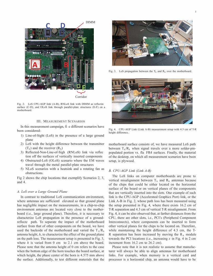
where antennas are sufficientl elevated so that ground planehas negligible impact on the measurements, in a chip-to-chipenvironment antennas are located very close to the mother-board (i.e., large ground plane). Therefore, it is necessary tocharacterize LoS propagation in the presence of a ground-reflecte path. To separate the impact of the motherboardsurface from that of other components on the board, we haveused the backside of the motherboard and varied the T x/Rxantenna height, h, to characterize the effect of the ground planeon the path loss. The measurement setup is presented in Fig. 3,where h is varied from 0 cm to 2.1 cm above the board.Please note that the antenna height of 0 cm refers to the casewhen the bottom edge of the horn touches the board surface, atwhich height, the phase center of the horn is 4.575 mm abovethe surface. Additionally, to test different materials that the
Fig. 3. LoS propagation between the Tx and Rx over the motherboard.
Fig. 4. CPU-AGP Link (Link A-B) measurement setup with 4.3 cm of T-Rheight difference.
motherboard surface consists of, we have measured LoS pathbetween Tx/Rx when signal travels over a more solder-pin-populated portion vs. fla FR4 surfaces. Finally, the materialof the desktop, on which all measurement scenarios have beensetup, is plywood.
B. CPU-AGP Link (Link A-B)The LoS links on computer motherboards are prone to
vertical misalignment between Tx and Rx antennas becauseof the chips that could be either located on the horizontalsurface of the board or on vertical planes of the componentsthat are vertically inserted into the slots. One example of suchlink is the CPU-AGP (Accelerated Graphics Port) link, or theLink A-B in Fig. 2, whose path loss has been measured usingthe setup presented in Fig. 4, where there exists 16.2 cm ofT-R separation and 4.3 cm of vertical T-R misalignment. FromFig. 4, it can be also observed that, at farther distances from theCPU, there are other slots, i.e., PCI’s (Peripheral ComponentInterconnects), where components can be inserted to formother vertical planes for the chips to be located on. Therefore,while maintaining the height difference of 4.3 cm, the T-R separation has been increased by moving the Rx moduletowards the PCI locations (i.e., increasing x in Fig. 4 in 2 cmincrement from 16.2 cm to 26.2 cm).
Please note that it is not realistic to assume that manufac-turer will always be able to align antennas for motherboardlinks. For example, when memory is a vertical card andprocessor is a horizontal chip, an antenna would have to be
4
mounted on a plastic slot in which memory is inserted in orderto be on the same height as the processor. However, in thatcase, connection between the antenna and the memory cardwould be difficult Even if the antennas between processor andmemory are aligned, they would have to send signal throughplastic holder, which would significantl attenuate the signal.While tilting the antenna may seem as a simple solution for thepropagation problem experienced with vertical misalignmentbetween Tx and Rx as in CPU-AGP environment, implemen-tation of such solution can be quite challenging, especiallywhen planar antennas are required to facilitate integration withchips. Increasing the beamwidth of the antenna can be anothersolution to overcome the vertical offset between Tx and Rx, butthe wider beamwidth would also increase delay spread, which,in turn, reduces the channel coherence bandwidth. Hence,having a study of how much signal varies when antennasare misaligned in vertical plane is important because it allowsmanufactures to estimate the performance vs. layout tradeoffs.
C. RNLoS Link with DIMM as Reflectin Surface (Link C-D)Due to densely populated environment on a motherboard,
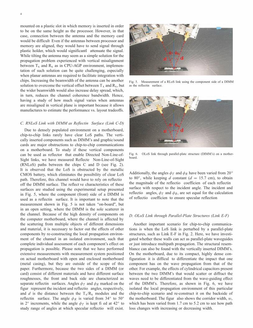
chip-to-chip links rarely have clear LoS paths. The verti-cally inserted components such as DIMM’s and graphic/soundcards are major obstructions to chip-to-chip communicationson a motherboard. To study if these vertical componentscan be used as reflector that enable Directed Non-Line-of-Sight links, we have measured Reflecte Non-Line-of-Sight(RNLoS) paths between the chips C and D (see Fig. 2).It is observed that the LoS is obstructed by the metallicCMOS battery, which eliminates the possibility of clear LoSpath. Therefore, this channel would have to rely on reflectiooff the DIMM surface. The reflect ve characteristics of thesesurfaces are studied using the experimental setup presentedin Fig. 5, where the component (front) side of a DIMM isused as a reflectin surface. It is important to note that themeasurement shown in Fig. 5 is not taken “on-board", butin an open setting, where the DIMM is the sole scatterer inthe channel. Because of the high density of components onthe computer motherboard, where the channel is affected bythe scattering from multiple objects of different dimensionsand material, it is necessary to factor out the effects of othercomponents by re-constructing the local propagation environ-ment of the channel in an isolated environment, such thatcomplete individual assessment of each component’s effect onpropagation is possible. Please note that we have performedextensive measurements with measurement system positionedon actual motherboard with open and enclosed motherboard(metal casing), but they are outside of the scope of thispaper. Furthermore, because the two sides of a DIMM (orcard) consist of different materials and have different surfaceroughnesses, the front and back side are characterized asseparate reflectin surfaces. Angles φT and φR marked on thefigur represent the incident and reflectio angles, respectively,and d is the distance between the Tx/Rx modules and thereflectin surface. The angle φR is varied from 34◦ to 50◦
in 2◦ increments, while the angle φT is kept fi ed at 42◦ tostudy range of angles at which specular reflectio will exist.
Fig. 5. Measurement of a RLoS link using the component side of a DIMMas the reflectin surface.
Fig. 6. OLoS link through parallel-plate structure (DIMM’s) on a mother-board.
Additionally, the angles φT and φR have been varied from 20◦
to 80◦, while keeping d constant (d = 15.7 cm), to obtainthe magnitude of the reflectio coefficien of each reflectinsurface with respect to the incident angle. The incident andreflectio angles, φT and φR , are set equal for the calculationof reflectio coefficien to ensure specular reflection
D. OLoS Link through Parallel-Plate Structures (Link E-F)
Another important scenario for chip-to-chip communica-tions is when the LoS link is perturbed by a parallel-platestructures, such as Link E-F in Fig. 2. Here, we have investi-gated whether these walls can act as parallel-plate waveguidesor just introduce multipath propagation. The structural resem-blance can also be found with the vertically inserted DIMM’s.On the motherboard, due to its compact, highly dense con-figuration it is difficul to differentiate the impact that onecomponent has on the wave propagation from that of theother. For example, the effects of cylindrical capacitors presentbetween the two DIMM’s that would scatter or diffract thewaves need to be differentiated from the wave-guiding effectof the DIMM’s. Therefore, as shown in Fig. 6, we haveisolated the local propagation environment of this particularchip-to-chip scenario and re-construct it on the backside ofthe motherboard. The figur also shows the corridor width, w,which has been varied from 1.7 cm to 5.2 cm to see how pathloss changes with increasing or decreasing width.
5
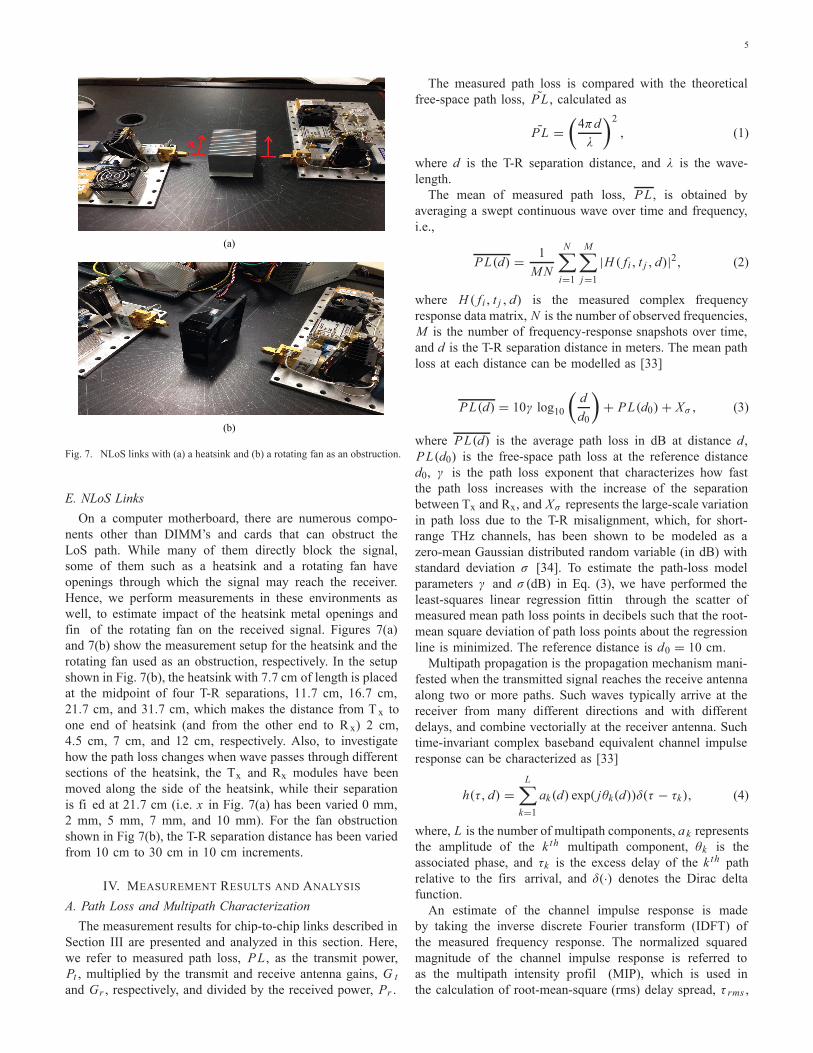
Fig. 7. NLoS links with (a) a heatsink and (b) a rotating fan as an obstruction.
E. NLoS LinksOn a computer motherboard, there are numerous compo-
nents other than DIMM’s and cards that can obstruct theLoS path. While many of them directly block the signal,some of them such as a heatsink and a rotating fan haveopenings through which the signal may reach the receiver.Hence, we perform measurements in these environments aswell, to estimate impact of the heatsink metal openings andfin of the rotating fan on the received signal. Figures 7(a)and 7(b) show the measurement setup for the heatsink and therotating fan used as an obstruction, respectively. In the setupshown in Fig. 7(b), the heatsink with 7.7 cm of length is placedat the midpoint of four T-R separations, 11.7 cm, 16.7 cm,21.7 cm, and 31.7 cm, which makes the distance from T x toone end of heatsink (and from the other end to R x) 2 cm,4.5 cm, 7 cm, and 12 cm, respectively. Also, to investigatehow the path loss changes when wave passes through differentsections of the heatsink, the Tx and Rx modules have beenmoved along the side of the heatsink, while their separationis fi ed at 21.7 cm (i.e. x in Fig. 7(a) has been varied 0 mm,2 mm, 5 mm, 7 mm, and 10 mm). For the fan obstructionshown in Fig 7(b), the T-R separation distance has been variedfrom 10 cm to 30 cm in 10 cm increments.
IV. MEASUREMENT RESULTS AND ANALYSIS
A. Path Loss and Multipath CharacterizationThe measurement results for chip-to-chip links described in
Section III are presented and analyzed in this section. Here,we refer to measured path loss, PL, as the transmit power,Pt , multiplied by the transmit and receive antenna gains, G tand Gr , respectively, and divided by the received power, Pr .
The measured path loss is compared with the theoreticalfree-space path loss, P L , calculated as
P L =
(
4πdλ
)2, (1)
where d is the T-R separation distance, and λ is the wave-length.
The mean of measured path loss, PL , is obtained byaveraging a swept continuous wave over time and frequency,i.e.,
PL(d) =1
MN
N∑
i=1
M∑
j=1|H ( fi , t j , d)|2, (2)
where H ( f i , t j , d) is the measured complex frequencyresponse data matrix, N is the number of observed frequencies,M is the number of frequency-response snapshots over time,and d is the T-R separation distance in meters. The mean pathloss at each distance can be modelled as [33]
PL(d) = 10γ log10
(
dd0
)
+ PL(d0) + Xσ , (3)
where PL(d) is the average path loss in dB at distance d,PL(d0) is the free-space path loss at the reference distanced0, γ is the path loss exponent that characterizes how fastthe path loss increases with the increase of the separationbetween Tx and Rx, and Xσ represents the large-scale variationin path loss due to the T-R misalignment, which, for short-range THz channels, has been shown to be modeled as azero-mean Gaussian distributed random variable (in dB) withstandard deviation σ [34]. To estimate the path-loss modelparameters γ and σ(dB) in Eq. (3), we have performed theleast-squares linear regression fittin through the scatter ofmeasured mean path loss points in decibels such that the root-mean square deviation of path loss points about the regressionline is minimized. The reference distance is d0 = 10 cm.
Multipath propagation is the propagation mechanism mani-fested when the transmitted signal reaches the receive antennaalong two or more paths. Such waves typically arrive at thereceiver from many different directions and with differentdelays, and combine vectorially at the receiver antenna. Suchtime-invariant complex baseband equivalent channel impulseresponse can be characterized as [33]
h(τ, d) =
L∑
k=1ak(d) exp( jθk(d))δ(τ − τk), (4)
where, L is the number of multipath components, a k representsthe amplitude of the k th multipath component, θk is theassociated phase, and τk is the excess delay of the k th pathrelative to the firs arrival, and δ(·) denotes the Dirac deltafunction.
An estimate of the channel impulse response is madeby taking the inverse discrete Fourier transform (IDFT) ofthe measured frequency response. The normalized squaredmagnitude of the channel impulse response is referred toas the multipath intensity profil (MIP), which is used inthe calculation of root-mean-square (rms) delay spread, τ rms ,
6
Fig. 8. Measured and theoretical path loss curves for LoS link over themotherboard with T-R separation of 23.5 cm and varying Tx/Rx heights abovethe motherboard surface (in reference to measurement setup of Fig. 3).
a measure of multipath spread within the channel. It is animportant parameter for characterizing time dispersion orfrequency selectivity, and is found by taking the square rootof the second central moment of MIP [33], i.e.,
τrms =
√
√
√
√
L∑
k=1(τk − τm)2|h(t, τk, d)|2, (5)
where L is the number of multipath components, τ k is theexcess delay of the k th path relative to the firs arrival, andτm is the mean excess delay (the firs moment of the MIP)define as
τm =
L∑
k=1τk · |h(t, τk, d)|2. (6)
B. Characterization of LoS Path Loss over a Large GroundPlane
Fig. 8 compares the measured and theoretically calculated(i.e., using Eq.(1)) path loss curves for the experimental setupdescribed in Section III-A, where T-R separation distanceis 23.5 cm. The oscillations observed in the measured pathloss are the result of strong reflection that arrive at thereceiver after reflectin off the Tx hardware. These multipathsthat bounce between the Tx and Rx modules due to thenarrow beamwidths of the antennas have also been observedin [34] for LoS propagation environment. Furthermore, wecan observe that the measured path loss when both the T xand Rx are h = 2.1 cm above the ground plane follows theFriis formula prediction well. This is not a surprising resultdue to narrow beamwidths of the antennas and shows thatthe ground reflecte paths do not reach the receiver at theseantenna heights.
It is also observed that, when antennas are positioned onthe board surface (i.e., h = 0 cm), the ground reflectiondestructively interfere with the LoS path, resulting in about 3dB higher path loss than what is predicted by the Friis formula.On the other hand, when the antennas are 8 mm above the
TABLE IIMEAN EXCESS DELAYS, RMS DELAY SPREADS, AND COHERENCE BAND-
WIDTHS FOR LOS LINK OVER THE MOTHERBOARD WITH DIFFERENTTx/Rx HEIGHTS.
board (h = 0.8 cm), the reflecte and LoS paths constructivelyinterfere, and the measured path loss actually becomes slightlylower than the theoretical free-space curve. To summarize, theoscillation in measured path losses is due to the interferencebetween the LoS and Tx-hardeware-reflecte paths that are indifferent delay bins, while the amplitude shift in the path lossarises from the constructive/destructive interference betweenthe LoS and ground-reflecte paths that fall within the samedelay bin (i.e., their path length difference is smaller than thespatial resolution of the measurement system).
Another interesting observation from Fig. 8 is that for thesame height of 0 cm, path loss is reduced by 3 dB whenthe antennas are placed over a section of the board that hashigher solder pin density (refer to "h = 0 cm solder pin" inFig. 8). This is because the amplitude and phase of the groundreflecte signal are changed due to the higher reflect vity andsurface roughness of the solder-pin-populated surface. Table IIpresents the measured RMS delay spread, mean excess delay,and the coherence bandwidth (Bc = 1/(2 ∗ π ∗ τrms )) forthis measurement setup. It is observed that the coherencebandwidth decreases with the increasing height, and is sig-nificantl widened for the solder-pin scenario. This dramaticincrease in the coherence bandwidth for the case of groundreflectio off solder-pin-populated surface is backed by thepower delay profile for this measurement setup (see Fig. 9).In the figure the reflectio from Tx antenna back panel locatedat the excess delay of approximately 2 ns is clearly visible foreach Tx/Rx height. A closer look at the profile also revealsthat the amplitude of the reflectio is significantl reduced forthe solder-pin scenario (marked with solid squares in Fig. 9)since the reflectio is scattered, and therefore, weakened, bythe obstructing pins. Also, multiple weaker reflection can beobserved in this case. Consequently, the RMS delay spread isdramatically reduced, which in turn resulted in much widercoherence bandwidth for this particular scenario.
These results indicate that the effect of ground reflectionvaries with the Tx/Rx height: few millimeters of variation inTx/Rx height off the board result in the increase or decreasein path loss by as much as 3 dB, depending on the nature ofinterference (i.e. destructive or constructive) between the LoSpath and the ground-reflecte path.
7
Fig. 9. Normalized power delay profil for LoS link over the motherboardwith different Tx/Rx heights above the motherboard surface (in reference tomeasurement setup of Fig. 3).
Fig. 10. Measured and calculated path loss curves for CPU-AGP link (LinkA-B) and CPU-PCI links with T-R height difference of 4.3 cm (in referenceto measurement setup of Fig. 4).
C. Characterization of CPU-AGP Link (Link A-B)
Link A-B, shown in Fig. 2, describes a typical link betweenthe processor and the graphics card, where the Tx and Rxantennas are not on the same height. Fig. 10 shows themeasured path losses for the setup presented in Fig. 4 aswell as the corresponding theoretical values obtained fromEq.(1). We can observe that the path loss is higher for shorterdistances, which may seem counter-intuitive. However, con-sidering the geometrical structure, this is very possible. Notethat the antennas have high directivity and narrow beamwidthand that height difference of 4.3 cm creates very obstructedLoS propagation for short distances. On the other hand, as thedistance increases, the Tx/Rx antennas start falling within eachothers’ beamwidths, and more of the LoS power as well as theground-reflecte power is detected toward the receiver, whichresults in less path loss. However, note that even at maximumdistance of 26.2 cm (i.e., size of the motherboard), the heightdifference of 4.3 cm still introduces loss of about 15 dB withsignifican fluctuatio in path loss. This result indicates that theA-B link is probably not a reliable channel, which raises thefollowing question: how much of a height difference betweenTx and Rx antennas can be tolerated?
Fig. 11. Measured and calculated path loss curves for A-B link with varyingRx antenna height when Tx antenna is fi ed to hTx = 2.1 cm (in referenceto measurement setup of Fig. 4).
Fig. 11 shows measured path loss curves for differentheights of the Rx antenna when the Tx antenna is fi ed atthe height 2.1 cm from the board (h Tx = 2.1 cm). Theplot shows that for the height difference less than 1.3 cm,the measured path loss matches the theoretical values, whilefor greater height differences, measurements start to deviatefrom the Friis formula with greater fluctuatio in path loss.From these results, we can conclude that the LoS chip-to-chip wireless channel on the horizontal plane (on motherboardsurface) with minor Tx/Rx height difference is feasible, whilethe link between two chips, whose height difference is in theorder of few centimeters, such as Link A-B, will suffer fromsignifican loss.
Fig. 12 shows the scatter plot of the measured mean pathloss for several distances as well as the regression fi throughthe measurements for a LoS link over the motherboard with4.3 cm of height difference between Tx and Rx. From theregression fit the path loss exponent is found to be γ =
−4.6302; the path loss at the reference distance of 10 cmwas PL0 = 102.384 dB; and the standard deviation wasσ = 0.4179 dB. Note that the negative path loss exponentfound from Fig. 12 is the result of narrow-beam antennas aswell as the presence of large ground plane.
It should be noted that, for motherboard channels withvertical T-R misalignment, there exists trade-off between thepath loss and the delay spread. When the antennas have widerbeamwidth, more of the transmitted power will reach thevertically offset receiver, but more multipaths will also becreated due to reflection from other motherboard componentsas well as the motherboard surface, increasing the RMSdelay spread, and therefore, reducing the channel coherencebandwidth. To verify this, CST simulation has been performed,where two Tx/Rx horn antenna pairs with HPBW’s of 10◦
and 26◦, each separated by 16.2 cm with vertical offset of4.3 cm as in CPU-AGP environment, are compared in termsof their S21 and RMS delay sread. The result has shown thatan increase of 16◦ in HPBW results in 20 dB increase inthe received power and 71.8 % reduction (from 606 MHz to171 MHz) in coherence bandwidth. Therefore, selection of an
8
Fig. 12. Measured mean path losses and regression fi for A-B link with4.3 cm of height difference between Tx and Rx antennas (d0 = 10 cm) (inreference to measurement setup of Fig. 4).
Fig. 13. Normalized power delay profil for A-B link with height differenceof 4.3 cm between Tx and Rx for different T-R separations (in reference tomeasurement setup of Fig. 4).
appropriate antenna beamwidth that delivers enough power toall receiver locations, while minimizing delay spread, is criticalfor wireless channels on a computer motherboard.
Fig. 13 presents the power delay profile for several T-R separations when the difference between the Tx and Rxantenna heights is 4.3 cm. We observe that the reflectionfrom the Tx arrive at the receiver with larger excess delay(i.e., τ = 1.8 ns, 2.1 ns, and 2.4 ns) as the separationdistance increases (i.e., d = 18.2 cm, 22.2 cm, and 26.2 cm,respectively) due to the longer path lengths that the reflecterays have to travel.
D. Characterization of RNLoS link with DIMM as ReflectinSurface (Link C-D)
In this section, we study if some of the components onthe motherboard can be used as reflectors i.e., we have ana-lyzed Reflecte Non-Line-of-Sight (RNLoS) paths using themeaseurement setup presented in Fig. 5, which is exemplifieby the link between the chips C and D in Fig. 2.
Figure 14 shows the measured path loss plots with a DIMMas the reflectin surface, while the receiver angle φ R is variedbetween 34◦ and 50◦ in 2◦ increments, while the transmitterangle φT is kept fi ed at 42◦. For both the front and back side
of the DIMM, shown in Fig. 14(a) and 14(b), respectively, themeasured path loss is the lowest for φR = 42◦, which meansthat maximum power transfer is occurring under the condition,φT = φR , for both sides of the reflect ve surface. The differ-ence between them, however, is that, for the backside, the pathloss increases linearly with the deviation from the specularreflectio angle, 42◦, while this is not necessarily the case forthe front side of DIMM. For example, the second highest pathlosses are for φR = 40◦ and 44◦, then, the third highest pathlosses belong to φR = 38◦ and 46◦, etc. For deviation greaterthan 6◦, the path loss approaches noise level. On the otherhand, for the front side of DIMM, the second highest pathloss is for φR = 38◦, rather than 40◦ or 44◦. Furthermore,it is observed that for receiver angles other than φ R = 42◦
and 38◦, the path loss curves are hard to distinguish. Theseresults are closely related to the material inhomogeneity andsurface irregularity of the DIMM’s front side. The fact that itssurface consists of more than one material of varying reflectiocoefficien and that it has high surface roughness createsdiffuse reflection of random amplitudes, phases, delays, andpropagation directions. Therefore, their vectorial sum at aspecifi point in space is also random.
Figures 15(a) and 15(b) present the PDP’s for the front andthe back sides of a DIMM, respectively. From the PDPs, itcan be observed that a single cluster of later-arriving paths isdetected for the front side of DIMM (labeled 1 in Fig. 15(a)),while two such clusters are observed for the back side of theDIMM (labeled 1 and 2 in Fig. 15(b)). This is due to thedifferent surface roughness and the reflect vity of the two sides.For the flat highly reflect ve back side (Fig. 15(b)), there arethree reflections the firs path at τ = 0 is the one that starts atTx, reflect off DIMM surface and arrives at the Rx (since thereis no line-of-sight path); the reflectio observed in Cluster 1is the path that travels from Tx, reflect off DIMM surface,bounces off the back panel of Rx antenna, travels to DIMMonce again, and back to Rx;the reflectio observed in Cluster2 is the path that travels from Tx, reflect off DIMM surfaceand Rx back panel, travels back to Tx through reflectio offDIMM, bounces off Tx back panel and DIMM surface, andfinall reaches the Rx. For the front side of DIMM (Fig. 15(a)),Cluster 2 is absent in the PDP since the surface is rougher andless reflectr ve than the back side, so that it cannot producestrong enough reflectio that travels back to Tx. Note that thetrajectories of all of these multipaths have been identifie bycomputing the distance travelled with the excess delay of eachpath (d = c × τ ). In Fig. 15(b), intuitively speaking, Cluster2 should be weaker than Cluster 1 since it travels the longerdistance. However, the Angle-of-Arrival (AoA) also impactsthe power of the received signal. Especially, for such a narrowbeam, the simulated radiation pattern of the horn reveals thatthe AoA of only 8◦ off the direction of maximum gain can leadto 9 dB weaker detected signal. Therefore, even though Cluster1 should have higher power than Cluster 2 (by 3.8 dB to beexact), the deviation of AoA from maximum of the mainlobecan result in 5 dB weaker power of Cluster 1 compared toCluster 2.
The mean excess delays, RMS delay spreads, and thecoherence bandwidths of this RNLoS channel with the three

9
Fig. 14. Measured and theoretically calculated path loss curves for RNLoSlinks with different receiver angles when the transmitter angle is fi ed toφT = 42◦ and DIMM is used as the reflectin surface (in reference to LinkC-D and measurement setup of Fig. 5): (a) front side of DIMM ; (b) backside of DIMM.
reflectin surfaces presented in Table III provide numericalverificatio of the qualitative analysis made from Fig. 15. Itcan be observed in Table III that the maximum coherencebandwidth is found for the DIMM back side for the angleof specular reflection φT = φR = 42◦, and as the receiverangle gets farther away from it, the coherence bandwidthdecreases rapidly. Nevertheless, we can see that the coherencebandwidth stays in the GHz range up to 38◦ and 44◦. ForDIMM front side, the largest coherence bandwidth is alsofound at φR = 42◦, but it is three times narrower than thecoherence bandwidth of the back side. Additionally, other thanφR = 38◦ and 42◦, the coherence bandwidths significantldrop to MHz range. It is also observed that the front side of agraphic card exhibits the lowest coherence bandwidth amongthe three surfaces due to its highest surface irregularity, whileits maximum coherence bandwidth occurs at φ R = 44◦, whichis 2◦ off from the angle of specular reflection Please note thatthe delay spreads presented in Table III are the values obtainedin "open" or "isolated" channel environment, and therefore,they cannot be directly related to more realistic motherboardenvironment. However, the purpose of this particular measure-
Fig. 15. Normalized power delay profile for RNLoS links with differentreceiver angles when the transmitter angle is fi ed to φT = 42◦ and DIMMis used as the reflectin surface (in reference to Link C-D and measurementsetup of Fig. 5): (a) front side of DIMM; (b) back side of DIMM.
ment campaign is to identify 300GHz wave’s interaction withthe common materials found on the motherboard in terms oftheir penetration/reflectio characteristics. In other words, thecoherence bandwidths provided in Table III can be consideredas the maximum possible values when no other components onthe motherboard are obstructing the RNLoS path between twochips. Furthermore, in Table III, we have shown how delayspread varies as the angular orientation of receiver deviatesfrom that of the transmitter, which captures more practicalaspects of RNLoS channel on motherboard since it is notrealistic to expect specular reflectio for all antenna positionson a computer motherboard. Such information will be usefulfor layout designers and manufacturers.
Finally, Fig. 16 shows the magnitude of the reflectiocoefficient of the three surfaces (DIMM front side, DIMMback side, and graphic card front side) as a function of incidentangle. The reflectio coefficien is found from the reflectioloss of each surface, i.e.
RL = −20log10|Ŵ|, (7)
where Ŵ is the reflectio coefficient and RL, reflectio lossin dB, is calculated from the link budget equation:
10
TABLE IIIMEAN EXCESS DELAY, RMS DELAY SPREAD, AND COHERENCE BAND-
WIDTH FOR THE RNLOS SCENARIO WITH DIFFERENT REFLECTINGSURFACES.
RL = Pt − Pr + Gt + Gr − P L [dB], (8)
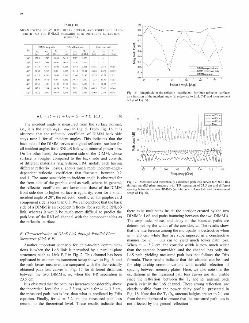
The incident angle is measured from the surface normal,i.e., it is the angle φT (= φR) in Fig. 5. From Fig. 16, it isobserved that the reflectio coefficien of DIMM back sidestays near 1 for all incident angles. This indicates that theback side of the DIMM serves as a good reflectin surface forall incident angles for a RNLoS link with minimal power loss.On the other hand, the component side of the DIMM, whosesurface is rougher compared to the back side and consistsof different materials (e.g. Silicon, FR4, metal), each havingdifferent reflectio losses, shows much more incident-angle-dependent reflectio coefficien that fluctuate between 0.2and 1. The same sensitivity to incident angle is observed forthe front side of the graphic card as well, where, in general,the reflectio coefficient are lower than those of the DIMMfront side due to higher surface irregularity; even for a smallincident angle of 20◦, the reflectio coefficien for graphic cardcomponent side is less than 0.3. We can conclude that the backside of a DIMM is an excellent reflecto for a reliable RNLoSlink, whereas it would be much more difficul to predict thepath loss of the RNLoS channel with the component sides asthe reflectin surface.
E. Characterization of OLoS Link through Parallel-PlateStructures (Link E-F)
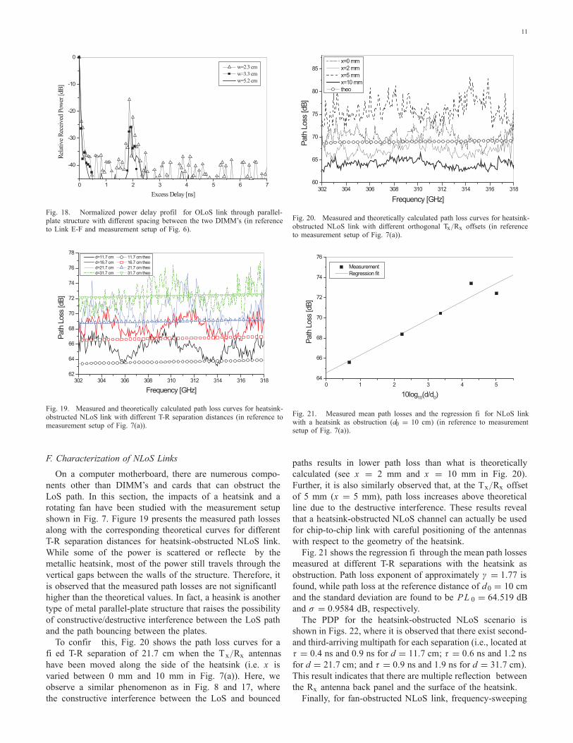
Another important scenario for chip-to-chip communica-tions is when the LoS link is perturbed by a parallel-platestructures, such as Link E-F in Fig. 2. This channel has beenreplicated in an open measurement setup shown in Fig. 6, andthe path losses measured are compared with the theoreticallyobtained path loss curves in Fig. 17 for different distancesbetween the two DIMM’s, w, when the T-R separation is23.5 cm.
It is observed that the path loss increases considerably abovethe theoretical level for w = 2.3 cm, while for w = 3.3 cm,the measured path loss is less than what is predicted by Friisequation. Finally, for w = 5.2 cm, the measured path lossreturns to the theoretical level. These results indicate that
Fig. 16. Magnitude of the reflectio coefficient for three reflectin surfacesas a function of the incident angle (in reference to Link C-D and measurementsetup of Fig. 5).
Fig. 17. Measured and theoretically calculated path loss curves for OLoS linkthrough parallel-plate structure with T-R separation of 23.5 cm and differentspacing between the two DIMM’s (in reference to Link E-F and measurementsetup of Fig. 6).
there exist multipaths inside the corridor created by the twoDIMM’s: LoS and paths bouncing between the two DIMM’s.The amplitude, phase, and delay of the bounced paths aredetermined by the width of the corridor, w. The results showthat the interference among the multipaths is destructive whenw = 2.3 cm, while they are superimposed in a constructivemanner for w = 3.3 cm to yield much lower path loss.When w = 5.2 cm, the corridor width is now much widerthan the antenna beamwidth, and the channel has only theLoS path, yielding measured path loss that follows the Friisformula. These results indicate that this channel can be usedfor chip-to-chip communications with careful selection ofspacing between memory plates. Here, we also note that theoscillations in the measured path loss curves are still visiblesince the reflection between the Tx and Rx antenna backpanels exist in the LoS channel. These strong reflection areclearly visible from the power delay profile presented inFig. 18. Note that the Tx/Rx antenna heights are set to 2.1 cmfrom the motherboard to ensure that the measured path loss isnot affected by the ground reflection
11
Fig. 18. Normalized power delay profil for OLoS link through parallel-plate structure with different spacing between the two DIMM’s (in referenceto Link E-F and measurement setup of Fig. 6).
Fig. 19. Measured and theoretically calculated path loss curves for heatsink-obstructed NLoS link with different T-R separation distances (in reference tomeasurement setup of Fig. 7(a)).
F. Characterization of NLoS Links
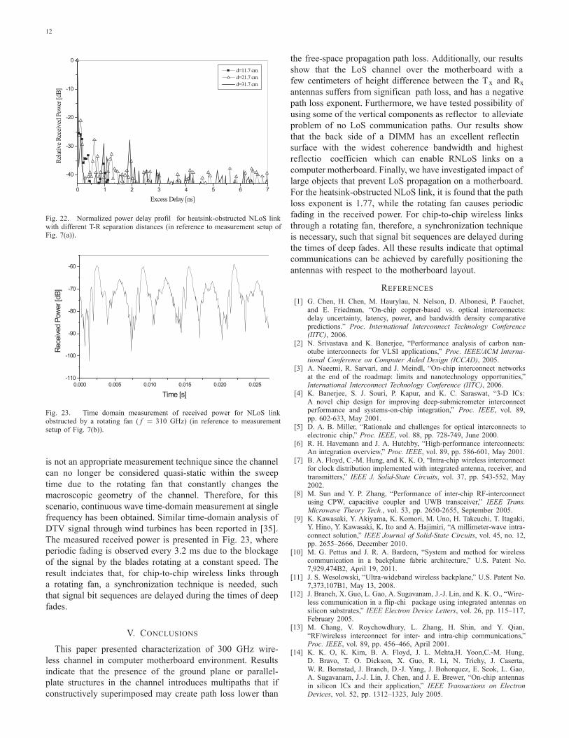
On a computer motherboard, there are numerous compo-nents other than DIMM’s and cards that can obstruct theLoS path. In this section, the impacts of a heatsink and arotating fan have been studied with the measurement setupshown in Fig. 7. Figure 19 presents the measured path lossesalong with the corresponding theoretical curves for differentT-R separation distances for heatsink-obstructed NLoS link.While some of the power is scattered or reflecte by themetallic heatsink, most of the power still travels through thevertical gaps between the walls of the structure. Therefore, itis observed that the measured path losses are not significantlhigher than the theoretical values. In fact, a heasink is anothertype of metal parallel-plate structure that raises the possibilityof constructive/destructive interference between the LoS pathand the path bouncing between the plates.
To confir this, Fig. 20 shows the path loss curves for afi ed T-R separation of 21.7 cm when the Tx/Rx antennashave been moved along the side of the heatsink (i.e. x isvaried between 0 mm and 10 mm in Fig. 7(a)). Here, weobserve a similar phenomenon as in Fig. 8 and 17, wherethe constructive interference between the LoS and bounced
Fig. 20. Measured and theoretically calculated path loss curves for heatsink-obstructed NLoS link with different orthogonal Tx/Rx offsets (in referenceto measurement setup of Fig. 7(a)).
Fig. 21. Measured mean path losses and the regression fi for NLoS linkwith a heatsink as obstruction (d0 = 10 cm) (in reference to measurementsetup of Fig. 7(a)).
paths results in lower path loss than what is theoreticallycalculated (see x = 2 mm and x = 10 mm in Fig. 20).Further, it is also similarly observed that, at the Tx/Rx offsetof 5 mm (x = 5 mm), path loss increases above theoreticalline due to the destructive interference. These results revealthat a heatsink-obstructed NLoS channel can actually be usedfor chip-to-chip link with careful positioning of the antennaswith respect to the geometry of the heatsink.
Fig. 21 shows the regression fi through the mean path lossesmeasured at different T-R separations with the heatsink asobstruction. Path loss exponent of approximately γ = 1.77 isfound, while path loss at the reference distance of d0 = 10 cmand the standard deviation are found to be PL 0 = 64.519 dBand σ = 0.9584 dB, respectively.
The PDP for the heatsink-obstructed NLoS scenario isshown in Figs. 22, where it is observed that there exist second-and third-arriving multipath for each separation (i.e., located atτ = 0.4 ns and 0.9 ns for d = 11.7 cm; τ = 0.6 ns and 1.2 nsfor d = 21.7 cm; and τ = 0.9 ns and 1.9 ns for d = 31.7 cm).This result indicates that there are multiple reflection betweenthe Rx antenna back panel and the surface of the heatsink.
Finally, for fan-obstructed NLoS link, frequency-sweeping
12
Fig. 22. Normalized power delay profil for heatsink-obstructed NLoS linkwith different T-R separation distances (in reference to measurement setup ofFig. 7(a)).
Fig. 23. Time domain measurement of received power for NLoS linkobstructed by a rotating fan ( f = 310 GHz) (in reference to measurementsetup of Fig. 7(b)).
is not an appropriate measurement technique since the channelcan no longer be considered quasi-static within the sweeptime due to the rotating fan that constantly changes themacroscopic geometry of the channel. Therefore, for thisscenario, continuous wave time-domain measurement at singlefrequency has been obtained. Similar time-domain analysis ofDTV signal through wind turbines has been reported in [35].The measured received power is presented in Fig. 23, whereperiodic fading is observed every 3.2 ms due to the blockageof the signal by the blades rotating at a constant speed. Theresult indciates that, for chip-to-chip wireless links througha rotating fan, a synchronization technique is needed, suchthat signal bit sequences are delayed during the times of deepfades.
V. CONCLUSIONS
This paper presented characterization of 300 GHz wire-less channel in computer motherboard environment. Resultsindicate that the presence of the ground plane or parallel-plate structures in the channel introduces multipaths that ifconstructively superimposed may create path loss lower than
the free-space propagation path loss. Additionally, our resultsshow that the LoS channel over the motherboard with afew centimeters of height difference between the Tx and Rxantennas suffers from significan path loss, and has a negativepath loss exponent. Furthermore, we have tested possibility ofusing some of the vertical components as reflector to alleviateproblem of no LoS communication paths. Our results showthat the back side of a DIMM has an excellent reflectinsurface with the widest coherence bandwidth and highestreflectio coefficien which can enable RNLoS links on acomputer motherboard. Finally, we have investigated impact oflarge objects that prevent LoS propagation on a motherboard.For the heatsink-obstructed NLoS link, it is found that the pathloss exponent is 1.77, while the rotating fan causes periodicfading in the received power. For chip-to-chip wireless linksthrough a rotating fan, therefore, a synchronization techniqueis necessary, such that signal bit sequences are delayed duringthe times of deep fades. All these results indicate that optimalcommunications can be achieved by carefully positioning theantennas with respect to the motherboard layout.
REFERENCES
[1] G. Chen, H. Chen, M. Haurylau, N. Nelson, D. Albonesi, P. Fauchet,and E. Friedman, “On-chip copper-based vs. optical interconnects:delay uncertainty, latency, power, and bandwidth density comparativepredictions.” Proc. International Interconnect Technology Conference(IITC), 2006.
[2] N. Srivastava and K. Banerjee, “Performance analysis of carbon nan-otube interconnects for VLSI applications,” Proc. IEEE/ACM Interna-tional Conference on Computer Aided Design (ICCAD), 2005.
[3] A. Naeemi, R. Sarvari, and J. Meindl, “On-chip interconnect networksat the end of the roadmap: limits and nanotechnology opportunities,”International Interconnect Technology Conference (IITC), 2006.
[4] K. Banerjee, S. J. Souri, P. Kapur, and K. C. Saraswat, “3-D ICs:A novel chip design for improving deep-submicrometer interconnectperformance and systems-on-chip integration,” Proc. IEEE, vol. 89,pp. 602-633, May 2001.
[5] D. A. B. Miller, “Rationale and challenges for optical interconnects toelectronic chip,” Proc. IEEE, vol. 88, pp. 728-749, June 2000.
[6] R. H. Havemann and J. A. Hutchby, “High-performance interconnects:An integration overview,” Proc. IEEE, vol. 89, pp. 586-601, May 2001.
[7] B. A. Floyd, C.-M. Hung, and K. K. O, “Intra-chip wireless interconnectfor clock distribution implemented with integrated antenna, receiver, andtransmitters,” IEEE J. Solid-State Circuits, vol. 37, pp. 543-552, May2002.
[8] M. Sun and Y. P. Zhang, “Performance of inter-chip RF-interconnectusing CPW, capacitive coupler and UWB transceiver,” IEEE Trans.Microwave Theory Tech., vol. 53, pp. 2650-2655, September 2005.
[9] K. Kawasaki, Y. Akiyama, K. Komori, M. Uno, H. Takeuchi, T. Itagaki,Y. Hino, Y. Kawasaki, K. Ito and A. Hajimiri, “A millimeter-wave intra-connect solution,” IEEE Journal of Solid-State Circuits, vol. 45, no. 12,pp. 2655–2666, December 2010.
[10] M. G. Pettus and J. R. A. Bardeen, “System and method for wirelesscommunication in a backplane fabric architecture,” U.S. Patent No.7,929,474B2, April 19, 2011.
[11] J. S. Wesolowski, “Ultra-wideband wireless backplane,” U.S. Patent No.7,373,107B1, May 13, 2008.
[12] J. Branch, X. Guo, L. Gao, A. Sugavanam, J.-J. Lin, and K. K. O., “Wire-less communication in a flip-chi package using integrated antennas onsilicon substrates,” IEEE Electron Device Letters, vol. 26, pp. 115–117,February 2005.
[13] M. Chang, V. Roychowdhury, L. Zhang, H. Shin, and Y. Qian,“RF/wireless interconnect for inter- and intra-chip communications,”Proc. IEEE, vol. 89, pp. 456–466, April 2001.
[14] K. K. O, K. Kim, B. A. Floyd, J. L. Mehta,H. Yoon,C.-M. Hung,D. Bravo, T. O. Dickson, X. Guo, R. Li, N. Trichy, J. Caserta,W. R. Bomstad, J. Branch, D.-J. Yang, J. Bohorquez, E. Seok, L. Gao,A. Sugavanam, J.-J. Lin, J. Chen, and J. E. Brewer, “On-chip antennasin silicon ICs and their application,” IEEE Transactions on ElectronDevices, vol. 52, pp. 1312–1323, July 2005.

13
[15] K. K. O, K. Kim, B. Floyd, J. Mehta, H. Yoon, C.-M. Hung, D. Bravo,T. Dickson, X. Guo, R. Li, N. Trichy, J. Caserta, W. Bomstad, J. Branch,D.-J. Yang, J. Bohorquez, J. Chen, E.-Y. Seok, L. Gao, A. Sugavanam,J.-J. Lin, S. Yu, C. Cao, M.-H. Hwang, S.-H. Hwang, H. Wu, N. Zhang,and J. E. Brewer, “The feasibility of on-chip interconnection usingantennas,” IEEE/ACM International Conference on Computer-AidedDesign ICCAD-2005, pp. 979–984, 6-10 November 2005.
[16] Z. M. Chen and Y. P. Zhang, “Inter-chip wireless communication chan-nel: measurement, characterization, and modeling,” IEEE Transactionson Antennas and Propagation, vol. 55, pp. 978-986, March 2007.
[17] J. Karedal, A. Singh, F. Tufvesson, and A. Molisch, “Characterizationof a computer board-to-board ultra-wideband channel,” IEEE Commu-nications Letters, vol. 11, pp. 468-470, June 2007.
[18] D. W. Matolak, S. Kaya, A. Kodi “Channel modeling for wirelessnetworks-on-chips,” IEEE Communications Magazine, vol. 51, no. 6,pp. 180–186, June 2013.
[19] J. Gelabert, D. J. Edwards and C. J. Stevens, “Experimental evaluationof UWB wireless communication within PC case,” Electronics Letters,vol. 47, pp. 773–775, June 2011.
[20] K. Ramachandran, R. Kokku, R. Mahindra, and S. Rangarajan “60GHzdata-center networking: Wireless -> worry less?” Technical report, NEC,2008.
[21] D. Halperin, S. Kandula, J. Padhye, P. Bahl, and D. Wetherall, “Aug-menting data center networks with multi-gigabit wireless links,” Proc.of ACM SIGCOMM, pp. 38–49, August 2011.
[22] J.-Y. Shin, E. G. Sirer, and D. Kirovsi, “On the feasibility of completelywireless data centers,” Technical Reports, Cornell University (2011).
[23] A. Valdes-Garcia, S. Reynolds, A. Natarajan, and D. Kam, “Single-element and phased-array transceiver chipsets for 60-GHz Gb/s com-munications,” IEEE Communications Magazine, vol. 49, pp. 120–131,April 2011.
[24] H. Vardhan, N. Thomas, S.-R. Ryu, B. Banerjee, and R. Parkash,“Wireless data center with millimeter wave network,” IEEE Proceedingof GLOBECOM10, pp. 1–6, December 2010.
[25] Infiniban Trade Association, “InfiniBan continues growthamong supercomputers on TOP500 list”, November 2014http : //www.in f inibandta.org/content/pages.php?pg =
pressr oomi tem&reci d = 805[26] InfiniBan Trade Association, “InfiniBan roadmap”,
http : //www.in f inibandta.org/content/pages.php?pg =
technologyo verview[27] Wikipedia, Wireless Gigabit Alliance, https :
//en.wikipedia.org/wiki/WirelessG igabitA lliance[28] P. H. Siegel,“Terahertz technology,” IEEE Transactions on Microwave
Theory and Techniques, MTT-50, pp. 910–928, March 2002.[29] http://www.kratosepd.com/ /media/EP/Datasheets/[30] http://www.nordengroup.com/products/frequency-multipliers/frequency-
multiplier-33-to-50-ghz/[31] http://vadiodes.com/index.php/en/products/broadband-multipliers/10-
products/165-wr65x3[32] http://www.vadiodes.com/index.php/en/12-product/126-wr28shm12[33] A. Zajic, Mobile-to-mobile wireless channels, Artech House, Boston
MA, January 2013.[34] S. Kim, A. Zajic, ”Statistical Characterization of 300-GHz Propagation
on a Desktop”, IEEE Transactions on Vehicular Technology, vol. 64,pp. 3330–3338, August 2015.
[35] I. Angulo, D. de la Vega, C. Fernandez, Y. Wu, P. Angueira, J. L.Ordiales, ”An Empirical Comparative Study of Prediction Methods forEstimating DTV Signal Scattering from Wind Turbines”, IEEE Trans.Broadcasting, vol. 57, no. 2, pp. 195-203, June 2011.
Seunghwan Kim (S’14) Seunghwan Kim was bornin Seoul, South Korea, in 1986. He received Bach-elor of Applied Science in Electrical Engineer-ing (with Distinction) from University of Waterloo,Canada, in 2009. During his degree, he has workedas a Research Assistant at the TelecommunicationGroup of Korea Electrotechnology Research Insti-tute (KERI), and as a Hardware Engineer at MitelNetworks. He is currently pursuing the Ph.D. degreein Electrical Engineering at Georgia Institute ofTechnology in the area of channel measurement,
characterization, modeling, and antenna design for future THz device-to-device communication systems.
Alenka Zajic (S’99-M’09-SM’13) Alenka Zajicreceived the B.Sc. and M.Sc. degrees form theSchool of Electrical Engineering, University of Bel-grade, in 2001 and 2003, respectively. She receivedher Ph.D. degree in Electrical and Computer Engi-neering from the Georgia Institute of Technologyin 2008. Currently, she is an Assistant Professor inSchool of Electrical and Computer Engineering atGeorgia Institute of Technology. Prior to that, shewas visiting faculty in School of Computer Scienceat Georgia Institute of Technology, a post-doctoral
fellow in the Naval Research Laboratory, and design engineer at SkyworksSolutions Inc. Her research interests span areas of electromagnetics, wirelesscommunications, signal processing, and computer engineering.
Dr. Zajic received the Neal Shepherd Memorial Best Propagation PaperAward, the Best Paper Award at ICT 2008, the Best Student Paper Awardat WCNC 2007, and was also the recipient of the Dan Noble Fellowshipin 2004, awarded by Motorola Inc. and IEEE Vehicular Technology Societyfor quality impact in the area of vehicular technology. Currently, she is aneditor for IEEE Transactions on Wireless Communications and the Chair ofthe IEEE MTT/AP Atlanta Chapter.