
A 2.45-GHz Rectifier-Booster Regulator With Impedance ...
11
This article has been accepted for inclusion in a future issue of this journal. Content is final as presented, with the exception of pagination. IEEE TRANSACTIONS ON MICROWAVE THEORY AND TECHNIQUES 1 A 2.45-GHz Rectifier-Booster Regulator With Impedance Matching Converters for Wireless Energy Harvesting Shiquan Fan , Member, IEEE, Zheyi Yuan , Wei Gou, Student Member, IEEE, Yang Zhao , Chaoyun Song , Member, IEEE, Yi Huang , Senior Member, IEEE, Jiafeng Zhou , and Li Geng , Member, IEEE Abstract— In this paper, a proof-of-concept high-efficiency rectifier-booster regulator (RBR) with an impedance matching converter operating at 2.45 GHz is proposed. An entire WLAN energy harvesting system is demonstrated. A flower-shaped broadband dual-polarized cross dipole antenna with a full-wave matching network is employed to harvest electromagnetic energy from a WiFi router. A novel RBR is proposed to rectify the RF energy to dc and boost the output voltage. It is evolved from a Greinacher rectifier and two Cockcroft–Walton charge pumps to form a full-wave rectifier. An equivalent resistance model is established to evaluate the optimal stage of the RBR. Furthermore, a boost converter is designed as an impedance matching converter to harvest as much energy as possible from the RBR and store the energy into a 1-mF supercapacitor. Experimental results show that the RBR can provide 1.7-V output voltage under -10-dBm input power. In addition, the RBR can achieve up to ×3.4 voltage boosting with 85% voltage conversion rate (VCR) and provide a higher than 1-V output voltage within a distance of 50 cm between an antenna with 20-dBm transmitting power and the rectenna. The excellent performance shows the wide practicality of the proposed design method for the Internet- of-Things (IoT) applications. Index Terms— Cockcroft–Walton charge pump, Greinacher rectifier, impedance matching converter, Internet of Things (IoT), rectenna, WLAN energy harvesting. I. I NTRODUCTION A S THE Internet of Things (IoT) is becoming a hot research field, integrated circuits, which aim at smart home, health care, or environment monitoring applications, have met explosive growth [1]–[3]. In the meantime, the power consumption and energy source of these circuits have attracted Manuscript received August 1, 2018; revised November 3, 2018 and January 7, 2019; accepted March 14, 2019. This work was supported in part by the National Natural Science Foundation of China under Grant 61504105 and in part by the National Key Research and Development Program of China under Grant 2016YFB0400200. This paper is an expanded version from the IEEE International Wireless Symposium, Chengdu, Sichuan, China, May 6–9, 2018. (Corresponding authors: Shiquan Fan; Jiafeng Zhou; Li Geng.) S. Fan, Z. Yuan, W. Gou, Y. Zhao, and L. Geng are with the School of Electronic and Information Engineering, Xi’an Jiaotong University, Xi’an 710049, China (e-mail: [email protected]; [email protected]). C. Song, Y. Huang, and J. Zhou are with the Department of Electrical Engineering and Electronics, University of Liverpool, Liverpool L69 3GJ, U.K. (e-mail: [email protected]). Color versions of one or more of the figures in this paper are available online at http://ieeexplore.ieee.org. Digital Object Identifier 10.1109/TMTT.2019.2910062 wide attention. Ultralow power designs and reliable power sources are necessary for these circuits since many of them are designed to work for tens of years. It is impractical to replace energy source for some specific applications. The concept of harvesting energy from ambient environment has been raised for a long time [4]–[7]. Many types of energy sources such as solar energy and thermal energy have been adopted to power circuits. Nevertheless, the drawbacks restrict the practicability of such sources. For instance, solar energy is very limited at night and thermal energy harvesting breaks down in the environment with a stable temperature. Radio frequency (RF) signals, however, are widely used for mobile communications, radio/TV broadcasting systems, and WiFi networks. RF energy can be harvested anytime and almost anywhere with a rectenna [8]–[13]. The feasibility of RF energy harvesting has been experimentally proved from hard- ware implementation viewpoint [6], [7], [14]–[17]. Many papers have been published to deal with the problems of RF energy harvesting [2], [3], [18]–[22]. Chen and Chiu [2] focuses on the optimization of antennas to collect more power. Lu et al. [3] propose a new rectifier to improve power conversion efficiency (PCE). However, most previous works do not take much consideration on the output voltage features of harvesters. Normally, RF energy is weak and discontinuous, especially under outdoor conditions. Even when the harvester has high energy conversion efficiency, the output voltage is usually very low. Thus, in this case, RF energy cannot be used directly to power the next stage, which usually demands a supply voltage of several V [23]–[24]. In order to guarantee a high-voltage conversion rate (VCR), a simple half-wave rectifier is employed in a 2.45-GHz energy harvesting system [25], but the output voltage of the rectifier is only 0.41 V. Even when a boost converter is cascaded to step up the output voltage to 3.0 V, an additional voltage supply of 1.2 V is needed to enable the normal operation of the boost converter, which is very inconvenience for real applications. A Greinacher rectifier can be used to rectify and boost the output voltage, but the output voltage is still quite low for most ICs [2], [26]–[29]. A conventional Dickson charge pump can be employed as a dc–dc voltage multiplier to further boost the output voltage of the rectifier. However, it suffers from the drawback of high reverse dc bias when 0018-9480 © 2019 IEEE. Personal use is permitted, but republication/redistribution requires IEEE permission. See http://www.ieee.org/publications_standards/publications/rights/index.html for more information.
-
Upload
khangminh22 -
Category
Documents
-
view
4 -
download
0
Transcript of A 2.45-GHz Rectifier-Booster Regulator With Impedance ...
This article has been accepted for inclusion in a future issue of this journal. Content is final as presented, with the exception of pagination.
IEEE TRANSACTIONS ON MICROWAVE THEORY AND TECHNIQUES 1
A 2.45-GHz Rectifier-Booster RegulatorWith Impedance Matching Converters
for Wireless Energy HarvestingShiquan Fan , Member, IEEE, Zheyi Yuan , Wei Gou, Student Member, IEEE, Yang Zhao ,
Chaoyun Song , Member, IEEE, Yi Huang , Senior Member, IEEE, Jiafeng Zhou ,
and Li Geng , Member, IEEE
Abstract— In this paper, a proof-of-concept high-efficiencyrectifier-booster regulator (RBR) with an impedance matchingconverter operating at 2.45 GHz is proposed. An entire WLANenergy harvesting system is demonstrated. A flower-shapedbroadband dual-polarized cross dipole antenna with a full-wavematching network is employed to harvest electromagnetic energyfrom a WiFi router. A novel RBR is proposed to rectify theRF energy to dc and boost the output voltage. It is evolvedfrom a Greinacher rectifier and two Cockcroft–Walton chargepumps to form a full-wave rectifier. An equivalent resistancemodel is established to evaluate the optimal stage of the RBR.Furthermore, a boost converter is designed as an impedancematching converter to harvest as much energy as possible fromthe RBR and store the energy into a 1-mF supercapacitor.Experimental results show that the RBR can provide 1.7-V outputvoltage under −10-dBm input power. In addition, the RBR canachieve up to ×3.4 voltage boosting with 85% voltage conversionrate (VCR) and provide a higher than 1-V output voltage within adistance of 50 cm between an antenna with 20-dBm transmittingpower and the rectenna. The excellent performance shows thewide practicality of the proposed design method for the Internet-of-Things (IoT) applications.
Index Terms— Cockcroft–Walton charge pump, Greinacherrectifier, impedance matching converter, Internet of Things (IoT),rectenna, WLAN energy harvesting.
I. INTRODUCTION
AS THE Internet of Things (IoT) is becoming a hotresearch field, integrated circuits, which aim at smart
home, health care, or environment monitoring applications,have met explosive growth [1]–[3]. In the meantime, the powerconsumption and energy source of these circuits have attracted
Manuscript received August 1, 2018; revised November 3, 2018 andJanuary 7, 2019; accepted March 14, 2019. This work was supported in part bythe National Natural Science Foundation of China under Grant 61504105 andin part by the National Key Research and Development Program of Chinaunder Grant 2016YFB0400200. This paper is an expanded version from theIEEE International Wireless Symposium, Chengdu, Sichuan, China, May 6–9,2018. (Corresponding authors: Shiquan Fan; Jiafeng Zhou; Li Geng.)
S. Fan, Z. Yuan, W. Gou, Y. Zhao, and L. Geng are with the Schoolof Electronic and Information Engineering, Xi’an Jiaotong University, Xi’an710049, China (e-mail: [email protected]; [email protected]).
C. Song, Y. Huang, and J. Zhou are with the Department of ElectricalEngineering and Electronics, University of Liverpool, Liverpool L69 3GJ,U.K. (e-mail: [email protected]).
Color versions of one or more of the figures in this paper are availableonline at http://ieeexplore.ieee.org.
Digital Object Identifier 10.1109/TMTT.2019.2910062
wide attention. Ultralow power designs and reliable powersources are necessary for these circuits since many of themare designed to work for tens of years. It is impractical toreplace energy source for some specific applications. Theconcept of harvesting energy from ambient environment hasbeen raised for a long time [4]–[7]. Many types of energysources such as solar energy and thermal energy have beenadopted to power circuits. Nevertheless, the drawbacks restrictthe practicability of such sources. For instance, solar energyis very limited at night and thermal energy harvesting breaksdown in the environment with a stable temperature. Radiofrequency (RF) signals, however, are widely used for mobilecommunications, radio/TV broadcasting systems, and WiFinetworks. RF energy can be harvested anytime and almostanywhere with a rectenna [8]–[13]. The feasibility of RFenergy harvesting has been experimentally proved from hard-ware implementation viewpoint [6], [7], [14]–[17].
Many papers have been published to deal with the problemsof RF energy harvesting [2], [3], [18]–[22]. Chen and Chiu[2] focuses on the optimization of antennas to collect morepower. Lu et al. [3] propose a new rectifier to improve powerconversion efficiency (PCE). However, most previous worksdo not take much consideration on the output voltage featuresof harvesters. Normally, RF energy is weak and discontinuous,especially under outdoor conditions. Even when the harvesterhas high energy conversion efficiency, the output voltage isusually very low. Thus, in this case, RF energy cannot beused directly to power the next stage, which usually demandsa supply voltage of several V [23]–[24].
In order to guarantee a high-voltage conversion rate (VCR),a simple half-wave rectifier is employed in a 2.45-GHz energyharvesting system [25], but the output voltage of the rectifieris only 0.41 V. Even when a boost converter is cascaded tostep up the output voltage to 3.0 V, an additional voltagesupply of 1.2 V is needed to enable the normal operationof the boost converter, which is very inconvenience for realapplications. A Greinacher rectifier can be used to rectifyand boost the output voltage, but the output voltage is stillquite low for most ICs [2], [26]–[29]. A conventional Dicksoncharge pump can be employed as a dc–dc voltage multiplierto further boost the output voltage of the rectifier. However,it suffers from the drawback of high reverse dc bias when
0018-9480 © 2019 IEEE. Personal use is permitted, but republication/redistribution requires IEEE permission.See http://www.ieee.org/publications_standards/publications/rights/index.html for more information.

This article has been accepted for inclusion in a future issue of this journal. Content is final as presented, with the exception of pagination.
2 IEEE TRANSACTIONS ON MICROWAVE THEORY AND TECHNIQUES
TABLE I
COMPARISON OF THE PROPOSED RF ENERGY HARVESTER WITH RECENT REPORTED WORK
the number of cascading stage increases, which causes lowVCR and PCE [30]–[32]. There is still a lack of discussionon the optimal number of stages of the Dickson charge pumpto guarantee a high enough output voltage. Also, a Dicksoncharge pump generates various odd harmonics, which requirescomplex filters in the circuit [26]. A negative-to-positivevoltage converter (NVC) can be used as an active rectifier,which is composed of four MOS transistors connected as a1-bit static random access memory (SRAM) to realize self-negative driving [5], [33], [34]. However, it can achieve highVCR and PCE only when the voltage from the harvester isaround the threshold voltage of the MOS transistors. In orderto harvest as much energy as possible, impedance matchingdesign (e.g., boost converter) is also very important for aharvesting system [25], [28], [35]–[37].
At the same time, the dc voltage from a rectifier is moreimportant for some applications, because the poststage circuits(e.g., current bias, bandgap reference, oscillator, or regulator)still need a high voltage (cold startup voltage of active ICs)to maintain their normal operating conditions. Based on theenergy harvesting circuit designed in a previous work [27],this paper mainly considers how to boost the output voltageof the rectifier. Table I provides a summary of recent work onRF energy harvesters. Compared with other works, the outputvoltage of the proposed rectifier is improved significantly atlow input power levels. With an input power of −10 dBm,the proposed rectifier can provide 1.70-V output voltage,which is high enough to directly drive most poststage activeenergy harvesting ICs without any additional voltage source.
Based on the above-mentioned considerations, a proof-of-concept prototype ambient energy harvester is proposed andimplemented. The system architecture is shown in Fig. 1.In our previous work, a rectifier-booster regulator (RBR)evolved from a Greinacher rectifier and two Cockcroft–Waltoncharge pumps were used to form a full-wave rectifier [38].A complete WLAN energy harvesting system with the max-imum power point tracking (MPPT) is introduced in thispaper. It includes the design of the rectenna (antenna withRF matching network), the operating principle and model-ing of the RBR and the implementation of the impedance
Fig. 1. Architecture of the proposed WLAN energy harvesting system.
matching converter. In our other work [35], a buck-boost con-verter is adopted as an impedance matching converter to trackthe maximum power from a piezoelectric cantilever energysource. However, in this work, a boost converter is designed tomeet the requirement of the WLAN energy harvesting system.Test results confirm the validity of the proposed analysis anddesign techniques.
This paper is organized as follows. Section II presents thearchitecture of the proposed WLAN energy harvesting system,which includes the design of the rectenna, the RBR, and theimpedance matching converter. Then in Section III, the designconsideration is discussed, including the operating principle,the capacitor selection, the equivalent resistance modeling, andthe optimal stages of the RBR. Experimental results are givenin Section IV. Finally, conclusions are drawn in Section V.
II. ARCHITECTURE OF THE PROPOSED SYSTEM
The architecture and the subblock implementation of theproposed WLAN energy harvesting system are described inthis section, including the antenna with an RF matchingnetwork, the RBR, and the impedance matching converter.
A. Architecture of the System
The architecture of the proposed WLAN energy harvestingsystem is shown in Fig. 1. It includes an RF power ampli-fier (PA) with an antenna (WiFi Router), a receiving antennawith matching network, an RBR voltage booster, an impedancematching converter, and an energy storage unit (super capacitoror rechargeable battery). Electromagnetic energy radiated fromthe antenna is harvested by a dual-polarized cross dipoleantenna with an RF matching network. A novel RBR is

This article has been accepted for inclusion in a future issue of this journal. Content is final as presented, with the exception of pagination.
FAN et al.: 2.45-GHz RBR WITH IMPEDANCE MATCHING CONVERTERS FOR WIRELESS ENERGY HARVESTING 3
Fig. 2. Circuit implementation of the proposed RBR.
proposed to rectify RF power to dc and boost the outputvoltage. Then, a dc–dc converter with dc impedance matchingis employed to maximize the harvested energy.
B. Rectenna Design
With the diffusion of signal from an RF source, its powerdensity will decrease fast with distance. This makes wirelessenergy harvesting difficult over a long distance, especiallywhen using an omnidirectional antenna as the source. Thepower captured, PRX, by an omnidirectional antenna is
PRX =(
PTX × 1
4π R2
)×
(λ2G
4π
)(1)
where the former part of (1) is the density of the transmitpower PTX in free space with a distance of R, the latter is theeffective area of the receiving antenna, λ is the wavelengthof the carrier, and G is the antenna gain. PTX of a normalsource, typically a WiFi router, is usually limited to 20-dBm.With a 20-dBm omnidirectional source, the power density infree space can be calculated. Since the power density reducesquite rapidly with R, a rectenna has to be carefully designedto improve the level of harvested power.
A flower-shaped broadband dual-polarized cross dipoleantenna with an RF matching network [27] is employedto harvest electromagnetic energy from a WiFi router. Theelectromagnetic energy is transformed into RF energy. Thecross dipole antenna is selected due to its planar shape anddual polarization, which is suitable for incoming signals witharbitrary polarizations. A flower-shaped slot filter is designedon the patch antenna to suppress harmonics. A matchingnetwork is devised and optimized for a good match with awide range of input power. The antenna has a gain of 3.9 dBand a return loss of better than −12 dB at 2.45 GHz.
This rectenna can achieve high efficiency over a verywide band. It can also potentially harvest energy from otherresources, such as mobile communication signals. A two-branch matching network with a full-wave rectifier is usedso that high performance can be achieved even with arelatively low power density. The rectenna has a maxi-mum conversion efficiency of around 55% for −10-dBminput power. Considering the high dc power output of thisdesign in a relatively low power density environment, thisrectenna can be used for efficient wireless energy harvest-ing for a wide range of the wireless sensor and networkapplications.
Fig. 3. Power stages of the boost converter for impedance matching.
C. RBR implementation
Normally, a Greinacher rectifier, formed by C1∼4 and D1∼4as shown in Fig. 2, works as a voltage quadrupler. During thepositive cycle of an RF signal, C2 is charged to VN throughthe C2–D2path. During the negative cycle, C1 is charged toVP through the C1–D1 path. Meanwhile, C4 is charged to2VN through the C4–D4–C2 path. During the next positivecycle, C3 is charged to 2VP through the C1–D3–C3 path. Thus,totally twice the differential voltage between nodes A1 and B1can be obtained with four diodes and four capacitors.
A Greinacher rectifier can be divided into two separate two-stage Cockcroft–Walton charge pumps connected to virtualground (gnd). Even though a Greinacher rectifier can boost theoutput voltage of a rectenna, the voltage may still be too lowto power the next stage directly, especially when the RF signalis weak. If more boosting stages are cascaded after nodes A1and B1, the output voltage can be further increased.
Therefore, an RBR is proposed in this paper, where Ai
and Bi are the output nodes of the i th-stage RBR, as shownin Fig. 2. It is evolved from a Greinacher rectifier and aCockcroft–Walton charge pump to rectify RF energy receivedby the antenna to dc and to simultaneously boost the outputvoltage. The RBR combines the merits of both the Greinacherrectifier and the Cockcroft–Walton charge pump. Here, theCockcroft–Walton charge pump is not simply connected afterthe Greinacher rectifier. The Greinacher rectifier not onlyfunctions as a rectifier but also forms the initial stages of theCockcroft–Walton charge pump.
D. Impedance Matching Converter
The function of the impedance matching converter is torealize a constant input impedance R, which should be equalto the output impedance Ro of the RBR [37], [39]. WhenReq = Ro, the maximum power can be harvested, as shownin Fig. 1.
Since the output of the previous stages is nearly constant,a dc source with a steady voltage VRBR is used to representthe antenna and RBR. The impedance matching converteris then built with control signals ϕ1 and ϕ2, as shownin Fig. 3. The waveform of the inductor current in oneswitching period is shown in Fig. 4. The pulse frequencymodulation (PFM) control method is applied. ϕ1 as the PFMsignal is active for a constant time, which determines tonas shown in Fig. 4. ϕ2 is used to release the energy storedin the inductor. For the boost converter operating in anasynchronous mode, SW2 can be replaced by a diode. Thus,ϕ2 is no longer needed. T is the switching period of thePFM signal.

This article has been accepted for inclusion in a future issue of this journal. Content is final as presented, with the exception of pagination.
4 IEEE TRANSACTIONS ON MICROWAVE THEORY AND TECHNIQUES
Fig. 4. Waveform variation of the inductor current in one switching period.
During the charging time ton, the voltage difference betweenVRBR and gnd builds up current in the inductor. The relation-ship between the current and the voltage of the inductor canbe described by
uind = Ldiind
dt(2)
iind ≡ iin =∫ ton
0
uind
Ldt . (3)
Since uind = VRBR during the charging time, the expressionof the inductor current can be rewritten as
Iin = VRBR
Lt, t ∈ [0, ton] (4)
Imax = VRBR
Lton. (5)
During the discharging period toff , the inductor is connectedto Cstore. The inductor current begins to decrease with a higherVout. It can be obtained
toff = VRBR
Vout − VRBRton. (6)
Then, the power of the boost converter can be calculatedand its average power is used to calculate the equivalentresistance. The energy from the RBR during each cycle can beexpressed by
E = (ton + toff) · VRBR · Iavg (7)
where Iavg is the average inductor current in the period of tonand toff , which is equal to Imax/2. E is related to both ton andtoff . However, toff can be much smaller than ton for high VCR,thus (7) can be approximated to
E ≈ ton · VRBR · Imax
2= V 2
RBR · t2on
2L. (8)
Finally, the average power and the equivalent resistance are
Pavg = E
T= V 2
RBR · t2on
2LfPFM (9)
Req = V 2RBR
Pavg= 2L
t2on · fPFM
. (10)
For a specific L of 820 μH, the relationship between Reqand the maximum PFM switching frequency fPFM of the boostconverter under different ton time is shown in Fig. 5. It can beseen that with the increase in ton, the input energy of the boostconverter in one switching period will increase, determinedby (8). In order to keep Req constant to match Ro of theRBR, the required fPFM will decrease significantly.
Fig. 5. Calculated Req versus fPFM under different ton.
Fig. 6. Stage division of a Greinacher rectifier.
III. DESIGN CONSIDERATIONS
To further analyze the features of the RBR, the detaileddesign consideration including circuit modeling and discussionare presented in the following sections.
A. Modeling of the RBR
It is a challenging task to analyze the whole structurealtogether. To make it easier, the RBR structure is dividedinto discrete stages. Each stage consists of one capacitor andone diode on each half side of a full-wave regulator. It meansthat a Greinacher rectifier is split into two stages. Usually,the startup time of a rectifier is much longer than the cyclelength of a signal. In the analysis, a fast model is consideredwhere a steady state can be reached in one cycle.
The stage division is shown in Fig. 6. Stage 1 is used to shiftthe dc level of the signal, whereas Stage 2 can hold the outputvoltage at the peak value. The startup waveforms of each singlestage and the combination of them are shown in Fig. 7. Theinput signal, vin, is assumed to be a sine wave with an ampli-tude of Vamp. In Stage 1, v1 follows vin in the positive half-cycle. In the negative half-cycle, v1 is connected to ground bythe diode, and the capacitor C1 can be charged to its maximumvoltage Vamp. Therefore, the output of Stage 1, v1, in the steadystate is
v1 = vin + Vamp. (11)
In Stage 2, the diode allows C2 to be charged byvin,2 in the positive half-cycle and makes it not discharge-able from this path. Therefore, C2 will hold the peakvalue of vin,2. The output of Stage 2 (v2) in the steadystate is
v2 = max(vin,2). (12)

This article has been accepted for inclusion in a future issue of this journal. Content is final as presented, with the exception of pagination.
FAN et al.: 2.45-GHz RBR WITH IMPEDANCE MATCHING CONVERTERS FOR WIRELESS ENERGY HARVESTING 5
Fig. 7. Startup waveforms of (a) stage 1, (b) stage 2, and (c) both stages.
Fig. 8. Full-wave rectifier cascaded by one booster stage.
Thus, the output of a Greinacher rectifier in the steady statecan be expressed as
vout = max(vin + Vamp) = 2Vamp. (13)
In order to further increase the output voltage level, morestages can be cascaded after the rectifier as boost stages.In Fig. 8, a booster is connected to the rectifier by using v1as the input and v2 as the virtual ground.
The operation of the additional booster is similar to thefirst stage. However, it should be noted that v2 is higher thanv1. The maximum voltage difference between them is about2Vamp. Therefore, the booster can increase the output voltageby 2Vamp. To implement a full-wave regulator, another half-wave RBR is built and connected in the opposite direction,as shown in the grey part of Fig. 8.
The output of a full-wave RBR can be given by
vout = vout+ − vout− = 4Vamp − (−4Vamp) = 8Vamp. (14)
The output of an RBR with N-stage rectifiers or boostersshould be
vout,N = 4NVamp. (15)
Fig. 9. Relationship between the coupling capacitance and the outputpower.
B. Capacitor Selection of the RBR
For a charge pump operating at a constant frequency,a small value of the flying capacitance means low outputpower. However, a large value could not always ensure highoutput power either. There is an optimal range that is mainlydetermined by the parasitic resistance of the connecting wire,switches, and the operating frequency of the charge pump.
To maximize the output voltage and the power of theproposed regulator, an optimal choice of component values isnecessary. In the ideal case, energy can be fully transferredand stored into capacitors if the parasitic resistance of allcomponents is negligible. However, it is no longer the caseafter the parasitic resistance is considered.
In each cycle, the coupling capacitor C1 is first charged dur-ing the negative half-cycle, and then the energy is transferredinto the storage capacitor C2. The steady state is consideredhere to help build the model.
The power available from a capacitor can be given by
P = 1
2CV 2 f. (16)
The voltage on the capacitor during each charge cycle canbe expressed by
V = Vc(1 − e− t
RC)
(17)
where Vc is the equivalent charge voltage, f is the operatingfrequency of the charge pump, and t is the charging timein each cycle. These are considered to be constant in thesteady state. C is the coupling capacitor and R is the serialparasitic resistor that is mainly from the diode. Therefore,with a specific resistance (SMS7630 in our case), the optimalrange of capacitance can be shown in Fig. 9 by combining(16) and (17). The selection of the center point is based onthe extreme low point of the second derivative. An optimalvalue of the coupling capacitance can be chosen to achievethe highest output power.
C. Equivalent Resistance of the RBR
In the ideal case, the output voltage can be increasedby further cascading boosters without limitation. Even whenthe voltage drop on diodes is taken into consideration,this tendency will only slow down. However, this is not
This article has been accepted for inclusion in a future issue of this journal. Content is final as presented, with the exception of pagination.
6 IEEE TRANSACTIONS ON MICROWAVE THEORY AND TECHNIQUES
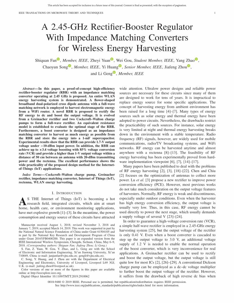
Fig. 10. Equivalent resistance model of the RBR.
practical due to that only limited power can be harvested bythe rectenna.
When the input power is sufficient, each node in the RBRcan be charged to the maximum value. However, in realconditions, the input power is usually limited, and the loadeffect cannot be neglected. When the harvesting power is notenough to drive the load at all stages, the output voltage will godown, and it will also limit the total output power. Therefore,the feature of the internal equivalent resistance of the RBRneeds to be studied.
Here, an equivalent resistance model of the RBR is shownin Fig. 10. RL is the load resistance, which is 10 M� of theprobe in this case. RS,N is the internal equivalent resistanceof the N-stage RBR. Vin,N is the ideal output voltage of theN-stage RBR given in (15), which satisfies
Vin,N = Vout,N = 4NVamp. (18)
According to Fig. 10, if RS,N is much smaller than RL ,the output voltage, Vout, can be close to the ideal case. Thatis, Vout = Vin,N . If RS,N is comparable to or larger than RL ,the voltage drop on RS,N cannot be ignored, which causesa decrease in Vout. In order to carefully study the feature ofRS,N , the input and output voltage waveforms of the equivalentresistance model of the RBR are illustrated in Fig. 11.
The energy consumed at RL in a period T can becalculated by
EL = PL · T = V 2out
RL· T (19)
where Vout and RL represent the output voltage and the loadresistance shown in Fig. 10, respectively.
On the other hand, the energy provided by the RBR can beexpressed as
Ein = Iin · Vout · tθ (20)
where Iin is the average current within tθ . tθ is the conductionperiod, which satisfies
⎧⎨⎩
tθ = T − 4t0
t0 = T
2πarcsin
(Vout
Vin,N
)(21)
where T is the period of the sine wave, and t0 is the momentwhen the input voltage becomes larger than the output voltage.
Fig. 11. Waveforms illustration of the input and output voltages of theequivalent resistance model of the RBR shown in Fig. 10.
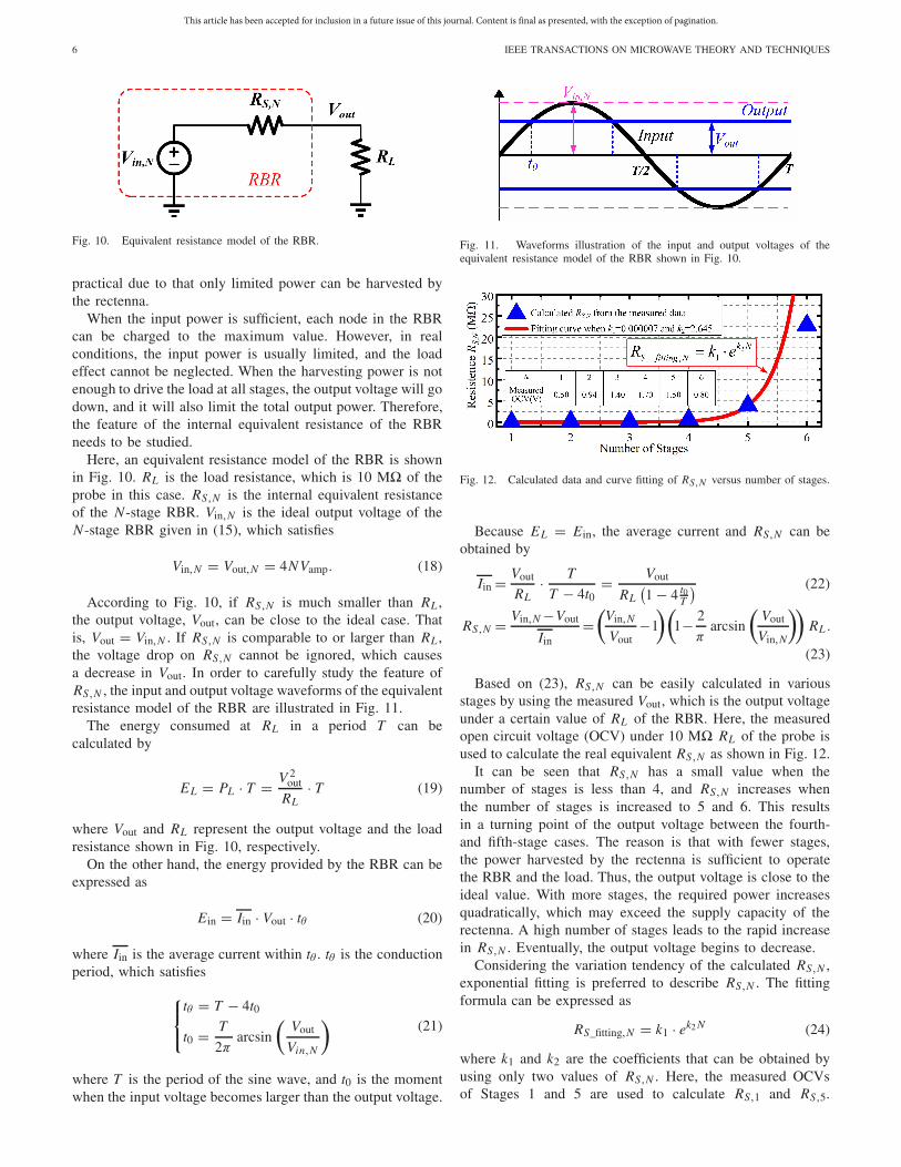
Fig. 12. Calculated data and curve fitting of RS,N versus number of stages.
Because EL = Ein, the average current and RS,N can beobtained by
Iin = Vout
RL· T
T − 4t0= Vout
RL(1 − 4 t0
T
) (22)
RS,N = Vin,N −Vout
Iin=
(Vin,N
Vout−1
)(1− 2
πarcsin
(Vout
Vin,N
))RL .
(23)
Based on (23), RS,N can be easily calculated in variousstages by using the measured Vout, which is the output voltageunder a certain value of RL of the RBR. Here, the measuredopen circuit voltage (OCV) under 10 M� RL of the probe isused to calculate the real equivalent RS,N as shown in Fig. 12.
It can be seen that RS,N has a small value when thenumber of stages is less than 4, and RS,N increases whenthe number of stages is increased to 5 and 6. This resultsin a turning point of the output voltage between the fourth-and fifth-stage cases. The reason is that with fewer stages,the power harvested by the rectenna is sufficient to operatethe RBR and the load. Thus, the output voltage is close to theideal value. With more stages, the required power increasesquadratically, which may exceed the supply capacity of therectenna. A high number of stages leads to the rapid increasein RS,N . Eventually, the output voltage begins to decrease.
Considering the variation tendency of the calculated RS,N ,exponential fitting is preferred to describe RS,N . The fittingformula can be expressed as
RS_fitting,N = k1 · ek2 N (24)
where k1 and k2 are the coefficients that can be obtained byusing only two values of RS,N . Here, the measured OCVsof Stages 1 and 5 are used to calculate RS,1 and RS,5.

This article has been accepted for inclusion in a future issue of this journal. Content is final as presented, with the exception of pagination.
FAN et al.: 2.45-GHz RBR WITH IMPEDANCE MATCHING CONVERTERS FOR WIRELESS ENERGY HARVESTING 7
Fig. 13. Comparison of the calculated (from the models) and measured OCVand VCR versus the number of stages.
The coefficients of k1 and k2 can be solved as 0.000007 and2.645, respectively. The fitted curve is also plotted in Fig. 12.It shows very good agreement with the calculated one.
D. Number of Booster Stages
According to the above analysis, k1 and k2 can be calculatedby using only two sets of the measured data, thus the outputvoltage can be extracted from (23). This process makesit possible to accurately predict the variation tendency andimprovement effect of the output voltage by only using verylimited data.
In order to verify the accuracy of the equivalent resistancemodel, the output voltage of the RBR is analyzed. Here,the VCR is used and defined by Vout/Vin,N . The output voltageof the first stage is considered to be equal to the ideal output.Then, the ideal output voltage of the N th-stage should be Ntimes of that of the first stage. The calculated and measuredOCV and VCR are shown in Fig. 13. Here, it is difficultto exactly solve Vout from (23) directly. The measured andmodeling results have some disagreement. The data pointsshown in Fig. 13 do not perfectly match each other. It can beseen that the OCV increases rapidly before the turning point,and decreases dramatically after this point. The measuredresults match the modeling ones very well. The average erroris less than 10%, which verifies the correctness of the modeland the relevant theoretical analysis.
IV. EXPERIMENTAL RESULTS
A. RBR Measurement
The performance of the proposed RBR with the matchingnetwork is measured at different RF input power levels asshown in Fig. 14. The measured reflection coefficient S11 ofthe RBR is better than −10 dB between 2.4 and 2.5 GHzwhen the input power to the RBR is in the range of interest,i.e., from −10 to 0 dBm.
The RF-to-dc PCE can be expressed as
η = Pout
Pin= Vout · Iout
Pin= V 2
out
RL · Pin(25)
where Pin is the input power from the RF source and Pout isthe dc output power that can be obtained by measuring theoutput voltage on the load RL .
An RF signal generator (RIGOL DSG3060) is used asthe input RF source. The measured output voltage versus
Fig. 14. Measured S11 of the RBR with the matching network.
Fig. 15. Measured (a) output voltage and (b) PCE of the RBR versus RFinput power with various load impedances.
input power is shown in Fig. 15(a). Since the output voltageand efficiency are highly dependent on the load resistance,the measurements were carried out with RL = 500 �,2 k�, 10 k�, 20 k�, 30 k�, 65 k�, and 10 M� (Probe),respectively. For safe operation, each measurement is stoppedwhen the output voltage reaches 14 V. The proposed RBR canprovide a 5.9-V output voltage under 0-dBm input power orlarger than 1 V under −14-dBm input power with 10-M� loadresistance. The measured RF-to-dc PCE versus input power isshown in Fig. 15(b). The peak PCE of 37.5% is achieved with13-dBm input power and 20-k� load resistance.
B. Wireless Experiment
The test platform of the proposed full system is shownin Fig. 16. A four-stage RBR was adopted for the experiment.The RF signal is generated by a signal generator. A PA with11-dB gain is used to magnify the RF signal. The input

This article has been accepted for inclusion in a future issue of this journal. Content is final as presented, with the exception of pagination.
8 IEEE TRANSACTIONS ON MICROWAVE THEORY AND TECHNIQUES
Fig. 16. Test platform of the proposed RF energy harvester.
TABLE II
PARAMETERS OF THE WLAN ENERGY HARVESTING SYSTEM
Fig. 17. Measured output power versus output voltage under different loadimpedances at three different output power levels of the PA.
power of the harvester from the rectenna can be changed byvarying the magnitude of the RF signal or the distance betweenthe antenna and the harvester. Parameters of the developedWLAN energy harvesting system are given in Table II. Theinput impedance of the boost converter can be calculated byemploying (10), which should match the output impedance ofthe RBR.
Since the proposed harvester focuses on indoor RF energyharvesting, 2.45-GHz signals are commonplace in such envi-ronment (WiFi networks, ZigBee, or Bluetooth communica-tions) and are employed for the system test in this paper.Fig. 17 shows the measured results of the output power versusoutput voltage of the proposed system under different loadimpedances at three different power levels of the RF signal.
Fig. 18. Measured OCV of the proposed system and the Greinacher rectifierversus the distance between the antenna and rectenna.
Fig. 19. Measured output voltage when harvesting WLAN energy from aWiFi router.
The distance between the antenna and the rectenna is set to15 cm, and the magnitude of the RF signal is varied. Whenthe output powers of the PA are 15, 17, and 19 dBm, andthe measured OCVs are 1.7, 2.6, and 3.5 V, respectively.Keeping the output power of the PA at 19 dBm, when thedistance is increased to 25, 40, and 50 cm, the measuredOCVs are 2.1, 1.3, and 1.0 V, respectively. Compared with[2]–[4], the proposed harvester boosts the output voltage tohigher levels. This is very desirable for many IoT applications.Also as shown in Fig. 17, all three scatter curves of the outputpower exhibit a single peak characteristic, which indicates thepossibility of applying the MPPT technique to further improvethe performance of the harvester.
Normally, the output power of a WiFi router is no more than20 dBm. In this experiment, a PA is employed to simulate theoperation of a WiFi router as an energy source. To facilitatecomparison of our design, both a Greinacher rectifier anda four-stage RBR voltage booster are implemented. Fig. 18shows the measured results of the OCV versus the distancebetween the transmit antenna and the rectenna. It indicatesthat the proposed system can provide over 1- and 0.5-V outputvoltages within a distance of 50 and 90 cm, respectively. Com-pared with the Greinacher rectifier, the proposed system canboost the output voltage up to 3.4 times higher. The distancecan be increased further by using a higher gain antenna.
The proposed system is used to harvest energy from a WiFirouter (TP-LINK TL_WDR5620) with a distance of 15 cm

This article has been accepted for inclusion in a future issue of this journal. Content is final as presented, with the exception of pagination.
FAN et al.: 2.45-GHz RBR WITH IMPEDANCE MATCHING CONVERTERS FOR WIRELESS ENERGY HARVESTING 9
Fig. 20. Measured charging process of a 1-mF capacitor with and withoutthe boost converter.
while the router is downloading a big data file. Fig. 19 showsthe transient waveforms of the output voltage of the harvesterwith a Greinacher rectifier (with and without an output capac-itor) and with the four-stage RBR. It can be seen that theharvester with the RBR increases the output voltage signifi-cantly. Such measured results have further demonstrated thefeasibility of harvesting WLAN energy by using the proposedRF energy harvesting system.
To optimize the available power of the RBR, the chargingprocess of a 1-mF supercapacitor is measured. A boost con-verter is employed to match the impedance and maximize theharvested power. A PFM frequency of 10 kHz and turn-on timeof 2.5 μs are used to realize the input impedance of 20 k�of the boost converter to match the output impedance of theRBR. The charging process is shown in Fig. 20. The steadyoutput voltages with and without the boost converter under10-M� load resistance are 1.216 and 0.936 V, respectively.The output power can be calculated by using the equation ofP = V 2/R, which shows that the output power is increasedby nearly 70% after using an impedance matching converter.
V. CONCLUSION
To sum up, a novel high VCR RBR with an impedancematching converter has been proposed to harvest wirelessenergy from the WLAN. The RBR is evolved from aGreinacher rectifier and a Cockcroft–Walton charge pump toform a full-wave rectifier. An equivalent resistance model ofthe RBR is established to accurately predict the variationtendency of the output voltage by only using very limited data.The measured results show that nearly 315% output voltageimprovement is achieved with the RBR. Then, combinedwith a flower-shaped broadband dual-polarized cross-dipoleantenna and a boost converter as an impedance matchingconverter, the entire WLAN energy harvesting system isdemonstrated. It harvests RF energy from a WiFi router andstores the electric energy in a supercapacitor. Compared withdirectly charging a supercapacitor by the RBR, nearly 70%more energy has been harvested by adding an impedancematching converter between the RBR and the supercapacitor.These merits prove the excellent practicality of the proposedharvesting system for IoT applications.
ACKNOWLEDGMENT
The authors would like to thank Dr. M. Ye of XJTU for thehelpful technical discussions.
REFERENCES
[1] T. Wu and H. C. Yang, “RF energy harvesting with cooperative beamselection for wireless sensors,” IEEE Wireless Commun. Lett., vol. 3,no. 6, pp. 585–588, Dec. 2014.
[2] Y.-S. Chen and C.-W. Chiu, “Maximum achievable power conversionefficiency obtained through an optimized rectenna structure for RFenergy harvesting,” IEEE Trans. Antennas Propag., vol. 65, no. 5,pp. 2305–2317, May 2017.
[3] Y. Lu et al., “A wide input range dual-path CMOS rectifier for RF energyharvesting,” IEEE Trans. Circuits Syst. II, Express Briefs, vol. 64, no. 2,pp. 166–170, Feb. 2017.
[4] U. Olgun, C.-C. Chen, and J. L. Volakis, “Investigation of rectennaarray configurations for enhanced RF power harvesting,” IEEE AntennasWireless Propag. Lett., vol. 10, pp. 262–265, Apr. 2011.
[5] K. R. Sadagopan, J. Kang, Y. Ramadass, and A. Natarajan, “A 960pWco-integrated-antenna wireless energy harvester for WiFi backchan-nel wireless powering,” in IEEE Int. Solid-State Circuits Conf.(ISSCC) Dig. Tech. Papers, San Francisco, CA, USA, Feb. 2018,pp. 136–138.
[6] E. Falkenstein, M. Roberg, and Z. Popovic, “Low-power wirelesspower delivery,” IEEE Trans. Microw. Theory Techn., vol. 60, no. 7,pp. 2277–2286, Jul. 2012.
[7] Y. Han, O. Leitermann, D. A. Jackson, J. M. Rivas, and D. J. Per-reault, “Resistance compression networks for radio-frequency powerconversion,” IEEE Trans. Power Electron., vol. 22, no. 1, pp. 41–53,Jan. 2007.
[8] Y.-J. Ren and K. Chang, “5.8-GHz circularly polarized dual-dioderectenna and rectenna array for microwave power transmission,”IEEE Trans. Microw. Theory Techn., vol. 54, no. 4, pp. 1495–1502,Jun. 2006.
[9] Z. Harouni, L. Cirio, L. Osman, A. Gharsallah, and O. Picon, “A dualcircularly polarized 2.45-GHz rectenna for wireless power transmis-sion,” IEEE Antennas Wireless Propag. Lett., vol. 10, pp. 306–309,Apr. 2011.
[10] H. Sun, Y.-X. Guo, M. He, and Z. Zhong, “A dual-band rectennausing broadband Yagi antenna array for ambient RF power harvest-ing,” IEEE Antennas Wireless Propag. Lett., vol. 12, pp. 918–921,Jul. 2013.
[11] M. Stoopman, S. Keyrouz, H. J. Visser, K. Philips, and W. A. Serdijn,“Co-Design of a CMOS rectifier and small loop antenna for highlysensitive RF energy harvesters,” IEEE J. Solid-State Circuits, vol. 49,no. 3, pp. 622–634, Mar. 2014.
[12] M. A. Abouzied and E. Sánchez-Sinencio, “Low-input power-levelCMOS RF energy-harvesting front end,” IEEE Trans. Microw. TheoryTechn., vol. 63, no. 11, pp. 3794–3805, Nov. 2015.
[13] J. Bito, J. G. Hester, and M. M. Tentzeris, “Ambient RF energy harvest-ing from a two-way talk radio for flexible wearable wireless sensordevices utilizing inkjet printing technologies,” IEEE Trans. Microw.Theory Techn., vol. 63, no. 12, pp. 4533–4543, Dec. 2015.
[14] M. Piñuela, P. D. Mitcheson, and S. Lucyszyn, “Ambient RF energyharvesting in urban and semi-urban environments,” IEEE Trans. Microw.Theory Techn., vol. 61, no. 7, pp. 2715–2726, Jul. 2013.
[15] J.-P. Curty, N. Joehl, F. Krummenacher, C. Dehollain, andM. J. Declercq, “A model for μ-power rectifier analysis and design,”IEEE Trans. Circuits Syst. I, Reg. Papers, vol. 52, no. 12, pp. 2771–2779,Dec. 2005.
[16] V. Kuhn, C. Lahuec, F. Seguin, and C. Person, “A multi-band stackedRF energy harvester with RF-to-DC efficiency up to 84%,” IEEE Trans.Microw. Theory Techn., vol. 63, no. 5, pp. 1768–1778, May 2015.
[17] M. A. Abouzied, K. Ravichandran, and E. Sánchez-Sinencio,“A fully integrated reconfigurable self-startup RF energy-harvesting sys-tem with storage capability,” IEEE J. Solid-State Circuits, vol. 52, no. 3,pp. 704–719, Mar. 2017.
[18] A. K. Moghaddam, J. H. Chuah, H. Ramiah, J. Ahmadian, P. I. Mak,and R. P. Martins, “A 73.9%-efficiency CMOS rectifier using a lowerDC feeding (LDCF) self-body-biasing technique for far-field RF energy-harvesting systems,” IEEE Trans. Circuits Syst. I, Reg. Papers, vol. 64,no. 4, pp. 992–1002, Apr. 2017.
[19] T.-H. Lin, J. Bito, J. G. Hester, J. Kimionis, R. A. Bahr, andM. M. Tentzeris, “Ambient energy harvesting from two-way talk radiofor on-body autonomous wireless sensing network using inkjet and 3Dprinting,” in IEEE MTT-S Int. Microw. Symp. Dig., Honololu, HI, USA,Jun. 2017, pp. 1034–1037.
[20] G. Papotto, F. Carrara, and G. Palmisano, “A 90-nm CMOS threshold-compensated RF energy harvester,” IEEE J. Solid-State Circuits, vol. 46,no. 9, pp. 1985–1997, Sep. 2011.

This article has been accepted for inclusion in a future issue of this journal. Content is final as presented, with the exception of pagination.
10 IEEE TRANSACTIONS ON MICROWAVE THEORY AND TECHNIQUES
[21] J. Masuch, M. Delgado-Restituto, D. Milosevic, and P. Baltus, “Co-integration of an RF energy harvester into a 2.4 GHz transceiver,” IEEEJ. Solid-State Circuits, vol. 48, no. 7, pp. 1565–1574, Jul. 2013.
[22] Z. Popovic et al., “Scalable RF energy harvesting,” IEEE Trans. Microw.Theory Techn., vol. 62, no. 4, pp. 1046–1056, Apr. 2014.
[23] T. Sakamoto, Y. Ushijima, E. Nishiyama, M. Aikawa, and I. Toyoda,“5.8-GHz series/parallel connected rectenna array using expandabledifferential rectenna units,” IEEE Trans. Antennas Propag., vol. 61,no. 9, pp. 4872–4875, Sep. 2013.
[24] S.-T. Khang, D.-J. Lee, I.-J. Hwang, T.-D. Yeo, and J.-W. Yu,“Microwave power transfer with optimal number of rectenna arrays formidrange applications,” IEEE Antennas Wireless Propag. Lett., vol. 17,no. 1, pp. 155–159, Jan. 2018.
[25] S.-E. Adami et al., “A flexible 2.45-GHz power harvesting wristbandwith net system output from–24.3 dBm of RF power,” IEEE Trans.Microw. Theory Techn., vol. 66, no. 1, pp. 380–395, Jan. 2018.
[26] H. Zhang, Z. Zhong, Y.-X. Guo, and W. Wu, “Differentially-fed chargepumping rectifier design with an enhanced efficiency for ambient RFenergy harvesting,” in IEEE MTT-S Int. Microw. Symp. Dig., Jun. 2017,pp. 613–616.
[27] C. Song, Y. Huang, J. Zhou, J. Zhang, S. Yuan, and P. Carter, “A high-efficiency broadband rectenna for ambient wireless energy harvest-ing,” IEEE Trans. Antennas Propag., vol. 63, no. 8, pp. 3486–3495,Aug. 2015.
[28] S. D. Assimonis, S.-N. Daskalakis, and A. Bletsas, “Sensitive and effi-cient RF harvesting supply for batteryless backscatter sensor networks,”IEEE Trans. Microw. Theory Techn., vol. 64, no. 4, pp. 1327–1338,Apr. 2016.
[29] M. Mattsson, C. I. Kolitsidas, and B. L. G. Jonsson, “Dual-band dual-polarized full-wave rectenna based on differential field sampling,” IEEEAntennas Wireless Propag. Lett., vol. 17, no. 6, pp. 956–959, Jun. 2018.
[30] Z. Zeng, X. Li, A. Bermak, C.-Y. Tsui, and W.-H. Ki, “A WLAN2.4-GHz RF energy harvesting system with reconfigurable rectifierfor wireless sensor network,” in Proc. IEEE Int. Symp. Circuits Syst.(ISCAS), Montreal, QC, Canada, May 2016, pp. 2362–2365.
[31] A. Biswas, S. B. Hamidi, C. Biswas, P. Roy, D. Mitra, and D. Dawn,“A novel CMOS RF energy harvester for self-sustainable applications,”in Proc. IEEE 19th Wireless Microw. Technol. Conf. (WAMICON), SandKey, FL, USA, Apr. 2018, pp. 1–5.
[32] M. Taghadosi, L. Albasha, N. A. Quadir, Y. A. Rahama, andN. Qaddoumi, “High efficiency energy harvesters in 65 nm CMOSprocess for autonomous IoT sensor applications,” IEEE Access, vol. 6,pp. 2397–2409, Dec. 2018.
[33] M. H. Ouda, M. Arsalan, L. Marnat, A. Shamim, and K. N. Salama,“5.2-GHz RF power harvester in 0.18-μm CMOS for implantableintraocular pressure monitoring,” IEEE Trans. Microw. Theory Techn.,vol. 61, no. 5, pp. 2177–2184, May 2013.
[34] A. S. Almansouri, M. H. Ouda, and K. N. Salama, “A CMOS RF-to-DCpower converter with 86% efficiency and-19.2-dBm sensitivity,” IEEETrans. Microw. Theory Techn., vol. 66, no. 5, pp. 2409–2415, May 2018.
[35] S. Fan, R. Wei, L. Zhao, X. Yang, L. Geng, and P. X.-L. Feng,“An ultralow quiescent current power management system with max-imum power point tracking (MPPT) for batteryless wireless sen-sor applications,” IEEE Trans. Power Electron., vol. 33, no. 9,pp. 7326–7337, Sep. 2018.
[36] V. Marian, B. Allard, C. Vollaire, and J. Verdier, “Strategy for microwaveenergy harvesting from ambient field or a feeding source,” IEEE Trans.Power Electron., vol. 27, no. 11, pp. 4481–4491, Nov. 2012.
[37] S. Bandyopadhyay and A. P. Chandrakasan, “Platform architecture forsolar, thermal, and vibration energy combining with MPPT and singleinductor,” IEEE J. Solid-State Circuits, vol. 47, no. 9, pp. 2199–2215,Sep. 2012.
[38] S. Fan et al., “A high-efficiency radio frequency rectifier-booster regula-tor for ambient WLAN energy harvesting applications,” in IEEE MTT-SInt. Microw. Symp. Dig., May 2018, pp. 1–3.
[39] S. Dehghani, S. Abbasian, and T. Johnson, “Tracking load to optimizepower efficiency in RF to DC rectifier circuits,” in Proc. IEEE WirelessPower Transf. Conf. (WPTC), Boulder, CO, USA, May 2015, pp. 1–3.
[40] L. Shen and X. Yang, “A novel rectifier circuit operating at dual-frequencies of 1.8 GHz and 2.4 GHz,” in IEEE MTT-S Int. Microw.Workshop Ser. RF Wireless Technol. Biomed. Healthcare Appl. (IMWS-BIO), Singapore, Dec. 2013, pp. 1–3.
[41] B. L. Pham and A.-V. Pham, “Triple bands antenna and high efficiencyrectifier design for RF energy harvesting at 900, 1900 and 2400 MHz,”in IEEE MTT-S Int. Microw. Symp. Dig., Seattle, WA, USA, Jun. 2013,pp. 1–3.
Shiquan Fan (S’13– M’15) received the B.Sc.,M.Sc., and Ph.D. degrees in microelectronics fromXi’an Jiaotong University, Xi’an, China, in 2003,2009, and 2014, respectively.
From 2003 to 2006, he was a Research and Devel-opment Engineer for power management systemdesign and development. From 2016 to 2017, he wasa Visiting Scholar with the Department of ElectricalEngineering and Computer Science, Case WesternReserve University, Cleveland, OH, USA. He iscurrently an Associate Professor with the School of
Microelectronics, Xi’an Jiaotong University. His current research interestsinclude analog and mixed-signal integrated circuit, energy harvesting system,power management circuit, and system design.
Dr. Fan was a recipient of the Science and Technology Improvement Awardby Shaanxi Municipal Government in 2015 and the Lam Research ThesisAward twice from Lam Research Corporation in 2015.
Zheyi Yuan received the B.Sc. degree in micro-electronics from Xi’an Jiaotong University, Xi’an,China, in 2017, where he is currently pursuing theM.S. degree in microelectronics.
His current research interests include RF energyharvesting and power management circuits.
Wei Gou (S’18) received the B.Sc. and M.S. degreesin microelectronics from Xi’an Jiaotong University,Xi’an, China, in 2015 and 2018, respectively.
In 2018, he joined Huawei Technologies Co.,Ltd., Xi’an, as an Analog IC Design Engineer. Hiscurrent research interests include power managementcircuits and systems and all-digital phase lock loops.
Yang Zhao received the B.Sc. degree in micro-electronics from Xi’an Jiaotong University, Xi’an,China, in 2016, where he is currently pursuing theM.S. degree in microelectronics.
His current research interests include piezoelectricenergy harvesting and power management circuits.

This article has been accepted for inclusion in a future issue of this journal. Content is final as presented, with the exception of pagination.
FAN et al.: 2.45-GHz RBR WITH IMPEDANCE MATCHING CONVERTERS FOR WIRELESS ENERGY HARVESTING 11
Chaoyun Song (M’16) received the B.Sc., M.Sc.,and Ph.D. degrees in electrical engineering andelectronics from the University of Liverpool(UoL), Liverpool, U.K., in 2012, 2013, and 2017,respectively.
From 2015 to 2016, he was a Research Assistantand an Antenna Design Engineer with UoL andBAE Systems, Chelmsford, U.K. He is currently aPost-Doctoral Research Associate with UoL. He hasauthored or coauthored more than 30 papers ininternationally refereed journals and conference pro-
ceedings. He has filed six U.S., EU, and U.K. patents. His current researchinterests include liquid antennas, novel materials, wireless energy harvesting,rectifying antennas, wireless power transfer, global navigation satellite systemantennas, anti-jamming technologies, and smart sensors for the Internet ofThings.
Dr. Song was a recipient of many international awards, such as the recipientof the IET Present Around the World Competition in 2016, the EW Bright-Sparks Award for Outstanding Electronic Engineers under age 30 in theU.K., 2018, and the BAE Systems Chairman’s Award in 2017 for theinnovation of next generation global navigation satellite system antennas.He has been a regular Reviewer of many international journals, includingApplied Physics Letters, Scientific Reports, the IEEE TRANSACTIONS ON
ANTENNAS AND PROPAGATION, the IEEE TRANSACTIONS ON INDUSTRIALELECTRONICS, the IEEE TRANSACTIONS ON MICROWAVE THEORY AND
TECHNIQUES, the IEEE TRANSACTION ON CIRCUITS AND SYSTEMS—I:REGULAR PAPERS, the IEEE ANTENNAS AND WIRELESS PROPAGATION
LETTERS, and IEEE SENSORS LETTERS.
Yi Huang (S’91–M’96–SM’06) received the B.Sc.degree in physics from Wuhan University, Wuhan,China, in 1984, the M.Sc. (Eng.) degree inmicrowave engineering from the Nanjing ResearchInstitute of Electronics Technology (NRIET), Nan-jing, China, in 1987, and the D.Phil. degree in com-munications from the University of Oxford, Oxford,U.K., in 1994.
Since 1987, he has been conducting researchon wireless communications, applied electromagnet-ics, radar, and antennas. His experience includes
three years spent with NRIET as a Radar Engineer and various periods withthe Universities of Birmingham, Oxford and Essex, U.K., as a Member ofResearch Staff. In 1994, he joined British Telecom Labs, as a ResearchFellow. In 1995, he joined the Department of Electrical Engineering andElectronics, University of Liverpool, Liverpool, U.K., where he is currentlya Full Professor of wireless engineering, the Head of the High FrequencyEngineering Group, and the Deputy Head of the Department. He has beena Consultant to various companies. He has authored or coauthored morethan 350 refereed papers in leading international journals and conferenceproceedings. He authored Antennas: from Theory to Practice (Wiley, 2008)and Reverberation Chambers: Theory and Applications to EMC and AntennaMeasurements (Wiley, 2016).
Mr. Huang is a Fellow of the IET and a Senior Fellow of the HEA. He wasa recipient of many research grants from research councils, governmentagencies, charity, EU and industry, and served on a number of national andinternational technical committees. He has been an Editor, Associate Editor,or a Guest Editor of five international journals. He has been a Keynote/InvitedSpeaker and an organizer of many conferences and workshops (e.g., WiCom2006, 2010, IEEE iWAT2010, LAPC2012, and EuCAP2018). He is currentlythe Editor-in-Chief of Wireless Engineering and Technology and an AssociateEditor of the IEEE ANTENNAS AND WIRELESS PROPAGATION LETTERS,and the Ireland Representative to the European Association of Antenna andPropagation (EurAAP).
Jiafeng Zhou received the Ph.D. degree in electricalengineering and electronics from the University ofBirmingham, Birmingham, U.K., in 2004.
He then moved to the Department of Electronicand Electrical Engineering, University of Bristol,Bristol, U.K., until 2013, where he was involvedin the development of highly efficient and lin-ear amplifiers. In 1997, he was with the NationalMeteorological Satellite Centre of China, Beijing,China, where he was involved in the developmentof communication systems for Chinese geostationary
meteorological satellites. From 2004 to 2006, he was a Research Fellowwith the University of Birmingham, where he was involved in phased arraysfor reflector observing systems. He is currently with the Department ofElectrical Engineering and Electronics, University of Liverpool, Liverpool,U.K. His current research interests include microwave power amplifiers, filters,electromagnetic energy harvesting, and wireless power transfer.
Li Geng (M’06) received the B.Sc. degree inphysics, and the M.Sc. and Ph.D. degrees in electri-cal engineering from the Xi’an University of Tech-nology, Xi’an, China, in 1990, 1998, and 2001,respectively.
She was the Director of the Department of Micro-electronics, Xi’an Jiaotong University, Xi’an. From1999 to 2000, she was a Visiting Scholar withthe Department of Electrical Engineering, IlmenauUniversity of Technology, Ilmenau, Germany. From2007 to 2008, she was a Visiting Professor with
the Department of Electrical Engineering, Stanford University, Stanford, CA,USA. She is currently a Professor with the Department of Microelectronics,Xi’an Jiaotong University. Her current research interests include powermanagement integrated circuits, low-voltage low-power analog and mixed-signal integrated circuits, RF integrated circuit, and bioimplant systems.
Dr. Geng was a Technical Program Committee member of ASSCC from2010 to 2018. She was a recipient of the Science and Technology ImprovementAward of the Ministry of National Mechanical Industry, China, in 1999 andthe Science and Technology Improvement Award by Shaanxi MunicipalGovernment in 2000, 2001, 2010, and 2015, respectively.