An Exact Method using Quantum Theory to Calculate ... - arXiv
10
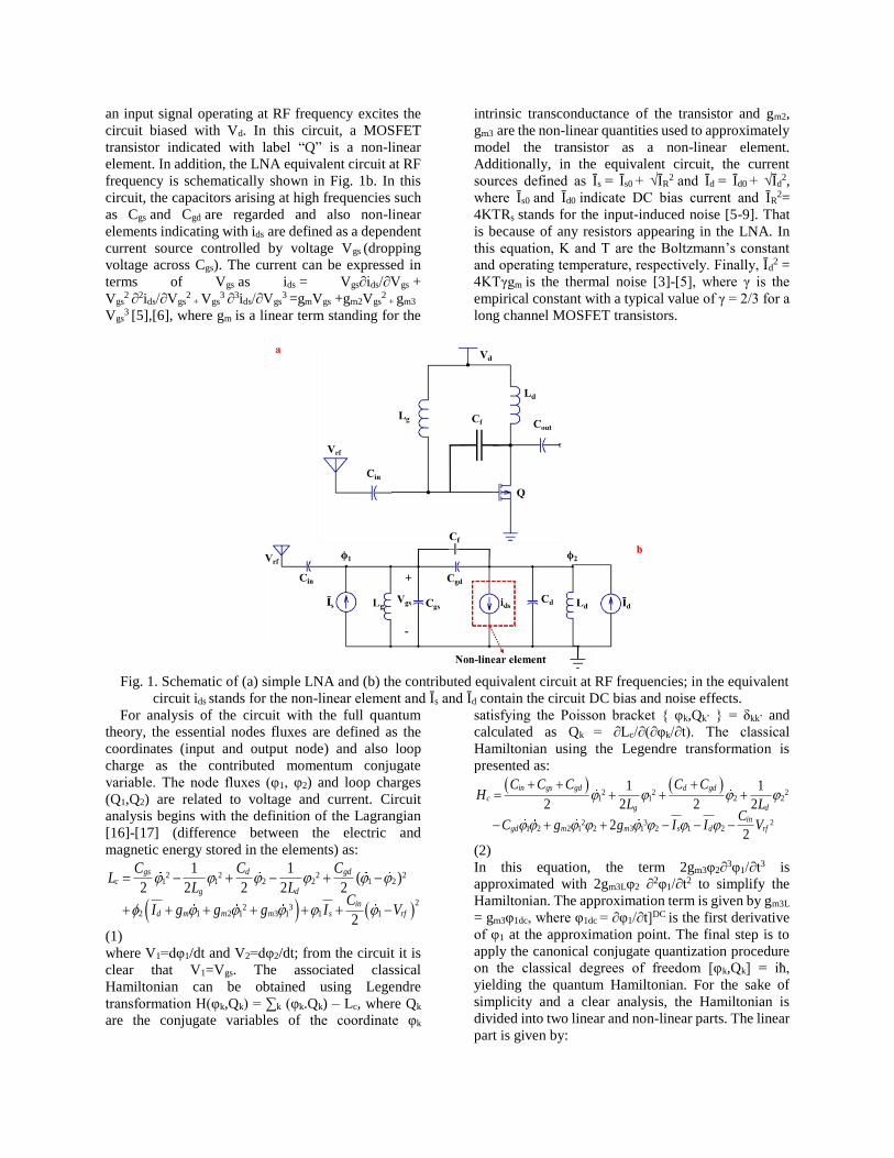
An Exact Method using Quantum Theory to Calculate the Noise Figure in a Low Noise Amplifier Ahmad Salmanogli Çankaya University, Engineering faculty, Electrical and Electronic Department, Ankara, Turkey Abstract— In this article, a low noise amplifier is quantum mechanically analyzed to study the behavior of the noise figure. The analysis view is changed from the classic to quantum, because using quantum theory produces some degrees of freedom, which may be ignored when a circuit is analyzed using a classical theory. For this reason, the associated Lagrangian is initially derived for the circuit and then using Legendre transformation and canonical quantization procedure the classical and quantum Hamiltonian are derived, respectively. Consequently, the dynamic equation of motion of the circuit is introduced by which all of the circuit measurable observations such as voltage and current fluctuations are calculated. As an interesting point of this study, the low noise amplifier is deliberately supposed as two oscillators connecting to each other sharing the mutual specifications and accordingly the voltage and current are expressed in terms of the oscillator’s photon number. As a result, one can analyze the critical quantity such as the noise figure in terms of the oscillator’s photon number and also the photons coupling between oscillators. The latter mentioning term is considered as a factor to engineering the amplifier critical quantities. Additionally, the considered circuit is designed and classically simulated to testify the derived results using the quantum theory. Index Terms—quantum theory, low noise amplifier, noise figure. I. INTRODUCTION One of the critical parts of a Radar system [1],[2] contributes to the receiver subsystem as a very weak echo gets back from a higher altitude. The detection of such signals is very difficult, because the detecting signal power level equals the noise level [1],[2]. To enhance the radar receiver sensitivity, the related noise power of this subsystem should be limited as much as possible. For this subsystem, a low noise amplifier (LNA) [3]-[6] has been considered as an indispensable part, which can effectively amplify a very weak receiving signal, and also add a noise with a minimum level to the signal. In fact, in a radar receiver this is LNA that should dominate the sensitivity. However, the design of a LNA is mostly challenging. The LNA design contains some unusual trade-offs among noise figure (NF), linearity, gain, impedance matching, and also power consumption [3]-[6]. However, the designer mainly focuses on LNA related NF, which is a very critical factor in the detection of a very weak signal. This is due to the fact that the noise performance of a LNA can easily affect the receiver performance as well. There are some different types of LNA circuit such as common source LNA (CS-LNA) [7]-[9] and common gate LNA (CG-LNA) [7], [10]- [11]. The former one has been widely used due to its very good noise performance, while the latter one achieves a very good impedance matching and in contrast has a poor NF. For instance, to improve CG- LNA noise performance, the capacitive cross-coupling technique has been employed [3],[7]. Also, some additional inductors are added at the main transistor’s drain to improve the noise performance by cancelling out the parasitic capacitance effect [5]-[7]. Additionally, the capacitance connected between gate and drain of the transistor in a cascade LNA [7],[12], which is mainly used to improve the LNA linearity [5]-[8] can help to minimize NF. So far, some LNA design circuits are cited in which the aim is to improve the performance of the LNA. However, there are so many articles (not cited in this study) that have investigated LNA performance enhancing due to its priority in systems such as radar. Beside this, there are some other applications such as quantum radars [13]- [15] that need to use an Ultra-low noise amplifier. This means that NF is very important in such an application. That is why we specifically focus on this factor in this study and try to analyze this quantity from the other and exact point of view called quantum theory [16]- [17]. In contrast to the classical point of view that the LNA has been analyzed so far, this study investigates LNA using quantum theory. It is supposed that quantum theory gives some extra degrees of freedom that the designed circuit becomes fully understandable. This study starts with an important assumption that the designed LNA operates like two coupled oscillators to each other. It means that all of the LNA important properties such as NF can be affected through coupling the mentioned oscillators to each other. Thus, this is the oscillator's photon number that affects the system performance. To completely understand the LNA operating, the circuit degrees of freedom such as voltage and current are derived and expressed in terms of the oscillator's photon numbers. Additionally, using the current and voltage definitions, other parameters such as power gain and power consumption can be defined in the same way. II. THEORY and BACKFROUND A typical LNA (CS with a capacitive feedback) is schematically illustrated in Fig. 1a. In this circuit Vrf as
-
Upload
khangminh22 -
Category
Documents
-
view
10 -
download
0
Transcript of An Exact Method using Quantum Theory to Calculate ... - arXiv

An Exact Method using Quantum Theory to Calculate the Noise
Figure in a Low Noise Amplifier Ahmad Salmanogli
Çankaya University, Engineering faculty, Electrical and Electronic Department, Ankara, Turkey
Abstract— In this article, a low noise amplifier is
quantum mechanically analyzed to study the behavior of
the noise figure. The analysis view is changed from the
classic to quantum, because using quantum theory
produces some degrees of freedom, which may be
ignored when a circuit is analyzed using a classical
theory. For this reason, the associated Lagrangian is
initially derived for the circuit and then using Legendre
transformation and canonical quantization procedure
the classical and quantum Hamiltonian are derived,
respectively. Consequently, the dynamic equation of
motion of the circuit is introduced by which all of the
circuit measurable observations such as voltage and
current fluctuations are calculated. As an interesting
point of this study, the low noise amplifier is deliberately
supposed as two oscillators connecting to each other
sharing the mutual specifications and accordingly the
voltage and current are expressed in terms of the
oscillator’s photon number. As a result, one can analyze
the critical quantity such as the noise figure in terms of
the oscillator’s photon number and also the photons
coupling between oscillators. The latter mentioning term
is considered as a factor to engineering the amplifier
critical quantities. Additionally, the considered circuit is
designed and classically simulated to testify the derived
results using the quantum theory.
Index Terms—quantum theory, low noise amplifier,
noise figure.
I. INTRODUCTION
One of the critical parts of a Radar system [1],[2]
contributes to the receiver subsystem as a very weak
echo gets back from a higher altitude. The detection of
such signals is very difficult, because the detecting
signal power level equals the noise level [1],[2]. To
enhance the radar receiver sensitivity, the related noise
power of this subsystem should be limited as much as
possible. For this subsystem, a low noise amplifier
(LNA) [3]-[6] has been considered as an indispensable
part, which can effectively amplify a very weak
receiving signal, and also add a noise with a minimum
level to the signal. In fact, in a radar receiver this is
LNA that should dominate the sensitivity. However,
the design of a LNA is mostly challenging. The LNA
design contains some unusual trade-offs among noise
figure (NF), linearity, gain, impedance matching, and
also power consumption [3]-[6]. However, the
designer mainly focuses on LNA related NF, which is
a very critical factor in the detection of a very weak
signal. This is due to the fact that the noise
performance of a LNA can easily affect the receiver
performance as well. There are some different types of
LNA circuit such as common source LNA (CS-LNA)
[7]-[9] and common gate LNA (CG-LNA) [7], [10]-
[11]. The former one has been widely used due to its
very good noise performance, while the latter one
achieves a very good impedance matching and in
contrast has a poor NF. For instance, to improve CG-
LNA noise performance, the capacitive cross-coupling
technique has been employed [3],[7]. Also, some
additional inductors are added at the main transistor’s
drain to improve the noise performance by cancelling
out the parasitic capacitance effect [5]-[7].
Additionally, the capacitance connected between gate
and drain of the transistor in a cascade LNA [7],[12],
which is mainly used to improve the LNA linearity
[5]-[8] can help to minimize NF. So far, some LNA
design circuits are cited in which the aim is to improve
the performance of the LNA. However, there are so
many articles (not cited in this study) that have
investigated LNA performance enhancing due to its
priority in systems such as radar. Beside this, there are
some other applications such as quantum radars [13]-
[15] that need to use an Ultra-low noise amplifier. This
means that NF is very important in such an application.
That is why we specifically focus on this factor in this
study and try to analyze this quantity from the other
and exact point of view called quantum theory [16]-
[17]. In contrast to the classical point of view that the
LNA has been analyzed so far, this study investigates
LNA using quantum theory. It is supposed that
quantum theory gives some extra degrees of freedom
that the designed circuit becomes fully
understandable. This study starts with an important
assumption that the designed LNA operates like two
coupled oscillators to each other. It means that all of
the LNA important properties such as NF can be
affected through coupling the mentioned oscillators to
each other. Thus, this is the oscillator's photon number
that affects the system performance. To completely
understand the LNA operating, the circuit degrees of
freedom such as voltage and current are derived and
expressed in terms of the oscillator's photon numbers.
Additionally, using the current and voltage definitions,
other parameters such as power gain and power
consumption can be defined in the same way.
II. THEORY and BACKFROUND
A typical LNA (CS with a capacitive feedback) is
schematically illustrated in Fig. 1a. In this circuit Vrf as
an input signal operating at RF frequency excites the
circuit biased with Vd. In this circuit, a MOSFET
transistor indicated with label “Q” is a non-linear
element. In addition, the LNA equivalent circuit at RF
frequency is schematically shown in Fig. 1b. In this
circuit, the capacitors arising at high frequencies such
as Cgs and Cgd are regarded and also non-linear
elements indicating with ids are defined as a dependent
current source controlled by voltage Vgs (dropping
voltage across Cgs). The current can be expressed in
terms of Vgs as ids = Vgs∂ids/∂Vgs +
Vgs2 ∂2ids/∂Vgs
2 + Vgs
3 ∂3ids/∂Vgs
3 =gmVgs +gm2Vgs
2 + gm3
Vgs3 [5],[6], where gm is a linear term standing for the
intrinsic transconductance of the transistor and gm2,
gm3 are the non-linear quantities used to approximately
model the transistor as a non-linear element.
Additionally, in the equivalent circuit, the current
sources defined as Īs = Īs0 + √ĪR2 and Īd = Īd0 + √Īd
2,
where Īs0 and Īd0 indicate DC bias current and ĪR2=
4KTRs stands for the input-induced noise [5-9]. That
is because of any resistors appearing in the LNA. In
this equation, K and T are the Boltzmann’s constant
and operating temperature, respectively. Finally, Īd2 =
4KTγgm is the thermal noise [3]-[5], where γ is the
empirical constant with a typical value of γ = 2/3 for a
long channel MOSFET transistors.
Fig. 1. Schematic of (a) simple LNA and (b) the contributed equivalent circuit at RF frequencies; in the equivalent
circuit ids stands for the non-linear element and Īs and Īd contain the circuit DC bias and noise effects.
For analysis of the circuit with the full quantum
theory, the essential nodes fluxes are defined as the
coordinates (input and output node) and also loop
charge as the contributed momentum conjugate
variable. The node fluxes (φ1, φ2) and loop charges
(Q1,Q2) are related to voltage and current. Circuit
analysis begins with the definition of the Lagrangian
[16]-[17] (difference between the electric and
magnetic energy stored in the elements) as:
2 2 2 21 1 2 2 1 2
22 3
2 1 2 1 3 1 1 1
1 1( )
2 2 2 2 2
2
gs d gdc
g d
ind m m m s rf
C C CL
L LC
I g g g I V
(1)
where V1=dφ1/dt and V2=dφ2/dt; from the circuit it is
clear that V1=Vgs. The associated classical
Hamiltonian can be obtained using Legendre
transformation H(φk,Qk) = ∑k (φk.Qk) – Lc, where Qk
are the conjugate variables of the coordinate φk
satisfying the Poisson bracket { φk,Qk’ } = δkk’ and
calculated as Qk = ∂Lc/∂(∂φk/∂t). The classical
Hamiltonian using the Legendre transformation is
presented as:
2 2 2
1 1 2 2
2 3 21 2 2 1 2 3 1 2 1 2
1 1
2 2 2 2
22
in gs gd d gd
cg d
ingd m m s d rf
C C C C CH
L LC
C g g I I V
(2)
In this equation, the term 2gm3φ2∂3φ1/∂t3 is
approximated with 2gm3Lφ2 ∂2φ1/∂t2 to simplify the
Hamiltonian. The approximation term is given by gm3L
= gm3φ1dc, where φ1dc = ∂φ1/∂t]DC is the first derivative
of φ1 at the approximation point. The final step is to
apply the canonical conjugate quantization procedure
on the classical degrees of freedom [φk,Qk] = iħ,
yielding the quantum Hamiltonian. For the sake of
simplicity and a clear analysis, the Hamiltonian is
divided into two linear and non-linear parts. The linear
part is given by:

2 2 212 2 2 2
1 1 2 2 1 2 1 1 21 1 2 2 1 2 1 2
2 1 21 1 2 2 1 2 2 1 2 1 2
1 1 2 2 1 2 2 1
1 1 1 1 1
2 2 2 2 2 2 2 2 2
2 2 2 2 2 2 2
m m m m rfL
q g p q d p p p q q
m m m m m rf rf rf
q p q p q p q p
g g g Pg VH Q Q Q Q
C L C C L C C Cg g g g P g V GV G V
Q Q Q Q Q QC C C C
(3)
where Cq1, Cq2, Cp1, Cp2, Cq1q2, Cq1p1, Cq1p2, Cq2p1,
Cq2p2, P1, P2, G1 and G2 are constants defined in
Appendix A. In this equation, we used two definitions
as the following 1/2Lg’ ≡ (1/2Lg + gm2/2Cp1) and 1/2Ld’
≡ (1/2Ld + gm2/2Cp2); at each one the second term
indicates the effect of the intrinsic transconductance
and also coupling capacitors on both gate and drain
connecting inductors. In other words, the inductors
connected to the transistor can be manipulated due to
the coupling effect. The important point here is that
one can easily find from the Hamiltonian expressed in
Eq. 3 that the equation contains two oscillators; the
first oscillator is connected to the gate and the other is
connected to the drain of the transistor and oscillate
respectively with ω1 = 1/√(Lg’Cq1) and ω2 =
1/√(Ld’Cq2). Other terms in Eq. 3 such as Q1Q2, Q1φ1,
Q2φ1, Q1φ2 show the coupling between oscillators,
meaning that the oscillators share the energy between
themselves. The last terms as Q1, φ1, Q2, φ2 declare the
coupling of the RF source to the contributed
oscillators. Beside of the linear Hamiltonian expressed
in Eq. 3, the non-linear Hamiltonian is presented as:
2 2 21 2 2 2 1 2 11 2
1 2 2 2 1 22
2 32 2 2 2 2 2 2
11 1 2 12 2 2 11 12 1 2 2 11 1 2
211 1 1 2 11 12 2 1 2
3
2 ' 2 ' 2 '2
2
2 2
rf rf m rfin rf
q p q p p pNL
N L m m L
m
m mNL
V V g VQ Q C C V
C C CH g g
C Q C Q C C Q Q C g
C g Q C C g Q
(4) where C’q1p2, C’p1p2, C’q2p2, C11, C12, and C22 are constants
and defined in Appendix A. One can consider HNL in Eq. 4 as
HNL= HNL2 + HNL3, where HNL3 regarded as the perturbation
term and its effect on the energy eigenvalue and eigenstates will
be studied. In the following, the total Hamiltonian is considered
as H = H0+ Hp, where H0 = HL+HNL2 stands for un-perturbed
Hamiltonian and Hp = HNL3 indicates the perturbed
Hamiltonian. To derive the dynamic equation of motion of the
circuit to study the parameters such as voltage and current from
quantum theory point of view, it needs to define the
Hamiltonian in terms of the creation and annihilation operators.
For this reason, the coordinate parameters (φ1, φ2) and the
related momentum conjugate (Q1,Q2) are expressed in terms of
the ladder operators. One can easily re-express the Hamiltonian
in terms of the ladder operators using the quantization
procedure Q1 = -i(a1-a1+).√(ħ/2Z1), φ1 = (a1+a1
+).√(ħZ1/2) and
Q2 = -i(a2-a2+)√(ħ/2Z2), φ2 = (a2+a2
+)√(ħZ2/2), where (ak,ak+) k
= 1,2 are the first and second oscillator’s ladder operators. Also,
the contributed impedance for each oscillator are expressed as
Z1 = √(Lg’/Cq1) and Z2 = √(Ld’/Cq2). Thus, H0 is introduced as
expressed in Eq. 5:
0 1 1 1 2 2 2 1 1 2 2
1 2 1 2
21 1 1 1 2 2 2 2 1 1 2 2
1 1 2 2 1 2 12
12 1 1 1 2 2 1 1 2 2
1 2 2 1
1 1
2 2 4. . .
4 4 4. .
4 4
q q
m m m
q p q p q p
m m r
q p q p
H a a a a a a a aC Z Z
i g i g i g Za a a a a a a a a a a a
C C C Zg i g PV
Z Z a a a a a a a aC C
11 1
2 2 1 22 2 1 1 2 2
1 2
22 2 22 3 2 1 1 1 2 2 11 2 2
1 2
21 1 2 2 2 2 2 2
1 2 1 2 2
2 2
2 2 2 2 2 2
24 ' 2
4 ' 4 '
f m
rf m rf m rf m
L
m rfm m L in rf
p p
m rf rf
q p q p
g Za a
PV g Z iGV g iG V ga a a a a a
Z Z
g V Zg g Z Z a a a a C C V a a
C
i g V Z i Va a a a a a a a
C Z C
2NL
(5)
where subscripts “L” and “NL2” stand for the linear and nonlinear parts, respectively. In the Hamiltonian expressed
in Eq. 5, all of the constant terms are ignored to simplify the equation. Also, the perturbation Hamiltonian is given by:
22 2 212 2 2
2 3 11 1 1 12 2 2 11 1 11 2
212 11 1 1 2 2 11 1 1 1 1
1 2
1 211 12 2 2 1 1 2 2
2
22 2 2
2 222
22 2
mp m m L
m
m
Z gH g g C a a C a a C a a
Z Zi
C C a a a a C g a a a aZ Z
i Z ZC C g a a a a a a
Z
(6)

Table 1. Data used to simulate the LNA using
quantum theory
Stands for
W Transistor channel
width
300 um
Lt Transistor channel
length
50 um
tSiO2 SiO2 thickness 200 nm
Lov Overlapping
length
0.1× Lt
Tc Operational
temperature
4 K
γ Empirical constant 2/3
Cf Feedback
capacitor
0.2 pF
Cin Input capacitance 1.8 pF
Cd Drain capacitance 0.08 pF
Lg Gate inductance 1.2 nH
Ld Drain inductance 0.95 nH
gm2 Second order non-
linearity [5,6]
250
mA/V2
gm3 Third order non-
linearity [5,6]
1300
mA/V3
III. RESULTS and DISCUSSIONS
A. The oscillators Energy dispersion
In this section, we tried to analyze the energy
associated with each oscillator and examine the effect
of the non-linear part on the energy levels (using
Table. 1 according to ATF54143 transistor’s data). It
supposes |j1> and |j2> as the energy state of the first
and second oscillator, respectively. Therefore, using
Hamiltonian expressed in Eq. 5, one can calculate the
energy of the oscillators using Ej = <ji|H0|ji>, where ji
= 1,2. Thus, the oscillators associated energies due to
the un-perturbed Hamiltonian (H0) are given by:
1
2
1 0 1 1 1 11 1
2 0 2 2 2 2 22 2 2 2
1| | . ,
2 2 21
| | . .2 2 2 2 2 '
mj
q p
m rfj
q p q p
i gE j H j j j
Ci g i V
E j H j j j jC C
(7)
Eq. 6 clearly shows that each oscillator is affected by
the associated energy (first term) and also by the
intrinsic transconductance of the transistor (second
term). It means that changing the gain of the current in
the transistor should impact the energy levels of the
oscillators. Also, E2 is additionally influenced by the
other factor that arose due the non-linearity induced in
the transistor. This is a critical factor manipulated by
the RF incident wave and can change the energy of the
second oscillator. This factor will be discussed in
detail in the following. Moreover, we considered the
effect of the perturbed Hamiltonian on the energy
levels of the oscillators and it found that Hp = HNL3
doesn’t affect the energy levels of the oscillators. It
means Ej(1) = <ji|Hp|ji> = 0, where Ej
(1) is the change in
energy using the first order perturbation theory. The
oscillator's energy dispersion is studied and simulated
and the results are depicted in Fig. 2. In this figure, it
is tried to depict the oscillators associated energy
levels versus transistor intrinsic transconductance for
different values of the RF incident wave. From Eq. 7,
it is clear that Ej1 doesn’t be affected by Vrf amplitude,
therefore, in Fig. 2a it just considers the effect of j1. In
contrast, Fig. 2b shows the effect of the Vrf amplitude
on E2 energy. It is shown in Fig. 2b that increasing the
incident wave amplitude (Vrf) manipulates E2 but not
E1. This comes from the last term in H0{NL2} which
controls the coupling of Vrf to the second oscillator.
Fig. 2 Oscillators energy dispersion vs. gm (S), for different values of Vrf; a) absolute value of the energy of OSCI for
different level of energy j1 = 1 and 2, b) a) absolute value of the energy of OSCII for different value of Vrf at j2 = 1.

B. Energy Eigen state due to the Perturbation
Hamiltonian
Beside the energy (Eigen-values), the state
(Eigenstate) of the oscillators can be dispersed. One
can utilize the first perturbation theory to figure out
about the oscillator’s state changing due to the
perturbation effect. The change of a typical state is
calculated using first perturbation theory by: |j>(1) =
∑i≠j {(<i|Hp|j>)/(Ei-Ej)}×|j>, where |j> is the pure state
of the oscillators. The results of calculation are
presented in Eq. 8 as:
1
2 2 2 2 2 2 2 21
1(1)
1 11
2 2 2 2 2 2 2(1)2
2 2 122 2 ( 3) ( 3) ( 1) ( 1)
| |0
| | 3 3 3 1 1 2 1 1
2 2
p
i ji j
p
i j j j j j j j j ji j
i H jj j
E Ei H j j j j j j j
j j CE E Z E E E E E E E E
(8)
This equation shows that |j1> doesn’t be disturbed by
Hp, while |j2> is strongly affected by the perturbation
Hamiltonian. It is found that the state of the second
oscillator |j2> is coupled to |j2±1> and | j2±3> due to
the nonlinearity effect. For instance, if one fixes the
second oscillator state at |0> as a pure state, the final
state of this oscillator is mixed to |0> with |1> and |3>;
meaning that Hp causes mixed states rather than a pure
state. As an another example, for a pure state |3>, the
final state that the oscillator can resonance in, is
declared as |0>, |2>, |4> and |6>; causes a mixing of
state |3> with states |0>, |2>, |4> and |6>.
C. Fluctuation of the voltage, current and
transconductance
Using the Hamiltonian (H0) expressed in Eq. 3 and
Eq. 4, one can calculate the current and voltage as an
important physical variable. The voltage and current
operators (V1 and I1 for the first oscillator and V2 and
I2 for the second oscillator) are calculated (using V =
[ϕ, H0]/iħ, I = [Q, H0]/iħ) and given by:
1 2 1 2 1 21
1 1 2 2 1 1 2 1 22
1 1 2 2 1 21
' 1 1 2 1 1 2 1 2
2 1 1 2 2 22
2 1 2 2 1 2 2 2
2 2 2 2 '
2 2 2 2 2 '
2 2 2 2 '
m m rf rf N
q q q q p q p q p
m m m m rf rf m N
g q p q p p p p p
m m rf rf N
q q q q p q p q p
Q Q g g GV V gV
C C C C Cg Q g Q g Pg V V g g
IL C C C C
Q Q g g G V V gV
C C C C C
2
22 2 1 1 2 1 1 2
2' 2 2 1 2 1 2 1 2 1 2 2 22 2 2 2 2 ' 2 ' 2 '
m m m m rf rf m N rf N rf N
d q p q p p p p p q p q p
g Q g Q g P g V V g g V g Q V g QI
L C C C C C C
(9)
Finally, the fluctuation of degrees of freedom (physical variables variance) are calculated using ∆V2 = <V2>-<V>2
and ∆I2 = <I2>-<I>2. The calculation results are expressed in Eq. 10 as:
1 2 1 22 21 1 2 1 1 2
1 12 1 12
1 2 1 22 22 1 2 2 1 2
21 2 21 2
2 1 2 1 ; 2 1 2 12 2 2 2
2 1 2 1 ; 2 1 2 12 2 2 2
ph ph ph phQ Q g g
ph ph ph phQ Q d d
V n n I n nC C L L
V n n I n nC C L L
(10)
where n1ph and n2ph are the first and second oscillators
number of photons, respectively, and are calculated
using Hamiltonian expressed in Eq. 5 by examining
the expectation value of the <ak+ak>. The constants
used in Eq. 10 including CQ1, CQ2, CQ12, CQ21, Lg1, Lg12,
Ld1, and Ld21 are defined as: 2
2 21 1 2 2
2 22 21 1 1 1 12 1 2 1 2 1 2
22 2
1 1 122 2 2 2
2 2 2 2 2 2 21 1 2 2 1
1 1 1;
4 4 2 2 '
1 1 1;
2 2 ' 4 4
m q q m N rfq
Q q q p Q q q q p q p
m N rf q m qq
Q q q p q p Q q q q p
g Z C C g g VZ C
C C C C C C C
g g V C g Z CZ C
C C C C C C C
(11)
and 2
2 2 21 2 2
2 22 21 ' 1 1 12 2 1 1 2 1 2
2 2
22 1 1 1
2 ' 2 2 2 2 21 1 2 1 2 1
1 1 1 2;
4 4 4 4 '
1 1 1;
2 2 ' 2 2 ' 2
m q m q m m N rfq
g g q p g q p p p p p
m N rf m N rf mq q q
d d q p q p d q p q p p
g C g C g g g VZ C
L L C L C C C
g g V g g V gC C Z C
L L C C L C C C
2
2 1 22 '
N rf
p p p
g V
C
(12)
where gNL = gm2+2gm3L. Eq. 10 clearly shows that the
voltage and current fluctuation is strongly dependent
on the number of photons of the oscillators. It means
that this is the oscillator’s number of photons to make
the voltage and current fluctuations. The results
expressed in Eq. 10 can be considered as the main
impact of this work by which one can clearly observe
the dependence of the fluctuation of the oscillators on

the number of photons. This equation additionally
shows that the photons created by an oscillator can
couple to the other oscillator and change the
specification of the oscillator. Accordingly, the
coupling is done by a factor shown in Eq. 11 and Eq.
12. The latter mentioned equations demonstrate that
the coupling factor is specifically manipulated by the
transconductance of the transistor (gm) and also the
non-linear effect produced by the transistor (gN). To
get a better idea about the effect of the photons number
on the voltage and current fluctuation, one can
consider and study the oscillators' contributed number
of photons plotting versus intrinsic transconductance
and incident RF frequency (ωin). The results are
illustrated in Fig. 3.
Fig. 3. Number of oscillators output photons vs. RF source angular frequency (ωin) and gm,Vrf = 3×10⁻⁴ v, Cf = 0.002
pF a) OSCI and b) OSCII
From the figures shown, it is clear to understand the
effect of the design parameters on the oscillator's
number of photons. In this simulation, the RF incident
wave amplitude is assumed to be Vrf = 4×10⁻⁴ v. First
of all, if one compares the amplitude of the number of
the photons of the oscillators, it is clear that n2ph>n1ph;
this is due to the fact that an LNA generally amplifies
the input signals. Also, in each figure, increasing
gm leads to photons increasing. This relates to the
increase of the energy of oscillators. This point is
illustrated in Fig. 2. Nonetheless, the significant point
is n2ph amplification as ωin is increased. This means
that the OSC_II number of photons is directly affected
by that factor.
Additionally, one can use Eq. 10 to derive the other
important and critical factors in LNA like noise figure.
Thus, using the general formula [4-8], NF is calculated
in quantum area in terms of the oscillators photon
number as:
1 21 2
1 12
22 1 2
1 221 21 2
2 1 2 14 4 2 2
1 1 1.
.4 2 1 2 12 2
ph phdevice m m Q Q
input ss ph ph
d d
n nN KT g g C C
NFG N I R
KTR n nV L L
(13)
where G is the power gain and Ndevice and Ninput [3]-[9]
are the device thermal noise and input noise,
respectively. In Fig. 4, NF is simulated for the selected
data as Vrf = 4×10⁻⁴ v and Cf = 0.002 pF. From Eq. 13,
it is clear that everything relates to the oscillator's
number of photons. It means that by controlling the
number of photons one can deliberately manage NF
for the designed LNA. From the results depicted in
Fig. 3, we got the point that the crucial case is just the
second oscillator, which is affected by ωin and also gm.
Thus, the change of ωin and gm leads to change n2ph as
expressed in Eq. 13. As one can observe in Fig. 4,
increasing gm causes an increase of NF. This is
contributed to the power gain decreasing. However,
the important point is the area on the figure indicated
with a dashed-square. The mentioned odd behavior
occurs where the incident frequency equals the
summation of the two oscillators frequency ωin = ω1 +
ω2. At that frequency NF is strongly decreased. This
gives a clue to any designer when the main aim is to
maintain the LNA related NF at the minimum level.
This achievement is so important and in the following,
we will show that this can just be fully predicted by
quantum theory. To show the point, the LNA
illustrated in Fig. 1 is simulated using an electronic
based software to testify the result. The main aim is to
compare the results attained using the quantum theory
with the simulation result. For the LNA simulation, we

used the data from Table. 1. The LNA PCB layout is
depicted in Fig. 5a. If one compares Fig. 5a with Fig.
1a, it is clear that the inductors are a passive element
in Fig. 1a is replaced with the Microstrip transmission
line as a RF element. In this modeling, ATF54143
transistor is used, which is schematically illustrated as
an inset figure in Fig. 5a. Fig. 5b shows the circuit
transconductance versus incident wave frequency.
This is a typical value for the circuit transconductance
and it can be controlled and engineered for the desired
amplitude on operational frequencies. However, it is
not the aim of this study.
Fig. 4. NF vs. RF incident wave angular frequency (GHz) and intrinsic transconductance (S), Vrf =3×10⁻⁴ v, Cf =
0.08 pF effect.
Fig. 5. Simulation of a LNA using ADS; a) PCB layout of the related LNA, b) LNA circuit transconductance vs. ωin (GHz), c)
noise figure of the LNA vs. ωin (GHz)

The important result is illustrated in Fig. 5c where the NF is
depicted versus incident wave frequency. In this figure as
indicated with the dashed-ellipsoid on the figure, around 12
GHz the graph shows the odd behavior (a local minimum as a
turning point). However, this figure doesn’t show the NF
changing the same as the Fig. 4. This contributes to the
difference between the classical and quantum theory analysis.
Nonetheless, the graph illustrated in Fig. 5c, shows a local
minimum around the frequency that the summation of the two
oscillator’s frequencies equal to the incident frequency. This
point partially confirms the odd behavior shown in Fig. 4. The
mentioned deficiency is attributed to the transistor nonlinear
model utilized for simulation of the LNA; in that model there is
no degrees of freedom to change the model specifications such
as transistor channel width and length, and also SiO2 thickness.
These are the critical parameters that we used from table 1 to
model the LNA in the quantum realm.
Consequently, the idea of the oscillators photon number and its
essential role to define the important characteristics of the LNA
works well.
IV. Conclusions
In this article, a LNA was designed and studied its operations
using quantum theory. One of the main goals was that using
quantum theory to analyze the LNA circuit gave us more
degrees of freedom to efficiently manage the trade-off between
quantities in the circuit. For this reason, we analyzed the circuit
and derived the Lagrangian for the designed LNA and
examined the Hamiltonian of the circuit. The Hamiltonian of
the circuit was divided into two linear and nonlinear parts to
completely clarify the circuit. The relationship showed that the
designed LNA operated like two simple LC oscillators coupled
to each other. Using this point, the energy levels of the two
oscillators were calculated by applying the first order
perturbation theory. Additionally, the effect of the perturbation
Hamiltonian was investigated on the oscillator states. Finally,
the voltage and current signals as the observable operators were
calculated and they were completely expressed in terms of the
oscillator's photon number. Using the derived relationship, a
general formula was introduced for NF by which one can easily
find the effect of the oscillator's number of photons on the NF
and how the first and the second oscillators can affect NF. It
was the main goal of this study that we were looking for.
Additionally, the considered circuit was designed and
classically simulated; the results partially testified the derived
results using the quantum theory. Of course, we thought that
this is due to the lack of the classical approach to fully analysis
the circuit.
Acknowledgment
This work is supported by Çankaya University in Turkey.
References
[1] B. R. Mahafza, “Radar Systems Analysis and Design Using
MATLAB,” Chapman & Hall/CR, 2000.
[2] M.L. Skolnik, “Introduction to Radar Systems,” Third
Edition, McGraw Hill, 2001.
[3] B. T. Venkatesh Murthy, I. Srinivasa Rao, “Highly linear
dual capacitive feedback LNA for Lband atmospheric radars,”
Journal of Electromagnetic Waves and applications, vol. 30,
pp. 1-15, 2016.
[4] M. P. van der Heijden, L. C. N. de Vreede, and J. N.
Burghartz, “On the Design of Unilateral Dual-Loop Feedback
Low-Noise Amplifiers with Simultaneous Noise, Impedance,
and IIP3 Match,” IEEE J.Solid-State Circuits, vol. 39, pp. 1727-
1737,2004.
[5] V. Aparin and L. E. Larson, “Modified Derivative
Superposition Method for Linearizing FET Low-Noise
Amplifiers,” IEEE Trans. Microw. Theory Techn, vol. 53, pp.
571-581,2005.
[6] S. Ganesan, E. Sánchez-Sinencio, and J. Silva-Martinez, “A
Highly Linear Low-Noise Amplifier, IEEE Trans. Microw.
Theory Techn,” vol. 54, pp. 4079-4086, 2006.
[7] X. Fan, H. Zhang, and E. Sánchez-Sinencio, “A Noise
Reduction and Linearity Improvement Technique for a
Differential Cascode LNA,” IEEE J.Solid-State Circuits, vol.
43, pp. 588-599, 2008.
[8] D. K. Sheffer and T. H. Lee, “A 1.5 V, 1.5 GHz CMOS low-
noise amplifier,” IEEE J. Solid-State Circuits, vol. 32, pp. 745–
759, 1997.
[9] D. K. Sheffer and T. H. Lee, “Corrections to A 1.5 V, 1.5
GHz CMOS low-noise amplifier,” IEEE J. Solid-State Circuits,
vol. 40, pp.1397–1398, 2005.
[10] X. Li, S. Shekhar, and D. J. Allstot, “Gm-boosted
common-gate LNA and differential Colpitts VCO/QVCO in
0.18-um CMOS,” IEEE J.Solid-State Circuits, vol. 40, pp.
2609–2619, 2005.
[11] W. Zhuo, X. Li, S. Shekhar, S. H. K. Embabi, J. Pineda de
Gyvez, D. J. Allstot, and E. Sánchez-Sinencio, “A capacitor
cross-coupled common-gate low noise amplifier,” IEEE Trans.
Circuits Syst. II: Expr. Briefs, vol. 52, pp. 875–879, 2005.
[12] Z. Hamaizia, N. Sengouga, M. Missous, M.C.E. Yagoub,
“A 0.4 dB noise figure wideband low-noise amplifier using a
novel InGaAs/InAlAs/InP device,” Materials Science in
Semiconductor Processing, vol. 14, pp. 89–93, 2011.
[13] M. Lanzagorta, “Quantum Radar,” A Publication in the
Morgan & Claypool Publishers series, 2012.
[14] A. Salmanogli, D. Gokcen, “Entanglement Sustainability
Improvement Using Optoelectronic Converter in Quantum
Radar (Interferometric Object-Sensing),” IEEE Sensors
Journal, vol. 21, pp. 9054-9062, 2021.
[15] A Salmanogli, D Gokcen, HS Gecim, “Entanglement
Sustainability in Quantum Radar,” IEEE J. Sel. Top. Quantum
Electron, vol. 26, pp. 1-11, 2020.
[16] B. Huttner, S. M. Barnett, “Quantization of the
electromagnetic field in dielectrics,” Phys Rev A, vol. 46, pp.
4306-14, 1992.
[17] M. O. Scully, M. S. Zubairy, “Quantum Optics,”
Cambridge University Press, UK, 1997.

Appendix A:
To deriving the Hamiltonian, the relationship between [Q1,Q2] and [∂φ1/∂t, ∂φ2/∂t] is expressed as:
1 1 1
2 2 2
0
0 0 0
in gd gs N gd in rfm
gd d gd
C C C C C C VQ g
Q C C C
(A1)
where CN = (2gm2 +3gm3L)×φ2DC considered as the nonlinear capacitor and φ2DC stands for the amount of φ2 at the operational point.
Using (A1), one can express [∂φ1/∂t, ∂φ2/∂t] in terms of [Q1,Q2] and [φ1,φ2] as:
11 111 12 11 12 11 12
2 21 22 2 21 22 2 21 22
0
0 0 0
in rfm C VQ gC C C C C C
C C Q C C C C
(A2)
where C11, C12, C21, and C22 can be expressed as:
11 12 21 22
2
; ;d gd gd in N d gd
inv inv inv
gdinv in N d gd d gd
C C C C C C CC C C C
C C C
C C C C C C C C
(A3)
Also to simplify the algebra, we used definitions as:
2 211 21
21 111
2 212 22
12 222
12 11 22 2111 22 21 12
1 2
2 211 22
1 2
1 ( ) ( )
2 2 2
1 ( ) ( )
2 2 2
1 2 ( ) 2 ( )
2 2 2
1 ( ) 1 (;
2 2 2
in gs gd d gdgd
q
in gs gd d gdgd
q
in gs gd d gd
gdq q
in gs gd d g
p p
C C C C C C CC C C
C
C C C C C C CC C C
C
C C C C C C C C CC C C C C
C
C C C C C C C
C C
211
21 111 1
222 21 21
22 21 11 122 2 1 2
11 1211 12 22 11
1 2 2 1
211 1
1 2 1 2
) 1 2 ( );
2 2 2
1 2 ( ) 1 2 ( );
2 2 2 2
1 1 2 ( );
2 2 2
1 12 ; 2
2 ' 2 '
d in gs gdgd
q p
d gd d gdgd gd
q p q p
in gs gdgd gd
p p q p
inp p q p
C C C CC C C
C
C C C C C C CC C C C C C
C C
C C C C CC C C C C C
C C
C C CC C
21 11 12
2 2
1; 22 '
in inq p
C C C CC
(A4)
The other parameters are expressed as:
11 12 212 211 21 11 21
22 11 21221 11 11 11 12
12 22221 21 22
( ) ( )2 . ; ; 2 . ;
2 2 2 2 2
( ) ( ); 2 . ; 2 .
2 2 2 2 2
( ) ( )2 . ; 2 .
2 2 2
in gs gd d gdin gd in in
in gs gd in gs gdgd in in in
d gd d gdin in
P C C C P P C CC C C C C C C C
P q C C C q C C CC C C C C C C C C
q C C q C CC C C C C
13 2321 11 22 11
1 11 12 2 21 22 1 11 12 13 2 21 22 23
; ;2 2 2
; ; ;
gd in gd in
d
m rf m rf
q qC C C C C C C C
Is IP P P P P P G q q q G q q q
g V g V
(A5)
The constants A1, A2, A3, B1, B2, B3, E1ω, and E2ω are defined as:

1 32 2 1 1 1 11 2 1 2
22 2
2 1 2 1 22 1 2 1 2 1 1 2 1 2 1
2 21
1 1 2 1 1 2 11 2 1 2
1 1;
4 44
1
4 4 4 ' 4 '
1
4 4 '4
m m
q p q pq q
m m m NL rf NL rf
p p q p p p q p
m NL rf
q p q pq q
i g gA A
C CC Z Z
ig g Z ig g V g V ZA Z Z Z Z
C C Z C C Z
i g Z g V ZB
C Z C ZC Z Z
3
2 2 2 2 2
2
2 1 2 1 21 1 2 2 1 1 2
1 1 11
1
2 2 2 22 2 22 11
2
1;
4 4 '
1
4 4 4 '
1
2 2 2 2
1
2 2 2 2 2
m NL rf
q p q p
m m m NL rf
p p q p p p
rf m rf
rf m rfin NL rf
g g VB
C C
ig g ig g VB Z Z Z Z
C C C
GV iPg V ZE
Z
G V iP g V Z ZE iC C g V
Z
(A6)
where gNL = gm2+2gm3L.
Appendix B:
The S-parameters of the simulated LNA are presented as: