
Functionalization of white phosphorus in the coordination sphere of transition metal complexes
Upload
khangminh22Category
view
8download
0
Delft University of Technology
An Edgy Journey with Transition Metal DichalcogenidesFrom Flakes to NanopillarsMaduro, L.A.
DOI10.4233/uuid:25111657-c744-49ef-84f9-3beba5a48e63Publication date2021Document VersionFinal published versionCitation (APA)Maduro, L. A. (2021). An Edgy Journey with Transition Metal Dichalcogenides: From Flakes to Nanopillars.https://doi.org/10.4233/uuid:25111657-c744-49ef-84f9-3beba5a48e63
Important noteTo cite this publication, please use the final published version (if applicable).Please check the document version above.
CopyrightOther than for strictly personal use, it is not permitted to download, forward or distribute the text or part of it, without the consentof the author(s) and/or copyright holder(s), unless the work is under an open content license such as Creative Commons.
Takedown policyPlease contact us and provide details if you believe this document breaches copyrights.We will remove access to the work immediately and investigate your claim.
This work is downloaded from Delft University of Technology.For technical reasons the number of authors shown on this cover page is limited to a maximum of 10.

AN EDGY JOURNEY WITH TRANSITION METALDICHALCOGENIDES
FROM FLAKES TO NANOPILLARS


AN EDGY JOURNEY WITH TRANSITION METALDICHALCOGENIDES
FROM FLAKES TO NANOPILLARS
Proefschrift
ter verkrijging van de graad van doctor
aan de Technische Universiteit Delft,
op gezag van de Rector Magnificus Prof.dr.ir T. H. J. J. van der Hagen,
voorzitter van het College voor Promoties,
in het openbaar te verdedigen op donderdag 30 september 2021 om 15:00 uur
door
Louis Arcolino MADURO
Master of Science in Physics,Universiteit Leiden, Nederland
geboren te Aruba.
Dit proefschrift is goedgekeurd door de
promotor: prof. dr. L. Kuiperscopromotor: dr. S. Conesa-Boj
Samenstelling promotiecommissie:
Rector Magnificus, voorzitterProf. dr. L. Kuipers, Technische Universiteit Delft, promotorDr. S. Conesa-Boj, Technische Universiteit Delft, copromotor
Onafhankelijke leden:Prof. dr. S. Gröblacher, Technische Universiteit DelftProf. dr. ir. S. J. van der Molen, Universiteit LeidenProf. dr. F. J. García de Abajo, Institut de Ciències Fotòniques, SpainProf. dr. A. Davydov, National Institute of Standards and Technology,
United States of AmericaDr. E. Greplová Technische Universiteit DelftProf. dr. Y. M. Blanter, Technische Universiteit Delft, reservelid
Keywords: transition metal dichalcogenides nanostructures, transmissionelectron microscopy, electron energy-loss spectroscopy, densityfunctional theory
Printed by: Gildeprint - The Netherlands
Front & Back: Front: SEM image of a single sulfurized nanopillar with MoS2
flakes protruding from the Mo core. Back: SEM image of part ofnanopillar array, where the base of the nanopillars are surroundedby monolayers of MoS2. Credits: L. A. Maduro, J. Schlachter, S.Arora, and countless others
Copyright © 2021 by Louis Arcolino Maduro
Casimir PhD Series, Delft-Leiden 2021-23
ISBN 978-90-8593-489-9
An electronic version of this dissertation is available athttp://repository.tudelft.nl/.

To my parents
The universe is full of magical things,patiently waiting for our wits to grow sharper
- Author Disputed


CONTENTS
Summary xi
Samenvatting xiii
Summario xvii
1 Introduction 1References . . . . . . . . . . . . . . . . . . . . . . . . . . . . . . . . . . . . 6
2 First-Principle Methods for Electron Energy-Loss Spectroscopy Interpreta-tion 132.1 Introduction . . . . . . . . . . . . . . . . . . . . . . . . . . . . . . . . 142.2 The Macroscopic Dielectric Function . . . . . . . . . . . . . . . . . . . . 142.3 The Microscopic Dielectric Function . . . . . . . . . . . . . . . . . . . . 162.4 The Dielectric Connection with EELS . . . . . . . . . . . . . . . . . . . . 182.5 The Free Electron Gas . . . . . . . . . . . . . . . . . . . . . . . . . . . . 192.6 Density Functional Theory . . . . . . . . . . . . . . . . . . . . . . . . . 212.7 Implementation in WIEN2k . . . . . . . . . . . . . . . . . . . . . . . . . 222.8 GW Approximation . . . . . . . . . . . . . . . . . . . . . . . . . . . . . 23References . . . . . . . . . . . . . . . . . . . . . . . . . . . . . . . . . . . . 25
3 Strain-Dependent Edge Structures in MoS2 Layers 293.1 Introduction . . . . . . . . . . . . . . . . . . . . . . . . . . . . . . . . 303.2 Structural Analysis . . . . . . . . . . . . . . . . . . . . . . . . . . . . . 303.3 Strain-Dependent Edge Structure in a MoS2 Flake . . . . . . . . . . . . . 323.4 EELS Characterization of Electronic Properties of MoS2 Flakes . . . . . . . 333.5 Strain Dependence of Free-Edge Curvature . . . . . . . . . . . . . . . . . 353.6 Conclusion . . . . . . . . . . . . . . . . . . . . . . . . . . . . . . . . . 36References . . . . . . . . . . . . . . . . . . . . . . . . . . . . . . . . . . . . 37
4 Metallic edge-states in Zig-Zag vertically-oriented MoS2 nanowalls 434.1 Introduction . . . . . . . . . . . . . . . . . . . . . . . . . . . . . . . . 444.2 Focus ion beam patterning for the fabrication of edge-controlled MoS2
nanowalls . . . . . . . . . . . . . . . . . . . . . . . . . . . . . . . . . . 454.3 Structural Characterisation of MoS2 nanowalls . . . . . . . . . . . . . . . 45
4.3.1 Chemical Mapping. . . . . . . . . . . . . . . . . . . . . . . . . . 454.3.2 Fingerprinting the edge-type nature of MoS2 nanowalls . . . . . . . 46
4.4 Edge-dependent electronic behaviour . . . . . . . . . . . . . . . . . . . 474.5 Ab -initio calculation of the density of states in MoS2 nanowalls . . . . . . 494.6 Conclusion . . . . . . . . . . . . . . . . . . . . . . . . . . . . . . . . . 51References . . . . . . . . . . . . . . . . . . . . . . . . . . . . . . . . . . . . 51
vii

viii CONTENTS
5 Molybdenum Nanopillar Arrays: Fabrication and Engineering 575.1 Introduction . . . . . . . . . . . . . . . . . . . . . . . . . . . . . . . . 585.2 Fabrication of Mo Nanopillars . . . . . . . . . . . . . . . . . . . . . . . 58
5.2.1 Electron-Beam Lithography . . . . . . . . . . . . . . . . . . . . . 595.2.2 Cryogenic Deep Reactive Ion Etching . . . . . . . . . . . . . . . . 605.2.3 Removal of Residual Resist . . . . . . . . . . . . . . . . . . . . . . 60
5.3 Results . . . . . . . . . . . . . . . . . . . . . . . . . . . . . . . . . . . 615.3.1 HMDS Adhesion Layer . . . . . . . . . . . . . . . . . . . . . . . . 615.3.2 SiO2 Adhesion Layer . . . . . . . . . . . . . . . . . . . . . . . . . 625.3.3 High-Aspect Ratio Structures . . . . . . . . . . . . . . . . . . . . 65
5.4 Conclusions & Outlook . . . . . . . . . . . . . . . . . . . . . . . . . . . 66References . . . . . . . . . . . . . . . . . . . . . . . . . . . . . . . . . . . . 67
6 Synthesis and Characterization of Core-Shell Mo-MoS2 Nanopillars 716.1 Introduction . . . . . . . . . . . . . . . . . . . . . . . . . . . . . . . . 726.2 Sulfurization of Mo nanopillars . . . . . . . . . . . . . . . . . . . . . . . 73
6.2.1 Sulfurization Process. . . . . . . . . . . . . . . . . . . . . . . . . 736.2.2 Results . . . . . . . . . . . . . . . . . . . . . . . . . . . . . . . . 736.2.3 Reaction Time Dependence . . . . . . . . . . . . . . . . . . . . . 78
6.3 Structural Analysis of Sulfurized Mo Nanopillars . . . . . . . . . . . . . . 796.3.1 Chemical Composition of Sulfurized Mo Nanopillars . . . . . . . . 796.3.2 Shell-Pitch Dependence . . . . . . . . . . . . . . . . . . . . . . . 806.3.3 Shell Structural Characterisation. . . . . . . . . . . . . . . . . . . 82
6.4 Electronic and Optical Properties . . . . . . . . . . . . . . . . . . . . . . 826.4.1 Electron energy-loss spectroscopy Characterization . . . . . . . . . 826.4.2 Non-linear Optical Behaviour . . . . . . . . . . . . . . . . . . . . 85
6.5 Towards Sulfurized W Nanopillars . . . . . . . . . . . . . . . . . . . . . 876.6 Conclusion & Outlook. . . . . . . . . . . . . . . . . . . . . . . . . . . . 88References . . . . . . . . . . . . . . . . . . . . . . . . . . . . . . . . . . . . 89
7 Disentangling electronic and optical properties of WS2 polytypes with ab-initio calculations 937.1 Introduction . . . . . . . . . . . . . . . . . . . . . . . . . . . . . . . . 947.2 Atomic Models . . . . . . . . . . . . . . . . . . . . . . . . . . . . . . . 957.3 Computational details . . . . . . . . . . . . . . . . . . . . . . . . . . . 95
7.3.1 Geometry optimization . . . . . . . . . . . . . . . . . . . . . . . 957.3.2 Energy Loss Function & Joint Density of States. . . . . . . . . . . . 967.3.3 Spin-Orbit Coupling . . . . . . . . . . . . . . . . . . . . . . . . . 967.3.4 GW Approximation . . . . . . . . . . . . . . . . . . . . . . . . . 97
7.4 Results . . . . . . . . . . . . . . . . . . . . . . . . . . . . . . . . . . . 977.4.1 Geometry Optimization . . . . . . . . . . . . . . . . . . . . . . . 977.4.2 Density of States & Band Structure . . . . . . . . . . . . . . . . . . 987.4.3 Energy Loss Function & Joint Density of States. . . . . . . . . . . . 1027.4.4 Discussion & Comparison with Experiment . . . . . . . . . . . . . 103
7.5 Conclusions & Outlook . . . . . . . . . . . . . . . . . . . . . . . . . . . 107References . . . . . . . . . . . . . . . . . . . . . . . . . . . . . . . . . . . . 108

CONTENTS ix
8 Outlook 113References . . . . . . . . . . . . . . . . . . . . . . . . . . . . . . . . . . . . 116
A General tips in cleanroom nanofabrication 119A.1 Ambient Conditions . . . . . . . . . . . . . . . . . . . . . . . . . . . . 120A.2 Electron Beam Lithography . . . . . . . . . . . . . . . . . . . . . . . . . 120
A.2.1 Brief Introduction to Electron Beam Lithography . . . . . . . . . . 120A.2.2 Choice of Resist . . . . . . . . . . . . . . . . . . . . . . . . . . . 120A.2.3 Proximity Effect Correction and Multipass Lithography . . . . . . . 121
A.3 Inductively Coupled Plasma for Reactive Ion Etching . . . . . . . . . . . . 122A.3.1 Choice of materials . . . . . . . . . . . . . . . . . . . . . . . . . 122A.3.2 Etch Rate Parameters . . . . . . . . . . . . . . . . . . . . . . . . 122
B On the use of Hydrogen Silsesquioxane for electron beam lithography 123B.1 Brief Introduction to Hydrogen Silsesquioxane . . . . . . . . . . . . . . . 124B.2 Using HSQ . . . . . . . . . . . . . . . . . . . . . . . . . . . . . . . . . 124B.3 Resist lifetime . . . . . . . . . . . . . . . . . . . . . . . . . . . . . . . . 125B.4 Adhesion . . . . . . . . . . . . . . . . . . . . . . . . . . . . . . . . . . 125B.5 Etch Resistance . . . . . . . . . . . . . . . . . . . . . . . . . . . . . . . 126
C Working with a high performance computing cluster 127C.1 Brief Introduction To High Performance Computing . . . . . . . . . . . . 128C.2 The Importance of Proper Package use . . . . . . . . . . . . . . . . . . . 128
D Practical considerations for density functional theory calculations 131D.1 Introduction . . . . . . . . . . . . . . . . . . . . . . . . . . . . . . . . 132D.2 The Self-Consistent Field Cycle in WIEN2k . . . . . . . . . . . . . . . . . 132
D.2.1 Structure determination . . . . . . . . . . . . . . . . . . . . . . . 132D.2.2 Convergence criteria . . . . . . . . . . . . . . . . . . . . . . . . . 132
D.3 Lattice Parameters Determination . . . . . . . . . . . . . . . . . . . . . 133D.3.1 Volume optimization. . . . . . . . . . . . . . . . . . . . . . . . . 133D.3.2 Force optimization. . . . . . . . . . . . . . . . . . . . . . . . . . 133D.3.3 Nonlocal van der Waals interaction in WIEN2k . . . . . . . . . . . 134D.3.4 Density of States Calculation. . . . . . . . . . . . . . . . . . . . . 134D.3.5 Band Structure . . . . . . . . . . . . . . . . . . . . . . . . . . . . 134D.3.6 Optical Properties . . . . . . . . . . . . . . . . . . . . . . . . . . 135
D.4 GW approximation considerations . . . . . . . . . . . . . . . . . . . . . 135D.4.1 GW approximation in WIEN2k . . . . . . . . . . . . . . . . . . . . 135D.4.2 Energy Loss Function in the GW approximation with WIEN2k . . . . 135
D.5 Troubleshooting . . . . . . . . . . . . . . . . . . . . . . . . . . . . . . 136References . . . . . . . . . . . . . . . . . . . . . . . . . . . . . . . . . . . . 137
Curriculum Vitæ 143
List of Publications 145
Acknowledgements 147


SUMMARY
The family of transition metal dichalcogenides offer a unique platform for electronic andoptical tunability due to the sensitivity to their dimensional configuration, edge termi-nations, and varying crystal phases. In this thesis we focus on structures based on thetransition metal dichalcogenides MoS2 and WS2. We study how different crystal phasesand edge structures of these two transition metal dichalcogenides affect their optical,electronic, and structural behaviour with the use of electron energy loss spectroscopy,energy-dispersive X-ray spectroscopy, and high resolution spatial imaging in the trans-mission electron microscopy in order to carry out our studies. When possible, we com-plement our experimental studies with ab initio calculations.In chapter 3 we use monochromated electron energy-loss spectroscopy together withhigh resolution imaging in the transmission electron microscope and demonstrate thepresence of strain-dependent edge structures in flakes of MoS2 monolayers. The strainat the edges of the MoS2 layers depends on the presence of zig-zag or armchair edges.Tensile strain is observed for both types of edge configurations, with the zig-zag edgesexhibiting larger strain than the armchair edges. We observe a broadening of the excitonpeaks in the transition region when going from three to two monolayers of MoS2.In chapter 4 we controllably fabricate MoS2 nanowalls with specific atomic edge termi-nations. The MoS2 layers are exfoliated from a bulk crystal and deposited onto a Si sub-strate. By exploiting the crystal symmetries of MoS2 we chose specific edge structurescorresponding to zig-zag and armchair edge terminations in a thick MoS2 flake. High-resolution transmission electron microscopy is used to identify the edge structures. Withelectron energy loss spectroscopy we observe edge-dependent electronic behaviour. Anindication of metallic edge behaviour corresponding to the zig-zag edge termination isobserved, which is in agreement with metallic behaviour of a simple model of a zig-zagterminated MoS2 nanowall which is found by density functional theory calculations.In chapter 3 and chapter 4 we studied MoS2 structures fabricated based on exfoliationtechniques. While exfoliation techniques can be used to study fundamental questionsconcerning transition metal dichalcogenides, it is not a scalable technique for indus-trial scale applications. In this respect, we develop a scalable two-step procedure basedon nanofabrication techniques(chapter 5) combined with chemical vapour deposition(chapter 6). In chapter 5 we describe a fabrication process for Mo nanopillars produc-ing nanopillar structures with controllable shapes, sizes, and densities. We start withdepositing a layer of Si3N4 via low-pressure chemical vapour deposition on top of a Sisubstrate, which is used as a protective layer for the Si. Afterwards, sputter-depositionof Mo films on top of Si substrates is carried out. The controllable Mo nanopillar fabri-cation is achieved by first defining nanostructures with electron beam lithography usinghydrogen silsesquioxane negative tone resist as a mask. We subsequently etch the un-protected Mo film at cryogenic temperatures using inductively coupled plasma reactive
xi

xii SUMMARY
ion etching in a SF6/O2 gas mixture. The utility of the Si3N4 layer becomes apparent inthe etching step. With the used etch parameters Si etches at a much higher rate thanMo; The Si is rapidly etched away leading to the Mo nanostructures collapsing onto theSi surface in the case without a Si3N4 protective layer. With this procedure we fabricateMo nanopillars with smooth sidewalls and high aspect ratios where the sizes, shapes,and densities are controlled with precision. The remaining resist is removed by using adiluted hydrofluoric acid solution.In chapter 6 we use the fabricated Mo nanopillars as a template for the synthesis ofcore-shell Mo-MoS2 nanopillars using chemical vapour deposition. We find that a reac-tion temperature of 650C produces controllable MoS2 shells for the fabricated nanopil-lars. By varying the reaction time we can control the size and morphology of the MoS2
shell. The core-shell configuration of the Mo-MoS2 nanopillars is confirmed using high-resolution transmission electron microscopy and energy-dispersive X-ray spectroscopy.We observe that the MoS2 shell consists of MoS2 layers which grow perpendicular to theMo core, resulting in a mixture of horizontally and vertically oriented MoS2 layers withrespect to the substrate surface. The orientation of the MoS2 shells indicate that theboundaries of the core-shell Mo-MoS2 nanopillars consists of edge structures of MoS2
layers. The plasmonic behaviour of the Mo core and MoS2 shell is studied with the useof electron energy-loss spectroscopy. A bulk plasmon peak, along with π-plasmon peaksfor the MoS2 shell is found which is in agreement with literature values for MoS2. Wedemonstrate that the metallic behaviour of the Mo core is retained by observations ofthe bulk plasmonic peaks found in bulk Mo. Finally, the nonlinear optical responseof the core-shell Mo-MoS2 nanopillars is studied and compared to the nonlinear opti-cal response of MoS2 flakes grown on the same substrate. For the core-shell Mo-MoS2
nanopillars an enhanced nonlinear signal of the second harmonic generation signal ofthe 775 nm laser excitation and sum-frequency mixing signal is observed compared tothe MoS2 flakes.In chapter 7 we use ab initio methods based on density functional theory and many-body perturbation theory to study the electronic and optical behaviour of different crys-tal phases of bulk WS2. The crystal phases studied are the 2H, 3R, and mixed 2H-3Rpolytypes of WS2. From the density of states we see for all the crystal structures thatthe tungsten d orbitals and sulfur p orbitals are the main contributors for states nearthe Fermi energy. All three crystal phases exhibit an indirect band gap. The 2H phasehas a band gap value of 1.39 eV, in agreement with literature values. The 3R phase hasa band gap value of 1.62 eV, which is the first such calculation of the band gap of the 3RWS2 polytype to our knowledge. The mixed 2H-3R phase has a band gap value lying inbetween the 2H and 3R crystal phases at 1.48 eV, in agreement with the measured valuefound for such a crystal. The positions of the bulk plasmon peaks do not vary much forthe different crystal phases, lying in a range of 20.69 eV and 22.03 eV. We further identifythe valence and conduction bands contributions to the joint density of states, which canbe directly related to the energy loss function within dielectric theory framework used inthis work. The band structure character can be further used to identify the orbital naturein the joint density of states, which can then be related to the features in the energy-lossfunction.

SAMENVATTING
De familie van transitiemetaal dichalcogeniden vormt een unieke platform voor het ge-controleerd afstemmen van elektronische en optische eigenschappen door hun gevoe-ligheid voor de specifieke dimensionale configuratie, atomaire randstructuren, en kristal-structuren. In deze scriptie concentreren wij ons op de transitiemetaal dichalcogenidenMoS2 en WS2. Wij bestuderen de optische, elektronische, en structurele eigenschappenals functie van verschillende kristalstructuren en configuraties van de atomaire randenvan deze transitiemetaal dichalcogeniden. We voeren ons onderzoek uit met behulp vanelektronen-energieverlies-spectroscopie, energie-dispersieve Röntgenspectroscopie, endoor hoge resolutie afbeeldingen te maken met behulp van transmissie-elektronenmicro-scopie. Wij gebruiken ab initio methoden om de eigenschappen van de bestudeerdetransitiemetaal dichalcogeniden verder te begrijpen. In hoofdstuk 3 gebruiken we mono-chromeelektronen-energieverlies-spectroscopie samen met hoge resolutie afbeeldingen van eentransmissie-elektronenmicroscoop om de aanwezigheid van spanning af-hankelijke rand-structuren aan te tonen. De structurele spanning bij de randen van de MoS2 lagen wordtbepaald door de aanwezigheid van zigzagvormige of armstoelvormige atomaire config-uraties. Trekspanning is waargenomen voor beide type randstructuren, waar de zigza-gvormige randen onder een hogere spanning staan dan de armstoelvormige randen. Wijnemen een verbreding waar van de exciton pieken in het gebied rond de overgang vantwee tot drie monolagen van MoS2.In hoofdstuk 4 fabriceren wij op een controleerbare wijze MoS2 nanomuren met speci-fieke atomaire randstructuren. Dikke lagen van MoS2 zijn geëxfolieerd van een bulkkristal en vervolgens gelegd op een Si substraat. Door gebruik te maken van de kristalsymmetrieën van MoS2 is het mogelijk om zigzagvormige en armstoelvormige rand-structuren te isoleren uit de gebruikte dikke vlok van MoS2. De zigzagvormige en arm-stoelvormige atomaire randstructuren van de MoS2 nanomuren worden aangetoond doorhoge resolutie afbeeldingen te maken in een transmissie-elektronenmicroscoop. Wijzien rand-afhankelijke elektronische eigenschappen met behulp van elektronen-energie-verlies-spectroscopie. Wij observeren me-taalachtig gedrag bij de zigzagvormige rand-structuren, dat in overeenkomst is met me-taalachtig gedrag in een simpel model vaneen MoS2 nanomuur met zigzagvormige randstructuren, berekend met behulp van dicht-heidsfunctionaaltheorie.In hoofdstuk 3 en hoofdstuk 4 hebben wij MoS2 structuren bestudeerd die gemaakt zijnmet behulp van exfoliëren. Door dit exfoliëren is het mogelijk geweest om fundamentelevragen over transitiemetaal dichalcogeniden te beantwoorden. Deze specifieke manier-en om te exfoliëren zijn echter niet geschikt om op te schalen voor industriële appli-caties. Daarom hebben wij een opschaalbare twee-staps methode ontwikkeld, gebaseerdop nanofabricage methoden (hoofdstuk 5) gecombineerd met chemische dampdeposi-
xiii

xiv SAMENVATTING
tie (hoofdstuk 6), voor het maken van nanostructuren gemaakt van transitiemetaal di-chalcogeniden. Wij beginnen in hoofdstuk 5 met de beschrijving van een controleer-bare fabricage methode om Mo nanopilaren te produceren met verschillende vormen,dimensies, en dichtheden. Wij beginnen het process door eerst een beschermende laagvan Si3N4 aan te brengen op een Si substraat met behulp van lage-druk chemische damp-depositie. Vervolgens gebruiken we sputter-depositie om een laag Mo te deponerenop het substraat. De gecontroleerde Mo nanopilaar fabricage wordt allereerst mogelijkgemaakt door de nanostructuren te definiëren met elektronenbundel lithografie in com-binatie met een waterstof silsesquioxane negatief resist als een masker. Vervolgens etsenwe de onbeschermde laag Mo op cryogene temperaturen door gebruik te maken van in-ductief gekoppeld plasma-etsen in een SF6/O2 gas mengsel. In de stap met het plasma-etsen kunnen we duidelijk het effect van de Si3N4 laag zien. De gebruikte etsparametersleiden tot een veel hogere etssnelheid voor het onderliggende Si substraat vergelekenmet de laag Mo; in het geval zonder de Si3N4 laag wordt de onderliggende Si snel weggeëtst,met als gevolg dat de Mo nanostructuren op het geëtste Si oppervlak instorten. Metdit process is het mogelijk om op een controleerbare wijze Mo nanopilaren te makenmet scherpe zijwanden, hoge aspectverhouding, waarbij nanopilaren met verschillendegroottes, vormen, en dichtheden worden geproduceerd. Het resterende resist wordtweggehaald in een verdunde oplossing van waterstoffluoride zuur. In hoofdstuk 6 wor-den de gefabriceerde Mo nanopilaren gebruikt als steiger voor kern-schil Mo-MoS2 nano-pilaren die worden gemaakt met behulp van chemische dampdepositie. De groei van deMoS2 schil is goed te controleren bij een reactietemperatuur van 650C. De grootte envorm van de MoS2 schil kan worden gecontroleerd door de reactietijd te variëren. Dekern-schil structuur wordt in beeld gebracht met behulp van hoge resolutie transmissie-elektronenmicroscopie en energie-dispersieve Röntgenspectroscopie. De schil van MoS2
bestaat uit lagen van MoS2 die loodrecht groeien ten opzichte van de Mo kern, met alsgevolg dat er horizontale en verticale MoS2 lagen groeien ten opzichte van het substraatoppervlak. De oriëntatie van de MoS2 schil is een indicatie dat de grenzen van de kern-schil Mo-MoS2 nanopilaren bestaan uit MoS2 randstructuren. Wij gebruiken elektronenergieverlies spectroscopie om het plasmonische gedrag van de Mo kern en MoS2 schilte bestuderen. De bulk plasmon piek, samen met de π-plasmon piek, is waargenomenvoor de MoS2 schil en die zijn in goede overeenkomst met de literatuur waarden. Hetmetallische gedrag van de Mo kern is aan te tonen door de waarneming van de bulk plas-mon pieken karakteristiek voor puur Mo. Tenslotte, bestuderen wij de niet-lineaire op-tische respons van de kern-schil Mo-MoS2 nanopilaren en vergelijken we de respons metde respons van MoS2 vlokken die op hetzelfde substraat zijn gegroeid. Vergeleken metde MoS2 vlokken tonen de kern-schil Mo-MoS2 nanopilaren een versterkt niet-lineairesignaal van de tweede harmonische generatie van 775 nm laser licht en van het som-frequentie signaal.In hoofdstuk 7 gebruiken wij ab initio methoden gebaseerd op dichtheidsfunctionaalthe-orie en veel-deeltjes storingsrekening om het elektronische en optische gedrag van ver-schillende kristalstructuren van WS2 te bestuderen. Wij bestuderen de zogenaamde 2H,3R, en gemengde 2H-3R polytypen van WS2. Uit de toestandsdichtheid zien wij dat dewolfraam d-orbitalen en zwavel p-orbitalen de grootste bijdragen leveren aan de elek-tronische toestanden van 2H-3R WS2 dichtbij de Fermi energie. Alle drie de kristalstruc-

SAMENVATTING xv
turen hebben een indirecte band gap. De 2H kristalfase heeft een band gap waarde van1.39 eV, in overeenkomst met literatuur waarden. De 3R kristalfase heeft een band gapwaarde van 1.62 eV. Dit is voor zover wij weten de eerste berekening van de band gapvan de 3R kristalfase. De gemengde 2H-3R kristalfase heeft een band gap waarde die ligttussen de waardes van de 2H en 3R fase, en is 1.48 eV, in overeenkomst met de eerstegemeten waarde van deze kristalfase. De bulk plasmon pieken van de verschillendekristalstructuren liggen dichtbij elkaar, tussen de 20.69 eV en 22.03 eV. Verder lichtenwe de bijdrage van de valentiebanden en de geleidingsbanden aan de gezamenlijk toes-tandsdichtheid toe, die direct kan worden gerelateerd aan de energieverlies functie in decontext van dielektrische theorie. De bandstructuur kan verder worden gebruikt om hetorbitale karakter van de gezamenlijk toestandsdichtheid te bestuderen om vervolgenshet gedrag van de energieverlies functie te begrijpen.


SUMMARIO
E famia di dicalcogenido di metal di transicion ta ofrece un plataforma unico pa sinton-isacion electronico y optico debi na nan sensibilidad pa mustra nan configuracion di-mensional, terminacion di e randnan atomico presente y variacion di e fasenan di cristal.Den e tesis aki nos ta enfoca riba e structuranan basa riba e dicalcogenidonan di metaldi transicion MoS2 y WS2. Nos ta investiga con diferente fase di cristal y structura di randatomico di e dos dicalcogenidonan di metal di transicion aki ta afecta nan comporta-cion optico, electronico y structural, uzando spectroscopia di perdemento di energia die electronnan, spectroscopia di X-ray di dispersion di energia y imagen espacial di res-olucion halto den microscopia di transmision di electron pa haci e investigacion. Undata posibel, nos ta complementa nos investigacionnan experimental cu calculacionnanfor di cuminsamento.Den capitulo 3 nos ta uza spectroscopia monocromatico di perdemento di energia di eelectronnan hunto cu imagen di resolucion halto den microscop di transmision di elec-tron y nos ta demostra presencia di structura di rand dependiente di stress den scamadi monocapa di MoS2. E stress na e randnan di e capanan di MoS2 ta depende di e pres-encia di rand cu forma zig-zag of cu forma di stoel di man. Ta observa stress door direkmento na ambos tipo di configuracion di rand, cu e randnan cu forma zig-zag presen-tando mas stress cu e randnan cu forma di stoel di man. Nos ta observa un hanchamentodi e topnan di exciton den e region di transicion bayendo di tres pa dos monocapa diMoS2.Den capitulo 4 na un forma controlabel nos a traha nanomuraya di MoS2 cu termina-cion di rand atomico specifico. E capanan di MoS2 ta forma door di exfoliacion for di uncristal na bulto y ta pone nan riba un substrato di Si. Probechando e simetrianan di ecristal di MoS2 nos ta scoge structura di rand specifico cu ta coresponde cu terminaciondi rand cu forma zig-zag y cu forma di stoel di man den un scama diki di MoS2. Ta uzamicroscopia di transmision di electron di resolucion halto pa identifica e structuranandi rand atomico. Cu spectroscopia di perdemento di energia di e electronnan nos ta ob-serva comportacion electronico dependiente di e randnan. Ta observa un indicacion dicomportacion di rand metalico cu ta coresponde cu e terminacion di rand cu forma zig-zag, cual ta concorda cu comportacion metalico di un modelo simpel di un nanomurayadi MoS2 cu terminacion cu forma zig-zag haya pa medio di calculacion cu teoria fun-cional di densidad.Den capitulo 3 y 4 nos a investiga e structuranan di MoS2 fabrica, basa riba e tecnicanandi exfoliacion. Aunke por uza e tecnicanan di exfoliacion pa investiga cuestionnan fun-damental relaciona cu e dicalcogenidonan di metal di transicion, e no ta un tecnica es-calabel pa aplicacion na escala industrial. Pa tal motibo, nos a desaroya un proceduraescalabel di dos paso basa riba tecnica di nanofabricacion (capitulo 5) combina cu de-posicion kimico di vapor (capitulo 6). Den capitulo 5 nos ta describi un proceso di fabri-
xvii

xviii SUMMARIO
cacion di nanopilar di Mo cu ta produci structura nanopilar cu forma, grandura y densi-dad controlabel. Nos ta cuminsa depositando un capa di Si3N4 pa medio di deposicionkimico di vapor na presion abou, cu ta uza como capa protector pa Si. Despues nos taefectua deposicion di capa di Mo riba e substratonan di Si pa medio di pulverisacioncatodico. Ta logra fabricacion di nanopilar di Mo controlabel door di defini primera-mente e nanostructuranan cu litografia di rayo di electron, uzando como masker e re-sistencia di tono negativo di hidrogeno silseskioxano. Posteriormente nos ta kita e capadi Mo cu no ta protegi uzando kitamento di ion reactivo pa medio di plasma acopla in-ductivamente den un mescla di gas SF6/O2 na temperatura criogenico. E uzo di e capadi Si3N4 ta bira evidente durante e stap di kitamento di e Mo. Cu e parameternan di kita-mento uza nos ta observa cu Si ta bira kita na un velocidad mucho mas halto cu Mo; Si takita perde rapidamente cu e resultado cu e nanostructuranan di Mo ta colapsa cay riba esuperficie di Si den e caso cu no tin un capa protector di Si3N4 riba Si. Cu e procedura akinos por produci nanopilar di Mo cu muraya lateral liso y proporcion di aspecto halto naunda ta controla grandura, forma y densidad di e structuranan cu precision. Ta eliminae resto di e capa di proteccion uzando un solucion dilui di acido hidrofluorico.Den capitulo 6 nos ta uza e nanopilarnan di Mo fabrica como skelet pa e sintesis dinanopilar, unda tin un centro di Mo rondona pa MoS2, cu nos ta yama nanopilar diMo-MoS2 cu casca nucleo, uzando deposicion kimico di vapor. Nos a descubri cu untemperatura di reaccion di 650C pa e sintesis ta produci casca di MoS2 controlabel pae nanopilarnan fabrica. Variando e tempo di reaccion nos por controla e grandura y emorfologia di e casca di MoS2. E configuracion di e casca nucleo di e nanopilarnan diMo-MoS2 ta keda confirma pa medio di microscopia di transmision di electron na undanos a traha imagen di resolucion halto hunto cu spectroscopia di X-ray di dispersion dienergia. Nos a observa cu e casca di MoS2 ta consisti di capa di MoS2 cu ta crece perpen-dicularmente for di e nucleo di Mo, resultando den un mescla di capa di MoS2 orientahorizontalmente y verticalmente respecto di e superficie di e substrato di Si. E orienta-cion di e cascanan di MoS2 ta indica cu e limitenan di e nanopilarnan di Mo-MoS2 cucasca nucleo ta consisti di structura di rand di e capanan di MoS2. Uzando spectroscopiadi perdemento di energia di e electronnan nos a investiga e comportacion plasmonicodi e nucleo di Mo y di e casca di MoS2. Nos a haya un top di plasmon na bulto, hunto cutop di -plasmon di e casca di MoS2, cu ta di acuerdo cu e balornan haya den literatura ci-entifico pa MoS2. Nos ta demostra cu e comportacion metalico di e nucleo di Mo ta kedapresente door di observacion di e topnan di plasmon na bulto haya den Mo na bulto.Finalmente, nos a investiga e reaccion optico no lineal di e nanopilarnan di Mo-MoS2 cucasca nucleo y a compara e señal cu e reaccion optico no lineal di e scamanan di MoS2
cu a crece riba e mesun substrato di Si. Pa e nanopilarnan di Mo-MoS2 cu casca nucleonos ta observa un señal no lineal amplia di e señal di e di dos generacion harmonico die excitacion cu laser di 775 nm y di e señal di mescla di e suma di frecuencia compara cue scamanan di MoS2.Den capitulo 7 nos ta haci calculacion for di cuminsamento basa riba teoria funcional didensidad y riba teoria di perturbacion di hopi curpa pa investiga e comportacion elec-tronico y optico di diferente fase di cristal di WS2 na bulto. E fasenan di cristal investigata e politiponan di WS2: 2H, 3R y 2H-3R mescla. E densidad di e estadonan ta demostrapa tur e structuranan di cristal cu e contribucionnan mas grandi pa e estadonan cerca

SUMMARIO xix
di e energia di Fermi ta e orbitalnan d di tungsteno y e orbitalnan p di azufro. Tur tresfase di cristal tin un habri di banda indirecto. E habri di banda di fase 2H tin un balor di1.39 eV, di acuerdo cu e balornan den literatura cientifico. E habri di banda di fase 3R tinun balor di 1.62 eV. Cu nos sa, esaki ta e prome biaha cu a haci e tipo di calculacion akipa determina e balor di e habri di banda di e politipo 3R di WS2. E fase mixto 2H-3R tinun balor di habri di banda cu ta keda entre e fasenan di cristal 2H y 3R, cu ta 1,48 eV, diacuerdo cu e balor haya for di experimento haci cu cristal di fase 2H-3R. E posicionnandi e topnan di plasmon na bulto no ta varia mucho hopi entre e tres fasenan di cristal,unda e balornan ta entre 20.69 eV y 22.03 eV. Ademas, nos a identifica e contribucion die bandanan di valencia y di conduccion na e densidad di e estadonan conhunto, cu porrelaciona directamente cu e funcion di perdemento di energia den cuadro di e teoria di-electrico uza den e estudio aki. Por sigui uza e caracter di structura di banda pa identificae caracter orbital den e densidad di e estadonan conhunto, cu na su turno por relacionacu e caracteristicanan pa studia structura di e funcion di perdemento di energia.


1INTRODUCTION
1

1
2 1. INTRODUCTION
A MATTER OF (QUANTUM) MATTER
F Or the majority of human history, we have created tools without the need of a funda-mental understanding of the underlying materials1. However, this lack of knowledge
has been the one source of inspiration for thousands of scientists to pursue a path inunravelling the mysteries of nature. With this motivation, theories to understand thelaws of nature have undergone multiple paradigm shifts throughout our history, withthe most recent occurring in the beginning of the twentieth century with the advent ofquantum mechanics.
Quantum theory, and its relativistic counterpart Quantum Field Theory, is undoubt-edly the most successful description of nature we have ever developed. Our fundamen-tal understanding of materials, as well as our ability to craft new materials, has greatlyincreased due to the development of quantum theory, increasingly powerful comput-ers, and reliable and accurate techniques and instrumentation. Thanks to our ever-improving understanding, we are in a unique position to tackle pressing technologicalchallenges facing our contemporary world such as energy storage and generation, effi-cient and secure communication, and sensitive medical techniques, to name a few ex-amples.
With this state of affairs, a massive research effort is taking place in material science tobest understand and craft new technologies suited for these challenges. One particularlypromising group of materials in this context is the family of transition metal dichalco-genides (TMDs). Materials of the family of TMDs exhibit remarkable physical and chem-ical functionalities, which in turns makes a wide range of applications possible. Thisthesis is a study of the physical properties of different nanoscale structures composedof TMD materials. In the following sections, we will develop some acquaintance of theproperties of TMDs that make them so promising both in terms of fundamental scienceand of practical applications.
TWO-DIMENSIONAL PLAYGROUNDSThe family of layered, or van der Waals (vdW), materials is characterized by the layeredorganization of their constituent atoms; the atoms inside a layer are tightly bound byvalence bonds, while the layers are weakly bound by the van der Waals interaction. Theunique interplay of weak vdW bonding between layers, and strong covalent bonding ofatoms inside a layer, makes it possible to isolate single layers of vdW materials. Oneuseful analogy is comparing the mechanical stability of layered materials with a stack ofplywood; it is quite easy to move around sheets of plywood with respect to each other,however a bit more directed effort is needed to tear apart one of these sheets. The firstisolation and study of graphene demonstrated the potential applications of vdW mate-rials; graphene, a single layer of carbon atoms, exhibited remarkable properties quitedifferent from its bulk counterpart, graphite [1].
The remarkable properties of graphene led to an explosion of interest in other vdW ma-terials, one such group of vdW materials is the aforementioned family of TMDs. In the
1It would be quite cumbersome to have to know the laws of quantum mechanics before one is allowed to usea hammer.

1
3
case of TMDs, transition metal atoms M are sandwiched between chalcogen atoms C ,forming a C-M-C atomic layer. The presence of different atoms inside the layers of TMDsmakes it possible to further build different crystals due to, on the one hand, the differentarrangement of atoms inside the layers and, on the other hand, the different stackingsequences of the layers as well as the relative orientation between adjacent layers.
TMD materials exhibit a wide range of tunability as a consequence of these polytypes [2–4]. In a very simplistic picture, the polytypes of the TMDs of interest in this thesis canbe split into two groups that depend on the atomic coordination inside a layer, namelyTMDs with octahedral and trigonal prismatic atomic coordination. The octahedral phaseis more commonly known as the 1T (Tetragonal) phase (a distorted octahedral phase 1T’is also possible). The trigonal prismatic phase consists of two polytypes, the 2H (Hexag-onal) and 3R (Rhombohedral) polytype; for all polytype phases, the digit indicates theamount of layers in the unit cell, and the letter indicates the type of symmetry exhibited.In this work we will mainly focus on two TMDs with trigonal prismatic atomic coordina-tion: MoS2 and WS2. Other TMDs with similar properties as MoS2 and WS2 can be foundby replacing the S atoms with Se or Te atoms. Interestingly, the coexistence of the 2Hand 3R phases in a single crystal, termed polytypism, has also been observed for TMDs,resulting in another degree of tunability [5–9].
The remarkable sensitivity of the physical properties of TMDs with respect to their di-mensionality (from bulk to two-dimensional (2D) and one-dimensional (1D) configura-tions) is one of the main driving forces motivating their detailed investigation [10, 11].As a representative example, MoS2 undergoes an indirect-to-direct bandgap transitionwhen going from the bulk to monolayer form, as well as a change in band gap value [12].In this respect, a field effect transistor has already been demonstrated with monolayerMoS2 [13], showcasing the functionalities of TMDs in the monolayer limit. Monolayersof TMDs also provide a playground for nonlinear optics applications [14]. Furthermore,the application of strain to monolayers of TMDs can be used to further modulate theirelectronic and optical properties [15, 16].
Another interesting phenomenon present in these materials occurs when twisting lay-ers of vdW materials with respect to each other, forming what are called Moiré super-lattices. At certain rotation angles of the layers, the total structure has an ordered butnon-periodic geometry, even though the atoms inside a layer follow a periodic struc-ture. Twisted vdW layers offers another area of research where the electronic and opticalproperties of vdW materials can be tuned and explored by changing the rotation angle.The field of twisted vdW materials got its spark by the discovery of unconventional su-perconductivity in bilayers of graphene [17, 18], with now a burgeoning field consistingof other vdW materials including TMDs [19–21].
LOW-DIMENSIONAL EDGE-FILLED OPPORTUNITIESIn recent years one-dimensional structures, such as nanowires, have garnered ample in-terest due to their applicability as biological sensors, catalysts, and conductors [22–27].In this regard, one-dimensional TMD-based nanostructures are promising candidatesdue to their intrinsic dimensional sensitivity. In particular, TMD layers exhibit a variety

1
4 1. INTRODUCTION
of edge terminations as a consequence of a lack of inversion symmetry. The most com-mon of these edge terminations, consisting of dangling bonds, are the armchair (AC) andthe zigzag (ZZ) edge structures. Crucially, the appearance of these edge structures have adramatic effect on the resulting electronic and magnetic properties of low-dimensionalTMD structures [19, 28–31]; in the trigonal phase, nanoribbons with ZZ edge structuresare predicted to be metallic and ferromagnetic, while AC terminated nanoribbons arepredicted to be direct bandgap semiconductors.
The catalytic properties of TMD materials have also been demonstrated to be quite sen-sitivity to specific edge terminations. Indeed, combining a large amount of exposededges with a low-dimensional nanostructure can be used to enhance the catalytic ac-tivity compared to a two-dimensional sheet. One-dimensional structures, such as core-shell nanowires based on TMDs, have displayed promise in the hydrogen evolution re-action (HER) and energy storage [32–36]. The core-shell geometry also highlights oneof the possibilities of TMD-based heterostructures; the TMD shell can be used as a pro-tective layer in acidic solutions, such is often the case in catalytic reactions. Finally, wenote that optical properties such as nonlinear optical effects, single photon emission,and photovoltaic response all can be tuned by engineering specific edge structures andlow-dimensional configurations of TMDs [37–41].
With these motivations, it is clear that the design and fabrication of TMDs nanostruc-tures with novel morphologies that maximize the number of exposed active edge sitesis a key aspect for further improvements in terms of applications. Realizing this goalrequires correlating specific structural properties with their electronic and optical prop-erties with the highest possible precision. It is with these considerations in mind that wecontinue with the specific aims of this work.
SCOPE, GOALS, AND JOURNEYThis thesis aims to combine materials science engineering, fabrication of structures atthe nanoscale, state-of-the-art characterization, and ab initio calculations, focusing onthe study of the morphological, electronic and optical properties of low-dimensionaltransition metal dichalcogenides (TMDs) nanostructures from both an experimental andtheoretical point of view.
The experimental perspective consists on adapting well-established top-down approachesto fabricate novel types of low-dimensional TMD nanostructures with morphologies thatcannot be obtained from traditional bottom-up methods. To create these TMD nanos-tructures, we employ several techniques such as exfoliation, focused ion beam milling(FIB), electron beam lithography (EBL), cryogenic deep reactive ion etching, and chem-ical vapor deposition (CVD).
The subsequent structural and optoelectronic characterization of these TMD nanostruc-tures is then carried out by means of Transmission Electron Microscopy (TEM). In theTEM, structural characterization is determined by employing aberration corrected TEMalong with energy-dispersive X-ray spectroscopy (EDX). The local electronic propertiesare examined by means of electron energy loss spectroscopy (EELS) in the TEM to maptheir electronic and optical behaviour with the associated structural properties.

1
5
Understanding the experimental results obtained for the novel TMD nanostructures fab-ricated in the course of this thesis strongly benefits from a complementary theoreticalperspective based on first-principles calculation. In this thesis, we deploy a combina-tion of density functional theory (DFT), many body perturbation theory, and dielectricresponse theory to illucidate many of the relevant physical properties of these novellow-dimensional TMD nanostructures, such as their band structure and their electronenergy-loss distribution. In the following, we provide a brief outline summarising themain content of each of the chapters that compose this thesis.
CHAPTER 2We start by presenting an overview of dielectric response theory and related theoreticalmethods, relevant for the interpretation of the electron energy-loss spectroscopy mea-surements. This chapter thus provides us with the theoretical foundations that will makepossible a deeper understanding of the physical properties of the TMD nanostructuresfabricated and studied in this thesis.
CHAPTER 3In this chapter we characterize edge structures in thin layers of exfoliated MoS2 flakes.We combine scanning TEM with the Geometrical Phase Analysis method to map thestrain along the edges of the MoS2 flakes. The analysis of high-resolution EEL spectrareveals strain present along the edge structures together with a broadening of excitonpeaks near these edge structures.
CHAPTER 4In this chapter we adapt a well-established top-down fabrication technique, FIB, in orderto selectively pattern the two types of edges, armchair (AC) and zigzag (ZZ), within out-of-plane exfoliated MoS2 flakes. The resulting nanostructures are denoted as "nanowalls".Precise control on the specific type of resulting edge structure, ZZ and AC, is achievedas confirmed by means of high-resolution TEM measurements, while EELS analysesdemonstrate an edge-dependent response of these MoS2 nanowalls. Additionally, DFTcalculations confirms the metallic behaviour of a simple ZZ MoS2 nanowall model.
CHAPTER 5In Chapter 3 and Chapter 4 we used exfoliated MoS2 to study edge-related propertiesin TMD nanostructures. Unfortunately, a fabrication strategy involving exfoliation andFIB does not readily scale up as required for industrial practical applications. In thischapter, we develop a novel strategy to fabricate Mo nanopillars, which achieves precisecontrol of the aspect-ratio, morphology, and density of the fabricated nanostructures.The fabricated Mo nanopillars are then used as a template for the synthesis of core-shellMo-MoS2 nanopillars in Chapter 6.
CHAPTER 6In this chapter we build upon the work of Chapter 5 and describe the synthesis of core-shell Mo-MoS2 nanopillars using the fabricated Mo nanopillars as a template. The growth
1
6 REFERENCES
of MoS2 is verified by means of Raman spectroscopy, while the core-shell configurationis confirmed using high resolution TEM and EDX. The MoS2 growth is further studiedusing FIB cross-section and SEM imaging. We further study the local electronic prop-erties of the core-shell nanopillars with high-resolution EELS. In addition, the nonlinearresponse of the core-shell nanopillars is studied and an enhanced response as comparedto reference MoS2 is reported.
CHAPTER 7In this chapter we deploy Density Functional Theory and perturbation theory in theGW approximation formalism to understand from the theoretical point of view the bandstructure and dielectric response of various polytypes of WS2 in the trigonal phase andcompare with experimental measurements. We find a clear difference in the band struc-ture of the different polytypes, while the dielectric response shows very similar behaviourfor the different polytypes.
CONCLUSIONWe finish this thesis with an outlook on possible interesting routes for further study ofnanostructured TMD materials realised in this work.
REFERENCES[1] K. S. Novoselov, D. Jiang, F. Schedin, T. J. Booth, V. V. Khotkevich,
S. V. Morozov, and A. K. Geim, Two-dimensional atomic crystals, Pro-ceedings of the National Academy of Sciences 102, 10451 (2005),https://www.pnas.org/content/102/30/10451.full.pdf .
[2] Y. Yu, G.-H. Nam, Q. He, X.-J. Wu, K. Zhang, Z. Yang, J. Chen, Q. Ma, M. Zhao, Z. Liu,F.-R. Ran, X. Wang, H. Li, X. Huang, B. Li, Q. Xiong, Q. Zhang, Z. Liu, L. Gu, Y. Du,W. Huang, and H. Zhang, High phase-purity 1T-MoS2- and 1T-MoSe2-layered crys-tals, Nature Chemistry 10, 638 (2018).
[3] D. Voiry, A. Mohite, and M. Chhowalla, Phase engineering of transition metaldichalcogenides, Chem. Soc. Rev. 44, 2702 (2015).
[4] R. Suzuki, M. Sakano, Y. J. Zhang, R. Akashi, D. Morikawa, A. Harasawa, K. Yaji,K. Kuroda, K. Miyamoto, T. Okuda, K. Ishizaka, R. Arita, and Y. Iwasa, Valley-dependent spin polarization in bulk MoS2 with broken inversion symmetry, NatureNanotechnology 9, 611 (2014).
[5] L. Chen, H. Feng, R. Zhang, S. Wang, X. Zhang, Z. Wei, Y. Zhu, M. Gu, andC. Zhao, Phase-Controlled Synthesis of 2H/3R-MoSe2 Nanosheets on P-Doped Car-bon for Synergistic Hydrogen Evolution, ACS Applied Nano Materials 3, 6516 (2020),https://doi.org/10.1021/acsanm.0c00988 .
[6] J.-U. Lee, K. Kim, S. Han, G. H. Ryu, Z. Lee, and H. Cheong, Raman Signatures ofPolytypism in Molybdenum Disulfide, ACS Nano 10, 1948 (2016), pMID: 26756836,https://doi.org/10.1021/acsnano.5b05831 .
REFERENCES
1
7
[7] A. A. Puretzky, L. Liang, X. Li, K. Xiao, K. Wang, M. Mahjouri-Samani,L. Basile, J. C. Idrobo, B. G. Sumpter, V. Meunier, and D. B. Geohegan,Low-Frequency Raman Fingerprints of Two-Dimensional Metal DichalcogenideLayer Stacking Configurations, ACS Nano 9, 6333 (2015), pMID: 25965878,https://doi.org/10.1021/acsnano.5b01884 .
[8] S. E. van Heijst, M. Mukai, E. Okunishi, H. Hashiguchi, L. I. Roest, L. Maduro,J. Rojo, and S. Conesa-Boj, Illuminating the Electronic Properties of WS2
Polytypism with Electron Microscopy, Annalen der Physik n/a, 2000499,https://onlinelibrary.wiley.com/doi/pdf/10.1002/andp.202000499 .
[9] L. I. Roest, S. E. van Heijst, L. Maduro, J. Rojo, and S. Conesa-Boj, Charting thelow-loss region in electron energy loss spectroscopy with machine learning, Ultrami-croscopy 222, 113202 (2021).
[10] T. Eknapakul, P. D. C. King, M. Asakawa, P. Buaphet, R.-H. He, S.-K. Mo, H. Tak-agi, K. M. Shen, F. Baumberger, T. Sasagawa, S. Jungthawan, and W. Meevasana,Electronic Structure of a Quasi-Freestanding MoS2 Monolayer, Nano Letters 14, 1312(2014), pMID: 24552197, https://doi.org/10.1021/nl4042824 .
[11] K. F. Mak, C. Lee, J. Hone, J. Shan, and T. F. Heinz, Atomically Thin MoS2: A NewDirect-Gap Semiconductor, Phys. Rev. Lett. 105, 136805 (2010).
[12] A. Splendiani, L. Sun, Y. Zhang, T. Li, J. Kim, C.-Y. Chim, G. Galli, and F. Wang,Emerging Photoluminescence in Monolayer MoS2, Nano Letters 10, 1271 (2010),https://doi.org/10.1021/nl903868w .
[13] B. Radisavljevic, A. Radenovic, J. Brivio, V. Giacometti, and A. Kis, Single-layer MoS2
transistors, Nature Nanotechnology 6, 147 (2011).
[14] X. Wen, Z. Gong, and D. Li, Nonlinear optics of two-dimensional transition metal dichalcogenides, InfoMat 1, 317 (2019),https://onlinelibrary.wiley.com/doi/pdf/10.1002/inf2.12024 .
[15] A. Castellanos-Gomez, R. Roldán, E. Cappelluti, M. Buscema, F. Guinea, H. S. J.van der Zant, and G. A. Steele, Local Strain Engineering in Atomically Thin MoS2,Nano Letters 13, 5361 (2013), pMID: 24083520, https://doi.org/10.1021/nl402875m.
[16] C. Palacios-Berraquero, D. M. Kara, A. R. P. Montblanch, M. Barbone, P. Latawiec,D. Yoon, A. K. Ott, M. Loncar, A. C. Ferrari, and M. Atatüre, Large-scale quantum-emitter arrays in atomically thin semiconductors, Nature Communications 8, 15093(2017).
[17] Y. Cao, V. Fatemi, S. Fang, K. Watanabe, T. Taniguchi, E. Kaxiras, and P. Jarillo-Herrero, Unconventional superconductivity in magic-angle graphene superlattices,Nature 556, 43 (2018).

1
8 REFERENCES
[18] R. Bistritzer and A. H. MacDonald, Moiré bands in twisted double-layergraphene, Proceedings of the National Academy of Sciences 108, 12233 (2011),https://www.pnas.org/content/108/30/12233.full.pdf .
[19] K. Yao, N. R. Finney, J. Zhang, S. L. Moore, L. Xian, N. Tancogne-Dejean, F. Liu,J. Ardelean, X. Xu, D. Halbertal, K. Watanabe, T. Taniguchi, H. Ochoa, A. Asenjo-Garcia, X. Zhu, D. N. Basov, A. Rubio, C. R. Dean, J. Hone, and P. J. Schuck, En-hanced tunable second harmonic generation from twistable interfaces and verticalsuperlattices in boron nitride homostructures, Science Advances 7 (2021), 10.1126/s-ciadv.abe8691, https://advances.sciencemag.org/content/7/10/eabe8691.full.pdf .
[20] Z. Zhang, Y. Wang, K. Watanabe, T. Taniguchi, K. Ueno, E. Tutuc, and B. J. LeRoy,Flat bands in twisted bilayer transition metal dichalcogenides, Nature Physics 16,1093 (2020).
[21] F. Wu, T. Lovorn, E. Tutuc, I. Martin, and A. H. MacDonald, Topological Insulators inTwisted Transition Metal Dichalcogenide Homobilayers, Phys. Rev. Lett. 122, 086402(2019).
[22] M. P. Zach, K. H. Ng, and R. M. Penner, MolybdenumNanowires by Electrodeposition, Science 290, 2120 (2000),https://science.sciencemag.org/content/290/5499/2120.full.pdf .
[23] P. K. Sahoo, R. Janissen, M. P. Monteiro, A. Cavalli, D. M. Murillo, M. V. Merfa,C. L. Cesar, H. F. Carvalho, A. A. de Souza, E. P. A. M. Bakkers, and M. A. Cotta,Nanowire Arrays as Cell Force Sensors To Investigate Adhesin-Enhanced Holdfastof Single Cell Bacteria and Biofilm Stability, Nano Letters 16, 4656 (2016), pMID:27336224, https://doi.org/10.1021/acs.nanolett.6b01998 .
[24] P. Chen, T. Zhou, M. Chen, Y. Tong, N. Zhang, X. Peng, W. Chu, X. Wu, C. Wu,and Y. Xie, Enhanced Catalytic Activity in Nitrogen-Anion Modified Metallic CobaltDisulfide Porous Nanowire Arrays for Hydrogen Evolution, ACS Catalysis 7, 7405(2017), https://doi.org/10.1021/acscatal.7b02218 .
[25] V. Gautam, S. Naureen, N. Shahid, Q. Gao, Y. Wang, D. Nisbet, C. Ja-gadish, and V. R. Daria, Engineering Highly Interconnected Neuronal Net-works on Nanowire Scaffolds, Nano Letters 17, 3369 (2017), pMID: 28437614,https://doi.org/10.1021/acs.nanolett.6b05288 .
[26] D. J. Carrad, A. B. Mostert, A. R. Ullah, A. M. Burke, H. J. Joyce, H. H. Tan, C. Ja-gadish, P. Krogstrup, J. Nygård, P. Meredith, and A. P. Micolich, Hybrid NanowireIon-to-Electron Transducers for Integrated Bioelectronic Circuitry, Nano Letters 17,827 (2017), pMID: 28002672, https://doi.org/10.1021/acs.nanolett.6b04075 .
[27] Y. Zhao, J. T. Smith, J. Appenzeller, and C. Yang, Transport Modulation in Ge/SiCore/Shell Nanowires through Controlled Synthesis of Doped Si Shells, Nano Letters11, 1406 (2011), pMID: 21417251, https://doi.org/10.1021/nl1031138 .

REFERENCES
1
9
[28] Y. Li, Z. Zhou, S. Zhang, and Z. Chen, MoS2 Nanoribbons: High Stability and Un-usual Electronic and Magnetic Properties, Journal of the American Chemical Society130, 16739 (2008), pMID: 19007118, https://doi.org/10.1021/ja805545x .
[29] K. Dolui, C. D. Pemmaraju, and S. Sanvito, Electric Field Effects on Arm-chair MoS2 Nanoribbons, ACS Nano 6, 4823 (2012), pMID: 22546015,https://doi.org/10.1021/nn301505x .
[30] H. Xu, S. Liu, Z. Ding, S. J. R. Tan, K. M. Yam, Y. Bao, C. T. Nai, M.-F. Ng, J. Lu,C. Zhang, and K. P. Loh, Oscillating edge states in one-dimensional MoS2 nanowires,Nature Communications 7, 12904 (2016).
[31] H. Zhang, X.-B. Li, and L.-M. Liu, Tunable electronic and magnetic prop-erties of WS2 nanoribbons, Journal of Applied Physics 114, 093710 (2013),https://doi.org/10.1063/1.4820470 .
[32] N. Choudhary, C. Li, H.-S. Chung, J. Moore, J. Thomas, and Y. Jung, High-Performance One-Body Core/Shell Nanowire Supercapacitor Enabled by ConformalGrowth of Capacitive 2D WS2 Layers, ACS Nano 10, 10726 (2016), pMID: 27732778,https://doi.org/10.1021/acsnano.6b06111 .
[33] X. Xia, J. Tu, Y. Zhang, X. Wang, C. Gu, X.-b. Zhao, and H. J. Fan, High-Quality Metal Oxide Core/Shell Nanowire Arrays on Conductive Substrates forElectrochemical Energy Storage, ACS Nano 6, 5531 (2012), pMID: 22545560,https://doi.org/10.1021/nn301454q .
[34] Z. Chen, D. Cummins, B. N. Reinecke, E. Clark, M. K. Sunkara, and T. F. Jaramillo,Core-shell MoO3-MoS2 Nanowires for Hydrogen Evolution: A Functional Designfor Electrocatalytic Materials, Nano Letters 11, 4168 (2011), pMID: 21894935,https://doi.org/10.1021/nl2020476 .
[35] D. R. Cummins, U. Martinez, R. Kappera, D. Voiry, A. Martinez-Garcia, J. Jasinski,D. Kelly, M. Chhowalla, A. D. Mohite, M. K. Sunkara, and G. Gupta, Catalytic Ac-tivity in Lithium-Treated Core-Shell MoOx /MoS2 Nanowires, The Journal of PhysicalChemistry C 119, 22908 (2015), https://doi.org/10.1021/acs.jpcc.5b05640 .
[36] D. R. Cummins, U. Martinez, A. Sherehiy, R. Kappera, A. Martinez-Garcia, R. K.Schulze, J. Jasinski, J. Zhang, R. K. Gupta, J. Lou, M. Chhowalla, G. Sumanasekera,A. D. Mohite, M. K. Sunkara, and G. Gupta, Efficient hydrogen evolution in transitionmetal dichalcogenides via a simple one-step hydrazine reaction, Nature Communi-cations 7, 11857 (2016).
[37] M. A. Lukowski, A. S. Daniel, F. Meng, A. Forticaux, L. Li, and S. Jin, Enhanced Hy-drogen Evolution Catalysis from Chemically Exfoliated Metallic MoS2 Nanosheets,Journal of the American Chemical Society 135, 10274 (2013), pMID: 23790049,https://doi.org/10.1021/ja404523s .
[38] Y. J. Zhang, T. Ideue, M. Onga, F. Qin, R. Suzuki, A. Zak, R. Tenne, J. H. Smet, andY. Iwasa, Enhanced intrinsic photovoltaic effect in tungsten disulfide nanotubes, Na-ture 570, 349 (2019).

1
10 REFERENCES
[39] X. Yin, Z. Ye, D. A. Chenet, Y. Ye, K. O’Brien, J. C. Hone, and X. Zhang,Edge Nonlinear Optics on a MoS2 Atomic Monolayer, Science 344, 488 (2014),https://science.sciencemag.org/content/344/6183/488.full.pdf .
[40] K.-I. Lin, Y.-H. Ho, S.-B. Liu, J.-J. Ciou, B.-T. Huang, C. Chen, H.-C. Chang,C.-L. Tu, and C.-H. Chen, Atom-Dependent Edge-Enhanced Second-HarmonicGeneration on MoS2 Monolayers, Nano Letters 18, 793 (2018), pMID: 29327927,https://doi.org/10.1021/acs.nanolett.7b04006 .
[41] M. Bolhuis, J. Hernandez-Rueda, S. E. van Heijst, M. Tinoco Rivas, L. Kuipers, andS. Conesa-Boj, Vertically-oriented MoS2 nanosheets for nonlinear optical devices,Nanoscale 12, 10491 (2020).

11


2FIRST-PRINCIPLE METHODS FOR
ELECTRON ENERGY-LOSS
SPECTROSCOPY INTERPRETATION
Electron energy-loss spectroscopy (EELS) in the Transmission Electron Microscope (TEM)represents a powerful tool to understand the behaviour of both valence and core electronsof a material. Here we describe how dielectric response theory can be used to characterisethe main features displayed by EEL spectra. In order to understand the experimentallyacquired spectra, we deploy first-principle methods in the context of density functionaltheory (DFT) as implemented in the WIEN2k package. Furthermore, we describe the GWapproximation (GWA) as implemented in the GAP2 code. These ab initio techniques areused through this thesis to compare and validate the corresponding experimental EELSresults. Specifically in Chapter 4 for modelling Zigzag MoS2 nanowalls and in Chapter 7to accurately determine the band gap of polytypes of WS2.
13

2
142. FIRST-PRINCIPLE METHODS FOR ELECTRON ENERGY-LOSS SPECTROSCOPY
INTERPRETATION
2.1. INTRODUCTIONIn this chapter we review the dielectric response of a material under an external pertur-bation. A brief description on how the microscopic and macroscopic dielectric functionsare related to the energy-loss function, and subsequently, the electron energy-loss func-tion. We continue with describing the dielectric function of the free electron gas, a simplemodel that can be used to qualitatively describe the phenomenon of plasmons in solids.We combine the different approaches as described in [1–7] to come to an understandingof dielectric theory.
We continue with describing the electronic and dielectric response of materials with cal-culations based on first principles methods. In this work we will be carrying out ab initiocalculations of different crystal structure configurations by means of Density FunctionalTheory (DFT) [8, 9] using the WIEN2k software package [10, 11].
Furthermore, in order to obtain accurate estimates of the band gap associated with thedifferent polytypes of WS2 (to be described in Chapter 7), we describe the GW approx-imation as implemented in the GAP2 code by Jiang et al. [12, 13]. To this purpose, theoutput of the WIEN2k DFT calculations are used as input for the GW calculations in theGAP2 code. With this combination of the DFT and GW calculations we are able to evalu-ate the density of states (DOS), the band structure, the joint density of states (JDOS), andthe energy-loss function (ELF) [5, 14, 15].
2.2. THE MACROSCOPIC DIELECTRIC FUNCTIONThe response of a solid under an external time-dependent electromagnetic perturbationcan be described by a complex dielectric tensor. The complex dielectric tensor is directlyrelated to the polarization of the solid by the external electromagnetic field. In the caseof an isotropic solid and cubic crystal the dielectric tensor reduces to a scalar quantity inwhat is termed the dielectric function
ε= ε1 + iε2 (2.1)
To find the dielectric function we start with making the distinction between the mi-croscopic and macroscopic dielectric functions. The microscopic dielectric function isquantity one acquires from a quantum mechanical calculation. However, this is not thequantity one measures in experiments. The measured optical quantities are related tothe macroscopic dielectric function.
The aim of the next sections is to describe the relation between the microscopic andmacroscopic dielectric functions. We first start by describing how the macroscopic di-electric function can be evaluated in terms of its microscopic counterpart. The micro-scopic dielectric function relates the external potential V ext (r′) caused by an excitationat position r’ and frequency ω to the total potential of the system V tot al (r,ω) at positionr by [5, 14]
V total(r,ω) =∫ε−1(r,r’,ω)V ext(r′)dr′ (2.2)
2.2. THE MACROSCOPIC DIELECTRIC FUNCTION
2
15
where ε−1(r,r’,ω) is the inverse dielectric tensor. It is useful to study Eq. (2.2) in reciprocalspace with reciprocal lattice vectors G, and G’
V totalG (q,ω) =∑
G′ε−1
GG′ (q,ω)V extG′ (q,ω) (2.3)
where q is the wavevector of the external excitation. In the case of an external pertur-bation caused by incident light, short wavelength components can be neglected and weassume that only long wavelength components contribute to the external potential; inthe case of light in the optical regime, the wavelength of the incident light is much largerthan the lattice spacing. In the long wavelength limit it is reasonable to assume that theexternal potential is uniform over the unit cell, i.e. a constant. In this case, only the G’ =0 component survives in the sum in Eq. (2.3)
V tot alG (q,ω) = ε−1
G0(q,ω)V ext0 (q,ω) (2.4)
The macroscopic quantities we are interested in V tot alM (q,ω) are connected to the aver-
age of the total potential in the unit cell V tot alG (q,ω),
V tot alM (q,ω) = ⟨V tot al
G (q,ω)⟩G’=0 (2.5)
The macroscopic potential is determined by taking the G = 0 component. We see thenthat the macroscopic potential is related to the average of the microscopic dielectric ten-sor in Eq. (2.4) by
V totalM (q,ω) = ⟨ε−1
GG′ (q,ω)⟩G=0,G’=0V ext0 (q,ω) (2.6)
From Eq 2.6 we see that the macroscopic dielectric tensor is given by
ε−1M (q,ω) = ⟨ε−1
G,G′ (q,ω)⟩G=0,G′=0 (2.7)
In other words, the macroscopic dielectric function is found by calculating the inversemicroscopic dielectric function up to a certain cut-off G. Let us summarize the mainfindings of this discussion. With the considerations above, the macroscopic dielectricfunction is evaluated by
• calculating the microscopic dielectric function εG,G′ up to a certain cut-off
• inverting the microscopic dielectric function ε−1G,G′
• average over the microscopic dielectric function ε−1G,G′ by taking the G = G’ = 0 com-
ponents ⟨ε−1G,G′ (q,ω)⟩G=0,G′=0
• invert ⟨ε−1G,G′ (q,ω)⟩G=0,G′=0 to acquire the macroscopic dielectric function

2
162. FIRST-PRINCIPLE METHODS FOR ELECTRON ENERGY-LOSS SPECTROSCOPY
INTERPRETATION
The above procedure results in a macroscopic dielectric function that describes the re-sponse of a solid that includes short wavelength components even in the presence ofan external potential with long wavelength variations in space. The shorter wavelengthcomponents are termed local field effects. In practice, it is easier to first take the G = G’ = 0component of the inverse microscopic dielectric function, and then inverting the foundquantity to find the macroscopic dielectric function, i.e.
ε−1M (q,ω) = (ε0,0(q,ω))−1 6= ⟨ε−1
G,G′ (q,ω)⟩G=0,G′=0 (2.8)
Effectively, this means averaging the response function over the unit cell and neglectinglocal field effects. For bulk solids and long wavelength external perturbations Eq. (2.8)give reasonable results [14]. However, care has to be taken when considering the re-sponse of nanostructures, as well as short wavelength perturbations, such as those causedby X-rays or fast electrons [2–4, 6, 14].
2.3. THE MICROSCOPIC DIELECTRIC FUNCTIONIn the previous discussion we have seen how the dielectric tensor not only depends onthe frequency ω of the external perturbation, but it also depends on the wavevector qof the external perturbation. We start here with defining the generalized microscopicdielectric tensor and then apply the approximations given at the end of the previoussection. The microscopic dielectric tensor is given by [16]
ε(r, t ;r′, t ′) = δ(r− r′)δ(t − t ′)−∫
P (r, t ;r", t ′)v(r"− r)dr" (2.9)
where v(r "-r’) is the bare Coulomb interaction and P is the polarization propagator. Thepolarization propagator in this case is restricted to the random phase approximation,which leads to the expression
εG,G′ (q,ω) = δG,G′ − v(q+G)P 0G,G′ (q,ω) (2.10)
where the polarization propagator P 0G,G′ (q,ω) is given by
P 0G,G′ (q,ω) = 1
Ωc
∑n′,n,k
f0(En,k+q)− f0(En′,k)
En,k+q −En′,k −ωM G
n′,n(k,q)∗M G′n′,n(k,q) (2.11)
where f0(En′,k) is the Fermi-Dirac distribution, Ω is the volume of the crystal. n′ and nare the band indices for unoccupied and occupied bands, respectively. Mn′,n(k) is themomentum matrix element relating the transition from a filled level n of one band tothe unoccupied band n′ at a given k within the Brillouin zone. The matrix elementsM G
n′,n(k,q) are given by
M Gn′,n(k,q) = ⟨n′,k|e−i (q+G)·r|n,k+q⟩ (2.12)

2.3. THE MICROSCOPIC DIELECTRIC FUNCTION
2
17
with the Bloch states |n′,k⟩ in the real space representation given by
⟨r|n′,k⟩ = 1pΩc
uk,n′ (r)e i kn′ ·r (2.13)
where the modulation function uk,n′ shares the periodicity of the solid andΩc is the unitcell volume. By solving the set of equations Eqns. (2.10)-(2.13) one can then calculatethe dielectric function in the random phase approximation. Under the influence of anexternal perturbation, be it light or electrons, the microscopic dielectric function is ingeneral a function of the frequencyω and momentum wave vector q of the perturbationε(q,ω). We adopt the Independent Particle Approximation (IPA) and examine the casewhere q = 0, which is what one assumes when one neglects the electron-hole interactionduring the absorption process for a long wavelength external perturbation leading to auniform external potential over the unit cell. We further neglect local field effects insidethe unit cell. In such a case, the imaginary part of the dielectric function is given by (withG = G’ = 0) [2]
ε2(0,ω) = 4π2e2
m2ω2
∑n,n′
∫2
(2π)3 d 3k|Mn′,n(k)|2δ(En(k)−En′ (k)−ħω) (2.14)
If the matrix elements show no k dependence, then the imaginary part of the dielectricfunction reads
ε2(0,ω) ∝|Mn′,n |2 × Jn′,n(ħω) (2.15)
where Jn′,n(ħω) is the joint density of states of the occupied and unoccupied states withenergy difference ħω. In this approximation we can see that the imaginary part of thedielectric function can be directly connected to the band structure of the solid by way ofthe joint density of states. Once we have the imaginary part of the dielectric function,the real part can be calculated via the Kramers-Kronig relations
ε1(ω)−1 = 1
πP
∫ ∞
−∞ε2(ω′)ω′−ωdω′ (2.16)
ε2(ω) = 1
πP
∫ ∞
−∞ε1(ω′)−1
ω′−ω dω′ (2.17)
where P is the Cauchy principle value of the integral. Having found the real and imagi-nary parts of the dielectric function the energy loss function can be calculated using thedielectric function
ΓELF (ω) = Im
[ −1
ε(ω)
]= ε2
ε21 +ε2
2
(2.18)

2
182. FIRST-PRINCIPLE METHODS FOR ELECTRON ENERGY-LOSS SPECTROSCOPY
INTERPRETATION
The relation Eq. (2.18) is related to the energy lost by long-wavelength electromagneticradiation after interaction with a solid. In the next section we will see how the energyloss function is related to electron energy-loss spectroscopy.
2.4. THE DIELECTRIC CONNECTION WITH EELSIn this section we give a brief sketch on the connection between dielectric response the-ory and electron energy-loss spectroscopy. For simplicity, we describe the non-retardedapproximation, as is given in [1, 4]. In electron energy-loss spectroscopy one measuresthe energy-loss of an external electron after it has interacted with a solid. Effectively, onemeasures how the solid has slowed down the external electrons during the electron-solidinteraction. An electron traveling along a straight-line trajectory r = re (t) with a velocityv experiences an energy loss ∆E due to an induced electric field in the solid Ei nd actingback on the external electron
∆E = e∫
d tv ·Ei nd [re (t ), t ] =∫ ∞
0ħωdωΓEELS (ω) (2.19)
with
ΓEELS (ω) = e
πħω∫
d tRee−iωt v ·Ei nd [re , t ] (2.20)
The loss probability Γ(ω) is given per unit of transferred frequency ω. The problem thenlies in finding the induced electric field that the external electron generates Ei nd . Forwhat follows, we use Poisson’s equation in the non-retarded approximation. For sim-plicity let us assume that the electrons travel along the z-axis, such that re (t) = r0 + vt, v= vz. Poisson’s equation states that the electric field E(r,ω) generated at position r by apotential V (r,ω) is related to the charge density ρ(r,ω) by
E(r,ω) =−∇V (r,ω) (2.21)
and
∇2V (r,ω) =−ρ(r,ω)
ε0(2.22)
The potential V consists of the screened interaction W (r,r′,ω) at the point r by a unitcharge located at r’ and the charge density of a moving electron. The potential is givenby
V (r,ω) =− e
v
∫d z ′W (r,R0, z ′,ω)e iω(z ′−z0)/v (2.23)

2.5. THE FREE ELECTRON GAS
2
19
where R0 is the electron impact parameter. Using Eq.(2.21) on Eq.(2.23) we find thatthe electron energy-loss probability is given by (and remembering that we only have anelectron moving along the z-axis)
ΓEELS (R0,ω) = e2
πħv2
∫d zd z ′cos
[ω(z − z ′)
v
]× Im−W (R0, z,R0, z ′,ω) (2.24)
where W is the frequency-dependent screened interaction. The above describes a semi-classical approach to connect the dielectric properties and energy loss function to EELS.A full quantum mechanical description of the solid and external electrons yields [17]
ΓEELS (ω) =∫
d 2R|ψi⊥(R)|2ΓEELS (R,ω) (2.25)
where ΓEELS (R,ω) is the energy-loss in the classical dielectric formalism, and ψi⊥(R) isthe component of the incident electron wave function perpendicular to the electronbeam direction. Eq. (2.25) tells us that the energy-loss can be described by using theenergy-loss formulation in the classical dielectric formalism weighted by the intensityof the electron beam spot |ψi⊥(R)|2 as long as all the inelastic signal is collected by thespectrometer. To calculate the energy-loss one needs to find a model for the screened in-teraction W . It is here where the dielectric response comes into the picture. Describingthe screened interaction using the dielectric function as described in the previous sec-tions yields a reliable measure of the electron energy-loss. In the case of a homogeneousmedium in the non-relativistic limit the electron energy-loss of a bulk material is givenby
Γbulk (ω) = 2e2L
πħv2 Im
−1
ε
ln(qc v/ω) (2.26)
where it is assumed that the dielectric function has no q dependence as in the ε(o,ω)description in the previous section and L is the thickness of the solid. Eq. (2.26) is validwhen low enough momentum transfer is collected below a cutoff momentum qc . Wehave now arrived at the connection between dielectric theory and the energy-loss of anexternal electron. It is instructive to see what this dielectric formalism can tell us bystudying a simple model for the dielectric function ε. In the next section we will describethe dielectric function of a free electron gas and comment on the observable features ofthis model.
2.5. THE FREE ELECTRON GASThe free electron gas can be used to give a qualitative feel of the phenomena that one canobserve in the context of the dielectric response of a material. The qualitative behaviourof the valence electrons in a solid can be described as a set of coupled oscillators, whichare considered as almost free particles. The equation of motion that describes the re-sponse of a "quasi free" electron with effective mass m, and damping constant Γ to alocal electric field E is given by

2
202. FIRST-PRINCIPLE METHODS FOR ELECTRON ENERGY-LOSS SPECTROSCOPY
INTERPRETATION
mx+mΓx =−eE (2.27)
In the presence of a an oscillating external field E = Ee−iωt the dielectric function for thefree electron gas is given by
ε(ω) = ε1 + iε2 = 1−ω2
p
ω2 +Γ2 +iΓω2
p
ω(ω2 +Γ2)(2.28)
where the plasma resonance frequency ωp is a function of the valence electron densityn
ωp =√
ne2
ε0m(2.29)
The transmitted external electron causes a collective excitation of the valence electronswith energy Ep = ħωp , called a plasmon. By using the relation E = ħω the energy lossfunction of the free electron gas can be written as
Im
−1
ε(E)
=
E 2p (Eħ/τ)
(E 2 −E 2p )2 + (Eħ/τ)2
(2.30)
where τ = 1/Γ is the relaxation time of plasma oscillations. In practice, we do not dealwith perfect infinite crystals. One has to take into account the presence of interfacesbetween two or multiple media. For simplicity, let us assume a slab of the solid of interestis in vacuum, such is the case for TEM-EELS measurements. In this case, a collectiveexcitation is formed at the surface of the solid, and is termed a surface plasmon. Theenergy of the surface plasmon in the free electron gas is given by
ωs =ωpp
2(2.31)
The free electron gas model for the dielectric response describes qualitatively quite wellthe sharp plasmon resonances of materials, and is a quite good estimation in the case ofAl [2, 6]. A more accurate description of the dielectric response can be done by expand-ing the free electron gas model by including the effects of bound electrons, or carryingout a full quantum mechanical calculation. We have seen how dielectric response theoryand EELS are connected, and how dielectric theory in the free electron gas can describethe existence of collective excitations. A natural extension is to use EELS to study otheroptical phenomena such as excitons, polaritons, and interband transitions of materi-als [2, 6, 18, 19].

2.6. DENSITY FUNCTIONAL THEORY
2
21
2.6. DENSITY FUNCTIONAL THEORYIn the previous sections we described dielectric response theory and its connection toelectron energy-loss spectroscopy. In order to use dielectric theory, it is important to usewavefunctions that accurately describe the solid of interest. One popular approach is touse Density Functional Theory (DFT). We start with defining the total energy of a systemin DFT using the Born-Oppenheimer approximation [8–11, 20]:
Etot = TS +Een +EH +Exc +Enn , (2.32)
where TS is the kinetic energy of the electrons in the system, Een is the electron-nucleusenergy, EH is the Hartree energy, Exc is the exchange-correlation energy, and Enn is thenucleus-nucleus energy. In this form all the many-body interactions are lumped intothe exchange-correlation term Exc . The ground state energy of the system is obtained byminimizing the total energy with respect to the total density ρ(r)
δEtot(r)
δρ(r)(2.33)
where the density of the electrons ρ(r) is given by
ρ(r) =N∑
i=1|ψi (r)|2 (2.34)
∫d 3rρ(r) = N (2.35)
and the sum is over N orbitals ψi (r), such that the constraint Eq. (2.35) is fulfilled whereN is the total amount of electrons in the system. Minimizing the energy functional withthe constraints above yields the Kohn-Sham equations
(− 1
2∇2 +VK S
)ψi (r) = Eiψi (r) (2.36)
where the Kohn-Sham potential VK S is defined by
VK S (r) ≡Ven(r)+VH (r)+Vxc (r) (2.37)
and is the sum of the electron-nucleusVen(r), Hartree VH (r), and exchange-correlation(XC) Vxc (r) potentials. In order to obtain the Kohn-Sham energies Ei and wavefunctionsψi (r) an iterative procedure is carried out where 1) a trial electron density is used, 2) thetrial density is used to solve the Kohn-Sham equations to obtain ψi , 3) the electron den-sity with the obtainedψi are calculated and 4) compare the trial and calculated electrondensities [21]. The whole procedure is repeated should the trial density and calculated
2
222. FIRST-PRINCIPLE METHODS FOR ELECTRON ENERGY-LOSS SPECTROSCOPY
INTERPRETATION
electron densities not match. A new trial density is formed by mixing the original trialdensity with the calculated electron density [10, 11, 21].
In order to solve the Kohn-Sham equations, one needs to find a potential functionalwhich accurately describes the system of interest. A popular approach is to formulatea potential functional which is a simple function of the density itself, in what is calledthe Local Density Approximation(LDA). Another approach is to use potential functionalswhich consists of gradients of the density to correct for the non-homogeneity of the trueelectron density, in what is called the Generalized Gradient Approximations. The LDAand GGA frameworks are inadequate in describing the van der Waals interaction, namelythe mathematical formulation of the functionals in the LDA and GGA frameworks are lo-cal. The van der Waals interaction is an essentially nonlocal effect. The non-local effectscan be seen in the decay of the interaction energy of the different types of functionals, i.e.the van der Waals interaction leads to a decay in interaction energy proportional to r−6,while the interaction energy in the local functionals decay approximately exponentially.
One possible way to correct for the non-local dispersion due to the van der Waals inter-action is to introduce an empirical correction in the DFT calculations. The empirical cor-rection obeys then the r−6 decay, while an appropriate damping should be introducedfor correct accounting of the interactions when going from short-range to the long-rangecorrelations [10, 11, 22–26]. While introducing an empirical correction in DFT to accountfor the van der Waals interaction has been quite successful, another approach is to in-troduce a nonlocal correlation-energy term, which is given by
E nlc = 1
2
∫d 3r d 3r ′n(r)φ(r,r′)n(r′) (2.38)
where the kernel φ(r,r′) accounts for the long-range correlation in an appropriate man-ner. The kernel is a function of the electron density, the derivative of the electron den-sity, and on the distance |r− r′|. The double integration in Eq. (2.38) results in a com-putationally expensive procedure and improvements in implementation of the doubleintegration has made calculations with large supercells feasible [27].
2.7. IMPLEMENTATION IN WIEN2KIn this work we use the WIEN2k DFT package [10, 11], where a linearized augmentedplane waves complemented by local orbitals (LAPW+lo) method is used to generate thebasis set for the wavefunctions. In this method, the solid of interest is divided into anatomic region and an interstitial region. The basic idea of the LAPW+lo method as im-plemented in WIEN2k is to set up a basis of linearized plane waves inside the atomic re-gion which includes local orbitals to properly account for the radial function variations.In atom t the atomic region basis set is formed by a linear combination of local atomicorbitals,
φlot lm = [
Al ot lmut l (r,Et l )+B lo
t lm ut l (r,Et l )]Ylm(r) (2.39)

2.8. GW APPROXIMATION
2
23
where ut l (r,Et l ) are radial wavefunctions of atom t , ut l (r,Et l ) is the first energy deriva-tive of ut l (r,Et l ) and Ylm(r) are spherical harmonics. The local orbitals are zero outsidethe atomic region, and together with the condition of normalization ofφl o
t lm , sets restric-
tions on the values of the coefficients Alot lm and B lo
t lm . The unit cell is partitioned intoatomic regions and interstitial regions, where in the interstitial regions a plane wave ex-pansion is used
φLAPWkn
=
∑
l ,m[
Aknt lmut l (r,Et l )+B kn
t lm ut l (r,Et l )]Yl m(r) inside sphere
1pω
e i kn ·r interstitial region(2.40)
where kn = k+Kn . Kn are the reciprocal lattice vectors and k is the wave vector insidethe first Brillouin zone. At the atomic sphere boundary the φLAPW
knand its derivative are
continuous, setting a restriction for the coefficients Aknt lm and B kn
t lm . The potential in thisbasis is set is expanded
V (r) = ∑
l ,m Vl ,mYl ,m(r) inside sphere∑K VKe i K·r outside sphere
(2.41)
Finally, the Kohn-Sham orbitals can be expanded, with band index n
Ψnk =∑i
c inkφi , (2.42)
where the coefficients c ink can be found by solving the Kohn-Sham equations following
the restrictions imposed in the previous section.
2.8. GW APPROXIMATIONOne limitation of the DFT approach that often arises is the band gap problem [28, 29].Calculations on the DFT level often underestimates or overestimates the band gap valuesof solids, and in some cases predicts insulating behaviour for known metals or vice versa.Several approaches exist that aim to ameliorate the band gap problem, including the useof semi-local potentials in the DFT calculations [28]. Another popular approach is theGW approximation [16], which involves using a one-particle Green’s function approachto calculate accurate band structures for insulators and semiconductors as described byHedin [16]. The GW approximation uses the one-particle Green’s function G togetherwith the dynamically screened Coulomb interaction W to calculate self-energy correc-tions to the KS ground state energy.
Here we briefly describe the GW approximation in the G0W0 scheme using the random-phase approximation (RPA). The interacting single-particle Green’s function G(r,r′;ω)corresponding to quasi-particle energies EQP
nk is given by

2
242. FIRST-PRINCIPLE METHODS FOR ELECTRON ENERGY-LOSS SPECTROSCOPY
INTERPRETATION
Figure 2.1: In the WIEN2k package, the basis functions are defined by separating the atomic and interstitialregions. The atomic regions are then described by linear combinations of atomic orbitals, while the interstitialregion is instead described by an expansion in terms of plane waves.
G(r,r′,ω) =∑nk
ψnk(r)ψ∗nk(r′)
ω−EQPnk
(2.43)
whereψ(r)nk are the KS wavefunctions and k is the Bloch wavevector in the first Brillouinzone. The poles in the Green’s functions represented by EQP
nk can be calculated by solvingthe quasi-particle equation
[1
2∇2 +Vext (r)+VH (r)
]Ψnk(r)+
∫Σ(r,r′;EQP
nk )Ψnk(r)dr′ = EQPnk Ψnk(r) (2.44)
where Σ(r,r′;EQPnk ) is the self-energy which contains all the electron-electron interac-
tions, andΨnk(r) is the quasi-particle wavefunction. The external and Hartree potentialsare given by Vext (r) and VH (r), respectively. The self-energy is given by
Σ(r,r′;ω) = i
2π
∫G(r,r′;ω+ω′)W (r′,r,ω′)e iω′ηdω′ (2.45)
where η is an infinitesimal positive number and W (r′,r,ω′) is the dynamically screenedCoulomb potential. In general, the self-energy is non-Hermitian, where the real partof the self-energy represents the single-particle excitation energies and the excitationlifetime is related to the imaginary part of the self-energy. The dynamically screenedCoulomb potential can be found by solving the following sets of equations [16, 30–34]
W (r′,r,ω′) = v(r,r′)+∫ ∫
v(r,r1)P (r1,r2;ω)W (r2,r′)dr1dr2 (2.46)

REFERENCES
2
25
P (r,r′;ω) =− 1
2π
∫G(r,r′;ω+ω′)G(r′,r;ω′)e iω′ηdω′ (2.47)
where the bare Coulomb potential is given by v(r,r′) = 1/|r− r′| and P (r,r′;ω) is the po-larizability or polarization propagator in the RPA [16], i.e. a one-particle Green functionis used to describe the polarization. The above procedure calculates the quasi-particleenergies using the G and W in a one shot calculation as a first-order correction to theKS ground state, and is termed the G0W0 scheme in the GW approximation. A fullyself-consistent approach involving multiple iterative calculations of the G and W termscan be carried out by following Hedin’s equations in combination with Dyson equa-tions [16, 30–33]. With the above considerations the quasi-particle corrected energy tothe KS energy E K S
i is given by
EQPnk = E K S
nk +Znk⟨ψnk|Σxc (E K Snk )−Vxc |ψnk⟩ (2.48)
where the KS exchange-correlation potential is given by Vxc and the quasi-particle renor-malization factor Znk is given by
Znk ≡(1− ∂[Σxc (E)]nk
∂E
)−1∣∣∣∣E=E K S
nk
(2.49)
In this thesis, the GW calculations are carried out using the GAP2 code [12, 13], an all-electron GW code interfaced with WIEN2k. The GW calculations are carried out on anequally spaced k-mesh using an auxiliary basis set χq
i (r) where
ψnk(r)ψ∗mk−q(r) =∑
iM i
nm(k,q)χqi (r) (2.50)
M inm(k,q) =
∫Ω
[χ
qi (r)ψ∗
mk−q(r)]∗ψnk(r)dr (2.51)
defines a product basis set using the KS orbitals and Ω is the unit cell volume. QP en-ergies at k-points that are not considered in the original GW calculations are obtainedusing the Fourier interpolation approach [35]. The wavefunctions acquired from the GWcalculations are then used to calculate the density of states, band structure, and energy-loss function [14].
REFERENCES[1] R. H. Ritchie, Plasma losses by fast electrons in thin films, Phys. Rev. 106, 874 (1957).
[2] H. Raether, Excitation of Plasmons and Interband Transitions by Electrons (SpringerTracts in Modern Physics, 1980).
[3] R. Egerton, Electron-Energy Loss Spectroscopy in the Electron Microscope (Springer,1980).

2
26 REFERENCES
[4] F. J. García de Abajo, Optical excitations in electron microscopy, Rev. Mod. Phys. 82,209 (2010).
[5] C. Ambrosch-Draxl and J. O. Sofo, Linear optical properties of solids within the full-potential linearized augmented planewave method, Computer Physics Communi-cations 175, 1 (2006).
[6] H. Ibach and H. Lüth, Solid-State Physics, An Introduction to Principles of MaterialsScience, Fourth Edition (Springer, 2009).
[7] R. F. Egerton, Electron energy-loss spectroscopy in the TEM, Reports on Progress inPhysics 72, 016502 (2008).
[8] P. Hohenberg and W. Kohn, Inhomogeneous electron gas, Phys. Rev. 136, B864(1964).
[9] W. Kohn and L. J. Sham, Self-consistent equations including exchange and correla-tion effects, Phys. Rev. 140, A1133 (1965).
[10] P. Blaha, K. Schwarz, G. K. Madsen, D. Kvasnicka, J. Luitz, et al., wien2k, Anaugmented plane wave+ local orbitals program for calculating crystal properties(2001).
[11] P. Blaha, K. Schwarz, F. Tran, R. Laskowski, G. K. H. Madsen, and L. D. Marks,WIEN2k: An APW+lo program for calculating the properties of solids, The Journalof Chemical Physics 152, 074101 (2020), https://doi.org/10.1063/1.5143061 .
[12] H. Jiang, R. I. Gómez-Abal, X.-Z. Li, C. Meisenbichler, C. Ambrosch-Draxl, andM. Scheffler, Fhi-gap: A gw code based on the all-electron augmented plane wavemethod, Computer Physics Communications 184, 348 (2013).
[13] H. Jiang and P. Blaha, GW with linearized augmented plane waves extended by high-energy local orbitals, Phys. Rev. B 93, 115203 (2016).
[14] V. Keast, An introduction to the calculation of valence EELS: Quantum mechanicalmethods for bulk solids, Micron 44, 93 (2013).
[15] C. Hébert, Practical aspects of running the WIEN2k code for electron spectroscopy,Micron 38, 12 (2007).
[16] L. Hedin, New Method for Calculating the One-Particle Green’s Function with Appli-cation to the Electron-Gas Problem, Phys. Rev. 139, A796 (1965).
[17] R. H. Ritchie and A. Howie, Inelastic scattering probabilities in scanningtransmission electron microscopy, Philosophical Magazine A 58, 753 (1988),https://doi.org/10.1080/01418618808209951 .
[18] A. Polman, M. Kociak, and F. J. García de Abajo, Electron-beam spectroscopy fornanophotonics, Nature Materials 18, 1158 (2019).

REFERENCES
2
27
[19] D. N. Basov, M. M. Fogler, and F. J. García de Abajo, Polaritons invan der Waals materials, Science 354 (2016), 10.1126/science.aag1992,https://science.sciencemag.org/content/354/6309/aag1992.full.pdf .
[20] J. Thijssen, Computational Physics, Second Edition (Cambridge University Press,2007).
[21] D. S. Scholl and J. A. Steckel, Density Functional Theory, A Practical Introduction(Wiley, 2009).
[22] K. Berland, V. R. Cooper, K. Lee, E. Schröder, T. Thonhauser, P. Hyldgaard, and B. I.Lundqvist, van der Waals forces in density functional theory: a review of the vdW-DFmethod, Reports on Progress in Physics 78, 066501 (2015).
[23] M. Dion, H. Rydberg, E. Schröder, D. C. Langreth, and B. I. Lundqvist, Van der waalsdensity functional for general geometries, Phys. Rev. Lett. 92, 246401 (2004).
[24] D. C. Langreth, B. I. Lundqvist, S. D. Chakarova-Käck, V. R. Cooper, M. Dion,P. Hyldgaard, A. Kelkkanen, J. Kleis, L. Kong, S. Li, P. G. Moses, E. Murray, A. Puzder,H. Rydberg, E. Schöder, and T. Thonhauser, A density functional for sparse matter,Journal of Physics: Condensed Matter 21, 084203 (2009).
[25] F. Tran, L. Kalantari, B. Traoré, X. Rocquefelte, and P. Blaha, Nonlocal van der Waalsfunctionals for solids: Choosing an appropriate one, Phys. Rev. Materials 3, 063602(2019).
[26] F. Tran, J. Stelzl, D. Koller, T. Ruh, and P. Blaha, Simple way to apply nonlocal vander Waals functionals within all-electron methods, Phys. Rev. B 96, 054103 (2017).
[27] Riley, Kevin E. and Pitonák, Michal and Jurecka, Petr and Hobza, Pavel, Stabilizationand Structure Calculations for Noncovalent Interactions in Extended Molecular Sys-tems Based on Wave Function and Density Functional Theories, Chemical Reviews110, 5023 (2010), pMID: 20486691, https://doi.org/10.1021/cr1000173 .
[28] D. Koller, F. Tran, and P. Blaha, Improving the modified Becke-Johnson exchangepotential, Phys. Rev. B 85, 155109 (2012).
[29] F. Tran, J. Doumont, L. Kalantari, A. W. Huran, M. A. L. Marques, and P. Blaha,Semilocal exchange-correlation potentials for solid-state calculations: Currentstatus and future directions, Journal of Applied Physics 126, 110902 (2019),https://doi.org/10.1063/1.5118863 .
[30] L. Reining, The GW approximation: content, successes and limi-tations, WIREs Computational Molecular Science 8, e1344 (2018),https://onlinelibrary.wiley.com/doi/pdf/10.1002/wcms.1344 .
[31] F. Aryasetiawan and O. Gunnarsson, "The GW method", Reports on Progress inPhysics 61, 237 (1998).

2
28 REFERENCES
[32] D. Golze, M. Dvorak, and P. Rinke, The GW Compendium: A Practical Guide to The-oretical Photoemission Spectroscopy, Frontiers in Chemistry 7, 377 (2019).
[33] X. Leng, F. Jin, M. Wei, and Y. Ma, GW method and Bethe-Salpeter equation for calcu-lating electronic excitations, WIREs Computational Molecular Science 6, 532 (2016),https://www.onlinelibrary.wiley.com/doi/pdf/10.1002/wcms.1265 .
[34] X. Blase, I. Duchemin, D. Jacquemin, and P.-F. Loos, The Bethe-Salpeter EquationFormalism: From Physics to Chemistry, The Journal of Physical Chemistry Letters11, 7371 (2020), pMID: 32787315, https://doi.org/10.1021/acs.jpclett.0c01875 .
[35] W. E. Pickett, H. Krakauer, and P. B. Allen, Smooth Fourier interpolation of periodicfunctions, Phys. Rev. B 38, 2721 (1988).

3STRAIN-DEPENDENT EDGE
STRUCTURES IN MOS2 LAYERS
Edge structures are low-dimensional defects unavoidable in layered materials of the tran-sition metal dichalcogenides (TMD) family. Among the various types of such structures,the armchair (AC) and zigzag (ZZ) edge types are the most common. It has been predictedthat the presence of intrinsic strain localized along these edge structures can have directimplications for the customization of their electronic properties. However, pinning downthe relation between local structure and electronic properties at these edges is challenging.Here we quantify the local strain field that arises at the edges of MoS2 flakes by combiningaberration-corrected transmission electron microscopy (TEM) with the geometrical phaseanalysis (GPA) method. We also provide further insight on the possible effects of such edgestrain on the resulting electronic behavior by means of electron energy loss spectroscopy(EELS) measurements. Our results reveal that the two-dominant edge structures, ZZ andAC, induce the formation of different amounts of localized strain fields. We also show thatby varying the free edge curvature from concave to convex, compressive strain turns intotensile strain. These results pave the way toward the customization of edge structures inMoS2, which in turn can be used to engineer the properties of layered materials and thuscontribute to the optimization of the next generation of atomic-scale electronic devicesbuilt upon them.
Parts of this chapter have been published in Nano Letters 17 (11), 7021 (2017) by M. Tinoco, L. Maduro, M.Masaki, E. Okunishi, and S. Conesa-Boj.
29

3
30 3. STRAIN-DEPENDENT EDGE STRUCTURES IN MOS2 LAYERS
3.1. INTRODUCTION
L Ayered materials of the transition-metal dichalcogenide (TMD) family have experi-enced an impressive boost in recent years motivated by their striking physical func-
tionalities. In particular, MoS2 has become a very promising material exhibiting a widerange of possibilities in terms of applications from catalysis [1, 2] to electronic [3–5] andoptical [6, 7] devices. For instance, when MoS2 is thinned down to a single monolayer(ML), its indirect band gap switches to a direct bandgap [8, 9] of around 1.88 eV.
Recently, significant attention has been devoted to a specific type of low-dimensionaldefects, unavoidable in TMDs, known as the edge structures, which are also present inother important layered materials such as graphene [10–13]. These defects arise due tothe lack of inversion symmetry in TMDs, which leads in turn to the formation of differentedge configurations. Among the various types of possible edge terminations, the specificstructures that exhibit a higher degree of symmetry are the so-called armchair (AC) andzigzag (ZZ) structures.
Remarkably, rather than representing a bottleneck for the customization of TMD-baseddevices, these edge structures allow the tailoring of their associated electronic prop-erties [14, 15] as well as their chemical reactivity [16]. For instance, carrier transportin graphene has been demonstrated to depend drastically on its specific edge struc-tures [17–19]. Another example is provided by triangular MoS2 nanocrystals depositedon Au (111) substrate [20], which exhibit the presence of metallic edge modes in theZZ terminations. These various features illustrate the potentialities of engineering edgestructures in layered materials for application in electronics and optoelectronics [21, 22].
An important property that characterizes these edge structures is their intrinsic strain. Inthe case of graphene, it has been predicted that edges structures can be found under ei-ther compression or tension, depending on the specific type of edge structures [12, 13].However, most of these studies are limited to density functional theory (DFT) calcula-tions. Therefore, there is an urgency to carry out an experimental program to validatethese theoretical expectations. Moreover, although strain is a well-understood mecha-nism from the theoretical point of view, the experimental quantification of its effects inedge structures in MoS2 has never been performed so far [23], and thus its impact re-mains largely unexplored. Bridging this gap is therefore one of the main motivations ofthis work.
3.2. STRUCTURAL ANALYSISWe combine aberration-corrected scanning transmission electron microscopy (AC-STEM)with the geometrical phase analysis (GPA) method to quantify the local strain field relax-ation map in MoS2 layers. First of all, the crystalline nature of the MoS2 flakes is deter-mined by means of AC HAADF-STEM. For these studies, MoS2 flakes are mechanicallyexfoliated and subsequently transferred to a TEM grid. Figure 3.1a displays a AC-STEMimage of a representative MoS2 flake, obtained by operating the microscope at 200 kV.The characteristic hexagonal honeycomb atomic arrangement of [0001]-oriented MoS2
flake is clearly resolved.
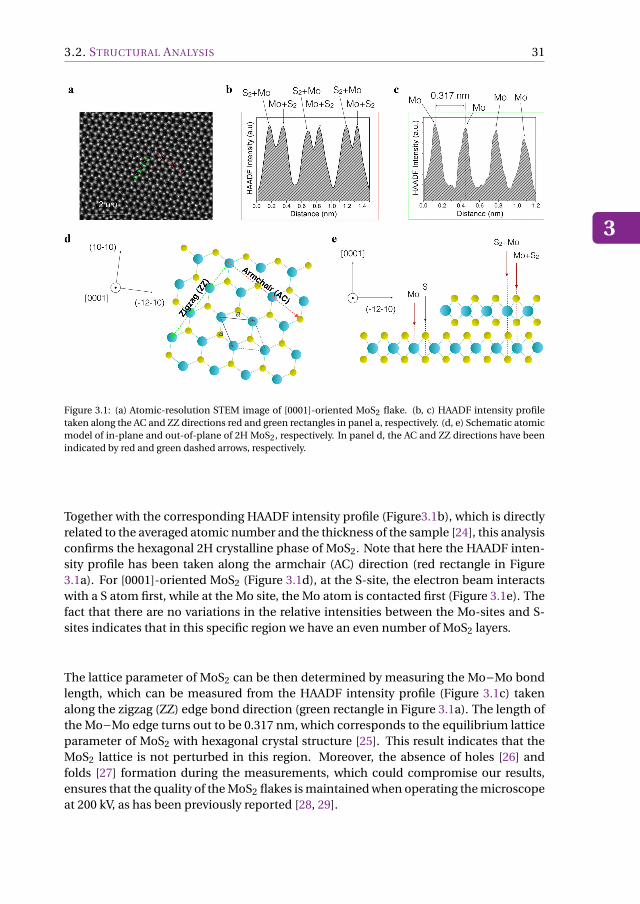
3.2. STRUCTURAL ANALYSIS
3
31
Figure 3.1: (a) Atomic-resolution STEM image of [0001]-oriented MoS2 flake. (b, c) HAADF intensity profiletaken along the AC and ZZ directions red and green rectangles in panel a, respectively. (d, e) Schematic atomicmodel of in-plane and out-of-plane of 2H MoS2, respectively. In panel d, the AC and ZZ directions have beenindicated by red and green dashed arrows, respectively.
Together with the corresponding HAADF intensity profile (Figure3.1b), which is directlyrelated to the averaged atomic number and the thickness of the sample [24], this analysisconfirms the hexagonal 2H crystalline phase of MoS2. Note that here the HAADF inten-sity profile has been taken along the armchair (AC) direction (red rectangle in Figure3.1a). For [0001]-oriented MoS2 (Figure 3.1d), at the S-site, the electron beam interactswith a S atom first, while at the Mo site, the Mo atom is contacted first (Figure 3.1e). Thefact that there are no variations in the relative intensities between the Mo-sites and S-sites indicates that in this specific region we have an even number of MoS2 layers.
The lattice parameter of MoS2 can be then determined by measuring the Mo−Mo bondlength, which can be measured from the HAADF intensity profile (Figure 3.1c) takenalong the zigzag (ZZ) edge bond direction (green rectangle in Figure 3.1a). The length ofthe Mo−Mo edge turns out to be 0.317 nm, which corresponds to the equilibrium latticeparameter of MoS2 with hexagonal crystal structure [25]. This result indicates that theMoS2 lattice is not perturbed in this region. Moreover, the absence of holes [26] andfolds [27] formation during the measurements, which could compromise our results,ensures that the quality of the MoS2 flakes is maintained when operating the microscopeat 200 kV, as has been previously reported [28, 29].
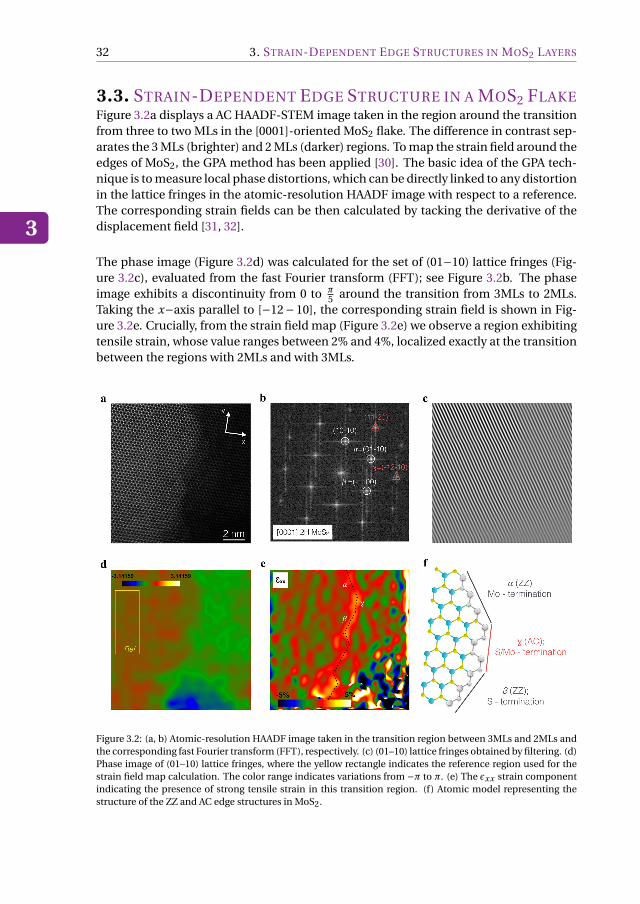
3
32 3. STRAIN-DEPENDENT EDGE STRUCTURES IN MOS2 LAYERS
3.3. STRAIN-DEPENDENT EDGE STRUCTURE IN A MOS2 FLAKEFigure 3.2a displays a AC HAADF-STEM image taken in the region around the transitionfrom three to two MLs in the [0001]-oriented MoS2 flake. The difference in contrast sep-arates the 3 MLs (brighter) and 2 MLs (darker) regions. To map the strain field around theedges of MoS2, the GPA method has been applied [30]. The basic idea of the GPA tech-nique is to measure local phase distortions, which can be directly linked to any distortionin the lattice fringes in the atomic-resolution HAADF image with respect to a reference.The corresponding strain fields can be then calculated by tacking the derivative of thedisplacement field [31, 32].
The phase image (Figure 3.2d) was calculated for the set of (01−10) lattice fringes (Fig-ure 3.2c), evaluated from the fast Fourier transform (FFT); see Figure 3.2b. The phaseimage exhibits a discontinuity from 0 to π
5 around the transition from 3MLs to 2MLs.Taking the x−axis parallel to [−12−10], the corresponding strain field is shown in Fig-ure 3.2e. Crucially, from the strain field map (Figure 3.2e) we observe a region exhibitingtensile strain, whose value ranges between 2% and 4%, localized exactly at the transitionbetween the regions with 2MLs and with 3MLs.
Figure 3.2: (a, b) Atomic-resolution HAADF image taken in the transition region between 3MLs and 2MLs andthe corresponding fast Fourier transform (FFT), respectively. (c) (01–10) lattice fringes obtained by filtering. (d)Phase image of (01–10) lattice fringes, where the yellow rectangle indicates the reference region used for thestrain field map calculation. The color range indicates variations from −π to π. (e) The εxx strain componentindicating the presence of strong tensile strain in this transition region. (f) Atomic model representing thestructure of the ZZ and AC edge structures in MoS2.

3.4. EELS CHARACTERIZATION OF ELECTRONIC PROPERTIES OF MOS2 FLAKES
3
33
More specifically, such transition region is defined by the intersections of the familyof planes 1100 and 1-210. The atomic terminations of these two families of planesare known as zigzag (ZZ) and armchair (AC) configurations, respectively, and are repre-sented in Figure 3.2f. Note that when two ZZ edges merge, the resulting junction definesthe minimal unit of an AC edge. We find that the ZZ edges exhibit tensile strain rangingbetween (2 ± 0.5) % and (4 ± 1) %, where the later value arises at the junctions betweentwo ZZ edges (that represents a short AC edge). However, the longer AC edge (labeled asγ) appears under a tensile strain of around (2 ± 0.5) %. Note that here we use a Fouriermask that leads to a spatial resolution of 0.5 nm. This choice represents an appropri-ate balance between smoother strain fields but worse spatial resolution (achieved with asmall mask) and better spatial resolution but with a higher level of fluctuation.
The appearance of such localized strain at the ZZ and AC edges could be related to theedge relaxation mechanism itself, induced by the adjustment of the bond length andbond angles of the edge atoms [33]. In this scenario, the MoS2 sheets generated by me-chanical exfoliation initially have an excess of energy. Therefore, the free-edges (S-Mo-S)of the MoS2 flakes are originated with stress. Subsequently, the MoS2 sheet relaxes to re-duce this excess of energy. Theoretical calculations of the elastic properties of phospho-rene nanoribbons [34] reported a similar result, where the energy relaxation modifies theatomic arrangement of AC and ZZ edges, resulting into a tensile stress along the ZZ andAC edges consistent with our findings here. Moreover, we also found that this relaxationmechanism is translated into an out-of-plane distortion [35].
3.4. EELS CHARACTERIZATION OF ELECTRONIC PROPERTIES
OF MOS2 FLAKESTo obtain further insight on the effects of edge strain on the resulting electronic behavior,we have carried out a direct correlation experiment by means of an electron energy lossspectroscopy (EELS) analysis [36]. For these measurements a monochromated electronsource operating at 60 kV was used, which achieves an energy resolution of around 30meV. A crucial advantage of EELS is that it allows achieving high-energy resolution whilesimultaneously leading to competitive spatial resolution [37].
Figure 7.8a displays a low-magnification HAADF-STEM image taken in the same regionwhere the strain measurements were performed (see Figure 3.2a). Subsequently, point-by-point EELS spectra were recorded at different locations in the boundary region be-tween 2MLs and 3MLs, indicated by the points S1 to S4 in Figure 3a. We focused onthe low-loss energy region, ranging between electron energy losses of 0 and 4 eV. Themost-distinctive features of the EELS spectra (Figure 7.8b) are the presence of two rela-tively narrow peaks, located at around 1.89 eV (peak A) and 2.05 eV (peak B), respectively.These two peaks in the MoS2 EELS spectra can be interpreted as arising from the directexciton transitions, specially due to band splitting effects induced to interlayer interac-tion and spin-orbit coupling [9, 38, 39]. Our measurements for the position of these EELSpeaks are consistent with previously experimental [40] and theoretical studies [41].
We further quantify the properties of these exciton peaks by means of a fitting procedure,in which a double Gaussian is used for the signal combined with a quadratic polynomial

3
34 3. STRAIN-DEPENDENT EDGE STRUCTURES IN MOS2 LAYERS
Figure 3.3: (a) Low-magnification HAADF–STEM image of the MoS2 flake in the transition region between 2and 3 ML. (b) Offset of the EELS spectra corresponding to S1, S2, S3, and S4 in panel a. (c–f) EELS spectrarecorded at S1, S2, S3, and S4 with the corresponding fits.
for the background. The comparison between the EELS measurements and the resultingfits is shown in Figures 7.8c-f, where we also show the two Gaussian peaks, denoted bypeak A and peak B, with the background subtracted. One factor that is known to affectthe peaks’ width is the thickness of the MoS2 layers [40]. Moreover, it is conceivable thatthe strain localized at the interface (see Figure 3.2e) might also induce variations in thesewidths.
To investigate the interplay between these two effects, we have recorded EELS spectraat two additional locations, labeled by T1 (in 2 MLs region) and T2 (in 3 MLs region) inFigure 7.8a. Because these EELS spectra correspond to regions far from the boundaries,no effects associated with edge strain are expected to arise. By comparing the values ofthe full-width at half-maximum (FWHM) of peak A (B) value between points T1 and T2,we find that it increases by around 70% (30%). However, when comparing the FWHMvalues of peak A (B) between the points S1 and S3 (see Figure 3.4) (that is, just before andafter crossing the interface where, in addition to the different thicknesses, we must also

3.5. STRAIN DEPENDENCE OF FREE-EDGE CURVATURE
3
35
Figure 3.4: Variation of the full-width at half-maximum (FWHM) of peaks A and B along this transition region,where measurements corresponding to the points labeled as S1 to S4 in Figure 7.8a are shown.
account for the possible effects of strain), we find that the increase is now around 30%(15%). Therefore, we observe a nontrivial dependence of the FWHM values of the twoexciton peaks at the interface region, which cannot be accounted purely by the changein thickness and, at least partly, should be understood in terms of the interface strain.
This remarkable correlation highlights the deep connection between structural and elec-tronic properties of MoS2, which can be tuned layer by layer. In this respect, new theo-retical calculations would be required to fully disentangle the contribution of the variousphysical mechanisms that contribute to the exciton peak broadening, especially the in-terplay between the tensile strain at the edge and the layer thickness variation.
Concerning the peak positions as determined from the fit, we find values of 1.89 and1.88 eV for peak A and 2.05 and 2.08 eV for peak B in the regions with two and three MLs,respectively. We therefore find that for peak B there is a clear difference in peak positionbetween the two regions. This behavior could be understood as a direct consequenceof the specific crystalline structure of MoS2. Indeed, for an odd number of MoS2 layers,the crystal belongs to the non-centrosymmetric D3h space group. However, for an evennumber of layers instead, the crystal belongs to the D3d space group, which is character-ized by inversion symmetry.
3.5. STRAIN DEPENDENCE OF FREE-EDGE CURVATUREStrain-dependent edge structures also arise at the interface between the MoS2 flake andthe vacuum, the so-called free edges. Figure 3.5 displays a AC HAADF-STEM image takenin a region that only exhibits ZZ edge terminations. As can be observed from the filteredlattice fringes image (Figure 3.5b), this free edge alternates concave and convex regions.These opposite-curvature regions are originated during the mechanical exfoliation pro-cess.
By applying the geometrical phase analysis method as described above, we can evaluatethe local strain field map which allows us to distinguish regions with alternating localizedcompressive and tensile strain at the ZZ edges. In particular, the concave regions exhibit

3
36 3. STRAIN-DEPENDENT EDGE STRUCTURES IN MOS2 LAYERS
Figure 3.5: (a) AC HAADF-STEM image of a region exhibiting a free edge of MoS2. (b) From the filtered latticefringes, we can clearly identify concave and convex terminations. (c) The εxx strain component indicating thepresence of compressive (tensile) strain in the concave (convex) region.
a compressive strain, while for the convex ones a tensile strain is exhibited. Moreover,as compared to the strain values reported at the interface between 2MLs and 3MLs (seeFigure 3.2e), here the levels of strain reached are higher, with values up to around +30%in the convex regions and down to around 14% in the concave regions. These resultssuggest that the possibility of exploiting the free edge curvature to turn tensile into com-pressive strain could provide a novel handle to tune the electronic properties of layeredmaterials.
3.6. CONCLUSIONTo summarize, controlling and understanding the formation of localized strain at theedge structures of TMD materials is of great importance toward the customization oftheir electronic properties. Here, by combining aberration-corrected TEM with the geo-metrical phase analysis method, we have quantified the edge structures and elastic prop-erties of MoS2 flakes. We find that the relaxation of the ZZ and AC edge structures leadsto the appearance of a tensile strain, with magnitude ranging between 2% and 4%. Thisimplies that the tensile strain can lead to the elastic distortion of the edge.
Furthermore, the EELS analysis performed at the same transition region highlights anincrease of the exciton A and B peak widths by around 30% and 15%, respectively, that

REFERENCES
3
37
can at least partly be explained by the presence of such tensile strain at the edges. How-ever, this broadening of the exciton peaks also receives contributions from the changeof thickness of the MoS2 layers. In this respect, new theoretical calculations would berequired to fully disentangle the contribution of the various physical mechanisms thatcontribute to the exciton peak broadening, especially the interplay between the tensilestrain at the edge and the layer thickness variation.
Finally, strain measurements performed at free edges between MoS2 and a vacuum,which exhibit convex and concave regions, demonstrate the direct interplay betweeninterface curvature and the presence of either tensile or compressive strain.
Even if in this work we have restricted ourselves to the analysis of MoS2 flakes, our ap-proach is fully general, and we plan to extend it to a comprehensive analysis of the strain-dependent edge structures in other layered materials. Our results could therefore pavethe way toward the customization of electronic properties of TMD materials by meansof strain-dependent edge structure.
REFERENCES[1] M. A. Lukowski, A. S. Daniel, F. Meng, A. Forticaux, L. Li, and S. Jin, Enhanced Hy-
drogen Evolution Catalysis from Chemically Exfoliated Metallic MoS2 Nanosheets,Journal of the American Chemical Society 135, 10274 (2013), pMID: 23790049,https://doi.org/10.1021/ja404523s .
[2] D. Voiry, H. Yamaguchi, J. Li, R. Silva, D. C. B. Alves, T. Fujita, M. Chen, T. Asefa, V. B.Shenoy, G. Eda, and M. Chhowalla, Enhanced catalytic activity in strained chem-ically exfoliated WS2 nanosheets for hydrogen evolution, Nature Materials 12, 850(2013).
[3] J. V. Lauritsen, J. Kibsgaard, S. Helveg, H. Topsøe, B. S. Clausen, E. Lægsgaard, andF. Besenbacher, Size-dependent structure of MoS2 nanocrystals, Nature Nanotech-nology 2, 53 (2007).
[4] B. Radisavljevic, A. Radenovic, J. Brivio, V. Giacometti, and A. Kis, Single-layer MoS2
transistors, Nature Nanotechnology 6, 147 (2011).
[5] M.-Y. Li, Y. Shi, C.-C. Cheng, L.-S. Lu, Y.-C. Lin, H.-L. Tang, M.-L. Tsai, C.-W. Chu,K.-H. Wei, J.-H. He, W.-H. Chang, K. Suenaga, and L.-J. Li, Epitaxial growth of amonolayer WSe2-MoS2 lateral p-n junction with an atomically sharp interface, Sci-ence 349, 524 (2015).
[6] Z. Yin, H. Li, H. Li, L. Jiang, Y. Shi, Y. Sun, G. Lu, Q. Zhang, X. Chen, andH. Zhang, Single-Layer MoS2 Phototransistors, ACS Nano 6, 74 (2012), pMID:22165908, https://doi.org/10.1021/nn2024557 .
[7] A. F. Rigosi, H. M. Hill, Y. Li, A. Chernikov, and T. F. Heinz, Probing Inter-layer Interactions in Transition Metal Dichalcogenide Heterostructures by OpticalSpectroscopy: MoS2/WS2 and MoSe2/WSe2, Nano Letters 15, 5033 (2015), pMID:26186085, https://doi.org/10.1021/acs.nanolett.5b01055 .

3
38 REFERENCES
[8] Y. Chen, J. Xi, D. O. Dumcenco, Z. Liu, K. Suenaga, D. Wang, Z. Shuai, Y.-S.Huang, and L. Xie, Tunable Band Gap Photoluminescence from Atomically ThinTransition-Metal Dichalcogenide Alloys, ACS Nano 7, 4610 (2013), pMID: 23600688,https://doi.org/10.1021/nn401420h .
[9] K. F. Mak, C. Lee, J. Hone, J. Shan, and T. F. Heinz, Atomically Thin MoS2: A NewDirect-Gap Semiconductor, Phys. Rev. Lett. 105, 136805 (2010).
[10] C. D. Reddy, A. Ramasubramaniam, V. B. Shenoy, and Y.-W. Zhang, Edge elasticproperties of defect-free single-layer graphene sheets, Applied Physics Letters 94,101904 (2009), https://doi.org/10.1063/1.3094878 .
[11] C. K. Gan and D. J. Srolovitz, First-principles study of graphene edge properties andflake shapes, Phys. Rev. B 81, 125445 (2010).
[12] V. B. Shenoy, C. D. Reddy, A. Ramasubramaniam, and Y. W. Zhang, Edge-Stress-Induced Warping of Graphene Sheets and Nanoribbons, Phys. Rev. Lett. 101, 245501(2008).
[13] S. Jun, Density-functional study of edge stress in graphene, Phys. Rev. B 78, 073405(2008).
[14] X. Peng, Q. Wei, and A. Copple, Strain-engineered direct-indirect band gap transi-tion and its mechanism in two-dimensional phosphorene, Phys. Rev. B 90, 085402(2014).
[15] H. J. Conley, B. Wang, J. I. Ziegler, R. F. Haglund, S. T. Pantelides, and K. I. Bolotin,Bandgap Engineering of Strained Monolayer and Bilayer MoS2, Nano Letters 13,3626 (2013), pMID: 23819588, https://doi.org/10.1021/nl4014748 .
[16] J. Kibsgaard, Z. Chen, B. N. Reinecke, and T. F. Jaramillo, Engineering the surfacestructure of MoS2 to preferentially expose active edge sites for electrocatalysis, NatureMaterials 11, 963 (2012).
[17] N. M. R. Peres, J. N. B. Rodrigues, T. Stauber, and J. M. B. L. dos Santos, Dirac elec-trons in graphene-based quantum wires and quantum dots, Journal of Physics: Con-densed Matter 21, 344202 (2009).
[18] N. M. R. Peres, Colloquium: The transport properties of graphene: An introduction,Rev. Mod. Phys. 82, 2673 (2010).
[19] A. C. Neto, F. Guinea, and N. M. Peres, Drawing conclusions from graphene, PhysicsWorld 19, 33 (2006).
[20] S. Helveg, J. V. Lauritsen, E. Lægsgaard, I. Stensgaard, J. K. Nørskov, B. S. Clausen,H. Topsøe, and F. Besenbacher, Atomic-Scale Structure of Single-Layer MoS2 Nan-oclusters, Phys. Rev. Lett. 84, 951 (2000).

REFERENCES
3
39
[21] A. M. van der Zande, P. Y. Huang, D. A. Chenet, T. C. Berkelbach, Y. You, G.-H. Lee,T. F. Heinz, D. R. Reichman, D. A. Muller, and J. C. Hone, Grains and grain bound-aries in highly crystalline monolayer molybdenum disulphide, Nature Materials 12,554 (2013).
[22] H. R. Gutiérrez, N. Perea-López, A. L. Elías, A. Berkdemir, B. Wang, R. Lv, F. López-Urías, V. H. Crespi, H. Terrones, and M. Terrones, Extraordinary Room-TemperaturePhotoluminescence in Triangular WS2 Monolayers, Nano Letters 13, 3447 (2013),pMID: 23194096, https://doi.org/10.1021/nl3026357 .
[23] Q. Wu, X. Li, A. A. Volinsky, and Y. Su, Edge eigen-stress and eigen-displacement ofarmchair molybdenum disulfide nanoribbons, Physics Letters A 381, 1568 (2017).
[24] J. M. LeBeau and S. Stemmer, Experimental quantification of annular dark-fieldimages in scanning transmission electron microscopy, Ultramicroscopy 108, 1653(2008).
[25] J. Kang, S. Tongay, J. Zhou, J. Li, and J. Wu, Band offsets and heterostructuresof two-dimensional semiconductors, Applied Physics Letters 102, 012111 (2013),https://doi.org/10.1063/1.4774090 .
[26] M. Sammalkorpi, A. Krasheninnikov, A. Kuronen, K. Nordlund, and K. Kaski, Me-chanical properties of carbon nanotubes with vacancies and related defects, Phys.Rev. B 70, 245416 (2004).
[27] A. Castellanos-Gomez, H. S. J. van der Zant, and G. A. Steele, Folded MoS2 layerswith reduced interlayer coupling, Nano Research 7, 572 (2014).
[28] J. Brivio, D. T. L. Alexander, and A. Kis, Ripples and Layers in Ultra-thin MoS2 Membranes, Nano Letters 11, 5148 (2011), pMID: 22010987,https://doi.org/10.1021/nl2022288 .
[29] Y. Shi, J.-K. Huang, L. Jin, Y.-T. Hsu, S. F. Yu, L.-J. Li, and H. Y. Yang, Selective Deco-ration of Au Nanoparticles on Monolayer MoS2 Single Crystals, Scientific Reports 3,1839 (2013).
[30] M. Hÿtch, E. Snoeck, and R. Kilaas, Quantitative measurement of displacement andstrain fields from HREM micrographs, Ultramicroscopy 74, 131 (1998).
[31] S. Conesa-Boj, F. Boioli, E. Russo-Averchi, S. Dunand, M. Heiss, D. Rüffer, N. Wyrsch,C. Ballif, L. Miglio, and A. F. i. Morral, Plastic and Elastic Strain Fields inGaAs/Si Core-Shell Nanowires, Nano Letters 14, 1859 (2014), pMID: 24564880,https://doi.org/10.1021/nl4046312 .
[32] J. H. Warner, N. P. Young, A. I. Kirkland, and G. A. D. Briggs, Resolving strain incarbon nanotubes at the atomic level, Nature Materials 10, 958 (2011).
[33] Y. Huang, C. Ling, H. Liu, and S. Wang, Edge-, width- and strain-dependentsemiconductor-metal transition in SnSe nanoribbons, RSC Adv. 4, 6933 (2014).

3
40 REFERENCES
[34] V. Sorkin and Y. W. Zhang, The structure and elastic properties of phosphorene edges,Nanotechnology 26, 235707 (2015).
[35] V. V. Ivanovskaya, P. Wagner, A. Zobelli, I. Suarez-Martinez, A. Yaya, and C. P.Ewels, Graphene edge structures: Folding, scrolling, tubing, rippling and twisting, inGraphITA 2011, edited by L. Ottaviano and V. Morandi (Springer Berlin Heidelberg,Berlin, Heidelberg, 2012) pp. 75–85.
[36] R. Arenal, O. Stéphan, M. Kociak, D. Taverna, A. Loiseau, and C. Colliex, ElectronEnergy Loss Spectroscopy Measurement of the Optical Gaps on Individual Boron Ni-tride Single-Walled and Multiwalled Nanotubes, Phys. Rev. Lett. 95, 127601 (2005).
[37] F. J. García de Abajo, Optical excitations in electron microscopy, Rev. Mod. Phys. 82,209 (2010).
[38] A. Splendiani, L. Sun, Y. Zhang, T. Li, J. Kim, C.-Y. Chim, G. Galli, and F. Wang,Emerging Photoluminescence in Monolayer MoS2, Nano Letters 10, 1271 (2010),pMID: 20229981, https://doi.org/10.1021/nl903868w .
[39] X. Fan, D. J. Singh, and W. Zheng, Valence Band Splitting on Multi-layer MoS2: Mixing of Spin-Orbit Coupling and Interlayer Coupling, TheJournal of Physical Chemistry Letters 7, 2175 (2016), pMID: 27225320,https://doi.org/10.1021/acs.jpclett.6b00693 .
[40] H. C. Nerl, K. T. Winther, F. S. Hage, K. S. Thygesen, L. Houben, C. Backes, J. N.Coleman, Q. M. Ramasse, and V. Nicolosi, Probing the local nature of excitons andplasmons in few-layer MoS2, npj 2D Materials and Applications 1, 2 (2017).
[41] H.-P. Komsa and A. V. Krasheninnikov, Effects of confinement and environment onthe electronic structure and exciton binding energy of MoS2 from first principles,Phys. Rev. B 86, 241201 (2012).

41

4METALLIC EDGE-STATES IN
ZIG-ZAG VERTICALLY-ORIENTED
MOS2 NANOWALLS
In Chapter 3 we have seen how the specific edge configuration of an exfoliated flake ofMoS2 can affect the strain and electronic structure of the flake. In order to unambigu-ously probe the corresponding physical properties, accurate control of the structural de-sign of nanostructures based on layered materials is necessary. The remarkable propertiesof layered materials such as MoS2 strongly depend on their dimensionality. Beyond ma-nipulating their dimensions, it has been predicted that the electronic properties of MoS2
can also be tailored by carefully selecting the type of edge sites exposed. However, achiev-ing full control over the type of exposed edge sites while simultaneously modifying thedimensionality of the nanostructures is highly challenging. Here we adopt a top-downapproach based on focus ion beam in order to selectively pattern the exposed edge sites.This strategy allows us to select either the armchair (AC) or the zig-zag (ZZ) edges in theMoS2 nanostructures, as confirmed by high-resolution transmission electron microscopymeasurements. The edge-type dependence of the local electronic properties in these MoS2
nanostructures is studied by means of electron energy-loss spectroscopy measurements.This way, we demonstrate that the ZZ-MoS2 nanostructures exhibit clear fingerprints oftheir predicted metallic character. Our results represent a stepping stone towards novelapproaches for the design and fabrication of more complex nanostructures based on MoS2
and related layered materials for applications in fields such as electronics, optoelectronics,photovoltaics, and photocatalysts.
Parts of this chapter has been published in Scientific Reports 9, 15602 (2019) by M. Tinoco, L. Maduro, and S.Conesa-Boj.
43

4
44 4. METALLIC EDGE-STATES IN ZIG-ZAG VERTICALLY-ORIENTED MOS2 NANOWALLS
4.1. INTRODUCTION
T He ability of crafting new materials in a way that makes possible controlling andenhancing their properties is one of the main requirements of the ongoing nan-
otechnology revolution [1, 2]. In this context, a family of materials that has attractedintense attention recently are two-dimensional (2D) layered materials of the TransitionMetal Dichalcogenide (TMD) family such as MoS2. These materials have been exten-sively studied due to their promising electrical and optical properties [3–6].
A defining feature of TMDs is that they exhibit a lack of inversion symmetry, which leadsto the appearance of a variety of different edge structures. The most common of these,consisting of dangling bounds, are the armchair (AC) and the zig-zag (ZZ) edge struc-tures. Of particular relevance in this context, the electronic properties of MoS2 havebeen predicted to be affected by the presence of the different edge structures in ratherdifferent ways. For instance, the AC edges have been predicted to be semiconducting,while the ZZ edges should exhibit instead metallic behavior [7–10]. Moreover, ab-initiotheoretical calculations predict that these metallic states at the edges of MoS2 could leadto the formation of plasmons [11]. Beyond this tuning of electronic properties, other at-tractive applications of these active edge sites arise in photocatalysis, such as their usein hydrogen evolution reactions (HER) [12–15].
With these motivations, it is clear that the design and fabrication of MoS2 nanostructureswith morphologies that maximize the number of exposed active edge sites is a key aspectfor further improvements in terms of applications. In this respect, significant efforts havebeen pursued to realize the systematic bottom-up growth of vertically-oriented standingMoS2 layers. This configuration leads to the edge sites facing upwards, therefore maxi-mizing the number of exposed edge sites as compared with the more common horizon-tal configuration, where its basal plane lies parallel to the substrate [16–23].
However, this bottom-up approach is hampered by a lack of reproducibility due to thecomplexities of the growth mechanism. Another limitation within the bottom-up ap-proach is that the specific type of edges exposed cannot be selectively grown. Ideally,one would like to combine the best of both worlds. On the one hand, it is important tobe able to controllably grow MoS2 nanostructures that exhibit the largest possible sur-face area of edge structures, as it is achieved by the bottom-up strategy summarizedabove. On the other hand, one would also like to be able to select the specific type ofedge sites exposed, in particular, by selecting whether these correspond to AC or to ZZedges. Therefore, the main goal of this work is to bridge these two requirements by re-alizing a novel approach to the growth of vertically-oriented standing MoS2 layers withfull control on the nature of the exposed edge sites.
To achieve this goal, here we adapt a well-established top-down approach based on fo-cus ion beam (FIB) in a way that allows us to selectively pattern both types of edges (ACand ZZ) within out-of-plane (vertical) MoS2 nanostructures. In the context of patterninglayered materials, the usefulness of FIB has been repeatedly demonstrated [24–26]. Bymeans of this technique, we are able to selectively maximize the density of exposed edgesites while controlling their type. Subsequently, by combining high-resolution transmis-sion electron microscopy (TEM) with electron energy-loss spectroscopy (EELS) mea-

4.2. FOCUS ION BEAM PATTERNING FOR THE FABRICATION OF EDGE-CONTROLLED MOS2
NANOWALLS
4
45
surements, we are able to confirm not only the crystallographic nature of both the ACand ZZ MoS2 surfaces, but also we can demonstrate that, despite the roughness andimperfections induced during the fabrication procedure, the ZZ MoS2 nanostructuresclearly exhibit a metallic character, in agreement with the theoretical predictions fromab-initio calculations [11]. The results of this study should open new opportunities forthe nanoengineering of the edge types in MoS2 nanostructures as well as in related lay-ered materials, paving the way towards novel exciting opportunities both for fundamen-tal physics and technological applications in fields such as electronics, optoelectronics,photovoltaics, and photocatalysts.
4.2. FOCUS ION BEAM PATTERNING FOR THE FABRICATION OF
EDGE-CONTROLLED MOS2 NANOWALLSMoS2 bulk crystal obtained from Alfa Aesar (with a 99.999% purity) was mechanicallyexfoliated with Poly-Di-Methyl-Siloxaan (PDMS) and then transferred to a SiO2/Si sub-strate. The MoS2 nanostructures were milled using a FEI Helios G4 CX focus ion beam.The ion milling procedure was carried out using a very low energy electron beam of 15kV, and an ion beam of 2 pA. From crystal structure considerations, the possible anglesbetween adjacent flat edges within MoS2 flakes should be multiples of 30°. Specifically,the expected angles between adjacent AC and ZZ edge structures in a MoS2 flake suchas that of Figure 4.1a should be 30°, 90°, and 120°, as illustrated in Figure 4.1b. Takinginto account this information, we designed the orientation of the different areas of theMoS2 flake that subsequently will be patterned. In this way, we can ensure the full con-trol over the resulting specific edge crystallographic orientation. Figure 4.1c,d display ascanning electron microscopy (SEM) image of the MoS2 flake that has been used for thefabrication of the nanostructures, taken before and after the milling respectively. Beforethe milling is performed, a protective metallic layer of tungsten (W) with a thickness of500nm was deposited on top of the selected areas of the MoS2 flake. Subsequently, weperformed a series of milling and cleaning processes in order to construct the vertically-aligned MoS2 nanostructures. Figure 4.1d displays three ordered vertically-oriented pat-terned arrays of MoS2 nanostructures, which in the following are denoted as nanowalls(NWs). Two of these sets of nanowalls are oriented perpendicularly with respect to eachother, guaranteeing that this way one of two arrays will correspond to AC (ZZ) NWs whilethe other array will correspond instead to the complementary ZZ (AC) ones. These NWsare found to exhibit a uniform thickness being (89±5) nm (central array in Figure 4.1d)and (68±5) nm (rightmost array in Figure 4.1d). Note that the left-most array was fabri-cated without the protective metal layer.
4.3. STRUCTURAL CHARACTERISATION OF MOS2 NANOWALLS
4.3.1. CHEMICAL MAPPINGTo further examine the crystallographic nature of the resulting vertical MoS2 nanostruc-tures, transmission electron microscopy (TEM) studies were carried out. For these stud-ies, we lifted out two of the MoS2 NWs from the two different patterned NWs arrays usinga micromanipulator. Subsequently, the nanostructure was mounted onto a TEM half-

4
46 4. METALLIC EDGE-STATES IN ZIG-ZAG VERTICALLY-ORIENTED MOS2 NANOWALLS
Figure 4.1: (a) Atomic model of a MoS2 flake viewed along the [0001] direction, where we indicate the cor-responding zig-zag (ZZ) and armchair (AC) edges. (b) From geometric considerations, we can determine thepossible values that the angles between adjacent AC and ZZ edges should take; (c) and (d) SEM micrographs ofthe MoS2 flake used for patterning the nanowalls, taken before and after the milling respectively. In (d), threedifferent set of arrays can be observed. The left-most array was fabricated without the protective metal layer,while the other arrays used instead this protective metal layer.
grid. This whole procedure takes place within the FIB chamber.
Figure 4.2a displays a high-angle annular dark-field scanning transmission electron mi-croscopy (HAADF-STEM) image of a selected region of the ZZ MoS2 nanowall, bracketedbetween the Si substrate and the metallic protective layer. Figure 4.2b shows the corre-sponding chemical composition of this nanowall obtained by means of Energy Disper-sive X-ray Spectroscopy (EDS) measurements. From the EDS map, the different chemi-cal components of the NWs can be clearly distinguished: the MoS2 segment, embeddedwithin the protective metal layer tungsten (W), and the silicon (Si) substrate.
4.3.2. FINGERPRINTING THE EDGE-TYPE NATURE OF MOS2 NANOWALLSFrom the crystalline structure studies carried out by means of high-resolution TEM mea-surements (Figure 4.3), we are able to confirm the specific edge site configuration for thetwo NW arrays. Figures 4.3a and 4.3b display the results of the TEM measurements onthe AC and ZZ MoS2 surfaces respectively. By comparing the two crystallographic orien-tations, AC and ZZ, we can observe the differences between the atomic arrangement ofeach surface, which are consequently characterized by different fast Fourier transforms

4.4. EDGE-DEPENDENT ELECTRONIC BEHAVIOUR
4
47
Figure 4.2: (a) HAADF-STEM image of an area of the ZZ MoS2 NW, which is bracketed between the Si substrateand the metallic protective layer; (b) The corresponding EDX compositional maps (Mo in green, S in yellow, Win blue).
(FFTs) (shown in the insets of Figure 4.3a,b). From these results, it is clearly noticeablethe excellent agreement between the experimental FFTs obtained from the TEM mea-surements and the corresponding ones calculated theoretically in terms of the expectedatomic configuration (shown in Figure 4.3c,d). These results provide direct confirma-tion that these vertically-oriented MoS2 nanowalls are in fact exposing ZZ and AC edgeterminations, therefore validating our fabrication strategy.
4.4. EDGE-DEPENDENT ELECTRONIC BEHAVIOURIn order to pin down the local electronic properties of the AC and ZZ MoS2 NWs, elec-tron energy-loss spectroscopy (EELS) measurements have been carried out in a scanningtransmission electron microscope (STEM). In Figure 4.4 we show the energy-loss spectracorresponding to both the AC and ZZ surfaces taken at different points along the lengthof the nanowall, spanning multiple layers of MoS2. As it can be observed in the two sets

4
48 4. METALLIC EDGE-STATES IN ZIG-ZAG VERTICALLY-ORIENTED MOS2 NANOWALLS
Figure 4.3: (a,b) HRTEM micrographs of representative ZZ and AC MoS2 nanowalls, respectively. The insetsindicate the corresponding fast Fourier transform (FFT). (c) and (b) The atomic modelling associated to theAC and ZZ orientations of the NWs, together with the theoretical calculation of the expected FFTs.
of EELS spectra, the MoS2 bulk plasmon signal appears at 23.4 eV in both samples withsimilar intensities and general shape, in agreement with previous analyses [27, 28].
Nevertheless, the MoS2 surface plasmon peak, present at 15.2 eV, turns out to appearonly on a restricted subset of the spectra of the ZZ-nanowalls. Considering that the fab-ricated AC-nanowalls are thinner than the ZZ-terminated ones, the presence of the sur-face MoS2 plasmon on the ZZ-nanowalls cannot be attributed to a lower thickness of thesample. Therefore, the origin of this peak should be caused by another phenomena. Inthat respect, it is important to notice that the MoS2 surface plasmon peak appears anddisappears in a periodic manner, depending on the specific position along the nanowallwhere the EELS spectrum is collected.
It is found that the positions which correspond to local maxima of the intensity associ-ated to this surface plasmon peak are separated by around 12 nm between each other.This behavior can be attributed to the presence of metallic surface plasmon polaritons(SPP), which are planar waves appearing at the interfaces between a metal and a dielec-

4.5. AB -INITIO CALCULATION OF THE DENSITY OF STATES IN MOS2 NANOWALLS
4
49
Figure 4.4: EELS spectra taken at different positions of the armchair (a) and zig-zag (b) nanowalls respectively,for the region of electron energy losses between 5 and 40 eV. Each curve corresponds to a different positionalong the nanowalls, spaced 1 nm apart.
tric material under some external excitation, such as an electron beam [29]. That couldcorrespond to the oscillatory character present in our EELS spectra. Therefore, from thisanalysis, we can conclude that the ZZ MoS2 NWs surfaces present a clear metallic char-acter. On the contrary, the AC MoS2 NWs do not exhibit such metallic behavior. With thisresult, we can hereby confirm that the ZZ MoS2 NWs are dominantly enclosed by zig-zagedges structures. It is also worth mentioning here that no signal arising from neitherthe metal layer nor the Ga used for the FIB milling were present at any of the acquiredEELS spectra, indicating that the possible contamination from Ga in the nanowalls isnon-existing.
4.5. AB -INITIO CALCULATION OF THE DENSITY OF STATES IN
MOS2 NANOWALLSIn order to further validate the onset of the metallic behavior observed in the ZZ MoS2
nanowalls, we calculated the corresponding density of states (DoS) by means of ab-initiocalculations in the framework of density functional theory (DFT). The van der Waals(vdW) interactions characteristic of MoS2 were incorporated by using the non-local vdWfunctional model [30] as implemented in the WIEN2k code [31]. The density of statescalculations were performed using both linearized augmented plane wave (LAPW) andlocal orbitals (LO) methods implemented in the WIEN2k package.

4
50 4. METALLIC EDGE-STATES IN ZIG-ZAG VERTICALLY-ORIENTED MOS2 NANOWALLS
Figure 4.5: (a) The ZZ MoS2 nanowall can be modelled by constructing a 1×3×1 supercell with vacuum in thez direction. A vacuum layer with length of 17.170 Å was inserted along the ZZ edge of the nanowall, in orderto to avoid spurious interactions between the repeating supercell images. This 1×3×1 supercell in the x andz directions was used to determine the density of states associated to the ZZ MoS2 nanowall, which can betreated as a two-dimensional sheet composed by ZZ nanorribons stacked along the y direction. (b) Density ofstates of ZZ MoS2 nanowalls (top panel) and the individual contributions to the DOS from the Mo and S atomslocated at the ZZ surface (central and bottom panels).
In these calculations, the nonlocal van der Waals [32, 33] (vdW) interactions used forthe DoS calculations adopts optB88 [34] for the exchange term, the local density ap-proximation [35] (LDA) for the correlation term, and the DRSLL kernel for the non-localterm [36]. For the non-local vdW integration, the cut-off density rc was set to 0.3 bohr−3,while the plane wave expansion cut-off Gmax was set to 20 bohr−1. No spin polarizationwas considered. The lattice parameters were found by volume and force optimization ofthe supercell, such that the force on each atom was less than 1.0 mRy/bohr.
The total energy convergence criteria was set to be 0.1 mRy between self-consistent field(SCF) cycles, while the charge convergence criteria was set to 0.001e, with e the elemen-tary unit charge. The core and valence electron states were separated by an energy gapof 6.0 Ry. Furthermore, the calculations used an R × kmax value of 6.0, where R is theradius of the smallest Muffin Tin sphere, and kmax is the largest k-vector. The first Bril-louin zone for the lattice parameter calculations was sampled with 100 k-points usingthe tetrahedon method of Blöchl et al. [37], which corresponds to 21 k-points in the ir-reducible Brillouin zone. With the above parameters the optimized lattice parameterswere a = 3.107Å and c = 12.087Å, which are in good agreement with the experimentalvalues a = 3.161Å and c = 12.295 Å [38].
The DoS was calculated with a denser k-point sampling of the Brillouin zone consistingof 1600 k-points, corresponding to 630 k-points in the irreducible Brillouin zone. Wemodeled the ZZ MoS2 nanowall by constructing a 1×3×1 supercell of MoS2, as shownin Figure 4.5a. In order to minimize the interactions between periodic images due to the

4.6. CONCLUSION
4
51
3D boundary conditions, we introduced a vacuum layer such that the distance betweenperiodic images is 17.170 Å.
The resulting calculated total DoS for the ZZ MoS2 nanowalls is displayed in Figure 4.5b.A clear absence of a gap in the DOS near the Fermi energy is observed, which implies afinite probability (11.65 states/eV) for states just below and above the Fermi energy levelbeing populated, highlighting the metallic behavior of the ZZ MoS2 NWs. Figure 4.5b(middle panel) also displays the individual contributions of the 4d states of Mo atomslocated at the surface of the ZZ MoS2 nanowall. These 4d states of Mo are also observedto cross over the Fermi energy (1.35 states/eV), contributing therefore to the metalliccharacter of the ZZ MoS2 nanowall. The individual contribution of the 3p states of Satoms located at the surface of the NW turns out to be much smaller from the DFT cal-culation, 0.08 states/eV. Therefore, the dominant contribution to the metallic characterof ZZ MoS2 nanowalls can be confidently attributed to Mo-4d states of MoS2.
4.6. CONCLUSIONIn this study we have presented a novel approach for the top-down fabrication of orderedvertically-oriented MoS2 nanostructures (denoted as nanowalls) which makes possibleto achieve at the same time, a large density of exposed active edge sites while also to con-trollably select whether these are of the AC or ZZ types. The crystallographic nature of theexposed surfaces has been validated by means of high-resolution TEM measurements.We have also studied the local electronic properties of these NW surfaces by means ofEELS, finding direct evidence of the metallic character of the ZZ surfaces as indicated bythe presence of MoS2 surface plasmon peak.
The metallic nature of the ZZ MoS2 nanowalls demonstrated in this work could be ex-ploited to open new opportunities for nanoengineering the edge type in MoS2 nanos-tructures, as well as in related layered materials for example within the TMD family.These prospects could impact both for fundamental physics and technological appli-cations in fields such as electronics, optoelectronics, photovoltaics, and photocatalysts.
REFERENCES[1] B. Bhattacharyya, A. Sharma, B. Sinha, K. Shah, S. Jejurikar, T. D. Senguttuvan, and
S. Husale, Evidence of robust 2D transport and Efros-Shklovskii variable range hop-ping in disordered topological insulator (Bi2Se3) nanowires, Scientific Reports 7,7825 (2017).
[2] B. Bhattacharyya, A. Sharma, V. P. S. Awana, A. K. Srivastava, T. D. Senguttuvan, andS. Husale, Observation of quantum oscillations in FIB fabricated nanowires of topo-logical insulator (Bi2Se3), Journal of Physics: Condensed Matter 29, 115602 (2017).
[3] K. F. Mak, C. Lee, J. Hone, J. Shan, and T. F. Heinz, Atomically Thin MoS2: A NewDirect-Gap Semiconductor, Phys. Rev. Lett. 105, 136805 (2010).
[4] A. Splendiani, L. Sun, Y. Zhang, T. Li, J. Kim, C.-Y. Chim, G. Galli, and F. Wang,

4
52 REFERENCES
Emerging Photoluminescence in Monolayer MoS2, Nano Letters 10, 1271 (2010),https://doi.org/10.1021/nl903868w .
[5] B. Radisavljevic, A. Radenovic, J. Brivio, V. Giacometti, and A. Kis, Single-layer MoS2
transistors, Nature Nanotechnology 6, 147 (2011).
[6] K. F. Mak, K. He, J. Shan, and T. F. Heinz, Control of valley polarization in monolayerMoS2 by optical helicity, Nature Nanotechnology 7, 494 (2012).
[7] Y. Li, Z. Zhou, S. Zhang, and Z. Chen, MoS2 Nanoribbons: High Stability and Un-usual Electronic and Magnetic Properties, Journal of the American Chemical Society130, 16739 (2008), pMID: 19007118, https://doi.org/10.1021/ja805545x .
[8] H. Pan and Y.-W. Zhang, Edge-dependent structural, electronic and magnetic prop-erties of MoS2 nanoribbons, J. Mater. Chem. 22, 7280 (2012).
[9] D. Davelou, G. Kopidakis, G. Kioseoglou, and I. N. Remediakis, MoS2 nanostruc-tures: Semiconductors with metallic edges, Solid State Communications 192, 42(2014).
[10] J. V. Lauritsen, M. Nyberg, R. T. Vang, M. V. Bollinger, B. S. Clausen, H. T. e,K. W. Jacobsen, E. L. gsgaard, J. K. N. rskov, and F. Besenbacher, Chemistry ofone-dimensional metallic edge states in MoS2nanoclusters, Nanotechnology 14, 385(2003).
[11] T. P. Rossi, K. T. Winther, K. W. Jacobsen, R. M. Nieminen, M. J. Puska, and K. S.Thygesen, Effect of edge plasmons on the optical properties of MoS2 monolayerflakes, Phys. Rev. B 96, 155407 (2017).
[12] J. Kibsgaard, Z. Chen, B. N. Reinecke, and T. F. Jaramillo, Engineering the surfacestructure of MoS2 to preferentially expose active edge sites for electrocatalysis, NatureMaterials 11, 963 (2012).
[13] D. Voiry, M. Salehi, R. Silva, T. Fujita, M. Chen, T. Asefa, V. B. Shenoy,G. Eda, and M. Chhowalla, Conducting MoS2 Nanosheets as Catalysts forHydrogen Evolution Reaction, Nano Letters 13, 6222 (2013), pMID: 24251828,https://doi.org/10.1021/nl403661s .
[14] M. A. Lukowski, A. S. Daniel, F. Meng, A. Forticaux, L. Li, and S. Jin, Enhanced Hy-drogen Evolution Catalysis from Chemically Exfoliated Metallic MoS2 Nanosheets,Journal of the American Chemical Society 135, 10274 (2013), pMID: 23790049,https://doi.org/10.1021/ja404523s .
[15] T. F. Jaramillo, K. P. Jørgensen, J. Bonde, J. H. Nielsen, S. Horch, andI. Chorkendorff, Identification of Active Edge Sites for Electrochemi-cal H2 Evolution from MoS2 Nanocatalysts, Science 317, 100 (2007),https://science.sciencemag.org/content/317/5834/100.full.pdf .

REFERENCES
4
53
[16] M.-A. Kang, S. K. Kim, J. K. Han, S. J. Kim, S.-J. Chang, C.-Y. Park, S. Myung, W. Song,S. S. Lee, J. Lim, and K.-S. An, Large scale growth of vertically standing MoS2 flakeson 2D nanosheet using organic promoter, 2D Materials 4, 025042 (2017).
[17] A. V. Agrawal, N. Kumar, S. Venkatesan, A. Zakhidov, C. Manspeaker, Z. Zhu, F. Rob-les Hernandez, J. Bao, and M. Kumar, Controlled Growth of MoS2 Flakes from in-Plane to Edge-Enriched 3D Network and Their Surface-Energy Studies, ACS AppliedNano Materials 1, 2356 (2018), https://doi.org/10.1021/acsanm.8b00467 .
[18] Y. Teng, H. Zhao, Z. Zhang, Z. Li, Q. Xia, Y. Zhang, L. Zhao, X. Du, Z. Du,P. Lv, and K. Åwierczek, MoS2 Nanosheets Vertically Grown on Graphene Sheetsfor Lithium-Ion Battery Anodes, ACS Nano 10, 8526 (2016), pMID: 27556425,https://doi.org/10.1021/acsnano.6b03683 .
[19] X. Zeng, H. Hirwa, M. Ortel, H. C. Nerl, V. Nicolosi, and V. Wagner, Growth of largesized two-dimensional MoS2 flakes in aqueous solution, Nanoscale 9, 6575 (2017).
[20] X. Wang, H. Feng, Y. Wu, and L. Jiao, Controlled Synthesis of Highly Crystalline MoS2
Flakes by Chemical Vapor Deposition, Journal of the American Chemical Society135, 5304 (2013), pMID: 23489053, https://doi.org/10.1021/ja4013485 .
[21] Y. Jung, J. Shen, Y. Sun, and J. J. Cha, Chemically Synthesized Het-erostructures of Two-Dimensional Molybdenum/Tungsten-Based Dichalcogenideswith Vertically Aligned Layers, ACS Nano 8, 9550 (2014), pMID: 25153809,https://doi.org/10.1021/nn503853a .
[22] D. Kong, H. Wang, J. J. Cha, M. Pasta, K. J. Koski, J. Yao, and Y. Cui, Synthesis of MoS2
and MoSe2 Films with Vertically Aligned Layers, Nano Letters 13, 1341 (2013), pMID:23387444, https://doi.org/10.1021/nl400258t .
[23] H. Wang, C. Tsai, D. Kong, K. Chan, F. Abild-Pedersen, J. K. Nørskov, and Y. Cui,Transition-metal doped edge sites in vertically aligned MoS2 catalysts for enhancedhydrogen evolution, Nano Research 8, 566 (2015).
[24] S. Friedensen, J. T. Mlack, and M. Drndic, Materials analysis and focused ion beamnanofabrication of topological insulator Bi2Se3, Scientific Reports 7, 13466 (2017).
[25] P. A. Sharma, A. L. Lima Sharma, M. Hekmaty, K. Hattar, V. Stavila, R. Goeke, K. Er-ickson, D. L. Medlin, M. Brahlek, N. Koirala, and S. Oh, Ion beam modification oftopological insulator bismuth selenide, Applied Physics Letters 105, 242106 (2014),https://doi.org/10.1063/1.4904936 .
[26] D. S. Fox, Y. Zhou, P. Maguire, A. OâNeill, C. ÃâCoileáin, R. Gatensby, A. M.Glushenkov, T. Tao, G. S. Duesberg, I. V. Shvets, M. Abid, M. Abid, H.-C. Wu, Y. Chen,J. N. Coleman, J. F. Donegan, and H. Zhang, Nanopatterning and Electrical Tun-ing of MoS2 Layers with a Subnanometer Helium Ion Beam, Nano Letters 15, 5307(2015), pMID: 26154305, https://doi.org/10.1021/acs.nanolett.5b01673 .

4
54 REFERENCES
[27] B. Yue, F. Hong, K.-D. Tsuei, N. Hiraoka, Y.-H. Wu, V. M. Silkin, B. Chen, and H.-k.Mao, High-energy electronic excitations in a bulk MoS2 single crystal, Phys. Rev. B96, 125118 (2017).
[28] L. Martin, R. Mamy, A. Couget, and C. Raisin, Optical Properties and Collective Ex-citations in MoS2 and NbSe2 in the 1.7 to 30 eV Range, physica status solidi (b) 58,623 (1973), https://onlinelibrary.wiley.com/doi/pdf/10.1002/pssb.2220580223 .
[29] D. N. Basov, M. M. Fogler, and F. J. García de Abajo, Polaritons invan der Waals materials, Science 354 (2016), 10.1126/science.aag1992,https://science.sciencemag.org/content/354/6309/aag1992.full.pdf .
[30] F. Tran, J. Stelzl, D. Koller, T. Ruh, and P. Blaha, Simple way to apply nonlocal vander Waals functionals within all-electron methods, Phys. Rev. B 96, 054103 (2017).
[31] P. Blaha, K. Schwarz, G. K. H. Madsen, D. Kvasnicka, L. J., L. R., F. Tran, and L. D.Marks, WIEN2k, An Augmented Plane Wave + Local Orbitals Program for Calculat-ing Crystal Properties (Karlheinz Schwarz, Techn. Universität Wien, Austria), 2018.ISBN 3-9501031-1-2, .
[32] J. Klimeš, D. R. Bowler, and A. Michaelides, Chemical accuracy for the van der Waalsdensity functional, Journal of Physics: Condensed Matter 22, 022201 (2009).
[33] J. c. v. Klimeš, D. R. Bowler, and A. Michaelides, Van der Waals density functionalsapplied to solids, Phys. Rev. B 83, 195131 (2011).
[34] A. D. Becke, Density-functional exchange-energy approximation with correctasymptotic behavior, Phys. Rev. A 38, 3098 (1988).
[35] J. P. Perdew and Y. Wang, Accurate and simple analytic representation of the electron-gas correlation energy, Phys. Rev. B 45, 13244 (1992).
[36] M. Dion, H. Rydberg, E. Schröder, D. C. Langreth, and B. I. Lundqvist, Van der WaalsDensity Functional for General Geometries, Phys. Rev. Lett. 92, 246401 (2004).
[37] P. E. Blöchl, O. Jepsen, and O. K. Andersen, Improved tetrahedron method forBrillouin-zone integrations, Phys. Rev. B 49, 16223 (1994).
[38] B. Schönfeld, J. J. Huang, and S. C. Moss, Anisotropic mean-square displacements(MSD) in single-crystals of 2H- and 3R-MoS2, Acta Crystallographica Section B 39,404 (1983).

55


5MOLYBDENUM NANOPILLAR
ARRAYS: FABRICATION AND
ENGINEERING
In the previous chapters we have studied the edge properties of flakes of exfoliated MoS2.The exfoliation process of the flakes is one of limited control and scalability. As a conse-quence of the limitations of the exfoliation process we do not have control of the specificedge structures formed and the total amount of exposed edges of an exfoliated flake. Analternative to exfoliation is the use of top-down and bottom-up approaches to have thedesired control of the structural properties of transition metal dichalcogenides (TMDs).In this chapter we report on the large-scale fabrication of molybdenum (Mo) nanopil-lar (NP) arrays with NP widths down to 75 nm by means of deep-reactive ion etching atcryogenic temperatures. A variable-thickness Mo metal layer sputtered onto a Si3N4/Sisubstrate makes possible NPs with different lengths in a controllable manner. We demon-strate how our fabrication strategy leads to tunable cross-sections with different geome-tries, including hexagonal, cylindrical, square and triangular shapes, by using electronbeam lithography on hydrogen silsesquioxane negative tone resist. To ensure well-definedfacets and surfaces, we employ deep-reactive ion etching in a gas mixture of SF6 and O2 atcryogenic temperatures in an inductively coupled plasma reactive ion etching (ICP-RIE)system. Furthermore, these Mo NPs will represent the template for the fabrication of core-shell Mo-MoS2 one-dimensional nanostructures to be discussed in Chapter 6. These resultsrepresent an attractive route towards the realization of high-density TMDs NP arrays forapplications from nanoelectronics to quantum sensing and hydrogen evolution reactioncatalysis.
Parts of this chapter has been published in Physica E: Low-Dimensional Systems and Nanostructures, 114903(2021) by L. Maduro, C. de Boer, M. Zuiddam, E. Memisevic, and S. Conesa-Boj.
57

5
58 5. MOLYBDENUM NANOPILLAR ARRAYS: FABRICATION AND ENGINEERING
5.1. INTRODUCTION
O Ne-dimensional (1D) Molybdenum (Mo) nanostructures have garnered significantattention recently due to their potential uses in a wealth of applications from inter-
connects in nanoelectronic devices to promoting the hydrogen evolution reaction [1–6].This potential stems from their remarkable properties, such as efficient electron emis-sion and structural stability
Of particular interest for applications in nanoelectronics is the fact that 1D Mo nanos-tructures exhibit reduced resistivity is their widths are decreased [1], thus making 1D Monanostructures promising candidates for interconnects for nanodevices. Furthermore,arranging 1D Mo nanostructures into geometric arrays whose axis is perpendicular tothe substrate surface represents one of the main challenges for concerning their inte-gration into nanoelectronic applications. Previous works have extensively studied thebottom-up fabrication of 1D Mo nanostructures, focusing mostly on approaches suchas electrodeposition and reduction, hydrogenation, and chemical vapour deposition [1–7]. However, these approaches have some limitations in terms of scalability as well asconcerning the control on the orientation, shape, and density of the 1D nanostructuresat spatially well-defined locations.
With this motivation, the main goal of this work is to bridge this gap by demonstratinga novel top-down approach for the large-scale fabrication of 1D Mo nanostructures, de-noted in the following as nanopillars (NPs), arrays whose shape, width, pitch, and lengthcan be fully controlled by deploying a combination of sputter-deposition, electron beamlithography, and cryogenic deep-reactive ion etching techniques. Our strategy for thelarge-scale fabrication of Mo NPs draws inspiration from the cryogenic deep-reactive ionetching of silicon, where micron-depth smooth vertical sidewalls can be formed whenusing a SF6/O2 gas mixture [8–12].
The close similarity between the etching processes of refractory metals and of Si sug-gests that a cryogenic deep-reactive ion etching process could be adopted to fabricatenanostructures with well-defined sidewalls also in the case of Mo. Taking into accountthese considerations, in this work we modify the electron beam lithography and cryo-genic deep-reactive ion etching procedure for Si NP fabrication [13–16]to fabricate MoNPs. We believe that these results would enable a wide range of technological applica-tions.
5.2. FABRICATION OF MO NANOPILLARSHere we modify the electron beam lithography and cryogenic deep reactive ion etchingprocedure for Si NP fabrication [13–16] to fabricate Mo NPs. We show how the adhesionlayer and development process for the used resists for electron lithography can affect thepatterned Mo. Our fabrication strategy is schematically displayed in Figure 5.1. Piecesof 1 x 1cm2 p-doped Si(001) are used throughout the whole process. Firstly, the Si piecesare cleaned via the RCA process [17]. Secondly, a low-stress Si3N4 layer is grown on topof the silicon pieces by means of low pressure chemical vapour deposition (LPCVD) ina Tempress furnace. The Si3N4 layer is used as a protective layer for the Si pieces, sinceit is well-known that Si is also etched in SF6/O2 gas mixtures. Subsequently, a layer of

5.2. FABRICATION OF MO NANOPILLARS
5
59
Figure 5.1: Schematic of the fabrication approach of the Mo NP arrays adopted in this work. The process startswith the LPCVD deposition of the Si3N4 layer and ends with the HF resist removal which reveals the NP arrays.
molybdenum (Mo) is sputter-deposited on top of this Si3N4 layer by using an AllianceConcept Ac 450 sputter-deposition system with an DC power of 100 W at a pressure of3.4 µbar.
5.2.1. ELECTRON-BEAM LITHOGRAPHYAfterwards, a spin coating of negative tone resist is carried out on top of the Mo metallayer. Crucially, in order to ensure the desired NP dimensions, the resist mask needs tohave high plasma resistance while also being able to maintain the mask shape during theetching process. To fulfill these requirements, Flowable Oxide-16 (FOx-16) and FlowableOxide-25, (FOx-25) from Dow Corning were adopted in this work [18].
Before applying the FOx resist, a monolayer of HexaMethylDiSilazane (HMDS) adhesionpromoter is evaporated on top of the metal layer using a Delta RC80 apparatus from SussMicrotech [19]. The FOx resist is left to warm up to room temperature [20] and then aspincoat speed between 1500 and 10000 rpm is used to acquire a uniform resist layeron the samples. A resist thickness between 800 nm and 400 nm was achieved with theFOx-25 resist for the used spincoat speeds, while for the case of FOx-16 a resist thicknessbetween 600 nm and 400 nm is achieved.
The samples are then baked on hotplates in two consecutive baking steps of 150 C and220o C for 2 minutes each. The desired NP arrays patterns are written in a RAITH 5000+EBPG or in a RAITH 5200 EBPG system at 100 keV accelerating voltage. Proximity EffectCorrection (PEC) was implemented via a Monte Carlo approach in the TRACER programfrom GenISys GmbH to ensure sharp edges of the smallest NP patterns. The optimaldose depends both on the size of the NP patterns and on the pitch-to-pitch distance be-tween NPs. It is found that a larger dose is needed when decreasing the size of the NPpatterns and that resist NP widths down to 30 nm are achieved by the combination oflarge dose and small pitch-to-pitch NP distance. After exposure, the FOx-16 was devel-oped in 6.25% TMAH for 45 seconds at room temperature. In the case of FOx-25 resist, a

5
60 5. MOLYBDENUM NANOPILLAR ARRAYS: FABRICATION AND ENGINEERING
different development procedure is required when resist layers thicker than 600 nm areused as described below.
5.2.2. CRYOGENIC DEEP REACTIVE ION ETCHINGVertical sidewall formation in silicon is achieved via cryogenic deep reactive ion etchingin a SF6/O2 gas mixture [8–12]. The fabrication of sharp vertical sidewalls is achieved bya combination of sidewall protection due to a passivation layer along the sidewalls and areduction in the reaction probability of chemical etching [21–24]. In the SF6/O2 plasmaSF6 decomposes into SF+
5 ions and F radicals. Ion bombardment of the radicals withsilicon in the SF6/O2 plasma results in the formation of volatile SiF4 which is pumpedaway during etching. An oxyfluoride layer of SiOx Fy (x =1,2 ,y = 2,4) is formed along-side the formation of SiF4. The SF+
5 ions locally etch away SiOx Fy , where the etching ofSiOx Fy is a chemical etching process and depends strongly on the process temperature.The chemical etching of SiOx Fy is reduced by etching the silicon at cryogenic tempera-tures [10, 13, 22, 25–27].
Similarly, in fluorine-oxygen based plasma etching of refractory metals Me (Me = Moor W) a metal hexafluoride MeF6 compound is formed along with an oxyfluoride layerMeOx Fy [17, 27, 28], where the formed MeOx Fy is less volatile than MeF6 [29–31]. Asin the case of silicon, the more volatile MeF6 is pumped away during etching, while theMeOx Fy formation reduces the etch rate of the metal [30, 31]. The MeOx Fy is etchedaway in a chemical etching process by ions formed in the plasma.
Different SF6/O2 mixtures were used in order to acquire the optimal etch-passivationratio, with the most successful mixture being a gas mixture of 200.0 sccm SF6 and 5.0sccm O2. A platen power of 70 W combined with an ICP power of 1100 W was used toetch the NP structures. With these conditions, an etch rate of 140 nm/min was found forthe Mo structures. Cryogenic deep reactive ion etching of the developed samples wassubsequently carried out in an Oxford Instruments PlasmaPro 100 Estrelas system. Thesample was placed on a carrier wafer that is clamped to a cryogenic holder which wascooled by a flow of liquid N2. Helium backing is used to ensure proper thermal contactbetween the holder and the sample.
Before starting the etch a 30 minute O2 plasma clean of the chamber is carried out at-20C. The system is subsequently cooled down to the etching temperature of -100C±2C. The etching was carried out in pulsed sequences of 100 kHz with a duty cycle of10%. The slit-valve was left fully opened to ensure the lowest possible pressure duringthe etch. A three minute pre-conditioning step of the chamber is carried out in orderto encourage reproducibility between different etching sessions [32]. Fomblin oil wasplaced between the sample and carrier wafer to further improve thermal contact. A wait-ing time of 1 minute is carried out after the carrier wafer with the sample is placed insidethe process chamber.
5.2.3. REMOVAL OF RESIDUAL RESISTAfter cryogenic etching the remaining FOx resist, along with the SiO2 adhesion layer, isremoved by a diluted solution of hydrofluoric acid (HF). A 5% HF dip for 120 seconds

5.3. RESULTS
5
61
Figure 5.2: SEM images of Mo NPs with square cross-sections fabricated on top of a Si wafer either with (a) andwithout (b) a protective Si3N4 layer, demonstrating how only in the first case a regular NP array is obtained.The inset in (a) displays a representative NP. The scale bar is 2 µm.
resulted in all the FOx resist and SiO2 being removed from the NP structures. We alsonote that the HF dip did not affect the shape of the NPs and barely etched away any ofthe underlying Si3N4.
5.3. RESULTS
5.3.1. HMDS ADHESION LAYERFigure 5.2a displays an array of Mo NPs with square cross-sections, with the inset fo-cusing on a representative NP, demonstrating that a high yield of Mo NPs characterizedby regular sidewalls is achieved. In Figure 5.2 a 340 nm film of Mo was used for the NPfabrication. Figure 5.2b illustrates the role played by the Si3N4 protective layer in the fab-rication process: since the etch chemistry for Mo is presumably different from the onerequired for Si etching the underlying Si is etched away at a higher rate than the Mo. Inturn, this higher Si etch rate leads to an undercut that results into the Mo NPs topplingonto the Si substrate.
To further demonstrate how our fabrication strategy offers precise control on the geom-etry of the resulting Mo NPs, equilateral triangles, circular, and hexagonal patterns aredesigned in a 500 nm Mo film and the resulting Mo NP arrays are displayed in Figure 5.3.The insets are top views of the respective NPs, highlighting the corresponding geomet-rical cross-sections. One can observe from Figure 5.3 how Mo regular arrays of NPs withwell-defined facets and varying cross-sectional shapes can be reliably fabricated for large(between 200 nm and 300 nm) nanostructures where their shapes are retained down tothe 100 nm range.
Furthermore, NP arrays with varying pitches are designed in order to determine the min-imum distance achievable between the NPs of an array. The results for this pitch distanceanalysis are presented in Figure 5.4. A minimum pitch distance of 300 nm was achievedin the case of NP with widths of 100 nm. It is found that decreasing the NP dimensionsresults in smaller pitch distances available before overexposure results. The dosage re-quired for the different NP shapes does not vary significantly when considering the total

5
62 5. MOLYBDENUM NANOPILLAR ARRAYS: FABRICATION AND ENGINEERING
Figure 5.3: SEM images of regular arrays of Mo NPs exhibiting (a) square, (b) circular, (c) triangular, and (d)hexagonal cross-sections respectively, as illustrated by the corresponding top-view images shown in the insets.The scale bar is 1 µm.
area of each respective NP, as indicated in Figure 5.5.
5.3.2. SIO2 ADHESION LAYERDuring the optimization process for the NP structures both the FOx-16 and FOx-25 reachedtheir shelf-life. One of the effects of the aged resist is the observation of a worsening ofthe adhesion of the resists to the Mo surface, even when HMDS is used as an adhesionpromotor. In order to reacquire good adhesion to the Mo surface a SiO2 layer was usedas an alternative adhesion layer due to its close similarity to the FOx molecular structure.We note that FOx resists consists of a cage-like structure of Si-H and Si-O bonds. Afterexposure and development of the FOx resists the Si-H bonds are broken and only theSi-O bonds are left [32, 33]. Due to the remaining Si-O bonds in the FOx patterns a thinlayer of SiO2 was used as an alternative to HMDS as an adhesion layer.
Before applying the FOx resist a 15 nm layer of SiO2 on top of the Mo metal was depositedvia Plasma Enhanced Chemical Vapour Deposition (PECVD) in an Oxford InstrumentsPlasmaPro 80 system.
After exposure the FOx was developed in heated Microposit MF321 at 50C for 5 min-utes, followed by a 30 second dip in H2O. After the H2O dip the samples were placed ina beaker filled with isopropanol, with care being taken such that the surface of the sub-strates always has liquid on it when transferring the substrates to the different solutions

5.3. RESULTS
5
63
Figure 5.4: Different pitches for Mo NP arrays with a pitch of 300 nm (a,c,e,g) and of 600 nm (b,d,f,h). Asin Figure 5.3 these NP exhibit square (a,b), circular (c,d), triangular (e,f) and hexagonal (g,h) cross-sectionsrespectively. The scale bar is 1 µm

5
64 5. MOLYBDENUM NANOPILLAR ARRAYS: FABRICATION AND ENGINEERING
Figure 5.5: (a) SEM images of the Mo NP array with square cross-sections fabricated with the modified resistrecipe. (b) Same as (a) now for Mo nanocone arrays. Both in (a) and (b) the scale bar is 5µm. (c) Dosage neededas function of the nanostructure dimensions. The shape of each marker is the same as the cross-section of thecorresponding NPs. (d)Etch rate (in nm/min) as a function of the platen power at 1100 W ICP power.
mentioned above. After the development step the samples are placed in a Leica supercritical CO2 drying system. The use of supercritical resist drying is known to be advanta-geous when patterning resist structures with large aspect-ratios [7, 34–36]. We note thatthe combination of critical point drying (CPD) together with SiO2 as an adhesion layeris necessary to counteract the aged FOx resist issue. In Figure 5.5 the nanostructuresfabricated with the modified resist recipe can be seen.
First of all, with the modified recipe we are able to reproduce NP structures with the de-sired etch profile, as shown in Figure 5.5a for the case of NPs with square cross-sections.Furthermore, we are able to fabricate NPs of Mo where the base is noticeably wider thanthe top, which will be referred to as nanocones in the following, and that are displayedin Figure 5.5b. The fabrication of such Mo nanocones is achieved by slightly modifyingthe etching process.
For the etching procedure of the straight sidewall structures, a Si carrier wafer is usedwhere a thick layer of SiO2 is deposited via LPCVD. Instead, for the nanocones etchingprocedure, a Si carrier wafer is used where both sides have a thick layer of SiO2. For theseMo nanocones, only a square design for the patterned HSQ resist was used. The Monanocones tend to retain the shape profile of the HSQ resist at the top of the nanoconefor all patterned diameters. The morphology along the entire length of the nanoconedepends on the lateral size of the HSQ resist structure at the top of the nanocone. Mo

5.3. RESULTS
5
65
nanocones with a patterned HSQ width between 200 nm - 300 nm retain the squareshape along the entire nanocone length. The sharp edges of the nanocones tend to be-come rounded for smaller HSQ resist diameters after etching.
In both lithographic processes (leading to the square cross-section NP and the nanocones)we observed that the dosage needed to produce nanostructures of specific diametersvaries with the size of these structures. Figure 5.5c displays the dose required for spe-cific dimensions and shapes of the resulting Mo NPs. In both cases, it is found that thesmaller structures require a higher exposure. Additionally, in order to ensure straightsidewalls, it is necessary to avoid a too high platen power which could etch away the FOxresist before all the unexposed Mo metal is etched away. Figure 5.5d indicates the etchrate as a function of platen power at fixed ICP power and gas flows. For the sub-150 nmstructures, lower platen power (below 70 W) results in the formation of straight sidewallsin the Mo metal.
We note that the etch rate in the ICP-RIE system changed abruptly during the optimiza-tion process and Figure 5.5d denotes the current etch rates for Mo in the Oxford Instru-ments PlasmaPro 100 Estrelas ICP-RIE system. A higher etch rate for the Mo NP struc-tures was found after the abrupt etch rate change. Decreasing the platen power led torecovering the Mo NP structures with the desired etch profiles. The etch rate in ICP-RIEsystems tend to drift over time, which could be a consequence of a change in the processchamber, e.g Helium leakage into the process chamber, or using different clamping ringsin the process chamber [37, 38]. As of writing the etch rates denoted in Figure 5.5d haveremained stable. Further research is necessary to understand the origin of the abruptchange in etch rate of the ICP-RIE system.
5.3.3. HIGH-ASPECT RATIO STRUCTURESFinally, in Figure 5.6 the limits of our modified and unmodified resist recipes and etchingprocedures can be seen. In Figure 5.6(a,b) HSQ resist NPs made with the modified resistrecipe in a 800 nm thick HSQ layer can be seen. Widths down to 40 nm are achieved atrelatively high exposures(~5300 µC/cm2) with the modified HSQ resist recipe. For resistNP widths below 100 nm a minimum of 100 nm pillar-to-pillar distance can be achievedwith the modified resist recipe before overexposure becomes an issue. In Figure 5.6(c,d)square Mo NPs with a length of 880 nm and width down to 60 nm made with a HSQ resistmask of 600 nm using the unmodified recipe can be seen. For the Mo NP structures inFigure 5.6(c,d) the HSQ resist was completely etched away during the cryogenic etchingprocess, which can explain the loss of shape retention of the NP. For both the modifiedand unmodified resist recipes we note that for features below 75 nm in size the shape ofthe Mo NPs are not reliably maintained after cryogenic etching.
The loss of shape for small diameters could be due to the very aggressive plasma pa-rameters used. We found that NP widths down to 50 nm can recovered by lowering theplaten power to 30 W. We have observed that the exposure needed for the HSQ resist forfeatures greater than 100 nm tends to stay stable over the span of months, while the ex-posure required for sub-100 nm structures tends to increase as the HSQ resist ages, bothfor the modified and unmodified resist recipes.

5
66 5. MOLYBDENUM NANOPILLAR ARRAYS: FABRICATION AND ENGINEERING
Figure 5.6: (a,b) SEM images of 800 nm thick HSQ resist NP array. Widths down to 40 nm with square cross-sections fabricated with the modified resist recipe. (c,d) Mo metal NPs fabricated with the unmodified resistprocess, with a length of 880 nm and width of 60 nm. The scale bar in (a) is 1 µm, and the scale bar in (c) is 2µm. Both in (b) and (d) the scale bar is 400 nm.
5.4. CONCLUSIONS & OUTLOOKIn this chapter, we have demonstrated the feasibility of a novel strategy for the top-down large-scale fabrication of geometric arrays of Mo NPs with different cross-sectionalshapes as well as of nanocones. Our approach is based on the combination of electronbeam lithography and cryogenic deep-reactive ion etching, and makes possible a precisecontrol on the shapes, lengths, widths, and pitches of the resulting Mo NP arrays, whichin all cases are characterized by well-defined smooth sidewalls. The proposed top-downapproach is not limited to the fabrication of NPs, since one can easily modify the shapeof the etched molybdenum by changing the exposure design of the resist mask. We alsonote that the use of a SiO2 adhesion layer for the FOx resist might also be implementedfor other metals, such as Cu or Au, where adhesion is known to be a problem[19]. Inthis respect, our method for the deep etching of structures in molybdenum could alsobe used to etch metals with similar etch chemistries. It is found that the limiting fac-tor for large-aspect ratio of the NPs is the thickness of the resist mask, where the usedFOx resist has a low selectivity during cryogenic reactive ion etching of the molybde-num. These results represent an attractive route towards the realization of high-densityMo NP arrays for applications from nanoelectronics to quantum sensing and hydrogenevolution reaction catalysis.

REFERENCES
5
67
REFERENCES[1] M. P. Zach, K. H. Ng, and R. M. Penner, Molybdenum
Nanowires by Electrodeposition, Science 290, 2120 (2000),https://science.sciencemag.org/content/290/5499/2120.full.pdf .
[2] A. Kovic, A. Znidarsic, A. Jesih, A. Mrzel, M. Gaberscek, and A. Hassanien, A novelfacile synthesis and characterization of molybdenum nanowires, Nanoscale researchletters 7, 567 (2012).
[3] J. Zhou, S. Deng, L. Gong, Y. Ding, J. Chen, J. Huang, J. Chen, N. Xu, and Z. L.Wang, Growth of Large-Area Aligned Molybdenum Nanowires by High Tempera-ture Chemical Vapor Deposition: Synthesis, Growth Mechanism, and Device Appli-cation, The Journal of Physical Chemistry B 110, 10296 (2006), pMID: 16722732,https://doi.org/10.1021/jp061213z .
[4] C. A. Spindt, I. Brodie, L. Humphrey, and E. R. Westerberg, Physical propertiesof thin-film field emission cathodes with molybdenum cones, Journal of AppliedPhysics 47, 5248 (1976), https://doi.org/10.1063/1.322600 .
[5] D. Dvorsek, M. Zumer, V. Nemanic, D. Mihailovic, and D. Vengust, Growth and fieldemission properties of vertically aligned molybdenum-sulfur-iodine nanowires onmolybdenum and quartz substrates, Journal of Applied Physics 102, 114308 (2007),https://doi.org/10.1063/1.2820009 .
[6] X. Zhang, F. Zhou, W. Pan, Y. Liang, and R. Wang, General Construc-tion of Molybdenum-Based Nanowire Arrays for pH-Universal Hydrogen Evo-lution Electrocatalysis, Advanced Functional Materials 28, 1804600 (2018),https://onlinelibrary.wiley.com/doi/pdf/10.1002/adfm.201804600 .
[7] K. S. Yeong and J. T. L. Thong, Field-emission properties of ultrathin5nm tungsten nanowire, Journal of Applied Physics 100, 114325 (2006),https://aip.scitation.org/doi/pdf/10.1063/1.2400722 .
[8] C. P. D’Emic, K. K. Chan, and J. Blum, Deep trench plasma etching of single crys-tal silicon using SF6/O2 gas mixtures, Journal of Vacuum Science & Technology B:Microelectronics and Nanometer Structures Processing, Measurement, and Phe-nomena 10, 1105 (1992), https://avs.scitation.org/doi/pdf/10.1116/1.586085 .
[9] T. Syau, B. J. Baliga, and R. W. Hamaker, Reactive Ion Etching of Silicon TrenchesUsing SF6/O2 Gas Mixtures, Journal of The Electrochemical Society 138, 3076 (1991).
[10] B. Wu, A. Kumar, and S. Pamarthy, High aspect ratio silicon etch: A review, Journalof Applied Physics 108, 051101 (2010), https://doi.org/10.1063/1.3474652 .
[11] R. Legtenberg, H. Jansen, M. de Boer, and M. Elwenspoek, Anisotropic Reactive IonEtching of Silicon Using SF6/O2/CHF3 Gas Mixtures, Journal of The ElectrochemicalSociety 142, 2020 (1995).

5
68 REFERENCES
[12] H. Jansen, M. de Boer, J. Burger, R. Legtenberg, and M. Elwenspoek, The black sili-con method ii:the effect of mask material and loading on the reactive ion etching ofdeep silicon trenches, Microelectronic Engineering 27, 475 (1995).
[13] P. V. Antonov, M. R. Zuiddam, and J. W. M. Frenken, Fabrication of high-aspect ratiosilicon nanopillars for tribological experiments, Journal of Micro/Nanolithography,MEMS, and MOEMS 14, 1 (2015).
[14] C. Fischer, J. W. Menezes, S. A. Moshkalev, C. VerÃssimo, A. R. Vaz, and J. W. Swart,Fabrication of high-aspect ratio silicon nanopillars and nanocones using deep reac-tive ion etching, Journal of Vacuum Science & Technology B: Microelectronics andNanometer Structures Processing, Measurement, and Phenomena 27, 2732 (2009),https://avs.scitation.org/doi/pdf/10.1116/1.3246359 .
[15] L. S. Golobokova, Y. V. Nastaushev, F. N. Dultsev, D. V. Gulyaev, A. B. Talochkin, andA. V. Latyshev, Fabrication and optical properties of silicon nanopillars, Journal ofPhysics: Conference Series 541, 012074 (2014).
[16] X.-L. Han, G. Larrieu, P.-F. Fazzini, and E. Dubois, Realization of ultra dense arraysof vertical silicon nanowires with defect free surface and perfect anisotropy using atop-down approach, Microelectronic Engineering 88, 2622 (2011), proceedings ofthe 36th International Conference on Micro- and Nano-Engineering (MNE).
[17] S. Franssila, Introduction to Microfabrication, Second Edition (Bantam, 2010).
[18] A. E. Grigorescu and C. W. Hagen, Resists for sub-20-nm electron beam lithographywith a focus on HSQ: state of the art, Nanotechnology 20, 292001 (2009).
[19] Z. Zhang, H. Duan, Y. Wu, W. Zhou, C. Liu, Y. Tang, and H. Li, Improving the ad-hesion of hydrogen silsesquioxane (hsq) onto various substrates for electron-beamlithography by surface chemical modification, Microelectronic Engineering 128, 59(2014).
[20] M. Häffner, A. Haug, A. Heeren, M. Fleischer, H. Peisert, T. Chasse, andD. P. Kern, Influence of temperature on HSQ electron-beam lithography, Jour-nal of Vacuum Science & Technology B: Microelectronics and Nanome-ter Structures Processing, Measurement, and Phenomena 25, 2045 (2007),https://avs.scitation.org/doi/pdf/10.1116/1.2794324 .
[21] M. J. de Boer, J. G. E. Gardeniers, H. V. Jansen, E. Smulders, M. . Gilde, G. Roelofs,J. N. Sasserath, and M. Elwenspoek, Guidelines for etching silicon MEMS structuresusing fluorine high-density plasmas at cryogenic temperatures, Journal of Microelec-tromechanical Systems 11, 385 (2002).
[22] S. Tachi, K. Tsujimoto, and S. Okudaira, Low-temperature reactive ion etchingand microwave plasma etching of silicon, Applied Physics Letters 52, 616 (1988),https://doi.org/10.1063/1.99382 .
[23] S. Tachi, K. Tsujimoto, S. Arai, and T. Kure, Low-temperature dry etching, Journal ofVacuum Science & Technology A 9, 796 (1991), https://doi.org/10.1116/1.577364 .

REFERENCES
5
69
[24] K. Tsujimoto, S. Okudaira, and S. Tachi, Low-Temperature Microwave Plasma Etch-ing of Crystalline Silicon, Japanese Journal of Applied Physics 30, 3319 (1991).
[25] N. Chekurov, K. Grigoras, A. Peltonen, S. Franssila, and I. Tittonen, The fabricationof silicon nanostructures by local gallium implantation and cryogenic deep reactiveion etching, Nanotechnology 20, 065307 (2009).
[26] H. Jansen, H. Gardeniers, M. de Boer, M. Elwenspoek, and J. Fluitman, A surveyon the reactive ion etching of silicon in microtechnology, Journal of Micromechanicsand Microengineering 6, 14 (1996).
[27] H. V. Jansen, M. J. de Boer, S. Unnikrishnan, M. C. Louwerse, and M. C. Elwenspoek,Black silicon method: X. A review on high speed and selective plasma etching of sili-con with profile control: an in-depth comparison between Bosch and cryostat DRIEprocesses as a roadmap to next generation equipment, Journal of Micromechanicsand Microengineering 19, 033001 (2009).
[28] S. Ma, Y. Xia, Y. Wang, K. Ren, R. Luo, L. Song, X. Chen, J. Chen, and Y. Jin, Fabrica-tion and characterization of a tungsten microneedle array based on deep reactive ionetching technology, Journal of Vacuum Science & Technology B 34, 052002 (2016),https://doi.org/10.1116/1.4960715 .
[29] T. P. Chow and A. J. Steckl, Plasma Etching of Refractory Gates for VLSI Applications,Journal of The Electrochemical Society 131, 2325 (1984).
[30] W. S. Pan and A. J. Steckl, Selective reactive ion etching of tungsten filmsin CHF3 and other fluorinated gases, Journal of Vacuum Science & Tech-nology B: Microelectronics Processing and Phenomena 6, 1073 (1988),https://avs.scitation.org/doi/pdf/10.1116/1.584300 .
[31] A. Picard and G. Turban, Plasma etching of refractory metals (W, Mo, Ta) and sili-con in SF6 and SF6-O2. An analysis of the reaction products, Plasma Chemistry andPlasma Processing 5, 333 (1985).
[32] H. Namatsu, Y. Takahashi, K. Yamazaki, T. Yamaguchi, M. Nagase, and K. Kurihara,Three-dimensional siloxane resist for the formation of nanopatterns with minimumlinewidth fluctuations, Journal of Vacuum Science & Technology B: Microelectron-ics and Nanometer Structures Processing, Measurement, and Phenomena 16, 69(1998), https://avs.scitation.org/doi/pdf/10.1116/1.589837 .
[33] C. L. Frye and W. T. Collins, Oligomeric silsesquioxanes, (HSiO3/2)n, Journal of theAmerican Chemical Society 92, 5586 (1970), https://doi.org/10.1021/ja00722a009 .
[34] T. Wahlbrink and Daniel Küpper and Y.M. Georgiev and J. Bolten and M. Möllerand David Küpper and M.C. Lemme and H. Kurz, Supercritical drying process forhigh aspect-ratio hsq nano-structures, Microelectronic Engineering 83, 1124 (2006),micro- and Nano-Engineering MNE 2005.

5
70 REFERENCES
[35] A. Agarwal and M. J. Kushner, Seasoning of plasma etching reactors: Ion energy dis-tributions to walls and real-time and run-to-run control strategies, Journal of Vac-uum Science & Technology A 26, 498 (2008), https://doi.org/10.1116/1.2909966 .
[36] A. N. Chaika, N. N. Orlova, V. N. Semenov, E. Y. Postnova, S. A. Krasnikov, M. G.Lazarev, S. V. Chekmazov, V. Y. Aristov, V. G. Glebovsky, S. I. Bozhko, and I. V. Shvets,Fabrication of [001]-oriented tungsten tips for high resolution scanning tunnelingmicroscopy, Scientific Reports 4, 3742 (2014).
[37] I. Marinkovic, Optomechanical Devices in the Quantum Regime (Ph.D. Thesis, DelftUniversity of Technology, 2019).
[38] J. T. Hill, Nonlinear Optics and Wavelength Translation Via Cavity-Optomechanics(Ph.D. Thesis, California Institute of Technology, 2013).

6SYNTHESIS AND
CHARACTERIZATION OF
CORE-SHELL MO-MOS2
NANOPILLARS
The fabrication of two-dimensional (2D) materials, such as transition metal dichalco-genides (TMDs), in geometries beyond the standard platelet-like configuration exhibitssignificant challenges which severely limit the range of available morphologies. Thesechallenges arise due to the anisotropic character of their bonding, van der Waals out-of-plane while covalent in-plane. Furthermore, industrial applications based on TMDsnanostructures with non-standard morphologies require full control on the size-, morpho-logy- and position on the wafer scale. Such a precise control remains an open problemwhose solution would lead to the opening of novel directions in terms of electronic and op-toelectronic applications. Here, we report on a novel strategy to fabricate vertical position-controlled Mo-MoS2 core-shell nanopillars (NPs). Metal-molybdenum (Mo) NPs are firstpatterned on a silicon wafer using lithography and cryo-etching, as described in chap-ter 5. These Mo NPs are then used as scaffolds for the synthesis of Mo-MoS2 core-shellNPs by exposing them in a rich sulfur environment. Cross-sectional transmission elec-tron microscopy (TEM) analysis reveals the well-defined morphologies and the Mo-MoS2
core-shell nature of the NPs. We demonstrate that individual Mo-MoS2 core-shell NPsexhibit enhanced second order nonlinear optical processes, such as sum frequency gen-eration (SFG).Our resultsrepresent an important step towards realising one-dimensionalTMD-based nanostructures as building blocks of a new generation of sensors, nanopho-tonic devices, and hydrogen evolution reactions.
Parts of this chapter are under review for publication (2021) by L. Maduro, M. Noordam, M. Bolhuis, L. Kuipersand S. Conesa-Boj.
71

6
72 6. SYNTHESIS AND CHARACTERIZATION OF CORE-SHELL MO-MOS2 NANOPILLARS
6.1. INTRODUCTION
O Ne-dimensional (1D) nanostructures have repeatedly demonstrated their relevancefor applications ranging from biological sensors [1–3], single electron emitters [4, 5],
to clean energy harvesting [6, 7]. Effectively deploying 1D nanomaterials for such appli-cations requires achieving an excellent and reproducible control of their sizes, shapes,and morphologies. While these conditions have been realised with astonishing degreeof precision in the case of conventional semiconductor materials and heterostructuresbuilt upon them, the same level of control remains to be achieved for materials of thetransition metal dichalcogenides (TMD) family.
The challenge in assembling one-dimensional nanostructures based on TMD materi-als lies in the anisotropic character of their bonding, which favours the formation ofplatelet-like structures when growing them using bottom-up approaches and thus limitsthe range of available morphological configurations. Realising the size- and morphology-controllable fabrication of 1D TMD nanomaterials would make possible several noveldirections in terms of applications. Specifically, 1D TMD-based heterostructures whichcombine different materials would benefit from a greatly expanded portfolio of tunableproperties, leading to emerging functionalities different from those found in the indi-vidual components. For instance, core-shell WOx -WS2 nanowires have been shown tooutperform stand-alone two-dimensional TMD-based capacitors due to the interplaybetween the conductive WOx core and a WS2 shell that favors fast ionic adsorption andtransport [8]. Likewise, MoOx -MoS2 nanowires exhibit an enhanced HER catalytic activ-ity compared to 2D layers of MoS2, due to the interplay between the conductive MoOx
core and the catalytically active MoS2 shell [9, 10].
With this motivation, here we develop a novel strategy for the fabrication of metal-TMDcore-shell 1D nanostructures based on the combination of top-down and bottom-upapproaches, and demonstrate its feasibility for the fabrication of vertically-aligned Mo-MoS2 core-shell heterostructures denoted as nanopillars (NPs). Metal-semiconductorheterostructures have been shown to represent an alternative pathway to favourable cat-alytic [11], optical [12], and electronic properties [13]. Our strategy builds upon the top-down fabrication approach to the Mo nanopillars described in the previous chapter, andis based on the sulfurisation of the as-prepared Mo NPs in a Chemical Vapour Deposition(CVD) setup [14, 15] leading to core-shell Mo-MoS2 one-dimensional NPs.
We then employ several characterization techniques to explore their structural, elec-tronic, and optical properties. First of all, Raman spectroscopy along with Energy Dis-persive X-ray (EDX) spectroscopy in the Transmission Electron Microscope (TEM) con-firms the growth of a MoS2 shell on the as-fabricated Mo NPs. We then study the de-pendence of the formed MoS2 shell as function of pillar-to-pillar distance and NP width.Subsequently, High-Resolution Transmission Electron Microscopy (HR-TEM) is used topin down the atomic configuration of the core-shell structures, while Electron EnergyLoss Spectroscopy (EELS) makes possible elucidating their local electronic behaviourand correlating it with structural features. Finally, nonlinear optical measurements arecarried out, demonstrating an enhanced nonlinear optical response of the core-shellstructures as compared to a reference composed by 2D MoS2 flakes.

6.2. SULFURIZATION OF MO NANOPILLARS
6
73
6.2. SULFURIZATION OF MO NANOPILLARS
6.2.1. SULFURIZATION PROCESSIn this work, we develop a procedure to fabricate core-shell Mo-MoS2 NPs with the fol-lowing design criteria in mind: (1) a metallic Mo core whose shape can be easily tailoredfor specific applications, (2) a MoS2 shell whose size and shape can be controlled, and (3)vertical alignment of the core-shell NPs with respect to the substrate surface to providea large amount of exposed MoS2 edges.
The core-shell Mo-MoS2 NPs are synthesized using a two-step chemical vapor depo-sition (CVD) process. We first fabricate Mo NPs as described in Chapter 5 (see Figure6.1(a,b) for representative Mo NP arrays) and then use these Mo NPs as scaffolds for theMoS2 shell growth, in a process known as sulfurization. We briefly describe here the sul-furization process, see [15] for further details. To begin with,the wafer containing the MoNPs are placed in the middle zone of a three zone, split-tube, CVD furnace containinga quartz reaction tube, as schematically represented in Figure 6.1(c). The sulfur powderused as a precursor is placed upstream in a separate zone. The synthesis is performed atambient pressure and argon (Ar) is used as a carrier gas. The separate zones of the CVDfurnace allow us to control the temperature of the Mo-metal NPs and the sulfur precur-sor independently. From previous experience, we know that the growth rate of MoS2 inthis two-step process can be precisely controlled by adjusting the reaction temperature,reaction time and the flow rate of the Ar carrier gas. A reaction temperature of 650C andan Ar gas flow of 150 sccm results in controllable growth of the core-shell Mo-MoS2 NPs.We also discuss the effects of a reaction temperature of 750C. We vary the reaction timefor various core-shell Mo-MoS2 NP synthesis experiments keeping a constant reactiontemperatore of 650 for each corresponding synthesis.
The reaction tube is flushed with Ar gas for 30 minutes at 500 sccm before each synthesisto make sure that all oxygen is vacated from the system. This flow rate is maintained untilthe Mo NPs reach a temperature of 500C after which the Ar gas flow is reduced down to150 sccm. The temperature in the middle zone, containing the Mo NPs, is heated to thetarget temperature of 650C at a rate of 10C/min. Once the sample reaches the targettemperature the sulfur will be heated up to 220C, also at a rate of 10C/min. At thismoment the reaction timer is started. After the reaction time has elapsed, the entiresystem is naturally cooled down to room temperature, while maintaining an Ar gas flowof 150 sccm.
6.2.2. RESULTSTo illustrate the end product of the sulfurisation process, Figure 6.1(d,e) displays theresulting vertically-aligned metal-TMD Mo-MoS2 NPs obtained from the sulfurisation ofthe Mo NPs from Figure 6.1(a,b). At a reaction temperature of 650C and reaction timeof 5 minutes, the MoS2 growth tends to have the same morphology as the fabricated MoNPs, as can be seen by comparing the top with the bottom panels of Figure 6.1. The NPsare surrounded at their base by what appears to be horizontal MoS2 layers, where the sizeof the horizontal layer increases as the electron beam exposure during the lithographystep is increased, as well as when the NP pitch is decreased.

6
74 6. SYNTHESIS AND CHARACTERIZATION OF CORE-SHELL MO-MOS2 NANOPILLARS
Figure 6.1: ((a,b), Scanning Electron Micrograph (SEM) of Mo NP array corresponding to 350 nm thick Mo layerbefore sulfurization. c, Schematic of sulfurization of Mo nanopillars, (d) Sulfurized Mo NPs corresponding to(a) and (e) sulfurized Mo NPS corresponding to (b). The scale bar is 2 µm.

6.2. SULFURIZATION OF MO NANOPILLARS
6
75
Figure 6.2: (a) SEM image of triangular MoS2 flakes nearby sulfurized Mo NP arrays, and (b) overview of sulfu-rized Mo NPs arrays. In (a,b) the scale bar is 30 µm. Raman spectrum of (c) substrate not containing the NPsarrays and (d) representative sulfurized Mo NPs array.
The presence of MoS2 on the substrate and on the NP arraysis confirmed by Ramanspectroscopy measurements, as illustrated by Figure 6.2(c,d). On all arrays, we find thein-plane E1
2g and out-of-plane A1g Raman modes characteristic for trigonal prismatic(2H-MoS2) crystal phase, which demonstrates the consistent MoS2 growth from the fab-ricated Mo nanostructures. Additionally, we observe the E1g peak in the Raman spec-tra, suggesting that vertically-grown MoS2 is present on the substrate. The E1g peakgradually disappears as we go to smaller NP diameters, which can be explained by aweaker signal due to the smaller diameters. Another indication of vertically-alignedMoS2 nanosheets can be found by comparing the ratio of intensities of the E1
2g and A1g
peaks. For all arrays the ratio of the intensities of the A1g and E12g peaks remain the same,
suggesting the presence of vertically-aligned MoS2 layers.
Furthermore, we find nearby the fabricated NPs the presence of triangular flakes on thesubstrate. Raman spectroscopy confirms that these triangular flakes are layers of MoS2,where in some cases the E1g peak is also found, indicating thick layers of MoS2 on thesurface of the substrate that may have vertically-oriented layers. We suspect that a smallfraction of the Mo NPs sublimate and react with the S vapour to form these structures onother parts of the substrate. Alternatively, residual Mo may be present after the cryogenicetching step. The residual Mo on the substrate surface reacts with the S vapor to formthe horizontal MoS2 flakes.
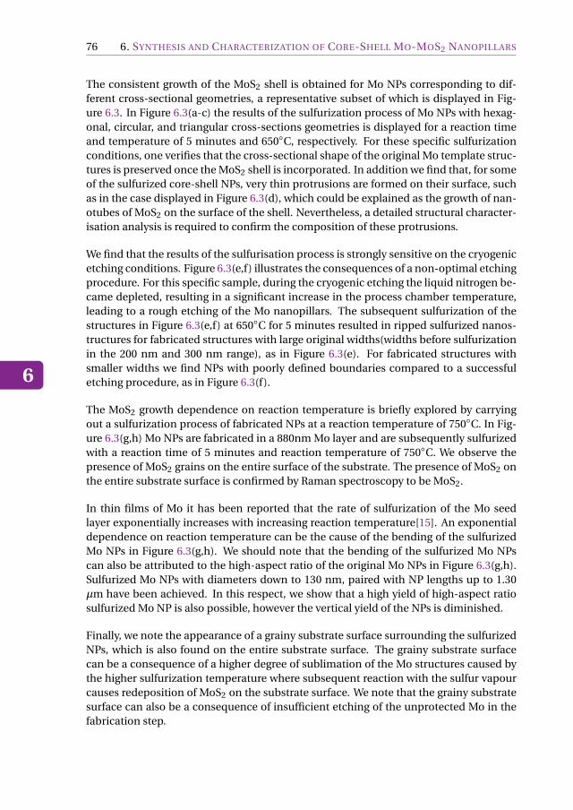
6
76 6. SYNTHESIS AND CHARACTERIZATION OF CORE-SHELL MO-MOS2 NANOPILLARS
The consistent growth of the MoS2 shell is obtained for Mo NPs corresponding to dif-ferent cross-sectional geometries, a representative subset of which is displayed in Fig-ure 6.3. In Figure 6.3(a-c) the results of the sulfurization process of Mo NPs with hexag-onal, circular, and triangular cross-sections geometries is displayed for a reaction timeand temperature of 5 minutes and 650C, respectively. For these specific sulfurizationconditions, one verifies that the cross-sectional shape of the original Mo template struc-tures is preserved once the MoS2 shell is incorporated. In addition we find that, for someof the sulfurized core-shell NPs, very thin protrusions are formed on their surface, suchas in the case displayed in Figure 6.3(d), which could be explained as the growth of nan-otubes of MoS2 on the surface of the shell. Nevertheless, a detailed structural character-isation analysis is required to confirm the composition of these protrusions.
We find that the results of the sulfurisation process is strongly sensitive on the cryogenicetching conditions. Figure 6.3(e,f) illustrates the consequences of a non-optimal etchingprocedure. For this specific sample, during the cryogenic etching the liquid nitrogen be-came depleted, resulting in a significant increase in the process chamber temperature,leading to a rough etching of the Mo nanopillars. The subsequent sulfurization of thestructures in Figure 6.3(e,f) at 650C for 5 minutes resulted in ripped sulfurized nanos-tructures for fabricated structures with large original widths(widths before sulfurizationin the 200 nm and 300 nm range), as in Figure 6.3(e). For fabricated structures withsmaller widths we find NPs with poorly defined boundaries compared to a successfuletching procedure, as in Figure 6.3(f).
The MoS2 growth dependence on reaction temperature is briefly explored by carryingout a sulfurization process of fabricated NPs at a reaction temperature of 750C. In Fig-ure 6.3(g,h) Mo NPs are fabricated in a 880nm Mo layer and are subsequently sulfurizedwith a reaction time of 5 minutes and reaction temperature of 750C. We observe thepresence of MoS2 grains on the entire surface of the substrate. The presence of MoS2 onthe entire substrate surface is confirmed by Raman spectroscopy to be MoS2.
In thin films of Mo it has been reported that the rate of sulfurization of the Mo seedlayer exponentially increases with increasing reaction temperature[15]. An exponentialdependence on reaction temperature can be the cause of the bending of the sulfurizedMo NPs in Figure 6.3(g,h). We should note that the bending of the sulfurized Mo NPscan also be attributed to the high-aspect ratio of the original Mo NPs in Figure 6.3(g,h).Sulfurized Mo NPs with diameters down to 130 nm, paired with NP lengths up to 1.30µm have been achieved. In this respect, we show that a high yield of high-aspect ratiosulfurized Mo NP is also possible, however the vertical yield of the NPs is diminished.
Finally, we note the appearance of a grainy substrate surface surrounding the sulfurizedNPs, which is also found on the entire substrate surface. The grainy substrate surfacecan be a consequence of a higher degree of sublimation of the Mo structures caused bythe higher sulfurization temperature where subsequent reaction with the sulfur vapourcauses redeposition of MoS2 on the substrate surface. We note that the grainy substratesurface can also be a consequence of insufficient etching of the unprotected Mo in thefabrication step.

6.2. SULFURIZATION OF MO NANOPILLARS
6
77
Figure 6.3: The fabricated shapes of (a) hexagonal (b) circular, (c,d) triangular structures can still be seen aftersulfurization. Reaction temperature is in (a-f) 650C, and in (g,h) 750C. The thickness of the Mo layer usedin the nanofabrication process is (a-c) 500 nm, (d) 440 nm, (e,f) 350 nm, and (g-h) 880 nm. The scale bar in(a,b,c,e) is 1µm and in (d,f,h) the scale bar is 400 nm.

6
78 6. SYNTHESIS AND CHARACTERIZATION OF CORE-SHELL MO-MOS2 NANOPILLARS
Figure 6.4: The results of the sulfurization of squared cross-section Mo NP with widths of 300 nm for threedifferent reaction times: (a) 5 min, (b) 7.5 min, and (c) 10 min. The scale bar is 1 µm.
6.2.3. REACTION TIME DEPENDENCEFrom the above discussion we have seen how the reaction temperature can affect thenanofabricated structures and the underlying substrate. Namely, a high reaction tem-perature (750C) leads to a high degree of MoS2 growth on the substrate surface, andwhat appears to be full sulfurization of the Mo NPs. In contrast, for a reaction tempera-ture of 650 and 5 minutes reaction time the sulfurized NPs retain the shape of the un-sulfurized nanofabricated Mo NPs. It is for this reason we use for the remainder of thischapter a reaction temperature of 650C for the subsequent sulfurization processes. Wecontinue with studying the effects of reaction time on the nanofabricated structures. Wecompare sulfurized Mo NPs with the same square nanofabricated shape and with simi-lar widths and lengths. Mo NPs were fabricated starting from a 500nm thick Mo layer.The fabricated Mo NPs were subsequently sulfurized while only varying the reactiontimes for the sulfurization process of the different Mo NPs substrates. Figure 6.4 displaysthe outcome of the sulfurization of squared cross-section Mo NPs with widths approx-imately 300nm for three different reaction times: 5 min, 7.5 min, and 10 min. As weincrease the reaction time the sulfurized Mo NPs gradually lose their original nanofab-ricated shape. Furthermore, a sizeable increase in NP width is observed when the re-action time is increased. We attribute this loss of shape and increase in the width of thenanofabricated structures to a higher degree of sulfurization of the Mo metal. In the caseof fabricated Mo NPs with widths in the 100nm-150nm range we see little difference be-tween the 7.5 min and 10 min reaction times. We will later see that this is due to fullsulfurization of these smaller nanofabricated NPs.

6.3. STRUCTURAL ANALYSIS OF SULFURIZED MO NANOPILLARS
6
79
Figure 6.5: (a) Low-magnification HRTEM image of a slab of sulfurized Mo nanopillars. (b) Composition ofa high-angle annular dark-field (HAADF) STEM image (left side) with the corresponding compositional EDXmap (right side) associated to the cross-section of this sulfurised NPs.
6.3. STRUCTURAL ANALYSIS OF SULFURIZED MO NANOPILLARS
6.3.1. CHEMICAL COMPOSITION OF SULFURIZED MO NANOPILLARSThe core-shell structure of the sulfurized Mo NPs is confirmed using Energy-DispersiveX-ray spectroscopy in the Scanning Transmission Electron Microscope (STEM-EDX). Wecarry out STEM-EDX in a Titan Cube microscope operated at 300 kV to determine thespecific chemical composition of the sulfurized Mo NPs. In order to prepare the samplefor TEM inspection, cross-section lamellas are prepared with a focused ion beam (FIB)milling approach using a FEI Helios G4 CX focus ion beam. The ion milling procedurewas carried out using a very low energy electron beam of 10 kV, and an ion beam of18 pA. Note that a Pt protective layer is deposited on top of the NPs to avoid damageduring ion beam milling. Markers are placed aligned with a row of sulfurized NPs toassist with precise milling of the lamella near the NPs of interest. Care is taken to limitthe SEM exposure of the NPs during the lamella fabrication procedure, as too much SEMexposure leads to contamination visible during TEM inspection.
Figure 6.5(a) displays a low-magnification TEM image of a cross-section of sulfurized MoNPs with a starting length of 350nm with square cross-sections corresponding to a reac-tion time of 5 minute. The Mo core can be seen along with a bright shell surrounding thecore. Figure 6.5(b) shows a composition of an high-angle annular dark-field (HAADF)STEM image (left side) with the corresponding compositional EDX map (right side) as-sociated to the cross-section of this core-shell nanopillars, where the latter confirms theMo-MoS2 nature of the core-shell configuration.

6
80 6. SYNTHESIS AND CHARACTERIZATION OF CORE-SHELL MO-MOS2 NANOPILLARS
Figure 6.6: (a)-(c) SEM images of FIB cross-sections carried our for three different NP arrays. The original MoNP widths are 100 nm (a), 200 nm (b), and 300 nm (c), the pitch for all three arrays is 500 nm, and the scale baris 1 µm. The light (dark) contrast indicates the Mo core (MoS2 shell). (d) and (e) Average thickness of the MoS2shell growth (evaluated over 10 NPs in each case) in the radial and axial directions respectively, as a functionof the pitch for a fixed growth time of 7.5 min. We show results corresponding to NPs with original widths ofboth 200 and 300 nm. The increase in the MoS2 shell growth as the pitch increases highlights the effect of thecompetitive growth-regime between nearby NPs. Error bars indicating standard deviation.
6.3.2. SHELL-PITCH DEPENDENCEWe prepare cross-sections of different arrays using focus ion beam (FIB) to determinethe shell-thickness of various nanopillar widths. SEM images of FIB cross-sections per-formed for three different NP arrays are displayed in Figs. 6.6(a-c). The information pro-vided by these cross-sectional SEM images is used to determine the thickness of theMoS2 shell in the axial and radial direction for the NP arrays considered. The originalMo NP widths are 100 nm (Fig. 6.6(a)), 200 nm (Fig. 6.6(b)), and 300 nm (Fig. 6.6(c)), thepitch for all three arrays is 500 nm, and a fixed growth time of 7.5 min is adopted. Thanksto the difference in contrast, these cross-sectional SEM images reveal the Mo core andMoS2 shell morphology of the sulfurized Mo NPs for the NPs with original Mo widths of200 nm and specially for 300 nm, see Figs. 6.6(b) and Fig.6.6(c) respectively. By averag-ing over 10 NPs in each of the two arrays corresponding to Mo NPs with original widthsof 200 and 300 nm, one can determine the thickness of the radial and axial MoS2 shellgrowth as a function of the pitch, displayed in Figs. 6.6(d) and 6.6(e) respectively. Onthe one hand, the thickness of the MoS2 shell in the radial direction appears to be largeras the pitch is increased, with the NPs with original Mo width of 200 nm exhibiting thethicker shell. One possible explanation for this trend is that the direct flux of the sulfurprecursor impinging on the Mo NP sidewalls is one of the main pathways contributing
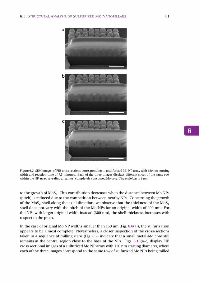
6.3. STRUCTURAL ANALYSIS OF SULFURIZED MO NANOPILLARS
6
81
Figure 6.7: SEM images of FIB cross sections corresponding to a sulfurized Mo NP array with 150 nm startingwidth and reaction time of 7.5 minutes. Each of the three images displays different slices of the same rowwithin the NP array, revealing an almost completely consumed Mo core. The scale bar is 1 µm.
to the growth of MoS2. This contribution decreases when the distance between Mo NPs(pitch) is reduced due to the competition between nearby NPs. Concerning the growthof the MoS2 shell along the axial direction, we observe that the thickness of the MoS2
shell does not vary with the pitch of the Mo NPs for an original width of 200 nm. Forthe NPs with larger original width instead (300 nm), the shell thickness increases withrespect to the pitch.
In the case of original Mo NP widths smaller than 150 nm (Fig. 6.6(a)), the sulfurizationappears to be almost complete. Nevertheless, a closer inspection of the cross-sectionstaken in a sequence of milling steps (Fig. 6.7) indicate that a small metal-Mo core stillremains at the central region close to the base of the NPs. Figs. 6.10(a-c) display FIBcross sectional images of a sulfurized Mo NP array with 150 nm starting diameter, whereeach of the three images correspond to the same row of sulfurized Mo NPs being milled

6
82 6. SYNTHESIS AND CHARACTERIZATION OF CORE-SHELL MO-MOS2 NANOPILLARS
in subsequent FIB milling steps. These Mo NPs were sulfurized for 7.5 minutes. Wecan conclude from the difference in contrast of the SEM images that for this specificconfiguration the Mo core is close to being completely consumed and turned into MoS2.However, we also note that a small metal-Mo core still remains at the central region ofthe NP.
6.3.3. SHELL STRUCTURAL CHARACTERISATIONWe proceed to assess the structural properties of core-shell Mo-MoS2 NPs. In particu-lar, we are interested in the specific orientation of the MoS2 layers in the shell with re-spect to the Mo core NP. The structural analysis in Figure 6.8 was carried out in an JEOLmono-ARM200F microscope operated at 200 kV in TEM mode. In all these images, aspot of size 3 was used, the monochromator was activated without any slit. First of all,Figure 6.8(a) displays a low-magnification bright-field HRTEM image taken on a repre-sentative core-shell NP sulfurized with a reaction time of 7.5 minutes. Figure 6.8(b-d)display the corresponding high-magnification TEM images taken at various locationsat the interface between the Mo core and the MoS2 shell: top, right side, and left siderespectively. From these images one can clearly see that the MoS2 layers grow perpen-dicularly with respect to the surface of the Mo core: the top region exhibits vertical MoS2
layers (see Figure 6.8(b), while the side regions display instead MoS2 layers with an hor-izontal orientation with respect to the substrate. The presence of MoS2 layers with con-sistently perpendicular orientations with respect to the Mo core surface suggest that theouter boundary of the core-shell NPs contain a high density of MoS2 edge terminations.We note that confirming the boundary composition of the core-shell NPs is not possiblewith the lamella cross-section technique due to the protective Pt layer deposited on topof the NPs. An alternative method to determine the precise boundary of the NPs could beto use ultrasonication of the NPs and directly depositing the solution of ultrasonicatedNPs onto a TEM grid.
From Figure 6.8(b-d) one observes that in the top and side regions of the NPs the MoS2
layers display a certain disorder in their relative orientations, while maintaining theirglobal orientation with respect to the Mo surface. Figure 6.8(f) displays an intensity pro-file corresponding to a linescan acquired in the region displayed with a black square in(e), which in turn is marked as a blue square in (d). The interlayer distance is measured tobe 0.64±0.01 nm, consistent with previous growth of vertically-aligned MoS2 sheets [15].Furthermore, we have determined that the orientation of the MoS2 layers in the shell ex-hibit identical structural properties irrespectively of the reaction times; in other words,the reaction time mostly dictates the amount of Mo consumed and transformed intoMoS2, and therefore the overall thickness of the shell.
6.4. ELECTRONIC AND OPTICAL PROPERTIES
6.4.1. ELECTRON ENERGY-LOSS SPECTROSCOPY CHARACTERIZATIONIn the previous sections we discussed the structural properties of the core-shell Mo-MoS2 NPs. We continue here with probing the electronic properties of the sulfurizedNPs using spatially-resolved electron energy-loss spectroscopy in the scanning trans-mission electron microscope (STEM-EELS). The nature of collective excitations of the

6.4. ELECTRONIC AND OPTICAL PROPERTIES
6
83
Figure 6.8: (a) Low-magnification bright-field HRTEM image of the cross-section associated to a representa-tive core-shell Mo-MoS2 NP, corresponding to a sulfurisation time of 7.5 minutes. (b,c,d) High-magnificationHRTEM images taken at various locations at the interface between the Mo core and the MoS2 shell: top, rightside, and left side respectively. (f) Linescan of the region displayed in (e), which in turn is marked as a bluesquare in (d).
constituents of the core-shell NPs is investigated with spatially-resolved EELS. The elec-tron energy-loss spectral image shown in Figure 6.9 and Figure 6.10 was also recordedin the JEOL mono-ARM200F microscope operated at 200 kV using the STEM mode. Themonochromator was set up on with a slit of 0.1 µm inserted. A probe size of 6C, a CL2aperture of 30µm, and a camera length of 12 cm were employed. The EELS was recordedusing a a Gatan GIF Continuum spectrometer with dispersion of 0.015 eV/ch, the aper-ture of the GIF was set to 5 mm, and the pixel time was 1.3 s. Figure 6.9 displays a spatiallyresolved EELS map of a core-shell NP sulfurized with a 7.5 min reaction time, where eachpixel corresponds to an individual EEL spectrum comprising an area of 1nm2. We aim tostudy the interplay between the Mo core and MoS2 shell and so the regions of interest are1) the Mo core (1-2), 2) the Mo-MoS2 interface (3-4), and 3) the MoS2 shell (5-6), whichcan be seen in Figure 6.9(c). In order to increase the signal-to-noise ratio Figure 6.9 weanalyze the EEL spectra of the regions of interest by taking the average EEL spectra ofsquares of 5x5 pixels in order to increase the signal-to-noise ratio.
Averaged EEL spectra corresponding to the regions of interest described above can beseen in Figure 6.9b. We start with the MoS2 shell, given by spectra sp5 and sp6. In bothsp5 and sp6 a peak is found at 22.48 eV, which can be attributed to the bulk plasmonpeak of MoS2 [16–20]. Furthermore, a feature located at around 8 eV is also observed inthe MoS2 shell, which is similar to the π-character interlayer excitations of the electronsthat are not involved in ionic-covalent bonding [19, 20]. The presence of interlayer exci-

6
84 6. SYNTHESIS AND CHARACTERIZATION OF CORE-SHELL MO-MOS2 NANOPILLARS
Figure 6.9: Core-shell Mo-MoS2 NPs synthesized with a reaction time of 7.5 minutes with (a) low-magnificationimage showing the region of interest with the green outline indicating the boundaries for the EELS map. (c)An area of 5x5 pixels in the spectral map is taken to improve the signal to noise ratio. The different areas (1-6)are chosen such that we have the contributions mainly from the Mo core(1-2), from the shell(5-6), and in theinterface region(3-4). (b) EEL spectra corresponding to the averaged areas denoted in (c)
tations should only be possible if the electron beam is perpendicular to the MoS2 layers.The interlayer excitations can be due to the horizontal layers of the different facets ofthe NPs curving slightly upwards. The behaviour of the Mo core is given by the averagedspectra sp1 and sp2. There are two main peaks present in the Mo core, a large peak lo-cated at 24.0 eV and a smaller peak located at 10.3 eV. Both peaks in sp1 and sp2 can beattributed to the two bulk plasmon peaks found in metallic Mo [21]. The interface region,given by spectra sp3 and sp4, we see a large peak located between the bulk plasmon peakof MoS2 and the bulk plasmon peak of Mo located at 24 eV. It is possible that the peak at24.0 eV is a consequence of the averaging of the 5×5 pixels that is being used here, lead-ing to overlapping of the bulk plasmons peaks of the core and shell. In order to properlydisentangle the contributions from the core and shell and have sufficient signal-to-noiseratio we average over 3x3 pixels, the results of which can be seen in Figure 6.10.

6.4. ELECTRONIC AND OPTICAL PROPERTIES
6
85
Figure 6.10: Core-shell Mo-MoS2 NPs synthesized with a reaction time of 7.5 minutes with (a) low-magnification image displaying the region of interest for the EELS map. (b) Positions of the averaged(3x3pixels) EEL spectra which are taken in regular spatial intervals, with (c) the corresponding averaged EEL spec-tra.
The averaged spectra are taken in regular spatial intervals across the spectral image,where all the regions(core, shell, interface) of interest are taken into account. Inspec-tion of the spectral image in Figure 6.10 reveals the presence of the bulk plasmon peaksalready found in Figure 6.9 for the Mo core and MoS2 shell. Additionally, we do not findthe peak at 24.0 eV for the averaged EEL spectra at the Mo-MoS2 interfaces, suggestingthat the large peak found in sp3 and sp4 in Figure 6.9 is a result of the larger averagingarea at the interface of the Mo-MoS2.
6.4.2. NON-LINEAR OPTICAL BEHAVIOURWe next study the nonlinear response of the core-shell NPs by using two different colorultrashort laser pulses. These two pulses have wavelengths of 775 nm and 1200 nm re-spectively and a pulse duration of around 150 fs for both pulses with a 80 MHz repetitionrate. The average power of the laser pulses is set to 3.8 mW and 3.6 mW for the 1200nm and 775 nm pulse respectively. Both laser pulses are focused onto the sample andare spatially and temporally overlapped to generate the nonlinear signals. The spectraof the nonlinear signals are measured using a high sensitivity spectrometer. The laserpulses were generated by a femtosecond laser oscillator (Tsunami, Spectra-Physics) andan optical parametric oscillator (OPAL, Spectra-Physics). Both laser beams were focusedonto the sample using a microscope objective (Olympus UP-LSAPO 40×/0.95), whichalso collects the emitted light originated through the nonlinear laser-NPs interaction.The collected light was filtered and imaged onto the slit of a spectrometer (PI, SpectraPro 2300I).
In Figure 6.11 the nonlinear optical response of a representative NP array is presented.Five peaks are visible which can attributed to second-harmonic generation (SHG) where,

6
86 6. SYNTHESIS AND CHARACTERIZATION OF CORE-SHELL MO-MOS2 NANOPILLARS
Figure 6.11: Nonlinear response of triangular NP arrays with 75 nm diameter and 350 nm length. Comparisonwith nearby MoS2 flakes and Si substrate background can be seen.
ωSHG =2ω1200 andωSHG = 2ω775, third-harmonic generation (THG), whereωTHG = 3ω1200,sum-frequency generation (SFG) where,ωSFG =ω775+ω1200 and four-wave mixing (FWM)where ωFWM = 2ω775 −ω1200.
In addition to the nonlinear spectra acquired on the Mo-MoS2 NPs, we also display thecorresponding nonlinear spectra taken on the substrate material (Si/SiO2) as well as onthe nearby located MoS2 flakes, which provide a reference for the same material un-der a different configuration. It can be observed that the third-order nonlinear signals(FWM, THG) are similar for the background and NPs. The THG nonlinear signal is evenslightly reduced with respect to the background. However, the second order processes(SHG, SFG) are highly enhanced in the MoS2. Indeed, the NP array, compared with thehorizontally-oriented MoS2 flakes of reference, benefits from the emission of even largernonlinear signals for the SHG775 nm and the SFG.
In order to explore the origin of nonlinear signals from the NP array, we perform a rasterscan over the nanopillar array. Figure 6.12 shows a false color map of the intensities of theSFG (left), SHG (middle) and THG (right) nonlinear signals around the nanopillar array.Although different NPs can be distinguished from the second order nonlinear signals,the nonlinear intensities of the individual NPs differ. This could potentially be explainedby slightly different orientations or angles of the NPs. There also appears to be nonlinearsignal generated in between the NPs and this is most likely originated from horizontallyoriented flakes in between the NPs that can be seen in the SEM images in Figure 6.2.

6.5. TOWARDS SULFURIZED W NANOPILLARS
6
87
Figure 6.12: Raster scan of the triangular core-shell MoS2 NP arrays corresponding to the spectrum in Fig-ure 6.11. A clear signal from the SFG and SHG is found in the NP array area, while the THG1200nm signal of thesubstrate is substantially higher than that of the NP arrays.
6.5. TOWARDS SULFURIZED W NANOPILLARSIn this chapter we have demonstrated the fabrication and synthesis of core-shell Mo-MoS2 NPs with a combination of top-down and bottom-up approaches. One can imag-ine extending this methodology to create NP structures of different TMDs. In this re-spect, we report here on attempts to fabricate W NPs with the goal to further use these WNPs as a template for the synthesis of WS2 based NPs. We use a fabrication and etchingrecipe for the W NP fabrication similar to the one for Mo NPs arrays. In Figure 6.13 theresults of one such attempt can be seen. In Figure 6.13(a), and Figure 6.13(b) an arrayof W NPs before and after sulfurization can be seen, respectively. In the case of W NPswe observer significant tapering at the base of the NPs after patterning and cryogenicreactive ion etching. Tapering is found for all NP widths. One reason for the large degreeof tapering for the W NPs can be the use of RF sputter-deposition for the W layer insteadof using DC sputtering. Another possibility lies in the use of high power(70W) for thereactive ion etching; The W etch rate is slightly higher than for Mo using the same etchparameters. In the case of Mo etching, it was found that lowering the power to 30W leadsto consistent fabrication of NPs with sub-100nm widths. We suspect that this is due toa lower degree of backscattering on the surface of the substrate of the ions during thedry etching. It remains to be seen if a lower etch power is needed to fabricate smoothsidewalls of W NPs, or whether other etch parameters should be varied.
We continue with the sulfurization of the fabricated W NPs. Similar sulfurization param-eters are used for the W NPs compared to what was used for the Mo nanostructures. Thesulfurization process of the as fabricated W NPs results in all the the sulfurized NPs hav-ing an ill-defined shape. W NPs with diameters in the 150 nm range tend to be rippedapart after sulfurization. Smaller widths for the original W NPs lead to a single sulfurizedW NP, however with an ill-defined shape. One possible reason for the ill-defined shapesof the sulfurized W NPs can be the less than optimal fabrication results for the W NPs.Another possible reason is a high sulfurization rate for the W NPs, leading to very littlecontrol of the growth mechanism for the W nanostructures. For the fabrication and syn-thesis of WS2 NPs further research is still needed to acquire precise control of fabricatedand synthesized structures.

6
88 6. SYNTHESIS AND CHARACTERIZATION OF CORE-SHELL MO-MOS2 NANOPILLARS
Figure 6.13: SEM images of W nanopillars before (a) and after (b) sulfurization. Both scale bars are 1 µm. Theoriginal widths for the W NPs are around 150 nm.
6.6. CONCLUSION & OUTLOOKIn this chapter we have shown how fabricated Mo NPs can be used as a template to syn-thesize core-shell Mo-MoS2 nanopillars. The formation of the MoS2 shell can be pre-cisely controlled using a reaction temperature of 650 and by varying the reaction time.The shell of MoS2 grows vertically with respect to the Mo core, leading to a mixture ofvertically and horizontally oriented MoS2 layers in the shell with respect to the substratesurface. This suggests that the amount of exposed edge structures of the MoS2 layers canbe reliably controlled by, first of all, varying the NP diameter and length in the fabricationstep, and secondly, by adjusting the reaction time of the sulfurization.
The electronic structure between the Mo core and MoS2 shell was studied using STEM-EELS. We found that the Mo core maintains its metallic character due to the appearanceof the two bulk plasmon peaks associated with pure Mo. We also found features associ-ated with the bulk plasmon peak and interlayer excitations associated with MoS2 in theshell of the NPs. The EEL spectra indicate a sharp distinction between the Mo plasmonicactivity and the MoS2 plasmonic activity.
Additionally, we have found a nonlinear optical response of the core-shell Mo-MoS−2NPs. By comparing the nonlinear response of the NPs with the nonlinear response offlakes near the NP arrays we see a clear difference in the intensity of the nonlinear re-sponse, where a larger nonlinear response is found for the core-shell NPs for secondharmonic generation of 775 nm light, and sum-frequency generation. Further work isneeded to determine the degree of tunability of the nonlinear optical response of thecore-shell NPs with respect to shell size, widths, shapes, and pitch.
In previous studies of core-shell MoOx -MoS2 nanowires, several authors demonstratedfavourable HER [9, 10, 22, 23] compared to monolayer flakes. They attributed the HER tothe combination of the catalytically active MoS2 shell and the conductive MoOx . In theirexperiments, MoS2 shells were synthesized with the basal planes parallel to the MoOx
core. In this respect, the core-shell nanostructures developed in this work are promisingcandidates for HER experiments; advantageous catalytic activity can be supported duethe large amount of exposed edges, such is found at the boundaries of the core-shell NPsin this work.

REFERENCES
6
89
REFERENCES[1] P. K. Sahoo, R. Janissen, M. P. Monteiro, A. Cavalli, D. M. Murillo, M. V. Merfa,
C. L. Cesar, H. F. Carvalho, A. A. de Souza, E. P. A. M. Bakkers, and M. A. Cotta,Nanowire Arrays as Cell Force Sensors To Investigate Adhesin-Enhanced Holdfastof Single Cell Bacteria and Biofilm Stability, Nano Letters 16, 4656 (2016), pMID:27336224, https://doi.org/10.1021/acs.nanolett.6b01998 .
[2] V. Gautam, S. Naureen, N. Shahid, Q. Gao, Y. Wang, D. Nisbet, C. Ja-gadish, and V. R. Daria, Engineering Highly Interconnected Neuronal Net-works on Nanowire Scaffolds, Nano Letters 17, 3369 (2017), pMID: 28437614,https://doi.org/10.1021/acs.nanolett.6b05288 .
[3] D. J. Carrad, A. B. Mostert, A. R. Ullah, A. M. Burke, H. J. Joyce, H. H. Tan, C. Ja-gadish, P. Krogstrup, J. Nygård, P. Meredith, and A. P. Micolich, Hybrid NanowireIon-to-Electron Transducers for Integrated Bioelectronic Circuitry, Nano Letters 17,827 (2017), pMID: 28002672, https://doi.org/10.1021/acs.nanolett.6b04075 .
[4] J. Zhou, S. Deng, L. Gong, Y. Ding, J. Chen, J. Huang, J. Chen, N. Xu, and Z. L.Wang, Growth of Large-Area Aligned Molybdenum Nanowires by High Tempera-ture Chemical Vapor Deposition: Synthesis, Growth Mechanism, and Device Appli-cation, The Journal of Physical Chemistry B 110, 10296 (2006), pMID: 16722732,https://doi.org/10.1021/jp061213z .
[5] M. P. Zach, K. H. Ng, and R. M. Penner, MolybdenumNanowires by Electrodeposition, Science 290, 2120 (2000),https://science.sciencemag.org/content/290/5499/2120.full.pdf .
[6] Y. Bi and J. Ye, In situ oxidation synthesis of Ag/AgCl core-shell nanowires and theirphotocatalytic properties, Chem. Commun. , 6551 (2009).
[7] P. Chen, T. Zhou, M. Chen, Y. Tong, N. Zhang, X. Peng, W. Chu, X. Wu, C. Wu,and Y. Xie, Enhanced Catalytic Activity in Nitrogen-Anion Modified Metallic CobaltDisulfide Porous Nanowire Arrays for Hydrogen Evolution, ACS Catalysis 7, 7405(2017), https://doi.org/10.1021/acscatal.7b02218 .
[8] N. Choudhary, C. Li, H.-S. Chung, J. Moore, J. Thomas, and Y. Jung, High-Performance One-Body Core/Shell Nanowire Supercapacitor Enabled by ConformalGrowth of Capacitive 2D WS2 Layers, ACS Nano 10, 10726 (2016), pMID: 27732778,https://doi.org/10.1021/acsnano.6b06111 .
[9] Z. Chen, D. Cummins, B. N. Reinecke, E. Clark, M. K. Sunkara, and T. F. Jaramillo,Core-shell MoO3-MoS2 Nanowires for Hydrogen Evolution: A Functional Designfor Electrocatalytic Materials, Nano Letters 11, 4168 (2011), pMID: 21894935,https://doi.org/10.1021/nl2020476 .
[10] D. R. Cummins, U. Martinez, R. Kappera, D. Voiry, A. Martinez-Garcia, J. Jasinski,D. Kelly, M. Chhowalla, A. D. Mohite, M. K. Sunkara, and G. Gupta, Catalytic Ac-tivity in Lithium-Treated Core-Shell MoOx /MoS2 Nanowires, The Journal of PhysicalChemistry C 119, 22908 (2015), https://doi.org/10.1021/acs.jpcc.5b05640 .

6
90 REFERENCES
[11] S. K. Dutta, S. K. Mehetor, and N. Pradhan, Metal Semiconductor Heterostructuresfor Photocatalytic Conversion of Light Energy, The Journal of Physical ChemistryLetters 6, 936 (2015), pMID: 26262849, https://doi.org/10.1021/acs.jpclett.5b00113.
[12] Y. Liu, H. Ma, X. X. Han, and B. Zhao, Metal-semiconductor heterostructuresfor surface-enhanced raman scattering: synergistic contribution of plasmons andcharge transfer, Mater. Horiz. 8, 370 (2021).
[13] J. Tan, S. Li, B. Liu, and H.-M. Cheng, Structure, Preparation, and Applications of 2DMaterial-Based Metal-Semiconductor Heterostructures, Small Structures 2, 2000093(2021), https://onlinelibrary.wiley.com/doi/pdf/10.1002/sstr.202000093 .
[14] D. Kong, H. Wang, J. J. Cha, M. Pasta, K. J. Koski, J. Yao, and Y. Cui, Synthesis of MoS2
and MoSe2 Films with Vertically Aligned Layers, Nano Letters 13, 1341 (2013), pMID:23387444, https://doi.org/10.1021/nl400258t .
[15] M. Bolhuis, J. Hernandez-Rueda, S. E. van Heijst, M. Tinoco Rivas, L. Kuipers, andS. Conesa-Boj, Vertically-oriented MoS2 nanosheets for nonlinear optical devices,Nanoscale 12, 10491 (2020).
[16] M. Tinoco, L. Maduro, and S. Conesa-Boj, Metallic edge states in zig-zag vertically-oriented MoS2 nanowalls, Scientific Reports 9, 15602 (2019).
[17] B. Yue, F. Hong, K.-D. Tsuei, N. Hiraoka, Y.-H. Wu, V. M. Silkin, B. Chen, and H.-k.Mao, High-energy electronic excitations in a bulk MoS2 single crystal, Phys. Rev. B96, 125118 (2017).
[18] L. Martin, R. Mamy, A. Couget, and C. Raisin, Optical Properties and Collective Ex-citations in MoS2 and NbSe2 in the 1.7 to 30 eV Range, physica status solidi (b) 58,623 (1973), https://onlinelibrary.wiley.com/doi/pdf/10.1002/pssb.2220580223 .
[19] K. Zeppenfeld, Electron energy losses and optical anisotropy of MoS2 single crystals,Optics Communications 1, 377 (1970).
[20] W. Y. Liang and S. L. Cundy, Electron energy loss studies of the tran-sition metal dichalcogenides, The Philosophical Magazine: A Jour-nal of Theoretical Experimental and Applied Physics 19, 1031 (1969),https://doi.org/10.1080/14786436908225867 .
[21] J. H. Weaver, D. W. Lynch, and C. G. Olson, Optical properties of V, Ta, and Mo from0.1 to 35 eV, Phys. Rev. B 10, 501 (1974).
[22] X. Xia, J. Tu, Y. Zhang, X. Wang, C. Gu, X.-b. Zhao, and H. J. Fan, High-Quality Metal Oxide Core/Shell Nanowire Arrays on Conductive Substrates forElectrochemical Energy Storage, ACS Nano 6, 5531 (2012), pMID: 22545560,https://doi.org/10.1021/nn301454q .

REFERENCES
6
91
[23] D. R. Cummins, U. Martinez, A. Sherehiy, R. Kappera, A. Martinez-Garcia, R. K.Schulze, J. Jasinski, J. Zhang, R. K. Gupta, J. Lou, M. Chhowalla, G. Sumanasekera,A. D. Mohite, M. K. Sunkara, and G. Gupta, Efficient hydrogen evolution in transitionmetal dichalcogenides via a simple one-step hydrazine reaction, Nature Communi-cations 7, 11857 (2016).

92

7DISENTANGLING ELECTRONIC AND
OPTICAL PROPERTIES OF WS2
POLYTYPES WITH ab-initioCALCULATIONS
This work aims to elucidate the crystal-structure dependence of the electronic and opticalproperties of the 2H and 3R polytypes of WS2, as well as of its 2H-3R polytype, by means ofan extensive ab-initio study based on Density Functional Theory (DFT) methods. The one-particle Green’s function (GW approximation) is computed in DFT and used to accuratelypredict the band gaps of the different polytypes of WS2. Furthermore, we calculate theoptical response of the WS2 polytypes in terms of its energy loss function (ELF) and com-pare our predictions with experimental measurements of electron energy loss spectroscopy(EELS) on the same WS2 polytypes. By studying the density of states, the joint density ofstates, and the band structure of these different polytypes, we are able to provide a theoret-ical assessment of the underlying origin of the different features observed in the low-lossregion of EEL spectra taken on WS2 nanostructures.
Parts of this chapter will be submitted for publication (2021) by L. Maduro, S. E. van Heijst, H. Jiang, and S.Conesa-Boj.
93
7
947. DISENTANGLING ELECTRONIC AND OPTICAL PROPERTIES OF WS2 POLYTYPES WITH
ab-initio CALCULATIONS
7.1. INTRODUCTION
M Aterials of the transition metal dichalcogenide (TMD) family have attracted ampleinterest due to the wide range of tunability of their electronic and optical proper-
ties [1–6]. This flexibility in tailoring the physical properties of TMD materials can beattributed to their marked sensitivity with respect to their dimensionality [7, 8], specificedge configurations [9–11], and stacking sequence [12–15].
The most common stacking sequences present in TMD materials are the 2H and 3Rstacking sequences. In addition, mixed stacking sequences of the 2H and 3R crystalphases, termed polytypism, have been observed in MoS2 [16] and MoSe2 [17]. Recently,the observation of 2H-3R polytypism in WS2 has been reported [18, 19]. There, the plas-monic and electronic implications of 2H-3R polytypism were studied by means of a com-bination of transmission electron microscopy (TEM) measurements and data process-ing with machine learning (ML), where deep neural networks make possible an efficientsubtraction of the zero-loss peak background and the determination of the underlyingbandgap value.
In this context, it is important to disentangle how the optical and electronic propertiesof the materials of the TMD family differ between either the 2H and 3R crystal phasesand the mixed 2H-3R polytypism. With this motivation, this chapter will focus on pin-ning down the crystallographic dependence of the electronic and optical properties ofbulk WS2 for these three stacking sequences from a theoretical perspective. Specifically,we will be carrying out ab initio calculations based on different WS2 crystal structureconfigurations by means of Density Functional Theory (DFT) [20, 21] using the WIEN2ksoftware package [22, 23].
Furthermore, in order to obtain accurate estimates of the band gap associated to the dif-ferent polytypes of WS2, we will use the GW approximation as implemented in the GAP2code by Jiang et al. [24, 25]. To this purpose, the outputs of the WIEN2k DFT calculationsare used as input for the GW calculations in the GAP2 code. With this combination of theDFT and GW calculations we are able to evaluate the density of states (DOS), the bandstructure, the joint density of states (JDOS), and the energy loss function (ELF) for thethree polytypes of WS2. This information, in turn, makes possible disentangling the de-pendence of the electronic and optical behaviour of the WS2 polytypes on the underlyingcrystal structure.
We start by defining the crystal structures of interest for this work. We continue withdescribing the calculational details concerning the geometry optimization, DOS, bandstructure, JDOS, and ELF for the different polytypes with the acquired wavefunctionsand energies. In the final section, we discuss the main results of our theoretical calcula-tions and compare them with experimental measurements acquired on WS2 nanostruc-tures exhibiting the same crystalline structure.

7.2. ATOMIC MODELS
7
95
Figure 7.1: The different polytypes of WS2. In the top panels, it is shown how all three polytypes exhibit ahexagonal structures when viewed from the [0001] direction; (a) the 2H crystal phase exhibits a honeycomblattice, while the (b) 3R and (c) 2H-3R polytypes both have an atom in the middle of their honeycomb struc-tures. The stacking sequences of the 2H, 3R and their mixed 2H-3R polytypes can be better assessed whenviewed from a lateral viewpoint with respect to the layers, as illustrated in the bottom panels.
7.2. ATOMIC MODELSWe start by first defining the atomic models of the different WS2 polytypes that are be-ing considered in this study. The DFT calculations presented in this work are based onthe structural atomic models displayed in Figure 7.1. Figure 3.1(a) and (b) display theatomic model of the 2H and 3R polytypes, respectively. The 2H polytype exhibits thecharacteristic hexagonal stacking order (A A′), where the adjacent layers are rotated 180and stacked directly upon one another. The 3R polytype is characterized by the rhombo-hedral stacking order (B A), in which the adjacent layers are slightly displaced from eachother without any rotation. Figure 7.1(c) shows the atomic model of the mixed 2H-3RWS2 polytypes, which is characterized by a layer stacking order of the type B A A′. Thisstacking order arises from the mixture of the 2H (A A′) and 3R (B A) polytypes [26].
7.3. COMPUTATIONAL DETAILS
7.3.1. GEOMETRY OPTIMIZATIONIn this work we present two sets of calculations, one set of results will be on the DFTlevel, while the other set will be on the GW level. For each level of calculation and foreach crystal lattice a specific amount of k-point sampling is used until convergence hasbeen achieved with respect to the k-points. The k-points sampling of the first Brillouin

7
967. DISENTANGLING ELECTRONIC AND OPTICAL PROPERTIES OF WS2 POLYTYPES WITH
ab-initio CALCULATIONS
zone for the lattice parameter calculations and all subsequent calculations are carriedout using the tetrahedon method of Blöchl et al. [27]. Geometry optimization is carriedout using the literature values for lattice parameters of the 2H and 3R polytypes of WS2
as a starting point. For the 2H-3R polytypism, we use the literature values of the latticeparameters of the 3R structure as a starting point for the geometry optimization.
The calculations on the DFT level are carried out using the linearized augmented planewave (LAPW) and local orbitals (LO) methods implemented in the WIEN2k package. Forall the crystal structures the following calculation parameters were kept the same. Thenonlocal van der Waals [28, 29](vdW) interactions used for the DOS calculations usesoptB88 [30] for the exchange term, the local density approximation [31] (LDA) for thecorrelation term, and the DRSLL kernel for the non-local term [32]. For the non-localvdW integration the cut-off density rc was set to 0.3 bohr−3, while the plane wave expan-sion cut-off Gmax was set to 20 bohr−1. No spin polarization was considered.
The lattice parameters were found by volume and force optimization of the different unitcells, such that the force on each atom was less than 1.0 mRy/bohr. The total energy con-vergence criteria was set to be 0.1 mRy between self-consistent field (SCF) cycles, whilethe charge convergence criteria was set to 0.001e, with e the elementary unit charge. Thecore and valence electron states were separated by an energy gap of 6.0 Ry. Furthermore,the calculations used an Rkmax of 7.0, where R is the radius of the smallest Muffin Tinsphere, and kmax is the largest k-vector.
7.3.2. ENERGY LOSS FUNCTION & JOINT DENSITY OF STATESThe joint density of states and energy loss function ΓELF (E) are calculated with the opticpackage as implemented in WIEN2k and is used to compare experimental EELS mea-surements [33–35]. The optic package calculates the optical properties in the RandomPhase Approximation (RPA), neglecting local field effects. The joint density of states andthe imaginary part of the dielectric function ε(E) are calculated by the program joint. Af-terwards, the real part of the dielectric function is calculated using the Kramers-Kronigrelations. The energy loss function is subsequently calculated using the relation
ΓELF(E) = Im
( −1
ε(ω)
)(7.1)
7.3.3. SPIN-ORBIT COUPLINGSpin-orbit coupling is included after the geometry optimization in a one-shot calcula-tion for the DOS, band structure, and ELF calculations. The spin-orbit coupling is in-cluded by using scalar-relativistic wavefunctions in a second-variational procedure [36,37]. We ensure that enough eigenstates are included in the calculations including spin-orbit coupling by increasing EMAX in case.in1 to 7.5 Ry. Well-converged k-meshes areused for each lattice structure when calculating the DOS, band structure, and ELF andcan be found in Table 7.2. For each lattice structure we used the same k-mesh for theDOS, band structure, and ELF for each level of calculation(DFT or GW level).

7.4. RESULTS
7
97
7.3.4. GW APPROXIMATIONAfter geometry optimization, the equilibrium lattice parameters obtained are used forthe GW approximation calculations as implemented in the GAP2 code[24, 25]. There, theGreen’s function G and the screened Coulomb interaction W are calculated in the RPAframework. For the 2H and mixed 2H-3R crystal phases, we use a 6×6×1 k-mesh sam-pling of the Brillouin zone, while a 4×4×4 k-mesh sampling is used instead for the 3Rcrystal phase case. Fourier interpolation is used to interpolate a fine k-mesh from thesparse-mesh originally used in the GW calculations to obtain quasiparticle energies[38].Spin-orbit coupling effects are taken into account in a perturbative one-shot manner.Table 7.2 displays the values of the k-mesh used for the GW calculation and for the cal-culation of the DOS, band structure, and ELF. These k-meshes are kept the same for thecalculations with and without spin-orbit coupling.
7.4. RESULTSWe are now ready to present the main results of this theoretical study of the electronicand optical properties of the WS2 polytypes. First, we present our determination of thedensity of states and band structure on these materials. Then we evaluate the energy lossfunction and the corresponding density of states. Finally, we provide a comparison withexperimental results based on measurements taken on WS2 nanostructures exhibitingthe same polytypes.
7.4.1. GEOMETRY OPTIMIZATIONGeometry optimization is carried out to find the equilibrium lattice parameters of thedifferent polytypes for the subsequent calculations. Convergence with respect to theamount of k-points is obtained for all the polytypes, and the corresponding numericalvalues obtained are reported Table 7.1. There, we also compare the calculated lattice pa-rameters of the 2H and 3R polytypes with the literature values, finding good agreement.In the case of the 2H-3R polytypism, the in-plane and out-of-plane lattice parametersare found to be similar to the 3R polytype. Using the symmetry package in WIEN2k, wecan identify that the 2H-3R polytypism belongs to the P3m1 space group.
Crystal Phase Geometry OptimizationCalculated Lat-tice Parameters
ExperimentalMeasurements
2H-3R 24 x 24 x 3a = b = 3.205 Å,c = 19.057 Å
–
2H 16 x 16 x 3a = b = 3.194 Å,c = 12.458 Å
a = b = 3.153 Å,c = 12.323 Å
3R 14 x 14 x 14a = b = 3.199 Å,c = 18.733 Å
a = b = 3.158 Å,c = 18.490 Å
Table 7.1: k-mesh used for the calculations and crystal structures. We also display, for each WS2 polytype, thecalculated lattice parameters with the corresponding experimental values from [39].

7
987. DISENTANGLING ELECTRONIC AND OPTICAL PROPERTIES OF WS2 POLYTYPES WITH
ab-initio CALCULATIONS
Figure 7.2: Geometry optimization of the (a) 2H-3R, (b) 2H, and (c) 3R structures. The convergence of thecalculations for the 2H and 3R structures is verified by varying the amount of number of k-point sampling. Forthe 2H-3R crystal structure, a larger set of k-point sampling turns out to be required.
7.4.2. DENSITY OF STATES & BAND STRUCTUREWe continue our discussion with the density of states and electronic band structure ofthe three WS2 polytypes. In Figure 7.4 the total density of states, the projected density ofstates, and the band structure, of the 2H, 3R, and 2H-3R polytypism are displayed. Forall three crystalline structures, it is the W d-orbitals that primarily allows occupied andunoccupied states near the Fermi energy, a result which is consistent with related DFTstudies on MoS2 by Espejo et al. [2] and Coutinho et al. [40]. The effects of spin-orbitcoupling (SOC) are also taken into account, the result of which leads to a small changein the density of states near the Fermi energy for all cases.
The band gap of the 2H-3R polytype is 1.48 eV without SOC and 1.40 eV with SOC, while
Crystal Phase GW calculation DOS, band structure, ELF
2H-3R 6 x 6 x 1 23 x 23 x 3
2H 6 x 6 x 1 20 x 20 x 4
3R 4 x 4 x 4 16 x 16 x 16
Table 7.2: k-mesh used for the calculations, of the density of states, band structure, and energy loss function.The k-meshes are kept the same for the calculations with and without spin-orbit coupling.

7.4. RESULTS
7
99
the band gap of the 2H structure is 1.39 eV without SOC and 1.34 eV with SOC. Includingspin-orbit coupling has a most prominent effect for the 3R polytype, as we observe adramatic shift in the calculated band gap value of the 3R polytype, decreasing from 1.62eV(without SOC) to 1.47 eV(with SOC), compared to the rather more modest shift forthe 2H (from 1.39 eV to 1.34 eV) and 2H-3R (from 1.48 eV to 1.40 eV) polytypes. Wenote that that band gap value of the 2H-3R polytypism lies in between those of the 2Hand 3R polytypes in the cases with and without spin-orbit coupling. This effect could beexplained by the one-shot post inclusion of spin-orbit coupling in the GW calculations.
For the band structure plots, we choose k-paths in the primitive Brillouin zones such thata complete irreducible set of symmetry lines is obtained. For the 2H and 2H-3R poly-types, identical k-paths in the Brillouin zone are chosen since their primitive Brillouinzone have identical symmetry points. For the 3R polytype we follow the prescriptionsof [41–46] for the selection of the k-path in the primitive Brillouin zone. The Brillouinzone for the 2H and 2H-3R structures can be seen in Figure 7.3, while the Brillouin zonefor the 3R structure can be seen in Figure 7.3. Due to the similarity of the primitive Bril-louin zones of the 2H and 2H-3R polytypes, we are able to make a direct comparison ofthe conduction and valence bands behaviours. Such a direct comparison is not possiblefor all three polytypes, since the primitive Brillouin zone of the 3R structure is dissimilarto those of the 2H and 2H-3R Brillouin zones.
In the case of the 2H and 2H-3R polytypes, the conduction band minima is found tobe at the same point in the Brillouin zone, located between the K and Γ points in theBrillouin zone. While the valence band maximum for the 2H is at the Γ point, for the 2H-3R polytypism the valence band maximum lies at the A point. In the case of the 2H-3Rpolytypism there are three bands near the Fermi, as oppose to two bands near the Fermienergy for the 2H case. The extra band near the Fermi energy in the 2H-3R polytypism isthe cause of the shift of the valence band maximum from the Γ point to the A point. As aconsequence of the extra band near the Fermi energy, an additional band can be foundnear the K point. The extra band near the K point leads to additional bands appearingwhen taking spin-orbit coupling into account.
As mentioned above, the band gap of the 3R structure is 1.62 eV without SOC and 1.47 eVwith SOC. In the case of the 3R structure, the valence band maximum lies at the Z point,while the conduction band minimum lies between the Γ and X points in the Brillouinzone. For this 3R crystal structure, we see that the band near the Fermi energy is splitinto two bands at the B, X and Q points in the Brillouin zone when including spin-orbitcoupling. The conduction band minimum lies between the Γ and X points and is pusheddown in energy when including spin-orbit coupling, while the maximum of the valenceband is not changed significantly by the inclusion of spin-orbit coupling.

7
1007. DISENTANGLING ELECTRONIC AND OPTICAL PROPERTIES OF WS2 POLYTYPES WITH
ab-initio CALCULATIONS
Figure 7.3: Primitive Brillouin zone of the 2H and 2H-3R structures. (a) Top and (c) side view of the primitiveBrillouin zone together with the reciprocal lattice vectors a∗, b∗, and c∗. Skew view (b) of the 2H and 2H-3Rprimitive Brillouin zones illustrating the rest of the primitive Brillouin zone. Following [41–46] we choose ak-path along the Γ-M-K-Γ-A-L-H-A high symmetry points for the band structure plots for the 2H and 2H-3Rsystems. Primitive Brillouin zone of the 3R structure.(d) Top and (e) side view of the primitive Brillouin zonetogether with the reciprocal lattice vectors a∗, b∗, and c∗. Different skew view (f) and (g) further illustrate theprimitive Brillouin zone of the 3R structure. Following [41–46] we choose a k-path along the Γ-L-B1-B-Z-Γ-X-Q-F-P1-Z-L-P-Z high symmetry points for the band structure plots for the 3R system.

7.4. RESULTS
7
101
Figure 7.4: Density of states of the (a) 2H-3R, (c) 2H, and (e) 3R structures, with and without spin-orbit coupling(SOC) taken into account. Band structure plot of the (b) 2H-3R, (d) 2H, and (f) 3R structures with and withoutspin-orbit coupling.

7
1027. DISENTANGLING ELECTRONIC AND OPTICAL PROPERTIES OF WS2 POLYTYPES WITH
ab-initio CALCULATIONS
7.4.3. ENERGY LOSS FUNCTION & JOINT DENSITY OF STATESWe continue our discussion of the theoretical predictions of the electronic and opticalproperties of the WS2 polytypes by describing the energy loss function and the joint den-sity of states, first for the 2H-3R polytype and then with the 2H and 3R crystal phases.Due to the symmetry properties of these polytypes, we have two distinct sets of energylosses for each polytype, namely the in-plane and out-of-plane energy-losses. For thisreason, we represent graphically the energy loss associated with in-plane and out-of-plane losses separately. Additionally, we compare the energy loss function calculated atthe DFT level and at the GW level, with and without taking the spin-orbit coupling effectsinto account.
The energy loss function for the different WS2 polytypes is displayed in Figures 7.5, 7.6,and 7.7 respectively. For all the different crystal structures considered, the in-plane andout-of-plane bulk plasmon peaks lie between 20.91 eV and 22.02 eV. The in-plane andout-of-plane bulk plasmons differ by no more than 0.24 eV for both the DFT and GWcalculations. The effects of spin-orbit coupling can be clearly seen both at the DFT andat the GW level: the bulk plasmon peaks for both in-plane and out-of-plane losses shiftstowards lower energy losses. The positions of the bulk plasmon peaks for the differentcrystal structures and theoretical calculations are reported in Table 7.3.
Furthermore, in the energy loss region below losses of 10 eV we observe a number ofdistinct peaks. These features present in the low-loss region could be attributed to inter-band transitions between the valence and conduction bands near the Fermi energy, aswe will discuss below. We present results for the joint density of states calculated at theGW level. We compare results with and without taking spin-orbit coupling into account.For all three polytypes, we calculate the joint density of states taking all the bands intoaccount.
We also evaluate the contribution of separate bands to the joint density of states to elu-cidate which one are important in specific energy losses regions. We start with the calcu-lation of the joint density of states by including one valence band, the top valence band,and one conduction band, specifically the bottom conduction band. We then includean increasing amount of valence and conduction bands with respect to the top valenceband and the bottom conduction band, and represent graphically the results while com-paring with the total joint density of states. We note that in the cases including spin-orbitcoupling, we double the amount of bands needed with respect to the case without spin-orbit coupling to properly describe the energy loss spectra.
In order to properly describe the bulk plasmon peaks appearing in the energy loss re-gions in the range between 10 eV to 30 eV range, a larger amount of bands needs to beincorporated into the joint density of states calculation; this is consistent with the con-cept of plasmons arising as collective excitations of the electrons in the material. Wecontinue first without considering spin-orbit coupling. In the energy loss region below10 eV, we observe from the joint density of states that the top twenty valence bands andbottom twenty conduction bands can completely describe the energy regions below 10eV for the 2H polytype, while for the 3R polytype ten valence bands and ten conductionbands is sufficient to completely describe the energy loss region below 10 eV. For the

7.4. RESULTS
7
103
2H-3R polytypism a larger amount of bands is needed to completely describe the regionbelow 10 eV. As we proceed towards smaller energy losses we can see that a decreasingamount of valence and conduction bands are needed to explain the peaks in the corre-sponding energy region for all the polytypes.
7.4.4. DISCUSSION & COMPARISON WITH EXPERIMENTOur calculations for the value of the band gap and the location of the bulk plasmon peakfor the 2H crystal structure of WS2 are found to be in good agreement with previoustheoretical and experimental work [3, 5, 47–50]. Therefore, we are confident that wecan reliably apply the same theoretical machinery to predict the electrical and opticalproperties of the corresponding 2H-3R polytype.
In this work we have also calculated that the 2H-3R polytype should exhibit an indirectband gap with a value in the range between 1.40 eV 1.48 eV. This prediction is in excellentagreement with the experimental result reported in [18, 19], where a band gap value of1.6+0.3
−0.2 eV was extracted after subtracting the EELS zero-loss peak using machine learn-ing techniques.
Finally, for the 3R polytype we have calculated an indirect band gap with a value in therange between 1.47 and 1.62 eV. The large discrepancy for the band gap calculations inthe cases with and without taking into account the spin-orbit coupling could be relatedto an insufficiently dense k-mesh used in the GW calculation for the 3R polytype. Forthis crystal structure, we also calculate a bulk plasmon peak whose position is close tothat of the 2H and 2H-3R polytypes. As of writing, no experimental measurements of theposition of the bulk plasmon peak, the band gap type, or the band gap value have beenreported for the 3R polytype and hence we cannot compare our predictions to experi-mental data.
In the case of 2H-3R polytypism, the location of the bulk plasmon peak observed in WS2
nanostructures by means of electron-energy loss spectroscopy [18, 19] is rather similarto that of the bulk plasmon peak in the 2H polytype, in agreement with the theoreticalpredictions in this work.
Crystal Phase DFT no SOC DFT with SOC GW no SOC GW with SOC
2H-3R∥ 21.67 eV 20.72 eV 21.57 eV 20.91 eV
2H-3R⊥ 21.43 eV 20.94 eV 21.65 eV 21.10 eV
2H∥ 22.03 eV 20.69 eV 21.57 eV 21.46 eV
2H⊥ 21.84 eV 20.94 eV 21.76 eV 21.57 eV
3R∥ 21.95 eV 20.94 eV 21.43 eV 21.08 eV
3R⊥ 22.00 eV 21.02 eV 21.97 eV 21.59 eV
Table 7.3: In-plane (∥) and out-of-plane (⊥) locations of the bulk plasmon (BP) peaks for the three differentWS2 polytypes considered here. We show results for both the DFT and GW calculations, with and withoutspin-orbit coupling effects.

7
1047. DISENTANGLING ELECTRONIC AND OPTICAL PROPERTIES OF WS2 POLYTYPES WITH
ab-initio CALCULATIONS
Figure 7.5: Energy loss function for the 2H-3R polytype of WS2. (a) and (b) in-plane energy loss function withand without spin-orbit coupling (SOC). (c) and (d) out-of-plane energy loss function with and without SOC.Joint density of states of 2H-3R structure calculated on the GW level (e) and (f) without spin-orbit coupling. (g)and (h) with spin-orbit coupling. Here VB and CB stand for Valence Band and Conduction Band respectively.

7.4. RESULTS
7
105
Figure 7.6: Same as Fig. 7.5 for the 2H crystal structure.

7
1067. DISENTANGLING ELECTRONIC AND OPTICAL PROPERTIES OF WS2 POLYTYPES WITH
ab-initio CALCULATIONS
Figure 7.7: Same as Fig. 7.5 for the 3R crystal structure.

7.5. CONCLUSIONS & OUTLOOK
7
107
Figure 7.8: (a,b) Experimental EELS measurements acquired on a WS2 nanostructure characterized by thesame 2H/3R polytypism. Note that the zero-loss peak (ZLP) has not been subtracted from the EELS data.
Figure 7.8(c,d) displays then experimental EELS measurements acquired on a WS2 nanos-tructure also characterized by the same 2H/3R polytypism [18, 19] in the same energy-loss range that the corresponding theoretical calculations. Note that the zero-loss peak(ZLP) has not been subtracted from the EELS data. In these experimental measurements,one observes in the low-loss region two peaks located at 3.5 eV and 8 eV. The peak at 8eV, which can be associated to the interlayer coupling, is consistent with the featuresof the GW calculation both including and excluding SOC effects. On the other hand,the feature at 3.5 eV is not visible in the calculated ELF, but calculated DOS, see Fig-ure 3.2(a), indicates that this peak is associated to a electronic transition from occupiedd states to unoccupied d states of W. The absence of the feature at 3.5 eV energy loss canbe explained due to limitations of the GW approach; GW accurately describes a single-particle process, however for optical excitations the effect of interactions between holesand electrons needs to be taken into account. Properly describing electron-hole interac-tions could be achieved by solving the Bethe-Salpeter Equations (BSE) [51–53]. Furtherdetails about the origin of these two observed peaks in the low-loss region can be foundin the JDOS discussion below.
Concerning the bulk plasmon, it is located at around 23 eV in the experimental EELSmeasurements while in the DFT and GW calculations it appears at slightly smaller val-ues. The slight discrepancy between the calculated and experimentally measured bulkplasmons of the mixed 2H-3R polytype can be attributed to the exclusion of local field ef-fects and non-zero momentum transfer effects while calculating the dielectric responseof the material as implemented in the optic package[33, 34, 54].
7.5. CONCLUSIONS & OUTLOOKIn this work, we have carried out ab initio calculations based on the 2H, 3R, and 2H-3R polytypes of WS2. We showed how the band gap value of the 2H-3R polytypism liesbetween the band gap values of the 2H and 3R polytypes, where it is observed to be closerto the 2H band gap value compared to the 3R band gap value, and is in good agreementwith experimental measurements.

7
108 REFERENCES
Comparable band structures were found of the 2H and 2H-3R polytypes, where the topof the valence band of the 2H-3R polytypism lies at the A high symmetry point. We haveshown that the bulk plasmon peaks of all the polytypes occurs at very similar energyloss values. For the energy loss function, we have determined the contribution of thedifferent valence and conduction bands to the energy loss intensity for different energyloss regions.
One point of future research would be the determination of the character of the differentcontributing bands in the low loss region. Additionally, a denser k-mesh for the 3R GWcalculation should be implemented in order to determine whether the band gap discrep-ancy for calculations with and without spin-orbit coupling can be explained. Furtherstudies of the energy loss function near the band gap can be carried out by solving theBethe-Salpeter equations to determine how the excitonic behaviour between the poly-types may differ among them [4, 6, 55, 56].
REFERENCES[1] S. Manzeli, D. Ovchinnikov, D. Pasquier, O. V. Yazyev, and A. Kis, 2D transition metal
dichalcogenides, Nature Reviews Materials 2, 17033 (2017).
[2] C. Espejo, T. Rangel, A. H. Romero, X. Gonze, and G.-M. Rignanese, Band structuretunability in MoS2 under interlayer compression: A DF T and GW study, Phys. Rev.B 87, 245114 (2013).
[3] P. Johari and V. B. Shenoy, Tunable Dielectric Properties of Transi-tion Metal Dichalcogenides, ACS Nano 5, 5903 (2011), pMID: 21707067,https://doi.org/10.1021/nn201698t .
[4] A. Ramasubramaniam, D. Naveh, and E. Towe, Tunable band gaps in bilayertransition-metal dichalcogenides, Phys. Rev. B 84, 205325 (2011).
[5] J. Gusakova, X. Wang, L. L. Shiau, A. Krivosheeva, V. Shaposhnikov, V. Borisenko,V. Gusakov, and B. K. Tay, Electronic Properties of Bulk and Monolayer TMDs: Theo-retical Study Within DFT Framework (GVJ-2e Method), physica status solidi (a) 214,1700218 (2017), https://onlinelibrary.wiley.com/doi/pdf/10.1002/pssa.201700218 .
[6] J. Ryou, Y.-S. Kim, S. Kc, and K. Cho, Monolayer MoS2 Bandgap Modulation by Di-electric Environments and Tunable Bandgap Transistors, Scientific Reports 6 (2016).
[7] T. Eknapakul, P. D. C. King, M. Asakawa, P. Buaphet, R.-H. He, S.-K. Mo, H. Tak-agi, K. M. Shen, F. Baumberger, T. Sasagawa, S. Jungthawan, and W. Meevasana,Electronic Structure of a Quasi-Freestanding MoS2 Monolayer, Nano Letters 14, 1312(2014), pMID: 24552197, https://doi.org/10.1021/nl4042824 .
[8] K. F. Mak, C. Lee, J. Hone, J. Shan, and T. F. Heinz, Atomically Thin MoS2: A NewDirect-Gap Semiconductor, Phys. Rev. Lett. 105, 136805 (2010).
[9] H. Xu, S. Liu, Z. Ding, S. J. R. Tan, K. M. Yam, Y. Bao, C. T. Nai, M.-F. Ng, J. Lu,C. Zhang, and K. P. Loh, Oscillating edge states in one-dimensional MoS2 nanowires,Nature Communications 7, 12904 (2016).

REFERENCES
7
109
[10] M. Tinoco, L. Maduro, M. Masaki, E. Okunishi, and S. Conesa-Boj, Strain-Dependent Edge Structures in MoS2 Layers, Nano Letters 17, 7021 (2017), pMID:29064254, https://doi.org/10.1021/acs.nanolett.7b03627 .
[11] M. Tinoco, L. Maduro, and S. Conesa-Boj, Metallic edge states in zig-zag vertically-oriented MoS2 nanowalls, Scientific Reports 9, 15602 (2019).
[12] J. He, K. Hummer, and C. Franchini, Stacking effects on the electronic and opticalproperties of bilayer transition metal dichalcogenides MoS2, MoSe2, WS2, and WSe2,Phys. Rev. B 89, 075409 (2014).
[13] R. Suzuki, M. Sakano, Y. J. Zhang, R. Akashi, D. Morikawa, A. Harasawa, K. Yaji,K. Kuroda, K. Miyamoto, T. Okuda, K. Ishizaka, R. Arita, and Y. Iwasa, Valley-dependent spin polarization in bulk MoS2 with broken inversion symmetry, NatureNanotechnology 9, 611 (2014).
[14] L. Chen, H. Feng, R. Zhang, S. Wang, X. Zhang, Z. Wei, Y. Zhu, M. Gu, andC. Zhao, Phase-Controlled Synthesis of 2H/3R-MoSe2 Nanosheets on P-Doped Car-bon for Synergistic Hydrogen Evolution, ACS Applied Nano Materials 3, 6516 (2020),https://doi.org/10.1021/acsanm.0c00988 .
[15] J. Wilson and A. Yoffe, The transition metal dichalcogenides discussion and inter-pretation of the observed optical, electrical and structural properties, Advances inPhysics 18, 193 (1969), https://doi.org/10.1080/00018736900101307 .
[16] J.-U. Lee, K. Kim, S. Han, G. H. Ryu, Z. Lee, and H. Cheong, Raman Signatures ofPolytypism in Molybdenum Disulfide, ACS Nano 10, 1948 (2016), pMID: 26756836,https://doi.org/10.1021/acsnano.5b05831 .
[17] A. A. Puretzky, L. Liang, X. Li, K. Xiao, K. Wang, M. Mahjouri-Samani,L. Basile, J. C. Idrobo, B. G. Sumpter, V. Meunier, and D. B. Geohegan,Low-Frequency Raman Fingerprints of Two-Dimensional Metal DichalcogenideLayer Stacking Configurations, ACS Nano 9, 6333 (2015), pMID: 25965878,https://doi.org/10.1021/acsnano.5b01884 .
[18] S. E. van Heijst, M. Mukai, E. Okunishi, H. Hashiguchi, L. I. Roest, L. Maduro,J. Rojo, and S. Conesa-Boj, Illuminating the Electronic Properties of WS2
Polytypism with Electron Microscopy, Annalen der Physik n/a, 2000499,https://onlinelibrary.wiley.com/doi/pdf/10.1002/andp.202000499 .
[19] L. I. Roest, S. E. van Heijst, L. Maduro, J. Rojo, and S. Conesa-Boj, Charting thelow-loss region in electron energy loss spectroscopy with machine learning, Ultrami-croscopy 222, 113202 (2021).
[20] P. Hohenberg and W. Kohn, Inhomogeneous electron gas, Phys. Rev. 136, B864(1964).
[21] W. Kohn and L. J. Sham, Self-consistent equations including exchange and correla-tion effects, Phys. Rev. 140, A1133 (1965).

7
110 REFERENCES
[22] P. Blaha, K. Schwarz, G. K. Madsen, D. Kvasnicka, J. Luitz, et al., wien2k, Anaugmented plane wave+ local orbitals program for calculating crystal properties(2001).
[23] P. Blaha, K. Schwarz, F. Tran, R. Laskowski, G. K. H. Madsen, and L. D. Marks,WIEN2k: An APW+lo program for calculating the properties of solids, The Journalof Chemical Physics 152, 074101 (2020), https://doi.org/10.1063/1.5143061 .
[24] H. Jiang, R. I. Gómez-Abal, X.-Z. Li, C. Meisenbichler, C. Ambrosch-Draxl, andM. Scheffler, Fhi-gap: A gw code based on the all-electron augmented plane wavemethod, Computer Physics Communications 184, 348 (2013).
[25] H. Jiang and P. Blaha, GW with linearized augmented plane waves extended by high-energy local orbitals, Phys. Rev. B 93, 115203 (2016).
[26] A. Yan, W. Chen, C. Ophus, J. Ciston, Y. Lin, K. Persson, and A. Zettl, Identifyingdifferent stacking sequences in few-layer cvd-grown Mos2 by low-energy atomic-resolution scanning transmission electron microscopy, Phys. Rev. B 93, 041420(2016).
[27] P. E. Blöchl, O. Jepsen, and O. K. Andersen, Improved tetrahedron method forBrillouin-zone integrations, Phys. Rev. B 49, 16223 (1994).
[28] J. Klimeš, D. R. Bowler, and A. Michaelides, Chemical accuracy for the van der Waalsdensity functional, Journal of Physics: Condensed Matter 22, 022201 (2009).
[29] J. c. v. Klimeš, D. R. Bowler, and A. Michaelides, Van der Waals density functionalsapplied to solids, Phys. Rev. B 83, 195131 (2011).
[30] A. D. Becke, Density-functional exchange-energy approximation with correctasymptotic behavior, Phys. Rev. A 38, 3098 (1988).
[31] J. P. Perdew and Y. Wang, Accurate and simple analytic representation of the electron-gas correlation energy, Phys. Rev. B 45, 13244 (1992).
[32] M. Dion, H. Rydberg, E. Schröder, D. C. Langreth, and B. I. Lundqvist, Van der WaalsDensity Functional for General Geometries, Phys. Rev. Lett. 92, 246401 (2004).
[33] C. Ambrosch-Draxl and J. O. Sofo, Linear optical properties of solids within the full-potential linearized augmented planewave method, Computer Physics Communi-cations 175, 1 (2006).
[34] V. Keast, An introduction to the calculation of valence EELS: Quantum mechanicalmethods for bulk solids, Micron 44, 93 (2013).
[35] C. Hébert, Practical aspects of running the WIEN2k code for electron spectroscopy,Micron 38, 12 (2007).
[36] D. D. Koelling and B. N. Harmon, A technique for relativistic spin-polarised calcula-tions, Journal of Physics C: Solid State Physics 10, 3107 (1977).

REFERENCES
7
111
[37] A. H. MacDonald, W. E. Picket, and D. D. Koelling, A linearised relativisticaugmented-plane-wave method utilising approximate pure spin basis functions,Journal of Physics C: Solid State Physics 13, 2675 (1980).
[38] W. E. Pickett, H. Krakauer, and P. B. Allen, Smooth Fourier interpolation of periodicfunctions, Phys. Rev. B 38, 2721 (1988).
[39] W. Schutte, J. De Boer, and F. Jellinek, Crystal structures of tungsten disulfide anddiselenide, Journal of Solid State Chemistry 70, 207 (1987).
[40] S. Coutinho, M. Tavares, C. Barboza, N. Frazão, E. Moreira, and D. L. Azevedo,3R and 2H polytypes of MoS2: DFT and DFPT calculations of structural, optoelec-tronic, vibrational and thermodynamic properties, Journal of Physics and Chem-istry of Solids 111, 25 (2017).
[41] W. Setyawan and S. Curtarolo, High-throughput electronic band structure calcula-tions: Challenges and tools, Computational Materials Science 49, 299 (2010).
[42] J. Perez-Mato, D. Orobengoa, E. Tasci, G. De la Flor Martin, and A. Kirov, Crystallog-raphy online: Bilbao crystallographic server, Bulgarian Chemical Communications43, 183 (2011).
[43] M. I. Aroyo, J. M. Perez-Mato, C. Capillas, E. Kroumova, S. Ivantchev, G. Madariaga,A. Kirov, and H. Wondratschek, Bilbao crystallographic server: I. databases and crys-tallographic computing programs, Zeitschrift für Kristallographie - Crystalline Ma-terials 221, 15 (2006).
[44] M. I. Aroyo, A. Kirov, C. Capillas, J. M. Perez-Mato, and H. Wondratschek, Bil-bao Crystallographic Server. II. Representations of crystallographic point groups andspace groups, Acta Crystallographica Section A 62, 115 (2006).
[45] M. I. Aroyo, D. Orobengoa, G. de la Flor, E. S. Tasci, J. M. Perez-Mato, and H. Won-dratschek, Brillouin-zone database on the Bilbao Crystallographic Server, Acta Crys-tallographica Section A 70, 126 (2014).
[46] Tasci, E.S., de la Flor, G., Orobengoa, D., Capillas, C., Perez-Mato, J.M., and Aroyo,M.I., An introduction to the tools hosted in the bilbao crystallographic server, EPJWeb of Conferences 22, 00009 (2012).
[47] K. K. Kam and B. A. Parkinson, Detailed photocurrent spectroscopy of the semicon-ducting group VIB transition metal dichalcogenides, The Journal of Physical Chem-istry 86, 463 (1982), https://doi.org/10.1021/j100393a010 .
[48] H. Jiang, Electronic band structures of molybdenum and tungsten dichalcogenidesby the gw approach, The Journal of Physical Chemistry C 116, 7664 (2012),https://doi.org/10.1021/jp300079d .
[49] M. Bell and W. Liang, Electron energy loss studies in solids; the tran-sition metal dichalcogenides, Advances in Physics 25, 53 (1976),https://doi.org/10.1080/00018737600101362 .

7
112 REFERENCES
[50] W. Y. Liang and S. L. Cundy, Electron energy loss studies of the tran-sition metal dichalcogenides, The Philosophical Magazine: A Jour-nal of Theoretical Experimental and Applied Physics 19, 1031 (1969),https://doi.org/10.1080/14786436908225867 .
[51] J. Deslippe, G. Samsonidze, D. A. Strubbe, M. Jain, M. L. Cohen, and S. G. Louie,"berkeleygw: A massively parallel computer package for the calculation of the quasi-particle and optical properties of materials and nanostructures", Computer PhysicsCommunications 183, 1269 (2012).
[52] A. Gulans, S. Kontur, C. Meisenbichler, D. Nabok, P. Pavone, S. Rigamonti, S. Sag-meister, U. Werner, and C. Draxl, Exciting: a full-potential all-electron package im-plementing density-functional theory and many-body perturbation theory, Journalof Physics: Condensed Matter 26, 363202 (2014).
[53] C. Vorwerk, B. Aurich, C. Cocchi, and C. Draxl, "bethe-salpeter equation for absorp-tion and scattering spectroscopy: implementation in the exciting code", ElectronicStructure 1, 037001 (2019).
[54] H. Raether, Excitation of plasmons and interband transitions by electrons, Vol. 88(Springer, 1980) pp. 19–22.
[55] X. Leng, F. Jin, M. Wei, and Y. Ma, GW method and Bethe-Salpeter equation for calcu-lating electronic excitations, WIREs Computational Molecular Science 6, 532 (2016),https://www.onlinelibrary.wiley.com/doi/pdf/10.1002/wcms.1265 .
[56] X. Blase, I. Duchemin, D. Jacquemin, and P.-F. Loos, The Bethe-Salpeter EquationFormalism: From Physics to Chemistry, The Journal of Physical Chemistry Letters11, 7371 (2020), pMID: 32787315, https://doi.org/10.1021/acs.jpclett.0c01875 .

8OUTLOOK
113

8
114 8. OUTLOOK
A PATH FORWARD
I N this thesis, we have discussed a broad range of theoretical calculations, fabrica-tion and sample preparation strategies, and characterization techniques. A variety of
structures based on transition metal dichalcogenides were studied, both in experimen-tal measurements, and theoretical modelling of transition metal dichalcogenides for theinterpretation of electron energy loss spectra in the transmission electron microscope.In this final chapter of the thesis we will provide an outlook on some of the questions leftunanswered and on possible routes for further research.
In Chapter 3 we have seen how monochromated electron energy loss spectroscopy mea-surements along with structural characterization in the transmission electron micro-scope can be used to probe the properties of monolayers and edge structures of MoS2.Likewise, in Chapter 4 we have seen how focused ion beam milling along with exploit-ing the crystallographic symmetries of MoS2 can be used to expose edge-dependentelectronic properties of MoS2 nanowalls. The sample preparation strategies, along withcharacterization techniques, can be used to study other transition metal dichalcogenidestructures with similar preparation parameters as those discussed in chapters 3 and 4.
However, some open questions remain concerning ab initio methods to interpret theenergy loss spectra of MoS2 monolayers ands nanowalls. We address the issues of abinitio methods at the end of this outlook chapter. In Chapters 5 and 6 we have demon-strated a scalable strategy to fabricate and synthesize core-shell nanopillars based ontransition metal dichalcogenides. In the next section we address some open questionswhich would be important to address in the context of these core-shell nanopillars.
TRANSITION METAL DICHALCOGENIDES-BASED NANOPILLARS
FABRICATION STRATEGYIn Chapters 4 and 7 we have demonstrated how the combination of nanofabrication andchemical vapour deposition makes it possible to produce core-shell Mo-MoS2 nanopil-lars. The size, shape, and density of these nanopillars can be easily controlled in thefabrication step, while the shell can be controlled in the chemical vapour depositionstep.
The described procedure could be expanded to other TMDs by using a different chalco-gen powder for the chemical vapour deposition, such as Se or Te, or mixtures thereof tocreate ternary or quaternary core-shell TMD nanopillars based on Mo [1, 2]. Another ap-proach is to change the transition metal in the fabrication step, where an example withW has already been demonstrated in chapter 6. The fabrication of W nanopillars up tonow has not been of the same quality as the Mo nanopillars, e.g. the shape control andsharp reproducible sidewalls have not been achieved in W nanopillar fabrication.
One way to improve the W nanopillar fabrication is to experiment with different etchingparameters such as higher etching temperatures, different ICP power, platen power, orSF6/O2 gas mixtures. Another pathway for improving the W nanopillar fabrication is toexperiment with different sputter-deposition parameters of the W film, such as deposi-tion of W in multiple steps.
8
115
One can also imagine sputtering a mixture of Mo and W layers to create transition metalheterostructures for fabrication and subsequent sulfurization in the chemical vapourdeposition process. It remains to be seen whether the fabrication strategy can be ex-tended to other transition metals that also form flourides and oxyflourides, such as Nbor Ta [3–5].
NANOPILLARS CHARACTERIZATIONIn Chapter 6, structural and local electronic analyses of core-shell nanopillars were car-ried out in the transmission electron microscope. From the structural analysis we havefound the growth of the MoS2 layers which are oriented perpendicular to the surfaceof the Mo core. In order to carry out this structural analysis, lamella preparation in afocused ion beam milling system was performed.
One drawback of the lamella preparation technique is the deposition of a Pt layer on topof the core-shell nanopillars. The use of a protective Pt layer has made the unambiguousstructural characterisation of the boundaries of the nanopillars not possible. However,we suspect that the boundaries of the core-shell nanopillars have a large amount of ex-posed edges of MoS2 layers due to the similarities of the shell growth to the growth ofvertical MoS2 nanosheets. One alternative route for structural characterization of theshell boundaries is to use ultrasonication to transfer the nanopillars onto a grid.
In Chapter 6, a nonlinear optical behaviour was observed in the core-shell Mo-MoS2
nanopillars, which was enhanced from the response of nearby MoS2 flakes. It is notyet clear how the specific geometry of the core-shell nanopillars improves the observednonlinear response. Comparison of the response of the core-shell nanopillars with ver-tically grown MoS2 nanosheets can elucidate the controllable tunability of the nonlinearoptical response of MoS2 nanostructures. In order to disentangle the nonlinear opticalresponse of the core and the shell structures, nonlinear characterization should be car-ried out on Mo nanopillars.
Finally, we mention the potential application in hydrogen evolution reaction. The po-tential for hydrogen evolution reaction in other works on core-shell nanostructures basedon transition metal dichalcogenides [6–8] has already been realized. The advantage ofthe core-shell geometry for hydrogen evolution reaction is attributed to the conductivecore in combination with the catalytically active TMD shell. In this respect, the fab-ricated core-shell nanopillars in this work can be a promising candidate for hydrogenevolution reaction due to the combination of a metallic core and TMD shell with a largeamount of exposed catalytically active edge structures. Similar to the nonlinear opticalcharacterization, comparison of different nanopillar geometries with vertically grownnanosheets can elucidate the potential of core-shell nanopillars for hydrogen evolutionreaction.
AB INITIO METHODSThe combination of atomic resolution transmission electron microscopy and monochro-mated electron energy loss spectroscopy makes it possible to correlate structural andelectronic properties of nanomaterials. In recent years the use of monochromated elec-
8
116 REFERENCES
tron energy loss spectroscopy[9] is increasing in popularity. As a consequence, furthertheoretical development is needed to correctly interpret the spectra acquired. One ap-proach, which is used in this work, is to use ab initio methods to simulate energy lossspectra.
In Chapter 4 and Chapter 7 we used density functional theory as implemented in theWIEN2k package together with the GW approximation as implemented in the GAP2 codeto interpret the energy loss spectra of the respective structures. We have seen good agree-ment of the ab initio calculations with the experimental results found in this work, how-ever, as usual with numerical simulations, there always exists the possibility to improveon the precision and accuracy of the results.
We address here a few selected issues concerning the ab initio methods used in this workfor future interpretation of monochromated electron energy loss spectra combined withatomic spatial resolution. One drawback of the WIEN2k package for calculating the di-electric response is that it neglects the local field effects, which can be quite importantfor nanostructures. Additionally, the long wavelength limit of the external perturbationis used, which is no longer a reasonable assumption for perturbations caused by a swiftmoving electron. Both of these limitations have to be addressed for accurate ab initiocalculations for interpretation of energy loss in the electron microscope.
Another issue to be addressed is the addition of spatially resolved energy loss functionsin ab initio methods. One final issue, which might be one that plagues all ab initio codesis known as the tyranny of the scale. The tyranny of scale here applies to the prohibitivelylarge computational resources required to calculate realistic physical systems, such assystems with defects, monolayers of TMDs, or MoS2 nanowalls. The issue of scale is onethat hinders the calculations of realistic physical systems with many-body perturbationtheory based on density functional theory, such as the GW approximation and solvingthe Bethe-Salpeter equations. As a consequence, ab initio methods to determine accu-rate band gaps and excitonic behaviour of these type of realistic physical systems mightstill be out of reach for the foreseeable future.
REFERENCES[1] S. Susarla, A. Kutana, J. A. Hachtel, V. Kochat, A. Apte, R. Vajtai, J. C. Idrobo, B. I.
Yakobson, C. S. Tiwary, and P. M. Ajayan, Quaternary 2D Transition Metal Dichalco-genides (TMDs) with Tunable Bandgap, Advanced Materials 29, 1702457 (2017),https://www.onlinelibrary.wiley.com/doi/pdf/10.1002/adma.201702457 .
[2] Y.-C. Zou, Z.-G. Chen, S. Liu, K. Aso, C. Zhang, F. Kong, M. Hong, S. Mat-sumura, K. Cho, and J. Zou, Atomic Insights into Phase Evolution in TernaryTransition-Metal Dichalcogenides Nanostructures, Small 14, 1800780 (2018),https://onlinelibrary.wiley.com/doi/pdf/10.1002/smll.201800780 .
[3] S. Franssila, Introduction to Microfabrication, Second Edition (Bantam, 2010).
[4] L. Xu, H. Gong, L. Deng, F. Long, Y. Gu, and J. Guan, Complex-Mediated Synthesisof Tantalum Oxyfluoride Hierarchical Nanostructures for Highly Efficient Photocat-
alytic Hydrogen Evolution, ACS Applied Materials & Interfaces 8, 9395 (2016), pMID:27010186, https://doi.org/10.1021/acsami.6b02622 .
[5] T. T. Tran, M. Gooch, B. Lorenz, A. P. Litvinchuk, M. G. Sorolla, J. Brgoch,P. C. W. Chu, and A. M. Guloy, Nb2O2F3: A Reduced Niobium (III/IV) Oxyflu-oride with a Complex Structural, Magnetic, and Electronic Phase Transition,Journal of the American Chemical Society 137, 636 (2015), pMID: 25581015,https://doi.org/10.1021/ja511745q .
[6] Z. Chen, D. Cummins, B. N. Reinecke, E. Clark, M. K. Sunkara, and T. F.Jaramillo, Core-shell MoO3-MoS2 Nanowires for Hydrogen Evolution: A FunctionalDesign for Electrocatalytic Materials, Nano Letters 11, 4168 (2011), pMID: 21894935,https://doi.org/10.1021/nl2020476 .
[7] D. R. Cummins, U. Martinez, R. Kappera, D. Voiry, A. Martinez-Garcia, J. Jasinski,D. Kelly, M. Chhowalla, A. D. Mohite, M. K. Sunkara, and G. Gupta, Catalytic Ac-tivity in Lithium-Treated Core-Shell MoOx /MoS2 Nanowires, The Journal of PhysicalChemistry C 119, 22908 (2015), https://doi.org/10.1021/acs.jpcc.5b05640 .
[8] D. R. Cummins, U. Martinez, A. Sherehiy, R. Kappera, A. Martinez-Garcia, R. K.Schulze, J. Jasinski, J. Zhang, R. K. Gupta, J. Lou, M. Chhowalla, G. Sumanasekera,A. D. Mohite, M. K. Sunkara, and G. Gupta, Efficient hydrogen evolution in transitionmetal dichalcogenides via a simple one-step hydrazine reaction, Nature Communica-tions 7, 11857 (2016).
[9] J. A. Hachtel, A. R. Lupini, and J. C. Idrobo, Exploring the capabilities of monochro-mated electron energy loss spectroscopy in the infrared regime, Scientific Reports 8,5637 (2018).
117


AGENERAL TIPS IN CLEANROOM
NANOFABRICATION
119

A
120 A. GENERAL TIPS IN CLEANROOM NANOFABRICATION
In this appendix a few handy tips and practices for cleanroom work will be described.The tips and practices described here are a mixture of results found through trial anderror and through conversations with other cleanroom users. Any specific fabricationproject will have its subtleties and will require some degree of optimization, however itdoes not hurt to ask someone who might be doing something a bit similar and take thatadvice into account.
A.1. AMBIENT CONDITIONSMaintining a constant temperature and humidity in the cleanroom is crucial for the re-producibility and quality of fabricated nanostructures; the lifetime and usefulness ofmost resists depend heavily on these two parameters. A humidity level between 40%and 60 % should be maintained in order to use resists, with an ideal level in the 45%-50%range. A relatively high humidity (> 60%) usually leads to poor adhesion or cracking ofthe resists, which can be attributed to the hydrophobic nature of resists. Various aspectsof nanofabrication depend on temperature, e.g. lift-off, resist storage, acid processing,to name a few. As such, it is important to be sure that the temperature of the fabrica-tion process is consistent. Generally speaking, the wetbench area should have a workingtemperature around 20-25C.
A.2. ELECTRON BEAM LITHOGRAPHY
A.2.1. BRIEF INTRODUCTION TO ELECTRON BEAM LITHOGRAPHYIn the past decades electron beam lithography (EBL) has emerged as a powerful tool tocreate structures to study properties at the nanoscale. One of the attractive features ofEBL is its flexibility to create high quality structures from the micron range all the waydown to sub-10nm structures. Electron beam lithography consists of exposing a elec-tron sensitive polymer, termed "resist", to an electron beam. The exposed resist areasare chemically modified. The chemically modified sample can then be used for furtherprocessing. The shape of the pattern made with electron beam lithography can thus beeasily changed by changing the path the electron beam traverses on the sample surface.The design can be made with several software packages, e.g. KLayout, or AutoCad. Ifone needs a bit more rigorous control of the specific shapes, it is also possible to createa design using Python.
A.2.2. CHOICE OF RESISTBefore choosing a resist, we still need to know what types of resists are available. Thereare two classes of electron beam resists that can be used. We speak of a negative-toneresist when the bonds of the polymer are strengthened at the exposed areas. The unex-posed areas can be washed away by placing the sample in a solution, called the devel-oper. The unexposed area can then be etched away in either a wet chemical etch or dryetch process.Conversely, if the bonds are weakened at the exposed areas we speak of a positive-toneresist. In the case of a positive-tone resist, it is the exposed area that is washed awaywhen the sample is placed in a developer solution. In this case, it is the exposed areasthat can be etched away in a wet chemical etch or dry etch process. Alternatively, one

A.2. ELECTRON BEAM LITHOGRAPHY
A
121
can deposit a material on top of the developed sample and use lift-off of the resist whichthen results in the deposited material remaining in the exposed area.Ultimately, the choice of resists depends on the specific wishes of the user, e.g. structurewidth, thickness, complexity, or multiple lithography steps needed. As a rule of thumb,the size of the patterned structures depends on the thickness of the resist used; the thin-ner the resist, the smaller the structures that can be patterned. Quite often, resists comein various viscosities, resulting in different thicknesses of the resist after spincoating.Additionally, one needs to take into account the adhesion of a specific resist to the un-derlying material.
A.2.3. PROXIMITY EFFECT CORRECTION AND MULTIPASS LITHOGRAPHYIn order to improve the quality of the patterned structures one can employ proximity ef-fect correction (PEC) and/or multipass electron beam lithography. We first start with theimplementation of PEC.In the case of PEC the goal is to correct for possible edge effects of a design, e.g. roundor sharp corners; when exposing the sample the pattern generator exposes the selectedarea with the given exposure in the pattern generator software(cjob in this case). Unlessotherwise instructed to, the pattern generator does not correct for forward or backscat-tering of electrons in your resist or substrate. Using PEC as implemented in the TRACERprogram from GenISys GmbH using a Monte Carlo approach. In the TRACER program,one can find a selection of resists and materials that are usually found in nanofabrica-tion processes. In Fig A.1 the steps on how to create a specific stack of materials for theMonte Carlo simulation can be seen. We first start with choosing the materials to use,and their corresponding thicknesses. Afterwards, one can choose how many electronsshould be considered in the simulation. After the simulation is finished, the user hasthe choice of either exporting the numerical result or a fitted Gaussian model for use inBEAMER. Implementation of the PEC is done by selecting the PEC module in BEAMERand creating the .gpf file of the desired design.The goal of multipass electron beam lithography is to average out inherent instabilitiesin the pattern generation system during patterning, e.g. stage drift or beam fluctuations.The idea of multipass lithography is to expose the selected areas multiple times with asmaller exposure instead of a single exposure. A multipass process can be carried out intwo ways in the Kavli Nanolab cleanroom. One can choose to expose the design multi-ple times in cjob, i.e. writing the desired design x times and choosing the exposure to beµC/cm2/x. Alternatively, BEAMER has the option to implement multipass lithography inthe .gpf file itself. In Fig A.2 the steps for implementing a multistep process in BEAMERcan be seen. The use has the choice of carrying out 2 or 4 passes for exposure. Alterna-tively, the user can set a fixed exposure step value which a new pass will be carried out.In this case, the final exposure is set in cjob and cjob will calculate how many passes willbe carried out when a specific exposure step is chosen, i.e. final exposure/exposure step.

A
122 A. GENERAL TIPS IN CLEANROOM NANOFABRICATION
A.3. INDUCTIVELY COUPLED PLASMA FOR REACTIVE ION ETCH-ING
A.3.1. CHOICE OF MATERIALSAdvantages of the use of an inductively coupled plasma for reactive ion etching (ICP-RIE) are such that one can create high aspect ratio structures in the material of choice.Quite often the materials silicon and silicon nitride are the ones etched in an ICP-RIEprocess. As this thesis has showed high aspect ratio structures are also possible in filmsof molybdenum, and to some degree, films of tungsten.It is possible to etch high aspect ratio structures with an ICP-RIE due to the optimal con-centration of ion species in the plasma and the directional bombardment designed intoan ICP-RIE system. As a result, the etch rate of a material in an ICP-RIE system canbe orders of magnitude higher than the etch rate in a RIE system. Additionally, the etchrates of different materials etched in the same ICP-RIE system can also differ by orders ofmagnitude, as this the case when comparing the etch rates of silicon(~ µm/minute) andmolybdenum or tungsten (~100s nm/minute). One must think carefully of the differentmaterials used If one wants to etch heterostructures in an ICP-RIE process.
A.3.2. ETCH RATE PARAMETERSThe etch rate parameters for materials like silicon or silicon nitride can be quite easilyfound in the literature. However, one should also be aware that different ICP-RIE systemsmight have different geometries for the process chamber. In general different chambergeometries lead to different etch rates for the same material when using the same etchparameters. However, one can think of using the etch rate of a different ICP-RIE systemas a starting point for determination of the etch rate parameters for the ICP-RIE systembeing used.One final note on the etch rate. It has been observed in the Kavli Nanolab cleanroomthat the etch rates of materials in ICP-RIE systems tend to change suddenly, even af-ter months or years of having a consistent etch rate. The sudden change in etch ratehas been observed in different ICP-RIE systems, whether they are made from the samecompany or from different companies, and for different materials. The change in etchrate can be easily seen for ICP-RIE systems with a laser interferometry system. However,for systems without such a laser interferometry system, such as the Oxford InstrumentsPlasmaPro 100 Estrelas and the Adixen AMS 100 I-speeder, the change in etch rate is notso easily identifiable. In the case of a much higher etch rate one trick is to use a "sacri-ficial" sample and over-etch this sample. The over-etched sample can then be used as areference to identify when the etch rate has become much higher.

BON THE USE OF HYDROGEN
SILSESQUIOXANE FOR ELECTRON
BEAM LITHOGRAPHY
123

B
124 B. ON THE USE OF HYDROGEN SILSESQUIOXANE FOR ELECTRON BEAM LITHOGRAPHY
B.1. BRIEF INTRODUCTION TO HYDROGEN SILSESQUIOXANEHydrogen Silsesquioxane (HSQ) is a negative tone resist that has been used as a type of"spin-on-glass" material due to its dielectric properties and excellent gap filling prop-erty. It is composed of H-Si-H and O-Si-O bonds which are ordered in a cage-like struc-ture. Exposing the HSQ to electrons leads to the breaking of the weak H-Si bonds, even-tually leading to the formation of Si-O bonds in the exposed area. The unexposed areascan be washed away with solutions containing TMAH, essentially forming nanostruc-tures of SiO2. With careful fabrication, sub-10 nm structures of HSQ can be fabricatedonto the desired substrate. In addition to high spatial resolution, HSQ is also knownfor its high etch-resistance and stability in plasmas used in reactive ion etching systemsmaking it ideal as a mask for high aspect ratio structures. However, HSQ remains a noto-riously difficult resist to work with and the focus of this appendix is on the difficulties onecan encounter when working with HSQ. The advice in this section consists partly frompersonal experience with HSQ and partly a summary of the literature which is availableon HSQ, which can be found at the end of this section.
B.2. USING HSQHSQ, like other resists, is dissolved in a solution where the ratio of resist to solvent de-termines the thickness of the resist after spin-coating. It is possible to choose in whichsolvent the HSQ is dissolved. The first generation FOx-1x HSQ resists are dissolved inMIBK, while the second generation FOx-2x HSQ resists are dissolved in volatile methylsiloxane (VMS). This distinction in solvents is important if one wishes to use a multilayerresist system containing HSQ; other resists use MIBK as a developer, e.g. PMMA, so resistmixing can occur which can lead to undesired results. The layer thickness of HSQ afterspin-coating can be anywhere from 120 nm to 900 nm, depending on the concentrationof HSQ in the solvent. Be aware that the thicker the HSQ layer, the more difficult it be-comes to develop the resist. TMAH containing developers, e.g. MF322, can be used forlow concentrations of HSQ resist, however the thicker HSQ resists might need to be de-veloped in 25% TMAH solution. The ideal developer ultimately depends on your processand surface of the substrate.In the case of the FOx-1x series a thinner layer of HSQ can be spin-coated by diluting theFOx-1x resist in MIBK. Note that the HSQ should be diluted in teflon beakers as the HSQwill leave residues in glass beakers which cannot be removed. The teflon beakers can becleaned by a short HF dip. The HSQ is stored in 5 mL bottles in liquid nitrogen, and touse a bottle on should ask Eugene Straver for a bottle. The bottles are placed inside afridge after they are taken out of the liquid nitrogen. It is advised to let the HSQ warm upto room temperature after taking it out of the fridge, usually leaving the HSQ bottle forat least 30 minutes in a beaker in the HSQ spin-coating wetbench is sufficient.After the HSQ is warmed up, it can be poured into a syringe and it is advised to let a fewdroplets flow outisde of the syringe to make sure there are no bubbles in the resist, thisis especially useful when using the thicker HSQ resists.After spin-coating the further process steps, (exposure, development, etching), shouldbe done as soon as possible. The exposure should happen immediately after spin-coating.Likewise, the development should happen immediately after exposure. Ideally, the sam-

B.3. RESIST LIFETIME
B
125
ple should be etched in a reactive ion etching plasma procedure on the same day as theprevious lithography steps. However, it is still possible to carry out the etching 3 daysafter exposure and development, but not 5 days after exposure!Removing the remaining HSQ can be done in a similar fashion to the removal of SiO2.Reactive ion etching in carbon containing etch chemistries, e.g. CF4 or CHF3, will re-move the remaining HSQ. Another way to remove the remaining HSQ is by a dip in HF orbuffered HF. In both cases one should be aware that the patterned structure can also bedamaged by the reactive ion etching or HF dip. In the case of Mo and W nanostructures,a 40% HF dip is too agressive, and a diluted 5% HF concentration gave the best results.
B.3. RESIST LIFETIMEArguably the main cause of difficulties with HSQ is its relatively short lifetime. The shortlifetime can be traced back to the reabsorption of H into the treated HSQ, leading to theloss of sharp features, lower etch resistance, lower adhesion, and less stability while us-ing reactive ion etching. In the Kavli Nanolab the HSQ is stored in liquid nitrogen, andwhen needed, a 5 mL bottle is taken out of the liquid nitrogen for use. The storage inliquid nitrogen can dramatically increase the shelf lifetime of the resist up to 1.5 years,compared to a couple of months when not stored in liquid nitrogen. It can occur thatthe HSQ might give good results one week, while the results of the HSQ after week thatcan all be immediately and significantly worse.To be clear, the shelf lifetime mentioned above refers to the moment that the resist ar-rived to the lab for use until the moment that the resist consistently gives bad resultsafter use in electron beam lithography. This distinction is made to compare with the"out-of-the-liquid-nitrogen" lifetime of the HSQ. It was found that the best structuresare produced when using HSQ that was immediately taken out of the liquid nitrogen.However, after 3 weeks of taking the resist out of the liquid nitrogen the quality of thestructures sharply decreases.
B.4. ADHESIONAdhesion of resists to surfaces is a general concern in electron beam lithography. In thecase of HSQ the adhesion is the best when applying the HSQ to Si substrates. The na-tive oxide formed on the Si helps with the adhesion of the HSQ onto the Si, and thisadhesion is further improved due to the electron exposure. However, adhesion to othersubstrates can be problematic, especially in the case of metal substrates. One way to by-pass the adhesion problem is to evaporate HMDS onto the substrate before spin-coatingthe HSQ. Alternatively, one can also use the fact that HSQ has good adhesion to SiO2; ifthe fabrication process allows it, one can deposit a thin layer of SiO2 either with PECVDor sputter-deposition onto the substrate before spin-coating the HSQ.Finally, it should be noted that adhesion of the HSQ to the substrate becomes worse asthe resist reaches its shelf lifetime, especially in the case of Mo and W and presumablyother metals.

B
126 B. ON THE USE OF HYDROGEN SILSESQUIOXANE FOR ELECTRON BEAM LITHOGRAPHY
B.5. ETCH RESISTANCEAs was mentioned above, the etch resistance of HSQ in reactive ion etching proceduresis one of the reason for its continued use in electron beam lithography. In the case of Si,aspect ratios as high as 1:24 can be achieved in CHF3/O2 etch chemistries. HSQ is par-ticularly etch resistant in pure O2 plasmas, making it ideal as a mask for organic resistsif one wants to make a bilayer HSQ/organic resist system. In the case of more aggresiveetch chemistries like the ones used in this thesis, the selectivity of the HSQ with respectto the metal is not particularly large. However, as of writing, a resist that can withstandthe etch chemistry needed for the metal etching has not been found.As was mentioned above, the etch procedure with HSQ should be done as close as pos-sible to the exposure and development step of HSQ. It was found that etching a sample5 days after exposure and development led to poor results. As of writing, having a 3 dayperiod between development and etching of the sample still gave good results.

CWORKING WITH A HIGH
PERFORMANCE COMPUTING
CLUSTER
127

C
128 C. WORKING WITH A HIGH PERFORMANCE COMPUTING CLUSTER
C.1. BRIEF INTRODUCTION TO HIGH PERFORMANCE COMPUT-ING
It is safe to assume that the reader has in their pocket what a person in the 1960’s wouldcall a supercomputer. Current smartphones have the memory and computing powerthat would fill entire rooms a few decades ago. Recent advances in computing powerand algorithms have made it possible to tackle computational problems which were un-tenable a few decades ago. However, with great computing power comes great confusionon how to use said computing power, at least when it comes to the author of this thesis.The goal of this section is to give a few tips on how to work with high performance com-puting clusters (HPC), and how to tackle possible pitfalls when carrying out large-scalecalculations.For what follows we assume the use of a Linux based system. HPC consists of multi-ple computers connected to each other to form a network, where each computer canbe considered a node. The idea is to tackle large computational problems with a largeamount of computers, what is termed parallel computing. Communication betweenthe nodes depends on the type of connections between the nodes. Cables connectingnodes usually consist of ethernet cables or infiniband cables. We will not go into muchdetail about these different types of cables. The important thing to remember is thatinfiniband cables support larger data volume and fast communication between differ-ent nodes compared to ethernet cables. This distinction can be useful if one is carryingout a calculation that cannot be easily split among nodes. We speak of a homogeneouscomputing cluster when all the nodes consists of the same type of hardware and connec-tions, and a heterogeneous computing cluster when different types of compute nodesand/or connections are used.The hierarchy of a computing cluster can be split into a master node and worker node.A user usually logs onto the computing cluster into the master node. It is in the masternode that a user can submit jobs for the worker nodes to carry out. The resources of acomputing cluster is usually managed by a resource manager software package. In thecase of the HPC05 computing cluster, PBS/torque resource manager is used. The Carte-sius supercomputer facility at Surfsara uses the SLURM resource manager. The use ofdifferent resource managers usually has the effect that a different job submission scriptis needed to start a calculation.
C.2. THE IMPORTANCE OF PROPER PACKAGE USEInstalling software packages onto a computer cluster is not a trivial matter, since mostusers do not have administrator privileges. A lack of administrator privileges has a con-sequence that the "sudo apt-get" command cannot be used for easy installation of asoftware package onto the cluster. In such a case, the user needs to manually install allthe auxiliary packages needed for a specific software package. Quite often one can finddifferent versions of the same package, so care is needed to install the correct packageversions. It is also important that the packages also be compiled with the same compil-ers. It can happen that compiling different auxiliary packages with different compilerscan lead to no errors when compiling and installing the software package needed for therequired calculation. However, when performing the actual calculations the software

C.2. THE IMPORTANCE OF PROPER PACKAGE USE
C
129
package can stay stuck at a specific point of the calculation, this can be due to slightlydifferent definitions of function between different versions of compilers. In some cases,it also necessary to know the specific hardware being used in order to set the proper flagswhen compiling and installing packages.


DPRACTICAL CONSIDERATIONS FOR
DENSITY FUNCTIONAL THEORY
CALCULATIONS
131

D
132 D. PRACTICAL CONSIDERATIONS FOR DENSITY FUNCTIONAL THEORY CALCULATIONS
D.1. INTRODUCTIONIn chapter 2 we briefly discussed the formalism of density functional theory(DFT) andthe GW approximation. In this appendix we will go more into detail on how the DFTcalculations are carried out in the WIEN2k package[21]. Topics that will be discussedare the determination of the atomic models used in this work, k-point convergence, cal-culations of the density of states, determining the band structure, and calculation of theenergy loss function. At the end of this appendix highlight possible roadblocks one mightencounter while carrying out the DFT calculations.
D.2. THE SELF-CONSISTENT FIELD CYCLE IN WIEN2K
D.2.1. STRUCTURE DETERMINATIONThe first step into understanding the system of study is to actually define the system.We need to define the system geometrically, i.e. the amount of atoms, the atomic co-ordinates, and the type of crystal. The geometrical configuration of the system of in-terest in WIEN2k is saved in type.struct files, where ’type’ is the name of a system e.g.CO2.struct. The WIEN2k software has a package, named StructGen, wherein it is possi-ble to define the system by specifying the amount of atoms in the unit cell, distances,angles, and symmetry group. The StructGen package is rather limited to unit cells ofbulk systems. More sophisticated structures, supercells, with e.g. defects, impurities, orsurfaces effects, can be generated with the structeditor WIEN2k package. The structe-ditor package is interfaced with Octave, an open source version of Matlab. The atomicstructures can be visualized with the XCRYSDEN[34]. Other programs such as Rhodiusfrom the University of Cadíz and VESTA[1] can also be used to create and visualize unitcells and supercells. One problem encountered with supercells created with Rhodius isthat WIEN2k gives rounding errors for large supercells. Large supercells created withRhodius tend to be problematic with WIEN2k due to rounding errors of the positions ofthe atoms. The rounding errors problem can be solved by adjusting the tolerance level inWIEN2k. WIEN2k(and other DFT codes) carry out their calculations in reciprocal space.The calculations in reciprocal space come as a natural consequence of the periodicity ofthe crystals studied with DFT codes.
D.2.2. CONVERGENCE CRITERIAAfter determining the structure we need to specify the amount of k-points needed, theatomic radii, and the separation energy of core and valence electrons. The use of k-points is due to the reciprocal lattice calculation mentioned above. The amount of k-points needed depends on the type of material being used (metal, semiconductor, insu-lator), and on the size of the unit cell. When carrying out calculations with metals a largeamount of k-points are needed(1000-10000’s k-points), while less k-points are neededfor semiconductors(100-1000’s), and even less for insulators(1-10 k-points). The atomicradii should be chosen such that the atomic spheres are touching, but not overlapping.The atomic radius is chosen by setting a value of "RKmax" in WIEN2k. RKmax is theproduct of the smallest atomic sphere radius times the largest k-vector of the plane waveexpansion of the wave function. The size of the basis set is determined by RKmax, whilethe calculation time depends on both RKmax and the amount of k-points used. Accurate

D.3. LATTICE PARAMETERS DETERMINATION
D
133
results can be acquired by increasing the amount of k-points and RKmax and afterwardscalculate some physical properties (band structure, density of states, EELS) until thesephysical properties do not change significantly from one calculation to the other.The orbitals generated by WIEN2k need to have the correct electron density in order todescribe a physically realistic system. Core state electrons are bound states and as a con-sequence the orbitals associated to core states should not have charge leakage outsideof the atomic sphere. As a rule of thumb, the charge associated with core states shouldbe between 97% to 100% inside the atomic sphere. The situation is different for valenceelectrons, which have a much larger degree of delocalization as compared to core elec-trons. The distinction between core and valence states can be done by specifying a cut-off energy at which electrons can be considered to be of the core or valence type. Bydefault the energy seperation is set to 13.61 eV. The WIEN2k code willl give a warningif charge is leaking from the core states. However, the warning does not automaticallylead to the code crashing and unphysical results can be a consequence of a calculation.The amount of charge leakage from the core states need to be carefully checked beforeconcluding if a calculation gives real physical results.
D.3. LATTICE PARAMETERS DETERMINATION
D.3.1. VOLUME OPTIMIZATIONOne can begin with using the experimentally measured values for the lattice parametersto define the locations of the atoms in the unit cell. Lattice parameters close to literaturevalues are quite consistenly found with DFT calculations[21][2]. Volume optimizationand internal structure optimization can be carried out in order to acquire the correcttheoretical equilibrium lattice parameters in order to qualitatively and quantitativelycompare with experiments. One way of finding the optimized volume is by minimiz-ing the equation of state as in [36][35], where the energy E of a crystal at a volume V isgiven by:
E(V ) = E0 + K0V
K ′0
( (V0/V )K ′0
K ′0 −1
+1)− K0V0
K ′0 −1
(D.1)
where K0 is the modulus of incompressibility, and K ′0 is its first derivative with respect
to pressure. V0 is the equilibrium volume, and E0 is the equilibrium energy of a crystal.The approach taken is this work is to vary the unit cell volume until a minimum in thetotal energy of the system is found with respect to the unit cell volume. The unit cellwith minimum energy is taken as the equilibrium unit cell, which is subsequently usedfor further calculations in the equilibrium(non-strained) state. One way this can be doneis by increasing the total volume of the unit cell, while keeping the a:b:c ratio constant.The optimized volume can then be used to optimize the c/a ratio. Alternatively, one canalso vary the c/a ratio while keeping the volume constant.
D.3.2. FORCE OPTIMIZATIONVolume optimization of a crystal concerns the calculation of the lattice parameters whichminimizes the equation of state Eq. D.1. Additionally, in WIEN2k one can use internal

D
134 D. PRACTICAL CONSIDERATIONS FOR DENSITY FUNCTIONAL THEORY CALCULATIONS
force optimization of the atoms in the unit cell to acquire the correct internal coordi-nates. Force optimization is another step of optimization that is carrried out in a similarmatter as the volume optimization calculations that were discussed in the previous sec-tion. The electronic structure of MoS2 is highly sensitive to the internal atom coordinatesand interlayer distance. Applying strain or an electric field can lead to large changes inthe interlayer distance and internal atomic coordinates [37] [38] [39] [40].
D.3.3. NONLOCAL VAN DER WAALS INTERACTION IN WIEN2KThe transition metal dichalcogedides are layered materials, whose van der Waals inter-action is of significance for determining their physical properties, as we have seen inthis thesis. In this work we have chosen to use the implementation of a non-local vander Waals functional, as implemented in WIEN2k. We choose the van der Waals func-tional optB88-vdW as this gives reliable results for layered solids [32]. In the WIEN2kimplementation care needs to be taken such that a smooth density ρs is defined as
ρs (r) =ρ(r), ρ(r) ≤ ρcρ(r)+Aρc (ρ(r)−ρc )
1+A(ρ(r)−ρc ) , ρ(r) > ρc(D.2)
where A = 1 bohr3. For a specific ρc , a plane-wave expansion cutoff Gmax also needs tobe chosen. Different ρc and Gmax values were studied in [31] and [32], and reasonablevalues found are ρc = 0.3 bohr−3 at a plane-wave expansion cutoff Gmax = 20 bohr−1
gives reliable results. We chose these values for calculations including van der Waalsinteractions in this work.
D.3.4. DENSITY OF STATES CALCULATIONThe density of states (DOS) is calculated in WIEN2k after a well-converged SCF calcula-tion has been carried out. A finer k-mesh is needed for the DOS, so usually one increasesthe amount of k-points and runs lapw1 with the finer k-mesh to acquire the wavefunc-tions and energies of the system of interest. Afterwards, the script lapw2 with the "qtl"option can be run to acquire densities and partial density of states to study propertieslike specific orbital (s,p,d) dependence of specific atoms in the system of interest.
D.3.5. BAND STRUCTURETo calculate the band structure of materials a specific path in the Brillouin zone needsto be chosen. In the literature there are standard high symmetry points that are usuallyused for such band structure plots. However, one has a lot of freedom to choose whichpath one is interested in. After choosing the path, the amount of k-points along a pathneeds to be chosen. Note that the amount of k-points along a path is not neccesarily thesame as the amount of k-points used in a different calculation, e.g. a DOS calculation.It can occur that the amount of k-points chosen for a path is much larger than in a DOScalculation, leading to slightly different band gap values in the case of semiconductorsand insulators. A path can be chosen by loading the case.struct file of interest into theXCRYSDEN visualization package. With XCRYSDEN the amount of k-points can be cho-sen along the path of choice. After choosing a path, run lapw1. The script lapw2 needs to

D.4. GW APPROXIMATION CONSIDERATIONS
D
135
be run with the "qtl" and "band" switches. Afterwards,one can use the "spaghetti" scriptto calculate the band structure, while also using
D.3.6. OPTICAL PROPERTIESOptical properties are calculated in WIEN2k with the optic package. The optic packagecalculates linear optical properties of solids in the Random Phase Approxiation (RPA).After choosing a finer k-mesh, one can rerun lapw1 and afterwards lapw2 with the "-fermi" switch to generate the weight file for the different bands in the calculation.After running lapw2, the script "optic" generates the momentum matrix elements for thedifferent bands for each k-point combination. After using optic, the results are fed intothe "joint" script to calculate the imaginary part of the dielectric function by carryingout the Brillouin zone integration. The function "kram" can be used to calculate the realpart of the dielectric function, along with the energy loss function, absorption spectrum,and refractive indices. Additionally, Gaussian broadening and a scissor operator can beused with the kram script.
D.4. GW APPROXIMATION CONSIDERATIONS
D.4.1. GW APPROXIMATION IN WIEN2KWe use the output of WIEN2k SCF calculations as the input for the GW approximationcalculations. It is important that well-converged DFT calculations are used for the inputof the GW calculations. To carried out different k-point convergence tests for the DFTcalculations before continuing with the GW calculations. This is done on an equallyspaced k-mesh where quasi-particle energies are calculated. However, for physical prop-erties like the density of states and energy loss function, a denser k-mesh is needed withk-points that were not considered in the original GW calculation. The C-shell scriptsgap2_analy and gap2_gwnvf are used to acquire quasi-particle energies using Fourier in-terpolation method for the k-points not considered in the original GW calculation. Theoutput of these scripts are case.vector and case.energy files that can then be used for fur-ther calculations. In the case of the density of states and band structure, the gap2_analyscript has the option to directly carry out these calculations. For the band structure, astandard path in the Brillouin zone is chosen with the quasi-particle corrected energies.One can choose a different path in the Brillouin zone by using xcrysden to create a dif-ferent case.klist_band file. Using the command
"gap2_analy -f casefile -gwdir /PATH/gw_case_directory -t dos/band -gwtag (the typeof approximation, GW, G0W0, etc) -gw (gap2c.x or gap2c-mpi.x) -nkp (#number of k-points)"
The use of the script gap2_gwnvf can also be used with the above command withoutthe "-t dos/band" tag.
D.4.2. ENERGY LOSS FUNCTION IN THE GW APPROXIMATION WITH WIEN2KFor the energy loss function the dielectric function needs to be calculated. This is donein principle within the GW approximation to acquire the dynamical Coulomb potential

D
136 D. PRACTICAL CONSIDERATIONS FOR DENSITY FUNCTIONAL THEORY CALCULATIONS
W . A few more steps are needed to use the results of the GW calculations for the opti-cal properties calculations in the optic package. Namely, after using either gap2_analyor gap2_gwnvf the files with the quasi-particle energies are stored in case.vector_GWand case.energy_GW. These files are needed for the optic calculations and need to be re-named as case.vector and case.energy. Furthermore, there are an additional number offiles that need to be renamed in order to carry out the calculations with optic. All of thefiles that need to be renamed in order to carry out calculations with optic are:
• case.clmsum_gw -> case.clmsum
• case.klist -> case.klist
• case.kgen-dos -> case.kgen
• case.energy_GW-dos -> case.energy
• case.energyso_GW-dos -> case.energyso when including spin-orbit coupling
• case.in1_gw -> case.in1 (or case.in1c_gw -> case.in1c in the case without inversionsymmetry)
• case.vector_GW-dos -> case.vector
• case.vectorso_GW-dos -> case.vectorso when including spin-orbit coupling
• case.scf1-dos -> case.scf1
• case.scf2_GW-dos -> case.scf2
• case.r2v_gw -> case.r2v
• case.vns_gw -> case.vns
• case.vsp_gw -> case.vsp
Afer renaming these files, the calculations with the optic package can resume as in thecase without the GW calculations.
D.5. TROUBLESHOOTINGWhen encountering problems while carrying out a calculation with WIEN2k, the firststep is to check if all the parameters or files are correct. If the problem persists, WIEN2khas an extensive mailing list and clever use of keywords can be used to find an issueraised by another use which is similar to the issue at hand. Here we mention some is-sues encountered in this work and possible solutions. In the case of the crystal struc-tures of WS2 a problem was encountered for the 3R structure. Namely, the SCF cyclewould immediately crash for calculations with the 3R structure. The issue is due to the3R structure itself with different versions of WIEN2k and the intel fortran compilers. Thecalculations would crash when the 2017 intel fortran compilers were used with any ver-sion of WIEN2k. Switching to the 2016 intel fortran compilers resulted in working SCFcalculations for the 2017 and 2018 versions of WIEN2k, but not the 2019 WIEN2k ver-sion. The reason why the 3R calculations crashed for the 2017 fortran compilers and2019 WIEN2k versions is not yet known. The takeaway message is that it is useful to

REFERENCES
D
137
have older versions available to check if certain calculations crash due to changes madebetween compiler and package versions.
REFERENCES[1] K. Momma and F. Izumi VESTA 3 for three-dimensional visualization of crys-
tal, volumetric, and morphology data, J. Apply. Cryst. (2011), 44, 1272-1276,https://doi.org/10.1107/S0021889811038970
[2] C. Espejo T. Rangel, A.H. Romero, X. Gonze, G.-M Rignanese Band structure tunabil-ity in MoS2 under interlayer compression: A DFT and GW study, Physical Review B 87,245114 (2013)
[3] B. Schonfeld, J.J. Huang, S.C. Moss Anisotropic mean-square displacement (MSD) insingle crystals of 2H- and 3R-MoS2, Acta Crystallographica B39 (1983), 404-407
[4] J. Gusakova, Z. Wang, L. Lynn Shiau, A. Krivosheeva, V. Shaposhnikov, V. Borisenko,V. Gusakov, B. Kang Tay Detailed Photocurrent Spectroscopy of the SemiconductingGroup VI Transition Metal Dichalcogenides, J. Phys. Chem. 1982, 86, 463-467
[5] K.F. Mak, C. Lee, J. Hone, J. Shan, T.F. Heinz Atomically Thin MoS2: A New Direct-GapSemiconductor, Physical Review Letters 105, 136805 (2010)
[6] M.M. Glazov, T. Amand, X. Marie, D. Lagarde, L. Bouet, and B. Urbazek Exciton finestructure and spin decoherence in monolayers of transition metal dichalcogenides,Physical Review B 89, 201302(R) (2014)
[7] M.T. Rivas, L. Maduro, M. Masaki, E. Okunish, and S. Conesa-Boj Strain-dependentEdge Structures in MoS2 Layers, Nano Letters, 17, 7021 (2017)
[8] M.V. Bollinger, J.V. Lauritsen, K.W. Jacobsen, J.K. Nørskov, S. Helveg, and F. Besen-bacher One-Dimensional Metallic Edge States in MoS2, Physical Review Letters 87,196803 (2001)
[9] X. Qian, J. Liu, L. Fu, and J. Li Quantum spin Hall effect in two-dimensional transitionmetal dichalcogenides, Science 20 Nov 2014
[10] H. Xu, S. Liu, Z. Ding, S.J.R. Tan, K.M. Yam, Y. Bao, C.T. Nai, M. Ng, J. Lu, C. Zhang,and K.P. Loh Oscillating edge states in one-dimensional MoS2, Nature Communica-tions DOI: 10.1038/ncomms12904
[11] X. Fan, D.J. Singh, and W. Zheng Valence Band Splitting on Multilayer MoS2: Mixingof Spin-Orbit Coupling and Interlayer Coupling, The Journal of Physical Chemistry2016, 7, 2175-2181
[12] F. Hüser, T. Olsen, and K.S. Thygesen How dielectric screening in two-dimensionalcrystals affects the convergence of excited-state calculations: Monolayer MoS2, Physi-cal Review B 88, 245309 (2013)
[13] J. Xiao, M. Zhao, Y. Wang, and X. Zhang Excitons in atomically thin 2D semiconduc-tors and their applications, Nanophotonics DOI 10.1515/nanoph-2016-0160

D
138 REFERENCES
[14] S.R. Park and C. Kim Microscopic mechanism for the Rashba spin-band splitting:Perspective from formation of local orbital angular momentum, Journal of ElectronSpectroscopy and Related Phenomena 201 (2015) 6-17
[15] S.M. Kochm M. Kira, G. Khitrova, and H.M. Gibbs Semiconductor excitons in newlight, Nature materials VOL 5, july 2006
[16] G.D. Scholes and G. Rumbles Excitons in nanoscale systems, Nature materials VOL5, september 2006
[17] K.S. Thygesen Calculating excitons, plasmons, and quasiparticles in 2D materialsand van der Waals heterostructures, 2D materials 4 (2017) 022004
[18] T. Olsen, S. Latini, F. Rasmussen, and K.S. Thygesen Simple Screened HydrogenModel of Excitons in Two-Dimensional Materials, Physical Review Letters 116 056401(2016)
[19] P. Puschnig and C. Ambrosch-Draxl Optical absorption spectra of semiconductorsand insulators including electron-hole correlations: An ab-initio study within theLAPW method
[20] R. Laskowski and N.E. Christensen Ab initio calculations of excitons in AlN and El-liott’s model, Physical Review B 74, 075203 (2006)
[21] K. Schwarz P. Blaha Solid state calculations using WIEN2k, Computational MaterialsScience 28 (2003) 259-273
[22] C Ambrosch-Draxl J. O. Sofo Linear optical properties of solids within the full-potential linearized augmented planewave method Computer Physics Communica-tions 175 (2006) 1-14
[23] C. Hébert Practical aspects of running the WIEN2k code for electron spectroscopy,Micron 38 (2007) 12-28
[24] R.J. Nicholls and A.J. Scott Practical approaches to the accurate modelling of EELSedges using Density Functional Theory, Journal of Physics: Conference Series 126(2008) 012038
[25] J.A. Camargo-Martìnez and R. Baquero Performance of the modified Becke-Johnsonpotential for semiconductors, Physical Review B 86, 195106(2012)
[26] J.A. Camargo-Martìnez and R. Baquero The band gap problem: the accuracy of theWien2k code confronted, arXiv:1208.2057v2 [cond-mat.str-e] 17 Jun 2013
[27] D. Koller, F. Tran, and P. Blaha Improving the modified Becke-Johnson exchange po-tential, Physical Review B 85, 155109 (2012)
[28] K.E. Riley, M. Pitonák, P. Jurecka, and P. Hobza Stabilization and Structure Calcu-lations for Noncovalent Interactions in Extended Molecular Systems Based on WaveFunction and Density Functional Theories, Chem. Rev. 2010, 110, 5023-5063

REFERENCES
D
139
[29] K. Berland, V.R. Cooper, K. Lee, E. Schröder, T. Thonhauser, P. Hyldgaard, and B.I.Lundqvist van der Waals forces in density functional theory: a review of the vdW-DFmethod, Reports on Progress in Physics 78 (2015), 066501
[30] M. Dion, H. Rydberg, E. Schröder, D.C. Langreth, and B.I. Lundqvist van der WaalsDensity Functional for General Geometries, Physical Review Letters, Volume 92,Number 24, 2004
[31] D.C. Langreth, B.I. Lundqvist, S.D. Chakarova-Käck, V.R. Cooper, M. Dion, P.Hyldgaard, A. Kelkkanen, J. Kleis, L. Kong, S. Li, P.G. Moses, E. Murray, A. Puzder,H. Rydberg. E. Schröder, and T. Thonhauser A density functional for sparse matter,Journal of Physics: Condensed Matter 21 (2009) 084203
[32] F. Tran, L. Kalantari, B. Traoré, X. Rocquefelte, and P. Blaha Nonlocal van der Waalsfor solids: Choosing an appropriate one, Physical Review Materials 3, 063602 (2019)
[33] F. Tran, J. Stelzl, D. Koller, T. Ruh, and P. Blaha Simple way to apply nonlocal van derWaals functionals within all-electron methods, Physical Review B 96, 054103 (2017)
[34] A. Kokalj Computer graphics and graphical user interfaces as tools in simulations ofmatter at the atomic scale Comp. Mater. Sci., 2003, Vol. 28, p. 155
[35] Alberto Ajurrat Ascunce Quantitative methods for electron energy loss spectroscopy,PhD thesis, Universitat de Barcelona
[36] D.M. Teter, G.V. Gibbs, M.B. Boisen, D.C. Allan, M.P. Teter First-principles study ofseveral hypothetical silica framework structures, Physical Review B 52, 8064-8073(1995)
[37] H. Peelaers, C.G. Van de Walle Effects of strain on band structure and effective massesin MoS2, Physical Review B 86, 241401 (2012)
[38] E. Scalise, M. Houssa, G. Pourtois, V. Afanas’ev, A. Stesmans Strain-Induced Semi-conductor to Metal Transition in the Two-Dimensional Honeycomb Structure of MoS2,Nano Res. 2012, 5(1): 43-48
[39] W.S. Yun, S.W. Han, S.C. Hong, I.G. Kim, J.D. Lee Thickness and strain effects on elec-tronic structures of transition metal dichalcogenides: 2H-MX2 semiconductors (M=Mo, W; X= S, Se, Te) , Physical Review B 85, 033305 (2012)
[40] A. Ramasubramaniam, D. Naveh, E. Towe Tunable band gaps in bilayer transition-metal dichalcogenides , Physical Review B 84, 205325 (2011)
[41] K. Jorissen The ab initio calculation of relativistic electron energy loss spectra, PhDThesis, Universiteit Antwerpen 2007
[42] S. Woo, H.C. Par, and Y.W. Son Poisson’s ratio in layered two-dimensional crystals,Physical Review B 93, 075420 (2016)

D
140 REFERENCES
[43] Z. Y. Zhu, Y.C. Cheng, U. Schwingenschlögl Observation of monolayer valence bandspin-orbit effect and induced quantum well statesin MoX2, Nature CommunicationsDOI: 10.1038/ncomms5673
[44] X. Fan, W.T. Zheng, D.J. Singh Nature of Valence Band Splitting on Multilayer MoS2,Physical Review B 84,153402 (2011)
[45] Z. Y. Zhu, Y.C. Cheng, U. Schwingenschlögl Giant spin-orbit-induced spinsplitting in two-dimensional transition-metal dichalcogenide semiconductors,arXiv:1509.06118
[46] A. Molina Sánchez Effect of spin-orbit interaction on the optical spectra of single-layer, double-layer, and bulk MoS2
[47] M.G. Bell, W.Y. Liang Electron energy loss studies in solids; The transition metaldichalcogenides, Advances in Physics, 1976, Vol. 25, No. 1, 53-86
[48] W.Y. Liang, Sl.L. Cundy Electron energy loss studies of the transition metal dichalco-genides, Philosophical Magazine, 19:161, 1031-1043
[49] K. Zeppenfeld Electron Energy Losses and Optical Anisotropy of MoS2 single crystals,Optics Communications Volume 1, number 8, 1970
[50] A. Kumar, P.k. Ahluwalia Tuneable dielectric response of transition metal dichalco-genides MX2 (M = Mo, W; X = S, Se, Te): Effect of quantum confinement, Physica B 407(2012) 4627-4634
[51] P. Johari, V. B. Shenoy Tuneable Dielectric Properties of Transition Metal Dichalco-genides, ACS Nano Vol. 5, No. 7, 5903-5908, 2011
[52] D. B. Williams, C. B. Carter Transition Electron Microscopy, Second Edition
[53] H. Raether , Springer Tracts in Modern Physics 88
[54] W. Wang, C. Yang, L. bai, M. Li, W. Li First-Principles Study on the Structural andElectronic Properties of Monolayers MoS2 with S-vacancy under Uniaxial TensileStrain, Nanomaterials 2018, 8, 74
[55] I.A. Rahmanm, A. Purqon First Principles Study of Molybdenum Disulfide ElectronicStructure J, Phys.L Conf. Ser. 877 012026
[56] M. Kan, J.Y Wang, X.W. Li, S.H. Zhang, Y.W. Li, Y. Kawazoe, Q. Sun, P. Jena Structuresand Phase Transition of a MoS2 Monolayer The Journal of Physical Chemistry 2018,118, 1515-1522
[57] S. Ahmad, S. Muhkerjee A Comparative Study of Electronic Properties of Bulk MoS2
and Its Monolayer Using DFT Techniqure: Application of Mechanical Strain On MoS2
Monolayer Graphene, 2014, 3, 52-59
[58] M. Sharma, P. Jamdagni, A. Kumar, P.K. Ahluwalia Electronic and dielectric propertiesof MoS2-MoX2 heterostructures AIP Conference Proceedings 1661, 080028 (2015)

REFERENCES
D
141
[59] E. Scalise, M. Houssa, G. Pourtois, V. Afanas’ev, A. Stesmans Strain-Induced Semi-conductor to Metal Transition in the Two-Dimensional Honeycomb Structure of MoS2
Nano Res. 2012, 5(1):43-48


CURRICULUM VITÆ
Louis Arcolino MADURO
04-10-1990 Born in Aruba
EDUCATION2003–2009 Voortgezet Wetenschappelijk Onderwijs
Colegio Arubano, Aruba
2009–2013 Bachelor of Science in PhysicsUniversiteit Leiden, Leiden, The NetherlandsThesis: Multifrequency EPR on Titanium Oxides Mixtures and on the
Fe(O,S)3 complexSupervisor: Prof. dr. E. Groenen
2013–2016 Master of Science in Experimental PhysicsUniversiteit Leiden, Leiden, The NetherlandsThesis: Cotunneling with energy-dependent contact transmissionSupervisor: Prof. dr. ir. S.J. van der Molen
Thesis: Towards current-induced magnetization switching with a 100%spin-polarized current
Supervisor: Prof. dr. J. Aarts
2017–2021 Ph.D. PhysicsDelft Univeristiy of Technology, Delft, The NetherlandsThesis: An Edgy Journey with Transition Metal Dichalcogenides:
From Flakes to NanopillarsPromotors: Prof. dr. L. Kuipers and Dr. S. Conesa-Boj
143


LIST OF PUBLICATIONS
9. A. Brokkelkamp, J. ter Hoeve, I. Postmes, S. van Heijst, L. Maduro, A. Davydov, S. Krylyuk,J. Rojo, S. Conesa-Boj EELS-based spatially-resolved determination of the bandgap anddielectric function in nanomaterials (In preparation) (2021)
8. L. Maduro, S. van Heijst, H. Jiang, S. Conesa-Boj First-principles calculation of the opto-electronic properties of polytypic WS2 (In preparation) (2021)
7. L. Maduro, M. Noordam, M. Bolhuis, L. Kuipers and S. Conesa-Boj Position-ControlledFabrication of Vertically-Aligned Mo-MoS2 Core-Shell Nanopillar Arrays (Under review) (2021)
6. L. Maduro, C. de Boer, M. Zuiddam, E. Memisevic, S. Conesa-Boj Molybdenum nanopillararrays: Fabrication and Engineering Physica E: Low-Dimensional Systems and Nanostruc-tures, 114903 (2021)
5. S. van Heijst, M. Mukai, E. Okunishi, H. Hashiguchi L. Roest, L. Maduro, J. Rojo,S. Conesa-Boj Illuminating the electronic properties of WS2 polytypism with electron mi-croscopy Annalen der Physik 18, 639 (2021)
4. L.I. Roest. S.E. van Heist, L. Maduro, J. Rojo, S. Conesa-Boj Charting the low-loss region inelectron energy loss spectroscopy with machine learning, Ultramicroscopy 18, 639 (2021)
3. M. Tinoco†, L. Maduro†, S. Conesa-Boj Metallic edge states in zig-zag vertically-orientedMoS2 nanowalls, Scientific Reports 9, 15602 (2019).
2. M. Tinoco, L. Maduro, M. Masaki, E. Okunishi, S. Conesa-Boj Strain-Dependent EdgeStructures in MoS2 Layers, Nano Letters 17, 70217026 (2017)
1. S. Blok, R.R. Agundez Mojarro, L. Maduro, M. Blaauboer, S.J. Van Der Molen, Inelasticcotunneling with energy-dependent contact transmission, The Journal of Chemical Physics146, 092325 (2017)
†Equal contribution
145


ACKNOWLEDGEMENTS
Now that we have all those formalities out of the way, it’s time for some fun.1 I am ofthe opinion that, much like a child, it takes a village to raise a PhD student. So somewords of appreciation are needed for the inhabitants of the village that helped make thisjourney possible, enjoyable, and always filled with interesting moments(in between allthe impossible and unenjoyable moments). During my years here in QN it has been myprivilege to get to know, work, share a drink, talk about life and the universe, joke around,complain about another failed experiment, complain about code that keeps on crashing,and experience an undoubtedly changed world since march 2020, with a bunch of won-derful people.
First I would like to thank Sonia Conesa-Boj for the opportunity to work in this group,the morning and afternoon coffees, as well as the never-ending support and advice givenduring the last four years. It has been a wonderful journey from the first interview up un-til the last shared cup of coffee right before writing this sentence. When I joined we werea group of three for a long time, and it has been exciting to see how the group has grown,and will undoubtedly continue (CVD) growing. Gràcies per tot, ha estat una experienciagenial!
I would also like to thank my promotor Kobus Kuipers. I highly appreciate your sup-port for the PhD council and your constant work on creating a healthy working environ-ment, where everyone can flourish.
I joined the Conesa-Boj group as the first PhD student, joining the first postdoc MiguelTinoco Rivas in helping to set up the lab. Miguel, it was a pleasure working with you.Your unending patience is one of your biggest assets. I wish you further success on youracademic and non-academic journey. The group started to grow when Maarten, andthen shortly after, Sabrya joined for their PhD projects(it’s always entertaining to seewho can out-organize the other). I can say that for both of you that your attention to de-tails have been a tremendous asset to the group and will surely help you with whateverpaths you two choose to take. Abel I’m sure that your chill attitude will help with all thelearning of the machines that you will continue to do, if not then you can always try anduse an infinite amount of Gaussians. During my PhD I had the opportunity to supervisethree bachelor students, Olivier, Martijn, and James. I hope that you learned from meas much as I learned from you. At the end of 2019 I got interested in machines and howthey learn, thanks to the nice lectures given by Juan Rojo at Nikhef. Fortunately, Juan,together with the machine teachers, Laurien, Isabel and Jaco all took an interest in ap-plying their teaching skills towards spectroscopy techniques used in the TEM. It was agreat pleasure to work with you all, I’m quite glad and proud with what we were able toaccomplish and am excited to see how the work can be further used for analysis in theTEM community. We can also use this work to convince our future machine overlords
1with grammar mistakes and typos and all!
147

148 ACKNOWLEDGEMENTS
to spare us when the singularity occurs. I am in the fortunate position to have knownall the members that have been part of the Conesa-Boj group, namely the rest not yetmentioned being Assunta, Magda, Stef, Rose, Dave, Jorien, and Jeroen.
Carrying out research in this day and age is a massive undertaking, where a supportstaff is crucial to make sure that everything runs smoothly. I would like to thank Etty,Heleen, Maria, and Erika(I hope that one day I will learn to fill in my hours on time) forall the support they have given, Tino and Tom for the help in setting up the CVD lab.I would also especially like to thank all who made it possible to give us researchers theopportunity to keep on researching during all the lockdowns. For me at least, being ableto see my colleages every once in a while during the first weeks of the first lockdown(andall subsequent lockdowns) helped with coping to this strange new world.
The research carried out in this work wouldn’t have been possible without the facil-ities provided by the Kavli nanolab. A big chunk of the work was possible due to a lotof fruitful discussions with the amazing Kavli nanolab staff. I’m sure every cleanroomuser is super greatful that it’s been possible to keep the cleanroom open and continuewith nanofabrication processes during the last eighteen months, and I would like to ex-press my deep gratitude for all the hard work of the Kavli nanolab staff. When it came toetching nanopillars, I could always turn to Marc Z and Charles for helpful suggestionson how to proceed further with the Estrelas. Using the FIB system wouldn’t have beenpossible without the support from Hozanna. Of course, the rest of the cleanroom pro-cesses would not have been possible without the advice and help of Pauline, Eugene,Anja, Arnold, Roald, Bas, and Ewan.F190 has always been the office which I have inhabited since I started in QN. At onepoint the original F190 (Miguel, Jeremié, Mari, Dima, Ranko) was arguably the loudestoffice in the F-wing corridor, and I take quite a lot of pride in that. The current F190(Brecht, Jorrit, Ulderico, Jorris, and Maarten) needs to defend that title, in my humbleopinion. Dima, I know how much you value PhD theses, so this line is for you :). I cannotsay enough words of thanks to Jeremié for your help with my DFT questions. Mari andMiguel, it was always entertaining to hear you talk(curse) in spanish about whatever andnothing. And Ranko, I’m pretty sure you always enjoyed my vocal excercises in the of-fice. Also, you might have a dutch passport now, but you will always have a Montenegrinpassport in my heart :). In a way, Jorrit has been a member of F190 even before startinghis PhD. For a while it was fun to see who could arrive the earliest in the office(althoughnothing beats the tyranny of living in the same city as where one works). The gold stan-dard of arriving early is still given by Miguel’s punctuality.The cleanly cleanroom days were(and still are) made more enjoyable by having amaz-ing colleagues to work with, along with all the toys(I mean equipment) available in thecleanroom. In this respect, fruitful (and unfruitful, vegetable) discussions concerningnanopillars with Brecht always made the time fly by quite fast(there’s a joke on fast etch-ing there somewhere, probably). I also want to thank Elvedin for all the discussions onresist and recipes, without which would have made the fabrication process quite a bitmore difficult. Additionally, the NP project was further enhanced(get it?) by Marc N’snonlinear optical experiments. It was very encouraging to see someone from outsidethe group being so enthousiastic for the NP project and helpful in getting some nice ex-periments done on them.

ACKNOWLEDGEMENTS 149
Other than the sciencey scientific part, the friday afternoon drinks in the TeePee cafe,with the subsequent dinners have been the origin for a lot of great memories. Partnersin crime include(but are not limited to) Rasa, Iacopo(fellow first PhD in a new groupperson), Laëtitia, Lukas, Mattias, Thierry, Nikos, Holger, and Patrick; Here’s to futuredays with more Teepee and dinners.Another group of QN inebriators that I managed to be part of include Sonakshi(arguably,the leader), Nina(space girl), Nicco, Parsa, Liu, Mathijs, and it’s been a privilege to getto know all of you. I’m sure that one day our social-activities-organization-skills will im-prove. Sonakshi, this friendship started in Courchevel, I think our first conversation wasabout toes or something. It’s been a great couple of years, and when you become all richand powerful, please remember about the little people(i.e. give me your monniiesss).
As some of you might know, I do enjoy a pun or two. I think that one beautiful fea-ture of language is that there is evidence that puns might be found in all languages.2 Ofcourse, this is one personal opinion on language, and other (wrong)opinions exist thatstate that puns do not count as humor(they do). What I want to convey here is that weall have a deep personal connection to the languages that we speak. Papiamento hasalways been an important part of my identity, and as such, it was very important to methat there be a Papiamento translation of the summary of this thesis. For this I wouldlike to thank Esther and Ramon Todd Dandaré for their help in translating the summaryinto Papiamento. Masha danki pa e ayudo, mi ta spera cu Papiamento por sigui crece ypor bira mas uza den e literatura cientifico.
Before getting the PhD position in QN there were two couches and one small roommade available to me after I gave up my student room after my master studies. The twocouches belonged to two wonderful people who would later become my housemates atZuidwal. Jess and Sindy, moving in with you two was one of the best decisions I have evermade. All the fond memories created during the trips to Haagse markt, random walks inthe Hague, and random dance parties during the first lockdown(I shudder when I imag-ine how that first period of isolation would have been without you two), has been someof the best times in my life. Perhaps one day I will have as much a love for board gamesas ya’ll and Ben. I also need to give a big word of thanks to Mark and Nicolle for thesmall room provided to me during the last months of 2016 and first half of 2017(and thiswas not even the first time I lived in that room). Thank you for everything! During thesearch for a PhD position having two caring housemates really helped with that periodof uncertainty. I think a box of stickers should be a nice present for you. Now with thePhD ending, I am once again asking for that room.......................just kidding.
During all the years living in the Netherlands I’ve managed to have a not-blood-relatedfamily away from the Aruban home. Thank you all for all the outings, sleepovers, dinners,discussions, dancing, laughing. Eventhough we might not see each other as much as weused to, the love is still there. Here’s to all the amazing years of the past, and to the yearsto come ; Krista, Lloyd, Kyra, Tibi, Sarah, Thali, Memo, Sherwin, Pedro, Viviana, Deon,Carolus, Kaye, Damiano, Birgitt, Andrew, Stacey, Evertson(AASSSPPEEENNN), Taiza,Densay, Junior, Kevin, Alyssa, Iskra, Mandy Patch, Nova. Tambe mi kier a bisa cu turbiaha mi bai bek Aruba, mi semper por a hang out cu the flower sisters, Dani y Chantal,
2See for example the article "Are pun mechanisms universal? A comparative analysis across language families"https://doi.org/10.1515/humor-2012-0017

150 ACKNOWLEDGEMENTS
y papia k over di tur cos y nada. Stima boso tur, ok?I also want to mention all the other people that I have met that made this journey quiteenjoyable Yildiz, Herr Dr. Felix, Moritz(ettcchiiinngg), Mark J, Andreas, Luca, Will, Sar-wan, Gert-Jan, Irina, Robbie(squints).
Finalmente, mi kier a agradeci mi famia pa tur e apoyo cu mi a hanja durante tur eanjanan ki na Hulanda. Mi semper ta hanja heimwee net despues cu mi ta yega bek Hu-landa fey Aruba. No tin niun manera cu mi por paga bek tur e amor cu mi a hanja feymi mayornan. Mami, Papi, danki pa tur e pasenshi, amor, pastechi, y apoyo. Giovanno,Gianlo, Gianira, ami ta esun mas bunita :). Stima boso tur, ok?
That was quite a ride, amirite?
Copyright © 2022 FDOKUMEN


![Two transition-metal phosphites, Na2[M(HPO3)2] (M ... - CORE](https://static.fdokumen.com/doc/165x107/63237e023a06c6d45f06246b/two-transition-metal-phosphites-na2mhpo32-m-core.jpg)