An ammonia gas sensor based on non-catalytically synthesized carbon nanotubes on an anodic aluminum...
8
Available online at www.sciencedirect.com Sensors and Actuators B 127 (2007) 447–454 An ammonia gas sensor based on non-catalytically synthesized carbon nanotubes on an anodic aluminum oxide template Nguyen Duc Hoa, Nguyen Van Quy, Yousuk Cho, Dojin Kim ∗ School of Nano Science and Technology, Chungnam National University, Daejeon, Republic of Korea Received 7 February 2007; received in revised form 27 April 2007; accepted 27 April 2007 Available online 3 May 2007 Abstract In this study, an ammonia gas sensor structure for mass production is realized with an array of carbon nanotubes synthesized on an anodic aluminum oxide (AAO) template. The device is expected to yield a uniform performance due to the regular and uniform nano channels in the AAO. It is a vertical structure made with open-ended multi-wall carbon nanotubes through deposition on the inside wall of the AAO so that the gas would diffuse into the nano channels for adsorption. The carbon nanotubes are in the form of flaked carbons having many defect sites. The results show that the sensor has high sensitivity, fast response time of less than 1min and good reproducible recovery behaviors in atmospheric pressure at room temperature. © 2007 Elsevier B.V. All rights reserved. Keywords: Carbon nanotube; AAO; Ammonia gas sensor 1. Introduction Gas sensors have attracted interest due to their varied appli- cations [1–5]. Many of the traditional gas sensors were based on the change in electrical conductance of the semiconducting oxide materials, such as WO 3 , TiO 2 , SnO 2 and ZnO [6–9]. The oxide gas sensors, however, usually operate above room temper- atures, rendering limited practical applications. Recently, with the advent of carbon nanotubes (CNTs), they have attracted great interest for use as gas sensors mainly due to their large surface area, high electrical conductivity and chemical stability while the surface reacts with gas molecules [10–14]. CNT-based sensors have been investigated for the detection of gases of H 2 , NO 2 , CO 2 ,O 2 and NH 3 [15–20] as well as of other chemicals like organic compounds [21,22]. Both single- wall (SWNTs) and multi-wall carbon nanotubes (MWNTs) have been used as the sensing probes. For device fabrication, either CNTs were directly synthesized on substrates via chemical vapor deposition (CVD), or the collected CNT powders were pasted on substrates. In the former method of CNT application, our experience showed that the uniformity of the CNTs was ∗ Corresponding author. Tel.: +82 42 821 6639; fax: +82 42 823 4224. E-mail address: [email protected] (D. Kim). difficult to control due to the self-assembling nature of the syn- thesis process. In particular, the control of the synthesis process is usually not accurate enough to reproduce the length, density and diameter of the CNTs from operation to operation. Also, the poor adhesion of the CNTs on substrates is related with device reliability. On the other hand, in the latter method, the perfor- mance and sensitivity of the sensor device will greatly depend on the amount of CNTs in the pastes. For a higher content of CNTs in the paste, blending is a critical issue that is yet to be resolved. Therefore, a precise control of the CNT amount in the paste and the paste thickness are required for device uniformity. In this context, the authors propose a new CNT sensor structure. Its main features are: (i) the substrate called anodic aluminum oxide (AAO) and (ii) the CNTs synthesized on the surface of the nano pore wall. The AAO fabricated on a Si sub- strate is mechanically stable and forms regular arrays of nano pores of uniform diameter and length. The CNTs synthesized on the surface of the nano pore wall conform to the geometry of the nano pores in the AAO, and thus they also form regular arrays of nanotubes of uniform diameter and length. In addition, since the size control of the nano pores in AAO is very much repro- ducible in the anodization process, the uniform CNT structure can be reproducibly realized. Due to the large-area extensibility of the AAO template, sensor devices can be mass-produced as well. This integration capability of uniform structure is a key 0925-4005/$ – see front matter © 2007 Elsevier B.V. All rights reserved. doi:10.1016/j.snb.2007.04.041
-
Upload
independent -
Category
Documents
-
view
1 -
download
0
Transcript of An ammonia gas sensor based on non-catalytically synthesized carbon nanotubes on an anodic aluminum...
A
aAwsa©
K
1
coooatiat
oowbCvpo
0d
Available online at www.sciencedirect.com
Sensors and Actuators B 127 (2007) 447–454
An ammonia gas sensor based on non-catalytically synthesized carbonnanotubes on an anodic aluminum oxide template
Nguyen Duc Hoa, Nguyen Van Quy, Yousuk Cho, Dojin Kim ∗School of Nano Science and Technology, Chungnam National University, Daejeon, Republic of Korea
Received 7 February 2007; received in revised form 27 April 2007; accepted 27 April 2007Available online 3 May 2007
bstract
In this study, an ammonia gas sensor structure for mass production is realized with an array of carbon nanotubes synthesized on an anodicluminum oxide (AAO) template. The device is expected to yield a uniform performance due to the regular and uniform nano channels in theAO. It is a vertical structure made with open-ended multi-wall carbon nanotubes through deposition on the inside wall of the AAO so that the gas
ould diffuse into the nano channels for adsorption. The carbon nanotubes are in the form of flaked carbons having many defect sites. The resultshow that the sensor has high sensitivity, fast response time of less than 1 min and good reproducible recovery behaviors in atmospheric pressuret room temperature.
2007 Elsevier B.V. All rights reserved.
dtiaprmoCrp
sasspt
eywords: Carbon nanotube; AAO; Ammonia gas sensor
. Introduction
Gas sensors have attracted interest due to their varied appli-ations [1–5]. Many of the traditional gas sensors were basedn the change in electrical conductance of the semiconductingxide materials, such as WO3, TiO2, SnO2 and ZnO [6–9]. Thexide gas sensors, however, usually operate above room temper-tures, rendering limited practical applications. Recently, withhe advent of carbon nanotubes (CNTs), they have attracted greatnterest for use as gas sensors mainly due to their large surfacerea, high electrical conductivity and chemical stability whilehe surface reacts with gas molecules [10–14].
CNT-based sensors have been investigated for the detectionf gases of H2, NO2, CO2, O2 and NH3 [15–20] as well as ofther chemicals like organic compounds [21,22]. Both single-all (SWNTs) and multi-wall carbon nanotubes (MWNTs) haveeen used as the sensing probes. For device fabrication, eitherNTs were directly synthesized on substrates via chemical
apor deposition (CVD), or the collected CNT powders wereasted on substrates. In the former method of CNT application,ur experience showed that the uniformity of the CNTs was∗ Corresponding author. Tel.: +82 42 821 6639; fax: +82 42 823 4224.E-mail address: [email protected] (D. Kim).
notdcow
925-4005/$ – see front matter © 2007 Elsevier B.V. All rights reserved.oi:10.1016/j.snb.2007.04.041
ifficult to control due to the self-assembling nature of the syn-hesis process. In particular, the control of the synthesis processs usually not accurate enough to reproduce the length, densitynd diameter of the CNTs from operation to operation. Also, theoor adhesion of the CNTs on substrates is related with deviceeliability. On the other hand, in the latter method, the perfor-ance and sensitivity of the sensor device will greatly depend
n the amount of CNTs in the pastes. For a higher content ofNTs in the paste, blending is a critical issue that is yet to be
esolved. Therefore, a precise control of the CNT amount in theaste and the paste thickness are required for device uniformity.
In this context, the authors propose a new CNT sensortructure. Its main features are: (i) the substrate called anodicluminum oxide (AAO) and (ii) the CNTs synthesized on theurface of the nano pore wall. The AAO fabricated on a Si sub-trate is mechanically stable and forms regular arrays of nanoores of uniform diameter and length. The CNTs synthesized onhe surface of the nano pore wall conform to the geometry of theano pores in the AAO, and thus they also form regular arraysf nanotubes of uniform diameter and length. In addition, sincehe size control of the nano pores in AAO is very much repro-
ucible in the anodization process, the uniform CNT structurean be reproducibly realized. Due to the large-area extensibilityf the AAO template, sensor devices can be mass-produced asell. This integration capability of uniform structure is a key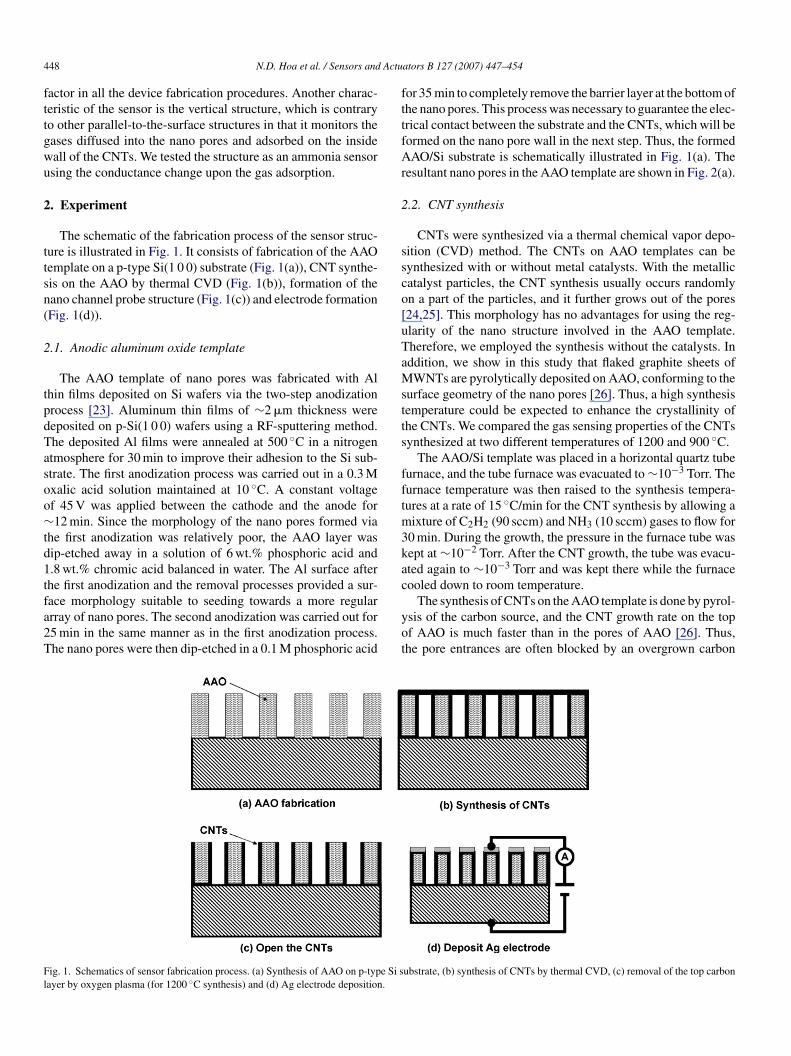
4 Actu
fttgwu
2
ttsn(
2
tpdTasoo∼td1tfa2T
fttfAr
2
ssco[uTaMstts
fftm3kac
Fl
48 N.D. Hoa et al. / Sensors and
actor in all the device fabrication procedures. Another charac-eristic of the sensor is the vertical structure, which is contraryo other parallel-to-the-surface structures in that it monitors theases diffused into the nano pores and adsorbed on the insideall of the CNTs. We tested the structure as an ammonia sensorsing the conductance change upon the gas adsorption.
. Experiment
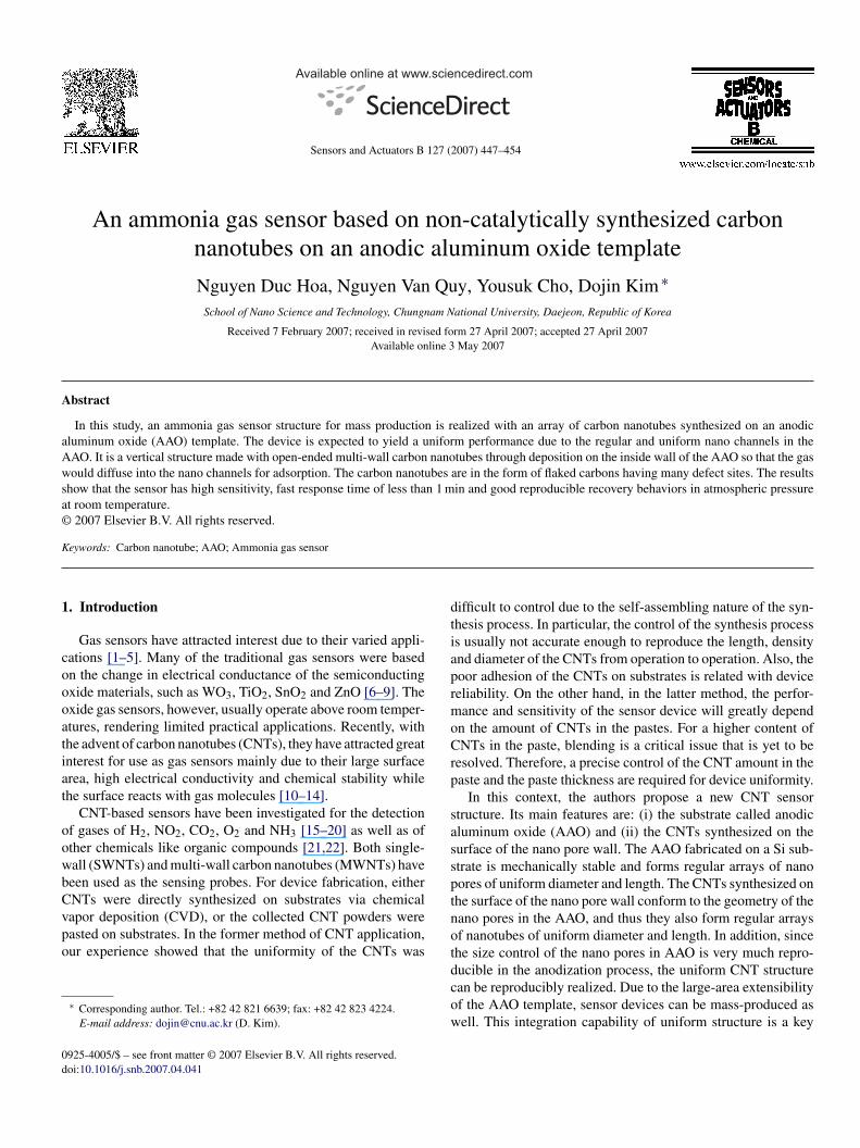
The schematic of the fabrication process of the sensor struc-ure is illustrated in Fig. 1. It consists of fabrication of the AAOemplate on a p-type Si(1 0 0) substrate (Fig. 1(a)), CNT synthe-is on the AAO by thermal CVD (Fig. 1(b)), formation of theano channel probe structure (Fig. 1(c)) and electrode formationFig. 1(d)).
.1. Anodic aluminum oxide template
The AAO template of nano pores was fabricated with Alhin films deposited on Si wafers via the two-step anodizationrocess [23]. Aluminum thin films of ∼2 �m thickness wereeposited on p-Si(1 0 0) wafers using a RF-sputtering method.he deposited Al films were annealed at 500 ◦C in a nitrogentmosphere for 30 min to improve their adhesion to the Si sub-trate. The first anodization process was carried out in a 0.3 Mxalic acid solution maintained at 10 ◦C. A constant voltagef 45 V was applied between the cathode and the anode for12 min. Since the morphology of the nano pores formed via
he first anodization was relatively poor, the AAO layer wasip-etched away in a solution of 6 wt.% phosphoric acid and.8 wt.% chromic acid balanced in water. The Al surface afterhe first anodization and the removal processes provided a sur-
ace morphology suitable to seeding towards a more regularrray of nano pores. The second anodization was carried out for5 min in the same manner as in the first anodization process.he nano pores were then dip-etched in a 0.1 M phosphoric acidyot
ig. 1. Schematics of sensor fabrication process. (a) Synthesis of AAO on p-type Si sayer by oxygen plasma (for 1200 ◦C synthesis) and (d) Ag electrode deposition.
ators B 127 (2007) 447–454
or 35 min to completely remove the barrier layer at the bottom ofhe nano pores. This process was necessary to guarantee the elec-rical contact between the substrate and the CNTs, which will beormed on the nano pore wall in the next step. Thus, the formedAO/Si substrate is schematically illustrated in Fig. 1(a). The
esultant nano pores in the AAO template are shown in Fig. 2(a).
.2. CNT synthesis
CNTs were synthesized via a thermal chemical vapor depo-ition (CVD) method. The CNTs on AAO templates can beynthesized with or without metal catalysts. With the metallicatalyst particles, the CNT synthesis usually occurs randomlyn a part of the particles, and it further grows out of the pores24,25]. This morphology has no advantages for using the reg-larity of the nano structure involved in the AAO template.herefore, we employed the synthesis without the catalysts. Inddition, we show in this study that flaked graphite sheets ofWNTs are pyrolytically deposited on AAO, conforming to the
urface geometry of the nano pores [26]. Thus, a high synthesisemperature could be expected to enhance the crystallinity ofhe CNTs. We compared the gas sensing properties of the CNTsynthesized at two different temperatures of 1200 and 900 ◦C.
The AAO/Si template was placed in a horizontal quartz tubeurnace, and the tube furnace was evacuated to ∼10−3 Torr. Theurnace temperature was then raised to the synthesis tempera-ures at a rate of 15 ◦C/min for the CNT synthesis by allowing aixture of C2H2 (90 sccm) and NH3 (10 sccm) gases to flow for
0 min. During the growth, the pressure in the furnace tube wasept at ∼10−2 Torr. After the CNT growth, the tube was evacu-ted again to ∼10−3 Torr and was kept there while the furnaceooled down to room temperature.
The synthesis of CNTs on the AAO template is done by pyrol-sis of the carbon source, and the CNT growth rate on the topf AAO is much faster than in the pores of AAO [26]. Thus,he pore entrances are often blocked by an overgrown carbon
ubstrate, (b) synthesis of CNTs by thermal CVD, (c) removal of the top carbon
N.D. Hoa et al. / Sensors and Actuators B 127 (2007) 447–454 449
F CNTs
laT1upltrHtsIt
fiS(ot
2
t
wbot
TsgobTcco
3
3
ig. 2. SEM images for (a) the AAO template (insert shows the top view), (b) theynthesis) and (d) the sensor with Ag electrode deposition.
ayer through the shadow effect, while the inside of the poresre voided with CNT formation in the step, as shown in Fig. 2(b).his is the case particularly at a high synthesis temperature of200 ◦C. The top graphite layer then needs to be removed tose the CNTs on the pore wall as the sensing probe. Oxygenlasma etching was then used in order to remove the carbonayer deposited on the top in order to obtain open tube CNTs inhe step, as shown in Fig. 1(c). This was done for 20 min with aadio frequency power of 100 W at a pressure of ∼5 ×10⁻² Torr.owever, the growth kinetics at 900 ◦C was relatively slow, and
he pore entrances could be maintained open during the synthe-is; thus, the oxygen plasma etching process was not required.n the following, we will see the effect of oxygen treatment onhe sensor performance.
The morphology of the synthesized CNTs was examined byeld-emission scanning electron microscopy (FE-SEM, Hitachi-4700), high-resolution transmission electron microscopyHRTEM), micro Raman spectroscopy using a wavelengthf 514.532 nm (Ar-ion laser) and X-ray photoelectron spec-roscopy (XPS) methods.
.3. Device fabrication and characterization
Thin films of Ag were then sputter deposited for the elec-rode. In order to avoid the deposition into the pores, the sample
Cntd
s with blocked pores (1200 ◦C synthesis), (c) the CNTs with open ends (900 ◦C
as tilted at about 30◦ from the normal incidence of the sputteream. The dc sputtering process was carried out at a pressuref 5 × 10⁻³ Torr and a current of 40 mA for 2 min to achieve ahickness of 40 nm (Fig. 1(d)).
The test chamber was first evacuated and then filled with N2.he initial state of the gas sensing test was established by ateady state resistance of the sensor under a nitrogen flow. Theas sensing properties were measured at atmospheric pressuref the gases at room temperature by measuring the resistanceetween the top Ag electrode and the bottom semiconductor.he gases of nitrogen and ammonia were introduced into thehamber at a rate of 500 sccm using mass flow controllers. Theoncentrated ammonia was diluted by mixing with high purityf N2 gas.
. Results and discussion
.1. Carbon nanotube property
The morphologies of the AAO template and the synthesized
NTs investigated with FE-SEM are shown in Fig. 2. The AAOano pores of two-dimensional arrays with uniform size and dis-ribution are illustrated in Fig. 2(a). The diameter and inter-poreistance were about 65 and 105 nm, respectively. The pore length
4 Actuators B 127 (2007) 447–454
wsswadTleawi
eaAswoTdAbsfioscFwotaa[c
cF1Tgv[rcCccpsfit
Fb
Fig. 3. (a) TEM image of the CNTs showing uniform distribution of length and◦
50 N.D. Hoa et al. / Sensors and
as about 1.4 �m. It can be seen that the pores go through theubstrate. The morphology after the CNT synthesis at 1200 ◦C ishown in Fig. 2(b), where the entrances of the pores are blockedith graphite layers due to the accelerated pyrolysis at a rel-
tively high synthesis temperature. The morphology at 900 ◦Cid not show the blocking of the entrances, as shown in Fig. 2(c).he surface with open entrances, after removing the top graphite
ayers by oxygen plasma for 1200 ◦C grown CNTs, was appar-ntly similar to that in Fig. 2(c). The partly cracked sectionlso revealed the CNTs synthesized on the inside of the porealls. The morphology after Ag electrode deposition is shown
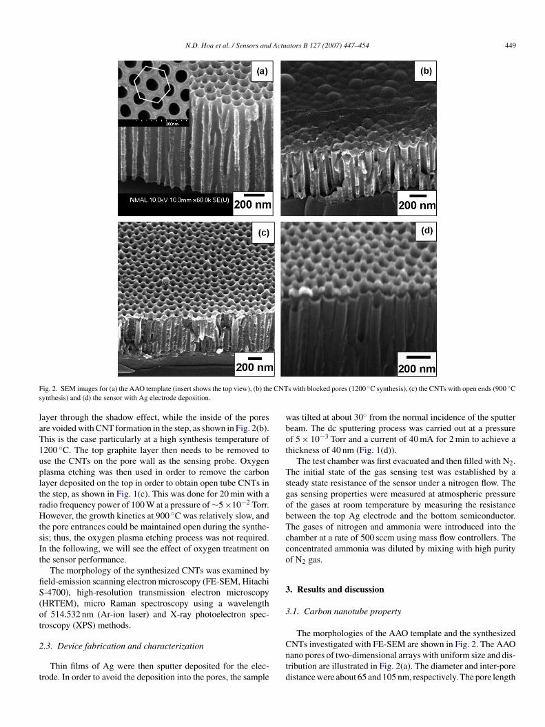
n Fig. 2(d).The crystallinity of the synthesized carbon nanotubes was
xamined with TEM and Raman spectroscopy. Fig. 3(a) showsTEM image of the 1200 ◦C grown CNTs taken after etching theAO template away. This again revealed the uniformity of the
ynthesized CNTs in length and diameter. The average lengthas 1.4 �m according to the length of the pores, but the diameterf the CNTs, ∼70 nm, was a little greater than that of the pores.he latter can be attributed to the shrinkage of the AAO bodyuring the high-temperature CNT synthesis. The as-synthesizedAO template by anodization was mostly in amorphous form,ut it crystallized with high temperature annealing [27]. The highynthesis temperature would certainly offer the annealing effector the crystallization and densification of the AAO, and accord-ngly enlarge pore diameters. Fig. 3(b) shows an HRTEM imagef the MWNT wall grown at 1200 ◦C. The stack of grapheneheets was clearly observed for its thickness of ∼15 nm. Therystallinity was better than that grown at 900 ◦C, as shown inig. 3(c). It is well known that the CNTs synthesized on AAOithout catalyst are formed by flakes of carbon sheet insteadf continuous sheets. One study noted at the higher tempera-ure synthesis that: (i) the sizes of the flaked graphite platesre greater and (ii) the interlayer spacing is ∼0.34 nm, whichgrees well with the spacing of the graphite of high crystallinity28]. Therefore, the present results are great improvements inrystallinity with respect to the lower-temperature synthesis.
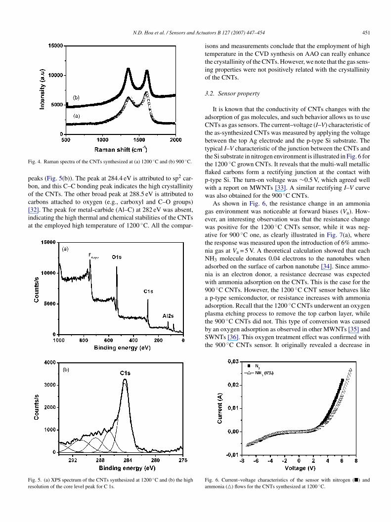
Raman spectroscopy investigation also revealed the highrystalline quality of the synthesized MWNTs, as shown inig. 4. In general, two main peaks were observed at 1288 and592 cm−1. They are called D- and G-bands, respectively [29].he D-band is known to be associated with defective, disorderedraphite or glassy carbon, while the G-band is related to the sp2
ibration in the graphite of a two-dimensional hexagonal lattice30]. The ratio of the peak intensities or IG/ID has often beeneferred to as a measure of the crystallinity of the synthesizedarbon nanotubes [29]. The estimated ratio of ∼1.17 for 1200 ◦CNTs was compatible with that of the MWNTs synthesized onatalytic metals via a thermal CVD method [29]. The spectruman again be compared with that synthesized at a lower tem-erature of 900 ◦C [31], where the smaller IG/ID ratio (∼0.8)uggests more defects in the CNTs. This comparison again con-rms the higher crystallinity of the CNTs for higher synthesis
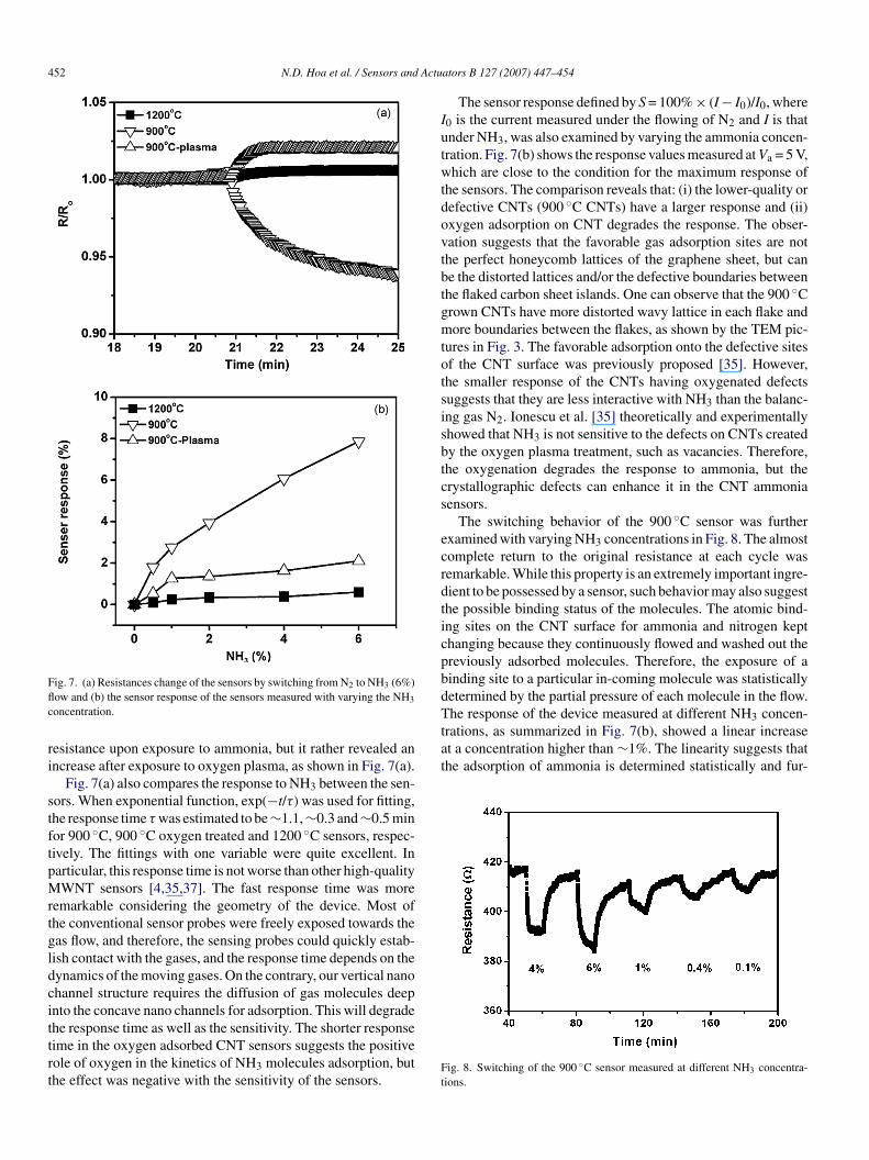
emperature.The XPS examination of the 1200 ◦C CNTs is shown in
ig. 5(a). It shows the presence of aluminum, oxygen and car-on. The analysis of the C 1s peak reveals it as an overlap of some
diameters. HRTEM images of the CNT walls synthesized at (b) 1200 C and (c)900 ◦C.
N.D. Hoa et al. / Sensors and Actu
F
pboc[ia
Fr
ittio
3
aCtbtttflpww
ig. 4. Raman spectra of the CNTs synthesized at (a) 1200 ◦C and (b) 900 ◦C.
eaks (Fig. 5(b)). The peak at 284.4 eV is attributed to sp2 car-on, and this C–C bonding peak indicates the high crystallinityf the CNTs. The other broad peak at 288.5 eV is attributed to
arbons attached to oxygen (e.g., carboxyl and C–O groups)32]. The peak for metal-carbide (Al–C) at 282 eV was absent,ndicating the high thermal and chemical stabilities of the CNTst the employed high temperature of 1200 ◦C. All the compar-ig. 5. (a) XPS spectrum of the CNTs synthesized at 1200 ◦C and (b) the highesolution of the core level peak for C 1s.
gewatnNanw9aaptbSt
Fa
ators B 127 (2007) 447–454 451
sons and measurements conclude that the employment of highemperature in the CVD synthesis on AAO can really enhancehe crystallinity of the CNTs. However, we note that the gas sens-ng properties were not positively related with the crystallinityf the CNTs.
.2. Sensor property
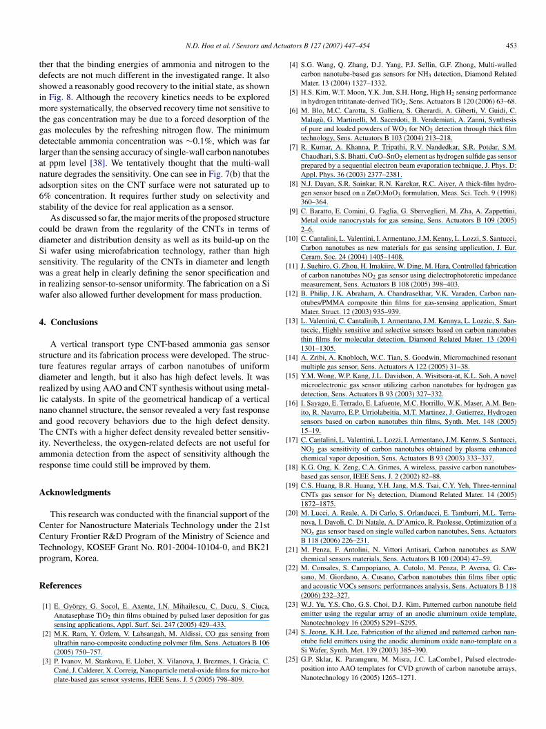
It is known that the conductivity of CNTs changes with thedsorption of gas molecules, and such behavior allows us to useNTs as gas sensors. The current–voltage (I–V) characteristic of
he as-synthesized CNTs was measured by applying the voltageetween the top Ag electrode and the p-type Si substrate. Theypical I–V characteristic of the junction between the CNTs andhe Si substrate in nitrogen environment is illustrated in Fig. 6 forhe 1200 ◦C grown CNTs. It reveals that the multi-wall metallicaked carbons form a rectifying junction at the contact with-type Si. The turn-on voltage was ∼0.5 V, which agreed wellith a report on MWNTs [33]. A similar rectifying I–V curveas also obtained for the 900 ◦C CNTs.As shown in Fig. 6, the resistance change in an ammonia
as environment was noticeable at forward biases (Va). How-ver, an interesting observation was that the resistance changeas positive for the 1200 ◦C CNTs sensor, while it was neg-
tive for 900 ◦C one, as clearly illustrated in Fig. 7(a), wherehe response was measured upon the introduction of 6% ammo-ia gas at Va = 5 V. A theoretical calculation showed that eachH3 molecule donates 0.04 electrons to the nanotubes when
dsorbed on the surface of carbon nanotube [34]. Since ammo-ia is an electron donor, a resistance decrease was expectedith ammonia adsorption on the CNTs. This is the case for the00 ◦C CNTs. However, the 1200 ◦C CNT sensor behaves likep-type semiconductor, or resistance increases with ammonia
dsorption. Recall that the 1200 ◦C CNTs underwent an oxygenlasma etching process to remove the top carbon layer, while
he 900 ◦C CNTs did not. This type of conversion was causedy an oxygen adsorption as observed in other MWNTs [35] andWNTs [36]. This oxygen treatment effect was confirmed withhe 900 ◦C CNTs sensor. It originally revealed a decrease in
ig. 6. Current–voltage characteristics of the sensor with nitrogen (�) andmmonia (�) flows for the CNTs synthesized at 1200 ◦C.
452 N.D. Hoa et al. / Sensors and Actu
Fflc
ri
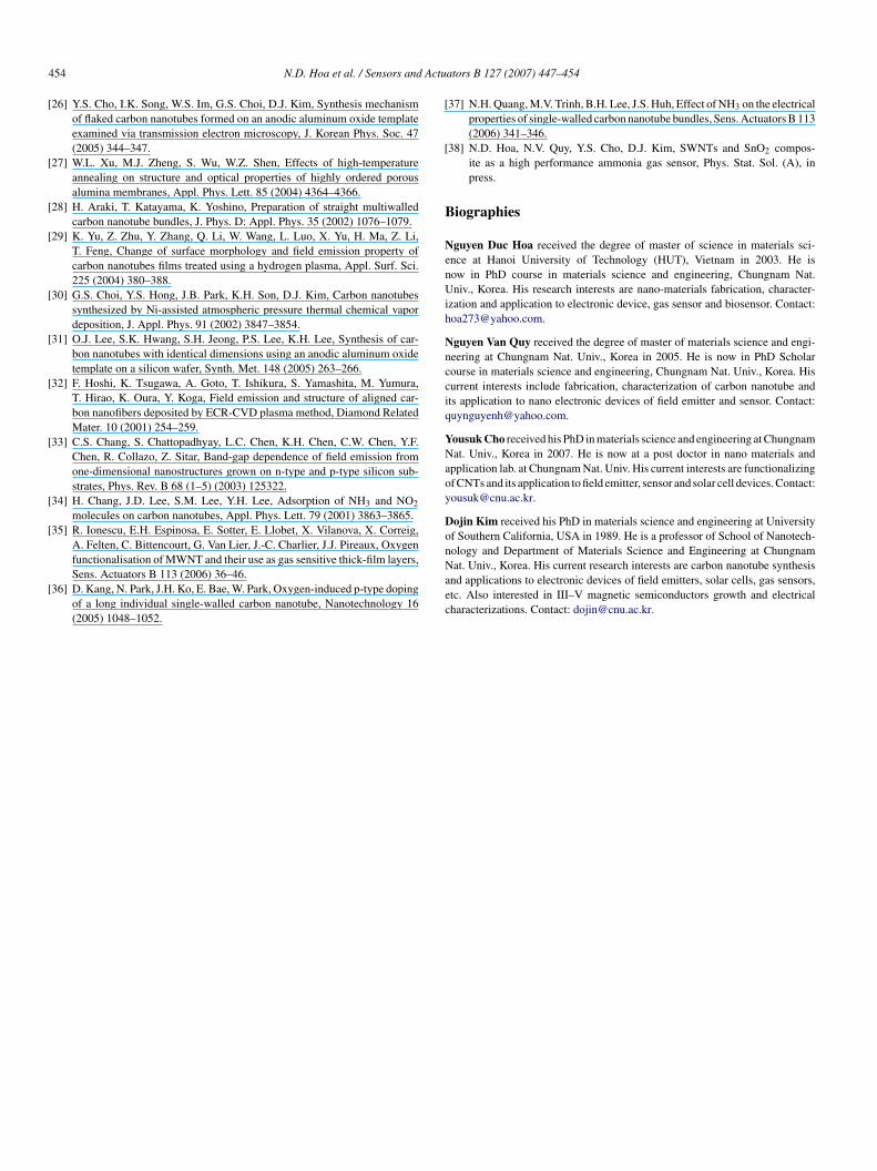
stftpMrtgldcittrt
Iutwtdovtbtgmtotsisbtcs
ecrdticpbdT 3trations, as summarized in Fig. 7(b), showed a linear increaseat a concentration higher than ∼1%. The linearity suggests thatthe adsorption of ammonia is determined statistically and fur-
ig. 7. (a) Resistances change of the sensors by switching from N2 to NH3 (6%)ow and (b) the sensor response of the sensors measured with varying the NH3
oncentration.
esistance upon exposure to ammonia, but it rather revealed anncrease after exposure to oxygen plasma, as shown in Fig. 7(a).
Fig. 7(a) also compares the response to NH3 between the sen-ors. When exponential function, exp(−t/τ) was used for fitting,he response time τ was estimated to be∼1.1,∼0.3 and∼0.5 minor 900 ◦C, 900 ◦C oxygen treated and 1200 ◦C sensors, respec-ively. The fittings with one variable were quite excellent. Inarticular, this response time is not worse than other high-qualityWNT sensors [4,35,37]. The fast response time was more
emarkable considering the geometry of the device. Most ofhe conventional sensor probes were freely exposed towards theas flow, and therefore, the sensing probes could quickly estab-ish contact with the gases, and the response time depends on theynamics of the moving gases. On the contrary, our vertical nanohannel structure requires the diffusion of gas molecules deepnto the concave nano channels for adsorption. This will degrade
he response time as well as the sensitivity. The shorter responseime in the oxygen adsorbed CNT sensors suggests the positiveole of oxygen in the kinetics of NH3 molecules adsorption, buthe effect was negative with the sensitivity of the sensors.Ft
ators B 127 (2007) 447–454
The sensor response defined by S = 100% × (I − I0)/I0, where0 is the current measured under the flowing of N2 and I is thatnder NH3, was also examined by varying the ammonia concen-ration. Fig. 7(b) shows the response values measured at Va = 5 V,hich are close to the condition for the maximum response of
he sensors. The comparison reveals that: (i) the lower-quality orefective CNTs (900 ◦C CNTs) have a larger response and (ii)xygen adsorption on CNT degrades the response. The obser-ation suggests that the favorable gas adsorption sites are nothe perfect honeycomb lattices of the graphene sheet, but cane the distorted lattices and/or the defective boundaries betweenhe flaked carbon sheet islands. One can observe that the 900 ◦Crown CNTs have more distorted wavy lattice in each flake andore boundaries between the flakes, as shown by the TEM pic-
ures in Fig. 3. The favorable adsorption onto the defective sitesf the CNT surface was previously proposed [35]. However,he smaller response of the CNTs having oxygenated defectsuggests that they are less interactive with NH3 than the balanc-ng gas N2. Ionescu et al. [35] theoretically and experimentallyhowed that NH3 is not sensitive to the defects on CNTs createdy the oxygen plasma treatment, such as vacancies. Therefore,he oxygenation degrades the response to ammonia, but therystallographic defects can enhance it in the CNT ammoniaensors.
The switching behavior of the 900 ◦C sensor was furtherxamined with varying NH3 concentrations in Fig. 8. The almostomplete return to the original resistance at each cycle wasemarkable. While this property is an extremely important ingre-ient to be possessed by a sensor, such behavior may also suggesthe possible binding status of the molecules. The atomic bind-ng sites on the CNT surface for ammonia and nitrogen kepthanging because they continuously flowed and washed out thereviously adsorbed molecules. Therefore, the exposure of ainding site to a particular in-coming molecule was statisticallyetermined by the partial pressure of each molecule in the flow.he response of the device measured at different NH concen-
ig. 8. Switching of the 900 ◦C sensor measured at different NH3 concentra-ions.
Actu
tdsimtgdlana6s
cdSswiw
4
stdrlnaTiar
A
CCTp
R
[
[
[
[
[
[
[
[
[
[
[
[
[
[
[
N.D. Hoa et al. / Sensors and
her that the binding energies of ammonia and nitrogen to theefects are not much different in the investigated range. It alsohowed a reasonably good recovery to the initial state, as shownn Fig. 8. Although the recovery kinetics needs to be explored
ore systematically, the observed recovery time not sensitive tohe gas concentration may be due to a forced desorption of theas molecules by the refreshing nitrogen flow. The minimumetectable ammonia concentration was ∼0.1%, which was fararger than the sensing accuracy of single-wall carbon nanotubest ppm level [38]. We tentatively thought that the multi-wallature degrades the sensitivity. One can see in Fig. 7(b) that thedsorption sites on the CNT surface were not saturated up to% concentration. It requires further study on selectivity andtability of the device for real application as a sensor.
As discussed so far, the major merits of the proposed structureould be drawn from the regularity of the CNTs in terms ofiameter and distribution density as well as its build-up on thei wafer using microfabrication technology, rather than highensitivity. The regularity of the CNTs in diameter and lengthas a great help in clearly defining the senor specification and
n realizing sensor-to-sensor uniformity. The fabrication on a Siafer also allowed further development for mass production.
. Conclusions
A vertical transport type CNT-based ammonia gas sensortructure and its fabrication process were developed. The struc-ure features regular arrays of carbon nanotubes of uniformiameter and length, but it also has high defect levels. It wasealized by using AAO and CNT synthesis without using metal-ic catalysts. In spite of the geometrical handicap of a verticalano channel structure, the sensor revealed a very fast responsend good recovery behaviors due to the high defect density.he CNTs with a higher defect density revealed better sensitiv-
ty. Nevertheless, the oxygen-related defects are not useful formmonia detection from the aspect of sensitivity although theesponse time could still be improved by them.
cknowledgments
This research was conducted with the financial support of theenter for Nanostructure Materials Technology under the 21stentury Frontier R&D Program of the Ministry of Science andechnology, KOSEF Grant No. R01-2004-10104-0, and BK21rogram, Korea.
eferences
[1] E. Gyorgy, G. Socol, E. Axente, I.N. Mihailescu, C. Ducu, S. Ciuca,Anatasephase TiO2 thin films obtained by pulsed laser deposition for gassensing applications, Appl. Surf. Sci. 247 (2005) 429–433.
[2] M.K. Ram, Y. Ozlem, V. Lahsangah, M. Aldissi, CO gas sensing from
ultrathin nano-composite conducting polymer film, Sens. Actuators B 106(2005) 750–757.[3] P. Ivanov, M. Stankova, E. Llobet, X. Vilanova, J. Brezmes, I. Gracia, C.Cane, J. Calderer, X. Correig, Nanoparticle metal-oxide films for micro-hotplate-based gas sensor systems, IEEE Sens. J. 5 (2005) 798–809.
[
ators B 127 (2007) 447–454 453
[4] S.G. Wang, Q. Zhang, D.J. Yang, P.J. Sellin, G.F. Zhong, Multi-walledcarbon nanotube-based gas sensors for NH3 detection, Diamond RelatedMater. 13 (2004) 1327–1332.
[5] H.S. Kim, W.T. Moon, Y.K. Jun, S.H. Hong, High H2 sensing performancein hydrogen trititanate-derived TiO2, Sens. Actuators B 120 (2006) 63–68.
[6] M. Blo, M.C. Carotta, S. Galliera, S. Gherardi, A. Giberti, V. Guidi, C.Malagu, G. Martinelli, M. Sacerdoti, B. Vendemiati, A. Zanni, Synthesisof pure and loaded powders of WO3 for NO2 detection through thick filmtechnology, Sens. Actuators B 103 (2004) 213–218.
[7] R. Kumar, A. Khanna, P. Tripathi, R.V. Nandedkar, S.R. Potdar, S.M.Chaudhari, S.S. Bhatti, CuO–SnO2 element as hydrogen sulfide gas sensorprepared by a sequential electron beam evaporation technique, J. Phys. D:Appl. Phys. 36 (2003) 2377–2381.
[8] N.J. Dayan, S.R. Sainkar, R.N. Karekar, R.C. Aiyer, A thick-film hydro-gen sensor based on a ZnO:MoO3 formulation, Meas. Sci. Tech. 9 (1998)360–364.
[9] C. Baratto, E. Comini, G. Faglia, G. Sberveglieri, M. Zha, A. Zappettini,Metal oxide nanocrystals for gas sensing, Sens. Actuators B 109 (2005)2–6.
10] C. Cantalini, L. Valentini, I. Armentano, J.M. Kenny, L. Lozzi, S. Santucci,Carbon nanotubes as new materials for gas sensing application, J. Eur.Ceram. Soc. 24 (2004) 1405–1408.
11] J. Suehiro, G. Zhou, H. Imakiire, W. Ding, M. Hara, Controlled fabricationof carbon nanotubes NO2 gas sensor using dielectrophotoretic impedancemeasurement, Sens. Actuators B 108 (2005) 398–403.
12] B. Philip, J.K. Abraham, A. Chandrasekhar, V.K. Varaden, Carbon nan-otubes/PMMA composite thin films for gas-sensing application, SmartMater. Struct. 12 (2003) 935–939.
13] L. Valentini, C. Cantalinib, I. Armentano, J.M. Kennya, L. Lozzic, S. San-tuccic, Highly sensitive and selective sensors based on carbon nanotubesthin films for molecular detection, Diamond Related Mater. 13 (2004)1301–1305.
14] A. Zribi, A. Knobloch, W.C. Tian, S. Goodwin, Micromachined resonantmultiple gas sensor, Sens. Actuators A 122 (2005) 31–38.
15] Y.M. Wong, W.P. Kang, J.L. Davidson, A. Wisitsora-at, K.L. Soh, A novelmicroelectronic gas sensor utilizing carbon nanotubes for hydrogen gasdetection, Sens. Actuators B 93 (2003) 327–332.
16] I. Sayago, E. Terrado, E. Lafuente, M.C. Horrillo, W.K. Maser, A.M. Ben-ito, R. Navarro, E.P. Urriolabeitia, M.T. Martinez, J. Gutierrez, Hydrogensensors based on carbon nanotubes thin films, Synth. Met. 148 (2005)15–19.
17] C. Cantalini, L. Valentini, L. Lozzi, I. Armentano, J.M. Kenny, S. Santucci,NO2 gas sensitivity of carbon nanotubes obtained by plasma enhancedchemical vapor deposition, Sens. Actuators B 93 (2003) 333–337.
18] K.G. Ong, K. Zeng, C.A. Grimes, A wireless, passive carbon nanotubes-based gas sensor, IEEE Sens. J. 2 (2002) 82–88.
19] C.S. Huang, B.R. Huang, Y.H. Jang, M.S. Tsai, C.Y. Yeh, Three-terminalCNTs gas sensor for N2 detection, Diamond Related Mater. 14 (2005)1872–1875.
20] M. Lucci, A. Reale, A. Di Carlo, S. Orlanducci, E. Tamburri, M.L. Terra-nova, I. Davoli, C. Di Natale, A. D’Amico, R. Paolesse, Optimization of aNOx gas sensor based on single walled carbon nanotubes, Sens. ActuatorsB 118 (2006) 226–231.
21] M. Penza, F. Antolini, N. Vittori Antisari, Carbon nanotubes as SAWchemical sensors materials, Sens. Actuators B 100 (2004) 47–59.
22] M. Consales, S. Campopiano, A. Cutolo, M. Penza, P. Aversa, G. Cas-sano, M. Giordano, A. Cusano, Carbon nanotubes thin films fiber opticand acoustic VOCs sensors: performances analysis, Sens. Actuators B 118(2006) 232–327.
23] W.J. Yu, Y.S. Cho, G.S. Choi, D.J. Kim, Patterned carbon nanotube fieldemitter using the regular array of an anodic aluminum oxide template,Nanotechnology 16 (2005) S291–S295.
24] S. Jeong, K.H. Lee, Fabrication of the aligned and patterned carbon nan-
otube field emitters using the anodic aluminum oxide nano-template on aSi Wafer, Synth. Met. 139 (2003) 385–390.25] G.P. Sklar, K. Paramguru, M. Misra, J.C. LaCombe1, Pulsed electrode-position into AAO templates for CVD growth of carbon nanotube arrays,Nanotechnology 16 (2005) 1265–1271.
4 Actu
[
[
[
[
[
[
[
[
[
[
[
[
[
B
NenUih
Nncciq
YNaoy
Donology and Department of Materials Science and Engineering at Chungnam
54 N.D. Hoa et al. / Sensors and
26] Y.S. Cho, I.K. Song, W.S. Im, G.S. Choi, D.J. Kim, Synthesis mechanismof flaked carbon nanotubes formed on an anodic aluminum oxide templateexamined via transmission electron microscopy, J. Korean Phys. Soc. 47(2005) 344–347.
27] W.L. Xu, M.J. Zheng, S. Wu, W.Z. Shen, Effects of high-temperatureannealing on structure and optical properties of highly ordered porousalumina membranes, Appl. Phys. Lett. 85 (2004) 4364–4366.
28] H. Araki, T. Katayama, K. Yoshino, Preparation of straight multiwalledcarbon nanotube bundles, J. Phys. D: Appl. Phys. 35 (2002) 1076–1079.
29] K. Yu, Z. Zhu, Y. Zhang, Q. Li, W. Wang, L. Luo, X. Yu, H. Ma, Z. Li,T. Feng, Change of surface morphology and field emission property ofcarbon nanotubes films treated using a hydrogen plasma, Appl. Surf. Sci.225 (2004) 380–388.
30] G.S. Choi, Y.S. Hong, J.B. Park, K.H. Son, D.J. Kim, Carbon nanotubessynthesized by Ni-assisted atmospheric pressure thermal chemical vapordeposition, J. Appl. Phys. 91 (2002) 3847–3854.
31] O.J. Lee, S.K. Hwang, S.H. Jeong, P.S. Lee, K.H. Lee, Synthesis of car-bon nanotubes with identical dimensions using an anodic aluminum oxidetemplate on a silicon wafer, Synth. Met. 148 (2005) 263–266.
32] F. Hoshi, K. Tsugawa, A. Goto, T. Ishikura, S. Yamashita, M. Yumura,T. Hirao, K. Oura, Y. Koga, Field emission and structure of aligned car-bon nanofibers deposited by ECR-CVD plasma method, Diamond RelatedMater. 10 (2001) 254–259.
33] C.S. Chang, S. Chattopadhyay, L.C. Chen, K.H. Chen, C.W. Chen, Y.F.Chen, R. Collazo, Z. Sitar, Band-gap dependence of field emission fromone-dimensional nanostructures grown on n-type and p-type silicon sub-strates, Phys. Rev. B 68 (1–5) (2003) 125322.
34] H. Chang, J.D. Lee, S.M. Lee, Y.H. Lee, Adsorption of NH3 and NO2
molecules on carbon nanotubes, Appl. Phys. Lett. 79 (2001) 3863–3865.35] R. Ionescu, E.H. Espinosa, E. Sotter, E. Llobet, X. Vilanova, X. Correig,
A. Felten, C. Bittencourt, G. Van Lier, J.-C. Charlier, J.J. Pireaux, Oxygen
functionalisation of MWNT and their use as gas sensitive thick-film layers,Sens. Actuators B 113 (2006) 36–46.36] D. Kang, N. Park, J.H. Ko, E. Bae, W. Park, Oxygen-induced p-type dopingof a long individual single-walled carbon nanotube, Nanotechnology 16(2005) 1048–1052.
Naec
ators B 127 (2007) 447–454
37] N.H. Quang, M.V. Trinh, B.H. Lee, J.S. Huh, Effect of NH3 on the electricalproperties of single-walled carbon nanotube bundles, Sens. Actuators B 113(2006) 341–346.
38] N.D. Hoa, N.V. Quy, Y.S. Cho, D.J. Kim, SWNTs and SnO2 compos-ite as a high performance ammonia gas sensor, Phys. Stat. Sol. (A), inpress.
iographies
guyen Duc Hoa received the degree of master of science in materials sci-nce at Hanoi University of Technology (HUT), Vietnam in 2003. He isow in PhD course in materials science and engineering, Chungnam Nat.niv., Korea. His research interests are nano-materials fabrication, character-
zation and application to electronic device, gas sensor and biosensor. Contact:[email protected].
guyen Van Quy received the degree of master of materials science and engi-eering at Chungnam Nat. Univ., Korea in 2005. He is now in PhD Scholarourse in materials science and engineering, Chungnam Nat. Univ., Korea. Hisurrent interests include fabrication, characterization of carbon nanotube andts application to nano electronic devices of field emitter and sensor. Contact:[email protected].
ousuk Cho received his PhD in materials science and engineering at Chungnamat. Univ., Korea in 2007. He is now at a post doctor in nano materials and
pplication lab. at Chungnam Nat. Univ. His current interests are functionalizingf CNTs and its application to field emitter, sensor and solar cell devices. Contact:[email protected].
ojin Kim received his PhD in materials science and engineering at Universityf Southern California, USA in 1989. He is a professor of School of Nanotech-
at. Univ., Korea. His current research interests are carbon nanotube synthesisnd applications to electronic devices of field emitters, solar cells, gas sensors,tc. Also interested in III–V magnetic semiconductors growth and electricalharacterizations. Contact: [email protected].