Synthesis of carbon nanotubes within porous anodic alumina ...
198
HAL Id: tel-01312414 https://hal.archives-ouvertes.fr/tel-01312414 Submitted on 6 May 2016 HAL is a multi-disciplinary open access archive for the deposit and dissemination of sci- entific research documents, whether they are pub- lished or not. The documents may come from teaching and research institutions in France or abroad, or from public or private research centers. L’archive ouverte pluridisciplinaire HAL, est destinée au dépôt et à la diffusion de documents scientifiques de niveau recherche, publiés ou non, émanant des établissements d’enseignement et de recherche français ou étrangers, des laboratoires publics ou privés. Synthesis of carbon nanotubes within porous anodic alumina templates for electronic applications Leandro Nicolas Sacco To cite this version: Leandro Nicolas Sacco. Synthesis of carbon nanotubes within porous anodic alumina templates for electronic applications. Materials Science [cond-mat.mtrl-sci]. Ecole Polytechnique, 2015. English. tel-01312414
-
Upload
khangminh22 -
Category
Documents
-
view
1 -
download
0
Transcript of Synthesis of carbon nanotubes within porous anodic alumina ...

HAL Id: tel-01312414https://hal.archives-ouvertes.fr/tel-01312414
Submitted on 6 May 2016
HAL is a multi-disciplinary open accessarchive for the deposit and dissemination of sci-entific research documents, whether they are pub-lished or not. The documents may come fromteaching and research institutions in France orabroad, or from public or private research centers.
L’archive ouverte pluridisciplinaire HAL, estdestinée au dépôt et à la diffusion de documentsscientifiques de niveau recherche, publiés ou non,émanant des établissements d’enseignement et derecherche français ou étrangers, des laboratoirespublics ou privés.
Synthesis of carbon nanotubes within porous anodicalumina templates for electronic applications
Leandro Nicolas Sacco
To cite this version:Leandro Nicolas Sacco. Synthesis of carbon nanotubes within porous anodic alumina templates forelectronic applications. Materials Science [cond-mat.mtrl-sci]. Ecole Polytechnique, 2015. English.�tel-01312414�

Doctoral thesis in Physics
Synthesis of carbon nanotubes within porous
anodic alumina templates for electronic
applications
Leandro Nicolás Sacco

Thèse
Présentée pour obtenir le grade
DOCTEUR DE L’ECOLE POLYTECHNIQUE
Spécialité : Physique
Par
Leandro Nicolás SACCO
Thèse soutenue le 15 décembre 2015devant le jury composé de :

Para Roxane,
para Léa,
y para los que vendrán…

Acknowledgements
First of all I would like to thank to Costel-Sorin Cojocaru and Bérengère Lebental for the
opportunity that they gave me in order to carry out my Ph.D thesis at the Laboratoire de
Physique des Interfaces et des Couches Minces (LPICM). Opportunity is something that you can
never give back.
In particular, I want to thank to my thesis supervisor Costel to help me and advise me to
perform the steps taken at me arrival in France. In the scientific plane, I want to highlight his
open mind in order to listen my ideas and construct together new approaches to solve
problems. Finally I want to express my gratitude for his encouragement in hard times.
I am also grateful to my co-supervisor Marc Châtelet for his predisposition and help, he
was always present in order to invest his time and ready for the discussion, on the other hand
Marc was a great allied for the writing of the present work.
Additionally, I want to be thankful with all the former and present members of the
NanoMaDe team. In different stages, all of them support me and help me. Especially, I want to
thank to Ki-Hwan Kim, Emmanuel Lefeuvre and Lucie Leveau which help with the first steps
concerning the experimental procedures. Also I want to thanks to the support and help of
Heechul Woo, Fatima Bouanis, Laurent Baraton and David Brunel. The present work it would
not have been possible without the constant technical presence of Léo Caristan and Garry Rose,
their help have been invaluable. Both of them, always they rescued me when technical
problems appeared. Finally, I would like to express all my esteem to Ileana Florea that not only
help me with the preparation of the obtained superb TEM images and their interpretation, but
also was there for all discussions that have paved a friendship.
I want to express my sincere thanks to all the LPICM members that directly or indirectly
help me to perform my work without any concern. In particular to Pere Roca i Cabarrocas that
always was present and following my thesis. Also many members helped me in different
instance with the most diverse problems such as: Gabriela Medina, Laurence Corbel, Eric
Paillassa and Cyril Jadaud.
The Ph.D results a crucial step for the professional formation of a researcher. In my case
such achievement also was possible due to the previous educational formation that I forged in
my native country. I want to highlight that I was form under a free university system, such
educational system largely provided me the tools to carry out the Ph.D thesis. Therefore I
always will recognize to the University of Buenos Aires and all the teachers that helped and
formed me as scientific researcher, in especial to Silvia Goyanes who introduced me to the
astonishing nanotechnology universe.
Always, I will be honored and thankful to the Ecole Polytechnique to embrace me and
allows performing my thesis in such environment of excellence.
I want to thanks to my family that help me and always support me without any
condition to reach all my dreams. Especialmente, MUCHAS GRACIAS papá y mamá por toda la
ayuda desde siempre y sin importar las distancias siempre estarán conmigo.
Finally, the last person whom I want to put into words my gratitude for all the
unconditional support, is to mon amour, ma famille, mon âme sœur, Roxane Alarcón who
appeared magically the 30th March 2014 and from that time we lived amazing things and we
continue for sure.

Contents
INTRODUCTION ............................................................................................................. 1
References ................................................................................................................................................................ 5
CHAPTER 1. ..................................................................................................................... 6
POROUS ANODIC ALUMINA TEMPLATES .............................................................. 6
1.1 The formation process of PAA ................................................................................................................... 7 1.2.1 Species migration and the grow mechanism ........................................................................................ 9 1. 2. 2 Potentiostatic and Galvanostatic procedures .................................................................................. 11 1.2.3 Stages during the pore growth formation ............................................................................................ 12 1.2.4 The Two Step anodization process .......................................................................................................... 14 1.2.5 Differences between the simple anodization and the two step anodization .................... 17
1.3 Factors that influence the PAA structure ............................................................................................ 19 1.3.1 Anodization voltage .......................................................................................................................................... 20 1.3.2 Type and concentration electrolytes ...................................................................................................... 21 1.3.3 Anodized duration ............................................................................................................................................. 23 1.3.4 Electrolyte temperature ..................................................................................................................................... 24 1.3.5 Aluminum substrate ............................................................................................................................................. 25
1.4 Lateral-PAA templates ............................................................................................................................... 26
1.5 Experimental procedure ........................................................................................................................... 27 1.5.1 Anodization experimental set-up ................................................................................................................... 28 1.5.2 Electropolishing process .................................................................................................................................... 29 1.5.3 Two anodization process ................................................................................................................................... 30 1.5.5 PAA-Lateral templates type fabrication ....................................................................................................... 33 1.5.6 Characterization techniques of the PAA structure .................................................................................. 37
1.6 Fabrication and Characterization of the PAA templates ............................................................... 38 1.6.1 Measurement of the geometrical features of the PAA structures...................................................... 39
1.6.1.1 Porosity ............................................................................................................................................................. 40 1.6.1.2 Circularity ......................................................................................................................................................... 41 1.6.1.3 Pore ordering degree ................................................................................................................................... 41
1.6.2 Image processing ................................................................................................................................................... 43

1.6.3 Influence of the anodization parameters on the PAA structure ......................................................... 44 1.6.3.1 Anodization voltage ..................................................................................................................................... 44 1.6.3.2 Electrolyte temperature ............................................................................................................................. 49 1.6.3.3 Different single crystal orientation ........................................................................................................ 51
1.6.4 Lateral-PAA fabrication....................................................................................................................................... 56 1.6.4.1 Influence of the temperature over the lateral-PAA structure ......................................................... 56 1.6.4.2 Thinning process in lateral-PAA templates ............................................................................................ 58
1.7 Conclusions .................................................................................................................................................... 61
References ............................................................................................................................................................. 62
CHAPTER 2. ................................................................................................................... 66
CATALYST ELECTRODEPOSITION INSIDE PAA ................................................. 66
2.1 Electrodeposition process ........................................................................................................................ 66
2.2 The principle of the electrodeposition process ............................................................................... 68 2.2.1 The electrodeposition process within PAA templates ........................................................................... 70
2.3 Experimental setup and parameters involved in the electrodeposition procedure .......... 72 2.3.1 Three electrode configuration system .......................................................................................................... 72 2.3.2 Experimental setup ............................................................................................................................................... 73
2.4 The metal deposition at the bottom of the pores............................................................................. 74 2.4.1 Influence of the barrier layer thickness over the metal electrodeposition ................................... 75 2.4.2 Operational range of the metal electrodeposition depending on the anodization voltage .... 79 2.4.3 Influence of the pore length on the electrodeposition process .......................................................... 83 2.4.4 Evidence of metal nanoparticles deposited at the bottom of the pores ......................................... 85 2.4.5 Number of catalytic nanoparticles electrodeposited per pore ........................................................... 87
2.6 Conclusions .................................................................................................................................................... 92
References ............................................................................................................................................................. 94
CHAPTER 3. ................................................................................................................... 96
SYNTHESIS OF CARBON NANOTUBES WITHIN PAA TEMPLATES ............... 96
3.1 Characteristics and physical properties of carbon nanotubes ................................................... 97 3.1.1 Electronic properties ........................................................................................................................................... 99 3.1.2 Optical properties ............................................................................................................................................... 100

3.1.3 Mechanical properties ...................................................................................................................................... 102 3.1.4 Thermal properties ............................................................................................................................................ 103
3.2 Carbon nanotubes based devices ........................................................................................................ 104 3.2.1 CNTs-Based sensors .......................................................................................................................................... 106 3.2.2 CNTs-based interconnects .............................................................................................................................. 107 3.2.3 Field emission devices ...................................................................................................................................... 108
3.3 Synthesis of carbon nanotubes ............................................................................................................. 110 3.3.1 Chemical Vapor Deposition (CVD) method .............................................................................................. 112 3.3.2 Catalyst for the synthesis of CNTs ............................................................................................................... 113 3.3.2 Organized growth of carbon nanotubes .................................................................................................... 115
3.4 Experimental set-up ................................................................................................................................. 116
3.5 Results of the synthesis of carbon nanotubes within vertical-PAA templates .................... 119 3.5.1 Nanoparticles pretreatment........................................................................................................................... 120 3.5.3 Influence of the branch structure over the synthesis of CNTs ......................................................... 124 3.5.4 Evolution of CNTs inside the PAA templates .......................................................................................... 127 3.5.5 Effect of the pore length ................................................................................................................................... 136
3.6 Synthesis of CNTs inside lateral-PAA templates ............................................................................ 139 3.6.1 Synthesis of CNTs into lateral PAA templates fabricated with different thinning process
conditions ......................................................................................................................................................................... 139 3.6.2 Temperature influence on the CNTs growth ........................................................................................... 141
3.7 Conclusions .................................................................................................................................................. 142
References ........................................................................................................................................................... 144
CHAPTER 4. ................................................................................................................ 151
THE APPLICATIONS OF DEVICES BASED ON CNTS GROWTH INSIDE PAA
TEMPLATES ............................................................................................................... 151
4.1 Devices fabrication and characterization......................................................................................... 152 4.1.1 Lateral-PAA devices preparation ................................................................................................................. 152 4.1.2 Vertical-PAA devices preparation................................................................................................................ 154 4.2.1 Impact of the Contact mode of CNTs on the electrical behavior ..................................................... 157 4.2.2 Devices with capping layer ............................................................................................................................. 160 4.2.3 Metal decoration on devices without capping layer ............................................................................ 167
4.3 Vertical-PAA devices ................................................................................................................................ 171 4.3.1 Electrical behavior ............................................................................................................................................. 171

4.3.2 Light Illumination ............................................................................................................................................... 176 4.3.3 Humidity Sensing ................................................................................................................................................ 177
References ........................................................................................................................................................... 183
CONCLUSIONS & PROSPECTIVE .......................................................................... 185

1
Introduction
The Nobel Prize winner in physics, Richard Feynman, asked the following question,
during a talk that he has given for the annual meeting of the American Physical Society in 1959:
Why cannot we write the entire 24 volumes of the Encyclopedia Britannica on the head of a
pin?
Basically the idea of manipulating the matter at the atomic scale was introduced.
However we cannot manipulate atoms as easily as objects in the macroscopy world. Therefore
many scientists started to fabricate and observe objects with size smaller than a 10-8 meters
which opened a new domain in the world of science named nanotechnology.
There are a wide variety of nano-objects that can be classified based on their inherent
structure: nanoparticles, nanowires, nanotubes, nanoribbons, nanosheets and so on and so
forth. The common denominator of such structures is that they possess at least one
characteristic length in the nanometric scale. The discovery of carbon nanotubes (CNTs) in 1991
was one of the most emblematic ones, due to the unique electrical, mechanical, thermal and
optical properties. For instance CNTs have been proposed as candidate for a space elevator
cable [1].
Despite the promising and astonishing properties of such nanometric structures, the
critical subject of their manipulation remains as the primordial challenge. Very expensive and
time consuming techniques, like e-beam lithography, have been developed in order to precisely
control the growth of nanostructures, or to obtain a nano-objet from the etching of a bulk
material. Such techniques are suitable as probes of concepts, however the atom-by-atom
bottom-up approach is unrealistic because they are not compatible with a massive integration.

Introduction
2
Therefore many efforts have been focused in order to fabricate devices by bottom-up approach
where molecule-by-molecule follows the guidelines of supramolecular multi-component. On
the other hand the miniaturization of the fabricated devices is reaching a bottleneck since the
scaling-down for enhancing their performance is close to the limitation. Consequently the
efforts concentrated to achieve device fabrication by continuous miniaturization leads to
performances with a decline in the electrical conductivity transports values and a significantly
loss of reliability. Therefore different strategies have been explored to overcome the presented
problematics associated with the scaling-down process of the fabricated nanodevices. l
The control growth of the nanostructures (mainly in terms of length, growth rate and
position) that form the device, plays a critical role in the further device performance. Self-
organized templates provide several advantages in order to control the growth nanostructures.
For instance track-etched polycarbonate [2], block copolymers [3] or DNA origami [4], and
porous anodic alumina (PAA) templates have been widely studied. In particular PAA template
has become a commonly used template with potential applications in a wide range of areas,
owing to their easy and cheap implementation, geometry versatility, mechanically robustness,
and potential application in large surfaces. Typically, PAA templates present a vertical pore
structure with pore diameters of the order of nanometers and length up to millimeters; the
ideal pore organization is arranged on a honeycomb pattern. The fabrication is performed by
the anodization of aluminum which allows tuning of the pore structure characteristics by the
variation of the parameters involved in their fabrication. Taking advantage of the well-ordered
structure and the confinement imposed by the pores, these templates are utilized for the
growth of carbon nanotubes and silicon nanowires. The growth of such nanostructures inside
PAA paves the way to high densities of individual connection per cm2 [5]. Several applications
have been reported by the template-assisted growth of nanostructures in different domains,
for instance field emitters [6], gas sensors [7], data storage media [8], solar cells fabrication [9],
and for Lithium ion batteries [10].
The main constraint of the growth of nanostructures within PAA is given by the oxide
barrier which remains at the bottom of the pores, such barrier could present difficulties for the

Introduction
3
catalyst deposition required for a further synthesis of nanostructures. Different strategies have
been adopted in order to overcome this problem, for instance the detachment of the PAA
structure from the supporting aluminum, or by the etching of such barrier that allows an easy
collective contact compatible with electronic devices fabrication since aluminum acts as a
possible contact.
In the present work, we take both advantages of the PAA templates and carbon
nanotubes for the device fabrications. Two different templates based approaches have been
adopted, exploiting in each case their characteristic configuration. The device fabrication based
on CNTs grown on conventional vertical-PAA templates doesn’t require costly and complicated
procedures and are compatible with large area devices, in contrast the active element for a
further device application is confined inside the pores which can limit the wide range of
application. On the other hand CNTs have been grown inside lateral-PAA templates, such kind
of templates are compatible with the planar circuit integration, in addition the tubes are
between two terminals which offers the possibility of light illumination or further CNT
functionalization. For the fabrication of such devices more technological steps are involved
including lithography stages. With the vertical-PAA templates humidity sensing devices are
presented and also the interconnection main characteristics circuits are established. The
lateral-PAA fabricated shown an unequalled photonic response under light illumination
exhibiting potential application in the photodetection and photovoltaic domain.
Complementary in each device step, fundamental mechanism concerning the anodization
process and the synthesis of carbon nanotubes have been studied.
Regarding the device fabrication several steps have to be performed, one of the
principal aims of the present work is to obtain a deep understanding on the processes involved
in their fabrication, in order to improve the potentialities of the fabricated device.
Consequently, the study of the anodization process and the impact of the fabrication
parameters on the PAA structure have been addressed. Subsequently the interaction between
the catalyst depositions inside the template is studied, taking into account that such interaction
will mainly define the growth of the carbon nanostructures. Once such processes are controlled

Introduction
4
and optimized, the second main goal of the present work is dealt with: the characterization of
the fabricated devices ant the exploration of different application domain depending on the
device characteristics.
The structure of the present thesis follows the road towards the device fabrication from
the beginning of the template fabrication towards the proper device characterization. Firstly,
the main features of the structural of PAA templates and the influence of the anodization
parameters on the geometrical features are introduced in the first chapter. Their formation
process and the experimental methods utilized in order to tune the template are investigated.
The second chapter is devoted at the study of the electrodeposition process inside the pore
structure. Moreover we utilized the nanoparticle deposition as fingerprint of the pore structure
which allows the analysis of the best pore structural configuration for the synthesis of CNTs. In
the third chapter the synthesis conditions are study in order to obtain the maximum number of
CNTs per unit of area, a highly desire property towards the device fabrication. The performing
sensing results of the fabricated devices and the mechanisms responsible of the sensing
activities are summarized in the chapter four. The different fabricated devices in their two
configurations, lateral and vertical, are electrically and optoelectronically analyzed, in addition
for vertical devices the humidity measurements are executed. Finally, the last chapter presents
the general conclusion of the work and the prospective of the potentialities of the devices
fabricated using PAA templates

Introduction
5
References
1. Edwards, B.C., The NIAC Space Elevator Program. Space Elevators and Tethers, 2002: p. 84-90. 2. Dauginet-De Pra, L., et al., Fabrication of a new generation of track-etched templates and their
use for the synthesis of metallic and organic nanostructures. Nuclear Instruments and Methods in Physics Research Section B: Beam Interactions with Materials and Atoms, 2002. 196(1–2): p. 81-88.
3. Lee, D.H., et al., Hierarchically Organized Carbon Nanotube Arrays from Self‐Assembled Block Copolymer Nanotemplates. Advanced Materials, 2008. 20(13): p. 2480-2485.
4. Maune, H.T., et al., Self-assembly of carbon nanotubes into two-dimensional geometries using DNA origami templates. Nature nanotechnology, 2010. 5(1): p. 61-66.
5. Choi, W.B., et al., Ultrahigh-density nanotransistors by using selectively grown vertical carbon nanotubes. Applied Physics Letters, 2001. 79(22): p. 3696-3698.
6. Angelucci, A., et al., Field emission properties of carbon nanotube arrays grown in porous anodic alumina. physica status solidi (c), 2009. 6(10): p. 2164-2169.
7. Kolmakov, A., et al., Detection of CO and O2 using tin oxide nanowire sensors. Advanced Materials, 2003. 15(12): p. 997-1000.
8. Terris, B. and T. Thomson, Nanofabricated and self-assembled magnetic structures as data storage media. Journal of physics D: Applied physics, 2005. 38(12): p. R199.
9. Dang, H., et al., Nanotube photovoltaic configuration for enhancement of carrier generation and collection. 2015.
10. Ahn, Y.-k., et al., Enhanced electrochemical capabilities of lithium ion batteries by structurally ideal AAO separator. Journal of Materials Chemistry A, 2015. 3(20): p. 10715-10719.

6
Chapter 1.
Porous Anodic Alumina templates
Porous Anodic Alumina (PAA) has been studied during the last century. The first studies
were focused on the corrosive and mechanical resistance applications. Due to improvements in
the electronic microscopy field, in 1953 Keller et. al. [1] carried out the first studies in order to
characterize the nanometric features of the PAA. Nevertheless the first important work that
supplied a detailed explanation of the pore growth mechanism was performed in 1970 by
O’Sullivan and Wood [2], such work made a crucial step towards the understanding of the PAA
formation. Until the 1990’s mostly of the efforts were concentrated to obtain a detail
description of the PAA and an explanation of the mechanics involved in the PAA fabrication. An
important innovation was achieved by Masuda and Fukuda [3] when they proposed the two-
step anodization process. This technique has improved the PAA organization leading to a
template with a highly ordered close packed array. In addition, numerous progresses have been
performed in terms of the template tailoring, adjusting the parameters involved in the
fabrication process [4, 5], showing the great versatility of such template fabrication approach.
Therefore the study of the PAA has opened new frontiers for template fabrication since the
numerous advantages that provide this kind of porous structure, such as the pore ordered
distribution, the wide range of possible pore aspect-ratios, the easy control of the structural
parameters of the template, and the low cost of implantation of the anodization process.
This nanostructured template has triggered several applications and open new frontiers
in the nanotechnology domain such as electronics [6], optoelectronics [7], photocatalytic [8],

Chapter 1. Porous anodic alumina templates
7
nanophotonic [9], microfluidic and sensing devices [10], energy conversion [11] , as well as
functional electrodes [12] and magnetic recording media [13].
Furthermore, in our team the lateral-PAA has been fabricated by Cojocaru et al. [14].
This sort of PAA planar structure increases the versatility of the PAA templates due to the
inherent horizontal pore direction that they can be integrated in planar circuits, in particular
they can be implemented in the photodetection and telecommunication domain [15] .
However some complications related with the device fabrication still remain, like the
integration of the PAA with nano-objects as carbon nanotubes (CNTs) or silicon nanowires
(SNWs) due to the oxide barrier layer at the bottom of the pores. The existing compact barrier
layer hinders the electrochemical deposition of metals into the pores. The thickness of the
barrier layer can be extremely important and determines any further applications of
nanostructures formed by the anodization of aluminum. Moreover, concerning the lateral-PAA
templates further studies must be performed in order to have a better understanding of the
impact of the anodization parameters over the pore structure.
In this chapter the investigation of the PAA is presented in detail, providing the main
characteristics of this template, the parameters involved in the fabrication and the influence
over the pore structure, additionally the lateral-PAA will be introduced as well, pointing out the
differences with the conventional vertical PAA templates in terms of the fabrication process
and the impact of the anodization parameters over the pore structure.
1.1 The formation process of PAA
Aluminum easily reacts with oxygen at room temperature forming an alumina surface
inert to oxygen, therefore such oxide layer avoids a further oxidation of the metal. The
thickness of this oxide native layer is in the order of a few nanometers. When aluminum is
exposed to the air, aluminum is oxidized like below:

Chapter 1. Porous anodic alumina templates
8
4 Al + 3 O2 → 2 Al2O3
Generally the anodization process is realized in an aqueous environment when a
potential is applied between the aluminum and a highly inert electrode set as cathode.
Therefore an electric field is established which assists the oxidize species through the metal
oxide layer leading to an increment of the aluminum oxide thickness. The following reaction
takes places at the aluminum surface:
2 Al3+ + 6 HO- → Al2O3(s) + 3 H2O
During the anodization process equilibrium is established between the chemical
reactions at the cathode and the anode, leading to the following reactions:
2 Al → 2 Al3+ + 6e- (at the anode)
6 H2O + 6 e- → 6 OH- + 3 H2 (at the anode).
Therefore the anodization evolves due to the existing electric field generated for applied
anodized voltage, such electric field should be strong enough to move the ions across the metal
oxide layer.
Two different types of anodic aluminum oxide can be obtained: the barrier-type anodic
alumina or the porous-type anodic alumina, as is shown in figure 1-1. The structure of the
resulting anodic alumina depends on the pH of the electrolyte. For basics or neutrals pH, a
barrier-type anodic alumina is formed, as is shown in figure 1-1 (a). In such case, the native
barrier layer is growing until it reaches a critic thickness from which the process cannot evolve
anymore, because the strength of the electric field is not strong enough to transport the ions
through this insulating layer. The thickness of this layer dBL is proportional to the applied
anodization voltage UAnod, as given by the following equation:
𝑑𝐵𝐿 = 𝑘 ∗ 𝑈𝐴𝑛𝑜𝑑 (1)
With k constant that depends on the electrolyte, the anodization temperature [2] and
the duration of the anodization process [16]. This value can vary from 1-1.5 nm/V [17].
Chapter 1. Porous anodic alumina templates
9
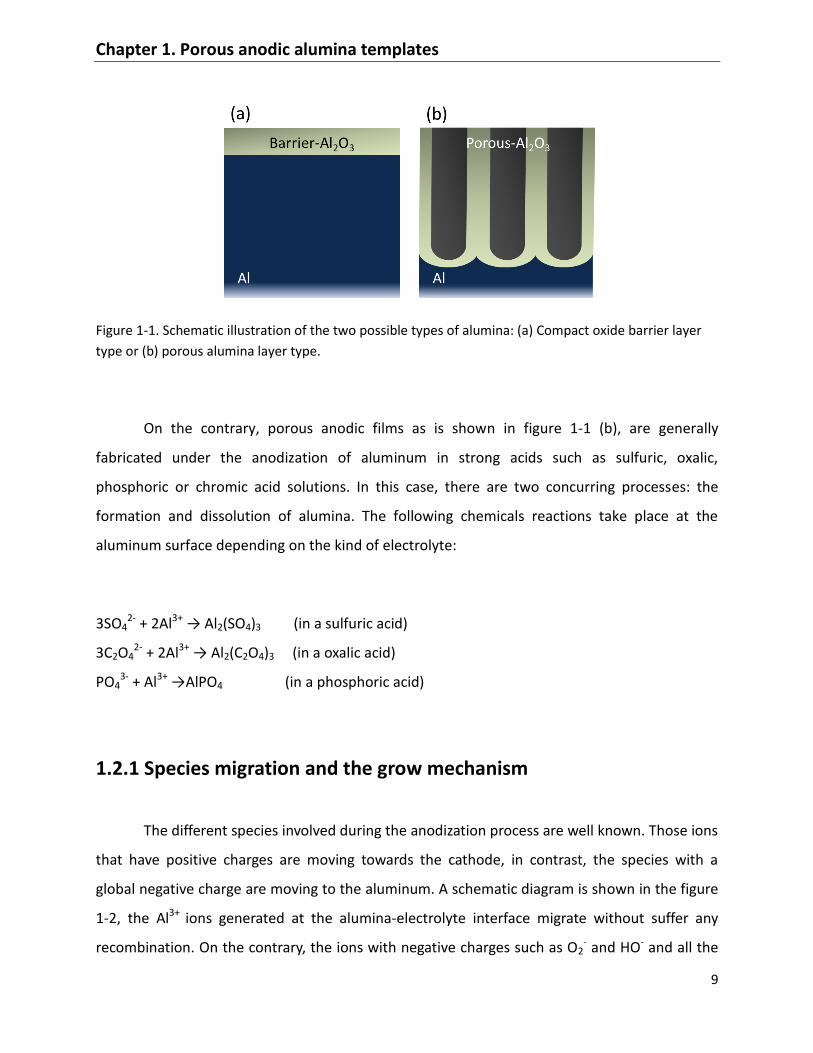
Figure 1-1. Schematic illustration of the two possible types of alumina: (a) Compact oxide barrier layer
type or (b) porous alumina layer type.
On the contrary, porous anodic films as is shown in figure 1-1 (b), are generally
fabricated under the anodization of aluminum in strong acids such as sulfuric, oxalic,
phosphoric or chromic acid solutions. In this case, there are two concurring processes: the
formation and dissolution of alumina. The following chemicals reactions take place at the
aluminum surface depending on the kind of electrolyte:
3SO42- + 2Al3+ → Al2(SO4)3 (in a sulfuric acid)
3C2O42- + 2Al3+ → Al2(C2O4)3 (in a oxalic acid)
PO43- + Al3+ →AlPO4 (in a phosphoric acid)
1.2.1 Species migration and the grow mechanism
The different species involved during the anodization process are well known. Those ions
that have positive charges are moving towards the cathode, in contrast, the species with a
global negative charge are moving to the aluminum. A schematic diagram is shown in the figure
1-2, the Al3+ ions generated at the alumina-electrolyte interface migrate without suffer any
recombination. On the contrary, the ions with negative charges such as O2- and HO- and all the

Chapter 1. Porous anodic alumina templates
10
anions formed with the different acid electrolytes, moves to the alumina-electrolyte interface.
Nonetheless the migration that takes place in the oxide layer is still not well understood [18].
Many efforts are focus in order to formulate a theoretical model that describes the migration
that occurs within the oxide layer. Finally it is not well established if the alumina formation takes
place at the alumina-electrolyte or at aluminum-alumina interphases. In the first case, the Al3+
ions migrate from oxide-metal zone to the oxide-electrolyte interphase and such ions react with
the oxygen ions present in the electrolyte. On the other hand, if the oxide formation occurs at
the alumina-aluminum interphases, the oxygen ions such as O2- and HO- migrate across the
alumina layer reacting with the Al3+ ions generated in this region. The figure 1-2 takes into
account the two ways.
Figure 1-2. Schematic of the ion migration and the main chemicals reaction involved in the porous
formation. Both alumina formations are considered in this representation, at the oxide-electrolyte
interphase and at the metal-oxide interphase. The water formation and the acid-basic reactions are not
represented for sake of simplicity.

Chapter 1. Porous anodic alumina templates
11
Although the difficulties to well describe the oxide formation, it is important to highlight
that the PAA formation is the product of the interaction of two complex processes such as the
stress inside the alumina formed at the aluminum surface, and the field assisted dissolution
under the application of an electric field in an acidic environment generally obtained by the
electrochemically way.
The volume expansion induces the stress inside the oxide layer. The volume expansion is
the relationship between the volumes of the initial aluminum and the final alumina formed
layer. This value can vary between 1 and 2 depending on the anodization conditions [5]. The
volume increases due to the incorporation of oxygen ions inside the aluminum. In addition
depending on the acidic electrolyte, different ions can be incorporated into the pore walls, and
these impurities generate an electrostatic field that imposes a local stress inside the alumina.
Therefore the oxide layer acts as dielectric between the aluminum and the electrolyte,
generating local charges in each interphase and leading to an electrostatic field that induces
forces within the oxide layer.
1. 2. 2 Potentiostatic and Galvanostatic procedures
There are two procedures in order to perform the anodization process. The galvanostatic
and potentiostatic methods, both procedures are schematized in the figure 1-3. The first
technique consists in the application of a constant current between the electrodes. In the
potentiostatic procedure a constant tension is applied between the anode and cathode.
Basically the pore growth formation occurs in a stationary regime. Therefore both
procedures lead to similar results in this regime. However the beginning of the anodization
process is not in a stationary phase, therefore there are some impacts over the pore structure
due to the first moments of the anodization process [19]. For instance, as it shown in section
1.3.1 mostly of the structural parameters of the PAA depend on the applied tension, such as the
pore diameter and the interpore distance. Therefore if a galvanostatic procedure is performed
these parameters suffer variations until the stationary regime is reached. Taking into account

Chapter 1. Porous anodic alumina templates
12
these properties, we have chosen the potentiostatic method in order to fabricate the PAA
templates.
Figure 1-3. Schematic representation of the two existing procedures in order to execute the anodization
process: the galvanostatic (red line) and potentiostatic (black line) procedures.
1.2.3 Stages during the pore growth formation
Different stages take place during the pore growth formation. Each phase is schematized
in the Figure 1-4. Under a potentiostatic procedure, five different steps can be clearly identified
as the anodization current evolves, where each step is related with a different growth pore
regime.
When the process start, the aluminum has a native oxide layer of a few nanometers,
thus when tension is applied the current is high because the resistance between the aluminum
and the electrolyte is low. The aluminum surface suffers an abrupt oxidation, which corresponds
to the second stage of the anodization process, where the thickness of the grown oxide layer
leads to a current breakdown due to increment of the resistance in the system. As the

Chapter 1. Porous anodic alumina templates
13
anodization evolves with time, the volume expansion of the alumina starts with a local
dissolution of the oxide. The field assisted phenomenon plays a crucial role focusing in the
defects of the surface, this local field concentration generates a preferentially ion transfer which
induces an effective etching of the alumina. In such defecting sites, the first paths of the pores
are created [2, 20] and such concentration leads to bigger alumina dissolution generating an
increment in the anodization current, as shown in the stage three, the dissolution and the
formation of alumina become coexisting processes . In this stage the pores are created, and the
dissolution is only active at the bottom of the pores due to local field density. The oxide layer at
the bottoms pores is thinner leading to a greater concentration of the field lines in these zones
and it will be a bigger amount of species involved in the dissolution. This effect leads to two
coexisting phenomenon: the local dissolution at the bottom of the pores and the growth of the
oxide layer. Finally, when equilibrium between the dissolution and formation of alumina is
established the pore growth takes place, corresponding to the stage four, the aluminum suffers
an oxidation process creating the porous structure. As the anodization continues, the pores
start to growth straight.
When the pores grow straight and parallel among then, the self-organization begins with
a hexagonal pore array, with a period proportional to the applied tension. This is the final stage
which occurs in a stationary regime where the pores length increases with the anodization time.
The characteristic time in order to reach the self-organized pore growth regime depends mainly
in the ion transport that takes places at the bottom of the pores, such value is determined by
different anodized parameters, such as: applied voltage, electrolyte temperature, and
concentration.
In conclusion, when the steady state regime is reached, the pore ordering degree highly
differs at the top surface, where the pore formation begins from the bottom of the pores zone,
as is schematized in the figure 1-4. This kind of porous structure is not desirable for the
synthesis of nanostructures due to the irregular pathway of the pores that can block the
nanostructure formation, and additionally a very low order distribution of pores are obtained at
the top surface of the template. In order to avoid the described template configuration the two

Chapter 1. Porous anodic alumina templates
14
step anodization process is introduced to achieve a highly ordered pore distribution with
straight pores.
Figure 1-4. Schematic illustration of the steps involves in the pore growth during the potentiostatic
procedure and their respective current time anodization curve pointing out every stage of the pore grow
formation.
1.2.4 The Two Step anodization process
The pore self-organization structure is reached in the stationary regime when the
equilibrium between the alumina dissolution and formation is established, and the pores grow
parallel to the electric field lines generated between the cathode and the aluminum. Therefore
the pore distribution at the top of the alumina surface has low ordering degree. The pore
ordering degree is strictly related with the fact that the pore pathways at the beginning of the
process are focused in the defects of the aluminum surface. These sites act as the seeds of the
futures pores. In principle many procedures [21, 22] can be applied to obtain a smooth

Chapter 1. Porous anodic alumina templates
15
aluminum surface to reduce the surface defects, anyway the pore ordering degree is not close
to an ideal hexagonal array.
A significant improvement concerning the pore ordering was introduced by Masuda and
Fakuda [23] when they proposed the two step anodization process. This technique exploits the
fact that the initial sites of the pores are the defects of the surface. The methodology consists in
the formation of PAA layer and the subsequent removal, the procedure of this technique is
schematized in the figure 1-5. The first anodization process is performing until the self-
organization is reached; therefore the bottom pores distribution has a higher order degree than
the pore distribution at the top surface of the alumina. Then such layer is removed on etchant
solution that only eliminates the alumina leaving the nano-imprints of the bottom pores in the
aluminum surface. Finally a second anodization process is carried out, however in this case the
field lines are focused in the nano-imprints of the previous ordered bottom pores. Therefore the
pores growth formation begins straight following a hexagonal array.
Figure 1-5. Schematic diagram representation of the PAA structure in the different fabrication steps
involved in the two-step anodization process. (a) First anodization performed until the pores grow
straight. (b) Removal of the porous alumina layer in a chromic acid solution. (c) Second anodization
process.

Chapter 1. Porous anodic alumina templates
16
The figure 1-6 shows the differences of the pore ordering degree between a PAA
structures obtained via a simple anodization process, figure 1-6 (a) and a PAA structure
fabricated by the two step anodization method, figure 1-6 (b). In both cases a previous
electropolishing process has been applied. This procedure will be described in detail in the
experimental section 1.5.3.
The main advantages of these techniques are: the low cost of implementation, the easy
execution of each step concerned for the PAA fabrication, and the simple control of the pore
array, thus the pore structure of the PAA can be controlled adjusting the parameters involved in
the anodization process. Anyway a previous polished step is required to obtain highly ordered
pore array. In contrast, the biggest limits imposed by this techniques are that, the perfect pore
ordering is reached in domains of the order of µm2 sizes [24], such constrain is caused by grain
boundaries and dislocations density in the metal substrate. A drawback inherent of such
technique relies on the fact that is required an initial sacrificial layer that will not be present in
the final porous alumina. This is a big constraint for device fabrication on Si supports because
very thick layer of aluminum has to be deposited.
Figure 1-6. SEM top-view images of PAA fabricated by the (a) simple anodization process, the average
pore diameter is (22 ± 5) nm and (b) two step anodization process, the average pore diameter is (32 ± 4)
nm.
Many techniques have been developed to reach a perfect pore ordering degree.
However these techniques involve: lithography steps [25, 26], plasma treatments [27-31], mask

Chapter 1. Porous anodic alumina templates
17
fabrications [32-36], atomic force microscopy implantation or a combination of these
techniques. Therefore these procedures have many disadvantages because there are very
costly, time consuming, and all of them present scale size limitations. In addition, the
procedures that involved a mask have a low versatile degree because only a few pore size cell
structures can be fabricated.
In conclusion, depending on the future application a compromise among the pore
ordering degree and the implementations constraints must be taken into account in order to
choose the procedure to create the pre-determined sites that will lead origin to the pore
formation.
1.2.5 Differences between the simple anodization and the two step
anodization
There are some differences between the kinetics of the first and the second anodization
performed over the same sample under identical anodization conditions. Figure 1-7 shows the
current curves of the first and second anodization as function of time.
In the second anodization process, the electric field is concentrated on the nano-
imprints created due to the elimination of the PAA layer (formed during the first anodization
process). This phenomenon has different impacts over the kinetics of the pore formation.
During the first anodization the current breakdown is higher because a thick alumina layer is
created during the first moments where only the pathways are created in the defect sites; on
the contrary during the second anodization, the pores are ready to grow since the nano-
imprints act as the defects sites. This effect also influences over the alumina formation and
dissolution, which is reached faster in the second anodization as the pores begin to grow
straight leading to an easier ion transport than in the crooked pores of the first anodization.
Therefore the pore rate formation is bigger in the second anodization. Another
difference is that in the stationary regime, during the second anodization current slightly
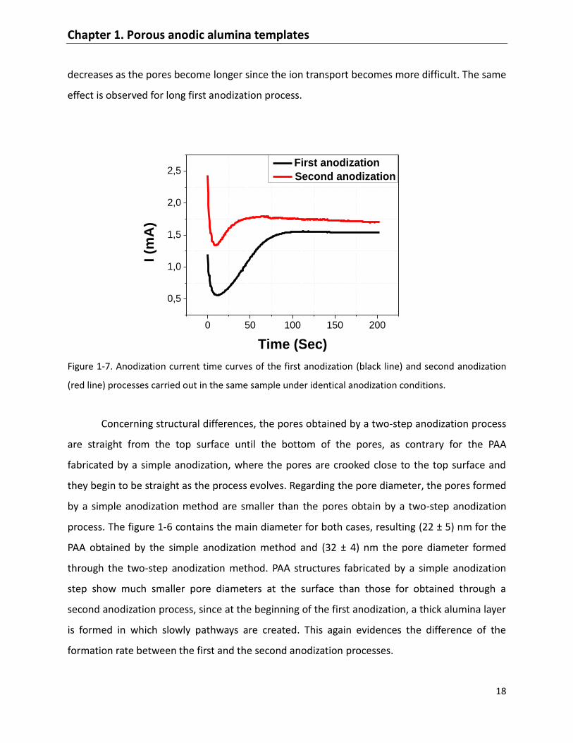
Chapter 1. Porous anodic alumina templates
18
decreases as the pores become longer since the ion transport becomes more difficult. The same
effect is observed for long first anodization process.
0 50 100 150 200
0,5
1,0
1,5
2,0
2,5
I (m
A)
Time (Sec)
First anodization
Second anodization
Figure 1-7. Anodization current time curves of the first anodization (black line) and second anodization
(red line) processes carried out in the same sample under identical anodization conditions.
Concerning structural differences, the pores obtained by a two-step anodization process
are straight from the top surface until the bottom of the pores, as contrary for the PAA
fabricated by a simple anodization, where the pores are crooked close to the top surface and
they begin to be straight as the process evolves. Regarding the pore diameter, the pores formed
by a simple anodization method are smaller than the pores obtain by a two-step anodization
process. The figure 1-6 contains the main diameter for both cases, resulting (22 ± 5) nm for the
PAA obtained by the simple anodization method and (32 ± 4) nm the pore diameter formed
through the two-step anodization method. PAA structures fabricated by a simple anodization
step show much smaller pore diameters at the surface than those for obtained through a
second anodization process, since at the beginning of the first anodization, a thick alumina layer
is formed in which slowly pathways are created. This again evidences the difference of the
formation rate between the first and the second anodization processes.

Chapter 1. Porous anodic alumina templates
19
1.3 Factors that influence the PAA structure
Self-organized porous anodic alumina can be described as close packed array with
hexagonal ordered cells with pores in each center cell. The PAA are characterized by several
structural parameters such as: pore diameter, interpore distance, oxide barrier layer thickness,
and pore length. Figure 1-8 schematized a typical PAA structure pointing out the main
parameters. The versatility of such type of template relies in the fact that the geometrics
features of the cell structure can be adjusted controlling the parameters involved in the
anodization process. For instance the anodization voltage has a huge impact over the cell
structure. The type of electrolyte determines the operational voltage range in which the PAA
has an order hexagonal array. The anodization duration basically defines the pore length. The
electrolyte concentration and the anodization temperature generally influence over the pore
rate formation. However, in the present work we verify that in the lateral-PAA template has a
strong impact over the pore diameter. In addition the cristanility of the aluminum substrate or
the crystal orientation impacts over the pore ordering degree [37-40].
Figure 1-8. Schematic representation of the porous anodic alumina and their cell structure parameters.

Chapter 1. Porous anodic alumina templates
20
1.3.1 Anodization voltage
The most influential factor during the anodization process is the applied tension. It
affects most of the structural features of the PAA, such as the pore diameter, the interpore
distance and the oxide barrier layer at the bottom pores.
The pore diameter of the PAA structure is linearly dependent of the applied voltage with
a proportional value λP that can vary from 1.3 nmV-1[41]. Therefore the pore diameter 𝐷𝑃 can
be expressed in terms of the anodization voltage UAnod as:
𝐷𝑃 = 𝜆𝑃 ∗ 𝑈𝐴𝑛𝑜𝑑 (2)
It is generally accepted that the interpore distance (𝐷𝐶) of anodic porous alumina is
linearly proportional to the forming potential in the stationary regime growth of anodic porous
alumina with a proportionality constant λC of approximately 2.5nmV-1 [42]:
𝐷𝐶 = 𝜆𝐶 ∗ 𝑈𝐴𝑛𝑜𝑑 (3)
A depth study of aluminum anodization in sulfuric and oxalic acid was performed by
Ebihara et al. [43, 44]. They established the following relation depending on the applied voltage
range.
H2SO4: 𝐷𝐶 = 12.1 + 1.99 ∗ 𝑈𝐴𝑛𝑜𝑑 (3 − 18𝑉)
C2H2O4: 𝐷𝐶 = 14.5 + 2 ∗ 𝑈𝐴𝑛𝑜𝑑 (𝑈𝐴𝑛𝑜𝑑 ≤ 20𝑉)
𝐷𝐶 = −1.70 + 2.81 ∗ 𝑈𝐴𝑛𝑜𝑑 (𝑈𝐴𝑛𝑜𝑑 ≥ 20𝑉)
In addition the anodized voltage determines the ion transport ratio, higher voltages lead
to higher anodized currents. Therefore the pore rate formation is determined by the applied
potential. The anodization performed at low voltages is denominated as mild process, where
the pore rate formation is low, consequently long times are required to achieved a pore order at
Chapter 1. Porous anodic alumina templates
21
the bottom pores. On the other hand, a hard anodization is obtained when a high field is
applied. This process produces highly ordered PAA membranes with a fast film growth rate. The
operational range and the optimal order of the PAA structure are determined by the
anodization electrolyte.
1.3.2 Type and concentration electrolytes
The kind of electrolyte firstly determines the type of anodic alumina obtained.
Depending on their pH a barrier-type or porous-type can be obtained. For the non-porous
regimes, neutral pH’s have to be employed. For the porous anodic alumina type pH<4 is
required. In addition the concentration determines the velocity of the reaction, the rate of the
species migration and the speed of the chemical reactions. However there are not concluding
results on the impact of the electrolyte concentration over the pore structure [45]. Besides, the
type of electrolyte influences over the global organization of the PAA. The most common acids
are the oxalic, sulfuric and phosphoric acids.
The properties of the PAA formed by anodizing are also related to the electrolyte species
incorporated into the oxide walls. The incorporation of anions modifies the space charge
accumulation in the porous and barrier-type alumina films [46]. The duplex structure of the cell
walls is described in the figure 1-9 where the cell structure contains two regions a pure alumina
wall and anion incorporated layer. It was reported that the thickness of the inner layer varies
depending on the electrolyte implemented in the succeeding order [47]:
H2SO4 < C2H2O4 <H3PO4

Chapter 1. Porous anodic alumina templates
22
Figure 1-9. Schematic representation of the inner and outer pore cell structure depending of the
anodized electrolyte: Sulfuric acid, Oxalic acid and Phosphoric acid. The thickness of the inner layer
varies depending on the electrolyte implemented in the following order: H2SO4 < C2H2O4 <H3PO4.
However, it is important to point out that the pore diameter is not directly sensitive to
the nature of the electrolyte. Each electrolyte has different values in terms of ion conductivity
and dissolution ratio, these factors impacts over the anodization current. Since the increment of
the applied tension leads to a higher density of current, therefore the anodized solution
determines the operational conditions in which the self-organized PAA structure can be
obtained. There is a threshold voltage for each particular electrolyte, for lower applied tension
than this value, the electric field generated is not strong enough to assisted properly the
alumina dissolution and formation, thus the stress generated in the oxide layer is not balanced,
leading to a disordered structure. On the other hand, high voltages lead to high currents,
increasing the ion transport, thus increasing the rate of O2 produced during the anodization.
These gas bubbles generated from water electrolysis continuously emerge at the sample
surface. The abundant gas bubbles hinder the ion diffusion, which will lead to the irregular
arrangement of the pore cell and disrupts the self-ordering process of the pores, in spite of the
process is performed under permanent stirring. Higher voltages can leads to the dielectric
breakdown of the barrier layer and burned the sample. So for a given electrolyte, the upper
limited voltage in self-ordering range is lower than the breakdown tension, and there is a

Chapter 1. Porous anodic alumina templates
23
narrow range of anodizing voltage within which self-ordering can occur. For instance for oxalic
acid the voltage range is 20-80V with an optimal order degree typically when the anodization is
performed at 40V [48-50], for sulfuric acid the operational range is between 7-70V [48-50] with
the best pore order structure is obtained when the anodization is carried out at 25 V and for
phosphoric acid the voltage range is from 60-235V and the optimal voltage is at 195V [42, 48-
50].
Finally the type of electrolyte defines the operational voltage range in which a self-
organized hexagonal pore array can be obtained; such voltage range directly determines the
main pore structures of the PAA templates, such as the interpore distance, pore diameter, and
barrier oxide layer thickness. In conclusion the type of electrolyte not only defines the, inner
and outer pore cell structure, but additionally indirectly determines the range of the
characteristics length of the pore structure.
1.3.3 Anodized duration
The anodization duration determines the pores length. Basically longer anodization leads
to longer alumina layers. This parameter has a huge influence over the pore order when a two-
step anodization process is performed. For highly ordered close-packed hexagonal pore array,
mechanical stress between neighboring pores has to be stabilized in order to distribute
mechanical stress equally, so long anodization is required in order to achieve this mechanical
stress equilibrium. Therefore for a longer anodization duration leads to a better pore ordering at
the bottom pores. The second anodization is carried out in pre-textured surface where the
nano-imprints are situated at the bottom pores location of the former PAA layer, therefore it is
expected a better pore ordering degree in the final PAA structure obtained in the second
anodization when the pores generated at the first anodization are longs and straight.

Chapter 1. Porous anodic alumina templates
24
Figure 1-10. Schematics illustrating of the non-uniform distribution of anions incorporated in the outer
pore wall. A different level of impurity in anodic oxide is depicted with gray scale [51].
For very long anodization process, of the order of 12 hours, the duration of the
anodization also impacts over the anion incorporation to the outer walls of the cell structure, as
the pores growth, the ion transport is more difficult, which leads to decrease the density of
current in spite of the applied potential is the same, so the pore diameter remains the same;
however a gradient of impurity concentration is established as the concentration of the solution
decreases when the anodization evolves [51]. Figure 1-10 described this situation where the
impurities along the grow direction vary as a function of the anodization time.
1.3.4 Electrolyte temperature
The anodization temperature determines the kinetics of the process. An increment of
temperature accelerates the ion transport and the chemical reactions leading to an increment
on the current density. Therefore the anodization temperature basically impacts over the pore
formation rate leading to a faster self-organization of the pore array. However a very fast

Chapter 1. Porous anodic alumina templates
25
anodization rate can generate O2 bubbles which are difficult to remove from the anodized
surface affecting the pore ordering degree.
Concerning the structural features of the PAA, the anodization temperature mainly
impacts over the thickness of the oxide barrier layer. Higher the electrolyte temperature leads
to lowers thickness of the oxide layer. This is attributed to the direct result of an enhanced
field-assisted dissolution of oxide at the oxide/electrolyte interface. The oxide barrier thickness
plays a critical role in the electrodeposition process of metal nanoparticles. Consequently, the
control of such barrier results of particular importance for a further nanoparticle deposition
within the PAA templates.
On the other hand, the anodization temperature has not great impact over the pore
diameter and the interpore distance for the conventional vertical PAA templates [52, 53].
However in the present work, a detailed analysis of the influence of the anodization
temperature over the pore structure of lateral-PAA and vertical-PAA templates has been
performed. The results reveal that under the horizontal configuration the pore diameter is
highly sensible to the electrolyte temperature.
1.3.5 Aluminum substrate
The geometric features of the formed PAA structures mainly depend on the anodization
conditions. However, the kind of substrate also impacts over the formed PAA structure. The
systematic utilization of the anodic alumina would require the spatial ordering of the pore
channels to be controllable and homogeneous over large areas, so a very desirable
characteristic of the anodic alumina is the high regularity of the pore configuration. Besides the
anodization conditions, the pore order degree depends on the impurity concentrations, size of
impurities, size of aluminum grains, texture and surface morphology [54, 55]. Moreover, the
difference in the structure of anodic oxides films grown on various faces of single crystal
substrates has been studied [37-40, 55, 56]. The best ordering of porous structure has been

Chapter 1. Porous anodic alumina templates
26
observed on the grains with (1 0 0) orientation, while the structure with the worst ordering is
formed on the Al grains with nearly (1 1 0) orientation Ng et. al [39] attributed the relation
between the pore ordering and the crystal orientation as product of the influence elastic
anisotropy over the oxide flow.
1.4 Lateral-PAA templates
The self-organized PAA templates enable the integration of collectively nanostructures
arrays into functional devices. However the conventional vertical-PAA templates cannot be
incorporated in planar integrated circuits. Therefore the development of PAA templates that
entails a planar architecture will widely open the application domain of devices based on PAA
templates. Besides, with lateral anodization directly contact of organized nanostructures can be
achieved between two electrodes through the synthesis of nano-objets within lateral-PAA
templates.
The lateral-PAA templates were firstly fabricated by Masuda et. al. [57], however an
increase of quality and reliability concerning the template fabrication arrived several years
later, when Cojocaru et. al. [58] have introduced the practical fabrication of lateral-type porous
anodic alumina starting from patterned aluminum stripes. As result of such work, many studies
have been focused on the fabrication of lateral-PAA templates with the goal of the fabrication
PAA functional devices [59-62].
On the other hand, the fabrication process of the lateral-PAA templates is much
complex than the conventional vertical type. For instance, it is necessary to encapsulate an
aluminum stripe in order to just expose a certain side of the aluminum in the electrolyte bath.
Otherwise, the pore formation occurs over the whole aluminum surface. The situation is
schematized in the figure 1-11 (a), on the contrary when a capping layer covers the aluminum
stripes, the anodization takes place only on the exposed side face of the aluminum stripes as
shown in figure 1-11 (b).

Chapter 1. Porous anodic alumina templates
27
Figure 1-11. Schematic representation of anodization cell and the resulting pore structure depending on
the (a) uncapped aluminum stripe and (b) capping layer configurations.
The capping layer induce constrains effects that don’t exist in the case of the
conventional vertical-PAA structures. Therefore a deeply study of the influence of the
anodization parameter over the pore structure must be performed, since it is not possible to
directly transfer the knowledge from the vertical PAA fabrication to the lateral type.
1.5 Experimental procedure
Two different classes of templates have been fabricated: the conventional vertical-PAA
type and the lateral-PAA type. Concerning the anodization process, the techniques involved in

Chapter 1. Porous anodic alumina templates
28
the fabrication of both kinds of templates are similar. Firstly an electropolishing process must
be performing in order to flatten the aluminum surface. Afterwards, the anodization process
can be carried out, where a disorder pores distribution is obtained at the top surface; on the
contrary as the anodization evolves an order hexagonal array is reached at the bottom pores.
For the two step anodization method, the first anodic layer is removed in a chromic acid
solution and the second anodization process is executed, in this step the pores start to grow in
a pre-patterned surface. Therefore, a self-ordering process is obtained from the initial moment
of the anodization. In order to eliminate the oxide barrier layer at the bottom pores, at the end
of the anodization process an exponential voltage decrease is applied. This method exploits the
linear relation between the applied potential and the thickness of the oxide barrier. The idea
consists in a gradual descent of the anodization in order to continuously thin the oxide barrier
layer at the bottom of the pores. Such layer is completely removed after the application of the
chemical etching. After the implementation of the mentioned processes the template is ready
for nanoparticle deposition and further nanostructure growth.
1.5.1 Anodization experimental set-up
The experimental set up for the anodization process is shown in the figure 1-12. The
sampler holder is made of Teflon. This device has been designed in order to perform
anodization in circular surface of 0.38 cm2, thus always the same area is anodized and exposed
to the electrolyte solution. Due to the fact that during the anodization process bubbles are
generated as products of chemical reactions, a constant strong stirring is required. Otherwise,
the bubbles isolate certain substrate area. The current flows between graphite (this electrode
that doesn’t react with the electrolyte) and an aluminum foil. Additionally, the aluminum foil is
in contact with a copper electrode inside the Teflon cell. In order to apply the potential and
measure the anodization current, a power supply and a current meter are connected. The
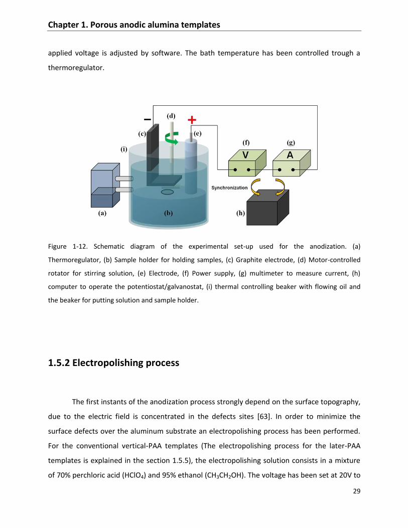
Chapter 1. Porous anodic alumina templates
29
applied voltage is adjusted by software. The bath temperature has been controlled trough a
thermoregulator.
Figure 1-12. Schematic diagram of the experimental set-up used for the anodization. (a)
Thermoregulator, (b) Sample holder for holding samples, (c) Graphite electrode, (d) Motor-controlled
rotator for stirring solution, (e) Electrode, (f) Power supply, (g) multimeter to measure current, (h)
computer to operate the potentiostat/galvanostat, (i) thermal controlling beaker with flowing oil and
the beaker for putting solution and sample holder.
1.5.2 Electropolishing process
The first instants of the anodization process strongly depend on the surface topography,
due to the electric field is concentrated in the defects sites [63]. In order to minimize the
surface defects over the aluminum substrate an electropolishing process has been performed.
For the conventional vertical-PAA templates (The electropolishing process for the later-PAA
templates is explained in the section 1.5.5), the electropolishing solution consists in a mixture
of 70% perchloric acid (HClO4) and 95% ethanol (CH3CH2OH). The voltage has been set at 20V to

Chapter 1. Porous anodic alumina templates
30
obtain the flattest surface. The electropolishing solution temperature has been kept at 5°C
during 6 minutes. A constant stirring is applied to remove the bubbles produced during the
process.
1.5.3 Two anodization process
After the application of the electropolishing process, the two anodization process can be
performed. In the present work 0.3 M oxalic acid has been used as electrolyte. The range of
temperature has been varied from 10 to 25°C. The voltage range has been varied from 20-60V.
During the first anodization process, a disordered pore distribution is formed at the
alumina surface, after a certain anodization time the pores growth straight and a hexagonal
pore array is obtained on the bottom pores. In all cases the first anodization process has been
performed during two hours. Then first alumina layer is removed in a chromic acid solution,
consisting in a mixture of 0.17 M chromic acid and 0.6 M phosphoric acid at 60°C. The duration
of such process depends on the pore growth rate formation. Typically for anodization process
performed at 40V in an oxalic acid solution, in order to completely eliminate the anodized layer
it is necessary at least to dipped the sample in the chromic solution during half of the time of
the first anodization duration [64]. Therefore the time duration of the first anodization process
is taken as reference. Finally, the duration of the removal process has been set up as the half
duration of the first anodization process for anodization voltages lowers than 40V. Therefore
the PAA is dipped in the chromic acid solution during one hour. In contrast for anodization
voltages higher than 40V, which correspond to a higher pore growth formation rate formation,
the duration time of the alumina removal in the chromic acid solution has been set up as equal
to the first anodization process time duration, is to say 2 hours. Such dipped times in the
chromic acid solution guarantied the entirely elimination of the PAA layer. Subsequently, the
second anodization process has been executed over an aluminum pre-textured surface where

Chapter 1. Porous anodic alumina templates
31
the nano-imprints have been generated due to the removal of the former PAA layer. The
second anodization duration has been varied from 90 seconds up to 1 hour.
1.5.4 Barrier thinning process
The main problem in order to utilize the PAA built electronic devices relies on the
compact oxide barrier layer present at the bottom of the pores. Such layer is highly resistive
and insulates the pores from the aluminum. Therefore the presence of such layer introduces
many difficulties for the device fabrication, for instance for the metal nanoparticle
electrodeposition it is necessary to overcome the potential induced from this layer to make an
electrical contact. Additionally, the thickness of the barrier layer varies from one pore to the
next one, all over the surface, so the thickness barrier for each pore is slightly different. For
the multiple device applications it is mandatory to control the uniformity and the thickness of
this oxide barrier layer.
Many efforts have been performed in order to reduce or eliminate the oxide barrier
layer. The most common process is the wet chemical etching [65]. Typically the PAA is
submerged in a H3PO4 solution that selectively etches the alumina. However, this solution
attacks the alumina isotropically leading to a pore widening process. In addition, this process
can be applied to obtain a bigger pore diameter [66]. Thus, such process constrains the
minimum pore diameter for a determined cell structure. On the other hand, the dry etching is
an alternative route in order to remove the oxide barrier layer. For instance, pore opening
process can be performed using a dry etching with an Ar+ ion beam [67-70], Ga+ ion beam [71,
72] and with CF4 ions [73]. Nevertheless, these techniques involve sophisticated and costly
technologies.

Chapter 1. Porous anodic alumina templates
32
An interesting approach was introduced by Furneaux et. al [74] which consists in
sequentially decrease the voltage at the of the anodization process, exploiting the dependence
between the thickness of the oxide barrier layer and the anodization potential applied,
expressed in the equation (1). For each applied voltage a corresponding pore cell structure is
determined. Subsequently, at the end of the anodic layer, the voltage is constantly decreased in
order to thin the oxide barrier layer. Nonetheless, the voltage decrease has to be properly
adjusted. Due to the voltage impact over the pore structure, at every potential drop, the
system enters in a new equilibrium state where the alumina dissolution and formation leads to
another pore cell structure. This new cell structure has a less thick oxide barrier layer, but in
addition, a minor interpore distance and pore diameter than the one’s obtained with the
previous applied voltage. Therefore a branched structure can be obtained depending on the
shape and rate of the voltage decrease [75]. For further nanostructure growth within PAA
templates, such multi-branched structure is not desirable since the pores are not straight
anymore which is hindering for instance a deposition of the nanoparticle that is fundamental
for the growth of carbon nanostructures or silicon nanowires [76].
The voltage decrease has to be established taking into consideration that at every
potential fall, the system enters into a new equilibrium state with their respective pore cell
structural characteristics length which depends on the anodization parameters. Therefore, a
drastic change of applied potential can stop the anodization because the system cannot be self-
adjusted into the new anodization conditions, leading to an interruption of the porous
formation. Under the described situation the oxide barrier layer remains at the bottom of the
pores.
In conclusion the anodization voltage has to be decreased preventing a branch structure
formation, which is associated with long time between every voltage drop, and on the other
hand i we must avoide the interruption of the anodization process that takes places when the
anodization potential changes are too fast.
As the barrier layer thickness is proportional to the applied anodization potential, the
voltage decrease at any time should always be proportional to the previously applied voltage.
This can be expressed by the following equation:

Chapter 1. Porous anodic alumina templates
33
𝑑𝑈
𝑑𝑡= 𝑉0 ∗ 𝑈 (4)
Where 𝑈 is the anodization voltage, 𝑡 the time and 𝑉0 a constant value. Finally, the
anodization voltage results,
𝑈(𝑡) = 𝑉0 ∗ exp(−𝜂 ∗ 𝑡) + 𝑉′ (5)
Therefore there are three parameters to establish. In one case, 𝑉0 and 𝑉′ determine
the shape of the exponential voltage decrease. On the other hand, 𝜂 defines the voltage decay
rate. In the present work these values were fixed taking as reference a previous work
performed in our group by Marquardt et. al [76] who probed an efficient thinning barrier
process. On the other hand, in the present work, we have proved that such exponential
decrease parameters lead to a branched structure. Such structure at the bottom of the pores
has been studied by lamella preparation and subsequently by TEM observations. In addition, by
the nanoparticles deposition in chapter 2 an interesting approach is presented in order to
obtain a quantitative value of the branches created per primary pore, depending on the
anodization conditions. Consequently, the exponential voltage decrease parameters have to be
optimized in order to obtain straight along all the PAA structure.
Finally in order to completely remove the oxide barrier layer at the bottom of the pores,
in addition of the exponential decrease applied at the end of the anodization process, a wet
chemical etching in a 0.3 M H3PO4 solution has been performed at 30°C during 25 minutes.
1.5.5 PAA-Lateral templates type fabrication
In order to fabricate the encapsulated aluminum stripes different steps are required,
involving, metal evaporation, lithography, chemical wet etching, PECVD deposition and reactive

Chapter 1. Porous anodic alumina templates
34
ion etching (RIE). The procedure for the lateral-PAA template fabrication is schematized in the
figure 1-13 (a) pointing out the structure configuration obtained at each implemented process.
Firstly, aluminum is evaporated on p-type silicon wafer substrate in an evaporator Plassy
MEB 550S. The main evaporation parameters are the evaporation rate, the evaporation current
and the pressure of the chamber. In our case the evaporation rate has been set at 0,3nm/sec,
the current at 20 A under a pressure of the order of 1.00xe-7 Torr. Subsequently, a
photolithography has been performed. The mask pattern is also schematized in the figure 1-13
(b), indicating the channel region, that separates the aluminum electrode (zone A) with pore
structure (zone B). Such mask contains 6 kinds of channel width while the channel length is
fixed (5 μm), and for each channel width, there are 5 electrodes exists (same dimension), D1 to
D5.
For the first photolithography step, negative resin AZ 5214 has been deposited over the
sample in a spin-coating system with a rotating of 4000 rpm, subsequently the samples have
been heated at 110°C during 30 seconds. The photolithography step is performed in a double-
sided aligned system. The aluminum stripes have been generated through the aluminum
etching at room temperature during 8 minutes, in a mixture solution of 1-5 % HNO3 (for
aluminum oxidation), 65-75 % H3PO4, 5-10 % CH3COOH (for wetting and buffering) and H2O
dilution to define the etch rate at given temperature. In order to deposit the material of the
capping layer the PE-CVD process has been performed. For the silicon nitride deposition (SiNx)
the pressure of the chamber has been set at 1 mbar, the temperature set at 350°C, the HFSiN
flow was and the plasma power at 20 sccm and 50 W. After the SiNx deposition, the second
photolithography step is performed. The substrate is deposited in a spin-coating system with a
rotation of 5000 rpm and a Resine Shipley S1813 is spread out onto the substrate. Then the
substrate is deposited onto a hotplate during 60 seconds at 115°C. For the proper lithography
step, the illumination by UV-light is performed during 180 seconds, with wavelength of 380 nm
and power density of 25 mW/cm2. Subsequently the sample is dipped in a 351 development
solution during 25 seconds. The reactive ion etching steps have been executed in an Advanced
Vaccum RIE system. This stage is carried out in order to remove SiNx zones where the resin is

Chapter 1. Porous anodic alumina templates
35
not present. The process is performed at room temperature, under power etching of 100 W
and a pressure of 0.5 mbar. The final step, is to etch the aluminum, this process is carried out
with Al etch solution at 60°C during 20 seconds. After this final step, one aluminum surface
exposed side is obtained.
However before the pore growth takes place, the electropolishing process is performed.
For these kinds of templates a modified electropolishing solution has been prepared in order to
prevent a fast consummation of the aluminum. The solution is a mixture of 70% HClO4, ethanol
and Isopropan-ol (IPA) with 1:14:15 volume ratio. The process was carried out at 5°C applying
5V during 2 seconds. Such electropolishing process is compatible for lateral-PAA template
fabrication, as the aluminum surface is smoothened while the aluminum surface is not placed
too deeply inside capping layer. Finally the anodization process can be performed and the pore
formation will occur only in the planar orientation. Concerning the barrier thinning process at
the bottom of the pores, both the exponential voltage decrease parameters and the wet
chemical etching in the 0.3 M H3PO4 solution procedure, have been chosen identically for the
fabrication of the vertical-PAA templates and the lateral-ones.

Chapter 1. Porous anodic alumina templates
36
Figure 1-13. (a) Schematic diagram of the aluminum encapsulation fabrications pointing out the
different steps involved: Aluminum deposition, Positive photoresist deposition for lithography step,
aluminum etching for stripes generation, SiNx layer deposition to create the capping layer, second
lithography step with a negative photoresist resin, reactive ion etching to create the channel between
two terminals, and the anodization process for the lateral pore formation. The mask used for the
lithography steps is also included pointing out the zones A and B of the lateral template. (b) Designed
mask for lateral-PAA templates indicating the channel region.
.

Chapter 1. Porous anodic alumina templates
37
1.5.6 Characterization techniques of the PAA structure
The PAA templates have been characterized by Field-Emission Scanning Electronic
Microscopy (FE-SEM, HITACHI S4800). Additionally, in order to obtain a high description of the
pores structure cross-section Transmission Electronic Microscopy (TEM) analyses were
performed using a Titan-FEI electron microscope operation at 200kV and equipped with a Cs
probe corrector and a SuperX detector for EDS chemical analyses.
Figure 1-14. Schematic representation for obtain a PAA/Al lamella.
Chapter 1. Porous anodic alumina templates
38
For the TEM analyses the preparation of the cross sections has been done using the
Focus Ion Beam technique (FIB, Scios DualBeam). The procedure to obtain the PAA/Al lamella is
described in the figure 1-14. At first place, the area of interest is selected and a 2/2/20 µm
Platinum protective layer is deposited to protect it from excessive ion damage. Secondly, the
selected area is isolated using the energetic gallium ion beam. Once the area is isolated, the
milling process begins using high current ion beam and then as the lamella becomes thin 0.8 -
1µm the ion beam current is decreased. The lamella is removed from the substrate with a micro
manipulator and transferred to a TEM sample grid. A second milling process using very low ion
beam currents, is performed for thinning more the lamella until its thickness is about 30-50nm
thick. The lamella obtained is transferred to the electron microscope chamber for the TEM
observation and analyses.
1.6 Fabrication and Characterization of the PAA templates
The implementation of PAA templates for the device fabrication requires a strict control
of the parameters which are involved in the anodization process and further detailed
characterization of the porous structure. Such precise control of the anodization process allows
achieving a desire pore configuration. For such purpose, some parameters implicated in the
anodization process have been studied in order to analyze their impact over the pore structure
such as: the anodization time, the anodization voltage, and the electrolyte temperature.
Concerning the influence of the aluminum substrate over the resulting formed PAA, the
anodization process has been performed using aluminum substrate with different single crystal
orientations.
Moreover, the study of the electrolyte temperature over the pore structure on lateral-
PAA templates has been carried out, as a result of such study we have been probed that it is of
paramount importance to control the electrolyte temperature for the fabrication of templates

Chapter 1. Porous anodic alumina templates
39
with a planar geometry which it is not the case, in the range of studied temperatures, for
vertical PAA templates.
1.6.1 Measurement of the geometrical features of the PAA structures
In the present work, a deep study over the pore structure has been performed. Besides
the typical parameters, such as the pore length, pore diameter and the interpore distance other
important pore structural parameters have been studied as the porosity, the circularity and the
pore order degree. All these parameters supply valuable information for further device
fabrication and characterization.
Figure 1-15. Vertical-PAA template. (a) SEM top view and (b) TEM side-view.

Chapter 1. Porous anodic alumina templates
40
The figure 1-15 shows a top and side view of a vertical-PAA template. From figure 15 (a)
all parameters related with the pores features can be inferred. On the other hand, figure 15 (b)
shows a TEM image of a side view of the pores. In order to obtain such sample a lamella
fabrication is required. These kinds of sample provide valuable information concerning the pore
length, the straightness of the pores and the structure at the bottom of the pores.
1.6.1.1 Porosity
The porosity is defined as a ratio of a surface area occupied by pores to the whole
surface area. For a single regular hexagon with one pore inside, the porosity formulation can be
written as follows:
𝑃 =𝑆𝑝𝑜𝑟𝑒𝑠
𝑆=
𝑆𝑃
𝑆ℎ (6)
Where 𝑆 is the total area of the template and 𝑆𝑃 is the pore area. Assuming that each
single pore is a perfect circle, the following equations for 𝑆𝑃 and 𝑆ℎ can be further evolved:
𝑆𝑃 = 𝜋 ∙ (𝐷𝑃
2)
2
(7)
𝑆ℎ =√3∙𝐷𝐼
2
2 (8)
Substitution of Eqs. (7) and (8) into Eq. (6) leads to the following expression for the
porosity of a nanostructure with hexagonally arranged cells:
𝑃 = 𝜋
2∙√3(
𝐷𝐼
𝐷𝑃)
2
(9)

Chapter 1. Porous anodic alumina templates
41
There is a great inconsistency in the literature among experimental data on the porosity
of nanostructures, with the estimated porosity of anodic porous alumina varying from about 8%
to 30% [77].
1.6.1.2 Circularity
A deviation of pore shape from an ideal circle can be described by circularity coefficient,
defined as:
𝐶 = 4𝜋 ∙ (𝑆𝑃
𝑝𝑒𝑟𝑖𝑚𝑒𝑡𝑒𝑟2) (10)
The circularity value of 1.0 indicates that the pore is ideally circular, while values close to
0.0 indicate an elongated polygon.
1.6.1.3 Pore ordering degree
The self-ordering process of the PAA can be addressed as configuration that tends to
minimize the energy of perfect equilateral triangles among then. Due to the symmetry of the
porous structure Mínguez-Bacho et.al [78] proposed the self-correlation function (SCF) in order
to obtain a quantitative estimation of the regularity of the pores. The SCF is given by (11) and
implanted on SEM images. This equation takes the image and the same image is shifted in a
distance k1 and k2 in the 𝑥 and 𝑦 axis with respect to the center of the image. Where 𝐹(𝑥, 𝑦) is
the image matrix.
𝐺(𝑘1, 𝑘2) = ∑ 𝐹(𝑥, 𝑦) ∙ 𝐹(𝑥 + 𝑘1, 𝑦 + 𝑘2)𝑘1𝑘2 (11)
The resulting image, 𝐺(𝑘1, 𝑘2), gives a measure of the periodicity of the original image.
In order to obtain a quantitative value of the degree of order of the anodized samples we

Chapter 1. Porous anodic alumina templates
42
calculated the Normalized Spatial Order Parameter (NSOP) which is given by the following
equation,
𝑁𝑆𝑂𝑃 =1
6∙
∑𝐼𝑁𝑁
𝐹𝑊𝐻𝑀𝑁𝑁
6𝑁𝑁=1
𝐼𝐶𝑆𝐹𝑊𝐻𝑀𝐶𝑆
(12)
Figure 1-16. FE-SEM micrograph of PAA surfaces with their respective SCIs and crossing center profiles.
(a) Highly ordered hexagonal pattern. (b) Low ordered pore structure.
Chapter 1. Porous anodic alumina templates
43
Where the intensity (I) and the full width at half maximum (FWHM) of both central spot
(CS) and the nearest neighbor (NN) of three crossing center profiles measured on the self-
correlated imaged (SCI) provide the information of the pore ordering degree. These profiles are
measured every 60° between them and the opposite vertex of a hexagon formed by the relative
maxima. When the SCF is applied to a perfect ordered hexagonal array the resulting SCI is an
image with a hexagonal pattern. The image starts to differ from a hexagonal since more than
one pattern coexists or the degree of ordering is low, the SCF leads to a central spot surrounded
by a ring. Therefore, when the intensity of the first neighbors of central spot is more similar in
comparison with the intensity of the central spot, the NSOP is close to 1, which implies a highly
ordered hexagonally array. On the contrary, when the central spot is surrounded by a ring, the
intensity of the NN differs significantly with the intensity of the CS, which means that image has
low regularity. Figure 1-16 shows two SEM micrograph, their respective SCI and a crossing
center profile carried out on two different PAA templates. Figure 1-16 (a) shows an order pore
structure that leads to a SCI with hexagonally array. On the other hand, figure 1-16 (b) shows a
poorly ordered pore structure leading to a SCI with central spot is surrounded by a ring. In both
cases it is possible to compare the differences of the intensities of the CS and the NN.
Conventionally, Fast Fourier Transform (FFT) is one of the most used powerful tools for
SEM micrographs processing, however the implantation of the Self-correlation function is a
statistical tool that leaves out the subjective factors and interpretations involved in other
techniques [78].
1.6.2 Image processing
The basics parameters of the PAA structures have been measured using the ImageJ
software. Such software allows performing directly measurements over different geometrical
features, for instance: the pore diameter, pore area, pore perimeter. With these values is
Chapter 1. Porous anodic alumina templates
44
possible to obtain the porosity, the circularity and the interpore distance. In order to obtain
such characteristics length of the pores, a binarization of the SEM image is performed, as
results the obtained image contains in black the surfaces which correspond to the pores and in
white the zone associated with the alumina top surface of the PAA. On the other hand the pore
regularity have been studied using the open software WSxM4.0 [79]. A self-correlation function
(SCF) was performed to the SEM micrographs. The resulting self-correlated image (SCI) is a
mathematical image that gives information of how well an image correlates with itself under
discrete displacements in all possible directions. The combination of both software allows the
calculation of the most relevant geometrical features of the PAA templates.
1.6.3 Influence of the anodization parameters on the PAA
structure
The PAA templates present a great adaptability because their structure can be easily tailored by
adjusting the parameters involved in the two-step anodization process. For the device
fabrication it is of paramount importance to precisely control the cell structure. For both types
of templates vertical and lateral one’s, in the present work a study of the impact of the
anodization parameters over the pore structure has been performed.
1.6.3.1 Anodization voltage
The PAA structure is mainly affected by the applied potential, since such anodization parameter
determines the pore diameter, the interpore distance, and the thickness of the oxide barrier
layer at the bottom pores. Additionally it influences the pore rate formation and the pore

Chapter 1. Porous anodic alumina templates
45
ordering degree. Figure 1-17 shows top SEM images of PAA structures. These samples have
been fabricated through the two anodization method using a 0.3 M oxalic acid solution at
17,5°C applying voltages in the range of 20V-60V with increment of 10V. The main pore
geometrical features have been calculated, as is shown in the figure 1-19.
Figure 1-17. SEM images of PAA top surfaces anodized in a 0.3M oxalic acid solution at 17.5°C applying
different anodized voltages in the range of 20-60V. (a) 20V, (b) 30V, (c) 40V, (d) 50V and (e) 60 V.

Chapter 1. Porous anodic alumina templates
46
From the plots of the figure 18 (a) and (b) it is possible to calculate 𝜆𝑃 and 𝜆𝐶
respectively, implementing the linear relation between the applied potential, the pore diameter
and the interpore distance. The obtained values are 𝜆𝑃 = (1,06 ± 0,07)𝑛𝑚
𝑉 and 𝜆𝑃 = (3,47 ±
0,11)𝑛𝑚
𝑉 . Both values are of the same order of the reported one’s in the literature [48].
Therefore, to obtain an order array pattern it’s not only necessary to achieve the
equilibrium between the dissolution and formation of the alumina at the bottom pores, figure
19 clearly indicates that all the current behaviors for all the anodization voltages follow the
same trend. The internal stresses generated during the pore formation determine the pore
ordering degree, thus depending on the ion transport a different volume expansion of the
alumina is achieved, K. Nielsch et. Al [42] conclude that the best pore ordering is achieved when
a volume expansion of alumina to aluminum is about 1.2. Therefore the anodization current
highly impacts over the pore ordering degree, this fact is in accordance with previous
experience that shows that the best pore order when the applied potential is 40V in an oxalic
acid environment also depends on the electrolyte concentration and temperature [53, 80-82],
which directly impacts over the anodization current. In addition for higher voltages than 60V
the anodization current is not stable and the sample is near to the burning point, so under such
conditions the pore ordering is almost non-existent.
In conclusion the characteristics of the PAA are closely related, the NSOP value provides
a reference of the pore ordering array and these values are in perfect accordance with the ideal
porosity values and the pore diameter and interpore distance. On the contrary, there is not any
specific relation between the pore ordering degree or the quality of the pore structure and the
circularity of the pores, for instance a low pore regularity is obtained when the anodization is
performed applied voltage is of 60V but the pores are more circular than PAA structure
anodized at 40V when the pore structure obtained is the closest to ideal hexagonal pore array.

Chapter 1. Porous anodic alumina templates
47
20 30 40 50 60
10
20
30
40
50
60
70
80
90
100M
ain
dia
me
ter
(nm
)
Voltage (V)
Equation y = a + b*x
Weight Instrumental
Residual Sum of Squares
1,92954
Pearson's r 0,98978
Adj. R-Square 0,97458
Value Standard Erro
Main diamete Intercept 0 --
Main diamete Slope 1,0602 0,07638
(a)
20 30 40 50 60
50
100
150
200
250
300
Inte
rpo
re d
ista
nce (
nm
)
Voltage (V)
Equation y = a + b*x
Weight Instrumental
Residual Sum of Squares
0,24092
Pearson's r 0,99776
Adj. R-Square 0,99441
Value Standard Error
Interpore distan Intercept 0 --
Interpore distan Slope 3,4715 0,11634
(b)
20 30 40 50 60
-0,1
0,0
0,1
0,2
0,3
0,4
0,5
0,6
NS
OP
(a.u
)
Voltage (V)
(c)
20 30 40 50 60
0,04
0,06
0,08
0,10
0,12
0,14
0,16
0,18
Po
ros
ity
Voltage (V)
(d)
20 30 40 50 60
0,0
0,2
0,4
0,6
0,8
1,0
1,2
Cir
cu
lari
ty
Voltage (V)
(e)
Figure 1-18. Main characteristics of the Vertical-PAA fabricated by a two anodization process in a 0.3M
oxalic acid at 17,5°C. (a) Pore diameter, (b) Interpore distance, (c) NSOP value that indicates the pore
ordering degree, (d) Porosity and (e) Circularity of the pores.

Chapter 1. Porous anodic alumina templates
48
Concerning the porosity, as is shown in the figure 1-18 (d) the pore area over the total
area varies only in a 10% between 30 and 50V anodization range voltage, but this value
significant differs when the anodization voltages are lower or higher of this voltage range. This
is also related with the pore ordering due to for an ideal pore hexagonal array the porosity has
to be of the 10% as K. Nielsch et. al [42] proposed.
The most circular pores are obtained when the anodization applied tension is of 40V as
is it shows in figure 18 (e). However it is important to point out that for high anodization as 60V
the pores are quiet circular despite of the low pore ordering degree generated due to not
favorable anodization conditions.
0 100 200 300 400 500
0,5
1,0
1,5
2,0
2,5
3,0
3,5
4,0
4,5
I (m
A)
Time (Sec)
20V 30V 40V 50V 60V
Figure 1-19. Current as function of time for all different anodization voltages applied, in the range of
20V-60V with increment of 10V.
For the further device fabrication is necessary the nanoparticle deposition is required
and the consequently elimination of the oxide bottom layer. Although an exponential voltage
decrease is performed at the end of the anodization process to reduce such layer, a wet etching
is required for the complete alumina elimination at the bottom of the pores. However such wet
etching process generates a pore widening phenomenon due to the isotropic etching. The PAA
features have been measured and calculated after the pore widening process. The results are

Chapter 1. Porous anodic alumina templates
49
summarized in the table 1-1. Evidently the pore diameter is increased, and the interpore
distance rests without any change as the pores remain at the same position, consequently the
porosity is increased. On the other hand the pore ordering degree is increased, which is related
to the fact that the isotropic etching induces more circular pores, thus implicates that the pore
are more similar among them. The measurement of an increment of the pore ordering degree
due to an increase of the pore circularity, this phenomenon reflects the fact that the procedure
in order to quantified how the pore pattern differs from an ideal hexagonal array, not only
takes into account the position of the pores, but also such method considers the pore
morphology as contraposition of other methods [39, 83].
Processes involved in the
sample fabrication
Diameter [nm] Interpore
distance [nm]
NSOP [a.u] Porosity
[%]
Circularity
Two-anodization
40±7 135 ± 25 0,45 ± 0,15 8 ± 1 0,55 ± 0,15
Two-anodization and pore
widening
52±10 135 ± 25 0,62 ± 0,10 14 ± 1 0,75 ± 0,10
Table 1-1. Differences of the cell parameters of PAA templates before and after the pore widening
process.
1.6.3.2 Electrolyte temperature
The anodization temperature mainly affects the anodization current. In the present
work, a detailed analysis of the influence of the electrolyte temperature over the pore structure
has been performed.
The sample has been fabricated by the two anodization process in a 0.3 M oxalic acid
solution applying 40V. The range of temperature studied is 15-25°C, with an increment of
2.5°C. The figure 1-20 summarizes the PAA features measured as function of the anodization
temperature.

Chapter 1. Porous anodic alumina templates
50
14 16 18 20 22 24 26
40
45
50
55
60
65
Ma
in d
iam
ete
r (n
m)
Temperature (°C)
(a)
14 16 18 20 22 24 26
80
100
120
140
160
180
Inte
rpo
re d
ista
nce (
nm
)
Temperature (°C)
(b)
14 16 18 20 22 24 26
0,0
0,1
0,2
0,3
0,4
0,5
0,6
0,7
NS
OP
(a
.u)
Temperature (°C)
(c)
14 16 18 20 22 24 26
0,10
0,12
0,14
0,16
0,18
0,20P
oro
sit
y
Temperature (°C)
(d)
14 16 18 20 22 24 26
0,4
0,5
0,6
0,7
0,8
0,9
1,0
1,1
1,2
Cir
cu
lari
ty
Temperature (°C)
(e)
Figure 1-20. Main features of the PAA fabricated by a two anodization process in a 0.3M oxalic acid
where the range of the anodization temperature has been varied in the range of 15°C to 25°C with
increments of 2.5°C. (a) Pore diameter, (b) Interpore distance, (c) NSOP value that indicates the pore
ordering degree, (d) Porosity and (e) Circularity of the pores.

Chapter 1. Porous anodic alumina templates
51
The pore diameter as is shown in the figure 1-20 (a) does not change significantly in the
studied temperature range. However two different regimes can be identified where the pore
diameter remains almost constant. In the range of temperature from 15-20°C the pore
diameter is approximately 50 nm and in the range of 22.5-25°C the pore diameter is of the
order of 60 nm. The interpore distance does not suffer any meaningful change in the whole
range studied as is shows in the figure 1-20 (b). The best pore ordering degree of the PAA
structures is obtained in the 15-20°C range, for higher temperatures the pore ordering begins
to decrease. As shown in figure 1-20 (c) again, the pore periodicity is mainly imposed by the
volume expansion of the aluminum to alumina when the equilibrium of the alumina formation
and dissolution is achieved at the metal/oxide interphase. Since the electrolyte temperature
directly impacts over the anodization current, different volume expansion ratios are obtained
for different temperatures or electrolytes concentrations. The porosity follows the same trend
as the pore diameter, due to the fact that the interpore distance does not vary in the whole
range, thus the pore remains at the same position however in the range of temperature from
22.5-25°C the pores are slightly bigger leading to a change in the porosity. The circularity of the
pores shown in the figure 1-20 (e) does not suffer any change in the whole range of
investigated temperatures.
1.6.3.3 Different single crystal orientation
The crystal orientation of the aluminum substrates has a huge influence over the
regularity of the pores. In the present work, a comparative study of the anodization process
perform over three single crystal aluminum differently oriented substrates have been
investigated. Besides the pore ordering degree, a deeply analysis of the geometrical features of
the resulting PAA structure have been performed. There is not any publication that analyzed
the impact of the single crystal orientation of the aluminum over the final PAA characteristics
such as the pore diameter, interpore distance, and porosity and circularity of the pores.

Chapter 1. Porous anodic alumina templates
52
The samples have been prepared by two anodization process in a 0.3 M oxalic acid
solution at 17,5°C. The anodization voltage have been varied in the range of 20-60V, with an
increment of 10V.
Figure 1-21 shows the NSOP as function of the anodization voltage for the tree different
single crystal orientation (1 0 0), (1 1 0) and (1 1 1). The formed PAA has better pore ordering
when the crystal orientation of the aluminum is the (1 0 0), follow by the (1 1 1) crystal
orientation and finally the pore configuration that most differs from the hexagonal array is
obtained when the anodization process is executed in a single crystal aluminum with a (1 1 0)
orientation, which is in good agreement with theory and experimental reports [37, 40].
20 30 40 50 60
-0,1
0,0
0,1
0,2
0,3
0,4
0,5
0,6
0,7
0,8
NS
OP
(a.u
)
Voltage (V)
(1 0 0)
(1 1 0)
(1 1 1)
Figure 1-21. Normalized Spatial Order Parameter (NSOP) as function of the anodization voltage for PAA
templates that have been anodized from aluminum with three different crystal orientations (1 0 0), (1 1
0) and (1 1 1).
The pore ordering degree of the resulting PAA templates using three different oriented
crystals as substrates aluminum follows the same shape. For the three crystal orientations the

Chapter 1. Porous anodic alumina templates
53
optimal anodization voltage is 40V. Unless for the very low voltages and the highest anodization
voltage where the regularity of the pores is almost zero, the configuration closest to a
hexagonal array is obtained when the anodization process is performed using (1 0 0) a single
crystal aluminum, and the worst regularity always with the (1 1 0). Therefore, independently of
the applied anodization voltage the Pore Ordering (PO) satisfies always the following order:
PO(1 0 0) > PO(1 1 1) > PO(1 1 0)
In addition the geometrical PAA features have been measured depending on the single
crystal orientation of the original aluminum substrate and the anodization voltage. Table 1-2
summarizes the proportionally constants λP and 𝜆𝐶. From table 1-2 it is possible to conclude
that the pore diameter and the interpore distance for the oriented crystal (1 1 0) and (1 1 1)
are the same, but slightly change for the (1 0 0) crystal orientation.
Aluminum crystal orientation λP [nm/V] λC [nm/V]
[1 0 0] 1,07 ± 0,03 3,35 ± 0,15
[1 1 0] 0,94 ± 0,06 3,20 ± 0,20
[1 1 1] 0,96 ± 0,08 3,12 ± 0,13
Table 1-2. Proportionally constants λP and 𝜆𝐶 of the resulting PAA templates where the anodization
process have been executed using as substrates single aluminums crystal with different orientations.
On the other hand the porosity, the circularity and the Normalized Spatial Order
Parameter (NSOP) have been also measured in the voltage range from 20V to 60V depending
on the crystal orientation of the aluminum substrate. Table 1-3 summarizes the measured and
calculated PAA characteristics. The differences among the formed PAA structures are related
with the pore ordering. For instance the PAA formed using (1 0 0) generally has a better pore

Chapter 1. Porous anodic alumina templates
54
periodicity than the PAA fabricated from aluminum with other orientation, therefore the pores
tend to be more circular and the porosity is of the order of the 10%. However, it is important to
point out that for all the crystal orientation, the best pore ordering degree is always obtained
when the applied potential is 40V, and for voltages lower than 20V and higher than 60V the
pore ordering does not exist anymore. In conclusion the crystal orientation of the aluminum
substrate strongly affects the pore ordering which is related with the 10% porosity value and
pore with a high degree of circularity. Moreover, independently of the three different crystal
orientations that have been studied, all of them have the same optimal operational conditions.
Finally, it is important to point out that the formed PAA template obtained through the
anodization of a single crystal substrate has better pore ordering degree than the obtained
through the conventional aluminum foil. Therefore, in the case of utilization of PAA templates
fabricated by a two-step anodization method, in a certain application in which the periodicity of
the pores has a capital importance, from the present study we can conclude that results
advisable the implementation of single-crystal substrates, preferentially with a (1 0 0)
orientation, instead of the highly pure aluminum foil.
In the present work, the more relevant role of the pores is the confinement of carbon
nanostructures synthetized inside the PAA matrix, and the pore ordering degree takes a second
place of relevance. The fabrication of the vertical-PAA templates has been done using
aluminum foils with a purity of 99.995%. Such choice has been made, taking into consideration
the relative high cost of the single-crystal substrate in respect from the aluminum foils, and on
the other hand the regularity of the pores obtained with the aluminum foil in respect to the
substrates with the (1 0 0) single crystal orientation varies in a 20%, which will not directly
impact on the performance of the futures fabricated devices.

Chapter 1. Porous anodic alumina templates
55
Table 1-3. Summarizes the porosity, circularity and the Normalized Spatial Order Parameter (NSOP) as function of the anodization voltage for PAA
anodized in the three different single aluminum crystal.
Al crystal orientation
[1 0 0] [1 1 0] [1 1 1]
Voltage [V] Porosity[%] Circularity NSOP Porosity[%] Circularity NSOP Porosity[%] Circularity NSOP
20 6.7 ± 1.0 0,52 ± 0,16 0,05 ± 0,04 5.5 ± 1.5
0.66 ± 0.30
0,003 ±0.001
4.4 ± 1.6 0,65 ± 0.25
0,013 ± 0.002
30 7.5 ± 1.2 0,78 ± 0,13 0,30 ± 0,07 9.0 ± 2.5 0.54 ± 0.20 0,13 ± 0.07 7.0 ± 1.5 0,68 ± 0.20 0,28 ± 0.15
40 12 ± 1.3 0,78 ± 0,12 0,58 ± 0,06 10.7 ± 3.0 0.77 ± 0.15 0,40 ± 0.10 12.0 ± 2.0 0,58 ± 0.10
0,45 ± 0.10
50 9.5 ± 1.5 0,82 ± 0,11 0,43 ± 0,09 6.4 ± 2.0 0.75 ± 0.10 0,35 ± 0.12 7.2 ± 1.2 0,80 ± 0.15
0,38 ± 0.10
60 6 ± 0.5 0,67 ± 0,20 0,10 ± 0,07 8.4 ± 3.0 0.70 ± 0.20 0,06 ± 0.04 5.2 ± 1.8 0,72 ± 0.20 0,04 ± 0.002

Chapter 1. Porous anodic alumina templates
56
1.6.4 Lateral-PAA fabrication
The lateral-PAA templates open the opportunity for the planar device integration.
However in order to practically introduce and replace the conventional microelectronics
devices it is necessary to overcome several hurdles. For instance the typical connectors
between the electrodes are CNTs or SiNWs that can individually transport current of the
order of some µA. Therefore in order to compete with conventional single crystalline
MOSFETs hundreds or more nano-objets have to be connected per µm2. Therefore it is
crucial to improve the anodization conditions and to study the parameters involved in the
lateral-PAA fabrication in order to achieve the maximum connections between the
electrodes.
Nevertheless the capping layer deposit to anodize the aluminum just in the
horizontal direction introduces constrained effects, introducing more mechanical stress
applied to inward direction. Thus a deeply study has to be performed since it is not possible
to directly transfer the knowledge of the conventional vertical PAA templates for the lateral-
PAA template fabrication.
1.6.4.1 Influence of the temperature over the lateral-PAA structure
For the conventional vertical PAA templates the temperature of the acidic
environment in which the anodization process is performed barely affects over the pore
diameter and interpore distance. The same study has been performed in the lateral-PAA
templates. Figure 1-22 shows the pore structural of three lateral-PAA templates fabricated
through a simple anodization method in a 0.3M oxalic acid solution, where the anodization
voltage applied was 40V, the range of temperature studied have been 10-25°C, with
increment of 7,5°C. In the figure 1-22 (a), when the anodization process is performed at 25°C
the resulting structure presents two rows of pores that have being merged. Thus there are
no individual pores and all the pores suffer a pore merging phenomenon at the initial steps
of the pore formation process. When the anodization process is carried out at 17,5°C an

Chapter 1. Porous anodic alumina templates
57
intermediate configuration is obtained as is shown in the figure 1-22 (b), there are still pores
merged but there are also individual pores. On the contrary when the electrolyte
temperature is 10°C, as shown in the figure 1-22 (c) two rows of individual pores are
obtained. In conclusion in order to adjust the pore diameter it necessary to control the
electrolyte temperature since such anodization parameter has an important impact over the
resulting pore structure.
Figure 1-22. SEM images of lateral-PAA anodized at 40V in 0.3M oxalic solution for different
anodization temperature. (a) 25°C, (b) 17.5°C and (c) 10°C.

Chapter 1. Porous anodic alumina templates
58
The capping layer induces in addition other pore effect, as is shown in the figure 1-
23: the pore diameter closer to the SiO2 interphase has a smaller diameter than the upper
pores near to SiNx capping layer. This phenomenon is attributed to the different volume
expansion of the alumina due to the constrain imposed by the different materials. The pore
diameter have been measured near to the SiO2 interphase: the pore diameter is (44 ± 16)
nm and the upper pores, closer to the SiNx have a pore diameter of (55± 20) nm. In order to
achieve a symmetrical material, a SiO2 capping layer was deposited instead of the SiNx
capping layer, however several cracks sites have been detected therefore the anodization
process is not possible to be carry out in with this condition.
Figure 1-23. SEM images of a lateral-PAA template anodized at 10°C. The different interphases are
indicating.
1.6.4.2 Thinning process in lateral-PAA templates
For the device fabrication, the electrodeposition of nanoparticles has to be
performed, as it is explain in the section 1.5.4 for an effective elimination of the oxide barrier
layer at the bottom of the pores: for this purpose the exponential voltage decrease process
have been applied at the end of the anodization process with an operational range of

Chapter 1. Porous anodic alumina templates
59
temperature between 15-25°C [76]. Therefore to obtain a pore structure with two rows of
individual pores two strategies have been adopted. The first approach consists to fabricate
the lateral-PAA templates at 17,5°C applying an anodization potential of 30V. Therefore, the
pore diameter is smaller as the lower anodized voltage and the thinning barrier is effective
as the electrolyte temperature is included in the operative range of temperature. On the
other hand, the second way to fabricate a lateral-PAA template with individual pores with
the oxide layer at the bottom pores partially reduced, is based on the pore fabrication at
10°C applying 40V, which guarantees the individual pores growth. Then when the barrier
thinning process starts the electrolyte temperature is increased gradually until reaching the
17,5°C. The figure 1-24 shows the temperature of the electrolyte in the different stages of
the anodization process.
0 200 400 600 800 1000 1200
9
10
11
12
13
14
15
16
17
18
Exponential voltage
decrease
Te
mp
era
ture
(°C
)
Time (Sec)
Anodization
Figure 1-24. Variation of electrolyte temperature during the PAA formation in order to obtain
individual pores in lateral-PAA templates and effectively to reduce the oxide barrier layer at the
bottom of the pores. The anodization process has been performed during the first 500 seconds and
subsequently the exponential voltage decreased is applied.
Thus the barrier thinning process is non effective until the moment in which the
electrolyte temperature reaches 15°C. Figure 1-25 shows the lateral-PAA templates
fabricated at 30V with an electrolyte temperature of 17.5°C, the pore diameter size is

Chapter 1. Porous anodic alumina templates
60
equivalent to those obtained at 40V and with an anodization temperature of 10°C. Through
the two approaches the two rows of individual pores are obtained. The evidence of the
proper oxide barrier reduction has been obtained by the synthesis of CNTs inside the lateral-
PAA templates. Such results are summarizes in chapter 3.
Figure 1-25. SEM images of a lateral-PAA template anodized in a 0.3M oxalic acid solution through
two approaches. (a) Applying 30V with an electrolyte temperature of 17.5°C and (b) applying 40V
with the electrolyte temperature varied as is shown in figure 25 from 15°C to 17.5°C.
In conclusion, the electrolyte temperature has a strong impact over the pore
diameter in the fabrication of lateral-PAA templates. As difference with the conventional
vertical-PAA templates, where just the anodization voltage has to be adjusting in order to
control the main geometrical features of the PAA matrix, for the lateral-PAA templates
fabrication both anodization parameters, electrolyte temperature and anodization voltage
have to be carefully controlled.

Chapter 1. Porous anodic alumina templates
61
1.7 Conclusions
The fabrication and properties of PAA have been investigated in order to implement
templates for the growth of carbon nanostructures. The pore growth mechanism and the
influence of the anodization parameters over the pore structure have been studied, such
studies allowed to control and adjust the main geometrical features of the templates, such
as the pore diameter, the interpore distance and the oxide barrier layer at the bottom pores.
In particular, the impact of the anodization voltage, the electrolyte temperature and the
influence of the orientation of single crystal aluminum over the pore structure has been
deeply investigated. Moreover, an image processing tool was executed in order to measure
the pore order degree of the templates. A quantitative notion of the regularity of the pores
provides vital importance for the template fabrication and the growth of collective
nanostructure.
On the other hand, the lateral-PAA templates have been fabricated. In comparison
with the conventional vertical-PAA, the planar templates require patterning process in order
to selectively expose the desired aluminum side face. When the anodization process is
performed on such encapsulated aluminum, the capping layer imposes additional stresses
that impact over the formed pore structure. In this case the anodization temperature has a
huge influence over the pore diameter and the pore configuration.
The presented studies on the anodization technique and the PAA characteristics
provide capital knowledge for the fabrication of versatile templates, the first step towards
the device application.

Chapter 1. Porous anodic alumina templates
62
References
[1] F. Keller, et al., "Structural Features of Oxide Coatings on Aluminium," J.Electrochem. Soc., vol. 100, p. 411, 1953.
[2] J. P. O'Sullivan and G. P. Wood, "The formation and mechanism of formation of porous anodic alumina," Roy.Soc. Lond, vol. 317, p. 511, 1970.
[3] H. Masuda and K. Fukuda, "Ordered Metal Nanohole Arrays Made by a Two-Step Replication of Hoenycomb Structures of Anodic Alumina," Science, vol. 268, p. 1466, 1995.
[4] G. Ding, et al., "Fabrication of Porous Anodic Alumina with Ultrasmall Nanopores," Nanoscale Research Letters, vol. 5, p. 1257, 2010.
[5] A. P. Li, et al., "Hexagonal pore arrays with a 50–420 nm interpore distance formed by self-organization in anodic alumina," J. Appl. Phys, vol. 84, p. 6023, 1998.
[6] J. Kolar, et al., "Down-scaling of resistive switching to nanoscale," Journal of, vol. 2, p. 349, 2014.
[7] B. Dudem, et al., "Broadband and wide-angle antireflective characteristics of nanoporous anodic alumina films for silicon-based optoelectronic applications," Applied Physics B, pp. 10.1007/s00340-015-6007-2, 2015.
[8] S. Létant , et al., "Nanochannel Arrays on Silicon Platforms by Electrochemistry," NanoLetters, vol. 4, p. 1705, 2004.
[9] M. Kampa, et al., "Semiconductor photonic crystals for optoelectronics," Physica E: Low-dimensional Systems and Nanostructures, vol. 21, p. 802, 2004.
[10] A. Santos, et al., "Photoluminescent Enzymatic Sensor Based on Nanoporous Anodic Alumina," ACS Appl. Mater. Interfaces, vol. 4, p. 3584, 2012.
[11] W. Wang, et al., "Three-Dimensional Ni/TiO2 Nanowire Network for High Areal Capacity Lithium Ion Microbattery Applications," NanoLetters, vol. 12, p. 655, 2012.
[12] J. Berrigan, et al., "Conversion of porous anodic Al2O3 into freestanding,," Journal of, vol. 1, p. 128, 2013.
[13] K. Yasui, et al., "Patterned Magnetic Recording Media Using Anodic Porous Alumina with Single Domain Hole Configurations of 63 nm Hole Interval," Japanese Journal of Applied Physics, vol. 44, p. 12, 2005.
[14] C.-S. Cojocaru, et al., "Conformal Anodic Oxidation of Aluminum Thin Films," Nanoletters, vol. 5, p. 675, 2005.
[15] K.-H. Kim, et al., "Cup-Stacked Carbon Nanotube Schottky Diodes for Photovoltaics and Photodetectors," Advanced Materials, vol. 26, p. 4363, 2014.
[16] H. Han, et al., "In Situ Determination of the Pore Opening Point during Wet-Chemical Etching of the Barrier Layer of Porous Anodic Aluminum," ACS Appl Mater Interfaces. , vol. 5, p. 3441, 2013.
[17] S. Wernick, et al., "The Surface Treatment and Finishing of Aluminium and its Alloys," ed: ASM International, 1987, pp. 289-368
[18] T. Hoar and N. Mott, "A mechanism for the formation of porous anodic oxide films on aluminium," J. Phys. Chem. Solids., vol. 9, p. 97, 1959.
[19] T. A. Renshaw, "A Study of Pore Structures on Anodized Aluminum," Journal of the Electrochemical Society, vol. 108, pp. 185-191, 1961.
[20] G. E. Thompson, et al., "Anodic oxidation of aluminium," Philosophical Magazine Part B, vol. 55, pp. 651-667, 1987/06/01 1987.
[21] M. T. Wu, et al., "Effect of polishing pretreatment on the fabrication of ordered nanopore arrays on aluminum foils by anodization," Journal of Vacuum Science & Technology B, vol. 20, pp. 776-782, 2002.

Chapter 1. Porous anodic alumina templates
63
[22] D. Lo and R. A. Budiman, "Fabrication and Characterization of Porous Anodic Alumina Films from Impure Aluminum Foils," Journal of the Electrochemical Society, vol. 154, pp. C60-C66, January 1, 2007 2007.
[23] H. Masuda and K. Fukuda, "Ordered Metal Nanohole Arrays Made by a 2-Step Replication of Honeycomb Structures of Anodic Alumina," Science, vol. 268, pp. 1466-1468, Jun 9 1995.
[24] K. Lu, "Newfound capability of focused ion beam patterning guided anodization," Electrochimica Acta, vol. 63, pp. 256-262, Feb 29 2012.
[25] A. P. Li, et al., "Polycrystalline and monocrystalline pore arrays with large interpore distance in anodic alumina," Electrochemical and Solid State Letters, vol. 3, pp. 131-134, Mar 2000.
[26] W. Lee, et al., "Wafer-Scale Ni Imprint Stamps for Porous Alumina Membranes Based on Interference Lithography," Small, vol. 2, pp. 978-982, 2006.
[27] H. Oshima, et al., "Detecting dynamic signals of ideally ordered nanohole patterned disk media fabricated using nanoimprint lithography," Applied Physics Letters, vol. 91, Jul 9 2007.
[28] H. Masuda, et al., "Fabrication of highly ordered anodic porous alumina using self-organized polystyrene particle array," Chemistry Letters, vol. 33, pp. 584-585, May 5 2004.
[29] Y. Matsui, et al., "Highly Ordered Anodic Porous Alumina with 13-nm Hole Intervals Using a 2D Array of Monodisperse Nanoparticles As a Template," Small, vol. 2, pp. 522-525, 2006.
[30] B. Kim, et al., "Fabrication of Ordered Anodic Aluminum Oxide Using a Solvent-Induced Array of Block-Copolymer Micelles," Small, vol. 3, pp. 1869-1872, 2007.
[31] Z. J. Sun and H. K. Kim, "Growth of ordered, single-domain, alumina nanopore arrays with holographically patterned aluminum films," Applied Physics Letters, vol. 81, pp. 3458-3460, Oct 28 2002.
[32] H. Masuda, et al., "Square and triangular nanohole array architectures in anodic alumina," Advanced Materials, vol. 13, pp. 189-192, Feb 5 2001.
[33] H. Masuda, et al., "Highly ordered nanochannel-array architecture in anodic alumina," Applied Physics Letters, vol. 71, pp. 2770-2772, Nov 10 1997.
[34] B. Chen, et al., "Novel Patterns by Focused Ion Beam Guided Anodization," Langmuir, vol. 27, pp. 800-808, Jan 18 2011.
[35] J. Choi, et al., "Mechanism of guided self-organization producing quasi-monodomain porous alumina," Electrochimica Acta, vol. 50, pp. 2591-2595, 2005.
[36] T. S. Kustandi, et al., "Wafer-Scale Near-Perfect Ordered Porous Alumina on Substrates by Step and Flash Imprint Lithography," Acs Nano, vol. 4, pp. 2561-2568, May 2010.
[37] G. Beck and R. Bretzler, "Regularity of nanopores in anodic alumina formed on orientated aluminium single-crystals," Materials Chemistry and Physics, vol. 128, pp. 383-387, Aug 15 2011.
[38] C. Cheng, et al., "Simulation and experiment of substrate aluminum grain orientation dependent self-ordering in anodic porous alumina," Journal of Applied Physics, vol. 113, May 28 2013.
[39] C. K. Y. Ng and A. H. W. Ngan, "Precise Control of Nanohoneycomb Ordering over Anodic Aluminum Oxide of Square Centimeter Areas," Chemistry of Materials, vol. 23, pp. 5264-5268, Dec 13 2011.
[40] K. S. Napolskii, et al., "Origin of long-range orientational pore ordering in anodic films on aluminium," Journal of Materials Chemistry, vol. 22, pp. 11922-11926, 2012.
[41] J. W. Diggle, et al., "Anodic Oxide Films on Aluminum," Chemical Reviews, vol. 69, pp. 365-&, 1969.
[42] K. Nielsch, et al., "Self-ordering regimes of porous alumina: The 10% porosity rule," Nano Letters, vol. 2, pp. 677-680, Jul 2002.
[43] K. Ebihara, et al., "Kinzoku Hyomen Gijutsu," J. Met. Finish. Soc. Jpn, vol. 33, p. 156, 1982. [44] K. Ebihara, Takahashi, H. and and M. Nagayama, "J. Met. Finish. Soc. Japan," Kinzoku Hyomen
Gijutsu, vol. 34, pp. 548-553, 1983. [45] M. Curioni, et al., "Flow modulated ionic migration during porous oxide growth on
aluminium," Electrochimica Acta, vol. 55, pp. 7044-7049, Sep 30 2010.

Chapter 1. Porous anodic alumina templates
64
[46] A. Despić and V. Parkhutik, "Electrochemistry of Aluminum in Aqueous Solutions and Physics of Its Anodic Oxide," in Modern Aspects of Electrochemistry No. 20. vol. 20, J. O. M. Bockris, et al., Eds., ed: Springer US, 1989, pp. 401-503.
[47] G. E. Thompson, et al., "Nucleation and Growth of Porous Anodic Films on Aluminum," Nature, vol. 272, pp. 433-435, 1978.
[48] S. Z. Chu, et al., "Large-scale fabrication of ordered nanoporous alumina films with arbitrary pore intervals by critical-potential anodization," Journal of the Electrochemical Society, vol. 153, pp. B384-B391, 2006.
[49] S. Ono, et al., "Self-ordering of anodic porous alumina formed in organic acid electrolytes," Electrochimica Acta, vol. 51, pp. 827-833, Nov 10 2005.
[50] W. Lee, et al., "Fast fabrication of long-range ordered porous alumina membranes by hard anodization," Nature Materials, vol. 5, pp. 741-747, Sep 2006.
[51] H. Han, et al., "In Situ Determination of the Pore Opening Point during Wet-Chemical Etching of the Barrier Layer of Porous Anodic Aluminum Oxide: Nonuniform Impurity Distribution in Anodic Oxide," Acs Applied Materials & Interfaces, vol. 5, pp. 3441-3448, Apr 24 2013.
[52] L. Zaraska, et al., "Analysis of nanopore arrangement and structural features of anodic alumina layers formed by two-step anodizing in oxalic acid using the dedicated executable software," Applied Physics A, vol. 114, pp. 571-577, 2014/02/01 2014.
[53] S. K. Hwang, et al., "Fabrication of highly ordered pore array in anodic aluminum oxide," Korean Journal of Chemical Engineering, vol. 19, pp. 467-473, May 2002.
[54] J. M. Montero-Moreno, et al., "Influence of the aluminum surface on the final results of a two-step anodizing," Surface & Coatings Technology, vol. 201, pp. 6352-6357, Apr 2 2007.
[55] G. Beck and K. Petrikowski, "Influence of the microstructure of the aluminum substrate on the regularity of the nanopore arrangement in an alumina layer formed by anodic oxidation," Surface & Coatings Technology, vol. 202, pp. 5084-5091, Jul 30 2008.
[56] I. V. Roslyakov, et al., "Longitudinal pore alignment in anodic alumina films grown on polycrystalline metal substrates," Journal of Applied Crystallography, vol. 46, pp. 1705-1710, Dec 2013.
[57] H. Masuda, et al., "Fabrication of a One-Dimensional Microhole Array by Anodic-Oxidation of Aluminum," Applied Physics Letters, vol. 63, pp. 3155-3157, Dec 6 1993.
[58] C. S. Cojocaru, et al., "Conformal Anodic Oxidation of Aluminum Thin Films," Nano Letters, vol. 5, pp. 675-680, 2005/04/01 2005.
[59] H. G. Zhang, et al., "A horizontally aligned one-dimensional carbon nanotube array on a Si substrate," Journal of the Electrochemical Society, vol. 154, pp. H124-H126, 2007.
[60] M. H. Lee, et al., "Carbon Nanotubes Based on Laterally Formed Anodic Aluminum Oxide Template," Japanese Journal of Applied Physics, vol. 48, Apr 2009.
[61] M. Gowtham, et al., "Controlled fabrication of patterned lateral porous alumina membranes," Nanotechnology, vol. 19, Jan 23 2008.
[62] Y. Xiang, et al., "Microstructured horizontal alumina pore arrays as growth templates for large area few and single nanowire devices," Physica Status Solidi-Rapid Research Letters, vol. 2, pp. 59-61, Mar 2008.
[63] D. C. Leitao, et al., "Nanoscale Topography: A Tool to Enhance Pore Order and Pore Size Distribution in Anodic Aluminum Oxide," The Journal of Physical Chemistry C, vol. 115, pp. 8567-8572, 2011/05/05 2011.
[64] P. Erdogan, et al., "Effect of chemical etching on the morphology of anodic aluminum oxides in the two-step anodization process," Applied Surface Science, vol. 258, pp. 4544-4550, 2012.
[65] L. Zaraska, et al., "Anodic alumina membranes with defined pore diameters and thicknesses obtained by adjusting the anodizing duration and pore opening/widening time," Journal of Solid State Electrochemistry, vol. 15, pp. 2427-2436, Dec 2011.
[66] M. M. Rahman, et al., "Effect of the anodization voltage on the pore-widening rate of nanoporous anodic alumina," Nanoscale Research Letters, vol. 7, Aug 23 2012.

Chapter 1. Porous anodic alumina templates
65
[67] L. Ba and W. S. Li, "Influence of anodizing conditions on the ordered pore formation in anodic alumina," Journal of Physics D-Applied Physics, vol. 33, pp. 2527-2531, Oct 21 2000.
[68] T. Xu, et al., "Periodic holes with 10 nm diameter produced by grazing Ar+ milling of the barrier laver in hexagonally ordered nanoporous alumina," Nano Letters, vol. 2, pp. 37-41, Jan 2002.
[69] M.-N. Lin, et al., "Long-range ordered nanoaperture array with uniform diameter and interpore spacing," Applied Physics Letters, vol. 87, p. 173116, 2005.
[70] M. N. Lin, et al., "Fabrication of an ordered nanoparticle array with a nanoaperture membrane used as a contact-mask," Nanotechnology, vol. 17, pp. 315-319, Jan 14 2006.
[71] N.-W. Liu, et al., "Focused-Ion-Beam-Based Selective Closing and Opening of Anodic Alumina Nanochannels for the Growth of Nanowire Arrays Comprising Multiple Elements," Advanced Materials, vol. 20, pp. 2547-2551, 2008.
[72] M. Lillo and D. Losic, "Ion-beam pore opening of porous anodic alumina: The formation of single nanopore and nanopore arrays," Materials Letters, vol. 63, pp. 457-460, Feb 15 2009.
[73] X. Jiang, et al., "Diffusivity of sub-1,000 Da molecules in 40 nm silicon-based alumina pores," Microfluidics and Nanofluidics, vol. 5, pp. 695-701, 2008/11/01 2008.
[74] R. C. Furneaux, et al., "The Formation of Controlled-Porosity Membranes from Anodically Oxidized Aluminum," Nature, vol. 337, pp. 147-149, Jan 12 1989.
[75] D. I. Petukhov, et al., "Permeability of anodic alumina membranes with branched channels," Nanotechnology, vol. 23, Aug 24 2012.
[76] B. Marquardt, et al., "Density control of electrodeposited Ni nanoparticles/nanowires inside porous anodic alumina templates by an exponential anodization voltage decrease," Nanotechnology, vol. 19, Oct 8 2008.
[77] A. Eftekhari, Ed., Nanostructured Materials in Electrochemistry. Weinheim: WILEY-VCH Verlag GmbH & Co., 2008, p.^pp. Pages.
[78] I. Minguez-Bacho, et al., "Self-correlation function for determination of geometrical parameters in Nanoporous Anodic Alumina Films," Applied Physics a-Materials Science & Processing, vol. 106, pp. 105-112, Jan 2012.
[79] I. Horcas, et al., "WSXM: A software for scanning probe microscopy and a tool for nanotechnology," Review of Scientific Instruments, vol. 78, p. 013705, 2007.
[80] F. Li, et al., "On the Growth of Highly Ordered Pores in Anodized Aluminum Oxide," Chemistry of Materials, vol. 10, pp. 2470-2480, 1998/09/01 1998.
[81] S. Shingubara, et al., "Ordered two-dimensional nanowire array formation using self-organized nanoholes of anodically oxidized aluminum," Japanese Journal of Applied Physics Part 1-Regular Papers Short Notes & Review Papers, vol. 36, pp. 7791-7795, Dec 1997.
[82] M. A. Kashi and A. Ramazani, "The effect of temperature and concentration on the self-organized pore formation in anodic alumina," Journal of Physics D: Applied Physics, vol. 38, p. 2396, 2005.
[83] L. Zaraska, et al., "The effect of anode surface area on nanoporous oxide formation during anodizing of low purity aluminum (AA1050 alloy)," Journal of Solid State Electrochemistry, vol. 18, pp. 361-368, Feb 2014.

66
Chapter 2.
Catalyst Electrodeposition inside PAA
The present chapter introduces a description of the electrodeposition techniques and
the main advantages of the Pulsed Electrodeposition (PED) process for the catalyst
nanoparticle deposition within the porous anodic templates.
The impact of the oxide barrier layer at the bottom of the pores has been deeply
studied. For this purpose, depending on the anodization voltage, the anodization process has
been performed in different ranges of temperatures. As result, different deposition regimes
have been detected depending on the anodization temperature. The influence of the pore
length has also been investigated. We recall that in order to thin the oxide barrier layer, an
exponential voltage decrease process is applied at the end of the anodization process;
however this procedure can induce formation of a branch structure at the bottom pores.
Therefore in order to have insights of the pore structure at the bottom of the pores, a
comparison between the density of pores and the density of nanoparticles deposited has
been carried out for deriving a value of the branches generated per pore.
The main goal is to obtain a PAA with the pores homogeneously filled with
nanoparticles having a narrow distribution and appropriate size that presents good catalytic
activity in the process for the carbon nanotubes growth.
2.1 Electrodeposition process
During the last two centuries the electrodeposition process has been continuously
improved, this method is characterized by a relative simplicity and a low cost of

Chapter 2. Catalyst electrodeposition inside PAA
67
implementation. Firstly such technique was used for coating conductive materials with a
metal. In the recent years this process has also been widely used for the deposition inside
porous anodic alumina for templates fabrication. For instance several kind of metals or
semiconducting structures could be successfully electrodeposited such as nickel [1] , cobalt
[2], gold [3], zinc oxide [4], silicon [5] among others, leading to a nanostructured array of
high interest for various applications such as the synthesis of silicon nanowires [6, 7] or
nanotubes [8, 9].
In spite of the electrodeposition process being cost-effective compared to other
deposition methods such as the chemical vapor deposition, sputtering and evaporation, the
biggest constrain still relies in the difficulty to obtain a uniform layer deposition. In
particular, in order to uniformly deposit metal nanoparticles inside the PAA templates it is
crucial to homogeneously eliminate the oxide barrier layer at the bottom of the pores.
Different attempts such as DC, AC and pulse electrodeposition (PED) have been
proposed it in order to electrodeposit mater inside the porous structure overcoming the
limitation imposed by the oxide barrier layer. When the direct current (DC) method is
applied either in the galvanostatic or potentiostatic mode a good control of the crystallinity
of the deposited material can be achieved [10, 11]. However DC electrodeposition method
results an unstable deposition process that leads to an inhomogeneous pore filling rate due
to slight variations in the barrier layer thickness, which in turn induces big fluctuations on
the deposition rate in each pore of the alumina template. The difficulty arises since the
barrier layer at the bottom of the pores is resistive, leading to a potential drop across the
oxide barrier layer that depends proportionally on the barrier thickness. Some
improvements are obtained by removing the oxide barrier layer at the bottom of the pores
by a chemical attack, and subsequently perform a metal deposition step through another
method such as evaporation [12, 13] or sputtering [14, 15]. With such conductive layer at
the bottom of the pores is possible to implement the DC electrodeposition process. However
two extra steps are required; the thin metal layer deposition and the transfer of the alumina
membrane [16]. Therefore finally the thickness of the PAA layer is limited, since the PAA
membranes have to be relatively thick in order to avoid crack and fissures. Both processes
are not desirable for the high scale devices fabrication.

Chapter 2. Catalyst electrodeposition inside PAA
68
The AC electrodeposition method was introduced in order to overcome these oxide
barrier layer related problem [17] . In this case the alumina layer acts as a conductive layer
during the cathodic half-cycles, during these cycles the metals ions are reduced at the
bottom of the pores leading to the filling of material inside the nanopores, whilst the
alumina layer can be treated as a dielectric of a capacitor during the anodic cycles. The
rectifying behavior of the alumina and the concentration of the metal ions in the electrolyte
close to the barrier layer are less unsaturated than in the DC method, considering that the
capacitor can be discharged during these half-cycles. Therefore AC electrodeposition
process is less prone to limitations related to the oxide barrier layer at the bottom of the
pores. However, this method presents some disadvantages: part of the metal deposited is
oxidized and under some conditions, there may not be enough time for the ions after the
half negative potential to reach the bottom of the pores to maintain the same ion
concentration, which can impede the control of the deposition [18].
The pulse electrodeposition process (PED) was introduced by Nielsch et al., in order
to fill nickel nanowires within a PAA template [19]. This method can be seen as a variation of
the AC electrodeposition process. Basically it consists in applying a short constant cathodic
pulse in order to reduce the metallic ions followed by anodic constant pulse shorter than the
cathodic one, in order to discharge the alumina barrier that acts as a capacitor. The cycle is
completed by a delay time quite long to facility the recovery of the concentration close to
the electrolyte and the deposited material. The PED method allows more homogeneous and
uniform deposition inside the pores.
2.2 The principle of the electrodeposition process
The electrodeposition process relies on the reduction of metals ions. The metal to be
deposited can be supplied by two different ways: either the solution contains the
corresponding ionic form dissolved in a certain electrolyte, or the anode is made of the solid
form of the material to deposit on the cathode. Al least two electrodes are required in order
to carry out the process, the sample to be coated is set as cathode, where the reductions of

Chapter 2. Catalyst electrodeposition inside PAA
69
the metal ions take place. The metal ions (MeZ+) are reduced or oxidized with the following
principle reaction:
MeZ+ + Ze- ↔ Me.
When the reaction takes place from the left to right correspond to the reduction of
the metals ions leading to the metal deposition on the cathode. On the contrary when the
reaction occurs from right to left an oxidation of the metal ions takes place. The ratio
between the reduction and oxidation current is determined by the applied potential. The
Nernst potential ENernst is established when both currents are equals, defined as,
𝐸𝑁𝑒𝑟𝑛𝑠𝑡 =𝑅𝑇
𝑧𝐹𝑙𝑛 (
𝑎𝑀𝑧+
𝑎𝑀)
Where, 𝑅 is the universal gas constant, 𝑇 is the absolute temperature, 𝑧 is the
number of electrons involved in the reaction, 𝐹 is the faraday constant, 𝑎𝑀𝑧+ is the chemical
activity of the metal ions in the electrolyte and 𝑎𝑀 is the chemical activity in the electrode.
The metal deposition over the cathode takes place only if the applied potential is
higher than the Nernst potential. When the cathode is resistive, a potential drop occurs
decreasing the effective applied potential for the metal ions reduction in the cathode.
Therefore the potential must be sufficiently higher than the Nernst potential in order to
successfully perform the electrodeposition process.
In the particular case of a metal deposition inside a PAA matrix, the applied potential
must to be higher than the addition of the previously indicated Nernst potential and the
potential induced by the oxide barrier layer at the bottom of the pores. Consequently the
thickness of such barrier plays a critical role on the electrodeposition process.

Chapter 2. Catalyst electrodeposition inside PAA
70
2.2.1 The electrodeposition process within PAA templates
When electrodeposition is carried within PAA templates, a high overpotential applied
during the pulsed electrodeposition process is required to guarantee the metal deposition at
the bottom of the pores. The filling rate strongly depends on the oxide barrier layer between
the porous structure and the aluminum. However, it is important to point out that the
thickness of this barrier is not uniform, thus in each pore there is different resistance value.
Therefore the equivalent resistance of the circuit formed by the electrolyte, the oxide barrier
layer and the aluminum under layer is referred in figure 2-1.
Figure 2-1. Schematic representation of the equivalent electric circuit for the electrodeposition
process. The barrier layer at the pore bottom of each pore can have a different resistance value. The
resistance of the barrier layer is determinated by the parallel connection. Therefore the total barrier
layer resistance is equal to 𝑅𝑇𝑜𝑡𝑎𝑙 𝑏𝑎𝑟𝑟𝑖𝑒𝑟 = (∑1
𝑅𝐵𝑖𝑖 )
−1 .

Chapter 2. Catalyst electrodeposition inside PAA
71
Since the barrier layer at the bottom of each pore can have a different resistance
value, the barrier layer resistance can be calculated as parallel connection. Finally the total
resistance of the electrodeposition cell is the result of a serial connection between the
resistance of the electrolyte and the resistance oxide barrier layer.
The total resistance of the PAA template is drastically decreased due to the parallel
connection of the barrier layer. The electrodeposition current will preferentially flow
through the pores with lowest resistance values. In this situation, if the potential applied is
close to the reduction one, the metal deposition will take place just in the pores with the
lowest resistance values. Thus only with high overpotential it becomes possible to overcome
the potential drop in all the pores and achieve a uniform and homogenous deposition. In
those pores with a lower resistance the initial current is higher than in the other ones,
therefore the initial current extracts the ions from the electrolyte leading to an increase of
the electrolyte resistance in such pores, which finally compensates the higher resistance in
the pores with a thicker barrier layer. However too high overpotential can lead to a non-
stable deposition process [20] due to an excessive reduction of the electrolyte which leads to
an overdeposition in the pores with the lowest resistivity values. In this case, the size of the
deposited nanoparticles is not homogenous and the whole process results complicated to be
controled.
Therefore the overpotential is a crucial parameter in the pulsed electrodeposition
process. In this case also, in order to minimize oxide barrier layer impact, a barrier thinning
process is required to obtain a more uniform oxide barrier layer at the bottom pores. This
procedure allows decreasing the overpotential value, and controlling the size of the
nanoparticles deposited.
In the present work, the thinning barrier process consists in a combination of an
exponential voltage decrease at the end of the anodization process, followed by a wet
chemical etching. Both techniques have been implemented in order to uniformly reduce the
oxide barrier layer at the bottom of the pores.

Chapter 2. Catalyst electrodeposition inside PAA
72
2.3 Experimental setup and parameters involved in the
electrodeposition procedure
The electrodeposition process is generally considered to have a low-cost of
implementation [21]. In the present work the metal deposition process has been performed
in the same chemical cell as the anodization process. The only particularity relies in the
addition of a reference electrode to obtain a more stable deposition. The most relevant
parameters in the PED are the shape and the characteristics times of the applied pulse.
2.3.1 Three electrode configuration system
The deposition process is generally performed in a three electrode configuration. This
system involves the two electrodes named before, where the anode acts as the counter
electrode, and the cathode acts as working electrode. The third electrode introduced is a
reference electrode that defines a standard potential to which the electrodeposition
potential are referred. Typically reference electrode is an Ag/AgCl electrode, acting as half-
cell itself, since it contains oxidants and reductants of a redox couple. The importance of
such electrode relies on the fact that the potential of the counter electrode is constantly
adjusting the lack or excess of charges induced by the working electrode where the
deposition takes place, so either the working electrode or the counter electrode cannot be
taken as a reference electrode. On the contrary, the reference electrode can adjust and
measure the potential of the working electrode. Additionally, the reference electrode is
connected to a very high resistive voltmeter, thus the current flowing via such electrode is
negligible. Consequently all the current flow by the counter electrode providing the charges
in the circuit for the reduction process.

Chapter 2. Catalyst electrodeposition inside PAA
73
2.3.2 Experimental setup
The electrodeposition process has been performed with the same sample-holder
used for the anodization process. Thus, after the pore widening process the sample has been
transferred immediately into the appropriate electrolyte for the metal deposition process.
The three electrode setup has been used, where the reference electrode is an
Ag/AgCl electrode, the working electrode is PAA template and the counter electrode is a
graphite electrode. The setup was supplied by a potentiostat from the company Bio-Logic
and in order to set the electrodeposition parameters the EC-lab software has been
employed. This software allows designing the shape of the pulsed applied on the working
electrode. The potentiostatic mode has been chosen since it allows to apply the
overpotential. Consequently only the ions with a reduction potential contribute to the
electrodeposition current, leading to the metal deposition at the bottom pores. Under the
Galvanostatic mode, the imposed current will not necessary force the overpotential required
for the reduction of the ions contained in the electrolyte and can promotes hydrogen
evolution [22].
The simple pulsed shape applied for the PED process is shown in figure 2-2. The
pulse shape is composed by a short negative voltage of -5.5 V ms applied between the
working and reference electrode during 5 ms, followed by a longer rest time of 90 ms in the
open circuit potential (OCP). The OCP is the potential applied at the working electrode for
which no current pass by the counter electrode. This potential corresponds to the potential
that exist between both electrodes immersed in the electrolyte. Therefore the OCP
establishes the zero potential with respect to the chemical cell.

Chapter 2. Catalyst electrodeposition inside PAA
74
Figure 2-2. Applied pulse used for the electrodeposition process.
Nickel nanoparticles have been deposited at the bottom of the pores. In order to
carried out the electrodeposition process a Watts bath has been prepared, consisting in a
mixture of 330g/L NiO4•6H2O, 45g/L NiCl2•6H2O and 45g/L H3BO3. The number of sweeps has
been varied between 25 and 1000 in order to deposit and adjust the size of the
nanoparticles deposited.
2.4 The metal deposition at the bottom of the pores
Different studies have been performed in order to analyze the impact of the PAA
structure and the template fabrication conditions on the metal deposition process. For
instance, the influence of the anodization temperature, the anodized voltage and the pore
length has been deeply investigated. Finally the porosity of the PAA templates has been
compared with the density of nanoparticles per unit of area obtained through the deposition
process. Such comparison provides useful information of the possible branch structure
generated during the exponential decrease process applied in order to thin the oxide barrier
layer at the bottom of the pores. The ensembles of the performed studies are of paramount
importance for the device fabrication and their further characterization.

Chapter 2. Catalyst electrodeposition inside PAA
75
2.4.1 Influence of the barrier layer thickness over the metal
electrodeposition
The impacts over the catalyst deposition of the electrolyte temperature during the second
anodization process, and the exponential voltage decrease process have been investigated.
Previous works reported that the thickness of the oxide barrier layer depends on the
anodization temperature [23, 24]. The oxide barrier layer at the bottom of the pores is a
critical parameter that can determines the distribution of the deposited nanoparticles.
The exponential voltage decrease has been applied in order to reduce the oxide
barrier layer, where the exponential decay rate chosen is 𝜂 =2.0·10-3 s-1. Marquardt et. al
[25] have demonstrated that such decay rate effectively reduced the oxide barrier layer and
facilitate further electrodeposition procedure. However, in the present work it have been
evidenced that it is necessary to also establish a proper anodization temperature in order to
enhance the exponential voltage decrease process that will lead to uniform deposition of the
nanoparticles within the PAA structure.
The measurements of the thickness of the oxide barrier layer are complicated to
perform since a carefully cut of the PAA structure is required for avoiding any damage of the
sample [26]. A recommended approach is to mill the PAA with a Focus Ion bean [27].
However such technique is time consuming, additionally as previously mentioned, the
thickness of the oxide barrier layer statistically varies along all the interphase between the
aluminum and the PAA structure. The approach introduced in the present work, in order to
obtain information of the oxide barrier layer, consists in the deposition of the catalyst into
the PAA and the subsequent elimination of the PAA structure in a 0.2 M CrO3 and 0.6 M
H3PO4 solution. By this procedure is obtained indirect information of the oxide barrier layer
as it is possible to measure the distribution and the area occupied by the deposited material,
meaning that in these zones the thickness of the oxide barrier was lower than in the regions
where no material was deposited.
The second anodization process (including the exponential voltage decrease process)
has been performed at different temperatures. After the electrodeposition process, the PAA

Chapter 2. Catalyst electrodeposition inside PAA
76
has been removed in a chromic solution. The figure 2-3 shows the nanoparticle distribution
at the bottom pores of the as-removed PAA structure for the different temperatures of the
electrolyte during the second anodization process. The range of temperatures studied are
between 15,0°C and 17,5°C with increments of 0,5°C and the applied voltage for the
anodization process is of 40V. The second anodization process lasted 500 seconds followed
by the exponential voltage decrease process. Each image includes the electrodeposition
current monitoring as times evolve during the deposition process. During the
electrodeposition process 50 sweeps (pulse shape described above) have been applied.
The figure 2-3 (a) reveals that when the second anodization process is performed a
15,0°C there are is practically no deposition at the bottom of the pores. The
electrodeposition current is positive indicating an oxidation process instead of a reduction
process that could lead to metal deposition. We can infer that for these fabrication
conditions of the PAA the deposition process is not achieved due to the oxide barrier layer
not being efficiently reduced. By increasing the anodization temperature at 15,5°C, in the
figure 2-3 (b) it becomes possible to observe the presence of nanoparticles clusters of the
order of 100 nm2. In terms of the electrodeposition current, we notice that during the first
35 pulses the current is positive leading to a reduction of the Watts bath solution. However
the current decreases in absolute value, pulse by pulse, until process switch to an oxidation
regime. We note that in this case, the exponential voltage decrease process was effective
only in certain spots, leading to an inhomogeneous deposition. When the anodization
process is carried out at 16,0°C, as is shown in figure 2-3 (c) the clusters of nanoparticles
increase both in number and size becoming of the order of 500 nm2. Concerning the
electrodeposition current, we notice the redox process is achieved during the whole process
in spite of the magnitude of the current still decreasing in absolute values pulse after pulse.
The same trend is observed when the anodization process has been performed at 16,5°C as
is shown in figure 2-3 (d), the electrodeposition current in this case becoming higher in
absolutes terms and leading to a deposition of bigger nanoparticles cluster. Therefore as the
anodization temperature increases the exponential voltage decrease process becomes more
effective in order to thin the oxide barrier layer, due to the metal deposition process takes
place in large areas. Nonetheless the fabrication conditions in this range of temperatures are
not proper for a uniform deposition of individual nanoparticles. On the other hand, when
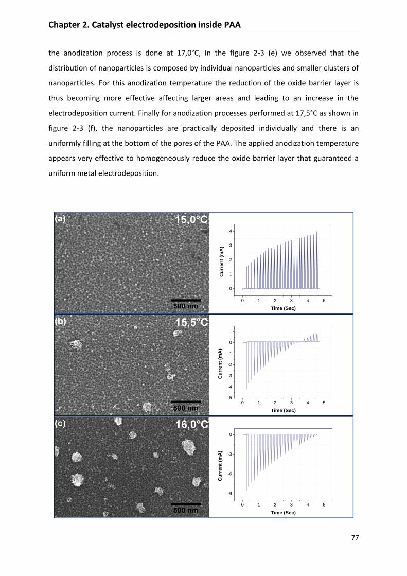
Chapter 2. Catalyst electrodeposition inside PAA
77
the anodization process is done at 17,0°C, in the figure 2-3 (e) we observed that the
distribution of nanoparticles is composed by individual nanoparticles and smaller clusters of
nanoparticles. For this anodization temperature the reduction of the oxide barrier layer is
thus becoming more effective affecting larger areas and leading to an increase in the
electrodeposition current. Finally for anodization processes performed at 17,5°C as shown in
figure 2-3 (f), the nanoparticles are practically deposited individually and there is an
uniformly filling at the bottom of the pores of the PAA. The applied anodization temperature
appears very effective to homogeneously reduce the oxide barrier layer that guaranteed a
uniform metal electrodeposition.
0 1 2 3 4 5
0
1
2
3
4
Cu
rre
nt
(mA
)
Time (Sec)
0 1 2 3 4 5-5
-4
-3
-2
-1
0
1
Cu
rre
nt
(mA
)
Time (Sec)
0 1 2 3 4 5
-9
-6
-3
0
Cu
rre
nt
(mA
)
Time (Sec)

Chapter 2. Catalyst electrodeposition inside PAA
78
0 1 2 3 4 5
-12
-9
-6
-3
0
Cu
rre
nt
(mA
)
Time (Sec)
0 1 2 3 4 5
-18
-15
-12
-9
-6
-3
0
Cu
rre
nt
(mA
)
Time (Sec)
0 1 2 3 4 5
-21
-18
-15
-12
-9
-6
-3
0
Cu
rre
nt
(mA
)
Time (Sec)
Figure 2-3. SEM images of nickel nanoparticles distribution at the bottom of the pores of removed
PAA structure (the alumina is eliminated in a chromic acid solution) and their correspondent
electrodeposition current as function of time. The second anodization process and the exponential
voltage decrease have been performed at different temperatures. The applied potential during the
anodization process is of 40V and the exponential voltage decrease constant is 𝜂 =2.0·10-3 s-1.
During the electrodeposition process 50 sweeps have been applied. The different anodization
temperatures are: (a) 15,0°C, (b) 15,5°C, (c) 16,0°C, (d) 16,5°C, (e) 17,0°C and (f) 17,5°C.
We evidenced that the anodization temperature has a great impact over the efficacy
of the exponential voltage decrease process. Consequently, different behaviors concerning
the metal deposition distribution have been observed in the range of the anodization
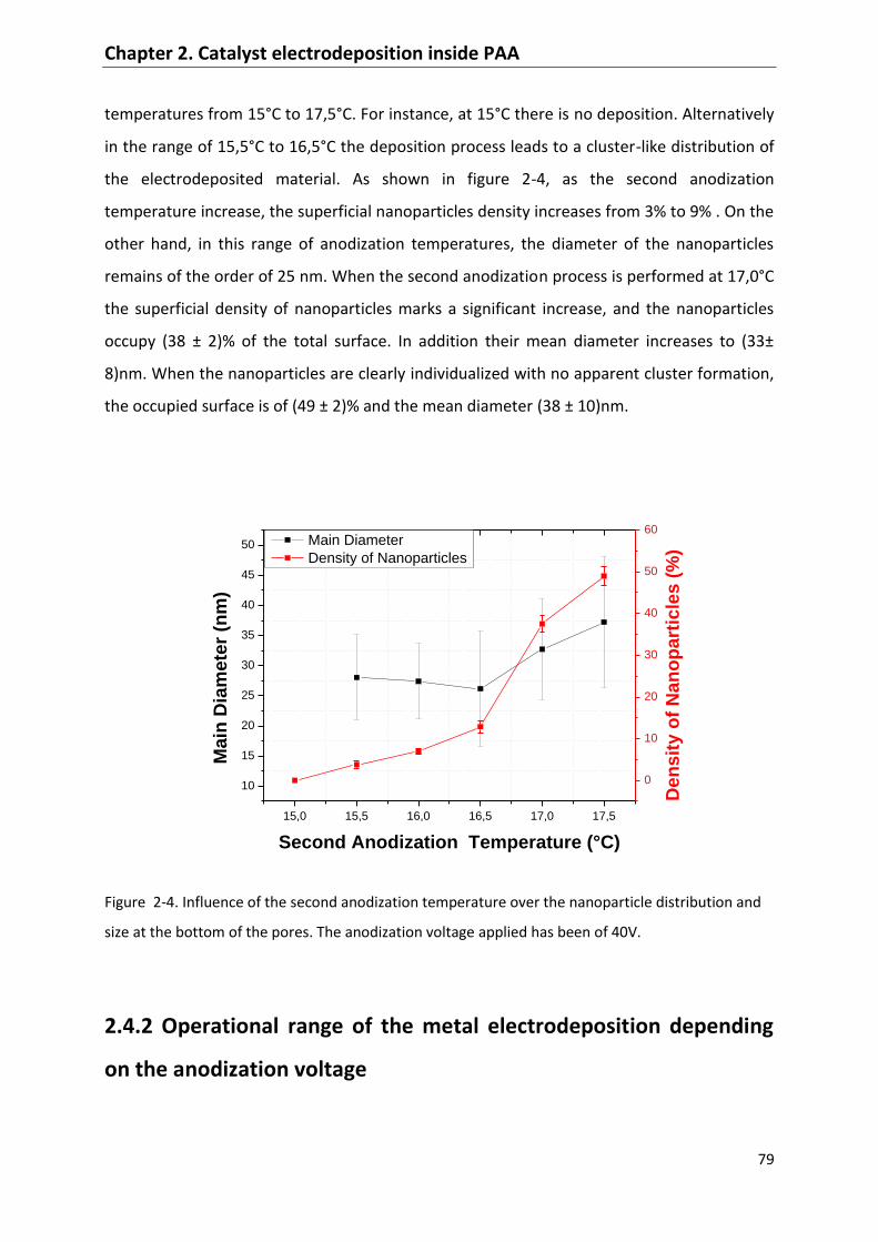
Chapter 2. Catalyst electrodeposition inside PAA
79
temperatures from 15°C to 17,5°C. For instance, at 15°C there is no deposition. Alternatively
in the range of 15,5°C to 16,5°C the deposition process leads to a cluster-like distribution of
the electrodeposited material. As shown in figure 2-4, as the second anodization
temperature increase, the superficial nanoparticles density increases from 3% to 9% . On the
other hand, in this range of anodization temperatures, the diameter of the nanoparticles
remains of the order of 25 nm. When the second anodization process is performed at 17,0°C
the superficial density of nanoparticles marks a significant increase, and the nanoparticles
occupy (38 ± 2)% of the total surface. In addition their mean diameter increases to (33±
8)nm. When the nanoparticles are clearly individualized with no apparent cluster formation,
the occupied surface is of (49 ± 2)% and the mean diameter (38 ± 10)nm.
15,0 15,5 16,0 16,5 17,0 17,5
10
15
20
25
30
35
40
45
50 Main Diameter
Density of Nanoparticles
Second Anodization Temperature (°C)
Main
Dia
mete
r (n
m)
0
10
20
30
40
50
60
Den
sit
y o
f N
an
op
art
icle
s (
%)
Figure 2-4. Influence of the second anodization temperature over the nanoparticle distribution and
size at the bottom of the pores. The anodization voltage applied has been of 40V.
2.4.2 Operational range of the metal electrodeposition depending
on the anodization voltage

Chapter 2. Catalyst electrodeposition inside PAA
80
The impact on the metal electrodeposition process has been studied in the range of
anodization voltage from 20V to 60V with increments of 10V. For all the prepared samples
the second anodization process duration has been set at 500 seconds followed by the
exponential voltage decrease process with the decay rate 𝜂 =2.0·10-3 s-1. The range of
temperature during second anodization process has been varied depending on the
anodization voltage. During the electrodeposition process 50 sweeps have been applied for
all the samples.
One of the most relevant parameter to analyze the impact of the electrodeposition
process is the global charge involved in the reaction. This is a quantitative value given by the
following equation:
𝑄 = ∫ 𝐼(𝑡)𝑑𝑡𝑡𝑓
𝑡𝑖
The figure 2-5 shows the global charge as a function of the anodization temperature
for different anodization potentials. For all the applied potentials, the deposition pattern
follows the same trends as the sample of figure 2-4 where the applied potential is of 40V.
The only difference relies on the range of temperature where the three regimes (non-
deposition, inhomogeneous deposition and individual nanoparticle deposition) are obtained.
The figure 2-5 indicates the non-deposition regime with a red dash lines, pointing out that
for these positive global charges values it is not possible to achieve the nanoparticle
deposition. Between the red dash line and the green dash line we indicated that for such
global charges values an inhomogeneous deposition pattern is obtained, with clusters of
nanoparticles. For higher 𝑄 values, the region delimited from the green dash line indicates
that the deposition of individual nanoparticles at the bottom of the pores is achieved.

Chapter 2. Catalyst electrodeposition inside PAA
81
12,5 15,0 17,5 20,0 22,5 25,0 27,5
-15
-12
-9
-6
-3
0
3
6
Ch
arg
e (
mC
)
Second Anodization Temperature (°C)
20V
30V
40V
50V
60V
Nondeposition Regime
Inhomogeneous
Regime
Individual Nanoparticle
Deposition Regime
Figure 2-5. Relation between the global charge accumulated during the electrodeposition process as
function of the anodization temperatures, for samples anodized in the range of 20V to 60V with
increment of 10V.
Using data plotted in figure 2-5 it is possible to infer the operational range of
temperature for each anodization potential, and the final deposition distribution at the
bottom of the pores. For instance, if the anodization process is performed at temperatures
lowers of 13°C, for an anodization potential of 20V, the electrodeposition current is always
positive preventing the an effective deposition process. For temperatures up to 14.5°C, the
global charge during the electrodeposition process is negative however the deposition is
non-uniform, and the deposition material is cluster-type. From anodization temperature of
15.0°C individual nanoparticles are deposited. On the other hand for anodization voltages of
60V, no material is deposited for anodization temperature lower than 19.0°C, the cluster-
type of distribution of nanoparticles is obtained in the range of temperatures from 19.5°C to
22.0°C, and individual nanoparticles begin to be deposited from temperatures higher than

Chapter 2. Catalyst electrodeposition inside PAA
82
22.5°C. In conclusion the exponential voltage decrease process is effective in different range
of temperatures for each applied anodized potential.
From figure 2-5, in addition to the operational range for each anodization voltage, it
is possible to conclude that higher anodization voltages require higher anodization
temperatures in order to effectively reduce the oxide barrier layer that will lead to a uniform
nanoparticle deposition. This phenomenon can be attributed to the fact of using the same
exponential voltage decrease rate for all the anodization voltages. Evidently, the final
thickness of the oxide barrier layer depends on the anodized voltage in spite of the same
decay rate applied and to finish, the exponential voltage decrease process at the same step.
For instance, figure 2-6 shows the exponential voltage decrease function for each
anodization voltage where we highlight the same final anodization step for each case. This
choice of the final voltage step should theoretically imply that the thickness of the oxide
barrier (𝐷𝐵𝐿) should remain the same for each case, where 𝐷𝐵𝐿 is given by the following
expression:
𝐷𝐵𝐿 = 𝛼𝑈𝐴𝑛𝑜𝑑𝑖𝑧𝑎𝑡𝑖𝑜𝑛
Where 𝛼 is a constant and 𝑈𝐴𝑛𝑜𝑑𝑖𝑧𝑎𝑡𝑖𝑜𝑛 is the applied potential. However as it is
possible to infer from the figure 6 the final thickness of the oxide barrier layer depends on
the anodization temperature and the exponential voltage decrease rate. Therefore a more
exact relation between the 𝐷𝐵𝐿 and the 𝑈𝐴𝑛𝑜𝑑𝑖𝑧𝑎𝑡𝑖𝑜𝑛 can be express as:
𝐷𝐵𝐿 = 𝛼(𝑇, 𝜂)𝑈𝐴𝑛𝑜𝑑𝑖𝑧𝑎𝑡𝑖𝑜𝑛
Where 𝛼(𝑇, 𝜂) depends on the temperature and the exponential voltage decrease rate.
We observe for each anodization voltage that it exists an associated decay rate that is
effective in a certain range of temperature and consequently the thinning process depends
on the anodization temperature. For higher anodization voltages, higher anodization
temperatures are required since the temperature has a direct impact on the enhanced field-
assisted dissolution of the oxide at the oxide/electrolyte interface.

Chapter 2. Catalyst electrodeposition inside PAA
83
Anodization Process
Exponential Voltage Decrease Process
0 200 400 600 800 1000 1200
0
10
20
30
40
50
60
70A
no
diz
ati
on
Vo
ltag
e (
V)
Time (Seconds)
Final voltage step= 4,97 V
Figure 2-6. Applied voltage during the second anodization process for the PAA fabrication. In solid
line the anodization potential followed in dash line by the exponential voltage decrease process. For
each anodize voltage 𝜂 =2.0·10-3 s-1 is the voltage decay rate and the final voltage is 4.97 V.
2.4.3 Influence of the pore length on the electrodeposition process
The anodization process duration has been the same for all the applied potentials
therefore longer pores are obtained for higher anodization potential, due to higher
anodization voltages which induce higher currents. In this study the anodization duration
has been varied in order to establish how the pore length affects the deposition process. The
first experiments were carried out with samples obtained (different anodization time) with
anodization potential of 30V, an anodization temperature of 17,5°C and an exponential
voltage decrease rate 𝜂 =2.0·10-3 s-1. Figure 2-7 shows the global charge accumulated as
function of the pore length. Additionally to the impact of the pore length on the
electrodeposition process, in the same graph we indicated the global charge accumulated

Chapter 2. Catalyst electrodeposition inside PAA
84
during the electrodeposition process of two samples obtained with an applied anodization
potential of 60V at two different anodization temperatures, 17,5°C in which case no
deposition is obtained and 25,0°C where the deposition is successfully performed. For all the
samples the electrodeposition process consisted of 50 applied sweeps.
0 1500 3000 4500 6000 7500
-15
-10
-5
0
5 30V-17,5°C
60V-17,5°C
60V-25°C
Ch
arg
e (
mC
)
Pore length (nm)
Figure 2-7. Graph of global accumulated charge during the electrodeposition process as function of
the pore length. The samples have been fabricated at anodization potential of 30V, an anodization
temperature of 17,5°C and with an exponential voltage decrease rate of 𝜂 =2.0·10-3 s-1. The
anodization time has been varied to obtain different pore length. These samples are compared with
the global charge obtained for the samples obtained with an anodization voltage of 60 V at
corresponding anodization temperatures of 17,5°C and 25,0°C.
In conclusion from figure 2-7 we can observe that the pore length in the studied
range does not significant affect the electrodeposition process. The nanoparticles
distribution is not highly affected considering that the global charge accumulated during the
electrodeposition process decrease in absolute values only 35% for a pore length variation
from 6 µm. This diminution in the charge can be attributed to a more complicated ion
transport inside the pores during the deposition process. It can also be related to a less

Chapter 2. Catalyst electrodeposition inside PAA
85
effective diffusion of the 0.3M H3PO4 solution during the pore widening process, in which
case the thinning process is becoming less effective. On the other hand, no deposition is
obtained when the sample is anodized at the same temperature but with an anodization
voltage of 60V, in which case the pore length was 5,3 µm. We corroborated that the
anodization temperature is more determinant than the pore length, because the
electrodeposition takes place applying the same voltage but increasing the anodization
temperature at 25,0°C which induces a higher anodization current that leads to a longer
pore formation. Therefore as previously discussed, the anodization temperature plays a
crucial role for the thinning barrier layer process that in turn will strongly impact the
electrodeposition process, the pore length variation over a relatively extended range has a
relatively low to negligible influence.
2.4.4 Evidence of metal nanoparticles deposited at the bottom of
the pores
Previously has been showed nanoparticles could be successfully deposited at the
bottom pores. Nonetheless such nanoparticles must furthermore play a catalytic role for the
synthesis of carbon nanostructures. In order to verify that the chemical composition and the
nature of the deposed material, chemical mapping analysis has been performed.
In the figure 2-8 is showed a chemical map carried out at the bottom pores zones
using the Electron Energy Loss Spectroscopy (EELS) technique in the Energy Filtered
Transmission Electron Microscopy (EFTEM) image mode. Figure 2-8 (a) shows the selected
area where the chemical mapping has been performed. As result in figure 2-8 (b), is
observed that the zone corresponding to the aluminum is in black revealing the absence of
nickel or oxygen. On the other hand, the surface occupied by the nanoparticles is colored in
green showing the presence of atomic nickel. Finally in red indicates the presence of oxygen,
in this case corresponding to the PAA zone. The figure 2-8 (c) and (d) are the EELS spectra
registered on the O K and Ni K ionization edges, respectively.

Chapter 2. Catalyst electrodeposition inside PAA
86
Figure 2-8. Chemical map performed at the bottom of the pores using the EELS technique in the
EFTEM imaging mode. (a) Region selected to carry out the chemical map. (b) Chemical mapping
indicating in red the atomic presence of oxygen and in green the atomic existence of atomic nickel.
(c) EELS spectra registered on the O K ionization edges. (d) EELS spectra registered on the Ni K
ionization edges.
We may conclude that the deposited nanoparticles within the PAA templates are
promising catalysts in terms of morphology and nature for catalyzing the CVD synthesis of
CNTs.

Chapter 2. Catalyst electrodeposition inside PAA
87
2.4.5 Number of catalytic nanoparticles electrodeposited per pore
Generally for the synthesis of CNTs the catalyst deposition plays a crucial role on the
final synthetized structure. Besides the metal deposition, in the particular case of the
synthesis within the PAA the pore structure the pore structure can highly affects the CVD
growth carbon nanostructures. For instance a branched structure can be impacted by
clogging during the growth inside the pores, since the gaseous precursors molecules lose
energy due to collisions with the pore walls avoiding the carbon appropriate diffusion
towards/inside the catalyst; in addition the growing CNTs can suffer mutual blocking among
them when they emerge from secondary branched pores and reach the primary pore.
Therefore, it is important to acquire relevant information of the bottom pore’s structure
before to proceed to the synthesis of carbon nanostructures within PAA templates.
Figure 2-9 shows a cross section TEM image corresponding to a PAA template with
electrodeposited nanoparticles at the bottom pores. The PAA was fabricated with an
anodization potential of 30V at 17,5°C. In figure 2-9 (a) are indicated the different zones of
the template as the PAA structure and the aluminum. At the bottom of the pores the nickel
nanoparticles are pointed as well as the presence of a branched pore structure near to the
interphase between the PAA and the aluminum. This structure reflects that the pore
formation evolves straight until the exponential voltage decrease process begins. In figure 10
(b) under a higher magnification it is possible to clearly identify the branched structure,
however in order to properly assess the number branches for each pore a tomography study
must be performed. The most important fact to highlight is that the nanoparticles
electrodeposition is successfully achieved in spite of a branch structure at the bottom of the
pores. However it is necessary to analyses the branch multiplication phenomenon regarding
the synthesis of carbon of nanostructures. In the present work we have introduce an
interesting approach that involves the nanoparticle deposition at the bottom of the pores in
order to count the number of branches created per primary pore during the exponential
voltage decrease process.

Chapter 2. Catalyst electrodeposition inside PAA
88
Figure 2-9. TEM cross-section of a PAA template anodized at 30V with anodization temperature of
17,5°C. The lamella has been obtained by FIB fabrication/manipulation. (a) PAA structure with
nanoparticles deposited at the bottom of the pores. (b) Zone of the bottom of the bottom of the
pores.
The adopted strategy to calculate the number of secondary pores generated per each
primary pore, consists in the comparison of the pore top surface with the pore distribution
at the bottom of the pores. The pore shape at the bottom of the PAA can be easily
performed measuring the density of the electrodeposited nanoparticles. From figure 2-6 is
possible to obtain the required electrodeposition conditions in order to achieved filling rate
of the pores close to 100%. Under these conditions, after the deposition process, the nickel
nanoparticles should cover completely the related “hole” left by the bottom pore. Avoiding
an over deposition state, the metal electrodeposition will than reflect the fingerprint of the
previous shape/state of the bottom of the pores. Figure 2-10 shows a schematic
representation of the procedure implemented to obtain the number of branches generated
by pore. Therefore properly adjusting the deposition conditions and by the subsequent
elimination of the PAA structure via selective chemical attack, it become possible to obtain
the bottom pores distribution that reflects the number of secondary branched pores
generated by primary pore. Afterwards, in order to have a notion of the number of branches
created for each primary pore, it is necessary to compare the number of nanoparticles per

Chapter 2. Catalyst electrodeposition inside PAA
89
cm2 with the number of the pores of the PAA per cm2. This correlation directly yield the
number of nanoparticles deposited in each primary pore. This approach provides a
quantitative notion of the number of branches generated during the exponential decrease
process.
Figure 2-10. Schematic representation of the procedure in order to deduce the distribution of the
bottom pores after the exponential voltage decrease process.
The figure 2-11 is shown the nanoparticles deposited at the bottom of the pores with
filling rate close to 100% while avoiding the overdeposition of nanoparticles into primary
pores. Correlating figure 2-11 and figure 2-4 (f), which satisfices the same requirements
previously mentioned, it is possible to estimate the bottom pores distribution before the
electrodeposition process, when anodization process is carried on in the voltage range of
20V to 60V with increments of 10V. Applying the same procedure implemented to calculate
the porosity of the PAA (section 1.6.2), the number of nanoparticles per unit of area can be
deduced.

Chapter 2. Catalyst electrodeposition inside PAA
90
Figure 2-11. Metal nanoparticles deposited at the bottom of the pore after the PAA selective etching.
The electrodeposition conditions applied are chosen in order to achieve a 100% branched pores
filling rate while avoiding the overdeposition of the nanoparticles into the primary pores. (a)
anodization voltage of 20V and electrolyte temperature of 16,5°C, (b) anodization voltage of 30V and
electrolyte temperature of 17,5°C, (c) anodization voltage of 50V and electrolyte temperature of
22,5°C and (d) anodization voltage of 60V and electrolyte temperature of 25,0°C. The
electrodeposition conditions have been the same for all the samples and 50 sweeps have applied for
each sample, whilst the exponential voltage decrease has been of 𝜂 =2.0·10-3 s-1.
The figure 2-12 (a) provides the information (above discussed) in order to calculate
the number of branches generated for each pore. The figure 2-12 (a) is the graph of the
density of pores and nanoparticles per unit of area in the logarithmic scale as function of the
anodization voltage. We can remark that the density of the pores decreases as the
anodization voltage increases. On the other hand the density of nanoparticles per unit area
fluctuates between 4.9x10⁻⁴ and 8,3x10⁻⁴. From the relation between the density of
nanoparticles and the density of the pores, we derived as is shows the plot in figure 14 (b)
the estimated number of nanoparticles deposited in each primary pore, for anodization

Chapter 2. Catalyst electrodeposition inside PAA
91
process in the voltage range of 20V to 60V. As the anodization voltage increases, the number
of nanoparticles deposited in each pore significantly increases. For instance for an
anodization voltage of 20V just two nanoparticles are deposited per pore, on the other hand
for the anodization voltage of 60V an averaged 10 nanoparticles are deposited in each pore.
Assuming that every bottom branched pore has been filled with one nanoparticle during the
electrodeposition process it is possible to consider that the number of nanoparticles
deposited for each primary pore is equal to the number of branches generated per pore
during the exponential voltage decrease process.
20 30 40 50 60
1E-5
1E-4
1E-3
Density of pores
Density of Nanoparticles
Voltage (V)
De
ns
ity
of
po
res
(1
/nm
2)
4,5E-4
6E-4
7,5E-4
9E-4
(a)
De
ns
ity
of
Na
no
pa
rtic
les
(1
/nm
2)
20 30 40 50 60
2
3
4
5
6
7
8
9
10
11
12
13
(b)
Rela
tio
n N
P/P
ore
s
Voltage (V)
Figure 2-12. (a) Measure of the density of pores per unit of area and density of nanoparticles per unit
of area in as function of the anodized voltage. (b) Calculated relation between the numbers of

Chapter 2. Catalyst electrodeposition inside PAA
92
nanoparticles deposited in each pore during the electrodeposition process as a function of the
anodization voltage.
We remark that when implementing the same exponential voltage decrease rate for
higher applied voltages the number of branches created for each pore is higher. Such
phenomenon of branch multiplication can be related to the fact of imposing the same
exponential voltage decrease regardless of the chosen anodization voltages. As the voltage
drop and the final applied voltage are the same for all the cases, the boundary conditions for
the exponential decrease process implies that the higher anodization voltages will require
more time to finalize the thinning process. Consequently longer exponential voltage
decrease process promotes the branches multiplication.
Anyway in order to obtain a more detailed analysis of the impact on the exponential
voltage decrease rate on the pore structure it is necessary to perform tomography studies,
thus a fully reconstruction of the pore structure can be obtained and subsequently also an
assessment of the number of branches per pore. Nevertheless it is important to highlight
that with the approach carried out in the present work it is possible to obtain a quantitative
result of a three dimensions structure (branch structure) from the analysis of a two
dimension distribution (electrodeposition of nanoparticles at the bottom of the pores),
providing precious information for both the synthesis of CNTs and from a more general
perspective for the further devices fabrication.
Under these PAA fabrication conditions, only the templates fabricated in the range of
20V to 30V are promising candidates for the synthesis of carbon nanotubes. The other type
of templates exhibits too numerous branch structure that can induce “clogging” side-effect
during the carbon nanostructure growth.
2.6 Conclusions

Chapter 2. Catalyst electrodeposition inside PAA
93
The electrodeposition process has been successfully carried out at the bottom of the
pores of the PAA templates. The influence of several anodization conditions has been
studied, such as the anodization temperature, the anodization voltage and the pore length.
The results obtained shows that the anodization temperature has a huge impact on the
oxide barrier layer formation at the bottom pores that in turn strongly impact the
electrodeposition process in terms of size, distribution and density of nanoparticles. For
higher anodization voltages, higher anodization process temperatures are require in order to
obtain a homogeneous distribution of nanoparticles. On the other hand, in the range of
pores length studied, from 100 nm to 6 µm, the pore length does not seem to have a
significant impact over the deposition process.
Through a chemical mapping analysis performed at the bottom of the pores by the
Electron Energy Loss Spectroscopy (EELS) technique in the Energy Filtered Transmission
Electron Microscopy EFTEM image mode, it has been evidenced that the material deposited
at the bottom of the pores are nickel nanoparticles.
A branched pore structure at the bottom of the pores has been observed from the
lamella preparation of the PAA templates and the further observation by TEM microscopy.
Nanoparticles have been electrodeposited at the bottom of the branched secondary pores
with a filling rate close to 100%. Subsequently by comparing the number of nanoparticles
deposited and the number of primary pores per unit of area, we obtained a relation of the
number of branches generated per pore for a range of anodization voltages. In the range of
anodization voltage from 20V to 60V we evidenced that for same value of the constant of
the exponential voltage decrease process, as the anodization voltage increase the number of
branches created per pore is increasing.
The results obtained provide valuable information for the further development of the
synthesis of carbon nanotubes within PAA templates in order to obtain the maximum
density of tubes per unit of area, a desirable characteristic for the device fabrication in the
present work.

Chapter 2. Catalyst electrodeposition inside PAA
94
References
[1] M. Zemanová, et al., "Nickel electrolytic colouring of anodic alumina for selective solar absorbing films," Renewable Energy, vol. 33, pp. 2303-2310, 2008.
[2] Z. Shaterabadi, et al., "Modification of microstructure and magnetic properties of electrodeposited Co nanowire arrays: A study of the effect of external magnetic field, electrolyte acidity and annealing process," Materials Chemistry and Physics, vol. 160, pp. 389-397, 2015.
[3] H.-N. Umh, et al., "Fabrication of gold nanowires (GNW) using aluminum anodic oxide (AAO) as a metal-ion sensor," Korean Journal of Chemical Engineering, vol. 32, pp. 299-302, 2015/02/01 2015.
[4] L. Li, et al., "Direct Electrodeposition of ZnO Nanotube Arrays in Anodic Alumina Membranes," The Journal of Physical Chemistry C, vol. 111, pp. 7288-7291, 2007/05/01 2007.
[5] J. Mallet, et al., "Growth of Silicon Nanowires of Controlled Diameters by Electrodeposition in Ionic Liquid at Room Temperature," Nano Letters, vol. 8, pp. 3468-3474, 2008/10/08 2008.
[6] A. P. Leontiev, et al., "Arrays of rhodium nanowires based on anodic alumina: Preparation and electrocatalytic activity for nitrate reduction," Electrochimica Acta, vol. 155, pp. 466-473, 2015.
[7] H. Liu, et al., "Optical properties of porous anodic alumina embedded Cu nanocomposite films," Optical Materials, vol. 44, pp. 9-12, 2015.
[8] N. Ke, et al., "Carbon nanotube diameter control via catalytic Co nanoparticles electrodeposited in porous alumina membranes," Rsc Advances, vol. 5, pp. 25747-25754, 2015.
[9] Y. Pang and R. Chandrasekar, "Cylindrical and Spherical Membranes of Anodic Aluminum Oxide with Highly Ordered Conical Nanohole Arrays," Natural Science, vol. 7, p. 232, 2015.
[10] B. S. Simpkins, et al., "Controlling the Crystallinity of Electrochemically Deposited CdS Nanowires," The Journal of Physical Chemistry C, vol. 117, pp. 11843-11849, 2013/06/06 2013.
[11] T. Gao, et al., "Template synthesis of single-crystal Cu nanowire arrays by electrodeposition," Applied Physics A, vol. 73, pp. 251-254, 2001/08/01 2001.
[12] D. Xu, et al., "Preparation and characterization of CdS nanowire arrays by dc electrodeposit in porous anodic aluminum oxide templates," Chemical Physics Letters, vol. 325, pp. 340-344, 2000.
[13] S. Dellis, et al., "Electrochemical synthesis of large diameter monocrystalline nickel nanowires in porous alumina membranes," Journal of Applied Physics, vol. 114, p. 164308, 2013.
[14] N. Zafar, et al., "Effects of pH on the crystallographic structure and magnetic properties of electrodeposited cobalt nanowires," Journal of Magnetism and Magnetic Materials, vol. 377, pp. 215-219, 2015.
[15] N. Adeela, et al., "Fabrication and temperature dependent magnetic properties of nickel nanowires embedded in alumina templates," Ceramics International, vol. 41, pp. 12081-12086, 2015.
[16] A. Brudzisz, et al., "Effect of processing parameters on pore opening and mechanism of voltage pulse detachment of nanoporous anodic alumina," Electrochimica Acta, vol. 178, pp. 374-384, 2015.
[17] V. Caboni, "Italian Patent 339 232," 1936. [18] N. J. Gerein and J. A. Haber, "Effect of ac Electrodeposition Conditions on the Growth of High
Aspect Ratio Copper Nanowires in Porous Aluminum Oxide Templates," The Journal of Physical Chemistry B, vol. 109, pp. 17372-17385, 2005/09/01 2005.

Chapter 2. Catalyst electrodeposition inside PAA
95
[19] K. Nielsch, et al., "Uniform nickel deposition into ordered alumina pores by pulsed electrodeposition," Advanced Materials, vol. 12, pp. 582-586, 2000.
[20] M. P. Proenca, et al., "Ni growth inside ordered arrays of alumina nanopores: Enhancing the deposition rate," Electrochimica Acta, vol. 72, pp. 215-221, 2012.
[21] U. S. Mohanty, "Electrodeposition: a versatile and inexpensive tool for the synthesis of nanoparticles, nanorods, nanowires, and nanoclusters of metals," Journal of Applied Electrochemistry, vol. 41, pp. 257-270, 2011/03/01 2011.
[22] C. Frantz, et al., "Pulse electrodeposition of adherent nickel coatings onto anodized aluminium surfaces," Applied Surface Science, vol. 330, pp. 39-47, 2015.
[23] L. Zaraska, et al., "Analysis of nanopore arrangement and structural features of anodic alumina layers formed by two-step anodizing in oxalic acid using the dedicated executable software," Applied Physics A, vol. 114, pp. 571-577, 2014/02/01 2014.
[24] R. Pinner, et al., "Factors Affecting the Formation of Anodic Oxide Coatings," Journal of the Electrochemical Society, vol. 102, pp. 359-360, 1955.
[25] B. Marquardt, et al., "Density control of electrodeposited Ni nanoparticles/nanowires inside porous anodic alumina templates by an exponential anodization voltage decrease," Nanotechnology, vol. 19, Oct 8 2008.
[26] S. Lee, et al., "Anodized pore structural evolution of focused ion beam patterned Al: direct analysis of branched nanopores and nanosacks," Physical Chemistry Chemical Physics, vol. 15, pp. 10659-10665, 2013.
[27] B. Chen and K. Lu, "Influence of Patterned Concave Depth and Surface Curvature on Anodization of Titania Nanotubes and Alumina Nanopores," Langmuir, vol. 27, pp. 12179-12185, 2011/10/04 2011.
96
Chapter 3.
Synthesis of carbon nanotubes within PAA
templates
Since the first observation of the MultiWall-Carbon NanoTubes (MWCNT) reported
by Ijima in 1991 [1], CNTs have been in the focus of many research studies due to the
behaviors of their quasi one dimension structure. As a result of such studies until nowadays
it has been proven that the CNTs present unique and exceptional thermal, mechanical and
electronic properties and remarkable chemical stability [2-5]. Consequently the CNTs have
expanded the limits for a wide range of applications. However even if individual CNTs
present excellent properties, there are still several challenges to overcome in order to
fabricate devices based on CNTs. The main difficulties rely on the alignment of the tubes [6],
the contacting [7] and the control of the electrical characteristics in terms of the chirality of
the tubes [8].
Collectively CNTs organization via the synthesis inside PAA templates is a quite
promising method to improve the main problems related with the synthesis of self-
organized CNTs. In addition due to the PAA versatility the CNTs can be synthetized with a
wide range of diameters, lengths and densities.
In the present chapter after the presentation of the main properties and applications
of the CNTs, the different synthesis methods in order to growth the CNTs are addressed. In
particularly the hot filament chemical vapor deposition (HF-CVD) technique and their
corresponding experimental set-up are introduced and discussed. Finally the main results
obtained of the synthesis of CNTs within PAA templates are presented pointing out the

Chapter 3. Synthesis of carbon nanotubes within PAA templates
97
properties of collectively organized device. The impact of the synthesis parameters and
boundaries conditions imposed by the template on the CNTs structures is investigated. The
obtained results in the present studies provide the accurate procedure in order to satisfy
one of the main objectives of the present work: the growth of aligned and collectively
ordered CNTs compatible with the device fabrication.
3.1 Characteristics and physical properties of carbon
nanotubes
The CNTs can be represented as graphene sheets rolled into cylinders. The number of
rolled up graphene sheets determines the type of tube, such as single-walled or multi-walled
as shown in figure 3-1. In a graphene sheet the carbon is sp2 hybridized forming a honey-
comb lattice.
Figure 3-1. Schematic representation of SWCNTs and MWCNTs.
The circumference of a SingleWall-Carbon NanoTube (SWCNT) is established by the
chiral vector which connects two different crystallographic sites. Therefore the structure of

Chapter 3. Synthesis of carbon nanotubes within PAA templates
98
two-dimensional graphene sheet is described by a unit cell as shown in figure 3-2 (a), such
unit cell which connects two different crystallographic sites. It is defined by the chiral vector
described in the following expression:
𝐶 = 𝑛𝑎1⃗⃗⃗⃗⃗ + 𝑚𝑎2⃗⃗⃗⃗⃗
Where 𝑎1⃗⃗⃗⃗⃗ and 𝑎2⃗⃗⃗⃗⃗ are the unit cell vectors of the two-dimensional lattice which
formed by the graphene sheet, and 𝑛 and 𝑚 are integrals numbers [9]. The chiral angle 𝜃
represents the angle between the 𝐶 and 𝑎1⃗⃗⃗⃗⃗ vectors. Therefore 𝜃 is given by:
𝜃 = tan−1 (√33
𝑛
2𝑚 + 𝑛)
The diameter 𝑑 of the carbon nanotube is given by the circumferential length 𝐿 as is
shown in the following expression:
𝑑 = 𝐿
𝜋=
|𝐶 ∙ 𝐶|
𝜋=
𝑎√𝑛2 + 𝑚2 + 𝑛 ∙ 𝑚
𝜋
Where 𝑎 = 2.49 �̇� is the constant lattice.
Finally, SWCNTs can be described by the chiral vector 𝐶, or by their diameter 𝑑 and
the 𝜃 angle. However, since the graphene sheet is the sum of the unit vectors, the cell is
usually described just with two integer numbers (𝑛, 𝑚) that determines the chiral vector.
Such integer values define three different types of CNTs. For instance, the armchair type
satisfies that 𝑛 = 𝑚 and in terms of the chiral angle 𝜃 = 30°. The zig-zag mode of CNT
verifies that 𝑚 = 0 meaning that chiral angle 𝜃 = 0°. The named chirals CNTs have integers
numbers (𝑛, 𝑚) with 𝑛 ≠ 𝑚 ≠ 0 which imply CNTs with chiral angles 0 < 𝜃 < 30°. The
figure 3-2 highlights the distinct CNTs types depending on the integers values 𝑛 and m . The
most important aspect to highlight is that the electronic, optical and mechanical properties
of the SWCNTs depend on their chirality.

Chapter 3. Synthesis of carbon nanotubes within PAA templates
99
Figure 3-2. The crystal lattice structure of a graphene sheet. The chiral vector 𝐶 is defined by the unit
vectors 𝑎1⃗⃗⃗⃗⃗ and 𝑎2⃗⃗⃗⃗⃗ with integers values 𝑛 and 𝑚. These integers values determines how the tube is
rolled up, therefore the chirality of the tube depends on the combination of such values. The three
different chiral possibilities of the SWCNT,armchair, zig-zag and chiral, are pointed out depending on
the chiral vectors.
3.1.1 Electronic properties
The most important aspects to point out concerning the electronic properties of the
CNTs are that the reduced phase space for scattering of the carriers leads to a ballistic or
quasi-ballistic transport. Consequently, power dissipation is low. The strong covalent bonds
of the carbon atoms provide a high mechanical and thermal stability, additionally a high
resistance to electromigration. For instance the current densities measured in carbon
nanotubes are high as 109 A/cm2 [10].
On the other hand the electronic behavior for the SWCNTs is determined by the
rolled up of the graphene sheets. As mentioned previously, the chirality of the SWCNTs is

Chapter 3. Synthesis of carbon nanotubes within PAA templates
100
defined by the integers numbers (𝑛, 𝑚), such numbers establish the electronic properties of
the tubes. For instance, the tubes that satisfy the relation |𝑛 − 𝑚| = 3𝑖 behave as metallic
conductors, in contrast when |𝑛 − 𝑚| = 3𝑖 ± 1 the SWCNTs have semiconducting
properties, where 𝑖 is an integer number. Conversely, the conducting behavior of the
MWCNT results more complicated to describe since every graphene sheet can be rolled up
differently leading to distinct conducting behaviors. Anyway CNTs with large diameters are
conductive at room temperature, therefore the chirality in this case is not critical [11] but
the diameter plays a crucial role. This is due to the fact that for semiconducting SWCNT the
energy gap 𝐸𝐺 depends on the nanotube diameter 𝑑, the nearest neighbor carbon bond
length 𝑎 and the 𝑉0 = −2.7 𝑒𝑉 nearest-neighboring tight-binding parameter [12]. The
energy gap 𝐸𝐺 of semiconducing SWCNT is given by:
𝐸𝐺 =𝑎𝑉0
𝑑
At room temperature 𝑘𝐵𝑇 ≈ 0.0258 𝑒𝑉, consequently, for diameters larger than 15
nm the energy gap becomes smaller than 0.0258 𝑒𝑉 which implies that all the shells of the
MWCNT including the semiconducting ones have a metallic conducting behavior. On the
other hand the transport in the MWCNTs strongly depends on the electrical contact, where
the transport can be dominated by just the outer-shells [13-16], on the contrary when a
perfect contact is achieved between the probe and the tube, all the rolled graphene sheets
contribute to the electron conduction [11]. Therefore the MWCNTs present 1-D or 2-D
transport characteristics depending on their structure and the contact with an electrode.
In conclusion in order to use the CNTs as building block for further electronic device
fabrication, it will be crucial the control of the tube structure, in particularly the chirality and
the tube diameter.
3.1.2 Optical properties
The low dimensionality of carbon nanotubes provides a quantum confinement for
electrons which impacts over the optical properties. Such confinement implies a typical
feature of one-dimensional crystal that relies in the formation of Van Hove singularities [17]

Chapter 3. Synthesis of carbon nanotubes within PAA templates
101
which are characterized of electronic transitions with energy levels related with a certain
density of states [18] that descends gradually and then increase in a discontinuous spike. On
the contrary three-dimension materials have a continuous density of states (DOS), the figure
3-3 shows the typical dependence of the electronic DOS for different dimensionalities.
Figure 3-3. Characteristic electronic density of state for different dimensionalities.
The Van Hove singularities are associated with remarkable optical properties, since in
agreement with the Fermi’s Golden Rule for any optical transition that is resonant with the
Van Hove singularities they are expected to be greatly enhanced [19]. Figure 3-4 shows the
electronic density of states (DOS) related to a single-walled nanotube.
Additionally the energies between the Van Hove singularities depend on the CNT
structure. Besides the optical transitions are sharp, therefore result relatively easy to detect
optical signals from individual CNTs with certain (𝑛, 𝑚) indices. Consequently, varying the
structure of individuals CNTs it is possible to obtain and detect different optoelectronic
properties [20-22]. It is important to point out that such optical results have been obtained
in SWCNTs [23] and MWCNTs [19]. However, in the case of the MWCNTs the tubes have to
satisfy certain structural conditions associated with their diameter and purity in order to

Chapter 3. Synthesis of carbon nanotubes within PAA templates
102
mask the fact that MWCNTs contain a mixture of tubes with small and larger diameters and
tubes presenting different chiralities that are coupled by Van der Waals interactions.
Figure 3-4. Band diagram and their corresponding one-dimensional density of state for (a) metallic
single-walled nanotubes and (b) semi-conductive single-walled nanotubes. The 𝑉1 → 𝐶1 correspond
the first Van Hobe optical transition and 𝑉2 → 𝐶2 the second Van Hobe optical transition.
Consequently it is preferable to perform Raman spectroscopy, photoluminescence
and optical absorption in order to fully characterized the structural of the CNTs. Besides the
optical response can be implemented for the separation of CNTs depending on their
structure [24] and a further device fabrication [25, 26].
3.1.3 Mechanical properties
Carbon covalent bond in the basal plane of graphite is the strongest of all chemical
bonds in nature; therefore carbon nanotubes have exceptional mechanical properties. For
instance theoretical calculations show that the Young’s modulus of an isolated SWCNT does
not depend on their chirality or their aspect ratio and has a value of the order of TPa [27].

Chapter 3. Synthesis of carbon nanotubes within PAA templates
103
Furthermore it has been reported through in-situ measurements that the experimental value
of an individual MWCNTs is 1.8 TPa [28], nevertheless this value decrease with the increasing
value of the nanotube diameter [29]. However the stiffness of the CNTs is subject to
different types of defects [30].
In spite of the very high Young’s modulus, by using atomic force microscopy it has
been proven that nanotubes can be bend into loops without any crack [31], revealing that
the CNTs are flexible, tough and possess a great capacity for reversible deformation. In
addition it has been reported that SWCNTs with small diameters can be elongated by a 30%
before breaking [32], and concerning the breaking strength value of 55 GPa has been
obtained [33]. On the other hand the tensile strength performed on MWCNTs reveals that is
lower in comparison with SWCNTs since the inner shells starts to pulled out breaking the
outermost layer [34].
In summary the CNTs have a high Young’s modulus value, a great capacity of
deformation and a high strength tensile value, besides a great aspect ratio can be obtained
since is possible to obtained ultra-long CNTs with heights of the order of tens of centimeter
[35]. Therefore due to their exceptional and unique mechanical properties CNTs are highly
used in diverse applications on mechanical devices and as reinforce for composite
fabrication.
3.1.4 Thermal properties
The CNTs are expected to be good thermal conductors along the tube axis due to the
ballistic conduction, and good insulators lateral to the tube axis. However the thermal
properties have not been so widely studied as the electronic, optical or mechanical one’s.
Such studies are still in development. The difficulty relies heavily on the difficult
manipulation of individuals tubes. From a theoretical approach, simulation has suggested
that the lattice thermal conductivity of a SWCNT with lattice indices of (10,10), reaches the
maximum value of approximately 37000 𝐾
𝑊∙𝑚 at 100 K and decreases to approximately 6600

Chapter 3. Synthesis of carbon nanotubes within PAA templates
104
𝐾
𝑊∙𝑚 at 300 K [36]. Nevertheless, due to the diverse methods of measuring and the different
sample qualities, the experimentally measured thermal conductivity value κ strongly varies
from 200–25 000 W 𝐾
𝑊∙𝑚 [37-39]. Recently it has been reported that the intrinsic thermal
conductivity of perfects crystalline SWCNTs is approximately 4000 𝐾
𝑊∙𝑚 . In addition
depending on the CNT structure and chirality it has been measured that κ tends to grow
with the increase on the SWCNT diameter [40]. Anyway further studies must be performed
in order to exploit all the thermal properties of the CNTs for the device fabrication.
3.2 Carbon nanotubes based devices
Since their discovery diverse investigations have been focused in the implementation
of CNTs for the device fabrication due to the exceptional mechanical, electronic, optical, and
thermal properties. The versatility of the CNTs and their uniqueness excellent properties
open the frontiers of the applications in widely different fields. In figure 3-5 a summary of
the implementation of CNT by major industry sector is given [41].
For instance due to their strong carbon covalent bond the CNTs have been used as
reinforcement for the fabrication composites [42, 43]. Basically the properties improved of
the composites are due to the reinforcement CNTs which includes: tensile strength and
tensile modulus toughness, glass transition temperature, thermal conductivity, electrical
conductivity and, solvent resistance [44]. Therefore this kind of material can be used in a
wide range applications such as the aerospace industry [45, 46], bike construction or tennis
racquets [47]. However the biggest challenge to overcome for the composite fabrication is
the homogeneous dispersion of CNTs which is complicated due to the Van der Waals
interaction among then [48].
Besides the excellent mechanical properties due to their high electronic conductivity
the CNTs have been chosen for various tip applications [49-52], in particular for the tip of
atomic force microscopy [53-55] and scanning tunneling microscopy [56, 57].

Chapter 3. Synthesis of carbon nanotubes within PAA templates
105
Figure 3-5. Global CNT demand by different field of application [41].
On the other hand CNTs are used as building block for the energy conversion and
storage devices [58-60], in particular, as electrodes for lithium-ion batteries due to their high
cyclic stability, however they are limited by a low capacity [60, 61]. On the contrary, silicon
has been extensively used as anode material due to the high gravimetric capacity.
Consequently, many efforts have been devoted to synthesizing CNT/Si composite materials,
which are expected to provide their individual advantages to guaranteed both requires
characteristics for the lithium-ion electrodes high specific capacity and cyclic stability. In the
same way, exploiting their unique tubular structures and superior electrical properties,
which leads to a fast ions and electrons transportation, vertically aligned densely packed
CNTs have been used as supercapacitors [62-64].
The CNTs are additionally used in order to fight against the environmental pollution
caused by toxic metals (heavy metals, radioactive metals) by the removal of toxic metals
from contaminated water. The CNTs have been used among diverse developed adsorbents,

Chapter 3. Synthesis of carbon nanotubes within PAA templates
106
because they present an exceptional effect on the fast adsorption and rapid removal of toxic
impurities from the aqueous source [65, 66].
In the following section it will highlight the implementation of CNTs with applications
that exploit the electronic and optoelectronics properties of such carbon nanostructures, in
particular the application associated with the synthesis of CNTs which have been grown
collectively organized.
3.2.1 CNTs-Based sensors
Their unique electrochemical, electronic and optical properties of CNTs provide a
unique platform for the fabrication of sensors based on electrochemical [67], electrical [68]
or optical signal outputs [69]. Moreover the high surface-to-volume ratio is a very attractive
characteristic in order to enhance the sensitivity of the CNTs-based sensors. In some cases
the CNTs have not the intrinsic recognition ability for sensing a certain entity. Therefore
CNTs can be hybridized with a component having specific recognition in order to perform
the proper sensing process [70, 71]. Due to development technique of the CNTs
functionalization, nowadays the diversity of sensors fabricated based on CNTs is extensive,
for instance there are sensors devoted for drug detection [72, 73], for the flow
measurement [74], as well for the detection of different gas species such as
𝑁𝐻3, 𝑁𝑂2, 𝐶𝑂2, 𝑂2, 𝐻2, 𝐴𝑟 among others [75-77]. Moreover there are a great diversity of
biosensors [75, 76], in particular this sort of sensor results very attractive because the
effective detection area can be made into the size of a single biomolecules or virus, thus the
characteristics lengths of the detector are from the same scale of the specific kind of
molecular to distinguish.
In conclusion a great variety of CNTs based sensors has been developed, the main
challenge relies in the CNT manipulation and the acquisition of the signal responsible of the
sensing performance. In our particular work the synthesis of CNTs within PAA templates

Chapter 3. Synthesis of carbon nanotubes within PAA templates
107
provides a platform for a collective organization of the CNTs and a simple method to
perform electrical [78] or optical measurements [79] toward a sensing device fabrication.
3.2.2 CNTs-based interconnects
The continuous device miniaturization using copper as wiring material causes
undesirable size effects in the interconnected systems. For instance there is a considerable
difference of thermal expansion of copper (17.5 ppm/k) with the thermal expansion of the
silicon (2.5ppm/k), this can induces a huge stress between both interphases. Besides the
maximal current density of copper is 107 A/cm2. These phenomena can lead to stress
migration and electro migration effects. Therefore alternatives technologies have to be
developed in order to overcome the continuous down scaling devices guarantying a low
resistivity and a high reliability. The International Technology Roadmap for Semiconductors
(ITRS) proposed several emerging technologies to replace copper in future interconnect
schemes [80] and projected carbon nanotubes as a very promising candidate due to their
extraordinary already mentioned thermal, electrical and mechanical properties.
The approach in order to resolve and improve the characteristics of metal-based
interconnects integrated circuit technology is called three dimensional integration. This
methodology will allow a decrease in the total length of the wiring in a given circuit, stacking
chips to make use of the vertical direction to integrate more components and functions in
the same device. The implementation requires simultaneously a high CNT quality and a large
CNT density. Many efforts have been addressed in order to develop this technique, however
performance advantage of three-dimensional integration cannot achieved the values of the
theoretical predictions for the CNTs [81, 82]. For instance Fiedler et. al measured the
resistance of a MWCNT with 20 shells, the resulting resistance of such nanotube is of 38
kΩ/CNT, two order of magnitudes higher than the theoretical value of 6.5 kΩ/CNT [83]. The
biggest obstacle to overcome is the CNT’s synthesis temperature, which on one hand
impacts on the CNT quality and on the other hand affects the electrical contact through the
interfacial oxide layers created during the CNT growth [81]. Recently Xu et.al [84] have

Chapter 3. Synthesis of carbon nanotubes within PAA templates
108
developed a procedure to avoid the constrains imposed by the temperature fabrication,
however they have not performed any electrical characterization of the device.
3.2.3 Field emission devices
Electrons are generally confined to the surface of bulk material by an energy barrier
roughly equivalent to the work function ɸ. The electrons can be emitted from such bulk
material under thermal excitation leading to a named thermionic emission mechanism. On
the other hand the field emission process can take place by quantum mechanical tunneling.
Under the application of a sufficiently strong electric field, electrons near to the Fermi level
tunnel to the energy barrier and escape to the vacuum level. The emitted current depends
on the local electric field at the emitting surface E, and on its work function ɸ. Figure 3-6
shows a schematic diagram of field emission process from a metal at absolute zero
temperature. Under the presence of a strong field the barrier formed along the line AB is
deformed promoting the electron tunneling phenomenon.
Figure 3-6. Diagram of the energy-level scheme for field emission from a metal at absolute
zero temperature.

Chapter 3. Synthesis of carbon nanotubes within PAA templates
109
The Fowler-Nordheim equation determines the behavior of a field emitting system
current which is given by the following expression,
𝐼 =𝑎 ∙ (𝛽 ∙ 𝐸)2
𝜑𝑒𝑥𝑝 (−
𝑏 ∙ 𝜑−3/2
𝛽 ∙ 𝐸)
where I is the field emission current density, φ is the work function, E is applied pontential,
the constants 𝑎 and 𝑏 are 1.54 × 10⁻⁶ A(eV)V−2and 6.83 × 10⁹ (eV)−3/2 Vm−1 respectively [85],
finally 𝛽 is named as the field enhancement factor which is equal to the aspect ratio of the
material which is affected by the applied field.
The current emission density equation implies that the current can increase by
several ways: decreasing the work function, increasing the applied electric field, increasing
the enhancement factor and a combination of all the mentioned factors.
Since the enhancement factor depends strongly on the aspect ratio of the emitter,
one of the simplest ways to generate a high enhancement is the utilization of a sharp object.
Carbon nanotubes satisfy many requirements to act as field emission tip due to the strength,
chemical stability, electronic conductivity and mainly due to the high aspect ratio.
The first reports have been made by Heer et al. [86] and Rinzer et al. [87] on the
field emission from films and individual multiwall carbon nanotubes respectively, such works
triggered the fabrication of field emitter devices on different substrates [88-90] and by
different techniques [91-93] .
The field emission process using CNTs as emitters are highly affected by two factors:
the morphology of the CNT and the density of CNTs. For instance the SWCNTs present a
higher enhancement factor value than the MWCNTs, however the MWCNTs have a lower
degradation rate. In addition the performance are also affected by the presence or not of
the catalyst at the tip of the CNT and if the tip is close-type or open type [94]. Concerning
the CNTs density, the field emission properties are affected by the distance between the
field emitter objects [95, 96]. A dense CNT structure suffers an electrostatic screening effect
generated by the neighboring proximity leading to a limitation field emission performance.
A pillar array of aligned CNT bundles has shown better field emission performance [97].

Chapter 3. Synthesis of carbon nanotubes within PAA templates
110
Despite the progresses achieved in the field emission domain there are still many
efforts to perform. For instance, reliability and reproducibility are the main factors. The
electrical breakdown and current degradation are the two biggest limiting causes of the
reliability of CNT based field emitters. In order to address such restrictions a new generation
of field emission devices are recently constructed based on the hybridization of CNTs and
graphene sheets [98-100], and carbon nanotubes supported nanowires [101, 102].
3.3 Synthesis of carbon nanotubes
Basically there are three types of methods that can be considered for synthetizing
synthetized CNTs. Arc discharge and laser ablation have been the first techniques used to
produce high quality CNTs but nowadays these methods have been mainly replaced by
chemical vapor deposition (CVD) techniques. The figure 3-7 illustrates the schematic
representation of the basic different CNT growth techniques.
The discovery of CNTs has been realized by Ijima and the production method
implemented was the arc-discharge [1]. The most common methods use DC arc discharge
between two graphite water-cooled electrodes as is indicated in figure 3-7 (a). The carbon
nanotube formation is generated due to the sublimation of the carbon-contained in the
negative electrode product under the high temperature arc discharge. Generally the
synthesis is performed at temperatures above 1700°C which leads to the production of CNTs
with a few amounts of defects. Both kinds of tubes can be synthetized, for the synthesis of
SWCNTs the anode is composed of graphite and a metal, such as Ni, Fe or Co. On the other
hand for the production of MWCNTs the absence of catalyst is required.
The laser ablation method has been introduced by Smalley group [103]. Typically
such technique is used to synthetized different fullerenes. Similar to the arc-discharge
technique as is shown in figure 3-8 (b), the CNTs are obtained due to laser vaporization of
graphite at temperatures of the order of 1200°C. The characteristics of the CNTs synthetized
depend on many parameters such as: the laser properties (energy fluence, peak power,

Chapter 3. Synthesis of carbon nanotubes within PAA templates
111
repetition rate and oscillation wavelength), the structural and chemical composition of the
target material, the chamber pressure and the chemical composition, flow and pressure of
the buffer gas, the substrate, and the distance between the target and the substrates. Both
types of CNTs can be synthetized by the laser ablation method, with highly pure graphite
electrode are obtained SWCNTs. For the synthesis of MWCNTs is necessary to used
MWCNTs targets as electrodes [104]. Anyway such technique is mostly executed in order to
obtain high pure SWCNTs.
Figure 3-7. Different methods in order to synthetize CNTs. (a) Arc-discharge, (b) laser ablation and (c)
chemichal vapor deposition (CVD).
The main problem of the arc-discharge and laser ablation procedures is the
production of carbon sub-products. Therefore a purification process must be carrying out in
order to separate the CNTs from the residual carbon. In addition the high temperatures
constrain the range of substrates that can be used. For these reasons the chemical vapor
deposition (CVD) technique has been widely implemented because the operational ranges of
temperatures are between 500-1000°C. Although a worse crystallinity of the tubes is
obtained, the carbon sub-products created during the synthesis are highly reduced. Besides
Chapter 3. Synthesis of carbon nanotubes within PAA templates
112
the CVD technique allows to control orientation, alignment, nanotube length, diameter,
purity and density of the synthetized CNTs.
3.3.1 Chemical Vapor Deposition (CVD) method
The prevailing method for the synthesis of CNTs is the chemical vapor deposition
method. In addition of the already mentioned benefits the CVD method is a low-cost
implemented technique. However the main advantages rely in the easy control of the CNTs
characteristics by varying the factors involved in their synthesis. Therefore a good
understanding of the synthesis parameters is required in order to obtain the desire carbon
nanostructure.
The synthesis of CNTs takes place when a carbon containing gas precursor is injected
into a reactor as is show in figure 3-7 (c). The process can be performed with or without
catalyst [105], however in presence of a catalytic nanoparticle the growth control is more
predictable, since the growth behavior and the final CNTs structure is highly determines by
the catalyst. The hydrocarbon used as gas precursor can be decomposed either thermally or
by enhanced plasma. The growth model of CNT is still discussed nowadays [106, 107]. Two
different growth mechanisms are proposed: the vapor-liquid-solid (VLS) and the vapor-solid-
solid mechanism (VSS). In the VLS case the catalytic nanoparticle form a liquid alloy between
the carbon and the metal, subsequently carbon atoms start to diffuse through the
nanoparticle and eventually precipitate at the nanoparticle surface forming the tube
structure [108]. In contrast, in the VSS mechanism the carbon atoms just diffuse through the
catalytic surface and the diffuse carbon precipitates leading the formation of CNT without
the formation of a liquid alloy between the carbon atoms and the nanoparticle [109].
The main CVD parameters that impacts over the CNT structures are: the process
temperature, the precursor gas and the vapor pressure. For instance the graphitization
quality of the CNTs is affected by the temperature process. In order to obtain less defective
carbon nanostructures higher synthesis temperatures are required. The range of

Chapter 3. Synthesis of carbon nanotubes within PAA templates
113
temperature to successfully growth CNTs are determined mainly by the carbon precursor
and catalyst type. For the synthesis of SWCNTs the nanoparticles impose a biggest constrain
[110, 111], however temperatures higher than 700°C are required in order to synthesized
SWCNTs with a low degree of impurities. Generally lowers process temperatures are
required for the synthesis of MWCNTs [112]. The gas precursor is another factor that has a
great impact on the final carbon structure generating sub-products due to a carbon excess
feedstock. Basically the only condition that has to satisfy the feedstock gas is the presence of
carbon in their molecular composition. Thus a great variety of precursors have been used for
the synthesis of CNTs, from waste chicken fat [113], coconut oil [114] to camphor [115].
However one of the most used gas precursor is acetylene (C2H2) since their easy
decomposition at relatively low temperatures. Nevertheless the high carbon content can
lead to the deposition of amorphous carbon on the sidewalls of the CNTs. Methane (CH4)
results an alternatively in order to avoid an over carbon deposition, however higher process
temperatures are required. The growth control and the carbon supply are also determined
by the vapor pressure. The total vapor pressure is given by the contribution of the gas
pressure of the carbon feedstock precursor, reductive gas and a carrier gas. Therefore a
proper balance among each gas has to be achieved, because a too low vapor pressure of the
gas precursor CNTs will not be created and on the contrary too high vapor pressure will lead
to the deposition of parasitic amorphous carbon that decreases the CNT quality an even can
clog the growth. Furthermore the growth dynamics it will be affected by the pretreatment
conditions [116, 117] and an eventual assistance energy source applied to decompose the
carbon feedstock such as: microwave plasma [118], DC plasma [119], RF plasma [120] or hot
filament [121].
3.3.2 Catalyst for the synthesis of CNTs
Conventionally the synthesis of CNTs is performed using catalyst nanoparticles since
the particle can defines and determines quality and characteristics of CNT. Various catalyst
types have been used for the CNT synthesis like Al, Mg, Sn, Cr, Mo and Mn [122]. However

Chapter 3. Synthesis of carbon nanotubes within PAA templates
114
transition metals such as Iron (Fe), Cobalt (Co) and Nickel (Ni) result to be result the most
effective catalyst to grow CNT [123]. Such metals have high carbon solubility and diffusion
rate at high temperature. Furthermore, they have stronger adhesion with the CNT produced
at the end of the process and potential in forming high curvature of CNT. Every catalyst
metal leads to different synthesis results, for instance, the catalytic activity of metal species
towards carbon deposition was found to decrease in the following order Nickel > Cobalt >
Iron [124]. In terms of the graphite structure the best results are obtained with cobalt
nanoparticles [125]. In the same group of transition metals, Pt, Ag, Cu, and Pd have been
also used for the CNT growth.
Despite the inherent characteristics of the catalytic nanoparticle, the interaction
between the catalyst and the substrate plays a crucial role. There are two different growth
behaviors as indicated in figure 3-8. When the catalyst is strongly attached to the support
layer, the CNT formation is product of the base-growth mode, as is shown in figure 3-8 (a). In
contrast, when the interaction between the catalyst and the support layer is weak the tip-
mode growth takes place, as is schematized in figure 3-8 (b).
Figure 3-8. The different growth mode depending on the interaction between the catalyst and the
support layer. (a) Tip-growth mode and (b) Base-growth mode.
It is important to note that under the ideal situation where one tube growths per
each pore of the PAA, and assuming that the tube is confined by the pores walls, the growth
Chapter 3. Synthesis of carbon nanotubes within PAA templates
115
mode inside the PAA structure which can only takes place is the tip-growth mode, otherwise
the grown CNT will clog the tube formation. Then it would be impossible forthe hydrocarbon
to reach the catalyst due to the boundary conditions imposed by the pore walls. The base-
growth mode can occur when the formed carbon structure is not confined by the pore walls.
Regarding towards an electrical device application, the tip-mode results a highly desirable
contact mode, because in such case the contact between CNT and certain electrode is
governed by the nanoparticle. An consequently, it opens the possibility to the creation of
Schottky Barrier [139]. Therefore the chemical nature of the nanoparticle at the CNT tip can
determine the electrical behavior of the fabricated device.
3.3.2 Organized growth of carbon nanotubes
Different kinds of approaches have been developed in order to control the collective
order of the CNTs. There are three possible ways to obtain an organized distribution of CNT
over a substrate: after the synthesis of CNTs, during the growth of the CNTs and before the
synthesis.
For instance, the organization after the CNTs synthesis consists in the dispersion of
already synthetized CNTs over a substrate by spin coating [126] or printed circuits [126]. This
kind of strategy is compatible with flexible substrates, however all the characteristics of the
CNTs are not controllable and consequently it results very difficult to obtain aligned CNTs
with difficulties to get an electrode contact.
On the other hand aligned CNTs can be obtained controlling the synthesis
parameters without any pretreatment over the substrate [127, 128]. During the catalyst
dissociation, the nanoparticle reaches an optimal size for carbon nucleation, and the
surrounding carbon transforms into a graphite tube. There exists an optimal inter-particle
distance that leads to continue aligned nanotube formation perpendicular to the substrate
direction [129]. Nevertheless this kind of approach limits mainly the CNTs density.

Chapter 3. Synthesis of carbon nanotubes within PAA templates
116
The most generalized adopted strategy in order to growth CNTs in predetermine sites
consist in the fabrication of patterned substrates. The catalyst is patterned by different
approach as laser writing, multiphoton lithography and focused ion beam milling [130].
These sorts of techniques can design arbitrary forms however there are serial methods
which imply a lower surface throughput. On the other hand locally directed actions that
interacts with a certain template by mechanical stresses, capillary forces or electromagnetic
fields, allows the creation of novel self-organized designs without throughput limitations
[131]. The major difficulty is that many of the mentioned processes require further
development to achieve high production rates and uniformity over large areas.
The synthesis of CNT within PAA templates results a solution in order to address the
problem of the collectively self-organized growth. The PAA structure provides an ordered
structure without the requirements of lithography steps. Besides, the catalyst can be easily
deposited at the bottom of the pores by a reliable and low cost process as the
electrodeposition process. In addition the anodization process offers the opportunity to
control the PAA structural characteristics. As the pore diameters present the same size as
the grown CNTs the pore can serve as guide for the future tube grown. Therefore the CNTs
grown inside growth parallels among then isolated with a given inter-tube distance. The
whole processes are compatible with large-scale production which attracts the interest of
many research groups [132-137].
3.4 Experimental set-up
In the present work the synthesis of CNTs has been carried out by the hot-filament
assisted chemical vapor deposition (HF-CVD) technique. This technique allows the local
thermal decomposition of the molecules involved in the synthesis at certain distance of the
sample with the catalyst nanoparticles. The implementation of the HF-CVD technique
enables the synthesis of CNTs at relatively lower temperatures than the conventional
thermal CVD process [138]. The figure 3-9 schematized the HF-CVD system pointing out the

Chapter 3. Synthesis of carbon nanotubes within PAA templates
117
two hot filaments. The filament can be powered independently in order to increase the
temperature locally leading to the molecule decomposition.
Figure 3-9. Schematic design of the hot filament chemical vapor deposition (HFCVD) system.
Methane has been chosen as the precursor gas and molecular hydrogen (H2) in order
to perform a pretreatment before the growth of the CNTs and to etch continuously the
parasitic amorphous carbon deposited in the sidewalls during the CNTs synthesis. Tungsten
filaments of 0.38 m thick are placed at each gas inlet. Subsequently the hydrocarbon
feedstock can be regulated by varying the hot filaments power. Different amount of
hydrocarbon and carbon atom can be created. The filament power for the molecular
hydrogen determines the energy of the hydrogen atoms which attack the parasitic
amorphous carbon.
In order to study the impact of the hot filament power (HFP) over the CNT structure
different ranges of power have been chosen. Additionally different pretreatment conditions
have been executed to study the impact of such treatment over the deposited nanoparticles.
The HF-CVD system has two different zones as indicated in the figure 3-9. This
configuration allows the exposition of the sample at high temperatures just for the desired

Chapter 3. Synthesis of carbon nanotubes within PAA templates
118
processes to be performed. The figure 3-10 shows the whole procedure for the synthesis of
CNTs with the respective position of the sample in each step. For instance during the heating
stage, the sample is located at the cooling zone. Subsequently when the set conditions of the
pretreatment process are achieved, the sample is translated in the process zone. When the
pretreatment is finished, the synthesis of the CNTs immediately begins. Finally when the
synthesis of CNTs is stopped the sample is moved again to the cooling zone while in the
process zone the temperature is decreasing.
Regime Sample position Process stage
1 Cooling zone
Heating
2 Process zone Pretreatment (Catalyst reduction & formation)
3 Process zone
CNT growth
4 Cooling zone
Cooling
Figure 3-10. Procedure to synthesized CNTs by the HF-CVD technique indicating the position of the
sample during the different processes stages.
The parameters values applied during the pretreatment and synthesis process are
summarized in table 3-1. The pressure, gas flow, HFP and temperature have been taken as
reference from previous works [138, 139]. On the other hand the synthesis duration has
been adjusted in order to control the nanotube length.

Chapter 3. Synthesis of carbon nanotubes within PAA templates
119
Process Pressure
[mbar]
H2 flow
[sccm]
CH4 flow
[sccm]
HFP H2
[W]
HFP CH4
[W]
Temperature
[°C]
Duration
[s]
Pretreatment 50 100 - 0-200 - 500-600 0-300
Synthesis 50 50 50 0-200 0-200 500-600 45-900
Table 3-1. Parameters values applied during the pretreatment and synthesis process for the
synthesis of CNTs by the HF-CVD technique.
3.5 Results of the synthesis of carbon nanotubes within
vertical-PAA templates
There are two main aspects that will determine the device behavior: the density of
CNTs per unit of area and the contact mode between the CNT and the electrode that collect
charges carriers. In the present work different studies have been executed in order to
maximize these two desirable characteristics for the further device fabrication based on CNT
grown inside vertical-PAA templates. The resulting CNTs growth is basically govern by the
geometrical characteristics of the PAA structure and the synthesis conditions. First we have
analyzed the interaction between catalyst and the supporting aluminum at different
temperature conditions. On the other hand the influence of the hot-filament power on the
CNT structure has been studied via Raman spectroscopy. In addition the influence of the
anodization voltage on the CNT growth behavior has been studied. As we have already
proved under the introduced template fabrication process, each anodization voltage is
associated with a different branched structure at the bottom of the pores. The impacts of
the structure at the bottom of the pores have been analyzed by electron microscopy studies
carried out on cross-sections samples prepared by FIB milling. Finally the influence of the
pore length over the density of CNTs synthesized inside the PAA template has been study in
order to maximize the number of contacts of the future fabricated devices.

Chapter 3. Synthesis of carbon nanotubes within PAA templates
120
3.5.1 Nanoparticles pretreatment
Conventionally, before the synthesis of CNTs a pretreatment under H2 atmosphere is
performed in order to improve the catalytic activity of the nanoparticles [140, 141]. However
these pretreatments can modify the interface between the catalyst and the support.
Therefore, it results of paramount importance to investigate the interaction between the
catalyst nanoparticles and the support, and the absence of any catalyst diffusion inside the
support material, and to block the catalytic activity of the nanoparticle by contamination
from substrate.
Different pretreatment conditions have been applied; subsequently the PAA layer
has been selectively removed in order to observe the nanoparticles at the bottom of the
pores. Figure 3-11 shows the nanoparticles distribution after applying three different
pretreatment conditions. For the sample preparation the two step anodization procedure
has been performed at 17,5°C with an anodization voltage of 30V. For the nanoparticles
deposition 50 sweeps have been applied during the electrodeposition process. Concerning
the pretreatment conditions as shown in table 3-1, the samples have been pre-treated at
500°C keeping the pressure at 50 mbar under molecular hydrogen. The introduced variations
have been the time duration process and the activation of the H2 hot filament power.
The figure 3-11 (a) shows the nanoparticles at the bottom of the pores for sample that has
been exposed at 500°C during 2 minutes. There are not any meaningful differences with the
same sample before the pretreatment but after the electrodeposition process as are shown
in chapter 2. When the pretreatment duration is increased up to 15 minutes, as is shows in
figure 3-11 (b) the sample starts to suffer the exposure to high temperatures creating
irregularities on topography of the bottom of the pores. As it is pointed out in figure 3-11 (c),
this effect is even more pronounced when the hot filament is activated during two minutes
with a power of 200 W. Under these conditions the catalyst starts to diffuse into the
aluminum foil.

Chapter 3. Synthesis of carbon nanotubes within PAA templates
121
Figure 3-11. SEM analyses on the distribution of the nanoparticles at the bottom of the pores after
different pretreatment conditions. (a) 500°C in H2 atmosphere during 2 minutes, (b) 500°C in H2
atmosphere during 15 minutes and (c) 500°C in H2 atmosphere during 15 minutes and the hot
filament activated with a power of 200W.
These analyses allowed us to conclude on the fact that the pretreatment conditions
that do not affects the interaction between the nanoparticles and the substrates are those
applied to sample exposed in the 500°C in H2 atmosphere during 2 minutes. Such conditions
have been taken as reference and have been used for the fabrication of all the samples.

Chapter 3. Synthesis of carbon nanotubes within PAA templates
122
Besides, we have realized that these conditions provide information for the further
synthesis of CNTs evidencing that long time exposure of the sample at 500°C has to be
avoided, in order to not damage the structure of the future device
3.5.2 Influence of the hot filament power on the CNTs
Compared with the conventional thermal CVD process the hot-filament assisted CVD
process allows to dissociate locally the molecules involved in the synthesis of CNT when they
pass along the hot-filament. Therefore the energy of the dissolved molecules will impact
over the CNT formation inside the PAA template.
Both hot-filament powers have been varied in order to analysis the impact over the
CNT quality. The template preparation has been performed using the two-step anodization
process with an anodization voltage of 30V and an electrolyte temperature of 17,5°C. For the
catalyst deposition, 50 sweeps have been applied. Concerning the growth of CNTs, the
temperature process has been set at 500°C, the total pressure 50 mbar and the gas flow has
been set to 50 sccm for both gases involved during the synthesis. The ranges of powers
studied have been 0W to 200W for both filaments. The synthesis duration has been of 600
seconds in order to obtain a spaghetti-like structure at the top of the PAA template.
Typical Raman spectra were carried out in order to obtain a quantitative value of the
CNT quality. The amount of defects present in the formed CNT is determined by the D-band
which indicates the disordering level and the G-band which evidence the graphitization level
of the synthesized carbon nanostructure. Finally the intensity ratio between the D-band and
G-band provides the information of the structural quality of the CNT, where lowers values of
𝐼𝐷 𝐼𝐺⁄ imply better quality of the synthesized CNT.
Figure 3-12 shows the Raman spectra obtained for the CNTs synthesized with
different hot filament power.

Chapter 3. Synthesis of carbon nanotubes within PAA templates
123
0 500 1000 1500 2000 2500 3000 3500
0,0
0,2
0,4
0,6
0,8
1,0G-Band
Inte
ns
ity
(a
.u)
Raman shift (cm-1)
CH4=130W H
2=180W
CH4=180W H
2=130W
CH4=180W H
2=180W
CH4=0W H
2=200W
CH4=200W H
2=0W
CH4=200W H
2=200W
D-Band
Figure 3-12. Raman spectra of grown CNTs using different hot filament powers of CH4 and H2.
Table 3-2 summarizes the 𝐼𝐷 𝐼𝐺⁄ values obtained for the different ranges of hot-
filament powers applied during the growth of CNTs. The obtained results reveal that the hot-
filament powers in the studied range do not significant affects the quality of the CNTs. On
the other hand the activation of one of the filament is required for the successful synthesis
of the CNTs.
𝑯𝑭 − 𝑷𝑪𝑯𝟒 [𝑾] 𝑯𝑭 − 𝑷𝑯𝟐
[𝑾] 𝑰𝑫 𝑰𝑮⁄
0 0 No CNTs obtained
130 180 1,08
180 130 1,11
200 0 1,17
0 200 1,15
200 200 1,13
Table 3-2. 𝐼𝐷 𝐼𝐺⁄ ratio obtained for different values of hot-filament powers applied during the
synthesis of CNTs.

Chapter 3. Synthesis of carbon nanotubes within PAA templates
124
As the hot filament power does not significantly affects the CNTs quality, the power
values has been adjusted in each case considering the technical aspect as the variability from
the set it values in each synthesis. In spite of the HFP values have not influence on the final
CNT structure, the activation of at least one filament is vital for the successful synthesis of
CNTs for the applied temperatures, flow gases and pressures.
3.5.3 Influence of the branch structure over the synthesis of CNTs
The PAA fabrication entails an exponential voltage decrease process, then a
branched structure is created at the bottom of the pores, as it is evidenced from the
comparison between the number of pores and the number of deposited nanoparticles. Due
to the porous structure, the growth of CNTs inside the PAA is completely different compared
with the growth on conventional plane substrates. In the porous configuration, the
hydrocarbons have more difficulty to reach the catalyst nanoparticles. The scenario is
aggravated with the presence of a branch structure at the bottom of the pores. Such
structure leads to energy losses of the hydrocarbon due to collisions with the pore walls
complicating the carbon diffusion into the catalytic nanoparticle. Even if the tubes are
formed they can be clogged among then when they reach the main pore. From figure 2-14 it
is proved that when the anodization process is performed with an exponential voltage
decrease of η =2.0·10-3 s-1 the number of branches generated during the barrier thinning
process for each pore depends on the anodization voltage. In the range of 20V to 30V
between two and three deposition sites are created per pore, as the anodization voltage
increases the number of branches also increases, for instance when the anodization voltage
is 40V in average 5,6 secondary pores are produced by pore, for 50V in average 7 secondary
pores and for anodization voltage of 60V, 10 secondary pores are created for each primary
pore.
Figure 3-13 displays the obtained CNTs grown in PAA templates anodized in the
range of 20V to 50V. The anodization conditions implemented have been adjusted in order
to successfully deposit the nanoparticles at the bottom of the pores. The same synthesis

Chapter 3. Synthesis of carbon nanotubes within PAA templates
125
conditions have been used for all the samples. Both filaments have been activated during
the CNT synthesis at a power of 180W and 130W for the H2 and CH4 filaments, respectively.
The synthesis temperature has been set at 500°C and 10 minutes duration process has been
considered.
For anodization voltages of 20V and 30 V, as shown in figures 3-13 (a) and (b) the
synthesis of CNTs is successfully carried out. In both samples the CNTs cover all the PAA
templates with a typical spaghetti-type distribution [142]. Under this kind of CNTs
distribution it is not possible to identify the amount of CNTs grown for each pore, however it
is possible to conclude that a high CNTs yield is obtained. In contrast when the anodization
process is performed applying 40V the amount of CNTs drastically decreases as shown in
figure 3-13 (c). When the anodized voltage is of 50V there are not any CNTs that reach the
top surface of the PAA structure as is indicated in figure 3-13 (d).
Figure 3-13. SEM analyses on CNTs synthetized within the PAA templates for different anodization
voltages (a) 20V, (b) 30 V, (c) 40V and (d) 50V. For the template fabrication a two anodization step
has been performed with 50 sweeps during the electrodeposition process in order to fill the pores
with nanoparticles. The differences for each sample rely on the anodization voltage with their
associated optimal anodization temperature for the electrodeposition process.

Chapter 3. Synthesis of carbon nanotubes within PAA templates
126
The obtained results are in complete agreement with the mentioned model introduced in
chapter 2 which predicts that the branched structure at the bottom of the pores created
during the exponential voltage decrease process makes significantly difficult the CNTs
growth. Therefore the anodization conditions highly affect the CNT formation. In order to
directly verify the effect imposed by the geometrical features of the PAA template fabricated
with an anodization voltage of 40 V, different cross-section of PAA lamella have been
prepared by FIB milling. Figure 3-14 contains TEM images of the cross-section of the PAA
template in which the synthesis of CNTs has been carried out. As it can be observed most of
the metal nanoparticles remain at the bottom of the pores zone, despite carbon
nanostructures have been formed, most of such structures cannot successfully evolves
outside the branched pore region. We attributed this phenomenon to the mentioned
branched structure at the bottom of the pores that hinders the CNTs formation.
Figure 3-14. Cross-sectional TEM images obtained through FIB milling of the PAA template. PAA
template fabricated with an anodization voltage of 40V, after catalyst deposition the CNTs synthesis
has been performed. The right of the image shows a magnification over the bottom of the pores.

Chapter 3. Synthesis of carbon nanotubes within PAA templates
127
From the obtained results we have chosen to perform the anodization with voltages
in the ranges of 20V to 30V. These anodization voltages lead to a PAA matrix with a more
disorder pore structures but guaranteed the growth of CNTs with higher yields.
3.5.4 Evolution of CNTs inside the PAA templates
For the fabrication of devices based on vertical templates it is crucial to control the
CNTs length. In order to connect individually each CNTs with an electrode the CNTs lengths
must be ideally the same as the pore length. Therefore, the synthesis of CNTs has to be
stopped when the CNTs reach the top of the PAA surface, otherwise when the tubes emerge
from the pores, they lost the confinement and a disorder CNTs distribution is obtained with
undesirable contacts among the carbon nanostructures.
Figure 3-15 shows SEM micrographs of CNTs growth inside PAA where the synthesis
duration has been varied for each sample.
The PAA templates have been fabricated by the two step anodization procedure,
with a second anodization duration time of 500 seconds, the anodization voltage of 30 V and
the electrolyte temperature of 17.5°C. The deposit the catalyst nanoparticles have been
made with 50 sweeps. For the synthesis of CNTs both filaments have been activated with a
power of 200W and 130W for the H2 and CH4 filaments, respectively. The synthesis
temperature has been fixed at 500°C and the duration process has been varied for each
sample. For the sample shown in figure 3-14 (a) the synthesis duration is of 180 seconds; we
can clearly observe the tips of the CNTs reaching the PAA top surface. When the synthesis
process least 195 seconds as is shown in figure 3-14 (b) that the CNTs begin to come out
from the pores, this is the initial configuration that leads to the spaghetti-like structure. This
kind of distribution is obtained when the synthesis duration takes 225 seconds as indicated
in figure 3-14 (c). The spaghetti-like structure results in an unwanted type of distribution
since the collective organization of the CNTs is lost outside the PAA structure. The time

Chapter 3. Synthesis of carbon nanotubes within PAA templates
128
duration process is a key parameter for the pore length which finally determines the CNTs
distribution.
Figure 3-15. SEM analyses of CNTs grown inside PAA templates fabricated following the two-step
anodization process for different durations of the CNTs synthesis: (a) 3 minutes, (b) 3.25 minutes and
(c) 3.75 minutes. The template fabrication is identical for the three samples.
On the other hand from figures 3-15 (a) and (b) we can estimate the number of CNTs
grown per pore. Under the described conditions 30% of nanotubes are grown from the total
number of pores.
In order to identify the evolution of the CNTs inside of the PAA templates a cross
section observation of the porous structure has been performed through the lamella
preparation using the FIB and further TEM observation. This procedure shed light over the
growth behavior inside the PAA structure as summarized in figure 3-16. The synthesis
duration has been stopped at three different times. For instance figures 3-16 (a) and (b)

Chapter 3. Synthesis of carbon nanotubes within PAA templates
129
shows the CNTs inside the PAA structure synthesized with a duration process of 60 seconds ,
the figure 3-16 (c) and (d) the process duration has been least 120 seconds and 180 seconds
for figures 3-16 (e) and (f). The common denominator in the three prepared samples is the
presence of Ni catalyst at the bottom of the pores. This fact can indicate that there is an
excess of deposited catalyst in order to growth the carbon nanostructures, but additionally it
can indicate the possible growth modes that can take place at the bottom of the pores. From
the SEM top views of figures 3-15 and 3-19 we can infer that the tip-grow mode occurs for
the CNTs that reach the PAA top surface, however it is important to point out that in such
cases the diameter of the CNTs and pore diameter are the same, therefore the tip-growth
mode is the only the one that can take place because the tubes are confined and carbon
feedstock can diffuse only through the catalyst. On the other hand, the presence of catalyst
at the bottom of the pores, and the fact that from figure 3-16 is not always possible to
identify the catalyst at the tip of each carbon nanostructures reflect that the base-growth
mode cannot be discarded when the synthetized CNTs are not confined by the pore walls.

Chapter 3. Synthesis of carbon nanotubes within PAA templates
130
Figure 3-16. FIB cross sections TEM analyses on samples for different durations of CNTs synthesis.
The syntheses of CNTs have been performed in three identical PAA templates. The synthesis duration
has been the only varied parameter. The synthesis processes have been: (a) and (b) 60 seconds, (c)
and (d) 120 seconds and (e) and (f) 180 seconds. The blue dashes lines indicate the average height
that CNTs reach inside the pores. The white dashes lines point out the standard deviation with
respect the mean height value
A comparison among the average height that the CNTs reach inside the PAA structure has
been performed. The dash blue line in figures 3-16 (a), (c) and (e) indicates the mean height

Chapter 3. Synthesis of carbon nanotubes within PAA templates
131
that the CNTs reach inside the PAA structure for different synthesis duration. The white dash
lines indicate the standard deviation of the height reached by the CNTs from the mean
value. It is important to point out that the height reached by the CNTs can highly differs from
the CNTs length since more than one CNT can grow in each pore, therefore the CNT is not
totally confined by the pore walls as it is clearly show in figure 3-15 (d). For a synthesis time
of 60 seconds the CNTs reach an average position from the aluminum of (450 ± 90) nm, in
this case, no CNT tip has been detected on the top surface of the PAA structure. When the
synthesis duration lasted 120 seconds the CNTs achieved an average height of (570 ± 160)
nm, under such conditions just a few CNTs reach the top surface. When the synthesis takes
place during 180 seconds the average height reach for the CNTs is (645 ± 110) nm, in this
case in 30% of the pores one CNT tip reaches the PAA top surface. The growth rate outside
the PAA structure results more complicated to quantify because as we have already
mentioned, without the pore wall confinement as the CNTs synthesis evolves with time the
distribution of formed carbon nanostructures leads to a spaghetti-like distribution on top of
the PAA template. Consequently it is very complicated to measure the length of individuals
CNTs.
Chemical analyses using energy dispersive X-ray spectroscopy (EDX) technique have
been performed for the identification of the CNTs and catalyst within the porous structure.
This type of analyses have been performed on a Titan-Themis TEM/STEM electron
microscope operating at 200kV accelerating voltage equipped with a Cs probe corrector and
SuperX detector. We have taken the K edge of carbon and Ni. Figure 3-17 and figure 3-18
summarize the EDX chemical analyses performed in two different areas, close to the bottom
of the pores (figure 3-17) and near the top surface of the PAA structure (figure 3-18) on the
sample for which we have considered two minutes for the tubes growth. The STEM-HAADF
images performed in the scanning imaging mode of the electron microscope give us a
primary information on the localization of the tubes and catalyst within the PAA structure.
The poor contrast between the tubes and the PAA structure makes difficult their
identification. Contrary the EDX elemental maps obtained for carbon and nickel revealed us
their exact localization. Moreover from the catalyst elemental map information concerning
their size could also be revealed.

Chapter 3. Synthesis of carbon nanotubes within PAA templates
132
Figure 3-17. EDX chemical analysis on an area chosen close to the bottom pores for the sample for
which the tubes synthesis has been carried out for 120 seconds. Up-Left:HAADF-STEM image for the
chosen area where the CNTs are difficult to identify within the PAA porous structure; Up-Right: EDX
Carbon elemental map and Down-Left: Ni elemental map , after background extraction Down-Right
:Relative map of carbon in red and nickel in pink .
Zone closer to the bottom of the pores

Chapter 3. Synthesis of carbon nanotubes within PAA templates
133
Figure 3-18. EDX chemical analysis on an area chosen close to the PAA surface for the sample for
which the tubes synthesis has been carried out for 120 seconds. Up-Left:HAADF-STEM image for the
chosen area where the CNTs are difficult to identify within the PAA porous structure; Up-Right: EDX
Carbon elemental map and Down-Left: Ni elemental map , after background extraction Down-Right
:Relative map of carbon in red and nickel in pink.
From the figures 3-16, 3-17 and 3-18 we concluded that only a fraction of the
deposited metal nanoparticle leads origin for the formation of CNTs, such catalyst excess
induces that part of the nickel which is contained within the nanotubes [143]. On the other
Zone closer to the PAA top surface

Chapter 3. Synthesis of carbon nanotubes within PAA templates
134
hand, the PAA structure limits only the maximum possible CNT diameter that can be grown
but we can have more than one tube that can be grown for each pore. However, we have
observed that just one CNT arises at the surface of the PAA structure as shown previously in
figures 3-14 (a) and 3-14 (b). These results indicate that the tubes that reach the PAA top
surface mainly have the same diameter as the host pore. On the contrary, it is not detected
more than one nanotube tip coming from one pore. This fact is attributed to a competition
established inside the pore when more than one tube per pore is formed, subsequently
these tubes can be blocked among them trying to emerge from the pore. Alternatively, if
there are not blocks, inside the pore, these CNTs need more time to reach the PAA top
surface because a greater length is required with a more entangled growth, as is clearly
shown in figure 3-16 (b).
The nanotube diameter is mainly determines by the catalyst size. In the present
work, we propose that the morphology of the nanoparticle determines the carbon
nanostructure behavior inside the vertical-PAA templates. From figure 2-11 we verify that
one nanoparticle is deposited at the bottom of each secondary pore. In some pores just one
carbon nanostructure growths with the same diameter as the host pore as it has been
previously mentioned. However there are pores as confirmed on figure 3-16, where more
than one tube growth inside with smaller diameter than the host pore. In these cases we can
explain such growth behavior due to the morphology of the catalyst nanoparticle. Assuming
that during the electrodeposition process the same mass of catalyst has been deposited in
each pore, we propose a model which takes into account the superficial area of the catalyst
nanoparticle. Basically, when the deposited catalyst differ from a nanoparticle with a
spherical geometry , more than one active site for the synthesis of CNTs can be created
during the pretreatment applied in a H2O atmosphere. Figure 3-19 schematized the
proposed growth behavior of CNTs inside the PAA depending on the catalyst morphology
which is governed by the bottom pore shape. For sake of simplicity we consider the growth
of CNTs without the presence of a branched structure. Figure 3-19 (a) shows two different
pore shapes. After the catalyst electrodeposition we assume that the catalyst follows the
bottom pore shape and in both cases the same amount of catalyst has been deposited, as
shown figure 3-19 (b). In the case where there is a higher superficial area, after the
pretreatment in H2O, the nanoparticles affected with these geometries can lead to more

Chapter 3. Synthesis of carbon nanotubes within PAA templates
135
than one catalytic nanoparticle as it is pointed out on figure 3-19 (c). Finally depending on
the nanoparticle morphology as is indicated in figure 3-19 (d), one tube or more than one
can be formed during the synthesis of CNTs. The introduced model is in agreement with the
fact that it exists an excess of catalyst at the bottom of the pores after the synthesis.
Concerning the CNT growth mode, we conclude that just one tube growths per pore
when the tip-mode takes place. However, when there is more than one tube it is not
possible to fully confirm such growth mode, because we cannot identify all their
corresponding CNTs tips with their respective catalyst.
Figure 3-19. Schematic representation of the carbon nanotubes growth proposed model in order to
explain the carbon nanostructure inside the PAA templates. For sake of simplicity we considered the
growth in a primary pore. (a) Bottom of the pores with different shapes. (b) Catalyst electrodeposited
at the bottom of the pores with different morphologies assuming that the same amount of mass
have been deposited. (c) Catalyst morphology after the pretreatment in a H2O atmosphere. (d)
Growth of carbon nanostructures.

Chapter 3. Synthesis of carbon nanotubes within PAA templates
136
In conclusion, the different growth behavior from pore to pore is not only
determined by the branched structure, but additionally by the nanoparticle morphology.
When the nanoparticle size that leads to the tube formation matches with the pore
diameter, as the synthesis takes place, just one tube grows per pore, without any
competition, and reachs the top PAA surface. On the other hand, we deduce that the carbon
nanotube cannot emerge from the pores for two reasons: a branched structure can block
the growth when the carbon nanostructures reach the primary pore. This growth behavior
has been verified for PAA templates fabricated with anodization voltage of 40V, where 5.5
branches are created per primary pore. In the range of anodized voltage of 20-30V between
2 and 3 pores are created, therefore such phenomenon can also occur. The second reason
that can induced to a reduction in the pore filling of CNTs, can be the formation of more
than one CNT per pore which established a competition among then, impeding that these
carbon nanostructures can emerge from the pores. However, further studies have to be
performed in order to directly corroborate the influence of the catalyst morphology on the
growth of CNTs inside the PAA templates.
3.5.5 Effect of the pore length
The higher density of contacts is a desired characteristic in order to fabricate devices
based on CNTs growth inside PAA structures. In previous section it has been demonstrated
that the porous structures highly affect the growth within the PAA templates and the
number of CNTs that emerge from the pores. In order to obtain a major density of CNTs, the
influence of the pore length has been studied. Besides the geometrical characteristics at the
bottom of the pores, the pore walls influence the CNTs growth since the hydrocarbon
molecules can lose energy due to collisions which lead to difficulty for further carbon
diffusion into the catalyst nanoparticle.
The PAA structure has been fabricated with an anodization voltage of 20V, the
anodization time has been varied between 60 seconds and 2000 seconds in order to obtain
PAA structure with various pore length. Figure 3-20 shows the SEM top images of the CNTs

Chapter 3. Synthesis of carbon nanotubes within PAA templates
137
grown inside the PAA templates. The synthesis duration in each case has been adjusted in
order to stop the CNT growth when the first tips are coming out from the PAA template.
From figure 3-20, we can verify that the pore length affects the growth of CNTs. Besides,
from figure 3-20 (a), (b) and (c) it is corroborated again that generally just one CNT tip arises
from each pore. For long pore length, no carbon nanostructures reach the top surfaceas
demonstrated in figure 3-19 (d).
Figure 3-20. SEM analyses on sample for which the CNTs have been synthetized within PAA
templates presenting different pore length: (a) 160 nm, (b) 340 nm, (c) 710 nm and (d) 1200 nm.
In figure 3-21 is plotted the percentage of CNT that arises from the pores as
function of the pore length . This value does not significantly change in the range of 120 nm
to 400 nm pore length, with a CNT filling rate of the order of 50%. For longer pore length,
this value drastically decreases down to 35%, however the density of CNT is increased in a
5% in comparison with the samples prepared with an anodization voltage of 30V and similar

Chapter 3. Synthesis of carbon nanotubes within PAA templates
138
length, this results is in agreement with the fact that a lower number of branches is created
at the bottom pores for lower anodization voltages, as a counterpart a lower pore order
degree is obtained. Finally for too long pore length CNT synthesis does not take place.
0 400 800 1200
0
10
20
30
40
50
60
70
(Nu
mb
er
of
CN
T/N
um
ber
of
Po
res)*
100 (
%)
Pore length (nm)
Figure 3-21. Percentage relation of the total CNTs grown within the PAA pores as function of the pore
length.
Therefore in order to increase the number of CNTs that reach the PAA top surface it
is necessary to considered the influence of the PAA height. The pore length range which
favors the CNTs growth is between 140nm and 400 nm, on the contrary pore length longer
than 800 nm drastically decreases the number of carbon nanostructures that can reach the
PAA top surface. This range has been taken as reference for the further device fabrication
based on CNTs grown within vertical-PAA templates.

Chapter 3. Synthesis of carbon nanotubes within PAA templates
139
3.6 Synthesis of CNTs inside lateral-PAA templates
Devices based on the lateral-PAA structures are useful and required for the
integration in planar electronic circuits, however their fabrication processes are more
complicated due to the capping layer required in order to perform just the anodization
process in the horizontal direction. Bolger et al. have demonstrated that pores created in the
planar direction have dendritic morphology [144], this kind of structure give difficulties for
the catalyst deposition and consequently further CNTs synthesis. Therefore, it is not possible
to directly transfer all the knowledge of the conventional vertical-PAA templates for the
fabrication of lateral-PAA templates, rather the fabrication parameters must be taken as
reference and subsequently a parametric study must be performed to optimize the lateral-
PAA fabrication.
3.6.1 Synthesis of CNTs into lateral PAA templates fabricated with
different thinning process conditions
In chapter 1 we have shown that the electrolyte temperature has a great impact on
the lateral pore structure. For instance for anodization voltage of 40V and an electrolyte
temperature of 17,5°C, the obtained structure presents a pore merge phenomenon. In order
to avoid such pore structure and successfully perform the thinning barrier process (which is
effective in the range of 15,0°C to 25,0°C), two different strategies have been adopted:
i-The anodization voltage has been set at 30V keeping the electrolyte temperature at
17,5°C.
ii-The anodization voltage applied has been set at 40V and the electrolyte
temperature has been set at 10,0°C and 1 minute before the beginning of the exponential
voltage decrease process the temperature has been increased with a rate of 1,0°C/min until
reach 17,5°C.

Chapter 3. Synthesis of carbon nanotubes within PAA templates
140
The catalyst deposition in the case of the vertical PAA templates can be verify
removing the PAA layer; in contrast due to the capping layer in the lateral-PAA templates the
nanoparticles deposition at the bottom of the pores is complicated to measure. Therefore
the synthesis of carbon nanostructures has been carried out without corroborating the
catalyst deposition process. In order to deposit the catalyst, 100 sweeps have been applied
during the electrodeposition process. Concerning the synthesis of carbon nanostructures
both filaments have been activated with a power of 200W and 130W for the H2 and CH4
filaments, respectively. The synthesis temperature has been at 500°C, the total gas pressure
has been set at 50 mbar and each gas flow at 50 sccm, the process duration has been of 10
minutes. Figure 3-22 shows the CNTs grown inside lateral-PAA templates fabricated by the
two approaches that guaranteed the individual pore formation, the successfully oxide
barrier thinning and subsequently catalyst deposition.
Figure 3-22. SEM analyses of CNTs grown inside lateral-PAA templates for two different templates
fabrication approaches. (a) The anodization voltage has been set at 30V keeping the electrolyte
temperature at 17,5°C. (b) The anodized voltage applied has been set at 40V and the electrolyte
temperature has been set at 10,0°C and 1 minute before the starting to decrease the exponential
voltage process the temperature has been increased with a rate of 1,0°C/min until reach 17,5°C.
Figures 3-22 (a) and (b) reveal that synthesis of CNTs has been successfully
performed in both kinds of templates. Anyway a significantly bigger amount of CNTs is
obtained in the templated anodized at 40V.

Chapter 3. Synthesis of carbon nanotubes within PAA templates
141
3.6.2 Temperature influence on the CNTs growth
The contact mode between the carbon nanostructure tip and the metal electrode
plays a crucial role in the device behavior. The contacting mode and the particular election
of the metal electrode can leads to a Schottky contact [145]. The ideal lateral-PAA device is
schematized in figure 3-23, where a tip contact mode between the catalyst nanoparticle and
the electrode is pointed out.
Figure 3-23. Schematic figure of an ideal lateral-PAA device based on CNTs grown inside horizontal
pores, where the nanoparticle directly contacts the electrode establishing a tip-contact mode.
The synthesis of CNTs inside the lateral-PAA templates has been performed at two
different temperatures in order to obtain straighter CNTs that will lead to a tip-contact mode
between the carbon nanostructure and the electrode. Figure 3-24 shows two lateral-PAA
templates fabricated under identical conditions. The lateral-PAA structures have been
obtained by the single-step anodization process applying a potential of 40V, the electrolyte
temperature has been varied between the anodization process and the exponential voltage
decrease process from 10,0°C and 17,5°C with a rate of 1,0°C/min. For the catalyst
deposition 100 sweeps has been applied. The HF-CVD with both activated filaments has
been carried out for the synthesis of CNTs with a power of 200W and 130W for the H2 and
CH4 filaments, respectively. The total gas pressure has been set at 50 mbar and each gas flow
at 50 sccm, the synthesis temperature has been the only varied parameter. In the case of
figure 3-24 (a) the process temperature has been set at 550°C, as results the CNTs mainly
start to grow in the vertical direction, therefore the collectively organization is highly
reduced, besides a further tip-mode contact seems impossible to achieve. When the

Chapter 3. Synthesis of carbon nanotubes within PAA templates
142
synthesis temperature is set at 600°C as shown in figure 3-24 (b) the amount of CNTs
increases significantly, but it is not possible to identify the lateral-PAA structure. Under these
synthesis conditions the collectively order and the horizontal direction of the synthesized
CNTs are completely lost. Therefore as shown in figure 3-24 the synthesis performed at
500°C leads to a smaller amount of CNTs. But this is more important for the further device
fabrication, since the CNTs are straighter in comparison with those synthetized at higher
temperatures.
Figure 3-24. SEM images of CNTs grown inside lateral-PAA templates at different synthesis
temperatures: (a) 550°C and (b) 600°C.
3.7 Conclusions
The syntheses of CNTs have been successfully performed in both types of PAA
templates. In order to obtain a collective organization of CNTs several influencing
parameters have to be controlled. Firstly the geometrical constrains imposed by the porous
structure must to be taken into account. In the vertical PAA templates it has been proven
that higher anodization voltages create more branches at the bottom pores. Although the
catalyst can be effectually deposited in all pores and their respective branches, the CNTs are
highly reduced, as the branched structure is predominant at the bottom of the pores. This
fact has been directly evidenced by FIB lamella preparation and further TEM/STEM analyses.
In addition the CNT growth evolution has been measured for the very first time for different

Chapter 3. Synthesis of carbon nanotubes within PAA templates
143
synthesis times inside the PAA structure. Such study provides useful information of the
growth rate and the growth dynamics. For instance despite the fact that generally just one
CNT tip reaches the top PAA surface, more than one CNT can grow in each pore and a
competition is established inside the pore that can even block the CNT formation. Besides it
has been verified that the pore length has a huge impact on the CNT yield. Concerning the
synthesis parameter, the hot-filament powers have been varied and it has been shown that
in the range of the studied powers there is no significant variation in terms of the CNTs
quality.
On the other hand the syntheses of CNTs have been studied in lateral-PAA templates.
Firstly trough the synthesis of CNTs, it has been shown two different procedures in order to
reduce the oxide barrier layer at the bottom pores without suffering a pore merging
phenomenon. Subsequently the synthesis temperature has been investigated in order to
obtain the straightest synthetized CNTs that will preserve a collective organization and
additionally will favor the tip-contact mode with the electrode that will collect the hole
carriers under a potential application.
Besides the important results obtained concerning the evolution and the dynamic
growth of the CNTs inside PAA structure, the present studies provide some parametric
values for the synthesis of CNTs inside PAA structures that will maximized two desired
characteristics for the future device fabrication: the number of contact between the CNTs
and the electrodes is maximized and secondly the tip-contact mode between the CNTs and
the metal electrode is highly promoted. Therefore all the fabrication conditions are
established for further device characterization.

Chapter 3. Synthesis of carbon nanotubes within PAA templates
144
References
[1] S. Iijima, "Helical microtubules of graphitic carbon," Nature, vol. 354, pp. 56-58, 1991. [2] S. Xie, et al., "Mechanical and physical properties on carbon nanotube," Journal of Physics
and Chemistry of Solids, vol. 61, pp. 1153-1158, 2000. [3] A. A. Balandin, "Thermal properties of graphene and nanostructured carbon materials,"
Nature Materials, vol. 10, pp. 569-581, 2011. [4] Q. Cao, et al., "Arrays of single-walled carbon nanotubes with full surface coverage for high-
performance electronics," Nat Nano, vol. 8, pp. 180-186, 2013. [5] S. Niyogi, et al., "Chemistry of Single-Walled Carbon Nanotubes," Accounts of Chemical
Research, vol. 35, pp. 1105-1113, 2002/12/01 2002. [6] M. F. L. De Volder, et al., "Carbon Nanotubes: Present and Future Commercial Applications,"
Science, vol. 339, pp. 535-539, Feb 1 2013. [7] G. S. Tulevski, et al., "Toward High-Performance Digital Logic Technology with Carbon
Nanotubes," Acs Nano, vol. 8, pp. 8730-8745, 2014/09/23 2014. [8] E. J. G. Santos, et al., "Toward Controlled Growth of Helicity-Specific Carbon Nanotubes," The
Journal of Physical Chemistry Letters, vol. 6, pp. 2232-2237, 2015/06/18 2015. [9] M. S. Dresselhaus, et al., "Physics of carbon nanotubes," Carbon, vol. 33, pp. 883-891, 1995. [10] R. H. Baughman, et al., "Carbon Nanotubes--the Route Toward Applications," Science, vol.
297, pp. 787-792, 2002. [11] H. J. Li, et al., "Multichannel Ballistic Transport in Multiwall Carbon Nanotubes," Physical
Review Letters, vol. 95, p. 086601, 2005. [12] J. W. G. Wilder, et al., "Electronic structure of atomically resolved carbon nanotubes,"
Nature, vol. 391, pp. 59-62, 1998. [13] S. Frank, et al., "Carbon Nanotube Quantum Resistors," Science, vol. 280, pp. 1744-1746,
June 12, 1998 1998. [14] A. Bachtold, et al., "Aharonov-Bohm oscillations in carbon nanotubes," Nature, vol. 397, pp.
673-675, 1999. [15] P. G. Collins, et al., "Engineering Carbon Nanotubes and Nanotube Circuits Using Electrical
Breakdown," Science, vol. 292, pp. 706-709, April 27, 2001 2001. [16] C. Berger, et al., "Multiwalled carbon nanotubes are ballistic conductors at room
temperature," Applied Physics A, vol. 74, pp. 363-365, 2002/03/01 2002. [17] L. Van Hove, "The Occurrence of Singularities in the Elastic Frequency Distribution of a
Crystal," Physical Review, vol. 89, pp. 1189-1193, 1953. [18] C. T. White and J. W. Mintmire, "Density of states reflects diameter in nanotubes," Nature,
vol. 394, pp. 29-30, 1998. [19] M. E. Brennan, et al., "Nonlinear photoluminescence from van Hove singularities in
multiwalled carbon nanotubes," Optics letters, vol. 28, pp. 266-268, 2003. [20] J. J. Crochet, et al., "Photoluminescence imaging of electronic-impurity-induced exciton
quenching in single-walled carbon nanotubes," Nat Nano, vol. 7, pp. 126-132, 2012. [21] K. Iakoubovskii, et al., "Midgap luminescence centers in single-wall carbon nanotubes
created by ultraviolet illumination," Applied Physics Letters, vol. 89, p. 173108, 2006. [22] D. Bouilly, et al., "Graft-Induced Midgap States in Functionalized Carbon Nanotubes," Acs
Nano, vol. 9, pp. 2626-2634, 2015/03/24 2015. [23] F. Wang, et al., "The Optical Resonances in Carbon Nanotubes Arise from Excitons," Science,
vol. 308, pp. 838-841, May 6, 2005 2005. [24] S. M. Bachilo, et al., "Structure-Assigned Optical Spectra of Single-Walled Carbon
Nanotubes," Science, vol. 298, pp. 2361-2366, December 20, 2002 2002. [25] M. Engel, et al., "Hot Spot Dynamics in Carbon Nanotube Array Devices," Nano Letters, vol.
15, pp. 2127-2131, 2015/03/11 2015.

Chapter 3. Synthesis of carbon nanotubes within PAA templates
145
[26] J. A. Misewich, et al., "Electrically Induced Optical Emission from a Carbon Nanotube FET," Science, vol. 300, pp. 783-786, May 2, 2003 2003.
[27] G. Overney, et al., "Structural rigidity and low frequency vibrational modes of long carbon tubules," Zeitschrift für Physik D Atoms, Molecules and Clusters, vol. 27, pp. 93-96, 1993/03/01 1993.
[28] M. M. J. Treacy, et al., "Exceptionally high Young's modulus observed for individual carbon nanotubes," Nature, vol. 381, pp. 678-680, 1996.
[29] M. S. Dresselhaus, et al., "UNUSUAL PROPERTIES AND STRUCTURE OF CARBON NANOTUBES," Annual Review of Materials Research, vol. 34, pp. 247-278, 2004.
[30] M. Sammalkorpi, et al., "Mechanical properties of carbon nanotubes with vacancies and related defects," Physical Review B, vol. 70, p. 245416, 2004.
[31] M. R. Falvo, et al., "Bending and buckling of carbon nanotubes under large strain," Nature, vol. 389, pp. 582-584, 1997.
[32] B. I. Yakobson, "Mechanical relaxation and “intramolecular plasticity” in carbon nanotubes," Applied Physics Letters, vol. 72, pp. 918-920, 1998.
[33] M.-F. Yu, et al., "Tensile Loading of Ropes of Single Wall Carbon Nanotubes and their Mechanical Properties," Physical Review Letters, vol. 84, pp. 5552-5555, 2000.
[34] M.-F. Yu, et al., "Strength and Breaking Mechanism of Multiwalled Carbon Nanotubes Under Tensile Load," Science, vol. 287, pp. 637-640, January 28, 2000 2000.
[35] R. Zhang, et al., "Growth of Half-Meter Long Carbon Nanotubes Based on Schulz–Flory Distribution," Acs Nano, vol. 7, pp. 6156-6161, 2013/07/23 2013.
[36] S. Berber, et al., "Unusually High Thermal Conductivity of Carbon Nanotubes," Physical Review Letters, vol. 84, pp. 4613-4616, 2000.
[37] P. Kim, et al., "Thermal Transport Measurements of Individual Multiwalled Nanotubes," Physical Review Letters, vol. 87, p. 215502, 2001.
[38] D. J. Yang, et al., "Thermal conductivity of multiwalled carbon nanotubes," Physical Review B, vol. 66, p. 165440, 2002.
[39] E. Brown, et al., "Ballistic thermal and electrical conductance measurements on individual multiwall carbon nanotubes," Applied Physics Letters, vol. 87, p. 023107, 2005.
[40] X. Zhang, et al., "Optical visualization and polarized light absorption of the single-wall carbon nanotube to verify intrinsic thermal applications," Light Sci Appl, vol. 4, p. e318, 2015.
[41] marketsandmarkets.com, "Carbon Nanotubes (CNTs) Market by Type (SWCNTS & MWCNTS), Application (Electronics & Semiconductors, Chemical & Polymers, Batteries & Capacitors, Energy, Medical, Composites, & Aerospace & Defense) & Geography - Global Trends & Forecasts To 2018," 2013.
[42] J. Guo, et al., "Aspect ratio effects of multi-walled carbon nanotubes on electrical, mechanical, and thermal properties of polycarbonate/MWCNT composites," Journal of Polymer Science Part B: Polymer Physics, vol. 52, pp. 73-83, 2014.
[43] K. Jiang, et al., "Nanotechnology: Spinning continuous carbon nanotube yarns," Nature, vol. 419, pp. 801-801, 2002.
[44] N. G. Sahoo, et al., "Polymer nanocomposites based on functionalized carbon nanotubes," Progress in Polymer Science, vol. 35, pp. 837-867, 2010.
[45] P. M. Ajayan and J. M. Tour, "Materials Science: Nanotube composites," Nature, vol. 447, pp. 1066-1068, 2007.
[46] M. B. Jakubinek, et al., "Single-walled carbon nanotube–epoxy composites for structural and conductive aerospace adhesives," Composites Part B: Engineering, vol. 69, pp. 87-93, 2015.
[47] C. Kingston, et al., "Release characteristics of selected carbon nanotube polymer composites," Carbon, vol. 68, pp. 33-57, 2014.
[48] X. Chen, et al., "Quantitative nanomechanical characterization of the van der Waals interfaces between carbon nanotubes and epoxy," Carbon, vol. 82, pp. 214-228, 2015.
[49] Z. Wu, et al., "Imaging of soft material with carbon nanotube tip using near-field scanning microwave microscopy," Ultramicroscopy, vol. 148, pp. 75-80, 2015.

Chapter 3. Synthesis of carbon nanotubes within PAA templates
146
[50] S. S. Wong, et al., "Single-walled carbon nanotube probes for high-resolution nanostructure imaging," Applied Physics Letters, vol. 73, pp. 3465-3467, 1998.
[51] H. Yan, et al., "Fabrication and Characterization of CNT-Based Smart Tips for Synchrotron Assisted STM," Journal of Nanomaterials, vol. 2015, p. 7, 2015.
[52] J. M. Larson, et al., "Scanning MWCNT-Nanopipette and Probe Microscopy: Li Patterning and Transport Studies," Small, pp. n/a-n/a, 2015.
[53] M. Kristoffer, et al., "Quantification of tip-broadening in non-contact atomic force microscopy with carbon nanotube tips," Nanotechnology, vol. 23, p. 405705, 2012.
[54] D. S. Engstrom, et al., "High Throughput Nanofabrication of Silicon Nanowire and Carbon Nanotube Tips on AFM Probes by Stencil-Deposited Catalysts," Nano Letters, vol. 11, pp. 1568-1574, 2011/04/13 2011.
[55] Y. Lisunova, et al., "Ultrahigh Currents in Dielectric-Coated Carbon Nanotube Probes," Nano Letters, vol. 13, pp. 4527-4531, 2013/09/11 2013.
[56] M. Irita, et al., "Application of Single-Walled Carbon Nanotube to the Probe of Scanning Tunneling Microscopy," e-Journal of Surface Science and Nanotechnology, vol. 11, pp. 105-108, 2013.
[57] S. Hasegawa, et al., "Nanometer-Scale Four-Point Probe Resistance Measurements of Individual Nanowires by Four-Tip STM," in Atomic Scale Interconnection Machines, C. Joachim, Ed., ed: Springer Berlin Heidelberg, 2012, pp. 153-165.
[58] Y. Qiu, et al., "Vertically Aligned Carbon Nanotubes on Carbon Nanofibers: A Hierarchical Three-Dimensional Carbon Nanostructure for High-Energy Flexible Supercapacitors," Chemistry of Materials, vol. 27, pp. 1194-1200, 2015/02/24 2015.
[59] F. A. Hill, et al., "Storing energy and powering small systems with mechanical springs made of carbon nanotube yarn," Energy, vol. 76, pp. 318-325, 2014.
[60] E. Frackowiak and F. Béguin, "Electrochemical storage of energy in carbon nanotubes and nanostructured carbons," Carbon, vol. 40, pp. 1775-1787, 2002.
[61] J. Ren, et al., "Twisting Carbon Nanotube Fibers for Both Wire‐Shaped Micro‐Supercapacitor and Micro‐Battery," Advanced Materials, vol. 25, pp. 1155-1159, 2013.
[62] H. Ben, et al., "Highly flexible, all solid-state micro-supercapacitors from vertically aligned carbon nanotubes," Nanotechnology, vol. 25, p. 055401, 2014.
[63] H. Zanin, et al., "Reduced graphene oxide and vertically aligned carbon nanotubes superhydrophilic films for supercapacitors devices," Materials Research Bulletin, vol. 49, pp. 487-493, 2014.
[64] X. Fan, et al., "Growth of carbon composites by grafting on pregrown vertically aligned single-walled carbon nanotube arrays and their use in high power supercapacitors," Rsc Advances, vol. 5, pp. 45484-45491, 2015.
[65] J.-G. Yu, et al., "Removal, recovery and enrichment of metals from aqueous solutions using carbon nanotubes," Journal of Radioanalytical and Nuclear Chemistry, vol. 299, pp. 1155-1163, 2014/03/01 2014.
[66] V. Gupta, et al., "Study on the removal of heavy metal ions from industry waste by carbon nanotubes: effect of the surface modification-A review," Critical Reviews in Environmental Science and Technology, pp. 00-00, 2015.
[67] M. M. Barsan, et al., "Electrochemical sensors and biosensors based on redox polymer/carbon nanotube modified electrodes: A review," Analytica Chimica Acta, vol. 881, pp. 1-23, 2015.
[68] K. Besteman, et al., "Enzyme-coated carbon nanotubes as single-molecule biosensors," Nano Letters, vol. 3, pp. 727-730, 2003.
[69] Y. C. Tan, et al., "Continuous refractive index sensing based on carbon-nanotube-deposited photonic crystal fibers," Sensors and Actuators B: Chemical, vol. 202, pp. 1097-1102, 2014.
[70] M. L. Yola and N. Atar, "A novel voltammetric sensor based on gold nanoparticles involved in p-aminothiophenol functionalized multi-walled carbon nanotubes: Application to the

Chapter 3. Synthesis of carbon nanotubes within PAA templates
147
simultaneous determination of quercetin and rutin," Electrochimica Acta, vol. 119, pp. 24-31, 2014.
[71] J. Kong, et al., "Functionalized carbon nanotubes for molecular hydrogen sensors," Advanced Materials, vol. 13, pp. 1384-1386, 2001.
[72] A. L. Sanati, et al., "A voltammetric sensor based on NiO/CNTs ionic liquid carbon paste electrode for determination of morphine in the presence of diclofenac," Materials Science and Engineering: C, vol. 35, pp. 379-385, 2014.
[73] B. Sanghavi, et al., "Nanomaterial-based electrochemical sensing of neurological drugs and neurotransmitters," Microchimica Acta, vol. 182, pp. 1-41, 2015/01/01 2015.
[74] S. Ghosh, et al., "Carbon Nanotube Flow Sensors," Science, vol. 299, pp. 1042-1044, February 14, 2003 2003.
[75] K. G. Ong, et al., "A wireless, passive carbon nanotube-based gas sensor," Sensors Journal, IEEE, vol. 2, pp. 82-88, 2002.
[76] S. Baldo, et al., "Defects and gas sensing properties of carbon nanotube-based devices," 2015.
[77] A. Star, et al., "Gas sensor array based on metal-decorated carbon nanotubes," The Journal of Physical Chemistry B, vol. 110, pp. 21014-21020, 2006.
[78] D. Ding, et al., "Hydrogen sensors based on aligned carbon nanotubes in an anodic aluminum oxide template with palladium as a top electrode," Sensors and Actuators B: Chemical, vol. 124, pp. 12-17, 2007.
[79] L. Wang, et al., "Engineering optical properties of metal/porous anodic alumina films for refractometric sensing," Applied Surface Science, vol. 355, pp. 139-144, 2015.
[80] http://cseweb.ucsd.edu/classes/fa12/cse291-c/roadmap/2011InterconnectRoadmap.pdf. (2011). INTERNATIONAL TECHNOLOGY ROADMAP FOR SEMICONDUCTORS.
[81] H. Fiedler, et al., "Carbon nanotube based via interconnects: Performance estimation based on the resistance of individual carbon nanotubes," Microelectronic Engineering, vol. 120, pp. 210-215, 2014.
[82] J. Liu, et al., "Chemically vapor deposited carbon nanotubes for vertical electronics interconnect in packaging applications," in Solid-State and Integrated Circuit Technology (ICSICT), 2014 12th IEEE International Conference on, 2014, pp. 1-6.
[83] K. Masayuki, et al., "Improvement in Electrical Properties of Carbon Nanotube Via Interconnects," Japanese Journal of Applied Physics, vol. 50, p. 05EF01, 2011.
[84] D. Xu and Z. Wang, "Structure design of through silicon via interconnects and growth of carbon nanotubes," in Electronic Packaging Technology (ICEPT), 2015 16th International Conference on, 2015, pp. 1105-1109.
[85] R. H. Fowler and L. Nordheim, "Electron emission in intense electric fields," in Proceedings of the Royal Society of London A: Mathematical, Physical and Engineering Sciences, 1928, pp. 173-181.
[86] W. A. de Heer, et al., "A Carbon Nanotube Field-Emission Electron Source," Science, vol. 270, pp. 1179-1180, November 17, 1995 1995.
[87] A. G. Rinzler, et al., "Unraveling Nanotubes: Field Emission from an Atomic Wire," Science, vol. 269, pp. 1550-1553, 1995.
[88] S. Sridhar, et al., "Enhanced Field Emission Properties from CNT Arrays Synthesized on Inconel Superalloy," Acs Applied Materials & Interfaces, vol. 6, pp. 1986-1991, 2014.
[89] S. Berhanu, et al., "Microscopic analysis of performance variations in carbon nanotube field emission cathodes: Implications for device optimization," physica status solidi (a), vol. 209, pp. 2114-2125, 2012.
[90] J. Su, et al., "Improved field emission properties of MgO‐nanoparticle‐doped carbon nanotube films and their application in miniature vacuum gauges," physica status solidi (a), vol. 210, pp. 349-355, 2013.
[91] X. Xia, et al., "Patterned growth of carbon nanotube array for field emission application," in Vacuum Nanoelectronics Conference (IVNC), 2015 28th International, 2015, pp. 140-141.

Chapter 3. Synthesis of carbon nanotubes within PAA templates
148
[92] J. Lee, et al., "High-performance field emission from a carbon nanotube carpet," Carbon, vol. 50, pp. 3889-3896, 2012.
[93] A. Pandey, et al., "Very stable electron field emission from strontium titanate coated carbon nanotube matrices with low emission thresholds," Acs Nano, vol. 7, pp. 117-125, 2012.
[94] J. M. Bonard, et al., "Field emission from carbon nanotubes: perspectives for applications and clues to the emission mechanism," Applied Physics A, vol. 69, pp. 245-254, 1999/09/01 1999.
[95] J.-M. Bonard, et al., "Tuning the field emission properties of patterned carbon nanotube films," Advanced Materials, vol. 13, pp. 184-188, 2001.
[96] M. O. S. Dantas, et al., "Field emission enhancement achieved by selective multi-walled carbon nanotubes deposition over silicon microstructures," in Microelectronics Technology and Devices (SBMicro), 2014 29th Symposium on, 2014, pp. 1-4.
[97] M. Katayama, et al., "Ultra-low-threshold field electron emission from pillar array of aligned carbon nanotube bundles," Japanese Journal of Applied Physics, vol. 43, p. L774, 2004.
[98] J.-H. Deng, et al., "Improved field emission of few-layer graphene–carbon nanotube composites by high-temperature processing," Materials Letters, vol. 124, pp. 15-17, 2014.
[99] H. Zanin, et al., "Field emission properties of the graphenated carbon nanotube electrode," Applied Surface Science, vol. 324, pp. 174-178, 2015.
[100] P. Nayak, et al., "Enhanced Electron Field Emission of One-Dimensional Highly Protruded Graphene Wrapped Carbon Nanotube Composites," The Journal of Physical Chemistry C, vol. 118, pp. 5172-5179, 2014.
[101] Y.-J. Hung, et al., "Patterned growth of carbon nanotubes over vertically aligned silicon nanowire bundles for achieving uniform field emission," Nanoscale Research Letters, vol. 9, pp. 1-7, 2014.
[102] H. Hu, et al., "Highly enhanced field emission from CuO nanowire arrays by coating of carbon nanotube network films," Vacuum, vol. 115, pp. 70-74, 2015.
[103] T. Guo, et al., "Catalytic growth of single-walled manotubes by laser vaporization," Chemical Physics Letters, vol. 243, pp. 49-54, 1995.
[104] A. A. Stramel, et al., "Pulsed laser deposition of carbon nanotube and polystyrene–carbon nanotube composite thin films," Optics and Lasers in Engineering, vol. 48, pp. 1291-1295, 2010.
[105] M. Rummeli, et al., "Synthesis of carbon nanotubes with and without catalyst particles," Nanoscale Research Letters, vol. 6, p. 303, 2011.
[106] J. Li, et al., "Carbon nanotube growth: First-principles-based kinetic Monte Carlo model," Journal of Catalysis, vol. 326, pp. 15-25, 2015.
[107] Y. Zhang, et al., "A new understanding of carbon nanotube growth: Different functions of carbon species," Applied Surface Science, vol. 332, pp. 756-760, 2015.
[108] E. Kukovitsky, et al., "VLS-growth of carbon nanotubes from the vapor," Chemical Physics Letters, vol. 317, pp. 65-70, 2000.
[109] D. Takagi, et al., "Carbon Nanotube Growth from Diamond," Journal of the American Chemical Society, vol. 131, pp. 6922-6923, 2009/05/27 2009.
[110] S. Sakurai, et al., "Diameter and Density Control of Single‐Walled Carbon Nanotube Forests by Modulating Ostwald Ripening through Decoupling the Catalyst Formation and Growth Processes," Small, vol. 9, pp. 3584-3592, 2013.
[111] M.-F. Fiawoo, et al., "Evidence of correlation between catalyst particles and the single-wall carbon nanotube diameter: a first step towards chirality control," Physical Review Letters, vol. 108, p. 195503, 2012.
[112] J. Prasek, et al., "Methods for carbon nanotubes synthesis—review," Journal of Materials Chemistry, vol. 21, pp. 15872-15884, 2011.
[113] A. B. Suriani, et al., "Vertically aligned carbon nanotubes synthesized from waste chicken fat," Materials Letters, vol. 101, pp. 61-64, 2013.
[114] S. Paul and S. K. Samdarshi, "A green precursor for carbon nanotube synthesis," New Carbon Materials, vol. 26, pp. 85-88, 2011.

Chapter 3. Synthesis of carbon nanotubes within PAA templates
149
[115] M. Kumar and Y. Ando, "Camphor–a botanical precursor producing garden of carbon nanotubes," Diamond and Related Materials, vol. 12, pp. 998-1002, 2003.
[116] G. D. Nessim, et al., "Precursor gas chemistry determines the crystallinity of carbon nanotubes synthesized at low temperature," Carbon, vol. 49, pp. 804-810, 2011.
[117] E. C. Neyts, "The role of ions in plasma catalytic carbon nanotube growth: A review," Frontiers of Chemical Science and Engineering, vol. 9, pp. 154-162, 2015.
[118] Y. C. Choi, et al., "Controlling the diameter, growth rate, and density of vertically aligned carbon nanotubes synthesized by microwave plasma-enhanced chemical vapor deposition," Applied Physics Letters, vol. 76, pp. 2367-2369, 2000.
[119] M. Chhowalla, et al., "Growth process conditions of vertically aligned carbon nanotubes using plasma enhanced chemical vapor deposition," Journal of Applied Physics, vol. 90, pp. 5308-5317, 2001.
[120] J. Wang, et al., "Synthesis of carbon nanosheets by inductively coupled radio-frequency plasma enhanced chemical vapor deposition," Carbon, vol. 42, pp. 2867-2872, 2004.
[121] X. Chen, et al., "TEM investigation on the growth mechanism of carbon nanotubes synthesized by hot-filament chemical vapor deposition," Micron, vol. 35, pp. 455-460, 2004.
[122] S. Esconjauregui, et al., "The reasons why metals catalyze the nucleation and growth of carbon nanotubes and other carbon nanomorphologies," Carbon, vol. 47, pp. 659-669, 2009.
[123] M. Kumar and Y. Ando, "Chemical vapor deposition of carbon nanotubes: a review on growth mechanism and mass production," Journal of Nanoscience and Nanotechnology, vol. 10, pp. 3739-3758, 2010.
[124] U. Narkiewicz, et al., "Catalytic decomposition of hydrocarbons on cobalt, nickel and iron catalysts to obtain carbon nanomaterials," Applied Catalysis A: General, vol. 384, pp. 27-35, 2010.
[125] M. Azam, et al., "Systematic review of catalyst nanoparticles synthesized by solution process: towards efficient carbon nanotube growth," Journal of Sol-Gel Science and Technology, vol. 73, pp. 484-500, 2015/02/01 2015.
[126] M. C. LeMieux, et al., "Solution Assembly of Organized Carbon Nanotube Networks for Thin-Film Transistors," Acs Nano, vol. 3, pp. 4089-4097, 2009/12/22 2009.
[127] D. Yu, et al., "Vertically Aligned Carbon Nanotube Arrays Co-doped with Phosphorus and Nitrogen as Efficient Metal-Free Electrocatalysts for Oxygen Reduction," The Journal of Physical Chemistry Letters, vol. 3, pp. 2863-2870, 2012/10/04 2012.
[128] V. Bajpai, et al., "Large-Scale Synthesis of Perpendicularly Aligned Helical Carbon Nanotubes," Journal of the American Chemical Society, vol. 126, pp. 5070-5071, 2004/04/01 2004.
[129] M. Bedewy, et al., "Collective mechanism for the evolution and self-termination of vertically aligned carbon nanotube growth," The Journal of Physical Chemistry C, vol. 113, pp. 20576-20582, 2009.
[130] M. De Volder, et al., "Strain-engineered manufacturing of freeform carbon nanotube microstructures," Nature communications, vol. 5, 2014.
[131] S. Tawfick, et al., "Engineering of Micro‐and Nanostructured Surfaces with Anisotropic Geometries and Properties," Advanced Materials, vol. 24, pp. 1628-1674, 2012.
[132] Y. Sui, et al., "Synthesis of multi branched carbon nanotubes in porous anodic aluminum oxide template," Carbon, vol. 39, pp. 1709-1715, 2001.
[133] T. Kyotani, et al., "Preparation of Ultrafine Carbon Tubes in Nanochannels of an Anodic Aluminum Oxide Film," Chemistry of Materials, vol. 8, pp. 2109-2113, 1996/01/01 1996.
[134] R. M. Matthew, et al., "Vertical single- and double-walled carbon nanotubes grown from modified porous anodic alumina templates," Nanotechnology, vol. 17, p. 3925, 2006.
[135] S.-H. Jeong, et al., "Carbon nanotubes based on anodic aluminum oxide nano-template," Carbon, vol. 42, pp. 2073-2080, 2004.
[136] N. Ke, et al., "Carbon nanotube diameter control via catalytic Co nanoparticles electrodeposited in porous alumina membranes," Rsc Advances, vol. 5, pp. 25747-25754, 2015.

Chapter 3. Synthesis of carbon nanotubes within PAA templates
150
[137] C. Rochford, et al., "Planarized arrays of aligned, untangled multiwall carbon nanotubes with Ohmic back contacts," Journal of Materials Research, vol. 30, pp. 315-322, 2015.
[138] K.-H. Kim, et al., "The role of catalytic nanoparticle pretreatment on the growth of vertically aligned carbon nanotubes by hot-filament chemical vapor deposition," Thin Solid Films, vol. 575, pp. 84-91, 2015.
[139] A. Gohier, et al., "High‐Rate Capability Silicon Decorated Vertically Aligned Carbon Nanotubes for Li‐Ion Batteries," Advanced Materials, vol. 24, pp. 2592-2597, 2012.
[140] G. D. Nessim, et al., "Tuning of vertically-aligned carbon nanotube diameter and areal density through catalyst pre-treatment," Nano Letters, vol. 8, pp. 3587-3593, 2008.
[141] R. Chetty, et al., "Effect of reduction temperature on the preparation and characterization of Pt− Ru nanoparticles on multiwalled carbon nanotubes," Langmuir, vol. 25, pp. 3853-3860, 2009.
[142] C. Dekker, "Carbon nanotubes as molecular quantum wires," Physics today, vol. 52, pp. 22-30, 1999.
[143] S. W. Pattinson, et al., "The life and death of carbon nanotubes," RSC Advances, vol. 2, pp. 2909-2913, 2012.
[144] C. T. Bolger, et al., "Mechanical constraint and release generates long, ordered horizontal pores in anodic alumina templates," Nanotechnology, vol. 23, p. 175602, 2012.
[145] K. H. Kim, et al., "Cup‐Stacked Carbon Nanotube Schottky Diodes for Photovoltaics and Photodetectors," Advanced Materials, vol. 26, pp. 4363-4369, 2014.

151
Chapter 4.
The applications of devices based on CNTs
growth inside PAA templates
Devices based on CNTs grown inside PAA templates have been characterized. Two
different templates approaches have been adopted for the device fabrication: the lateral-
PAA procedure which requires lithography steps and has a characteristic length device in the
micrometers scale and on the other hand, the conventional vertical-PAA templates which
are obtained by the simple anodization process of an aluminum foil, with a characteristic
device area in the millimeter scale.
For the lateral-PAA devices two different approaches have been implemented in
order to asymmetrically contact the arrays of nanotubes. This asymmetry arises from the
smart use of the aluminum as a Schottky contact for holes carriers and the metal as
nanoscale electronic contacts obtained by the promotion of a tip-contact mode or a metal
decoration of the side-wall of the CNTs. The resulting characterized devices present
outstanding photonic response under light illumination. By rough comparison with solar cell
devices fill factor has been calculated. Additionally exploring further potential applications in
telecommunications, time responsivity measurements have been performed in the infrared
band.
On the other hand, vertical-PAA devices have been electrically and optoelectronically
characterized. The same contact mode and work function configuration have been
preserved, however different behavior had been measured due to the inherent geometry of
each device that affects the active element for the sensing devices. In addition humidity

Chapter 4. The applications of devices based on CNTs growth inside PAA templates
152
sensing measurements has been performed, such measurements exhibits potential interest
for further applications in the gas sensing domain.
4.1 Devices fabrication and characterization
Over the previous chapters we have discussed the main processes involved for the
fabrication of devices based on CNTs grown inside PAA templates. The impact of the
anodization parameters on the resulting vertical-PAA templates has been deeply studied. By
the extensive analysis of the exponential voltage decrease process and catalyst
electrodeposition, the branched structure at the bottom of the pores has been deduced. The
template fabrication has been adjusted in order to obtain the maximum density of CNTs.
Therefore a set of optimized fabrications conditions have been established in order to allow
one to start their electrical characterization.
For the fabrication procedure of the lateral-PAA templates previous work has been
taken as reference [1]. In the present work, concerning the fabrication process the main
contribution relies on the studies of the effect of the anodization temperature on the pore
structure.
The conditions for fabrication of both kinds of devices are analyzed for further device
characterization performance. In addition we will introduce in detail the experimental set-
up used for the study of the electrical, photonic and humidity sensing performance of the
fabricated devices.
4.1.1 Lateral-PAA devices preparation
As it has been previously introduced for the lateral-PAA device fabrication 200 nm
thick aluminum have been evaporated on 500 nm thick thermally grown SiO2 on a p-doped
Si wafer. By photholitography steps aluminum stripes are obtained, ready to perform the

Chapter 4. The applications of devices based on CNTs growth inside PAA templates
153
anodization process. In order to favor the optimum pore formation an electropolishing
process is carried out in a mixture solution of 70% perchloric acid, ethanol and isopropanol,
with a volume ratio of 1:14:35 at 5°C during 2 seconds. Such mixture solution provides a
lower etching rate than the conventional electropolishing solution based on perchloric acid
and ethanol. The pore formation have been carried out by a simple anodization step in a 0.3
M Oxalic acid solution at 10°C applying 40 V during 60 minutes followed by the exponential
voltage decrease process with a decay rate of 2.0 x 10⁻³ sec-1. Subsequently a pore widening
process is performed in a 0.3 M H3PO4 solution in order to completely remove the oxide
barrier layer at the bottom of the pores, this process allows the successfully deposition of
the catalyst. The nanoparticles have been deposited by the electrodeposition process in
Watts baths solution using a square function, where the electrodeposition pulse has been
set at -5.5 V during 5 ms and the rest time in the open circuit voltage during 90 ms. The total
number of pulses has been set at 100.
Two different types of lateral-PAA devices have been used in order to perform the
optoelectronic device characterization. In one case the capping layer that prevents the pore
formation in the vertical direction has been removed after the anodization process by
reactive ion etching and further metal decoration of the grown CNTs has been done. For the
second kind of devices the SiNx layer has been kept in order to promote the tip-contact
mode between CNTs and the counter electrode.
The same CVD synthesis conditions have been implemented in both sorts of devices.
Before the CVD synthesis a pretreatment stage has been done in a H2 at 50 mbar, with gas
flow of 100 sccm at 500°C during 5 minutes. After the pretreatment step, both filaments are
activated with a power of 200W and 130W for the H2 and CH4, respectively. The flow has
been fixed at 50 sccm for both gases. The CNT synthesis duration has been set at 15 minutes.
Concerning the metal decoration process of the as-grown CNTs various metals has
been electrodeposited using the same chemical cell as for the catalyst deposition. The
prepared salts and pulses applied voltage for each solution are summarized in table 4-1. The
same numbers of sweeps, pulse and rest times have been used for all the prepared solution.

Chapter 4. The applications of devices based on CNTs growth inside PAA templates
154
Decorated metal Solution Applied pulse value [V]
Nickel 330 g/L NiSO4·6H2O, 45 g/L
NiCl2·6H2O, and 30 g/L H3BO3
-5.5 V
Palladium 2 g/L Pd(NH3)4Cl2 and 20
g/LNH4Cl
-5.75 V
Iron 120 g/L CoSO4·7H2O, 30 g/L
H3BO3 and 0,6 g/L C6H8O6
-5.4 V
Copper 1.0 M CuSO4·5H2O and 1.0 M
H3BO3
-4.3 V
Table 4-1. Mixture solution of the decorated metal on the side-walls of the carbon nanotubes grown
in lateral devices without the insulating capping layer.
4.1.2 Vertical-PAA devices preparation
The vertical-PAA templates have been fabricated by the two-step anodization
process. In order to obtain a flat surface an electropolishing process is performed in a
solution of 70% perchloric acid and ethanol in a proportion of 1:4 applying 20V during 7
minutes at 5°C. The first anodization process has been performed in a 0.3 M oxalic acid
solution at 17,5°C with an anodization voltage of 20V during 2 hours. The PAA layer has been
removed in a 0.2 M CrO3 and 0.6 M H3PO4 at 60°C during 1 hour. The second anodization
process is carried out under the same conditions as the first anodization step during 240
seconds followed by an exponential voltage decrease with a decay rate 2.0 x 10⁻³ sec-1. To
completely remove the oxide barrier the PAA structure is dipped in a 0.3M H3PO4 at 30°C
during 25minutes. Nickel nanoparticles have been deposited by the pulse electrodeposition
process in a Watt bath solution. A total of 50 sweeps has been applied. Each sweep is
formed by a pulse of -5,5 V applied during 5 ms and the rest time of 90 ms in the open circuit
potential. Concerning the synthesis of CNTs, a pretreatment has been performed during 5
minutes in a H2 atmosphere at 500°C, with a gas flow of 100 sccm at a pressure of 50 mbar.
During the CNTs growth both filament are activated with a power of 130 W for the CH4 and
180 W for the H2. The synthesis temperature has been fixed at 500°C during 90 seconds.

Chapter 4. The applications of devices based on CNTs growth inside PAA templates
155
Such template fabrication leads to an average interpore distance of 75 nm, a pore
diameter of 30 nm and a pore length of 350 nm. The fabrication conditions lead to a 50%
rate of successful growth of CNTs to respect the total number of pores, that is to say for half
of the total number of nanopores, a nanotube tip reach the top surface of the PAA. Precisely
the synthesis time duration has been adjusted in order to stop the synthesis when the first
nanotubes tips emerge from the pores. The mentioned devices fabrication condition leads to
an average CNTs density of 200 CNTs/µm2.
The counter electrode for vertical devices has been deposited differently than for
lateral templates.. The metal deposition has been performed in a Plassys Evaporator in a
pressure of 1.00 x 10⁻⁷ Torr, with a current of 0.2 A and deposition rate of 0.3 nm/ sec. Four
different electrode materials have been deposited: nickel, aluminum, palladium and gold.
The thickness of the electrode has been set at 10 nm. A simple shadow mask has been
mounted on top of the PAA structure. The resulting deposited counter electrodes are
squares of approximately 62500 µm2. The resulting vertical-PAA devices are schematized in
figure 4-1 where all the structural properties are indicated.
Figure 4-1. Schematic figure of the devices based on CNTs grown within vertical-PAA templates.

Chapter 4. The applications of devices based on CNTs growth inside PAA templates
156
4.1.3 Electrical, photonic and humidity characterization set-up
Electrical measurements have been realized using a Keithley 4200 SCS apparatus. The
measurement set-up possesses four micro-probes in order to carry out the electrical
measurements. In the present work the classical two probe measurement have been
implemented. Each probe is located in positional micrometers. The sample temperature can
be regulated through a Peltier mounted sample holder. The chamber is connected to two
pipe lines, in one case N2 can be introduced and in the second water vapor. Water vapors is
generating by circulating N2 in a heated bottle of water. The chamber is connected to a high
vaccum pumping system, with base pressure of the order of 1.00 x 10⁻⁵ mbar.
For the photonic characterization, the optical experimental setup consists of an
Olympus BX51 microscope capable of accommodating objectives of various magnifications
and NA values; the one used in this study was a 100× objective with a numerical aperture NA
= 0.9. A tunable argon ion laser (458, 514 nm wavelengths) from Melles Griot and a He-Ne
laser operating at 633 nm are focused on the sample in a normal incidence configuration.
Several neutral filters with the optical densities 0.3, 0.6, 1, 2, 3 or 4 are used to equally
attenuate the intensity of the laser beam over the wavelength range used in this study. For
infrared wavelengths, Thor Labs unfocused laser diodes (850 nm – L850P010 and 1550 nm –
ML925B45F) have been mounted on a temperature controlled laser diode mount (TCLDM9).
Optical chopper system and chopper wheels have been used for generating the 5 kHz laser
pulse in order to carry out time response measurements.
4.2 Devices based on CNTs grown in Lateral-PAA templates
Lateral devices based on CNTs have been optoelectronically characterized regarding
for further for photovoltaic and photodetectors applications. These devices are based on

Chapter 4. The applications of devices based on CNTs growth inside PAA templates
157
asymmetrical contacted arrays of nanotubes leading to Schottky photodiodes. Two different
strategies have been implemented in order to engineer the contact between the CNTs and
the counter electrode.
4.2.1 Impact of the Contact mode of CNTs on the electrical behavior
One of the properties that characterized the presented lateral devices based on CNTs
is that the contacting process of the CNTs with a counter electrode is achieved during the
CNTs synthesis. The contact mode between the CNTs and such terminal strongly affects the
current behavior of the fabricated devices. Basically two different contact modes can take
place during the CNTs growth as is indicated in figure 4-2, the side-wall contact mode and
the tip-contact mode. In the side-wall contact mode, the carbon material of the CNTs walls is
connected between the two terminal leading to a symmetrically connection with a
configuration of aluminum-CNT-aluminum. This symmetry is broken when the nanoparticle
present in the CNT tip directly contact to the counter electrode. Therefore the
asymmetrically contact is characterized by the aluminum-CNT-catalyst-aluminum
configuration. First the contact mode directly impacts on the electrical current considering
that the electric conduction of CNTs in the radial direction is much lower than in the axial
direction. On the other hand considering the tip-contact mode, the contact resistance by the
direct connection of the CNT with the counter electrode can be highly dependent on the
junction between the CNT and metal electrode. The adopted strategy to decrease the
contact resistance relies in the proper election of a metal electrode with a higher work
function than the work function of the CNTs. The work function of CNTs depends mainly on
their structural characteristics, the previously reported values are in the range of 4.5 eV to 5
eV [2-4]. The metals used as contacts electrodes are usually palladium (5.22 - 5.6 eV),
platinum (5.12 – 5.93 eV) and gold ( 5.1 - 5.47 eV) [5-7]. The lateral-PAA side contact
electrode is not readily available for modifying its contact interface with the CNTs.
Moreover, aluminum is not a metal with a well matched work function with the CNT work

Chapter 4. The applications of devices based on CNTs growth inside PAA templates
158
function [8], since their value is in the range of (4.06 – 4.26 eV). In summary the side-wall
contact mode has to be avoided for two main reasons:
i-Withthe symmetrical contact and under such configuration an electrical resistor is
obtained.
ii- Under the fabricated device configuration it is not possible to choose the electrode
material, therefore since work function values of the components of the device ( Aluminum
electrodes and the CNTs) are not well matched, it is impossible to create a Schottky contact
that can allow the application of the devices in the photonic domain.
On the other hand, the asymmetrically connection configuration offers the possibility
to create a Schottky contact, this kind of contact requires a well matched work function
among the device components.
Figure 4-2. Schematic images of the possible contact modes between the CNTs and the counter
electrodes.
In order to promote such asymmetrical contact mode two different approaches have
been adopted. The resulting devices are schematized in figure 4-3. In one case an insulating
capping layer has been deposited on top of the counter electrodes to eliminates as
maximum as possible the side-wall contact mode as is shown in figure 4-3 (a). The principle
consists in only exposing the surface in the same direction in which the growing CNTs
emerge from the pores. The procedure has to be complemented with the growth of the

Chapter 4. The applications of devices based on CNTs growth inside PAA templates
159
straightest CNTs as possible. Under such fabrication conditions the tip-contact mode is
highly promoted.
On the other hand a metal decoration process has been carried out in a chemical cell
through an electrodeposition process, in devices where the insulating capping layer is
removed after the catalyst nanoparticle process is performed. The idea consists in modifying
the nature of the side-wall contact mode by adding an interfacial metal between the carbon
nanotube wall and the counter electrode. Therefore after the decoration process the
symmetrical connection dominated by the side-wall contact mode is broken through the
incorporation of a metal as it is shown in figure 4-3 (b). This technique also allows a wider
range of metal work functions as non-catalytic metals for CNTs grown can now be utilized in
order to obtain an asymmetrical contact eliminating the dependence of the tip-contact
mode.
Figure 4-3. Two different implemented approaches in order to promote asymmetrically contacted
devices. The work functions values of the metal nanoparticles have been matched in order to obtain
a Schottky contact at the counter electrode. (a) Deposition of a capping layer to maximizes the tip-
contact mode between the CNTs and the counter electrode. The resulting contact between the two
terminal is dominated by the Aluminum-CNT-Metal catalyst-Aluminum. (b) Metal decoration of CNTs
performed in order to modify the nature of the side-wall contact mode that’s break the symmetry
configuration between the two terminals. The contacted configuration results Aluminum-CNT-
Decorated metal-Aluminum.

Chapter 4. The applications of devices based on CNTs growth inside PAA templates
160
4.2.2 Devices with capping layer
In the devices fabricated with a capping layer the nickel catalysts located at the
nanotube tips are used as nanoscale electronic contacts. The desired device architecture is
schematized in figure 4-3 (a), the present configuration takes mainly the advantage of, on
one side, the physical contacts of the left aluminum electrode with the as-grown CNTs within
the lateral-PAA, and simultaneously, the contact between the Ni catalyst-ended CNTs tips
with a counter electrode.
The electrical characterization has been performed by applying a voltage bias VB to
the counter electrode connecting CNT’s catalyst-terminated tip, whilst the lateral-PAA side
contact electrode is grounded. The current-voltage curve is displayed in figure 4-4 in black
line, it is clearly detected an efficient rectifying behavior in the reverse bias regime (VB < 0)
whereas current can flow in the forward bias regime (VB > 0).
Figure 4-4. Schematic band diagram of CNT Schottky diode at VB=0 following the device
configuration.

Chapter 4. The applications of devices based on CNTs growth inside PAA templates
161
Previously we mentioned that MWCNTs with diameters greater than 15 nm, at room
temperature have an electrical conducting behavior. In the present work the tubes have
diameters of the order of 30 nm which is twice larger; therefore a classical resistor behavior
could be expected. However as it is evidenced in figure 4-4 the obtained rectifier effect can
only take places if the CNTs have a semiconducting behavior. The only types of carbon
nanotubes reported in the literature with semiconducting behavior at room temperature
and independently of the diameter, are the cup-stacked carbon nanotubes (CS-CNTs) [9].
From a morphological approach, CS-CNTs consist on many truncated conical graphene
layers, different from conventional CNTs made up of multi-seamless cylinders of hexagonal
carbon networks. The figure 4-5 (a) shows a schematic representation of the named CS-CNT.
This kind of carbon structure are synthetized in a wide range of temperatures between
250°C and 1500°C [10, 11]. The growth mechanism is still under debate. Therefore in order
to explain the semiconducting behavior of the CNTs we assume that the resulting grown
carbon nanostructures within the lateral-PAA templates are CS-CNTs type. In order to obtain
information of the wall orientation of the synthetized carbon nanostructures inside the
lateral-PAA devices, TEM observation have been performed. The figure 4-5 (b) presents the
carbon nanostructures grown inside a lateral-PAA template. Concerning the grid
preparation, the lateral-PAA device has been scratched in the channel zone between the two
electrodes, and then the powder has been deposited on a TEM grid. From figure 4-5 (b) we
can observed that the corresponding carbon structure has an irregular channel that we can
attributed due to the product of the stacked truncated conical stacked graphene layer with a
graphitic edge. Anyway, besides the performed TEM observations, deeper structural studies
must been performed in order to obtain a complete characterization of the CNTs structures
grown inside the lateral-PAA templates.
On the other hand, concerning the carrier type involved in the conduction, a hole
transport is here assumed as CS-CNTs are grown on top of a SiO2 insulating layer. Indeed, as
generally observed for all carbon nanostructures based devices fabricated on SiO2 insulating
layer and measured in air, O2 /H2O redox couple species lead to the suppression of the n-
type conduction. Considering the difference work functions on each contact interface and
the p-type conduction and the observed rectifying behavior, a Schottky barrier model is by
far preferable to the tunnel contacts model proposed in the literature [12]. The left
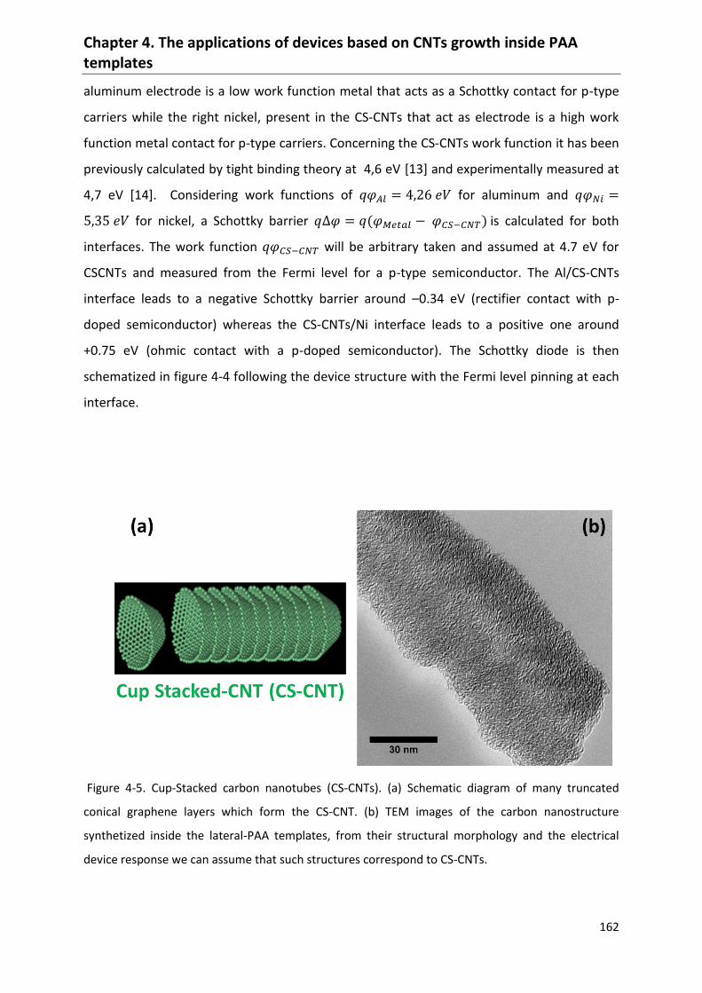
Chapter 4. The applications of devices based on CNTs growth inside PAA templates
162
aluminum electrode is a low work function metal that acts as a Schottky contact for p-type
carriers while the right nickel, present in the CS-CNTs that act as electrode is a high work
function metal contact for p-type carriers. Concerning the CS-CNTs work function it has been
previously calculated by tight binding theory at 4,6 eV [13] and experimentally measured at
4,7 eV [14]. Considering work functions of 𝑞𝜑𝐴𝑙 = 4,26 𝑒𝑉 for aluminum and 𝑞𝜑𝑁𝑖 =
5,35 𝑒𝑉 for nickel, a Schottky barrier 𝑞∆𝜑 = 𝑞(𝜑𝑀𝑒𝑡𝑎𝑙 − 𝜑𝐶𝑆−𝐶𝑁𝑇) is calculated for both
interfaces. The work function 𝑞𝜑𝐶𝑆−𝐶𝑁𝑇 will be arbitrary taken and assumed at 4.7 eV for
CSCNTs and measured from the Fermi level for a p-type semiconductor. The Al/CS-CNTs
interface leads to a negative Schottky barrier around –0.34 eV (rectifier contact with p-
doped semiconductor) whereas the CS-CNTs/Ni interface leads to a positive one around
+0.75 eV (ohmic contact with a p-doped semiconductor). The Schottky diode is then
schematized in figure 4-4 following the device structure with the Fermi level pinning at each
interface.
Figure 4-5. Cup-Stacked carbon nanotubes (CS-CNTs). (a) Schematic diagram of many truncated
conical graphene layers which form the CS-CNT. (b) TEM images of the carbon nanostructure
synthetized inside the lateral-PAA templates, from their structural morphology and the electrical
device response we can assume that such structures correspond to CS-CNTs.

Chapter 4. The applications of devices based on CNTs growth inside PAA templates
163
In order to evaluate the photonic response of the lateral device with a capping layer,
the channel where the CS-CNTs are located has been illuminated using infrared light with a
wavelength of 𝜆 = 850 𝑛𝑚 and a density power of 𝜌 = 2.22 𝑚𝑊 𝑐𝑚2⁄ . In figure 4-6 (a) it is
shown that under light illumination a large photocurrent (red line) is then added to the dark
current in the reverse bias regime. An equivalent photoresponse has been measured with a
𝜌 = 0.5 𝑚𝑊 𝑐𝑚2⁄ as is shown in figure 4-6 (b). In this plot, values around the origin are
enlightened and clearly show an open circuit and a short 𝑉𝑂𝐶 = 0, 17 𝑉 circuit current
𝐼𝑆𝐶 = −3,71 𝜇𝐴 . When a forward bias is equal to the band gap, the photocurrent is
cancelled at the open circuit voltage. In a first approximation, the open circuit voltage
measured here would give the bandgap energy of the CS-CNTs in this device at 𝐸𝐺~𝑞𝑉0 =
0,17 𝑒𝑉 [15].
Figure 4-6. Current-Voltage characteristics in the dark (black line) and under infra-red illumination
(red line) on the CNTs with an asymmetrical contact mode. (a) Electrical behavior in the range of -5V
to 5V with an IR power density of 𝜌 = 2.22 𝑚𝑊 𝑐𝑚2⁄ . (b) Magnified electrical behavior. The power
is plotted (blue line) to obtain the 𝑉𝑀 and 𝐼𝑀 parameters.
Therefore these devices based on CS-CNTs Schottky diodes are found to exhibit
potential benefits for photosensing and photovoltaic applications. In order to explore a
further application in the photovoltaic field, the fill factor 𝐹𝐹 has been calculated, such value
is a parameter which, in conjunction with 𝑉𝑂𝐶 and 𝐼𝑆𝐶 , determines the maximum power from
a solar cell. The fill factor is given by the following expression:

Chapter 4. The applications of devices based on CNTs growth inside PAA templates
164
𝐹𝐹 = 𝐼𝑀𝑉𝑀 𝐼𝑆𝐶𝑉0⁄
Where 𝐼𝑀 and 𝑉𝑀 are the maximum current and maximum voltage respectively
which leads to the maximum power generated by the photocurent. In figure 4-6 (b) the
power curve is plotted and the fill factor parameters are indicated. The as-derived values of
𝑉𝑀 = 0.09 𝑉 and 𝐼𝑀 = −1.75 𝜇𝐴 lead to a 𝐹𝐹 = 25%. This value is slightly below the 33%
measured for previously reported CNT Schottky diodes based on two-gates geometry [16].
In order to characterize the photoresponse performance of the device the
responsivity factor 𝑅 has been measured. The responsivity factor is given by the 𝐼𝑃ℎ 𝑃𝑖𝑛⁄ with
𝐼𝑃ℎ as the photocurrent generated at a given bias voltage 𝑉𝐵 with an incident power 𝑃𝑖𝑛. In
figure 4-7 is plotted for various laser powers (x-axis), and for different forcing voltage ranged
from 0 V to 5 V (vertical variation for each laser power). Different light sources with
calibrated and focused light beam covering the visible range have been utilized. Each laser
has a different laser incident power for instance 𝑃𝑖𝑛458 𝑛𝑚 = 2,8 𝜇𝑊, 𝑃𝑖𝑛
514 𝑛𝑚 = 330 𝜇𝑊 and
𝑃𝑖𝑛633 𝑛𝑚 = 630 𝜇𝑊. The photonic response has been measured varying the 𝑃𝑖𝑛 value
decreasing the incident power as 𝑃𝑖𝑛, 𝑃𝑖𝑛 2⁄ , 𝑃𝑖𝑛 5⁄ , 𝑃𝑖𝑛 10⁄ , 𝑃𝑖𝑛 102⁄ , 𝑃𝑖𝑛 103⁄ and 𝑃𝑖𝑛 104⁄ .
The measured responsivity decreases with increasing laser power and increases with
increasing forcing voltage. The plot exhibits a linear photoresponse as a function of the laser
power following a unique slope for all three wavelengths at fixed bias, but slightly different
for the different bias voltage at a fixed wavelength. This is indicative of a good calibration of
our photodetector. The maximum responsivity R is measured at an extremely high value of
8,4 × 10⁴ 𝐴 𝑊⁄ at 𝑉𝐵 = 5𝑉 under a 458 nm light illumination and at a low excitation
power 𝑃𝑖𝑛 = 0,28 𝑛𝑊. This leads to a measured external quantum efficiency (EQE)
𝜂𝑚 = 3,1 × 10⁵ . The external quantum efficiency gives us the ratio of the number of
carriers collected by the photonic device to the number of photons of a given energy
incident. The external quantum efficiency depends on the incident light wavelength and is
given by:
𝜂𝑚 =𝑅 × 𝑓 × ℎ
𝑞
Where 𝑓 is the frequency of the laser, ℎ is the Planck constant and 𝑞 is the electron
charge. This high level of EQE implies the presence of a high gain 𝐺 leading to the

Chapter 4. The applications of devices based on CNTs growth inside PAA templates
165
measurement of the intrinsic EQE 𝜂 as 𝜂 = 𝜂𝑚 𝐺⁄ . In analogy to CNTs where EQE has been
measured at a maximum η = 10% [17], we can assume here a minimum gain 𝐺~ 3,1 × 10⁶
at 458 nm.
Figure 4-7. Responsivity as a function of laser power (λ = 458 nm,514 nm, and 633 nm) for different
forcing voltage (ranged from 0 V to5 V). Each laser has different laser power (P in458nm= 2.8 µW, P in
514nm= 330 µW,and P in633nm = 630 µW) at first, and photonic response was measured by decreasing
laser power (P in , P in /2, P in /5, P in /10, P in /10 2 , P in /10 3 , and P in /10 4).
In order to set the sights on the potential applications of such devices in
telecommunications fields, time responsivity measurements have been performed in the
infrared band at 𝜆 = 1550 𝑛𝑚 using ultrafast Current-Voltage measurements as shown in
figure 4-8.

Chapter 4. The applications of devices based on CNTs growth inside PAA templates
166
Figure 4-8. Ultrafast Current-Voltage characteristics of a CNT device upon infraredlight (λ = 1550 nm)
set to 5 kHz at P in = 9 mW/cm 2 V B = 5 V. Rise and fall times are measured with the 10–90% method.
The device has been biased at 𝑉𝐵 = 5𝑉 and 𝜌𝑖𝑛 = 9 𝑚𝑊 𝑐𝑚2⁄ . A mechanical
chopper has been used to generate 5 kHz light pulses. For a reliable measurement of the rise
and fall times, each current point has been measured every 100 ns during 20 ns to avoid
parasitic device charging effects. Using the 10% – 90% method, the rise time has been
determined at 11.5 μs and the fall time at 21.7 μs. Although modern telecommunication
devices require picosecond time response, it is worth noting that these are the fastest time
responses measured for CNTs based devices [18].
The characterization of Schottky diode devices based on cup-stacked carbon
nanotubes arrays grown in lateral-PAA templates asymmetrically contacted reveals that such
devices present a strong photonic response under light illumination opening the possibility
for further photosensing and photovoltaic applications. This asymmetry connection arises
from the smart use of the aluminum as a Schottky contact for holes carriers and the nickel
catalyst ended tips as nanoscale electronic contacts. Due to the difference of the two
contacts work functions, a built-in field is formed in the channel allowing charges
photogeneration and separation under light illumination.

Chapter 4. The applications of devices based on CNTs growth inside PAA templates
167
4.2.3 Metal decoration on devices without capping layer
The asymmetrical connection between the two device terminals is a necessary
condition in order to have an electrical rectifier effect with photonic response under light
illumination, albeit the metal work function responsible of asymmetrical connection has to
be higher than the carbon nanotube work function. The figure 4-9 summarizes the different
metals work functions highlighting candidates for the fabrication of a device with a
photoresponse.
4,0 4,5 5,0 5,5 6,0
Al
Fe
Cu
Co
Ni
Pd
Pt
Meta
l
Work function (eV)
CNTs Work function
Figure 4-9. Work functions of carbon nanotubes and various metals which are possible to
electrodeposite.
The metal decoration of the CNTs has been performed by an electrodeposition
process. The decoration of the metal on the CNTs depends mainly on the structural quality
of the CNTs. The electrodeposited mechanisms that can take place depends on the CNT
quality, both situations are schematized in the figure 4-10. As it is previously mentioned the
CNTs have higher electric conduction in the axial direction than in the radial direction.
Therefore for zero defective nanotubes the electrical conduction will uniformly flow in such
direction, leading to a current concentration at the catalyst nanoparticle located at the CNT

Chapter 4. The applications of devices based on CNTs growth inside PAA templates
168
tip which implies that the decoration only takes place in the catalyst material. This
phenomena has been corroborated when the electrodeposition process has been performed
on SWCNTs with excellent structural properties [19]. On the contrary when CNTs have defect
sites the electrodeposited metal are preferentially nucleated at these points on the side–
walls [20], as well the current flow in the axial direction and the catalyst nanoparticle tip also
acts as deposition site. In the present work, after the electrical characterization of devices
with a capping layer, we concluded that the only explanation in order to obtain carbon
nanotubes with a semiconducting behavior is that the structure of the resulting tubes has a
cup-sacked configuration. Such structures possess graphene/graphitic edges that represent
very effective potential sites for a salt reduction and subsequently for localized surface metal
decoration through an electrodeposition process.
Figure 4-10 Schematic images of the possible deposition mechanism depending on the CNTs quality
structure.
The electrical characterization of the lateral devices without a capping layer has been
performed before and after the decoration process of various metals. The current-voltage
curves are shown in figure 4-11. The contact mode of the devices without the capping layer
is dominated by the side-wall mode. The main reason relies on the fact that it is most
difficult to obtain a tip-contact mode in the top surface of the aluminum counter electrode.
Therefore as is observed in figure 4-11 the electrical behavior for the devices with the

Chapter 4. The applications of devices based on CNTs growth inside PAA templates
169
pristine CS-CNTs is completely symmetrical and a rectifier effect is not detected. On the
contrary after metal decoration of nickel nanoparticles as indicated in the insight of the
figure 4-11 (a), a significant current increase is measured, both in the reverse and the
forward bias regimes, due to the newly formed contacts through nickel nanoparticles that
increase the channel conductivity. However, asymmetrical behavior is observed in green line
with a meaningfully higher current in the forward bias regime of almost two decades.
Similar results are obtained when palladium has been decorated on the side-walls of the CS-
CNTs as indicated in figure 4-11 (b). In both cases, upon exposure to infrared light with a
wavelength of 𝜆 = 850 𝑛𝑚 and a density power of 𝜌 = 2.22 𝑚𝑊 𝑐𝑚2⁄ the Ni and Pd
decorated CS-CNTs devices exhibit a strong photonic response, as it is pointing out in figure
4-11 (a) and (b) respectively, and a photocurrent is generated. In order to confirm that the
diode rectifier is also obtained due to the appropriate well matched work function of the
metal decorated and the counter electrode, the metal decoration of iron with work function
𝑞𝜑𝐹𝑒 = 4,7 𝑒𝑉 and copper with a work function 𝑞𝜑𝐶𝑢 = 4,65 𝑒𝑉 has been performed in
different devices. In figure 4-11 (c) and 12 (d) it is observed that after the electrodeposition
into the CS-CNTs, the electrical current is increase respect the pristine devices however non
rectifier effect and consequently there are not any photonic response. The increment in the
current is again attributed due to the new contacts created between the two terminals.
Therefore the series of performed experiments reveals that the nature of the contact
mode and the metal work function determines the electrical behavior of the device. The
asymmetrically connection has to be achieved and the work functions have to satisfy the
following relation:
𝜑𝐴𝑙 < 𝜑𝐶𝑆−𝐶𝑁𝑇 < 𝜑𝑀𝑒𝑡𝑎𝑙 𝑑𝑒𝑐𝑜𝑟𝑎𝑡𝑒𝑑
The performances observed for high work function metal nanoparticles decorated
devices are quite similar to one where the catalysts act as nanoplugs. Finally, the modulation
of the band energy diagram at the interface is represented for different nanoparticles. It
clearly supports the Schottky barrier model: nanoparticles work function higher than 5 eV
allows the fabrication of ohmic contacts and thus an efficient rectifier, while those with work
function lower than 5 eV let the device into symmetrical configuration with no rectifying
effect.

Chapter 4. The applications of devices based on CNTs growth inside PAA templates
170
Figure 4-11 Current-Voltage of devices based on CS-CNTs grown inside lateral-PAA templates without
a capping layer on top of the electrodes. (a) Current-Voltage characteristics of a CS-CNTs device
before Ni decoration in the dark (black line), after Ni decoration in the dark (green line) and under IR
illumination (red line). Left inset: SEM image before decoration. Right inset: SEM image after
decoration. Scale bar: 20 µm. (b) I – V characteristics of a CS-CNTs device before Pt decoration in the
dark (black line), after Pt decoration in the dark (purple line) and under IR illumination (red line).
Right inset: SEM image after metal decoration by an electrodeposition process. Image size: 10 μm × 5
μm. (c) I – V characteristics of a CS-CNTs device before Fe decoration in the dark (black line), after Fe
decoration in the dark (lilac line) and under IR illumination (red line). Right inset: SEM image after
decoration by an electrodeposition process. Image size: 20 μm × 10 μm. (d) I – V characteristics of a
CS-CNTs device before Cu decoration in the dark (black line), after Cu decoration in the dark (grey
line) and under IR illumination (red line).
Chapter 4. The applications of devices based on CNTs growth inside PAA templates
171
4.3 Vertical-PAA devices
The contact mode and the work function matching among the different component
of the lateral-PAA based devices are key characteristics to control in these kinds device
fabrication approach. Taking into account such evidences, the vertical-PAA devices based on
CNTs have been fabricated while preserving the mentioned properties. The electrical
characterization has been performed aiming to explore the potentialities of such devices as
interconnects. Finally the device performance for the detection of water molecules has been
performed targeting the possibility for a further application as gas sensing devices.
4.3.1 Electrical behavior
The electrical behaviors of the vertical-PAA templates have been performed
depositing four different materials on the counter electrodes on top of the PAA surface.
Figure 4-12 summarizes the current-voltage (I-V) curves for different voltage ranges and for
different electrodes materials. In all cases a resistor behavior has been measured, reflecting
the conducting nature of the CNTs grown inside the pores. The presence of a hysteresis
phenomenon has been investigated: on the figures 4-12, the black lines correspond to the
forward voltage sweeping and the red lines to the backward voltage sweeping. In the range
of voltages studies there are no straightforward evidence of a hysteresis phenomenon.
The resistance in all cases varies between 5 Ω and 7 Ω, reflecting that in all cases
approximately the same amounts of CNTs are contacted per electrode. The surface of each
electrode is of 0.06 mm2. A first order calculation of the resistivity of the individual CNTs can
be performed. The total resistance 𝑅𝑇𝑜𝑡𝑎𝑙 of the measured system is given by:
𝑅𝑇𝑜𝑡𝑎𝑙 = 𝑅𝐴𝑙 + 𝑅𝐸𝑙𝑒𝑐𝑡𝑟𝑜𝑑𝑒 + 𝑅𝐶𝑁𝑇 ǁ ~ 𝑅𝐶𝑁𝑇 ǁ = 1
∑ 1 𝑅𝐶𝑁𝑇(𝑖)⁄𝑁𝑖

Chapter 4. The applications of devices based on CNTs growth inside PAA templates
172
-0,010 -0,005 0,000 0,005 0,010
-2,0
-1,5
-1,0
-0,5
0,0
0,5
1,0
1,5
2,0
(a)
Cu
rren
t (m
A)
Voltage (V)
Forward
BackwardNickel Electrode
-0,10 -0,05 0,00 0,05 0,10-20
-15
-10
-5
0
5
10
15
20Nickel Electrode
Cu
rren
t (m
A)
Voltage (V)
(b)
-0.6 -0.4 -0.2 0.0 0.2 0.4 0.6
-90
-60
-30
0
30
60
90
Nickel Electrode(c)
Cu
rren
t (m
A)
Voltage (V)
-0,010 -0,005 0,000 0,005 0,010
-2,0
-1,5
-1,0
-0,5
0,0
0,5
1,0
1,5
2,0Aluminum Electrode
Cu
rren
t (m
A)
Voltage (V)
(d)
-0,10 -0,05 0,00 0,05 0,10-20
-15
-10
-5
0
5
10
15
20Aluminum Electrode
Cu
rre
nt
(mA
)
Voltage (V)
(e)
-0,6 -0,4 -0,2 0,0 0,2 0,4 0,6
-90
-60
-30
0
30
60
90
Aluminum Electrode
Cu
rre
nt
(mA
)
Voltage (V)
(f)
-0,010 -0,005 0,000 0,005 0,010
-2,0
-1,5
-1,0
-0,5
0,0
0,5
1,0
1,5
2,0Palladium Electrode
Cu
rren
t (m
A)
Voltage (V)
(g)
-0,10 -0,05 0,00 0,05 0,10-20
-15
-10
-5
0
5
10
15
20
(f)Palladium Electrode
Cu
rren
t (m
A)
Voltage (V)
-0,6 -0,4 -0,2 0,0 0,2 0,4 0,6
-90
-60
-30
0
30
60
90
(i)Palladium Electrode
Cu
rren
t (m
A)
Voltage (V)
-0,010 -0,005 0,000 0,005 0,010
-2,0
-1,5
-1,0
-0,5
0,0
0,5
1,0
1,5
2,0Gold Electrode
Cu
rren
t (m
A)
Voltage (V)
(j)
-0,10 -0,05 0,00 0,05 0,10-20
-15
-10
-5
0
5
10
15
20
(j)Gold Electrode
Cu
rren
t (m
A)
Voltage (V)
-0,6 -0,4 -0,2 0,0 0,2 0,4 0,6
-90
-60
-30
0
30
60
90
(l)Gold Electrode
Cu
rren
t (m
A)
Voltage (V)
Figure 4-12. Current-Voltages curves for different applied voltages ranges in the dual sweep mode:
0.01 V, 0.1 V and 0.5 V. The red line indicates the forward voltage sweeping variation and the black
line the voltage variation in the backward regime. Four different counter electrodes have been
deposited: (a), (b) and (c) nickel, (d), (e) and (f) aluminum, (g), (h) and (i) palladium and (j), (k) and (l)
gold.

Chapter 4. The applications of devices based on CNTs growth inside PAA templates
173
Where 𝑅𝐴𝑙 is the resistance of the aluminum foil, 𝑅𝐸𝑙𝑒𝑐𝑡𝑟𝑜𝑑𝑒 the resistance of the deposited
metal electrode and 𝑅𝐶𝑁𝑇 ǁ is the resulting resistance of the CNTs connected in parallel
between the aluminum and the counter electrode. Assuming that the resistance of the
aluminum and the counter electrodes is of the order 10-8 Ω, such values are negligible in
respect to the total measured resistance. On the other hand, considering that all the CNTs
connected in parallel have the same resistance value, therefore if 𝑅𝐶𝑁𝑇(𝑖) = 𝑅𝐶𝑁𝑇 , and the
total measured resistance is related to the resistance of the individual CNTs as:
𝑁 · 𝑅𝑇𝑜𝑡𝑎𝑙 = 𝑅𝐶𝑁𝑇
The calculated 𝑅𝐶𝑁𝑇 in all cases is of the order of 55 MΩ. In order to compare with
other results we calculate the resistivity value that does not depend on the characteristics
length of the transporting carrier element. In the literature it exists a wide range of CNTs
resistivity values between 0.36 𝑚𝛺 ∙ 𝑚 to 117 𝛺 ∙ 𝑚 [21, 22]. Such values strongly depend
on the straightness of the tubes and their quality structure. In order to calculate the
resistivity it is necessary to precise the characteristics lengths of the CNTs. Concerning the
diameter, the tubes have an average diameter of 30 nm, on the other hand for the nanotube
length we will approximate that the pores height are the same that CNTs length since the
synthesis process has been stopped when the CNTs tips reached the top PAA surface.
Therefore we assume that the average CNT length is 500 nm. Taking into account the
mentioned considerations, in our case, the resistivity of the tubes is of the order of
𝜌𝐶𝑁𝑇 = 0,05 𝛺 ∙ 𝑚 and the resistivity per electrode is of the order of 𝜌𝐸𝑙𝑒𝑐𝑡𝑟𝑜𝑑𝑒 = 0,9 𝛺 ∙
𝑚. This last value is still high for interconnects applications comparing with the obtained
value reported by Fiedler et al. [23] with a resistivity per via connection of 0,0004 𝛺 ∙ 𝑚,
however in such work lithography steps have been performed, the CNTs synthesis has been
carried out at 600°C, and complicated post-treatments have been executed in order to
improve the contact between the CNTs and the counter electrode. In our present work, the
synthesis temperature is mainly limited by the aluminum foil which starts to degrade at
660°C. Consequently it is possible to achieve CNTs with a better structural quality which can
lead to an improvement in conduction transport properties. Therefore further studies have
to be performed to improve the conduction properties of the devices based on vertical-PAA
templates that could open the possibility to applications in the interconnection

Chapter 4. The applications of devices based on CNTs growth inside PAA templates
174
Concerning the individual resistivity of the CNTs, such value might still be
overestimated. As it has been shown by cross-sectional TEM images (section 3.5.4) more
than one CNT can grow per pore, however mostly just one tip is reaching the top surface.
Therefore, in our calculation we are neglecting all the possible contacts that can take place
inside the pores. In addition, the type of contact between the tubes can even be more
dramatic for the resistivity inside the pore. Two types of contacts can occur (similarly as the
contact mode between the CNTs and the counter electrode): the side-wall contact mode and
the tip-contact mode, these contacts modes are schematized in the figure 4-13. When the
side-wall contact mode takes place the contact resistance is much higher than tip mode, for
instance Santini et al. [24] have reported a side-wall resistance of (45 ± 7) kΩ for nanotubes
with diameters of (18 ± 3) nm. Therefore such kind of contact may increase even more the
contribution to the resistance per pore leading to a more dramatic overestimation of the
individual CNTs calculation.
In conclusion the measured resistance value gives a notion of the vertical device for
the application as interconnect circuits, and on the other hand the transport deduced values
of individual CNTs are overestimated by the introduced assumptions.
Figure 4-13. Schematized images of the possible contact modes between CNTs inside the pores of the
PAA structure.

Chapter 4. The applications of devices based on CNTs growth inside PAA templates
175
In all cases for the presented devices, the electrical behavior measured has been
similar to a resistor type. For instance when aluminum has been deposited as counter
electrode, the same connection architecture is obtained as the lateral-devices with capping
layer. However there is no evidence of a semiconducting response of the CNTs. Two
different reasons can explained the obtained electrical behavior in the devices based-on
CNTs grown within vertical-PAA templates. Firstly, we can consider that a different tube
formation is involved in the vertical-PAA templates than in lateral ones. Therefore the pores
in the vertical direction can lead to the formation of carbon nanostructure mainly with
conducting properties. Alternatively, in spite of the work functions, values have been
preserved in both devices geometries: in the devices with the vertical templates the tip
contact mode is not achieved between the metal electrode and the CNT tip. In such case, it
is possible that part of deposited metal electrode can diffuse inside the pore and make the
contact with the sidewall of the carbon nanostructure. Under the described situation, the tip
contact mode is not preserved. Further studies have to be performed in order to clearly
identify the constraints of the formation of a Schottky contact in vertical-PAA templates.
On the other hand, the same electrical characterization has been performed on
device with a density of nanotubes of 60 CNTs/µm2. The figure 4-14 (a) shows the current-
voltage curve which presents a typical resistance. When the applying voltage is increased a
non-linear behavior is obtained. This kind of behavior has been previously reported by
Bockrath et al. [25] providing experimental evidence that the conductance in CNT bundles
exhibits Luttinger liquid behavior, however these behaviors have been obtained at low
temperatures [26]. More recently Kozlov [27] have revealed an abnormal zero bias at room
temperature in a forest of CNTs. This phenomenon is attributed due to the tunneling of the
charge carriers across the nanotube junctions which is enhanced by temperature gradients
created by measuring currents and used for the characterization of the nanotube junction
network [28]. Therefore such results are consistent with the cross-section TEM images, and
evidence that the deduced CNT resistivity is overestimated since there are other contacts
that are not considered. We attributed the apparition of the non-linear behavior at higher
powers due to higher temperature gradient generated at higher voltages between nanotube
junctions near the top PAA surface and inner aluminum which leads to an enhancement of
nonlinearities in the sample properties [27]. This phenomenon is consistent with the greater

Chapter 4. The applications of devices based on CNTs growth inside PAA templates
176
hysteresis effect in the reverse regime since more power is dissipated which emphasis the
nonlinearities of the device. The nonlinear electron transport in CNT bundles upon exposure
to chemical analytes have been recently started to be developed as sensing system [29].
-1,0 -0,5 0,0 0,5 1,0
-10
-5
0
5
10
Cu
rren
t (m
A)
Voltage (V)
Forward
Backward
(a)
-8 -6 -4 -2 0 2 4 6 8
-4
-3
-2
-1
0
1
2
3
4
Cu
rren
t (m
A)
Voltage (V)
Forward
Backward
(b)
Figure 4-14. Current-Voltage curves in different sweeping voltage range for a sample with a density
of CNTs of 60 CNTs/µm2. (a) Resistor behavior in the range -1V to 1V. (b) Semiconducting behavior in
the range -6 V to 6 V.
The fact that this kind of behavior has been detected in forest distributions indicates
in our case that many CNTs are contacting at the bottom pores. This CNTs distribution is
more pronounced in a sample with an anodization voltage of 30V, where more branches are
created from a stem pore. Consequently the CNTs that reach the top surface have probably
many CNTs contacting their surface along the pore.
4.3.2 Light Illumination
In order to test the photonic response of the vertical-PAA templates, the devices
have been illuminated using a blue laser with a wavelength of 458 nm. The devices with the
four deposited metal electrodes have been tested. However as is shown in figure 4-15 there
is no evidence of a photocurrent generated due to light illumination. The present

Chapter 4. The applications of devices based on CNTs growth inside PAA templates
177
measurements correspond to device with the palladium electrode, but similar results are
obtained with the others counters electrodes. The non-response of the device under light
illumination can be mainly attributed a two factors, firstly the light may not be able to
interact with the CNTs due to the counter electrode material shadowing the majority of the
photon flux. On the other hand, even if the light can enter to the pores it will mostly interact
with the nanotube tip closer to the contact with the top electrode, whilst generally the
maximum of the photocurrent amplitude is located in the channel regime between the two
contacts [30, 31].
-0,002 -0,001 0,000 0,001 0,002
-0,10
-0,05
0,00
0,05
0,10
nm
Cu
rren
t (m
A)
Voltage
Dark
3,0 W
4,5 W
6,0 W
8,0 W
Figure 4-15. Current-Voltage curve of vertical-PAA device with Pd electrode deposited as counter
electrode. Blue illuminations have been performed applying different powers.
4.3.3 Humidity Sensing
Several works have been focused on studying the electrical resistance variation of
MWCNTs when exposed to various gas or vapor environments, including NH3, NO2, and CO
[32, 33]. In particular gas sensors have been fabricated by Suresh Rajaputra et al. [34] using
CNTs grown inside PAA templates, however in this case the aluminum has been removed in
a chemical acid solution and the grown of CNTs was carried without catalyst, the resistivity

Chapter 4. The applications of devices based on CNTs growth inside PAA templates
178
of the device being in the order of 100 𝛺 ∙ 𝑚 . Such designed devices present the advantage
that gas can flow freely through the tubes due to the absence of the aluminum layer.
Growing CNTs inside vertical-templates, Ding et al. [35] also performed H2 sensing
measurements by depositing a palladium top electrode.
0 2 4 6 8 10
0
10
20
30
40
50
60
70
Relative Humidity
Nickel Electrode
Time (Hours)
Rela
tive H
um
idit
y (
%)
(a)
9.0
9.5
10.0
10.5
11.0
11.5
12.0
12.5
Resis
tan
ce (
Oh
m)
0 2 4 6 8 10
0
10
20
30
40
50
60
70
Relative Humidity
Aluminum Electrode
Time (Hours)
Rela
tive H
um
idit
y (
%)
6,45
6,50
6,55
6,60
6,65
6,70
6,75
6,80
6,85
6,90
Resis
tan
ce (
Oh
m)
(b)
Figure 4-16. Resistance variations as results of humidity response of vertical device with different
contact electrode: (a) nickel and (b) aluminum.
In the present work in order to perform humidity sensing measurement water vapor
have been introduced in the chamber where the electrical device characterization is carried
out. The tested devices have been the vertical devices with nickel and aluminum top
electrodes. The relative humidity has been increased from 1% up to 65% at room
temperature. Figure 4-16 shows the resistance variation with the change of the relative
humidity inside the chamber. In both cases the resistance increases under the augmentation
of the relative humidity. This response is consistent with the synthesis of highly defectives
CNTs, as water vapor are preferentially absorbed on the polar oxygen-containing defects
through the formation of hydrogen (H) bonds, which leads to a lowering of the induced p-
type doping on the CNT and increasing the electrical resistance. With the nickel top
electrode as is shown in figure 4-17(a), the device follows the trend of the humidity variation
inside the chamber. However contact related effects also are detected, for instance in the
relative humidity variation from 3% to 10% the gas flow injected has affected the probed
contacting the counter electrode which explains the great drop in the resistance value. In

Chapter 4. The applications of devices based on CNTs growth inside PAA templates
179
addition we observed that for relative humidity values lower than 40% the system requires
15 minutes approximately to detect the increment in the humidity. This fact indicates that
the water molecules needs some time to penetrate the porous structure. On the other hand
the device with the aluminum top electrode does not show a sensing response for humidity
values lower than 50 % as is indicated in figure 4-17 (b). This device starts to detect the
water molecules suddenly for values higher than 50%. In order to understand the huge
difference in the sensing performance, the electrode surfaces have been observed by SEM as
shown in the images in figure 4-17. In the case of the nickel electrodes, as it is clearly
pointed out in figure 4-18(a) the pore structure is still easily recognized through the
deposited metal, the insight reflects that CNTs tips are covered and after the metal electrode
deposition and are still recognizable. In contrast, for the aluminum deposition most of the
pores surface is covered as shown figure 4-17 (b), more likely by a uniform layer deposition,
therefore in such device a higher amount of water molecules is required to interact with the
active element of the device because the water molecules have to diffuse firstly through the
metal electrode. This explains the two different sharped sensing behaviors observed in the
device with deposited aluminum metal electrode. The resistance slowly increases in the
range of 1% to 40% when the water molecules interact just with the counter electrode, and
abruptly increases when the water molecules start to interact with the CNTs. The device
begins to sense difference in the relative humidity.
The obtained results reveal that the deposited electrode plays a crucial role in these
types of devices. Therefore the thickness of the metal electrode has to be optimized in order
to improve the sensing behavior of the devices based on CNTs grown inside vertical-PAA
templates(). Anyway, the introduced devices are quite promising for further gas sensing
application.

Chapter 4. The applications of devices based on CNTs growth inside PAA templates
180
Figure 4-18. SEM top images of the metal electrodes deposited on top of the vertical templates. Two
different metals have been deposited with a thickness of 30 nm. (a) Nickel and (b) Aluminum. Both
images contain insights in higher magnifications.

Chapter 4. The applications of devices based on CNTs growth inside PAA templates
181
4.4 Conclusions
The characterization of two different template approaches CNTs based devices has
been performed. Both kinds of devices offer different application fields. In spite of both
devices being based on arrays of CNTs, the inherent geometry determines the application
domain.
For the lateral devices based on CNTs unequalled optoelectronic devices based on
CNTs are presented for photovoltaic and photodetectors applications. These devices are
based on asymmetrical contacted arrays of nanotubes leading to Schottky photodiodes.
Lateral porous anodic alumina (LPAA) is used for the CVD synthesis of the organized
nanotubes array and two methods are developed for engineering their Schottky contacts.
Two different devices types have been fabricated in order to obtain such asymmetric
contact. In one case the tip-contact mode has been promoted. The second procedure takes
advantage of the defective zones of cup stacked-CNTs to perform a metal decoration
process and modifies the nature of the side-contact mode between the CNTs and the
counter electrodes. In order to obtain rectifier effect complementary to the asymmetrically
device connection, the work functions have to be well matched, a clear relation between the
values of the corresponding metal nanoparticle work functions and the measured rectifying
effect has been established in a Schottky barrier model. Such work function differences lead
to a built-in a field which is formed in the channel allowing charges photogeneration and
separation under light illumination and a high sensitivity has been found within a broadband
wavelength bandwidth (458 nm – 1550 nm). Photovoltaic parameters have been extracted
and they evidenced fill factors quasi-independent of the wavelength at around 25%. The
measured open circuit voltage is indicative of an intrinsic energy band gap of the as-growth
CS-CNTs at around 0.17 eV. Finally, ultra-fast I – V measurements performed at λ = 1550 nm
evidenced rise time measurements as fast as 11.5 μs which sets the actual state of the art
for carbon nanotubes and carbon nanofibers. It is also worth mentioning at this point that ,
to the extent of our knowledge, these are the first ever reported functional devices based on
lateral-PAA grown nanomaterials.

Chapter 4. The applications of devices based on CNTs growth inside PAA templates
182
For the fabrication of the vertical devices the contact mode and the relation between
the metal work functions have been preserved. Four different counter electrodes have been
deposited: nickel, aluminum, palladium and gold. Compared to the lateral-type devices,
although the same connection configuration and contact mode are conserved, the electrical
behavior of the device is a classical resistor. In order to establish the difference between the
electrical behaviors, further studies are required to determine the structure of the
synthetized in the vertical template, and additionally study the contact zone between the
grown CNTs and the deposited metal electrode. The electrode resistivity has been calculated
resulting of the order of 0.9 Ω·m, three orders of magnitude bigger than other reported
optimized interconnects devices, however many strategies can furthermore be adopted in
order to decrease this value. For instance, the synthesis temperature can be increased which
will lead to CNTs with better structural properties. For devices with a low CNTs density a
non-linear current-voltage behavior has been detected, equivalently to CNTs forest
distribution. This phenomenon is attributed to the tunneling effect of charge carriers across
the nanotube junctions enhanced by temperature gradients created by measuring applied
currents and used for the characterization of the nanotube junction network. The present
devices does not reflect a photonic response under light illumination, the problem could be
associated with the fact that the CNT are inside the pore structure. Finally humidity sensing
measurements has been performed and it has been verified that the sensing performance is
quite sensible to the nature and uniformity of the deposited counter electrode.
The lateral devices exhibits electronic and optoelectronic responses that open new
frontiers of the horizontal devices collectively organized arrays of one-dimensional
nanomaterials. On the other the vertical devices based on CNTs can considerably contributes
in the domain of interconnects and gas sensing.

183
References
[1] M. Gowtham, et al., "Controlled fabrication of patterned lateral porous alumina membranes," Nanotechnology, vol. 19, p. 035303, 2008.
[2] M. Shiraishi and M. Ata, "Work function of carbon nanotubes," Carbon, vol. 39, pp. 1913-1917, 2001.
[3] C. Cordeiro, et al., "Theoretical study of work function of conducting single-walled carbon nanotubes by a non-relativistic field theory approach," Carbon, vol. 47, pp. 690-695, 2009.
[4] N. de Jonge, et al., "Characterization of the field emission properties of individual thin carbon nanotubes," Applied Physics Letters, vol. 85, pp. 1607-1609, 2004.
[5] S. J. Tans, et al., "Room-temperature transistor based on a single carbon nanotube," Nature, vol. 393, pp. 49-52, 1998.
[6] R. Martel, et al., "Single-and multi-wall carbon nanotube field-effect transistors," Applied Physics Letters, vol. 73, pp. 2447-2449, 1998.
[7] H. M. Manohara, et al., "Carbon nanotube Schottky diodes using Ti-Schottky and Pt-Ohmic contacts for high frequency applications," Nano letters, vol. 5, pp. 1469-1474, 2005.
[8] Z. Chen, et al., "The role of metal-nanotube contact in the performance of carbon nanotube field-effect transistors," Nano letters, vol. 5, pp. 1497-1502, 2005.
[9] Q. Liu, et al., "Semiconducting properties of cup-stacked carbon nanotubes," Carbon, vol. 47, pp. 731-736, 2009.
[10] B. O. Boskovic, et al., "Large-area synthesis of carbon nanofibres at room temperature," Nature materials, vol. 1, pp. 165-168, 2002.
[11] J. Vera-Agullo, et al., "Evidence for growth mechanism and helix-spiral cone structure of stacked-cup carbon nanofibers," Carbon, vol. 45, pp. 2751-2758, 2007.
[12] T. Yamada, et al., "Tunneling between carbon nanofiber and gold electrodes," Journal of applied physics, vol. 107, p. 044304, 2010.
[13] W. A. Harrison, Electronic structure and the properties of solids: the physics of the chemical bond: Courier Corporation, 2012.
[14] V. Robinson, et al., "Work function reduction of graphitic nanofibers by potassium intercalation," Applied Physics Letters, vol. 87, p. 061501, 2005.
[15] S. M. Sze and K. K. Ng, Physics of semiconductor devices: John Wiley & Sons, 2006. [16] J. U. Lee, "Photovoltaic effect in ideal carbon nanotube diodes," Applied Physics Letters, vol.
87, pp. 73101-73101, 2005. [17] M. Freitag, et al., "Photoconductivity of single carbon nanotubes," Nano letters, vol. 3, pp.
1067-1071, 2003. [18] X. He, et al., "Photothermoelectric p–n junction photodetector with intrinsic broadband
polarimetry based on macroscopic carbon nanotube films," ACS nano, vol. 7, pp. 7271-7277, 2013.
[19] M. R. Maschmann, et al., "Lithography-free in situ Pd contacts to templated single-walled carbon nanotubes," Nano letters, vol. 6, pp. 2712-2717, 2006.
[20] S. Arai, et al., "Ni-deposited multi-walled carbon nanotubes by electrodeposition," Carbon, vol. 42, pp. 641-644, 2004.
[21] T. Hayashi, et al., "A reversible strain-induced electrical conductivity in cup-stacked carbon nanotubes," Nanoscale, vol. 5, pp. 10212-10218, 2013.
[22] H. Dai, et al., "Probing Electrical Transport in Nanomaterials: Conductivity of Individual Carbon Nanotubes," Science, vol. 272, pp. 523-526, April 26, 1996 1996.
[23] H. Fiedler, et al., "Carbon nanotube based via interconnects: Performance estimation based on the resistance of individual carbon nanotubes," Microelectronic Engineering, vol. 120, pp. 210-215, 2014.
Chapter 4. The applications of devices based on CNTs growth inside PAA templates
184
[24] C. A. Santini, et al., "Carbon nanotube–carbon nanotube contacts as an alternative towards low resistance horizontal interconnects," Carbon, vol. 49, pp. 4004-4012, 2011.
[25] M. Bockrath, et al., "Luttinger-liquid behaviour in carbon nanotubes," Nature, vol. 397, pp. 598-601, 1999.
[26] W. Y. Jang, et al., "Electrical characterization of individual carbon nanotubes grown in nanoporous anodic alumina templates," Applied Physics Letters, vol. 84, pp. 1177-1179, 2004.
[27] M. E. Kozlov, "Nonlinear electrical properties of carbon nanotube forests," Applied Physics Letters, vol. 99, p. 133111, 2011.
[28] J. Park, et al., "Electrical transport through crossed carbon nanotube junctions," Journal of applied physics, vol. 93, pp. 4191-4193, 2003.
[29] P. Gowda, et al., "Chemical vapor detection using nonlinear electrical properties of carbon nanotube bundles," Nanotechnology, vol. 25, p. 025708, 2014.
[30] M. Engel, et al., "Spatially resolved electrostatic potential and photocurrent generation in carbon nanotube array devices," ACS nano, vol. 6, pp. 7303-7310, 2012.
[31] M. Barkelid and V. Zwiller, "Photocurrent generation in semiconducting and metallic carbon nanotubes," Nature Photonics, vol. 8, pp. 47-51, 2014.
[32] L. Valentini, et al., "Sensors for sub-ppm NO2 gas detection based on carbon nanotube thin films," Applied Physics Letters, vol. 82, pp. 961-963, 2003.
[33] C. Cantalini, et al., "NO 2 gas sensitivity of carbon nanotubes obtained by plasma enhanced chemical vapor deposition," Sensors and Actuators B: Chemical, vol. 93, pp. 333-337, 2003.
[34] S. Rajaputra, et al., "Multi-walled carbon nanotube arrays for gas sensing applications," Nanotechnology, vol. 19, p. 345502, 2008.
[35] D. Ding, et al., "Hydrogen sensors based on aligned carbon nanotubes in an anodic aluminum oxide template with palladium as a top electrode," Sensors and Actuators B: Chemical, vol. 124, pp. 12-17, 2007.

185
Conclusions & Prospective
In the present work carbon nanotubes (CNTs) have been synthetized within porous
anodic alumina (PAA) templates for their device applications. The devices have been based
in two different templates approaches: the lateral-PAA and the vertical-templates. However
in order to achieve the desire device configuration several hurdles have been overcome,
therefore a deep understanding in the processes involved in each step of the fabrication
were required, from the anodization process for the PAA fabrication until the synthesis of
CNTs inside the pores. Once the devices have been fabricated, the mechanisms which take
part in the device performance have been elucidated, allowing the enhancement of the
specific function of the device or to obtain a notion of future improvements to realize.
The PAA templates have many advantages associated with their easy implantation
and flexibility to control their geometrical features. In the present work, by investigating the
anodization conditions, a fully characterization of the main pore properties have been
performed, such as the pore diameter, interpore distance, porosity, circularity of the pores
and the pore cell ordering. Such study provides useful information for a future precisely
device characterization. In particular for lateral-templates the study of the impact of the
anodization temperature has been realized. The obtained results reflect that the insulating
layer deposited in order to execute the pore formation just in a determined direction,
strongly affects the pore growth, and differently than the vertical pores where the
temperature barely affects the pore configuration on the top surface, in the same
temperature range, the lateral templates can leads to a pore merging phenomenon losing
the pore array.
The catalyst nanoparticles have been deposited by pulse electrodeposition. The
operational range depending on the anodization conditions has been studied. The catalyst
deposition and the PAA fabrication are strictly related by the oxide barrier layer at the
Conclusions & Prospective
186
bottom of the pores. The main constraint of the PAA relies on such barrier which introduces
difficulties for a further metal nanoparticle deposition. In the present work, an exponential
voltage decrease followed by a chemical wet etching has been applied in order to
completely remove such barrier. By the application of such process a branched structure can
be created at the bottom of the pores. The branched structures have been deduced
comparing the pore density with the pattern of nanoparticles electrodeposited at the
bottom of the pores, after the elimination of the PAA structure. This analysis allows the
prediction of the best pore structure for further synthesis of carbon nanostructures.
The synthesis of carbon nanotubes through the HF-CVD technique has been
successfully performed inside the PAA templates taking into account the geometrical
constraints imposed by the porous structure. It has been evidenced that the branched
structure at the bottom of the pores strongly affects the growth dynamics. For the very first
time the CNT growth evolution at different synthesis times inside the PAA structure has been
measured; such study provides meaningful information of the growth behavior within the
pores. In spite of the fact that generally just one nanotube tip reaches the top PAA surface
more than one CNT can grow in each pore and a competition is established inside the pore
that can even block the CNT formation. The synthesis conditions and the pore structure have
been conjointly adjusted to maximize the number of CNTs grown. In the vertical templates a
density of 2 x 10¹⁰ CNTs/cm2 has been achieved. Concerning the growth of CNTs inside the
lateral templates, the synthesis temperatures have been study in order to obtain the most
straight grown CNTs, which is a desirable characteristic for further device fabrication.
The characterization of two different templates approaches based devices has been
performed and different applications domains have been established depending on their
device designed configuration. Unequalled optoelectronic devices based on CNTs grown
inside lateral-PAA templates are presented for photovoltaic and photodetectors
applications. These devices are based on asymmetrical contacted arrays of nanotubes
leading to Schottky photodiodes. The contacting mode between the CNTs and the counter
electrode plays a crucial role in the electrical behavior. For instance a symmetrical behavior
leads to a classical resistor behavior. On the other hand when the contact is between the
nanoparticle tips of the CNT such symmetry is broken leading to Schottky contact. Under the
lateral template, two different strategies have been implemented in order to achieve such
Conclusions & Prospective
187
asymmetrical contact. In one case the insulating capping barrier deposited for the lateral
anodization process is kept during the nanotubes growth in order to promote the tips
contacts. On the other hand the insulating capping barrier is removed and a metal
decoration process is executed to modify the nature of the previous side-wall contacts,
adding a metal between the CNTs and the counter electrode, breaking the symmetrical
contact. By this approach, it have been verified that the work function of the metals that
contact with the aluminum electrode has to be higher than the CNTs work function.
Therefore in order to obtain a Schottky contact, the asymmetrical contact has to be satisfied
but in addition the work functions have to obey the following relation:
𝜑𝐴𝑙 < 𝜑𝐶𝑁𝑇 < 𝜑𝑀𝑒𝑡𝑎𝑙 𝑑𝑒𝑐𝑜𝑟𝑎𝑡𝑒𝑑
The devices satisfying both conditions show a strong photonic response. The work
function differences lead to a built-in field which is formed in the channel allowing charges
photogeneration and separation under light illumination sensitivity has been found within a
broadband wavelength bandwidth (458 nm – 1550 nm). Photovoltaic parameters have been
extracted and evidenced fill factors which are quasi-independent of the wavelength at
around 25%. Finally, ultra-fast current-voltage measurements performed at λ = 1550 nm
evidenced rise time measurements as fast as 11.5 μs. It is also worth to mention at this
point, that to the extent of our knowledge, they are the first ever reported functional
devices based on lateral-PAA grown nanomaterials. Similarly for vertical devices the contact
mode and the relation between the metal work functions have been preserved; however the
linear behavior has been obtained, in principle we attributed this observation to a different
carbon nanostructure growth in the different grown templates geometry or a diffusion of
the material that acts as electrode inside the pores contacting the carbon nanostructure,
leading to a symmetrical contact. Exploring the possible device application as interconnects
circuits, the device resistivity has been calculated resulting of the order of 0.9 Ω·m, three
orders of magnitude bigger than other interconnected devices, however several
improvements can be done to decrease such value. Devices with a low CNTs density, due to
more considerable branched structure shows a non-lineal current-voltage behavior,
equivalently to CNTs forest distribution, revealing that many tubes are touching among then
at the bottom pores. This phenomenon is attributed to the tunneling effect of charge
carriers across the nanotube junctions enhanced by temperature gradients created by

Conclusions & Prospective
188
measuring currents and used for the characterization of the nanotube junction network.
Such non-linear behavior can act as a tracer to determine the structure at the bottom pores.
The vertical devices do not reflect the photonic response under light illumination, this
characteristic was expected because CNT are inside the pore structure and cannot fully
interact with light. Finally humidity sensing measurements have been performed and it has
been verified that the sensing performance is quiet sensible to the deposited counter
electrode.
In the present work fundamental results associated to the growth of carbon
nanostructures inside vertical PAA templates can serve as guidelines to extend the current
frontiers for devices applications based on such nanotemplates fabrication approach. On the
other hand, lateral-type PAA photosensing devices and vertical-type PAA gas sensing devices
are presented with remarkable performances due to the adequate use of the Schottky
contacts. Both results provide a considerable contribution in the field of nanodevices
fabrication based on nanotemplates.
Regarding the future of the study topic, the introduced devices can been improved or
slightly adapted in order to explore other applications area. For instance lateral-PAA based
devices possess the great advantage that the grown CNTs are between two terminals. This
configuration is very suitable for a further CNTs functionalization that expands the
application fields as biosensing devices or gas sensors. Moreover such planar platform is very
versatile for various applications as transistor based on CNTs. Concerning the vertical
devices, still many improvements can be done to minimize the branched structure that will
lead to bigger CNT yield. Under such conditions, considering interconnects application area,
the number of contacted CNTs will be increased and the resistivity reduced. For the sensing
applications, the thickness of the electrode deposited has to be investigated because it is the
first element which interacts with the environment.