Anodic reactions occurring on simulated spent nuclear fuel ...

Subscriber access provided by MPI FUER EISENFORSCHUNG
The Journal of Physical Chemistry C is published by the American ChemicalSociety. 1155 Sixteenth Street N.W., Washington, DC 20036
Article
Gold Nanoparticles Partially Embedded in Ultrathin Anodic Alumina FilmsAndrei Ionut Mardare, Sergiy Borodin, Andreas Dirk Wieck, Michael Rohwerder, and Achim Walter Hassel
J. Phys. Chem. C, 2009, 113 (8), 3105-3109• DOI: 10.1021/jp806979g • Publication Date (Web): 03 February 2009
Downloaded from http://pubs.acs.org on March 3, 2009
More About This Article
Additional resources and features associated with this article are available within the HTML version:
• Supporting Information• Access to high resolution figures• Links to articles and content related to this article• Copyright permission to reproduce figures and/or text from this article
Gold Nanoparticles Partially Embedded in Ultrathin Anodic Alumina Films
Andrei Ionut Mardare,†,‡ Sergiy Borodin,† Andreas Dirk Wieck,‡ Michael Rohwerder,† andAchim Walter Hassel*,†
Max-Planck-Institut fur Eisenforschung GmbH, Max-Planck-Strasse 1, 40237 Dusseldorf, Germany, andRuhr-UniVersitat Bochum, 44780 Bochum, Germany
ReceiVed: August 5, 2008; ReVised Manuscript ReceiVed: December 5, 2008
Gold nanoparticles with diameters ranging from 3.2 to 9.7 nm were prepared on an ultrathin anodic aluminumfilm by means of molecular beam deposition. Coverages ranging from 17.9% to 48.5% and the subsequentanodic anodization behavior were studied. Further oxide growth does not completely cover the goldnanoparticles but takes place preferentially under the particles with a surprisingly low kinetic hindrance. Thegold nanoparticles are electrically isolated from the substrate as demonstrated by the absence of electrocatalyticreactions on the gold surface. A strong surface charge phenomenon is observed, which increases with increasinggold coverage that yields an increase of the capacity up to the minimum potential required for further oxideformation.
1. Introduction
In the past decade noble metal based nanocomposite materialsstarted to play an important role in both fundamental and appliedscientific research. The use of nanocomposites can lead tomonophasic or multiphasic materials such as ceramics, glasses,or porous materials, with tailored and improved properties.1
Depending on the intended application, a monophasic or amultiphasic structure is desired. For electroceramics, structuralmaterials, and other applications, materials with a high homo-geneity are required. For many other applications such ascatalysis or sensors, the intended materials property is resultingfrom the heterophase structure. This can be simply a result ofthe increased surface area due to the nanoparticles as for thecase of antibacterial properties of coatings containing silverparticles.2 More interesting, however, are structures in whichspecific properties are resulting from a confinement within themetal nanoparticles. Elghanian et al. used the change of theoptical properties of gold nanoparticles with their spacing withina polymeric aggregate for selective detection of polynucleotides.3
However, it requires soft matter to allow for the necessarychange in inter-particle distance. Particularly in the field ofsensors, the use of gold nanoparticles is very attractive becausethey can be easily modified chemically.4-6 Researchers havelearned how to control the shape of gold nanoparticles and theycan produce even nanobelts with high aspect ratios from anaqueous route using capping surfactants.7 Using a eutectoid solidstate decomposition, it is also possible to produce arrays of iso-oriented gold nanobelts.8,9
There are quite a number of approaches utilizing electro-chemistry. The charging of Au nanoparticles immobilized onindium tin oxide (ITO) has been studied as a function of theparticle size.10 Gold nanoparticle-alumina composites have alsobeen prepared directly by an electrochemical codepositionapproach tuning the surface charge of the nanoparticles.11 Inparticular, approaches in which immobilized gold nanoparticlesare combined with surfaces of limited conductance such as
diamond films are of interest for the oxygen reduction incatalytic studies.12-14
Recently, electron-beam-assisted deposition of metallic nano-particles on alumina has been reported and various nanostruc-tures could be formed by controlling the energy of the electronbeam in a transmission electron microscope. The growthmechanism was correlated to the charge accumulation on thesurface of alumina.15
The embedding of Au nanoparticles in alumina represents apromising way of achieving tailored nanocomposites with directapplications in the development of capacitive sensors, catalystsfor low temperature CO oxidation, or multilayered heterostruc-tures based on three-dimensional self-organization of the Aunanoparticles.16-18 An alternative strategy is the use of porousanodic alumina films. They can be easily prepared in dissolvingelectrolytes.19 These films can be employed as a template forthe deposition of gold nanoparticle arrays.20
The formation of an anodic bulk alumina film with a thicknessof a few nanometers is possible in neutral noncomplexingelectrolytes. With respect to the limited thickness of thepreviously air formed native alumina, a significant tunnelingprocess can be expected.21 This raises the question of how thesystem would accommodate voltages higher than the onecorresponding to the thickness of the native film. It could alloweither high tunneling currents from the substrate to the metalnanoparticles and a subsequent electrochemical reaction of theparticle surface or a further oxide growth under high fieldconditions. In the latter case the question arises where the oxidegrowth would take place, between the particles resulting in anembedment of the particles into the film or underneath theparticles resulting in an electrical disconnection. The share ofthese concurrent reactions might be influenced by the coverageand the geometry of the particles, an issue that is addressed inthis paper.
2. Experimental Section
2.1. Substrate Preparation and Au Nanoparticle Synthe-sis. Aluminum films 200 nm thick deposited on silica substrates(Marienfeld microscope cover glasses, 15 mm × 15 mm × 0.3mm) were used as templates for the synthesis of Au nanopar-ticles by means of molecular beam deposition (MBD). The silica
* Corresponding author, [email protected], fax +49-211-6792-218.† Max-Planck-Institut fur Eisenforschung GmbH.‡ Ruhr-Universitat Bochum.
J. Phys. Chem. C 2009, 113, 3105–3109 3105
10.1021/jp806979g CCC: $40.75 2009 American Chemical SocietyPublished on Web 02/03/2009
substrates were cleaned in an ultrasonic bath using isopropanoland deionized water successively. The Al thin films weredeposited from 99.9995% purity aluminum foils (Alfa Aesar)using an electron beam evaporator (ESV6 Leybold Univex 450vacuum system). The target material was compressed in a Wcrucible, and the evaporation was done at a pressure of10-4 Pa. The thickness of the films was monitored in situ usinga quartz crystal microbalance mounted in close vicinity of thesamples. The deposition rate was close to 1 nm s-1. Afterthe Al deposition, the samples were exposed for 24 h to theenvironment in normal atmospheric conditions (1 bar, 80%relative humidity) to allow a gas phase oxidation of thealuminum. A natural alumina film with a thickness of 2.6 nmwas obtained due to the high oxygen affinity of Al.22 On thesenaturally oxidized aluminum samples, four different series ofAu nanoparticles were thermally evaporated from a Knudsencell (Au purity 99.999%) in a custom-made ultrahigh vacuumsystem (UHV Prevac) having a base pressure better than10-8 Pa. The evaporation rate was calibrated using a crystalquartz microbalance (PTS Quartz) which was positioned on thesample stage before the nanoparticle synthesis. The Au evapora-tion rate used was 0.1 nm min-1, and the desired nominalthicknesses of 0.5, 1, 1.5, and 2 nm were controlled by time.
2.2. Description of the Microelectrochemical Cell. Theembedding of the Au nanoparticles in Al2O3 was achievedelectrochemically by anodizing the under lying Al thin film.For the growth and characterization of the anodic oxides onthe Au/Al samples, a scanning droplet cell (SDC) was used.23
The outer body of the cell was built from a 2.5 mm diametercapillary which was pulled using a puller (PC-10, Narishige),and a 200 µm diameter tip was obtained using a microgrinder(EG-400, Narishige). The reference electrode used was acapillary µ-AuHg/Hg2(CH3COO)2/NaCH3COO reference elec-trode having an 1 mm outer diameter and a 100 µm tip diameter,and the counter electrode was a 1 mm wide Au band (99.999%,Wielandt Dentaltechnik). All the components of microelectro-chemical cell were mounted into a transparent acrylic block.
Details regarding the reference electrode and cell fabricationwere reported previously.24,25 A silicone gasket was fabricatedat the tip of the cell by immersing it into liquid silicone followedby drying in a nitrogen stream. For ensuring a reproduciblewetted surface (working electrode) on the sample, the tip ofthe cell was pressed against the investigated surface with a forceof 10 mN measured by a force sensor (KD45 2N, ME-Messsysteme). In this way, the electrolyte/air contact wassevered and the expanding of the electrolyte droplet due toelectrocapillarity during the measurements could be avoided.26
2.3. Equipment. The Au nanoparticle covered surface of theAl thin films was locally anodized in acetate buffer electrolyte(pH 6.0) prepared from p.a. chemicals and deionized water usinga potentiostat (Solartron Schlumberger 1287). The anodizationwas carried out potentiodynamically with a rate of potentialincrease of 10, 25, 50, or most commonly 100 mV s-1. Cyclicvoltammograms (CVs) having the upper potential limit between1 and 10 V were sequentially recorded in 1 V steps for eachinvestigated region. Before each CV, the impedance of thealready formed oxide layer was measured at 0 V SHE using afrequency response analyzer (S5720C, NF Electronic Instru-ments). The Au nanoparticle microstructure was investigatedusing a field emission scanning electron microscope (FE-SEM,Zeiss Leo 1550 VP). A particle size distribution was calculatedfrom the images as described in the results section. The imageswere recorded using an acceleration voltage of 20 kV and thein-lens secondary electron detector. The angle-resolved X-rayphotoelectron spectroscopy (ARXPS) technique was used forthe nondestructive depth profiling of the Au concentration inanodic alumina. The Au/Al samples anodized at variousmaximum potentials were investigated using a PHI small spotscanning ESCA Quantum 2000 XPS system having a basepressure better than 5 × 10⁻⁸ Pa. The X-ray source used was a25 W Al KR focused in 100 µm spot on the samples surface.The measurements were carried out using a pass-energy of 46.95eV with a 0.2 eV step size. An ion neutralizer was used to avoidsurface charging of the alumina. The sample was tilted at
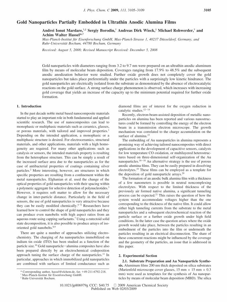
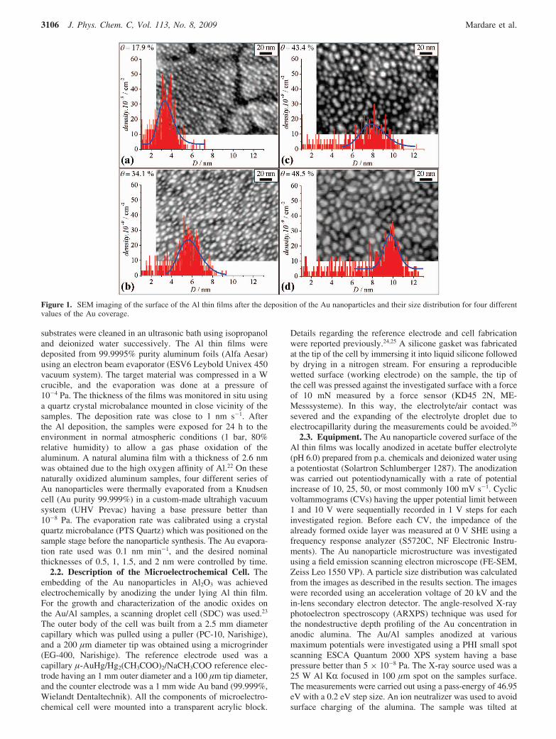
Figure 1. SEM imaging of the surface of the Al thin films after the deposition of the Au nanoparticles and their size distribution for four differentvalues of the Au coverage.
3106 J. Phys. Chem. C, Vol. 113, No. 8, 2009 Mardare et al.

different incidence angles while the angle between the analyzerand the monochromatic X-ray radiation was kept constant. Themeasurement spots have been localized on the surface of thesample with the help of scanning X-ray imaging (SXI). For thispurpose the X-ray beam was focused in a 5 µm spot and a totalarea of 1.4 mm × 1.4 mm was scanned. For interpreting theXPS spectra, Casa XPS software was used27 with the recalcu-lated sensitivity factors from PHI MultiPack software.28
3. Results and Discussions
In Figure 1 the microstructures of the Au nanoparticles ofdifferent size which were deposited onto the surface of the air-formed Al oxide films are shown. From the SEM micrographs,the diameters of the nanoparticles were measured using imageanalysis software29 and the size distribution was plotted for eachsample. Following a previously reported model for the Aunanoparticles growth mechanism on thermally oxidized Al, theright parts of the histograms were fitted with a log-normaldistribution function. The left part, corresponding to the smallerparticles, did not show any remarkable feature which could befitted using log-probability plots.30 The growth behavior isdifferent from the one reported in the literature and may beattributed to the oxide structure which is different in this study.In the present case an ultrathin amorphous native alumina filmwas used that allows a decent electron transport through theoxide by means of tunneling. This avoids surface charging whichcan influence the wettability. The most probable particlediameter taken from the position of the peak distribution yieldedvalues of 3.2, 5.6, 7.9, and 9.7 nm (corresponding to nominalthickness values as measured by the crystal quartz monitor of0.5 1.0, 1.5, and 2 nm, respectively) which can be directly takenfrom the graphs. The Au coverage (θ), measured as the ratiobetween the nanoparticles projected surface and the total surface,is also shown in Figure 1 for each investigated sample. The Aucoverage increased with increase of the nanoparticles averagediameter; these values match the results obtained on thermallygrown alumina.30
The potentiodynamic anodization of the aluminum samplescovered by different Au nanoparticles was studied as a functionof the nanoparticle average size. Figure 2 shows the CV recordedduring the stepwise anodic oxidation up to 10 V of the Au/Alsamples, all the potential values being given versus the standardhydrogen electrode (SHE). CVs measured during anodizationof pure Al thin films are shown for reference. For all samples,a typical valve metal behavior characterized by the presence ofan oxidation current plateau and a strong current decay upon
reversion of the scan direction as well as an incipient currentovershoot related to a delayed oxide formation could beobserved.31 The presence of the Au nanoparticles on the surfaceof the Al resulted in a retardation of the initial current increasefor the anodic oxide growth, experimentally observed as apassive region up to 1.5-2.0 V having a weak dependence onthe nanoparticles sizes. With the increase of the Au nanoparticlesizes, the values of the oxidation current plateaus decreased andthe incipient current overshoots showed a more pronouncedbehavior. Even though the Au/Al samples were polarized atpotentials as high as 10 V, no Au oxidation or reduction peakscould be observed. This means that the Au particles areelectrically isolated from the bulk aluminum. The gas phaseoxidation prior to the gold deposition generates a significanttunneling barrier as was found before.21 The subsequent Audeposition by MBD does not generate conducting paths throughthis dielectric material.
This behavior is essentially different from an approach inwhich metallic nanoparticles are electrodeposited. This elec-trodeposition takes place preferentially on the weakest spots ofthe oxide which have the highest conductivity. This wasconfirmed for Co and Ni nanoparticles on aluminum32 but alsofor Au on NiAl matrix which selectively forms alumina.33,34
These particles, which are connected to the substrate by a lowresistance path, can be easily polarized and would therefore actas a local electrode if the surrounding oxide film shows asignificantly lower conductivity.
For probing the extended passivity of the Al thin films in thepresence of the Au nanoparticles, potentiodynamic anodizationexperiments were conducted at various scan rates. Figure 3shows the cyclic voltammograms measured up to 7 V on anAu/Al sample with nanoparticles with an average diameter of5.6 nm. The current density was normalized to the rate ofpotential increase to allow for a direct comparison of the curves.At small rates (10 mV s-1) the passive region was present forpotentials up to 1.6 V. The small instabilities in the backwardscan are more pronounced since the absolute current scalesalmost linearly with the scan rate but will be visually amplifiedif the scan rate normalized values are plotted against thepotential. Increasing the scan rate, leads to a shift of the onsetof oxide growth resulting from the kinetic hindrance of oxideformation. The half-wave potentials are varying as a functionof the scanning rate, values of 1.78, 1.93, 2.02, and 2.15 V beingmeasured for the 10, 25, 50, and 100 mV s-1 scanning rates,respectively. A plot of the half-wave potentials against thelogarithm of the scan rate yields a linear relationship indicating,
Figure 2. Cyclic voltammograms of the Au/Al samples for differentvalues of the nanoparticle average size.
Figure 3. Cyclic voltammograms of the Au/Al sample with averagenanoparticles diameter of 5.6 nm measured at different rates of potentialincrease.
Gold Nanoparticles Partially Embedded in Alumina J. Phys. Chem. C, Vol. 113, No. 8, 2009 3107
that this is the typical retardation of oxide formation as describedin the extended high-field model according to Lohrengel.31
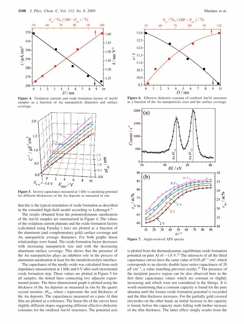
The results obtained from the potentiodynamic anodizationof the Au/Al samples are summarized in Figure 4. The valuesof the oxidation current plateaus and the oxide formation factors(calculated using Faraday’s law) are plotted as a function ofthe aluminum (and complementary gold) surface coverage andAu nanoparticle average diameters. For both graphs linearrelationships were found. The oxide formation factor decreaseswith increasing nanoparticle size and with the decreasingaluminum surface coverage. This shows that the presence ofthe Au nanoparticles plays an inhibitor role in the process ofaluminum anodization at least for the metal/electrolyte interface.
The capacitance of the anodic oxide was calculated from eachimpedance measurement at 1 kHz and 0 V after each incrementaloxide formation step. These values are plotted in Figure 5 forall samples, the dotted lines connecting two adjacent experi-mental points. The three-dimensional graph is plotted using thethickness of the Au deposits as measured in situ by the quartzcrystal monitor, tθAu, where t represents the real thickness ofthe Au deposits. The capacitances measured on a pure Al thinfilm are plotted as a reference. The linear fits of the curves haveslightly different slopes suggesting different effective dielectricconstants for the oxidized Au/Al structures. The potential axis
is plotted from the thermodynamic equilibrium oxide formationpotential on pure Al of -1.6 V.22 The intersects of all the fittedcapacitance curves have the same value of 0.05 µF-1 cm2, whichcorresponds to an electric double layer series capacitance of 20µF cm-2, a value matching previous results.35 The presence ofthe incipient passive region can be also observed here in thefirst three capacitance values which are constant or slightlyincreasing and which were not considered in the fittings. It isworth mentioning that a constant capacity is found for the purealumina until the former oxide formation potential is exceededand the film thickness increases. For the partially gold coveredelectrodes on the other hand, an initial increase in the capacityis found, before the capacity starts falling with further increaseof the film thickness. The latter effect simply results from the
Figure 4. Oxidation currents and oxide formation factors of Au/Alsamples as a function of Au nanoparticle diameters and surfacecoverage.
Figure 5. Inverse capacitance measured at 1 kHz vs anodizing potentialfor different thicknesses of the Au deposits as measured in situ.
Figure 6. Effective dielectric constant of oxidized Au/Al structuresas a function of the Au nanoparticles sizes and the surface coverage.
Figure 7. Angle-resolved XPS spectra.
3108 J. Phys. Chem. C, Vol. 113, No. 8, 2009 Mardare et al.
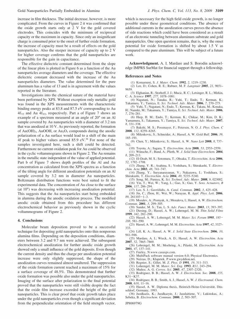
increase in film thickness. The initial decrease, however, is morecomplicated. From the curves in Figure 2 it was confirmed thatthe oxide growth starts only at 2 V for the gold coveredelectrodes. This coincides with the minimum of reciprocalcapacity or the maximum in capacity. Since only an insignificantcharge is consumed prior to the onset of further oxide formation,the increase of capacity must be a result of effects on the goldnanoparticles. Also the steeper increase of capacity up to 2 Vfor higher coverage confirms that the gold nanoparticles areresponsible for the gain in capacitance.
The effective dielectric constant determined from the slopeof the linear plots is plotted in Figure 6 as a function of the Aunanoparticles average diameters and the coverage. The effectivedielectric constant decreased with the increase of the Aunanoparticles diameters. The value determined for the purealuminum has a value of 13 and is in agreement with the valuesreported in the literature.
Investigations into the chemical nature of the material havebeen performed by XPS. Without exception only metallic goldwas found in the XPS measurements with the characteristicbinding energy peaks at 83.8 and 87.5 eV corresponding to Au4f7/2 and Au 4f5/2, respectively. Part a of Figure 7 shows anexample of a spectrum measured at an angle of 20° on an Alsample covered by Au nanoparticles with a diameter of 3.2 nmthat was anodized at 10 V. As previously reported, the formationof Au(OH)3, AuOOH, or Au2O3 compounds during the anodicpolarization of a Au surface would lead to a shift of the main4f peak to higher values around 85.9 eV.36 For none of thesamples investigated here, such a shift could be detected.Furthermore no current oxidation peak for Au could be observedin the cyclic voltammograms shown in Figure 2. The Au remainsin the metallic state independent of the value of applied potential.Part b of Figure 7 shows depth profiles of the Al and Auconcentration as calculated from the XPS spectra as a functionof the tilting angle for different anodization potentials on an Alsample covered by 3.2 nm in diameter Au nanoparticles.Boltzmann distribution functions were best suited to fit theexperimental data. The concentration of Au close to the surface(at 10°) was decreasing with increasing anodization potential.This suggests that the Au nanoparticles start being embeddedin alumina during the anodic oxidation process. The modifiedanodic oxide obtained from this procedure has differentelectrochemical behavior as previously shown in the cyclicvoltammograms of Figure 2.
4. Conclusions
Molecular beam deposition proved to be a successfultechnique for depositing gold nanoparticles onto thin nonporousalumina films. Depending on the deposition conditions, diam-eters between 3.2 and 9.7 nm were achieved. The subsequentelectrochemical anodization for further anodic oxide growthshowed only a small influence of the gold deposits. Even thoughthe current density and thus the charge per anodization potentialincrease were only slightly suppressed, the shape of theanodization curves remained almost unaltered. The suppressionof the oxide formation current reached a maximum of 15% fora surface coverage of 48.5%. This demonstrated that furtheroxide formation was possible also under the gold nanoparticles.Imaging of the surface after polarization to the final potentialproved that the nanoparticles were still visible despite the factthat the oxide film increase exceeded the height of the goldnanoparticles. This is clear proof that oxide growth takes placeunder the gold nanoparticles even though a significant deviationfrom the perpendicular orientation of the field strength vector,
which is necessary for the high field oxide growth, is no longerpossible under these geometrical conditions. The absence ofadditional currents in the anodization curves proves the absenceof side reactions which could have been considered as a resultof an electronic tunneling between aluminum substrate and goldnanoparticles. One open question remains, that is, why the onsetpotential for oxide formation is shifted by about 1.5 V ascompared to the pure aluminum. This will be subject of a futurework.
Acknowledgment. A. I. Mardare and S. Borodin acknowl-edge IMPRS SurMat for financial support through a fellowship.
References and Notes
(1) Komarneni, S. J. Mater. Chem. 1992, 2, 1219–1230.(2) Lee, D.; Cohen, R. E.; Rubner, M. F. Langmuir 2005, 21, 9651–
9659.(3) Elghanian, R.; Storhoff, J. J.; Mucic, R. C.; Letsinger, R. L.; Mirkin,
C. A. Science 1997, 277, 1078–1081.(4) Nagatani, N.; Tanaka, R.; Yuhi, T.; Endo, T.; Kerman, K.;
Takamura, Y.; Tamiya, E. Sci. Technol. AdV. Mater. 2006, 7, 270–275.(5) Yuhi, T.; Nagatani, N.; Endo, T.; Kerman, K.; Takata, M.; Konaka,
H.; Namiki, M.; Takamura, Y.; Tamiya, E. Sci. Technol. AdV. Mater. 2006,7, 276–281.
(6) Hiep, H. M.; Endo, T.; Kerman, K.; Chikae, M.; Kim, D. K.;Yamamura, S.; Takamura, Y.; Tamiya, E. Sci. Technol. AdV. Mater. 2007,8, 331–338.
(7) Bakshi, M. S.; Possmayer, F.; Petersen, N. O. J. Phys. Chem. C2008, 112, 8259–8265.
(8) Milenkovic, S.; Schneider, A.; Hassel, A. W. Gold Bull. 2006, 39,185–191.
(9) Chen, Y.; Milenkovic, S.; Hassel, A. W. Nano Lett 2008, 8, 737–742.
(10) Toyota, A.; Sagara, T. Electrochim. Acta 2008, 53, 2553–2559.(11) Wunsche, F.; Bund, A.; Plieth, W. J. Solid State Electrochem. 2004,
8, 209–213.(12) El-Deab, M. S.; Sotomura, T.; Ohsaka, T. Electrochim. Acta 2006,
52, 1792–1798.(13) Zhang, Y. R.; Asahina, S.; Yoshihara, S.; Shirakashi, T. Electro-
chim. Acta 2003, 48, 741–747.(14) Zhang, Y.; Suryanarayanan, V.; Nakazawa, I.; Yoshihara, S.;
Shirakashi, T. Electrochim. Acta 2004, 49, 5235–5240.(15) Song, M.; Furuya, K. Sci. Technol. AdV. Mater. 2008, 9, 023002.(16) Yin, T.; Wei, W.; Yang, L.; Gao, X.; Gao, Y. Sens. Actuators, B
2006, 117, 286–294.(17) Lee, S. J.; Gavriilidis, A. Catal. Commun. 2002, 3, 425–428.(18) Jin, C.; Zhou, H.; Wei, W.; Narayan, R. Appl. Phys. Lett. 2006,
89, 261103-1–3.(19) Mozalev, A.; Poznyak, A.; Mozaleva, I.; Hassel, A. W. Electrochem.
Commun. 2001, 3, 299–305.(20) Sander, M. S.; Tan, L. S. AdV. Funct. Mater. 2003, 13, 393–397.(21) Diesing, D.; Hassel, A. W.; Lohrengel, M. M. Thin Solid Films
1999, 342, 282–290.(22) Hassel, A. W.; Lohrengel, M. M. Mater. Sci. Forum 1995, 185-
188, 581–590.(23) Hassel, A. W.; Lohrengel, M. M. Electrochim. Acta 1997, 42, 3327–
333.(24) Lill, K. A.; Hassel, A. W. J. Solid State Electrochem. 2006, 10,
941–946.(25) Mardare, A. I.; Wieck, A. D.; Hassel, A. W. Electrochim. Acta
2007, 52, 7865–7869.(26) Lohrengel, M. M.; Moehring, A.; Pilaski, M. Electrochim. Acta
2001, 47, 137–141.(27) Fairley, N.www.casaxps.com.(28) MultiPack software manual version 6.0; Physical Electronics.(29) Neceas, D.; Klapetek, P.www.gwyddion.net.(30) Regnier, S.; Gillet, M. Z. Phys. D 1991, 19, 311–313.(31) Lohrengel, M. M. Mater. Sci. Eng. 1993, R11, 243–294.(32) Munoz, A. G. Corros. Sci. 2005, 47, 2307–2320.(33) Rodriguez, B. B.; Hassel, A. W. J. Electrochem. Soc. 2008, 155,
K31-K37.(34) Rodriguez, B. B.; Smith, A. J.; Hassel, A. W. J. Electroanal. Chem.
2008, 618, 11–16.(35) Hassel, A. W. Diploma thesis, Heinrich-Heine-Universitat, Dus-
seldorf, Germany, 1993.(36) Juodkazis, K.; Juodkazyte, J.; Jasulaitiene, V.; Lukinskas, A.;
Sebeka, B. Electrochem. Commun. 2000, 2, 503–507.
JP806979G
Gold Nanoparticles Partially Embedded in Alumina J. Phys. Chem. C, Vol. 113, No. 8, 2009 3109
Copyright © 2022 FDOKUMEN