Structural Engineering of Nanoporous Anodic Alumina and ...
307
STRUCTURAL ENGINEERING OF NANOPOROUS ANODIC ALUMINA AND APPLICATIONS Abel Santos Alejandro ISBN: 978-84-693-9438-0 Dipòsit Legal: T.71-2011 ADVERTIMENT. La consulta d’aquesta tesi queda condicionada a l’acceptació de les següents condicions d'ús: La difusió d’aquesta tesi per mitjà del servei TDX (www.tesisenxarxa.net ) ha estat autoritzada pels titulars dels drets de propietat intel·lectual únicament per a usos privats emmarcats en activitats d’investigació i docència. No s’autoritza la seva reproducció amb finalitats de lucre ni la seva difusió i posada a disposició des d’un lloc aliè al servei TDX. No s’autoritza la presentació del seu contingut en una finestra o marc aliè a TDX (framing). Aquesta reserva de drets afecta tant al resum de presentació de la tesi com als seus continguts. En la utilització o cita de parts de la tesi és obligat indicar el nom de la persona autora. ADVERTENCIA. La consulta de esta tesis queda condicionada a la aceptación de las siguientes condiciones de uso: La difusión de esta tesis por medio del servicio TDR (www.tesisenred.net ) ha sido autorizada por los titulares de los derechos de propiedad intelectual únicamente para usos privados enmarcados en actividades de investigación y docencia. No se autoriza su reproducción con finalidades de lucro ni su difusión y puesta a disposición desde un sitio ajeno al servicio TDR. No se autoriza la presentación de su contenido en una ventana o marco ajeno a TDR (framing). Esta reserva de derechos afecta tanto al resumen de presentación de la tesis como a sus contenidos. En la utilización o cita de partes de la tesis es obligado indicar el nombre de la persona autora. WARNING. On having consulted this thesis you’re accepting the following use conditions: Spreading this thesis by the TDX (www.tesisenxarxa.net ) service has been authorized by the titular of the intellectual property rights only for private uses placed in investigation and teaching activities. Reproduction with lucrative aims is not authorized neither its spreading and availability from a site foreign to the TDX service. Introducing its content in a window or frame foreign to the TDX service is not authorized (framing). This rights affect to the presentation summary of the thesis as well as to its contents. In the using or citation of parts of the thesis it’s obliged to indicate the name of the author.
-
Upload
khangminh22 -
Category
Documents
-
view
1 -
download
0
Transcript of Structural Engineering of Nanoporous Anodic Alumina and ...

STRUCTURAL ENGINEERING OF NANOPOROUS ANODIC ALUMINA AND
APPLICATIONS Abel Santos Alejandro
ISBN: 978-84-693-9438-0 Dipòsit Legal: T.71-2011
ADVERTIMENT. La consulta d’aquesta tesi queda condicionada a l’acceptació de les següents condicions d'ús: La difusió d’aquesta tesi per mitjà del servei TDX (www.tesisenxarxa.net) ha estat autoritzada pels titulars dels drets de propietat intel·lectual únicament per a usos privats emmarcats en activitats d’investigació i docència. No s’autoritza la seva reproducció amb finalitats de lucre ni la seva difusió i posada a disposició des d’un lloc aliè al servei TDX. No s’autoritza la presentació del seu contingut en una finestra o marc aliè a TDX (framing). Aquesta reserva de drets afecta tant al resum de presentació de la tesi com als seus continguts. En la utilització o cita de parts de la tesi és obligat indicar el nom de la persona autora. ADVERTENCIA. La consulta de esta tesis queda condicionada a la aceptación de las siguientes condiciones de uso: La difusión de esta tesis por medio del servicio TDR (www.tesisenred.net) ha sido autorizada por los titulares de los derechos de propiedad intelectual únicamente para usos privados enmarcados en actividades de investigación y docencia. No se autoriza su reproducción con finalidades de lucro ni su difusión y puesta a disposición desde un sitio ajeno al servicio TDR. No se autoriza la presentación de su contenido en una ventana o marco ajeno a TDR (framing). Esta reserva de derechos afecta tanto al resumen de presentación de la tesis como a sus contenidos. En la utilización o cita de partes de la tesis es obligado indicar el nombre de la persona autora. WARNING. On having consulted this thesis you’re accepting the following use conditions: Spreading this thesis by the TDX (www.tesisenxarxa.net) service has been authorized by the titular of the intellectual property rights only for private uses placed in investigation and teaching activities. Reproduction with lucrative aims is not authorized neither its spreading and availability from a site foreign to the TDX service. Introducing its content in a window or frame foreign to the TDX service is not authorized (framing). This rights affect to the presentation summary of the thesis as well as to its contents. In the using or citation of parts of the thesis it’s obliged to indicate the name of the author.

UNIVERSITAT ROVIRA I VIRGILI STRUCTURAL ENGINEERING OF NANOPOROUS ANODIC ALUMINA AND APPLICATIONS Abel Santos Alejandro ISBN:978-84-693-9438-0/DL: T.71-2011

UNIVERSITAT ROVIRA I VIRGILI STRUCTURAL ENGINEERING OF NANOPOROUS ANODIC ALUMINA AND APPLICATIONS Abel Santos Alejandro ISBN:978-84-693-9438-0/DL: T.71-2011

UNIVERSITAT ROVIRA I VIRGILI STRUCTURAL ENGINEERING OF NANOPOROUS ANODIC ALUMINA AND APPLICATIONS Abel Santos Alejandro ISBN:978-84-693-9438-0/DL: T.71-2011

UNIVERSITAT ROVIRA I VIRGILI STRUCTURAL ENGINEERING OF NANOPOROUS ANODIC ALUMINA AND APPLICATIONS Abel Santos Alejandro ISBN:978-84-693-9438-0/DL: T.71-2011

Abel Santos Alejandro
Structural Engineering of Nanoporous Anodic Alumina and
Applications
DOCTORAL THESIS
Supervised by
Dr. Josep Pallarès Marzal &
Dr. Lluís Francesc Marsal Garví
Departament d’Enginyeria Electrònica, Elèctrica i Automàtica Nanoelectronic and Photonic Systems (NePhos)
Tarragona
2010
UNIVERSITAT ROVIRA I VIRGILI STRUCTURAL ENGINEERING OF NANOPOROUS ANODIC ALUMINA AND APPLICATIONS Abel Santos Alejandro ISBN:978-84-693-9438-0/DL: T.71-2011

UNIVERSITAT ROVIRA I VIRGILI STRUCTURAL ENGINEERING OF NANOPOROUS ANODIC ALUMINA AND APPLICATIONS Abel Santos Alejandro ISBN:978-84-693-9438-0/DL: T.71-2011

Departament d'Enginyeria Electrònica, Elèctrica i Automàtica Escola Tècnica Superior D’Enginyeria Campus Sescelades Av. Països Catalans 26 43007 Tarragona Espanya
Josep Pallarès Marzal and Lluís Francesc Marsal Garví, Full Professors at the
Departament of Electronic, Electrical and Automatic Control Engineering of the
University Rovira i Virgili,
STATE:
That the present study, entitled "Structural Engineering of Nanoporous Anodic Alumina
and Applications", presented by Abel Santos Alejandro for the award of the degree of
Doctor, has been carried out under our supervision at the Departament of Electronic,
Electrical and Automatic Control Engineering of this university, and that it fulfils all the
requirements to be eligible for the European Doctorate Award.
Tarragona, 20th of September of 2010
Doctoral Thesis Supervisor Doctoral Thesis Co-supervisor
Dr. Josep Pallarès Marzal Dr. Lluís Francesc Marsal Garví
UNIVERSITAT ROVIRA I VIRGILI STRUCTURAL ENGINEERING OF NANOPOROUS ANODIC ALUMINA AND APPLICATIONS Abel Santos Alejandro ISBN:978-84-693-9438-0/DL: T.71-2011

UNIVERSITAT ROVIRA I VIRGILI STRUCTURAL ENGINEERING OF NANOPOROUS ANODIC ALUMINA AND APPLICATIONS Abel Santos Alejandro ISBN:978-84-693-9438-0/DL: T.71-2011

Acknowledgements
This PhD thesis is the result not only of my passion for science but also of the financial
support provided by the Rovira i Virgili University (Tarragona), which for the last four
years has been my home and my place of learning. I would like to thank my
supervisors Dr. Josep Pallarès Marzal and Dr. Lluís Francesc Marsal Garví for their
support throughout. They gave me total freedom to investigate into the exciting world of
nanotechnology. I specially appreciate Dr. Josep Ferré-Borrull’s corrections and
comments about my work, because they have allowed me to constantly improve my
work, and also been a source of constructive criticism and a series of master classes
on how to construct a scientific article.
I am grateful for the comments of the committee members and the external reviewers
about my PhD thesis (Dr. Ramón Alcubilla, Dr. Josep Ferré-Borrull, Dr. Julien
Bachmann, Dr. Luís M. Liz-Marzán, Dr. Francisco Meseguer, Dr. Josep M. Montero-
Moreno and Dr. Jaromír Hubálek).
I would also like to give especial thanks to the current and former members of the
nanoelectronic and photonic systems research group (NePhos) for their collaboration
during my PhD stay in Tarragona. In particular, I would like to mention Dr. Lukas
Vojkuvka for his willingness to introduce me to the wonderful world of nanotechnology,
for his stimulating discussions about nanoporous anodic alumina and for a special
friendship throughout these years.
UNIVERSITAT ROVIRA I VIRGILI STRUCTURAL ENGINEERING OF NANOPOROUS ANODIC ALUMINA AND APPLICATIONS Abel Santos Alejandro ISBN:978-84-693-9438-0/DL: T.71-2011

I am very grateful to the staff of the Scientific and Technical Service (SRCiT) for their
support and patience during the characterization sessions (Dr. Lukas Vojkuvka, Dr.
Mariana Stankova, Dr. Rita Marimon and Mercé Moncusí). I would also like to thank
the technical support members of the DEEEiA who helped me develop the anodizing
system and other experimental equipment (Jordi Maré, Josep María Badia, Jordi
Deosdad, Carmelo Fuentes and Jaume Pros).
I would like to thank Professor Dr. Kornelius Nielsch from the Institut für Angewandte
Physik of the University of Hamburg for giving me the opportunity to work in his
research group for three months. It was one of the most positive experiences of my life
and I will always be grateful to him. I am also very grateful to Dr. Josep M. Montero-
Moreno for his support, stimulating discussions and friendship in the course of my
research visit to Hamburg and for the subsequent supervision of my PhD thesis. I
should also thank Dr. Julien Bachmann for his kindness, friendship and for advice on
possible future post-doc projects; Dip. Ing. Lewis Akinsinde for his friendship and
technical support during my laboratory tasks in Hamburg (I will always remember our
discussions about football); and Janike Adomat for her friendship and for our short but
pleasant chats about books and science during my laboratory sessions in Hamburg.
Finally, I would like to thank the other members of the Nielsch’s for their support,
kindness and friendship during my research visit (vielen dank für alles!!).
UNIVERSITAT ROVIRA I VIRGILI STRUCTURAL ENGINEERING OF NANOPOROUS ANODIC ALUMINA AND APPLICATIONS Abel Santos Alejandro ISBN:978-84-693-9438-0/DL: T.71-2011

I dedicate this PhD thesis to Paqui Franco from the IES Francisco Ribalta of Castellón
de la Plana. She taught me the rigour of scientific reasoning by means of the wonderful
world of Mathematics. I will never forget either her words of support during the first
stage of my scientific life nor her master classes about Mathematics. She is a
wonderful mathematician and a constant source of scientific inspiration for me. Her
presence is felt in every line of this document.
I will forever be indebted to my family (Ana Claramonte, José Vicente Serer, Ana Lidón
Serer, Carmelo Muñoz, Rebeca Muñoz and Jorge Muñoz) for their appreciation and
love throughout my life. I reserve special thanks for my grandmothers (Severiana
Barradas and Ana Marzà), my grandfathers (José Santos and Manuel Alejandro) and
my uncle (José Serer). They have gone but they will always be in my thoughts.
Finally, I reserve the biggest acknowledgement for the members of my close family,
because they have always been by my side through thick and thin; Maria Isabel
Alejandro Marzà, my mother, who gave me life; José Santos Barradas, my father, the
supreme example of a hardworking man who has dedicated his life to supporting us,
working from dusk till dawn; Alicia Santos Alejandro, my sister, who is my greatest
friend and a constant source of support (tho’ a little tiresome sometimes). And last but
not least, I would like to remember our first dog (Tobi), who is now in the dog’s
paradise, and our present little dog (Newton), who is a new and special member of the
family.
This thesis would not have been possible without them.
UNIVERSITAT ROVIRA I VIRGILI STRUCTURAL ENGINEERING OF NANOPOROUS ANODIC ALUMINA AND APPLICATIONS Abel Santos Alejandro ISBN:978-84-693-9438-0/DL: T.71-2011

UNIVERSITAT ROVIRA I VIRGILI STRUCTURAL ENGINEERING OF NANOPOROUS ANODIC ALUMINA AND APPLICATIONS Abel Santos Alejandro ISBN:978-84-693-9438-0/DL: T.71-2011

I
Abstract
In this PhD thesis, various structural engineering strategies are applied to develop
innovative templates based on nanoporous anodic alumina. These templates are then
used to develop other nanostructures based on such multi-purpose materials as
polymers, magnetic metals and semiconductors. These replicated nanostructures can
be integrated in various types of nanodevices (e.g. nanoelectrodes for direct deposition
of nanoparticles from a gas draught, bulk-heterojunction solar cells, one-dimensional
optoelectronic devices, nanofilters and so on).
As a starting point, the methods for fabricating nanoporous anodic alumina templates
are presented.
First four typical self-ordered nanoporous anodic alumina templates are fabricated
using the two-step anodization process under mild anodization conditions. The acids
used for fabricating these nanoporous anodic alumina templates are sulphuric (H2SO4),
oxalic (H2C2O4) and phosphoric (H3PO4). Second, self-ordered nanoporous anodic
alumina templates are fabricated following the one-step anodization process under
hard conditions. Third, the two-step anodization technique is used under hard
conditions to develop nanoporous anodic alumina templates without a protective layer,
which is characteristic of the typical one-step anodization process. Fourth, following a
re-anodization technique under galvanostatic conditions, the aluminium oxide barrier
layer located at the pore bottom tips of these templates is removed without removing
the aluminium substrate or detaching the nanoporous anodic alumina template. Fifth,
by means of an asymmetric two-step anodization process in which the anodization
conditions are modified (i.e. anodization voltage, type and concentration of the acid
electrolyte), hierarchical nanoporous anodic alumina templates with multiple
configurations are fabricated.
UNIVERSITAT ROVIRA I VIRGILI STRUCTURAL ENGINEERING OF NANOPOROUS ANODIC ALUMINA AND APPLICATIONS Abel Santos Alejandro ISBN:978-84-693-9438-0/DL: T.71-2011

II
Sixth, bilayered nanoporous anodic alumina templates are produced by combining mild
and hard anodization regimes. Seventh, a silicon nitride master stamp is used to
fabricate perfectly ordered nanoporous anodic alumina templates by means of the
nanoimprint technique and direct anodization. Furthermore, by nanoimprinting and
applying suitable anodization conditions, perfectly ordered nanoporous anodic alumina
templates with extraordinary pore arrangement can be generated. Finally, high aspect
ratio nanoporous anodic alumina funnels are fabricated by intercalating consecutive
anodizing and pore widening steps. These nanostructures have extremely accurate
geometric characteristics as a result of two systematic calibration processes. In
addition, a theoretical model for the pore growth during the anodization process is
developed and experimentally validated.
Subsequently, some nanostructures replicated from the templates based on
nanoporous anodic alumina are discussed.
First, arrays of magnetic nanopillars on aluminium substrates are synthesized by DC
electrochemical deposition and characterized by environmental scanning electron
microscopy (ESEM), energy dispersive X-ray spectroscopy (EDXS) and micro-X-ray
diffraction (μ-XRD) measurements. Because of their magnetic properties, these
nanopillars arrays can be used as nanoelectrodes for the direct deposition of
nanoparticles from a gas draught or as electrostatic precipitators. Second, quasi-
ordered P3HT nanopillar-nanocap structures of controlled size are fabricated by using
hierarchical nanoporous anodic alumina as a template. Furthermore, high-density
nanopillar arrays of the same polymer are transferred onto ITO/glass substrates. The
resulting nanostructure is characterized by ESEM, transmission electron microscopy
(TEM), thermogravimetry (TGA), μ-XRD and current-sensing atomic force microscopy
(CS-AFM). It is confirmed that such polymeric nanostructures can be used to develop
high-efficient bulk-heterojunction organic solar cells.
UNIVERSITAT ROVIRA I VIRGILI STRUCTURAL ENGINEERING OF NANOPOROUS ANODIC ALUMINA AND APPLICATIONS Abel Santos Alejandro ISBN:978-84-693-9438-0/DL: T.71-2011

III
Third, mosaic arrays of nickel nanowires and nanotubes are successfully fabricated by
using bilayered nanoporous anodic alumina templates. The resulting nanostructures
are used to make a systematic study of how the main anodization parameters influence
pore re-arrangement during the change from mild to hard anodization. These arrays of
magnetic nanostructures could be used in new data storage platforms. Finally, linear
silica nanosphere chains with helical alignments are fabricated by vacuum infiltration
through nanoporous anodic alumina funnels. These nanostructures can be integrated
in one-dimensional nano-optical devices.
The presented results are expected to be the starting point for the development of new
nanodevices and applications in a wide range of research fields.
UNIVERSITAT ROVIRA I VIRGILI STRUCTURAL ENGINEERING OF NANOPOROUS ANODIC ALUMINA AND APPLICATIONS Abel Santos Alejandro ISBN:978-84-693-9438-0/DL: T.71-2011

IV
UNIVERSITAT ROVIRA I VIRGILI STRUCTURAL ENGINEERING OF NANOPOROUS ANODIC ALUMINA AND APPLICATIONS Abel Santos Alejandro ISBN:978-84-693-9438-0/DL: T.71-2011

V
List of Figures
Chapter 1
Figure 1.1
Current density-time transient of a typical anodization of aluminium
under potentiostatic conditions (oxalic acid 0.3 M at 40 V) and
schematic cross-section views describing the first stages of the
anodization process. a) The four main sections of the J-t transient (S1,
S2, S3 and S4) are related to different stages of pore formation and
growth: b) Formation of a thin, compact layer of Al2O3 (S1 in (a)). c)
Instabilities in the electric field across the oxide film dissolve partially
the oxide at certain sites (i.e. nucleating centres) (S2 in (a)). d) Pore
formation at the nucleating centres on the aluminium oxide surface (S3
in (a)). e) Steady growth of pores (i.e. competition between formation
and dissolution of aluminium oxide) (S4 in (a)). f) Magnified view of the
red circle in (e) showing the transport of the main ionic species through
the oxide barrier layer. (Page 9)
Figure 1.2 Crystallographic phases present on nanoporous anodic alumina as a
function of the temperature. (Page 10)
Figure 1.3 Schematic diagram of a nanoporous anodic alumina pore showing the
chemical composition distribution inside the pore walls. a) Top view. b)
Cross-sectional view. c) Environmental scanning electron microscopy
(ESEM) image of the top view of a NAAT fabricated with oxalic acid 0.3
M at 40 V. (Page 11)
UNIVERSITAT ROVIRA I VIRGILI STRUCTURAL ENGINEERING OF NANOPOROUS ANODIC ALUMINA AND APPLICATIONS Abel Santos Alejandro ISBN:978-84-693-9438-0/DL: T.71-2011

VI
Figure 1.4 Summary of the relationship between the interpore distance and the
anodization voltage for self-ordered pore growth under mild anodization
regimen (MA) in sulphuric (solid black squares), oxalic (solid green
triangle) and phosphoric (solid cyan rhombuses), and under hard
anodization regimen (HA) in sulphuric (solid red circles) and oxalic
(solid blue triangles). The blue and pink dashed lines indicate the trend
lines for MA and HA regimens, respectively. (Page 13)
Figure 1.5 Effect of annealing and electropolishing treatments on commercial
aluminium substrates. a) ESEM image of an as-produced commercial
aluminium substrate. b) ESEM image of an electropolished commercial
aluminium substrate without annealing treatment (small grain sizes). c)
ESEM image of an electropolished commercial aluminium substrate
with annealing treatment (the average grain size is noticeable
increased in contrast to (b)). (Page 15)
Figure 1.6 Schematic diagram describing the most widely used methods for
fabricating PD-NAATs and MD-NAATs throughout the NAA history. a)
One-step anodization (disordered PD-NAAT). b) Two-step anodization
(ordered PD-NAAT). c) Nanoimprinting anodization (ordered MD-
NAAT). (Page 20)
Figure 1.7 Schematic top view of a MD-NAAT fabricated by smart nanoimprinting.
Each new pore (red circles) grows guided by three imprinted pores
(gray circles). (Page 21)
UNIVERSITAT ROVIRA I VIRGILI STRUCTURAL ENGINEERING OF NANOPOROUS ANODIC ALUMINA AND APPLICATIONS Abel Santos Alejandro ISBN:978-84-693-9438-0/DL: T.71-2011

VII
Chapter 2
Figure 2.1 Schematic diagram of a basic electrochemical cell for anodizing
aluminium substrates. (Page 27)
Figure 2.2 Detailed photography of the first experimental setup used to fabricate
NAATs. (Page 28)
Figure 2.3 Detailed photography of the second experimental setup used to
fabricate NAATs. a) General photography of the assembled
electrochemical cell in the course of an anodization process. b) Lateral
view photography of the PVC cover. c) Bottom view photography of the
PVC cover. d) General photography of the liquid-cooler thermostat with
recirculation circuit and the Peltier cooling plate. e) Lateral view
photography of the Teflon container fixed to the Cu plate. f) Bottom
view photography of the Teflon container. (Page 30)
Figure 2.4 Detailed photography of the third experimental setup used to fabricate
NAATs. a) General view photography of the experimental setup. b)
Bottom view photography of the Armaflex covered PVC cover. c)
Lateral view photography of the Armaflex covered PVC cover. d) Top
view photography of the EPS casing that covers the Peltier cooling
plate. e) Magnified photography of the assembled setup. (Page 32)
Figure 2.5 Gantt diagram describing the evolution of the experimental setup over
the last six years. The first experimental setup was used for 1.5 years,
the second one for 2.5 and the third one for 2 years. (Page 33)
Figure 2.6 Experimental equipment used to fabricate nanoporous anodic alumina
templates. All these devices were assembled on a wheeled shelf to
ease the equipment transport in our laboratory. (Page 35)
UNIVERSITAT ROVIRA I VIRGILI STRUCTURAL ENGINEERING OF NANOPOROUS ANODIC ALUMINA AND APPLICATIONS Abel Santos Alejandro ISBN:978-84-693-9438-0/DL: T.71-2011

VIII
Figure 2.7 Some examples of Labview programs developed for anodizing
aluminium substrates. a) Ramp-step profile of V controlled by the
anodization time. b) Ramp-step profile of V controlled by the total
current charge. c) Constant profile of V controlled by the anodization
time. d) Constant profile of V controlled by the total current charge.
(Page 36)
Figure 2.8 Annealing process applied to commercial aluminium foils before
electropolishing. (Page 40)
Figure 2.9 Electropolishing process. a) Voltage and current-time transients of a
typical electropolishing process under potentiostatic conditions
(EtOH:HClO4 4:1 (v:v) at 20 V) and schematic cross-section views of
an annealed Al substrate before (1) and after (2) electropolishing. The
electric field generated is mainly focused on the protuberances (red
arrows), producing the smoothing surface effect. b) AFM images
together with the corresponding cross-section profiles (blue lines) for Al
substrates annealed but not electropolished (left) and annealed and
electropolished (right). (Page 43)
UNIVERSITAT ROVIRA I VIRGILI STRUCTURAL ENGINEERING OF NANOPOROUS ANODIC ALUMINA AND APPLICATIONS Abel Santos Alejandro ISBN:978-84-693-9438-0/DL: T.71-2011

IX
Chapter 3
Figure 3.1
Schematic slanted section views describing the two-step anodization
process. a) Annealed and electropolished aluminium substrate. b) PD-
NAATs with disordered pores on the top and ordered pores on the
bottom. c) Patterned Al substrate after removing the oxide film with
disordered pores. d) PD-NAAT with straight and hexagonally ordered
pores. (Page 49)
Figure 3.2 Current density-time (J-t) transients for each type of PD-NAATs
fabricated by the two-step anodization process. a) H2SO4 0.3 M at 20
V. b) H2C2O4 0.3 M at 40 V. c) H3PO4 0.3 M at 160 V. d) H3PO4 1 wt %
at 195 V. (Page 49)
Figure 3.3 Set of ESEM images of the four types of commonly PD-NAATs
fabricated by the two-step anodization process. Top and bottom views
of PD-NAATs produced by a) and b) H3PO4 1 wt % at 195 V. c) and d)
H3PO4 0.3 M at 160 V. e) and f) H2C2O4 0.3 M at 40 V. g) and h)
H2SO4 0.3 M at 20 V. (Page 51)
Figure 3.4 Set of AFM (before chemical etching) and ESEM (after chemical
etching) images of a PD-NAAT fabricated with H2C2O4 0.3 M at 40 V.
a) AFM top view. b) AFM bottom view. c) Magnified view of the blue
square in (b). d) Three-dimensional image of (c). e) ESEM bottom view
after chemical etching for pore opening. f) Magnified view of the white
square in (e). (Page 53)
UNIVERSITAT ROVIRA I VIRGILI STRUCTURAL ENGINEERING OF NANOPOROUS ANODIC ALUMINA AND APPLICATIONS Abel Santos Alejandro ISBN:978-84-693-9438-0/DL: T.71-2011

X
Figure 3.5 Pore widening calibration for samples fabricated with H3PO4 0.3 M at
160 V. a) Experimental relationship between pore diameter (dp) and
pore widening time (tpw). b) Set of ESEM images of the top views of
samples after different lengths of pore widening time (i.e. Sa as-
produced, Sb 15 min, Sc 30 min, Sd 45 min and Se 60 min). c) Pore
diameter distributions and Gaussian fits for each sample after
measurements from the ESEM images in (b). (Page 54)
Figure 3.6 Set of ESEM images of NAATs fabricated with H3PO4 1 wt % at 195 V
and H3PO4 0.3 M at 160 V. a) ESEM top view of a NAAT fabricated
with H3PO4 1 wt % at 195 V (red lines denote domain boundaries). b)
Magnified view of the blue square in (a) showing the deformed pores
(red circles). c) ESEM bottom view of the same NAAT shown in (a)
after removing the Al substrate (red lines indicate domain boundaries).
d) Magnified view of the blue square in (c) showing the holes between
irregular junctions (red circles). e) ESEM top view of a NAAT fabricated
with H3PO4 0.3 M at 160 V (red lines denote domain boundaries). f)
Magnified view of the blue square in (e) showing the deformed pores
(red circles). g) ESEM bottom view of the same NAAT shown in (e)
after removing the Al substrate (red lines indicate domain boundaries).
h) Magnified view of the blue square in (g) showing the holes between
irregular junctions (red circles). i) ESEM image of Al nanopillars and
schematic cross-section view describing the generation of deformed
pores (top) and aluminium nanopillars (bottom). (Page 56)
UNIVERSITAT ROVIRA I VIRGILI STRUCTURAL ENGINEERING OF NANOPOROUS ANODIC ALUMINA AND APPLICATIONS Abel Santos Alejandro ISBN:978-84-693-9438-0/DL: T.71-2011

XI
Figure 3.7 One-step anodization process under hard conditions. a) Current
density-time (J-t) transient for a PD-NAAT fabricated by the one-step
anodization process under hard conditions with H2C2O4 0.3 M at 140 V.
b) Schematic cross-section view of the resulting PD-NAAT. c)
Magnified views of the green and red circles in (b). (Page 59)
Figure 3.8 Set of ESEM images of PD-NAATs fabricated with H2C2O4 0.3 M at
120 and 140 V by the one-step anodization process under hard
conditions. a and b) Top views of NAATs fabricated at 120 and 140 V,
respectively. c and d) Cross-section views of NAATs fabricated at 120
and 140 V, respectively (red dotted lines denote the transition layer
from MA to HA). e and f) Magnified views of the transition zone in (c)
and (d). g and h) Bottom views of NAATs fabricated at 120 and 140 V,
respectively. (Page 61)
Figure 3.9 Digital photography showing the change in colour of PD-NAATs
fabricated by the one-step anodization process under hard conditions.
The yellow bright increases as the hard anodization voltage increases.
(Page 61)
Figure 3.10 Set of ESEM images of a PD-NAAT fabricated by the one-step
anodization process under hard conditions after wet chemical etching
in phosphoric acid solution 5 wt % for 1 h at 35ºC. a) Top view. b)
Slanted cross-section view (the protective layer becomes hair-like
alumina after long wet chemical etching). (Page 63)
UNIVERSITAT ROVIRA I VIRGILI STRUCTURAL ENGINEERING OF NANOPOROUS ANODIC ALUMINA AND APPLICATIONS Abel Santos Alejandro ISBN:978-84-693-9438-0/DL: T.71-2011

XII
Figure 3.11 Schematic slanted section views describing the two-step anodization
process under hard conditions. a) Annealed and electropolished
aluminium substrate. b) PD-NAATs with a protective layer on the top
and ordered pores on the bottom with the interpore distance for the
hard anodization voltage. c) Patterned Al substrate after removing the
oxide film. d) PD-NAAT with straight and ordered pores. (Page 65)
Figure 3.12 Set of ESEM images of PD-NAATs fabricated by two-step anodization
process under hard conditions. a) Top view of a burnt NAAT (rests of
fused alumina and branched pores are denoted by yellow and red
arrows, respectively). b) Branched pores on the top of a NAAT. c) Top
view of the resulting NAAT fabricated under suitable conditions at 140
V by the two-step anodization. d) Cross-section view of the same
NAAT (pores are straight and well-defined). (Page 67)
Figure 3.13 Current density and voltage-time (J-t and V-t) transients for a PD-NAAT
fabricated by the two-step anodization process under hard conditions
with H2C2O4 0.3 M at 120 V and the re-anodization process under
galvanostatic conditions to remove the oxide barrier layer from the pore
bottom tips. Each different background indicates each of the four
stages of the process (yellow-1st anodization step, white-removing the
alumina layer, orange-2nd anodization step and red-3rd re-anodization
step). (Page 70)
UNIVERSITAT ROVIRA I VIRGILI STRUCTURAL ENGINEERING OF NANOPOROUS ANODIC ALUMINA AND APPLICATIONS Abel Santos Alejandro ISBN:978-84-693-9438-0/DL: T.71-2011

XIII
Figure 3.14 Schematic slanted and cross-section views describing the re-
anodization process for removing the oxide barrier layer from the pore
bottom tips of NAATs fabricated by the two-step anodization process
under hard conditions. Magnified views of the pore bottom tips after
each step of the re-anodization process are shown in red circles. In this
case, it is represented a virtual re-anodization process of 3 steps.
(Page 72)
Figure 3.15 Set of ESEM images of a NAAT fabricated by the two-step anodization
process under hard conditions before and after the re-anodization
process. a) General cross-section view before the re-anodization
process. b) Magnified view of the yellow square in (a). c) Cross-section
view after the re-anodization process. d) Slanted cross-fracture after
the re-anodization process (yellow arrowheads indicate the aluminium
substrate inside the opened pores). (Page 73)
Figure 3.16 Schematic cross-section and top views describing the asymmetric two-
step anodization process for fabricating HNAATs. a) First step of the
anodization process under conditions (a). b) Pattern on the aluminium
substrate surface after removing the oxide film by wet chemical
etching. c) Second step of the anodization process under conditions
(b). Magnified views of the cross-section (red circle in (c)) and top
(orange circle in (c)) of the resulting HNAAT. (Page 75)
Figure 3.17 Set of ESEM images of the different types of HNAATs fabricated by the
asymmetric two-step anodization process. a) Top view of the
corresponding HNAAT. b) Bottom view of the corresponding HNAAT
after removing the Al substrate by wet chemical etching. (Page 79)
UNIVERSITAT ROVIRA I VIRGILI STRUCTURAL ENGINEERING OF NANOPOROUS ANODIC ALUMINA AND APPLICATIONS Abel Santos Alejandro ISBN:978-84-693-9438-0/DL: T.71-2011

XIV
Figure 3.18 Pore density-voltage ratio (ρp/conc-RV2/V1) relationship for samples from
S1 to S8 (filled black circles). The red solid curve represents the
potential fit of the experimental data. (Page 81)
Figure 3.19 Set of AFM and ESEM images of different types of HNAATs fabricated
by the asymmetric two-step anodization process. a) AFM top view of
the resulting HNAAT obtained under conditions S6. b) Magnified view
of the blue square in (a). c) Cross-section profile of the same HNAAT
corresponding to the white line in (b). d) ESEM cross-section view of
the resulting HNAAT obtained under conditions S5. (Page 82)
Figure 3.20 Current density-time (J-t) transients corresponding to the second
anodization step for the samples S6, S7, S8 and the symmetric
process with H2SO4 0.3 M at 18 V (Sy). a) J-t transients for the first
1800 s. b) J-t transients for the first 400 s in (a). c) Time values (tmin)
(solid red line and circles-left scale) and current density values (Jmin)
(solid black line and stars-right scale) corresponding to the minima of
the current density curves in (a) as a function of the corresponding
interconcavity distance (dinterconc). (Page 85)
Figure 3.21 Schematic cross-section view describing how pores nucleate and grow
inside the concavities of the HNAAT but some of them close to the
outer hexagonal lattice vanish (V) or merge (M) by the self-ordering
mechanism. (Page 86)
Figure 3.22 Set of ESEM images of the HNAATs fabricated under conditions S9
and S10 by the asymmetric two-step anodization process. a) Top view
of sample S9 at 0.2 M and b) 0.1 M. c) Top view of sample S10 at 0.1
M and b) 0.015 M. The red circles indicate concavities with more than
one pore. (Page 87)
UNIVERSITAT ROVIRA I VIRGILI STRUCTURAL ENGINEERING OF NANOPOROUS ANODIC ALUMINA AND APPLICATIONS Abel Santos Alejandro ISBN:978-84-693-9438-0/DL: T.71-2011

XV
Figure 3.23 Set of ESEM images at two different magnifications of the HNAATs
fabricated under conditions S9 and S10 by the asymmetric two-step
anodization process. a) Top view of sample S9. b) Magnified view of
the red square in (a). c) Top view of sample S10. d) Magnified view of
the red square in (c). (Page 88)
Figure 3.24 Template thickness (τ) as a function of the total current charge (Q) for
each of the anodization voltages (i.e. 40, 80, 110 and 140 V) together
with their corresponding linear fittings (equations are shown in Table
3.4). (Page 90)
Figure 3.25 Set of ESEM images of the top, bottom and cross-section views of the
different types of BNAATs together with a cross-section schematic view
describing the general structure of these BNAATs. (Page 94)
Figure 3.26 Set of graphics of ρp(HA) as a function of the main anodization
parameters Rv and VHA. a) Average values of ρp(HA) as a function of Rv
for each value of VHA. b) Average values of ρp(HA) as a function of VHA
for each value of Rv. c) 2D contour plot of ρp(HA) as a function of Rv
and VHA. d) 3D representation of ρp(HA) as a function of Rv and VHA.
(Page 100)
Figure 3.27 Schematic slanted section views describing the one-step anodization
process for fabricating MD-NAATs by nanoimprinting. a) The Si3N4
master stamp is pressed onto the annealed and electropolished
aluminium substrate. b) The Si3N4 master stamp pattern is transferred
to the Al substrate surface. c) Resulting MD-NAAT after direct
anodization under suitable conditions. (Page 102)
UNIVERSITAT ROVIRA I VIRGILI STRUCTURAL ENGINEERING OF NANOPOROUS ANODIC ALUMINA AND APPLICATIONS Abel Santos Alejandro ISBN:978-84-693-9438-0/DL: T.71-2011

XVI
Figure 3.28 Set of ESEM images corresponding to the different stages of the
nanoimprint process. a) Cross-section view of the Si3N4 master stamp.
b) Top view of the Si3N4 master stamp. c) Annealed and
electropolished aluminium substrate after transferring the pattern from
the Si3N4 master stamp by pressing at 20 kN·cm-2. d) Resulting MD-
NAAT after direct anodization at 93 V. (Page 103)
Figure 3.29 Schematic top view of a MD-NAAT with extraordinary interpore
distance fabricated by nanoimprinting. Each new pore (blue circles)
grows guided by three imprinted pores (gray circles) since the
concentric electric field around each imprinted pore (green dotted
circles) prevents from the generation of disordered pores inside the
pore lattice. (Page 105)
Figure 3.30 Set of ESEM images of two types of MD-NAATs fabricated by
nanoimprinting. a) With ordinary interpore distance of 235 nm at 93 V
(blue circle indicates a virtual guided pore generated under suitable
anodization conditions). b) With extraordinary interpore distance of 203
nm at 81 V (red circle denotes a guided pore generated inside the pore
lattice of three imprinted pores). (Page 106)
Figure 3.31 Schematic cross-section view of the fabrication process of nickel
master stamps from PD-NAATs. a) Resulting PD-NAAT after the two-
step anodization process. b) PD-NAAT after dissolving selectively the
remaining Al substrate. c) Thin layer of Ni sputtered on the bottom of
the PD-NAAT. d) Growth of the Ni layer by electrodeposition. e)
Resulting Ni master stamp after removing the PD-NAAT. (Page 107)
UNIVERSITAT ROVIRA I VIRGILI STRUCTURAL ENGINEERING OF NANOPOROUS ANODIC ALUMINA AND APPLICATIONS Abel Santos Alejandro ISBN:978-84-693-9438-0/DL: T.71-2011

XVII
Figure 3.32 Replicated nickel master stamps from the bottom of two types of PD-
NAATs. a) Pore lattice of 100 nm with H2C2O4 at 40 V. b) Pore lattice of
500 nm with H3PO4 at 195 V. (Page 107)
Figure 3.33 Schematic cross-section diagram describing the selective pore opening
process in MD-NAATs with extraordinary pore arrangement.
(Page 108)
Figure 3.34 Experimental relationships between the fabrication parameters (i.e.
total current charge (Q), anodization time length (t) and pore widening
time (tpw)) and the geometric characteristics (i.e. pore length (LP) and
diameter (dP)) obtained from the calibration processes). a) Total current
charge (black solid line is numerical simulation and black solid stars
are experimental values) and pore length (light gray solid line is
numerical simulation and light gray solid circles are experimental
values) versus anodization time. b) Pore length versus total current
charge. c) Pore diameter versus pore widening time. (Page 120)
Figure 3.35 Set of ESEM images of cross-section view of the fabricated types of
NAAFs together with magnified views of the junctions between
consecutive segments (yellow rectangles in (a), (b), (c) and (d)) and a
sketch of the NAAF structure. a) NF-I. b) NF-II. c) NF-III. d) NF-IV.
(Page 122)
Figure 3.36 Current density (J-light gray solid line-left scale) and total current
charge (Q-black solid line-right scale) transients throughout the
anodization process for the types of NAAFs fabricated. a) NF-I. b) NF-
II. c) NF-III. d) NF-IV. (Page 124)
UNIVERSITAT ROVIRA I VIRGILI STRUCTURAL ENGINEERING OF NANOPOROUS ANODIC ALUMINA AND APPLICATIONS Abel Santos Alejandro ISBN:978-84-693-9438-0/DL: T.71-2011

XVIII
Chapter 4
Figure 4.1 Current and voltage-time (I-t and V-t) transients for the
electrodeposition processes under controlled potential conditions. The
different sections of the current transient are separated by red solid
lines. a) For Co-NPs at -3 V. b) For Ni-NPs at -5 V. (Page 133)
Figure 4.2 Schematic slanted views describing the electrodeposition process
using a PD-NAAT without oxide barrier layer fabricated by the two-step
anodization process under hard conditions. a) PD-NAAT without oxide
barrier layer. b) A thin layer of metal is deposited at the pore bottoms.
c) Fast growth of metallic nanopillar arrays inside the template. d) The
template is entirely filled with metal. e) Metal film growth on the
template surface. f) Resulting metallic nanopillar arrays after removing
the template when the process is stopped at (d). (Page 134)
Figure 4.3 Set of ESEM images of the fabricated metallic nanopillar arrays. a)
Cross-section view of the Co-NPs after removing the template. b)
Cross-section view of the Ni-NPs after removing the template. c)
Magnified bottom view of Co-NPs. d) Magnified bottom view of Ni-NPs.
e) Magnified top view of Co-NPs. f) Magnified top view of Ni-NPs.
(Page 136)
Figure 4.4 Elemental qualitative analysis of Co-NPs and Ni-NPs by energy
dispersive X-ray spectroscopy (EDXS). a) Spectrum and weight
percentage (inset) of the elements present in Co-NPs. b) Spectrum and
weight percentage (inset) of the elements present in Ni-NPs.
(Page 137)
Figure 4.5 X-ray diffraction patterns of Co-NPs (a) and Ni-NPs (b). (Page 138)
UNIVERSITAT ROVIRA I VIRGILI STRUCTURAL ENGINEERING OF NANOPOROUS ANODIC ALUMINA AND APPLICATIONS Abel Santos Alejandro ISBN:978-84-693-9438-0/DL: T.71-2011

XIX
Figure 4.6 Schematic slanted section views describing the fabrication process of
P3HT nanopillars on a substrate of P3HT quasi-hexagonally arranged
nanocaps. a) 1st anodization step. b) Removing the Al2O3 film by wet
chemical etching. c) 2nd anodization step under asymmetric conditions.
d) P3HT spin-coated HNAAT. e) P3HT infiltration by melt-assisted
wetting. f) Removing of the remaining Al substrate and the HNAAT by
wet chemical etching processes. (Page 142)
Figure 4.7 Current density and voltage-time (J-t and V-t) transients for the
fabrication process of the HNAAT under asymmetric conditions. Point
A indicates nanocaps formation and B when nanopillars reach a
suitable depth. (Page 144)
Figure 4.8 Set of ESEM images of the resulting P3HT nanostructure. a) Top view
of the P3HT nanocap arrays substrate. b) Tilted (45º) top view of the
P3HT nanocap arrays substrate. c) Top view of the P3HT nanopillar
arrays. d) Tilted (45º) top view of the P3HT nanopillar arrays.
(Page 145)
Figure 4.9 Slanted cross-section view diagram describing the fabrication process
of the high-density arrays of semiconducting Poly(3-hexylthiophene)
nanopillars on ITO/glass substrates. a) NAAT template on aluminium
substrate once the second step of the anodization process has finished
(ordered pores). b) P3HT spin-coated NAAT. c) P3HT-covered NAAT
pressed and fixed to an ITO/glass substrate. d) NAAT infiltrated with
P3HT after heating and annealing treatment. e) Arrays of
semiconducting P3HT nanopillars on ITO/glass substrate after
removing the remaining Al substrate and the NAAT. (Page 151)
UNIVERSITAT ROVIRA I VIRGILI STRUCTURAL ENGINEERING OF NANOPOROUS ANODIC ALUMINA AND APPLICATIONS Abel Santos Alejandro ISBN:978-84-693-9438-0/DL: T.71-2011

XX
Figure 4.10 Set of ESEM images of a NAAT. a) Top view of a NAAT. b) Cross-
section view of the same NAAT. (Page 153)
Figure 4.11 Current density and voltage-time (J-t and V-t) transients for the
fabrication process of a NAAT. (Page 155)
Figure 4.12 Thermogravimetry curve of normalized mass (W, black line-left scale)
and derivative thermogravimetry curve (dW, red line-right scale) of a
P3HT sample. The blue circles indicate the main decomposition
temperatures (i.e. 314, 473 and 549ºC). (Page 156)
Figure 4.13 Set of cross-sectional TEM and ESEM images. a) TEM image of cross-
section view of a P3HT nanostructured film after microtoming. b) ESEM
image of cross-section view of the same P3HT nanostructured film
without removing the Al substrate and the NAAT. c) Magnified view of
the red square in (b). (Page 157)
Figure 4.14 Definition of the geometric characteristics for the NAAT and the
replicated P3HT nanostructure. a) Cross-section view of the NAAT. b)
Top view of the NAAT. c) Cross-section view of the P3HT
nanostructure. d) Top view of the P3HT nanostructure. (Page 159)
Figure 4.15 Set of ESEM images of the high-density arrays of semiconducting
P3HT nanopillars on ITO/glass substrates. a) Top view. b) Magnified
view of the red square in (a). c) Cross-section view of the same
sample after fracturing the ITO/glass substrate. d) Magnified view of
the red square in (c). (Page 160)
Figure 4.16 J-V characteristics of P3HT film and nanopillars by CS-AFM. a) J-V
curves of P3HT nanopillars (light grey solid line) and P3HT film (black
solid line). b) Scheme of CS-AFM measurements for P3HT nanopillars
and P3HT film. (Page 162)
UNIVERSITAT ROVIRA I VIRGILI STRUCTURAL ENGINEERING OF NANOPOROUS ANODIC ALUMINA AND APPLICATIONS Abel Santos Alejandro ISBN:978-84-693-9438-0/DL: T.71-2011

XXI
Figure 4.17 Topography and current mappings of P3HT nanopillars and P3HT film
by CS-AFM images. a) AFM topography for P3HT nanopillars. b) AFM
topography for P3HT film. c) AFM current mapping for P3HT
nanopillars and d) P3HT film. e) AFM topography (black solid line-left
scale) and current (red solid line-right scale) profiles corresponding to
the blue line in (a) and (c), respectively. f) AFM topography (black solid
line-left scale) and current (red solid line-right scale) profiles
corresponding to the blue line in (b) and (d), respectively. (Page 163)
Figure 4.18 Cross-section view diagram for a) P3HT film and b) nanopillars and
their equivalent electric circuits. (Page 167)
Figure 4.19 P3HT chains alignment by nanoconfinement. a) µ-X-ray diffraction
analysis of P3HT film and nanopillars. b) Scheme showing how the
P3HT chains are randomly arranged inside the film bulk. c) Scheme
showing the arrangement of the P3HT chains inside the nanopillars
after the NAATs infiltration. (Page 170)
Figure 4.20 Set of ESEM images of a BNAAT fabricated under conditions S2.0-140
(Table 3.5). a) HA bottom view of the BNAAT after applying a reactive
ion etching process (open pores). b) MA top view of the BNAAT. c)
Cross-section view of the BNAAT. d) Magnified view of the red
rectangle in (c) (V denotes vanished pores, M identifies these pores
that merge and C these pores that continue after the voltage change
(transition layer)). (Page 174)
UNIVERSITAT ROVIRA I VIRGILI STRUCTURAL ENGINEERING OF NANOPOROUS ANODIC ALUMINA AND APPLICATIONS Abel Santos Alejandro ISBN:978-84-693-9438-0/DL: T.71-2011

XXII
Figure 4.21 Cross-section view scheme showing the fabrication process of mosaic
arrays of Ni-Nws and Ni-Ntbs. a) As-produced BNAAT. b) Removing
the remaining Al substrate by wet chemical etching. c) Pore opening
process of the HA side by reactive ion etching. d) Formation of copper
contact by electrodeposition on the MA side. e) Nickel
electrodeposition (fabrication of Ni-Nws). f) Removing the Cu contact
by mechanical polishing. g) Atomic layer deposition (fabrication of Ni-
Ntbs). (Page 175)
Figure 4.22 Identification of different layers in a BNAAT by the electrodeposition
transient. a) Current and voltage-time (I-t and V-t) transients of an
entirely filled BNAAT by Ni electrodeposition under galvanostatic
conditions. b) Schematic cross-section view showing the different
layers of the BNAAT. (Page 178)
Figure 4.23 Set of ESEM images of the MA side of each type of BNAAT after Ni
electrodeposition, mechanical polishing, cleaning and pore widening.
(Page 180)
Figure 4.24 Schematic diagram showing the image analysis process carried out to
estimate NFP/NEP. (Page 181)
Figure 4.25 Set of graphics of NFP/NEP as a function of the main anodization
parameters (i.e. Rv and VHA). a) Average values of NFP/NEP as a
function of Rv for each value of VHA. b) Average values of NFP/NEP as a
function of VHA for each value of Rv. c) 2D contour plot of NFP/NEP as a
function of Rv and VHA. d) 3D representation of NFP/NEP as a function of
Rv and VHA. (Page 186)
UNIVERSITAT ROVIRA I VIRGILI STRUCTURAL ENGINEERING OF NANOPOROUS ANODIC ALUMINA AND APPLICATIONS Abel Santos Alejandro ISBN:978-84-693-9438-0/DL: T.71-2011

XXIII
Figure 4.26 Current density and voltage-time transients (i.e. J-t and V-t) for the
fabricated BNAATs. a) S0.5-80, S1.0-80 and S2.0-80. b) S0.5-110, S1.0-110 and
S2.0-110. c) S0.5-140, S1.0-140 and S2.0-140. d) Magnified view of (a). e)
Magnified view of (b). f) Magnified view of (c). (Page 187)
Figure 4.27 Schematic cross-section view of a BNAAT showing the three possible
pore rearrangements that take place during the anodization regimen
change. a) ρp(HA)/ρFP(MA) < 1 case i. b) ρp(HA)/ρFP(MA) = 1 case ii. c)
ρp(HA)/ρFP(MA) > 1 case iii. (Page 190)
Figure 4.28 ESEM top view of a virtual mosaic array of nickel nanowires and
nanotubes using a BNAAT. Ni-Nws are denoted by light green light
solid circles and Ni-Ntbs by green empty circles. (Page 193)
Figure 4.29 Silica nanospheres provided by Dr. Luís M. Liz-Marzán’s group. a)
Schematic cross-section view of a silica nanosphere. b) TEM image
analysis of silica nanospheres. c) Particle diameter distribution
obtained from TEM image analysis. (Page 196)
Figure 4.30 Pore widening calibration process for samples fabricated by the two-
step hard anodization process with H2C2O4 at 140 V. a) Experimental
relationship between pore diameter (dp) and pore widening time (tpw). b)
Set of ESEM images of the top view of samples at different lengths of
pore widening time. c) Gaussian fits and pore diameter distributions of
the different samples used in the calibration process. (Page 198)
Figure 4.31 Set of ESEM images of the NAAF used to fabricate the Si nanosphere
chains. a) Top view. b) Bottom view after detachment and pore
opening. c) Cross-section view. d) Magnified view of the red square in
(c). (Page 200)
UNIVERSITAT ROVIRA I VIRGILI STRUCTURAL ENGINEERING OF NANOPOROUS ANODIC ALUMINA AND APPLICATIONS Abel Santos Alejandro ISBN:978-84-693-9438-0/DL: T.71-2011

XXIV
Figure 4.32 Experimental set-up used to carry out the infiltration of the NAAF with
Si nanospheres. a) General view of the experimental set-up. b) Sample
holder. c) Magnified view of the sample holder cover. d) Magnified view
of the sample holder base. (Page 201)
Figure 4.33 Set of ESEM images of the resulting silica nanosphere chains. a) Silica
nanosphere chains on the polyamide filter after filtrating and cleaning.
b) Magnified view of the red square in (a). (Page 202)
Figure 4.34 Virtual configurations of Si nanosphere chains using different types of
NAAFs. a) Two-segments with one and two Si nanospheres. b) Two
segments with one and three Si nanospheres. c) Three segments with
one, two and three Si nanospheres. (Page 202)
UNIVERSITAT ROVIRA I VIRGILI STRUCTURAL ENGINEERING OF NANOPOROUS ANODIC ALUMINA AND APPLICATIONS Abel Santos Alejandro ISBN:978-84-693-9438-0/DL: T.71-2011

XXV
List of Tables
Chapter 1
Table 1.1 Qualitative relationships between anodization parameters and
structural characteristics of the NAATs. The symbol ↑ denotes that the
dependence between the anodization parameter and the
corresponding structural characteristic is direct, and ↓ that this
dependence is inversed. The degree of these dependences (included
between brackets) is divided into low, medium and high. (Page 17)
Chapter 2
Table 2.1 Technical characteristics of commercial aluminium foils used in our
experiments. (Page 38)
Chapter 3
Table 3.1 Characteristics of the commonly used acid solutions, anodization
voltages and temperatures together with the interpore distances (dinterp)
and pore diameters (dp) of the resulting PD-NAATs. (Page 50)
Table 3.2 Anodization conditions for fabricating the different types of HNAATs.
(Page 76)
Table 3.3 Geometric characteristics of the resulting HNAATs after image analysis
(dinterconc, dinterp, dconc, dp and ρp/conc). Values corresponding to samples
S9 and S10 are not shown because in these samples there was not
homogenous pore generation. (Page 78)
UNIVERSITAT ROVIRA I VIRGILI STRUCTURAL ENGINEERING OF NANOPOROUS ANODIC ALUMINA AND APPLICATIONS Abel Santos Alejandro ISBN:978-84-693-9438-0/DL: T.71-2011
XXVI
Table 3.4 Growth rates and linear fittings after various calibration processes.
(Page 91)
Table 3.5 Experimental matrix showing the experiments performed to fabricate
nine different types of BNAATs. The BNAATs are labelled as a function
of the corresponding values of Rv and VHA. (Page 92)
Table 3.6 Geometric characteristics of the fabricated BNAATs. Interpore distance
of the mild side (dinterp(MA)), interpore distance of the hard side
(dinterp(HA)), pore density of the mild side (ρp(MA)) and pore density of
the hard side (ρp(HA)). (Page 93)
Table 3.7 Complete set of the ρp(HA) measurements for each BNAATs.
(Page 95)
Table 3.8 Equations of the ANOVA table for a 32-factorial design. (Page 97)
Table 3.9 ANOVA table for the 32-factorial design corresponding to table 3.7.
(Page 98)
Table 3.10 Fabrication conditions for the different types of NAAFs (NF-I, NF-II, NF-
III and NF-IV). (Page 116)
Table 3.11 Geometric characteristics measured for each type of NAAF (i.e. pore
length, pore diameter and aspect ratio of each segment) together with
their target values (i.e. predicted values from the experimental
relationships obtained after the calibration processes). (Page 118)
Table 3.12 Values of the proportionality constant between Q and LP obtained from
the total current charge calibration process. (Page 119)
Table 3.13 Pore widening times and their corresponding pore diameters obtained
from the pore widening calibration process. (Page 119)
UNIVERSITAT ROVIRA I VIRGILI STRUCTURAL ENGINEERING OF NANOPOROUS ANODIC ALUMINA AND APPLICATIONS Abel Santos Alejandro ISBN:978-84-693-9438-0/DL: T.71-2011

XXVII
Chapter 4
Table 4.1 Characteristics of the electrolyte solutions employed for Co and Ni
electrodeposition. (Page 131)
Table 4.2 Geometric characteristics of the resulting P3HT nanostructure.
Interconcavity (dinterconc) and interpore (dinterp) distances, concavity (dconc)
and pore (dp) diameters, intercap distance (dintercap), and cap (dcap) and
pillar (dpillar) diameters. (Page 143)
Table 4.3 Average measurements of the geometric characteristics and their
standard deviations for the resulting P3HT nanostructures.
(Page 159)
Table 4.4 Properties of the electrically conductive platinum-chromium coated
cantilevers (ElectriMulti75-G from Budgetsensors). (Page 164)
Table 4.5 Parameters and their values used to calculate the contact area for the
P3HT film and the P3HT nanopillars. (Page 166)
Table 4.6 Parameters and their values used to calculate the electric resistivity
and the electric conductivity for the P3HT film and the P3HT
nanopillars. (Page 169)
Table 4.7 Complete set of the NFP/NEP measurements for each of the fabricated
BNAATs. (Page 182)
Table 4.8 Average values and standard deviations of the number of filled pores
(NFP), empty pores (NEP) and their ratio (NFP/NEP) for the fabricated
BNAATs. (Page 183)
Table 4.9 ANOVA table for the 32-factorial design corresponding to table 4.7.
(Page 184)
UNIVERSITAT ROVIRA I VIRGILI STRUCTURAL ENGINEERING OF NANOPOROUS ANODIC ALUMINA AND APPLICATIONS Abel Santos Alejandro ISBN:978-84-693-9438-0/DL: T.71-2011

XXVIII
Table 4.10 Comparison between the pore density values calculated from the HA
side (i.e. ρp(HA) in Table 3.6) and the filled pore density values
obtained after dividing the number of filled pores in the MA side by the
area analyzed (i.e. ρFP(MA) = NFP/Area). (Page 191)
UNIVERSITAT ROVIRA I VIRGILI STRUCTURAL ENGINEERING OF NANOPOROUS ANODIC ALUMINA AND APPLICATIONS Abel Santos Alejandro ISBN:978-84-693-9438-0/DL: T.71-2011

XXIX
List of Contributions
Journal Publications
[1] A. Santos, L. Vojkuvka, J. Ferré-Borrull, J. Pallarès, L.F. Marsal, In-situ
electrochemical dissolution of the oxide barrier layer of porous anodic alumina
fabricated by hard anodization, Journal of Electroanalytical Chemistry 632 (2009)
139-142.
[2] A. Santos, L. Vojkuvka, J. Ferré-Borrull, J. Pallarès, L.F. Marsal, Fabrication of
nickel and cobalt nanopillars on aluminium substrates using home-made porous
alumina as template, Nanoscale Research Letters 4 (2009) 1021-1028.
[3] A. Santos, P. Formentín, J. Ferré-Borrull, J. Pallarès, L.F. Marsal, Quasi-ordered
P3HT nanopillar-nanocap structures with controlled size, Materials Letters 64
(2010) 371-374.
[4] A. Santos, P. Formentín, J. Ferré-Borrull, J. Pallarès, L.F. Marsal, Fabrication and
characterization of high-density arrays of P3HT nanopillars on ITO/glass
substrates, Solar Energy Materials & Solar Cells 94 (2010) 1247-1253.
[5] A. Santos, J. Ferré-Borrull, J. Pallarès, L.F. Marsal, Hierarchical nanoporous
anodic alumina templates by asymmetric two-step anodization, Physica Status
Solidi a (Accepted).
UNIVERSITAT ROVIRA I VIRGILI STRUCTURAL ENGINEERING OF NANOPOROUS ANODIC ALUMINA AND APPLICATIONS Abel Santos Alejandro ISBN:978-84-693-9438-0/DL: T.71-2011

XXX
[6] L. Vojkuvka, A. Santos, J. Ferré-Borrull, J. Pallarès, L.F. Marsal, J.P. Celis, On the
mechanical properties of nanoporous anodized alumina by nanoindentation and
sliding tests, Acta Materialia (Submitted).
[7] A. Santos, P. Formentín, J. Ferré-Borrull, J. Pallarès, L.F. Marsal, Structural
engineering of nanoporous anodic alumina funnels with high aspect ratio, Journal
of Electroanalytical Chemistry (Accepted).
[8] A. Santos, J.M. Montero-Moreno, J. Bachmann, K. Nielsch, P. Formentín, J. Ferré-
Borrull, J. Pallarès, L.F. Marsal, Study of pore re-arrangement during mild to hard
anodization transition, Small (Submitted).
UNIVERSITAT ROVIRA I VIRGILI STRUCTURAL ENGINEERING OF NANOPOROUS ANODIC ALUMINA AND APPLICATIONS Abel Santos Alejandro ISBN:978-84-693-9438-0/DL: T.71-2011

XXXI
Conferences
[1] A. Santos, J. Ferré-Borrull, J. Pallarès, L.F. Marsal, Thinning barrier layer of self-
ordered porous alumina templates for nanostructure synthesis, IV Graduated
Student Meeting on Electronic Engineering, Tarragona-Spain (2007).
[2] A. Santos, J. Ferré-Borrull, J. Pallarès, L.F. Marsal, Template synthesis of nickel
and cobalt nanowires using home-made porous alumina, V Graduated Student
Meeting on Electronic Engineering, Tarragona-Spain (2008).
[3] A. Santos, J. Ferré-Borrull, J. Pallarès, L.F. Marsal, Fabrication of nickel and cobalt
nanowires using home-made porous alumina as template, Spanish Conference of
Nanophotonics, Tarragona-Spain (2008).
[4] A. Santos, J. Ferré-Borrull, J. Pallarès, L.F. Marsal, A new nanoporous structure of
anodic alumina fabricated by modified hard anodization procedure, Spanish
Conference on Electron Devices, Santiago de Compostela-Spain (2009).
[5] A. Santos, J. Ferré-Borrull, J. Pallarès, L.F. Marsal, Fabrication of a new structure
of nanoporous anodic alumina by two-step hard anodization procedure, First
International Conference on Multifunctional, Hybrid and Nanomaterials, Tours-
France (2009).
[6] A. Santos, J. Ferré-Borrull, J. Pallarès, L.F. Marsal, Template PMMA nanopillars on
a substrate of hexagonally quasi-ordered PMMA nanodots, VI Graduated Student
Meeting on Electronic Engineering, Tarragona-Spain (2009).
UNIVERSITAT ROVIRA I VIRGILI STRUCTURAL ENGINEERING OF NANOPOROUS ANODIC ALUMINA AND APPLICATIONS Abel Santos Alejandro ISBN:978-84-693-9438-0/DL: T.71-2011

XXXII
[7] A. Santos, J. Ferré-Borrull, J. Pallarès, L.F. Marsal, Template P3HT nanopillar
arrays on ITO substrates for developing P3HT nanostructured solar cells,
International Symposium on Flexible Electronics, Palma de Mallorca-Spain (2010).
[8] A. Santos, J. Ferré-Borrull, J. Pallarès, L.F. Marsal, P3HT nanopillars arrays on
ITO substrates based on nanoporous anodic alumina templates, Porous
Semiconductors Science and Technology, Valencia-Spain (2010).
[9] A. Santos, J. Ferré-Borrull, J. Pallarès, L.F. Marsal, Fabrication and electrical
characterization of conducting polymer nanopillars by current sensing atomic force
microcopy, Electrochemical Society Meeting, Vancouver-Canada (2010).
[10] R. Palacios, A. Santos, P. Formentín, E. Martínez-Ferrero, J. Pallarès, L.F Marsal,
Synthesis and characterization of polymer nanopillars for photonic and
optoelectronic applications, Spanish Conference of Nanophotonics, Segovia-Spain
(2010).
UNIVERSITAT ROVIRA I VIRGILI STRUCTURAL ENGINEERING OF NANOPOROUS ANODIC ALUMINA AND APPLICATIONS Abel Santos Alejandro ISBN:978-84-693-9438-0/DL: T.71-2011

XXXIII
Patent
A. Santos, J. Ferré-Borrull, J. Pallarès, L.F. Marsal, “Procedimiento para dissolver in
situ la capa-barrera de óxido de aluminio en el procedimiento de fabricación de
alúmina porosa”, Spanish Patent 200801448 (19-05-2008).
UNIVERSITAT ROVIRA I VIRGILI STRUCTURAL ENGINEERING OF NANOPOROUS ANODIC ALUMINA AND APPLICATIONS Abel Santos Alejandro ISBN:978-84-693-9438-0/DL: T.71-2011

UNIVERSITAT ROVIRA I VIRGILI STRUCTURAL ENGINEERING OF NANOPOROUS ANODIC ALUMINA AND APPLICATIONS Abel Santos Alejandro ISBN:978-84-693-9438-0/DL: T.71-2011

“I do not know what I may appear to the world; but to myself I seem to have been only
like a boy playing on the seashore, and diverting myself in now and then finding a
smoother pebble or a prettier shell than ordinary, whilst the great ocean of truth lay all
undiscovered before me.”
Isaac Newton
UNIVERSITAT ROVIRA I VIRGILI STRUCTURAL ENGINEERING OF NANOPOROUS ANODIC ALUMINA AND APPLICATIONS Abel Santos Alejandro ISBN:978-84-693-9438-0/DL: T.71-2011

UNIVERSITAT ROVIRA I VIRGILI STRUCTURAL ENGINEERING OF NANOPOROUS ANODIC ALUMINA AND APPLICATIONS Abel Santos Alejandro ISBN:978-84-693-9438-0/DL: T.71-2011

Thesis Contents
Abstract I
List of Figures V
List of Tables XXV
List of Contributions XXIX
1. Introduction 1
1.1. Objectives and structure of this PhD thesis 2
1.2. Origins of nanoporous anodic alumina 3
1.3. State of the art 6
1.3.1. Electrochemistry of the aluminium anodization process
1.3.2. Anodizing parameters and structural characteristics of
nanoporous anodic alumina
12
1.3.3. Experimental techniques for fabricating nanoporous anodic
alumina templates
18
1.4. Summary 24
2. Laboratory Equipment for Fabricating Nanoporous Anodic Alumina 25
2.1. Experimental setup for anodizing 27
2.1.1. Home-made electrochemical cell (evolution)
2.1.2. Equipment and software for anodizing and data storage 34
2.1.3. Future upgrades of the experimental setup 37
2.2. Pre-treatment of aluminium substrates 38
2.2.1. Commercial aluminium foils
2.2.2. Annealing of commercial aluminium foils 39
2.2.3. Electropolishing of annealed aluminium foils 41
2.3. Summary 44
UNIVERSITAT ROVIRA I VIRGILI STRUCTURAL ENGINEERING OF NANOPOROUS ANODIC ALUMINA AND APPLICATIONS Abel Santos Alejandro ISBN:978-84-693-9438-0/DL: T.71-2011

3. Fabrication Methods of Nanoporous Anodic Alumina Templates 45
3.1. Typical nanoporous anodic alumina templates 47
3.1.1. Two-step anodization process (mild anodization)
3.1.2. One-step anodization process (hard anodization) 57
3.2. Innovative nanoporous anodic alumina templates 62
3.2.1. Nanoporous anodic alumina templates without protective layer
under hard conditions
3.2.2. Nanoporous anodic alumina templates without oxide barrier layer 68
3.2.3. Hierarchical nanoporous anodic alumina templates 74
3.2.4. Bilayered nanoporous anodic alumina templates 89
3.2.5. Perfectly ordered nanoporous anodic alumina templates 101
3.2.6. Nanoporous anodic alumina funnels 109
3.3. Summary 126
4. Applications of Nanoporous Anodic Alumina Templates 127
4.1. Cobalt and nickel nanopillar arrays on aluminium substrates 129
4.2. Quasi-ordered P3HT nanopillar-nanocap structures 140
4.3. High-density nanopillar arrays of P3HT on ITO/glass substrates 147
4.4. Mosaic arrays of nickel nanowires and nanotubes 172
4.5. Linear silica chains with a helical arrangement 194
4.6. Summary 203
5. Summary and Conclusions 205
6. Bibliography 211
7. Appendix 241
UNIVERSITAT ROVIRA I VIRGILI STRUCTURAL ENGINEERING OF NANOPOROUS ANODIC ALUMINA AND APPLICATIONS Abel Santos Alejandro ISBN:978-84-693-9438-0/DL: T.71-2011

_______________________________________________________________
1. Introduction
UNIVERSITAT ROVIRA I VIRGILI STRUCTURAL ENGINEERING OF NANOPOROUS ANODIC ALUMINA AND APPLICATIONS Abel Santos Alejandro ISBN:978-84-693-9438-0/DL: T.71-2011

1. Introduction
_____________________________________________________________ 2
1.1. Objectives and structure of this PhD thesis
The objectives of this PhD thesis are the following:
i) To improve and develop the experimental set-up and the control system used to
fabricate nanoporous anodic alumina templates.
ii) To fabricate nanoporous anodic alumina templates with typical nanostructures
by two-step anodization (mild anodization) and one-step anodization (hard
anodization).
iii) To fabricate innovative nanoporous anodic alumina templates using several
anodization strategies.
iv) To functionalize these nanoporous templates and characterize the resulting
nanostructures.
The structure of this PhD thesis is as follows: Chapter 1 discusses the historical
development and the state of the art of nanoporous anodic alumina. It also provides
a detailed electrochemical description of the aluminium anodization process.
Chapter 2 describes the development of the experimental set-up used to fabricate
nanoporous anodic alumina templates (i.e. electrochemical cell) and to pre-treat
commercial aluminium substrates. Chapter 3 deals with both the typical and
innovative structures based on nanoporous anodic alumina resulting from different
anodization strategies. Chapter 4 focuses on the functionalization, characterization
and applications of the nanostructures derived from these nanoporous anodic
alumina templates with typical and innovative structures. Chapter 5 summarizes
and presents the conclusions obtained in the course of this PhD dissertation.
UNIVERSITAT ROVIRA I VIRGILI STRUCTURAL ENGINEERING OF NANOPOROUS ANODIC ALUMINA AND APPLICATIONS Abel Santos Alejandro ISBN:978-84-693-9438-0/DL: T.71-2011

1. Introduction
_____________________________________________________________ 3
1.2. Origins of nanoporous anodic alumina
The earliest studies that reports on nanoporous anodic alumina (NAA) date back to the
first decades of the 20th century and mainly focus on protective and decorative
purposes. Numerous patents were taken out over the years. In 1923, Bengough and
Stuart patented an electrochemical method for protecting aluminium (Al) foil and its
alloys from corrosion [1]. Carboni discovered a colouring method for Al foils in 1936,
which combined sequential anodization and alternating current using an acid solution
and a metal salt solution as electrolytes, respectively [2].
In 1953, Keller characterized the nanoporous anodic alumina structure for the first time
by electron microscopy. In his work, he describes the NAA structure as hexagonally
arranged arrays of nanometric pores, in which the interpore distance (i.e. the distance
between the centres of adjacent pores) is directly proportional to the anodization
voltage [3]. This work became the base for subsequent studies on the chemical and
physical properties of NAA. In this regard, the first theoretical models about the
formation mechanisms of both barrier and porous types of aluminium oxide (Al2O3)
were developed by Diggle in 1968 [4]. Subsequently, Thompson and Wood made good
use of new characterization techniques such as microtome sectioning and transmission
electron microscopy to provide a better understanding of the growth mechanism of
NAA, anion incorporation and water content in the NAA structure [5-9].
Numerous theoretical models about pore nucleation and growth in NAA have been put
forward [10-18], but the actual mechanism of NAA growth has yet to be completely
clarified. The scientific community agrees that pore nucleation starts to take place in
the oxide thin film formed on the aluminium surface at the beginning of the anodization
process (Figure 1.1 a). Instabilities in the electric field across the oxide thin film
generate electric field concentrations at certain sites on the oxide film surface
UNIVERSITAT ROVIRA I VIRGILI STRUCTURAL ENGINEERING OF NANOPOROUS ANODIC ALUMINA AND APPLICATIONS Abel Santos Alejandro ISBN:978-84-693-9438-0/DL: T.71-2011

1. Introduction
_____________________________________________________________ 4
(i.e. irregularities). At these sites, which act as nucleating centres, the electric field is
stronger, ionic conduction is enhanced and local temperature is increased by the Joule
effect (Figure 1.1 b). So, oxide is preferentially dissolved and pores are generated
through the oxide film surface, growing from these nucleating centres (Figure 1.1 c).
Once pores have nucleated, they grow until they achieve a steady state of growth, at
which point the flux of ionic species through the oxide barrier layer is in equilibrium
(Figures 1.1 d and e). This mechanism is generally accepted and resembles the
mechanism of other porous materials obtained by anodization (e.g. microporous
silicon).
The discovery of the two-step anodization process in 1995 [19] and the nanoimprint
process two years later [20] by Masuda and Fukuda, are two turning points in the
history of NAA. These fabrication processes are relatively inexpensive ways of
fabricating polydomain and monodomain nanoporous structures based on aluminium
oxide. The pore size distribution of these types of NAA is extremely narrow and can be
fabricated with a high aspect ratio (i.e. pore length / pore diameter). This fact opened a
new window on the fabrication of a new generation of nanostructures.
From the functionalization point of view, nanoporous anodic alumina templates
(NAATs) are a promising way of fabricating a wide range of nanostructures. The main
reasons for this are that NAATs can be fabricated in a cost-effective way and the
hexagonal pore arrangement can be easily transferred to other materials. A wide
variety of nanostructures based on multiple materials has been fabricated from
nanoporous anodic alumina templates. The most characteristic examples are
nanodots, antinanodots (holes), nanorods, nanowires, nanotubes, nanomembranes
and photonic crystals based on metals, oxides, semiconductors, polymers, carbon,
diamond, biomaterials, etc [21-135].
UNIVERSITAT ROVIRA I VIRGILI STRUCTURAL ENGINEERING OF NANOPOROUS ANODIC ALUMINA AND APPLICATIONS Abel Santos Alejandro ISBN:978-84-693-9438-0/DL: T.71-2011

1. Introduction
_____________________________________________________________ 5
Owing to the physical, mechanical and chemical properties of NAATs, the number of
functionalization techniques that can be used to functionalize NAATs is rather large.
Some examples are evaporation deposition, electrochemical deposition, electroless
deposition, thermal decomposition, physical vapour deposition, vacuum infiltration,
radiofrequency magnetron sputtering deposition, catalyzed epitaxial crystal growth, sol-
gel synthesis, atomic layer deposition, dry etching, plasma etching, ion milling etching,
reactive ion etching, molecular beam epitaxy, metal-organic chemical vapour
deposition, vapour-liquid-solid growth, low-pressure chemical vapour deposition, the
melt-assisted template method, simple wetting, chemical vapour deposition
polymerization, electropolymerization and so forth.
The work of many other groups has been published in recent years and has made an
extraordinary contribution to the development of nanoporous anodic alumina
technology and its applications. This work will be mentioned throughout this PhD
thesis.
UNIVERSITAT ROVIRA I VIRGILI STRUCTURAL ENGINEERING OF NANOPOROUS ANODIC ALUMINA AND APPLICATIONS Abel Santos Alejandro ISBN:978-84-693-9438-0/DL: T.71-2011

1. Introduction
_____________________________________________________________ 6
1.3. State of the art
1.3.1. Electrochemistry of the aluminium anodization process
In terms of thermodynamics, when certain metals or semimetals such as tantalum (Ta),
zirconium (Zr) and aluminium (Al) are exposed to the oxygen (O2) present in air
environment (Eq. 1.1) or liquid water (Eq. 1.2), they react spontaneously and a thin film
of the corresponding metal oxide is formed. In the case of aluminium, this phenomenon
is thermodynamically favoured by the large negative Gibb’s free energy change [136].
1·1582 −−=Δ→+ molKjG (s)OAl(g)O232Al(s) 0
322 (1.1)
1·8713 −−=Δ+→+ molKjG (g)3H (s)OAlO(l)H2Al(s) 02322 (1.2)
From the electrochemical point of view, the aluminium anodization process for
fabricating NAA is usually carried out using an electrolyte consisting of an aqueous
solution of sulphuric, oxalic or phosphoric acid, in which both the anode (i.e. aluminium
foil) and the cathode (i.e. platinum wire (Pt)) are partially immersed. When the
anodization voltage is applied between the anode and cathode, pores nucleate and
start to grow on the Al surface. The growth mechanism in steady state is the result of
competing oxidation (i.e. formation of oxide) and dissolution (i.e. dissolution of oxide)
through the anodization process. First, aluminium oxide grows at the aluminium-
alumina interface and within the oxide barrier layer because of the countermigration of
ionic species (i.e. Al3+ and O2-). Second, aluminium oxide (Al2O3) is dissolved at the
alumina-electrolyte interface.
UNIVERSITAT ROVIRA I VIRGILI STRUCTURAL ENGINEERING OF NANOPOROUS ANODIC ALUMINA AND APPLICATIONS Abel Santos Alejandro ISBN:978-84-693-9438-0/DL: T.71-2011

1. Introduction
_____________________________________________________________ 7
This process can be basically expressed by the following reduction-oxidation (i.e.
redox) equations:
i) Formation of alumina (aluminium-alumina interface – anode)
-322 6e(aq)6H (s)OAlO(l)H2Al(s) ++↔+ +3 (1.3)
ii) Dissolution of alumina (alumina-electrolyte interface – anode)
)(3)(2 23 lOHaqAl(aq)6H(s)OAl 32 +→+ ++ (1.4)
iii) Diffusion of aluminium cations (within oxide barrier layer – anode)
-3 6eaqAl2Al(s) +→ + )(2 (1.5)
iv) Hydrogen evolution (electrolyte-cathode interface – cathode)
)(3 2 gH6e(aq)6H - →++ (1.6)
At the same time as the anodic (Eq. 1.3, 1.4 and 1.5) and cathodic (1.6) reactions take
place, side reactions such as oxygen evolution at the anode evolve throughout the
anodization process. This means that the experimental anodic current efficiency (μ) is
always lower than 100%. The current density (J) of the anodization process under
potentiostatic conditions is a result of combining the anion (Ja), cation (Jc) and electron
(Je) current densities.
eca JJJJ ++= (1.7)
However, since the electric conductivity of the aluminium oxide is extremely low, the
predominant mechanism for transporting the charges for anodic and cathodic reactions
is ionic transport (i.e. Je <<< Ja + Jc). In this way, Eq. 1.7 yields:
ca JJJ +≅ (1.8)
UNIVERSITAT ROVIRA I VIRGILI STRUCTURAL ENGINEERING OF NANOPOROUS ANODIC ALUMINA AND APPLICATIONS Abel Santos Alejandro ISBN:978-84-693-9438-0/DL: T.71-2011

1. Introduction
_____________________________________________________________ 8
For this reason, from the kinetic point of view, the anodization process of aluminium is
mainly rate-limited by the ionic transport of the main ionic species (i.e. Al3+ and O2-)
across the aluminium-alumina interface, the alumina barrier layer and the alumina-
electrolyte interface. The current density-time transient under potentiostatic conditions
can be divided into four main sections, which are related to the four NAA growth stages
(Figure 1.1 a). During the first few seconds of the anodization process, the current
density decreases abruptly (S1 in Figure 1.a). In this stage, the aluminium substrate is
covered by a thin, compact layer of Al2O3 (Figure 1.1 b). Then J reaches its minimum
value (S2 in Figure 1.a) due to local instabilities in the electric field across the oxide
barrier layer (Figure 1.1 c) and subsequently increases to its maximum value (S3 in
Figure 1.a). During this period of time, pores nucleate on the oxide thin film (Figure 1.1
d). Finally, the current density decreases slightly and asymptotically to a constant value
(S4 in Figure 1.a) at which pore growth is under steady state (i.e. pores grow at a
constant rate) (Figure 1.1 e and f).
In terms of crystallography, as-produced NAA basically consists of an amorphous
phase. However, the NAA crystallographic phase evolves by being subject to a thermal
treatment [137-142]. Figure 1.2 shows the crystallographic phases of the NAA as a
function of temperature. First, the crystallographic phase transition from amorphous to
gamma alumina (γ - Al2O3) starts at 700ºC, becoming entirely γ - Al2O3 at 1000ºC. If the
temperature increases, a new crystallographic phase transition is initialized at 1100ºC
from gamma alumina to alpha alumina (α - Al2O3 or corundum). Finally, at 1200ºC the
NAA crystallographic phase becomes pure α-alumina.
UNIVERSITAT ROVIRA I VIRGILI STRUCTURAL ENGINEERING OF NANOPOROUS ANODIC ALUMINA AND APPLICATIONS Abel Santos Alejandro ISBN:978-84-693-9438-0/DL: T.71-2011

1. Introduction
_____________________________________________________________ 9
Figure 1.1 Current density-time transient of a typical anodization of aluminium under
potentiostatic conditions (oxalic acid 0.3 M at 40 V) and schematic cross-section views
describing the first stages of the anodization process. a) The four main sections of the
J-t transient (S1, S2, S3 and S4) are related to different stages of pore formation and
growth: b) Formation of a thin, compact layer of Al2O3 (S1 in (a)). c) Instabilities in the
electric field across the oxide film dissolve partially the oxide at certain sites (i.e.
nucleating centres) (S2 in (a)). d) Pore formation at the nucleating centres on the
aluminium oxide surface (S3 in (a)). e) Steady growth of pores (i.e. competition
between formation and dissolution of aluminium oxide) (S4 in (a)). f) Magnified view of
the red circle in (e) showing the transport of the main ionic species through the oxide
barrier layer.
UNIVERSITAT ROVIRA I VIRGILI STRUCTURAL ENGINEERING OF NANOPOROUS ANODIC ALUMINA AND APPLICATIONS Abel Santos Alejandro ISBN:978-84-693-9438-0/DL: T.71-2011

1. Introduction
_____________________________________________________________ 10
Chemically, two main regions can be distinguished in the structure of a nanoporous
anodic alumina pore (Figure 1.3) [143-145]. The first one is an inner layer close to the
aluminium-alumina interface, which is basically composed of pure alumina. The second
one is an outer layer located between the inner layer and the alumina-electrolyte
interface, which is contaminated by anionic species from the acid electrolyte (i.e.
phosphate, sulphate, oxalate, etc). The ratio between the inner layer thickness and the
outer layer thickness (i.e. τinner/τouter) depends on the acid electrolyte for NAA fabricated
under disordered regimens of pore growth: they are 0.05 for H2SO4, 0.1 for H2C2O4 and
0.5 for H3PO4 [6]. Nevertheless, for NAA fabricated under ordered regimens of pore
growth, this ratio is constant (i.e. 0.2) and, thus, independent of the acid electrolyte
used [145]. One important property of these layers is that the outer layer is less
resistant to chemical etching than the inner layer, which prevents the structure from
collapsing even at high porosity.
Figure 1.2 Crystallographic phases present on nanoporous anodic alumina as a
function of the temperature.
UNIVERSITAT ROVIRA I VIRGILI STRUCTURAL ENGINEERING OF NANOPOROUS ANODIC ALUMINA AND APPLICATIONS Abel Santos Alejandro ISBN:978-84-693-9438-0/DL: T.71-2011

1. Introduction
_____________________________________________________________ 11
Figure 1.3 Schematic diagram of a nanoporous anodic alumina pore showing the
chemical composition distribution inside the pore walls. a) Top view. b) Cross-sectional
view. c) Environmental scanning electron microscopy (ESEM) image of the top view of
a NAAT fabricated with oxalic acid 0.3 M at 40 V.
UNIVERSITAT ROVIRA I VIRGILI STRUCTURAL ENGINEERING OF NANOPOROUS ANODIC ALUMINA AND APPLICATIONS Abel Santos Alejandro ISBN:978-84-693-9438-0/DL: T.71-2011

1. Introduction
_____________________________________________________________ 12
1.3.2. Anodizing parameters and structural characteristics of nanoporous
anodic alumina
The structural characteristics of the nanoporous anodic alumina templates—that is to
say, pore diameter (dp), interpore distance (dinterp), porosity (P), degree of hexagonal
pore arrangement, template thickness (τ) and barrier layer thickness (τBL)—can be
controlled by the anodization parameters (i.e. anodization voltage (V), anodization time
(t) and type, temperature (T) and concentration (C) of the acid electrolyte) [145]. Table
1.1 qualitatively summarizes the relationships between the most characteristic
anodization parameters and the main structural characteristics.
First, the anodization voltage is restricted for a given acid electrolyte and its
concentration because if the anodization voltage is excessively high, the oxide barrier
layer usually burns and the pore growth is not homogeneous. There are three main
reasons for this phenomenon: i) conductivity increases in the oxide barrier layer at the
pore bottom tips produced by local heating; ii) ionization of atoms that generate more
electrons due to energy from the electric field; and iii) breakdown of the oxide barrier
layer from pre-existing cracks. The conductivity of the most usual acid electrolytes used
to anodize aluminium follows the sequence H2SO4 >H2C2O4 >H3PO4. According to this,
the ranges of the anodization voltage are 5-40 V for sulphuric acid (H2SO4), 30-140 V
for oxalic acid (H2C2O4) and 80-200 V for phosphoric acid (H3PO4). In addition, the
interpore distance (i.e. the distance between the centres of adjacent pores) is directly
proportional to the anodization voltage (Eq. 1.9). The proportionality constant (K1)
depends on the anodization regimen, which is approximately 2.5-2.8 nm·V-1 for mild
anodization and 2.0 nm·V-1 for hard anodization [146]. The interpore distance of the
NAATs varies from 50 to 500 nm, depending on the anodization conditions (Figure
1.4).
VKd 1interp = (1.9)
UNIVERSITAT ROVIRA I VIRGILI STRUCTURAL ENGINEERING OF NANOPOROUS ANODIC ALUMINA AND APPLICATIONS Abel Santos Alejandro ISBN:978-84-693-9438-0/DL: T.71-2011

1. Introduction
_____________________________________________________________ 13
The pore diameter is basically a function of the pH value (i.e. type and concentration of
the acid electrolyte). Low pH values lead to low anodization voltages. This means that
the field-assisted dissolution of Al2O3 at the pore tips is reduced and dp decreases. For
this reason pore diameters are largest with H3PO4 (i.e. higher pH and V) and the
shortest with H2SO4 (i.e. lower pH and V). The pore diameter of as-produced NAATs
can also be increased to several tens of nanometres by means of a wet chemical
etching process.
Figure 1.4 Summary of the relationship between the interpore distance and the
anodization voltage for self-ordered pore growth under mild anodization regimen (MA)
in sulphuric (solid black squares), oxalic (solid green triangle) and phosphoric (solid
cyan rhombuses), and under hard anodization regimen (HA) in sulphuric (solid red
circles) and oxalic (solid blue triangles). The blue and pink dashed lines indicate the
trend lines for MA and HA regimens, respectively.
UNIVERSITAT ROVIRA I VIRGILI STRUCTURAL ENGINEERING OF NANOPOROUS ANODIC ALUMINA AND APPLICATIONS Abel Santos Alejandro ISBN:978-84-693-9438-0/DL: T.71-2011

1. Introduction
_____________________________________________________________ 14
The pore growth rate (RP) is affected by the acid electrolyte temperature (T),
decreasing as T is reduced. In order to prevent the NAAT from dissolving in the course
of the anodization process, the temperature of the acid electrolyte solution has to be
kept lower than room temperature. The usual temperatures for anodization with oxalic
and sulphuric acid solutions under mild anodization conditions are commonly between
5 and 18ºC. Nevertheless, for anodization at high voltages (i.e. phosphoric acid at 195
V under mild conditions and oxalic acid at 140 V under hard conditions), T must be
close to 0ºC if the NAATs are not to be burned by local heat generated at the pore
bottom tips. For extraordinary anodization voltages (i.e. high-field anodization
[147,148]), the acid electrolyte temperature can be kept below 0ºC by adding a certain
quantity of ethanol (EtOH) to the acid aqueous solution. Another parameter that has an
effect on the pore growth rate is the stirring rate of the acid electrolyte since this
ensures that the diffusion of the ionic species and the temperature inside the pores are
homogeneous during the anodization process.
The degree of the hexagonal pore arrangement can be disturbed for several reasons.
First, after anodization, the grain boundaries of the aluminium substrate become
domain boundaries on the NAAT surface. These boundaries introduce disturbances
that lead to deformations of the pore arrangement [149]. In order to reduce the number
of grain boundaries and enlarge the polydomain areas (i.e. areas with the same pore
lattice orientation) it is recommended to enlarge the grain size of the aluminium foils by
applying an annealing process at 400ºC for 3 h under N2 atmosphere. Secondly, the
length of the anodization time affects the average domain size as well, being maximum
after 24 h of anodization (i.e. 4 μm2, approximately) [145]. So, for a two-step
anodization process, the first anodization step should be approximately 24 h. Longer
anodization times lead to ordering deviations due to changes in the pH value inside
pores. Finally, commercial aluminium substrates present parallel trenches of several
micrometres on their surface generated in the course of the industrial rolling.
UNIVERSITAT ROVIRA I VIRGILI STRUCTURAL ENGINEERING OF NANOPOROUS ANODIC ALUMINA AND APPLICATIONS Abel Santos Alejandro ISBN:978-84-693-9438-0/DL: T.71-2011

1. Introduction
_____________________________________________________________ 15
These trenches (i.e. surface roughness) yield different pore growth rates on the
aluminium substrate surface that modify the pore arrangement. In order to reduce the
surface roughness, an electropolishing stage is usually applied to the commercial
aluminium foils before anodization. Figure 1.5 shows the effect of the annealing and
electropolishing treatments on commercial Al substrates.
Figure 1.5 Effect of annealing and electropolishing treatments on commercial
aluminium substrates. a) ESEM image of an as-produced commercial aluminium
substrate. b) ESEM image of an electropolished commercial aluminium substrate
without annealing treatment (small grain sizes). c) ESEM image of an electropolished
commercial aluminium substrate with annealing treatment (the average grain size is
noticeable increased in contrast to (b)).
UNIVERSITAT ROVIRA I VIRGILI STRUCTURAL ENGINEERING OF NANOPOROUS ANODIC ALUMINA AND APPLICATIONS Abel Santos Alejandro ISBN:978-84-693-9438-0/DL: T.71-2011

1. Introduction
_____________________________________________________________ 16
The NAAT porosity (P) depends on the anodization regimen and, for an ideal
hexagonal pore arrangement, it can be estimated by Eq. 1.10 (i.e. for samples
fabricated under self-ordered pore growth conditions). Under mild anodization
conditions, P follows the 10% porosity role [145]. However, under hard anodization
conditions, its value is reduced by up to approximately 3.3% [146]. In addition, for
samples fabricated under disordered pore growth conditions, P can be higher or even
lower than 10%.
2
interp32 ⎟⎟⎠
⎞⎜⎜⎝
⎛=
dd
P pπ (1.10)
The oxide barrier layer thickness (τBL) at the pore bottom tips is directly proportional to
the anodization voltage (Eq. 1.11). The proportionality constant (K2) depends on the
anodization regimen as well, and is 1.3 and 1.0 nm·V-1 for mild and hard anodization
regimens, respectively. In accordance with the high field conductivity theory, τBL is
inversely proportional to J. For this reason, the oxide barrier layer thickness reduction
is attributed to the characteristic high current density of a hard anodization process
[146].
VK2BL =τ (1.11)
Usually, the NAAT thickness (τ) is controlled by the anodization time (t). Under
galvanostatic conditions, the relationship between τ and t is linear. However, under
potentiostatic conditions, the template thickness does not grow linearly as the
anodization time increases. So, to fabricate NAATs with controlled thickness under
such anodization conditions, it is more accurate to control τ using the total current
charge (Q), since the relationship between τ and Q is linear [150,151].
UNIVERSITAT ROVIRA I VIRGILI STRUCTURAL ENGINEERING OF NANOPOROUS ANODIC ALUMINA AND APPLICATIONS Abel Santos Alejandro ISBN:978-84-693-9438-0/DL: T.71-2011

1. Introduction
_____________________________________________________________ 17
In addition, the fabrication of defect-free NAATs requires aluminium foils of a high
degree of purity (i.e. higher than 99.99%). Bulk impurities become cracks and ruptures
in the NAAT structure after anodization because of different volume expansions of Al-
Al2O3 which can affect the functional properties of the NAATs.
Structural Characteristics
Anodization Parameters dp dinterp P RP τBL
V ↑ (medium) ↑ (high) ↓ (high) ↑ (high) ↑ (high)
t ↑ (low) - ↑ (low) ↓ (low) -
T ↑ (low) - ↓ (low) ↑ (medium) ↓ (medium)
C-pH ↑ (low) ↑ (low) ↑ (medium) ↓ (high) ↑ (high)
Table 1.1 Qualitative relationships between anodization parameters and structural
characteristics of the NAATs. The symbol ↑ denotes that the dependence between the
anodization parameter and the corresponding structural characteristic is direct, and ↓
that this dependence is inversed. The degree of these dependences (included between
brackets) is divided into low, medium and high.
UNIVERSITAT ROVIRA I VIRGILI STRUCTURAL ENGINEERING OF NANOPOROUS ANODIC ALUMINA AND APPLICATIONS Abel Santos Alejandro ISBN:978-84-693-9438-0/DL: T.71-2011

1. Introduction
_____________________________________________________________ 18
1.3.3. Experimental techniques for fabricating nanoporous anodic alumina
templates
The first nanoporous anodic alumina templates that were fabricated using one
anodization step were not of sufficient quality to be used as templates for fabricating
other nanostructures. The main reason was that they presented imperfections that
were transferred to the replicated nanostructures in the course of the replication
process [70,152-154].
The discovery of the two-step anodization process [19] made it possible to fabricate
NAATs with an almost ideal hexagonal pore arrangement because of the self-ordering
mechanism. This process consists of applying a long first anodization step (i.e. about
24 h) to high purity annealed and electropolished Al substrates. In the course of this
anodization step, the initially disordered pores are hexagonally ordered inside domains
of several μm2 by the self-ordering mechanism. Then, the Al2O3 film, which has
disordered pores on the top and ordered pores on the bottom, is removed by wet
chemical etching. The remaining Al substrate presents a patterned surface with
hexagonally ordered concavities. Subsequently, the second anodization step is applied
under the same conditions as the first step. Then, pores start to grow from the
concavities located on the patterned Al surface, which act as nucleating centres
concentrating the electric field. The pores remain hexagonally arranged throughout the
second anodization step. This process can be applied to fabricate polydomain NAATs
(PD-NAATs) with interpore distances of 55, 100 and 400-500 nm at a wide range of
anodization voltages (20, 40 and 160-195 V, respectively) by using sulphuric [155],
oxalic [156] and phosphoric [157] acid solutions, respectively. In addition, polydomain
NAATs with unusual interpore distances of 270 and 600 nm can be fabricated using
solutions of malonic [158] and citric acid [159] at 140 and 240 V, respectively.
UNIVERSITAT ROVIRA I VIRGILI STRUCTURAL ENGINEERING OF NANOPOROUS ANODIC ALUMINA AND APPLICATIONS Abel Santos Alejandro ISBN:978-84-693-9438-0/DL: T.71-2011

1. Introduction
_____________________________________________________________ 19
Monodomain nanoporous anodic alumina templates (MD-NAATs) with perfectly
hexagonal pore arrangements (i.e. NAATs without domain boundaries) were first
fabricated by means of a nanoimprint process [20]. In this process, a silicon carbide
(SiC) master stamp with hexagonally ordered convex tips on its surface is fabricated by
electron beam lithography. This mould is pressed on the top of an annealed and
electropolished Al substrate by applying several tons·cm-2. Then, the anodization
process is conducted in one step under suitable conditions (i.e. the anodization voltage
is established by substituting the lattice constant of the SiC master stamp in Eq. (1.9)).
This process enables monodomain NAATs to be mass produced in a cost-effective
way since the SiC mould can be used dozens of times. However, it has several
disadvantages: for example, the imprinted area is relatively small (i.e. around 3 mm2)
and the master stamp has to be changed every time the interpore distance and pore
diameter need to be modified.
MD-NAATs with a square pore arrangement can be fabricated using the nanoimprint
process too [160-161]. However, the aspect ratio (i.e. τ·dP-1) of such NAATs cannot be
higher than 200 since the pores trend spontaneously to hexagonal arrangements after
a certain anodization time (i.e. about 1 h) by the self-ordering mechanism.
The nanoimprint technique has evolved and one of the developments is the smart
nanoimprinting [162]. This technique uses a master stamp with silicon nitride (Si3N4)
nanopyramids fabricated by deep-UV lithography (DUVL), which is bound to a Si wafer.
The main advantages of this nanoimprint method are that the pressure applied is 50
times lower and the imprinted area is 30 times larger than the traditional nanoimprint
technique [20]. In addition, by selecting the suitable anodization voltage, it is possible
to use the self-guiding mechanism to fabricate MD-NAATs with an interpore distance
that is 60% of the lattice constant of the master stamp (i.e. every three imprinted pores
generate a new pore at the incentre of the triangular lattice (Figure 1.7)).
UNIVERSITAT ROVIRA I VIRGILI STRUCTURAL ENGINEERING OF NANOPOROUS ANODIC ALUMINA AND APPLICATIONS Abel Santos Alejandro ISBN:978-84-693-9438-0/DL: T.71-2011

1. Introduction
_____________________________________________________________ 20
Nevertheless, this fabrication method has several disadvantages. First, the master
stamps can be used only once or twice because Si is a rather brittle material and it is
easily crushed after imprinting. Secondly, the size and the depth of the imprinted
pattern can vary widely through the Al surface leading to defects in the NAAT. Finally,
the DUVL limits the interpore distances to 500 nm and the fabrication process of these
master stamps requires expensive laboratory equipment.
Figure 1.6 Schematic diagram describing the most widely used methods for fabricating
PD-NAATs and MD-NAATs throughout the NAA history. a) One-step anodization
(disordered PD-NAAT). b) Two-step anodization (ordered PD-NAAT). c)
Nanoimprinting anodization (ordered MD-NAAT).
UNIVERSITAT ROVIRA I VIRGILI STRUCTURAL ENGINEERING OF NANOPOROUS ANODIC ALUMINA AND APPLICATIONS Abel Santos Alejandro ISBN:978-84-693-9438-0/DL: T.71-2011

1. Introduction
_____________________________________________________________ 21
Another variation of this technique is to use commercial optical diffraction gratings as
the master stamp [163]. First, a commercial optical diffraction grating with a line
spacing of 833 nm is pressed on an annealed and electropolished aluminium substrate.
Secondly, the grating is turned 60º with respect to the direction of the first imprint and is
again pressed on the Al surface. In this way, rhomboidal ridges with a period of 962 nm
are transferred onto the Al surface and, by selecting suitable anodization conditions,
NAATs can be obtained with an interpore distance of 481 nm (i.e. the half period of the
rhomboidal ridges transferred to the Al substrate). This imprint technique is reasonably
cheap but is limited by the periods of the commercially available gratings. Another hard
material, nickel (Ni), has successfully been used to fabricate master stamps in a fast
and cost-effective way. In addition, owing to the mechanical strength of Ni, this master
stamp can be used more than once to fabricate monodomain NAATs by nanoimprinting
[164].
Figure 1.7 Schematic top view of a MD-NAAT fabricated by smart nanoimprinting.
Each new pore (red circles) grows guided by three imprinted pores (grey circles).
UNIVERSITAT ROVIRA I VIRGILI STRUCTURAL ENGINEERING OF NANOPOROUS ANODIC ALUMINA AND APPLICATIONS Abel Santos Alejandro ISBN:978-84-693-9438-0/DL: T.71-2011

1. Introduction
_____________________________________________________________ 22
Alternative nanoimprint approaches that use nanosphere arrays have been applied to
fabricate monodomain NAATs. In this technique, a layer of colloidal nanosphere arrays
of several materials (e.g. Si [165], Fe2O3 [166], polystyrene [167]) is deposited on a
substrate (e.g. mica substrates) and then pressed on the surface of an annealed and
electropolished Al substrate. The nanosphere layer shape is transferred to the Al
surface. Finally, the nanosphere layer is removed and the anodization process is
carried out under suitable conditions (i.e. the anodization voltage is calculated by
substituting the lattice constant of the nanosphere pattern in Eq. (1.9)). The main
limitations of these approaches are that it is extremely difficult to obtain uniform layers
of nanosphere arrays from colloidal nanosphere solutions and the defects present in
the nanosphere layer are transferred to the patterned Al substrate.
Such lithographic techniques as electron beam lithography (EBL) [168] and focus-ion-
beam lithography (FIBL) [169] have successfully been used to fabricate monodomain
NAATs. In these fabrication techniques, the pitch hexagonal pattern is first transferred
from a photoresist or PMMA resist to an annealed and electropolished Al substrate by
wet chemical etching. Then, the suitable anodization voltage is applied and a
monodomain NAAT without defects is obtained. The main advantage of these
techniques is that they provide high spatial resolution (i.e. lower than 100 nm) and it is
possible to optimize the depth of the patterning hollows for effective pore guiding.
However, it is unlikely that these techniques can be used for mass production of
monodomain NAATs because of the serial writing process. In addition, the laboratory
equipment required is rather expensive.
UNIVERSITAT ROVIRA I VIRGILI STRUCTURAL ENGINEERING OF NANOPOROUS ANODIC ALUMINA AND APPLICATIONS Abel Santos Alejandro ISBN:978-84-693-9438-0/DL: T.71-2011

1. Introduction
_____________________________________________________________ 23
A promising technique for fabricating monodomain NAATs is interference lithography
(IL) [170]. This process starts by covering the aluminium substrate with an ARC
material, and then continues by spin-coating with a photoresist. The photoresist/ARC
stack is patterned by IL using a double-exposure technique to produce periodic arrays
of holes in the photoresist with hexagonal symmetry (i.e. the Al substrate is rotated 60°
after the first exposure). The spacing of the holes is set by the choice of the angle
between the interfering laser beams. The periodic patterns created in the photoresist
are transferred to the ARC layer by dry etching using O2 plasma. The pattern is
subsequently transferred to the aluminium substrate by wet chemical etching. Then,
the ARC and photoresist layers are removed by using a resist-stripping solution. The
patterned Al substrate is anodized by applying a suitable anodization voltage. The main
advantages of interference lithography with regards to EBL and FIBL are that it allows
patterning over large areas and it is possible to use it with a wide variety of substrates
such as silicon, glass and flexible polymer substrates. Nevertheless, unlike other
techniques this technique requires costly laboratory facilities and the roughness of the
aluminium substrate has to be extremely low.
UNIVERSITAT ROVIRA I VIRGILI STRUCTURAL ENGINEERING OF NANOPOROUS ANODIC ALUMINA AND APPLICATIONS Abel Santos Alejandro ISBN:978-84-693-9438-0/DL: T.71-2011

1. Introduction
_____________________________________________________________ 24
1.4. Summary
This chapter has presented a general description of both the origins and the state-of-
the-art of the technology based on nanoporous anodic alumina. It has been
demonstrated that, in spite of the considerable effort made by many research groups
and the high number of reports on this topic, some questions about pore formation,
growth and the self-ordering mechanism of nanoporous anodic alumina are yet to be
clarified.
Nowadays, nanotechnology requires defect-free nanostructures with well-defined
structural characteristics. In order to fabricate such nanostructures by template
synthesis, defect-free templates need to be developed since any imperfections will be
transferred to the replicated nanostructure in the course of the process of synthesis.
These defects lead to of the functional failings of those devices in which these faulty
nanostructures have been integrated. Therefore, the accuracy and the productive
efficiency of the well-established NAAT fabrication techniques, which have been
mentioned throughout this chapter, should be improved. Fabrication techniques such
as interference lithography and nanoimprinting with versatile and long-lasting moulds
are promising methods that may be able to produce MD-NAATs at industrial level
without structural defects over large areas. However, several drawbacks still have to be
resolved.
NAA, then, is far from being a well-known material. There are still many questions that
need to be clarified if the material and its applications are to be better understood.
UNIVERSITAT ROVIRA I VIRGILI STRUCTURAL ENGINEERING OF NANOPOROUS ANODIC ALUMINA AND APPLICATIONS Abel Santos Alejandro ISBN:978-84-693-9438-0/DL: T.71-2011

_______________________________________________________________
2. Laboratory Equipment for
Fabricating Nanoporous
Anodic Alumina
UNIVERSITAT ROVIRA I VIRGILI STRUCTURAL ENGINEERING OF NANOPOROUS ANODIC ALUMINA AND APPLICATIONS Abel Santos Alejandro ISBN:978-84-693-9438-0/DL: T.71-2011

2. Laboratory Equipment for Fabricating Nanoporous Anodic Alumina
_____________________________________________________________ 26
In this chapter, the experimental set-up used to perform anodizations and the pre-
treatment of commercial aluminium substrates are described in detail.
First, the evolution over the time of the experimental set-up used to fabricate
nanoporous anodic alumina templates (i.e. the electrochemical cell) is presented. The
technical improvements made to improve the fabrication process are discussed step by
step. Furthermore, suggestions are made for future upgrades to increase the
production of nanoporous anodic alumina templates. These upgrades will make future
experiments more effective and able to cope with the high number of samples required.
Secondly, the treatments applied to commercial aluminium foils are reported. The
reasons why such treatments are needed to fabricate defect-free PD-NAATs or MD-
NAATs are explained and discussed. In this regard, the effects on commercial
aluminium substrates of the annealing and the electropolishing processes are studied
using several characterization techniques (i.e. ESEM and AFM).
UNIVERSITAT ROVIRA I VIRGILI STRUCTURAL ENGINEERING OF NANOPOROUS ANODIC ALUMINA AND APPLICATIONS Abel Santos Alejandro ISBN:978-84-693-9438-0/DL: T.71-2011

2. Laboratory Equipment for Fabricating Nanoporous Anodic Alumina
_____________________________________________________________ 27
2.1. Experimental setup for anodizing
2.1.1. Home-made electrochemical cell (evolution)
Basically, as Figure 2.1 shows, an electrochemical cell for anodizing aluminium can be
divided into the following main parts:
i) Anode (aluminium foil - 1)
ii) Cathode (platinum wire - 2)
iii) Electrolyte (acid aqueous solution - 3)
iv) Power supply (driving force - 4).
Both anode (Al) and cathode (Pt) are partially dipped into the acid electrolyte solution,
which acts as a medium for transporting the ionic species between the anode and
cathode (i.e. H+, Al3+ and O2-). The power supply provides the energy required to ionize
aluminium at the aluminium-alumina interface (anode) and generates electrons (e-).
When the suitable anodization voltage is applied between the anode and cathode,
pores nucleate and start to grow on the Al surface.
Figure 2.1 Schematic diagram of a basic electrochemical cell for anodizing aluminium
substrates.
UNIVERSITAT ROVIRA I VIRGILI STRUCTURAL ENGINEERING OF NANOPOROUS ANODIC ALUMINA AND APPLICATIONS Abel Santos Alejandro ISBN:978-84-693-9438-0/DL: T.71-2011

2. Laboratory Equipment for Fabricating Nanoporous Anodic Alumina
_____________________________________________________________ 28
As Figure 2.2 shows, the first anodization setup was developed by Dr. Lukas Vojkuvka
and consisted of a Teflon arm (1 in Figure 2.2) equipped with a Teflon holder (2 in
Figure 2.2) for a copper (Cu) plate (3 in Figure 2.2), on which aluminium substrates of 1
cm2 were placed. This Cu plate was connected to the positive pole of the power supply
by an insulating-covered copper wire (4 in Figure 2.2). In order to isolate part of the
aluminium substrate from the acid electrolyte, a polyvinyl chloride (PVC) cover with a
rubber o-ring was screwed on the Teflon holder (5 in Figure 2.2). The acid electrolyte
was poured into a double-walled glass (6 in Figure 2.2) connected to a liquid-cooler
thermostat with recirculation (7 in Figure 2.2) for adjusting the electrolyte temperature
and stirred constantly by a magnetic stirring plate. This experimental setup presented
several disadvantages. First, there were often leaks into the aluminium holder because
of the poor pressure of the PVC cover on the Teflon holder. Secondly, temperature
instabilities were found a result of poor temperature isolation. Finally, the electrolyte
flowed heterogeneously on the anode surface because of the stirring orientation (i.e.
perpendicular to the Al surface). These problems led to the development of an
improved electrochemical cell.
Figure 2.2 Detailed photography of the first experimental setup used to fabricate
NAATs.
UNIVERSITAT ROVIRA I VIRGILI STRUCTURAL ENGINEERING OF NANOPOROUS ANODIC ALUMINA AND APPLICATIONS Abel Santos Alejandro ISBN:978-84-693-9438-0/DL: T.71-2011

2. Laboratory Equipment for Fabricating Nanoporous Anodic Alumina
_____________________________________________________________ 29
The following experimental setup developed by our technical support group under the
supervision of Dr. Lukas Vojkuvka yielded a noticeable improvement (Figure 2.3 a)
which allowed our research group to fabricate other types of NAATs (i.e. samples
fabricated with oxalic and phosphoric acid under hard and mild anodization conditions,
respectively). In contrast to the first anodization cell, the new electrochemical cell made
it possible to control both the electrolyte and the aluminium substrate temperatures,
since the cooling system was divided into two main parts. The first one refrigerated the
aluminium substrate by means of a Peltier cooling plate and the second one directly
cooled the electrolyte solution by a stainless steel coil. Another technical improvement
on the first experimental setup was that the stirring direction was parallel and close to
the Al substrate. This yielded homogeneous electrolyte temperature and concentration
through the Al substrate surface in the course of the anodization process. Neither were
there any electrolyte leaks during the anodization process, firstly because the acid
electrolyte solution was placed on a Teflon container with a circular window sealed by a
rubber o-ring on the bottom to expose the Al substrate to the acid electrolyte, and
secondly because it was possible to apply a higher and homogeneous pressure by
eight screws between the rubber o-ring in the Teflon container and the Al substrate
attached to the Cu plate. Basically, the upgraded electrochemical cell has two main
parts and several attached elements:
1) Cover part (Figures 2.3 b and c) 2) Base part (Figures 2.3 d, e and f)
1.1 PVC cover 2.1 Teflon container
1.2 Electric motor 2.2 Cu plate
1.3 Teflon stirrer 2.3 Rubber o-ring
1.4 Spiral Pt wire rolled into Teflon stick 2.4 Circular window
1.5 Stainless steel coil 2.5 Peltier cooling plate
1.6 Thermal probe PT-1000 2.6 Cooler thermostat recirculation
UNIVERSITAT ROVIRA I VIRGILI STRUCTURAL ENGINEERING OF NANOPOROUS ANODIC ALUMINA AND APPLICATIONS Abel Santos Alejandro ISBN:978-84-693-9438-0/DL: T.71-2011

2. Laboratory Equipment for Fabricating Nanoporous Anodic Alumina
_____________________________________________________________ 30
Figure 2.3 Detailed photography of the second experimental setup used to fabricate
NAATs. a) General photography of the assembled electrochemical cell in the course of
an anodization process. b) Lateral view photography of the PVC cover. c) Bottom view
photography of the PVC cover. d) General photography of the liquid-cooler thermostat
with recirculation circuit and the Peltier cooling plate. e) Lateral view photography of the
Teflon container fixed to the Cu plate. f) Bottom view photography of the Teflon
container.
UNIVERSITAT ROVIRA I VIRGILI STRUCTURAL ENGINEERING OF NANOPOROUS ANODIC ALUMINA AND APPLICATIONS Abel Santos Alejandro ISBN:978-84-693-9438-0/DL: T.71-2011

2. Laboratory Equipment for Fabricating Nanoporous Anodic Alumina
_____________________________________________________________ 31
The second experimental setup was successfully used and allowed our research group
to accurately control the fabrication process of nanoporous anodic alumina templates.
However, after one year of use, several problems were detected with the temperature
control. In spring and summer time, the laboratory temperature was relatively high (i.e.
between 20 and 30ºC) and samples fabricated with oxalic and phosphoric acid under
hard and mild anodization conditions, respectively, often got burnt as a result of the
high temperature of both the acid electrolyte and the Al substrate. This setback was
fortunately avoided by several new enhancements (Figure 2.4). First, the isolation
systems of both the Peltier cooling plate and the PVC cover were improved by covering
the former with an expanded polystyrene (EPS) casing and the latter with flexible
thermal insulating rubber (Armaflex). Second, a more powerful liquid-cooler thermostat
was purchased to increase the pumping pressure in the cooling circuit. Third, a
temperature data logger (model Almemo MA2590-3S) was connected to the thermal
probe PT-1000 for monitoring and saving in-situ the electrolyte temperature in the
course of the anodization experiments. This instrument made it possible to adjust the
target temperature of the thermostat as a function of the electrolyte temperature inside
the electrochemical anodization cell.
With the experience of the last six years, our research group has been able to fabricate
an experimental setup that has allowed us to accurately and effectively fabricate
multiple types of NAATs. It has been proven that controlling such anodization
parameters as the system temperature (i.e. both acid electrolyte and aluminium
substrate temperature) and the stirring performance is the key factor in fabricating
defect-free NAATs successfully. Figure 2.5 shows a Gantt diagram of the evolution of
the experimental setup over the last six years together with a summary of the different
technical modifications. All these technical enhancements are the result of the hard
work of both previous and present members of our research group and its technical
support.
UNIVERSITAT ROVIRA I VIRGILI STRUCTURAL ENGINEERING OF NANOPOROUS ANODIC ALUMINA AND APPLICATIONS Abel Santos Alejandro ISBN:978-84-693-9438-0/DL: T.71-2011

2. Laboratory Equipment for Fabricating Nanoporous Anodic Alumina
_____________________________________________________________ 32
Figure 2.4 Detailed photography of the third experimental setup used to fabricate
NAATs. a) General view photography of the experimental setup. b) Bottom view
photography of the Armaflex covered PVC cover. c) Lateral view photography of the
Armaflex covered PVC cover. d) Top view photography of the EPS casing that covers
the Peltier cooling plate. e) Magnified photography of the assembled setup.
UNIVERSITAT ROVIRA I VIRGILI STRUCTURAL ENGINEERING OF NANOPOROUS ANODIC ALUMINA AND APPLICATIONS Abel Santos Alejandro ISBN:978-84-693-9438-0/DL: T.71-2011

2. Laboratory Equipment for Fabricating Nanoporous Anodic Alumina
_____________________________________________________________ 33
Figure 2.5 Gantt diagram describing the evolution of the experimental setup over the
last six years. The first experimental setup was used for 1.5 years, the second one for
2.5 and the third one for 2 years.
UNIVERSITAT ROVIRA I VIRGILI STRUCTURAL ENGINEERING OF NANOPOROUS ANODIC ALUMINA AND APPLICATIONS Abel Santos Alejandro ISBN:978-84-693-9438-0/DL: T.71-2011

2. Laboratory Equipment for Fabricating Nanoporous Anodic Alumina
_____________________________________________________________ 34
2.1.2. Equipment and software for anodizing and data storage
In order to carry out an in-depth study of the anodization processes of the different
NAATs fabricated during our experimental work, we had to analyse the anodization
curves. To this end, several devices and software for anodization and data storage
were incorporated into the second experimental setup. This laboratory equipment was
assembled on a wheeled shelf (Figure 2.6) and consisted of:
1) Personal computer for monitoring, control and data storage
2) Two power supplies for anodizing (Delta Elektronika model SM-1500 and
Agilent model N5772A)
3) Two multimeters for I-V measurements (Agilent model HP34401A)
4) Power supply for stirring
To fabricate the different types of typical and new nanoporous anodic alumina
templates, different types of voltage (V) and current density (J) profiles needed to be
applied. To this end, a complete set of home-made Labview programs was developed.
These programs made it possible not only to construct multiple profiles of both V and J
but also to control and monitor the anodization process using several control
parameters such as anodization time (t) and total current charge (Q). Some examples
of this set of programs are shown in Figure 2.7. The communication between the
software developed and installed in the PC and the anodizing hardware (i.e. power
supplies and multimeters) was established by means of a high-speed GPIB-USB
controller (National Instruments), which provided a superior performance of up to 1.8
MB·s-1 with the standard IEEE 488 handshake.
UNIVERSITAT ROVIRA I VIRGILI STRUCTURAL ENGINEERING OF NANOPOROUS ANODIC ALUMINA AND APPLICATIONS Abel Santos Alejandro ISBN:978-84-693-9438-0/DL: T.71-2011

2. Laboratory Equipment for Fabricating Nanoporous Anodic Alumina
_____________________________________________________________ 35
Figure 2.6 Experimental equipment used to fabricate nanoporous anodic alumina
templates. All these devices were assembled on a wheeled shelf to ease the
equipment transport in our laboratory.
UNIVERSITAT ROVIRA I VIRGILI STRUCTURAL ENGINEERING OF NANOPOROUS ANODIC ALUMINA AND APPLICATIONS Abel Santos Alejandro ISBN:978-84-693-9438-0/DL: T.71-2011

2. Laboratory Equipment for Fabricating Nanoporous Anodic Alumina
_____________________________________________________________ 36
Figure 2.7 Some examples of Labview programs developed for anodizing aluminium
substrates. a) Ramp-step profile of V controlled by the anodization time. b) Ramp-step
profile of V controlled by the total current charge. c) Constant profile of V controlled by
the anodization time. d) Constant profile of V controlled by the total current charge.
UNIVERSITAT ROVIRA I VIRGILI STRUCTURAL ENGINEERING OF NANOPOROUS ANODIC ALUMINA AND APPLICATIONS Abel Santos Alejandro ISBN:978-84-693-9438-0/DL: T.71-2011

2. Laboratory Equipment for Fabricating Nanoporous Anodic Alumina
_____________________________________________________________ 37
2.1.3. Future upgrades of the experimental setup
As has been mentioned above, the experimental setup used to fabricate NAATs has
been modified three times over the last six years, which has allowed our research
group to fabricate both typical and new NAATs free of defects. Nevertheless, as a
result of the high demand of samples for future experiments, several upgrades would
need to be applied to increase fabrication efficiency. For example:
i) Teflon containers with several windows enable various NAATs to be fabricated in
the same anodization process. It would also be possible to produce NAATs with
various diameters if Teflon containers had windows of different diameters.
ii) If the electrochemical cell was duplicated, triplicated or quadruplicated, several
anodization cells could be serial connected, which would exponentially increase
NAAT production.
iii) If the electrochemical cell were smaller it would be easier to handle. Temperature
control would also be easier because little acid electrolyte would be required.
iv) In order to accelerate the treatment of commercial aluminium substrates, there
should be a mechanical method for cutting individual chips from commercial Al foils
(e.g. by pressing different types of moulds depending on the desired chip
diameter).
v) An expressly designed copper thermal interchanger plate, a more powerful
thermostat and better thermal insulation equipment would enable the system
temperature to be controlled more efficiently.
vi) Substituting the spiral Pt wire rolled into a Teflon stick by a Pt grid close to the Al
substrate window would increase the current efficiency of the anodization process.
vii) Writing standard protocols for each step of the fabrication processes enable group
members to fabricate NAATs more easily and quickly.
UNIVERSITAT ROVIRA I VIRGILI STRUCTURAL ENGINEERING OF NANOPOROUS ANODIC ALUMINA AND APPLICATIONS Abel Santos Alejandro ISBN:978-84-693-9438-0/DL: T.71-2011

2. Laboratory Equipment for Fabricating Nanoporous Anodic Alumina
_____________________________________________________________ 38
2.2. Pre-treatment of aluminium substrates
2.2.1. Commercial aluminium foils
High-purity commercial aluminium foils used in the course of all our experiments were
purchased from Goodfellow Cambridge Ltd. The technical characteristics of these Al
substrates are presented in Table 2.1.
As was mentioned in 1.3.2, the purchased Al substrates needed to be treated before
anodizing for two main reasons: one, to enlarge the grain size of the commercial Al
substrates by an annealing process and therefore reduce the number of domain
boundaries and enlarge the average domain size of the resulting PD-NAATs; and two,
to reduce the surface roughness of the annealed Al substrates by means of an
electropolishing treatment. In this way, pore arrangement dislocations and surface
defects could be avoided.
Technical Characteristic Data
Supplier Goodfellow Cambridge Ltd
Code AL000431 (459-928-30)
Purity 99.999%
Impurities (ppm) Cu (0.3)
Fe (0.3)
Mg (1.2)
Si (0.8)
Size 5 cm x 5 cm x 250 μm
Temper As-rolled
Table 2.1 Technical characteristics of commercial aluminium foils used in our
experiments.
UNIVERSITAT ROVIRA I VIRGILI STRUCTURAL ENGINEERING OF NANOPOROUS ANODIC ALUMINA AND APPLICATIONS Abel Santos Alejandro ISBN:978-84-693-9438-0/DL: T.71-2011

2. Laboratory Equipment for Fabricating Nanoporous Anodic Alumina
_____________________________________________________________ 39
2.2.2. Annealing of commercial aluminium foils
The hexagonal pore arrangement of self-ordered nanoporous anodic alumina
templates gets worse as the number of grain boundaries in the aluminium substrate is
increased. After anodization, these grain boundaries become domain boundaries on
the NAAT surface and the pore arrangement is disturbed. In order to enlarge the grain
size (i.e. reduce the number of grain boundaries) and homogenize the crystalline phase
of commercial Al substrates, an annealing process is applied. Previously, the
commercial Al foils are chemically treated to remove superficial organic impurities by
immersion in a solution of HF:HNO3:HCl:H2O in a volume ratio of 1:10:20:69 at 60ºC for
3 min. Afterwards, they are degreased in an ultrasonic bath with acetone for 2 min at
room temperature, rinsed with double-deionised water (Purelab Option-Q 18.2 MΩ-cm)
twice and dried under N2 current. Then, the degreased Al substrates are deposited on
porcelain supports in an electric furnace equipped with a nitrogen (N2) inlet to prevent
oxidation at high temperature. Both temperature and N2 flux are automatically
monitored and controlled in the course of the annealing process, which consists of
three temperature steps (Figure 2.8). First, the temperature is increased slowly at
10ºC·min-1 until it reaches the annealing temperature (i.e. 400ºC). This temperature is
maintained constant for 3 h and, then, the furnace chamber is cooled slowly to room
temperature. The N2 flux remains constant throughout the process at a rate of 200
sccm. Finally, the annealed Al substrates are stored inside ziplock plastic bags under
N2 environment.
The resulting pore ordering of the NAATs fabricated from chemically and thermally
treated commercial aluminium foils is always improved if suitable cleaning and
annealing processes are applied before anodizing.
UNIVERSITAT ROVIRA I VIRGILI STRUCTURAL ENGINEERING OF NANOPOROUS ANODIC ALUMINA AND APPLICATIONS Abel Santos Alejandro ISBN:978-84-693-9438-0/DL: T.71-2011

2. Laboratory Equipment for Fabricating Nanoporous Anodic Alumina
_____________________________________________________________ 40
Figure 2.8 Annealing process applied to commercial aluminium foils before
electropolishing.
UNIVERSITAT ROVIRA I VIRGILI STRUCTURAL ENGINEERING OF NANOPOROUS ANODIC ALUMINA AND APPLICATIONS Abel Santos Alejandro ISBN:978-84-693-9438-0/DL: T.71-2011

2. Laboratory Equipment for Fabricating Nanoporous Anodic Alumina
_____________________________________________________________ 41
2.2.3. Electropolishing of annealed aluminium foils
The surfaces of commercial aluminium substrates are tarnished and have trenches
several micrometres deep. These surface imperfections yield different pore growth
rates on the aluminium substrate that modify the pore arrangement and are the source
of structural defects on the resulting NAATs. In order to reduce the surface roughness
and remove tarnishes from the Al surface an electropolishing process (i.e. surface
smoothening) is applied before anodizing. In this process, the annealed aluminium
substrate (anode) and a stainless steel bar (cathode) are submerged in a special
electrolyte solution. Then, a voltage is applied between them and the aluminium is
oxidized but no oxide is formed due to the chemical conditions of the electrolyte used.
The electric field generated on the Al surface is higher at the surface protuberances
than at the basins between adjacent protuberances, so the former dissolve faster than
the latter [171,172]. In the course of the electropolishing process, a viscous layer forms
on the aluminium surface, which peels off after some time. This phenomenon can be
observed with the naked eye and approximately indicates the end point of the
electropolishing process.
The electrolyte solution used to electropolish the annealed aluminium substrates is a
mixture of ethanol (EtOH) and perchloric acid (HClO4) 4:1 (v:v). The temperature of
both reagents must be kept around 5ºC before mixing since this reaction is extremely
exothermic and can be explosive. The electropolishing process is carried out in a
double-walled coolant glass by applying 20 V for 2 min at 5ºC under a constant stirring
rate of 300 r.p.m. to remove the bubbles generated on the Al surface. It is advisable to
modify the stirring direction (i.e. from ckw. to ccw.) several times during the
electropolishing process to obtain a better smoothing effect. The typical current profile
of an electropolishing process has two main parts (Figure 2.9 a). At the beginning of
this process, the value of the current is very high (i.e. 2.5 A, approximately) but
decreases ostensibly during the first few seconds (i.e. about 20 s) until it becomes
UNIVERSITAT ROVIRA I VIRGILI STRUCTURAL ENGINEERING OF NANOPOROUS ANODIC ALUMINA AND APPLICATIONS Abel Santos Alejandro ISBN:978-84-693-9438-0/DL: T.71-2011

2. Laboratory Equipment for Fabricating Nanoporous Anodic Alumina
_____________________________________________________________ 42
constant after some time (i.e. around 1.5 A). The smoothing surface effect takes places
during the first 2 o 3 min and it is not recommended to extend the process any longer.
Finally, the electropolished aluminium substrates are cleaned in an ultrasonic bath with
EtOH for 2 min at room temperature, rinsed with double-deionised water (Purelab
Option-Q 18.2 MΩ-cm) and dried under N2 current. According to atomic force
microscopy (AFM) analysis, the surface roughness of annealed and electropolished Al
substrates is less than 5 nm (Figures 2.9 b). Before anodizing, the annealed and
electropolished Al substrates of 25 cm2 are cut into squared pieces of 1 cm2 and stored
inside ziplock plastic bags under N2 environment.
UNIVERSITAT ROVIRA I VIRGILI STRUCTURAL ENGINEERING OF NANOPOROUS ANODIC ALUMINA AND APPLICATIONS Abel Santos Alejandro ISBN:978-84-693-9438-0/DL: T.71-2011

2. Laboratory Equipment for Fabricating Nanoporous Anodic Alumina
_____________________________________________________________ 43
Figure 2.9 Electropolishing process. a) Voltage and current-time transients of a typical
electropolishing process under potentiostatic conditions (EtOH:HClO4 4:1 (v:v) at 20 V)
and schematic cross-section views of an annealed Al substrate before (1) and after (2)
electropolishing. The electric field generated is mainly focused on the protuberances
(red arrows), producing the smoothing surface effect. b) AFM images together with the
corresponding cross-section profiles (blue lines) for Al substrates annealed but not
electropolished (left) and annealed and electropolished (right).
UNIVERSITAT ROVIRA I VIRGILI STRUCTURAL ENGINEERING OF NANOPOROUS ANODIC ALUMINA AND APPLICATIONS Abel Santos Alejandro ISBN:978-84-693-9438-0/DL: T.71-2011

2. Laboratory Equipment for Fabricating Nanoporous Anodic Alumina
_____________________________________________________________ 44
2.3. Summary
This chapter has described the laboratory equipment for fabricating nanoporous anodic
alumina templates.
First, we have provided a detailed account of how the electrochemical cell used to
fabricate nanoporous anodic alumina templates has evolved in recent years. The
technical improvements made in the anodization set-up have ostensibly improved the
fabrication process. This has been reflected in the production of defect-free
nanoporous anodic alumina templates. Bearing in mind the high demand of templates
for future applications, we have also made suggestions for future upgrades focused on
productivity.
Secondly, the treatments applied to commercial aluminium foils have been explained
and discussed. It has been demonstrated that an annealing process considerably
increases the aluminium grain size. This leads to larger domains in the resulting
nanoporous anodic alumina templates after anodizing. It has also been experimentally
proven that the application of a subsequent electropolishing step reduces the surface
roughness of commercial aluminium substrates from 100 to 5 nm, approximately.
In the following chapter, several anodization techniques for fabricating nanoporous
anodic alumina templates will be discussed. These anodization processes are
performed in the electrochemical cell using annealed and electropolished aluminium
substrates.
UNIVERSITAT ROVIRA I VIRGILI STRUCTURAL ENGINEERING OF NANOPOROUS ANODIC ALUMINA AND APPLICATIONS Abel Santos Alejandro ISBN:978-84-693-9438-0/DL: T.71-2011

_______________________________________________________________
3. Fabrication Methods of
Nanoporous Anodic Alumina
Templates
UNIVERSITAT ROVIRA I VIRGILI STRUCTURAL ENGINEERING OF NANOPOROUS ANODIC ALUMINA AND APPLICATIONS Abel Santos Alejandro ISBN:978-84-693-9438-0/DL: T.71-2011

3. Fabrication Methods of Nanoporous Anodic Alumina Templates
_____________________________________________________________
46
In this chapter, the experimental methods for fabricating typical and innovative
nanostructures based on nanoporous anodic alumina are described in detail.
First, the fabrication processes of typical PD-NAATs are presented. These typical
nanostructures are: i) PD-NAATs fabricated with sulphuric, oxalic and phosphoric acid
by a two-step anodization process under mild conditions; and ii) PD-NAATs fabricated
with oxalic acid by a one-step anodization process under hard conditions.
Secondly, the fabrication techniques for producing innovative NAATs are discussed in
detail. These innovative nanostructures can be divided into: i) PD-NAATs produced
with oxalic acid by a two-step anodization process under hard conditions; ii) PD-NAATs
without an oxide barrier layer on aluminium substrates by a re-anodization technique;
iii) hierarchical nanoporous anodic alumina templates fabricated by an asymmetric two-
step anodization process using sulphuric, oxalic and phosphoric acid; iv) bilayered
NAATs produced by combining mild and hard anodization regimes in the same
process; v) MD-NAATs with an extraordinary pore arrangement by the nanoimprinting
process; and vi) nanoporous anodic alumina funnels created by the consecutive
combination of anodizing and pore widening steps.
UNIVERSITAT ROVIRA I VIRGILI STRUCTURAL ENGINEERING OF NANOPOROUS ANODIC ALUMINA AND APPLICATIONS Abel Santos Alejandro ISBN:978-84-693-9438-0/DL: T.71-2011

3. Fabrication Methods of Nanoporous Anodic Alumina Templates
_____________________________________________________________
47
3.1. Typical nanoporous anodic alumina templates
In this section, the experimental fabrication processes of typical PD-NAATs are
described. The fabricated PD-NAATs are divided into two main types depending on the
anodization regime. The first type is fabricated by the two-step anodization process
under mild conditions and the second type by the one-step anodization process under
hard conditions.
3.1.1. Two-step anodization process (mild anodization)
To produce polydomain nanoporous anodic alumina templates with hexagonal pore
arrangements the two-step anodization technique is used [19]. The annealed and
electropolished Al substrates (Figure 3.1 a) are anodized in one of the four commonly
used acid solutions in our home-made electrochemical cell. The corresponding
anodization voltages and acid electrolyte temperatures together with the concentrations
are shown in Table 3.1 As was described in 1.3.3, the first anodization step is usually
performed for 24 h. When the first anodization step is finished, the aluminium oxide
(Al2O3) film with disordered pores on the top and ordered pores on the bottom is
selectively dissolved by wet chemical etching in a mixture of phosphoric acid (H3PO4)
0.4 M and chromic acid (H2CrO7) 0.2 M at 45ºC (Figure 3.1 b). The etching usually
lasts for as long as the first anodization step (i.e. about 24 h). However, it can last more
or less depending on the type of acid used. It is possible to reduce this time by
increasing the temperature solution at 70ºC. So, it is recommended to confirm that the
oxide layer has been entirely removed both visually, using a drop of water, and
electrically, using a tester. In this way, a hexagonally ordered pattern of hemispherical
concavities is produced on the aluminium surface by the self-ordering mechanism
(Figure 3.1 c). Then, the second anodization step is conducted under the same
anodization conditions as the first step. The anodization time of the 2nd step will depend
on the thickness of the resulting PD-NAAT.
UNIVERSITAT ROVIRA I VIRGILI STRUCTURAL ENGINEERING OF NANOPOROUS ANODIC ALUMINA AND APPLICATIONS Abel Santos Alejandro ISBN:978-84-693-9438-0/DL: T.71-2011

3. Fabrication Methods of Nanoporous Anodic Alumina Templates
_____________________________________________________________
48
In contrast to the 1st anodization step, in the 2nd anodization step the pores grow in an
orderly fashion, guided by the concavities on the patterned aluminium surface. The
resulting pores are straight and hexagonally ordered in domains of 4 μm2 (Figure 3.1
d).
Figure 3.2 shows the typical current density-time (J-t) transients for each type of PD-
NAAT fabricated by the two-step anodization process with H2SO4 0.3 M at 20 V,
H2C2O4 0.3 M at 40 V, H3PO4 0.3 M at 160 V and H3PO4 1 wt % at 195 V. At first sight,
as mentioned in chapter 1 (Figure 1.1), these curves can be divided into four main
sections. However, all the anodization curves of the first step differ from those of the
second step in the following aspects:
i) The minimum value of J (S2 in Figure 1.1) is higher for 2nd step than for 1st step.
ii) The characteristic local maximum peak of J related to the pore nucleation (S3 in
Figure 1.1) disappears from the 2nd step.
These differences can be attributed to the effect of the aluminium substrate patterning
(i.e. concavities on the aluminium surface after the Al2O3 film resulting from the 1st
anodization step has been removed). The local instabilities of the electric field across
the oxide barrier layer are reduced since it is concentrated on the bottom of the
concavities and pores grow directly on the bottom of these concavities. Finally, for long
anodization times, it is observed that both curves (i.e. 1st and 2nd step) converge
asymptotically at an approximately constant value of J.
UNIVERSITAT ROVIRA I VIRGILI STRUCTURAL ENGINEERING OF NANOPOROUS ANODIC ALUMINA AND APPLICATIONS Abel Santos Alejandro ISBN:978-84-693-9438-0/DL: T.71-2011

3. Fabrication Methods of Nanoporous Anodic Alumina Templates
_____________________________________________________________
49
Figure 3.1 Schematic slanted section views describing the two-step anodization
process. a) Annealed and electropolished aluminium substrate. b) PD-NAATs with
disordered pores on the top and ordered pores on the bottom. c) Patterned Al substrate
after removing the oxide film with disordered pores. d) PD-NAAT with straight and
hexagonally ordered pores.
Figure 3.2 Current density-time (J-t) transients for each type of PD-NAATs fabricated
by the two-step anodization process. a) H2SO4 0.3 M at 20 V. b) H2C2O4 0.3 M at 40 V.
c) H3PO4 0.3 M at 160 V. d) H3PO4 1 wt % at 195 V.
UNIVERSITAT ROVIRA I VIRGILI STRUCTURAL ENGINEERING OF NANOPOROUS ANODIC ALUMINA AND APPLICATIONS Abel Santos Alejandro ISBN:978-84-693-9438-0/DL: T.71-2011

3. Fabrication Methods of Nanoporous Anodic Alumina Templates
_____________________________________________________________
50
Figure 3.3 shows a set of environmental scanning electron microscopy (ESEM) images
of the typical nanoporous anodic alumina templates fabricated by two-step anodization
under mild anodization conditions. The interpore distances (dinterp) and pore diameters
(dp) of these nanostructures are 500 and 160 nm for H3PO4 1 wt % at 195 V (Figures
3.3 a and b), 400 and 120 nm for H3PO4 0.3 M at 160 V (Figures 3.3 c and d), 100 and
30 nm for H2C2O4 0.3 M at 40 V (Figures 3.3 e and f), and 20 and 55 nm for H2SO4
0.3 M at 20 V (Figures 3.3 g and h), respectively. The structural characteristics of the
typical PD-NAATs fabricated by the two-step technique are summarized in Table 3.1.
Acid Type C V (V) T (ºC) dinterp (nm) dp (nm)
1 wt % 195 0 500 160 H3PO4
0.3 M 160 5 400 120
H2C2O4 0.3 M 40 5 100 30
H2SO4 0.3 M 20 5 55 20
Table 3.1 Characteristics of the commonly used acid solutions, anodization voltages
and temperatures together with the interpore distances (dinterp) and pore diameters (dp)
of the resulting PD-NAATs.
In order to obtain free-standing nanoporous anodic alumina templates, the underlying
aluminium substrate is commonly dissolved by selective wet chemical etching using a
saturated solution of hydrochloric acid and cupric chloride (HCl·CuCl2). Depending on
the later functionalization stages, it is sometimes appropriate to use lower
concentrations of the same solution at a low temperature to reduce the heat generated
in the course of the Al dissolution (i.e. exothermic chemical reaction). Occasionally the
aluminium substrate needs to be partially dissolved to make the NAAT more
mechanically stable and easy to handle. This is possible if the areas to be conserved
are protected with nail lacquer or a special etching window.
UNIVERSITAT ROVIRA I VIRGILI STRUCTURAL ENGINEERING OF NANOPOROUS ANODIC ALUMINA AND APPLICATIONS Abel Santos Alejandro ISBN:978-84-693-9438-0/DL: T.71-2011
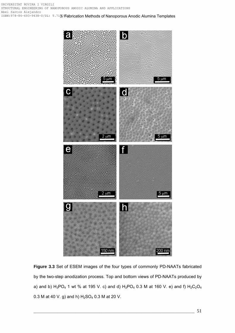
3. Fabrication Methods of Nanoporous Anodic Alumina Templates
_____________________________________________________________
51
Figure 3.3 Set of ESEM images of the four types of commonly PD-NAATs fabricated
by the two-step anodization process. Top and bottom views of PD-NAATs produced by
a) and b) H3PO4 1 wt % at 195 V. c) and d) H3PO4 0.3 M at 160 V. e) and f) H2C2O4
0.3 M at 40 V. g) and h) H2SO4 0.3 M at 20 V.
UNIVERSITAT ROVIRA I VIRGILI STRUCTURAL ENGINEERING OF NANOPOROUS ANODIC ALUMINA AND APPLICATIONS Abel Santos Alejandro ISBN:978-84-693-9438-0/DL: T.71-2011

3. Fabrication Methods of Nanoporous Anodic Alumina Templates
_____________________________________________________________
52
An atomic force microscopy (AFM) analysis of the PD-NAATs bottoms reveals that the
pore bottom tips are closed and covered by a hemispherical oxide barrier layer (Figure
3.4). In some functionalization processes, the oxide barrier layer needs to be removed
to obtain nanoporous anodic alumina membranes (NAAMs). There are several
methods by which this can be done, but the most widely used is chemical etching of
the pore bottom by a phosphoric acid solution 5 wt % at 35ºC. The NAAT is set on the
surface of the acid solution with the top (i.e. open side) facing up and the bottom (i.e.
closed side) facing down and in contact with the acid solution. The etching time
depends on the thickness of the oxide barrier layer and, therefore, on the anodization
condition (i.e. voltage, type of electrolyte, etc), with the etch rate between 75 and 100
nm·h-1. This wet chemical etching technique is very irregular since the pore openings
are non-uniform and the etching rate is rather difficult to control. In addition, the pore
diameter enlarges slightly because the acid solution penetrates into the pores before
the pore opens completely. As Figures 3.4 e and f show, after etching, larger voids
appear through the bottom of the NAAT and open and closed pores can be observed.
The resulting NAAMs do not reach the quality requirements of certain later
applications. Other alternative techniques will be described and discussed in section
3.2.2.
The pore diameter (dp) and porosity (P) of the typical PD-NAATs fabricated by the two-
step anodization with the four common acid solutions can be modified by means of wet
chemical etching (i.e. pore widening). For this purpose an aqueous solution of
phosphoric acid 5 wt % is commonly used at 35ºC. The dissolution rate is
approximately the same for each of the four common types of PD-NAATs fabricated
(i.e. 1.4 nm·min-1). Figure 3.5 shows an example of a calibration process that controls
the pore diameter of PD-NAAT produced with H3PO4 0.3 M at 160 V.
UNIVERSITAT ROVIRA I VIRGILI STRUCTURAL ENGINEERING OF NANOPOROUS ANODIC ALUMINA AND APPLICATIONS Abel Santos Alejandro ISBN:978-84-693-9438-0/DL: T.71-2011

3. Fabrication Methods of Nanoporous Anodic Alumina Templates
_____________________________________________________________
53
Figure 3.4 Set of AFM (before chemical etching) and ESEM (after chemical etching)
images of a PD-NAAT fabricated with H2C2O4 0.3 M at 40 V. a) AFM top view. b) AFM
bottom view. c) Magnified view of the blue square in (b). d) Three-dimensional image of
(c). e) ESEM bottom view after chemical etching for pore opening. f) Magnified view of
the white square in (e).
UNIVERSITAT ROVIRA I VIRGILI STRUCTURAL ENGINEERING OF NANOPOROUS ANODIC ALUMINA AND APPLICATIONS Abel Santos Alejandro ISBN:978-84-693-9438-0/DL: T.71-2011

3. Fabrication Methods of Nanoporous Anodic Alumina Templates
_____________________________________________________________
54
Figure 3.5 Pore widening calibration for samples fabricated with H3PO4 0.3 M at 160 V.
a) Experimental relationship between pore diameter (dp) and pore widening time (tpw).
b) Set of ESEM images of the top views of samples after different lengths of pore
widening time (i.e. Sa as-produced, Sb 15 min, Sc 30 min, Sd 45 min and Se 60 min). c)
Pore diameter distributions and Gaussian fits for each sample after measurements
from the ESEM images in (b).
UNIVERSITAT ROVIRA I VIRGILI STRUCTURAL ENGINEERING OF NANOPOROUS ANODIC ALUMINA AND APPLICATIONS Abel Santos Alejandro ISBN:978-84-693-9438-0/DL: T.71-2011

3. Fabrication Methods of Nanoporous Anodic Alumina Templates
_____________________________________________________________
55
Another phenomenon that has been observed is that, for NAATs fabricated under high
anodization voltages (i.e. NAATs fabricated with H3PO4 1 wt % at 195 V and H3PO4 0.3
M at 160 V), more than one pore may grow inside certain concavities mainly located on
the domain boundaries of the patterned aluminium surface. This is illustrated in Figure
3.6, which shows ESEM images of the top of two NAATs fabricated with H3PO4 1 wt %
at 195 V (Figure 3.6 a) and H3PO4 0.3 M at 160 V (Figure 3.6 e). In these ESEM
images, the domain boundaries are identified by red lines. From magnified views of
such images, it can be observed that these deformed pores (i.e. red circles) appear
mainly inside some of the concavities located on the domain boundaries and not within
these domains (Figures 3.6 b and f). In addition, ESEM images of the bottom views of
the same NAATs after the aluminium has been removed with a solution of HCl·CuCl2
show that the domain boundaries (i.e. red lines in Figures 3.6 c and g) on the bottom
are delimited by holes. From magnified views (Figures 3.6 d and h), it is observed that
these holes (i.e. red circles) are located on irregular junctions that connect four or five
non-hexagonally ordered pores and are initially filled with high aluminium nanopillars
(Figure 3.6 i).
This phenomenon is produced by the fact that the high electric field is strong at high
anodization voltages, which generates local Joule heating, local compressive stresses
due to electrostriction and volume expansion due to aluminium oxidation [149,158,173-
175]. All these effects are concentrated mainly at pores located on the domain
boundaries, deforming the ones on the top and producing irregular junctions on the
bottom, which are filled with Al in the course of the anodization process.
UNIVERSITAT ROVIRA I VIRGILI STRUCTURAL ENGINEERING OF NANOPOROUS ANODIC ALUMINA AND APPLICATIONS Abel Santos Alejandro ISBN:978-84-693-9438-0/DL: T.71-2011

3. Fabrication Methods of Nanoporous Anodic Alumina Templates
_____________________________________________________________
56
Figure 3.6 Set of ESEM images of NAATs fabricated with H3PO4 1 wt % at 195 V and
H3PO4 0.3 M at 160 V. a) ESEM top view of a NAAT fabricated with H3PO4 1 wt % at
195 V (red lines denote domain boundaries). b) Magnified view of the blue square in (a)
showing the deformed pores (red circles). c) ESEM bottom view of the same NAAT
shown in (a) after removing the Al substrate (red lines indicate domain boundaries). d)
Magnified view of the blue square in (c) showing the holes between irregular junctions
(red circles). e) ESEM top view of a NAAT fabricated with H3PO4 0.3 M at 160 V (red
lines denote domain boundaries). f) Magnified view of the blue square in (e) showing
the deformed pores (red circles). g) ESEM bottom view of the same NAAT shown in (e)
after removing the Al substrate (red lines indicate domain boundaries). h) Magnified
view of the blue square in (g) showing the holes between irregular junctions (red
circles). i) ESEM image of Al nanopillars and schematic cross-section view describing
the generation of deformed pores (top) and aluminium nanopillars (bottom).
UNIVERSITAT ROVIRA I VIRGILI STRUCTURAL ENGINEERING OF NANOPOROUS ANODIC ALUMINA AND APPLICATIONS Abel Santos Alejandro ISBN:978-84-693-9438-0/DL: T.71-2011

3. Fabrication Methods of Nanoporous Anodic Alumina Templates
_____________________________________________________________
57
3.1.2. One-step anodization process (hard anodization)
Polydomain nanoporous anodic alumina templates with hexagonal pore arrangement
are fabricated under hard anodization conditions using the one-step anodization
technique [146]. The annealed and electropolished Al substrates are anodized in
H2C2O4 0.3 M at 0ºC under high voltages. The experimental setup is the same as the
one used to produce PD-NAATs by the two-step anodization process but the
anodization conditions are different. The one-step anodization for fabricating PD-
NAATs under hard anodization conditions is divided into three stages (Figure 3.7 a).
First, when the acid electrolyte temperature is slightly higher than 0ºC (i.e. about 1ºC),
the anodization process starts under a constant voltage at 40 V. After about 5 min, the
electrolyte temperature is very close to 0ºC and the anodization voltage is slowly
increased at a rate of 0.5 V·s-1 until it reaches the target voltage (i.e. hard anodization
voltage). Then, the anodization voltage is maintained constant until the desired NAAT
thickness is reached. Figure 3.7 a shows a typical current density-time (J-t) transient of
a one-step anodization process under hard anodization conditions. During the one-step
anodization process, the following three different anodization regimes take place:
i) Mild anodization (MA) regime at 40 V (S1 in Figure 3.7 a).
ii) Transition anodization (TA) regime at voltage ramp 0.5 V·s-1 (S2 in Figure 3.7 a).
iii) Hard anodization (HA) regime at 140 V (S3 in Figure 3.7 a).
These different anodization regimes (i.e. MA, TA and HA) generate three different
layers on the resulting NAAT (Figure 3.7 b). During the first stage (S1), a protective
layer of NAA with disordered pores is formed on the aluminium surface. This layer is
about 500 nm thick and has two main functions: namely, i) to suppress breakdown
effects due to high temperatures and ii) to enable uniform oxide film growth at high
voltage. When the anodization voltage is increased (S2), the pores are reorganized
because the anodization conditions modify the pore lattice constant (i.e. dinterp).
UNIVERSITAT ROVIRA I VIRGILI STRUCTURAL ENGINEERING OF NANOPOROUS ANODIC ALUMINA AND APPLICATIONS Abel Santos Alejandro ISBN:978-84-693-9438-0/DL: T.71-2011

3. Fabrication Methods of Nanoporous Anodic Alumina Templates
_____________________________________________________________
58
In this way, some pores vanish (V in Figure 3.7 c) and others merge (M in Figure 3.7 c)
or continue (C in Figure 3.7 c) by the self-ordering mechanism during the transition
regime. The number of pores that vanish, merge or continue cannot be directly
established by cross-sectional observation because of the heterogeneity of the
transition layer. However, this value can be estimated indirectly (e.g. by
electrodeposition of metal into the pores). Section 4.4 makes an exhaustive study of
how the key parameters (i.e. anodization voltage ramp and hard anodization voltage)
affect on the quantity of pores that vanish, merge or continue growing by the self-
ordering mechanism. Finally, when the hard anodization voltage is reached (S3), the
pores growth uniformly at an exponential growth rate, which is characteristic of a hard
anodization process [146].
It has been demonstrated experimentally that the ordering degree increases as the
hard anodization voltage increases, the optimum value being 140 V [146]. Higher or
lower anodization voltages distort the pore lattice. ESEM images of the most
representative PD-NAATs fabricated by the one-step anodization process under hard
conditions are shown in Figure 3.8. It can be seen that the protective layer on the top of
the PD-NAATs is made up of disordered pores (Figures 3.8 a and b). The protective
layer can be seen in cross-section views (Figures 3.8 c and d). Nevertheless, even at
high magnifications (Figures 3.8 e and f), the pores that vanish cannot be distinguished
from those that merge or continue. The bottom views of the same PD-NAATs after the
aluminium substrate has been removed with a solution of HCl·CuCl2 (Figures 3.8 g and
h) confirm that the degree of hexagonal pore arrangement is ostensibly higher at 140 V
than at 120 V.
UNIVERSITAT ROVIRA I VIRGILI STRUCTURAL ENGINEERING OF NANOPOROUS ANODIC ALUMINA AND APPLICATIONS Abel Santos Alejandro ISBN:978-84-693-9438-0/DL: T.71-2011

3. Fabrication Methods of Nanoporous Anodic Alumina Templates
_____________________________________________________________
59
Figure 3.7 One-step anodization process under hard conditions. a) Current density-
time (J-t) transient for a PD-NAAT fabricated by the one-step anodization process
under hard conditions with H2C2O4 0.3 M at 140 V. b) Schematic cross-section view of
the resulting PD-NAAT. c) Magnified views of the green and red circles in (b).
UNIVERSITAT ROVIRA I VIRGILI STRUCTURAL ENGINEERING OF NANOPOROUS ANODIC ALUMINA AND APPLICATIONS Abel Santos Alejandro ISBN:978-84-693-9438-0/DL: T.71-2011

3. Fabrication Methods of Nanoporous Anodic Alumina Templates
_____________________________________________________________
60
The most noticeable characteristics of the PD-NAATs fabricated under hard
anodization conditions are the following:
i) The proportionality constant between the anodization voltage (V) and the interpore
distance is 2.0 nm·V-1, which is lower than for mild anodization conditions (i.e. 2.5-
2.8 nm·V-1). This reduction is attributed to the lower voltage dependence of both
the pore diameter (dp) and the oxide barrier layer thickness at the pore bottom tips
(τBL) under high electric field (i.e. high current density).
ii) The porosity under hard anodization conditions is between 3.3 and 3.4%, which is
approximately three times lower than for mild anodization under self-ordering
conditions (i.e. 10%).
iii) The proportionality constant between the anodization voltage (V) and the oxide
barrier layer thickness at the pore bottom tips (τBL) is 1.0 nm·V-1, which is 20%
lower than for mild anodization conditions (i.e. 1.3 nm·V-1). This reduction is
related to the high current density (J) associated with the hard anodization
process.
iv) The level of impurities for hard anodization conditions is lower than for mild
anodization conditions, which influences both the electrical and optical properties
(e.g. the PD-NAATs fabricated under hard conditions are bright yellow and those
fabricated under mild conditions are transparent (Figure 3.9)).
v) Strong fracture behaviour at the cell junctions under weak mechanical forces,
which produces crack propagation across the pores of PD-NAATs fabricated
under hard conditions [175].
UNIVERSITAT ROVIRA I VIRGILI STRUCTURAL ENGINEERING OF NANOPOROUS ANODIC ALUMINA AND APPLICATIONS Abel Santos Alejandro ISBN:978-84-693-9438-0/DL: T.71-2011

3. Fabrication Methods of Nanoporous Anodic Alumina Templates
_____________________________________________________________
61
Figure 3.8 Set of ESEM images of PD-NAATs fabricated with H2C2O4 0.3 M at 120 and
140 V by the one-step anodization process under hard conditions. a and b) Top views
of NAATs fabricated at 120 and 140 V, respectively. c and d) Cross-section views of
NAATs fabricated at 120 and 140 V, respectively (red dotted lines denote the transition
layer from MA to HA). e and f) Magnified views of the transition zone in (c) and (d). g
and h) Bottom views of NAATs fabricated at 120 and 140 V, respectively.
Figure 3.9 Digital photography showing the change in colour of PD-NAATs fabricated
by the one-step anodization process under hard conditions. The yellow bright increases
as the hard anodization voltage increases.
UNIVERSITAT ROVIRA I VIRGILI STRUCTURAL ENGINEERING OF NANOPOROUS ANODIC ALUMINA AND APPLICATIONS Abel Santos Alejandro ISBN:978-84-693-9438-0/DL: T.71-2011

3. Fabrication Methods of Nanoporous Anodic Alumina Templates
_____________________________________________________________
62
3.2. Innovative nanoporous anodic alumina templates
This section presents some alternative processes for fabricating innovative NAATs.
First, the two-step anodization process is used under hard conditions to produce PD-
NAATs without a protective barrier layer. Second, a re-anodization technique under
galvanostatic conditions is applied to remove the oxide barrier layer from the pore
bottom tips of these PD-NAATs. Third, an asymmetric two-step anodization process is
used to fabricate hierarchical nanoporous anodic alumina templates with a wide range
of configurations. Fourth, combinations of mild and hard anodization regimes are
applied to produce bilayered NAATs. Fifth, MD-NAATs with extraordinary pore
arrangements are generated by nanoimprinting from a silicon nitride master stamp.
Finally, nanoporous anodic alumina funnels are fabricated by combining anodizing and
pore widening stages.
3.2.1. Nanoporous anodic alumina templates without protective layer
under hard conditions
The one-step anodization process for fabricating PD-NAATs under hard conditions has
been presented in section 3.1.2. As has been shown, the resulting structures present a
protective layer of about 500 nm. This layer is composed of disordered pores with an
average diameter of 30 nm and its main functions are to suppress breakdown effects
due to high temperatures and to allow uniform pore growth at high voltage. From the
functionalization point of view, this layer may prevent templates for providing well-
defined nanostructures (e.g. metallic nanowires with rounded terminals). In order to
remove the protective layer from the top of the PD-NAATs fabricated under hard
conditions by the one-step process, a wet chemical etching in phosphoric acid solution
5 wt % at 35ºC was applied. The results (Figure 3.10) demonstrate that this technique
cannot dissolve this layer entirely without total collapse of the NAAT. Even after long
etching times, a hair-like layer of Al2O3 remain on the template surface.
UNIVERSITAT ROVIRA I VIRGILI STRUCTURAL ENGINEERING OF NANOPOROUS ANODIC ALUMINA AND APPLICATIONS Abel Santos Alejandro ISBN:978-84-693-9438-0/DL: T.71-2011

3. Fabrication Methods of Nanoporous Anodic Alumina Templates
_____________________________________________________________
63
In addition, the pore diameter is considerably enlarged. Other techniques enable this
layer to be removed entirely (e.g. ion milling, mechanical polishing, etc), but they
require expensive laboratory equipment.
In order to fabricate PD-NAATs under hard anodization conditions without a protective
layer in a fast and cost-effective way, a two-step anodization process is applied. In this
process, the anodization conditions are modified (Figure 3.11). The first step is the
one-step anodization process under hard anodization conditions. So, first, the annealed
and electropolished Al substrates (Figure 3.11 a) are anodized in H2C2O4 0.3 M at 0ºC
in the electrochemical cell under potentiostatic conditions at 40 V for 5 min. Then, the
anodization voltage is increased at 0.5 V·s-1 until it reaches the hard anodization
voltage, which is maintained for 30 min until pore development is complete (Figure 3.11
b). When the 1st anodization step is finished, the Al2O3 film with the protective layer on
the top and ordered pores on the bottom is selectively dissolved by wet chemical
etching in a mixture of phosphoric acid (H3PO4) 0.4 M and chromic acid (H2CrO7) 0.2 M
at 70ºC.
Figure 3.10 Set of ESEM images of a PD-NAAT fabricated by the one-step anodization
process under hard conditions after wet chemical etching in phosphoric acid solution 5
wt % for 1 h at 35ºC. a) Top view. b) Slanted cross-section view (the protective layer
becomes hair-like alumina after long wet chemical etching).
UNIVERSITAT ROVIRA I VIRGILI STRUCTURAL ENGINEERING OF NANOPOROUS ANODIC ALUMINA AND APPLICATIONS Abel Santos Alejandro ISBN:978-84-693-9438-0/DL: T.71-2011

3. Fabrication Methods of Nanoporous Anodic Alumina Templates
_____________________________________________________________
64
The etching time length is twice as long as the first anodization step (i.e. about 1 h). In
this way, a hexagonally ordered pattern of hemispherical concavities is produced on
the aluminium surface by the self-ordering mechanism (Figure 3.11 c). The lattice
constant of this pattern is the same as the interpore distance for the hard anodization
voltage. Then, the second anodization step is conducted by directly applying the hard
anodization voltage. The acid electrolyte concentration is modified in the course of the
anodization process. For the first 5 min, the acid solution used is H2C2O4 0.05 M in a
mixture of ethanol and water (EtOH:H2O 1:3 (v:v)). Subsequently, the acid electrolyte
concentration is increased to 0.3 M. In addition, the stirring rate is increased up 500
r.p.m. during the course of the anodization process. The electrolyte temperature is
maintained below 0ºC during the first minutes of the anodization process without
freezing (i.e. -4ºC, approximately). After 10 min, the system temperature is increased to
0ºC and remains constant until the anodization process is finished (Figure 3.11 d).
Ethanol is selected as the dissolvent to reduce the acid electrolyte temperature
because it has an extremely low freezing point (i.e. -114.3ºC) and does not react with
Al owing to its weak acidity (i.e. pKa 15.9). This strategy has previously been used to
produce NAATs under high-field anodization [176,177].
UNIVERSITAT ROVIRA I VIRGILI STRUCTURAL ENGINEERING OF NANOPOROUS ANODIC ALUMINA AND APPLICATIONS Abel Santos Alejandro ISBN:978-84-693-9438-0/DL: T.71-2011

3. Fabrication Methods of Nanoporous Anodic Alumina Templates
_____________________________________________________________
65
In this process, four factors prevent the NAAT from burning as a result of the high
temperature generated at high voltage. They are the following:
i) The lower acid electrolyte temperature makes it possible to dissipate the large
amount of heat generated during the anodization process under high voltage
due to the Joule effect.
ii) The high stirring rate guarantees a constant flow of cooled electrolyte inside the
pores and prevents the EtOH from vaporizing at the pore bottom due to high
temperature.
iii) The patterning of the Al substrate surface increases the anode area, so the
current density (J) involved in the process is reduced.
iv) The reduction of acid electrolyte concentration during the first minutes of the
anodization process decreases the electric field strength, leading to
homogeneous pore growth.
Figure 3.11 Schematic slanted section views describing the two-step anodization
process under hard conditions. a) Annealed and electropolished aluminium substrate.
b) PD-NAATs with a protective layer on the top and ordered pores on the bottom with
the interpore distance for the hard anodization voltage. c) Patterned Al substrate after
removing the oxide film. d) PD-NAAT with straight and ordered pores.
UNIVERSITAT ROVIRA I VIRGILI STRUCTURAL ENGINEERING OF NANOPOROUS ANODIC ALUMINA AND APPLICATIONS Abel Santos Alejandro ISBN:978-84-693-9438-0/DL: T.71-2011

3. Fabrication Methods of Nanoporous Anodic Alumina Templates
_____________________________________________________________
66
If the acid electrolyte temperature is excessively high or the stirring rate is not high
enough, then, the oxide film may burn. This phenomenon is reflected in an abrupt
increase in the current density (J) and in the generation of a dark yellow spot at the
NAAT centre. By inspecting ESEM images of a burnt NAAT, it can be seen that a thin
fused layer of Al2O3 partially covers disordered and branched pores (Figure 3.12 a). If
the acid electrolyte temperature is reduced and the stirring rate is increased, the oxide
film does not burn. However, branched pores (i.e. more than one pore per concavity on
the patterned Al substrate) appear on the concavities located on the domain
boundaries of the patterned Al substrate (Figure 3.12 b). This generation of branched
pores is attributed to local concentrations of the field strength that produce
heterogeneous pore growth. This drawback can be avoided by reducing the acid
electrolyte concentration during the first minutes of the 2nd anodization step (Figures
3.12 c and d). Finally, when the pore development is complete, the acid electrolyte
concentration is increased to conserve the hexagonal pore ordering throughout the rest
of the anodization process.
With this method, PD-NAATs can be successfully fabricated under hard conditions
without a protective oxide layer. This ostensibly increases the number of later
applications because these templates have straight and well-defined pores in all their
volume. Also no additional stages are required to remove the protective layer after
anodizing, which noticeably reduces fabrication costs.
UNIVERSITAT ROVIRA I VIRGILI STRUCTURAL ENGINEERING OF NANOPOROUS ANODIC ALUMINA AND APPLICATIONS Abel Santos Alejandro ISBN:978-84-693-9438-0/DL: T.71-2011

3. Fabrication Methods of Nanoporous Anodic Alumina Templates
_____________________________________________________________
67
Figure 3.12 Set of ESEM images of PD-NAATs fabricated by two-step anodization
process under hard conditions. a) Top view of a burnt NAAT (rests of fused alumina
and branched pores are denoted by yellow and red arrows, respectively). b) Branched
pores on the top of a NAAT. c) Top view of the resulting NAAT fabricated under
suitable conditions at 140 V by the two-step anodization. d) Cross-section view of the
same NAAT (pores are straight and well-defined).
UNIVERSITAT ROVIRA I VIRGILI STRUCTURAL ENGINEERING OF NANOPOROUS ANODIC ALUMINA AND APPLICATIONS Abel Santos Alejandro ISBN:978-84-693-9438-0/DL: T.71-2011

3. Fabrication Methods of Nanoporous Anodic Alumina Templates
_____________________________________________________________
68
3.2.2. Nanoporous anodic alumina templates without oxide barrier layer
As is well known, from the functionalization point of view, one of the most important
disadvantages of as-produced NAATs is that they present an alumina barrier layer
between the inner side of the pores at the bottom and the aluminium substrate. This
oxide barrier layer isolates electrically the aluminium substrate from the inner side of
the pores and impedes to use directly as-produced NAATs for electrodeposition. The
original structure must be modified by additional stages and several methods have
been developed for removing this oxide barrier layer. In that regard, several authors
have characterized and modified the oxide barrier layer by applying re-anodization
techniques [178-181].
The most widely used method to remove the oxide barrier layer from the pore bottom
tips involves the dissolution of the Al substrate in a saturated solution of cupric chloride
and hydrochloric acid (HCl·CuCl2) or in a saturated solution of mercury (II) chloride
(HgCl2) and the subsequent pore bottom opening, pore widening and sputtering of a
metal contact [182,183]. The NAAT can also be detached from the Al substrate by
applying a reversed-bias voltage in the same anodization electrolyte [184] or a direct-
bias voltage in a mixture of ethanol (EtOH) and perchloric acid (HClO4) [185,186].
When the NAAT is prepared on such substrates as Ag, the oxide barrier layer at the
pore bottom tips is thinner than those prepared on aluminium substrates [187]. So, this
oxide barrier layer can be removed without entire dissolution of the NAAT by
conventional wet chemical etching in phosphoric acid solution 5 wt %. Another way of
completely removing the oxide barrier layer from the pore bottom tips is to use a
cathodic polarization method in neutral potassium chloride (KCl) solution. This method
has been used for samples prepared on n-type silicon substrates with a Ti underlayer
[188]. This technique can be applied as well as for NAATs prepared on Al substrates,
but it is previously required stepwise anodization voltage reduction to pre-perforate the
UNIVERSITAT ROVIRA I VIRGILI STRUCTURAL ENGINEERING OF NANOPOROUS ANODIC ALUMINA AND APPLICATIONS Abel Santos Alejandro ISBN:978-84-693-9438-0/DL: T.71-2011

3. Fabrication Methods of Nanoporous Anodic Alumina Templates
_____________________________________________________________
69
oxide barrier layer [189]. In the particular case of NAATs grown on a conducting
underlayer, the oxide of which has a higher ionic conductivity than alumina, the oxide
barrier layer can be selectively perforated by this oxide [190].
In this section, it is discussed an electrochemical approach for dissolving in situ the
oxide barrier layer of NAATs fabricated by the two-step anodization process under hard
conditions. This process is carried out in successive re-anodization steps under
galvanostatic conditions and a criterion to establish when a new step has to begin is
established.
First, the annealed and electropolished Al substrates are anodized following the two-
step anodization process under hard anodization conditions exposed in section 3.2.1.
When the 2nd step of the anodization process under potentiostatic conditions is
finished, a new 3rd step is applied in the same acid electrolyte solution (Figure 3.13).
This step consists of a stepwise current-limited re-anodization under galvanostatic
conditions. The starting value of J is established depending on the last value of J
recorded in the 2nd anodization step. This value is halved and the anodization process
goes on by applying this current density value. Then, the voltage decreases until it
reaches an almost steady value. Once this quasi-steady state has been reached, the
current density is again halved, with the consequent reduction in voltage. The criterion
by which the current density is again halved and a new step of the current density re-
anodization starts is the instant at which the rate of voltage reduction is 0.1 V·s-1. Each
re-anodization step implies a reduction of several tens of nanometres of the oxide
barrier layer thickness (τBL). By repeating this procedure consecutively until reach low
voltages (i.e. about 5 V), it is possible to reduce the oxide barrier layer of the pore
bottom tips without pore branching. Finally, to uniformly remove the rest of the oxide
barrier layer, a conventional wet chemical etching in phosphoric acid solution 5 wt % at
35ºC is performed.
UNIVERSITAT ROVIRA I VIRGILI STRUCTURAL ENGINEERING OF NANOPOROUS ANODIC ALUMINA AND APPLICATIONS Abel Santos Alejandro ISBN:978-84-693-9438-0/DL: T.71-2011

3. Fabrication Methods of Nanoporous Anodic Alumina Templates
_____________________________________________________________
70
Figure 3.13 Current density and voltage-time (J-t and V-t) transients for a PD-NAAT
fabricated by the two-step anodization process under hard conditions with H2C2O4
0.3 M at 120 V and the re-anodization process under galvanostatic conditions to
remove the oxide barrier layer from the pore bottom tips. Each different background
indicates each of the four stages of the process (yellow-1st anodization step, white-
removing the alumina layer, orange-2nd anodization step and red-3rd re-anodization
step).
UNIVERSITAT ROVIRA I VIRGILI STRUCTURAL ENGINEERING OF NANOPOROUS ANODIC ALUMINA AND APPLICATIONS Abel Santos Alejandro ISBN:978-84-693-9438-0/DL: T.71-2011

3. Fabrication Methods of Nanoporous Anodic Alumina Templates
_____________________________________________________________
71
When the re-anodization current density is suddenly halved, the quantity of electro-
generated aluminium cations (Al3+) decreases. This implies a reduction of the oxide
formation rate because of the lack of aluminium cations. However, the oxide dissolution
rate remains steady for some time at the inner side of the pore bottom tips owing to this
chemical reaction depends mainly on the local temperature. Therefore, the net effect is
that the oxide barrier layer gets thinner, which is reflected in a decrease in the anodic
voltage. This oxide barrier layer thinning at the pore bottom tips can also be expressed
in terms of the pore branching (Figure 3.14). So, when the applied current density is
halved, the voltage decreases and pore branching occurs at the pore bottom tips.
However, just before the new pores are completely developed and begin to grow in a
steady growth rate, the current density is halved again and new branched pores are
generated inside those recently generated pores. In this way, by repeating this process
consecutively, the oxide barrier layer thickness of the original pores is reduced without
the complete growth of new pores.
As can be seen in Figure 3.15, by the end of the process, the oxide barrier layer of the
initial structure (Figure 3.15 a and b) has been completely removed from the pore
bottom tips (Figures 3.15 c and d). During this process, the pore diameters also
increase several tens of nanometres due to the applied wet chemical etching. The pore
opening is homogeneous throughout the metal-oxide interface and the NAAT remains
on the aluminium substrate. However, it must be taken into account that the resulting
NAAT can be broken down by mechanical stress given that the conversion of
aluminium to alumina involves large stresses. The theoretical Pilling-Bedworth Ratio
(PBR) for porous alumina formation with a 100% current efficiency is 1.60 and its
experimental value under conditions similar to those used in our process is 1.18 [151].
Moreover, the oxide barrier layer gives mechanical stability to the NAAT and, when it is
removed, the fragility of the resulting NAAT increases. In order to prevent peeling off or
fracture as far as possible, the NAAT has to be thick enough to resist these stresses.
UNIVERSITAT ROVIRA I VIRGILI STRUCTURAL ENGINEERING OF NANOPOROUS ANODIC ALUMINA AND APPLICATIONS Abel Santos Alejandro ISBN:978-84-693-9438-0/DL: T.71-2011

3. Fabrication Methods of Nanoporous Anodic Alumina Templates
_____________________________________________________________
72
In addition, the value of the current density at each step of the re-anodizing stage must
be enough in the following step to prevent partial discharges in the oxide barrier layer.
These discharges are produced by an insufficient reduction in ionic species and can
generate non-uniform branched current pathways across the oxide barrier layer that
lead to produce disordered branched pores as a result of the mechanical stress
between neighbouring pores.
Figure 3.14 Schematic slanted and cross-section views describing the re-anodization
process for removing the oxide barrier layer from the pore bottom tips of NAATs
fabricated by the two-step anodization process under hard conditions. Magnified views
of the pore bottom tips after each step of the re-anodization process are shown in red
circles. In this case, it is represented a virtual re-anodization process of 3 steps.
UNIVERSITAT ROVIRA I VIRGILI STRUCTURAL ENGINEERING OF NANOPOROUS ANODIC ALUMINA AND APPLICATIONS Abel Santos Alejandro ISBN:978-84-693-9438-0/DL: T.71-2011

3. Fabrication Methods of Nanoporous Anodic Alumina Templates
_____________________________________________________________
73
By means of this technique, it is possible to fabricate NAATs without oxide barrier layer
at the pore bottom tips that remain attached to the aluminium substrate. In contrast to
other techniques, by this method, the post-treatment costs of the as-produced NAATs
are considerably reduced. As it will be shown in 4.1, such resulting nanostructures can
be used to fabricate arrays of metallic nanopillars on aluminium substrates by direct
electrodeposition.
Figure 3.15 Set of ESEM images of a NAAT fabricated by the two-step anodization
process under hard conditions before and after the re-anodization process. a) General
cross-section view before the re-anodization process. b) Magnified view of the yellow
square in (a). c) Cross-section view after the re-anodization process. d) Slanted cross-
fracture after the re-anodization process (yellow arrowheads indicate the aluminium
substrate inside the opened pores).
UNIVERSITAT ROVIRA I VIRGILI STRUCTURAL ENGINEERING OF NANOPOROUS ANODIC ALUMINA AND APPLICATIONS Abel Santos Alejandro ISBN:978-84-693-9438-0/DL: T.71-2011

3. Fabrication Methods of Nanoporous Anodic Alumina Templates
_____________________________________________________________
74
3.2.3. Hierarchical nanoporous anodic alumina templates
As was commented in 3.1.1, the general structure of nanoporous anodic alumina
templates fabricated by the two-step anodization process is a close-packed array of
hexagonally arranged cells containing pores in each cell-centre. Geometric
characteristics such as pore diameter, interpore distance, porosity and pore density are
determined by the anodization voltage, temperature (T), and type and concentration of
the acid electrolyte. Thus, self-ordered nanoporous anodic alumina can be fabricated
with a relatively wide range of these geometric characteristics. However, from the point
of view of developing nanostructures with new morphologies, it is very interesting to
modify the original structure of nanoporous anodic alumina templates fabricated by the
two-step anodization process. To this end, it is possible to use several strategies that
allow changing the original structure of self-ordered nanoporous anodic alumina
templates. One example of this is to use an asymmetric two-step anodization process,
in which the anodization conditions (i.e. anodization voltage (V), and acid electrolyte
type and concentration (C)) between the first and second step are modified (Figure
3.16). The resulting nanostructure based on self-ordered nanoporous anodic alumina,
which is called hierarchical nanoporous anodic alumina templates (HNAATs), consists
of an outer hexagonal lattice of concavities inside which a number of pores grow. The
geometric characteristics of the outer concavities and the inner pores depend on the
anodization conditions used during the first (Figure 3.16 a) and the second step (Figure
3.16 c) of the anodization process, respectively. So, HNAATs with a wide range of
geometric characteristics can be obtained. The interpore distance and pore diameter of
both outer concavities and inner pores can be adjusted by establishing the anodization
parameters to satisfy the requirements of later applications (e.g. gas sensors, solar
cells, photonic devices, filters, etc).
UNIVERSITAT ROVIRA I VIRGILI STRUCTURAL ENGINEERING OF NANOPOROUS ANODIC ALUMINA AND APPLICATIONS Abel Santos Alejandro ISBN:978-84-693-9438-0/DL: T.71-2011

3. Fabrication Methods of Nanoporous Anodic Alumina Templates
_____________________________________________________________
75
Figure 3.16 Schematic cross-section and top views describing the asymmetric two-
step anodization process for fabricating HNAATs. a) First step of the anodization
process under conditions (a). b) Pattern on the aluminium substrate surface after
removing the oxide film by wet chemical etching. c) Second step of the anodization
process under conditions (b). Magnified views of the cross-section (red circle in (c))
and top (orange circle in (c)) of the resulting HNAAT.
UNIVERSITAT ROVIRA I VIRGILI STRUCTURAL ENGINEERING OF NANOPOROUS ANODIC ALUMINA AND APPLICATIONS Abel Santos Alejandro ISBN:978-84-693-9438-0/DL: T.71-2011

3. Fabrication Methods of Nanoporous Anodic Alumina Templates
_____________________________________________________________
76
In order to study how the anodization parameters affect on the resulting hierarchical
nanoporous anodic alumina templates, four primary anodization conditions are
arbitrarily chosen: namely, i) H3PO4 0.3 M at 170 V and 5ºC (MA), ii) H2C2O4 0.3 M at
40 V and 5ºC (MA), iii) H2C2O4 0.3 M at 120 V and 0ºC (HA) and iv) H2SO4 0.3 M at
18 V and 5ºC (MA). These conditions (or these conditions with a slight modification in
the voltage or in the acid concentration) are used in the 1st or 2nd anodization step in
different combinations so as to provide HNAATs with different geometric
characteristics. Table 3.2 summarizes the combinations and modifications of the
anodization conditions applied during the 1st and 2nd step, and the time length of the
pore widening (tpw) applied after the anodization process. Samples are classified
according to the parameter that is changed in the second step with respect to the first
(i.e. voltage, acid type or concentration).
1st Step 2nd Step Parameter Sample Acid V
(V) C (M)
T (ºC)
Acid V (V)
C (M)
T (ºC)
tpw (min)
S1 H2C2O4 120 0.3 0 H2C2O4 40 0.3 5 15
S2 H2C2O4 40 0.3 5 H2C2O4 20 0.3 5 15 V
S3 H3PO4 170 0.3 5 H3PO4 85 0.3 5 10
S4 H3PO4 170 0.3 5 H2C2O4 120 0.3 0 15
S5 H3PO4 170 0.3 5 H2C2O4 40 0.3 5 10
S6 H3PO4 170 0.3 5 H2SO4 18 0.3 5 10
S7 H2C2O4 120 0.3 0 H2SO4 18 0.3 5 5
Acid
S8 H2C2O4 40 0.3 5 H2SO4 18 0.3 5 5
S9 H3PO4 170 0.3 5 H3PO4 170 0.2 5 15 C
S10 H2C2O4 120 0.3 0 H2C2O4 120 0.1 0 15
Table 3.2 Anodization conditions for fabricating the different types of HNAATs.
UNIVERSITAT ROVIRA I VIRGILI STRUCTURAL ENGINEERING OF NANOPOROUS ANODIC ALUMINA AND APPLICATIONS Abel Santos Alejandro ISBN:978-84-693-9438-0/DL: T.71-2011

3. Fabrication Methods of Nanoporous Anodic Alumina Templates
_____________________________________________________________
77
To produce hierarchical nanoporous anodic alumina templates, the annealed and
electropolished Al substrates are anodized in our home-made electrochemical cell. The
first anodization step depends on whether the anodization regimen is mild (MA) or hard
(HA). For the samples fabricated under mild anodization conditions (i.e. S2, S3, S4, S5,
S6, S8 and S9) the first step consists of applying directly the corresponding anodization
voltage from the beginning. For the samples fabricated under hard anodization
conditions (i.e. S1, S7 and S10) a thin protective oxide layer is first formed on the
aluminium surface to suppress breakdown effects due to high temperature and enable
uniform oxide film growth at high voltage. When the first anodization step finishes, the
aluminium oxide film is dissolved by wet chemical etching in a mixture of phosphoric
acid 0.4 M and chromic acid 0.2 M at 70ºC for twice the time length as the first
anodization step. In this way, a pattern of hexagonally arranged concavities is
produced on the aluminium surface. Then, the 2nd step of the anodization process is
carried out under asymmetric anodization conditions (i.e. one or two anodization
parameters are changed respect to the 1st step) and pores (i.e. inner pores) grow
inside the concavities on the aluminium surface, which become alumina after
anodizing. The anodization voltage is maintained until the hierarchical nanoporous
anodic alumina template is thick enough to handle. After anodizing, the remaining
aluminium substrate is removed in a saturated solution of HCl·CuCl2. So, it is possible
to observe by ESEM the bottom of the resulting HNAATs. Finally, the pores are slightly
widened by wet chemical etching in phosphoric acid solution 5 wt % at 35ºC to make it
easier ESEM image analysis.
UNIVERSITAT ROVIRA I VIRGILI STRUCTURAL ENGINEERING OF NANOPOROUS ANODIC ALUMINA AND APPLICATIONS Abel Santos Alejandro ISBN:978-84-693-9438-0/DL: T.71-2011

3. Fabrication Methods of Nanoporous Anodic Alumina Templates
_____________________________________________________________
78
Figure 3.17 shows a set of ESEM images of the fabricated HNAATs (i.e. from S1 to
S10). At first glance, it is observed that, under the applied anodization conditions, it is
possible to fabricate HNAATs with a wide range of geometric characteristics such as
interconcavity (dinterconc) and interpore (dinterp) distance (i.e. centre-to-centre concavity
and pore distance, respectively) and concavity (dconc) and pore (dp) diameter. Also, in
order to determine the extent of pore generation, the pore density (ρp/conc), that
represents the number of pores per concavity, is estimated. The obtained results are
summarized in Table 3.3.
Sample dinterconc (nm) dinterp (nm) dconc (nm) dp (nm) ρp/conc
(pores/concavity)
S1 249.3 ± 32.9 105.0 ± 9.2 219.0 ± 18.7 45.9 ± 10.4 10.1 ± 1.7
S2 104.0 ± 9.7 74.4 ± 8.7 64.5 ± 7.8 22.1 ± 3.6 1.9 ± 0.8
S3 393.1 ± 37.2 126.2 ± 16.0 326.2 ± 31.5 108.0 ± 23.3 3.6 ± 0.7
S4 405.6 ± 46.7 282.8 ± 28.1 303.5 ± 37.0 64.0 ± 16.4 6.3 ± 1.2
S5 413.6 ± 37.1 97.6 ± 9.7 367.6 ± 30.0 36.5 ± 7.0 15.3 ± 3.0
S6 397.0 ± 45.4 48.1 ± 8.6 369.2 ± 53.3 23.1 ± 3.7 61.4 ± 6.5
S7 292.0 ± 35.2 47.5 ± 7.3 264.4 ± 41.0 23.4 ± 4.5 38.4 ± 3.5
S8 104.4 ± 10.5 55.5 ± 9.3 83.2 ± 11.5 21.0 ± 3.0 5.2 ± 0.8
Table 3.3 Geometric characteristics of the resulting HNAATs after image analysis
(dinterconc, dinterp, dconc, dp and ρp/conc). Values corresponding to samples S9 and S10 are
not shown because in these samples there was not homogenous pore generation.
As follows, it will be made an exhaustive analysis of the influence of each anodization
parameter on the resulting HNAATs.
UNIVERSITAT ROVIRA I VIRGILI STRUCTURAL ENGINEERING OF NANOPOROUS ANODIC ALUMINA AND APPLICATIONS Abel Santos Alejandro ISBN:978-84-693-9438-0/DL: T.71-2011

3. Fabrication Methods of Nanoporous Anodic Alumina Templates
_____________________________________________________________
79
Figure 3.17 Set of ESEM images of the different types of HNAATs fabricated by the
asymmetric two-step anodization process. a) Top view of the corresponding HNAAT. b)
Bottom view of the corresponding HNAAT after removing the Al substrate by wet
chemical etching.
UNIVERSITAT ROVIRA I VIRGILI STRUCTURAL ENGINEERING OF NANOPOROUS ANODIC ALUMINA AND APPLICATIONS Abel Santos Alejandro ISBN:978-84-693-9438-0/DL: T.71-2011

3. Fabrication Methods of Nanoporous Anodic Alumina Templates
_____________________________________________________________
80
For samples S1, S2 and S3, the anodization voltage is reduced between the first and
the second step while the rest of anodization parameters (i.e. type of acid electrolyte
and concentration) are kept constant. In the case of samples S4 to S8, the voltage is
also changed as a consequence of the acid electrolyte type change. As Figure 3.17
shows, for samples from S1 to S8, the generation of pores inside the concavities is
practically uniform through the top of the HNAATs. The value of the pore density
(ρp/conc) as a function of the voltage ratio between the first and the second step (RV2/V1),
which is defined as the ratio of the second step voltage (V2) to the first step voltage
(V1), is represented in Figure 3.18 for samples from S1 to S8. The mathematical
relationship between the pore density and the voltage ratio is also included in this
graph. The trend line is calculated for the range of RV2/V1 studied (i.e. 0.11-0.71). The
results suggest a noticeable increase in the density as the voltage ratio decreases. It is
interesting to note, however, the difference in pore density for samples S2 and S3.
Both correspond to a RV2/V1 = 0.50, but for different acids. More specifically, the pore
density is 1.92 for oxalic acid and 3.58 for phosphoric acid for the same voltage ratio
(i.e. 0.50). This suggests that the type of acid influences the relationship between the
pore density and the voltage ratio. It is also observed that a major decrease in the
anodization voltage between the first and the second step increases the pore density
for the same acid electrolyte, the value of which is 10.08 for S1 and 1.92 for S2 with
RV2/V1 0.33 and 0.50, respectively.
In samples from S4 to S8 an asymmetric process with a different acid electrolyte in the
1st and 2nd anodization step is applied. The combinations are chosen so that the
second anodization step voltage (V2) is lower than the first anodization step voltage
(V1). An interesting result is observed for samples S6, S7 and S8. In contrast with
previous studies [191,192], it is found that the pores do not only appear at the bottom
of the concavities but also nucleate on their walls.
UNIVERSITAT ROVIRA I VIRGILI STRUCTURAL ENGINEERING OF NANOPOROUS ANODIC ALUMINA AND APPLICATIONS Abel Santos Alejandro ISBN:978-84-693-9438-0/DL: T.71-2011

3. Fabrication Methods of Nanoporous Anodic Alumina Templates
_____________________________________________________________
81
To confirm this, an AFM image analysis is carried out for sample S6 (Figure 3.19 a, b
and c) and a cross-sectional ESEM image analysis for sample S5 (Figure 3.19 d). Both
the top and cross-section views from AFM images (Figure 3.19 a, b and c) reveal that
pores do not only nucleate and grow on the bottom of the concavities but also on their
walls. This is shown by the points 1, 2, 8 and 9 of the AFM cross-section (Figure 3.19
c). This phenomenon is attributed to the fact that pores cannot nucleate on the outer
hexagonal lattice of the concavities since the alumina-aluminium interface angle (θ0-m)
is less than 180 degrees there and, then, the field-assisted oxide dissolution is
suppressed. So, they are forced to nucleate and grow on the walls of the concavities
and perpendicularly to the Al surface, what distorts the corresponding pore lattice
constant.
Figure 3.18 Pore density-voltage ratio (ρp/conc-RV2/V1) relationship for samples from S1
to S8 (filled black circles). The red solid curve represents the potential fit of the
experimental data.
UNIVERSITAT ROVIRA I VIRGILI STRUCTURAL ENGINEERING OF NANOPOROUS ANODIC ALUMINA AND APPLICATIONS Abel Santos Alejandro ISBN:978-84-693-9438-0/DL: T.71-2011

3. Fabrication Methods of Nanoporous Anodic Alumina Templates
_____________________________________________________________
82
Figure 3.19 Set of AFM and ESEM images of different types of HNAATs fabricated by
the asymmetric two-step anodization process. a) AFM top view of the resulting HNAAT
obtained under conditions S6. b) Magnified view of the blue square in (a). c) Cross-
section profile of the same HNAAT corresponding to the white line in (b). d) ESEM
cross-section view of the resulting HNAAT obtained under conditions S5.
UNIVERSITAT ROVIRA I VIRGILI STRUCTURAL ENGINEERING OF NANOPOROUS ANODIC ALUMINA AND APPLICATIONS Abel Santos Alejandro ISBN:978-84-693-9438-0/DL: T.71-2011

3. Fabrication Methods of Nanoporous Anodic Alumina Templates
_____________________________________________________________
83
Another result that is worth noting is found for samples S6, S7 and S8, in which the
conditions of the second anodization step are the same (i.e. anodization voltage, type
and acid concentration) but the first step conditions are different. In these conditions,
as Figures 3.20 a and b show, the minimum of the anodization current density (J)
versus time (t) transient is shifted with respect to the symmetric process (i.e.
anodization process using H2SO4 0.3 M at 18 V for both the 1st and 2nd anodization
step). More concretely, the minimum appears later tmin and has a lower value Jmin.
Furthermore, for larger interconcavity distances (dinterconc) on the patterned aluminium
surface, the minimum appears at a longer tmin and the Jmin value is lower. The
corresponding values of tmin and Jmin are represented in Figure 3.20 c together with the
corresponding trend lines. This shift can also be explained as follows. When the
anodization conditions applied during the second step of the anodization process
reduce the pore lattice constant with regards to the first step (i.e. asymmetric process),
some nucleating centres (i.e. the preferred location for pore growth) appear on the
concavity walls of the patterned aluminium surface since the pores cannot nucleate on
the outer hexagonal lattice of the concavities (where θo-m is less than 180º). Then, as
Figure 3.21 illustrates, some pores nucleate and begin to grow on the concavity walls.
The number of these pores increases as the concavities on the patterned aluminium
surface gets wider and deeper (S8→S7→S6), which is reflected in an increase in tmin
and a decrease in Jmin (Figure 3.20 c). However, after a certain time, these pores
vanish and merge by the self-ordering mechanism and the current density curve leads
to a constant value when the steady-state pore growth is reached. As Figure 3.20 a
shows, this value is reached more quickly in the symmetric process than in the
asymmetric processes. This phenomenon may be related to the arrangement of pores
inside the concavities, which is slower because of the distortion in the corresponding
pore lattice constant. This distortion is counteracted when some pores vanish and
merge by the self-ordering mechanism until the pore lattice constant for the applied
anodization conditions is reached.
UNIVERSITAT ROVIRA I VIRGILI STRUCTURAL ENGINEERING OF NANOPOROUS ANODIC ALUMINA AND APPLICATIONS Abel Santos Alejandro ISBN:978-84-693-9438-0/DL: T.71-2011

3. Fabrication Methods of Nanoporous Anodic Alumina Templates
_____________________________________________________________
84
Finally, it is observed that the steady-state value is the same in all the studied cases
(i.e. Sy, S6, S7 and S8), which means that the interpore distance on the bottom of the
HNAAT after a certain anodization time depends only on the anodization voltage
applied during the second step of the anodization process. This is confirmed by ESEM
image analysis of the bottom of the HNAATs (Figure 3.17). These results agree with
previous studies in which a set of asymmetric anodizations are carried out by modifying
the anodization voltage in the second step of the process but keeping the voltage in the
first step constant and using the same acid electrolyte throughout the process [192].
For samples S9 and S10, the acid electrolyte concentration between the first and the
second step of the anodization process is modified. In these conditions, it is observed
that, unlike samples from S1 to S8, the generation of pores is not uniform through the
top surface of the HNAATs and there are two or three pores per concavity at most. This
can be seen in Figure 3.22, which shows ESEM images of the surface of samples S9
and S10. This fact is mainly attributed to the reduction of the acid electrolyte
concentration reduces the electric field strength while the average interpore distance
remains practically constant, because it depends essentially on the anodization voltage
(Table 1.1). For instance, Figure 3.22 shows that, in the case of sample S9, when the
acid electrolyte concentration is reduced from 0.3 to 0.2 M (Figure 3.22 a) some
concavities present more than one pore per concavity. However, when the acid
electrolyte concentration is reduced to 0.1 M only one pore per concavity can be
observed (Figure 3.22 b). In the case of sample S10, when the acid electrolyte
concentration is decreased from 0.3 to 0.1 M, certain quantity of concavities presents
more than one pore (Figure 3.22 c). After subsequent experiments, it is proven that,
when the acid electrolyte concentration is reduced to 0.015 M, just one pore per
concavity is found on the top surface of the HNAAT (Figure 3.22 d). As it is commented
in section 3.2.1, to reduce noticeably the acid concentration during the initial stage of
UNIVERSITAT ROVIRA I VIRGILI STRUCTURAL ENGINEERING OF NANOPOROUS ANODIC ALUMINA AND APPLICATIONS Abel Santos Alejandro ISBN:978-84-693-9438-0/DL: T.71-2011

3. Fabrication Methods of Nanoporous Anodic Alumina Templates
_____________________________________________________________
85
the 2nd step of the anodization process is a successful strategy for fabricating NAATs
by the two-step hard anodization process without a protective layer.
Figure 3.20 Current density-time (J-t) transients corresponding to the second
anodization step for the samples S6, S7, S8 and the symmetric process with H2SO4
0.3 M at 18 V (Sy). a) J-t transients for the first 1800 s. b) J-t transients for the first
400 s in (a). c) Time values (tmin) (solid red line and circles-left scale) and current
density values (Jmin) (solid black line and stars-right scale) corresponding to the minima
of the current density curves in (a) as a function of the corresponding interconcavity
distance (dinterconc).
UNIVERSITAT ROVIRA I VIRGILI STRUCTURAL ENGINEERING OF NANOPOROUS ANODIC ALUMINA AND APPLICATIONS Abel Santos Alejandro ISBN:978-84-693-9438-0/DL: T.71-2011

3. Fabrication Methods of Nanoporous Anodic Alumina Templates
_____________________________________________________________
86
Another observed phenomenon is that, in samples S9 and S10, these concavities with
more than one pore are located close to the domain boundaries of the patterned
aluminium surface. This is illustrated in Figure 3.23, in which samples S9 and S10 are
depicted at two different magnifications. In these images, the domain boundaries are
identified by red solid lines and the concavities with more than one pore appear
preferentially close to these domain boundaries and not inside the concavities within
the alumina domains. These boundaries seem to act as nucleation centres for
generating more than one pore per concavity. All this can be attributed to the fact that
the reduction in the acid electrolyte concentration decreases the strength of the electric
field at the aluminium oxide barrier layer. Consequently, the growth of pores is inhibited
except at those sites where the electric field is somewhat enhanced (i.e. domain
boundaries). This leads to the development of non-uniform current pathways through
the Al2O3 barrier layer during the initial stage of the second anodization step and to the
formation of more than one pore per concavity.
Figure 3.21 Schematic cross-section view describing how pores nucleate and grow
inside the concavities of the HNAAT but some of them close to the outer hexagonal
lattice vanish (V) or merge (M) by the self-ordering mechanism.
UNIVERSITAT ROVIRA I VIRGILI STRUCTURAL ENGINEERING OF NANOPOROUS ANODIC ALUMINA AND APPLICATIONS Abel Santos Alejandro ISBN:978-84-693-9438-0/DL: T.71-2011

3. Fabrication Methods of Nanoporous Anodic Alumina Templates
_____________________________________________________________
87
Figure 3.22 Set of ESEM images of the HNAATs fabricated under conditions S9 and
S10 by the asymmetric two-step anodization process. a) Top view of sample S9 at
0.2 M and b) 0.1 M. c) Top view of sample S10 at 0.1 M and b) 0.015 M. The red
circles indicate concavities with more than one pore.
UNIVERSITAT ROVIRA I VIRGILI STRUCTURAL ENGINEERING OF NANOPOROUS ANODIC ALUMINA AND APPLICATIONS Abel Santos Alejandro ISBN:978-84-693-9438-0/DL: T.71-2011

3. Fabrication Methods of Nanoporous Anodic Alumina Templates
_____________________________________________________________
88
One of the main advantages of hierarchical nanoporous anodic alumina templates is
that they are very versatile, because their geometric characteristics such as
interconcavity and interpore distance, concavity and pore diameters, and pore density
can be designed to satisfy the requirements (e.g. relationship between concavity and
pore diameters, etc) of later applications (e.g. filters, sensors, solar cells, etc). One
application of these nanostructures will be exposed in section 4.2, where the fabrication
process of quasi-ordered P3HT nanopillar-nanocap structures with controlled size from
HNAATs is shown in detail.
Figure 3.23 Set of ESEM images at two different magnifications of the HNAATs
fabricated under conditions S9 and S10 by the asymmetric two-step anodization
process. a) Top view of sample S9. b) Magnified view of the red square in (a). c) Top
view of sample S10. d) Magnified view of the red square in (c).
UNIVERSITAT ROVIRA I VIRGILI STRUCTURAL ENGINEERING OF NANOPOROUS ANODIC ALUMINA AND APPLICATIONS Abel Santos Alejandro ISBN:978-84-693-9438-0/DL: T.71-2011

3. Fabrication Methods of Nanoporous Anodic Alumina Templates
_____________________________________________________________
89
3.2.4. Bilayered nanoporous anodic alumina templates
This section discusses the fabrication process of bilayered nanoporous anodic alumina
templates. Two anodization regimes (i.e. mild anodization (MA) and hard anodization
(HA)) are combined to obtain NAATs with two types of layers. The pores of these
layers present different geometric characteristics (i.e. interpore distance and pore
diameter, mainly). In order to fabricate bilayered nanoporous anodic alumina templates
(BNAATs), the two-step anodization technique is used to anodize the annealed and
electropolished Al substrates. The first anodization step consists of applying directly the
anodization voltage for mild anodization (i.e. 40 V) with H2C2O4 0.3 M for 24 h. When
the first anodization step finishes, the aluminium oxide film is dissolved by wet chemical
etching using a mixture of H3PO4 0.4 M and H2CrO3 0.2 M at 45ºC for the same length
of time as the first anodization step, approximately. Then, the 2nd step of the
anodization process is started under the same anodization conditions (i.e. H2C2O4
0.3 M at 40 V). When the oxide layer reaches a previously established thickness, the
anodization voltage is increased at a certain rate until the hard anodization voltage is
reached. This process is conducted until the hard oxide layer achieves the previously
established thickness. In this way, it is possible to produce NAATs with two types of
layers, the first one under mild conditions and the second one under hard conditions.
Subsequently, the remaining aluminium substrate is removed in a saturated solution of
HCl·CuCl2, and a pore opening process is carried out using a reactive ion etching
(RIE), which combines a mixture of two types of gases (i.e. oxygen (O2) and
tetrafluoromethane (CF4)) with a plasma source. After this, both sides of the BNAATs
(i.e. mild and hard sides) are inspected by ESEM.
UNIVERSITAT ROVIRA I VIRGILI STRUCTURAL ENGINEERING OF NANOPOROUS ANODIC ALUMINA AND APPLICATIONS Abel Santos Alejandro ISBN:978-84-693-9438-0/DL: T.71-2011

3. Fabrication Methods of Nanoporous Anodic Alumina Templates
_____________________________________________________________
90
In order to control the thickness of each layer, an anodizing system is used to control
the total current charge (Q). This system calculates the total current charge of the
anodization process (i.e. the integrated current passed through the system) in real time
and stops when it reaches the pre-set target value of Q. Before fabricating the
BNAATs, several calibration processes are carried out to relate the template thickness
(τ) to Q depending on the anodization voltage (Figure 3.24). Four different anodization
voltages are applied (i.e. 40, 80, 110 and 140 V) and four samples are fabricated for
each one at different total current charge limits (i.e. 10, 20, 30 and 40 A·s). The
template thickness is measured at ten different cross-sections for each sample. The
growth rates obtained and the respective linear fittings are summarized in Table 3.4. In
this way, the total current charge limits are established as a function of the layer
thickness for each anodization voltage.
Figure 3.24 Template thickness (τ) as a function of the total current charge (Q) for
each of the anodization voltages (i.e. 40, 80, 110 and 140 V) together with their
corresponding linear fittings (equations are shown in Table 3.4).
UNIVERSITAT ROVIRA I VIRGILI STRUCTURAL ENGINEERING OF NANOPOROUS ANODIC ALUMINA AND APPLICATIONS Abel Santos Alejandro ISBN:978-84-693-9438-0/DL: T.71-2011

3. Fabrication Methods of Nanoporous Anodic Alumina Templates
_____________________________________________________________
91
Once the calibration processes have finished, the BNAATs can be designed. In this
case, the experimental conditions are selected to fabricate BNAATs with a total
thickness of 40 μm (i.e. 20 μm for the MA side and 20 μm for the HA side). A set of
ESEM images of the BNAATs obtained is shown in Figure 3.25.
In order to estimate the qualitative and quantitative influence of the main anodization
parameters (i.e. anodization voltage ramp and hard anodization voltage) on the pore
density of the hard side (ρp(HA)) of each type of BNAAT, a 3k-factorial design is chosen
to optimize the number of experiments and to investigate possible quadratic effects in
the relationship between parameters and the variable studied. The two experimental
parameters analyzed (k = 2) are the anodization voltage ramp (Rv) and the hard
anodization voltage (VHA). These experimental parameters are modified at three levels
(i.e. low, medium and high): namely, 0.5, 1.0 and 2.0 V·s-1 for Rv and 80, 110 and
140 V for VHA. So, a total of 32 = 9 experiments are performed.
Anodization Voltage
(V)
Growth Rate
(μm·(A·s)-1)
Linear Fitting
(τ versus Q )
Correlation
Coefficient (R)
40 0.48 τ (μm) = 0.48·Q (A·s) + 0.24 0.99977
80 0.57 τ (μm) = 0.57·Q (A·s) + 0.31 0.98583
110 0.58 τ (μm) = 0.58·Q (A·s) + 1.66 0.99993
140 0.63 τ (μm) = 0.63·Q (A·s) + 3.74 0.99245
Table 3.4 Growth rates and linear fittings after various calibration processes.
UNIVERSITAT ROVIRA I VIRGILI STRUCTURAL ENGINEERING OF NANOPOROUS ANODIC ALUMINA AND APPLICATIONS Abel Santos Alejandro ISBN:978-84-693-9438-0/DL: T.71-2011

3. Fabrication Methods of Nanoporous Anodic Alumina Templates
_____________________________________________________________
92
A summary of the fabrication conditions of the BNAATs produced (i.e. experimental
matrix) is shown in Table 3.5.
VHA (V)
Sample Label 80 110 140
0.5 S0.5 - 80 S0.5 - 110 S0.5 - 140
1.0 S1.0 - 80 S1.0 - 110 S1.0 - 140
Rv (
V·s
-1)
2.0 S2.0 - 80 S2.0 - 110 S2.0 - 140
Table 3.5 Experimental matrix showing the experiments performed to fabricate nine
different types of BNAATs. The BNAATs are labelled as a function of the
corresponding values of Rv and VHA.
The average value of the main geometric characteristics of each type of BNAAT such
as the interpore distance of the mild side (dinterp(MA)), the interpore distance of the hard
side (dinterp(HA)), the pore density of the mild side (ρp(MA)) and the pore density of the
hard side (ρp(HA)) are analyzed in detail and measured through ESEM image analysis.
The results are shown in Table 3.6.
In order to reduce the uncertainty in the data derived, ρp(HA) is measured in four
different areas of the same sample (i.e. four replications per sample) and calculated as
the number of pores per analyzed area. All the data collected (i.e. a total of 36
measurements) are compiled in Table 3.7.
UNIVERSITAT ROVIRA I VIRGILI STRUCTURAL ENGINEERING OF NANOPOROUS ANODIC ALUMINA AND APPLICATIONS Abel Santos Alejandro ISBN:978-84-693-9438-0/DL: T.71-2011

3. Fabrication Methods of Nanoporous Anodic Alumina Templates
_____________________________________________________________
93
Sample dinterp(MA)
(nm)
dinterp(HA)
(nm)
ρp(MA) ·1010
(pores·cm-2)
ρp(HA) ·109
(pores·cm-2)
S0.5 - 80 194 ± 15 2.99 ± 0.18
S0.5 - 110 228 ± 14 2.06 ± 0.11
S0.5 - 140 283 ± 11 1.83 ± 0.25
S1.0 - 80 200 ± 15 2.64 ± 0.12
S1.0 - 110 222 ± 18 2.13 ± 0.16
S1.0 - 140 279 ± 12 2.02 ± 0.08
S2.0 - 80 206 ± 16 2.13 ± 0.19
S2.0 - 110 244 ± 17 2.03 ± 0.08
S2.0 - 140
105 ± 7
285 ± 29
1.05 ± 0.11
1.61 ± 0.11
Table 3.6 Geometric characteristics of the fabricated BNAATs. Interpore distance of
the mild side (dinterp(MA)), interpore distance of the hard side (dinterp(HA)), pore density
of the mild side (ρp(MA)) and pore density of the hard side (ρp(HA)).
UNIVERSITAT ROVIRA I VIRGILI STRUCTURAL ENGINEERING OF NANOPOROUS ANODIC ALUMINA AND APPLICATIONS Abel Santos Alejandro ISBN:978-84-693-9438-0/DL: T.71-2011
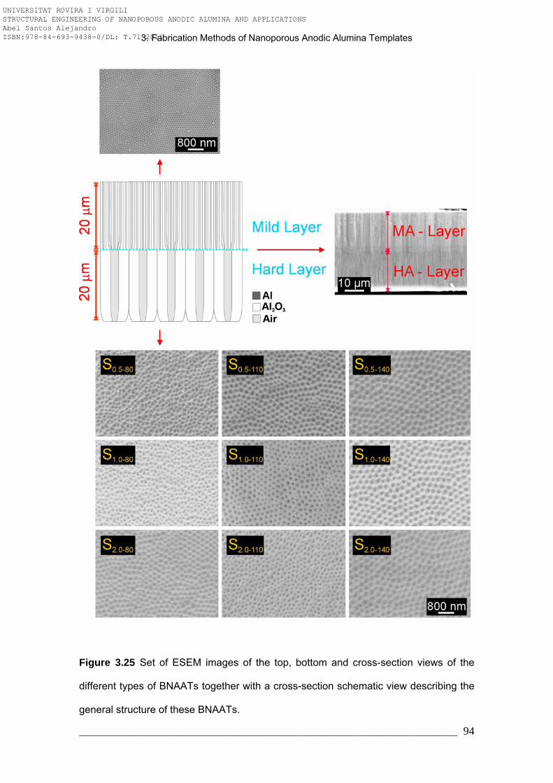
3. Fabrication Methods of Nanoporous Anodic Alumina Templates
_____________________________________________________________
94
Figure 3.25 Set of ESEM images of the top, bottom and cross-section views of the
different types of BNAATs together with a cross-section schematic view describing the
general structure of these BNAATs.
UNIVERSITAT ROVIRA I VIRGILI STRUCTURAL ENGINEERING OF NANOPOROUS ANODIC ALUMINA AND APPLICATIONS Abel Santos Alejandro ISBN:978-84-693-9438-0/DL: T.71-2011

3. Fabrication Methods of Nanoporous Anodic Alumina Templates
_____________________________________________________________
95
VHA (V)
ρp(HA) ·109
(pores·cm-2) 80 110 140
0.5 3.11 2.21 1.58
3.02 2.03 1.69
2.73 1.95 2.15
3.10 2.06 1.88
1.0 2.65 2.04 2.04
2.71 2.35 1.93
2.73 2.12 2.12
2.47 1.99 1.99
2.0 2.36 1.93 1.73
2.12 2.03 1.59
2.15 2.12 1.65
Rv (
V·s
-1)
1.90 2.05 1.47
Table 3.7 Complete set of the ρp(HA) measurements for each BNAATs.
Below, an analysis of variance (ANOVA) of the experimental results is carried out,
which will give objective conclusions about how the anodization parameters (i.e. Rv and
VHA) affect the analyzed variable (i.e. ρp(HA)).
UNIVERSITAT ROVIRA I VIRGILI STRUCTURAL ENGINEERING OF NANOPOROUS ANODIC ALUMINA AND APPLICATIONS Abel Santos Alejandro ISBN:978-84-693-9438-0/DL: T.71-2011

3. Fabrication Methods of Nanoporous Anodic Alumina Templates
_____________________________________________________________
96
If the effects of Rv and VHA are αi and βj, respectively, the following three null
hypotheses are tested by means of the ANOVA test:
i) H0: (α·β)ij = 0 (there is not significant effect of the interaction between the
anodization parameters (i.e. Rv·VHA) on ρp(HA)).
ii) H1: αi = 0 (there is not significant effect of Rv on ρp(HA)).
iii) H2: βj = 0 (there is not significant effect of VHA on ρp(HA)).
If these hypotheses are rejected, then, the alternative hypotheses will be accepted.
These alternative hypotheses are presented as follows:
i) H0*: (α·β)ij ≠ 0 (there is significant effect of the interaction between the
anodization parameters (i.e. Rv·VHA) on ρp(HA)).
ii) H1*: αi ≠ 0 (the effect of Rv on ρp(HA) is significant).
iii) H2*: βj ≠ 0 (the effect of VHA on ρp(HA) is significant).
The ANOVA table is calculated from the equations shown in Table 3.8, where SS is the
sum of squares of the source, DF denotes the degree of freedom of the source, MS is
the mean square of the source, F0 is the test statistic of this source, a and b denote the
total number of levels for Rv and VHA, respectively, and n is the total number of
replications.
UNIVERSITAT ROVIRA I VIRGILI STRUCTURAL ENGINEERING OF NANOPOROUS ANODIC ALUMINA AND APPLICATIONS Abel Santos Alejandro ISBN:978-84-693-9438-0/DL: T.71-2011

3. Fabrication Methods of Nanoporous Anodic Alumina Templates
_____________________________________________________________
97
Source SS DF MS F0
Rv ∑=
−=a
iivR abn
yy
bnSS
1
2...2
..1 1−a
1−=
aSS
MS vRvR
E
vRvR MS
MSF =−0
VHA ∑=
= −b
jjHAV abn
yy
anSS
1
2...2
..1 1−b
1−=
bSS
MS HAVHAV
E
HAVHAV MS
MSF =−0
Rv ·VHA HAVvR
a
i
b
jijHAVvR SSSS
abny
yn
SS −−⎟⎟⎠
⎞⎜⎜⎝
⎛−= ∑∑
= =1
2...
1
2.·
1 )1)(1( −− ba)1)·(1(
·· −−
=ba
SSMS HAVvR
HAVvRE
HAVvRHAVvR MS
MSF ·
·0 =−
Error ⎟⎟⎠
⎞⎜⎜⎝
⎛−−= ∑∑
= =
a
i
b
jijTE abn
yy
nSSSS
1
2...
1
2.
1 )1( −nab )1( −=
nabSSMS E
E
Total ∑∑∑= = =
−=a
i
b
j
n
kijkT abn
yySS
1
2...
1 1
2 1−abn
Table 3.8 Equations of the ANOVA table for a 32-factorial design.
The strategy used to test the null hypotheses H0, H1 and H2 is to compare the value of
F0 calculated from the ANOVA table to the value of the F-distribution for a significance
level of 95% (i.e. 0.05) with the corresponding value of DF(Source) and DF(Error) (i.e.
F(0.05; DF(Source); DF(Error))). In this way, the tested null hypotheses (i.e. H0, H1 and H2)
associated with each case enumerated above will be rejected if the following results
are obtained:
i) F0-Rv·VHA ≥ F(0.05; DF(Rv·VHA); DF(Error)).
ii) F0-Rv ≥ F(0.05; DF(Rv); DF(Error)).
iii) F0-VHA ≥ F(0.05; DF(VHA); DF(Error)).
So, after the values of each parameter are substituted in the equations shown in Table
3.8, the resulting ANOVA is presented in Table 3.9.
UNIVERSITAT ROVIRA I VIRGILI STRUCTURAL ENGINEERING OF NANOPOROUS ANODIC ALUMINA AND APPLICATIONS Abel Santos Alejandro ISBN:978-84-693-9438-0/DL: T.71-2011

3. Fabrication Methods of Nanoporous Anodic Alumina Templates
_____________________________________________________________
98
Source SS DF MS F0
Rv (V·s-1) 0.997 2 0.498 21.99
VHA (V) 3.680 2 1.840 81.21
Rv ·VHA (V2·s-1) 0.840 4 0.210 9.27
Error 0.610 27 0.023
Total 6.130 35
Table 3.9 ANOVA table for the 32-factorial design corresponding to table 3.7.
The ANOVA test confirms that the interaction between Rv and VHA is significant
because 9.27 is much larger than F(0.05; 4; 27) = 2.73. So, the hypothesis H0 is rejected. It
is also shown that the effect of VHA on ρp(HA) is approximately four times stronger than
the effect of Rv, although they are both significant (i.e. 81.21 and 21.99 > F(0.05; 2; 27) =
3.35).
In order to determine the combined effect of the main anodization parameters (i.e. Rv
and VHA) on the studied variable (ρp(HA)) and their individual effects, we analyze how
the variable changes when one of the parameters is fixed and the other is varied and
vice versa. The results can be seen in Figure 3.26. First, it is observed that ρp(HA)
varies linearly when the value of Rv is changed at 80 V. However, this linear behaviour
disappears at 110 and 140 V (Figure 3.26 a). This reveals the presence of quadratic
effects on the pore density of the hard side as the hard anodization voltage increases.
When Rv is fixed and VHA is modified, a slight quadratic effect appears when the hard
anodization voltage increases at 2.0 V·s-1 (Figure 3.26 b). These quadratic effects on
ρp(HA) can be observed both in the 2D contour plot (Figure 3.26 c) and the 3D
representation (Figure 3.26 d).
UNIVERSITAT ROVIRA I VIRGILI STRUCTURAL ENGINEERING OF NANOPOROUS ANODIC ALUMINA AND APPLICATIONS Abel Santos Alejandro ISBN:978-84-693-9438-0/DL: T.71-2011

3. Fabrication Methods of Nanoporous Anodic Alumina Templates
_____________________________________________________________
99
From the electrochemical point of view, these results can be explained in terms of the
self-ordering mechanism. As was mentioned in the introduction, pore ordering depends
mainly on the anodization voltage and for a given acid electrolyte the hexagonal pore
arrangement is perfect only under particular anodization conditions. In the case of
oxalic acid, these conditions are 40 and 140 V for mild and hard anodization regimes,
respectively. For intermediate anodization voltages (i.e. 80 and 110 V), the pore
ordering is disturbed because the porosity is progressively modified from about 10 (i.e.
at 40 V) to 3.3% (i.e. at 140 V). So, the quadratic effects observed in ρp(HA) when Rv
and VHA are modified can be attributed to nonlinear instabilities of the pore ordering
during the anodization regime transition from MA to HA. It is also proven that the
anodization voltage ramp influences the pore density of the hard side as well as the
hard anodization voltage, although the effects are weak and strong, respectively.
UNIVERSITAT ROVIRA I VIRGILI STRUCTURAL ENGINEERING OF NANOPOROUS ANODIC ALUMINA AND APPLICATIONS Abel Santos Alejandro ISBN:978-84-693-9438-0/DL: T.71-2011

3. Fabrication Methods of Nanoporous Anodic Alumina Templates
_____________________________________________________________
100
Figure 3.26 Set of graphics of ρp(HA) as a function of the main anodization parameters
Rv and VHA. a) Average values of ρp(HA) as a function of Rv for each value of VHA. b)
Average values of ρp(HA) as a function of VHA for each value of Rv. c) 2D contour plot
of ρp(HA) as a function of Rv and VHA. d) 3D representation of ρp(HA) as a function of Rv
and VHA.
UNIVERSITAT ROVIRA I VIRGILI STRUCTURAL ENGINEERING OF NANOPOROUS ANODIC ALUMINA AND APPLICATIONS Abel Santos Alejandro ISBN:978-84-693-9438-0/DL: T.71-2011

3. Fabrication Methods of Nanoporous Anodic Alumina Templates
_____________________________________________________________
101
3.2.5. Perfectly ordered nanoporous anodic alumina templates
This section discusses the fabrication process of monodomain nanoporous anodic
alumina templates (MD-NAATs) by nanoimprinting. Nanoimprinting has been improved
[160-164] since it was first used to fabricate high-aspect ratio MD-NAATs [20], and it is
now one of the most cost-effective and efficient methods of producing MD-NAATs. The
nanoimprint process makes it possible to produce perfect patterns of the master stamp
on the annealed and electropolished Al substrates which, after direct anodization under
suitable conditions, become MD-NAATs (Figure 3.27). However, crucial factors such as
the stamping pressure (PS) and the anodization conditions first have to be optimized. In
this way, perfectly ordered nanoporous anodic alumina templates can be mass
fabricated and the durability of the master stamp increased. In this case, the master
stamp used consists of hexagonally arranged Si3N4 pyramids with a period of 235 nm
(Figures 3.28 a and b). These pyramids are 130, 100, and 100 nm long, wide and high,
respectively. This Si3N4 master stamp is placed on an annealed and electropolished
aluminium substrate and then pressed under 20 kN·cm-2 using a conventional oil press.
The stamping pressure is maintained constant for 5 min to compensate for elastic
deformations in the Al substrates, which is reflected in a progressive decrease in PS
during the stamping process. The master stamp pattern, then, is transferred to the
entire surface of the aluminium substrate (Figure 3.28 c). After the nanoimprint
process, the anodization conditions have to be adjusted to the master stamp period
(i.e. 235 nm), since the transferred pattern defines the subsequent nucleation of pores
during the first stage of the anodization process. So, according to Eq. 1.9, the
anodization voltage for the interpore distance of 235 nm is about 93 V. In order to
prevent the template from burning, an acid electrolyte solution of H2C2O4 0.3 M in a
mixture of ethanol and water (EtOH:H2O 1:3 (v:v)) is used and the stirring rate is
increased to 500 r.p.m. during the course of the anodization process.
UNIVERSITAT ROVIRA I VIRGILI STRUCTURAL ENGINEERING OF NANOPOROUS ANODIC ALUMINA AND APPLICATIONS Abel Santos Alejandro ISBN:978-84-693-9438-0/DL: T.71-2011

3. Fabrication Methods of Nanoporous Anodic Alumina Templates
_____________________________________________________________
102
It is thus possible to maintain the electrolyte temperature at around 0ºC. If the self-
ordering conditions and the master stamp period match, high aspect ratio (i.e. pore
length / pore diameter) MD-NAATs can be fabricated (Figure 3.28 d).
Figure 3.27 Schematic slanted section views describing the one-step anodization
process for fabricating MD-NAATs by nanoimprinting. a) The Si3N4 master stamp is
pressed onto the annealed and electropolished aluminium substrate. b) The Si3N4
master stamp pattern is transferred to the Al substrate surface. c) Resulting MD-NAAT
after direct anodization under suitable conditions.
UNIVERSITAT ROVIRA I VIRGILI STRUCTURAL ENGINEERING OF NANOPOROUS ANODIC ALUMINA AND APPLICATIONS Abel Santos Alejandro ISBN:978-84-693-9438-0/DL: T.71-2011

3. Fabrication Methods of Nanoporous Anodic Alumina Templates
_____________________________________________________________
103
Furthermore, the combination of the self-ordering mechanism and the nanoimprint
technique allows monodomain nanoporous anodic alumina templates to be fabricated
with an extraordinary pore arrangement (i.e. interpore distance shorter than the master
stamp period). It is also necessary to adjust the anodization voltage so that the
interpore distance is 86% that of the master stamp. This strategy is represented in
Figure 3.29 and can be explained as follows: after the master stamp pattern has been
transferred onto the Al substrate surface and the suitable anodization conditions
applied, the self-ordering mechanism leads to new pore growth in the triangular lattice
delimited by three imprinted pores.
Figure 3.28 Set of ESEM images corresponding to the different stages of the
nanoimprint process. a) Cross-section view of the Si3N4 master stamp. b) Top view of
the Si3N4 master stamp. c) Annealed and electropolished aluminium substrate after
transferring the pattern from the Si3N4 master stamp by pressing at 20 kN·cm-2. d)
Resulting MD-NAAT after direct anodization at 93 V.
UNIVERSITAT ROVIRA I VIRGILI STRUCTURAL ENGINEERING OF NANOPOROUS ANODIC ALUMINA AND APPLICATIONS Abel Santos Alejandro ISBN:978-84-693-9438-0/DL: T.71-2011

3. Fabrication Methods of Nanoporous Anodic Alumina Templates
_____________________________________________________________
104
When the suitable anodization voltage is applied, the concentric electric field around
the patterned holes prevents new pores from being randomly generated inside the
triangular pore lattice formed by the imprinted pores. Pores are only allowed to grow at
the centre of each group of three imprinted pores. In order to calculate the anodization
voltage suitable for generating guided pores, it must be taken into account that the
diameter of the concentric electric field (dCEF) has to match the distance between
printed pores (i.e. dinterp). So, taking into account that the relationship between the
diameter of the concentric electric field and the anodization voltage is given by Eq. 3.1
[162], the anodization voltage required to generate one guided pore inside each
triangular pore lattice of imprinted pores can be estimated. Finally, the anodization
voltage required to generate guided pores in a triangular pore lattice with a period of
235 nm is found to be 81 V, and the interpore distance of the resulting MD-NAAT is
about 203 nm (Figure 3.30).
89.2CEFd
V = (3.1)
In order to explore other triangular pore lattices, two types of nickel (Ni) master stamps
are developed. These stamps are replicated from the bottom of PD-NAATs with
interpore distances of 500 and 100 nm (i.e. H3PO4 1 wt % at 195 V and H2C2O4 0.3 M
at 40 V). The fabrication process of these Ni master stamps is represented in Figure
2.40. First, PD-NAATs with interpore distances of 500 and 100 nm are fabricated by
the two-step anodization process (Figure 3.31 a). Second, the remaining aluminium
substrate is removed in a saturated solution of HCl·CuCl2 (Figure 3.31 b). Third, a thin
layer of Ni is sputtered on the bottom of the PD-NAATs at 80 mA for 5 min (i.e. a
thickness of about 100 nm) (Figure 3.31 c). Fourth, the thickness of this layer is
increased to 50 μm by electrodeposition of Ni from a Ni plating solution with NiCl2·6H2O
(0.084 M), Ni(H2NSO3)2·4H2O (1.59 M) and H3BO3 (0.33 M) at 7 mA·cm-2 for 3 h
UNIVERSITAT ROVIRA I VIRGILI STRUCTURAL ENGINEERING OF NANOPOROUS ANODIC ALUMINA AND APPLICATIONS Abel Santos Alejandro ISBN:978-84-693-9438-0/DL: T.71-2011

3. Fabrication Methods of Nanoporous Anodic Alumina Templates
_____________________________________________________________
105
(Figure 3.31 d). Finally, the PD-NAAT is dissolved by wet chemical etching using a
mixture of H3PO4 0.4 M and H2CrO3 0.2 M at 45ºC for about 24 h (Figure 3.31 e).
Unfortunately, it has not been possible to present here the results obtained after
imprinting such Ni master stamps onto annealed and electropolished Al substrates.
Nonetheless, it is expected that these Ni master stamps (Figure 3.32) can be used to
fabricate PD-NAATs with shorter pore lattices than the Ni master stamps. They can
also be used as a new way of fabricating PD-NAATs with hexagonal pore
arrangements in one step, because the 1st anodization step will be substituted by the
imprinting stage.
Figure 3.29 Schematic top view of a MD-NAAT with extraordinary interpore distance
fabricated by nanoimprinting. Each new pore (blue circles) grows guided by three
imprinted pores (grey circles) since the concentric electric field around each imprinted
pore (green dotted circles) prevents from the generation of disordered pores inside the
pore lattice.
UNIVERSITAT ROVIRA I VIRGILI STRUCTURAL ENGINEERING OF NANOPOROUS ANODIC ALUMINA AND APPLICATIONS Abel Santos Alejandro ISBN:978-84-693-9438-0/DL: T.71-2011

3. Fabrication Methods of Nanoporous Anodic Alumina Templates
_____________________________________________________________
106
Figure 3.30 Set of ESEM images of two types of MD-NAATs fabricated by
nanoimprinting. a) With ordinary interpore distance of 235 nm at 93 V (blue circle
indicates a virtual guided pore generated under suitable anodization conditions). b)
With extraordinary interpore distance of 203 nm at 81 V (red circle denotes a guided
pore generated inside the pore lattice of three imprinted pores).
UNIVERSITAT ROVIRA I VIRGILI STRUCTURAL ENGINEERING OF NANOPOROUS ANODIC ALUMINA AND APPLICATIONS Abel Santos Alejandro ISBN:978-84-693-9438-0/DL: T.71-2011

3. Fabrication Methods of Nanoporous Anodic Alumina Templates
_____________________________________________________________
107
Figure 3.31 Schematic cross-section view of the fabrication process of nickel master
stamps from PD-NAATs. a) Resulting PD-NAAT after the two-step anodization
process. b) PD-NAAT after dissolving selectively the remaining Al substrate. c) Thin
layer of Ni sputtered on the bottom of the PD-NAAT. d) Growth of the Ni layer by
electrodeposition. e) Resulting Ni master stamp after removing the PD-NAAT.
Figure 3.32 Replicated nickel master stamps from the bottom of two types of PD-
NAATs. a) Pore lattice of 100 nm with H2C2O4 at 40 V. b) Pore lattice of 500 nm with
H3PO4 at 195 V.
UNIVERSITAT ROVIRA I VIRGILI STRUCTURAL ENGINEERING OF NANOPOROUS ANODIC ALUMINA AND APPLICATIONS Abel Santos Alejandro ISBN:978-84-693-9438-0/DL: T.71-2011

3. Fabrication Methods of Nanoporous Anodic Alumina Templates
_____________________________________________________________
108
One of the main characteristics of MD-NAATs with an extraordinary pore arrangement
fabricated by nanoimprinting is that the oxide barrier layer at the pore bottom tips of the
guided pores is thinner than at the imprinted pores. This makes it possible to
selectively penetrate the oxide barrier layer. It is thus possible for the guided pores to
be filled first with a certain material A and, after the imprinted pores have been opened,
with a material B. This idea is schematically represented in Figure 3.33.
Figure 3.33 Schematic cross-section diagram describing the selective pore opening
process in MD-NAATs with extraordinary pore arrangement.
UNIVERSITAT ROVIRA I VIRGILI STRUCTURAL ENGINEERING OF NANOPOROUS ANODIC ALUMINA AND APPLICATIONS Abel Santos Alejandro ISBN:978-84-693-9438-0/DL: T.71-2011

3. Fabrication Methods of Nanoporous Anodic Alumina Templates
_____________________________________________________________
109
3.2.6. Nanoporous anodic alumina funnels
In previous works, inverted cone NAATs have been moulded using multi-short-
consecutive anodization and pore widening steps [193,194], and nanoporous anodic
alumina funnels with short aspect ratio have been used as a template to fabricate
shape-coded silica nanotubes [195]. Nevertheless, so far no works have reported
about the fabrication of nanoporous anodic alumina funnels (NAAFs) with high aspect
ratio, although these nanostructures could lead to a wide range of later applications as
diameter-modulated polymer fibres [196], linear noble-metal nanoparticle chains with
modulated diameters for one-dimensional nano-optical devices (e.g. plasmonic
waveguides, plasmonic printing) [197], magnetic nanotubes and nanowires with
multiple diameter modulations [198], chiral nanosphere chains of several materials
(gold, polystyrene, etc) by vacuum infiltration [199-201] and so on. In previous works
[193-194], in which funnel-like nanoporous anodic alumina templates with short aspect
ratio were fabricated under controlled potential conditions, the key factor used to
control the length of each segment was the anodization time length. However, in order
to fabricate NAAFs with high aspect ratio and controlled segment length under
controlled potential conditions, the key factor must be the total current charge passed
throughout the system, and not the anodization time length. In this section, it is
described an accurate method for fabricating high aspect ratio nanoporous anodic
alumina funnels. This method is based on combining sequential anodizing and pore
widening steps. Four types of NAAFs are fabricated by modifying the controlling
parameters of the anodization and the etching processes (i.e. the total current charge
and the pore widening time length, respectively). A theoretical electrochemical model is
applied to estimate quantitatively the dependence of the pore length on the anodization
time under controlled potential conditions. In addition, the experimental relationships
between the pore length, the anodization time and the total current charge are obtained
after various calibration experiments.
UNIVERSITAT ROVIRA I VIRGILI STRUCTURAL ENGINEERING OF NANOPOROUS ANODIC ALUMINA AND APPLICATIONS Abel Santos Alejandro ISBN:978-84-693-9438-0/DL: T.71-2011

3. Fabrication Methods of Nanoporous Anodic Alumina Templates
_____________________________________________________________
110
The experimental relationship between the pore widening time and the pore diameter is
established as well. The obtained results confirm that, under controlled potential
conditions, the key factor to control the segment length of NAAFs with high aspect ratio
is the integrated current passed throughout the system, and not the anodization time
length. The geometric characteristics of the resulting nanostructures (i.e. the pore
diameter and the length of each segment) are analyzed in detail by environmental
scanning electron microscopy (ESEM).
The electrochemical system that represents the aluminium (Al) anodization is basically
divided into two electrodes (i.e. anode and cathode), an acid electrolyte solution as a
medium and a power supply, which provides electrical energy (i.e. the driving force of
the anodization process). The voltage applied to the electrochemical system (V) can be
expressed as follows:
Systemca IREEV +−= )( (3.2)
where Ea is the anodic potential drop for driving the anodic reactions, Ec is the cathodic
potential drop for driving the cathodic reactions, I is the current passed throughout the
system and RSystem (73.73 KΩ from experimental measurements) is the electric
resistance of the system (i.e. contacts, wires, acid electrolyte solution, etc). On the one
hand, it has to take into account that, in the course of the anodization process, there is
a thin layer of aluminium oxide (Al2O3) covering the Al surface. So, it is possible to
assume that the anodic potential drop has, approximately, a linear relationship with the
Al2O3 film resistance (ROx) and the anodic reaction rate is limited by the ionic migration
throughout the oxide film [202]. In this way, Ea is given by:
OxaaCorra RSJEE +≈ (3.3)
UNIVERSITAT ROVIRA I VIRGILI STRUCTURAL ENGINEERING OF NANOPOROUS ANODIC ALUMINA AND APPLICATIONS Abel Santos Alejandro ISBN:978-84-693-9438-0/DL: T.71-2011

3. Fabrication Methods of Nanoporous Anodic Alumina Templates
_____________________________________________________________
111
where ECorr is the free corrosion potential of Al in the acid electrolyte solution, Ja is the
anodic current density and Sa is the anode surface area (0.71·10-4 m2 from
experimental measurements). In addition, ROx can be expressed as:
tSJ
KKRa
aOxdfOx ρ)( −= (3.4)
where Kf and Kd are the formation and the dissolution coefficients of Al2O3 in the Al
anodization process (5.275·10-9 and 2.374·10-9 m3·(A·s)-1, respectively [203]), ρOx is the
apparent resistivity of Al2O3 (1·1010 Ω·m), and t is the anodization time.
On the other hand, the main cathodic reaction that takes place during the Al
anodization process in the acid electrolyte solution is the hydrogen (H2) evolution. So,
assuming that the difference between the free corrosion potentials of electrodes made
of different materials is practically negligible in contrast to the voltage drop between
them, the cathodic potential drop is given by the Tafel’s equation [204]. This is:
⎟⎟⎠
⎞⎜⎜⎝
⎛−≈ r
Corr
acCorrc S
JJ
LnEE β (3.5)
where βc is the Tafel’s slope, JCorr is the free corrosion current density of Al in the acid
electrolyte solution and Sr is the ratio between the surface areas of the anode and the
cathode in the corrosion process (i.e. Sr = Sa/Sc). Substituting Equations Eq. 3.3, 3.4
and 3.5 into Eq. 3.2, then V can be expressed as follows:
Systemaaaca RSJKJLntJKV +++= 22
1 )(β (3.6)
UNIVERSITAT ROVIRA I VIRGILI STRUCTURAL ENGINEERING OF NANOPOROUS ANODIC ALUMINA AND APPLICATIONS Abel Santos Alejandro ISBN:978-84-693-9438-0/DL: T.71-2011

3. Fabrication Methods of Nanoporous Anodic Alumina Templates
_____________________________________________________________
112
where K1 and K2 are constants if the anodization parameters (i.e. temperature,
concentration of the acid electrolyte solution, stirring rate, etc) are not modified in the
course of the anodization process. These constants are given by the following
expressions:
Oxdf KKK ρ)(1 −= (3.7)
and
⎟⎟⎠
⎞⎜⎜⎝
⎛=
Corr
rc J
SLnK β2 (3.8)
So, deriving V respect to the anodization time (t) and taking into account that, under
controlled potential conditions, V is constant and Ja is a function of t, Eq. 3.6 leads to:
dtdJ
RSdt
dJJdt
dJtJKJK
dtdV a
Systemaa
ac
aaa +++==
120 12
1 β (3.9)
Reorganizing Eq. 2.9:
caSystemaa
aa
JRStJK
JKdt
dJ
β++
−=
21
31
·2 (3.10)
If it is considered that, for the cathodic reaction (i.e. hydrogen evolution), the value of βc
ranges from 50 to 80 mV [202], it is possible to neglect βc with regards to the other
terms of the denominator. In this way, Eq. 3.10 yields:
43
21
KtJKJK
dtdJ
a
aa+
−= (3.11)
UNIVERSITAT ROVIRA I VIRGILI STRUCTURAL ENGINEERING OF NANOPOROUS ANODIC ALUMINA AND APPLICATIONS Abel Santos Alejandro ISBN:978-84-693-9438-0/DL: T.71-2011

3. Fabrication Methods of Nanoporous Anodic Alumina Templates
_____________________________________________________________
113
where K3 and K4 are constants and correspond to the following equations:
13 2KK −= (3.12)
and
Systema RSK =4 (3.13)
Finally, by substituting the known values, Eq. 3.11 becomes:
)24.5()02.58()01.29( 2
+−
=tJ
Jdt
dJ
a
aa (3.14)
In order to solve this ordinary differential equation (ODE), the 4th order Runge-Kutta
numerical method is applied with the initial value problem Ja(t = 0 s) = 650 A·m-2 and
Δt = 0.1 s. Once the numerical relationship between Ja and t is obtained for each time
step (Δt), the evolution of the pore length (LP) in the course of the anodization process
can be calculated by applying the pore-filling method under controlled potential
conditions [150,151]:
∫=
=
=ftt
ttaP dttJKL
0
)·(5 (3.15)
where K5 is a constant value calculated as:
Ox
Ox
zFdM
Kη
=5 (3.16)
UNIVERSITAT ROVIRA I VIRGILI STRUCTURAL ENGINEERING OF NANOPOROUS ANODIC ALUMINA AND APPLICATIONS Abel Santos Alejandro ISBN:978-84-693-9438-0/DL: T.71-2011

3. Fabrication Methods of Nanoporous Anodic Alumina Templates
_____________________________________________________________
114
where MOx is the atomic weight of alumina (101.96 g·mol-1), η is the anodic current
efficiency (0.70 [151]), z is the number of electrons associated with the alumina
formation (6), F is the Faraday’s constant (96484.56 C·mol-1) and dOx is the alumina
density (3.2 g·cm-3 [145]).
The theoretical electrochemical model for nanoporous anodic alumina growth
expressed by Eq. 3.14 and 3.15 will be contrasted by the experimental results
presented as follows.
First, two calibration processes to relate the pore length (LP) to Q and the pore
diameter (dp) to the pore widening length (tpw), respectively, are carried out. In order to
calibrate the pore length, eight samples are fabricated following the two-step
anodization process under controlled potential conditions (i.e. 160 V) using the
anodizing control system based on the total current charge control presented in 3.2.4.
The acid electrolyte is an aqueous solution of phosphoric acid (H3PO4) 0.3 M at 5ºC.
The time length of the first anodization step is 1 h and the second anodization step is
limited by the total current charge. The different total current charge limits are 5, 10, 15,
20, 25, 30, 35 and 40 A·s and the resulting samples are labelled as Q05, Q10, Q15, Q20,
Q25, Q30, Q35 and Q40, respectively. The pore length of each sample is measured at ten
different cross-sections. In this way, the experimental relationships between Q, LP and t
are estimated under the anodization conditions used to fabricate the NAAFs. To
calibrate the pore widening process, five samples are fabricated following a two-step
anodization process under controlled potential conditions (i.e. 160 V). The time length
of both anodization steps is 1 h, using as acid electrolyte an aqueous solution of
phosphoric acid (H3PO4) 0.3 M at 5ºC. These samples are labelled as PW0, PW15,
PW30, PW45 and PW60. After the fabrication process, these samples are immersed in 5
wt % aqueous phosphoric acid at 35ºC for 0, 15, 30, 45 and 60 min, respectively. So,
the relationship between the pore diameter (dP) and the pore widening time length (tpw)
is established.
UNIVERSITAT ROVIRA I VIRGILI STRUCTURAL ENGINEERING OF NANOPOROUS ANODIC ALUMINA AND APPLICATIONS Abel Santos Alejandro ISBN:978-84-693-9438-0/DL: T.71-2011

3. Fabrication Methods of Nanoporous Anodic Alumina Templates
_____________________________________________________________
115
After the calibration processes, nanoporous anodic alumina funnels with high aspect
ratio are fabricated by anodizing annealed and electropolished Al substrates by the
two-step process. The anodization is carried out in our thermally isolated
electrochemical cell under controlled potential conditions. In the course of the
anodization process, the electrolyte is constantly stirred and its temperature is adjusted
at 5ºC. The first anodization step consists of applying the anodization voltage directly
(i.e. 160 V) in an electrolyte aqueous solution of H3PO4 0.3 M for 1 h at 5ºC.
Subsequently, this nanoporous anodic alumina film with disordered pores on the
surface and ordered pores on the bottom is dissolved by wet chemical etching in a
mixture of phosphoric acid 0.4 M and chromic acid 0.2 M at 70ºC for the same length of
time as the first anodization step (i.e. about 1 h). Then, multiple subsequent
anodization steps are conducted under the same anodization conditions but using as
control factor the total current charge (Q) instead of the anodization time (t). Depending
on the number of subsequent anodization steps, the four types of samples are labelled
as NF-I, NF-II, NF-III and NF-IV for one, two, three and four subsequent anodization
steps, respectively. Each subsequent anodization step corresponds to one segment in
the resulting NAAF structure. The total current charge of the whole fabrication process
is 62.64 A·s, which corresponds to the target pore length of 30 μm. Taking into account
that the pore length is directly proportional to the total current charge, this value is
divided by the number of subsequent anodization steps (i.e. the number of segments in
the resulting NAAF structure) and the limit values of Q for each subsequent anodization
step are 62.64, 31.32, 20.88 and 15.66 A·s for samples NF-I, NF-II, NF-III and NF-IV,
respectively. Between consecutive anodization steps, a pore widening stage,
conducted by wet chemical etching in 5 wt % aqueous phosphoric acid at 35ºC, is
intercalated to enlarge the pore diameter (dP), which depends on the pore widening
time (tpw). Finally, the remaining aluminium substrate is removed in a saturated solution
of HCl·CuCl2. The fabrication conditions of each type of sample are summarized in
Table 3.10.
UNIVERSITAT ROVIRA I VIRGILI STRUCTURAL ENGINEERING OF NANOPOROUS ANODIC ALUMINA AND APPLICATIONS Abel Santos Alejandro ISBN:978-84-693-9438-0/DL: T.71-2011

3. Fabrication Methods of Nanoporous Anodic Alumina Templates
_____________________________________________________________
116
Type of
NAAF
Anodization Steps
(after first step) QTotal (A·s) Qlimit (A·s)
Pore Widening
Steps
I 1 62.64 1
II 2 31.32 2
III 3 20.88 3
IV 4
62.64
15.66 4
Table 3.10 Fabrication conditions for the different types of NAAFs (NF-I, NF-II, NF-III
and NF-IV).
Both samples used to obtain the calibration curves (i.e. Q05, Q10, Q15, Q20, Q25, Q30, Q35,
Q40, PW0, PW15, PW30, PW45 and PW60) and the NAAFs (i.e. NF-I, NF-II, NF-III and NF-
IV) are inspected by ESEM and the measurements of dP and LP are obtained from
ESEM image analysis using a standard image processing package (ImageJ, public
domain programme developed at the RSB of the NIH, USA). The obtained results are
shown in Table 3.11. The results from the total current charge calibration process are
shown in Figure 3.34. The relationships Q-t (black solid line and stars in Figure 3.34 a -
left) and LP-t (light grey solid line and circles in Figure 3.34 a - right) are not linear,
following power trend lines (the obtained equations from the numerical simulations
fittings for Q-t and LP-t are included in Figure 3.34 a). Both the experimental values
(black stars and light grey circles in Figure 3.34 a) and the numerical simulations
obtained from the theoretical model developed (solid black and light grey lines in Figure
3.34 a) are in good agreement. The total current charge and the pore length evolution
throughout the anodization process can be divided into three main sections (Figure
3.34 a). At the first seconds of the anodization process (i.e. about 20 s), the pore
growth rate is very fast because the anodic current is entirely used in this process.
UNIVERSITAT ROVIRA I VIRGILI STRUCTURAL ENGINEERING OF NANOPOROUS ANODIC ALUMINA AND APPLICATIONS Abel Santos Alejandro ISBN:978-84-693-9438-0/DL: T.71-2011

3. Fabrication Methods of Nanoporous Anodic Alumina Templates
_____________________________________________________________
117
These results agree with previous works which reported about the growth rate of
NAATs at the first seconds of the anodization process (i.e. oxide barrier layer and pore
formation) [205]. After the first seconds of the anodization process, the pore growth
rate is progressively reduced as a result of the development of side reactions, which
decrease the anodic current efficiency (i.e. η). This growth rate reduction is maintained
until moderate anodization times (i.e. 2.5 h, approximately). Finally, for longer
anodization times, the pore growth rate becomes practically constant throughout the
anodization and can be fitted to a straight line. In addition, as Figure 3.34 b shows, the
pore length is directly proportional to the total current charge (i.e. the dependence of Q
on the anodization time is the same that for LP but dividing by a constant factor of 1.8
A·s·μm-1). From the electrochemical point of view, it means that the number of
electrons transferred into the electrochemical cell at a given time is directly proportional
to the number of oxygen (O) atoms used to form Al2O3, and the number of O atoms
used to oxidize aluminium corresponds to the number of O atoms diffused throughout
the Al2O3 layer at the same time. The value of this proportionality constant fluctuates
slightly throughout the anodization process (Table 3.12) because of side reactions such
as oxygen evolution at the anode [205], which reduce relatively the anodic current
efficiency. This could explain the slight deviation of the experimental values of Q·LP-1
from the trend line (Figure 3.34 b).
UNIVERSITAT ROVIRA I VIRGILI STRUCTURAL ENGINEERING OF NANOPOROUS ANODIC ALUMINA AND APPLICATIONS Abel Santos Alejandro ISBN:978-84-693-9438-0/DL: T.71-2011

3. Fabrication Methods of Nanoporous Anodic Alumina Templates
_____________________________________________________________
118
Measured Values Target Values
Type of
NAAF
Anodization
Step
Qlimit
(A·s) t (min) LP (μm) dP (nm)
Aspect
Ratio LP (μm) dP (nm)
Aspect
Ratio
I 2 62.64 385.3 30.22 ±
0.19
148.21 ±
8.66
203.9 30 150 200
2 31.32 158.6 14.95 ±
0.19
157.90 ±
7.26
94.7 15 150 100 II
3 31.32 229.7 15.51 ±
0.19
209.46 ±
10.19
74.1 15 200 75
2 20.88 81.2 9.74 ±
0.15
155.68 ±
9.26
62.6 10 150 66.7
3 20.88 136.0 9.43 ±
0.17
204.15 ±
8.82
46.2 10 200 50
III
4 20.88 146.3 10.70 ±
0.14
250.76 ±
10.91
42.7 10 250 40
2 15.66 105.4 7.19 ±
0.25
152.08 ±
6.91
47.3 7.5 150 50
3 15.66 111.0 7.29 ±
0.22
199.38 ±
11.86
36.6 7.5 200 37.5
4 15.66 111.1 7.16 ±
0.23
245.12 ±
12.18
29.2 7.5 250 30
IV
5 15.66 109.5 7.19 ±
0.26
288.91 ±
18.13
24.9 7.5 300 25
Table 3.11 Geometric characteristics measured for each type of NAAF (i.e. pore
length, pore diameter and aspect ratio of each segment) together with their target
values (i.e. predicted values from the experimental relationships obtained after the
calibration processes).
Regarding to the results obtained for the pore widening process, as Figure 3.34 c
shows, the relationship between dP and tpw is practically linear, with a dissolution rate of
about 1.4 nm·min-1. So, it is possible to fabricate NAAFs with controlled segment
diameter. The pore widening times and their corresponding pore diameters are
summarized in Table 3.13.
UNIVERSITAT ROVIRA I VIRGILI STRUCTURAL ENGINEERING OF NANOPOROUS ANODIC ALUMINA AND APPLICATIONS Abel Santos Alejandro ISBN:978-84-693-9438-0/DL: T.71-2011

3. Fabrication Methods of Nanoporous Anodic Alumina Templates
_____________________________________________________________
119
LP (μm) Q (A·s) Q·LP-1 ((A·s)·μm-1)
3.0 5 1.7
5.9 10 1.7
7.6 15 2.0
10.4 20 1.9
14.5 25 1.7
16.1 30 1.9
18.2 35 1.9
21.9 40 1.8
Table 3.12 Values of the proportionality constant between Q and LP obtained from the
total current charge calibration process.
tpw (min) dP (nm)
14 150
32 200
50 250
68 300
Table 3.13 Pore widening times and their corresponding pore diameters obtained from
the pore widening calibration process.
UNIVERSITAT ROVIRA I VIRGILI STRUCTURAL ENGINEERING OF NANOPOROUS ANODIC ALUMINA AND APPLICATIONS Abel Santos Alejandro ISBN:978-84-693-9438-0/DL: T.71-2011

3. Fabrication Methods of Nanoporous Anodic Alumina Templates
_____________________________________________________________
120
Figure 3.34 Experimental relationships between the fabrication parameters (i.e. total
current charge (Q), anodization time length (t) and pore widening time (tpw)) and the
geometric characteristics (i.e. pore length (LP) and diameter (dP)) obtained from the
calibration processes). a) Total current charge (black solid line is numerical simulation
and black solid stars are experimental values) and pore length (light grey solid line is
numerical simulation and light grey solid circles are experimental values) versus
anodization time. b) Pore length versus total current charge. c) Pore diameter versus
pore widening time.
UNIVERSITAT ROVIRA I VIRGILI STRUCTURAL ENGINEERING OF NANOPOROUS ANODIC ALUMINA AND APPLICATIONS Abel Santos Alejandro ISBN:978-84-693-9438-0/DL: T.71-2011

3. Fabrication Methods of Nanoporous Anodic Alumina Templates
_____________________________________________________________
121
The cross-section of the fabricated NAAFs are inspected by ESEM and a set of the
images is shown in Figure 3.35 together with magnified views of the junctions between
consecutive segments and a sketch of the corresponding NAAF structure. The
geometric characteristics of each type of NAAF (i.e. pore length, pore diameter and
aspect ratio of each segment) are summarized in Table 3.11 together with their target
values (i.e. predicted values from the experimental relationships obtained after the
calibration processes). As Figure 3.35 a shows, the structure of sample NF-I consists
of one segment with average pore length of 30.22 μm and average pore diameter of
148.21 nm. These values are very close to the target values of 30 μm and 150 nm,
respectively. The structure of this sample is the typical structure of NAAT fabricated by
the two-step anodization process. Figure 3.35 b shows the cross-section view of
sample NF-II, which presents two segments with average pore lengths of 15.51 and
14.95 μm for segments 1 and 2 (from top to bottom of the NAAF), respectively. The
average pore diameters of these segments are 209.46 and 157.90 nm, respectively.
Three segments are distinguished in the cross-section view of sample NF-III (Figure
3.35 c). The average segment lengths are 10.70, 9.43 and 9.74 μm with average pore
diameters of 250.76, 204.15 and 155.68 nm for segments 1, 2 and 3, respectively.
Finally, as Figure 3.35 d shows, sample NF-IV consists of four segments with average
lengths of 7.19, 7.16, 6.91 and 7.19 μm and average diameter of 288.91, 245.12,
199.38 and 152.08 nm for segments 1, 2, 3 and 4, respectively. As Table 3.11 shows,
the measured values of the pore length and the pore diameter are rather close to the
target values. This denotes that the calibration processes allow design with high level
of accuracy nanoporous anodic alumina funnels with high aspect ratio (i.e. LP/dP).
UNIVERSITAT ROVIRA I VIRGILI STRUCTURAL ENGINEERING OF NANOPOROUS ANODIC ALUMINA AND APPLICATIONS Abel Santos Alejandro ISBN:978-84-693-9438-0/DL: T.71-2011

3. Fabrication Methods of Nanoporous Anodic Alumina Templates
_____________________________________________________________
122
Figure 3.35 Set of ESEM images of cross-section view of the fabricated types of
NAAFs together with magnified views of the junctions between consecutive segments
(yellow rectangles in (a), (b), (c) and (d)) and a sketch of the NAAF structure. a) NF-I.
b) NF-II. c) NF-III. d) NF-IV.
UNIVERSITAT ROVIRA I VIRGILI STRUCTURAL ENGINEERING OF NANOPOROUS ANODIC ALUMINA AND APPLICATIONS Abel Santos Alejandro ISBN:978-84-693-9438-0/DL: T.71-2011

3. Fabrication Methods of Nanoporous Anodic Alumina Templates
_____________________________________________________________
123
The evolution of the current density (J) and the total current charge (Q) in the course of
the anodization process were recorded and are shown in Figure 3.36. As first result, it
is observed that as the number of consecutive anodization steps is increased, the
difference in the anodization time length is shorter between consecutive anodization
steps (Table 3.11). In fact, the length of the anodization time corresponding to sample
NF-IV for the second, third, fourth and fifth step is practically the same. In addition, the
time length corresponding to the second anodization step is shorter than the time
length of later anodization steps for all these samples with multiple anodization steps
(i.e. NF-II, NF-III and NF-IV). This could be attributed to the total current charge
employed to form the oxide barrier layer and pore nucleation on the patterned Al
substrate during the first stage of the second anodization step. This stage is denoted
by a typical current density peak, which vanishes for later anodization steps since no
total current charge is used to nucleate pores. This is due to the fact that the oxide
barrier layer is not entirely removed from the pore bottom tips after the pore widening
steps for samples with more than two anodization steps (i.e. NF-II, and NF-III and NF-
IV). Another reason for which the length of the anodization time corresponding to
consecutive anodization steps is more similar as the number of anodization steps is
increased is that, as the total current charge limit is reduced, the relationship between
Q and t becomes practically linear.
UNIVERSITAT ROVIRA I VIRGILI STRUCTURAL ENGINEERING OF NANOPOROUS ANODIC ALUMINA AND APPLICATIONS Abel Santos Alejandro ISBN:978-84-693-9438-0/DL: T.71-2011

3. Fabrication Methods of Nanoporous Anodic Alumina Templates
_____________________________________________________________
124
Figure 3.36 Current density (J-light grey solid line-left scale) and total current charge
(Q-black solid line-right scale) transients throughout the anodization process for the
types of NAAFs fabricated. a) NF-I. b) NF-II. c) NF-III. d) NF-IV.
UNIVERSITAT ROVIRA I VIRGILI STRUCTURAL ENGINEERING OF NANOPOROUS ANODIC ALUMINA AND APPLICATIONS Abel Santos Alejandro ISBN:978-84-693-9438-0/DL: T.71-2011

3. Fabrication Methods of Nanoporous Anodic Alumina Templates
_____________________________________________________________
125
In summary, in this section has been reported about the fabrication and
characterization of four types of nanoporous anodic alumina funnels with high aspect
ratio. To the best of our knowledge, for the first time, this type of nanostructures has
accurately been designed and fabricated. The target values of both LP and dP of each
segment and the measured values are very close. This resulted from two systematic
calibration processes, which allow designing the NAAF structure with a high level of
accuracy. In addition, the experimental relationships between the fabrication
parameters (i.e. total current charge, anodization time length and pore widening time)
and the geometric characteristics of the resulting nanostructures (i.e. pore length and
diameter) have been obtained.
A theoretical electrochemical model has been deduced to explain the pore growth
throughout the anodization time under controlled potential conditions. The numerical
simulation obtained from this electrochemical model agrees with the experimental
results of the relationship between the pore length and the anodization time. So, it is
proven that the electrochemical model developed is suitable to predict the pore growth
throughout the anodization process under controlled potential conditions.
It is expected that the presented NAAFs could be used as a template to fabricate a
wide range of new nanostructures which can be used in a wide range of later
applications as sensors, actuators, photonic devices and so on.
UNIVERSITAT ROVIRA I VIRGILI STRUCTURAL ENGINEERING OF NANOPOROUS ANODIC ALUMINA AND APPLICATIONS Abel Santos Alejandro ISBN:978-84-693-9438-0/DL: T.71-2011

3. Fabrication Methods of Nanoporous Anodic Alumina Templates
_____________________________________________________________
126
3.3. Summary
This chapter has described the experimental techniques for fabricating typical and
innovative nanostructures based on nanoporous anodic alumina.
The fabrication processes of two types of typical NAATs have been explained: PD-
NAATs produced with sulphuric, oxalic and phosphoric acid by the two-step
anodization process under mild conditions and PD-NAATs fabricated with oxalic acid
by the one-step anodization process under hard conditions. Furthermore, several
fabrication techniques for producing innovative NAATs (i.e. innovative pore geometries)
have been discussed. These nanostructures are: PD-NAATs produced without a
protective layer by a two-step anodization process under hard conditions, PD-NAATs
without an oxide barrier layer on aluminium substrates, hierarchical nanoporous anodic
alumina templates, bilayered NAATs, MD-NAATs with extraordinary pore arrangement
and nanoporous anodic alumina funnels.
In the following chapter, several applications of these templates will be presented.
Nevertheless, these nanostructures are expected to be used in numerous other
applications in the near future.
UNIVERSITAT ROVIRA I VIRGILI STRUCTURAL ENGINEERING OF NANOPOROUS ANODIC ALUMINA AND APPLICATIONS Abel Santos Alejandro ISBN:978-84-693-9438-0/DL: T.71-2011

_______________________________________________________________
4. Applications of Nanoporous
Anodic Alumina Templates
UNIVERSITAT ROVIRA I VIRGILI STRUCTURAL ENGINEERING OF NANOPOROUS ANODIC ALUMINA AND APPLICATIONS Abel Santos Alejandro ISBN:978-84-693-9438-0/DL: T.71-2011

4. Applications of Nanoporous Anodic Alumina Templates
____________________________________________________________ 128
In this chapter, some applications of the nanoporous anodic alumina templates
presented in the previous chapter are explained in detail.
First, arrays of cobalt and nickel nanopillars on aluminium substrates are synthesized
by DC electrochemical deposition using a template of PD-NAATs without an oxide
barrier layer (section 3.2.2). Second, quasi-ordered P3HT nanopillar-nanocap
structures with controlled size are fabricated by replicating from hierarchical
nanoporous anodic alumina templates (section 3.2.3). Third, high-density nanopillar
arrays of the same polymer with an average nanopillar height of 300 nm and an
average distance between adjacent nanopillars of 50 nm are transferred on ITO/glass
substrates from PD-NAATs fabricated by the two-step anodization process (section
3.3.1). Fourth, the first step for fabricating mosaic arrays of nickel nanowires and
nanotubes by electrochemical deposition and atomic layer deposition (ALD) using
bilayered nanoporous anodic alumina templates is presented (3.2.4). Finally, silica
nanoparticle chains are fabricated by vacuum infiltration through nanoporous anodic
alumina funnels (section 3.2.6).
By way of a conclusion, in each section, various future experiments for continuing the
work are discussed.
UNIVERSITAT ROVIRA I VIRGILI STRUCTURAL ENGINEERING OF NANOPOROUS ANODIC ALUMINA AND APPLICATIONS Abel Santos Alejandro ISBN:978-84-693-9438-0/DL: T.71-2011

4. Applications of Nanoporous Anodic Alumina Templates
____________________________________________________________ 129
4.1. Cobalt and nickel nanopillar arrays on aluminium
substrates
In terms of nanostructure fabrication, choosing a suitable template is one of the most
crucial factors in the synthesis process, because any defect in this template could be
transferred to the resulting nanostructure via replication. So far, several materials have
been used as a template for synthesizing nanowires or nanotubes. Nanoporous anodic
alumina templates (NAATs) have become one of the most widely used for the following
reasons: first, in contrast to other templates as polycarbonate membranes, NAATs
present a higher pore density and a narrower diameter pore distribution [206].
Secondly, the pore diameter and the interpore distance are rather controllable by
adjusting the anodization conditions [20]. Thirdly, as it has been commented in
previous chapters, by means of the two-step anodization process [19], it is possible to
fabricate PD-NAATs with a self-ordered hexagonally and periodic pore arrangement in
a more cost-effective way than with other methods like electron beam lithography [207].
The electrochemical deposition of metals from an electrolyte solution is commonly used
to fabricate nanowires and nanotubes by filling porous templates since it is a fast and
well-controlled method. Nonetheless, as-produced PD-NAATS have certain
disadvantages to be used directly as a template when an electrochemical deposition is
desirable. The main disadvantage is that there is an aluminium oxide barrier layer
between the pore bottom and the aluminium substrate. This oxide barrier layer
electrically isolates the metallic aluminium substrate from the inner side of the pores.
For this reason, when a direct current (DC) electrodeposition is carried out in an as-
produced NAAT, it is rather unstable and there is no uniform filling of the pores.
Moreover, high electrodeposition potentials are needed for tunnelling the electrons
throughout the oxide barrier layer of the pore bottom. Other deposition techniques like
electroless deposition [62], sol–gel [208], chemical vapour deposition [209] and atomic
layer deposition (ALD) [198] can avoid this drawback, since the growth of nanowires or
UNIVERSITAT ROVIRA I VIRGILI STRUCTURAL ENGINEERING OF NANOPOROUS ANODIC ALUMINA AND APPLICATIONS Abel Santos Alejandro ISBN:978-84-693-9438-0/DL: T.71-2011

4. Applications of Nanoporous Anodic Alumina Templates
____________________________________________________________ 130
nanotubes does not start at the pore tips, but from the pore walls. So far, several
methods have been applied for electrodepositing metals into NAATs. The most
commonly used are two. In the first one [210,211], the NAAT must be detached from
the aluminium substrate by dissolving the remaining Al substrate in a saturated solution
of HCl·CuCl2 or in a saturated solution of mercury (II) chloride (HgCl2). Subsequently,
the Al2O3 barrier layer is removed from the pore bottoms by a chemical etching process
in a solution of phosphoric acid (H3PO4). Finally, an electrical contact is sputtered on
one side of the freestanding NAAT. The second one is the pulsed electrodeposition
method, in which the NAAT remains on the aluminium substrate. By means of this
method, magnetic nanowire arrays of nickel have successfully been fabricated [21]. In
this section, it is presented a method for fabricating cobalt (Co) and nickel (Ni)
nanopillars (NPs) on aluminium substrates by direct electrodeposition using PD-NAATs
without oxide barrier layer. So, after removing the alumina template, the metallic
nanowires remain on the aluminium substrate.
PD-NAATs are prepared using the two-step anodization process under hard conditions
presented in section 3.2.1. When the anodization process is finished, the oxide barrier
layer at the pore bottom tips is removed by applying the re-anodization technique under
galvanostatic conditions commented in section 3.2.2. After the anodization process, the
resulting PD-NAATs with open pores at the Al2O3-Al interface acted as a transfer mask
to fabricate Co and Ni nanopillar arrays on Al substrates by DC electrodeposition. The
interpore distance, the pore diameter and the thickness of these templates are 250 nm,
200 nm and 12 μm, respectively. During the DC electrodeposition process, the upper
side of these templates is placed in contact with the corresponding electrolyte
solutions. In order to fabricate cobalt nanopillar arrays (Co-NPs), the electrolyte
consists of an aqueous solution of cobalt sulphate heptahydrate (CoSO4·7H2O) as
cobalt source and boric acid (H3BO3) as stabilizer. For fabricating nickel nanopillar
arrays (Ni-NPs), it is employed an aqueous solution containing nickel sulphate
UNIVERSITAT ROVIRA I VIRGILI STRUCTURAL ENGINEERING OF NANOPOROUS ANODIC ALUMINA AND APPLICATIONS Abel Santos Alejandro ISBN:978-84-693-9438-0/DL: T.71-2011

4. Applications of Nanoporous Anodic Alumina Templates
____________________________________________________________ 131
hexahydrate (NiSO4·6H2O) and nickel chloride hexahydrate (NiCl2·6H2O) as nickel
source and boric acid (H3BO3) as stabilizer. Both aqueous solutions are constantly
stirred at 150 r.p.m. and heated at 40ºC during the electrodeposition process in order
to maintain a constant concentration of the electrolyte inside the pores. The
concentration and pH of each electrolyte solution are shown in Table 4.1.
Electrolyte Solution pH Compound C (g·L-1) Function
Ni 4.5 NiSO4·6H2O 300 Nickel Source
NiCl2·6H2O 45 Nickel Source
H3BO3 45 Stabilizer
Co 3 CoSO4·7H2O 400 Cobalt Source
H3BO3 45 Stabilizer
Table 4.1 Characteristics of the electrolyte solutions employed for Co and Ni
electrodeposition.
Prior to the electrodeposition process, the templates are immersed in the
corresponding electrolyte bath for 5 min in order to completely wet the inner side of the
porous structure. The DC electrodeposition is carried out using a platinum (Pt) wire as
cathode and applying a constant profile of -3 V for Co solution and -5 V for Ni solution.
To characterize the Co-NPs and Ni-NPs, when the DC electrodeposition process is
finished, the templates are immersed in a mixture of H3PO4 0.4 M and H2CrO3 0.2 M at
70ºC for 1h in order to dissolve entirely the alumina structure used as a template.
Finally, the samples are washed with deionised water and dried under a draught. A
power supply from Keithley (model 2420 SourceMeter) is used to perform the DC
electrodeposition process.
UNIVERSITAT ROVIRA I VIRGILI STRUCTURAL ENGINEERING OF NANOPOROUS ANODIC ALUMINA AND APPLICATIONS Abel Santos Alejandro ISBN:978-84-693-9438-0/DL: T.71-2011

4. Applications of Nanoporous Anodic Alumina Templates
____________________________________________________________ 132
Figure 4.1 shows the current-time (I-t) transients corresponding to the DC
electrodeposition process of Co and Ni nanopillar arrays under controlled potential
conditions. It is possible to distinguish four different sections in the current curve for
both cobalt (Figure 4.1 a) and for nickel (Figure 4.1 b) electrodeposition. First, the
current decreases abruptly until it reaches a steady value (section 1 - S1). Then, the
current remains constant through a certain time length (section 2 - S2). Subsequently,
there is a noticeable increase until a second steady value is reached (section 3 - S3).
Finally, the current value becomes constant throughout the time again (section 4 - S4).
These four sections can be related to different stages of the growth of nanopillar arrays
inside the PD-NAATs. This process starts using as a template a PD-NAAT with open
pores at the Al2O3-Al interface (Figure 4.2 a). In the first section of the electrodeposition
curve (S1), metal nucleation centres in the pore bottom start to grow (Figure 4.2 b). The
decrease in the current profile can be explained by local depletion of the ionic
concentration at the pore bottom [212]. The current stabilizes when the ionic diffusion
can be compensated for this depletion (S2), and the metallic nanopillars grow filling the
pores (Figure 4.2 c). When the pores are entirely filled with Co and Ni, hemispherical
tips of metal grow over the upper end of each nanopillar (Figure 4.2 d), resulting in the
increase in current observed in the electrodeposition curve (S3). Finally, a metallic film
is formed on the PD-NAAT surface (Figure 4.2 e), what is denoted by a constant
current value through the time (S4). In order to obtain Co and Ni nanopillar arrays
without structural defects after removing the PD-NAAT, the electrodeposition process
must be finished at the end of S2 (Figure 4.2 f).
UNIVERSITAT ROVIRA I VIRGILI STRUCTURAL ENGINEERING OF NANOPOROUS ANODIC ALUMINA AND APPLICATIONS Abel Santos Alejandro ISBN:978-84-693-9438-0/DL: T.71-2011

4. Applications of Nanoporous Anodic Alumina Templates
____________________________________________________________ 133
Figure 4.1 Current and voltage-time (I-t and V-t) transients for the electrodeposition
processes under controlled potential conditions. The different sections of the current
transient are separated by red solid lines. a) For Co-NPs at -3 V. b) For Ni-NPs at -5 V.
UNIVERSITAT ROVIRA I VIRGILI STRUCTURAL ENGINEERING OF NANOPOROUS ANODIC ALUMINA AND APPLICATIONS Abel Santos Alejandro ISBN:978-84-693-9438-0/DL: T.71-2011

4. Applications of Nanoporous Anodic Alumina Templates
____________________________________________________________ 134
Figure 4.2 Schematic slanted views describing the electrodeposition process using a
PD-NAAT without oxide barrier layer fabricated by the two-step anodization process
under hard conditions. a) PD-NAAT without oxide barrier layer. b) A thin layer of metal
is deposited at the pore bottoms. c) Fast growth of metallic nanopillar arrays inside the
template. d) The template is entirely filled with metal. e) Metal film growth on the
template surface. f) Resulting metallic nanopillar arrays after removing the template
when the process is stopped at (d).
UNIVERSITAT ROVIRA I VIRGILI STRUCTURAL ENGINEERING OF NANOPOROUS ANODIC ALUMINA AND APPLICATIONS Abel Santos Alejandro ISBN:978-84-693-9438-0/DL: T.71-2011

4. Applications of Nanoporous Anodic Alumina Templates
____________________________________________________________ 135
Once the fabrication process is finished, the resulting Co and Ni nanopillar arrays
structures are characterized in detail by several techniques. First, the Co-NPs and Ni-
NPs are inspected by ESEM image analysis. Figure 4.3 compiles a set of ESEM
images of the Co-NPs (Figure 4.3 a) and Ni-NPs (Figure 4.3 b) in which it can be
observed that these nanopillar arrays remain fixed on the aluminium substrates after
dissolving the PD-NAAT (Figures 4.3 c and d). In addition, as Figures 4.3 e and f show,
the hexagonal arrangement corresponding to the PD-NAAT is kept after the
electrodeposition process. The average interpillar distance (i.e. about 250 nm)
corresponds to the average interpore distance of the template. This means that the
resulting nanostructure is tough enough to withstand the post-treatment (i.e. dissolution
of the PD-NAAT and cleaning). Moreover, the average pillar diameter (i.e. about 200
nm) is close to the average pore diameter of the template. There are no structural
defects in the resulting nanopillars. It is confirmed that the average height of the
nanopillars (i.e. around 12 μm) correspond approximately to the thickness of the PD-
NAAT. These facts imply that the electrodeposition process is carried out under
suitable conditions and the filling of the template pores is practically total.
Secondly, in order to confirm the chemical elements, the nanostructures are analysed
by energy dispersive X-ray spectroscopy (EDXS). As Figure 4.4 shows, both the
samples of Co (Figure 4.4 a) and Ni (Figure 4.4 b) nanopillar arrays are exclusively
composed of aluminium (from the Al substrate) and the respective metal (Co or Ni),
what means that there is no chemical contamination after the applied post-treatment.
The quantitative results are 19.5% Al and 80.5% Co for Co-NPs and 27.3% Al and
72.7% Ni for Ni-NPs.
UNIVERSITAT ROVIRA I VIRGILI STRUCTURAL ENGINEERING OF NANOPOROUS ANODIC ALUMINA AND APPLICATIONS Abel Santos Alejandro ISBN:978-84-693-9438-0/DL: T.71-2011

4. Applications of Nanoporous Anodic Alumina Templates
____________________________________________________________ 136
Figure 4.3 Set of ESEM images of the fabricated metallic nanopillar arrays. a) Cross-
section view of the Co-NPs after removing the template. b) Cross-section view of the
Ni-NPs after removing the template. c) Magnified bottom view of Co-NPs. d) Magnified
bottom view of Ni-NPs. e) Magnified top view of Co-NPs. f) Magnified top view of Ni-
NPs.
UNIVERSITAT ROVIRA I VIRGILI STRUCTURAL ENGINEERING OF NANOPOROUS ANODIC ALUMINA AND APPLICATIONS Abel Santos Alejandro ISBN:978-84-693-9438-0/DL: T.71-2011

4. Applications of Nanoporous Anodic Alumina Templates
____________________________________________________________ 137
Figure 4.4 Elemental qualitative analysis of Co-NPs and Ni-NPs by energy dispersive
X-ray spectroscopy (EDXS). a) Spectrum and weight percentage (inset) of the
elements present in Co-NPs. b) Spectrum and weight percentage (inset) of the
elements present in Ni-NPs.
UNIVERSITAT ROVIRA I VIRGILI STRUCTURAL ENGINEERING OF NANOPOROUS ANODIC ALUMINA AND APPLICATIONS Abel Santos Alejandro ISBN:978-84-693-9438-0/DL: T.71-2011

4. Applications of Nanoporous Anodic Alumina Templates
____________________________________________________________ 138
At last, the crystal phase of cobalt and nickel nanopillar arrays is revealed by micro-X-
ray diffraction (μ-XRD) analysis. As Figure 4.5 shows, both Co and Ni patterns of
nanopillar arrays present high-purity crystal phases since there are not any diffraction
peaks of their corresponding oxides. The main peaks for Co nanopillars are four and
appear at 41.6, 44.5, 47.4 and 62.5º, which correspond to <100>, <002>, <101> and
<102> planes for a hexagonal crystal lattice, respectively (Figure 4.5 a). The main
peaks for Ni nanopillars are three and appear at 41.5, 51.8 and 76.4º, which
correspond to <111>, <200> and <220> planes for a face-centred cubic crystal lattice,
respectively (Figure 4.5 b).
Figure 4.5 X-ray diffraction patterns of Co-NPs (a) and Ni-NPs (b).
UNIVERSITAT ROVIRA I VIRGILI STRUCTURAL ENGINEERING OF NANOPOROUS ANODIC ALUMINA AND APPLICATIONS Abel Santos Alejandro ISBN:978-84-693-9438-0/DL: T.71-2011

4. Applications of Nanoporous Anodic Alumina Templates
____________________________________________________________ 139
In summary, in this section it has been reported a simple electrochemical approach to
fabricate cobalt and nickel nanopillar arrays on aluminium substrates. By means of this
technique, it is feasible to reduce the number of stages in the fabrication process
because the removing of the oxide barrier layer from the pore bottom tips of the PD-
NAAT takes place during the anodization process. Another main feature of this process
is that the Co and Ni nanopillar arrays remain on the aluminium substrate after
removing the template. In addition, the resulting nanostructures have not presented
any defect and the nanopillar diameter and height and the interpillar distance
correspond to the geometric characteristics of the template.
It is considered that this is a promising technique for future applications and a means
for fabricating new nanodevices. One example of a future application of the resulting
nanostructures presented in this section could be to use the metallic nanopillar arrays
as nanoelectrodes for direct deposition of nanoparticles from a gas draught. This
nanostructure would act as an electrostatic precipitator by applying a high-voltage field.
UNIVERSITAT ROVIRA I VIRGILI STRUCTURAL ENGINEERING OF NANOPOROUS ANODIC ALUMINA AND APPLICATIONS Abel Santos Alejandro ISBN:978-84-693-9438-0/DL: T.71-2011

4. Applications of Nanoporous Anodic Alumina Templates
____________________________________________________________ 140
4.2. Quasi-ordered P3HT nanopillar-nanocap structures
Nowadays, it is possible to fabricate polymeric nanostructures such as nanotubes,
nanowires and nanorods by nanolithography [213], mechanical patterning [214] and
electro-spinning [215]. However, in order to produce highly-ordered polymeric
nanostructures [216–218], the most vastly used method has become the template
synthesis using nanoporous moulds because it is a cost-effective fabrication technique.
So far, nanoporous anodic alumina templates (NAATs) have become one of the most
widely used porous material as a pattern for their specific geometric characteristics (i.e.
pore density, pore diameter distribution, interpore distance and thickness). In addition,
by applying several strategies it is possible to modify the original structure of NAATs.
One example of modification are the hierarchical nanoporous anodic alumina templates
(HNAATs) presented in section 3.2.3, which are a promising material in order to be
used for developing novel nanostructures and nanodevices. One interesting
functionalization of HNAATs is to infiltrate their pores with polymers, which have many
potential applications owing to their physical and chemical properties (e.g.
transparency, pliability, biocompatibility, biodegradation and so on). In that regard,
among the thiophene family, Poly(3-hexylthiophene) (P3HT) is a suitable conjugated
polymer for being used to develop polymer-based photovoltaic cells. The efficiency of
these solar cells can be increased by means of nanostructured bulk-heterojunctions in
which the interfacial distance between the donor and the acceptor phases is lower than
20 nm [219]. In this section, it is presented a method for fabricating nanopillar-nanocap
structures based on P3HT by using HNAATs as a template. The applied technique
consists of a combination between the spin-coating and the melt-assisted template
wetting methods. The resulting nanostructure consists of P3HT nanopillars on a
substrate of P3HT quasi-hexagonally arranged nanocaps. The geometric
characteristics of these structures are analyzed in detail through ESEM images.
UNIVERSITAT ROVIRA I VIRGILI STRUCTURAL ENGINEERING OF NANOPOROUS ANODIC ALUMINA AND APPLICATIONS Abel Santos Alejandro ISBN:978-84-693-9438-0/DL: T.71-2011

4. Applications of Nanoporous Anodic Alumina Templates
____________________________________________________________ 141
In this case, the hierarchical nanoporous anodic alumina template used to develop
P3HT nanopillar-nanocap structures corresponds to that fabricated under conditions S5
shown in section 3.2.3. This template is fabricated using direct anodization of annealed
and electropolished aluminium substrates following an asymmetric two-step
anodization process. The 1st anodization step consists of applying the anodization
voltage directly (i.e. 170 V) in an electrolyte aqueous solution of phosphoric acid 0.3 M
(Figure 4.6 a). Then, the resulting nanoporous anodic alumina film is dissolved by wet
chemical etching in a mixture of H3PO4 0.4 M and H2Cr2O7 0.2 M at 70 °C. As a result,
a hexagonal pattern is produced on the aluminium surface (Figure 4.6 b). Afterwards,
the 2nd step of the anodization process is conducted under asymmetric anodization
conditions (i.e. 40 V) in an aqueous solution of oxalic acid 0.3 M. So, a HNAAT, which
consists of an outer hexagonal lattice of concavities in the interior of which pores grow,
is resulted (Figure 4.6 c). The anodization voltage (i.e. 40 V) during the 2nd anodization
step is maintained for 3 min, this is when the hierarchical nanoporous anodic alumina
template reaches the target thickness (i.e. about 500 nm). After the anodization
process, a slight pore widening step is applied by wet chemical etching in an aqueous
solution of phosphoric acid 5 wt % at 35 °C for 10 min in order to facilitate the
infiltration process of the pores. Once the template fabrication process is finished, the
HNAAT is infiltrated with Poly(3-hexylthiophene). First, the template is spin-coated at
2000 r.p.m. for 30 s by a drop of a chloroform (CH3Cl) solution of P3HT 10 wt %
(P3HT, melting point 238°C, Mw∼17500 g·mol−1, 99.995% regioregularity, Sigma-
Aldrich) (Figure 4.6 d). Secondly, the covered hierarchical nanoporous anodic alumina
template is annealed at 250°C for 30 min in air environment for injecting the polymer
into the pores by melt-assisted wetting (Figure 4.6 e). Finally, the infiltrated template is
slowly cooled to room temperature and the remaining Al substrate is removed in a
saturated solution of cupric chloride and hydrochloric acid (HCl·CuCl2). Subsequently,
the HNAAT is dissolved in a solution of sodium hydroxide (NaOH) 1 M at room
temperature (Figure 4.6 f) for 1 h.
UNIVERSITAT ROVIRA I VIRGILI STRUCTURAL ENGINEERING OF NANOPOROUS ANODIC ALUMINA AND APPLICATIONS Abel Santos Alejandro ISBN:978-84-693-9438-0/DL: T.71-2011

4. Applications of Nanoporous Anodic Alumina Templates
____________________________________________________________ 142
Figure 4.6 Schematic slanted section views describing the fabrication process of P3HT
nanopillars on a substrate of P3HT quasi-hexagonally arranged nanocaps. a) 1st
anodization step. b) Removing the Al2O3 film by wet chemical etching. c) 2nd
anodization step under asymmetric conditions. d) P3HT spin-coated HNAAT. e) P3HT
infiltration by melt-assisted wetting. f) Removing of the remaining Al substrate and the
HNAAT by wet chemical etching processes.
UNIVERSITAT ROVIRA I VIRGILI STRUCTURAL ENGINEERING OF NANOPOROUS ANODIC ALUMINA AND APPLICATIONS Abel Santos Alejandro ISBN:978-84-693-9438-0/DL: T.71-2011

4. Applications of Nanoporous Anodic Alumina Templates
____________________________________________________________ 143
The geometric characteristics of the HNAAT and the replicating polymeric
nanostructure are characterized by ESEM image analysis. In order to compare the
geometric characteristics of the template with the moulding nanostructure, the
interconcavity (dinterconc) and the interpore (dinterp) distance (i.e. centre-to-centre
concavity and pore distance, respectively), the concavity (dconc) and pore (dp) diameter,
the intercap distance (dintercap) (i.e. centre-to-centre cap), and both the cap (dcap) and
pillar (dpillar) diameter are estimated by ESEM image analysis. The obtained results are
summarized in Table 4.2. The standard deviation is used as an estimation of the
dispersion in the measurements.
Geometric Characteristic Measurement (nm)
dinterconc 398 ± 40
dinterp 101 ± 7
dconc 370 ± 33
dp 78 ± 14
dintercap 388 ± 35
dcap 351 ± 36
dpillar 52 ± 4
Table 4.2 Geometric characteristics of the resulting P3HT nanostructure. Interconcavity
(dinterconc) and interpore (dinterp) distances, concavity (dconc) and pore (dp) diameters,
intercap distance (dintercap), and cap (dcap) and pillar (dpillar) diameters.
UNIVERSITAT ROVIRA I VIRGILI STRUCTURAL ENGINEERING OF NANOPOROUS ANODIC ALUMINA AND APPLICATIONS Abel Santos Alejandro ISBN:978-84-693-9438-0/DL: T.71-2011

4. Applications of Nanoporous Anodic Alumina Templates
____________________________________________________________ 144
The current density and voltage-time (J-t and V-t) transients corresponding to the
fabrication process of the hierarchical nanoporous anodic alumina template are shown
in Figure 4.7. As it has been commented in section 3.2.3, the main difference between
symmetric and asymmetric two-step anodization processes is that, during the second
step of the asymmetric process, there is a shift in the minimum of J. In this case, this
shift is produced by the anodization voltage decrement between the 1st and 2nd step of
the anodization process since it implies a reduction in the lattice constant. So, pores
grow inside the concavities on the HNAAT surface. Before the infiltration stage, the
HNAAT is analyzed by ESEM image analysis and the resulting average interconcavity
and interpore distances are 398 and 101 nm, respectively. The average concavity and
pore diameters are 370 and 78 nm, respectively (Table 4.2).
Figure 4.7 Current density and voltage-time (J-t and V-t) transients for the fabrication
process of the HNAAT under asymmetric conditions. Point A indicates nanocaps
formation and B when nanopillars reach a suitable depth.
UNIVERSITAT ROVIRA I VIRGILI STRUCTURAL ENGINEERING OF NANOPOROUS ANODIC ALUMINA AND APPLICATIONS Abel Santos Alejandro ISBN:978-84-693-9438-0/DL: T.71-2011

4. Applications of Nanoporous Anodic Alumina Templates
____________________________________________________________ 145
In order to characterize the P3HT nanocap substrate, one HNAAT is fabricated by
stopping the 2nd step of the anodization process just before the pores started to grow
(point A in Figure 4.7). As Table 4.2 shows, the average intercap distance is 388 nm
and the average cap diameter is 351 nm (Figures 4.8 a and b). These results are
slightly shorter than the average interconcavity distance and the average concavity
diameter of the HNAAT, respectively. This fact implies that, during the annealing
process, a slight bulk contraction of the P3HT nanostructure takes place owing mainly
to the solvent (CH3Cl) evaporation.
Figure 4.8 Set of ESEM images of the resulting P3HT nanostructure. a) Top view of
the P3HT nanocap arrays substrate. b) Tilted (45º) top view of the P3HT nanocap
arrays substrate. c) Top view of the P3HT nanopillar arrays. d) Tilted (45º) top view of
the P3HT nanopillar arrays.
UNIVERSITAT ROVIRA I VIRGILI STRUCTURAL ENGINEERING OF NANOPOROUS ANODIC ALUMINA AND APPLICATIONS Abel Santos Alejandro ISBN:978-84-693-9438-0/DL: T.71-2011

4. Applications of Nanoporous Anodic Alumina Templates
____________________________________________________________ 146
For fabricating the final P3HT nanostructure with firm nanopillars on the substrate of
nanocap arrays (Figures 4.8 c and d), the anodization process is stopped when the
pores reached a height of about 500 nm (point B in Figure 4.7). Deeper pores generate
bundles of collapsed nanopillars, which cannot remain firm after the post-treatment
process (i.e. template removing and cleaning). As Table 4.2 shows, the average pillar
diameter is 52 nm. As the same that nanocap case, the nanopillars contract slightly
their dimensions (i.e. pillar diameter and height) with regards to the pore values (i.e.
pore diameter and height).
In summary, it has been exposed a reasonably fast and cost-effective method for
fabricating a hierarchical nanostructure based on P3HT nanopillar arrays on a
substrate of the same polymer with quasi-hexagonally ordered nanocap arrays. By
combining the spin-coating method with the melt-assisted wetting method a HNAAT is
infiltrated with P3HT. So, it is possible to replicate an original nanostructure based on
that polymer in a controlled way. It is found out that the resulting P3HT nanostructure
suffered a slight bulk contraction owing to the solvent evaporation during the annealing
process.
It is expected that the resulting P3HT nanostructure presented in this section could be
used for enhancing the efficiency of nanostructured organic solar cells. This fabrication
process could be extended to different types of copolymers with other interesting
properties (e.g. conductivity, luminescence and so on). Furthermore, the resulting
nanostructure can be easily fabricated with a wide range of geometric characteristics
for satisfying the requirements of later applications.
UNIVERSITAT ROVIRA I VIRGILI STRUCTURAL ENGINEERING OF NANOPOROUS ANODIC ALUMINA AND APPLICATIONS Abel Santos Alejandro ISBN:978-84-693-9438-0/DL: T.71-2011

4. Applications of Nanoporous Anodic Alumina Templates
____________________________________________________________ 147
4.3. High-density nanopillar arrays of P3HT on ITO/glass
substrates
Semiconducting organic polymers have become materials with a wide range of
applications. In recent years, an increasing attention has been paid to the development
of optoelectronic devices as polymer light-emitting diodes and solar cells [220-223].
Nowadays, owing to the high demand of energy, scientists are focusing their interest
on the development of high-efficient organic solar cells. Recently, several studies have
shown that to produce nanometre-scale interpenetrating network of a donor and an
acceptor phase is a promising way to improve the efficiency of organic solar cells [224-
227]. In these networks, the interfacial distance between the donor and the acceptor
must be similar to the exciton diffusion length. So far, fabrication methods such as
nanoimprinting [224], nanolithography [228], electro-spinning [215], printing and coating
[229] and template-assisted synthesis [219] have been used to produce this kind of
nanostructures. Among them, the most widespread method is the template synthesis
using nanoporous templates, since it is a cost-effective and versatile fabrication
technique. Since the two-step anodization process was reported [19], nanoporous
anodic alumina templates (NAATs) have become a material vastly used as a template
because it is possible to fabricate NAATs with quasi-hexagonal pore arrangement in an
inexpensive way.
Polymer nanostructures such as nanowires and nanotubes have been fabricated by
using NAATs following several infiltration techniques (e.g. by wetting the template with
a polymer solution or melt, by direct polymerization of a monomer inside the pores of
the template, etc.) [95]. In order to incorporate these nanostructures into optoelectronic
devices, it is needed to transfer them from the template to substrates which combine
electrical conductivity and optical transparency (e.g. indium-tin-oxide (ITO)/glass
substrates).
UNIVERSITAT ROVIRA I VIRGILI STRUCTURAL ENGINEERING OF NANOPOROUS ANODIC ALUMINA AND APPLICATIONS Abel Santos Alejandro ISBN:978-84-693-9438-0/DL: T.71-2011

4. Applications of Nanoporous Anodic Alumina Templates
____________________________________________________________ 148
However, it is necessary to avoid some drawbacks (e.g. the collapse and loss of well-
aligned orientation, the lack of adhesion with the supporting substrate, the entrapping
of gas bubbles into the nanostructure bulk and between the nanostructure base and
the supporting substrate and so on). For these reasons, each step of the fabrication
process and the used materials are crucial factors to produce faultless nanodevices
such as high-efficient polymer solar cells, sensors and so forth. Owing to their physical
and chemical properties, polymers of the thiophene family such as Poly(3-
hexylthiophene) (P3HT) are suitable conjugated polymers for being used in polymer-
based photovoltaic cells. The main reason of this is that P3HT presents a high
absorption coefficient close to the maximum photon flux in the solar spectrum and high
charge-carrier mobility. In addition, if the nanopillars are perpendicularly aligned to the
ITO substrate without forming aggregates, it is possible to fill completely the matrix
formed by the arrays of P3HT nanopillars with an electron-conducting polymer (e.g.
phenyl-C61-butyric acid methyl ester (PCBM)).
In this section, it is described a method for fabricating high-density arrays of P3HT
nanopillar arrays on ITO/glass substrates by replicating from nanoporous anodic
alumina templates. The applied technique consists of a combination between the spin-
coating and the melt-assisted template wetting methods [230]. One of the essential
points is to avoid generation of defects in the resulting P3HT nanostructure during the
fabrication process. Therefore, the nanopillar bulk is inspected by cross-sectional
transmission electron microscopy (TEM). The aspect ratio of the P3HT nanopillars is
adjusted by controlling the pore length and diameter of the NAATs. The geometry of
the polymer nanostructure is analyzed in detail through ESEM. In order to compare the
conductivity of a P3HT continuous film with the conductivity of a single P3HT
nanopillar, a current sensing atomic force microscopy (CS-AFM) analysis is performed.
The conductivity increase in the nanostructured sample is related to the alignment of
the polymer chains into the nanopillars bulk by a micro-X-ray diffraction (µ-XRD)
analysis.
UNIVERSITAT ROVIRA I VIRGILI STRUCTURAL ENGINEERING OF NANOPOROUS ANODIC ALUMINA AND APPLICATIONS Abel Santos Alejandro ISBN:978-84-693-9438-0/DL: T.71-2011

4. Applications of Nanoporous Anodic Alumina Templates
____________________________________________________________ 149
The employed materials are ITO-coated glass substrates (with nominal sheet
resistance of 15 Ohm·sqr-1) purchased from PsiOTec Ltd, high-purity (99.999%)
aluminium (Al) sheets obtained from Goodfellow Cambridge Ltd and P3HT purchased
from Sigma-Aldrich (melting point 238ºC, Mw∼17500 g·mol-1, 99.995% regioregularity).
First, nanoporous anodic alumina templates are fabricated using direct anodization of
these annealed and electropolished Al substrates in our home-made electrochemical
cell following a two-step anodization process. The first anodization step consists of
applying the anodization voltage directly (i.e. 160 V) in an electrolyte aqueous solution
of phosphoric acid 0.3 M. The resulting thin film of nanoporous anodic alumina
presents disordered pores on the surface and ordered pores on the bottom due to the
self-ordering mechanism. When the first anodization step finishes, the porous
aluminium oxide (Al2O3) film is dissolved by wet chemical etching in a mixture of
phosphoric acid 0.4 M and chromic acid 0.2 M at 70ºC. Then, the second step of the
anodization process is conducted under the same anodization conditions that the first
step but for 2.5 min. So, the nanoporous anodic alumina template reaches a suitable
pore length (i.e. about 300 nm) with quasi-hexagonal pore arrangement. After
anodization, a pore widening stage is conducted by wet chemical etching in 5 wt %
aqueous phosphoric acid at 35ºC for 40 min. Then, the pore diameter is enlarged up to
300 nm (Figure 4.9 a).
The commercial ITO-coated glass substrates are cleaned by ultrasonication in
detergent, isopropyl alcohol, and acetone. Then, they are dried under a stream of
nitrogen (N2) and stored in N2 environment just before their use in the fabrication
process.
UNIVERSITAT ROVIRA I VIRGILI STRUCTURAL ENGINEERING OF NANOPOROUS ANODIC ALUMINA AND APPLICATIONS Abel Santos Alejandro ISBN:978-84-693-9438-0/DL: T.71-2011

4. Applications of Nanoporous Anodic Alumina Templates
____________________________________________________________ 150
Once the anodization process is finished, the NAAT is infiltrated with Poly(3-
hexylthiophene). First, the template (i.e. aluminium substrate with a thin nanoporous
anodic alumina film with open nanopores on the top) is spin-coated at 2000 r.p.m. for
30 s by a drop of a chloroform (CH3Cl) solution of P3HT 10 wt % (Figure 4.9 b).
Secondly, a cleaned ITO/glass substrate is pressed on the top of the spin-coated
NAAT and fixed to it (Figure 4.9 c). Thirdly, the system glass/ITO-P3HT-NAAT is pre-
heated at 60ºC for 30 min and, then, annealed at 250ºC for 30 min in air environment.
So, the polymer is injected into the pores by melt-assisted wetting (Figure 4.9 d).
Finally, the sample is slowly cooled to room temperature and the remaining aluminium
substrate is removed in a saturated solution of HCl·CuCl2. The NAAT is dissolved in a
solution of sodium hydroxide (NaOH) 1 M for 1 h (Figure 4.9 e). The polymer
nanostructure attached to the ITO/glass substrate is rinsed with double-deionised water
(Purelab Option-Q 18.2 MΩ-cm) for several times to eliminate residual sodium and
aluminium hydroxide from the nanostructured P3HT film. Subsequently, it is dried at
30ºC for 1 h and stored in N2 environment in the dark just before its characterization.
UNIVERSITAT ROVIRA I VIRGILI STRUCTURAL ENGINEERING OF NANOPOROUS ANODIC ALUMINA AND APPLICATIONS Abel Santos Alejandro ISBN:978-84-693-9438-0/DL: T.71-2011

4. Applications of Nanoporous Anodic Alumina Templates
____________________________________________________________ 151
Figure 4.9 Slanted cross-section view diagram describing the fabrication process of
the high-density arrays of semiconducting Poly(3-hexylthiophene) nanopillars on
ITO/glass substrates. a) NAAT template on aluminium substrate once the second step
of the anodization process has finished (ordered pores). b) P3HT spin-coated NAAT.
c) P3HT-covered NAAT pressed and fixed to an ITO/glass substrate. d) NAAT
infiltrated with P3HT after heating and annealing treatment. e) Arrays of
semiconducting P3HT nanopillars on ITO/glass substrate after removing the remaining
Al substrate and the NAAT.
UNIVERSITAT ROVIRA I VIRGILI STRUCTURAL ENGINEERING OF NANOPOROUS ANODIC ALUMINA AND APPLICATIONS Abel Santos Alejandro ISBN:978-84-693-9438-0/DL: T.71-2011

4. Applications of Nanoporous Anodic Alumina Templates
____________________________________________________________ 152
Several techniques are used to characterize the fabricated samples. First, it is
confirmed by thermogravimetry analysis that the thermal treatment does not imply the
thermal decomposition of the P3HT samples. The morphology of the NAATs and their
polymeric replicas are inspected by ESEM. In order to analyse cross-sectional images
of the P3HT nanostructures by TEM, two NAATs are spin-coated at lower speed (i.e.
500 r.p.m. for 30 s). Then, these samples are fixed to ITO/glass substrates and
processed following the same thermal treatment that the rest of samples (i.e. pre-
heating and annealing conditions). After cooling, they are dipped into liquid N2 to
detach the infiltrated NAATs from the ITO/glass substrates. One of them is bent without
remove both the Al substrate and the NAAT and, subsequently, analysed by ESEM.
The other one is cross-sectionally microtomed after removing the Al substrate and the
NAAT and observed by TEM. In addition, current sensing atomic force microscopy
(CS-AFM) is performed for two kinds of devices: namely, glass-ITO/P3HT (film) and
glass-ITO/P3HT (nanostructured). In order to evaluate and compare the electrical
properties of the P3HT nanopillars, a P3HT flat sample is prepared (without
nanostructuring). A glass/ITO substrate is spin-coated with the same P3HT solution
(CH3Cl-P3HT 10 wt %) at higher speed (i.e. 4000 r.p.m. for 30 s). The applied thermal
treatment is the same that for the P3HT nanostructured samples. The thickness of the
P3HT film is approximately equivalent to the nanopillar height and the substrate
thickness (i.e. 425 nm). Electrically conductive platinum-chromium coated cantilevers
(ElectriMulti75-G with force constant 3 N/m from Budgetsensors) are used to scan the
surface of these devices while the current is measured between the tip and the
ITO/glass substrate. In order to detect the P3HT chain alignment, micro-X-ray
diffraction (µ-XRD) measurements are performed. The geometric characteristics of the
NAAT and the arrays of P3HT nanopillars are measured by ESEM image analysis
using ImageJ.
UNIVERSITAT ROVIRA I VIRGILI STRUCTURAL ENGINEERING OF NANOPOROUS ANODIC ALUMINA AND APPLICATIONS Abel Santos Alejandro ISBN:978-84-693-9438-0/DL: T.71-2011

4. Applications of Nanoporous Anodic Alumina Templates
____________________________________________________________ 153
First, the template design is a crucial factor because the low exciton diffusion length in
semiconducting polymers implies that the space between adjacent nanopillars must be
of order of several tens of nanometres. To this end, by nanostructuring the P3HT film,
the donor/acceptor interface can be enlarged within the attainable exciton diffusion
length. For this reason, NAATs are employed since they can be fabricated with
controlled pore geometry. For a given acid electrolyte, the interpore distance (dinterp) is
mainly established by the anodization voltage (V), the pore diameter (dp) depends on
the pore widening time (tpw) and the anodization voltage, and the pore length (Lp) is
controlled by the anodization time (t). Figures 4.10 a and b show ESEM images of the
top and the cross-sectional view of one NAAT, respectively. The templates are
fabricated by the well-established two-step anodization process in phosphoric acid,
yielding templates with an average interpore distance of 400 nm (i.e. V = 160 V) and an
average pore length of 300 nm (i.e. t = 2.5 min). The average pore diameter of 300 nm
is adjusted by the length of the pore widening time (i.e. tpw = 40 min).
Figure 4.10 Set of ESEM images of a NAAT. a) Top view of a NAAT. b) Cross-section
view of the same NAAT.
UNIVERSITAT ROVIRA I VIRGILI STRUCTURAL ENGINEERING OF NANOPOROUS ANODIC ALUMINA AND APPLICATIONS Abel Santos Alejandro ISBN:978-84-693-9438-0/DL: T.71-2011

4. Applications of Nanoporous Anodic Alumina Templates
____________________________________________________________ 154
The current density and voltage-time (J-t and V-t) transients for the NAAT fabrication
process are shown in Figure 4.11.
In order to fill entirely the fabricated NAATs with P3HT as well as to attach them to
ITO/glass substrates, it is used a combination between spin-coating and melt-assisted
wetting methods together with a subsequent thermal moulding stage. By means of this
technique, the formation of hollow nanopillars is avoided and the substrate thickness of
the P3HT nanopillar arrays (i.e. the P3HT film located between the nanopillar base and
the ITO/glass substrate) is controlled. After pressing and fixing the P3HT-covered
NAATs to the ITO/glass substrates, the samples are pre-heated at 60ºC to evaporate
the dissolvent (CH3Cl). Then, to remove any air inclusion from the interface between
the P3HT film and the ITO/glass substrate, the temperature is slowly increased to
250ºC (i.e. just above the P3HT melting point 238ºC). In this way, the filling of the
pores and the adhesion of the ITO/glass substrate to the cured P3HT film are improved
and completed throughout the NAAT. However, the removing processes of the Al
substrate and the NAAT can produce the detachment of the nanostructured P3HT film
as they are exothermic chemical reactions. In order to prevent this, both the HCl·CuCl2
and the NaOH solutions are cooled at 5ºC and these processes are conducted at low
stirring rate (i.e. 100 r.p.m.). In order to verify if the applied thermal treatment implies
the thermal decomposition of the P3HT samples, a thermogravimetry analysis is
performed. To this aim, a P3HT flat sample (i.e. without nanostructuring) is prepared as
follows: a glass/ITO substrate is spin-coated with a P3HT solution (CH3Cl-P3HT
10 wt %) at 4000 r.p.m. for 30 s. In this way, the thickness of this P3HT film is
approximately equivalent to the nanopillar height and the substrate thickness (i.e. 425
nm). The P3HT film is detached from the glass/ITO substrate by dipping into liquid N2
and dried at room temperature for 24 h. Subsequently, the thermogravimetric analysis
of the P3HT sample is carried out using a TGA instrument from Mettler-Toledo (model
TGA/SDTA 851e) in the temperature range from 19 to 990ºC.
UNIVERSITAT ROVIRA I VIRGILI STRUCTURAL ENGINEERING OF NANOPOROUS ANODIC ALUMINA AND APPLICATIONS Abel Santos Alejandro ISBN:978-84-693-9438-0/DL: T.71-2011

4. Applications of Nanoporous Anodic Alumina Templates
____________________________________________________________ 155
The applied nominal heating rate is 10ºC·min-1 and the air flow rate is maintained at 90
ml·min-1 during the entire process. Figure 4.12 shows the thermogravimetry curve of
normalized mass (W, black line-left scale) and the derivative thermogravimetry curve
(dW, red line-right scale). The thermal decomposition of the P3HT sample under air
atmosphere can be divided on three main stages. The first stage takes place at 314ºC
and it is due to the division of weaker alkyl chain [231-234]. The second stage is the
maximum decomposition temperature at 473ºC and it is related to the scission of the
alkyl side chain. The third decomposition stage appears at 549ºC. During this stage,
the oxidation of the P3HT sample is accelerated and the pyrolysis of the aromatic
backbone of the P3HT chain takes place. Beyond 578ºC the thermal decomposition is
finished and both W and dW remain stable. So, it is demonstrated that the thermal
treatment applied in the course of the fabrication process does not imply the P3HT
decomposition. For this reason, it is possible to use the resulting nanostructure in later
applications as nanostructured organic solar cells.
Figure 4.11 Current density and voltage-time (J-t and V-t) transients for the fabrication
process of a NAAT.
UNIVERSITAT ROVIRA I VIRGILI STRUCTURAL ENGINEERING OF NANOPOROUS ANODIC ALUMINA AND APPLICATIONS Abel Santos Alejandro ISBN:978-84-693-9438-0/DL: T.71-2011

4. Applications of Nanoporous Anodic Alumina Templates
____________________________________________________________ 156
To inspect if the fabricated arrays of Poly(3-hexylthiophene) nanopillars are entirely
solid and no air bubbles remain entrapped after the fabrication process, an analysis of
cross-sectional TEM images is performed (Figure 4.13 a). After this, it is proven that
the filling of the P3HT nanopillars is completely homogeneous. This guarantees that
the arrays of P3HT nanopillars have high mechanical firmness and the conductivity
throughout them is not hindered by any void into the nanopillar bulk. Another sample
prepared following the same fabrication process but without removing the NAAT is bent
and observed by cross-sectional ESEM images (Figures 4.13 b and c). The substrate
thickness of the P3HT nanopillar arrays for these samples is 10 µm. So, it is possible to
avoid the disintegration of the nanostructured P3HT during the preparation of the
microtome sections.
Figure 4.12 Thermogravimetry curve of normalized mass (W, black line-left scale) and
derivative thermogravimetry curve (dW, red line-right scale) of a P3HT sample. The
blue circles indicate the main decomposition temperatures (i.e. 314, 473 and 549ºC).
UNIVERSITAT ROVIRA I VIRGILI STRUCTURAL ENGINEERING OF NANOPOROUS ANODIC ALUMINA AND APPLICATIONS Abel Santos Alejandro ISBN:978-84-693-9438-0/DL: T.71-2011

4. Applications of Nanoporous Anodic Alumina Templates
____________________________________________________________ 157
Figure 4.13 Set of cross-sectional TEM and ESEM images. a) TEM image of cross-
section view of a P3HT nanostructured film after microtoming. b) ESEM image of
cross-section view of the same P3HT nanostructured film without removing the Al
substrate and the NAAT. c) Magnified view of the red square in (b).
UNIVERSITAT ROVIRA I VIRGILI STRUCTURAL ENGINEERING OF NANOPOROUS ANODIC ALUMINA AND APPLICATIONS Abel Santos Alejandro ISBN:978-84-693-9438-0/DL: T.71-2011

4. Applications of Nanoporous Anodic Alumina Templates
____________________________________________________________ 158
By means of ESEM image analysis, the structural characteristics of the resulting P3HT
nanostructures are measured. The average pillar diameter (dpillar) is 269 nm and the
average interpillar distance (dinterpillar) is 399 nm. The average pillar height (Hpillar), the
average distance between adjacent pillars (Einterpillar) and the average substrate
thickness (St) estimated from ESEM images are 295, 56 and 130 nm, respectively. The
geometric characteristics of both the NAAT and the replicated P3HT nanostructure are
defined in Figure 4.14 and their measurements together with their respective standard
deviations are summarized in Table 4.3. The dissolvent evaporation and the
crystallization after the thermal treatment yield a slight contraction of the nanopillar
dimensions (i.e. pillar diameter and height) with regards to the pore diameter and
height of the template. As Figures 4.15 a and b show, no bundles of P3HT nanopillars
are observed throughout the sample surface and the nanostructured film remains
completely attached to the ITO/glass substrate after the fabrication process (Figures
4.15 c and d). The natural tendency of polymer nanopillars to form aggregates by
attraction forces during the drying step can be overcome by designing appropriately the
nanopillar aspect ratio (i.e. Hpillar/dpillar). For this reason, it is extremely important to
control the fabrication process of the NAATs. In addition, it is possible to fabricate
nanopillar arrays with higher aspect ratios by combining a suitable nanopillar design
with other strategies such as supercritical drying and freeze-drying, [219,235].
UNIVERSITAT ROVIRA I VIRGILI STRUCTURAL ENGINEERING OF NANOPOROUS ANODIC ALUMINA AND APPLICATIONS Abel Santos Alejandro ISBN:978-84-693-9438-0/DL: T.71-2011

4. Applications of Nanoporous Anodic Alumina Templates
____________________________________________________________ 159
Geometric Characteristic Symbol Value ± STD (nm)
Pore Diameter dp 308 ± 16
Pore Length Lp 303 ± 24
Pillar Diameter dpillar 269 ± 26
Interpillar Distance dinterpillar 399 ± 35
Distance between adjacent pillars Einterpillar 56 ± 12
Pillar Height Hpillar 295 ± 56
Substrate Thickness St 130 ± 20
Table 4.3 Average measurements of the geometric characteristics and their standard
deviations for the resulting P3HT nanostructures.
Figure 4.14 Definition of the geometric characteristics for the NAAT and the replicated
P3HT nanostructure. a) Cross-section view of the NAAT. b) Top view of the NAAT. c)
Cross-section view of the P3HT nanostructure. d) Top view of the P3HT nanostructure.
UNIVERSITAT ROVIRA I VIRGILI STRUCTURAL ENGINEERING OF NANOPOROUS ANODIC ALUMINA AND APPLICATIONS Abel Santos Alejandro ISBN:978-84-693-9438-0/DL: T.71-2011

4. Applications of Nanoporous Anodic Alumina Templates
____________________________________________________________ 160
Figure 4.15 Set of ESEM images of the high-density arrays of semiconducting P3HT
nanopillars on ITO/glass substrates. a) Top view. b) Magnified view of the red square in
(a). c) Cross-section view of the same sample after fracturing the ITO/glass substrate.
d) Magnified view of the red square in (c).
UNIVERSITAT ROVIRA I VIRGILI STRUCTURAL ENGINEERING OF NANOPOROUS ANODIC ALUMINA AND APPLICATIONS Abel Santos Alejandro ISBN:978-84-693-9438-0/DL: T.71-2011

4. Applications of Nanoporous Anodic Alumina Templates
____________________________________________________________ 161
The high-density arrays of semiconducting P3HT nanopillars on ITO/glass substrates
are electrically characterized by current sensing atomic force microscopy (CS-AFM).
Figure 4.16 a shows the current density-voltage (J-V) characteristic of the
nanostructured P3HT and the P3HT film. The real contact area between the samples
(i.e. P3HT film and P3HT nanopillars) and the AFM tip is estimated by applying the
Hertz theory. In the case of the nanostructured sample, this curve can be considered
as the J-V characteristic for a single nanopillar (Figure 4.16 b), since the tip diameter of
the cantilever is < 25 nm (Table 4.4). In the bias voltage range of ± 2 V, the current
density (J) of the P3HT nanopillar is much higher than the P3HT film. Both curves
exhibit sigmoidal shapes and this result agrees with the results obtained for other
nanostructured polymers [236]. This behaviour is shown by many photoelectrochemical
solar cells [237,238]. Figures 4.17 a and b show the AFM topography images of the
P3HT nanopillars and the P3HT film, respectively. Their AFM current mapping images
are shown in Figures 4.17 c and d. On the one hand, it is seen that the current is
homogeneously distributed throughout the film surface, even though some small
fluctuations appear owing to the surface roughness according to previous studies
[239,240]. On the other hand, the current is heterogeneously arranged throughout the
surface of the P3HT nanopillars. It is observed that the current is ostensibly higher in
those areas corresponding to the nanopillar tips. In order to verify this, a cross-
sectional CS-AFM image analysis is carried out. Figures 4.17 e and f show the
superimposed AFM topography and current profiles of the P3HT nanopillars and the
P3HT film, respectively. It is seen that the maximum values of the current for the P3HT
nanopillars match approximately with the nanopillar positions in the topography profile.
This occurs for the P3HT film as well, but the maximum current values are due to small
protuberances located on the P3HT film surface. The average maximum current for the
P3HT nanopillars is 20.02 nA while for the P3HT film is 6.55 nA, which is approximately
3 times lower. Their standard deviations (SD) of current are 5.95 and 0.03 nA,
respectively.
UNIVERSITAT ROVIRA I VIRGILI STRUCTURAL ENGINEERING OF NANOPOROUS ANODIC ALUMINA AND APPLICATIONS Abel Santos Alejandro ISBN:978-84-693-9438-0/DL: T.71-2011

4. Applications of Nanoporous Anodic Alumina Templates
____________________________________________________________ 162
Figure 4.16 J-V characteristics of P3HT film and nanopillars by CS-AFM. a) J-V curves
of P3HT nanopillars (light grey solid line) and P3HT film (black solid line). b) Scheme of
CS-AFM measurements for P3HT nanopillars and P3HT film.
UNIVERSITAT ROVIRA I VIRGILI STRUCTURAL ENGINEERING OF NANOPOROUS ANODIC ALUMINA AND APPLICATIONS Abel Santos Alejandro ISBN:978-84-693-9438-0/DL: T.71-2011

4. Applications of Nanoporous Anodic Alumina Templates
____________________________________________________________ 163
Figure 4.17 Topography and current mappings of P3HT nanopillars and P3HT film by
CS-AFM images. a) AFM topography for P3HT nanopillars. b) AFM topography for
P3HT film. c) AFM current mapping for P3HT nanopillars and d) P3HT film. e) AFM
topography (black solid line-left scale) and current (red solid line-right scale) profiles
corresponding to the blue line in (a) and (c), respectively. f) AFM topography (black
solid line-left scale) and current (red solid line-right scale) profiles corresponding to the
blue line in (b) and (d), respectively.
UNIVERSITAT ROVIRA I VIRGILI STRUCTURAL ENGINEERING OF NANOPOROUS ANODIC ALUMINA AND APPLICATIONS Abel Santos Alejandro ISBN:978-84-693-9438-0/DL: T.71-2011

4. Applications of Nanoporous Anodic Alumina Templates
____________________________________________________________ 164
Characteristic Value
Resonant Frequency 75 kHz
Force Constant 3 N/m
Cantilever Length 225 μm
Mean Width 28 μm
Thickness 3 μm
Tip Height 17 μm
Tip Set Back 15 μm
Tip Radius < 25 nm
Coating Cr/Pt on both sides
Half Cone Angle 20º - 25º along cantilever axis
25º - 30º from side
10º at the apex
Contact Resistance 300 Ohms on platinum thin film surface
Table 4.4 Properties of the electrically conductive platinum-chromium coated
cantilevers (ElectriMulti75-G from Budgetsensors).
UNIVERSITAT ROVIRA I VIRGILI STRUCTURAL ENGINEERING OF NANOPOROUS ANODIC ALUMINA AND APPLICATIONS Abel Santos Alejandro ISBN:978-84-693-9438-0/DL: T.71-2011

4. Applications of Nanoporous Anodic Alumina Templates
____________________________________________________________ 165
In order to validate this result, it is calculated the electric conductivity (σ) and the
electric resistivity (ρ) of the P3HT nanopillars and the P3HT film from the J-V
characteristic (Figure 4.16 a). So, first, it is necessary to estimate the contact area (Ac)
between the AFM tip and the studied samples (i.e. film and nanopillars). To this aim,
the contact radius between the AFM tip and the sample (rc) is calculated by applying
the Hertz theory [240-247] as follows:
*
*3 )(
43
EFFR
r adc
+= (4.1)
where F is the loading force, Fad is the adhesion force, R* is the effective radius of
curvature of the AFM tip-sample contact and E* is the effective Young’s modulus. R* is
calculated as:
sampleAFMtip RRR11
*1
+= (4.2)
where RAFMtip and Rsample are the radius of the AFM tip and the radius of the sample,
respectively. E* is given by:
sample
sample
AFMtip
AFMtip
EEE)1()1(
*1 22 σσ −
+−
= (4.3)
where σAFMtip and σsample are the Poisson’s ratios, and EAFMtip and Esample are the Young’s
modulus of the AFM tip and the sample, respectively.
UNIVERSITAT ROVIRA I VIRGILI STRUCTURAL ENGINEERING OF NANOPOROUS ANODIC ALUMINA AND APPLICATIONS Abel Santos Alejandro ISBN:978-84-693-9438-0/DL: T.71-2011

4. Applications of Nanoporous Anodic Alumina Templates
____________________________________________________________ 166
Finally, the contact area between the AFM tip and the sample can be calculated as:
2cc rA π= (4.4)
Table 4.5 shows the value of each parameter under the work conditions. By
substituting these values in the equations, the contact radius and the contact area are
3.9 nm and 48.7 nm2 for the P3HT film and 3.7 nm and 43.9 nm2 for the P3HT
nanopillars, respectively.
Parameter Value
F (nN) 7
Fad (nN) 1
RAFMtip (nm) 25
Rsample (nm) (P3HT film) ∞
Rsample (nm) (P3HT nanopillars) 150
R* (nm) (P3HT film) 25.0
R* (nm) (P3HT nanopillars) 21.4
σAFMtip = σPt 0.39 [248]
σsample = σP3HT 0.35 [249]
EAFMtip = EPt (GPa) 168 [248]
Esample = EP3HT (GPa) 2.2 [249]
E* (GPa) 2.5
Table 4.5 Parameters and their values used to calculate the contact area for the P3HT
film and the P3HT nanopillars.
UNIVERSITAT ROVIRA I VIRGILI STRUCTURAL ENGINEERING OF NANOPOROUS ANODIC ALUMINA AND APPLICATIONS Abel Santos Alejandro ISBN:978-84-693-9438-0/DL: T.71-2011

4. Applications of Nanoporous Anodic Alumina Templates
____________________________________________________________ 167
In order to calculate the electrical conductivity (σ) of the studied samples (i.e. P3HT film
and P3HT nanopillars) from the current density-voltage (J-V) characteristic (Figure 4.16
a), only those points corresponding to the straight stretches of these curves are
considered (i.e. between 0 and 2.5 V). After linear fittings of these points, the electrical
resistances of both the P3HT film (Rfilm) and the P3HT nanopillars (Rnanopillars) result
0.29 x 10⁹ and 0.17 x 10⁹ Ω, respectively.
Furthermore, to estimate the real conductivity of the P3HT nanopillars, two equivalent
electric circuits are designed (Figure 4.18).
Figure 4.18 Cross-section view diagram for a) P3HT film and b) nanopillars and their
equivalent electric circuits.
UNIVERSITAT ROVIRA I VIRGILI STRUCTURAL ENGINEERING OF NANOPOROUS ANODIC ALUMINA AND APPLICATIONS Abel Santos Alejandro ISBN:978-84-693-9438-0/DL: T.71-2011

4. Applications of Nanoporous Anodic Alumina Templates
____________________________________________________________ 168
Two relationships are obtained from these equivalent electric circuits:
)( filmc
filmfilmfilm A
tR ρ=
(4.5)
)()( substratec
substratesubstrate
pillarc
pillarpillarsubstratepillarsnanopillar A
tAt
RRR ρρ +=+= (4.6)
where Rfilm is the electric resistance of the P3HT film, Rnanopillars is the electric resistance
of the P3HT nanopillars, Rpillar is the electric resistance of one P3HT nanopillar and
Rsubstrate is the electric resistance of the P3HT substrate under this nanopillar. The
electric resistivities of the P3HT film, nanopillar and substrate are ρfilm, ρpillar and
ρsubstrate, respectively. The thickness of the P3HT nanopillar (i.e. its height) is tpillar and
tsubstrate is the thickness of the P3HT substrate under this nanopillar. Finally, Ac(film),
Ac(pillar) and Ac(substrate) are the contact areas of the P3HT film, the P3HT nanopillar and
the P3HT substrate under such nanopillar calculated by the Hertz theory, respectively.
Considering that ρsubstrate = ρfilm, Ac(substrate) = Ac(pillar) and substituting the values shown in
Table 4.6, the electric resistivities of the P3HT film (ρfilm) and the P3HT pillar (ρpillar)
result 3.3 and 1.0 Ω·cm, and their conductivities (σ = 1/ρ) are 0.3 and 1.0 S·cm-1,
respectively. Furthermore, the electric resistivity of the P3HT film (ρfilm) is validated
using a resistivity testing equipment with 4-points from Lukas labs and the average
value for ρfilm after 10 measurements results 2.7 Ω·cm. So, this result ratifies that the
electric conductivity of the P3HT nanopillars is approximately three times higher than
the electric conductivity of the P3HT film. The measured σ of the P3HT film is in good
agreement with previously reported conductivity values [250].
UNIVERSITAT ROVIRA I VIRGILI STRUCTURAL ENGINEERING OF NANOPOROUS ANODIC ALUMINA AND APPLICATIONS Abel Santos Alejandro ISBN:978-84-693-9438-0/DL: T.71-2011

4. Applications of Nanoporous Anodic Alumina Templates
____________________________________________________________ 169
Parameter Value
tfilm (nm) 425
tpillar (nm) 295
tsubstrate (nm) 130
Ac(film) (nm2) 48.7
Ac(substrate) = Ac(pillar) (nm2) 43.9
Rfilm (Ω) 0.29 x 10⁹
Rnanostructured (Ω) 0.17 x 10⁹
Table 4.6 Parameters and their values used to calculate the electric resistivity and the
electric conductivity for the P3HT film and the P3HT nanopillars.
This result agrees with the assumption that nanostructured polymers present higher
conductivity than flat films of the same polymer. This can be explained by the
nanoconfinement of the polymer chains inside the nanopillar, which are oriented along
the nanopillar axis (i.e. perpendicular to the substrate) after the infiltration process
[236,251]. In order to confirm this issue, these samples are analyzed by micro-X-ray
diffraction (µ-XRD). Figure 4.19 a shows the out-of-plane µ-XRD profile from 2θ = 6.7
to 41º for P3HT nanopillars and P3HT film. There are three main peaks for P3HT
nanopillars and appear at 10.8, 16.1 and 23.6º, which correspond to ⟨200⟩, ⟨300⟩ and
⟨010⟩ planes, respectively. The peak intensity is higher in these angles for nanopillars
than for film, which indicates the presence of vertically aligned P3HT chains inside the
nanopillars. So, the P3HT chain alignment takes place during the infiltration process of
P3HT into the NAATs and remains after the fabrication process (Figures 4.19 b and c).
UNIVERSITAT ROVIRA I VIRGILI STRUCTURAL ENGINEERING OF NANOPOROUS ANODIC ALUMINA AND APPLICATIONS Abel Santos Alejandro ISBN:978-84-693-9438-0/DL: T.71-2011

4. Applications of Nanoporous Anodic Alumina Templates
____________________________________________________________ 170
There is π-π stacking of the P3HT chains along the nanopillar axis (i.e. orthogonal to
the substrate), which improves the charge-mobility in comparison with the film structure
based on the same polymer.
Figure 4.19 P3HT chains alignment by nanoconfinement. a) µ-X-ray diffraction
analysis of P3HT film and nanopillars. b) Scheme showing how the P3HT chains are
randomly arranged inside the film bulk. c) Scheme showing the arrangement of the
P3HT chains inside the nanopillars after the NAATs infiltration.
UNIVERSITAT ROVIRA I VIRGILI STRUCTURAL ENGINEERING OF NANOPOROUS ANODIC ALUMINA AND APPLICATIONS Abel Santos Alejandro ISBN:978-84-693-9438-0/DL: T.71-2011

4. Applications of Nanoporous Anodic Alumina Templates
____________________________________________________________ 171
In summary, it has been reported on the fabrication and characterization of high-
density arrays of semiconducting Poly(3-hexylthiophene) nanopillars on ITO/glass
substrates. This nanostructure presented an average nanopillar height of 300 nm and
an average distance between adjacent nanopillars of 50 nm, approximately.
Nanoporous anodic alumina with designed pore size it has been used as a template.
These templates have been infiltrated with P3HT by combining the spin-coating
method with the melt-assisted wetting method. After the fabrication process, faultless
P3HT replicas of these templates without internal voids and aggregates have been
obtained and they have remained perfectly fixed on the ITO/glass substrate. Therefore,
the aim of fabricating high-density arrays of P3HT nanopillars with high interface
required for photovoltaic applications has been successfully reached. To the best of our
knowledge, for the first time these nanostructures have been characterized by current
sensing atomic force microscopy and the J-V characteristic of a single P3HT nanopillar
has been measured. It has been demonstrated that the conductivity of the
nanostructured sample is enhanced owing to the high alignment of P3HT chains
throughout the nanopillar axis (i.e. perpendicular to ITO/glass substrate). By means of
µ-X-ray diffraction analysis, it has been found out that this chain alignment is produced
by confinement during the P3HT infiltration step of the fabrication process.
As it has been demonstrated, the use of these high-density arrays of semiconducting
P3HT nanopillars can be a suitable way to enhance the efficiency of photovoltaic
devices. There are two main reasons for this: on the one hand, the conductivity is
improved by vertical alignment of P3HT chains in nanopillars and, on the other hand,
nanostructuring provides a larger interface for charge collection. It is expected that the
presented P3HT nanostructure could be integrated in polymeric nanostructured solar
cells in the near future. In addition, this fabrication process could be extended to
different types of copolymers to satisfy the requirements of later applications such as
sensors, actuators, photonic devices and so on.
UNIVERSITAT ROVIRA I VIRGILI STRUCTURAL ENGINEERING OF NANOPOROUS ANODIC ALUMINA AND APPLICATIONS Abel Santos Alejandro ISBN:978-84-693-9438-0/DL: T.71-2011

4. Applications of Nanoporous Anodic Alumina Templates
____________________________________________________________ 172
4.4. Mosaic arrays of nickel nanowires and nanotubes
From the applications point of view, nanocomposites made of two types of materials or
geometries are of particular interest because they make it possible to produce a new
generation of nanodevices (e.g. functional nanoelectrodes, sensors, catalysts, optical
devices, etc.). To date, various studies have reported that two types of materials have
been combined in the same nanostructure using nanoporous anodic alumina templates
(NAATs). Mosaics of metallic nanowires made of two types of metals have been
fabricated into NAATs produced by nanoimprinting because these templates make it
possible a selective pore opening under suitable anodization conditions (section 3.2.5)
[252]. By means of alternating electrodeposition, magnetic multilayered nanowires with
alternating ferromagnetic and nonmagnetic metallic layers have been fabricated using
NAATs [253]. Nevertheless, in some applications, it would be desirable to fabricate
nanostructures that combine two types of geometries in the same NAAT. This section
describes a method for fabricating mosaic arrays of nickel (Ni) nanowires and
nanotubes in the same template by using bilayered nanoporous anodic alumina
templates (BNAATs). It is also demonstrated that this method is a way of indirectly
studying what happens in the transition layer of BNAATs when the main anodization
parameters (i.e. anodization voltage ramp and hard anodization voltage) are modified.
As was mentioned in section 3.2.4, BNAATs can be designed and fabricated by
combining mild (MA) and hard (HA) anodization regimes. In these templates, when the
anodization regime changes from MA to HA, some pores vanish and others merge
and/or continue. This is because the change in the anodization voltage enlarges both
the pore lattice (i.e. interpore distance) and the pore diameter. Therefore, the pores are
rearranged by the self-ordering mechanism.
UNIVERSITAT ROVIRA I VIRGILI STRUCTURAL ENGINEERING OF NANOPOROUS ANODIC ALUMINA AND APPLICATIONS Abel Santos Alejandro ISBN:978-84-693-9438-0/DL: T.71-2011

4. Applications of Nanoporous Anodic Alumina Templates
____________________________________________________________ 173
It is difficult to observe this phenomenon by means of a cross-sectional analysis using
ESEM or TEM (Figure 4.20). Neither do these experimental techniques enable the
number of pores that vanish and merge and/or continue to be quantified. In order for
this to be done, indirect methods such as the electrodeposition of metals need to be
used. This can be summed up in the following way (Figure 4.21): when the oxide
barrier layer on the bottom of the BNAAT (i.e. HA side) is removed (Figures 4.21 a, b
and c), the pores that connect the MA side to the HA side are those pores that merge
and/or continue after the anodization voltage change (i.e. the open pores). The other
pores on the MA side are the ones that vanish at the transition layer when the
anodization voltage is increased (i.e. the closed pores at the transition layer). The
number of pores that have vanished during the voltage change can thus be indirectly
quantified by means of a method such as metal electrodeposition (Figure 4.21 d and
e). So, the number of filled pores in the MA side after the electrodeposition (i.e.
nanowires) will be the number of open pores that connect the top and bottom of the
BNAAT (i.e. pores that merge and/or continue). The empty pores will be the closed
pores (i.e. the pores that vanish). In addition, after the electrodeposition process, by
removing the metal contact used to carry out the electrodeposition (Figure 4.21 f) and
applying an atomic layer deposition (ALD) stage to the MA side, nanotubes can be
fabricated in these empty pores, generating mosaic arrays of Ni nanowires (Ni-Nws)
and nanotubes (Ni-Ntbs) in the NAAT itself (Figure 4.21 g).
UNIVERSITAT ROVIRA I VIRGILI STRUCTURAL ENGINEERING OF NANOPOROUS ANODIC ALUMINA AND APPLICATIONS Abel Santos Alejandro ISBN:978-84-693-9438-0/DL: T.71-2011

4. Applications of Nanoporous Anodic Alumina Templates
____________________________________________________________ 174
Figure 4.20 Set of ESEM images of a BNAAT fabricated under conditions S2.0-140
(Table 3.5). a) HA bottom view of the BNAAT after applying a reactive ion etching
process (open pores). b) MA top view of the BNAAT. c) Cross-section view of the
BNAAT. d) Magnified view of the red rectangle in (c) (V denotes vanished pores, M
identifies these pores that merge and C these pores that continue after the voltage
change (transition layer)).
UNIVERSITAT ROVIRA I VIRGILI STRUCTURAL ENGINEERING OF NANOPOROUS ANODIC ALUMINA AND APPLICATIONS Abel Santos Alejandro ISBN:978-84-693-9438-0/DL: T.71-2011

4. Applications of Nanoporous Anodic Alumina Templates
____________________________________________________________ 175
Figure 4.21 Cross-section view scheme showing the fabrication process of mosaic
arrays of Ni-Nws and Ni-Ntbs. a) As-produced BNAAT. b) Removing the remaining Al
substrate by wet chemical etching. c) Pore opening process of the HA side by reactive
ion etching. d) Formation of copper contact by electrodeposition on the MA side. e)
Nickel electrodeposition (fabrication of Ni-Nws). f) Removing the Cu contact by
mechanical polishing. g) Atomic layer deposition (fabrication of Ni-Ntbs).
UNIVERSITAT ROVIRA I VIRGILI STRUCTURAL ENGINEERING OF NANOPOROUS ANODIC ALUMINA AND APPLICATIONS Abel Santos Alejandro ISBN:978-84-693-9438-0/DL: T.71-2011

4. Applications of Nanoporous Anodic Alumina Templates
____________________________________________________________ 176
In this case, the nine types of bilayered nanoporous anodic alumina templates are
designed and fabricated in the conditions described in section 3.2.4. The experimental
conditions are selected to fabricate BNAATs with a total thickness of 40 μm (i.e. 20 μm
for the MA side and 20 μm for the HA side) for two main reasons: i) to control the
length of the nanotubes fabricated by ALD and ii) to facilitate sample handling in the
course of the fabrication process.
The BNAATs are fabricated using the two-step anodization technique discussed in
section 3.2.4. Briefly, the 1st anodization step consists of directly applying the mild
anodization voltage (i.e. 40 V) with H2C2O4 0.3 M for 24 h. Then, the resulting Al2O3 film
is dissolved by wet chemical etching using a mixture of H3PO4 0.4 M and H2CrO3 0.2 M
at 45ºC. Subsequently, the 2nd step of the anodization process is started under the
same anodization conditions (i.e. H2C2O4 0.3 M at 40 V) and, when the oxide layer
reaches a thickness of 20 μm, the anodization voltage is increased at a set rate (i.e.
0.5, 1.0 or 2.0 V·s-1) until it reaches the hard anodization voltage (i.e. 80, 110 or 140 V).
This process is conducted until the hard oxide layer reaches a thickness of 20 μm. The
thickness of each layer is controlled by the anodizing control system presented in
section 3.2.4. The remaining aluminium substrate is removed in a saturated solution of
HCl·CuCl2, and a pore opening process is applied to the HA side by a reactive ion
etching (RIE) that combines a mixture of O2 and CF4 with a plasma source. After this,
both sides of the BNAATs (i.e. MA and HA sides) present open pores. Thereupon, a
thin layer of gold (Au) is plasma-sputtered onto the MA side of the BNAATs using a
conventional sputter coater for SEM observations to make the MA side surface
electrically conductive. A copper (Cu) contact, which acts as working electrode, is
grown from this Au layer by electrodeposition from a Cu plating solution comprising
copper (II) sulphate (CuSO4) 0.5 M and ammonium sulphate ((NH4)2SO4) 1 M under
galvanostatic conditions (i.e. -20 mA) at 45ºC for about 4 min.
UNIVERSITAT ROVIRA I VIRGILI STRUCTURAL ENGINEERING OF NANOPOROUS ANODIC ALUMINA AND APPLICATIONS Abel Santos Alejandro ISBN:978-84-693-9438-0/DL: T.71-2011

4. Applications of Nanoporous Anodic Alumina Templates
____________________________________________________________ 177
Once the Cu contact has been created on the MA side of the BNAATs, a nickel
electrodeposition process is performed using a solution composed of nickel sulphate
hexahydrate (NiSO4·6H2O) 300 g·L-1, nickel chloride hexahydrate (NiCl2·6H2O) 45 g·L-1
and boric acid (H3BO3) 45 g·L-1 as Ni electrolyte. To this end, the MA side of the
corresponding BNAAT (i.e. side with the Cu contact) is placed in contact with the
copper plate of the electrodeposition cell and the HA side faces the Ni electrolyte
solution, which is constantly stirred at 150 r.p.m. and heated at 35ºC throughout the
electrodeposition process. A platinum (Pt) mesh is used as counter electrode and the
electrodeposition process is conducted at -2 mA using a potentiostat-galvanostat from
Gamry (model 600).
The various layers of the BNAATs can be identified from the electrodeposition
transient, which allows the length of the Ni nanowires to be controlled at the same time.
The example in Figure 4.22 shows the current (I-t) and voltage-time (V-t) transients for
a BNAAT to be completely filled under galvanostatic conditions. Three main sections,
which are related to the different layers of the BNAAT, can be distinguished in the
voltage curve for the Ni electrodeposition. First, the voltage decreases abruptly until it
reaches a steady value. This value is maintained for a certain period of time (section
1 - S1). Then, there is a noticeable increase in V until a second steady value is reached
(section 2 - S2). After a certain period of time, the voltage suddenly increases again
until it reaches a new constant value. This value remains constant throughout the rest
of the electrodeposition process (section 3 - S3). These three sections can be related to
different stages of the Ni-Nws growth inside the BNAAT. First, the Ni-Nws grow from
the bottom (i.e. Cu contact) to fill the MA layer (S1). When the Ni-Nws front reaches the
transition layer (i.e. transition between MA and HA sides), V increases because the
electrodeposition area changes as a result of the change in the anodization regime.
Then, the Ni-Nws front starts to grow through the HA layer and this leads to a new
constant value of V (S2).
UNIVERSITAT ROVIRA I VIRGILI STRUCTURAL ENGINEERING OF NANOPOROUS ANODIC ALUMINA AND APPLICATIONS Abel Santos Alejandro ISBN:978-84-693-9438-0/DL: T.71-2011

4. Applications of Nanoporous Anodic Alumina Templates
____________________________________________________________ 178
Subsequently, when the Ni-Nws front reaches the top of the BNAAT, hemispherical tips
of Ni grow over the BNAAT surface. This leads to another increase in V since the
electrodeposition area is enlarged again. Finally, a growing constantly Ni layer covers
the BNAAT surface, which is denoted by a constant value of V through the time (S3).
Figure 4.22 Identification of different layers in a BNAAT by the electrodeposition
transient. a) Current and voltage-time (I-t and V-t) transients of an entirely filled BNAAT
by Ni electrodeposition under galvanostatic conditions. b) Schematic cross-section
view showing the different layers of the BNAAT.
UNIVERSITAT ROVIRA I VIRGILI STRUCTURAL ENGINEERING OF NANOPOROUS ANODIC ALUMINA AND APPLICATIONS Abel Santos Alejandro ISBN:978-84-693-9438-0/DL: T.71-2011

4. Applications of Nanoporous Anodic Alumina Templates
____________________________________________________________ 179
After the Ni electrodeposition process, the Cu contact must be removed from the MA
side of the BNAATs so that the Ni-Nws can be observed. To this end, a graded
mechanical polishing is carried out with the following polishing steps:
i) Water in a disc of SiC grinding paper 4000#.
ii) Suspension of 6 μm diamond particles on a polishing wheel.
iii) Suspension of 250 nm diamond particles on a polishing wheel.
iv) Suspension of 50 nm silica particles on a polishing wheel.
The mechanical polishing rate is established by repeated ESEM images acquired at
different steps in this process. Between successive polishing steps, an exhaustive
cleaning stage with deionized water is required to remove the particles left behind by
each polishing solution from the BNAAT surface and to prevent possible contamination.
If contamination does occur polishing will be irregular. Finally, to obtain well-contrasted
ESEM images, a final pore widening step is performed after the mechanical polishing
process by wet chemical etching in phosphoric acid solution 5 wt % at 35ºC for 20 min.
Figure 4.23 shows a set of ESEM images of the MA side of the resulting
nanostructures. At first glance, it is observed that the Ni-Nws are randomly distributed
and relatively short domains of empty pores appear over the entire MA side surface.
This means that, when the anodization voltage is increased from MA to HA regime, the
re-arrangement of pores in the transition layer (i.e. ramped voltage section) is not
ordered. However, once the HA voltage has been reached, after some time the pores
tend to adopt a hexagonal arrangement because of the self-ordering mechanism. This
can be observed in Figure 3.25, which shows the HA side of the different types of
BNAATs and the extent to which the pores are hexagonally arranged varies according
to the anodization conditions (i.e. minimum order for S0.5-80 and maximum order for
S2.0-140).
UNIVERSITAT ROVIRA I VIRGILI STRUCTURAL ENGINEERING OF NANOPOROUS ANODIC ALUMINA AND APPLICATIONS Abel Santos Alejandro ISBN:978-84-693-9438-0/DL: T.71-2011

4. Applications of Nanoporous Anodic Alumina Templates
____________________________________________________________ 180
In order to quantify the effect of the main anodization parameters on the ratio between
filled pores (i.e. NFP = Ni-Nws) and empty pores (i.e. NEP = future Ni-Ntbs), a 3k-factorial
design of experiments is applied to estimate possible quadratic effects on the studied
variable (i.e. ratio between filled and empty pores (NFP/NEP)). For each one of the
experiments (i.e. a total of 32 = 9), the MA side is analyzed in detail by image analysis
and four ESEM images at different areas of approximately 6 µm2 are obtained to
reduce the amount of variability in the data derived from local effects. The image
analysis process carried out to estimate NFP/NEP is schematically explained in Figure
4.24.
Figure 4.23 Set of ESEM images of the MA side of each type of BNAAT after Ni
electrodeposition, mechanical polishing, cleaning and pore widening.
UNIVERSITAT ROVIRA I VIRGILI STRUCTURAL ENGINEERING OF NANOPOROUS ANODIC ALUMINA AND APPLICATIONS Abel Santos Alejandro ISBN:978-84-693-9438-0/DL: T.71-2011

4. Applications of Nanoporous Anodic Alumina Templates
____________________________________________________________ 181
First, using ImageJ, two thresholds are obtained from each ESEM image, one for filled
pores and the other for empty pores. Then, by selecting suitable threshold limits, filled
pores (NFP) and empty pores (NEP) can be distinguished. Subsequently, each pore is
outlined by ellipses and, therefore, the number of each type of pores can be
automatically counted. All the acquired data are shown in Table 4.7 (i.e. total of 36
measurements) and the average values of NFP, NEP, and NFP/NEP together with their
corresponding standard deviation are summarized in Table 4.8 for each type of
BNAAT.
Figure 4.24 Schematic diagram showing the image analysis process carried out to
estimate NFP/NEP.
UNIVERSITAT ROVIRA I VIRGILI STRUCTURAL ENGINEERING OF NANOPOROUS ANODIC ALUMINA AND APPLICATIONS Abel Santos Alejandro ISBN:978-84-693-9438-0/DL: T.71-2011

4. Applications of Nanoporous Anodic Alumina Templates
____________________________________________________________ 182
VHA (V)
NFP/NEP
(Filled pores/Empty pores) 80 110 140
0.5 0.36 0.27 0.18
0.34 0.24 0.16
0.39 0.31 0.14
0.35 0.27 0.15
1.0 0.37 0.21 0.16
0.29 0.24 0.16
0.35 0.23 0.17
0.36 0.29 0.15
2.0 0.33 0.26 0.11
0.32 0.24 0.12
0.33 0.23 0.12
Rv (
V·s
-1)
0.32 0.23 0.11
Table 4.7 Complete set of the NFP/NEP measurements for each of the fabricated
BNAATs.
UNIVERSITAT ROVIRA I VIRGILI STRUCTURAL ENGINEERING OF NANOPOROUS ANODIC ALUMINA AND APPLICATIONS Abel Santos Alejandro ISBN:978-84-693-9438-0/DL: T.71-2011

4. Applications of Nanoporous Anodic Alumina Templates
____________________________________________________________ 183
Sample NFP
(Filled pores)
NEP
(Empty pores)
NFP/NEP
(Filled pores/Empty pores)
S0.5 - 80 162 ± 14 450 ± 20 0.36 ± 0.02
S0.5 - 110 123 ± 8 456 ± 37 0.27 ± 0.03
S0.5 - 140 76 ± 7 481 ± 9 0.16 ± 0.02
S1.0 - 80 139 ± 14 409 ± 10 0.34 ± 0.04
S1.0 - 110 107 ± 11 445 ± 12 0.24 ± 0.03
S1.0 - 140 80 ± 4 501 ± 7 0.16 ± 0.01
S2.0 - 80 142 ± 2 440 ± 4 0.32 ± 0.01
S2.0 - 110 102 ± 7 424 ± 3 0.24 ± 0.02
S2.0 - 140 57 ± 3 496 ± 6 0.12 ± 0.01
Table 4.8 Average values and standard deviations of the number of filled pores (NFP),
empty pores (NEP) and their ratio (NFP/NEP) for the fabricated BNAATs.
As was pointed out in section 3.2.4, an analysis of variance (ANOVA) of the
experimental results is performed to make an objective analysis of the effect of the
anodization parameters (i.e. Rv and VHA) on the analyzed variable (i.e. NFP/NEP). So, the
three null hypotheses tested by means of the ANOVA are:
i) H0: (α·β)ij = 0 (there is not significant effect of the interaction between the
anodization parameters (i.e. Rv·VHA) on NFP/NEP).
ii) H1: αi = 0 (there is not significant effect of Rv on NFP/NEP).
iii) H2: βj = 0 (there is not significant effect of VHA on NFP/NEP).
where αi and βj are the effects of Rv and VHA, respectively.
UNIVERSITAT ROVIRA I VIRGILI STRUCTURAL ENGINEERING OF NANOPOROUS ANODIC ALUMINA AND APPLICATIONS Abel Santos Alejandro ISBN:978-84-693-9438-0/DL: T.71-2011

4. Applications of Nanoporous Anodic Alumina Templates
____________________________________________________________ 184
After substituting the values of each parameter in the equations summarized in Table
3.8, the resulting ANOVA is presented in Table 4.9.
Source SS DF MS F0
Rv (V·s-1) 0.0082 2 0.0041 8.40
VHA (V) 0.2366 2 0.1183 243.80
Rv ·VHA (V2·s-1) 0.0020 4 0.0005 1.04
Error 0.0100 27 0.0005
Total 0.2600 35
Table 4.9 ANOVA table for the 32-factorial design corresponding to table 4.7.
The ANOVA test confirms that the interaction between Rv and VHA is not significant
because 1.04 is shorter than F(0.05; 4; 27) = 2.73. So, hypothesis H0 is accepted and the
interaction of the anodization parameters (i.e. Rv·VHA) has no significant effect on
NFP/NEP. When the hypotheses H1 and H2 are analyzed, both are rejected since the
effects of both anodization parameters are significant (i.e. 8.40 and 243.80 > F(0.05; 2; 27)
= 3.35). So, the alternative hypotheses H1* and H2* are accepted (section 3.2.4).
Nevertheless, it should be taken into account that the effect of Rv and VHA on NFP/NEP is
3.3 and 96.3% of the total effect, respectively. The effect of the anodization voltage
ramp on NFP/NEP, then, is practically negligible in contrast to the effect of the hard
anodization voltage.
UNIVERSITAT ROVIRA I VIRGILI STRUCTURAL ENGINEERING OF NANOPOROUS ANODIC ALUMINA AND APPLICATIONS Abel Santos Alejandro ISBN:978-84-693-9438-0/DL: T.71-2011

4. Applications of Nanoporous Anodic Alumina Templates
____________________________________________________________ 185
Figure 4.25 visually represents the change in the studied variable when one of the
anodization parameters is fixed and the other is modified and vice versa. First, it is
observed that NFP/NEP varies linearly when the value of Rv is changed at 80 V.
Nonetheless, slight quadratic effects on the NFP/NEP ratio appear when the voltage
ramp is increased at 110 and 140 V (Figure 4.25 a). When Rv is fixed and VHA is varied,
no significant quadratic effects are observed on NFP/NEP when the hard anodization
voltage increases (Figure 4.25 b). So, the effect of VHA on NFP/NEP is practically linear. It
can also be seen that the separation length between the trend lines in Figure 4.25 a
are ostensibly larger than in Figure 4.25 b. This confirms the statistical results obtained
from the ANOVA test since the effect of VHA on NFP/NEP is more significant than the
effect of Rv. These results can also be observed in the 2D contour plot (Figure 4.25 c)
and in the 3D representation (Figure 4.25 d).
In order to interpret the results from the electrochemical point of view, the different
anodization curves are analyzed in detail. With the end of simplifying this analysis, the
stage corresponding to MA is neglected. Figure 4.26 shows the current density and
voltage-time transients (i.e. J-t and V-t, respectively) of the voltage ramp and HA
stages for the fabricated BNAATs. As first result, it is verified that the effect of the
anodization voltage ramp is rather weak since the anodization curves for a given VHA
are very close and almost coinciding (Figures 4.26 a, b and c, respectively).
Furthermore, from these curves it is confirmed that anodization at 80 to 140 V follows
the hard anodization mechanism (i.e. an exponential decay of current density which
asymptotically tends to a constant value (limiting current density)) [146]. However, it is
observed that the shape of the anodization curves corresponding to the hard
anodization voltages of 80 and 110 V (Figures 4.26 a and b, respectively) clearly differ
from those obtained at 140 V (Figure 4.26 c), which indicates that the effect of the hard
anodization voltage is rather strong.
UNIVERSITAT ROVIRA I VIRGILI STRUCTURAL ENGINEERING OF NANOPOROUS ANODIC ALUMINA AND APPLICATIONS Abel Santos Alejandro ISBN:978-84-693-9438-0/DL: T.71-2011

4. Applications of Nanoporous Anodic Alumina Templates
____________________________________________________________ 186
Furthermore, when the voltage ramp stage is magnified (Figures 4.26 d, e and f), two
current density increases with a relative minimum or a plateau stage in between are
observed in all the BNAATs. Nevertheless, some differences can be distinguished:
namely, i) for the process at 80 V, two J increases take place and the relative minimum
of J coincides with the end of the voltage ramp stage (Figures 4.26 a and d), ii) for the
process at 110 V, two J increases with a plateau in between are distinguished and the
voltage ramp end coincides with the second increase of J (Figure 4.26 b and e) and iii)
for the 140 V process, three J increases with two plateaus are observed. The voltage
ramp end coincides with the second increase of J and a third increase of J is observed
after this (Figures 4.26 c and f).
Figure 4.25 Set of graphics of NFP/NEP as a function of the main anodization
parameters (i.e. Rv and VHA). a) Average values of NFP/NEP as a function of Rv for each
value of VHA. b) Average values of NFP/NEP as a function of VHA for each value of Rv. c)
2D contour plot of NFP/NEP as a function of Rv and VHA. d) 3D representation of NFP/NEP
as a function of Rv and VHA.
UNIVERSITAT ROVIRA I VIRGILI STRUCTURAL ENGINEERING OF NANOPOROUS ANODIC ALUMINA AND APPLICATIONS Abel Santos Alejandro ISBN:978-84-693-9438-0/DL: T.71-2011

4. Applications of Nanoporous Anodic Alumina Templates
____________________________________________________________ 187
Figure 4.26 Current density and voltage-time transients (i.e. J-t and V-t) for the
fabricated BNAATs. a) S0.5-80, S1.0-80 and S2.0-80. b) S0.5-110, S1.0-110 and S2.0-110. c) S0.5-140,
S1.0-140 and S2.0-140. d) Magnified view of (a). e) Magnified view of (b). f) Magnified view
of (c).
UNIVERSITAT ROVIRA I VIRGILI STRUCTURAL ENGINEERING OF NANOPOROUS ANODIC ALUMINA AND APPLICATIONS Abel Santos Alejandro ISBN:978-84-693-9438-0/DL: T.71-2011

4. Applications of Nanoporous Anodic Alumina Templates
____________________________________________________________ 188
From the structural point of view, these results can be explained in terms of pore
rearrangement. To this end, it is required to compare the pore density values
calculated from the HA side before Ni electrodeposition (i.e. ρp(HA) in Table 3.6) to
those values obtained after dividing the number of filled pores in the MA side by the
corresponding analyzed area (i.e. ρFP(MA) = NFP/Area in Table 4.10). In this test, three
possible idealized cases are taken into consideration (Figure 4.27):
i) If ρp(HA)/ρFP(MA) < 1, then the pore density in the HA side is lower than the
density of filled pores in the MA side. In this case, a significant number of pores would
merge upon changing the anodization regime from MA to HA (Figure 4.27 a).
ii) If ρp(HA)/ρFP(MA) = 1, then the pore density in the HA side coincides with the
filled pore density in the MA side. This would indicate that most “mild” pores simply
continue growing when the anodization regime changes to HA (Figure 4.27 b).
iii) If ρp(HA)/ρFP(MA) > 1, then the number of pores per unit area in the HA side is
higher than the number of filled pores in the MA side. This situation would imply
significant pore branching when the anodization regime changes from MA to HA in
some of the pores that continue growing after this change (Figure 4.27 c).
Considering the interval of the statistical error (i.e. standard deviation), we can exclude
ρp(HA)/ρFP(MA) < 1 (i.e. case i) under the anodization conditions studied (Table 4.10).
In the case of samples S0.5-80, S1.0-80, S2.0-80 and S0.5-110, the values of ρFP(MA) and
ρp(HA) are the same (i.e. case ii). The other samples (i.e. S0.5-140, S1.0-110, S1.0-140, S2.0-110
and S2.0-140) display ρp(HA)/ρFP(MA) > 1 (i.e. case iii), with the maximum difference
between both values obtained for sample S2.0-140.
UNIVERSITAT ROVIRA I VIRGILI STRUCTURAL ENGINEERING OF NANOPOROUS ANODIC ALUMINA AND APPLICATIONS Abel Santos Alejandro ISBN:978-84-693-9438-0/DL: T.71-2011

4. Applications of Nanoporous Anodic Alumina Templates
____________________________________________________________ 189
These results can be interpreted as follows: when the anodization regime changes
from MA to HA, some pores vanish and other ones continue growing. At this point, pore
vanishing is reflected in the J-t transient as the first current density increase observed
during the voltage ramp step. As voltage rises, the oxidation rate at the Al-Al2O3
interface increases faster than the dissolution rate at the Al2O3-Electrolyte interface.
Then, the oxide barrier layer gets thicker, which is translated in a relative minimum (for
samples S0.5-80, S1.0-80, S2.0-80) or in a plateau (for samples S0.5-140, S1.0-110, S1.0-140, S2.0-110
and S2.0-140) of the current density (i.e. higher electrical resistance). After this, a second
increase in the current density is observed. This could be related to nucleation of new
pores at some of the old pores (i.e. pores that continue growing).
This nucleation is not homogeneous (i.e. large domains of empty pores in Figure 4.23),
what is progressively compensated by the self-ordering mechanism (i.e. exponential
decay and stabilization of the current density after reaching the second increase of J).
This pore rearrangement by the self-ordering mechanism depends on the anodization
conditions. So, for samples fabricated at 140 V (i.e. S0.5-140, S1.0-140 and S2.0-140) a third
increase of J takes place, what could be attributed to a pore branching phenomenon
after the voltage ramp stage. Analyzing the results obtained from the test of the three
idealized cases (Figure 4.27), samples S1.0-110 and S2.0-110 cannot be included in this
interpretation because the third increase of J is not observed in their J-t transients
(Figure 4.26 e). Nevertheless, it has to take into account that the contemplated cases
(i.e. i, ii and iii) are ideal situations and, probably, the actual situations are a
combination of all them but in different percentages depending on the anodization
conditions. For this reason, these samples (i.e. S1.0-110 and S2.0-110) are considered as
intermediate stages between case ii and iii (the values of ρp(HA)/ρFP(MA)
corresponding to samples S1.0-110 and S2.0-110 in Table 4.10 are very close to case ii).
UNIVERSITAT ROVIRA I VIRGILI STRUCTURAL ENGINEERING OF NANOPOROUS ANODIC ALUMINA AND APPLICATIONS Abel Santos Alejandro ISBN:978-84-693-9438-0/DL: T.71-2011

4. Applications of Nanoporous Anodic Alumina Templates
____________________________________________________________ 190
Figure 4.27 Schematic cross-section view of a BNAAT showing the three possible pore
rearrangements that take place during the anodization regimen change. a)
ρp(HA)/ρFP(MA) < 1 case i. b) ρp(HA)/ρFP(MA) = 1 case ii. c) ρp(HA)/ρFP(MA) > 1 case iii.
UNIVERSITAT ROVIRA I VIRGILI STRUCTURAL ENGINEERING OF NANOPOROUS ANODIC ALUMINA AND APPLICATIONS Abel Santos Alejandro ISBN:978-84-693-9438-0/DL: T.71-2011

4. Applications of Nanoporous Anodic Alumina Templates
____________________________________________________________ 191
Sample ρp(HA) ·109
(Pores·cm-2)
ρFP(MA) ·109
(Filled pores·cm-2)
ρp(HA)/ρFP(MA)
(Pores /Filled pores)
Case
S0.5 - 80 2.99 ± 0.18 2.69 ± 0.30 1.11 ± 0.19 ii
S0.5 - 110 2.06 ± 0.11 2.04 ± 0.11 1.01 ± 0.11 ii
S0.5 - 140 1.83 ± 0.25 1.24 ± 0.12 1.48 ± 0.34 iii
S1.0 - 80 2.64 ± 0.12 2.30 ± 0.32 1.15 ± 0.21 ii
S1.0 - 110 2.13 ± 0.16 1.77 ± 0.14 1.20 ± 0.19 iii
S1.0 - 140 2.02 ± 0.08 1.30 ± 0.10 1.55 ± 0.18 iii
S2.0 - 80 2.13 ± 0.19 2.30 ± 0.04 0.93 ± 0.10 ii
S2.0 - 110 2.03 ± 0.08 1.72 ± 0.12 1.18 ± 0.13 iii
S2.0 - 140 1.61 ± 0.11 0.96 ± 0.09 1.68 ± 0.27 iii
Table 4.10 Comparison between the pore density values calculated from the HA side
(i.e. ρp(HA) in Table 3.6) and the filled pore density values obtained after dividing the
number of filled pores in the MA side by the area analyzed (i.e. ρFP(MA) = NFP/Area).
Once the Ni-Nws arrays have been electrodeposited onto the BNAATs, the following
step is to perform an atomic layer deposition (ALD) on the MA side of the
electrodeposited BNAATs in order to fabricate Ni-Ntbs. In this process, the precursor
(i.e. nickelocene (NiCp2)) is introduced into the ALD chamber in the gaseous state. So,
a monolayer of NiCp2 covers the pore walls by adsorption. Subsequently, the spare
NiCp2, which has not been deposited on the pore walls, is vented from the ALD
chamber by vacuum. Then, a certain quantity of ozone (O3) is introduced into the ALD
chamber in order to oxidize the monolayer of NiCp2 to nickel oxide (NiO). After this, the
spare O3 is extracted from the ALD chamber by vacuum. In order to increase the
thickness of the NiO layer, this process is repeated for several cycles, the exact
number of which depends on the experimental conditions.
UNIVERSITAT ROVIRA I VIRGILI STRUCTURAL ENGINEERING OF NANOPOROUS ANODIC ALUMINA AND APPLICATIONS Abel Santos Alejandro ISBN:978-84-693-9438-0/DL: T.71-2011

4. Applications of Nanoporous Anodic Alumina Templates
____________________________________________________________ 192
When the ALD is finished, a thermal treatment needs to be applied to reduce NiO to Ni
under hydrogen (H2) environment. Finally, the MA side needs to be cleaned by reactive
ion etching to remove the Ni deposited on the BNAAT surface. Nickel nanotubes
(Ni-Ntbs) will thus be deposited into the empty pores of the electrodeposited BNAATs
and, mosaic arrays of Ni-Nws and Ni-Ntbs will be fabricated at different ratios
(i.e. Ni-Nws/Ni-Ntbs = NFP/NEP). In addition, the resulting Ni-Nws and Ni-Ntbs will be of
the same length since the electrodeposition process was performed under controlled
conditions (i.e. Ni-Nws length control by the V-t transient).
Unfortunately, it has not been possible to present these results here since the
experimental parameters of the ALD reactor are still being calibrated. Nevertheless, the
final structures are expected to be fabricated in the coming months and the
electromagnetic properties will be measured by a superconducting quantum
interference device (SQUID). It will therefore be possible to study the magnetic
properties of these nanostructures. A virtual example of a mosaic of nickel nanowires
and nanotubes is shown in Figure 4.28.
UNIVERSITAT ROVIRA I VIRGILI STRUCTURAL ENGINEERING OF NANOPOROUS ANODIC ALUMINA AND APPLICATIONS Abel Santos Alejandro ISBN:978-84-693-9438-0/DL: T.71-2011

4. Applications of Nanoporous Anodic Alumina Templates
____________________________________________________________ 193
Figure 4.28 ESEM top view of a virtual mosaic array of nickel nanowires and
nanotubes using a BNAAT. Ni-Nws are denoted by light green light solid circles and Ni-
Ntbs by green empty circles.
UNIVERSITAT ROVIRA I VIRGILI STRUCTURAL ENGINEERING OF NANOPOROUS ANODIC ALUMINA AND APPLICATIONS Abel Santos Alejandro ISBN:978-84-693-9438-0/DL: T.71-2011

4. Applications of Nanoporous Anodic Alumina Templates
____________________________________________________________ 194
4.5. Linear silica nanosphere chains with a helical arrangement
In recent decades, the chemistry of silica has been used and studied in industrial fields
[254]. The optical behaviour of these nanoparticles depends on such characteristics as
size, shape, surrounding material, interaction between particles, alignment and so
forth. From the structural point of view, templating is one of the most suitable methods
for obtaining one-dimensional nanostructures because of the versatility of templates
such as nanoporous anodic alumina templates and its cost-effective processing.
Taking into account that the optical properties of silica nanoparticles depend on their
alignment inside the template, it would be interesting to study how different
nanoparticle arrangements influence the optical response. For instance, helical
ordering can be induced in the nanoparticle chains by selecting a suitable pore
diameter and even different alignments of nanoparticles can be generated in the same
chain by means of a graduated change in the pore diameter [199]. As was mentioned
in section 3.2.6, high aspect ratio nanoporous anodic alumina funnels (NAAFs) can be
fabricated in a well-controlled way. The geometric characteristics of these
nanostructures (i.e. segment length and diameter) can be designed with a high degree
of accuracy. Therefore, if these nanostructures are used as a template, a wide range of
alignments could be induced in the resulting silica nanoparticle chains within the
NAAFs and several alignments could even be combined in the same chain.
This section discusses a method for fabricating aligned silica nanosphere chains by
vacuum infiltration through nanoporous anodic alumina funnels.
UNIVERSITAT ROVIRA I VIRGILI STRUCTURAL ENGINEERING OF NANOPOROUS ANODIC ALUMINA AND APPLICATIONS Abel Santos Alejandro ISBN:978-84-693-9438-0/DL: T.71-2011

4. Applications of Nanoporous Anodic Alumina Templates
____________________________________________________________ 195
In order to fabricate silica (Si) nanosphere chains, a solution of silica nanospheres was
provided by Dr. Luís M. Liz-Marzán’s group (Universidade de Vigo) (Figure 4.29). This
solution is composed of Si nanospheres dispersed in ethanol (23.5 mg·ml-1) (Figure
4.29 a). According to TEM image analysis measurements, the average diameter of
these silica nanospheres is 99.40 ± 6.84 nm (Figure 4.29 b and c). With the objective of
fabricating silica nanosphere chains with a nominal diameter of 200 nm and a length of
5 μm, a nanoporous anodic alumina funnel is designed and used as a template. To
generate a “funnel effect”, the NAAF is designed in two segments: the first one
accumulates the nanospheres (i.e. the stacking segment) and the second one
evacuates the liquid by vacuum suction and provides the NAAF with mechanical
stability (i.e. the retaining segment). The stacking segment has to present a nominal
diameter that is slightly larger than 200 nm (e.g. 210 nm) and the retaining segment a
nominal diameter that is shorter than that of the nanosphere diameter (i.e. 100 nm).
Taking this into account, the NAAFs fabricated under the anodization conditions
applied in section 3.2.6 cannot be used since the as-produced pore diameter of these
templates is about 112 nm. So other anodization conditions are required if the segment
is to have a diameter shorter than 100 nm. The best strategy is considered to be the
use of a NAAF fabricated under hard anodization conditions with oxalic acid (H2C2O4),
since the as-produced pore diameter of these templates is about 60 nm. Furthermore,
the large interpore distance enables the pore diameter to be increased to values higher
than 200 nm. So, the NAAF is designed with a stacking segment that has a nominal
diameter of 210 nm and a length of 5 μm, and a retaining segment with a nominal
diameter of 60 nm and a length of 5 μm. In order to satisfy these geometric
characteristics, as was carried out in section 3.2.6, the pore widening process is
calibrated as a function of the pore widening time (i.e. Figure 4.30). In this case, the
pore length does not need to be calibrated as a function of the anodization time, since
UNIVERSITAT ROVIRA I VIRGILI STRUCTURAL ENGINEERING OF NANOPOROUS ANODIC ALUMINA AND APPLICATIONS Abel Santos Alejandro ISBN:978-84-693-9438-0/DL: T.71-2011

4. Applications of Nanoporous Anodic Alumina Templates
____________________________________________________________ 196
other studies have already reported the relationship between the anodization time and
the pore length [146].
Figure 4.29 Silica nanospheres provided by Dr. Luís M. Liz-Marzán’s group. a)
Schematic cross-section view of a silica nanosphere. b) TEM image analysis of silica
nanospheres. c) Particle diameter distribution obtained from TEM image analysis.
UNIVERSITAT ROVIRA I VIRGILI STRUCTURAL ENGINEERING OF NANOPOROUS ANODIC ALUMINA AND APPLICATIONS Abel Santos Alejandro ISBN:978-84-693-9438-0/DL: T.71-2011

4. Applications of Nanoporous Anodic Alumina Templates
____________________________________________________________ 197
First, an annealed and electropolished Al substrate is anodized in H2C2O4 0.3 M at 0ºC
using our electrochemical cell under potentiostatic conditions at 40 V for 5 min. Then,
an anodization voltage ramp is applied at 0.5 V·s-1 until the hard anodization voltage is
reached (i.e. 140 V). This voltage is maintained constant for about 30 min. When the 1st
anodization step finishes, the Al2O3 film with the protective layer on the top and ordered
pores on the bottom is dissolved by wet chemical etching in a mixture of H3PO4 0.4 M
and H2CrO7 0.2 M at 70ºC for 1 h. Then, the 2nd anodization step is conducted by
directly applying the hard anodization voltage for 5 min. The acid electrolyte
concentration is modified in the course of the anodization process. For the first minute,
the acid solution used consists of H2C2O4 0.05 M in a mixture of ethanol and water
(EtOH:H2O 1:3 (v:v)). Subsequently, the acid electrolyte concentration is increased to
0.3 M. The stirring rate is increased to 500 r.p.m. throughout the anodization process
and the electrolyte temperature is maintained below 0ºC without freezing (i.e. -4ºC).
After the second anodization step, a pore widening step is applied to increase the
segment diameter to 210 nm. This step, in accordance with the results of the
calibration process, is conducted by wet chemical etching in 5 wt % aqueous
phosphoric acid at 35ºC for 70 min (Figure 4.30). Once the stacking segment has been
fabricated, a 3rd anodization step is performed under the same anodization conditions.
The first minute of anodization is conducted with an ethanol-water solution of H2C2O4
0.05 M and for the following 4 min the solution concentration is increased to 0.3 M.
Finally, when the anodization process has finished, the NAAF is detached from the Al
substrate and the pores are opened at the same time by using a mixture of ethanol
(EtOH) and perchloric acid (HClO4) with poly(ethylene glycol) ((EtOH:HClO4):PEG
(1:1):0.25 ((v:v):v)) at very low temperature (i.e. about -10ºC). During this step, a
voltage of 163 V is applied for 3 min. In this way, a NAAF with open pores is produced.
Figure 4.31 shows a set of ESEM images of the resulting NAAF after the fabrication
process.
UNIVERSITAT ROVIRA I VIRGILI STRUCTURAL ENGINEERING OF NANOPOROUS ANODIC ALUMINA AND APPLICATIONS Abel Santos Alejandro ISBN:978-84-693-9438-0/DL: T.71-2011

4. Applications of Nanoporous Anodic Alumina Templates
____________________________________________________________ 198
Figure 4.30 Pore widening calibration process for samples fabricated by the two-step
hard anodization process with H2C2O4 at 140 V. a) Experimental relationship between
pore diameter (dp) and pore widening time (tpw). b) Set of ESEM images of the top view
of samples at different lengths of pore widening time. c) Gaussian fits and pore
diameter distributions of the different samples used in the calibration process.
UNIVERSITAT ROVIRA I VIRGILI STRUCTURAL ENGINEERING OF NANOPOROUS ANODIC ALUMINA AND APPLICATIONS Abel Santos Alejandro ISBN:978-84-693-9438-0/DL: T.71-2011
4. Applications of Nanoporous Anodic Alumina Templates
____________________________________________________________ 199
The experimental set-up used to infiltrate the NAAF with the Si nanosphere solution is
shown in Figure 4.32. In this device, the NAAF is placed on a commercial filter holder
for syringes. The stacking segment side faces the top of the holder and the retaining
segment side the bottom. The top of the holder is connected to a syringe and the
bottom to an Erlenmeyer equipped with a vacuum nozzle, which is connected to a
vacuum pump. Then, a vacuum of -1 bar is generated and 1 ml of the Si nanosphere
solution pours into the syringe. The vacuum pressure thus forces the Si nanosphere
solution to flow through the NAAF and it is filtered as a result of the “funnel effect” at
the end of the stacking segment. Subsequently, 6 ml of double-deionised water
(Purelab Option-Q 18.2 MΩ-cm) is poured into the syringe to dissolve the surrounding
EtOH from the surface of the Si nanospheres. Once the Si nanosphere chains have
been fabricated inside the NAAF, 0.2 ml of a chloroform (CH3Cl) solution of polystyrene
(PS) 0.2 wt % is poured and filtered through the infiltrated NAAF. Afterwards, a thermal
treatment is applied to cure the polymer (i.e. 100ºC for 30 min). Therefore, the Si
nanosphere chains inside the NAAF are covered by a thin layer of PS, which makes
the Si nanosphere chains more mechanically stable and adheres adjacent Si
nanospheres. Finally, the NAAF is dissolved by wet chemical etching in a mixture of
H3PO4 0.4 M and H2CrO7 0.2 M at 45ºC without stirring for 3 h. Finally, the resulting
solution with dispersed Si nanosphere chains is filtered and cleaned with double-
deionised water through a polyamide filter with a nominal filter size of 200 nm. The
resulting Si nanosphere chains are inspected by ESEM and a set of images is shown in
Figure 4.33. It can be seen that the silica nanosphere chains are relatively broken
owing to the filtrating and cleaning steps (Figure 4.33 a). Nevertheless, well-defined
chains can be distinguished. A certain helical alignment can also be detected, induced
by means of the “stacking effect” inside the stacking segment, the diameter of which
was designed previously (Figure 4.33 b).
UNIVERSITAT ROVIRA I VIRGILI STRUCTURAL ENGINEERING OF NANOPOROUS ANODIC ALUMINA AND APPLICATIONS Abel Santos Alejandro ISBN:978-84-693-9438-0/DL: T.71-2011

4. Applications of Nanoporous Anodic Alumina Templates
____________________________________________________________ 200
In summary, it has been demonstrated that the template design is a crucial factor in the
fabrication of well-defined silica nanosphere chains. The use of NAAFs as a template
turns out to be a cost-effective and accurate fabrication technique for this type of
nanostructures. They also make it possible to generate chains with a wide range of
morphologies, configurations and helical alignments. To this end, different types of
NAAFs need to be used. Some examples of these possible morphologies and
configurations of Si nanosphere chains are shown in Figure 4.34. Furthermore,
considering the considerable experience of the Colloid Chemistry Group (Universidade
de Vigo), it may be possible to fabricate these nanosphere chains using a wide variety
of materials (gold, silver, iron oxide, nickel, cobalt, etc) [255-259].
Figure 4.31 Set of ESEM images of the NAAF used to fabricate the Si nanosphere
chains. a) Top view. b) Bottom view after detachment and pore opening. c) Cross-
section view. d) Magnified view of the red square in (c).
UNIVERSITAT ROVIRA I VIRGILI STRUCTURAL ENGINEERING OF NANOPOROUS ANODIC ALUMINA AND APPLICATIONS Abel Santos Alejandro ISBN:978-84-693-9438-0/DL: T.71-2011

4. Applications of Nanoporous Anodic Alumina Templates
____________________________________________________________ 201
Figure 4.32 Experimental set-up used to carry out the infiltration of the NAAF with Si
nanospheres. a) General view of the experimental set-up. b) Sample holder. c)
Magnified view of the sample holder cover. d) Magnified view of the sample holder
base.
UNIVERSITAT ROVIRA I VIRGILI STRUCTURAL ENGINEERING OF NANOPOROUS ANODIC ALUMINA AND APPLICATIONS Abel Santos Alejandro ISBN:978-84-693-9438-0/DL: T.71-2011

4. Applications of Nanoporous Anodic Alumina Templates
____________________________________________________________ 202
Figure 4.33 Set of ESEM images of the resulting silica nanosphere chains. a) Silica
nanosphere chains on the polyamide filter after filtrating and cleaning. b) Magnified
view of the red square in (a).
Figure 4.34 Virtual configurations of Si nanosphere chains using different types of
NAAFs. a) Two-segments with one and two Si nanospheres. b) Two segments with
one and three Si nanospheres. c) Three segments with one, two and three Si
nanospheres.
UNIVERSITAT ROVIRA I VIRGILI STRUCTURAL ENGINEERING OF NANOPOROUS ANODIC ALUMINA AND APPLICATIONS Abel Santos Alejandro ISBN:978-84-693-9438-0/DL: T.71-2011

4. Applications of Nanoporous Anodic Alumina Templates
____________________________________________________________ 203
4.6. Summary
In this chapter, several nanostructures have been fabricated using both typical and
innovative nanoporous anodic alumina templates. The versatility of these templates
makes it possible to produce a wide range of nanostructures based on a wide variety of
materials.
First, magnetic nanopillar arrays of cobalt and nickel were fabricated by DC
electrodeposition on aluminium substrates using NAATs without an oxide barrier layer.
The resulting nanostructures could be used as electrofilters or electrostatic
precipitators. Second, quasi-ordered nanopillar-nanocap structures with controlled size
based on P3HT were produced using as template hierarchical nanoporous anodic
alumina templates. The replicated nanostructure presents the same hierarchical
structure as the template, which can be fabricated with a wide range of geometric
characteristics. This could provide a way of improving the efficiency of organic bulk-
heterojunction solar cells. Third, it has been demonstrated that there is an improvement
of the electrical properties (i.e. conductivity) in the course of the template synthesis of
high-density nanopillar arrays of P3HT on ITO/glass substrates. The nanoconfinement
of the polymer chains inside the pores generates a π-π stacking of the P3HT chains
along the nanopillar axis and orthogonal to the substrate, which improves the charge-
mobility. Fourth, the first stage in the fabrication of mosaic arrays of nickel nanowires
and nanotubes using bilayered nanoporous anodic alumina templates (i.e. nickel
nanowires electrodeposition) was presented. Using these nanostructures, the
behaviour of pores has been studied when the anodization conditions change from MA
to HA. A systematic study has been made to quantify the relationship between filled
and empty pores (i.e. nanowires and nanotubes, respectively). This study has shown
that the anodization voltage ramp does not have a significant effect on pore
rearrangement when the anodization regime changes from MA to HA.
UNIVERSITAT ROVIRA I VIRGILI STRUCTURAL ENGINEERING OF NANOPOROUS ANODIC ALUMINA AND APPLICATIONS Abel Santos Alejandro ISBN:978-84-693-9438-0/DL: T.71-2011

4. Applications of Nanoporous Anodic Alumina Templates
____________________________________________________________ 204
The mosaic arrays of nickel nanowires and nanotubes are expected to have interesting
magnetic properties, which can be tuned by modifying the ratio between nanowires and
nanotubes. Finally, silica nanosphere chains have been fabricated using nanoporous
anodic alumina funnels as a template. It has been demonstrated that vacuum
infiltration through this type of template is a cost-effective method for producing such
nanostructures. Furthermore, chains of nanospheres can be fabricated with a wide
range of morphologies and materials just by adjusting the geometric characteristics of
the NAAFs. This could become a way of modifying the optical properties of such
nanostructures for optoelectronic applications.
UNIVERSITAT ROVIRA I VIRGILI STRUCTURAL ENGINEERING OF NANOPOROUS ANODIC ALUMINA AND APPLICATIONS Abel Santos Alejandro ISBN:978-84-693-9438-0/DL: T.71-2011

_______________________________________________________________
5. Summary and Conclusions
UNIVERSITAT ROVIRA I VIRGILI STRUCTURAL ENGINEERING OF NANOPOROUS ANODIC ALUMINA AND APPLICATIONS Abel Santos Alejandro ISBN:978-84-693-9438-0/DL: T.71-2011

5. Summary and Conclusions
____________________________________________________________ 206
In the course of this PhD thesis, several anodization techniques have been used to
develop typical and innovative nanostructures based on nanoporous anodic alumina.
Subsequently, various types of nanostructures made of different materials have been
replicated from these nanoporous anodic alumina templates using a variety of
functionalization techniques.
First, typical nanoporous anodic alumina templates were developed using such well-
established fabrication techniques as the two-step anodization process under mild
conditions and the one-step anodization process under hard conditions:
i) Four typical types of self-ordered nanoporous anodic alumina templates
were fabricated using acid electrolyte solutions of sulphuric (H2SO4), oxalic
(H2C2O4) and phosphoric (H3PO4) acid.
ii) Self-ordered nanoporous anodic alumina templates were produced using
the one-step anodization process under hard conditions using oxalic acid as
electrolyte.
Second, several innovative templates based on nanoporous anodic alumina were
fabricated using various anodization strategies:
i) The two-step anodization technique was applied under hard conditions to
develop nanoporous anodic alumina templates without protective layer. So,
it is possible to fabricate templates with a large pore lattice constant (i.e.
interpore distance) in a cost-effective way since expensive laboratory
equipment is not required to remove the protective layer.
UNIVERSITAT ROVIRA I VIRGILI STRUCTURAL ENGINEERING OF NANOPOROUS ANODIC ALUMINA AND APPLICATIONS Abel Santos Alejandro ISBN:978-84-693-9438-0/DL: T.71-2011

5. Summary and Conclusions
____________________________________________________________ 207
ii) Using these templates fabricated by the two-step process under hard
anodization conditions and applying a re-anodization step under
galvanostatic conditions, the oxide barrier layer was removed from the pore
bottom tips without eliminating the aluminium substrate or detaching the
nanoporous anodic alumina template.
iii) Using an asymmetric two-step anodization (i.e. modifying the anodization
conditions between the 1st and 2nd anodization steps), hierarchical
nanoporous anodic alumina templates were produced with multiple
configurations (i.e. combinations of concavity and pore diameters).
iv) Bilayered nanoporous anodic alumina templates were produced by
combining mild and hard anodization regimes. Furthermore, a systematic
study was made of how the main anodization parameters affect the pore
density on the HA side.
v) Monodomain nanoporous anodic alumina templates were fabricated by
nanoimprinting followed by one direct anodization step. Moreover, perfectly
ordered nanoporous anodic alumina templates with an extraordinary pore
arrangement (i.e. pore lattice constant shorter than the master stamp lattice
constant) were developed from nanoimprinted aluminium substrates by
adjusting the anodization conditions.
vi) High aspect ratio nanoporous anodic alumina funnels were produced by
sequentially combining anodization and pore widening steps. By means of
several previous calibration processes, the accuracy degree of the
geometric characteristics (i.e. segment length and diameter) can be
fabricated with high degree of accuracy. An electrochemical pore growth
model was also developed and certified experimentally under the same
anodization conditions.
UNIVERSITAT ROVIRA I VIRGILI STRUCTURAL ENGINEERING OF NANOPOROUS ANODIC ALUMINA AND APPLICATIONS Abel Santos Alejandro ISBN:978-84-693-9438-0/DL: T.71-2011

5. Summary and Conclusions
____________________________________________________________ 208
Third, the nanoporous anodic alumina templates were used to produce nanostructures
made from different types of materials:
i) Cobalt and nickel nanopillar arrays were fabricated by DC electrodeposition
on aluminium substrates. Nanoporous anodic alumina templates without
oxide barrier layer produced by the two-step anodization process under
hard conditions were used for this purpose.
ii) Quasi-ordered nanopillar-nanocap arrays made from P3HT were replicated
from hierarchical nanoporous anodic alumina templates.
iii) High-density nanopillar arrays of P3HT were transferred from a nanoporous
anodic alumina template fabricated by the two-step anodization process
under mild conditions to an ITO/glass substrate. The electrical properties of
the polymeric nanostructure improved thanks to the nanoconfinement effect
inside the pores during the fabrication process.
iv) The first step in developing mosaic arrays of nickel nanowires and
nanotubes was successfully achieved by using bilayered nanoporous
anodic alumina templates (i.e. fabrication of Ni nanowires by
electrodeposition). In addition, pore development when the anodization
regime changes from MA to HA was systematically studied by applying a
design of experiments. To this end, nickel electrodeposition was used as an
indirect way of quantifying the effect of the main anodization parameters
(i.e. hard anodization voltage and anodization voltage ramp) on the
relationship between filled and empty pores (i.e. nanowires and nanotubes,
respectively). In this way, the ratio between nanowires and nanotubes in the
future mosaic arrays can be controlled and the magnetic properties of these
nanostructures studied as a function of this ratio.
UNIVERSITAT ROVIRA I VIRGILI STRUCTURAL ENGINEERING OF NANOPOROUS ANODIC ALUMINA AND APPLICATIONS Abel Santos Alejandro ISBN:978-84-693-9438-0/DL: T.71-2011

5. Summary and Conclusions
____________________________________________________________ 209
v) Silica nanosphere chains were fabricated by vacuum infiltration through a
previously designed nanoporous anodic alumina funnel. It was
demonstrated that by means of a suitable template design, a helical
alignment can be induced in the nanosphere chains. In the future, it is
thought that nanoparticle chains can be fabricated with a large number of
morphologies and configurations by using several types of nanoporous
anodic alumina templates.
It is envisaged that the results presented here will be the starting point for developing
new nanodevices such as organic nanostructured solar cells, magnetic materials for
data storage platforms, nanostructures with tuneable optic properties for optoelectronic
applications, selective filters and so forth.
So far, the fabrication of nanoporous anodic alumina templates has been a bottleneck
for developing new nanostructures. To solve this problem, various upgrades of the
experimental set-up have been proposed in an attempt to increase the fabrication
efficiency of templates. This PhD thesis has mainly focused on developing nanoporous
anodic alumina templates with different morphologies and geometric characteristics.
Nevertheless, from now on, it would be more interesting to focus on the development of
new nanostructures replicated from these templates, which could be integrated in a
wide range of nanodevices.
UNIVERSITAT ROVIRA I VIRGILI STRUCTURAL ENGINEERING OF NANOPOROUS ANODIC ALUMINA AND APPLICATIONS Abel Santos Alejandro ISBN:978-84-693-9438-0/DL: T.71-2011

5. Summary and Conclusions
____________________________________________________________ 210
UNIVERSITAT ROVIRA I VIRGILI STRUCTURAL ENGINEERING OF NANOPOROUS ANODIC ALUMINA AND APPLICATIONS Abel Santos Alejandro ISBN:978-84-693-9438-0/DL: T.71-2011

_______________________________________________________________
6. Bibliography
UNIVERSITAT ROVIRA I VIRGILI STRUCTURAL ENGINEERING OF NANOPOROUS ANODIC ALUMINA AND APPLICATIONS Abel Santos Alejandro ISBN:978-84-693-9438-0/DL: T.71-2011

6. Bibliography
____________________________________________________________ 212
[1] British Patent 223994 (1923).
[2] Italian Patent 741753 (1936).
[3] F. Keller, M.S. Hunter, D.L. Robinson, Structural features of oxide coatings on
aluminum, Journal of the Electrochemical Society 100 (1953) 411-419.
[4] J.W. Diggle, T.C. Downie, C.W. Coulding, Anodic oxide films on aluminum,
Chemical Review 69 (1969) 365-405.
[5] J.P. O’Sullivan, G.C. Wood, The morphology and mechanism of formation of
porous anodic films on aluminium, Proceedings of the Royal Society of London
Series A – Mathematical and Physical Sciences 317 (1970) 511-543.
[6] G.E. Thompson, G.C. Wood, Anodic films on aluminum, In treatise on materials
science and technology Vol. 23 (1983) Academic Press, New York.
[7] G.E. Thompson, Y. Xu, P. Skeldon, K. Shimizu, S.H. Han, G.C. Wood, Anodic
oxidation of aluminium, Philosophical Magazine B 55 (1987) 651-667.
[8] K. Shimizu, K. Kobayashi, G.E. Thompson, G.C. Wood, A novel marker for the
determination of transport numbers during anodic barrier oxide growth on
aluminium, Philosophical Magazine B 64 (1991) 345-353.
[9] G.C. Wood, P. Skeldon, G.E. Thompson, K. Shimizu, A model for the
incorporation of electrolyte species into anodic alumina, Journal of the
Electrochemical Society 143 (1996) 74-83.
[10] T.P. Hoar, N.F. Mott, A mechanism for the formation of porous anodic oxide
films on aluminium, Journal of Physics and Chemistry of Solids 9 (1959) 97-99.
[11] V.P. Parkhutik, V.I. Shershulsky, Theoretical modelling of porous oxide growth
on aluminum, Journal of Physics D - Applied Physics 25 (1992) 1258-1263.
[12] G. Patermarakis, P. Lenas, C.H. Karavassilis, G. Papayiannis, Kinetics of
growth of porous anodic Al2O3 films on Al metal, Electrochimica Acta 36 (1991)
709-725.
UNIVERSITAT ROVIRA I VIRGILI STRUCTURAL ENGINEERING OF NANOPOROUS ANODIC ALUMINA AND APPLICATIONS Abel Santos Alejandro ISBN:978-84-693-9438-0/DL: T.71-2011

6. Bibliography
____________________________________________________________ 213
[13] G. Patermarakis, N. Papandreadis, Study on the kinetics of growth of porous
anodic Al2O3 films on Al metal, Electrochimica Acta 38 (1993) 2351-2361.
[14] G. Patermarakis, D. Tzouvelekis, Development of a strict kinetic model for the
growth of porous anodic Al2O3 films on Aluminium, Electrochimica Acta 39
(1994) 2419-2429.
[15] G. Patermarakis, H.S. Karayannis, The mechanism of growth of porous anodic
Al2O3 films on aluminium at high film thicknesses, Electrochimica Acta 40 (1995)
2647-2656.
[16] G. Patermarakis, Transformation of the overall strict kinetic model governing the
growth of porous anodic Al2O3 films on aluminium to a form applicable to the
non-stirred bath film growth, Electrochimica Acta 41 2601-2611.
[17] J. Randon, P.P. Mardilovich, A.N. Govyadinov, R. Paterson, Computer-
simulation of inorganic membrane morphology Part 3 anodic alumina films and
membranes, Journal of Colloid and Interface Science 169 (1995) 335-341.
[18] S.K. Thamida, H.C. Chang, Nanoscale pore formation dynamics during
aluminum anodization, Chaos 12 (2002) 240-251.
[19] H. Masuda, K. Fukuda, Ordered metal nanohole arrays made by a two-step
replication of honeycomb structures of anodic alumina, Science 268 (1995)
1466-1468.
[20] H. Masuda, H. Yamada, M. Satoh, H. Asoh, M. Nakao, T. Tamamura, Highly
ordered nanochannel-array architecture in anodic alumina, Applied Physics
Letters 71 (1997) 2770-2772.
[21] K. Nielsch, F. Müller, A.P. Li, U. Gösele, Uniform nickel deposition into ordered
alumina pores by pulsed electrodeposition, Advanced Materials 12 (2000) 582-
586.
[22] J. Choi, G. Sauer, K. Nielsch, R.B. Wehrspohn, U. Gösele, Hexagonally
arranged monodisperse silver nanowires with adjustable diameter and high
aspect ratio, Chemistry of Materials 15 (2003) 776-779.
UNIVERSITAT ROVIRA I VIRGILI STRUCTURAL ENGINEERING OF NANOPOROUS ANODIC ALUMINA AND APPLICATIONS Abel Santos Alejandro ISBN:978-84-693-9438-0/DL: T.71-2011
6. Bibliography
____________________________________________________________ 214
[23] J. Liang, H. Chik, J. Xu, Nonlithographic fabrication of lateral superlattices for
nanometric electromagnetic-optic applications, Journal of Selected Topics in
Quantum Electronics 8 (2002) 998-1008.
[24] T. Shimizu, M. Nagayanagi, T. Ishida, O. Sakata, T. Oku, H. Sakaue, T.
Takahagi, S. Shingubara, Epitaxial growth of Cu nanodot arrays using an AAO
template on a Si substrate, Electrochemical and Solid-State Letters 9 (2006)
J13-J16.
[25] H. Masuda, K. Yasui, K. Nishio, Fabrication of ordered arrays of multiple
nanodots using anodic porous alumina as an evaporation mask, Advanced
Materials 12 (2000) 1031-1033.
[26] S.K. Park, J.S. Noh, W.B. Chin, D.D. Sung, Fabrication of metal nanodot arrays
using a porous alumina membrane as a template, Current Applied Physics 7
(2007) 180-185.
[27] H. Zhao, Z. Jiang, Z. Zhang, R. Zhang, X. Bao, Title in Chinese, Chinese
Journal of Catalysis 27 (2006) 381-385.
[28] K. Kordás, G. Tóth, J. Levoska, M. Huuhtanen, R. Keiski, M. Härkönen, T.F.
George, J. Vähäkangas, Room temperature chemical deposition of palladium
nanoparticles in anodic aluminium oxide templates, Nanotechnology 17 (2006)
1459-1463.
[29] Y.T. Pang, G.W. Meng, Q. Fang, L.D. Zhang, Silver nanowire array infrared
polarizers, Nanotechnology 14 (2003) 20-24.
[30] X.J. Xu, G.T. Fei, X.W. Wang, Z. Jin, W.H. Yu, L.D. Zhang, Synthetic control of
large-area, ordered silver nanowires with different diameters, Materials Letters
61 (2007) 19-22.
[31] M.S. Sander, L.S. Tan, Nanoparticle arrays on surfaces fabricated using anodic
alumina films as templates, Advanced Functional Materials 13 (2003) 393-397.
UNIVERSITAT ROVIRA I VIRGILI STRUCTURAL ENGINEERING OF NANOPOROUS ANODIC ALUMINA AND APPLICATIONS Abel Santos Alejandro ISBN:978-84-693-9438-0/DL: T.71-2011

6. Bibliography
____________________________________________________________ 215
[32] S.L. Pan, D.D. Zeng, H.L. Zhang, H.L. Li, Preparation of ordered array of
nanoscopic gold rods by template method and its optical properties, Applied
Physics A – Materials Science & Processing 70 (2000) 637-640.
[33] P. Evans, W.R. Hendren, R. Atkinson, G.A. Wurtz, W. Dickson, A.V. Zayats,
R.J. Pollard, Growth and properties of gold and nickel nanorods in thin film
alumina, Nanotechnology 17 (2006) 5746-5753.
[34] N.B. Chaure, P. Stamenov, F.M.F. Rhen, J.M.D. Coey, Oriented cobalt
nanowires prepared by electrodeposition in a porous membrane, Journal of
Magnetism and Magnetic Materials 290-291 (2005) 1210-1213.
[35] K. Yasui, T. Morikawa, K. Nishio, H. Masuda, Patterned magnetic recording
media using anodic porous alumina with single domain hole configurations of
63 nm hole interval, Japanese Journal of Applied Physics 44 (2005) L469-L471.
[36] J. Xu, Y. Xu, Fabrication of amorphous Co and Co-P nanometer array with
different shapes in alumina template by AC electrodeposition, Materials Letters
60 (2006) 2069-2072.
[37] Y.T. Pang, G.W. Meng, Y. Zhang, Q. Fang, L.D. Zhang, Copper nanowire
arrays for infrared polarizer, Applied Physics A – Materials Science &
Processing 76 (2003) 533-536.
[38] K. Nielsch, R.B. Wehrspohn, J. Barthel, J. Kirschner, U. Gösele, S.F. Fisher, H.
Kronmüller, Hexagonally ordered 100 nm period nickel nanowire arrays Applied
Physics Letters 79 (2001) 1360-1362.
[39] K. Nielsch, R.B. Wehrspohn, S.F. Fischer, H. Kronmüller, J. Barthel, J.
Kirschner, T. Schweinböck, D. Weiss, U. Gösele, High density hexagonal nickel
nanowires arrays with 65 and 100 nm-period, Material Research Society
Symposium Proceedings 705 (2002) Y9.3.1-Y9.3.6.
[40] K. Nielsch, R.B. Wehrspohn, J. Barthel, J. Kirschner, H. Kronmüller, T.
Schweinböck, , D. Weiss, U. Gösele, High density hexagonal nickel nanowire
array, Journal of Magnetism and Magnetic Materials 249 (2002) 234-240.
UNIVERSITAT ROVIRA I VIRGILI STRUCTURAL ENGINEERING OF NANOPOROUS ANODIC ALUMINA AND APPLICATIONS Abel Santos Alejandro ISBN:978-84-693-9438-0/DL: T.71-2011

6. Bibliography
____________________________________________________________ 216
[41] K. Nielsch, R. Hertel, R.B. Wehrspohn, J. Barthel, J. Kirschner, U. Gösele, S.F.
Fischer, H. Kronmüller, Switching behavior of single nanowires inside dense
nickel nanowire arrays, IEEE Transactions on Magnetics 38 (2002) 2571-2573.
[42] G. Sauer, G. Brehm, S. Schneider, H. Graener, G. Seifert, K. Nielsch, J. Choi, P.
Göring, U. Gösele, P. Miclea, R.B. Wehrspohn, Surface-enhanced Raman
spectroscopy employing monodisperse nickel nanowire arrays, Applied Physics
Letters 88 (2006) 023106-1-3.
[43] A. Kumar, S. Fähler, H. Schlörb, K. Leistner, L. Schultz, Competition between
shape anisotropy and magnetoelastic anisotropy in Ni nanowires
electrodeposited within alumina templates, Physical Review B 73 (2006)
064421-1-5.
[44] Y.T. Pang, G.W. Meng, L.D. Zhang, Y. Qin, X.Y. Gao, A.W. Zhao, Q. Fang,
Arrays of ordered Pb nanowires and their optical properties for laminated
polarizers, Advanced Functional Materials 12 (2002) 719-722.
[45] K. Kim, M. Kim, S.M. Chao, Pulsed electrodeposition of palladium nanowire
arrays using AAO template, Materials Chemistry and Physics 96 (2006) 278-
282.
[46] A. Vlad, M. Mátéfi-Tempfli, S. Faniel, V. Bayot, S. Melinte, L. Piraux, S. Mátéfi-
Tempfli, Controlled growth of single nanowires within a supported alumina
template, Nanotechnology 17 (2006) 4873-4876.
[47] X.T. Tang, G.C. Wang, M. Shima, Perpendicular giant magnetoresistance of
electrodeposited Co/Cu-multilayered nanowires in porous alumina templates,
Journal of Applied Physics 99 (2006) 033906-1-7.
[48] N.B. Chaure, J.M.D. Coey, Fabrication and characterization of electrodeposited
Co1-xCrx nanowires, Journal of Magnetism and Magnetic Materials 303 (2006)
232-236.
UNIVERSITAT ROVIRA I VIRGILI STRUCTURAL ENGINEERING OF NANOPOROUS ANODIC ALUMINA AND APPLICATIONS Abel Santos Alejandro ISBN:978-84-693-9438-0/DL: T.71-2011

6. Bibliography
____________________________________________________________ 217
[49] Y. Dahmane, L. Cagnon, J. Voiron, S. Pairis, M. Bacia, L. Ortega, N. Benbrahim,
A. Kadri, Magnetic and structural properties of electrodeposited CoPt and FePt
nanowires in nanoporous alumina templates, Journal of Physics D: Applied
Physics 39 (2006) 4523-4528.
[50] X.L. Fei, S.L. Tang, R.L. Wang, H.L. Su, Y.W. Du, Fabrication and magnetic
properties of Fe-Pd nanowires arrays, Solid State Communications 141 (2007)
25-28.
[51] D. Losic, J.G. Shapter, J.G. Mitchell, N.H. Voelcker, Fabrication of gold
nanorods arrays by templating from porous alumina, Nanotechnology 16 (2005)
2275-2281.
[52] X. Gu, Ch. Nie, Y. Lai, Ch. Lin, Synthesis of silver nanorods and nanowires by
tartrate-reduced route in aqueous solutions, Materials Chemistry and Physics
96 (2006) 217-222.
[53] X. Ren, X.M. Huang, H.H. Zhang, Title in Chinese, Acta Physico-Chimica Sinica
22 (2006) 102-105.
[54] H. Cao, L. Wang, Y. Qiu, Q. Wu, G. Wang, L. Zhang, X. Liu, Generation and
growth mechanism of metal (Fe, Co, Ni) nanotube arrays, ChemPhysChem 7
(2006) 1500-1504.
[55] W. Lee, R. Scholz, K. Nielsch, U. Gösele, A template-based electrochemical
method for the synthesis of multisegmented metallic nanotube, Angewandte
Chemie International Edition 44 (2005) 6050-6054.
[56] K. Nielsch, F.J. Castaño, S. Matthias, W. Lee, C.A. Ross, Synthesis of
cobalt/polymer multilayer nanotubes, Advanced Engineering Materials 7 (2005)
217-221.
[57] M. Steinhart, Z. Jia, A.K. Schaper, R.B. Wehrspohn, U. Gösele, J.H. Wendorff,
Palladium nanotubes with tailored wall morphologies, Advanced Materials 15
(2003) 706-709.
UNIVERSITAT ROVIRA I VIRGILI STRUCTURAL ENGINEERING OF NANOPOROUS ANODIC ALUMINA AND APPLICATIONS Abel Santos Alejandro ISBN:978-84-693-9438-0/DL: T.71-2011

6. Bibliography
____________________________________________________________ 218
[58] M. Steinhart, J.H. Wendorff, R.B. Wehrspohn, Nanotubes à la carte: Wetting of
porous templates, ChemPhysChem 4 (2003) 1171-1176.
[59] M. Steinhart, R.B. Wehrspohn, U. Gösele, J.H. Wendorff, Nanotube by template
wetting: A modular assembly system, Angewandte Chemie International Edition
43 (2004) 1334-1344.
[60] M. Lee, S. Hoag, D. Kim, Chemical-free synthesis of electrically connected gold
nanotubes/nanoparticles from solution-infiltrated anodized aluminum oxide
template, Applied Physics Letters 89 (2006) 043120-1-3.
[61] M. Lahav, T. Sehavek, A. Vaskevich, I. Rubinstein, Nanoparticle nanotubes
Angewandte Chemie International Edition 42 (2003) 5576-5579.
[62] W. Wang, N. Li, X. Li, W. Geng, S. Qiu, Synthesis of metallic nanotube arrays in
porous anodic aluminum oxide template through electroless deposition,
Materials Reseach Bulletin 41 (2006) 1417-1423.
[63] D.D. Sung, M.S. Choo, J.S. Noh, W.B. Chin, W.S. Yang, A new fabrication
method of aluminum nanotube using anodic porous alumina film as a template,
Bulletin of the Korean Chemical Society 27 (2006) 1159-1163.
[64] Y. Li, G.W. Meng, L.D. Zhang, F. Phillipp, Ordered semiconductor ZnO
nanowire arrays and their photoluminescense properties, Applied Physics
Letters 76 (2000) 2011-2013.
[65] E. Ko, J. Choi, K. Okamoto, Y. Tak, J. Lee, Cu2O nanowires in an alumina
template: Electrochemical conditions for the synthesis and photoluminescense
characteristics, ChemPhysChem 7 (2006) 1505-1509.
[66] G.Q. Ding, W.Z. Shen, M.J. Zheng, Z.B. Zhou, Indium oxide “rods in dots”
nanostructures, Applied Physics Letters 89 (2006) 063113-1-3.
[67] C.T. Wu, F.H. Ko, H.Y. Hwang, Self-aligned tantalum oxide nanodots arrays
through anodic alumina template, Microelectronic Engineering 83 (2006) 1567-
1570.
UNIVERSITAT ROVIRA I VIRGILI STRUCTURAL ENGINEERING OF NANOPOROUS ANODIC ALUMINA AND APPLICATIONS Abel Santos Alejandro ISBN:978-84-693-9438-0/DL: T.71-2011

6. Bibliography
____________________________________________________________ 219
[68] I.H. Park, J.W. Lee, C.W. Chung, Formation of Si nanostructures using dry
etching with self-organized metal oxide nanopillar mask, Integrated
Ferroelectrics 78 (2006) 245-253.
[69] H.J. Fan, W. Lee, R. Scholz, A. Dadgar, A. Krost, K. Nielsch, M. Zacharias,
Arrays of vertically aligned and hexagonally arraged ZnO nanowires: a new
template-directed approach, Nanotechnology 16 (2005) 913-917.
[70] H. Masuda, K. Nishio, N. Baba, Fabrication of porous TiO2 films using two-step
replication of microstructure of anodic alumina, Japanese Journal of Applied
Physics 31 (1992) L1775-L1777.
[71] K. Nishio, K. Iwata, H. Masuda, Fabrication of nanoporous WO3 membranes
and their electrochromic properties, Electrochemical and Solid-State Letters 6
(2003) H21-H23.
[72] M.S. Sander, M.J. Cote, W. Gu, B.M. Kile, C.P. Tripp, Template-assisted
fabrication of dense, aligned arrays of titania nanotubes with well-controlled
dimensions on substrates, Advanced Materials 16 (2004) 2052-2057.
[73] H.S. Min, J.K. Lee, Ferroelectric nanotubes array growth in anodic porous
alumina nanoholes on silicons, Ferroelectrics 336 (2006) 231-235.
[74] P. Alonso-González, M.S. Martín-González, J. Martín-Sánchez, Y. González, L.
González, Ordered InAs QDs using prepatterned substrates by monolithically
integrated porous alumina, Journal of Crystal Growth 294 (2006) 168-173.
[75] Y.D. Wang, K.Y. Zang, S.J. Chua, Nonlithographic nanopatterning through
anodic aluminum oxide template and selective growth of highly ordered GaN
nanostructures, Journal of Applied Physics 100 (2006) 054306-1-4.
[76] M. Jung, H.S. Lee, H.L. Park, H.J. Lim, S.I. Mho, Fabrication of the uniform
CdTe quantum dot array of GaAs substrate utilizing nanoporous alumina masks,
Current Applied Physics 6 (2006) 1016-1019.
UNIVERSITAT ROVIRA I VIRGILI STRUCTURAL ENGINEERING OF NANOPOROUS ANODIC ALUMINA AND APPLICATIONS Abel Santos Alejandro ISBN:978-84-693-9438-0/DL: T.71-2011

6. Bibliography
____________________________________________________________ 220
[77] M. Jung, H.S. Lee, H.L. Park, H.J. Lim, S.I. Mho, Fabrication of high density
CdTe/GaAs nanodots arrays using nanoporous alumina masks, Current Applied
Physics 6 (2006) e187-e191.
[78] Y. Wang, K. Zang, S. Chua, M.S. Sander, S. Tripathy, C.G. Fonstad, High-
density arrays of InGaN nanorings, nanodots, and nanoarrows fabricated by a
template-assisted approach, The Journal of Physical Chemistry B 110 (2006)
11081-11087.
[79] M. Konkonou, A.G. Nassiopoulou, K.P. Giannakopoulos, A. Travlos, T. Stoica,
S. Kennou, Growth and characterization of high density stoichiometric SiO2 dot
arrays on Si through an anodic porous alumina template, Nanotechnology 17
(2006) 2146-2151.
[80] G.Q. Ding, M.J. Zheng W.L. Xu, W.Z. Shen, Fabrication of nanocrystalline Si:H
nanodot arrays with controllable porous alumina membranes, Thin Solid Films
508 (2006) 182-185.
[81] M. Nakao, S. Oku, T. Tamamura, K. Yasui, H. Masuda, GaAs and InP nanohole
arrays fabricated by reactive beam etching using highly ordered alumina
membranes, Japanese Journal of Applied Physics 38 (1999) 1052-1055.
[82] H. Sai, H. Fujii, K. Arafune, Y. Ohshita, M. Yamaguchi, Y. kanamori, H. Yugami,
Antireflective subwavelength structures on crystalline Si fabricated using
directly formed anodic porous alumina masks, Applied Physics Letters 88 (2006)
201116-1-3.
[83] C. Wu, J.B. Shi, C.J. Chen, J.Y. Lin, Synthesis and optical properties of ordered
30 nm PbS nanowire arrays fabricated into sulfuric anodic alumina membrane,
Materials Letters 60 (2006) 3618-3621.
[84] A. Aguilera, V. Jayaraman, S. Sanagapalli, R.S. Singh, V. Jayaraman, K.
Sampson, V.P. Singh, Porous alumina templates and nanostructured CdS for
thin film solar cells applications, Solar Energy Materials & Solar Cells 90 (2006)
713-726.
UNIVERSITAT ROVIRA I VIRGILI STRUCTURAL ENGINEERING OF NANOPOROUS ANODIC ALUMINA AND APPLICATIONS Abel Santos Alejandro ISBN:978-84-693-9438-0/DL: T.71-2011

6. Bibliography
____________________________________________________________ 221
[85] W. Yang, Z. Wu, Z. Lu, X. Yang, L. Song, Template-electrodeposition
preparation and structural properties of CdS nanowires arrays, Microelectonic
Engineering 83 (2006) 1971-1974.
[86] A. Varfolomeev, D. Zaretsky, V. Pokalyakin, S. Tereshin, S. Pramanik, S.
Bandyopadhyay, Admittance of CdS nanowires embedded in porous alumina
template, Applied Physics Letters 88 (2006) 113114-1-3.
[87] X.Y. Zhang, L.H. Xu, J.Y. Dai, Y. Cai, N. Wang, Synthesis and characterization
of single crystalline selenium nanowires arrays, Materials Research Bulletin 41
(2006) 1729-1734.
[88] J. Zhang, B. Xu, F. Jiang, Y. Yang, J. Li, Fabrication of ordered InN nanowire
arrays and their photoluminiscense properties, Physics Letters A 337 (2005)
121-126.
[89] X. Zhu, J. Ma, Y. Wang, J. Tao, J. Zhou, Z. Zhao, L. Xie, H. Tian, Fabrication of
indium sulfide nanofibers via a hydrothermal method assisted by AAO template,
Materials Research Bulletin 41 (2006) 1584-1588.
[90] H. Yan, L. Zhang, J. Shen, Z. Chen, G. Shi, B. Zhang, Synthesis, property and
field-emission behaviour of amorphous polypyrrole nanowires, Nanotechnology
17 (2006) 3446-3450.
[91] G.A. O’Brien, A.J. Quinn, S. Iacopino, N. Pauget, G. Redmond, Polythiophene
mesowires: synthesis by template wetting and local electrical characterization of
single wires, Journal of Materials Chemistry 16 (2006) 3237-3241.
[92] H.W. Shin, S.Y. Cho, K.H. Choi, S.L. Oh, Y.R. Kim, Directional random lasing in
dye-TiO2 doped polymer nanowire array embedded in porous alumina
membrane, Applied Physics Letters 88 (2006) 263112-1-3.
[93] L. Zhao, W. Yang, Y. Ma, J. Yao, Y. Li, H. Liu, Perylene nanotubes fabricated
by the template method, Chemical Communications (2003) 2442-2443.
UNIVERSITAT ROVIRA I VIRGILI STRUCTURAL ENGINEERING OF NANOPOROUS ANODIC ALUMINA AND APPLICATIONS Abel Santos Alejandro ISBN:978-84-693-9438-0/DL: T.71-2011

6. Bibliography
____________________________________________________________ 222
[94] S.M. Yang, K.H. Chen, Y.F. Yang, Synthesis of polyaniline nanotubes in the
channels of anodic alumina membrane, Synthetic Metals 152 (2005) 65-68.
[95] M. Steinhart, J.H. Wendorff, A. Greiner, R.B. Wehrspohn, K. Nielsch, J.
Schilling, J. Choi, U. Gösele, Polymer nanotubes by wetting of ordered porous
templates, Science 296 (2002) 1997.
[96] Z.W. Niu, D. Li, Z.Z. Yang, Title in Chinese, Chinese Journal of Polymer
Science 21 (2003) 381-384.
[97] J.J. Schneider, J. Engstler, Carbon and polymer filaments in nanoporous
alumina, European Journal of Inorganic Chemistry (2006) 1723-1736.
[98] L. Sun, J. Dai, G.L. Baker, M.L. Bruening, High-capacity, protein-binding
membranes based on polymer brushes grown in porous substrates, Chemistry
of Materials 18 (2006) 4033-4039.
[99] K. Nishio, M. Nakao, A. Yokoo, H. Masuda, Ideally ordered metal hole arrays
with high aspect ratios prepared from anodic porous alumina, Japanese Journal
of Applied Physics 42 (2003) L83-L85.
[100] T. Yanagishita, K. Nishio, H. Masuda, Fabrication of metal nanohole arrays with
high aspect ratios using two-step replication of anodic porous alumina,
Advanced Materials 17 (2005) 2241-2243.
[101] R.O. Al·Kaysi, C.J. Bardeen, General method for the synthesis of crystalline
organic nanorods using porous alumina templates, Chemical Communications
(2006) 1224-1226.
[102] S. Ravindran, G.T.S. Andavan, C. Tsai, C.S. Ozkan, T.K. Hollis, Perforated
organometallic nanotubes prepared from a Rh N-heterocyclic carbene using a
porous alumina membrane, Chemical Communications (2006) 1616-1618.
[103] Y. Wang, Ch. Ye, G. Wang, L. Zhang, Y. Liu, Z. Zhao, In sity x-ray diffraction
study on AgI nanowire arrays, Applied Physics Letters 82 (2003) 4253-4255.
UNIVERSITAT ROVIRA I VIRGILI STRUCTURAL ENGINEERING OF NANOPOROUS ANODIC ALUMINA AND APPLICATIONS Abel Santos Alejandro ISBN:978-84-693-9438-0/DL: T.71-2011

6. Bibliography
____________________________________________________________ 223
[104] Y. Piao, H. Lim, J.Y. Chang, W.Y. Lee, H. Kim, Nanostructured materials
prepared by use of ordered porous alumina membranes, Electrochimca Acta 50
(2005) 2997-3013.
[105] A. Johansson, E. Widenkvist, J. Lu, M. Boman, U. Jansson, Fabrication of high-
aspect-ratio prussian blue nanotubes using a porous alumina template, Nano
Letters 5 (2005) 1603-1606.
[106] W. Wang, S.Y. Wang, Y.L. Gao, K.Y. Wang, M. Liu, Nickel sulfide nanotubes
formed by a directional infiltration self-assembly route in AAO templates,
Material Science and Engineering B 133 (2006) 167-171.
[107] T. Kyotani, L.F. Tsai, A. Tomita, Preparation of ultrafine carbon tubes in
nanochannels of an anodic aluminum oxide film, Chemistry of Materials 8 (1996)
2109-2113.
[108] X.Y. Zhang, L.D. Zhang, M.J. Zheng, G.H. Li, L.X. Zhao, Template synthesis of
high-density carbon nanotube arrays, Journal of Crystal Growth 223 (2001)
306-310.
[109] Y.C. Sui, B.Z. Cui, R. Guardián, D.R. Acosta, L. Martínez, R. Perez, Growth of
carbon nanotubes and nanofibres in porous anodic alumina film, Carbon 40
(2003) 1011-1016.
[110] Q.L. Chen, K.H. Xue, W. Shen, F.F. Tao, S.Y. Yin, W. Xu, Fabrication and
electrochemical properties of carbon nanotube array electrode for
supercapacitors, Electrochimica Acta 49 (2004) 4157-4161.
[111] A. Yin, M. Tzolov, D.A. Cardimona, J. Xu, Template-growth of highly ordered
carbon nanotubes arrays on silicon, IEEE Transactions on Nanotechnology 5
(2006) 564-567.
[112] S. Wen, M. Jung, O.S. Joo, S.I. Mho, EDLC characteristics with high specific
capacitance of the CNT electrodes grown on nanoporous alumina templates,
Current Applied Physics 6 (2006) 1012-1015.
UNIVERSITAT ROVIRA I VIRGILI STRUCTURAL ENGINEERING OF NANOPOROUS ANODIC ALUMINA AND APPLICATIONS Abel Santos Alejandro ISBN:978-84-693-9438-0/DL: T.71-2011

6. Bibliography
____________________________________________________________ 224
[113] K. Yu, G. Ruan, Y. Ben, J.J. Zou, Synthesis of carbon nanotubes within Pt
nanoparticles-decorated AAO template, Materials Letters 61 (2004) 97-100.
[114] T. Yanagishita, M. Sasaki, K. Nishio, H. Masuda, Carbon nanotubes with a
triangular cross-section, fabricated using anodic porous alumina as the
template, Advanced Materials 16 (2004) 429-432.
[115] H. Masuda, M. Ohya, H. Asoh, M. Nakao, M. Nohtomi, T. Tamamura, Photonic
crystal using anodic porous alumina, Japanese Journal of Applied Physics 38
(1999) L1403-L1405.
[116] H. Masuda, M. Ohya, K. Nishio, H. Asoh, M. Nakao, M. Nohtomi, A. Yakoo, T.
Tamamura, Photonic band gap in anodic porous alumina with extremely high
aspect ratio formed in phosphoric acid solution, Japanese Journal of Applied
Physics 39 (2000) L1039-L1041.
[117] H. Masuda, M. Ohya, H. Asoh, K. Nishio, Photonic band gap in naturally
occurring ordered anodic porous alumina, Japanese Journal of Applied Physics
40 (2001) L1217-L1219.
[118] H. Masuda, M. Yamada, F. Matsumoto, S. Yakoyama, S. Mashiko, M. Nakao, K.
Nishio, Lasing from two-dimensional photonic crystals using anodic porous
alumina, Advanced Materials 18 (2006) 213-216.
[119] R.B. Wehrspohn, J. Schilling, Electrochemically prepared pore arrays for
photonic-crystal applications, MRS Bulletin August (2001) 623-626.
[120] I. Mikulskas, S. Juodkazis, R. Tomasiunas, J.G. Dumas, Aluminum oxide
photonic crystals grown by a new hybrid method, Advanced Materials 13 (2001)
1574-1577.
[121] J. Choi, J. Schilling, K. Nielsch, R. Hillerbrand, M. Reiche, R.B. Wehrspohn, U.
Gösele, Large-area porous alumina photonic crystals via imprint method,
Materials Research Society Symposium Proccedings 722 (2002) L5.2.1-L5.2.6.
UNIVERSITAT ROVIRA I VIRGILI STRUCTURAL ENGINEERING OF NANOPOROUS ANODIC ALUMINA AND APPLICATIONS Abel Santos Alejandro ISBN:978-84-693-9438-0/DL: T.71-2011

6. Bibliography
____________________________________________________________ 225
[122] J. Choi, Y. Luo, R.B. Wehrspohn, R. Hillerbrand, J. Schilling, U. Gösele, Perfect
two-dimensional porous alumina photonic crystals with duplex oxide layers,
Journal of Applied Physics 94 (2003) 4757-4762.
[123] T. Yanagishita, K. Nishio, H. Masuda, Nanoimprinting using Ni molds prepared
from highly ordered porous alumina templates, Japanese Journal of Applied
Physics 45 (2006) L804-L806.
[124] M. Vázquez, M. Hernández-Vélez, A. Asenjo, D. Navas, K. Pirota, V. Prida, O.
Sánchez, J.L. Baldonedo, Preparation and properties of novel magnetic
composite nanostructures: Arrays of nanowires in porous membranes, Physica
B: Condensed Matter 384 (2006) 36-40.
[125] H. Masuda, H. Hogi, K. Nishio, F. Matsumoto, Arrangement of ferritin molecules
on a gold disk array fabricated on highly ordered anodic porous alumina
substrate, Chemistry Letters 33 (2004) 812-813.
[126] W. Lee, M. Alexe, K. Nielsch, U. Gösele, Metal membranes with hierarchically
organized nanotube arrays, Chemistry of Materials 17 (2005) 3325-3327.
[127] H. Masuda, F. Matsumoto, K. Nishio, Title in Japanese, Electrochemistry 72
(2004) 389-394.
[128] H. Masuda, M. Watanabe, K. Yasui, D. Tryk, T.N. Rao, A. Fujishima,
Fabrication of a nanostructured diamond honeycomb film, Advanced Materials
12 (2000) 444-447.
[129] H. Masuda, K. Yasui, M. Watanabe, K. Nishio, M. Nakao, T. Tamamura, T.N.
Rao, A. Fujishima, Fabrication of through-hole diamond membranes by plasma
etching using anodic porous alumina mask, Electrochemical and Solid-State
Letters 4 (2001) G101-G103.
[130] F. Matsumoto, K. Nishio, H. Masuda, Flow-through-type DNA array based on
ideally ordered anodic porous alumina, Advanced Materials 16 (2004) 2105-
2108.
UNIVERSITAT ROVIRA I VIRGILI STRUCTURAL ENGINEERING OF NANOPOROUS ANODIC ALUMINA AND APPLICATIONS Abel Santos Alejandro ISBN:978-84-693-9438-0/DL: T.71-2011

6. Bibliography
____________________________________________________________ 226
[131] F. Matsumoto, K. Nishio, T. Miyasaka, H. Masuda, Ideally ordered, high-density
patterning of DNA on Au disk array fabricated using anodic porous alumina,
Japanese Journal of Applied Physics 43 (2004) L640-L643.
[132] F. Matsumoto, M. Kamiyama, K. Nishio, H. Masuda, Highly ordered
nanopatterning of DNA with 40 nm diameter using anodic porous alumina
substrate, Japanese Journal of Applied Physics 44 (2005) L355-L358.
[133] V. Grasso, V. Lambertini, P. Ghisellini, F. Valerio, E. Stura, P. Perlo, C. Nicolini,
Nanostructuring of a porous aluimina matrix for a biomolecular microarray,
Nanotechnology 17 (2006) 795-798.
[134] S. Myler, S.D. Collyer, K.A. Bridge, S.P.J. Higson, Ultra-thin-polysiloxane-film-
composite membranes for the optimisation of amperometric oxidase enzyme
electrodes, Biosensors and Bioelectronics 17 (2002) 35-43.
[135] A.R. Walpole, E.P. Brigge, M. Karlsson, E. Palsgard, P.R. Wilshaw, Nano-
porous alumina coatings for improved bone implant interfaces,
Materialwissenschaft und Werkstofftechnik 34 (2003) 1064-1068.
[136] F. Li, Nanostructure of anodic porous alumina films of interest in magnetic
recording, PhD Thesis, The University of Alabama, (1998).
[137] P.P. Mardilovich, A.N. Govyadinov, N.I. Mukhurov, A.M. Rzhevskii, R. Paterson,
New and modified anodic alumina membranes Part I. Thermotreatment of
anodic alumina membranes, Journal of Membrane Science 98 (1995) 131-142.
[138] W.L. Xu, M.J. Zheng, S. Wu, W.Z. Shen, Effects of high-temperature annealing
on structural and optical properties of highly ordered porous alumina
membranes, Applied Physics Letters 85 (2004) 4364-4366.
[139] A. Kirchner, K.J.D. MacKenzie, I.W.M. Brown, T. Kemmitt, M.E. Bowden,
Structural characterisation of heat-treated anodic alumina membranes prepared
using a simplified fabrication process, Journal of Membrane Science 287 (2007)
264-270.
UNIVERSITAT ROVIRA I VIRGILI STRUCTURAL ENGINEERING OF NANOPOROUS ANODIC ALUMINA AND APPLICATIONS Abel Santos Alejandro ISBN:978-84-693-9438-0/DL: T.71-2011

6. Bibliography
____________________________________________________________ 227
[140] Y Li, G.H. Li, G.W. Meng, L.D. Zhang, F. Phillipp, Photoluminescence and
optical absorption caused by the F+ centres in anodic alumina membranes,
Journal of Physics: Condensed Matter 13 (2001) 2691-2699.
[141] N.M. Yakovleva, A.N. Yakovlev, E.A. Chupakhina, Structural analysis of
alumina films produced by two-step electrochemical oxidation, Thin Solid Films
366 (2000) 37-42.
[142] L.F. Marsal, L. Vojkuvka, P. Formentín, J. Pallarès, J. Ferré-Borrull, Fabrication
and optical characterization of nanoporous alumina films annealed at different
temperatures, Optical Materials 31 (2009) 860-864.
[143] J. Lee, S. Nigo, Y. Nakano, S. Kato, H. Kitazawa, G. Kido, Structural analysis of
anodic porous alumina used for resistive random memory, Science and
Technology of Advanced Mateirals 11 (2010) 025002-1-4
[144] F. Le Coz, L. Arurault, S. Fontorbes, V. Vilar, L. Datas, P. Winterton, Chemical
composition and structural changes of porous templates obtained by anodising
aluminium in phosphoric acid electrolyte, Surface and Interface Ananlysis 42
(2010) 227-233.
[145] K. Nielsch, J. Choi, K. Schwim, R.B. Wehrspohn, U. Gösele, Self-ordering
regimes of porous alumina: The 10% Porosity Rule, Nano Letters 2 (2002) 677-
680.
[146] W. Lee, R. Ji, U. Gösele, K. Nielsch, Fast fabrication of long-range ordered
porous alumina membranes by hard anodization, Nature Materials 5 (2006)
741-747.
[147] Y. Li, M. Zheng, L. Ma, W. Shen, Fabrication of highly ordered alumina films by
stable high-field anodization, Nanotechnology 17 (2006) 5101-5105.
[148] Y.B. Li, M.J. Zheng, L. Ma, High-speed growth and photoluminescence of
porous anodic alumina films with controllable interpore distances over a large
range, Applied Physics Letters 91 (2007) 073109-1-3.
UNIVERSITAT ROVIRA I VIRGILI STRUCTURAL ENGINEERING OF NANOPOROUS ANODIC ALUMINA AND APPLICATIONS Abel Santos Alejandro ISBN:978-84-693-9438-0/DL: T.71-2011

6. Bibliography
____________________________________________________________ 228
[149] F. Li, L. Zhang, R.M. Metzger, On the growth of highly ordered pores in
anodized aluminium oxide, Chemistry of Materials 10 (1998) 2470–2480.
[150] H. Takahashi, M. Nagayama, The determination of the porosity of anodic oxide
films on aluminium by the pore-filling method, Corrosion Science 18 (1978) 911-
925.
[151] A. Eftekhari (Ed.), Nanostructured Materials in Electrochemistry, WILEY-VCH
Verlag GmbH & Co. KGaA, Weinheim, (2008) 1-116.
[152] H. Masuda, H. Tanaka, N. Baba, Preparation of porous material by replacing
microstructure of anodic alumina film with metal, Chemistry Letters 19 (1990)
621-622.
[153] H. Masuda, K. Nishio, N. Baba, Preparation of microporous metal membranes
by two-step replication of the microstructure of anodic alumina, Thin Solid Films
223 (1993) 1-3.
[154] H. Masuda, T. Mizuno, N. Baba, T. Ohmori, Fabrication of Pt microporous
electrodes from anodic porous alumina and immobilization of GOD into their
micropores, Journal of Electroanalytical Chemistry 368 (1994) 333-336.
[155] H. Masuda, F. Hasegwa, S. Ono, Self-ordering of cell arrangement of anodic
porous alumina formed in sulfuric acid solution, Journal of The Electrochemical
Society 144 (1997) L127-L130.
[156] H. Masuda, M. Satoh, Fabrication of gold nanodot array using anodic porous
alumina as an evaporation mask, Japanese Journal of Applied Physics 35
(1996) L126-L129.
[157] H. Masuda, K. Yada, A. Osaka, Self-ordering of cell configuration of anodic
porous alumina with large-size pores in phosphoric acid solution, Japanese
Journal of Applied Physics 37 (1998) L1340-L1342.
[158] W. Lee, K. Nielsch, U. Gösele, Self-ordering behavior of nanoporous anodic
aluminum oxide (AAO) in malonic acid anodization, Nanotechnology 18 (2007)
475713.
UNIVERSITAT ROVIRA I VIRGILI STRUCTURAL ENGINEERING OF NANOPOROUS ANODIC ALUMINA AND APPLICATIONS Abel Santos Alejandro ISBN:978-84-693-9438-0/DL: T.71-2011

6. Bibliography
____________________________________________________________ 229
[159] S. Ono, M. Saito, M. Ishiguro, H. Asoh, Controling factor of self-ordering of
anodic porous alumina, Journal of The Electrochemical Society 151 (2004)
B473-B478.
[160] H. Masuda, H. Asoh, M. Watanabe, K. Nishio, M. Nakao, T. Tamamura, Square
and triangular nanohole array architectures in anodic alumina, Advanced
Materials 13 (2001) 189-192.
[161] H. Asoh, S. Ono, T. Hirose, M. Nakao, H. Masuda, Growth of anodic porous
alumina with square cells, Electrochimica Acta 48 (2003) 3171-3174.
[162] J. Choi, K. Nielsch, M. Reiche, R.B. Wehrspohn, U. Gösele, Fabrication of
monodomain alumina pore arrays with an interpore distance smaller than the
lattice constant of the imprint stamp, Journal of Vacuum Science & Technology
B 21 (2003) 763-766.
[163] J. Choi, Y.B. Park, A. Scherer, Fabrication of a tungsten master stamp using
self-ordered porous alumina, Nanotechnology 16 (2005) 1655-1659.
[164] W. Lee, R. Ji, C.A. Ross, U. Gösele, K. Nielsch, Wafer-scale Ni imprint stamps
for porous alumina membranes based on interference lithography, Small 2
(2006) 978-982.
[165] S. Fournier-Bidoz, V. Kitaev, D. routkevitch, I. Manners, G.A. Ozin, Highly
ordered nanosphere imprinted nanochannel alumina (NINA), Advanced
Materials 16 (2004) 2193-2196.
[166] Y. Matsui, K. Nishio, H. Masuda, Highly ordered anodic porous alumina with 13-
nm hole intervals using a 2D array of monodisperse nanoparticles as a template,
Small 2 (2006) 522-525.
[167] H. Asoh, S. Ono, Design of two-dimensional/three-dimensional composite
porous alumina by colloidal crystal templating and subsequent anodization,
Applied Physics Letters 87 (2005) 103102-1-3.
UNIVERSITAT ROVIRA I VIRGILI STRUCTURAL ENGINEERING OF NANOPOROUS ANODIC ALUMINA AND APPLICATIONS Abel Santos Alejandro ISBN:978-84-693-9438-0/DL: T.71-2011

6. Bibliography
____________________________________________________________ 230
[168] A.P. Li, F. Muller, U. Gösele, Polycrystalline and monocrystalline pore arrays
with large interpore distance in anodic alumina, Electrochemical and Solid-State
Letters 3 (2000) 131-134.
[169] C.Y. Liu, A. Datta, Y.L. Wang, Ordered anodic alumina nanochannels on
focused-ion-beam-prepatterned aluminum surfaces, Applied Physics Letters 78
(2001) 120-122.
[170] R. Krishnan, C.V. Thompson, Monodomain high-aspect-ratio 2D and 3D
ordered porous alumina structures with independently controlled pore spacing
and diameter, Advanced Materials 19 (2007) 988-992.
[171] V.V. Yuzhakov, P.V. Takhistov, A.E. Miller, H.C. Chang, Pattern selection
during electropolishing due to double-layer effects, Chaos 9 (1999) 62-77.
[172] W. Guo, D.T. Johnson, Pattern selection with anisotropy during aluminum
electropolishing, Journal of Crystal Growth 268 (2004) 258-271.
[173] P. Skeldon, G.E. Thompson, S.J. García-Vergara, L. Iglesias-Rubianes, C.E.
Blanco-Pinzón, A tracer study of porous anodic alumina, Electrochemical and
Solid-State Letters 9 (2006) B47-B51.
[174] S.J. García-Vergara, P. Skeldon, G.E. Thompson, H. Habazaki, A flow model of
porous anodic film growth on aluminium, Electrochimica Acta 52 (2006) 681-
687.
[175] W. Lee, K. Schwirn, M. Steinhart, E. Pippel, R. Scholz, U. Gösele, Structural
engineering of nanoporous anodic aluminium oxide by pulse anodization of
aluminium, Nature Nanotechnology 3 (2008) 234-239.
[176] L. Yao, M. Zheng, H. Li, L. Ma, W. Shen, High-performance humidity sensors
based on high-field anodized porous alumina films, Nanotechnology 20 (2009)
395501-1-5.
[177] Z. Yao, M. Zheng, L. Ma, W. Shen, The fabrication of ordered nanoporous
metal films based on high field anodic alumina and their selected transmission
enhancement, Nanotechnology 19 (2008) 465705-1-7.
UNIVERSITAT ROVIRA I VIRGILI STRUCTURAL ENGINEERING OF NANOPOROUS ANODIC ALUMINA AND APPLICATIONS Abel Santos Alejandro ISBN:978-84-693-9438-0/DL: T.71-2011

6. Bibliography
____________________________________________________________ 231
[178] R.C. Furneaux, W.R. Rigby, A.P. Davidson, The formation of controlled-
porosity membranes from anodically oxidized aluminium, Nature 337 (1989)
147-149.
[179] A. Jagminas, M. Kurtinaitiene, R. Angelucci, G. Valincius, Modification of
alumina barrier-layer through re-anodization in an oxalic acid solution with
fluoride additives, Applied Surface Science 252 (2006) 2360-2367.
[180] G. Koh, S. Agarwal, P.S. Cheow, C.S. Toh, Characterization of the barrier layer
of nanoporous alumina films prepared using two different contact configurations,
Electrochimica Acta 52 (2007) 2815–2821.
[181] S.Z. Chu, K. Wada, S. Inoue, S. Todoroki, Formation and microstructures of
anodic alumina films from aluminum sputtered on glass substrate, Journal of
The Electrochemical Society 149 (2002) B321-B327.
[182] X.Y. Zhang, L.D. Zhang, W. Chen, G.W. Meng, M.J. Zheng, L.X. Zhao,
Electrochemical fabrication of highly ordered semiconductor and metallic
nanowires arrays, Chemistry of Materials 13 (2001) 2511-2515.
[183] Y.C. Sui, B.L. Cui, L. Martínez, R. Pérez, D.J. Sellmyer, Pore structure, barrier
layer topography and matrix alumina structure of porous anodic alumina film,
Thin Solid Films 406 (2002) 64-69.
[184] M. Tian, S. Xu, J. Wang, N. Kumar, E. Wertz, Q. Li, P.M. Campbell, M.H.W.
Chan, T.E. Mallouk, Penetrating the oxide barrier in situ and separating
freestanding porous anodic alumina films in one step, Nano Letters 5 (2005)
697-703.
[185] W. Chen, J.S. Wu, J.H. Yuan, X.H. Xia, X.H. Lin, An environment-friendly
electrochemical detachment method for porous anodic alumina, Journal of
Electroanalytical Chemistry 600 (2007) 257-264.
[186] L. Gao, P. Wang, X. Wu, S. Yang, X. Song, A new method detaching porous
anodic alumina films from aluminum substrates, Journal of Electroceramics 21
(2008) 791-794.
UNIVERSITAT ROVIRA I VIRGILI STRUCTURAL ENGINEERING OF NANOPOROUS ANODIC ALUMINA AND APPLICATIONS Abel Santos Alejandro ISBN:978-84-693-9438-0/DL: T.71-2011

6. Bibliography
____________________________________________________________ 232
[187] M.S. Sander, A.L. Prieto, R. Gronsky, T. Sands, A.M. Stacy, Fabrication of
high-density, high aspect ratio, large-area Bismuth Telluride nanowires arrays
by electrodeposition into porous anodic alumina templates, Advanced Materials
14 (2002) 665-667.
[188] O. Rabin, P.R. Herz, Y.M. Lin, A.I. Akinwande, S.B. Cronin, M.S. Dresselhaus,
Formation of thick porous anodic alumina films and nanowires arrays on silicon
wafers and glass, Advanced Functional Materials 13 (2003) 631-638.
[189] X. Zhao, S.K. Seo, U.J. Lee, K.H. Lee, Controlled electrochemical dissolution of
anodic aluminium oxide for preparation of open-through pore structures, Journal
of the Electrochemical Society 154 (2007) C553-C557.
[190] J. Oh, C.V. Thompson, Selective barrier perforation in porous alumina anodized
on substrates, Advanced Materials 20 (2008) 1368-1372.
[191] Y. Li, Z.Y. Ling, S.S. Chen, J.C. Wang, Fabrication of novel porous anodic
alumina membranes by two-step hard anodization, Nanotechnology 19 (2008)
225604-1-6.
[192] J.M. Montero-Moreno, M. Sarret, C. Müller, Some considerations on the
influence of voltage in potentiostatic two-step anodizing of AA1050, Journal of
The Electrochemical Society 154 (2007) C169-C174.
[193] T. Nagaura, F. Takeuchi, S. Inoue, Fabrication and structural control of anodic
alumina films with inverted cone porous structure using multi-step anodizing,
Electrochimica Acta 53 (2008) 2109-2114.
[194] T. Nagaura, F. Takeuchi, Y. Yamauchi, K. Wada, S. Inoue, Fabrication of
ordered Ni nanocones using a porous anodic alumina template,
Electrochemistry Communications 10 (2008) 681-685.
[195] B. He, S.J. Son, S.B. Lee, Suspension array with shape-coded silica nanotubes
for multiplexed immunoassays, Analytical Chemistry 79 (2007) 5257-5263.
UNIVERSITAT ROVIRA I VIRGILI STRUCTURAL ENGINEERING OF NANOPOROUS ANODIC ALUMINA AND APPLICATIONS Abel Santos Alejandro ISBN:978-84-693-9438-0/DL: T.71-2011

6. Bibliography
____________________________________________________________ 233
[196] Y. Wang, U. Gösele, M. Steinhart, Mesoporous polymer nanofibers by
infiltration of block copolymers with sacrificial domains into porous alumina,
Chemistry of Materials 20 (2008) 379-381.
[197] L. Liu, W. Lee, R. Scholz, E. Pippel, U. Gösele, Tailor-made inorganic
nanopeapods: Structural design of linear noble metal nanoparticle chains,
Angewandte Chemie International Edition 47 (2008) 7004-7008.
[198] K. Pitzschel, J.M. Montero-Moreno, J. Escrig, O. Albrecht, K. Nielsch, J.
Bachmann, Controlled introduction of diameter modulations in arrayed magnetic
iron oxide nanotubes, ACS Nano 3 (2009) 3463-3468.
[199] M. Tymczenko, L.F. Marsal, T. Trifonov, I. Rodriguez, F. Ramiro-Manzano, J.
Pallarès, A. Rodriguez, R. Alcubilla, F. Meseguer, Colloidal cristal wires,
Advanced Materials 20 (2008) 2315-2318.
[200] T. Sawitowski, Y. Miquel, A. Heilmann, G. Schmid, Optical properties of quasi
one-dimensional chains of gold nanoparticles, Advanced Functional Materials
11 (2001) 435-440.
[201] F. Li, X. Badel, J. Linnros, J.B. Wiley, Fabrication of colloidal crystals with
tubular-like packings, Journal of the American Chemical Society 127 (2005)
3268-3269.
[202] G.E. Thompson, G.C. Wood, Porous anodic film formation on aluminium,
Nature 290 (1981) 230-232.
[203] R. Kanakala, P.V. Singaraju, R. Venkat, B. Das, Modeling of porous alumina
template formation under constant current conditions, Journal of The
Electrochemical Society 152 (2005) J1-J5.
[204] L. Hao, B.R.Cheng, Advantages of constant current density control over
constant voltage control in aluminium anodizing, Metalast International Inc.
Technical Report (2001) 1-17.
UNIVERSITAT ROVIRA I VIRGILI STRUCTURAL ENGINEERING OF NANOPOROUS ANODIC ALUMINA AND APPLICATIONS Abel Santos Alejandro ISBN:978-84-693-9438-0/DL: T.71-2011

6. Bibliography
____________________________________________________________ 234
[205] Z. Wu, C. Ritchter, L. Menon, A study of anodization process during pore
formation in nanoporous alumina templates, Journal of The Electrochemical
Society 154 (2006) E8-E12.
[206] O. Jessensky, F. Müller, U. Gösele, Self-organized formation of hexagonal pore
arrays in anodic alumina, Applied Physics Letters 72 (1998) 1173-1175.
[207] D. Routkevitch, A.A. Tager, J. Haruyama, D. Almawlawi, M. Moskovits, J.M. Xu,
Nonlithographic nano-wire arrays: fabrication, physics, and device applications,
IEEE Transactions on Electron Devices 147 (1996) 1646-1658.
[208] B.B. Lakshmi, P.K. Dorhout, C.R. Martin, Sol−gel template synthesis of
semiconductor nanostructures, Chemistry of Materials 9 (1997) 857-862.
[209] Z. Fan, D. Dutta, C.J. Chien, H.Y. Chen, E.C. Brown, P.C. Chang, J.G. Lu,
Electrical and photoconductive properties of vertical ZnO nanowires in high
density arrays, Applied Physics Letters 89 (2006) 213110-1-3.
[210] Z. Wang, M. Brust, Fabrication of nanostructure via self-assembly of nanowires
within the AAO template, Nanoscale Research Letters 2 (2007) 34-39.
[211] R. Inguanta, M. Butera, C. Sunseri, S. Piazza, Fabrication of metal nano-
structures using anodic alumina membranes grown in phosphoric acid solution:
Tailoring template morphology, Applied Surface Science 253 (2007) 5447-5456.
[212] C. Shönenberger, B.M.I. van der Zande, L.G. Fokkink, M. Henny, C. Schmid, M.
Krüger, A. Bachtold, R. Huber, H. Birk, U. Staufer, Template Synthesis of
Nanowires in porous polycarbonate membranes: Electrochemistry and
morphology, The Journal of Physical Chemistry B 101 (1997) 5497-5505.
[213] A. del Campo, E. Arzt, Fabrication approaches for generating complex micro-
and nanopatterns on polymeric surfaces, Chemical Reviews 108 (2008) 911-
945.
UNIVERSITAT ROVIRA I VIRGILI STRUCTURAL ENGINEERING OF NANOPOROUS ANODIC ALUMINA AND APPLICATIONS Abel Santos Alejandro ISBN:978-84-693-9438-0/DL: T.71-2011

6. Bibliography
____________________________________________________________ 235
[214] S.A. Harfenist, S.D. Cambron, E.W. Nelson, S.M. Berry, A.W. Isham, M.M.
Crain, K.M. Walsh, R.S. Keynton, R.W. Cohn, Direct drawing of suspended
filamentary micro- and nanostructures from liquid polymers, Nano Letters 4
(2004) 1931-1937.
[215] A. Greiner, J.H. Wendorff, Electrospinning: A fascinating method for the
preparation of ultrathin fibers, Angewandte Chemie International Edition 46
(2007) 5670-5703.
[216] Y. Sun, M. Steinhart, D. Zschech, R. Adhikari, G.H. Michler, U. Gösele,
Diameter-dependence of the morphology of PS-b-PMMA nanorods confined
within ordered porous alumina templates, Macromolecular Rapid
Communications 26 (2005) 369-375.
[217] S. Grimm, K. Schwirn, P. Göring, H. Knoll, P.T. Miclea, A. Greiner, J.H.
Wendorff, R.B. Wehrspohn, U. Gösele, M. Steinhart, Nondestructive
mechanical release of ordered polymer microfiber arrays from porous templates,
Small 3 (2007) 993-1000.
[218] S. Grimm, R. Giesa, K. Sklarek, A. Langner, U. Gösele, H.W. Schmidt, M.
Steinhart, Nondestructive replication of self-ordered nanoporous alumina
membranes via cross-linked polyacrylate nanofiber arrays, Nano Letters 8
(2008) 1954-1959.
[219] N. Haberkorn, J.S. Gutmann, P. Theato, Template-assisted fabrication of free-
standing nanorod arrays of a hole-conducting cross-liked triphenylamine
derivative: Towards ordered bulk-heterojunction solar cells, ACS Nano 3 (2009)
1415-1422.
[220] I.F. Perepichka, D.F. Perepichka, H. Meng, F. Wudl, Light-emitting
polythiophenes, Advanced Functional Materials 17 (2005) 2281-2305.
[221] J. Meier, S. Dubail, R. Platz, P. Torres, U. Kroll, J.A. AnnaSelvan, N. Pellaton,
Vaucher, Ch. Hof, D. Fischer, H. Keppner, R. Flückiger, A. Shah, V. Shklover,
K.D. Ufert, Towards high-efficiency thin-film silicon solar cells with the
‘‘micromorph’’ concept, Solar Energy Materials & Solar Cells 49 (1997) 35-44.
UNIVERSITAT ROVIRA I VIRGILI STRUCTURAL ENGINEERING OF NANOPOROUS ANODIC ALUMINA AND APPLICATIONS Abel Santos Alejandro ISBN:978-84-693-9438-0/DL: T.71-2011

6. Bibliography
____________________________________________________________ 236
[222] J. Meier, E. Vallat-Sauvain, S. Dubail, U. Kroll, J. Dubail, S. Golay, L.
Feitknecht, P. Torres, S. Fay, D. Fischer, A. Shah, Microcrystalline/micromorph
silicon thin-film solar cells prepared by VHF-GD technique, Solar Energy
Materials & Solar Cells 66 (2001) 73-84.
[223] B. Kippelen, J.L. Brédas, Organic photovoltaics, Energy & Environmental
Science 2 (2009) 251-332.
[224] J.H. Lee, D.W. Kim, H. Jang, J.K. Choi, J. Geng, J.W. Jung, S.C. Yoon, H.T.
Jung, Enhanced solar-cell efficiency in bulk-heterojunction polymer systems
obtained by nanoimprinting with commercially available AAO membrane filters,
Small 5 (2009) 2139-2143.
[225] M. Aryal, F. Buyukserin, K. Mielczarek, X.M. Zhao, J. Gao, A. Zakhidov, W. Hu, Imprinted large-scale high density polymer nanopillars for organic solar cells,
Journal of Vacuum science and Technology B 26 (2008) 2562-2566.
[226] I. Gonzalez-Valls, M. Lira-Cantu, Vertically-aligned nanostructures of ZnO for
excitonic solar cells: a review, Energy & Environmental Science 2 (2009) 19-34.
[227] M. Helgesen, R. Sondergaard, F.C. Krebs, Advanced materials and processes
for polymer solar cell devices, Journal of Materials Chemistry 20 (2010) 36-60.
[228] M. Aryal, K. Trivedi, W. Hu, Nano-confinement induced chain alignment in
ordered P3HT nanostructures defined by nanoimprint lithography, ACS Nano 3
(2009) 3085-3090.
[229] F.C. Krebs, Fabrication and processing of polymer solar cells: A review of
printing and coating techniques, Solar Energy Materials & Solar Cells 93 (2009)
394-412.
[230] R. Palacios, P. Formentín, T. Trifonov, M. Estrada, R. Alcubilla, J. Pallarès, L.F.
Marsal, Semiconducting P3HT microstructures: fibres and tubes obtained from
macroporous silicon template, Physica Status Solidi (RRL) 2 (2008) 206-208.
UNIVERSITAT ROVIRA I VIRGILI STRUCTURAL ENGINEERING OF NANOPOROUS ANODIC ALUMINA AND APPLICATIONS Abel Santos Alejandro ISBN:978-84-693-9438-0/DL: T.71-2011

6. Bibliography
____________________________________________________________ 237
[231] A.R. Adhikari, M. Huang, H. Bakhru, M. Chipara, C.Y. Ryu, P.M. Ajayan,
Thermal property of regioregular poly(3-hexylthiophene)/nanotube composites
using modified single-walled carbon nanotubes via ion irradiation,
Nanotechnology 17 (2006) 5947-5953.
[232] J. He, Z. Su, B. Yu, L. Xiang, B. Yan, Y. Wang, Synthesis and characterization
of copolythiophene, Journal of Applied Polymer Science 105 (2007) 3543-3550.
[233] G.F. Malgas, C.J. Arendse, S. Mavundla, F.R. Cummings, Interfacial analysis
and properties of regioregular poly(3-hexylthiophene) spin-coated on an indium
tin oxide-coated glass substrate, Journal of Materials Science 43 (2008) 5599-
5604.
[234] R. Ramani, J. Srivastava, S. Alam, Application of model-free kinetics to the
thermal and thermo-oxidative degradation of poly(3-hexylthiophene),
Thermochimica Acta 499 (2010) 34-39.
[235] T. Tanaka, M. Morigami, H. Oizumi, T. Ogawa, Freeze-drying process to avoid
resist pattern collapse, Japanese Journal of Applied Physics 32 (1993) 5813-
5814.
[236] J.I. Lee, S.H. Cho, S.M. Park, Jin K. Kim, Jai K. Kim, J.W. Yu, Y.C. Kim, T.P.
Russell, Highly aligned ultrahigh density arrays of conducting polymer nanorods
using block copolymer templates, Nano Letters 8 (2008) 2315-2320.
[237] A. Heller, H.J. Lewerenz, B. Miller, Silicon photocathode behavior in acidic V(II)-
V(III) solutions, Journal of American Chemical Society 103 (1981) 200-201.
[238] B.J. Tufts, I.L. Abrahams, L.G. Casagrande, N.S. Lewis, Studies of the n-
GaAs/KOH-Se-2-Se-2 semiconductor/liquid junction, The Journal of Physical
Chemistry 93 (1989) 3260-3269.
[239] D.H. Han, H.J. Lee, S.M. Park, Electrochemistry of conductive polymers XXXV:
Electrical and morphological characteristics of polypyrrole films prepared in
aqueous media studied by current sensing atomic force microscopy,
Electrochimica Acta 50 (2005) 3085-3092.
UNIVERSITAT ROVIRA I VIRGILI STRUCTURAL ENGINEERING OF NANOPOROUS ANODIC ALUMINA AND APPLICATIONS Abel Santos Alejandro ISBN:978-84-693-9438-0/DL: T.71-2011

6. Bibliography
____________________________________________________________ 238
[240] H.J. Lee, S.M. Park, Electrochemistry of conductive polymers 37. Nanoscale
monitoring of electrical properties during electrochemical growth of polypyrrole
and its aging, The Journal of Physical Chemistry B 109 (2005) 13247-13254.
[241] D.H. Han, S.M. Park, Electrochemistry of conductive polymers 32. Nanoscopic
examination of conductivities of polyaniline films, The Journal of Physical
Chemistry B 108 (2004) 13921-13927.
[242] H.J. Lee, S.M. Park, Electrochemistry of conductive polymers 33. Electrical and
optical properties of electrochemically deposited poly(3-methylthiophene) films
employing current-sensing atomic force microscopy and reflectance
spectroscopy, The Journal of Physical Chemistry B 108 (2004) 16365-16371.
[243] C.G. Wu, S.S. Chang, Nanoscale measurements of conducting domains and
current-voltage characteristics of chemically deposited polyaniline films, The
Journal of Physical Chemistry B 109 (2005) 825-832.
[244] S.S. Chang, C.G. Wu, Effects of polymerization media on the nanoscale
conductivity and current-voltage characteristics of chemically synthesized
polyaniline films, The Journal of Physical Chemistry B 109 (2005) 18275-18282.
[245] D.H. Han, J.W. Kim, S.M. Park, Electrochemistry of conductive polymers 38.
Electrodeposited poly(3,4-ethylenedioxy-thiophene) studied by current sensing
atomic force microscopy, The Journal of Physical Chemistry B 110 (2006)
14874-14880.
[246] K.D. O’Neil, B. Shaw, O.A. Semenikhin, On the origin of mesoscopic
inhomogeneity of conducting polymers, The Journal of Physical Chemistry B
111 (2007) 9253-9269.
[247] G.G. Min, S.J. Choi, S.B. Kim, S.M. Park, Electrochemistry of conductive
polymers 44: A comparative study on electrochemically polymerized
polythiophenes from thiophene, bithiophene, and terthiophene, Synthetic Metals
159 (2009) 2108-2116.
[248] D. Tahk, H.H. Lee, D.Y. Khang, Elastic Moduli of organic electronic materials by
the buckling method, Macromolecules 42 (2009) 7079-7083.
UNIVERSITAT ROVIRA I VIRGILI STRUCTURAL ENGINEERING OF NANOPOROUS ANODIC ALUMINA AND APPLICATIONS Abel Santos Alejandro ISBN:978-84-693-9438-0/DL: T.71-2011

6. Bibliography
____________________________________________________________ 239
[249] S.J.A. Koh, H.P. Lee, C. Lu, Q.H. Cheng, Molecular dynamics simulation of a
solid platinum nanowire under uniaxial tensile strain: Temperature and strain-
rate effects, Physical Review B 72 (2005) 085414-1-11.
[250] K.H. Yim, G.L. Whiting, C.E. Murphy, J.J.M. Halls, J.H. Burroughes, R.H.
Friend, J.S. Kim, Controlling electrical properties of conjugated polymers via a
solution-based p-type doping, Advanced Materials 20 (2008) 3319-3324.
[251] H.S. Wang, L.H. Lin, S.Y. Chen, Y.L. Wang, K.H. Wei, Ordered
polythiophene/fullerene composite core–shell nanorod arrays for solar cell
applications, Nanotechnology 20 (2009) 075201-1-5
[252] H. Masuda, A. Abe, M. Nakao, A. Yokoo, T. Tamamura, K. Nishio, Ordered
mosaic nanocomposites in anodic porous alumina, Advanced Materials 15
(2003) 161-164.
[253] L.F. Liu, W.Y. Zhou, S.S. Xie, O. Albrecht, K. Nielsch, Microstructure and
temperature-dependent magnetic properties of Co/Pt multilayered nanowire,
Chemical Physics Letters 466 (2008) 165-169.
[254] R.K. Iler, The Chemistry of Silica, Wiley, New York (1978).
[255] L.M. Liz-Marzán, M. Giersig, P. Mulvaney, Synthesis of nanosized gold-silica
core-shell particles, Langmuir 12 (1996) 4329-4335.
[256] T. Ung, L.M. Liz-Marzán, P. Mulvaney, Controlled method for silica-coating of
silver colloids. Influence of coating on the rate of chemical reactions, Langmuir
14 (1998) 3740-3748.
[257] A. Shavel, L.M. Liz-Marzán, Shape control of iron oxide nanoparticles, Physical
Chemistry Chemical Physics 11 (2009) 3762-3766.
[258] M. Grzelczak, J. Pérez-Juste, B. Rodríguez-González, M. Spasova, I.
Barsukov, M. Farle, L.M. Liz-Marzán, Pt-catalyzed growth of Ni nanoparticles in
aqueous CTAB solution, Chemistry of Materials 20 (2008) 5399-5405.
UNIVERSITAT ROVIRA I VIRGILI STRUCTURAL ENGINEERING OF NANOPOROUS ANODIC ALUMINA AND APPLICATIONS Abel Santos Alejandro ISBN:978-84-693-9438-0/DL: T.71-2011

6. Bibliography
____________________________________________________________ 240
[259] Y. Kobayashi, M. Horie, M. Konno, B. Rodríguez-González, L.M. Liz-Marzán,
Synthesis and properties of silica coated cobalt nanoparticles, The Journal of
Physical Chemistry B 107 (2003) 7420-7425.
UNIVERSITAT ROVIRA I VIRGILI STRUCTURAL ENGINEERING OF NANOPOROUS ANODIC ALUMINA AND APPLICATIONS Abel Santos Alejandro ISBN:978-84-693-9438-0/DL: T.71-2011

_______________________________________________________________
7. Appendix
UNIVERSITAT ROVIRA I VIRGILI STRUCTURAL ENGINEERING OF NANOPOROUS ANODIC ALUMINA AND APPLICATIONS Abel Santos Alejandro ISBN:978-84-693-9438-0/DL: T.71-2011

7. Appendix
____________________________________________________________ 242
A.1. Environmental Scanning Electron Microscopy (ESEM)
In this PhD thesis, an environmental scanning electron microscope (ESEM FEI Quanta
600) has been used to acquire images of different types of samples. Furthermore, this
microscope is equipped with an energy dispersive X-ray spectroscope (EDXS) to
perform chemical analysis. In this microscope, a focused high-energy electrons beam
generates a diversity of signals at the sample surface. These signals are derived from
the interactions between electrons and sample and include secondary and
backscattered electrons. These electrons reveal information about the sample
properties such as the external morphology and crystal structure. The secondary
electrons show the morphology and topography of the sample and the backscattered
electrons give contrasts in composition in multiphase samples.
The essential components of an ESEM are:
i) Electron source (i.e. gun)
ii) Electron lenses
iii) Sample stage
iv) Detectors for the different types of signals
v) Display-data output devices
vi) Infrastructure requirements (i.e. power supply, vacuum system, cooling
system, vibration-free floor and room-free of ambient magnetic and electric
fields)
A minimal sample preparation is required before ESEM observations and this process
depends on the nature of each sample. For instance, the most electrically insulating
samples are coated with a thin layer of conducting material (e.g. gold or carbon).
However, it is possible to work at low vacuum mode in order to analyse some insulating
samples.
UNIVERSITAT ROVIRA I VIRGILI STRUCTURAL ENGINEERING OF NANOPOROUS ANODIC ALUMINA AND APPLICATIONS Abel Santos Alejandro ISBN:978-84-693-9438-0/DL: T.71-2011

7. Appendix
____________________________________________________________ 243
Figure A.1 Environmental scanning electron microscope FEI Quanta 600 located at
the SRCiT in the URV. Supervised by Dr. Lukas Vojkuvka.
UNIVERSITAT ROVIRA I VIRGILI STRUCTURAL ENGINEERING OF NANOPOROUS ANODIC ALUMINA AND APPLICATIONS Abel Santos Alejandro ISBN:978-84-693-9438-0/DL: T.71-2011

7. Appendix
____________________________________________________________ 244
A.2. Transmission Electron Microscopy (TEM)
In this PhD thesis a transmission electron microscope (TEM JEOL 1011) has been
used. In this microscope, a beam of electrons is transmitted through the sample,
generating interactions electrons-sample. For this reason, ultra thin samples are
needed. Therefore, depending on the nature of the sample, it is needed a suitable
treatment such as microtome cross-section. By means of this microscope, it is possible
to obtain images at smaller magnifications than by ESEM. The contrast in TEM images
is due to absorption of electrons in the sample for characteristics such as thickness and
chemical composition. Furthermore, modulations in the chemical identity, the crystal
orientation and the electronic structure of the sample can be identified as well.
The basic elements of a TEM are:
i) Electron emission source (i.e. tungsten filament)
ii) Electromagnetic lenses and electrostatic plates for guiding the electron
beam
iii) Sample stage (i.e. support mesh grid)
iv) Detectors for the different signals
v) Display-data output devices
vi) Infrastructure requirements (i.e. power supply, vacuum system, cooling
system, vibration-free floor and room-free of ambient magnetic and electric
fields)
The bright field imaging mode is the most commonly used in TEM observations. In this
mode, the contrast is generated by occlusion and absorption of electrons in the
sample. In the TEM images, these thicker areas of the sample and these areas with a
higher atomic number are dark, while areas without sample are bright.
UNIVERSITAT ROVIRA I VIRGILI STRUCTURAL ENGINEERING OF NANOPOROUS ANODIC ALUMINA AND APPLICATIONS Abel Santos Alejandro ISBN:978-84-693-9438-0/DL: T.71-2011

7. Appendix
____________________________________________________________ 245
By means of other modes (i.e. diffraction contrast, electron energy loss and phase
contrast), it is possible to extract a high quantity of information about the sample (e.g.
detection of crystal defects, elemental composition, crystal structure, etc).
Figure A.2 Transmission electron microscope TEM JEOL 1011 placed at the SRCiT in
the URV. Supervised by Mercé Moncusí and Dr. Rita Marimon.
UNIVERSITAT ROVIRA I VIRGILI STRUCTURAL ENGINEERING OF NANOPOROUS ANODIC ALUMINA AND APPLICATIONS Abel Santos Alejandro ISBN:978-84-693-9438-0/DL: T.71-2011

7. Appendix
____________________________________________________________ 246
A.3. Atomic Force Microscopy (AFM)
In this PhD thesis, an atomic force microscope (AFM Agilent 6400) has been used to
carry out several characterizations. This microscope consists of a cantilever with a tip
(i.e. probe) at its end which scans the sample surface. The principle of this microscope
is that, when the tip is placed near to the sample surface, certain forces are generated
between the tip and the sample surface, what implies a deflection of the cantilever (i.e.
Hooke’s law). These forces, which depend on the operation mode, are mechanical
contact, van der Waals, capillary, chemical bonding, electrostatic, magnetic, Casimir,
solvation and so on. Usually, the generated deflection is measured by a laser spot
reflected from the top surface of the cantilever to a position sensitive detector
consisting of two close-spaced photodiodes, the output of which is collected by a
differential amplifier. An angular displacement of the cantilever generates a difference
of the collected light between both photodiodes and the output signal (i.e. difference
between the photodiode signals normalized by their sum) is proportional to the
cantilever deflection. So, it is possible to detect cantilever deflections shorter than 10
nm.
There are three main AFM operating modes:
i) Contact mode (the force between the tip and the sample surface is kept
constant during the scanning by a constant deflection)
ii) Non-contact mode (the tip of the cantilever does not contact the sample
surface and the separation distance between the cantilever tip and the
sample surface is measured)
iii) Tapping mode (the cantilever is oscillated up and down at a frequency near
to the resonance frequency by a small piezoelectric element mounted in the
tip holder)
UNIVERSITAT ROVIRA I VIRGILI STRUCTURAL ENGINEERING OF NANOPOROUS ANODIC ALUMINA AND APPLICATIONS Abel Santos Alejandro ISBN:978-84-693-9438-0/DL: T.71-2011

7. Appendix
____________________________________________________________ 247
Figure A.2 Atomic force microscope AFM Agilent 6400 located at the SRCiT in the
URV. Supervised by Dr. Mariana Stankova.
UNIVERSITAT ROVIRA I VIRGILI STRUCTURAL ENGINEERING OF NANOPOROUS ANODIC ALUMINA AND APPLICATIONS Abel Santos Alejandro ISBN:978-84-693-9438-0/DL: T.71-2011

7. Appendix
____________________________________________________________ 248
A.4. Micro-X-Ray Diffraction (μ-XRD)
In this PhD thesis, the micro-X-ray diffraction (μ-XRD) measurements have been
performed using a Bruker-AXS D8-Discover diffractometer equipped with a parallel
incident beam (i.e. Göbel mirror), a vertical θ-θ goniometer, a XYZ motorized stage and
a general area diffraction system (GADDS). In this equip, the samples are placed
directly on the sample holder and the area of interest is selected with the aid of a video-
laser focusing system. An X-ray collimator system allows analyzing areas of 500 μm.
The X-ray diffractometer is operated at 40 kV and 40 mA to generate Cukα radiation.
The GADDS detector is 30 x 30 cm with a 1024 x 1024 pixel CCD sensor. It is
collected one frame (2D XRD patterns) covering the 2θ from 7 up to 41º at a distance
of 15 cm between the sample and the detector. The exposition time is 900 s per frame
and it is chi-integrated to generate the conventional 2θ-I diffractogram.
In this technique, first, the X-rays interact with electrons of the sample atoms. When the
X-ray photons collide with these electrons, some photons from the incident beam are
deflected away from the direction where they originally travel. If the wavelength of
these scattered X-rays does not change (i.e. the X-ray photons do not lose any
energy), the process is called elastic scattering (i.e. Thompson scattering) and only
momentum is transferred in the scattering process. These are the X-rays that are
measured in the diffraction experiments and the scattered X-rays carry information
about the electron distribution in materials. In addition, in the inelastic scattering
process (i.e. Compton scattering), some X-ray energy is transferred to the electrons
and the scattered X-rays have different wavelength than the incident X-rays.
UNIVERSITAT ROVIRA I VIRGILI STRUCTURAL ENGINEERING OF NANOPOROUS ANODIC ALUMINA AND APPLICATIONS Abel Santos Alejandro ISBN:978-84-693-9438-0/DL: T.71-2011

7. Appendix
____________________________________________________________ 249
The diffracted waves from the different atoms can interfere with each other and the
resultant intensity distribution is strongly modulated by this interaction. If the atoms are
periodically arranged (e.g. in crystals), the diffracted waves consist of sharp
interference maxima (i.e. peaks) with the same symmetry as in the atoms distribution.
Therefore, by measuring the diffraction pattern, it is possible to deduce the distribution
of atoms in a given material. The peaks in the X-ray diffraction pattern are directly
related to the atomic distances.
Figure A.4 Micro-X-ray diffractometer Bruker-AXS D8-Discover located at the SRCiT in
the URV. Supervised by Dr. Francesc Gispert i Guirado.
UNIVERSITAT ROVIRA I VIRGILI STRUCTURAL ENGINEERING OF NANOPOROUS ANODIC ALUMINA AND APPLICATIONS Abel Santos Alejandro ISBN:978-84-693-9438-0/DL: T.71-2011

7. Appendix
____________________________________________________________ 250
A.5. Four-Point Probe
In order to validate conductivity measurements, a four-point probe from Lukas lab has
been used. In this equipment, separated pairs of current-carrying and voltage-sensing
electrodes are used to perform more accurate measurements than with traditional two-
point probe technique since almost no current flows in the sense wires and, thus, the
voltage drop is extremely low. The sense wires are the inside pair and the force wires
are the outside par. This equipment is commonly connected to a power supply and to a
multimeter of high resolution to measure the different electrical characteristics.
It has to take into account that the application of a metal to a semiconductor forms a
schottky diode rather than an ohmic contact. For this reason, the electrical
measurements in this type of materials are directly performed in the four-point probe. In
addition, for these samples with very high or very low resistivity, it is required an
adjustment of the drive current to reach a reliable reading. These samples with a rough
surface are easier to measure than these with polished surfaces.
The four-point probe is placed in a special covered-room to perform electrical
measurements in the dark.
UNIVERSITAT ROVIRA I VIRGILI STRUCTURAL ENGINEERING OF NANOPOROUS ANODIC ALUMINA AND APPLICATIONS Abel Santos Alejandro ISBN:978-84-693-9438-0/DL: T.71-2011

7. Appendix
____________________________________________________________ 251
Figure A.5 Four-point probe Lukas Lab located at the optical characterization
laboratory in the URV (DEEEiA).
UNIVERSITAT ROVIRA I VIRGILI STRUCTURAL ENGINEERING OF NANOPOROUS ANODIC ALUMINA AND APPLICATIONS Abel Santos Alejandro ISBN:978-84-693-9438-0/DL: T.71-2011

7. Appendix
____________________________________________________________ 252
A.6 Image Analysis Software (ImageJ)
In order to extract accurate measurements from ESEM, TEM and AFM images, it has
been used the public domain software ImageJ. This is a Java-based image processing
program developed at the National Institute of Health. ImageJ is designed with an open
architecture that provides extensibility via Java plugins and recordable macros and can
be developed by means of ImageJ’s built-in editor and a Java compiler. Among its
functions, by ImageJ it is possible to display, edit, process, save, analyze and print 8-
bit, 16-bit and 32-bit images in many formats such as TIFF, PNG, GIF, JPEG, BMP,
DICOM, and FITS. Furthermore, some statistics functions such as density histograms
and line profile plots are provided. Distance measurements and angles can be
performed together with other functions such as logical and arithmetical operations
between images, contrast adjustments, convolution, Fourier analysis, sharpening,
smoothing, edge detection and median filtering.
UNIVERSITAT ROVIRA I VIRGILI STRUCTURAL ENGINEERING OF NANOPOROUS ANODIC ALUMINA AND APPLICATIONS Abel Santos Alejandro ISBN:978-84-693-9438-0/DL: T.71-2011

UNIVERSITAT ROVIRA I VIRGILI STRUCTURAL ENGINEERING OF NANOPOROUS ANODIC ALUMINA AND APPLICATIONS Abel Santos Alejandro ISBN:978-84-693-9438-0/DL: T.71-2011

UNIVERSITAT ROVIRA I VIRGILI STRUCTURAL ENGINEERING OF NANOPOROUS ANODIC ALUMINA AND APPLICATIONS Abel Santos Alejandro ISBN:978-84-693-9438-0/DL: T.71-2011

UNIVERSITAT ROVIRA I VIRGILI STRUCTURAL ENGINEERING OF NANOPOROUS ANODIC ALUMINA AND APPLICATIONS Abel Santos Alejandro ISBN:978-84-693-9438-0/DL: T.71-2011

UNIVERSITAT ROVIRA I VIRGILI STRUCTURAL ENGINEERING OF NANOPOROUS ANODIC ALUMINA AND APPLICATIONS Abel Santos Alejandro ISBN:978-84-693-9438-0/DL: T.71-2011