New and modified anodic alumina membranes Part I. Thermotreatment of anodic alumina membranes
Upload
independentCategory
view
2download
0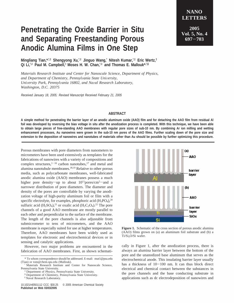
Penetrating the Oxide Barrier in Situand Separating Freestanding PorousAnodic Alumina Films in One StepMingliang Tian,* ,†,‡ Shengyong Xu, †,‡ Jinguo Wang, † Nitesh Kumar, †,‡ Eric Wertz, ‡
Qi Li, †,‡ Paul M. Campbell, | Moses H. W. Chan, †,‡ and Thomas E. Mallouk* ,†,§
Materials Research Institute and Center for Nanoscale Science, Department of Physics,and Department of Chemistry, PennsylVania State UniVersity,UniVersity Park, PennsylVania 16802, and NaVal Research Laboratory,Washington, D.C. 20375
Received January 18, 2005; Revised Manuscript Received February 21, 2005
ABSTRACT
A simple method for penetrating the barrier layer of an anodic aluminum oxide (AAO) film and for detaching the AAO film from residual Alfoil was developed by reversing the bias voltage in situ after the anodization process is completed. With this technique, we have been ableto obtain large pieces of free-standing AAO membranes with regular pore sizes of sub-10 nm. By combining Ar ion milling and wettingenhancement processes, Au nanowires were grown in the sub-10 nm pores of the AAO films. Further scaling down of the pore size andextension to the deposition of nanowires and nanotubes of materials other than Au should be possible by further optimizing this procedure.
Porous membranes with pore diameters from nanometers tomicrometers have been used extensively as templates for thefabrications of nanowires with a variety of compositions andcomplex structures,1-16 carbon nanotubes,17 and metal andalumina nanotubule membranes.18,19Relative to other porousmedia, such as polycarbonate membranes, well-fabricatedanodic alumina oxide (AAO) membranes possess a muchhigher pore densitysup to about 1011pores/cm2sand anarrower distribution of pore diameters. The diameter anddensity of the pores are controllable by varying the anodi-zation voltage of high-purity aluminum foil or film with aspecific electrolyte, for examples, phosphoric acid (H3PO4),20
sulfuric acid (H2SO4),21 or oxalic acid (H2C2O4).22 The porechannels of a good AAO membrane are mostly parallel toeach other and perpendicular to the surface of the membrane.The length of the pore channels is also adjustable fromsubmicrometer to tens of micrometers, and the AAOmembrane is especially suited for use at higher temperatures.Therefore, AAO membranes have been widely used astemplates for electronic and electrochemical devices or insensing and catalytic applications.
However, two major problems are encountered in thefabrication of AAO membranes. First, as shown schemati-
cally in Figure 1, after the anodization process, there isalways an alumina barrier layer between the bottom of thepore and the unanodized base aluminum that serves as theelectrochemical anode. This insulating barrier layer usuallyhas a thickness of 10-100 nm. It can thus block directelectrical and chemical contact between the substances inthe pore channels and the base conducting substrate inapplications such as dc electrodeposition of nanowires and
* To whom correspondence should be addressed. E-mail: [email protected](Tian) or [email protected] (Mallouk).
† Materials Research Institute and Center for Nanoscale Science,Pennsylvania State University.
‡ Department of Physics, Pennsylvania State University.§ Department of Chemistry, Pennsylvania State University.| Naval Research Laboratory.
Figure 1. Schematic of the cross section of porous anodic alumina(AAO) films grown on (a) an aluminum foil substrate and (b) aTi/SixO/Si wafer.
NANOLETTERS
2005Vol. 5, No. 4
697-703
10.1021/nl0501112 CCC: $30.25 © 2005 American Chemical SocietyPublished on Web 03/03/2005
field-emission devices. Second, the anodized AAO layer isfirmly attached to the base aluminum, making it difficult toobtain free-standing AAO membranes for some applications.
A common practice to overcome these problems is to etchaway the base aluminum substrate with saturated HgCl2 andthen etch away the exposed barrier layer with∼6 wt %H3PO4. In another approach, after the AAO film is formedthe bias voltage is progressively stepped down in 5%decrements, causing perforation of the barrier layer.20 Thisis followed by further chemical etching at the AAO/aluminum interface with an acid (H2SO4 or H3PO4) thatdetaches the AAO film from the base aluminum foil. Becauseboth approaches induce isotropic chemical etching of thealumina film, they both inevitably enlarge the pore size. Withthe progressive miniaturization of electronic devices, thereis now a need to study the electrical and structural propertiesin systems of ultrathin nanowires. In this field, large piecesof free-standing AAO films with pore sizes as small as afew nanometers could play an important role if an approachto penetrate the barrier layer without significantly enlargingthe original pore size of the anodized AAO film can bedeveloped.
However, because the free-standing AAO films are fragilewhen their thickness is less than 10µm, it is of great interestto develop methods to fabricate thin AAO film on rigid Sisubstrates for device design,23 thermoelectric,24,25 and fieldemitter26 devices by depositing nanowire or carbon nanotubearrays directly onto these substrates. To realize these devices,the oxide barrier layer of the AAO films must be penetratedin situ. Rabin et al.27 investigated AAO films on Si waferswith a metallic Ti adhesion layer and reported that the oxidebarrier layer could be removed by cathodically biasing thefilm in KCl solution for a few minutes. Thinning of thealumina barrier layer was thought to involve a local increaseof the pH value over 8. However, the Ti adhesion layer wasalso oxidized when the Al layer was fully anodized with0.04 M oxalic acid or 20 vol % H2SO4.27 Electrodepositionin an AAO film on a Si wafer without removing theinsulating barrier layer has also been reported,17,26,28wherethe growth of NWs was achieved by using an ac method orby utilizing the tiny conduction paths that may be embeddedin the alumina barrier layer. In that case, the higher barrierresistance greatly adds to the impedance of nanodevices andthus restricts their applications, such as in field emitters.
In this paper, we demonstrate that penetrating the oxidebarrier layer of an AAO film and detaching the film fromthe base aluminum can be realized in situ in one step byreversing the polarity of the voltage immediately after thecompletion of the anodization process. With this technique,we have routinely obtained large-area free-standing AAOmembranes with an average pore diameter below 10 nm.
Two types of AAO films were prepared by using astandard anodization procedure from (a) 99.999% pure Alfoils (Aldrich, 100 mm× 100 mm× 1 mm) and (b) electron-beam-evaporated Al/Ti double layers on 4 in. thermallyoxidized (100) Si wafers (Al/Ti/SiOx/Si), respectively, asshown schematically in Figure 1. Before anodization, theas-purchased Al foils were mechanically polished and
annealed at 350°C for 6 h. The Al foils were thenelectrochemically polished for 10 min in an electrolytecomposed of 60 vol % H3PO4 and 40 vol % H2SO4 at 75°C, with an electrical current density of 125 mA/cm2. Thesurface of the well-polished Al foil is shiny and mirrorlike.This process is extremely important in making large piecesof high-quality AAO films. For Al/Ti/SiOx/Si samples,because the Al films had a smooth surface, they were directlyanodized without any polishing. Dilute sulfuric acid (3 vol% H2SO4) was chosen as the electrolyte for the anodizationprocess at 0-3 °C. Because the dissolution rate of the AAOfilm in dilute sulfuric acid is negligible near 0°C, this enablesus to obtain small-pore AAO films at a relatively highvoltage, 16-18 V, without causing excessive current flowand heat evolution. A pure Pb or Pt plate was used as theelectrochemical cathode in the experiments.
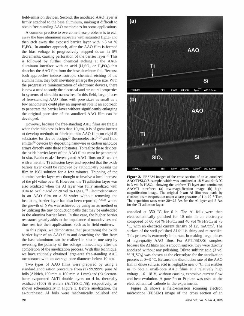
Figure 2a shows a field-emission scanning electronmicroscope (FESEM) image of the cross section of an
Figure 2. FESEM images of the cross section of an as-anodizedAAO/Ti/SixO/Si sample, which was anodized at 18 V and 0-3 °Cin 3 vol % H2SO4, showing the uniform Ti layer and continuousAAO/Ti interface: (a) low-magnification image; (b) high-magnification image. The original 9µm Al film was made byelectron-beam evaporation under a base pressure of 1× 10⁻⁶ Torr.The deposition rates were 20-25 Å/s for the Al layer and 5 Å/sfor the Ti adhesion layer.
698 Nano Lett., Vol. 5, No. 4, 2005
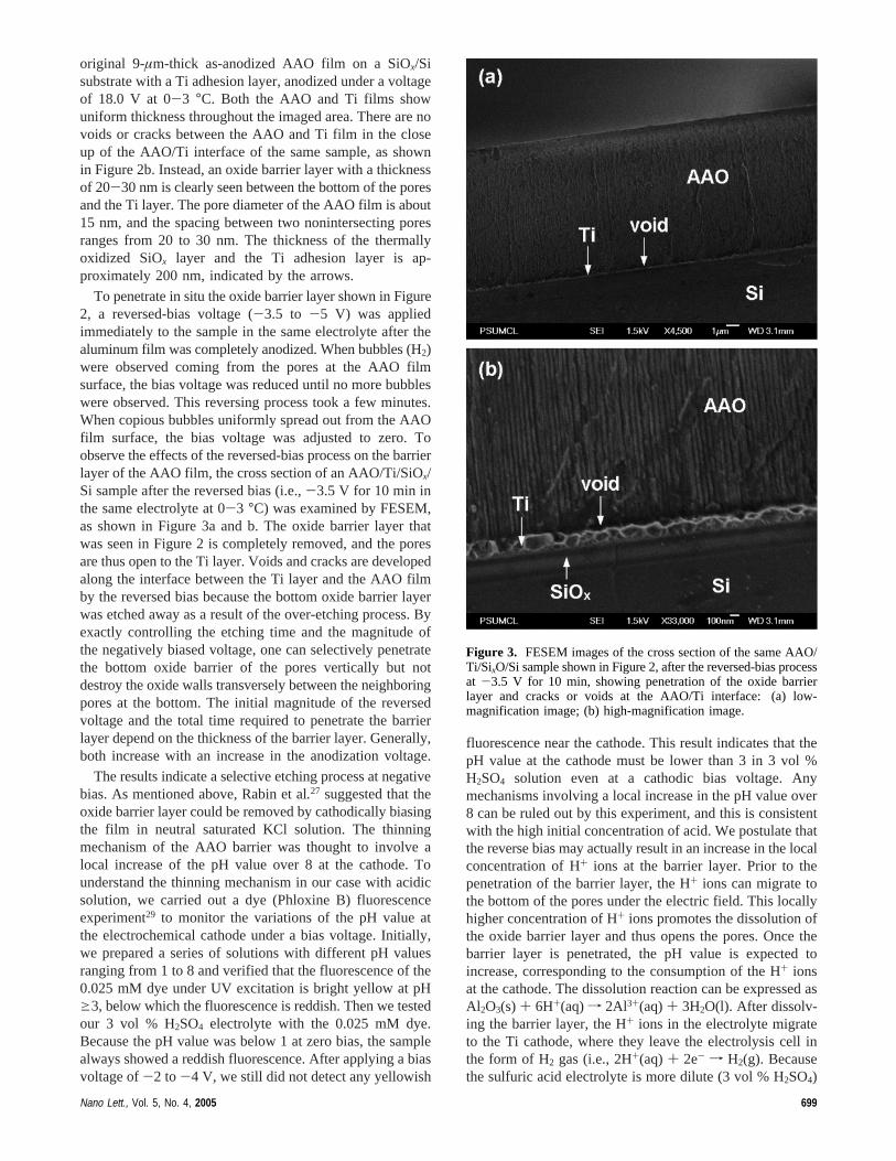
original 9-µm-thick as-anodized AAO film on a SiOx/Sisubstrate with a Ti adhesion layer, anodized under a voltageof 18.0 V at 0-3 °C. Both the AAO and Ti films showuniform thickness throughout the imaged area. There are novoids or cracks between the AAO and Ti film in the closeup of the AAO/Ti interface of the same sample, as shownin Figure 2b. Instead, an oxide barrier layer with a thicknessof 20-30 nm is clearly seen between the bottom of the poresand the Ti layer. The pore diameter of the AAO film is about15 nm, and the spacing between two nonintersecting poresranges from 20 to 30 nm. The thickness of the thermallyoxidized SiOx layer and the Ti adhesion layer is ap-proximately 200 nm, indicated by the arrows.
To penetrate in situ the oxide barrier layer shown in Figure2, a reversed-bias voltage (-3.5 to -5 V) was appliedimmediately to the sample in the same electrolyte after thealuminum film was completely anodized. When bubbles (H2)were observed coming from the pores at the AAO filmsurface, the bias voltage was reduced until no more bubbleswere observed. This reversing process took a few minutes.When copious bubbles uniformly spread out from the AAOfilm surface, the bias voltage was adjusted to zero. Toobserve the effects of the reversed-bias process on the barrierlayer of the AAO film, the cross section of an AAO/Ti/SiOx/Si sample after the reversed bias (i.e.,-3.5 V for 10 min inthe same electrolyte at 0-3 °C) was examined by FESEM,as shown in Figure 3a and b. The oxide barrier layer thatwas seen in Figure 2 is completely removed, and the poresare thus open to the Ti layer. Voids and cracks are developedalong the interface between the Ti layer and the AAO filmby the reversed bias because the bottom oxide barrier layerwas etched away as a result of the over-etching process. Byexactly controlling the etching time and the magnitude ofthe negatively biased voltage, one can selectively penetratethe bottom oxide barrier of the pores vertically but notdestroy the oxide walls transversely between the neighboringpores at the bottom. The initial magnitude of the reversedvoltage and the total time required to penetrate the barrierlayer depend on the thickness of the barrier layer. Generally,both increase with an increase in the anodization voltage.
The results indicate a selective etching process at negativebias. As mentioned above, Rabin et al.27 suggested that theoxide barrier layer could be removed by cathodically biasingthe film in neutral saturated KCl solution. The thinningmechanism of the AAO barrier was thought to involve alocal increase of the pH value over 8 at the cathode. Tounderstand the thinning mechanism in our case with acidicsolution, we carried out a dye (Phloxine B) fluorescenceexperiment29 to monitor the variations of the pH value atthe electrochemical cathode under a bias voltage. Initially,we prepared a series of solutions with different pH valuesranging from 1 to 8 and verified that the fluorescence of the0.025 mM dye under UV excitation is bright yellow at pHg3, below which the fluorescence is reddish. Then we testedour 3 vol % H2SO4 electrolyte with the 0.025 mM dye.Because the pH value was below 1 at zero bias, the samplealways showed a reddish fluorescence. After applying a biasvoltage of-2 to -4 V, we still did not detect any yellowish
fluorescence near the cathode. This result indicates that thepH value at the cathode must be lower than 3 in 3 vol %H2SO4 solution even at a cathodic bias voltage. Anymechanisms involving a local increase in the pH value over8 can be ruled out by this experiment, and this is consistentwith the high initial concentration of acid. We postulate thatthe reverse bias may actually result in an increase in the localconcentration of H+ ions at the barrier layer. Prior to thepenetration of the barrier layer, the H+ ions can migrate tothe bottom of the pores under the electric field. This locallyhigher concentration of H+ ions promotes the dissolution ofthe oxide barrier layer and thus opens the pores. Once thebarrier layer is penetrated, the pH value is expected toincrease, corresponding to the consumption of the H+ ionsat the cathode. The dissolution reaction can be expressed asAl2O3(s) + 6H+(aq)f 2Al3+(aq)+ 3H2O(l). After dissolv-ing the barrier layer, the H+ ions in the electrolyte migrateto the Ti cathode, where they leave the electrolysis cell inthe form of H2 gas (i.e., 2H+(aq) + 2e- f H2(g). Becausethe sulfuric acid electrolyte is more dilute (3 vol % H2SO4)
Figure 3. FESEM images of the cross section of the same AAO/Ti/SixO/Si sample shown in Figure 2, after the reversed-bias processat -3.5 V for 10 min, showing penetration of the oxide barrierlayer and cracks or voids at the AAO/Ti interface: (a) low-magnification image; (b) high-magnification image.
Nano Lett., Vol. 5, No. 4, 2005 699
than that used by Dresselhaus et al.,27 the Ti adhesion layerremains metallic. No column-shaped TiOx structures areobserved in Figure 3, and thus Au nanowires can be directlyelectrodeposited into the pores of the AAO film by using adc voltage with the Ti layer working as the cathode.
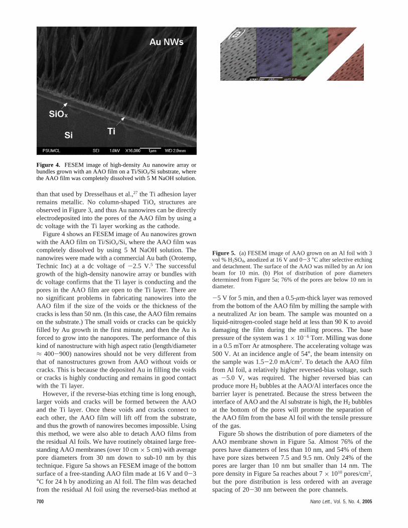
Figure 4 shows an FESEM image of Au nanowires grownwith the AAO film on Ti/SiOx/Si, where the AAO film wascompletely dissolved by using 5 M NaOH solution. Thenanowires were made with a commercial Au bath (Orotemp,Technic Inc) at a dc voltage of-2.5 V.5 The successfulgrowth of the high-density nanowire array or bundles withdc voltage confirms that the Ti layer is conducting and thepores in the AAO film are open to the Ti layer. There areno significant problems in fabricating nanowires into theAAO film if the size of the voids or the thickness of thecracks is less than 50 nm. (In this case, the AAO film remainson the substrate.) The small voids or cracks can be quicklyfilled by Au growth in the first minute, and then the Au isforced to grow into the nanopores. The performance of thiskind of nanostructure with high aspect ratio (length/diameter≈ 400-900) nanowires should not be very different fromthat of nanostructures grown from AAO without voids orcracks. This is because the deposited Au in filling the voidsor cracks is highly conducting and remains in good contactwith the Ti layer.
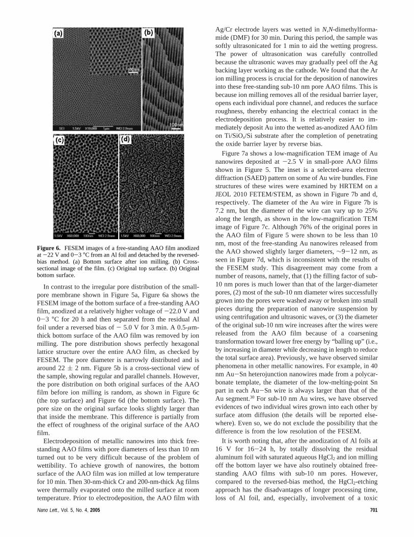
However, if the reverse-bias etching time is long enough,larger voids and cracks will be formed between the AAOand the Ti layer. Once these voids and cracks connect toeach other, the AAO film will lift off from the substrate,and thus the growth of nanowires becomes impossible. Usingthis method, we were also able to detach AAO films fromthe residual Al foils. We have routinely obtained large free-standing AAO membranes (over 10 cm× 5 cm) with averagepore diameters from 30 nm down to sub-10 nm by thistechnique. Figure 5a shows an FESEM image of the bottomsurface of a free-standing AAO film made at 16 V and 0-3°C for 24 h by anodizing an Al foil. The film was detachedfrom the residual Al foil using the reversed-bias method at
-5 V for 5 min, and then a 0.5-µm-thick layer was removedfrom the bottom of the AAO film by milling the sample witha neutralized Ar ion beam. The sample was mounted on aliquid-nitrogen-cooled stage held at less than 90 K to avoiddamaging the film during the milling process. The basepressure of the system was 1× 10⁻⁶ Torr. Milling was donein a 0.5 mTorr Ar atmosphere. The accelerating voltage was500 V. At an incidence angle of 54°, the beam intensity onthe sample was 1.5-2.0 mA/cm2. To detach the AAO filmfrom Al foil, a relatively higher reversed-bias voltage, suchas -5.0 V, was required. The higher reversed bias canproduce more H2 bubbles at the AAO/Al interfaces once thebarrier layer is penetrated. Because the stress between theinterface of AAO and the Al substrate is high, the H2 bubblesat the bottom of the pores will promote the separation ofthe AAO film from the base Al foil with the tensile pressureof the gas.
Figure 5b shows the distribution of pore diameters of theAAO membrane shown in Figure 5a. Almost 76% of thepores have diameters of less than 10 nm, and 54% of themhave pore sizes between 7.5 and 9.5 nm. Only 24% of thepores are larger than 10 nm but smaller than 14 nm. Thepore density in Figure 5a reaches about 7× 10¹⁰ pores/cm2,but the pore distribution is less ordered with an averagespacing of 20-30 nm between the pore channels.
Figure 4. FESEM image of high-density Au nanowire array orbundles grown with an AAO film on a Ti/SiOx/Si substrate, wherethe AAO film was completely dissolved with 5 M NaOH solution.
Figure 5. (a) FESEM image of AAO grown on an Al foil with 3vol % H2SO4, anodized at 16 V and 0-3 °C after selective etchingand detachment. The surface of the AAO was milled by an Ar ionbeam for 10 min. (b) Plot of distribution of pore diametersdetermined from Figure 5a; 76% of the pores are below 10 nm indiameter.
700 Nano Lett., Vol. 5, No. 4, 2005
In contrast to the irregular pore distribution of the small-pore membrane shown in Figure 5a, Figure 6a shows theFESEM image of the bottom surface of a free-standing AAOfilm, anodized at a relatively higher voltage of-22.0 V and0-3 °C for 20 h and then separated from the residual Alfoil under a reversed bias of- 5.0 V for 3 min. A 0.5-µm-thick bottom surface of the AAO film was removed by ionmilling. The pore distribution shows perfectly hexagonallattice structure over the entire AAO film, as checked byFESEM. The pore diameter is narrowly distributed and isaround 22( 2 nm. Figure 5b is a cross-sectional view ofthe sample, showing regular and parallel channels. However,the pore distribution on both original surfaces of the AAOfilm before ion milling is random, as shown in Figure 6c(the top surface) and Figure 6d (the bottom surface). Thepore size on the original surface looks slightly larger thanthat inside the membrane. This difference is partially fromthe effect of roughness of the original surface of the AAOfilm.
Electrodeposition of metallic nanowires into thick free-standing AAO films with pore diameters of less than 10 nmturned out to be very difficult because of the problem ofwettibility. To achieve growth of nanowires, the bottomsurface of the AAO film was ion milled at low temperaturefor 10 min. Then 30-nm-thick Cr and 200-nm-thick Ag filmswere thermally evaporated onto the milled surface at roomtemperature. Prior to electrodeposition, the AAO film with
Ag/Cr electrode layers was wetted inN,N-dimethylforma-mide (DMF) for 30 min. During this period, the sample wassoftly ultrasonicated for 1 min to aid the wetting progress.The power of ultrasonication was carefully controlledbecause the ultrasonic waves may gradually peel off the Agbacking layer working as the cathode. We found that the Arion milling process is crucial for the deposition of nanowiresinto these free-standing sub-10 nm pore AAO films. This isbecause ion milling removes all of the residual barrier layer,opens each individual pore channel, and reduces the surfaceroughness, thereby enhancing the electrical contact in theelectrodeposition process. It is relatively easier to im-mediately deposit Au into the wetted as-anodized AAO filmon Ti/SiOx/Si substrate after the completion of penetratingthe oxide barrier layer by reverse bias.
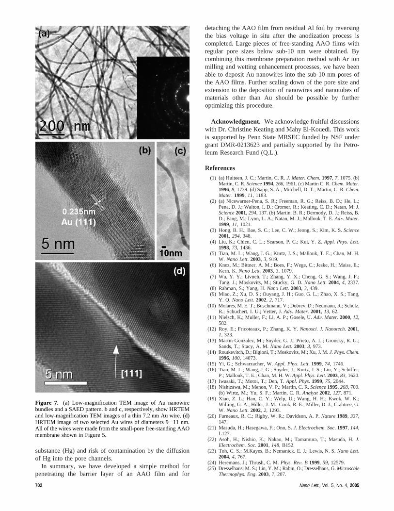
Figure 7a shows a low-magnification TEM image of Aunanowires deposited at-2.5 V in small-pore AAO filmsshown in Figure 5. The inset is a selected-area electrondiffraction (SAED) pattern on some of Au wire bundles. Finestructures of these wires were examined by HRTEM on aJEOL 2010 FETEM/STEM, as shown in Figure 7b and d,respectively. The diameter of the Au wire in Figure 7b is7.2 nm, but the diameter of the wire can vary up to 25%along the length, as shown in the low-magnification TEMimage of Figure 7c. Although 76% of the original pores inthe AAO film of Figure 5 were shown to be less than 10nm, most of the free-standing Au nanowires released fromthe AAO showed slightly larger diameters,∼9-12 nm, asseen in Figure 7d, which is inconsistent with the results ofthe FESEM study. This disagreement may come from anumber of reasons, namely, that (1) the filling factor of sub-10 nm pores is much lower than that of the larger-diameterpores, (2) most of the sub-10 nm diameter wires successfullygrown into the pores were washed away or broken into smallpieces during the preparation of nanowire suspension byusing centrifugation and ultrasonic waves, or (3) the diameterof the original sub-10 nm wire increases after the wires werereleased from the AAO film because of a coarseningtransformation toward lower free energy by “balling up” (i.e.,by increasing in diameter while decreasing in length to reducethe total surface area). Previously, we have observed similarphenomena in other metallic nanowires. For example, in 40nm Au-Sn heterojunction nanowires made from a polycar-bonate template, the diameter of the low-melting-point Snpart in each Au-Sn wire is always larger than that of theAu segment.30 For sub-10 nm Au wires, we have observedevidences of two individual wires grown into each other bysurface atom diffusion (the details will be reported else-where). Even so, we do not exclude the possibility that thedifference is from the low resolution of the FESEM.
It is worth noting that, after the anodization of Al foils at16 V for 16-24 h, by totally dissolving the residualaluminum foil with saturated aqueous HgCl2 and ion millingoff the bottom layer we have also routinely obtained free-standing AAO films with sub-10 nm pores. However,compared to the reversed-bias method, the HgCl2-etchingapproach has the disadvantages of longer processing time,loss of Al foil, and, especially, involvement of a toxic
Figure 6. FESEM images of a free-standing AAO film anodizedat-22 V and 0-3 °C from an Al foil and detached by the reversed-bias method. (a) Bottom surface after ion milling. (b) Cross-sectional image of the film. (c) Original top surface. (b) Originalbottom surface.
Nano Lett., Vol. 5, No. 4, 2005 701
substance (Hg) and risk of contamination by the diffusionof Hg into the pore channels.
In summary, we have developed a simple method forpenetrating the barrier layer of an AAO film and for
detaching the AAO film from residual Al foil by reversingthe bias voltage in situ after the anodization process iscompleted. Large pieces of free-standing AAO films withregular pore sizes below sub-10 nm were obtained. Bycombining this membrane preparation method with Ar ionmilling and wetting enhancement processes, we have beenable to deposit Au nanowires into the sub-10 nm pores ofthe AAO films. Further scaling down of the pore size andextension to the deposition of nanowires and nanotubes ofmaterials other than Au should be possible by furtheroptimizing this procedure.
Acknowledgment. We acknowledge fruitful discussionswith Dr. Christine Keating and Mahy El-Kouedi. This workis supported by Penn State MRSEC funded by NSF undergrant DMR-0213623 and partially supported by the Petro-leum Research Fund (Q.L.).
References
(1) (a) Hulteen, J. C.; Martin, C. R.J. Mater. Chem. 1997, 7, 1075. (b)Martin, C. R.Science1994, 266, 1961. (c) Martin C. R.Chem. Mater.1996, 8, 1739. (d) Sapp, S. A.; Mitchell, D. T.; Martin, C. R.Chem.Mater. 1999, 11, 1183.
(2) (a) Nicewarner-Pena, S. R.; Freeman, R. G.; Reiss, B. D.; He, L.;Pena, D. J.; Walton, I. D.; Cromer, R.; Keating, C. D.; Natan, M. J.Science2001, 294, 137. (b) Martin, B. R.; Dermody, D. J.; Reiss, B.D.; Fang, M.; Lyon, L. A.; Natan, M. J.; Mallouk, T. E.AdV. Mater.1999, 11, 1021.
(3) Hong, B. H.; Bae, S. C.; Lee, C. W.; Jeong, S.; Kim, K. S.Science2001, 294, 348.
(4) Liu, K.; Chien, C. L.; Searson, P. C.; Kui, Y. Z.Appl. Phys. Lett.1998, 73, 1436.
(5) Tian, M. L.; Wang, J. G.; Kurtz, J. S.; Mallouk, T. E.; Chan, M. H.W. Nano Lett. 2003, 3, 919.
(6) Knez, M.; Bittner, A. M.; Boes, F.; Wege, C.; Jeske, H.; Maiss, E.;Kern, K. Nano Lett. 2003, 3, 1079.
(7) Wu, Y. Y.; Livneh, T.; Zhang, Y. X.; Cheng, G. S.; Wang, J. F.;Tang, J.; Moskovits, M.; Stucky, G. D.Nano Lett. 2004, 4, 2337.
(8) Rahman, S.; Yang, H.Nano Lett. 2003, 3, 439.(9) Miao, Z.; Xu, D. S.; Ouyang, J. H.; Guo, G. L.; Zhao, X. S.; Tang,
Y. Q. Nano Lett.2002, 2, 717.(10) Molares, M. E. T.; Buschmann, V.; Dobrev, D.; Neumann, R.; Scholz,
R.; Schuchert, I. U.; Vetter, J.AdV. Mater. 2001, 13, 62.(11) Nielsch, K.; Muller, F.; Li, A. P.; Gosele, U.AdV. Mater. 2000, 12,
582.(12) Roy, E.; Fricoteaux, P.; Zhang, K. Y.Nanosci. J. Nanotech. 2001,
1, 323.(13) Martin-Gonzalez, M.; Snyder, G. J.; Prieto, A. L.; Gronsky, R. G.;
Sands, T.; Stacy, A. M.Nano Lett.2003, 3, 973.(14) Routkevitch, D.; Bigioni, T.; Moskovits, M.; Xu, J. M.J. Phys. Chem.
1996, 100, 14073.(15) Yi, G.; Schwarzacher, W.Appl. Phys. Lett. 1999, 74, 1746.(16) Tian, M. L.; Wang, J. G.; Snyder, J.; Kurtz, J. S.; Liu, Y.; Schiffer,
P.; Mallouk, T. E.; Chan, M. H. W.Appl. Phys. Lett. 2003, 83, 1620.(17) Iwasaki, T.; Motoi, T.; Den, T.Appl. Phys. 1999, 75, 2044.(18) Nishizawa, M.; Menon, V. P.; Martin, C. R.Science1995, 268, 700.
(b) Wirtz, M.; Yu, S. F.; Martin, C. R.Analyst2002, 127, 871.(19) Xiao, Z. L.; Han, C. Y.; Welp, U.; Wang, H. H.; Kwok, W. K.;
Willing, G. A.; Hiller, J. M.; Cook, R. E.; Miller, D. J.; Crabtree, G.W. Nano Lett. 2002, 2, 1293.
(20) Furneaux, R. C.; Rigby, W. R.; Davidson, A. P.Nature1989, 337,147.
(21) Masuda, H.; Hasegawa, F.; Ono, S.J. Electrochem. Soc. 1997, 144,L127.
(22) Asoh, H.; Nishio, K.; Nakao, M.; Tamamura, T.; Masuda, H.J.Electrochem. Soc. 2001, 148, B152.
(23) Toh, C. S.; M.Kayes, B.; Nemanick, E. J.; Lewis, N. S.Nano Lett.2004, 4, 767.
(24) Heremans, J.; Thrush, C. M.Phys. ReV. B 1999, 59, 12579.(25) Dresselhaus, M. S.; Lin, Y. M.; Rabin, O.; Dresselhaus, G.Microscale
Thermophys. Eng. 2003, 7, 207.
Figure 7. (a) Low-magnification TEM image of Au nanowirebundles and a SAED pattern. b and c, respectively, show HRTEMand low-magnification TEM images of a thin 7.2 nm Au wire. (d)HRTEM image of two selected Au wires of diameters 9-11 nm.All of the wires were made from the small-pore free-standing AAOmembrane shown in Figure 5.
702 Nano Lett., Vol. 5, No. 4, 2005
(26) Jeong, S. H.; Hwang, H. Y.; Lee, K. H.; Jeong, Y. S.Appl. Phys.Lett. 2001, 2052.
(27) Rabin, O.; Herz, P. R.; Lin, Y. M.; Akinwande, A. I.; Croniun, S.B.; Dresselhaus, M. S.AdV. Funct. Mater.2003, 13, 631.
(28) Hu, W. C.; Gong, D. W.; Chen, Z.; Yuan, L. M.; Saito, K.; Grimes,C. A.; Kichambare, P.Appl. Phys. Lett.2001, 79, 3083.
(29) Chen, G.; Delafuente, D. A.; Sarangapani, S.; Mallouk, T. E.Catal.Today2001, 67, 341.
(30) Wang, J. G.; Tian, M. L.; Mallouk, T. E.; Chan, M. H. W.NanoLett. 2004, 4, 1313.
NL0501112
Nano Lett., Vol. 5, No. 4, 2005 703
Copyright © 2022 FDOKUMEN