Bending Behaviour of nanochannels in the edges of anodic aluminum oxide membrane
6
Delivered by Ingenta to: Guest User IP : 182.183.174.155 Thu, 06 Sep 2012 18:40:22 ARTICLE Copyright © 2013 by American Scientific Publishers All rights reserved. Printed in the United States of America Advanced Science, Engineering and Medicine Vol. 5, pp. 239–244, 2013 (www.aspbs.com/asem) Bending Behavior of Nanochannels in the Edges of Anodic Aluminum Oxide Membrane Jafar Khan Kasi 1, 2, ∗ , Ajab Khan Kasi 1, 2 , Nitin Afzulpurkar 1 , Erik Bohez 1 , and Amporn Poyai 3 1 School of Engineering and Technology, Asian Institute of Technology, Klong Luang, Pathumthani 12120, Thailand 2 Department of Physics, University of Balochistan, Quetta 87300, Pakistan 3 Thai Microelectronics Center (TMEC), Chachoengsao 24000, Thailand Anodic aluminum oxide (AAO) is one of the important materials use for self-assembly nanoscale fabrication. This paper focuses the study of bending behavior of the nanochannels in AAO membrane. In plane membrane the channels originate from the surface and move inside aluminum perpendicularly, however in edges when these nanochannels come close from two sides change their path and show some bending behavior in spite following their path. One of the main reasons is the forces which move the generation of nanochannels from high pore density to low pore density. The characterization in different conditions and attempts to find the theoretical explanation of the forces which are responsible for such behavior has been made in this research. KEYWORDS: Anodic Aluminum Oxide, Membrane, Nanoporous, Bending, Pore Density, Barrier Layer. 1. INTRODUCTION Alumina is an attractive ceramic use for the fabrication of nanoscale structures. Anodic aluminum oxide provides the non-lithographic techniques which are utilized to fabricate nanostructures. This small scale self-organized fabrication technique was introduced by Kellers and his co-workers 60 year back. 1 In this electrochemical process a natural oxide layer, AAO is formed on the surface of the alu- minum (Al) which increases the thickness. The Al oxide layer consists of close-packed pores, normally hexagonal in shape. First planar AAO membrane was fabricated in 1984 by Itaya et al. in Japan. 2 Kanno et al. reported the regu- lar pore anodic aluminum oxide membrane in 1988. 3 AAO template has extraordinary material characteristics such as thermal and mechanical stabilities, 4–5 controllable pore dimension, 6–7 controllable interpore distances, 8 and easy fabrication procedure. 9 Large area low cost and non-clean room process increases popularity of AAO membrane. 10 New techniques such as nanoimprinting, 11 multiple beam interference lithography, 12 self-assembly, 13 and template- directed growth 14 are excellent contender for fabrication of 3D nanostructures. AAO has extensive applications in various commercial and scientific fields. 15–17 AAO tem- plate are used for sensors, 18 filters, 19–20 photovoltaic, 21 solar cell, 22 magnetic storage, 23 synthesis of carbon nano- tube, 24 nanowires, 25–27 nanorods, 28 capacitors, 29–32 drug ∗ Author to whom correspondence should be addressed. Emails: [email protected], [email protected] Received: 12 June 2012 Accepted: 28 June 2012 separation, 33 hemodialysis, 34–35 photonics, 36 and lithium ion batteries. 37 In 1995 Masuda et al. introduced two step of anodization in which they obtained self-ordered aligned nanopores hexagonal alumina structure for large defect free region. 38 Anodization varies the morphology of the alu- minum surface. The mechanism of the pores formation is not cleared yet, although many models and theories have been developed for the pore formation. Jessensky et al. pro- posed that the expansion of the Al during oxide formation produces repulsive forces between the pores; consequently develop mechanical stress which generate self-organized hexagonal pore arrays. 39 The AAO membrane has the high density of uniform pores which are well aligned perpen- dicular to the surface and penetrate its whole thickness. 40 The pore diameters can easily be controlled from few nanometers to several hundred nanometers by the anodiza- tion condition. 41–43 Similarly the pore density can also be varied by changing the electrolytic solution use for anodization. Two step of mild anodization (MA) provided more regularity to the hexagonal structure of the pores. Lee et al. enhanced the anodization rate by hard anodiza- tion (HA) in 2006. 44 The drawback of the HA was burn- ing and cracks at the surface of alumina. 45 To solve the cracking problem a new method, pulse anodization (PA) was developed by combining the properties of conven- tional MA and HA, using sulfuric acid (H 2 SO 4 or oxalic acid (H 2 C 2 O 4 as electrolytes. 46 In PA a low potential pulse follow by a high potential pulse are applied peri- odically to achieve MA and HA conditions continuously. AAO has also been used for making three dimensional (3D) objects such as rectangular, triangular, pentagonal, Adv. Sci. Eng. Med. 2013, Vol. 5, No. 3 2164-6627/2013/5/239/006 doi:10.1166/asem.2013.1252 239
-
Upload
instiutebiochemistrybalcohistanquettapakistan -
Category
Documents
-
view
0 -
download
0
Transcript of Bending Behaviour of nanochannels in the edges of anodic aluminum oxide membrane
Delivered by Ingenta toGuest User
IP 182183174155Thu 06 Sep 2012 184022 A
RTIC
LECopyright copy 2013 by American Scientific Publishers
All rights reserved
Printed in the United States of America
Advanced ScienceEngineering and MedicineVol 5 pp 239ndash244 2013(wwwaspbscomasem)
Bending Behavior of Nanochannels in theEdges of Anodic Aluminum Oxide MembraneJafar Khan Kasi1 2lowast Ajab Khan Kasi1 2 Nitin Afzulpurkar1 Erik Bohez1 and Amporn Poyai3
1School of Engineering and Technology Asian Institute of Technology Klong Luang Pathumthani 12120 Thailand2Department of Physics University of Balochistan Quetta 87300 Pakistan3Thai Microelectronics Center (TMEC) Chachoengsao 24000 Thailand
Anodic aluminum oxide (AAO) is one of the important materials use for self-assembly nanoscale fabricationThis paper focuses the study of bending behavior of the nanochannels in AAO membrane In plane membranethe channels originate from the surface and move inside aluminum perpendicularly however in edges whenthese nanochannels come close from two sides change their path and show some bending behavior in spitefollowing their path One of the main reasons is the forces which move the generation of nanochannels fromhigh pore density to low pore density The characterization in different conditions and attempts to find thetheoretical explanation of the forces which are responsible for such behavior has been made in this research
KEYWORDS Anodic Aluminum Oxide Membrane Nanoporous Bending Pore Density Barrier Layer
1 INTRODUCTION
Alumina is an attractive ceramic use for the fabrication ofnanoscale structures Anodic aluminum oxide provides thenon-lithographic techniques which are utilized to fabricatenanostructures This small scale self-organized fabricationtechnique was introduced by Kellers and his co-workers60 year back1 In this electrochemical process a naturaloxide layer AAO is formed on the surface of the alu-minum (Al) which increases the thickness The Al oxidelayer consists of close-packed pores normally hexagonal inshape First planar AAO membrane was fabricated in 1984by Itaya et al in Japan2 Kanno et al reported the regu-lar pore anodic aluminum oxide membrane in 19883 AAOtemplate has extraordinary material characteristics suchas thermal and mechanical stabilities4ndash5 controllable poredimension6ndash7 controllable interpore distances8 and easyfabrication procedure9 Large area low cost and non-cleanroom process increases popularity of AAO membrane10
New techniques such as nanoimprinting11 multiple beaminterference lithography12 self-assembly13 and template-directed growth14 are excellent contender for fabricationof 3D nanostructures AAO has extensive applications invarious commercial and scientific fields15ndash17 AAO tem-plate are used for sensors18 filters19ndash20 photovoltaic21
solar cell22 magnetic storage23 synthesis of carbon nano-tube24 nanowires25ndash27 nanorods28 capacitors29ndash32 drug
lowastAuthor to whom correspondence should be addressedEmails jafarkhankasigmailcom JafarKhanKasiaitasiaReceived 12 June 2012Accepted 28 June 2012
separation33 hemodialysis34ndash35 photonics36 and lithiumion batteries37 In 1995 Masuda et al introduced two stepof anodization in which they obtained self-ordered alignednanopores hexagonal alumina structure for large defect freeregion38 Anodization varies the morphology of the alu-minum surface The mechanism of the pores formation isnot cleared yet although many models and theories havebeen developed for the pore formation Jessensky et al pro-posed that the expansion of the Al during oxide formationproduces repulsive forces between the pores consequentlydevelop mechanical stress which generate self-organizedhexagonal pore arrays39 The AAO membrane has the highdensity of uniform pores which are well aligned perpen-dicular to the surface and penetrate its whole thickness40
The pore diameters can easily be controlled from fewnanometers to several hundred nanometers by the anodiza-tion condition41ndash43 Similarly the pore density can alsobe varied by changing the electrolytic solution use foranodization Two step of mild anodization (MA) providedmore regularity to the hexagonal structure of the poresLee et al enhanced the anodization rate by hard anodiza-tion (HA) in 200644 The drawback of the HA was burn-ing and cracks at the surface of alumina45 To solve thecracking problem a new method pulse anodization (PA)was developed by combining the properties of conven-tional MA and HA using sulfuric acid (H2SO4 or oxalicacid (H2C2O4 as electrolytes46 In PA a low potentialpulse follow by a high potential pulse are applied peri-odically to achieve MA and HA conditions continuouslyAAO has also been used for making three dimensional(3D) objects such as rectangular triangular pentagonal
Adv Sci Eng Med 2013 Vol 5 No 3 2164-662720135239006 doi101166asem20131252 239
Delivered by Ingenta toGuest User
IP 182183174155Thu 06 Sep 2012 184022
Bending Behavior of Nanochannels in the Edges of Anodic Aluminum Oxide Membrane Kasi et al
ARTIC
LEtubular conical cone and bowl shapes47ndash48 Kasi et alintroduced a new method in which cracks were utilized tomake tubular and rectangular membranes49 Here in thisresearch we focus on the behavior of the nanochannelNormally channels originate barrier layer (BL) from thesurface of aluminum instantly after applying voltage andmoving into the depth of aluminum following the pathperpendicular to the surface In our experiment initiallythe channels were aligned but when reached to the cornerwhere they close to each other from two sides despite ter-minated they moved towards the other surface changing itsoriginal path This unique behavior of nanochannels havebeen analyzed on the bases of forces and electric currentconductivity of the Al sample
2 EXPERIMENTAL DETAILS
21 Materials
Aluminum sheet of 9956 purity from lsquoThe NilacoCorporationrsquo Japan was used as the starting materialAl sheets with dimension 1 mmtimes 3 mmtimes 10 mm wereused for the fabrication of planar membrane Prior toanodizing samples were degreased in acetone and rinsedin deionized water
22 Fabrication of Anodic AluminumPorous Membrane
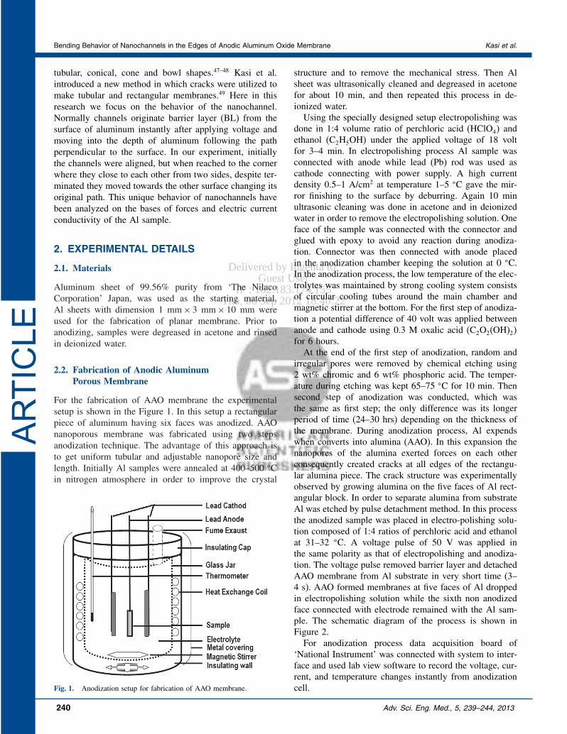
For the fabrication of AAO membrane the experimentalsetup is shown in the Figure 1 In this setup a rectangularpiece of aluminum having six faces was anodized AAOnanoporous membrane was fabricated using two stepsanodization technique The advantage of this approach isto get uniform tubular and adjustable nanopore size andlength Initially Al samples were annealed at 400ndash500 Cin nitrogen atmosphere in order to improve the crystal
Fig 1 Anodization setup for fabrication of AAO membrane
structure and to remove the mechanical stress Then Alsheet was ultrasonically cleaned and degreased in acetonefor about 10 min and then repeated this process in de-ionized waterUsing the specially designed setup electropolishing was
done in 14 volume ratio of perchloric acid (HClO4 andethanol (C2H5OH) under the applied voltage of 18 voltfor 3ndash4 min In electropolishing process Al sample wasconnected with anode while lead (Pb) rod was used ascathode connecting with power supply A high currentdensity 05ndash1 Acm2 at temperature 1ndash5 C gave the mir-ror finishing to the surface by deburring Again 10 minultrasonic cleaning was done in acetone and in deionizedwater in order to remove the electropolishing solution Oneface of the sample was connected with the connector andglued with epoxy to avoid any reaction during anodiza-tion Connector was then connected with anode placedin the anodization chamber keeping the solution at 0 CIn the anodization process the low temperature of the elec-trolytes was maintained by strong cooling system consistsof circular cooling tubes around the main chamber andmagnetic stirrer at the bottom For the first step of anodiza-tion a potential difference of 40 volt was applied betweenanode and cathode using 03 M oxalic acid (C2O2(OH)2for 6 hoursAt the end of the first step of anodization random and
irregular pores were removed by chemical etching using2 wt chromic and 6 wt phosphoric acid The temper-ature during etching was kept 65ndash75 C for 10 min Thensecond step of anodization was conducted which wasthe same as first step the only difference was its longerperiod of time (24ndash30 hrs) depending on the thickness ofthe membrane During anodization process Al expendswhen converts into alumina (AAO) In this expansion thenanopores of the alumina exerted forces on each otherconsequently created cracks at all edges of the rectangu-lar alumina piece The crack structure was experimentallyobserved by growing alumina on the five faces of Al rect-angular block In order to separate alumina from substrateAl was etched by pulse detachment method In this processthe anodized sample was placed in electro-polishing solu-tion composed of 14 ratios of perchloric acid and ethanolat 31ndash32 C A voltage pulse of 50 V was applied inthe same polarity as that of electropolishing and anodiza-tion The voltage pulse removed barrier layer and detachedAAO membrane from Al substrate in very short time (3ndash4 s) AAO formed membranes at five faces of Al droppedin electropolishing solution while the sixth non anodizedface connected with electrode remained with the Al sam-ple The schematic diagram of the process is shown inFigure 2For anodization process data acquisition board of
lsquoNational Instrumentrsquo was connected with system to inter-face and used lab view software to record the voltage cur-rent and temperature changes instantly from anodizationcell
240 Adv Sci Eng Med 5 239ndash244 2013
Delivered by Ingenta toGuest User
IP 182183174155Thu 06 Sep 2012 184022
Kasi et al Bending Behavior of Nanochannels in the Edges of Anodic Aluminum Oxide Membrane
ARTIC
LE
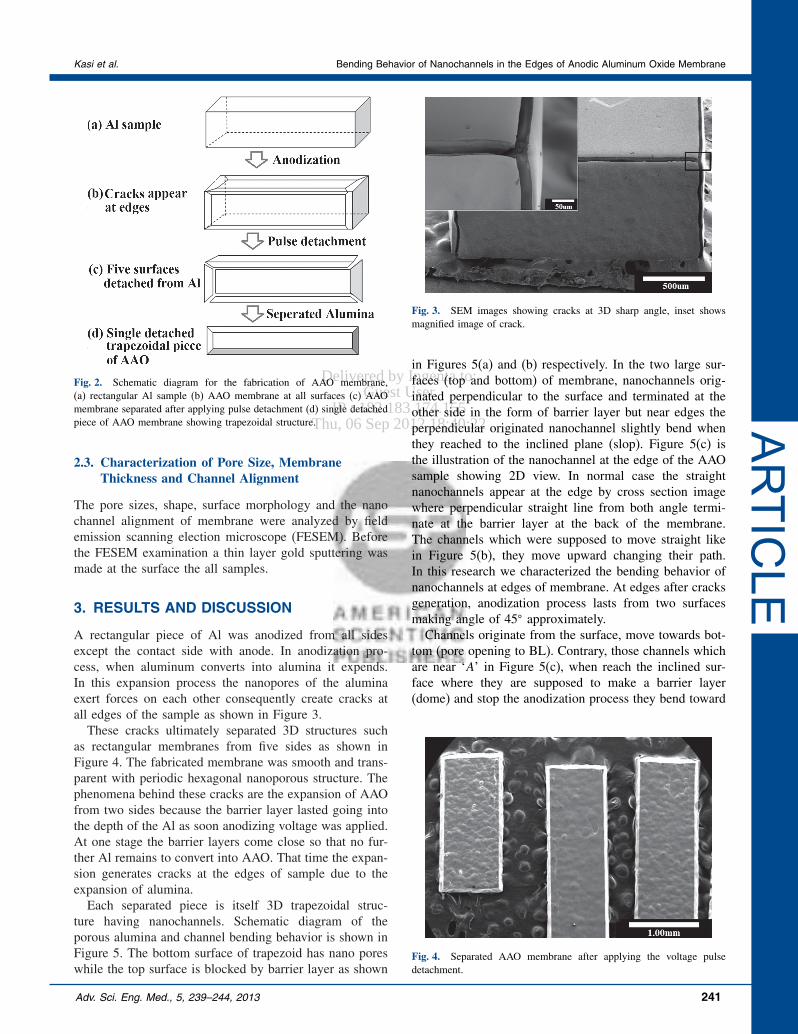
Fig 2 Schematic diagram for the fabrication of AAO membrane(a) rectangular Al sample (b) AAO membrane at all surfaces (c) AAOmembrane separated after applying pulse detachment (d) single detachedpiece of AAO membrane showing trapezoidal structure
23 Characterization of Pore Size MembraneThickness and Channel Alignment
The pore sizes shape surface morphology and the nanochannel alignment of membrane were analyzed by fieldemission scanning election microscope (FESEM) Beforethe FESEM examination a thin layer gold sputtering wasmade at the surface the all samples
3 RESULTS AND DISCUSSION
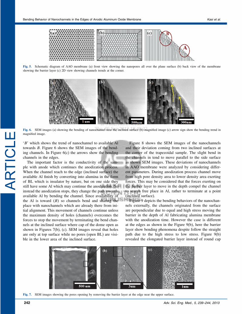
A rectangular piece of Al was anodized from all sidesexcept the contact side with anode In anodization pro-cess when aluminum converts into alumina it expendsIn this expansion process the nanopores of the aluminaexert forces on each other consequently create cracks atall edges of the sample as shown in Figure 3These cracks ultimately separated 3D structures such
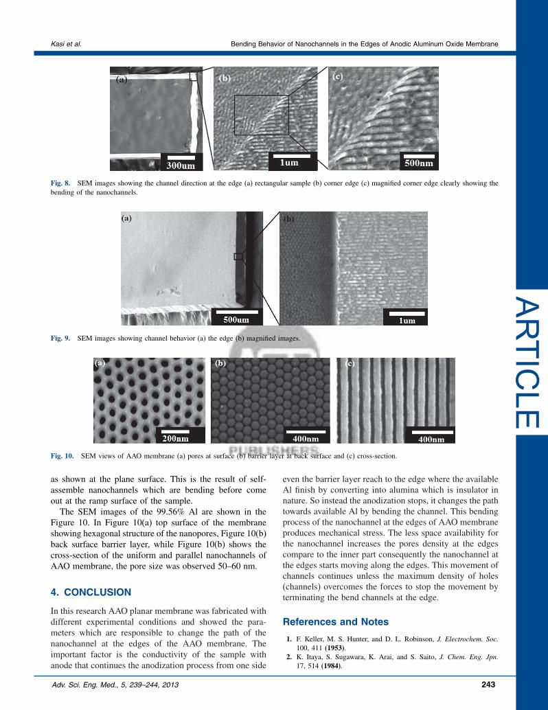
as rectangular membranes from five sides as shown inFigure 4 The fabricated membrane was smooth and trans-parent with periodic hexagonal nanoporous structure Thephenomena behind these cracks are the expansion of AAOfrom two sides because the barrier layer lasted going intothe depth of the Al as soon anodizing voltage was appliedAt one stage the barrier layers come close so that no fur-ther Al remains to convert into AAO That time the expan-sion generates cracks at the edges of sample due to theexpansion of aluminaEach separated piece is itself 3D trapezoidal struc-
ture having nanochannels Schematic diagram of theporous alumina and channel bending behavior is shown inFigure 5 The bottom surface of trapezoid has nano poreswhile the top surface is blocked by barrier layer as shown
Fig 3 SEM images showing cracks at 3D sharp angle inset showsmagnified image of crack
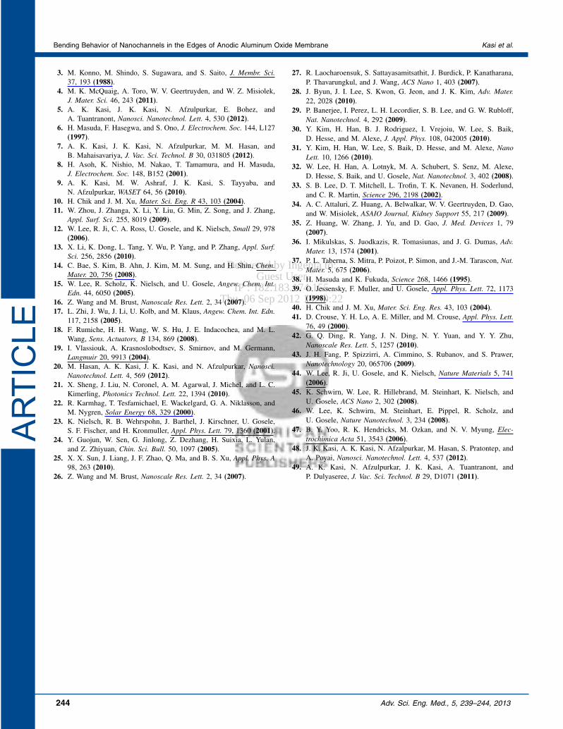
in Figures 5(a) and (b) respectively In the two large sur-faces (top and bottom) of membrane nanochannels orig-inated perpendicular to the surface and terminated at theother side in the form of barrier layer but near edges theperpendicular originated nanochannel slightly bend whenthey reached to the inclined plane (slop) Figure 5(c) isthe illustration of the nanochannel at the edge of the AAOsample showing 2D view In normal case the straightnanochannels appear at the edge by cross section imagewhere perpendicular straight line from both angle termi-nate at the barrier layer at the back of the membraneThe channels which were supposed to move straight likein Figure 5(b) they move upward changing their pathIn this research we characterized the bending behavior ofnanochannels at edges of membrane At edges after cracksgeneration anodization process lasts from two surfacesmaking angle of 45 approximatelyChannels originate from the surface move towards bot-
tom (pore opening to BL) Contrary those channels whichare near lsquoArsquo in Figure 5(c) when reach the inclined sur-face where they are supposed to make a barrier layer(dome) and stop the anodization process they bend toward
Fig 4 Separated AAO membrane after applying the voltage pulsedetachment
Adv Sci Eng Med 5 239ndash244 2013 241
Delivered by Ingenta toGuest User
IP 182183174155Thu 06 Sep 2012 184022
Bending Behavior of Nanochannels in the Edges of Anodic Aluminum Oxide Membrane Kasi et al
ARTIC
LE
Fig 5 Schematic diagram of AAO membrane (a) front view showing the nanopores all over the plane surface (b) back view of the membraneshowing the barrier layer (c) 2D view showing channels trends at the corner
Fig 6 SEM images (a) showing the bending of nanochannel near the inclined surface (b) magnified image (c) arrow sign show the bending trend inmagnified image
lsquoBrsquo which shows the trend of nanochannel to available Altowards B Figure 6 shows the SEM images of the bend-ing channels In Figure 6(c) the arrows show the bendingchannels in the edgesThe important factor is the conductivity of the sam-
ple with anode which continues the anodization processWhen the channel reach to the edge (inclined surface) theavailable Al finish by converting into alumina in the formof BL which is insulator by nature but on one side theystill have some Al which may continue the anodization Soinstead the anodization stops they change the path towardsavailable Al by bending the channel Since availability ofthe Al is toward B so channels bend and sharing theplace with nanochannels which are already there from ini-tial alignment This movement of channels continue unlessthe maximum density of holes (channels) overcomes theforces to stop the movement by terminating the bend chan-nels at the inclined surface where cap of the dome open asshown in Figures 7(b) (c) SEM images reveal that holesare only at top surface while no pores (open BL) are visi-ble in the lower area of the inclined surface
Fig 7 SEM images showing the pores opening by removing the barrier layer at the edge near the upper surface
Figure 8 shows the SEM images of the nanochannelsand their deviation coming from two inclined surfaces atthe corner of the trapezoidal sample The slight bend inthe channels in tend to move parallel to the side surfaceas shown SEM images These deviations of nanochannelsin AAO membrane were analyzed by considering differ-ent parameters During anodization process channel movefrom high pore density area to lower density area exertingforces This may be considered that the forces exerting onthe barrier layer to move in the depth compel the channelto search free place in Al rather to terminate at a point(inclined surface)Figure 9 depicts the bending behaviors of the nanochan-
nels externally the channels originated from the surfaceare perpendicular due to equal and high stress moving thebarrier in the depth of Al fabricating alumina membranewith the anodization time However the case is differentat the edges as shown in the Figure 9(b) here the barrierlayer show bending phenomena despite follow the straightpath due to the high stress to low stress Figure 9(b)revealed the elongated barrier layer instead of round cap
242 Adv Sci Eng Med 5 239ndash244 2013
Delivered by Ingenta toGuest User
IP 182183174155Thu 06 Sep 2012 184022
Kasi et al Bending Behavior of Nanochannels in the Edges of Anodic Aluminum Oxide Membrane
ARTIC
LE
Fig 8 SEM images showing the channel direction at the edge (a) rectangular sample (b) corner edge (c) magnified corner edge clearly showing thebending of the nanochannels
Fig 9 SEM images showing channel behavior (a) the edge (b) magnified images
Fig 10 SEM views of AAO membrane (a) pores at surface (b) barrier layer at back surface and (c) cross-section
as shown at the plane surface This is the result of self-assemble nanochannels which are bending before comeout at the ramp surface of the sampleThe SEM images of the 9956 Al are shown in the
Figure 10 In Figure 10(a) top surface of the membraneshowing hexagonal structure of the nanopores Figure 10(b)back surface barrier layer while Figure 10(b) shows thecross-section of the uniform and parallel nanochannels ofAAO membrane the pore size was observed 50ndash60 nm
4 CONCLUSION
In this research AAO planar membrane was fabricated withdifferent experimental conditions and showed the para-meters which are responsible to change the path of thenanochannel at the edges of the AAO membrane Theimportant factor is the conductivity of the sample withanode that continues the anodization process from one side
even the barrier layer reach to the edge where the availableAl finish by converting into alumina which is insulator innature So instead the anodization stops it changes the pathtowards available Al by bending the channel This bendingprocess of the nanochannel at the edges of AAO membraneproduces mechanical stress The less space availability forthe nanochannel increases the pores density at the edgescompare to the inner part consequently the nanochannel atthe edges starts moving along the edges This movement ofchannels continues unless the maximum density of holes(channels) overcomes the forces to stop the movement byterminating the bend channels at the edge
References and Notes
1 F Keller M S Hunter and D L Robinson J Electrochem Soc100 411 (1953)
2 K Itaya S Sugawara K Arai and S Saito J Chem Eng Jpn17 514 (1984)
Adv Sci Eng Med 5 239ndash244 2013 243
Delivered by Ingenta toGuest User
IP 182183174155Thu 06 Sep 2012 184022
Bending Behavior of Nanochannels in the Edges of Anodic Aluminum Oxide Membrane Kasi et al
ARTIC
LE3 M Konno M Shindo S Sugawara and S Saito J Membr Sci
37 193 (1988)4 M K McQuaig A Toro W V Geertruyden and W Z Misiolek
J Mater Sci 46 243 (2011)5 A K Kasi J K Kasi N Afzulpurkar E Bohez and
A Tuantranont Nanosci Nanotechnol Lett 4 530 (2012)6 H Masuda F Hasegwa and S Ono J Electrochem Soc 144 L127
(1997)7 A K Kasi J K Kasi N Afzulpurkar M M Hasan and
B Mahaisavariya J Vac Sci Technol B 30 031805 (2012)8 H Asoh K Nishio M Nakao T Tamamura and H Masuda
J Electrochem Soc 148 B152 (2001)9 A K Kasi M W Ashraf J K Kasi S Tayyaba and
N Afzulpurkar WASET 64 56 (2010)10 H Chik and J M Xu Mater Sci Eng R 43 103 (2004)11 W Zhou J Zhanga X Li Y Liu G Min Z Song and J Zhang
Appl Surf Sci 255 8019 (2009)12 W Lee R Ji C A Ross U Gosele and K Nielsch Small 29 978
(2006)13 X Li K Dong L Tang Y Wu P Yang and P Zhang Appl Surf
Sci 256 2856 (2010)14 C Bae S Kim B Ahn J Kim M M Sung and H Shin Chem
Mater 20 756 (2008)15 W Lee R Scholz K Nielsch and U Gosele Angew Chem Int
Edn 44 6050 (2005)16 Z Wang and M Brust Nanoscale Res Lett 2 34 (2007)17 L Zhi J Wu J Li U Kolb and M Klaus Angew Chem Int Edn
117 2158 (2005)18 F Rumiche H H Wang W S Hu J E Indacochea and M L
Wang Sens Actuators B 134 869 (2008)19 I Vlassiouk A Krasnoslobodtsev S Smirnov and M Germann
Langmuir 20 9913 (2004)20 M Hasan A K Kasi J K Kasi and N Afzulpurkar Nanosci
Nanotechnol Lett 4 569 (2012)21 X Sheng J Liu N Coronel A M Agarwal J Michel and L C
Kimerling Photonics Technol Lett 22 1394 (2010)22 R Karmhag T Tesfamichael E Wackelgard G A Niklasson and
M Nygren Solar Energy 68 329 (2000)23 K Nielsch R B Wehrspohn J Barthel J Kirschner U Gosele
S F Fischer and H Kronmuller Appl Phys Lett 79 1360 (2001)24 Y Guojun W Sen G Jinlong Z Dezhang H Suixia L Yulan
and Z Zhiyuan Chin Sci Bull 50 1097 (2005)25 X X Sun J Liang J F Zhao Q Ma and B S Xu Appl Phys A
98 263 (2010)26 Z Wang and M Brust Nanoscale Res Lett 2 34 (2007)
27 R Laocharoensuk S Sattayasamitsathit J Burdick P KanatharanaP Thavarungkul and J Wang ACS Nano 1 403 (2007)
28 J Byun J I Lee S Kwon G Jeon and J K Kim Adv Mater22 2028 (2010)
29 P Banerjee I Perez L H Lecordier S B Lee and G W RubloffNat Nanotechnol 4 292 (2009)
30 Y Kim H Han B J Rodriguez I Vrejoiu W Lee S BaikD Hesse and M Alexe J Appl Phys 108 042005 (2010)
31 Y Kim H Han W Lee S Baik D Hesse and M Alexe NanoLett 10 1266 (2010)
32 W Lee H Han A Lotnyk M A Schubert S Senz M AlexeD Hesse S Baik and U Gosele Nat Nanotechnol 3 402 (2008)
33 S B Lee D T Mitchell L Trofin T K Nevanen H Soderlundand C R Martin Science 296 2198 (2002)
34 A C Attaluri Z Huang A Belwalkar W V Geertruyden D Gaoand W Misiolek ASAIO Journal Kidney Support 55 217 (2009)
35 Z Huang W Zhang J Yu and D Gao J Med Devices 1 79(2007)
36 I Mikulskas S Juodkazis R Tomasiunas and J G Dumas AdvMater 13 1574 (2001)
37 P L Taberna S Mitra P Poizot P Simon and J-M Tarascon NatMater 5 675 (2006)
38 H Masuda and K Fukuda Science 268 1466 (1995)39 O Jessensky F Muller and U Gosele Appl Phys Lett 72 1173
(1998)40 H Chik and J M Xu Mater Sci Eng Res 43 103 (2004)41 D Crouse Y H Lo A E Miller and M Crouse Appl Phys Lett
76 49 (2000)42 G Q Ding R Yang J N Ding N Y Yuan and Y Y Zhu
Nanoscale Res Lett 5 1257 (2010)43 J H Fang P Spizzirri A Cimmino S Rubanov and S Prawer
Nanotechnology 20 065706 (2009)44 W Lee R Ji U Gosele and K Nielsch Nature Materials 5 741
(2006)45 K Schwirn W Lee R Hillebrand M Steinhart K Nielsch and
U Gosele ACS Nano 2 302 (2008)46 W Lee K Schwirn M Steinhart E Pippel R Scholz and
U Gosele Nature Nanotechnol 3 234 (2008)47 B Y Yoo R K Hendricks M Ozkan and N V Myung Elec-
trochimica Acta 51 3543 (2006)48 J K Kasi A K Kasi N Afzalpurkar M Hasan S Pratontep and
A Poyai Nanosci Nanotechnol Lett 4 537 (2012)49 A K Kasi N Afzulpurkar J K Kasi A Tuantranont and
P Dulyaseree J Vac Sci Technol B 29 D1071 (2011)
244 Adv Sci Eng Med 5 239ndash244 2013
Delivered by Ingenta toGuest User
IP 182183174155Thu 06 Sep 2012 184022
Bending Behavior of Nanochannels in the Edges of Anodic Aluminum Oxide Membrane Kasi et al
ARTIC
LEtubular conical cone and bowl shapes47ndash48 Kasi et alintroduced a new method in which cracks were utilized tomake tubular and rectangular membranes49 Here in thisresearch we focus on the behavior of the nanochannelNormally channels originate barrier layer (BL) from thesurface of aluminum instantly after applying voltage andmoving into the depth of aluminum following the pathperpendicular to the surface In our experiment initiallythe channels were aligned but when reached to the cornerwhere they close to each other from two sides despite ter-minated they moved towards the other surface changing itsoriginal path This unique behavior of nanochannels havebeen analyzed on the bases of forces and electric currentconductivity of the Al sample
2 EXPERIMENTAL DETAILS
21 Materials
Aluminum sheet of 9956 purity from lsquoThe NilacoCorporationrsquo Japan was used as the starting materialAl sheets with dimension 1 mmtimes 3 mmtimes 10 mm wereused for the fabrication of planar membrane Prior toanodizing samples were degreased in acetone and rinsedin deionized water
22 Fabrication of Anodic AluminumPorous Membrane
For the fabrication of AAO membrane the experimentalsetup is shown in the Figure 1 In this setup a rectangularpiece of aluminum having six faces was anodized AAOnanoporous membrane was fabricated using two stepsanodization technique The advantage of this approach isto get uniform tubular and adjustable nanopore size andlength Initially Al samples were annealed at 400ndash500 Cin nitrogen atmosphere in order to improve the crystal
Fig 1 Anodization setup for fabrication of AAO membrane
structure and to remove the mechanical stress Then Alsheet was ultrasonically cleaned and degreased in acetonefor about 10 min and then repeated this process in de-ionized waterUsing the specially designed setup electropolishing was
done in 14 volume ratio of perchloric acid (HClO4 andethanol (C2H5OH) under the applied voltage of 18 voltfor 3ndash4 min In electropolishing process Al sample wasconnected with anode while lead (Pb) rod was used ascathode connecting with power supply A high currentdensity 05ndash1 Acm2 at temperature 1ndash5 C gave the mir-ror finishing to the surface by deburring Again 10 minultrasonic cleaning was done in acetone and in deionizedwater in order to remove the electropolishing solution Oneface of the sample was connected with the connector andglued with epoxy to avoid any reaction during anodiza-tion Connector was then connected with anode placedin the anodization chamber keeping the solution at 0 CIn the anodization process the low temperature of the elec-trolytes was maintained by strong cooling system consistsof circular cooling tubes around the main chamber andmagnetic stirrer at the bottom For the first step of anodiza-tion a potential difference of 40 volt was applied betweenanode and cathode using 03 M oxalic acid (C2O2(OH)2for 6 hoursAt the end of the first step of anodization random and
irregular pores were removed by chemical etching using2 wt chromic and 6 wt phosphoric acid The temper-ature during etching was kept 65ndash75 C for 10 min Thensecond step of anodization was conducted which wasthe same as first step the only difference was its longerperiod of time (24ndash30 hrs) depending on the thickness ofthe membrane During anodization process Al expendswhen converts into alumina (AAO) In this expansion thenanopores of the alumina exerted forces on each otherconsequently created cracks at all edges of the rectangu-lar alumina piece The crack structure was experimentallyobserved by growing alumina on the five faces of Al rect-angular block In order to separate alumina from substrateAl was etched by pulse detachment method In this processthe anodized sample was placed in electro-polishing solu-tion composed of 14 ratios of perchloric acid and ethanolat 31ndash32 C A voltage pulse of 50 V was applied inthe same polarity as that of electropolishing and anodiza-tion The voltage pulse removed barrier layer and detachedAAO membrane from Al substrate in very short time (3ndash4 s) AAO formed membranes at five faces of Al droppedin electropolishing solution while the sixth non anodizedface connected with electrode remained with the Al sam-ple The schematic diagram of the process is shown inFigure 2For anodization process data acquisition board of
lsquoNational Instrumentrsquo was connected with system to inter-face and used lab view software to record the voltage cur-rent and temperature changes instantly from anodizationcell
240 Adv Sci Eng Med 5 239ndash244 2013
Delivered by Ingenta toGuest User
IP 182183174155Thu 06 Sep 2012 184022
Kasi et al Bending Behavior of Nanochannels in the Edges of Anodic Aluminum Oxide Membrane
ARTIC
LE
Fig 2 Schematic diagram for the fabrication of AAO membrane(a) rectangular Al sample (b) AAO membrane at all surfaces (c) AAOmembrane separated after applying pulse detachment (d) single detachedpiece of AAO membrane showing trapezoidal structure
23 Characterization of Pore Size MembraneThickness and Channel Alignment
The pore sizes shape surface morphology and the nanochannel alignment of membrane were analyzed by fieldemission scanning election microscope (FESEM) Beforethe FESEM examination a thin layer gold sputtering wasmade at the surface the all samples
3 RESULTS AND DISCUSSION
A rectangular piece of Al was anodized from all sidesexcept the contact side with anode In anodization pro-cess when aluminum converts into alumina it expendsIn this expansion process the nanopores of the aluminaexert forces on each other consequently create cracks atall edges of the sample as shown in Figure 3These cracks ultimately separated 3D structures such
as rectangular membranes from five sides as shown inFigure 4 The fabricated membrane was smooth and trans-parent with periodic hexagonal nanoporous structure Thephenomena behind these cracks are the expansion of AAOfrom two sides because the barrier layer lasted going intothe depth of the Al as soon anodizing voltage was appliedAt one stage the barrier layers come close so that no fur-ther Al remains to convert into AAO That time the expan-sion generates cracks at the edges of sample due to theexpansion of aluminaEach separated piece is itself 3D trapezoidal struc-
ture having nanochannels Schematic diagram of theporous alumina and channel bending behavior is shown inFigure 5 The bottom surface of trapezoid has nano poreswhile the top surface is blocked by barrier layer as shown
Fig 3 SEM images showing cracks at 3D sharp angle inset showsmagnified image of crack
in Figures 5(a) and (b) respectively In the two large sur-faces (top and bottom) of membrane nanochannels orig-inated perpendicular to the surface and terminated at theother side in the form of barrier layer but near edges theperpendicular originated nanochannel slightly bend whenthey reached to the inclined plane (slop) Figure 5(c) isthe illustration of the nanochannel at the edge of the AAOsample showing 2D view In normal case the straightnanochannels appear at the edge by cross section imagewhere perpendicular straight line from both angle termi-nate at the barrier layer at the back of the membraneThe channels which were supposed to move straight likein Figure 5(b) they move upward changing their pathIn this research we characterized the bending behavior ofnanochannels at edges of membrane At edges after cracksgeneration anodization process lasts from two surfacesmaking angle of 45 approximatelyChannels originate from the surface move towards bot-
tom (pore opening to BL) Contrary those channels whichare near lsquoArsquo in Figure 5(c) when reach the inclined sur-face where they are supposed to make a barrier layer(dome) and stop the anodization process they bend toward
Fig 4 Separated AAO membrane after applying the voltage pulsedetachment
Adv Sci Eng Med 5 239ndash244 2013 241
Delivered by Ingenta toGuest User
IP 182183174155Thu 06 Sep 2012 184022
Bending Behavior of Nanochannels in the Edges of Anodic Aluminum Oxide Membrane Kasi et al
ARTIC
LE
Fig 5 Schematic diagram of AAO membrane (a) front view showing the nanopores all over the plane surface (b) back view of the membraneshowing the barrier layer (c) 2D view showing channels trends at the corner
Fig 6 SEM images (a) showing the bending of nanochannel near the inclined surface (b) magnified image (c) arrow sign show the bending trend inmagnified image
lsquoBrsquo which shows the trend of nanochannel to available Altowards B Figure 6 shows the SEM images of the bend-ing channels In Figure 6(c) the arrows show the bendingchannels in the edgesThe important factor is the conductivity of the sam-
ple with anode which continues the anodization processWhen the channel reach to the edge (inclined surface) theavailable Al finish by converting into alumina in the formof BL which is insulator by nature but on one side theystill have some Al which may continue the anodization Soinstead the anodization stops they change the path towardsavailable Al by bending the channel Since availability ofthe Al is toward B so channels bend and sharing theplace with nanochannels which are already there from ini-tial alignment This movement of channels continue unlessthe maximum density of holes (channels) overcomes theforces to stop the movement by terminating the bend chan-nels at the inclined surface where cap of the dome open asshown in Figures 7(b) (c) SEM images reveal that holesare only at top surface while no pores (open BL) are visi-ble in the lower area of the inclined surface
Fig 7 SEM images showing the pores opening by removing the barrier layer at the edge near the upper surface
Figure 8 shows the SEM images of the nanochannelsand their deviation coming from two inclined surfaces atthe corner of the trapezoidal sample The slight bend inthe channels in tend to move parallel to the side surfaceas shown SEM images These deviations of nanochannelsin AAO membrane were analyzed by considering differ-ent parameters During anodization process channel movefrom high pore density area to lower density area exertingforces This may be considered that the forces exerting onthe barrier layer to move in the depth compel the channelto search free place in Al rather to terminate at a point(inclined surface)Figure 9 depicts the bending behaviors of the nanochan-
nels externally the channels originated from the surfaceare perpendicular due to equal and high stress moving thebarrier in the depth of Al fabricating alumina membranewith the anodization time However the case is differentat the edges as shown in the Figure 9(b) here the barrierlayer show bending phenomena despite follow the straightpath due to the high stress to low stress Figure 9(b)revealed the elongated barrier layer instead of round cap
242 Adv Sci Eng Med 5 239ndash244 2013
Delivered by Ingenta toGuest User
IP 182183174155Thu 06 Sep 2012 184022
Kasi et al Bending Behavior of Nanochannels in the Edges of Anodic Aluminum Oxide Membrane
ARTIC
LE
Fig 8 SEM images showing the channel direction at the edge (a) rectangular sample (b) corner edge (c) magnified corner edge clearly showing thebending of the nanochannels
Fig 9 SEM images showing channel behavior (a) the edge (b) magnified images
Fig 10 SEM views of AAO membrane (a) pores at surface (b) barrier layer at back surface and (c) cross-section
as shown at the plane surface This is the result of self-assemble nanochannels which are bending before comeout at the ramp surface of the sampleThe SEM images of the 9956 Al are shown in the
Figure 10 In Figure 10(a) top surface of the membraneshowing hexagonal structure of the nanopores Figure 10(b)back surface barrier layer while Figure 10(b) shows thecross-section of the uniform and parallel nanochannels ofAAO membrane the pore size was observed 50ndash60 nm
4 CONCLUSION
In this research AAO planar membrane was fabricated withdifferent experimental conditions and showed the para-meters which are responsible to change the path of thenanochannel at the edges of the AAO membrane Theimportant factor is the conductivity of the sample withanode that continues the anodization process from one side
even the barrier layer reach to the edge where the availableAl finish by converting into alumina which is insulator innature So instead the anodization stops it changes the pathtowards available Al by bending the channel This bendingprocess of the nanochannel at the edges of AAO membraneproduces mechanical stress The less space availability forthe nanochannel increases the pores density at the edgescompare to the inner part consequently the nanochannel atthe edges starts moving along the edges This movement ofchannels continues unless the maximum density of holes(channels) overcomes the forces to stop the movement byterminating the bend channels at the edge
References and Notes
1 F Keller M S Hunter and D L Robinson J Electrochem Soc100 411 (1953)
2 K Itaya S Sugawara K Arai and S Saito J Chem Eng Jpn17 514 (1984)
Adv Sci Eng Med 5 239ndash244 2013 243
Delivered by Ingenta toGuest User
IP 182183174155Thu 06 Sep 2012 184022
Bending Behavior of Nanochannels in the Edges of Anodic Aluminum Oxide Membrane Kasi et al
ARTIC
LE3 M Konno M Shindo S Sugawara and S Saito J Membr Sci
37 193 (1988)4 M K McQuaig A Toro W V Geertruyden and W Z Misiolek
J Mater Sci 46 243 (2011)5 A K Kasi J K Kasi N Afzulpurkar E Bohez and
A Tuantranont Nanosci Nanotechnol Lett 4 530 (2012)6 H Masuda F Hasegwa and S Ono J Electrochem Soc 144 L127
(1997)7 A K Kasi J K Kasi N Afzulpurkar M M Hasan and
B Mahaisavariya J Vac Sci Technol B 30 031805 (2012)8 H Asoh K Nishio M Nakao T Tamamura and H Masuda
J Electrochem Soc 148 B152 (2001)9 A K Kasi M W Ashraf J K Kasi S Tayyaba and
N Afzulpurkar WASET 64 56 (2010)10 H Chik and J M Xu Mater Sci Eng R 43 103 (2004)11 W Zhou J Zhanga X Li Y Liu G Min Z Song and J Zhang
Appl Surf Sci 255 8019 (2009)12 W Lee R Ji C A Ross U Gosele and K Nielsch Small 29 978
(2006)13 X Li K Dong L Tang Y Wu P Yang and P Zhang Appl Surf
Sci 256 2856 (2010)14 C Bae S Kim B Ahn J Kim M M Sung and H Shin Chem
Mater 20 756 (2008)15 W Lee R Scholz K Nielsch and U Gosele Angew Chem Int
Edn 44 6050 (2005)16 Z Wang and M Brust Nanoscale Res Lett 2 34 (2007)17 L Zhi J Wu J Li U Kolb and M Klaus Angew Chem Int Edn
117 2158 (2005)18 F Rumiche H H Wang W S Hu J E Indacochea and M L
Wang Sens Actuators B 134 869 (2008)19 I Vlassiouk A Krasnoslobodtsev S Smirnov and M Germann
Langmuir 20 9913 (2004)20 M Hasan A K Kasi J K Kasi and N Afzulpurkar Nanosci
Nanotechnol Lett 4 569 (2012)21 X Sheng J Liu N Coronel A M Agarwal J Michel and L C
Kimerling Photonics Technol Lett 22 1394 (2010)22 R Karmhag T Tesfamichael E Wackelgard G A Niklasson and
M Nygren Solar Energy 68 329 (2000)23 K Nielsch R B Wehrspohn J Barthel J Kirschner U Gosele
S F Fischer and H Kronmuller Appl Phys Lett 79 1360 (2001)24 Y Guojun W Sen G Jinlong Z Dezhang H Suixia L Yulan
and Z Zhiyuan Chin Sci Bull 50 1097 (2005)25 X X Sun J Liang J F Zhao Q Ma and B S Xu Appl Phys A
98 263 (2010)26 Z Wang and M Brust Nanoscale Res Lett 2 34 (2007)
27 R Laocharoensuk S Sattayasamitsathit J Burdick P KanatharanaP Thavarungkul and J Wang ACS Nano 1 403 (2007)
28 J Byun J I Lee S Kwon G Jeon and J K Kim Adv Mater22 2028 (2010)
29 P Banerjee I Perez L H Lecordier S B Lee and G W RubloffNat Nanotechnol 4 292 (2009)
30 Y Kim H Han B J Rodriguez I Vrejoiu W Lee S BaikD Hesse and M Alexe J Appl Phys 108 042005 (2010)
31 Y Kim H Han W Lee S Baik D Hesse and M Alexe NanoLett 10 1266 (2010)
32 W Lee H Han A Lotnyk M A Schubert S Senz M AlexeD Hesse S Baik and U Gosele Nat Nanotechnol 3 402 (2008)
33 S B Lee D T Mitchell L Trofin T K Nevanen H Soderlundand C R Martin Science 296 2198 (2002)
34 A C Attaluri Z Huang A Belwalkar W V Geertruyden D Gaoand W Misiolek ASAIO Journal Kidney Support 55 217 (2009)
35 Z Huang W Zhang J Yu and D Gao J Med Devices 1 79(2007)
36 I Mikulskas S Juodkazis R Tomasiunas and J G Dumas AdvMater 13 1574 (2001)
37 P L Taberna S Mitra P Poizot P Simon and J-M Tarascon NatMater 5 675 (2006)
38 H Masuda and K Fukuda Science 268 1466 (1995)39 O Jessensky F Muller and U Gosele Appl Phys Lett 72 1173
(1998)40 H Chik and J M Xu Mater Sci Eng Res 43 103 (2004)41 D Crouse Y H Lo A E Miller and M Crouse Appl Phys Lett
76 49 (2000)42 G Q Ding R Yang J N Ding N Y Yuan and Y Y Zhu
Nanoscale Res Lett 5 1257 (2010)43 J H Fang P Spizzirri A Cimmino S Rubanov and S Prawer
Nanotechnology 20 065706 (2009)44 W Lee R Ji U Gosele and K Nielsch Nature Materials 5 741
(2006)45 K Schwirn W Lee R Hillebrand M Steinhart K Nielsch and
U Gosele ACS Nano 2 302 (2008)46 W Lee K Schwirn M Steinhart E Pippel R Scholz and
U Gosele Nature Nanotechnol 3 234 (2008)47 B Y Yoo R K Hendricks M Ozkan and N V Myung Elec-
trochimica Acta 51 3543 (2006)48 J K Kasi A K Kasi N Afzalpurkar M Hasan S Pratontep and
A Poyai Nanosci Nanotechnol Lett 4 537 (2012)49 A K Kasi N Afzulpurkar J K Kasi A Tuantranont and
P Dulyaseree J Vac Sci Technol B 29 D1071 (2011)
244 Adv Sci Eng Med 5 239ndash244 2013
Delivered by Ingenta toGuest User
IP 182183174155Thu 06 Sep 2012 184022
Kasi et al Bending Behavior of Nanochannels in the Edges of Anodic Aluminum Oxide Membrane
ARTIC
LE
Fig 2 Schematic diagram for the fabrication of AAO membrane(a) rectangular Al sample (b) AAO membrane at all surfaces (c) AAOmembrane separated after applying pulse detachment (d) single detachedpiece of AAO membrane showing trapezoidal structure
23 Characterization of Pore Size MembraneThickness and Channel Alignment
The pore sizes shape surface morphology and the nanochannel alignment of membrane were analyzed by fieldemission scanning election microscope (FESEM) Beforethe FESEM examination a thin layer gold sputtering wasmade at the surface the all samples
3 RESULTS AND DISCUSSION
A rectangular piece of Al was anodized from all sidesexcept the contact side with anode In anodization pro-cess when aluminum converts into alumina it expendsIn this expansion process the nanopores of the aluminaexert forces on each other consequently create cracks atall edges of the sample as shown in Figure 3These cracks ultimately separated 3D structures such
as rectangular membranes from five sides as shown inFigure 4 The fabricated membrane was smooth and trans-parent with periodic hexagonal nanoporous structure Thephenomena behind these cracks are the expansion of AAOfrom two sides because the barrier layer lasted going intothe depth of the Al as soon anodizing voltage was appliedAt one stage the barrier layers come close so that no fur-ther Al remains to convert into AAO That time the expan-sion generates cracks at the edges of sample due to theexpansion of aluminaEach separated piece is itself 3D trapezoidal struc-
ture having nanochannels Schematic diagram of theporous alumina and channel bending behavior is shown inFigure 5 The bottom surface of trapezoid has nano poreswhile the top surface is blocked by barrier layer as shown
Fig 3 SEM images showing cracks at 3D sharp angle inset showsmagnified image of crack
in Figures 5(a) and (b) respectively In the two large sur-faces (top and bottom) of membrane nanochannels orig-inated perpendicular to the surface and terminated at theother side in the form of barrier layer but near edges theperpendicular originated nanochannel slightly bend whenthey reached to the inclined plane (slop) Figure 5(c) isthe illustration of the nanochannel at the edge of the AAOsample showing 2D view In normal case the straightnanochannels appear at the edge by cross section imagewhere perpendicular straight line from both angle termi-nate at the barrier layer at the back of the membraneThe channels which were supposed to move straight likein Figure 5(b) they move upward changing their pathIn this research we characterized the bending behavior ofnanochannels at edges of membrane At edges after cracksgeneration anodization process lasts from two surfacesmaking angle of 45 approximatelyChannels originate from the surface move towards bot-
tom (pore opening to BL) Contrary those channels whichare near lsquoArsquo in Figure 5(c) when reach the inclined sur-face where they are supposed to make a barrier layer(dome) and stop the anodization process they bend toward
Fig 4 Separated AAO membrane after applying the voltage pulsedetachment
Adv Sci Eng Med 5 239ndash244 2013 241
Delivered by Ingenta toGuest User
IP 182183174155Thu 06 Sep 2012 184022
Bending Behavior of Nanochannels in the Edges of Anodic Aluminum Oxide Membrane Kasi et al
ARTIC
LE
Fig 5 Schematic diagram of AAO membrane (a) front view showing the nanopores all over the plane surface (b) back view of the membraneshowing the barrier layer (c) 2D view showing channels trends at the corner
Fig 6 SEM images (a) showing the bending of nanochannel near the inclined surface (b) magnified image (c) arrow sign show the bending trend inmagnified image
lsquoBrsquo which shows the trend of nanochannel to available Altowards B Figure 6 shows the SEM images of the bend-ing channels In Figure 6(c) the arrows show the bendingchannels in the edgesThe important factor is the conductivity of the sam-
ple with anode which continues the anodization processWhen the channel reach to the edge (inclined surface) theavailable Al finish by converting into alumina in the formof BL which is insulator by nature but on one side theystill have some Al which may continue the anodization Soinstead the anodization stops they change the path towardsavailable Al by bending the channel Since availability ofthe Al is toward B so channels bend and sharing theplace with nanochannels which are already there from ini-tial alignment This movement of channels continue unlessthe maximum density of holes (channels) overcomes theforces to stop the movement by terminating the bend chan-nels at the inclined surface where cap of the dome open asshown in Figures 7(b) (c) SEM images reveal that holesare only at top surface while no pores (open BL) are visi-ble in the lower area of the inclined surface
Fig 7 SEM images showing the pores opening by removing the barrier layer at the edge near the upper surface
Figure 8 shows the SEM images of the nanochannelsand their deviation coming from two inclined surfaces atthe corner of the trapezoidal sample The slight bend inthe channels in tend to move parallel to the side surfaceas shown SEM images These deviations of nanochannelsin AAO membrane were analyzed by considering differ-ent parameters During anodization process channel movefrom high pore density area to lower density area exertingforces This may be considered that the forces exerting onthe barrier layer to move in the depth compel the channelto search free place in Al rather to terminate at a point(inclined surface)Figure 9 depicts the bending behaviors of the nanochan-
nels externally the channels originated from the surfaceare perpendicular due to equal and high stress moving thebarrier in the depth of Al fabricating alumina membranewith the anodization time However the case is differentat the edges as shown in the Figure 9(b) here the barrierlayer show bending phenomena despite follow the straightpath due to the high stress to low stress Figure 9(b)revealed the elongated barrier layer instead of round cap
242 Adv Sci Eng Med 5 239ndash244 2013
Delivered by Ingenta toGuest User
IP 182183174155Thu 06 Sep 2012 184022
Kasi et al Bending Behavior of Nanochannels in the Edges of Anodic Aluminum Oxide Membrane
ARTIC
LE
Fig 8 SEM images showing the channel direction at the edge (a) rectangular sample (b) corner edge (c) magnified corner edge clearly showing thebending of the nanochannels
Fig 9 SEM images showing channel behavior (a) the edge (b) magnified images
Fig 10 SEM views of AAO membrane (a) pores at surface (b) barrier layer at back surface and (c) cross-section
as shown at the plane surface This is the result of self-assemble nanochannels which are bending before comeout at the ramp surface of the sampleThe SEM images of the 9956 Al are shown in the
Figure 10 In Figure 10(a) top surface of the membraneshowing hexagonal structure of the nanopores Figure 10(b)back surface barrier layer while Figure 10(b) shows thecross-section of the uniform and parallel nanochannels ofAAO membrane the pore size was observed 50ndash60 nm
4 CONCLUSION
In this research AAO planar membrane was fabricated withdifferent experimental conditions and showed the para-meters which are responsible to change the path of thenanochannel at the edges of the AAO membrane Theimportant factor is the conductivity of the sample withanode that continues the anodization process from one side
even the barrier layer reach to the edge where the availableAl finish by converting into alumina which is insulator innature So instead the anodization stops it changes the pathtowards available Al by bending the channel This bendingprocess of the nanochannel at the edges of AAO membraneproduces mechanical stress The less space availability forthe nanochannel increases the pores density at the edgescompare to the inner part consequently the nanochannel atthe edges starts moving along the edges This movement ofchannels continues unless the maximum density of holes(channels) overcomes the forces to stop the movement byterminating the bend channels at the edge
References and Notes
1 F Keller M S Hunter and D L Robinson J Electrochem Soc100 411 (1953)
2 K Itaya S Sugawara K Arai and S Saito J Chem Eng Jpn17 514 (1984)
Adv Sci Eng Med 5 239ndash244 2013 243
Delivered by Ingenta toGuest User
IP 182183174155Thu 06 Sep 2012 184022
Bending Behavior of Nanochannels in the Edges of Anodic Aluminum Oxide Membrane Kasi et al
ARTIC
LE3 M Konno M Shindo S Sugawara and S Saito J Membr Sci
37 193 (1988)4 M K McQuaig A Toro W V Geertruyden and W Z Misiolek
J Mater Sci 46 243 (2011)5 A K Kasi J K Kasi N Afzulpurkar E Bohez and
A Tuantranont Nanosci Nanotechnol Lett 4 530 (2012)6 H Masuda F Hasegwa and S Ono J Electrochem Soc 144 L127
(1997)7 A K Kasi J K Kasi N Afzulpurkar M M Hasan and
B Mahaisavariya J Vac Sci Technol B 30 031805 (2012)8 H Asoh K Nishio M Nakao T Tamamura and H Masuda
J Electrochem Soc 148 B152 (2001)9 A K Kasi M W Ashraf J K Kasi S Tayyaba and
N Afzulpurkar WASET 64 56 (2010)10 H Chik and J M Xu Mater Sci Eng R 43 103 (2004)11 W Zhou J Zhanga X Li Y Liu G Min Z Song and J Zhang
Appl Surf Sci 255 8019 (2009)12 W Lee R Ji C A Ross U Gosele and K Nielsch Small 29 978
(2006)13 X Li K Dong L Tang Y Wu P Yang and P Zhang Appl Surf
Sci 256 2856 (2010)14 C Bae S Kim B Ahn J Kim M M Sung and H Shin Chem
Mater 20 756 (2008)15 W Lee R Scholz K Nielsch and U Gosele Angew Chem Int
Edn 44 6050 (2005)16 Z Wang and M Brust Nanoscale Res Lett 2 34 (2007)17 L Zhi J Wu J Li U Kolb and M Klaus Angew Chem Int Edn
117 2158 (2005)18 F Rumiche H H Wang W S Hu J E Indacochea and M L
Wang Sens Actuators B 134 869 (2008)19 I Vlassiouk A Krasnoslobodtsev S Smirnov and M Germann
Langmuir 20 9913 (2004)20 M Hasan A K Kasi J K Kasi and N Afzulpurkar Nanosci
Nanotechnol Lett 4 569 (2012)21 X Sheng J Liu N Coronel A M Agarwal J Michel and L C
Kimerling Photonics Technol Lett 22 1394 (2010)22 R Karmhag T Tesfamichael E Wackelgard G A Niklasson and
M Nygren Solar Energy 68 329 (2000)23 K Nielsch R B Wehrspohn J Barthel J Kirschner U Gosele
S F Fischer and H Kronmuller Appl Phys Lett 79 1360 (2001)24 Y Guojun W Sen G Jinlong Z Dezhang H Suixia L Yulan
and Z Zhiyuan Chin Sci Bull 50 1097 (2005)25 X X Sun J Liang J F Zhao Q Ma and B S Xu Appl Phys A
98 263 (2010)26 Z Wang and M Brust Nanoscale Res Lett 2 34 (2007)
27 R Laocharoensuk S Sattayasamitsathit J Burdick P KanatharanaP Thavarungkul and J Wang ACS Nano 1 403 (2007)
28 J Byun J I Lee S Kwon G Jeon and J K Kim Adv Mater22 2028 (2010)
29 P Banerjee I Perez L H Lecordier S B Lee and G W RubloffNat Nanotechnol 4 292 (2009)
30 Y Kim H Han B J Rodriguez I Vrejoiu W Lee S BaikD Hesse and M Alexe J Appl Phys 108 042005 (2010)
31 Y Kim H Han W Lee S Baik D Hesse and M Alexe NanoLett 10 1266 (2010)
32 W Lee H Han A Lotnyk M A Schubert S Senz M AlexeD Hesse S Baik and U Gosele Nat Nanotechnol 3 402 (2008)
33 S B Lee D T Mitchell L Trofin T K Nevanen H Soderlundand C R Martin Science 296 2198 (2002)
34 A C Attaluri Z Huang A Belwalkar W V Geertruyden D Gaoand W Misiolek ASAIO Journal Kidney Support 55 217 (2009)
35 Z Huang W Zhang J Yu and D Gao J Med Devices 1 79(2007)
36 I Mikulskas S Juodkazis R Tomasiunas and J G Dumas AdvMater 13 1574 (2001)
37 P L Taberna S Mitra P Poizot P Simon and J-M Tarascon NatMater 5 675 (2006)
38 H Masuda and K Fukuda Science 268 1466 (1995)39 O Jessensky F Muller and U Gosele Appl Phys Lett 72 1173
(1998)40 H Chik and J M Xu Mater Sci Eng Res 43 103 (2004)41 D Crouse Y H Lo A E Miller and M Crouse Appl Phys Lett
76 49 (2000)42 G Q Ding R Yang J N Ding N Y Yuan and Y Y Zhu
Nanoscale Res Lett 5 1257 (2010)43 J H Fang P Spizzirri A Cimmino S Rubanov and S Prawer
Nanotechnology 20 065706 (2009)44 W Lee R Ji U Gosele and K Nielsch Nature Materials 5 741
(2006)45 K Schwirn W Lee R Hillebrand M Steinhart K Nielsch and
U Gosele ACS Nano 2 302 (2008)46 W Lee K Schwirn M Steinhart E Pippel R Scholz and
U Gosele Nature Nanotechnol 3 234 (2008)47 B Y Yoo R K Hendricks M Ozkan and N V Myung Elec-
trochimica Acta 51 3543 (2006)48 J K Kasi A K Kasi N Afzalpurkar M Hasan S Pratontep and
A Poyai Nanosci Nanotechnol Lett 4 537 (2012)49 A K Kasi N Afzulpurkar J K Kasi A Tuantranont and
P Dulyaseree J Vac Sci Technol B 29 D1071 (2011)
244 Adv Sci Eng Med 5 239ndash244 2013
Delivered by Ingenta toGuest User
IP 182183174155Thu 06 Sep 2012 184022
Bending Behavior of Nanochannels in the Edges of Anodic Aluminum Oxide Membrane Kasi et al
ARTIC
LE
Fig 5 Schematic diagram of AAO membrane (a) front view showing the nanopores all over the plane surface (b) back view of the membraneshowing the barrier layer (c) 2D view showing channels trends at the corner
Fig 6 SEM images (a) showing the bending of nanochannel near the inclined surface (b) magnified image (c) arrow sign show the bending trend inmagnified image
lsquoBrsquo which shows the trend of nanochannel to available Altowards B Figure 6 shows the SEM images of the bend-ing channels In Figure 6(c) the arrows show the bendingchannels in the edgesThe important factor is the conductivity of the sam-
ple with anode which continues the anodization processWhen the channel reach to the edge (inclined surface) theavailable Al finish by converting into alumina in the formof BL which is insulator by nature but on one side theystill have some Al which may continue the anodization Soinstead the anodization stops they change the path towardsavailable Al by bending the channel Since availability ofthe Al is toward B so channels bend and sharing theplace with nanochannels which are already there from ini-tial alignment This movement of channels continue unlessthe maximum density of holes (channels) overcomes theforces to stop the movement by terminating the bend chan-nels at the inclined surface where cap of the dome open asshown in Figures 7(b) (c) SEM images reveal that holesare only at top surface while no pores (open BL) are visi-ble in the lower area of the inclined surface
Fig 7 SEM images showing the pores opening by removing the barrier layer at the edge near the upper surface
Figure 8 shows the SEM images of the nanochannelsand their deviation coming from two inclined surfaces atthe corner of the trapezoidal sample The slight bend inthe channels in tend to move parallel to the side surfaceas shown SEM images These deviations of nanochannelsin AAO membrane were analyzed by considering differ-ent parameters During anodization process channel movefrom high pore density area to lower density area exertingforces This may be considered that the forces exerting onthe barrier layer to move in the depth compel the channelto search free place in Al rather to terminate at a point(inclined surface)Figure 9 depicts the bending behaviors of the nanochan-
nels externally the channels originated from the surfaceare perpendicular due to equal and high stress moving thebarrier in the depth of Al fabricating alumina membranewith the anodization time However the case is differentat the edges as shown in the Figure 9(b) here the barrierlayer show bending phenomena despite follow the straightpath due to the high stress to low stress Figure 9(b)revealed the elongated barrier layer instead of round cap
242 Adv Sci Eng Med 5 239ndash244 2013
Delivered by Ingenta toGuest User
IP 182183174155Thu 06 Sep 2012 184022
Kasi et al Bending Behavior of Nanochannels in the Edges of Anodic Aluminum Oxide Membrane
ARTIC
LE
Fig 8 SEM images showing the channel direction at the edge (a) rectangular sample (b) corner edge (c) magnified corner edge clearly showing thebending of the nanochannels
Fig 9 SEM images showing channel behavior (a) the edge (b) magnified images
Fig 10 SEM views of AAO membrane (a) pores at surface (b) barrier layer at back surface and (c) cross-section
as shown at the plane surface This is the result of self-assemble nanochannels which are bending before comeout at the ramp surface of the sampleThe SEM images of the 9956 Al are shown in the
Figure 10 In Figure 10(a) top surface of the membraneshowing hexagonal structure of the nanopores Figure 10(b)back surface barrier layer while Figure 10(b) shows thecross-section of the uniform and parallel nanochannels ofAAO membrane the pore size was observed 50ndash60 nm
4 CONCLUSION
In this research AAO planar membrane was fabricated withdifferent experimental conditions and showed the para-meters which are responsible to change the path of thenanochannel at the edges of the AAO membrane Theimportant factor is the conductivity of the sample withanode that continues the anodization process from one side
even the barrier layer reach to the edge where the availableAl finish by converting into alumina which is insulator innature So instead the anodization stops it changes the pathtowards available Al by bending the channel This bendingprocess of the nanochannel at the edges of AAO membraneproduces mechanical stress The less space availability forthe nanochannel increases the pores density at the edgescompare to the inner part consequently the nanochannel atthe edges starts moving along the edges This movement ofchannels continues unless the maximum density of holes(channels) overcomes the forces to stop the movement byterminating the bend channels at the edge
References and Notes
1 F Keller M S Hunter and D L Robinson J Electrochem Soc100 411 (1953)
2 K Itaya S Sugawara K Arai and S Saito J Chem Eng Jpn17 514 (1984)
Adv Sci Eng Med 5 239ndash244 2013 243
Delivered by Ingenta toGuest User
IP 182183174155Thu 06 Sep 2012 184022
Bending Behavior of Nanochannels in the Edges of Anodic Aluminum Oxide Membrane Kasi et al
ARTIC
LE3 M Konno M Shindo S Sugawara and S Saito J Membr Sci
37 193 (1988)4 M K McQuaig A Toro W V Geertruyden and W Z Misiolek
J Mater Sci 46 243 (2011)5 A K Kasi J K Kasi N Afzulpurkar E Bohez and
A Tuantranont Nanosci Nanotechnol Lett 4 530 (2012)6 H Masuda F Hasegwa and S Ono J Electrochem Soc 144 L127
(1997)7 A K Kasi J K Kasi N Afzulpurkar M M Hasan and
B Mahaisavariya J Vac Sci Technol B 30 031805 (2012)8 H Asoh K Nishio M Nakao T Tamamura and H Masuda
J Electrochem Soc 148 B152 (2001)9 A K Kasi M W Ashraf J K Kasi S Tayyaba and
N Afzulpurkar WASET 64 56 (2010)10 H Chik and J M Xu Mater Sci Eng R 43 103 (2004)11 W Zhou J Zhanga X Li Y Liu G Min Z Song and J Zhang
Appl Surf Sci 255 8019 (2009)12 W Lee R Ji C A Ross U Gosele and K Nielsch Small 29 978
(2006)13 X Li K Dong L Tang Y Wu P Yang and P Zhang Appl Surf
Sci 256 2856 (2010)14 C Bae S Kim B Ahn J Kim M M Sung and H Shin Chem
Mater 20 756 (2008)15 W Lee R Scholz K Nielsch and U Gosele Angew Chem Int
Edn 44 6050 (2005)16 Z Wang and M Brust Nanoscale Res Lett 2 34 (2007)17 L Zhi J Wu J Li U Kolb and M Klaus Angew Chem Int Edn
117 2158 (2005)18 F Rumiche H H Wang W S Hu J E Indacochea and M L
Wang Sens Actuators B 134 869 (2008)19 I Vlassiouk A Krasnoslobodtsev S Smirnov and M Germann
Langmuir 20 9913 (2004)20 M Hasan A K Kasi J K Kasi and N Afzulpurkar Nanosci
Nanotechnol Lett 4 569 (2012)21 X Sheng J Liu N Coronel A M Agarwal J Michel and L C
Kimerling Photonics Technol Lett 22 1394 (2010)22 R Karmhag T Tesfamichael E Wackelgard G A Niklasson and
M Nygren Solar Energy 68 329 (2000)23 K Nielsch R B Wehrspohn J Barthel J Kirschner U Gosele
S F Fischer and H Kronmuller Appl Phys Lett 79 1360 (2001)24 Y Guojun W Sen G Jinlong Z Dezhang H Suixia L Yulan
and Z Zhiyuan Chin Sci Bull 50 1097 (2005)25 X X Sun J Liang J F Zhao Q Ma and B S Xu Appl Phys A
98 263 (2010)26 Z Wang and M Brust Nanoscale Res Lett 2 34 (2007)
27 R Laocharoensuk S Sattayasamitsathit J Burdick P KanatharanaP Thavarungkul and J Wang ACS Nano 1 403 (2007)
28 J Byun J I Lee S Kwon G Jeon and J K Kim Adv Mater22 2028 (2010)
29 P Banerjee I Perez L H Lecordier S B Lee and G W RubloffNat Nanotechnol 4 292 (2009)
30 Y Kim H Han B J Rodriguez I Vrejoiu W Lee S BaikD Hesse and M Alexe J Appl Phys 108 042005 (2010)
31 Y Kim H Han W Lee S Baik D Hesse and M Alexe NanoLett 10 1266 (2010)
32 W Lee H Han A Lotnyk M A Schubert S Senz M AlexeD Hesse S Baik and U Gosele Nat Nanotechnol 3 402 (2008)
33 S B Lee D T Mitchell L Trofin T K Nevanen H Soderlundand C R Martin Science 296 2198 (2002)
34 A C Attaluri Z Huang A Belwalkar W V Geertruyden D Gaoand W Misiolek ASAIO Journal Kidney Support 55 217 (2009)
35 Z Huang W Zhang J Yu and D Gao J Med Devices 1 79(2007)
36 I Mikulskas S Juodkazis R Tomasiunas and J G Dumas AdvMater 13 1574 (2001)
37 P L Taberna S Mitra P Poizot P Simon and J-M Tarascon NatMater 5 675 (2006)
38 H Masuda and K Fukuda Science 268 1466 (1995)39 O Jessensky F Muller and U Gosele Appl Phys Lett 72 1173
(1998)40 H Chik and J M Xu Mater Sci Eng Res 43 103 (2004)41 D Crouse Y H Lo A E Miller and M Crouse Appl Phys Lett
76 49 (2000)42 G Q Ding R Yang J N Ding N Y Yuan and Y Y Zhu
Nanoscale Res Lett 5 1257 (2010)43 J H Fang P Spizzirri A Cimmino S Rubanov and S Prawer
Nanotechnology 20 065706 (2009)44 W Lee R Ji U Gosele and K Nielsch Nature Materials 5 741
(2006)45 K Schwirn W Lee R Hillebrand M Steinhart K Nielsch and
U Gosele ACS Nano 2 302 (2008)46 W Lee K Schwirn M Steinhart E Pippel R Scholz and
U Gosele Nature Nanotechnol 3 234 (2008)47 B Y Yoo R K Hendricks M Ozkan and N V Myung Elec-
trochimica Acta 51 3543 (2006)48 J K Kasi A K Kasi N Afzalpurkar M Hasan S Pratontep and
A Poyai Nanosci Nanotechnol Lett 4 537 (2012)49 A K Kasi N Afzulpurkar J K Kasi A Tuantranont and
P Dulyaseree J Vac Sci Technol B 29 D1071 (2011)
244 Adv Sci Eng Med 5 239ndash244 2013
Delivered by Ingenta toGuest User
IP 182183174155Thu 06 Sep 2012 184022
Bending Behavior of Nanochannels in the Edges of Anodic Aluminum Oxide Membrane Kasi et al
ARTIC
LE3 M Konno M Shindo S Sugawara and S Saito J Membr Sci
37 193 (1988)4 M K McQuaig A Toro W V Geertruyden and W Z Misiolek
J Mater Sci 46 243 (2011)5 A K Kasi J K Kasi N Afzulpurkar E Bohez and
A Tuantranont Nanosci Nanotechnol Lett 4 530 (2012)6 H Masuda F Hasegwa and S Ono J Electrochem Soc 144 L127
(1997)7 A K Kasi J K Kasi N Afzulpurkar M M Hasan and
B Mahaisavariya J Vac Sci Technol B 30 031805 (2012)8 H Asoh K Nishio M Nakao T Tamamura and H Masuda
J Electrochem Soc 148 B152 (2001)9 A K Kasi M W Ashraf J K Kasi S Tayyaba and
N Afzulpurkar WASET 64 56 (2010)10 H Chik and J M Xu Mater Sci Eng R 43 103 (2004)11 W Zhou J Zhanga X Li Y Liu G Min Z Song and J Zhang
Appl Surf Sci 255 8019 (2009)12 W Lee R Ji C A Ross U Gosele and K Nielsch Small 29 978
(2006)13 X Li K Dong L Tang Y Wu P Yang and P Zhang Appl Surf
Sci 256 2856 (2010)14 C Bae S Kim B Ahn J Kim M M Sung and H Shin Chem
Mater 20 756 (2008)15 W Lee R Scholz K Nielsch and U Gosele Angew Chem Int
Edn 44 6050 (2005)16 Z Wang and M Brust Nanoscale Res Lett 2 34 (2007)17 L Zhi J Wu J Li U Kolb and M Klaus Angew Chem Int Edn
117 2158 (2005)18 F Rumiche H H Wang W S Hu J E Indacochea and M L
Wang Sens Actuators B 134 869 (2008)19 I Vlassiouk A Krasnoslobodtsev S Smirnov and M Germann
Langmuir 20 9913 (2004)20 M Hasan A K Kasi J K Kasi and N Afzulpurkar Nanosci
Nanotechnol Lett 4 569 (2012)21 X Sheng J Liu N Coronel A M Agarwal J Michel and L C
Kimerling Photonics Technol Lett 22 1394 (2010)22 R Karmhag T Tesfamichael E Wackelgard G A Niklasson and
M Nygren Solar Energy 68 329 (2000)23 K Nielsch R B Wehrspohn J Barthel J Kirschner U Gosele
S F Fischer and H Kronmuller Appl Phys Lett 79 1360 (2001)24 Y Guojun W Sen G Jinlong Z Dezhang H Suixia L Yulan
and Z Zhiyuan Chin Sci Bull 50 1097 (2005)25 X X Sun J Liang J F Zhao Q Ma and B S Xu Appl Phys A
98 263 (2010)26 Z Wang and M Brust Nanoscale Res Lett 2 34 (2007)
27 R Laocharoensuk S Sattayasamitsathit J Burdick P KanatharanaP Thavarungkul and J Wang ACS Nano 1 403 (2007)
28 J Byun J I Lee S Kwon G Jeon and J K Kim Adv Mater22 2028 (2010)
29 P Banerjee I Perez L H Lecordier S B Lee and G W RubloffNat Nanotechnol 4 292 (2009)
30 Y Kim H Han B J Rodriguez I Vrejoiu W Lee S BaikD Hesse and M Alexe J Appl Phys 108 042005 (2010)
31 Y Kim H Han W Lee S Baik D Hesse and M Alexe NanoLett 10 1266 (2010)
32 W Lee H Han A Lotnyk M A Schubert S Senz M AlexeD Hesse S Baik and U Gosele Nat Nanotechnol 3 402 (2008)
33 S B Lee D T Mitchell L Trofin T K Nevanen H Soderlundand C R Martin Science 296 2198 (2002)
34 A C Attaluri Z Huang A Belwalkar W V Geertruyden D Gaoand W Misiolek ASAIO Journal Kidney Support 55 217 (2009)
35 Z Huang W Zhang J Yu and D Gao J Med Devices 1 79(2007)
36 I Mikulskas S Juodkazis R Tomasiunas and J G Dumas AdvMater 13 1574 (2001)
37 P L Taberna S Mitra P Poizot P Simon and J-M Tarascon NatMater 5 675 (2006)
38 H Masuda and K Fukuda Science 268 1466 (1995)39 O Jessensky F Muller and U Gosele Appl Phys Lett 72 1173
(1998)40 H Chik and J M Xu Mater Sci Eng Res 43 103 (2004)41 D Crouse Y H Lo A E Miller and M Crouse Appl Phys Lett
76 49 (2000)42 G Q Ding R Yang J N Ding N Y Yuan and Y Y Zhu
Nanoscale Res Lett 5 1257 (2010)43 J H Fang P Spizzirri A Cimmino S Rubanov and S Prawer
Nanotechnology 20 065706 (2009)44 W Lee R Ji U Gosele and K Nielsch Nature Materials 5 741
(2006)45 K Schwirn W Lee R Hillebrand M Steinhart K Nielsch and
U Gosele ACS Nano 2 302 (2008)46 W Lee K Schwirn M Steinhart E Pippel R Scholz and
U Gosele Nature Nanotechnol 3 234 (2008)47 B Y Yoo R K Hendricks M Ozkan and N V Myung Elec-
trochimica Acta 51 3543 (2006)48 J K Kasi A K Kasi N Afzalpurkar M Hasan S Pratontep and
A Poyai Nanosci Nanotechnol Lett 4 537 (2012)49 A K Kasi N Afzulpurkar J K Kasi A Tuantranont and
P Dulyaseree J Vac Sci Technol B 29 D1071 (2011)
244 Adv Sci Eng Med 5 239ndash244 2013