Effect of zigzag and armchair edges on the electronic transport ...
13
Effect of zigzag and armchair edges on the electronic transport in single-layer and bilayer graphene nanoribbons with defects Anna Orlof, J Ruseckas and Igor Zozoulenko Linköping University Post Print N.B.: When citing this work, cite the original article. Original Publication: Anna Orlof, J Ruseckas and Igor Zozoulenko, Effect of zigzag and armchair edges on the electronic transport in single-layer and bilayer graphene nanoribbons with defects, 2013, Physical Review B. Condensed Matter and Materials Physics, (88), 12. http://dx.doi.org/10.1103/PhysRevB.88.125409 Copyright: American Physical Society http://www.aps.org/ Postprint available at: Linköping University Electronic Press http://urn.kb.se/resolve?urn=urn:nbn:se:liu:diva-98145
-
Upload
khangminh22 -
Category
Documents
-
view
1 -
download
0
Transcript of Effect of zigzag and armchair edges on the electronic transport ...
Effect of zigzag and armchair edges on the
electronic transport in single-layer and bilayer
graphene nanoribbons with defects
Anna Orlof, J Ruseckas and Igor Zozoulenko
Linköping University Post Print
N.B.: When citing this work, cite the original article.
Original Publication:
Anna Orlof, J Ruseckas and Igor Zozoulenko, Effect of zigzag and armchair edges on the
electronic transport in single-layer and bilayer graphene nanoribbons with defects, 2013,
Physical Review B. Condensed Matter and Materials Physics, (88), 12.
http://dx.doi.org/10.1103/PhysRevB.88.125409
Copyright: American Physical Society
http://www.aps.org/
Postprint available at: Linköping University Electronic Press
http://urn.kb.se/resolve?urn=urn:nbn:se:liu:diva-98145
PHYSICAL REVIEW B 88, 125409 (2013)
Effect of zigzag and armchair edges on the electronic transport in single-layer and bilayergraphene nanoribbons with defects
A. Orlof*
Mathematics and Applied Mathematics, MAI, Linkoping University, SE-581 83 Linkoping, Sweden
J. Ruseckas†
Institute of Theoretical Physics and Astronomy, Vilnius University, A. Gostauto 12, LT-01108 Vilnius, Lithuania
I. V. Zozoulenko‡
Laboratory of Organic Electronics, ITN, Linkoping University, SE-601 74 Norrkoping, Sweden(Received 25 June 2013; revised manuscript received 21 August 2013; published 4 September 2013)
We study electronic transport in monolayer and bilayer graphene with single and many short-range defectsfocusing on the role of edge termination (zigzag versus armchair). Within the tight-binding approximation, wederive analytical expressions for the transmission amplitude in monolayer graphene nanoribbons with a singleshort-range defect. The analytical calculations are complemented by exact numerical transport calculations formonolayer and bilayer graphene nanoribbons with a single and many short-range defects and edge disorder. Wefind that for the case of the zigzag edge termination, both monolayer and bilayer nanoribbons in a single- andfew-mode regime remain practically insensitive to defects situated close to the edges. In contrast, the transmissionof both armchair monolayer and bilayer nanoribbons is strongly affected by even a small edge defect concentration.This behavior is related to the effective boundary condition at the edges, which, respectively, does not and doescouple valleys for zigzag and armchair nanoribbons. In the many-mode regime and for sufficiently high defectconcentration, the difference of the transmission between armchair and zigzag nanoribbons diminishes. We alsostudy resonant features (Fano resonances) in monolayer and bilayer nanoribbons in a single-mode regime witha short-range defect. We discuss in detail how an interplay between the defect’s position at different sublatticesin the ribbons, the defect’s distance to the edge, and the structure of the extended states in ribbons with differentedge termination influence the width and the energy of Fano resonances.
DOI: 10.1103/PhysRevB.88.125409 PACS number(s): 81.05.ue, 72.80.Vp
I. INTRODUCTION
Ever since the experimental isolation of graphene in 2004,1
significant research efforts have been focused on investigatingthe electronic and transport properties of its nanoribbons.A number of various techniques have been developed inorder to fabricate graphene nanoribbons (GNRs). Theseinclude electron beam lithography and etching,2,3 chemicalsynthesis,4 unzipping of carbon nanotubes to form graphenenanoribbons,5 bottom-up approaches,6 and others (various as-pects of fabrication and characterization of graphene nanorib-bons are addressed in a recent review7). Special attention, bothexperimental and theoretical, has been paid to investigatingthe effect of disorder on transport in GNRs. A pronouncedfeature of the majority of transport experiments in GNRs isthe absence of conductance quantization,2,3,8 the effect whichis routinely observed in conventional semiconductor quantumwires and quantum point contact systems.9 Another distinctfeature of the conductance of GNRs is the appearance ofthe transport gap not predicted by the transport calculationsfor ideal GNRs.2,3 These features in the conductance ofrealistic GNRs are related to the effect of disorder, suchas edge disorder as well as short- and long-range disorderdue to adatoms, vacancies, and defects, Coulomb impuritiesin substrates, ripples on the surface, etc. Theoretically, theeffect of disorder in GNRs has been studied in many differentcontexts, including the transport gap formation, suppression ofquantization, symmetries, localization, Fano resonances, andmany others.10–23
Edge disorder plays an especially important role in GNRs.This is because such disorder is almost unavoidable inGNRs produced by most fabrication methods used today(especially by the commonly used etching technique), whereasthe effect of disorder in the bulk of GNRs, such as chargedCoulomb impurities, can be reduced by using suspendedsamples.24 (Note that vacancies and defects have a rathersmall concentration in high-quality exfoliated samples.25) Ithas been demonstrated previously that edge disorder is largelyresponsible for the formation of the transport gap and thesuppression of the conductance quantization.14–16 Consideringthe importance of edge disorder for transport properties ofGNRs, a question arises as to whether for a similar disorderdensity the nanoribbons with different edge character [zigzagand armchair (zGNR and aGNR)] are affected in a similar wayor not. This is the central question in the present work. Note thatthe role and the manifestation of the edge character in transportand electronic properties of GNRs have been addressed in anumber of previous studies. For example, zigzag and armchairedges probed by scanning tunneling spectroscopy exhibitdifferent features of the standing wave patterns.26–28 It has alsobeen shown that in a single-mode regime, zGNRs show theperfect conductance if the scattering is limited to long-rangeimpurities only.29,30 This remarkable property of zGNR wasattributed to the single-valley transport caused by the existenceof a chiral mode propagating at the edge of the zGNR.31 TheaGNRs and zGNRs also show different profiles of currentdistribution.32
125409-11098-0121/2013/88(12)/125409(12) ©2013 American Physical Society
A. ORLOF, J. RUSECKAS, AND I. V. ZOZOULENKO PHYSICAL REVIEW B 88, 125409 (2013)
In the present paper, we study the effect of edge disorder onthe transport properties of both GNRs and bilayer graphenenanoribbons (BGNs), focusing on the difference betweenzigzag and armchair edges. We extend our calculation to themultimode regime, thus not limiting ourselves to a single-modepropagation. In contrast to previous studies, which mostlyrelied on numerical calculations, in the present study wedevelop an analytical approach that provides the exact resultsfor the transmission coefficient of GNRs. Also, in additionto monolayer nanoribbons, we consider the case of bilayergraphene nanoribbons, with both zigzag and armchair edges(aBGNs and zBGNs). One of our most important findings isthat for the case of the zigzag edge, both monolayer and bilayernanoribbons (zGNRs and zBGNs) remain practically insensi-tive to the disorder situated close to the edges. This remarkablebehavior is not related to the chiral edge state residing at thezigzag boundary,31 as this behavior persists into the few-moderegime as well. Instead, it is related to the effective boundarycondition at the zigzag edge which does not couple valleys,33
thus hindering the intervalley scattering due to the edgedisorder. (Note that the edge defects are essentially short-rangescatterers favoring large momentum transfer leading to theintervalley scattering.20,29,34) In contrast, the armchair edgemixes the valleys33; as a result, the conductance of bothaGNRs and aBGNs is strongly affected by even a small defectconcentration. We demonstrate that for a sufficiently highconcentration of disorder, the difference in the conductanceof zigzag and armchair ribbons diminishes in a many-moderegime. In our paper, we also address Fano resonances in asingle-mode regime that originate from the interference of anextended scattering state in nanoribbons and a quasilocalizedstate on the defect.21–23 We discuss in detail how an interplaybetween the defect’s position at different sublattices in theribbons, the defect’s distance to the edge, and the structure ofthe extended states of ribbons with different edge terminationinfluence the width and the energy of Fano resonances.
The paper is organized as follows. In Sec. II we presentthe tight-binding model of p-orbital electrons in monolayerand bilayer nanoribbons with edge disorder. The conductancecalculations in graphene nanoribbons with edge defects areperformed on the basis of the recursive Green’s function
technique,35 which is briefly presented in Sec. II A. To analyzethe conductance, we also perform calculation for a nanoribbonwith a single defect situated at different distances from theedge. Such calculations are performed analytically with thehelp of the Green’s function and the Dyson equations andare described in Sec. II B. Note that analytical calculations areespecially instrumental for the case of Fano resonances, whichcan be quite narrow in wide nanoribbons and thus are easilymissed in numerical calculations. Sections III A and III Cpresent the results and a discussion concerning the effect ofedge defects on the transmission of nanoribbons, and Sec. III Baddresses the resonance scattering leading to Fano resonancesin the conductance. Finally, Sec. IV presents the conclusions.
II. FORMULATION AND APPROACH TO THE PROBLEM
A. Model and technique description
In this section, we formulate the basics of electron trans-mission in single- and bilayer graphene nanoribbons. We usethe standard nearest-neighbor p-orbital electron tight-bindingHamiltonian of the form H = H0 + V0, where H0 is the kineticenergy operator and V0 describes the electron scattering ondefects. We start with monolayer graphene with36
H0 = −t∑
i
(a†i bi+� + H.c.), (1)
where the summation runs over a hexagonal graphene lattice[Fig. 1(a)], a
†i (ai) and b
†i (bi) are the standard creation
(annihilation) operators at sublattices A and B in the unitcell i of position pa1 + qa2 (p,q integers), and � denotes thenearest-neighbor cells. The parameter t is the nearest-neighborhopping energy (t ≈ 2.8 eV). The scattering on defects isdescribed by the potential V0,
V0 = U∑
i
(a†i ai + b
†i bi), (2)
where the summation runs over defected sites with the on-sitepotential U .
Bilayer graphene is considered in the form of Bernalstacking; see Fig. 1(d). The kinetic energy operator has the
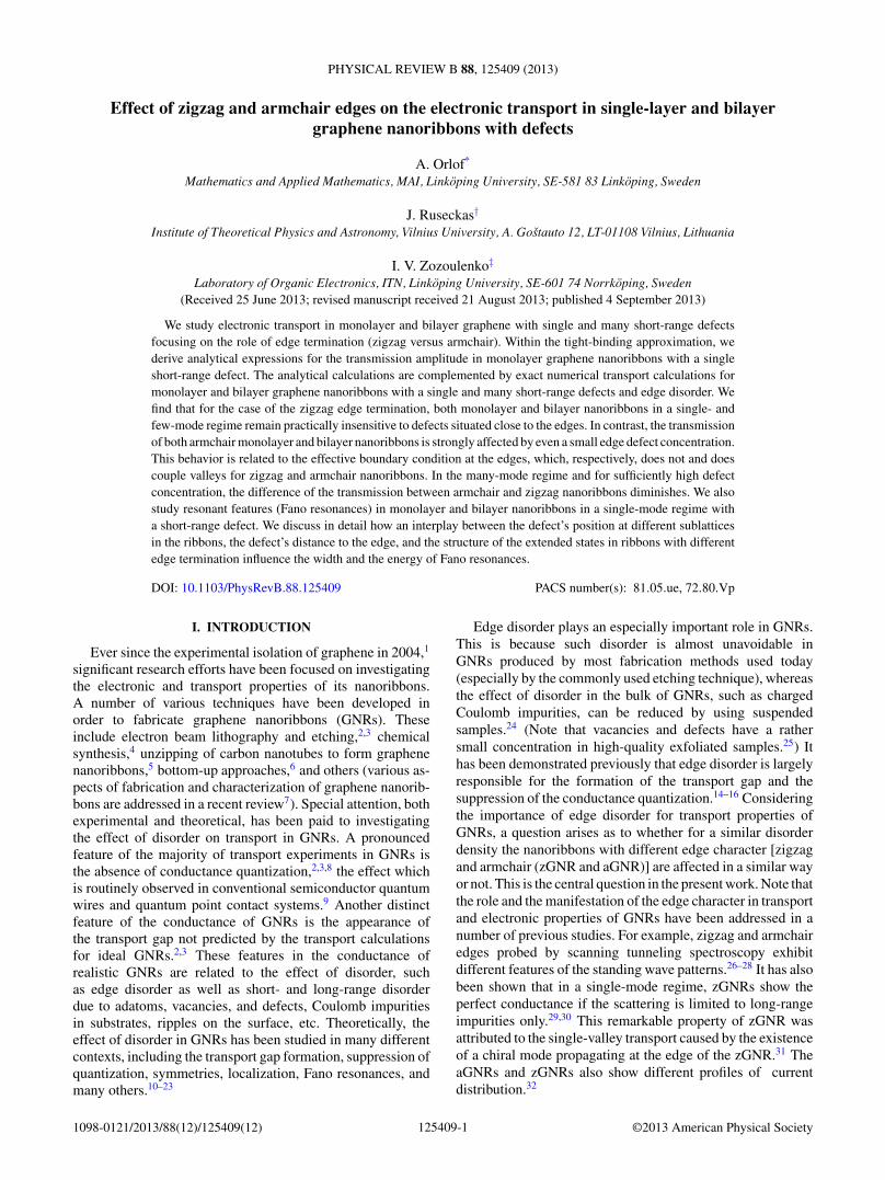
FIG. 1. (Color online) (a) Honeycomb lattice structure of graphene composed of two interpenetrating triangular lattices; a1 = a(3/2,√
3/2)and a2 = a(3/2, − √
3/2) are the lattice unit vectors, and a ≈ 1.42 A is the carbon-carbon distance.36 A (red) and B (blue) mark two sublatticesof the graphene lattice. (b) Asymmetric graphene sheet. (c) Labeling of carbon atoms in the rectangular unit cell used in analytical calculations.(d) Structure of bilayer graphene indicating sublattices A1,B1 (upper layer) and A2,B2 (lower layer) and hopping integrals γ1 between sites inthe sublattices A1 and A2, and γ3 between sites in the sublattices B1 and B2.
125409-2
EFFECT OF ZIGZAG AND ARMCHAIR EDGES ON THE . . . PHYSICAL REVIEW B 88, 125409 (2013)
form36,37
H0 = −γ0
∑i:l=1,2
(a†l,ibl,i+�+H.c.)−γ1
∑i
(a†1,ia2,i+H.c.)
− γ3
∑i
(b†1,ib2,i + H.c.), (3)
where a†l,i (al,i) and b
†l,i (bl,i) are the creation (annihilation)
operators for sublattices A and B in the layer l = 1,2 inthe unit cell i. γ0 is the nearest-neighbor hopping energywithin one layer (γ0 ≈ 3.16 eV). In calculations for BGNswe assume γ1 = 0.39
3.16 [γ0] and γ3 = 0, i.e., we consider theminimal low-energy model.36,37 A definition of sublatticesfor bilayer graphene is illustrated in Fig. 1: sites belongingto the sublattices A1 and A2 are situated on the top of eachother, whereas sites belonging to B1 and B2 are displaced. Thescattering on defects is described by
V0 = U∑
i:l=1,2
(a†l,ial,i + b
†l,ibl,i), (4)
where the summation runs over defected sites with the on-sitepotential U . From now on we will express all energies inthe units of the hopping energy t for monolayer grapheneand γ0 for bilayer graphene. In our calculation, we use amodel of the strong short-range scattering setting U = 100in numerical calculations and setting U → ∞ in analyticalones. This model is appropriate to describe the absence of acarbon atom at the edge of a nanoribbon or a vacancy in thebulk, as well as to describe a scattering on an adatom.38,39
The conductance calculation of monolayer graphenenanoribbons (GNRs) with a single defect is performed ana-lytically and confirmed numerically. The analytical approachis described in detail in the next section. The calculation of theconductance in monolayer graphene nanoribbons with manydefects and all calculations for bilayer graphene nanoribbons(BGNs) are performed numerically on the basis of the recursiveGreen’s function technique.18,35 In this technique, a ribbonof width W is divided into three regions, namely a leftlead, a scattering region, and a right lead. The scatteringpotential is defined in the scattering region of length L,whereas both semi-infinite leads are considered to be ideal(no scattering). In the recursive Green’s function technique,Green’s functions of every slice in the scattering region arecalculated and recursively coupled by the Dyson equation toobtain the Green’s function of the whole scattering region.The surface Green’s function of the leads is calculatedusing the wave functions of the Bloch states of the infiniteleads. The transmission and reflection amplitudes are obtainedwith use of previously calculated Green’s functions. Theconnection between the transmission and the conductance atzero temperature is provided by the Landauer formula,
G = 2e2
h
∑α,β
Tβ,α, Tβ,α = |tβ,α|2, (5)
where Tβ,α and tβ,α are, respectively, the transmission coeffi-cient and the transmission amplitude from the incoming stateα in the left lead to the outgoing state β in the right lead. Wealso calculate the local density of states (LDOS) of graphene
nanoribbons with a defect, expressing it via the imaginary partof the Green’s function of the ribbon in a standard way.18,35
B. Analytical expressions for transmission of electrons inmonolayer graphene nanoribbons with a single defect
For configurations of graphene with rectangular geometry,it is convenient to use a rectangular unit cell, as has been donein Refs. 40 and 41. Such a unit cell has four atoms labeled withthe symbols l, λ, ρ, and r , as shown in Fig. 1(c). The atomswith labels l and ρ belong to sublattice A, and the atoms withlabels λ and r belong to sublattice B. We use dimensionlessCartesian components of the wave vector
κ = 3akx, ξ =√
3aky (6)
instead of the wave-vector components kx and ky . The firstBrillouin zone corresponding to the rectangular unit cellcontains the values of the wave vectors κ and ξ in theintervals −π � κ < π , −π � ξ < π . Compared to the areaof the Brillouin zone of the hexagonal unit cell, the area ofthe Brillouin zone of the rectangular unit cell is two timessmaller. The smaller Brillouin zone leads to the appearance ofadditional dispersion branches. Those dispersion branches canbe taken into account by using the values of the wave vectorin the longitudinal direction from a two times larger interval[−2π,2π ).
Analytical expressions for wave functions in graphenenanoribbons were provided in Refs. 40 and 41. Eigenfunctionsof tight-binding Hamiltonian (1) in armchair and zigzaggraphene nanoribbons can be written as
ψσν,κ‖(�) = χσ
ν,κ‖(�⊥)eiκ‖m . (7)
Here σ = aGNR,zGNR, and the triplet � = m,n,α indicatesthe position of the site. The numbers m and n determinethe position of the rectangular unit cell and α = l,ρ,λ,r
shows the position in the cell. For aGNR, the transverseand longitudinal components of the wave vector are κ⊥ = ξ ,κ‖ = κ , and for zGNR they are κ⊥ = κ , κ‖ = ξ . The functionsχσ
ν,κ‖(�⊥) with �⊥ = n,α are transverse mode wave functions.The corresponding eigenenergies are
E(κ,ξ ) = s1|φ(κ,ξ )| (8)
with s1 = ±1 and
φ(κ,ξ ) = −e−i κ2 + 2 cos
(ξ
2
). (9)
The square of the absolute value of φ(κ,ξ ) is
|φ(κ,ξ )|2 = 1 + 4 cos2
(ξ
2
)− 4 cos
(ξ
2
)cos
(κ
2
). (10)
The longitudinal component of the wave vector κ‖ cantake values from the interval −2π � κ‖ < 2π . The possiblevalues of the transverse component of the wave vector aredetermined by the boundary conditions. In tight-binding cal-culations, there is a difference between graphene nanoribbonshaving the longitudinal axis of symmetry and without it. Asymmetrical sheet of graphene is shown in Fig. 1(a), whereasan asymmetrical sheet is shown in Fig. 1(b). We considergraphene nanoribbons having N whole rectangular unit cells in
125409-3
A. ORLOF, J. RUSECKAS, AND I. V. ZOZOULENKO PHYSICAL REVIEW B 88, 125409 (2013)
the transverse direction. That is, zGNRs with the longitudinalaxis of symmetry and aGNRs without the axis of symmetryhave N rectangular unit cells in the transverse direction, whilezGNRs without the axis of symmetry and aGNRs with thelongitudinal axis of symmetry have N + 1/2 rectangular unitcells in the transverse direction. From now on, we will writeequations only for symmetrical nanoribbons. Equations forasymmetrical aGNRs can be obtained by changing the numberN to N − 1/2 and for asymmetrical zGNRs by changing toN + 1/2.
For aGNR, the transverse component of the wave vector is
ξν = πν
N + 1, ν = 1, . . . ,N + 1, (11)
and for zGNR the transverse component of the wave vectorκν ≡ κν(ξ ) is the solution of the equation
sin(κνN )
sin[κν
(N + 1
2
)] = 2 cos
(ξ
2
), ν = 1, . . . ,N. (12)
The expressions for the transverse mode wave functionsχσ
ν,κ‖ (�⊥) are given in Appendix.For calculation of the Green’s function, it is useful to have
the eigenfunctions of graphene ribbons characterized not bythe longitudinal wave vector but by the energy. Given theenergy, the components of the wave vector ξν and κν for aGNR
can be calculated from Eq. (11) and
κν(E) = s12 arccos
[1 − E2
4 cos(
ξν
2
) + cos
(ξν
2
)]. (13)
The sign s1 can be determined from the sign of the energy:s1 = sgn(E). For zGNR, the wave vector κ (i)
ν is the solution ofthe equation
|E| =∣∣∣∣∣∣
sin(
κ (i)ν
2
)sin
[κ
(i)ν
(N + 1
2
)]∣∣∣∣∣∣ , (14)
whereas the wave vector ξ (i)ν (E) is determined from the
equation
ξ (i)ν = ±2 arccos
(sin(κ (i)
ν N )
2 sin[κ
(i)ν
(N + 1
2
)])
. (15)
Here index i = 1,2 numbers solutions having the same indexν; different indices i correspond to different valleys.
Given the eigenfunctions ψσν,κ‖ (�), the general expression
for the retarded Green’s function is
G0(�,�′; E) =∑
s1=±1
∑ν
∫ 2π
−2π
dκ‖ψσ
ν,κ‖ (�)ψσ∗ν,κ‖(�
′)
E − E(κ,ξ ) + iη. (16)
From Eq. (16) for symmetrical zGNR we obtain the retardedGreen’s function
G0(�,�′; E) = −i
N∑ν=1
∑i=1,2
1
vzGNRν,i (E)
⎧⎨⎩
χ zGNRν,i,ξ
(i)ν
(�⊥; E)χ zGNRν,i,−ξ
(i)ν
(�′⊥; E)eiξ (i)
ν (E)(m−m′) , m > m′,
χ zGNRν,i,−ξ
(i)ν
(�⊥; E)χ zGNRν,i,ξ
(i)ν
(�′⊥; E)e−iξ (i)
ν (E)(m−m′) , m < m′,(17)
where
vzGNRν,i = ∂
∂ξE(κ (i)
ν (ξ ),ξ )
∣∣∣∣ξ=ξ
(i)ν
= −s1(−1)νN sin
(κ (i)
ν
2
)cos
[κ (i)
ν
(N + 1
2
)] − 12 sin(κ (i)
ν N )
N sin(
κ(i)ν
2
)− 1
2 sin(κ (i)ν N ) cos
[κ
(i)ν
(N + 1
2
)] sin
(ξ (i)ν
2
)(18)
is the velocity. The sign of ξ (i)ν in Eq. (15) should be chosen in such a way that the velocity vzGNR
ν,i is positive.The symmetrical aGNR has states localized on the atoms with indices ρ and λ with the energies E = ±1.40 Thus the expression
for the retarded Green’s function in symmetrical aGNR is
G0(�,�′; E) = −i
N∑ν=1
1
vaGNRν (E)
{χ aGNR
ν,κν(�⊥; E)χ aGNR
ν,−κν(�′
⊥; E)eiκν (E)(m−m′) , m > m′
χ aGNRν,−κν
(�⊥; E)χ aGNRν,κν
(�′⊥; E)e−iκν (E)(m−m′) , m < m′
(19)
+∑
s1=±1
χ aGNRN+1 (�⊥; E)χ aGNR∗
N+1 (�′⊥; E)
E − s1δm,m′ , (19)
where
vaGNRν = ∂
∂κE(κ,ξν)
∣∣∣∣κ=κν
= 1
Ecos
(ξν
2
)sin
(κν
2
)(20)
is the velocity. The last term in Eq. (19) is from the localized states corresponding to ν = N + 1. For asymmetrical aGNR, thereis no such localized states and the last term in Eq. (19) is absent.
The expression for the Green’s function of a system with a single defect is45
G(�,�′) = G0(�,�′) + G0(�,�0)UG0(�0,�′)
1 − UG0(�0,�0), (21)
125409-4
EFFECT OF ZIGZAG AND ARMCHAIR EDGES ON THE . . . PHYSICAL REVIEW B 88, 125409 (2013)
where G0 = [E − H0 + iη]−1 is the retarded Green’s function of the graphene nanoribbon without defect. The transmissionamplitude from the transverse mode ν ′ to ν can be calculated using the Green’s function46
tν,ν ′ = i√
υνυν ′∑�⊥,�′
⊥
χ∗ν (�⊥)e−iκν (m−m0)G(�,�′)χν ′(l′⊥)eiκν′ (m′−m0). (22)
Using Eqs. (19), (21), and (22), the transmission amplitude for aGNR with a defect is
tν,ν ′ = δν,ν ′ −√
vaGNRν
vaGNRν ′
i UvaGNR
νχ aGNR
ν,−κν(�0⊥)χ aGNR
ν ′,κν′ (�0⊥)
1 + iUN∑
ν ′′=1
1vaGNR
ν′′χ aGNR
ν ′′,−κν′′ (�0⊥)χ aGNRν ′′,κν′′ (�0⊥) − U
∑s1=±1
1E−s1
χ aGNR∗N+1 (�0⊥)χ aGNR
N+1 (�0⊥)
. (23)
For zGNR with a defect, the transmission amplitude is
tν,i;ν ′,i ′ = δν,ν ′δi,i ′ −√
vzGNRν,i
vzGNRν ′,i ′
i U
vzGNRν,i
χ zGNRν,i,−ξ
(i)ν
(�0⊥)χ zGNRν ′,i ′,ξ (i′ )
ν′(�0⊥)
1 + iUN∑
ν ′′=1
∑i ′′
1vzGNR
ν′′ ,i′′χ zGNR
ν ′′,i ′′,−ξ(i′′ )ν′′
(�0⊥)χ zGNRν ′′,i ′′,ξ (i′′ )
ν′′(�0⊥)
. (24)
If the defect is an absence of an atom, then Eqs. (23) and (24)should be taken in the limit U → ∞. From this point on wewill consider such defects.
III. CONDUCTANCE OF MONOLAYER GRAPHENENANORIBBONS AND BILAYER GRAPHENE
NANORIBBONS WITH DEFECTS
In this section, we present and discuss the results for theconductance of nanoribbons with single and many defects.Most of the calculations are performed for zGNRs and zigzagbilayer graphene nanoribbons of width 23.71 nm as well asmetallic aGNRs and armchair bilayer graphene nanoribbonsof width 23.73 nm, if not stated differently. (Calculations inSec. III B are performed for narrower ribbons.)
A. Effect of a single defect
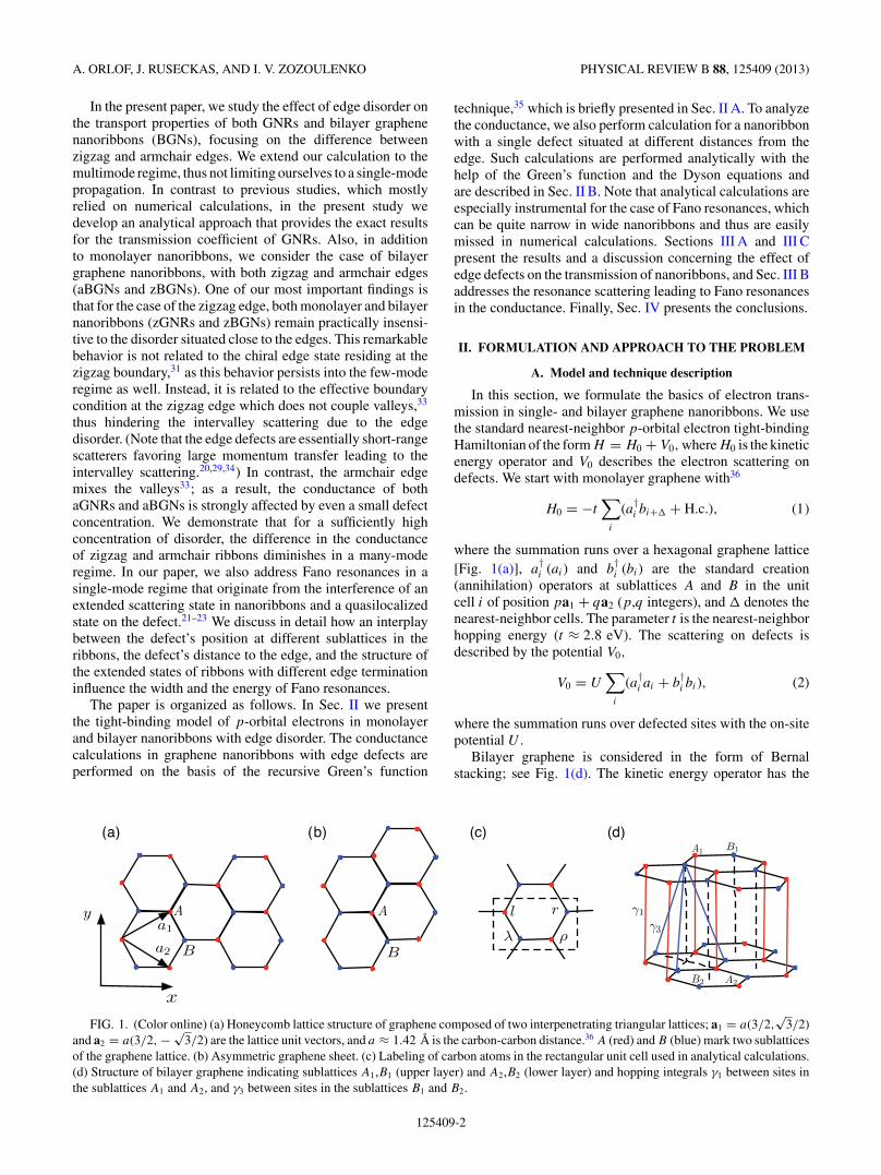
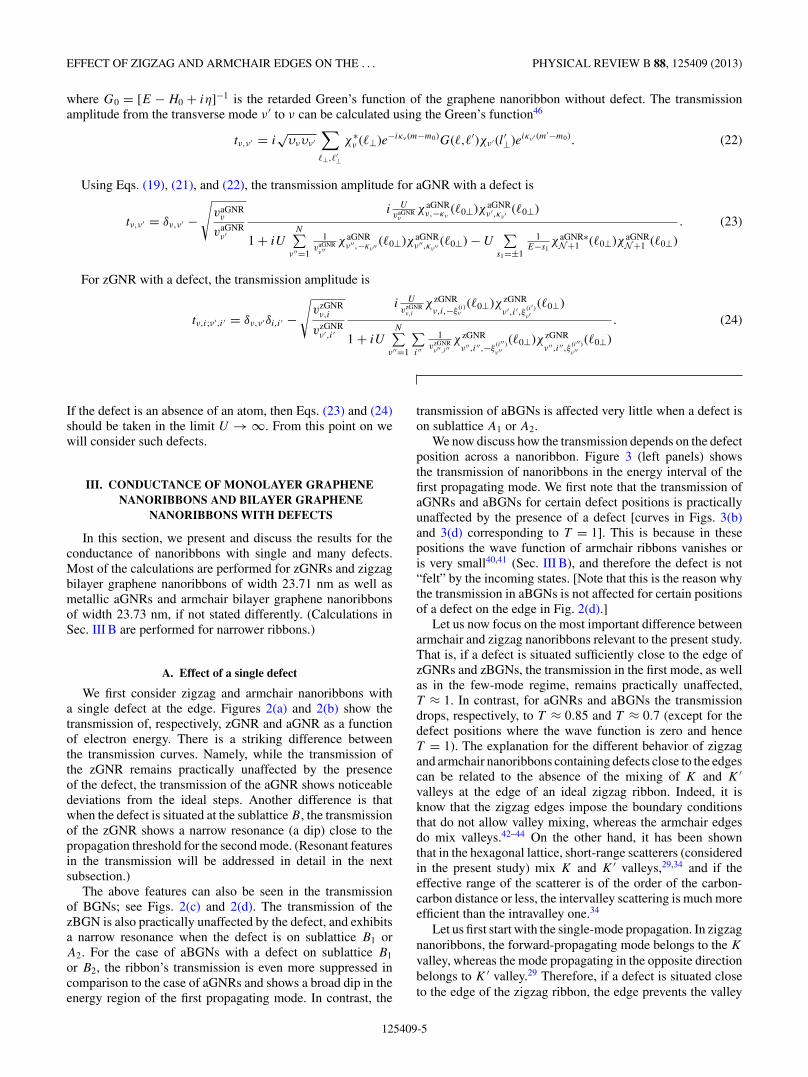
We first consider zigzag and armchair nanoribbons witha single defect at the edge. Figures 2(a) and 2(b) show thetransmission of, respectively, zGNR and aGNR as a functionof electron energy. There is a striking difference betweenthe transmission curves. Namely, while the transmission ofthe zGNR remains practically unaffected by the presenceof the defect, the transmission of the aGNR shows noticeabledeviations from the ideal steps. Another difference is thatwhen the defect is situated at the sublattice B, the transmissionof the zGNR shows a narrow resonance (a dip) close to thepropagation threshold for the second mode. (Resonant featuresin the transmission will be addressed in detail in the nextsubsection.)
The above features can also be seen in the transmissionof BGNs; see Figs. 2(c) and 2(d). The transmission of thezBGN is also practically unaffected by the defect, and exhibitsa narrow resonance when the defect is on sublattice B1 orA2. For the case of aBGNs with a defect on sublattice B1
or B2, the ribbon’s transmission is even more suppressed incomparison to the case of aGNRs and shows a broad dip in theenergy region of the first propagating mode. In contrast, the
transmission of aBGNs is affected very little when a defect ison sublattice A1 or A2.
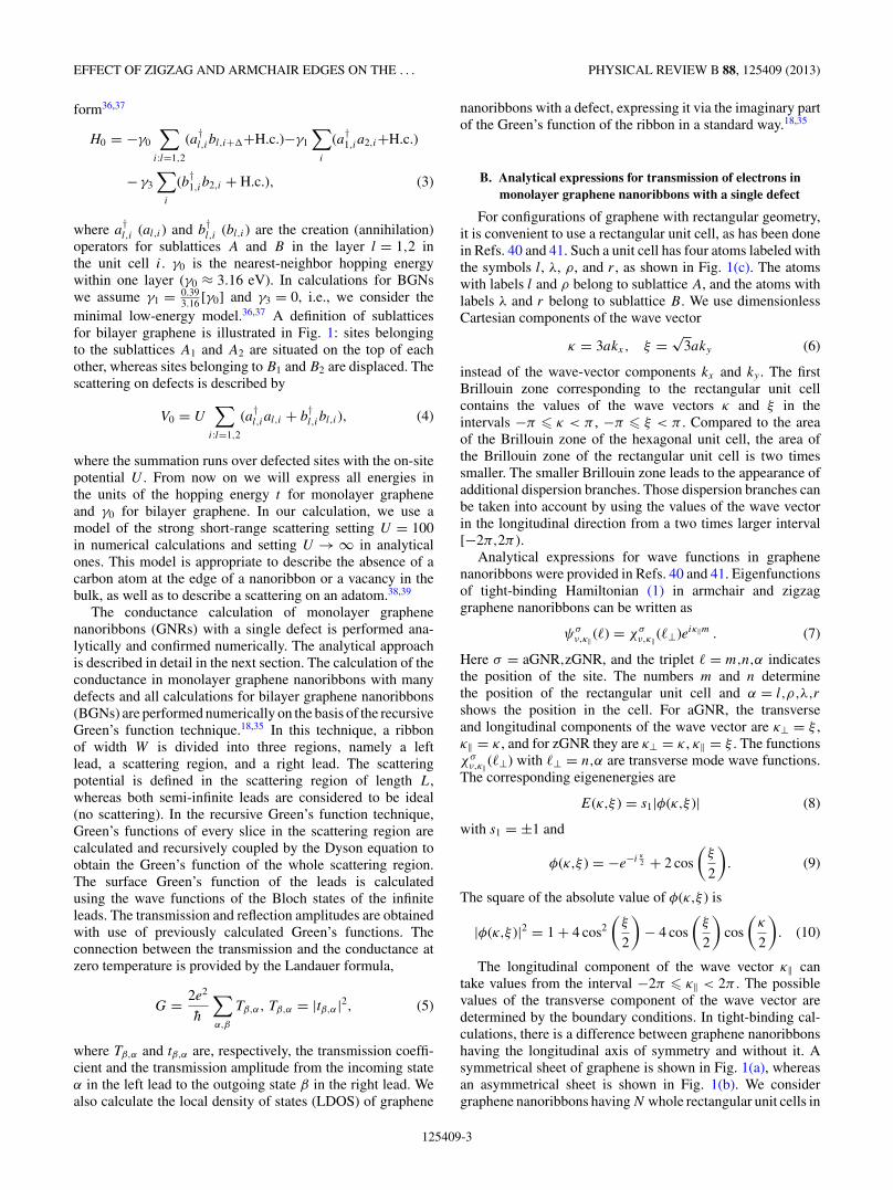
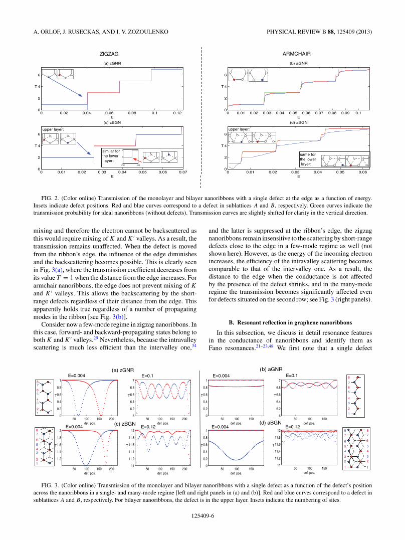
We now discuss how the transmission depends on the defectposition across a nanoribbon. Figure 3 (left panels) showsthe transmission of nanoribbons in the energy interval of thefirst propagating mode. We first note that the transmission ofaGNRs and aBGNs for certain defect positions is practicallyunaffected by the presence of a defect [curves in Figs. 3(b)and 3(d) corresponding to T = 1]. This is because in thesepositions the wave function of armchair ribbons vanishes oris very small40,41 (Sec. III B), and therefore the defect is not“felt” by the incoming states. [Note that this is the reason whythe transmission in aBGNs is not affected for certain positionsof a defect on the edge in Fig. 2(d).]
Let us now focus on the most important difference betweenarmchair and zigzag nanoribbons relevant to the present study.That is, if a defect is situated sufficiently close to the edge ofzGNRs and zBGNs, the transmission in the first mode, as wellas in the few-mode regime, remains practically unaffected,T ≈ 1. In contrast, for aGNRs and aBGNs the transmissiondrops, respectively, to T ≈ 0.85 and T ≈ 0.7 (except for thedefect positions where the wave function is zero and henceT = 1). The explanation for the different behavior of zigzagand armchair nanoribbons containing defects close to the edgescan be related to the absence of the mixing of K and K ′valleys at the edge of an ideal zigzag ribbon. Indeed, it isknow that the zigzag edges impose the boundary conditionsthat do not allow valley mixing, whereas the armchair edgesdo mix valleys.42–44 On the other hand, it has been shownthat in the hexagonal lattice, short-range scatterers (consideredin the present study) mix K and K ′ valleys,29,34 and if theeffective range of the scatterer is of the order of the carbon-carbon distance or less, the intervalley scattering is much moreefficient than the intravalley one.34
Let us first start with the single-mode propagation. In zigzagnanoribbons, the forward-propagating mode belongs to the K
valley, whereas the mode propagating in the opposite directionbelongs to K ′ valley.29 Therefore, if a defect is situated closeto the edge of the zigzag ribbon, the edge prevents the valley
125409-5
A. ORLOF, J. RUSECKAS, AND I. V. ZOZOULENKO PHYSICAL REVIEW B 88, 125409 (2013)
FIG. 2. (Color online) Transmission of the monolayer and bilayer nanoribbons with a single defect at the edge as a function of energy.Insets indicate defect positions. Red and blue curves correspond to a defect in sublattices A and B, respectively. Green curves indicate thetransmission probability for ideal nanoribbons (without defects). Transmission curves are slightly shifted for clarity in the vertical direction.
mixing and therefore the electron cannot be backscattered asthis would require mixing of K and K ′ valleys. As a result, thetransmission remains unaffected. When the defect is movedfrom the ribbon’s edge, the influence of the edge diminishesand the backscattering becomes possible. This is clearly seenin Fig. 3(a), where the transmission coefficient decreases fromits value T = 1 when the distance from the edge increases. Forarmchair nanoribbons, the edge does not prevent mixing of K
and K ′ valleys. This allows the backscattering by the short-range defects regardless of their distance from the edge. Thisapparently holds true regardless of a number of propagatingmodes in the ribbon [see Fig. 3(b)].
Consider now a few-mode regime in zigzag nanoribbons. Inthis case, forward- and backward-propagating states belong toboth K and K ′ valleys.29 Nevertheless, because the intravalleyscattering is much less efficient than the intervalley one,34
and the latter is suppressed at the ribbon’s edge, the zigzagnanoribbons remain insensitive to the scattering by short-rangedefects close to the edge in a few-mode regime as well (notshown here). However, as the energy of the incoming electronincreases, the efficiency of the intravalley scattering becomescomparable to that of the intervalley one. As a result, thedistance to the edge when the conductance is not affectedby the presence of the defect shrinks, and in the many-moderegime the transmission becomes significantly affected evenfor defects situated on the second row; see Fig. 3 (right panels).
B. Resonant reflection in graphene nanoribbons
In this subsection, we discuss in detail resonance featuresin the conductance of nanoribbons and identify them asFano resonances.21–23,48 We first note that a single defect
FIG. 3. (Color online) Transmission of the monolayer and bilayer nanoribbons with a single defect as a function of the defect’s positionacross the nanoribbons in a single- and many-mode regime [left and right panels in (a) and (b)]. Red and blue curves correspond to a defect insublattices A and B, respectively. For bilayer nanoribbons, the defect is in the upper layer. Insets indicate the numbering of sites.
125409-6
EFFECT OF ZIGZAG AND ARMCHAIR EDGES ON THE . . . PHYSICAL REVIEW B 88, 125409 (2013)
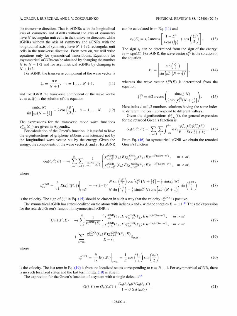
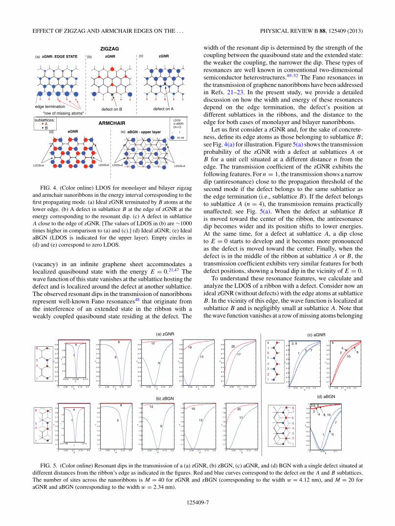
FIG. 4. (Color online) LDOS for monolayer and bilayer zigzagand armchair nanoribbons in the energy interval corresponding to thefirst propagating mode. (a) Ideal zGNR terminated by B atoms at thelower edge. (b) A defect in sublattice B at the edge of zGNR at theenergy corresponding to the resonant dip. (c) A defect in sublatticeA close to the edge of zGNR. [The values of LDOS in (b) are ∼1000times higher in comparison to (a) and (c).] (d) Ideal aGNR; (e) IdealaBGN (LDOS is indicated for the upper layer). Empty circles in(d) and (e) correspond to zero LDOS.
(vacancy) in an infinite graphene sheet accommodates alocalized quasibound state with the energy E = 0.21,47 Thewave function of this state vanishes at the sublattice hosting thedefect and is localized around the defect at another sublattice.The observed resonant dips in the transmission of nanoribbonsrepresent well-known Fano resonances48 that originate fromthe interference of an extended state in the ribbon with aweakly coupled quasibound state residing at the defect. The
width of the resonant dip is determined by the strength of thecoupling between the quasibound state and the extended state:the weaker the coupling, the narrower the dip. These types ofresonances are well known in conventional two-dimensionalsemiconductor heterostructures.49–52 The Fano resonances inthe transmission of graphene nanoribbons have been addressedin Refs. 21–23. In the present study, we provide a detaileddiscussion on how the width and energy of these resonancesdepend on the edge termination, the defect’s position atdifferent sublattices in the ribbons, and the distance to theedge for both cases of monolayer and bilayer nanoribbons.
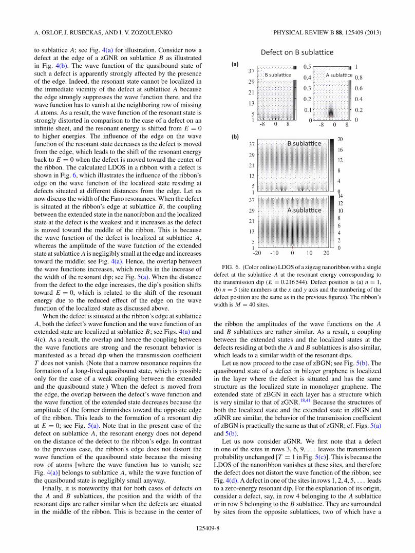
Let us first consider a zGNR and, for the sake of concrete-ness, define its edge atoms as those belonging to sublattice B;see Fig. 4(a) for illustration. Figure 5(a) shows the transmissionprobability of the zGNR with a defect at sublattices A orB for a unit cell situated at a different distance n from theedge. The transmission coefficient of the zGNR exhibits thefollowing features. For n = 1, the transmission shows a narrowdip (antiresonance) close to the propagation threshold of thesecond mode if the defect belongs to the same sublattice asthe edge termination (i.e., sublattice B). If the defect belongsto sublattice A (n = 4), the transmission remains practicallyunaffected; see Fig. 5(a). When the defect at sublattice B
is moved toward the center of the ribbon, the antiresonancedip becomes wider and its position shifts to lower energies.At the same time, for a defect at sublattice A, a dip closeto E = 0 starts to develop and it becomes more pronouncedas the defect is moved toward the center. Finally, when thedefect is in the middle of the ribbon at sublattice A or B, thetransmission coefficient exhibits very similar features for bothdefect positions, showing a broad dip in the vicinity of E = 0.
To understand these resonance features, we calculate andanalyze the LDOS of a ribbon with a defect. Consider now anideal zGNR (without defects) with the edge atoms at sublatticeB. In the vicinity of this edge, the wave function is localized atsublattice B and is negligibly small at sublattice A. Note thatthe wave function vanishes at a row of missing atoms belonging
FIG. 5. (Color online) Resonant dips in the transmission of a (a) zGNR, (b) zBGN, (c) aGNR, and (d) BGN with a single defect situated atdifferent distances from the ribbon’s edge as indicated in the figures. Red and blue curves correspond to the defect on the A and B sublattices.The number of sites across the nanoribbons is M = 40 for zGNR and zBGN (corresponding to the width w = 4.12 nm), and M = 20 foraGNR and aBGN (corresponding to the width w = 2.34 nm).
125409-7
A. ORLOF, J. RUSECKAS, AND I. V. ZOZOULENKO PHYSICAL REVIEW B 88, 125409 (2013)
to sublattice A; see Fig. 4(a) for illustration. Consider now adefect at the edge of a zGNR on sublattice B as illustratedin Fig. 4(b). The wave function of the quasibound state ofsuch a defect is apparently strongly affected by the presenceof the edge. Indeed, the resonant state cannot be localized inthe immediate vicinity of the defect at sublattice A becausethe edge strongly suppresses the wave function there, and thewave function has to vanish at the neighboring row of missingA atoms. As a result, the wave function of the resonant state isstrongly distorted in comparison to the case of a defect on aninfinite sheet, and the resonant energy is shifted from E = 0to higher energies. The influence of the edge on the wavefunction of the resonant state decreases as the defect is movedfrom the edge, which leads to the shift of the resonant energyback to E = 0 when the defect is moved toward the center ofthe ribbon. The calculated LDOS in a ribbon with a defect isshown in Fig. 6, which illustrates the influence of the ribbon’sedge on the wave function of the localized state residing atdefects situated at different distances from the edge. Let usnow discuss the width of the Fano resonances. When the defectis situated at the ribbon’s edge at sublattice B, the couplingbetween the extended state in the nanoribbon and the localizedstate at the defect is the weakest and it increases as the defectis moved toward the middle of the ribbon. This is becausethe wave function of the defect is localized at sublattice A,whereas the amplitude of the wave function of the extendedstate at sublattice A is negligibly small at the edge and increasestoward the middle; see Fig. 4(a). Hence, the overlap betweenthe wave functions increases, which results in the increase ofthe width of the resonant dip; see Fig. 5(a). When the distancefrom the defect to the edge increases, the dip’s position shiftstoward E = 0, which is related to the shift of the resonantenergy due to the reduced effect of the edge on the wavefunction of the localized state as discussed above.
When the defect is situated at the ribbon’s edge at sublatticeA, both the defect’s wave function and the wave function of anextended state are localized at sublattice B; see Figs. 4(a) and4(c). As a result, the overlap and hence the coupling betweenthe wave functions are strong and the resonant behavior ismanifested as a broad dip when the transmission coefficientT does not vanish. (Note that a narrow resonance requires theformation of a long-lived quasibound state, which is possibleonly for the case of a weak coupling between the extendedand the quasibound state.) When the defect is moved fromthe edge, the overlap between the defect’s wave function andthe wave function of the extended state decreases because theamplitude of the former diminishes toward the opposite edgeof the ribbon. This leads to the formation of a resonant dipat E = 0; see Fig. 5(a). Note that in the present case of thedefect on sublattice A, the resonant energy does not dependon the distance of the defect to the ribbon’s edge. In contrastto the previous case, the ribbon’s edge does not distort thewave function of the quasibound state because the missingrow of atoms [where the wave function has to vanish; seeFig. 4(a)] belongs to sublattice A, while the wave function ofthe quasibound state is negligibly small anyway.
Finally, it is noteworthy that for both cases of defects onthe A and B sublattices, the position and the width of theresonant dips are rather similar when the defects are situatedin the middle of the ribbon. This is because in the center of
Defect on B subla�ice
A subla�ce
B subla�ce
A subla�ce
B subla�ce
(a)
(b)
-8 0 8 -8 0 81
21
5
13
29
37
0
0.3
0.1
0.2
0.4
0.5
0
0.6
0.2
0.4
0.8
1
-20 -10 0 10 20
1
21
5
13
29
37
1
21
5
13
29
37
FIG. 6. (Color online) LDOS of a zigzag nanoribbon with a singledefect at the sublattice A at the resonant energy corresponding tothe transmission dip (E = 0.216 544). Defect position is (a) n = 1,(b) n = 5 (site numbers at the x and y axis and the numbering of thedefect position are the same as in the previous figures). The ribbon’swidth is M = 40 sites.
the ribbon the amplitudes of the wave functions on the A
and B sublattices are rather similar. As a result, a couplingbetween the extended states and the localized states at thedefects residing at both the A and B sublattices is also similar,which leads to a similar width of the resonant dips.
Let us now proceed to the case of zBGN; see Fig. 5(b). Thequasibound state of a defect in bilayer graphene is localizedin the layer where the defect is situated and has the samestructure as the localized state in monolayer graphene. Theextended state of zBGN in each layer has a structure whichis very similar to that of zGNR.18,41 Because the structures ofboth the localized state and the extended state in zBGN andzGNR are similar, the behavior of the transmission coefficientof zBGN is practically the same as that of zGNR; cf. Figs. 5(a)and 5(b).
Let us now consider aGNR. We first note that a defectin one of the sites in rows 3, 6, 9, . . . leaves the transmissionprobability unchanged [T = 1 in Fig. 5(c)]. This is because theLDOS of the nanoribbon vanishes at these sites, and thereforethe defect does not distort the wave function of the ribbon; seeFig. 4(d). A defect in one of the sites in rows 1, 2, 4, 5, . . . leadsto a zero-energy resonant dip. For the explanation of its origin,consider a defect, say, in row 4 belonging to the A sublatticeor in row 5 belonging to the B sublattice. They are surroundedby sites from the opposite sublattices, two of which have a
125409-8
EFFECT OF ZIGZAG AND ARMCHAIR EDGES ON THE . . . PHYSICAL REVIEW B 88, 125409 (2013)
high LDOS; see Fig. 4(d). This means that the localized statewill not be very distorted and its resonant energy will remainpractically the same as for an infinite graphene sheet. Note thatthe width of the state is essentially the same for all the defectpositions except for those closest to the ribbon’s edge. As thewave function of the extended state alternates between zeroand a constant value across the ribbon, its overlap with thelocalized state around the defect does not change much whenone moves the defect across the ribbon. However, because theextended state vanishes outside the ribbon, the overlap betweenstates will be smaller for the defect at the edge, which leads toa narrower resonance; see Fig. 5(c).
Finally, let us consider the case of aBGN; see Fig. 5(d).As for the case of aGNR, a defect in sites with a vanishingLDOS does not affect the transmission probability (rows 3, 6,9, . . . ). In contrast to aGNR, the transmission probability ofaBGN behaves qualitatively different depending on whethera defect is on the A or B sublattice. A defect in one of thesites in rows 1, 2, 4, 5, . . . in sublattice A leads to a broadand shallow resonance dip at the energy E ≈ 0. A defect inthe same rows but at sublattice B corresponds to dips withtransmission T = 0 and has a resonance energy significantlyshifted from zero. To explain the origin and features of theresonances, let us focus on a representative case of a defect atsublattice B in row 5. It is surrounded by sites from sublatticeA, all with low (or zero) LDOS; see Fig. 4(e). As discussedabove for the case of zGNR, this would lead to a significant
distortion of the wave function of the localized state and ashifting of the resonant energy from E = 0 to higher values.However, in contrast to zGNR, the energy and the width of theresonance dip for aBGN remain practically unchanged whenthe defect is moved toward the middle of the ribbon. This isbecause the LDOS of aBGN alternates between zero and thesame constant value across the ribbon, consequently it distortsthe localized state around different sites in the same way, andthe overlap remains the same. Consider now a defect in row4 but at sublattice A. Such a defect has two neighbors with ahigh LDOS; see Fig. 4(e). As a result, similarly to the casesdiscussed above, the localized state remains practically notdistorted, which leads to a resonant dip with a resonant statewith energy E ≈ 0.
Let us finally note that the properties of resonant states,such as the transmission minimum, the resonance width, andthe energy, depend on the defect strength. For example, anincrease in the on-site potential strength leads to a decrease inthe transmission minimum for the zero-energy resonant statesin armchair nanoribbons.
C. Effect of many defects
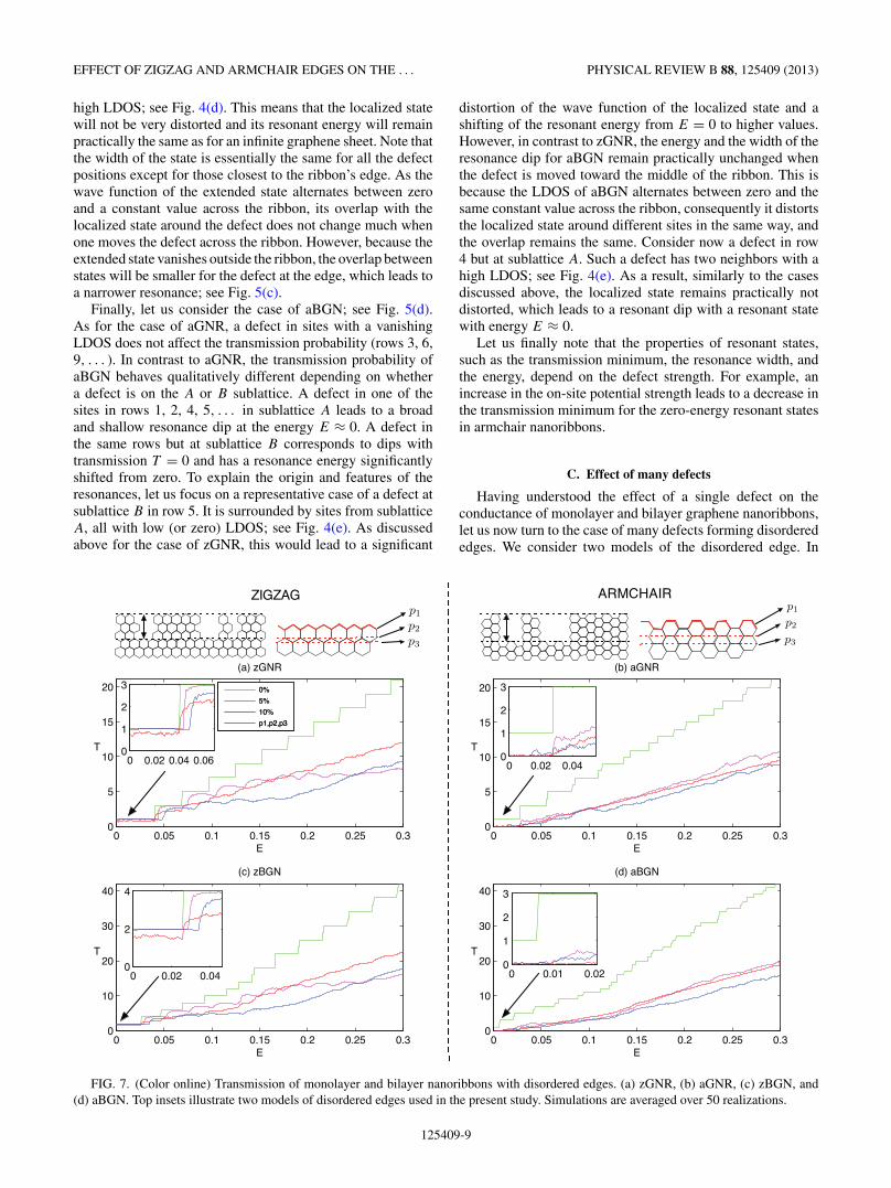
Having understood the effect of a single defect on theconductance of monolayer and bilayer graphene nanoribbons,let us now turn to the case of many defects forming disorderededges. We consider two models of the disordered edge. In
p1
p2
p3
p1
p2
p3
FIG. 7. (Color online) Transmission of monolayer and bilayer nanoribbons with disordered edges. (a) zGNR, (b) aGNR, (c) zBGN, and(d) aBGN. Top insets illustrate two models of disordered edges used in the present study. Simulations are averaged over 50 realizations.
125409-9
A. ORLOF, J. RUSECKAS, AND I. V. ZOZOULENKO PHYSICAL REVIEW B 88, 125409 (2013)
the first model, all the edge atoms covered by rectangularareas of random lengths and constant depths (of 5% and10% of the ribbon width) are removed, as shown in Fig. 7.Such a model apparently preserves the edge topology (i.e.,zigzag or armchair) in the direction of transport. In the secondmodel, we follow Ref. 18 and introduce a disordered edgeby removing atoms from the outermost row (indicated bythe red solid line in the insets) with probability p1 = 0.5,followed by removing atoms from the second and third rowswith conditional probabilities p2 = 0.5 and p3 = 0.5 if at leastone of the adjacent atoms from the previous row is absent.
Figure 7 shows the transmission probability of monolayerand bilayer nanoribbons in the energy interval spanning bothfew- and many-mode regimes. For both models of disorder,the transmission of monolayer and bilayer nanoribbons of thesame edge topology is rather similar, even though the trans-mission of bilayer nanoribbons is somehow lower than that ofmonolayer ones. This is consistent with the case of a ribbonwith a single defect, where the corresponding transmission ofmonolayer and bilayer nanoribbons is also rather similar; seeFigs. 2 and 3.
Let us now discuss differences and similarities in thetransmission of zigzag and armchair nanoribbons. In thesingle- and few-mode regime, the conductance of both aGNRand aBGN is strongly suppressed. Note that even with a singledefect, the conductance of armchair nanoribbons shows anoticeable suppression; see Figs. 2(b), 2(d), 3(b), and 3(d).With many defects this suppression adds up, leading to theformation of a pronounced transport gap of zero conductance.In contrast, in a few-, and especially in the single-mode regime,the conductance of zigzag ribbons is affected very little. Thisbehavior can also be traced to the corresponding behavior ofzigzag nanoribbons with a single defect, the conductance ofwhich remains unchanged in comparison to the ideal case,provided that the defect is situated not far from the edge(Sec. III A). It is noteworthy that for the disorder preservingthe edge topology, the conductance of both zGNR and zBGNin a single-mode regime remains practically unchanged incomparison to the ideal case.
In a many-mode regime, the difference in conductancebetween zigzag and armchair ribbons practically disappears;cf. Figs. 7(a) and 7(b) and Figs. 7(c) and 7(d). As discussed inSec. III A, the distance to the edge for which the conductanceof zigzag ribbons is not affected by the presence of the defectshrinks as the energy of the electrons increases [see Fig 3, rightpanels in (a)–(d)]. Thus, for high energies the armchair andzigzag ribbons become equally sensitive to the edge disorder.
IV. CONCLUSIONS
We have studied the transmission properties of mono-and bilayer graphene nanoribbons with defects, focusing onthe role of edge termination (zigzag versus armchair). Usingthe standard tight-binding model of p-orbital electrons on ahexagonal lattice, we have developed an analytical approachbased on the Green’s function technique and the Dysonequation for calculation of the transmission coefficient ofmonolayer graphene nanoribbons with a single short-rangedefect. Calculation of the conductance in monolayer graphenenanoribbons with many defects and calculations for bilayer
graphene nanoribbons is performed numerically on the basisof the tight-binding recursive Green’s function technique. Theprincipal conclusions of our work can be summarized asfollows:
(i) For the case of the zigzag edge termination, bothmonolayer and bilayer nanoribbons in a single- and a few-mode regime remain practically insensitive to defects situatedclose to the edges. This remarkable behavior is related to theeffective boundary condition at the zigzag edges which do notcouple valleys, thus prohibiting intervalley scattering due toshort-range defects situated close to the edges. In contrast, thearmchair edges mix the valleys; as a result, the conductance ofboth monolayer and bilayer nanoribbons is strongly affectedby even a small defect concentration at the edges.
(ii) For higher electron energies in the many-mode regime,the difference of the transmission between the armchair andzigzag ribbons diminishes, and for sufficiently high defectconcentration they become equally sensitive to the edgedisorder.
(iii) Both monolayer and bilayer nanoribbons with a short-range defect show resonant features in the lowest energy mode.Resonances are identified to be of Fano type and emerge fromthe interference between the quasibound localized state aroundthe defect and the extended state in the ribbon. We considerfour different cases of a defect in (a) zGNR, (b) zBGN,(c) aGNR, and (d) aBGN. We discuss in detail how theinterplay between the defects position at different sublattices inthe ribbons, the defect distance to the edge, and the structure ofthe extended states in ribbons with different edge terminationinfluence the width and the energy of Fano resonances.
ACKNOWLEDGMENTS
The authors thank T. Heinzel, Hengyi Xu, and A. A.Shylau for help with the programming code for the numericalcalculations. I.V.Z. and J.R. acknowledge a collaborative grantfrom the Swedish Institute.
APPENDIX: TRANSVERSE MODE WAVE FUNCTIONS
The transverse mode wave function in aGNR is
χ aGNRν,κ (n,r) = 1√
2(N + 1)sin(ξνn), (A1)
χ aGNRν,κ (n,ρ) = −1√
2(N + 1)
φ(κ,ξν)
E(κ,ξν)sin
[ξν
(n − 1
2
) ],
(A2)
χ aGNRν,κ (n,λ) = −1√
2(N + 1)e−i κ
2 sin
[ξν
(n − 1
2
) ], (A3)
χ aGNRν,κ (n,l) = 1√
2(N + 1)e−i κ
2φ(κ,ξν)
E(κ,ξν)sin(ξνn). (A4)
For zGNR, taking into account Eq. (12) we have
χ zGNRν,ξ (n,r) = CzGNR
ν,ξ sin(κνn), (A5)
125409-10
EFFECT OF ZIGZAG AND ARMCHAIR EDGES ON THE . . . PHYSICAL REVIEW B 88, 125409 (2013)
χ zGNRν,ξ (n,ρ) = s1(−1)νCzGNR
ν,ξ e−iξ
2 sin
[κν
(N+1
2−n
) ],
(A6)
χ zGNRν,ξ (n,λ) = −CzGNR
ν,ξ e−iξ
2 sin
[κν
(n − 1
2
) ], (A7)
χ zGNRν,ξ (n,l) = s1(−1)ν+1CzGNR
ν,ξ sin[κν(N + 1 − n)], (A8)
where
CzGNRν,ξ =
{2N − sin(κνN )
sin(
κν
2
) cos
[κν
(N + 1
2
)]}− 12
(A9)
is the normalization factor. It should be noted thatfor both wave functions χ aGNR
ν,κ and χ zGNRν,ξ , given
by Eqs. (A1)–(A4) and (A5)–(A8), the followingequality holds: χσ∗
ν,κ‖(�⊥) = χσν,−κ‖ (�⊥).
*[email protected]†[email protected]‡[email protected]. S. Novoselov, A. K. Geim, S. V. Morozov, D. Jiang, Y. Zhang,S. V. Dubonos, I. V. Grigorieva, and A. A. Firsov, Science 306, 666(2004).
2M. Y. Han, B. Ozyilmaz, Y. Zhang, and P. Kim, Phys. Rev. Lett. 98,206805 (2007).
3F. Molitor, A. Jacobsen, C. Stampfer, J. Guttinger, T. Ihn, andK. Ensslin, Phys. Rev. B 79, 075426 (2009).
4X. Li, X. Wang, L. Zhang, S. Lee, and H. Dai, Science 319, 1229(2008).
5D. V. Kosynkin, A. L. Higginbotham, A. Sinitskii, J. R. Lomeda,A. Dimiev, B. K. Price, and J. M. Tour, Nature (London) 458, 872(2009).
6J. Cai, P. Ruffieux, R. Jaafar, M. Bieri, T. Braun, S. Blankenburg,M. Muoth, A. P. Seitsonen, M. Saleh, X. Feng, K. Mullen, andR. Fasel, Nature (London) 466, 470 (2010).
7X. Jia, J. Campos-Delgado, M. Terrones, V. Meuniere, and M. S.Dresselhaus, Nanoscale 3, 86 (2011).
8Y.-M. Lin, V. Perebeinos, Z. Chen, and P. Avouris, Phys. Rev. B 78,161409 (2008).
9J. Davies, The Physics of Low-Dimensional Semiconductors (Cam-bridge University Press, Cambridge, 1998).
10D. A. Areshkin, D. Gunlycke, and C. T. White, Nano Lett. 7, 204(2007).
11D. Gunlycke, D. A. Areshkin, and C. T. White, Appl. Phys. Lett.90, 142104 (2007).
12D. Querlioz, Y. Apertet, A. Valentin, K. Huet, A. Bournel, S. Galdin-Retailleau, and P. Dollfus, Appl. Phys. Lett. 92, 042108 (2008).
13A. Lherbier, B. Biel, Y.-M. Niquet, and S. Roche, Phys. Rev. Lett.100, 036803 (2008).
14M. Evaldsson, I. V. Zozoulenko, H. Xu, and T. Heinzel, Phys. Rev.B 78, 161407 (2008).
15E. R. Mucciolo, A. H. Castro Neto, and C. H. Lewenkopf, Phys.Rev. B 79, 075407 (2009).
16S. Ihnatsenka and G. Kirczenow, Phys. Rev. B 80, 201407(2009).
17A. Cresti and S. Roche, Phys. Rev. B 79, 233404 (2009).18H. Xu, T. Heinzel, and I. V. Zozoulenko, Phys. Rev. B 80, 045308
(2009).19J. Wurm, M. Wimmer, and K. Richter, Phys. Rev. B 85, 245418
(2012).20F. Libisch, S. Rotter, and J. Burgdorfer, New J. Phys. 14, 123006
(2012).21K. Wakabayashi, J. Phys. Soc. Jpn 71, 2500 (2002).
22Y.-J. Xiong and X.-L. Kong, Physica B 405, 1690 (2010).23D. A. Bahamon, A. L. C. Pereira, and P. A. Schulz, Phys. Rev. B
82, 165438 (2010).24J. C. Meyer, A. K. Geim, M. I. Katsnelson, K. S. Novoselov, T. J.
Booth, and S. Roth, Nature (London) 446, 60 (2007).25F. Schedin, A. K. Geim, S. V. Morozov, E. W. Hill, P. Blake, M. I.
Katsnelson, and K. S. Novoselov, Nat. Mater. 6, 652 (2007).26L. G. Cancado, M. A. Pimenta, B. R. A. Neves, M. S. S. Dantas,
and A. Jorio, Phys. Rev. Lett. 93, 247401 (2004).27C. Park, H. Yang, A. J. Mayne, G. Dujardin, S. Seo, Y. Kuk,
J. Ihm, and Gunn Kim, Proc. Natl. Acad. Sci. (USA) 108, 18622(2011).
28X. Chen, H. Wan, K. Song, D. Tang, andG. Zhou, Appl. Phys. Lett. 98, 263103 (2011); X. Chen,K. Song, B. Zhou, H. Wang, and G. Zhou, ibid. 98, 093111 (2011).
29K. Wakabayashi, Y. Takane, and M. Sigrist, Phys. Rev. Lett. 99,036601 (2007).
30L. R. F. Lima, F. A. Pinheiro, R. B. Capaz, C. H. Lewenkopf, andE. R. Mucciolo, Phys. Rev. B 86, 205111 (2012).
31K. Wakabayashi, M. Fujita, H. Ajiki, and M. Sigrist, Phys. Rev. B59, 8271 (1999).
32L. P. Zarbo and B. K. Nikolic, Europhys. Lett. 80, 47001 (2007).33L. Brey and H. A. Fertig, Phys. Rev. B 73, 195408 (2006).34T. Ando and T. Nakanishi, J. Phys. Soc. Jpn. 67, 1704 (1998).35H. Xu, T. Heinzel, M. Evaldsson, and I. V. Zozoulenko, Phys. Rev.
B 77, 245401 (2008).36A. H. Castro Neto, F. Guinea, N. M. R. Peres, K. S. Novoselov, and
A. K. Geim, Rev. Mod. Phys. 81, 109 (2009).37J. Nilsson, A. H. Castro Neto, F. Guinea, and N. M. R. Peres, Phys.
Rev. B 78, 045405 (2008).38A. Ferreira, J. Viana-Gomes, J. Nilsson, E. R. Mucciolo, N. M. R.
Peres, and A. H. Castro Neto, Phys. Rev. B 83, 165402 (2011).39T. O. Wehling, S. Yuan, A. I. Lichtenstein, A. K. Geim, and M. I.
Katsnelson, Phys. Rev. Lett. 105, 056802 (2010).40A. Onipko, Phys. Rev. B 78, 245412 (2008).41J. Ruseckas, G. Juzeliunas, and I. V. Zozoulenko, Phys. Rev. B 83,
035403 (2011).42L. Brey and H. A. Fertig, Phys. Rev. B 73, 235411 (2006).43A. R. Akhmerov and C. W. J. Beenakker, Phys. Rev. B 77, 085423
(2008).44D. R. da Costa, A. Chaves, G. A. Farias, L. Covaci, and F. M.
Peeters, Phys. Rev. B 86, 115434 (2012).45E. N. Economou, Green’s Functions in Quantum Physics (Springer,
Heidelberg, 2006).46S. Datta, Electronic Transport in Mesoscopic Systems (Cambridge
University Press, Cambridge, 1997).
125409-11
A. ORLOF, J. RUSECKAS, AND I. V. ZOZOULENKO PHYSICAL REVIEW B 88, 125409 (2013)
47V. M. Pereira, F. Guinea, J. M. B. Lopes dos Santos, N. M. R. Peresand A. H. Castro Neto, Phys. Rev. Lett. 96, 036801 (2006).
48U. Fano, Phys. Rev. 124, 1866 (1961).49W. Porod, Z. A. Shao, and C. S. Lent, App. Phys. Lett. 61, 1350
(1992).
50W. Porod, Z. A. Shao, and C. S. Lent, Phys. Rev. B 48, 8495(1993).
51P. J. Price, Appl. Phys. Lett. 62, 289 (1993).52H. Xu, T. Heinzel, M. Evaldsson, S. Ihnatsenka, and I. V.
Zozoulenko, Phys. Rev. B 75, 205301 (2007).
125409-12