Alloy formation at the Ni–Al interface for nickel films deposited on Al(110) surfaces
23
Surface Science 450 (2000) 204–226 www.elsevier.nl/locate/susc Alloy formation at the Ni–Al interface for nickel films deposited on Al(110) surfaces V. Shutthanandan 1, Adli A. Saleh 2, R.J. Smith * Physics Department, Montana State University, Bozeman, MT 59717, USA Received 28 September 1999; accepted for publication 21 December 1999 Abstract Alloy formation at the Ni–Al interface for thin nickel films deposited on Al(110) surfaces has been studied using high-energy ion scattering/channeling (HEIS) and X-ray photoelectron spectroscopy ( XPS ). For nickel atoms deposited at room temperature on Al(110), a large amount of nickel–aluminum intermixing occurs at the interface. For the first two monolayers (ML) of deposited nickel, an NiAl-like compound is formed. The intermixing continues with a di erent rate, forming an Ni 3 Al-like compound for nickel coverages from 2 to 8 ML, at which point a nickel metal film begins to grow on the surface. Nickel atoms deposited at 250°C on the Al(110) surface exhibit no surface compound formation, but di use up to 400 A ˚ into the aluminum substrate. Interatomic potentials based on the embedded-atom method (EAM ) are used in a Monte Carlo approach to simulate the evolution of the Ni–Al(110) interface as a function of the nickel coverage. The calculated ion-scattering yields and X-ray photoelectron intensities from nickel and aluminum atoms in these simulated interfaces are in good quantitative agreement with the experimental results. The simulations show a high-density Ni–Al alloy forming at the Al(110) surface which apparently inhibits outward di usion of aluminum, leading to the more nickel-rich alloy and finally nickel film growth. The ion-scattering simulations show an unusually large amount of backscattering occurring below the Ni–Al(110) interface, apparently associated with defocusing of the incident ion beam. © 2000 Elsevier Science B.V. All rights reserved. Keywords: Aluminum; High energy ion scattering (HEIS ); Metal–metal interfaces; Nickel; X-ray photoelectron spectroscopy 1. Introduction and growth modes of metal–metal interfaces, which range from alloy formation [1], to island growth [2], to epitaxial growth [3–5]. The driving The structure and properties of ultrathin metal force in these growth modes is the minimization films on metal substrates have been the subject of of the total energy of the system, including the intense study in recent years. In particular, a surface energies of the substrate and adsorbate, considerable amount of interest has been focused and the interface energy [6 ]. The surface energies on trying to understand the interface structures of a particular substrate and the adsorbate material can be calculated or obtained experimentally, but * Corresponding author. Fax: +1-406-994-4452. the interfacial energy cannot be determined easily, E-mail address: [email protected] ( R. Smith) since strong interactions between the adsorbate 1 Present address: Environmental and Molecular Sciences and substrate can complicate the matter. Laboratory, PNNL, Richland, WA 99352, USA. We have focused our studies on transition- 2 Present address: Charles Evans & Associates, 301 Chesapeake Drive, Redwood City, CA 94063, USA. metal–aluminum interfaces because of their tech- 0039-6028/00/$ - see front matter © 2000 Elsevier Science B.V. All rights reserved. PII: S0039-6028(00)00050-9
Transcript of Alloy formation at the Ni–Al interface for nickel films deposited on Al(110) surfaces

Surface Science 450 (2000) 204–226www.elsevier.nl/locate/susc
Alloy formation at the Ni–Al interface for nickel filmsdeposited on Al(110) surfaces
V. Shutthanandan 1, Adli A. Saleh 2, R.J. Smith *Physics Department, Montana State University, Bozeman, MT 59717, USA
Received 28 September 1999; accepted for publication 21 December 1999
Abstract
Alloy formation at the Ni–Al interface for thin nickel films deposited on Al(110) surfaces has been studied usinghigh-energy ion scattering/channeling (HEIS) and X-ray photoelectron spectroscopy ( XPS). For nickel atomsdeposited at room temperature on Al(110), a large amount of nickel–aluminum intermixing occurs at the interface.For the first two monolayers (ML) of deposited nickel, an NiAl-like compound is formed. The intermixing continueswith a different rate, forming an Ni3Al-like compound for nickel coverages from 2 to 8 ML, at which point a nickelmetal film begins to grow on the surface. Nickel atoms deposited at 250°C on the Al(110) surface exhibit no surfacecompound formation, but diffuse up to 400 A into the aluminum substrate. Interatomic potentials based on theembedded-atom method (EAM) are used in a Monte Carlo approach to simulate the evolution of the Ni–Al(110)interface as a function of the nickel coverage. The calculated ion-scattering yields and X-ray photoelectron intensitiesfrom nickel and aluminum atoms in these simulated interfaces are in good quantitative agreement with the experimentalresults. The simulations show a high-density Ni–Al alloy forming at the Al(110) surface which apparently inhibitsoutward diffusion of aluminum, leading to the more nickel-rich alloy and finally nickel film growth. The ion-scatteringsimulations show an unusually large amount of backscattering occurring below the Ni–Al(110) interface, apparentlyassociated with defocusing of the incident ion beam. © 2000 Elsevier Science B.V. All rights reserved.
Keywords: Aluminum; High energy ion scattering (HEIS); Metal–metal interfaces; Nickel; X-ray photoelectron spectroscopy
1. Introduction and growth modes of metal–metal interfaces,which range from alloy formation [1], to islandgrowth [2], to epitaxial growth [3–5]. The drivingThe structure and properties of ultrathin metalforce in these growth modes is the minimizationfilms on metal substrates have been the subject ofof the total energy of the system, including theintense study in recent years. In particular, asurface energies of the substrate and adsorbate,considerable amount of interest has been focusedand the interface energy [6 ]. The surface energieson trying to understand the interface structuresof a particular substrate and the adsorbate materialcan be calculated or obtained experimentally, but
* Corresponding author. Fax: +1-406-994-4452. the interfacial energy cannot be determined easily,E-mail address: [email protected] (R. Smith) since strong interactions between the adsorbate1 Present address: Environmental and Molecular Sciences
and substrate can complicate the matter.Laboratory, PNNL, Richland, WA 99352, USA.We have focused our studies on transition-2 Present address: Charles Evans & Associates, 301
Chesapeake Drive, Redwood City, CA 94063, USA. metal–aluminum interfaces because of their tech-
0039-6028/00/$ - see front matter © 2000 Elsevier Science B.V. All rights reserved.PII: S0039-6028 ( 00 ) 00050-9

205V. Shutthanandan et al. / Surface Science 450 (2000) 204–226
nological applications [7], as well as the fundamen- interfaces. This may be possible using Augerelectron spectroscopy [20], or X-ray photoelectrontal interest discussed above. Aluminum-based
transition-metal alloys are important in applica- spectroscopy as reported here.To better characterize the evolution of the Ni–tions for catalysis [8,9], high-temperature, low-
density structural materials [7], metallization Al interface, we have carried out high-energy ion-scattering (HEIS) and X-ray photoelectronlayers in semiconductors [10] and thin magnetic
devices [11,12]. This work is part of a systematic spectroscopy ( XPS) experiments on thin nickelfilms deposited on Al(110) single-crystal surfacesinvestigation to understand the fundamental physi-
cal concepts that determine the growth modes of at room temperature and at 250°C. We chose thiselevated temperature because, for the nickel–alu-ultrathin transition-metal films deposited on alumi-
num single-crystal substrates. In this study, we minum system, reaction temperatures are generallyreported in the range of 225–325°C. Our resultsconcentrated on nickel films on the Al(110) sur-
face. Detailed descriptions of the structures and show that nickel atoms react with aluminum atomsto form an alloy already at room temperature upgrowth modes of some other transition-metal over-
layers (palladium, titanium, iron) on aluminum to a coverage of eight monolayers (ML) of nickel,at which point a nickel metal film begins to coversurfaces are given elsewhere [1,3–5,13].
There have been numerous studies of nickel– the reacted interface. However, nickel atomsdeposited at 250°C show little evidence of com-aluminum phase formation at elevated temper-
atures, including by X-ray diffraction ( XRD) [14], pound formation at the interface and insteaddiffuse hundreds of Angstroms into the aluminumphotoemission spectroscopy [15], Rutherford
backscattering spectroscopy (RBS) [16 ], ion-beam substrate. Using Monte Carlo (MC ) simulationswith embedded-atom (EAM) potentials, togethermixing [17], transmission electron microscopy
(TEM) [18], glancing-angle X-ray diffraction [19] with ion-scattering yield simulations, we obtainedan atomic-scale picture of the interface reaction toand Auger electron spectroscopy [20]. Phase for-
mation in sputter-deposited nickel/aluminum compare with our room-temperature measure-ments. These simulations reveal a surprisingmultilayers has been studied [21,22], as well as —
the complement to our work — thin aluminum amount of near-surface dechanneling which affectsthe interpretation of the high-energy ion-scatter-films on Ni(110) [23]. Only a few of these experi-
ments were performed on single-crystal surfaces. ing results.Most were performed either on polycrystallinesubstrates or on bilayers of nickel and aluminum.The main point here is that the results from these 2. Experimental set-upexperiments do not agree upon which phase isformed first at the interface. Some authors con- The experiments were performed in an ultrahigh
vacuum (UHV ) chamber equipped with facilitiesclude that the strong reaction between nickel andaluminum atoms results in NiAl3 as the first phase for HEIS, XPS, argon-ion sputtering, residual gas
analysis, and thin-film metal depositions. Theto form at the Ni–Al interface, in agreement withthe predictions of the effective heat of formation 2 MV Van de Graaff accelerator was connected to
this chamber via a differentially pumped beam linerule [24]. Others conclude that the B2 NiAl phaseis the first to grow upon annealing of the multilayer [25]. The base pressure of the chamber was
1×10⁻¹⁰ Torr. For the high-energy ion-scatteringfilms [21,22]. The NiAl phase has the highest heatof formation for this system and has a relatively experiments, 1.0 MeV He+ ions were incident
normal to the Al(110) surface along the [110]simple CsCl crystal structure, so we might expectit to form first. Because of these conflicting obser- channeling direction. The standard dose of inci-
dent He+ ions for one spectrum wasvations, the nickel–aluminum system merits moreattention. In particular, for modern ultrathin film 1.6×10¹⁵ ions cm−2. A solid-state detector was
used to collect the backscattered He+ ions at adevices, there is a need to characterize alloy forma-tion in the monolayer regime for metal—metal scattering angle of 105°.

206 V. Shutthanandan et al. / Surface Science 450 (2000) 204–226
The XPS spectra were measured using a 100 mm were recorded after each nickel deposition andchanneling spectra were recorded after every fourthhemispherical analyzer in a fixed-analyzer-trans-
mission mode with a pass energy of 50 eV. An evaporation. Both of these experiments were doneat room temperature. Occasionally, a random ori-Al Ka (1486 eV ) X-ray source with 200 W power
was used to generate X-rays. For XPS measure- entation, non-channeling RBS spectrum was takento check for any nickel shadowing effects thatments the sample was kept in the channeling
alignment and the photoelectrons entered the ana- could affect our nickel coverage measurements. Inthe elevated-temperature experiment, channelinglyzer with a polar emission angle of 30° from the
sample normal. All XPS binding energies presented spectra and XPS spectra were taken after eachnickel deposition. The uncertainty in the HEISin this paper are referenced to the Fermi level.
The aluminum single crystal used in these yields reported here is estimated to be about 6%,with contributions to the uncertainty coming fromexperiments was cut and oriented to within 0.5°
of the (110) surface using the Laue X-ray method. the determination of the detector solid angle, theintegrated charge, the scattering angle and theThe aluminum crystal was initially polished
mechanically and then chemically etched to remove determination of the surface peak area.the damage from polishing. Following this pro-cedure the aluminum crystal was further cleanedin vacuum by argon-ion sputtering. A beam of1 keV energy and 1 mA current was used to sputterthe surface for several hours, followed by elevated- 3. Results and discussiontemperature sputtering at 100°C for 2 h. Followingthe sputtering, the sample was annealed for 25 min 3.1. Nickel deposition on Al(110) at room
temperatureat 450°C and subsequently cooled to room temper-ature. The cleanliness of the surface was checkedby XPS and HEIS. This sputter–annealing cycle The reaction and growth of ultrathin nickel
films deposited on the Al(110) surface was studiedwas continued until a clean Al(110) surface withnegligible impurities such as oxygen and carbon primarily through the use of surface peak areas in
HEIS and chemical shift, satellite separation andwas obtained.The nickel films were vapor-deposited on the lineshape analysis of the core-level XPS spectra.
By measuring the changes in the surface peak areaAl(110) surface at room temperature and at 250°Cusing a resistively heated, nickel wire source. (SPA) of the ion backscattering yield for the
aluminum surface as a function of nickel coverage,During the evaporation the chamber pressureincreased slightly. Analysis of the residual gas we can often determine the average stoichiometry
of the reacted interface even if the interface isshowed that this increase was primarily associatedwith residual hydrogen. The calibrated platinum disordered. The nickel SPA when measured in a
non-channeling geometry is used to calculate theresistor inside the sample holder registered nosignificant rise in the sample temperature during absolute coverage (atoms cm−2) of nickel atoms
on the Al(110) surface. In the channeling geome-these evaporations. The arrangement of the appa-ratus was such that HEIS, XPS and thin-film try, the aluminum and nickel SPAs are used to
study the atomic structure of the reacted interface.depositions could be made without moving thesample at all. By looking at the XPS core-level chemical shifts
and satellite structures associated with the Ni 2pIn principle, one would like to perform HEISand XPS experiments after every nickel deposition. core level, it is possible in some cases to identify
the compounds formed at the interface.However, because of the long data-collection timeinvolved in our experiments, we divided these Furthermore, the intensities of the characteristic
photoelectron peaks for the nickel and aluminumexperiments into two parts. In the first experiment,channeling spectra were taken after each nickel atoms can be used to model the morphology of
the overlayers.deposition. In a second experiment, XPS spectra

207V. Shutthanandan et al. / Surface Science 450 (2000) 204–226
3.1.1. High-energy ion-scattering and channelingstudies
Previous studies of the nickel–aluminum systemhave concluded that NiAl3 is the first phase toform at the interface between thick nickel andaluminum layers. Thermally reacted bilayer experi-ments [16 ] and ion-mixing experiments [17] fornickel/aluminum indicate that NiAl3 is the firstphase to form at elevated temperatures. Ruckmanand co-workers also reported that the NiAl3 phaseformed at room temperature for thin nickel filmsdeposited on aluminum films [15]. However, TEMstudies of nickel deposited on thick aluminumfilms show that NiAl is the first phase to form fora substrate temperature of 70°C, while NiAl3 isformed at 250°C [18]. Thus, the first question weaddressed was whether or not nickel forms NiAl3at the Ni–Al(110) interface under the conditionsof our experiments. The answer to this questioncomes mainly from the XPS results. However, theion-channeling results are presented first since the
Fig. 1. Ion scattering/channeling spectra for 1 MeV He+ ionsnickel coverage and the overlayer growth modeon Ni+Al(110), for several nickel coverages as indicated in theare inferred from them.figure. The energies of the aluminum and nickel surface peaksFig. 1 plots the ion-channeling spectra for nickelare indicated by the arrows. The spectra have been offset as
and aluminum for several nickel depositions. The indicated by the dash–dot lines.arrows and the dashed lines in the figure indicatethe energetic positions expected for backscatteringfrom nickel and aluminum atoms at the surface. there is no shadowing of nickel atoms.
Consequently, the nickel coverage was determinedOne monolayer (ML) of nickel coverage here isequivalent to the atomic density of the Al(110) precisely by the SPA in the channeling direction
for the coverage range studied in theseplane, 0.862×10¹⁵ atoms cm−2. For each nickeldeposition we calculated the number of visible experiments.
From Fig. 1 we can see that the aluminumnickel atoms per cm2 on the Al(110) surface, usingthe surface peak area of nickel, the Rutherford surface peak area has increased after the nickel
deposition of 0.98 ML. That is, more aluminumcross-section and the experimental parameters.This number of nickel atoms on the aluminum atoms are visible to the ion beam in the presence
of nickel atoms at the surface. This suggests thatsurface was found to increase linearly with thedeposition time throughout the experiment. The surface aluminum atoms have moved from their
initial equilibrium positions and have reduced thedeposition rate of 0.37×10¹⁵ atoms cm−2min−1(0.43 ML min−1) was obtained from these meas- shadowing of deeper substrate aluminum atoms.
If the nickel atoms formed an ordered overlayerurements. To check for possible shadowing ofsurface nickel atoms, the incident angle for the ion directly above the aluminum atoms we would
expect to see a reduction in the SPA of aluminumbeam was occasionally set at several degrees awayfrom the normal channeling direction; i.e., in a associated with nickel shadowing of aluminum
atoms. Instead, we see an increase in the SPA ofrandom direction. We did not see any reductionin the number of nickel atoms visible to the ion aluminum, suggesting that nickel and aluminum
atoms are interacting with each other, and thatbeam along the channeling direction as comparedwith the random direction. This indicates that the aluminum atoms are displaced from their initial

208 V. Shutthanandan et al. / Surface Science 450 (2000) 204–226
this region is equal to 1.97. In the second regionthe number of visible aluminum atoms increaseswith a lesser slope than in the first region, up to8.1 ML of nickel coverage. In this region the slopeis equal to 0.35 aluminum atoms per nickel atom.After 8.1 ML of nickel coverage, the curve seemsto saturate towards a line with zero slope.
These observations (Figs. 1 and 2) suggest thatnickel atoms are reacting with aluminum atomson the Al(110) surface at two different rates,forming a surface compound at the interface, untila nickel film ultimately covers the reacted interface.The reaction continues up to 8.1 ML of nickelcoverage at room temperature. For all of thespectra shown in Fig. 1, aluminum atoms are visi-
Fig. 2. Number of aluminum atoms visible to the ion beam as ble to the incident ion beam at the sample surface.a function of nickel coverage on the Al(110) surface. The solid
That is, we did not observe any shift in thelines are the least-squares fits to the data points in three differentaluminum surface peak position even for a nickelregions. Three different alloy compositions are also indicated.coverage of 12.8 ML. This means that there arealuminum atoms that are not covered by the nickelfilm. Furthermore, it is seen in Fig. 1 that the low-positions. This observation rules out the formation
of an ordered nickel overlayer at sites directly energy tail of the nickel surface peak is broadenedat 12.8 ML of nickel coverage compared with thatabove aluminum surface atoms.
Since the surface peak of the aluminum atoms of 0.98 ML and 5.6 ML. This suggests that a smallnumber of nickel atoms ( less than 0.5 ML) haveis superimposed on a background signal, it is
necessary to remove the background under the diffused deep into the aluminum bulk at roomtemperature. The presence of disordered Ni atomssurface peak. A triangular background subtraction
method was used for this purpose, as shown for in the Al substrate can result in small-angle,multiple scattering events, which ultimately deflectthe 0.98 ML spectrum in Fig. 1 and described
elsewhere [26 ]. The area of the triangle is the channeled ions through a sufficiently largeangle to cause them to collide with the walls ofsubtracted from the total peak area of the surface
peak. After this background removal, the surface the substrate channels. Such dechanneling eventsresult in increased backscattering yield as seen bypeak area is used to calculate the number of
aluminum atoms visible to the ion beam. the increase in the minimum yield behind the Alsurface peak in Fig. 1. The effects of multipleFig. 2 plots the number of aluminum atoms
visible to the incident ion beam (aluminum SPA) scattering have been discussed, for example, foramorphous Au layers on Si [28]. On the otheras a function of nickel coverage (nickel SPA) as
determined from channeling spectra similar to hand, since we did not observe any significantbroadening of the nickel tail at lower nickel cover-those shown in Fig. 1. Such plots are very useful
for developing models for reacted interfaces ages ( less than 8 ML), and continuous displace-ments of the aluminum atoms are observed for[1,13,27]. From this figure we can unambiguously
see that more and more aluminum atoms become these lower nickel depositions (increase in thealuminum SPA), we infer that the deposited nickelvisible to the incident ion beam as the nickel
coverage increases up to 8.1 ML (7×10¹⁵ atoms atoms are staying near to the surface region,resulting in compound formation at the surface.cm2). There are three main regions to recognize in
this figure. In the first region the number of visible The large increase in the number of aluminumatoms visible to the incident helium-ion beam,aluminum atoms increases sharply with the nickel
coverage up to 2.3 ML. The slope of the curve in measured as a function of nickel coverage and

209V. Shutthanandan et al. / Surface Science 450 (2000) 204–226
shown in Fig. 2, indicates that there is a strong the atoms after every 10 cycles, generating 50snapshots. A snapshot of the clean Al(110) surfacenickel–aluminum reaction at the interface. In a
conventional interpretation of the results in Fig. 2, is shown in Fig. 3a. Here, the positions of thealuminum atoms are projected on to the (001)the slopes for ion-scattering yields versus nickel
coverage are used to determine the average stoichi- plane. The displacements of the atoms from theirequilibrium lattice sites associated with thermalometry of the reacting interface region [29]. In the
present case, a slope of 2:1 in region 1 would vibrations are apparent in the snapshot. Ion-scat-tering simulations were then performed on theseindicate that we are forming an Al2Ni phase.
However, there is no stable Ni–Al compound with snapshots using methods described elsewhere [31–33]. Calculations of the expected XPS intensitiesthis stoichiometry in the nickel–aluminum bulk
phase diagram [30]. Instead, based on the XPS using these snapshots are discussed later in thispaper.and EAM results discussed below, we conclude
that an NiAl compound forms and near-surface We next simulated the overlayer experiment byplacing nickel atoms on the already evolvedaluminum atoms are struck by the incident helium
ions; i.e., near-surface dechanneling occurs. The Al(110) surface. Initially, 12 nickel atoms(0.5 ML) were placed at random coordinatesEAM simulations play an important role in under-
standing this discrepancy. above the surface. The system was then evolvedfor 15 000 cycles. Following each 5000 cycles, 50snapshots of the evolved system were created in3.1.2. High-energy ion-scattering simulation studies
To better understand the Ni–Al interface forma- the manner described above, resulting in a total of150 snapshots. The calculated ion-scattering yieldstion we have performed Monte Carlo simulations
of the ion-scattering/channeling experiments of and XPS intensities calculated from such snapshotswere compared with the measured yields and inten-nickel on the Al(110) surface [31,32]. We briefly
summarize the simulation procedure here. In these sities. A snapshot for Al(110)+0.5 ML of nickelis shown in Fig. 3b, where aluminum atoms aresimulations we use the Metropolis scheme for
determining which trial atomic displacements are indicated by open circles and nickel atoms aredenoted by closed circles. Considerable disorder isaccepted [33,34]. The interactions between nickel
and aluminum atoms are determined using EAM already apparent near the surface in the snapshot.We next deposited another 0.5 ML of nickel atomspotentials [35]. It is reasonable to expect that the
results of our simulations will agree with the at random positions on the already evolvedNi/Al(110) system. The same procedures wereexperimental results since use of the EAM poten-
tials has been shown to reproduce portions of the used to evolve the crystal and then to simulate theion-scattering and XPS results. We continued thenickel–aluminum bulk phase diagram [36 ], various
relaxations and reconstructions on metal surfaces deposition of nickel atoms, in increments of0.5 ML, up to 4 ML total nickel coverage. The[37], and composition profiles for alloys exhibiting
surface segregation [38]. We first performed MC snapshots for 2 and 3 ML of nickel on the Al(110)surface are shown in Fig. 3c and d, respectively.simulations for the clean Al(110) surface. The
crystal contained 48 layers of rectangular Al(110) In Fig. 4, we show the experimental and simu-lated ion-scattering yields from the aluminumplanes, each with 24 atoms (4×6). The bottom
six layers were frozen at the bulk aluminum lattice atoms as a function of nickel coverage. The experi-mental results are denoted by open circles whilepositions while the upper 42 layers were free to
move. Periodic boundary conditions were simulation results are designated by solid circles.The solid and dashed lines are linear fits to theemployed parallel to the surface. The crystal was
initially evolved for 5000 cycles at room temper- data intended primarily to guide the eye. Thenumber of aluminum atoms visible to the incidentature. We define one ‘cycle’ as one attempted move
for each free atom in the Metropolis scheme. While ion beam, calculated using Monte Carlo simula-tions, also increases at two different rates depend-evolving the crystal for an additional 500 cycles,
we periodically stored the atomic configuration of ing on the nickel coverage. It is remarkable that

210 V. Shutthanandan et al. / Surface Science 450 (2000) 204–226
Fig. 3. Side view of the snapshots of the simulated Al(110) surfaces for different coverages of nickel: (a) clean Al(110), (b) 0.5 MLof nickel, (c) 2 ML of nickel, (d) 3.0 ML of nickel. The positions of the atoms are projected on to the (001) plane. Open (solid)circles indicate the positions of aluminum (nickel ) atoms. Only the top 10 layers of the aluminum crystal are shown.
the simulations also show a break around 2 ML atom up to a nickel coverage of 2 ML, followedby a slope of 0.31 aluminum atoms per nickelof nickel coverage. For the experimental yield, the
initial slope is 1.6 aluminum atoms per nickel atom atom at higher coverages. In comparing theseresults in Fig. 4, a constant value of 1.33 ML hasup to a nickel coverage of 2.2 ML, followed by a
slope of 0.38 aluminum atoms per nickel atom at been subtracted from the calculated yields. This isthe difference in the simulated and measured valueshigher coverages. From the simulation we obtain
an initial slope of 2.5 aluminum atoms per nickel for the ion-scattering yield for the clean Al(110)
211V. Shutthanandan et al. / Surface Science 450 (2000) 204–226
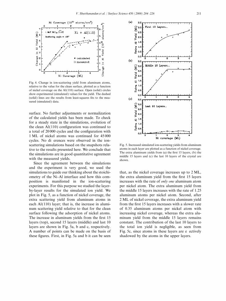
Fig. 4. Change in ion-scattering yield from aluminum atoms,relative to the value for the clean surface, plotted as a functionof nickel coverage on the Al(110) surface. Open (solid) circlesshow experimental (simulated) values for the yield. The dashed(solid) lines are the results from least-squares fits to the mea-sured (simulated) data.
surface. No further adjustments or normalizationof the calculated yields has been made. To checkfor a steady state in the simulations, evolution ofthe clean Al(110) configuration was continued toa total of 20 000 cycles and the configuration with1 ML of nickel atoms was continued for 45 000cycles. No differences were observed in the ion-
Fig. 5. Increased simulated ion-scattering yields from aluminumscattering simulations based on the snapshots rela-atoms in each layer are plotted as a function of nickel coverage.tive to the results presented here. We conclude thatThe extra aluminum yields from (a) the first 15 layers, (b) thethe simulations are in good quantitative agreementmiddle 15 layers and (c) the last 10 layers of the crystal are
with the measured yields. shown.Since the agreement between the simulations
and the experiment is very good, we used thesimulations to guide our thinking about the stoichi- that, as the nickel coverage increases up to 2 ML,
the extra aluminum yield from the first 15 layersometry of the Ni–Al interface and how this com-position is manifested in the ion-scattering increases with the rate of only one aluminum atom
per nickel atom. The extra aluminum yield fromexperiments. For this purpose we studied the layer-by-layer results for the simulated ion yield. We the middle 15 layers increases with the rate of 1.25
aluminum atoms per nickel atom. Second, afterplot in Fig. 5, as a function of nickel coverage, theextra scattering yield from aluminum atoms in 2 ML of nickel coverage, the extra aluminum yield
from the first 15 layers increases with a slower rateeach Al(110) layer; that is, the increase in alumi-num scattering yield relative to that for the clean of 0.35 aluminum atoms per nickel atom with
increasing nickel coverage, whereas the extra alu-surface following the adsorption of nickel atoms.The increase in aluminum yields from the first 15 minum yield from the middle 15 layers remains
constant. The contribution of the last 10 layers tolayers (top), second 15 layers (middle) and last 10layers are shown in Fig. 5a, b and c, respectively. the total ion yield is negligible, as seen from
Fig. 5c, since atoms in these layers are effectivelyA number of points can be made on the basis ofthese figures. First, in Fig. 5a and b it can be seen shadowed by the atoms in the upper layers.

212 V. Shutthanandan et al. / Surface Science 450 (2000) 204–226
In our HEIS experiment the relatively poor where epitaxy and shadowing of the substrate doesnot occur.depth resolution of the solid-state detector means
In region 2 of Fig. 2, for nickel coverages fromthat the extra ion-scattering yield from aluminum2.2 ML to 8.1 ML, the slope of 0.35 for theatoms for a particular nickel coverage is equal toscattering yield suggests that the average stoichi-the sum of the extra aluminum yield from Figs. 5a–ometry of the alloy formed here is 1:3, consistentc. For the clean Al(110) crystal, the contributionwith formation of Ni3Al. Even at this high nickelto the total ion-scattering yield from the middlecoverage, incoming nickel atoms are still leading15 layers as well as the last 10 layers is small sinceto the displacement of aluminum atoms, but at athe atoms in these layers are shadowed by theslower rate. Since we have a large source ofatoms in the top layers. However, we observe aaluminum atoms in the substrate, we might expectsignificant contribution to the extra aluminumaluminum atoms to diffuse to the surface. In fact,yields from the middle 15 layers of the simulatedthe effective heat of formation rule would predictcrystal as nickel atoms are added to the surface.the formation of aluminum-rich Al3Ni, the nextApparently, the presence of disordered aluminumstable phase on the aluminum-rich side of theatoms and relatively heavy nickel atoms near thephase diagram [24]. Apparently, the out-diffusionsurface leads to significant deflections of some ofof aluminum atoms from the substrate is inhibitedthe incident ions, and ultimately to an increasedby the existing NiAl reacted layer. We shall returnhitting probability in the middle 15 layers whichto this point later in the discussion.was absent in the clean Al(110) crystal. We refer
Above 8.1 ML of nickel coverage, the incomingto this phenomenon as near-surface dechanneling.nickel atoms are no longer displacing the alumi-The energy resolution of the solid-state detectornum atoms, as seen from the zero slope of alumi-(20 keV ) is insufficient to discriminate betweennum yield versus nickel coverage in region 3 ofthese dechanneled ions and the ions backscatteredFig. 2. This means that the interface reaction atfrom the top 15 layers where the disordered atomsroom temperature apparently stops and a nickel
reside. From the simulations we conclude thatmetal film begins to cover the surface. Up to the
almost half of the increased aluminum yield in the maximum coverage of this experiment, we did notinitial nickel coverage regime (up to 2 ML) is see any increase in the SPA of nickel for ionsassociated with near-surface dechanneling. After incident in a random direction as compared with2 ML of nickel coverage the dechanneling contri- the channeling direction. This absence of anbution remained constant. Thus, if we only con- increase in SPA tends to rule out the formation ofsider the first 15 layers, then the ion-scattering an ordered nickel overlayer or nickel islands ori-results and the XPS results to be discussed below ented with respect to the substrate channelingare consistent, indicating the formation of an NiAl- direction. We did not have a low-energy electronlike compound at the interface up to 2 ML of diffraction (LEED) capability in these experimentsnickel coverage and Ni3Al thereafter. The contri- to check for surface ordering. We conclude that,butions of multiple scattering and dechanneling to for these highest coverages, a disordered nickelthe surface peak area have been discussed in the film was formed on the reacted Ni–Al interface.past [28]. However, the typical contribution inthat case was much smaller than that seen in our 3.1.3. X-ray photoelectron spectroscopy: lineshapesimulations. Thus, our results should raise a cau- analysistion flag on the future use of the slope of scattering The channeling results by themselves are notyield to infer compound stoichiometry, at least for enough to justify our suggestion of the formationhigh-energy ion-scattering experiments where of different alloy phases at the interfaces. Fuggleenergy resolution is insufficient to distinguish and co-workers have studied in detail the chemicalbetween the two contributions. In this context, the shifts, satellite shifts, and shapes of the satelliteMC simulations are very important for fully under- and main 2p photopeaks ( XPS) of nickel in vari-
ous bulk Ni–Al alloy systems [39]. They foundstanding the experimental ion-scattering results

213V. Shutthanandan et al. / Surface Science 450 (2000) 204–226
that the base of the Ni 2p3/2 peak becomes more the main Ni 2p3/2 line becomes less symmetric asthe nickel coverage increases. We also see smallsymmetric as the aluminum concentration in vari-
ous Ni–Al alloys increases, because the satellite chemical shifts in the photopeak position.Furthermore, the peak position of the satellitepeak changes shape and its separation from the
photopeak increases. We have used these proper- moves towards the Ni 2p main peak, decreasingthe separation of the satellite and the main 2pties of the XPS peaks to complement the ion-
scattering results and to identify alloy stoichiome- peak. Thus the shape and separation of thesesatellites are quite different in the three regions oftry at the Ni–Al interface.
Fig. 6 shows plots of the X-ray photoelectron nickel coverage.We summarize the explanation for these featuresenergy distribution curves for the Ni 2p3/2 peak
(binding energy 852.65 eV ) and the satellite peak of the XPS spectra as follows. X-ray photoelectronspectra of pure nickel metal show a pronouncedfor different coverages of nickel on Al(110). Two
coverages were selected from each of the three ‘two-hole satellite’ at a higher binding energy [39].Electron energy-loss measurements of nickel showdifferent regions indicated in Fig. 2. The dashed
lines in Fig. 6 indicate the satellite peak positions that this intense core-level satellite is associatedwith intrinsic losses. The d-bands of nickel arefor the nickel, Ni3Al and NiAl phases based on
Ref. [39]. The spectra have been shifted vertically partially full, and at the same time the Fermi levelof nickel lies in the region where the d-band densityin order to compare the energy distribution curves.
From these figures one can see that the base of of states is high [40]. The Coulomb interactionbetween the core hole created by the photoexcita-tion and the unoccupied d-bands results in anexcited final state, leading to a satellite feature atlower kinetic energy (higher binding energy) in theNi 2p core-level spectrum [40–42]. In a relatedexperiment Fuggle et al. also showed that extrinsiccontributions to the satellite for Ni–Al alloys, suchas plasmon losses, are negligible compared withthe intrinsic losses [43]. The probability of creatinga ‘two-hole’ final state in Ni–Al alloys will thusdepend on the relative filling of the d-band nearthe Fermi level as well as any reduction in screeningof the core hole associated with charge transfer.Since the Pauli electronegativity of nickel (1.9) ishigher than that of aluminum (1.6), one wouldexpect that electrons are transferred from alumi-num to nickel in NiAl. But, both experiments andtheory suggest that the net electron transfer occursfrom nickel to aluminum [39,40]. Experimentally,the chemical shift of the nickel photopeak to largerbinding energy is consistent with transfer of chargeaway from the nickel atom. The theoretical pictureis not as clear, but using ‘Wigner–Seitz’ chargeanalysis, Lui and co-workers showed that nickel
Fig. 6. Ni 2p3/2 XPS spectra from nickel films deposited at room gains d-electrons while losing more sp-electrons totemperature on the Al(110) surface for selected nickel cover- aluminum, leading to a net electron transfer fromages, normalized to a constant height for the main peak. The
nickel to aluminum [40]. As for the filling of thedash–dot lines indicate satellite peak positions for three Ni–Ald-band in the alloys, the calculations suggest thatphases. The single dashed line indicates the 2p3/2 binding energy
for elemental nickel. while there is transfer from aluminum to the nickel

214 V. Shutthanandan et al. / Surface Science 450 (2000) 204–226
dilute nickel concentration near the aluminumsurface. Similar increases in core-level bindingenergies have also been reported for small metalclusters and atoms on inert substrates [45,46 ]. Thechemical shift then stays constant around 0.5 eVup to 2 ML of nickel coverage. After this, thechemical shift gradually decreases to zero at acoverage corresponding to approximately 6.5 ML,and stays at this value up to the maximum coverageof our experiment. The same trend was observedfor the satellite separation with increasing nickelcoverage. Up to 2 ML of nickel coverage theseparation has an average value of 7.5 eV.Thereafter it gradually decreases to the bulk valueof nickel (6.3 eV ) at a coverage of 6.5 ML. In
Fig. 7. The average chemical shifts for the Ni 2p line ( left axis — these plots the transition from region 1 to regionopen circles) and satellite separation for the Ni 2p3/2 line (right2 is not as clear as in the data of Fig. 2, possiblyaxis — closed circles) are plotted as a function of nickel coverageassociated with the relatively long attenuationon the Al(110) surface. Solid lines are provided to guide the eye.
lengths for photoelectrons with large kineticenergies.d-bands, the bands are not completely filled [44].
In Table 1 we compare our measured chemicalIn any case, it is the combination of charge transfershifts for the Ni 2p3/2 peak, and the separationand increased occupancy of the d-bands that isbetween the main 2p peak and the satellite peak,apparently responsible for the change in the posi-with Fuggle’s values. For the intermediate regiontions and shapes of the satellite and photopeak aswhich we have labeled in the table as Ni3Al, wethe concentration of nickel in the Ni–Al alloyhave used an average value for our data in theincreases.region from 2 to 6 ML of nickel coverage in Fig. 7.Fig. 7 plots the average chemical shift of theFrom the table we see that our measured valuesNi 2p line ( left axis) and the satellite separationfor the chemical shifts and the satellite separationbetween the main Ni 2p3/2 line and the satelliteare somewhat higher than Fuggle et al.’s values,peak (right axis) as a function of nickel coverage.but the trend of our values agrees very nicely withHere, we calculated the chemical shift as thetheirs. For example, the difference between thedifference between the binding energy of nickel insatellite separation in nickel and NiAl in Fuggle’sthe alloy phase and the binding energy of purecase is equal to 1.4 eV, while in our case it is equalnickel metal, averaged over both 2p lines. Afterto 1.2 eV. However, it is important to note athe very first nickel deposition we observed a
chemical shift of about 0.65 eV, attributed to a significant difference between the two experiments.
Table 1Comparison of chemical shifts and satellite separations for the Ni 2p3/2 peak in several Ni–Al alloys
Compound Chemical shift (eV ) Satellite separation (eV )
Our experiment Fuggle’s experiment Our experiment Fuggle’s experiment
Ni 0.0±0.2 0.0±0.2 6.3±0.4 5.8±0.4Ni3Al 0.2±0.2 0.0±0.2 6.9±0.4 6.5±0.2NiAl 0.5±0.2 0.2±0.2 7.5±0.4 7.2±0.4Ni2Al3 – 0.75±0.2 – 8.0±0.6NiAl3 – 1.05±0.2 –

215V. Shutthanandan et al. / Surface Science 450 (2000) 204–226
In Fuggle et al.’s experiment the XPS spectra for formats of the experiments themselves are quietdifferent, since in our experiments very thin nickelstoichiometric bulk Ni–Al alloys were measured,
while we collected XPS spectra for very thin films films were deposited on a single-crystal substrate,while in almost all of the other experiments thickof the Ni–Al alloys. Because of the large attenua-
tion lengths for these photoelectrons, our measure- nickel films were deposited on a polycrystallinesubstrate, and subsequently heated. In our experi-ments represent a superposition of the properties
of the nickel atoms throughout the films. Thus, ment we monitored the reaction while we werebuilding up the nickel film on the aluminum surfacewhile the ion-scattering technique provides well-
defined regions in terms of changes in the number at room temperature. It is also interesting to notethat a recent theoretical study of Ni–Al nanopar-of visible aluminum atoms, the XPS measurements
represent an average over the electronic properties ticles suggests that at 500 K three phases are foundto be stable in the core of the nanoparticles: NiAl,of much of the interface alloy. Furthermore, while
we did not observe any chemical shifts in the Ni 3p Ni3Al, and a face-centered cubic (fcc) solid solu-tion of aluminum in nickel [47]. The physicsline, we did see small chemical shifts in the Al 2p
line, but only comparable to our limited energy responsible for the stability of these particularphases in nanoparticles may be closely connectedresolution. Liu et al. reported a value of 0.2 eV
smaller binding energy for the Al 2p3/2 core level to the properties that determine the stoichiometryof the evolving Ni–Al interface observed in ourin NiAl [40]. Also, if we assume that we are
forming NiAl3 as the first phase at the interface, experiments.as seen by others, then based on the data in Table 1we should see a large chemical shift of about 3.1.4. X-ray photoelectron spectroscopy: intensity
analysis1.05 eV for the nickel peak. Such a shift, had itoccurred, would have been very evident in our Fig. 8a and b plot the normalized XPS inten-
sities for the Al 2p peak and the Ni 2p3/2 peak asexperiment, so we rule out the formation ofNiAl3 for thin nickel overlayers on Al(110) sur- a function of nickel coverage, respectively. The
aluminum intensity was normalized to the intensityfaces at room temperature.On the basis of the above discussion, we believe of the clean surface, while the nickel intensity was
normalized to its value at the maximum coveragethat in principle it is possible to identify the Ni–Al phases grown at the Ni–Al(110) interface by in our experiment (value at 12 ML). The thin solid
lines are intended to guide the eye, being liner fitslooking at the shape and the separation of thenickel photopeak and its satellite. In fact, the shifts to the data in the three coverage regimes defined
by the ion-scattering data. The intensity of theand the shapes depend on the electronic propertiesof nickel in these alloys, and are probably not Ni 2p peak (Fig. 8b) shows distinct slopes in the
different nickel coverage regimes, although thestrongly dependent on the precise geometricalstructure of the nickel atom environment. For transitions are in fact not sharp but somewhat
gradual. The aluminum XPS intensity (Fig. 8a)these thin films we do not expect that we haveactually formed the complete crystal structure of also shows three different attenuation rates. There
is an initial 10% drop followed by a region of littlethe respective nickel–aluminum compounds.Rather, we suggest that the chemical environment attenuation in the Al 2p intensity up to 2 ML of
nickel coverage. Thereafter, the intensity decreasesof the nickel atoms in our films is similar to thatof the nickel atoms in the various Ni–Al phases. at two different rates as the nickel coverage
increases.Thus, in comparing our lineshape with Fuggleet al.’s lineshapes, we conclude that the evolution As seen from Fig. 8a, the XPS intensity of
aluminum remains constant up to 2 ML of nickelof the Ni–Al interface follows a path from NiAl-like to Ni3Al-like to nickel metal film. These results coverage. This suggests that some of the aluminum
atoms are still present at the surface while theare significantly different from the bilayer experi-ments in which NiAl3 is the first phase reported nickel atoms diffuse into the substrate and react
with aluminum atoms. We also observed this beha-to form at the Ni–Al interface. Of course, the

216 V. Shutthanandan et al. / Surface Science 450 (2000) 204–226
HEIS measurements, since the depth resolution inHEIS is not adequate to determine segregation ona layer-by-layer basis. We shall discuss the quanti-tative agreement between the EAM simulationsand the XPS data in Section 3.1.6.
The aluminum intensity attenuates even moreafter 2 ML of nickel coverage, confirming theformation of a more nickel-rich phase at thesurface. The thick solid line in Fig. 8a shows theattenuation expected for the aluminum signalassuming that a flat nickel film grows on thesurface beginning at zero nickel coverage. For thecalculation we used an attenuation length of 20.3 Aand an interlayer spacing of 1.76 A, as discussedin the next section. The data are somewhat abovethis line, a fact that can be attributed to the alloyformation at the interface, or the formation ofnickel islands on the surface. As pointed out bySmith et al. for palladium on Al(111), it is difficultto distinguish between the formation of nickelislands and islands of a nickel–aluminum com-pound using Auger or XPS intensity analysis alone[48]. However, by using the chemical shiftsobserved in the XPS spectra for nickel we wereable to determine the formation of the nickel metaloverlayer. An analysis of the Ni 2p3/2 peaks showsthat the intensity increases (Fig. 8b) at threedifferent rates, depending on the nickel coverage.This behavior may also be modeled effectively
Fig. 8. Measured XPS intensities of (a) the Al 2p and (b) theusing three regions of island growth, with theNi 2p3/2 photoemission peaks as a function of nickel coverage.stoichiometry of the islands being NiAl andThe Ni 2p3/2 intensity has been normalized to its value at the
maximum coverage of our experiment (12 ML). The Al 2p Ni3Al in the respective regions.intensity was normalized to the value for the clean surface. Thelight solid lines are provided to guide the eye. Vertical lines are 3.1.5. X-ray photoelectron spectroscopy: intensityplaced at the break point in the ion-scattering yields as deter-
simulation studiesmined by Fig. 2. The heavy solid line was calculated assumingThe good agreement between the simulated andoverlayer growth of a Ni film as discussed in the text.
measured ion-scattering yields as shown in Fig. 4suggests that the MC simulations are correctlydescribing the movements of aluminum and nickelvior in the EAM simulations. Looking at the
snapshots ( Figs. 3b and c) very carefully for each atoms in the planes parallel to the surface. High-energy ion-scattering experiments performed withcoverage and calculating the number of aluminum
and nickel atoms in each layer, we conclude that ions at normal incidence are most sensitive to thesedisplacements. In order to characterize the move-up to 2 ML of coverage the incoming nickel atoms
move down into the aluminum substrate, causing ments of the atoms towards or away from thesurface we calculated the XPS intensities using thealuminum atoms to move off their lattice sites.
These displaced aluminum atoms move up into MC simulated snapshots and the surface sensitivityof XPS signals associated with the attenuation ofthe top layer. These observations reveal the impor-
tance of including XPS measurements with the photoelectron intensities at the respective kinetic

217V. Shutthanandan et al. / Surface Science 450 (2000) 204–226
energies. We use a simple model in which anexponential decay for the intensity of the photo-electrons through the layers is assumed, with amean attenuation length l [49]. We define z0 asthe z coordinate of the topmost layer of thesnapshots, and z
ias the z coordinate of the ith
atom in the crystal. Then the contribution to thephotoelectron intensity from this atom is given by
I0
expA− (zi−z
0)
l cos h B, (1)
where I0 is the unattenuated intensity if the atomresides at the surface, and h is the polar emissionangle between the surface normal and analyzer
Fig. 9. Simulated XPS intensities for the Ni 2p photoemission(30° in our case) [29]. The photoelectron cross-using the EAM snapshots with different values of l as indicated,section for the particular transition and all experi-plotted as a function of nickel coverage. Solid circles show themental parameters are also absorbed into I0. Then,experimental results.
the total XPS intensity from the adsorbate (nickel )and substrate (aluminum) will be given by thefollowing equations: best fit to the XPS nickel and aluminum intensities
of Fig. 8.INi=I0,Ni ∑
i=1NNi expA− (z
i,Ni−z0)
lNi cos h B (2) We plot in Fig. 9 the simulation results for theXPS intensity of the Ni 2p peak for different valuesof l, ranging from 1 A to 13.51 A. The final valueandwas obtained from the universal curve for thekinetic energy of the Ni 2p line [51]. Results for
IAl=I0,Al ∑i=1NAl expA− (z
i,Al−z0)
lAl cos h B, (3) some selected values of l are shown here. All ofthese intensities were normalized by a single valuefor I0; namely, the value obtained from the best-where NNi and NAl are the number of nickel and
aluminum atoms in the snapshots, and lNi and fitting line for our data. The goodness of fit waschecked by comparing the ratio of slopes beforelAl correspond to the attenuation lengths for
kinetic energies associated with the nickel and (S1) and after (S2) the first break in the intensityversus coverage curve, for both the measured andaluminum photoelectrons, respectively. z
i,Aland z
i,Ni are the z components of the ith nickel simulated data. Although the fit to the measureddata seems quite good in Fig. 9, there are consider-and aluminum atoms, respectively. Since the z
ivalues are determined by the MC simulation, and able fluctuations in the simulated XPS intensity
data (see Fig. 10b) associated with the statisticalh is determined by the experimental geometry, thel and I0 values are the only adjustable parameters nature of the simulation. Perhaps the most surpris-
ing result from these calculations is that the XPSin the above equations. Furthermore, I0s are justthe scaling factors in these equations, so l is the intensities calculated from the snapshots show the
break in intensity around 2 ML of nickel coverage.only free variable in these calculations. In fact,one might consider the value for l as fixed by the The existence of the break is independent of the
value of l as can be seen in Fig. 9. The best fit touniversal curve [50,51]. However, the value of l,particularly for an overlayer material, can vary the nickel data [S1(expt)/S2(expt)~S1(sim)/
S2(sim)] is obtained with a value of 5.19 A for l,dramatically from the value given by the universalcurve [52]. We applied the above equations to the considerably less than the value of 13.5 A obtained
from the universal curve. We performed an analysisMC simulated snapshots, and varied l to give the

218 V. Shutthanandan et al. / Surface Science 450 (2000) 204–226
experiment. The simulated aluminum intensity alsoshows the initial drop in the intensity followed bythe plateau up to 2 ML of nickel coverage.Therefore, from these ion-scattering and XPS cal-culations, we conclude that the MC simulationsprovide a reasonably good description of the inter-face structure. It is possible, however, that thesmall values obtained for l are an indication thatthe nickel atoms in the simulation may not havemoved as far below the surface as they are inreality for the Ni–Al interface.
3.1.6. Exploring the snapshotsSince the simulated ion-scattering yields and the
XPS intensities are agreeing quantitatively verywell with the measured values, we can hope thatthe MC simulations are correctly describing theNi–Al(110) reaction at room temperature.Therefore, by investigating the snapshots in severaldifferent ways we may be able to get more insightabout the reaction and growth process of nickelon Al(110). First, we consider the normalizedlayer occupancies, l; i.e., the number of atoms inlayer i divided by the number of lattice sites in theAl(110) layer (24 atoms). The layer occupanciesare plotted as a function of layer number forseveral Ni coverages in Fig. 11, where we show
Fig. 10. Simulated and measured XPS intensities for (a) the aluminum layer occupancies, nickel layer occupan-Al 2p, and (b) the Ni 2p3/2 photoemission as a function of nickel cies, and total (Ni+Al ) layer occupancies. Thecoverage. Solid (open) circles denote the simulated (measured) lines are spline fits to the data provided to guideresults. The best agreement with the data was obtained using
the eye. We define the surface layer of cleanattenuation lengths of 5.18 A for nickel and 15.0 A for alumi-Al(110) as the 0th layer, while the added layersnum. Solid lines are intended to guide the eye. Vertical lines are
placed at the break points in the ion-scattering yields as seen above the surface are denoted as 1st, 2nd and 3rdin Fig. 2. layers, respectively. At zero nickel coverage the
aluminum layer occupancies of the 0th and −1stlayers are one, while the occupancies of otherfor the aluminum XPS intensity similar to that
just described for the nickel intensity. The best fit layers (1, 2 and 3) are zero, as expected for a cleanaluminum crystal.to the aluminum data was obtained for l equal to
15 A, which is also smaller than the value obtained A number of points can be made based on thesefigures. First, in Fig. 11b it can be seen that as thefrom the universal curve, 20.2 A. Comparisons
between the measured and simulated intensities nickel coverage increases up to 2 ML the occu-pancy of nickel atoms in the 0th layer increasesfor aluminum and nickel XPS measurements
are shown in Fig. 10a and b, respectively. immediately, while the nickel occupancy in the 1stlayer becomes non-zero only after 0.5 ML of nickelExperimental results are denoted by open circles
while simulation results are indicated by solid deposition. This indicates that initially the depos-ited nickel atoms move down into the aluminumcircles. The solid lines are intended to guide the
eye. Clearly, both simulated (aluminum and substrate, causing aluminum atoms to move offtheir lattice sites. These displaced aluminum atomsnickel ) intensities show the same behavior as the

219V. Shutthanandan et al. / Surface Science 450 (2000) 204–226
in this layer stays nearly constant at the cleanAl(110) value (Fig. 11c). The second point is thatneither aluminum nor nickel atoms move into the2nd layer until after a coverage of 2 ML of nickelis achieved. Thus, aluminum atoms, piling up inthe 1st layer, and nickel atoms accumulating inthe 0th layer, contribute to an overall increase inlayer occupancies to a value of 1.5 in layers 0 and1, as seen in Fig. 11c. This increased density at theNi–Al interface, compared with the clean Al(110)layer density, is consistent with the formation of(110) planes of NiAl, and appears to be associatedwith the reduced reaction rate, and correspondingdecreased slope for aluminum ion yield seen inFig. 2 after 2 ML of nickel coverage. That is, after2 ML of nickel deposition, the aluminum atomsfrom below the interface will have more difficultypenetrating the relatively dense NiAl phase at theinterface, since most of the diffusion paths whichwere available earlier in the clean Al(110) layersare now blocked by extra atoms in these layers.Furthermore, looking again at Figs. 11a and b, wesee that after 2 ML of nickel coverage the occu-pancy of aluminum atoms in layer 1 starts decreas-ing. At the same time the nickel occupancy in layer1 is still increasing. Thus, after 2 ML of nickeldeposition we see the evolution of the dense inter-face towards a more nickel-rich composition, suchFig. 11. Normalized layer occupancies [number of atoms in a
layer divided by the number of sites in an Al(110) layer] as as Ni3Al, as suggested by the reduced slope fora function of layer number for selected Ni coverages for nickel ion yield in Fig. 2, and the Ni 2p XPS lineshapecoverage for (a) aluminum occupancies, (b) nickel occupancies, in Fig. 6.and (c) total occupancies in each layer. The surface layer of
The evolution of the simulated Ni/Al(110)clean Al(110) is labeled as the 0th layer. Added layers abovesystem is illustrated in Fig. 3, where a side view ofthe surface are labeled as 1st, 2nd, etc.the projected crystal (snapshot) is shown fordifferent coverages of nickel. At zero nickel cover-
move up into the 1st layer above the surface, as age, the clean Al(110) surface is well ordered asshown in Fig. 11a. That is, the occupancy of the seen in Fig. 3a. However, at a nickel coverage ofaluminum atoms in the 0th and −1st layers 0.5 ML the snapshot for the interface (Fig. 3b)decreases up to 2 ML of nickel coverage, while the shows the onset of reaction in the surface region.1st layer aluminum occupancy increases. This That is, a significant number of aluminum atomsbehavior was also evident in the aluminum XPS have already been displaced by the nickel adsorp-intensity profile (Fig. 8a) where the aluminum XPS tion. The snapshots for 2 ML and 3 ML of nickelintensity remains unchanged up to 2 ML of nickel on the Al(110) surface (Figs. 3c and d) also clearlycoverage. In fact, for 1 ML of nickel coverage, demonstrate the interfacial reaction between nickelabout 0.3 ML of nickel occupies the layer below and aluminum atoms. From these figures we seethe 0th layer (i.e., the −1st layer). Note also that that, with increasing nickel coverage, the Ni–while some nickel atoms moved into the −1st Al(110) interface is becoming more disorderedlayer, a corresponding amount of aluminum atoms whereas layers below the reacted interface remain
ordered. Furthermore, at 3 ML of nickel coverage,moved out of layer −1, so that the total occupancy

220 V. Shutthanandan et al. / Surface Science 450 (2000) 204–226
Table 2Comparison of some structural properties of aluminum, nickel,NiAl and Ni3Al
Crystal Structure Lattice Nearest-neighborconstant (A) distance (A)
Al fcc 4.051 2.863Ni fcc 3.508 2.481NiAl bcc 2.887 2.500Ni3Al fcc 3.589 2.537
the interface becomes more nickel-rich as seen inFig. 3d. This trend is observed for higher nickelcoverages as well.
The structural evolution of the Ni–Al(110)interface was further studied by calculating theaverage distances between nearest-neighbor atomsin each layer. Table 2 compares the structure,lattice constant and nearest-neighbor distance fordifferent Ni–Al alloys. From this table we can seethat the nearest-neighbor distances of NiAl,Ni3Al and nickel are very close to each other, butsignificantly different from that of aluminum.Hence, by looking at these distances in the snap-shots, we hoped to distinguish the different phasesformed at the Ni–Al interface during the nickeldeposition. Fig. 12 presents the average distancesbetween nearest-neighbor atoms in each layer plot-ted as a function of nickel coverage. We considered
Fig. 12. The average nearest-neighbor distances of atoms ina spherical shell, with radius R, around one atom each layer, calculated from the EAM snapshots and plotted asin a specific layer. Atoms inside this shell were a function of nickel coverage, are shown for two different valuesconsidered as the nearest neighbors for the atom of the shell radius as discussed in the text.
at the center of the shell. The average nearest-neighbor distance of a particular layer wasobtained by calculating the average distance NiAl and Ni3Al nearest-neighbor distances, and
significantly less than that for aluminum. This canbetween the atoms within the shell and the centeratom, and then averaged over the atoms in that also be seen in Fig. 11 and characterized by the
increase in the occupancies of these layers (0particular layer. This procedure was repeated forseveral layers. Different values of R were consid- and 1).
We repeated the analysis of the snapshots for aered for these calculations. Figs. 12a and b showthe calculated nearest-neighbor distances for some near-neighbor shell radius of 3.2 A, since this value
would include the aluminum nearest-neighbor dis-selected layers using shells with a radius of 2.7 Aand 3.2 A, respectively. The value of 2.7 A was tance. From Fig. 12b we can clearly see the struc-
tural transformation of the interface between 0chosen because the nearest-neighbor distances ofnickel, NiAl and Ni3Al are closer to this value. It and 2 ML of nickel coverage. The average nearest-
neighbor distances in the aluminum layers (0, −1,can be seen from Fig. 12a that the average nearest-neighbor distance between atoms in these simu- and −2) decrease with increasing nickel coverage
up to 2 ML, showing that the aluminum atoms inlated surface layers (−2 to 3) is comparable to the

221V. Shutthanandan et al. / Surface Science 450 (2000) 204–226
Table 3Comparison of nearest-neighbor atom types for two bulk nickel–aluminum phases, and summary of nearest-neigbor atom types inthe simulated snapshots of the Ni–Al interface
Atom No. of Al nearest No. of Ni nearest Atom No. of Al nearest No. of Ni nearestneighbors neighbors neighbors neighbors
NiAl Ni 8 0 Ni3Al Ni 4 8Al 0 8 Al 0 12
1.5 ML 3.5 MLLayer 0 Ni 7 4 Layer 0 Ni 6 6
Al 6 3 Al 5 7Layer 1 Ni 5 3 Layer 1 Ni 6 5
Al 6 3 Al 4 8Layer 2 Ni 4 3 Layer 2 Ni 4 5
Al 0 0 Al 2 6
the reacted region are closer to their nearest neigh- eight nickel nearest neighbors. For Ni3Al, on theother hand, nickel atoms have eight nickel nearest-bors than in the clean aluminum crystal.
Furthermore, the nearest-neighbor distances satu- neighbor and four aluminum nearest-neighboratoms, while the 12 nearest neighbors of aluminumrate upon completion of 2 ML of nickel. All of
these values are a little larger than the values atoms are all nickel. We studied the simulationsnapshots for evidence of this redistribution ofshown in Fig. 12a and those for NiAl and Ni3Al,
since the larger radius used in Fig. 12b includes neighbor atom type. The lower half of Table 3 showsthe results for layers 0, 1 and 2 at nickel coveragessome of the atoms in other layers as well as next-
nearest neighbors of the NiAl structure. It can of 1.5 ML and 3.5 ML. Again, the results are notconclusive but there is a definite tendency towardsalso be seen in Fig. 12b that the nearest-neighbor
distances in layers −3 and −4, while somewhat more nickel-rich surroundings for the aluminumatoms, with the number of nickel neighbors aroundaffected by the nickel deposition, remain relatively
close to the value for the aluminum substrate, the aluminum atoms nearly doubling as the coverageis increased from 1.5 to 3.5 ML. Also, the numberconfirming that the Ni–Al alloy formation is rela-
tively localized at the interface. Unfortunately, the of nickel–nickel pairs in layer 0 is smaller at lowcoverage, similar to the trend for the two bulkstatistics of the calculations with these relatively
small snapshots did not lead to a positive identifi- phases. On the other hand, while the two bulkphases have no aluminium–aluminum nearest-neigh-cation of the phases formed at the interface upon
the nickel deposition. The nearest-neighbor dis- bor pairs, the aluminum atoms in the snapshot dohave aluminum nearest neighbors. However, a ten-tances of NiAl, Ni3Al and nickel are all too close
to each other as seen from Table 2. dency for the number of these aluminum–aluminumpairs to decrease is seen in layers 0 and 1 as theAnother interesting distinction among the
different nickel–aluminum phases, besides the nickel coverage increases.changes in nearest-neighbor distances, is the changein nearest-neighbor atom type. We show in Table 3 3.2. Nickel deposition on Al (110) at 250°Cthe number and type of nearest neighbors for theNiAl and Ni3Al phases. For the pure elements, As mentioned earlier, there is a large amount
of work concerning Ni–Al interface formation andnickel and aluminum, the structure is fcc and eachatom has 12 nearest neighbors. As shown in Table 3, its characterization [14–19]. Most of the work has
been done with polycrystalline or bilayer samplesNiAl is body-centered cubic (bcc) with the CsClstructure, so each nickel atom has eight aluminum and at elevated temperatures. Reaction temper-
atures observed in these experiments are generallynearest neighbors and each aluminum atom has

222 V. Shutthanandan et al. / Surface Science 450 (2000) 204–226
reported to be in the range of 225–325°C. Very diffusing very deep into the aluminum substrate,and the number of nickel atoms in the surfacefew experiments have been reported for room-
temperature reaction [15,19]. To complement these region is much lower than that observed for room-temperature deposition. Second, the backgroundresults with measurements for a single-crystal sub-
strate, we deposited nickel atoms while the Al(110) behind the aluminum surface peak is larger for the250°C deposition. A portion of this increase maysurface temperature was maintained at 250°C. Ion-
scattering and XPS measurements were then made be associated with reduced channeling at the meas-urement temperature (110 °C) because of the largerafter the sample had cooled for several minutes to
a temperature around 110°C. All other experimen- vibration amplitude of the aluminum atoms atelevated temperatures [29]. However, it is alsotal parameters were the same as the room-temper-
ature experiment. likely that the presence of nickel atoms deep inthe substrate leads to significant deflection of somehelium ions, and increases the backscattering yield3.2.1. High-energy ion-scattering and channeling
studies from substrate aluminum atoms.We plot in Fig. 14 the backscattered ion-energyFig. 13 compares the ion-scattering energy dis-
tribution curves from these two experiments, distribution curve for nickel and aluminum forseveral different nickel coverages. The arrows indeposition at room temperature (open circles) and
at 250°C (closed circles), for the same nickel cover- the figure indicate the expected positions for sur-face nickel and aluminum atoms. The spectra haveage of 1.75 ML. Clearly, the two spectra are sig-
nificantly different from each other. First, the well- been shifted vertically in order to compare themmore easily. From this figure we immediately con-defined surface peak of nickel for deposition at
room temperature (50 keV wide) is now spread clude that, while some of the nickel atoms arepresent at the surface (Ni arrow) with aluminumover a large region (150 keV wide) for deposition
at 250°C. This indicates that the nickel atoms are atoms, most of the nickel atoms are diffusing into
Fig. 13. Ion backscattering spectra for 1.7 ML of nickel deposited on the Al(110) surface at two different temperatures. Open (closed)circles show the results for deposition with a substrate temperature of 30°C (250 °C). Backscattered ion-energy positions correspondingto nickel and aluminum surface atoms are indicated by the arrows.

223V. Shutthanandan et al. / Surface Science 450 (2000) 204–226
Fig. 15. Backscattered ion spectra for 1 MeV He+ ions after thedeposition of 4.78 ML of nickel on Al(110) surface at 250°C.Open (closed) circles show the spectrum for random (channel-
Fig. 14. Ion backscattering spectra for nickel deposited on the ing) alignment of the ion beam.Al(110) surface at 250°C for different nickel coverages as indi-cated in the figure. The spectra have been offset for better visibil-
concentration of nickel is quite low, with 4.8 MLity. The arrows indicate the expected energy positions forbackscattered ions from aluminum and nickel surface atoms. of nickel distributed over several hundred
Angstroms as indicated by the width of thenickel peak.the aluminum bulk. We also note that the nickel
peak width is increasing with increasing nickel Fig. 15 shows two ion-scattering spectra col-lected after 4.8 ML of nickel deposition at 250°C.coverage, indicating that after each nickel depos-
ition more nickel atoms are diffusing deeper into One spectrum (solid circles) was taken with theHe+-ion beam in the channeling direction, atthe aluminum bulk. As mentioned earlier, the
presence of these diffusing nickel atoms in the normal incidence, while the other spectrum (opencircles) was taken with the ion beam in a randomaluminum bulk causes the ‘bulk dechanneling’ to
increase. This increase is very noticeable in these direction, a few degrees away from the channelingdirection. We do not see any reduction in the peakfigures, as the background behind the aluminum
surface peak is increasing with the nickel coverage. area for nickel for the channeling geometry. Thissuggests that no Ni–Ni or Al–Ni shadowing existsAfter 4.8 ML of nickel coverage the aluminum
surface peak has nearly lost its original shape, in this region as might occur, for example, if thenickel occupied substitutional sites on the alumi-determined by the detector energy resolution. The
change of the aluminum backscattering yield with num lattice. From the backscattering spectrumcollected in the random geometry (Fig. 15),increasing nickel coverage is believed to be associ-
ated with the disorder of aluminum atoms in the together with the energy loss of helium ionsthrough the Al–Ni alloy and other experimentalsubstrate caused by the diffusing nickel atoms.
That is, the increase represents not only the visibil- parameters, we calculated the concentration–depthprofile of nickel atoms in the aluminum crystal.ity of aluminum atoms which have moved off
lattice sites, but also the dechanneling of helium The computer simulation code was used forthis purpose [53]. A solid solution of about 2%ions which have had their trajectories altered as a
result of passing through the disordered layer. In nickel in aluminum gave the best fit to the data.From these calculations we conclude that the nickelthis respect, the increase is similar to the dechanne-
ling that we discussed earlier associated with disor- atoms diffused about 400 A deep into the alumi-num crystal. It is clear from the data that theder at the Ni–Al interface. Note that the actual

224 V. Shutthanandan et al. / Surface Science 450 (2000) 204–226
nickel concentration is not uniform, with thelargest nickel concentration occurring in the regionfrom 100 to 200 A below the surface. The randomspectrum shown in Fig. 15 is not a truly randomspectrum because of the difficulty in completelyavoiding channeling in a single crystal. Yet, thefact that the nickel portion of the spectrum isthe same for the two spectra displayed indicatesthat all the nickel atoms in the substrate are visibleto the incident ion beam.
3.2.2. X-ray photoelectron spectroscopy studiesAfter each nickel deposition, XPS spectra of
the Ni 2p and the Al 2p core levels were collected.For each nickel deposition we observed a verysmall chemical shift in the Ni 2p3/2 peak. In Fig. 16we plot the normalized XPS intensities (solid cir-cles) for the Al 2p peak and the Ni 2p peak as afunction of nickel coverage. For comparison, wehave included the XPS intensities from the room-temperature deposition results (open circles). Thenickel XPS intensity for deposition at 250°C hasbeen normalized to the value of the intensity atthe maximum coverage in our room-temperatureexperiment. As before, the aluminum XPS inten-sity has been normalized to the intensity of theclean surface. From these figures it is clear thatthe behavior of the XPS intensities for both nickeland aluminum are quite different for deposition atthe two different temperatures. For deposition at250°C, the aluminum intensity stayed almost con-
Fig. 16. Measured XPS intensities for the (a) Al 2p and (b) thestant at its initial value for the clean surface. This Ni 2p3/2 photopeaks as a function of nickel coverage onsuggests that, even with 4.8 ML of deposited Al(110), deposited at 250°C (filled circles). The Ni 2p3/2 inten-
sity was normalized to the nickel intensity of the maximumnickel, the nickel atoms do not stay at the surface.coverage in the room-temperature experiment (12 ML). TheInstead they diffuse deep into the substrate and doAl 2p intensity is normalized to the value for the clean surface.not attenuate the aluminum XPS signal. Also, theThe room-temperature results (open circles) are shown forintensity of the nickel photoelectrons is much comparison.
smaller than that observed for deposition at roomtemperature. Thus, both the ion-scattering and the
scopy experiments for ultrathin nickel films depos-XPS results show that nickel atoms deposited atited on the Al(110) surface at room temperature250°C do not stay at the aluminum surface, butand at 250°C. Nickel atoms deposited at roominstead diffuse several hundred Angstroms into thetemperature continuously displaced the aluminumaluminum substrate.atoms for up to 8.1 ML of nickel coverage, indicat-ing a reaction at the interface between the nickeland aluminum atoms. For the first 2 ML of depos-4. Conclusionited nickel, an NiAl-like compound is formed whilefor nickel deposition between 2 and 8 ML, anIn summary, we have performed high-energy
ion-scattering and X-ray photoelectron spectro- Ni3Al-like compound is formed. These results

225V. Shutthanandan et al. / Surface Science 450 (2000) 204–226
differ significantly from those reported previously Referencesfor nickel/aluminum bilayers and evaporated films,where NiAl3 was the initial reaction product [1] N.R. Shivaparan, V. Shutthanandan, V. Krasemann,
R.J. Smith, Surf. Sci. 373 (1997) 221.observed. After 8 ML of nickel deposition, a nickel[2] X. Mingde, R.J. Smith, J. Vac. Sci. Technol. A 9 (1991)metal film starts to cover the reacted interface.
1828.Nickel atoms deposited at 250°C show no evidence [3] A.A Saleh, V. Shutthanandan, N.R. Shivaparan,of compound formation with aluminum atoms, R.J. Smith, T.T. Tran, S.A. Chambers, Phys. Rev. B 56
(1997) 9841.but diffuse 400 A deep into the aluminum sub-[4] A.A Saleh, V. Shutthanandan, N.R. Shivaparan,strate. We have used embedded-atom method
R.J. Smith, T.T. Tran, S.A. Chambers, Phys. Rev. B 49potentials together with Monte Carlo simulations(1994) 4908.
to study the clean Al(110) surface and the reaction [5] R.J. Smith, Y.W. Kim, N.R. Shivaparan, G.A. White,between nickel and aluminum atoms at the inter- M.A. Teter, Surf. Interface Anal. 27 (1999) 185.
[6 ] J.H. van der Merwe, E. Bauer, Phys. Rev. B 39 (1989)face. Snapshots of the evolving interface suggest3632.that the initial deposition of nickel results in a
[7] C.C. Koch, C.T. Liu, N.S. Stoloff, A. Wannier (Eds.),relatively dense NiAl phase that impedes furtherHigh-Temperature Ordered Intermetallic Alloys VIIMater.
out-diffusion of aluminum atoms from the sub- Res. Soc. Proc. Vol. 460 Materials Research Society, Pitts-strate. The interface composition is gradually burg, PA, 1997, and preceding volumes in this series.
[8] D.M. Zehner, D.W. Goodman (Eds.), Physical and Chem-transformed to a more nickel-rich phase, with theical Properties of Thin Metal Overlayers and Alloy Sur-nickel atoms having an electronic environmentfacesMater. Res. Soc. Proc. Vol. 83 Materials Researchsimilar to that of Ni3Al, and ultimately coveredSociety, Pittsburg, PA, 1987.
by nickel metal. Calculated ion-scattering yields [9] P.J Feibelman, R. Hamann, Surf. Sci. 173 (1986) L582.and X-ray photoelectron intensities using the snap- [10] T. Sands, Appl. Phys. Lett. 52 (1988) 197.
[11] T. Hamaguchi, H. Aida, S. Nakagawa, M. Naoe, J. Appl.shots are in remarkably good agreement with thePhys. 73 (1993) 6444.experimental results. The ion-scattering simula-
[12] T. Haeiwa, H. Negoro, M. Matsumoto, J. Appl. Phys. 69tions further reveal a surprising amount of ‘near-(1991) 5348.
surface dechanneling’ occurring just below the [13] N.R. Shivaparan, V. Krasemann, V. Shutthanandan,interface for the first few monolayers of nickel R.J. Smith, Surf. Sci. 365 (1996) 78.
[14] M. Nastasi, L.S. Hung, J.W. Mayer, Appl. Phys. Lett. 43deposition, bringing into question any interpreta-(1983) 831.tion of HEIS channeling data in terms of com-
[15] M.W. Ruckman, L. Jiang, M. Strongin, J. Vac. Sci. Tech-pound stoichiometry.nol. A 8 (1990) 134.
[16 ] E. Ma, M.-A. Nicolet, M. Nathan, J. Appl. Phys. 65(1989) 2703.
[17] J. Eridon, G.S. Was, L. Rehn, J. Mater. Res. 3 (1988) 626.[18] G. Dorey, Thin Solid Films 5 (1970) 69.Acknowledgements[19] S.M. Heald, E.V. Barrera, J. Mater. Res. 6 (1991) 935.[20] A. Arranz, C. Palacio, Thin Solid Films 317 (1998) 55.
The authors wish to thank Dr Art Voter from [21] K. Barmak, C. Michaelsen, G. Lucadamo, J. Mater. Res.Los Alamos National Laboratory, Los Alamos, 12 (1997) 133.
[22] C. Michaelsen, G. Lucadamo, K. Barmak, J. Appl. Phys.NM for providing the EAM potentials for nickel,80 (1996) 6689.aluminum and Ni–Al alloys, and Dr A.W. Denier
[23] P. Hahn, M.F. Bertino, J.P. Toennies, M. Ritter, W. Weiss,van der Gon from the Physics Department,Surf. Sci. 412/413 (1998) 82.
Eindhoven University of Technology, The [24] R. Pretorius, A.M. Vredenberg, F.W. Saris, R. de Reus,Netherlands, for his helpful discussion about the J. Appl. Phys. 70 (1991) 3636.
[25] R.J. Smith, C.N. Whang, X. Mingde, M. Worthington, C.Monte Carlo simulations. We are also grateful forHennessy, M. Kim, N. Holland, Rev. Sci. Instrum. 58the technical assistance of Norm Williams and(1987) 2284.Erik Andersen. This work was supported by the
[26 ] I. Stensgaard, L.C. Feldman, P.J. Silverman, Surf. Sci. 77National Science Foundation under Grants (1978) 513.DMR-9409205 and DMR-9710092, and by NASA [27] E.J. Van Loenen, M. Iwami, R.M. Tromp, J.F.W. van der
Veen, Surf. Sci. 137 (1984) 1.EPSCoR Grant NCCW-0058.

226 V. Shutthanandan et al. / Surface Science 450 (2000) 204–226
[28] K. Kinoshita, T. Narusawa, W.M. Gibson, Surf. Sci. 110 [40] S.-C. Lui, J.W. Davenport, E.W. Plummer, D.M. Zehner,G.W. Fernando, Phys. Rev. B 42 (1990) 1582.(1981) 369.
[41] W. Eberhardt, E.W. Plummer, Phys. Rev. B 21 (1980)[29] L.C. Feldman, J.W. Mayer, Fundamentals of Surface and3245.Thin Films Analysis, North-Holland, Amsterdam, 1986.
[42] S. Hufner, G.K. Wertheim, Phys. Rev. Lett. A 51 (1975)[30] M. Hansen, in: K. Anderko (Ed.), Constitution of Binary301.Alloys, McGraw-Hill, New York, 1958.
[43] J.C. Fuggle, F.U. Hillbrecht, R. Zeller, Z. Zolnierek, P.A.[31] V. Shutthanandan, A.A. Saleh, R.J. Smith, Phys. Rev. BBennett, Phys. Rev. B 27 (1983) 2145.48 (1993) 18 292.
[44] P.A. Schultz, J.W. Davenport, Scripta Metall. Mater. 27[32] V. Shutthandandan, Ph.D. thesis, Montana State Univer-(1992) 629.sity, 1994.
[45] U. Diebold, J.-M. Pan, T.E. Madey, Phys. Rev. B 47[33] A.W. Denier van der Gon, D. Frenkel, J.W.M. Frenken,(1993) 3868.R.J. Smith, P. Stoltze, Surf. Sci. 256 (1991) 385.
[46 ] W.F. Egelhoff, Surf. Sci. Rep. 6 (1987) 253.[34] N. Metropolis, A.W. Rosenbluth, M.N. Rosenbluth, A.H.
[47] S. Ramos de Debiaggi, J.M. Campillo, A. Caro, J. Mater.Teller, E. Teller, J. Chem. Phys. 21 (1953) 1087. Res. 14 (1999) 2849.
[35] A.F. Voter, S.P. Chen, in: R.W. Siegel, J.R. Weertman, R. [48] R.J. Smith, A.W. Denier van der Gon, J.F. van derVeen,Sinclair (Eds.), Characterization of Defects in Materials, Surf. Sci. 233 (1990) 103.MRS Symp. Proc. Vol. 82, Materials Research Society, [49] S. Ossicini, R. Memeo, F. Ciccacci, J. Vac. Sci. Technol.Pittsburgh, PA, 1986, p. 175. A 3 (1985) 387.
[36 ] S.M. Foiles, M.S. Daw, J. Mater. Res. 2 (1987) 5. [50] S. Tanuma, C.J. Powell, D.R. Penn, Surf. Interface Anal.[37] S.P. Chen, A.F. Voter, D.J. Sroloritze, Phys. Rev. Lett. 57 11 (1988) 577.
(1986) 1308. [51] M.P. Seah, W.A. Dench, Surf. Anal. 1 (1979) 2.[38] S.M. Foiles, Phys. Rev. B 32 (1985) 7685. [52] H. Li, B.P. Tonner, Surf. Sci. 237 (1990) 141.[39] F.U. Hillerbrecht, J.C. Fuggle, P.A. Bennett, Z. Zolnirek, [53] L.R. Doolittle, Nucl. Instrum. Methods Phys. Res. B 9
(1985) 344.C.h. Freiburg, Phys. Rev. B 27 (1983) 2179.