Adsorbate induced self-ordering of germanium nanoislands on Si(113
14
This content has been downloaded from IOPscience. Please scroll down to see the full text. Download details: IP Address: 181.214.24.4 This content was downloaded on 19/07/2015 at 11:54 Please note that terms and conditions apply. Adsorbate induced self-ordering of germanium nanoislands on Si(113) View the table of contents for this issue, or go to the journal homepage for more 2007 New J. Phys. 9 392 (http://iopscience.iop.org/1367-2630/9/10/392) Home Search Collections Journals About Contact us My IOPscience
-
Upload
bits-pilani -
Category
Documents
-
view
0 -
download
0
Transcript of Adsorbate induced self-ordering of germanium nanoislands on Si(113

This content has been downloaded from IOPscience. Please scroll down to see the full text.
Download details:
IP Address: 181.214.24.4
This content was downloaded on 19/07/2015 at 11:54
Please note that terms and conditions apply.
Adsorbate induced self-ordering of germanium nanoislands on Si(113)
View the table of contents for this issue, or go to the journal homepage for more
2007 New J. Phys. 9 392
(http://iopscience.iop.org/1367-2630/9/10/392)
Home Search Collections Journals About Contact us My IOPscience

T h e o p e n – a c c e s s j o u r n a l f o r p h y s i c s
New Journal of Physics
Adsorbate induced self-ordering of germaniumnanoislands on Si(113)
Thomas Schmidt 1,5, Torben Clausen 1, Jan Ingo Flege 1,6,Subhashis Gangopadhyay 1,7, Andrea Locatelli 2,Tevfik Onur Mentes 2, Fang Zhun Guo 3, Stefan Heun 4
and Jens Falta 1
1 Institute of Solid State Physics, University of Bremen, Otto-Hahn-Allee 1,28 359 Bremen, Germany2 Elettra Sincrotrone Trieste S.C.p.A., Strada Statale 14 km 163.5,AREA Science Park, 34012 Basovizza, Trieste, Italy3 SPring-8/JASRI, Kouto 1-1-1, Mikazuki, Sayo-gun, Hyogo 679-5198, Japan4 NEST CNR-INFM Scuola Normale Superiore, Piazza dei Cavalieri 7,56126 Pisa, ItalyE-mail: [email protected]
New Journal of Physics 9 (2007) 392Received 18 May 2007Published 31 October 2007Online athttp://www.njp.org/doi:10.1088/1367-2630/9/10/392
Abstract. The impact of Ga preadsorption on the spatial correlation ofnanoscale three-dimensional (3D) Ge-islands has been investigated by low-energy electron microscopy and low-energy electron diffraction. SubmonolayerGa adsorption leads to the formation of a 2D chemical nanopattern, since theGa-terminated (2× 2) domains exclusively decorate the step edges of the Si(113)substrate. Subsequent Ge growth on such a partially Ga-covered surface resultsin Ge 3D islands with an increased density as compared to Ge growth on cleanSi(113). However, no pronounced alignment of the Ge islands is observed.Completely different results are obtained for Ga saturation coverage, whichresults in the formation of (112) and (115) facets regularly arranged with aperiodicity of about 40 nm. Upon Ge deposition, Ge islands are formed at a highdensity of about 1.3× 1010 cm−2. These islands are well ordered as they alignat the substrate facets. Moreover, the facet array induces a reversal of the Geislands’ shape anisotropy as compared to growth on planar Si(113) substrates.
5 Author to whom any correspondence should be addressed.6 Present address: Brookhaven National Laboratory, Upton, NY, USA.7 Present address: School of Physics and Astronomy, University of Nottingham, Nottingham NG7 2RD, UK.
New Journal of Physics 9 (2007) 392 PII: S1367-2630(07)50612-91367-2630/07/010392+13$30.00 © IOP Publishing Ltd and Deutsche Physikalische Gesellschaft

2
Contents
1. Introduction 22. Experimental 33. Results and discussion 4
3.1. Submonolayer Ga coverage. . . . . . . . . . . . . . . . . . . . . . . . . . . . 43.2. Ge growth on step-edge-decorated Ga:Si(113). . . . . . . . . . . . . . . . . . 53.3. Ga saturation coverage. . . . . . . . . . . . . . . . . . . . . . . . . . . . . . 63.4. Ge growth on facetted Ga:Si(113). . . . . . . . . . . . . . . . . . . . . . . . 9
4. Conclusion 11Acknowledgments 12References 12
1. Introduction
The growth of nanoscale three-dimensional (3D) germanium islands on silicon has attracted alarge interest because of potential technological applications in opto-electronic devices [1]–[3].For many of these applications, a uniform size distribution of the nanoislands is important.This is closely related to a uniform distribution of the islands’ distance distribution, becausevia growth kinetics, island nuclei with regular spacing will grow at similar rates. Thiscorrelation between regular arrangement and size distribution has been demonstrated forstacked layers of Ge islands with Si spacer layers in between [4]–[6]. An explanation forthe spatial ordering of nanoscale islands in stacked hetero-epitaxial structures has been givenin terms of strain [7]. After overgrowth with a spacer layer of the host material, the latticemismatch leads to strain fields emerging from the islands. This results in a strain modulationat the spacer layer surface and, thus, to heterogeneous nucleation conditions. For a properchoice of the spacer layer thickness, this approach does not lead to a reproduction of thenucleation sites in the next layer (strong vertical ordering), but to a reduced vertical orderingwhich allows for an increase of the lateral ordering with increasing number of island layers,as has been demonstrated for many different material systems like InAs/GaAs(001) [8, 9],InP/InGaP(001) [10], PbSe/PbTe(111) [11, 12] and CdSe/ZnSe(001) [13, 14].
In comparison to artificially introduced ordering, e.g. by electron beam lithography [15] oratomic probe manipulation [16], the above-mentioned approach of growing stacked nanoislandstructures employs self-organization and, thus, is much better suited for technologicalapplications, since it enables parallelized fabrication. However, this self-ordering approach has amajor drawback: in the bottom layers, the islands are still quite randomly distributed. Differentself-organized growth techniques have been employed in order to produce regularly spacednanostructures in a single layer, i.e. without (or prior to) stacking. Most of these techniquesagain employ a strain modulation of the substrate in order to induce heterogeneous, spatiallyperiodic nucleation conditions. For instance, this can be achieved by using dislocated [17]or rippled, pseudomorphically strained [18, 19] GexSi1−x buffer layers. In these cases, thelateral periodicity is coupled to the Ge contentx, therefore this parameter can hardly beused for additional tailoring of the electronic properties. This limitation might be overcomeby using adsorbate-induced self-ordering. Recently, we were able to show that submonolayer
New Journal of Physics 9 (2007) 392 (http://www.njp.org/)

3
deposition of Ga on Si(111) at high temperature leads to the decoration of step edges and domainboundaries of the initial Si(111)-(7× 7) domains [20, 21]. As a consequence, a 2D nanopatternof Ga-terminated and Ga-free surface regions can be achieved, and subsequent Ge deposition onsuch a chemically modulated surface results in the growth of 3D nanoscale Ge islands alignedat step edges and domain boundaries [22]. In the present study, we explore the possibilities touse the approach of adsorbate-induced ordering for the alignment of Ge islands on the Si(113)surface. As will be shown in the following, this approach can also be applied here, but themechanism, as compared to Si(111), is completely different, allowing for even more pronouncedGe island ordering.
In contrast to many other high-index Si surfaces, the Si(113) surface has a low surfacefree energy [23] and is, therefore, a stable facet of Si. From a technological point of view [24],Si(113) might become an alternative to Si(001), the latter still being the substrate for mostdevice applications. In contrast to Si(111), the lack of rotational symmetry of the Si(113) surfacefacilitates the growth of highly anisotropic Ge islands. In a narrow temperature and coveragerange, nanowires extending in [332̄] direction can be grown [25, 26]. It is believed [27] that thisstrong anisotropy is stabilized by a reduction of the strain energy originating from the latticemismatch between Ge and Si. However, this is controversially discussed [28]. It is also reportedthat the nanowires are metastable and can be transformed into elongated islands by ripeningat growth temperature [29], hence growth kinetics and especially diffusion anisotropy mightalso play an important role. Regarding the spatial correlation of such Ge nanowires (as wellas that of similar GexSi1−x nanowires), vertical ordering in stacked heterostructures has beenobserved [30]–[32]. However, no reports on lateral ordering of Ge nanostructures on Si(113) areavailable so far. In the following, we present low-energy electron microscopy (LEEM) resultsin order to address that issue. This experimental method has already been shown to be very wellsuited for the study of the evolution of Ge nanostructures during growth on Si [22, 33].
2. Experimental
The experiments discussed in the following were performed in the ultra-high vacuum set-upat the spectroscopic photoemission and low-energy electron microscope [34, 35] located at theundulator beamline 1.2 at the Elettra synchrotron light source, with a base pressure in the low10−10 mbar range.
The Si(113) substrates were degassed at 600◦C for at least 12 h. The native oxide wasremoved by 2–3 short flashes to about 1200◦C for up to 30 s. This procedure results in theformation of the (3× 2) surface reconstruction. Subsequently, the samples were exposed todifferent deposits of Ga at a temperature of about 500◦C. Finally, Ge was grown at temperaturesranging from 460 to 500◦C, without Ga codeposition. All preparation steps as mentionedabove were monitoredin situ by low-energy electron diffraction (LEED) and LEEM. Thetemperature was measured with an infrared pyrometer as well as with a thermocouple attachedto the sample holder. The absolute accuracy is estimated to be about±40◦C. Both Ga andGe were evaporated from effusion cells heated by electron beam bombardment, at depositionrates of about 0.17 and 0.24 ML min−1 for Ga and Ge, respectively. One monolayer (ML)corresponds to 4.09× 10¹⁴ atoms cm−2. Experiments without Ga preadsorption were performedto calibrate the Ge evaporator flux. For this purpose, we used the onset of the formation ofGe Stranski–Krastanov islands [36] at 4.4 bilayers (BL; 1 BL= 2 ML), as previously reportedby Yasueet al [37]. As the Ge sticking coefficient can be expected to be very close to unity,
New Journal of Physics 9 (2007) 392 (http://www.njp.org/)
4
(a)
0 ML Ga
250 nm
2.0 eV
[332]– [110]–
(b)
0.24 ML Ga
250 nm
2.0 eV
[332]– [110]–
(c)
0.30 ML Ga
250 nm
2.0 eV
[332]– [110]–
(d)
0 ML Ga: (3×2) 24.0 eV
[332]–
[110]–
(e)
0.30 ML Ga: (3×2) & (2×2) 22.8 eV
[332]–
[110]–
(f) 250 nm
16.0 eV
[332]– [110]–
(10)(00)
(01)
(1–2 0)
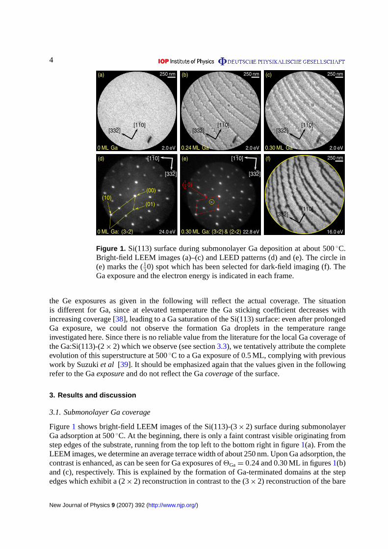
Figure 1. Si(113) surface during submonolayer Ga deposition at about 500◦C.Bright-field LEEM images (a)–(c) and LEED patterns (d) and (e). The circle in(e) marks the (130) spot which has been selected for dark-field imaging (f). TheGa exposure and the electron energy is indicated in each frame.
the Ge exposures as given in the following will reflect the actual coverage. The situationis different for Ga, since at elevated temperature the Ga sticking coefficient decreases withincreasing coverage [38], leading to a Ga saturation of the Si(113) surface: even after prolongedGa exposure, we could not observe the formation Ga droplets in the temperature rangeinvestigated here. Since there is no reliable value from the literature for the local Ga coverage ofthe Ga:Si(113)-(2× 2) which we observe (see section3.3), we tentatively attribute the completeevolution of this superstructure at 500◦C to a Ga exposure of 0.5 ML, complying with previouswork by Suzukiet al [39]. It should be emphasized again that the values given in the followingrefer to the Gaexposureand do not reflect the Gacoverageof the surface.
3. Results and discussion
3.1. Submonolayer Ga coverage
Figure1 shows bright-field LEEM images of the Si(113)-(3× 2) surface during submonolayerGa adsorption at 500◦C. At the beginning, there is only a faint contrast visible originating fromstep edges of the substrate, running from the top left to the bottom right in figure1(a). From theLEEM images, we determine an average terrace width of about 250 nm. Upon Ga adsorption, thecontrast is enhanced, as can be seen for Ga exposures of2Ga = 0.24 and 0.30 ML in figures1(b)and (c), respectively. This is explained by the formation of Ga-terminated domains at the stepedges which exhibit a (2× 2) reconstruction in contrast to the (3× 2) reconstruction of the bare
New Journal of Physics 9 (2007) 392 (http://www.njp.org/)

5
(a)
0.3 ML Ga
250 nm
5.6 eV
[332]– [110]–
(b)
0.3 ML Ga + 0.5 BL Ge
250 nm
5.6 eV
[332]– [110]–
(c)
0.3 ML Ga + 1.2 BL Ge
250 nm
5.6 eV
[332]– [110]–
(d)
0.3 ML Ga + 4.9 BL Ge
250 nm
5.6 eV
[332]– [110]–
(e)
0.3 ML Ga + 6.4 BL Ge
250 nm
3.2 eV
[332]– [110]–
(f)
14.9 BL Ge
500 nm
3.0 eV
[332]–[110]–
Figure 2. Bright-field LEEM images obtained during Ge deposition (a)–(e)at 460◦C on a partially Ga covered Si(113) surface and, for comparison,(f) at 440◦C on bare Si(113). The Ge coverage is indicated in each frame.Note the different scale bar in image (f).
Si(113) substrate. This transition is also confirmed by LEED, as shown in figures1(d) and (e).Prior to Ga deposition, a (3× 2) pattern is visible. The (n1
2 ) spots are faint and diffuse, pointingto a high density of anti-phase domain boundaries of the (3× 2) reconstruction typically foundon the Si(113) surface [40]. Upon Ga adsorption, additional spots appear, indicative of acoexistence of domains with (3× 2) and (2× 2) superstructure. Dark-field imaging with the( 1
30 ) spot of the (3× 2) reconstruction (cf figure1(f)) unambiguously proves that the Ga-terminated (2× 2) domains are located at the step edges. Thus, the submonolayer adsorption ofGa on Si(113) leads to step edge decoration and hence to the formation of a stripe-shaped 2Dnanopattern. This type of chemical surface modulation is very similar to the findings obtainedfor submonolayer Ga deposits on Si(111) [21]. For the latter surface orientation, the Ga-inducedprepatterning of the substrate can be exploited in order to grow aligned Ge nanoislands [22]. Inthe following, we will address the question whether this holds for the Si(113) surface as well.
3.2. Ge growth on step-edge-decorated Ga:Si(113)
A series of bright-field LEEM images obtained during Ge deposition at 460◦C onto a partiallyGa-covered Si(113) as described in the previous section is presented in figures2(a)–(e). At theinitial stage of growth, the nucleation of 2D Ge islands is observed. There is no preferentialnucleation in the Ga-terminated regions. Instead, a homogeneous nucleation is found in the Ga-depleted surface areas, as can be seen from figure2(b). After coalescence of the 2D islands,a Ge wetting layer is formed, as shown in figure2(c). At the electron energy chosen for this
New Journal of Physics 9 (2007) 392 (http://www.njp.org/)

6
experiment, further Ge deposition does not lead to a noticeable change in LEEM contrast,until small bright spots appear at a Ge coverage2Ge between 4 and 5 BL, as depicted infigure2(d). These bright spots are identified as 3D Ge islands. At2Ge = 6.4 BL (cf figure2(e)),the nucleation stage of these 3D islands has been finished, i.e. the islands grow in size, whereastheir density remains constant. For comparison, a LEEM image recorded from a Ge film ofsimilar thickness grown at similar temperature on bare Si(113) [36] is shown in figure2(f). Inboth cases, i.e. with and without submonolayer Ga preadsorption, the 3D islands are elongatedalong the [33̄2] direction. Also, the onset of 3D island formation [37] (between 4 and 5 BL)is very similar in both cases. The most apparent difference between both surface orientationsis the reduced 3D island density for growth on bare Si(113). As we reported previously [36],the Ge 3D island density on the bare Si(113) surface shows a clear Arrhenius behaviour, fromwhich an island density of 6× 107 cm−2 is deduced for a growth temperature of 460◦C. Thecorresponding value for Ge growth on partially Ga-terminated Si(113), as determined fromimages like the one shown in figure2(e), is almost two orders of magnitude larger and amountsto about 4× 109 cm−2. This clearly proves that Ga step-edge decoration of Si(113) leads to areduction of the surface diffusion length for subsequently deposited Ge. When comparing thesurface morphology found here to that observed for Ge grown on a partially Ga-terminatedSi(111) surface [22], the alignment of the Ge 3D islands—if any, cf figures2(a) and (e)—with respect to the step edges is much less pronounced for the (113) surface orientation. Onereason might be the small diffusion length for Ge already at the initial stages of growth. Fromfigure2(b) this can be estimated to be only a few tens of nanometres at the growth temperatureused here. This limited surface diffusion could be due to island nucleation at surface defectslike domain boundaries. In comparison, e.g. to Si(111)-(7× 7), the domain boundary density ofSi(113)-(3× 2) is much larger. On clean Si(113), however, these domain boundaries do not actas heterogeneous nucleation centres, and step flow growth has been observed above 400◦C [41].Therefore, the low Ge diffusion length between the decorated step edges observed here canmost likely be attributed to mobile Ga atoms on the terraces which may promote 2D Ge islandnucleation.
Owing to the low diffusion length, the density of the 2D Ge islands is high, offeringmany additional step edge sites which are likely to be energetically attractive to Ga atoms. Thisprobably leads to a redistribution of Ga all over the surface and hence may spoil the chemicalsurface modulation. The assumption of a redistribution of Ga is further supported by the fact thatafter Ge growth no contrast from the former Ga-rich domains is visible with LEEM, opposed torespective results on Si(111) reported previously [22].
In order to verify the scenario proposed above, further investigations would be necessarywith the Ge diffusion length tuned to be at least comparable to the mean terrace width, byincreasing either or both the Ge growth temperature as well as the step edge density, e.g.via the miscut angle. Then, a significant alignment of Ge 3D islands at step edges could beexpected. But instead of pursuing this approach, we present a completely different scheme inthe following, which enables a well-ordered arrangement of Ge 3D islands.
3.3. Ga saturation coverage
The evolution of the surface reconstruction during Ga adsorption at 500◦C up to saturationcoverage is shown in the LEED patterns in figures3(a)–(c). At 2Ga = 0.42 ML, the initial(3× 2) pattern has changed to a superposition of contributions from (3× 2) and (2× 2) domains,
New Journal of Physics 9 (2007) 392 (http://www.njp.org/)

7
(a)
0.42 ML Ga: (3×2) & (2×2) 24.0 eV
[332]–
[110]–
(b)
0.6 ML Ga: (2×2) 24.0 eV
[332]–
[110]–
(c)
1.1 ML Ga: (4×1) & (6×1) 24.0 eV
[332]–
[110]–
Figure 3. LEED patterns obtained during saturation of the Si(113) surface withGa at 500◦C. The Ga exposure is indicated in each frame.
3.2 ML Ga 24.0 eV
[332]–
[110]–
100% BZ
.–20 –10 0 10 20
k (nm–1)
40
50
60
70
80
90
100
k ⊥(n
m–1
)
[332–]
[113]
.–20 –10 0 10 20
k (nm–1)
[332–]
[113]
.–20 –10 0 10 20
k (nm–1)
[332–]
[113]
Figure 4. LEED pattern (top) obtained after Ga saturation at 500◦C. Line scansalong the direction of the red, green and blue arrows in the LEED pattern(at 0, 1/6 and 1/4 of the Brillouin zone (BZ)), are shown as a function of thevertical scattering vector componentk⊥ in the three frames at the bottom, withrespective colour maps. (See alsomovie 1.)
as already discussed in section3.1. After exposure to about 0.6 ML, the surface is completely(2× 2) reconstructed. Based on the results discussed in section3.1, this means that the wholesurface is Ga-terminated at this stage. Nevertheless, the evolution of the surface structure isnot yet complete. Upon further Ga deposition, the LEED pattern changes again, as shown infigure 3(c) for 2Ga = 1.1 ML. The nature of this rather complex LEED pattern is revealedin figure 4. Reflections occur at lines parallel to the [332̄] direction, i.e. the (almost) vertical
New Journal of Physics 9 (2007) 392 (http://www.njp.org/)
8
3.2 ML Ga
250 nm
3.4 eV
[332]– [110]– –0.5
0
0.5
1.0
–200 0 200Distance (nm) along [332
_]
Aut
ocor
rela
tion
(nor
mal
ized
)
~40 nm
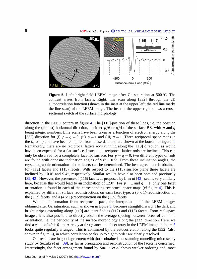
[115] [112]250 nm
Figure 5. Left: bright-field LEEM image after Ga saturation at 500◦C. Thecontrast arises from facets. Right: line scan along [332̄] through the 2Dautocorrelation function (shown in the inset at the upper left; the red line marksthe line scan) of the LEEM image. The inset at the upper right shows a cross-sectional sketch of the surface morphology.
direction in the LEED pattern in figure4. The [1̄10]-position of these lines, i.e. the positionalong the (almost) horizontal direction, is eitherp/6 or q/4 of the surface BZ, withp andqbeing integer numbers. Line scans have been taken as a function of electron energy along the[332̄] direction for (i) p = q = 0, (ii) p = 1 and (iii) q = 1. Three reciprocal space maps inthek‖–k⊥ plane have been compiled from these data and are shown at the bottom of figure4.Remarkably, there are no reciprocal lattice rods running along the [113] direction, as wouldhave been expected for a flat surface. Instead, all reciprocal lattice rods are inclined. This canonly be observed for a completely facetted surface. Forp = q = 0, two different types of rodsare found with opposite inclination angles of 9.8◦
± 0.5◦. From these inclination angles, thecrystallographic orientation of the facets can be determined. The best agreement is obtainedfor (112) facets and (115) facets. With respect to the (113) surface plane these facets areinclined by 10.0◦ and 9.4◦, respectively. Similar results have also been obtained previously[39, 42]. However, the presence of (116) facets, as proposed by Liet al [42], seems very unlikelyhere, because this would lead to an inclination of 12.0◦. For p = 1 andq = 1, only one facetorientation is found in each of the corresponding reciprocal space maps (cf figure4). This isexplained by different surface reconstructions on each facet type, a (6× 1)-reconstruction onthe (112) facets, and a (4× 1)-reconstruction on the (115) facets.
With the information from reciprocal space, the interpretation of the LEEM imagesobtained after Ga saturation, such as shown in figure5, becomes straightforward. The dark andbright stripes extending along [11̄0] are identified as (112) and (115) facets. From real-spaceimages, it is also possible to directly obtain the average spacing between facets of commonorientation, i.e. the periodicity of the surface morphology along the [332̄] direction. Here, wefind a value of 40± 6 nm. Already at first glance, the facet array in the LEEM image in figure5looks quite regularly arranged. This is confirmed by the autocorrelation along the [332̄] (alsoshown in figure5), in which correlation peaks up to eighth order are clearly resolved.
Our results are in good agreement with those obtained in a scanning tunnelling microscopystudy by Suzukiet al [39], as far as orientation and reconstruction of the facets is concerned.Interestingly, the facet arrangement found by Suzukiet al shows weaker ordering and, most
New Journal of Physics 9 (2007) 392 (http://www.njp.org/)

9
3.2 ML Ga + 6.7 BL Ge
250 nm
5.0 eV
[332]– [110]–
0
0.5
1.0
–400 –200 0 200 400Distance (nm)
[332_
]
0
0.5
1.0[11
_0]
Aut
ocor
rela
tion
(nor
mal
ized
)
0 20 40 60 80 100 1200
0.1
0.2
Island diameter (nm)
[332_
]
0
0.1
0.2[11_
0]
Rel
ativ
e ab
unda
nce
Figure 6. Left: bright-field LEEM image after deposition of 6.7 BL Ge at 500◦Con a Ga-saturated, facetted Si(113) surface as shown in figure5. Top right: linescan along [1̄10] and [33̄2] through the autocorrelation function of the LEEMimage on the left. Bottom right: histograms of island diameters in [11̄0] and[332̄] direction. About 750 islands were considered for the histograms.
important, an average period length of only about 10 nm, that is a factor of 4 smaller as comparedto our results. Although the reason for this difference is not yet fully understood, we suggestthat the facets’ average spacing and their long-range ordering depend on surface kinetics and,hence, on details of the sample preparation. More specifically, in their systematic study of thedependence of surface reconstruction and morphology on Ga deposit and substrate temperature,Suzuki et al always used a quite large Ga flux of about 1 ML per minute and quenched thesamples to room temperature immediately after Ga adsorption. In the work presented here, theGa flux was much lower and, accordingly, the deposition times were longer. This may lead toconditions closer to thermodynamic equilibrium, and thus to coarser structures and enhancedordering.
3.4. Ge growth on facetted Ga:Si(113)
The facet structure as characterized in the previous section has a strong impact on the surfacemorphology after Ge deposition. As can be seen from the LEEM image in figure6, a veryhigh density (about 1.3× 1010 cm−2) of small Ge 3D islands is formed at 500◦C. Again, the Ge
New Journal of Physics 9 (2007) 392 (http://www.njp.org/)

10
3.2 ML Ga + 6.7 BL Ge
250 nm
5.0 eV
[332]– [110]
–
Figure 7. Bright-field LEEM image of the same surface as in figure6. The areaselected here shows a big contaminant island near the centre. Denuded zonesare visible in the vicinity of that island, extending towards the [1̄10] and [1̄10]directions.
islands have an anisotropic shape, but now they are elongated along [1̄10 ], that means they havean opposite shape anisotropy as compared to Ge growth on bare or partially Ga covered Si(113).This is confirmed by the quantitative analysis of the average Ge island diameter, which amountsto 25± 6 nm in [33̄2] direction, in contrast to 40± 15 nm along [1̄10], as can be seen from thehistograms in figure6. The same type of anisotropy is observed for the Ge island spacing. Fromthe autocorrelation along [11̄0], as depicted in figure6, an average nearest-neighbour distanceof 100± 10 nm is derived, whereas in [332̄] direction, a value of 50± 6 nm is found. Within theexperimental uncertainty, the latter value matches the facet periodicity of 40± 6 nm. In addition,more pronounced maxima are observed in the autocorrelation along [332̄] as compared to thatalong [1̄10] (cf figure6), pointing to a longer-range order in [332̄] direction.
Both the spacing and the ordering anisotropy are strong indications for an alignment ofthe Ge islands at the facets. This is further supported by the above-mentioned value of the Geisland width in [33̄2] direction (25± 6 nm), as this value is in good agreement with the averagefacet width, i.e. half the facet array periodicity. Due to different surface free energies of thedifferent facets, one can expect that the Ge islands preferentially nucleate at one type of facet(which, however, could not be resolved in our experiments). The facet boundary then acts as agrowth barrier for the Ge islands, thus the width of these islands is expected to be limited bythe facet widths. In addition to this impact from surface energetics, surface kinetics also favoursthe reversal of the shape anisotropy. This can be seen from figure7, where a surface regionwith a large contaminant island has been selected for LEEM imaging. In the vicinity of thiscontamination along the〈11̄0〉 directions, almost no Ge islands are found within a distance of
New Journal of Physics 9 (2007) 392 (http://www.njp.org/)
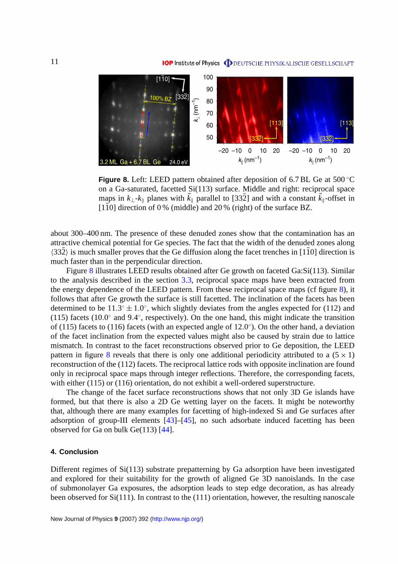
11
3.2 ML Ga + 6.7 BL Ge 24.0 eV
[332]–
[110]–
100% BZ
–20 –10 0 10 20k (nm–1)
50
60
70
80
90
100
k ⊥(n
m–1
)
[332–]
[113]
–20 –10 0 10 20k (nm–1)
[332–]
[113]
Figure 8. Left: LEED pattern obtained after deposition of 6.7 BL Ge at 500◦Con a Ga-saturated, facetted Si(113) surface. Middle and right: reciprocal spacemaps ink⊥-k‖ planes withEk‖ parallel to [33̄2] and with a constantEk‖-offset in[11̄0] direction of 0 % (middle) and 20 % (right) of the surface BZ.
about 300–400 nm. The presence of these denuded zones show that the contamination has anattractive chemical potential for Ge species. The fact that the width of the denuded zones along〈332̄〉 is much smaller proves that the Ge diffusion along the facet trenches in [11̄0] direction ismuch faster than in the perpendicular direction.
Figure8 illustrates LEED results obtained after Ge growth on faceted Ga:Si(113). Similarto the analysis described in the section3.3, reciprocal space maps have been extracted fromthe energy dependence of the LEED pattern. From these reciprocal space maps (cf figure8), itfollows that after Ge growth the surface is still facetted. The inclination of the facets has beendetermined to be 11.3◦
± 1.0◦, which slightly deviates from the angles expected for (112) and(115) facets (10.0◦ and 9.4◦, respectively). On the one hand, this might indicate the transitionof (115) facets to (116) facets (with an expected angle of 12.0◦). On the other hand, a deviationof the facet inclination from the expected values might also be caused by strain due to latticemismatch. In contrast to the facet reconstructions observed prior to Ge deposition, the LEEDpattern in figure8 reveals that there is only one additional periodicity attributed to a (5× 1)reconstruction of the (112) facets. The reciprocal lattice rods with opposite inclination are foundonly in reciprocal space maps through integer reflections. Therefore, the corresponding facets,with either (115) or (116) orientation, do not exhibit a well-ordered superstructure.
The change of the facet surface reconstructions shows that not only 3D Ge islands haveformed, but that there is also a 2D Ge wetting layer on the facets. It might be noteworthythat, although there are many examples for facetting of high-indexed Si and Ge surfaces afteradsorption of group-III elements [43]–[45], no such adsorbate induced facetting has beenobserved for Ga on bulk Ge(113) [44].
4. Conclusion
Different regimes of Si(113) substrate prepatterning by Ga adsorption have been investigatedand explored for their suitability for the growth of aligned Ge 3D nanoislands. In the caseof submonolayer Ga exposures, the adsorption leads to step edge decoration, as has alreadybeen observed for Si(111). In contrast to the (111) orientation, however, the resulting nanoscale
New Journal of Physics 9 (2007) 392 (http://www.njp.org/)
12
chemical surface modulation cannot be used for a pronounced heterogeneous nucleation of Ge3D islands. This is most likely due to the limited diffusion of Ge, which is reflected by thehomogeneous nucleation of 2D Ge islands already in the initial growth stage and, as compared toGe growth on bare Si(113), by an increased density of Ge 3D islands upon further Ge deposition.Our results suggest that the approach of submonolayer Ga adsorption might only be appropriateif the terrace width can be reduced down to the order of the diffusion length, e.g. by using vicinalSi(113) substrates.
For Ga saturation coverage, the Si(113) surface becomes unstable, and (112) and (115)facets extending along the [11̄0] direction are formed, with (6× 1) and (4× 1) reconstruction,respectively. For the preparation conditions used here, the facet arrangement is very regular,with a period length of about 40 nm. Subsequent Ge deposition leads to the selective growthof nanoscale Ge 3D islands which align at the facets. The shape anisotropy of these islandsis reversed with respect to that found for growth on bare or partially Ga-covered Si(113). Oneconsequence of this change in anisotropy is that the approach presented here might also enablethe growth of Ge nanowires extending in the [11̄0] direction.
Acknowledgments
This work has been supported by the European Community—Research Infrastructure Actionunder the FP6 (contract no. RII3–CT–2004–506008), and by the Deutsche Forschungs-gemeinschaft (grant no. FA 363/6).
References
[1] Abstreiter G, Schittenhelm P, Engel C, Silveira E, Zrenner A, Meertens D and Jäger W 1996Semicond. Sci.Technol.111521
[2] Kasper E 1996Appl. Surf. Sci.102189[3] Konle J, Presting H, Kibbel H, Thinke K and Sauer R 2001Solid State Electron.451921[4] Teichert C, Lagally M G, Peticolas L J, Bean J C and Tersoff J 1996Phys. Rev.B 5316334[5] Kienzle O, Ernst F, Rühle M, Schmidt O G and Eberl K 1999Appl. Phys. Lett.74269[6] Holý V, Stangl J, Zerlauth S, Bauer G, Darowski N, Lübbert D and Pietsch U 1999J. Phys. D: Appl. Phys.
32A234[7] Tersoff J, Teichert C and Lagally M G 1996Phys. Rev. Lett.761675[8] Xie Q, Madhukar A, Chen P and Kobayashi N P 1995Phys. Rev. Lett.752542[9] Heinrichsdorff F, Krost A, Bimberg D, Kosogov A O and Werner P 1998Appl. Surf. Sci.123/124725
[10] Fantini A, Phillipp F, Kohler C, Porsche J and Scholz F 2002J. Cryst. Growth244129[11] Springholz G, Holý V, Pinczolits M and Bauer G 1998Science282734[12] Springholz Get al2000PhysicaE 7 870[13] Schmidt Th, Clausen T, Falta J, Alexe G, Passow T, Hommel D and Bernstorff S 2004Appl. Phys. Lett.84
4367[14] Schmidt Th, Roventa E, Alexe G, Clausen T, Flege J I, Bernstorff S, Rosenauer A, Hommel D and Falta J
2005Phys. Rev.B 72195334[15] Schmidt O G, Jin-Phillipp N Y, Lange C, Denker U, Eberl K, Schreiner R, Gräbeldinger H and Schweizer H
2000Appl. Phys. Lett.774139[16] Hirai A and Itoh K M 2004PhysicaE 23248[17] Pedersen E V, Shiryaev S Y, Jensen F, Hansen J L and Petersen J W 1998Surf. Sci. Lett.399L351[18] Ronda A, Abdallah M, Gay J M, Stettner J and Berbezier I 2000Appl. Surf. Sci.162–3576
New Journal of Physics 9 (2007) 392 (http://www.njp.org/)
13
[19] Ronda A and Berbezier I 2004PhysicaE 23370[20] Gangopadhyay S, Schmidt Th and Falta J 2004Surf. Sci.55263[21] Schmidt Th, Gangopadhyay S, Flege J I, Clausen T, Locatelli A, Heun S and Falta J 2005New J. Phys.7 193[22] Schmidt Th, Flege J I, Gangopadhyay S, Clausen T, Locatelli A, Heun S and Falta J 2007Phys. Rev. Lett.98
066104[23] Feng Y P, Wee T H, Ong C K and Poon H C 1996Phys. Rev.B 544766[24] Müssig H J, Dabrowski J, Ehwald K E, Gaworzewski P, Huber A and Lambert U 2001Microelectron. Eng.
56195[25] Omi H and Ogino T 1997Appl. Phys. Lett.712163[26] Omi H and Ogino T 1999Phys. Rev.B 597521[27] Sumitomo K, Omi H, Zhang Z and Ogino T 2003Phys. Rev.B 67035319[28] Bottomley D J, Omi H and Ogino T 2001J. Cryst. Growth22516–22[29] Zhang Z, Sumitomo K, Omi H and Ogino T 2002Surf. Sci.49793[30] Darhuber A A, Zhu J, Holý V, Stangl J, Mikulik P, Brunner K, Abstreiter G and Bauer G 1998Appl. Phys.
Lett.731535[31] Omi H and Ogino T 1998Appl. Surf. Sci.130–2781[32] Zhu J, Brunner K, Abstreiter G, Kienzle O, Ernst F and Rühle M 1999Phys. Rev.B 6010935[33] Ross F M, Tromp R M and Reuter M C 1999Science2861931[34] Schmidt T, Heun S, Slezak J, Diaz J and Prince K 1998Surf. Rev. Lett.5 1287[35] Locatelli A, Aballe L, Mentes T O, Kiskinova M and Bauer E 2006Surf. Interface Anal.381554–7[36] Clausen T, Schmidt Th, Flege J I, Locatelli A, Heun S, Mentes T O, Guo F Z and Falta J 2006Appl. Surf. Sci.
2525321[37] Yasue T, Koshikawa T and Bauer E 2002J. Vac. Sci. Technol.B 202496–9[38] Jung T M, Kaplan R and Prokes S M 1993Surf. Sci. Lett.289L577[39] Suzuki H, Nakahara H, Miyata S and Ichimiya A 2001Surf. Sci.493166–72[40] Suzuki T, Minoda H, Tanishiro Y and Yagi K 1998Surf. Rev. Lett.5 249–54[41] Knall J and Pethica J B 1992Surf. Sci.265156–67[42] Li L, Wei Y and Tsong I S T 1995J. Vac. Sci. Technol.A 131473–7[43] Gai Z, Ji H, He Y, Hu C, Zhao R G and Yang W S 1995Surf. Sci.338L851–6[44] Ji H, Zhao R G and Yang W S 1997Surf. Sci.371349–57[45] Ji H, Li X, Zhao R G, Gai Z and Yang W S 1997Surf. Sci.384276–82
New Journal of Physics 9 (2007) 392 (http://www.njp.org/)