AD 297 361 - DTIC
215
UNCLASSI FIED AD 297 361 ARMED SERVICES TECHNICAL INFORAON AGENCY ARLINGTON HALL STATION ARLINGTON 12, VIRGINIA UNCLASSIFIED
-
Upload
khangminh22 -
Category
Documents
-
view
0 -
download
0
Transcript of AD 297 361 - DTIC

UNCLASSI FIED
AD 297 361
ARMED SERVICES TECHNICAL INFORAON AGENCYARLINGTON HALL STATIONARLINGTON 12, VIRGINIA
UNCLASSIFIED
NOTICE: When government or other drawings, speci-fications or other data are used for any purposeother than in connection with a definitely relatedgovertment procurement operation, the U. S.Govei tment thereby incurs no responsibility, nor anyobligation whatsoever; and the fact that the Govern-ment may have fotmallated, uished, or in a way
supplied the said drawings, specifications, or otherdata is not to be regarded by implication or other-wise as in any Manner licensing the holder or any,other person or corporation, or conveying any rightsor permission to mmaufacture, use or sell anypatented invention that may in any way be relatedthereto.

441
I-L IVSO

Serial No. TVC,2-60
QUARTZ CRYSTAL OSCILLATOR CIRCUITSV FINAL REPORTContract No. DA36-039 SC-88-892
Department of the Army Project No. 3 G-4,645401V 1 July 1961 to 30 June 1962I. S. ARMY SIGNAL RESEARCH AND
DEVELOPMENT LABORATORYFORT MONMOUTH, NEW JERSEY
ASTIA AVAILAB9IITY NOTICE
Qualified requestors may obtain Copies
of this report from ASTIA.

QUARTZ CRYSTAL OSCILLATOR CIRCUITS
FINAL REPORT
Contract No. DA36-039 SC-88892
PR&C 61-ELP/D-4209
Dated 14 December 1962
Department of the Army Project No. 3026-05001
1 July 1961 to 30 June 1962
The object of this study was to facilitate andsystematize the design of quartz crystal oscillatorsin the frequency range of 1 KC to 200 MC, throughrecommended circuits and design procedures. Thiswork should lead to decreased design time and costsand increased equipment reliability.
Approved by: Prepared by:
H. R. Meadows D. FirthSection Chief Project EngineerStff and Systems Engineering
Mgectrical_ . ineer "

TABLE OF CONTENTS
Pargraph Title
1.0 PURPOSE... .... .... ... ... .........
2.0 ABSTRACT..... .. .. .;. .. .. ~ 1
3.0 PUBLICATIONS, LECTURES, REPORTS, AND
CONFERENCES .. i............. 2
3.1 Publications................ ............ 2
3.2 Lectures.........................
3. 3 Rtepo r ts............. ........ 2
3.4 Conferences ......... .......... 29
4.0 FACTUAL DATA........................... 4
4.1 introduction....................... 4
4. 1. 1 Philosophy of Approach .. .. ....... .. .. .. .... 4
4. 1.'2 Report Layout .. .. ... ...... .. .. ... ..... 5
4. 2 Q~~~~~iartz Crystal Characteristics........
4.2.1 Oeneral....... ......... .. .. .. .. .... 6
4. 2. 1.1 Frequency Stabilizing.Properties of the Quartzcrystal .. ... .... .. .. .... .... ...... 12
4. 2. 1.2 Oscillator Frequency Tolerance .. .. .... ...... 15
4. 2. 1.3 Crystal Power Dissipation. .. .. .. ... .... .... 17
4. 2. 2 Analysis of an Oscillator .. .. ... .... ........ 19
4. 2. 3 Active Device Characteristic.. .. .. ... ... .... 25
4.2.4 impedance Transforming Networks . . . . - . . . . 26

TABLE OF CONTENTS (Cont)
Pararath Title RAMe
4. 3 Performance Specificatifn of an Oscillator.........27
4. 4 Design Procedure. .. ... ... ............ 7
4. 5 Oscillator Design at High Frequencies. .. .... 28
4.5.1 General .. ..... .... ....... . 28
4.5. 2 Crystal Characteristica . . . .. .. ... 30
4. 5.3 Active Device Characteristics .. ........... 34
4. 5. 3.1 Feedback Effects at High Frequencies..........35
4. 5. 3.2 Active Device Configurations Used Dluring ThisProgram.... .... ............. 40
4. 5.3. 3 Aids to Active Device Selection. .. .. ... ........ 41/
4.5.3i.3. 1 Vacuum Tubes .. .. .. .... .... ... ....... 41
4. 5.3. 3.2 Transistors .. .. .... ... .... .... ...... 43
4. 5.3. 4 Determination of Active Device Characteristics .. . . 46
4. 5.4 Design Procedure. .. .. .... ... .... ...... 50
4. 5.4. 1 Step 1, Crystal Operating Condition. .. .. .. ...... 50
4.5.4.2 Step 2, Selection of Crystal Type . . .. .. .. .. ....... 50
4. 5.4. 3 Step 3, Oscillator Configuration .. .. .... ...... 51
4. 5.4. 4 Step 4, Desired Active Device Characteristics ... 52
4. 5.4. 5 Step 5, Selection of Active Device .. .. .. ..... . 54
4. 5.4. 6 Step 6, Determination of Active Device Characteristics .55
4.5. 41.7 Step 7, Calculation of oscillator Component Values. 55

TABLE OF CONTENTS (Cont)
Nragra~h Title Pg
4. 5.4. 8 Step 8, Design of Impedance TransformingNetwork .. . .. .. .. .. . . .7
4i .. 4.90 Step 9, Experim ental Adjustments . . . 57
4. 6 Oscillator DesgIgn at Low Frequencies .60 ... s
4. 6.1 General.......... ... ... ....... 60
4. 6.2 Crystal Characteristics...............60
4. 6. 3 Active Device Characteristics .. .. ......... 6-3
4.6.3.1 Tubes . .... . .. .. .. .. . .. .. .. . .63
4. 6. 3. 1.1 Typical Tube Amplifier Operating Characteristics 66
4. 6.3. 2 Transistors .. ...... . ... ..... . . 66
4. 6. 3.2. 1 Power Gain, InuRn itu esistance ...... 68
4. 6. 3.2. 2 Common Base to Common Emitter 'h'Parameter Conversions .. ... .... ........ 68
4. 6. 3.2. 3 Typical Transistor Aplfe ertg
Characteristics .. .. ... .... .... ....... 69
* 4. 6. 3.2. 4 Simplifications of Gp, Bin, and RO Formulae . 70
4. 6. 4Possible Oscillator Configuratons...........704
4. 6.4. 1 Oscillator Configurations Below 100 KC... 70
4. 6. 4. 1.1 Single -Stage Untuned Oscillators .. .. .. ........ 71I
4. 6.4. 1.2 Grounded Grid or Grounded Base Connections . . . . 72
4. 6. 4. 1.3 Grounded Cathode or Grounded EmitterConnections. .. .. .. ... .... .......... 73

TABLE OF CONTENTS (Cont)
PararaphTitle 990-e
4. 6. 4. 1.4 Triode Oscillator .. .. ... .... .... .... ..... 4
4. 6. 4. 1.65 Transistor Oscillator . ................ 76
4. 6.4. 1i 6 Single-Stage Oscillator using the Crystal to GivePhase Inversion .. .. ... .... ..... 78
4.6. 4. 1.7 Two-Stage Untuned Oscillators.. .. .. .. .. ... 70
4. 6. 4.2 Oscillator Configurations Above 100 KC.........80
4.6. 5 impedance Transforming Networks .. .. .. ....... 80
4.6.6 Design Procedure...... .. .... ......... 814
.6. 6. 1 Step 1, Crystal Op-eration. .. .. ....... 81
4.6.6.2 step 2, Selection of Crystal Type ~ . . . . 81
4. 6.6. 3 Step 3, Oscillator Configuration .. .. .... ...... 82
4. 6. 6.4 Step 4, Desired Active Device C1Aracteristics . . . . 82
4.6..6.5 Step 5, Selection of Active Device. .. ... ....... 83
4. 6.6. 6 Step 6, Determination of Active Device Characteristics 83
4. 6. 6. 7 Step 7, Calculation of Oscillator Component Values.. 83
4. 6. 6.8 Step 8, Design of Impedance Transforming ewr 84
4. 6. 6.9 Step 9, Experimental Adjustments.....-. 84
4. 7 Impedance Transforming Networks .. .. .... ...... 84
4.7.1 7r Network .. .. ..... . . .. .. .. . .. . .. 84
4.7.1.1 7rNetwork Analysis . .. .. ......... . . . 84
4.7.1.2 irNetwork Design .. .. .. . . . .. .. . . . . . . 86
4.7.2 Capacitive Divider Network..... ....... . 90
iv

TABLE OF CONTENTS (Cont)
- PragaphTitle tame
4. 7. 2. 1 Analysis of Capacitive Divider Network.......... 00
4 7. 3 Untuned Inductive Transformer..............93
4. 7. 3.1 Inductive Transformer i'nalysis .. .. .. .. .... .... 3
4.17. 3.1. 1 Untuned Transform er, Heavy Secondary Load ..... 94
F4. 7. 3. 1. 2 Untuned Transformer Design, Heavy .secondary L oad. 97
4. 7. 3. 1. 3 Untuned Transformer, Light Secondary Load ..... 99
4.7i3 1.L4 Transformer DesiM, Light Secondary Load........02
4.L7. 4 Wien Bridge Network .. .. .. .... ........ 103
4. 7.4. 1 Wien Bridge Network.Antalysis. .. .. ......... 103
5.0 CONCLUSIONS AND RECOMMENDATIONS .. .. ..... 106
5. 1 Conclusions. .. .. .... .... .. .... ... ... 106
5. 2 Recommendations .. .. .. .... .... .... ..... 106
5. 2. 1 High-Frequency Oscillators. .. .. .. .... ... ... 106
5. 2.2 Low-Frequency Oscillators .. -.. .. .. .. .. .. 107
6.0 IDENTIFICATION OF PERSONNEL .. .. .. ....... 108
7.0 BIDLIOGRAPHY. .. .. ... ... .... .... ..... 109
v

OSCILLATOR DESIGN AND EVALUATION DATA
ADD ndix Title 2W
A 150Me Oscillator Using 2N9i7 Transistor ..... A~1
B5 i93- Mc Oscilator Using 2N917 Transistor .. .. . . ..... B
C. 120-MO Oscillator Using 2,N22,17 Transistor......C-
D 120-MC Oscillator Using 2N834 Transistor D -1
E7'5-MC Oscfilator Using 2N2219 Transistor'.........~
FiOO-MC Tube Oscillator Using 5718A Sub-iniature Triode F4
G 150-mc Tube Oscillator Using 8058 Nuvistor. .. .. . . .....
if 200-MO Tube Oscillator Using 57i8A ......... .-
I 200-MC Tube Oscillator Using 80 5 8.............-
J i-KC Two-Stage Tube Oscillator Using i2AX7(Wien Bridge) J IkIK3-KC Two-Stg TueOcillator Using i2AX7(Wien Bridge K-i
L ~I-KC Single-Stage Tube (i2AT7) Oscillator Using the QuartzCrystal to Give Phase Inversion..... .. .. .. .. .. . ....
M 1-K Two-tage scilator Using ZN336 Transistor (TunedOutput). .. .. .. ....... .. .. ... .... ....... M-i
N 3-KC Two-Stagze Oscillator Using 2N336 Transistor (Tunedoutput) .. .. .. ... .... .... ... .... ....... N-I
03-KC Tuned- Output Oscillator Using 2N336 Transistor... 0-1
P 20-KC Tuned Output Oscillator Using 2N336 Transistor. .. P-i
vi

-LIST OF ILLUSTRATIONS
Figure Title Pg
1 Equivalent Electrical Circuits of a Crystal..... . . .
2 Impedance I Z I , Resistance Re, Reactance Xe, and SeriesArm Reactance Xlofa Crystal as at Function of Frquency. . 9
3 Impedance Diagram of a Crystal.. ... ... ..... . 13
f4 Series L C Circuit Phase Curve .. .. .. .. ... ...... 13
5 Equivalent Parallel Crystal Circuit. .. ....... 14
6 Overall Frequency Tolerance.... .. .. .. .. .. .. .. . ....
7Effective Crystal Circuit in Series Resonant Oscillator . . .. 8
8Crystal Dissipation Curve .. .. .. ... ... ... ... ... 19
9 Basic Oscillator. .. .. ... .. ... ... ... ... ... 20
10, Basic Oscillator - Loop Broken .. .. .. ... ... ... ... 20
11 Grounded Grid Oscillator. .. .. .. .. ... ... ... ..... 23.
12. Impedance Transforming Networks .. .. .. ... ... ..... 26
13 Variation of Resistance and Reactance WithFrequency of 1/2 watt Resistors .-. . . . . . 29
14 HihFeuny Oscillators, Input and Output Circuits......3
15 Active Device Configurations .. .. .. .. ... ... ... ... 36
16 Active Device Equivalent Circuit. .. .. .. .. .... .. ..... 37
17 Characteristics of a Unlateralized High-Frequency
Transistor!...... .. . .. .. .. . .. . . . 44
18 Phase Angle Curve ofa4CR Lead Network. .. .. .. . .... 5
vii

3
LIST OF ILLUSTRATIONS (Cent)
Figure Title Sam e
19 Diode Limiter Circuit . . ... 8 .0 ..
20 Transistor "Black Box" . . ............ 67
21 Low Frequency Grounded Grid Oscillator ...... . .. . . 72
22 Grounded Cathode Tuned Oscillator .... .. . . . . .. . 74
23 Grounded Emitter Tuned Oscillator .......... ..... 76
24 Crystal Position in Two Stage Oscillator ................ 79
25 it Network Transformation ....................... 85
26 r Network Vector Relationships ... ... ........ 86
27 Example of VT Network Design ..... ........... 89 )28 Capacitive Divider Coupling Network ................. . 90
29 Phase Shift Characteristics ...... ............ . . 92
30 Inductive Transformer . .. . . . . . 93 •31 Primary Vector Digram ...................... 95
32 Secondary Vector Diagram. . ................... ... 95
33 Transformer Vector Diagram ...... ................. 96 )34 Driven Transformer .... . .... 97
35 Secondary Vector Diagram, Lightly Loaded . . . 99
36 Driven Transformer, Lightly Loaded . ......... . . . . 100
37 Wien Bridge Network Circuit ..... ...... .... . . . . . 10-3
38 Wien Bridge Network Vector Diagram .......... ... 104
viii

LI8T OF TABLES
2 Table Title Pn
1 Typical Crystal Parameter Values . .. .. ..
2Definitions of Symnbols in Figu re 2... .. .. .. .. ......
-3 Table of IMpedance Tranformations.... .. .. .....
4 Military Standard Crystals, Hiigh Frequency.........33
5 "Y", Paramieter Variations with Frequen~cy. . .... ... 45
46 Oscillator Frequency Tolerance%)... ... .. .. . ..
7Military Standard Crystals, Low Frequency........6
8 Twin Triode Characteristics... .. .... ....... 74
ix

1. 0 PURPOSE
The purpose of this program was to develop design procedures for quartzcrystal oscillator circuits that are readily usable by the average electronic design,engineer. In addition, the program included the development of performance datasheets for both vacuum tube and transistor oscillators covering the frequency rangefrom 1 KC to 200 MC. The program was not concerned with extremely stable osci-lators requiring oven control, but with non-temperature controlled medium stability
circuits.
2.0 ABSTRACT
This Final Engineering Report presents extensive data supporting the designiand operation of quartz crystal oscillators. Design procedures are developed for both
high and low frequency oscillator circuits in the !-KC to 200-MC range. Vacuum tubesand transistors were studied in both the low and the high frequency ranges (1 KO to
800 KC and 30 MC to 200 MC).
The report begins with a general discussion of the properties of quartzcrystals, the characteristics of tubes and transistors, and impedance transforming
networks. The general analysis of an oscillator is presented, a general designspecification is developed, and a basic design procedure is established.
Separate sections are devoted to design procedures for high-frequency andlow-frequency crystal oscillators. The report concludes with a design data sectioncontaining the results of oscillator evaluations during the program period.
II
T1

"I
3.0 PUBLICATIONS, LECTURES, REPORTS, AND CONFERENCES
3.1 Publications
None
3.2 Lectures
None
3.3 Reports
The first Quarterly Report, Magnavox Serial No. TP62-411, on the subjectcontract was distributed in accordance with USAELRDL instructions on 19 January1962.
The second Quarterly ReportMagnavox Serial No. TP62472, on the subjectcontract was distributed in accordance with USAE LDL instructions on 23 March1962.
The third Quarterly Report, Magnavox Serial Noi 62-554, on the subjectcontract was distributed in accordance with USAELRDL instructions on 20 July 1962.
3.4 Conferences
3.4. 1 The first project conference on the subject contract was held at the USAELRDLHexagon Building, Fort Monmouth, New Jersey, on 19 July 1961. In attendance wereMessrs. o. P. Layden and S. Schodowski for USAELRPL and Messrs. K G. Stewart,H. i. Meadows, and 0 Plait for The Mgnavox Company. Minutes of the meeting
were prepared,. submitted to USAELRDL, and are on file for reference.3.4.2 The second project conference was held at The Magnavox Company, Fort
Wayne, indiana,on 6 October 1961. In attendance were Mr S. SchodowSki for USAELRDLand Messrs. A. 0. Plait D. Firth, and H. R. Meadows for The M nvox Company.
Minutes of the meeting were prepared, submitted to USAELRL, and are on file forreference.3. 4. 3 The third project conference was held at the USAELRDL Hexagon Biding,
Fort Momnouth, New Jersey, on 12 December 1961. In attendance were Messrs, 0. PLayden and S. Schodowski for USAELRDL and Messrs. 0. F. ReynodsE.D.Ad],
and H. R. Meadows for The Magnavox Company. Minutes of the meeting were pre-pared, submitted to USAEL _L, and are on file for reference.
2

- 3. 4.4 The fourth project conferenee was held at The Magnavox Company, Fort Wayne,indiana, on 23 January 1962. In attendance were Mr. 0. P. Layden for USAELRDL
T'- and Messrs. H. R. Meadows., D. Firth, and A. 0. Plait for The Magnavox Company.-. Minutes of the meeting were prepared, submitted to USAELRDL, and are on file for
reference.
"! 3. 4. 5 The fifth project conference was held at The Magnavox Company, Fort Wayne,Indlana, on 27 March 1962. In attendance were Mr. S. Schodowski for U SAELRDLand Messrs. H. R. Meadows and D. Firth for The Magnavox Compa ny. Minutes ofthe meeting were prepared, submitted to USAELRDL, and are on file for reference.
3. 4. 6 The sixth project conference was held at the USAELRDL Hexagon Building,Fort Monmouth, New Jersey, on 11 June 1962. in attendance were Messrs, S.Schodoweki and 0. P. Layden for USAELRDL and Measrs, H. R, Meadows, D. Firth,and J. R. Yope for The Magnavox Company. Minutes of the meeting were prepared,submitted to USAELRDL, and are on file for reference.
If,
I-

'
4.0 FACTUAL DATA
4.1 introduction
This is the final report on a one-year study program under the sponsorshipof USAELADL, charged with the development of design procedures for crystal oscil-lators employing either tubes or transistors, in certain frequency bands where designprocedures had not previously been established. The specific frequency bands ofinvestigation were:
(a) Crystal controlled vacuum tube oscillator design from 1 KC to800 KC.
(b) Crystal-controlled transistor oscillator design from 1 KC to16 KC.
(c) Crystal-controlled vacuum tube oscillator design from 150 MCto 200 MC.
(d) Crystal-controlled transistor oscillator design from 30 MC to200 MC.
Oscillator design at frequencies intermediate to those of (a), (b), (c), and(d) above is covered in the final reports of two other study programs sponsored bythe USAELRDL (Reference I and 2,Paragraph 7.0).
The contract period was from 1 July 1961 to 30 June 1962, and approxi-
mately 28 man-months of effort were involved.
4. 1.1 Philosophy of Approach
To some extent, the design of quartz crystal oscillators has always.beensurrounded by an aura of mystery; capable engineers who would not normally resortto "cut and try" methods do so when faced with crystal oscillator design.
This appears to be due in part to the historical literature which tends toemphasize the more obscure details of the subject at the expense of the essentials.Technical articles of this type tend to overawe the designer faced with the mundanetask of designing an oscillator of more moderate performance. Not that such dis-cussions are without value, but reports of this type often wrongly assume that thereader is fully conversant with the details of the design of less sophisticatedoscillators.
4

The objective of th,is report is to present to the user the sentiaI knowledgethat is required to appreciate the design problem, 'to supplement this with informationconcerning the components of the oscillator circuit, and to associate these into a de-sign procedure that leads to satisfactory designs.
Because of the normally non-linear operation of an oscillator, a true mathe-matical model would consist of a series of non- linear equations describing the actionof the circuit. These equations would define the circuit action completely, and frotethem it would be possible to predit all the operating characteristics of an oscillatorHowever, the difficulties of this approach are formidable. Even simple non-linearequations are difficult to. manipulate, and when it is considered that the non-linearIcharacteristics of a transistor, tube, or quartz crystal vary with power leve4 fre-quency and temperature, the difficulties of this approach are apparent.
1"As is usual under these circumstances, the design approach falls back on
the use of linear describing equations, which are at least valid for establishing the.- necessary conditions for oscillation to commence, and supplements this approach
with experimentally gathered information to allow a reasonable degree of circuit
performance prediction. This simplifies the oscillator equations considerably while-- increasing the importance of the experimental data. Because of this, the major part
of this program was devoted to the study of the practical aspects of oscillator design,with detailed evaluations of various oscillators covering the frequency bands underdiscussion.
4. 1.2 Report Layout
This report consists of the following four sections:
- (a) An introductory section containing general information concerningthe properties of:
*- (1) Quartz crystals
(2) Tube and transistor characteristics
(3) Impedance transforming networks
Other topics covered in this section are:
(4) A genieral analysis of an oscillator
(5) The general design specification of the performance of
an oscillator
5

() A rudimentary design procedure estab-lishing the designdecisions that are required to produce a design meetingthe specification
(b) A section devoted to high-frequency crystal oscillator design, discuss ing quartz crystal and active device characteristics in specific
terms applicable to design at high frequenciesm This information isthen regrouped to form a step-by-step design procedure.
(c) A section devoted to low-frequency crystal oscillators having asimilar form to section (b).
Appended to sections (b) and (c) is a sub-section containing analyses ofseveral impedance transforming networks together with design information.
(d) A design data section containing the results of the evaluations of theexperimental oscillators constructed during the contract period.
4.2 Quartz C-ryst;l Ch racteristics
4. 2.1 General
A quartz crystal resonator is an electromechanical transducer having "piezoelectric properties. The application of an electrical potential to the quartzcrystal produces a mechanical stress within the crystal structure similar to that
obtained by the application of mechanical force. Conversely, the application ofmechanical force to the crystal creates a potential difference across the crystalstructure. Therefore, by suitably connecting two or more electrodes to a quartzcrystal, it can be made to vibrate by applying an alternating voltage to theseelectrodes. if the output of the alternating voltage source is held constant and thefrequency continuously varied, certain frequencies will be found at which the ampli-tude of the mechanical vibration becomes a maximum. These are the frequenciesat wich the quartz crystal goes into mechanical resonance.
Because of the electromechanical coupling in the crystal, the mechanicalmotion of the crystal appears at the input terminals as an electrical tuned circuitat frequencies in the immediate vicinity of the mechanical resonant frequencies.
The important electrical properties of the quartz crystal are:
(a) The high effective Q of the quartz crystal; tat is, the highratio of energy stored in the crystal relative to the energydissipated in storing that energy.
6

(b) The wide range of frequencies over which quartz crystals canbe made to resonate.
(c) The excellent stability of the electrical parameters of the quartzcrystal when subjected to temperature changes,
IThese three properties account for their wide use In stable oscillator designs.
The equivalent electrical circuit of a quartz crystal resonator is shown InFigure 1. L i and C1 are primarily dependent on the mass and compliance of thequartz, and Rl1 is mostly determined by the means of supporting the crystal andattaching the electrodes,
ILI R#
R,/R1 Xe
. Fgur 1.Equvalent Electrical Cictsoa Crystal
These are the motional impdan ce elements of the cry stal, so called because they are
the effective electrical equivalents of the vibratory motion of the crystal. C0 is anI actual electrical capacitance due to the electrode attachments t the quartz and tothe stray capacitance in the assembly. Typical values of the parameters for 200 KC,
-2 MC, and 30 MC crystals are shown in Table 1.
This circuit is not a valid representation of the electrical characteristics of- a crystal at all frequencies. Every mechanical structure has several modes of reso-
nance. A simple bar., for example, has flexural, torsional, shear, and extensionalmodes of oscillation in 4ach of the three axes.
7

1
TABLE 1. TYPICAL CRYSTAL PARAMETER VALUES i
Parameters 20'0 KC 2 MC 30 MC
R2K 100 ohms 20 ohms
L1 27 H 520 MH 11 MH
C1 0. 024 PF '0. 012 PF 0.0026 PF
Co 9 PF 4F 6 PF
Q 18 x 10 3 54 x 10 3 10
Furthermore, mechanical resonance can be excited at the overtones of each of thesebasic modes. The manufacturer shapes, proportions, and clamps the crystal so asto make one of these mechanical resonances predominant while suppressing allothers that could possibly occur at frequencies immediately adjacent to this desiredone. If, as is normally the case, sufficient suppression of the undesired resonancesis achieved, the circuits of Figure 1 are valid electrical equivalents of the electro-mechanical characteristics of the crystal in the frequency band immediately aroundthe predominant mechanical resonance frequency.
With this restriction, the behavior of the quartz crystal can be uiscussedin terms of the electrical equivalent circuit of Figure 1 (a) where L 1 , C1 , R 1 ,and Co are essentially independent of frequency. in the frequency band of interest,this circuit can be considered as a series combination of a resistance Re and areactance Xe as. shown in Figure 1 (b). The values of Re and Xe are frequencydependent and vary in the general manner indicated in Figure 2 as functions of
frequency. , The various symbols are defined in Table 2, and the impedancelevels should be regarded as plotted to a logarithmic scale, Figure 2 and Table2 are reproduced from the "L X E. Standards On Piezoelectric Crystals - The 4Piezoelectric Vibrator: Definitions and Methods of Measurement, 1957."
*Contained in the March 1957 Proceedings of the I. R E.
8

IX'l
fsf fr to t fFREQUENCY
Figure.2. Iipedance IZIORes-istance Re. Reactance Xe, and SeriesArm Reactance XI of a Crystal as a Function of Frequency
TABLE 2:. DEFINITIONS OF SYMBOLS IN FIGUIRE 2
ISymn-bolI Definition
IrCapacitance ratio -- 0
C,
f m Frequency of minimum impedance1
fs Motional arm resonance frequency
Resonance frequency (Xe 0)
la Antiresonance frequency (Xe 0)
f£ Parallel resonance frequency =1 [ _1 (+L /yp27r L L C r J
In Frequency of maxi mum impedance
1'Rs nc itac XBr -AtResonance resistance (Xe 0)
Ra Aipesance resm(itnmc yta (Xeean0)
Zn Impedance at fn (minimum crystal impedance)
9

Interpreting the points of interest on the curves of Figure 2 from left to right,fs is the frequency at which the motional arm is series resonant. At this frequency Ithe crystal appears at its terminals as a combination of RI in parallel with C0 . Athigh frequencies, where it is common practice to tune CO With an inductive Shunt, fsis the desirable crystal operating point. At a slightly higher frequency, the motionalarm reactance X1 is inductive and of such a value that its equivalent inductance whentransformed to a parallel element (see Table 3 (b))resonates with C. The formulaeillustrating this effect are:
-X 1 (+ -)=XC (1
and Rp - Rr R 1 (1 + Qr 2 ) (2)
where Qr - Xi at frequency frQr RI
Equation (1) shows that X 5. X1, provided that Qr < I; that is, X1 << Ri . Equation(2) shows that Rr differs trom 1(i by the factor (1 + Q- ), and since this is practicallyequal to 1 under the assumed conditions, Rr is almost equal to R1 .
As the frequency is further increased, the value of I Z I also increasesrapidly until at frequency fa, Xe again falls to zero and Re has the value Ra. At thisfrequency the equivalent motional arm inductance X1 again resonates- with Co andEquatious (1) and (2) can be restated as:
xa = X C
(
2Rp =Ra R, (1 + Qa 2 ) (4)
where _1 - at frequency fa
At fa, however, 9a > 1 (see behavior of X1 characteristic) and, therefore,
XP - -(5)
and = R- P4 R1Qa 2 (6)
10

T TABLE 3. TABLE OF IMPEDANCE TRANSF'ORMATIONS
it
I.) Lp
Rs Ls Lo w LO
ItoR As ++
RR *
Ib RgLL P Lpi Ll 1+ Ls I *
NO o~l t
Rg C P 14j j C[I+ I]
[I+cI!qRP its3E~IJ h Re [I+Q'
III c(1.C.R
C* s c
17+ W C's

i
Other frequencies of lesser interest are fm and fn, the frequencies at which the crystalexhibits its minimum and maximum impedances, respectively, and fp, the frequency atwhich the motional arm reactance would be in series resonance with CO if this werepossible, It should be noted that f does not coinctde with the antiresonant frequency
fa because of the finite Q of the motional arm.
The impedance curves of Figure 2 can also be presented as an impedance planeloci as shown in Figure 3. This presentation is valid, provided that
i - R 1 .
2W (f n fm) Co
An indication of the bandwidth in which these effects occur may be obtained bynoting that for most crystals, the capacitance ratio r lies between 900 and 500. sub-stituting a typical value of r - 300 into the equation for fp, the ratio of fp to fs gives:
1 /2 1P- (1 +-.) 1 .= 1.0017 (7)
fs r 2r
For example, if fs - MC, then the bandwidth within which the crystal resonanceeffects occur will be typically less than 2 KC.
The spacing between fs and fr can be shown to be very small (Reference 3,Paragraph 7.0); frequency differences of 1 or 2 parts per million are typical. Thefrequency difference between fs and fm is equal to that between f. and fr4. 2. 1. 1 Frequency Stabilizing Properties of the Quartz Crysta
The frequency stability of an oscillator is dependent on the stability of thephase shifts existing within the feedback loop and the rate of change of phase shiftwith frequency, , of the frequency controlling element. The total loop phase
shift in the oscillator has to remain zero at all times if oscillation is to be maintained,and any phase changes occurring external to the frequency controlling element haveto be cancelled by an equal but opposite phase change in this element. A large ....is therefore the important characteristic of the frequency controlling element d fand the quartz crystal can exhibit this characteristic for two conditions of operation;that is, when the crystal operates at resonance or at parallel resonance.
(a) Operation at Resonance
When the crystal is operated at resonance, the frequency stabilizing effectoccurs in the vicinity of fr and is dependent on the ability of the crystal to shif the
12

1Rr
Ii +
x 2nz f~R1
IiFigure 3. Imnpedance Diagram of a Crystal
I phase of the crystal current relative to that of the drive voltage. -Figure 3 shows therelatively large phase change that occurs between fs and fr, two frequencies separatedby only a few parts per million and which is indicative of a large d.± The behavior
df
50 _
- - - __ - _ -- 25
- - ---- -- - - - 25 h£
ST73 Rzzzzzzz:- fFigure 4. Series L C Circuit Phase Curve
13

1
of the phase shift with frequency is of the form shown in Pigure 4, the phase anglepart of the universal resonance curve of a tuned LC circuit (Reference 4, Paragraph7. 0). It can be shown that, in the immediate vicinity of fr :grp
d =. Li.- (8)df fr
This indicates the importance of the crystal Q on its frequency stabilizing properties.However, in order to make use of this property, it is necessary to sample the crystal
current and this can be done only by the inclusion of an impedance in series with thecrystal. in this process, power has to be supplied to this impedance (see Paragraph4. . 2); that is, this impedance has a resistive compon ent effectively in series withthe crystal. This network therefore has greater losses than the crystal alone and,consequently, has a lower Q than that of the crystal. Because of the dependence ofoscillator frequency stability on crystal Q, At is in the interest of frequency stabilityto make this effective series resistance small relative to Rr . Similarly, the drivingsource will also introduce a resistance in series with the crystal, resulting in afurther degradation of the crystal Q.
A similar reduction in the frequency stabilizing property of the crystal willalso occur if the frequency of oscillation is not in the immediate vicinity of fr, sinceas Figure 4 shows, the slope of the phase curve 11L decreases at frequenciesremoved from fr. df
(b) Operation at Parallel Resonance
In parallel resonance operation, the crystal in conjunction with an externalparallel capacitor CL forms a parallel resonant circuit as shown in Figure 5, where:
X -XL XC (9)
and CT CO + CL (10)
ZG C1 ZGC
$774 - ,.... - _L Twe 5 Equivalent Parallel Crysta Circuit
14

L
fT The antiresonant frequency f'a is intermediate between f, and f. and can be regardedas a special case of fa. if this circuit is fed from a constant current source, the be-havior of the phase angle of the crystal voltage relative to the phase of the supplycurrent is similar to that shown in Figure 4, if the sign of the phase shift is reversed.rEquation (8) is again applicable in determining the rate of change of phase angle, andthe reduction of this rate by the external circuit can best be illustrated by transformingf R i Into its parallel equivalent resistor R'a, Equation (4) shows that:
Ra R 1 (1 Q a 2(1)
whereQa 7 X at frequency i'a
Direct comparison can now be made between RG, the effective resistance
of the driving source acting in parallel with the crystal, and R'a. A value of RG = Ft'
will reduce the Q and, hence, d--by'2. A similar Q degradation occurs due to thedfeffective parallel resistance of the circuit used to sampe the volae across the crystal.
Both methods of crystal operation indicate the importance of the crystal Q on.oscillator stability and the need to minimize the degrading effect of the driving and phaseshift sampling circuits. In practice because of the effects discussed in Paragraph4.2.2, a compromise to necessary, and loading that reduces the Q by a factor of 2 or3 is considered permissible.
4. 2.1.2 Oscillator Frequency Tolerance
All military standard crystal units have a specified frequency tolerance towhich they must conform. This specification guarantees that any crystal manufacturedto the standards of the particular crystal type number will be in resonance or parallelresonance with a specified loading capacitor, at the nominal frequency staed on thecrystal holder to within the given tolerance. and over the specified operating tempera-ture range. This tolerance makes allowances for:
(a)' The effect of temperature on the crystal resonance (or parallelresonance) frequency and the variations in the magnitde of tiseffect from unit to unit.
(b) The accuracy with which the crystal unit resonance (or parallel
resonance) frequency can be adJusted in manufacture.
15

As an lilustration, Figure 6 defines the frequency tolerance of a wide temperaturerange crystal. The tolerance is assumed to be *0. 005 percent and the characteristicsare typical of an AT-cut crystal showing the changes of fr or f a is a function of (temperature. fn is the nominal crystal frequency as marked on the crystal holder.As shown in curves (a) and (b), the actual deviation due to temperature may be no morethan *0. 002 percent, but an additional -0. 003-percent manufacturing allowance is con-tained in the overall frequency tolerance, In a large batch of crystals of the samenominal frequency, crystals will be found exhibiting the extremes of curves (a) and (b)as well as the intermediate characteristics shown in (c).
+0.oo5% ,2 0 ""I
9a 00C
-0.005%- ----
Figure 6. Overall Frequency Tolerance
The overall oscillator frequency tolerance is partially determined by the Icrystal frequency tolerance. Any phase shift or changes of phase occurring withinthe remainder of the oscillator circuit will require equal and opposite compensatingphase changes in the crystal. Since the crystl phase angle cannot change withouta proportionate change in oscillator frequency, an additional frequency tolerance inexcess of that of the crystal is incurred. This effect can be considered as having thefollowing two components: I
(a) A constant migecorrelation of oscillator and crybtal frequencies .due toa constant phase error existg in the remainder of the oscillator cir- Icuit. This phase error can be due to numerous causes which cannotbe discussed meaningfully without digressing into a general discussionof oscillator characteristics. It is sufficient to state that such con-stant phase errors can occur and may result in co'nslderable mis-correlation between the oscillator and ciystal frequencies. j
b).A variant oscillator frequency error due to cha-ne in the phase angleof the remainder of the oscillator circuit due to the effectof tempera Iture, voltage, aging, etc.
16

The correction of a constant phase error is a simple matter requiring only that,a- corn-plementary phase shift be introduced to give frequency correlation. The existence of afixed phase error can be determined by using a Crystal impedance Meter, one of thefunctions of which is to determine the fr or f a of a crystal. Comparison of the fre-quency measured, using this apparatus under the prescribed testing conditionsviththat of the oscillator shows the amount of miscorrelation due to fixed phase error inthe oscillator. Adjustments can then be made to the oscillator circuit until agreementbetween the two frequencies is reached.
The above process requires little effort, and large values of miscorrelationare inexcusable when the effect on oscillator overall frequency tolerance is considered.However, it is reported that miscorrelation is responsible for the great majority ofcrystal misapplications in military equipments, and it is clear that increased emphasisis required on this point in oscillator design,
The variable phase error component is more difficult to correct because ofthe temperature dependence of virtually all the circuit components. Because of thisit is advisable to use high quality components in al parts of the circuit where signalflow occurs. if this is insufficient, temperature compensating components wil be
- required.
The experiences of this program show that if only the precaution of usingise usthe oveallow i of
- -. high--quality components is used, the overall oscilltor frequency tolerance can be ex-pected to be 1. 2 to 2 times that of the crystal alone. For example, a number ofoscillators using a crystal with an overall frequency tolerance of *0. 005 percent willeach have an overall frequency tolerance of between :0. 006 and A0. 01 percent, de-pending on the phase stability of the remainder of the oscillator circuit.4. 2.1.3 Crysta Power Dissipation
The crystal power dissipation level can have a marked Influence on the per-formance of a crystal. The major effect is the increased frequency drift with time as
* -the power dissipation is Increased. All military standard crystals have specifiedmaximum power dissipation which should not be exceeded! under any c.ircumstances.
The crystal specification only defines R r max, the maximum value of Br and
the range of values encountered in practice can be wide, particularly for crystals de-signed to operate 5Wlow -20 MC. Most crystas will have Rr vlues of 0. 25 to 0. 5 R max,
but the total range is likely to be of the order of .RB to R " max.
The effects of the possible variation of R r on crysta dssIpaton are analyzedwith the aid of FIgure 7 which shows the cryst connected as a series element betweena supply sourco of resistance R G and a load Rin. This is typical of the crystaloperating conditions in a series resonant oscilltor. The crysta disipation P will be:
17

V2FR
r£
PC (~+Rj~+ ;; 2 (12)(RO + Rin + iir )2
V AIN
a ?-.----------
Figure 7, Effective Crystal Circuit in Series Resonant Oscillator! I
Referring to Paragraph 4. 2. 1. regardifng the cystal Q degradation due tothe terminating resistance levels, a value of (RG- 4 R-) re 1 mau will t
in a Q degradation of 4 for a crystal having Rr .+ Rr ~r max'
Assuming this to be a suitable terminating level:V2
Rr max 3(3
Rr max is a constant for a given crystal type, and if V is held constant, the crystal
power dissipation equation reduces to:
kPC c -. 2 .(14)
C r- . (1+ rm (.)YRr max 3 Rr
R-r
Normalizing and plotting Equation (14) for a range of Rr max ! r )
values gives the graph of Figure 8 (parameter BG + R m 1 Rrmax
-- 9_ _iinacytlhvn
This curve shows that, under the given terminating conditions, a crystl having
Rr - Rr max will have the highest dissipation for a fixed value of input
voltage V. In practice, V will not be constant due to the imperfect limiting actionof the active device and will be larger for lower values of R . The maximum dis-sipation wil, therefore, probably occur for a crystal of 0.2 Rr max
18

0.
W
017
S 0 -. -Q- -
:-_ ,._
F 0. C s - Curve
cr sa re on reitne yn ewe LR adR frtegvntr9\
-. n 0di I . - d i
.---- amp- - - -
due to to atclrvleo triaigrsitne hsn .ma Vles oul
E i () i fe MAX
Sa lFigure 8. Crystal Dpssipatinn Cirve
- The dashed lines indicate the limits of crystal dispation that will occur forcrystal resonant resistances lying between 1 Rr and Rr for the given ter- !
minatng condition. In this example the change in dissipation is not large. This isdue to the particular value of terminating resistance chosen; smaller values would
i" result in larger deviations.
Equation (12) is, of course, the well knownpower transfer equation if rand
Rin are lumped tgether. It follows that mlaximum crystal power dissipation will a-
ways occut for the condition where he crystal resistance equals the combined sum of
the source and load resistance.
- " 4. 2.2 AnalysIsof- an Oscillator
The previous discussion establishes the necessary elements of an oscillator;namely, a t uned circuit element and an acetive device. It also points out the interactionthat occurs between these components and the necessity of- minimizing this interaction.This, in tur implies the maipulation of impedance levels within the oscillator cir-cuit to satisfy this condition and, hence, the use of impednce transform~ng networks.
19

DEVICE
NETWORKm.
EFFICIENCY a it
Figure 9. Basic Oscillator
Figure 9 shows the basic oscillator. The :block marked "ACTIVE DEVICE"represents the tube or transistor with its associated blasing networks, and the blocklabelled "FEEDBACK NETWORK" contains the crystal together with any requiredimpedance matching transformers. The feedback network receives power from theoutput of the active device and supplies power to the control electrode of the activedevice.
Linear network theory shows that oscillation can only occur when these two
conditions are satisfied-
Condition (a)-- The loop power gain must be equal to or greaterthan unity.
Condition (b)- The loop phase angle must equal zero. -*
These conditions can be interpreted for convenience of analysis as shown inFigure 10, which shows the oscillator circuit of Figure 9 with the connection betweenthe active device output and the feedback network broken and with an additional loadimpedance ZFB (equal to that of the feedback network when loaded with the activedevice input impedance) connected to the active device output, 4
. . .PT
PF- I ,P. I N- f ..... -- . i- - ... . /-! PLNETEVCERV ZF LOADI__"'- °"- ItI~
Figure 10. Basic OscUlator - Loop Broken
20

Jif the applied signal voltage VFB produces an output voltage Vo equal to VFB,
then Condition (a-) is satisfied, since the power into the feedback network equals thepower into ZFB, which, by definition, equals the feedback network input impedance,
in addition, the phase Vo relative to VFB muit equal zero degrees or, the equivalent,1any integral multiple of 360 degrees.
in a practical design, if the loop gain was unity, the oscillator performancewould be poor, since the loop gain is a function of the active device gain which is, inturn, dependent on power supply, external load, and ambient temperature variations,Small changes in any of these factors would probably reduce the loop gain below unity,with a resultant cessation of oscillation. A nore practical requirement is that theloop gain should be greater than unity to insure that the gain never falls to unity underthe most adverse operating conditions likely to be encountered. Condition (a) must,therefore, be modified to read as follows-
Condition (c) - The lop power gain must be greater than unity.
I Referring to Figure 10, the active device power gain may be defined as:
Power into the total load resistance RT - TPower into the active device input P(1
j and the feedback network efficiency as-
Power into the active device input - PinIE = -- - - -- - - - - --- ---- - -( sPower into the feedback network PFB
Then the net power gain between the feedback network input and the activedevice output is:
=E. = p . (17)p p -PFB
but T P L + FB (18)
I and therefore P- PL + PFB
or PFB(G p 1) -L (20)
21
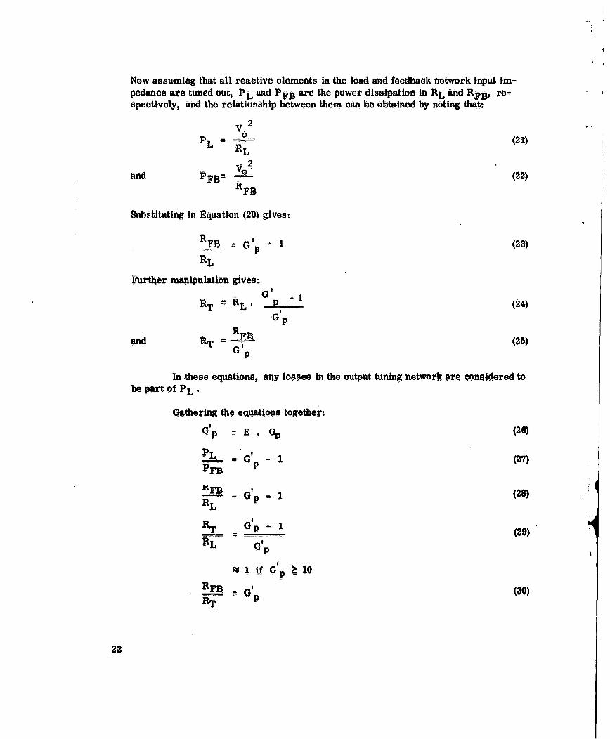
Now assuming that all reactive elements in the load and feedback network input im-pedance are tuned out, PL a d PFB are the power dissipation in RL and RFB, re-spectively, and the relationship between them can be obtained by noting that:
V-20PL " (21)
R L
and PFB " (22)
RFB
Substituting in Equation (20) gives:
RFB -'1 i (23)
RL
Further manipulation gives:.
=R. 2 .. (24)
and RT RFB (25)Gp
In these equations, any losses in the output tuning network are considered tobe part of PL
Gathering the equations together:
G'p E Gp (26)
PL GP p 1 (27)
FB
RL G(28)
RL
RT G'p1 (29)
RL G'~
1 if (Gp > 10
RFB ' (30)
22

II
These equations show that G',p governs the necessary impedance levels asso-eated with the oscillator. it also determines the maximum power output of the os
Cdlator, since the maxim m permissible feedback power FB max is limited by the
permissible crystal dissipation; the crystal being one of the dissipative elements inthe feedback network,
A simple example will illustrate the use of these formulae. Referring to!Figure 11 and making the following assumptions:
IL'
I _-
Figure 11. Grounded Grid Oscillator
I (a) The power gain Gp of the triode is 50 when loaded with
RT =0 K
I (b) The input resistance Rin of the triode under these conditionsis 200 ohms.
I (c) The effective resistance of the crystal at resonanceRr is 100 ohms.
I (d) The maximum allowable crystal dissipation is 2 MW.
I (e) The effective parallel loss resistance of the coil L is 40 K.
To finalize the design, the values of R and RFB have t b determined:
I hadt i
RinE - .67 (31)Bin -' R
then G p =34 (32)
GI Rand RL p • T R 10K (33)
23

The coil losses are included in this value and U L 13 K (34)
RFB = R T = 340K (35)
The Impedance reflected into the plate side of the impedanee transformer Lmust be 340 K when the secondary side is loaded with Re + AW The impedancetransformer ratio Tr will therefore be:
Tr _-340x 10 - 1100 (36)r 300
For simplicity in this example, it is assumed that the coil L has unity coupling between
turns, giving a turns ratio of:
N 1. -33 (37)
As previously stated, in any practical design the required feedback power will be atleast twice the amount indicated in these equations, to allow for circuit variations._!
This can be taken into account by introducing a modified value of G p; i. e., byusing G"p G' G in Equations (33) and (35). The resulting 9FB will be
2 3decreased, giving increased feedback power.
The permissible power output to the load R'L before crystal overdrive occurscan be determined by noting that 33 percent of the feedback power is dissipated in thecrystal. The maximum permissible feedback power is therefore 6 MW.
Pout - FB G' (38)p
S6x10 3 x34 = 204MW
Using a more realistic value of G p (G p = 11, for example) will give a power outputShe region of 60 to 70 MW. It is then a simple matter to determine the values of all
components to complete the desI-gn.
This example demonstrates the simplicity of oscillator design once the para-meters of the various circuit elements are lmown. In some cases, these parametersare directly available tough manufacturer's data sheets and present n problemother than that of interpretation. in other instances, little directly usable Informationis available, and the determination of the characteristics of the circuit elements becomes a major design problem,
The next three sections give general background information concer the
the characteristics of the oscillator circut elements.
24

I
4 2. 3 Active Device Characteristics
In Paragraph 4. 2. 2 the importance of the power gain of the active device inthe oscillator equations is noted. The characteristics of the active device that in-fluence an oscillator design are:
(a) The power gain of the device as a function of outputloading
J (b) The input impedance of the device as a function ofoutput loading
(c) The phase angle between input and output as a functionof output and input loading
(d) Power output versus supply voltage, current, and load
(e) Variations in the above due to changes in temperature
I) Gain stability as a function of gain magnitude
From DC to 10 MC the manufacturer, A data sheets usually supply sufficient parameterinformation to enable characteristics (a) to (e) to be determined by calculation with areasonable degree of accuracy, while (t) is of minor importance at these frequencies.Above 10 MC the parasitic reactive elements and the physical dimensions of the activedevice begin to have an increasing effect on operation. The available data is ordinarilynot sufficiently detailed to account for these effects, and the prediction of active deviceperformance characteristics becomes less accurate as the operating frequency increases.Even If this was not the case, the stray reactance introduced by the physical circuitlayout would have a similar effect, lowering the accuracy with which the characteristicsof the active device ( together with its associated network) can be predicted.
For these reasons, the technique of determining the active device charactera--tics at high frequencies, advocated in Paagrap 4. 5. 3.4, is an experimental methodin which the active device characteristics are measured in a circuit similar in layout
to that envisioned for the oscillator circuit. Unfortunately, the amount of data thatcan be obtained in this way is rather limited unless specialized instrumen tion isavailable. Characteristics (a), (b), and (I) can be determined with fair accuracyusing a relatively sip~pe measuring procedure, while (c), (e), and to some extent,.
(d) must depend on oscillator design experience.
In Paragraphs 4. 5. 3. and 4.6. 3, design information is presented on the se-J lection of tubes and transistors, tagether wit methods of calculton or measurement
of their characteristics.
25

4.2.4 Impedance Transforming Networks
cause of the large differences in impedance levels likely to exist betweenthe crystal and the active device, at least one impedance transforming network isusually necessary in an oscillator. Possible applications Of impedance transformingnetworks in oscillators are:
(a) To transformu the impedance level of the feedback network to thatrequired at the active device output
(b) To transform the input impedance of the active device to a suitableterminating level for the feedback network
(c) To transform the oscillator load to a level suitable for connectionto the active device.
in applications (a) and. (b) an additional requirement has to be met. Not onlymust the network transform impedance levels, it must also introduce a desired amountof phase shift between input and output. This will normally be 0 degrees or 180 degrees,depending on the osbillator configuration, but it may be desirable to introduce smalladditional phase shifts to ,compensate for those introduced in other parts of the circuit,This requirement can be met by applying suitable formulae to the impedance trans-former design.
Commonly used impedance trans-forming networks are shown in Figure 12.These networks are normally used with a tuning reactance as shown in dashed linesin (a) to (e), although these components play no part in the Imedance transformingaction. These networks, or the tuning coil in the case of (d), contain resistive elementsin the form of coll losses that result in power loss. This power loss reduces the ef-ficiency of power transfer through the network and must be accounted for in theoscillator design. Analyses of the networks of Figure 12 are made i Paragraph 4.7.
-. 1I I I I I
!L I _ lIi iI- II I -I i I I
oj.. - --
i I I II I I
II ,I II I I I
i I I
a~rm (a) (b) (C) Cd) (e)
Figure 12. Impedance Transforming Networks
26

4.3 Performance Specliation of an Oscillator
Prior to the design of an oscillator, a specification is written fixing the os-cillator performance requirements. These requirements are normally specified inthe following form
(a) The frequency of osillation, the, frequency tolerance, and theos sti r atibjot,1- frequency stability required of the oscillator when su bjected toa certain range of environmental stress, to specified variationsin oscillator loading and to per missible power source variations.The minimum time period between readjustment of oscillatorfrequency to compensate for frequency drifts due to aging, andthe maximum harmonic output may also be specified.
(b) The power output and its variation, when subjected to a certainrange of environmental stress, specified variations in oscillatorloading, and permissible power source variations.
(c The load inedance into which the oscillator will work. In someinstances the load will be a mixer circuit or other non-linear input
* - impedance circuit and, in this case, the load impedance is likelyto be only vaguely defined.
* (d) The permissible input power, the input voltage level, and the
expected range of variation.
(e) The oscillator package size.
In addition, the type of active device; that is, tube or transistor, and themaximum cost may be specified.
4.4 Design Procedure
Based on this specification, a process of selection is necessary to arriveat a final design. This involves the selection of:
(a) The crystal operating condition. At frequencies up to 20 MC to25 MC, there is a choice between operation at resonance or parallel
resonance; at higher frequencies, only crystals operating atresonance are available.
(b) A particular type of crystal from those. available at the desiredfrequency of operation.
27

(c) The oscillator configuration. This will be governed by (b).
(d) The desired active device characteristics based on (b) and (c).
(e) A particular type of tube or transistor based on (d).
(1) The type or types of impedance transforming network thatwill be used based on (b), (c), and (e). -{
There is a wide freedom of choice during this selection process, particularlyin steps (a) through ()g and in order to optimize the design, this freedom of choice hasto be limited by consideration of the known operating characteristics of tubes, tramistors,impedance transforming networks, and experimental oscllator performance evaluationdata at the desired operating frequency. From these considerations criteria can thenbe developed that will increase the possibility of optimizing the design of oscillators.
4.6 5 scillatorJDesign at High roecs
S4. .1 General
At frequencies above 20 MC the characteristics of the various components ofan oscillator begin to be frequency-dependent due to the presence of parasitic reactancein its various forms. Circuit layout is also more critical for the same reasons andmay be the determining factor in the level of performance that can be attained. Further,measurements become more difficult to make with any assurance of a reasonable ac-curacy. These effects are relatively mild at the lower frequencies under discussionand become worse as the frequency increases.
The prerequisite for design is to know the characteristics of the test equip-ment that will be used and to appreciate this influence on the circuit under test. It isnot always sufficient to rely on manufacturers' specifications, since aging and otherfactors may degrade performance considerably. As an example, one vacuum-tubevoltmeter used during early design evaluations had a parallel .input resistance of afew hundred ohms in addition to the specified capacitance of 3 PF at 200 MC. Anothervacuum-tube voltmeter had a parallel input resistance of 5 K at 150 MC until the de-tector diode was chaged, after which the parallel input resistance increased to over25 K.
Effects of this nature considerably influence the interpretation of measurementsand should be constantly kept in mind. Similarly, circuit components are likely to dif-fer considerably fom their nominal values. Mica c apacitrs of nominal value exceeding10 PF cmnot be relied on to have an actual capacitce approaching the nominal value
at the higher frequencies. This effect c be important, particularly in impedancetransforming networks. Carbon resistors also vary considerably from their nominal
28

a 44
__ wiR
B i l 1- 1--- -- ~ - ~ - 1
,---- ----- 47------
U 4.
UUR1- -0
--- 7- - - 7 - N -: V- 071-7
A'4fz7
1221
29

values as shown in Figure 13. The deviation is particularly large for resistor valuesgreater than 2 K and less than 40 ohms. These characteristics are those of a widelyused make of !/2 watt resistor. The same make of 1/4 watt resistor exhibits essen- Itially similar frequency characteristics. In many cases this effect will be of littleconsequence; for example, in decoupling networks, etc. in other inStances, such 1as using a resistor to load the oscillator, it will be essential to know the actualvalue of resistance with reasonable accuracy.
Circuit wiring will also influence the performance of these elements. It isof little use to employ a component with a desired characteristic if the component willbe wired into the circuit with long lead lengths. One inch of 20 gauge wire has a self-inductance of approximately 0. 02 UH, corresponding to a reactance of 25 ohms at 200MC. When working at low impedance levels, this inductance can have appreciableeffect on circuit performance. Long lead lengths also increase mutual inductivecoupling (the effects of which are more difficult to interpret) and stray capacitivecoupling (which will have a maximum effect at high impedance points of the circuit).
Because of the possible wide deviations from nominal of the components that {will be used in an oscillator, it is advisable to measure the component values at theparticular operating frequency to insure that design conditions are being fulfilled.In fact, the experiences of this program suggest that impedance measuring equip-ment is essential to the design effort at the high frequencies. Throughout that partof the program dealing with high4frequency oscillators, an Rx meter was in constantuse and proved invaluable in aiding the design effort.
The circuit layout problems posed during initial experimental designevaluation are somewhat different from those in a final design. It will be necessaryto take measurements and change components in the circuit to evaluate the per-formance, while this will not be necessary in the final design. A more open con- fstruction is therefore necessary initially, to allow access for voltage measuringprobes and to facilitate the changing of components: Figure 14 shows photographs
of the layouts used for all the high frequency oscillator test circuits evaluatedduring this program. In these layouts the output and input circuits were separated
by the screening plate shown extending across the chassis. The necessity of employing this screen is not known. It was included during the early evaluations asan additional safeguard and, since the layout met the measurement needs, it re-
mained throughout the program.
45. C rysa CharacteristicsTable 4 shows the military standard crystals applicable to oscillator design
above 20 MC. More detailed information on most of these crystals is contained inReference 5, Paragraph 7.0. There are no military standards for crystals operatingat frequencies above 125 MC, but crystals meeting the general requirements of tyes
30

, BOTTOM LEG OF C CANCELLATION FiLAMENT
IMPE DANCE TRANSFORMER COEDCUUN
11OK
904A om 7 AL = TERMINAL
21465 TRANSITOR' INPUT CoCwiTn '1056 T
CAPAIVF IPDAC CPCTIVE IMPEDANCE - LOADTRANS AAMER TRANSFORMERRMSO
I OUTPUT,
DEOILN"21434 TRANSISTOR CIRCUITS B+ DECOUPLING I06 TUBE
1 Fiigre 14. High Frequency Oscillators, Input and Output Circuits
31

CR-54A/U or CR-56A/U can be obtained for operation at up to at least 200 MC. Themajor difference is that R1 may be as high as 100 ohms instead of the 60-ohm maxi-mum value of Rr specified for the CR-54A/U or CR-56A/U units. 1
All the tabulated crystals are designed to operate at resonance. The circuitof Figure 1 can still be regarded as a useful equivalent circuit, although parasitic '[reactance in the crystal holder has a bearing on the performance at the higher fre-quencies.
At frequencies above 125 MC, a slightly different approach is required. TheCo of these crystals is typically 7 PF, giving a reactance Xco of 180 .ohms to 114 ohmsin the 12.5 MC to 2-00 MC band. in order that resonance will occur, it is necessary thatXco grae thn4 vausof <2should be greater than 2 and preferably greater than 4. For values of
the crystal always appears cajacitivei and for - values between 2 and. 3, the phaseR1
shifting ability of the crystal is severely degraded. Since these conditions are notsatisfied for Ri values of 60 ohms to 100 ohms (the range in which these crystals canbe expected to fall), it is necessary to increase the effective reactance of Xco . Thisis normally done by connecting a low Q inductance in parallel with the crystal, thevalue of the inductor being such as to cancel out Xco at the frequency of resonance.The coil is arranged to be of low Q in order to make the cancellation uncritical, butthe effective parallel resistance of the coil should be 10 to 20 times the value of Rto avoid degrading the crystal resonance characteristic.
in order to determine the value of the cancellation inductor, it Is necessaryto know the value of Co at the operating frequency. Co measurements at frequencieswell below the operating frequency have little meaning, since the effect of the crystalholder parasitic reactive elements is to increase the effective value of CO . Co musttherefore be measured at a frequency near to the operating frequency, but sufficientlylower so that the series arm element does not appreciably fect the measurement.
A measuring frequency 5 percent to 10 percent below the operating frequency isnormally satisfactory.
In many instances, cancellation coils are used in oscillators operating below125 MC. The reason for this is that Xco forms a low impedance feedback path inde-pendent of the crystal. The remainder of the oscillator is usually capable of intro-ducting large phase shifts with only a small reduction in power gain.
i
32

TABLE 4. MILITARY STANDARD CRYSTALS, HIGH FEQUENCY
WIDE TEMPERATURE RANGE CRYSTALS
Maximu mNominal Operat'ing Frequency EquivalentFrequency Temperature Tolerance Drive Res istance(Megacycles) (Centigrade) (Percent) Level Holder Type __ (Ohms)
()10 to .61 -550 to + 1050 ±0. 005 20MW iHC-6/U CR-51 A/U 4010 to 61 460O to +105o ±0. 005s 2amid4 HC-6/U CR-52 A/Ui 40i MW
()15 to 50 "56 to +1050 ±0.A05 2 MW HC-0/U CR-24/U 50 and 75
17 to 61 4.5o0 to +1050 ±0. 0015 2 MEW HC 18/U JCR155/U 4017 to 61 56 to +-1050 ±0. 0025 2 MW HC-18/1U CR-.67/U
r17 to 61 .450 to +1050 ±0. 0015 HC-18/U! CR-42/U
17 to 61 55O to +1050 ±0.M025 HC18/Ul CR-76/U117 to 62 .5,59 to +1050 ±0. 002 HC-25/U1 C2-77/U35 to 50 "550 to +1050 ±0. 003 HC-29/U CR-73/U
()50 to 87 -550 to +1050 ±0. 005 20MW H1C-/U CR-53 A/U 60
50 to 125 55() to +1050 ±0. 0015 2 MW HC-6/U CR-54 A/U 50 an 60s0 to 125 -55o to +1050 ±0. 005 2 MW HC-18/!U CR-56 A/U 50 and 60
TEMPERATURECONTROLLED CRYSTALS10 to61 75Q ±50 ±0. 0025 2adl C-/ R6/ 40
MW10 to 75 75P0 1 ±0. 002 2 and 1 HC-6/U CR-32 A/U 40 and 50
MW
*17 to 61 8 50 50 1-0. 002 2 and 1 HC-18/U CR-61/U 40
45 t 7 850*50MW45 o 5 80 50±99 0015 HC-2 6/U CR-74/U
50 to 87 750 ±50 1-0. 00125 HC -6/U CR-75/U
50 to 125 850 ±59 ±*0. 002 1 MW HC-18/ CR- A/ 50 and 60
()GOVERNMENT PERMISSION REQUIRED PRIOR TO. USE
33

Therefore, oscillation via Co is possible if the amplifier gain is sufficient. The can-cellation coil reduces the possibility of this occurring. -
The standard military crystal test sets for the frequency range discussedhere are the Crystal Impedance Meters TS4683/TSM and the AN/TSM-15, covering Tthe frequency ranges of 10 MC to 140 MC and 75 MC to 200 MC, respectively The I.TS-683/TSM is supplied with a selection of fixed substitution resistors for use between50 MC and 140 MC in determining crystal resonance resistance, and a variable sub- rstitution resistor for use below 50 MC. The AN/TSM-15 is supplied with six variable Asubstitution resistors which, between them, cover the resistance range of 10 ohms to110 ohms, with a negligible reactive component over the range of 75 MC to 200 MC. -.
i4. 5, 3 Active Device Characteristics
it is desirable to know the values of the active device characteristics that Iinfluence performance. These are:
(a) Power gain as a function of output load!
(b) Input impedance as a function of load 1(c) Phase angle of output voltage relative to input voltage as a function
of input and output terminations g
(d) Power output as a function of supply power and load impedance
(e) Variations of the above as a function of temperature
(j) Gain stability as a function of load
These characteristics become increasingly difficult to determine as the
operating frequency is increased. At frequencies above 10 or 20 MC, calculations fbased on the simple formulae adequate for low-frequency operation begin to loseaccuracy because of the effects of parasitic reactance. improvement of these
formulae to account for the new effects results in unwieldly expressions. Also,since the additional parameters (cathode lead inductance, transit time, mutualcouplings, etc.) are not normally known with any certainty unless measurementsare performed, this approach is likely to defeat its object; that is, to design by cal- {culation rather than by experiment. The physical layout of the active device and itsassociated: components may also introduce comparable parasitic reactance, makingthe prediction of performance difficult.
The alternative approach is to experimentally measure as many of theactive device characteristics as possible at the desired operating frequency and under
34
circuit conditions approaching those in which the active device will be used. In practice,this consists of measuring thepower gain versus load, and input impedance versus load.Prom these measurements an indication of gain stability as a function of load can alsobe obtained. This leaves items (c), (d), and (e) yet to be determined. item (d) can bef calculated with reasonable accuracy by methods discussed later. item (e) can only bedetermined experimentally with any degree of accuracy. Because it is easier tomeasure the overall effects of temperature on an oscillator, as indicated by the outputfrequency and power changes, than to measure the active device characteristic varia-tions, the design recommendations given later rely on information gathered in this wayas a substitute for (e). The measurement of Item (c) requires specialized equipmentat high frequencies and, since this will not normally be available to the designer, pastexperience nust again be relied on.
J Before this process of measurement is implemented, the designer must choosea particular active device type; and, to avoid the waste of time incurred if the choice isinappropriate, a basis for this selection must be developed. Furthermore, it is de-sirable that this basis be formed on the information contained in the manufacturer's datasheets.
* 1 One effect that cannot be easily gauged from the data sheets concerns the in-
herent feedback within the active device. This effect is particularly important at thehigher frequencies because the feedback path is either wholly or partially through thestray capacitance of the active device and its associated circuits. This feedback isnot necessarily positive feedback at the desired oscillator frequency, where the inputand output circuits of the active device are essentially resistive due to the conjugatematching employed. The danger is that at adjacent fequencies these tuning networks
are likely to produce large phase shifts which, in conjunction with that in the inherentL feedback path, will result in positive feedback and possible oscillation. It should alsobe noted that, at the desired oscillator frequency, this undesired feedback path is inparallel with the desired feedback path containing the crystal. The necessary condition
I for oscillation to occur is that the combined feedback signal from the two paths shouldresult in 0 degrees phase shift. The desired feedback path wiIl have to compensate forany phase shift present in the undesired feedback path and may result in the crystal
I operating off resonance.
The following discussion is intended to show the effect of the inherent feed-back paths more clearly and the methods available for counteracting it The discussionI is in no way rigorous; for more detailed discussions, see References 6, 7, and 8 ofParagraph 7.0.
I 4. 5. 3. 1 Feedback Effects at High Frequencies1 The behavior of any active device can be characterized by a set of four para-
meters which may be specified in various forms. The form used here, and the one
35

most applicable at high frequencies, is the admittance or 'y' parameter form. For thethreetmethods of connecting a tube or transistor as shown iii Figure 15, the equaitionscharacterizing the active device aire:
Ii yi'i + YrV2 (9
12 YfV 1 + YoV 2 (0
where the positive direction of 11, 12o V1, and V2 is taken as indicated in Figure 15,and where:.
Y =G + iBi I L when 2, 2' are short circuited: (41)VI
=r Gr + jBr = when 1,1' are short circulted (42)V2
Yf O f + jrf 12 when 2, 2' are short circuited, (43)VI
y0 G0 +B 0 =when 1, 1' are short circuited (44)V2
t I
fyi tv, -- 2
' 2~
-o
"lvig
I1- _ _2
Cd) (6) (2
Fiur 15 Active DeieCofgrain
36 1 VtV-

The four param eters will, in generali be different for each of the connectionsshown in Figure 15 (a) to (c) and (d) to (P), and can be distinquise frmechohr yana additional Suffix inidicating the grounded element. From Equations (39) and (40) theJequivalent circuit of Figure 16 can be developed, which also Shows a load of admittance
YLand a driving source of admnittance YG, where:
IYL OL + AL (45)
YC G + jEG (46)
I('Vi "Yr )VI Y +Yr
IFigu re 16. Active Device Equivalenit Circuit
I Referring to Figure 16, the nodal equations are:
I1 -"(Yi + Ya)Vi + Yr V (47)
0= l + ('f + (48)2
The power output is given by-
P VG, (49)
j(Y1 + 1 f L (0
+ O)(YO + YL) Yf Yrl (0
The maximum available power P avfrom a source of admittance
Pav (5v
I YGG IBG j: (51
V 37

and is supplied to the active device when the input is conjugately matched to the source.The transducer power gain Gt is defined as:
t (52)
Pay
- 2+ (YO + Y Yf X Yr (53)
The denominator of Equation (53) is the vectorial difference of
(Yi + YG ) (Yo + YL ) and (Yf x Yr ); and if these terms approach a om-
parable magnitude and phase angle, G Will approach infinity. it can be shown(References 6 and 71 Paragraph 7, 0) that the circuit is likely to oscillate if:
jYf yrI " Re (Yf Yr) - 2 (G + GG)(G 0 + GL) (54)
where Re (Yf Yr) is the real part of Yf . Yr. Conversely, the amplifier is unconditionally stable if the Stability factor K is greater than unity. This is defined as.
K 2 (Gi + GG) (G + GL)K = .. .... .:. ... _ _(55)
- Yf •Yr' + Re(Y Yr)
The amount by which K exceeds unity Is a direct indication of the circuit sta-bility. K values as high as 10 have been suggested as desirable In transistor amplifiercircuits undergoing severe environmental stress. This takes into account the rela-tively large parameter spread encountered in transistors of the same type, and suggeststhat a K value of 3 or 4 would be adequate for a vacuum tube amplifier, where theparameters are less temperature dependent and where the parameter spread betweenunits of the same type is smaller.
The cause of this tendency of the amplifier toward instability is the term Yr,the admittance coupling the output and input of the active device. In a vacuum tube thisconsists primarily of the parasitic capacitance between plate and cathode or plate andgrid for grounded grid or grounded cathode amplifiers, respectively. In a transistor,-Y is a combination of resistance and cap citance in the semiconductor material andthe header capacitance. In neither case does "Yr contribute to the useful forward gainof the amOlfier, and its minimization Is desirable in an active device.
38

There are two alternative methods of stabilizing the amplifier power gain: by
unflateralization (or neutralization) or by mismatch.
(a) Stabilization by Unilateralization or Neutralization
Referring to Figure 16, if an admittance Yr is introduced in parallel
with "Yr, the two cancel, resulting in zero coupling between output and input. TheI transducer gain becomes:
I It ni 4y-Y-(6I(Yi (Y - '120 L
and the amplifier is unconditionally stable. The amplifier is then said to be unlater-alized. If the added admittance fully or partially cancels only the susceptive part of
Yr, the amplifier is said to be neutralized.
if conjugate matching of input and output if employed, maximum gain is ob-tained and is given by:-s given 2
IGt Max- RX 2f(7
I (b) Stabilization by Mismatch
Referring to Equation (55), the stability factor is increased if thenumerator is increased and the denominator is held constant. This means that GG andGL have to be increased, since Gi and G0 are active device parameters, The
Optimum conditions of mismatch (that is, that producing the highest gain for a givenstability) is obtained when:
I GG GL =m(8
-- - - In (58).C., Go
I where m is termed the mismatch factor. Provided that:
GG0 (m+ 1) >> Yf. Yr (59)
and the susceptive ompnents of Y1 and Yo are tuned outh, te expression for power gain
is.G - (60)
+ 0039
39

(c) Comparison of Power Gain Using the Two Stabilizing Methods
Stabilizing the amplifier gain by mismatch results in a smalier power
gain relative to that obtainable by unilateralization for a given stability. This is ob-vious when it is considered that mismatchieng results in inefficient power transfer,whereas matching can be employed with a unilateralized amplifier. A direct com-parison can be obtained by taking the ratio of Equation (60) to Equation (57):
pm rm (61)
Gp unit (m + 1) 4
ifm = 1 (that is, no mismatch), the stability factor is given by:
K 5 : -- : -. . . . ... (62)
IYfYr[l + Re(Yf , Yr )
Employing mismatch and letting m - 2:1SGiG0
K - (63)Y --RI +Re(Yf
This results in an improvement of 2. 25 in K, while the loss in power gain, relative tothat obtainable using unilateralization, will be 4 DB. A similar comparison employing
m = 3 shows an improvement in stability of 4 times greater than that for m = 1, witha power gain loss of 7 DB compared to a unilateralized amplifier. These losses are
not too great when the unilateralized power gain capability is relatively high; that is,20 DB or greater. Otherwise the gain will be seriously affected.
4. 5.3.2 Active Device Configurations Used During This Program
Only two types of active device conf!uation have been investigated in detail
during this program: the grounded grid triode and the grounded base transistor con-figuratIons. A grounded emitter transistor amplifier and a grounded cathode tetrode
amplifier were evaluated at a frequency of 200 MC. Both circuits showed good gaincapabilities at thIs frequency. The tetrode had a stable gain of 300 and te transistor
a stable gain of 50. However, attempts to Incorporate these amplifiers in oscillator
circuits were unsuccessful due to the large undesired phase angle deviations occurringin the active device. Attempts were made to correct for these effects, but witout
success, and the experiments had to be abandoned because of Ime limitations,
It is doubtful if much was to be gpined from using these configurations in any
case. The tetrode design was undertaken because of the possibility of obtaing highergin and, hence, larger power output than that obtainable using a g d grid triode.
40

II
This would certainly have been the case except for the undesired phase shift problemsthat arose. However, this would only be gained at the expense of increased circuit con-plexity due to the presence of the screen grid and the necessity of using two impedancetransforming networks, one of them having phase inverting properties. The same resultcould be obtained using the two halves of a double triode with approximately the samenumber of componentsi one triode being used in the oscillator circuit, and the otherused as a buffer amplifier, This approach might possibly resul in i creased isolaton
of the oscillator from the load, but at the expense of increased power drain.
I The grounded emitter transistor oscillator design wars undertaken purely as aparallel effort to the tetrode design. Little advantage could be foreseen for this con-figuration in view of the excellent gains obtained previously with the runded base
circuit and because of the inherently higher gain variations of the grounded emitteraconfiguration, particularly with temperature.
Configurations other than the grounded base and grounded grid are occasionallymentioned in the following sections. However, this is done purely for completeness,and it is emphasized that the two above mentioned configurations are the ones coveredin this part of the report under high-frequency oscillators.
4. 5. 3. 3 Aids to Active Device Selection
44 5. 3. 1 Vacuum Tubes
SThe low-frequency parameters of a vacuum tube can be used to indicate thegain capabilities at high frequencies, provided that the effects of parasitic reactanceare small. The relevant low-frequency equations are:
(a) Grounded Grid Triodes
Power gain, Gp - (U + 1) . R(64p + R6T
where RT is the total load resistance. The maximum power gain Is,therefore:
i =max (U + 1) (65)
when RT >> Rp .I R + RT
Cathode input resistance, Rin - T T (66)U + 1
I
Y. 41

(b) Grounded Grid Pentodes or Tetrodes
Power gain, C ±- gm RT (67)
and the cathode input resistance:
Ain -! (68)gm
if A > T
(c) Grounded Cathode Pentodes or Tetrodes
Power Gain, Gp - RT Rin (69)
where Rtin - g , gk2 (70) jwhere Wgk- angular frequency of resonance of the grd-cathode
stray capacitance with the cathode leakage in-inductance
w & angular frequency of operationT & time delay due to transit time of, electrons
between grid and cathodeKe - constant dependent on tube geometry
In general, Wgk and TKe will not be known; however, te tube manufacturer
sometimes specifies Rin at a particular frequency fg, and a usable valueof input resistance at the desired operating frequency fd can be obtained by
f2
The power gain obtainable in either of these connections is proportional tothe total load resistance RT, the maximum value of which is limited in the following twoways. (a) The effective parallel resistance of the tuning inductor RD . Assuming
value of 10PF capacitance composed of strays and tuning capaci-tance in the plate circuit, the capacitive reactanCe at 100 MC is 160ohms. The Q of the inductance will be between 50 and 200, dependingon space requirements, etc., resulting in an RD of from 8 K to 32 K.For the same total tuning capacitance, these values will be 4K and 16K at 200 MC. The actual load RL will be n parallel with RD and, inorder to obtain a reasonable ratio of power into the load versus power con-
42
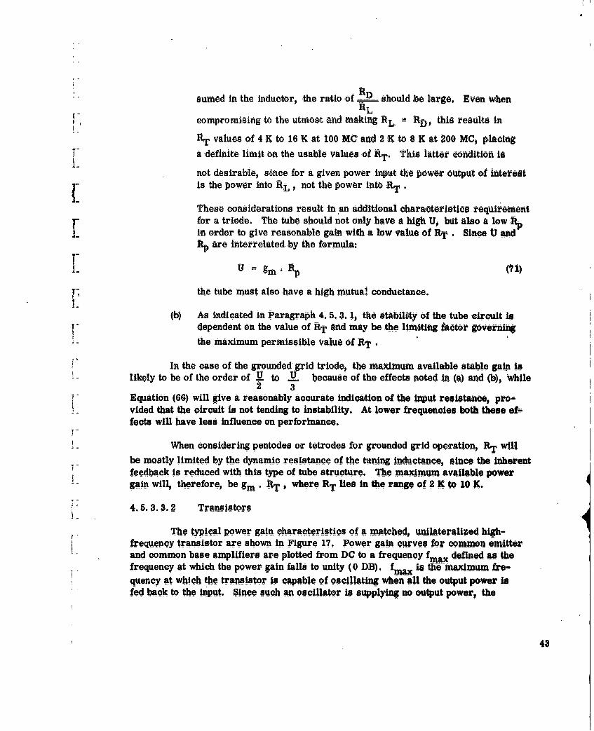
~R D- sumed in the inductor, the ratio of _ should be large. Even when
RLe-, compromising to the utmost and making RL - RD, this results in
RT values of 4 K to 16 K at 100 MC and 2 K to 8 K at 200 MC, placing
- a definite limit on the usable values of RT. This latter condition is
not desirable, since for a given power input the power output of interestIs the power into RL , not the power into RT.
These considerations result in an additional characteristics requirementr for a triode. The tube should not only have a high U, but also a low RP1. in order to give reasonable gain with a low value of RT ,. Since U and
Rp are interrelated by the formula:
7 the tube must also have a high mutua! conductance.
(b As indicated in Paragraph 4. 5. 3. 1, the stability of the tube circuit isdependent on the value of RT and may be the limiting factor governing
the maximum permissible value of RT.
In the case of the grounded grid triode, the maximum available stable gain is* - likely to be of the order of U to V because of the effects noted in (a) and (b), While
2 3Equation (66) will give a reasonably accurate indication of the input resistance, pro-
.-vided that the circuit is not tending to instability. At lower frequencies both these efifects will have less influence on perforhiance.
1.. When considering pentodes or tetrodes for grounded grid operation, RT willbe mostly limited by the dynamic resistance of the tuning inductance, since the inherent
- feedback is reduced with this type of tube structure. The maximum available powergain will, therefore, be gm . AT, where RT lies in the range of2Kto 10 K.
4.5.3.3.2 Transistors
The typical power gain characteristics of a matched uiLateralized high-Sfrequency transistor are shown in Figure 17. Power gain curves for common emitter
and common base amplifiers are plotted from DC to a frequency fmax defined as the
frequency at which the power gain falls to unity (0 DB). L is the maximum fre-quency at which the transistor is capable of oscillating when all the output power isfed back to the input. since such an oscillator is supplying no output power, the
43

Ii'V
-~ II
I/
/
//
/// I__ _ / 0 1
0___ __ ___ C
/ r34w /
/i I-w /*z /zI I,- It0 II
/ I/
w *6.4
// 0
- ____ __ 7~o___ ___ ___ -~ I
II/( S I
AI a
w I- - - a.
0 0 0 0
(90) 1 q14 ['~Iq1 'NWB &i3MOd I
*1I

transistor cannot be defined as operating in any particular mode, and it thereforefollows that fmax defines the frequency at which the power gain falls to 1, independentof the configuration in which the transistor is connected. At frequencies below fmak,
the power gain increases at a rate of 6 DE per octave until the low-frequency power.- gain is approached.
- Other high-frequency characteristics shown in Figure 17 are I hfe I and I hth,the common emitter and common base short circuit current gain nagnitudes, respective,ly. I hfej also exhibits a 6 DB per octave slope at high frequencies, the "cutoff ' fre-,quency being fB, the frequency at which hfe is 3 DB down on hFp, the low-frequency
current gain. Another term related to I hfe I is fT, the frequency at which hfe fialls
to 1. 1hfbil has the same general characteristic, the cutoff frequency fa being thatfrequency at which I hf J falls 3 DB below h, B, the lowf4requency common base currentgain. fT and fa are vaguely interrelated, a being typically 1 to 2. 5 times '
L. Manufacturer's data sheets give values for some of these quantities and, withthis Information and a knowledge of the generalized power gain curve, the gain capa-bilities of a transistor at any frequency can be predicted with reasonable accuracy
The determination of the input and output impedance or admittance levels ofthe transistor are not as simple. The parameters determining these quantities are
!- those stated in Paragraph 4. 5. 3. , and Table 5 shows the typical variations of theseparameters over the frequency range from 10 MC to 200 MC.
!- -TABLE 5. Y PARAMETER VARIATIONS WITH FREQUENCY
Parameter Variation" Gee (Gob) ..... Varie-s over a range of-10:1
Boe (Bob) Varies over a range of 2:1
. Gie Varies over a range of 10:1Bie Varies over a range of 3A 1Gfe Varies over a range of 6:1
Varie - o -1Bfe Varies over a range of 6:1Gre Varies over a range of 5:1I Bre Varies over a range of 5-1
The second suffix (e) or (b) refers to groundded emitter or groundedbase configuration, respectively.
45

*1'
Occasionally, a manufacturer presents this parameter data in graphical form, showingthe typical variation with frequency and transistor power levels of the Individual para-meters. These are rare instances, however; in the majority of cases no high-frequencyparameter information other than the magnitude of the high-frequency common emitter [current gain hfe is given.
GI,, BI , Go , and Bo can be measured using a two4erm inal Impedance bridge,but the forward and reverse admittance measurements require a three-terminal bridge,an instrument not normally available to the designer. The simplest solution is tomeasure the input Impedance of the transistor in the amplifier in which it will be usedin the oscillator circuit, for various values of load resistance. This measurement isas easy to make as that of Gi and Bt1 , and the desired data (input imiipedance as a func-tion of load) is obtained directly. This subject is discussed further in Paragraph "4. 5i3. 4.
The bias conditions of the transistor influence its characteristics appreciably.The data sheet values of fmax , fT, fB hfe ] etc., are normally given for speci-
fled values of collector current and voltage. Data sheets of high-speed switching -
transistors frequently give curves of fT versus collector current and yoltage, Thisinformation is usually sufficient to enable a desired biasing condition to be chosen.
The loading due to the output tuned circuit effective parallel resistance R,will normally have negligible effect in transistor oscillators because of the lowvalues of output load resistance necessary to maintain stability.
I4. 5. 3. 4 Determination of Active Device Characteristics
if the design requency is sufficiently low (20 MC or 30 MC), the power gainand input impedance as a function of load can be determined with reasonable accuracyby calculation, using te low--frequency parameters. -
The performance can then be checked experimentally using the load resistancedetermined i a single-tuned amplifier circuit driven from a sign generatr. Inputand output voltages are measured with the output circuit tuned to resonance and a
value obtained for the input resistance of the active device using the substitutionmethod. In this method, the input voltage to the active device is measured, then the
___ __ O- _e--- smaurd te hsignal generator is disconnected from the active device and connected to a resistor,and the voltage across the resistor is measured. Adjustment of the value of theresistor, until the voltage across it equals tat previously measured across the "active device, will determine the active device input resistance to the desired accuracy, !
From the above measurements the power gain can be obtained. This is basedon the assumption that the active device input impedace is essentially resistive at 1these frequencies; this is justifiable for transistors with an fT of 300 to 400 when
46

operated in the common base configuration, and particularly so for grounded grid triodesor pentodes.
A more accurate approach, and the only adequate one at higher frequencies,uses the same basic approach with the exception that an impedance measuring bridge issubstituted for the signal generator as a driving source. input and output voltages areagain measured with the output tuned to resonance, while the input impedance Ismeasured directly by the impedance bridge.
The impedance bridge used during this program was a Boonton RX meter whichhas a frequency range of 500 KC to 250 MC. As supplied by the manufacturer, the RX
7' meter is not entirely suitable for the neasuremen t of active device input impedance
, because of the high signal level existing at the bridge terminals. The maximum inputvoltage that can be applied to the emitter-base junction of a transistor before non-linearity occurs is typically 10 MV RMS, Since the output of the bridge is at least 10'ties this level, it follows that the bridge output voltage requires reduction to obtain, meaningful results. The simple modifications required are fully described in themeter instruction manual, and require less than one hour to complete. Other imped-ance meters can be used for these measurements, but the user is advised to insurethat the output level is suitable for this application.
After modification, the RX meter has certain peculiarities of operation which
may be misleading. These are:
(a) When operated at low bridge voltage levels, the bridge operatingfrequency is strongly dependent on the bridge oscillator voltagelevel. Slight adjustment of the bridge output voltage results insufficient change of bridge frequency that it will be necessary toreadjust the detector oscillator tuning to maintain a detector signal,(The detector oscillator frequency is 100 KC removed from theoperating frequency to give a 100-KC intermediate frequency ..)
(b) The feedthrough of the detector oscillator signal to the RX meterterminals has an amplitude of several millivolts, which is of thesame order as the desired bridge signal for transistor measure-ments. If the bandwidth of the transistor amplifier is sufficientlywide, this signal is amplified and appears at the output; this maymislead the operator into thinking that the circuit under measurementis oscillating, At test frequencies in the region of 170 MC and above,this feedthrough signal level begins to be excessive (values exceeding
20 MV have been measured). The values of gain and input impedancemeasured under these conditions are suspect because of possible non-linear operation, but appear to be adequate for the intended purpose.
47

I1
An alternative approach is available using the RX meter (see reference
9, Paragraph 7. 0). This consists of stopping the internal detector os-oillator and: substituting a mixer signal of lower amplitude from an ex-ternal source, at a frequency several megacycles removed from the
bridge frequency. The resulting heterodyne frequency is detected using Ia sensitive receiver. it is also possible that some Improvement could
be obtained using the existing circuit by reducing the amplitude of themixer oscillator signal. The detector circuit sensitivity is more than -adequate with the described modifications, and some degradation couldbe allowed if a reduction in feedthrough resulted. "I
The determination of the active device characteristics is made in the followingmanner.
Step I
ASsuming that the active device configuration and biasing conditions )have been determined from the previous discussion, the active device is incorporatedinto a single-tuned circuit amplifier. The tuning inductance used in the output circuitshould resonate with from 12 PF to 15 PF for designs at 200 MC and prorated for lowerfrequencies. The final oscillator package size should be kept in mind during the con-struction ol this coil, since it can be used in the final design and the coil loss in the
oscillator circuit will then be similar to that of the measurement circuit. The amplifier Iinput circuit is left untuned, with possibly an inductor in the input biasing circuit tominimize losses in parallel with the active device. )
The circuit layout should follow good engineering practice as to lead lengths,decoupling methods, etc., and should allow access for input and output voltage measur-Ing probes and for the RX meter connections. With the objective of building the proto-type oscillator on this chassis, provision should also be made for installing the addi-tional circuitry using minimum lead lengths. Figure 14 shows tube andtransistor oscillators constructed on a chassis that proved adequate for this purpose.During this measurement phase the impedance transforming network, crystal output
limiter diode, and Co cancellation coil are not Included in the circuit, This chassisis designed to be installed on the ground terminal post of the RX meter with the "live"terminal protruding through a clearance hole in the chassis into a position immediately
adjacent to the active device input connection. .,
Step 2
Adjust the RX meter to the frequen cy of interest, and measure the input
impedance of the voltmeters that will be used for measuring input and output AC voltage.This voltmeter loadig should be applied as a correction when calculating power gain
from the measured results. When a transistor circuit is being tested, the voltmeter
48

used for input voltage measurement should have the sensitivity necessary to measure10 MV with reasonable accuracy. In addition, measure the actual resistance of anumber of resistors for use in loading the amplifier output. An indication of thedesired range of actual resistance values required at any frequency can be obtained
, from the experimental evaluation sheets contained in this report.
1- Step 3
Position the amplifier on the AX meter, and connect the "live1,terminalof the ,X meter, to the amplifier' input via a capacitor of low impedance. Measurement
4 tis again recommended. Connect a load resistor of 200 oh1m-a or 1 K across the amplifieroutput for a transistor or tube circuit, respectively. Set the output signal level of thebridge to be compatible with the linear signal handling ability of the active device.
r Apply power to the active device, and tune the amplifier to resonance.
Null the bridge and note the input and output voltage and the parallel input impedancecomponents indicated by the bridge. When the amplifier employs a transistor in thegrtounded base configuration, te parallel inductive component is usually too small totune directly with the internal tuning capacitor, and the addition of external capacitanceis necessary to obtain a null.
Because of the small range of capacitance measuring capabilities of the RXmeter, it Is necessary to calibrate this external capacitor by the substitution method.A coil is wound to tune with the. bridge capacitor at the upper end of its range (100 PF),the capacitor to be calibrated is then placed in parallel with this coil across the bridgeterminal, and the RX meter is again nulled. The difference in the RX meter capacitor
* setting when measuring the coil alone and when measuring the coil and external capacitorin parallel is equal to the external capacitor value. Values of capacitance up to 120 PFcan be calibrated in this way.
Step 5
Repeat Step 4 for ascending values of load resistance across the am-, plifier output. Almost invariably, as the process of increasing the load resistor value
$ and measuring gain and input impedance proceeds, the resistive component of theactive device input imp edance will be found to increase in value. Eventually, if the
load resistor value is increased sufficiently, it will be found impossible t null thebridge or, aternativeiy, the null will occur at a high resistive component value. Thiscan be interpreted as complete instability of the test c|rcuit, the positive feedback pre-sent to the amplifier being sufficient to supply virtually all the required Input power,
49
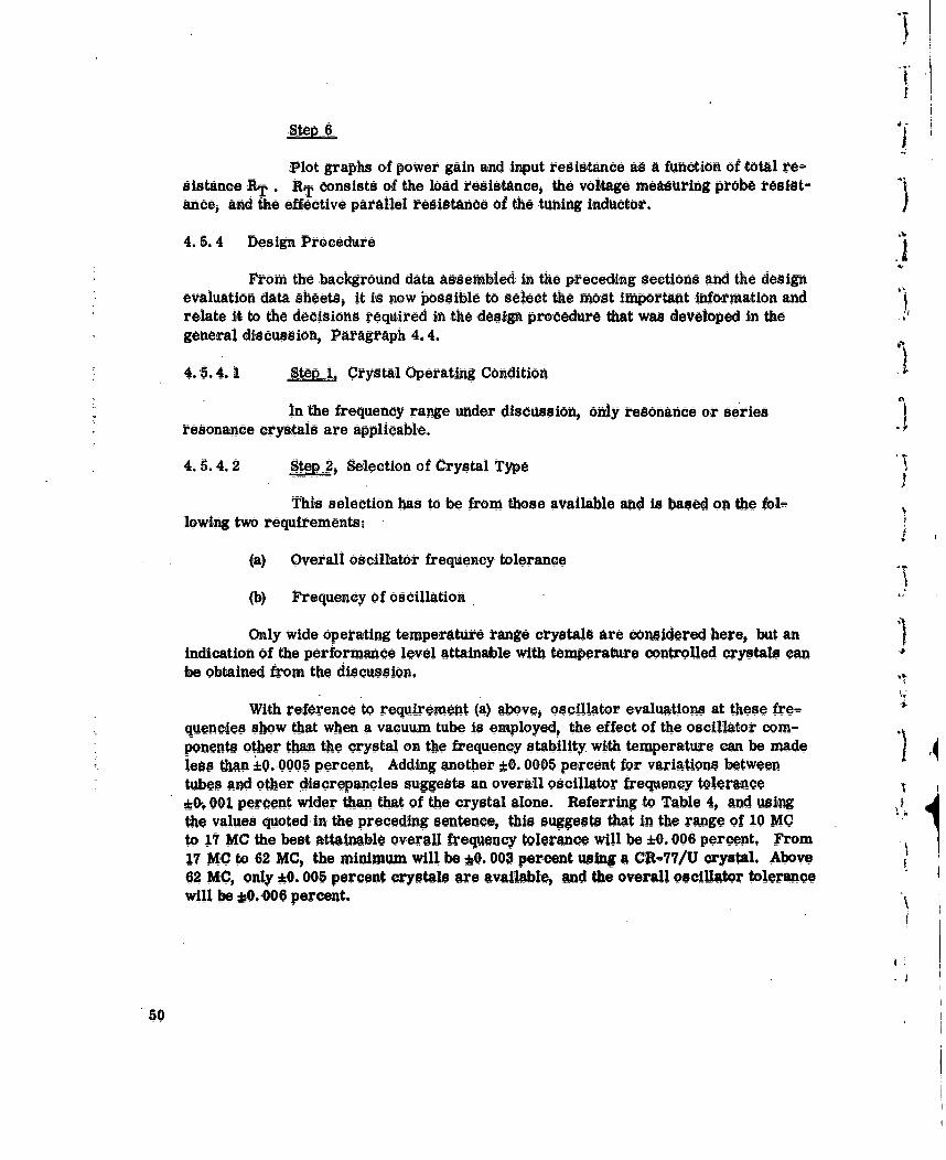
Plot graphs of power gain and input resistance as a function of total re-sistance ET. RT consists of the load resistance, the voltage measuring probe resistance, and the effective parallel resistance of the tuning inductor.
4. 5.4 Design Procedure
From the background data assembled in the preceding sections and the designevaluation data sheets, it is now 'ossible to select the most important information andrelate it to the decisions required n the design procedure that was developed in thegeneral discussion, Paragraph 4 4.4. 5. 4.1 Ster, Crystal Operating Condiin
in the frequency range under discussion, only resonance or seriesresonance crystals are applicable.
4.5.4.2 Step2, Selection of Crystal Type
This selection has to be from those available and is based on the fol-lowing two requirements:
(a) Overall oscillator frequency tolerance
(b) Frequency of oscillationOnly wide operating temperature range crystals are considered here, but an
indication of the performance level attainable with temperature controlled crystals canbe obtained from the discussion.
With reference to requirement (a) above, oscillator evaluations at these fre-quencies show that when a vacuum tube is employed, the effect of the oscillator corn-ponents other than the crystal on the frequency stability with temperature can be madeless than ±0. 0005 percent. Adding another ±0.0005 percent for variations betweentubes and other discrepancies suggests an overall oscillator frequency to-lerance
t0. 001 percent wider than that of the crystal alone. Referring to Table 4, and usingthe values quoted in the preceding sentence, this suggests that in the range of 10 MCto 17 MC the best attainable overall frequency tolerance will be ±0. 006 percent. From17 MC to 62 MC, the minimum will be *0. 003 percent usng a CR-77/U crystal. Above62 MC, only *0. 005 percent crystals are avalable, and the overall oscillator tolerancewill be *0..006 percent.
50

I
For transistor oscillators, the increase in frequency tolerance with tempera-
ture above that of the crystal alone was no greater than ±0. 009 percent. Adding another
*0i 001 percent for variations of transistor parameters, etc., suggests that an overalloscillator frequency tolerance *0. 003 percent wider than that of the crystal alone ispossible.
it should be noted that no attempts were made to correct the added frequencytolerance with temperature introduced by the active device. In the case of the tubeoscillator, there appears to be little to gain by doing this, in view of the limited ef-fect. However, in the transistor, oscillator, it should be possible to at least halve
the tolerance quoted.
Table 6 shows the minimum overall oscillator frequency tolerances likely to
be obtained at various frequencies.
I TABLE 6. OSCILLATOR FREQUENCY TOLERANCE (%)
Frequency (MC). Tube Oscillator Transistor Oscillator
10-17 &0. 006 +0. 008
17-62 ±0.003 0. 006
S4-200 +0. 006 *0i 008
If, in a particular design, closer frequency tolerances than these are required,temperature control of the crystal will be required. In extreme cases, temperaturecontrol of the entire circuit will be necessary.
Referring to requirement (b), Table 4 lists the available military standardcrystals. The contents of this table can be extended by noting that crystals conforming
to the CR-54A/U or CR-56A/U Specification (with the exception that R1 : 100 ohms)can be supplied in the frequency range of 125 MC to 200 MC.
1 4.5.4. 3 $tep 3 Oscillator Configuration
The grounded grid triode and thie grounded base transistor active device con-figurations were the only ones used successfully in this frequency range. Atempt to
design oscillators using a grounded cathode tetrode and: a grounded em itter transistorwere unsuccessful at 200 MC due to the large excess phase shift occurring in the am-plifier c cu ts. No similar designs at lower frequencies were attempted. However,based on the results obtained at 200 MC, neither of these circuits appears practcal

at frequencies above 100 MC; and, in the ease of the transistor, a more likely figurewould: be 30 MC.
Because of this ,imited experience with alternatives, the only cofigurationsdiscussed here are the grounded grid triode and the grounded base transistor circuits.The relative advantages of the triode over the transistor are:
(a) Better oscillator overall frequency stability (see discussion of Step 2of the Design Procedure, Paragraph 4. 5i 4. 2).
(b) Possible lower cost when high-temperature operation is required;that is, when only silicon transistors can be contemplated. This isparticularly true when the -requency of operation is higher than 120 MC.
The advantages of the transistor over the triode are:
(a) Considerably higher power output at all frequencies
(b) Reduced power dissipation,
(c) Decreased circuit complexity
(d) Less difficult to design (particularly for f > 100 MC)
(e) Smaller oscillator package size
These relative comments show that the transistor is superior to the triode inevery respect, other than oscillator overall frequency tolerance and, to a lesser ex-tent Ost. The use of a transistor is recommended In all oscillator designs forwhich their frequency tolerance degradation is acceptable.
4. 5.4. 4 Step 4, Desired Active Device Characteristics
Several of the desired active device characteristics are independent of fre-quency and crystal parameters. These are:
(a) High stable gain. This is desirable independent of power outPut re-quirements, since if the power output requirement is moderate, thegain (in excess of that necessary for oscillation with the specifiedload) can be employed in reducing the effects of the circuit on thefrequency of oscillation and the frequency stability. The gain varia-tions with temperature and between units should be small.
52
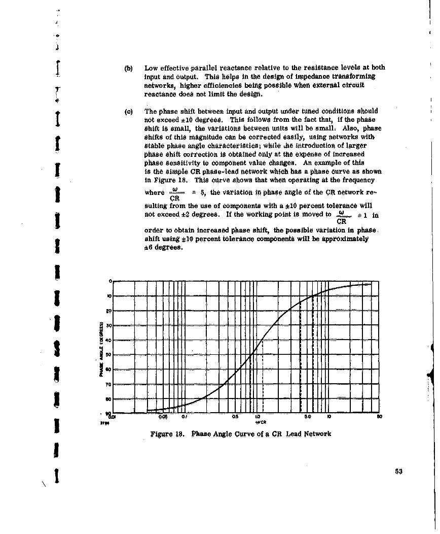
4V4.1q
(b) Low effective parallel reactance relative to the resistance levels at bothinput and output. This helps In the design of impedance transforming
T1- networks, higher efficiencies being possible when external circuitreactance does not limit the design.
(c) The phase shift between input and output under tufed c ondition s shouldnot exceed ±10 degrees. This follows from the fact that, if the phaseshift is small, the variations between units will be small, Also, phaseshifts of this magnitude can be corrected easily, using networks with,stable phase angle characteristics; while dhe introduction of largerphase shift correction is obtained only at the expense of increased
phase sensitivity to component value changes. An example of thisis the simple CR phase-lead network which has a phase curve as shownin Figure 18. This curve shows that when operating at the frequency
where C - 5, the variation in phase angle of the CR network re-CRsulting from the use of components with a *10 percent tolerance will
I not exceed ±2 degrees. if the working point is moved to -'L 4 1 inC A - iJ CRorder to obtain increased phase shift, the possible variation in phase.shift using *10 percent tolerance components will be approximately*6 degrees.
l0
S-L - - I - ---- ---
30- -
40 ---I-.I-I I I l ------] ll ! .. .I i --22 -...
Go ocs 0.1
Figure 18. Phase Angle Curve of a CR Lead Network
53

Other desirable characteristics of the active device are:
(a) An in-ut resistance approximately equal to the crystal resonanceresistance (Or series resistance);, s ince this will obviate the needfor an iJmpedance transforming network.
(b) A low output resistance compared to the effective load resistancedue to the impedance transformer losses. This characteristic .isfrequency dependent; the higher the frequency of operation, thelower the desirable output resistance.
4. 5. 4 5 Step 5, Selection of Active Device
Bearing in mind the characteristics of the triodes and transistorsavailable, the following recommendationB are made,
(a) Triodes for Operation Below 100 MC
U k 40
:S10 K
Cgk : 4 PF
(b) Triodes for Operation Above 100 MC
U 40
R 6K '
Cgk :5 2PF
The characteristics quoted for operation above 100 MC are equaly applicablefor operation below 100 MC; however, the requirements are less stringent at the lowerfrequencles.
Other physical features that point to good high frequency characteristics are:
(c) Small electrode structure mounted close to the tube plu , resulting inminimum lead inductance
(d) Multiple grid connections
54

Several commercial tubes having excellent characteristics are available in
miniature tube type envelopes. However, there do not appear to be any military typeequivalents, possibly because the close electrode spacing and lack of rigidity are in-
i compatible with military environmental stress levels.
There are also several coaxial triodes available that ar2 designed with highstress tevels in mind. These have performance characteristics superior to the com-mercial tubes mentioned in the preceding paragraph in that the lead inductance isfurther reduced and the grid for -ms a true screen between plate and cathode. However,
these tubes are quite expensive and would not normally be considered for this. applica-tion.
The nuvistor triode type 8058, which was used successfully at frequencies up
to 200 MC, represents a compromise both in cost and performance between the coaxialtriodes and the commercial tubes, having less isolation between input and output thanthe former and greater rigidity than the latter,
(e) Transistors
fmax 2 4 times the operating frequency
I fT > 2 times the operating fequency
Cob < 5PF
It is also desirable that the transistor power dissipation rating should not be
excessively large when compared with the required oscillator power output. HighP ower dissipation transistors tend to have more internal feedback because of thelarger junction areas.
4.5.4.6 Step 6, Determination of Active Device Characteristics
Using the data sheet information relating the active device characteris-tics to the bias conditions, design a suitable biasing network for the active device,incorporate this into a single tuned amplifier design as discussed in Paragraph 4. 5. 3. 4;and, using the methods discussed there, determine the power gain nd input resist-
once as a function of load resistance.
4. 5. 4.7 Step 7, Calculation of Oscillator Component Values
Select an operatng point from the power gain and input resistance -versus - RT curves obtained in Stop 6, by specifying a value of RT. The bases forselecting a value of RT Rre:
55

(a) The behavior of the Rin curve. Almost invariably, dR1 n increases
dRTrapidly with increasing values of RT, indicating the tendency of the
armplifier to oscillation for large RT values. The operating point must
therefore be selected for a value of RT that adequately suppresses this
effect. An empirical rule developed from the experience of the designevaluation is that the working value of Rin should not exceed twice thevalue that Rin approaches as RT is decreased to a low value. 'IA useful check on the adequacy of the chosen working point is obtainedwhen the oscillator is operated; as the oscillator output tuning is varied,
the oscillator Output voltage will fall to zero on either side of the optimumntuning point. If this tuning characteristic exhibits a hysteresis effect;that is, the oscillator output voltage does not vary smoothly when tunedthrough the operating range, but instead has a jerky action, it is a sureindication that the selected value of RT is too high and should be reduced.
(b) The ratio of load resistance RL to the effective tuned circuit losses RD
in parallel with RL . RT is comprised of RL and Rt , and the true power
gain is determined by the power into RL alone. If this is taken into ac
acount, the maximum true power gain may be obtained at a lower valueof RT than that stipulated in Item (a).
In transistor amplifiers this effect seldom requires consideration, sinceRL is generally considerably smaller than RD; but in triode amplifiers,where the output impedance level is higher, this, effect should be con-sidered.
When these conditions, Items (a) and (b), are satisfied, the usable powergain for a tube will be in the region of U to U, and for a transistor somewhere between200 to 300. Knowing:
(c) The active dece power gain, GP- f or a particular value of
(d) The active device input resistance, Rin RT
(e) The crystal series or resonance resistance, Rjor Rr
The following values can be calculated using Equations (26) to (30) of paragraph 4. 2 2.:
(i0 The feedback efficiency, E
56

II1 (g) The load resistance, RL
(h) The effective load in parallel with RL due to the feedback network,
RFB
R in ginI E or (72)iniAin + Rl, R in - + R r
I G' G E(3)P P
SRL-G .... 1 RI p
R '. T (75)
As a safety factor, it is recommended that the value of G p used indetermining RL and RFB, should be one-half to one-third of the valueobtained from Equation (73).
I 4. 5.4.8 Step 8, Design of Impedance Transforming Network
The impedance to be transformed is Rin + R1 and the transformedvalue should be RFB. The required transformation ratio is therefore:
R RTor -"F ..B --FE-
Rin + AI Rin + Rr
I Knowing Tr and the impedance levels involved, a suitable impedance transforming net-work can be.designed from the formulae in Paragraph 4.7. In designing this network,
the reactive component of the active device output impediance must be taken into ac-£ count.
4.5.4.9 Step 9, Experimental Adjustments
Convert the amplifier circuit into an oscillator by adding the impedancetransforming network and the crystal. Tune the oscillator for maxImum outPut voltage.Monitor the outut fequency and determine the mis-correlation between the actualfrequency and the crystal fr or f., depending on which applies. if the actual fre-J quency is above the crystal frequency, the crystal has to introduce a phase lead tooffset a phase lag in the remainder of the oscillator crocuit, or vice-versa. This mis-correlation can be corrected by introducing a small additional phase shift into the
57

I
impedance transforming network as indicated in Paragraph 4. 7. However, before ap-Aplylfng this correction it is useful to determine the loop gain in the circuit, by reducingthe loop gain until oscillation is just maintained. A practical method is to increase thetransformation ratio of the impedance transforming network. The operating transfor-mation ratio should then be one-half to one-third of that obtained from this test, and Jwill allow for vartations in the active device and other component characteristics. Itwill also reduce the power output variations under conditions of changing load, powersupply voltage, and temperature.
In the event that a Crystal Impedance (CI) meter it unavailable and consequent"ly kr or R1 cannot be determined by these means, an indication of the frequency correlation can be obtained by substituting a resistor (equal to Rr max ) for the crystaland -oting the frequency of oscillation. For good correlation, the frequency of os"cillation with the resistor substituted for the crystal should -be close to that obtainedwith the crystal in circuit. This implies that the substitution resistor should not bereactive, and it is suggested that this be confirmed by measurement at the frequencyof interest. if Xco is being tuned out, it will, of course, be necessary to remove thetuning coil when substitting the resistor for the crystal
if desired, this approach can be elaborated to yield the approximate value ofRr or R1 by comparing the oscillator output voltage for the two conditions of test. Ifthe output voltages are approximately equal, the value of Rr or i 1 is approximatelyequal to the substitutio n resistor value.
The crystal power dissipation should also be determined. This can be easilydone at oscillator frequencies up to 50 MC by measuring the voltage at each of thecrystal terminals and Calculating the difference voltage Vd. An approximate value ofcrystal power dissipation Pc is:
PC=V~ (77)
The V T V M probe capacity and resistance should be negligible in comparisonwith the circuit leveals.
At h~gher frequencies this requirement becomes increasingly difficult to meet,since the probe loading affects te frequency of oscillation and the oscillator drive con-ditions appreciably. In many cases oscilltion will cease when the probe is oeted
to the active device input side of the crysta. Normally, the effect of probe loading issmall when connected to the feedback side of the crystal, since the impedance level
RT Rothere is usually low (approximately T . .- 1 ). Measuring this voltage,
RT + RO Trand knowing Rtn and Rr allows an approximate determination of crystal dissipationto be made.
58
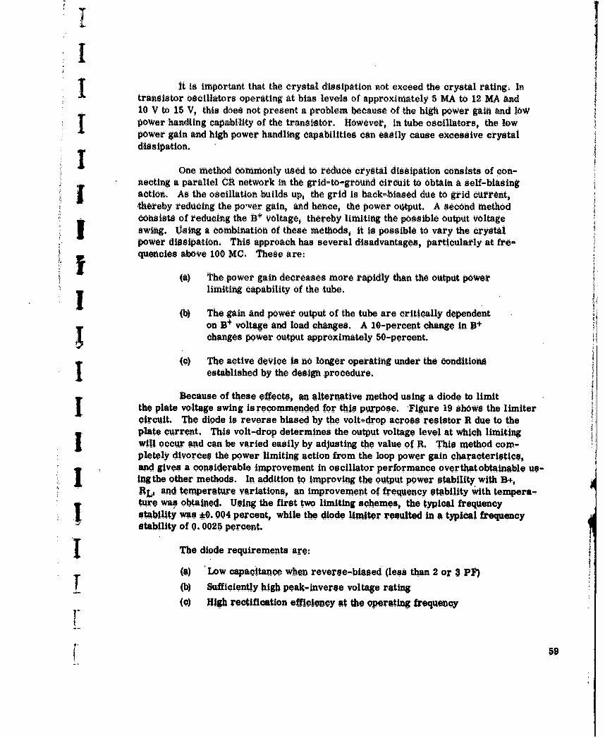
I
it is important that the crystal dissipation not exceed the crystal rating. Intransistor oscillators operating at bias levels of approximately 5 MA to 12 MA and10 V to 15 V, this does not present a problem because of the high power gain and lowr power handling capability of the transistor. However, in tube oscillators, the lowpower gain and high power handling capabilities can easily cause excessive crystaldissipation.
One method commonly used to reduce crystal dissipation consists of conenecting a parallel CR network in the grid-to~ground circuit to obtain a self-biasingaction. As the oscillation builds up, the grid is back-biased due to grid current,thereby reducing the powver gain, and hence, the power output. A second methodconsists of reducing the B* voltage, thereby limiting the possible output voltageswing. Using a combination of these methods, it is possible to vary the crystalpower dissipation, This approach has several disadvantages, particularly at fre-quencies above 100 MC. These are:
(a) The power gain decreases more rapidly than the output powerlimiting capability of the tube.
(b) The gain and power oUtput of the tube are critically dependenton B voltage and load changes, A 10-percent chge in B+
( changes power output approximately 50-percent.
(c) The active device is no longer operating under the conditionsestablished by the design procedure.
Because of these effects, an alternative method using a diode to limitthe plate voltage swing is recommended for this purpose. Figure 19 shows the limiter
circuit. The diode is reverse biased by the volt-drop across resistor R due to theplate current. This volt-drop determines the output voltage level at which limiting
I will occur and can be varied easily by adjusting the value of R. This method com-pletely divorces the power limiting action from the loop power gain characteristics,and gives a considerable improvement in oscillator performance over hat obtainable us-ing the other methods. In addition to improving the output power stbiliy wIth B+,Rl, and temperature variations, an improvement of frequency stbility with tempera-
ture was obtained. Using the first two limiting schemes. the typical frequencystability was *0. 004 percent, while the diode limiter resulted in a typical frequencystability of 0. 0025 percent.
The diode requirements are:(a) Low capacitance when reverse-biased (less than 2 or 3 PF)
I (b) Sufficiently high peak nverse voltage rating
(c) High rectification efficiency at the operating frequency
59

DIODE
R
Figure 19. Diode Limiter Circuit
4. 6 OsciflatorDesi at 1w Frequencie
4. 6. 1 General
Below 800 KC the characteristics of the various oscillator components are welldefined; component characteristics can be relied on; active device characteristics can becalculated from data sheet information with reasonable accuracy; phase shifts can bereadily controlled, etc. However, as the design frequency decreases, the oscillatorcomplexity tends to increase and, in many ways, low-frequency oscillator design be-comes more difficult than design at high frequencies. A major factor in the increasedcomplexity is the characteristics of the quartz crystals applicable to low-frequency de-sign. Another factor is the lack of variable capacitors and inductors of reasonable physi-cal size with sufficient tunable range.
These difficulties are not insuperable, and if oscillator Size and weight areunimportnt, no problem exists. If these factors are important, it is necessary touse a more complex oscillator circuit.
4.6.2 Crystal Characteristics
Table 7 shows the military standard crystal types applicable below 800 KC. Moredetailed information is contained in Reference 5, Paragraph 7. 0. There are no militaryspecifications at this time for crystals operating between 500 KC and 800 KC or below16 KC. However, crystals operating down to 800 CPS can be obtained.
Inspection of Table 7 shows that the major characteristics of the militarystandard crystals are:
(a) A poor frequency tolerance relative to that of higher frequency crystals
() Low allowable power dissipation below 80 KC(e) Large resonant resistance, particularly below 100 KC
60

I416 t6 L
00 00 . 0
If) cq 10 (b 4 m c l -
c 0 C% 0 0 Cill Ill
Ig g -
CD LO D r ;zf 1O-D OC0 0
L6 1C Ifq ft- ill Vq ~
V A4 r-4 Nqe co N- DC cq 1 . 4 CD
.l C C l N ' C
U)C- a)__
m4*b C9 0 "lr-4 C
0 00 0 0 0 00~0 00 000000QI ~ : -000000 t &t00 000
0 00 0 0 00 0o? 00o 00
000o In 0C0 O 00~ L~)t~I
P-4 I I I I I I I b- - -- I -I
00 ml00go0 000 0 OP0 c 4N00t CC0 00f 04L 0
61
Manufacturer's data for crystals operating below 16 KC continues the trendsshown in Table 7 with widening frequency tolerances, increasing resonant resistance,and decreasing power dissipation. Typical values are:
(a) Frequency tolerance, *0. 015%
(b) Maximum dissipation, 10 UW
(0) Maximum effective resonant resistance, 200 K(d) Crystal Q, 5000 to 50, 000
Table 7 shows that an abrupt change in the resonant resistance of the crystalsoccurs in the vicinity of 90 KC to 100 K.C At lower frequencies, the large value ofresonant resistance tends to prohibit their use in oscillators of the.Pierce type. Thereare two reasons for -this:
(a) Low series arn Q when operated with the specified load capacitor CL
(b) The large value of effective crystal resistance, R'a, incompatibleWith circuit levels at frequencies where reason (a) does not apply
To illustrate reason (a), a CR-38A/U crystal of 80-KC nominal frequency will.have a C0 of approximately 5 PF. Combining this with a cL -20 PFgives a CT 25 PF.Therefore, at 80 KC XCT 80 K. For operation in Pierce type oscillators, XCT should
be greater than twice and preferably 4 times the series arm resistance R1 . The specifi-cation sheet shows that Rr may be as high as 100 K, which does not satisfy the require-ments. Many CR-38A/U crystals have a resonant resistance considerably below themaximum permissible value and could therefore be operated satisfactorily in this circuit.However, if conditions approaching those of the example occur with the highest permis-
sible value of Rr , oscillation will not be possible with all crystals.
To illustrate reason (b), a CR-38A/U crystal of 16 KC nominal frequency willhave a CO of approximately 7 PF, Combining this with a CL = 20 PF gives a CT = 27 PF,At 16 KC, XCT 370 K. RI, the series arm resistance will be somewhat sma ller than
Rr, which in this case is 110 K maximum. The minimum series arm Q is thereforeapproximately 4. inserting these values in the formula:
R'a = (I + Q2 )R1 (78)
gives:
RI a s 1.6 MEGO
A crystal having Rr = 110 K is of low Q relative to other crystals of the same type havinglower Rr values. Consequently, the crystal loading due to the remainder of the oscillator
circuit should be minimized to avoid further Q degradation. Combined active device inputand driving source loading of at least 5 MEGO would be desirable.', These resistancelevels are incompatible with either tubes or transistors' and although impedance tra-
formers could possibly remedy this, the high impedance levels make this type of opera-tion undesirable.
62

Por these reasons, the low-frequency crystals designed for operation at paral-lel resonance in conjunction with a specified load capacitor are usually operated with theloading capacitor in series with the crystal. The crystal and loading capacitor com-bination behaves like a resonant circuit in the vicinity of the crystal parallel resonantfrequency, and can therefore be treated in the same manner as a crystal designed foroperation at resonance. S.ome advantage is gained in that, if th-t- loading capacitor is
i made variable, minor oscillator frequency errors can be corrected.
At frequencies above 100 KC, Rr is at least one order of magn itude smaller,permitting operation in Pierce type oscillators. Mile the value of R a will still belarge, the series arm Q will also be greater, permitting heavier loading of the crystalby the external circuit
I The crystals designed for use below 16 KC have four electrical connections,These can be paired for operation as a conventional two-terminal crystal or, alter-natively, the crystal can be used as a two-terminal pair network. When connectedin this way, the crystal operates as a mechanical bandpass filter with 0 degrees or180 degrees phase shift between input and output at mid-frequency; the phase angledepending on the circuit connections to the crystal. it will be shown that this methodof operation can greatly si.plify the oscillator circuit.
4 4.6.3 Active Device Characteristics
For the types of active device likely to be used in oscillator circuits at thesefrequencies, the characteristics are virtually independent of frequency from DC to 500KC. Practically all transistors of milliwatt power rating have current gain cutoff frequencies higher than 2 MC, while certain audio frequency triodes are the only vacuumtubes having performance limitations below 500 KC.
Power gain ard input impedance calculations can, therefore, be based on thelow-frequency active dev.ice parameters normally given in the data sheets. The ap-plicable formulae are given below.
1 4.6.3.1 Tubes(a) Grounded Grid Configuration
The power gain of a grounded grid amplifier is:
G (U + 1)RT(79)RT+Rp
V 63

where
U=tube gamplification factor
Rp =tube plate resistance
RT =total load resitanctie in the pla te circuit
The maximum power gain, GO mai-, obaAdDhnli , givig:
Op mgx - U + 1' (80)
The input resistance (cathode input) is.
The output resistance R- is:
R &RD +(U + 1RG(82
where
RG generator source resistance
(b) Grounded Cathode Configuration
The power gain expression is:U2 R R(p-RT + RIP),2 ()
whereR 9 value of the grid leak resistor
The maximum power gain is obtained when RT = , givng
The input resistance is:Gpa 8)*
in Rg
64

I The output resistance Is.
RO Rp
1'The formulae, as given, are directly applicable to triode amplifiers, 'but re-quire modificationi When used for penitode or tetrode circuits because of the large valuesIof. U and Rpencountered in multigrid tubes. The modified, formulaet are as follows:
(c), Grounded Grid configuration
Gp am R (87
I where gmn is the mutual conductance of the tube and is related to Uj and Pp by the ex-pression:
R0 =R- (90)
(d) Grounded' Cathode Configuration
Rin =Rg (92)
Ro Rp(93)
The introduction of an unbypassed catho resistor RKr changes the pow er gainI ~ ~formula for the triode to: ~
G T g
G1,4~T + Rp + (Uj + 1 )R K (94
Iand for a multigrid tube to: 2gm -. RT Rg()
(I1+ gm 1 RK
1Additional information is contained in Reference 4, Paragraph 7. 0.
65

4. 6. 3. 1. 1 Typical Tube Amnplifier Operating Characteristics
The typical values of power gain and input and output resistance to be expected
are:
(a) Grounded Grid Triode
Gp 20 to 80
R 150 ohms to 2 X
ft: 8 K to 80 K
(b) Grounded Grid Pentode or Tetrode
G: 50 to 250
Rig: 100 ohms to 1 K
IB0 : 200 K to 2 WEO
(c) Grounded cathode Triode
Q 10, 000 to 100p,000
Rin: Up to 2 MEGO (determined by permissible Rg)
5 K to 80 K
(d) Groundled Cathode Penltode or Tetrode
G 20,1000 to 200, 000
Rip: up to 2MEGO
no: 100 Kto 2MEGO
4. 6. 3.2 Transistors
The manufacturer'-s da ta sheets most frequently quote the 'h' or hybridA
transistor parameters. These are dlefined by the eqtrntions:
'Vin hi 'in + hr -V 0 (96)
66

I h . V0 (97)0= io + ho n
where (referring to Figure 20):
hi =input resistance at i, 1' with 2, 2' short-circuited
hr reverse voltage transfer ratio from 2,.2'to i, 1' with terminals 1, 1 opencircuited
...
hf & forward current transfer ratio from 1, 1to 2, 21 with 2, 2' short-circuited
ho & itput resistance at 2, 2 with 1,1 open-L. circuited
I'INI"VIN . [ TRANS| SMR Iv
VIN hi AIN 4 hr Vo
_?SU Io 'ht IIN+hoVo
Figure 20. Transistor "Black Box"
Figure 20 defines the current and voltage relationships.
Additional subscripts b, e, or c specify whether e parameters are thosefor the common base, common emitter, or common collector confgur ation, respec-tively. For the purpose of design calculation, these parameters may be regarded aspurely resistive in the frequency range under discussion. The base-emitter and base-_ collector capacitnces have only a limited effect which can be remedied if necessary
during the experimental stage of the oscillator design.
Typical values of these parameters in the grounded base confgation are
usually quoted in the transistor data sheets. These values are normally specified ata particular value of DC emitter or collector current, and for a particular value ofDC voltage between collector-base or collector-emitter I addition, graphs aregiven showing the change of the parameter values with emitter or collector current
67

Ii[
collector-base or collector-emitter voltage, and with temperature. By using these graphsand the quoted typical parameter values, it is possible to estimate the typical parametervalues over a wide range of current, voltage, and temperature.
The data sheets also usually specify the maximum and minimum values of lfe, ]the common emitter current gain, and frequently include this and the term (1 + hfb )tn the graphical information, For a given transistor type, the range of hfe betwe eenmi idmum and maximum values is typically 3: 1, and comarable variations of hib, hrb,and hob can be exected.
4.6.3.2. 1 Power Gain, Input and Output Resistance
The formulae for power gain, input resistance, and output resistance of atransistor in terms of the 'hi parameters are-
G f (98)1P (1 + ho IR )[hi+(hi ho f hr)T
where JRT - total load resistance
h-hr .hf .RT
Rin i +-ho RT
hi R Ihi . h 0 hf. hr+ho. h G ,
where
RG driving source resistance I4.6.3.2.2 Common Base to Common Emitter 'h' Parameter Conversions
The transistor data sheets normally give the common base parameters. To
convert these to the common emitter parameters, the following formulae are used:hib hIb
hie (101)
bb--rb Ab hrb (102)r +Ab + hf- hrb 1 +hfb
68 1

(hpb + Ab) h.(bhfe 1 + Ab + hfb hrb 1 + hV
hob - hob (104)hoe +A h hh+h,!.i Ab + hfi - hb 1 + hib"
where
Ab hb " hob hrb " hb (105))
The approximate formulae indicate the dependence of the common emitter parameterson the ter m (1 + hfb ). The value of hbi is within a few percent of -1. Consequently,when converting the parameters, small changes in the assumed value can radicallyaffect the values obtained. Therefors, the power gain and impedance level calculationsshould only be regarded as indicative of the actual performance of the transistor, ande)perimental checks are desirable.
4.6. 3. 2. 3 Typical Transistor Amplifier Operating Characteristics
The typical operating characteristics of small signal transistor amplifiersSsu suitable for low-frequency oscillator service are:
(a) Common Sae Amplifier
G = Up to 30 to 35 DB, depending on the degree of input
and output matching
Ri -30 to 150 ohms, depending on the total load resistance
1.o - 100 K to 2 MEGO, depending on the value of RG-
(b) Common Emitter Amplifier
-Go Up to 45 DB, depending on the degree of input and outputmatching
Rin & 500 ohms to 5 K, depending on the toial load resistance
R = O Kto 100 K, depending on the value of RG
69

4.6.3.2.4 Simplifications of Gp, Rln, and R0 Formulae -
Various simplifications of these formulae can be made under certain conditions,.if:"
IRT < (106)
then ho1
hGp T (107)
and: n i hi (108) j
These equations are usually applicable when RT S 60 K for common base Ioperation and RT s 5 K for common emitter operation. Also, if:
RG >> hi (109) 1then
Ro 0 -L (110)h o
Equation (110) Is usually applicable when RG > 1 K for common base operation and
RG > 15 K for common emitter operation.
4. 6.4 Possible Oscillator Configurations
Because of the large frequency range covered here and the drastic change inthe characteristics of quartz crystals in the vicinity of 100 KC, it is convenient to con-sider the possible oscillator configurations before discussing impedance transforming
networks. It is also convenient to consider the oscillator configurations in two parts,referring to oscillators below and above 100 KC.
4. 6. 4. 1 Oscillator Configurations Below 100 KC
The major factors influencing the possible oscillator configurations are:
(a) The high resonance resistance of the crystal
(b) The large size of variable capacitors and inductors suitable for Iuse as tuning elements
70

Item (b) does not constitute a problem, provided the oscillator size is of littleconsequence. Under these circumstances, the series on-figuration discussed in para-graph 4. 5 can be employed, with suitable modifications to account for the large value of Rr.
If the oscillator package size must be small, It will be necessary to considerother circuit configurations. The following discussion is intended to show which con-figurations can be profitably employed.
4.6. 4. 1. 1 Single-Stage Untuned Oscillators
- TThe factors that will determine the practicality of this configuration are:
(a) Oscillator Load, The following stages will normally be an amplifieror mixer. For a tube, the typical load resistance will, therefore, bein the region of 1 MEGO for an amplifier and somewhere between 1 Kand 50 K for a mixer, depending on the circuit operation. in the firstcase, the load power will be on the order of 1 UW- in the second, theload power requirements will normally be in the 1 MW to 20 MWregion. For a transistor the typicalload resistance will be between1 K and 3 K for an amplifier, and between 50 ohms and 3 K for a mixeror power amplifier. The input power requirements will range fromimicrowatts for a linear power amplifier to a few milliwatts for amixer or power amplifier.
(b) Exected available power gain G . For a tube in grounded grid con-nection, a realistic value of Gp will be between 30 and 400 (the
* lower value refers to triodes, the higher value to pentodes or tetrodes).For a tube in grounded cathode conniection, Gp will be in the region of1000 to 100, 00, depending on the grid leak resistor value employed.For a transistor in grounded base connection, Gp will be between 100and 1000, and in the grounded emitter connection between 5000 and20,000.
(c) Active device input resistance. For a tube in grounded grid connection,th e input resistance will be between 100 ohs and 2 K. In the groundedcathode connection, the input resistance will be any value up to 1 MEGO.For a transistor in grounded base connection, the input resistance willbe between 30 ohms and 200 ohs; in grounded emitter connection,
S- between 500 ohms and 5 K.(d) Active device loading requirements for hi power gain. For a tube in
( ~~~ ~~ Aciedeie-adng reureet fo hig_ -oe _ain -o --u-e i
either connection, the desirable load will be in the range of 20 K to 200K. For a transistor in grounded base connection, loads of 100 K orgreater are desirable. In the grounded emitter connection, loads of 10K to 50 K are desirable.
71

(e) Crystal characteristics (CR50A/U). The maximum resonant resistanceis 100 K with a possible minimum of 10 K. Q degradation considerationssuggest that a total terminating resistance in the region of 35 K or lesswill be desirable, giving a feedback efficiency E of 0. 26 for an upper Ilimnit crystal.
4. 6. 4 1. 2 Grounded Grid or Grounded Base Connections
Consideration of the data of Items (c) and (e), Paragraph 4. 6. 4. 1. 1, showsthat impedance transformation will be required between the crystal and the active deviceinput if the feedback efficiency is to approach 0. 26. Furthermore, this order ofefficiency will be required if reasonable power output is to be obtained because ofthe low available gain in these connections.
Consideration of Items (a) and (d) shows that, with one exception (the loadbeing a vacuum tube amplifier, R = I MEGO), impedance transforming will be Irequired between the active device and the load,
These considerations show that at least two impedance matching devices fwill be required because of the low gain available. im pedance transformation atthese frequencies requires inductive transformers, and this suggests the possibilityof phase inversion. Clearly, if a transformer has to be employed, its phase invert- iiing property can be used to take advantage of the higher available power gain of thegrounded cathode or grounded emitter connections.
This leaves only one case worthy of further consideration; that is, a groundedgrid oscillator feeding a grounded cathode amplifier. Figure 21 shows a schematic of -fsuch an oscillator.
Ip z 0.5 MA. I"-,300V
1/2- I2AX?
Rt K oTO 1OOK -
-/2-12 AXT M
Figure 21. Low Frequency Grounded Grid Oscillator
72

i
Using the following characteristics of the 12AX7:
v U =100
Rp 80K
and Rr 1O0K,
the following can be calculated
Load resistance - 70 K (300 K, 1 MEGO, aril 100 K in parallel)
SG 100_x 70 4150
it 150 x10. 3 5K100
16 x 103_ .01
102 x 103
E x Go 0.7
.- Thus, the loop gain is less than one, and oscillation will not occur using a crystal withRr -> 100 K. With a pentode or tetrode having a gm of 5000 UA/V, a power gain of
- 350 would be obtained; however, Rin (J4 would be 200 ohms, giving E= 0.002 oragain E x Gp = 0.7. gm
This shows that single-stage untuned oscillators without matching transformerst - are not practical, and from the previous discussion there appears to be no point in
using grounded grid or grounded base connections with a matching transformer. Theuse of a transformer alone does not void the initial discussion of this section concerningcircuit bulk, since large values of inductance can be packed into relatively small vol-ume, For example, 10 H in 1 to 2 cubic inches is possible.
I- 4.6.4.1.3 Grounded Cathode or Grounded Emitter Connections
J - Tuned output oscillators and oscillators employing an untuned matching trans-former in the output circuit can be considered together because of their similarity ofoperation. The following discussion is given in terms of the tuned output oscillators,but is also applicable to the untuned case, provided the transformer inductance does notintroduce excessive phase shift in the loop. In the untuned case, it may also be neces-sary to use a frequency selective network to prevent possible oscillation at higher fre-
I quencies.
73

!
4.6. 4. 1. 4 Triode Oscillator 1The circuit to be analyzed is shown in Figure 22. Assuming that the total load
RT is matched to the tube output resistance, the applicable power gain formula is: IU2R
p max 4 (11~I
I !
- - --:- ---
-- - ----!' ...... ....... 8+ 1
Figure 22. Grounded Cathode Tuned Oscillator I
Because Rg will be one of the crystal terminating resistors, its value should be lessthan 30 K id preferably no more than 20 K.
Fixing the value of Rg determines the type of tube which will give the greatestgain. The desirable characteristics are an Rp S 10 K and a U as large as possible.Table 8 presents e xamples of such tubes.
TABLE 8. TWIN TRIODE_ CHA RACTERISTICSTwin Triode ....-p(K)- .. gm (UA/V)U6201 10 5500 60
6414 9 5000 458829 7 6500 47
11!
74
"
3790
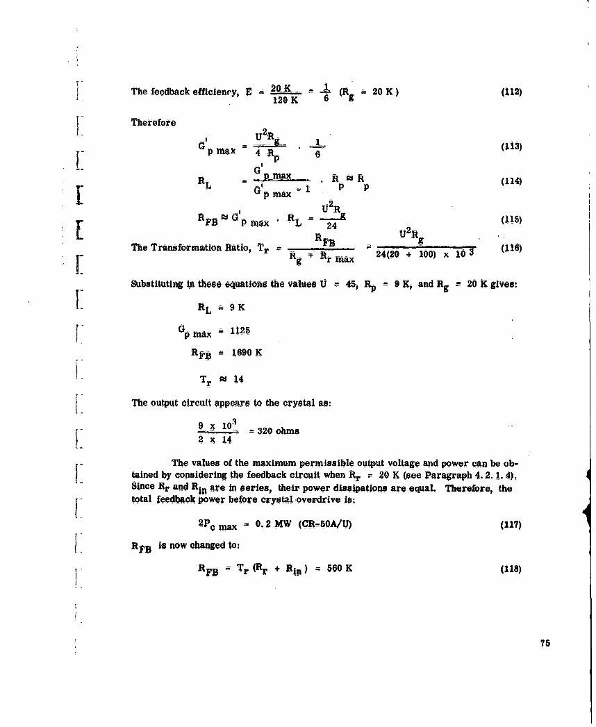
The feedback efficiency, E =20-K _ -R=2 )(12)12 K 6 g
Therefore
-A URpmha x 4 Rp (13
- pRaR p (114)pmax -
2-RUFi a L 24 (115)
The Transformation Ratio, Tr R + Rra 242 (116)x 6
Substituting in these equations the values V 4, it 9 K, and Rk - 20 K gives:
V G = 1125
RFB =1690 K
V Tr 1i4
The output circuit appears to the crystal as:
9 x_ -o __- 320 ohmsIi 2 x 14
The values of the maximum permissible output voltage and power can be ob-taned by considering the feedback circuit when Rr 20 K (see Paragraph 4. 2. 1.4).Since Rr and Rin are In series, their p-ower dissipations are equal. Therefore, the
total feedback power before crystal overdrive Is:
2P 0 max 0.2 MW (CR5OAU) (117)
RFB is now changed to:
v RFB Tr(Rr +R ) 50K(118)
75

VI
This i the load that the feedback network presents to the tube output and which appearseffectively in parallel with RL. Therefore, the power into RL if:
RFB,PL "R x 2Pc thax 1 12.5 MW (119) II
RL aa
The output voltage is approximately 10 VRMS. iThe power output calculation is based on the assumption that perfect limiting
occurs in the tube output circuit. This is not justifiable in practice, and the power outputwould have to be decreased. This calculation is also based on a loop gain of 1; a morerealistic loop gain of 2 would reduce the permissible output power to below 6 MW.
4.6.4. 1. 5 Transistor Oscillator iThe circuit to be analyzed is shown in Figure 23. For the 2N336 transistor, the
following parameters are quoted at the current and voltage levels assumed:
'2 v "!
I -II* ZI MA V06 5VOLTS 43K '
,ii 5000 i
Figure 23, Grounded Emitted Tuned Oscillator
bib 55 ohms
hob -0. 25 x WO 6mho
hrb 700 x 10-6
-0.99
'76

Con.'rsion to the co'11in emiitter parameters gives-o3
hi, 5.5 x 10 ohims
he 0. 25 x i0 rnho
-hre 7 x i0 4
hfe 9'9
Substituting these va'ues in Equations (98) and (99) with RT - 10 K gives:
Gp -12, 700
VRin 5 K
With the biasing network shown, the value of Rin is shuijted- by R131 and RB2 iin parallel,
and with the values showi, this reduces Rin to 3. 5 K and p to 8700.
G G 294 (r - 0 K) (120)- p -. JRin r
RL '~ RT $3RT 10 K (121)
RFB G'p RT 2.9 MEGO (122)IRF. B RFB
Transformation Ratio, T RF_ -- 28 (123)Rin Rr
- - giving a transformer turns ratio of 5. 3 if unity coupling is assumed,The values of the maximum permissible output voltage and power can be ob-
tained by considering the feedback circuit when Rr 1OK, the assumed minimum value,
Then:Ri
E n - 0.26 (124)Rin ' R r
77
!I
Therefore,
_P2ma 0. 14 MW (125)PFB 1 - ..
R Tr (Rin Rr) 380 K (126)
7R- RFB
- ' 5.3 MW (127)RL
This gives an output voltage of approximately 7 VRMS. This is a larger power outputthan the transistor is capable of giving under the assumed bias conditions, and thereis no danger of crystal overdrive. A larger power output could be obtained by re-designing the oscillator at a higher transistor dissipation level. No transformer Ilosses are accounted for, and, therefore, the effective load would actually be some-what lower than 10 K. Also, the calculation is based on a loop gain of I a more.realistic output power based on a loop gain of 2 would give a power output of 2. 5 MW.
The impedance level seen by the crystal at the secondary terminals of thefeedback transformer is approximatelyi
R- - 360 ohms (128)Tr
The crystal, therefore, sees a total terminating resistance of approximately 3. 9 K.
These two examples show that single-stage oscillators employing only oneimpedance transforming network are feasible. The power output capability of the tubeoscillator is twice that of the transistor oscillator. However, it would be difficult tolimit the output voltage swing to the level indicated. This problem will not be as severein the transistor oscillator because of the limited output voltage swing.
4. 6.4. 1. 6 Single-Stage Oscillator Using the Crystal to Give Phase Inversion I
As stated in Paragraph 4. 6. 2, the crystals used below 16 KC can be obtainedwith the four electrical connections to the crystal brought out individually from theholder. By connecting the crystal as a two-terminal pair network, a phase invertingbandpass filter centered at the crystal resonance frequency is formed (see Reference3, Paragraph 7. 0). 4
Only preliminary work has been performed using the crystal as describedabve, and the data gathered is insufficient to form the basis of a design procedure.Only one design evaluation was performed, but the results obtained were so promisingthat this circuit warrants serious consideration for oscillator design at very low
78
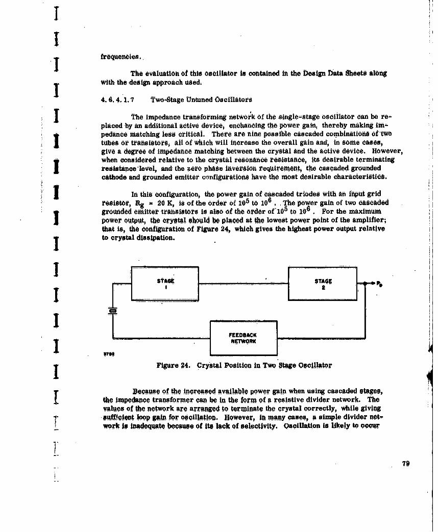
II
Ifrequencies,.
The evaluation of this oscillator is contained in the Design Data Sheets alongwith the design approach used.
4.6.4. 1. 7 Two-tage Untuned Oscillators
The impedance transforming network of the single-stage oscillator can be re-placed by an additional active device, enchancing the power gain, thereby making im-pedance matching less critical. There are nine possible cascaded combinations of twotubes or transistors, all of Which will increase the overall gain and, in some cases,give a degree of impedance matching between the crystal And the active device. However,when considered relative to the crystal resonance resistalnce, its desirable terminatingresistance'level, and the zero phase inversion requirement, the cascaded groundedcathode and grounded emitter configurations have the most desirable characteristics.
in this configuration, the power gain of cascaded triodes with an input gridresistor, Rg - 20 K, is of the order of I05 to i06. .The power gain of two cascadedgrounded emitter transistors is also of the order of'i05 to i0 6 . For the maimumpower output, the crystal should be placed at the lowest power point of the amplifier;that is, the configuration of Figure 24, which gives the highest power output relativeto crystal dissipation.
"I _ _ _.L __ .. . ... ._
i Figure 24. Crystal Position in Two Stage Oscillator
Because of the increased available power gain when using cascaded stges,
the impedance transformer can be in the form of a resistive divider network. Thevalues of the network are arranged to terminate the crysta! correctly, while givingsufficient loop gain for oscillation. However, in many cases, a simple divider net-work is iequate because of its lack of selectivity. Oscillation is likely t occur
79

i
either in an overtone mode of the crystal or due to positive feedback through Co. Thenecessary selectivity can be introduced by using a frequency selective RC network inplace of the resistive divider. A Wien bridge network serves this purpose admirably;examples of its use are given in the Design Data Sheets.
4. 6. 4. 2 Oscillator Configurations Above 100 KC
Due to the considerably smaller values of Rr max and the smaller inductorsand capacitors required for tuning and impedance transforming, only single-stageoscillators need be considered. Allowing for the different crystal characteristics,the grounded cathode and grounded emitter configurations still have the best characteristics both from the standpoitt of impedance matching and power gain. These configura-tions were an talyzed in Paragraphs 4. 6. 4. 1. 4 and 4. 6. 4. 1. 5 for tube and transistor,respectively, for low frequency oscillators. Crystals designed for resonant operationin this frequency band have Rr max of the order of 2K to 7 K, which suggests a de-
sirable terminating resistance of 1 K and 2 K. Inspection of the two calculations .showsthat for this condition the transistor will have superior gain capabilities due to its in-herently low input resistance when operating at high gain. However, either tube ortransistor oscillators should be capable of 50 MW to 100 MW output power in thisconnection with these crystals.
Pierce type oscillators using tubes are also feasible in this frequency bandiReferences 1 and 3, Paragraph 7. 0 deal extensively with tube oscillators of this type.
Field effect transistors should also function well in this configuration at these
frequencies.
4. 6. 5 Impedance Transforming Networks
The previous paragraphs note the difficulties of constructing tunable impedancetransforming networks at frequencies much below 100 KC and the consequent need foralternative types. The untuned inductive transformer appears to have possible ap-plication for this purpose (see Paragraph 4.7 ); however, if used solely to supply
feedback power, careful design is necessary to prevent phase sensitivity to the valueof. the crystal resonance resistance. Also, because of its wide bandwidth, it may benecessary to introduce additional selectivity to prevent parasitic oscillation. Nodesigns of this type have been evaluated and, therefore this is pure conjecture.
Another alternative would be to fix-tune the transformer, the transformerbeing designed, to be uncritical with regard to the tuning.
One partially satisfactory alternative to the tuned transformer is to use atwo-stage amplifier in conjunction with a selective feedback network. The disadvan-tage is the relative complexity of the oscillator circuit.
80

Below 16 KC an entirely satisfactory alternative for a tube oscillator is thecrystal phase-inverting circuit. The design evaluation circuit of this type was theleast complex of all those evaluated below 100 KC.
- Above 100 v, C, conventional tuned impedance transforming networks are ap-plicable. The r network, capacitive divider, tuned transformer, or auto-transformershould all work satisfactorily, providing the network design conditions are sat isfied.
-- 4.6.6 Design Procedure
An actual design procedure applicable to the entire frequency band is difficultto formulate because of the large variety of possible circuit conditions and the changiiigcharacteristics of crystals and impedance transforming networks. One approach tothis problem is to divide each step of the procedure Into three sections, each sectioncovering a particular frequency band. The frequency breakdown selected is:
(a) Below 16 KC
(b) 16 KC to 100 KC
(c) Above 100 KC
4 6. 6. 1 Step 1, Crystal Operation
(a) Below 16 KC. These crystals may be operated at resonance or atparallel resonance with a series capacitor. They can also be operatedas two' terminal pair filters.
(b) 16 KC to 100 KC. These crystals may be operated at resonance or atparallel resonance with a series capacitor.
(c) 100 KC to 500 KC. Resonance operation or parallel resonance witheither a series or parallel loading capacitor is possible.
[ 4. 6.6.2 Step 2, Selection of Crystal Type(a) Below 16 KC. If a design using the crysta as a filter is contmplated/
(applicable to tube oscillators only), the crystal should be purchasedas a resonance crystal with the four connections brought out indvidu-aly.
-. -If the cx ystal is to be used as a series feedback element, operation atparallel resonance with a series capacitor is recommended because ofthe small frequency tuning range available in this connection.
81

I
(b) 16 KC to 100 KC. Parallel resonance with a series tuning capacitor isrecommended because of the frequency tuning range capability.
(c) Above 100 KC. All three methods of using the crystal appear possible.However, no experimental evaluations have been made and, consequent- '1ly, no recommendations are made.
Table 7 shows the military standard low frequency crystals. This table shows Ithat no choice exists unless the special types are considered.
4. 6. 6.3 Step 3, Oscillator Configuration
(a) Below 16 KC. For a tube oscillator, a grounded cathode amplifier in
conjunction with a phase inverting crystal filter is the recommendedchoice. The second choice is the grounded cathode amplifier with out-put tuning if oscillator size is inconsequential. Thirdly, the two-stageamplifier with a frequency selective feedback network. These recom-mendations are based on circuit simplicity, since the performance ofall three types is comparable with the exception of power output.
No evaluations have been made using a phase inverting crystal filter in atransistor circuit, and therefore no recommendations concerning this typeof oscillator can be given. From the remaining possible configurations, agrounded emitter amplifier with output tuning is the recommended choice ifoscillator size Is unirmportant. The next choice is a two-stage groundedemitter amplifier with a frequency selective feedback network.
(b) 16 KC to 100 KC. For a tube oscillator, the recommended choice is agrounded cathode tuned output oscillator. The two-stage grounded cathode Iamplifier with frequency selective feedback is the second choice.
For a transistor oscillator, the grounded emitter tuned output circuit os- -dillator is recommended if oscillator size is unimportant. The secondchoice is two grounded emitter transistors with frequency selectivefeedback.
(0) Above 100 KC. Because no experimental evaluations were performed, norecommendations can be given regarding anti-resonant oscillators. Withregard to te other alternatives, the practical difficulties of tuning areeased and single-stge-tuned output circuits should present no problems.
4. 6.6. 4 Step 4, Desired Active Device Characteristics .1The requirements are:
82

(a) High gain at the circuit impedance levels of the selected configuration
" (b) Power ou Out limiting capability compatible with the crystal dissipationIi rating
(c) The active device characteristics should not be frequency sensitive atthe desired oscillator frequency
4. 6. 6. 5 Step 5, Selection of Active Device
j Tubes should be selected on the basis of:
(a) High U.
(b) Rp compatible with desired load.
(c) Rp and tube stray capacitance compatible with operating frequency.
(d) if the tube is to provide power output limiting action, the operatingpower level of the tube should also form a basis for selection. Thisis not completely necessary, since limiting diodes suitable for operationat these frequencies are inexpensive.
For a transistor the requirements are:
(a) A high common emitter cutrent gain(b) A current gain cutoff frequency fB of approximately three times the
desired operating frequency
- 4. 6.6. 6 Step 6, Determination of Active Device Characteristics
At the frequencies under discussion, the active device power gain, input re-sis tarce, and output resistance can be calculated from the formulae of Paragraph4. 6. 3 and the manufacturer's data sheet information. The calculations should bemade for power levels compatible with the crystal dissipation. The biasing levelsshould be such that output limiting will prevent crystal overdrive.
4.6.6. 7 Step 7, Calculation of Oscillator Component ValuesVarious examples of the calculations involved are given in this report and in
the Design Dat Sheets. These examples should be referred to as possible methodsof implementing this process.
83

4.6.6.8 Step 8, Design of Impedance Transforming Network
Reference should be made to Paragraph 4. 7 for impedance transforming -network design formulae.
4.6.6.9 Step 9, Experimental Adjustments
Before connecting the feedback loop, it is helpful to check the actual amplifierpower gain and the phase angle between input and output voltage. The latter is easilydetermined using an oscilloscope. The output limiting action of the amplifier can alsobe checked by overdriving the amplifier and viewing the output waveform.
4.7 Impedance Transforming Nef works
Several impedance transforming networks are analyzed in the following dis- -cussion. in addition to deriving the transformation ratio, the analyses also show thephase relationships between input and output voltages of the netwogks. From the re-suits of the analyses, design equations or methods are presented which enableimpedance transforming networks to be designed for a specific transformation ratiowith a given phase shift between input and output. j
4.7.1 y- Network
4.7.1.1 IrNetwork AnalysisThe following analysis is based on the practical circuit aspects of the network.
This Is not the most presentable approach mathematically, but it is believed to yield abetter practical appreciation of the transforming action of the network.
The useful properties of the v network from the oscillator design viewpointare:
(a) The impedance transforming properties between input and output
(b) The phase inverting action between input and output when thecomponent values are chosen appropriately
The analysis of the impedance transforming portion of the network is develop- .1ed through the transformations shown in Figure 25. The required network trans-
formation equations are given in Table 3. Figure 25 shows only that part of the net-work active in the impedance transforming function; the second capacitor used to tunewith L' is not shown.
84

-~VIN VIN VIM V-- ----- N-
71
L L. .
L 'I rI !L-
pea (a) (b (C) (d)
Figure25, ir Network Transformation
Transforming from (a) to (b), Figure 25, the relationships between rs' and rsI and C' and C (Table 3, c) are:
rs.( + 22 )(19wo C re
and
C' = c. + ~)2c (130)
Transforming from (b) to (c), Figure 25, gives,
Lef L 2' (131)
h Transforming from (c) to (d), Figure 25 (Table 3, b):
a____ L + eff 1+ R'L r' rL) 132
R +R'L (r
and L' Leff 1 + (L _ 1133)L eff
85
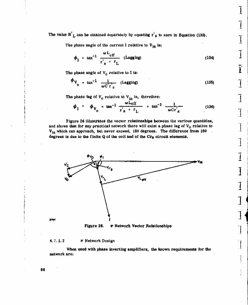
The value R'L can be obtained separately by equating r's to zero in Equation (132).
The phase angle of the current i relative to Vtn is:
tan 1 r.- -- - (Lagging) (134)r s + r L
The phase angle of Vo relative to i is:
0 tan (Lagging) (135)o tWC rs
The phase lag of Vo relative to V1n is, therefore: Itan - Leff + tan (136)
rs rL rs
Figure 26 illustrates the vector relationships between the various quantities,and shows that for any practical network there will exist a phase lag of Vo relative to fVin which can approach, but never exceed, 180 degrees. The difference from 180
degrees is due to the finite Q of the coil and of the Cr8 circuit elements.
-r ---rl-
Figure 26, v Network Vector Relationships *1
4.7.1.2 7r Network Design
When used with phase inverting amplifiers, the known requirement for thenetwork are:
86

(a) The value of Rs . The known ratio of outputpower to feedback powerdetermines Rs
(b) The value of rs, This is the value of the am plifier input resistance inseries with the crystal resonant resistance.
(c) The degired phase shift deviation from 80 degrees may be known. Thisis mostly applicable to high frequency design.
(d) At high frequencies, the value of L' is fixed, This is the value of induct-ance which will tune with the total output capacitance, and includes thetube or transistor output capacitance and the tuning capacitance. At[ low frequencies, the value of L' becomes a design variable.
The network unknowns are RL, C, rL, and L. The value of resistance, RL,
is not normally of major importance in itself, since its effect can usually be incorpo-rated into the oscillator load by appropriately reducing the total load dissipation. Thedifficulty is that the values of the other unknowns are all related to RL, except thatwhen RL is greater than 5Rs, its effect will be relatively small.
With this number of unknowns the network design becomes involved especial-ly when phase requirements have to be met. A relatively rapid! method that enablesthe designer to pay constant attention to the design requirements is the graphicalapproach outlined below. This is based on the vector diagram of Figure 26.
Since r s and Rs are known and represent the same power dissipation, the- ratio of Vo/Vin can be calculated as follows:
Vin (137)[ VoUsing suitable scaling, draw a line of length Vi on the reference axis. From
the origin of the vector Vin, draw a partial circle of radius Vo in the third quadrant.Bisect Vin and, using this point as origin, draw a semicircle in the fourth quadrantof diameter Vin. These two circular segments are the loci of Vo and V(r s + r),respectively. If the requ red phase angle between Vo and Vin is known, the vector
Vo can be drawn; if not, a value must be assumed.
Specifying any one of the remaining four vector quantities will automaticallyconplete the design, since VLeff and V'c are In opposition to each other and mutually
perpendicular to Vr' s and V(r's + r). The choice resolves into the assumption ofrlavalue for 01l, and the- following factors may influence this choie. For a fixed
phase angle between Vo and Vin, -the value of *i-used determines the power transferefficiency Pe, since:
87

VrIII
Pe 1 (138)r 5 rL V(r's rL)
As 01 approaches 90 degrees, the efficiency increases. This is the sameas saying the coil losses approach zero, This may be an important factor in the de-sign of low gain amplifier circuits. Another effect as 411 approaches 90 degrees isthat the effective Q of the output tuning circuit increases and may be important fromthe point of view of harmonic rejection.
Using these factors as a design basis, a value for I can be selected; andthe values of C, L, andl rL can be calculated, using Equations (139) through (143). itshould be noted that in these equations Vrss Vc, VLeff and VrL are voltage magnitudes.
r' (139)V 2
X(, (140)t ?
S. Vrs
X' [1 + ( ]Table 3, part (d)) (141)
X - (Table 3, Part (b) (142)
L, VLeff_ IXL+ (143)f eff + r,
VrXL.. L (144)- L -r 5 .s Vrs IIXL r
The Q of inductance L (145)rL
if this Q is not a feasible value (either too small or too large), the design canbe optimized by recalculating, using a new value olf PI. Increasing *I w i require Ia higher Q for the coil and vice-versa. A typical design is shown in Figure 27.
88

J*
IS0 0
---
00 t +
Io. '40;L000 ,,* q ' ,
,cm to SO goo"" "a -.. I x - (D
--, .Z o 1
II 1
o It x
IL 0
la I,
4 -wa
00
ii: ~ W 0 ="
z
o Do
89

4. 7.2 Capacitive Divider Network
4. 7. 2. 1 Analysis of Capacitive -Divider Network
Referring to Figure 28, it is assumed that the reactive elements are at reao .n ance at angular frequency w , and that a voltage Vin is present acros the seriescomnbinlation of C1 and C2. rs is the load applied across Cg,and Vout Is the voltageacross Vs. Then-
1 Ism "T IN
3706
Figure 28. Capacitive Divider Coupling Network '
Vi 1 + j W(CI+ C2)r
1dC r /900 -tan'I +~. C~A (146)
When 22(bj 2 22 2
+~
(C1 C 2 ) 1r C C
V 0 C _ _ _ _ (1 4 7 )1
IVin 1I -2in2Now - -,the outpu poemutb eult where 13 is that value ofresistan ce which, if connected across Vi with r. discnected, would dissiptthsame power that r5 doe wihvlae cosi. hti,
does wit v~tg 0 acosi.Ta sH represents rs trangs-ferred to the in put side of the network. Therefore:
RSI
and Id2(149)
90

Substituting for IyO. 12-
T 2-C2 r2
(150)7- +s (C 1 2 r
- I + W2(Ci + C2)2 rs 2
-s 1+ (a2(C1 2 r (1
H )2rsW C1 r.
Therefore, for the particular case where to 9(0 i + C2) 2r 2 1, Equation (16!)becomes:f22 2 rs (152)
For ease of calculation, it is convenient to obtain the relationship, H_
I-1+S W(C +0)r 2C + ) 0)
- 2 1 ~+ --k---(153)R 2 C 0 r29
Where
S+01W(C 1 + C2)
If rs = 2X(cI + 2 thenR s 1.25R's1 2),
and ifr. = 3X.(c I C2 ), thenR, = 1. 11R'S
This shows that forr 5 > 3 + 2), Rs R ,a Equatin (152) adeq
describes the circuit insofar as transformation ratio is concerned.
The phase shift occurring between input and output of the network Is also ofInterest. The general phase shift characteristic is shown in Figure 29.
91

PHASE _ -
LEAO
LOGW -c- . r5
Figure 29. Phase shift Characteristics
Calculations using the formula 4) 0o tan'1 w (C1 + 02) 1~(see Equationi(146))show that for:
2X(C 1 + C2), 7
3X c 1 + Cg), 1890
=s 6 X(cl + C2), l oo
it should be noted that this phase shift is independent of any phase shift due to mnis-tuning of the tank circuit.
An additional effect, which if; not brought out in the analysis,. is the effectivecapacitance Cn presented by the C, C2 nd r5 combination to the inpu ore
C 1 [ W 2 wC 2 (C1 + C2) rs2 14
2 2 2
for the conditio W2 (C1 + C ) 2r >> 1. This reduces to
n C1 + C2
If this condition does not apply, then:
SC 1 *C 2 since C C + CC1+ C2 2- 2
92

The capacitive divider network is useful in oscillator design because of the.. Simplicity of the design equations and the design accuracy obtainable, All the high-
frequency oscillators evaluated for this program used this type of feedbahk networkbecause of these good features.
The analysis assumes that losses in the capacitors have no effect on thenetwork performance. This Is a justified assumption when high-quality capacitorsare used.
J 4.7.3 Untuned Inductive Transformer
4. 7. 3. 1 inductive Transformer Analysis
-The circuit to be Analyzed is shown In Figure 30,
.VIN
Figure 30. Inductive Transformer
I" whereThe primary windg inductance
r1 - The primary winding resistance
]i L2 The secondary winding inductancer2 - The secondary winding resistce
1 rs - The load resistance in the secondary circuit
M The mutual inductive coupling between the two windings defined by:
M = K 2(156)
The dots indicate winding polarities. As shown, the transformer has nominalphase lverting properties.
93

The equations describing this circuit are:
Vin II(rl+IWL) +!2. JwM (157)
0 = 1(j W M) + i2 (r2 + rs + J. w L2 ) (158)
Substituting for I2 in Equation (157) gives:
I U (rg + r5 I=1 (r 2 + r s)2 + 2L2
Two conditions of operation are considered: .1(a) Wen the secondary winding is heavily loaded. This would be the case
when the oscillator load is connected to the secondary, the assumptionbeing that the feedback power can also be derived from the secondarywinding without the need for additional inductive transformers.
(b) When the secondary is used Solely to supply feedback power and theterm E x 0 is large, say larger than 30. in this case the transformer Iis lightly loaded.
These extreme loading conditions have considerable effect on the transformer operationand are separately analyzed.
4.7. 3. 1. 1 Untuned Transformer, Heavy Secondary Load I
For this loading condition, the object is to make the impedance at the primarywinding terminals almost purely resistive in order to minimize the phase shift between
a! and Vi. The phase shift between Vo and Vin should be as close to 180 degrees aspossible.
Assuming that w L2 ?a 3(r 2 + rs ), Equation (159) simplifies to:
Vin I I r L2 + (r + r - j to ) (160)
Substitu ting for M gives:
Vin -J1 [r + k2 (r2 + r. + 2 (161)
InI

FThe phase angle of V inwith respect to -1Is:
tail -k (162)tan~rr2k+ r--)
+ 2 1 2L2
Typical vector relationships for the transformer primary are shown in Figure3-1. Equation (158) establishes the conditions in the secondary of the transformer. Thephase angle between the induced voltage 11 (j w M and 12 Is givenby
#~tan1 wL 2tan (163)
-r 2 rr
*11
Figure 31. Primary Vector Diagram
Figure 32 shows typical vector relationships for the transformer secondary,remembering- that w L2 2: 3 (r 2 + r5 ). Combining Figures 31 and -32 gives thevector diagram of the loaded transformer shown In Figure 33. The total phase anglebetween Vin and V0 is:
T 2 l + 2+ 0 -9

t~n~[ri+k2 k2) wL1
k2 (r2 + r-)
+ tL 2 ]L 900 (164)
r 4, rVarious points may be noted, as follows:
(a) if 0~1 is less than 18 degrees, the voltage acrosthe resistive comnpo-nent of the transformer input impedance is greater than 95 percent ofVin, and the Load reflected from the secondary can, for all practicalpurposes, be regaded as:
Vtrg+ rS) r ~gth)uL
N~ ~ Ii[i~(rigr,)+rj]
1IwjuL'~ -ILrJ jwM
Ivmoo0Figure 33. Transformer Vector Diaga
k 2 ~(r2 + r5 )('L2
Further if r2 -*r r., this reduces to:
Equation (166) is the well Imnown transformation ratio.
(b) The power transfer efficiency of the transformer is:LIk;
1 r&T = -- (167)
r+ k (r +-1
96

(c) Small variations of iS 1 and 02 from their ideal values of 0 and 90- degrees tend to co mpensate each other in maintaining a phase angle
approaching 180 degrees between Vin and Vo. However, if fed froma resistive source, the source voltage will lag Vin because of the in-ductive nature of the load. This will increase the deviation from 180degrees of the phase angle of Vo relative to the source voltage. Forexample, if the source is a grounded cathode vacuum tube, it appears
-. as a power source consisting of P in series with a voltage generator,-uVg. in oscillator design, the phase angle of Vo relative to Vg is theIimportant relationship.
4. 7. 3. 1. 2 Untuned Transformer Design, Heavy Secondary Load
IFigure 34 is represientative of a trau-afomei driven by an active device, thelatter being shown as a voltage generator in series with its output resistance Ro.
R0
L R° 2
-- L ik2 g .r 2
- V l' k2 .L1 s,, L2
- ( K2 ) L41
Figure 34. Driven Transformer Heavy Secondary Load
At frequencies where untuned transformers are likely to be used (say, below 100 KC),U- it is not difficult to obtain coupling coefficients greater than 0. 9 and winding Q's greater
than 100 using ferrite or laminated iron cores. Assuming these values as minimumconditions, rl + k2
2r will normally be small compared to R k2 1r
and will, terefore, have negligible effect on the value of In any case, the effect ofrr and k2
2 is to reduce and ignoring them will add a safety factor inthei ' L2
design. is the modified primary phase angle due to the presence of Ro.
With these assumptions,
Ro + Rs + 0.2 . j W L_ (k - 0.9) (168)
97

0.2 wLand tan (169)
R 0 4 RB
or LI fl0 + . n (1701)
0.2W (
and assuming a value for j6! determines L 1. The value of * should be sm all (say,10 to 15 degrees) to avoid the need for excessive phase correction elsewhere in theoscillator circuit.
Using K = 0.9 and the known values of Rs and r., the value of L2 can be cal- jculated by subrtituting for Li in Equatlon (166).
L2 0.8 x L (171)
At this point in the calculation the following condition should be checked:
w L2 - 3r,
if not, the value L2 should be increased to satisfy this condition and the new values of1,
L, and lq determined from Equations (171) and (170), respectively.
-2 Calculate the secondary phase angle using the equation.
tan L2 (172)1 1r,Calculate Tfrom:
T -- 0'1 + 4$2 + 9 0 0 (173)
The resulting #T should be within 10 or 15 degrees of 180 degrees, since phaseshifts of this magnitude can be uncriticaly introduced at other points in the circuit.One particularly easy method is to add a fixed capacitor across the transformer -
primary winding.. In ts case, the transformer is actually tuned. However, the Qis less than 1 and the capacitor value is uncritical and, therefore, is not required: tobe variable. This method also serves to limit the amplifier bandwidth, thereby re- - Iducing the possibility of parasitic oscillation.
The original assumption concerning the effect of r1 and r 2 can now be checkedand corrections made, if necessary.
98

Ii 4.7. 3. 1. 3 Untuned Transformer, Light Secondary Load
if the transformer is solely employed to give phase-inverted feedback power,the transformer operation is radically changed. The oscillator load is in parallel withthe transformer primary winding, and the secondary of the transformer operates underessentially open circuit conditions; that is, W L2 < rs .
I Under these conditions, consideration of Equation (158) shows .that the voltageacross r5 will lag the induced voltage -I i , j w M by a small phase angle 2 as
i |shown in Figure 35, where(tan " rs t2(174)
-2 r 5 + r
I Ii
SV(r r2) VL2
Figure 35. Secondary Vector Diagram, Lightly Loaded
It is evident from Figure 35 that the impedance looking into the transformerprimary must have a large inductive component compared to its resistive componentin order that the phse angle between input and output voltages approaches 180 degrees.Referring to Equation (159) and approximating for the condition (r2 + rs) 3 w L2
giveS:
I2M2(r + r 2 - j wL 2 )Vin I1 [ri + + 2 . .. L 1 (175)
L 02 + r ) 2
This equation simplifies further to:
I 99
99
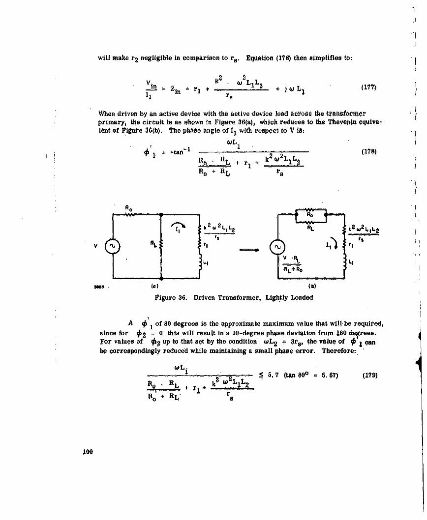
will make r2 negligible in comparlson to rs . Equation (176) then simplifies to:
Vi k2 w2 2LL-Zin - ' I! + 2 JwL i (177)
When driven -by an active device with the active device load across the transformerprimary, the circuit is as shown in Figu;re 36(a), which reduces to the Thevenin equivalent of Figure 36(b). The phase angle of 1.1 with respect to V is:
wL
an(178)SRL + r+ kW 1Ro + RL'
R6R 0 O
-L- kzW ,L Lrsi
V -R
RL+Ro
603. (0) (b)
Figure 36. Driven Transformer, Lightly Loaded
A of 80 degrees is the approximate maximum value that willbe required,
since for 462 = 0 this will result in a 10-degree phase deviation from 180 defrees.For values of- 02 up to that set by the condition wL 2 3r., the value of 1nbe correspondingly reduced while maintaining a small phase error. Therefore:
wL1RL S k. w L < 5. 7 (tan 80- 5.67) (179)f't- " ,- + r +R 0 + RL r
100

The Q of the primary winding will be greater th .an 100 at the frequencies underconsideration, provided that a suitable iron core is used. Therefore rl is approximately20 times smnaller than the remainder of the denominator of Equationi (179) and cani beignored. Furthermore, the desired Value of RFB wilb tlatoe order ofmgi
tude greater than RL; anid, therefore, k2 WL1 Lg , which is the equivalent series
resisatanjce 'of RFB3, will be negligible in comparisont with R O and RL in parallel. Con-.sequently, the input circuit phase angle is givera with sufflclent accurticy by the
11 *' =tan wL.R 0 + RL(80.1 1 R0 RL
IThe effective parallel resistafn e seen at the primary winding terminals with the secon-dary loaded is (Table 3 (b )
k2 2- L 2L1 2
'I R (r 1 + ~ 12)[ + 2 11
From the previous discussion:
W2L2
k -wL1 L2 2 >51
(r+
I Therefore:
k2 w21 L (182)
+ w- -,L -
For the particular case where r, « -1< this simplifies to:
R r __ (183)
I Theeff.ative parallel coil loss resistance Is:
RL1 (184)
V .101

4.7.3.1.4 Transformer Design, Light Secondary Load
Substitute tan 5 ' = 5.7 into Equation (180) to determine LI:
Li 7 R RLW Ro + RL (185)
Assume a value for the primary winding Q (Qv) to determine "I from: IwL 1
r - - (186)
Calculate.
RLi Qp coL 1 (187)
Combining this value of RLi in parallel with the known value of FRFB gives:
- RLi X RFB (188)RLi + RFB
L2 can now be determined from Equation (182) if a value for K if assumed.
[ r J (189)
A suitable K value will be 0.9.
Check to see that the following condition exists:.
w#L < 3r (190)
if not, decrease L2 accordingly. The simplest method possibly it to recalculateEquations (186) through (184) using a smaller L, value. The reduction in the L1value required is estimated from the reduction in L2 required.
The phase shift between input and output can be estimated from:
OT = 2 + o'. + 900 (19)
W L2 + tan 1 (Ro + R0-W - ----- ---- .. .. --.. + 90 °
rs Ro RL
102

I
4. 7. 4 Wien Bridge Network
4.7. 4. 1 Wien Bridge Network Analysis
I The Wien Bridge network his frequency selective properties that are usefulin untuned oscillators. The network is shown in Figure 37.
Th euaios.o thi ircut are
II
~~Vin i I1 [ a- - C ... . + ........ + j w CR (92
1 1
(I1 + J w CR) (R+ + = .. R !4
where w =
SAt w w" .o R
__. ,the reactive compnent in the denom_!nator falls to_ zero and:
VoVVtini
C103
,4 _ _ _ _ _ _ _ _ _ _ _ _

At angular frequencies In the vicinity of W , the response is similar to that of atuned circuit.
The vector relationships within the network at angular frequency W' can bedetermined -by noting that:
R ____.... (19?)
jWC
and therefore:
Figure 38 shows the vector diagram for the network at ) w
450
v "A/ VINVN
Figure 38. Wien Bridge Network Vector Diagram
The input impedance is:
V.Vin 3 R(1-j) (199)I! 2
Or transforming to parallel elements, the parallel resistance is:
R -3R (200)
and the parallel capacitive reactance is
X c 3R (201)
The Wien Bridge network i-s only one case of this_ type of network. If the net-work Is analyzed in its general form where R 1 and C1 are the series elements and R2and C2 are the parallel elements, the input and output voltages are in phase when:
104

C C2 R]R2
The relationship betweenl V ° tzr haeageiVin.
V 1 (203)
Vin Rl + 1 +cl
*. 1I
II
105
5.0 CONCLUSIONS AND RECOMMENDATIONS
5. 1 Conclusions
Background data applicable to the design and operation of -both high and lowfrequency oscillators 'has been presented. The data that is applicable to high fre-quency oscillators has been combined with experimentally gathered data to form adesign procedure for the frequency range of 30 MC to 200 MC,
This design procedure is simple in form and should present few difficultiesin execution, The most complex part of the procedure is the determination of theactive device characteristics, and this is straightforward once the techniques havebeen mastered. An active device evaluation normally requires tess than one hourto complete. This compares favorab ly with the time required to calculate 2 or 3values of power gain and input impedance, using the complex parameters of an activedevice. In addition, the data obtained by measurement is more reliable, since it isobtained under actual operating conditions.
The low-frequency design procedure offered is somewhat vague because ofthe li mited number of evaluations obtained of any one type of oscillator, and alsobecause of the large number of feasible oscillator configurations. Nevertheless,when used In conjunction with the background data and the Design Data SheetA, itsupplies the information necessary for low frequency oscillator design.
5.2 Recom m endations
5.2.1 High-Frequency Oscillators
The high frequency oscillator design procedure is limited by its failure to
consider alternative active device configurations. Areas of investigati6n that wouldmake the procedure more universal would be:
(a) Grounded grid pentodes or tetrodes at all frequencies
(b) Grounded cathode pentodes and tetrodes in the 20 MC to 100 MC region
(c) Grounded emitter transistors in the 20 MC to 50 MC region
Other areas that could profitably be investigated are:
(d) Methods of reducing oscillator frequency instability with temperature,due to the active device and oscillator components other than the crystl.This is particularly applicable to the transistor.
106

I!
(e) Extending the frequency range above 200 MC, Judging by the experiences,of the design evaluation program, 200 MC does not appear to be the upperflimit of performance. in fact, one 200-MC oscillator operated quite well
on the next higher crystal overtone mode at a frequency of 244 MC. Os-dillator operation up to at least 300 MC should be investigated.
(f The operation of the oscillator under typical loading conditions. Themajority of oscillators will be loaded by a mixer or other non-linearcircuit which may influence performance considerably. The limitedinformation obtained during this program suggests that the non-linearloading effect is negligible. However, a fuller investigation would bedesirable.
5. 2. 2 Low- Frequeney Oscillators
T The tow~frequency oscillator design procedure is limited by the lack of sufflcient evaluation data, due to the limited number of circuits evaluated. To correctthis, it is recommended that the following circuits be further evaluated:
(a) Oscillators below 16 KC using the crystal as a two-terminal pairfilter network.
(b) Antiresonant Oscillators in the 100-KC to 500-KC frequency band.It appears that field effect transistors could be effectively used inthis application.
II
SI
I
I
II- . 107

6.0 IDENTIFICATION OF MERSONNEL
The following personnel devoted the indicated amount of time to this project:
(a) Donald Firth, Electrical Engineer, 7. 13 MM (1235 hours)
(b) John R. Yope, Electrical Engineer, 10. 76 MM (1864 hours)
(c) Gregory J. Bittner, Electrical Engineer, 4. 59 MM ( 795 hours)
(d) Alan 0. Plait, Electrical Engineer, 1. 48 MM ( 257 hours)
(e) H. Rex Meadows, Senior Staff Engineer, Time not chargeable
NOTE
1 manr-month (MM) 173.3 hours
I

7.0 BIBLIOGRAPHY
(1) "A Study of Crystal Oscillator Circuits, " Armour ResearChFoundation; Contract No, DA 36-039-SC-64609, Final Report;August 1957.
- (2) "Transistor Crystal Oscillator Circuitry, " Motorola, inc.Contract No. DA-36-039-SC 72837, Final Report; August 1957.
(3) "Handbook of Piezoelectric Crysta ls for Radio EquipmentDesigners," Philco Corporation; WADC Technical Report56-156, ASTIA Document No. AD 110448.
\ (4) Terman, "Radio Engineer's Handbook"
r (5) MIL-C 3098C, Supplement 1
(6) Gartner, "Transistors: Principles, Design, and'Applicatiom "
(7) Boothroyd and Page, "Instability in Two Port Active Networks";
IRE Transactions on Circuit Theory, Pages 133 - 139; June 1958.
- (8) "Diffused Base Mesa Transistors Type 2N1141, 2N1142, and2Ni143," Texas Instrments Qualification Report
(9) "New Method of Measuring High Frequency Transistor AdmittanceParameters Using the Boonton RX Meter"; Amperex Teeh News;Vol. 2, No. 1
•1I0
109

OSCILLATOR DESIGN AND EVALUATION DATA
The oscillator design evaluatiois contained in these appendices are the re-I - suits of the evaluation program that was conducted in parallel with the study program.
The object of this experimental program was to determine the practical worth of the.bbackground data gathered from the literature and, conversely, to modify this back-
ground data in accordance with the specific requirements of crystal oscillator designas determined from the evaluations,
I The purpose of presenting these design evaluations is to illustrate the use ofthe techniques described in the Final Report and to show the level of performance likelyto be achieved. it is also possible that the designs presented will find use when aI. general purpose oscillator is required and there is insufficient time available to carryout a design.
LThis approach has been experimentally substantiated to some extenti The twohigh-power output transistor oscillators (75 MC and 120 MC) were both used in limited
f" production run equipments with satisfactory results, in spite of considerably differentcircuit layouts from those of the prototype circuits. The only deviation was that thepower output capabilities of the oscillators averaged out at about 20 percent less thanthat obtained from the prototypes.
The format utilized for each evaluation is as follows:
(a) A short discussion giving general information concerning thedesign and any difficulties encountered
-- (b) A schematic of the oscillator together with other pertinentcircuit information
(e) The design calculations
(d) The evaluation data
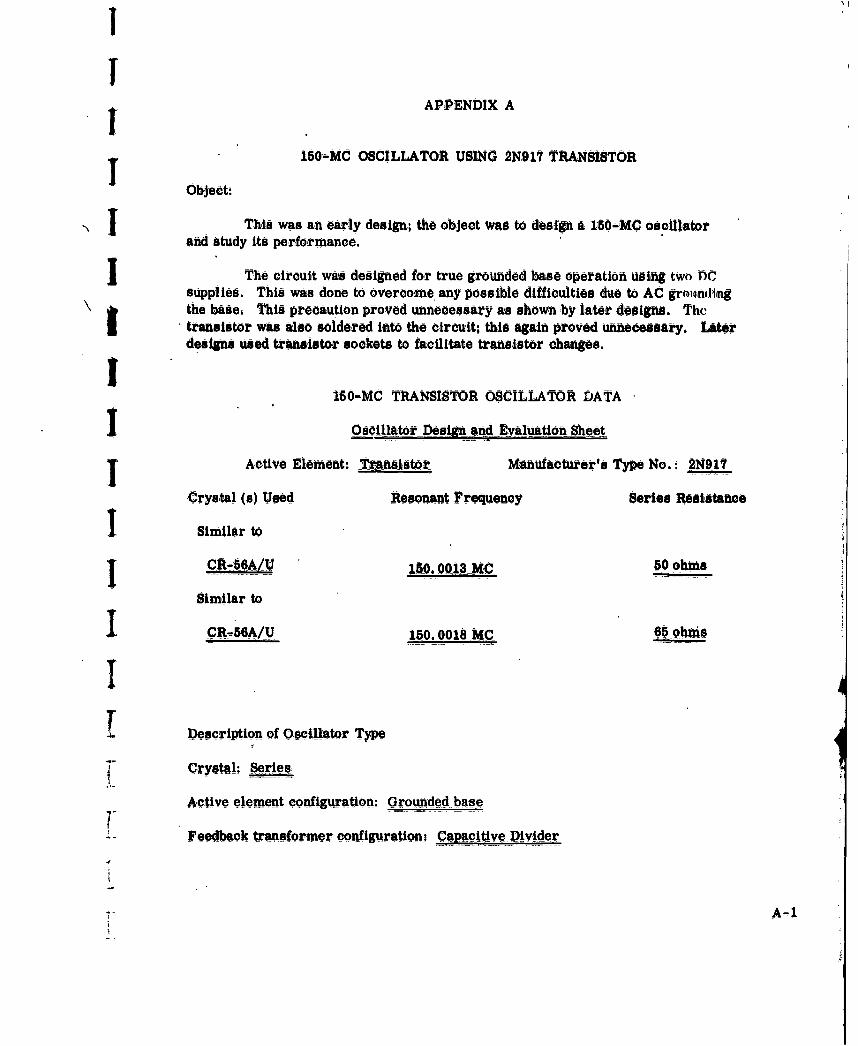
I
APPENDIX A
i l60-MC OSCILLATOR USING 2N9i1 TRANSISTOR
Object-
I ~ ~~This was a~n early design.i the ,object. was to desi'gn a 10"= oscitt aor"
and study its perform ance
The circuit was designed for true grounded base operation using two PCsupplies. This was done to overcome any possible difficulties due to AC grounlingthe base. This precaution proved unnecessary as shown by later design. The
3 transistor was also soldered into the circuit; this again proved unnecessary. Laterdesigns used transistor sockets to facilitate transistor changes.i
150-MC TRANSISTOR OSCILLATOR DATAI Oscillator Desig and Evaluation Sheet
Ac~ve Element: Transiustr_ Manufacturer's Typ No: 2N917
Crystal (s) Used Resonant Frequency Series Resistance
I Similar to
I CR-6A/U 150.0o13 Mo C 50 ohms
Similar to
I CR;56A/U 150.0018 MC 65 ohms
I
IDescription of Oscillator Type
7 Crystal: Series
Active element confi ation: Groundedbase
:- Feedback transformer configuration: Capacitive Divider
A-!

? _ T _ _____
-
Lx NTES WTH
Fiur A-i.0 15O COsclao ici
gain nd inut reistan e f the amplfier thsremainin Circuit cmoetvle r
determined as follows:
From the amplifier culrvesselect a working point at:
Gp - 300, RT =600 ohms, Rill= 150 ohms and taking R1 max =100 ohms
R = Rin + R, 250 ohms
s-
and using a safety factor of 2:
P 90
RFBa 2L R 5 4 K
Fo aacitive divider feedback netwrk, the relevant equations are:
or C
or C 2 = 14 C1
if C2 = 50 UUF, C, 3.6 UUF.
A4~

- Ni, NIVO 83MOci
Inin en N N - ii 0
*4
0 0~ -COWft-' a tD
(SNN ) 'V'3N___3HinN
I A4

The actual value of C2 used was nominally 5 UUF.
The phase lead introduced by the capacitive divider network is:
8±900 - taifw (C1 + C2 )R s
5'~ for Cg 5,0 UUFj
The effective parallel loss resistance of the tuning coil was 9 K which is --
negligible compared with 600 ohms. Therefore, RL RT = 600 ohms (680 ohms
nominal value). The voltage measuring probe loss was also negligible.
This circuit was also evaluated with C2 = 25 UUF.
A4

0 l 0 0 0cq cq C .
U)4 oI C) oI II 4 04 4toIT E41?~ ~ z -44 3 V
to. ~0 0n 0bt
g o 0 3I t f N. t o . .
> II
IbiM ..
0 .--
-Iiib
0~ 0P-4 UOD
0uIf
~A4o

IL1
CLa
00
- - - -------- - - ~ -
0
'I" CM 0 ) O N
__ __ 000C
Mo 0, 91
A-6-

APPENDIX BI193-MC OSCILLATOR USING 2N917 TRANSISTOR
I This is essentially the same circuit that was used at 150 MC with tuning and
feedback circuit changes. However, a comparison of the power gain and input resis-tance as a function of load for the two cases shows that the transistor characteristicschanged considerably.
IThe 150-MC crystal was again used in this evaluation by operating it in the9th overtone mode. Late in the evaluation period the pins of the crystal holder (HC-18) were damaged and it was necessary to transfer the crystal to another holder (HC-6). The repackaged crystal resistance was approximately 20 percent larger and theseries resonance frequency decreased 10 K1. No other ill effects were noted.
I An attempt was made in this design to separate the temperature effects of thecrystal and the remainder of the circuit. The crystal was mounted in an oven whichheld its temperature at 65°C *50C, and the resulting frequency-versus-temperaturedata showed an improvement from ±38 PPM to approximately II PPM (extrapolatingthe temperature controlled curve to 80 0 C).
The peculiar "kinks" in the frequency-versus-temperature curves are prob-ably due to ice melting on the components, since the temperature chamber used at
this time was particularly vulnerable to "snowing up."
193-MC TRANSISTOR OSCILLATOR DATA
j Oscillator Design and Evaluation Sheet
I Active Element: Transistor Manufacturer's Type No: 2N917
Crystal (s) Used Resonant Frequency Series Resistance
SSi milar to
I CR-56A/U 192. 8560 MC 78 ohms
Similar to
II CR-56A/U (REPACKAGED) 192. 8463 MC 96hMUL
B-V
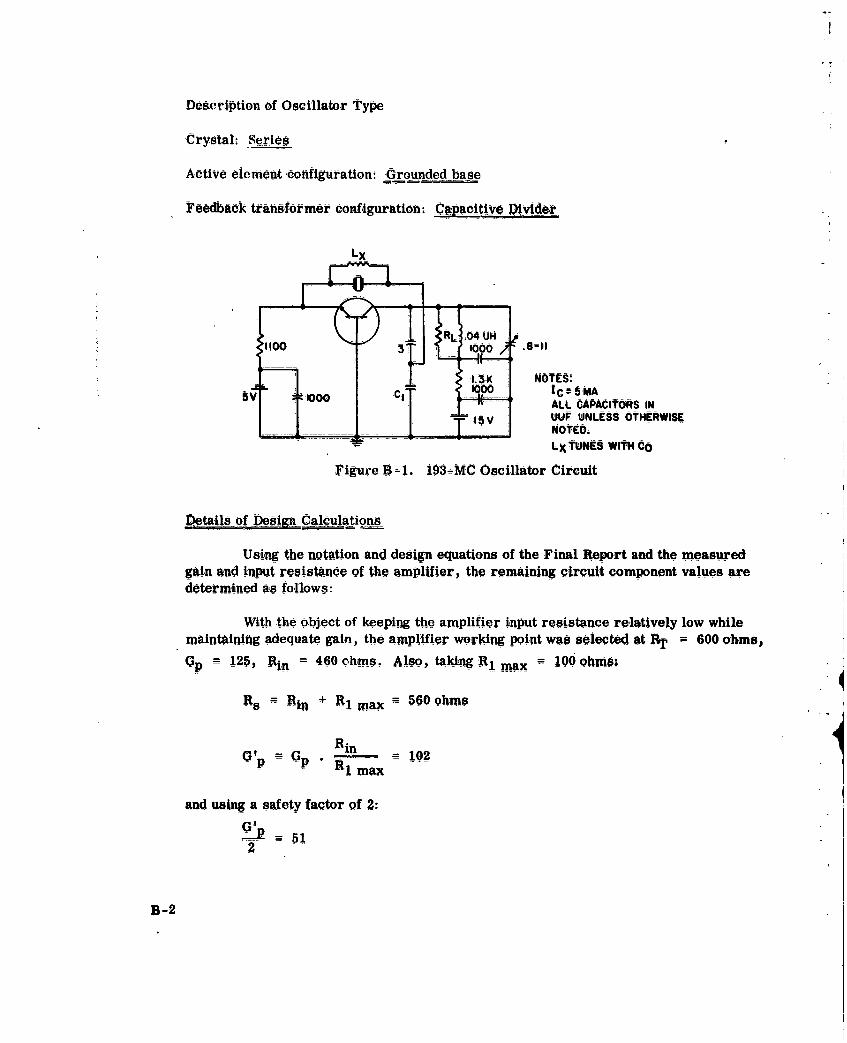
Description of Oscillator Type
Crystal: Series
Active element configuration: -Grounded base
Feedback transformer configuration: Capacitive Divider
II - L .04_UH -
310 10 *8
3K NOTES,C I ALL CAACiWORS IN
15V UUF UNLESS OTHERWISE_____-__ NOTED.
LX TUNES WITH C(O
Figure B 1. 193-MC Oscillator Circuit
Details of Design Calcuations
Using the notation and design equations of the Final Report and the measuredgain and input resistance of the amplifier, the remaining circuit component values aredetermined as follows:
With the object of keeping the amplifier input resistance relatively low whilemaintaining adequate gain, the amplifier working point was selected at l = 600 ohms,
p = 125, -Rin 460 ohms. Also, taking R1 max = 100 ohms;
Rs Rin + Rl max 560 ohms
-in 102Gp -= R,• t max
and using a safety factor of 2:
2 -=512
B-2

I ~~ 1flv-sNIW9~MOd
II 0 -
0 0
--~ -- ---
0I 0
B-4

i
RFB- 2 RT =31K "
Using a capacitive divider feedback network, the equations are:
_RFB ( +C 2
or C2 7.4C1 -
For C2 - 25 UUF, C1 3.4 UUF.
The nominal value of C 1 used was 3 UUF.,
The loading effect of the voltmeter probe and the coil losses was negligible,and a RL value of 640 ohms (750 ohms nominal value) was used.
The phase lead introduced by the capacitive divider network is:
6 P 90 ta i l w(C i + C2)R s
30 for C2 - 25 UUF
An evaluation was also carried out for C2 15 UUF.
B-4

I ZZZ UZ I 0
I ii lii I i i ai".IC
-% 0-a 0-
in
...
..
. .. _ _ 004 i, + 00 _ F-A
0 -4I o
4 0e 4 -q
3*
I i C C C.)C) .. .......... .+ 4 +*1 II4: -I
0 t c " tu - u u
z b
I-
qR wI t- IR
t4o 0 0
0~1 v~- *
'I P-44-~4 0 ~0
B-5
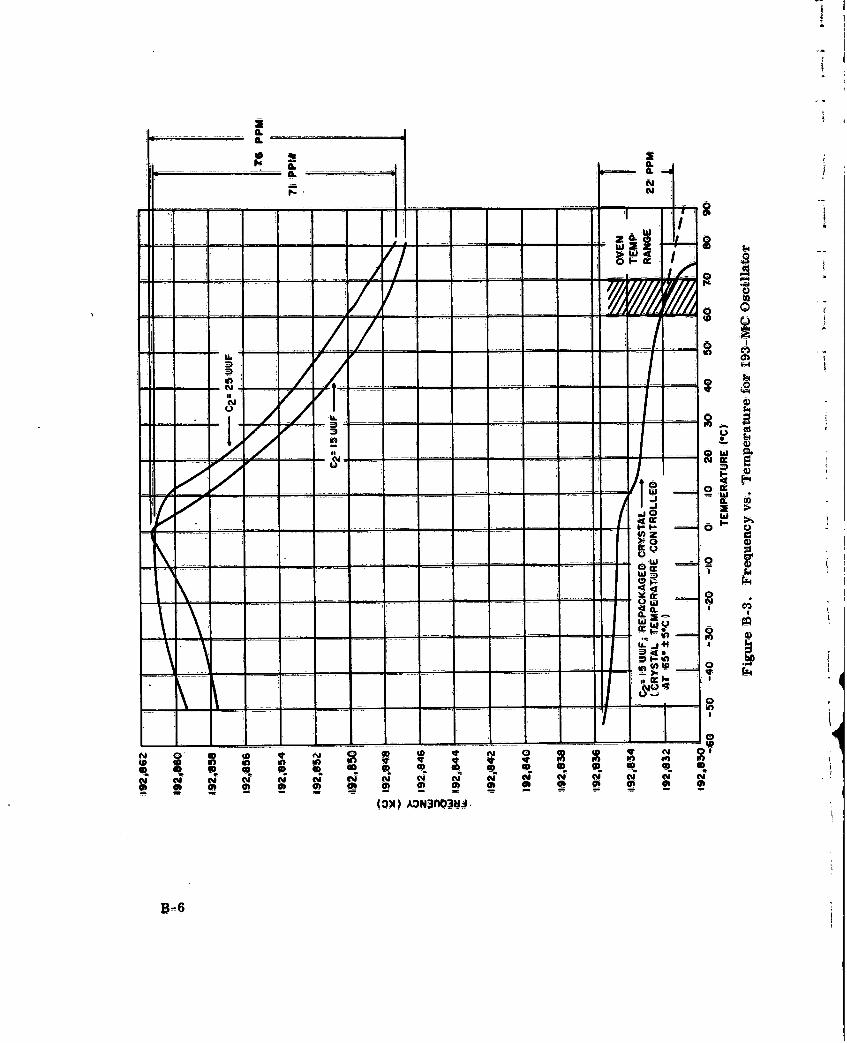
ILi
I. _ _ _ __ _ _ _ _
IL.I
* IF
w~ Z mw
- ----- c m a
__ M__-1
o o
40,~- 1w
N0 U
--- -- Q- W- i C Y
i 0
OD N 0 0 C 0
Of W Nm N M N NV NY Nf N N N~ N N
(ON) AONMfO3.1
B46

APPENDIX C
120-MC OSCILLATOR USING 2N2217 TRANSISTOR
Object:
The object of this design was to obtain high power output while maintainingcrystal dissipation below maximum rating. The power output was in the region of 100,MW to 120 MW at room temperature for a crystal dissipation of 1 to 1. 5 MW.
The family of transistors investigated was the 2N2217-19, the only differencebetween these types being in the values of h. , Experimental tests showed that the9N2217 (the lowest gain type) suffered least from the effects of internaI feedback atthis frequency, and this type was selected for the application.
The experimentally derived power gain and input resistance curves of theamplifier Show that the load resistance necessary for stable gain is in the region of200 to 300 ohms, an undesirable range of values in view of the specified 28-volt supply.
4 This resulted in considerable mismatching of the oscillator to the power supply and,consequently, a poor oscillator efficiency.
Temperature tests of the oscillator resulted in frequency deviations ofi-O. 0052percent us ng RL 325 ohms (measured at 120 MC) and *0. 0044 percent usingRL & 250 ohms. These tolerances are 3 to 4 times those expected of the crystal!alone and indicate the price paid for the high power output. Similar results were ob-tained from a temperature test on a production unit when loaded with a Class B poweramplifier.
The results obtained with this oscillator should be compared with those of the75-MC oscillator, which was designed for higher power output using a slightly differentapproach,
120-MC TRANSISTOR OSCILLATOR DATA
Oscillator Design and Evaluation Sheet
T Active Element- Transistor Manufacturer's Type No: 2N2217
Crystal (s) Used Resonant Frequency Series Resistance
CR-56A/U 120.0005 MC 38 ohms
C R 156A/U 119. 9977 MC 48 ohms
C-i

Description of' Oscillator Type
Crystal: Series
Active element configuration, Grounded Base
Feedback transformer configuration, CLa aitive Divider
10006
Figure C 1. 120-MC Oscillator Circuit, 2$2,217 Transistor
Details of Desipgn qalulaion
Using the notation and design equations of the Final Report and the measured
gain and input resistan ce of the amplifier, the remaining circuit component values aredetermined as follows:
From the ampDlifier curves a working pit at 32Rhs ~=60
=i 130 ohms was selected. Also Rr max 60 ohms.
R 1S Bin r max 190Oohms
p 5 430
and -2152 -
C42

0 00 § 0----- -
A-
- ~ -w -
-- -- - - - -
-SIO - - -3NiI3 - - - - -
IC

G
FB - 2X RT - 69 K
For a capacitive divider feedback nretwork, the equations are.
+ 22Tr RFB =36
or C2 18 C1
For C1 ' 8 UUF, C2 = 140 tUUF-.
To obtain high power output, C2 was decreased to 50 UUF giving a crystaldissipation of I to .,5 MW.
The phase lead introduced by the capacitive divider is:
9 9 0° tan lw(C 1 + C2)R
= 70
The loading effect8 of voltmeter probe and coil losses were negligible in comparison to RT . Therefore, RL = RT 320 ohms (360 ohms nominal Value).
This circuit was also evaluated for an RL = 250 ohms.
C-4

4.
00m
cqz0 00
0 0
0 Mi0
044
ooto to L 0 A
A 0
eq a 0 0cv) 0 00 0 01
" 0o
--
0-4 >
>n a
-1 00 04 kd PI444
oop~ 4 00
CU

- M- .--- ---
020
a - - C
zct 0~ 0 a
m N tycutiON 0-NnOu
1.44

APPENDIX D
I l20 MC OSCILLATOR USING 2N834 TRANSISTOR
Object
J |in view of the wide oscillator frequency tolerance and low efficiency of the120-MC Oscillator using a 2N2217, the object was to attempt to achieve comparableoutput power using a transistor of lower power rating. The basis for this approachwas that a transistor having smaller junction areas would have equal stability at higherRL values, thereby improving the efficiency.
I The evaluation of the oscillator showed no improvement in efficiency. Thepower output dropped by 20 percent compared with the previous design, while the DCpower input also dropped by 20 percent.
The temperature stability of the oscillator was improved over the previousT design having a value of 0.0037 percent, an improvement of *00.0015 percent. This
is possibly due to lower amplifier gain used in this design.
I 120-MC TRANSISTOR OSCILLATOR DATA
OsciLatorDesign and Evaluation Sheet
Active Element: Transistor Manufacturer's Type No.: 2N834
Crystal (a) Used Resonant Frequency Series Resistance
CR-56/U 120.0005 MC 38 ohms
I Description of Oscillator Type
I Crystal: Series-
Active element configuration: Grounded Base
Feedback transformer configuration: Capacitive Divider
~D-1

390'NOTES
oi -1000 13600 oJoU W OTERWISE1 20OME A
Figure D-1. 120-mc Oscillator Circuit, 2N834 Transistor
7O r
POWER GAIN/
GOC5O --
300
200 -00
o r - -46.-W
2N3 Tasstra 120
D-2

Wiw
1 ~ ~~~10,004 1- - - - - -I
TEMPERATURE Mc)
Figure D-3. Frequency Versus Temperature, 2,N834 Transistor at 120 MC,
I using the notation and design equations of the Final Report and the measuredgain and input resistance of the amplifier, the remaining circuit component values aredetermined as follows:
A working power gain of 450 was selected corresponding to RT 390 ohmsand Rin - 150 ohms. The crystal resonance resistance HRmx= 50 ohms. Therefore:
Rs Rin+ -Rr 200, ohms
Gp -G. RIM 340
Using a safety factor of 2 gives:
=17 02
1'D4

RFB= 2 RT 6 C' K
Using a catpacitive divider feedba~ck network, the relevant equations are:)2TransformainRto=__- 330=
or c 1
Le t c 10 JU j then C ±1710 UUF12
Optimnum crystal drive level (1Ito 1.5 MW) was obtained with C1 50 UUF.
The phase lead introduced by the capacitive divider is:
q& = 9O tnl w (c, + 2it
7 0 for C =50 UUF2
JD-4

44
I--
0 06
k 40.
U) U) 0)
~~44
0 0 c
UC.) . ~ 0 02o
- 440 m c
+ -0 4
44~
00 loL 0

iiI
APPENDIX E
I 5 MC OSCILLATOR USING 2N2219 TRANSISTOR
Object:
' The object was to develop as much power output as possible while main-taming the crystal dissipation below the 2 MW maximum.
j This design followed the 120-MC high power oscillator. The 2N2217 - 2N2219types were again selected for evaluation. At this frequency the 2N2219 had the bestpower gain-to-input resistance characteristic. When converted to an oscillator and
the feedback network optimized, the performance was surprisingly poor; i. e, thepower output was only 100 MW.
JAfter several values of load resistance and feedback network were attemptedwithout any improvementi it was decided to partially neutralize the transistor so that
* operation with a larger value of load resistor would be possible. The neutralizing
scheme consisted of connecting a coil of 0. 15 UH across the crystal socket. Retesting the circuit on the RX Meter (crystal removed) gave the improved curves ofFigure E 2. These curves show stable gain characteristics for RT 900 ohms.
In practice the maximum value was 500 ohms before tuning hysteresis occurred.
The neutralized oscillator displayed a much improved power output (170 MW),but the surprising characteristic was a frequency stability with temperature of *0. 0013percent. This is approximately one-third of that typically obtained with previoustransistor oscillators. No further evaluations were made, and it is undeterminedwhether this was a freak occurrence or whether the neutralizing was Influential in thisimprovement.
I 75-MC TRANSISTOR OSCILLATOR DATA
j Oscillator Design and Evaluation Sheet
Active Element: Transistor Manufacturer's Type No,: 2N2219
Crystal (s) Used Resonant Frequency Series Resistance
1 CR-56/U 74.9995 MC 38 ohms
It
:. E--

Description of Oscillator Type
Crystal: Series
Active element configuration: Grounded Base
Feedback transfortmer coiifiguration: Capat pv Pivider
+22
Ooo 2400 o.um 'RL
... . ZOO --- --. 1000SUH ="
1 7 0 0 2 0- 3 9 A L L 4 0 O ANOTES: 3kz25,MA.
ALL CAPAUTORS IN UUF UNLESS OTHERWISE NOTED.
Figure E-1: 75-MC OscillatOr Circuit
Details of Degign Calculations
Using the notation and design equations of the Final Report and the measuredgain and input resistance of the amplif'ier, the remaining component values were de-termined as follows for the partially neutralized circuit case:
A power gain of 88 was selected corresponding to:
RT - 470 ohms, R-- = 45 ohms
The crystal resonance resistance, Rr 50 ohms max:
Rs Rin + Rr = 95 ohms
Rinf Gp x = 42
E.2

IL
I ~ ~ --- ---- - - - --- - -5 Lt
I'ma Hi 13"- -G3MIn~
a E-3

NIVO V31MOd
__0 0
8- 84
00
00 00
(S~gO)WIJ 3~VJSI3~ .flto
E-4

Using a safety factor of 2 gives:
2
RFJB 21 x470 =9.9KX
Jusing a capacitive divider feedback network, the relevlat equaions are:-
T 1~~=0 4 {1 '
Ior C 9C
ufLtting C1 8 UUMP gives C2 72 U~U-F
Optimnum crystal drive level (1 to 1. 5 MW) Was obtained for 02g 100 UUJF.
The has led itrouce by the capacitive divider is.
6 0 -Otan~lw (CI +C2R
1 100
Z"

0-
M o ohr
a) 0 0 ~ C0'co >o
00 0 '1 cq
0 .4H
a)40 i nU )a
LoH4J ~
0
0 C)- 11(L
-j - i )
000) 04- 1 .
a) 0
+ Si, 0 ->~ >
044
Q bD bI 0e 0 0 0 go.
> 4 74 44
u 0
i.- 1-- V-4Y- 0 4
- 0 -H 0 0 -H f4 o
E4 ~
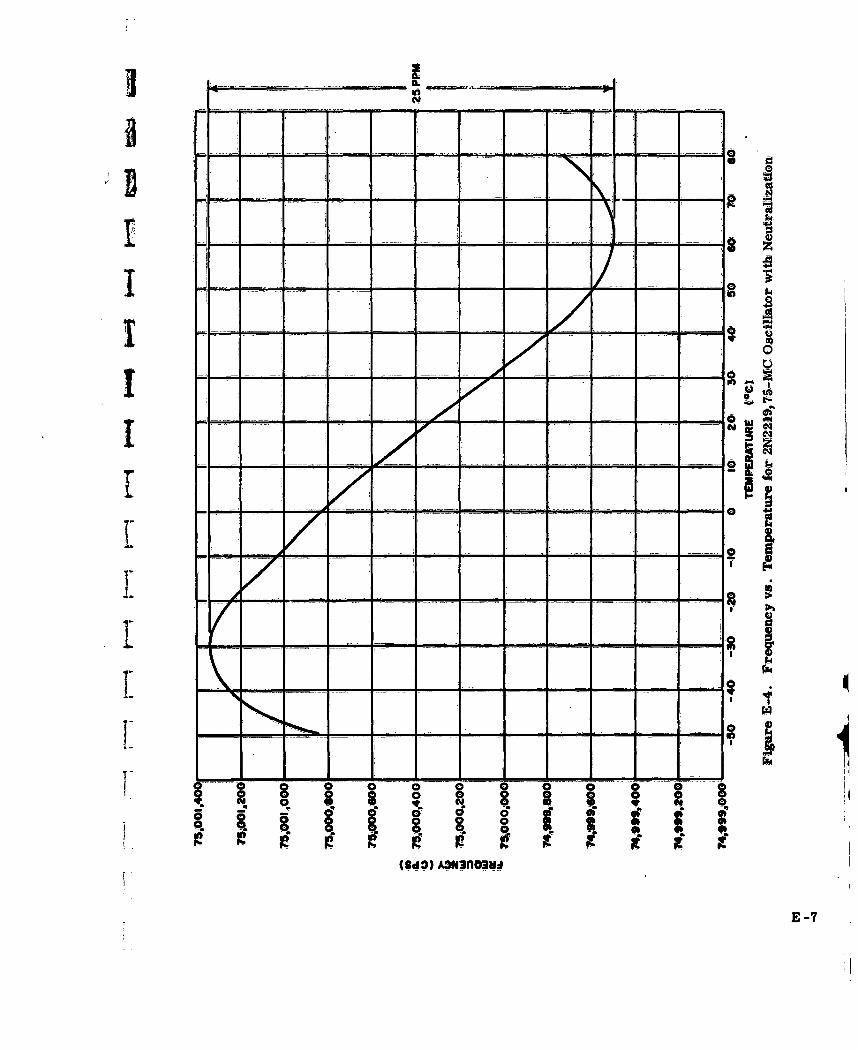
c~cq
4 a
-- o--
qe
E4

APPENDIX F
100MC TUBE OSCILLATOR USING 5718A SUB-MiNIATURE TRIODE
Object-
This design and the one at 200 MC using the 5718A triode were the first onesattempted using tubes. The object was to determine the difficulties that would be en-countered in tube oscillator design at these higher frequencies.
'I Design Details.
The physical layout followed as ciosely as possible the one previously Used inthe transistor oscillators. However, because of the physical bulk of the tube, chaes
were necessary and the layout shown in Figure F-I was used.
CRYSTAL GRID
AND CATHODE RF SHIELD, I-/2 IN. HIGHFILAMENT CIRCUITS
CHOKETUBE IN RFSHIELD AND.CLAMP K l
CORNER OF SHIELDCUT AWAY TO ADMIT
FILAMENT PLATE TUNING, PLATE LEADJ CHOKE LOAD, ANDDECOUPUINGCIRCUITS
I .. . .... _ ___
Figure F-i. Chassis LayoutI,Difficulty was experienced in establishing this design; several redesigns of
the grid and cathode circuits were necessary before a successful oscillator was ob-tained. Intially, the circuit was constructed with the grid directly grounded and thecathode connected to ground via a 1-VH choke. This arrangement was unsatisfactorybecause of uncontroled oscillation that could be tuned in, in addition to the desiredcrystal controlled oscillation. After several grid and cathode circuit redesigns weremade, the circuit shown in Figure F-2 was found to give stable crystal controlled os-
f cillation.
F--

.1
Conclusions:
Because of the amount of experimental work involved in developing a sais-factory oscillator, this design cannot be claimed as a successful exampile of the de-sign procedure. The information obtained from the design measurements, while beingsufficient to determine the feedback requirements for the crystal-controlled oscillationat 100 MC, did not predict the instability that occurred at adjacent frequencies.
This possibility is noted in the Final Report. However, it can justifiably beignored, since these undesired effects did not occur in the majority of the oscillatorsconstructed using the design procedure. This design and the one at 200 MC usingthe same tube type proved to be exceptions to the rule,
Some of the possible reasons for the uncontrolled oscillation are given below:
(a) Feedback through the un neutrafiied crystal Co undoubtedly hadsome effect, since the circuit was stable with the crystal removed.However, this feedback alone is insufficient to cause oscillation,since a Co of 7 PF has a reactance of 230 ohms at 100 MC.This is incompatible with the loop gain requirements for the feed-back ratio used.
(b) Inductive couPling between output tuning coil and. the cathode choke.
Because of the single-ended layout of the tube, the RF shieldingwas poor in the vicinity of the tube base. However, the circuitwhen tested as an amplifier did not show any tendency toward in-stability.
(c) The grid circuit had an important bearing on the instability, andthere appeared to be positive feedback via this circuit.
100-MC TUBE OSCILLATOR DATA
Oscillator Design and Evaluation Sheet
(Test results obtained with diode limiting)
Active Element: Tub Manufacturer's Type No.: 5718A
Crystal Used Resonant Frequency Resonance Resistance
CR-56/U 99.9998 MC 29 ohms
Description of Oscillator Type
Active element configuration: Grounded Grid
Feedback transformer configuration: Capacitive Divider
F42

I 0.6-14 NOTES0.15UH :RL ALL CAPACITORS I UUF
___ iUNLESS WOTRWISIE NOTED
X -X - N3062 IpUIMA
I2f' 300 0.5 U14 1000 20C0
I 3.11M 3.3WH2
Figure F-2. Oscillator Circuit, 6118A Tube at 100 MC
J IDetails of Design Ca&LZUtigns
Using the notation and design equations of the Final Report and the measuredgain and input resistance of the amplifier, the remaining circuit component values are
determined as follows:
J The workcing point selected was GI, 12 ~ 190 ohms and HT =3K.
For ]Rr max 60 ohm s:
Rs Rr + .in250ohms
I RFB 2 xR~l4.5
2
2F-

Itsing a cttimaitive divider fecedback network, the relevant equations ate-
'nFB ; ___
tFrans'formationll ratio - 4C2
or C2 C
For -C2 2OUIUF, C1 3 UUF
The phase lead introduced by the capacitive divider is;
tar 1 W (C 1 + C 2) RA 15degrees
The voltage mneasuring probe parallel resistance was S0 K and the effective parallelloss resistance of the coil was 25 K, giving a parallel combination of 17 K. The loadresistance value required to make- the total load resistance, At ± 3. 9 K was therefore5 K. The actual load resistance Value used was 5. 4 K~ having a nomninal Value of 15K.
30,
00.
0 1990 2000 3000 4000 5000 -6000 7000 6000-LOAD RESISTANCE, R7 (OHMS)4
Figure F-3. Input Resistance and Powver Gain Versus Load Resistance,5718A Tube at 100 MC
F -4

I~ ~ --'0,0 - ~---- -
"19: 5 J4 mU-O30..o 0- o 0034 50 goTO6
TEMOERATUREt (0c)Figure F-4. Frequency Versus TeMperature, 5718A Tuba at 100o MC,5 With Diode Limiting
F"

tt ~ ~ L tot 1 0
eq Nq eq Nq e
0. to H H
U 14410 1 t ~ CO C
fXi H-4 0 >n 0 V 0 (D
00 A0 0 d0.0 ..0 . . 0 0 0
o4 bl V4 b.
zp 9 4 0II 4I1 4 0 eq0 e 0 +0
;4p
'-44-H -HOa- t1

U
BAPPENDIX G
150-MC TUME OSCILLATOR USIN 8058 NUVISTOR
Object:
fAlternative tube types were reviewed as a result of:
(a) The difficulties experienced with the oscillators usimg the 5718Atube in progressing from the design and measurements stage toa finalized oscillator
(b) A clearer knowledge of the characteristics required of the tubeI in aft oscillator circuit
3 The desirable characteristics are discussed in the high-frequency design proceduresection of the Final Report and will not be restated here. tased on these considerations,the nuvistor triode, type 8058, was selected for experimental evaluation. The objectwas to determine if a finalized tube oscillator eould be designed by a straightforwardapplication of the design procedure, without recourse to experimental methods.
The physical layout of the circuit is shown in Figure 14 of the Final Reportand, as can be seen, the construction of the tube resulted in good shielding betweeninput and output circuits. The only adjustment required to finalize this oscillatorconsisted of increasing C2 from 3 UUF to 5 UUF with a corresponding adjustment ofthe limiter diode biasing resistor. In this case the allowable plate swing beforecrystal overdrive was 10 VRMS.
Conclusions :
j No difficulties were experienced in finalizing this oscillator, and this appearsto be due mainly to the better isolation between input and output sections of the tube.Isolation was aided by the considerably better RF shielding that can be applied to theexternal circuitry of a tube of planar or semi-planar construction.
In comparing the evaluation datA of this design with the one at 200 MV using11 the same type of tube, the following items stand out:
(a) The frequency stability of this oscillator as a function oftemperature is lower by a factor of 2. in view of the simi-larity of the circuits and circuit components in the twooscillators, it appears that this may be attributable to d-U ferences in the crystal temperature c harceristics. No
verification of this has been made.
0-

II
(b) Both the 150 Mc and the 200 MC oscillator data indicate thatthis tube is critically dependent on filament supply voltaget the
ratio - 2.5. The cathode appears to be running underAf
temperature limited conditionsI and for many oscillator applications
a stabilized heater supply would be required. (Another possibilitywould be to replace the limiter diode biasing resistor with a znerdiode, thereby stabilizing the limiting voltage.)
!50 MC NUVSTOR OSCILLATOR DATA
OscillatorDeinndEautoSht
Active Element: NXWvitr Manufacturer's Type No.: 8058
Crystal Used Resonant Frequency Series Resistance
Similar To
CR-169, 1002 20 WC 41 ohmsh
Description of Oscillator Type
Crystal: Series
Active element configuration: Grounded Grid
Feedback transformer configuration: Capacitive Divider
"~ ~~ al w1...4islo'~luiiio0.06 UN A". CAPACITORS IN, WI,
X X UNLESS OTHERWISE NOTDA LX L
l P [F000 - Zp UIOMA
LO UW LOUH 40 0 00 LX PlStONATI WITH Co OFY___ CRYSTAL T
x x I I '1i/ Iooo ll!O
SFigur G-1. Oscllator Circuit, 8058 Nuvitor at 150 MC0-2 5
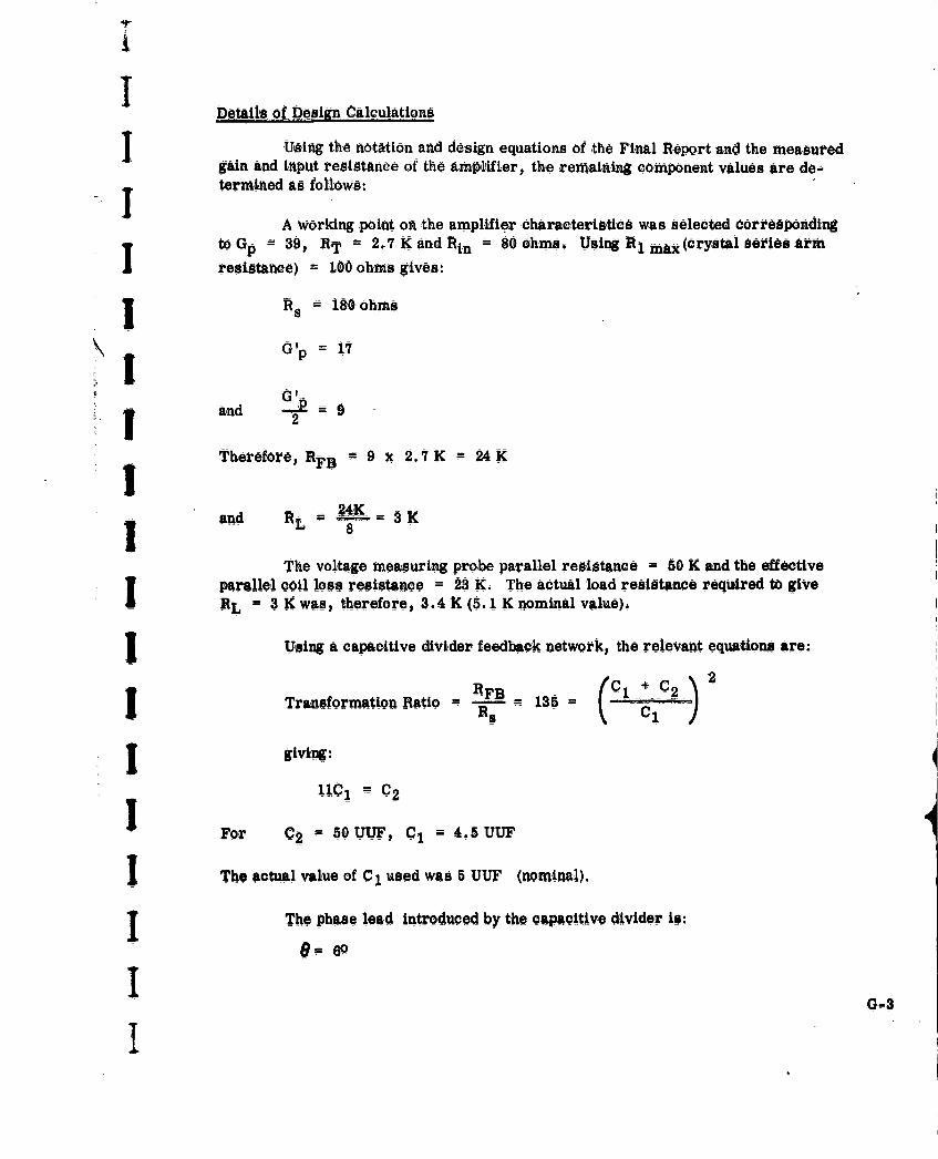
Details of Design Caiculations
J Using the notation and design equations of the Final !Report and the measuredgain and input resistance of the amplifier, the remaining component values are de-termined as follows:
A working point on the amplifier characteristics was selected correspondingto Gp= 39, RT
- 2.7 K ad Bin = 80 ohms. Using R1 max (crystal series arm
resistance) 100 ohms gives:
Rs 180 ohms
i Gp =17
G '-and9
Therefore, RFB = 9 x 2.7K = 24K
- 24K
and RL - 8 3K
The voltage measuring probe parallel resistance = 50 K and the effectiveparallel coil los resistance = 23 K, The actual load resistance required to giveRL f 3 K was, therefore, 3.4 K (5.1 K nominal value).
I Using a capacitive divider feedback network, the relevant equations are:
2! Transformation Ratio RFB-- 135
I giving:
For C ! __M C2 FIFor C2 = 50 UUF, C1 4.5UUF
I The actual value of C used was 5 UUF (nominal).
I The phase lead introduced by the capacitive divider is:
960
G-3I
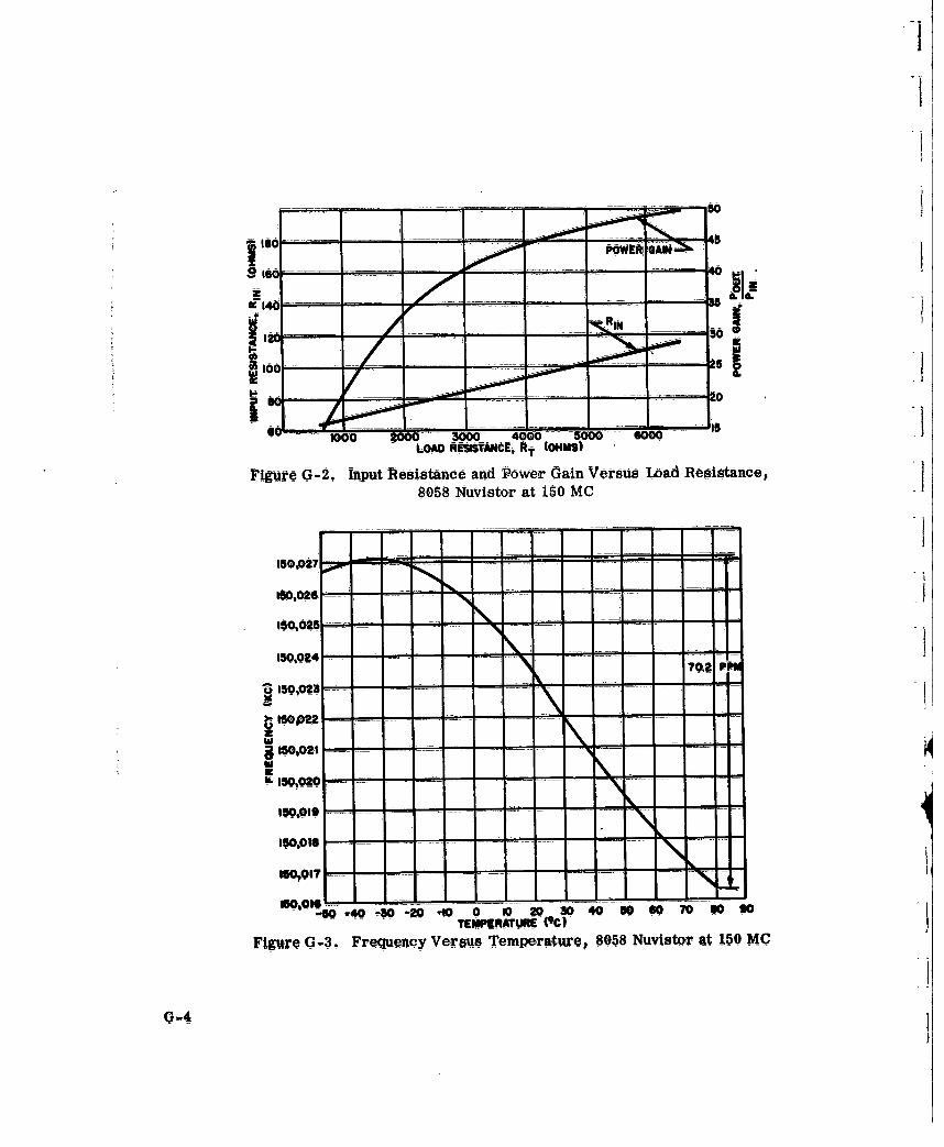
ILI
1 0
100 200 00 4000 5000 6000
LOAD RESISTANCE, RT (OHMS)
Figure G42. Input liesistance and Power Gain Versus Load Resistance,8058 Nuvistor at 150 MC
150,027 - - -- - -
100,26-
150,04--
~IW0P2 ------ - - - - -
Z
1t50,021-------------------
W150,016-----------------------
150,016------- -
-- 40-00 -10 0 020 30 405060790030- TEMPERATMR (90Figu~eG-3 Frquency Versus Temperature, 8058 Nuvistor at 150 MC
G-4

c.) to 0.
-044101
UI V- C4.
C4 LR H
0. 0
0~~ 0 0i I I II
. 0 IW 000 'o>
14G4

I
APPENDIX H
I 200-MC TUBE OSCILLATOR USING 5718A
Object.
This design actually preceded that of the 100-MC oscillator using the sametube type. The object was to determine design difficulties using tube circuits at thisfrequency.
The physical circuit layout was the same as that used for the 100-MC tubeoscillator, as shown in Figure Fi.
Design Details:
initially, this oscillator was constructed with an RC network in the grid toprovide limiting action and with a choke in the cathode to reduce shunt losses in thefeedback path. The resulting oscillator was unsatisfactory due to "squegging" (arelaxation type modulation of the oscillator output due to the action of the grid circuit
j time-constant) and to uncontrolled oscillation. Adjustment of the grid time constantcured the "squegging", but it was necessary to replace the cathode choke with aresistor to prevent the uncontrolled oscillation. The remaining defect in the oscillator
j was crystal overdrive. It was found impractical to remedy this by B+ and grid circuitadjustments, and the diode limiting circuit was incorporated into the design to give thenecessary limiting action. After these changes, the oscillator performed well asshown in the accompanying data sheet.
Conclusions:
Many of the remarks concerning the 100-MC oscillator are applicable to thisdesign. This oscillator exhibited the same tendency to uncontrolled oscillation until
5circuit changes were made in the grid and cathode circuits. In this case, however,stabilizing the circuit was easier, the amount of experimental adjustment requiredSbeing far smaller; no expanation is available for this discrepancy.
The difficulty in keeping the crystal drive within permissible limits is due tothe low gain in the amplifier portion of the circuit and the relatively large linear signal
5 handling properties of a vacuum tube. in this design, the plate voltagehdtobelimiedto less than 4 VRMS to prevent crystal overdrive. When it is considered that platevoltages of iOOV or more are required to optimize the gain, it is easily seen that externallimiting methods are necessary,
IIIt-

200MC TUBE OSCILLATOR DATA
Oscillattor 0001p and vauaton Sheet
Active Element: Tu~be Manufaturer's Type No. 5-118A
Crystal Used Resonant Frequency Series Resistance
Similar to
CR-7/U199.9990 MC 88ohms
Description of Oscil1lator Type
Crystal: Series
Active element configuain Gounde Grid
Feedback transformer configuration: Capacitive Divfder
S -0.6140.0 UN RL ALL CGACITORS IN- UUF
x LX UNLESS OTHERWISE NOTED
X XIN3062~ 1p a10,MA
1.0 N IUN ~ - 000 270LX RSNATES WITH C0 OF- CRYSTAL Y
X.3 L __ 125 VOC
1gure H 1. Oscillator Circu t, 5718A Tube at 200 MC
Details of Design Calculations
'Using the notation and design equations of the Final Report and the measuredgain and input resistance of the Amplifier, the remaining circuit component valuesare determined as follows:
H- 2

Thv working point was selected at R'T 1. pG 2 i 2 hs
I Using a crystal series resistance value of 100 ohms gives:
I ft5 =R1, +- R1 29 22ohms
I G'~6.6
-P 3.3
2
_RFB
RL icuigvoltage measuring -.
(robe. and coil losses )-=232
I Using a capacitive divider feedback network, the relevant equations aire:
Transformation Rtatio 9 F 4= _ ___2
I giving, C2 =4C,
For C2 =25 UUF, C1 6 UUF
The actual value of C1 used was 8 UU.
The voltage measuring probe parallel resistance was 8 K and the eff ectivtParallel lose resistance of the coil was 8 K; that is, a parallel combination of 4 K.The actual loading resistance value required to make the total load resistance, RL2.3 K was therefore 5.4 K. The actual value used was 5 K (13 K nominal value).The phase lead introduced by the capacitive divider is 70.
H43
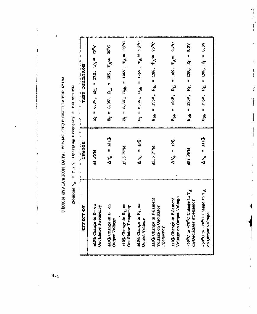
tf TO. C434~
eq~ eqqta
09 N
CV) CO -v.44 .. I
11 A
to w to
10>01
00.
0Z
o to
0 eQ )
0 e0q
00
$4 5Z4 N () oto 0 00-
A. > A 0 0
U U~
> -
H-4

GAI
fl 10
efFectIVE LOAD ARESISTANCE, Rt(OHMS)10
IFigure H 2. Input lResistance and Power Gain Versus Load Resistance, 6718ATube at 200 MC
200,0 00---
3c 19,99I------------1. 44 PPM
g 0,10 - -
-
191,991.---------------
90-40 30 *20 410 0 10 20 30 40 50 00 70 00-TEMfERATURE (C0
Figue H-.Fequenc Vess Temperatue, 5718A Tube at 200 MC
H"-5

I
APPENDIX I
I 200-MC TUE OSCILLATOR USING 8058 NUVISTOR
j This circuit is essentially similar to that used in the 150-MC oscillator(Appendix G), and the comments made concerning the design and performance of thatoscillator are directly applicable.
200-MC NUVISTOR OSCILLATOR DATA
Oscillator Design and Evaluation Sheet
3 Active Element: Nuvistor Manufacturer's Type No.: h058
Crystal Used Resonant Frequency Series ResistanceSimilar to
CH -56,/,U 199.9990 MC 8,8 ohms
I Description of Oscillator Type
Crystal: Series_
I Active element configuration: Grounded Grid
Feedback transformer configuration: apacitive Divider
I
0 .6 -14 u. RL ALL CAPACITORS IN UUF
I .I7UNLESS OTHERWISE NOTEDXL
O1.0 UH 1.0 UH LX RESONATES WITH C0 OFy U CRYSTAL Y
LOWN 25-
1
-
I Figure I-I. Oscillator Circuit, 8058 Nuvistor at 200 MC
I

Dail -of Desjgwxalculsktions
Using the notation and design equations of the Final Report and the measuredgain and input resistance of the amplifier, the remaining circult component valuesare determined as follows for the amprliier characterited by condition No, 1 (seeFigure 1-2).
A working point was selected at R T 2.5 K,
Op 58, Rin - 75 ohms, R1 max " 100 ohms
Rs - 175 ohms
Bin .6-X Gp = 12.52 ER's X P
'!
rIB 2 x RT = 31K
L-B
2
The coil losses are already acounted for in the amplifier curves, so in thiscase RL consists of the actual loading resistor in parallel with the voltmeter probeeffective parallel resistance. The value of the latter was 8 K, requiring that theloading resistor be 4.2 K to give RL 2 2 K. The loading resistor used had a nona10 K value corresponding to an actual resistance of 4.5 K at this frequency.
Using a capacitive divider feedback network, the relevant equations are:
Transformation Ratio - _ -- 177 - ___C _ 2
or C2 = 12C,
Therefore, for C2 = 25 UUF, C - 2 UUF,
The value of C1 used was 3 UUF.
I-2

II10 - - - - - as3
- Ef "I_ _ _ _ _ _ _ _ _ _ _ _ _ _ _ _ _ _ _ _ _ _ _ _ I N , P0 O ITI N !
POERGIN O tN ON D O.! No
To --- 2000 300
4 ,0 2 - -- - 2
go 006 0
No. Ill CHK INCTOE-RU,1v0 ---
tll----T, O ------------------ _ I_ CATTPPM
0100 _ ----- - --- -4
ILL
- -W,-40 - 30 -04 ___ __0_ _x 7O§47, 4SO 9 9
TEMPERATURE (00{ Figure 1-4. 'Feuncy Versus Temperature, 8058 Nuvistor at 200 MC7-q e-- -

C>1 NON
06 to4
0 00
oa 0
- k -
0 o0 .
, * Q. 9 - -q
000)0
I 1--

.
APPENDIX J
l-KC TWO-STAGE TUBE OSCILLATOR USING 12AX7 (WIEN BRIDGE)
J Object:
In this design the object was to determine the factors influencing the oscillatorIperformance.The initial plan was to use a resistive divider feedback network to supply theS feedback power, but this method proved unusable because of the lack of frequency
selectivity. Oscillation at a high audio frequency occurred due to feedback via thecrystal Co . Replacing the resistive divider with the Wien Bridge network added theI selectivity required to prevent this parasitic oscillation. No other difficldties wereexperienced in finalizing this design.
I Conclusions:
The performance of the oscillator is shown by the evaluation data was sais-factory, having a performance approaching that of the high-frequency oscillators.
INo difficulties should be met in designs of this type, provided that frequencyselectivity is introduced into the oscillator. Crystal overdrive does not constitute amajor problem because of the high available gain. The major disadvantage is the cir-Icult complexity.
1-KC TWO-STAGE TUBE OSCILLATOR (WIEN BRIDGE)
I-Opscillator Designmad- Evaluation Sheet
J Active Element: Vacuum Tube Manufacturer's Type No.: 12AX7
Crystal Used Resonant Frequency Resonance Resistance
T44 99993CPS 5K ohms
Description of Oscillator Type
I Crystal: Series
I Active element configuration: Grounded CathodeFeedback transformer configuration: Wien Bridge
T-- --- - - -
.7~i

'10OK UM0-+12efv
lox NOTES:X1 I- 1- RoM---- ALL CAPACITR
IOOK SO 3K NTD0.031 0.6 OMA
.~i-~--*---~ - pguo. MA
p600 ~~~~ 200 t: z10 oG 00 1 1Figure J-1 I-KC Two-Stage Wien Bridg-e Oscillator
With this type of circuit it is convenient to determine the loop voltage gainrather than the Power gain. The amplifier voltage gain from the grid of V1 to theplate of V2 is:
_V 1RL1- U2 RL9RM + Rpl RL 2 + Rp 2
For the biasing conditiOns shown (Ip 0.-5 MA, Vg 4V
U1 U2 100, Rpj = p 85 K
V2=970
This assumes that the loading of the feedback network is negligible (Condition 1).
The voltage attenuation of the feedback network can be calculated as follows:
J-2

IFor this type of crystal, Rr max 200 K. Therefore, the voltage attenuation
between the crystal input and V1 grid input is:
Rgi- RgI + 20 0 K
If the loading of Rr max 1Rgi on Rb is assumed small (Condition 2), the
attenuation between points X and Y (Figure J-4) is:
Ar ab
The attenuation from the plate of V2 to point X Is:
Aw - 1 at the bridge "resonant" frequency.
The total attenuation is therefore:
AT -Ad x Ar.x AwI To satisfy Condition I the feedback network should appear as at least 10 times
RL2; that is, not less than 300 K. Section 4.7.4 of the Final report shows that the
effective parallel resistance of a Wien Bridge network is equal to three times the valueof the resistive elements of the bridge. Therefore, a value of 100 K for these elementssatisfies Condition 1.
I The value of Br max + Rg cannot be less than 200 K, and therefore a value of
Rb less than 20 K will satisfy Condition 2.
The loop voltage gain from the input of the Wien Bridge network to the plateof V2 is therefore.
=1 Rb Rg9GVL 97x 0b RgiX2OI 9
Letting Ra + R 100 K, Rb - 15 K, and equating GVL = 1.4 (loop power gain =2)
I gives:Rg1 -K
The requirement for zero loop phase shift is that:C1 R1C2R2 ~---- (refer to Wien Bridge analysis)
r, ( ---
'A4

where the effects of amplifier output resistance and crystal loading are taken intoaccount in the values of Ri and R2 , respectively. For the particular feedback net-
work used, the calculation of Wo Is as follows:
For the crystal used, Rr = 55 K and therefore Rb in parallel with Rr +
Rgl is 12 K.
Therefore, R2 = 112 K.
The output resistance of V2 is 30 K in parallel with Rp -85 K; that is, 22 K. There-
fore i -122 K. C1 i eqUa to 1600 UUF in series with 3000 UUF; that is, 1040 UUF
and C2 1600 UUF. Therefore,
0 C~cf2 1/2
66,20
or fo 1050 CPS
The calculated fo based on component nominal values agrees to within 5 percent of theactual fo which was experimentally adjusted.
The network would be more optimum if the values of Rb and Rgl had been
interchanged; changes in the value of Rr would then have less effect on loop phase
change, since R 2 would be more nearly constant.
The maximum permissible output voltage before crystal overdrive occurs canbe determined by considering the feedback network when Rr = Rr min which is
assumed to be 20 K. For Rg 1 - 5 K the crysta dissipation will be 10 UW for an In
put power of 12.5 UW into Hr and Rg 1 in series, This corresponds to a voltage of 0.56 V
at point Y, Figure J-l. The voltage at point X is therefore:
0 56vx -x O100000 = 4.1V15000
Since the voltage at the Wien Bridge network is three times Vx , the oscillator
otput voltge bfore crystgl overload occurs is app roxmately 12 V. This is not
completely accurate, since the network used does not completely satisfy the WienBridge conditions.
J-4

ot 0. 0
;Lo C o C i c
4-4 1-
r-
P -4 F-
!A 0 -4 48O
I..5

I
APPENDIX K3-KC TWOSTAGE TUBE OSCILLIOR USING 12AX7 (WIEN BRIDGE)
This design was based on the 1-KC oscillator of the same type, the sole ad-justment being in the values of capacitance used in the feedback network. All commentsconcerning the 1-KC Wien Bridge Oscillator are applicable to this oscillator.
I' 3-KC TW-STAGE TUBE OSCILLATOR (WIEN BRIDGE)
Oscillator Deig and Evaluation Sheet
Active Element- Vacuum Tube Manufacturer's Type No. : 12AX7
i Crystal Used Resonant Frequency Resonance Resistance
Description of Oscillator Type
t Crystal: Sories
i Active element configuration: Common Cathode
Feedback transformer configuration: Wien Bridge
DetaLils o-f Desi~gn Calculations
The design calculations for this oscillator are the same as in Appendix Jwith the exception of the Wien Bridge network capacitor value. In this case C1 equals
470 UUF in series with 2400 UUF (390 UUF) and C2 470 UUF. Insertiing theseI ! values into the equation-
050 [C1 1C 2 1] 1/2
Gives Wo 18,300
Or fo = 29500 CPS
J The design calculation again gives good agreement between calculated andexperimentally adjusted network values.
K-1

OE M -K -- 1 1 M -1 I
20K ;NOT"S:- - -----
ALL CAPACIfTORI" UP UNLESS
B~lK O -ERISE30KtNOTED.cr), OOK 003 pq soS MA
-- ZpUOS MA
6.3v Ig
ULI S 15100 IMfG 20o 1 omb 00 1 =1
Figure K-1. 3-KC Wien Bridge Oscillator
K42

oa o 0I00n
to a
11 A
14 0.4 I ZI Z I 'I
EI f f 4) C OD E -
25 C6 N N
E 4N N
P4II I II
~~~q 0 0 0 .0
4.0 0- A0
P 4k N N + 0
U U
H 0 0)
-N K4

4
APPENDIX L
1 KC SINGLESTAGE TUBE (12AT7) OSCILLATOR USING THE QUARTZ CRYSTALj TO GIVE PHASE INVERSION
Object:
This type of circuit is discussed briefly in Reference 3, Paragraph 7.0 of theFinal Report, and the object of this design was to develop a suitable design methodand to determine any disadvantages of the circuit.
Design Details:
I The first requirement in establishing a design procedure was to determinethe transfer characteristic of a crystal connected as a four-terminal network. TheJbest method found is described in the design calculation discu3sion and depends onhaving a signal generator of good short-term frequency stability. The Hewlett-Packard 200CD Signal Generator was adequate for this purpose. Once this informa-
j tion was known, the finaiini of the oscillator was straightforward.
The power transfer efficiency of the crystal varied somewhat depending on thevalue of the output load resistor used, and the optimum condition of operation was notclear. Several evaluations were therefore run for various values of loading resisto:which, in the oscillator, is the grid leak resistor R. No feedback network adjust-ments were made as R was varied, and consequently the loop gain increased by afactor of 2.7 for the Rg = 1 MEGO evaluation over that for Rg -- 200 K.
I Conclusions:i 1 The value of Rg used had negligible effect on the oscillator performance. It
would appear that the highest value of Rg consistent with the maximum permissible
value for the particular tube type should be used, in view of the improved transfer
efficiency for highaue of Rg
hh The evaluation data indicates a slight improvement in performance for the
hher values of Rg, particularly in the effect of B+ changes on power ouput.
insufficient data was obtained to determine the influence of the crystal Rron performance. The tabulated data shows that the crystal input impedance stays consistently approximately 300 K higher than the value of output load resistor used. This
value of 300 K, the input resistance with the output short circuited, is a value 5.5times greater than the resonance resistance of this particular crystal when connectedV.
I" L-1

as a two-terminal device. Th-is may or may not be coincidental. If the deduction isvalid, it may be possible to extrapolate the results of this test. A crystal with Rr
200 K (the assumed maximum value or Rr) could be expected to have an input resis-
tance of 1 MEGO with the output shorted, or 2 MEGO for a load resistance of 1 MEGO.The efficiency would be approximately 40 percent. These assumptions have not beenverified,
The work done on this circuit is not sufficient to establish a complete designprocedure for the reasons given in the preceding paragraph. Nevertheless, the -ir-plicity of this oscillator circuit makes it the recommended choice for vacuum tubeoscillators below 16 KC.
1 KC SINGLE4TAGE TUIE OSCILLATOR USING THE QUARTZ CRYSTALTO GIVE PHASE INV SION
Os-cilator Defsign-ai vlation SheetT
Active Element: Tube Manufacturer's Type No.: 12AT7
Crystal Used Resonant Frequency Resonance Resistance
T9J 999.93 CPS 55 K
Description of Oscillator Type
Crystal: Series
Active Element Configuration: Ground d Cathode
Feedback Transformer Configuration; Reststive Divider with crystal providing phaseinversion
Details of Design CLcultions
Usin the circuit shown in Figure L-2, measurements were made of thepower
transfer efficiency of the crysal connected as a four-terminal network for various
values of R. The measuring frequency was adjusted to give phase inversion of Vo with
respect to Vc pas measured with a dual beam oscilloscope. The results of these
measurements are tabulated below:
L- 2

SI
10OK 0.5NOTES:
J _ ALL CAPACITORSIN~pF UNLESSOTHERWISE NOTED.
133K 1p30.15MA
MMO
1 Figure L-1. 1-Kc Crystal Phase-Inverting oscillator
I -__-300K
I ~ ~~~SIGNALjve-R jv
GEEAO I_ _ _
ii _______Figure L-2. Crystal Test Circuit
H 0 c1j Crystal Input EfficiencyI _________ Vc1 VGResistane, R'r( 0 /m
20K 0.063 0.50 300K 0.06
Z00K 0.420 0.63 510K 0.45
j510K 0.*540 0.75 900K 0.51
T750K 0.610 0.78 1.1 MEGO 0.54
I MEGO) 0.690 1 0.81 1 l. 3MEGO) 0.62
7--

The characteristics of a 12AT7 at ip 0. 75 MA are:
U -35
Using a value of RT 17 K gives a voltage gain of:
GV = 12.4RT + Rp
Introducing a loop power gain safety factor of 2 gives:
v 8.7
The crystal filter voltage attenuation for R g 200 K is given in the
table as 0.42. Therefore, the voltage gain from the input of the crystal to the tubeoutput is:
v x 0.42 3.7
To reduce the 10oP gain to unity, the attenuation introduced by the feedbackdivider network (assuming the loading of this network by the crystal is negligible)must be:
Ar RR Got 0.27R R 2 Gv
R2giving R! 0.37
Therefore, for R1 = 100 K, R2 = 36 K
Since the crystal input resistance is 510 K, its effect on Ar iS neggible.
RT Consist$ of the output load, the feedback load, and the plate supply resistor. The
plate supply resistor was determined previously from plate voltage limiting considera-tions as 51 K, and the feedback load is approximately 130 K. The load resistor valueis therefore 33 K.
The crystal power dissipation relative to the power into the crystal is:
L-4

IPe 0- 55 Pin
and if P - max f1 0 lOUW, then.
orV, (Pin -R'r) 3V
IThe oscillator output voltage before crystal overload is:
ft Ar
I
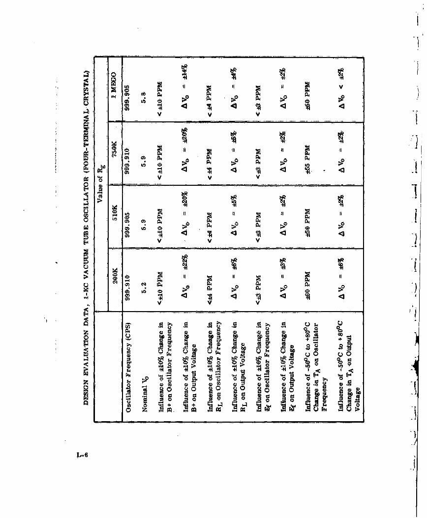
LO P4
05
-VAV
P4 0 4
00
0A Lffi CA
o~g
P4 0~ II - 4
< 0 00 0
rx- --------- 4---
"44
0 -z P-
4 Q4
LC 6

!
Ij APPENDIX M
1KC TWO-STAGE TRANSISTOR OSCILLATOR (T-NED OUTPUT)
In this circuit the amplifier gain, is well in excess of 106. Consequently,there was no difficulty in providing adequate loop gain. In fact, it was necessary to
S severely mismatch the crystal to limit the loop gain suffciently (note the 2 K resistrin the resistive divider feedback network).
1 No difficulty occurred in finalizing the design, Other methods could have beenused to give the necessary selectivity. For example, a Wien Brige network couldhave been used in place of the tuned circuit afd resistance divider network. Further-more, because of the high available power gain, the sacrifice in output power using theWien Bridge would not be unduly large, since the total load resistance could be re-duced appreciably by appropriately increasing the feedback power.
i-KC TWO-STAGE TRANSISTOR OSCILLATOR (TUMED OUTPUT)
Oscillator Designad EvaluationSheet
I Active Element: Tratistor Manufacturer's Type No.: 2N336
Crystal Used Resonant Frequency Resonance Resistance
I T-9J 999. 93 CPS 55 Kilohms
j Description of Oscillator Type
Crystal: SeriesActive element configuration: Common Emiter
i 1Feedback transformer configuration: Resistive Divider
Details of Desin Calculations
The parameters of the 2N336 at le 1 MA as given in the manufacturer'sdata sheets are:
Ie - MA, Vcb 5V
I bib 55 ohms
hb -M99
~M-1

- - I - - 300
SIX SIX I0K 3,3K 0.22 1 10mm 3000
47 4 l- 0147
-- ALL CAPACITORS
COIL 03609NO- I D-O &K 47 sooIV IOAMA
IftaMA
Figure M-1. 1-KC Two-Stage Transistor Oscillator
hrb =700 x 10-6
hob .25 x 10 mhos
giig 4b =714 x lo 6
Transformling common emitter parameters gives, for le 3 MA, Vcb 5 V:
hie 2.2 Kilohms
hre 10
hf e 120
hoe 45 x 10-6 znos
M42

Sitmilarly, for Te 0.4 MA, Vee - V
hie 9.7K
h 1. i
i hfv 57
hoe 12 x 106 mhosThe total load on Q2 is the load resistor (3 K), the load of the feedback net-
work (set at 50 K), and the coil loss resistance (35 K) all in parallel, constituting aload of 2. 6 K. Using the parameters for le = 3 MA and iT = 2. 6 K gives the second
stage gain:
Gp2 15,000
iRin (transistor alane) 1. 9 K
3 The actual. input resistance of the second stage consists of Rin in parallel with 7. 5 K
and 33 K (6. 1 K) giving: Rin (actual) = 1.3 K
This additional input load reduces the total gain of the second stage by a
-' r of _ tranBstor) where R is the total resistance in parallel with RinR + Bin(tasto)
(transistor). Therefore, G'p 2 0.76 x 15,000 = 11,000
ImI Using Rin (actual) as the load of Q1 and the parameters for 'e 0.4 MA gves a first
stage gain: Gp1 - 430
I andBin (transistor) 9.7 K
Combining this with the biasing network (11.6 K) gives:
Rin (actual) = 5.3 K
j andG'pl 230
The total power gain is:
Op -= 1,000 x 230 - 2.5 x 10⁶
M-3

which corresponds -to a loop voltage gain:
G v %5T 1600
For a loop voltage gain of 1.4 (corresponding to a ioop power gain of 2), the voltageattenuation of the feedback network is:
A 1600 11.4
The attenuation ratio of the crystal-transtator input portion of the network is fixed(Bin 5.3 r max 200 K); that is:
Ac 2 0 5 9' 5.3
The attenuation required of the feedback resistive divider is therefore:
i150~Ar = - = 3'0.99
The value of Ar used was nominally 26 (51 K and 2 K).
The coil tuning capacitance required was 0.23 UP.
M-4

TVC1 C
V~~~~~~ ____________________________
U A~ o 0 0q op , O
+ +0 PA 04
zH Z0. 4) 0. 0)rz
z4 (6 -
oo 20 0 0
o M-5

I
I APPENDIX N
3-KC TWO-STAGE TRANSISTOR OSCILLATOR (TUNED OUTPUT)
This circuit is similar to the oscillator evaluated in Appendix M. The soleJ difference is in the tuned circuit elements.
At this frequency the inductor had a Q of 150 which resulted in less loadingthan in the 1 KC design. However, since the loading was already negligible in thelatter designthis had no effect on the calculations. The value of tuning capacitor re-quired was 0.026 UP.
I The comments made concerning the 1 KC oscillator of this type are equalyapplicabile to this oscillator,
i 3KC TWO-STAGE TRANSISTOR OSCILLATOR (TUNED OUTPUT)~IJ Oscillator Desg and Evaluation Sheet
Active Element: Transistor Manufacturer's Type No.: 9N33 6
I Crystal Used Resonant Frequency Resonance Resistance
T-9XY 2999.6 iCPS 50 Kllohmis
Description of Oscillator Type
ICrystal: Series
Active element configuration: Common Emitter
Feedback transformer configuration: Resistive Divider
I
N-i

3000 330
51K 1K lox 33K .0026 lib M4*AV
47-
___ ALL CAPACITORSIN UP I UNLESSOTHERWIE NO.
Figure 1-1. 3-KC Two-Stage Transistor Oscillator
N42

C4'
_ eq
400 0
0 CO
ob
4 eq
o so
FzN4

IAPPENDIX 0
3-KC TUNIED OUTPUT TRANSISTOR OSCILLATOR
" IObjects
The circuits of the two-stage oscillators are rather complex, and the objectof this design was to simplify the oscillator circuit.
Design Details:
Calculation showed that the major design problem would be in obtaining suf-ficient output voltage limiting to prevent crystal overdrive. The major cause of thisproblem was the lower power gain of the single-stage amplifier compared to that ofthe two-stage amplifier. The first method used to limit the output voltage swing wasto bias the transistor for a Vce 2V, thereby limiting the operating voltage range.This alone was inadequate for a value of Rr - 20 K (the assumed minimum value),due to the relatively large energy storage capability of the it network inductor, andit was necessary to limit the positive collector voltage swing with a zener diodeconnected between emitter and collector.
To prevent undue loading of the oscillator by the B+ feed resistor, this resis-tor was connected to the low impedance side of the ir network. The effective load ofthis resistor appearing in parallel with the oscillator load at the collector of the tran-sistor was approximately 220 K, due to the impedance transforming action of the irnetwork. The output power lost in this resistor is therefore less than I0 percent.
I Conclusions:
This oscillator has good operating characteristics as shown in the evaluationdata, the major disadvantage being its low power output capability of 0. 2 MW.
3-KC TUNED OUTPUT TRANSISTOR OSCILLATOR
j Oscillator Design and Evaltution Sheet
Active Element: Transistor Manufacturer's Type No.: 2N336
Crystal Used Resonant Frequency Resonance Resistance
I T-9XY 2999.6 CPS 50 Kilohms
Description of Oscillator Type
I Crystal: SeriesActive element configuration: Common Emitter
I Feedback transformer configuration: P! Network
1 0-1

ALL CAPACITORSIN /.F UNLESSOTHERWISE NOTE
look 13A 0.03 - R
Figure 0-1. 3-KC Single-Stage Tr'ansistor Oscillator
DVetis oqf Design _Calculations
Using the notatti n, and equations of the Final Report, the calculations are sfollows:
For le 1 MA, Vce 5V, the parameters of the 2N336 are:
hie 5.5 x 10³ ohms
hre 1400 x 106
hfe =100'
hoe 24 x 10 - nhos
which, for RT 17 K gives:-
=p 22,00
Rin 3.K
0-2

II
,The total input resistance consists of 3. 8 K and the two 100 K biasing resistorsin parallel; that is, 3.6 K. The biasing network resistance Rb reduces the gain to:
RbRb x Bin 20, 000
J R ma = 200Kan1dRs - " 204K
and therefore:
G' =Gp. - 350
orI °175I 2
aRFB=-X RT 3MEGO
Therefore, the transformation ratio is:
1 RFBTr Bs 15
I The voltage transformation ratio is:
TV 4
3 The coil to be used had L = 110 MH, andr L = 13 ohms at 3 KC, giving.
XL = 2100 ohms
Ignoring loading (justified below):
XLwhr is+-! (1)1
Swhere XC is the reactance of the capacitance in the impedance transforming leg of the
Tr network. Therefore:
f Xc 420 ohms
.0-3

Coimparing XC with Rs in parallel with the 13-K resistor supplying B+ showsthat the phase error will be less than 2 degrees and loading can be ignored. Also r's,the series equivalent of the load, will be approximately 14 ohms.
XLeff XL- XC - 17,00 ohms
| tan- 1 X Left=-_
rL + r's
* i < I degree
Since loading effects are negligible, Equation (1) is justified. Therefore:
C---'h- 0.13UF
The value of the tuning capacitor is given by:
CT = -- ff = 0.031wT c XLeff
Feedback Phase Shift for Rr # Rr min
it is shown previously that for Rr 200 K, the feedback phase shift will
be less than 3 degrees. If this network is then used with a crystal with Rr 20 K
(lowest Rr value likely to occur), this phase shIt may increase. Rs and the 13 K
resistor in parallel gives a total secondary load of 8.5 K. Using the parallel to seriestransforms, C and Rs in parallel transform to:
s 8 1500(I 2 )21 ohms
Xc Xc Q2X'- 1X Xc =420 ohms
- +Q 2 --
XCTherefore . ta - 87 degrees
ta =XL-f tan- 50 > 89 degreesqb-- I - n 1 r ~ , - - -. .. ___g__..
rL +
0-4

Phase error - 180 0 OVo 3 degrees
Maximum crystal dissipation will occur for Rr - 20 K (the asurmed miximumI value), and the permissible output voltage is determined as follows:
For a maximum crystal dissipation of 10 UW, the permissible feedback powerP FB for Rin 3.6 K will be 12 U-W. Therefore, the output voltage of the 7 networkmaust not exceed a value of:
IV 'pB Bx s tin 0.5 3 VRMS
3 andV O ax V x Tv
2.2 VEMS
The load presented to the translator by the 13 K resistor supplying B+ whentransformed throtgh the r network is:
Tr X 13:,000 220K
Therefore, for RT = 17 K, RL ts required to be 19 K.
j A value of 20 K was used for RL.
1I
III
J 0-5

0.
C1 C.)04
00q3
o 44q 00 0eq q
eq0I I IIIIR
CA0 0
vi VI
.o 4) P4);
AN l- - __
iP4 0 0s a~
0
0-6
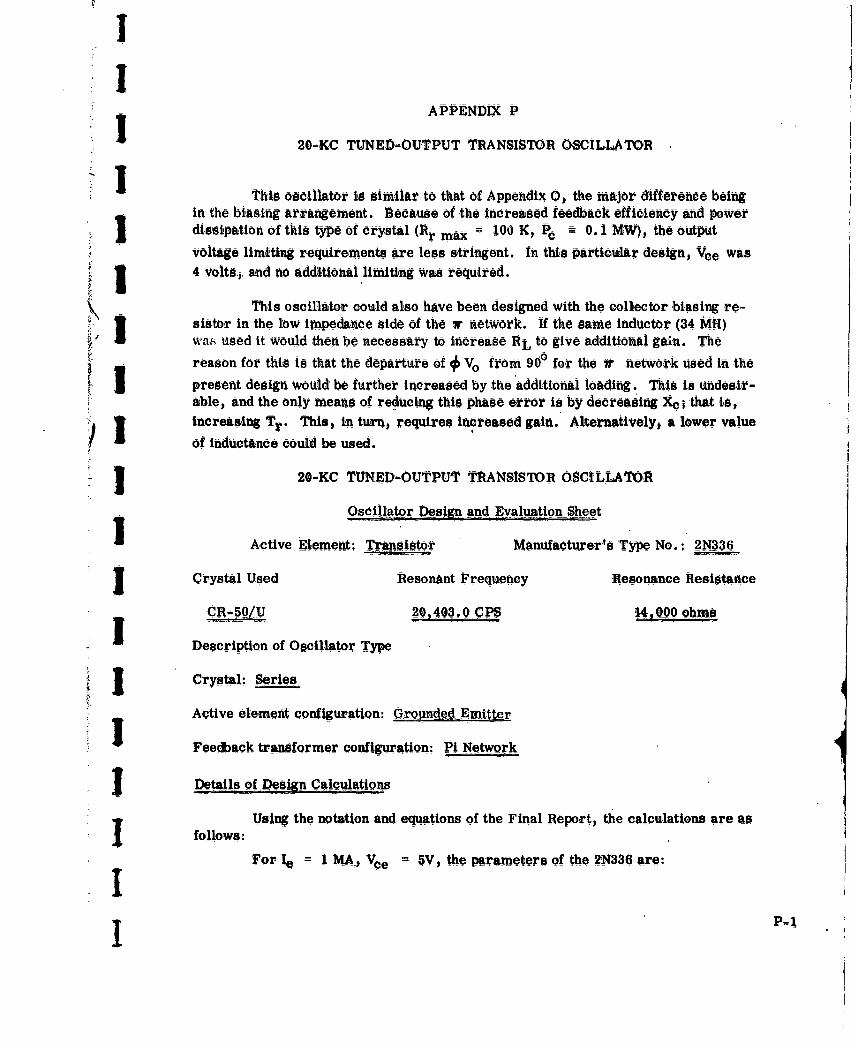
I
APPENDIX P
20-KC TUNED-OUTPUT TRANSISTOR OSCILLATOR
This oscillator is similar to that of Appendix 0, the major difference beingin the biasing arrangement. Because of the increased feedback efficiency and powerdissipation of this type of crystal (Hr max = 100 K, PC 0. i MW), the output
voltage limiting requirements are less stringent. In this particular design, Vce wasj 4 volts, and no additional limiting was required.
This oscillator could also have been designed with the collector biasing re-3 sistor in the low impedance side of the w network. If the same inductor (34 MH)
was used it would then be necessary to increase RL to give additional gain, The
reason for this is that the departure of 0 Vo from 900 for the 7r network used in the
present design would be further increased by the additional loading. This is undesir-able, and the only means of reducing this phase error is by decreasing Xc; that is,increasing Tr. This, in turn, requires increased gain. Alternatively, a lower value
of inductance could be used.
20-KC TUNED-OUTPUT TRANSISTOR OSCILLATOR
O scilator Design and Evaluation Sheet
Active Element: Transistor Manufacturer's Type No.: 2N336
j Crystal Used Resonant Frequency Resonance Resistance
CR-50/U 20403.0 CPS 14,000 Ohms
Description of Oscillator Type
Crystal: Series
Active element configuration: Grounded Emitter
Feedback transformer configuration P! Network
J Details Of Pesign CalcW atons
Using the notation and equations of the Final Report, the calculations are asI follows:
For Ie 1 MA, Vce 5V, the Parameters of the 2N336 are:
IP-

£ A
- 6200
.2eV33K 10K
- S4MH -
I NOTES:
~1~ IN~ UNLESS
25001&pP SSOOp&paP 22 OTHERWISE NOTED
I I E' 1 ~
15K 22 5100 I I- __ -~ -I
Figure P-i. 20-KC Single-Stage Transistor Oscillator
hie 5.5 X io~ ohms
hre = 1400 X 10-6
life = 100 ~.1
hoe = 24 X 10-6 ohms
which, for RT 10K gives:
14,000
= 4.4K
The total input resistance consists of 4.4 K and the two bIasing resistors inparallel; that is, 3.1 K. The biasing network resistance Rb 10 K reduces the gain
to:Rb
K Rb+Rifl 10,700
P-2

~r10x X OandR Il 103 K
Therefore:
5 01 2
Therefore, the transformation ratio is:
Tr Rpg 15
The voltage transformation ratio is:
TV I .
j ~The coil to beused had L = 4H L= ma2.4 KCgiving:
IXL = 43,50 ohms
Ignoring loading (justified below):
XL V 1= 4.9 (1)
I where XC is the reactance of the capacitance in the impedance transforming leg of their network. Therefore:
Xc =8900hmMa
Comparing Xc with Rs shows that the phase error will be less than 1 degree
and loading can be ignored. Also, r's will be approximately 8 ohms.
IX~effXL XC 3 4 6 ohms
=tan~l 88 dgree
P-3

Since loading effects are negligible, Equation (1) Is jiistified.: Therefore:
C - 8800 UU
The value of the tuning capacitor is given bye
CT == 2960UVUFw. XLeff
Feedback Phase Shift for Rr -r min
it is shown previously that for Rr 100 K, the feedback phase shift will be
less than 3 degrees., if this network is then used with a crystal with Hr = 10 K
(lowest Rr value likely to occur), this phase shift may increase. ( S - 13 K4)
Using the parallel-to series transforms, C and He in parallel transform to:
r =61 ohms
X'= Xc
Therefore 1 Vo 86 degrees
t = 89 degrees
Phase error = 5 degrees
Maximum crystal dissipation will occur for Hr 10 K (the asumed minimum
value), and the permissible output voltage is determined as follows:
For a maximum crystal dissipaton of 100 UW, the permissible feedbackpower PFB for Rin = 3. 1 K will be 130 UW. Therefore, the output voltage of the Ir
network must not exceed a value of:
V=IPFB X mmn- 1.3 VRMS
and VO max = V x Tv
= 5.1VRMS
P-4

E-4' E
VA K4
4
C-
- IVI vieq
-I -~ ----- --
0 0) 4) (
"A 0~ 40,18t

IIIt t0a
I u
Oi I i 1
&t c~
t~!. ~1~ VE
II - 45Sp
II I ~ 1d! isf. gig~ X6i a

-~~~~~ -. e q
0-*1i
Vf d Ir I I~~~i
A Ao
il

IJDISTRIBUTION LIST FOR FINAL REPORT AND DESIGN DATA SHEETS
JCONTRACT- A3039ooSC-892-
CONTRACTOR The jenavoxCcmpany DATE 26 November !962.!TO cTs TcCx
OASD (R&E), Room 3E1065 Commander
ATTN: Technical Library Aeronautical Systems Division
The Pentagon ATTN: ASNPVE-2, Mr. E. Borgelt
Washington 25, D.C. 1 Wright-Patterson AFB, Ohio
Commanding Genieral CommanderU.S. Army Electronics Command Aeronautical Systerns Division
ATTN: AMSEL-ED ATTN: ASAPRL
I Fort Monmouth, New Jersey •1 Wright-Patterson AFEB, Ohio
Commanding General Commander
tU.S. Army Electronics Command Roome Air Development Center
ATTN: AMSEL-RD-4 ATTN- RAAID
Fort Monmouth, New Jersey Griffiss AFB, New York
I Director Chief
* U. S. Naval Research Laboratory U.S. Army Security Agenc-y
ATTN: Code 2027 Arlington Hall Station
Washington 25, D. C. Arlington 12, Virginia 2
Commanding Officer & Director Deputy PresidentU.S. Navy Electronics Laboratory U.S. Army Security Agency Board
San Diego 52, California 1 Arlington Hall StationArlington 12, VirginiaI
Chief, Bureau of Ships
ATTN: Code 690B, Mr. R. B. CommanderMcDowell Armed Services Technical Information
Department of the Navy AgencyWashington 25, D.C. ATTN: TIPCR
Arlington Hall Station
Commander Arlington 12, Virginia 10Wright Air Development DivisionATTN: WCLNE, Mr, C. FriendWright-Patterson AFB, Ohio 1
II DIST--
DISTRIBUT1ION LIST (Cont)
SC889
rTO C TO CYS
National B3ureau of Standards ATTN- SELRA/bE1Boulder LaboratoriesATTN: Mr .. George ATTN& SELRAT1Boulder, Colorado1
ATTNe SELIRA/PFj Technical StaffComm ander - rdrReach(Record Copy)1 IAir Force CambrdeRsac
Laboratories ATTN: SELA/TN 3ATTN4: CRXL-RL G. Hanscom Field ATTN: SELRA/PF, Dr. E. A.Bedford, Massachusetts Gerber
Commander ATTN : SE.LRA/PP, Miss M.Air Force Command & Control Develop- Herberg 3
ment DivisionATTN: CRZC A TT N: SELRA/NRC, M r. E.L. G. Hanscom Field Jakubowios1Bedford, Massachusetts
ATTN,- SELRA/SE!, Mr. R. j. LukpasCom mander (Evans Area)1Air Force Command & Control Develop-
ment Division ATTN,: SELRtA/PFP, Mr. S.ATTN: _CCRR and CCSD Schodowski 63L. G. Hanscom Field
Bdford, Massachusetts 2 Com manding fieU.S. Army Elevtronics Material
*AFSC Liaison Officer Support AgencyNaval Air R&D Activities Command ATTN: SELMA/ADJJohnsvdllle, Pennsylvania 1 Fort Monmuouth, New Jersey I
Comanding Officer National Aeronautics & SpaceIU..5 A rmy Electronics R&D Administration
La~rt~y Ooddard Space Flight CenterATTh; SELR/N ATTN: Dr. R. Btapf
For Mnmuth, New Jersey 1 renbelt, aryland1
ATTN: SELRA/LNE1
ATTN: SELRA/LNR1
DIST-2

II1 DISTRIBUTION LIST (Cont)
SC-88892
I TO CYS
' 1 ARF Products, inc. Delco -Radio Division
j 7627 Lake Street General Motors Coiporation
River Forestj Illnois 700 East Firmin Street
j 1ATTN: Mr. A. Przedpelski Kokomo, Indiana
-N Bell Telephone Laboratories, Ino. Electromagnetic Technology Corp.
t Allentown, 1375 California Avenue
£ Pennsylvania Palo Alto, California
ATTN: Mr. Roger A. Sykes ATTN: Mr. William don
5 Bendix Systems Division Frequency Electronics Inc.
Communications Department 2260 46th Street
/ I 3300 Plymouth Road Astoria, New York
Ann Arbor, Michigan ATTN: Mr. Martin Bloch
ATTN. Mr. V. Hutton 1Frontier Electronics Co.
Bliley Electric Company 4600 Memphis Avenue
Union Station Building Cleveland 9, Ohio
Erie, Pennsylvania ATTN- Mr. Patrick LannanATTN: Mr. John Wolfskill
General Dynamics/Pomona
Dr. Virgil E. Bottom Guidance Design Group 252McMurry College Mail Zone 6-65, Box 1011
Abilene, Texas 1 Pomona, Californiai ATTN- Mr. George E. Stanley
SBulova Watch Company
Electronics Division General Electric Co.
61 10 Woodside Avenue Defense Electronics Div.
Woodside 77, New York Syracuse, New York
ATTN: Mr. John L. Denman 1General Electric Co.
Collins Rodio Company Communcations Prods, Dept.
Cedar Rapids, Mountainview Road
Iowa 1 Lynchburg, VirginiaATTN: Mr. John Sherman
Crosley DivisionAVCO Corporation Hoffman Electronics Corp.1329 Arlington Street 3761 S. Hill Street
Cincinnati 25, Ohio 1 Los Angeles 7, California
DIST-3

DISTRIBUTION LIST (Cont)
SC-88892
TO CTYS YS
ITT Laboratories Midland Manufacturing Co.500 Washington Avenue 3156 iberglas RoadNutley, New Jersey 1 Kansas City, Kansas
ITT Laboratories Motorola, nc492 River Road Communications DivisionNutley) New Jersey 1 1450 No. Cicero AvenueATTN- Mr. E. Neugrosohel) Dept. 722 12 Chicago 51, Illinois
ATTN: Mr. P. RichardsonJadlsky & Bailey, Inc.1339 Wisconsin Avenue National CompanyWashington 7, D.C. 1 61 Sherman Street
Malden 48, Massachusetts
Keystone Electronics Co.6'5 Seventh Avenue New Mexico State UniversityNewark) New Jersey Engineering Experiment StationATTN, Mr. James Ronan 1 Las Cruees, New Mexico
ATTN- Mr. William MeSpaddenThe James Knights Co.131 South Wells Street New York UniversittySandwich, Illinois University HeightsATTN- Mr. M. J. Silver 1 New York, New York
ATTN. Mr. Frank Bloom IManson Laboratories, Inc.375 Fairfield Avenue Philco CorporationStamford, Connecticut Government & Industrial GroupATTN- Mr. J. Guttman 1 4700 Wissahickon Avenue
Philadelphia, PennsylvaniaMcCoy Electronics Co.Mount Holly Springs Pioneer-CentralPennsylvania Division of Bendix CorporationATTN- Mr. L. McCoy Davenport, Iowa
ATTN: Dr. D. E. NewellMelpar, Ine.3000 Arlington Blvd,Falls Church, Virginia 1
DIST-4

1.
DISTRIBUTION LIST (Cont)
SC88892
'To10~Y TO CYs
Polartron, Ine Raytheon Company
422 Morris Avenue 1089 Washington StreetLong Branch, New Jersey New Newton, MassachusettsATTN: Mr. H. D. Tan, zman
ReevesHoffman DivisionRadio Corporation of America Cherry & North StreetsFront & Cooper Streets Carlisle, Pennsylvania
I Camd en, New Jersey ATTN: Mr. George SpeaseATTN: Mr. M. Lysobey
Scientific Radio Products, Inc.Strand Engineering Co. 23.03 West 8th StreetBox 76 Loveland, Colorado
T" Ann Arbor, MichiganI. ATTN. Mr. W. Casto Sylvania Electric Corporation
1100 Wehrle Drive
- Systems Incorporated Buffalo', New York2400 Diversified Way ATTN: Mr. E. A. Mooss, Dept. 14Orlando, FloridaATTN: Dr. W. H. Horton Westinghouse Co rporation
Air-Arm DivisionValpey Crystal Company P. 0. Box 7461-244 Highland Street Baltimore 3, Maryland
Holliston, MassachusettsATTN- Mr. T. Valpey
I- Institute of Science and TechnologyThe University of MichiganBox 618Anna Arbor, MichiganATTN: Technical Documents Service 1
0 This contract is supervised by the Solid State and Frequency Control Division,Electronics Components Department, USAELRDL, Fort Monmouth, New Jersey,For further technical information, contact the Project Engineer, Mr. Stanley S.
i " Schodowskl, Telephone 531-2602 (New Jersey Area Code 201).
DIST-5

THE ** COMPANY 0 OVERNME4T AND I.NDUSTRIAL DIVISION