
Phosphatidylinositol 4 Phosphate Regulates Targeting of Clathrin Adaptor AP1 Complexes to the Golgi
Upload
khangminh22Category
view
2download
0
ELECTRICAL ENGINEERING DEPARTMENT
California Polytechnic State University
Senior Project Final Report
AC/DC LED Light Bulb Adaptor with
Internal Rechargeable Batteries
December 1, 2021
Authors
Esteban Rubio
Matthew Delaby
Advisor
Dr. Taufik
2
Table of Contents
List of Figures ………………………………………………………………………………..….. 4
List of Tables .………………………………………………………………………………...…..5
Abstract ……...……………………………………………………………………………………7
Chapter 1 : Introduction …………………………………………………………………………..8
Chapter 2 : Background ………………………………………………………………………....11
Chapter 3 : Design Requirements ……………………………………………………………….15
3.1 Customer Needs Assessment ………………………………………………………..15
3.2 Requirements and Specifications ……………………………………………………15
3.3 Functional Decomposition …………………………………………………………..17
3.3.1 Level 0 Block Diagram ……………………………………………………17
3.3.2 Level 1 Block Diagram ……………………………………………………17
Chapter 4 : Design …………………………………………………………………………....…20
4.1 Component Selection ……………………………………………………………..…20
4.1.1 Switch Selection ………………………………………………………...…20
4.1.2 AC/DC Rectifier Selection ……………………………………………..…21
4.1.3 DC Flyback Controller 1 Selection ……………………………………..…23
4.1.4 DC Flyback Controller 2 Selection ……………………………………..…25
4.1.5 Diode Selection ………………………………………………………....…27
3
4.1.6 Charging Circuit Selection …………………………………………...……29
4.2 Final Circuit Layout ……………………………………………………………....…31
Chapter 5 : Simulation Results and Analysis ……………………………………………………32
5.1 Simulation Tool Selection ……………………………………………………...……32
5.2 Simulation Setup ……………………………………………………………….……32
5.3 Simulation Results and Analysis ……………………………………………………35
5.3.1 120 V AC at 60 Hz to a LED light bulb load without batteries …………..35
5.3.2 120 V AC at 60 Hz to a LED light bulb load with batteries …………...…38
5.3.3 120 V AC at 60 Hz with no load without batteries ……………………….40
5.3.4 120 V AC at 60 Hz with no load with batteries …………………………..41
5.3.5 240 V AC at 60 Hz to a LED light bulb load without batteries …………..42
5.3.6 240 V AC at 60 Hz to a LED light bulb load with batteries ……………...44
5.3.7 240 V AC at 60 Hz with no load without batteries ……………………….46
5.3.8 240 V AC at 60 Hz with no load with batteries …………………………..47
5.3.9 48 V DC to a LED light bulb load without batteries ……………………...48
5.3.10 48 V DC to a LED light bulb load with batteries ………………………..51
5.3.11 48 V DC with no load without batteries ………………………………....53
5.3.12 48 V DC with no load with batteries …………………………………….54
5.3.13 12 V batteries to a LED light bulb load ………………………………….56
5.3.14 12 V batteries with no load ………………………………………………57

4
Chapter 6 : Conclusion …………………………………………………………………………..58
References ……………………………………………………………………………………….61
Appendix A. Analysis of Senior Project Design ………………………………………………..66
Appendix B. Project Timeline …………………………………………………………………..73
Appendix C. Bill of Materials …………………………………………………………………...74
List of Figures
Figure 3‑1: Level 0 block diagram of the unit including all inputs and outputs required. ……...17
Figure 3‑2: Level 1 block diagram including all inputs, outputs,and interconnections ...……….17
Figure 4-1: LTSpice Model of the AC/DC Rectifier Circuit …………………………………....22
Figure 4-2: LTSpice Model of the DC Flyback Controller 1 …………………………………...25
Figure 4-3: LTSpice Model of the DC Flyback Controller 2 ..………………………………….27
Figure 4‑4: LTSpice Model of the Dual Diode OR Gate allowing either the DC Flyback
Controller 1 Output or the AC/DC Rectifier Output to be used at a time ……………………....29
Figure 4‑5: LTSpice Model of the Charging Circuit using the LTM8062A IC with a Battery ....30
Figure 4-6: Final Circuit Design with all modular circuits ……………………………………...31
Figure 5‑1: LED Light bulb model used for the testing of the circuit ………………………….34
Fig 0-1: Summer Quarter Gantt Chart …………………………………………………………..73
Fig 0-2: Fall Quarter Gantt Chart ………………………………………………………………..73

5
List of Tables
Table 3-1: Requirements and Specifications …………………………………………………...15
Table 3-2: Level 0 Block Diagram Breakdown ………………………………………………...17
Table 3-3: Level 1 Block Diagram AC Rectifier Circuit Breakdown ………………………….18
Table 3-4: Level 1 Block Diagram DC Flyback Controller 1 Breakdown ……………………..18
Table 3-5: Level 1 Block Diagram 48-12 V DC Flyback Controller 2 Breakdown …………….18
Table 3-6: Level 1 Block Diagram Diode Breakdown ………………………………………….19
Table 3-7: Level 1 Block Diagram Switch Breakdown ………………………………………....19
Table 3-8: Level 1 Block Diagram Charging Circuit Breakdown ………………………………19
Table 3-9: Level 1 Block Diagram Battery Breakdown ………………………………………...19
Table 5-1: Key Values of various modules in Test Case 1 ……………………………...………37
Table 5-2: Efficiency of the various modules in Test Case 1 …………………………………...38
Table 5-3: Key Values of various modules in Test Case 2 ……………………………...………39
Table 5-4: Efficiency of the various modules in Test Case 2 …………………………...……....40
Table 5-5: Key Values of various modules in Test Case 3 ………………………………...…....40
Table 5-6: Efficiency of the various modules in Test Case 3 …………………………………...41
Table 5-7: Key Values of various modules in Test Case 4 ……………………………………...42
Table 5-8: Efficiency of the various modules in Test Case 4 ………………………...………....42
Table 5-9: Key Values of various modules in Test Case 5 ………………………………...…....44

6
Table 5-10: Efficiency of the various modules in Test Case 5 ……………………...…………..44
Table 5-11: Key Values of various modules in Test Case 6 ……………………...……………..46
Table 5-12: Efficiency of the various modules in Test Case 6 ……………………...…………..46
Table 5-13: Key Values of various modules in Test Case 7 ……………………...……………..47
Table 5-14: Efficiency of the various modules in Test Case 7 ……………………...…………..47
Table 5-15: Key Values of various modules in Test Case 8 ……………………………...……..48
Table 5-16: Efficiency of the various modules in Test Case 8 ……………………...…………..48
Table 5-17: Key Values of various modules in Test Case 9 ……………………...……………..50
Table 5-18: Efficiency of the various modules in Test Case 9 …………………...……………..50
Table 5-19: Key Values of various modules in Test Case 10 …………………………………...51
Table 5-20: Efficiency of the various modules in Test Case 10 ………………………...……....52
Table 5-21: Key Values of various modules in Test Case 11 ………………………...………....54
Table 5-22: Efficiency of the various modules in Test Case 11 ………………………………...54
Table 5-23: Key Values of various modules in Test Case 12 ……………………………….......55
Table 5-24: Efficiency of the various modules in Test Case 12 …………………………….......55
Table 5-25: Key Values of various modules in Test Case 13 ……………………………...……56
Table 5-26: Efficiency of the various modules in Test Case 13 …………………………….......57
Table 5-27: Key Values of various modules in Test Case 14 ……………………………...…....57
Table 0-1 Bill of Materials per Module …………………………………………………………74

7
Abstract
To make a sustainable product and provide a temporary source of lights on during
emergencies, this project aims to create a small unit that can be attached to a light bulb of any
variety and connect it to a socket. Within the device is a rechargeable battery that, when the
device is not connected to an 120V AC, 240V AC, or 48V DC power source, will power the light
for a short period of time. The battery can be charged during the standard operation of the device
and can be powered by the US and EU standard outlet voltages as well as the outlet voltage of 48
V DC from the DC House Project. This device should not impede normal operation of the light
bulb and require little to no modifications of the housing unit for the light bulb. The device,
under normal operations, outputs enough power to supply the 12 V DC LED light bulb for full
output from the device. All the sources, 120 V AC, 240 V AC, 48 V DC, and 12 V DC allow for
full functionality albeit at a low efficiency rating that could be improved. For no load scenarios,
the device still dissipates a notable amount of power and is less efficient than the loaded sources
but some of the issue is eased with the inclusion of batteries if no load is present. Although the
device may not be the most effective or efficient, when under the right conditions, it fulfills the
goals.

8
Chapter 1: Introduction
According to the United States Energy Information Administration, in 2016 the United
States had more power outages than any other developed countries [1]. A study by Climate
Central using data from the North American Electric Reliability Corporation shows that power
outages in the United States have increased 66% in the past ten years when compared to the prior
ten years of 2000 to 2009 [2]. Although most of the outages in the United States are caused by
weather related incidents [2], power outages are not exclusive to the US. In 2021 over 200
million people in Pakistan lost power due to poor grid management, while 13% of the world does
not have access to electricity at all [3]. Fixing the cause of these power outages is not an easy
task, but there is clearly a demand for products that can help combat these energy losses.
This project encompasses two major ideas that are prevalent in society at large, those
being power electronics and energy storage. The first of the two, power electronics deals with the
processing of electrical power as an input into an electrical device to get a controlled and
conditional output [4]. Simply put, this means that if a device is given a raw input signal, the
device will use some sort of circuit, feedback loop, or separate signal to change or adjust the
signal such that the output is adjusted in some way. Those adjustments can be an increase or
decrease in magnitude, a change in frequency, inversion from DC-AC, or a combination of one
of those or many more. This field of study is key for the allowance of society as a whole to
function as it does today. For example, powerlines make use of this technology as they move the
power cross country. The towers and transformers attached switch power from high voltage to
extremely high voltages, from several thousands of volts to hundreds of thousands of volts, and
then back down again such that power is accessible anywhere it is needed while not losing too

9
much of it during the transitional phases. As time moves forward, so does this technology with
large advancements in the field of power semiconductor devices, frequency drivers, and complex
power control and protection systems that could all improve electronics in several ways [5][6].
The other major field that this project relies on is the field of energy storage or saving
energy in some sort of medium for later redistribution or use. Currently there are many media
used for the purpose of storing energy such as compressed air storage, super-capacitors, molten
salts or other thermal storage materials, flywheels, or what is relevant to this project: batteries
[7]. There are so many different types of batteries that are each advancing in different ways.
Lead Acid batteries are often used in Electric vehicles exploring large advancements in quick
charging capabilities while Lithium-ion batteries are often used in personal electronics,
developing better energy density as well as longer life cycle [8]. These two examples as well as
the plethora of additional advancements help to make more renewable energy sources such as
wind or solar more viable sources of power. Oftentimes these green sources have a limited
operational time but energy storage such as batteries will help to store the excess energy
generated from these sources to then release them when the source can no longer produce. In
turn the batteries will decrease the need for fuels such as natural gas or coal to be used to provide
the marginal electricity.
This project aims to provide customers with a backup battery for their individual light
bulbs. It will accept either AC voltage ranging from 120 to 240 Volts AC rms [9][10] or a DC
voltage of 48 Volts [11]. The input will be decided between AC or DC via a switch on the
device. The product will power a 12 Volt DC LED bulb when a button is pressed to activate it
during an instance when a facility loses power. The product will also be portable so when

10
removed from a standard E26 light socket [12], the device will also meet all safety requirements
for commercial and consumer use [13][14][15] that apply to the device.
The following report will be organized as follows. After the title page, a clear and precise
table of content and list of figures will be added such that any read may quickly locate specific
aspects and pages if desired. Following the directory and the abstract, the introduction provides
the reader a base understanding of the project and the means of which it is to be completed. The
methodology of the report includes all the steps taken to plan out the project so far and include
but will not be limited to customer needs, requirements and specifications, functional block
diagrams and breakdowns, a tentative project schedule, and a material and labor cost estimate.
Upon development and completion of the project, sections for the results, discussions, and
conclusion will be added. Before the report finishes, an appendix has been added answering
several concerns and questions regarding various topics such as the IEEE code of ethics [16]]17].
The report will end with a citation of all references that were used and sited within the entirety of
the report.

11
Chapter 2: Background
While the current number of people without power is around 13% or 940 million people
[3], there is a problem with how the legacy AC transmission system works in the distribution of
power. Due to the centralized approach in generating and delivering the power, it requires a large
scale of infrastructure to put the system into effect. One method to improve the current power
system is by making the network decentralized. This way the system works on smaller scales and
allows for individual households to provide themselves with power. A project that has been
conducted at Cal Poly to develop a solution to achieve this is called the DC House project. The
project aims to take one source or several renewable sources that provide DC voltage as well as a
centralized battery system and redistribute it for the rest of the house [19][34]. The DC project
started in 2011 and has continued to be developed, analyzed, and improved. This senior project
seeks to combine several ideas from various projects and papers from this system and make a
product that is applicable both for DC houses as well as regular AC houses that use 110VAC to
240VAC [31]-[33].
Several of the previous DC House projects either have similar subject matters or relate
rather closely to this senior project; however, this project is slightly broader as the design will
accept an AC input as well. A thesis project described in [20] worked on designing a DC light
bulb that has several key features that would be ideal for this project such as having the ability of
a dimming functionality, the ability to run off a 48VDC bus powered by renewable sources, and
the use with a standard light socket (A19 and E26) such that no specialized equipment is needed.
The thesis paper goes into detail on the construction and part section that was required and how
the device functions. The resulting product is great but over exceeds and lacks some of the

12
features we are looking to implement. The voltage range of 33 VDC to 63 VDC exceeds the DC
voltage input of 48 V that would be supplied but still allows for a range of working conditions if
the voltage being provided fluctuates. Two features it does lack are a battery pack and a potential
for an AC input signal. The battery pack will allow for the device to be recharged and used in a
way that the light can be fully operational at maximum or near maximum lighting output for a
length of time that will allow for any users to ensure their surroundings are safe if in a blackout.
For the battery pack, look towards the thesis paper [21] in which they developed a battery pack
and charging mechanism that uses the same 48VDC provided by the bus to recharge the pack.
This paper also developed a LED driver circuit that helps to fix the issue of DC light bulbs
dimming unintentionally when not powered by a constant 48 VDC source. The device being
developed for this project should be able to take AC input signals of 120 VAC as well as 240
VAC that should be stepped down and converted to 48 VDC through a separate circuit from the
driving circuit. The device should also be able to switch between AC and DC sources using a
rock switch to allow for the user to potentially plug the device into a standard socket and not
require a 48 VDC bus.
A critical part of the two aforementioned master’s theses was a buck converter, an
electrical component that takes one voltage and drops it to a lower voltage that can be adjusted
by using various setups of resistors, capacitors, and other components. These converters were a
key component in taking a 48 VDC signal provided by the bus and converting it down to a 5
VDC signal in the first and second thesis papers as well as a 1.2 VDC signal in the second paper.
In both of these papers they use an integrated circuit referred to as a linear regular chip
specifically the LT3014, a low dropout micropower linear regulator, as the component that can
be adjusted to take the higher DC voltage and drop it down to a workable level while keeping the

13
power usage low and the waste heat low as well. According to both the papers as well as the
datasheets [22], this component takes a wide range of DC inputs, from 3V - 80V DC, while
outputting a range of voltages determined by 2 resistors and outputting a steady current of 20mA
of current no matter what the input. The same datasheet lists two common applications that could
apply to this project, those being low current high voltage regulators and battery-powered system
regulators. The second of these applications is going to be important for the charging phase of
the battery packs within the project. The regulators will help to limit the voltage that is put across
the batteries as a protection. If the voltage is too large across these batteries, they can be
irreparably damaged and can lead to further damage in the rest of the system as well as creating
excess heat and fire risks. The first common application, low current high voltage regulators will
come into play as it did in the thesis papers, when in it was used to take the high 48 VDC input
and adjust or lower it so that the same source can be used to drive several other important ICs
within the devices that were needed in order to drive the LEDs as well as the dimming circuits.
However, this device may be extremely inefficient as it is taking such a large voltage 48V DC as
low as 5 V. The efficiency can be improved by increasing the operating output voltages of the
various converters that are needed; however, both of the output voltages and currents must be the
same or similar such that the LED would be receiving the same input no matter what source is
selected and if a battery is to be included, the converter output voltage would need to match the
battery capacity which at 12V or 24V could drastically increase the size of the project beyond the
size and weight limitations.
Moreover, another potential challenge with the project is the multiple inputs that are
driving a singular load or output. There are several solutions, with one such option being a
MISO, or Multiple Input Single Output, circuit design such as the one seen and designed in the

14
senior project presented in [23]. The referenced design is for a different purpose, but shows the
basic idea of taking several inputs, using MOSFETs to limit and control the voltage that is being
supplied from the various sources. The system, as described in the paper, allows for some
voltage variation in the sources and accounts for some of the variation and limits the impact that
it will have on the output of the system. For the project, the system above is a bit overly complex
and could lead to a longer development time and excess power loss. Since the project is limited
to two sources that can be switched on and off, a much simpler diode OR logic systems should
work [24]. The diode logic should allow for a simple 2 component circuit to allow for one source
to provide the power to drive the LED light bulb while the other source is tied to ground and
won’t provide power to the system. The diode selection must be able to allow the determined
voltage to cross with a high enough reverse current protections to protect the second source and
its transforming circuit while also having a forward current that is large enough to handle the
larger current between the two sources, but this will be further discussed and elaborated on in
Chapter 4 which refers to component selection.

15
Chapter 3: Design Requirements
3.1 Customer Needs Assessment
This project targets customers in need of insurance that their lights will remain
operational during a power outage, or to people in third world countries operating their lights
directly off solar panels. The operation time is such that the users have time to find things or
people that would be helpful to last in a larger term outage before they lose complete access to
light. The unit will operate on an AC input ranging from 120-240 V to be marketable in both the
United States and European countries, and with the flip of a switch, the product will also be able
to input a DC voltage from solar panels or other sustainable sources of 48 V and operate a 12 V
standard light bulb. The switching between AC and DC sources should be simple enough such
that any person is able to do so without instructions. Ideally the device will be non-intrusive and
will be easy to install into an already operational light source, removing the light from the
preexisting socket and installing the device and then reinstalling the light into the device. The
installation of the device should also require little to no alterations to the unit housing the light so
that it will be marketable to consumers that already have structures in place and want the device
just for emergency situations.
3.2 Requirements and Specifications
Table 3-1. Requirements and Specifications
Marketing
Requirements
Engineering
Specifications Justification

16
1 Nominal Input AC Voltage
.Ranging from 110 V - 240 V
.(50-60Hz)
The product needs to be operational in
.multiple countries with utility companies.
1 Nominal Input DC Voltage of
.48V +/- 5%
The product needs to be operational in third
.world countries or else powered by solar or
.renewable resources that generate their own
.electricity.
2 Output voltage of 12 V DC Product needs to meet what is considered the
.standard of DC voltage to operate on the
.maximum amount of light bulbs.
3 Unit will be compatible with a
.standard E26 socket base
The product needs to be compatible with as
/many lights sockets out there as possible.
3 Unit will have a simple switch
.to choose between 120V AC
.and 48V DC input
The product must be easy to use and
.compatible in different countries.
4 Unit will cost less than 215
.dollars to manufacture
The product needs to be advertised to people
.who would want to send it to developing
.locations and be able to compete with similar
.designs on the market.
5 Unit will be within 4” x 2.5” x
.2.5” case
The product should not require any
.construction or adjustment of current light
.bulb sockets to be in use.
5 Unit should be less than 2
.pounds
The product should not be heavy enough to
.need support when installed into a system.
2,3 Unit will be able to operate in
.temperatures below 70℃ or
.158० F [X]
With the high voltages that the current is
.intaking, it is important that the Unit can
.withstand some heat generated by the voltage
.to keep the consumers safe.
Marketing Requirements
1. Variety of Inputs
2. Works with the majority of bulbs
3. Easy to install and use
4. Low Cost
5. Small and Lightweight

17
3.3 Functional Decomposition
3.3.1 Level 0 Block Diagram
Fig. 3-1. Level 0 block diagram of the unit including all inputs and outputs required.
Table 3-2. Level 0 Block Diagram Breakdown
Module DC/AC LED Lightbulb Adaptor Unit
Input 48 V DC
.120-240 V AC
Switch (User Input in the form of Power Source Selection)
Output 12 V DC
Function The module will take in renewable energy bus 48 V DC, US standard
.120 V AC, or EU 240 V AC and a user defined input to output a 12 V
.DC signal to power a light source.
3.3.2 Level 1 Block Diagram
Fig. 3-2. Level 1 block diagram including all inputs, outputs, and interconnections

18
Table 3-3. Level 1 Block Diagram AC Rectifier Circuit Breakdown
Module AC Rectifier
Input 120-240 V AC
Output .156-168 V DC for 120V AC, 292-319 V DC for 240V AC
Function The Converter converts the 120 V AC or the 240 V AC to a DC that
.will be fed into a flyback controller to further decrease the voltage
.such that it can run the LED light bulb.
Table 3-4. Level 1 Block Diagram DC Flyback Controller 1 Breakdown
Module DC Flyback Controller (48-12)
Input 156-168 V DC for 120V AC, 292-319 V DC for 240V AC
Output 12 V DC
Function This converter will take in the higher DC voltages from the Ac
.rectifier circuit and step it down to 12 V DC.
Table 3-5. Level 1 Block Diagram 48-12 V DC Flyback Controller 2 Breakdown
Module DC Flyback Controller (48-12)
Input 48 V DC
Output 12 V DC
Function This converter will take in the 48V DC voltage from a standard solar
,bank and step it down to 12 V DC.
19
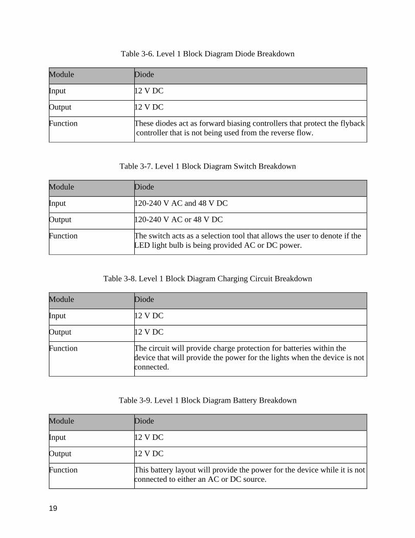
Table 3-6. Level 1 Block Diagram Diode Breakdown
Module Diode
Input 12 V DC
Output 12 V DC
Function These diodes act as forward biasing controllers that protect the flyback
. controller that is not being used from the reverse flow.
Table 3-7. Level 1 Block Diagram Switch Breakdown
Module Diode
Input 120-240 V AC and 48 V DC
Output 120-240 V AC or 48 V DC
Function The switch acts as a selection tool that allows the user to denote if the
,LED light bulb is being provided AC or DC power.
Table 3-8. Level 1 Block Diagram Charging Circuit Breakdown
Module Diode
Input 12 V DC
Output 12 V DC
Function The circuit will provide charge protection for batteries within the
,device that will provide the power for the lights when the device is not
,connected.
Table 3-9. Level 1 Block Diagram Battery Breakdown
Module Diode
Input 12 V DC
Output 12 V DC
Function This battery layout will provide the power for the device while it is not
,connected to either an AC or DC source.
20
Chapter 4: Circuit Design 4.1 Component Selection
For the design of the project on the next level, the component level, several factors were
needed for determining the correct components. For instance, there is a small amount of space in
which to fit all of the components needed such that the device is small and easy to install as
listed in Chapter 3. This means that surface mounted IC’s and a limited number of individual
components would be preferable. But that limited space means that excess power loss in the form
of heat is also a big factor as one component or IC overheating could heat other components as
well as the failure and damage to the component that is inherent in overheating. However, there
is the cost limit and some very specific goals to meet as of the customers' requirements.
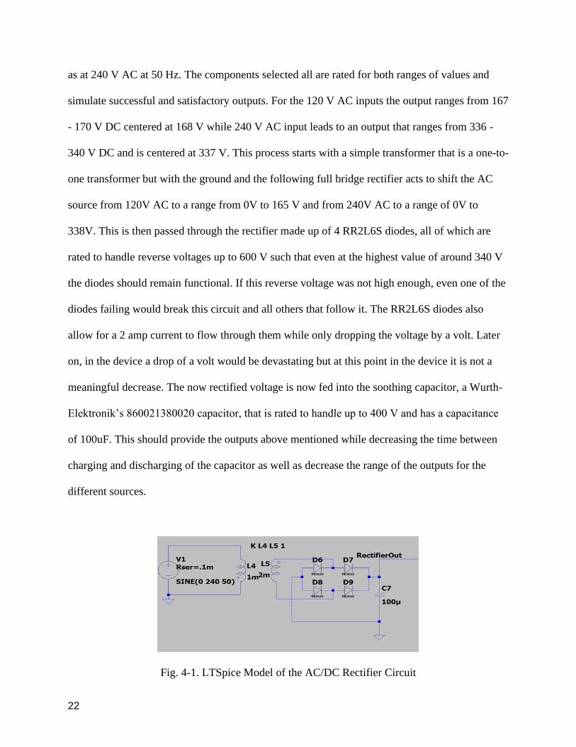
4.1.1 Switch Selection
With all of that said, this switch is key to selecting which form of power the device is
connected to and if connected improperly could damage the device. This will allow the user to
specify which source of power is being used, 120V or 240 V AC or the 48V DC. For the switch
the device is using the TWTADE Latching Polarity Reverse Switch off of amazon as it is rated
to be able to withstand both of the extreme voltages with ease as well as the much lower dc
voltage as well. The caveat being that the 48 volts must first be dropped to a lower voltage using
a flyback controller. This switch works in the toggle format meaning that the device has a ON-
OFF-ON configuration, with the different settings being used for 120V AC or 240V AC on one
of the ON states while the 48V DC will be on the other ON state leaving the OFF state being
used as a ground or off state. The switch is rather large, but the device casing should be large
enough to house this component along with all the other necessary pieces to be discussed. The

21
cost of $6.99 is rather high as well for a prototype, but if manufacturing were to be on a larger
scale, the price per component would hopefully be negotiable with the manufacturer.
4.1.2 AC/DC Rectifier Selection
The next important component to be chosen is the AC/DC rectifier. This rectifier is one
of our own designs but follows a fairly simple design mechanic. The AC sources will be filtered
through a bridge rectifier that will make all of the voltage positive, keeping the current flow in
one direction. The capacitor at the output helps to smooth out the rippling voltage that the
rectifier generates. By increasing the value of the capacitor, the dc output can be further honed
such that the possible range of output values becomes a tighter group which will be helpful in
choosing the next component, the Flyback controller 1. With a more defined range of inputs, the
device should be put under less stress than if fed a more widely fluctuating set of values. The
inclusion of a transformer in the bridge rectifying circuit is a means to help improve the
efficiency of the device as well as being less bulky and more cost effective than a center tapped
transformer. For example, a center tapped transformer can cost as much as $20 dollars with a
size of 1.5” x 2” which if fit into the device could take up most if not all of the available space.
And with two of these potentially needed, it was decided to go with a non-center tapped
transformer for potential space concerns.
It was also important that the rectifying circuit could handle both the possible AC values
for inputs. If not there would need to be two versions of this circuit and the next included in the
same device and that would require a much more complicated overall product design and as well
as a reselection of both the switch as well as potentially of the flyback controller 1 which would
be used. Thankfully the design shown in Fig. 4-1 functions for both 120 V AC at 60 Hz as well
22
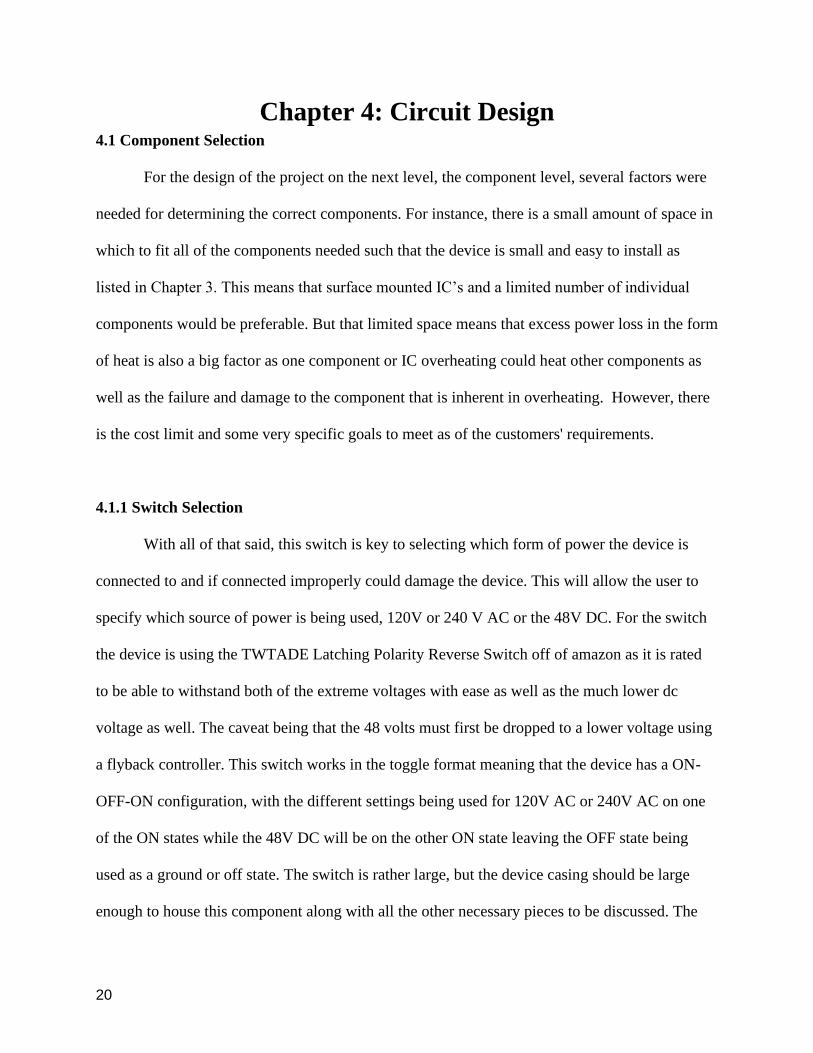
as at 240 V AC at 50 Hz. The components selected all are rated for both ranges of values and
simulate successful and satisfactory outputs. For the 120 V AC inputs the output ranges from 167
- 170 V DC centered at 168 V while 240 V AC input leads to an output that ranges from 336 -
340 V DC and is centered at 337 V. This process starts with a simple transformer that is a one-to-
one transformer but with the ground and the following full bridge rectifier acts to shift the AC
source from 120V AC to a range from 0V to 165 V and from 240V AC to a range of 0V to
338V. This is then passed through the rectifier made up of 4 RR2L6S diodes, all of which are
rated to handle reverse voltages up to 600 V such that even at the highest value of around 340 V
the diodes should remain functional. If this reverse voltage was not high enough, even one of the
diodes failing would break this circuit and all others that follow it. The RR2L6S diodes also
allow for a 2 amp current to flow through them while only dropping the voltage by a volt. Later
on, in the device a drop of a volt would be devastating but at this point in the device it is not a
meaningful decrease. The now rectified voltage is now fed into the soothing capacitor, a Wurth-
Elektronik’s 860021380020 capacitor, that is rated to handle up to 400 V and has a capacitance
of 100uF. This should provide the outputs above mentioned while decreasing the time between
charging and discharging of the capacitor as well as decrease the range of the outputs for the
different sources.
Fig. 4-1. LTSpice Model of the AC/DC Rectifier Circuit
23
4.1.3 DC Flyback Controller 1 Selection
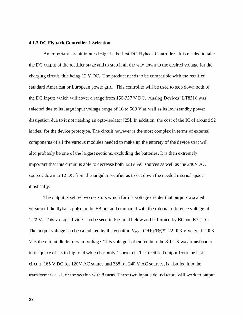
An important circuit in our design is the first DC Flyback Controller. It is needed to take
the DC output of the rectifier stage and to step it all the way down to the desired voltage for the
charging circuit, this being 12 V DC. The product needs to be compatible with the rectified
standard American or European power grid. This controller will be used to step down both of
the DC inputs which will cover a range from 156-337 V DC. Analog Devices’ LT8316 was
selected due to its large input voltage range of 16 to 560 V as well as its low standby power
dissipation due to it not needing an opto-isolator [25]. In addition, the cost of the IC of around $2
is ideal for the device prototype. The circuit however is the most complex in terms of external
components of all the various modules needed to make up the entirety of the device so it will
also probably be one of the largest sections, excluding the batteries. It is then extremely
important that this circuit is able to decrease both 120V AC sources as well as the 240V AC
sources down to 12 DC from the singular rectifier as to cut down the needed internal space
drastically.
The output is set by two resistors which form a voltage divider that outputs a scaled
version of the flyback pulse to the FB pin and compared with the internal reference voltage of
1.22 V. This voltage divider can be seen in Figure 4 below and is formed by R6 and R7 [25].
The output voltage can be calculated by the equation Vout= (1+R6/R7)*1.22- 0.3 V where the 0.3
V is the output diode forward voltage. This voltage is then fed into the 8:1:1 3-way transformer
in the place of L3 in Figure 4 which has only 1 turn to it. The rectified output from the last
circuit, 165 V DC for 120V AC source and 338 for 240 V AC sources, is also fed into the
transformer at L1, or the section with 8 turns. These two input side inductors will work to output

24
the voltage across L3 to L2 making both of those values 13 V for both possible sources. The
average continuous drain current of the STW11nm80 N-Channel MOSFET is given to be up to
11 A, and the maximum switch voltage ratings of this MOSFET are 200V for the drain to source
voltage along with a positive or negative voltage value of 20 for the gate to source voltage. The
selected output diode that soothes the voltage, the RB238T150, also allows a wide range of
possible output currents to flow through it, including the desired 2A, and has a reverse voltage of
150V while only decreasing the voltage that flows through it to about 12.5 V DC since the
forward voltage is 0.65 V. The high reverse voltage, along with that of the diodes further in the
design will help to protect this section in the case of component failures. That then charges up
the output capacitor, an 860040675011 capacitor developed by Wurth Elektronik, which was
chosen to provide an output as close to 12 V DC as possible while also being rated to handle
enough voltage in excess as an extra precaution against unseen errors or miscalculations. In both
areas the 470 µF capacitor exceeds, outputting roughly 12.55 V DC for both possible AC sources
while being rated for 50V.

25
Fig. 4-2. LTSpice Model of the DC Flyback Controller 1
4.1.4 Flyback Controller 2 Selection
A different component is needed to take the DC input and step it down to the correct
level as well as limit the current from the source to one that the rest of the design will require. If
this product is to be used in the DC house Project, we can expect a common bus voltage to be
around 48 V DC with the house's power distribution being most efficient in the voltage range of
around 38 V DC to about 50 V DC [26]. Keeping this in mind with the other limitations and
desired outputs, Analog Devices’ LT3748 simple flyback controller was selected. This converter
allows for a broad range of DC inputs, which includes the most efficient range of outputs from
the DC house, to act as a source for the component while outputting the desired 12 V DC and 2
A with ease. The price tag of $3.79 for a single component is a bit high for a single device if the
final product wants to be sold at a reasonable price, but for a single unit for the prototype the cost

26
is acceptable for the $215 prototype cost limit. With greater production the overall price of this
component and all additional components will decrease. This integrated circuit also comes with a
high operating temperature, simple Vout controls, and the possibility for a programmable
undervoltage lockout.
The next step with this part selected is to calculate the additional component values
needed to get the desired outputs. The output voltage is programmed using external resistors seen
below in Figure 5 as R2 and R3 and the equation Vout = VBG(RFB/RREF)(1/NPS) - VF where VBG is
a reference voltage used by the error amplifier with a value of 1.223 V. The voltage is then
passed through the, which has a turns ratio of 4 with a 48 V input and an AC output of 15 V. VF
refers to the forward voltage of the output diode and the 30BQ060 has a given forward voltage of
500 mV. This 500 mV is the maximum voltage drop though and is only applied when the current
is running at 3 A. The product will not run at that high of a current though and using the Max
Forward Voltage Drop Characteristics figure in the datasheet [28] it can be expected to be
around 400mV instead. Applying this voltage drop to the above equation used to program the
output voltage it can be seen that the output voltage of the controller would be very close to 12
volts. An additional important component for the flyback controller is the MOSFET. The
average continuous drain current of the Si4490DY N-Channel MOSFET is given to be up to 4 A,
but our current will be lower than that so the drain current can be seen to be closer to 3.8. The
maximum switch voltage rating of this MOSFET is 200V, for the drain to source voltage, and a
positive or negative value of 20 volts for the gate to source voltage.
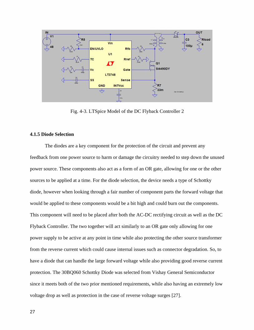
27
Fig. 4-3. LTSpice Model of the DC Flyback Controller 2
4.1.5 Diode Selection
The diodes are a key component for the protection of the circuit and prevent any
feedback from one power source to harm or damage the circuitry needed to step down the unused
power source. These components also act as a form of an OR gate, allowing for one or the other
sources to be applied at a time. For the diode selection, the device needs a type of Schottky
diode, however when looking through a fair number of component parts the forward voltage that
would be applied to these components would be a bit high and could burn out the components.
This component will need to be placed after both the AC-DC rectifying circuit as well as the DC
Flyback Controller. The two together will act similarly to an OR gate only allowing for one
power supply to be active at any point in time while also protecting the other source transformer
from the reverse current which could cause internal issues such as connector degradation. So, to
have a diode that can handle the large forward voltage while also providing good reverse current
protection. The 30BQ060 Schottky Diode was selected from Vishay General Semiconductor
since it meets both of the two prior mentioned requirements, while also having an extremely low
voltage drop as well as protection in the case of reverse voltage surges [27].

28
A few downsides for the use of this component are the cost of the component as well as
the rating of the component as obsolete according to digikey. In regard to the former, the cost of
one of these is a bit more than many other standard Schottky diodes. With the average single
component cost of around $0.64, the price of $1.27 is almost double the regular price but it is
still easily within the budget. Since there will be no need for any additional circuit components,
the device would need at least four of these devices for this section of the project, with the total
cost of both components being $ 5.08 plus shipping and handling. Furthermore, if produced in
mass the price would fall even lower and the price could even drop below a dollar a component.
The latter of the two issues, that the device has been labeled by some as obsolete, is an issue of
practicality and desired function. When searching for other potential Schottky diodes a main
feature that was observed was the forward voltage drop. Using a 2 A average rectified current,
which is the desired current output from the flyback controller and rectifier mentioned above, a
forward voltage drop was observed and noted in many if not most of the more modern parts, the
voltage drop could get as high as 1.5 volts. With the voltage from the two transformers set to be
12 V DC, a voltage drop larger than 500 mV would be too great of a loss for the rest of the
device to function properly. The 30BQ060 has a 500mV drop, but that is when the current is
running at 3 A. Using the Max Forward Voltage Drop Characteristic figure in the datasheet [28],
it can be observed that at the optimal current of 2 A the forward voltage drop should be no larger
than 400 mV or 0.4 V which should allow for the further aspects of the device to function at full
capacity. In addition to the lower forward voltage drop the IC has a max reverse voltage of 60 V
so even if one of the diodes fails, the other diode should remain functional.
29
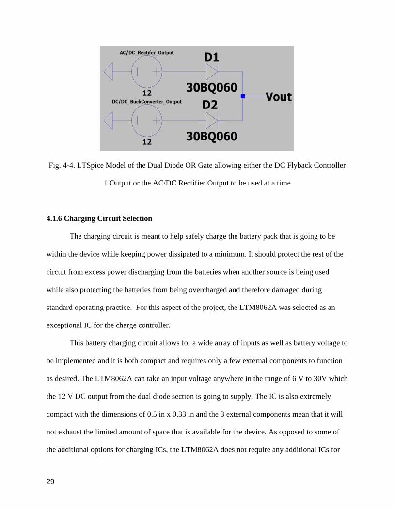
Fig. 4-4. LTSpice Model of the Dual Diode OR Gate allowing either the DC Flyback Controller
1 Output or the AC/DC Rectifier Output to be used at a time
4.1.6 Charging Circuit Selection
The charging circuit is meant to help safely charge the battery pack that is going to be
within the device while keeping power dissipated to a minimum. It should protect the rest of the
circuit from excess power discharging from the batteries when another source is being used
while also protecting the batteries from being overcharged and therefore damaged during
standard operating practice. For this aspect of the project, the LTM8062A was selected as an
exceptional IC for the charge controller.
This battery charging circuit allows for a wide array of inputs as well as battery voltage to
be implemented and it is both compact and requires only a few external components to function
as desired. The LTM8062A can take an input voltage anywhere in the range of 6 V to 30V which
the 12 V DC output from the dual diode section is going to supply. The IC is also extremely
compact with the dimensions of 0.5 in x 0.33 in and the 3 external components mean that it will
not exhaust the limited amount of space that is available for the device. As opposed to some of
the additional options for charging ICs, the LTM8062A does not require any additional ICs for
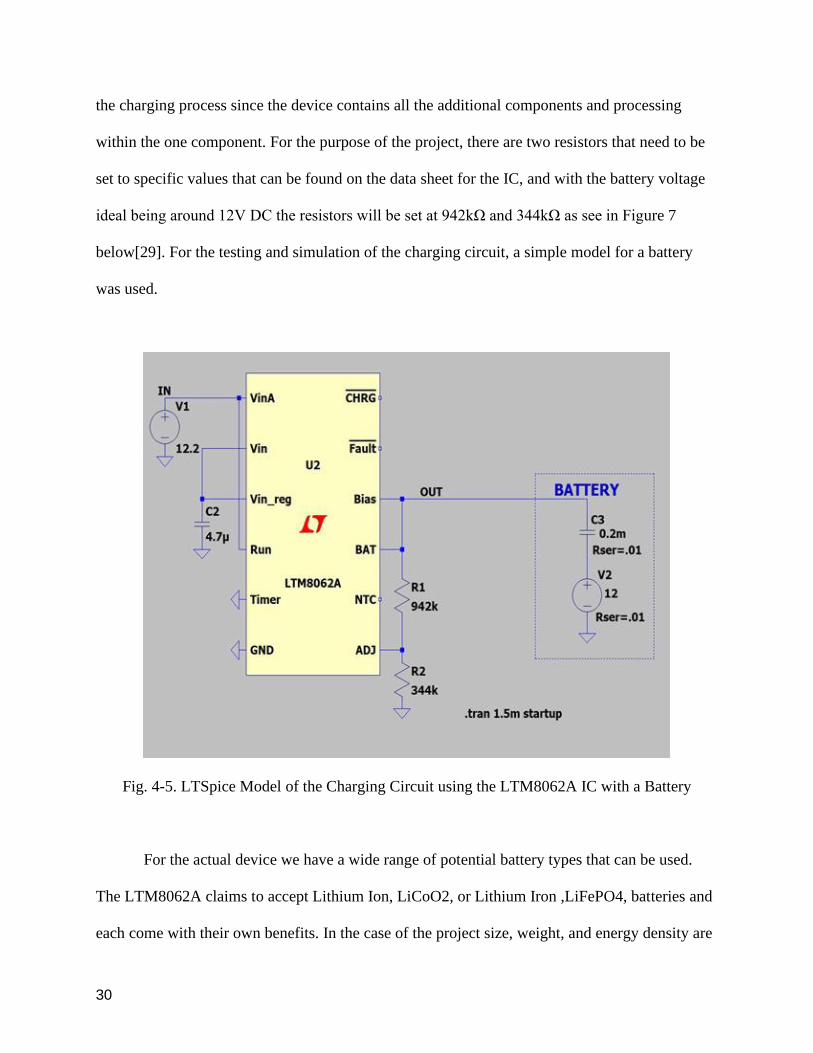
30
the charging process since the device contains all the additional components and processing
within the one component. For the purpose of the project, there are two resistors that need to be
set to specific values that can be found on the data sheet for the IC, and with the battery voltage
ideal being around 12V DC the resistors will be set at 942kΩ and 344kΩ as see in Figure 7
below[29]. For the testing and simulation of the charging circuit, a simple model for a battery
was used.
Fig. 4-5. LTSpice Model of the Charging Circuit using the LTM8062A IC with a Battery
For the actual device we have a wide range of potential battery types that can be used.
The LTM8062A claims to accept Lithium Ion, LiCoO2, or Lithium Iron ,LiFePO4, batteries and
each come with their own benefits. In the case of the project size, weight, and energy density are
31
all important factors and the Lithium-ion batteries are slightly more preferable in this case[30].
The CR2023 also is rechargeable with a voltage of 3 V per battery meaning that to make up the
12V needed, four of the batteries will be placed in series. The size of the CR2023 batteries is a
good fit for the device since their coin shape will allow for the batteries to be stacked and held
within the device with relative ease. One consideration is that the diameter of these small
batteries is about an inch, however with the standard E26 adaptor socket being around an inch as
well the devices width should be able to have excess space to allow for the loading of the
batteries.
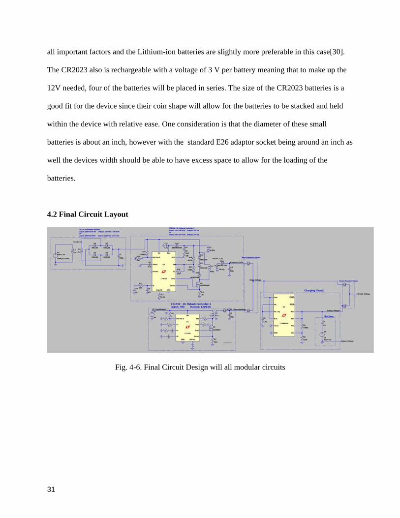
4.2 Final Circuit Layout
Fig. 4-6. Final Circuit Design will all modular circuits

32
Chapter 5: Simulation Results and Analysis
5.1 Simulation Tool Selection
For this project, there were a variety of simulation tools that were available for use such
as PSpice, MultiSim, or Proteus however LTSpice was selected for several reasons. One of the
largest reasons is that both authors of this report and project have the most experience with
LTSpice over all other simulation tools listed or used before. The fact that most, if not all, Cal
Poly EE students are trained in this program means that any students who are looking to expand
upon or adjust the project at a later date will be able to without having to learn any new program
and the accompanying tips or tricks. This compounds with the easy-to-use interface that is
present when working with LTSpice as well as the ease of importing new models, selecting from
a wide list of existing models of individual components or ICs, as well as editing existing models
to have more specific usage cases.
For this project, for three of the major modules that make up this device, a preexisting IC
was in the LTSpice component making the development and design of the circuit and its
components degrees easier than having to develop two brand new flyback controllers and an
even more complex charging circuit. With the provided IC’s and the accompanying data sheets,
it was a simple process to set up the required circuits to get the desired outputs.
5.2 Simulation Setup
For the testing of this device, there will be eleven cases of interest that are going to be
observed and recorded to see how our circuit will likely respond to the various different inputs.
Those cases are as follows:
1) 120 V AC at 60 Hz to a LED light bulb load without batteries

33
2) 120 V AC at 60 Hz to a LED light bulb load with batteries
3) 120 V AC at 60 Hz with no load without batteries
4) 120 V AC at 60 Hz with no load with batteries
5) 240 V AC at 50 Hz to a LED light bulb load without batteries
6) 240 V AC at 50 Hz to a LED light bulb load with batteries
7) 240 V AC at 50 Hz with no load without batteries
8) 240 V AC at 50 Hz with no load with batteries
9) 48 V DC to a LED light bulb load without batteries
10) 48 V DC to a LED light bulb load with batteries
11) 48 V DC to a LED with no load without batteries
12) 48 V DC to a LED with no load with batteries
13) 12 V batteries to a LED light bulb load
14) 12 V batteries with no load
For each of these test cases, the voltage and current will be measured throughout the
device, following the flow of the current as well as checking positions where the diodes should
be preventing current from flowing. From this the power and efficiency of the device can be
found at several points and that could lead to further improvements in later iterations of the
device. Furthermore, all tests will have the same LED modeled load. A diode is set to model the
LED with the saturation current, IS, and the emission coefficient, N being set to emulate the
values of a 12V DC 8.8W LED battery. Before calculating the missing values of N and IRS
needed to model the device from equation 𝐼𝐷 = 𝐼𝑠(𝑒𝑞∗𝑉𝑑/𝑁∗𝐾∗𝑇 − 1) but that can be rearranged
to solve for N. The new equation would be 𝑁 =𝑙𝑛(𝐼𝐷/𝐼𝑆)∗𝐾∗𝑇
𝑞∗𝑉𝑑+ 1.
34
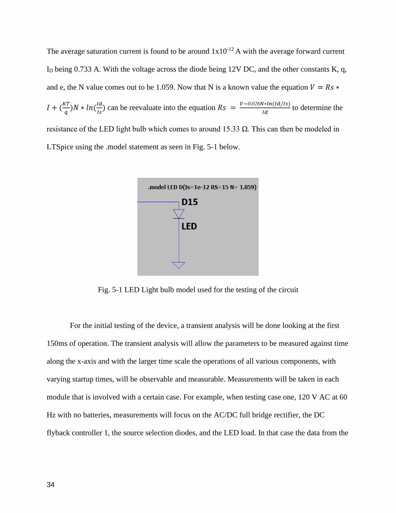
The average saturation current is found to be around 1x10-12 A with the average forward current
ID being 0.733 A. With the voltage across the diode being 12V DC, and the other constants K, q,
and e, the N value comes out to be 1.059. Now that N is a known value the equation 𝑉 = 𝑅𝑠 ∗
𝐼 + (𝐾𝑇
𝑞)𝑁 ∗ 𝑙𝑛(
𝐼𝑑
𝐼𝑠) can be reevaluate into the equation 𝑅𝑠 =
𝑉−0.026𝑁∗𝑙𝑛(𝐼𝑑/𝐼𝑠)
𝐼𝑑 to determine the
resistance of the LED light bulb which comes to around 15.33 Ω. This can then be modeled in
LTSpice using the .model statement as seen in Fig. 5-1 below.
Fig. 5-1 LED Light bulb model used for the testing of the circuit
For the initial testing of the device, a transient analysis will be done looking at the first
150ms of operation. The transient analysis will allow the parameters to be measured against time
along the x-axis and with the larger time scale the operations of all various components, with
varying startup times, will be observable and measurable. Measurements will be taken in each
module that is involved with a certain case. For example, when testing case one, 120 V AC at 60
Hz with no batteries, measurements will focus on the AC/DC full bridge rectifier, the DC
flyback controller 1, the source selection diodes, and the LED load. In that case the data from the

35
DC flyback controller 2 and the charging circuit will be observed and measured but will not be
included if the measurements are not anomalous or otherwise faulty in some way or form.
When testing the various voltage sources, in order to best simulate a fully functional
device, all components will remain attached, but the voltage sources will be set to zero when
applicable. When testing the four cases involving the AC source, the DC source will be set to
zero volts. The various test cases that call to be performed without the battery are meant to
simulate if the user has removed or neglected to include the batteries within the device. In order
to simulate that change, the connection between the charging circuit and the battery, as seen in
Figure 4-5, will be deleted. For all cases the current behind the various diodes, which act as
protection in some cases, will be noted to check that no components that are not meant to be in
use are being negatively affected by the source in use. An additional note is that for the
calculation of these simulations, the modified trapezoidal integration that is standard with
LTSpice does not function with the simulation as it provides an error claiming the time step is
too small. This message seems to mean that the circuit calculations are too difficult for the
default solver to find. This was overcome by switching the integration method from the modified
trapezoid to the gear method. This method takes a bit longer to compute, about 15 minutes per
simulation, but is able to fully simulate the device while also helping to simplify circuits that
tend to have a lot of small oscillation in values.
5.3 Simulation Results and Analysis
5.3.1 120 V AC at 60 Hz to a LED light bulb load without batteries
The reason for such a long simulation time is for the AC circuits. Although the AC full
bridge rectifier is active within the first dozen or seconds making the output of the rectifier 168
36
V DC, the flyback controller has a fairly long startup time as it would start outputting the desired
12 V DC for about 145 seconds. With that in mind, collecting data until 160 seconds seems to
allow for the rest of the circuit to hit steady state. At this point the output of the flyback is steady
at 12V as it ranges from 11.9 V to 12V, and the voltage is in the high state for 5.8 μs of the 13 μs
for a duty cycle of roughly 45%. The other data points for the voltages vary but this duty cycle
remains constant and doesn’t change by more and 2% with that being the final output voltage
which has a duty cycle of 47%. We see the expected total voltage drop from the initial decreased
voltage of 12 V DC to the output voltage of 11.2 V DC and although this is a bit lower than the
desired output of 12 V the LED load still pulls the needed current such that it should function if
the device operates in this manner.
In this scenario we see the worst efficiency and power loss at the flyback controller 1
which is the area that was expected. This section was designed to handle both the higher and
lower AC voltage ranges and with that lack of specificity, efficiency was traded for saving space.
The observable current is roughly similar with input and output for that section, but the voltage
drop that is needed for the rest of the device is large, 156.4 V, so the massive decrease in power
is also expected. That being said, the power must be dissipated somewhere, and the most likely
form is to be heat. The LT8316 is rated to handle higher temperatures and even higher voltages
than it will likely experience in this device but the same cannot be said for the charging circuits
and some of the other diodes. One solution for this includes the wise spacing of the components
within the device such that the more heat sensitive components are farther away from the
controller than those that can handle a higher operating temperature. A second solution that
could be implemented at the same time is having some form of heat dissipation around these
components.

37
An interesting data point is the lack of current draw from the charging circuit. The 8.4
mA that it appears to pull seems to be from enough to operate the charging circuit although the
voltage input is sufficiently large. A reason this might be that the voltage that the second diode
selection or gate being provided by the flyback controller is such that the diode protecting the
charging circuit never needs to allow current to be pulled. Since there is then no output for the
device to put any current or voltage into, the circuit just doesn’t pull much in the first place. If
there is no battery to be charged and the following circuit does not need to be supplied with any
additional current, then this module acts in standby mode just in case a battery is added. It does
show that the protection diode from the second or gate is functional and upon further testing, the
protection diode for the flyback controller 2 that takes the 48 V and decreases it to 12 V is also
functional allowing no current to flow forward or in reverse.
Table 5-1: Key Values of various modules in Test Case 1
AC Rectifier Flyback Controller 1 Diode Selection 1 Charging Circuit/Battery LED Load
Voltage Average Current
Power Voltage
Average Current
Power Voltage Current Power Voltage
Current Power Voltage Current Power
Input 120V
AC
1.3 A 156 W 168.3
V
790 mA 132.9
W
11.9 V 685
mA
8.15
W
11.4 V 8.4 mA 0.095
W
11.4 V 683.9
mA
8.14
W
Output 168.3V 790 mA 132.9
W
11.9 V 685 mA 8.15
W
11.4 V 678 A 7.73
W
11.2 V 5.9 mA 0.066
W
11.2 V 684
mA
7.66
W
From the values collected above the power at the inputs and outputs can be calculated
using the simple formula of 𝑃 = 𝐼 ∗ 𝑉 and the resulting values are displayed. Taking those
values, the efficiency of each section can be calculated to find the efficiency of each section
involved in the test case shown. This is calculated using the equation 𝜂 =𝑃𝑜𝑤𝑒𝑟𝑜𝑢𝑡
𝑃𝑜𝑤𝑒𝑟 𝑖𝑛∗ 100.

38
Table 5-2 Efficiency of the various modules in Test Case 1
AC/DC Rectifier Flyback
Controller 1
Diode Selection 1 Charging
Circuit/Battery
LED Load
Efficiency 85.2% 6.1 % 94.8% 69.5% 94.1%
5.3.2 120 V AC at 60 Hz to a LED light bulb load with batteries
The key difference between case one and case 2 is that for case 2 the 12 V battery is
connected to the circuit, and this makes a large difference in the collected data. This data starts at
T=0 with the battery supplying the 12 V needed for the load and as such the load is receiving the
11.6 V after less than 2 ms. There is a slight voltage drop from the diode in place to protect the
circuit and the LED is drawing the optimal 8.25 W that it desires for operation. For the first 145
ms the other diode in the second source selection diode gate operates as a protection diode
preventing reverse current or voltage from negatively affecting the rest of the circuit that
precedes the gate as well as the charging circuit that will later charge the battery. For the voltage
supplied by the battery we do not see any real change in the amplitude for the voltage and so
there is not a measurable duty cycle, but this is as desired for the first 145ms since the source is
ideally pure DC voltage. After the startup time for the flyback controller 1, there is a brief time
where the voltage from the flyback controller extends higher than the 11.999 V provided from
the battery, but it then falls below that and for this case the charging circuit and the battery will
provide most of the power for the LED load.
After both sources have settled into the steady state, a duty cycle for the output voltage
appears with the period being 282 μs long with the active state being around 36.7 μs which
calculates the duty cycle to be 13%. This is the lowest duty cycle for the several cases where one

39
can be observed and the believed reason for this is the fact that the charging circuit is providing
most of the power.
Another effect of the steady state is that the flyback controller output does not provide no
power to the output power. With a total output current of 721 mA and the battery only providing
630 mA of current the remaining 91 mA must come across the other diode. So, this current is
supplementing the current that is drawn from the battery as the battery occasionally drops below
the voltage of the flyback control and requires more current to charge up to full again. With the
current increasing to help charge back up the battery through the diode selection we get a larger
output current from the flyback controller as well as through the diode which improves the
efficiency of the flyback control, but subsequent current drop decreases the efficiency of the
diode selection gate. The efficiency of the flyback controller is still too low to be efficient in long
term usage without the addition of the heat dissipation or mitigation methods previously
mentioned. It would be beneficial to include both if not more of the mentioned method to
hopefully relieve the stress that the power loss puts on the other components will not damage the
integrity of the device or the safety of the user.
Table 5-3: Key Values of various modules in Test Case 2
AC Rectifier Flyback Controller 1 Diode Selection 1 Charging Circuit/Battery LED Load
Voltage Average Current
Power Voltage
Average Current
Power Voltage Current Power Voltage
Current Power Voltage Current Power
Input 120 V
AC
1.36 A 163.2
W
168 V 795 mA 133.5
6 W
12.3 V 2.06 A 25.34
W
11.9 V 901mA 10.72
W
11.9 V 721
mA
8.57
W
Output 168 V 795 mA 133.56
W
12.3 V 2.06 A 25.34
W
11.9 V 990
mA
11.78
W
11.9 V 630 mA 7.49
W
11.6 V 720
mA
8.25
W

40
Table 5-4 Efficiency of the various modules in Test Case 2
AC/DC Rectifier Flyback
Controller 1
Diode Selection 1 Charging
Circuit/Battery
LED Load
Efficiency 81.8% 18.9% 46.5% 69.9% 96.2%
5.3.3 120 V AC at 60 Hz with no load without batteries
For the no load cases the simulation was the same as prior but the load was disconnected
and so was the battery in this simulation. When observing the voltages, it would appear almost
like the device is still operating. The voltages out of the flyback controller are as high as desired
for the different modules that are to follow, however here the first difference is spotted. The
voltage drop across the diode is smaller than the other test cases, only being 0.2 V. It can be
determined that the large current that is being pulled through the diode is going to the charging
circuit since there is nearly no reverse current flowing through the diode that is protecting the DC
source components and that the diode that normally is connected to the output is only passing 40
mA. The current that is being pulled into the charging circuit is being dissipated through since
only 1.5 mA are being output form the module. Although the flyback controller’s inefficiency is
now a tested fact in this circuit, the massive drop in current means that there is little other power
dissipation in the second diode selection gate, but it also means that the efficiency of the gate as
well as the charging circuit is terrible and near 0%. This all points to the device being impractical
and wasteful if it is to be plugged in with no load and without batteries.
Table 5-5: Key Values of various modules in Test Case 3
AC Rectifier Flyback Controller 1 Diode Selection 1 Charging Circuit/Battery Diode Selection 2
Voltage Average
Current
Power Voltag
e
Average
Current
Power Voltage Current Power Voltag
e
Current Power Voltage Current Power

41
Input 120 V AC
1.19 A 142.8 W
168 V 798 mA 134.1 W
12.3 V 1.7 20.91 W
12.1 V 1.16 A 14.04W
12.2 40 mA 0.48 W
Output 168 V 798 mA 134.1 W
12.3 V 1.7 A 20.91 W
12.1 V 1.2 14.52 W
11.9 V 1.5 mA 0.18 W
12.2 V 0 A 0
Table 5-6 Efficiency of the various modules in Test Case 3
AC/DC Rectifier Flyback
Controller 1
Diode Selection 1 Charging
Circuit/Battery
Diode Selection 2
Efficiency 93.9% 15.6% 69.4% 1.3% 0%
5.3.4 120 V AC at 60 Hz with no load with batteries
When case three is run again but with time with the batteries added back into the device
and observe the data points below, a lot of the same aforementioned conclusions about the device
can be assumed. For example, we see the same higher output voltage at the end step, and this is
due to the lower current that is flowing through the selection diodes not being large enough to
cause a voltage drop. There is also more data from the charging circuit that seems to show the
circuit being even less efficient than where there are no batteries installed within the device. It is
believed that this decrease in efficiency is caused by the module providing a constant low
amount of power into the battery to keep it at maximum value as it slowly dissipates its power.
However, with that the charging circuit is still pulling 99% of the current that is passing out of
the flyback controller and as discussed above this is almost entirely being dissipated as heat.
It can be noted that during the time before the flyback controller is outputting, the voltage
output of this device is at a steady 12 V that is being provided from the connected battery, but
about 5 ms after the controller starts to output data a small duty cycle is introduced to the output.
The difference between the high and low state is 15 mV, therefore not really impactful, but it is

42
still present. The period seems to be 283 μs with the high state only lasting 1.9 μs so it has a duty
cycle of 0.7%.
Table 5-7: Key Values of various modules in Test Case 4
AC Rectifier Flyback Controller 1 Diode Selection 1 Charging Circuit/Battery Diode Selection 2
Voltage Average
Current
Power Voltag
e
Average
Current
Power Voltage Current Power Voltag
e
Current Power Voltage Current Power
Input 120 V
AC
1.22 A 146.4
W
168 V 546 mA 91.7
W
12.45 V 3.1 A 38.6
W
12.25 1.6 A 19.6
W
12 V 6 mA 0.07
W
Output 168 V 546 mA 91.7 W 12.45
V
3.1 A 38.6
W
12.25 V 1.7 A 20.8
W
12 V 6 mA 0.07
W
11.9 V 0 0
Table 5-8 Efficiency of the various modules in Test Case 4
AC/DC Rectifier Flyback
Controller 1
Diode Selection 1 Charging
Circuit/Battery
Diode Selection 2
Efficiency 62.6% 42.1% 53.9% 0.4% 0%
5.3.5 240 V AC at 50 Hz to a LED light bulb load without batteries
For the 240 V AC source the same delay in data is visible in the cases that had to do with
the 120 V AC, those being that the LT8316 needs around 145 ms to start up so data for the other
modules up until that point does not exist. After that point the data that is seen is almost
satisfactory. The parts that are satisfactory are the LED load and the Charging circuit. For the
same reasons as it was discussed in case one, the charging circuit has relatively higher efficiency
since the device has no need to be pulling any power from the circuit. The power that is pulled is
pulled in the no load state for this module as it sees no load. If the voltage provided from the
flyback controller does not drop more than the 0.3 V that the selection diodes decrease the

43
voltage by then the charging circuit, which has an output voltage of 11.28 V, will never have a
large enough voltage and not nearly a high enough current to be the dominating output and
provide power to the LED.
When looking at the different voltages of this circuit scenario, it is noticeable that the
voltage drop caused by each diode is not as large as it normally is in some of the other cases.
While the forward drop for the 48 V DC source case is closer to 0.5 V from each diode, for this
case the voltage drop is closer to 0.35 V to 0.4 V per diode. This does not hurt the circuit in any
large way, in fact it seems to improve the efficiency marginally, but the cause is not entirely
known. It is likely that the lower voltage drop could be from the lower than nominal currents.
But the voltage drop is consistent as we see the 12 V from the flyback controller dropped to 11.6
V after it passes through the first diode selection gate. It drops further to 11.3 V after it passes
through the second gate and to the LED load. At both of the diode selection gates, it is
observable that there is no reverse current passing through the unused portions of the circuit,
protecting both the DC flyback controller as well as the charging circuitry. All these separate
voltages all have a similar duty cycle with the active state of the voltages lasting for 5.9 μs of the
17 μs period, otherwise a 35% duty cycle. Some of the currents are also a little sporadic at points
but in most of those cases the currents' high points make up 2.6 μs of a 21 μs period for a duty
cycle of 12.3%. It is high enough to be a concern for elongated operation.

44
Table 5-9: Key Values of various modules in Test Case 5
AC Rectifier Flyback Controller 1 Diode Selection 1 Charging Circuit/Battery LED Load
Voltage Average
Current
Power Voltag
e
Average
Current
Power Voltage Current Power Voltag
e
Current Power Voltage Current Power
Input 240 V
AC
937.5
mA
225W 337 V 564 mA 190
W
12 V 2.3 A 27.6
W
11.6 V 5.62
mA
0.065
W
11.6 V 688
mA
7.98
Output 337 V
DC
564 mA 190 W 12 V 2.3 A 27.5
W
11.6 V 690
mA
8 W 11.3 V 4.34
mA
0.049
W
11.3 V 686
mA
7.75
W
The flyback controller in this section has an efficiency rating that is dissatisfactory and
the likely reasoning for this has been mentioned in the prior cases and scenarios. The aspect of
this circuit that is not already noted is the low efficiency of the diode selection gate. This is due
to the oscillations of current. For the data collected a rough estimate of the average current was
taken but the fluctuation makes the data for that segment hard to parse and less reliable than for
the other modules. In most of the other modules, the current stabilized and a cleaner reading was
able to be taken.
Table 5-10 Efficiency of the various modules in Test Case 5
AC/DC Rectifier Flyback
Controller 1
Diode Selection 1 Charging
Circuit/Battery
LED Load
Efficiency 84.4% 14.6% 28.9% 75.4% 97.1%
5.3.6 240 V AC at 50 Hz to a LED light bulb load with batteries
Like how the battery helped to jumpstart the device when operating with the 120 V AC
source with the battery attached, it also helps to jumpstart the device in this case as well. The AC
rectifier gets up to 337 V DC within a matter of a dozen milliseconds, but the flyback controller
takes much longer to reach steady state. This is made up for by the battery which starts to supply
45
power to the LED load within a millisecond of starting measurements. It provides a steady 11.9
V DC and 698 A to the load. It is noted that once the flyback controller reaches steady state, it
provides the charging circuit with the power it needs to keep the battery topped off and
performing optimally as well as providing the additional 23 mA of the 721 mA that the load
desires to be operating at maximum efficiency. The discharge rate of the battery is such that by
the time the battery starts to see an observable drop in output voltage, the flyback controller
should be functioning and is providing the required voltage and current for the charging circuit to
fulfill its function of maintaining battery voltage.
Once again the voltage drop across the diodes falls from the expected 0.5 V to 0.3 V and
it is consistent for the various protection diodes in place. It is first seen between the output of the
flyback controller and the output voltage from the first diode selection gate. It is then seen across
the second diode selection gate from the battery voltage this time to the voltage that the output is
receiving. As mentioned prior, this in fact does help to improve the efficiency slightly by
decreasing the voltage drop while maintaining a relatively steady current from the various
modules. Accompanying the steady voltage drop is an equally consistent duty cycle for the same
voltages. For each of the measured voltages there was a consistent period between the higher and
lower measured data points that was 279.6 μs long with the data being in the upper voltage
range for 26.2 μs for a duty cycle of 9.4 %. Like the other AC source case with the battery
involved the duty cycle is comparably lower than their battery-less counterparts. Most likely the
longer period is due to the battery providing the voltage and the power provided by it is a lot
more stable than the power that would be provided by the flyback controller. The charging and
discharging of the smoothing capacitors lead to a more defined shorted duty cycle but the battery
circuit that would be in place has no charging capacitor as it is already a pure DC source.

46
The efficiency of this case is low for most of the modules with the exception of the LED
load, the AC rectifier, and the charging circuit. The charging circuit most likely lacks an even
higher efficiency due to the fact that the circuit is doing two-fold. The higher current pulled is
needed to power the battery charging circuit as it must charge the battery while the battery is
output to the load. As discussed in the prior cases the flyback controller lacks efficiency due to
several issues such as non-specificity and extremely high input voltage.
Table 5-11: Key Values of various modules in Test Case 6
AC Rectifier Flyback Controller 1 Diode Selection 1 Charging Circuit/Battery LED Load
Voltage Average Current
Power Voltage
Average Current
Power Voltage Current Power Voltage
Current Power Voltage Current Power
Input 240 V
AC
1.18 A 283.2
W
337 V 618 mA 274.9
W
12.2 V 3.04 A 37.3
W
11.9 V 1.05 A 12.48
W
11.9 V 721
mA
8.58
W
Output 337 V 618 mA 274.9
W
12.2 V 3.04 A 37.3
W
11.9 V 1.07 A 12.48
W
11.9 V 698 mA 8.31
W
11.6 V 721
mA
8.36
W
Table 5-12 Efficiency of the various modules in Test Case 6
AC/DC Rectifier Flyback
Controller 1
Diode Selection 1 Charging
Circuit/Battery
LED Load
Efficiency 97% 13.6% 33.5% 66.6% 97.4%
5.3.7 240 V AC at 50 Hz with no load without batteries
There are several similarities between case 7 and case 3. Those start with a total of zero
amps through the output which makes sense as there is nowhere for the current to flow through
as well as the lack of a voltage drop across the second diode and a small voltage drop across the
first selection diode gate. As noted in all the other no load test cases, there is still a large roughly
1 A current being pulled by the charging circuit. This current pull is causing the flyback

47
controller to read a load and therefore pull a current from the ac rectifier. With the 240 V
becoming 338 V there is room for huge power loss and we see that reflected in the efficiency of
each of the different modules.
An interesting note to make is that there is a bit of surge current through the rectifier
diodes during the startup phase of the rectifier where the current seems to reach as high as 5 A
but it then quickly, within 2 ms settles down to the range of 400 mA to 800 mA still fluctuating
quite a bit. This is the same region where the voltage output of the rectifier is reaching its peak
voltage before settling.
Table 5-13: Key Values of various modules in Test Case 7
AC Rectifier Flyback Controller 1 Diode Selection 1 Charging Circuit/Battery Diode Selection 2
Voltage Average Current
Power Voltage
Average Current
Power Voltage Current Power Voltage
Current Power Voltage Current Power
Input 240 V
AC
2.16 A 518.4
W
338 V 1.04 351.5
W
12.3 V 3.25 A 39.98
W
12.2 V 1.3 A 15.86
W
12.2 V 35mA 0.43
W
Output 338 V 1.04 351.5
W
12.3 V 3.25 A 39.98
W
12.2 V 1.38 A 16.84
W
12.9 V 10 mA 0.129
W
12.2 V 0 0
Table 5-14 Efficiency of the various modules in Test Case 7
AC/DC Rectifier Flyback
Controller 1
Diode Selection 1 Charging
Circuit/Battery
Diode Selection 2
Efficiency 67.8% 11.4% 42.1% 0.8% 0%
5.3.8 240 V AC at 50 Hz with no load with batteries
As expected the case of 240 V AC with no load but with batteries has a similar output to
the 120 V AC case with no load but with batteries. From the following set of data, the same
conclusions can be implied but there is the addition of a lower efficiency rating in the flyback

48
controller by about 20%. Most likely what caused this is the much larger voltage input. As
opposed to the 168 V input in case 4, during case 8 the input into the flyback controller is twice
that, or 337 V. While the voltage doubled from one case to the other the current also increased
which only applies to the amount of power that the flyback controller is receiving. So, a 90 W
power load becomes small when compared to the 212 W power load. On top of that the
efficiency is only going to decrease since the output voltage and current remain roughly similar
in both cases. This proves two things: one that the flyback controller is outputting consistently
the right values, and that it would need to be improved on if the product was going to go into
development for mass production.
Table 5-15: Key Values of various modules in Test Case 8
AC Rectifier Flyback Controller 1 Diode Selection 1 Charging Circuit/Battery Diode Selection 2
Voltage Average Current
Power Voltage
Average Current
Power Voltage Current Power Voltage
Current Power Voltage Current Power
Input 240 V
AC
1.41 A 338.4
W
337 V 630 mA 212.3
W
12.3 3.3 A 40.59
W
12.1 1.64 A 19.26
W
12 7.5 mA 0.09
W
Output 337 V 630 mA 212.3
W
12.3 3.3 A 40.59
W
12.1 1.65 A 19.97
W
12 V 7.5 mA 0.09
W
11.9 V 0 0 W
Table 5-16 Efficiency of the various modules in Test Case 8
AC/DC Rectifier Flyback
Controller 1
Diode Selection 1 Charging
Circuit/Battery
Diode Selection 2
Efficiency 62.7% 19.1% 49.2% 0.5% 0%
5.3.9 48 V DC to a LED light bulb load without batteries
For this test case, all of the voltages meet the expected values. The input voltage 48 V
DC is steady in our simulation, and it is safe to say that a practical voltage would adjust slightly
49
above and below the nominal value; however, it is our belief that the device will still be fully
functional in those cases. The output from the flyback controller 2 is slightly higher than the
nominal or desired 12V that was described in chapter 3 of the report but that is beneficial. During
the creation of this circuit, it was noted that the diodes were going to have a significant voltage
drop so the output from the controller needed to be slightly higher than originally intended. With
the output hovering around 13 V DC, this would lead perfectly into the 12 V DC required for the
LED light bulb that is acting as the load. For each selection diode in place, we saw the
appropriate drop in voltage of about half a volt. Even though the voltages did have about a half
volt range of fluctuation, most likely due to the capacitors chosen, the voltage drop across each
diode was consistent and should not affect the output of the device.
One concern was that if the battery was not connected, then it could be possible for the
current from the flyback controller and the battery charging circuit to combine again after at the
junction right before the load. In order to prevent this a second diode selection or gate was
added. This helped to protect the charging circuit from reverse current from the flyback
controller as well as only allowing for one of the two possible sources to provide power to the
load at a time. It also had the benefit of stabilizing the voltage slightly. When the voltage and
current from the flyback controller dropped too low, the charging circuit would step in to provide
more current, up to its max, to help and keep the output current and voltage as close to what is
required as possible.
It is also interesting to note that the duty cycle for all of the different voltage ranges
stayed relatively constant throughout the process with the only difference coming from the
charging circuit. For the flyback controllers 13V, the diode selections 12.5V, and for the LED
loads 12V they all had a period of around 4 μs with the active or high state of the voltage taking

50
up roughly 2 μs giving the device a duty cycle of around 50%. For the charging circuit however,
while the total period was still around 4 μs the active state made up a much larger portion of 2.8
μs or a duty cycle of 70%.
Table 5-17: Key Values of various modules in Test Case 9
Flyback Controller 2 Diode Selection 1 Charging Circuit/Battery LED Load
Voltage Average
Current
Power Voltage Current Power Voltage Current Power Voltag
e
Current Power
Input 48V 641mA 30.8W 12.3V -
13V
2.2A 28.6W 11.7V -
12.5V
1.01A 12.6W 11.7V -
12.5
1.07A 13.4W
Output 12.3V -
13V
2.2A 28.6W 11.7V -
12.5 V
2.08A 26W 11.9V -
12V
0.85A 10.2W 11.8V -
12V
759mA 9.1 W
From the values collected above the power at the inputs and outputs can be calculated
and displayed as well as the efficiencies.
Table 5-18 Efficiency of the various modules in Test Case 9
Flyback Controller 2 Diode Selection 1 Charging Circuit/Battery LED Load
Efficiency 92.9% 90.9% 81% 68%
For the device in this configuration, the individual modules are all fairly effective and
efficient. With each component having an efficiency of over 80% as seen above with the
expectation of the LED load which sits at 68%. Where this device fails is in the efficiency of the
device as a whole. With 30.8 W of power being fed into the device and only 12W of output
power, this device has an efficiency of only 30%. The lack of efficiency in the simulation might
be due to a lack of a more complex and realistic voltage source for the device. With the

51
limitations of the knowledge of LTSpice, the testing of this voltage source may not be as detailed
or fine-tuned as it possibly could be and with that the efficiency of the device might suffer as
well. This failure in efficiency could also come from the large voltage drop of 48 V to 12V while
maintaining roughly the same current draw throughout the device. This loss in power is most
likely going to come in the form of heat loss so during manufacturing, a well-designed heat
dissipation system would need to be considered. This would increase the cost of development as
well as cost of the product, but would in the long run increase the lifespan of the device
5.3.10 48 V DC to a LED light bulb load with batteries
Starting with the voltages at key points, all of the voltages meet the expected values. The
input voltage 48 V DC is steady in our simulation, and it is important to say that in a more
practical situation, that steady voltage is likely to waiver a small about, however, the voltage
values at the following points in the circuit are satisfactory and it is believed that even with the
slight oscillation of the voltage source, the other key values will remain at a similar range.
Table 5-19: Key Values of various modules in Test Case 10
Flyback Controller 2 Diode Selection 1 Charging Circuit/Battery LED Load
Voltage Average
Current
Power Voltage Current Power Voltage Current Power Voltag
e
Current Power
Input 48 V 641mA 30.8W 12.3V -
13.3V
2A 26.6W 11.9V -
12.4V
1.12A 13.9W 11.9V -
12.4V
1.02A 12.6W
Output 12.3V -
13.3V
2A 26.6W 11.9V -
12.4V
2.14A 26.58
W
11.9V -
11.91V
605mA 7.2W 11.5V -
12V
786mA 9.4 W

52
Table 5-20 Efficiency of the various modules in Test Case 10
Flyback Controller 2 Diode Selection 1 Charging Circuit/Battery LED Load
Efficiency 86.36% 99.9% 51% 74.6%
When observing the variation in the voltage outputs of the different modular voltages, it's
important to note that the switching time for the voltage ranges was 3 μs between the different
values with 1 μs so the device has a 33% duty cycle. This duty cycle is consistent across all
collected voltage values with the exception of the voltage provided by the battery that has a total
period of 4 μs with the voltage being high for 2 μs for a duty cycle of 50%. There was only one
anomalous voltage in this test case, that being during the first 5ms of startup time, the voltage
output of the flyback controller 2 jumped up to 16V before settling into steady state at around 13
V. This higher temporary output leads to higher outputs at the other component points but all of
the devices, components, and ICs are all rated well above this outlining voltage so there should
be no adverse effects after the first few milliseconds of startup.
The current is a similar situation with the current ranging from 0 A to 4 A with an
average forward current of 2 A. The currents seem to be fluctuating along with the charging and
discharging of the capacitors leading towards the high voltage taking up 2 μs of the 3 μs period
with the duty cycle of 66% being constant across all of the various components. A major point of
power loss is during the flyback controller 2 where it appears that 4.2 W of power seems to have
been dissipated in the form of heat. This could be damaging to the device in terms of long
operating hours, but a few potential solutions could include having a more heat resistant casing
as well as investing in some form of a heat sink or heat dissipation method for the circuit that
would not compromise the size, weight, or structural integrity of the device itself. The still worse
section of efficiency is in the charging circuit with its 51% efficiency. Part of the lack of
53
efficiency is that the output from the charging circuit is split into two different outputs with the
first being the charging of the battery, and the second being the LED load. The light bulb
selected for this device only requires 0.753 A for full operation, but the charging circuit requires
the larger current of about an amp. At the node following the first source selection diodes, the
current is at 2.14 A but is split as the charging circuit pulls the 1 A it would need, leaving the
remaining 1.02 A to flow through the second diode section module and provide the 0.750 A the
LED needs to turn on. The excess current should allow for a slight voltage drop while
maintaining an active light which is an optimal outcome seeing how the voltages have a slight
oscillation. It is also important to note that the first set of source selection diodes do successfully
serve their secondary purpose of protecting the AC components from a large reverse current
since less than a tenth of a femtoamp,10-15, is measured feeding back into those components.
5.3.11 48 V DC to a LED with no load without batteries
For the DC source without batteries and without a load, the results mirror the other cases
that lack both. There is a noticeable lack of voltage drop across the second diode selection gate.
But where this case differs is twofold. The first difference is that a full voltage drop can be
observed from the first diode selection gate. The voltage drops from the flyback controller drops
by 0.8 V and the current drops by an amp and a half. The reason for this massive drop at over a
module that should not have any larger current pull is most likely a failure at the smoothing
capacitor that is not rated for such a voltage that is above 15 V. Under normal operation the
voltage at this node does not reach above 14.5 V so the capacitor seems to operate normally. But
the second difference from this test scenario and the other no-load tests is that in this test, the
voltage is a whole 2 V higher than the normal max of 14.5 V. In actuality this would damage the

54
capacitor and would require an upgrade and a replacement. Doing so would likely drop the
voltage value back down to 14 V as well as slightly improving the efficiency of the diode
selection gate for this case. The replacement would likely have little effect on the efficiency of
the various other components for the no load scenario, however.
Table 5-21: Key Values of various modules in Test Case 11
Flyback Controller 2 Diode Selection 1 Charging Circuit/Battery Diode Selection 2
Voltage Average
Current
Power Voltage Current Power Voltage Current Power Voltag
e
Current Power
Input 48 V 3.04 A 145.9
W
16.8 V 2.3 38.6
W
15.6 V 379.6
mA
5.9 W 15.6 50.4 mA 0.87
W
Output 16.8 V 2.3 38.6
W
15.6 V 430
mA
6.7 W 14.5 V 3.2 mA 0.05W 15.6 0 0
Table 5-22: Efficiency of the various modules in Test Case 11
Flyback Controller 2 Diode Selection 1 Charging Circuit/Battery Diode Selection 2
Efficiency 26.5% 17.4% 0.8% 0%
5.3.12 48 V DC to a LED with no load with batteries
In sharp contrast with the no load without batteries test, the no load with batteries test
resembles the regular DC source cases much more closely than anticipated. The prior no-load
simulations had almost all had vastly different outcomes from the simulations with loads. In this
case, the voltages, the duty cycles, and even some of the amperage and power matched with the
loaded cases being off by about 25%. The voltage drops across the first diode as it should, by 0.5
V and the voltage drops slightly at the second but with no load that is expected. If there was a

55
load, the voltage drop would likely be another 0.5 V such that the output of this case would
match the output of case 10. There is also a great efficiency in the diode selection gate 1 and the
flyback controller 2. So, this case, although far from perfect, is likely to be the second best no
load case. In the case of this simulation, there isn't the same pressure on the smoothing capacitor
of the flyback controller as there was in the batteryless no load case. This would lead to less
failure at that component but does not mean that there is no possibility for failure at that point. If
there is a high enough current spike, it could overload the capacitor or overcome the reverse
current protection of the other diode in the first selection gate. If that were to happen and the
current spike remained active for long enough, even sever ms would be enough, it could
overcome the output diode from the flyback controller 1 module and potentially damage the AC
source components
Table 5-23: Key Values of various modules in Test Case 12
Flyback Controller 2 Diode Selection 1 Charging Circuit/Battery Diode Selection 2
Voltage Average
Current
Power Voltage Current Power Voltage Current Power Voltag
e
Current Power
Input 48 V 531 mA 25.5
W
12.9 1.8 A 23.2
W
12.4 1.14 A 14.1
W
12.4 53 mA 0.66
W
Output 12.9 V 1.8 A 23.2
W
12.4 1.5 A 18.6
W
12 5 mA 0.06W 12.3 0 0 W
Table 5-24: Efficiency of the various modules in Test Case 12
Flyback Controller 2 Diode Selection 1 Charging Circuit/Battery Diode Selection 2
Efficiency 90.9 80.2% 0.4% 0%

56
5.3.13 12 V batteries to a LED light bulb load
When testing the device in this final case, the device at this point is practically very
simple. It consists of a battery connected to a light bulb with a diode in between. Testing this
circuit, still using the complete circuit shown in Fig 4-6 with the battery as the sole voltage
source, the decrease in current draw was smaller than in prior cases, decreasing only by a
fraction of a milliamp to stay roughly at 720 mA. This steady current and lack of potential
sources of power loss or power dissipation also means that this simple circuit layout would be
highly efficient at 96.6%. The only source of the lost power is the voltage drop across the
selection diode as it had a voltage drop of 0.4 V which resulted in a power decrease of 0.29
watts. With the circuit as simple as it is, it still meets all of the bulb’s requirements for power, so
the device running on just batteries should be functional. The device operates off of 4 batteries
each rated for 250 mAh and since this device outputs at 12 V and the battery storage doesn’t
increase when added in series, the device may only be operating under only battery power for
about 25 minutes before some dimming is seen. This means that the device should only be used
on batteries alone in cases of extreme emergencies. This lifespan can be improved with the
addition of batteries that have a higher storage capacity or are rated for a higher mAh.
Table 5-25: Key Values of Test Case 13
Charging Circuit/Battery LED Load
Voltage Current Power Voltage Current Power
Input 0V 0A 0W 12V 720.7mA 8.65W
Output 12V 720.7mA 8.65W 11.6V 720.7mA 8.36W

57
From the values collected above the power at the inputs and outputs can be calculated
and displayed above. In this case the efficiency for the charging circuit was not included as there
are no real inputs to the charging circuit but the output is connected to both the battery and the
second source selection diodes. Taking those values, the efficiency for the LED load section was
found.
Table 5-26: Efficiency of the various modules in Test Case 13
LED Load
Efficiency 96.6%
5.3.14 12 V batteries with no load
When a battery is connected to a diode that is then not connected to anything else, that is
just an open circuit. No real current is flowing with on a microscoping 10 microamps at most as
just a passive loss of current from the batteries. That being said that open circuit means that this
test case is the most effective no-load case since the device is not dissipating any power
whatsoever.
Table 5-27: Key Values of Test Case 13
Charging Circuit/Battery Diode Selection 2
Voltage Current Power Voltage Current Power
Input 0 0 0 12 V 10 μA 0.00012
W
Output 12 V 10 μA 0.00012 W 11.97 V 0 0

58
Chapter 6: Conclusion
The goal of this project was to develop an adaptor that is attached to a light-bulb screw
base pluggable into a 120 V AC source, a 240 V AC source, or a 48 V DC source. The adaptor
could also have the light bulb operate at full power, while also charging internal batteries that
will provide power to the light bulb when the device is not attached to one of the three other
possible sources. This ideally would help to provide some light to people in need when there is a
power outage due to a distributor error, or some natural disaster and allow for the user to find
various key items or tools that could mean the difference between life and death.
The development and testing of this device have proved that the design currently listed
above can work in some cases but can be improved upon in several areas. It was observed that
the device is fully operationally, albeit inefficient, when it is plugged into one of the possible
sources. When the device does not have the batteries attached, the device is slightly less efficient
than when batteries are attached. But with batteries installed, the device will output enough
power to the LED light bulb, while also charging the battery if the voltage falls below the
nominal voltage of the batteries. When the device is not powered by one of the three main
sources, and instead solely powered by the batteries, the battery outputs enough power to run the
LED for about half of an hour. This is not a long time but will provide important minutes of light
needed to gather one’s thoughts as well as any important items before losing light and sight
entirely.
There are several points of potential improvements for this current design. The first is to
improve the no load cases and decrease the current drawn and power dissipated during these
states, as that issue was present in all no-load cases except for the no load case involving just the
59
battery which is an open circuit. One potential solution is to change how the charging circuit is
included into the device. The addition of another switch that could either connect or disconnect
the charging circuit would drop the current draw to zero for that module, as the IC would not
have the ability to draw the current needed for it to check the charge and output of the attached
battery. A simpler charging circuit could also be used in order to decrease the overall complexity
of the device as well as decrease the potential need for the power to be drawn to the module. It
could also be beneficial to size some of the components even higher than the sizing done. Most
of the components were properly sized for surge voltages and currents but increasing the
tolerances may be of some assistance in improving the no load cases, given that the device may
have to be enlarged or rearranged in order to fit all the components.
The next area that could be improved is the flyback controller 1, or the controller that
decreased the rectified AC voltage from its high range down to around 12 volts. This section of
the device is going to be inefficient in its nature as it has to decrease the output voltage of one
module down to a tenth or a thirty-th of that value while also providing a high current. A
possible solution is to make the flyback controllers more specified for each source. Having one
controller for the 120 V AC source and a different one for the 240 V AC source would allow for
each individual controller to be more fine-tuned and efficient but comes at the cost of adding
more components, leading to an increased size as well as increased potential for fail points. This
solution would also affect the rest of the device, calling for a more complex switch as well as
increasing the source selection diodes to 3 sources from 2, but that section would still operate
roughly the same as before. Having the separate controllers would also require separate full
bridge rectifiers as well as allowing those devices to become more precise, further improving the

60
modular efficiency. The increase in complexity in adding another controller could also lead to
more user errors in the selection of the wrong source.
Another area for improvement is the battery lifetime of the device. With the current
selected batteries, the amp-hour lifespan of the device is roughly half an hour, which would
temporarily aid those without power, but definitely has room for improvement. The selection of a
similar battery with a longer operation time under the same operating conditions could increase
the number of people that the device could be of assistance to. The issue could also be improved
upon as LED lighting technology improves. If the bulbs require less power to operate, the
operating time of the device would increase proportionally.
A final area for improvement could be the simulation program. LTSpice is a well-defined
and complex simulation program, with the lack of a price tag not hurting its case. However, the
testing procedures' extended operation time limits the number of tests that can reasonably be
done, and a more robust simulation tool could allow for more tests to be run. The additional data
could lead to the discovery of more potential areas of improvement as well as the ability to run
more complex analysis on how the device would interact with variations to the different sources.
For example, the Monte Carlo test will run effectively when testing out individual modules of the
device, but when attempted for the device in its entirety, the test failed to run successfully and
produced no additional or usable information. A tool that could run the device simulations with a
decreased run time, would be more likely to run simulations like the Monte Carlo tests in a
reasonable length of time. In addition, although the LTSpice library of IC is large, several
manufacturers of different but useful IC do not produce LTSpice models for some of the newer
or more complex components they develop but do make the products available for other
simulation tools.

61
References
[1]. “U.S. Energy Information Administration - EIA - Independent Statistics and Analysis,”
Average frequency and duration of electric distribution outages vary by states - Today in
Energy - U.S. Energy Information Administration (EIA). [Online]. Available:
https://www.eia.gov/todayinenergy/detail.php?id=35652. [Accessed: 15-Mar-2021].
[2]. A. Kenword, BLACKOUT: EXTREME WEATHER, CLIMATE CHANGE AND POWER
OUTAGES, 01-Oct-2014. [Online]. Available: https://www.ourenergypolicy.org/wp-
content/uploads/2014/04/climate-central.pdf. [Accessed: 15-Mar-2021].
[3]. H. Ritchie and M. Roser, “Access to Energy,” Our World in Data, 20-Sep-2019.
[Online]. Available: https://ourworldindata.org/energy-access#access-to-electricity.
[Accessed: 15-Mar-2021].
[4]. R. W. Erickson and Maksimovic Dragan, Fundamentals of power electronics. Norwell,
MA: Kluwer Academic, 2001.
[5]. B. K. Bose, "Advances in power electronics and drives-their impact on energy and
environment," 1998 International Conference on Power Electronic Drives and Energy
Systems for Industrial Growth, 1998. Proceedings., 1998, pp. 1 Vol.1-, doi:
10.1109/PEDES.1998.1329980.
[6]. J. Song et al., "A control and protection system in a loop testing technology for a flexible
power electronics substation," 2018 13th IEEE Conference on Industrial Electronics and
Applications (ICIEA), 2018, pp. 2051-2056, doi: 10.1109/ICIEA.2018.8398047.
[7]. D. Elliot, Energy Storage Systems. Philadelphia, PA: IOP Publishing, 2017.

62
[8]. Aoxia Chen and P. K. Sen, "Advancement in battery technology: A state-of-the-art
review," 2016 IEEE Industry Applications Society Annual Meeting, 2016, pp. 1-10, doi:
10.1109/IAS.2016.7731812.
[9]. “Travel Adaptor for USA,” Electrical Safety First. [Online]. Available:
https://www.electricalsafetyfirst.org.uk/guidance/advice-for-you/when-travelling/travel-
adaptor-for-
usa/#:~:text=In%20the%20USA%20the%20supply,the%20appliance%20operates%20at
%20120V). [Accessed: 10-Feb-2021].
[10]. R. Steves, “Electric Europe: Adapters and Converters,” Rick Steves' Europe. [Online].
Available: https://www.ricksteves.com/travel-tips/phones-tech/electric-adapters-
converters. [Accessed: 10-Feb-2021].
[11]. D. H. and S. Galiardi, “48 Volt Systems: The Future of Off-Grid Solar,” Renogy United
States, 2020. [Online]. Available: https://www.renogy.com/blog/48-volt-systems-the-
future-of-offgrid-solar-/. [Accessed: 10-Feb-2021].
[12]. A. Fathollahi, A. Abdallah, “Light Bulb Adapter”, US9642222B2, January 5th, 2015
[13]. Ioan Plotog and Marian Vladescu "Power LED efficiency in relation to operating
temperature ", Proc. SPIE 9258, Advanced Topics in Optoelectronics, Microelectronics,
and Nanotechnologies VII, 92582O (20 February 2015);
https://doi.org/10.1117/12.2072276
[14]. “Department of Labor UNITED STATESDEPARTMENT OF LABOR,” 1915.82 -
Lighting. | Occupational Safety and Health Administration. [Online]. Available:
https://www.osha.gov/laws-regs/regulations/standardnumber/1915/1915.82. [Accessed:
01-Mar-2021].

63
[15]. M. Macairan, “Design of Portable DC Light Bulb for the DC House Project”, 2013
[16]. E. Lukascs, “How to write a basic technical paper for the IEEE?,” IEEE Report
Formating. [Online]. Available: https://www.e-nformation.ro/wp-
content/uploads/2015/11/IEEE-How-to-write-a-basic-technical-paper_.pdf. [Accessed:
12-Feb-2021].
[17]. “IEEE Code of Ethics,” IEEE. [Online]. Available:
https://www.ieee.org/about/corporate/governance/p7-8.html. [Accessed: 15-Mar-2021].
[18]. “IEEE Citation Guide,” IEEE, 12-Dec-2018. [Online]. Available:
https://ieeeauthorcenter.ieee.org/wp-content/uploads/IEEE-Reference-Guide.pdf.
[Accessed: 08-Mar-2021].
[19]. Taufik and M. Muscarella, “Development of DC House Prototypes as Demonstration
Sites for an Alternate Solution to Rural Electrification,” Proc. 6th International Annual
Engineering Seminar (inAES), 2016, pp. 262-265.
[20]. Liang, and Taufik. Design of DC Light Bulb for the DC House Project: A Thesis. San
Luis Obispo, Calif.: California Polytechnic State U], 2012. Print.
[21]. Macairan, Jan Marvin Perez, and Taufik. Design of Portable DC Light Bulb for the DC
House Project. Web.
[22]. “Low Dropout Micropower Linear Regulator,” LT3014 Datasheet. [Online]. Available:
https://www.analog.com/media/en/technical-documentation/data-sheets/3014fd.pdf.
[Accessed: 20-Jul-2021].
[23]. Santos, Chad, James, Siby, and Taufik. Design of a Multiple Input Single Output DC-DC
Converter for the DC House Project. Web.

64
[24]. E.A. Parr. "CHAPTER 2 - Logic Families." Logic Designer's Handbook. Second ed.
Elsevier, 1993. 27-49. Web.
[25]. Analog Devices. (2021, April). LT8316 Datasheet - analog devices. Retrieved November
8, 2021, from https://www.analog.com/media/en/technical-documentation/data-
sheets/LT8316.pdf.
[26]. Crowfoot, Joseph., and Taufik. Design and Modeling of the Cal Poly DC House Power
Distribution System a Thesis. California Polytechnic State University], 2011.
[27]. “LT3748 – 100V Isolated Flyback Controller - Analog Devices.” Analog Devices, Linear
Technologies, 2010, https://www.analog.com/media/en/technical-documentation/data-
sheets/3748fb.pdf.
[28]. “30BQ060PBF - Digi-Key.” Digikey, International Rectifier, 7 Mar. 2010,
https://media.digikey.com/pdf/Data%20Sheets/Vishay%20Semiconductors/30BQ060PBF
.pdf.
[29]. “LTM8062/LTM8062A - Analog Devices.” Analog Devices, Linear Technology
Corporation, 2010, https://www.analog.com/media/en/technical-documentation/data-
sheets/8062fd.pdf.
[30]. Balakrishnan, Neethu T. M., et al. “Lithium Iron Phosphate (LiFePO4) as High-
Performance Cathode Material for Lithium-Ion Batteries.” Metal, Metal-Oxides and
Metal Sulfides for Batteries, Fuel Cells, Solar Cells, Photocatalysis and Health Sensors,
Springer International Publishing, 2021, pp. 35–73, doi:10.1007/978-3-030-63791-0_2.
[31]. Chaidez, J.E., “DC House Modeling and System Design”, Senior Project report,
Electrical Engineering, Cal Poly State University, 2011.
65
[32]. Taufik and M. Taufik, “The DC House Project: Promoting the Use of Renewable Energy
for Rural Electrification,” Proc. of International Conference on Power Engineering and
Renewable Energy, 2012, pp. 1-4.
[33]. M. Cabaj, “DC House Model Design and Construction,” Senior Project Report, Electrical
Engineering, Cal Poly State University, 2012.
[34]. Taufik, “The DC House Project: An Alternate Solution for Rural Electrification,” Proc.
of IEEE Global Humanitarian Technology Conference, 2014, pp. 174-179.

66
Appendix A. Senior Project Analysis
Title: AC or DC source LED Light Bulb Adaptor with Internal Rechargeable Batteries
Student Names: Esteban Rubio and Matthew Delaby
Advisor’s Name: Dr. Taufik
1)Summary of Functional Requirements
The backup adapter will take both AC and a DC power source that intends for the light
attached to be operational constantly, even during power outages or in places where consistent
power is hard to come by. The device will take 120 V AC and 240 V AC so that the device can
be easily sold or adapted to overseas households or markets without any manipulation of the
internal design. An external charge collector should be used such that the device will be
compatible with solar energy systems that output a voltage bus of 48V DC as well. When the
device is not powered by the standard AC operating voltages, due to an outage or other reasons,
an internal battery will act as the new power source and provide a limited amount of light for the
consumer.
2)Primary Constraints
Several issues and limitations that make the project’s design more difficult. The first is
the idea and requirement that the device is capable of taking in both 120 V AC rms and 230 V
AC rms. This high variance means that the device must have one or two things. The components
used in the device need to be able to handle such a wide range of inputs or there needs to be a
subset of circuits within the device that can separately handle each various input voltages. This

67
leads into the second problem, the size of the device. The consumer has asked that the device be
small such that it does not require any larger adjustment to any sources that would use the
lightbulb, keeping the device small leads to an issue with heat and excess heat dissipation. The
prototype, ideally made through 3D printing, might have an issue with melting if not able to
withstand the heat generated using various circuits.
3)Economics
Multiple factors can make this device more profitable. If we succeed in making this
device as intended and can establish large-scale manufacturing, the capital cost of developing
and making the circuits and putting them together is cheaper and the main costs would come
from employment and material acquisition. Any additional cost to the consumer will be fairly
low. If someone wants to buy this device, the main cost for the consumer is the initial investment
of purchasing the device and then the replacement of the internal battery every few years. It is
reasonable to assume that even without use, the battery will slowly deteriorate but the device has
an easy to replace battery. Another alternative is to make the internal battery harder to replace
such that the consumer would need to buy another device instead of replacing the battery but that
runs into ethical and environmental issues.
4)Manufacturing on Sale Basis
It is important when considering this device’s commercial impact to acknowledge the few
similar products in the marketplace but one considerable difference between the devices on the
market and the device underdevelopment. An internal DC source, the battery pack within the
device, can power our device such that our device can function without any other inputs. This

68
advantage over the competitive products allows for us to reach out into other untapped markets.
One potential market that we can reach out to is places where power is less available or much
more costly. If we, or some other organization, provides these types of areas with smaller solar
generators, we can reach out and provide them with the base devices. It would also be financially
viable to reach out to people willing to fund and pay for such projects for cash and capital as
there are dozens if not hundreds of organizations that seeks to ease the life of those in less
developed countries or places that are often ravaged by storms, earthquakes, fires, or other
natural disasters where the emergency light provided by the device might mean the difference
between life and death.
5)Environmental
As with all devices that use electronic components, the inherent use of limited, rare, and
non-compostable resources causes environmental issues. The wastes from electronic devices are
long lasting when it comes to ending up in landfills and do not decompose. To minimize the total
amount of products that end up in a landfill, the best method is to make the device have a long
initial lifespan. The lifespan can be further elongated by making the devices simple and easy to
repair. When the initial lifespan ends entirely, the base parts, such as the battery and charge
capacitors, or rectifier diodes are easily replaceable. This does still produce some wastes like the
batteries or other replaceable components as well as byproducts of the production of the device,
however, it vastly increases the lifespan of the core device and in the long run may reduce waste
dramatically if the device is picked up for mass production.

69
6)Manufacturability
The main issues that I can see with the manufacturability of the device is the smaller size
of the device. While circuits are easier to mass produce, using modern techniques and
technologies, the building and connecting of larger components into the smaller cases is
something that must be carefully done. A programmed robotic device can operate with the
precision required to complete all the necessary smaller and more precise movements required
and would save on human cost after taking the initial capital into consideration. However, the
idea to use robots to develop this device depends heavily on the initial success of the device. If
the device sells sufficiently to warrant such a large-scale production, the switch from manual to
machine would be worth the switch, but if not as much interest as foreseen, the production of the
device will be dependent on the hands of skilled workers to put together. It would also be
important to consider shipping the manufacturing of these more skilled components overseas
where the labor is cheaper but with that comes ethical issues and discussion of national pride.
7)Sustainability
The base design of this project seeks to make the source of light that the product can
supply a more sustainable and easily obtainable resource. The battery within the device, ideally,
can charge using any source of solar energy on par for other standard uses. If it charges using a
solar source, there would be less energy produced by means such as coal or natural gas. The
device does have several failure points within the device that can be a cause for maintaining the
device. If the device works as functions, the only aspect that would needing replacing
occasionally would be the battery, however points such as the charge collector, battery supply,
and the transformers needed to step down from such high voltages such as 230 V AC rms to 12

70
V are much harder parts to replace or maintain than the simple battery. The accessibility of these
components within the device is harder to reach for the safety of the consumer such that they are
less likely to touch such high voltages, but with a failure in one of these smaller parts, the device
would become broken or obsolete. This is one area where further discussions and designing are
needed to improve the device.
8)Ethical Discussion
Addressing some of the ethical concerns of IEEE requires elaboration. The 9th concern,
or “ to avoid injuring others, their property, reputation, or employment by false or malicious
actions, rumors or any other verbal or physical abuses”. The design and development work to
decrease the chance of failure and any harm to the user or their property. Another concern is “to
improve the understanding by individuals and society of the capabilities and societal implications
of conventional and emerging technologies” addressed with a simple instruction manual in
various languages. The multiple languages ensure that people of various countries or ethnicities
comprehend how to safely operate the device and can see the basic steps needed to repair or
replace parts safely.
9)Health and Safety
While during the intentional operation of the device, there’s no risk of any danger.
However, the potential sources of error come into play when a part of the device malfunctions. If
a component like one of the transformers bursts or malfunctions in some way there’s a high
potential fire risk if other safety precautions are not met. In a system like this ideally the source
has a ground connection as one means of prevention, as well as the shorting of this circuit

71
tripping one of the fuses if used in someone’s home. If for some reason those precautions don’t
stop the device from receiving power when broken in some way, the risk becomes very real. If
the power is not cut to this device before someone attempts to remove the device from its socket,
there’s also the risk of someone receiving a massive shock to their system potentially burning the
victim or causing potential heart stoppage. With some of the larger drops in power also comes
some heat dissipation and if that process is not done carefully or with enough expertise, there is
also a burn risk associated with touching the device when it is being provided power from either
120V AC, 240 V AC, or 48 V DC but not when the device is operating off of the internal
batteries.
10)Social and Political Concerns
One of the major motivating factors of the decision of my partner and I to start this
project is one of a helpful nature. We were looking for a project that could aid others in
situations worse than we find ourselves in. With this project, we hope to provide a small comfort
to those people as a safe and reliable form of light that can charge using solar energy sources. If
our device is fully operational, in locations where power outages are consistent and lasting our
device can save lives. For example, if we could have implemented these in Texas when
thousands of Texans were without power, our device could have provided some form of comfort
as a light used to find other objects or things to use rather than burning small candles which
could product harmful gas when used in excess in the case when they’re locked in their house
due to the snowstorm. The potential for people unable to purchase the device due to the high cost
listed in this report is an issue. This cost estimate shows experimental and developmental cost. If
the product was to be mass produced, ideally the purchasing of components in bulk would drive

72
down cost and allow for the device to sell at more reasonable prices that the everyday consumer
would be able to afford.
11)Development
One new tool that we have learned about and how to use was the Monte Carlo simulation
tool present in the LTSpice. This tool is incredible when used with the measure tools within the
same program. These two tools allow for one circuit to test hundreds of possible differences in
the tolerance levels and operating temperatures of the various circuit components. This is a tool
that allows for the testing of dozens or even hundreds of various circuits that can assist in
reducing the chance of any physical failure that may occur due to those variations in temperature
and tolerances. One tool needed in development of the device is Solid Works. To develop the
outer casing with the exact dimensions needed, we will need to make our own case and submit
the correct files to a source that will produce several copies of the casing. Further practice in
tools such as PCB eagle are also needed as the practical experimentation that we have is subpar.

73
Appendix B. Project Timeline
Figure 0-1 shows the planned milestones timeline that was agreed upon for the duration
of the Summer quarter of 2021. Figure 0-2 shows the planned milestones timeline for the Fall
quarter of the subsequent school year of 2021. The timeline included some aspects that were
hardware focused but due to COVID and time constraints for the testing phase, the project was
completed via simulation in the LTSpice program.
Fig 0-1: Summer Quarter Gantt Chart
Fig. 0-2: Fall Quarter Gantt Chart

74
Appendix C. Bill of Materials
Table 0-1
Bill of Materials
Count Sim
Refer
Value Description Size Part
Number
Manufacturer Cost per
unit
Total
Cost
1 D1 RB238
T150
Schottky Barrier Diode 4.5mm x
10mm x
2.8mm
RB238T15
0
Rohm $0.59 $0.59
1 D2 RB558
VA150
Schottky Barrier Diode 1.3mm x
1.7mm x
0.5mm
RB558VA1
50
Rohm $0.73 $0.73
1 D3 RFN5
TF8S
Super-Fast Recovery
Diode
4mm x
10mm x
2.4mm
RFN5TF8S Rohm $0.66 $0.66
2 D4, D5 1N537
5B
Zener Voltage Regulator 4mm x
5mm x
3.2mm
1N5375B OnSemi $0.11 $0.22
4 D6, D7,
D8, D9
RR2L6
S
Rectifier diode 2mm x
2mm x
4.5mm
RR2L6S Rohm $0.20 $0.80
5 D10,
D11,
D12,
D14,
D15
30BQ0
60
Schottky Rectifier 8.1mm x
6.2mm x
2.4mm
30BQ060 International
Rectifier
$0.42 $2.10
1 R1 1.5
MΩ
Thick Film Resistors -
SMD 0805 15Mohm 5%
High Voltage
0.5mm x
2mm
KTR10EZP
J156
Rohm $0.12 $0.12
2 R2,
R14
56.2
kΩ
Thick Film Resistors -
SMD AEC-Q200 1 %
0.45mm
x 1.6mm
ERJ-
UP3F5622
V
Panasonic $0.26 $0.52
2 R3, R8 10 kΩ Thick Film Resistors -
SMD ResHighPowerA
2512 10k 1% TC100
0.6mm x
6.4mm
CHP2512A
FX-
1002ELF
Bourns $1.10 $2.20
1 R4 50 mΩ Resistors - SMD 0603
0.05ohm 1% CS-Thk
Film
0.5mm x
1.6mm
UCR03EV
PFSR050
Rohm $0.68 $0.68
1 R5 121 kΩ Thick Film Resistors -
SMD AEC-Q200
0.45mm
x 1.6mm
ERJ-
UP3F1213
V
Panasonic $0.26 $0.26
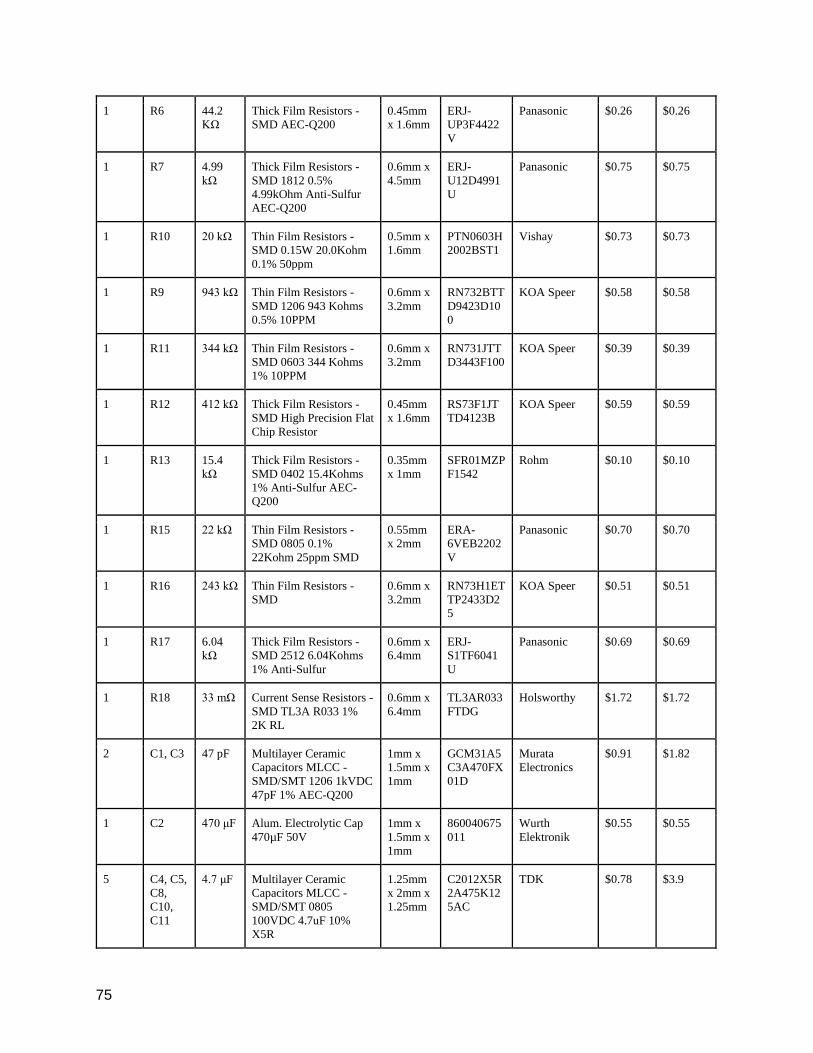
75
1 R6 44.2
KΩ
Thick Film Resistors -
SMD AEC-Q200
0.45mm
x 1.6mm
ERJ-
UP3F4422
V
Panasonic $0.26 $0.26
1 R7 4.99
kΩ
Thick Film Resistors -
SMD 1812 0.5%
4.99kOhm Anti-Sulfur
AEC-Q200
0.6mm x
4.5mm
ERJ-
U12D4991
U
Panasonic $0.75 $0.75
1 R10 20 kΩ Thin Film Resistors -
SMD 0.15W 20.0Kohm
0.1% 50ppm
0.5mm x
1.6mm
PTN0603H
2002BST1
Vishay $0.73 $0.73
1 R9 943 kΩ Thin Film Resistors -
SMD 1206 943 Kohms
0.5% 10PPM
0.6mm x
3.2mm
RN732BTT
D9423D10
0
KOA Speer $0.58 $0.58
1 R11 344 kΩ Thin Film Resistors -
SMD 0603 344 Kohms
1% 10PPM
0.6mm x
3.2mm
RN731JTT
D3443F100
KOA Speer $0.39 $0.39
1 R12 412 kΩ Thick Film Resistors -
SMD High Precision Flat
Chip Resistor
0.45mm
x 1.6mm
RS73F1JT
TD4123B
KOA Speer $0.59 $0.59
1 R13 15.4
kΩ
Thick Film Resistors -
SMD 0402 15.4Kohms
1% Anti-Sulfur AEC-
Q200
0.35mm
x 1mm
SFR01MZP
F1542
Rohm $0.10 $0.10
1 R15 22 kΩ Thin Film Resistors -
SMD 0805 0.1%
22Kohm 25ppm SMD
0.55mm
x 2mm
ERA-
6VEB2202
V
Panasonic $0.70 $0.70
1 R16 243 kΩ Thin Film Resistors -
SMD
0.6mm x
3.2mm
RN73H1ET
TP2433D2
5
KOA Speer $0.51 $0.51
1 R17 6.04
kΩ
Thick Film Resistors -
SMD 2512 6.04Kohms
1% Anti-Sulfur
0.6mm x
6.4mm
ERJ-
S1TF6041
U
Panasonic $0.69 $0.69
1 R18 33 mΩ Current Sense Resistors -
SMD TL3A R033 1%
2K RL
0.6mm x
6.4mm
TL3AR033
FTDG
Holsworthy $1.72 $1.72
2 C1, C3 47 pF Multilayer Ceramic
Capacitors MLCC -
SMD/SMT 1206 1kVDC
47pF 1% AEC-Q200
1mm x
1.5mm x
1mm
GCM31A5
C3A470FX
01D
Murata
Electronics
$0.91 $1.82
1 C2 470 μF Alum. Electrolytic Cap
470µF 50V
1mm x
1.5mm x
1mm
860040675
011
Wurth
Elektronik
$0.55 $0.55
5 C4, C5,
C8,
C10,
C11
4.7 μF Multilayer Ceramic
Capacitors MLCC -
SMD/SMT 0805
100VDC 4.7uF 10%
X5R
1.25mm
x 2mm x
1.25mm
C2012X5R
2A475K12
5AC
TDK $0.78 $3.9

76
1 C6 0.1 μF Multilayer Ceramic
Capacitors MLCC -
SMD/SMT 25V 0.1uF
C0G 1206 10% AEC-
Q200
1.6mm x
3.2mm x
1.6mm
C1206C104
K3GACAU
TO
KEMET $2.01 $2.01
2 C7, C9 100 μF Alum. Electrolytic Cap
100µF 400V
16mm 860021380
020
Wurth
Elektronik
$2.49 $4.98
1 M1 STW1
1NM8
0
N-channel 800 V, 0.35
Ohm, 11 A MDmesh
Power MOSFET
20.2mm
x
15.8mm
x 5mm
STW11NM
80
STMicroelectr
onics
$0.98 $0.98
1 Q2 Si4490
DY
N-Channel 200-V (D-S)
MOSFET
5.8mm x
4.8mm x
1.35mm
Si4490DY Siliconix $1.01 $1.01
1 K 1:1 600 Ohm 1:1 EI14
Isolation Transformer
13mm x
6mm x
12mm
Walfrontvo
qgntyag2
Walfront $1.09 $1.09
1 K1 8:1:1 Pulse Transformer, 600
H, 1.85 ohm, 4.5 kV
18mm x
16.5mm
x 18mm
750813134 Wurth
Elektronik
$8.16 $8.16
1 K5 4:1 PWR XFMR
LAMINATED 16VA TH
65mm x
51mm x
38.8mm
BV054-
5384.0-ND
Pulse
Electronics
Power
$10.97 $10.97
1 U1 LT831
6
Dc Flyback Controller 1
Input: 156 -168 V DC
Output: 12V 2A
Or
Input: 330 -337 V DC
Output: 12V 2A
6.4mm x
6.6mm x
1.78mm
LT8316 Analog
Devices
$2.62 $2.62
1 U3 LT374
8
DC Flyback Controller 2
Input: 48V, Output:
12V@2A
4mm x
4.9mm x
1.1mm
LT3748 Analog
Devices
$3.79 $3.79
1 U2 LTM8
062A
uModule Power
Tracking Battery
Chargers
12.7mm
x 7.6mm
x 4.4mm
LTM8062A Analog
Devices
$12.39 $12.39
4 Battery 3 V 3v Lithium Coin Cell
Battery
Diameter
=20mm
Height
=3.2mm
CR2023 Duracell $2.75 $10.98
Total Costs $81.15
Copyright © 2022 FDOKUMEN