antibacterial, plasmonic, and toxic properties of engineered
Upload
khangminh22Category
view
0download
0
Citation: Barichello, J.; Mariani, P.;
Matteocci, F.; Vesce, L.; Reale, A.;
Di Carlo, A.; Lanza, M.; Di Marco, G.;
Polizzi, S.; Calogero, G. The Golden
Fig: A Plasmonic Effect Study of
Organic-Based Solar Cells.
Nanomaterials 2022, 12, 267.
https://doi.org/10.3390/
nano12020267
Academic Editors: Sae Byeok Jo and
Elias Stathatos
Received: 29 November 2021
Accepted: 12 January 2022
Published: 14 January 2022
Publisher’s Note: MDPI stays neutral
with regard to jurisdictional claims in
published maps and institutional affil-
iations.
Copyright: © 2022 by the authors.
Licensee MDPI, Basel, Switzerland.
This article is an open access article
distributed under the terms and
conditions of the Creative Commons
Attribution (CC BY) license (https://
creativecommons.org/licenses/by/
4.0/).
nanomaterials
Article
The Golden Fig: A Plasmonic Effect Study of Organic-BasedSolar CellsJessica Barichello 1,*, Paolo Mariani 1 , Fabio Matteocci 1, Luigi Vesce 1 , Andrea Reale 1 , Aldo Di Carlo 1,2,Maurizio Lanza 3, Gaetano Di Marco 3, Stefano Polizzi 4 and Giuseppe Calogero 3,*
1 CHOSE—Centre for Hybrid and Organic Solar Energy, Department of Electronic Engineering,University of Rome “Tor Vergata”, 00133 Roma, Italy; [email protected] (P.M.);[email protected] (F.M.); [email protected] (L.V.); [email protected] (A.R.);[email protected] (A.D.C.)
2 ISM-CNR, Istituto di Struttura della Materia, Consiglio Nazionale delle Ricerche, 00133 Roma, Italy3 CNR-IPCF, Istituto per i Processi Chimico-Fisici, Consiglio Nazionale delle Ricerche, 98158 Messina, Italy;
[email protected] (M.L.); [email protected] (G.D.M.)4 Dipartimento di Scienze Molecolari e Nanosistemi, Università Ca’ Foscari Venezia,
30172 Venezia-Mestre, Italy; [email protected]* Correspondence: [email protected] (J.B.); [email protected] (G.C.)
Abstract: An optimization work on dye-sensitized solar cells (DSSCs) based on both artificial andnatural dyes was carried out by a fine synthesis work embedding gold nanoparticles in a TiO2 semi-conductor and perfecting the TiO2 particle sizes of the scattering layer. Noble metal nanostructuresare known for the surface plasmon resonance peculiarity that reveals unique properties and hasbeen implemented in several fields such as sensing, photocatalysis, optical antennas and PV devices.By embedding gold nanoparticles in the mesoporous TiO2 layer and adding a scattering layer, wewere able to boost the power conversion efficiency (PCE) to 10.8%, using an organic rutheniumcomplex. The same implementation was carried out using a natural dye, betalains, extracted fromSicilian prickly pear. In this case, the conversion efficiency doubled from 1 to 2% (measured at 1 SUNillumination, 100 mW/cm2 under solar simulation irradiation). Moreover, we obtained (measured at0.1 SUN, 10 mW/cm2 under blue light LED irradiation) a record efficiency of 15% with the betalain-based dye, paving the way for indoor applications in organic natural devices. Finally, an attempt toscale up the system is shown, and a betalain-based- dye-sensitized solar module (DSSM), with anactive area of 43.2 cm2 and a PCE of 1.02%, was fabricated for the first time.
Keywords: DSSC; gold nanoparticles; plasmonic effect; natural dye; DSSM
1. Introduction
The current energy crisis spurs us to employ pollution-free sustainable energy sources.Since solar radiation is the most abundant energy resource available on Earth [1], photo-voltaics (PVs) are being considered one of the most promising technologies based on arenewable source. Recently, numerous research groups have invested much effort in testingnew 2D/3D materials, innovative device structures and cheap fabrication procedures toenhance power conversion efficiency (PCE) and lower material costs in order to enablePV devices compete with electricity produced from fossil fuels [2,3]. Dye-sensitized solarcells (DSSCs) belong to the so-called third-generation solar cells. Despite their moderateefficiencies as compared to first-generation silicon cells (a certified PCE of 26% for the bestsilicon cell and a certified PCE of 13% for DSSCs) [4], DSSC technology continues to attractthe attention of the scientific community with 1000 published articles in 2020 [5]. DSSCshave gained widespread interest due to their low production costs, simple fabrication and,above all, their tunable optical properties and the weak dependence of PCE on the inci-dence radiation angle. Moreover, DSSCs have the feature of increasing PCE under low sun
Nanomaterials 2022, 12, 267. https://doi.org/10.3390/nano12020267 https://www.mdpi.com/journal/nanomaterials
Nanomaterials 2022, 12, 267 2 of 13
radiation intensity and diffuse light conditions when compared to PV technologies basedsolely on semiconductors [6]. These last peculiarities identify DSSC devices as some of themost suitable PV technologies for indoor application [7–9]. Furthermore, many researchersare proposing DSSCs as power supply cells for Internet of Things (IoT) systems [8,9] un-derlying connections among wireless sensor nodes, consumer electronic devices, wearabledevices and smart meters; since the power needed for IoT devices is typically low, DSSCdevices can easily supply their energy consumption under indoor conditions.
The DSSC, or Gräzel’s device [10], has a typical sandwich shape where all active layersare typically sanMdwiched between two transparent conductive glasses. The workingelectrode (WE) is conductive glass where a mesoporous layer of TiO2 (or another semicon-ductor) lies. The TiO2 layer is then sensitized by a dye and impregnated with an electrolytesolution (redox mediator) and the device is finally closed with another conductive glass,the counter electrode (CE), where a catalyst is deposited. The dye absorbs the solar radia-tion and injects excited electrons in the conduction band of the semiconductor; the redoxmediator works to regenerate the oxidized dye. The redox mediator regenerates itself byaccepting electrons from the catalyst and, in this way, the electrons’ flow continues againand again.
Since the first presentation of the nanostructured titanium dioxide (TiO2) DSSC [10],improvements have been carried out for each constituent of this photo-electrochemicaldevice [11] and, in particular, several functional elements have been added to the initialsimple structure, with the aim of improving light harvesting and charge transport, de-creasing dark current and reducing charge carriers’ recombination. A state-of-the-art cellhas around 11% of PCE, with a ruthenium-based dye and an iodine-based electrolyte [12].The poor light absorption capability of metal oxides (TiO2 absorbs light mainly in theUV region) and of the dye molecules (ruthenium-based dye absorbs light in the visibleregion) [13] is a hindrance to their PCE growth. Incorporation of plasmonic nanoparticles(NPs), such as Ag and Au NPs, into photovoltaics appears to be a highly promising strategyfor the improvement of their PCE [14,15]. In fact, NP scattering induces non-Hermitiancoupling between the clockwise and counter-clockwise rotating intracavity modes. Someresearchers showed that, by straightforwardly tuning the relative position and the volumeof the nanoparticles, achirality and strong chiral behaviors of the reflected fields can beobserved due to the asymmetric backscattering. This is a counter-intuitive characteristic ofchaotic dynamics. They believe that the chiral light chaos is highly feasible in the laboratory.Beyond their fundamental scientific significance, their results will deepen our understand-ing of non-linear phenomena and chaos in open systems, and may pave the way towardpotential applications [16]. Furthermore, NP-mediated chiral light chaos is based on sym-metrical second-harmonic generation [17], which reflects the interaction of optical fieldswith matter inside the anode. Indeed, it has been found that plasmonic NPs absorb lightvia the collective oscillations of surface electrons, which can be excited and directly injectedinto the conduction band of semiconductors [15]. Furthermore, the poor light absorptioncapability of TiO2 can also be extended through the enhancement of the photo-absorptioncross-section of dye molecules [18]. In addition, the formation of Schottky barriers at theinterface of metal oxide and metal NPs can significantly reduce the recombination rate ofphoto-excited electron–hole pairs [19]. Therefore, plasmonic NPs of different morphologiesshowing tuned surface plasmon resonance (SPR) characteristics have been tested for thePCE enhancement of DSSCs [18–21]. Although the incorporation of bare plasmonic metalNPs has improved the PCE of DSSCs, the use of corrosive iodide-based liquid electrolytesresults in reduced long-term stability, unless metal NPs are protected [22–24]. Therefore,core–shell nanostructures having a noble metal core and metal oxide shell have gainedimmense attention in various applications, including DSSCs, due to their unique physicalproperties with high thermal and chemical stability [23–30]. The aim of this work is toinvestigate the gold plasmonic effect in a natural dye-based device and to compare it tothat of an artificial dye.

Nanomaterials 2022, 12, 267 3 of 13
In the present work, we developed an original scattering layer that comprises nanopar-ticles of three different sizes (250, 300, 500 nm), and we compared it with a commercialone (NPs of 250 nm). As a reference dye, we used the ruthenium complex N719 (di-tetrabutylammonium cis-bis (isothiocyanato)bis(2,2′-bipyridyl-4,4′-dicarboxylato) ruthe-nium(II) [12]. The addition on the semiconductor layer of a thin film (5 µm) of TiO2 withlarge NPs (>20 nm) is well known to boost the optical absorption and ensure adequatelight trapping in a device [31,32]. The choice of using three NP sizes, to the best of ourknowledge, for the first time in the literature, was made to obtain scattering at differentlight wavelengths. Device optimization by our homemade scattering layer caused anincrement of 7% in the current density (Jsc) and an 8% increment in PCE. After this, core-shell Au@TiO2 NPs were incorporated directly into the TiO2 nanoparticles to assemblethe photo-active layer (Figure 1). This structure boosts the PCE, mainly influencing theopen circuit voltage (Voc) (+4%), reaching a PCE of 10.85% (+5%). We tested, for the firsttime in the literature, the effect of core–shell Au@TiO2 NPs in a natural dye-based DSSCwith betalains from Sicilian prickly pear. In the struggle to cut costs and to use increasinglypollution-free materials, it is of significant importance to investigate the use of natural dyesthat are ideal candidates for environmentally friendly solar cells. Natural DSSCs are awidely explored topic because they are non-toxic, low cost, renewable and abundant, butmuch effort is needed to increase their efficiency that is currently mainly around 3% [33,34].Here, with the presence of Au@TiO2 NPs, the efficiency doubled from 1 to 2%, mainlyinfluenced by Voc and Jsc. We performed JV measurement at 0.1 SUN (indoor conditions,blue LED irradiation) with the aim of proving the capability of natural dye to produce highPCE under shadow conditions and considering their application in an indoor context: 15%and 64% of conversion efficiencies were obtained with betalains and N719, respectively. Asthe last step of this work, we present a first attempt to scale up this device. We realized anatural dye-sensitized solar module (DSSM) with an active area of 43.2 cm2 and a PCE of1.02%. As far as we know, this is the largest module based on a natural dye reported in apublished work.
Nanomaterials 2022, 12, 267 3 of 14
and chemical stability [23–30]. The aim of this work is to investigate the gold plasmonic effect in a natural dye-based device and to compare it to that of an artificial dye.
In the present work, we developed an original scattering layer that comprises nanoparticles of three different sizes (250, 300, 500 nm), and we compared it with a commercial one (NPs of 250 nm). As a reference dye, we used the ruthenium complex N719 (di-tetrabutylammonium cis-bis (isothiocyanato)bis(2,2′-bipyridyl-4,4′-dicarboxylato) ruthenium(II) [12]. The addition on the semiconductor layer of a thin film (5 µm) of TiO2 with large NPs (>20 nm) is well known to boost the optical absorption and ensure adequate light trapping in a device [31,32]. The choice of using three NP sizes, to the best of our knowledge, for the first time in the literature, was made to obtain scattering at different light wavelengths. Device optimization by our homemade scattering layer caused an increment of 7% in the current density (Jsc) and an 8% increment in PCE. After this, core-shell Au@TiO2 NPs were incorporated directly into the TiO2 nanoparticles to assemble the photo-active layer (Figure 1). This structure boosts the PCE, mainly influencing the open circuit voltage (Voc) (+4%), reaching a PCE of 10.85% (+5%). We tested, for the first time in the literature, the effect of core–shell Au@TiO2 NPs in a natural dye-based DSSC with betalains from Sicilian prickly pear. In the struggle to cut costs and to use increasingly pollution-free materials, it is of significant importance to investigate the use of natural dyes that are ideal candidates for environmentally friendly solar cells. Natural DSSCs are a widely explored topic because they are non-toxic, low cost, renewable and abundant, but much effort is needed to increase their efficiency that is currently mainly around 3% [33,34]. Here, with the presence of Au@TiO2 NPs, the efficiency doubled from 1 to 2%, mainly influenced by Voc and Jsc. We performed JV measurement at 0.1 SUN (indoor conditions, blue LED irradiation) with the aim of proving the capability of natural dye to produce high PCE under shadow conditions and considering their application in an indoor context: 15% and 64% of conversion efficiencies were obtained with betalains and N719, respectively. As the last step of this work, we present a first attempt to scale up this device. We realized a natural dye-sensitized solar module (DSSM) with an active area of 43.2 cm2 and a PCE of 1.02%. As far as we know, this is the largest module based on a natural dye reported in a published work.
Figure 1. Cross-section view of plasmonic-based dye-sensitized solar cell.
2. Materials and Methods 2.1. Preparation of TiO2 Sub-Micrometric Powder and Paste for Scattering
The sub-micrometric TiO2 particles (beads) were prepared via a sol–gel process, followed by a solvothermal treatment in an ethanol/water solution (160 °C, 16 h) and calcination (500 °C, 2 h), as described in [35]. Titanium (IV) isopropoxide (TIP) was used as a titanium precursor and hexadecylammine (HAD) acted as a structure-directing agent in the precursor solution, whereas KCl was used to control the monodispersity of the beads by adjusting the ionic strength of the solution. To obtain the final mesoporous, crystalline anatase TiO2 beads with sizes of about 300 nm and 500 nm, in the following
Figure 1. Cross-section view of plasmonic-based dye-sensitized solar cell.
2. Materials and Methods2.1. Preparation of TiO2 Sub-Micrometric Powder and Paste for Scattering
The sub-micrometric TiO2 particles (beads) were prepared via a sol–gel process, fol-lowed by a solvothermal treatment in an ethanol/water solution (160 C, 16 h) and calci-nation (500 C, 2 h), as described in [35]. Titanium (IV) isopropoxide (TIP) was used as atitanium precursor and hexadecylammine (HAD) acted as a structure-directing agent inthe precursor solution, whereas KCl was used to control the monodispersity of the beadsby adjusting the ionic strength of the solution. To obtain the final mesoporous, crystallineanatase TiO2 beads with sizes of about 300 nm and 500 nm, in the following solution com-position of HDA:H2O:KCl:ethanol:TIP (molar ratio), were used: 0.5:5:5.5 × 10⁻³:230.3:1.0(300 nm) and 0.75:7:5.5 × 10⁻³:230.3:1.0 (500 nm). We used, as a reference, a scattering layerpurchased from a company (Dyesol, Queanbeyan, Australia) with nanoparticles of 250 nm.
Nanomaterials 2022, 12, 267 4 of 13
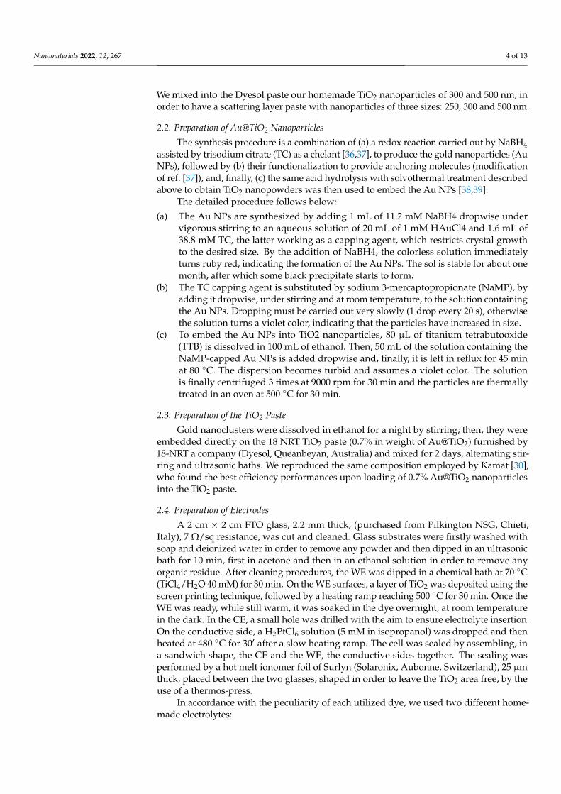
We mixed into the Dyesol paste our homemade TiO2 nanoparticles of 300 and 500 nm, inorder to have a scattering layer paste with nanoparticles of three sizes: 250, 300 and 500 nm.
2.2. Preparation of Au@TiO2 Nanoparticles
The synthesis procedure is a combination of (a) a redox reaction carried out by NaBH4assisted by trisodium citrate (TC) as a chelant [36,37], to produce the gold nanoparticles (AuNPs), followed by (b) their functionalization to provide anchoring molecules (modificationof ref. [37]), and, finally, (c) the same acid hydrolysis with solvothermal treatment describedabove to obtain TiO2 nanopowders was then used to embed the Au NPs [38,39].
The detailed procedure follows below:
(a) The Au NPs are synthesized by adding 1 mL of 11.2 mM NaBH4 dropwise undervigorous stirring to an aqueous solution of 20 mL of 1 mM HAuCl4 and 1.6 mL of38.8 mM TC, the latter working as a capping agent, which restricts crystal growthto the desired size. By the addition of NaBH4, the colorless solution immediatelyturns ruby red, indicating the formation of the Au NPs. The sol is stable for about onemonth, after which some black precipitate starts to form.
(b) The TC capping agent is substituted by sodium 3-mercaptopropionate (NaMP), byadding it dropwise, under stirring and at room temperature, to the solution containingthe Au NPs. Dropping must be carried out very slowly (1 drop every 20 s), otherwisethe solution turns a violet color, indicating that the particles have increased in size.
(c) To embed the Au NPs into TiO2 nanoparticles, 80 µL of titanium tetrabutooxide(TTB) is dissolved in 100 mL of ethanol. Then, 50 mL of the solution containing theNaMP-capped Au NPs is added dropwise and, finally, it is left in reflux for 45 minat 80 C. The dispersion becomes turbid and assumes a violet color. The solutionis finally centrifuged 3 times at 9000 rpm for 30 min and the particles are thermallytreated in an oven at 500 C for 30 min.
2.3. Preparation of the TiO2 Paste
Gold nanoclusters were dissolved in ethanol for a night by stirring; then, they wereembedded directly on the 18 NRT TiO2 paste (0.7% in weight of Au@TiO2) furnished by18-NRT a company (Dyesol, Queanbeyan, Australia) and mixed for 2 days, alternating stir-ring and ultrasonic baths. We reproduced the same composition employed by Kamat [30],who found the best efficiency performances upon loading of 0.7% Au@TiO2 nanoparticlesinto the TiO2 paste.
2.4. Preparation of Electrodes
A 2 cm × 2 cm FTO glass, 2.2 mm thick, (purchased from Pilkington NSG, Chieti,Italy), 7 Ω/sq resistance, was cut and cleaned. Glass substrates were firstly washed withsoap and deionized water in order to remove any powder and then dipped in an ultrasonicbath for 10 min, first in acetone and then in an ethanol solution in order to remove anyorganic residue. After cleaning procedures, the WE was dipped in a chemical bath at 70 C(TiCl4/H2O 40 mM) for 30 min. On the WE surfaces, a layer of TiO2 was deposited using thescreen printing technique, followed by a heating ramp reaching 500 C for 30 min. Once theWE was ready, while still warm, it was soaked in the dye overnight, at room temperaturein the dark. In the CE, a small hole was drilled with the aim to ensure electrolyte insertion.On the conductive side, a H2PtCl6 solution (5 mM in isopropanol) was dropped and thenheated at 480 C for 30′ after a slow heating ramp. The cell was sealed by assembling, ina sandwich shape, the CE and the WE, the conductive sides together. The sealing wasperformed by a hot melt ionomer foil of Surlyn (Solaronix, Aubonne, Switzerland), 25 µmthick, placed between the two glasses, shaped in order to leave the TiO2 area free, by theuse of a thermos-press.
In accordance with the peculiarity of each utilized dye, we used two different home-made electrolytes:
Nanomaterials 2022, 12, 267 5 of 13
• J8* (LiI 0.1 M, I2 0.05 M, MPII 0.6 M, TBP 0.5 M in AN:VN 70:30) for N719 [40];• AS8* (LiI 0.8 M, I2 0.05 M in AN:VN 85:15) for natural dye, betalains [40,41];
where MPII is 1-methyl-3-propyl imidazolium iodide, TBP is 4-tert-butyl-pyridine, AN isacetonitrile and VN is valeronitrile.
As explained in detail in a previous paper [40], the addition of basic compounds suchas TBP causes a partial desorption of natural dyes from the TiO2 surface and a shift of theabsorption spectra towards the red region. This last effect leads to a decrement in the molarextinction coefficient of the natural dye and a general decrease in device performance. Onthe other hand, the presence of TBP in a ruthenium dye DSSC influences the conductiveband of TiO2, increasing the Voc and all the photovoltaic parameters [40].
2.5. Realization of the DSSC Module
Taking into account the cell fabrication shown above, a similar procedure was appliedfor the realization of a Z-type DSSC module; two conductive glasses covered with afluorine-doped tin-oxide (FTO, 7 ohm/square) were cut with the dimensions of 10.5 cm× 9.5 cm. Among them, 8 cells were isolated, etching the FTO with a CO2 laser system.The conductive glasses were cleaned with deionized water and soap and then rinsed withacetone and ethanol. Since the screen printing technique is considered one of the mostreproducible methods for scaling up to large areas (>10 cm2) [42], all active layers weredeposited by an automated screen printer. A silver paste (7710 from Chimet, Arezzo, Italy)was screen printed on each electrode (WE and CE) to create vertical connections for eachcell in the module. On the WE, a TiO2 paste (18 NRT by GreatCell Solar, Rome, Italy) wasdeposited. We then sintered the titania layer in an oven for 30 min at 500 C. On the counterelectrode, a layer of platinum paste (from 3D Nano, Kraków, Poland) thinner than 1 µmwas printed and then fired at 480 C for 30 min. After dipping the WE in the dye solutionovernight (around 16 h), the two electrodes were sealed with a thermoplastic foil (Bynel60 by DuPont, Milan, Italy) shaped in order to protect the grids and the substrates weresealed by a thermal press. The electrolyte was inserted by the vacuum back filling techniquethrough little channels (around 0.8 mm) left in the Bynel mask. At the end, we sealed thedevice with a UV-curable commercial resin (ThreeBond®, Saint Ouen L’Aumone, France).
2.6. Preparation of Dye Sensitizer
A ruthenium complex, N719 (purchased from Solaronix, Aubonne, Switzerland) wasdissolved with a concentration of 0.3 mM in ethanol solvent. One hundred grams of Sicilianprickly pear was collected from the plant when fruits reached the typical red color. Later,fruits were washed with distilled water and left to dry. Using a mortar and a pestle, thefruits were mashed to facilitate the dye extraction process. A doubled amount of acidsolution (water and HCl 2M) at pH 2, compared to the obtained liquid, was added and theextract was left in an ultrasonic bath for 20 min. At the end, the extract was filtrated.
2.7. Measurement
Anode thickness was measured with a profilometer DektakXT Veeco150 (Bruker,Arcore, Italy). X-ray diffraction (XRD) was carried out using a X’Pert system (Bragg–Brentano parafocusing geometry) (Philips, Malvern Panalytical Ltd., Malvern, UK) withnickel-filtered Cu Kα1 radiation (λ = 0.154184 nm). Transmission electron microscope (TEM)images were taken using a JEOL JEM 3010 (Jeol, Tokyo, Japan) operating at 300 kV. Forscanning electron microscopy (SEM) images, a SIGMA VP (Zeiss, Oberkochen, Germany)instrument with a field emission gun (FEG) source, using the in-lens secondary electrondetector (Everhart-Thornley), and an FEI model QUANTA FEG 450 (FELMI ZFE, Graz,Austria), were used. We obtain the current–voltage (I-V) curves with a digital Keithley236 multimeter (Farnell®, Milan, Italy) connected to a PC. We utilized a solar simulator(Model LS0100-1000, 300 W Xe-Arc lamp, powered by LSN251 power supply equippedwith AM 1.5 filter, 100 mWcm−2) (LOT-Oriel, Rome, Italy) to simulate sunlight irradiationand the incident irradiance was measured with a Si-based pyranometer. Absorption spectra
Nanomaterials 2022, 12, 267 6 of 13
were detected by a L20 UV–Vis spectrophotometer (range 180–1100 nm) (Perkin Elmer,Milan, Italy). The electrical performance of the DSCMs was measured under a ClassB Sun Simulator Solar Constant 1200 KHS (G2V, Edmonton, AB, Canada) at AM 1.5 G,100 mWcm−2, using a Keithley 2420 (Farnell®, Milan, Italy) as a source-meter in ambientconditions, calibrated with a SKS 1110 sensor (Skye Instruments Ltd., Llandrindod Wells,Powys, UK). For indoor light irradiation, we chose a typical light tube, a LIFE LED 9Wlamp, to test the DSCs under realistic indoor conditions. We measured the light intensitythat strikes the DSC by using a modified piranometer PYRIS (Perkin Elmer, Milan, Italy).As relatively few reports exist that focus on the use of DSCs for indoor light harvesting, nostandard indoor light source has been established to date.
3. Results3.1. The Scattering Layer
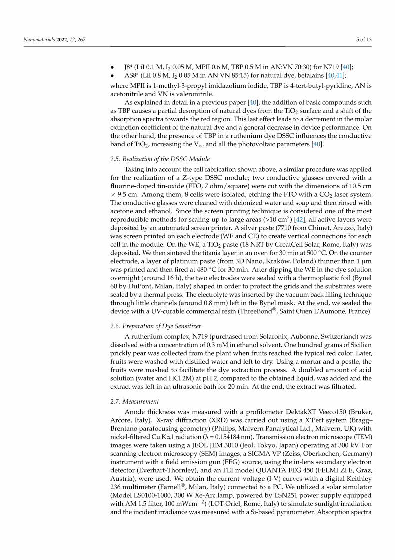
With the aim of studying the scattering light effect in DSSCs and to improve theperformance of the device, we wanted to fabricate an original scattering layer that wasdifferent from the commercial one (Wer 2.0 from Dyesol, Queanbeyan, Australia). Wepropose a scattering layer with nanoparticles of different sizes, between 300 and 500 nm,in order to improve the light backscattering at different wavelengths. A SEM image(Figure 2) shows the obtained nanoparticles of different sizes. We tested the homemadescattering layer paste (named “scattering J”) with NPs of three sizes (250, 300 and 500 nm)by comparing it with the commercial one (only 250 nm) called “scattering D”. For eachbatch, composed of five cells, statistical results are shown in Table 1. The most influencedelectrical parameter is the current density (Jsc) that increases by 7% using the three NP sizesin the scattering layer, confirming their ability to scatter light of different wavelengths. Afteroptimizing the device’s scattering layer, we moved on to the gold nanoparticle fabrication.
Nanomaterials 2022, 12, 267 6 of 14
For scanning electron microscopy (SEM) images, a SIGMA VP (Zeiss, Oberkochen, Ger-many) instrument with a field emission gun (FEG) source, using the in-lens secondary electron detector (Everhart-Thornley), and an FEI model QUANTA FEG 450 (FELMI ZFE, Graz, Austria), were used. We obtain the current–voltage (I-V) curves with a digital Keithley 236 multimeter (Farnell®, Milan, Italy) connected to a PC. We utilized a solar simulator (Model LS0100-1000, 300 W Xe-Arc lamp, powered by LSN251 power supply equipped with AM 1.5 filter, 100 mWcm−2) (LOT-Oriel, Rome, Italy) to simulate sunlight irradiation and the incident irradiance was measured with a Si-based pyranometer. Ab-sorption spectra were detected by a L20 UV–Vis spectrophotometer (range 180–1100 nm) (Perkin Elmer, Milan, Italy). The electrical performance of the DSCMs was measured un-der a Class B Sun Simulator Solar Constant 1200 KHS (G2V, Edmonton, AB, Canada) at AM 1.5 G, 100 mWcm−2, using a Keithley 2420 (Farnell®, Milan, Italy) as a source-meter in ambient conditions, calibrated with a SKS 1110 sensor (Skye Instruments Ltd., Llan-drindod Wells, Powys, UK). For indoor light irradiation, we chose a typical light tube, a LIFE LED 9W lamp, to test the DSCs under realistic indoor conditions. We measured the light intensity that strikes the DSC by using a modified piranometer PYRIS (Perkin Elmer, Milan, Italy). As relatively few reports exist that focus on the use of DSCs for indoor light harvesting, no standard indoor light source has been established to date.
3. Results 3.1. The Scattering Layer
With the aim of studying the scattering light effect in DSSCs and to improve the per-formance of the device, we wanted to fabricate an original scattering layer that was dif-ferent from the commercial one (Wer 2.0 from Dyesol, Queanbeyan, Australia). We pro-pose a scattering layer with nanoparticles of different sizes, between 300 and 500 nm, in order to improve the light backscattering at different wavelengths. A SEM image (Figure 2) shows the obtained nanoparticles of different sizes. We tested the homemade scattering layer paste (named “scattering J”) with NPs of three sizes (250, 300 and 500 nm) by com-paring it with the commercial one (only 250 nm) called “scattering D”. For each batch, composed of five cells, statistical results are shown in Table 1. The most influenced elec-trical parameter is the current density (Jsc) that increases by 7% using the three NP sizes in the scattering layer, confirming their ability to scatter light of different wavelengths. After optimizing the device’s scattering layer, we moved on to the gold nanoparticle fabrication.
Figure 2. (A) SEM image of the sub-micrometric particle sizes (250, 300 and 500 nm) used for scat-tering layer. (B) SEM image of NPs
A B
Figure 2. (A) SEM image of the sub-micrometric particle sizes (250, 300 and 500 nm) used forscattering layer. (B) SEM image of NPs.
Table 1. Electrical parameter comparison between DSSC devices made with scattering D (Dyesol)and scattering J (homemade). Relative increment is calculated as an average.
TiO2 + scatt. D TiO2 + scatt. J
Jsc (mA/cm2) 20.0 ± 0.7 21.5 ± 0.3 +7%Voc (V) 0.69 ± 0.01 0.69 ± 0.01 -FF (%) 64 ± 1 65 ± 1 +1%η (%) 9.1 ± 0.4 9.8 ± 0.2 +8%
3.2. Au@TiO2
With the aim of further increasing electrical performances (such as VOC, JSC andPCE), we synthesized TiO2 nanoparticles with embedded gold clusters (Au@TiO2). Asalready mentioned, metal clusters should act as a co-sensitizer of the TiO2 mesoscopiclayer, through the effect of their surface plasmon resonance (SPR) and its influence onthe TiO2 electronic structure. Furthermore, the increased SPR-induced light scattering
Nanomaterials 2022, 12, 267 7 of 13
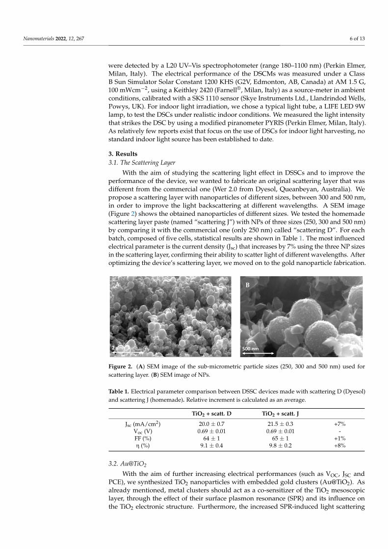
in the visible range should both increase the optical path and reduce the transmissionof the incident light. Moreover, this increased SPR-induced light scattering allows anenhancement of the rate of photons captured by the dye molecules and their conversioninto charge carriers. Regarding the embedding procedure, the gold surface needs to besupplied with a moiety which anchors on TiO2. In order to induce electrostatic repulsionbetween Au NPs and avoid their agglomeration during cappant substitution, a conjugatesalt of MPA, namely sodium 3-mercaptopropionate (NaMP), was used. This methodsuccessfully produces a stable dispersion of functionalized Au NPs with the original size.In absorbance spectra of Figure 3A, we compare bare and capped gold nanoparticles toembedded Au@TiO2; it emerges that no agglomeration occurs. The SPR width suggests thatgold nanoparticles with a narrow distribution of sizes are obtained, however, the averagesize calculated by using Mie theory (11 nm) is clearly overestimated, which is intrinsic to thismethodology for very small particles, since surface effects become increasingly importantbelow 10 nm [43]. Au NPs remained stable in size, without agglomerating, during theembedding procedure as well as after calcination. XRD showed that the embeddingprocedure led to the formation of amorphous TiO2 nanoparticles, which transformed intocrystalline anatase TiO2 nanoparticles after calcination (Figure 3B). The final Au@TiO2material is shown in the TEM images in Figure 4. Most of the Au nanoparticles arebelow 5 nm in size and are protected inside the TiO2 larger nanoparticles (Figure 4c,d).Furthermore, it is possible to notice that Au NPs are not seen to grow in size or agglomerateduring the embedding process (Figure 4b); indeed, the observed red-shift in absorbancespectra between Au NPs and Au@TiO2 must be related to readjustment of the electronicstructure of the material due to the interaction between gold and TiO2.
Nanomaterials 2022, 12, 267 8 of 14
(A) (B)
Figure 3. (A) Comparison of absorption spectra of bare and capped gold nanoparticles with embedded Au@TiO2. (B) Comparison of XRD patterns of gold, anatase and Au@TiO2.
Figure 4. TEM images of the Au@TiO2 nanoparticles: (a) before calcination and (b–d) after calcination; (c) and (d) magnification of a gold nanoparticle (dark spot) surrounded by TiO2 fringes.
3.3. The Working Electrode
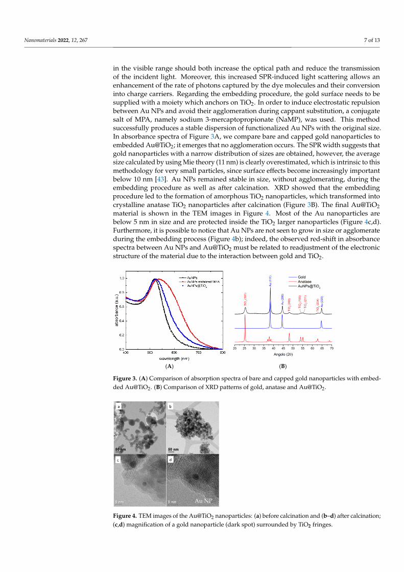
In order to investigate the plasmonic effect of gold NPs when mixed in the TiO2 paste, UV absorption spectra of solid bulk WEs (FTO/TiO2) were made. In Figure 5, we compare the reference TiO2 layer with the one mixed with Au@TiO2 nanoparticles. The presence of gold can be clearly recognized thanks to the absorbance increment in the spectral region 450–600 nm. This boosting effect of the Au NPs’ SPR has been confirmed on samples impregnated with the N719 dye (notice the large increase in the absorbance peak in Figure 6A), similar to previous work [43–45]. However, a different behavior was observed in samples impregnated with the betalain-based dye. Surprisingly, gold nanoparticles do not show the plasmonic effect and do not influence the absorbance intensity, resulting in no differences at all between the reference TiO2 and the doped TiO2 (Figure 6B). The different molar extinction coefficients (ε) are likely to be the cause of the dissimilar behavior. Indeed, N719 has a lower ε than betalains (ε N719: 1.4 × 10⁻⁴, ε betalains: 6.5 × 10⁻⁴ M−1cm−1) [40,46] and the higher ability of the betalains to capture photons could saturate the
Au NP
Figure 3. (A) Comparison of absorption spectra of bare and capped gold nanoparticles with embed-ded Au@TiO2. (B) Comparison of XRD patterns of gold, anatase and Au@TiO2.
Nanomaterials 2022, 12, 267 8 of 14
Figure 3. (A) Comparison of absorption spectra of bare and capped gold nanoparticles with embed-ded Au@TiO2. (B) Comparison of XRD patterns of gold, anatase and Au@TiO2.
Figure 4. TEM images of the Au@TiO2 nanoparticles: (a) before calcination and (b–d) after calcination; (c) and (d) magnification of a gold nanoparticle (dark spot) surrounded by TiO2 fringes.
3.3. The Working Electrode
In order to investigate the plasmonic effect of gold NPs when mixed in the TiO2 paste, UV absorption spectra of solid bulk WEs (FTO/TiO2) were made. In Figure 5, we compare the reference TiO2 layer with the one mixed with Au@TiO2 nanoparticles. The presence of gold can be clearly recognized thanks to the absorbance increment in the spectral region 450–600 nm. This boosting effect of the Au NPs’ SPR has been confirmed on samples im-pregnated with the N719 dye (notice the large increase in the absorbance peak in Figure 6A), similar to previous work [43–45]. However, a different behavior was observed in samples impregnated with the betalain-based dye. Surprisingly, gold nanoparticles do not show the plasmonic effect and do not influence the absorbance intensity, resulting in no differences at all between the reference TiO2 and the doped TiO2 (Figure 6B). The different molar extinction coefficients (ε) are likely to be the cause of the dissimilar behavior. In-deed, N719 has a lower ε than betalains (ε N719: 1.4 × 10⁻⁴, ε betalains: 6.5 × 10⁻⁴ M−1cm−1) [40,46] and the higher ability of the betalains to capture photons could saturate the ab-sorption. Another reason for the lack of the gold plasmon effect could lie in the different absorptions of betalains in a blue region [39,44] compared to N719; this absorption inter-cepts the light that should be used by the gold NPs for the plasmon effect.
Au NP
Figure 4. TEM images of the Au@TiO2 nanoparticles: (a) before calcination and (b–d) after calcination;(c,d) magnification of a gold nanoparticle (dark spot) surrounded by TiO2 fringes.
Nanomaterials 2022, 12, 267 8 of 13
3.3. The Working Electrode
In order to investigate the plasmonic effect of gold NPs when mixed in the TiO2paste, UV absorption spectra of solid bulk WEs (FTO/TiO2) were made. In Figure 5, wecompare the reference TiO2 layer with the one mixed with Au@TiO2 nanoparticles. Thepresence of gold can be clearly recognized thanks to the absorbance increment in thespectral region 450–600 nm. This boosting effect of the Au NPs’ SPR has been confirmedon samples impregnated with the N719 dye (notice the large increase in the absorbancepeak in Figure 6A), similar to previous work [43–45]. However, a different behaviorwas observed in samples impregnated with the betalain-based dye. Surprisingly, goldnanoparticles do not show the plasmonic effect and do not influence the absorbanceintensity, resulting in no differences at all between the reference TiO2 and the doped TiO2(Figure 6B). The different molar extinction coefficients (ε) are likely to be the cause ofthe dissimilar behavior. Indeed, N719 has a lower ε than betalains (ε N719: 1.4 × 10⁻⁴,ε betalains: 6.5 × 10⁻⁴ M−1cm−1) [40,46] and the higher ability of the betalains to capturephotons could saturate the absorption. Another reason for the lack of the gold plasmoneffect could lie in the different absorptions of betalains in a blue region [39,44] comparedto N719; this absorption intercepts the light that should be used by the gold NPs for theplasmon effect.
Nanomaterials 2022, 12, 267 8 of 14
Figure 3. (A) Comparison of absorption spectra of bare and capped gold nanoparticles with embed-ded Au@TiO2. (B) Comparison of XRD patterns of gold, anatase and Au@TiO2.
Figure 4. TEM images of the Au@TiO2 nanoparticles: (a) before calcination and (b–d) after calcination; (c) and (d) magnification of a gold nanoparticle (dark spot) surrounded by TiO2 fringes.
3.3. The Working Electrode
In order to investigate the plasmonic effect of gold NPs when mixed in the TiO2 paste, UV absorption spectra of solid bulk WEs (FTO/TiO2) were made. In Figure 5, we compare the reference TiO2 layer with the one mixed with Au@TiO2 nanoparticles. The presence of gold can be clearly recognized thanks to the absorbance increment in the spectral region 450–600 nm. This boosting effect of the Au NPs’ SPR has been confirmed on samples im-pregnated with the N719 dye (notice the large increase in the absorbance peak in Figure 6A), similar to previous work [43–45]. However, a different behavior was observed in samples impregnated with the betalain-based dye. Surprisingly, gold nanoparticles do not show the plasmonic effect and do not influence the absorbance intensity, resulting in no differences at all between the reference TiO2 and the doped TiO2 (Figure 6B). The different molar extinction coefficients (ε) are likely to be the cause of the dissimilar behavior. In-deed, N719 has a lower ε than betalains (ε N719: 1.4 × 10⁻⁴, ε betalains: 6.5 × 10⁻⁴ M−1cm−1) [40,46] and the higher ability of the betalains to capture photons could saturate the ab-sorption. Another reason for the lack of the gold plasmon effect could lie in the different absorptions of betalains in a blue region [39,44] compared to N719; this absorption inter-cepts the light that should be used by the gold NPs for the plasmon effect.
Au NP
Figure 5. Absorbance spectra of the reference TiO2 and the one mixed with Au@TiO2.
Nanomaterials 2022, 12, 267 9 of 14
absorption. Another reason for the lack of the gold plasmon effect could lie in the different absorptions of betalains in a blue region [39,44] compared to N719; this absorption intercepts the light that should be used by the gold NPs for the plasmon effect.
Figure 5. Absorbance spectra of the reference TiO2 and the one mixed with Au@TiO2.
(A) (B)
Figure 6. Absorbance spectra of the WE with the reference TiO2 and the one mixed with Au@TiO2 after dipping in (A) N719 and (B) betalains.
3.4. Photovoltaic Performances In order to identify the effect of gold nanoparticles on the complete device, we
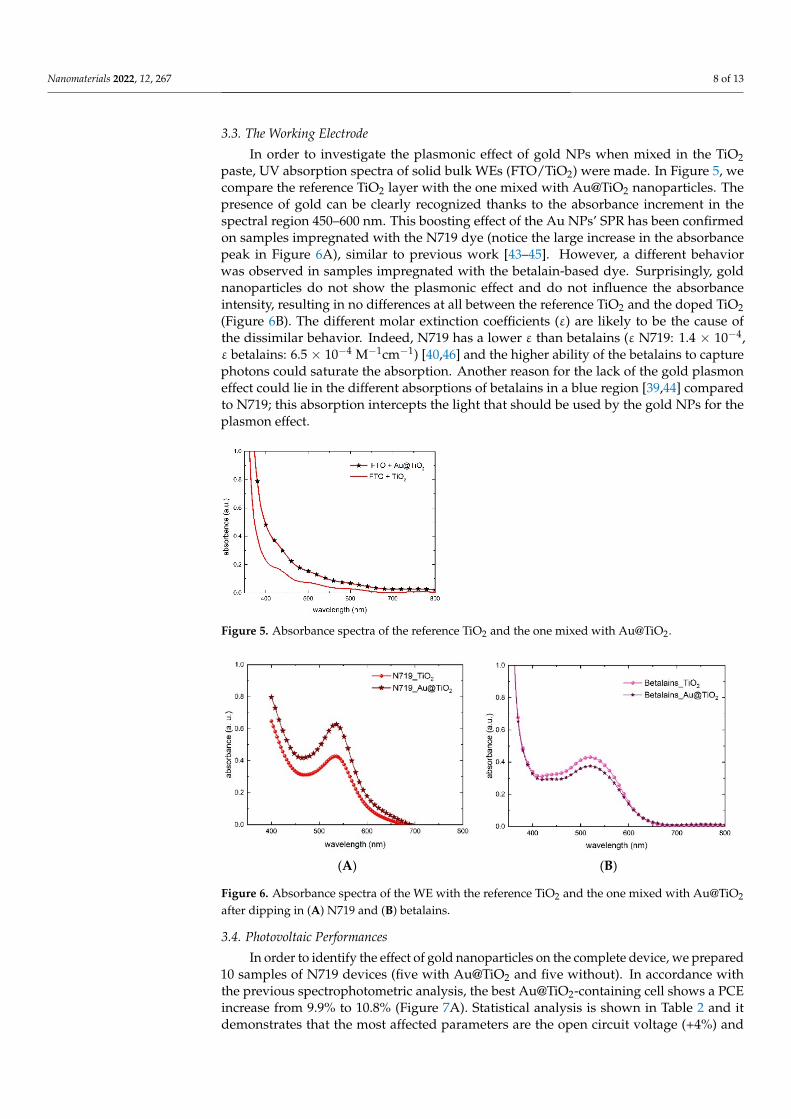
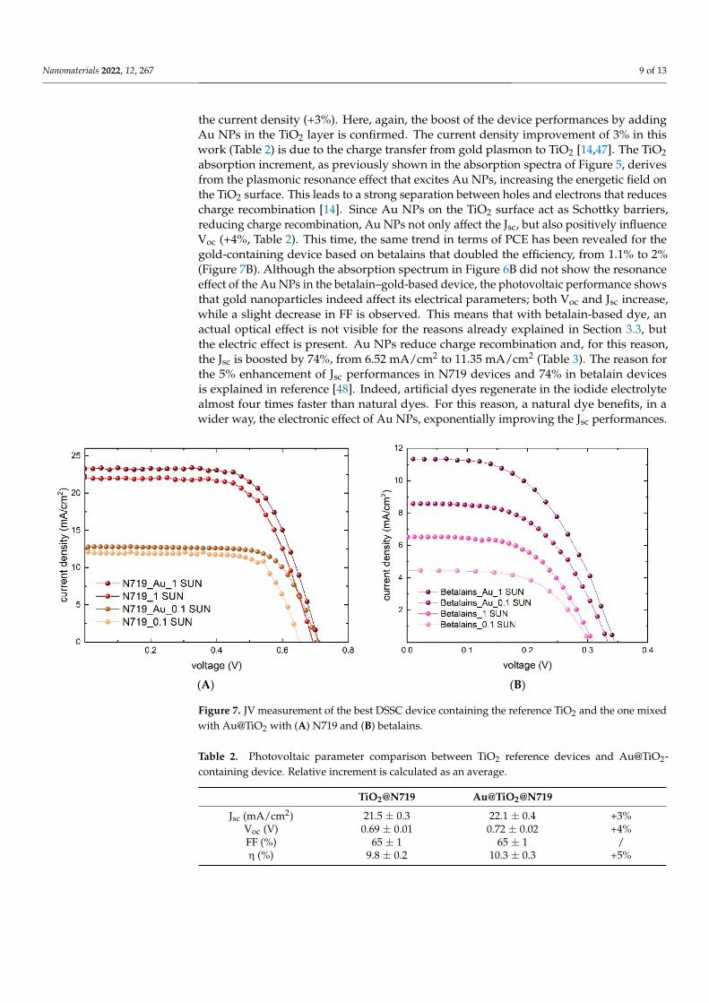
prepared 10 samples of N719 devices (five with Au@TiO2 and five without). In accordance with the previous spectrophotometric analysis, the best Au@TiO2-containing cell shows a PCE increase from 9.9% to 10.8% (Figure 7A). Statistical analysis is shown in Table 2 and it demonstrates that the most affected parameters are the open circuit voltage (+4%) and the current density (+3%). Here, again, the boost of the device performances by adding Au NPs in the TiO2 layer is confirmed. The current density improvement of 3% in this work (Table 2) is due to the charge transfer from gold plasmon to TiO2 [14,47]. The TiO2 absorption increment, as previously shown in the absorption spectra of Figure 5, derives from the plasmonic resonance effect that excites Au NPs, increasing the energetic field on the TiO2 surface. This leads to a strong separation between holes and electrons that reduces charge recombination [14]. Since Au NPs on the TiO2 surface act as Schottky barriers, reducing charge recombination, Au NPs not only affect the Jsc, but also positively influence Voc (+4%, Table 2). This time, the same trend in terms of PCE has been revealed for the gold-containing device based on betalains that doubled the efficiency, from 1.1% to 2% (Figure 7B). Although the absorption spectrum in Figure 6B did not show the resonance effect of the Au NPs in the betalain–gold-based device, the photovoltaic performance shows that gold nanoparticles indeed affect its electrical parameters; both Voc and Jsc increase, while a slight decrease in FF is observed. This means that with
Figure 6. Absorbance spectra of the WE with the reference TiO2 and the one mixed with Au@TiO2
after dipping in (A) N719 and (B) betalains.
3.4. Photovoltaic Performances
In order to identify the effect of gold nanoparticles on the complete device, we prepared10 samples of N719 devices (five with Au@TiO2 and five without). In accordance withthe previous spectrophotometric analysis, the best Au@TiO2-containing cell shows a PCEincrease from 9.9% to 10.8% (Figure 7A). Statistical analysis is shown in Table 2 and itdemonstrates that the most affected parameters are the open circuit voltage (+4%) and
Nanomaterials 2022, 12, 267 9 of 13
the current density (+3%). Here, again, the boost of the device performances by addingAu NPs in the TiO2 layer is confirmed. The current density improvement of 3% in thiswork (Table 2) is due to the charge transfer from gold plasmon to TiO2 [14,47]. The TiO2absorption increment, as previously shown in the absorption spectra of Figure 5, derivesfrom the plasmonic resonance effect that excites Au NPs, increasing the energetic field onthe TiO2 surface. This leads to a strong separation between holes and electrons that reducescharge recombination [14]. Since Au NPs on the TiO2 surface act as Schottky barriers,reducing charge recombination, Au NPs not only affect the Jsc, but also positively influenceVoc (+4%, Table 2). This time, the same trend in terms of PCE has been revealed for thegold-containing device based on betalains that doubled the efficiency, from 1.1% to 2%(Figure 7B). Although the absorption spectrum in Figure 6B did not show the resonanceeffect of the Au NPs in the betalain–gold-based device, the photovoltaic performance showsthat gold nanoparticles indeed affect its electrical parameters; both Voc and Jsc increase,while a slight decrease in FF is observed. This means that with betalain-based dye, anactual optical effect is not visible for the reasons already explained in Section 3.3, butthe electric effect is present. Au NPs reduce charge recombination and, for this reason,the Jsc is boosted by 74%, from 6.52 mA/cm2 to 11.35 mA/cm2 (Table 3). The reason forthe 5% enhancement of Jsc performances in N719 devices and 74% in betalain devicesis explained in reference [48]. Indeed, artificial dyes regenerate in the iodide electrolytealmost four times faster than natural dyes. For this reason, a natural dye benefits, in awider way, the electronic effect of Au NPs, exponentially improving the Jsc performances.
Nanomaterials 2022, 12, 267 10 of 14
betalain-based dye, an actual optical effect is not visible for the reasons already explained in Section 3.3, but the electric effect is present. Au NPs reduce charge recombination and, for this reason, the Jsc is boosted by 74%, from 6.52 mA/cm2 to 11.35 mA/cm2 (Table 3). The reason for the 5% enhancement of Jsc performances in N719 devices and 74% in betalain devices is explained in reference [48]. Indeed, artificial dyes regenerate in the iodide electrolyte almost four times faster than natural dyes. For this reason, a natural dye benefits, in a wider way, the electronic effect of Au NPs, exponentially improving the Jsc performances.
(A) (B)
Figure 7. JV measurement of the best DSSC device containing the reference TiO2 and the one mixed with Au@TiO2 with (A) N719 and (B) betalains.
Table 2. Photovoltaic parameter comparison between TiO2 reference devices and Au@TiO2-containing device. Relative increment is calculated as an average.
TiO2@N719 Au@TiO2@N719 Jsc (mA/cm²) 21.5 ± 0.3 22.1 ± 0.4 +3%
Voc (V) 0.69 ± 0.01 0.72 ± 0.02 +4% FF (%) 65 ± 1 65 ± 1 / η (%) 9.8 ± 0.2 10.3 ± 0.3 +5%
Since DSSC technology provides better performances in terms of PCE [8,9], with a LED lamp set at 0.1 SUN, we performed a JV measurement in order to evaluate the behavior of our devices in indoor environments. The device takes a longer time to recover due to the low photon flux that it receives and the fill factor consequently increases its value. Measurements with an LED lamp also confirmed the precedent behavior; gold nanoparticles boosted the efficiency from 56 to 64% for the N719 dye and from 7.9 to 15% for betalain dye (Table 3).
Table 3. Electrical parameter at 1 SUN, 100 mW/cm2 (solar simulator) and 0.1 SUN, 10 mW/cm2 (LED).
Sample Anode Irradiation (mW/cm2) Jsc (mA/cm2) Voc (V) FF (%) PCE (%)
Betalains TiO2@Au 100 11.3 0.34 52 2.0 Betalains TiO2 100 6.5 0.30 57 1.1 Betalains TiO2@Au 10 (LED) 8.6 0.33 54 15.3
Figure 7. JV measurement of the best DSSC device containing the reference TiO2 and the one mixedwith Au@TiO2 with (A) N719 and (B) betalains.
Table 2. Photovoltaic parameter comparison between TiO2 reference devices and Au@TiO2-containing device. Relative increment is calculated as an average.
TiO2@N719 Au@TiO2@N719
Jsc (mA/cm2) 21.5 ± 0.3 22.1 ± 0.4 +3%Voc (V) 0.69 ± 0.01 0.72 ± 0.02 +4%FF (%) 65 ± 1 65 ± 1 /η (%) 9.8 ± 0.2 10.3 ± 0.3 +5%
Nanomaterials 2022, 12, 267 10 of 13
Table 3. Electrical parameter at 1 SUN, 100 mW/cm2 (solar simulator) and 0.1 SUN, 10 mW/cm2 (LED).
Sample Anode Irradiation(mW/cm2) Jsc (mA/cm2) Voc (V) FF (%) PCE (%)
Betalains TiO2@Au 100 11.3 0.34 52 2.0Betalains TiO2 100 6.5 0.30 57 1.1Betalains TiO2@Au 10 (LED) 8.6 0.33 54 15.3Betalains TiO2 10 (LED) 4.4 0.31 57 7.9
N719 TiO2@Au 100 23.3 0.71 65 10.8N719 TiO2 100 22.0 0.69 65 9.9N719 TiO2@Au 10 (LED) 12.8 0.71 70 63.6N719 TiO2 10 (LED) 12.0 0.65 72 56.2
Since DSSC technology provides better performances in terms of PCE [8,9], witha LED lamp set at 0.1 SUN, we performed a JV measurement in order to evaluate thebehavior of our devices in indoor environments. The device takes a longer time to recoverdue to the low photon flux that it receives and the fill factor consequently increases itsvalue. Measurements with an LED lamp also confirmed the precedent behavior; goldnanoparticles boosted the efficiency from 56 to 64% for the N719 dye and from 7.9 to 15%for betalain dye (Table 3).
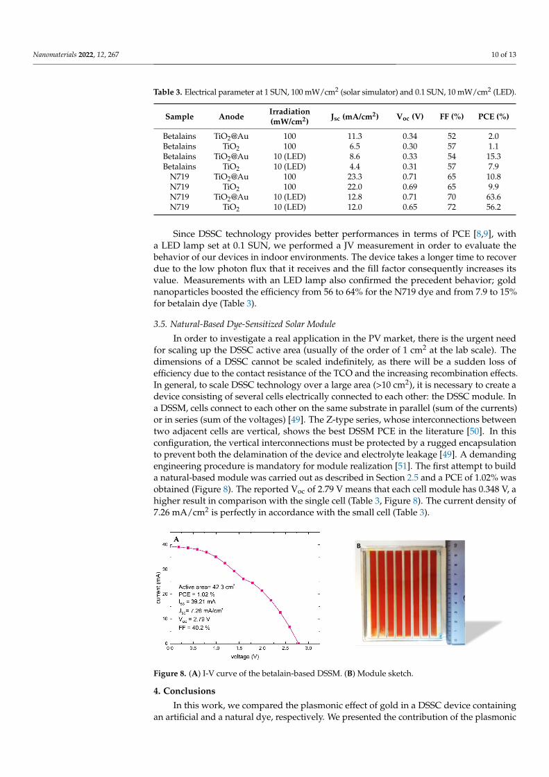
3.5. Natural-Based Dye-Sensitized Solar Module
In order to investigate a real application in the PV market, there is the urgent needfor scaling up the DSSC active area (usually of the order of 1 cm2 at the lab scale). Thedimensions of a DSSC cannot be scaled indefinitely, as there will be a sudden loss ofefficiency due to the contact resistance of the TCO and the increasing recombination effects.In general, to scale DSSC technology over a large area (>10 cm2), it is necessary to create adevice consisting of several cells electrically connected to each other: the DSSC module. Ina DSSM, cells connect to each other on the same substrate in parallel (sum of the currents)or in series (sum of the voltages) [49]. The Z-type series, whose interconnections betweentwo adjacent cells are vertical, shows the best DSSM PCE in the literature [50]. In thisconfiguration, the vertical interconnections must be protected by a rugged encapsulationto prevent both the delamination of the device and electrolyte leakage [49]. A demandingengineering procedure is mandatory for module realization [51]. The first attempt to builda natural-based module was carried out as described in Section 2.5 and a PCE of 1.02% wasobtained (Figure 8). The reported Voc of 2.79 V means that each cell module has 0.348 V, ahigher result in comparison with the single cell (Table 3, Figure 8). The current density of7.26 mA/cm2 is perfectly in accordance with the small cell (Table 3).
Nanomaterials 2022, 12, 267 11 of 14
Betalains TiO2 10 (LED) 4.4 0.31 57 7.9 N719 TiO2@Au 100 23.3 0.71 65 10.8 N719 TiO2 100 22.0 0.69 65 9.9 N719 TiO2@Au 10 (LED) 12.8 0.71 70 63.6 N719 TiO2 10 (LED) 12.0 0.65 72 56.2
3.5. Natural-Based Dye-Sensitized Solar Module In order to investigate a real application in the PV market, there is the urgent need
for scaling up the DSSC active area (usually of the order of 1 cm2 at the lab scale). The dimensions of a DSSC cannot be scaled indefinitely, as there will be a sudden loss of efficiency due to the contact resistance of the TCO and the increasing recombination effects. In general, to scale DSSC technology over a large area (>10 cm2), it is necessary to create a device consisting of several cells electrically connected to each other: the DSSC module. In a DSSM, cells connect to each other on the same substrate in parallel (sum of the currents) or in series (sum of the voltages) [49]. The Z-type series, whose interconnections between two adjacent cells are vertical, shows the best DSSM PCE in the literature [50]. In this configuration, the vertical interconnections must be protected by a rugged encapsulation to prevent both the delamination of the device and electrolyte leakage [49]. A demanding engineering procedure is mandatory for module realization [51]. The first attempt to build a natural-based module was carried out as described in Section 2.5 and a PCE of 1.02% was obtained (Figure 8). The reported Voc of 2.79 V means that each cell module has 0.348 V, a higher result in comparison with the single cell (Table 3, Figure 8). The current density of 7.26 mA/cm2 is perfectly in accordance with the small cell (Table 3).
Figure 8. (A) I-V curve of the betalain-based DSSM. (B) Module sketch.
4. Conclusions In this work, we compared the plasmonic effect of gold in a DSSC device containing
an artificial and a natural dye, respectively. We presented the contribution of the plasmonic effect of gold in a natural-based DSSC. We started with an improvement of the scattering layer effect: adding for the first time in the literature, as far as we know, three different sizes of nanoparticles (250, 300, 500 nm) in the scattering paste that amplifies the optical effect of the scattering layer. In this way, we have demonstrated a Jsc and PCE improvement of 7% and 8%, respectively, due to this optical effect. Furthermore, through fine synthesis work, we incorporated gold nanoparticles in a TiO2 core–shell to benefit from the plasmonic resonance effect, increasing the PCE of an N719-based DSSC from 9.8 to 10.3% (+5% on average), obtaining a maximum PCE of 10.8%. Once the optimization of the device was completed, we finally tested this structure and the plasmonic effect with a natural dye, betalains extracted from Sicilian prickly pear. We have discovered that the plasmonic gold resonance does not affect the optical properties of a natural-based device,
Figure 8. (A) I-V curve of the betalain-based DSSM. (B) Module sketch.
4. Conclusions
In this work, we compared the plasmonic effect of gold in a DSSC device containingan artificial and a natural dye, respectively. We presented the contribution of the plasmonic
Nanomaterials 2022, 12, 267 11 of 13
effect of gold in a natural-based DSSC. We started with an improvement of the scatteringlayer effect: adding for the first time in the literature, as far as we know, three different sizesof nanoparticles (250, 300, 500 nm) in the scattering paste that amplifies the optical effect ofthe scattering layer. In this way, we have demonstrated a Jsc and PCE improvement of 7%and 8%, respectively, due to this optical effect. Furthermore, through fine synthesis work,we incorporated gold nanoparticles in a TiO2 core–shell to benefit from the plasmonicresonance effect, increasing the PCE of an N719-based DSSC from 9.8 to 10.3% (+5% onaverage), obtaining a maximum PCE of 10.8%. Once the optimization of the device wascompleted, we finally tested this structure and the plasmonic effect with a natural dye,betalains extracted from Sicilian prickly pear. We have discovered that the plasmonic goldresonance does not affect the optical properties of a natural-based device, contrary to theartificial one, but the plasmonic contribution is effective from an electrical point of view.In the natural-based device, the optical effect of gold is not visible as the molar extinctioncoefficient of betalains is much higher than that of N719, thus saturating the absorptioneffect. On the other hand, in previous work, it was found that an artificial dye regeneratesfour times faster than a natural one; therefore, the electronic enhancement effect in reducingcharge recombination exponentially benefits a natural dye rather than an artificial one. Thebetalain-based device increased the PCE from 1 to 2% in the presence of gold (1 SUN, solarsimulator irradiation). With the aim of indoor applications, we measured both devicesunder 0.1 SUN (blue LED irradiation) and obtained PCEs of 64% and 15% for the N719and for the betalains, respectively. In addition, a first attempt was made to manufacturemodules with a natural dye to scale up the process. A 42.3 cm2 active area module, with anatural-based dye, achieved 1.02% PCE; as far as we know, this is the module based on anatural dye with the largest area reported in the literature.
Author Contributions: Conceptualization, J.B., G.C. and S.P.; methodology, J.B., G.C. and M.L.;validation, J.B., G.C., P.M., S.P. and M.L.; formal analysis, J.B., G.C., P.M. and L.V.; investigation, J.B.,G.C., P.M., L.V. and G.D.M.; resources, S.P., A.R., G.C., A.D.C., G.D.M. and F.M.; data curation, J.B.and G.C.; writing—original draft preparation, J.B.; writing—review and editing, J.B., G.C., P.M., M.L.and S.P.; visualization, J.B. and G.C.; supervision, G.C. and J.B.; project administration, J.B., G.C. andS.P. All authors have read and agreed to the published version of the manuscript.
Funding: This research received no external funding.
Data Availability Statement: The data presented in this study are available on request from thecorresponding authors.
Acknowledgments: We kindly acknowledge Roberto Caruso, Giuseppe Lupò and Giuseppe Spinellafor their technical support in some experimental set ups.
Conflicts of Interest: The authors declare no conflict of interest.
References1. Gielen, D.; Boshell, F.; Saygin, D.; Bazilian, M.D.; Wagner, N.; Gorini, R. The role of renewable energy in the global energy
trans-formation. Energy Strategy Rev. 2019, 24, 38–50. [CrossRef]2. Parida, B.; Iniyan, S.; Goic, R. A review of solar photovoltaic technologies. Renew. Sustain. Energy Rev. 2011, 15, 1625–1636.
[CrossRef]3. Bellani, S.; Bartolotta, A.; Agresti, A.; Calogero, G.; Grancini, G.; Di Carlo, A.; Kymakis, E.; Bonaccorso, F. Solution-processed
two-dimensional materials for next-generation photovoltaics. Chem. Soc. Rev. 2021, 50, 11870–11965. [CrossRef] [PubMed]4. NERL. Available online: https://www.nrel.gov/pv/cell-efficiency.html (accessed on 31 October 2021).5. Available online: https://scholar.google.com/scholar?q=DSSC&hl=it&as_sdt=0%2C5&as_rr=1&as_vis=1&as_ylo=2020&as_
yhi=2021 (accessed on 31 October 2021).6. Shakeel Ahmada, M.; Pandeya, A.K.; Abd Rahima, N. Advancements in the development of TiO2 photoanodes and its fabrication
methods for dye sensitized solar cell (DSSC) applications. A review. Renew. Sustain. Energy Rev. 2017, 77, 89–108. [CrossRef]7. Gong, J.; Sumathy, K.; Qiao, Q.; Zhou, Z. Review on dye-sensitized solar cells (DSSCs): Advanced techniques and research trends.
Renew. Sustain. Energy Rev. 2017, 68, 234–246. [CrossRef]8. Devadiga, D.; Selvakumar, M.; Shetty, P.; Santosh, M.S. Dye-Sensitized Solar Cell for Indoor Applications: A Mini-Review.
J. Electron. Mater. 2021, 50, 3187–3206. [CrossRef]
Nanomaterials 2022, 12, 267 12 of 13
9. Freitag, M.; Teuscher, J.; Saygili, Y.; Zhang, X.; Giordano, F.; Liska, P.; Hua, J.; Zakeeruddin, S.M.; Moser, J.-E.; Grätzel, M.; et al.Dye-sensitized solar cells for efficient power generation under ambient lighting. Nat. Photon 2017, 11, 372–378. [CrossRef]
10. O’Reagan, B.; Grätzel, M. A low-cost, high-efficiency Solar-Cell based on Dye-Sensitized Colloidal TiO2 films. Nature 1991,353, 737–740. [CrossRef]
11. Sharifi, N.; Tajabadi, F.; Taghavinia, N. Recent Developments in Dye-Sensitized Solar Cells. ChemPhysChem 2014, 15, 3902–3927.[CrossRef] [PubMed]
12. Nazeeruddin, M.K.; De Angelis, F.; Fantacci, S.; Selloni, A.; Viscardi, G.; Liska, P.; Ito, S.; Takeru, B.; Grätzel, M. Combinedex-perimental and DFT-TDDFT computational study of photoelectrochemical cell ruthenium sensitizers. J. Am. Chem. Soc. 2005,127, 16835–16847. [CrossRef]
13. Liu, X.; Iocozzia, J.; Wang, Y.; Cui, X.; Chen, Y.; Zhao, S.; Li, Z.; Lin, Z. Noble metal–metal oxide nanohybrids with tailorednanostructures for efficient solar energy conversion, photocatalysis and environmental remediation. Energy Environ. Sci. 2017,10, 402–434. [CrossRef]
14. Atwater, H.A.; Polman, A. Plasmonics for improved photovoltaic devices. Nat. Mater. 2010, 9, 205–213. [CrossRef] [PubMed]15. Clavero, C. Plasmon-induced hot-electron generation at nanoparticle/metal-oxide interfaces for photovoltaic and photocatalytic
devices. Nat. Photonics 2014, 8, 95–103. [CrossRef]16. Liu, Z.-X.; You, C.; Wang, B.; Dong, H.; Xiong, H.; Wu, Y. Nanoparticle-mediated chiral light chaos based on non-Hermitian mode
coupling. Nanoscale 2020, 12, 2118–2125. [CrossRef] [PubMed]17. Xiong, H.; Si, L.-G.; Guo, J.F.; Lü, X.-Y.; Yang, X. Classical theory of cylindrical nonlinear optics: Second-harmonic generation.
Phys. Rev. A 2011, 83, 063845. [CrossRef]18. Wen, C.; Ishikawa, K.; Kishima, M.; Yamada, K. Effects of silver particles on the photovoltaic properties of dyesensitized TiO2
thin films. Sol. Energy Mater. Sol. Cells 2000, 61, 339–351. [CrossRef]19. Hou, W.; Pavaskar, P.; Liu, Z.; Theiss, J.; Aykol, M.; Cronin, S.B. Plasmon resonant enhancement of dye sensitized solar cells.
Energy Environ. Sci. 2011, 4, 4650–4655. [CrossRef]20. Naphade, R.A.; Tathavadekar, M.; Jog, J.P.; Agarkar, S.; Ogale, S. Plasmonic light harvesting of dye sensitized solar cells by
Au-nanoparticle loaded TiO2 nanofibers. J. Mater. Chem. A 2014, 2, 975–984. [CrossRef]21. Xu, Q.; Liu, F.; Liu, Y.; Cui, K.; Feng, X.; Zhang, W.; Huang, Y. Broadband light absorption enhancement in dye-sensitized solar
cells with Au-Ag alloy popcorn nanoparticles. Sci. Rep. 2013, 3, 2112. [CrossRef]22. Jung, H.; Koo, B.; Kim, J.-Y.; Kim, T.; Son, H.J.; Kim, B.; Kim, J.Y.; Lee, D.-K.; Kim, H.; Cho, J.; et al. Enhanced Photovoltaic
Properties and Long-Term Stability in Plasmonic Dye-Sensitized Solar Cells via Noncorrosive Redox Mediator. ACS Appl.Mater. Interfaces 2014, 6, 19191–19200. [CrossRef]
23. Erwin, W.R.; Zarick, H.F.; Talbert, E.M.; Bardhan, R. Light trapping in mesoporous solar cells with plasmonic nanostructures.Energy Environ. Sci. 2016, 9, 1577–1601. [CrossRef]
24. Jang, Y.H.; Jang, Y.J.; Kim, S.; Quan, L.N.; Chung, K.; Kim, D.H. Plasmonic Solar Cells: From Rational Design to MechanismOverview. Chem. Rev. 2016, 116, 14982–15034. [CrossRef] [PubMed]
25. Zhang, N.; Liu, S.; Xu, Y.-J. Recent progress on metal core@semiconductor shell nanocomposites as a promising type ofphotocatalyst. Nanoscale 2012, 4, 2227–2238. [CrossRef]
26. Li, G.; Tang, Z. Nanoscale, Noble metal nanoparticle@metal oxide core/yolk–shell nanostructures as catalysts: Recent progressand perspective. Nanoscale 2014, 6, 3995–4011. [CrossRef]
27. Rai, P.; Majhi, S.M.; Yu, Y.-T.; Lee, J.-H. Noble metal@metal oxide semiconductor core@shell nano-architectures as a new platformfor gas sensor applications. RSC Adv. 2015, 5, 76229–76248. [CrossRef]
28. Jiang, R.; Li, B.; Fang, C.; Wang, J. Unraveling the Evolution and Nature of the Plasmons in (Au Core)–(Ag Shell) Nanorods.Adv. Mater. 2014, 26, 5274–5309. [CrossRef]
29. Rai, P.; Yoon, J.W.; Jeong, H.M.; Hwang, S.J.; Kwak, C.H.; Lee, J.H. Design of highly sensitive and selective Au@NiO yolk–shellnanoreactors for gas sensor applications. Nanoscale 2014, 6, 8292–8299. [CrossRef]
30. Choi, H.; Chen, W.T.; Kamat, P.V. Know Thy Nano Neighbor. Plasmonic versus Electron Charging Effects of Metal Nano-particlesin Dye-Sensitized Solar Cells. ACS Nano 2012, 6, 4418–4427. [CrossRef]
31. Hore, S.; Vetter, C.; Kern, R.; Smit, H.; Hinsch, A. Influence of scattering layers on efficiency of dye-sensitized solar cells. Sol. EnergyMater. Sol. Cells 2006, 90, 1176–1188. [CrossRef]
32. Lee, J.-K.; Jeong, B.-H.; Jang, S.-I.; Kim, Y.-G.; Jang, Y.-W.; Lee, S.-B.; Kim, M.-R. Preparations of TiO2 pastes and its application tolight-scattering layer for dye-sensitized solar cells. J. Ind. Eng. Chem. 2009, 15, 724–729. [CrossRef]
33. Calogero, G.; Bartolotta, A.; Di Marco, G.; Di Carlo, A.; Bonaccorso, F. Vegetable-based dye-sensitized solar cells. Chem. Soc. Rev.2015, 44, 3244–3294. [CrossRef] [PubMed]
34. Bartolotta, A.; Calogero, G. Dye-sensitized solar cells: From synthetic dyes to natural pigments. Solar Cells Light Manag. 2019,107–161. [CrossRef]
35. Chen, D.; Cao, L.; Huang, F.; Imperia, P.; Cheng, Y.-B.; Caruso, R.A. Synthesis of Monodisperse Mesoporous Titania Beads withControllable Diameter, High Surface Areas, and Variable Pore Diameters (14−23 nm). J. Am. Chem. Soc. 2010, 132, 4438–4444.[CrossRef] [PubMed]
36. Li, J.; Hua, C.Z. Size Tuning, Functionalization, and Reactivation of Au in TiO2 Nanoreactors. Angew. Chem. Intern. Ed. 2005,44, 4342–4345. [CrossRef] [PubMed]
Nanomaterials 2022, 12, 267 13 of 13
37. Samal, A.K.; Sreeprasad, T.S.; Pradeep, T. Investigation of the role of NaBH4 in the chemical synthesis of gold nanorods. J.Nanopart. Res. 2009, 12, 1777–1786. [CrossRef]
38. Barbé, C.J.; Arendse, F.; Comte, P.; Jirousek, M.; Lenzmann, F.; Shklover, V.; Grätzel, M. Nanocrystalline Titanium Oxide Electrodesfor Photovoltaic Applications. J. Am. Ceram. Soc. 2005, 80, 3157–3171. [CrossRef]
39. Shklover, V.; Nazeeruddin, M.K.; Zakeeruddin, S.M.; Barbe, C.; Kay, A.; Haibach, T.; Steurer, W.; Hermann, R.; Nissen, H.-U.;Grätzel, M. Structure of nanocrystalline TiO2 powders and precursor to their highly efficient photosensitizer. Chem. Mater. 1997,9, 430–439. [CrossRef]
40. Calogero, G.; Yum, J.-H.; Sinopoli, A.; Di Marco, G.; Grätzel, M.; Nazeeruddin, M.K. Anthocyanins and betalains as light-harvesting pigments for dye-sensitized solar cells. Sol. Energy 2012, 86, 1563–1575. [CrossRef]
41. Calogero, G.; Barichello, J.; Citro, I.; Mariani, P.; Vesce, L.; Bartolotta, A.; Di Carlo, A.; Di Marco, G. Photoelectrochemical andspectrophotometric studies on dye-sensitized solar cells (DSCs) and stable modules (DSCMs) based on natural apocarotenoidspigments. Dye. Pigment. 2018, 155, 75–83. [CrossRef]
42. Mariani, P.; Vesce, L.; Di Carlo, A. The role of printing techniques for large-area dye sensitized solar cells. Semicond. Sci. Technol.2015, 30, 104003. [CrossRef]
43. Haiss, W.; Thanh, N.T.K.; Aveyard, J.; Fernig, D.G. Determination of Size and Concentration of Gold Nanoparticles from UV−VisSpectra. Anal. Chem. 2007, 79, 4215–4221. [CrossRef] [PubMed]
44. Brown, M.D.; Suteewong, T.; Kumar, R.S.S.; D’Innocenzo, V.; Petrozza, A.; Lee, M.M.; Wiesner, U.; Snaith, H.J. PlasmonicDye-Sensitized Solar Cells Using Core−Shell Metal−Insulator Nanoparticles. Nano Lett. 2011, 11, 438–445. [CrossRef]
45. Shah, A.A.; Umar, A.A.; Salleh, M.M. Efficient quantum capacitance enhancement in DSSC by gold nanoparticles plasmoniceffect. Electrochim. Acta 2016, 195, 134–142. [CrossRef]
46. Calogero, G.; Di Marco, G.; Cazzanti, S.; Caramori, S.; Argazzi, R.; Di Carlo, A.; Bignozzi, C.A. Efficient Dye-Sensitized Solar CellsUsing Red Turnip and Purple Wild Sicilian Prickly Pear Fruits. Int. J. Mol. Sci. 2010, 11, 254–267. [CrossRef]
47. Liu, C.; Liang, M.; Khaw, C. Effect of gold nanoparticles on the performances of TiO2 dye sensitised solar cell. Ceram. Int. 2018,44, 5926–5931. [CrossRef]
48. Calogero, G.; Di Marco, G.; Caramori, S.; Cazzanti, S.; Argazzi, R.; Bignozzi, C.A. Natural dye senstizers for photoelectrochemicalcells. Energy Environ. Sci. 2009, 2, 1162–1172. [CrossRef]
49. Vesce, L.; Guidobaldi, A.; Mariani, P.; DI Carlo, A.; Parisi, M.L.; Maranghi, S.; Basosi, R. Scaling-up of Dye Sensitized SolarModules. In World Scientific Reference of Hybrid Materials; World Scientific: Singapore, 2019; pp. 423–485.
50. Giordano, F.; Guidobaldi, A.; Petrolati, E.; Vesce, L.; Riccitelli, R.; Reale, A.; Brown, T.M.; Di Carlo, A. Realization of highperformance large area Z-series-interconnected opaque dye solar cell modules. Prog. Photovolt. Res. Appl. 2012, 21, 1653–1658.[CrossRef]
51. Barichello, J.; Vesce, L.; Mariani, P.; Leonardi, E.; Braglia, R.; Di Carlo, A.; Canini, A.; Reale, A. Stable Semi-TransparentDye-Sensitized Solar Modules and Panels for Greenhouse Application. Energies 2021, 14, 6393. [CrossRef]
Copyright © 2022 FDOKUMEN