Effect of active layer morphology on recombination mechanism in polymer: fullerene organic bulk...
6
Mater. Res. Soc. Symp. Proc. Vol. 1390 © 2012 Materials Research Society DOI: 10.1557/opl.2012.773 Effect of active layer morphology on recombination mechanism in polymer: fullerene organic bulk heterojunction solar cells Pavel Dutta 1 , Mukesh Kumar 1 , Monika Rathi 2 , Phil Ahrenkiel 2 , David Galipeau 1 , Venkat Bommisetty 1 1 Department of Electrical Engineering, South Dakota State University, Brookings, SD 57007, USA 2 Nanoscience and Nanoengineering Department, South Dakota School of Mines and Technology, Rapid City, SD 57701, USA ABSTRACT The effect of phase separation of the donor-acceptor (DA) blend on the dominant recombination mechanism in polymer-fullerene [(poly(3-hexylthiophene) (P3HT) and phenyl- C 61 -butyric acid methyl ester (PCBM)] based bulk heterojunction (BHJ) cells has been investigated. Coarse (70-150 nm) and fine (20-25 nm) phase separated blends and corresponding devices were prepared using chlorobenzene (CB) and ortho-dichlorobenzene (1,2-DCB) as spin casting solvents respectively. Nanoscale mobility measurements indicated highly unbalanced charge transport in coarse morphology based (CB cast) devices. Linear dependence of short circuit current (J sc ) vs. light intensity (I) suggested first order monomolecular (MR) recombination in the fine phase separated devices (1,2-DCB cast) whereas sub-linearity suggested dominant role of bimolecular (BR) recombination in coarse phase separated devices (CB cast). Improved device efficiency of 1,2-DCB based devices (η ≈ 2.54 %) compared to CB (η ≈ 0.9 %) may be attributed to reduced BR recombination as a result of finer phase separation. INTRODUCTION Organic bulk heterojunction (BHJ) solar cells have received considerable attention in recent years due to their potential for cost-effective energy conversion and because of their light weight and compatibility with flexible plastic substrates [1]. However, organic BHJ cells suffer from low efficiency compared to existing inorganic photovoltaic technologies and therefore further improvements are required for broader adaptation of organic solar cells into commercial market. Low efficiency of polymer: fullerene solar cells may arise from various reasons like incomplete absorption of photons, insufficient exciton generation, low mobility of carriers, leakage of current and recombination of carriers to name a few. Out of these, carrier recombination may play an important role in limiting the performance of these devices. Recombination is mainly divided into two types: monomolecular (MR) recombination which is a first order recombination process and bimolecular (BR) recombination which is a second order recombination process [2]. Though studies have been conducted to determine the underlying mechanisms of MR and BR recombinations, their role on the performance of BHJ devices is still not clear. MR recombination has often been identified as the primary efficiency limiting factor while several other reports emphasized dominant role of BR recombination [3-5]. Moreover, the connection between morphology and dominant recombination mechanisms is also not clearly understood yet [6]. Therefore, the study of the recombination processes at the nanoscale is critical to understand the underlying fundamental mechanism of these processes which may
-
Upload
independent -
Category
Documents
-
view
3 -
download
0
Transcript of Effect of active layer morphology on recombination mechanism in polymer: fullerene organic bulk...

Mater. Res. Soc. Symp. Proc. Vol. 1390 © 2012 Materials Research SocietyDOI: 10.1557/opl.2012.773
Effect of active layer morphology on recombination mechanism in polymer: fullerene organic bulk heterojunction solar cells
Pavel Dutta1, Mukesh Kumar1, Monika Rathi2, Phil Ahrenkiel2, David Galipeau1, Venkat Bommisetty1 1Department of Electrical Engineering, South Dakota State University, Brookings, SD 57007, USA 2 Nanoscience and Nanoengineering Department, South Dakota School of Mines and Technology, Rapid City, SD 57701, USA ABSTRACT
The effect of phase separation of the donor-acceptor (DA) blend on the dominant recombination mechanism in polymer-fullerene [(poly(3-hexylthiophene) (P3HT) and phenyl-C61-butyric acid methyl ester (PCBM)] based bulk heterojunction (BHJ) cells has been investigated. Coarse (70-150 nm) and fine (20-25 nm) phase separated blends and corresponding devices were prepared using chlorobenzene (CB) and ortho-dichlorobenzene (1,2-DCB) as spin casting solvents respectively. Nanoscale mobility measurements indicated highly unbalanced charge transport in coarse morphology based (CB cast) devices. Linear dependence of short circuit current (Jsc) vs. light intensity (I) suggested first order monomolecular (MR) recombination in the fine phase separated devices (1,2-DCB cast) whereas sub-linearity suggested dominant role of bimolecular (BR) recombination in coarse phase separated devices (CB cast). Improved device efficiency of 1,2-DCB based devices (η ≈ 2.54 %) compared to CB (η ≈ 0.9 %) may be attributed to reduced BR recombination as a result of finer phase separation. INTRODUCTION
Organic bulk heterojunction (BHJ) solar cells have received considerable attention in recent years due to their potential for cost-effective energy conversion and because of their light weight and compatibility with flexible plastic substrates [1]. However, organic BHJ cells suffer from low efficiency compared to existing inorganic photovoltaic technologies and therefore further improvements are required for broader adaptation of organic solar cells into commercial market.
Low efficiency of polymer: fullerene solar cells may arise from various reasons like incomplete absorption of photons, insufficient exciton generation, low mobility of carriers, leakage of current and recombination of carriers to name a few. Out of these, carrier recombination may play an important role in limiting the performance of these devices. Recombination is mainly divided into two types: monomolecular (MR) recombination which is a first order recombination process and bimolecular (BR) recombination which is a second order recombination process [2]. Though studies have been conducted to determine the underlying mechanisms of MR and BR recombinations, their role on the performance of BHJ devices is still not clear. MR recombination has often been identified as the primary efficiency limiting factor
while several other reports emphasized dominant role of BR recombination [3-5]. Moreover, the connection between morphology and dominant recombination mechanisms is also not clearly understood yet [6]. Therefore, the study of the recombination processes at the nanoscale is critical to understand the underlying fundamental mechanism of these processes which may
further help to effectively reduce the recombination processes and improve the performance of the BHJ solar cells.
This report makes an attempt to study the effect of blend morphology on charge recombination processes in BHJ solar cells using a combination of nanoscale and device level measurements. Blends of poly(3-hexylthiophene (P3HT) as donor and phenyl-C61-butyric acid methyl ester (PCBM) as acceptor having coarse and fine phase separation were prepared using chlorobenzene (CB) and 1,2-dicholobenzene (1,2-DCB) as spin casting solvents respectively and BHJ devices were fabricated using similar conditions. Spatially resolved morphological and nanoscale current measurements combined with device-level light intensity dependent photocurrent measurements were conducted. Results indicated a correlation between blend morphology, recombination mechanisms and device efficiency of BHJ solar cells. Coarse phase separation was found to increase BR recombination which might substantially reduce the device performance.
EXPERIMENT
Indium tin oxide (ITO) substrates were cleaned and a hole transporting layer of Poly(3,4-ethylenedioxythiophene) poly(styrenesulfonate) (PEDOT:PSS) was spin-coated onto cleaned ITO-glass substrates at 4000 rpm for 2 min. The coated substrates were further annealed at 140 °C for 15 minutes on a hotplate. Blend solutions of 1:1 ratio of P3HT (20 mg/ml; Rieke Met. Inc) and PCBM (20 mg/ml; Nano-C) were prepared in CB and 1,2-DCB solvents and were stirred at 400 rpm/60 °C for 12 hours. Blend films were spin-coated onto PEDOT:PSS coated substrates in two consecutive steps: 100 rpm for 20 s and 800 rpm for 2 min. The samples were thermally annealed at 140 °C for 10 minutes under an inert N2 atmosphere (inside glove box). The active layer thickness was 100-110 nm for all the samples. Finally, a 100 nm thick Al back electrode was deposited by thermal evaporation to complete the device fabrication. The active area of the devices was 0.1cm2.
AFM measurements were conducted in inert nitrogen environment using an Agilent 5500 microscope placed inside a glove box (O2 < 0.1 ppm, H2O < 0.1 ppm). Tapping mode topography and phase imaging were conducted using silicon tips (Budget Sensors) having nominal resonance frequency ≈ 75 kHz, force constant ≈ 3 N/m and tip radius of ~ 10 nm. Pt-Ir coated silicon tips (Budget Sensors; radius ~ 20 nm; force constant of 0.2 N/m; resonance frequency ≈ 14 kHz) were used to record hole current. High workfunction of Pt (later shown in Figure 2 (f)) allows injection of holes into P3HT while blocking the electrons. Electron current measurements were conducted using contact mode Si tips (Budget Sensors) of 0.2 N/m spring constant coated with 50 nm of Mg by thermal evaporation at 0.1 nm/sec. Low workfunction of Mg allows collection of electrons from PCBM while blocking the holes (see figure 2 (g)). Local I-V measurements were done sweeping voltage across the conducting tip with the sample being grounded.
Current density-voltage (J-V) measurements of the devices were conducted using an Agilent 4155C Semiconductor Parameter Analyzer. The devices were illuminated at the transparent ITO electrode side by a white light source adjusted to 1 Sun (100 mW/cm2) intensity. Intensity dependent current-voltage measurements were done by varying the intensity of the incident light on the devices using a set of neutral density filters (0.1 – 3 optical density).
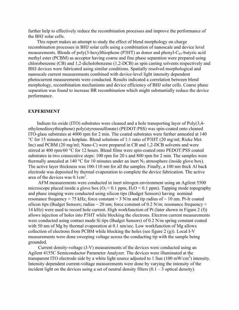
Thickness of the active layers and metal electrodes was measured using a Dektak profilometer as well as by imaging a step created on the film using AFM. RESULTS AND DISCUSSION AFM measurements The topographic (height) images in figure 1 (a) and (b) show distributed domains of P3HT and
Figure 1. (a and c) Topography images of P3HT: PCBM blended films spin cast from CB and 1,2-DCB solvents, respectively. (b and d) shows the corresponding phase images PCBM. A distinct difference in the surface morphology of donor and acceptor components was noticeable among the blends. The phase images of CB (figure 1 c) and 1,2 DCB (figure 1 d) based films showed a significant variation in the length scales of DA phase separation. Morphology of the films prepared with CB solvent showed coarser phase separation with large domains of P3HT (brighter regions) separated by PCBM clusters. The size of P3HT domains and PCBM clusters vary from 70 to 110 nm and 80 to 150 nm, respectively. For statistical validity, several images of different locations along with the representative images (shown in figure 1) were analyzed to estimate the sizes. Whereas, blends cast from 1,2 DCB exhibited a finer phase separation of 20-25 nm length scale. Surface roughness of CB and 1,2-DCB based blends was 2.75 nm and 1.70 nm respectively. Finer phase separation was attributed to the higher boiling point, polarity and solubility of 1,2-DCB compared to CB solvent [7]. Conducting Atomic Force Microscopy
Hole and electron current images of the blends prepared with CB solvent are shown in figure 2 (a) and (b), respectively. Figure 2 (c) and (d) show the hole and electron current C-AFM images of 1,2-DCB based blend respectively. The detection of holes and electrons by Pt and Mg coated tips respectively is shown in the energy level diagram in figure 2 (e). Since the holes and electrons flow through the active layer, C-AFM also gives an indication of the 3D morphology of the active layer. Discontinuous regions of P3HT and PCBM phases isolated at larger length
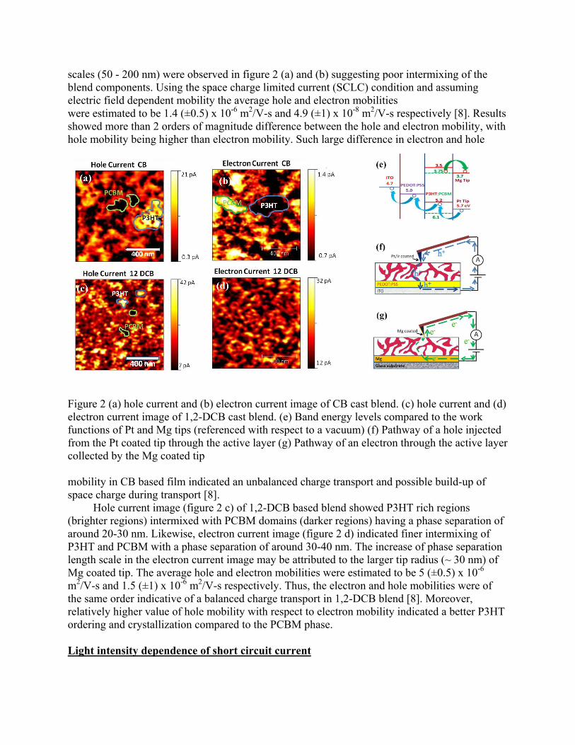
scales (50 - 200 nm) were observed in figure 2 (a) and (b) suggesting poor intermixing of the blend components. Using the space charge limited current (SCLC) condition and assuming electric field dependent mobility the average hole and electron mobilities were estimated to be 1.4 (±0.5) x 10-6 m2/V-s and 4.9 (±1) x 10-8 m2/V-s respectively [8]. Results showed more than 2 orders of magnitude difference between the hole and electron mobility, with hole mobility being higher than electron mobility. Such large difference in electron and hole
Figure 2 (a) hole current and (b) electron current image of CB cast blend. (c) hole current and (d) electron current image of 1,2-DCB cast blend. (e) Band energy levels compared to the work functions of Pt and Mg tips (referenced with respect to a vacuum) (f) Pathway of a hole injected from the Pt coated tip through the active layer (g) Pathway of an electron through the active layer collected by the Mg coated tip mobility in CB based film indicated an unbalanced charge transport and possible build-up of space charge during transport [8]. Hole current image (figure 2 c) of 1,2-DCB based blend showed P3HT rich regions (brighter regions) intermixed with PCBM domains (darker regions) having a phase separation of around 20-30 nm. Likewise, electron current image (figure 2 d) indicated finer intermixing of P3HT and PCBM with a phase separation of around 30-40 nm. The increase of phase separation length scale in the electron current image may be attributed to the larger tip radius (~ 30 nm) of Mg coated tip. The average hole and electron mobilities were estimated to be 5 (±0.5) x 10-6 m2/V-s and 1.5 (±1) x 10-6 m2/V-s respectively. Thus, the electron and hole mobilities were of the same order indicative of a balanced charge transport in 1,2-DCB blend [8]. Moreover, relatively higher value of hole mobility with respect to electron mobility indicated a better P3HT ordering and crystallization compared to the PCBM phase. Light intensity dependence of short circuit current

Figure 3 (a) shows the variation of short-circuit current density (Jsc) with light intensity in log-log scale for CB and 1,2-DCB P3HT:PCBM BHJ cells. A linear dependence of Jsc vs Intensity was observed for 1,2-DCB based device indicative of MR recombination [9]. However, in case of CB based devices, the curve was linear at low intensity regime (1-30 mW/cm2) indicating MR recombination and a strong sub-linearity was observed at higher light intensity regime (30-100 mW/cm2) suggesting the onset of BR recombination [10 ,11]. Therefore, results indicated a crossover from MR to BR recombination at higher light intensities.
Figure 3. (a) Dependence of Short circuit current (a) and Open circuit voltage (b) with I Moreover, the linearity of Jsc vs Intensity plot in 1,2-DCB based cell was an indication of balanced charge transport which may be attributed to higher degree of phase separation and similarity in electron and hole mobilities. On the other hand, the sub-linearity in coarse phase CB based cell suggested an unbalanced charge transport with possible build-up of space charge and an order of magnitude difference in the electron and hole mobilities [12]. Results suggested that efficient phase separation of 1,2-DCB based blend is likely to suppress BR recombination and may promote MR recombination at operational light intensities. Device current-voltage measurements The performance of the devices fabricated using CB and 1,2 DCB cast active layers were compared using illuminated (A.M. 1.5 ) current density vs. voltage (J-V) plots as shown in figure 4. Power conversion efficiency (PCE or η), open circuit voltage (Voc) and short circuit
Figure 4. Device J-V curve of CB and 1,2-DCB based devices

current density (Jsc) of the two cells are summarized in Table 2. The PCE of 1,2-DCB based cell were 2.54 and 0.9 % respectively. There was a significant decrease in the PCE, Voc and Jsc of CB as compared to 1,2-DCB blend which may be attributed to strong BR recombination due to coarse or inefficient phase separation. CONCLUSIONS Nanoscale and device level measurements suggested that coarse phase separation may lead to dominant BR recombination which might result in lower efficiency of devices. Finer or efficient phase separation may promote MR recombination and higher efficiency. Therefore, reducing recombination by proper control of blend morphology may be one of the ways to improve the efficiency of organic BHJ solar cells. ACKNOWLEDGMENTS This research was supported by National Science Foundation (DMR-0923115, CMMI-1063263), National Science Foundation/EPSCoR Grant No. 0091948 and by the State of South Dakota.
REFERENCES 1. C. J. Brabec , S. Gowrisanker, J. J. M. Halls, D. Laird, S. Jia and S. P. Williams, Adv. Mater., 22, 3839, 2010. 2. C. Deibel, A. Baumann, V. Dyakonov, Appl. Phys. Lett., 93, 163303, 2008. 3. L. J. A. Koster, V. D. Mihailetchi and P. W. M. Blom, Appl. Phys. Lett., 88, 052104, 2006. 4. S. R. Cowan, A. Roy, and A. J. Heeger, Phys. Rev. B. 82, 245207, 2010. 5. C. Deibel and A.Wagenpfahl, Phys. Rev. B 82, 207301, 2010. 6. S. Shoaee, M. P. Eng, E. Espíldora, J. L. Delgado, B. Campo, N. Martín, D.Vanderzande
and J. R. Durrant, Energy Environ. Sci., 3, 971–976, 2010. 7. P. Dutta, Y. Xie, M. Kumar, M. Rathi, P. Ahrenkiel, D. Galipeau, Q. Qiao, and V. Bommisetty, J. Photon. Energy, 1, 011124, 2011. 8. V. D. Mihailetchi, J. Wildeman, and P. W. M. Blom, Phys. Rev. Lett., 94, 126602, 2005. 9. L. J. A. Koster, V. D. Mihailetchi, H. Xie, and P. W. M. Blom, Appl. Phys. Lett., 87,
203502, 2005. 10. C. G. Shuttle, B. O'Regan, A. M. Ballantyne, J. Nelson, D. D. C. Bradley, J. R. Durrant,
Phys. Rev. B, 78, 113201, 2008. 11. C. Groves and N. C. Greenham, Phys. Rev. B, 78, 155205, 2008. 12. R. A. Marsh, C. R. McNeill, A. Abrusci, A. R. Campbell and R. H. Friend, Nano Lett., 8, 1393, 2008.