A comprehensive study for the plasmonic thin-film solar cell with periodic structure
15
A comprehensive study for the plasmonic thin-film solar cell with periodic structure Wei E. I. Sha, Wallace C. H. Choy, and Weng Cho Chew Department of Electrical and Electronic Engineering, the University of Hong Kong, Pokfulam Road, Hong Kong, China. Weng Cho Chew is On Leave of Absence from the University of Illinois, Urbana-Champaign, USA. [email protected] Abstract: A comprehensive study of the plasmonic thin-film solar cell with the periodic strip structure is presented in this paper. The finite-difference frequency-domain method is employed to discretize the inhomogeneous wave function for modeling the solar cell. In particular, the hybrid absorbing boundary condition and the one-sided difference scheme are adopted. The parameter extraction methods for the zeroth-order reflectance and the absorbed power density are also discussed, which is important for testing and optimizing the solar cell design. For the numerical results, the physics of the absorption peaks of the amorphous silicon thin-film solar cell are explained by electromagnetic theory; these peaks correspond to the waveguide mode, Floquet mode, surface plasmon reso- nance, and the constructively interference between adjacent metal strips. The work is therefore important for the theoretical study and optimized design of the plasmonic thin-film solar cell. © 2010 Optical Society of America OCIS codes: (310.6628)Subwavelength structures, nanostructures; (310.6805)Theory and de- sign; (240.6680)Surface plasmons; (050.1755)Computational electromagnetic methods. References and links 1. J. Nelson, The Physics of Solar Cells (Imperial College Press, London, 2003) 2. P. W¨ urfel, Physics of Solar Cells: From Principles to New Concepts (Wiley-VCH, Berlin, 2004). 3. K. L. Chopra, P. D. Paulson, and V. Dutta, “Thin-film solar cells: An overview,” Prog. Photovoltaics 12, 69-92 (2004). 4. L. Zeng, Y. Yi, C. Hong, J. Liu, N. Feng, X. Duan, L. C. Kimerling, and B. A. Alamariu, “Efficiency enhancement in Si solar cells by textured photonic crystal back reflector,” Appl. Phys. Lett. 89, 111111 (2006). 5. C. Haase, and H. Stiebig, “Thin-film silicon solar cells with efficient periodic light trapping texture,” Appl. Phys. Lett. 91, 061116 (2007). 6. H. Sai, H. Fujiwara, M. Kondo, and Y. Kanamori, “Enhancement of light trapping in thin-film hydrogenated microcrystalline Si solar cells using back reflectors with self-ordered dimple pattern,” Appl. Phys. Lett. 93, 143501 (2008). 7. W. Zhou, M. Tao, L. Chen, and H. Yang, “Microstructured surface design for omnidirectional antireflection coatings on solar cells,” J. Appl. Phys. 102, 103105 (2007). 8. R. Zia, M. D. Selker, P. B. Catrysse, and M. L. Brongersma, “Geometries and materials for subwavelength surface plasmon modes,” J. Opt. Soc. Am. A 21, 2442-2446 (2004). 9. J. Homola, S. S. Yee, and G. Gauglitz, “Surface plasmon resonance sensors: Review,” Sens. Actuator B. 54, 3-15 (1999). 10. H. Ditlbacher, J. R. Krenn, N. Felidj, B. Lamprecht, G. Schider, M. Salerno, A. Leitner, and F. R. Aussenegg, “Fluorescence imaging of surface plasmon fields,” Appl. Phys. Lett. 80, 404-406 (2002). (C) 2010 OSA 15 March 2010 / Vol. 18, No. 6 / OPTICS EXPRESS 5993 #124045 - $15.00 USD Received 9 Feb 2010; revised 4 Mar 2010; accepted 5 Mar 2010; published 10 Mar 2010
-
Upload
independent -
Category
Documents
-
view
5 -
download
0
Transcript of A comprehensive study for the plasmonic thin-film solar cell with periodic structure

A comprehensive study for theplasmonic thin-film solar cell with
periodic structure
Wei E. I. Sha, Wallace C. H. Choy, and Weng Cho ChewDepartment of Electrical and Electronic Engineering, the University of Hong Kong, Pokfulam
Road, Hong Kong, China.Weng Cho Chew is On Leave of Absence from the University of Illinois, Urbana-Champaign,
Abstract: A comprehensive study of the plasmonic thin-film solarcell with the periodic strip structure is presented in this paper. Thefinite-difference frequency-domain method is employed to discretize theinhomogeneous wave function for modeling the solar cell. Inparticular,the hybrid absorbing boundary condition and the one-sided differencescheme are adopted. The parameter extraction methods for the zeroth-orderreflectance and the absorbed power density are also discussed, which isimportant for testing and optimizing the solar cell design.For the numericalresults, the physics of the absorption peaks of the amorphous siliconthin-film solar cell are explained by electromagnetic theory; these peakscorrespond to the waveguide mode, Floquet mode, surface plasmon reso-nance, and the constructively interference between adjacent metal strips.The work is therefore important for the theoretical study and optimizeddesign of the plasmonic thin-film solar cell.
© 2010 Optical Society of America
OCIS codes:(310.6628)Subwavelength structures, nanostructures; (310.6805)Theory and de-sign; (240.6680)Surface plasmons; (050.1755)Computational electromagnetic methods.
References and links1. J. Nelson, The Physics of Solar Cells (Imperial College Press, London, 2003)2. P. Wurfel, Physics of Solar Cells: From Principles to NewConcepts (Wiley-VCH, Berlin, 2004).3. K. L. Chopra, P. D. Paulson, and V. Dutta, “Thin-film solar cells: An overview,” Prog. Photovoltaics 12, 69-92
(2004).4. L. Zeng, Y. Yi, C. Hong, J. Liu, N. Feng, X. Duan, L. C. Kimerling, and B. A. Alamariu, “Efficiency enhancement
in Si solar cells by textured photonic crystal back reflector,” Appl. Phys. Lett. 89, 111111 (2006).5. C. Haase, and H. Stiebig, “Thin-film silicon solar cells with efficient periodic light trapping texture,” Appl. Phys.
Lett. 91, 061116 (2007).6. H. Sai, H. Fujiwara, M. Kondo, and Y. Kanamori, “Enhancement of light trapping in thin-film hydrogenated
microcrystalline Si solar cells using back reflectors with self-ordered dimple pattern,” Appl. Phys. Lett. 93,143501 (2008).
7. W. Zhou, M. Tao, L. Chen, and H. Yang, “Microstructured surface design for omnidirectional antireflectioncoatings on solar cells,” J. Appl. Phys. 102, 103105 (2007).
8. R. Zia, M. D. Selker, P. B. Catrysse, and M. L. Brongersma, “Geometries and materials for subwavelength surfaceplasmon modes,” J. Opt. Soc. Am. A 21, 2442-2446 (2004).
9. J. Homola, S. S. Yee, and G. Gauglitz, “Surface plasmon resonance sensors: Review,” Sens. Actuator B. 54, 3-15(1999).
10. H. Ditlbacher, J. R. Krenn, N. Felidj, B. Lamprecht, G. Schider, M. Salerno, A. Leitner, and F. R. Aussenegg,“Fluorescence imaging of surface plasmon fields,” Appl. Phys. Lett. 80, 404-406 (2002).
(C) 2010 OSA 15 March 2010 / Vol. 18, No. 6 / OPTICS EXPRESS 5993#124045 - $15.00 USD Received 9 Feb 2010; revised 4 Mar 2010; accepted 5 Mar 2010; published 10 Mar 2010

11. H. Raether, Surface Plasmons on Smooth and Rough Surfaces and on Gratings (Springer-Verlag, Berlin, 1988).12. K. Kato, H. Tsuruta, T. Ebe, K. Shinbo, F. Kaneko, and T. Wakamatsu, “Enhancement of optical absorption
and photocurrents in solar cells of merocyanine Langmuir-Blodgett films utilizing surface plasmon excitations,”Mater. Sci. Eng. C-Biomimetic Supramol. Syst. 22, 251-256 (2002)
13. K. Tvingstedt, N. K. Persson, O. Inganas, A. Rahachou, and I. V. Zozoulenko, “Surface plasmon increase ab-sorption in polymer photovoltaic cells,” Appl. Phys. Lett.91, 113514 (2007).
14. V. E. Ferry, L. A. Sweatlock, D. Pacifici, and H. A. Atwater, “Plasmonic nanostructure design for efficient lightcoupling into solar cells,” Nano Lett. 8, 4391-4397 (2008)
15. R. A. Pala, J. White, E. Barnard, J. Liu, and M. L. Brongersma, “Design of plasmonic thin-film solar cells withbroadband absorption enhancements,” Adv. Mater. 21, 3504-3509 (2009)
16. M. Qiu, and S. L. He, “A nonorthogonal finite-difference time-domain method for computing the band structureof a two-dimensional photonic crystal with dielectric and metallic inclusions,” J. Appl. Phys. 87, 8268-8275(2000).
17. A. Farjadpour, D. Roundy, A. Rodriguez, M. Ibanescu, P. Bermel, J. D. Joannopoulos, S. G. Johnson, and G. W.Burr, “Improving accuracy by subpixel smoothing in the finite-difference time domain,” Opt. Lett. 31, 2972-2974(2006).
18. K. G. Ong, O. K. Varghese, G. K. Mor, K. Shankar, and C. A. Grimes, “Application of finite-difference timedomain to dye-sensitized solar cells: The effect of nanotube-array negative electrode dimensions on light absorp-tion,” Sol. Energy Mater. Sol. Cells 91, 250-257 (2007).
19. Z. M. Zhu and T. G. Brown, “Full-vectorial finite-difference analysis of microstructured optical fibers,” Opt.Express 10, 853-864 (2002)
20. C. P. Yu and H. C. Chang, “Compact finite-difference frequency-domain method for the analysis of two-dimensional photonic crystals,” Opt. Express 12, 1397-1408 (2004).
21. R. Luebbers, F. P. Hunsberger, K. S. Kunz, R. B. Standler,and M. Schneider, “A frequency-dependent finite-difference time-domain formulation for dispersive materials,” IEEE Trans. Electromagn. Compat. 32, 222-227(1990).
22. D. F. Kelley and R. J. Luebbers, “Piecewise linear recursive convolution for dispersive media using FDTD,” IEEETrans. Antennas Propag. 44, 792-797 (1996).
23. G. Veronis and S. Fan, “Overview of Simulation Techniques for Plasmonic Devices,” in Surface PlasmonNanophotonics, M. L. Brongersma and P. G. Kik, eds., (Springer, Dordrecht, The Netherlands, 2007)
24. M. E. Veysoglu, R. T. Shin, and J. A. Kong, “A finite-difference time-domain analysis of wave scattering fromperiodic surfaces: Oblique-incidence case,” J. Electromagn. Waves Appl. 7, 1595-1607 (1993).
25. A. Taflove and S. C. Hagness, Computational Electrodynamics: the Finite-Difference Time-Domain Method,Third Edition (Artech House, Boston, 2005).
26. S. Zhao and G. W. Wei, “High-order FDTD methods via derivative matching for Maxwell’s equations withmaterial interfaces,” J. Comput. Phys. 200, 60-103 (2004).
27. D. M. Sullivan, Electromagnetic Simulation Using the FDTD Method (Wiley-IEEE Press, New York, 2000).28. A. F. Oskooi, L. Zhang, Y. Avniel, and S. G. Johnson, “The failure of perfectly matched layers and towards their
redemption by adiabatic absorbers,” Opt. Express 16, 11376-11392 (2008).29. W. C. Chew, Waves and Fields in Inhomogenous Media (Van Nostrand Reinhold, New York, 1990).30. S. G. Johnson and J. D. Joannopoulos, “Block-iterative frequency-domain methods for Maxwell’s equations in a
planewave basis,” Opt. Express 8, 173-190 (2001).31. W. C. Chew and W. H. Weedon, “A 3-D perfectly matched medium from modified Maxwell’s equations with
stretched coordinates,” Microw. Opt. Technol. Lett. 7, 599-604 (1994).32. W. C. Chew, J. M. Jin, and E. Michielssen, “Complex coordinate stretching as a generalized absorbing boundary
condition,” Microw. Opt. Technol. Lett. 15, 363-369 (1997).33. C. M. Rappaport, M. Kilmer, and E. Miller, “Accuracy considerations in using the PML ABC with FDFD
Helmholtz equation computation,” Int. J. Numer. Model.-Electron. Netw. Device Fields 13, 471-482 (2000).34. G. Mur, “Absorbing boundary-conditions for the finite-difference approximation of the time-domain
electromagnetic-field equations,” IEEE Trans. Electromagn. Compat. 23, 377-382 (1981).35. J. P. Berenger, “A perfectly matched layer for the absorption of electromagnetic-waves,” J. Comput. Phys. 114,
185-200 (1994).36. M. G. Moharam, E. B. Grann, D. A. Pommet, and T. K. Gaylord,“Formulation for stable and efficient imple-
mentation of the rigorous coupled-wave analysis of binary gratings,” J. Opt. Soc. Am. A-Opt. Image Sci. Vis. 12,1068-1076 (1995).
37. E. D. Palik, Handbook of Optical Constants of Solids (Academic Press, London, 1998).38. X. W. Chen, W. C. H. Choy, and S. L. He, “Efficient and rigorous modeling of light emission in planar multilayer
organic light-emitting diodes,” J. Disp. Technol. 3, 110-117 (2007).
(C) 2010 OSA 15 March 2010 / Vol. 18, No. 6 / OPTICS EXPRESS 5994#124045 - $15.00 USD Received 9 Feb 2010; revised 4 Mar 2010; accepted 5 Mar 2010; published 10 Mar 2010

Fig. 1: The schematic diagram of a solar cell structure.
1. Introduction
Solar cells (SCs) [1, 2], which can provide renewable and clean energy by converting sunlightto electrical power, have attracted much attention in the past few years. Despite the growingimportance, we need to reduce the cost of the SCs and increasethe energy conversion efficiencybefore they can successfully replace fossil fuel for electrical power generation.
A careful optical design of the device structure is crucial for optimizing the performanceparticularly for thin film SCs due to the typically weak lightabsorption of the materials suchas amorphous silicon (A-Si) [3]. Figure 1 shows the schematic diagram of a solar cell structurewith the textured back reflector (BR) and the antireflection (AR) coatings. As a light-trappingconfiguration, the textured BRs [4, 5, 6] have been proposed for extending the optical pathlength. However, the configuration may suffer from the back surface recombination loss. More-over, the textured AR coatings [7] have been employed to reduce the reflection of light at the topsurface of the SCs. But the AR coatings cannot offer the sufficient light concentration. There-fore, better light trapping and concentration schemes are desirable for further improving theexternal quantum efficiency of SCs. Surface plasmon resonances (SPRs) are collective oscilla-tions of the free electrons that are confined to surfaces and interact strongly with light resultingin a polariton. SPR usually occurs at the interface between adielectric with the positive dielec-tric constantεd
r and a metal with the negative dielectric constantεmr . Meanwhile, SPR, which
is the eigenstate of the Maxwell’s equations for the dielectric-metal structure, only exist whenRe(−εm
r ) > εdr is satisfied [8][9]. To excite the SPR by light, a coupling technique providing
the wavevector mismatch is required. For SCs, the metallic periodic nanostructures and the sub-wavelength scatterers have been used to excite the SPR [10, 11, 12, 13, 14, 15]. Some of theunique features of the plasmonic thin-film SC are the broadband and wideangle absorption en-hancements. Both theoretical and experimental results have demonstrated that the strong-peakabsorption enhancements appear at specific wavelengths. Asa result, the short-circuit currentor the open-circuit voltage is also increased.
In order to describe the propagation and scattering of sunlight within the SC and to optimizethe process, Maxwell’s equations have to be rigorously solved. Some of the well-adopted full-
(C) 2010 OSA 15 March 2010 / Vol. 18, No. 6 / OPTICS EXPRESS 5995#124045 - $15.00 USD Received 9 Feb 2010; revised 4 Mar 2010; accepted 5 Mar 2010; published 10 Mar 2010

wave solvers for optical simulation are the finite-difference time-domain (FDTD) [16, 17, 18]and the FDFD methods [19, 20]. Due to the fact that most optical materials are dispersive, therecursive convolution (RC) method [21] or the piecewise linear recursive convolution (PLRC)method [22] should be used for the FDTD method. For noble metals, such as Ag and Au, thecomplex dielectric constants have to been described by a large number of summation terms inLorentz-Drude model [23]. Hence, these recursive convolution implementations will consumea lot of CPU time. However, for the FDFD method, one can use an experimentally tabulateddielectric constants of the dispersive materials directly. Furthermore, compared with the FDFDmethod, the FDTD method is not easy to treat the periodic boundary conditions particularlyfor the oblique incidence case [16, 24, 25]. In most places, unless a solar panel is mounted onan expensive tracking system, most of the time light is incident on the array obliquely. Hence,the ability of FDFD method to handle the case of oblique incidence is clearly an importantadvantage over the FDTD method for modeling the SCs. In addition, the FDFD method canuse a variety of flexible difference techniques, such as one-sided difference scheme, to improvethe accuracy. But the FDTD method will suffer from instability problem if these techniques areadopted [26].
For the FDFD method, most papers adopted the staggered grid,because it can satisfy thedivergence-free condition automatically. However, the averaged material model [19, 20, 27]cannot accurately resolve the local field at the high-contrast interface between dielectric andmetal. Besides, few papers have modeled SCs with periodic structures by using the FDFDmethod. Consequently, it is highly desirable to establish arigorous and efficient method formodeling SCs, in particular, the periodically patterned structures.
In this paper, we use the FDFD method to discretize the inhomogeneous wave function formodeling the plasmonic thin-film SC. In order to accurately treat the dielectric-metal inter-face, the flexible one-sided difference scheme is introduced. While the perfectly matched layer(PML) cannot work very well under periodic boundary condition [28], the hybrid absorbingboundary condition (ABC) is proposed here to reduce the spurious numerical reflections fromthe outmost boundary of the PML. Moreover, we propose the rigorous phase and attenuationconstants conditions of the SPR for general lossy materials. In addition, we will unveil theorigins of the absorption peaks of SC structures using electromagnetic theory.
2. Theoretical modeling
A two-dimensional (2-D) plasmonic thin-film silicon SC structure is shown in Fig. 2. Since thes-polarized incident light cannot excite the SPR [9], we mainly consider the p-polarized lightwith the electromagnetic components ofHz, Ex, andEy. The exp( j0ωt) time convention is used.For the SCs, all the materials are non-magnetic (i.e.µr = 1).
2.1. Finite-difference equation
For the 2-D isotropic and inhomogeneousmedia with the complex dielectric constant ofεr(x,y),the wave function of the total fieldHt
z is given by [29]
∂∂x
(
1εr(x,y)
∂Htz
∂x
)
+∂∂y
(
1εr(x,y)
∂Htz
∂y
)
+ k20Ht
z = 0 (1)
(C) 2010 OSA 15 March 2010 / Vol. 18, No. 6 / OPTICS EXPRESS 5996#124045 - $15.00 USD Received 9 Feb 2010; revised 4 Mar 2010; accepted 5 Mar 2010; published 10 Mar 2010

Fig. 2: The unit cell of the plasmonic thin-film SC. The four-layered structure includes indiumtin oxide (ITO), absorbing materials, Au (or Ag) electrodes, and substrate with thickness ofd1,d2, d3, andd4, respectively. The distance between two adjacent strips isds and the periodicityis P. The incident light propagates into the structure through the ITO. The PML and the Murabsorbing boundary conditions are employed at the top and the bottom of the SC structure. Theperiodic boundary conditions (PBC) at the left and right sides of the unit cell are imposed.
Fig. 3: The inhomogeneous material treatment. The squares denote the five difference nodes.The center square is enclosed by the four rectangular regions with different dielectric constants.Γmm′ are the contiguous edges of the rectangular regions (See Appendix A).
wherek0 is the wave number of free space. Figure 3 shows the general geometry for the inho-mogeneous material treatment. Using the second-order central differences, we have
∂∂x
(
1εr(x,y)
∂Htz
∂x
)
=1∆x
(
Htz(i+1, j)−Ht
z(i, j)
εr(i+1/2, j)∆x
−Htz(i, j)−Ht
z(i−1, j)εr(i−1/2, j)∆x
)
+ O(∆2x)
(2)
(C) 2010 OSA 15 March 2010 / Vol. 18, No. 6 / OPTICS EXPRESS 5997#124045 - $15.00 USD Received 9 Feb 2010; revised 4 Mar 2010; accepted 5 Mar 2010; published 10 Mar 2010

where∆x is the spatial step along thex direction. For the p-polarized incident light, the follow-ing averaging techniques can be adopted for the dielectric constants, i.e.
1εr(i+1/2, j)
≈ 12
(
1εr1
+1
εr4
)
(3)
1εr(i−1/2, j)
≈ 12
(
1εr2
+1
εr3
)
(4)
where the subscript 1, 2, 3, and 4 denote the small rectangular regions as shown in Fig. 3.Using the notations ofΦ1 = Ht
z(i, j −1), Φ2 = Htz(i−1, j), Φ3 = Ht
z(i, j), Φ4 = Htz(i + 1, j),
andΦ5 = Htz(i, j+1), the continuous inhomogeneous wave equation Eq. (1) can be discretized
into FDFD equation as5
∑m=1
cmΦm = 0 (5)
where
c1 =12
(
1εr1
+1
εr2
)
· 1∆2
y(6)
c2 =12
(
1εr2
+1
εr3
)
· 1∆2
x(7)
c4 =12
(
1εr4
+1
εr1
)
· 1∆2
x(8)
c5 =12
(
1εr3
+1
εr4
)
· 1∆2
y(9)
c3 = −12
(
1εr1
+1
εr2+
1εr3
+1
εr4
)
·(
1∆2
x+
1∆2
y
)
+ k20 (10)
It should be noted that the FDFD form of the inhomogeneous wave equation can be convertedto that of the homogeneous wave equation if the four rectangular regions have the same dielec-tric constant. For the p-polarized incident plane wave, it has been reported that the averagingtechniques of Eq. (3) and Eq. (4) are effective for the inhomogeneous material treatment [30].Here, we show that the averaging techniques can also be rigorously derived by the integral formof the wave equation and the boundary conditions (See Appendix A). SinceH inc
z is known (theincident light) and the FDFD equation ofHt
z is expressed as Eq. (5), the FDFD equation for thescattered-fieldHs
z can be derived by
Htz = H inc
z + Hsz (11)
2.2. Boundary conditions
As shown in Fig. 2, the ABCs along they directions are used to avoid the spurious reflectionsof waves at the top and bottom boundaries of computational domain. The complex-coordinatePML [31, 32] is an efficient and accurate ABC which has the formof
∂ 2Hsz
∂x2 +1sy
∂∂y
(
1sy
∂Hsz
∂y
)
+ k20Hs
z = 0 (12)
(C) 2010 OSA 15 March 2010 / Vol. 18, No. 6 / OPTICS EXPRESS 5998#124045 - $15.00 USD Received 9 Feb 2010; revised 4 Mar 2010; accepted 5 Mar 2010; published 10 Mar 2010

where
sy =
1− j0σ(y)ωε0
, within PML
1, other(13)
whereε0 is the permittivity of free space, andω is the angular frequency of the incident light.The polynomial variation of the conductivitiesσ is employed, i.e.
σ( j) =C∆y
(
j−1/2L
)Q
, j = 1,2, . . . ,8 (14)
σ( j +1/2) =C∆y
(
jL
)Q
, j = 0,1, . . . ,8 (15)
whereL is the layer number of the PML,Q is the order of the polynomial, andC is a constant.For reducing the spurious numerical reflections, the optimized settings are set toL = 8,Q = 3.7,andC = 0.02. The proper discretization form [33] for the coordinate-stretched term of Eq. (12)is given by
1sy
∂∂y
(
1sy
∂Hsz
∂y
)
≈ 1sy( j)∆y
[
Hsz (i, j +1)−Hs
z(i, j)sy( j +1/2)∆y
−
Hsz (i, j)−Hs
z (i, j−1)
sy( j−1/2)∆y
] (16)
At the outermost boundary of the PML, the Mur ABC [34] replacing the traditional perfectlyelectric conductor truncation condition is employed to further reduce the spurious numericalreflections. Taking the top planey = 0 as an example, the second-order Mur ABC can be writtenas
[
∂∂y
− j0
(
k0 +1
2k0
∂ 2
∂x2
)]
Hsz
∣
∣
∣
∣
y=0= 0 (17)
and its discretized form is given by
f1Hsz (i, j)+ f2Hs
z (i−1, j)+ f3Hsz (i+1, j)+ f4Hs
z (i, j +1) = 0 (18)
where
f1 = 2exp( j0k0∆y)−2k20∆2
x exp( j0k0∆y)−2
f2 = f3 = 1−exp( j0k0∆y)
f4 = 2k20∆2
x
(19)
Particularly, we introduce the exponential difference strategy [35] to improve accuracy.Regarding the periodic structure, the periodic boundary conditions along thex directions
need to be implemented. Based on the Floquet theorem, we have
Hsz (x + P,y) = Hs
z (x,y)exp(− j0k0cosθ ·P)
Hsz (x,y) = Hs
z (x + P,y)exp( j0k0cosθ ·P)(20)
whereP is the periodicity andθ is the incident angle with respect tox direction. Comparedwith the FDFD method, the second equation of Eq. (20) is not easy to be treated by the FDTDmethod, particularly for the oblique incidence case because one does not know the scattered-field values at a future time in periodic device structures. It should be noted that the periodicboundary conditions should also be implemented at the regions of the hybrid ABC.
(C) 2010 OSA 15 March 2010 / Vol. 18, No. 6 / OPTICS EXPRESS 5999#124045 - $15.00 USD Received 9 Feb 2010; revised 4 Mar 2010; accepted 5 Mar 2010; published 10 Mar 2010

Although the FDFD form Eq. (5) can generally treat the dielectric-dielectric and dielectric-metal interfaces, the accuracy will degrade at the interfaces. Thus the one-sided differencescheme is used to rectify the problem. For the horizontal interface (y = yh) between the media1 and the media 2, the boundary condition for the scattered magnetic field is
(
1εr1
∂∂y
Hs1z − 1
εr2
∂∂y
Hs2z
)∣
∣
∣
∣
y=yh
=
(
1εr2
∂∂y
H incz − 1
εr1
∂∂y
H incz
)∣
∣
∣
∣
y=yh
(21)
Using the high-order-accurate one-sided differences, we get
∂∂y
Hs1z
∣
∣
∣
∣
x=i∆x
≈ 1.5Hs1z (i, j)−2Hs1
z (i, j−1)+0.5Hs1z (i, j−2)
∆y
∂∂y
Hs2z
∣
∣
∣
∣
x=i∆x
≈ −1.5Hs2z (i, j)+2Hs2
z (i, j +1)−0.5Hs2z (i, j +2)
∆y
(22)
The one-sided difference scheme is flexible and can have higher-order accuracy. For the verticalinterfaces, one can also use the one-sided differences.
2.3. Parameter extraction
In this section, we will discuss the details to extract the important parameters including theabsorption power density and the zeroth-order reflectance and transmittance. By applying theabove FDFD equations and the boundary conditions to all freeN nodes in the solution region, asparse matrix equation is formed because only the nearest adjacent nodes affect the value ofHs
zat each node. Hence, the scattered magnetic field can be solved by the iterative methods with thememory and computational complexity ofO(N). After this, the total electric field componentsare calculated by
Etx(i, j +1/2)≈ 1
2
(
1εr(i, j +1)
+1
εr(i, j)
)
Htz(i, j +1)−Ht
z(i, j)j0ωε0 ·∆y
(23)
Ety(i+1/2, j)≈ 1
2
(
1εr(i+1, j)
+1
εr(i, j)
)
Htz(i+1, j)−Ht
z(i, j)
− j0ωε0 ·∆x(24)
The electron-hole pair generation depends on the photon energy absorbed by the absorbingmaterial per unit time per unit area, i.e.
η =
∫
Saσa|E|2ds
∆Sa
=−ωε0
∫
SaIm(εra) |E|2ds
∆Sa
(25)
whereη is the power density,Sa denotes the region of the absorbing material,∆Sa is the area ofSa, andσa = −ωε0Im(εra) is the conductivity of the absorbing material.
For the SC with the periodic structure, the zeroth-order reflectance and transmittance are theimportant parameters for optimizing the SC structures and comparing the theoretical resultsto the experimental ones. Physically, the dips of the reflectance correspond to the absorptionpeaks. The Floquet modes (space harmonics) for the two-dimensional periodic structure aregiven by
Ψp = exp(− jUpx)exp(− jVpy) (26)
where
Up = k0cosθ +2π p
P, p = 0,±1,±2, . . . (27)
(C) 2010 OSA 15 March 2010 / Vol. 18, No. 6 / OPTICS EXPRESS 6000#124045 - $15.00 USD Received 9 Feb 2010; revised 4 Mar 2010; accepted 5 Mar 2010; published 10 Mar 2010

0.8 0.82 0.84 0.86 0.88 0.9 0.92 0.94 0.96 0.98 10
0.1
0.2
0.3
0.4
0.5
0.6
0.7
0.8
Wavelength (m)R
p/T
p
R
p (FDFD)
Rp (RCWA)
Tp (FDFD)
Tp (RCWA)
Fig. 4: The zeroth-order reflectance and transmittance by the FDFD method and the rigorouscoupled-wave algorithm.
Vp =
√
k20−U2
p , k20 ≥U2
p
− j
∣
∣
∣
∣
√
k20−U2
p
∣
∣
∣
∣
, k20 < U2
p
(28)
According to the orthogonal properties of the Floquet modes, we get
Rp =
∣
∣
∣
1P
∫ P0 Hs
z (x,yr)exp( jk0 cosθx)dx∣
∣
∣
2
A2 (29)
and
Tp =
∣
∣
∣
1P
∫ P0 Ht
z(x,yt)exp( jk0cosθx)dx∣
∣
∣
2
A2 (30)
whereA is the amplitude of the incident light, andyr and yt are the virtual boundaries forcomputing the zeroth-order reflectanceRp and the zeroth-order transmittanceTp, respectively.
As a testing structure, we consider the periodic dielectricstrip model in free space. Theincident plane wave is given by
H incz (x,y) = exp(− jk0 (xcosθ + ysinθ )) (31)
whereθ = 85◦ andk0 = 2π . The dielectric constant of each strip is taken asεr = 4− 0.1 j.The periodicity isP = 0.6m, the thickness of each strip isd3 = 0.5m, and the distance betweenthe adjacent dielectric strips isds = 0.3m. The spatial steps are set to∆x = ∆y = 0.01m. Thezeroth-order reflectance and transmittance are calculatedby the FDFD method and the rigorouscoupled-wave algorithm [36]. As shown in Fig. 4, the two approaches agree with each othervery well.
3. Simulation results
We start with a simple semi-infinite structure of A-Si/Au which can allow us to intrusively studySPRs. For the semi-infinite structure, the correspondingHz fields in the A-Si and Au layers canbe assumed as
Hz(x, y) = exp(
jkSiy y− jkxx
)
, kSiy = β Si
y + jαSiy , y < 0 (32)
(C) 2010 OSA 15 March 2010 / Vol. 18, No. 6 / OPTICS EXPRESS 6001#124045 - $15.00 USD Received 9 Feb 2010; revised 4 Mar 2010; accepted 5 Mar 2010; published 10 Mar 2010
400 450 500 550 600 650 700 750 800−10
−8
−6
−4
−2
0
2
4x 10
7
Wavelength (nm)
Atte
nuat
ion
Con
stan
t (m
−1)
A−SiAu
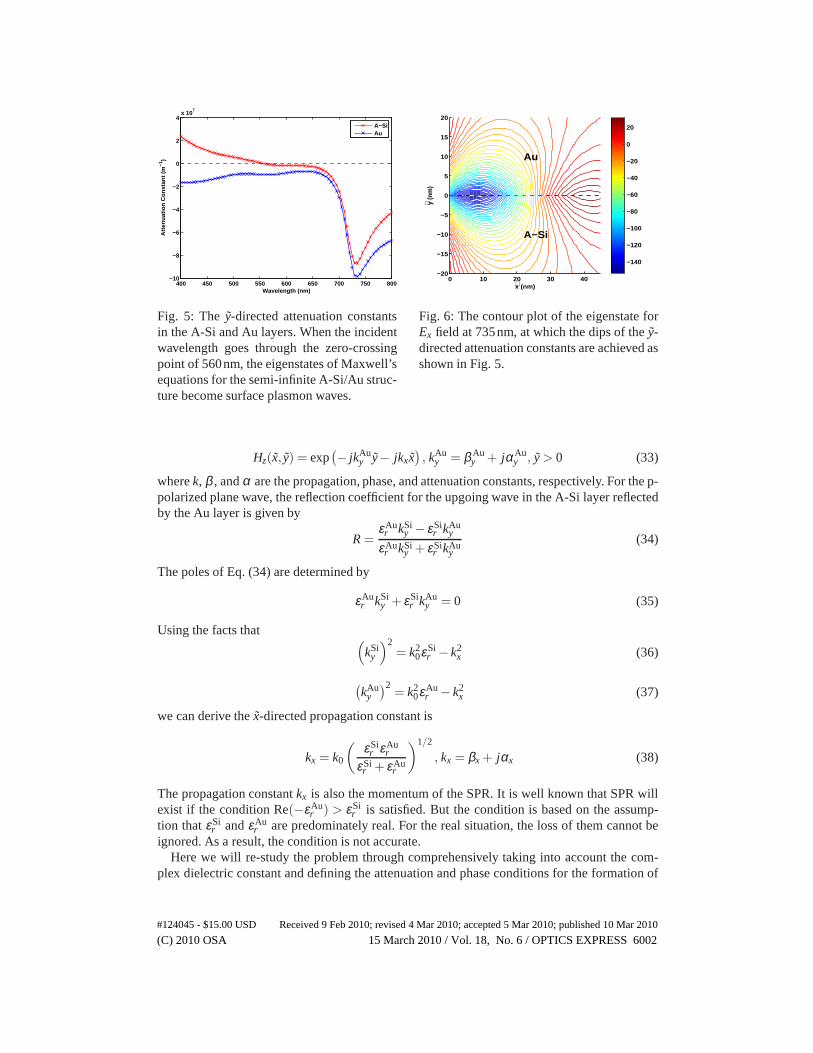
Fig. 5: The ˜y-directed attenuation constantsin the A-Si and Au layers. When the incidentwavelength goes through the zero-crossingpoint of 560nm, the eigenstates of Maxwell’sequations for the semi-infinite A-Si/Au struc-ture become surface plasmon waves.
0 10 20 30 40−20
−15
−10
−5
0
5
10
15
20
x (nm)
y (n
m)
A−Si
Au
∼
∼
−140
−120
−100
−80
−60
−40
−20
0
20
Fig. 6: The contour plot of the eigenstate forEx field at 735nm, at which the dips of the ˜y-directed attenuation constants are achieved asshown in Fig. 5.
Hz(x, y) = exp(
− jkAuy y− jkxx
)
, kAuy = β Au
y + jαAuy , y > 0 (33)
wherek, β , andα are the propagation, phase, and attenuation constants, respectively. For the p-polarized plane wave, the reflection coefficient for the upgoing wave in the A-Si layer reflectedby the Au layer is given by
R =εAu
r kSiy − εSi
r kAuy
εAur kSi
y + εSir kAu
y(34)
The poles of Eq. (34) are determined by
εAur kSi
y + εSir kAu
y = 0 (35)
Using the facts that(
kSiy
)2= k2
0εSir − k2
x (36)
(
kAuy
)2= k2
0εAur − k2
x (37)
we can derive the ˜x-directed propagation constant is
kx = k0
(
εSir εAu
r
εSir + εAu
r
)1/2
, kx = βx + jαx (38)
The propagation constantkx is also the momentum of the SPR. It is well known that SPR willexist if the condition Re(−εAu
r ) > εSir is satisfied. But the condition is based on the assump-
tion thatεSir andεAu
r are predominately real. For the real situation, the loss of them cannot beignored. As a result, the condition is not accurate.
Here we will re-study the problem through comprehensively taking into account the com-plex dielectric constant and defining the attenuation and phase conditions for the formation of
(C) 2010 OSA 15 March 2010 / Vol. 18, No. 6 / OPTICS EXPRESS 6002#124045 - $15.00 USD Received 9 Feb 2010; revised 4 Mar 2010; accepted 5 Mar 2010; published 10 Mar 2010

SPR. The ˜y-directed propagation constants in the A-Si and Au layers are the double-value func-tions ofkx. Considering that the SPR is a surface wave decayed away fromthe dielectric-metalinterface ( ˜y = 0), we have
αSiy < 0, αAu
y < 0 (39)
In other words, the surface plasmon poles should be on the proper Riemann sheets of bothkSiy
andkAuy , i.e. Im
(
kSiy
)
< 0 and Im(
kAuy
)
< 0. As shown in Fig. 5, from solving for the root ofEq. (35), the attenuation constant of the field at A-Si layer change sign when the incident wave-length goes through 560nm. Meanwhile, the locations of the poles of Eq. (34) are changed fromthe improper Riemann sheets to the proper Riemann sheets. According to the Drude model, themetallic dielectric function is approximated as
εAur (ω) ≈ 1−
ω2p
ω2 (40)
whereωp is the plasma frequency of Au. Hence, the SPRs exist at long wavelength rangewhere the metal is opaque. This also agrees with the fact thatthe SPRs exist when the incidentwavelength is larger than 560nm. Thus the eigenstates of theMaxwell’s equations for the semi-infinite A-Si/Au structure are the SPRs if the conditions of Eq. (39) are satisfied. Besides theattenuation constants conditions, the SPRs should satisfythe phase constants conditions also,i.e.
β Siy < 0, β Au
y < 0 (41)
The phase constants conditions agree with the oscillation property of the SPRs. Figure 6 showsthe contour plot of the eigenstate forEx field at 735nm, where the maximum phase constantβx
of the SPR is achieved by the resonance conditionεSir +εAu
r ≈ 0. It is interesting to note that thefield profile looks very symmetric becausekx becomes very large at 735nm and thuskSi
y in Eq.(36) andkAu
y in Eq. (37) are comparable to each other. At the wavelength, the maximum ampli-tudes of the attenuation constants (i.e. the minimum attenuation lengths along ˜y directions) areachieved as well.
For the SC with periodic metal nanopatterns as shown in Fig. 2, the absorbing material isA-Si and the substrate is glass (SiO2). The complex dielectric constants of the materials (Au,A-Si, etc) are taken from [37, 38]. The geometric parametersof the device are set asd1 = 25nm,d2 = 120nm,d3 = 40nm,d4 = 30nm,ds = 100nm, andP = 200nm. They-directed incidentfield is the p-polarized plane wave with the amplitude of 1 andthe frequency spectrum from400nm to 800nm. The spatial step is set to∆x = ∆y = 0.5nm. Fig. 7 shows the absorbed powerdensity of the A-Si layer. Using the planar Au layer, the non-strip (planar) structure is alsomodeled. For the non-strip structure,d2 = 140nm is adopted for achieving the same A-Si areawhile other parameters are unchanged.
The A-Si bulk material has insufficient absorption from 650nm to 800nm due to its lowerconductivity at the long wavelength region as shown in the inset of Fig. 7. For both strip andnon-strip structures, the absorptionη as described by Eq. (25) is significantly enhanced at thelong wavelength region as shown in Fig. 7. The enhancement isdue to the substantial increaseof |E|2. Moreover, the strip structure shows even stronger absorption due to the excited SPRand the constructive interference between strips. In fact,the efficient absorption can enhancethe external quantum efficiency.
More importantly, our results can show the origins of the absorption peaks which are ex-plained by electromagnetic theory. Along±y directions, we consider the structures as the mul-tilayered medium. The waveguide modes can be approximatelyfound by computing the gen-eralized reflection coefficientRi,i+1 of the medium between the ith layer and the(i +1)th layer
(C) 2010 OSA 15 March 2010 / Vol. 18, No. 6 / OPTICS EXPRESS 6003#124045 - $15.00 USD Received 9 Feb 2010; revised 4 Mar 2010; accepted 5 Mar 2010; published 10 Mar 2010

400 450 500 550 600 650 700 750 8000
0.5
1
1.5
2
2.5x 10
9
Wavelength (nm)
Abs
orbe
d P
ower
Den
sity
(W
/m2 )
StripNon−Strip
400 600 8000
2
4
6
8
x 105
Wavelength (nm)
Con
duct
ivity
(S
)
A
B
12
3
4
5
6
Fig. 7: The absorbed power densityη by theA-Si for the periodic strip structure and the“artificially” periodic non-strip structure. Thelower arrows (from A to B) denote the ab-sorption peaks of the non-strip structure andthe upper arrows (from 1 to 6) denote the ab-sorption peaks of the strip structure.
400 450 500 550 600 650 700 750 8000.1
0.2
0.3
0.4
0.5
0.6
0.7
0.8
0.9
1
Wavelength (nm)
Gen
eral
ized
Ref
lect
ion
Coe
ffici
ents
Strip (ITO/A−Si/Au/SiO2)Strip (ITO/A−Si/SiO2)Non−Strip (ITO/A−Si/Au/SiO2)
A
B12
2
6
4
Fig. 8: The generalized reflection coeffi-cients for locating the waveguide modes.The dips of the generalized reflection coeffi-cients correspond to some absorption peaksof Fig. 7.
[29]
Ri,i+1 =Ri,i+1 + Ri+1,i+2e−2 jki+1,y(di+1−di)
1+ Ri,i+1Ri+1,i+2e−2 jki+1,y(di+1−di)(42)
where(di+1 − di) is the thickness of the(i +1)th layer. Considering that the excitation isy-directed plane-wave,ki+1,y = ki+1 = k0
√εr,i+1. The waveguide modes can be obtained from thelocal minima of the generalized reflection coefficient as shown in Fig. 8. As shown in Fig. 7 andFig. 8, the waveguide modes contribute to all the absorptionpeaks (A and B) of the non-stripstructure. In this case, the interface between the A-Si and Au layers can be considered as a goodmirror for trapping the light in the non-strip structure. This is the reason why the absorptionenhancement still happens in the planar structure. However, for the non-strip structure, the SPRcannot be excited due to the momentum mismatch. For the stripstructure, Fig. 9 showsHt
zfield distributions at the absorption peaks. There are two different multilayered media in thestrip structure as shown in Fig. 2. At the regions where the Austrips are present, the mediumis Air/ITO/A-Si/Au/SiO2/Air. In the other region, the medium is Air/ITO/A-Si/SiO2/Air. Thewaveguide modes of the former medium contribute to the absorption peaks 1, 2, and 6 (SeeFig. 7). The absorption peaks 2 and 4 are mainly due to the waveguide modes of the mediumwithout the Au strip.
Since the SC has the periodic structure, the Floquet modes also enhance the absorption. TheHt
z field distributions for the peaks 3 and 4 show the resonant states (Floquet modes) alongxdirections. The periodic boundaries (PBC in Fig. 2) behave like a magnetic wall or electric wallfor the peaks of 3 and 4 respectively. The concentrated field at the absorption layer is due to theFloquet modes that can be observed clearly in Fig. 9(c) and Fig. 9(d).
The SPR is successfully excited by the sub-scatterer strip at the wavelength 745nm as shownin Fig. 5 and Fig. 7. According to the mode conversion theory,the sub-wavelength strip canexcite the evanescent wave components, which may provide the momentum mismatch∆k withthe continuous spectrum up to 2π/d3. The field profile is shown in Fig. 9(e). Thex-directedboundaries of the strips achieve better field concentrationthan they-directed boundaries. The
(C) 2010 OSA 15 March 2010 / Vol. 18, No. 6 / OPTICS EXPRESS 6004#124045 - $15.00 USD Received 9 Feb 2010; revised 4 Mar 2010; accepted 5 Mar 2010; published 10 Mar 2010

(a) Peak 1: 455nm (b) Peak 2: 545nm
(c) Peak 3: 585nm (d) Peak 4: 705nm
(e) Peak 5: 745nm (f) Peak 6: 780nm
Fig. 9: TheHtz field distribution for the periodic strip structure.
phenomenon agrees well with the semi-infinite model in whichthe momentum of the SPR isapproximately calculated by Eq. (35)-Eq. (38).
The interference pattern between the adjacent metal stripsis shown in Fig. 9(d), Fig. 9(e), andFig. 9(f). The surface waves decayed away from they-directed boundaries of the strips interfere
(C) 2010 OSA 15 March 2010 / Vol. 18, No. 6 / OPTICS EXPRESS 6005#124045 - $15.00 USD Received 9 Feb 2010; revised 4 Mar 2010; accepted 5 Mar 2010; published 10 Mar 2010

with each other. The constructive interference leads to thebroadband absorption especially forthe red light and even extends to the infrared region. From 700nm to 800nm, the absorptionpeaks of 4, 5, and 6 are not obvious due to the low conductivities of the A-Si. Thus, a goodbroadband absorbing material with the larger conductivityis very important for improving theabsorption properties of SCs. It should be noted that besides Fig. 9(e), there are some concen-trated fields at the dielectric-metal interfaces in Fig. 9(d) and Fig. 9(f). They are also SPRs. TheSPRs are weak because there are no obvious momentum dips as shown in Fig. 5.
4. Conclusion
Using the FDFD method, the rigorous and efficient model of thethin-film plasmonic SC withthe periodic strip has been developed. Compared with the PML, the hybrid ABC works bet-ter especially for the periodic structure. Moreover, the material discontinuities are accuratelytreated by the inhomogeneous wave equation and the one-sided difference scheme. We alsoproposed the phase and attenuation constants conditions ofthe SPR for lossy material systems.
By using the semi-infinite dielectric-metal structure, ourresults show that SPRs will exist ifthe vertical phase and attenuation constants are negative in both dielectric and metal layers. Thesub-wavelength scatterers can excite the evanescent waves, which provide the size-dependentcontinuous spectrum components. Hence, the subwavelengthscatterers can excite the SPRs forthe broadband light enhancement.
Our results also show that the origins of the absorption peaks for the periodic strip SC struc-ture can be explained by the waveguide mode, the Floquet mode, the SPR, or the constructiveinterference between strips. By changing the geometric parameters, the locations of peaks canbe modified for optimizing the performance of solar cells.
A. Integral form of the wave equation
Using the Gauss’s law, the contour integral form for the waveequation is given by
∮
∂Sm
∂Htz
∂nmdl + k2
m
∫∫
Sm
Htzds = 0 (A-1)
whereSm denotes the four small rectangles enclosing the center square point as shown in Fig.3 and∂Ht
z/∂nm denotes the derivatives ofHtz normal to the contours∂Sm. Applying the central
differences to Eq. (A-1) yields
k21
∆x∆y
4Φ3 +
∆y
2∆x(Φ4−Φ3)+
∆x
2∆y(Φ1−Φ3) =
−∫
Γ12
∂Φ∂n1
dl −∫
Γ14
∂Φ∂n1
dl(A-2)
k22
∆x∆y
4Φ3 +
∆y
2∆x(Φ2−Φ3)+
∆x
2∆y(Φ1−Φ3) =
−∫
Γ21
∂Φ∂n2
dl −∫
Γ23
∂Φ∂n2
dl(A-3)
k23
∆x∆y
4Φ3 +
∆y
2∆x(Φ2−Φ3)+
∆x
2∆y(Φ5−Φ3) =
−∫
Γ32
∂Φ∂n3
dl −∫
Γ34
∂Φ∂n3
dl(A-4)
(C) 2010 OSA 15 March 2010 / Vol. 18, No. 6 / OPTICS EXPRESS 6006#124045 - $15.00 USD Received 9 Feb 2010; revised 4 Mar 2010; accepted 5 Mar 2010; published 10 Mar 2010

k24
∆x∆y
4Φ3 +
∆y
2∆x(Φ4−Φ3)+
∆x
2∆y(Φ5−Φ3) =
−∫
Γ43
∂Φ∂n4
dl −∫
Γ41
∂Φ∂n4
dl(A-5)
According to the boundary conditions at the interfaces(
1εr1
∂Φ(1)
∂n1+
1εr2
∂Φ(2)
∂n2
)∣
∣
∣
∣
∣
Γ12,Γ21
= 0 (A-6)
(
1εr2
∂Φ(2)
∂n2+
1εr3
∂Φ(3)
∂n3
)∣
∣
∣
∣
∣
Γ23,Γ32
= 0 (A-7)
(
1εr3
∂Φ(3)
∂n3+
1εr4
∂Φ(4)
∂n4
)∣
∣
∣
∣
∣
Γ34,Γ43
= 0 (A-8)
(
1εr4
∂Φ(4)
∂n4+
1εr1
∂Φ(1)
∂n1
)∣
∣
∣
∣
∣
Γ41,Γ14
= 0 (A-9)
we get the FDFD form of the inhomogeneous wave function, which is the same as Eq. (5).
Acknowledgement
We would like to acknowledge the support of the grants (#712108) from the Research GrantCouncil of the Hong Kong Special Administrative Region, China. The first author expresseshis sincere gratitude to Mr. Kwan Wing Keung, the Universityof Hong Kong for his technicalsupport.
(C) 2010 OSA 15 March 2010 / Vol. 18, No. 6 / OPTICS EXPRESS 6007#124045 - $15.00 USD Received 9 Feb 2010; revised 4 Mar 2010; accepted 5 Mar 2010; published 10 Mar 2010