A packed-bed DBD micro plasma reactor for CO2 dissociation
9
A packed-bed DBD micro plasma reactor for CO 2 dissociation: Does size matter? Supplementary information Y. Uytdenhouwen a,b , S. Van Alphen a , I. Michielsen a,b , V. Meynen b , P. Cool b , A. Bogaerts a a Research Group PLASMANT, Department of Chemistry, University of Antwerp, Universiteitsplein 1, Wilrijk B-2610, Belgium b Research Group LADCA, Department of Chemistry, University of Antwerp, Universiteitsplein 1, Wilrijk B-2610, Belgium
-
Upload
khangminh22 -
Category
Documents
-
view
4 -
download
0
Transcript of A packed-bed DBD micro plasma reactor for CO2 dissociation
A packed-bed DBD micro plasma reactor for CO2dissociation:Doessizematter?SupplementaryinformationY. Uytdenhouwen a,b, S. Van Alphen a, I. Michielsen a,b, V. Meynen b, P. Cool b, A. Bogaerts a
a Research Group PLASMANT, Department of Chemistry, University of Antwerp, Universiteitsplein 1, Wilrijk B-2610, Belgium
b Research Group LADCA, Department of Chemistry, University of Antwerp, Universiteitsplein 1, Wilrijk B-2610, Belgium

1 Electricalcharacterization:Theory
Figure 2 of the main paper shows a typical oscillogram and a simplified Lissajous figure. The oscillogram obtained from each experiment can be directly analysed to calculate the peak-to-peak voltage (𝑈"") and root-mean-square current (𝐼$%&) of the plasma reactor.
Further analysis of the Lissajous figures gives information about the electrical behaviour of the plasma. The Lissajous figure can be divided into four regions, representing the four phases occurring during one voltage period. They consist of two capacitive phases, AB and CD, where the reactor behaves like a capacitor with no activity in the reaction volume; as well as two discharge phases, BC and DA, where the gas present in the reaction volume is (partially) transformed into a plasma and a net flow of electrons through the reactor is present, resulting in a combined resistive-capacitive behaviour of the reactor. The Q-U Lissajous figure has the benefit that the slopes directly relate to a physical value, i.e. the capacitance of the reactor during that specific phase, since 𝑑𝑄/𝑑𝑈 = 𝐶. In the capacitive phases, the slopes show the total capacitance of the reactor 𝐶,-.. which can be represented in a simplified electrical model, shown in Figure S1a), by two capacitors in series, representing the capacitance of the dielectric barrier 𝐶/0-. and the discharge gap 𝐶12" according to the following equation:
345677
= 348967
+ 34;<=
(SI1)
In the discharge phase, the charge built up by the applied voltage reaches a threshold, which ignites the plasma. The capacitance of the discharge gap is then electrically bypassed due to the conductivity of the plasma and only the capacitance of the dielectric barrier remains, shown by the respective slopes. This phase is depicted in the simplified model by the dielectric barrier capacitance bypassed by a low value resistor. In the capacitance phase the model uses an infinitely high value resistor.
Figure S1: a) Simplified electrical model for a DBD reactor. b) Extended model for a DBD reactor incorporating partial discharging.

The flaw with this model is its assumption of a fully discharged reaction volume, leaving only the capacitance of the dielectric tube 𝐶/0-. as the source of the slope of the discharge phase. However, if the reaction volume is not entirely discharged and not all accumulated charge is used, we get an intermediate phase, i.e., a partial discharge, with an effective capacitance and slope 𝜁/0-. that has a value between 𝐶/0-. and 𝐶,-.. , depending on the degree of partial discharging. A new model was proposed by Peeters and van de Sanden [1] to accommodate this partial discharging of the DBD reactor, as shown in Figure S1b). The electrical model is now divided into two parts: a non-discharging 𝛼 part and a discharging 𝛽 part. When the reactor is in the discharge phase, the volume 𝛼 of the reactor that is not ignited is now represented by a partial capacitance for the dielectric barrier and the discharge gap; while the ignited volume 𝛽 is represented by the complementary capacitances configured like the original model. However, during the capacitive phase of the reactor, the resistor in the 𝛽 part again has an infinitely high value, resulting in the cumulated capacitive behaviour of the dielectric barrier and reaction volume like before. Using this model, the fraction of partial discharging can now be quantified and used as a measure of efficient behaviour of a particular reactor setup. This fraction of partial discharging 𝛼 is calculated by the formula of Peeters and van de Sanden [1]:
𝛼 = 48967AB896748967A45677
(SI2)
𝐶,-.. and 𝜁/0-. can directly be determined by calculating the respective slopes of the Lissajous figure; the capacitance of the ideal, fully discharged reactor 𝐶/0-. however, cannot. Butterworth et al. [2] showed that this value can be obtained by using an argon plasma, making this the closest approximation compared with roughly calculated values, since this method uses the actual reactor set-up. A dielectric capacitance 𝐶/0-. of 26.6 ± 0.2 mC/V is measured, independent of the discharge gap size.
Next, the burning voltage can be determined. The burning voltage is the minimum voltage required to maintain the plasma discharge during the experiment and is normally determined in the Lissajous figure as half of the voltage difference between the intersects with the x-axis. This value needs to be corrected for the partial discharging of the reactor according to the formula of Peeters and van de Sanden [1]:
𝑈CDE =3A45677 48967⁄3A45677 B8967⁄ Δ𝑈 (SI3)
Finally, the displaced charge during the discharge phase 𝑄/0H" and the number of micro discharges are calculated. This is done to analyse the average strength of the discharges. The displaced charge 𝑄/0H" is calculated by taking the difference in charge between points A and D in the Lissajous figure, see also figure 2 in the main paper. Individual micro discharges are determined after normalization of the current profile and applying height and width threshold values to exclude signal noise, resonance, and systematic measuring errors. The Picoscope 6402D oscilloscope from Picotech used a sample rate of 625 MS/s in our set-up, corresponding to a sample interval of 1.6 ns, which is well below the typical duration of a micro discharge of around (a few) hundred nano seconds. Different threshold values were used for empty and packed reactors due to the large difference in discharge intensity (width and height). This does mean that not every single discharge in the reactor can be measured, e.g. if they are too short, too small, or coincide with a bigger peak or resonance. Therefore, the returned value will not be the exact number of discharges in the plasma but will still be a systematically calculated and representable number.
2 Electricalcharacterization:Resultsofthepackedreactor
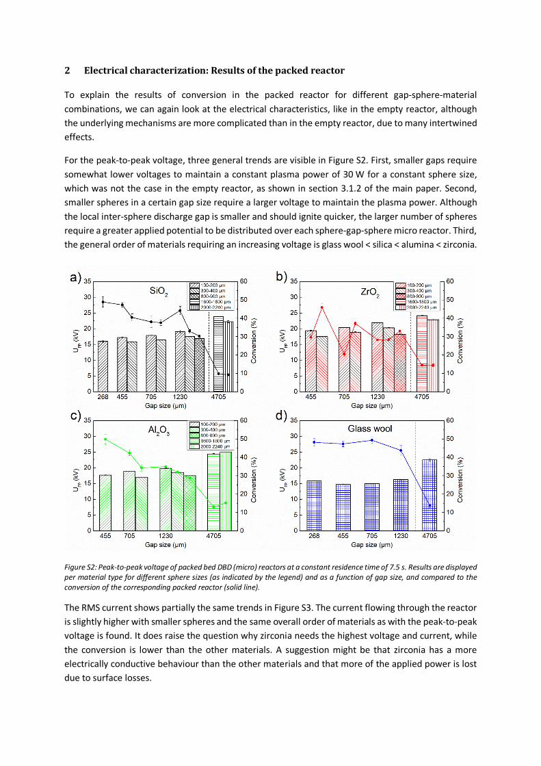
To explain the results of conversion in the packed reactor for different gap-sphere-material combinations, we can again look at the electrical characteristics, like in the empty reactor, although the underlying mechanisms are more complicated than in the empty reactor, due to many intertwined effects.
For the peak-to-peak voltage, three general trends are visible in Figure S2. First, smaller gaps require somewhat lower voltages to maintain a constant plasma power of 30 W for a constant sphere size, which was not the case in the empty reactor, as shown in section 3.1.2 of the main paper. Second, smaller spheres in a certain gap size require a larger voltage to maintain the plasma power. Although the local inter-sphere discharge gap is smaller and should ignite quicker, the larger number of spheres require a greater applied potential to be distributed over each sphere-gap-sphere micro reactor. Third, the general order of materials requiring an increasing voltage is glass wool < silica < alumina < zirconia.
Figure S2: Peak-to-peak voltage of packed bed DBD (micro) reactors at a constant residence time of 7.5 s. Results are displayed per material type for different sphere sizes (as indicated by the legend) and as a function of gap size, and compared to the conversion of the corresponding packed reactor (solid line).
The RMS current shows partially the same trends in Figure S3. The current flowing through the reactor is slightly higher with smaller spheres and the same overall order of materials as with the peak-to-peak voltage is found. It does raise the question why zirconia needs the highest voltage and current, while the conversion is lower than the other materials. A suggestion might be that zirconia has a more electrically conductive behaviour than the other materials and that more of the applied power is lost due to surface losses.

Figure S3: Average current flow (root mean square) of packed bed DBD (micro) reactors at a constant residence time of 7.5 s. Results are displayed per material type for different sphere sizes (as indicated by the legend) and as a function of gap size, and compared to the conversion of the corresponding packed reactor (solid line).
The effective capacitance and the derived partial discharging fraction of the reactor, displayed in Figure S4 and Figure S5, show some counterintuitive trends. The trend of the empty reactor, where a smaller discharge gap results in less partial discharging and thus a higher conversion, is still visible. However, this is clearly material dependent, as the decrease of a follows the order glass wool >> silica > alumina / zirconia Moreover, in packed bed reactors, less partial discharging does not always mean higher conversion. Zirconia spheres within a fixed discharge gap cohere to this trend, but silica and alumina show the opposite results. It shows that decreasing the sphere size leads to more partial discharging, since the plasma cannot be so easily ignited, but that the conversion still increases. Glass wool shows very low partial discharging behaviour with some of the highest conversions as a result.
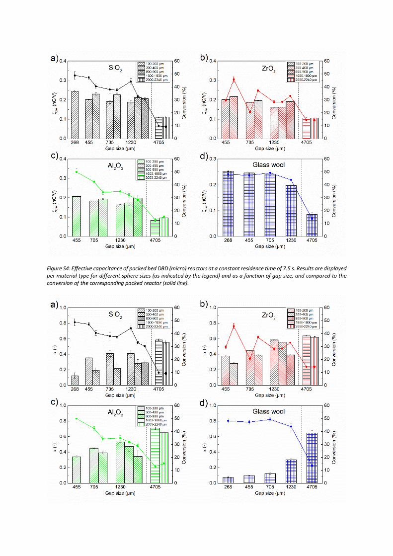
Figure S4: Effective capacitance of packed bed DBD (micro) reactors at a constant residence time of 7.5 s. Results are displayed per material type for different sphere sizes (as indicated by the legend) and as a function of gap size, and compared to the conversion of the corresponding packed reactor (solid line).
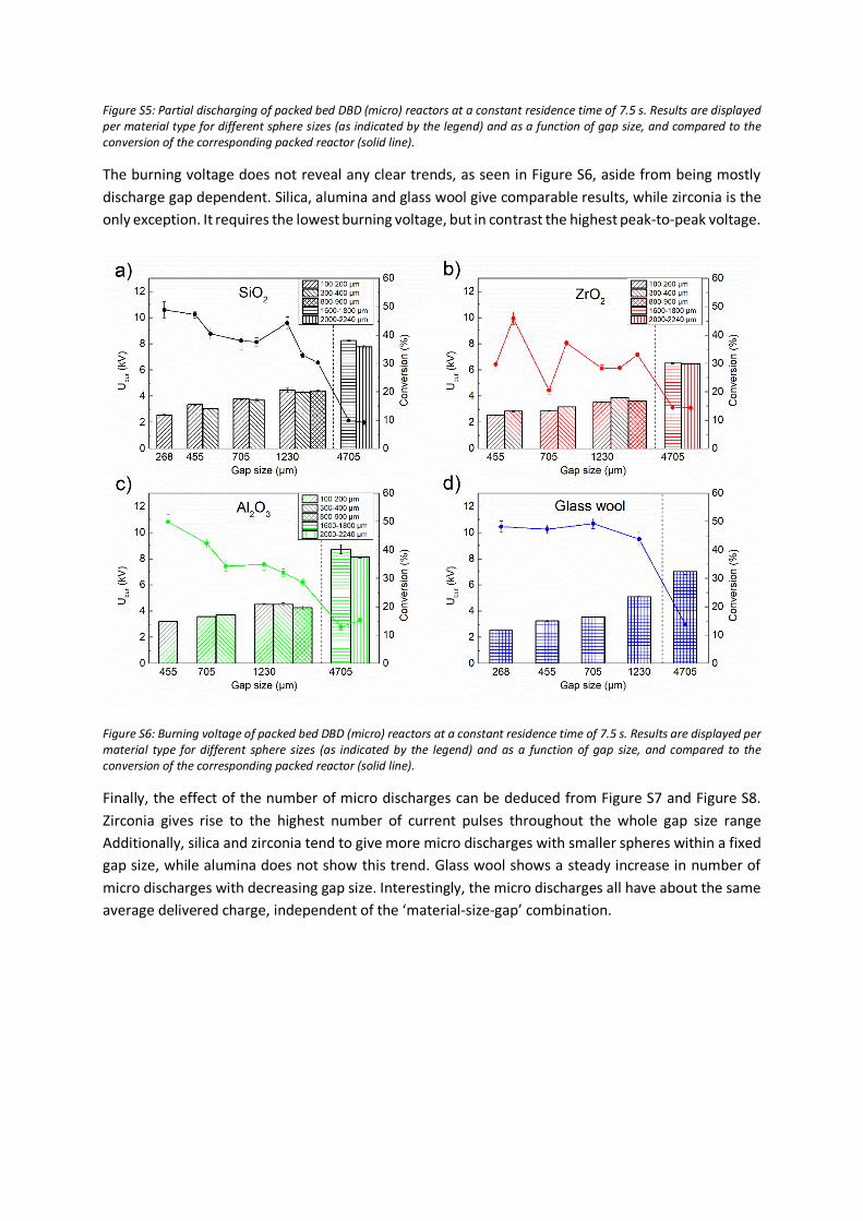
Figure S5: Partial discharging of packed bed DBD (micro) reactors at a constant residence time of 7.5 s. Results are displayed per material type for different sphere sizes (as indicated by the legend) and as a function of gap size, and compared to the conversion of the corresponding packed reactor (solid line).
The burning voltage does not reveal any clear trends, as seen in Figure S6, aside from being mostly discharge gap dependent. Silica, alumina and glass wool give comparable results, while zirconia is the only exception. It requires the lowest burning voltage, but in contrast the highest peak-to-peak voltage.
Figure S6: Burning voltage of packed bed DBD (micro) reactors at a constant residence time of 7.5 s. Results are displayed per material type for different sphere sizes (as indicated by the legend) and as a function of gap size, and compared to the conversion of the corresponding packed reactor (solid line).
Finally, the effect of the number of micro discharges can be deduced from Figure S7 and Figure S8. Zirconia gives rise to the highest number of current pulses throughout the whole gap size range Additionally, silica and zirconia tend to give more micro discharges with smaller spheres within a fixed gap size, while alumina does not show this trend. Glass wool shows a steady increase in number of micro discharges with decreasing gap size. Interestingly, the micro discharges all have about the same average delivered charge, independent of the ‘material-size-gap’ combination.
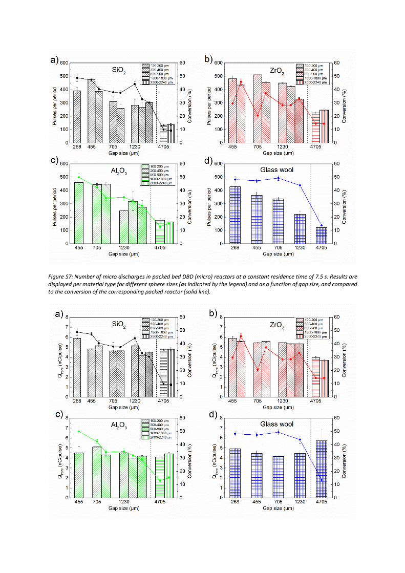
Figure S7: Number of micro discharges in packed bed DBD (micro) reactors at a constant residence time of 7.5 s. Results are displayed per material type for different sphere sizes (as indicated by the legend) and as a function of gap size, and compared to the conversion of the corresponding packed reactor (solid line).
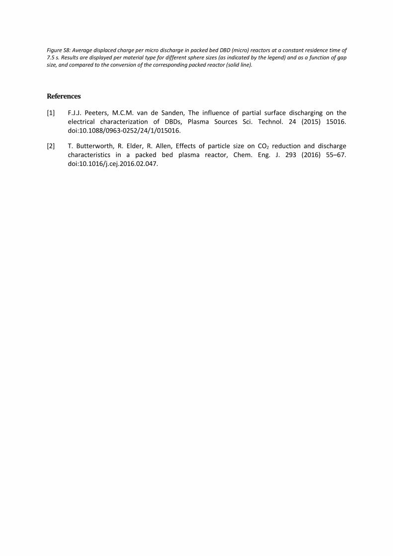
Figure S8: Average displaced charge per micro discharge in packed bed DBD (micro) reactors at a constant residence time of 7.5 s. Results are displayed per material type for different sphere sizes (as indicated by the legend) and as a function of gap size, and compared to the conversion of the corresponding packed reactor (solid line).
References
[1] F.J.J. Peeters, M.C.M. van de Sanden, The influence of partial surface discharging on the electrical characterization of DBDs, Plasma Sources Sci. Technol. 24 (2015) 15016. doi:10.1088/0963-0252/24/1/015016.
[2] T. Butterworth, R. Elder, R. Allen, Effects of particle size on CO2 reduction and discharge characteristics in a packed bed plasma reactor, Chem. Eng. J. 293 (2016) 55–67. doi:10.1016/j.cej.2016.02.047.