A high level FPGA-based abstract machine for image processing
16
A high level FPGA-based abstract machine for image processing A. Bouridane, D. Crookes, P. Donachy, K. Alotaibi, K. Benkrid * Department of Computer Science, The Queen’s University of Belfast, Belfast BT7, Ireland Abstract Image processing requires high computational power, plus the ability to experiment with algorithms. Recently, re- configurable hardware devices in the form of field programmable gate arrays (FPGAs) have been proposed as a way of obtaining high performance at an economical price. At present, however, users must program FPGAs at a very low level and have a detailed knowledge of the architecture of the device being used. They do not therefore facilitate easy devel- opment of, or experimentation with, image processing algorithms. To try to reconcile the dual requirements of high performance and ease of development, this paper reports on the design and realisation of an FPGA based image pro- cessing machine and its associated high level programming model. This abstract programming model allows an appli- cation developer to concentrate on the image processing algorithm in hand rather than on its hardware implementation. The abstract machine is based on a PC host system with a PCI-bus add-on card containing Xilinx XC6200 series FPGA(s). The machine’s high level instruction set is based on the operators of image algebra. XC6200 series FPGA configurations have been developed to implement each high level instruction. Ó 1999 Elsevier Science B.V. All rights reserved. Keywords: Digital image processing; Custom computing; High performance architectures; FPGA’s 1. Introduction Image processing applications usually require the processing of large amounts of data, and the time constraints of imaging applications often demand that this processing be done, if not in real time, at least in reasonable time. Much eort has therefore gone into designing high performance architectures tailored to image processing appli- cations. One common approach to high performance image processing has been to use parallel com- puting [1]. Because of the regular nature of low level image processing, it is not dicult to partition image data across several processors, and then to process each partition in parallel. Some operations will of course require additional Journal of Systems Architecture 45 (1999) 809–824 * Corresponding author. E-mail: [email protected] 1383-7621/99/$ – see front matter Ó 1999 Elsevier Science B.V. All rights reserved. PII: S 1 3 8 3 - 7 6 2 1 ( 9 8 ) 0 0 0 4 0 - X
-
Upload
independent -
Category
Documents
-
view
1 -
download
0
Transcript of A high level FPGA-based abstract machine for image processing
A high level FPGA-based abstract machine for image processing
A. Bouridane, D. Crookes, P. Donachy, K. Alotaibi, K. Benkrid *
Department of Computer Science, The Queen's University of Belfast, Belfast BT7, Ireland
Abstract
Image processing requires high computational power, plus the ability to experiment with algorithms. Recently, re-
con®gurable hardware devices in the form of ®eld programmable gate arrays (FPGAs) have been proposed as a way of
obtaining high performance at an economical price. At present, however, users must program FPGAs at a very low level
and have a detailed knowledge of the architecture of the device being used. They do not therefore facilitate easy devel-
opment of, or experimentation with, image processing algorithms. To try to reconcile the dual requirements of high
performance and ease of development, this paper reports on the design and realisation of an FPGA based image pro-
cessing machine and its associated high level programming model. This abstract programming model allows an appli-
cation developer to concentrate on the image processing algorithm in hand rather than on its hardware implementation.
The abstract machine is based on a PC host system with a PCI-bus add-on card containing Xilinx XC6200 series FPGA(s).
The machine's high level instruction set is based on the operators of image algebra. XC6200 series FPGA con®gurations
have been developed to implement each high level instruction. Ó 1999 Elsevier Science B.V. All rights reserved.
Keywords: Digital image processing; Custom computing; High performance architectures; FPGA's
1. Introduction
Image processing applications usually requirethe processing of large amounts of data, and thetime constraints of imaging applications oftendemand that this processing be done, if not in realtime, at least in reasonable time. Much e�ort has
therefore gone into designing high performancearchitectures tailored to image processing appli-cations.
One common approach to high performanceimage processing has been to use parallel com-puting [1]. Because of the regular nature of lowlevel image processing, it is not di�cult topartition image data across several processors, andthen to process each partition in parallel. Someoperations will of course require additional
Journal of Systems Architecture 45 (1999) 809±824
* Corresponding author. E-mail: [email protected]
1383-7621/99/$ ± see front matter Ó 1999 Elsevier Science B.V. All rights reserved.
PII: S 1 3 8 3 - 7 6 2 1 ( 9 8 ) 0 0 0 4 0 - X
communication, such as neighbourhood opera-tions or histogram ®nding; but provided there is afast, low-latency communications network, thisdoes not reduce performance drastically. This lat-ter point does require attention, however, as atypical workstation cluster running a general-purpose communications shell such as MPI canoften yield disappointing performance. Multipro-cessor image processing systems have generallyspeaking not yet ful®lled their promise. This ispartly a matter of the cost, lack of stability andsoftware support for parallel machines; it is alsopartly a matter of communication overheads ±particularly if images are being captured and dis-tributed in real time. There is a lot of work cur-rently in progress to develop low latencycommunication shells on workstations, but theywill always have di�culties in coping with realtime video processing.
A second way of obtaining high performance inimage processing applications is to use moderndigital signal processing (DSP) processors [2,3].These processors have additional instructionsspecially tailored to DSP applications (such asmultiply-accumulate instructions), and implementother architectural features such as pipelining toexploit implicit parallelism. DSP processors andtheir associated software tools have made signi®-cant progress in recent years, and can yield im-pressive performance rates.
A third architectural approach to obtaininghigh performance image processing is to use ded-icated hardware, such as ASICS or VLSI chips, forspeci®c algorithms such as convolution. The ob-vious drawback of this dedicated approach hasrecently started to be overcome with the develop-ment of programmable, recon®gurable FPGA de-vices (®eld programmable gate arrays). Thesedevices o�er performance which is steadily ap-proaching that of special purpose, algorithm-spe-ci®c hardware, but with the ability to be reused fordi�erent algorithms because they can be dynami-
cally recon®gured very rapidly. A range of repre-sentative samples of FPGA-based recon®gurablesystems which can be used for image processingapplications includes: the Splash-2 system devel-oped by the SRC (Supercomputing ResearchCentre) [4]; the G-800 system produced by GigaOperations [5]; the PIPS proposed by Chan [6]; theXilinx 6200 series, a ®ne grain FPGA device; andAn FPGA-based coprocessor for image processingproposed by Hamid [7].
FPGA chips are claimed to o�er an attractivecombination of low cost, high performance, andapparent ¯exibility. But there is a cost. The pro-gramming model for bare FPGAs is at the gatelevel. And even with libraries of common functionslike multipliers and adders, the programmer stillmust think at the logic block level rather than at thealgorithmic, high level programming level. Theultimate goal would of course be to be able to writein a high level language (such as, arguably, `C'),and rely on sophisticated software tools to generatee�cient FPGA con®gurations automatically. Un-fortunately, this paradise is still over the horizon.
This paper describes some results of a researchprogramme at The Queen's University of Belfastwhich aims to bridge the gap between applicationsprogramming and FPGA control [8]. The aim ofthe research is to provide a high level program-ming model speci®cally for low level image pro-cessing tasks, and software tools which providee�cient FPGA implementations automatically. Byadopting an application-speci®c approach, basedon an algebra specially developed for image pro-cessing, it becomes possible to de®ne a relativelysmall set of basic, tailorable FPGA con®gurations.These core con®gurations have been developedand optimised by hand, targeted for the XilinxXC6216 FPGA ± a 64 ´ 64 grid of cells. The set ofcore con®gurations have been designed in a waywhich enables them to be tailored for di�erentparameters. The result is a system which providesthe performance bene®ts of FPGAs, but provides
810 A. Bouridane et al. / Journal of Systems Architecture 45 (1999) 809±824

a very high level programming model to the ap-plication developer. All the con®gurations discus-sed in this paper have been designed using theViewlogic WorkView CAD tool. From this anEDIF description is generated. The physical¯oorplan layouts for the Xilinx XC6216 FPGAwere generated using the Xilinx XACTstep Place-and-Route software, using the EDIF descriptionas an input. The con®gurations have been testedusing Xilinx's simulation tools.
In the sections which follow, the paper ®rstoutlines the programming model which the FPGAimage coprocessor supports. This is a high levelmodel, based on image algebra [12]. Then the de-sign of the necessary FPGA con®gurations is de-veloped. Convolution is used as a typicaloperation, and a feature of the designs is that theyare scalable, and conform to a standard frame-work which enables all the instructions to be im-plemented using a small set of basic buildingblocks. Some additional facilities which we haveimplemented are described, though details are notgiven for the sake of space. Finally, some conclu-sions are drawn on the work, and on future di-rections which we are currently pursuing.
2. Design of the image processing machine
At its most basic level, the programming modelfor our image processing machine is a host pro-cessor (typically a PC, programmed in C++) andan FPGA-based image coprocessor. This copro-cessor supports a high level, image processing-speci®c instruction set. The programmer's inter-face to the instruction set is via a C++ class.
The application developer proceeds as though astandard library of image-level routines is pro-vided, for common tasks such as the neighbour-hood convolution operation. Behind the scenes,when the user calls a coprocessor instruction, thesoftware environment will use the details of this
instruction call to extract the corresponding actualFPGA con®guration from a library; it will thendownload the con®guration to the FPGA board,and tailor any cells if necessary; and ®nally it willpass the image data to the FPGA board, and storethe results as they are generated. To the user, theprogramming model is merely the set of algebraicoperators provided by the library. When the op-eration is complete, the application program willbe able to proceed, possibly to another coproces-sor instruction, at which point the above process isrepeated. Thus the FPGA coprocessor is con-stantly being recon®gured during execution of anapplication program (though certain optimisationscan easily be implemented, such as checking thecurrent board con®guration before recon®guring,in case the board is already con®gured correctly ±as might typically be the case if the applicationprogram is in a tight loop).
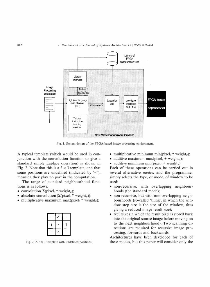
The overall design of the software system whichprovides this high level programming model, andhides all details of con®gurations from the user, isshown in Fig. 1.
2.1. The coprocessor instruction set
The high level instruction set is based on pre-vious image processing programming abstractionsdeveloped at QUB [9±11] which in turn were basedon Image Algebra [12]. In practice, we have con-centrated on providing FPGA support for theneighbourhood operators in Image Algebra, sincecommunication costs on the PCI bus suggest itmay sometimes be just as fast to execute point-to-point image operations (such as image subtractionor thresholding) on the host processor.
All the neighbourhood operations require twothings:· a template (which has a size, and a set of
weights);· a neighbourhood function to be applied to each
image neighbourhood (e.g. convolution).
A. Bouridane et al. / Journal of Systems Architecture 45 (1999) 809±824 811
A typical template (which would be used in con-junction with the convolution function to give astandard simple Laplace operation) is shown inFig. 2. Note that this is a 3 ´ 3 template, and thatsome positions are unde®ned (indicated by `�'),meaning they play no part in the computation.
The range of standard neighbourhood func-tions is as follows:· convolution R(pixeli * weightii);· absolute convolution |R(pixeli * weightii)|;· multiplicative maximum max(pixeli * weightii);
· multiplicative minimum min(pixeli * weightii);· additive maximum max(pixeli + weightii);· additive minimum min(pixeli + weightii).Each of these operations can be carried out inseveral alternative modes, and the programmersimply selects the type, or mode, of window to beused:· non-recursive, with overlapping neighbour-
hoods (the standard mode);· non-recursive, but with non-overlapping neigh-
bourhoods (so-called `tiling', in which the win-dow step size is the size of the window, thusgiving a reduced image result size);
· recursive (in which the result pixel is stored backinto the original source image before moving onto the next neighbourhood). Two scanning di-rections are required for recursive image pro-cessing, forwards and backwards.
Architectures have been developed for each ofthese modes, but this paper will consider only theFig. 2. A 3 ´ 3 template with unde®ned positions.
Fig. 1. System design of the FPGA-based image processing environment.
812 A. Bouridane et al. / Journal of Systems Architecture 45 (1999) 809±824

standard (non-recursive) mode of neighbourhoodinstructions.
To carry out a neighbourhood operation, theapplication programmer will perform the follow-ing tasks:· Build a tailored instruction by giving the func-
tion, the template and the image size.· Perform the instruction, using the routine:
perform�input;; output;�:
3. Implementation of the coprocessor instruction set
This section outlines the development and de-sign of the FPGA con®gurations necessary toimplement the high level instruction set for theneighbourhood operations described above. Inderiving our design, there are certain key guidingprinciples which were followed.· Scalability. The hardware design should not be
inherently limited to a particular data wordlength or a particular template size or shape.
· First-time-right place and route. A design gener-ated from the high level instruction should al-ways guarantee to place and route ®rst timeand require no alteration from the user. Thiswill in¯uence the design of building block com-ponents.
· Utilisation of chip functionality. Although it isimportant that chip resources are used e�cient-ly, once a ®t for an instruction has been ob-tained, there is nothing in particular to begained from further reducing the number ofgates used. This factor di�ers from, say, theVLSI approach.
· Reusability. The instruction set should be imple-mented using arrangements of readily customi-sable building block units that may be reusedin a number of instructions.
As a ®rst step, the con®guration for a two-dimen-sional 3 ´ 3 convolver will be presented. Con®gu-
rations for the other neighbourhood operators areessentially variations of this, with di�erent func-tional sub-blocks. Our convolver is not particularlynovel, and we have used existing approaches.
3.1. A 2-D convolver
Any neighbourhood image operation involvespassing a 2-D window over an image, and carryingout a calculation at each window position, as il-lustrated in Fig. 3. Convolution is the best knownneighbourhood calculation.
The resulting image is de®ned as follows:
Ri�Pÿpt;j�Qÿqt �XQÿ1
l�0
XPÿ1
k�0
Ck;l Xi�k;j�l
8i; j 2 0; 0�M ÿ P ; N ÿ Q;
which can be rewritten as:
Ri�pt;j�qt �XQÿ1
l�0
c�l�T x�i; j� l�; �1�
where c(l) are coe�cient column vectors. For ex-ample, a 3 ´ 3 window may be reorganised asfollows:
and x(i,j + l) are input image column vectors, andwhere:
c�l�T x�i; j� l� �XPÿ1
k�0
Ck;l Xi�k;j�l: �2�
A. Bouridane et al. / Journal of Systems Architecture 45 (1999) 809±824 813
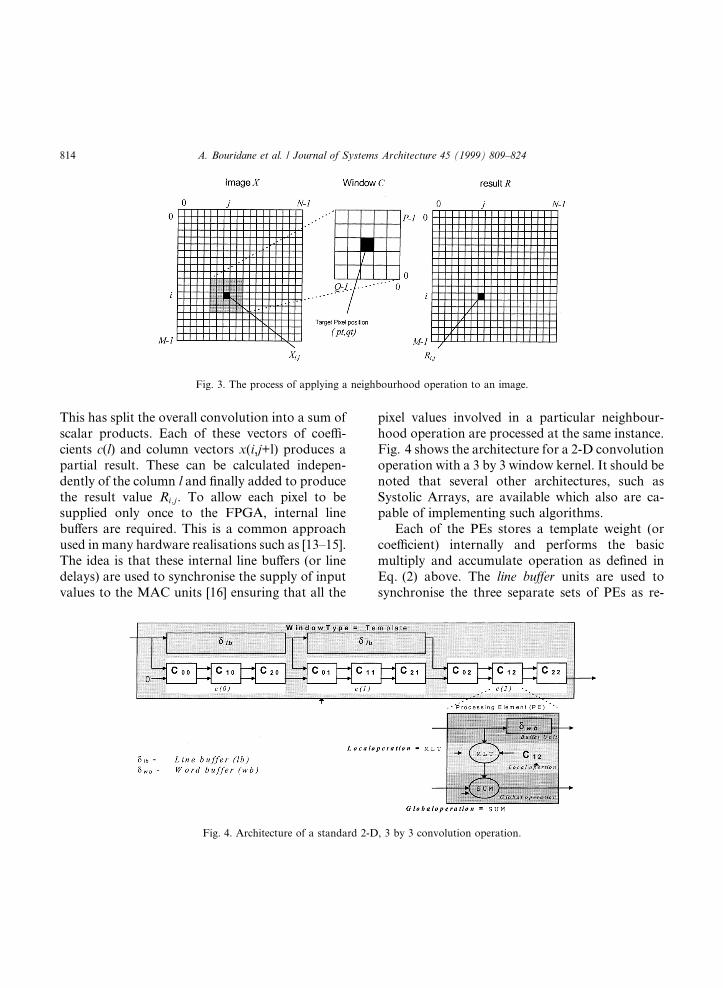
This has split the overall convolution into a sum ofscalar products. Each of these vectors of coe�-cients c(l) and column vectors x(i,j+l) produces apartial result. These can be calculated indepen-dently of the column l and ®nally added to producethe result value Ri;j. To allow each pixel to besupplied only once to the FPGA, internal linebu�ers are required. This is a common approachused in many hardware realisations such as [13±15].The idea is that these internal line bu�ers (or linedelays) are used to synchronise the supply of inputvalues to the MAC units [16] ensuring that all the
pixel values involved in a particular neighbour-hood operation are processed at the same instance.Fig. 4 shows the architecture for a 2-D convolutionoperation with a 3 by 3 window kernel. It should benoted that several other architectures, such asSystolic Arrays, are available which also are ca-pable of implementing such algorithms.
Each of the PEs stores a template weight (orcoe�cient) internally and performs the basicmultiply and accumulate operation as de®ned inEq. (2) above. The line bu�er units are used tosynchronise the three separate sets of PEs as re-
Fig. 4. Architecture of a standard 2-D, 3 by 3 convolution operation.
Fig. 3. The process of applying a neighbourhood operation to an image.
814 A. Bouridane et al. / Journal of Systems Architecture 45 (1999) 809±824
quired by Eq. (1). The word bu�er (wb) in each ofthe PEs is used to synchronise the supply of thepixels as speci®ed by Eq. (2).
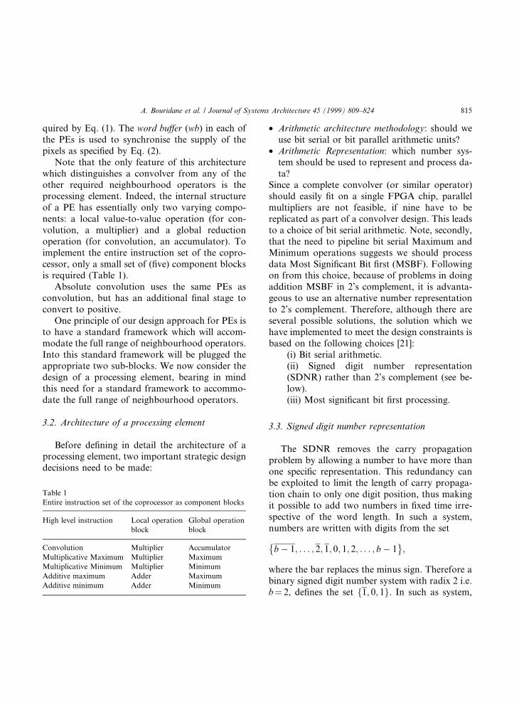
Note that the only feature of this architecturewhich distinguishes a convolver from any of theother required neighbourhood operators is theprocessing element. Indeed, the internal structureof a PE has essentially only two varying compo-nents: a local value-to-value operation (for con-volution, a multiplier) and a global reductionoperation (for convolution, an accumulator). Toimplement the entire instruction set of the copro-cessor, only a small set of (®ve) component blocksis required (Table 1).
Absolute convolution uses the same PEs asconvolution, but has an additional ®nal stage toconvert to positive.
One principle of our design approach for PEs isto have a standard framework which will accom-modate the full range of neighbourhood operators.Into this standard framework will be plugged theappropriate two sub-blocks. We now consider thedesign of a processing element, bearing in mindthis need for a standard framework to accommo-date the full range of neighbourhood operators.
3.2. Architecture of a processing element
Before de®ning in detail the architecture of aprocessing element, two important strategic designdecisions need to be made:
· Arithmetic architecture methodology: should weuse bit serial or bit parallel arithmetic units?
· Arithmetic Representation: which number sys-tem should be used to represent and process da-ta?
Since a complete convolver (or similar operator)should easily ®t on a single FPGA chip, parallelmultipliers are not feasible, if nine have to bereplicated as part of a convolver design. This leadsto a choice of bit serial arithmetic. Note, secondly,that the need to pipeline bit serial Maximum andMinimum operations suggests we should processdata Most Signi®cant Bit ®rst (MSBF). Followingon from this choice, because of problems in doingaddition MSBF in 2's complement, it is advanta-geous to use an alternative number representationto 2's complement. Therefore, although there areseveral possible solutions, the solution which wehave implemented to meet the design constraints isbased on the following choices [21]:
(i) Bit serial arithmetic.(ii) Signed digit number representation(SDNR) rather than 2's complement (see be-low).(iii) Most signi®cant bit ®rst processing.
3.3. Signed digit number representation
The SDNR removes the carry propagationproblem by allowing a number to have more thanone speci®c representation. This redundancy canbe exploited to limit the length of carry propaga-tion chain to only one digit position, thus makingit possible to add two numbers in ®xed time irre-spective of the word length. In such a system,numbers are written with digits from the set
bÿ 1; . . . ; 2; 1; 0; 1; 2; . . . ; bÿ 1�
;
where the bar replaces the minus sign. Therefore abinary signed digit number system with radix 2 i.e.b� 2, de®nes the set f1; 0; 1g. In such as system,
Table 1
Entire instruction set of the coprocessor as component blocks
High level instruction Local operation
block
Global operation
block
Convolution Multiplier Accumulator
Multiplicative Maximum Multiplier Maximum
Multiplicative Minimum Multiplier Minimum
Additive maximum Adder Maximum
Additive minimum Adder Minimum
A. Bouridane et al. / Journal of Systems Architecture 45 (1999) 809±824 815
the number 5 may be represented by any of thefollowing:
1 0 1 � 1 1 1 � 1 1 0 1 � 1 1 1 1 � 1 1 1 0 1:
The advantages of such a system, however, arenot without their cost. Two bits of data (onepositive and one negative) are needed to representa single binary digit. This is at the expense of in-creased bandwidth of interconnects between ar-ithmetic units and ultimately physical chip area[17,18].
Because image data may have to be occasion-ally processed on the host processor, the basicstorage format for image data is 2's complement.Therefore, processing elements ®rst convert theirincoming image data to SDNR. This also reducesthe chip area required for the line bu�ers (in whichdata is held in 2's complement). A ®nal unit toconvert a SDNR result into 2's complement will beneeded before any results can be returned to thehost system.
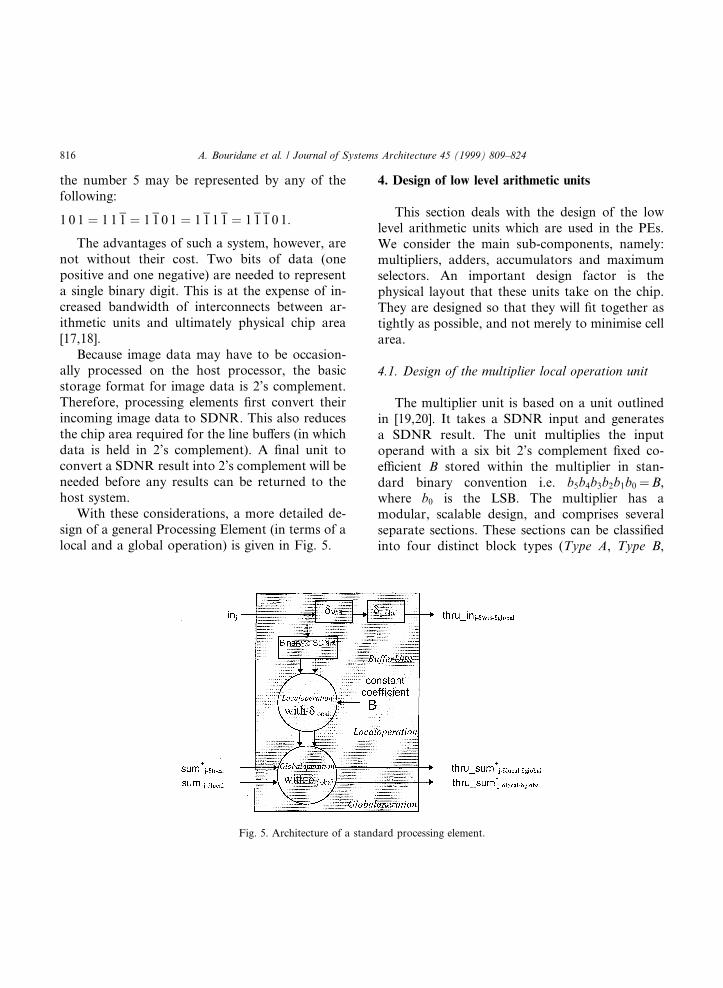
With these considerations, a more detailed de-sign of a general Processing Element (in terms of alocal and a global operation) is given in Fig. 5.
4. Design of low level arithmetic units
This section deals with the design of the lowlevel arithmetic units which are used in the PEs.We consider the main sub-components, namely:multipliers, adders, accumulators and maximumselectors. An important design factor is thephysical layout that these units take on the chip.They are designed so that they will ®t together astightly as possible, and not merely to minimise cellarea.
4.1. Design of the multiplier local operation unit
The multiplier unit is based on a unit outlinedin [19,20]. It takes a SDNR input and generatesa SDNR result. The unit multiplies the inputoperand with a six bit 2's complement ®xed co-e�cient B stored within the multiplier in stan-dard binary convention i.e. b5b4b3b2b1b0�B,where b0 is the LSB. The multiplier has amodular, scalable design, and comprises severalseparate sections. These sections can be classi®edinto four distinct block types (Type A, Type B,
Fig. 5. Architecture of a standard processing element.
816 A. Bouridane et al. / Journal of Systems Architecture 45 (1999) 809±824

Type C and Type D). The overall multiplier unitis constructed using a series of these smallerblocks: for an N-bit coe�cient, a multiplier isbuilt from
Type A! Type B! �N ÿ 3� Type C ! Type D:
Thus the coe�cient word length may be increasedor decreased. To increase the coe�cient length,additional Type C units are added, and to reduceit, Type C units are removed. The minimum co-e�cient word length is three. This occurs when themultiplier is constructed using a Type A, Type Band a Type D unit.
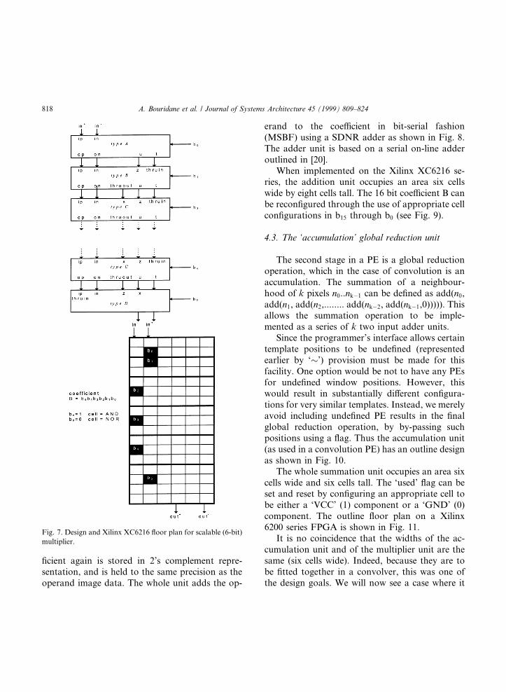
To show how the individual multiplier sectionshave been designed for scalability and for ®rsttime place and route, Fig. 6 gives the outline ¯oorplans on a Xilinx XC6216 FPGA for each of thefour multiplier sections. Then Fig. 7 shows boththe logical structure of a complete (6-bit) multi-
plier unit, and the outline ¯oor plan for the wholeunit.
Since an FPGA is a recon®gurable hardwaredevice and the coe�cients in a neighbourhoodwindow remain static throughout an entire imageoperation, the coe�cients can either be hardwiredinto the designs, or written in to the appropriatecells after the FPGA is recon®gured. We haveadopted the latter approach, as it avoids having torecon®gure the entire chip when a second convo-lution is required in which only the weights aredi�erent.
4.2. Design of the `addition' local operation unit
For instructions such as additive minimum andadditive maximum, the local operation is additionrather than multiplication. The addition unit takesa single SDNR input value, adds a coe�cient B tothis input and outputs a SDNR result. This coef-
Fig. 6. Outline ¯oor plan on Xilinx XC6216 FPGA for SDNR serial multiplier sections.
A. Bouridane et al. / Journal of Systems Architecture 45 (1999) 809±824 817
®cient again is stored in 2's complement repre-sentation, and is held to the same precision as theoperand image data. The whole unit adds the op-
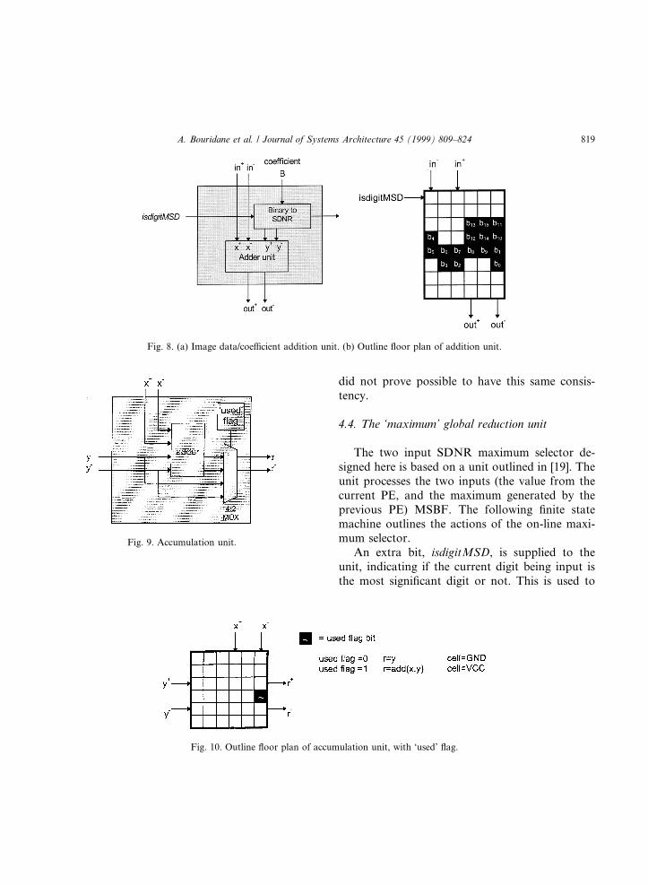
erand to the coe�cient in bit-serial fashion(MSBF) using a SDNR adder as shown in Fig. 8.The adder unit is based on a serial on-line adderoutlined in [20].
When implemented on the Xilinx XC6216 se-ries, the addition unit occupies an area six cellswide by eight cells tall. The 16 bit coe�cient B canbe recon®gured through the use of appropriate cellcon®gurations in b15 through b0 (see Fig. 9).
4.3. The `accumulation' global reduction unit
The second stage in a PE is a global reductionoperation, which in the case of convolution is anaccumulation. The summation of a neighbour-hood of k pixels n0..nkÿ1 can be de®ned as add(n0,add(n1, add(n2,........ add(nkÿ2, add(nkÿ1,0))))). Thisallows the summation operation to be imple-mented as a series of k two input adder units.
Since the programmer's interface allows certaintemplate positions to be unde®ned (representedearlier by `�') provision must be made for thisfacility. One option would be not to have any PEsfor unde®ned window positions. However, thiswould result in substantially di�erent con®gura-tions for very similar templates. Instead, we merelyavoid including unde®ned PE results in the ®nalglobal reduction operation, by by-passing suchpositions using a ¯ag. Thus the accumulation unit(as used in a convolution PE) has an outline designas shown in Fig. 10.
The whole summation unit occupies an area sixcells wide and six cells tall. The `used' ¯ag can beset and reset by con®guring an appropriate cell tobe either a `VCC' (1) component or a `GND' (0)component. The outline ¯oor plan on a Xilinx6200 series FPGA is shown in Fig. 11.
It is no coincidence that the widths of the ac-cumulation unit and of the multiplier unit are thesame (six cells wide). Indeed, because they are tobe ®tted together in a convolver, this was one ofthe design goals. We will now see a case where it
Fig. 7. Design and Xilinx XC6216 ¯oor plan for scalable (6-bit)
multiplier.
818 A. Bouridane et al. / Journal of Systems Architecture 45 (1999) 809±824
did not prove possible to have this same consis-tency.
4.4. The `maximum' global reduction unit
The two input SDNR maximum selector de-signed here is based on a unit outlined in [19]. Theunit processes the two inputs (the value from thecurrent PE, and the maximum generated by theprevious PE) MSBF. The following ®nite statemachine outlines the actions of the on-line maxi-mum selector.
An extra bit, isdigitMSD, is supplied to theunit, indicating if the current digit being input isthe most signi®cant digit or not. This is used to
Fig. 8. (a) Image data/coe�cient addition unit. (b) Outline ¯oor plan of addition unit.
Fig. 10. Outline ¯oor plan of accumulation unit, with `used' ¯ag.
Fig. 9. Accumulation unit.
A. Bouridane et al. / Journal of Systems Architecture 45 (1999) 809±824 819

reset the initial hot-state of the circuit to `A' and toindicate the start of two new operands. There isless regularity in this operation. Using the manualplace and route tools, the Maximum unit occupiesan area of 12 cells tall by eight cells wide. Ideallythis unit would be the same width as the otherunits designed up to now (six cells). However,because of routing problems, the minimum widththat could be realised for this unit was 8 cells. Thismeans, for instance, that in the PE for a multipli-cative maximum instruction, there will be somewasted cells, because a complete multiply-maxi-mum unit will be eight cells wide, and there willtwo columns of unused cells beside the six-cellwide multiplier.
The outline ¯oor plan is given in Fig. 12. Againa similar approach has been applied to the use ofthe unused (or �) coe�cient in a window.
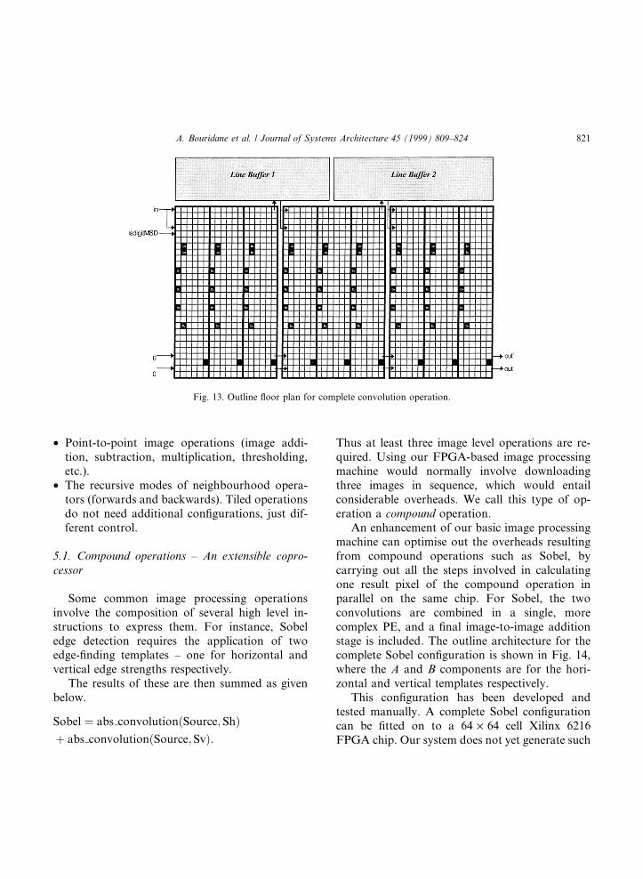
4.5. Layout of a complete convolution con®guration
The overall convolution circuit can ®tted ontothe XC6216 architecture 54 cells wide by 38 cellstall, as shown in Fig. 13. The cells labelled in blackshow the nine six-bit coe�cients and the nine used(or `�') ¯ags.
5. Summary of other facilities
For the sake of space, the full range of con®g-urations which our system provides have not beendescribed in the preceding sections. Other facilitiesfor which con®gurations have been developed in-clude:· The `Minimum' global operation unit.· The `absolute' unit which is applied as a ®nal
stage to calculate absolute convolution.· Binary-to-SDNR and SDNR-to-Binary conver-
sion units.
Fig. 12. Outline ¯oor plan for `Maximum' global reduction
unit.
Fig. 11. Finite state machine for maximum of X and Y.
820 A. Bouridane et al. / Journal of Systems Architecture 45 (1999) 809±824
· Point-to-point image operations (image addi-tion, subtraction, multiplication, thresholding,etc.).
· The recursive modes of neighbourhood opera-tors (forwards and backwards). Tiled operationsdo not need additional con®gurations, just dif-ferent control.
5.1. Compound operations ± An extensible copro-cessor
Some common image processing operationsinvolve the composition of several high level in-structions to express them. For instance, Sobeledge detection requires the application of twoedge-®nding templates ± one for horizontal andvertical edge strengths respectively.
The results of these are then summed as givenbelow.
Sobel � abs convolution�Source; Sh�� abs convolution�Source; Sv�:
Thus at least three image level operations are re-quired. Using our FPGA-based image processingmachine would normally involve downloadingthree images in sequence, which would entailconsiderable overheads. We call this type of op-eration a compound operation.
An enhancement of our basic image processingmachine can optimise out the overheads resultingfrom compound operations such as Sobel, bycarrying out all the steps involved in calculatingone result pixel of the compound operation inparallel on the same chip. For Sobel, the twoconvolutions are combined in a single, morecomplex PE, and a ®nal image-to-image additionstage is included. The outline architecture for thecomplete Sobel con®guration is shown in Fig. 14,where the A and B components are for the hori-zontal and vertical templates respectively.
This con®guration has been developed andtested manually. A complete Sobel con®gurationcan be ®tted on to a 64 ´ 64 cell Xilinx 6216FPGA chip. Our system does not yet generate such
Fig. 13. Outline ¯oor plan for complete convolution operation.
A. Bouridane et al. / Journal of Systems Architecture 45 (1999) 809±824 821

new architectures automatically from compoundexpressions, though it would be desirable to do so.If and when this capability is implemented, ourimage coprocessor will provide the programmerwith an extensible instruction set as opposed to thecurrent static instruction set.
6. Conclusion
This paper has discussed the design of anFPGA-assisted image processing development en-vironment, which has the primary goal of pro-viding a high level programming model. Thisenables the application developer to concentrateon the image processing aspects of a problem,rather than having to get to grips with FPGAtechnology. The programming model we haveadopted is based on the image-level neighbour-hood operators of Image Algebra, and an exten-sive range of algorithms can be implementede�ciently in this simple model.
In designing the FPGA-assisted image pro-cessing system, the design constraints for theFPGA con®gurations turn out to be somewhatdi�erent from the normal use of FPGAs. Becauseof the needs for experimentation with di�erentalgorithms, the FPGA architectures must be de-signed, not so much to maximise chip area utili-
sation, but for scalability and reuse. At times it isnecessary to sacri®ce chip area for greater re-usablilty, but in the context of providing a com-plete environment, this sacri®ce is well worthwhile.To provide a much more powerful ability to buildand to experiment with di�erent operations, we aredeveloping a more sophisticated tool which willenable rapid assembly of new con®gurations fromarrangements of basic building blocks [22]. Thissystem will enable the description and generationof all the con®gurations outlined in this paper, andmany more. It will support di�erent number rep-resentations and user-de®ned word lengths, andgenerate FPGA con®gurations automatically, with®rst-time-right place and route.
References
[1] H.C. Webber (Ed.), Image processing and transputers,
IOS Press, 1992.
[2] K. Rajan, K.S. Sangunni, J. Ramakrishna, Dual-DSP
systems for signal and image-processing, Microprocessing
& Microsystems 17 (9) (1993) 556±560.
[3] T. Akiyama, H. Aono, K. Aoki et al., MPEG2 video codec
using Image compression DSP, IEEE Transactions on
consumer electronics 40 (3) (1994) 466±472.
[4] J.M. Arnold, D.A. Buell, E.G. Davis, Splash-2, Proceed-
ings of the 4th Annual ACM Symposium on Parallel
Algorithms and Architectures, ACM Press, New York,
1992, pp. 316±324.
Fig. 14. Architecture outline for Sobel edge detection operator.
822 A. Bouridane et al. / Journal of Systems Architecture 45 (1999) 809±824
[5] Gigaops Ltd., The G-800 System, 2374 Eunice St. Berke-
ley, CA 94708.
[6] S.C. Chan, H.O. Ngai, K.L. Ho, A programmable image
processing system using FPGAs, International Journal of
Electronics 75 (4) (1993) 725±730.
[7] G. Hamid, An FPGA-Based coprocessor for image
processing, IEE Colloquium, Integrated Imaging Sensors
and Processing, 1994, pp. 6/1±6/4.
[8] P. Donachy, Design and implementation of a high level
image processing machine using recon®gurable hardware,
Ph.D. Thesis, Department of Computer Science, The
Queen's University of Belfast, 1996.
[9] J.A. Steele, An abstract machine approach to environ-
ments for image interpretation on transputers, Ph.D.
Thesis, The Queens' University of Belfast, 1994.
[10] D. Crookes, P.J. Morrow, P.J. McParland, IAL: A
parallel image processing programming language, IEE
Proceedings 137 (3) (1990) 176±182.
[11] T.J. Brown, D. Crookes, A high level language for image
processing, Image and Vision Computing 12 (2) (1994) 67±
79.
[12] G.X. Ritter, J.N. Wilson, J.L. Davidson, Image Algebra:
An overview, Computer Vision, Graphics and Image
Processing 49 (1990) 297±331.
[13] Plessey, PDSP16488 Single Chip Convolver with integral
line delay, Technical report, Plessey Semiconductors Ltd.,
Cheney Manor, Swindon, Wiltshire SN2 2QW, UK, 1988.
[14] R.G. Shoup, Parameterised Convolution Filtering in an
FPGA, More FPGAs, W. Moore, W. Luk (Eds.),
Abington EE&CS Books, 1994, pp. 274.
[15] W. Kamp, H. Kunemund, Soldner, H. Hofer, Program-
mable 2D linear ®lter for video applications, IEEE journal
of Solid State Circuits (1990) 735±740.
[16] V. Hecht, K. Ronner, P. Pirsch, A defect-tolerant systolic
array implementation for real-time image processing,
Journal of VLSI signal processing 5 (1993) 37±47.
[17] D. Phatak, I. Koren, Hybrid signed-digit number systems:
A uni®ed framework for redundant number representa-
tions with bounded carry propagation chains, IEEE
Computer 43 (8) (1994) 880±891.
[18] R.F. Woods, J.V. McCanny, Design of a high perfor-
mance IIR digital ®lter chip, IEE Proceedings-E 139 (3)
(1992) 195±202.
[19] J. Moran, I. Rios, J. Meneses, Signed Digit Arithmetic on
FPGAs, More FPGAs, W. Moore, W. Luk (Eds.),
Abington EE&CS Books, 1994, pp. 250.
[20] M. Ercegovac, T. Lang, Fast multiplication without carry-
propagate addition, IEEE Computer 39 (11) (1990) 1385±
1390.
[21] J. Duprat, Y. Herreros, J. Muller, Some results about on-
line computation of function, Ninth Symposium on
Computer Arithmetic, Santa Monica, 1989.
[22] K. Alotaibi, D. Crookes, A. Bouridane, An FPGA
environment for image processing applications, Proceed-
ings of IMVIP-97 1 (1997) 171±184.
Dr A Bouridane holds an ``Ingenioratd'Etat'' degree in Electronics from theNational Polytechnic School of Algiers``ENPA'' (Algeria), an MPhil degree inVLSI design for Signal Processingfrom the University of Newcastle Up-on Tyne (UK) and a PhD degree inComputer Vision from the Universityof Nottingham (UK). Dr A. Bouri-dane held several positions in R&Dbefore joining the Queen's Universityof Belfast. His research interests are inHigh Performance Image Processing,
Custom Computing using FPGAs, Computer Vision andComputer Architectures for Signal/Image Processing.
Prof. D. Crookes is Professor ofComputer Engineering, and head ofdepartment of Computer Science, atQueen's University of Belfast. He ob-tained a BSc (1st Class) in Mathe-matics and Computer Science in 1977,and a PhD in Computer Science in1980, both from Queen's University.His research interests include archi-tectures for high Performance imageprocessing, and high level languagesand software tools for parallel pro-cessing.
Paul Donaghy graduated with a BSc(Hon.) and a PhD degree in ComputerScience both from the Queen's Uni-versity of Belfast in 1993 and 1996,respectively. Since 1996 he has beenwith British Telecom. (Belfast). Hisresearch interests include High Per-formance Computing and image pro-cessing architectures using FPGAs.
A. Bouridane et al. / Journal of Systems Architecture 45 (1999) 809±824 823

Khaled BENKRID was born in Al-giers, Algeria, on November 12, 1975.He received the BSc degree in Elec-tronics from the ENP of Algiers (Al-geria) in 1997. He is working towardshis Ph.D. degree at the Queen's Uni-versity of Belfast (Department ofComputer Science). His research in-terests include Custom Computingusing FPGAs, High Performance Im-age Processing and Computer Arith-metic.
Khalid ALOTAIBI was born in Ri-yadh, Saudi Arabia, on October, 1965.He received the BSc degree in Com-puter Science from King Saud Uni-versity (Saudi Arabia) in 1990. Since1996, he has been working towards hisPh.D. degree at the Queen's Universityof Belfast (Department of ComputerScience). His research interests includeCustom Computing using FPGAs andHigh Perfomace Image processing.
824 A. Bouridane et al. / Journal of Systems Architecture 45 (1999) 809±824