A Fully Integrated MIMO MultiBand Direct-Conversion CMOS Transceiver for WLAN Applications (802.11n
14
IEEE JOURNAL OF SOLID-STATE CIRCUITS, VOL. 42, NO. 12, DECEMBER 2007 2795 A Fully Integrated MIMO Multiband Direct Conversion CMOS Transceiver for WLAN Applications (802.11n) Arya Behzad, Senior Member, IEEE, Keith A. Carter, Hung-Ming (Ed) Chien, Stephen Wu, Member, IEEE, Meng-An Pan, C. Paul Lee, Qiang (Tom) Li, Senior Member, IEEE, John C. Leete, Member, IEEE, Stephen Au, Member, IEEE, Michael S. Kappes, Member, IEEE, Zhimin Zhou, Dayo Ojo, Lijun Zhang, Alireza Zolfaghari, Member, IEEE, Jesse Castanada, Hooman Darabi, Senior Member, IEEE, Benson Yeung, Ahmadreza Rofougaran, Senior Member, Maryam Rofougaran, Member, Jason Trachewsky, Member, IEEE, Tushar Moorti, Rohit Gaikwad, Amit Bagchi, Joachim S. Hammerschmidt, Member, IEEE, Jay Pattin, Jacob J. Rael, Member, IEEE, and Bojko Marholev Abstract—802.11n is the latest offering from the IEEE standard committee tasked with enabling and enhancing WLAN systems. This standard utilizes several techniques to offer a much larger rate versus range than the legacy WLAN systems. A single-chip multiband direct-conversion CMOS MIMO transceiver (2 2) targeted for WLAN applications is presented. This transceiver is capable of satisfying the requirements of the draft 802.11n stan- dard and achieves PHY rates of Mb/s. The receivers and transmitters achieve an EVM of better than dB (0.9%) and dB (1.0%) operating in legacy g and a modes, respectively. From a 1.8 V supply and with both cores operating, the chip draws 275 mA in RX mode and 280 mA in TX mode. Index Terms—80211n, CMOS radio, direct conversion, lin- earization, MIMO, multiband, OFDM, radio calibration, trans- ceiver, WLAN. I. INTRODUCTION T HE IEEE 802.11a and g WLAN protocols provide com- munications data up to 54 Mbps using a 20 MHz channel bandwidth in the 2.4 and 5 GHz ISM and UNII bands, respec- tively. The rapid adoption of these systems in the past few years, resulting from advancements in transceiver design and integra- tion [1], [2], has led to a demand for more robust wireless links as well as higher data rates. These demands can be met by the adoption of multi-in, multi-out (MIMO) techniques, the use of wider band channels, utilization of higher order constella- tions, and/or the use of lower coding rates for the modulation. The emerging 802.11n standard will adopt some or all of these techniques to provide a robust and high-data-rate wireless link. Such a standard would therefore need to utilize a high-perfor- mance transceiver. In order to keep the cost down, the trans- Manuscript received April 16, 2007; revised June 28, 2007. A. Behzad, C. P. Lee, S. Au, D. Ojo, and R. Gaikwad are with Broadcom, San Diego, CA 92127 USA (e-mail: [email protected]). K. A. Carter, H.-M. Chien, S. Wu, M.-A. Pan, Q. Li, J. C. Leete, Z. Zhou, L. Zhang, A. Zolfaghari, J. Castanada, H. Darabi, B. Yeung, A. Rofougaran, M. Rofougaran, J. Pattin, J. J. Rael, and B. Marholev are with Broadcom, Irvine, CA 92617 USA. M. S. Kappes is with IQ Analog, San Diego, CA 92130 USA. J. Trachewsky, T. Moorti, A. Bagchi, and J. S. Hammerschmidt are with Broadcom, Sunnyvale, CA 94086 USA. Digital Object Identifier 10.1109/JSSC.2007.908667 ceiver would need to be highly integrated and preferably imple- mented in CMOS technology. Multipath fading has traditionally been a fundamental barrier to achieving high data rates in wireless communication systems. Multipath is a phenomenon caused by the multiple arrivals of the transmitted signal to the receiver due to reflections off of “scatterers.” For traditional communication systems, multipath fading is more problematic when a direct line-of-sight (LOS) path does not exist between the transmitter and the receiver (this is commonly known as a Rayleigh fading scenario). One problem with mulipath is that it can create a selective fading re- sponse at the received signal, particularly when the bandwidth of the modulated signal is wide as compared with the “coher- ence bandwidth” of the channel. Another problem is that the received amplitude can vary significantly with a small change in the distance between the receiver and the transmitter. In an additive-white-Gaussian-noise (AWGN) channel, a “reasonable” SNR is sufficient for obtaining a low probability of error in the system. This is due to the fact that the only factor that can impact an error event is large additive noise. On the other hand, in a faded environment, a very large SNR would be required for a low probability of error for both coherent as well as noncoherent communication systems. This is due to the fact that, even in the presence of high SNR, errors can occur due to the deep fade present in the channel. Without the use of some form of “diversity,” performance in a faded environment can be quite poor. One or more dimen- sions [degrees of freedom (DOF)] are therefore exploited in a faded wireless system to enable diversity. Diversity can be im- plemented in the form of time diversity (e.g., interleaving of coded symbols), frequency diversity (e.g., intersymbol equal- ization, spread spectrum techniques, or OFDM), or spatial di- versity (e.g., selection diversity or space-time coding). These diversity techniques can then be utilized to improve the relia- bility of the link. One of the methods utilized in 802.11a/g standards for com- bating multipath is the use of OFDM coding. Using OFDM, the wideband modulation is subdivided into many subcarriers, each of which has a narrow bandwidth in comparison to the coher- ence bandwidth of a typical indoor environment. Therefore, a frequency-selective fade over the wide bandwidth (Fig. 1) is ef- 0018-9200/$25.00 © 2007 IEEE
-
Upload
independent -
Category
Documents
-
view
3 -
download
0
Transcript of A Fully Integrated MIMO MultiBand Direct-Conversion CMOS Transceiver for WLAN Applications (802.11n

IEEE JOURNAL OF SOLID-STATE CIRCUITS, VOL. 42, NO. 12, DECEMBER 2007 2795
A Fully Integrated MIMO Multiband DirectConversion CMOS Transceiver for WLAN
Applications (802.11n)Arya Behzad, Senior Member, IEEE, Keith A. Carter, Hung-Ming (Ed) Chien, Stephen Wu, Member, IEEE,
Meng-An Pan, C. Paul Lee, Qiang (Tom) Li, Senior Member, IEEE, John C. Leete, Member, IEEE,Stephen Au, Member, IEEE, Michael S. Kappes, Member, IEEE, Zhimin Zhou, Dayo Ojo, Lijun Zhang,
Alireza Zolfaghari, Member, IEEE, Jesse Castanada, Hooman Darabi, Senior Member, IEEE, Benson Yeung,Ahmadreza Rofougaran, Senior Member, Maryam Rofougaran, Member, Jason Trachewsky, Member, IEEE,
Tushar Moorti, Rohit Gaikwad, Amit Bagchi, Joachim S. Hammerschmidt, Member, IEEE, Jay Pattin,Jacob J. Rael, Member, IEEE, and Bojko Marholev
Abstract—802.11n is the latest offering from the IEEE standardcommittee tasked with enabling and enhancing WLAN systems.This standard utilizes several techniques to offer a much largerrate versus range than the legacy WLAN systems. A single-chipmultiband direct-conversion CMOS MIMO transceiver (2 2)targeted for WLAN applications is presented. This transceiver iscapable of satisfying the requirements of the draft 802.11n stan-dard and achieves PHY rates of 270 Mb/s. The receivers andtransmitters achieve an EVM of better than 41 dB (0.9%) and40 dB (1.0%) operating in legacy g and a modes, respectively.
From a 1.8 V supply and with both cores operating, the chip draws275 mA in RX mode and 280 mA in TX mode.
Index Terms—80211n, CMOS radio, direct conversion, lin-earization, MIMO, multiband, OFDM, radio calibration, trans-ceiver, WLAN.
I. INTRODUCTION
THE IEEE 802.11a and g WLAN protocols provide com-munications data up to 54 Mbps using a 20 MHz channel
bandwidth in the 2.4 and 5 GHz ISM and UNII bands, respec-tively. The rapid adoption of these systems in the past few years,resulting from advancements in transceiver design and integra-tion [1], [2], has led to a demand for more robust wireless linksas well as higher data rates. These demands can be met bythe adoption of multi-in, multi-out (MIMO) techniques, the useof wider band channels, utilization of higher order constella-tions, and/or the use of lower coding rates for the modulation.The emerging 802.11n standard will adopt some or all of thesetechniques to provide a robust and high-data-rate wireless link.Such a standard would therefore need to utilize a high-perfor-mance transceiver. In order to keep the cost down, the trans-
Manuscript received April 16, 2007; revised June 28, 2007.A. Behzad, C. P. Lee, S. Au, D. Ojo, and R. Gaikwad are with Broadcom,
San Diego, CA 92127 USA (e-mail: [email protected]).K. A. Carter, H.-M. Chien, S. Wu, M.-A. Pan, Q. Li, J. C. Leete, Z. Zhou,
L. Zhang, A. Zolfaghari, J. Castanada, H. Darabi, B. Yeung, A. Rofougaran,M. Rofougaran, J. Pattin, J. J. Rael, and B. Marholev are with Broadcom, Irvine,CA 92617 USA.
M. S. Kappes is with IQ Analog, San Diego, CA 92130 USA.J. Trachewsky, T. Moorti, A. Bagchi, and J. S. Hammerschmidt are with
Broadcom, Sunnyvale, CA 94086 USA.Digital Object Identifier 10.1109/JSSC.2007.908667
ceiver would need to be highly integrated and preferably imple-mented in CMOS technology.
Multipath fading has traditionally been a fundamental barrierto achieving high data rates in wireless communication systems.Multipath is a phenomenon caused by the multiple arrivals ofthe transmitted signal to the receiver due to reflections off of“scatterers.” For traditional communication systems, multipathfading is more problematic when a direct line-of-sight (LOS)path does not exist between the transmitter and the receiver(this is commonly known as a Rayleigh fading scenario). Oneproblem with mulipath is that it can create a selective fading re-sponse at the received signal, particularly when the bandwidthof the modulated signal is wide as compared with the “coher-ence bandwidth” of the channel. Another problem is that thereceived amplitude can vary significantly with a small changein the distance between the receiver and the transmitter.
In an additive-white-Gaussian-noise (AWGN) channel, a“reasonable” SNR is sufficient for obtaining a low probabilityof error in the system. This is due to the fact that the only factorthat can impact an error event is large additive noise. On theother hand, in a faded environment, a very large SNR would berequired for a low probability of error for both coherent as wellas noncoherent communication systems. This is due to the factthat, even in the presence of high SNR, errors can occur due tothe deep fade present in the channel.
Without the use of some form of “diversity,” performance ina faded environment can be quite poor. One or more dimen-sions [degrees of freedom (DOF)] are therefore exploited in afaded wireless system to enable diversity. Diversity can be im-plemented in the form of time diversity (e.g., interleaving ofcoded symbols), frequency diversity (e.g., intersymbol equal-ization, spread spectrum techniques, or OFDM), or spatial di-versity (e.g., selection diversity or space-time coding). Thesediversity techniques can then be utilized to improve the relia-bility of the link.
One of the methods utilized in 802.11a/g standards for com-bating multipath is the use of OFDM coding. Using OFDM, thewideband modulation is subdivided into many subcarriers, eachof which has a narrow bandwidth in comparison to the coher-ence bandwidth of a typical indoor environment. Therefore, afrequency-selective fade over the wide bandwidth (Fig. 1) is ef-
0018-9200/$25.00 © 2007 IEEE
2796 IEEE JOURNAL OF SOLID-STATE CIRCUITS, VOL. 42, NO. 12, DECEMBER 2007
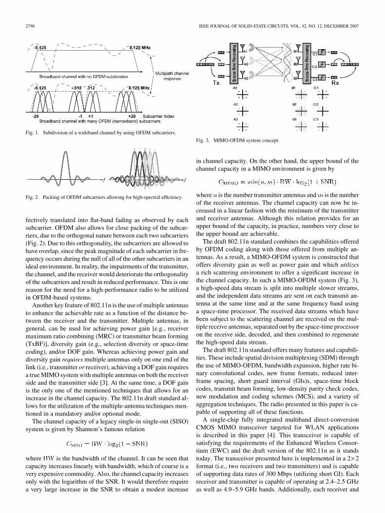
Fig. 1. Subdivision of a wideband channel by using OFDM subcarriers.
Fig. 2. Packing of OFDM subcarriers allowing for high-spectral efficiency.
fectively translated into flat-band fading as observed by eachsubcarrier. OFDM also allows for close packing of the subcar-riers, due to the orthogonal nature between each two subcarriers(Fig. 2). Due to this orthogonality, the subcarriers are allowed tohave overlap, since the peak magnitude of each subcarrier in fre-quency occurs during the null of all of the other subcarriers in anideal environment. In reality, the impairments of the transmitter,the channel, and the receiver would deteriorate the orthogonalityof the subcarriers and result in reduced performance. This is onereason for the need for a high-performance radio to be utilizedin OFDM-based systems.
Another key feature of 802.11n is the use of multiple antennasto enhance the achievable rate as a function of the distance be-tween the receiver and the transmitter. Multiple antennas, ingeneral, can be used for achieving power gain [e.g., receivermaximum ratio combining (MRC) or transmitter beam forming(TxBF)], diversity gain (e.g., selection diversity or space-timecoding), and/or DOF gain. Whereas achieving power gain anddiversity gain requires multiple antennas only on one end of thelink (i.e., transmitter or receiver), achieving a DOF gain requiresa true MIMO system with multiple antennas on both the receiverside and the transmitter side [3]. At the same time, a DOF gainis the only one of the mentioned techniques that allows for anincrease in the channel capacity. The 802.11n draft standard al-lows for the utilization of the multiple-antenna techniques men-tioned in a mandatory and/or optional mode.
The channel capacity of a legacy single-in single-out (SISO)system is given by Shannon’s famous relation
where is the bandwidth of the channel. It can be seen thatcapacity increases linearly with bandwidth, which of course is avery expensive commodity. Also, the channel capacity increasesonly with the logarithm of the SNR. It would therefore requirea very large increase in the SNR to obtain a modest increase
Fig. 3. MIMO-OFDM system concept.
in channel capacity. On the other hand, the upper bound of thechannel capacity in a MIMO environment is given by
where is the number transmitter antennas and is the numberof the receiver antennas. The channel capacity can now be in-creased in a linear fashion with the minimum of the transmitterand receiver antennas. Although this relation provides for anupper bound of the capacity, in practice, numbers very close tothe upper bound are achievable.
The draft 802.11n standard combines the capabilities offeredby OFDM coding along with those offered from multiple an-tennas. As a result, a MIMO-OFDM system is constructed thatoffers diversity gain as well as power gain and which utilizesa rich scattering environment to offer a significant increase inthe channel capacity. In such a MIMO-OFDM system (Fig. 3),a high-speed data stream is split into multiple slower streams,and the independent data streams are sent on each transmit an-tenna at the same time and at the same frequency band usinga space-time processor. The received data streams which havebeen subject to the scattering channel are received on the mul-tiple receive antennas, separated out by the space-time processoron the receive side, decoded, and then combined to regeneratethe high-speed data stream.
The draft 802.11n standard offers many features and capabili-ties. These include spatial division multiplexing (SDM) throughthe use of MIMO-OFDM, bandwidth expansion, higher rate bi-nary convolutional codes, new frame formats, reduced inter-frame spacing, short guard interval (GIs)s, space-time blockcodes, transmit beam forming, low-density parity check codes,new modulation and coding schemes (MCS), and a variety ofaggregation techniques. The radio presented in this paper is ca-pable of supporting all of these functions.
A single-chip fully integrated multiband direct-conversionCMOS MIMO transceiver targeted for WLAN applicationsis described in this paper [4]. This transceiver is capable ofsatisfying the requirements of the Enhanced Wireless Consor-tium (EWC) and the draft version of the 802.11n as it standstoday. The transceiver presented here is implemented in a 2 2format (i.e., two receivers and two transmitters) and is capableof supporting data rates of 300 Mbps (utilizing short GI). Eachreceiver and transmitter is capable of operating at 2.4–2.5 GHzas well as 4.9–5.9 GHz bands. Additionally, each receiver and

BEHZAD et al.: A FULLY INTEGRATED MIMO MULTIBAND DIRECT CONVERSION CMOS TRANSCEIVER FOR WLAN APPLICATIONS (802.11N) 2797
Fig. 4. Transceiver high-level block diagram.
transmitter is capable of working with modulated signals with(RF) modulation bandwidths of 10–40 MHz. The receivers andtransmitters are fed by a shared PLL through LO generation anddistribution circuitry. The receivers and transmitters achieve anerror-vector-magnitude (EVM) of better than 41 dB (0.9%)and 40 dB (1.0%) operating in legacy G and A modes, respec-tively (results limited by laboratory OFDM signal generators).From a 1.8 V supply and with both cores operating, the chipconsumes 275 mA in Rx mode and 280 mA in Tx mode. Ascompared with the previously published MIMO transceivers forWLAN [5]–[7], this transceiver is implemented in a low-cost0.18 m CMOS technology, covers both the G-band as well asthe entire worldwide A-band, is significantly smaller in area,is capable of operating over RF channel bandwidths of 10,20, or 40 MHz, and achieves much lower noise figure (NF),phase noise (PN), and EVM. Furthermore, for the first time,transceiver performance under various draft 802.11n MCSs arepresented and PHY rates of 270 Mbps are shown (withoutthe use of short GI).
II. ARCHITECTURE AND CIRCUIT IMPLEMENTATION
The full 2 2 MIMO transceiver is composed of two multi-band Rx chains, two multiband Tx chains, a PLL and LO gen-eration and distribution section, various calibration blocks, dig-ital control section, and some other miscellaneous circuits. Thehigh-level block diagram is shown in Fig. 4. Each subblock isdescribed in Sections II-A–E.
A. Receiver
A block diagram of each one of the receiver slices is shownin Fig. 5(a). (Note that, for simplicity, all block diagrams areshown with single-ended traces, but the actual transceiveris designed with fully differential signaling throughout thechip). The 5 GHz or 2 GHz signal is received and amplifiedby the appropriate differential LNA, then directly down-con-verted by the quadrature mixers associated with that band.The downconverted signal is then applied to the first high-passVGA (HPVGA1), where the signal is amplified and the dcoffsets associated with the self mixing of the mixers and devicemismatches are rejected. The signal is then filtered by the
Fig. 5. (a) Block diagram of each receive slice (for simplicity, RSSIs are shownonly on the I path and the dc cancellation loops are only shown on the Q path.(b) Block diagram of each transmit slice.
Fig. 6. High-linearity Tx mixer transconductor and gain control stage.LO-feedthrough cancellation current sources also shown.
fourth-order Butterworth filters which act to reject any inter-ferers. The signal is then further amplified by HPVGA2 andHPVGA3, each with their own dc-offset cancellation loops.The resultant and outputs are then buffered and sent to the
and ADCs on the companion PHY MAC chip. Eachone of the HPVGAs has a programmable gain of 0 to 30 dB in3 dB steps. The corner frequency of the HPFs in the HPVGAsare calibrated using an on-chip RC calibration loop. Further,the HPF corners are programmable over a wide range to satisfythe integrity of the lower index OFDM subcarriers during thepayload while allowing for fast settling during the preamble.The corner frequency of the LPF is also calibrated to the desiredbandwidth (5, 10, or 20 MHz) to ensure the proper system oper-ation in the presence of large adjacent channel interferers. Two

2798 IEEE JOURNAL OF SOLID-STATE CIRCUITS, VOL. 42, NO. 12, DECEMBER 2007
Fig. 7. A-band PA driver transconductance linearization.
wideband RSSI signals as well as one narrowband RSSI ensurethe proper operation of the system over a very wide dynamicrange and in the presence of large (e.g., CCK, OFDM, BT, orCW) interferers. Each receiver slice is capable of 100 dB oftotal gain, 100 dB of gain control range, achieves an inputIIP3 of 5 dBm with the RF front-end at low gain, and an NFof 4 dB with the RF front-end at maximum gain.
B. Transmitter
Fig. 5(b) displays the block diagram of each one of the trans-mitter slices. Received quadrature signals from the DACs are ap-plied to the programmable bandwidth and gain low-pass filters.The outputs of the LPFs are then applied to the appropriate up-conversion quadrature mixers which directly convert the base-band signal to the desired RF band. The upconversion mixers(with associated transconductors) are designed for high linearityand low LOFT over a wide gain control range [8]. The RF signalis then amplified through two stages of programmable gain. Thefinal gain stage is capable of driving a 50 load through abalun and is internally matched to 100 differential. The RFgain stages are designed such that their power consumption isreduced at lower gain settings.
The core of the transconductance stage is shown in Fig. 6[8], [9]. The input pair, M1 and M2, is put in feedback to lin-earize the effective transconductance. The signal currents flowthrough M3 and M4 and are mirrored to M5 and M6. The ef-fective transconductance of the circuit is underhigh levels of degeneration. R3–R11 are the degeneration resis-tors used to reduce the device offsets. Note that R1 and R2 arenot used as part of gain control. When R1 and R2 are changed,the overall ratio of the signal to offsets will change since theoffset contribution of all of the devices in the signal path fol-lowing R1 and R2 will remain constant, whereas all offsets priorto R1 and R2 will scale by the change in the gain. The circleddevices in Fig. 6 constitute the proposed gain-control scheme[8], [10]. The gates of both the shunt device M7 and the cas-cade devices M5 and M6 are tied together. To the first order, thecurrent gain will be given by the ratio of their ’s. There-fore, the gain-control scheme is independent of process, voltage,and temperature variation and possesses a high linearity. A vari-able gain is implemented by using multiple shunt devices. Thefour current sources that are shown are utilized to cancel LOfeedthrough due to dc offsets as well as direct RF coupling atduring startup calibration. No calibration is required as the gain
Fig. 8. Transconductance curves for the A-band PA driver stage. The main,aux1, aux2, and total transconductance curves are shown.
Fig. 9. Block diagram of the shared integer-N PLL utilized on the MIMOtransceiver. Very low-noise regulators are utilized on sensitive blocks to obtaina very low-phase-noise design.
of the block is changed. The calibration algorithm is describedin Section II-D.
Fig. 7 shows the simplified schematic of the PA driver. Athree-stage transconductance linearization is used to improvelinearity over wide range of inputs [11]. The first stage, biasedwell in the class-A region, supplies the majority of the gainbut is only linear over a small range of inputs. The second andthird stages biased at class-AB and class-B, respectively, con-tribute more to the gain as input increases and counteract thegain roll-off in the first stage. The class-AB nature of the driversaves valuable dc current when the circuit is not transmittinglarge signals. The obtained transconductance curves for eachof the subsections of the PA driver as well as the overall resul-tant transconductance is shown in Fig. 8. The transmitter has anoutput P1dB of 14 dBm in the A-band and an output P1dB of
16 dBm in the G-band.
C. PLL and LO Generation
A shared integer- PLL is used to synthesize the properLO (Fig. 9). The on-chip crystal oscillator whose divided downoutput provides the reference to the PFD is capable of oper-ating with a 20 MHz, 40 MHz, or 80 MHz crystal. In orderto minimize the impact of the VCO noise, The PFD compar-ison frequency is chosen to be as high as possible to allowwide PLL loop bandwidth. Further, in order to minimize thephase noise arising from the loop filter and charge pump, alow programmable KVCO (30 MHz/V at 3.5 GHz, typically)and high charge pump current are used. The PLL utilizes asingle VCO with a wide tuning range to cover both 802.11 fre-quency bands. A 9 bits high-accuracy VCO calibration is imple-mented to choose the best VCO subband for the desired channel.

BEHZAD et al.: A FULLY INTEGRATED MIMO MULTIBAND DIRECT CONVERSION CMOS TRANSCEIVER FOR WLAN APPLICATIONS (802.11N) 2799
Fig. 10. Contribution of the various PLL blocks to the overall PLL phase noiseat 5420 MHz.
Fig. 11. LO generation and distribution (Q-path not shown).
Every block in the synthesizer including the crystal oscillatorand the bias and supply generation circuitry for the PLL aredesigned, simulated, and optimized for optimal noise perfor-mance. Three very low-noise regulators are integrated on chipand provide a low-noise supply voltage to the crystal oscillator,the charge pump, as well as the VCO. All of the componentsof the PLL other than a large capacitor in the loop filter are in-tegrated on-chip. The block-by-block noise simulation resultsare then used to obtain an overall closed-loop PLL phase-noiseresponse for the various channels. The simulation results for5420 MHz are shown in Fig. 10. These simulated results matchthose of the measurements very closely.
In order to avoid any pulling effects by any of the transmit-ters on the VCO, the VCO operates at 2/3 the channel frequencyfor the 802.11a band and at 3/4 the channel frequency for the802.11b/g bands (Fig. 11). A differential and quadrature LOsignal is required for the operation of each one of the Rx andTx mixers at the 2.4 or 5 GHz bands. Proper LO buffering anddistribution is therefore essential for the robust operation of thesystem over PTV as well as for reducing power consumption.Therefore, the LO distribution channels were accounted for inthe very early stages of the floor planning of the chip. Each localbuffer is designed to be able to drive the local mixer as well asthe routing and the next buffer stage (Fig. 11). As such, the LO
Fig. 12. Sources of LOFT in a direct-conversion transmitter.
Fig. 13. Sources of IQ imbalance in a direct-conversion transmitter.
Fig. 14. Simplified block diagram of LOFT and IQ imbalance estimationcircuitry.
distribution of the chip is scalable to larger integratedMIMO systems.
D. Calibration Techniques
The transceiver utilizes extensive self-contained and/or DSP-assisted auto-calibration circuitry. These calibrations includeindependent and multiphase LO feedthrough calibration (RFcoupling and dc offsets) on each transmit core; independentquadrature (phase and amplitude) calibration on each receiveand transmit core; resistor calibration for bias current genera-tion blocks; LPF and HPF corner calibration on filters; mul-tiphase VCO calibration (open-loop, closed-loop, and refreshmode); and VCO gain calibration and transmitter power calibra-tion. Additionally, a high-accuracy temperature sensor allowsfor temperature-based calibrations, if necessary. Some of thesecalibrations may have been desirable but not absolutely neces-sary for some legacy WLAN ICs, but they are essential for ob-taining the performance at the levels that are required by thisRFIC. These calibrations ensure optimal operation over PVTvariations, as well as a high yielding part.

2800 IEEE JOURNAL OF SOLID-STATE CIRCUITS, VOL. 42, NO. 12, DECEMBER 2007
Fig. 15. Gain-control-independent LOFT cancellation algorithm.
Two types of LOFT exist in a direct-conversion up-convertermixer (Fig. 12). The first type, baseband LOFT (BB_LOFT),originates from the device offsets in the DAC, LPF, and thetransconductance stage. The offsets will up-convert and gen-erate a LOFT component at the output of the mixer. The secondtype, RF_LOFT, is a direct-coupling component either throughparasitic capacitance or mutual inductance. The two types ofoffsets require a dual-cancellation scheme to cancel both com-ponents at their sources.
Quadrature imbalances in a direct-conversion transmitter areprimarily due to two factors (Fig. 13). The first set of imbal-ances are generated at the baseband paths, and are due to deviceand bias mismatches between the and paths. The secondset of imbalances, which often dominate, are due to RFimbalances such as LO imbalances and the mixer mis-matches.
Fig. 14 illustrates the simplified transmitter path along withthe block diagram of the circuitry utilized to detect the LOFTand imbalances. During calibration, baseband sine and co-sine signals are applied at the transmitter input. These signalsare up-converted and combined by the quadrature up-converterand amplified by the RF transmit path. The envelope detectorand associated circuitry are utilized to detect the ripple in theoutput signal, amplify and filter this ripple, and pass on to thebaseband DSP circuitry for analysis. For sinusoidal inputsat BB_I and BB_Q, the high-frequency envelope detector gen-erates a filtered and amplified baseband ripple with the strongestspectral components at due to LOFT and at 2x due to
imbalance (shown in Fig. 15) and weaker spectral lines atharmonics of these fundamental frequencies. Care is taken toensure the envelope detector output and the associated analog
baseband blocks are operated in a sufficiently linear mode suchthat these harmonics do not interfere with the calibration.
Shown in Fig. 6 are the two sets of currents that removeLOFT by introducing an artificial and counteracting offset. First,BB_LOFT_IP and BB_LOFT_IN cancel all of the offsets priorto the gain-control stage. The baseband gain control is also doneat these nodes and will scale the cancellation current by the samefactor, maintaining proper cancellation current without the needfor a recalibration. Note that the devices M5 and M6 are after thegain-control shunt devices and could contribute a BB_LOFT atvery high attenuation settings. In practice, these devices can bemade sufficiently large to have minimal offsets. A second set ofcorrection currents, RF_LOFT_IP and RF_LOFT_IN, are at thedrain nodes of M5 and M6. The injection is done immediatelybefore the switching quads of the mixer but after the gain-con-trol shunt devices so that the cancellation currents will not beaffected by the gain change. Each set of correction currents arebinary-weighted current DACs (IDACs).
A straightforward algorithm can be devised to separate thetwo LOFT components and remove LOFT as well as im-balance. Fig. 15 shows a flowchart of the proposed algorithm.First, a set of and sinusoids is injected at baseband. Spec-tral analysis of the detector’s output reveals the magnitude of theLOFT ( ) and imbalance ( ) [4X]. Second, the gainis set to minimum to significantly attenuate the baseband off-sets. The remaining LOFT is from RF. Third, the RF_LOFT iscancelled using the RF IDAC. Fourth, with the RF_LOFT can-celled, the gain is changed to maximum. This will allow a goodvisibility in the event that the BB_LOFT is small. Fifth, the re-maining BB_LOFT can be cancelled using the BB IDAC. Notethat the maximum amount of LOFT suppression will depend on

BEHZAD et al.: A FULLY INTEGRATED MIMO MULTIBAND DIRECT CONVERSION CMOS TRANSCEIVER FOR WLAN APPLICATIONS (802.11N) 2801
Fig. 16. Rx IQ calibration—same core method.
Fig. 17. Rx IQ calibration—cross-core method.
the resolution of both IDACs and the achievable amount of sup-pression of the BB_LOFT in Step 2. Lastly, keeping the gainat maximum, components can be removed by adjustingthe baseband signal’s phase and amplitude to correct theimbalance. The phase and amplitude information can then beused to predistort the modulated signal in the DSP.
In order to obtain optimal receiver performance, especiallyfor the 5 GHz band, Rx calibration is required. One methodwould be to utilize the calibrated transmitter to transmit a singlesideband test tone and couple this test tone to the receiver. Then,the down-converted and signals at the receiver baseband canbe used to calibrate the Rx and in the digital baseband. Inthe basic implementation of such a scheme in a MIMO radio,the Tx1 output would be used to calibrate Rx1, and Tx2 outputwould be use to calibrate Rx2 (Fig. 16). The issue with this ap-proach is that the loading of BUF21 is different during calibra-tion and during normal operation. The same can be said aboutthe loading of BUF22. With this scheme, therefore, post-calibra-tion image rejection can be limited to 35 dBc. In the currentchip, an alternative cross-core calibration method has been uti-lized (Fig. 17). In this approach, the output of Tx2 is coupledto the input of Rx1 during calibration. Therefore, the loadingof BUFF22 is constant during calibration and normal opera-tion. The procedure is repeated for Rx2 once Rx1 is calibrated.
Fig. 18. Design of the fpBGA package substrate. The RF section of one coreis shown.
Fig. 19. Measured PN at transmitter output (5.24 GHz).
With this approach, post-calibration image rejection is betterthan 50 dBc.
E. Packaging Issues
In addition to the challenges associated with designing asingle transceiver for high EVM performance, there are manyother potential complications that need to be addressed in orderto be able to integrate multiple such transceivers on the sameSi substrate. For example, this chip includes 16 RF IOs, 16baseband analog signal-path IOs, several other analog IOs (e.g.,RSSIs, TSSIs, and temperature sensor) and tens of high-speeddigital IOs. Unfortunately, such a chip cannot be integratedin an RF-friendly package such as an LPCC, and larger morecomplex packages are required. In this case, a 165 ball fpBGApackage is utilized. Full 3-D electromagnetic simulations wereconducted on the package to ensure proper operation andisolation of the numerous RF sections of the chip (Fig. 18).In order to ensure optimal performance, the chip design, chipfloor planning, package design, and many aspects of the boarddesign were conducted simultaneously and further complicatedthe overall design task.
2802 IEEE JOURNAL OF SOLID-STATE CIRCUITS, VOL. 42, NO. 12, DECEMBER 2007
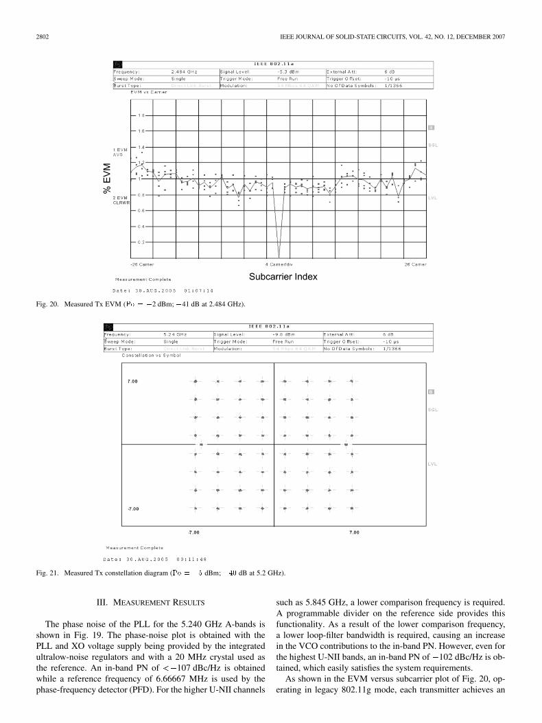
Fig. 20. Measured Tx EVM (Po = �2 dBm; �41 dB at 2.484 GHz).
Fig. 21. Measured Tx constellation diagram (Po = �5 dBm; �40 dB at 5.2 GHz).
III. MEASUREMENT RESULTS
The phase noise of the PLL for the 5.240 GHz A-bands isshown in Fig. 19. The phase-noise plot is obtained with thePLL and XO voltage supply being provided by the integratedultralow-noise regulators and with a 20 MHz crystal used asthe reference. An in-band PN of 107 dBc/Hz is obtainedwhile a reference frequency of 6.66667 MHz is used by thephase-frequency detector (PFD). For the higher U-NII channels
such as 5.845 GHz, a lower comparison frequency is required.A programmable divider on the reference side provides thisfunctionality. As a result of the lower comparison frequency,a lower loop-filter bandwidth is required, causing an increasein the VCO contributions to the in-band PN. However, even forthe highest U-NII bands, an in-band PN of 102 dBc/Hz is ob-tained, which easily satisfies the system requirements.
As shown in the EVM versus subcarrier plot of Fig. 20, op-erating in legacy 802.11g mode, each transmitter achieves an

BEHZAD et al.: A FULLY INTEGRATED MIMO MULTIBAND DIRECT CONVERSION CMOS TRANSCEIVER FOR WLAN APPLICATIONS (802.11N) 2803
Fig. 22. Measured Rx constellation diagram.
EVM of 41 dB while transmitting 2 dBm. As shown in theconstellation diagram of Fig. 21, in the legacy 802.11a mode,each transmitter achieves an EVM of 40 dBm at 5 dBm Txpower. The constellation diagram at the nominal received powerlevel as well as at the sensitivity level of the receiver for the legacy802.11g 54 Mbps packets are shown in Fig. 22 (2.412 GHz). Achip-referred sensitivity level of 78 dBm (at each antenna) isachieved in MRC mode. Under similar conditions, the sensitivityfor an 802.11a signal at 5.24 GHz is 79 dBm. In draft 802.11nMCS15, 40 MHz mode, AWGN channel, with standard GI(270 Mbps PHY rate), a chip-referred sensitivity of 72 dBm isachieved. These EVM and sensitivity results are an indicationof the excellent analog characteristics of the transceiver such asphase noise, balance, linearity, and NF. All Rx and Tx EVMmeasurements are limited and affected by the EVM of the labsignal generation and VSA equipment, which are only a fewdecibels better in performance than the device-under-test.
Fig. 23(a) displays the average effective throughput of thesystem in a Chariot test. The chipset is set to the MCS15 mode,with a channel bandwidth of 40 MHz, and standard GI. In this set-ting, the PHY rate is 270 Msps. The 2442 MHz G-band channel isutilizedfor this test.Athroughputof 200 Mbps isachieved.Thismeasurement is performed in an unconstrained system wherethe CPU or TCP would not limit the throughput of the system.Fig. 23(b) displays short-range over-the-air testing at 5.24 GHz,where a maximum throughput of 193 Mbps is achieved.
Fig. 24 displays the throughput versus range for a com-bined line-of-sight and nonline-of-sight channel. This test isperformed in a 2 2 configuration with the radio set to the2.442 GHz channel. The results are compared against a legacy802.11g system. The advantages of the draft 802.11n MIMOsystem as compared with a legacy system are apparent at boththe short range as well as the long range.
Fig. 23. Real-world system performance/throughput. (a) Cable test, 2�2system, throughput >200 Mbps, PHY rate = 270 Mbps, 2.442 GHz channel.(b) Close-range (10 ft) over the air at 5.24 GHz, 2�2 system, maximumthroughput > 193 Mbps.
As mentioned earlier, small antenna displacements can resultin large channel-capacity variations. When three antennas areavailable in the system, the best two antennas can be selected byutilizing a spatial probing algorithm. This algorithm is operatedas an extension of the rate-selection algorithm. The radio pre-sented here can be utilized in this 3 3 dynamic antenna-selec-tion system when three antennas are available. This dynamic an-

2804 IEEE JOURNAL OF SOLID-STATE CIRCUITS, VOL. 42, NO. 12, DECEMBER 2007
Fig. 24. Effective system throughput versus range for a system utilizing thisradio and a comparison against a legacy 802.11g system.
TABLE ITRANSCEIVER PERFORMANCE SUMMARY
Fig. 25. (a) Die microphotograph of a SISO 802.11a transceiver ([2]) (b) Diemicrophotograph of this dual-band MIMO transceiver.
tenna-selection algorithm maximizes throughput at a particularlocation, maximizes the throughput under worst channel con-ditions, and maximizes the average throughput of the system.As a result, the system is able to maintain consistent and highthroughput over time without the added cost and power con-sumption penalty of a third receive and/or transmit path.
The transceiver performance summary is summarized inTable I.
IV. CONCLUSION
The highest performance, lowest power, smallest area, multi-band draft 802.11n transceiver published to date has beenimplemented in a digital CMOS process and presented here. Thetransceiver is capable of supporting PHY ratesof 270 Mbps andan effective throughput of 190 Mbps in real-world over-the-air testing. Various calibration techniques have been utilized toenable high performance, low power, and/or high productionyield.
The chip die photograph is shown in Fig. 25(b). The chipintegrates the equivalent of approximately 100 single-ended in-ductors. The IC occupies a total die area of 18 mm in a digital0.18 m CMOS process and is packaged in a 165 ball fpBGApackage. The chip is designed such that it can be utilized in amultitransceiver configuration to build a larger MIMO system(e.g., 4 4). The chip passes better than 2 kV ESD perfor-mance on all pins. As a comparison, the die photograph of afirst-generation 802.11a transceiver implemented in the sameprocess technology is shown to scale in Fig. 25(a)[2]. This802.11a transceiver occupies 12 mm . The fact that a dual-coredual-band triple-mode transceiver can be implemented in only1.5 the area of a single-core single-band transceiver of only afew years ago is testimony to the advancements in architecturesand circuit techniques in the past few years.
ACKNOWLEDGMENT
The authors would like to thank the contributions by thelayout teams in Irvine and San Diego, CA, the WLAN System,Digital, Software and Board Group in Sunnyvale, CA, the RFand Test Groups in Irvine and San Diego, and the CAD andOperations Group in Irvine. In particular, the contributions ofE Geronaga, J. Kim, H. Tran, S. Tian, R. Chen, R. Lee, P. Kil-coyne, M Macintosh, Y. Wong, and J. Chen are acknowledged.The authors would also like to thank M. Hurlston and K. Bultfor the review of the paper.
REFERENCES
[1] S. Mehta et al., “An 802.11g WLAN SoC,” in IEEE ISSCC Dig. Tech.Papers, 2005, pp. 94–95.
[2] A. Behzad et al., “A 5 GHz direct-conversion CMOS transceiver uti-lizing automatic frequency control for the IEEE 802.11a wireless LANstandard,” IEEE J. Solid-State Circuits, vol. 39, no. 12, pp. 2209–2220,Dec. 2004.
[3] D. Tse and P. Viswanath, Fundamentals of Wireless Communica-tions. Cambridge, U.K.: Cambridge Univ. Press, 2005.
[4] A. Behzad et al., “A fully integrated MIMO multiband direct conver-sion CMOS transceiver for WLAN applications (802.11n),” in IEEEISSCC Dig. Tech. Papers, 2007, pp. 560–561.
[5] D. Rahn et al., “A fully integrated multiband MIMO WLAN trans-ceiver RFIC,” IEEE J. Solid-State Circuits, vol. 40, no. 8, pp.1629–1641, Aug. 2005.
[6] G. Chien et al., “A fully-integrated dual-band MIMO transceiver IC,”in RFIC Dig. Tech. Papers, 2006.

BEHZAD et al.: A FULLY INTEGRATED MIMO MULTIBAND DIRECT CONVERSION CMOS TRANSCEIVER FOR WLAN APPLICATIONS (802.11N) 2805
[7] Y. Palaskas et al., “A 5 GHz 108 Mb/s 2�2 MIMO transceiver withfully integrated+16 dBm PAs in 90 nm CMOS,” in IEEE ISSCC Dig.Tech. Papers, 2006, pp. 368–369.
[8] C. P. Lee et al., “A highly linear direct-conversion transmit mixertransconductance stage with local oscillation feedthrough and I/Qimbalance cancellation scheme,” in IEEE ISSCC Dig. Tech. Papers,2006, pp. 368–369.
[9] I. Mehr and D. R. Welland, “A CMOS continuous-time Gm-C filterfor PRML read channel applications at 150 Mb/s and beyond,” IEEEJ. Solid-State Circuits, vol. 32, no. 4, pp. 499–513, Apr. 1997.
[10] K. Bult and G. J. G. M. Geelen, “An inherently linear and compactmost-only current division technique,” IEEE J. Solid-State Circuits,vol. 27, no. 12, pp. 1730–1735, Dec. 1992.
[11] A. Behzad et al., “A 4.92–5.845 GHz direct-conversion CMOS trans-ceiver for IEEE 802.11a wireless LAN,” in RFIC Dig. Tech. Papers,2004.
Arya Behzad (S’90–M’95–SM’03) received theB.S.E.E. degree (summa cum laude) from ArizonaState University (ASU), Tempe, as the OutstandingGraduate of College of Engineering in 1991. Hereceived the M.S.E.E. degree from the University ofCalifornia at Berkeley in 1994 after completing histhesis on the Infopad project
He worked at MicroUnity Systems Engineeringfrom 1994 to 1996 as a Senior Analog and SystemEngineer implementing RF and analog front-ends forset-top boxes and cable modems. From 1996 to 1998,
he worked at Maxim Integrated Products implementing high-precision analogcomponents, infrared receivers, and cellular phone ICs. Since 1998 he has beenwith Broadcom Corporation working on integrated tuners, gigabit Ethernetand wireless LAN systems and ICs. He is currently a Director of Engineeringworking on radios for current and future generation wireless products, andin charge of R&D, architecture and circuit level design of all Wireless LANRadio products at Broadcom. He is also a Broadcom Distinguished Engineer.He is recognized as one of the most influential contributors to CMOS RF R&Defforts at the company where his product shipments have surpassed the 200million unit mark. He has over 50 issued patents and more than 50 patentspending as well as many publications in the areas of precision analog circuits,cellular transceivers, integrated tuners, gigabit Ethernet, and wireless LANs.He has taught courses and presented technical seminars at various conferencesand at several universities including UC Berkeley, UCLA, UCSD, and Caltech.He is the author of the book Wireless LAN Radios: From System Definition toTransistor Design (IEEE Press/Wiley, 2007).
Mr. Behzad has served as a Guest Editor of the IEEE JOURNAL OF SOLID-STATE CIRCUITS (JSSC) and is currently an Associate Editor for the JSSC. Heis in his sixth year serving as a member of the IEEE ISSCC Wireless TechnicalCommittee.
Keith A. Carter received the M.S. degree in elec-trical engineering from Santa Clara University, SantaClara, CA, in 1996.
From 1991 to 2000, he developed wirelessintegrated circuits primarily for Hewlett-Packardemphasizing CDMA applications. Currently, he iswith Broadcom Corporation, Irvine, CA, developingnext-generation wireless products.
Hung-Ming (Ed) Chien received the B.S. degree,with a double major in electrical engineering andphysics, from National Tsing-Hua University,Hsin-Tsu, Taiwan, R.O.C., in 1993. He received theM.S. and Ph.D. degrees in electrical engineeringfrom the University of California, Los Angeles, in1997 and 2003, respectively.
Since 1999, he has been with Broadcom Corpo-ration, Irvine, CA, as a Senior Principal Scientist.His research interests include RF and analogmixed-signal integrated circuits design.
Stephen Wu (M’07) was born in 1973. He receivedthe B.S. and M.S. degrees in electrical engineeringfrom the University of California at Los Angeles in1997. He was a Master’s Fellow at Hughes Aircraft,Torrance, CA, from 1995 to 1997.
Since 1999, he has been working at Innovent Sys-tems, now Broadcom Corporation, Irvine, CA. Hisresearch interests include RF and analog integratedcircuit design for wireless communications.
Meng-An Pan was born in Taipei, Taiwan, R.O.C.,in 1969. He received the B.S. degrees in electricaland industrial engineering from Tsing Hua Univer-sity, Taiwan, in 1993, and the M.S. degree in elec-trical engineering from the University of Californiaat Los Angeles (UCLA) in 1997.
He has been working for Broadcom Corporationsince 1999. His research interests incude analog andRFIC design for wireless communications.
C. Paul Lee received the M.S. degree in electricalengineering from the University of California at LosAngeles in 2003.
Since 2003, he has been with Broadcom Corpora-tion, San Diego, CA, as a Senior Staff Design Engi-neer. He has been a chip lead in the WLAN embeddedradio products since 2006. His current research inter-ests include RF and analog integrated circuit designfor wireless communication systems.
Qiang (Tom) Li (S’98–M’01–SM’05) received theB.S. degree in electrical engineering from the Bei-jing Institute of Technology (BIT), Beijing, China, in1991, and the Ph.D. degree in electrical engineeringfrom the University of Central Florida, Orlando, in2001.
Since 2001, he has been with Broadcom Corpo-ration, Irvine, CA, as a Principle Scientist workingon analog and radio frequency integrated circuit de-sign for Bluetooth, WirelessLAN, and cellular sys-tems. He worked at Northeast Research Institute of
Electronics Technology (China) from 1991 to 1996, and as an analog circuitdesign engineer he was primarily involved in the research and development ofweak signal detection and processing technology in a noisy environment.
John C. Leete (M’95) received the B.S. degree inelectrical engineering from North Carolina State Uni-versity, Raleigh, in 1995, and the M.S. degree in elec-trical engineering from the University of California atLos Angeles in 1999.
He is currently with Broadcom Corporation,Irvine, CA. His research interests are in CMOSRF transceiver design and mixed-signal simulationmethods.
2806 IEEE JOURNAL OF SOLID-STATE CIRCUITS, VOL. 42, NO. 12, DECEMBER 2007
Stephen Au (M’97) received the B.A.Sc. (Co-op)and M.A.Sc. degrees in electrical engineering fromthe University of Waterloo, Waterloo, Ontario,Canada, in 1994 and 1996, respectively.
From 1994 to 1996, he was a research assistantin the same university working on low-voltagelow-power over-sampling data converters. From1996 to 2003, he designed several product lines ofhigh-speed/high-resolution data converters at MaximIntegrated Products, Sunnyvale, CA. In 2003, hejoined Broadcom, Irvine, CA, where he worked on a
sigma-delta audio ADC. Since 2004, he has been with Broadcom, San Diego,CA, working on various radio designs including MIMO and embedded WLAN.His research interests include high-performance data converters, frequencysynthesizers, and receiver designs.
Michael S. Kappes (M’93) received the B.S.E.E. andM.S.E.E. degrees from the University of California atSan Diego in 1990 and 1992, respectively.
From 1993 to 1997, he was with Brooktree Corp.,San Diego, CA, in the communications businessunit, working on analog circuits for telecommunica-tions. In 1997, Brooktree was acquired by RockwellSemiconductor Systems which was later spun off asConexant Systems. He was with Conexant Systemsas a Group Leader developing high-performance linedrivers and data converters for DSL where he was
named Engineer of the Year in 1999. In 2000, he joined Innovent Corporationfocusing on development of continuous-time delta-sigma data converters andswitching regulator systems for Bluetooth transceivers. Innovent was acquiredby Broadcom Corporation later that year. He worked at Broadcom until 2005on analog interface technology for 802.11a and 802.11n transceivers. In June2005, he founded IQ Analog Corporation, San Diego, CA. IQ Analog isfocused on developing SoC products leveraging adaptive DSP techniques toaugment analog interface technology.
Zhimin Zhou received the B.S. degree in electricalengineering from Beijing University, Beijing, China,and the M.S. degree in physics from the Universityof Pennsylvania, Philadelphia. He received the Ph.D.degree in electrical engineering from the Universityof California at Los Angeles (UCLA) in 1997.
He has been a Principal Scientist and ProjectManager with Innovent and later Broadcom sinceJune 2000. Prior to joining Broadcom, he was aco-founder, Engineering Manager and Director atPixArt Technology from April 1997 to May 2000.
He was a Research Scientist at the Jet Propulsion Laboratory from December1993 to 1997. He has extensive experience in research and product develop-ment in the fiends of RFIC, analog and mixed-signal IC and CMOS imagingtechnology. He holds eight U.S. patents in related subjects.
Dayo Ojo received the B.S. degree in electrical en-gineering and computer science and material scienceand engineering (EECS/MSE) from the Universityof California at Berkeley in 1999. He received theM.S. degree in electrical and computer engineeringfrom the University of California at San Diego in2004 after completing his thesis on high efficiencylinearized power amplifiers.
He was with Altera Corporation, San Jose, CA,from 1999 to 2002 as a Mixed Signal Design Engi-neer, where he worked on clock recovery and high-
speed digital circuits. Since 2004, he has been with Broadcom Corporation, SanDiego, CA, where he is a Senior Staff Design Engineer engaged in the designand development of CMOS transceivers for WLAN, Bluetooth and GPS ap-plications. He has more than eight patents issued and pending in the areas ofRF/analog architecture, system and IC designs. His research interests includeRF and analog integrated circuit design for wireless communication.
Lijun Zhang received the B.S. and M.S. degrees inelectrical engineering from the University of Scienceand Technology of China (USTC) in 1993 and 1996,respectively, and the Ph.D. degree in electrical engi-neering from the University of California at Los An-geles (UCLA) in 2000.
From June 2000 to December 2000, he was withAgilent Technology in West Lake Village, CA,working on RF-CMOS CAD. Since December 2000,he has been with Broadcom Corporation, Irvine, CA,working in the areas of on-chip passive and wireless
radio transceiver design.
Alireza Zolfaghari (M’01) received the B.S. andM.S. degrees in electrical engineering, electronicsfrom Sharif University of Technology, Tehran, Iran,in 1994 and 1996, respectively, and the Ph.D. degreefrom the University of California at Los Angeles in2001.
In 1998, he was with TIMA Laboratory, Grenoble,France. In 2001, he joined Transpectrum Technolo-gies, Los Angeles, where he worked on high-speedamplifiers for optical transceivers. From 2002 to2004, he was with RF Micro Devices, Irvine, CA,
and then he joined Broadcom Corporation, Irvine, where he is currently aSenior Principal Scientist. His research interests include analog and RF circuitsfor wireless communications.
Jesse Castanada received the B.S. degree in physicsfrom Saint Mary’s College in 1970, the M.S.E.E. de-gree from the University of California at Los Angeles(UCLA) in 1978, the Engineer degree from UCLA in1981, and the Ph.D. degree from UCLA in 1988 witha specialization in electromagnetics, applied mathe-matics, and quantum electronics.
He joined the RF/Wireless group at BroadcomCorporation in 2000. Much of his work is in thedevelopment, design and support of on-chip passivesfor the radio projects. In addition, he is involved
in antenna design and support, including antennas for WLAN, Bluetooth,Cellular, and compact FM. From 1996 to 2000, he was a Lecturer at the UCLAElectrical Engineering Department and at the same time a Consultant withPhraxos Research and Development. From 1986 to 1997, he was Vice Presidentand Senior Research Engineer with Phraxos Research and Development, Inc.He was responsible for the technical management of projects in the area ofelectromagnetic modeling and design, principally of microwave and millimeterwave passive components and circuits, antennas, antenna arrays, conformalantennas, frequency selective surfaces and radomes, and advanced materials.From 1978 to 1985, he was with Hughes Aircraft Company, Radar SystemsGroup, Antenna Department. His work was primarily in the area of microwaveantenna design and analysis, including electronically scanned antenna arraysand related technologies, planar arrays, frequency selective surfaces, radomes,and adaptive arrays. He was a principal analyst and consultant to group andsection level engineers. He has contributed to more than twelve journal papersand holds more than twelve patents in the areas of on-chip RF passives andantennas for mobile wireless applications.
Dr. Castanada was awarded a Hughes Doctoral Fellowship, 1978–1982, andArmy Research Fellowship, 1983–1985, and a Pacific Telesis Senior Fellow-ship, 1987.
Hooman Darabi (S’98–M’99–SM’05) received thePh.D. degree in electrical engineering from the Uni-versity of California at Los Angeles in 1999.
He is currently a Director, Engineering withBroadcom Corporation, Irvine, CA. His interestsinclude analog and RF IC design for wirelesscommunications, including Bluetooth, WLAN, andcellular applications.

BEHZAD et al.: A FULLY INTEGRATED MIMO MULTIBAND DIRECT CONVERSION CMOS TRANSCEIVER FOR WLAN APPLICATIONS (802.11N) 2807
Benson Yeung received the B.S.E.E. degree fromIowa State University, Ames, in 1998.
He has been with Broadcom Corporation since2003. He is mainly responsible for system/RFICradio verification for WLAN products includingwriting bench automated characterization programfor both radio and system platforms. He is involvedin RF system optimization from radio chip level tosystem driver testing. He is also involved in showingbench demo to potential customers, and providingtraining to junior and intern engineers.
Ahmadreza Rofougaran (M’95–SM’05) ) receivedthe B.S.E.E., M.S.E.E., and Ph.D. degrees from theUniversity of California at Los Angeles (UCLA) in1986, 1988, and 1998, respectively.
He joined Broadcom in July 2000 through In-novent System’s acquisition. He founded InnoventSystems Incorporated, a Bluetooth/RF CMOS com-pany in 1999. Since the acquisition of his companyby Broadcom in 2000, he has been in charge of allRF CMOS radios for Bluetooth and WLAN, andhe has lead Broadcom to be among the top market
share holders in both Bluetooth and WLAN. In 2006, he was recognized asa Broadcom Fellow for his contribution to development of RF CMOS. Inaddition to product development, he also leads the research and developmentof next-generation RF Cellular radios, RFID products and smart antennas. Hehas over 45 technical papers and is a named inventor on more than 100 issuedand pending U.S. patents.
Dr. Rofougaran’s technical contributions in RF CMOS have been recognizedworldwide by both industry and academia. He also has received several pre-mium international IEEE awards, such as 1998 Design Automation ConferenceBest Paper Award, 1997 ISSCC Jack Raper Award for Outstanding TechnologyDirection Paper, 1996 ISSCC Jack Kilby Outstanding Student Paper Award, and1996 New Technology Award by Wireless Design and Development Magazine,1995 Best Paper Award, and IEEE European Solid-State Circuits Conference.
Maryam Rofougaran (M’99) received the B.S. andM.S. degrees in electrical engineering from the Uni-versity of California at Los Angeles (UCLA) in 1992and 1995, respectively.
At UCLA, she played a significant role in the pi-oneering design of a single-chip 900 MHz CMOStransceiver. She was the co-founder of Innovent Sys-tems, which was acquired by Broadcom Corporationin 2000. She is currently Senior Director of Engi-neering at Broadcom, focusing on wireless radio de-velopment and products. She has several patents all
in the area of wireless systems and IC design.Ms. Rofougaran is the co-author of numerous award-winning papers in-
cluding the 1995 European Solid-State Circuits Conference Best Paper Award,the 1996 International Solid State Circuits Conference ISSCC Jack KilbyAward for Outstanding Paper, the 1997 ISSCC Jack Raper Award for Out-standing Technology Direction, and the 1998 Design Automation ConferenceBest Paper Award.
Jason Trachewsky (M’07) received the B.S.E.E. de-gree from Stanford University, Stanford, CA, in 1991.
He is currently a Broadcom Fellow and SeniorTechnical Director in Broadcom’s Office of the CTOand is investigating new wireless technologies. Priorto his current position, he was Senior Director ofEngineering for the Wireless LAN Business Unitat Broadcom. In that role, he was responsible forBroadcom’s R&D for 802.11 products from 802.11bthrough the 802.11n MIMO wireless LAN standard,and made several contributions to the 802.11n
drafts. Prior to Broadcom, he was with Epigram, Inc., which was acquired byBroadcom in 1999, and Applied Signal Technology, Inc.
Tushar Moorti received the M.S.E.E. degree fromStanford University, Stanford, CA, in 1995.
He worked at Epigram, Inc. from 1998 to 1999designing phone-line and power-line networking forhome networking. After the acquisition of Epigramby Broadcom Corporation in 1999, he has architectedand designed wireless LAN chips for 802.11a/b/g/n,creating the first 802.11g and 802.11n products in theindustry. He is currently a Director of Systems Ar-chitecture working on next-generation wireless net-working.
Rohit Gaikwad received the Ph.D. degree from RiceUniversity, Houston, TX, in 2000.
He joined Broadcom Corporation in 2000 and hasarchitected and designed wireless LAN chips for802.11a/b/g/n, creating the first 802.11g and 802.11nproducts in the industry. He is currently a Managerof Systems Architecture working on next-generationwireless networking.
Amit Bagchi received the S.B. and M.Eng. degreesin electrical engineering from the Massachusetts In-stitute of Technology, Cambridge, in 1997.
From 1997 to 1999, he was with Teledesic Corpo-ration, Seattle, WA. He is currently with BroadcomCorporation, Sunnyvale, CA. His interests includethe design, implementation, and productization ofnext-generation WLAN systems.
Joachim S. Hammerschmidt (S’96–M’01) receivedthe Dipl.-Ing. and Dr.-Ing. degrees in electrical engi-neering from Technische Universität München, Mu-nich, Germany, in 1996 and 2000, respectively. Healso received the M.Sc. degree from Oxford Univer-sity, Oxford, U.K., in 1994, doing research on electro-optic interferometric switches.
In April 2001, he joined the Wireless SystemsDepartment of Agere Systems at the Bell Labs inMurray Hill, NJ. There and at Agere locations inNieuwegein, The Netherlands, and Allentown, PA,
he was involved in research and development for rate and range enhancementof wireless systems with a focus on multiple-antenna signal processing. SinceJune 2004, he has been with the Home Networking Division of Broadcom,Sunnyvale, CA, where he is working on next-generation Wireless LANtechnology.
Jay Pattin received the B.S. degree in electrical en-gineering and computer science from the Massachu-setts Institute of Technology, Cambridge, in 1983.
He joined Epigram, Inc. in 1997 prior to its acqui-sition by Broadcom in 1999, where he has workedon SoC architecture, hardware–software interfaces,design verification and methodology. He is currentlya Technical Director in Broadcom’s Wireless LANBusiness Unit focusing on SoC architecture anddesign methodology. Prior to joining Epigram,he had over 10 years of experience in processor
development. He holds several patents in microprocessor, cache controller, andmemory system design.

2808 IEEE JOURNAL OF SOLID-STATE CIRCUITS, VOL. 42, NO. 12, DECEMBER 2007
Jacob J. Rael (S’93–M’99) received the S.B. degreefrom the Massachusetts Institute of Technology,Cambridge, in 1991, and the M.S. and Ph.D. de-grees in electrical engineering from the Universityof California at Los Angeles in 1995 and 2007,respectively.
Since 1998, he has been with Broadcom Corpora-tion, Irvine, CA, where he is a Manager. His interestsare in CMOS RF design.
Dr. Rael is the Chairman of the Los AngelesChapter of the Solid-State Circuits Society. He is the
co-recipient of the Jack Kilby Best Student Paper Award at the 1996 ISSCC,the Jack Raper Award for Outstanding Technology Directions Paper at the1997 ISSCC, and the Design Contest Award at the 1998 Design AutomationConference.
Bojko Marholev was born in Sweden in 1969. He re-ceived the M.S. degree in electrical engineering fromLund University, Lund, Sweden, in 1995.
In 1996, he joined Ericsson in Lund where heworked with RF and mixed-signal IC developmentas a designer and project manager. At Ericsson, hewas involved in the development of the Bluetoothwireless standard and products. In 2001, he joinedBroadcom Corporation, Irvine, CA, where he cur-rently holds a position as Engineering Director. Hisinterests include RF, analog and digital IC design.