SP504 WAN Multi-Mode Serial Transceiver - Octopart
31
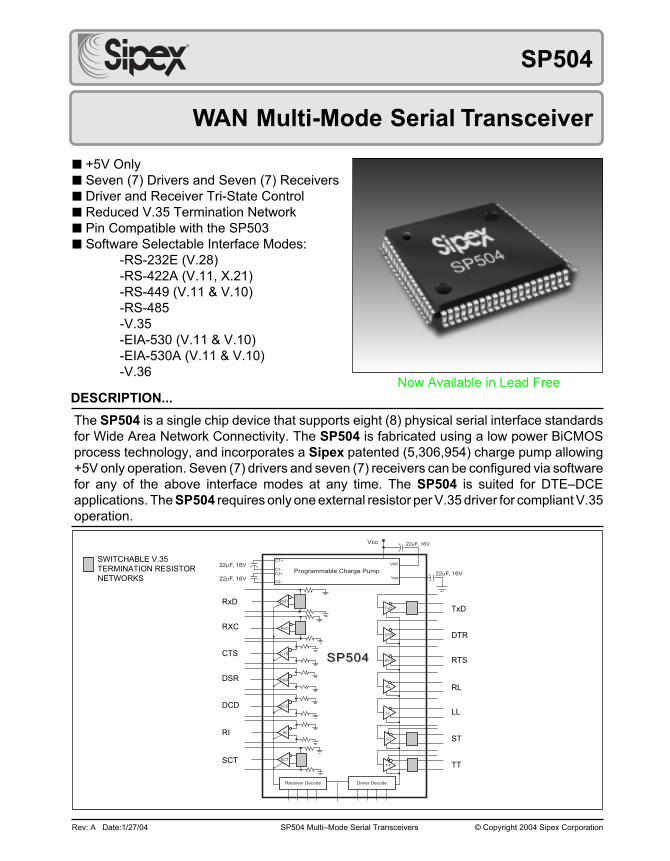
Now Available in Lead Free 1 Rev: A Date:1/27/04 SP504 Multi–Mode Serial Transceivers © Copyright 2004 Sipex Corporation The SP504 is a single chip device that supports eight (8) physical serial interface standards for Wide Area Network Connectivity. The SP504 is fabricated using a low power BiCMOS process technology, and incorporates a Sipex patented (5,306,954) charge pump allowing +5V only operation. Seven (7) drivers and seven (7) receivers can be configured via software for any of the above interface modes at any time. The SP504 is suited for DTE–DCE applications. The SP504 requires only one external resistor per V.35 driver for compliant V.35 operation. DESCRIPTION... ■ +5V Only ■ Seven (7) Drivers and Seven (7) Receivers ■ Driver and Receiver Tri-State Control ■ Reduced V.35 Termination Network ■ Pin Compatible with the SP503 ■ Software Selectable Interface Modes: -RS-232E (V.28) -RS-422A (V.11, X.21) -RS-449 (V.11 & V.10) -RS-485 -V.35 -EIA-530 (V.11 & V.10) -EIA-530A (V.11 & V.10) -V.36 SWITCHABLE V.35 TERMINATION RESISTOR NETWORKS RxD RXC CTS DSR DCD RI SCT TxD DTR RTS RL LL ST TT SP504 WAN Multi-Mode Serial Transceiver ® Driver Decode Receiver Decode Programmable Charge Pump Vss SP504 SP504 Vcc Vdd C1+ C1- C2+ C2- 22μF, 16V 22μF, 16V TxD DTR RTS RL LL RxD RxC CTS DSR DCD RI SCT TT ST 22μF, 16V 22μF, 16V
-
Upload
khangminh22 -
Category
Documents
-
view
0 -
download
0
Transcript of SP504 WAN Multi-Mode Serial Transceiver - Octopart
Now Available in Lead Free
1
Rev: A Date:1/27/04 SP504 Multi–Mode Serial Transceivers © Copyright 2004 Sipex Corporation
The SP504 is a single chip device that supports eight (8) physical serial interface standards
for Wide Area Network Connectivity. The SP504 is fabricated using a low power BiCMOS
process technology, and incorporates a Sipex patented (5,306,954) charge pump allowing
+5V only operation. Seven (7) drivers and seven (7) receivers can be configured via software
for any of the above interface modes at any time. The SP504 is suited for DTE–DCE
applications. The SP504 requires only one external resistor per V.35 driver for compliant V.35
operation.
DESCRIPTION...
■ +5V Only
■ Seven (7) Drivers and Seven (7) Receivers
■ Driver and Receiver Tri-State Control
■ Reduced V.35 Termination Network
■ Pin Compatible with the SP503
■ Software Selectable Interface Modes:
-RS-232E (V.28)
-RS-422A (V.11, X.21)
-RS-449 (V.11 & V.10)
-RS-485
-V.35
-EIA-530 (V.11 & V.10)
-EIA-530A (V.11 & V.10)
-V.36
SWITCHABLE V.35
TERMINATION RESISTOR
NETWORKS
RxD
RXC
CTS
DSR
DCD
RI
SCT
TxD
DTR
RTS
RL
LL
ST
TT
SP504
WAN Multi-Mode Serial Transceiver
®
Driver DecodeReceiver Decode
Programmable Charge PumpVss
SP504SP504
Vcc
VddC1+
C1-C2+
C2-
22µF, 16V
22µF, 16V
TxD
DTR
RTS
RL
LL
RxD
RxC
CTS
DSR
DCD
RI
SCT
TT
ST
22µF, 16V
22µF, 16V

2
Rev: A Date:1/27/04 SP504 Multi–Mode Serial Transceivers © Copyright 2004 Sipex Corporation
SPECIFICATIONST
A = +25°C and V
CC = +5.0V unless otherwise noted.
MIN. TYP. MAX. UNITS CONDITIONS
LOGIC INPUTS
VIL 0.8 VoltsVIH 2.0 Volts
LOGIC OUTPUTS
VOL 0.4 Volts IOUT= +3.2mAVOH 2.4 Volts IOUT= –1.0mA
RS-485 DRIVER
TTL Input LevelsVIL 0.8 VoltsVIH 2.0 Volts
OutputsHIGH Level Output +6.0 VoltsLOW Level Output –0.3 VoltsDifferential Output ±1.5 ±5.0 Volts RL=54 , CL=50pFBalance ±0.2 Volts |VT| - |VT|Offset +2.5 VoltsOpen Circuit Voltage ±6.0 VoltsOutput Current 28.0 mA RL=54 Short Circuit Current ±250 mA Terminated in –7V to +10V
Transition Time 20 40 ns Rise/fall time, 10%–90%Max. Transmission Rate 10 Mbps RL=54 ; Figure 3aPropagation Delay TA @ 25°C & VCC = +5V only tPHL 50 80 100 ns Figures 3a and 5; RL=54 tPLH 50 80 100 ns CL=50pFDifferential Driver Skew 20 40 ns | tPHL – tPLH |; TA @ +25°C
RS-485 RECEIVER
TTL Output LevelsVOL 0.4 VoltsVOH 2.4 Volts
InputHIGH Threshold +0.2 +12 Volts (a)-(b)LOW Threshold –7.0 –0.2 Volts (a)-(b)Common Mode Range –7.0 +12.0 VoltsHIGH Input Current Refer to Rec. input graphLOW Input Current Refer to Rec. input graphReceiver Sensitivity ±0.2 Volts Over –7V to +12V common
mode rangeInput Impedance 12 k
Max. Transmission Rate 10 Mbps Figure 3aPropagation Delay TA = 25°C & VCC = +5V only tPHL 80 110 180 ns Figures 3a and 7; A is invert- tPLH 80 110 180 ns ing and B is non-inverting.Differential Receiver Skew 30 ns | tPHL – tPLH |; TA @ +25°C
V.35 DRIVER
TTL Input Levels All outputs measured w/VIL 0.8 Volts 150 termination resistorVIH 2.0 Volts connected to the non-
inverting outputs as shownOutputs in Figure 18.
Differential Output ±0.44 ±0.66 Volts RL=100 Source Impedance 50 100 150
Short-Circuit Impedance 135 150 165 VOUT = –2V to +2V; A = BVoltage Output Offset –0.6 +0.6
Transition Time 35 60 ns 48kbps data rate.; TA@ 25°CMax. Transmission Rate 10 Mbps RL=100

3
Rev: A Date:1/27/04 SP504 Multi–Mode Serial Transceivers © Copyright 2004 Sipex Corporation
SPECIFICATIONS (Continued)
TA = +25°C and V
CC = +5.0V unless otherwise noted.
MIN. TYP. MAX. UNITS CONDITIONS
V.35 DRIVER
Propagation Delay TA @ 25°C & VCC = +5V only tPHL 50 80 100 ns Figures 3b and 5 tPLH 50 80 100 nsDifferential Driver Skew 30 40 ns | tPHL – tPLH |; TA @ +25°C
V.35 RECEIVER
TTL Output LevelsVOL 0.4 Volts
VOH 2.4 VoltsInput
Differential Threshold ±80 mVInput Impedance 90 100 110
Short-Circuit Impedance 135 150 165 VIN = +2V to –2VMax. Transmission Rate 10 MbpsPropagation Delay TA @ 25°C & VCC = +5V only tPHL 100 130 200 ns Figure 3b and 7; A is invert- tPLH 100 130 200 ns ing and B is non-inverting.Differential Receiver Skew 30 ns | tPHL – tPLH |; TA @ +25°C
RS-422 DRIVER (V.11)
TTL Input LevelsVIL 0.8 VoltsVIH 2.0 Volts
OutputsOpen Circuit Voltage,VO ±6.0 Volts RL=3.9k Differential Output, VT ±2.0 ±5.0 Volts RL=100
0.5VO 0.67VO Volts TA @ +25°CBalance ±0.4 Volts |VT| – |VT|Offset +3.0 VoltsShort Circuit Current ±150 mA Vout = 0V
Power Off Current ±100 µA Vcc = 0V, Vout = ±0.25VTransition Time 20 40 ns Rise/fall time, 10%-90%Max. Transmission Rate 10 Mbps RL=100 ; Figure 3aPropagation Delay TA @ 25°C & VCC = +5V only tPHL 50 80 100 ns Figure 3a and 5; tPLH 50 80 100 ns RDIFF=100 Differential Driver Skew 20 40 ns | tPHL – tPLH |; TA @ +25°C
RS-422 RECEIVER (V.11)
TTL Output LevelsVOL 0.4 VoltsVOH 2.4 Volts
InputHIGH Threshold +0.2 +6.0 Volts (a)-(b)LOW Threshold –6.0 –0.2 Volts (a)-(b)Common Mode Range –7.0 +7.0 VoltsHIGH Input Current Refer to Rec. input graphLOW Input Current Refer to Rec. input graphReceiver Sensitivity ±0.3 Volts VCM = +7V to –7VInput Impedance 4 k VIN = +10V to –10V
Max. Transmission Rate 10 MbpsPropagation Delay TA @ 25°C & VCC = +5V only tPHL 80 110 180 ns Figure 3a and 7; A is invert- tPLH 80 110 180 ns ing and B is non-inverting.Differential Receiver Skew 30 ns | tPHL – tPLH |; TA @ +25°C
RS-232 DRIVER (V.28)
TTL Input LevelVIL 0.8 VoltsVIH 2.0 Volts

4
Rev: A Date:1/27/04 SP504 Multi–Mode Serial Transceivers © Copyright 2004 Sipex Corporation
SPECIFICATIONS (Continued)
TA = +25°C and V
CC = +5.0V unless otherwise noted.
MIN. TYP. MAX. UNITS CONDITIONS
RS-232 DRIVER (V.28)
OutputsHIGH Level Output +5.0 +15 Volts RL=3k , VIN=0.8VLOW Level Output –15.0 –5.0 Volts RL=3k , VIN=2.0VOpen Circuit Voltage –15 +15 VoltsShort Circuit Current ±100 mA VOUT = 0VPower Off Impedance 300 Vcc = 0V, Vout = ±2.0V
Slew Rate 30 V/µs RL=3k , CL= 50pFVCC = +5.0V, TA @ +25°C
Transition Time 1.56 µs RL=3k , CL=2500pF ;between ±3V, TA @ +25°C
Max. Transmission Rate 120 230.4 kbps RL=3k , CL=2500pFPropagation Delay TA @ 25°C & VCC = +5V only tPHL 0.5 1 4 µs Measured from 1.5V of VIN tPLH 0.5 1 4 µs to 50% of VOUT; RL=3k
RS-232 RECEIVER (V.28)
TTL Output LevelsVOL 0.4 VoltsVOH 2.4 Volts
InputHIGH Threshold 1.7 3.0 VoltsLOW Threshold 0.8 1.2 VoltsReceiver Open Circuit Bias +2.0 VoltsInput Impedance 3 5 7 k VIN = +15V to –15V
Max. Transmission Rate 120 230.4 kbpsPropagation Delay TA @ 25°C & VCC = +5V only tPHL 0.05 0.25 1 µs Measured from 50% of VIN tPLH 0.05 0.25 1 µs to 1.5V of VOUT.
RS-423 DRIVER (V.10)
TTL Input LevelsVIL 0.8 VoltsVIH 2.0 Volts
OutputOpen Circuit Voltage, VO ±4.0 ±6.0 Volts RL=3.9k HIGH Level Output, VT +3.6 +6.0 Volts RL=450 ; VOUT ! 0.9VOCLOW Level Output, VT –6.0 –3.6 Volts RL=450 ; VOUT ! 0.9VOC
0.9VOC Volts TA =+25˚C,, VCC = +5.0VShort Circuit Current ±150 mA VOUT = 0V, VCC = +5.0V
Power Off Current ±100 µA VCC = 0V, VOUT= ±0.25VTransition Time 100 ns Rise/fall time, between ±3VMax. Transmission Rate 120 kbps RL=450 Propagation Delay TA @ 25°C & VCC = +5V only tPHL 0.05 0.5 2 µs Measured from 1.5V of VIN tPLH 0.05 0.5 2 µs to 50% of VOUT; RL=450
RS-423 RECEIVER (V.10)
TTL Output LevelsVOL 0.4 VoltsVOH 2.4 Volts
InputHIGH Threshold +0.3 +7.0 VoltsLOW Threshold –7.0 –0.3 VoltsHIGH Input Current Refer to Rec. input graphLOW Input Current Refer to Rec. input graphReceiver Sensitivity ±0.3 Volts VCM = +7V to –7VInput Impedance 4 k VIN = +10V to –10V
Max. Transmission Rate 120 kbps
5
Rev: A Date:1/27/04 SP504 Multi–Mode Serial Transceivers © Copyright 2004 Sipex Corporation
SPECIFICATIONS (Continued)
TA = +25°C and V
CC = +5.0V unless otherwise noted.
MIN. TYP. MAX. UNITS CONDITIONS
RS-423 RECEIVER (V.10)
Propagation Delay TA @ 25°C & VCC = +5V only tPHL 0.05 0.2 1 µs Measured from 50% of VIN tPLH 0.05 0.2 1 µs to 1.5V of VOUT
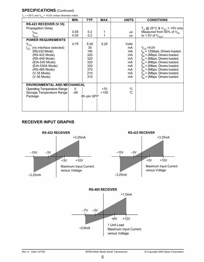
POWER REQUIREMENTS
VCC 4.75 5.00 5.25 VoltsICC (no interface selected) 30 mA VCC =5.0V (RS-232 Mode) 140 mA fIN = 120kbps. Drivers loaded. (RS-422 Mode) 320 mA fIN = 2Mbps. Drivers loaded. (RS-449 Mode) 320 mA fIN = 2Mbps. Drivers loaded. (EIA-530 Mode) 320 mA fIN = 2Mbps. Drivers loaded. (EIA-530A Mode) 320 mA fIN = 2Mbps. Drivers loaded. (RS-485 Mode) 370 mA fIN = 2Mbps. Drivers loaded. (V.35 Mode) 210 mA fIN = 2Mbps. Drivers loaded. (V.36 Mode) 310 mA fIN = 2Mbps. Drivers loaded.
ENVIRONMENTAL AND MECHANICAL
Operating Temperature Range 0 +70 °CStorage Temperature Range –65 +150 °CPackage 80–pin QFP
RECEIVER INPUT GRAPHS
+3.25mA
–3.25mA
+10V+3V
–3V–10V
Maximum Input Current
versus Voltage
RS-422 RECEIVER
+3.25mA
–3.25mA
+10V+3V
–3V–10V
Maximum Input Current
versus Voltage
RS-423 RECEIVER
+1.0mA
–0.6mA
+12V+6V
–3V–7V
1 Unit Load
Maximum Input Current
versus Voltage
RS-485 RECEIVER
6
Rev: A Date:1/27/04 SP504 Multi–Mode Serial Transceivers © Copyright 2004 Sipex Corporation
ABSOLUTE MAXIMUM RATINGSThese are stress ratings only and functional operation
of the device at these ratings or any other above those
indicated in the operation sections of the specifications
below is not implied. Exposure to absolute maximum
rating conditions for extended periods of time may
affect reliability.
VCC
............................................................................+7V
Input Voltages:
Logic...............................-0.3V to (VCC
+0.5V)
Drivers............................-0.3V to (VCC
+0.5V)
Receivers...........................................±15V
Output Voltages:
Logic................................-0.3V to (VCC
+0.5V)
Drivers................................................±14V
Receivers........................-0.3V to (VCC
+0.5V)
Storage Temperature..........................-65˚C to +150˚C
Power Dissipation.........................................2000mW
STORAGE CONSIDERATIONSDue to the relatively large package size of the 80-pin
quad flat-pack, storage in a low humidity environment
is preferred. Large high density plastic packages are
moisture sensitive and should be stored in Dry Vapor
Barrier Bags. Prior to usage, the parts should remain
bagged and stored below 40°C and 60%RH. If the
parts are removed from the bag, they should be used
within 48 hours or stored in an environment at or below
20%RH. If the above conditions cannot be followed,
the parts should be baked for four hours at 125°C in
order remove moisture prior to soldering. Sipex ships
the 80-pin QFP in Dry Vapor Barrier Bags with a
humidity indicator card and desiccant pack. The hu-
midity indicator should be below 30%RH.
Package Derating:
øJA
....................................................46°C/W
øJC
...................................................16 °C/W
OTHER AC CHARACTERISTICST
A = +70°C to 0°C and V
CC = +4.75V to +5.25V unless otherwise noted.
PARAMETER MIN. TYP. MAX. UNITS CONDITIONS
DRIVER DELAY TIME BETWEEN ACTIVE MODE AND TRI-STATE MODE
RS-232 MODE
tPZL; Tri-state to Output LOW 0.70 5.0 µs CL = 100pF, Fig. 4 ; S2closed
tPZH; Tri-state to Output HIGH 0.40 2.0 µs CL = 100pF, Fig. 4 ; S2closed
tPLZ; Output LOW to Tri-state 0.20 2.0 µs CL = 100pF, Fig. 4 ; S2closed
tPHZ; Output HIGH to Tri-state 0.40 2.0 µs CL = 100pF, Fig. 4 ; S2closed
RS-423 MODE
tPZL; Tri-state to Output LOW 0.15 2.0 µs CL = 100pF, Fig. 4 ; S2closed
tPZH; Tri-state to Output HIGH 0.20 2.0 µs CL = 100pF, Fig. 4 ; S2closed
tPLZ; Output LOW to Tri-state 0.20 2.0 µs CL = 100pF, Fig. 4 ; S2closed
tPHZ; Output HIGH to Tri-state 0.15 2.0 µs CL = 100pF, Fig. 4 ; S2closed
RS-422, RS-485 MODES
tPZL; Tri-state to Output LOW 2.80 10.0 µs CL = 100pF, Fig. 4 & 6; S1closed
tPZH; Tri-state to Output HIGH 0.10 2.0 µs CL = 100pF, Fig. 4 & 6; S2closed
tPLZ; Output LOW to Tri-state 0.10 2.0 µs CL = 15pF, Fig. 4 & 6; S1closed
tPHZ; Output HIGH to Tri-state 0.10 2.0 µs CL = 15pF, Fig. 4 & 6; S2closed
V.35 MODE
tPZL; Tri-state to Output LOW 2.60 10.0 µs CL = 100pF, Fig. 4 & 6; S1closed
tPZH; Tri-state to Output HIGH 0.10 2.0 µs CL = 100pF, Fig. 4 & 6; S2closed

7
Rev: A Date:1/27/04 SP504 Multi–Mode Serial Transceivers © Copyright 2004 Sipex Corporation
OTHER AC CHARACTERISTICS (Continued)
TA = +70°C to 0°C and V
CC = +4.75V to +5.25V unless otherwise noted.
PARAMETER MIN. TYP. MAX. UNITS CONDITIONS
V.35 MODE
tPLZ; Output LOW to Tri-state 0.10 2.0 µs CL = 15pF, Fig. 4 & 6; S1closed
tPHZ; Output HIGH to Tri-state 0.15 2.0 µs CL = 15pF, Fig. 4 & 6; S2closed
RECEIVER DELAY TIME BETWEEN ACTIVE MODE AND TRI-STATE MODE
RS-232 MODE
tPZL; Tri-state to Output LOW 0.12 2.0 µs CL = 100pF, Fig. 2 ; S1closed
tPZH; Tri-state to Output HIGH 0.10 2.0 µs CL = 100pF, Fig. 2 ; S2closed
tPLZ; Output LOW to Tri-state 0.10 2.0 µs CL = 100pF, Fig. 2 ; S1closed
tPHZ; Output HIGH to Tri-state 0.10 2.0 µs CL = 100pF, Fig. 2 ; S2closed
RS-423 MODE
tPZL; Tri-state to Output LOW 0.10 2.0 µs CL = 100pF, Fig. 2 ; S1closed
tPZH; Tri-state to Output HIGH 0.10 2.0 µs CL = 100pF, Fig. 2 ; S2closed
tPLZ; Output LOW to Tri-state 0.10 2.0 µs CL = 100pF, Fig. 2 ; S1closed
tPHZ; Output HIGH to Tri-state 0.10 2.0 µs CL = 100pF, Fig. 2 ; S2closed
RS-422/RS-485 MODES
tPZL; Tri-state to Output LOW 0.10 2.0 µs CL = 100pF, Fig. 2 & 8 ; S1closed
tPZH; Tri-state to Output HIGH 0.10 2.0 µs CL = 100pF, Fig. 2 & 8 ; S2closed
tPLZ; Output LOW to Tri-state 0.10 2.0 µs CL = 15pF, Fig. 2 & 8 ; S1closed
tPHZ; Output HIGH to Tri-state 0.10 2.0 µs CL = 15pF, Fig. 2 & 8; S2closed
V.35 MODE
tPZL; Tri-state to Output LOW 0.10 2.0 µs CL = 100pF, Fig. 2 & 8; S1closed
tPZH; Tri-state to Output HIGH 0.10 2.0 µs CL = 100pF, Fig. 2 & 8; S2closed
tPLZ; Output LOW to Tri-state 0.10 2.0 µs CL = 15pF, Fig. 2 & 8; S1closed
tPHZ; Output HIGH to Tri-state 0.10 2.0 µs CL = 15pF, Fig. 2 & 8; S2closed
TRANSCEIVER TO TRANSCEIVER SKEW [ (tphl
– tplh
)Trcvr1
– (tphl
– tplh
)TrcvrX
]
RS-232 Driver 20 50 ns VCC
= +5.0V, TA @ +25°C
RS-232 Receiver 20 ns
RS-422 Driver 20 50 ns VCC
= +5.0V, TA @ +25°C
RS-422 Receiver 20 ns
RS-423 Driver 20 50 ns VCC
= +5.0V, TA @ +25°C
RS-423 Receiver 20 ns
V.35 Driver 20 50 ns VCC
= +5.0V, TA @ +25°C
V.35 Receiver 20 ns
8
Rev: A Date:1/27/04 SP504 Multi–Mode Serial Transceivers © Copyright 2004 Sipex Corporation
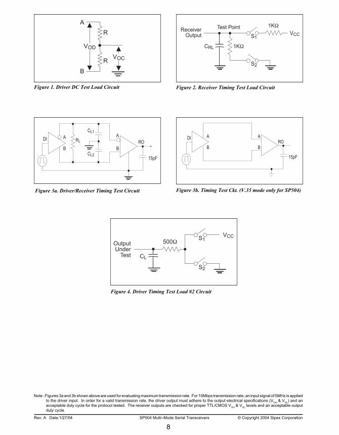
Figure 3a. Driver/Receiver Timing Test Circuit Figure 3b. Timing Test Ckt. (V.35 mode only for SP504)
15pF
ROA
B
A
B
DI
Figure 4. Driver Timing Test Load #2 Circuit
Figure 1. Driver DC Test Load Circuit Figure 2. Receiver Timing Test Load Circuit
CL1
15pF
RO
A
B
A
B
DI
CL2
RL
A
B
R
R
VOD
VOC
500
CL
OutputUnder
Test
S1
S2
VCC
1K
1K CRL
ReceiverOutput S1
S2
Test PointVCC
Note : Figures 3a and 3b shown above are used for evaluating maximum transmission rate. For 10Mbps transmission rate, an input signal of 5MHz is applied
to the driver input. In order for a valid transmission rate, the driver output must adhere to the output electrical specifications (VOH
& VOL
) and an
acceptable duty cycle for the protocol tested. The receiver outputs are checked for proper TTL/CMOS VOH
& VOL
levels and an acceptable output
duty cycle.
9
Rev: A Date:1/27/04 SP504 Multi–Mode Serial Transceivers © Copyright 2004 Sipex Corporation
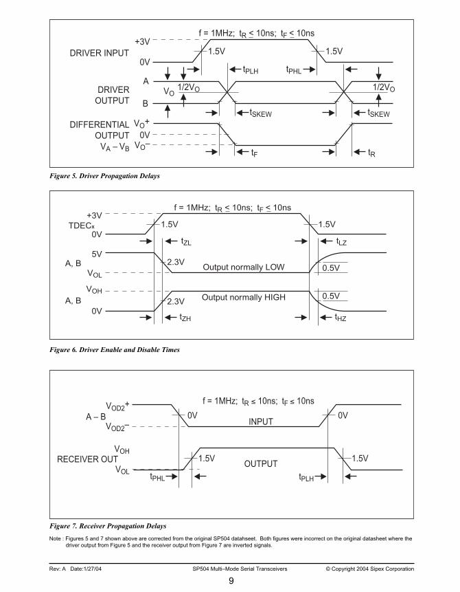
Figure 6. Driver Enable and Disable Times
Figure 7. Receiver Propagation Delays
+3V
0VTDECX
5V
VOL
A, B
0V
1.5V 1.5V
tZL
tZH
f = 1MHz; tR < 10ns; tF < 10ns
VOH
A, B 2.3V
2.3V
tLZ
tHZ
0.5V
0.5V
Output normally LOW
Output normally HIGH
VOH
VOL
RECEIVER OUT 1.5V 1.5V
tPHL
f = 1MHz; tR " 10ns; tF " 10ns
OUTPUT
VOD2+
VOD2–
A – B 0V 0V
tPLH
INPUT
Figure 5. Driver Propagation Delays
+3V
0VDRIVER INPUT
B
ADRIVER
OUTPUT
VO+DIFFERENTIAL
OUTPUT
VA – VB
0VVO
–
tSKEW tSKEW
1.5V 1.5V
tPLH
tRtF
f = 1MHz; tR < 10ns; tF < 10ns
VO1/2VO 1/2VO
tPHL
Note : Figures 5 and 7 shown above are corrected from the original SP504 datahseet. Both figures were incorrect on the original datasheet where the
driver output from Figure 5 and the receiver output from Figure 7 are inverted signals.

10
Rev: A Date:1/27/04 SP504 Multi–Mode Serial Transceivers © Copyright 2004 Sipex Corporation
Figure 8. Receiver Enable and Disable Times
+3V
0V
RDECX
5V
0V
1.5V 1.5V
tZL
tZH
f = 1MHz; tR < 10ns; tF < 10ns
RECEIVER OUT 1.5V
1.5V
tLZ
tHZ
0.5V
0.5V
Output normally LOW
Output normally HIGH
VIL
VIH
RECEIVER OUT
Figure 9. Typical RS-232 Driver Output Waveform Figure 10. Typical RS-423 Driver Output Waveform
Figure 11. Typical RS-422/485 Driver Output Waveform Figure 12. Typical V.35 Driver Output Waveform
- 0V
- 0V
- 0V
- 0V
- 0V
- 0V
- 0V
- 0V
DRIVER INPUT
DRIVER OUTPUT
DRIVER INPUT
DRIVER OUTPUT
DRIVER INPUT
DRIVER OUTPUT
DRIVER INPUT
DRIVER OUTPUT

11
Rev: A Date:1/27/04 SP504 Multi–Mode Serial Transceivers © Copyright 2004 Sipex Corporation
PINOUT…
PIN ASSIGNMENTS…CLOCK AND DATA GROUPPin 1 — RxD — Receive Data; TTL output,sourced from RD(a) and RD(b) inputs.
Pin 14 — TxD — TTL input ; transmit datasource for SD(a) and SD(b) outputs.
Pin 15 — TxC — Transmit Clock; TTL input forTT driver outputs.
Pin 20 — RxC — Receive Clock; TTL outputsourced from RT(a) and RT(b) inputs.
Pin 22 — ST — Send Timing; TTL input; sourcefor ST(a) and ST(b) outputs.
Pin 37 — RT(a) — Receive Timing; analoginput, inverted; source for RxC.
Pin 38 — RT(b) — Receive Timing; analoginput, non-inverted; source for RxC.
Pin 42 — ST(a) — Send Timing; analog output,inverted; sourced from ST.
Pin 44 — ST(b) — Send Timing; analog output,non-inverted; sourced from ST.
Pin 59 — SD(b) — Analog Out — Send data,non-inverted; sourced from TxD.
Pin 61 — SD(a) — Analog Out — Send data,inverted; sourced from TxD.
Pin 63 — TT(a) — Analog Out — TerminalTiming, inverted; sourced from TxC
Pin 65 — TT(b) — Analog Out — TerminalTiming, non–inverted; sourced from TxC.
Pin 70 — RD(a) — Receive Data, analog input;inverted; source for RxD.
Pin 71 — RD(b) — Receive Data; analog input;non-inverted; source for RxD.
Pin 76 — SCT(a) — Serial Clock Transmit;analog input, inverted; source for SCT.
Pin 77 — SCT(b) — Serial Clock Transmit:analog input, non–inverted; source for SCT
Pin 79 — SCT — Serial Clock Transmit; TTLoutput; sources from SCT(a) and SCT(b) inputs.
CONTROL LINE GROUPPin 13 — DTR — Data Terminal Ready; TTLinput; source for TR(a) and TR(b) outputs.
Pin 16 — RTS — Ready To Send; TTL input;source for RS(a) and RS(b) outputs.
Pin 17 — RL — Remote Loopback; TTL input;source for RL(a) and RL(b) outputs.
Pin 18 — V35_STAT — V.35 Status; TTLoutput; outputs logic high when in V.35 mode.
Pin 19 — DCD— Data Carrier Detect; TTLoutput; sourced from RR(a) and RR(b) inputs.
Pin 21 — RI — Ring Indicate; TTL output;sourced from IC(a) and IC(b) inputs.
Pin 24 — LL — Local Loopback; TTL input;source for LL(a) and LL(b) outputs.
Pin 35 — RR(a)— Receiver Ready; analoginput, inverted; source for DCD.
Pin 36 — RR(b)— Receiver Ready; analoginput, non-inverted; source for DCD.
Pin 39 — IC(a)— Incoming Call; analog input,inverted; source for RI.
RxD 1
RDEC0 2
RDEC1 3
RDEC2 4
RDEC3 5
TTEN 6
SCTEN 7
N/C 8
TDEC3 9
TDEC2 10
TDEC1 11
TDEC0 12
DTR 13
TxD 14
TxC 15
RTS 16
RL 17
V35_STAT 18
DCD 19
RxC 20
RI 2
1
ST
22
ST
EN
23
LL 24
VC
C 25
C1+
26
VD
D 27
C2+
28
GN
D 29
C1– 30
C2– 31
VS
S 32
VC
C 33
GN
D 34
RR
(a)
35
RR
(b)
36
RT
(a)
37
RT
(b)
38
IC(a
) 3
9
IC(b
) 4
0
60 GND
59 SD(b)
58 TR(a)
57 GND
56 TR(b)
55 VCC
54 RS(a)
53 GND
52 RS(b)
51 LL(a)
50 GND
49 LL(b)
48 VCC
47 RL(a)
46 GND
45 RL(b)
44 ST(b)
43 GND
42 ST(a)
41 VCC
80 C
TS
79 S
CT
78 D
SR
77 S
CT
(b)
76 S
CT
(a)
75 G
ND
74 V
CC
73 V
CC
72 G
ND
71 R
D(b
)
70 R
D(a
)
69 D
M(b
)
68 D
M(a
)
67 C
S(b
)
66 C
S(a
)
65 T
T(b
)
64 G
ND
63 T
T(a
)
62 V
CC
61 S
D(a
)
SP504
12
Rev: A Date:1/27/04 SP504 Multi–Mode Serial Transceivers © Copyright 2004 Sipex Corporation
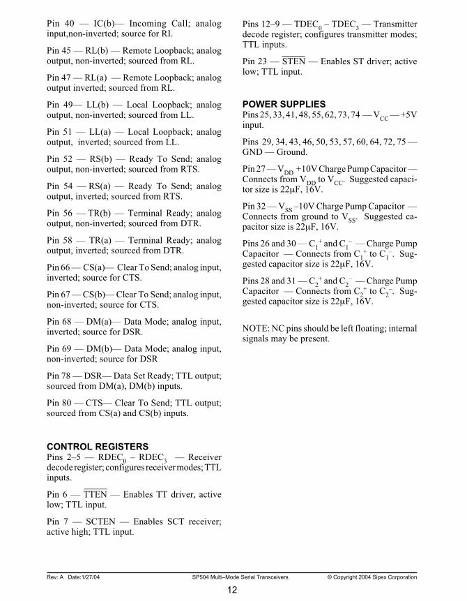
Pin 40 — IC(b)— Incoming Call; analoginput,non-inverted; source for RI.
Pin 45 — RL(b) — Remote Loopback; analogoutput, non-inverted; sourced from RL.
Pin 47 — RL(a) — Remote Loopback; analogoutput inverted; sourced from RL.
Pin 49— LL(b) — Local Loopback; analogoutput, non-inverted; sourced from LL.
Pin 51 — LL(a) — Local Loopback; analogoutput, inverted; sourced from LL.
Pin 52 — RS(b) — Ready To Send; analogoutput, non-inverted; sourced from RTS.
Pin 54 — RS(a) — Ready To Send; analogoutput, inverted; sourced from RTS.
Pin 56 — TR(b) — Terminal Ready; analogoutput, non-inverted; sourced from DTR.
Pin 58 — TR(a) — Terminal Ready; analogoutput, inverted; sourced from DTR.
Pin 66 — CS(a)— Clear To Send; analog input,inverted; source for CTS.
Pin 67 — CS(b)— Clear To Send; analog input,non-inverted; source for CTS.
Pin 68 — DM(a)— Data Mode; analog input,inverted; source for DSR.
Pin 69 — DM(b)— Data Mode; analog input,non-inverted; source for DSR
Pin 78 — DSR— Data Set Ready; TTL output;sourced from DM(a), DM(b) inputs.
Pin 80 — CTS— Clear To Send; TTL output;sourced from CS(a) and CS(b) inputs.
CONTROL REGISTERSPins 2–5 — RDEC
0– RDEC
3— Receiver
decode register; configures receiver modes; TTLinputs.
Pin 6 — TTEN — Enables TT driver, activelow; TTL input.
Pin 7 — SCTEN — Enables SCT receiver;active high; TTL input.
Pins 12–9 — TDEC0
– TDEC3
— Transmitterdecode register; configures transmitter modes;TTL inputs.
Pin 23 — STEN — Enables ST driver; activelow; TTL input.
POWER SUPPLIESPins 25, 33, 41, 48, 55, 62, 73, 74 — V
CC— +5V
input.
Pins 29, 34, 43, 46, 50, 53, 57, 60, 64, 72, 75 —GND — Ground.
Pin 27 — VDD
+10V Charge Pump Capacitor —Connects from V
DDto V
CC. Suggested capaci-
tor size is 22µF, 16V.
Pin 32 — VSS
–10V Charge Pump Capacitor —Connects from ground to V
SS. Suggested ca-
pacitor size is 22µF, 16V.
Pins 26 and 30 — C1+ and C
1– — Charge Pump
Capacitor — Connects from C1
+ to C1
–. Sug-gested capacitor size is 22µF, 16V.
Pins 28 and 31 — C2+ and C
2– — Charge Pump
Capacitor — Connects from C2
+ to C2
–. Sug-gested capacitor size is 22µF, 16V.
NOTE: NC pins should be left floating; internalsignals may be present.

13
Rev: A Date:1/27/04 SP504 Multi–Mode Serial Transceivers © Copyright 2004 Sipex Corporation
VCC = +5V
–5V
–5V
+5V
VDD Storage Capacitor
C1 C2
C4
++ +
–
––
VSS Storage Capacitor
C3
+–
Figure 13b. Charge Pump Phase 1 for ±5V.
VCC = +5V
+5V
VDD Storage Capacitor
C1 C2
C4
++ +
–
––
VSS Storage Capacitor
C3
+–
–5V
Figure 13a. Charge Pump Phase 1 for ±10V.
FEATURES…The SP504 is a highly integrated serial trans-ceiver that allows software control of its inter-face modes. Similar to the SP503, the SP504offers the same hardware interface modes forRS-232 (V.28), RS-422A (V.11), RS-449, RS-485, V.35, EIA-530 and includes V.36 andEIA-530A. The interface mode selection is donevia an 8–bit switch; four (4) bits control thedrivers and four (4) bits control the receivers.The SP504 is fabricated using low powerBiCMOS process technology, and incorporatesa Sipex patented (5,306,954) charge pumpallowing +5V only operation. Each device ispackaged in an 80–pin JEDEC Quad FlatPackpackage.
The SP504 is ideally suited for wide area net-work connectivity based on the interface modesoffered and the driver and receiver configura-tions. The SP504 has seven (7) independentdrivers and seven (7) independent receivers. InV.35 mode, the SP504 includes the necessarycomponents and termination resistors internalwithin the device for compliant V.35 operation.
THEORY OF OPERATIONThe SP504 is made up of five separate circuitblocks — the charge pump, drivers, receivers,decoder and switching array. Each of thesecircuit blocks is described in more detail below.
Charge–PumpTheSP504's charge pump design is based on theSP503 where Sipex's patented charge pumpdesign (5,306,954) uses a four–phase voltageshifting technique to attain symmetrical ±10Vpower supplies. In addition, the SP504 chargepump incorporates a "programmable" featurethat produces an output of ±10V or ±5V for V
SSand V
DDdepending on the mode of operation.
The charge pump still requires external capaci-tors to store the charge. Figure 17a shows thewaveform found on the positive side of capaci-tor C2, and Figure 17b shows the negative sideof capcitor C2. There is a free–running oscilla-tor that controls the four phases of the voltageshifting. A description of each phase follows.
The SP504 charge pump is used for RS-232where the output voltage swing is typically±10V and also used for RS-423. However, RS-
423 requires the voltage swing on the driveroutput be between ±4V to ±6V during an opencircuit (no load). The charge pump would needto be regulated down from ±10V to ±5V. Atypical ±10V charge pump would require exter-nal clamping such as 5V zener diodes on V
DDand V
SSto ground. The ±5V output has sym-
metrical levels as in the ±10V output. The ±5Vis used in the following modes where RS-423levels are used: RS-449, EIA-530, EIA-530Aand V.36.
Phase 1 (±10V)— V
SScharge storage — During this phase of
the clock cycle, the positive side of capacitorsC
1and C
2are initially charged to +5V. The C
l+
is then switched to ground and the charge on C1
–
is transferred to C2–. Since C
2+ is connected to
+5V, the voltage potential across capacitor C2
isnow 10V.
Phase 1 (±5V)— V
SS& V
DDcharge storage and transfer —
With the C1
and C2
capacitors initially chargedto +5V, C
l+ is then switched to ground and the
charge on C1– is transferred to the V
SSstorage
capacitor. Simultaneously the C2– is switched to
ground and the 5V charge on C2
+ is transferredto the V
DD storage capacitor.

14
Rev: A Date:1/27/04 SP504 Multi–Mode Serial Transceivers © Copyright 2004 Sipex Corporation
Figure 17. Charge Pump Waveforms
Figure 14a. Charge Pump Phase 2 for ±10V.
Figure 15. Charge Pump Phase 3.
VCC = +5V
–10V
VDD Storage Capacitor
C1 C2
C4
++ +
–
––
VSS Storage Capacitor
C3
+–
VCC = +5V
–5V
–5V
+5V
VDD Storage Capacitor
C1 C2
C4
++ +
–
––
VSS Storage Capacitor
C3
+–
Figure 16. Charge Pump Phase 4.
Figure 14b. Charge Pump Phase 2 for ±5V.
VCC = +5V
VDD Storage Capacitor
C1 C2
C4
++ +
–
––
VSS Storage Capacitor
C3
+––5V
VCC = +5V
+10V
VDD Storage Capacitor
C1 C2
C4
++ +
–
––
VSS Storage Capacitor
C3
+–
GND
–10V
+10V
C2+
C2–
(a)
(b)
GND
C2+
+5V
GND
GND
C2–
–5V
Phase 2 (±10V)— V
SS transfer — Phase two of the clock con-
nects the negative terminal of C2
to the VSS
storage capacitor and the positive terminal of C2
to ground, and transfers the generated –l0V orthe generated –5V to C
3. Simultaneously, the
positive side of capacitor C 1
is switched to +5Vand the negative side is connected to ground.
Phase 2 (±5V)— V
SS& V
DDcharge storage — C
1+ is recon-
nected to VCC
to recharge the C1
capacitor. C2
+
is switched to ground and C2– is connected to C
3.
The 5V charge from Phase 1 is now transferred
to the VSS
storage capacitor. VSS
receives acontinuous charge from either C
1or C
2. With
the C1 capacitor charged to 5V, the cycle beginsagain.
Phase 3— V
DDcharge storage — The third phase of the
clock is identical to the first phase — the chargetransferred in C
1 produces –5V in the negative
terminal of C1, which is applied to the negative
side of capacitor C2. Since C
2+ is at +5V, the
voltage potential across C2
is l0V. For the 5Voutput, C
2+ is connected to ground so that the
potential on C2 is only +5V.
15
Rev: A Date:1/27/04 SP504 Multi–Mode Serial Transceivers © Copyright 2004 Sipex Corporation
The RS-232 drivers are used in RS-232 modefor all signals, and also in V.35 mode where theyare used as the control line signals such as DTRand RTS.
The RS-423 drivers are also single–ended sig-nals with a minimum voltage output of ±3.6V(with 450 loading) and can operate up to120kbps. Open circuit V
OLand V
OHmeasure-
ments are ±4.0V to ±6.0V. The RS-423 driversare used in RS-449, EIA-530, EIA-530A andV.36 modes as Category II signals from each oftheir corresponding specifications.
The third type of driver produces a differentialsignal that can maintain RS-485, ±1.5V differ-ential output levels with a worst case load of54 . The signal levels and drive capability ofthe RS-485 drivers allow the drivers to alsosupport RS-422 (V.11) requirements of ±2Vdifferential output levels with 100 loads. TheRS-422 drivers are used in RS-449, EIA-530,EIA-530A and V.36 modes as Category I sig-nals which are used for clock and data.
The fourth type of driver is the V.35 driver.V.35 levels require ±0.55V driver output sig-nals with a load of 100 . The SP504 driverssimplify existing V.35 implementations that useexternal termination schemes. The drivers werespecifically designed to comply with the re-quirements of V.35 as well as the driver outputimpedance values of V.35. The drivers achievethe 50 to 150 source impedance. However,an external 150 resistor to ground must beconnected to the non-inverting outputs; SD(b),ST(b), and TT(b), in order to comply with the135 to 165 short-circuit impedance for V.35.The V.35 driver itself is disabled and transpar-ent when the decoder is in all other modes. Allof the differential drivers; RS-485, RS-422, andV.35, can operate up to 10Mbps.
The driver inputs are both TTL or CMOS com-patible. Since there are no pull-up or pull-downresistors on the driver inputs, they should be tiedto a known logic state in order to define thedriver output.
Since both VDD
and VSS
are separately gener-ated from V
CCin a no–load condition, V
DDand
VSS
will be symmetrical. Older charge pumpapproaches that generate V– from V+ will showa decrease in the magnitude of V– compared toV+ due to the inherent inefficiencies in thedesign.
The clock rate for the charge pump typicallyoperates at 15kHz. The external capacitors mustbe a minimum of 22µF with a 16V breakdownrating.
External Power SuppliesFor applications that do not require +5V only,external supplies can be applied at the V+ andV– pins. The value of the external supply volt-ages must be no greater than ±l0.5V. The toler-ance should be ±5% from ±10V. The currentdrain for the supplies is used for RS-232 andRS-423 drivers. For the RS-232 driver, the cur-rent requirement will be 3.5mA per driver. TheRS-423 driver worst case current drain will be11mA per driver. Power sequencing is requiredfor the SP504. The supplies must be sequencedaccordingly: +10V, +5V and –10V. An externalcircuit would be needed for proper power sup-ply sequencing. Consult factory for applicationcircuitry.
DriversThe SP504 has seven (7) enhanced independentdrivers. Control for the mode selection is donevia a four–bit control word. The drivers are pre-arranged such that for each mode of operation,the relative position and functionality of thedrivers are set up to accommodate the selectedinterface mode. As the mode of the drivers ischanged, the electrical characteristics will changeto support the requirements of clock, data, andcontrol line signal levels. Table 1 shows themode of each driver in the different interfacemodes that can be selected.
There are four basic types of driver circuits —RS-232, RS-423, RS-485 and V.35.
The RS-232 drivers output single–ended signalswith a minimum of ±5V (with 3k and 2500pFloading), and can operate up to 120kbps.

16
Rev: A Date:1/27/04 SP504 Multi–Mode Serial Transceivers © Copyright 2004 Sipex Corporation
ReceiversThe SP504 has seven (7) independent receiverswhich can be programmed for the differentinterface modes. Control for the mode selectionis done via a 4–bit control word that is indepen-dent from the driver control word. The codingfor the drivers and receivers is identical. There-fore, if the modes for the drivers and receiversare supposed to be identical in the application,the control lines can be tied together.
Like the drivers, the receivers are pre-arrangedfor the specific requirements of the interface. Asthe operating mode of the receivers is changed,the electrical characteristics will change to sup-port the requirements of clock, data, and controlline receivers. Table 2 shows the mode of eachreceiver in the different interface modes that canbe selected.
There are three basic types of receiver circuits— RS-232, RS-423, and RS-485.
The RS-232 receiver is a single–ended inputwith a threshold of 0.8V to 2.4V. The RS-232receiver has an operating voltage range of ±15Vand can receive signals up to 120kbps. Theinput sensitivity complies with EIA-RS-232 andV.28 at +3V to -3V. The input impedance is3k to 7k . RS-232 receivers are used in RS-232 mode for all data, clock and control signals.They are also used in V.35 mode for control linesignals such as CTS and DSR.
The RS-423 receivers are also single–ended buthave an input threshold as low as ±200mV. Theinput impedance is guaranteed to be greater than4k , with an operating voltage range of ±7V.The RS-423 receivers can operate up to 120kbps.RS-423 receivers are used in RS-449, EIA-530,EIA-530A and V.36 modes as Category II sig-nals as indicated by their corresponding specifi-cations.
The third type of receiver is a differential whichsupports RS-485. The RS-485 receiver has aninput impedance of 15k and a differentialthreshold of ±200mV. Since the characteristicsof an RS-422 (V.11) receiver are actuallysubsets of RS-485, the receivers for RS-422requirements are covered by the RS-485 receivers.
RS-422 receivers are used in RS-449,EIA-530, EIA-530A and V.36 as Category Isignals for receiving clock, data, and some con-trol line signals. The differential receivers canreceive data up to 10Mbps.
The RS-485 receivers are also used for the V.35mode. Unlike the older implementations ofdifferential or V.35 receivers, the SP504 con-tains an internal resistor termination networkthat ensures a V.35 input impedance of 100 (±10 ) and a short-circuit impedance of 150 (±15 ). The traditional V.35 implementationsrequired external termination resistors to acheivethe proper V.35 impedances. The internal net-work is connected via low on-resistance FETswitches when the decoder is changed to V.35mode. The termination network is transparentwhen all other modes are selected. The V.35receivers can operate up to 10Mbps.
All receivers include a fail-safe feature thatoutputs a logic HIGH when the receiver inputsare open. For single-ended RS-232 receivers,there are internal 5k pull-down resistors on theinputs which produces a logic HIGH ("1") at thereceiver outputs. The single-ended RS-423 re-ceivers produce a logic LOW ("0") on the outputwhen the inputs are open. This is due to a pull-up device connected to the input. The differen-tial receivers have the same internal pull-updevice on the non-inverting input which pro-duces a logic HIGH ("1") at the receiver output.The three differential receivers when config-ured in V.35 mode (RxD, RxC & SCT) do nothave fail-safe because the internal terminationresistor network is connected.
DecoderThe SP504 has the ability to change the inter-face mode of the drivers or receivers via an 8–bitswitch. The decoder for the drivers and receiv-ers is not latched; it is merely a combinationallogic switch.
The control word can be externally latchedeither HIGH or LOW to write the appropriatecode into the SP504. The codes shown in Tables1 and 2 are the only specified, valid modes fortheSP504. Undefined codes may represent otherinterface modes not specified (consult the fac-

17
Rev: A Date:1/27/04 SP504 Multi–Mode Serial Transceivers © Copyright 2004 Sipex Corporation
tory for more information). The drivers arecontrolled with the data bits labeled TDEC
3–
TDEC0. All of the drivers can be put into tri-
state mode by writing 0000 to the driver decodeswitch. The three drivers TxD, ST and TxC,have a 150 pull-down resistor to ground con-nected at the (b) output. This resistor is part ofthe V.35 driver circuitry and should be con-nected when in V.35 mode. Tri-state is possiblefor all drivers in RS-232 mode. The receiversare controlled with data bits RDEC
3–RDEC
0;
the code 0000 written to the receivers will placethe outputs into tri-state mode. The 0000 de-coder word will override the enable control linefor the one receiver (SCT).
Using the V.35_STAT PinThe SP504 includes a V.35 status pin where theV35_STAT pin (pin 18) is a logic HIGH ("1")when the decoder is set to V.35 mode. The pinis a logic LOW ("0") when in all other modesincluding tri-state (decoder set at "0000"). Pin18 allows the user to easily add FET switches orsolid state relays to connect the external 150 resistor for V.35 operation. V35_STAT can beconnected to the gate of the FET switches or thecontrol of the relays so that the 150 resistorsare connected to the non-inverting output of thethree V.35 drivers. The output current of theV35_STAT pin is that of a typical TTL load of–3.2mA. The electrical specifications are simi-lar to the SP504 receiver outputs. This featurewould reduce additional logic required by oldertraditional methods.
NET1/NET2 Testing and CompliancyMany system designers are required to certifytheir system for use in the European publicnetwork. Electrical testing is performed in ad-herence to the NET (Norme Européenne deTélécommunication) which specifies the ITUSeries V specifications. The SP504 adheres toall the required physical layer testing for NET1and NET2. Consult factory for details.

18
Rev: A Date:1/27/04 SP504 Multi–Mode Serial Transceivers © Copyright 2004 Sipex Corporation
SP504 Receiver Mode Selection
SP504 Driver Mode Selection
Pin Label
RDEC3–RDEC
0
RD(a)
RD(b)
RT(a)
RT(b)
CS(a)
CS(b)
DM(a)
DM(b)
RR(a)
RR(b)
IC(a)
IC(b)
SCT(a)
SCT(b)
Pin Label Mode: RS232 V.35 RS422 RS485 RS449 EIA530 EIA-530A V.36
0000 0010 1110 0100 0101 1100 1101 1111 0110
SD(a) tri-state V.28 V.35– V.11– RS485– V.11–
SD(b) V.35+ V.11+ RS485+ V.11+
TR(a) tri-state V.28 V.11– RS485– V.11– V.10
TR(b) tri-state tri-state tri-state V.11+ RS485+ V.11+ tri-state
RS(a) tri-state V.28 V.11– RS485– V.11–
RS(b) tri-state tri-state tri-state V.11+ RS485+ V.11+
RL(a) tri-state V.28 V.11– RS485– V.10
RL(b) tri-state
tri-state
tri-state V.11+ RS485+ tri-state
LL(a) tri-state V.28 V.11– RS485– V.10
LL(b) tri-state tri-state tri-state V.11+ RS485+ tri-state
ST(a) tri-state V.28 V.35– V.11– RS485– V.11–
ST(b) V.35+ V.11+ RS485+ V.11+
TT(a) tri-state V.28 V.35– V.11– RS485– V.11–
TT(b) V.35+ V.11+ RS485+ V.11+tri-state tri-state
tri-state
tri-statetri-state
tri-state
V.28
V.28
V.28
V.28
V.11–
V.11+
V.11–
V.11+
V.11–
V.11+
V.10
tri-state
tri-state
V.11–
V.11+
V.11–
V.11+
V.10
V.11–
V.11+
V.11–
V.11+
V.11–
V.11+
V.11–
V.11+
V.11–
V.11+
V.10
tri-state
V.10
tri-state
V.11–
V.11+
V.10
tri-state
V.10
tri-state
V.10
tri-state
V.11–
V.11+
V.11–
V.11+
3 0TDEC –TDEC
Mode: RS232 V.35 RS422 RS485 RS449 EIA530 EIA-530A V.36
0000 0010 1110 0100 0101 1100 1101 1111 0110
V.28 V.35– V.11– RS485– V.11–
V.35+ V.11+ RS485+ V.11+
V.28 V.11– RS485– V.11–
V.11+ RS485+ V.11+
V.28 V.11– RS485– V.11–
V.11+ RS485+ V.11+
V.28 V.11– RS485–
V.11+ RS485+
V.28 V.11– RS485–
V.11+ RS485+
V.28 V.11– RS485–
V.11+ RS485+
V.28 V.35– V.11– RS485– V.11–
V.35+ V.11+ RS485+ V.11+
V.28
V.28
V.28
V.11–
V.11+
V.11–
V.11+
V.11–
V.11+
V.11–
V.11+
V.11–
V.11+
V.11–
V.11+
V.11–
V.11+
V.11–
V.11+
V.10
V.10
V.10
V.11–
V.11+
>12k to GND
>12k to GND
>12k to GND
>12k to GND
>12k to GND
>12k to GND
>12k to GND
>12k to GND
>12k to GND
>12k to GND
>12k to GND
>12k to GND
>12k to GND
>12k to GND
>12k to GND
>12k to GND
>12k to GND >12k to GND
>12k to GND
>12k to GND
>12k to GND
>12k to GND
>12k to GND
>12k to GND
>12k to GND
>12k to GND
>12k to GND
V.11–
V.11+
V.11–
V.11+
>12k to GND >12k to GND
V.10V.10
>12k to GND
V.10
>12k to GND
V.10
V.11–
V.11+
V.11–
V.11+
V.11–
V.11+
>12k to GND
V.10
V.11–
V.11+
V.11–
V.11+
V.35–
V.35+
V.28
>12k to GND
Table 1. Driver Mode Selection
Table 2. Receiver Mode Selection

19
Rev: A Date:1/27/04 SP504 Multi–Mode Serial Transceivers © Copyright 2004 Sipex Corporation
Figure 18. Typical Operation Circuit
RD(a) 70
RxD 1
RD(b) 71
RT(a) 37
RxC 20
RT(b) 38
CS(a) 66
CTS 80
CS(b) 67
DM(a) 68
DSR 78
DM (b) 69
RR(a) 35
DCD 19
RR(b) 36
IC(a) 39
RI 21
IC(b) 40
SCT(a) 76
SCT 79
SCTEN 7SCT(b) 77
14 TxD
61 SD(a)
59 SD(b)
22 ST
42 ST(a)
44 ST(b)
23 STEN
15 TxC
63 TT(a)
65 TT(b)
6 TTEN
13 DTR
58 TR(a)
56 TR(b)
16 RTS
54 RS(a)
52 RS(b)
17 RL
47 RL(a)
45 RL(b)
24 LL
51 LL(a)
49 LL(b)
22µF22µF
1N5819
VCC VDD C1- C2-
VSS
C1+ C2+
+5V
10µF2725 26 312830
22µF
32
External Latch
5
4
3
2
9
10
11
12
RD
EC
XT
DE
CX
0
1
0
0
0
1
0
0
RS-422 Mode Input Word
A B
Charge Pump
A — Receiver Tri-State circuitry & V.35termination resistor circuitry forRxD, RxC & SCT.
B — Driver Tri-State circuitry & V.35termination circuitry for TxD,TxC & ST.
SP504
(SEE PAGE 12 FOR GROUND PINS)
① ☛ For V.35 Termination, needs to be connectedfor proper V.35 operation. A low on-resistance ("1 ) FET or switch can be usedto connect and disconnect the resistor fromthe non-inverting output.
150
①
150
①
150
①
22µF

20
Rev: A Date:1/27/04 SP504 Multi–Mode Serial Transceivers © Copyright 2004 Sipex Corporation
Figure 19. Mode Diagram — RS-232
RD(a) 70
RxD 1
RT(a) 37
RxC 20
13 DTR
58 TR(a)
CS(a) 66
CTS 80
16 RTS
54 RS(a)
DM(a) 68
DSR 78
17 RL
47 RL(a)
RR(a) 35
DCD 19
24 LL
51 LL(a)
IC(a) 39
RI 21
22 ST
42 ST(a)
23 STENSCT(a) 76
SCT 79 15 TxC
63 TT(a)
6 TTEN
SCTEN 7
0 0 1 0 0 0 1 0
STEN ST TTEN TT SCTEN SCT 1 Disabled 1 Disabled 1 Enabled 0 Enabled 0 Enabled 0 Disabled
14 TxD
61 SD(a)
RECEIVERS DRIVERS
MODE: RS-232DRIVER RECEIVER
TDEC3 TDEC2 TDEC1 TDEC0 RDEC3 RDEC2 RDEC1 RDEC0
21
Rev: A Date:1/27/04 SP504 Multi–Mode Serial Transceivers © Copyright 2004 Sipex Corporation
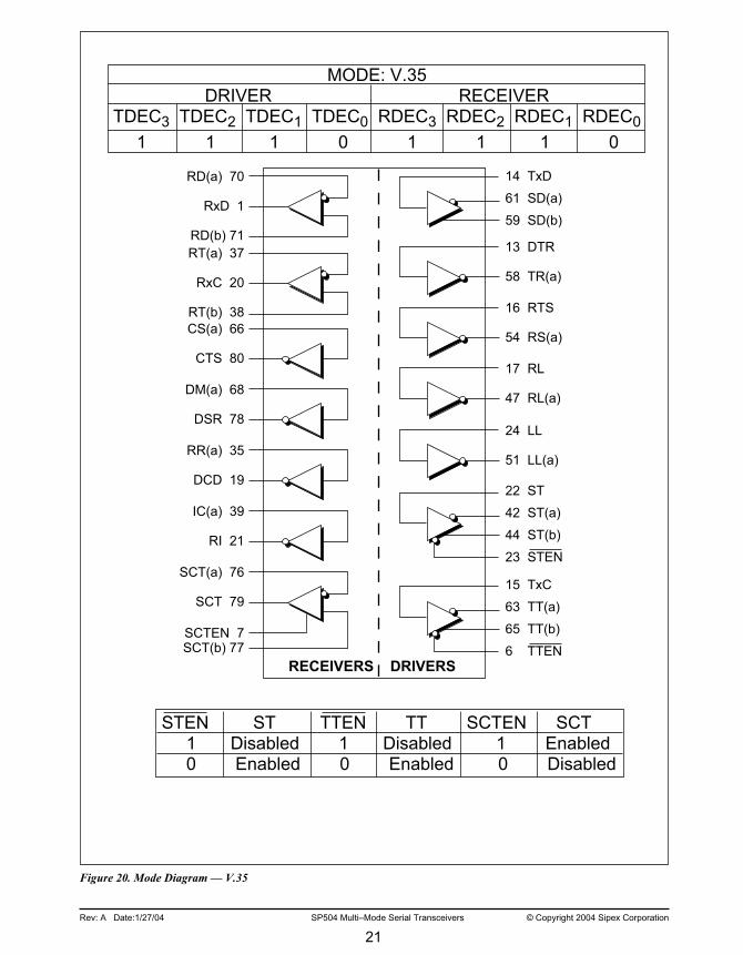
Figure 20. Mode Diagram — V.35
RD(a) 70
RxD 1
RD(b) 71
MODE: V.35DRIVER RECEIVER
TDEC3 TDEC2 TDEC1 TDEC0 RDEC3 RDEC2 RDEC1 RDEC0
RT(a) 37
RxC 20
RT(b) 38
13 DTR
58 TR(a)
CS(a) 66
CTS 80
16 RTS
54 RS(a)
DM(a) 68
DSR 78
17 RL
47 RL(a)
RR(a) 35
DCD 19
24 LL
51 LL(a)
IC(a) 39
RI 21
SCT(a) 76
SCT 79
SCTEN 7SCT(b) 77
1 1 1 0 1 1 1 0
STEN ST TTEN TT SCTEN SCT 1 Disabled 1 Disabled 1 Enabled 0 Enabled 0 Enabled 0 Disabled
14 TxD
61 SD(a)
59 SD(b)
22 ST
42 ST(a)
44 ST(b)
23 STEN
15 TxC
63 TT(a)
65 TT(b)
6 TTENRECEIVERS DRIVERS

22
Rev: A Date:1/27/04 SP504 Multi–Mode Serial Transceivers © Copyright 2004 Sipex Corporation
Figure 21. Mode Diagram — RS-422
RD(a) 70
RxD 1
RD(b) 71
RT(a) 37
RxC 20
RT(b) 38
CS(a) 66
CTS 80
CS(b) 67
DM(a) 68
DSR 78
DM (b) 69
RR(a) 35
DCD 19
RR(b) 36
IC(a) 39
RI 21
IC(b) 40
SCT(a) 76
SCT 79
SCTEN 7SCT(b) 77
0 1 0 0 0 1 0 0
STEN ST TTEN TT SCTEN SCT 1 Disabled 1 Disabled 1 Enabled 0 Enabled 0 Enabled 0 Disabled
14 TxD
61 SD(a)
59 SD(b)
22 ST
42 ST(a)
44 ST(b)
23 STEN
15 TxC
63 TT(a)
65 TT(b)
6 TTEN
13 DTR
58 TR(a)
56 TR(b)
16 RTS
54 RS(a)
52 RS(b)
17 RL
47 RL(a)
45 RL(b)
24 LL
51 LL(a)
49 LL(b)
RECEIVERS DRIVERS
MODE: RS-422DRIVER RECEIVER
TDEC3 TDEC2 TDEC1 TDEC0 RDEC3 RDEC2 RDEC1 RDEC0
23
Rev: A Date:1/27/04 SP504 Multi–Mode Serial Transceivers © Copyright 2004 Sipex Corporation
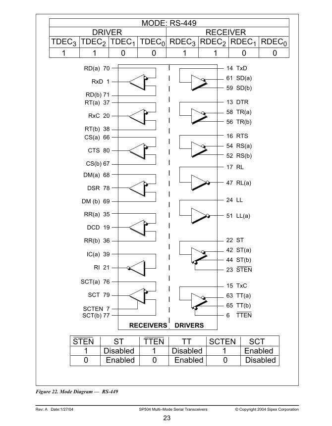
Figure 22. Mode Diagram — RS-449
RD(a) 70
RxD 1
RD(b) 71
RT(a) 37
RxC 20
RT(b) 38
CS(a) 66
CTS 80
CS(b) 67
DM(a) 68
DSR 78
DM (b) 69
RR(a) 35
DCD 19
RR(b) 36
IC(a) 39
RI 21
SCT(a) 76
SCT 79
SCTEN 7SCT(b) 77
1 1 0 0 1 1 0 0
STEN ST TTEN TT SCTEN SCT 1 Disabled 1 Disabled 1 Enabled 0 Enabled 0 Enabled 0 Disabled
14 TxD
61 SD(a)
59 SD(b)
22 ST
42 ST(a)
44 ST(b)
23 STEN
15 TxC
63 TT(a)
65 TT(b)
6 TTEN
13 DTR
58 TR(a)
56 TR(b)
16 RTS
54 RS(a)
52 RS(b)
17 RL
47 RL(a)
24 LL
51 LL(a)
RECEIVERS DRIVERS
MODE: RS-449DRIVER RECEIVER
TDEC3 TDEC2 TDEC1 TDEC0 RDEC3 RDEC2 RDEC1 RDEC0
24
Rev: A Date:1/27/04 SP504 Multi–Mode Serial Transceivers © Copyright 2004 Sipex Corporation
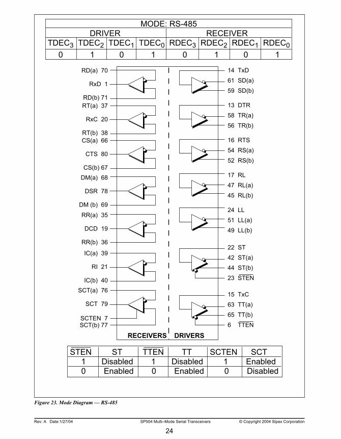
Figure 23. Mode Diagram — RS-485
RD(a) 70
RxD 1
RD(b) 71
RT(a) 37
RxC 20
RT(b) 38
CS(a) 66
CTS 80
CS(b) 67
DM(a) 68
DSR 78
DM (b) 69
RR(a) 35
DCD 19
RR(b) 36
IC(a) 39
RI 21
IC(b) 40
SCT(a) 76
SCT 79
SCTEN 7SCT(b) 77
0 1 0 1 0 1 0 1
STEN ST TTEN TT SCTEN SCT 1 Disabled 1 Disabled 1 Enabled 0 Enabled 0 Enabled 0 Disabled
14 TxD
61 SD(a)
59 SD(b)
22 ST
42 ST(a)
44 ST(b)
23 STEN
15 TxC
63 TT(a)
65 TT(b)
6 TTEN
13 DTR
58 TR(a)
56 TR(b)
16 RTS
54 RS(a)
52 RS(b)
17 RL
47 RL(a)
45 RL(b)
24 LL
51 LL(a)
49 LL(b)
RECEIVERS DRIVERS
MODE: RS-485DRIVER RECEIVER
TDEC3 TDEC2 TDEC1 TDEC0 RDEC3 RDEC2 RDEC1 RDEC0

25
Rev: A Date:1/27/04 SP504 Multi–Mode Serial Transceivers © Copyright 2004 Sipex Corporation
Figure 24. Mode Diagram — EIA-530
RD(a) 70
RxD 1
RD(b) 71
RT(a) 37
RxC 20
RT(b) 38
CS(a) 66
CTS 80
CS(b) 67
DM(a) 68
DSR 78
DM (b) 69
RR(a) 35
DCD 19
RR(b) 36
IC(a) 39
RI 21
SCT(a) 76
SCT 79
SCTEN 7SCT(b) 77
1 1 0 1 1 1 0 1
STEN ST TTEN TT SCTEN SCT 1 Disabled 1 Disabled 1 Enabled 0 Enabled 0 Enabled 0 Disabled
14 TxD
61 SD(a)
59 SD(b)
22 ST
42 ST(a)
44 ST(b)
23 STEN
15 TxC
63 TT(a)
65 TT(b)
6 TTEN
13 DTR
58 TR(a)
56 TR(b)
16 RTS
54 RS(a)
52 RS(b)
17 RL
47 RL(a)
24 LL
51 LL(a)
RECEIVERS DRIVERS
MODE: EIA-530DRIVER RECEIVER
TDEC3 TDEC2 TDEC1 TDEC0 RDEC3 RDEC2 RDEC1 RDEC0
26
Rev: A Date:1/27/04 SP504 Multi–Mode Serial Transceivers © Copyright 2004 Sipex Corporation
RD(a) 70
RxD 1
MODE: EIA-530ADRIVER RECEIVER
TDEC3 TDEC2 TDEC1 TDEC0 RDEC3 RDEC2 RDEC1 RDEC0
RT(a) 37
RxC 20
DM(a) 68
DSR 78
IC(a) 39
RI 21
SCT(a) 76
SCT 79
SCTEN 7SCT(b) 77
1 1 1 1 1 1 1 1
STEN ST TTEN TT SCTEN SCT 1 Disabled 1 Disabled 1 •Enabled 0 Enabled 0 Enabled 0 •Disabled
14 TxD
61 SD(a)
59 SD(b)
15 TxC
63 TT(a)
65 TT(b)
6 TTENRECEIVERS DRIVERS
22 ST
42 ST(a)
44 ST(b)
23 STEN
24 LL
51 LL(a)
17 RL
47 RL(a)
45 RL(b)
13 DTR
58 TR(a)
16 RTS
54 RS(a)
52 RS(b)
CS(a) 66
CTS 80
RR(a) 35
DCD 19
RR(b) 36
CS(b) 67
RT(b) 38
RD(b) 71
STEN ST TTEN TT SCTEN SCT
1 Disabled 1 Disabled 1 Enabled
0 Enabled 0 Enabled 0 Disabled
Figure 25. Mode Diagram — EIA-530A
27
Rev: A Date:1/27/04 SP504 Multi–Mode Serial Transceivers © Copyright 2004 Sipex Corporation
RD(a) 70
RxD 1
RD(b) 71
MODE: V.36DRIVER RECEIVER
TDEC3 TDEC2 TDEC1 TDEC0 RDEC3 RDEC2 RDEC1 RDEC0
RT(a) 37
RxC 20
RT(b) 38
13 DTR
58 TR(a)
CS(a) 66
CTS 80
16 RTS
54 RS(a)
DM(a) 68
DSR 78
17 RL
47 RL(a)
RR(a) 35
DCD 19
24 LL
51 LL(a)
IC(a) 39
RI 21
SCT(a) 76
SCT 79
SCTEN 7SCT(b) 77
0 1 1 0 0 1 1 0
STEN ST TTEN TT SCTEN SCT 1 Disabled 1 Disabled 1 •Enabled 0 Enabled 0 Enabled 0 •Disabled
14 TxD
61 SD(a)
59 SD(b)
22 ST
42 ST(a)
44 ST(b)
23 STEN
15 TxC
63 TT(a)
65 TT(b)
6 TTENRECEIVERS DRIVERS
STEN ST TTEN TT SCTEN SCT
1 Disabled 1 Disabled 1 Enabled
0 Enabled 0 Enabled 0 Disabled
Figure 26. Mode Diagram — V.36
28
Rev: A Date:1/27/04 SP504 Multi–Mode Serial Transceivers © Copyright 2004 Sipex Corporation
SEL A 0 0 1 1
SEL B 0 1 0 1
LOOPBACK 1 1 1 1
SHUTDOWN 0 0 0 0
T4TX4TI41 3
R1RI1RX1 1519
R2RI2RX2 1620
R3RI3RX3 1721
R4RI4RX4 1822
T1TX1TI1 626
T2TX2TI2 727
T3TX3TI3 428
T1TX1 6TI126
T2TI2 TX2 727
R1RI1RX1 1519
R2RX2 RI2 1620
284TX3
3TX4TI3
T3
18RI4
17RI321 RX3
R3
21
26T1
6TX1TI1
7TX2
1915RI1
RX1R1 16RI2
T4TX4TI41 3
T3TX3TI3 428
R3RI3RX3 17
R4RI4RX4 1822
26T1
6TX1TI1
7TX2
284TX3
3TX4TI3
T3
1915RI1
RX1R1 16RI2
18RI4
17RI321 RX3
R3
Figure 28. Mode selection for the SP332
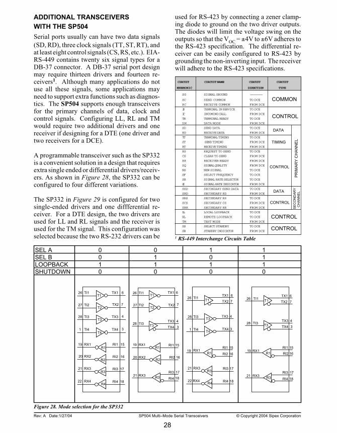
ADDITIONAL TRANSCEIVERS
WITH THE SP504
Serial ports usually can have two data signals
(SD, RD), three clock signals (TT, ST, RT), andat least eight control signals (CS, RS, etc.). EIA-RS-449 contains twenty six signal types for aDB-37 connector. A DB-37 serial port designmay require thirteen drivers and fourteen re-ceivers1. Although many applications do notuse all these signals, some applications mayneed to support extra functions such as diagnos-tics. The SP504 supports enough transceiversfor the primary channels of data, clock andcontrol signals. Configuring LL, RL and TMwould require two additional drivers and onereceiver if designing for a DTE (one driver andtwo receivers for a DCE).
A programmable transceiver such as the SP332is a convenient solution in a design that requiresextra single ended or differential drivers/receiv-ers. As shown in Figure 28, the SP332 can beconfigured to four different variations.
The SP332 in Figure 29 is configured for twosingle-ended drivers and one diffferential re-ceiver. For a DTE design, the two drivers areused for LL and RL signals and the receiver isused for the TM signal. This configuration wasselected because the two RS-232 drivers can be
CIRCUIT CIRCUITNAME CIRCUIT CIRCUIT
MNEMONIC DIRECTION TYPE
SG SIGNAL GROUND --------------
SC SEND COMMON TO DCE
RC RECEIVE COMMON FROM DCE
IS TERMINALINSERVICE TO DCE
IC INCOMINGCALL FROM DCE
TR TERMINAL READY TO DCE
DM DATA MODE FROM DCE
SD SEND DATA TO DCE
RD RECEIVEDATA FROM DCE
TT TERMINALTIMING TO DCE
ST SENDTIMING FROM DCE
RT RECEIVE TIMING FROM DCE
RS REQUEST TO SEND TO DCE
CS CLEAR TO SEND FROM DCE
RR RECEIVER READY FROM DCE
SQ SIGNALQUALITY FROM DCE
NS NEW SIGNAL TO DCE
SF SELECT FREQUENCY TO DCE
SR SIGNAL RATE SELECTOR TO DCE
SI SIGNALRATEINDICATOR FROM DCE
SSD SECONDARY SEND DATA TO DCE
SRD SECONDARY RD FROM DCE
SRS SECONDARY RS TO DCE
SCS SECONDARY CS FROM DCE
SRR SECONDARY RR FROM DCE
LL LOCAL LOOPBACK TO DCE
RL REMOTE LOOPBACK TO DCE
TM TEST MODE FROM DCE
SS SELECT STANDBY TO DCE
SB STANDBYINDICATOR FROM DCE
COMMON
CONTROL
DATA
TIMING
CONTROL
DATA
CONTROL
CONTROL
CONTROL
PR
IMA
RY
CH
AN
NE
LS
EC
ON
DA
RY
C
HA
NN
EL
1 RS-449 Interchange Circuits Table
used for RS-423 by connecting a zener clamp-ing diode to ground on the two driver outputs.The diodes will limit the voltage swing on theoutputs so that the V
OC= ±4V to ±6V adheres to
the RS-423 specification. The differential re-ceiver can be easily configured to RS-423 bygrounding the non-inverting input. The receiverwill adhere to the RS-423 specifications.

29
Rev: A Date:1/27/04 SP504 Multi–Mode Serial Transceivers © Copyright 2004 Sipex Corporation
Figure 29. Adding extra differential and single-ended transceivers using the SP332
22µF 22µF
22µF25 27 26 30 28 31 32
1N5819
VCC VDD C1-C2-
VSSC1+ C2+
22µF
61
59
+5V
SP504CF
DriversTxD
1458
56DTR
1354
52RTS
1663
65TxC
1542
44ST
2247
45RL
1751
49LL
2470
71RxD
137
38RxC
2066
67CTS
8068
69DSR
7835
36DCD
1939
40RI
2176
77SCT
79
Receivers
TDEC3—TDEC0 (pins 9-12)
+5V
5
VCC
10µF
SP332
28
8
21
4
3
18
17
9
12
11
13
10
14
V+
V-
C1+
C1-
C2+
C2-
0.1µF
0.1µF0.1µF
0.1µF
SEL A
SEL B
24
2
see pinout diagram for various ground pins
10µF
6
7
26
27
15
16
19
20
T1
T2
T3
R1
R2
R3
0
1LOOPBACK 123
42212307251735
6248269271129133115
523
DB-37 Connector
34
16
RDEC3—RDEC0 (pins 5-2)
"1100" for RS-449 mode
10
14
18
LL
RL
TM
Note: The SP332 will require clamping di-
odes on the driver outputs to limit the volt-
age to ±6V and comply with the RS-423
driver output specification of VOC
= ±4V to
±6V and VOUT! ±3.6V with a 450 load.

30
Rev: A Date:1/27/04 SP504 Multi–Mode Serial Transceivers © Copyright 2004 Sipex Corporation
80 PIN MQFP (MS-022 BC)
b e
Seating
PlaneA1
AA
L1
5°-16°
0° MIN.
0°–7°
5°-16°
L
A2
0.30" RAD. TYP.
0.20" RAD. TYP.
c
PIN 1
E1
D1
D
CLE
CL
D2
E2
DIMENSIONS
Minimum/Maximum
(mm)
SYMBOL
A
A1
A2
b
D
D1
D2
E
E1
E2
e
N
80–PIN MQFP
JEDEC MS-22
(BEC) Variation
MIN NOM MAX
2.45
0.00 0.25
1.80 2.00 2.20
0.22 0.40
17.20 BSC
14.00 BSC
12.35 REF
17.20 BSC
14.00 BSC
12.35 REF
0.65 BSC
80
COMMON DIMENTIONS
SYMBL MIN NOM MAX
c 0.11 23.00
L 0.73 0.88 1.03
L1 1.60 BASIC
PACKAGE: 80 Pin MQFP
Available in Lead free packaging. To order add "-L" suffix to the partnumber. EXAMPLE: SP385EET/ER = standard,SP385EET/ER-L = lead free.
31
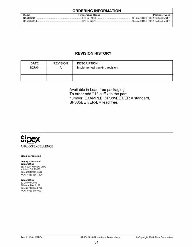
Rev: A Date:1/27/04 SP504 Multi–Mode Serial Transceivers © Copyright 2004 Sipex Corporation
ORDERING INFORMATIONModel Temperature Range Package Types
SP504MCF ........................................................................ 0°C to +70°C ...................................................... 80–pin JEDEC (BE-2 Outline) MQFP
SP504MCF-L...................................................................0°C to +70°C.....................................................80–pin JEDEC (BE-2 Outline) MQFP
Corporation
ANALOG EXCELLENCE
Sipex Corporation
Headquarters andSales Office233 South Hillview DriveMilpitas, CA 95035TEL: (408) 934-7500FAX: (408) 935-7600
Sales Office22 Linnell CircleBillerica, MA 01821TEL: (978) 667-8700FAX: (978) 670-9001
DATE REVISION DESCRIPTION
1/27/04 A Implemented tracking revision.
REVISION HISTORY