MSP430F261x, MSP430F241x Device Erratasheet - Octopart
24
Errata SLAZ033J – October 2007 – Revised December 2011 MSP430F261x, MSP430F241x Device Erratasheet 1 Current Version See Appendix A for prior silicon versions. ✓ The checkmark means that the issue is present in that revision. Device Rev: ADC25 BCL12 CPU8 CPU16 CPU19 DMA3 DMA4 FLASH19 FLASH24 FLASH27 FLASH36 PORT10 PORT12 SVS2 TA12 TA16 TAB22 TB2 TB16 USCI20 MSP430F2416 H ✓ ✓ ✓ ✓ ✓ ✓ ✓ ✓ ✓ ✓ ✓ ✓ ✓ ✓ ✓ ✓ ✓ MSP430F2417 H ✓ ✓ ✓ ✓ ✓ ✓ ✓ ✓ ✓ ✓ ✓ ✓ ✓ ✓ ✓ ✓ ✓ MSP430F2418 H ✓ ✓ ✓ ✓ ✓ ✓ ✓ ✓ ✓ ✓ ✓ ✓ ✓ ✓ ✓ ✓ ✓ MSP430F2419 H ✓ ✓ ✓ ✓ ✓ ✓ ✓ ✓ ✓ ✓ ✓ ✓ ✓ ✓ ✓ ✓ ✓ MSP430F2616 H ✓ ✓ ✓ ✓ ✓ ✓ ✓ ✓ ✓ ✓ ✓ ✓ ✓ ✓ ✓ ✓ ✓ ✓ ✓ ✓ MSP430F2617 H ✓ ✓ ✓ ✓ ✓ ✓ ✓ ✓ ✓ ✓ ✓ ✓ ✓ ✓ ✓ ✓ ✓ ✓ ✓ ✓ MSP430F2618 H ✓ ✓ ✓ ✓ ✓ ✓ ✓ ✓ ✓ ✓ ✓ ✓ ✓ ✓ ✓ ✓ ✓ ✓ ✓ ✓ MSP430F2619 H ✓ ✓ ✓ ✓ ✓ ✓ ✓ ✓ ✓ ✓ ✓ ✓ ✓ ✓ ✓ ✓ ✓ ✓ ✓ ✓ Device Rev: USCI21 USCI22 USCI23 USCI24 USCI25 USCI26 USCI27 USCI30 XOSC5 MSP430F2416 H ✓ ✓ ✓ ✓ ✓ ✓ ✓ ✓ ✓ MSP430F2417 H ✓ ✓ ✓ ✓ ✓ ✓ ✓ ✓ ✓ MSP430F2418 H ✓ ✓ ✓ ✓ ✓ ✓ ✓ ✓ ✓ MSP430F2419 H ✓ ✓ ✓ ✓ ✓ ✓ ✓ ✓ ✓ MSP430F2616 H ✓ ✓ ✓ ✓ ✓ ✓ ✓ ✓ ✓ MSP430F2617 H ✓ ✓ ✓ ✓ ✓ ✓ ✓ ✓ ✓ MSP430F2618 H ✓ ✓ ✓ ✓ ✓ ✓ ✓ ✓ ✓ MSP430F2619 H ✓ ✓ ✓ ✓ ✓ ✓ ✓ ✓ ✓ 1 SLAZ033J – October 2007 – Revised December 2011 MSP430F261x, MSP430F241x Device Erratasheet Submit Documentation Feedback Copyright © 2007–2011, Texas Instruments Incorporated
-
Upload
khangminh22 -
Category
Documents
-
view
8 -
download
0
Transcript of MSP430F261x, MSP430F241x Device Erratasheet - Octopart

ErrataSLAZ033J–October 2007–Revised December 2011
MSP430F261x, MSP430F241x Device Erratasheet
1 Current Version
See Appendix A for prior silicon versions.
The checkmark means that the issue is present in that revision.
Device Rev
:
AD
C25
BC
L12
CP
U8
CP
U16
CP
U19
DM
A3
DM
A4
FL
AS
H19
FL
AS
H24
FL
AS
H27
FL
AS
H36
PO
RT
10
PO
RT
12
SV
S2
TA
12
TA
16
TA
B22
TB
2
TB
16
US
CI2
0
MSP430F2416 H MSP430F2417 H MSP430F2418 H MSP430F2419 H MSP430F2616 H MSP430F2617 H MSP430F2618 H MSP430F2619 H
Device Rev
:
US
CI2
1
US
CI2
2
US
CI2
3
US
CI2
4
US
CI2
5
US
CI2
6
US
CI2
7
US
CI3
0
XO
SC
5
MSP430F2416 H MSP430F2417 H MSP430F2418 H MSP430F2419 H MSP430F2616 H MSP430F2617 H MSP430F2618 H MSP430F2619 H
1SLAZ033J–October 2007–Revised December 2011 MSP430F261x, MSP430F241x Device ErratasheetSubmit Documentation Feedback
Copyright © 2007–2011, Texas Instruments Incorporated
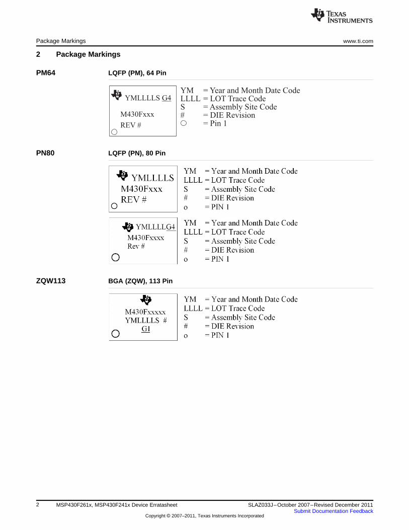
YMLLLLS G4
M430Fxxx
REV #
YM = Year and Month Date CodeLLLL = LOT Trace CodeS = Assembly Site Code# = DIE Revision
= Pin 1
Package Markings www.ti.com
2 Package Markings
PM64 LQFP (PM), 64 Pin
PN80 LQFP (PN), 80 Pin
ZQW113 BGA (ZQW), 113 Pin
2 MSP430F261x, MSP430F241x Device Erratasheet SLAZ033J–October 2007–Revised December 2011Submit Documentation Feedback
Copyright © 2007–2011, Texas Instruments Incorporated
www.ti.com Detailed Bug Description
3 Detailed Bug Description
ADC25 ADC12 Module
Function Write to ADC12CTL0 triggers ADC12 when CONSEQ = 00
Description If ADC conversions are triggered by the Timer_B module and the ADC12 is insingle-channel single-conversion mode (CONSEQ = 00), ADC sampling is enabled bywrite access to any bit(s) in the ADC12CTL0 register. This is contrary to the expectedbehavior that only the ADC12 enable conversion bit (ADC12ENC) triggers a new ADC12sample.
Workaround When operating the ADC12 in CONSEQ = 00 and a Timer_B output is selected as thesample and hold source, temporarily clear the ADC12ENC bit before writing to other bitsin the ADC12CTL0 register. The following capture trigger can then be re-enabled bysetting ADC12ENC = 1.
3SLAZ033J–October 2007–Revised December 2011 MSP430F261x, MSP430F241x Device ErratasheetSubmit Documentation Feedback
Copyright © 2007–2011, Texas Instruments Incorporated
Detailed Bug Description www.ti.com
BCL12 Basic Clock Module
Function Switching RSELx or modifying DCOCTL can cause DCO dead time or a complete DCOstop
Description After switching RSELx bits (located in register BCSCTL1) from a value of >13 to a valueof <12 OR from a value of <12 to a value of >13, the resulting clock delivered by theDCO can stop before the new clock frequency is applied. This dead time isapproximately 20 µs. In some instances, the DCO may completely stop, requiring apower cycle.
Furthermore, if all of the RSELx bits in the BSCTL1 register are set, modifying theDCOCTL register to change the DCOx or the MODx bits could also result in DCO deadtime or DCO hang up.
Workaround
• When switching RSEL from >13 to <12, use an intermediate frequency step. Theintermediate RSEL value should be 13.
Current RSEL Target RSEL Recommended Transition Sequence
15 14 Switch directly to target RSEL
14 or 15 13 Switch directly to target RSEL
14 or 15 0 to 12 Switch to 13 first, and then to target RSEL (two step sequence)
0 to 13 0 to 12 Switch directly to target RSEL
AND
• When switching RSEL from <12 to >13, it is recommended to set RSEL to its defaultvalue first (RSEL = 7) before switching to the desired target frequency.
AND
• If RSEL is at 15 (highest setting), it is recommended to set RSEL to its default valuefirst (RSEL = 7) before accessing DCOCTL to modify the DCOx and MODx bits. Afterthe DCOCTL register modification, the RSEL bits can be manipulated in an additionalstep.
Example flow for safely loading the factory-programmed calibration constants:
AssemblyMOV.B #XT2OFF+RSEL2+RSEL1+RSEL0,&BCSCTL1 ; BCL12 Workaround, first set RSELx=7MOV.B &CALDCO_1MHZ,&DCOCTL ; Then set target DCOx and MODxMOV.B &CALBC1_1MHZ,&BCSCTL1 ; Finally set target RSELx
CBCSCTL1 = XT2OFF + RSEL2 + RSEL1 + RSEL0; // BCL12 Workaround, first set RSELx=7DCOCTL = CALDCO_1MHZ; // Then set target DCOx and MODxBCSCTL1 = CALBC1_1MHZ; // Finally set target RSELx
Note that the 3-step clock startup sequence consisting of clearing DCOCTL, loading theBCSCTL1 target value, and finally loading the DCOCTL target value as suggested in thein the "TLV Structure" chapter of the MSP430F2xx User's Guide (SLAU144) is notaffected by BCL12 if (and only if) it is executed after a device reset (PUC) prior to anyother modifications being made to BCSCTL1, because, in this case, RSEL still is at itsdefault value of 7. However, any further changes to the DCOx and MODx bits require theconsideration of the workaround described here.
4 MSP430F261x, MSP430F241x Device Erratasheet SLAZ033J–October 2007–Revised December 2011Submit Documentation Feedback
Copyright © 2007–2011, Texas Instruments Incorporated
www.ti.com Detailed Bug Description
CPU8 CPU Module
Function Using odd values in the SP register
Description The SP can be written with odd values. In the original CPU, an odd SP value could becombined with an odd offset (for example, mov. #value, 5(SP)). In the new CPU, theSP can be written with an odd value, but the first time the SP is used, the LSB is forcedto 0.
Workaround Do not use odd values with the SP.
CPU16 CPU Module
Function Indexed addressing with instructions calla, mova, and bra
Description With indexed addressing mode and instructions calla, mova, and bra, it is not possibleto reach memory above 64k if the register content is < 64k.
Example: Assume R5 = FFFEh. The instruction calla 0004h(R5) results in a 20-bit callof address 0002h instead of 10002h.
Workaround
• Use different addressing mode to reach memory above 64k.• First use adda [index],[Rx] to calculate address in upper memory and then use
calla [Rx].
CPU19 CPU Module
Function CPUOFF can change register values
Description If a CPUOFF command is followed by an instruction with an indirect addressed operand(for example, mov @R8, R9, and RET), an unintentional register-read operation canoccur during the wakeup of the CPU. If the unintentional read occurs to a read-sensitiveregister (for example, UCB0RXBUF or TAIV), which changes its value or the value ofother registers (IFGs), the bug leads to lost interrupts or wrong register read values.
Workaround Insert a NOP instruction after each CPUOFF instruction.
DMA3 DMA Module
Function Read-modify-write instructions may corrupt DMA address registers
Description When a 16-bit-wide read-modify-write instruction (such as add.w and sub.w) is directlyused on a DMA address register (DMAxSA or DMAxDA), the register contents arecorrupted.
Workaround
• Do not use 16-bit-wide read-modify-write instructions on DMA address registers.Instead, if address calculations are necessary, do the calculations first, and thenassign the result to the DMA address registers.
or
• Use 20-bit-wide read-modify-write instructions (such as addx.a, subx.a) on the DMAaddress registers, if needed.
5SLAZ033J–October 2007–Revised December 2011 MSP430F261x, MSP430F241x Device ErratasheetSubmit Documentation Feedback
Copyright © 2007–2011, Texas Instruments Incorporated

Detailed Bug Description www.ti.com
DMA4 DMA Module
Function Corrupted write access to 20-bit DMA registers
Description When a 20-bit wide write to a DMA address register (DMAxSA or DMAxDA) isinterrupted by a DMA transfer, the register contents may be unpredictable.
Workaround
• Design the application to ensure that no DMA access interrupts 20-bit wide accessesto the DMA address registers.
or
• When accessing the DMA address registers, enable the Read Modify Write disablebit (DMARMWDIS = 1), or temporarily disable all active DMA channels (DMAEN = 0).
or
• Use word access for accessing the DMA address registers. Note that this limits thevalues that can be written to the address registers to 16-bit values (lower 64K offlash).
FLASH19 Flash Module
Function EEI feature does not work for code execution from RAM
Description When the program is executed from RAM, the flash controller EEI feature does not work.The erase cycle is suspended, and the interrupt is serviced, but there is a problem whileresuming with the erase cycle.
Addresses applied to flash are different from the actual values while resuming erasecycle after ISR execution.
Workaround None
FLASH24 Flash Module
Function Write or erase emergency exit can cause failures
Description When a flash write or erase is abruptly terminated, the following flash accesses by theCPU may be unreliable and result in erroneous code execution. The abrupt terminationcan be the result of one the following events:
1. The Flash Controller Clock is configured to be sourced by an external crystal. Anoscillator fault occurs thus stopping this clock abruptly.
or
2. The Emergency Exit bit (EMEX in FCTL3) when set forces a write or an eraseoperation to be terminated before normal completion.
or
3. The Enable Emergency Interrupt Exit bit (EEIEX in FCTL1) when set with GIE = 1can lead to an interrupt causing an emergency exit during a Flash operation.
Workaround
1. Use the internal DCO as the flash controller clock provided from MCLK or SMCLK.
or
2. After setting EMEX = 1, wait for a sufficient amount of time before flash is accessedagain.
or
3. No workaround. Do not use EEIEX bit.
6 MSP430F261x, MSP430F241x Device Erratasheet SLAZ033J–October 2007–Revised December 2011Submit Documentation Feedback
Copyright © 2007–2011, Texas Instruments Incorporated
www.ti.com Detailed Bug Description
FLASH27 Flash Module
Function EEI feature can disrupt segment erase
Description When a flash segment erase operation is active with EEI feature selected (EEI = 1 inFLCTL1) and GIE = 0, the following can occur:
An interrupt event causes the flash erase to be stopped, and the flash controller expectsan RETI to resume the erase. Because GIE = 0, interrupts are not serviced and RETInever happens.
Workaround
• Do not set bit EEI = 1 when GIE = 0.
or
• Force an RETI instruction during the erase operation during the check for BUSY=1(FCLTL3).
Sample Code:MOV R5, 0(R5) ; Dummy write, erase segment
LOOP: BIT #BUSY, &FCTL3 ; test busy bitJMP SUB_RETI ; Force RETI instructionJNZ LOOP ; loop while BUSY=1
SUB_RETI: PUSH SRRETI
FLASH36 Flash Module
Function Flash content may degrade due to aborted page erases
Description If a page erase is aborted by EEIEX, the flash page containing the last instruction beforeerase operation starts to degrade. This effect is incremental and, after repetitions, maylead to corrupted flash content.
Workaround
• Use the EEI (interrupt erasing) feature instead of EEIEX (abort erasing).
or
• A PSA checksum can be calculated over affected flash page using the marginal readmode (marginal 0). If the PSA sum differs from expected PSA value, the affectedflash page must be reprogrammed.
or
• Start flash erasing from RAM and limit system frequency to <1 MHz ( to ensure a6-µs delay after EEIEX). If the last instruction before erasing is located in RAM, flashcell degradation does not occur.
PORT10 Digital I/O Module
Function Pullup/pulldown resistor selection when module pin function is selected
Description When the pullup/pulldown resistor for a certain port pin is enabled (PxREN.y = 1) andthe module port pin function is selected (PxSEL.y = 1), the pullup/pulldown resistorconfiguration of this pin is controlled by the respective module output signal (Module XOUT) instead of the port output register (PxOUT.y).
Workaround None. Do not set PxSEL.y and PxREN.y at the same time.
7SLAZ033J–October 2007–Revised December 2011 MSP430F261x, MSP430F241x Device ErratasheetSubmit Documentation Feedback
Copyright © 2007–2011, Texas Instruments Incorporated
Detailed Bug Description www.ti.com
PORT12 Digital I/O Module, Port 1 and 2
Function PxIFG is set on PUC
Description The PxIN register is cleared when a PUC is asserted, and it regains the original valueafter the PUC is de-asserted. If the PxIN register bits read high, asserting a PUC causesclearing of the register, which results in a high-to-low transition. Once the PUC isde-asserted, the PxIN register is restored to high, which results in a low-to-hightransition. This behavior results in the PxIFG being set regardless of the PxIES setting.
Workaround Prior to setting PxIE bits, ensure that corresponding PxIFG bits are cleared.
SVS2 Supply Voltage Supervisor Module
Function DAC1 overwrites an input of the SVS comparator
Description DAC1 overrides the input of the SVS comparator. This is caused by a conflict betweenSVS and DAC1 at Port 6.7. DAC1 is enabled when DAC12AMPx > 0.
Workaround Do not enable DAC1 when SVS is used.
TA12 Timer_A Module
Function Interrupt is lost (slow ACLK)
Description Timer_A counter is running with slow clock (external TACLK or ACLK) compared toMCLK. The compare mode is selected for the capture/compare channel and the CCRxregister is incremented by one with the occurring compare interrupt (if TAR = CCRx).
Due to the fast MCLK, the CCRx register increment (CCRx = CCRx + 1) happens beforethe Timer_A counter has incremented again. Therefore, the next compare interruptshould happen at once with the next Timer_A counter increment (if TAR = CCRx + 1).This interrupt is lost.
Workaround Switch capture/compare mode to capture mode before the CCRx register increment.Switch back to compare mode afterward.
TA16 Timer_A Module
Function First increment of TAR erroneous when IDx > 00
Description The first increment of TAR after any timer clear event (POR/TACLR) happensimmediately following the first positive edge of the selected clock source (INCLK,SMCLK, ACLK, or TACLK). This is independent of the clock input divider settings (ID0,ID1). All following TAR increments are performed correctly with the selected IDx settings.
Workaround None
8 MSP430F261x, MSP430F241x Device Erratasheet SLAZ033J–October 2007–Revised December 2011Submit Documentation Feedback
Copyright © 2007–2011, Texas Instruments Incorporated
www.ti.com Detailed Bug Description
TAB22 Timer_A/Timer_B Module
Function Timer_A/B register modification after Watchdog Timer PUC
Description Unwanted modification of the Timer_A/B registers TACTL and TAIV can occur when aPUC is generated by the Watchdog Timer (WDT) in watchdog mode and any Timer_A/Bcounter register TACCRx/TBCCRx is incremented/decremented (Timer_A/B does notneed to be running).
Workaround Initialize TACTL/TBCTL register after the reset occurs using a MOV instruction (BIS/BICmay not fully initialize the register). TAIV/TBIV is automatically cleared following thisinitialization.
Example code:MOV.W #VAL, &TACTL
orMOV.W #VAL, &TBCTL
Where, VAL = 0, if Timer is not used in application; otherwise, user defined per desiredfunction.
TB2 Timer_B Module
Function Interrupt is lost (slow ACLK)
Description Timer_B counter is running with slow clock (external TBCLK or ACLK) compared toMCLK. The compare mode is selected for the capture/compare channel and the CCRxregister is incremented by 1 with the occurring compare interrupt (if TBR = CCRx).
Due to the fast MCLK, the CCRx register increment (CCRx = CCRx + 1) happens beforethe Timer_B counter has incremented again. Therefore, the next compare interruptshould happen at once with the next Timer_B counter increment (if TBR = CCRx + 1).This interrupt is lost.
Workaround Switch capture/compare mode to capture mode before the CCRx register increment.Switch back to compare mode afterward.
TB16 Timer_B Module
Function First increment of TBR erroneous when IDx > 00
Description The first increment of TBR after any timer clear event (POR/TBCLR) happensimmediately following the first positive edge of the selected clock source (INCLK,SMCLK, ACLK, or TBCLK). This is independent of the clock input divider settings (ID0,ID1). All following TBR increments are performed correctly with the selected IDx settings.
Workaround None
9SLAZ033J–October 2007–Revised December 2011 MSP430F261x, MSP430F241x Device ErratasheetSubmit Documentation Feedback
Copyright © 2007–2011, Texas Instruments Incorporated

Detailed Bug Description www.ti.com
USCI20 USCI Module
Function I2C mode multi-master transmitter issue
Description When configured for I2C master-transmitter mode and used in a multi-masterenvironment, the USCI module can cause unpredictable bus behavior if all of thefollowing conditions are true:
1. Two masters are generating SCL.
and
2. The slave is stretching the SCL low phase of an ACK period while outputting NACKon SDA.
and
3. The slave drives ACK on SDA after the USCI has already released SCL, and thenthe SCL bus line is released.
and
4. The transmit buffer has not been loaded before the other master continuescommunication by driving SCL low.
The USCI remains in the SCL high phase until the transmit buffer is written. After thetransmit buffer has been written, the USCI interferes with the current bus activity andmay cause unpredictable bus behavior.
Workaround
• Ensure that slave does not stretch the SCL low phase of an ACK period.
or
• Ensure that the transmit buffer is loaded in time.
or
• Do not use the multi-master transmitter mode.
10 MSP430F261x, MSP430F241x Device Erratasheet SLAZ033J–October 2007–Revised December 2011Submit Documentation Feedback
Copyright © 2007–2011, Texas Instruments Incorporated
6
Filter Length + 64 Baud Rate × 16Max BRCLK = ×
2 3 × 10
www.ti.com Detailed Bug Description
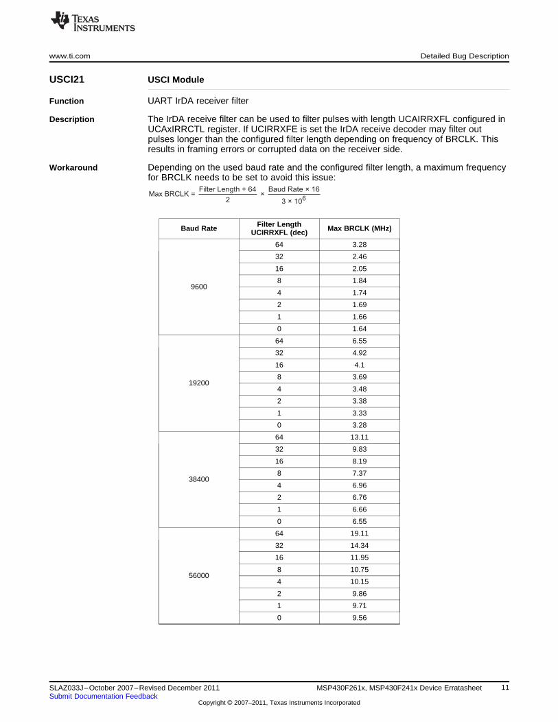
USCI21 USCI Module
Function UART IrDA receiver filter
Description The IrDA receive filter can be used to filter pulses with length UCAIRRXFL configured inUCAxIRRCTL register. If UCIRRXFE is set the IrDA receive decoder may filter outpulses longer than the configured filter length depending on frequency of BRCLK. Thisresults in framing errors or corrupted data on the receiver side.
Workaround Depending on the used baud rate and the configured filter length, a maximum frequencyfor BRCLK needs to be set to avoid this issue:
Filter LengthBaud Rate Max BRCLK (MHz)UCIRRXFL (dec)
64 3.28
32 2.46
16 2.05
8 1.849600
4 1.74
2 1.69
1 1.66
0 1.64
64 6.55
32 4.92
16 4.1
8 3.6919200
4 3.48
2 3.38
1 3.33
0 3.28
64 13.11
32 9.83
16 8.19
8 7.3738400
4 6.96
2 6.76
1 6.66
0 6.55
64 19.11
32 14.34
16 11.95
8 10.7556000
4 10.15
2 9.86
1 9.71
0 9.56
11SLAZ033J–October 2007–Revised December 2011 MSP430F261x, MSP430F241x Device ErratasheetSubmit Documentation Feedback
Copyright © 2007–2011, Texas Instruments Incorporated

Detailed Bug Description www.ti.com
USCI22 USCI Module
Function I2C master receiver with 10-bit slave addressing
Description Unexpected behavior of the USCI_B can occur when configured in I2C master receivemode with 10-bit slave addressing under the following conditions:
1. The USCI sends first byte of slave address, the slave sends an ACK and whensecond address byte is sent, the slave sends a NACK.
2. Master sends a repeat start condition (if UCTXSTT = 1).
3. The first address byte following the repeated start is acknowledged.
However, the second address byte is not sent; instead, the master incorrectly starts toreceive data and sets UCBxRXIFG = 1.
Workaround Do not use a repeated start condition; instead, set the stop condition UCTXSTP = 1 inthe NACK ISR prior to the following start condition (USTXSTT = 1).
USCI23 USCI Module
Function UART transmit mode with automatic baud rate detection
Description Erroneous behavior of the USCI_A can occur when configured in UART transmit modewith automatic baud rate detection. During transmission if a "Transmit break" is initiated(UCTXBRK = 1), the USCI_A does not deliver a stop bit of logic high; instead, it sends alogic low during the subsequent synch period.
Workaround
• Follow user's guide instructions for transmitting a break/synch field followingUCSWRST = 1.
or
• Set UCTXBRK = 1 before an active transmission; that is, check for bit UCBUSY = 0and then set UCTXBRK = 1.
USCI24 USCI Module
Function Incorrect baud rate information during UART automatic baud rate detection mode
Description Erroneous behavior of the USCI_A can occur when configured in UART mode withautomatic baud rate detection. After automatic baud rate measurement is complete, theUART updates UCAxBR0 and UCAxBR1. Under oversampling mode (UCOS16 = 1), forbaud rates that should result in UCAxBRx = 0x0002, the UART incorrectly reports it asUCAxBRx = 0x5555.
Workaround When break/synch is detected following the automatic baud rate detection, the flagUCBRK flag is set to 1. Check if UCAxBRx = 0x5555 and correct it to 0x0002.
12 MSP430F261x, MSP430F241x Device Erratasheet SLAZ033J–October 2007–Revised December 2011Submit Documentation Feedback
Copyright © 2007–2011, Texas Instruments Incorporated
www.ti.com Detailed Bug Description
USCI25 USCI Module
Function TXIFG is not reset when NACK is received in I2C mode
Description When the USCI_B module is configured as an I2C master transmitter, the TXIFG is notreset after a NACK is received if the master is configured to send a restart (UCTXSTT =1 and UCTXSTP = 0).
Workaround Reset TXIFG in software within the NACKIFG interrupt service routine.
USCI26 USCI Module
Function tbuf parameter violation in I2C multi-master mode
Description In multi-master I2C systems, the timing parameter tbuf (bus free time between a stopcondition and the following start) is not ensured to match the I2C specification of 4.7 µsin standard mode and 1.3 µs in fast mode. If the UCTXSTT bit is set during a running I2Ctransaction, the USCI module waits and issues the start condition on bus release,causing the violation to occur.
NOTE: It is recommended to check if UCBBUSY bit is cleared before settingUCTXSTT = 1.
Workaround None
USCI27 USCI Module
Function Timing of USCI I2C interrupts may cause device reset due to automatic clear of an IFG.
Description When certain USCI I2C interrupt flags (IFG) are set and an automatic flag-clearing eventon the I2C bus occurs, the program counter may become corrupted. This happens onlywhen the IFG is cleared within a critical time window (~6 CPU clock cycles) after a USCIinterrupt request occurs and before the interrupt servicing is initiated. The affectedinterrupts are UCBxTXIFG, UCSTPIFG, UCSTTIFG and UCNACKIFG.
The automatic flag-clearing scenarios are described in the following situations:
• A pending UCBxTXIFG interrupt request is cleared on the falling SCL clock edgefollowing a NACK.
• A pending UCSTPIFG, UCSTTIFG, or UCNACKIFG interrupt request is cleared by afollowing Start condition.
Workaround
• Polling the affected flags instead of enabling the interrupts
or
• Ensuring the above mentioned flag-clearing events occur after a time delay of 6 CPUclock cycles has elapsed since the interrupt request occurred and was accepted.
13SLAZ033J–October 2007–Revised December 2011 MSP430F261x, MSP430F241x Device ErratasheetSubmit Documentation Feedback
Copyright © 2007–2011, Texas Instruments Incorporated

Detailed Bug Description www.ti.com
USCI30 USCI Module
Function I2C mode master receiver / slave receiver
Description The USCI I2C module, when configured as a receiver (master or slave), performs adouble-buffered receive operation. For example, in a transaction of two bytes, after thefirst byte is moved from the receive shift register to the receive buffer, the byte isacknowledged and the state machine allows the reception of the next byte.
If the receive buffer has not been cleared of its contents by reading the UCBxRXBUFregister by the time the seventh bit of the following data byte is received, an errorcondition may occur on the I2C bus. Depending on the USCI configuration, the followingmay occur:
• If the USCI is configured as an I2C master receiver, an unintentional repeated startcondition can be triggered or the master can switch into an idle state (I2Ccommunication aborted). The reception of the current data byte is not successful inthis case.
• If the USCI is configured as I2C slave receiver, the slave can switch to an idle state,stalling I2C communication. The reception of the current data byte is not successfulin this case. The USCI I2C state machine notifies the master of the aborted receptionwith a NACK.
Note that the error condition described above occurs only within a limited window of theseventh bit of the current byte being received. If the receive buffer is read outside of thiswindow (before or after), then the error condition does not occur.
Workaround The error condition can be avoided by servicing the UCBxRXIFG in a timely manner.This can be done by (a) servicing the interrupt and ensuring UCBxRXBUF is readpromptly or (b) using the DMA to automatically read bytes from receive buffer uponUCBxRXIFG being set.
OR
If the receive buffer cannot be read out in time, test the I2C clock line before theUCBxRXBUF is read out to ensure that the critical window has elapsed. This is done bychecking if the clock line low status indicator bit UCSCLLOW is set for at least threeUSCI bit clock cycles; that is, 3 × tBitClock.
NOTE: The last byte of the transaction must be read directly from UCBxRXBUF.For all other bytes, follow the workaround.
Code flow for workaround:
1. Enter RX ISR for reading receiving bytes
2. Check if UCSCLLOW.UCBxSTAT == 1
3. If no, repeat step 2 until set.
4. If yes, repeat step 2 for a time period > 3 × tBitClock, where tBitClock = 1/ fBitClock
5. If window of 3 × tBitClock cycles has elapsed, it is safe to read UCBxRXBUF.
14 MSP430F261x, MSP430F241x Device Erratasheet SLAZ033J–October 2007–Revised December 2011Submit Documentation Feedback
Copyright © 2007–2011, Texas Instruments Incorporated
www.ti.com Detailed Bug Description
XOSC5 LFXT1 Module
Function LF crystal failures may not be properly detected by the oscillator fault circuitry
Description The oscillator fault error detection of the LFXT1 oscillator in low-frequency mode(XTS = 0) may not work reliably, causing a failing crystal to go undetected by the CPU;that is, OFIFG is not set.
Workaround None
15SLAZ033J–October 2007–Revised December 2011 MSP430F261x, MSP430F241x Device ErratasheetSubmit Documentation Feedback
Copyright © 2007–2011, Texas Instruments Incorporated

16 MSP430F261x, MSP430F241x Device Erratasheet SLAZ033J–October 2007–Revised December 2011Submit Documentation Feedback
Copyright © 2007–2011, Texas Instruments Incorporated

www.ti.com Appendix A
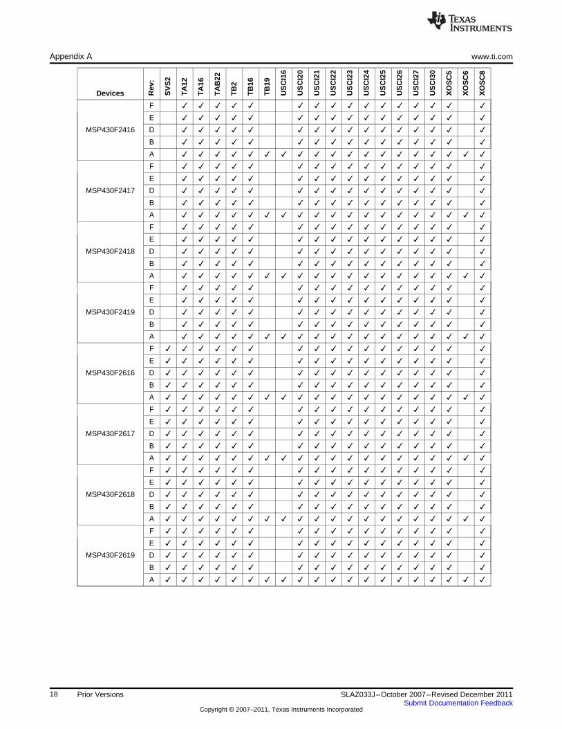
Appendix A Prior Versions
The checkmark means that the issue is present in that revision.
Devices Rev
:
AD
C18
AD
C19
AD
C25
BC
L12
BC
L13
CO
MP
2
CP
U8
CP
U16
CP
U19
DM
A3
DM
A4
FL
AS
H19
FL
AS
H22
FL
AS
H23
FL
AS
H24
FL
AS
H25
FL
AS
H27
FL
AS
H36
PO
RT
10
PO
RT
12
F E
MSP430F2416 D B A F E
MSP430F2417 D B A F E
MSP430F2418 D B A F E
MSP430F2419 D B A F E
MSP430F2616 D B A F E
MSP430F2617 D B A F E
MSP430F2618 D B A F E
MSP430F2619 D B A
17SLAZ033J–October 2007–Revised December 2011 Prior VersionsSubmit Documentation Feedback
Copyright © 2007–2011, Texas Instruments Incorporated
Appendix A www.ti.com
Devices Rev
:
SV
S2
TA
12
TA
16
TA
B22
TB
2
TB
16
TB
19
US
CI1
6
US
CI2
0
US
CI2
1
US
CI2
2
US
CI2
3
US
CI2
4
US
CI2
5
US
CI2
6
US
CI2
7
US
CI3
0
XO
SC
5
XO
SC
6
XO
SC
8
F E
MSP430F2416 D B A F E
MSP430F2417 D B A F E
MSP430F2418 D B A F E
MSP430F2419 D B A F E
MSP430F2616 D B A F E
MSP430F2617 D B A F E
MSP430F2618 D B A F E
MSP430F2619 D B A
18 Prior Versions SLAZ033J–October 2007–Revised December 2011Submit Documentation Feedback
Copyright © 2007–2011, Texas Instruments Incorporated
www.ti.com Detailed Bug Description
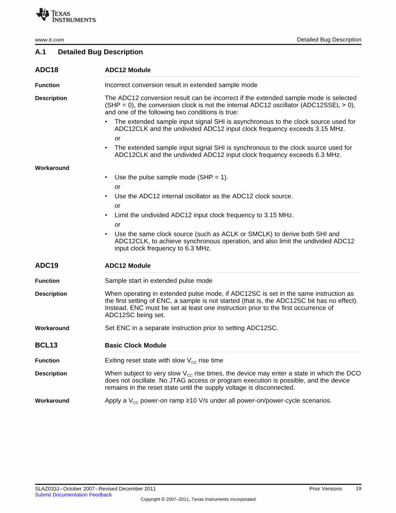
A.1 Detailed Bug Description
ADC18 ADC12 Module
Function Incorrect conversion result in extended sample mode
Description The ADC12 conversion result can be incorrect if the extended sample mode is selected(SHP = 0), the conversion clock is not the internal ADC12 oscillator (ADC12SSEL > 0),and one of the following two conditions is true:
• The extended sample input signal SHI is asynchronous to the clock source used forADC12CLK and the undivided ADC12 input clock frequency exceeds 3.15 MHz.
or
• The extended sample input signal SHI is synchronous to the clock source used forADC12CLK and the undivided ADC12 input clock frequency exceeds 6.3 MHz.
Workaround
• Use the pulse sample mode (SHP = 1).
or
• Use the ADC12 internal oscillator as the ADC12 clock source.
or
• Limit the undivided ADC12 input clock frequency to 3.15 MHz.
or
• Use the same clock source (such as ACLK or SMCLK) to derive both SHI andADC12CLK, to achieve synchronous operation, and also limit the undivided ADC12input clock frequency to 6.3 MHz.
ADC19 ADC12 Module
Function Sample start in extended pulse mode
Description When operating in extended pulse mode, if ADC12SC is set in the same instruction asthe first setting of ENC, a sample is not started (that is, the ADC12SC bit has no effect).Instead, ENC must be set at least one instruction prior to the first occurrence ofADC12SC being set.
Workaround Set ENC in a separate instruction prior to setting ADC12SC.
BCL13 Basic Clock Module
Function Exiting reset state with slow VCC rise time
Description When subject to very slow VCC rise times, the device may enter a state in which the DCOdoes not oscillate. No JTAG access or program execution is possible, and the deviceremains in the reset state until the supply voltage is disconnected.
Workaround Apply a VCC power-on ramp ≥10 V/s under all power-on/power-cycle scenarios.
19SLAZ033J–October 2007–Revised December 2011 Prior VersionsSubmit Documentation Feedback
Copyright © 2007–2011, Texas Instruments Incorporated

Detailed Bug Description www.ti.com
COMP2 Comparator_A+ Module
Function Configuring the port disable register (CAPD)
Description According to the user's guide, each bit in the CAPD register should correspond with itsassociated port I/O number. For example, when bit 0 of CAPD is set, the port disablefunction of pin Px.0 is enabled, bit 1 controls Px.1, and so on (where Px is the port thatcontains the comparator inputs). However, on this device, the bits of the CAPD registercorrespond with the Comparator_A input number. For example, bit 0 of CAPD controlsthe CA0 input, bit 1 controls CA1, etc. This difference matters when the port I/O numberis not the same as the comparator input number.
If the wrong CAPD bit is set, the port I/O function for the wrong pin is disabled. Also, theanalog signal applied to the comparator input pin being used may cause a parasiticcurrent to flow from VCC to GND. See the Comparator_A+ chapter of the MSP430x2xxFamily User's Guide (SLAU144) for more information on CAPD.
Workaround None
FLASH22 Flash Module
Function Flash controller may prevent correct LPM entry
Description When ACLK (or SMCLK) is used as the flash controller clock source and this clocksource is deactivated due to a low-power mode entry while a flash erase or writeoperating is pending, the flash controller keeps ACLK (or SMCLK) active even after theflash operation has been completed. This results in an incorrect LPM entry andincreased current consumption. Note that this issue can only occur when the flashoperation and the low-power mode entry are initiated from code located in RAM.
Workaround Do not enter low-power modes while flash erase or write operations are active. Wait forthe operation to complete before entering a low-power mode.
FLASH23 Flash Module
Function Erasing flash memory
Description The option to erase all main memory segments (MERAS = 1, ERASE = 0) does notapply to the entire main memory area. Flash arrays below and above the 64k addressboundary must be erased separately.
Workaround Erase each main memory segment separately.
20 Prior Versions SLAZ033J–October 2007–Revised December 2011Submit Documentation Feedback
Copyright © 2007–2011, Texas Instruments Incorporated
www.ti.com Detailed Bug Description
FLASH25 Flash Module
Function Marginal read mode is not functional
Description The control bits for marginal read mode contained in the FCTL4 register areautomatically cleared by any flash access. This prevents the marginal read mode frombeing used.
Workaround It is possible to read out memory contents in marginal read mode if the indexedaddressing mode X(Ry) is used to access the flash memory. In this case, the FCTL4control bits are not cleared, and the marginal read mode works as expected. It isrecommended to write the code for reading the flash memory contents in assembler, asthis allows full control over the used addressing mode. Note that certain assemblers mayoptimize an indexed addressing source operation of 0(Ry) to an indirect register mode@Ry operation, which does not work. The following is an example of reading the wordmemory location 0x4000 in marginal read mode, preventing a possible assembleroptimization:mov.w #0x4000,R15 ; Pointer to target addressdec.w R15 ; Decrement pointermov.w 1(R15),R12 ; Read memory contents at R15+1, store result in R12
TB19 Timer_B Module
Function TBIFG/TBIV not updated after access to TBIV
Description After any access to TBIV, the TBIFG flag should automatically be cleared and the TBIVvalue should be updated to reflect the new state of Timer_B interrupts. However, theyare not updated.
Workaround None
USCI16 USCI Module
Function UART/IrDA mode lost characters
Description When configured for UART/IrDA mode, the USCI baud rate generator may halt operationunder the following conditions:
• IrDA mode: Repeated invalid start bits on the receive line
or
• UART/IrDA modes: Positive pulse on the receive line during break characterreception inside the stop-bit time slot (the second stop-bit time slot if UCSPB = 1)with a pulse width that passes the deglitch filter but is shorter than one-half of a bittime.
After halting, additional characters are ignored. Transmit functionality is not affected.
Workaround Check the UCBUSY flag status periodically in software. If the flag is set and no characterhas been received in the expected time, reset the USCI module in software. To reset theUSCI module, toggle UCSWRST and reenable the USCI interrupts.
21SLAZ033J–October 2007–Revised December 2011 Prior VersionsSubmit Documentation Feedback
Copyright © 2007–2011, Texas Instruments Incorporated
Detailed Bug Description www.ti.com
XOSC6 XT2 Module
Function XT2 crystal failures may not be properly detected by the oscillator fault circuit
Description The XT2OF flag should be set if the XT2 frequency falls below 30 kHz. If there is nooscillation at all, the flag operates properly. However, 0 kHz to 30 kHz produces anundefined state on XT2OF. When this occurs, OFIFG is not set.
Workaround Do not depend on the fault detection circuitry to accurately detect all failures.
XOSC8 LFXT1 Module
Function ACLK failure when crystal ESR is below 40 kΩ
Description When ACLK is sourced by a low-frequency crystal with an ESR below 40 kΩ, the dutycycle of ACLK may fall below the specification; the OFIFG may become set or, in someinstances, ACLK may stop completely.
Workaround See the application report XOSC8 Guidance (SLAA423) for information regardingworking with this erratum.
22 Prior Versions SLAZ033J–October 2007–Revised December 2011Submit Documentation Feedback
Copyright © 2007–2011, Texas Instruments Incorporated
www.ti.com Revision History
Revision History
Changes from I Revision (May 2011) to J Revision ........................................................................................................ Page
• Changed BCL12 description ............................................................................................................ 4
NOTE: Page numbers for previous revisions may differ from page numbers in the current version.
23SLAZ033J–October 2007–Revised December 2011 Revision HistorySubmit Documentation Feedback
Copyright © 2007–2011, Texas Instruments Incorporated
IMPORTANT NOTICE
Texas Instruments Incorporated and its subsidiaries (TI) reserve the right to make corrections, modifications, enhancements, improvements,and other changes to its products and services at any time and to discontinue any product or service without notice. Customers shouldobtain the latest relevant information before placing orders and should verify that such information is current and complete. All products aresold subject to TI’s terms and conditions of sale supplied at the time of order acknowledgment.
TI warrants performance of its hardware products to the specifications applicable at the time of sale in accordance with TI’s standardwarranty. Testing and other quality control techniques are used to the extent TI deems necessary to support this warranty. Except wheremandated by government requirements, testing of all parameters of each product is not necessarily performed.
TI assumes no liability for applications assistance or customer product design. Customers are responsible for their products andapplications using TI components. To minimize the risks associated with customer products and applications, customers should provideadequate design and operating safeguards.
TI does not warrant or represent that any license, either express or implied, is granted under any TI patent right, copyright, mask work right,or other TI intellectual property right relating to any combination, machine, or process in which TI products or services are used. Informationpublished by TI regarding third-party products or services does not constitute a license from TI to use such products or services or awarranty or endorsement thereof. Use of such information may require a license from a third party under the patents or other intellectualproperty of the third party, or a license from TI under the patents or other intellectual property of TI.
Reproduction of TI information in TI data books or data sheets is permissible only if reproduction is without alteration and is accompaniedby all associated warranties, conditions, limitations, and notices. Reproduction of this information with alteration is an unfair and deceptivebusiness practice. TI is not responsible or liable for such altered documentation. Information of third parties may be subject to additionalrestrictions.
Resale of TI products or services with statements different from or beyond the parameters stated by TI for that product or service voids allexpress and any implied warranties for the associated TI product or service and is an unfair and deceptive business practice. TI is notresponsible or liable for any such statements.
TI products are not authorized for use in safety-critical applications (such as life support) where a failure of the TI product would reasonablybe expected to cause severe personal injury or death, unless officers of the parties have executed an agreement specifically governingsuch use. Buyers represent that they have all necessary expertise in the safety and regulatory ramifications of their applications, andacknowledge and agree that they are solely responsible for all legal, regulatory and safety-related requirements concerning their productsand any use of TI products in such safety-critical applications, notwithstanding any applications-related information or support that may beprovided by TI. Further, Buyers must fully indemnify TI and its representatives against any damages arising out of the use of TI products insuch safety-critical applications.
TI products are neither designed nor intended for use in military/aerospace applications or environments unless the TI products arespecifically designated by TI as military-grade or "enhanced plastic." Only products designated by TI as military-grade meet militaryspecifications. Buyers acknowledge and agree that any such use of TI products which TI has not designated as military-grade is solely atthe Buyer's risk, and that they are solely responsible for compliance with all legal and regulatory requirements in connection with such use.
TI products are neither designed nor intended for use in automotive applications or environments unless the specific TI products aredesignated by TI as compliant with ISO/TS 16949 requirements. Buyers acknowledge and agree that, if they use any non-designatedproducts in automotive applications, TI will not be responsible for any failure to meet such requirements.
Following are URLs where you can obtain information on other Texas Instruments products and application solutions:
Products Applications
Audio www.ti.com/audio Communications and Telecom www.ti.com/communications
Amplifiers amplifier.ti.com Computers and Peripherals www.ti.com/computers
Data Converters dataconverter.ti.com Consumer Electronics www.ti.com/consumer-apps
DLP® Products www.dlp.com Energy and Lighting www.ti.com/energy
DSP dsp.ti.com Industrial www.ti.com/industrial
Clocks and Timers www.ti.com/clocks Medical www.ti.com/medical
Interface interface.ti.com Security www.ti.com/security
Logic logic.ti.com Space, Avionics and Defense www.ti.com/space-avionics-defense
Power Mgmt power.ti.com Transportation and Automotive www.ti.com/automotive
Microcontrollers microcontroller.ti.com Video and Imaging www.ti.com/video
RFID www.ti-rfid.com
OMAP Mobile Processors www.ti.com/omap
Wireless Connectivity www.ti.com/wirelessconnectivity
TI E2E Community Home Page e2e.ti.com
Mailing Address: Texas Instruments, Post Office Box 655303, Dallas, Texas 75265Copyright © 2011, Texas Instruments Incorporated