WMS7170/1 - Octopart
23
PRELIMINARY Publication Release Date: April 21, 2005 - 1 - Revision 1.1 WMS7170/1 NONVOLATILE DIGITAL POTENTIOMETERS WITH UP/DOWN (3-WIRE) INTERFACE, 10KOHM, 50KOHM, 100KOHM RESISTANCE 100 TAPS WITH OPTIONAL OUTPUT BUFFER
-
Upload
khangminh22 -
Category
Documents
-
view
3 -
download
0
Transcript of WMS7170/1 - Octopart

PRELIMINARY
Publication Release Date: April 21, 2005 - 1 - Revision 1.1
WMS7170/1
NONVOLATILE DIGITAL POTENTIOMETERS
WITH UP/DOWN (3-WIRE) INTERFACE,
10KOHM, 50KOHM, 100KOHM RESISTANCE
100 TAPS
WITH OPTIONAL OUTPUT BUFFER
WMS7170/1
- 2 -
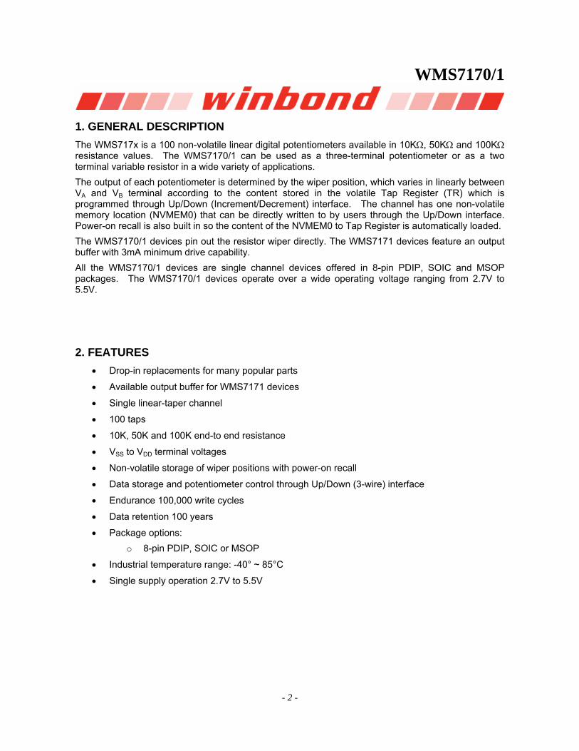
1. GENERAL DESCRIPTION The WMS717x is a 100 non-volatile linear digital potentiometers available in 10KΩ, 50KΩ and 100KΩ resistance values. The WMS7170/1 can be used as a three-terminal potentiometer or as a two terminal variable resistor in a wide variety of applications. The output of each potentiometer is determined by the wiper position, which varies in linearly between VA and VB terminal according to the content stored in the volatile Tap Register (TR) which is programmed through Up/Down (Increment/Decrement) interface. The channel has one non-volatile memory location (NVMEM0) that can be directly written to by users through the Up/Down interface. Power-on recall is also built in so the content of the NVMEM0 to Tap Register is automatically loaded.
B
The WMS7170/1 devices pin out the resistor wiper directly. The WMS7171 devices feature an output buffer with 3mA minimum drive capability. All the WMS7170/1 devices are single channel devices offered in 8-pin PDIP, SOIC and MSOP packages. The WMS7170/1 devices operate over a wide operating voltage ranging from 2.7V to 5.5V.
2. FEATURES • Drop-in replacements for many popular parts
• Available output buffer for WMS7171 devices
• Single linear-taper channel
• 100 taps
• 10K, 50K and 100K end-to end resistance
• VSS to VDD terminal voltages
• Non-volatile storage of wiper positions with power-on recall
• Data storage and potentiometer control through Up/Down (3-wire) interface
• Endurance 100,000 write cycles
• Data retention 100 years
• Package options: o 8-pin PDIP, SOIC or MSOP
• Industrial temperature range: -40° ~ 85°C
• Single supply operation 2.7V to 5.5V
WMS7170/1
Publication Release Date: April 21, 2005 - 3 - Revision 1.1
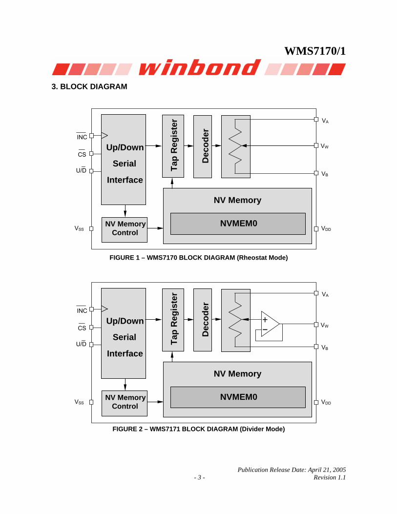
3. BLOCK DIAGRAM
Up/Down
Serial
Interface Ta
p R
egis
ter
Dec
oder
NVMEM0
NV Memory
NV Memory Control
CS
VSS VDD
VA
VB
VW
INC
U/D
FIGURE 1 – WMS7170 BLOCK DIAGRAM (Rheostat Mode)
Up/Down
Serial
Interface
Tap
Reg
iste
r
Dec
oder
NVMEM0
NV Memory
NV Memory Control
CS
VSS VDD
VA
VB
VW
INC
U/D
FIGURE 2 – WMS7171 BLOCK DIAGRAM (Divider Mode)
WMS7170/1
- 4 -
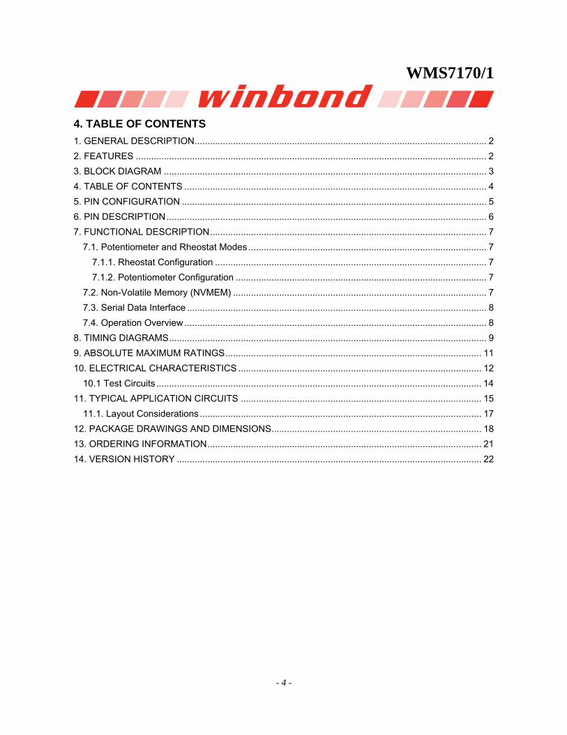
4. TABLE OF CONTENTS 1. GENERAL DESCRIPTION.................................................................................................................. 2 2. FEATURES ......................................................................................................................................... 2 3. BLOCK DIAGRAM .............................................................................................................................. 3 4. TABLE OF CONTENTS ...................................................................................................................... 4 5. PIN CONFIGURATION ....................................................................................................................... 5 6. PIN DESCRIPTION............................................................................................................................. 6 7. FUNCTIONAL DESCRIPTION............................................................................................................ 7
7.1. Potentiometer and Rheostat Modes ............................................................................................. 7 7.1.1. Rheostat Configuration .......................................................................................................... 7 7.1.2. Potentiometer Configuration .................................................................................................. 7
7.2. Non-Volatile Memory (NVMEM) ................................................................................................... 7 7.3. Serial Data Interface ..................................................................................................................... 8 7.4. Operation Overview ...................................................................................................................... 8
8. TIMING DIAGRAMS............................................................................................................................ 9 9. ABSOLUTE MAXIMUM RATINGS.................................................................................................... 11 10. ELECTRICAL CHARACTERISTICS ............................................................................................... 12
10.1 Test Circuits ............................................................................................................................... 14 11. TYPICAL APPLICATION CIRCUITS .............................................................................................. 15
11.1. Layout Considerations .............................................................................................................. 17 12. PACKAGE DRAWINGS AND DIMENSIONS.................................................................................. 18 13. ORDERING INFORMATION........................................................................................................... 21 14. VERSION HISTORY ....................................................................................................................... 22

WMS7170/1
Publication Release Date: April 21, 2005 - 5 - Revision 1.1
5. PIN CONFIGURATION
1
VSS
1
2
3
4 5
6
7
8
2
3
4 5
6
7
8
1
2
3
4 5
6
7
8
INC VDD
U/D
VA
CS
VB
VW
VSS VW
VW
8-MSOP
8-SOIC
8-PDIP
INC
U/D
VA
VDD
CS
VB
VSS
INC
U/D
VA
VDD
CS
VB

WMS7170/1
- 6 -
6. PIN DESCRIPTION TABLE 1 – PIN DESCRIPTION
Pin Name I/O Description
INC I Increment Control. A High-Low transition of INC when
CS is low will move the wiper up or down for one
increment based on the U/D input
U/D I Up/Down control Input. High state will cause the wiper to move to the VB terminal, Low state to the VB A terminal
VA - High terminal of WinPot
VSS - Ground pin, logic ground reference
VDD - Power Supply
CS I Chip Select. When CS is HIGH, the part is deselected
and the device will be in the standby mode. CS LOW enables the part, placing it in the active power mode
VBB - Low terminal of WinPot
VW O
Wiper terminal of WinPot (can be buffered), its position on the resistor array is controlled by the inputs on INC , U/D ,
and CS

WMS7170/1
Publication Release Date: April 21, 2005 - 7 - Revision 1.1
7. FUNCTIONAL DESCRIPTION
The WMS7170/1, a nonvolatile digitally programmable potentiometers with 100 taps, with or without output buffer, is designed to operate as both a potentiometer or a variable resistor depending upon the output configuration selected. The chip can store up to one 8-bit word in a nonvolatile memory (NVMEM0) in order to set the tap register value when the device is powered up. The WMS7170/1 is controlled by a serial Up-Down (3-wire) interface that allows setting the tap register value as well as storing data in the nonvolatile memory.
7.1. POTENTIOMETER AND RHEOSTAT MODES
The WMS7170/1 can operate as either a rheostat or as a potentiometer (voltage divider). When in the potentiometer configuration there are two possible modes. One is done using WMS7170 Winpot device without the output buffer and the other mode is done with WMS7171 WinPot device with the output buffer.
7.1.1. Rheostat Configuration The WMS7170/1 acts as a two terminal resistive element in the rheostat configuration where one terminal can be connected to either the end point pins of the resistor (VA and VB) and the other terminal is the wiper (V
B
W) pin. This configuration controls the resistance between the two terminals and the resistance can be adjusted by sending the corresponding tap register setting to the WMS7170/1 or can also be set by loading a pre-set tap register value from nonvolatile memory NVMEM0 upon power up.
7.1.2. Potentiometer Configuration In potentiometer configuration an input voltage is applied to either one of the end point pins (VA or VB). The voltage on the wiper pin will be proportional to the voltage difference between V
B
A and VBB and the wiper setting. The resistance cannot be directly measured in this configuration.
7.2. NON-VOLATILE MEMORY (NVMEM)
The WMS7170/1 has one NVMEM position available for storing the potentiometer setting. The NVMEM position can be directly written via the Up/Down interface. The potentiometer is loaded with the value stored in the NVMEM0 on power up.

WMS7170/1
- 8 -
7.3. SERIAL DATA INTERFACE
The Up/Down family has a 3-wire Serial Data Interface consisting of CS , INC , U/D pins. Only UP/DOWN operations can be performed. The key features of this interface include:
• Increment/Decrement operations on the tap register (TR)
• Direct refresh of tap register (TR) from internal NVMEM
• Nonvolatile storage of the present tap register value into the NVMEM and automatic recall at power up
• For WMS7171 devices, output buffer amplifier
7.4. OPERATION OVERVIEW
The wiper position or the Tap Register(TR) setting can only be changed by the UP/DOWN operation with the combination of CS , U/D , and INC signals. When CS is low, the part will be activated and
the TR setting can be changed by toggling INC , and TR will move up when U/D is High and move
down when U/D is Low. The TR setting will be stored into the user NVMEM automatically each time CS goes high while INC holds high. Otherwise, if INC is low when CS goes high, the TR setting
will not be stored. The NVMEM content will be automatically loaded into TR at Power On. The user
NVMEM can be tested through the voltage measurement on the wiper pin after saving TR setting into
the NVMEM and reloading into the TR. When the TR setting is already at LOW, further DOWN
operations won’t change the setting. Similarly, when TR setting is at HIGH, further UP operations
won’t change the setting.
When CS is held HIGH, the part will be in Standby mode and the TR setting will not be changed.
The operating modes of Up/Down are summarized below.
CS U/D INC Operation
Low High High to Low Wiper toward VA
Low Low High to Low Wiper toward VBB
Low to High x High Store Wiper Position
Low to High x Low No Store, Return to Standby
High x x Standby
Note: x means don’t care

WMS7170/1
Publication Release Date: April 21, 2005 - 9 - Revision 1.1
8. TIMING DIAGRAMS
Conditions: VDD = +2.7V to 5.5V, VA = VDD, VB = 0V, T = 25°C B
U /D
CS
INC t I L
tDI tID
tIHt C YC t C I tIC
tF t R
V W
MI[1]
90% 90%
1 0%
(store)tCPH
t I W
FIGURE 3 –WMS7170/1 TIMING DIAGRAM Note:
[1] MI in the AC Timing diagram (Figure 3) refers to the minimum incremental change in the wiper output due to a change in the wiper position.

WMS7170/1
- 10 -
TABLE 10 – TIMING PARAMETERS
PARAMETERS SYMBOL MIN. MAX. UNITS
CS to INC Setup tCI 100 ns
U/D to INC Setup tDI 50 ns
U/D to INC Hold tID 100 ns
INC LOW Period tIL 250 ns
INC HIGH Period tIH 250 ns
INC Inactive to CS Inactive tIC 1 μs
CS Deselect Time (NO STORE) tCPH 100 ns
CS Deselect Time (STORE) tCPH
15 (2.7V) ms
INC to VW Change tIW 5 μs
INC Cycle Time tCYC 1 μs
INC Input Rise and Fall Time tR, tF 500 μs
Power-Up to Wiper Stable tPU 1 ms
VCC Power-Up rate tR VCC
0.2 (13ms
50 (54μs
0-2.7V) 0-2.7V)
V/ms
WMS7170/1
Publication Release Date: April 21, 2005 - 11 - Revision 1.1
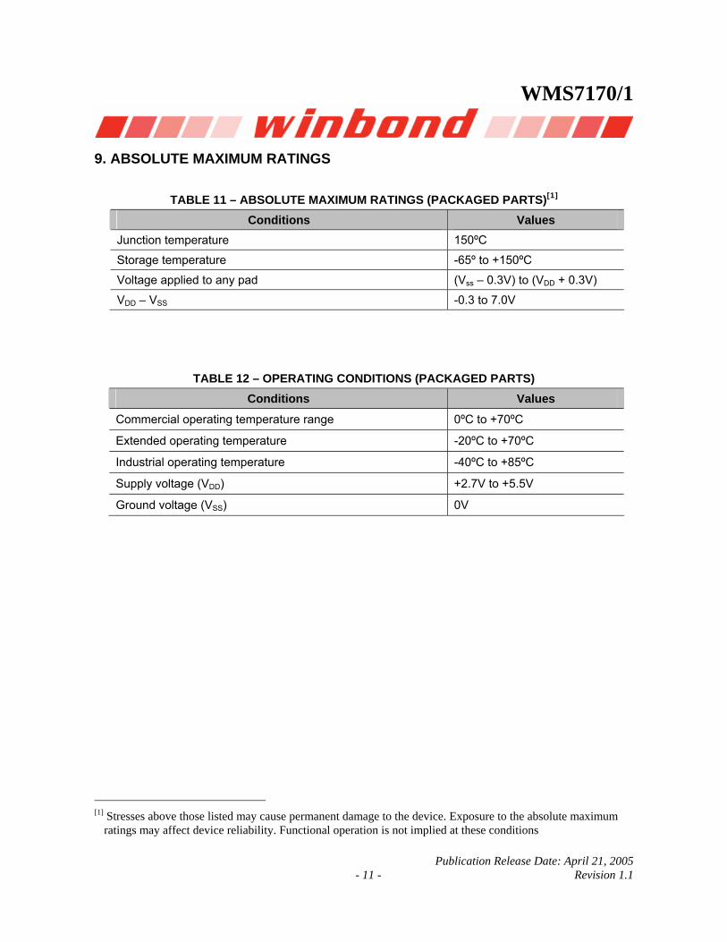
9. ABSOLUTE MAXIMUM RATINGS
TABLE 11 – ABSOLUTE MAXIMUM RATINGS (PACKAGED PARTS)[1]
Conditions Values Junction temperature 150ºC
Storage temperature -65º to +150ºC
Voltage applied to any pad (Vss – 0.3V) to (VDD + 0.3V)
VDD – VSS -0.3 to 7.0V
TABLE 12 – OPERATING CONDITIONS (PACKAGED PARTS) Conditions Values
Commercial operating temperature range 0ºC to +70ºC
Extended operating temperature -20ºC to +70ºC
Industrial operating temperature -40ºC to +85ºC
Supply voltage (VDD) +2.7V to +5.5V
Ground voltage (VSS) 0V
[ ]1 Stresses above those listed may cause permanent damage to the device. Exposure to the absolute maximum ratings may affect device reliability. Functional operation is not implied at these conditions
WMS7170/1
- 12 -
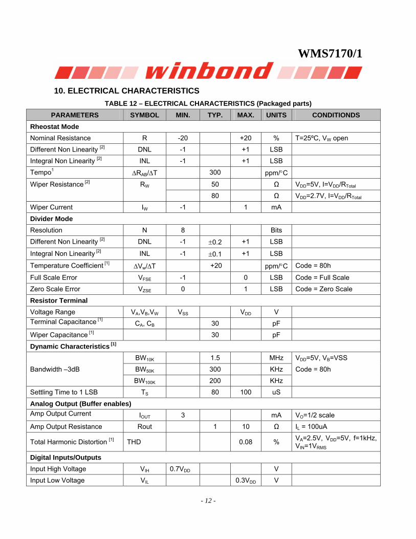
10. ELECTRICAL CHARACTERISTICS TABLE 12 – ELECTRICAL CHARACTERISTICS (Packaged parts)
PARAMETERS SYMBOL MIN. TYP. MAX. UNITS CONDITIONDS Rheostat Mode Nominal Resistance R -20 +20 % T=25ºC, VW open
Different Non Linearity [2] DNL -1 +1 LSB
Integral Non Linearity [2] INL -1 +1 LSB
Tempo1 ΔRAB/ΔT 300 ppm/°C
Wiper Resistance [2] RW 50 Ω VDD=5V, I=VDD/RTotal
80 Ω VDD=2.7V, I=VDD/RTotal
Wiper Current IW -1 1 mA
Divider Mode Resolution N 8 Bits
Different Non Linearity [2] DNL -1 ±0.2 +1 LSB
Integral Non Linearity [2] INL -1 ±0.1 +1 LSB
Temperature Coefficient [1] ΔVw/ΔT +20 ppm/°C Code = 80h
Full Scale Error VFSE -1 0 LSB Code = Full Scale
Zero Scale Error VZSE 0 1 LSB Code = Zero Scale
Resistor Terminal Voltage Range VA,VB,VB W VSS VDD V Terminal Capacitance [1]
CA, CBB 30 pF
Wiper Capacitance [1] 30 pF
Dynamic Characteristics [1] BW10K 1.5 MHz VDD=5V, VB=VSS B
Bandwidth –3dB BW50K 300 KHz Code = 80h
BW100K 200 KHz
Settling Time to 1 LSB TS 80 100 uS
Analog Output (Buffer enables) Amp Output Current IOUT 3 mA VO=1/2 scale
Amp Output Resistance Rout 1 10 Ω IL = 100uA
Total Harmonic Distortion [1] THD 0.08 % VA=2.5V, VDD=5V, f=1kHz, VIN=1VRMS
Digital Inputs/Outputs Input High Voltage VIH 0.7VDD V
Input Low Voltage VIL 0.3VDD V
WMS7170/1
Publication Release Date: April 21, 2005 - 13 - Revision 1.1
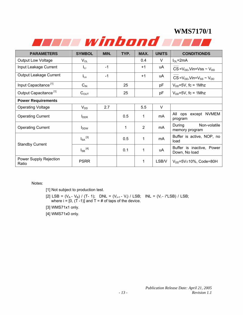
PARAMETERS SYMBOL MIN. TYP. MAX. UNITS CONDITIONDS Output Low Voltage VOL 0.4 V IOL=2mA
Input Leakage Current ILI -1 +1 uA CS =VDD,Vin=Vss ~ VDD
Output Leakage Current ILo -1 +1 uA CS =VDD,Vin=VSS ~ VDD
Input Capacitance [1] CIN 25 pF VDD=5V, fc = 1Mhz
Output Capacitance [1] COUT 25 pF VDD=5V, fc = 1Mhz
Power Requirements Operating Voltage VDD 2.7 5.5 V
Operating Current IDDR 0.5 1 mA All ops except NVMEM program
Operating Current IDDW 1 2 mA During Non-volatile memory program
ISA [3] 0.5 1 mA Buffer is active, NOP, no
load Standby Current
ISB [4] 0.1 1 uA Buffer is inactive, Power
Down, No load
Power Supply Rejection Ratio PSRR 1 LSB/V VDD=5V±10%, Code=80H
Notes:
[1] Not subject to production test. [2] LSB = (VA - VB) / (T- 1); DNL = (VB i+1 - Vi) / LSB; INL = (Vi - i*LSB) / LSB;
where i = [0, (T -1)] and T = # of taps of the device. [3] WMS71x1 only. [4] WMS71x0 only.
WMS7170/1
- 14 -
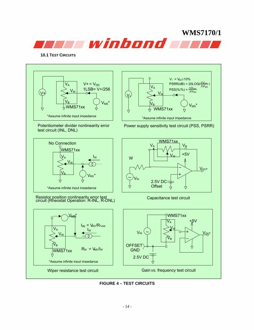
10.1 TEST CIRCUITS
FIGURE 4 – TEST CIRCUITS
Potentiometer divider nonlinearity error test circuit (INL, DNL)
*Assume infinite input impedance
V+
VMS*
V+ = VDD 1LSB= V+/256
WMS71xx
VA
VB B
VW
Resistor position nonlinearity error test circuit (Rheostat Operation: R-INL, R-DNL)
*Assume infinite input impedance
No Connection
V MS *
WMS71xx
WVA
VBB
VW
IW
WMS71xx
10%
Wiper resistance test circuit
*Assume infinite input impedance
V MS*
WMS71xx
VA
VBB
VW
IW I W = V DD /R Total
R W = V MS /I W
Power supply sensitivity test circuit (PSS, PSRR)
*Assume infinite input impedance
V+
V+ = V DD ±
VA
VBB
VW
VMS*
PSRR(dB) = 20LOG ( Δ VΔ
) MS VDD
PSS(%/% ) = VΔ M VΔ S
DD
WMS71xxVA VB B
VW
VIN~
+5V
V OUT
2.5V DCOffset
Capacitance test circuit
VA
VBB
WMS71xx
VW VIN ~
+5V
OFFSETGND
VOUT
2.5V DC
Gain vs. frequency test circuit

WMS7170/1
Publication Release Date: April 21, 2005 - 15 - Revision 1.1
11. TYPICAL APPLICATION CIRCUITS
Vin
VOUT = - VIN A
B
RR
RA = 256
D)(256RAB − , RB = B
256DRAB
RAB = Total resistance of potentiometer D = Wiper setting for WMS71XX
FIGURE 5 – PROGRAMMABLE INVERTING GAIN AMPLIFIER USING THE WMS7170/1
VOUT = VIN (1+A
B
RR
)
RA = 256
D)(256RAB − , RB = B
256DRAB
RAB = Total resistance of potentiometer D = Wiper setting for WMS71XX
FIGURE 6 – PROGRAMMABLE NON-INVERTING GAIN AMPLIFIER USING THE WMS7170/1
RA RB
WMS71XX _ VOUT OP
AMP+
VIN + VOUT OP AMP_
WMS71XX
RA RB B

WMS7170/1
- 16 -
VREF = 5.0v
GND
VREFH
WMS71xx
V+
I = 32mA
FIGURE 7 – WMS7170/1 TRIMMING VOLTAGE REFERENCE
INC\ CS\
RF Input
FILTER
L1 CHOKE
WMS71xx WINPOT
CS\U/D\INC\VSS
VA VW VB
VDD RF OUT
VDD
Q1
RF POWER AMP
C10.1uF
U/D\
C2
FIGURE 8 – WMS7170/1 RF AMP CONTROL
WMS7170/1
Publication Release Date: April 21, 2005 - 17 - Revision 1.1
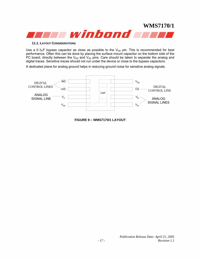
11.1. LAYOUT CONSIDERATIONS
Use a 0.1μF bypass capacitor as close as possible to the VDD pin. This is recommended for best performance. Often this can be done by placing the surface mount capacitor on the bottom side of the PC board, directly between the VDD and VSS pins. Care should be taken to separate the analog and digital traces. Sensitive traces should not run under the device or close to the bypass capacitors. A dedicated plane for analog ground helps in reducing ground noise for sensitive analog signals.
CAP
VDD
CS
VB
VW
INC
U/D
VA
VSS
ANALOGSIGNAL LINES
DIGITALCONTROL LINES
ANALOGSIGNAL LINE
DIGITALCONTROL LINE
FIGURE 9 – WMS7170/1 LAYOUT
WMS7170/1
- 18 -
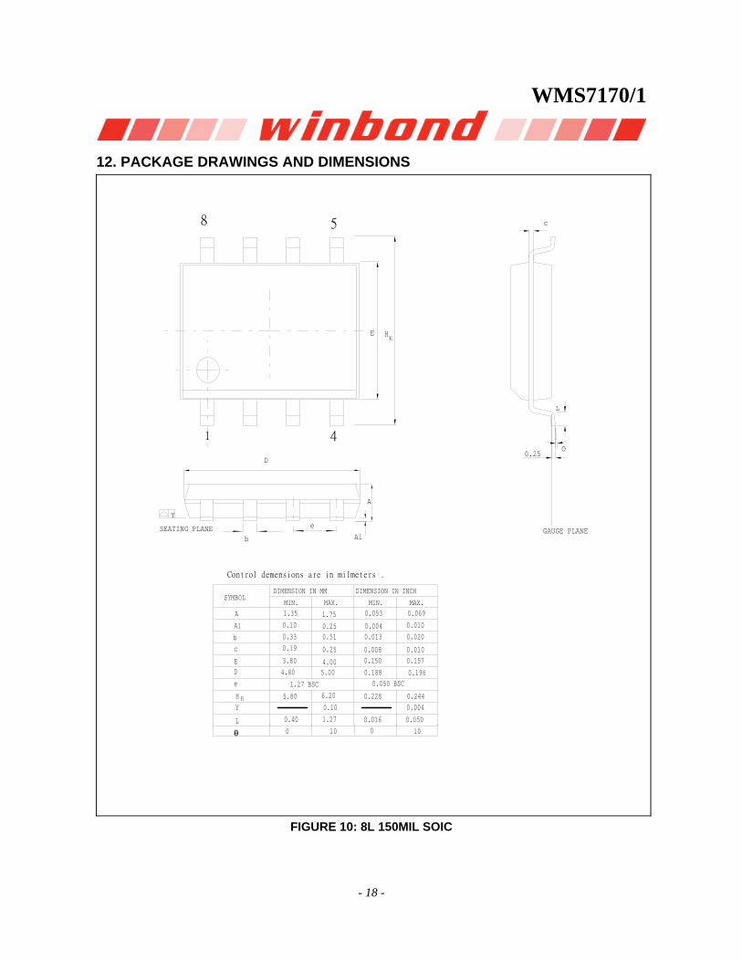
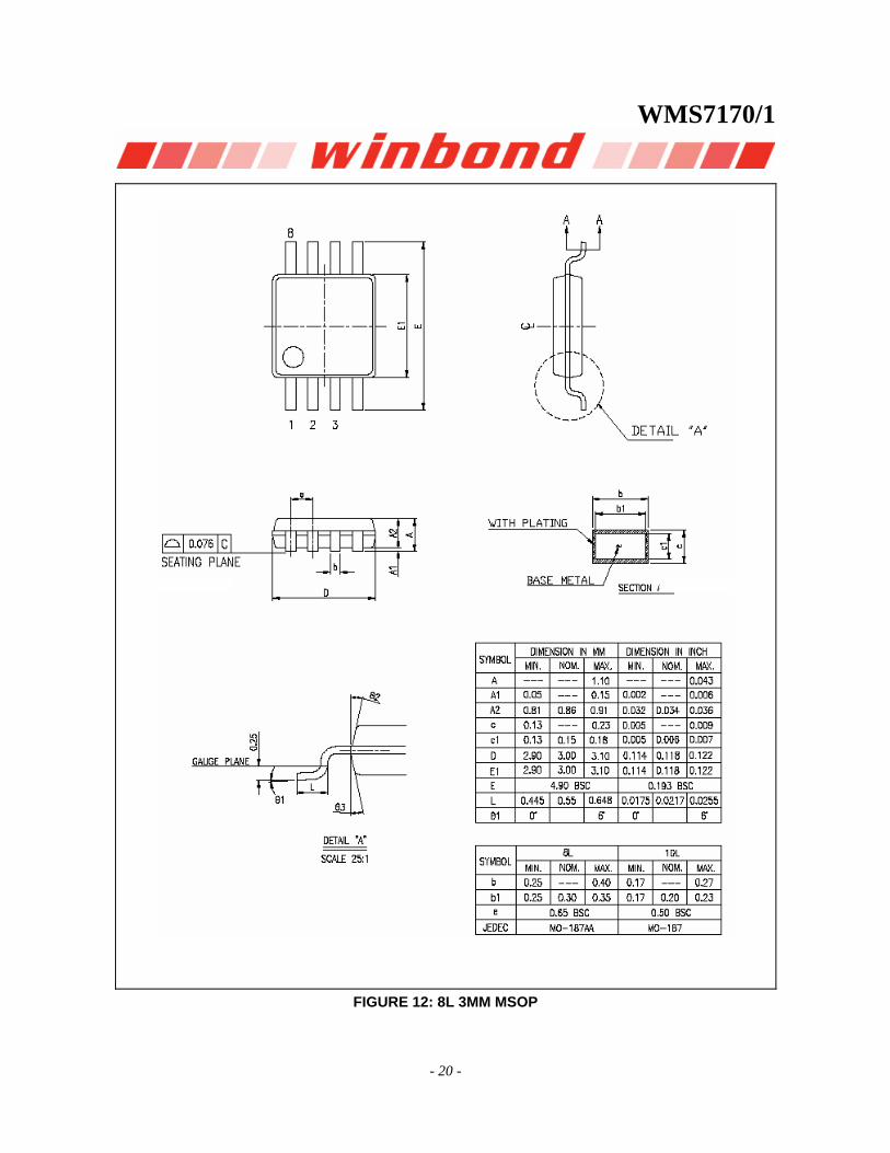
12. PACKAGE DRAWINGS AND DIMENSIONS
L
O
c
D
A1
A
e
bSEATING PLANE
Y
0.25
GAUGE PLANE
E HE
1
8 5
4
4.00
0.25
0.510.25
E
cbA1
3.80
0.190.330.10
0.1570.010
0.0200.010
0.1500.008
0.0130.004
MAX.DIMENSION IN MM
1.75A
SYMBOLMIN.1.35
DIMENSION IN INCH
0.069MIN.
0.053MAX.
Control demensions are in milmeters .
1.270.106.20
L
θ
YH
0 100.40
5.80
e 1.27 BSC
0.050
0.0040.244
00.016
0.228
10
0.050 BSC
E
D 4.80 5.00 0.188 0.196
FIGURE 10: 8L 150MIL SOIC
WMS7170/1
Publication Release Date: April 21, 2005 - 19 - Revision 1.1
1 .6 31 .4 70 .0 6 40 .0 5 8
S ym b o l M in N o m M a x M a xN o mM in
D im e n s io n in in c h D im e n s io n in m m
A
B c D
e
A L
S
A A
1 2
E
0 .0 6 0 1 .5 2
0 .1 75 4 .4 5
0 .0 10 0 .1 25 0 .0 16
0 .1 3 0
0 .0 1 8
0 .13 5
0 .02 2
3 .1 8
0 .4 1
0 .2 5
3 .3 0
0 .4 6
3 .4 3
0 .5 6
0 .0 08
0 .1 2 0 0 .3 75
0 .0 1 0
0 .1 3 0
0 .0 1 4
0 .14 0
0 .2 0
3 .0 5
0 .2 5
3 .3 0
0 .3 6
3 .5 6
0 .25 50 .2 5 00 .2 4 5 6 .4 86 .3 56 .2 2
9 .5 3
7 .6 27 .3 7 7 .8 70 .30 00 .2 90 0 .3 1 0
2 .2 9 2 .5 4 2 .7 90 .0 9 0 0 .1 0 0 0 .11 0
B 1
1
e
E 1 0 .3 6 0 0 .3 8 0 9 .1 4 9 .6 5
0 1 5
0 .0 45 1 .1 4
0 .3 5 50 .3 3 5 8 .5 1 9 .0 2
1 50
S e a tin g P la n e
e A
2 A c
E
B a s e P la n e1A
1 E
D
1 B B
1 e
L
A
S
8 5
1 4
α
α
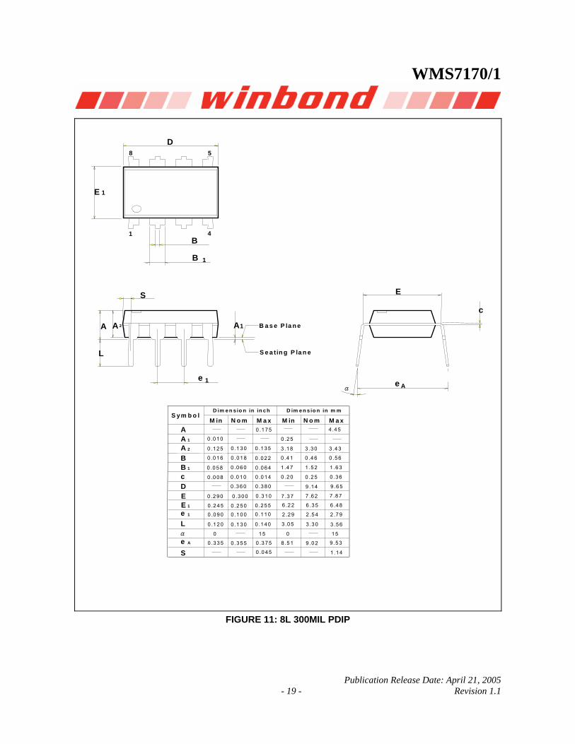
FIGURE 11: 8L 300MIL PDIP
WMS7170/1
- 20 -
FIGURE 12: 8L 3MM MSOP

WMS7170/1
Publication Release Date: April 21, 2005 - 21 - Revision 1.1
13. ORDERING INFORMATION Winbond’s WinPot Part Number Description:
T B RRR P Winbond WinPot Products w/ Up-Down Interface
Number Of Taps:
7 = 100
WMS71
For Up/Down interface:
0 : No buffer
1 : With buffer
End-to-end Resistance:
010: 10Kohm
050: 50Kohm
100: 100Kohm
Package:
S: SOIC
P: PDIP
M: MSOP
Output Buffer
End-to-End Resistance
SOIC PDIP MSOP
10K WMS7170010S WMS7170010P WMS7170010M
50K WMS7170050S WMS7170050P WMS7170050M
NO
100K WMS7170100S WMS7170100P WMS7170100M
10K WMS7171010S WMS7171010P WMS7171010M
50K WMS7171050S WMS7171050P WMS7171050M
YES
100K WMS7171100S WMS7171100P WMS7171100M
For the latest product information, access Winbond’s worldwide website at http://www.winbond-usa.com
WMS7170/1
- 22 -
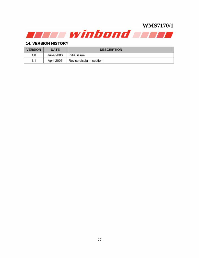
14. VERSION HISTORY VERSION DATE DESCRIPTION
1.0 June 2003 Initial issue
1.1 April 2005 Revise disclaim section

WMS7170/1
Publication Release Date: April 21, 2005 - 23 - Revision 1.1
Copyright© 2005, Winbond Electronics Corporation. All rights reserved. ChipCorder® and ISD® are trademarks of Winbond Electronics Corporation. SuperFlash® is the trademark of Silicon Storage Technology, Inc. All other trademarks are properties of their respective owners.
This datasheet and any future addendum to this datasheet is(are) the complete and controlling ISD® ChipCorder® product specifications. In the event any inconsistencies exist between the information in this and other product documentation, or in the event that other product documentation contains information in addition to the information in this, the information contained herein supersedes and governs such other information in its entirety. This datasheet is subject to change without notice.
The 100-year retention and 100K record cycle projections are based upon accelerated reliability tests, as published in the Winbond Reliability Report, and are neither warranted nor guaranteed by Winbond. This product incorporates SuperFlash®.
Application examples and alternative uses of any integrated circuit contained in this publication are for illustration only and Winbond makes no representation or warranty that such applications shall be suitable for the use specified.
The contents of this document are provided “AS IS”, and Winbond assumes no liability whatsoever and disclaims any express or implied warranty of merchantability, fitness for a particular purpose or infringement of any Intellectual property. In no event, shall Winbond be liable for any damages whatsoever (including, without limitation, damages for loss of profits, business interruption, loss of information) arising out of the use of or inability to use the contents of this documents, even if Winbond has been advised of the possibility of such damages.
The contents of this document are provided only as a guide for the applications of Winbond products. Winbond makes no representation or warranties with respect to the accuracy or completeness of the contents of this publication and reserves the right to discontinue or make changes to specifications and product descriptions at any time without notice. No license, whether express or implied, to any intellectual property or other right of Winbond or others is granted by this publication. Except as set forth in Winbond's Standard Terms and Conditions of Sale, Winbond assumes no liability whatsoever and disclaims any express or implied warranty of merchantability, fitness for a particular purpose or infringement of any Intellectual property.
Winbond customers using or selling these products for use in such applications do so at their own risk and agree to fully indemnify Winbond for any damages resulting from such improper use or sales.
Winbond products are not designed, intended, authorized or warranted for use as components in systems or equipment intended for surgical implantation, atomic energy control instruments, airplane or spaceship instruments, transportation instruments, traffic signal instruments, combustion control instruments, or for other applications intended to support or sustain life. Furthermore, Winbond products are not intended for applications wherein failure of Winbond products could result or lead to a situation wherein personal injury, death or severe property or environmental damage could occur.