SKYPER 52 R - Octopart
24
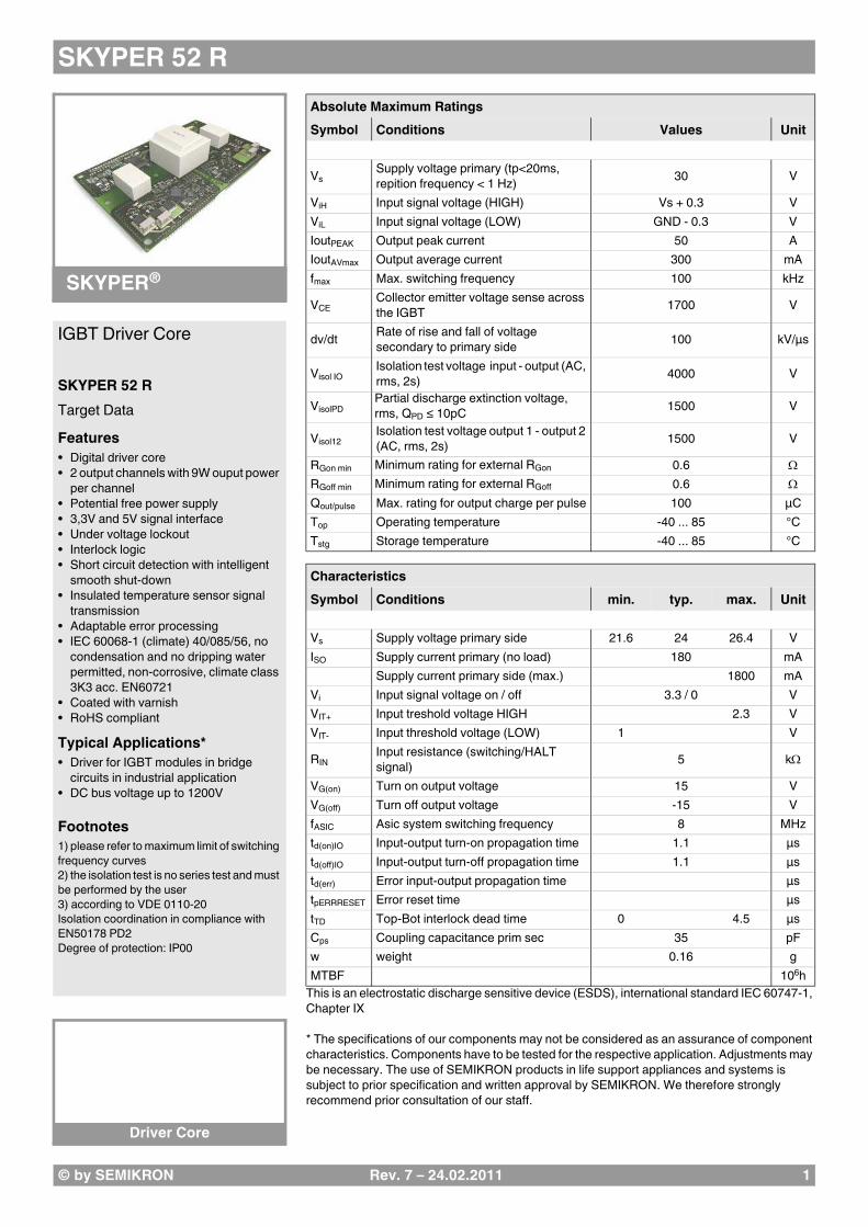
SKYPER 52 R © by SEMIKRON Rev. 7 – 24.02.2011 1 SKYPER ® Driver Core IGBT Driver Core SKYPER 52 R Target Data Features Digital driver core 2 output channels with 9W ouput power per channel Potential free power supply 3,3V and 5V signal interface Under voltage lockout Interlock logic Short circuit detection with intelligent smooth shut-down Insulated temperature sensor signal transmission Adaptable error processing IEC 60068-1 (climate) 40/085/56, no condensation and no dripping water permitted, non-corrosive, climate class 3K3 acc. EN60721 Coated with varnish RoHS compliant Typical Applications* Driver for IGBT modules in bridge circuits in industrial application DC bus voltage up to 1200V Footnotes 1) please refer to maximum limit of switching frequency curves 2) the isolation test is no series test and must be performed by the user 3) according to VDE 0110-20 Isolation coordination in compliance with EN50178 PD2 Degree of protection: IP00 This is an electrostatic discharge sensitive device (ESDS), international standard IEC 60747-1, Chapter IX * The specifications of our components may not be considered as an assurance of component characteristics. Components have to be tested for the respective application. Adjustments may be necessary. The use of SEMIKRON products in life support appliances and systems is subject to prior specification and written approval by SEMIKRON. We therefore strongly recommend prior consultation of our staff. Absolute Maximum Ratings Symbol Conditions Values Unit V s Supply voltage primary (tp<20ms, repition frequency < 1 Hz) 30 V V iH Input signal voltage (HIGH) Vs + 0.3 V V iL Input signal voltage (LOW) GND - 0.3 V Iout PEAK Output peak current 50 A Iout AVmax Output average current 300 mA f max Max. switching frequency 100 kHz V CE Collector emitter voltage sense across the IGBT 1700 V dv/dt Rate of rise and fall of voltage secondary to primary side 100 kV/µs V isol IO Isolation test voltage input - output (AC, rms, 2s) 4000 V V isolPD Partial discharge extinction voltage, rms, Q PD ≤ 10pC 1500 V V isol12 Isolation test voltage output 1 - output 2 (AC, rms, 2s) 1500 V R Gon min Minimum rating for external R Gon 0.6 R Goff min Minimum rating for external R Goff 0.6 Q out/pulse Max. rating for output charge per pulse 100 µC T op Operating temperature -40 ... 85 °C T stg Storage temperature -40 ... 85 °C Characteristics Symbol Conditions min. typ. max. Unit V s Supply voltage primary side 21.6 24 26.4 V I SO Supply current primary (no load) 180 mA Supply current primary side (max.) 1800 mA V i Input signal voltage on / off 3.3 / 0 V V IT+ Input treshold voltage HIGH 2.3 V V IT- Input threshold voltage (LOW) 1 V R IN Input resistance (switching/HALT signal) 5 k V G(on) Turn on output voltage 15 V V G(off) Turn off output voltage -15 V f ASIC Asic system switching frequency 8 MHz t d(on)IO Input-output turn-on propagation time 1.1 µs t d(off)IO Input-output turn-off propagation time 1.1 µs t d(err) Error input-output propagation time µs t pERRRESET Error reset time µs t TD Top-Bot interlock dead time 0 4.5 µs C ps Coupling capacitance prim sec 35 pF w weight 0.16 g MTBF 10 6 h
-
Upload
khangminh22 -
Category
Documents
-
view
0 -
download
0
Transcript of SKYPER 52 R - Octopart
SKYPER 52 R
© by SEMIKRON Rev. 7 – 24.02.2011 1
SKYPER®
Driver Core
IGBT Driver Core
SKYPER 52 R
Target Data
Features
Digital driver core
2 output channels with 9W ouput power
per channel
Potential free power supply
3,3V and 5V signal interface
Under voltage lockout
Interlock logic
Short circuit detection with intelligent
smooth shut-down
Insulated temperature sensor signal
transmission
Adaptable error processing
IEC 60068-1 (climate) 40/085/56, no
condensation and no dripping water
permitted, non-corrosive, climate class
3K3 acc. EN60721
Coated with varnish
RoHS compliant
Typical Applications*
Driver for IGBT modules in bridge
circuits in industrial application
DC bus voltage up to 1200V
Footnotes
1) please refer to maximum limit of switching
frequency curves
2) the isolation test is no series test and must
be performed by the user
3) according to VDE 0110-20
Isolation coordination in compliance with
EN50178 PD2
Degree of protection: IP00
This is an electrostatic discharge sensitive device (ESDS), international standard IEC 60747-1,
Chapter IX
* The specifications of our components may not be considered as an assurance of component
characteristics. Components have to be tested for the respective application. Adjustments may
be necessary. The use of SEMIKRON products in life support appliances and systems is
subject to prior specification and written approval by SEMIKRON. We therefore strongly
recommend prior consultation of our staff.
Absolute Maximum Ratings
Symbol Conditions Values Unit
VsSupply voltage primary (tp<20ms,
repition frequency < 1 Hz)30 V
ViH Input signal voltage (HIGH) Vs + 0.3 V
ViL Input signal voltage (LOW) GND - 0.3 V
IoutPEAK Output peak current 50 A
IoutAVmax Output average current 300 mA
fmax Max. switching frequency 100 kHz
VCECollector emitter voltage sense across
the IGBT1700 V
dv/dtRate of rise and fall of voltage
secondary to primary side100 kV/µs
Visol IOIsolation test voltage input - output (AC,
rms, 2s)4000 V
VisolPDPartial discharge extinction voltage,
rms, QPD ≤ 10pC1500 V
Visol12Isolation test voltage output 1 - output 2
(AC, rms, 2s)1500 V
RGon min Minimum rating for external RGon 0.6
RGoff min Minimum rating for external RGoff 0.6
Qout/pulse Max. rating for output charge per pulse 100 µC
Top Operating temperature -40 ... 85 °C
Tstg Storage temperature -40 ... 85 °C
Characteristics
Symbol Conditions min. typ. max. Unit
Vs Supply voltage primary side 21.6 24 26.4 V
ISO Supply current primary (no load) 180 mA
Supply current primary side (max.) 1800 mA
Vi Input signal voltage on / off 3.3 / 0 V
VIT+ Input treshold voltage HIGH 2.3 V
VIT- Input threshold voltage (LOW) 1 V
RINInput resistance (switching/HALT
signal)5 k
VG(on) Turn on output voltage 15 V
VG(off) Turn off output voltage -15 V
fASIC Asic system switching frequency 8 MHz
td(on)IO Input-output turn-on propagation time 1.1 µs
td(off)IO Input-output turn-off propagation time 1.1 µs
td(err) Error input-output propagation time µs
tpERRRESET Error reset time µs
tTD Top-Bot interlock dead time 0 4.5 µs
Cps Coupling capacitance prim sec 35 pF
w weight 0.16 g
MTBF 106h

SKYPER® 52 R
2011-02-24 – Rev07 © by SEMIKRON
2
Technical Explanations
Revision 07 Status: preliminary Prepared by: Johannes Krapp
This Technical Explanation is valid for the following parts: Related Documents:
part number: L50450XX (PCB Nr), L610030XX (Article Nr) title: Data Sheet SKYPER® 52 R
date code (YYWW): ≥ 1040
SKYPER® 52 R
1. Content
1. Content .......................................................................................................................................................... 2
2. Revision History ........................................................................................................................................... 3
3. Introduction .................................................................................................................................................. 3
31. Handling Instructions ............................................................................................................................... 3
32. Block Diagram ........................................................................................................................................... 4
33. Mechanical Data ........................................................................................................................................ 5
4. Pinning .......................................................................................................................................................... 6
41. Primary SidePIN Array X10, X20 ............................................................................................................. 6
42. Secondary Side PIN Array X100, X101, X200, 201 ................................................................................. 8
5. Primary Side interface ............................................................................................................................... 10
51. Digital Input Signals ...............................................................................................................................10
52. Power Supply ..........................................................................................................................................11
53. Failure Management ...............................................................................................................................12
54. System Diagnostic Indication by LED ..................................................................................................12
55. Halt Logic Signal (HLS) ..........................................................................................................................14
56. Under Voltage Protection (UVP) primary .............................................................................................15
57. Overfrequency Monitoring (OFM) .........................................................................................................15
58. Dead Time generation (Interlock high / low side) adjustable (DT) ....................................................15
6. Seoncdary Side interface .......................................................................................................................... 16
61. Short Circuit Protection by VCEsat monitoring / de-saturation monitoring (SCP) .........................16
62. Adjustment of DSCP ...............................................................................................................................16
63. External Boost Capacitors (BC) ............................................................................................................17
64. Gate Resistors ........................................................................................................................................18
65. Gate Clamping ........................................................................................................................................18
66. Under Voltage Protection secondary ...................................................................................................19
67. Temperature Sensing .............................................................................................................................19
68. IntelliOFF .................................................................................................................................................20
7. Driver Performance .................................................................................................................................... 22
71. Insulation .................................................................................................................................................23
72. Isolation Test Voltage .............................................................................................................................23
73. Environmental Conditions .....................................................................................................................23
8. Marking ....................................................................................................................................................... 24
9. Status Definition ......................................................................................................................................... 24
SKYPER® 52 R
2011-02-24 – Rev07 © by SEMIKRON
3
2. Revision History
Revision Date Changes
00 2008-07-16 Initial target / advanced technical documentation.
01 2008-11-10 Initial target / advanced technical documentation. Additional chapters
02 2009-04-03 Target / specification of product features
03 2009-09-24 Target/ specification of product features/ temperature sensing
04 2010-05-03 Preliminary/Modification Performance Diagramm/ Dimensions+Drill Sizes/ Update Pinning
05 2010-08-20 Update LED
06 2010-09-23 Update structure, changed boot time, changed failure logic, tolerance of power supply
07 2011-02-24 Update LED, Exchange Slot 7 and 8
3. Introduction The SKYPER 52 driver core constitutes an interface between IGBT module and the controller. This driver core is based on fully digital signal processing and provides individual control parameter settings and drives parallel connected. The differential signal processing ensures a high level of signal integrity and hence high noise rejection. With the digital driver SKYPER 52, switching characteristics, shut down levels, as well as error processing can be set to meet the given application requirements. This means flexibility with the driver circuitry properties and, consequently, the control settings for the power electronics, which can be adapted to meet the individual needs. If an error is detected, this then means that all of the power transistors can be switched off either individually or sequentially. Overvoltages, especially those that occur in short-circuit turn-off conditions, are reduced by the IGBT driver. To do so, the driver switches the power transistor smoothly. This is possible by intelligent turn-off control.
SKYPER® 52
Two output channels with 9W output per channel
Up to 1700V VCE
Integrated potential free power supply for secondary side
Matched propagation delay for all outputs
UVP (primary & secondary), Interlock logic , Halt logic signal
Intelligent smooth turn off
Failure processing with individual adaptation
DC bus voltage up to 1200V
Coated with varnish
31. Handling Instructions Please provide for static discharge protection during handling. As long as the driver board is not completely assembled,
the input terminals have to be short-circuited. Persons working with devices have to wear a grounded bracelet. Any synthetic floor coverings must not be statically chargeable. Even during transportation the input terminals have to be short-circuited using, for example, conductive rubber. Worktables have to be grounded. The same safety requirements apply to MOSFET- and IGBT-modules.
It is important to feed any errors back to the control circuit and to switch off the device immediately in failure events. Repeated turn-on of the IGBT into a short circuit with a high frequency may destroy the device.
The inputs of the driver boards are sensitive to over-voltage. Voltages higher than specified level +0,3V or below -0,3V may destroy these inputs. Therefore, control signal over-voltages exceeding the above values have to be avoided.
For design support please read the SEMIKRON Application Manual Power Modules and SEMIKRON Application Notes available at www.SEMIKRON.com or consult your responsible sales contact.
Please note:
Unless otherwise specified, all values in this technical explanation are typical values. Typical values are the average values expected in large quantities and are provided for information purposes only. These values can and do vary in different applications. All operating parameters should be validated by user’s technical experts for each application.

SKYPER® 52 R
2011-02-24 – Rev07 © by SEMIKRON
4
32. Block Diagram
SKYPER 52
Primary Control
Digital Signal Converter
Modem
Modem
Power Supply
Secondary ControlHigh Side
incl. Under Voltage
Protection, IntelliOff
Secondary ControlLow Side
incl. Under Voltage
Protection, IntelliOff
Gate DriverHigh Side
Gate Signal ConverterHigh Side
Desat DetectHigh Side
Active Gate Control / Clamp
Gate DriverLow Side
Gate Signal ConverterLow Side
Active Gate Control / Clamp
Desat DetectLow Side
Temp. Detect
Power Supply
VP
GND
HALT_TX
DIAG_TX
HALT_RX
DIAG_RX
BOT_RX
TOP_RX
R_DEADTIME
ERROROFF_OFF
V3P3
GND
GND
TOP_VCE_INTOP_CFG_INTOP_CFG_OUTTOP_GATINGTIME
TOP_GATE_CLMP
TOP_GATE_ON
TOP_GATE_OFFTOP_GATE_SOFTOFFTOP_VPTOP_VNTOP_GNDTOP_V3P3TOP_ERROROFF_OFFTOP_INTELLIOFFTOP_TEMP_PTOP_TEMP_N
BOT_CFG_INBOT_CFG_OUTBOT_GATINGTIME
BOT_VCE_IN
BOT_GATE_CLMP
BOT_GATE_OFFBOT_GATE_SOFTOFFBOT_VPBOT_VN
BOT_GATE_ON
BOT_GND
BOT_V3P3BOT_ERROROFF_OFFBOT_INTELLIOFF

SKYPER® 52 R
2011-02-24 – Rev07 © by SEMIKRON
5
33. Mechanical Data
Dimensions in mm (top view)
Soldering Hints Finished Hole & Pad Size in mm
The temperature of the solder must not exceed 260°C, and solder time must not exceed 10 seconds.
The ambient temperature must not exceed the specified maximum storage temperature of the driver.
The solder joints should be in accordance to IPC A 610 Revision D (or later) - Class 3 (Acceptability of Electronic Assemblies) to ensure an optimal connection between driver core and printed circuit board
The driver is not suited for hot air reflow or infrared reflow processes.
Ø 1,1 ±0,05
pad size: min. 1,8
Use of Support Posts
The connection between driver core and printed circuit board should be mechanical reinforced by using support posts.
The driver board has got ten holes for supports posts.
Using support posts with external screw thread improves mechanical assembly.
Product information of suitable support posts and distributor contact information is available at e.g. http://www.richco-inc.com or http://www.ettinger.de.
Drill Size in mm
Ø
35
,00
35
,00
±0,2mm unless otherwise noted
X100 X101 X201 X200
X20 X10
3,18
SKYPER 52
Printed Ciruit Board
Support post with external screw thread
Hole for support post

SKYPER® 52 R
2011-02-24 – Rev07 © by SEMIKRON
6
4. Pinning 41. Primary SidePIN Array X10, X20
Connector X10, X20 (Male headers soldering technique)
6
0,635
2,54
Grid: 2,54mm
Connection type: soldering
Surface: selective gold-plated
Male cross-section: square 0,635
1
28
1
14
PIN Signal Function Specification
X10:01 ERROROFF_OFF Disable shut-down output signal LOW (connection to ground) = enable shut-down output signal HIGH (connection to V3P3) = disable shut-down output signal
X10:02 VP Driver core power supply. Bypass with low ESR capacitor and place as close to VP pin as possible.
Supply voltage +24VDC ( 10%)
X10:03 GND Ground
X10:04 V3P3 Reference voltage for ERROROFF_OFF, DEADTIME_OFF
Terminated with 1kΩ
X10:05 GND Ground
X10:06 HALT_TX_N Differential driver core status output. This output pair is the differential status signal output from the core.
Open collector output to GND
Umax=5,5V; Imax=10mA LOW = Ready to operate HIGH = Not ready to operate
X10:07 HALT_TX_P Open collector output to 3,3V
X10:08 GND Ground
X10:09 DIAG_TX_P Reserved. Do not connect.
X10:10 HALT_RX_P Differential driver core status input. This input pair (HALT_RX_P, HALT_RX_N) is the differential status signal input to the core.
Digital 3,3/5V logic LOW = enable driver core HIGH = disable driver core
X10:11 DIAG_RX_P Reserved. Do not connect.
X10:12 BOT_RX_P Differential switching signal input low side. This input pair (BOT_RX_P, BOT_RX_N) is the differential signal input to the core.
Digital 3,3/5V logic LOW = low side transistor off HIGH = low side transistor on
X10:13 TOP_RX_P Differential switching signal input high side. This input pair (TOP_RX_P, TOP_RX_N) is the differential signal input to the core.
Digital 3,3/5V logic LOW = high side transistor off HIGH = high side transistor on
X10:14 GND Ground
X10:15 GND Ground
X10:16 TOP_RX_N Differential switching signal input high side. This input pair (TOP_RX_P, TOP_RX_N) is the differential signal input to the core.
Digital 3,3/5V logic LOW = high side transistor on HIGH = high side transistor off
X10:17 BOT_RX_N Differential switching signal input low side. This input pair (BOT_RX_P, BOT_RX_N) is the differential signal input to the core.
Digital 3,3/5V logic LOW = low side transistor on HIGH = low side transistor off
X10:18 DIAG_RX_N Reserved. Do not connect.
X10:19 HALT_RX_N Differential driver core status input. This input pair (HALT_RX_P, HALT_RX_N) is the differential status signal input to the core.
Digital 3,3/5V logic
LOW = disable driver core HIGH = enable driver core
SKYPER® 52 R
2011-02-24 – Rev07 © by SEMIKRON
7
X10:20 DIAG_TX_N Reserved. Do not connect.
X10:21 GND Ground
X10:22 GND Ground
X10:23 R_DEADTIME Adjustment of locking time. External resistor to ground.
X10:24 GND Ground
X10:25 V3P3 Reference voltage for ERROROFF_OFF, DEADTIME_OFF
Terminated with 1kΩ
X10:26 GND Ground
X10:27 VP Driver core power supply. Bypass with low ESR capacitor and place as close to VP pin as possible.
Supply voltage +24VDC ( 10%)
X10:28 DEADTIME_OFF Disable interlock logic. LOW (connection to ground) = enable interlock logic HIGH (connection to V3P3) = disable interlock logic
X20:01 ~ X20:14
GND Ground

SKYPER® 52 R
2011-02-24 – Rev07 © by SEMIKRON
8
42. Secondary Side PIN Array X100, X101, X200, 201
Connector X100, X101, X200, X201 (Male headers soldering technique)
6
0,635
2,54
Grid: 2,54mm
Connection type: soldering
Surface: selective gold-plated
Male cross-section: square 0,635
1
14
PIN Signal Function Specification
X100:01 TOP_GND Ground for power supply Connection to emitter (high side)
X100:02 TOP_GATE_SOFTOFF Control input for smooth shut-down setting (high side)
External resistor to gate (high side)
X100:03 TOP_VN Output power supply for external boost capacitors (high side)
Typ. -15V; Max. -18V
X100:04 TOP_GATE_OFF Switch off signal high side transistor Connection to gate (high side)
X100:05 TOP_VP Output power supply for external boost capacitors (high side)
Typ. -+15V; Max. +18V
X100:06 TOP_GATE_ON Switch on signal high side transistor Connection to gate (high side)
X100:07 TOP_GND Ground for power supply Connection to emitter (high side)
X100:08 TOP_GND Ground for power supply Connection to emitter (high side)
X100:09 TOP_GATE_ON Switch on signal high side transistor Connection to gate (high side)
X100:10 TOP_VP Output power supply for external boost capacitors (high side)
Typ. +15V; Max. +18V
X100:11 TOP_GATE_OFF Switch off signal high side transistor Connection to gate (high side)
X100:12 TOP_VN Output power supply for external boost capacitors (high side)
Typ. -15V; Max. -18V
X100:13 TOP_GATE_SOFTOFF Control input for smooth shut-down setting (high side)
External resistor to gate (high side)
X100:14 TOP_GND Ground for power supply Connection to emitter (high side)
X101:01 TOP_GATE_CLMP Gate voltage clamping (high side)
X101:02 TOP_GND Ground for power supply Connection to emitter (high side)
X101:03 TOP_ERROROFF_OFF Disable shut-down output signal LOW (connection to ground) = enable shut-down output signal HIGH (connection to TOP_V3P3) = disable shut-down output signal
X101:04 TOP_INTELLIOFF Intelligent shut-down setting (high side) External resistor to ground
X101:05 TOP_V3P3 Reference voltage for TOP_ERROROFF_OFF
Terminated with 1kΩ
X101:06 TOP_TEMP_P Temperature sensor positive input Temperature dependent resistor between TOP_TEMP_P and TOP_TEMP_N; RTEMP<430Ω
General error input Generic failure input. Pull up resistor 511Ω
Failure -> over 1,5V
No failure -> under 1,5V
X101:07 TOP_GND Ground for power supply Connection to emitter (high side)
X101:08 TOP_GND Ground for power supply Connection to emitter (high side)

SKYPER® 52 R
2011-02-24 – Rev07 © by SEMIKRON
9
X101:09 TOP_TEMP_N Temperature sensor negative input Connected to ground
X101:10 TOP_GATINGTIME Blanking time setting of short circuit detection (high side)
External resistor to ground
X101:11 TOP_VCE_CFG_IN Threshold voltage setting of short circuit detection (high side)
Resistor between TOP_VCE_CFG_IN and TOP_VCE_CFG_OUT
X101:12 TOP_VCE_CFG_OUT
X101:13 TOP_GND Ground for power supply Connection to emitter (high side)
X101:14 TOP_VCE_IN Input short circuit detection (high side) Connected to auxiliary collector (high side)
X200:01 BOT_GND Ground for power supply Connection to emitter (low side)
X200:02 BOT_GATE_ON Switch on signal low side transistor Connection to gate (low side)
X200:03 BOT_VP Output power supply for external boost capacitors (low side)
Typ. +15V; Max. +18V
X200:04 BOT_GATE_OFF Switch off signal high side transistor Connection to gate (low side)
X200:05 BOT_VN Output power supply for external boost capacitors (low side)
Typ. -15V; Max. -18V
X200:06 BOT_GATE_SOFTOFF Control input for smooth shut-down setting (low side)
External resistor to gate (low side)
X200:07 BOT_GND Ground for power supply Connection to emitter (low side)
X200:08 BOT_GND Ground for power supply Connection to emitter (low side)
X200:09 BOT_GATE_SOFTOFF Control input for smooth shut-down setting (low side)
External resistor to gate (low side)
X200:10 BOT_VN Output power supply for external boost capacitors (low side)
Typ. -15V; Max. -18V
X200:11 BOT_GATE_OFF Switch off signal high side transistor Connection to gate (low side)
X200:12 BOT_VP Output power supply for external boost capacitors (low side)
Typ. +15V; Max. -18V
X200:13 BOT_GATE_ON Switch on signal low side transistor Connection to gate (low side)
X200:14 BOT_GND Ground for power supply Connection to emitter (low side)
X201:01 BOT_GND Ground for power supply Connection to emitter (low side)
X201:02 BOT_GND Ground for power supply Connection to emitter (low side)
X201:03 BOT_V3P3 Reference voltage for BOT_ERROROFF_OFF
Terminated with 1kΩ
X201:04 BOT_INTELLIOFF Intelligent shut-down setting (low side) External resistor to ground
X201:05 BOT_ERROROFF_OFF Disable shut-down output signal LOW (connection to ground) = enable shut-down output signal HIGH (connection to BOT_V3P3) = disable shut-down output signal
X201:06 BOT_GND Ground for power supply Connection to emitter (low side)
X201:07 BOT_GATE_CLMP Gate voltage clamping (low side)
X201:08 BOT_VCE_IN Input short circuit detection (low side) Connected to auxiliary collector (low side)
X201:09 BOT_GND Ground for power supply Connection to emitter (low side)
X201:10 BOT_VCE_CFG_OUT Threshold voltage setting of short circuit detection (high side)
Resistor between BOT_VCE_CFG_IN and BOT_VCE_CFG_OUT
X201:11 BOT_VCE_CFG_IN
X201:12 BOT_GATINGTIME Blanking time setting of short circuit detection (low side)
External resistor to ground
X201:13 BOT_GND Ground for power supply Connection to emitter (low side)
X201:14 BOT_GND Ground for power supply Connection to emitter (low side)

SKYPER® 52 R
2011-02-24 – Rev07 © by SEMIKRON
10
5. Primary Side interface The ground potentials on the driver board are equal and all physically connected with each other on the printed circuit board. Because of the voltage drop on the power supply cable, the potential of power supply ground at the user side is different to the ground potential on the driver board.
51. Digital Input Signals The signal inputs for high side and low side are compatible with 3.3V and 5V I/O standards. This means that the driver circuit can be directly connected to standard logic outputs of microcontroller or DSP without additional level shifting. To obtain high performance and reliable signal transmission in a power electronic environment, differential signalling is used for the inputs.
Application Example - Connection µC / DSP with User Interface
User Side
TOP_RX_P
TOP_RX_N
PWM INPUT TOP(from controller)
1K
1K
1K
1K
BOT_RX_P
BOT_RX_N
PWM INPUT BOT(from controller)
1K
1K
1K
1K
SKYPER 52 R
4,75K
4,75K
4,75K
4,75K
The application example shows a circuit in push-pull configuration for high and lows side input. The termination resistors are ~5k ohm. To simplify the interface with less EMC robustness following circuit can be used for standard PWM:
User Side
TOP_RX_P
TOP_RX_N
PWM INPUT TOP(from controller)
BOT_RX_P
BOT_RX_N
PWM INPUT BOT(from controller)
To increase the EMC robustness following circuit with differential signals coming out of the controller can be used:
User Side
TOP_RX_P
TOP_RX_N
PWM INPUT TOP(from controller)
PWM INPUT TOP(from controller)
SKYPER 52 R
BOT_RX_P
BOT_RX_N
PWM INPUT BOT(from controller)
PWM INPUT BOT(from controller)
Please note:
It is not permitted to apply switching pulses shorter than 2µs.
Please note:
Do not remove the plug with applied voltage of the power supply. This can lead to unspecified voltage levels at the output stages of the driver board with the risk of destructions.

SKYPER® 52 R
2011-02-24 – Rev07 © by SEMIKRON
11
52. Power Supply A few basic rules should be followed when dimensioning the user side power supply for the driver board. The following table shows the required features of an appropriate power supply.
Requirements of the auxiliary power supply
Power supply +24V ±10%
Maximum rise time of auxiliary power supply 50ms
Minimum peak current of auxiliary supply 1,5A
Power on reset completed after (typ.) 3s
The supplying switched mode power supply may not be turned-off for a short time as consequence of its current limitation. Its output characteristic needs to be considered. Switched mode power supplies with fold-back characteristic or hiccup-mode can create problems if no sufficient over current margin is available. The voltage has to rise continuously and without any plateau formation. If the power supply is able to provide a higher current, a peak current will flow in the first instant to charge up the input capacitances on the driver. Its peak current value will be limited by the power supply and the effective impedances (e.g. distribution lines), only. It is recommended to avoid the paralleling of several customer side power supply units. Their different set current limitations may lead to dips in the supply voltage. The driver board is ready for operation typically 3s after turning on the supply voltage. The driver status signal HALT_RX and HALT_TX is operational after this time. Without any error present, the HALT_TX signal will be reset. To assure a high level of system safety the high and low side, signal inputs should stay in a defined state (OFF state) during driver turn-on time. Only after the end of the power-on-reset, IGBT operation shall be permitted.
Connection of Stabilizing Capacitor
User Side
VP
GND
CVP+24V
VP should be additionally stabilized by low ESR capacitor CVP. This capacitor has to be placed as close to VP pins as possible.
Dimension of CVP:
CVP > 200 Cies
Cies is the input capacitance of connected power semiconductor (see power semiconductor data sheet).
CVP should be minimum 220µF/100V.
Please note:
Do not apply switching signals during power on reset.

SKYPER® 52 R
2011-02-24 – Rev07 © by SEMIKRON
12
53. Failure Management A failure caused by under voltage protection (primary and secondary), critical frequency monitoring, short circuit protection or temperature protection will force HALT_TX into LOW state (not ready to operate) and set the error latch. The IGBTs will be switched off (IGBT driving signals set to LOW) and switching pulses from the controller will be not transferred to the output stage. At the same time an internal timer with a time constant of 20s is started. If no failure is present anymore, a time of minimum 20s after failure detection is passed, the driver board is ready to operate and switching signals are transferred to the output stage again.
The shut-down of all connected IGBTs in case of detected failure event can be disabled by using the ERROROFF_OFF function. If this function is activated, a detected failure is indicated at HALT_TX. The shut-down has to be forced by the user.
Failure management by controller: Enabling ERROROFF_OFF Failure management by driver
User Side
ERROROFF_OFF
V3P3
User SideTOP_ERROROFF_OFF
TOP_V3P3
BOT_ERROROFF_OFF
BOT_V3P3
If the shut-down should be forced by the driver, ERROROFF_OFF must be connected to GND, TOP_ERROROFF_OFF must be connected to TOP_GND and BOT_ERROROFF_OFF must be connected to BOT_GND.
54. System Diagnostic Indication by LED The system status during system power on, normal operation or failure event are illuminated by three tri-colours LEDs (LED 0 (V12) on primary side, LED 1 (V105) on secondary side for high side switch, LED 2 (V205) on secondary side for low side switch) on the driver board. The LEDs indicate the following conditions.
Diagnostic Code – System Start
LED 0 (V12) Description
green, flashes System is starting and checking supply voltages.
red, flashes Supply voltage < Vs min.
yellow, flashes Failure during system start. Automatic restart after 10 seconds and Vs > threshold level for reset.
LED 1 (V105), LED 2 (V205) Description
yellow, flashes System is starting and waiting for configuration of secondary side.
Diagnostic Code – Normal Operation
LED 0 (V12) Description
green, steady on System is working. No system failures occur since last system start.
LED 1 (V105), LED 2 (V205) Description
green, steady on System is working. No system failures occur since last system start.
Please note:
With activating the ERROROFF_OFF function, the user is responsible for protection shut-down of the IGBTs.

SKYPER® 52 R
2011-02-24 – Rev07 © by SEMIKRON
13
Diagnostic Code – Failure Type Indication after Failure Event on Primary Side
LED 0 (V12) is illuminating ten flashes with a frequency of 1Hz. After no illumination for three seconds, the flashing sequence is repeated. The failure indication is illuminated until the driver is rebooted (turn-off of internal power supply).
Examples for LED 0 (V12):
Flashing sequence Description
Failure caused by critical oscillation of input signal is present.
Failure caused by under voltage supply, but is not present anymore.
LED 0 (V12)
Flash 1 Flash 2 Flash 3 Flash 4 Flash 5
Status HALT signal from customer
Status oscillation failure (>100kHz)
Failure of signal transmission sec to
prim
Failure secondary side
Under voltage supply
Flash 6 Flash 7 Flash 8 Flash 9 Flash 10
Status Short circuit or internal supply under
voltage
Over current at primary power
supply
Overvoltage at generic Analogue input (High Side)
Switching Signal TOP/BOT while
system is resetting
Internal Error
LED 0 (V12) (colour of the flash) Description
green OK. No failure.
yellow Failure was occurred, but failure is not present anymore.
red Failure is present.
Diagnostic Code – Failure Type Indication after Failure Event on Secondary Side
LED 1 (V105) and LED 2 (V205) are illuminating five flashes with a frequency of 1Hz. After no illumination for three seconds, the flashing sequence is repeated. The failure indication is illuminated until reconfiguration of the secondary side (turn-off of internal power supply).
Examples for LED 1 (V105), LED 2 (V205):
Flashing sequence Description
Failure caused by under voltage +15V is present.
Failure caused by under voltage -15V happened, but is not present anymore.
LED 1 (V105), LED 2 (V205)
flash 1 flash 2 flash 3 flash 4 flash 5
Short circuit of IGBT Status failure of power supply
Status under voltage +15V
Status under voltage -15V
Internal Error
LED 1 (V105), LED 2 (V205) (colour of the flash) Description
green OK. No failure.
yellow Failure was occurred, but failure is not present anymore.
red Failure is present.
SKYPER® 52 R
2011-02-24 – Rev07 © by SEMIKRON
14
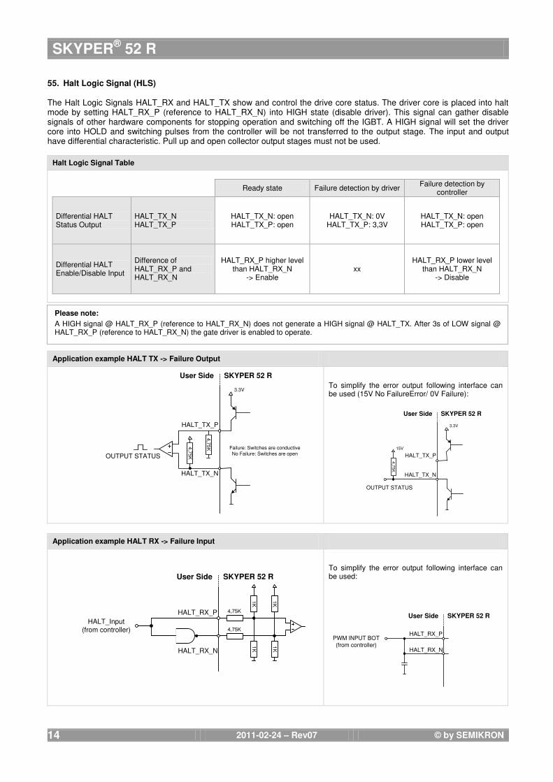
55. Halt Logic Signal (HLS) The Halt Logic Signals HALT_RX and HALT_TX show and control the drive core status. The driver core is placed into halt mode by setting HALT_RX_P (reference to HALT_RX_N) into HIGH state (disable driver). This signal can gather disable signals of other hardware components for stopping operation and switching off the IGBT. A HIGH signal will set the driver core into HOLD and switching pulses from the controller will be not transferred to the output stage. The input and output have differential characteristic. Pull up and open collector output stages must not be used.
Halt Logic Signal Table
Ready state Failure detection by driver
Failure detection by controller
Differential HALT Status Output
HALT_TX_N HALT_TX_P
HALT_TX_N: open HALT_TX_P: open
HALT_TX_N: 0V HALT_TX_P: 3,3V
HALT_TX_N: open HALT_TX_P: open
Differential HALT Enable/Disable Input
Difference of HALT_RX_P and HALT_RX_N
HALT_RX_P higher level than HALT_RX_N
-> Enable xx
HALT_RX_P lower level than HALT_RX_N
-> Disable
Application example HALT TX -> Failure Output
To simplify the error output following interface can be used (15V No FailureError/ 0V Failure):
Application example HALT RX -> Failure Input
To simplify the error output following interface can be used:
Please note:
A HIGH signal @ HALT_RX_P (reference to HALT_RX_N) does not generate a HIGH signal @ HALT_TX. After 3s of LOW signal @ HALT_RX_P (reference to HALT_RX_N) the gate driver is enabled to operate.
HALT_RX_P
HALT_RX_N
PWM INPUT BOT(from controller)
User Side SKYPER 52 R
User Side
HALT_RX_P
HALT_RX_N
HALT_Input(from controller)
1K
1K
1K
1K
SKYPER 52 R
4,75K
4,75K
HALT_TX_P
HALT_TX_N
OUTPUT STATUS
User Side SKYPER 52 R
3.3V
15V
4,7
5K
HALT_TX_P
HALT_TX_N
OUTPUT STATUS
User Side SKYPER 52 R
3.3V
Failure: Switches are conductiveNo Failure: Switches are open
4,7
5K
4,7
5K

SKYPER® 52 R
2011-02-24 – Rev07 © by SEMIKRON
15
56. Under Voltage Protection (UVP) primary
Signal Characteristics typ.
Under voltage protection trip level 16V
Threshold level for reset after failure event 18V
If the internally detected supply voltage of the driver board falls below this level, the IGBTs will be switched off (IGBT driving signals set to LOW) and the failure signal is present. The system restarts after 20 seconds and, if the supply voltage is higher than threshold level for reset after failure event. 57. Overfrequency Monitoring (OFM) This circuit monitors oscillation at the digital inputs. If the switching frequency is > 100kHz, the IGBTs will be switched off (IGBT driving signals set to LOW). The system restarts after 20 seconds and, if applied switching frequency is < 100kHz. 58. Dead Time generation (Interlock high / low side) adjustable (DT) The dead time circuit prevents, that high and low side IGBT of one half bridge are switched on at the same time (shoot through). The dead time is not added to a dead time given by the controller. Thus the total dead time is the maximum of "built in dead time" and "controller dead time". It is possible to control the driver with one switching signal and its inverted signal.
Pulse pattern – DT
TOP_RX (LOW)
TOP_RX (HIGH)
TOP_GATE_ON
BOT_RX (HIGH)
BOT_RX (LOW)
TOP_GATE_OFF
BOT_GATE_ON
BOT_GATE_OFF
td(on;off)IO
tTD
The total propagation delay of the driver is the sum of interlock
dead time (tTD) and driver input output signal propagation delay (td(on;off)IO) as shown in the pulse pattern. Moreover the switching time of the IGBT chip has to be taken into account (not shown in the pulse pattern).
If only one channel is switching, there will be no interlock dead
time. No error message will be generated when overlap of switching
signals occurs.
Adjustment of Dead time / Neutralizing Locking Functions Application Example (tTD = 3,0µs)
Interlock time [µs]
R_DEADTIME DEADTIME_OFF
1,0 RTD = 0Ω GND
1,5 RTD = 100Ω GND
2,0 RTD = 220Ω GND
2,5 RTD = 470Ω GND
3,0 RTD = 1kΩ GND
3,5 RTD = 2,2kΩ GND
4,0 RTD = 4,7kΩ GND
4,5 RTD = 10kΩ GND
no interlock open V3P3
User Side
R_DEADTIME
GND
RTD
V3P3
DEADTIME_OFF
1k
Please note:
The dead time has to be longer than the turn-off delay time of the IGBT in any case. This is to avoid that one IGBT is turned on before the other one is not completely discharged. If the dead time is too short, the heat generated by the short circuit current may destroy the module in the event of a short circuit in top or bottom arm.
The average output current is available at each output channel. It is not possible to interconnect the output channels to achieve a higher average output current by neutralizing the locking function.

SKYPER® 52 R
2011-02-24 – Rev07 © by SEMIKRON
16
6. Seoncdary Side interface 61. Short Circuit Protection by VCEsat monitoring / de-saturation monitoring (SCP) The SCP circuit is responsible for short circuit sensing. It monitors the collector-emitter voltage VCE of the IGBT during its on-state. Due to the direct measurement of VCEsat on the IGBT's collector, the SCP circuit switches off the IGBTs and an error is indicated. After tbl has passed, the de-saturation monitoring will be triggered as soon as VCE > VCEstat and will turn off the IGBT and the failure mode is active. The blanking time (tbl) and the collector-emitter threshold static monitoring voltage (VCEstat) may be controlled by external resistors RGATINGTIME and RCE. Possible failure modes are shows in the following pictures.
Short circuit during operation Turn on of IGBT too slow * Short circuit during turn on
V
t
VCEstat
VCEsat
VCE
turn on instant gate voltage
tbl
V
t
VCEstat
VCEsat
VCE
turn on instant gate voltage
tbl
V
t
VCEstat
VCEsat
VCE
turn on instant gate voltage
tbl
* or adjusted blanking time too short
62. Adjustment of DSCP The external components RCE and RGATINGTIME are applied for adjusting the steady-state threshold the blanking time.
Connection RCE and RGATINGTIME Dimensioning of RCE and RGATINGTIME
User Side
TOP_GND
TOP_VCE_CFG_IN
TOP_VCE_CFG_OUT
TOP_GATINGTIME
RCE
RGATINGTIME
BOT_GND
BOT_VCE_CFG_IN
BOT_VCE_CFG_OUT
BOT_GATINGTIME
RCE
RGATINGTIME
1221V801,21
V309,2V
1000R
CEstat
CE
Blanking time [µs]
RGATINGTIME
[Ω]
3 10k
4 4,7k
5 2,2k
6 1k
7 470
8 220
9 100
10 0
VCEstat: Collector-emitter threshold static monitoring voltage
tbl: Blanking time
VCEstat_max = 10,5V
Please Note: The equations are calculated not considering the forward voltage of the high voltage diode (~1,5V). The calculated values VCEstat and tbl are typical values at room temperature can and do vary in the application (e.g. tolerances of used high voltage diode, resistor RCE, RGATINGTIME). The DSCP function is not recommended for over current protection. If the SCP function is not used, for example during the experimental phase, TOP_VCE_IN must be connected with TOP_GND for disabling SCP @ high side and BOT_VCE_IN must be connected with BOT_GND for disabling SCP @ low side. Please consider that no protection will be anymore available

SKYPER® 52 R
2011-02-24 – Rev07 © by SEMIKRON
17
The high voltage diode blocks the high voltage during IGBT off state. The connection of this diode between driver and IGBT is shown in the following schematic.
Connection High Voltage Diode Characteristics
User Side
RCE
TOP_VCE_CFG_IN
TOP_VCE_CFG_OUT
TOP_GND
Load
High Side
Low Side
TOP_VCE_IN
BY203/20S
TOP_GATINGTIME
RGATINGTIME
RCE
BOT_VCE_CFG_IN
BOT_VCE_CFG_OUT
BOT_GND
BOT_VCE_IN
BOT_GATINGTIME
BY203/20S
RGATINGTIME
Reverse blocking voltage of the diode shall be higher than the
blocking voltage of the used IGBT. Reverse recovery time of the fast diode shall be lower than td(off)
of the used IGBT. Forward voltage of the diode: 1,5V @ 2mA forward current
(Tj=25°C).
63. External Boost Capacitors (BC) The gate charge of the driver may be increased by additional boost capacitors to drive IGBT with large gate capacitance.
Connection External Boost Capacitors Dimensioning of Cboost
TOP_VP
TOP_GND
User Side
TOP_VP
TOP_VN
TOP_VN
CboostVPCboostVN
BOT_VP
BOT_GND
BOT_VP
BOT_VN
BOT_VN
CboostVPCboostVN
If the required gate charge is > 5µC, additional boost capacitor has to be used. CboostVP = 5 × Cies CboostVN = 5 × Cies Cies is the input capacitance of connected power semiconductor Minimum rated voltage CboostVP: 25V Minimum rated voltage CboostVN: 25V Type of capacitor: ceramic capacitor Please consider the maximum rating four output charge per pulse of the gate driver.
Application Hints
The external boost capacitors should be connected as close as possible to the gate driver and to have low inductance.

SKYPER® 52 R
2011-02-24 – Rev07 © by SEMIKRON
18
64. Gate Resistors The output transistors of the driver are MOSFETs. The drains of the MOSFETs are separately connected to external terminals in order to provide setting of the turn-on and turn-off speed of each IGBT by the external resistors RGon and RGoff. As an IGBT has input capacitance (varying during switching time) which must be charged and discharged, both resistors will dictate what time must be taken to do this. The final value of the resistance is difficult to predict, because it depends on many parameters as DC link voltage, stray inductance of the circuit, switching frequency and type of IGBT.
Connection RGon, RGoff Application Hints
User Side
BOT_GATE_ON
TOP_GATE_ON
TOP_GND
BOT_GND
BOT_GND
TOP_GATE_OFF
BOT_GATE_OFF
RGon
RGoff
RGE
RGon
RGoff
RGE
Load
TOP
BOT
10K
10K
The gate resistor influences the switching time, switching losses, dv/dt behaviour, etc. and has to be selected very carefully. Due to this influence a general value for the gate resistors cannot be recommended. The gate resistor has to be optimized according to switching behaviour and over voltage peaks within the specific circuitry. By increasing RGon the turn-on speed will decrease. The reverse peak current of the free-wheeling diode will diminish. By increasing RGoff the turn-off speed of the IGBT will decrease. The inductive peak over voltage during turn-off will diminish. In order to ensure locking of the IGBT even when the driver supply voltage is turned off, a resistance (RGE) has to be integrated.
65. Gate Clamping By using an external Schottky diode, the voltage at the gate can be limited in case of turned off driver.
Connection Clamping Diode
User Side
BOT_GATE_ON
TOP_GATE_ON
TOP_GND
BOT_GND
BOT_GND
TOP_GATE_OFF
BOT_GATE_OFF
RGon
RGoffRGE
RGon
RGoffRGE
Load
TOP
BOT
10K
10K
TOP_GATE_CLMP
BOT_GATE_CLMP
Application hint:
For futher design support, please read the Application Note AN-7002 "Connection of Gate Drivers to IGBT and Controller". The application note is available on Driver Electronics product page at www.SEMIKRON.com.
Please note:
Do not connect the terminals TOP_GATE_ON with TOP_GATE_OFF and BOT_GATE_ON with BOT_GATE_OFF, respectively.
Application hint:
For futher design support, please read the Application Note AN-7003 "Gate Resistior – Principles and Applications". The application note is available on Driver Electronics product page at www.SEMIKRON.com.

SKYPER® 52 R
2011-02-24 – Rev07 © by SEMIKRON
19
66. Under Voltage Protection secondary This function monitors the rectified voltage on the secondary side. The table below gives an overview of the trip level.
Signal Characteristics typ.
Under voltage protection trip level +15V 11V
Threshold level for reset after failure event +15V 13V
Under voltage protection trip level -15V -11V
Threshold level for reset after failure event -15V -13V
67. Temperature Sensing
TOP_TEMP_P can be used for external fault signals from e. g. over current protection circuit or over temperature protection circuit to place the gate driver into halt mode. Failure is detected when voltage gets over 1,5V. TOP_TEMP_P has to be connected with ground.
Trip level
Failure >1,5V
No failure <1,5V
Application Example for Temperature Sensor
To realise temperature sensing a temperature dependent resistor can be connected to TOP_TEMP_P. Trip level is set at 430Ω. To adapt temperature range to customer’s temperature sensor following circuit can be used. Disabling of this function can be achieved by connection to Ground. You can find an application example for NTC and PTC sensors.
SKYPER 52 R Adaption circuit for Temp Sensors
TOP_TEMP_P
TOP_TEMP_N
-
+
15kΩ
+15V
PTC120kΩ @ 150°C
15kΩ
Adaption of Trip Level: Rtemp
1µF1µF
TOP_TEMP_P
TOP_TEMP_N
-
+
15kΩ
+15V
NTC
15kΩ
1µF1µF

SKYPER® 52 R
2011-02-24 – Rev07 © by SEMIKRON
20
VG(t)
VGE(t)
IG(t)
IC(t)
VCE(t)
0
0
0
0
VG+
VGE(pl)
VG+
VGE(th)
VCC
t
t
t
t
VCEsat
t0 t1
Miller plateau
t2
discharging CGC
discharging CGE and CGC
I0
VG-
VG-
t3
Voltage peak caused by stray inductances
68. IntelliOFF An intelligent turn-off feature has been implemented in order to avoid critical voltage spikes at the IGBT pins during turn-off procedure. This feature can turn-off the IGBT in a shorter time without generating dangerous voltage spikes, if used appropriately. Following diagrams demonstrate gate capacitor discharging and time dependant voltage and current traces.
After initiating the turn-off procedure the driver switches gate voltage to -15V. The discharging procedure of the gate-collector capacitor CGC and gate-emitter capacitor CGE starts immediately and the gate current rises to its negative maximum (period t0). Because of the miller effect the VGE remains at higher level for a while. IntelliOFF functionality of SKYPER 52 shortens the time frame until end of t1 switching the ROFF resistor and RSOFTOFF resistor parallel to accelerate the discharging of CGE and CGC without having a significant effect on the level of VCE (period t0 and t1). During the period t2 SKYPER 52 switches back to RSOFTOFF resistor only and discharging continues without parallel connection of ROFF resistor to reduce the discharging speed. This avoids voltage spikes at IGBT pins because of the high response capability of VCE and IC to VGE decrease. After passing the critical time frame t2 SKYPER 52 again establishes the parallel connection of ROFF resistor and RSOFTOFF resistor to achieve the secure OFF state of the IGBT (period t3). The length of the time period will be determined by the RINTELLIOFF connected between SKYPER 52 pin and ground.
Gate Turn-Off Current Gate Turn-Off Voltage and Current Diagrams
CGC
IGC
IGE
CGE
IG
VCC
RGGate Driver Circuit

SKYPER® 52 R
2011-02-24 – Rev07 © by SEMIKRON
21
User Side
RON
ROFF
RSOFTOFF
TOP_GATE_ON
TOP_GATE_OFF
TOP_GATE_SOFTOFF
TOP_INTELLIOFFRINTELLITOFF
BOT_GATE_ON
BOT_GATE_OFF
BOT_GATE_SOFTOFF
BOT_INTELLIOFF
RON
ROFF
RSOFTOFF
RINTELLITOFF
SKYPER 52
t
TOP_ONBOTTOM_ON
ON
OFF
ON
OFF
t IntelliOFF t IntelliOFF
ON
OFF
TOP_SOFTOFFBOTTOM_SOFTOFF
TOP_OFFBOTTOM_OFF
RON, ROFF, RSOFTOFF and RINTELLIOFF Connections Resistor RINTELLIOFF Characteristics
The resistor RINTELLIOFF connected to ground determines the time constant for connection of the regular ROFF resistor parallel to RSOFTOFF resistor.
Possible values are:
Resistor RINTELLIOFF [Ω] tIntelliOFF [μs] 0 2.33
100 2.00
220 1.67
470 1.33
1000 0.67
2200 0.67
4700 0.33
10,000 no IntelliOff
error
For timings see diagram below
RON, ROFF, RSOFTOFF and RINTELLIOFF Timings
SKYPER® 52 R
2011-02-24 – Rev07 © by SEMIKRON
22
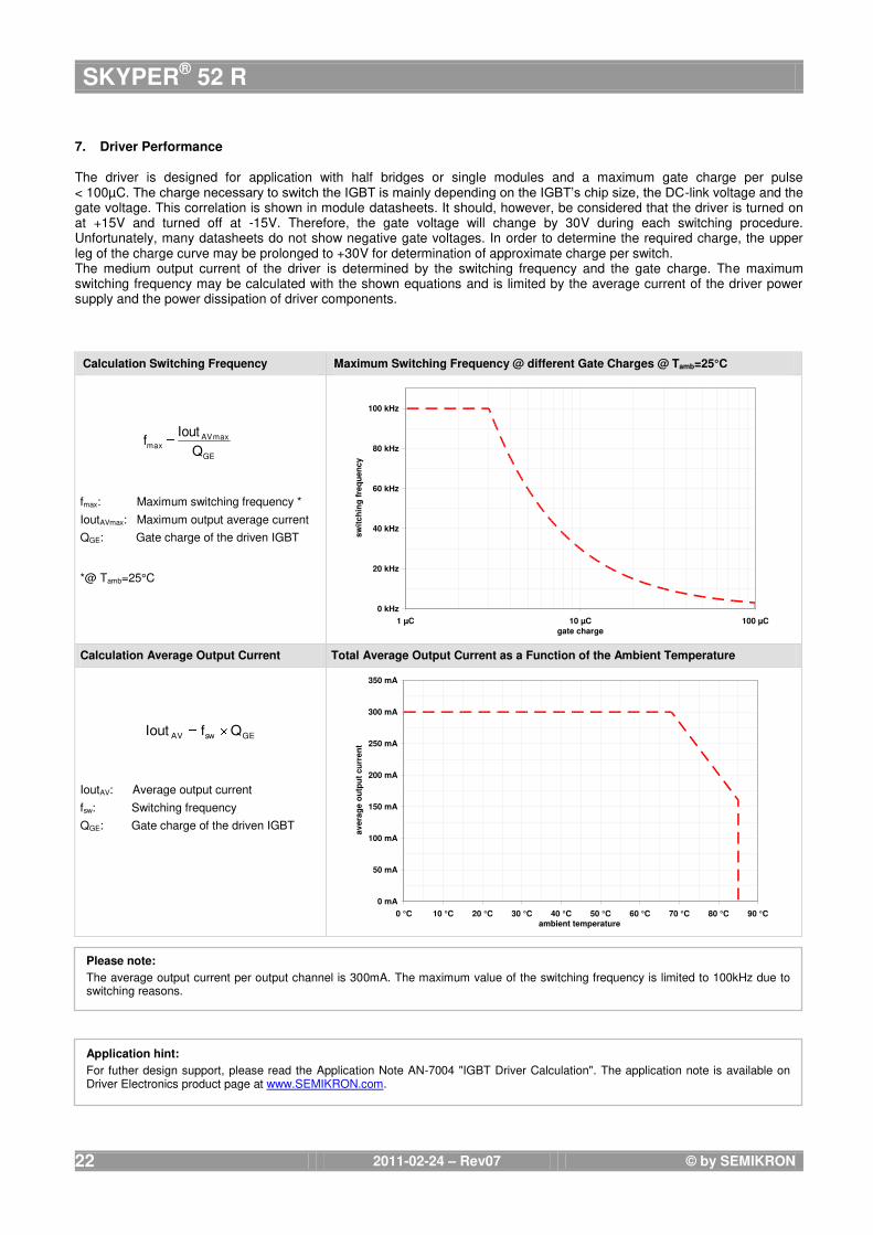
7. Driver Performance The driver is designed for application with half bridges or single modules and a maximum gate charge per pulse < 100µC. The charge necessary to switch the IGBT is mainly depending on the IGBT’s chip size, the DC-link voltage and the gate voltage. This correlation is shown in module datasheets. It should, however, be considered that the driver is turned on at +15V and turned off at -15V. Therefore, the gate voltage will change by 30V during each switching procedure. Unfortunately, many datasheets do not show negative gate voltages. In order to determine the required charge, the upper leg of the charge curve may be prolonged to +30V for determination of approximate charge per switch. The medium output current of the driver is determined by the switching frequency and the gate charge. The maximum switching frequency may be calculated with the shown equations and is limited by the average current of the driver power supply and the power dissipation of driver components.
Calculation Switching Frequency Maximum Switching Frequency @ different Gate Charges @ Tamb=25°C
fmax: Maximum switching frequency *
IoutAVmax: Maximum output average current
QGE: Gate charge of the driven IGBT *@ Tamb=25°C
0 kHz
20 kHz
40 kHz
60 kHz
80 kHz
100 kHz
1 µC 10 µC 100 µC
gate charge
sw
itc
hin
g f
req
ue
nc
y
Calculation Average Output Current Total Average Output Current as a Function of the Ambient Temperature
GEswAV QfIout
IoutAV: Average output current
fsw: Switching frequency
QGE: Gate charge of the driven IGBT
0 mA
50 mA
100 mA
150 mA
200 mA
250 mA
300 mA
350 mA
0 °C 10 °C 20 °C 30 °C 40 °C 50 °C 60 °C 70 °C 80 °C 90 °C
ambient temperature
av
era
ge
ou
tpu
t c
urr
en
t
Please note:
The average output current per output channel is 300mA. The maximum value of the switching frequency is limited to 100kHz due to switching reasons.
GE
maxAVmax
Q
Ioutf
Application hint:
For futher design support, please read the Application Note AN-7004 "IGBT Driver Calculation". The application note is available on Driver Electronics product page at www.SEMIKRON.com.

SKYPER® 52 R
2011-02-24 – Rev07 © by SEMIKRON
23
71. Insulation
Magnetic transformers are used for insulation between gate driver primary and secondary side. The transformer set consists of pulse transformers which are used for turn-on and turn-off signals of the IGBT and the signal feedback between secondary and primary side, and a DC/DC converter. This converter provides a potential separation (galvanic separation) and power supply for the two secondary (high and low) sides of the driver. Thus, external transformers for power supply are not required.
Creepage and Clearance Distance in mm
Secondary to secondary Min. 7,2
Primary to secondary Min. 18,0
72. Isolation Test Voltage The isolation test voltage represents a measure of immunity to transient voltages. The maximum test voltage and time applied once between input and output, and once between output 1 and output 2 are indicated in the absolute maximum ratings. The high-voltage isolation tests and repeated tests of an isolation barrier can degrade isolation capability due to partial discharge. Repeated isolation voltage tests should be performed with reduced voltage. The test voltage must be reduced by 20% for each repeated test. The isolation will be ensured by the isolation barrier (transformer) that is checked in the part. An isolation test is not performed as a series test. Therefore, the user can perform once the isolation test with voltage and time indicated in the absolute maximum ratings.
73. Environmental Conditions The driver board is type tested under the environmental conditions below.
Conditions Values (max.)
Thermal Cycling - 100 cycle, Tstg(max) - Tstg(min), without operation
- Tested acc. IEC 60068-2-14 Test Na
Vibration Sinusoidal sweep 20Hz … 500Hz, 5g, 26 sweeps per axis (x, y, z) - Tested acc. IEC 68-2-6
- Connection between driver core and printed circuit board mechanical reinforced by using support posts.
Shock Half-sinusoidal pulse 15g, shock width 18ms, 3 shocks in each direction (±x, ±y, ±z), 18 shocks in total
- Tested acc. IEC 68-2-27
- Connection between driver core and printed circuit board mechanical reinforced by using support posts.
Temperature humidity - 40/085/56 (+40°C, 85% RH, 56h)
- Tested acc. IEC 60068-1 (climate)
- Climate class 3K3
Fast transients (Burst) - Power terminals: 4kV / 5kHz
- Control terminals: 4kV / 5kHz
- Tested acc. EN 61000-4-4
Electrostatic discharge (ESD)
- Contact discharge: 6kV
- Air discharge: 8kV
- Tested acc. EN 61000-4-2
Radio Frequency Fields - Electrical field: 7,5V/m
- Polarisation: vertical + horizontal
- Frequency: 80 MHz - 1000 MHz
- Modulation: 80% AM, 1kHz
- Tested acc. EN 61000-4-3
RF Conducted Disturbance
- Voltage: 10V EMF
- Frequency: 150 kHz - 80 MHz
- Modulation: 80 % AM, 1kHz
- Tested acc. EN 61000-4-6

SKYPER® 52 R
2011-02-24 – Rev07 © by SEMIKRON
24
8. Marking Every driver board is marked. The marking contains the following items.
Part marking information
2D data matrix code
Type: EEC 200
Standard: ICO / IEC 16022
Cell size: 0.254 – 0.3 mm
Dimension: 5 x 5 mm
Data in plain text
XXXXXXXX 8 digits part number (e.g. L5022001)
YY 2 digits version number (e. g. NF)
ZZZZ 4 digits date code (e.g. 0440 = year + week)
VVVV 4 digits continuous lot number
U 1 digit country code
TTTTT 5 digits account number (e.g. 54229)
9. Status Definition
Data Sheet Status Product Status Definition
Target Formative or in design The data sheet and technical explanations contain advanced information or the design specifications for product development. Specifications may change in any manner without notice.
Preliminary First production The data sheet and technical explanations contain preliminary data, and supplementary data might be published at a later date. SEMIKRON reserves the rights to make changes at any time without notice in order to improve design.
No identification Full production The data sheet and technical explanations contain final specification. SEMIKRON reserves the rights to make changes at any time without notice in order to improve design.
DISCLAIMER
SEMIKRON reserves the right to make changes without further notice herein to improve reliability, function or design. Information furnished in this document is believed to be accurate and reliable. However, no representation or warranty is given and no liability is assumed with respect to the accuracy or use of such information. SEMIKRON does not assume any liability arising out of the application or use of any product or circuit described herein. Furthermore, this technical information may not be considered as an assurance of component characteristics. No warranty or guarantee expressed or implied is made regarding delivery, performance or suitability. This document is not exhaustive and supersedes and replaces all information previously supplied and may be superseded by updates without further notice.
SEMIKRON products are not authorized for use in life support appliances and systems without the express written approval by SEMIKRON.
www.SEMIKRON.com