A Power-Efficient Multiband Planar USB Dongle Antenna for ...
15
sensors Article A Power-Efficient Multiband Planar USB Dongle Antenna for Wireless Sensor Networks Wei-Yuan Chiang 1 , Chia-Hao Ku 1 , Chiung-An Chen 1, *, Le-Yu Wang 1 , Patricia Angela R. Abu 2 , Pei-Zong Rao 3 , Chih-Kai Liu 3 , Chao-Hsiang Liao 4 and Shih-Lun Chen 5, * 1 Department of Electrical Engineering, Ming Chi University of Technology, New Taipei City 24301, Taiwan; [email protected] (W.-Y.C.); [email protected] (C.-H.K.); [email protected] (L.-Y.W.) 2 Department of Information Systems and Computer Science, Ateneo de Manila University, Quezon City 1108, Philippines; [email protected] 3 Shenzhen Jaguar Wave Technology Co. Ltd., Shenzhen 518103, China; [email protected] (P.-Z.R.); [email protected] (C.-K.L.) 4 Wireless Laboratory, SGS Taiwan Ltd., New Taipei City 24803, Taiwan; [email protected] 5 Department of Electronic Engineering, Chung Yuan Christian University, Taoyuan City 32023, Taiwan * Correspondence: [email protected] (C.-A.C); [email protected] (S.-L.C); Tel.: +886-2-2908-9899 (C.-A.C); Tel.: +886-3-265-4610 (S.-L.C) Received: 17 May 2019; Accepted: 30 May 2019; Published: 5 June 2019 Abstract: Wireless Sensor Networks (WSNs) had been applied in Internet of Things (IoT) and in Industry 4.0. Since a WSN system contains multiple wireless sensor nodes, it is necessary to develop a low-power and multiband wireless communication system that satisfies the specifications of the Federal Communications Commission (FCC) and the Certification European (CE). In a WSN system, many devices are of very small size and can be slipped into a Universal Serial Bus (USB), which is capable of connecting to wireless systems and networks, as well as transferring data. These devices are widely known as USB dongles. This paper develops a planar USB dongle antenna for three frequency bands, namely 2.30–2.69 GHz, 3.40–3.70 GHz, and 5.15–5.85 GHz. This study proposes a novel antenna design that uses four loops to develop the multiband USB dongle. The first and second loops construct the low and intermediate frequency ranges. The third loop resonates the high frequency property, while the fourth loop is used to enhance the bandwidth. The performance and power consumption of the proposed multiband planar USB dongle antenna were significantly improved compared to existing multiband designs. Keywords: multiband planar; USB dongle antenna; wireless sensor networks 1. Introduction The increasing use of portable devices with low-power integrated circuits and wireless communication has paved its way to a new generation of wireless sensor area networks. Simultaneously there is a trend towards the miniaturization of devices. In wild band use, this would refer to wireless networks that consist of several small body sensor units with a central control unit. Therefore, Chen et al. [1] used a micro-control unit design that covers all of the wireless body sensor nodes and manages a low power usage. Moreover, Chen et al. [2] proposed a reconfigurable filter to adjust the different biomedical signal inputs in order to optimize system performance. Since the growth of use of wireless communication systems, processing requires a higher frequency and a wider transfer band. The data type of Wireless Body Area Networks (WBANs) is no longer limited to data in digits. With this, the new wireless communication specification and its power consumption increased drastically. Chen et al. [3] proposed an efficient lossless compression design. By efficiently Sensors 2019, 19, 2568; doi:10.3390/s19112568 www.mdpi.com/journal/sensors
-
Upload
khangminh22 -
Category
Documents
-
view
3 -
download
0
Transcript of A Power-Efficient Multiband Planar USB Dongle Antenna for ...

sensors
Article
A Power-Efficient Multiband Planar USB DongleAntenna for Wireless Sensor Networks
Wei-Yuan Chiang 1 , Chia-Hao Ku 1, Chiung-An Chen 1,*, Le-Yu Wang 1, Patricia Angela R. Abu 2,Pei-Zong Rao 3, Chih-Kai Liu 3 , Chao-Hsiang Liao 4 and Shih-Lun Chen 5,*
1 Department of Electrical Engineering, Ming Chi University of Technology, New Taipei City 24301, Taiwan;[email protected] (W.-Y.C.); [email protected] (C.-H.K.);[email protected] (L.-Y.W.)
2 Department of Information Systems and Computer Science, Ateneo de Manila University,Quezon City 1108, Philippines; [email protected]
3 Shenzhen Jaguar Wave Technology Co. Ltd., Shenzhen 518103, China;[email protected] (P.-Z.R.); [email protected] (C.-K.L.)
4 Wireless Laboratory, SGS Taiwan Ltd., New Taipei City 24803, Taiwan; [email protected] Department of Electronic Engineering, Chung Yuan Christian University, Taoyuan City 32023, Taiwan* Correspondence: [email protected] (C.-A.C); [email protected] (S.-L.C);
Tel.: +886-2-2908-9899 (C.-A.C); Tel.: +886-3-265-4610 (S.-L.C)
Received: 17 May 2019; Accepted: 30 May 2019; Published: 5 June 2019
Abstract: Wireless Sensor Networks (WSNs) had been applied in Internet of Things (IoT) and inIndustry 4.0. Since a WSN system contains multiple wireless sensor nodes, it is necessary to developa low-power and multiband wireless communication system that satisfies the specifications of theFederal Communications Commission (FCC) and the Certification European (CE). In a WSN system,many devices are of very small size and can be slipped into a Universal Serial Bus (USB), which iscapable of connecting to wireless systems and networks, as well as transferring data. These devicesare widely known as USB dongles. This paper develops a planar USB dongle antenna for threefrequency bands, namely 2.30–2.69 GHz, 3.40–3.70 GHz, and 5.15–5.85 GHz. This study proposesa novel antenna design that uses four loops to develop the multiband USB dongle. The first andsecond loops construct the low and intermediate frequency ranges. The third loop resonates thehigh frequency property, while the fourth loop is used to enhance the bandwidth. The performanceand power consumption of the proposed multiband planar USB dongle antenna were significantlyimproved compared to existing multiband designs.
Keywords: multiband planar; USB dongle antenna; wireless sensor networks
1. Introduction
The increasing use of portable devices with low-power integrated circuits and wirelesscommunication has paved its way to a new generation of wireless sensor area networks. Simultaneouslythere is a trend towards the miniaturization of devices. In wild band use, this would refer to wirelessnetworks that consist of several small body sensor units with a central control unit. Therefore,Chen et al. [1] used a micro-control unit design that covers all of the wireless body sensor nodes andmanages a low power usage. Moreover, Chen et al. [2] proposed a reconfigurable filter to adjust thedifferent biomedical signal inputs in order to optimize system performance.
Since the growth of use of wireless communication systems, processing requires a higher frequencyand a wider transfer band. The data type of Wireless Body Area Networks (WBANs) is no longer limitedto data in digits. With this, the new wireless communication specification and its power consumptionincreased drastically. Chen et al. [3] proposed an efficient lossless compression design. By efficiently
Sensors 2019, 19, 2568; doi:10.3390/s19112568 www.mdpi.com/journal/sensors
Sensors 2019, 19, 2568 2 of 15
compressing the data, the transfer speed and the power consumption were improved. Thus, the WBANfield could integrate a real-time health monitoring system that can continuously update the sensorrecords through the Internet and has also become an important interdisciplinary domain.
The continuous development in wireless communications improves the efficiency of an antennaby designing a smaller one that is more useful in terms of radiative properties. This led the way toresearch on multiband antenna. The Multiple-Input and Multiple-Output (MIMO) system is onetypical case of the use of multiband antenna. Printed antennas have demonstrated that it can be useful,not only as a communicating element, but also as a sensor or energy collector. With this, the multibandantenna design has become an extensive subject. As a result, the use of a multiband antenna system onmobile devices is a common trend [4].
In recent years, the more compact and more powerful devices are the major design trends.Among those is the multiband antennas for Universal Serial Bus (USB) dongles that have been ofparticular interest due to the ease of carrying them as well as their plug and play function. The commonUSB dongle antenna design adopted the C-type line, combined with open or short stubs [4–6]. The stubscan also generate the low band [7–10]. In [11–17], the multi-path coupling antenna design was described.The main antenna and stubs are used to generate both the low band and middle band. The high bandneeds two coupling stubs in order to generate a wider bandwidth.
The reduction of the volume of the antenna is under the constraint of its fundamental physical limitsin terms of trade-off between radiation performances and impedance bandwidth. Limitations in termsof bandwidth and efficiency suggest an analysis with respect to fundamental limits. The Chu’s modeluses spherical modes to estimate the minimum stored energy around the antenna [18]. Equation (1)shows the modified formula of the Q-factor and the antenna size [18,19]:
Q =2ω ·maxWm, We
Pr + PΩ≈ η
1
(ka)3 +1ka
(1)
where We is the stored electric energy, Wm is the stored magnetic energy, Pr is the radiated power,PΩ is the power dissipated from ohmic losses, η is the radiation efficiency, a is the minimum radius ofthe sphere enclosing the antenna, and k is the wave number (k = 2π/λ). It is very difficult to have awide bandwidth (low Q-factor) and at the same time have a good efficiency for miniature antennas.Thus, the miniaturization of antennas causes them to suffer from both limited efficiency and lowbandwidth. Miniaturization of devices leads to the reduction of antennas, thus becoming an importantchallenge. Otherwise, the radiation efficiency decreases when the size of the antenna is reduced.For example, the meander line antenna is a small antenna that has a simple structure and can supporthigher bandwidth, but these antennas have low radiation efficiency [20].
The important parameters of the antenna design are its operation frequency bands, radiationefficiency, and peak gain. The first work estimated the radiation efficiency. Figure 1 shows aschematic diagram of the communication system. The received power (Prx) is estimated using the Friistransmission equation shown in Equation (2) where Ptx is the transmission power, Gtx is the transmissionantenna gain, Grx is the received antenna gain, λ is the free space wavelength, and R is transmissiondistance [21]. Grx is the 3D average gains, defined in Equation (3). Using an omnidirectional antennato transmit the signal has a Gtx of 0 dBi. The receiver minimum input level sensitivity is −61 dBm,which meets the specification of IEEE (Institute of Electrical and Electronics Engineers) [22]. If thetransmission port is an ideal isotropic antenna, the Grx gain must be larger than −17 dBi when thefrequency is 2.45 GHz. In addition, the transition range is 5 m with a transmission power of 10 dBm.The minimum radiation efficiency must be larger than 2%, and it can be calculated using Equation (3).However, the minimum radiation efficiency must be larger than 4% when the frequency is 2.45 GHz.On the other hand, the minimum radiation efficiency must be larger than 10% when the frequency is5.5 GHz.
Sensors 2019, 19, 2568 3 of 15Sensors 2019, 19, x FOR PEER REVIEW 3 of 15
Figure 1. The schematic diagram of the communication system.
( )
2
24
tx tx rxrx
P G GP
R
= (2)
( )3 10 logD average gain radiation efficiency= (3)
The next main parameter is the peak gain. The ideal USB dongle antenna is an omnidirectional
antenna. In this study, the design goal is to have a peak gain within 0–4 dBi. This antenna is
operated on LTE (Long Term Evolution), which covers 2.30–2.69 GHz, 3.40–3.70 GHz, and 5.15–5.85
GHz bands, 5G system (5th generation system) that covers 3.40–3.70 GHz, and the LTE-U
(LTE-Unlicensed) band that covers 2.40–2.44 GHz and 5.15–5.85 GHz [23,24].
In this study, a planar antenna is designed to satisfy the conditions of low cost, miniaturized,
and multiband antennas, taking into consideration the size and its production. It is challenging to
design a multiband antenna as the structure gets smaller and smaller. The goal of this study is to
design a triple band antenna that has a 10% radiation efficiency at three operating frequency bands
with a peak gain within 0–4 dBi for each band.
The planar USB dongle is proposed in this work. The planar USB dongle antenna is a low
power device that satisfies the condition of a low power system design. The proposed design
combines one main feed antenna and three stubs in order to generate triple bands within a 10 mm ×
10 mm area. The main feed antenna is responsible for generating the low band and middle band.
One stub is incorporated to couple with the main antenna for the 2.30–2.69 GHz and 3.40–3.70 GHz
bands. The second stub is incorporated to generate the high band. Lastly, the third stub is
incorporated to increase the high band bandwidth in order to cover the 5.15–5.85 GHz band. Section
2 presents the antenna design and optimization. The performance comparison of the proposed
antenna to previous works is presented and discussed in Section 3.
2. Antenna Design and Optimization
The structure of the planar USB dongle antenna proposed in this study is illustrated in Figure
2a. The size of the main structure is 10 × 10 mm2, while the volume of the planar USB dongle antenna
assembly is 10 × 50 × 0.8 mm3. The detailed dimensions of the planar USB dongle antenna are listed
in Table 1.
The proposed antenna is designed on an FR4 substrate. Its measured relative permittivity and
loss tangent are 4.4 and 0.02, respectively. The antenna is operated on LTE, which covers 2.30–2.69
GHz, 3.40–3.70 GHz, and 5.15–5.85 GHz bands, and the 5G system (Sub 6 GHz spectrum), which
covers 3.40–3.60 GHz bands. Otherwise, the LTE-U band of the 5G system that covers 2.40–2.44 GHz
and 5.15–5.85 GHz is included in the design goal of this antenna.
Figure 2b illustrates the simulation model that is constructed using the high frequency structure
simulator, ANSYS HFSS EM software. The design targets three bands: (1) The lower band that covers
2.30–2.69 GHz, (2) the middle band that covers 3.40–3.70 GHz, and (3) the upper band that covers
5.15–5.85 GHz.
Figure 1. The schematic diagram of the communication system.
Prx =PtxGtxGrxλ2
(4πR)2 (2)
3D average gain = 10 log(radiation e f f iciency) (3)
The next main parameter is the peak gain. The ideal USB dongle antenna is an omnidirectionalantenna. In this study, the design goal is to have a peak gain within 0–4 dBi. This antenna is operatedon LTE (Long Term Evolution), which covers 2.30–2.69 GHz, 3.40–3.70 GHz, and 5.15–5.85 GHz bands,5G system (5th generation system) that covers 3.40–3.70 GHz, and the LTE-U (LTE-Unlicensed) bandthat covers 2.40–2.44 GHz and 5.15–5.85 GHz [23,24].
In this study, a planar antenna is designed to satisfy the conditions of low cost, miniaturized, andmultiband antennas, taking into consideration the size and its production. It is challenging to design amultiband antenna as the structure gets smaller and smaller. The goal of this study is to design a tripleband antenna that has a 10% radiation efficiency at three operating frequency bands with a peak gainwithin 0–4 dBi for each band.
The planar USB dongle is proposed in this work. The planar USB dongle antenna is a low powerdevice that satisfies the condition of a low power system design. The proposed design combinesone main feed antenna and three stubs in order to generate triple bands within a 10 mm × 10 mmarea. The main feed antenna is responsible for generating the low band and middle band. One stubis incorporated to couple with the main antenna for the 2.30–2.69 GHz and 3.40–3.70 GHz bands.The second stub is incorporated to generate the high band. Lastly, the third stub is incorporated toincrease the high band bandwidth in order to cover the 5.15–5.85 GHz band. Section 2 presents theantenna design and optimization. The performance comparison of the proposed antenna to previousworks is presented and discussed in Section 3.
2. Antenna Design and Optimization
The structure of the planar USB dongle antenna proposed in this study is illustrated in Figure 2a.The size of the main structure is 10 × 10 mm2, while the volume of the planar USB dongle antennaassembly is 10 × 50 × 0.8 mm3. The detailed dimensions of the planar USB dongle antenna are listed inTable 1.
The proposed antenna is designed on an FR4 substrate. Its measured relative permittivity and losstangent are 4.4 and 0.02, respectively. The antenna is operated on LTE, which covers 2.30–2.69 GHz,3.40–3.70 GHz, and 5.15–5.85 GHz bands, and the 5G system (Sub 6 GHz spectrum), which covers3.40–3.60 GHz bands. Otherwise, the LTE-U band of the 5G system that covers 2.40–2.44 GHz and5.15–5.85 GHz is included in the design goal of this antenna.
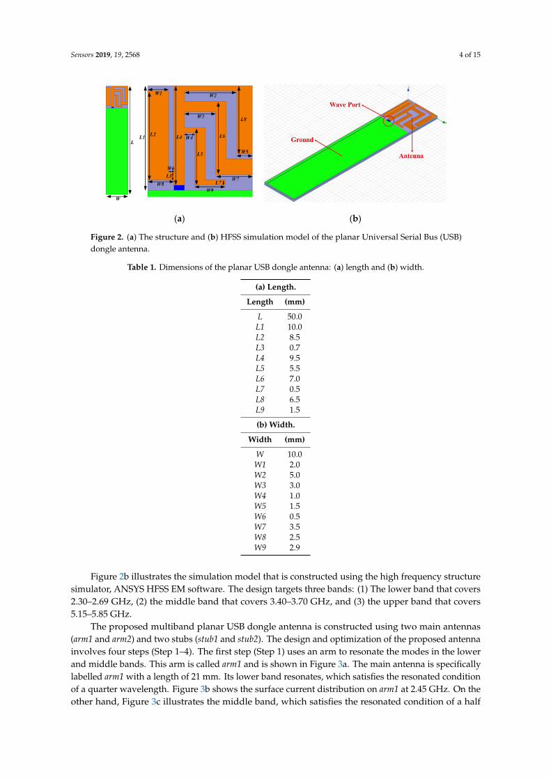
Sensors 2019, 19, 2568 4 of 15
Sensors 2019, 19, x FOR PEER REVIEW 4 of 15
(a) (b)
Figure 2. (a) The structure and (b) HFSS simulation model of the planar Universal Serial
Bus (USB) dongle antenna.
Table 1. Dimensions of the planar USB dongle antenna: (a) length and (b) width.
(a) Length.
Length (mm)
L 50.0
L1 10.0
L2 8.5
L3 0.7
L4 9.5
L5 5.5
L6 7.0
L7 0.5
L8 6.5
L9 1.5
(b) Width.
Width (mm)
W 10.0
W1 2.0
W2 5.0
W3 3.0
W4 1.0
W5 1.5
W6 0.5
W7 3.5
W8 2.5
W9 2.9
The proposed multiband planar USB dongle antenna is constructed using two main antennas
(arm1 and arm2) and two stubs (stub1 and stub2). The design and optimization of the proposed
antenna involves four steps (Step 1–4). The first step (Step 1) uses an arm to resonate the modes in
the lower and middle bands. This arm is called arm1 and is shown in Figure 3a. The main antenna is
specifically labelled arm1 with a length of 21 mm. Its lower band resonates, which satisfies the
resonated condition of a quarter wavelength. Figure 3b shows the surface current distribution on
arm1 at 2.45 GHz. On the other hand, Figure 3c illustrates the middle band, which satisfies the
resonated condition of a half wavelength. This is the second resonant mode of arm1. Figure 4 shows
the simulation results of the return loss with various L8 parameter values for arm1. In Step 1, the
Figure 2. (a) The structure and (b) HFSS simulation model of the planar Universal Serial Bus (USB)dongle antenna.
Table 1. Dimensions of the planar USB dongle antenna: (a) length and (b) width.
(a) Length.
Length (mm)
L 50.0L1 10.0L2 8.5L3 0.7L4 9.5L5 5.5L6 7.0L7 0.5L8 6.5L9 1.5
(b) Width.
Width (mm)
W 10.0W1 2.0W2 5.0W3 3.0W4 1.0W5 1.5W6 0.5W7 3.5W8 2.5W9 2.9
Figure 2b illustrates the simulation model that is constructed using the high frequency structuresimulator, ANSYS HFSS EM software. The design targets three bands: (1) The lower band that covers2.30–2.69 GHz, (2) the middle band that covers 3.40–3.70 GHz, and (3) the upper band that covers5.15–5.85 GHz.
The proposed multiband planar USB dongle antenna is constructed using two main antennas(arm1 and arm2) and two stubs (stub1 and stub2). The design and optimization of the proposed antennainvolves four steps (Step 1–4). The first step (Step 1) uses an arm to resonate the modes in the lowerand middle bands. This arm is called arm1 and is shown in Figure 3a. The main antenna is specificallylabelled arm1 with a length of 21 mm. Its lower band resonates, which satisfies the resonated conditionof a quarter wavelength. Figure 3b shows the surface current distribution on arm1 at 2.45 GHz. On theother hand, Figure 3c illustrates the middle band, which satisfies the resonated condition of a half
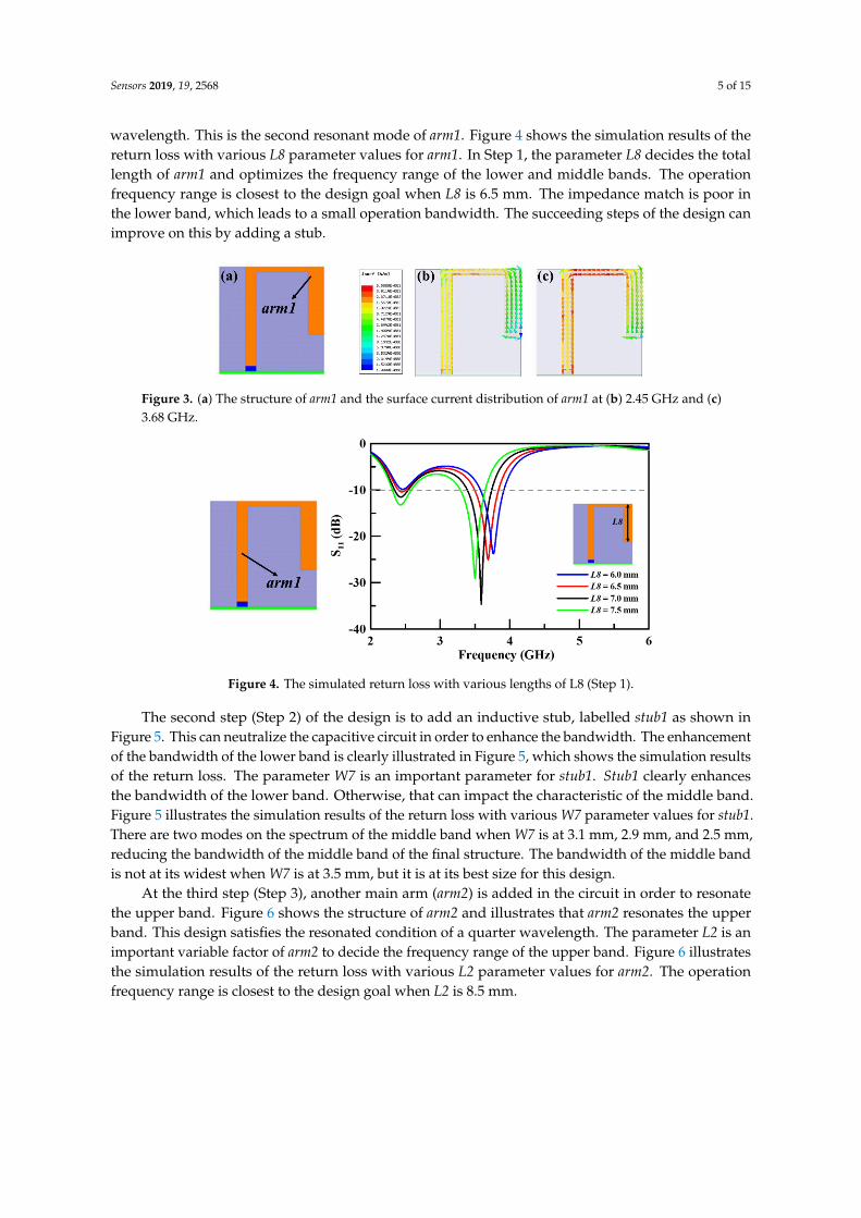
Sensors 2019, 19, 2568 5 of 15
wavelength. This is the second resonant mode of arm1. Figure 4 shows the simulation results of thereturn loss with various L8 parameter values for arm1. In Step 1, the parameter L8 decides the totallength of arm1 and optimizes the frequency range of the lower and middle bands. The operationfrequency range is closest to the design goal when L8 is 6.5 mm. The impedance match is poor inthe lower band, which leads to a small operation bandwidth. The succeeding steps of the design canimprove on this by adding a stub.
Sensors 2019, 19, x FOR PEER REVIEW 5 of 15
parameter L8 decides the total length of arm1 and optimizes the frequency range of the lower and
middle bands. The operation frequency range is closest to the design goal when L8 is 6.5 mm. The
impedance match is poor in the lower band, which leads to a small operation bandwidth. The
succeeding steps of the design can improve on this by adding a stub.
Figure 3. (a) The structure of arm1 and the surface current distribution of arm1 at (b) 2.45
GHz and (c) 3.68 GHz.
Figure 4. The simulated return loss with various lengths of L8 (Step 1).
The second step (Step 2) of the design is to add an inductive stub, labelled stub1 as shown in
Figure 5. This can neutralize the capacitive circuit in order to enhance the bandwidth. The
enhancement of the bandwidth of the lower band is clearly illustrated in Figure 5, which shows the
simulation results of the return loss. The parameter W7 is an important parameter for stub1. Stub1
clearly enhances the bandwidth of the lower band. Otherwise, that can impact the characteristic of the
middle band. Figure 5 illustrates the simulation results of the return loss with various W7 parameter
values for stub1. There are two modes on the spectrum of the middle band when W7 is at 3.1 mm, 2.9
mm, and 2.5 mm, reducing the bandwidth of the middle band of the final structure. The bandwidth of
the middle band is not at its widest when W7 is at 3.5 mm, but it is at its best size for this design.
Figure 5. The simulated return loss with various lengths of W7 (Step 2).
Figure 3. (a) The structure of arm1 and the surface current distribution of arm1 at (b) 2.45 GHz and (c)3.68 GHz.
Sensors 2019, 19, x FOR PEER REVIEW 5 of 15
parameter L8 decides the total length of arm1 and optimizes the frequency range of the lower and
middle bands. The operation frequency range is closest to the design goal when L8 is 6.5 mm. The
impedance match is poor in the lower band, which leads to a small operation bandwidth. The
succeeding steps of the design can improve on this by adding a stub.
Figure 3. (a) The structure of arm1 and the surface current distribution of arm1 at (b) 2.45
GHz and (c) 3.68 GHz.
Figure 4. The simulated return loss with various lengths of L8 (Step 1).
The second step (Step 2) of the design is to add an inductive stub, labelled stub1 as shown in
Figure 5. This can neutralize the capacitive circuit in order to enhance the bandwidth. The
enhancement of the bandwidth of the lower band is clearly illustrated in Figure 5, which shows the
simulation results of the return loss. The parameter W7 is an important parameter for stub1. Stub1
clearly enhances the bandwidth of the lower band. Otherwise, that can impact the characteristic of the
middle band. Figure 5 illustrates the simulation results of the return loss with various W7 parameter
values for stub1. There are two modes on the spectrum of the middle band when W7 is at 3.1 mm, 2.9
mm, and 2.5 mm, reducing the bandwidth of the middle band of the final structure. The bandwidth of
the middle band is not at its widest when W7 is at 3.5 mm, but it is at its best size for this design.
Figure 5. The simulated return loss with various lengths of W7 (Step 2).
Figure 4. The simulated return loss with various lengths of L8 (Step 1).
The second step (Step 2) of the design is to add an inductive stub, labelled stub1 as shown inFigure 5. This can neutralize the capacitive circuit in order to enhance the bandwidth. The enhancementof the bandwidth of the lower band is clearly illustrated in Figure 5, which shows the simulation resultsof the return loss. The parameter W7 is an important parameter for stub1. Stub1 clearly enhancesthe bandwidth of the lower band. Otherwise, that can impact the characteristic of the middle band.Figure 5 illustrates the simulation results of the return loss with various W7 parameter values for stub1.There are two modes on the spectrum of the middle band when W7 is at 3.1 mm, 2.9 mm, and 2.5 mm,reducing the bandwidth of the middle band of the final structure. The bandwidth of the middle bandis not at its widest when W7 is at 3.5 mm, but it is at its best size for this design.
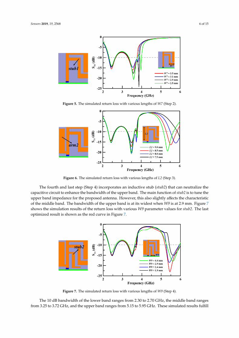
At the third step (Step 3), another main arm (arm2) is added in the circuit in order to resonatethe upper band. Figure 6 shows the structure of arm2 and illustrates that arm2 resonates the upperband. This design satisfies the resonated condition of a quarter wavelength. The parameter L2 is animportant variable factor of arm2 to decide the frequency range of the upper band. Figure 6 illustratesthe simulation results of the return loss with various L2 parameter values for arm2. The operationfrequency range is closest to the design goal when L2 is 8.5 mm.
Sensors 2019, 19, 2568 6 of 15
Sensors 2019, 19, x FOR PEER REVIEW 5 of 15
parameter L8 decides the total length of arm1 and optimizes the frequency range of the lower and
middle bands. The operation frequency range is closest to the design goal when L8 is 6.5 mm. The
impedance match is poor in the lower band, which leads to a small operation bandwidth. The
succeeding steps of the design can improve on this by adding a stub.
Figure 3. (a) The structure of arm1 and the surface current distribution of arm1 at (b) 2.45
GHz and (c) 3.68 GHz.
Figure 4. The simulated return loss with various lengths of L8 (Step 1).
The second step (Step 2) of the design is to add an inductive stub, labelled stub1 as shown in
Figure 5. This can neutralize the capacitive circuit in order to enhance the bandwidth. The
enhancement of the bandwidth of the lower band is clearly illustrated in Figure 5, which shows the
simulation results of the return loss. The parameter W7 is an important parameter for stub1. Stub1
clearly enhances the bandwidth of the lower band. Otherwise, that can impact the characteristic of the
middle band. Figure 5 illustrates the simulation results of the return loss with various W7 parameter
values for stub1. There are two modes on the spectrum of the middle band when W7 is at 3.1 mm, 2.9
mm, and 2.5 mm, reducing the bandwidth of the middle band of the final structure. The bandwidth of
the middle band is not at its widest when W7 is at 3.5 mm, but it is at its best size for this design.
Figure 5. The simulated return loss with various lengths of W7 (Step 2). Figure 5. The simulated return loss with various lengths of W7 (Step 2).
Sensors 2019, 19, x FOR PEER REVIEW 6 of 15
At the third step (Step 3), another main arm (arm2) is added in the circuit in order to resonate
the upper band. Figure 6 shows the structure of arm2 and illustrates that arm2 resonates the upper
band. This design satisfies the resonated condition of a quarter wavelength. The parameter L2 is an
important variable factor of arm2 to decide the frequency range of the upper band. Figure 6
illustrates the simulation results of the return loss with various L2 parameter values for arm2. The
operation frequency range is closest to the design goal when L2 is 8.5 mm.
Figure 6. The simulated return loss with various lengths of L2 (Step 3).
The fourth and last step (Step 4) incorporates an inductive stub (stub2) that can neutralize the
capacitive circuit to enhance the bandwidth of the upper band. The main function of stub2 is to tune
the upper band impedance for the proposed antenna. However, this also slightly affects the
characteristic of the middle band. The bandwidth of the upper band is at its widest when W9 is at 2.9
mm. Figure 7 shows the simulation results of the return loss with various W9 parameter values for
stub2. The last optimized result is shown as the red curve in Figure 7.
Figure 7. The simulated return loss with various lengths of W9 (Step 4).
The 10 dB bandwidth of the lower band ranges from 2.30 to 2.70 GHz, the middle band ranges
from 3.25 to 3.72 GHz, and the upper band ranges from 5.15 to 5.95 GHz. These simulated results
fulfill the spectrum requirements of LTE bands and cover the 5G system (Sub 6 GHz spectrum).
Otherwise, these operation bands can cover the LTE-U band in the 5G system. The variation of
impedance for each step in the design process is shown in Figure 8. The imaginary part of the
impedance is close to zero ohm during the optimized processes.
Figure 6. The simulated return loss with various lengths of L2 (Step 3).
The fourth and last step (Step 4) incorporates an inductive stub (stub2) that can neutralize thecapacitive circuit to enhance the bandwidth of the upper band. The main function of stub2 is to tune theupper band impedance for the proposed antenna. However, this also slightly affects the characteristicof the middle band. The bandwidth of the upper band is at its widest when W9 is at 2.9 mm. Figure 7shows the simulation results of the return loss with various W9 parameter values for stub2. The lastoptimized result is shown as the red curve in Figure 7.
Sensors 2019, 19, x FOR PEER REVIEW 6 of 15
At the third step (Step 3), another main arm (arm2) is added in the circuit in order to resonate
the upper band. Figure 6 shows the structure of arm2 and illustrates that arm2 resonates the upper
band. This design satisfies the resonated condition of a quarter wavelength. The parameter L2 is an
important variable factor of arm2 to decide the frequency range of the upper band. Figure 6
illustrates the simulation results of the return loss with various L2 parameter values for arm2. The
operation frequency range is closest to the design goal when L2 is 8.5 mm.
Figure 6. The simulated return loss with various lengths of L2 (Step 3).
The fourth and last step (Step 4) incorporates an inductive stub (stub2) that can neutralize the
capacitive circuit to enhance the bandwidth of the upper band. The main function of stub2 is to tune
the upper band impedance for the proposed antenna. However, this also slightly affects the
characteristic of the middle band. The bandwidth of the upper band is at its widest when W9 is at 2.9
mm. Figure 7 shows the simulation results of the return loss with various W9 parameter values for
stub2. The last optimized result is shown as the red curve in Figure 7.
Figure 7. The simulated return loss with various lengths of W9 (Step 4).
The 10 dB bandwidth of the lower band ranges from 2.30 to 2.70 GHz, the middle band ranges
from 3.25 to 3.72 GHz, and the upper band ranges from 5.15 to 5.95 GHz. These simulated results
fulfill the spectrum requirements of LTE bands and cover the 5G system (Sub 6 GHz spectrum).
Otherwise, these operation bands can cover the LTE-U band in the 5G system. The variation of
impedance for each step in the design process is shown in Figure 8. The imaginary part of the
impedance is close to zero ohm during the optimized processes.
Figure 7. The simulated return loss with various lengths of W9 (Step 4).
The 10 dB bandwidth of the lower band ranges from 2.30 to 2.70 GHz, the middle band rangesfrom 3.25 to 3.72 GHz, and the upper band ranges from 5.15 to 5.95 GHz. These simulated results fulfill
Sensors 2019, 19, 2568 7 of 15
the spectrum requirements of LTE bands and cover the 5G system (Sub 6 GHz spectrum). Otherwise,these operation bands can cover the LTE-U band in the 5G system. The variation of impedance foreach step in the design process is shown in Figure 8. The imaginary part of the impedance is close tozero ohm during the optimized processes.Sensors 2019, 19, x FOR PEER REVIEW 7 of 15
2 3 4 5 6Frequency (GHz)
0
50
100
150
200
250
Inp
ut
Imp
ed
an
ce R
eal
Part
()
Step 1
Step 2
Step 3
Step 4
2 3 4 5 6
Frequency (GHz)
-800
-600
-400
-200
0
200
400
600
Inp
ut
Imp
ed
an
ce I
m. P
art
()
Step 1
Step 2
Step 3
Step 4
Figure 8. Variations of the impedance using the different models in the optimization
processes.
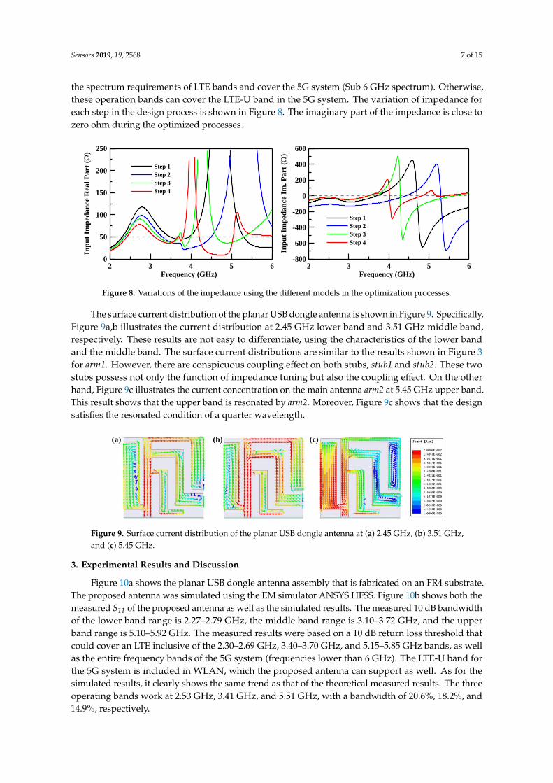
The surface current distribution of the planar USB dongle antenna is shown in Figure 9.
Specifically, Figure 9a,b illustrates the current distribution at 2.45 GHz lower band and 3.51 GHz
middle band, respectively. These results are not easy to differentiate, using the characteristics of the
lower band and the middle band. The surface current distributions are similar to the results shown in
Figure 3 for arm1. However, there are conspicuous coupling effect on both stubs, stub1 and stub2. These
two stubs possess not only the function of impedance tuning but also the coupling effect. On the other
hand, Figure 9c illustrates the current concentration on the main antenna arm2 at 5.45 GHz upper
band. This result shows that the upper band is resonated by arm2. Moreover, Figure 9c shows that the
design satisfies the resonated condition of a quarter wavelength.
Figure 9. Surface current distribution of the planar USB dongle antenna at (a) 2.45 GHz, (b)
3.51 GHz, and (c) 5.45 GHz.
3. Experimental Results and Discussion
Figure 10a shows the planar USB dongle antenna assembly that is fabricated on an FR4
substrate. The proposed antenna was simulated using the EM simulator ANSYS HFSS. Figure 10b
shows both the measured S11 of the proposed antenna as well as the simulated results. The measured
10 dB bandwidth of the lower band range is 2.27–2.79 GHz, the middle band range is 3.10–3.72 GHz,
and the upper band range is 5.10–5.92 GHz. The measured results were based on a 10 dB return loss
threshold that could cover an LTE inclusive of the 2.30–2.69 GHz, 3.40–3.70 GHz, and 5.15–5.85 GHz
bands, as well as the entire frequency bands of the 5G system (frequencies lower than 6 GHz). The
LTE-U band for the 5G system is included in WLAN, which the proposed antenna can support as
well. As for the simulated results, it clearly shows the same trend as that of the theoretical measured
results. The three operating bands work at 2.53 GHz, 3.41 GHz, and 5.51 GHz, with a bandwidth of
20.6%, 18.2%, and 14.9%, respectively.
Figure 8. Variations of the impedance using the different models in the optimization processes.
The surface current distribution of the planar USB dongle antenna is shown in Figure 9. Specifically,Figure 9a,b illustrates the current distribution at 2.45 GHz lower band and 3.51 GHz middle band,respectively. These results are not easy to differentiate, using the characteristics of the lower bandand the middle band. The surface current distributions are similar to the results shown in Figure 3for arm1. However, there are conspicuous coupling effect on both stubs, stub1 and stub2. These twostubs possess not only the function of impedance tuning but also the coupling effect. On the otherhand, Figure 9c illustrates the current concentration on the main antenna arm2 at 5.45 GHz upper band.This result shows that the upper band is resonated by arm2. Moreover, Figure 9c shows that the designsatisfies the resonated condition of a quarter wavelength.
Sensors 2019, 19, x FOR PEER REVIEW 7 of 15
2 3 4 5 6Frequency (GHz)
0
50
100
150
200
250
Inp
ut
Imp
ed
an
ce R
eal
Part
()
Step 1
Step 2
Step 3
Step 4
2 3 4 5 6
Frequency (GHz)
-800
-600
-400
-200
0
200
400
600
Inp
ut
Imp
ed
an
ce I
m. P
art
()
Step 1
Step 2
Step 3
Step 4
Figure 8. Variations of the impedance using the different models in the optimization
processes.
The surface current distribution of the planar USB dongle antenna is shown in Figure 9.
Specifically, Figure 9a,b illustrates the current distribution at 2.45 GHz lower band and 3.51 GHz
middle band, respectively. These results are not easy to differentiate, using the characteristics of the
lower band and the middle band. The surface current distributions are similar to the results shown in
Figure 3 for arm1. However, there are conspicuous coupling effect on both stubs, stub1 and stub2. These
two stubs possess not only the function of impedance tuning but also the coupling effect. On the other
hand, Figure 9c illustrates the current concentration on the main antenna arm2 at 5.45 GHz upper
band. This result shows that the upper band is resonated by arm2. Moreover, Figure 9c shows that the
design satisfies the resonated condition of a quarter wavelength.
Figure 9. Surface current distribution of the planar USB dongle antenna at (a) 2.45 GHz, (b)
3.51 GHz, and (c) 5.45 GHz.
3. Experimental Results and Discussion
Figure 10a shows the planar USB dongle antenna assembly that is fabricated on an FR4
substrate. The proposed antenna was simulated using the EM simulator ANSYS HFSS. Figure 10b
shows both the measured S11 of the proposed antenna as well as the simulated results. The measured
10 dB bandwidth of the lower band range is 2.27–2.79 GHz, the middle band range is 3.10–3.72 GHz,
and the upper band range is 5.10–5.92 GHz. The measured results were based on a 10 dB return loss
threshold that could cover an LTE inclusive of the 2.30–2.69 GHz, 3.40–3.70 GHz, and 5.15–5.85 GHz
bands, as well as the entire frequency bands of the 5G system (frequencies lower than 6 GHz). The
LTE-U band for the 5G system is included in WLAN, which the proposed antenna can support as
well. As for the simulated results, it clearly shows the same trend as that of the theoretical measured
results. The three operating bands work at 2.53 GHz, 3.41 GHz, and 5.51 GHz, with a bandwidth of
20.6%, 18.2%, and 14.9%, respectively.
Figure 9. Surface current distribution of the planar USB dongle antenna at (a) 2.45 GHz, (b) 3.51 GHz,and (c) 5.45 GHz.
3. Experimental Results and Discussion
Figure 10a shows the planar USB dongle antenna assembly that is fabricated on an FR4 substrate.The proposed antenna was simulated using the EM simulator ANSYS HFSS. Figure 10b shows both themeasured S11 of the proposed antenna as well as the simulated results. The measured 10 dB bandwidthof the lower band range is 2.27–2.79 GHz, the middle band range is 3.10–3.72 GHz, and the upperband range is 5.10–5.92 GHz. The measured results were based on a 10 dB return loss threshold thatcould cover an LTE inclusive of the 2.30–2.69 GHz, 3.40–3.70 GHz, and 5.15–5.85 GHz bands, as wellas the entire frequency bands of the 5G system (frequencies lower than 6 GHz). The LTE-U band forthe 5G system is included in WLAN, which the proposed antenna can support as well. As for thesimulated results, it clearly shows the same trend as that of the theoretical measured results. The threeoperating bands work at 2.53 GHz, 3.41 GHz, and 5.51 GHz, with a bandwidth of 20.6%, 18.2%, and14.9%, respectively.
Sensors 2019, 19, 2568 8 of 15
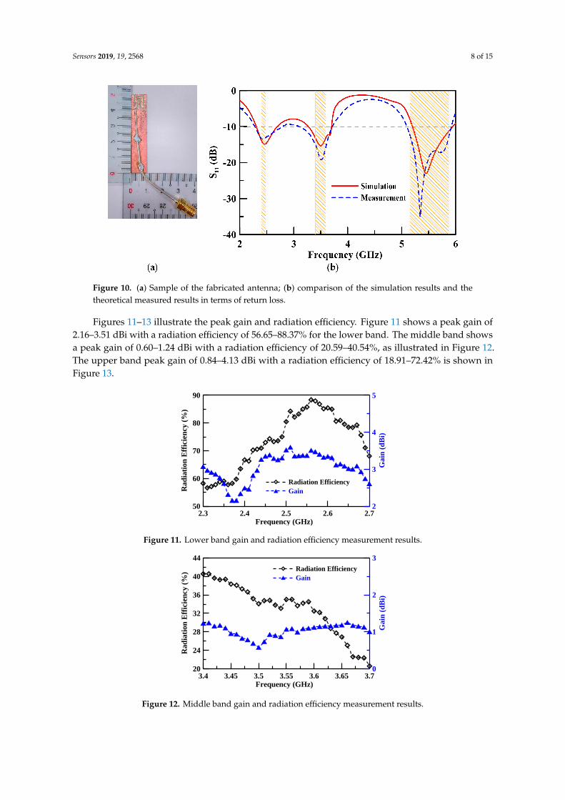
Figure 10. (a) Sample of the fabricated antenna; (b) comparison of the simulation results and thetheoretical measured results in terms of return loss.
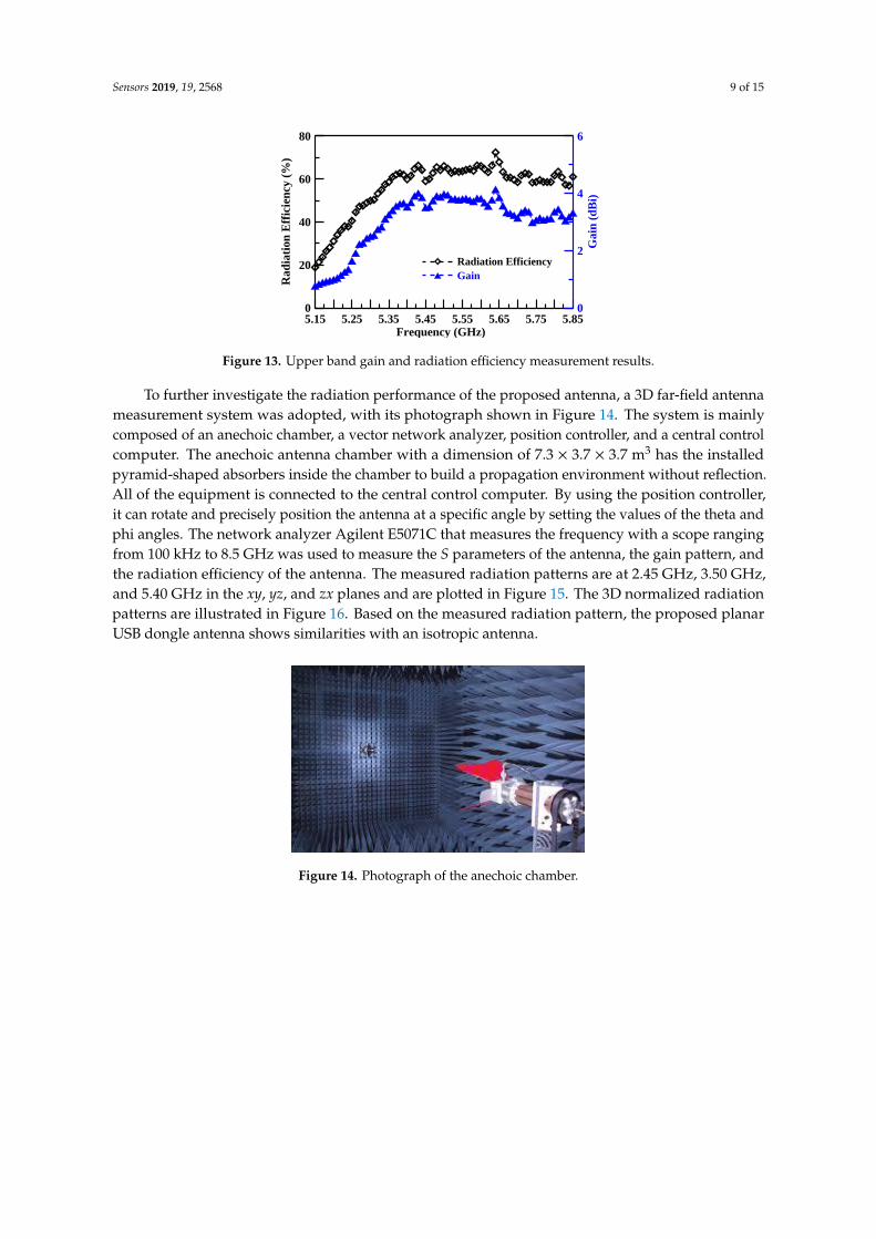
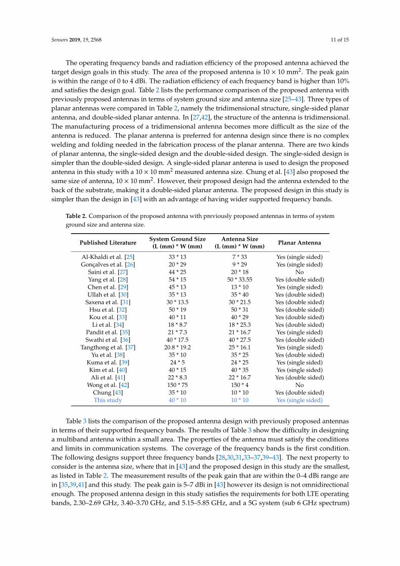
Figures 11–13 illustrate the peak gain and radiation efficiency. Figure 11 shows a peak gain of2.16–3.51 dBi with a radiation efficiency of 56.65–88.37% for the lower band. The middle band showsa peak gain of 0.60–1.24 dBi with a radiation efficiency of 20.59–40.54%, as illustrated in Figure 12.The upper band peak gain of 0.84–4.13 dBi with a radiation efficiency of 18.91–72.42% is shown inFigure 13.
Sensors 2019, 19, x FOR PEER REVIEW 8 of 15
2 3 4 5 6Frequency (GHz)
-40
-30
-20
-10
0
S1
1 (
dB
)
Simulation
Measurement
(a) (b)
Figure 10. (a) Sample of the fabricated antenna; (b) comparison of the simulation results
and the theoretical measured results in terms of return loss.
Figures 11–13 illustrate the peak gain and radiation efficiency. Figure 11 shows a peak gain of
2.16–3.51 dBi with a radiation efficiency of 56.65–88.37% for the lower band. The middle band shows
a peak gain of 0.60–1.24 dBi with a radiation efficiency of 20.59–40.54%, as illustrated in Figure 12.
The upper band peak gain of 0.84–4.13 dBi with a radiation efficiency of 18.91–72.42% is shown in
Figure 13.
2.3 2.4 2.5 2.6 2.7Frequency (GHz)
50
60
70
80
90
Rad
iati
on
Eff
icie
ncy (
%)
2
3
4
5
Gain
(d
Bi)
Radiation Efficiency
Gain
Figure 11. Lower band gain and radiation efficiency measurement results.
3.4 3.45 3.5 3.55 3.6 3.65 3.7Frequency (GHz)
20
24
28
32
36
40
44
Rad
iati
on
Eff
icie
ncy (
%)
0
1
2
3
Gain
(d
Bi)
Radiation Efficiency
Gain
Figure 12. Middle band gain and radiation efficiency measurement results.
Figure 11. Lower band gain and radiation efficiency measurement results.
Sensors 2019, 19, x FOR PEER REVIEW 8 of 15
2 3 4 5 6Frequency (GHz)
-40
-30
-20
-10
0
S1
1 (
dB
)
Simulation
Measurement
(a) (b)
Figure 10. (a) Sample of the fabricated antenna; (b) comparison of the simulation results
and the theoretical measured results in terms of return loss.
Figures 11–13 illustrate the peak gain and radiation efficiency. Figure 11 shows a peak gain of
2.16–3.51 dBi with a radiation efficiency of 56.65–88.37% for the lower band. The middle band shows
a peak gain of 0.60–1.24 dBi with a radiation efficiency of 20.59–40.54%, as illustrated in Figure 12.
The upper band peak gain of 0.84–4.13 dBi with a radiation efficiency of 18.91–72.42% is shown in
Figure 13.
2.3 2.4 2.5 2.6 2.7Frequency (GHz)
50
60
70
80
90
Rad
iati
on
Eff
icie
ncy (
%)
2
3
4
5
Gain
(d
Bi)
Radiation Efficiency
Gain
Figure 11. Lower band gain and radiation efficiency measurement results.
3.4 3.45 3.5 3.55 3.6 3.65 3.7Frequency (GHz)
20
24
28
32
36
40
44
Rad
iati
on
Eff
icie
ncy (
%)
0
1
2
3
Gain
(d
Bi)
Radiation Efficiency
Gain
Figure 12. Middle band gain and radiation efficiency measurement results. Figure 12. Middle band gain and radiation efficiency measurement results.
Sensors 2019, 19, 2568 9 of 15Sensors 2019, 19, x FOR PEER REVIEW 9 of 15
5.15 5.25 5.35 5.45 5.55 5.65 5.75 5.85Frequency (GHz)
0
20
40
60
80
Rad
iati
on
Eff
icie
ncy (
%)
0
2
4
6
Gain
(d
Bi)
Radiation Efficiency
Gain
Figure 13. Upper band gain and radiation efficiency measurement results.
To further investigate the radiation performance of the proposed antenna, a 3D far-field
antenna measurement system was adopted, with its photograph shown in Figure 14. The system is
mainly composed of an anechoic chamber, a vector network analyzer, position controller, and a
central control computer. The anechoic antenna chamber with a dimension of 7.3 × 3.7 × 3.7 m3 has
the installed pyramid-shaped absorbers inside the chamber to build a propagation environment
without reflection. All of the equipment is connected to the central control computer. By using the
position controller, it can rotate and precisely position the antenna at a specific angle by setting the
values of the theta and phi angles. The network analyzer Agilent E5071C that measures the
frequency with a scope ranging from 100 kHz to 8.5 GHz was used to measure the S parameters of
the antenna, the gain pattern, and the radiation efficiency of the antenna. The measured radiation
patterns are at 2.45 GHz, 3.50 GHz, and 5.40 GHz in the xy, yz, and zx planes and are plotted in
Figure 15. The 3D normalized radiation patterns are illustrated in Figure 16. Based on the measured
radiation pattern, the proposed planar USB dongle antenna shows similarities with an isotropic
antenna.
Figure 14. Photograph of the anechoic chamber.
Figure 13. Upper band gain and radiation efficiency measurement results.
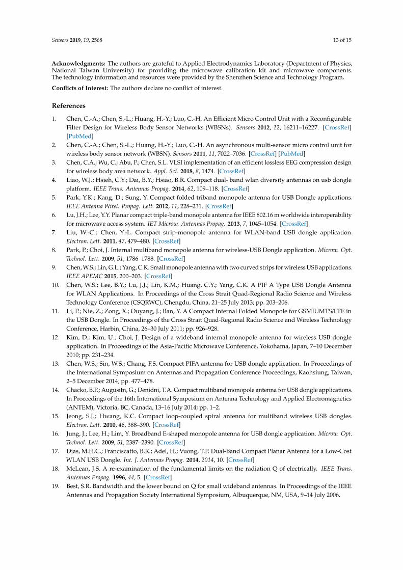
To further investigate the radiation performance of the proposed antenna, a 3D far-field antennameasurement system was adopted, with its photograph shown in Figure 14. The system is mainlycomposed of an anechoic chamber, a vector network analyzer, position controller, and a central controlcomputer. The anechoic antenna chamber with a dimension of 7.3 × 3.7 × 3.7 m3 has the installedpyramid-shaped absorbers inside the chamber to build a propagation environment without reflection.All of the equipment is connected to the central control computer. By using the position controller,it can rotate and precisely position the antenna at a specific angle by setting the values of the theta andphi angles. The network analyzer Agilent E5071C that measures the frequency with a scope rangingfrom 100 kHz to 8.5 GHz was used to measure the S parameters of the antenna, the gain pattern, andthe radiation efficiency of the antenna. The measured radiation patterns are at 2.45 GHz, 3.50 GHz,and 5.40 GHz in the xy, yz, and zx planes and are plotted in Figure 15. The 3D normalized radiationpatterns are illustrated in Figure 16. Based on the measured radiation pattern, the proposed planarUSB dongle antenna shows similarities with an isotropic antenna.
Sensors 2019, 19, x FOR PEER REVIEW 9 of 15
5.15 5.25 5.35 5.45 5.55 5.65 5.75 5.85Frequency (GHz)
0
20
40
60
80
Rad
iati
on
Eff
icie
ncy (
%)
0
2
4
6
Gain
(d
Bi)
Radiation Efficiency
Gain
Figure 13. Upper band gain and radiation efficiency measurement results.
To further investigate the radiation performance of the proposed antenna, a 3D far-field
antenna measurement system was adopted, with its photograph shown in Figure 14. The system is
mainly composed of an anechoic chamber, a vector network analyzer, position controller, and a
central control computer. The anechoic antenna chamber with a dimension of 7.3 × 3.7 × 3.7 m3 has
the installed pyramid-shaped absorbers inside the chamber to build a propagation environment
without reflection. All of the equipment is connected to the central control computer. By using the
position controller, it can rotate and precisely position the antenna at a specific angle by setting the
values of the theta and phi angles. The network analyzer Agilent E5071C that measures the
frequency with a scope ranging from 100 kHz to 8.5 GHz was used to measure the S parameters of
the antenna, the gain pattern, and the radiation efficiency of the antenna. The measured radiation
patterns are at 2.45 GHz, 3.50 GHz, and 5.40 GHz in the xy, yz, and zx planes and are plotted in
Figure 15. The 3D normalized radiation patterns are illustrated in Figure 16. Based on the measured
radiation pattern, the proposed planar USB dongle antenna shows similarities with an isotropic
antenna.
Figure 14. Photograph of the anechoic chamber. Figure 14. Photograph of the anechoic chamber.

Sensors 2019, 19, 2568 10 of 15Sensors 2019, 19, x FOR PEER REVIEW 10 of 15
(a) (b)
(c)
Figure 15. Two-dimensional normalized radiation pattern of the planar USB dongle
antenna at (a) 2.45 GHz, (b) 3.51 GHz, and (c) 5.45 GHz.
(a) (b)
(c)
x
yz
Figure 16. Three-dimensional normalized radiation pattern of the planar USB dongle
antenna at (a) 2.45 GHz, (b) 3.51 GHz, and (c) 5.44 GHz.
Figure 15. Two-dimensional normalized radiation pattern of the planar USB dongle antenna at (a)2.45 GHz, (b) 3.51 GHz, and (c) 5.45 GHz.
Sensors 2019, 19, x FOR PEER REVIEW 10 of 15
(a) (b)
(c)
Figure 15. Two-dimensional normalized radiation pattern of the planar USB dongle
antenna at (a) 2.45 GHz, (b) 3.51 GHz, and (c) 5.45 GHz.
(a) (b)
(c)
x
yz
Figure 16. Three-dimensional normalized radiation pattern of the planar USB dongle
antenna at (a) 2.45 GHz, (b) 3.51 GHz, and (c) 5.44 GHz.
Figure 16. Three-dimensional normalized radiation pattern of the planar USB dongle antenna at (a)2.45 GHz, (b) 3.51 GHz, and (c) 5.44 GHz.
Sensors 2019, 19, 2568 11 of 15
The operating frequency bands and radiation efficiency of the proposed antenna achieved thetarget design goals in this study. The area of the proposed antenna is 10 × 10 mm2. The peak gainis within the range of 0 to 4 dBi. The radiation efficiency of each frequency band is higher than 10%and satisfies the design goal. Table 2 lists the performance comparison of the proposed antenna withpreviously proposed antennas in terms of system ground size and antenna size [25–43]. Three types ofplanar antennas were compared in Table 2, namely the tridimensional structure, single-sided planarantenna, and double-sided planar antenna. In [27,42], the structure of the antenna is tridimensional.The manufacturing process of a tridimensional antenna becomes more difficult as the size of theantenna is reduced. The planar antenna is preferred for antenna design since there is no complexwelding and folding needed in the fabrication process of the planar antenna. There are two kindsof planar antenna, the single-sided design and the double-sided design. The single-sided design issimpler than the double-sided design. A single-sided planar antenna is used to design the proposedantenna in this study with a 10 × 10 mm2 measured antenna size. Chung et al. [43] also proposed thesame size of antenna, 10 × 10 mm2. However, their proposed design had the antenna extended to theback of the substrate, making it a double-sided planar antenna. The proposed design in this study issimpler than the design in [43] with an advantage of having wider supported frequency bands.
Table 2. Comparison of the proposed antenna with previously proposed antennas in terms of systemground size and antenna size.
Published Literature System Ground Size(L (mm) * W (mm)
Antenna Size(L (mm) * W (mm) Planar Antenna
Al-Khaldi et al. [25] 33 * 13 7 * 33 Yes (single sided)Gonçalves et al. [26] 20 * 29 9 * 29 Yes (single sided)
Saini et al. [27] 44 * 25 20 * 18 NoYang et al. [28] 54 * 15 50 * 33.55 Yes (double sided)Chen et al. [29] 45 * 13 13 * 10 Yes (single sided)Ullah et al. [30] 35 * 13 35 * 40 Yes (double sided)
Saxena et al. [31] 30 * 13.5 30 * 21.5 Yes (double sided)Hsu et al. [32] 50 * 19 50 * 31 Yes (double sided)Kou et al. [33] 40 * 11 40 * 29 Yes (double sided)Li et al. [34] 18 * 8.7 18 * 25.3 Yes (double sided)
Pandit et al. [35] 21 * 7.3 21 * 16.7 Yes (single sided)Swathi et al. [36] 40 * 17.5 40 * 27.5 Yes (double sided)
Tangthong et al. [37] 20.8 * 19.2 25 * 16.1 Yes (single sided)Yu et al. [38] 35 * 10 35 * 25 Yes (double sided)
Kuma et al. [39] 24 * 5 24 * 25 Yes (single sided)Kim et al. [40] 40 * 15 40 * 35 Yes (single sided)Ali et al. [41] 22 * 8.3 22 * 16.7 Yes (double sided)
Wong et al. [42] 150 * 75 150 * 4 NoChung [43] 35 * 10 10 * 10 Yes (double sided)This study 40 * 10 10 * 10 Yes (single sided)
Table 3 lists the comparison of the proposed antenna design with previously proposed antennasin terms of their supported frequency bands. The results of Table 3 show the difficulty in designinga multiband antenna within a small area. The properties of the antenna must satisfy the conditionsand limits in communication systems. The coverage of the frequency bands is the first condition.The following designs support three frequency bands [28,30,31,33–37,39–43]. The next property toconsider is the antenna size, where that in [43] and the proposed design in this study are the smallest,as listed in Table 2. The measurement results of the peak gain that are within the 0–4 dBi range arein [35,39,41] and this study. The peak gain is 5–7 dBi in [43] however its design is not omnidirectionalenough. The proposed antenna design in this study satisfies the requirements for both LTE operatingbands, 2.30–2.69 GHz, 3.40–3.70 GHz, and 5.15–5.85 GHz, and a 5G system (sub 6 GHz spectrum)

Sensors 2019, 19, 2568 12 of 15
operating band, 3.40–3.60 GHz. The LTE-U band of a 5G system is also included in the supportedfrequency bands of the proposed antenna in this study.
Table 3. Comparison of the proposed antenna with previously proposed antennas in terms of supportedfrequency bands.
Published Literature Lower Band (GHz) Middle Band (GHz) Upper Band (GHz)
Al-Khaldi et al. [25] 2.50–3.50 NA 5.00–5.50Gonçalves et al. [26] 2.30–2.69 NA NA
Saini et al. [27] 2.30–2.70 3.40–3.60 NAYang et al. [28] 1.39–1.48 1.75–4.20 5.04–6.00Chen et al. [29] 2.40–2.484 NA 4.70–5.825Ullah et al. [30] 2.30–2.69 3.40–3.70 5.15–5.85
Saxena et al. [31] 2.30–2.622.63–2.90 3.30–4.80 5.50–8.02Hsu et al. [32] 1.43–3.29 NA NAKou et al. [33] 2.21–2.53 3.20–3.83 5.41–8.37Li et al. [34] 2.41–2.63 3.39–3.70 4.96–6.32
Pandit et al. [35] 2.35–2.53 3.20–4.26 5.24–6.06Swathi et al. [36] 1.68–2.71 3.26–4.06 5.03–6.25
Tangthong et al. [37] 2.29–2.98 3.23–4.16 5.08–6.38.Yu et al. [38] NA 3.20–3.90 5.75–5.85
Kuma et al. [39] 2.50–2.71 3.37–3.63 5.20–5.85Kim et al. [40] 2.39–2.59 3.10–3.57 5.45–6.50Ali et al. [41] 2.26–2.57 3.27–3.60 5.69–5.98
Wong et al. [42] 2.41–2.63 NA 5.15–5.85Chung [43] 2.30–2.69 3.40–3.70 5.15–5.85This study 2.27–2.79 3.11–3.72 5.10–5.92
4. Conclusions
A high-performance antenna has two main indicators. The first indicator is the function of theantenna, namely its supported frequency bands, gain, and radiation efficiency. The second indicatorpertains to the structure of the antenna. The size of antenna needs to be as small as possible and underits physical limited condition. Under Chu’s limits, the radiation efficiency and bandwidth are limitedby the size of the antenna. The Friis transmission equation can estimate the radiation efficiency that thesystem needs under the conditions of the operational environment. The omnidirectional antenna is anideal mode for the USB dongle antenna; the ideal peak gain must be close to 0 dBi. Following the saidconditions enables the construction of an antenna design that works within its expected performance.Moreover, manufacturing of the antenna must be simplified in order to reduce the cost.
A compact multiband planar USB dongle antenna has been designed to cover the LTE, 5G system(Sub 6 GHz spectrum), Bluetooth, and frequency bands for WSNs. The radiation efficiency achieved is10% for each band. The peak gain for each band is approximately 0–4 dBi. The main antenna has acompact size of 10 × 10 mm2 and a volume of 10 × 50 × 0.8 mm3. The main advantage of the proposedantenna is that it can support the triple band operation with a small size and simplified process formanufacturing. The proposed antenna can support a 5G LTE system, which can be embedded in awireless communication device for WSNs applications.
Author Contributions: Conceptualization, W.-Y.C.; Data curation, C.-H.K. and C.-A.C.; Formal analysis, W.-Y.C.,C.-H.K., C.-A.C., P.A.R.A. and S.-L.C.; Investigation, W.-Y.C., C.-A.C. and S.-L.C.; Methodology, W.-Y.C. andC.-H.K.; Project administration, W.-Y.C. and C.-H.K.; Resources, W.-Y.C., C.-H.K., C.-A.C. and C.-H.L.; Software,W.-Y.C., C.-H.K., C.-A.C. and L.-Y.W.; Supervision, W.-Y.C.; Validation, C.-H.K., C.-A.C., L.-Y.W., P.-Z.R. andC.-K.L.; Visualization, W.-Y.C., P.A.R.A., P.-Z.R., C.-K.L., C.-H.L. and S.-L.C.; Writing – original draft, W.-Y.C.,C.-A.C., P.A.R.A. and S.-L.C.; Writing – review & editing, C.-A.C., P.A.R.A., P.-Z.R., C.-K.L. and S.-L.C.
Funding: This work was supported by the Ministry of Science and Technology (MOST), Taiwan, undergrant numbers of MOST-107-2218-E-131-002, MOST-107-2221-E-033-057, MOST-107-2622-E-131-007-CC3,MOST-106-2622-E-033-014-CC2, MOST-106-2221-E-033-072, MOST-106-2119-M-033-001, MOST 107-2112-M-131-001, and the National Chip Implementation Center, Taiwan.
Sensors 2019, 19, 2568 13 of 15
Acknowledgments: The authors are grateful to Applied Electrodynamics Laboratory (Department of Physics,National Taiwan University) for providing the microwave calibration kit and microwave components.The technology information and resources were provided by the Shenzhen Science and Technology Program.
Conflicts of Interest: The authors declare no conflict of interest.
References
1. Chen, C.-A.; Chen, S.-L.; Huang, H.-Y.; Luo, C.-H. An Efficient Micro Control Unit with a ReconfigurableFilter Design for Wireless Body Sensor Networks (WBSNs). Sensors 2012, 12, 16211–16227. [CrossRef][PubMed]
2. Chen, C.-A.; Chen, S.-L.; Huang, H.-Y.; Luo, C.-H. An asynchronous multi-sensor micro control unit forwireless body sensor network (WBSN). Sensors 2011, 11, 7022–7036. [CrossRef] [PubMed]
3. Chen, C.A.; Wu, C.; Abu, P.; Chen, S.L. VLSI implementation of an efficient lossless EEG compression designfor wireless body area network. Appl. Sci. 2018, 8, 1474. [CrossRef]
4. Liao, W.J.; Hsieh, C.Y.; Dai, B.Y.; Hsiao, B.R. Compact dual- band wlan diversity antennas on usb dongleplatform. IEEE Trans. Antennas Propag. 2014, 62, 109–118. [CrossRef]
5. Park, Y.K.; Kang, D.; Sung, Y. Compact folded triband monopole antenna for USB Dongle applications.IEEE Antenna Wirel. Propag. Lett. 2012, 11, 228–231. [CrossRef]
6. Lu, J.H.; Lee, Y.Y. Planar compact triple-band monopole antenna for IEEE 802.16 m worldwide interoperabilityfor microwave access system. IET Microw. Antennas Propag. 2013, 7, 1045–1054. [CrossRef]
7. Liu, W.-C.; Chen, Y.-L. Compact strip-monopole antenna for WLAN-band USB dongle application.Electron. Lett. 2011, 47, 479–480. [CrossRef]
8. Park, P.; Choi, J. Internal multiband monopole antenna for wireless-USB Dongle application. Microw. Opt.Technol. Lett. 2009, 51, 1786–1788. [CrossRef]
9. Chen, W.S.; Lin, G.L.; Yang, C.K. Small monopole antenna with two curved strips for wireless USB applications.IEEE APEMC 2015, 200–203. [CrossRef]
10. Chen, W.S.; Lee, B.Y.; Lu, J.J.; Lin, K.M.; Huang, C.Y.; Yang, C.K. A PIF A Type USB Dongle Antennafor WLAN Applications. In Proceedings of the Cross Strait Quad-Regional Radio Science and WirelessTechnology Conference (CSQRWC), Chengdu, China, 21–25 July 2013; pp. 203–206.
11. Li, P.; Nie, Z.; Zong, X.; Ouyang, J.; Ban, Y. A Compact Internal Folded Monopole for GSMIUMTS/LTE inthe USB Dongle. In Proceedings of the Cross Strait Quad-Regional Radio Science and Wireless TechnologyConference, Harbin, China, 26–30 July 2011; pp. 926–928.
12. Kim, D.; Kim, U.; Choi, J. Design of a wideband internal monopole antenna for wireless USB dongleapplication. In Proceedings of the Asia-Pacific Microwave Conference, Yokohama, Japan, 7–10 December2010; pp. 231–234.
13. Chen, W.S.; Sin, W.S.; Chang, F.S. Compact PIFA antenna for USB dongle application. In Proceedings ofthe International Symposium on Antennas and Propagation Conference Proceedings, Kaohsiung, Taiwan,2–5 December 2014; pp. 477–478.
14. Chacko, B.P.; Augusitn, G.; Denidni, T.A. Compact multiband monopole antenna for USB dongle applications.In Proceedings of the 16th International Symposium on Antenna Technology and Applied Electromagnetics(ANTEM), Victoria, BC, Canada, 13–16 July 2014; pp. 1–2.
15. Jeong, S.J.; Hwang, K.C. Compact loop-coupled spiral antenna for multiband wireless USB dongles.Electron. Lett. 2010, 46, 388–390. [CrossRef]
16. Jung, J.; Lee, H.; Lim, Y. Broadband E-shaped monopole antenna for USB dongle application. Microw. Opt.Technol. Lett. 2009, 51, 2387–2390. [CrossRef]
17. Dias, M.H.C.; Franciscatto, B.R.; Adel, H.; Vuong, T.P. Dual-Band Compact Planar Antenna for a Low-CostWLAN USB Dongle. Int. J. Antennas Propag. 2014, 2014, 10. [CrossRef]
18. McLean, J.S. A re-examination of the fundamental limits on the radiation Q of electrically. IEEE Trans.Antennas Propag. 1996, 44, 5. [CrossRef]
19. Best, S.R. Bandwidth and the lower bound on Q for small wideband antennas. In Proceedings of the IEEEAntennas and Propagation Society International Symposium, Albuquerque, NM, USA, 9–14 July 2006.
Sensors 2019, 19, 2568 14 of 15
20. Kiruthiga, V.; Thamarairubini, K.; Sowbakkiyam, S.; Ramaya, K.; Ashwin, K.; Suresh Kumar, S. Design andComparative Study of Meander Antenna and Microstrip Patch Antenna. Int. J. Adv. Res. Electron. Commun.Eng. 2014, 3, 1526–1528.
21. Shaw, J.A. Radiometry and the Friis transmission equation. Am. J. Phys. 2013, 81, 33–37. [CrossRef]22. IEEE STANDARDS. Available online: https://standards.ieee.org/standard/802_11n-2009.html (accessed on
29 October 2009).23. Khan, R.; Al-Hadi, A.A.; Soh, P.J.; Kamarudin, M.R.; Ali, M.T. User influence on mobile terminal antennas:
A review of challenges and potential solution for 5G antennas. IEEE Access 2018, 6, 77695–77715. [CrossRef]24. Bairagi, A.K.; Abedin, S.F.; Tran, N.H.; Niyato, D.; Hong, C.S. QoE-Enabled Unlicensed Spectrum Sharing in
5G: A Game-Theoretic Approach. IEEE Access 2018, 6, 50538–50554. [CrossRef]25. Al-Khaldi, M. A highly compact multiband antenna for Bluetooth/WLAN, WiMAX, and Wi-Fi applications.
Microw. Opt. Technol. Lett. 2017, 59, 77–80. [CrossRef]26. Gonçalves, R.; Carvalho, N.B.; Pinho, P. Small antenna design for very compact devices and wearables.
IET Microw. Antennas Propag. 2017, 11, 874–879. [CrossRef]27. Saini, H.S.; Thakur, A.; Kumar, R.; Sharma, A.; Kumar, N. A small size wideband planar inverted-F antenna
for USB dongle devices. In Proceedings of the IEEE 1st International Conference on Power Electronics,Intelligent Control and Energy Systems (ICPEICES), Delhi, India, 4–6 July 2016; pp. 1–3.
28. Yang, Y.; Liu, Y. A CPW-fed triple-band planar monopole antenna for internet of things applications.In Proceedings of the International Conference on Cyber-Enabled Distributed Computing and KnowledgeDiscovery, Shanghai, China, 13–15 October 2014; pp. 380–383.
29. Chen, W.S.; Yang, C.K.; Lin, G.Q. Compact design of printed antenna with a ground slot for USB applications.In Proceedings of the IEEE 5th Asia-Pacific Conference on Antennas and Propagation (APCAP), Kaohsiung,Taiwan, 26–29 July 2016; pp. 127–128.
30. Ullah, S.; Hayat, S.; Umar, A.; Ali, U.; Tahir, F.A.; Flint, J.A. Design, fabrication and measurement of triple bandfrequency reconfigur-able antennas for portable wireless communications. AEU Int. J. Electron. Commun.2017, 81, 236–242. [CrossRef]
31. Saxena, S.; Kanaujia, B.K.; Dwari, S.; Kumar, S.; Tiwari, R. A com- pact microstrip fed dual polarisedmultiband antenna for IEEE 802.11 a/b/g/n/ac/ax applications. AEU Int. J. Electron. Commun. 2017, 72, 95–103.[CrossRef]
32. Hsu, C.-W.; Shih, M.-H.; Wang, C.-J. A triple-strip monopole antenna with dual-band circular polarization.In Proceedings of the IEEE 5th Asia-Pacific Conference on Antennas and Propagation (APCAP), Kaohsiung,Taiwan, 26–29 July 2016; pp. 137–138.
33. Kou, H.-R.; Zhang, B.-Z.; Duan, J.-P.; Ge, S.-L. Triple-band monopole planar antenna designed forWLAN/WiMAX application. In Proceedings of the IEEE International Conference on Microwave andMillimeter Wave Technology (ICMMT), Beijing, China, 5–8 June 2016; pp. 555–557.
34. Li, L.; Zhang, X.; Yin, X.; Zhou, L. A compact triple-band printed monopole antenna for WLAN/WiMAXapplications. IEEE Antennas Wirel. Propag. Lett. 2016, 15, 1853–1855. [CrossRef]
35. Pandit, V.K.; Harish, A.R. A compact CPW-fed triple band monop-ole antenna for WLAN/WiMAX applications.In Proceedings of the Asia-Pacific Microwave Conference (APMC), New Delhi, India, 5–9 December 2016;pp. 1–4.
36. Swathi, S.; Bhanumathi, V. Triple band monopole antenna for WLAN and WIMAX applications.In Proceedings of the International Conference on Recent Trends in Information Technology (ICRTIT),Chicago, IL, USA, 8–14 July 2012; pp. 1–4.
37. Tangthong, N.; Moeikham, P.; Akatimagool, S. A compact multi band CPW-Fed monopole antennausing L-shaped and straight slots. In Proceedings of the 13th International Conference on ElectricalEngineering/Electronics, Computer, Telecommunications and Information Technology (ECTI-CON),Chiang Mai, Thailand, 1–28 June 2016; pp. 1–4.
38. Yu, K.; Li, Y.; Wang, Y. Multi-band metamaterial-based microstrip antenna for WLAN and WiMAXapplications. In Proceedings of the International Applied Computational Electromagnetics SocietySymposium—Italy (ACES), Florence, Italy, 26–30 March 2017; pp. 1–2.
39. Kuma, A.; Jhanwar, D.; Sharma, M.M. A compact printed multi stubs loaded resonator rectangular monopoleantenna design for multiband wireless systems. Int. J. RF Microw. Comput. Aided Eng. 2017, 27, e21147.[CrossRef]

Sensors 2019, 19, 2568 15 of 15
40. Oh Kim, D.; Kim, C.-Y.; Yang, D.-G.; Sajjad Ahmad, M. Multiband omnidirectional planar monopole antennawith two split ring resonator pairs. Microw. Opt. Technol. Lett. 2017, 59, 753–758. [CrossRef]
41. Ali, T.; Biradar, R.C. A compact multiband antenna using k/4 rectangular stub loaded with metamaterial forIEEE 802.11N and IEEE 802.16E. Microw. Opt. Technol. Lett. 2017, 59, 1000–1006. [CrossRef]
42. Wong, K.-L.; Lu, J.-Y. Small-size narrow open-slot antenna for the 2.4/5.2/5.8-GHz WLAN operation alongthe side edge of the metal-framed smartphone. Microw. Opt. Technol. Lett. 2016, 58, 886–892. [CrossRef]
43. Chung, M.A. A miniaturized triple band monopole antenna with a coupled branch strip for bandwidthenhancement for IoT applications. Microw. Opt. Technol. Lett. 2018, 60, 2336–2342. [CrossRef]
© 2019 by the authors. Licensee MDPI, Basel, Switzerland. This article is an open accessarticle distributed under the terms and conditions of the Creative Commons Attribution(CC BY) license (http://creativecommons.org/licenses/by/4.0/).