A Compact and Versatile Electrospray Ion Beam ... - mediaTUM
154
Department of Physics A Compact and Versatile Electrospray Ion Beam Deposition Setup Advanced Sample Preparation for Experiments in Surface Science Tobias Kaposi Dissertation Technical University Munich
-
Upload
khangminh22 -
Category
Documents
-
view
0 -
download
0
Transcript of A Compact and Versatile Electrospray Ion Beam ... - mediaTUM

Department of Physics
A Compact and VersatileElectrospray Ion Beam Deposition Setup
Advanced Sample Preparationfor Experiments in Surface Science
Tobias KaposiDissertation
Technical University Munich


Technische Universität München
Lehrstuhl E20 - Molekulare Nanowissenschaften und ChemischePhysik von Grenzflächen
A Compact and VersatileElectrospray Ion Beam Deposition Setup
Advanced Sample Preparationfor Experiments in Surface Science
Tobias Kaposi
Vollständiger Abdruck der von der Fakultät für Physik der Technischen Univer-sität München zur Erlangung des akademischen Grades eines Doktors der Natur-wissenschaften (Dr. rer. nat.) genehmigten Dissertation.
Vorsitzender: Prof. Dr. Michael Knap
Prüfer der Dissertation: 1. Prof. Dr. Johannes Barth
2. Prof. Dr. Ulrich K. Heiz
Die Dissertation wurde am 31.3.2016 bei der Technischen Universität Müncheneingereicht und durch die Fakultät für Physik am 17.5.2016 angenommen.


Again the message to experimentalists is: Be sensible but don’t
be impressed too much by negative arguments. If at all possible,
try it and see what turns up.
- Francis Crick


For Marlene

Abstract
Over the course of surface science’s almost 100 year long history, a particu-
lar class of experimental problems, namely self-assembling organic molecules
adsorbed on pristine surfaces, has earned special interest. Especially the
fabrication and control of functional molecular films and nanoarchitectures
have been a strong motivational driving force in this regard. For the express
purpose of depositing organic molecules onto surfaces under ultrahigh vac-
uum (UHV) conditions organic molecular beam epitaxy (OMBE) has so far
been the method of choice. OMBE, however, suffers from a severe limita-
tion due to molecular thermolability, which renders deposition of high mass
molecules impossible.
In order to push the boundaries towards molecules of arbitrary mass a spe-
cialized sample preparation setup utilizing the concept of electrospray ion
beam deposition (ESIBD) has been developed and built during this thesis.
In contrast to OMBE, this technique is of a more intricate nature and re-
quires careful control of several closely intertwined system parameters. Due
to the critical source processes being conducted at atmospheric pressure a
differential pumping system has to be implemented. Ions then have to be
transmitted through this using radio frequency (RF) driven ion guidance
systems in order to minimize beam current losses. Critical parameters of
the pumping and ion guiding systems have to be controlled using an em-
bedded system with integral control capabilities. The setup presented here
fulfills all of these requirements in an unprecedented compact and versatile
manner. It has been used to conduct a series of proof-of-principle sample
preparations using a well known molecule. Additionally, a series of STM ex-
periments have been conducted using OMBE as the preparation technique
in order to put the capabilities of this method into perspective.


Kurzfassung
Während der beinahe einhundertjährigen geschichtlichen Entwicklung der
Oberflächenphysik hat sich die Klasse der selbstanordnenden organischen
Moleküle auf hochreinen Oberflächen als Objekt wissenschaftlichen Inter-
esses besonders hervor getan. Insbesondere die Herstellung und Modifikation
von funktionellen Molekülschichten und Nanoarchitekturen waren treibende
Kräfte dieser Entwicklung. Für die Deposition organischer Moleküle auf
Oberflächen unter Ultrahochvakuum (UHV) war bisher die Organische Mole-
kularstrahlepitaxie (OMBE) die Methode der Wahl. Diese ist jedoch lim-
itiert aufgrund der thermischen Instabilität von Molekülen hoher molarer
Masse, welche deswegen zur Deposition nicht zur Verfügung stehen.
Um die Deposition beliebig schwerer Moleküle zu ermöglichen wurde im
Rahmen der vorliegenden Arbeit ein hoch spezialisiertes Präparationssys-
tem entwickelt und aufgebaut, welches auf dem Prinzip der Elektrospray-
Ionenstrahldeposition (ESIBD) beruht. Im Gegensazu zu OMBE ist dieses
jedoch deutlich komplexer und setzt die präzise Steuerung meherer, stark
verflochtener Systemparameter voraus. Da die Ionen-erzeugenden Prozesse
bei Umgebungsdruck stattfinden ist der Bau eines differentiell gepumpten
Kammersystems von Nöten, durch welches die erzeugten Ionen mithilfe
von hochfrequent betriebenen Ionenleitern geführt werden müssen, um Ver-
luste zu minimieren. Kritische Parameter des Pumpsystems und der Ionen-
leitenden Systeme müssen von einem embedded system mit umfassendem
Steuerungspotential kontrolliert werden. Der hier präsentierte, überaus kom-
pakte und flexible Aufbau erfüllt all diese Bedingungen und wurde bereits
verwendet um eine Reihe erster Versuchsdepositionen mit einem wohl bekan-
nten Molekül durchzuführen. Außerdem wurden in einer Serie von STM Ex-
perimenten, bei denen OMBE als Präparationsmethode verwendet wurde,
die Fähigkeiten der beiden Techniken verglichen.


Contents
1 Introduction and Motivation 1
2 Fundamentals and Theory 5
2.1 Scanning Tunneling Microscopy . . . . . . . . . . . . . . . . . . . . . . . 6
2.1.1 Theoretical Aspects . . . . . . . . . . . . . . . . . . . . . . . . . 6
2.1.2 STM Control . . . . . . . . . . . . . . . . . . . . . . . . . . . . . 8
2.1.3 Sample Geometries . . . . . . . . . . . . . . . . . . . . . . . . . . 10
2.1.4 A Few Words on Commensurability . . . . . . . . . . . . . . . . 11
2.2 Organic Molecular Beam Epitaxy . . . . . . . . . . . . . . . . . . . . . . 13
2.3 Electrospray Ionization . . . . . . . . . . . . . . . . . . . . . . . . . . . . 15
2.3.1 Spray Modes . . . . . . . . . . . . . . . . . . . . . . . . . . . . . 16
2.3.2 Ion Generation . . . . . . . . . . . . . . . . . . . . . . . . . . . . 17
2.4 Vacuum Ion Guidance Systems . . . . . . . . . . . . . . . . . . . . . . . 20
2.4.1 Theory of RF-driven Ion Guides . . . . . . . . . . . . . . . . . . 21
2.4.2 Multipole Ion Guides . . . . . . . . . . . . . . . . . . . . . . . . . 23
2.4.3 Ion funnel . . . . . . . . . . . . . . . . . . . . . . . . . . . . . . . 25
2.4.4 Ion Trajectory Simulations . . . . . . . . . . . . . . . . . . . . . 27
2.4.5 RF Power Supplies . . . . . . . . . . . . . . . . . . . . . . . . . . 29
3 STM: Case Studies of a Predicament 31
3.1 Rare Earth Sandwich Complexes . . . . . . . . . . . . . . . . . . . . . . 31
3.1.1 Self-assembly on Noble Metal Surfaces . . . . . . . . . . . . . . . 33
3.1.2 Contrast through Orientation? . . . . . . . . . . . . . . . . . . . 36
3.1.3 Summary . . . . . . . . . . . . . . . . . . . . . . . . . . . . . . . 40
3.2 Alkyne-functionalized Pyrenes . . . . . . . . . . . . . . . . . . . . . . . . 41
3.2.1 Phenyl-terminated Control Group . . . . . . . . . . . . . . . . . 42
3.2.2 Pyridyl-mediated Self-assembly . . . . . . . . . . . . . . . . . . . 43
3.2.3 Summary . . . . . . . . . . . . . . . . . . . . . . . . . . . . . . . 47
3.3 Limitations of OMBE . . . . . . . . . . . . . . . . . . . . . . . . . . . . 47

CONTENTS
3.3.1 Thermolability . . . . . . . . . . . . . . . . . . . . . . . . . . . . 48
3.3.2 Contamination . . . . . . . . . . . . . . . . . . . . . . . . . . . . 51
3.3.3 Deposition Parameters . . . . . . . . . . . . . . . . . . . . . . . . 55
4 Electrospray Ion Beam Deposition: A Sprayed Solution 59
4.1 The Setup in its Current State . . . . . . . . . . . . . . . . . . . . . . . 60
4.2 ESI Source . . . . . . . . . . . . . . . . . . . . . . . . . . . . . . . . . . 63
4.2.1 Spraying in Low Vacuum . . . . . . . . . . . . . . . . . . . . . . 63
4.2.2 Spraying at Atmospheric Pressure . . . . . . . . . . . . . . . . . 68
4.3 Differential Pumping . . . . . . . . . . . . . . . . . . . . . . . . . . . . . 70
4.3.1 Attainable Pressures . . . . . . . . . . . . . . . . . . . . . . . . . 70
4.3.2 The Current Solution . . . . . . . . . . . . . . . . . . . . . . . . 74
4.4 Ion Guidance Systems . . . . . . . . . . . . . . . . . . . . . . . . . . . . 77
4.4.1 Relations derived from Simulations . . . . . . . . . . . . . . . . . 77
4.4.2 Ion Funnel . . . . . . . . . . . . . . . . . . . . . . . . . . . . . . . 79
4.4.3 Thin Wire Ion Guides . . . . . . . . . . . . . . . . . . . . . . . . 81
4.5 Supply and Control . . . . . . . . . . . . . . . . . . . . . . . . . . . . . . 83
4.5.1 Radio Frequency Boosters . . . . . . . . . . . . . . . . . . . . . . 84
4.5.2 Supply and Measurement Electronics . . . . . . . . . . . . . . . . 88
4.5.3 Control Software . . . . . . . . . . . . . . . . . . . . . . . . . . . 93
4.6 Sample Preparation and Analysis . . . . . . . . . . . . . . . . . . . . . . 95
4.6.1 2H-TPP on Au(111) and Ag(111) . . . . . . . . . . . . . . . . . . 97
5 Conclusion and Outlook 101
A Materials & Methods 105
A.1 STM: Samples and Procedures . . . . . . . . . . . . . . . . . . . . . . . 105
A.2 SIMION: Simulation Parameters . . . . . . . . . . . . . . . . . . . . . . 106
A.3 ESIBD: Solutions and Procedures . . . . . . . . . . . . . . . . . . . . . . 107
B Electronic Hardware 109
B.1 OMBE Heating Control Unit . . . . . . . . . . . . . . . . . . . . . . . . 109
B.2 RF Booster . . . . . . . . . . . . . . . . . . . . . . . . . . . . . . . . . . 111
B.3 High Voltage Board . . . . . . . . . . . . . . . . . . . . . . . . . . . . . . 115
B.4 Current Detect Board . . . . . . . . . . . . . . . . . . . . . . . . . . . . 117
B.5 Solar Power Board . . . . . . . . . . . . . . . . . . . . . . . . . . . . . . 120
References 123
Acknowledgment 139

1
Introduction and Motivation
Nanoscience is the investigation and controlled manipulation of material systems which
exhibit one or more of their three spatial dimensions in the nm range. Here, matter
behaves differently, with material properties showing a strong dependence on system
size and quantum mechanical effects. It is, today, one of the most busy fields of research
even though its history only dates back to the early 1980’s with Binnig and Rohrer’s
invention of the scanning tunneling microscope (STM) [1, 2] and the discovery of C60
[3], a relatively short time-frame compared to other scientific areas. This has largely
been motivated due to the rapid developments in semiconductor technology, where
upholding Moore’s law [4] has now made the control of processes at the nanometer
scale mandatory in order to reach a sufficiently small feature size, a development which
had been predicted for quite some time [5]. In turn, a broad shift of focus towards this
regime has occurred in other fields as well, such as chemistry and engineering in general
(see below).
The field’s spiritual roots go back to the beginnings of surface science [6, 7], with
which it is closely related to quite some extent. Richard Feynman is often cited as
the original instigator of research into nanoscience due to his immensely foresighted
1959 talk, "There’s plenty of room at the bottom" [8], in which he predicted systems
verging on science fiction then, some of which have been realized by now. His influence,
however, has been found to be retro-fitted, very much akin to a classical post hoc ergo
propter hoc fallacy, as the talk only really came to fame in the 1990’s, well after the
first groundbreaking experiments [9]. Whatever its true origins, nanoscience has now
sprouted into a multitude of diverse sub-areas, spread out, for the most part, diffusely
over the classical fields of chemistry, physics, and electrical engineering. Amongst its
most heavily investigated topics are such diverse elements as: catalysis [10–12], quantum
computing [13, 14], spintronics and magnetic information storage [15–17], molecular
machinery [18–20], and even tribology [21, 22].
1

1. INTRODUCTION AND MOTIVATION
The Science of Molecules at Interfaces
One particularly interesting and much studied class of phenomena in nanoscience is the
behavior of single molecules (or ensembles thereof) adsorbed on well-defined semicon-
ductor or metal surfaces. Due to the predominance of electrostatic and dipole forces
at these length scales an intriguing interplay between molecules and surface arises.
This can manifest itself as an attractive interaction between molecules, leading to self-
assembled structures exhibiting properties very much worth investigating in itself as
molecular machines [23] or novel sources for the bottom-up fabrication of nanosized
patterns [24]. The latter are often cited as promising candidates for etching templates
or nano-sized beakers [25, 26]. However, because these structures consist of molecules
with distinct chemical and/or physical properties frequently surpassing those of classi-
cal building materials, a whole meta-level of purposeful design possibilities arises. Why
go to great lengths in making a molecular etching mask for nano-electronics, when
you can "just as easily" fabricate a molecular transistor or circuit [27–29] using similar
techniques, for example? The true power of self-assembled molecular architectures on
surfaces thus lies in the possibility to combine form with function, as these two aspects,
which are usually strongly separated in systems design, converge at the nano-scale.
The biggest challenge in designing such systems, which science has yet to overcome,
lies in the reliable prediction of the aforementioned interactive behavior. Whether
molecules will be attracted more or less to each other or even the surface depends
strongly on their chemical nature and functional moieties, opening up a vast hyper-
space of possible assembly and on-surface reaction pathways [30–32]. Minute changes
in chemical composition and/or surface constitution can thus have a large influence on
the resulting behavior upon adsorption. Although experienced researchers can usually
design a molecule such that it behaves within certain predictable limits, a level of control
needed to build truly complex systems is still very much out of reach. Finding general
relationships, which govern these dependencies, is thus currently of great interest in
both experimental and theoretical surface science [33, 34]. Furthermore, surface con-
taminations may also have a devastating impact, making the use of ultra-clean sample
preparation and analysis techniques necessary.
More is More - A Motivation
In conjunction with the empiric nature of scientific research it would thus be beneficial to
expand the scope of systems which can be investigated in order to arrive at far-reaching
and universal correlations. This would, in turn, enable the tailored manufacture of nano-
systems by means of a sort of nano-cookbook. It is exactly this proposed expansion of
2

scope, which represents the motivational basis for the present thesis. So far, only one
sample preparation technique has been commonly used to deposit organic molecules on
surfaces under ultra-clean conditions, namely organic molecular beam epitaxy (OMBE)
[35]. However, this technique is, as will be shown later on, considerably limited in the
scope of molecules available for deposition with it due to thermolability, which runs
counter to the aforementioned desired expansion. Apart from that, it also features
some other, more minor drawbacks, as we will see. Suitable alternative techniques,
which allow for thermolabile molecules to be deposited and subsequently investigated
thus have to be found and developed.
In the following chapters one such technique, called electrospray ion beam deposition
(ESIBD), will be presented and discussed. In chapter 2 an overview and theoretical
discussion of all relevant techniques, including both mentioned preparation methods as
well as STM, will be given. During this thesis, a series of STM experiments with the
aim of investigating different molecules adsorbed on noble metal substrates in ultrahigh
vacuum (UHV) have been conducted, using the traditional OMBE deposition method.
These molecules were specifically chosen to be at the limit of OMBE’s capabilities.
Results of these investigations will be presented in chapter 3 with a special emphasis
on such findings, which directly or indirectly result from complications during sample
preparation and thus highlight OMBE’s limitations.
Furthermore, in order to push back these boundaries and embark on the road to sam-
ple preparations with thermolabile molecules an ESIBD setup was developed and built
during the present thesis. In contrast to OMBE’s straightforward approach, however,
ESIBD is a complex process necessitating precise control of many intricately interact-
ing system parts. This starts at the purely mechanical level of a differential pumping
system, which is intertwined closely with a series of ion beam guiding devices. These,
in turn, are in need of a suitable electronic power supply, which should itself be pre-
cisely controllable along with several other system parameters. An almost completely
custom-made system consisting of mechanical and electronic hardware, an embedded
control system, as well as a suitable control software has been developed and built. It is
being presented and discussed in detail in chapter 4 and has already been successfully
used to conduct proof-of-principle depositions of a well known molecule onto coinage
metal surfaces, which were subsequently investigated using STM. It is, in contrast to
setups used for similar purposes, extremely compact and versatile, allowing connection
to a multitude of different experimental setups. However, ample room for improve-
ments exists and some refinement and reconstruction proposals will be given alongside
the conclusion in chapter 5.
3

1. INTRODUCTION AND MOTIVATION
4

2
Fundamentals and Theory
One rather striking similarity between almost all surface science techniques is the need
for a special sample preparation procedure in order to conduct measurements on a well
defined system. Some spectroscopic techniques, which allow the experimentalist, under
certain circumstances, to simply place an otherwise untreated sample into the setup and
start measuring may be the rare exceptions to this rule [36–39]. While some prepara-
tive procedures, such as scotch-tape exfoliation [40, 41], are very straightforward, in the
great majority of cases a more or less time consuming and elaborate process has to be
followed long before the actual experiment can take place. Sometimes this procedure is
even more complex and lengthy than the measurement itself, this being largely due to
the fact that physics on the atomic scale works very fast and thus probing phenomena
in surface science often allows for quite short data acquisition times. It is also a very
crucial part of the overall procedure as, depending on its complexity, different degrees
of errors can be made by the experimenter which sometimes only become apparent after
the measurement when analyzing the data [42]. As today there is a sheer plethora of
surface science techniques in use, many of which are being utilized in rather different,
specialized fields of research, a comparable amount of sample preparation techniques
has been developed. For example, scanning probe microscopy with its relatively young
history of about 30 years has already spawned dozens of "sub-techniques" focused on
different particular working effects [43, 44], most of which make use of specialized sample
preparation procedures with those commonly used in semiconductor research probably
being the most time consuming ones. Due to this significant importance it is of course
worthwhile to invest time and effort into the continued development of sample prepa-
ration techniques in order to both improve experimental data as well as establish new
venues for scientific research. In the following chapter, the theoretical basis of one of the
most prominent representatives of all scanning probe techniques and two complementing
sample preparation procedures will be laid out.
5

2. FUNDAMENTALS AND THEORY
2.1 Scanning Tunneling Microscopy
Scanning Tunneling Microscopy is the forefather of all scanning probe microscopy (SPM)
techniques and has since its invention in the early 1980’s by Binnig and Rohrer [1, 2] lead
to a downright deluge of experimental findings in various sub-areas of surface science
and the development of many further techniques [43].
2.1.1 Theoretical Aspects
STM’s core functionality, namely the ability to atomically resolve a sample surface
[45], stems from the effect of quantum tunneling whereby electrons can seemingly pass
through an energy barrier, which would be considered insurmountable in classical me-
chanics. Figure 2.1 schematically represents an electron tunneling from left to right
through a barrier with potential energy VB higher than the wave function’s energy
eigenvalue EΨ. To the left and right of the barrier the wave can propagate freely.
Within the barrier however, one observes an exponential decay, leading to a reduced
probability density on the right hand side ("after" tunneling).
Ener
gy (
a.u
.)
Distance (a.u.)
V0
EΨ
VB
> V E > VE < VEΨ Ψ
Figure 2.1: Sketch of an electron tunneling through an energy barrier.
This phenomenon had first been discovered and described in theory by Hund in 1927
for energetically equivalent states in isomers [46] and was almost immediately used to
explain the process of alpha decay [47, 48] utilizing a then novel method developed
by Wenzel, Kramer, Brioullin and others (the WKB method) to approximate non-
constant potentials [49–52]. Shortly after Hund’s findings it also played a prominent
role in Fowler’s and Nordheim’s theoretical explanation of field electron emission [53].
The effect was first theoretically proposed to be applicable to the contact resistance
between two metals separated by a thin insulating layer in 1930 by Frenkel [54], a
theory improved upon by Holm in 1950 [55]. It was first experimentally observed in p-n
6

2.1 Scanning Tunneling Microscopy
junctions of germanium [56] and later in superconducting metal-oxide-metal samples
[57, 58], quite some time before observations in a metal-vacuum-metal environment
could be made [59]. This hold-up was largely attributed to the need for very low
vibrational disturbance [60] as stable metal to metal distances of under 100 Å had to be
provided, but a first working prototype setup for measuring surface microtopography
was then developed very quickly [61].
x
I,z
Figure 2.2: Schematic representation of the tip-sample interaction in the STM scan-ning process. The left side shows a metal single crystal surface with an organic moleculeadsorbed and the tip scanning over it. The graph on the right hand side represents theresulting tunneling current or tip height, depending on the measurement mode (see Section2.1.2). As the resulting data are a convolution of topography and electronic structure onemay obtain additional features like the local maximum in the middle where topographicallyone would expect something more akin to the dashed line.
The experimental power of vacuum tunneling electrons comes from the fact that the
wave function features an exponential decay characteristic in the barrier. If tunneling
electrons are collected as a current and its magnitude is measured, this results in an
exponential dependence of current on the vacuum barrier’s width which allows for high
vertical resolution and thus contrast as the current passing through a typical barrier
of 3-5 eV changes by approximately one order of magnitude over the distance of just
1 Å [43, 62]. This, now, is the working principle of scanning tunneling microscopy,
wherein a sharp tip is scanned across a sample surface at distances in the Å regime
and the resulting tunneling current is amplified and measured, thus generating a digital
image of the sample surface (see figure 2.2). The microscopic course of events, as is so
often the case, is of course more complicated than this simple one-dimensional model.
Apart from tip-sample distance a multitude of other factors play both minor and major
roles influencing the magnitude of the actual tunneling current. Most prominent of
these is the local density of electronic states (LDOS) at the Fermi level ρs(EF ), which
greatly influences the tunneling current. Areas of high LDOS result in high tunneling
probability and vice versa, which leads to a proportional dependence of tunneling current
7

2. FUNDAMENTALS AND THEORY
It on ρs(EF ) [43]:
It ∝ V ρs(EF ) exp
[−2
√2m(VB − EΨ)z
~
]∝ V ρs(EF ) e−1.025
√VBz (2.1)
with bias voltage V and electron mass m. This, especially in the investigation of
molecules on surfaces, leads to a convolution of topographic and electronic data in the
resulting image as is illustrated in figure 2.2 where the current measured by scanning
over an adsorbed molecule displaying a U-like shape actually contains a third maximum
in the middle because of a high local electron density due to chemical composition. The
assiduous experimenter thus has to take great care in interpreting his or her experimen-
tal data so as not to arrive at false conclusions. Of course, the tip shape and density of
states may also influence the results, but Tersoff and Hamann showed that (2.1) is valid
under some assumptions, namely low bias and temperature, approximation of the tip
wave function as a spherical, s-type wave function, and that ρs(EF ) is actually probed
at a distance of z+R to the sample, where R is the radius of the tip, or in other words
in the middle of the tip [63, 64]. This is an important first approach to explaining the
high spatial resolution of STM even though tip apexes are usually in the range of 100
to 1000 Å, although a more localized d-state of the tip also plays a significant role in
this regard [43, 65–67]. A further consequence of (2.1) is that:
dI
dV∝ ρs(EF ) (2.2)
a direct proportionality between LDOS and differential conductance. This relation is
an important implication allowing acquisition of so-called scanning tunneling spectra,
as it can be expanded to LDOS at energies different from EF (see section 3.1.2).
2.1.2 STM Control
As groundbreaking and expansive as STM’s working principles may appear, its actual
implementation is just as important to obtain solid experimental results. First and
foremost one must be capable of precisely controlling tip position and movement. This
is commonly achieved by utilizing piezoelectric actuators for all three degrees of freedom
which can be controlled precisely by applying a voltage boosted by a HV amplifier.
Different designs of such piezo-stages are available on the market and have been the
focus of intensive research since the advent of scanning probe microscopy [69–73]. All
systems however share a common basic structure, an example of which is shown in
figure 2.3, representing one of the STM setups used within the framework of this thesis
which is commercially available from SPS-Createc GmbH and was initially developed
by Meyer [68, 74]. The whole custom-built machine complete with liquid He cryostat
8

2.1 Scanning Tunneling Microscopy
Pie
zos
DSP Board
STM Soware
20 Bit D/A
18 Bit A/D
> 200 kHz
> 200 kHz
TSM320C6711
USB
HV Amp
Op
to-
cou
ple
r
X, Y, Z
TipUT
IT
Sample
Figure 2.3: Working diagram of the SPS-Createc STM setup used in this thesis. Controlvoltages and tunneling current read-out are generated and, respectively, processed by thedigital signal processor (DSP) board which constantly communicates with the measurementsoftware via USB [68].
and additional facilities for sample handling and preparation has been described in more
detail elsewhere [75, 76]. The second setup used in this thesis is custom-built as well,
but features a commercially available variable-temperature STM unit by SPECS GmbH
[77]. This machine has been described in detail in other works as well [78, 79]. Further
information on experimental procedures can be found in appendix A.1.
PI controllerZ(t)D(t)
P
O(t)I(t)
X(t)
Tunnel juncon& I-V amplifier
Amplifier &piezo response
Figure 2.4: Flow chart of a simple PI feedback loop model to control tip-sample distancesin constant current mode. From [80] with modifications.
Basically, there are two fundamental working modes in STM: constant height and
constant current mode. In the first one the tip is held at a constant height while scanning
and the resulting tunneling current used to construct the image, while in the second the
tip-sample distance is continuously adjusted in order to hold the current constant. The
second mode is the one which has been used most commonly within the framework of
this thesis. In constant current mode the tip height as a function of lateral position is
9

2. FUNDAMENTALS AND THEORY
used to construct the image. This mode is the one more commonly used as it effectively
prevents the tip from crashing into the sample at sudden changes in topography. It
does, however, make the use of a more or less sophisticated proportional-integral (PI)
feedback loop necessary which constantly calculates deviation of the tunneling current
I(t) from a constant set-point and adjusts the tip-sample distance D(t) accordingly
by changing the z-piezo’s driving voltage. In the model shown in figure 2.4 at every
sampling point t the sample height Z(t) is subtracted from the piezo height X(t) and
the resulting distance logarithmically converted into the tunneling current I(t). This is
then compared to the set-point P and the resulting output O(t) in turn applied to the
piezo amplifier. Note, that this represents a theoretical control setup for modeling the
PI feedback response in a generic SPM setting including e.g. AFM or others, where
no physical tunneling current is being acquired. In an actual STM setup the set-point
would be compared directly to the measured tunneling current [80].
2.1.3 Sample Geometries
As is the case for piezo-stages there is likewise a multitude of different sample holders
for all kinds of SPM setups available on the market. Two different ones have been
used during this thesis, they are shown in figure 2.5. In order to reduce vibrational
interference sample holders are usually built in a somewhat sturdy fashion as the one
from SPS-Createc (fig. 2.5a) shows. The sample can be heated via direct contact to an
oven which in turn is driven by a simple heating wire coiled up inside a ceramic part (not
clearly visible in the drawing) which makes for reasonable thermal retention. Heating
wires as well as a thermocouple attached to the oven are fed through ceramic inlays
to reach the back contacts. Whenever the sample is clamped to a manipulator spring-
loaded contacts on said manipulator provide contacting to electrical feed-throughs in
the manipulator flange. Mounting the actual sample to the holder involves a series of
complicated procedures, including soldering and spot-welding at multiple locations.
The SPECS holder (fig. 2.5b) relies on sandwiching the sample between two Mo
plates using screws. In this case, a thermocouple can be spot-welded to the bottom
plate and fed in such a way through a ceramic block opposite the fixture where the
manipulator attaches that it forms exposed ends on the ceramic, which can again be
contacted by some spring-loaded counterpart. This makes measuring the sample tem-
perature impossible while attached to a manipulator, but as this geometry relies on
indirect electron beam heating special sample heating facilities in the chamber have
to be used or a sample holder gripping the sample from the ceramic side constructed
10

2.1 Scanning Tunneling Microscopy
clampingfixtures
clampingfixture
sample sample
oven screws
ceramics
ceramicspacer
backcontacts
thermocouplecontacts
a b
Moplates
Figure 2.5: Isometric drawings of the two STM sample holders used in this thesis.a - SPS-Createc sample holder with direct Joule heating oven. In practice a thermocoupleis spot-welded to the oven as close as possible to the sample. Both thermocouple andheating wires are soldered to the back contacts on the hidden side of the back ceramic.From [75] with modifications. b - SPECS sample holder design. Thermocouple contactsare created by repeatedly threading the strands through holes in the ceramic spacer. Bothimages have different scales, the samples are actually of similar size.
anyway. Regarding experimental procedures appendix A.1 contains more information
on sample cleaning.
2.1.4 A Few Words on Commensurability
Some important practical aspects of the technique have been mentioned now, but data
analysis has been neglected so far. A common point of interest when investigating layers
of self-assembling molecules on surfaces is to check for commensurability of the assembly.
This is given if its periodicity matches the periodicity of the underlying crystal in such
a way that every molecule is adsorbed on a similar site relative to the crystal lattice. If
commensurability is not formed in such a system usually a characteristic Moiré pattern
emerges due to periodicity between surface and assembly arising on a much larger
scale. Adsorption sites then change gradually from molecule to molecule which can lead
to topographical corrugation as well as gradual changes in LDOS, both of which can
be observed in the resulting image. A sort of in-between state exists, however, where
adsorption sites change back and forth between adjacent molecules in an ABAB fashion.
Here, no Moiré pattern emerges, we will thus call it quasi-commensurate. Whatever
the state of commensurability of a system is, it arises due to either molecule-sample or
molecule-molecule interactions being predominant and is thus a good indicator to gauge
these interactions [81, 82].
11

2. FUNDAMENTALS AND THEORY
12.24°
3.61 3.51
8.95°
3.58
Figure 2.6: A simple method to check for commensurability in an investigated systemby trying to fit an experimentally determined unit cell to the underlying crystal lattice.Measured lengths are given in multiples of a fictitious lattice constant. The red dashed linerepresents the unit cell measured from experimentally acquired data, both the blue andthe black outline are possible solutions with the blue one being quasi-commensurate.
Checking for commensurability is often carried out in a very time-consuming and
cumbersome way by overlaying a model of the assembly onto a model of the crystal in
some image processing software suit and then fiddling around with the relative angles
and precise size of the images in order to get them to align. Within this thesis a much
more straightforward approach has been utilized wherein first the assembly’s unit cell
dimensions are measured from a high resolution STM image with as much accuracy
as possible. It is worth mentioning here that angles are notoriously more challenging
to measure accurately than distances, because overlaying an angle-measuring grid is
an inherently approximating method whereas measuring distances can be accomplished
very repeatably by averaging several line profiles. Relative errors for distances are
usually around 3 % while measured angles have been found to deviate by some 5° when
conducting data analysis during this thesis, although they may be more precise in other
systems. Nevertheless, a rough estimate of the angle formed between the crystal’s dense-
packed directions and the unit cell vectors has to be made. This can be obtained by
controlled crashing of the tip into the sample such that an indentation of a few tens
of nm is formed. The sides of this indentation will be parallel to the crystal’s dense-
packed directions and can thus yield the crystal’s orientation relative to the image axes.
If the tip is crashed more forcefully into the sample even larger dislocation lines will be
produced from which orientation angles can be measured more precisely. The resulting
unit cell is then simplified to the corresponding tetragon and one of its corners fixed to
12

2.2 Organic Molecular Beam Epitaxy
a random adsorption site (see figure 2.6) with the unit cell rotated relative to the lattice
accordingly. From there it is quite easy to see if a possible commensurate solution to
the problem exists which still satisfies the STM calibration’s accuracy.
In the example shown one would rather go with the black solution for two reasons:
one, it is the commensurate one whereas the blue one is only quasi-commensurate and
two, and more importantly, the relative deviation from the measured model is only
half as big. Note, that the relative angles have much less significance compared to the
length, as both solutions deviate from the measurement by a comparable amount which
is well within the range of accuracy for measuring angles from an STM image. As this
approach nicely puts the problem into the realm of computational geometry one could
very easily write a short piece of code which automatically calculates possible solutions
and shows whether or not they are within a reasonable margin of error with regard to
the setup’s calibration.
2.2 Organic Molecular Beam Epitaxy
By and large, organic molecular beam epitaxy (OMBE), more generally called organic
molecular beam deposition, is the single most prevalent method for the clean deposition
of sublimable organic molecules in ultra-high vacuum setups onto samples which can
then be investigated by a variety of surface physical techniques such as the aforemen-
tioned STM and others [35, 83, 84]. At its core the process is rather straightforward.
The molecular powder to be investigated is heated, while contained within a quartz or
other inert crucible in order to minimize contamination and unwanted chemical reac-
tions, and sublimates into the vacuum chamber, usually through some form of shutter
or aperture to reduce contamination of the system. A sample is placed conveniently
within the resulting beam of molecules such that deposition can occur (see figure 2.7a,
shutter omitted for simplicity). Whether or not the overall process indeed leads to
epitaxial results or not depends on the pair of substrate and molecule chosen [85], so
"organic molecular beam deposition" seems to be the more suitable description. For
reasons of continuity and consistency with previous works however "organic molecular
beam epitaxy" and its abbreviation will be used throughout this thesis.
Duration of the deposition as well as sufficient sublimation temperature of course
depend on the molecule to be investigated and can range from minutes to several hours
and from room temperature to a few hundred °C, respectively. Purity of the powder is
usually ensured by a process referred to as "degassing" wherein the powder is heated
prior to the actual preparation in order to evaporate chemical byproducts and contam-
inants. Heating can be facilitated via both direct or indirect methods and is commonly
13

2. FUNDAMENTALS AND THEORY
TI
1
a
2
b
4
3
5
6 7
8
Figure 2.7: a - Schematic drawing of an organic molecular beam epitaxy setup showingits crucial components: 1 - sample, 2 - heated crucible, 3 - chamber wall, 4 - gate valve, 5- bellow, 6 - pumping valve, 7 - temperature sensor, 8 - water cooling system. b - Photoof an actual OMBE with three ovens and a metal evaporator (hidden in the back) in fourseparate compartments. Heating and thermocouple contacts can be seen below the ovensand quartz crucibles inside them. The threaded rod on top is used to mount a simplerotary shutter.
checked by direct measurement with an incorporated thermocouple, making a simple
form of temperature control loop possible if the thermocouple readout is digitized with
an analog-to-digital converter. Depending on the type of heating method such systems
tend to be rather slow in response, thus a simple PI controller is usually a sufficient
software solution. However, if direct heating is applied to the oven and the thermocou-
ple is in electrical contact to the heating power supply care has to be taken to measure
the thermoelectric voltage with a floating unit. In this way the heating voltage will
not be read as a thermoelectric voltage which would otherwise significantly skew the
temperature readings. Appendix B.1 contains a wiring diagram and PCB layout for a
basic control unit capable of both digitizing thermoelectric voltages with a small su-
perimposed heating voltage as well as generating a control voltage to drive an external
heating power supply.
In order to reduce chamber contamination from degassing surfaces, as well as un-
necessary loss of material, a water cooling system is often added to the design to keep
most of the apparatus cold and allow instant cool-down of the remaining powder after
the preparation has been finished. This can also be used to keep further crucibles con-
taining different molecules cool, which are commonly employed because such a setup is
integrated into the vacuum chamber to a certain degree and changing different molecu-
14

2.3 Electrospray Ionization
lar species can be a tedious maintenance job. Figure 2.7a thus also shows a gate valve,
bellow and pumping valve needed to routinely disconnect the OMBE from the main
chamber and change molecules. Such a procedure requires at least a mild bake-out
before opening the gate valve again and usually takes one day. Figure 2.7b shows a
photo of the "inner workings" of an actual OMBE with three ovens available for hold-
ing quartz crucibles as well as an additional metal evaporator which simply consists
of a Tungsten filament around which a suitable metal wire can be wound. These four
compartments are separated in order to prevent cross-contamination between crucibles
which of course could otherwise lead to erroneous experimental data.
Apart from the rather cumbersome way of changing molecules there are several
other drawbacks to this method, many of which will be discussed in much more de-
tail in section 3.3, but some prominent ones certainly warrant mentioning here. For
sure the most limiting factor in OMBE is inherently given by the need to sublimate
organic molecules which works reasonably well for sufficiently small (that is to say, low
in molecular mass) species, but becomes more and more complicated and eventually
impossible for bigger molecules which tend to undergo cracking or polymerizing reac-
tions at elevated temperatures. Furthermore, deposition parameters are often hard to
estimate for novel substances and even with a previously investigated species these may
vary over time as the crucible filling is reduced or parts of the substance undergo some
sort of detrimental reaction. There is also the matter of cleanliness of the preparation
as sometimes impurities may still be contained in the molecular powder which are hard
or impossible to eliminate even with thorough degassing of the substance. All of these
disadvantages, but mainly the method’s limitation to molecules below around 1000 gmol
call for a more flexible and powerful alternative.
2.3 Electrospray Ionization
Generating ions from nonvolatile compounds has been of scientific interest for over fifty
years and this has generally been accomplished by using desorption techniques such
as laser desorption (LD), fast atom bombardment (FAB), plasma desorption (PD),
matrix-assisted laser desorption/ionization (MALDI) and others [86]. Most of these
techniques however, are limited to a certain range of molecular masses or classes of
molecules, and/or experimentally very challenging, such as field desorption for example
[87]. They also tend to generate only very low ion beam currents which, for their
common purpose as ion sources in mass spectrometry [88], tends not to be a major
drawback. This does however limit their use as ion sources for deposition purposes as it
would lead to disproportionately long sample preparation times, a circumstance which
15

2. FUNDAMENTALS AND THEORY
especially in ultrahigh vacuum setups is considered a major drawback due to continued
contamination of the sample by residual background gas. Fortunately, an alternative
has been under development since the 1960’s: electrospray ionization (ESI).
In essence, the process of ESI involves pumping a solution of molecules through a
needle into a high electric field. The electrostatic forces acting upon the liquid result in
a spray, with ions subsequently being generated from the spray’s charged droplets (see
section 2.3.2). The technique’s roots date back to 19th’s century physics with both the
Plateau-Rayleigh instability as well as the Rayleigh limit playing a major role at the
core of the process [89–91]. The next crucial steps were Zeleny’s observations of liquid
surfaces under the influence of an applied charge [92, 93], but although some additional
findings were made in the following decade [94, 95] it took almost 50 years until Taylor
developed a theory to describe the behavior of such surfaces during the 1960’s while
underpinning his findings with very demonstrative experimental data [96–99]. During
this time Dole first reported the use of electrospray ionization as an ion source for mass
spectrometry (ESI-MS) [100], a combination which was greatly improved by Fenn and
coworkers during the 1980’s [101–103]. As a deposition method electrospraying has
had a history since the 1950’s when it was used in nuclear physics as a fabrication
technique for thin radioactive emitters [104], but it was only after the advent of ESI-MS
that it’s worth was really recognized, especially for preparing samples of polymers and
biomolecules for all sorts of analytical investigations [105–108].
2.3.1 Spray Modes
A schematic view of some of the fundamental processes in electrospray ionization can
be seen in figure 2.8. The overview sketches a fictional syringe supplying analyte so-
lution to the spraying needle to which a high electrostatic potential is applied. The
counter electrode across from it may serve an additional purpose as atmospheric pres-
sure interface into the first differentially pumped vacuum chamber if the ESI source is
used in conjunction with MS or other systems which operate in a vacuum environment.
Depending on the sign of the high voltage applied to the needle positive or negative
spray modes are possible, wherein also either positive or negative ions will be produced,
respectively. All basic principles are similar for both modes, thus, for the sake of clarity,
from now on all considerations and discussions will be made pertaining to the positive
mode.
The zoomed insert depicts (not to scale) the microscopic processes. Due to the
strong electrostatic force acting on the solvent a so-called Taylor cone is formed at
the needle which represents the system’s equilibrium state between electrostatic force
16

2.3 Electrospray Ionization
kV/mm~
Figure 2.8: Sketch of ESI’s "inner workings" showing the characteristic Taylor cone with avery short jet and droplets undergoing repeated cycles of solvent evaporation and Coulombfission until only charged molecules are left over to enter the atmospheric pressure interfaceto the right. From [109] with modifications.
and surface tension [110]. Once a certain threshold potential is overcome the surface
tension is too weak to completely compensate the electrostatic pull and due to some
perturbation the cone begins ejecting charged liquid towards the counter electrode. The
exact manner of this ejection depends on a series of parameters such as applied potential,
pumping speed, viscosity and conductivity of the liquid, and a range of different spray
regimes has been observed experimentally [111, 112]. There is ample evidence that even
early stage phenomena such as these spray modes as well as inherent electrochemical
processes within the needle can influence the nature and chemistry of generated ions
[113–115], a strong testament to the technique’s immanent intricacies. One particularly
stable spray mode is the so-called cone-jet mode where a fine jet originating from the
cone eventually destabilizes into a spray of fine droplets (see figure 2.9).
2.3.2 Ion Generation
How actual ions are formed from the spray’s resulting droplets is still a matter of some
debate and several models exist (see further below), however, a common feature of
sprayed droplets in a strong electric field is the phenomenon of Coulomb fission [116].
Due to their high curvature droplets have high evaporation rates, but their initial charge
17

2. FUNDAMENTALS AND THEORY
stays more or less constant and has to be accommodated on an ever shrinking area.
Already Rayleigh showed that a spherical, charged drop is stable so long as the charge
is below the so-called Rayleigh limit qR [91]:
qR =√
8π2ε0γd3 (2.3)
with vacuum permittivity ε0, surface tension γ, and droplet diameter d.
a b
SleeveGlas
needle
Taylorcone
100 μm
c
Figure 2.9: Photos of different Taylor cone modes, a and b taken during experiments onthe setup used and developed in this thesis, c is from [113] with modifications. a - Taylorcone in stable cone-jet mode. b - Elongated Taylor cone at a higher voltage. This modeis much less stable and frequently leads to irreversible breakaway of the cone which, dueto a hysteretic behavior, necessitates re-adjusting the voltage. c - Close-up of the stablecone-jet mode which can be clearly seen to break up into very fine droplets.
Once a sufficient amount of solvent has evaporated and the Rayleigh limit is over-
come the droplet in turn ejects a so-called Rayleigh jet to again increase its surface to
volume ratio and form yet another stable state with q < qR. This process of solvent
18

2.3 Electrospray Ionization
evaporation and Coulomb fission can, in principle, continue even outside of the electro-
static field, as small perturbations at the droplet surface suffice to initiate Rayleigh jet
formation. For the subsequent generation of ions there are, as mentioned above, three
major models in use and these had been wildly contested until recently [117–119], as it
became apparent that ions may be generated differently depending on certain circum-
stances. See figure 2.10 for a descriptive representation of these models and [120] for
a comprehensive review on the subject from which some of the following standpoints
have been collated.
Ion Evaporation Model (IEM): In this model an analyte molecule of low molecular
weight is already ionized inside the droplet by protonation (usually organic acids are
added to electrospray solutions to facilitate protonation and increase conductivity) and
is ejected out of it through acceleration by the droplet’s own electric field [121]. This
process shows some similarities to Coulomb fission, thus a distinction between the two
may be impossible for droplets in the nano-size regime [122].
a
b
c
Figure 2.10: Overview of the three most commonly used models of ion generation in ESI.a - Ion evaporation model (IEM). b - Charged residue model (CRM). c - Chain ejectionmodel (CEM). From [120] with modifications.
Charged Residue Model (CRM): As IEM seems to be a suitable model for ions of
low molecular mass CRM is its counterpart for large, globular molecules which remain
inside the droplet until even the last solvent layer has been evaporated and the remain-
ing surface charge is transferred to the molecule, thus forming the analyte ion. As for
19

2. FUNDAMENTALS AND THEORY
some ions charge states beyond the Rayleigh limit have been observed it is assumed
that during the droplet shrinking process in CRM small ions are able to carry the ex-
cess surface charge and may be emitted via IEM, thus forming a combined CRM-IEM
process [123].
Chain Ejection Model (CEM): Lastly, this model explains the generation of ions
from long, unfolded and slightly hydrophobic polymer chains. For these the droplet
presents an energetically unfavorable environment which causes them to drift towards
the surface. There, they are partially charged and ejected step-wise while acquiring
more and more charge. This difference in ion generation processes between folded and
unfolded proteins is assumed to play an important role in the latter’s disproportionately
higher MS intensities [124].
Eventually, no matter which model was "followed" by mother nature, a beam of ions
remains from the sprayed solution which now has to be handled by the experimenter ac-
cording to her needs. In a simple deposition setup the counter electrode may directly be
the sample to be deposited on, in others the generated ion beam passes an atmospheric
pressure interface of sorts and has to be axially contained further downstream.
2.4 Vacuum Ion Guidance Systems
Ever since ions and charged particles in general have been investigated in the gas phase
one of the most prominent questions posed has been how to effectively and efficiently
contain them. Answers to this question have taken many forms, depending on the
special circumstances under which containment is desired, with electro- and magne-
tostatic systems having been among the earliest representatives [125–127]. The field
was expanded considerably after Paul and Steinwedel introduced the electrodynamic
quadrupole ion trap or mass filter in the 1950’s [128, 129] which has since literally
opened up its own era in analytical chemistry and from which several improvements
and branchings have been derived over the past 60 years [130, 131]. Many more uses for
such field-driven confinement systems have been found and investigated, particularly in
particle accelerator and nuclear fusion research [132–134]. Out of necessity regarding
the setup developed within the framework of this thesis however, the following sections
will solely focus on radio frequency (RF) driven ion optics, but the inclined reader can
find more on electrostatic and magnetic confinement in the literature [135, 136].
The basic working principle of a quadrupole mass filter stems from the interplay of
RF and DC voltages applied to its rods (see figure 2.11). This causes ions traversing
its length to oscillate and although stable trajectories exist which allow an ion to pass
the device this is at any given set of parameters usually only the case for a very narrow
20

2.4 Vacuum Ion Guidance Systems
band of mass to charge ratios, hence the term "mass filter". This application of RF and
DC voltages onto a set of electrodes is a general theme also for higher order multipoles
and stacked ring ion guides and it’s the fundamental reason for their ability to confine
and focus ion beams (see sections 2.4.2 and 2.4.3). Whether these electrodes are then
arranged parallel or perpendicular to the ion beam is, at first surprisingly so, of little
consequence for the actual confining effect which will be discussed in more detail in the
following sections.
Figure 2.11: Schematic view of a stable ion trajectory inside a quadrupole mass filter.Two RF voltages of identical wavelength and amplitude are applied in such a manner thatneighboring electrodes are phase shifted by π with respect to each other. Furthermore, aDC potential is applied between the two RF voltages.
2.4.1 Theory of RF-driven Ion Guides
Ion confinement in rapidly oscillating electrodynamic fields has one unifying physical
source which is known as the ponderomotive force [137, 138]. A charged particle is
alternating between attraction and repulsion to and from an ion guide’s electrodes as
the RF potential runs the course of its oscillation. During the attractive half-periods it
will thus be closer to the electrodes than during the repulsive ones and this circumstance
in conjunction with the inhomogeneity of the field, which is stronger at points closer
to the electrodes, leads to a net force pointing away from them. This unifying feature
is the boon for theoretical considerations regarding all RF-driven ion guides, because
although for one special case, the quadrupole, solutions to the ion’s equation of motion
can be derived by solving the Mathieu equations [139], this seems not to be possible for
higher order multipoles of any form. Solving the Mathieu equations for the quadrupole
leads to two dimensionless parameters governing the stability of ion trajectories through
such a device:
au = ±8qVDCmr2
0Ω2(2.4)
21

2. FUNDAMENTALS AND THEORY
qu = ± 4qVRFmr2
0Ω2(2.5)
with elementary charge q, ion mass m, and inscribed radius r0. One can see that these
only depend on the RF voltage’s angular frequency Ω = 2πf and its amplitude VRF as
well as the DC potential’s magnitude VDC . It is thus possible with a quadrupole mass
filter to reach a so-called resonant mode by tuning these parameters, where ions of a
certain mass to charge (m/z) ratio are transmitted through the device. Investigations
into ion trajectories for higher order multipoles with more than two electrode pairs have
yielded much more complicated correlations where sadly no analytical solutions exist
[140–143]. In general, higher order multipoles are used for transmission of a broad band
of m/z ratios instead of mass filtering. This works just as well without a DC potential,
leaving only the RF-field’s capability to restrain ions to be discussed.
In a comprehensive review Gerlich used the more general ponderomotive force ansatz
to nonetheless derive some fundamental theoretical aspects of ion motion in RF-driven
ion guides and the following deductions can be found in more detail there [144]. The
classical, non-relativistic equation of motion for such a particle is:
mr = qE(r, t) + qr ×B(r, t) (2.6)
with particle position r, electric field E, and magnetic field B. Neglecting the magnetic
field contribution is valid due to the ion’s low velocities and hence low Lorentz forces,
as compared to electrons. Another simplification can be made by using a superposition
ansatz to split the electric field into a static part Es(r) and a time dependent part thus
yielding:
mr = qE0(r) cos(Ωt+ δ) + qEs(r) (2.7)
with the external field’s amplitude E0, and a phase-shift δ. To solve for the particle’s
position r(t) one then considers a separation of the motion into a slow drift term R0(t)
and a rapidly oscillating one R1(t):
r(t) = R0(t) +R1(t) = R0(t)− a(t) cos Ωt (2.8)
A time-independent amplitude a can be approximated from the corresponding oscillat-
ing motion in a homogeneous field and is then given as:
a =qE0
mΩ2(2.9)
The validity of this approximation as well as the separation ansatz used for (2.8) how-
ever depends on the nature of the interaction between ions and the RF field. If this
interaction is adiabatic, that is, no energy is being transferred between the two, a will
22

2.4 Vacuum Ion Guidance Systems
indeed be constant over time and (2.9) valid. Also, in this case, oscillating motion and
drift motion are truly decoupled from one another. This is a commonly used method
called the adiabatic approximation [145] and it has been found to be valid for regions
inside an ion guide which are not too close to the electrode surfaces where spatial vari-
ation of the electric field is smooth enough, such that during one oscillation period the
field changes only insignificantly [144].
Following a short mathematical conversion using a Taylor expansion and some vector
analysis one arrives at a differential equation for the non-oscillating drift motion R0(t):
mR0 = − q2
4mΩ2∇E2
0 − q∇Φs (2.10)
with the electrostatic potential Φs. The first part of this result is precisely the aforemen-
tioned ponderomotive force, always pointing toward lower field regions and independent
of the ion charge’s sign, as it is squared. Also worth noting is its dependence on Ω2.
This decrease of force with increasing frequency can be nicely visualized, as the ion
switches back and forth more rapidly and hence travels a shorter distance in the repul-
sive potential. One can write (2.10) in the form:
mR0 = −∇V ∗(R0) (2.11)
with the so-called pseudopotential:
V ∗(R0) =q2
4mΩ2E2
0 + qΦs (2.12)
This is a universal result for all RF-driven ion guides although the pseudopotential’s
actual shape will vary with the design as E0(R0) depends on the geometry of the
electrodes. Furthermore, due to the assumptions made, this result can no longer be
applied to the quadrupole’s mass filtering capabilities. Also, the spatial limits of the
adiabatic approximation’s validity will change as the so-called adiabaticity parameter:
η =2q
mΩ2· |∇E0| (2.13)
which should always be considerably smaller than unity also depends on E0(R0) and
thus electrode geometry.
2.4.2 Multipole Ion Guides
As has been mentioned above the quadrupole mass filter has lead to many design branch-
ings over the years as experimenters were looking for solutions to ever more specialized
problems, some of which require completely disparate developments. A commercial
23

2. FUNDAMENTALS AND THEORY
a b
Figure 2.12: Schematic drawings of two types of RF-driven ion guides used and developedin this thesis. a - A multipole consisting of eight electrodes arranged parallel to the beam,hence a so-called octopole. b - An ion funnel with ring-electrodes stacked perpendicularto the beam direction. Explained in more detail in section 2.4.3.
quadrupole for example is usually built from steel or Mo rods of circular cross section
although an ideal quadrupole field would require a hyperbolic cross section. As this
deviation from the ideal case has an adverse influence on the filtering solution attempts
have been made to approximate a hyperbolic electrode by using an array of thin wires
[146, 147]. On the other hand, high mass resolution may not be desired if one is look-
ing for a conducting ion guide where high transmission of a range of different masses
is asked for. This express purpose is being fulfilled by multipole ion guides [148–150]
which feature a number of electrode pairs N > 2 (see figure 2.12).
The pseudopotential without its electrostatic part in such a geometry takes the form
[151]:
V ∗ = N2 q2
4mΩ2
V 2RF
r20
(r
r0
)(2N−2)
(2.14)
One can easily deduce the significant influence of the number of electrode pairs on the
pseudopotential’s shape from this. The more electrodes are being used the steeper the
potential will be in their vicinity and correspondingly flatter in the middle of the device.
This in turn plays an important role in the transmission capabilities of such devices as
more charge will fit into the inscribed diameter and steeper repulsive potential with
higher N , although this effect will be discussed in more detail in section 4.4.1. There,
we will also see that, although it is not apparent from the formulas derived here, a
resonance condition depending on m/z of the transmitted ions also exists for higher
order multipole ion guides.
Another property rising proportional to N is a multipole’s ability to shield its in-
scribed volume against influences from externally applied fields, because at constant
24

2.4 Vacuum Ion Guidance Systems
inscribed radius r0 the space between electrodes reduces with N (see figure 2.13). This
correlation is experimentally of importance if badly conducting surfaces in the vicinity
of a multipole are charging up during an experiment. See section 4.4.3.
Figure 2.13: Contour plot of field penetration in an octopole with a potential Uext appliedon the outside of the octopole with the rods’ potentials set to zero. Rod cross sections arehatched. The percentage values are given relative to the external potential. From [144]with modifications.
2.4.3 Ion funnel
Although multipoles have certainly improved greatly upon the quadrupole’s transmis-
sion capabilities, their use for this purpose is limited to a certain set of circumstances.
They tend to work poorly in pressures above 10−2 mbar and although they have been
used as collisional focusing devices and in buffer gas cooling experiments, their ability
to focus an ion beam’s diameter down to smaller sizes is severely limited [130, 152, 153].
There is also no straightforward way to focusing simply by geometric adjustments to
the electrode array, e.g. by arranging them in such a way that the inscribed cylinder
is tapered towards one end. This would inadvertently lead to a gradual change of res-
onance or stability parameters over the length of the device and ions of all mass to
charge ratios would be confined poorly at some point or another, thus leading to signif-
icant losses. However, a device which perfectly compensates the multipole’s drawbacks
does exist: the ion funnel. In contrast to the axially parallel alignment of a multipole
the electrodes in an ion funnel are stacked perpendicular to the ion beam (fig. 2.12),
a method of confinement which had been predicted to be possible by Gerlich and has
25

2. FUNDAMENTALS AND THEORY
been under constant development predominantly by Smith an coworkers since the 1990s
[144, 154–157]. This now renders focusing of ions possible by sequentially reducing elec-
trode diameters towards the rear end of the device. However, some considerations have
to be taken into account when doing this.
The pseudopotential in such a configuration can be written as [158]:
V ∗(r, z) =Vmax
I20 (r0/δ)
[I2
1 (r/δ) cos2(z/δ) + I20 (r/δ) sin2(z/δ)
](2.15)
with the maximum effective potential at r0:
Vmax =qV 2
RF
4mΩ2δ(2.16)
which depends on the spacing between electrodes d via a characteristic length δ = dπ . I0
and I1 are zeroth and first order first kind modified Bessel functions which, for arguments
x 1, can both be approximated to be In(x) ≈ exp(x)/√
2πx. Again, after a short
mathematical conversion this allows for a more intuitive look at the pseudopotential:
V ∗(r) ≈ Vmaxr0
rexp
(r − r0
δ/2
)(2.17)
This highlights a fundamental correlation between electrode spacing and pseudopoten-
tial reach, namely that if δ is halved so is the reach of V ∗, because similar potential
values will be obtained if the exponent stays constant, which will be the case for pro-
portionally smaller distances from the electrodes r− r0. Thus, especially in the case of
space charge limited transmission, higher charge capacities can be reached by decreasing
the electrode spacing.
a b
z y z y
V * V *
Figure 2.14: Potential landscape in an ion funnel at a height x cutting through the centerof the device. a - Potential produced by rings with equal inner diameter. b - Potentialarising from rings with inner diameter decreasing in z-direction. From [159].
Over the course of the last mathematical conversion the pseudopotential’s depen-
dency on z was lost, but this can again be derived for areas close to the central axis
from 2.15 by assuming r = 0, because I0(0) = 1, while I1(0) = 0:
V ∗(0, r) = Vtrap sin2(zδ
)(2.18)
26

2.4 Vacuum Ion Guidance Systems
Here Vtrap is the so-called trapping potential, which equals the fractional prefactor in
2.15 and can be approximated to be:
Vtrap ≈ Vmax2πr0
δexp
(2r0
δ
)(2.19)
This dependence is of utmost importance at the focusing stage of an ion funnel where
the electrodes’ inner diameters are constantly decreased, which in turn leads to an
exponentially proportional increase in trapping potential barriers along z, which have
to be overcome by the ions, thus leading to significant losses at this stage (see figure
2.14).
Usually, a pulling DC potential is applied to an ion funnel in order to mitigate
this effect, which has so far been neglected in all equations for the pseudopotential,
but as can be seen from figure 2.14b at the very narrow stages towards the funnel’s
rear end this effect is so pronounced that it may lead to losses either way, because of
the effect’s inherent exponential behavior, which a linear DC potential will eventually
be unable to overcome. Similar to the pseudopotential penetration range, however,
the trapping potential is likewise exponentially dependent on the electrode spacing.
Stacking the electrodes more closely towards the funnel’s focusing end should thus be
a viable option, an approach which has been used in constructing an ion funnel within
the present work, see section 4.4.2. On the other hand, Julian et al. have taken the
counterintuitive approach of using large electrode spacing with the argument that in
this configuration the ions are already confined more closely to the axis due to the
farther reaching potential and can thus be more easily focused into a small aperture
[160]. The downside of this approach is of course reduced charge carrying capacity in
the space charge limited regime.
2.4.4 Ion Trajectory Simulations
Calculating the trajectories and overall behavior of ions traveling through RF-driven
ion guides is, as has been mentioned in the previous sections, at best challenging and at
worst impossible due to the complexity inherent in higher order multipole fields. And
this is already the case for just one particle; once an ensemble of ions is investigated the
Coulomb interaction between them leads to a classical many-body problem, thus not
only completely prohibiting an analytical solution but also greatly increasing the ex-
pense and computing time of numerical approximations. Such approaches have been of
considerable interest in physics for almost a hundred years now and especially in plasma
physics the so-called particle-in-cell method has been an early representative capable of
27

2. FUNDAMENTALS AND THEORY
tackling many-body charged particle problems via a fluid dynamic, mixed Lagrangian-
Eulerian frame ansatz [161–163]. Simulations of ion trajectories in RF-driven guides
can be conducted with a somewhat simpler model by eliminating the Lagrangian fluid
frame. For this purpose the commercially available software package SIMION 8.1 was
utilized in this thesis, which has its roots in an electrostatic optics program developed
in the 1970’s and has been greatly improved by Dahl and Manura since the 1990’s
[164–166]. It has been used to solve a multitude of charged particle problems including
electron trajectories in different settings [167, 168], ion motion in quadrupoles and other
ion guides [158, 169], mobility spectrometers [170], and ion trajectories at atmospheric
pressure [171], among others.
At its core SIMION calculates electric and magnetic fields at discrete mesh points
utilizing finite different methods and a Runge-Kutta solver for solving differential equa-
tions, most importantly the Laplace equation [166]. From these fields and the ions’
positions in them forces acting on the ions are then calculated, which in turn lead to
their trajectories (again via an adaptive step size Runge-Kutta solver). This process is
repeated over several time steps until a certain termination condition is met. A very
powerful feature is the ability to run custom-coded segments (written in Lua) at specific
points during this iterative process, which allows the user to e.g. influence electrode
potentials or have the ions scatter with neutral background gas atoms or molecules (see
figure 2.15).
Space charge or Coulomb repulsion between ions can be taken into account using
a built-in factor repulsion approach where simulated ions are point charges actually
consisting of bunches of ions (a super-particle approximation) and each point charge’s
effective charge is the product of a single ion’s charge times a given multiplication factor
(which we will call repulsion factor from here on) [172]. One super-ion thus generated
typically emulates around 5000 real ions and in turn simulations contain anywhere be-
tween 103 and 104 super-ions enabling simulation of ensembles of up to 1010 cm−3 ions,
a reasonable number compared to laboratory ion beam densities [162]. This approxima-
tion however is only used in calculating the Coulomb repulsion between the ions, which
scales with (repulsion factor)2. Interaction with the electrodes’ potential and scattering
with neutral background gas are calculated for individual ions, not super-ions. Thus,
for different calculations with constant total charge but different repulsion factors both
kinetic and potential energy of the system scale with the number of simulated ions, but
the Coulomb energy more or less stays constant [173].
Apart from physical electrode geometries, which can be defined by the user via
several different methods, implementation of static pseudopotentials is also possible.
Whatever the nature of the potential’s source, ions are generally initialized at random
28

2.4 Vacuum Ion Guidance Systems
Create all ions; inialize each ion*
Loop for each ion or execute for all simultaneously in Grouped Mode
Reset stac variables/arrays
Loop for each me step
Compute me step and adjust*
Single me step integraon (a few iteraons)
Compute acceleraon from ion repulsion
Compute acceleraon from array instance*
Update ion trajectory
Other acons*
Call terminate for each ion*
Figure 2.15: Flow diagram of SIMION’s iterative ion trajectory simulation procedure.Entries marked with an asterisk allow for integration of user-made procedures. From [166]with modifications.
starting points. However, random initial distributions are known from particle-in-cell
simulations to cause artificial over-excitation of the system resulting in high noise or
even completely divergent behavior and simulation blow-up due to high energy regions
where ions are placed too close to each other [161]. Several so-called “quiet start”
methods have been developed to increase signal-to-noise ratio in such simulations by
correcting initial moments or distributions [174]. In this thesis a “soft start” approach
is used, where over the course of an adjustable initial alignment phase the ion charge
q is logarithmically expanded from 1 to 100%, thus slowly “turning on” space charge
and allowing the ions to gradually relax into a more stable distribution, thereby greatly
reducing the risk of simulation blow-up.
See appendix A.2 for more detailed information on chosen simulation parameters
and models.
2.4.5 RF Power Supplies
One of the most fundamental technical requirements in the application of RF-driven
ion guides is, of course, the prior generation of a suitable RF potential. Ever since the
invention of the Paul trap sinusoidal signals have been the most commonly used form
of potential due to the relatively low complexity of generation via simple oscillating
29

2. FUNDAMENTALS AND THEORY
circuits [131]. These circuits are driven resonantly to the electrodes and have a fixed
frequency. Mass selection is facilitated by sweeping RF and DC amplitudes such that
the ratio VDC/VRF stays constant. Figure 2.16 shows the circuit diagram of one such
sinusoidal power supply. Over the years, however, many groups have found that the
waveform of said RF potential can take almost any form without compromising stability
of ion trajectories, although there is certainly an influence on the boundaries of stable
regions [175]. Square waves have been among the first "deviators" from the well-trodden
path of sinusoidal potentials [176–178], but other forms are possible [179] and in general
a theoretical treatment of stability has been conducted by studying solutions to the
Hill equation, of which the aforementioned Mathieu equation is a subset for the case
of sine waves [180]. Using square or other waves of course necessitates different forms
of signal generation, which, in contrast to analog oscillating circuits, are commonly
digital in nature. This has led to the development of the so-called digital ion trap, for
example [181]. Two major advantages of these systems are their ability to abruptly
start and stop signal creation as well as an inherent capability to easily sweep across
a more or less wide band of frequencies, which distinctly sets them apart from their
analog counterparts and allows for a completely different mode of operation [182, 183].
In exchange, however, there are some complications to keep in mind considering signal
transduction in the cable due to its inherent dispersion, and the ion guides capacitance,
which may lead to resonant behavior all along (see section 4.4).
Figure 2.16: Circuit diagram of a simple multipole power supply operating in resonantmode with the electrodes (here rods). Capacitors C1 and C2 can be adjusted in order toreach resonance with rod setups of slightly different capacities. The RF voltage can bemeasured via two rectifying diodes connected to an operational amplifier. From [131].
30

3
STM: Case Studiesof a Predicament
The importance of Scanning Probe Microscopy studies of organic molecules adsorbed
onto pristine surfaces has been discussed exhaustively within the previous two chapters.
Here, we will focus on two case studies of different molecules and their behavior when
adsorbed on single crystal noble metal samples. Both have one preparative step in
common, which is the use of an OMBE source for deposition of the different species. For
the sake of a proper introduction and overall completeness, several noteworthy results
regarding these two examples will be discussed, but they will be summarized in their
respective sections rather than the thesis conclusion as they do not directly contribute to
the main focus of this work. However, special emphasis will be put on such phenomena
or experimental shortcomings directly related to the OMBE preparation technique, all
of which will be discussed in the last section, including a few more systems, which have
been the focus of prior works. Characteristic preparation parameters, if not mentioned
within this chapter, can be found in appendix A.1. Scanning parameters of individual
images will be mentioned in the corresponding figure captions in parentheses. All images
were obtained in constant current mode unless noted otherwise.
3.1 Rare Earth Sandwich Complexes
Ever since the advent of single molecule magnets in the 1990’s [184, 185] this class of
materials has been under intense investigation as a possible candidate for future use in
quantum computers, spintronics, and high density information storage [17, 186–188].
One specific subgroup, rare earth complexes with phthalocyanine-based ligands, have
more recently risen to fame and attracted special interest due to their high single-ion
31
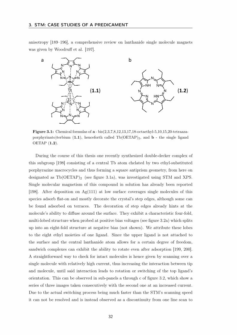
3. STM: CASE STUDIES OF A PREDICAMENT
anisotropy [189–196], a comprehensive review on lanthanide single molecule magnets
was given by Woodruff et al. [197].
a b
(1.1) (1.2)
Figure 3.1: Chemical formulas of a - bis(2,3,7,8,12,13,17,18-octaethyl-5,10,15,20-tetraaza-porphyrinato)terbium (1.1), henceforth called Tb(OETAP)2, and b - the single ligandOETAP (1.2).
During the course of this thesis one recently synthesized double-decker complex of
this subgroup [198] consisting of a central Tb atom chelated by two ethyl-substituted
porphyrazine macrocycles and thus forming a square antiprism geometry, from here on
designated as Tb(OETAP)2 (see figure 3.1a), was investigated using STM and XPS.
Single molecular magnetism of this compound in solution has already been reported
[198]. After deposition on Ag(111) at low surface coverages single molecules of this
species adsorb flat-on and mostly decorate the crystal’s step edges, although some can
be found adsorbed on terraces. The decoration of step edges already hints at the
molecule’s ability to diffuse around the surface. They exhibit a characteristic four-fold,
multi-lobed structure when probed at positive bias voltages (see figure 3.2a) which splits
up into an eight-fold structure at negative bias (not shown). We attribute these lobes
to the eight ethyl moieties of one ligand. Since the upper ligand is not attached to
the surface and the central lanthanide atom allows for a certain degree of freedom,
sandwich complexes can exhibit the ability to rotate even after adsorption [199, 200].
A straightforward way to check for intact molecules is hence given by scanning over a
single molecule with relatively high current, thus increasing the interaction between tip
and molecule, until said interaction leads to rotation or switching of the top ligand’s
orientation. This can be observed in sub-panels a through c of figure 3.2, which show a
series of three images taken consecutively with the second one at an increased current.
Due to the actual switching process being much faster than the STM’s scanning speed
it can not be resolved and is instead observed as a discontinuity from one line scan to
32

3.1 Rare Earth Sandwich Complexes
the next (marked by a thin white line in figure 3.2b). The same effect can be achieved
by a so-called lateral manipulation experiment, wherein the tip is used as a somewhat
sophisticated stick to push or pull adsorbates around. This is driven by either attractive
or repelling tip-adsorbate interactions and experimentally realized by lateral movement
of the tip above the sample at a fixed bias voltage.
5 Å
a b c
Figure 3.2: Rotation of the upper ligand of a single Tb(OETAP)2 molecule adsorbed onAg(111) due to interaction with the STM tip (a,c: +1.1 V, 8e-11 A; b: +1.1 V, 2e-10 A).
3.1.1 Self-assembly on Noble Metal Surfaces
Dosing higher amounts of OETAP double-decker molecules onto pristine noble metal
surfaces leads to supramolecular structures formed by attractive van der Waals in-
teractions between diffusing complexes. Figure 3.3 shows this self-assembling behav-
ior. Assemblies on Ag(111) and Cu(111) were investigated for Tb(OETAP)2 within
the framework of this thesis while its closely related dysprosium counterpart, namely
Dy(OETAP)2, was the subject of interest in a collaborative work soon to be published
[201] and is mentioned here because of its very similar behavior. Both lanthanide double-
decker molecules exhibit the characteristic four-fold, multi-lobed shape at positive bias
voltages, which was mentioned before (cf. black outline in figure 3.3b) which splits into
eight lobes when measuring at negative bias (cf. figure 3.3f). However, at certain bias
voltages one can observe an intriguing difference in apparent height between assembled
molecules, which can be seen clearly in 3.3a. A few very bright spots can be attributed
to second layer molecules (around 1-2 % in most preparations), especially since these
molecules can be moved around on an island simply by scanning over them, but the
difference in contrast of the surrounding assembly (∼ 2Å) does not correspond to an
additional layer of either double-deckers (∼ 3Å) or single OETAP molecules (∼ 1.5Å,
all apparent height measured at +1.2 V). In a first attempt to get to the bottom of this
phenomenon a series of lateral manipulation experiments was conducted at an island
33

3. STM: CASE STUDIES OF A PREDICAMENT
edge in order to take the assembly apart step by step. This only ever yielded intact
Tb(OETAP)2 molecules. Moreover, the appearance of this pattern strongly depends on
applied bias and "bright" species can be irreversibly switched into "dark" ones through
strong tip-sample interactions. Both effects will be discussed in more detail in the
following subsection.
10 nm 3 nm
3 nm
a
b
c
N
Tb
NN
N
NNN
N
N
Tb
NN
N
NNN
N
N
Tb
NN
N
NNN
NN
Tb
NN
N
NNN
N
NTb
N
NN
NN
N N
NTb
N
NN
NN
N N
N
N
NN
N
N
N
N
N
N
Tb
NN
N
NNN
N
N
Tb
NN
N
NNN
N
φ
a1
α1
α2
a2
1 nm
d f
30 nm
e
Figure 3.3: Self-assembling behavior of Tb(OETAP)2 on Ag (111) (a-d) and Cu(111) (e)as well as Dy(OETAP)2 on Au(111) (f). Dense-packed crystal directions are indicated bysixfold stars. a - Overview image (+1.2 V, 8e-11 A). b - High resolution close-up image(+1.0 V, 1e-10 A). c - False color high resolution image highlighting the orientations ofsingle molecules (+1.5 V, 1e-10 A). d - Tentative model of the assembly and its character-istic dimensions. e - Overview image (+0.65 V, 1e-10 A). f - Overview image from [201],scale bar = 3 nm (-2.3 V, 6e-11 A).
Tb(OETAP)2 forms extended and very well ordered islands on Ag(111) (figure 3.3a-
d) with a rhombic unit cell with measured unit cell vectors of a1 = 14.1 ± 0.4 Å and
a2 = 14.2 ± 0.4 Å , included angles α1 = 114 ± 5° and α2 = 66 ± 5°, and an angle
φ = 20 ± 5° between a1 and the closest dense-packed crystal direction. Overlaying a
tentative model obtained with the methods described in section 2.1.4 onto a model of
the Ag(111) crystal one can see that within the limits of the STM’s calibration a quasi-
commensurate overlayer is possible with exact unit cell parameters of a1 = 13.9 Å ,
a2 = 14.2 Å , α1 = 114.2°, α2 = 60.5°, φ = 20.5°. Relative to the underlying crystal
lattice this assembly can thus be designated as a (√
93x√
97)R20.5° superstructure [202].
34

3.1 Rare Earth Sandwich Complexes
In such an overlayer only every other molecule is adsorbed on a similar adsorption
site, as can be seen in figure 3.3d. Bear in mind however, that the nature of the
adsorption sites shown in this model (top and bridge, respectively) is pure speculation
as this information can not be obtained from measuring characteristic dimensions alone.
To this end an additional adsorption site determination experiment would have to be
conducted, because although STM does allow for atomic resolution it is usually not
possible to image molecules and the underlying crystal lattice at the same time [74, 203].
A quasi-commensurate overlayer will, however, be given in any case, no matter the
actual adsorption sites. This is corroborated by the fact that, at certain bias voltages,
the macrocycle backbones of single molecules within the assembly can be observed
which express a sub-pattern of alternating vertical rows of similarly aligned molecules.
Figure 3.3c shows such an image at high contrast and false coloration to better make
out the cross-shaped backbones (two differently aligned molecules are marked with X’s).
Measuring the angle of orientation with respect to the crystal lattice is rather imprecise
due to the small dimensions of the backbones, but a tentative guess has nevertheless
been incorporated into figure 3.3d. It shows that similarly aligned molecules are likewise
adsorbed on similar adsorption sites, which is a good indicator as to the validity of this
model.
Tb(OETAP)2 on Cu(111) as well as Dy(OETAP)2 on Au(111) and Cu(111), and
single OETAP molecules on Au(111) behave very similar to the self-assembly just de-
scribed. The first case is shown in figure 3.3e and although either the attractive inter-
action between molecules and copper surface or the diffusion barrier is stronger to the
point where markedly more single molecules can be observed on the free terraces there
are still extensive and neatly ordered islands being formed. The unit cell dimensions
here are a little extended in comparison, with: a1 = 14.2 ± 0.5 Å, a2 = 14.8 ± 0.5 Å,
α1 = 115±5°, and α2 = 65±5°. No lattice directions were determined during this exper-
iment, making even a tentative model impossible. A significant portion of the individual
molecules, however, have been found to be single OETAP fragments, a fact which will be
the main focus of subsection 3.3.1. Furthermore, the assemblies exhibit the exact same
random contrast pattern mentioned before, which indicates that this phenomenon does
not arise due to interaction with the surface. The same is apparently true for assemblies
of Dy(OETAP)2 shown in figure 3.3f. Although this image has been taken at negative
bias where the molecules display their eight-fold HOMO state one can still make out
differences in contrast, albeit more gradual than in the other cases. Lattice vectors here
are again similar to the ones mentioned above and the same alternating alignment from
one row to the next can be observed. The same goes for assemblies of single OETAP
molecules (not shown here) [201]. Overall, this is a strong indicator for molecule-surface
35

3. STM: CASE STUDIES OF A PREDICAMENT
interactions being rather weak compared to molecule-molecule interactions as obviously
the choice of surface does not greatly influence the assembly characteristics. However,
the formation of quasi-commensurate as opposed to perfectly commensurate assemblies
does mitigate this indication somewhat. Usually, a markedly different behavior can be
observed when comparing molecules on noble metal surfaces as surface reactivity is, for
many systems, weakest for Au(111), stronger for Ag(111), and strongest for Cu(111)
[204, 205].
3.1.2 Contrast through Orientation?
The phenomenon of bias voltage dependent molecular contrast in Tb(OETAP)2 islands,
which has been mentioned before, can be seen in more detail in figure 3.4. Sub-panels a
to c show an overview of one island at +1.2, +1.4, and +1.6 V, respectively. With rising
bias voltage one can clearly see a gradually more and more homogeneous appearance
of the first layer until almost all of them appear to be of similar brightness at a certain
threshold voltage, while the very few second layer molecules seem to remain unchanged.
Towards lower positive biases below +1.2 V (not shown) even more molecules appear
darker, that is to say at a lower apparent height, while some will stay bright down
to very low bias values above the Fermi level. Also, the change is not sudden, but
rather very gradual in a two-fold way: not all molecules exhibit the onset at the same
voltage and when they do, contrast increases over a range of a few hundred mV for each
individual molecule. There is thus at any given positive voltage below this "saturation"
a wide range of apparent heights observable. Saturation voltages range from +1.6 to
2.0 V, probably depending on the tip state, although more statistics would have to be
acquired in order to reliably gauge this influence. At negative biases assemblies appear
non-uniform as well, but no such saturating behavior could be observed during our
experiments in this regime. Very interestingly, sufficiently strong tip-sample interactions
can change this individual contrast and irreversibly so.
Figures 3.4d-i show a series of images obtained during so-called vertical manipula-
tion (VM) experiments. This procedure implies equilibrating the tip at a fixed position
and distance (controlled via the tunneling current) above the sample surface and open-
ing the PI-feedback loop. Afterwards, bias or distance may be sweeped in order to
obtain characteristic I(V) and dI/dV(V) spectra; this process is generally known as
scanning tunneling spectroscopy (STS). Sometimes, it is also worthwhile to sweep both
parameters at the same time or keep both constant in order to induce some desired
effect through tip-sample interactions. In this particular case at first a reference image
was obtained after which the bias voltage was sweeped from -1.0 to 2.0 V at a position
36

3.1 Rare Earth Sandwich Complexes
15 nm
a b c
5 nm
d
e
f
g
h
i
Figure 3.4: Molecular contrast in an assembly of Tb(OETAP)2 on Ag(111) depending onbias voltage and tip-sample interactions. a− c - Bias dependence showing more and moreuniform contrast at higher bias voltages (a: +1.2 V, b: +1.4 V, c: +1.6 V; all: 8e-11 A).d− i - Consecutive series of vertical manipulation experiments with tip positions indicatedby green marks. Some images were obtained after two manipulations (all: +1.2 V, 1e-10A).
37
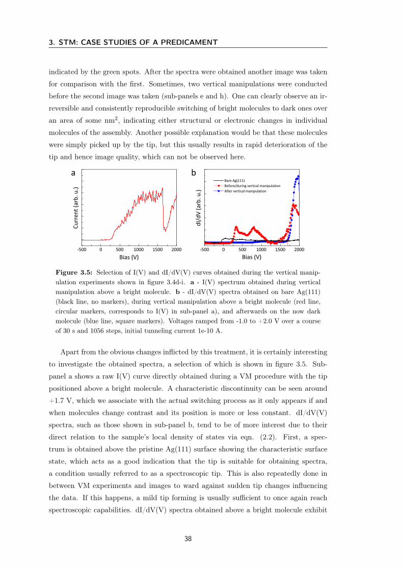
3. STM: CASE STUDIES OF A PREDICAMENT
indicated by the green spots. After the spectra were obtained another image was taken
for comparison with the first. Sometimes, two vertical manipulations were conducted
before the second image was taken (sub-panels e and h). One can clearly observe an ir-
reversible and consistently reproducible switching of bright molecules to dark ones over
an area of some nm2, indicating either structural or electronic changes in individual
molecules of the assembly. Another possible explanation would be that these molecules
were simply picked up by the tip, but this usually results in rapid deterioration of the
tip and hence image quality, which can not be observed here.
a b
Figure 3.5: Selection of I(V) and dI/dV(V) curves obtained during the vertical manip-ulation experiments shown in figure 3.4d-i. a - I(V) spectrum obtained during verticalmanipulation above a bright molecule. b - dI/dV(V) spectra obtained on bare Ag(111)(black line, no markers), during vertical manipulation above a bright molecule (red line,circular markers, corresponds to I(V) in sub-panel a), and afterwards on the now darkmolecule (blue line, square markers). Voltages ramped from -1.0 to +2.0 V over a courseof 30 s and 1056 steps, initial tunneling current 1e-10 A.
Apart from the obvious changes inflicted by this treatment, it is certainly interesting
to investigate the obtained spectra, a selection of which is shown in figure 3.5. Sub-
panel a shows a raw I(V) curve directly obtained during a VM procedure with the tip
positioned above a bright molecule. A characteristic discontinuity can be seen around
+1.7 V, which we associate with the actual switching process as it only appears if and
when molecules change contrast and its position is more or less constant. dI/dV(V)
spectra, such as those shown in sub-panel b, tend to be of more interest due to their
direct relation to the sample’s local density of states via eqn. (2.2). First, a spec-
trum is obtained above the pristine Ag(111) surface showing the characteristic surface
state, which acts as a good indication that the tip is suitable for obtaining spectra,
a condition usually referred to as a spectroscopic tip. This is also repeatedly done in
between VM experiments and images to ward against sudden tip changes influencing
the data. If this happens, a mild tip forming is usually sufficient to once again reach
spectroscopic capabilities. dI/dV(V) spectra obtained above a bright molecule exhibit
38

3.1 Rare Earth Sandwich Complexes
a strong peak at approx. +1.8 V with two further peaks below +1 V, the latter two
being completely absent when measuring over a dark molecule. A strong influence of
this change in apparent height on the molecule’s electronic state or vice versa is thus
obviously given, although as to the nature of this change no conclusive evidence can be
extracted from such spectra alone. It is worth noting, however, that this irreversible
switching phenomenon can just as well be achieved by repeatedly scanning over an as-
sembly at voltages above +1.7 V or by vertical manipulation with a constant voltage
pulse above said threshold.
The question now arises, whether this observed switching is entirely electronic in
nature or not. A change in the molecular backbone’s orientation is, in any case, very
hard to detect, even when a molecule directly at an island edge with more degrees of
freedom is affected (see outlines in figures 3.4e and f). Nevertheless, a slight misalign-
ment of one backbone with respect to the alternating pattern mentioned above, which is
relaxed into the energetically more favorable position by tip-sample interactions, could
still be possible. In many cases, however, even after switching a small residual bright
part at the fringe of some molecules could be observed (outlines in figure 3.4i). This
suggests an, at least partial, involvement of the ethyl moieties which, from a sterical
point of view, would have enough degrees of freedom to account for such a restructuring
effect. An attempt was made to find a relation between the number of bright species and
sample temperature during deposition by cooling the sample with liquid nitrogen dur-
ing the preparation or annealing the sample towards higher temperatures. The second
method indeed leads to islands consisting of almost uniformly dark molecules with the
same characteristic, low amount of second layer growth. A measurably larger number
of bright molecules at low preparation temperatures would have allowed calculation of
the activation energy of this switching process, but the data proved inconclusive due to
too much contamination on the sample, which is common when preparing at very low
temperatures.
In this case, a comprehensive conclusion can not be drawn from STM and STS data
alone, if only because a large part of the molecule and especially its interaction with the
substrate are experimentally simply not accessible. In order to shine some more light
onto this effect, XPS measurements were conducted by Mateusz Paszkiewicz to gain
information about chemical and electronic properties of the adsorbate (see figure 3.6).
One should keep in mind that contrary to STM, however, XPS is a technique which in-
herently averages over a considerable surface area of an investigated sample, thus some
results may be hard to reconcile at first. Any way, Lanthanide sandwich complexes are
known to be able to switch between two different charge states of the central metal atom
[206], an explanation which could account for this switching phenomenon. This may
39

3. STM: CASE STUDIES OF A PREDICAMENT
a b
Figure 3.6: Tb 3d3/2 region of XP spectra of a monolayer of Tb(OETAP)2 on Ag(111).a - After deposition onto a cold sample (-184°C). b - After annealing to 200°C.
be the case even though a gradual change in apparent height is observed, as molecules
adsorbed on surfaces can very easily be partially charged [207], although the irreversibil-
ity of the process does not quite fit into this picture alone. XPS measurements were
conducted with both room temperature and cold preparations, but no differences in the
Tb3d3/2 peak could be observed. However, the obtained peak intensity was rather low,
thus a conclusive negative result can not be drawn from this observation. Furthermore,
samples of different coverages were prepared in order to check for the metal surface’s
influence on the electronic state of either ligand or central atom, but again no differences
could be observed. All in all, further studies have to be conducted in order to reach
solid conclusions as to the origin of this puzzling phenomenon.
3.1.3 Summary
In this section, the combined STM and XPS study of a sandwich complex consisting of
a terbium central atom and two peripherally ethyl-functionalized porphyrazines, called
Tb(OETAP)2, was discussed. These molecules, which are potential candidates for ap-
plications as single molecule magnets, are apart from being soluble also capable of being
sublimed and deposited onto a sample surface where they adsorb in a flat-on fashion
and self-assemble into regular, dense-packed islands even at low coverage. These as-
semblies show a remarkable independence of the substrate material used, with islands
of Tb(OETAP)2 on both Ag(111) and Cu(111) as well as Dy(OETAP)2 on Cu(111)
and Au(111), and single OETAP molecules on Au(111) all self-assembling in a very
similar fashion, pointing to the fact that molecule-molecule interactions far outweigh
surface-molecule interactions. Both double-decker species exhibit a peculiar random
distribution of apparent heights or brightnesses in these islands, the source of which
has yet to be determined. Brighter individuals can be irreversibly switched into darker
ones by different forms of tip-sample interaction or annealing of the whole sample. The
40

3.2 Alkyne-functionalized Pyrenes
central terbium atom’s charge state has been investigated as a possible source of this
effect with XPS, but a solid conclusion has yet to be reached.
3.2 Alkyne-functionalized Pyrenes
One recurring and successful modus operandi in surface science is to widen the scope of a
study by investigating molecules, which are not only showing promising self-assembling
behavior or other intermolecular interactions, but also some further physicochemical in-
tramolecular property. This is especially the case for the chemical class of polyaromatic
hydrocarbons (PAHs), which have certainly earned a significant amount of disrepute
in human health-related issues [208, 209], but are nevertheless continually presenting
valuable research examples in diverse branches of science, recently even in astrochem-
istry [210–212]. One such representative is pyrene (benzo[def ]phenanthrene), one of the
smaller PAHs, which, together with its derivatices, has a long-standing scientific history
mainly because of its high quantum-yield fluorescence [213–217]. Further topics of inter-
est are its ability to couple to and thereby functionalize carbon nanotubes and graphene
[218–221], and its inherent self-assembling capabilities [222–227], both of which are usu-
ally investigated in conjunction with, or at least making use of, its fluorescence. Over
the last fifteen or so years, pyrene derivatives have furthermore been investigated with
scanning probe techniques [228–233], as they are under certain circumstances able to
self-assemble on surfaces and due to their luminescence properties present just such an
interesting dually capable system mentioned at the outset.
Figure 3.7: Chemical skeletal formulas of the pyrene derivatives investigated during thisthesis.
Within this section the STM investigation of a family of pyrene derivatives function-
alized with different ethynyl-based moieties shown in figure 3.7 will be discussed. The
information contained herein is currently in preparation for publication [234] and a series
41

3. STM: CASE STUDIES OF A PREDICAMENT
of preliminary studies have been conducted by Tobias Hoh [235]. In order to facilitate
self-assembly upon adsorption pyrene backbones were functionalized with ethynylpyrid-
4-yl moieties, which should be able to attractively interact with other such moieties
via either H-bonds [225, 236] or pyridyl-metal-pyridyl coordination [237, 238] while still
maintaining a certain degree of flexibility, which tends to be a favorable circumstance for
self-assembling behavior. Backbones were either functionalized tetradentated (species
(2.1)), designated as tetra-pyridyl-pyrene, or bidentated in a cis- ((2.2)) or trans-like
((2.3)) fashion, hence designated as cis- and trans-pyridyl-pyrene, respectively. The
overall adsorption behavior without attractive intermolecular interaction other than
possible van der Waals forces was investigated via a control group of pyrenes likewise
functionalized with ethynylphenyl moieties (species (2.1-3a)) which will be designated
in a similar way as x-phenyl-pyrene, where x is again either tetra, cis or trans.
3.2.1 Phenyl-terminated Control Group
Depositing molecules of the aforementioned control group onto a bare Ag(111) surface
leads to flat-on adsorption for every member of the family (see figure 3.8). As expected,
no attractive interaction between individual molecules can be observed in any case,
instead a more or less uniform statistical distribution of molecules all over open crystal
terraces becomes apparent, with step edges being decorated to saturation (not shown).
The preferred decoration of steps indicates the molecules’ ability to freely diffuse on the
surface, which in turn points to physisorption rather than chemisorption.
4 nm
a
2 nm
b
1 nm
c
Figure 3.8: Adsorption behavior of phenyl terminated ethynyl-pyrenes on Ag(111).a - Overview image of tetra-phenyl-pyrene (2.1a) (+1 V, 5e-10 A). b - Closeup of cis-phenyl-pyrene (2.2a) (+0.1 V, 1e-10 A). c - High resolution image of two trans-phenyl-pyrene molecules (2.3a) in a preparation of (2.2a) (+0.1 V, 9e-11 A).
There is, however, still a distinct effect of surface-molecule interaction visible in
the orientation of individual molecules. These tend to more or less closely align their
short symmetry axis (dotted line in figure 3.7) with one of the dense-packed crystal
42

3.2 Alkyne-functionalized Pyrenes
directions such that said axis is off to one side or the other by about 8 to 9±5°. This
is especially nicely observable in the case of the cis-species (2.2a), which exhibits a
characteristic pacman-like shape with one big, bright protrusion in the back attributed
to the pyrene backbone and two dimmer lobes which can be attributed to the phenyl-
ethynyl moieties (figure 3.8b), leaving no doubt as to the direction of the molecule’s
short symmetry axis. Surprisingly, this is not as easy for the x-shaped tetra-species
(2.1a), because although the angles included between the legs (the four dim, peripheral
lobes are attributed to the phenyl moieties) are nominally 120° and 60° and should thus
be easily differentiated, this is in practice severely complicated due to the leg’s, albeit
limited, flexibility (figure 3.8a). Nevertheless, even if short and long symmetry axis can
not be distinguished one at least observes the same three-fold orientational preference
as in the cis case. Whether or not this is also true for the trans-species (2.3a) remains
speculative, because only very few representatives of this module have been observed
experimentally (figure 3.8c) as contamination in preparations of (2.2a), certainly not
enough to acquire a sufficiently large dataset of statistical relevance. They exhibit an
elongated z-shape, again with a bright central pyrene backbone lobe and two peripheral
dime lobes attributed to the phenyl moieties, which due to its prochirality inherently
leads to two different forms upon adsorption, both of which can conveniently be seen in
the figure. From the adsorption behavior of their pyridyl-terminated counterpart (2.1a),
which will be discussed in the following section, however, it is quite likely that also this
species exhibits the same orientational preference. As an aside: in many preparations
of phenyl-terminated species small, circular protrusions could sometimes be observed
(see circles in figure 3.8a), which will be further discussed in section 3.3.2.
3.2.2 Pyridyl-mediated Self-assembly
As in the case of phenyl-terminated species the deposition of pyridyl-terminated mol-
ecules leads, in every case, to flat-on adsorption and free diffusion on a Ag(111) surface.
Quite remarkably different now, however, is the intermolecular interaction, which leads
to completely different self-assembled supramolecular architectures for the three species,
even at low to medium coverages. Tetra-pyridyl-pyrene (2.1) readily forms extended,
close-packed, and very regular islands even at low surface coverage (see figure 3.9a and
b) with one border always attached to the bottom side of a step edge, suggesting that
these act as nucleation sites.
The architecture exhibits a rhombic unit cell which, using the technique mentioned
in section 2.1.4, can be tentatively assigned the following dimensions: a1 = 15.6 Å,
a2 = 17.6 Å, α1 = 99.2°, α1 = 80.8°, and an angle φ = -13.5° between a1 and the
43

3. STM: CASE STUDIES OF A PREDICAMENT
1 nm
a₁a₂
2 nm5 nm
a b c
Figure 3.9: Self-assembled island of tetra-pyridyl-pyrene (2.1) on Ag(111). Stars indicatedense-packed crystal directions. a - Overview image (-0.2 V, 1e-10 A). b - High resolutionimage (-0.5 V, 1e-10 A). c - Tentative model of the assembly shown in sub-panel b.
closest dense-packed crystal direction (see figure 3.9c). The model reveals a quasi-
commensurate overlayer where every other row of molecules in a1-direction is adsorbed
on identical adsorption sites (although the exact nature of these sites could not be deter-
mined experimentally, see section 3.1.1), which can be designated as (√
29x√
37)R-13.5°
[202]. Again, as in the case of the phenyl-substituted species, a rotation of the molecule’s
short symmetry axis slightly off to one close-packed crystal direction is observable. The
fact that this effect appears in all phenyl-terminated species and, as we will see, likewise
in all assemblies of pyridyl-terminated ones, strongly suggests that its cause is an in-
teraction between pyrene backbone and surface. Furthermore, a distinct interdigitation
between adjacent molecules can be seen. This points to N-H bonds as the driving force
of the assembly and, paired with the symmetry axis rotation, leads to an organizational
chirality, as in principle for every crystal direction rotation off to both sides and thus
two different interdigitation motifs (or synthons) should be possible with similar unit
cells, but with either positive or negative angle φ. While indeed both of these mirror-
symmetric domains were observed during our experiments (for example in figures 3.9a
and b), all possible combinations or phases could not be recorded as this would have
required extensive amounts of images of different islands. Also worth mentioning is
a small cavity of ∼ 6x6 Å2 can be observed between molecules in a2-direction. This
"pocket" will be of further interest in section 3.3.2.
Cis-pyridyl-pyrene (2.2) on the other hand tends not to form islands at coverages
below one full monolayer, but instead agglomerates in the form of 1D-like chains or
at most small clusters of six to ten individual molecules (see figure 3.10). Sub-panel
a shows a preparation at low coverage. At medium coverages, shown in sub-panel
b, (2.2) exhibits more irregular behavior with chains and clusters agglomerating in a
seemingly uncontrolled way, although individual segments with a certain amount of
44

3.2 Alkyne-functionalized Pyrenes
short-range order can still be observed. Chains and clusters are formed through two
distinct intermolecular binding motifs: on the one hand N-H bonds between a pyridyl
moiety and the pyrene backbone of an adjacent molecule (clearly observable within
the cluster in figure 3.10a) and on the other a sort of head-to-head motif wherein two
molecules face each other with some attractive interaction between adjacent pyridyl
moieties, the latter of which is the predominant motif in chains and displays some kind
of attractive interaction such that another pair of pyridyl-connected molecules may
attach on either side, thus forming the chain. It is assumed that the head-to-head motif
is facilitated by pyridyl-metal-pyridyl coordination involving a surface atom which is
slightly pulled out of its plane by the attractive interaction [207].
2 nm5 nm3 nm
a cb
d
Figure 3.10: Supramolecular architectures of cis-pyridyl-pyrene (2.2) on Ag(111). Starsindicate dense-packed crystal directions. a - High resolution image of a short chain anda cluster at low coverage (-0.2 V, 1.5e-10 A). b - Closeup image of irregular chains atmedium coverage (-0.2 V, 1e-10 A). c - High resolution image of (2.2) at ∼1 ML coverage(+0.1 V, 1e-10 A). d - Raw data image reel of a series of lateral manipulation experimentsto investigate the head-to-head binding motif (-1.0 V, 8e-11 A).
The "bond" lengths between two head-to-head molecules forming such a dimer dis-
play a great range of flexibility, as can be seen in both low and medium coverage images,
an effect which was investigated by a series of lateral manipulation experiments. This
45

3. STM: CASE STUDIES OF A PREDICAMENT
was initially done to test the strength of a head-to-head bond by trying to move an in-
tact dimer around on the surface, but quickly a great degree of freedom of the individual
molecules became apparent (see figure 3.10d). It was even possible to instigate a third
binding motif, wherein both molecules interdigitate to form a close-packed and chiral
dimer, much like the interplay one can observe in self-assembled islands of the tetra-
pyridyl species. This very binding motif, albeit a bit less dense with tiny pockets between
the molecules, along with the N-H bond between legs and pyrene backbones mentioned
above, defines the characteristic interaction when coverages around one monolayer are
deposited and a tight-packed assembly can be observed (see figure 3.10c). Columns
of dimers are held together by pyridyl-backbone attraction and in turn these columns
are tightly packed by the sheer amount of molecules on the surface. At an angle to
these columns a characteristic line pattern emerges, with molecules alternately facing
in opposite directions. Due to the dimer’s inherent chirality frequent crystal twinning
can be observed along such lines (black line in figure 3.10c).
1 nm5 nm
a
1 nm
b c
Figure 3.11: Self-assembled Kagome-patterned island of tetra-pyridyl-pyrene (2.3) onAg(111). Stars indicate dense-packed crystal directions. a - Overview image (-0.2 V,1e-10 A). b - High resolution image of the structure’s unit cell (-0.02 V, 5e-10 A). c -Tentative model of the assembly shown in sub-panel b.
The third and only prochiral member of this family, trans-pyridyl-pyrene (2.3),
forms, much like its tetra counterpart, very regular and extended islands, also at low
surface coverage. These are once again always pinned on one edge to the bottom side
of a step edge, which again hints to their role as nucleation sites. However, the pattern
formed is now an intriguing, open-porous Kagome lattice or trihexagonal tiling with
a perfectly hexagonal unit cell (see figure 3.11a) [239]. Characteristically for Kagome
lattices these islands feature pores of two different diameters, namely ∼6 and ∼18 Å.
High resolution images show that these assemblies are resulting from N-H bonds be-
tween pyridyl moieties and pyrene backbones of adjacent molecules. Similar to species
(2.1) and (2.2) the molecules are again adsorbed in such a way that the short symmetry
46

3.3 Limitations of OMBE
axis of the pyrene backbone is rotated slightly off of a dense-packed crystal direction.
Interestingly, islands of this kind are exclusively formed by molecules of the same chi-
rality which in turn results in organizational chirality of the assembly, hence again, as
in the case of the tetradentated species, two mirror-symmetric domains are possible
(figures 3.11a and b show both of these). The resulting unit cell was obtained via the
techniques mentioned in section 2.1.4 and found to be perfectly commensurate with
the underlying crystal which is reflected in the model in figure 3.11c. The following
dimensions were determined: a1 = a2 = 30.6 Å, α1 = 1/2α2 = 60° with an angle in-
cluded between either unit vector and the closest dense-packed direction of φ = ± 19.1°,
depending on the chirality of the assembly. This overlayer can thus be designated as a
(√
112x√
112)R±19.1° superstructure relative to the crystal lattice [202]. The lattice’s
commensurability in conjunction with the rigidity of its three-fold N-H bonded synthons
leads to an amazingly steady long-range order. Islands in the 0.1 µm2 size regime have
been observed.
3.2.3 Summary
In conclusion, the STM study of a family of ethynyl-functionalized pyrenes was presented
and discussed in this section. A control group of bi- or tetradentated pyrenes function-
alized with ethynylphenyl moieties was capable of sublimation and flat-on adsorption on
Ag(111) and showed, as expected, a random surface distribution and hence no attractive
interaction between individual molecules. Ethynylpyridyl-terminated counterparts of
these control molecules which also allowed for sublimation and flat-on deposition, how-
ever, exhibited significant attractive interaction through a multitude of different bind-
ing motifs. The molecular synthons thus formed lead to a diverse number of different
supramolecular architectures, some of which exhibited surface-organizational chirality
either through them consisting of prochiral monomers or chiral synthons, or both. Only
the cis-pyridyl-pyrene species showed no capability of forming regular, self-assembled is-
lands at sub-monolayer coverages, but still exhibited an interesting head-to-head binding
motif, presumably incorporating silver surface atoms in a pyridyl-metal-pyridyl coordi-
nation. Good use was made of a method developed and discussed in section 2.1.4 to
accurately deduce unit cell dimensions from approximately measured lengths and angles
in order to fully characterize and describe most of the investigated architectures.
3.3 Limitations of OMBE
As this thesis is predominantly a work with a focus on highlighting the immense as-
sets of electrospray ion beam deposition and its advantages compared to using such
47

3. STM: CASE STUDIES OF A PREDICAMENT
techniques as organic molecular beam epitaxy we will, in this section, emphasize on
some of the drawbacks of OMBE, particularly with respect to preparations for use with
scanning probe microscopy techniques. Most of the material presented here stems from
experiments conducted on the systems introduced within the two previous sections, but
some additional findings from other works, or experiments conducted within the frame-
work of this thesis, but too short to warrant granting them a separate section, will be
featured as well.
3.3.1 Thermolability
Perhaps the most obvious and immutable drawback of OMBE, at least in the spirit
of this work’s introductory remarks on "more is more", is given by the thermolability
inherent in all organic molecules, which are heavier than a certain molecular mass or
of a particularly unstable structure, that is their "willingness" or ability to undergo de-
composition, disproportionation or polymerization reactions at elevated temperatures.
These molecules are thus not suitable for deposition via OMBE and put a somewhat
natural stopper on the technique’s capabilities and subsequently on the scope of possible
surface scientific experiments as well. A defining thermolability criterion is not easily
found and predicting a molecule’s thermal stability is next to impossible, as this strongly
depends on its chemical structure and potential energy landscape, most important about
which are the number of possible decomposition pathways and their respective energy
barriers [240–242]. However, empirical studies relating some basic elements of chemical
structure to overall thermal stability have been conducted and may serve as guidelines
for a rough estimate on whether or not a molecule may be suitable for deposition with
OMBE [243–245]. Molecules at or above this limit of structural integrity are thus either
completely inaccessible to STM studies relying on OMBE or can, at the very least, lead
to contamination by co-adsorption of cracked species or byproducts, which have formed
in the OMBE crucible due to intermolecular interactions. Furthermore, molecules in-
vestigated in scanning probe experiments are often tailor-made. Choosing a suitable
molecule for de-novo synthesis is thus challenging in two regards, because even if its
synthesis bears fruit there still remains the question of its suitability for deposition via
OMBE. This is further complicated by the fact that publishing negative results in sci-
ence, which in this case would mean studies of non-sublimable molecules for example, is
increasingly getting out of style [246] while the number of peer-reviewed, but still irre-
producible results steadily increases [247–249], even in very "hard" fields such as physics
[250, 251]. The much cited paradigm of science having a kind of "self-correction" mech-
48

3.3 Limitations of OMBE
anism is thus slowly being undermined, which, not only when choosing molecules for
synthesis, leads to more trial and error than necessary.
1 nm 1 nm 20 nm
a b c
Figure 3.12: Thermolability observed in preparations of Tb(OETAP)2 on Ag(111). a -High resolution image of single OETAP molecules (+0.5 V, 7e-11 A). b - High resolutionimage of an intact Tb(OETAP)2 molecule for comparison (+1.0 V, 8e-11 A). c - Overviewimage of a contaminated preparation (+1.1 V, 1e-10 A).
Thermolability of a molecule does not necessarily imply that it is completely impos-
sible to sublime. If a suitable deposition temperature can be found which is close, but
not above the decomposition temperature, a certain ratio of intact vs. cracked species
will be deposited. During the course of this thesis thermolability of both kinds was en-
countered in two different adsorbates, the first of which, Tb(OETAP)2, has already been
discussed in section 3.1 and could readily be sublimed and deposited. However, prepa-
rations of this sandwich complex almost always include at least some contamination of
cracked single OETAP ligands. This becomes exceptionally apparent when dosing the
molecules onto a Cu(111) surface, where they prefer to stick to open terraces and can
be clearly observed while scanning (see figure 3.3e). On Ag(111) surfaces only solitary
individuals or at most groups of three to four are ever observed isolated on terraces
(see figure 3.12a). Luckily, these can easily be distinguished from intact double-deckers
by their shape and apparent height (cf. figures 3.12a and b) or tip-induced rotation
of the upper ligand (see figure 3.2). The small amount of single OETAP observed on
Ag(111) suggests either preferred decoration of step edges or, more likely, segregation
and self-assembly into islands which has been observed for dedicated preparations of
OETAP on Au(111) [201]. Presumably, in our experiments these self-assemblies were
never found during imaging as only a negligibly small percentage of the whole crystal
is ever imaged even during very extended scanning probe measurements. Even if 1000
images of 1µm2 size were obtained from a single sample during an experiment, with
both of these numbers being gross overestimations of standard procedures, still only
1 · 10−5 parts of the surface area of a sample with a 10 mm diameter would have been
49

3. STM: CASE STUDIES OF A PREDICAMENT
imaged. This can make finding, and reproducibly investigating, segregating and/or self-
assembling cracked species, which amount to just a few percent of the overall deposited
molecules, very tedious. In turn, this is both bane as well as boon of the technique as
some contaminations do not jeopardize experimental findings because they may simply
seldom be encountered. Of course, this may or may not be true for other techniques
used in conjunction with OMBE. Especially spectroscopic methods often produce data
averaged over the whole sample surface or a significant part of it, thus easily running
afoul of such adulterating contaminations.
a b c
5 nm 2 nm(4.1)
Figure 3.13: Thermolability in a chiral extended phthalocyanine. a - Chemical formulaof (4.1) with binaphthoxy moiety outlined in red. b - Butterfly-like, presumably dimerizedcracking product of (4.1) on Ag(111) (+0.05 V, 6e-11 A). c - Single dimer and a monomerproduced via tip-sample interaction (-0.05 V, 6e-11 A) [252].
The second example of thermolability directly encountered during this thesis was
the case of a chiral phthalocyanine functionalized with binaphthoxy moieties shown in
figure 3.13a. Its investigation was intended a first step towards a potential chiral sin-
gle molecule magnet sandwich complex with said phthalocyanine as the ligand. Upon
adsorption on Ag(111) however, no intact molecules have so far been found. At moder-
ately low deposition temperatures either no adsorbate or conglomerations of contamina-
tion can be found. Increasing the deposition temperature leads to more contamination
and eventually butterfly-like, isolated structures can be observed (see figure 3.13b).
These are too small to be attributable to the chiral phthalocyanines, as they are only
marginally bigger than unfunctionalized phthalocyanines (∼ 20 Å vs. ∼ 15 Å)[253],
do not exhibit a characteristic cross-shape, which should be expected for such a rigid
molecule, and can furthermore be split into two mirror-symmetric parts very easily by
surprisingly mild tip-sample interactions like lateral or vertical manipulation, or nearby
tip forming procedures (figure 3.13c), a structural frailty, which would be utterly im-
possible to observe if there was an intact phthalocyanine backbone. Presumably, these
structures can be attributed to be dimers of the binaphthoxy functional groups split off
50

3.3 Limitations of OMBE
of the phthalocyanine at elevated temperatures, but as to their binding motif a sensible
model has yet to be developed. Investigation of this molecule is still ongoing, but it is
unclear whether a suitable window of deposition temperatures can be found to enable
sample preparations with intact species.
3.3.2 Contamination
a
b
Figure 3.14: Synthesis of the family of alkyne-functionalized pyrenes discussed in section3.2. a - Synthesis of species (2.1-3) and (2.2-3a). b - Synthesis of species (2.1a).
Thermolability is, of course, not the only source of observable byproducts or cracked
species on a sample by far. Even if molecules are thermally stable and can be nicely
deposited in an intact manner additional adsorbates may still be encountered if the
feed material is itself contaminated to begin with. Usually, such contaminations can be
gotten rid of through a process called degassing, wherein the OMBE crucible containing
the feed material is heated for several hours (sometimes even days), but before any
actual sample preparation is taking place. Small molecular weight contaminations are
thus purged from the feedstock and relatively pure material left over for deposition.
Alas, this procedure is not fool-proof. Contaminants of similar weight as the analyte
or with a particularly strong affinity to be embedded in the analyte’s crystal structure
51

3. STM: CASE STUDIES OF A PREDICAMENT
can only be removed partly and will thus always be co-deposited in every subsequent
preparation. If OMBE crucibles are re-used from one investigated molecule to the next,
care has to be taken in order to avoid cross-contamination, but a much more common
source for such contaminants are byproducts or leftover reactants of the analyte’s actual
chemical synthesis.
2 nm1 nm
a b
630 625 620 615
I 3d
Binding Energy (eV)
Inte
nis
ty (
arb
. un
its)
batch 1
batch 2
1 nm
c d
Figure 3.15: Preparations of alkyne-terminated pyrenes showing circular protrusionsattributed to iodine contaminants. a - Tetra-pyridyl-pyrene (2.1) (-1.0 V, 5e-11 A). b -Trans-pyridyl-pyrene (2.3) (+0.1 V, 9e-11 A). c - Phases of (2.1) and (2.3) with highiodine content (left: +0.1 V, 9e-11 A; right: -0.2 V, 2e-10 A). d - XPS comparison of theI3d region for a contaminated (1) and a clean batch (2) of (2.1).
A textbook example is given by the family of alkyne-functionalized pyrenes discussed
in section 3.2. These molecules were synthesized using a Pd-catalyzed Sonogashira-
Hagihara cross-coupling reaction (SI in [234]) of either 4-iodopyridine or iodobenzene
with acetylene terminated pyrene cores (see figure 3.14a), which in turn had been syn-
thesized in a similar fashion from brominated or iodated pyrene cores and trimethylsi-
lylacetylene [254–256]. The only exception to this pathway being tetra-phenyl-pyrene
(2.1a), which had been obtained directly by cross-coupling of tetrabromopyrene with
phenylacetylene (see figure 3.14b). From a stoichiometric point of view a large quantity
of halogen-containing byproducts (mostly HX) is released during these reactions, as
much as eight times the product molarity in the case of tetra-pyridyl-pyrene (2.1). It
is unclear whether from these byproducts or from the CuI catalyst used, but in some
52

3.3 Limitations of OMBE
batches a contamination of iodine atoms was observed during STM measurements after
deposition on Ag(111) as small circular protrusions at all utilized bias voltages (see
figure 3.15).
Tetra-pyridyl-pyrene (2.1) assemblies are able to trap either one or two of these
iodine atoms in the pockets mentioned in section 3.2.2 (figure 3.15a). Regarding changes
in the assemblies’ internal structure due to this additional participant, high resolution
images show that most molecules are still oriented parallel to each other with a small
minority (5% or less) now being incorporated at a right angle without deteriorating
influence on the long-range order of the assembly. As this is not the case for clean
tetra-pyridyl-pyrene (2.1) assemblies it acts as an indicator as to the widening influence
of iodine on the structure’s unit cell, which now appears not to be quasi-commensurate,
but incommensurate and elongated with respect to assemblies of clean batches with
dimensions of a1 = 15.3 ± 0.5 Å, a2 = 18.8 ± 0.5 Å, α1 = 80 ± 5°, and α2 = 100 ± 5°.
Despite this incommensurability no Moiré pattern could ever be observed in long range
images. It is worth noting, however, that a tentative model can be constructed where
all iodine atoms are adsorbed on identical adsorption sites, which are assumed to be
hollow site as these have been long known to be the preferred sites for iodine on Ag(111)
[257]. Whether pockets are filled with zero, one or two iodine atoms is thus presumed to
be the result of an intricate minimization balance between the assembly’s lattice energy
and the iodine’s adsorption energy. Further on, however, we will show that this balance
can be severely tilted in the iodine’s favor if enough contaminant is present.
Contaminated assemblies of trans-pyridyl-pyrene (2.3) incorporate iodine atoms
in the small cavities (see figure 3.15b), which, due to the assembly’s commensurate
nature, can easily always feature a hollow site (see model in figure 3.11c). Rarely,
single iodine atoms are encountered in the big cavities as well, but only ever one and
always tucked neatly into one of the corners. In contrast to assemblies of (2.1) here the
unit cell dimensions, or commensurability for that matter, are not perturbed by this
contamination, presumably due to the hollow sites being readily available. However, in
both cases new structures may arise if the amount of co-adsorbed iodine is high enough.
This was achieved by chance through a double preparation using contaminated batches
of both (2.1) and (2.3), although as to why in this case assemblies with distinctly
more iodine content as compared to two single preparations were observed remains
an open question. The tetra-species’ assemblies are now stretched in both directions
with iodine occupying interstitial pockets almost always in pairs (left side of figure
3.15c) while trans-species assemblies show complete restructuring into two much more
dense-packed phases (one of which is shown on the right hand side of figure 3.15c).
Interestingly, little or no evidence was found for iodine contaminations in preparations of
53

3. STM: CASE STUDIES OF A PREDICAMENT
cis-pyridyl-pyrene (2.2) or any of the phenyl-terminated species (2.1-3a) other than the
odd circular protrusion, which may just as well be attributed to any other contamination
(see circles in figure 3.8a). This suggests that either these batches were free from
contamination or that no significant attractive interaction actually exists between the
functionalized pyrenes and iodine and the contaminant is thus only incorporated into
the two aforementioned self-assemblies out of geometrical reasons similar to the lock and
key model, which is so often encountered in nanoscience. The clean preparations of (2.1)
and (2.3) shown in section 3.2 were obtained from batches, which had been synthesized
at slightly different reaction conditions, but this was not the case for any of the other
molecules, so presumably preparations of these were contaminated as well, but due to
non-attractive behavior the iodine segregated and was never observed experimentally.
1000
100
200 300 400 500 600 700 800 900 1000 1100 1200
m/z (-)
Rel
ave
inte
nsi
ty (
%)
195.1251.2
327.1 501.3588.2
354.1
406.2
656.3652.2
655.3
654.3
905.5
405.2
404.1
matrix
adduct withmatrix
+ matrix
M⁺
Figure 3.16: MALDI-MS spectrum of a contaminated batch of (2.3).
As a last remark it is worth mentioning, that such contaminations can often be very
hard to detect prior to the actual STM experiments. The most widely-used analytical
instrument in the organic chemist’s toolbox is probably NMR spectroscopy, which is
great for structural analysis, but suffers from a very low sensitivity [258]. Of course, in
the present case of iodine byproduct even an arbitrarily sensitive NMR spectrometer
would not have detected the contamination unless an 127I measurement would have
been conducted. Even with more sensitive techniques the experimenter can run afoul
of adverse conditions. Figure 3.16 shows a mass spectrum of a contaminated batch of
(2.3) obtained through matrix-assisted laser desorption/ionization mass spectrometry
(MALDI-MS) with no visible trace of 127I or significant other contaminations, for that
54

3.3 Limitations of OMBE
matter. However, here MALDI was conducted in the positive ion mode, which, of course,
iodide I− is not accessible with. Only XPS measurements of two different batches of
molecules could finally and clearly show that the contaminant was indeed iodine (see
figure 3.15d).
3.3.3 Deposition Parameters
Apart from such serious limitations and drawbacks as thermolability and contaminations
there are a series of minor intricacies, which tend to complicate working with an OMBE
apparatus. One example is the need to exchange feedstock powder between experiments,
which always makes some maintenance downtime necessary, as has been mentioned in
section 2.2. Probably more costly in overall measurement time, however, is the need
to find suitable deposition parameters for novel feed material. Even if the sample can
be positioned precisely and reliably relative to the OMBE and always the same shutter
position is used there are still two parameters left, upon which surface coverage depends,
namely deposition time and temperature. The former has a linear influence while the
latter’s is exponential via Arrhenius’ law. This usually makes a tedious process of
repeated sample preparation and examination necessary wherein deposition temperature
and/or time are increased step-wise from a first educated guess until some molecules
can be observed on the surface. In a low temperature setup such as the Createc machine
used in this thesis, which necessitates a certain cool-down phase for freshly prepared
samples, one such cycle can only be repeated maybe twice or three times in one day.
Thus, finding suitable deposition parameters usually takes up a few days right at the
start of new projects.
25 nm 100 nm 100 nm
a b c
Figure 3.17: Comparison of deposition parameters for two batches of trans-pyridyl-pyrene(2.3). a - Molecules of batch 1 deposited for a total of 40 minutes at 320-340°C (+0.3 V,1e-10 A). b - Empty preparation after deposition from batch 2 for 30 minutes at 340°C(+2.3 V, 1e-10 A). c - Molecules again from batch 2 after 10 minutes deposition at 230°C(+2.0 V, 2e-10 A).
55

3. STM: CASE STUDIES OF A PREDICAMENT
Remarkably, under certain circumstances this tedious procedure might be neces-
sary even for molecules, which had previously already been investigated with suitable
deposition times and temperatures. Figure 3.17 shows such a case in which two differ-
ent batches of trans-pyridyl-pyrene (2.3) showed two completely different sublimation
behaviors. Batch 1 could usually be deposited in sub-monolayer coverages at ∼340°Cwithin a few tens of minutes, but when the new batch 2, which had been synthesized
slightly differently (see previous section), was used for the first time initial preparations
yielded only very dirty samples and upon examination of the powder left in the crucible
this was found to have undergone some kind of pyrolytic reaction. It was only after
filling the crucible with fresh material and a cautious renewed search for parameters
that a radical change in deposition temperature became apparent with batch 2 yield-
ing similar surface coverages a full 100°C below that of batch 1. Interestingly, a new
batch of tetra-pyridyl-pyrene (2.1) had also been synthesized under similarly changed
reaction conditions, but this showed no such shift in sublimation temperature. Investi-
gations regarding the nature of this behavior, which is presumably due to a change in
the powder’s aggregation state, are still being conducted.
Such unusual effects, however, are not the only source for changing deposition pa-
rameters. A very common behavior, especially in extended series of experiments, is the
need to gradually increase the deposition temperature in order to obtain similar surface
coverages. This can be due to unwanted polymerization side reactions making parts of
the powder unavailable or simply because the crucible filling is nearing its end. Dual
depositions, wherein two different molecules are deposited onto the same sample, are at
a double disadvantage due to this and thus tend to be even less reproducible. If at some
point one preparation is found to contain an insufficient amount of surface coverage
usually a second preparation is made on top of the already "coated" sample. During
this thesis this had to be done many times, including during experiments on a molecule,
designated as BO-ADPM [259, 260], which was collaboratively investigated together
with Alissa Wiengarten to further elucidate its potential as a donor material in organic
photovoltaics (see figure 3.18). While most of the experimental results can be found in
her PhD thesis [76] some interesting observations regarding deposition behavior are also
worth noticing. In order for the reader to better understand what figure 3.18 is showing
it should be mentioned that BO-ADPM adsorbs flat-on on Ag(111) and can be observed
as an almost quadratic ensemble of four lobes, one of which is always of markedly in-
creased apparent height compared to the others (figure 3.18b:I). This is attributed to
the oxyphenyl moieties bending out of the molecular plane in opposite directions, which
can be seen in the side-view of an energetically optimized geometry obtained via the
56

3.3 Limitations of OMBE
HyperChem software suite. Subsequently, due to this non-planar adsorption geome-
try attractive interaction between individual molecules arises and oligomers containing
mostly two, three or four molecules are formed even at very low surface coverages.
10 nm
5 nm5 nm
1 nm
a b d
c e
I
III
II
IV
Figure 3.18: Investigation of BO-ADPM on Ag(111). a - Skeletal formula of BO-ADPMand top as well as side view of its energetically optimized geometry obtained via Hyper-Chem. b - Monomer and oligomers of BO-ADPM on Ag(111) with the number of moleculesgiven in roman numerals (I: -0.3 V, 5e-10 A; II/III: -0.1 V, 2e-10 A; IV: -0.6 V, 1e-10 A).c - Preparation intended for slightly below full monolayer coverage (-0.1 V, 1e-10 A). d -Double preparation of BO-ADPM and C60 on Ag(111) (+0.7 V, 1e-10 A). e - Additionaldosing of BO-ADPM onto the preparation shown in sub-panel d (+1.0 V, 8e-11 A).
In order to investigate the electronic interplay between BO-ADPM and a potential
electron acceptor a series of dual preparations was made with C60 as a co-adsorbate.
During one experiment a coverage close to one monolayer of BO-ADPM was deposited
in order to add C60 on top and still have a sufficient amount of free Ag surface for tip
formings (see figure 3.18). This worked reasonably well, but it should be noted that
obtaining such a coverage is mostly a matter of fortunate circumstances. In an earlier
approach first a low coverage of C60 was prepared in order to then deposit BO-ADPM
on top of the islands formed. From figure 3.18d can be seen that in this case deposition
parameters for BO-ADPM were misjudged at first and additional molecules had to be
dosed on top, leading to loosely adsorbed contamination being pushed around by the
tip, which is visible as horizontal stripes in the images (fig. 3.18e).
57

3. STM: CASE STUDIES OF A PREDICAMENT
In general, the need for secondary preparations tends to increase contamination
as the sample is being manipulated around in the chamber and shutters are opened
and closed, giving off adsorbed molecules, which can in turn contaminate the sample
even further. This can be mitigated by using a quartz microbalance in the chamber to
accurately measure the amount of deposited molecules in the first place, but even then
finding suitable deposition parameters is necessary to begin with as such a microbalance
can of course not distinguish between intact molecules and cracked species or dirt being
sublimed out of the crucible.
58

4
Electrospray Ion Beam Deposition:A Sprayed Solution
Although by now the discerning reader may have probably drawn the preliminary con-
clusion that this work is but a vituperation on all things OMBE and that electrospray
ion beam deposition (ESIBD) is the one and only solution to every experimentalist’s last
problem, this is, alas, far from the truth. The reasons for this are two-fold: on the one
hand, OMBE does have its uses, especially because it enables a fast and straightforward
deposition method for a still quite large scope of molecules, which is well understood
and easy to maintain. On the other hand, straightforwardness, or rather lack thereof,
is exactly ESIBD’s greatest weakness, and significantly so. Within the following chap-
ter we will explore its many advantages, especially with regard to OMBE’s drawbacks
discussed in the last chapter, but also some disadvantages and hurdles, which have to
be overcome in order to fully open the limits on deposition of fragile molecules. As the
whole process is rather complex, at first the current state of the machine will be dis-
cussed to give the reader an overview, which should act as a reference base. From there,
its individual parts will be presented and explained in more detail within dedicated
sections.
Large parts of the work presented here would have been impossible without the
energetic and fruitful help and collaboration of a number of amazing bachelor and
master students. Their works have all contributed to the current state of the machine
in one way or another and their theses contain further information well worth reading
up on [109, 159, 178, 261–265].
59

4. ELECTROSPRAY ION BEAM DEPOSITION: A SPRAYED SOLUTION
4.1 The Setup in its Current State
Figure 4.1 shows an isometric overview of the combined ESIBD and STM setup, which
is the focus of this work. The opaque chambers on the left represent the existing
STM setup consisting of a preparation chamber (the rear one in blue) and the actual
measurement chamber (left most, light green), which have been described in previous
works [78, 79]. The ESIBD setup is shown translucent on the right and consists, in ion
beam direction, of the ESI source (green), four differentially pumped chambers (purple
and yellow), and finally the preparation chamber (rust).
Manipulators
Gate valves
STM chamber
Preparaon chamber
ESI/TPD chamber
Differenal chambers 1-3
Differenal chamber 4
ESI source
Figure 4.1: Color-coded isometric overview of the combined ESIBD-STM setup developedduring this thesis. Pumps, mounting racks and further accessories are not shown.
At the very right of figure 4.1 one can see the actual ESI source (green), which is
the only functional part at atmospheric pressure. A camera mounted on top of it allows
for observation of the needle during spraying. This is necessary for two purposes, one
being simple position control, the other observation of the current spray mode when
adjusting the needle voltage. Not shown here is the syringe pump, which supplies the
feed material to the needle. Starting from the source, the ions are transferred into the
vacuum system through an atmospheric pressure interface (API, see section 4.2). As the
API introduces a lot of air into the system a series of differentially pumped chambers is
60

4.1 The Setup in its Current State
necessary to reduce the pressure step-wise until ultrahigh vacuum conditions are reached
(see section 4.3). The first three vacuum chambers are actually just one aluminum
box with dividing walls separating it into three parts (thus only one color in figure
4.1). These dividing walls also act as mounting fixtures for the ion guides and orifices
connecting the chambers. The whole box is mounted on its own rack and can, along with
pumps and further accessories, be completely detached from the high/ultrahigh vacuum
part, which is affixed to another rack. This modularity makes relatively straightforward
maintenance and restructuring possible. Flexibility is further increased by the fact that
the aforementioned aluminum box containing the first three chambers actually has a
lid, which can be easily removed, thus allowing direct access to the ion guides and
cabling contained therein. Each compartment has a flange at the bottom for pump
connection as well as several side flanges for electronic feedthroughs, pressure gauges or
other accessories. The front most flange holds the ESI source while at the very back
connection to chamber 4 is implemented. Furthermore, the dividing walls are removable
as well and can be customized to suit the needs of special experiments. All flanges and
the lid are made gas-tight through the use of custom O-rings while vacuum grade silicon
sealant is used for the dividing walls as these are not removed very often.
Differential chamber 4 serves, just as all prior differential chambers, the only purpose
of further reducing the pressure. It is needed because the aluminum box could not be
connected directly to the preparation chamber due to too high pressure differences.
Finally, after passing chamber 4 the ion beam reaches the preparation chamber where
the sample can be placed on a small manipulation and heating/cooling mounting stage.
The interface between ESIBD and STM parts is implemented through a very flexible
DN100 bellow, which allows for a certain difference in chamber levels between ESIBD
and STM. This is necessary as the latter can be floated on pneumatic legs to reduce
vibrational noise while the former is at a constant level. In order to prevent complete
compression of the evacuated bellow by atmospheric pressure a set of strong compression
springs is installed in parallel (not shown). This still allows for more flexibility than a
rigid spacer while at the same time reducing vibrational coupling of ESIBD and STM
to a manageable minimum. Convenient sample manipulation is facilitated through a
series of manipulators, the longest of which can be used to transfer samples from one
of the two setups to the other, thus functionally connecting ESIBD and STM.
At crucial points gate valves can be used to separate parts of the combined setup
from the rest. This can be done between STM measurement and preparation chamber,
between STM and ESIBD setup, and finally also between differential chambers 3 and 4
of the ESIBD setup. It is thus easily possible to completely separate ESIBD from STM
with, for example, either one evacuated while the other can be vented for maintenance.
61

4. ELECTROSPRAY ION BEAM DEPOSITION: A SPRAYED SOLUTION
The gate valve between differential chambers 3 and 4, which is fully integrated into
chamber 4, is necessary, because the ESI preparation chamber and chamber 4 already
represent an ultrahigh and high vacuum environment, respectively. These chambers
thus have to be pumped at all times as otherwise frequent bakeouts would be necessary
to reach the respective base pressures again. This is not the case for the first three
differentially pumped chambers, however, where chamber 3 reaches a base pressure only
in the 10−6 mbar regime, perfectly reachable without a bakeout procedure. Furthermore,
gas loads and therefore necessary pumping power are highest in this part of the system,
thus relatively big and noisy pumps are used, which can severely impair STM sensitivity.
For these reasons the first three differential chambers are only pumped if and when an
ESIBD preparation is actually taking place, and vented otherwise.
NeedleHeated
capillary TWIG 1Gatevalve TWIG 3
TPD
STM
Gatevalve
Gatevalve
TWIG 2FunnelCamera
Loadlock
OMBE
Met
als
Manipulator
Manipulator
Figure 4.2: Schematic top view inside the combined ESIBD and STM setup, color codedsimilar to figure 4.1.
A schematic look inside the setup can be taken with figure 4.2, which is color-coded
in a similar way to figure 4.1. It shows a top view with the beam traveling from left to
right. Thus, the source can be seen on the left edge, followed by the API and aluminum
box. The first differential chamber contains an ion funnel to focus the ions exiting the
API’s heated capillary and transfer them into the second chamber (see section 4.4.2).
From there, they are transmitted into the third chamber by a 16-pole thin wire ion
guide (TWIG, see section 4.4.3). Both the funnel as well as the first TWIG represent
a direct connection between their respective entry and exit chambers such that ion
guidance is not broken at any of the orifices. A second TWIG, which is fully located in
62

4.2 ESI Source
chamber 3, then transmits them right up to the gate valve. With a thickness of 4 mm
the gate valve represents the largest gap in this ion guidance system where usually great
care is taken to position the ion guides as close to each other as possible to minimize
losses. Right after the gate valve a third TWIG takes up the ions and, again spanning
over two different vacuum stages, directly transmits them to the preparation chamber.
There, the sample mounting stage can be moved close to this TWIG’s exit for sample
preparation.
As mentioned before, after a completed preparation the sample can be transferred
to the STM setup for measurement. The ESI preparation chamber does, however, pro-
vide the further analytical capability of temperature programmed desorption (TPD)
measurements (see section 4.6). This is implemented through temperature-controlled
heating of the sample via an electron beam while at the same time measuring par-
tial pressure of molecular fragments in the chamber with a built-in quadrupole mass
spectrometer (QMS). If and when the sample is transferred to the STM setup further
preparative steps can be conducted in the preparation chamber there, which hosts a
metal evaporator and an OMBE. Finally, samples can be removed from and brought
into the system via a loadlock directly connected to the STM measurement chamber.
4.2 ESI Source
The first and certainly most crucial part of an ESIBD setup is the electrospray ionization
source itself. For its basic working principle see section 2.3. Within the framework of this
thesis two different spraying methods were investigated. At first, an attempt was made
to place the needle in a low vacuum environment in order to obtain higher ion beam
currents, a procedure already known from literature [266, 267]. Now, however, spraying
at atmospheric pressure is employed, as this first approach was met by a number of
challenges, which, in combination, proved to be insurmountable. Both methods will be
discussed in detail within this section. As mentioned in section 2.3.1, ion generation
through ESI is possible either in positive or negative spray mode, generating ions charged
correspondingly. During this thesis only positive mode ESI was used.
4.2.1 Spraying in Low Vacuum
The advantages of spraying in sub-ambient pressure conditions are manifold making this
spray method, at least in theory, vastly superior to spraying at atmospheric pressure.
First and foremost, much higher ion currents can be achieved because a setup like this
obviously eschews the need for an atmospheric pressure interface. These usually consist
63

4. ELECTROSPRAY ION BEAM DEPOSITION: A SPRAYED SOLUTION
of long, heated capillaries (see next subsection), which incur heavy transmission losses
right at the very onset of the ion beam [268]. Ion generation itself is more efficient
because droplets shrink more rapidly as they are both generally smaller in size and
evaporation is enhanced by the reduced background pressure. Also, a smaller spray
plume is formed, which can be sampled more extensively by a subsequent skimmer
[269]. In order to test the feasibility of sub-ambient electrospraying a first setup of such
a type was investigated in this thesis.
1
2 3 4
Figure 4.3: Schematic (not to scale) view of the supersonic expansion sheath ESI setup:1 - needle, 2 - de Laval nozzle, 3 - skimmer, 4 - detector plate.
A sketch of the low vacuum spray setup is shown in figure 4.3 with the metallic
outline depicting the first compartment of the aluminum chamber, which is closed using
a Plexiglas lid, allowing observation during experiments from outside. Within it, a small
Plexiglas box is mounted using one of the side flanges, which contains the actual ESI
source. The needle (1) is supplied from the outside with feed material and connected to a
HV source through a metallic connector described in the next subsection. Furthermore,
it is surrounded by a convergent-divergent nozzle (2, more commonly known as a de
Laval nozzle) made from Plexiglas as well such that the needle can be observed during
spraying. Through this nozzle surrounding air is sucked into the Plexiglas box forming a
coaxial sheath of gas around the needle. Due to the nozzle’s shape the gas is accelerated
to supersonic speeds in an area starting at the nozzle’s neck and ending a few cm
downstream, the so-called Mach cone. The idea behind using such a nozzle is that the
supersonically expanded sheath gas guides the electrosprayed droplets from the needle
through a subsequent skimmer (3), which must be located within the Mach cone, and
into the next chamber. The skimmer plays a double role as counter electrode to the
needle and is commonly held at a few hundred volts. After the skimmer a metallic plate
(4) is located, which, connected to ground or a DC voltage source via an amperemeter,
acts as a detector to measure the resulting beam current. Needle and skimmer currents
can be measured in a similar fashion.
64

4.2 ESI Source
The only chamber pumped in this setup is the aluminum compartment housing the
detector plate and Plexiglas box. A base pressure of ∼ 2 mbar is reached here through
the use of a 500 m3/h roots pump supported by a 125 m3/h scroll pump. The pressure
inside the Plexiglas box is simply controlled by a throttle valve reducing the amount
of air flowing through the de Laval nozzle and usually kept at ∼ 80 mbar. Common
problems in the day to day use of this setup arise mainly due to the materials used.
The Plexiglas boxes will frequently crack, presumably due to corrosion from sprayed
solvents, as this happens even though tempered Plexiglas is used at only ∼ 80 mbar
of total pressure difference. Threaded holes drilled into the material to mount smaller
parts easily induce cracks if screws are not being tightened very carefully. Furthermore,
excessive use of plastics in general near ion beams can lead to charging and thus detri-
mental influences on ion generation and/or beam control (see below as well as subsection
4.4.3). In this case a quick work-around is to use fine grid wire mesh to dissipate charge
before it can accumulate. A further source of complications is introduced through the
method of feedstock supply utilized in this case. The spray solution can, in theory, be
easily supplied to the needle using the setup’s inherent pressure difference between out-
side and Plexiglas box. However, applying the full 900 mbar or so overpressure to the
feedstock reservoir would result in a liquid flow much too high for stable spray modes,
making pressure reduction through a throttle valve necessary. Both the Plexiglas box
pressure as well as the overpressure applied to the feedstock can be directly measured
via differential membrane pressure gauges. 80 mbar of box pressure is found to be a
lower limit as otherwise feedstock liquid may start to evaporate within the reservoir
and feed tube. This will then either lead to contamination within tubes leading to the
pressure gauges due to intense boiling in the reservoir or trapping of minute bubbles in
the capillary tube connecting the reservoir to the needle. Bubbles transported to the
needle will then result in very unstable spraying conditions. Furthermore, prohibitive
circumstances can arise from liquid freezing upon exiting from the needle due to the
sheath gas being rapidly cooled by the supersonic expansion induced through nozzle
and pressure differences. This has even been observed as a continuous icicle forming
a connection from the needle all the way downstream to the detector plate. Freezing
can be somewhat mitigated by heating the sheath gas upstream of the nozzle using
resistively heated copper tubing.
By and large, however, this method’s greatest potential pitfall lies in the generation
of gas discharge phenomena within the low vacuum environment. This is due to the
reduced background pressure, which lowers the breakdown voltage needed to ignite
a gas discharge, as correlated via Paschen’s law (see figure 4.4a) [270]. A minimum
breakdown voltage exists at a certain product of pressure and electrode distance p · d,
65

4. ELECTROSPRAY ION BEAM DEPOSITION: A SPRAYED SOLUTION
which for air is in the range of ∼300 V at p ·d ≈ 5 mbar ·mm [271]. As Paschen’s curves
rise relatively flat from this minimum on towards higher values of p · d and electrode
voltages of several hundred volts are common in ESI, discharge phenomena in a setup
such as the one described here are a possibility to reckon with. Discharge types observed
are, from least to most common: corona discharges at the needle tip (although these
do not directly result in breakdown of the voltage), arcing, or glow discharges across
the chamber. The latter are usually not visible to the naked eye at these pressures
and have to be identified indirectly. Their generation, however, is much facilitated in
such a setup, because the breakdown condition p · d can be satisfied by an arbitrary
number of possible distances between the high voltage electrode and any grounded
surface within the chamber. Arcing is seen more seldom as the currents needed are
almost never reached. All types have a potentially detrimental effect in common, which
is the fragmentation of molecular ions.
a b
c d
II
1800 1850 1900 1950 2000 2050 2100-5.0x10⁻⁷
0.0
5.0x10⁻⁷
1.0x10⁻⁶
1.5x10⁻⁶
2.0x10⁻⁶
2.5x10⁻⁶
I (A
) skimmer
plate
Vneedle (V)
1800 1850 1900 1950 2000 2050 2100500
550
600
650
700
750
800
V ski
mm
er
Vneedle
(V)
(V)
500 550 600 650 700 750 800
20
40
60
V pla
te
Vskimmer (V)
(V)
Figure 4.4: Glow discharge in a low vacuum, supersonic expansion sheath ESI setup.a - Paschen curves for different molecular gases. From [270]. b - Dependence of skimmervoltage on needle voltage showing a characteristic glow discharge behavior. c - Skimmerand detector plate current dependence on needle voltage. d - Plate voltage rising afterglow discharge ignition.
66

4.2 ESI Source
Figures 4.4b through d show the characteristic behavior generated by glow discharge
in the described supersonic expansion sheath ESI setup. In this experiment, needle
and skimmer voltage were increased in parallel such that the current measured on the
detector plate was kept constant. At a certain skimmer potential of ∼700 V breakdown
is reached and a glow discharge is ignited. The plate current skyrockets as is typical for
such a phenomenon. Interestingly, the skimmer current can be seen plummeting at the
same moment. We attribute this effect to the circumstance that the discharge somehow
seems to extend over two different pressure regions. This assumption is supported by
the fact that it’s actually the needle voltage breaking down, not the skimmer voltage.
Presumably, the breakdown threshold p · d will initially be reached between skimmer
and detector plate, as needle and skimmer are too far apart, even at such high needle
voltages, for a glow discharge to occur there. Still, some kind of "spooky action at a
distance" is at work, electrically connecting the two. The high ion current flowing from
needle to skimmer is, of course, the most probable candidate although the supersonic
sheath gas should prohibit any such influence acting against the flow direction. In any
case, the measured skimmer current now not only consists of the impinging ions, but
is actually the net difference between them and the discharge current flowing to the
detector plate. It is thus now more or less an arbitrary number, which also explains
how negative values are possible. As an aside: the high voltage power supplies used in
this experiment are quite susceptible to high loads such as glow discharge currents, for
example. This is manifested in the plate voltage, which was actually kept nominally
constant, but can be seen rising after ignition occurs.
0.0
0.2
0.4
0.6
0.8
1.0
Inte
nsi
ty (
a.u
.)
m/z (-)
75 200 400 600 800
Figure 4.5: Mass spectrum of rhodamine B electrosprayed using the supersonic expansionsheath source in an ESIBD setup at the Max Planck institute for solid state research inStuttgart [272].
In an early attempt to better characterize the supersonic expansion sheath ESI
source it was taken to an existing ESIBD setup in Stuttgart and mounted there. Rho-
67

4. ELECTROSPRAY ION BEAM DEPOSITION: A SPRAYED SOLUTION
damine B was electrosprayed and a mass spectrum of the resulting ion beam taken with
an integrated TOF-MS analyzer (see figure 4.5). This shows quite efficient fragmenta-
tion of the ion beam with only a very low intensity molecule peak (at m/z = 444) still
visible. As much as this may be desired in analytical chemistry it has to be avoided
at all cost in a preparative ESIBD setup. Due to the narrow window of discharge-free
spraying, as well as all the other minor disadvantages of the system mentioned above,
the decision was made to postpone investigations of this avenue in favor of the more
controllable ambient pressure mode.
4.2.2 Spraying at Atmospheric Pressure
Atmosphericpressure
interface (API)
XYZmicrometer
screws
Feedtube
Tofunnel
Needle
Fingand
contact
Figure 4.6: Ambient pressure ESI source currently in use in schematic isometric view.
The currently used ESI source can be seen in figure 4.6. Not shown is the sy-
ringe pump used to drive a Hamilton micro-syringe, thereby supplying the needle with
spraying solution through the feed tube. Typical pumping speeds are in the range of
∼ 20µl/h. All liquid containing parts are tightly interlocked using IDEX Health &
Science MicroTight fittings. For precise positioning of the needle a set of micrometer
screws is used as a mounting stage, while the needle position itself can be monitored via
a camera. Both metallic as well as glass capillary needles are usable, usually with inner
diameters of 10-100 µm. To reduce vibration of the rather flimsy needles plastic sleeves
are used to sheathe them, thereby adding some rigidity. Connection of the needle to
the high voltage source is implemented through a metallic fitting between feed tube
68

4.2 ESI Source
and needle. Here, electrical contact can be established independently of needle material
as the spraying solution is in direct contact with the connector. Due to the solution’s
limited conductivity, however, this leads to a significant potential drop between connec-
tor and glass needle tip. Thus, higher needle potentials have to be used for spraying
in this case, which are usually in the range of ∼4 kV for glass and ∼2 kV for metallic
needles. Above these values voltage breakdown through arcing to the atmospheric pres-
sure interface (API) or sliding discharge across the anodized micrometer screws occurs.
Connector and mounting stage are electrically disconnected by a 5 mm thick PTFE
washer.
Figure 4.7: Profile of the atmospheric pressure interface showing the curvature approxi-mated by linear segments. From [109] with modifications.
The API is made of brass and custom machined to obtain a gently curved inside
(see figure 4.7), as Pauly et al. have found that this greatly increases transmission
efficiency compared to a flat inlet [273]. The working hypothesis is, that an unbroken,
hydrodynamic flow of background gas along this curved line keeps ions from impinging
on the API surface. Pauly et al. achieved some 10 nA transmitted current with their
prototype, which could be reproduced with the API described here when using solutions
of similar analyte concentration. A straight cylindrical tube of 1 mm inner diameter
and 60 mm length directly follows the curved section. This "inlet capillary" reduces
gas flow into the first vacuum chamber, although the diameter is somewhat larger than
standard API’s found in literature [274, 275]. Furthermore, it can be heated from inside
the chamber by a series of heating resistors, which are usually regulated such that a
temperature of ∼200°C is reached towards the back end of the capillary. This provides
additional heat needed for the evaporation of solvent, which is a crucial part in ion
generation, and can thus increase transmitted ion currents by a factor of 2 in this setup.
69

4. ELECTROSPRAY ION BEAM DEPOSITION: A SPRAYED SOLUTION
However, due to the large inflow of cold air the API’s front end is merely warm to the
touch [276].
The final installation is a Faraday cage surrounding both mounting stage and API
to protect users from accidental electrocution. Micrometer screws can still be actuated
through long plastic extensions. The syringe pump is caged, too, because liquids of very
high conductance could potentially lead to electrocution hazards there as well. It has
been found that irregular airflow from the nearby located pump motors can negatively
influence long-time stability of the spray. The Faraday cage surrounding needle and
API is thus usually wrapped in aluminum foil to provide a more controllable spraying
environment. Finally, Faraday cage, micrometer screws (and thereby the needle) as
well as the API are all mounted on a single flange, custom-made to fit the aluminum
chamber. Removal for maintenance or necessary rearrangements is thus facilitated.
4.3 Differential Pumping
One of the main challenges in operating an ESIBD system is to efficiently process the
gas load introduced into the system through the API, which naturally represents a kind
of controlled leak. This is usually achieved through a series of subsequent chambers,
each with its own pump, connected by different interfaces. For experiments conducted
under UHV conditions, a pressure reduction of 12 to 13 orders of magnitude is neces-
sary. Designing such a differential pumping system involves careful consideration of a
multitude of factors, such as pumping speeds, pump hookup, orifice leak rates and so
on. In this section a comparison of theoretically possible pressure levels to the setup de-
veloped during this thesis will be made. Due to the range of different pressure regimes
involved in differential pumping, theoretical calculations rely both on fluid dynamics
and the kinetic theory of gases. Derivations of most of the formulas used here can be
found in standard textbooks [277, 278].
4.3.1 Attainable Pressures
Starting at atmospheric pressure and commencing all the way to ultrahigh vacuum, the
residual gas flow in ESIBD goes through all regimes, from continuum, via Knudsen (also
called transient), to molecular flow. These regimes are characterized by comparing the
mean free path λ of a gas to a representative length d of the investigated system, giving
the so-called Knudsen number:
Kn =λ
d(4.1)
70

4.3 Differential Pumping
In gas flow problems d is usually the length of some confinement, which, in all cases
during this discourse, will be the diameter of an orifice. Molecular flow is given in
systems with Kn greater than unity, continuum flow if Kn < 10−2, and Knudsen flow
in between those two limits. With orifice diameters in the mm range molecular flow
through them is obtained at or below 0.1 mbar, where the mean free path is ∼ 10µm.
Likewise, continuum flow is given at pressures above 10 mbar. Of vital importance for
the question whether or not a certain chamber pressure can be obtained is the pump
throughput Qpump, which is the product of pumping speed S and chamber pressure p.
Qpump = p · S (4.2)
Another fundamental relationship is that between leak rate C of an orifice and flow rate
Qorifice through it:
Qorifice = ∆p · C (4.3)
where ∆p is the difference in pressure at both sides of the orifice. Both Q-quantities
have the dimension of an energy flow and will be calculated in mbar·ls throughout this
thesis. As mass conservation dictates that Qpump = Qorifice, the obtainable chamber
base pressure depends only on orifice leak rate and possible pumping speed, both of
which can, in turn, be dependent on pressure. In principle, gas flow into the subsequent
chamber would have to be subtracted from the inflow, but it is usually several orders
of magnitude smaller and can thus be neglected.
Pumping speed depending on intake pressure can be calculated for ideal pumps, but
several factors complicate calculations for real ones. This is, however, usually measured
by the manufacturer during development of a pump and necessary values can thus
be obtained from diagrams and tables. Due to both S and C being dependent on
chamber pressure, the design of differentially pumped systems is an inherently implicit
problem, which can make computational simulations necessary [279]. In our case, we
will work with the basic assumption that pumping speeds of ∼ 100 l/s are possible in
low and medium vacuum stages, whereas several hundred l/s can be reached in high and
ultrahigh vacuum stages where turbomolecular pumps can be used. This leaves us with
the sole task of calculating orifice leak rates, which utilizes different formulas depending
on the flow regime. As all interfaces investigated within this work basically take the
form of long tubes, we will only use formulas for this class of orifice. A comparison of
leak rates of the presently used tubular interfaces to thin apertures has been given in
[109].
At the API (which we will call interface 1, for easier comparison with subsequent
interfaces) continuous flow predominates, but the pressure difference between laboratory
71

4. ELECTROSPRAY ION BEAM DEPOSITION: A SPRAYED SOLUTION
environment and first chamber is usually so large that so-called choked flow occurs. This
circumstance arises in continuous flow settings if the ratio of pressures after and before
an orifice p1/p0 rises above a certain threshold. As per equation (4.3), the flow rate
and thus gas speed initially rise with pressure difference, but at the aforementioned
threshold the gas will be accelerated to sonic speeds at which point a further increase
of gas flow is impossible. For dry air, this threshold ratio is ∼ 0.48, thus choked flow in
interface 1 already arises at chamber pressures of 480 mbar and below, which is still a
very high value. Due to the gas traveling at sonic speed (Mach 1) the pressure at the
interface’s low pressure side will be equal to exactly this value. Only after expansion
into the surrounding chamber will the actual base pressure be reached. In low vacuum
environments this attenuation is usually accomplished within a few cm [280]. On the
other hand, this makes calculating the orifice gas flow easier, as the chamber pressure
does not have to be known. Reasonably correct calculations are, however, complicated
by the fact that flows at the speed of sound through such small orifices are usually
turbulent in nature. This is characterized in fluid mechanics by the so-called Reynolds
number:
Re =v · dν
(4.4)
which compares a characteristic dimension d (here the orifice diameter) to the flow speed
v and kinematic viscosity ν of the fluid. Above a critical value of Re ≈ 2300 turbulent
flow becomes increasingly likely. As Reynolds numbers of several tens of thousands can
easily be reached in APIs (∼26000 for a 1 mm diameter API) one has to make use of
the following formula to calculate C [278]:
Cturbulent = 1.015 · d19/7
(c6
η
)1/7
·(p0 + p1
l
)4/7
· (p0 − p1)−3/7 (4.5)
where d and l are the interface’s diameter and length, respectively, c is the gas’s
mean thermal velocity (463 m/s for dry air at 20°C) and η its dynamic viscosity
(18.2·10−6 Pas).
For an API of 1 mm in diameter and 60 mm in length, such as the one used in
this thesis, equation (4.5) yields leak rates of ∼ 0.3 l/s. Combined with a maximum
pressure difference of 520 mbar limited by choked flow this leads to a flow rate of around
150 mbar·ls . Compared to the aforementioned pumping speeds of ∼100 l/s we arrive at
obtainable pressures in the single digit mbar regime for the first vacuum chamber, thus
already gaining three of the 13 orders of magnitude needed. It is also worth noting that
continuum dynamics allows us to calculate the Mach number Mi at the interface inlet
via [281]:
f · l2d
= 1/2
(1
M2i
− 1
)+ ln(Mi) (4.6)
72

4.3 Differential Pumping
wherein f is a friction factor depending on Reynolds number and surface roughness of
the interface, calculated to be 0.04 in this case (equation (5) in [282]). This gives an inlet
speed of Mi ≈ 0.5, which underlines and corroborates the flow field effect mentioned in
section 4.2.2.
A chamber pressure in the low mbar range still puts interface 2 (between chambers
1 and 2) well into the continuous flow regime. Here, the actual orifice consists of a
series of stacked ring electrodes of an ion funnel (see section 4.4.2) such that a channel
of 1.7 mm in diameter and of ∼ 10 mm length is formed. As the flow is again choked,
we can still use equation (4.5) to calculate the leak rate, which is now around 1.3 l/s.
This increase by a factor of ∼4 with regard to the first interface would theoretically
in turn also lead to a reduction of the pressure gradient by a similar factor. However,
this interface is much rougher than the API’s smooth capillary, which increases the
orifice’s flow resistance. Thus, equation (4.5) has a limited accuracy in this case and
we will see in the following subsection that in reality better leak rates are achieved. A
pressure gradient on the order of ∼ 10−2 should be obtainable with such an interface in
any case. This leads to base pressures around 10−2 mbar in the second chamber, thus
very conveniently bypassing the Knudsen flow regime, which would necessitate more
complicated mathematics to calculate C. Even within interface 2 no Knudsen flow is
present, because the choked flow leads to exit pressures of the same magnitude as the
intake pressure. One is thus able to gain another two orders of magnitude at this stage.
From chamber 2 on we can thus use the following, much easier formula to calculate
leak rates in the molecular flow regime [278]:
Cmolecular = 12.1 · 104 · d3
l(4.7)
Wires used to construct the TWIGs connecting these chambers have to fit through
these orifices alongside the ion beam, however. This makes an inner diameter of at least
3 mm necessary (see section 4.4.3). The interfaces have typical lengths of 50 to 100 mm.
This yields theoretical leak rates in the range of 0.01 l/s, which would result in pressure
gradients of ∼ 10−4 or even lower using turbomolecular pumps with pumping speeds of
several 100 l/s. Only two further interfaces and pumps operating in the molecular flow
regime are thus necessary to reach UHV conditions.
It is worth mentioning, however, that no matter the speed of the installed pumps
a small fraction of the residual gas exiting interface 2 will be transmitted all the way
to the last UHV chamber of the system as a molecular beam, since the molecular flow
regime is given from chamber 2 on. This fraction is proportional to ∆Ω/π, where ∆Ω is
the solid angle of the last chamber interface as seen by the molecules exiting interface 2
73

4. ELECTROSPRAY ION BEAM DEPOSITION: A SPRAYED SOLUTION
[283]. Thus, the further away the two interfaces, the smaller the fraction of residual gas
transmitted as a beam will be. This results in a minimum length Lmin of the system
from this point on:
Lmin ≥dx2·
√C2
Sx
p2
px(4.8)
with the last interface diameter dx, interface leak rate C2 and base pressure p2 of cham-
ber 2, and pumping speed Sx and base pressure px of the UHV chamber. Considering
the parameters of chamber 2 discussed above, a pumping speed of 400 l/s in the last
UHV chamber, a desired base pressure of 10−10 mbar there, and an orifice of 7 mm in
diameter (see next subsection) we arrive at a necessary length of ∼ 1600 mm. Fortu-
nately, this can be avoided by controlled misalignment of the ion guides such that no
direct path is given for a molecular beam to traverse the whole length. Exit and inlet of
subsequent ion guides are thus slightly tilted with respect to each other, a fact, which
apparently does not significantly reduce ion transmission (see section 4.4).
4.3.2 The Current Solution
Figure 4.8 shows a schematic layout of the differential pumping system in its latest state.
Differential chambers 1 and 2 are pumped by Pfeiffer WKP roots pumps with nominal
pumping speeds of 500 and 250 m3/h (∼ 140 and 70 l/s), respectively. Both are backed
by two Edwards XDS35i scroll pumps, one of which also acts as the forepump for the
600 l/s Oerlikon Mag W turbomolecular pump installed below differential chamber 3.
Finally, the last differential as well as the ESIBD preparation chamber are pumped by
two turbomolecular pumps of the same design, but with 400 l/s pumping speed, both
of which are connected to the extensive UHV forepump system. This also provides
roughing pressure for the STM preparation chamber turbo and consists of two parallel,
small turbomolecular pumps (an Oerlikon Mag W with 80 l/s closer to the ESIBD side
and a Pfeiffer 50 l/s at the STM side) with separate Edwards rotary vane forepumps
(∼ 1.4 and 2.2 l/s, respectively). The redundancy here once again enables quick and
easy separation of the two systems for maintenance and modifications. Several valves in
addition to the ones necessary for just this separation procedure (mentioned in section
4.1) are installed. The manually operated bypass connecting differential chambers 1 to
3 acts as a pressure relief during the initial start-up procedure while pumping down
from atmospheric pressure. Here, large absolute pressure differences can occur, which
can lead to damaging of fragile ion funnel and TWIG parts as well as degradation, over
time, of the sealant used at the separating walls. Once chamber pressures are in the
mbar range, this bypass is closed. Vice versa, it has to be opened again during the
74

4.3 Differential Pumping
venting procedure. Several valves connected to atmosphere facilitate a faster venting
process. All pneumatically and magnetically operated valves, except the one used to
separate differential chambers 3 and 4, are hooked up to separate safety switches, which
are wired to shut in case of an electrical blackout. The UHV forepump system also
provides pre- and bakeout vacuum for all functional parts connected to the STM such
as the loadlock, OMBE, metal evaporators and so on.
D1 D2 D3 D4 EP SP S
X
ESIsource
Chambers: D1..4 Differenal chambers 1-4
EP ESI prep. chamber
SP STM prep. chamber
S STM chamber
Roots pump Scroll pump Turbo pump Rotary pump Ion pump
X Loadlock, OMBE, metal evap., ...
Manual operaon Pneumac operaonMagnec operaon
Valve Gate valve ... with safety funcon Exhaust
Figure 4.8: Schematic overview of the differential pumping system developed during thisthesis. Dotted outlines mark multiples of possible further parts.
Chamber pressures in the ESIBD system are measured using two different types
of gauges. For differential chambers 1 and 2 Oerlikon Leybold CERAVAC CTR 100
capacitive membrane gauges are used. Data from these are collected via RS232 and
processed by the control system (see section 4.5). At all other stages Oerlikon Leybold
IONIVAC ITR 90 combination gauges are in operation. These feature a Pirani cell for
pressures above 2.4 ·10−2 mbar and a Bayard Alpert hot cathode cell for lower pressures
down to a limit of 5 · 10−10 mbar. They are hooked up to a PROFIBUS field bus which
also connects to all Mag W turbomolecular pumps via Mag.Drive iS control units and
is likewise read and processed by the control system.
75

4. ELECTROSPRAY ION BEAM DEPOSITION: A SPRAYED SOLUTION
Pressures obtained with this system are summarized in table 4.1, along with the
corresponding actual and theoretically reachable inflow leak rates C and Ctheo, respec-
tively. Reasonable agreement with output of the theoretical formulas discussed in the
previous section is found for the first three differentially pumped chambers. The API’s
upward deviation from the theoretical value may well be due to the fact that the first
chamber’s roots pump is hooked up to it via a ∼300 mm long section of vacuum tubing.
The chamber pressure is thus presumably higher than the pump intake pressure, which
in turn would decrease the pump throughput compared to the nominal one calculated
by using the chamber pressure. Correspondingly, this would mean a lower leak rate
than the one given in table 4.1. The same is true for chamber 2, although here the
obtained leak rate is actually lower than the theoretically calculated one. We attribute
this to the significant surface roughness of the ion funnel interface, which leads to a
profound increase in flow resistance. This offsets the aforementioned effect of nominal
pump throughput even below the theoretical value.
Table 4.1: Chamber pressures, pumping speeds, and corresponding leak rates.
Chamber Pressure (mbar) S (l/s) C (l/s) Ctheo (l/s)Diff. 1 1.7 140 0.5 0.3Diff. 2 2.5·10−2 70 1 1.3Diff. 3 2·10−6 600 0.05 0.065Diff. 4 1·10−8 400 2 0.3ESIBD prep. <5·10−10 400 - 0.6
For chamber 3, which is separated from chamber 2 by a 80x3.5 mm tube, we find
a remarkable agreement between theory and reality. However, chamber 4 seems, at
first glance, to exhibit a flaw in either system setup or calculation. The value obtained
for Ctheo assumes a tubular orifice of 6.5 mm in diameter and 110 mm in length. As
mentioned, this large inner diameter becomes necessary due to the TWIG wires (see
also section 4.4.3). However, equation (4.8) now comes into play as the length from
chamber 2 to the end of this orifice approaches Lmin. A precise calculation of this
length is complicated, as its exact starting point depends on the length of the gas
expansion zone behind the ion funnel, from which on truly molecular flow is given. It
is presumed, however, that the pressure in chamber 4 could be much improved (and
thus maybe chamber 4 even omitted) by implementing a bend in the optical axis before
the UHV chambers of the system (as mentioned in the previous section). Finally, the
ESIBD preparation chamber’s leak rate can not be compared to its theoretical value
as the pressure gauge installed there bottoms out at 5·10−10 mbar. However, with the
76

4.4 Ion Guidance Systems
theoretical leak rate (for a 70x7 mm tube) and the given pumping speed a base pressure
of 1.5·10−11 mbar should be obtainable. This, of course, is a pressure range which is
only reachable under ideal bakeout and operating conditions and presumably not given
with this relatively new setup.
4.4 Ion Guidance Systems
At its heart ESIBD is very close to classical separation techniques insofar as the ion
beam has to be efficiently separated from the neutral background gas flow. The problem
is being complicated by the fact that ion beams will tend to diverge because of internal
Coulomb repulsion. Just a set of subsequent, differentially pumped chambers separated
by skimmers or other orifices is thus not a sufficient solution, as this would result
in immense ion losses and only a minute amount would actually be deposited onto a
sample, if any. Furthermore, such a setup would make removal of contaminants from the
beam impossible, which would then be co-deposited, thus further decreasing the actual
analyte coverage. Hence, differentially pumped chambers have to be functionalized with
ion guidance systems, which focus the beam and transmit it from chamber to chamber,
and allow for a certain refinement of the beam. Two such systems, the ion funnel and the
thin wire ion guide, have been investigated and improved upon during this thesis. Some
prior studies on the devices discussed in this section can be found in [109, 159, 178, 261].
4.4.1 Relations derived from Simulations
As mentioned in section 2.4 the movement of ions through RF-driven ion guides can be
a complex matter, depending on a multitude of different parameters and dimensions. In
order to better gauge design restrictions it is thus convenient to simulate this behavior
before actually building a new ion guidance system. So far, in every RF-driven ion
guide a resonant behavior has been found, due to which at a certain RF frequency a
maximum amount of ion beam current can be transmitted. We will show here that
understanding this phenomenon and developing a model to describe it are key steps for
deriving estimates of crucial design parameters.
Figure 4.9 shows snapshots taken during SIMION simulations of ion trajectories in
a 16-pole thin wire ion guide. Even at a quick glance it becomes apparent that ions
accumulate close to the electrodes rather than being randomly dispersed all over the
ion guide’s internal area. This is a clear indication of space charge induced Coulomb
repulsion, which, together with the electrodes’ repulsive potential, leads to this ring-
like charge distribution. Furthermore, a frequency dependent oscillation behavior of the
77

4. ELECTROSPRAY ION BEAM DEPOSITION: A SPRAYED SOLUTION
0.9 MHz 2.7 MHz 6.0 MHza b c
Figure 4.9: SIMION simulations highlighting resonance behavior in a 16-pole thin wire ionguide. Parameters: R = 1.5 mm, d = 0.32 mm, VRF = 50 V, p = 0.1 mbar, m = 5000 amu,q = +5 e, t = 1000 µs. Values for Ω are given in the subfigures.
ions can be observed (marked by red ellipses). At low frequencies (panel a), the RF
potential’s attractive half period is so long that some ions are accelerated too far and
impinge on the electrodes. At the resonance frequency (2.7 MHz, panel b) a perfect
oscillation between electrodes is possible without impinging. Thus, the ion cloud ring
can exhibit its maximum radius. Further increasing the frequency (panel c), however,
leads to very small oscillations which enable ions to be pushed out the ion guide through
the gap between two electrodes by the repulsive potential.
We can model this behavior by assuming a free particle oscillation driven by an
external potential. Neglecting dampening, this has a characteristic amplitude of:
A(Ω) =F0
m · Ω2(4.9)
with the maximum force F0 of the external potential and its frequency Ω, and the
particle’s mass m. Close to the shortest virtual line connecting two adjacent electrodes
one can approximate F0 by comparing this region to the space within a parallel-plate
capacitor:
F0 =U0 · zde
(4.10)
where U0 is the capacitor’s voltage, z the particle’s charge, and de the inter-electrode
distance. Substituting the RF-potential’s amplitude VRF for U0 we can thus easily
derive a dependence of the resonance frequency on some important parameters, if we
assume optimal operation whenever A(Ω) ≈ de is given (see figure 4.9b):
Ωmax ∝1
de
√VRF
z
m(4.11)
In general, more charge will fit into ion guides of larger inner diameter di, because a
larger repulsive Coulomb potential can be accommodated. Another important message
78

4.4 Ion Guidance Systems
of figure 4.9 is that due to the charge’s ring-like distribution this increase is linearly
dependent on di. However, if the number of electrode pairs N is kept constant with
increasing di also de will increase, leading to a shift of Ωmax, but more importantly also
to a decrease of repulsive force at all distances from the electrodes. N should thus be
increased proportionally to di in order to keep de small and constant. Furthermore, an
ion guide’s repulsive potential, and thereby its capability to constrain a high amount
of charge, is proportional to V 2RF (equations (2.14) and (2.16)). We thus arrive at a
tentative proportional relation for the maximum retainable charge of:
Qmax ∝dide· V 2
RF (4.12)
with 1de∝ N . Larger inner diameters and more electrodes are thus beneficial to the
amount of charge which can be retained and transmitted by the ion guide. This, how-
ever, is in conflict with both the background gas leak rate of such a device and its
constructability, respectively. Hence, a good compromise between these factors has to
be reached.
4.4.2 Ion Funnel
The interface between differential chambers 1 and 2 is formed by a custom-built ion
funnel which has been described in [109] and is based on an earlier prototype [159].
It represents a novel design insofar as, compared to earlier ion funnels in literature
[156, 157], it not only features a gas tight section to reduce background gas leak rate,
but also unbroken application of repulsive RF and cascading DC potential over its whole
length (see figure 4.10).
A first section consisting of electrodes with 30 mm inner diameter facilitates trapping
of ions ejected from the expansion zone at the API exit. After 96 electrodes of constant
diameter this is then gradually tapered down to eventually reach an inner diameter
of 1.7 mm. To accommodate for the increased trapping potential (see section 2.4.3)
at these small diameters the whole device features two different spacings between the
generally 0.2 mm thick electrodes. 0.4 mm spacing is used until an inner diameter of
12 mm is reached, and 0.2 mm from then on. As this results in a shift of the device’s
resonance condition two RF potentials of differing frequencies have to be used to drive
the ion funnel. Both this RF as well as a DC potential (see below) are applied to the
electrodes via connections facilitated through the use of printed circuit boards (PCBs).
A series of capacitors for capacitive coupling of the RF potential as well as resistors to
gradually change the DC potential are mounted on these PCBs (schematically shown
on the bottom of figure 4.10).
79

4. ELECTROSPRAY ION BEAM DEPOSITION: A SPRAYED SOLUTION
Figure 4.10: Schematic representation of the ion funnel developed during this thesis andothers. From [109]
Starting at the 3 mm i.d. electrode 0.2 mm thick PE gaskets are used to make the
space between electrodes gas-tight. This forms a tight channel similar to a tube, which
increases flow resistance for the residual background gas and hence optimizes the leak
rate into the next chamber. Due to the relatively high surface roughness of this tube
induced by the stacked electrodes flow resistance is increased even further compared
to a smooth tube. The 3 mm i.d. electrode is also used as the actual base plate of
the device and hence features the largest outer diameter. This facilitates mounting of
insulated rods to stack the electrodes on, as well as mounting of this 0.2 mm base plate
to a mechanically more stable one for fixation to the chamber wall. In this way, the
RF potential is not broken by the use of a thick base plate to which at best a DC
potential could be applied. This is usually the case in ion funnels reported in literature.
Downsides of this design are the relative mechanical frailty of this plate and the large
capacity it represents compared to all other electrodes, which may deteriorate the RF
signal’s shape.
Two factors can decrease ion transmission at this stage. One is the trapping potential
arising between electrodes, while the other is given by the relatively high background
gas pressure. Short mean free paths result from this, leading to a constant redistribution
of ion momenta. A pulling DC potential gradient is thus applied to the device in order
to facilitate hopping transport of ions from one potential well to the next. Presumably,
the gas-tight section plays a somewhat assisting role in this effort. As it already starts
at an inner diameter of 3 mm it features a short funnel-like section comparable to the
one exhibited by the API. Due to choked flow arising within the gas-tight section the
80

4.4 Ion Guidance Systems
inflow gas speed is also increased. This should, in theory, facilitate ion transmission
as it represents an additional directional effect on top of the DC potential. Further
experiments with funnels of differently designed gas-tight sections have to be conducted
to reach definitive conclusions about this assumption.
4.4.3 Thin Wire Ion Guides
So far, all calculations and theoretical considerations have shown that, in order to
maximize the amount of charge transmitted through a multipole ion guide, its inner
diameter and/or number of electrode pairs should be as big or high as possible. A
large inner diameter, however, would lead to very broad ion beams, which would in
turn be hard to focus for transmission into a subsequent chamber. To circumvent this
problem, the so-called thin wire ion guide (TWIG) has been developed, which is a
multipole ion guide consisting of wire electrodes. This facilitates increase of the number
of electrodes, while keeping the inner diameter to a manageable size. Furthermore,
it enables construction in such a way that wires are taut from one chamber into the
next, thus featuring an unbroken restraining potential on the ion beam at the chamber
interface. This class of devices has been investigated in several prior works [109, 159,
178, 262].
The current setup features a total of three 16-wire TWIGs (see also figure 4.2), the
first of which is mounted directly behind the ion funnel’s exit and transports the ion
beam all the way into the third differential chamber. To reduce the background gas leak
rate a 80x3.5 mm tube comprises the chamber interface between differential chambers
2 and 3, through which the wires are taut. These have a diameter of 0.235 mm and are
mounted such that the ion guide’s outer diameter amounts to 3 mm. An insulating gap
of 0.25 mm between the wires and the interfacial tube is thus provided for. A second
TWIG of similar design takes up the ion beam in chamber 3 and transports it right
up to the gate valve separating chambers 3 and 4. It does not feature any gas-tight
sections as it is mounted fully within chamber 3. Both these first two TWIGs use
PCBs as mechanical fixtures to solder the wires on. These are also used for electrical
connection of the two RF potentials used to drive the ion guides. The third TWIG
is mounted directly behind the aforementioned gate valve and transmits the ion beam
from there through chamber 4 and another interface all the way to the sample in the
ESIBD preparation chamber. Its first section is a gas-tight tube of 110x6.5 mm in
dimension, to decrease gas leak between chambers 3 and 4. The significantly larger
inner diameter is necessary, because the beam suffers from some widening over the gap
arising due to the gate valve, and the diverged beam could otherwise not be sampled
81

4. ELECTROSPRAY ION BEAM DEPOSITION: A SPRAYED SOLUTION
sufficiently. Still, some 50% loss occurs at this stage. Correspondingly, wires of 0.5 mm
diameter have to be used to remain at a relatively constant inter-electrode distance de.
Another gas-tight section (70x7 mm) makes up the interface between chamber 4 and the
preparation chamber. As the third TWIG resides completely within the setup’s UHV
part the use of PCBs as mounting fixtures becomes impossible due to their high vapor
pressure and increased degassing during bakeout. Only stainless steel, aluminum, and
PEEK are thus used in the construction of this device and wires are held taut by screws
rather than soldering [109]. Ion beam currents transmitted through these ion guides as
well as the ion funnel can be measured on the subsequent device by applying a pulling
DC potential to its wires and measuring the resulting current.
0
10
100
1000
-10
-50
Pote
n
al (
V)
x axes (mm)
y ax
es (
mm
)
0 1
1
2
3
4
5
2 3 4 0 1 2 3 4 0 1 2 3 4 5
a b c
Figure 4.11: SIMION simulation results highlighting the effect of an external charge ona TWIG’s internal potential landscape. a - No external charge applied, TWIG electrodesat opposite potential of ±50 V. b - +1 kV of external charge, TWIG electrodes again atopposite potential of ±50 V. c - +1 kV of external charge, TWIG electrodes at 0 V.
Due to the relatively short distances between the ion-beam-confining inner area of
such ion guides to the vacuum chamber environment this design is prone to detrimental
influences from involuntary charging. Great care thus has to be taken to remove any
non-conductive surfaces from the vicinity of the wires, as can already be seen from
simulation results shown in figure 4.11 (see also figure 2.13). Therein, a chargeable
surface was placed around a 16-pole TWIG and the influence of the surface charge on
the TWIG’s internal potential landscape investigated. A charge sufficient to reach an
external potential of 1 kV raises the internal potential to some 20 V, which is already
more than the ions’ kinetic energy, regardless of the applied electrode potential. If a
transported ion beam of some nA suffers from losses on the order of a few percent (a
quite reasonable amount), which impinge on such a surface, this amount of charge can
easily be accumulated within just a few tens of seconds. Surfaces close to the TWIG
wires are thus usually metallic. Wherever wires have to be mounted or guided, fixtures
made of silicon carbide (SiC) are used. These exhibit a small conductivity on the order
82

4.5 Supply and Control
of 10−7 S/m, such that both charging as well as parasitic currents flowing between
oppositely charged wires can be effectively prevented. Furthermore, SiC exhibits a very
low vapor pressure, thus making it suitable for use in the UHV chambers as well.
The resonance behavior mentioned in section 4.4.1 can be confirmed experimentally
in these devices (see figure 4.12). It is shown here for beams of two different molecules,
namely Rhodamine B and 2H-TPP (see also section 4.6). For an RF amplitude of 40 VPPa plateau instead of a peak is observable, which means the TWIG’s transmission capacity
is not maxed out. This makes determination of the resonance frequency somewhat
hard in this case. Both molecules, however, feature this plateau at roughly the same
frequency, which is to be expected as their molecular masses don’t differ much. Only at
smaller values for VPP can an actual resonance frequency be observed, as the TWIG’s
capacity is reduced and limits the amount of transmittable charge. A clear shift of the
resonance towards smaller frequencies is observed, which is in good agreement with the
considerations mentioned in section 4.4.1, although these measurements represent only
preliminary data. Further experiments have to be conducted in order to fully quantify
all relations obtained from theory.
Figure 4.12: Resonance measured in a 16-pole TWIG for two different substances (Rho-damine B and 2H-TPP), and at different RF amplitudes VPP .
4.5 Supply and Control
So far, a lot of the system’s functionality has been discussed, but without proper power
supply and control of the individual parts no actual operation can commence. Off
the rack solutions to this problem are out of the question due to the setup’s inherent
intricacies as well as the need for flexibility during experimentation. A series of tailor-
made supply and control devices have thus been developed and built during construction
of the ESIBD setup, which will be discussed in the following section.
83

4. ELECTROSPRAY ION BEAM DEPOSITION: A SPRAYED SOLUTION
4.5.1 Radio Frequency Boosters
Every ion guidance system necessitates at least as many radio frequency power supplies
(each generating two signals phase-shifted by 180°) as there are ion guides installed if
complete control over their respective transmission resonances is to be achieved. In
the particular case of this work’s ESIBD system one more supply is needed as the ion
funnel connecting chambers 1 and 2 operates at two different frequencies. From the AC
point of view it can thus actually be seen as two separate devices placed at the closest
possible distance to each other. To generate this many high power radio frequency
signals a special type of RF amplifier or booster has been developed and several devices
of its kind built. In contrast to the resonant oscillator approach introduced in section
2.4.5 here a different kind of concept was chosen. Its working principles are partly based
on digital processes, which are easy to implement and control. The fact that square
wave signals are amplified allows utilization of a broad frequency band through the use
of TTL signal generators discussed in the following subsection. At its very core the
amplified RF signal is generated by two series of MOSFETs, one n- the other p-channel,
which are both connected to the outgoing line through their respective drain contacts.
The n-channel MOSFET source contacts are connected to ground (VGND), while the
p-channel sources are connected to a variable DC voltage (VP) generated outside the
booster, which defines the resulting RF signal’s amplitude. Alternately switching n-
and p-channel MOSFETs on and off thus generates a square wave signal with a low
state equal to VGND and a high state equal to VP. Furthermore, a DC offset can be
capacitively coupled to the signal in order to raise or lower it with respect to VGND.
A schematic sketch of the booster’s work flow from the incoming TTL signal all
the way to the outgoing, amplified, high power square wave signal is shown in figure
4.13. Running through it from left to right the incoming TTL signal is first noise-
reduced and, more importantly, shaped by a Schmitt trigger, after which it is fed into a
complex programmable logic device (CPLD) as its clock signal. Very basically, a CPLD
represents an array of logic circuitry (so-called macrocells) who’s wiring and thereby
functionality can be changed programmatically. It can thus "mimic" the behavior of an
arbitrary logic circuit. In the CPLD, two working signals of halve the initial frequency
are generated by a logic circuit equivalent to a synchronous T flip-flop. These two
signals will, in the analog part of the booster, control the MOSFET switching and have
to be further modified beforehand to fulfill some necessary qualities. The most crucial
prerequisite is that both series of MOSFETs never be switched on at the same time as
this would result in a short-circuit between VP and VGND. Due to unavoidable, finite
rise and fall times a duty cycle of the control signals of below 50% is thus necessary.
84

4.5 Supply and Control
GD
GD
GD
GD VP-12
VP-12
VGND
VGND
VGND+VDC
VGND
VP-12
3.3
3.3
3.3 VP-7
VP-7
V+5
V+5
V+12
V+12
VP
VP
VP+VDC
VP
VDC
GD
VGNDTTL in
RF out
CPLD
Highdelay
Lowdelay
Digitalisolators
MOSFETdrivers
MOSFETsDC
offset
VP
VP
+
+
-
-
2
2
VP
VP
2
2
Figure 4.13: Sketch of the inner workings of a digital high frequency voltage booster forsquare wave signals.
In other words, a short dead time where neither series of MOSFETs is active between
switching has to be provided, which can be accomplished by artificially shortening
the control signals’ active states. This is implemented by feeding both control signals
into separate RC-circuits outside the CPLD, which results in a sawtooth signal. In
turn, this signal is squared up again by a Schmitt trigger, which, due to the trigger’s
threshold switching behavior, leads to a small time delay relative to the original signal,
independent of its frequency. Logically ANDing this delayed signal with the original
one thus leads to reduction of the duty cycle. If one of the two initial signals is inverted
before this process (as can be seen for the high side signal) a phase-shift of 180° can be
provided. Because the high side p-channel MOSFETs are active low another inversion
of this signal has to be carried out by the CPLD.
Up until this point all involved signals are at a TTL level of +3.3 V relative to
the logic ground GD. The MOSFET gate signal drivers however, operate at +5 V.
Furthermore, the high side driver ground can not be below VP-12 V and the output
signal ground VGND should not be the same as the digital ground to minimize noise
in the digital part. Decoupling of the TTL signals generated in the CPLD into the
actual driving signals is thus necessary. This is accomplished by two digital isolators,
one transforming the low side signal to an amplitude of 5 V relative to VGND while the
85

4. ELECTROSPRAY ION BEAM DEPOSITION: A SPRAYED SOLUTION
other transforms the high side signal to a working range of VP-12 to VP-7 V. Finally,
the MOSFET drivers transform these inputs to gate driving signals with an amplitude
of +12 V, relative to VGND and VP-12, respectively. For simplicity only one MOSFET
of each type is shown in figure 4.13, but actually several are used in parallel on each side
to allow for higher load currents. The so produced signal thus oscillates between VGND
and VP. To establish a symmetric oscillation between +VP/2 and -VP/2 decoupling
via a high-end capacitor is implemented before the signal is emitted. Furthermore, the
same capacitor allows for the signal to be offset by a DC voltage VDC. This is usually
done to implement a small pulling potential between adjacent ion guides.
In principle, all voltages and signals needed could be generated in one integrated
system, but this is not done for two major reasons. On the one hand, the schematic
process shown produces only one oscillating signal while two are needed for just one
ion guide. Devices for two signals phase-shifted by 180° (easily implemented by logical
negation) have thus to be supplied by one booster. As the MOSFETs generate quite
a lot of heat it is advantageous to combine boosters for two ion guides (or one ion
funnel with two stages) into one 19” subrack with one shared heat sink. This, however,
usually only leaves enough room to generate static supply voltages (such as the +3.3,
+5, and +12 V used) through switching power supplies. On the other hand, dedicated
embedded system for generation and measurement of a series of different voltages and
currents has been designed to control the whole setup anyway. This can be easily used
to supply all needed non-static signals and voltages (TTL in, VP, VDC) and will be
discussed in the following section. More information on the RF booster containing a
PCB layout and wiring schematics can be found in appendix B.2.
As is the case in all high frequency applications impedance matching of this system’s
individual parts to each other is crucially important to obtain consistently good signal
quality [284]. First and foremost, this includes all supply cables connecting the booster
to the ion guides and oscilloscope. If cable and instrument impedances are not matched,
signals will be reflected at the connections and these reflections will be superimposed
onto the original signal, severely decreasing its quality. Due to the use of square waves
93 Ω impedance cables have been chosen for two reasons, the first being minimum
capacitance per unit length. This is important, as high cable capacitance, such as
in the more commonly used 50 Ω cables, generally leads to broadening of the edge
transitions, which again means decrease of signal quality. For this reason, a termination
circuit is connected at the cable end closest to the supplied ion guide. It consists of
two 50 Ω high power thermal resistors and a 2.2 pF capacitance, all in series, connected
to ground. The second advantage of 93 Ω impedance cables becomes apparent here,
because the use of larger termination resistors leads to lower AC idle currents and thus
86

4.5 Supply and Control
power dissipation. The combined resistance of 100 Ω is close enough to the cable value to
make for good termination, while the capacitance blocks low frequency currents, which
need not be dissipated as they don’t affect signal quality. The capacitance also blocks
the aforementioned DC offset, which would again result in useless power dissipation.
-600 -400 -200 0 200 400 600
Vo
ltag
e (a
rb. u
.)
Time (ns)
-600 -400 -200 0 200 400 600
Vo
ltag
e (a
rb. u
.)
Time (ns)
-600 -400 -200 0 200 400 600
Vo
ltag
e (a
rb. u
.)
Time (ns)
-600 -400 -200 0 200 400 600
Vo
ltag
e (a
rb. u
.)
Time (ns)
a b
c d
Figure 4.14: Impedance matching of the RF booster signal to the supply cable. Inputduring the measurement: 5 MHz, thus 2.5 MHz output measured here. a - Output di-rectly at the booster. b - Signal at the end of the supply cable without termination. c- Un-terminated signal when applied to a TWIG. d - Properly terminated signal duringoperation.
Figure 4.14 shows the termination circuit’s influence on the signal transmitted to
the ion guides. Sub-panel a is a direct measurement of the booster output with a
50 Ω termination resistor attached to compensate for the booster’s internal impedance
mismatch (a short section of cable is used inside the booster to connect the PCBs to the
actual output pin). It shows a steady and clear square wave of 2.5 MHz frequency, hence
5 MHz were applied to the booster input. Sub-panel b shows how the signal would look
at the cable end close to an ion guide without termination circuit. Severe reflections are
superimposed onto the original signal and it is barely recognizable anymore. Connecting
to a TWIG in this configuration (sub-panel c) mitigates this somewhat due to the
TWIG’s inherent, but very small, load. However, a signal of this form is still much
too compromised to be of practical use. Furthermore, such cable reflections can lead
87

4. ELECTROSPRAY ION BEAM DEPOSITION: A SPRAYED SOLUTION
to energy dissipation at the MOSFET outputs, leading to unnecessary and possibly
detrimental heating of these parts. Only after connection of the termination circuit
(sub-panel d) can one consider it to be close enough to the original output, although
some small overshoot can still be observed due to the remaining mismatch of 93 Ω cable
impedance and 100 Ω termination resistance.
An unavoidable drawback of this solution is the significant amount of heat, which is
dissipated by the thermal resistors. A group of termination circuits sufficient for three
ion guides is thus usually mounted together on one aluminum board with internal water
cooling to remove this excess heat. Furthermore, impedance matching of the ion guides
themselves is not implemented in this scheme. This would necessitate a significantly
larger effort as either ion guide impedances would have to be measured and individually
matched LC-circuits constructed or an actively self-adjusting circuit would have to be
designed and built. The second option is preferable as impedances vary with applied
frequency, which is certainly important here. However, as figure 4.14d shows, a TWIG’s
impedance influence on signal reflections is not significant to begin with. For the ion
funnel, which exhibits a much larger capacitance, the effect is much more pronounced.
This capacitance, however, also leads to resonance behavior of the funnel in a certain
frequency range. There, the signal takes sinusoidal shape, an effect which could not be
mitigated by impedance matching anyway.
4.5.2 Supply and Measurement Electronics
All supply voltages and signals needed to operate the aforementioned RF boosters as
well as all other parts of the ESIBD setup are generated by a single embedded control
system. This has, for the most part, been discussed in great detail in [265], but for
the sake of completeness a brief overview will be given here. Some additional features
developed within the scope of the present thesis will also be explained.
Overall, the supply electronics consist of a series of eurocard format PCB boards,
each with a unique functionality, all of which are mounted inside a single 19” subrack.
Connection and signal transfer between individual boards is implemented through a
modified, full-duplex serial peripheral bus (designated BBus, see figure 4.15) transmitted
on a flexible ribbon cable. A central microcontroller (on the CPU board) controls
all transmissions as well as user interface in- and output via a TFT touch display.
Alternatively, control via a lab computer is also possible through an FTDI-facilitated
USB connection. The system is thus able to operate in a fully standalone mode or
be controlled remotely with both features possible at the same time. Especially in a
laboratory environment crowded with bulky instrumentation this represents a significant
88

4.5 Supply and Control
CPUboard
USB SPI
Touchdisplay
BBus
DACarrayboard
Frequencysynth.board
HVsourceboard
Currentdetectboard
8xDAC
voltage
8xTTL
frequency
Highvoltage
4xlow
current
Figure 4.15: Schematic overview of the embedded ESIBD control and supply system.From [265] with modifications.
advantage over a single control mode. The main reason to build an embedded system
with central microcontroller, however, is the need for precise timing of operations (see
description of current detect board below). Long-range remote control capability, such
as from a home or office PC, via Ethernet or Wi-Fi is in principle already possible with
the currently used components, but still has to be fully implemented.
All boards except the CPU board have a single, individual purpose of either gen-
erating or measuring signals. For example, as much as eight completely independent
DC voltages in variable ranges from -10 to +10 V are generated by the DAC array
board. These are either used directly as small offset voltages for RF boosters (VDC, see
previous section) or as control voltages for devices with analog input capability. Two
power supplies fall into the latter category. One is a variable +6 kV module used to
generate the ESI needle potential. The other is a variable high-power supply, which will
be used in the future to generate the RF booster’s amplitude voltage VP in a range of
0-100 V at 500 W maximum power. It will be described in future publications. Until
now, variable benchtop laboratory power supplies have been used to generate VP in a
range from 0 to 80 V. The TTL input signals for the RF boosters are generated by a
dedicated frequency synthesizer board capable of generating eight individual signals in
a range of 0.1 Hz to 70 MHz in steps of 0.1 Hz. The HV and current detect boards will
be discussed in more detail below.
The connecting element between all boards is, as already mentioned, the peripheral
bus called BBus. During a dedicated send/receive phase exchange of 16 bits of data is
carried out serially between the CPU board as master and one of the other boards as
slave. The transfer protocol itself has been discussed more thoroughly in [265], but one
detail is worth mentioning here. The control signals sent via BBus have to be received
89

4. ELECTROSPRAY ION BEAM DEPOSITION: A SPRAYED SOLUTION
and interpreted by some kind of logic circuitry. Thus, every board features at least
one CPLD, similar to the one mentioned in the previous section, albeit with a more
sophisticated programming. There, a state machine implements the serial data transfer
by clocked writing to (and reading from) an internal shift register realized through a
series of T type flip-flops. It also interprets the received data to some degree and acts
accordingly, thus either switching certain board devices on and off or relaying parts of
the data to them. In order to completely control the number of macrocells used in this
manner programs for these CPLDs were written in ABEL. Although logic programming
is nowadays usually conducted using more high-level languages like VHDL or Verilog this
older language is much closer to the hardware. This allows for a more direct control
of macrocell use, whereas higher level languages tend to require a certain amount of
overhead. As the CPLDs on some of the boards should be as small as possible in order
to minimize power consumption the more time-consuming, but macrocell-wise more
efficient programming in ABEL was chosen.
High Voltage Board
Figure 4.16 shows the work flow of a high voltage board. The CPLD is supplied with
command information via the BBus and shifts it into its internal shift register. The
command word contains control data for the DAC (digital to analog converter), which is
passed on by the CPLD. This results in a variable control voltage put out by the DAC
with 16 bit resolution. The board can produce high voltage in a range from -1.1 to
+1.1 kV at a maximum current of a few mA. This is basically done by two HV sources
on the board, one for positive, the other for negative voltages. The exact level of high
voltage generated is proportional to the control voltage supplied by the DAC. As there
are two separate sources for positive and negative values the full 16 bit range is available
for both polarities.
Photovoltaicrelays
HVsources
Reedrelay
HV outDAC
ADC
Resistor cascade
+1.1
-1.1
BBus
CPLD
Figure 4.16: Schematic wiring diagram of the high voltage board.
A series of three photovoltaic relays (displayed as one in figure 4.16) controlled by
the CPLD act as switches for two major purposes. Two of them turn each individual
90

4.5 Supply and Control
HV source’s supply voltage on and off such that only one of them ever operates at the
same time, while the third controls the state of a reed relay, which connects the correct
HV source output to the board output. As an additional, security-related feature the
outputs of the two supply voltage controlling photovoltaic relays are also used to drive
a bright red warning light on the front of the 19” rack. This clearly indicates danger
by high voltage to everyone in the lab. Some care has to be taken programmatically
to first switch both HV sources off before changing polarity. This is so the reed relay
won’t stay stuck in a particular configuration due to high currents flowing when either
of the HV sources is on and the relay switched. Finally, in order to directly check and
measure the high voltage output it is connected to an ADC (analog to digital converter)
via a serial resistor cascade. The latter being necessary to reduce the voltage to a level
manageable by the ADC, which converts it to a digital signal with 24 bit resolution.
This result, in turn, can then be sent by the CPLD via BBus to the CPU board. See
appendix B.3 for PCB layout and wiring diagram of the HV board.
Current Detect Board
The current detect board enables continuous, floating measurement of up to four cur-
rents in the pA regime. A simplified schematic wiring diagram of its inner workings is
shown in figure 4.17. This is the only board which features two CPLDs. The so-called
low side CPLD only handles BBus data transfer and relays relevant data to the high
side CPLD. A series of digital isolators of the same make and model as the ones used
in the RF boosters electronically decouple the signals between the two CPLDs. This is
necessary because of the prerequisite to measure at a floating potential as many current
sources (e.g. the ESI needle) are at high voltage levels. The board’s high side, which
contains almost all the functionality, thus has to be completely decoupled from the low
side, which is connected to all other boards via the BBus. It consists of two 24-bit
ADCs (only one shown), each being able to convert two voltages (again, only one is
shown) into digital signals. These are generated through conversion of the sense current
by an operational amplifier circuit. Furthermore, to each thus measured device a small
bias voltage (±10 V) can be applied through the use of 16-bit DACs. Their output is
connected to the ADC preamplifier’s non-inverting (+) input. Due to the amplifier’s
feedback loop the inverting (−) input will be driven towards the DAC potential, thus
applying it to the sense input as well. Quick and easy variation of some pulling or
retarding potential during measurement is thus facilitated.
The ADCs used in this design are of the delta-sigma modulating type. Rather than
constantly and instantaneously converting voltages to digital signals they work in a
91

4. ELECTROSPRAY ION BEAM DEPOSITION: A SPRAYED SOLUTION
ADC Sense
DACOp.
amps.
±10 VBBus
High CPLD
Low CPLD
GDA
GD
GD
+3.3 +3.3
Digitalisolators
+
+
-
-
Figure 4.17: Schematic wiring diagram of the current detect board. A more detailedversion along with a PCB layout can be found in appendix B.4.
burst-like manner. This is characterized by a finite, integrating conversion time after
which the result can be sent to the CPLD. A crucial factor in the operation of such a
current detection mechanism is the need to ensure a constant time interval of 20 ms
between starting conversions. In this manner, 50 Hz noise produced by other labora-
tory equipment can be effectively suppressed by always converting for a complete noise
period. Due to the very small currents measured by these boards even relatively minor
50 Hz contamination would otherwise prove to be quite detrimental. Conveniently, the
ADCs used in this design already feature built-in oscillators, which supply them with
a working clock perfectly synced to a 20 ms conversion time. However, a new conver-
sion will only be started if and when data generated by the last one has been collected
by the CPLD. A separate state machine is thus implemented there, which constantly
waits for an interrupt sent by the ADC and immediately upon receiving it starts the
data transfer. In turn, this is also one of the main reasons why an embedded system
was chosen over a more easily implementable control solution via a lab PC. The CPU
board’s microcontroller is, in contrast to software running on a PC, quite capable of
ensuring precisely timed collection of peripherally generated ADC conversion results.
Data loss as well as 50 Hz noise interference can thus both be kept to a minimum.
Solar Power Board
The electronic decoupling mentioned above, in turn, necessitates some sort of electroni-
cally decoupled power supply chain for all high side devices, which is implemented on a
separate PCB called the solar power board. In contrast to all other boards mentioned
thus far it is static in the sense that its functionality can not be controlled program-
matically. It thus features no connection to the BBus and no logic devices such as a
CPLD. At its heart is an array of LEDs powered by buck (step-down) regulators with
an initial supply voltage of +48 V generated elsewhere in the subrack by a switching
power supply. Mounted close and opposite to these LEDs is a similar array of photo-
voltaic (PV) cells. Light emitted from the LED array is again converted into electrical
92

4.5 Supply and Control
current there, thus a photovoltaic isolator is formed. Power consumption of the current
detect boards has to be optimized to some degree, as one such solar power board is
only capable of supplying ∼70 mA of load current. Due to the power being transferred
solely via photons the PV cells’ output is completely decoupled from the input ground.
Contrary to a magnetic power transfer with a coupling capacity of some 10 to 100 pF
such a photonic power transfer has a capacity in the single digit pF range. Furthermore,
there is no inherent AC current superimposed. This +15 V output is then modulated by
a further series of buck regulators and voltage converters such that all supply voltages
needed by one current detect board (+3.3 V, +5 V, ±12 V) can be generated. It is
thus possible for the current detect board’s high side to float and match the electronic
potential of any device at which currents are to be measured. The solar power board is
able to supply between 0.5 and 1 W at a floating potential of some kV with an overall
efficiency of 5% and a leakage current below 10 pAPP. Care has to be taken to remove
as much noise from these supply voltages as possible to ensure optimum working condi-
tions for the current detect board’s ADC. Otherwise, conversion results may be severely
deteriorated. See appendix B.5 for a detailed wiring diagram and PCB layout of such
a board.
4.5.3 Control Software
Although, as it was already mentioned, the ESIBD supply and measurement electronics
system presents standalone capabilities it does so only for generation and measurement
of voltages and currents, respectively. Pump and pressure data obtained by the pe-
ripheral electronics mentioned in section 4.3, however, still have to be collected and
interpreted by a dedicated laboratory PC. In principle, the control electronics system
would be able to read out the RS232 pressure gauges and pumps, but for the PROFIBUS
devices no such capability is possible. An integral control program was thus developed
using the National Instruments LabVIEW software suite. It is capable of communication
with all peripheral devices as well as the control electronics. The latter is implemented
through COM-port emulation via USB, while the PROFIBUS periphery is controlled
via a PCI master card. Another PCI card is used to augment the number of available
RS232 ports. Through this extended peripheral communication all chamber pressures
and pump status data (rotor speed, high load or temperature status etc.) can be dis-
played and logged. Furthermore, all electronics output signals can be controlled, while
measured currents can likewise be displayed and logged.
Almost by definition this scope of control and logging abilities necessitates a robust
software architecture, particularly because communication with multiple RS232 devices
93

4. ELECTROSPRAY ION BEAM DEPOSITION: A SPRAYED SOLUTION
can very easily lead to data mix-up or loss of communication. For this reason, a queued
message handler has been implemented (see figure 4.18). It utilizes a number of message
and data queues for a sophisticated, but very robust and fail-safe internal communica-
tion structure. Therein, several while loops run in parallel and fulfill different purposes.
The UI event handler, for example, waits for basic input from the user interface. If
such an event is detected, an appropriate message is generated and enqueued into the
UI message queue (blue). This, in turn, is fed into the main message handler, which
interprets message by message and either acts accordingly (by opening a new window,
for example) or relays a message to another loop. Messages dequeued and processed by
a loop are permanently erased. It is thus a fundamental requirement for such a system
to ensure that only one loop acts as a consumer for a particular queue. In contrast
however, there may be an arbitrary number of message producers as new messages are
always simply added to a queue. In this way, no race conditions can occur as loops
only act when specifically called upon by a message. Thus, fail-safe parallel operation
of different while loops is possible.
UI event handler While loop
Device control Device I/O
Main message handler
Produces basic UI messages
UI
Device/UI queue producer Device queue consumer
Consumes UI messages and producesbasic messages for device queues:
- „Start” pressed- „Stop” pressed- ...
Displays/logs data
Sends commands to device
Receives data from device
- Start/stop acquision- Start/stop logging- Open pump control panel- ...
UI message queue
Case structure? ?
?
User commands
Device message queue
Data queue/nofier
Figure 4.18: Flow diagram of the LabVIEW program used to remote-control the ESIBDperipheral electronics.
Actual peripheral device input and output operations are performed by a series
of device I/O loops, one for each method of communication. These loops consume
94

4.6 Sample Preparation and Analysis
corresponding device message queues (green) and accordingly transmit commands to
the periphery. In turn, data received from devices is enqueued into a special data queue
(red). This is then dequeued by dedicated device control loops, which display and log
it while at the same time allowing the user to make adjustments, thus again adding
to the device message queue and so on and so forth. Separating these two crucial
functionalities (device I/O and user interface) allows for a smooth operation as neither
process has to halt while the other runs its course.
4.6 Sample Preparation and Analysis
The ESIBD preparation chamber has already been featured in two prior works [109, 264],
but some additional modifications have been undertaken in the meantime. First and
foremost, the ion beam now has an unbroken connection from the source all the way
to the sample. This has been implemented by omitting the quadrupole mass selector
(QMS) discussed in [109] and its chamber in favor of a long UHV-compatible TWIG, to
facilitate a first proof of principle ESIBD-STM experiment (see following subsection).
This UHV-TWIG transmits the beam from the gate valve between chambers 3 and 4
right up to the sample. The gate valve itself, however, still incurs the single greatest
loss in ion beam intensity after the atmospheric pressure interface. A solution for this
problem is in its early stages and will be discussed in future works. The current solution
has been implemented to facilitate a proof of concept ESIBD preparation and following
STM measurement (see next subsection).
Figure 4.19 shows side and top views shot through the chamber windows during
operation. The new UHV-compatible TWIG is mounted at a slight tilt off of the central
axis. This ensures that a molecular beam of residual gas atoms with traveling direction
parallel to the ion beam must hit a chamber wall at some point as no unbroken optical
axis is given (see section 4.3). In order to measure ion beam intensity and necessary
retarding potential for soft-landing without contaminating the sample a test pad was
installed behind it. This is connected to the sample’s bias voltage feedthrough and can
be positioned close to the TWIG exit for preparatory measurements. As the ESIBD
setup is now completely connected to the STM chambers sample transfer between the
two is facilitated via a long manipulator (see section 4.1), which can be seen in the top
view. Other than that, the sample mounting stage is identical to the one presented in
[109, 264] with a pneumatic bellow for tight gripping of the sample and a filament for
electron beam heating.
Some significant modifications have been made to the so-called Feulner cap [285, 286]
as compared to its predecessor discussed in a previous work [109]. Its main advantage is a
95

4. ELECTROSPRAY ION BEAM DEPOSITION: A SPRAYED SOLUTION
TWIG
Feulner cap
Sample
Thermo-couple
contacts
Pneumacbellow
Filament
Filament
Manipulator
Pressuregauge
Test pad
Figure 4.19: Side and top view photographies of the preparation chamber in operation.In the right image the long manipulator connecting the ESIBD and STM chambers canbe seen attached to the sample. The operating pressure gauge’s glowing filament can beobserved as well.
significant boost of the signal-to-noise ratio during temperature programmed desorption
(TPD) measurements, where the sample is brought close to its inlet and heated, such
that adsorbed molecules are desorbed in a controlled manner. These are then ionized by
electrons emitted from a filament located inside the cap (see figure 4.20) and accelerated
towards a quadrupole mass selector with subsequent detector. Without such a cap the
partial pressure of molecules available for ionization would be greatly reduced, amongst
other disadvantages. In order to further increase the performance compared to the older
design (figure 4.20a) its opening angle was increased to allow for more direct flight paths
from the sample to the ion source region around the filament and grid. This should
decrease re-adsorption and thereby increase the number of ionized molecules, leading to
even higher signal-to-noise ratios. Also, its length was reduced to further decrease areas
available for re-adsorption. As the metal cap is mounted to a relatively big ceramic part
of the QMS its back end was extended to facilitate a more stable mounting procedure
utilizing set screws. The bulk material used is aluminum, galvanized with a layer of
gold to decrease the sticking coefficient. The whole cap can be heated by electron beam
heating from the outside using a filament fixed to its back end (visible in the left image
of figure 4.19). Unfortunately, it was installed rather recently and initial measurements
comparing it to its predecessor still have to be conducted and can thus not be included
in this thesis.
96

4.6 Sample Preparation and Analysis
to QMS to QMS
ceramics
filament
cap
ceramics
grid
a b c
Figure 4.20: Feulner caps used for TPD experiments in the ESIBD preparation chamber.a, b - Schematic views of the old and new design, respectively. c - Photo of a prototypebuilt according to the new design.
4.6.1 2H-TPP on Au(111) and Ag(111)
In a preliminary proof of principle experiment to test the fundamental usability of
this setup a solution of 2H-TPP was electrosprayed (see appendix A.3 for information
on chemicals and experimental parameters) and the resulting ion beam subsequently
deposited onto two different metal samples, namely Au(111) and Ag(111). 2H-TPP
(figure 4.21a) adsorbs in a deformed, but mostly flat-on fashion on noble metal surfaces,
well known from literature [287], which is the main reason this molecule was chosen in
favor of a more thermolabile one. Rhodamine B had been considered, as its spray
characteristics were well known from prior experiments, but to our knowledge there are
no STM data for comparison in the literature. One preliminary test was carried out,
but this yielded only agglomerated adsorbate which proved impossible to analyze using
STM.
Figure 4.21 shows that ESIBD has been achieved with 2H-TPP, but that some
additional refinements on the setup have to be implemented to improve its performance.
During two initial preparations, the first on Au(111), the second on Ag(111), ion beam
currents of 100 pA and 50 pA could be reached on the sample, respectively. On the Au
sample this was held for 30 minutes, yielding a total deposition charge of 50 pAh, while
on Ag a significantly longer deposition was chosen in order to reach 125 pAh. Only a
small decelerating voltage of ∼+1-2 V had to be applied to reduce the current to zero,
which indicates a rather low ion kinetic energy, at least in z-direction. During deposition
the sample was thus held at ground potential, as a few eV of energy upon impact are
97

4. ELECTROSPRAY ION BEAM DEPOSITION: A SPRAYED SOLUTION
not sufficient to break molecules of this size. The samples were then transferred into
the STM, cooled using liquid nitrogen, and subsequently investigated. However, surface
coverages achieved in both preparations were so low that no single molecules could be
found adsorbed on open terraces of the crystal. On Au(111) step edges were sparsely
decorated (red circles in figure 4.21b), while on Ag(111), presumably due to the larger
deposited charge, a regular step edge decoration was achieved (panel c). It is, however,
unclear if this is truly 2H-TPP as sub-molecular resolution proved to be elusive due to
vibrational noise during STM measurement.
a
b
c
d
Figure 4.21: 2H-TPP investigated on Au(111) and Ag(111) samples using ESIBD-STM.a - Chemical formula of 2H-TPP. b - First preparation of 2H-TPP on Au(111) (+1.28 V,7e-11 A). c - 2H-TPP on Ag(111) (+1.36 V, 1.1e-10 A). d - Second preparation on Au(111)(+1.25 V, 1e-10 A). [288]
Nominally, the deposition currents and times mentioned above should be sufficient
to deposit a much higher coverage onto a surface, if each molecule is assumed to be
singly charged. Even if higher charge states are achieved, which is not likely due to
the molecule’s small size, this could not explain these unexpectedly low coverages. A
significant portion of the ion beam thus has to consist of unwanted contaminations,
which are then co-deposited. Indeed, especially the outer parts of the Au(111) sample
exhibited many contaminated spots. This, at least, fits very well to the ring-like ion
distribution in a TWIG mentioned in section 4.4.1. To achieve a more even distribution
98

4.6 Sample Preparation and Analysis
on Ag(111), and desorb some of the more volatile contaminants, the sample was lightly
annealed to 100°C for 10 minutes before cooling down and measuring. Annealing at
these parameters is not expected to decrease 2H-TPP coverage in any case, as even the
unfunctionalized porphine backbone does not significantly desorb at this temperature
[289]. This procedure led to a much cleaner surface, suggesting that most of the con-
tamination consists of very light and volatile molecules. A distinction between solvent
or molecule feedstock contamination has yet to be made, possibly using the system’s
built-in TPD capability.
In order to further increase the deposition charge a special dummy sample holder
with a 1 mm pin was built to find the optimum manipulator position with respect to the
third TWIG’s exit aperture. It was thus possible to both increase the deposition current
to 180 pA, while also depositing more closely to the sample center, which is easier to
access due to the STM’s limited measurement area. After a third deposition, again on
Au(111), with this current for 2 h and a total of 360 pAh, finally self-assembled islands
of 2H-TPP could be observed (figure 4.21d). Similar to the two initial preparations a
significant amount of co-deposited contaminants were observed in this case, although
fortunately with no detrimental influence on the molecule’s attractive interaction.
In any case, the need for a mass-selecting filter in the beam path has become ap-
parent through this preliminary set of experiments. The resonance behavior of higher
order multipoles, such as the TWIGs used in this setup, is simply too little selective
regarding m/z ratios of molecules to be of efficient use in cleaning the beam from un-
wanted contaminants. Even more important, however, is a significant increase in beam
current to reach higher coverages more quickly. In the following chapter, we will discuss
some possible reconstructions which have to be made in order to reach this goal.
99

4. ELECTROSPRAY ION BEAM DEPOSITION: A SPRAYED SOLUTION
100

5
Conclusion and Outlook
Over the last 100 pages or so the necessary steps and requirements for building a func-
tional ESIBD setup have been laid out. It has been shown that ESIBD used as a
sample preparation technique for scanning probe microscopy setups is a powerful alter-
native to the more traditional method of OMBE, but significantly more complicated
to implement. Here, the most important conclusions derived from investigations and
construction efforts conducted throughout this thesis will be summarized. Since the
setup’s current state leaves ample room for augmentations and refurbishment an exten-
sive outlook on potential future improvements will be given at the end.
First, a series of STM experiments utilizing OMBE as the predominant sample
preparation procedure was discussed (chapter 3). Molecules investigated during these
experiments had been chosen specifically to be close to the limit of OMBE’s capa-
bilities with regard to thermolability. Rare earth sandwich complexes designated as
Tb(OETAP)2 which are promising candidates due to their single molecule magnetic
properties and had not been investigated with STM before, exhibited self-assembling
behavior on noble metal surfaces. This has been found to be markedly similar to an-
other such molecule (Dy(OETAP)2) investigated by others, and almost independent of
the type of noble metal chosen. In all cases a highly intriguing distribution of appar-
ent molecule heights in self-assembled islands could be observed, with bright species
being susceptible to irreversible switching into darker ones by tip-sample interactions.
Whether this behavior stems from conformational changes or rather the metal atom’s
charge state or indeed some as yet unknown source is still a matter of debate and leaves
ample room for further studies. Pertaining to the limits of OMBE in this case were
findings of cracked single OETAP molecules during preparations, which hinted at the
molecule’s thermolability.
In another such set of experiments a family of alkyne-functionalized pyrenes, a
molecule well known for its fluorescent properties, was investigated. They exhibited
101

5. CONCLUSION AND OUTLOOK
a spectrum of different self-assembling behaviors upon adsorption on Ag(111) and
Cu(111), depending on whether phenyl or pyridyl termination moieties had been used
and where. While the test group using phenyl moieties consistently showed non-
interacting random distributions of molecules at sub-monolayer coverages all pyridyl
terminated species exhibited some form of attractive self-assembling or at least ag-
glomerating behavior. These species thus formed a wide range of markedly differing
supramolecular architectures, giving valuable insight into intramolecular interactions
using such moieties. Furthermore, in some batches of feedstock material a contamina-
tion of iodine had been present, originating from the molecules’ chemical synthesis route.
This was, in turn, co-deposited onto the samples prepared using OMBE, because it had
remained in the crucible even after thorough degassing. The adsorbed iodine had, in
at least two cases, a profound influence on the molecules’ self-assembling behavior and
resulting supramolecular architectures. This highlights both the need for ultra-clean
preparations in surface science as well as the possibilities arising from co-deposition of
halogens with such molecules.
In principle, ESIBD is able to overcome the limits of OMBE highlighted by the two
systems summarized above, as well as a few others mentioned in chapter 3 as well. First
and foremost, it is, in contrast to OMBE, not limited by a molecule’s thermolability due
to the soft ionization procedure from feedstock solutions. Furthermore, the resulting
ion beam can, in principle, be purified using mass selecting ion guidance systems, thus
opening the gateway to truly ultra-clean sample preparations. This option has been
omitted in favor of a proof-of-principle experiment, however, but will be implemented
at a later stage (see below). As a sort of bonus, simply measuring the ion beam current
allows for precise control of the amount of material deposited per unit time, which
greatly increases preparation reproducibility compared to OMBE. This again requires a
largely contamination-free ion beam, however, as well as information about the analyte
ion’s charge state, which can in turn be gained using a quadrupole mass selector.
A series of experimental challenges accompanies the design, construction, and oper-
ation of an ESIBD setup, however. In chapter 4, the setup and its development process
during this thesis was presented as a series of separate, but intricately interacting parts.
At first, a comparison of two different approaches to ESI was given, depending on
whether spraying occurs at atmospheric pressure or in a low vacuum environment. The
latter option had been investigated first and exhibited some, at the time, insurmount-
able challenges due to material failure and electrical gas discharge phenomena. This led
us to postponing further experiments and switching to atmospheric spraying instead,
which is now very much controllable and utilizes a relatively novel and little investigated
type of atmospheric pressure interface.
102

Some considerations have been taken regarding the crucially important differential
pumping system and it has been shown that residual gas leak rates of chamber interfaces
are nicely comparable to theoretically calculated values. In principle, the system could
operate just as well with one chamber less, but this requires some modifications (see
below). Of course, the differential pumping system by itself is almost useless without
proper guiding of the ion beam from one chamber to the next. This has been accom-
plished through the use of an ion funnel and three thin wire ion guides (TWIGs), which
still represent a relatively novel solution to this class of transport problem. All ion
guides connecting adjacent chambers are constructed using long gas-tight tube sections
to further reduce the residual gas flow and thereby increase the pressure gradient. Most
importantly, ion guidance at chamber interfaces remains unbroken in most cases due to
special construction provisions, thus leading to very high ion transmission coefficients
at all interfaces but one (see below). For all TWIGs this necessitates the use of slightly
conductive SiC fixtures to give the wires mechanical stability without running the risk
of charging or shorting phenomena. Overall, this combined differential-pumping/ion-
guiding system represents a novel and ingenious solution incorporating a series of ad-
vancements compared to similar systems. This allows for an unprecedented small size,
while at the same time increasing flexibility and versatility.
An electronic system used for control and supply of almost all vital parts of this
system has been introduced as an almost necessary alternative to off the rack solutions.
Radio frequency (RF) signals are amplified by a custom-designed, digital RF booster,
which in turn supplies the ion guides with some care taken to prevent supply line
impedance mismatch. Its input as well as several other signals and/or voltages are
supplied by an embedded control system, which also features the possibility for high
resolution current measurements on a floating potential. The latter functionality is
implemented through the use of a photovoltaically decoupling DC power supply board.
In addition to complete standalone capabilities it is also possible to control all relevant
register values remotely from a laboratory PC via USB. To facilitate stable control of
the embedded system alongside the PC-controlled turbomolecular pumps and vacuum
gauges a robust queued event handling structure has been implemented using LabVIEW.
With this ESIBD setup attached to an existing STM system a series of proof-of-
principle preparations and subsequent STM measurements has been conducted using
2H-TPP as the analyte molecule. After some initial impediments a coverage sufficient
for the formation of extended, self-assembled islands on Au(111) could be obtained.
This validates the setup’s principal working condition and represents, to the best of our
knowledge, the first attempt of exclusively using higher order multipoles to successfully
103

5. CONCLUSION AND OUTLOOK
guide an ion beam in an ESIBD setup all the way to the sample, and through all UHV
stages.
Although the setup is thus in principle working as intended, there is still ample room
for improvements. First and foremost, a filtering quadrupole mass selector (QMS)
should be included in the ion beam to remove unwanted contamination and enable
ultra-clean preparations. This will, however, presumably necessitate the use of focusing
electrostatic lenses due to the QMS’s poor acceptance and exit behavior, as otherwise
losses in addition to those induced by the QMS’s low transmission will occur. Some
of these losses can be mitigated by improving the transmission at the entrance to the
system’s UHV part. Possibilities here include the construction of a new, much thinner
valve, the use of electrostatic lenses, or the construction of a novel ion guide capable of
extending into the UHV part whenever the valve is open. Another source for additional
ions would be given by reverting to the low vacuum spray source. This, of course,
would necessitate investigation and circumvention of all challenges encountered with
this approach so far, which in itself represents an interesting and promising experimental
avenue.
Less experimentally challenging, but still necessitating quite extensive changes,
would be the reduction of the system size by one chamber, which has been shown
to be theoretically possible. This would in turn also imply reduction of the number
of pumps and thereby increase stability of the system against vibrational noise. Some
precautions regarding the formation of a residual gas molecular beam have then to be
taken, however, as the system size would shrink well below the critical length Lmin
discussed in section 4.3. More importantly, room for the QMS (and an ample work-
ing pressure below 10−7 mbar) would have to be supplied before the entrance into the
UHV part. These prerequisites would make a significant reconstruction of the current
solution necessary. Plans already exist for some of these modifications, which would
also improve the flexibility of the system’s non-UHV part, compared to the more rigid
aluminum box, which is employed now.
Last, but not least, a multitude of possible preparation and measurement exper-
iments will represent the actual fruit of all this labor. The new Feulner cap design
as well as a precise temperature ramp control for TPD experiments remain yet to be
tested. Finally, in order to make full use of the ESIBD setup’s mobility the preparation
chamber and its sample manipulation system should be adapted such that connection
to any other in-house setup can be facilitated and all sample holders used for prepara-
tions. Apart from several scanning probe machines this would also allow connection to
a number of XPS setups, one of which is frequently used at synchrotron beam lines, thus
greatly enhancing the scope of usability for the ESIBD setup presented in this thesis.
104

Appendix A
Materials & Methods
A.1 STM: Samples and Procedures
SPS-CreaTec Setup
All STM images in chapter 3 were obtained close to the boiling point of liquid helium
(∼5-6 K) at base pressures below 5 ·10−10 mbar. Images were recorded in constant cur-
rent mode, unless noted otherwise, with an electrochemically etched and subsequently
sputtered tungsten tip. Image analysis was conducted with the WSxM software [290].
Feedstock molecules used in this part of the thesis were custom synthesized with puri-
ties above 90%. They were thoroughly degassed at temperatures close to the deposition
temperature for extended periods of time before deposition. All crystal samples used
(Ag(111) and Cu(111)) were obtained from Surface Preparation Laboratory. These were
cleaned by repeated cycles of sputtering with Ar+ (at 800 eV and 2.5·10−5 mbar pres-
sure) and subsequent annealing to 450°C, and their surface quality routinely checked by
STM before deposition. Preparations were conducted with the sample at room temper-
ature, unless cold preparations are noted, which were facilitated through flow cooling
with liquid helium to reach sample temperatures anywhere between -170°C and room
temperature.
SPECS Setup
STM images in chapter 4 were obtained at 90 K, using liquid nitrogen cooling, and at
base pressures below 2 · 10−10 mbar. As above, images were recorded using the con-
stant current mode and a similarly prepared tungsten tip. Image analysis was likewise
conducted using the WSxM software [290]. 2H-TPP from Sigma-Aldrich (>99%) was
used as feedstock material, but see apendix A.3. Crystals used (Ag(111) and Au(111))
were likewise obtained from Surface Preparation Laboratory and cleaned similarly by
105

A. MATERIALS & METHODS
sputtering (1 keV) and annealing (between 570 and 670 K), with surface quality again
checked for atomically flat areas using STM. Preparations were conducted with the
sample at room temperature.
A.2 SIMION: Simulation Parameters
All ion trajectory simulations were conducted using SIMION 8.1 modified with cus-
tom coded user program sections to allow for hard sphere collisions with a buffer gas
obeying a Maxwell-Boltzmann distribution. Additional gas kinetic parameters needed
for collisions are pressure, collision cross section and mass, the last being calculated by
assuming ions to have the same density as nitrogen and correcting for the larger volume.
Simulation time steps were defined as the minimum of either a predefined fraction of one
RF cycle or the timespan between two collisions. Overall simulation time was chosen
long enough to ensure equilibrium conditions were reached. This was usually the case
within 1000 µs, but sometimes longer runs were needed.
Space charge repulsion was simulated using SIMION’s built-in factor repulsion ap-
proach where simulated ions are point charges actually consisting of bunches of ions (a
super-particle approximation) and each point charge’s effective charge is the product
of a single ion’s charge times a given repulsion factor. Single ions were assumed to be
spherical which allowed calculation of ion charge q via the Rayleigh limit for a given
radius. Electrode geometries and pseudopotential field extents were specified directly in
SIMION workbench. Ions were then started cold and randomly distributed over a speci-
fiable part of the simulation space. A so-called “soft start” approach was used, where
over the course of an adjustable initial alignment phase the ion charge q is logarith-
mically expanded from 1 to 100%, thus slowly “turning on” space charge and allowing
the ions to gradually relax into a more stable distribution. This greatly reduces risk of
simulation blow-up.
In order to emulate ion guides and pseudopotentials extending infinitely in z-direction
ions “leaving” simulation space in z-direction were reinserted into the volume at a z-
position given by a certain distribution while conserving both momentum and position
in x-y. This reinsertion mechanism, if not handled properly, may very easily lead to an
artificial energy transfer into the system and skewing of temperature and charge density
distributions. On the upside, this approach allows one to neglect possible buffer gas
drift speeds in real ion guides by directly simulating an equilibrium charge capacity. Ion
beam currents can then be calculated by multiplying the resulting linear charge density
with an arbitrary buffer gas speed. Ions impinging on electrode surfaces or crossing
106

A.3 ESIBD: Solutions and Procedures
the gap between two electrodes were considered neutralized and not accounted for any
further.
Super-ion positions and energies were usually recorded from around 500 µs until the
end of simulation to ensure cut-off of data strongly influenced by starting conditions.
From these recorded data mean values for charge density distributions and ion temper-
atures as well as kinetic results such as lifetime and mean time between collisions were
extracted. Furthermore, time evolutions of ion count and mean ion temperature were
obtained to check if and when equilibrium conditions had been reached.
A.3 ESIBD: Solutions and Procedures
Chemicals and Solutions
Table A.1: Chemicals used to mix ESIBD spray solutions, their minimum purities andsuppliers.
Chemical Purity (%) SupplierMethanol CHROMASOLV 99.9 Sigma-AldrichEthanol abs. puriss. p.a. 99.8 Sigma-Aldrich2-Propanol ROTISOLV 99.95 RothToluene 99.85 ThermoFisherH2O CHROMASOLV 99.9 Sigma-AldrichAcetic Acid puriss. p.a. 99.8 FlukaRhodamine B 95 Sigma-Aldrich2H-TPP 99 Sigma-Aldrich
From the chemicals summarized in table A.1, solutions of both analytes (Rho-
damine B and 2H-TPP) were mixed. For Rhodamine solutions a variable solvent
base mixture of A:B:C 47.5:47.5:5 Vol.-% was prepared, with A = methanol, ethanol,
2-propanol, B = H2O, C = acetic acid. Rhodamine B was then added such that con-
centrations between 10−3 and 10−5 mol/l were obtained, with 10−4 mol/l being the
one used to obtain the data presented in chapter 4. Solutions of 2H-TPP consisted of
A:B:C 57.5:37.5:5 Vol.-%, with A = toluene, B = methanol, C = acetic acid, and a
concentration of 10−4 mol/l.
Preparation Parameters
Crucial parameters used during ESIBD preparations are given in table A.2 with hyphens
indicating where a value is not applicable. E.g. for ESI needle, API, and sample
107

A. MATERIALS & METHODS
no RF supply parameters are given, because these devices are only driven using DC
voltages. Two values for ΩRF are given for the ion funnel corresponding to the high and
low electrode spacing part, respectively. Currents I were obtained by connecting an
ammeter in series between the device and its power supply. For ESI needle and sample
this can be done continuously, while all RF-driven devices have to be disconnected from
their supply and connected to a small pulling potential, again via an ammeter. The
current measured then equals the ion beam current transmitted by the previous device.
Due to the need for disconnection from the RF-supply this can not be done during
deposition, but is rather conducted beforehand to find suitable supply parameters to
reach a maximum beam current. No value for I is given for the ion funnel, because
its inherent RC time constant leads to very long equilibration times, making current
measurements practically useless. Currents mentioned here are approximate values and
changed by as much as 20% between experiments, mainly because the needle current
itself strongly depends on, as yet uncontrollable, factors such as room temperature and
air humidity. Ion beam currents impinging on the sample thus likewise varied from
preparation to preparation and are mentioned in section 4.6. Finally, pressures given
here are at the entrance side of the corresponding device. The exit pressure of TWIG
2 is the same as its entrance pressure, as it resides fully in chamber 3. TWIG 3 also
traverses through a pressure stage of 1·10−8 mbar (see section 4.3).
Table A.2: Supply parameters, obtained currents and chamber pressures during ESIBDpreparations.
Device VDC (V) ΩRF (MHz) VPP (V) I (nA) p (mbar)ESI needle 3000 - - 20-30 1013API 200 - - 15-20 1013Ion funnel 200-0 1.8/0.9 80 - 1.7TWIG 1 0 2-2.5 40 5 2.5·10−2
TWIG 2 -2 2-2.5 40 4.5 2·10−6
TWIG 3 -7 2 40 2 2·10−6
Sample 0 - - see sec. 4.6 <5·10−10
108

Appendix B
Electronic Hardware
B.1 OMBE Heating Control Unit
Figure B.1: PCB layout of the OMBE heating control unit.
109

B. ELECTRONIC HARDWARE
1 OmbeC
ontrol
1D
:\DataT
UM
\ES
Iwork\E
SI-P
CB
\Om
beCo
ntrol\O
mbeC
ontrol.d
db - Om
beContro
l.prj28-A
pr-2014
TU-M
ünchen
Physik
-E20
James F
ranck S
tr.8
5747
Garch
ing1.0
/
Main
GD
3 7
U5A
AD
8595
186
2
5
RS
U4B
AD
8595
C2
1100n
C1
8100n
GD +
15
-15
657
U6C
OP
A2277
765 34
U1
TM
PM
04212
R7
10k
C1
54.7u
C1
74.7u
C1
44.7u
GD
R8
10k
R9
1M
GD
12
J7
Therm
o 2
GD
+15
-15
R18
10k
GD
R17
10k
123456
J5Th
ermo
GD
GD
GD
186
2
5
RS
U5B
AD
8595
R10
10k
C2
04.7u
C2
24.7u
C1
94.7u
GD
R11
10k
R1
61M
GD
12
J8
Therm
o 1
GD
186
2
5
RS
U3B
AD
8595
R4
10k
C1
04.7u
C1
24.7u
C9
4.7u
GD
R5
10k
R6
1M
GD
12
J6T
hermo
3
GD
186
2
5R
S
U2B
AD
8595
R1
10k
C5
4.7uC
74.7u
C4
4.7u
GD
R2
10k
R3
1M
GD
12
J4
Therm
o 4
231
U7B
OP
A2277
R15
10k
GD
R14
10k
657
U7C
OP
A2277
R20
10k
GD
R19
10k
3 7
U4A
AD
8595
3 7
U3A
AD
8595
3 7
U2A
AD
8595
4 8
U7A
OP
A2
277
4 8
U6A
OP
A2
277
C1
6100
n
C1
3100
n
C1
11
00n
C8
100
n
C6
100n
C2
100n
C25
100
n
C23
100
n
C26
100
n
C24
100
n
1 2 3 4 5 6 7 8 91
0
J11A
mp1
:2
12
J3
230V~
GD
GD
C1
4.7u
C3
4.7u
231
U6B
OP
A2277
R13
10k
GD
R12
10k
J10
HO
LE
J9HO
LE J1HO
LE
J2HO
LE
Figure B.2: Wiring diagram of the OMBE heating control unit.
110

B.2 RF Booster
B.2 RF Booster
2
Square-Power3
SquarePower.prj25-Oct-2013
TUMünchen E20
2.1/
D1
5.6V
2
1 3U12940-5.0
C2
22u
C1
22u
2
1
3
5U4
TMP10112
C3
22u
VP-12
D2
5.6V
R2
4.7k
2
1 3U32940-5.0
C4
22u
VP
R1
4.7k
12
J5
VP 5
VP
12
J2
VGND 5
V+12
VP-7
VGND
V+12 V+5
1234
J3
230V
1234
J4
VP 12
2
1
3
5U2
TMP10112
H3
H2
H1
1234
J1
VGND12
Figure B.3: Wiring diagram and PCB layout of the RF booster’s internal DC powersupply.
111

B. ELECTRONIC HARDWARE
1 Square-P
ulser
1S
quareSource.prj
17-Dec-2013
TUMünchen
E20
3.0/
12345 86 7
U10
SI8620
12345 86 7
U9
SI8620
TD
I 1T
DO
35
TC
K1
1T
MS
25
U7B
LC
4064ZE
-48IO
2IO
3IO
4
IO7
IO8
IO9
IO10
IO14
IO15
IO16
IO17
CL
K18
CL
K19
IO20
IO21
IO22
IO23
IO24
IO26
IO27
IO28
IO31
IO32
IO33
IO34
IO48
IO47
IO46
IO45
IOE
44
CL
K43
CL
K42
IOE
41
IO40
IO39
IO38
+3.3GND
GN
D
GN
D
TDI
TCK
TDO
TMS
+1.8GND
+3.3
+1.8
U7C
LC
4064ZE
-48
VP
-12
VP
-7
GD
GD
+3.3
+3.3G
D
12
34
578
91012
TD
OT
DI
TM
ST
CK
V+
GN
DC
lkR
ES
Data
GN
D
J2P
rogram
GD
+3.3
V+
5
C15
100nC14
100nC
16100n
C17
100n
64
U11B
74LV
C1G
98-ER
6
1k
D6
1N4448
D7
1N4448 +
3.3
GD
12
J4
Square-In
GD
H2
H1
H3
H4
64
U6B
74LV
C1G
98-E
R5
100R
GD
64
U4B
74LV
C1G
98-E
R3
100R
GD
GND5
GND13
GND29
GND37
+3.3V6
+1.8V12
+3.3V30
+1.8V36
U7A
LC
4064ZE
-48
+3.3
+1.8
+3.3
D1
3,6V
R1
3.3k
2
13
U1
2940-3.3
C1
22u
C2
22u
C13
100n
2
51
43
U8
LP
2985
GD
765 34
U2
TM
PM
04212
+12
2 513
U6A
74LV
C1G
98-E 2 513
U3A
74LV
C1G
98-E
C9
100n
C10
100n
C12
100n
C8
100n2 5
13
U11A
74LV
C1G
98-E 2 513
U5A
74LV
C1G
98-E
1234
J8Data-V
P
1234
J7Data-V
GN
D
VG
ND
1 2J1230V
C11
220p
C6
220p
D5
MB
R0520
D3
MB
R0520
12J6In-V
P
12J5In-V
GN
D
T2
100R
T4
100R
64
U5B
74LV
C1G
98-E
R4
100R
GDC
7
220p
D4
MB
R0520
T3
100R
64
U3B
74LV
C1G
98-E
R2
100R
GDC
5
220p
D2
MB
R0520
T1
100R
2 513
U4A
74LV
C1G
98-EJ3
GD
C4
100n C3
100n
High M
osFets
Low
MosF
ets
Figure B.4: Wiring diagram of the RF booster’s digital signal modifying board.
112

B.2 RF Booster
Figure B.5: PCB layout of the RF booster’s digital signal modifying board.
Figure B.6: PCB layout of the RF booster’s signal boosting board.
113

B. ELECTRONIC HARDWARE
3 Sq
uare-H
V 15M
Hz 200V
3
SquareA
lu.prj 16-Dec-2013
TUMünchen
E20
2/
AluP
ower
Q4
Q3
Q5
Q1
IRF
R9310
Q2
IRF
R320
42
53 1
6U
2M
AX
5048C
VP
-12
VP
C9
4.7uF
Q6
Q7
Q9
C2
100nF 500V
V+
12
VG
ND
Q8
C14
C13
C4
C5
C11
C12
C1
C22
C21
C23
J1
OU
T
J3
VG
ND
J11V
GN
D
J14IN
-GN
D
J9V
+12
J10V
P-12
J12In-V
P
J5V
P
J4 VP
H3
H4
H2
H1
R4
1R
R3
4.7R
C3
22u
42
53 1
6U
4M
AX
5048CV
PC
17
4.7uF
R7
1R
R6
4.7R
42
53 1
6U
1M
AX
5048CC8
4.7uF
R1
4.7R
R2
1R
C622u
42
53 1
6U
3M
AX
5048CC16
4.7uF
R9
4.7R
R10
1R
R8
47R
R5
47R
VG
ND
C24
C10
47pF
C7
47pF
J2
VG
ND
C28
47pF
42
53 1
6U
6M
AX
5048CC27
4.7uF
R131R
R12
4.7R
C19
47pF
C25
47pF
42
53 1
6U
5M
AX
5048CC26
4.7uF
R14
4.7R
R11
1R
C15
47pF
Q12
Q10
Q11
C32
C31
C30
C29
J7V
P-12
J6V
GN
DJ13
DriveV
GG
J15D
riveVG
G
J8D
riveVG
G
C18
47pF
C20
47pF
Active low
Active high
Figure B.7: Wiring diagram of the RF booster’s signal boosting board.
114

B.3 High Voltage Board
B.3 High Voltage Board
1 ES
I1H
VS
ource.prj 9-M
ay-2014
TU
- Mü
nch
enE
20
2.1
/
HV
(c) H.S
chlich
ting
1234 J3
Pow
er
R2
9
10k
231
U15
BO
PA
2277
R28
12k
C1
2100
n
54
3
U10
CD
AC
881
1C
26
47p
657
U15C
OP
A22
77
+5V
GND
6 716Bit
U10A
8811C
27B
LK
C3
3220p
GD
AG
DA
+5V
6
GN
D4 V
+2S
leep3 U
18R
EF
195
GD
A
+5.5A
C32
100n
In3 +
V1G
nd2
HV
5
Gnd 6
Ref10
4 U19H
V-T
M
R1
1RG
DA
J2
DigitalG
ND
J6
AnalogG
ND
R30
1RC
36
10n
C3
4
22uF
25V
+15
Ref- 14
Ref+
13
CO
M7
CH
0 8
CH
3 11
CH
2 10
CH
1 9
F0
SD
IS
CK
CS
SD
OG
ND
V+
GND
U5C
LT
C2
492
R11
47R
R1
047R
C1
31u
C8
100n
C9
100n
615
+5V
GN
D
1224Bit
U5A
LT
C24
92
4
3 2SCK
SDI
CS
SDO
24Bit 5
1CK
U5B
LT
C24
92
GD
A
GD
A
R9
1kR
81k
R32
1R
L1
LT
100
00@0,14A
C3
81
0n
12345 J5P
ower
GD
A+
5.5A
12
J10
HV
-Out
8
12
SCK
SDI
CS
16Bit
U10B
DA
C881
1
In3 +
V1G
nd2
HV
5
Gnd 6
Ref10
4 U20H
V-T
M
C37
10n
R35
100k
R34
100k
R33
100k
R3
8100k
R3
7100k
R3
6100k
R4
11
00k
R4
01
00k
R3
91
00k
R44
100k
R43
100k
R42
100k
R47
100k
R46
100k
R45
100k
R50
100k
R49
100k
R48
100k
R5
3100
k
R5
2100
k
R5
1100
k
R56
100k
R55
100k
R54
100k
R5
9100k
R5
8100k
R5
7100k
R6
2100
k
R6
1100
k
R6
0100
kR
2722k
657
U14C
OP
A22
77
R2
322k
R3
1
1R
132
S1B
RL
-1X2-H
V
5 6
S1A
RL
-1X
2-HV
C35
22uF 25V
I/O2
1
I/O28
I/O3I/O4I/O5I/O6I/O8I/O9I/O
10I/O
11
I1
2I/O1
4I/O1
5I/O1
6I/O1
7I/O1
9I/O2
0I/O2
2I2
3
I27
I/O29
I/O30
I/O31
I/O34
I/O35
I/O36
I/O37
CLK38
CLK39
I/O41
I/O42
I/O43
I/O44
I/O47
I/O48
I/O49
I/O50
I/O53
I/O54
I/O55
I/O56
I/O58
I/O59
I/O60
I/O61
I 62
I/O64
I/O65
I/O66
I/O67
I/O69
I/O70
I/O71
I/O72
I 73
I77
I/O78
I/O79
I/O80
I/O81
I/O84
I/O85
I/O86
I/O-OE87
CLK88
CLK89
I/O-OE91
I/O92
I/O93
I/O94
I/O97
I/O98
I/O99
I/O100
GN
D
GN
D
GN
D
TC
K
GND
GND
GND
GN
D
GND
GND
VC
CO
GN
D
VC
C
VCCO
VCC
VCCOGND
GN
D
VC
CO
VCCO
VCC
VCCO
VC
C
TD
IT
DO
TM
S
U6C
LC
425
6ZE
-100
+
GN
D
2 4 U12B
8M
Hz
GND1
GND7
GND18
GND26
+3.3V13
GND32
GND46
GND51
GND57
GND68
GND76
GND82
GND96
+1.8V25
+3.3V33
+1.8V40
+3.3V45
+3.3V63
+1.8V75
+3.3V83
+1.8V90
+3.3V95
U6A
LC
4256ZE
-100
C40
100n
C15
100n
+1.8
C2
4
100n
+3.3
D6
3,6V
R4
3.3
k
R7
470R
D5
Pow
er
D1
1N
58
19
+5
2
13
U2
2940-3.3
C6
22u
2
13
U1
2940-5
C4
22u
C1
22u
D4
5.6V
C5
22u
C10
100
n
2
51
43
U4
LP
2985
+1.8
+15
OU
T1S
ense2S
Dow
n3G
ND
4E
rror 5V
tap6
FB
ack 7IN
8U
3L
P29
51
GD
R6
1,2
k
R3
3,9
k
C7
100n
D3
5,6V
R2
220
R
R5
470R
+3.3
GD
+5.5A
GD
12
34
578
91
01
2
TD
OT
DI
TM
ST
CK
V+
GN
D
Clk
RE
S
Data
GN
D
J8P
rogram TD
I 2T
DO
74
TC
K24
TM
S52 U
6BL
C4
256
ZE
-100
GD
+3.3
+5
R2
4470
R
12
34
56
78
910
1112
1314
1516
1718
1920
2122
2324
2526 J7 F
LA
CH
26
GD
GD
A
4 8U
15A
OP
2277
C30
100n
C29
100n
4 8U
14A
OP
2277
C28
100n
C31
100n
GD
+5.5A
231U
14B
OP
A2277
R26
15R
+15
GD
+15
-15
-15
+5
+3.3
+6V
-5V
U12A
8MH
z
GD
GD
C3
22u
C2 22u
D2
1N
58
19
GD
A
R63
1R R64
1R
GD
235 6
1
4
U16
PV
G61
2A
235 6
1
4
U13
PV
G61
2A
235 6
1
4
U17
PV
G61
2A
R2
1470
R
R2
5470
R+
5
GD
C39
100n
C11
100n
C25
100n
14
16 15
SCK
SDIO
CS
20Bit
23Xin
Xout
U7C
DA
C1
220
111
210
20Bit
+2.5
Out
C2
C1
9
U7D
DA
C122
0
657
U8C
OP
A22
77R
14
1k
C18
100n
C2
3
10n
C20
3.3
n
231
U8B
OP
A227
7R
18
24kR
ef2.5
GD
A
R16
5kR15
5k
GD
AC
19100n
GD
A
AGND
13 5+5A
20Bit
U7B
DA
C1220
+5D
20B
it
4
DGND
1
U7A
DA
C122
0+
5
C16
100n
C17
BL
K
4 8U
8A
OP
2277
C21
100n
C22
100n
C14
100n
J9
AnalogG
ND
U11
A
100
MH
z
+3.3
+
GN
D
2 4 U11
B
100MH
z
R2
01
0R
R1
9
20kR
17
20kGD
A
Ref5
Ref5
GD
A1A
1C
2A2
C3A
3C
4A4
C5A
5C
6A6
C7A
7C
8A8
C9A
9C
10A1
0C11A11
C12A1
2C13A1
3C14A1
4C15A1
5C16A1
6C17A1
7C18A1
8C19A1
9C20A2
0C21A2
1C22A2
2C23A2
3C24A2
4C25A2
5C26A2
6C27A2
7C28A2
8C29A2
9C30A3
0C31A3
1C32A3
2C
J11
C64
+15
GD
-15G
D
DA
C2
0
DA
C1
6In-5
DA
C2
0
DA
C1
6
In-5
R13
10k
R1
21
0k
DIG
-A
DIG
-BD
IG-A
DIG
-BG
D+
3.3
4
3
7
5+
15G
ND-15
+5
U9A
DG
419
281 U
9CD
G4
19
A0
6U
9B
DG
419
+5
D7
1N4
007 D8
1N4
007
J1HO
LE
J4HO
LE
R2
26.8k
1.1kV
:2.5V =
4403
MR
: 6815R =
440.2
Figure B.8: Wiring diagram of the high voltage board.
115

B. ELECTRONIC HARDWARE
Figure B.9: PCB layout of the high voltage board.
116

B.4 Current Detect Board
B.4 Current Detect Board
2 Interfa
ce3
5-Feb-2015
TUMünchen
Ph
ysik
E20
James F
ranck Str.
85747 Garching
Fon +
49 89 2891 -26271.0
/
Cu
rrent-D
etector
(c) H.S
chlich
ting
4
3 2
SC
K
SD
I
CS
SD
O
24Bit
5
1C
K
U8B
LT
C2492
+3.3
+3.3
GDG
D
GD
GD
+3.3
C17
100n
C18
100n
C15
100n
GD
A C16
100n
GD
A
+3.3A
GD
A
GD
A
8
1 2
SC
K
SD
I
CS
16Bit
U2B
DA
C8811
12345678 J10
JUM
P 4
+3.3A
GD
A+
3.3A
J12G
ND
-High
J11G
ND
-Low
+3.3A
I/O21
I/O28
I/O3
I/O4
I/O5
I/O6
I/O8
I/O9
I/O10
I/O11
I12
I/O14
I/O15
I/O16
I/O17
I/O19
I/O20
I/O22
I23
I27I/O29I/O30I/O31I/O34I/O35I/O36I/O37C
LK
38CL
K39I/O41I/O42I/O43I/O44I/O47I/O48I/O49I/O50
I/O53
I/O54
I/O55
I/O56
I/O58
I/O59
I/O60
I/O61
I62
I/O64
I/O65
I/O66
I/O67
I/O69
I/O70
I/O71
I/O72
I73
I 77I/O
78I/O
79I/O
80I/O
81
I/O84
I/O85
I/O86
I/O-O
E87
CL
K88
CL
K89
I/O-O
E91
I/O92
I/O93
I/O94
I/O97
I/O98
I/O99
I/O100
GND
GND
GND
TCK
GN
D
GN
D
GN
DGND
GN
D
GN
D
VCCO
GND
VCCV
CC
O
VC
C
VC
CO
GN
D
GND
VCCO
VC
CO
VC
C
VC
CO
VCC
TDITDO
TMS
U9C
LC
4256ZE
-100
AdcC
lk
SC
kS
DI
SD
O
SC
E
SR
dy
R2
10k R3
10k R4
10k R5
10k R6
10k
123456 J9 DIG
I-IO
8
1 2
SC
K
SD
I
CS
16Bit
U3B
DA
C8811
12345 86 7
U19
SI8620
12345 86 7
U18
SI8620
12345 86 7
U20
SI8620
C20
100n
C19
100n
IO2
IO3
IO4
IO7
IO8
IO9
IO10
IO1
4
IO1
5
IO1
6
IO1
7
CL
K1
8
CL
K1
9
IO2
0
IO2
1
IO2
2
IO2
3
IO2
4
IO26
IO27
IO28
IO31
IO32
IO33
IO34
IO48
IO47
IO46
IO45
IOE
44
CL
K43
CL
K42
IOE
41
IO40
IO39
IO38
+3.3GND
GN
D
GN
D
TDI
TCK
TDO
TMS
+1.8GND
+3.3
+1.8
U1
4C
LC
406
4Z
E-4
8
U23A
100MH
z
BA
-3B
A-4
BA
-2
BA
-6
BD
IB
DO
BC
K
BA
-1B
Clo
ck
12
34
56
78
91
011
12
13
14
15
16
17
18
19
20
21
22
23
24
25
26
J8S
erialBus
BA
-5
BA
-9B
A-8
BA
-7
GD
A
C52
BL
K
GD
A
+3.3A
BA
-3
BA-4
BA
-2
BA-6
BD
IB
DO
BC
K
BA
-1B
Clo
ck
BA-5
BA-9BA-8
BA-7
R51
47R
R50
47RR
4947R
R48
47RR
4747R
+3.3
GD
+5.5
13 2 J7 V-S
el
U22A
100MH
z
+3.3
GD
C51
BL
K
R53
47R
R54
47R
R55
47R
R56
47R
3.3V =
15mA
Si8620 R
ec 2x 6.3mA
Si8620 T
ran 1x 2,1mA
LC
4256 0.3mA
Quarz
Figure B.10: Digital wiring diagram of the current detect board.
117

B. ELECTRONIC HARDWARE
1 Main
35-F
eb-2015
TUMünchen
Ph
ysik
E20
James F
ranck Str.
85747 Garching
Fon +
49 89 2891 -26271.0
/
Cu
rrent-D
etector
(c) H.S
chlich
ting
657
U7C
OPA
2277
54
3
U3C
8811C
247p
231
U7B
OPA
2277
R36
100M657
U5C
OPA
2140
R8
10R
Ref- 14
Ref+
13
CO
M7
CH
0 8
CH
3 11
CH
2 10
CH
1 9
F0
SD
IS
CK
CS
SD
OG
ND
V+
GND
U8C
LT
C2492
R32
22k
R34
22k
R29
22k
R31
22k
+5
V6
GN
D4
V+
2
Sleep
3 U6
RE
F1
95
C4
1nR
37
22
k
R3
82
2k
GD
657
U1
CA
D8
61
7
D3
4448
D4
4448
2.5V
T2
10M
R43
10M
+5.5
GD
GD
+11
-11
R41
470RR
40470R
C21
1u GD
C7
100
n
231U
1B
AD
86
17
C23
1u
C24
1u
R1
10
k
GD
Pow
erP
ower.sch
+-10V
C61n
R35
100M231
U5B
OPA
2140
D1
4448
D2
4448
+11
-11
R10
22k
C5
1n
657
U4C
OPA
2277
R12
22k
54
3
U2C
8811C
147p
231
U4B
OPA
2277
R7
10R
R11
22k
C3
1n
GD
GD
R25
22k
R28
22k
R23
22k
R27
22k2.5V
T1
10M
R4210M
+-10V
C25
1u
C26
1u
Ref 2
,5
Ref 5
Ref 5
Ref 5
Ref 5
Ref 2,5
Ref 2,5
InterfaceInterface.sch
C2
2
1u
R3
9
1k
Voltage O
utput:-10V
.. +10V
Current agaist O
utput: 100MR
1pA ->
100uV100nA
-> 10V
Ref 5V
->Input 0 .. 5VH
ere: Com
= 2.5V
R1522k
R9
22k
R13
22k
R14
22k
R17
22k
R19
22k
R18
22k
R2222k
R16
22k
R20
22k
R21
22k
R30
22kR
3322k
R26
22kR
2422k
OutA
OutB
SensA
SensB
R521
k123456 J5 A
DC
-In
GD
GD
12
V =
6.8
8 m
AA
D8
61
7 2
x 4
0uA
OPA
227
7 4x
80
0u
AO
PA21
40
2x 1
80
0u
A
5.5
V =
0,3
1 m
AL
TC
24
92
1x
30
0u
AA
D8
811
2x
5uA
RE
F1
95
1x
45
uA
Figure B.11: Analog wiring diagram of the current detect board.
118

B.4 Current Detect Board
Figure B.12: PCB layout of the current detect board.
119

B. ELECTRONIC HARDWARE
B.5 Solar Power Board
1 Solar P
ower
3P
owerS
.prj7-N
ov-2014
TUMünchen
E20
2.0/
Main
1 2 3 4J2
LE
DO
ut
+12
L2
100uH
Solarzellen
Cells.sch
1A1C
2A2C
3A3C
4A4C
5A5C
6A6C
7A7C
8A8C
9A9C
10A10C11A11C12A12C13A13C14A14C15A15C16A16C17A17C18A18C19A19C20A20C21A21C22A22C23A23C24A24C25A25C26A26C27A27C28A28C29A29C30A30C31A31C32A32C
J5C64
+48
+48
+L
ED
a
GD
L
R5
15k
C5
100u 50VR
6220k
GD
GD
GD
GD
GD
R14
1R
High
Voltage
R16
1R
LO
W V
oltage
C3
100u 50V+
LE
Db
R12
1RR
111R
R8
1R
D5
13V
C14
100u 20V
+15
C15
100u 20V
C31
330u
GD
+5.5
+12
-12
+3.3
C33
100u
C32
100u
C30
330u
+L
ED
a
+L
ED
b
GD
L
GD
-LE
Da
-LE
Db
GD
-LE
Da
-LE
Db
OV
LO
1Iadj2E
n3G
ND
5-S
ns 7+
Sns 8
Vint 9IN
10
Coff
4
Gate 6
U2
LM
3409+5.5
R21
220k
L4
100uH
C13
220p
R26
220k
D4
6.2V
L6
100uH
R22
1M
R24
4,7k
C19
100u 20V
+15
C12
100u 20VC
291u
SW
1SW
2CB
oot3B
ias5S
ync6R
t7P
good8
FB
1.01V9
SS
/Trk
11
PG
ND
16
V+
+14
En
12V
+4
PG
ND
15
V+
+13
AG
ND
10PAD
17 U14
LM
46000
GD
R19
10k
C23
1uC
254,7u
C20
100n
+3.3
R20
220k
L3
100uH
C11
220p
R25
220k
D3
3,6V
L5
100uH
R18
1M
R23
220k
C17
100u 20V
+15
C10
100u 20VC
281u
SW
1SW
2CB
oot3B
ias5S
ync6R
t7P
good8
FB
1.01V9
SS
/Trk
11
PG
ND
16
V+
+14
En
12V
+4
PG
ND
15
V+
+13
AG
ND
10
PAD17 U
13L
M46000
GD
R17
10k
C22
1uC
244,7u
C18
100n
J3
TP
B
J1T
PB
FB
1C+
2GN
D3C
-4
OU
T5
Ref 6
Osc 7
IN+
8U
15L
T1054
C16
100u
C26
100u
Q3
ZT
X853
R27
3.3k
-12C27
22u
+12
GD
R4
22k
C9
1u
C4
1nC
71u
L1
100uH
+48
R2
15k
R3
220k
R13
1RR
101R
C1
100u 50V
R7
1RR
91R
R15
1R
GD
L
OV
LO
1Iadj2E
n3G
ND
5-S
ns 7+
Sns 8
Vint 9IN
10
Coff
4
Gate 6
U1
LM
3409
R1
22k
C8
1u
C2
1nC
61u
123456 J4 U-O
UT
+12
+5.5
+3.3
-12
+15
GD
GD
-U2
GD
-U3
+U
2+
U3
C21
1u
+15
Q2
ZX
MP
7A17
D2
SS
19
Q1
ZX
MP
7A17
D1
SS
19
2
13
U16
LM
2940
GD
L7
100uH
U3
XO
B17
U4
XO
B17
U5
XO
B17
U6
XO
B17
U7
XO
B17
U8
XO
B17
U9
XO
B17
U10
XO
B17
GD
+15
U11
XO
B17
U12
XO
B17
U21
XP
EP
HR
LU
31U41
U40U
30U20
U19U
29U39
U38U
28U18
U17U
27U37
U22U
32U42
U26U
36U46
U45U
35U25
U24U
34U44
U43U
33U23
1 2 3 4J6
LE
DIn
H1
H3
H4
H2
H8
H7
H6
H5
+a
-a+b
-b
Figure B.13: Wiring diagram of the solar power board.
120

B.5 Solar Power Board
Figure B.14: PCB layout of the solar power board.
121

B. ELECTRONIC HARDWARE
122

References
[1] Binnig, G, et al. Tunneling through a controllable vacuum gap. Applied Physics Letters, 40(2):178–180,1982. doi:10.1063/1.92999 1, 6
[2] Binnig, G, et al. Surface Studies by Scanning Tunneling Microscopy. Physical Review Letters, 49(1):57–61,1982. doi:10.1103/PhysRevLett.49.57 1, 6
[3] Kroto, HW, et al. C 60: buckminsterfullerene. Nature, 318(6042):162–163, 1985 1
[4] Moore, GE. Lithography and the future of Moore’s law. vol. 2440, pp. 2–17. 1995. doi:10.1117/12.2092441
[5] Schaller, RR. Moore’s law: past, present and future. IEEE Spectrum, 34(6):52–59, 1997. doi:10.1109/6.591665 1
[6] Langmuir, I. Forces Near the Surfaces of Molecules. Chemical Reviews, 6(4):451–479, 1930. doi:10.1021/cr60024a002 1
[7] Lennard-Jones, J. Processes of adsorption and diffusion on solid surfaces. Transactions of the FaradaySociety, 28:333–359, 1932 1
[8] Feynman, RP. There’s plenty of room at the bottom. Engineering and science, 23(5):22–36, 1960 1
[9] Toumey, CP. Reading Feynman into nanotechnology. Techné: Research in Philosophy and Technology,12(3):133–168, 2008 1
[10] James, SL. Metal-organic frameworks. Chemical Society Reviews, 32(5):276, 2003. doi:10.1039/b200393g1
[11] Schlögl, R and Abd Hamid, SB. Nanocatalysis: Mature Science Revisited or Something Really New?Angewandte Chemie International Edition, 43(13):1628–1637, 2004. doi:10.1002/anie.200301684 1
[12] Zhou, K and Li, Y. Catalysis Based on Nanocrystals with Well-Defined Facets. Angewandte ChemieInternational Edition, 51(3):602–613, 2012. doi:10.1002/anie.201102619 1
[13] Li, X, et al. An All-Optical Quantum Gate in a Semiconductor Quantum Dot. Science, 301(5634):809–811,2003. doi:10.1126/science.1083800 1
[14] Maune, BM, et al. Coherent singlet-triplet oscillations in a silicon-based double quantum dot. Nature,481(7381):344–347, 2012. doi:10.1038/nature10707 1
[15] Wolf, SA, et al. Spintronics: A Spin-Based Electronics Vision for the Future. Science, 294(5546):1488–1495, 2001. doi:10.1126/science.1065389 1
[16] Awschalom, DD and Flatté, ME. Challenges for semiconductor spintronics. Nature Physics, 3(3):153–159,2007. doi:10.1038/nphys551 1
[17] Bogani, L and Wernsdorfer, W. Molecular spintronics using single-molecule magnets. Nature Materials,7(3):179–186, 2008. doi:10.1038/nmat2133 1, 31
123

REFERENCES
[18] Sauvage, J and Amendola, V. Molecular Machines and Motors. No. Bd. 99 in Molecular machines andmotors. Springer, 2001 1
[19] Shirai, Y, et al. Directional Control in Thermally Driven Single-Molecule Nanocars. Nano Letters,5(11):2330–2334, 2005. doi:10.1021/nl051915k 1
[20] Kudernac, T, et al. Electrically driven directional motion of a four-wheeled molecule on a metal surface.Nature, 479(7372):208–211, 2011. doi:10.1038/nature10587 1
[21] Bhushan, B. Nanotribology and nanomechanics. Wear, 259(7–12):1507–1531, 2005. doi:10.1016/j.wear.2005.01.010 1
[22] Gebeshuber, IC, Stachelberger, H, and Drack, M. Diatom Bionanotribology - Biological Surfaces inRelative Motion: Their Design, Friction, Adhesion, Lubrication and Wear. Journal of Nanoscience andNanotechnology, 5(1):79–87, 2005. doi:10.1166/jnn.2005.018 1
[23] Yoon, B, et al. Hydrogen-bonded structure and mechanical chiral response of a silver nanoparticle super-lattice. Nature Materials, 13(8):807–811, 2014. doi:10.1038/nmat3923 2
[24] Barth, JV. Molecular Architectonic on Metal Surfaces. Annual Review of Physical Chemistry, 58(1):375–407, 2007. doi:10.1146/annurev.physchem.56.092503.141259 2
[25] Henzie, J, et al. Large-Area Nanoscale Patterning: Chemistry Meets Fabrication. Accounts of ChemicalResearch, 39(4):249–257, 2006. doi:10.1021/ar050013n 2
[26] Kuemmel, M, et al. A Chemical Solution Deposition Route To Nanopatterned Inorganic Material Surfaces.Chemistry of Materials, 19(15):3717–3725, 2007. doi:10.1021/cm0706245 2
[27] Ghosh, AW, Rakshit, T, and Datta, S. Gating of a Molecular Transistor: Electrostatic and Conforma-tional. Nano Letters, 4(4):565–568, 2004. doi:10.1021/nl035109u 2
[28] Stauth, SA and Parviz, BA. Self-assembled single-crystal silicon circuits on plastic. Proceedings of theNational Academy of Sciences, 103(38):13922–13927, 2006. doi:10.1073/pnas.0602893103 2
[29] Engel, M, et al. Thin Film Nanotube Transistors Based on Self-Assembled, Aligned, SemiconductingCarbon Nanotube Arrays. ACS Nano, 2(12):2445–2452, 2008. doi:10.1021/nn800708w 2
[30] Barlow, SM and Raval, R. Complex organic molecules at metal surfaces: bonding, organisation andchirality. Surface Science Reports, 50(6–8):201–341, 2003. doi:10.1016/S0167-5729(03)00015-3 2
[31] Rosei, F, et al. Properties of large organic molecules on metal surfaces. Progress in Surface Science,71(5–8):95–146, 2003. doi:10.1016/S0079-6816(03)00004-2 2
[32] Lindner, R and Kühnle, A. On-Surface Reactions. ChemPhysChem, 16(8):1582–1592, 2015. doi:10.1002/cphc.201500161 2
[33] Ariga, K, et al. Challenges and breakthroughs in recent research on self-assembly. Science and Technologyof Advanced Materials, 9(1):014109, 2008. doi:10.1088/1468-6996/9/1/014109 2
[34] Whitelam, S and Jack, RL. The Statistical Mechanics of Dynamic Pathways to Self-assembly. Annual Re-view of Physical Chemistry, 66(1):143–163, 2015. doi:10.1146/annurev-physchem-040214-121215. ArXiv:1407.2505 2
[35] Forrest, SR. Ultrathin Organic Films Grown by Organic Molecular Beam Deposition and Related Tech-niques. Chemical Reviews, 97(6):1793–1896, 1997. doi:10.1021/cr941014o 3, 13
[36] Hoenig, M and de Kersabiec, AM. Sample preparation steps for analysis by atomic spectroscopy methods:present status. Spectrochimica Acta Part B: Atomic Spectroscopy, 51(11):1297–1307, 1996. doi:10.1016/0584-8547(96)01507-8 5
[37] Oliveira, Ed. Sample preparation for atomic spectroscopy: evolution and future trends. Journal of theBrazilian Chemical Society, 14(2):174–182, 2003. doi:10.1590/S0103-50532003000200004 5
124

REFERENCES
[38] Mitra, S. Sample preparation techniques in analytical chemistry, vol. 237. John Wiley & Sons, 2004 5
[39] Sneddon, J, et al. Sample Preparation of Solid Samples for Metal Determination by Atomic Spec-troscopy—An Overview and Selected Recent Applications. Applied Spectroscopy Reviews, 41(1):1–14,2006. doi:10.1080/05704920500385445 5
[40] Rao, CNR, et al. Graphene: The New Two-Dimensional Nanomaterial. Angewandte Chemie InternationalEdition, 48(42):7752–7777, 2009. doi:10.1002/anie.200901678 5
[41] Radisavljevic, B, et al. Single-layer MoS2 transistors. Nature Nanotechnology, 6(3):147–150, 2011. doi:10.1038/nnano.2010.279 5
[42] Lyn, JA, et al. Measurement uncertainty from physical sample preparation: estimation including system-atic error. The Analyst, 128(11):1391, 2003. doi:10.1039/b307581h 5
[43] Meyer, E, Hug, HJ, and Bennewitz, R. Scanning probe microscopy: the lab on a tip. Springer Science &Business Media, 2013 5, 6, 7, 8
[44] Stroscio, J, et al. Scanning Tunneling Microscopy. Methods of Experimental Physics. Elsevier Science,2013 5
[45] Rohrer, H. STM: 10 years after. Ultramicroscopy, 42:1–6, 1992. doi:10.1016/0304-3991(92)90239-G 6
[46] Hund, F. Zur Deutung der Molekelspektren. III. Zeitschrift für Physik, 43(11-12):805–826, 1927. doi:10.1007/BF01397249 6
[47] Gamow, G. Zur Quantentheorie des Atomkernes. Zeitschrift für Physik, 51(3-4):204–212, 1928. doi:10.1007/BF01343196 6
[48] Gurney, RW and Condon, EU. Wave mechanics and radioactive disintegration. Nature, 122(3073):439,1928 6
[49] Jeffreys, H. On Certain Approximate Solutions of Lineae Differential Equations of the Second Order.Proceedings of the London Mathematical Society, s2-23(1):428–436, 1925. doi:10.1112/plms/s2-23.1.428 6
[50] Wentzel, G. Eine Verallgemeinerung der Quantenbedingungen für die Zwecke der Wellenmechanik.Zeitschrift für Physik, 38(6-7):518–529, 1926. doi:10.1007/BF01397171 6
[51] Kramers, HA. Wellenmechanik und halbzahlige Quantisierung. Zeitschrift für Physik, 39(10-11):828–840,1926. doi:10.1007/BF01451751 6
[52] Brillouin, L. La mécanique ondulatoire de Schrödinger; une méthode générale de résolution par approxi-mations successives. CR Acad Sci, 183(11):24–26, 1926 6
[53] Fowler, RH and Nordheim, L. Electron Emission in Intense Electric Fields. Proceedings of the RoyalSociety of London A: Mathematical, Physical and Engineering Sciences, 119(781):173–181, 1928. doi:10.1098/rspa.1928.0091 6
[54] Frenkel, J. On the Electrical Resistance of Contacts between Solid Conductors. Physical Review,36(11):1604–1618, 1930. doi:10.1103/PhysRev.36.1604 6
[55] Holm, R. The Electric Tunnel Effect across Thin Insulator Films in Contacts. Journal of Applied Physics,22(5):569–574, 1951. doi:10.1063/1.1700008 6
[56] Esaki, L. New Phenomenon in Narrow Germanium p − n Junctions. Physical Review, 109(2):603–604,1958. doi:10.1103/PhysRev.109.603 7
[57] Giaever, I. Electron Tunneling Between Two Superconductors. Physical Review Letters, 5(10):464–466,1960. doi:10.1103/PhysRevLett.5.464 7
[58] Giaever, I. Energy Gap in Superconductors Measured by Electron Tunneling. Physical Review Letters,5(4):147–148, 1960. doi:10.1103/PhysRevLett.5.147 7
125

REFERENCES
[59] Young, R, Ward, J, and Scire, F. Observation of Metal-Vacuum-Metal Tunneling, Field Emission, andthe Transition Region. Physical Review Letters, 27(14):922–924, 1971. doi:10.1103/PhysRevLett.27.922 7
[60] Giaever, I. Nobel Lecture: Electron Tunneling and Superconductivity. In S Lundqvist, editor, NobelLectures, Physics 1971-1980. World Scientific Publishing Co., Singapore, 1992 7
[61] Young, R, Ward, J, and Scire, F. The Topografiner: An Instrument for Measuring Surface Microtopogra-phy. Review of Scientific Instruments, 43(7):999–1011, 1972. doi:10.1063/1.1685846 7
[62] Wiesendanger, R. Scanning Probe Microscopy and Spectroscopy: Methods and Applications. CambridgeUniversity Press, 1994 7
[63] Tersoff, J and Hamann, DR. Theory and Application for the Scanning Tunneling Microscope. PhysicalReview Letters, 50(25):1998–2001, 1983. doi:10.1103/PhysRevLett.50.1998 8
[64] Tersoff, J and Hamann, DR. Theory of the scanning tunneling microscope. In H Neddermeyer, editor,Scanning Tunneling Microscopy, no. 6 in Perspectives in Condensed Matter Physics, pp. 59–67. SpringerNetherlands, 1985. DOI: 10.1007/978-94-011-1812-5_5 8
[65] Ohnishi, S and Tsukada, M. Molecular orbital theory for the scanning tunneling microscopy. Solid StateCommunications, 71(5):391–394, 1989. doi:10.1016/0038-1098(89)90777-1 8
[66] Chen, CJ. Effects of m 6= 0 tip states in scanning tunneling microscopy: The explanations of corrugationreversal. Physical Review Letters, 69(11):1656–1659, 1992. doi:10.1103/PhysRevLett.69.1656 8
[67] Chen, CJ. Introduction to scanning tunneling microscopy. Oxford University Press, 2008 8
[68] CreaTec Fischer & Co. GmbH, E, Industriestr. 9. www.createc.de 8, 9
[69] Binnig, G and Smith, DPE. Single-tube three-dimensional scanner for scanning tunneling microscopy.Review of Scientific Instruments, 57(8):1688–1689, 1986. doi:10.1063/1.1139196 8
[70] Renner, C, et al. A vertical piezoelectric inertial slider. Review of Scientific Instruments, 61(3):965–967,1990. doi:10.1063/1.1141450 8
[71] Pohl, DW. Some design criteria in scanning tunneling microscopy. IBM Journal of Research and Devel-opment, 30(4):417–427, 1986. doi:10.1147/rd.304.0417 8
[72] Holmes, M, Hocken, R, and Trumper, D. The long-range scanning stage: a novel platform for scanned-probe microscopy. Precision Engineering, 24(3):191–209, 2000. doi:10.1016/S0141-6359(99)00044-6 8
[73] MacLeod, JM, et al. Two linear beetle-type scanning tunneling microscopes. Review of Scientific Instru-ments, 74(4):2429–2437, 2003. doi:10.1063/1.1544423 8
[74] Meyer, G, Zöphel, S, and Rieder, KH. Scanning Tunneling Microscopy Manipulation of Native SubstrateAtoms: A New Way to Obtain Registry Information on Foreign Adsorbates. Physical Review Letters,77(10):2113–2116, 1996. doi:10.1103/PhysRevLett.77.2113 8, 35
[75] Seufert, KJ. Nanochemistry with porphyrins - a 2D perspective. Dissertation, Technische UniversitätMünchen, München, 2011 9, 11
[76] Wiengarten, AC. Scanning tunneling microscopy investigation of structure and electronic properties ofsurface-confined tetrapyrrolic species. Ph.D. thesis, Technische Universität München, 2015 9, 56
[77] SPECS Surface Nano Analysis GmbH, B, Voltastrasse 5. www.specs.de 9
[78] Fischer, S. Combined STM and X-ray spectroscopy study of surface-confined biologically relevantmolecules. Ph.D. thesis, Technische Universität München, 2013 9, 60
[79] Oh, SC. Single layer films of functional molecules on noble metal surfaces visited by scanning tunnelingmicroscopy and X-ray spectroscopy. Ph.D. thesis, Technische Universität München, 2014 9, 60
126

REFERENCES
[80] Stirling, J. Control theory for scanning probe microscopy revisited. Beilstein Journal of Nanotechnology,5:337–345, 2014. doi:10.3762/bjnano.5.38 9, 10
[81] Rabe, JP and Buchholz, S. Commensurability and Mobility in Two-Dimensional Molecular Patterns onGraphite. Science, 253(5018):424–427, 1991. doi:10.1126/science.253.5018.424 11
[82] Tait, SL, et al. One-dimensional self-assembled molecular chains on Cu (100): Interplay between surface-assisted coordination chemistry and substrate commensurability. The Journal of Physical Chemistry C,111(29):10982–10987, 2007 11
[83] Hara, M, et al. Epitaxial Growth of Organic Thin Films by Organic Molecular Beam Epitaxy. JapaneseJournal of Applied Physics, 28(Part 2, No. 2):L306–L308, 1989. doi:10.1143/JJAP.28.L306 13
[84] So, FF, et al. Quasi-epitaxial growth of organic multiple quantum well structures by organic molecularbeam deposition. Applied Physics Letters, 56(7):674–676, 1990. doi:10.1063/1.102733 13
[85] Schreiber, F. Organic molecular beam deposition: Growth studies beyond the first monolayer. physicastatus solidi (a), 201(6):1037–1054, 2004. doi:10.1002/pssa.200404334 13
[86] Vestal, ML. Methods of Ion Generation. Chemical Reviews, 101(2):361–376, 2001. doi:10.1021/cr990104w15
[87] McEwen, CN and Larsen, BS. Fifty years of desorption ionization of nonvolatile compounds. InternationalJournal of Mass Spectrometry, 377:515–531, 2015. doi:10.1016/j.ijms.2014.07.018 15
[88] Cole, R. Electrospray and MALDI Mass Spectrometry: Fundamentals, Instrumentation, Practicalities,and Biological Applications. Wiley, 2011 15
[89] Plateau, J. Mémoire sur les phénomènes que présente une masse liquide et soustraite à l’action de lapesanteur. Nouveaux mémoires de l’Académie Royale des Sciences et Belles-Lettres de Bruxelles, 16:1,1843 16
[90] Rayleigh, L. On the Capillary Phenomena of Jets. Proceedings of the Royal Society of London Series I,29:71–97, 1879 16
[91] Rayleigh, L. XX. On the equilibrium of liquid conducting masses charged with electricity. The London,Edinburgh, and Dublin Philosophical Magazine and Journal of Science, 14(87):184–186, 1882 16, 18
[92] Zeleny, J. The Electrical Discharge from Liquid Points, and a Hydrostatic Method of Measuring theElectric Intensity at Their Surfaces. Physical Review, 3(2):69–91, 1914. doi:10.1103/PhysRev.3.69 16
[93] Zeleny, J. Instability of Electrified Liquid Surfaces. Physical Review, 10(1):1–6, 1917. doi:10.1103/PhysRev.10.1 16
[94] Wilson, CTR and Taylor, GI. The bursting of soap-bubbles in a uniform electric field. Mathematical Pro-ceedings of the Cambridge Philosophical Society, 22(05):728–730, 1925. doi:10.1017/S030500410000960916
[95] Macky, WA. Some Investigations on the Deformation and Breaking of Water Drops in Strong ElectricFields. Proceedings of the Royal Society of London A: Mathematical, Physical and Engineering Sciences,133(822):565–587, 1931. doi:10.1098/rspa.1931.0168 16
[96] Taylor, G. Disintegration of Water Drops in an Electric Field. Proceedings of the Royal Society of LondonA: Mathematical, Physical and Engineering Sciences, 280(1382):383–397, 1964. doi:10.1098/rspa.1964.0151 16
[97] Taylor, GI and McEwan, AD. The stability of a horizontal fluid interface in a vertical electric field. Journalof Fluid Mechanics, 22(01):1–15, 1965. doi:10.1017/S0022112065000538 16
[98] Taylor, G. The Force Exerted by an Electric Field on a Long Cylindrical Conductor. Proceedings of theRoyal Society of London A: Mathematical, Physical and Engineering Sciences, 291(1425):145–158, 1966.doi:10.1098/rspa.1966.0085 16
127

REFERENCES
[99] Taylor, G. Electrically Driven Jets. Proceedings of the Royal Society of London A: Mathematical, Physicaland Engineering Sciences, 313(1515):453–475, 1969. doi:10.1098/rspa.1969.0205 16
[100] Dole, M, et al. Molecular Beams of Macroions. The Journal of Chemical Physics, 49(5):2240–2249, 1968.doi:10.1063/1.1670391 16
[101] Yamashita, M and Fenn, JB. Electrospray ion source. Another variation on the free-jet theme. TheJournal of Physical Chemistry, 88(20):4451–4459, 1984. doi:10.1021/j150664a002 16
[102] Yamashita, M and Fenn, JB. Negative ion production with the electrospray ion source. The Journal ofPhysical Chemistry, 88(20):4671–4675, 1984. doi:10.1021/j150664a046 16
[103] Fenn, JB, et al. Electrospray ionization for mass spectrometry of large biomolecules. Science,246(4926):64–71, 1989. doi:10.1126/science.2675315 16
[104] Carswell, DJ and Milsted, J. A new method for the preparation of thin films of radioactive materialof thin films of radioactive material. Journal of Nuclear Energy (1954), 4(1):51–54, 1957. doi:10.1016/0891-3919(57)90115-8 16
[105] Hoyer, B, et al. Electrostatic Spraying: A Novel Technique for Preparation of Polymer Coatings onElectrodes. Analytical Chemistry, 68(21):3840–3844, 1996. doi:10.1021/ac9605509 16
[106] Morozov, VN and Morozova, TY. Electrospray Deposition as a Method for Mass Fabrication of Mono-and Multicomponent Microarrays of Biological and Biologically Active Substances. Analytical Chemistry,71(15):3110–3117, 1999. doi:10.1021/ac981412h 16
[107] Morozov, VN and Morozova, TY. Electrospray Deposition as a Method To Fabricate Functionally ActiveProtein Films. Analytical Chemistry, 71(7):1415–1420, 1999. doi:10.1021/ac9808775 16
[108] Rauschenbach, S, et al. Electrospray Ion Beam Deposition of Clusters and Biomolecules. Small, 2(4):540–547, 2006. doi:10.1002/smll.200500479 16
[109] Walz, A. Design and Optimization of Transmission Performance in an ESIBD System. Master’s thesis,Technische Universität München, 2015 17, 59, 69, 71, 77, 79, 80, 81, 82, 95
[110] Wilm, MS and Mann, M. Electrospray and Taylor-Cone theory, Dole’s beam of macromolecules atlast? International Journal of Mass Spectrometry and Ion Processes, 136(2):167–180, 1994. doi:10.1016/0168-1176(94)04024-9 17
[111] Cloupeau, M and Prunet-Foch, B. Electrohydrodynamic spraying functioning modes: a critical review.Journal of Aerosol Science, 25(6):1021–1036, 1994. doi:10.1016/0021-8502(94)90199-6 17
[112] Juraschek, R and Röllgen, FW. Pulsation phenomena during electrospray ionization. InternationalJournal of Mass Spectrometry, 177(1):1–15, 1998. doi:10.1016/S1387-3806(98)14025-3 17
[113] Nemes, P, Marginean, I, and Vertes, A. Spraying Mode Effect on Droplet Formation and Ion Chemistryin Electrosprays. Analytical Chemistry, 79(8):3105–3116, 2007. doi:10.1021/ac062382i 17, 18
[114] Konermann, L, Silva, EA, and Sogbein, OF. Electrochemically Induced pH Changes Resulting in ProteinUnfolding in the Ion Source of an Electrospray Mass Spectrometer. Analytical Chemistry, 73(20):4836–4844, 2001. doi:10.1021/ac010545r 17
[115] Rohner, TC, Lion, N, and Girault, HH. Electrochemical and theoretical aspects of electrospray ionisation.Physical Chemistry Chemical Physics, 6(12):3056–3068, 2004. doi:10.1039/B316836K 17
[116] Duft, D, et al. Coulomb fission: Rayleigh jets from levitated microdroplets. Nature, 421(6919):128–128,2003. doi:10.1038/421128a 17
[117] Labowsky, M, Fenn, JB, and Fernandez de la Mora, J. A continuum model for ion evaporation from adrop: effect of curvature and charge on ion solvation energy. Analytica Chimica Acta, 406(1):105–118,2000. doi:10.1016/S0003-2670(99)00595-4 19
128

REFERENCES
[118] Kebarle, P and Peschke, M. On the mechanisms by which the charged droplets produced by electrospraylead to gas phase ions. Analytica Chimica Acta, 406(1):11–35, 2000. doi:10.1016/S0003-2670(99)00598-X19
[119] Fernandez de la Mora, J. Electrospray ionization of large multiply charged species proceeds via Dole’scharged residue mechanism. Analytica Chimica Acta, 406(1):93–104, 2000. doi:10.1016/S0003-2670(99)00601-7 19
[120] Konermann, L, et al. Unraveling the Mechanism of Electrospray Ionization. Analytical Chemistry, 85(1):2–9, 2013. doi:10.1021/ac302789c 19
[121] Iribarne, JV and Thomson, BA. On the evaporation of small ions from charged droplets. The Journal ofChemical Physics, 64(6):2287–2294, 1976. doi:10.1063/1.432536 19
[122] Gomez, A and Tang, K. Charge and fission of droplets in electrostatic sprays. Physics of Fluids (1994-present), 6(1):404–414, 1994. doi:10.1063/1.868037 19
[123] Hogan, CJ, et al. Combined Charged Residue-Field Emission Model of Macromolecular ElectrosprayIonization. Analytical Chemistry, 81(1):369–377, 2009. doi:10.1021/ac8016532 20
[124] Konermann, L, Rodriguez, AD, and Liu, J. On the Formation of Highly Charged Gaseous Ions fromUnfolded Proteins by Electrospray Ionization. Analytical Chemistry, 84(15):6798–6804, 2012. doi:10.1021/ac301298g 20
[125] Busch, H. Berechnung der Bahn von Kathodenstrahlen im axialsymmetrischen elektromagnetischen Felde.Annalen der Physik, 386(25):974–993, 1926. doi:10.1002/andp.19263862507 20
[126] Gans, R. Electron Paths in Electron-Optical Systems. Z tech Physik, 18:41–48, 1937 20
[127] Gray, F. Electrostatic Electron-Optics. Bell System Technical Journal, 18(1):1–31, 1939. doi:10.1002/j.1538-7305.1939.tb00805.x 20
[128] Paul, W and Steinwedel, H. Notizen: Ein neues Massenspektrometer ohne Magnetfeld. Zeitschrift fürNaturforschung A, 8(7):448–450, 1953 20
[129] Paul, W, Reinhard, HP, and Zahn, Uv. Das elektrische Massenfilter als Massenspektrometer und Iso-topentrenner. Zeitschrift für Physik, 152(2):143–182, 1958. doi:10.1007/BF01327353 20
[130] Dawson, P. Quadrupole mass analyzers: performance, design and some recent applications. Mass Spec-trometry Reviews, 5(1):1–37, 1986 20, 25
[131] Dawson, PH. Quadrupole Mass Spectrometry and Its Applications. Elsevier, 1976 20, 30
[132] Osovets, SM. Use of high-frequency electromagnetic fields for plasma containment and stabilization.Journal of Nuclear Energy Part C, Plasma Physics, Accelerators, Thermonuclear Research, 6(4):421,1964. doi:10.1088/0368-3281/6/4/308 20
[133] Rosenzweig, J and Serafini, L. Transverse particle motion in radio-frequency linear accelerators. PhysicalReview E, 49(2):1599–1602, 1994. doi:10.1103/PhysRevE.49.1599 20
[134] Reiser, M. Theory and Design of Charged Particle Beams. Wiley Series in Beam Physics and AcceleratorTechnology. Wiley, 2008 20
[135] Heddle, D. Electrostatic Lens Systems, 2nd edition. CRC Press, 2000 20
[136] Orloff, J. Handbook of Charged Particle Optics, Second Edition. CRC Press, 2008 20
[137] Landau, L and Lifshitz, E. Mechanics. Course of theoretical physics. Pergamon, 1960 21
[138] Nicholson, D. Introduction to plasma theory. Wiley series in plasma physics. Wiley, 1983 21
[139] Dawson, PH. Energetics of ions in quadrupole fields. International Journal of Mass Spectrometry andIon Physics, 20(2–3):237–245, 1976. doi:10.1016/0020-7381(76)80152-0 21
129

REFERENCES
[140] Szabo, I. New ion-optical devices utilizing oscillatory electric fields. I. Principle of operation and ana-lytical theory of multipole devices with two-dimensional electric fields. International Journal of MassSpectrometry and Ion Processes, 73(3):197–235, 1986. doi:10.1016/0168-1176(86)80001-5 22
[141] Hägg, C and Szabo, I. New ion-optical devices utilizing oscillatory electric fields. II. Stability of ion motionin a two-dimensional hexapole field. International Journal of Mass Spectrometry and Ion Processes,73(3):237–275, 1986. doi:10.1016/0168-1176(86)80002-7 22
[142] Hägg, C and Szabo, I. New ion-optical devices utilizing oscillatory electric fields. III. Stability of ionmotion in a two-dimensional octopole field. International Journal of Mass Spectrometry and Ion Processes,73(3):277–294, 1986. doi:10.1016/0168-1176(86)80003-9 22
[143] Hägg, C and Szabo, I. New ion-optical devices utilizing oscillatory electric fields. IV. Computer simulationsof the transport of an ion beam through an ideal quadrupole, hexapole, and octopole operating in therf-only mode. International Journal of Mass Spectrometry and Ion Processes, 73(3):295–312, 1986. doi:10.1016/0168-1176(86)80004-0 22
[144] Gerlich, D. Inhomogeneous RF Fields: A Versatile Tool for the Study of Processes with Slow Ions. InCY Ng, M Baer, I Prigogine, and SA Rice, editors, Advances in Chemical Physics, pp. 1–176. John Wiley& Sons, Inc., 1992 22, 23, 25, 26
[145] Dehmelt, H and others. Radiofrequency spectroscopy of stored ions I: Storage. Advances in Atomic andMolecular Physics, 3:53–72, 1967 23
[146] Zahn, Uv. Präzisions-Massenbestimmungen mit dem elektrischen Massenfilter. Zeitschrift für Physik,168(2):129–142, 1962. doi:10.1007/BF01379263 24
[147] Matsuda, H and Matsuo, T. A new method of producing an electric quadrupole field. InternationalJournal of Mass Spectrometry and Ion Physics, 24(1):107–118, 1977. doi:10.1016/0020-7381(77)83008-824
[148] Tosi, P, et al. Transport of an ion beam through an octopole guide operating in the R.F.-onlymode. International Journal of Mass Spectrometry and Ion Processes, 93(1):95–105, 1989. doi:10.1016/0168-1176(89)83077-0 24
[149] Xu, HJ, et al. A new cooling and focusing device for ion guide. Nuclear Instruments and Meth-ods in Physics Research Section A: Accelerators, Spectrometers, Detectors and Associated Equipment,333(2):274–281, 1993. doi:10.1016/0168-9002(93)91166-K 24
[150] Syed, SUAH, et al. Experimental Investigation of the 2D Ion Beam Profile Generated by an ESI Octopole-QMS System. Journal of The American Society for Mass Spectrometry, 25(10):1780–1787, 2014. doi:10.1007/s13361-014-0958-0 24
[151] Tolmachev, AV, Udseth, HR, and Smith, RD. Charge Capacity Limitations of Radio Frequency Ion Guidesin Their Use for Improved Ion Accumulation and Trapping in Mass Spectrometry. Analytical Chemistry,72(5):970–978, 2000. doi:10.1021/ac990729u 24
[152] Douglas, DJ and French, JB. Collisional focusing effects in radio frequency quadrupoles. Journal of theAmerican Society for Mass Spectrometry, 3(4):398–408, 1992. doi:10.1016/1044-0305(92)87067-9 25
[153] Kellerbauer, A, et al. Buffer gas cooling of ion beams. Nuclear Instruments and Methods in PhysicsResearch Section A: Accelerators, Spectrometers, Detectors and Associated Equipment, 469(2):276–285,2001. doi:10.1016/S0168-9002(01)00286-8 25
[154] Shaffer, SA, et al. A novel ion funnel for focusing ions at elevated pressure using electrospray ionizationmass spectrometry. Rapid Communications in Mass Spectrometry, 11(16):1813–1817, 1997. doi:10.1002/(SICI)1097-0231(19971030)11:16<1813::AID-RCM87>3.0.CO;2-D 26
[155] Shaffer, SA, et al. An Ion Funnel Interface for Improved Ion Focusing and Sensitivity Using ElectrosprayIonization Mass Spectrometry. Analytical Chemistry, 70(19):4111–4119, 1998. doi:10.1021/ac9802170 26
130

REFERENCES
[156] Kim, T, et al. Design and Implementation of a New Electrodynamic Ion Funnel. Analytical Chemistry,72(10):2247–2255, 2000. doi:10.1021/ac991412x 26, 79
[157] Kelly, RT, et al. The ion funnel: Theory, implementations, and applications. Mass Spectrometry Reviews,29(2):294–312, 2010. doi:10.1002/mas.20232 26, 79
[158] Tolmachev, AV, et al. Simulation-based optimization of the electrodynamic ion funnel for high sensitivityelectrospray ionization mass spectrometry. International Journal of Mass Spectrometry, 203(1–3):31–47,2000. doi:10.1016/S1387-3806(00)00265-7 26, 28
[159] Sernicola, NR. Aufbau und Simulation einer Ionenoptik im Feinvakuum. Bachelor’s thesis, TechnischeUniversität München, 2014 26, 59, 77, 79, 81
[160] Julian, RR, Mabbett, SR, and Jarrold, MF. Ion Funnels for the Masses: Experiments and Simulationswith a Simplified Ion Funnel. Journal of the American Society for Mass Spectrometry, 16(10):1708–1712,2005. doi:10.1016/j.jasms.2005.06.012 27
[161] Dawson, JM. Particle simulation of plasmas. Reviews of Modern Physics, 55(2):403–447, 1983. doi:10.1103/RevModPhys.55.403 28, 29
[162] Birdsall, CK and Langdon, AB. Plasma Physics via Computer Simulation. CRC Press, 2004 28
[163] Verboncoeur, JP. Particle simulation of plasmas: review and advances. Plasma Physics and ControlledFusion, 47(5A):A231, 2005. doi:10.1088/0741-3335/47/5A/017 28
[164] Dahl, DA, Delmore, JE, and Appelhans, AD. SIMION PC/PS2 electrostatic lens design program. Reviewof Scientific Instruments, 61(1):607–609, 1990. doi:10.1063/1.1141932 28
[165] Dahl, DA. simion for the personal computer in reflection. International Journal of Mass Spectrometry,200(1–3):3–25, 2000. doi:10.1016/S1387-3806(00)00305-5 28
[166] Manura, D and Dahl, D. SIMION (R) 8.0 User Manual. Scientific Instrument Services, Inc., NJ 08551,2016 28, 29
[167] Lollobrigida, V, et al. Electron trajectory simulations of time-of-flight spectrometers for core level high-energy photoelectron spectroscopy at pulsed X-ray sources. Journal of Electron Spectroscopy and RelatedPhenomena, 205:98–105, 2015. doi:10.1016/j.elspec.2015.09.005 28
[168] Schiwietz, G, et al. The retarding Bessel-Box–An electron-spectrometer designed for pump/probe exper-iments. Journal of Electron Spectroscopy and Related Phenomena, 203:51–59, 2015. doi:10.1016/j.elspec.2015.06.011 28
[169] Schwartz, JC, Senko, MW, and Syka, JEP. A two-dimensional quadrupole ion trap mass spectrometer.Journal of the American Society for Mass Spectrometry, 13(6):659–669, 2002. doi:10.1016/S1044-0305(02)00384-7 28
[170] Han, F, et al. Computational fluid dynamics-Monte Carlo method for calculation of the ion trajectoriesand applications in ion mobility spectrometry. International Journal of Mass Spectrometry, 309:13–21,2012. doi:10.1016/j.ijms.2011.08.017 28
[171] Appelhans, AD and Dahl, DA. SIMION ion optics simulations at atmospheric pressure. InternationalJournal of Mass Spectrometry, 244(1):1–14, 2005. doi:10.1016/j.ijms.2005.03.010 28
[172] Tolmachev, AV, Udseth, HR, and Smith, RD. Modeling the ion density distribution in collisional coolingRF multipole ion guides. International Journal of Mass Spectrometry, 222(1–3):155–174, 2003. doi:10.1016/S1387-3806(02)00960-0 28
[173] Hasch, P and Schlichting, H. private communication, 2016 28
[174] Sydora, RD. Low-noise electromagnetic and relativistic particle-in-cell plasma simulation models. Journalof Computational and Applied Mathematics, 109(1–2):243–259, 1999. doi:10.1016/S0377-0427(99)00161-229
131

REFERENCES
[175] Konenkov, NV, Sudakov, M, and Douglas, DJ. Matrix methods for the calculation of stability diagrams inquadrupole mass spectrometry. Journal of the American Society for Mass Spectrometry, 13(6):597–613,2002. doi:10.1016/S1044-0305(02)00365-3 30
[176] Richards, JA, Huey, RM, and Hiller, J. A new operating mode for the quadrupole mass filter. InternationalJournal of Mass Spectrometry and Ion Physics, 12(4):317–339, 1973. doi:10.1016/0020-7381(73)80102-030
[177] Sheretov, EP, et al. Hyperboloid mass spectrometers for space exploration. International Journal of MassSpectrometry, 189(1):9–17, 1999. doi:10.1016/S1387-3806(99)00041-X 30
[178] Sterzl, S. Aufbau und Charakterisierung eines neuartigen Hochfrequenz-Ionenleiters für hochmolekulareIonen. Bachelor’s thesis, Technische Universität München, 2013 30, 59, 77, 81
[179] Sadat Kiai, SM, et al. Study of a quadrupole ion trap supplied with a periodic impulsional po-tential. International Journal of Mass Spectrometry and Ion Processes, 107(2):191–203, 1991. doi:10.1016/0168-1176(91)80058-U 30
[180] Sheretov, EP. Opportunities for optimization of the rf signal applied to electrodes of quadrupole massspectrometers.: Part I. General theory. International Journal of Mass Spectrometry, 198(1–2):83–96,2000. doi:10.1016/S1387-3806(00)00165-2 30
[181] Ding, L, Sudakov, M, and Kumashiro, S. A simulation study of the digital ion trap mass spectrometer.International Journal of Mass Spectrometry, 221(2):117–138, 2002. doi:10.1016/S1387-3806(02)00921-130
[182] Landais, B, et al. Varying the radio frequency: a new scanning mode for quadrupole analyzers. RapidCommunications in Mass Spectrometry, 12(6):302–306, 1998. doi:10.1002/(SICI)1097-0231(19980331)12:6<302::AID-RCM154>3.0.CO;2-U 30
[183] Schlunegger, UP, Stoeckli, M, and Caprioli, RM. Frequency scan for the analysis of high mass ions gener-ated by matrix-assisted laser desorption/ionization in a Paul trap. Rapid Communications in Mass Spec-trometry, 13(18):1792–1796, 1999. doi:10.1002/(SICI)1097-0231(19990930)13:18<1792::AID-RCM715>3.0.CO;2-S 30
[184] Sessoli, R, et al. High-spin molecules: [Mn12O12(O2CR)16(H2O)4]. Journal of the American ChemicalSociety, 115(5):1804–1816, 1993. doi:10.1021/ja00058a027 31
[185] Sessoli, R, et al. Magnetic bistability in a metal-ion cluster. Nature, 365(6442):141–143, 1993. doi:10.1038/365141a0 31
[186] Leuenberger, MN and Loss, D. Quantum computing in molecular magnets. Nature, 410(6830):789–793,2001. doi:10.1038/35071024 31
[187] Ardavan, A, et al. Will Spin-Relaxation Times in Molecular Magnets Permit Quantum InformationProcessing? Physical Review Letters, 98(5):057201, 2007. doi:10.1103/PhysRevLett.98.057201 31
[188] Mannini, M, et al. Magnetic memory of a single-molecule quantum magnet wired to a gold surface. NatureMaterials, 8(3):194–197, 2009. doi:10.1038/nmat2374 31
[189] Vitali, L, et al. Electronic Structure of Surface-supported Bis(phthalocyaninato) terbium(III) SingleMolecular Magnets. Nano Letters, 8(10):3364–3368, 2008. doi:10.1021/nl801869b 32
[190] Branzoli, F, et al. Spin Dynamics in the Negatively Charged Terbium (III) Bis-phthalocyaninato Complex.Journal of the American Chemical Society, 131(12):4387–4396, 2009. doi:10.1021/ja808649g 32
[191] Stepanow, S, et al. Spin and Orbital Magnetic Moment Anisotropies of MonodispersedBis(Phthalocyaninato)Terbium on a Copper Surface. Journal of the American Chemical Society,132(34):11900–11901, 2010. doi:10.1021/ja105124r 32
[192] Lodi Rizzini, A, et al. Coupling Single Molecule Magnets to Ferromagnetic Substrates. Physical ReviewLetters, 107(17):177205, 2011. doi:10.1103/PhysRevLett.107.177205 32
132

REFERENCES
[193] Ganzhorn, M, et al. Strong spin-phonon coupling between a single-molecule magnet and a carbon nanotubenanoelectromechanical system. Nature Nanotechnology, 8(3):165–169, 2013. doi:10.1038/nnano.2012.25832
[194] Komeda, T, et al. Variation of Kondo Peak Observed in the Assembly of Heteroleptic 2,3-Naphthalocyaninato Phthalocyaninato Tb(III) Double-Decker Complex on Au(111). ACS Nano,7(2):1092–1099, 2013. doi:10.1021/nn304035h 32
[195] Dreiser, J, et al. Exchange Interaction of Strongly Anisotropic Tripodal Erbium Single-Ion Magnets withMetallic Surfaces. ACS Nano, 8(5):4662–4671, 2014. doi:10.1021/nn500409u 32
[196] Komeda, T, Katoh, K, and Yamashita, M. Double-decker phthalocyanine complex: Scanning tunnelingmicroscopy study of film formation and spin properties. Progress in Surface Science, 89(2):127–160, 2014.doi:10.1016/j.progsurf.2014.03.001 32
[197] Woodruff, DN, Winpenny, REP, and Layfield, RA. Lanthanide Single-Molecule Magnets. ChemicalReviews, 113(7):5110–5148, 2013. doi:10.1021/cr400018q 32
[198] Gimenez-Agulla, N, et al. Single-Molecule-Magnet Behavior in the Family of [Ln(OETAP)2] Double-Decker Complexes (Ln=Lanthanide, OETAP=Octa(ethyl)tetraazaporphyrin). Chemistry – A EuropeanJournal, 20(40):12817–12825, 2014. doi:10.1002/chem.201402869 32
[199] Otsuki, J, et al. Rotational Libration of a Double-Decker Porphyrin Visualized. Journal of the AmericanChemical Society, 132(20):6870–6871, 2010. doi:10.1021/ja907077e 32
[200] Écija, D, et al. Assembly and Manipulation of Rotatable Cerium Porphyrinato Sandwich Complexes on aSurface. Angewandte Chemie International Edition, 50(17):3872–3877, 2011. doi:10.1002/anie.20100737032
[201] Cirera, B, et al. Characterization of Surface-Decoupled Double-Decker Complexes on Coinage Metals, Inpreparation 33, 34, 35, 49
[202] Held, G. Low-energy electron diffraction crystallography of surfaces and interfaces. Bunsen-Magazin 12,(12):124–131, 2010 34, 44, 47
[203] Böhringer, M, et al. Adsorption site determination of PTCDA on Ag(110) by manipulation of adatoms.Surface Science, 419(1):L95–L99, 1998. doi:10.1016/S0039-6028(98)00733-X 35
[204] Bieri, M, et al. Two-Dimensional Polymer Formation on Surfaces: Insight into the Roles of PrecursorMobility and Reactivity. Journal of the American Chemical Society, 132(46):16669–16676, 2010. doi:10.1021/ja107947z 36
[205] Mendez, J, Lopez, MF, and Martin-Gago, JA. On-surface synthesis of cyclic organic molecules. ChemicalSociety Reviews, 40(9):4578–4590, 2011. doi:10.1039/C0CS00161A 36
[206] Inose, T, et al. Switching of Single-Molecule Magnetic Properties of TbIII–Porphyrin Double-DeckerComplexes and Observation of Their Supramolecular Structures on a Carbon Surface. Chemistry – AEuropean Journal, 20(36):11362–11369, 2014. doi:10.1002/chem.201402669 39
[207] Tseng, TC, et al. Charge-transfer-induced structural rearrangements at both sides of organic/metal in-terfaces. Nature Chemistry, 2(5):374–379, 2010. doi:10.1038/nchem.591 40, 45
[208] Boffetta, P, Jourenkova, N, and Gustavsson, P. Cancer risk from occupational and environmental exposureto polycyclic aromatic hydrocarbons. Cancer Causes & Control, 8(3):444–472, 1997. doi:10.1023/A:1018465507029 41
[209] Mastral, AM and Callén, MS. A Review on Polycyclic Aromatic Hydrocarbon (PAH) Emissions fromEnergy Generation. Environmental Science & Technology, 34(15):3051–3057, 2000. doi:10.1021/es001028d41
133

REFERENCES
[210] Vijh, UP, Witt, AN, and Gordon, KD. Discovery of Blue Luminescence in the Red Rectangle: PossibleFluorescence from Neutral Polycyclic Aromatic Hydrocarbon Molecules? The Astrophysical JournalLetters, 606(1):L65, 2004. doi:10.1086/421106 41
[211] Tielens, A. Interstellar Polycyclic Aromatic Hydrocarbon Molecules*. Annual Review of Astronomy andAstrophysics, 46(1):289–337, 2008. doi:10.1146/annurev.astro.46.060407.145211 41
[212] Gredel, R, et al. Abundances of PAHs in the ISM: confronting observations with experimental results.Astronomy & Astrophysics, 530:A26, 2011. doi:10.1051/0004-6361/201116602 41
[213] Birks, JB. Excimers. Reports on Progress in Physics, 38(8):903, 1975. doi:10.1088/0034-4885/38/8/00141
[214] Park, YH, et al. Theoretical investigation of tetra-substituted pyrenes for organic light emitting diodes.Current Applied Physics, 6(4):691–694, 2006. doi:10.1016/j.cap.2005.04.021 41
[215] Lo, MY, et al. Organic-Inorganic Hybrids Based on Pyrene Functionalized Octavinylsilsesquioxane Coresfor Application in OLEDs. Journal of the American Chemical Society, 129(18):5808–5809, 2007. doi:10.1021/ja070471m 41
[216] Figueira-Duarte, TM and Müllen, K. Pyrene-Based Materials for Organic Electronics. Chemical Reviews,111(11):7260–7314, 2011. doi:10.1021/cr100428a 41
[217] Lee, OP, et al. Efficient Small Molecule Bulk Heterojunction Solar Cells with High Fill Factors viaPyrene-Directed Molecular Self-Assembly. Advanced Materials, 23(45):5359–5363, 2011. doi:10.1002/adma.201103177 41
[218] Nakashima, N, Tomonari, Y, and Murakami, H. Water-Soluble Single-Walled Carbon Nanotubes via Non-covalent Sidewall-Functionalization with a Pyrene-Carrying Ammonium Ion. Chemistry Letters, (6):638–638, 2002. doi:10.1246/cl.2002.638 41
[219] Zhang, J, et al. Photoluminescence and Electronic Interaction of Anthracene Derivatives Adsorbed onSidewalls of Single-Walled Carbon Nanotubes. Nano Letters, 3(3):403–407, 2003. doi:10.1021/nl025952c41
[220] Ehli, C, et al. Interactions in Single Wall Carbon Nanotubes/Pyrene/Porphyrin Nanohybrids. Journal ofthe American Chemical Society, 128(34):11222–11231, 2006. doi:10.1021/ja0624974 41
[221] Ramakrishna Matte, HSS, et al. Quenching of fluorescence of aromatic molecules by graphene due toelectron transfer. Chemical Physics Letters, 506(4–6):260–264, 2011. doi:10.1016/j.cplett.2011.03.031 41
[222] Zhang, X, et al. Morphology-Controllable Synthesis of Pyrene Nanostructures and Its Morphology De-pendence of Optical Properties. The Journal of Physical Chemistry B, 109(40):18777–18780, 2005. doi:10.1021/jp052385j 41
[223] Endo, M, et al. Pyrene-Stacked Nanostructures Constructed in the Recombinant Tobacco Mosaic VirusRod Scaffold. Chemistry – A European Journal, 12(14):3735–3740, 2006. doi:10.1002/chem.200501309 41
[224] Ferris, DP, et al. Light-Operated Mechanized Nanoparticles. Journal of the American Chemical Society,131(5):1686–1688, 2009. doi:10.1021/ja807798g 41
[225] Llanes-Pallas, A, et al. Engineering of Supramolecular H-Bonded Nanopolygons via Self-Assembly ofProgrammed Molecular Modules. Journal of the American Chemical Society, 131(2):509–520, 2009. doi:10.1021/ja807530m 41, 42
[226] Stylianou, KC, et al. A Guest-Responsive Fluorescent 3D Microporous Metal-Organic Framework Derivedfrom a Long-Lifetime Pyrene Core. Journal of the American Chemical Society, 132(12):4119–4130, 2010.doi:10.1021/ja906041f 41
[227] Sezi, S and Wagenknecht, HA. DNA-templated formation of fluorescent self-assembly of ethynyl pyrenes.Chemical Communications, 49(81):9257–9259, 2013. doi:10.1039/C3CC44733B 41
134

REFERENCES
[228] Wang, D, et al. Adlayer structures of pyrene and perylene on Cu (111): an in situ STM study. Surfacescience, 478(1):L320–L326, 2001 41
[229] France, CB and Parkinson, BA. Naphtho[2,3-a]pyrene Forms Chiral Domains on Au(111). Journal of theAmerican Chemical Society, 125(42):12712–12713, 2003. doi:10.1021/ja037056o 41
[230] Yip, HL, et al. Two-Dimensional Self-Assembly of 1-Pyrylphosphonic Acid: Transfer of Stacks on Struc-tured Surface. Journal of the American Chemical Society, 128(17):5672–5679, 2006. doi:10.1021/ja056315241
[231] Zhang, Xm, et al. Triphenylene Substituted Pyrene Derivative: Synthesis and Single Molecule Investiga-tion. The Journal of Physical Chemistry C, 117(1):307–312, 2013. doi:10.1021/jp3095616 41
[232] Pham, TA, et al. Self-assembly of pyrene derivatives on Au(111): substituent effects on intermolecularinteractions. Chemical Communications, 50(91):14089–14092, 2014. doi:10.1039/C4CC02753A 41
[233] Mistry, A, et al. The Synthesis and STM/AFM Imaging of ’Olympicene’ Benzo[cd]pyrenes. Chemistry –A European Journal, 21(5):2011–2018, 2015. doi:10.1002/chem.201404877 41
[234] Kaposi, T, et al. Supramolecular spangling, crocheting and knitting of functionalized pyrene moleculeson a silver surface, Submitted to ACS Nano 41, 52
[235] Hoh, T. Scanning Tunneling Microscopy Investigations of Functionalized Pyrenes and Quaterphenyls onMetal and Insulating Substrates. Bachelor’s thesis, Technische Universität München, 2013 42
[236] Piot, L, et al. Selective Formation of Bi-Component Arrays Through H-Bonding of Multivalent MolecularModules. Advanced Functional Materials, 19(8):1207–1214, 2009. doi:10.1002/adfm.200801419 42
[237] Heim, D, et al. Self-Assembly of Flexible One-Dimensional Coordination Polymers on Metal Surfaces.Journal of the American Chemical Society, 132(19):6783–6790, 2010. doi:10.1021/ja1010527 42
[238] Ecija, D, et al. Hierarchic Self-Assembly of Nanoporous Chiral Networks with Conformationally FlexiblePorphyrins. ACS Nano, 4(8):4936–4942, 2010. doi:10.1021/nn1013337 42
[239] Kepler, J. Harmonices mundi libri V. 1619 46
[240] Zavitsas, AA. The Relation between Bond Lengths and Dissociation Energies of Carbon-Carbon Bonds.The Journal of Physical Chemistry A, 107(6):897–898, 2003. doi:10.1021/jp0269367 48
[241] Alshareef, AH, et al. Effect of Chemical Structure on the Cracking and Coking of Archipelago ModelCompounds Representative of Asphaltenes. Energy & Fuels, 26(3):1828–1843, 2012. doi:10.1021/ef300035p48
[242] Markopoulos, G and Grunenberg, J. Predicting Kinetically Unstable C-C Bonds from the Ground-StateProperties of a Molecule. Angewandte Chemie International Edition, 52(40):10648–10651, 2013. doi:10.1002/anie.201303821 48
[243] Blake, E, et al. Thermal Stability as a Function of Chemical Structure. Journal of Chemical & EngineeringData, 6(1):87–98, 1961. doi:10.1021/je60009a020 48
[244] Johns, IB, McElhill, EA, and Smith, JO. Thermal Stability of Some Organic Compounds. Journal ofChemical & Engineering Data, 7(2):277–281, 1962. doi:10.1021/je60013a036 48
[245] Korshak, VV, Khomutov, VA, and Doroshenko, YY. A study of thermal stability in a number of aromaticand nitrogen containing polycyclic compounds. Polymer Science USSR, 18(3):597–603, 1976. doi:10.1016/0032-3950(76)90253-7 48
[246] Fanelli, D. Negative results are disappearing from most disciplines and countries. Scientometrics,90(3):891–904, 2011. doi:10.1007/s11192-011-0494-7 48
[247] Ioannidis, JPA. Why Most Published Research Findings Are False. PLoS Med, 2(8):e124, 2005. doi:10.1371/journal.pmed.0020124 48
135

REFERENCES
[248] Prinz, F, Schlange, T, and Asadullah, K. Believe it or not: how much can we rely on published data onpotential drug targets? Nature Reviews Drug Discovery, 10(9):712–712, 2011. doi:10.1038/nrd3439-c1 48
[249] Begley, CG and Ellis, LM. Drug development: Raise standards for preclinical cancer research. Nature,483(7391):531–533, 2012. doi:10.1038/483531a 48
[250] Kay, AW, et al. Multi-atom resonant photoemission. Journal of Electron Spectroscopy and RelatedPhenomena, 114–116:1179–1189, 2001. doi:10.1016/S0368-2048(00)00429-1 48
[251] Amsler, C, et al. Review of Particle Physics. Physics Letters B, 667(1–5):1–6, 2008. doi:10.1016/j.physletb.2008.07.018 48
[252] Bischoff, F and Gimenez-Agullo, N. private communication, 2015 50
[253] Kröger, I, et al. Submonolayer growth of copper-phthalocyanine on Ag(111). New Journal of Physics,12(8):083038, 2010. doi:10.1088/1367-2630/12/8/083038 50
[254] Zeitouny, J, et al. On the route to mimic natural movements: synthesis and photophysical properties ofa molecular arachnoid. Chemical Communications, 47(1):451–453, 2010. doi:10.1039/C0CC03045G 52
[255] Marangoni, T, et al. Thermosolutal Self-Organization of Supramolecular Polymers into Nanocraters.Langmuir, 27(4):1513–1523, 2011. doi:10.1021/la104276y 52
[256] Yoosaf, K, et al. From Molecular to Macroscopic Engineering: Shaping Hydrogen-Bonded Organic Nano-materials. Chemistry – A European Journal, 17(11):3262–3273, 2011. doi:10.1002/chem.201002103 52
[257] Forstmann, F, Berndt, W, and Büttner, P. Determination of the Adsorption Site by Low-EnergyElectron Diffraction for Iodine on Silver (111). Physical Review Letters, 30(1):17–19, 1973. doi:10.1103/PhysRevLett.30.17 53
[258] Lindon, J. Encyclopedia of Spectroscopy and Spectrometry. Elsevier Science, 2010 54
[259] Leblebici, SY, et al. Near-Infrared Azadipyrromethenes as Electron Donor for Efficient Planar Het-erojunction Organic Solar Cells. ACS Applied Materials & Interfaces, 3(11):4469–4474, 2011. doi:10.1021/am201157d 56
[260] Leblebici, SY, et al. Reducing Exciton Binding Energy by Increasing Thin Film Permittivity: An EffectiveApproach To Enhance Exciton Separation Efficiency in Organic Solar Cells. ACS Applied Materials &Interfaces, 5(20):10105–10110, 2013. doi:10.1021/am402744k 56
[261] Steinacher, R. Development of Soft Landing Instrumentation for SPM Investigation. Master’s thesis,Technische Universität München, 2012 59, 77
[262] Buberl, T. Charakterisierung neuartiger Ionenleiter für ionenstrahlgestützte Deposition: Experiment undSimulation. Bachelor’s thesis, Technische Universität München, 2013 59, 81
[263] Reinisch, D. Entwurf und Aufbau einer ESI-Quelle. Bachelor’s thesis, Technische Universität München,2013 59
[264] Sigl, L. Probenpräparation für ionenstrahlgestützte Deposition und Rastersondenmikroskopie. Bachelor’sthesis, Technische Universität München, 2014 59, 95
[265] Walz, M. Design of an electronic control unit for an ESIBD System. Master’s thesis, Technische Univer-sität München, 2015 59, 88, 89
[266] Page, JS, et al. Subambient Pressure Ionization with Nanoelectrospray Source and Interface for ImprovedSensitivity in Mass Spectrometry. Analytical Chemistry, 80(5):1800–1805, 2008. doi:10.1021/ac702354b63
[267] Marginean, I, et al. Achieving 50% Ionization Efficiency in Subambient Pressure Ionization with Nano-electrospray. Analytical Chemistry, 82(22):9344–9349, 2010. doi:10.1021/ac1019123 63
136

REFERENCES
[268] Wilm, M and Mann, M. Analytical Properties of the Nanoelectrospray Ion Source. Analytical Chemistry,68(1):1–8, 1996. doi:10.1021/ac9509519 64
[269] Gamero-Castano, M, et al. On the current emitted by Taylor cone-jets of electrolytes in vacuo: Implicationsfor liquid metal ion sources. Journal of Applied Physics, 83(5):2428–2434, 1998. doi:10.1063/1.367002 64
[270] Lieberman, M and Lichtenberg, A. Principles of Plasma Discharges and Materials Processing. Wiley,2005 65, 66
[271] Slade, P and Taylor, E. Electrical breakdown in atmospheric air between closely spaced (0.2 µm-40 µm)electrical contacts. IEEE Transactions on Components and Packaging Technologies, 25(3):390–396, 2002.doi:10.1109/TCAPT.2002.804615 66
[272] Rauschenbach, S and Rinke, G. private communication, 2012 67
[273] Pauly, M, et al. A hydrodynamically optimized nano-electrospray ionization source and vacuum interface.The Analyst, 139(8):1856, 2014. doi:10.1039/c3an01836a 69
[274] El-Faramawy, A, Siu, KWM, and Thomson, BA. Efficiency of Nano-Electrospray Ionization. Journal ofthe American Society for Mass Spectrometry, 16(10):1702–1707, 2005. doi:10.1016/j.jasms.2005.06.011 69
[275] Page, JS, et al. Biases in Ion Transmission Through an Electrospray Ionization-Mass SpectrometryCapillary Inlet. Journal of the American Society for Mass Spectrometry, 20(12):2265–2272, 2009. doi:10.1016/j.jasms.2009.08.018 69
[276] Walz, A. private communication, 2016 70
[277] O’Hanlon, J. A User’s Guide to Vacuum Technology. John Wiley & Sons, 2003 70
[278] Jousten, K. Handbook of Vacuum Technology. John Wiley & Sons, 2008 70, 72, 73
[279] Tamenori, Y. Development of a differential pumping system for soft X-ray beamlines for windowlessexperiments under normal atmospheric conditions. Journal of Synchrotron Radiation, 17(2):243–249,2010. doi:10.1107/S0909049509052571 71
[280] Miller, DR. Free jet sources. In G Scoles, editor, Atomic and molecular beam methods, vol. 1. OxfordUniversity Press: New York, 1988 72
[281] Bomelburg, HJ. Estimation of gas leak rates through very small orifices and channels. Tech. rep., BattellePacific Northwest Labs., 1977 72
[282] Haaland, SE. Simple and Explicit Formulas for the Friction Factor in Turbulent Pipe Flow. Journal ofFluids Engineering, 105(1):89–90, 1983. doi:10.1115/1.3240948 73
[283] Ogletree, DF, et al. A differentially pumped electrostatic lens system for photoemission studies in themillibar range. Review of Scientific Instruments, 73(11):3872–3877, 2002. doi:10.1063/1.1512336 74
[284] Pozar, DM. Microwave Engineering. John Wiley & Sons, 2012 86
[285] Feulner, P and Menzel, D. Simple ways to improve "flash desorption" measurements from single crystalsurfaces. Journal of Vacuum Science & Technology, 17(2):662–663, 1980. doi:http://dx.doi.org/10.1116/1.570537 95
[286] Schlichting, H and Menzel, D. Techniques for wide range, high resolution and precision, thermal desorptionmeasurements: I. Principles of apparatus and operation. Surface Science, 285(3):209 – 218, 1993. doi:http://dx.doi.org/10.1016/0039-6028(93)90431-I 95
[287] Auwärter, W, et al. Porphyrins at interfaces. Nature Chemistry, 7(2):105–120, 2015 97
[288] Jiang, L, Walz, A, and Zhang, B. private communication, 2016 98
[289] Wiengarten, A, et al. Surface-assisted dehydrogenative homocoupling of porphine molecules. Journal ofthe American Chemical Society, 136(26):9346–9354, 2014 99
[290] Horcas, I, et al. WSXM: A software for scanning probe microscopy and a tool for nanotechnology. Reviewof Scientific Instruments, 78(1):013705, 2007. doi:10.1063/1.2432410 105
137

REFERENCES
138

Acknowledgment
First and foremost, my deepest and very personal gratitude goes to my family for their
unwavering love and support all these years, especially my wife Marlene, to whom I
dedicate this work. The stuff you guys had to put up with...
On a more professional level I am greatly indebted to an illustrious group of people for
various reasons, all of whom I’ve had the great pleasure of becoming acquainted with.
In no logical or chronological order these are:
Andi and Michi Walz, who are masterminds in finding mechanical and IT solutions,
respectively, and solving problems in general, and the best M.Sc. students and lab
partners one can possibly hope for. In addition to them, it has been a great pleasure
to collaborate with Theresa Buberl, Julian Lloyd, Seung Cheol Oh, David Reinisch,
Nicolo Sernicola, Lukas Sigl, Richard Steinacher, and Sabrina Sterzl on the ESIBD
system. The same goes for projects at the STM, where Martin Schwarz, Nacho Urgel,
Alissa Wiengarten, and Domenik Zimmermann always created an enjoyable and relaxed
working atmosphere. Special thanks are extended in this experimental regard to Felix
Bischoff, Karl Eberle, Li Jiang, Mateusz Paszkiewicz, and Bodong Zhang, who all made
significant contributions to measurements on machines which I lacked the necessary
expertise for.
Johannes Barth, who gave me both the opportunity to work on a fiendishly challeng-
ing project, as well as unquestioning support when things looked questionable. Hartmut
Schlichting, for teaching me a whole new spectrum of skills both theoretical and prac-
tical, and extending a level of sympathy and understanding, which, quite frankly, I
haven’t really earned. Peter Feulner, for an inestimable amount of advice, both profes-
sional and personal, and many inspiring and fruitful discussions during lunch and over a
sip of "coffee". Willi Auwärter, for being a great supervisor and teaching me a lot about
STM and rigorous experimental practice. Joachim Reichert, for fruitful discussions, sup-
port during the ESIBD preparations, and a very enjoyable teaching collaboration. Flo
Klappenberger and CA Palma, for their support with XPS measurements and discus-
139
Acknowledgment
sions removing the scales from my eyes regarding a career in science. All post-docs
not mentioned so far (Alex, Anthoula, David, David (not a typo), Francesco, Knud,
Manuela, Özge, Yiqi, Yuanyuan), for a generally enjoyable working environment and
great company.
This work would have been impossible without the help and profound expertise of a
number of very talented and motivated people, who made things possible very quickly
which would otherwise have cost a significant amount of time and nerves. The two
Karls, Kölbl and Eberle, savants in all things metal and vacuum, respectively. Reinhold
Schneider, who can solder contacts invisible to the naked eye and holds sway over
an unfathomable repository of (somtimes exotic) electronic spare parts. Max Glanz
and Viktoria Blaschek, for unquestioning help and support with IT and administrative
problems. All employees of the E11, E15, and central chemistry and physics machine
shops, for many a part quickly made, and advice in mechanical matters. It is a true pity
that this kind of service is regarded so lowly nowadays and more and more technical
assistant positions are being axed every year.
Finally, the last few years have been made all the more worthwhile by an amazingly
cooperative spirit and fun atmosphere among the students, especially Flo (you sneaky
bastard!) and the other office mates Andi, Nacho, Peter and Runyuan, but also some
very important people from other offices and the "Kofferraum": Alissa, Claudia, Daniel,
Felix, Jacob, Kathi, Mateusz, Martin, Martin, Martin (not a typo either), Michi, Murat,
Nenad, Peter, Sybille, Tobias, Wastl, and Wolfgang. It’s hard to find suitable words
to describe this feeling of camaraderie, although many a good one surely has been
exchanged during lunch breaks and other opportunities, time and again. Woe be unto
me if I should have forgotten anyone and a beer unto that person who feels wronged by
being left out of this collection of awesome people. I hope I have given to the group at
least some bit of what I have gained from your friendship. Good memories.
140