A 3-D Analytical Physically Based Model for the Subthreshold Swing in
10
IEEE TRANSACTIONS ON ELECTRON DEVICES, VOL. 54, NO. 9, SEPTEMBER 2007 2487 A 3-D Analytical Physically Based Model for the Subthreshold Swing in Undoped Trigate FinFETs Hamdy Abd El Hamid, Jaume Roig Guitart, Valeria Kilchytska, Denis Flandre, Senior Member, IEEE, and Benjamin Iñiguez, Senior Member, IEEE Abstract—An analytical physically based analysis for undoped FinFET devices in the subthreshold and near-threshold regimes has been developed by solving the 3-D Poisson equation, in which the mobile-charge term was included. From this analysis, a subthreshold-swing model has been developed; this model is also based on a new physically based analysis of the conduction path. The subthreshold-swing model has been verified by comparison with 3-D numerical simulations and measured values; a very good agreement with both 3-D numerical simulation and the experimen- tal results was observed. Index Terms—Conduction path, semiconductor-device mod- eling, subthreshold swing, undoped FinFET, 3-D Poisson’s equation. I. INTRODUCTION T HE DOUBLE-GATE (DG) MOSFET structure minimizes short-channel effects in order to allow a more aggressive device downscaling [1]. Numerical simulations have shown that it can be scalable down to 10-nm gate length [2], [3]. In the past, process complexity posed a serious technological barrier to the development of DG devices. In 1998, Hisamoto et al. [4] introduced the FinFET, demonstrating a not very complex process that yielded n-channel devices with promising per- formance and scalability. The FinFET uses a single poly-Si layer deposited over a silicon fin, which is patterned to form perfectly aligned gates and straddling the fin structure for optimal performance. P-channel FinFETs were subsequently demonstrated using a similar fabrication process and showed excellent characteristics [5]. Undoped devices are particularly Manuscript received February 13, 2007; revised June 4, 2007. This work was supported in part by the European Commission under Contract IST-506844 (“SINANO”), by the Spanish Ministerio de Ciencia y Tecnología under Projects TEC2005-06297/MIC, and by the Distinction of the Catalan Government for the Promotion of University Research. The review of this paper was arranged by Editor C. Jungemann. H. A. El Hamid and B. Iñiguez are with the Departament d’Enginyeria Elec- trònica, Elèctrica i Automàtica, Universitat Rovira i Virgili, 43007 Tarragona, Spain (e-mail: [email protected]; [email protected]). J. R. Guitart is with the Intégration de systèmes de gestion de l’énergie Group, Laboratoire d’Architectures et d’Analyse des Systèmes, Centre Na- tional de la Recherche Scientifique, 31077 Toulouse Cedex 4, France. V. Kilchytska and D. Flandre are with the Laboratoire de Microélectronique, Université catholique de Louvain, 1340 Louvain-la-Neuve, Belgium. Color versions of one or more of the figures in this paper are available online at http://ieeexplore.ieee.org. Digital Object Identifier 10.1109/TED.2007.902415 interesting, since they offer higher mobility (because of the decrease of the body-scattering effects) than doped devices. So far, very little work has been done on the analytical modeling of FinFET devices, although there have been some works studying the FinFET performance through numerical simulation [6], or studying the device physics from experi- mental data [8]–[18]. The reason why, so far, there is so little work on analytical modeling has probably something to do with the fact that, as the devices’ dimensions are scaled down, the 3-D electrostatics becomes significant, and compact-model development becomes a difficult problem to solve. Pei et al. [19] presented 3-D subthreshold swing and threshold-voltage rolloff models but are only valid for doped FinFET devices, i.e., neglecting the mobile-charge term (and, therefore, neglecting volume inversion). However, in undoped devices, the mobile charge will affect the electrostatic perfor- mance, at least in the near-threshold regime. On the other hand, in undoped thin-body devices, an accurate consideration of the conduction path is necessary for a subthreshold and near- threshold model. The model by Havalpar et al. [7], which ex- tends to undoped FinFETs, the analysis carried out by [20] for doped DG MOSFETs, is based on the calculation of a minimum potential in the fin, but no analytical expression is obtained for its position. On the other hand, [7] considers a constant mobile- charge density in the fin cross section perpendicular to the channel, which is only valid in very narrow FinFETs (less than 20 nm of fin width). In this paper, we introduce an analytical analysis of the 3-D electrostatics for undoped FinFET in the subthreshold and near-threshold regimes, from which, using an adequate consideration of the position of the conduction path, we develop a subthreshold-swing model, which has been validated by comparison with both 3-D numerical simula- tions and experimental measurements. The devices, fabricated by the IMEC research group (Leuven, Belgium), have been characterized in the Microelectronics Laboratory at Université catholique de Louvain (Louvain-la-Neuve, Belgium). The fin height is 60 nm, with different channel lengths and different fin widths. This paper is organized as follows. In Section II, we present the solution of 3-D Poisson equation including the mobile- charge term. In Section III, we introduce the subthreshold- swing model, which includes the physics of the conduction paths and their effects on the devices’ performance. Finally, the summary is presented in Section IV. 0018-9383/$25.00 © 2007 IEEE
-
Upload
independent -
Category
Documents
-
view
3 -
download
0
Transcript of A 3-D Analytical Physically Based Model for the Subthreshold Swing in

IEEE TRANSACTIONS ON ELECTRON DEVICES, VOL. 54, NO. 9, SEPTEMBER 2007 2487
A 3-D Analytical Physically BasedModel for the Subthreshold Swing in
Undoped Trigate FinFETsHamdy Abd El Hamid, Jaume Roig Guitart, Valeria Kilchytska, Denis Flandre, Senior Member, IEEE,
and Benjamin Iñiguez, Senior Member, IEEE
Abstract—An analytical physically based analysis for undopedFinFET devices in the subthreshold and near-threshold regimeshas been developed by solving the 3-D Poisson equation, inwhich the mobile-charge term was included. From this analysis, asubthreshold-swing model has been developed; this model is alsobased on a new physically based analysis of the conduction path.The subthreshold-swing model has been verified by comparisonwith 3-D numerical simulations and measured values; a very goodagreement with both 3-D numerical simulation and the experimen-tal results was observed.
Index Terms—Conduction path, semiconductor-device mod-eling, subthreshold swing, undoped FinFET, 3-D Poisson’sequation.
I. INTRODUCTION
THE DOUBLE-GATE (DG) MOSFET structure minimizesshort-channel effects in order to allow a more aggressive
device downscaling [1]. Numerical simulations have shown thatit can be scalable down to 10-nm gate length [2], [3]. In thepast, process complexity posed a serious technological barrierto the development of DG devices. In 1998, Hisamoto et al. [4]introduced the FinFET, demonstrating a not very complexprocess that yielded n-channel devices with promising per-formance and scalability. The FinFET uses a single poly-Silayer deposited over a silicon fin, which is patterned to formperfectly aligned gates and straddling the fin structure foroptimal performance. P-channel FinFETs were subsequentlydemonstrated using a similar fabrication process and showedexcellent characteristics [5]. Undoped devices are particularly
Manuscript received February 13, 2007; revised June 4, 2007. This workwas supported in part by the European Commission under Contract IST-506844(“SINANO”), by the Spanish Ministerio de Ciencia y Tecnología under ProjectsTEC2005-06297/MIC, and by the Distinction of the Catalan Government forthe Promotion of University Research. The review of this paper was arrangedby Editor C. Jungemann.
H. A. El Hamid and B. Iñiguez are with the Departament d’Enginyeria Elec-trònica, Elèctrica i Automàtica, Universitat Rovira i Virgili, 43007 Tarragona,Spain (e-mail: [email protected]; [email protected]).
J. R. Guitart is with the Intégration de systèmes de gestion de l’énergieGroup, Laboratoire d’Architectures et d’Analyse des Systèmes, Centre Na-tional de la Recherche Scientifique, 31077 Toulouse Cedex 4, France.
V. Kilchytska and D. Flandre are with the Laboratoire de Microélectronique,Université catholique de Louvain, 1340 Louvain-la-Neuve, Belgium.
Color versions of one or more of the figures in this paper are available onlineat http://ieeexplore.ieee.org.
Digital Object Identifier 10.1109/TED.2007.902415
interesting, since they offer higher mobility (because of thedecrease of the body-scattering effects) than doped devices.
So far, very little work has been done on the analyticalmodeling of FinFET devices, although there have been someworks studying the FinFET performance through numericalsimulation [6], or studying the device physics from experi-mental data [8]–[18]. The reason why, so far, there is so littlework on analytical modeling has probably something to dowith the fact that, as the devices’ dimensions are scaled down,the 3-D electrostatics becomes significant, and compact-modeldevelopment becomes a difficult problem to solve.
Pei et al. [19] presented 3-D subthreshold swing andthreshold-voltage rolloff models but are only valid for dopedFinFET devices, i.e., neglecting the mobile-charge term (and,therefore, neglecting volume inversion). However, in undopeddevices, the mobile charge will affect the electrostatic perfor-mance, at least in the near-threshold regime. On the other hand,in undoped thin-body devices, an accurate consideration ofthe conduction path is necessary for a subthreshold and near-threshold model. The model by Havalpar et al. [7], which ex-tends to undoped FinFETs, the analysis carried out by [20] fordoped DG MOSFETs, is based on the calculation of a minimumpotential in the fin, but no analytical expression is obtained forits position. On the other hand, [7] considers a constant mobile-charge density in the fin cross section perpendicular to thechannel, which is only valid in very narrow FinFETs (less than20 nm of fin width). In this paper, we introduce an analyticalanalysis of the 3-D electrostatics for undoped FinFET in thesubthreshold and near-threshold regimes, from which, usingan adequate consideration of the position of the conductionpath, we develop a subthreshold-swing model, which has beenvalidated by comparison with both 3-D numerical simula-tions and experimental measurements. The devices, fabricatedby the IMEC research group (Leuven, Belgium), have beencharacterized in the Microelectronics Laboratory at Universitécatholique de Louvain (Louvain-la-Neuve, Belgium). The finheight is 60 nm, with different channel lengths and different finwidths.
This paper is organized as follows. In Section II, we presentthe solution of 3-D Poisson equation including the mobile-charge term. In Section III, we introduce the subthreshold-swing model, which includes the physics of the conductionpaths and their effects on the devices’ performance. Finally, thesummary is presented in Section IV.
0018-9383/$25.00 © 2007 IEEE

2488 IEEE TRANSACTIONS ON ELECTRON DEVICES, VOL. 54, NO. 9, SEPTEMBER 2007
Fig. 1. FinFET cross section for this paper and also that used in simulator. (a) xz device structure. (b) yz device structure.
II. POTENTIAL MODEL DERIVATION
Fig. 1 shows the FinFET structure considered in this paper.The channel is practically undoped (∼= 1015 cm−3), the n+
source and drain are highly doped, buried-oxide thickness of
150 nm, oxide thickness of 1.5 nm, midgap work function,and all measurements and calculations have been done at roomtemperature, all through HFIN = 60 nn, WFIN = 20−60 nm(from DG to Trigate MOSFETs). As the channel length

EL HAMID et al.: THREE-DIMENSIONAL ANALYTICAL PHYSICALLY BASED MODEL FOR SUBTHRESHOLD SWING 2489
becomes comparable with the fin height and fin width, thechannel electrostatics for the device is governed by the 3-DPoisson’s equation, with only the mobile-charge term included
∂2φ(x, y, z)∂x2
+∂2φ(x, y, z)
∂y2+∂2φ(x, y, z)
∂z2=q
εsin(x, y, z).
(1)
The electron density is given as
n(x, y, z) = nie[φ(x,y,z)−φF (x)]/VT (2)
where ni is intrinsic electron density in silicon, VT is thethermal voltage, and φF is the nonequilibrium quasi-Fermilevel referenced to the Fermi level in the source, satisfying thefollowing boundary conditions
φF (0) = 0 (3)
φF (L) =Vds (4)
Vds is the drain-source voltage. Before listing the boundary con-ditions, we need to mention that the model we shall introducecan be applied for: DG MOSFET (if we consider that the finheight is very long), Square-Gate All-Around MOSFET (if wehave taken into account the bottom gate potential VGS2, seeFig. 1), and, finally, FinFET (if we ground the bottom gateand use the same oxide thickness for both the right–left andtop gates).
The boundary conditions for φ, based on the whole alterna-tive device, are given as follows.
1) Boundary condition of the right gate
Coxo · [VGS1 − φms − φ(x, y = t0, z)]
= −εSi∂φ(x, y, z)
∂y
∣∣∣∣y=t0
. (5)
2) Boundary condition of the left gate
Coxo · [VGS1 − φms − φ(x, y = −t0, z)]
= εSi∂φ(x, y, z)
∂y
∣∣∣∣y=−t0
. (6)
3) Boundary condition of the top gate
Cox1 · [VGS1 − φms − φ(x, y, z = ho)]
= −εSi∂φ(x, y, z)
∂z
∣∣∣∣z=h0
. (7)
4) Boundary condition of the bottom gate
Cox2 · [VGS2 − φms − φ(x, y, z = −ho)]
= εSi∂φ(x, y, z)
∂z
∣∣∣∣z=−h0
. (8)
Notice that we have considered that VGS1 is the potentialapplied on both left/right and top gate. In addition, we haveconsidered that the bottom-gate biasing (will be the buriedoxide for FinFET as example) is not the same potential as thetop gate VGS1. From the last boundary condition (8), we can
say that the device can be identified as a FinFET with andwithout a back-gate biasing, as square-gate all around by settingVGS1 and VGS2 at the same value (if the oxide thickness hasthe same value everywhere) and, finally, as a DG MOSFET byremoving the top and bottom gate (this can done if consideredvery high values for the top- and bottom-gate oxide thickness).The boundary condition at the source and drain can be writtenas follows.
At the source end
φ(0, y, z) = Vbi. (9)
At the drain end
φ(L, y, z) = Vbi + Vds. (10)
We should mention here, that we have assumed that thesource/drain-to-channel junction is abruptly doped, and wehave neglected the corner effects.
In the above equations, φms is the gate work function referredto intrinsic silicon, and Vbi is the built-in voltage given as(∼0.6 V, VT · ln(NS/D/ni), where NS/D is the doping of thesource/drain diffusion), where (5)–(8) arise from the continuityof the normal component of the displacement vector across theinterface.
To solve the potential in (1) using the last boundary condi-tions, we have considered that the potential will be the sum ofthree (the third component included in 2-D solution) compo-nents as
φ(x, y, z) = φ2−D(y, z) + φ3−D(x, y, z) (11)
where φ2−D(y, z) is the 2-D potential and related to the 1-Dpotential as
φ2−D(y, z) = φ1−D(y) + αo(y) · z + α1(y) · z2 (12)
with boundary conditions
Cox1 · [VGS1 − φms − φ2−D(y, z = ho)]
= −εSi∂φ2−D(y, z)
∂z
∣∣∣∣z=h0
(13)
Cox2 · [VGS2 − φms − φ2−D(y, z = −ho)]
= εSi∂φ2−D(y, z)
∂z
∣∣∣∣z=−h0
. (14)
Assuming drift-diffusion transport, the drain–current can bewritten as
ID = q · ni ·Wµ
Vds∫0
e−φF /VT dφF
L∫0
dxHfin/2∫
−Hfin/2
∫ Wfin/2
Wfin/2eφ(x,y,z)/VT dy dz
(14a)
where µ is the electron low field mobility. In the subthresholdregime, the quasi-Fermi potential keeps its value at the sourceend in most of the channel [23]; in fact, this region, with aconstant value of φF , is the only region which significantly

2490 IEEE TRANSACTIONS ON ELECTRON DEVICES, VOL. 54, NO. 9, SEPTEMBER 2007
contributes to the integral in the denominator on the right-handside of (14a) [24]. Therefore, for practical purposes, in the 3-DPoisson (1), we can use the expression of the electron densitywith φF = 0 (which is the value of the quasi-Fermi potential atthe source) [27].φ1−D(y) is the solution of
∂2φ1−D(y)∂y2
=q
εsinie
φ1−D(y)/Vt (15)
with the following boundary conditions
∂φ1−D(y)∂y
∣∣∣∣y=0
= 0 (16)
and (symmetric boundary condition)
Coxo · [VGS1 − φms − φ1−D(y = to)] = −εsi ·∂φ0∂y
∣∣∣∣y=to
.
(17)
We found that
φ1−D(y) = VT · ln[B2
n
2 · δ sec2(Bn · y)]. (18)
Bn, δ, αo, and α1 are indicated in Appendix A.φ3−D(x, y, z) is the solution of the residual 3-D Poisson’s
equation
∇2φ3−D(x, y, z) =q
εsinie
φ2−D(x,y)/VT
×[eφ3−D(x,y,z)/VT − 1
]. (19)
Assuming that φ3−D/VT is small, (19) can be reduced to be aLaplace equation. This is a reasonable approximation in well-behaved devices, with not too-strong short-channel effects. Thisis equivalent in using the superposition of a 2-D solution of thePoisson’s equation assuming a 2-D distribution of the mobilecharge and a 3-D solution of Laplace’s equation (as done in[27] for cylindrical Gate-All-Around MOSFETs). Therefore,φ3−D(x, y, z) can be considered the solution of
∂2φ3−D(x, y, z)∂x2
+∂2φ3−D(x, y, z)
∂y2
+∂2φ3−D(x, y, z)
∂z2= 0 (20)
with boundary conditions
Cox1 · [0−φ3−D(x, y, z=ho)]= −εSi∂φ3−D(x, y, z)
∂z
∣∣∣∣z=h0
(21)
Cox2 ·[0−φ3−D(x, y, z=−ho)]= εSi∂φ3−D(x, y, z)
∂z
∣∣∣∣z=−h0
(22)
φ3−D(0, y, z)|Source−end=Vbi−φ2−D(y, z) (23)
φ3−D(L, y, z)|Drain−end=Vds+Vbi−φ2−D(y, z).
(24)
Fig. 2. Three-dimensional potential variation along the channel position (11).VGS1 = 0.2 V, HFIN = 60 nm, WFIN = 20 nm, and L = 60 nm. The dottedline are the numerical simulation at Vds = 0.8 V [7].
After solving the potential for the last components (seeAppendix A), we obtained that
φ3−D(x, y, z)
=cos(λy · y)
·{
1∑N=0
∆P2∆R1
cos(λzN · z)·[Vds ·D1+Vbi ·Do]
−(S1
∆R1cos(λzN · z)+ So
∆Ro·sin(λzN ·z)
)·Do
}
(25)
Do =sinh(λx · x)−sinh [λx ·(x−L)]
sinh(λx ·L)(26)
D1=sinh(λx ·x)sinh(λx ·L)
(27)
where ∆P2, ∆Ro, ∆R1, So, and S1 are scaling factors, andtheir values have been indicated in Appendix A. λy , λz , and λx
are the eigenvalues (see Appendix A), where
λx =
√(λz
ho
)2
+(λy
to
)2
. (28)
We need to mention here, that we have used the lowest eigen-value, for both λy and λz . λzo and λz1 [which appeared inthe summation of (25)] are due to the top- and bottom-gateboundary conditions.
The total 3-D potential is obtained by applying (11) to thepotential components [sum of (12) and (25)] (see Fig. 2).
III. SUBTHRESHOLD-SWING MODEL
Considering the potential distribution all over the chan-nel region, the location of the minimum potential in the
EL HAMID et al.: THREE-DIMENSIONAL ANALYTICAL PHYSICALLY BASED MODEL FOR SUBTHRESHOLD SWING 2491
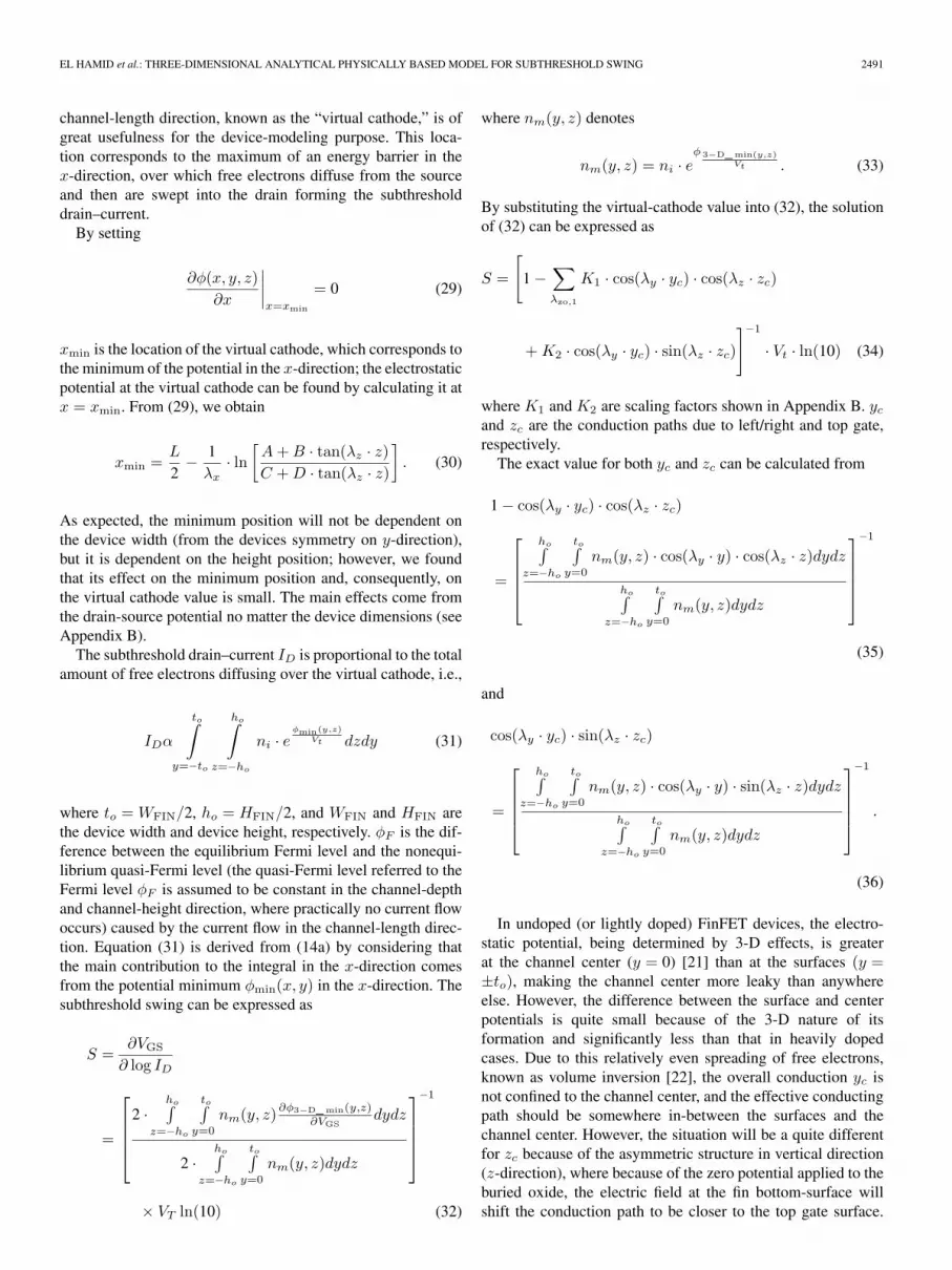
channel-length direction, known as the “virtual cathode,” is ofgreat usefulness for the device-modeling purpose. This loca-tion corresponds to the maximum of an energy barrier in thex-direction, over which free electrons diffuse from the sourceand then are swept into the drain forming the subthresholddrain–current.
By setting
∂φ(x, y, z)∂x
∣∣∣∣x=xmin
= 0 (29)
xmin is the location of the virtual cathode, which corresponds tothe minimum of the potential in the x-direction; the electrostaticpotential at the virtual cathode can be found by calculating it atx = xmin. From (29), we obtain
xmin =L
2− 1λx
· ln[A+B · tan(λz · z)C +D · tan(λz · z)
]. (30)
As expected, the minimum position will not be dependent onthe device width (from the devices symmetry on y-direction),but it is dependent on the height position; however, we foundthat its effect on the minimum position and, consequently, onthe virtual cathode value is small. The main effects come fromthe drain-source potential no matter the device dimensions (seeAppendix B).
The subthreshold drain–current ID is proportional to the totalamount of free electrons diffusing over the virtual cathode, i.e.,
IDα
to∫y=−to
ho∫z=−ho
ni · eφmin(y,z)
Vt dzdy (31)
where to = WFIN/2, ho = HFIN/2, and WFIN and HFIN arethe device width and device height, respectively. φF is the dif-ference between the equilibrium Fermi level and the nonequi-librium quasi-Fermi level (the quasi-Fermi level referred to theFermi level φF is assumed to be constant in the channel-depthand channel-height direction, where practically no current flowoccurs) caused by the current flow in the channel-length direc-tion. Equation (31) is derived from (14a) by considering thatthe main contribution to the integral in the x-direction comesfrom the potential minimum φmin(x, y) in the x-direction. Thesubthreshold swing can be expressed as
S =∂VGS
∂ log ID
=
2 ·ho∫
z=−ho
to∫y=0
nm(y, z)∂φ3−D_ min(y,z)
∂VGSdydz
2 ·ho∫
z=−ho
to∫y=0
nm(y, z)dydz
−1
× VT ln(10) (32)
where nm(y, z) denotes
nm(y, z) = ni · eφ 3−D_ min(y,z)
Vt . (33)
By substituting the virtual-cathode value into (32), the solutionof (32) can be expressed as
S =
[1 −
∑λzo,1
K1 · cos(λy · yc) · cos(λz · zc)
+K2 · cos(λy · yc) · sin(λz · zc)]−1
· Vt · ln(10) (34)
where K1 and K2 are scaling factors shown in Appendix B. yc
and zc are the conduction paths due to left/right and top gate,respectively.
The exact value for both yc and zc can be calculated from
1 − cos(λy · yc) · cos(λz · zc)
=
ho∫z=−ho
to∫y=0
nm(y, z) · cos(λy · y) · cos(λz · z)dydz
ho∫z=−ho
to∫y=0
nm(y, z)dydz
−1
(35)
and
cos(λy · yc) · sin(λz · zc)
=
ho∫z=−ho
to∫y=0
nm(y, z) · cos(λy · y) · sin(λz · z)dydz
ho∫z=−ho
to∫y=0
nm(y, z)dydz
−1
.
(36)
In undoped (or lightly doped) FinFET devices, the electro-static potential, being determined by 3-D effects, is greaterat the channel center (y = 0) [21] than at the surfaces (y =±to), making the channel center more leaky than anywhereelse. However, the difference between the surface and centerpotentials is quite small because of the 3-D nature of itsformation and significantly less than that in heavily dopedcases. Due to this relatively even spreading of free electrons,known as volume inversion [22], the overall conduction yc isnot confined to the channel center, and the effective conductingpath should be somewhere in-between the surfaces and thechannel center. However, the situation will be a quite differentfor zc because of the asymmetric structure in vertical direction(z-direction), where because of the zero potential applied to theburied oxide, the electric field at the fin bottom-surface willshift the conduction path to be closer to the top gate surface.

2492 IEEE TRANSACTIONS ON ELECTRON DEVICES, VOL. 54, NO. 9, SEPTEMBER 2007
Fig. 3. Subthreshold swing at low drain-source voltage (a) versus fin widthand (b) versus channel length. Solid lines in (a) and (b) are the calculationsusing our model, the dashed circle are the numerical results, and the stars andtriangular in (a) are the experimental results, Vds = 20 mV, HFIN = 60 nm.
Moreover, the quantum effect will affect the conduction-pathlocation for both doped and undoped devices; however, weconsider, here, a device with sizes large enough to neglect thequantum confinement.
Mathematically, the integration in y-direction of (32) can beapproximated, due to the device symmetry in y-direction, by itsvalue at y = to/2; however, this cannot be done in z-directiondue to the asymmetric device structure. This means that theyc will be closer to y = to/2 (i.e., WFIN/4). At high drain-source voltage, the virtual-cathode position will go towardthe source end, but this will not prevent the effect of drain-source voltage on the virtual-cathode value, i.e., drain-inducedbarrier-lowering effect (see Fig. 1 and potential equation). Theincrease of drain-source potential will raise the FinFET electricfield at the back interface, and the conduction path “zc” willshift up more toward the top-gate surface. It is expected thatboth conduction paths will be strong functions of both devicedimension ratios (i.e., WFIN/HFIN), and device biasing (i.e.,xmin/0.5L).
A good agreement has been obtained in Fig. 3(a) and (b)at low Vds value, for yc at approximately to/2 and zc atapproximately at 95% of fin height.
At high Vds values, as we have aforementioned, the electricfield will increase at the back surface compared to the top-gatesurface, which will push the conduction path toward the topsurface. A good agreement has been obtained in Fig. 4(a) and
Fig. 4. Subthreshold swing at high drain-source voltage (a) S versus fin widthand (b) S versus channel length. Solid lines in (a) and (b) are the calculationsusing our model, the dashed circle are the numerical results, and the stars andtriangular in (a) are the experimental results, Vds = 1 V, HFIN = 60 nm.
Fig. 5. Subthreshold swing versus fin height at channel length = 60 nm andzc ∼ HFIN. The lines are the calculations with our model; the stars areexperimental data at 60 nm.
(b) at high Vds value, for yc at approximately 77% ofWFIN andzc at approximately at 99% of fin height.
After comparing the model with both numerical simulationsand experimental data, we found that both yc and zc barely

EL HAMID et al.: THREE-DIMENSIONAL ANALYTICAL PHYSICALLY BASED MODEL FOR SUBTHRESHOLD SWING 2493
Fig. 6. Eigenvalue calculations [(26)–(28)]. (c) and (d) show the lowest eigenvalues used to verify (20).
change from their original values (yc = to/2 and zc = ho).Therefore, the model gives acceptable results for all devicedimensions, as shown in Fig. 5. In Fig. 5, we have fixed theconduction-path value “zc,” at a value closer to the fin height,and we got a good agreement even if we changed the fin-height value, with a slight change of yc value from its originalvalue, as shown in the figure. This change in yc comes fromthe effects of the electric field of the top gate on the right- andleft-upper corners as we increase and decrease the fin height.We remark that, due to the symmetry of the device, we solvethe electrostatic problem in one half of the width; in each half,there is one yc, and in every half, it changes due to changes inthe electric field from the top gate (i.e., changes of the top-gatevoltage).
At a high drain voltage, not only the drain–current increasesfor WFIN = 70 nm when compared to WFIN = 20 nm butalso the slope increases, because the conduction path at highdrain-source voltage will be closer to the surface with a widerwidth than the equivalent conduction path at low drain-source-voltage value.
IV. CONCLUSION
In this paper, we have developed an analytical model forthe 3-D electrostatic potential for undoped FinFET by solvingthe Poisson equation including the mobile-charge term. Fromthis 3-D analysis, we have derived an analytical model of thesubthreshold swing, taking into account the voltage-dependentposition of the conduction path. Very good agreement has beenobtained with both measurements and numerical simulations.
APPENDIX A3-D POISSON’S EQUATION SOLVING PROCEDURE
We define the oxide capacitances as
Coxo =εoxtox
(A-1)
Cox1 =εoxtox1
(A-2)
Cox2 =εoxtb. (A-3)
2494 IEEE TRANSACTIONS ON ELECTRON DEVICES, VOL. 54, NO. 9, SEPTEMBER 2007
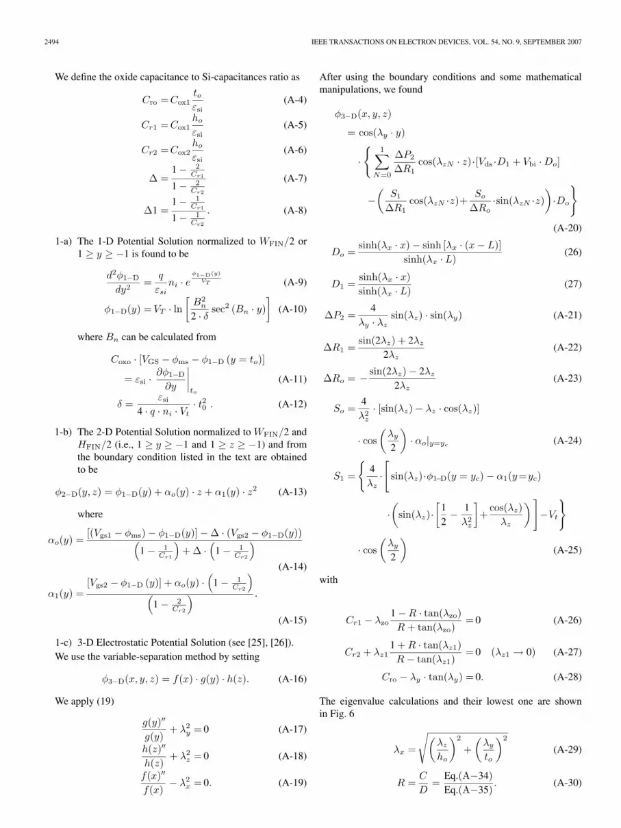
We define the oxide capacitance to Si-capacitances ratio as
Cro =Cox1toεsi
(A-4)
Cr1 =Cox1ho
εsi(A-5)
Cr2 =Cox2ho
εsi(A-6)
∆ =1 − 2
Cr1
1 − 2Cr2
(A-7)
∆1 =1 − 1
Cr1
1 − 1Cr2
. (A-8)
1-a) The 1-D Potential Solution normalized to WFIN/2 or1 ≥ y ≥ −1 is found to be
d2φ1−Ddy2
=q
εsini · e
φ1−D(y)VT (A-9)
φ1−D(y) =VT · ln[B2
n
2 · δ sec2 (Bn · y)]
(A-10)
where Bn can be calculated from
Coxo · [VGS − φms − φ1−D (y = to)]
= εsi ·∂φ1−D∂y
∣∣∣∣to
(A-11)
δ =εsi
4 · q · ni · Vt· t20 . (A-12)
1-b) The 2-D Potential Solution normalized to WFIN/2 andHFIN/2 (i.e., 1 ≥ y ≥ −1 and 1 ≥ z ≥ −1) and fromthe boundary condition listed in the text are obtainedto be
φ2−D(y, z) = φ1−D(y) + αo(y) · z + α1(y) · z2 (A-13)
where
αo(y) =[(Vgs1 − φms) − φ1−D(y)] − ∆ · (Vgs2 − φ1−D(y))(
1 − 1Cr1
)+ ∆ ·
(1 − 1
Cr2
)(A-14)
α1(y) =[Vgs2 − φ1−D (y)] + αo(y) ·
(1 − 1
Cr2
)(
1 − 2Cr2
) .
(A-15)
1-c) 3-D Electrostatic Potential Solution (see [25], [26]).We use the variable-separation method by setting
φ3−D(x, y, z) = f(x) · g(y) · h(z). (A-16)
We apply (19)
g(y)′′
g(y)+ λ2y = 0 (A-17)
h(z)′′
h(z)+ λ2z = 0 (A-18)
f(x)′′
f(x)− λ2x = 0. (A-19)
After using the boundary conditions and some mathematicalmanipulations, we found
φ3−D(x, y, z)
= cos(λy · y)
·{
1∑N=0
∆P2∆R1
cos(λzN · z)·[Vds ·D1 + Vbi ·Do]
−(S1
∆R1cos(λzN ·z)+ So
∆Ro·sin(λzN ·z)
)·Do
}
(A-20)
Do =sinh(λx · x) − sinh [λx · (x− L)]
sinh(λx · L)(26)
D1 =sinh(λx · x)sinh(λx · L)
(27)
∆P2 =4
λy · λzsin(λz) · sin(λy) (A-21)
∆R1 =sin(2λz) + 2λz
2λz(A-22)
∆Ro = − sin(2λz) − 2λz
2λz(A-23)
So =4λ2z
· [sin(λz) − λz · cos(λz)]
· cos(λy
2
)· αo|y=yc
(A-24)
S1 =
{4λz
·[
sin(λz)·φ1−D(y = yc) − α1(y=yc)
·(
sin(λz)·[
12− 1λ2z
]+
cos(λz)λz
)]−Vt
}
· cos(λy
2
)(A-25)
with
Cr1 − λzo1 −R · tan(λzo)R+ tan(λzo)
= 0 (A-26)
Cr2 + λz11 +R · tan(λz1)R− tan(λz1)
= 0 (λz1 → 0) (A-27)
Cro − λy · tan(λy) = 0. (A-28)
The eigenvalue calculations and their lowest one are shownin Fig. 6
λx =
√(λz
ho
)2
+(λy
to
)2
(A-29)
R =C
D=
Eq.(A−34)Eq.(A−35)
. (A-30)
EL HAMID et al.: THREE-DIMENSIONAL ANALYTICAL PHYSICALLY BASED MODEL FOR SUBTHRESHOLD SWING 2495
APPENDIX BVIRTUAL-CATHODE VALUE AND ITS POSITION
2-a) Virtual-Cathode Position
∂φ(x, y, z)∂x
∣∣∣∣x=xmin
= 0. (A-31)
Set
A =∆P2 ·
[Vds + Vbi · (1 − e−λx·L)
]− (1 − e−λx·L) · S1
∆R1 · (1 − e−2λx·L)
(A-32)
B = − (1 − e−λx·L) · So
∆Ro · (1 − e−2λx·L)(A-33)
C =∆P2∆R1
[Vbi −
[Vds + Vbi · (1 − e−λx·L)
]2 sinh(λx · L)
]
− S1∆R1
[1 − (1 − e−λx·L)
2 sinh(λx · L)
](A-34)
D = − So
∆Ro
[1 − (1 − e−λx·L)
2 sinh(λx · L)
](A-35)
xmin =L
2− 1λx
· ln[A+B · tan(λz · z)C +D · tan(λz · z)
]. (A-36)
2-b) Subthreshold-Swing Parameters K1 and K2
K1 =So
∆Ro
Do|x=xmin
φ1−D(y = yc)(A-37)
K2 =S1
∆R1
Do|x=xmin
φ1−D(y = yc). (A-38)
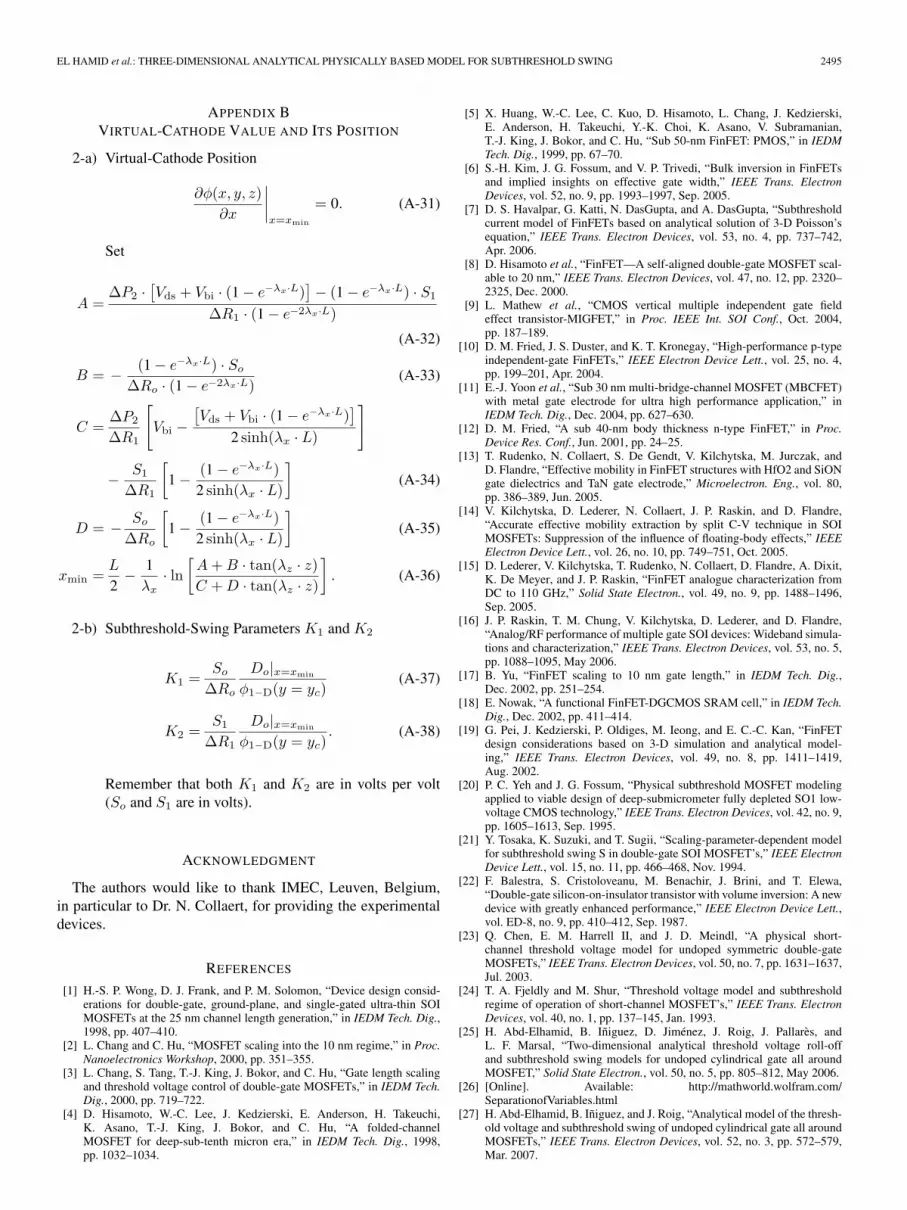
Remember that both K1 and K2 are in volts per volt(So and S1 are in volts).
ACKNOWLEDGMENT
The authors would like to thank IMEC, Leuven, Belgium,in particular to Dr. N. Collaert, for providing the experimentaldevices.
REFERENCES
[1] H.-S. P. Wong, D. J. Frank, and P. M. Solomon, “Device design consid-erations for double-gate, ground-plane, and single-gated ultra-thin SOIMOSFETs at the 25 nm channel length generation,” in IEDM Tech. Dig.,1998, pp. 407–410.
[2] L. Chang and C. Hu, “MOSFET scaling into the 10 nm regime,” in Proc.Nanoelectronics Workshop, 2000, pp. 351–355.
[3] L. Chang, S. Tang, T.-J. King, J. Bokor, and C. Hu, “Gate length scalingand threshold voltage control of double-gate MOSFETs,” in IEDM Tech.Dig., 2000, pp. 719–722.
[4] D. Hisamoto, W.-C. Lee, J. Kedzierski, E. Anderson, H. Takeuchi,K. Asano, T.-J. King, J. Bokor, and C. Hu, “A folded-channelMOSFET for deep-sub-tenth micron era,” in IEDM Tech. Dig., 1998,pp. 1032–1034.
[5] X. Huang, W.-C. Lee, C. Kuo, D. Hisamoto, L. Chang, J. Kedzierski,E. Anderson, H. Takeuchi, Y.-K. Choi, K. Asano, V. Subramanian,T.-J. King, J. Bokor, and C. Hu, “Sub 50-nm FinFET: PMOS,” in IEDMTech. Dig., 1999, pp. 67–70.
[6] S.-H. Kim, J. G. Fossum, and V. P. Trivedi, “Bulk inversion in FinFETsand implied insights on effective gate width,” IEEE Trans. ElectronDevices, vol. 52, no. 9, pp. 1993–1997, Sep. 2005.
[7] D. S. Havalpar, G. Katti, N. DasGupta, and A. DasGupta, “Subthresholdcurrent model of FinFETs based on analytical solution of 3-D Poisson’sequation,” IEEE Trans. Electron Devices, vol. 53, no. 4, pp. 737–742,Apr. 2006.
[8] D. Hisamoto et al., “FinFET—A self-aligned double-gate MOSFET scal-able to 20 nm,” IEEE Trans. Electron Devices, vol. 47, no. 12, pp. 2320–2325, Dec. 2000.
[9] L. Mathew et al., “CMOS vertical multiple independent gate fieldeffect transistor-MIGFET,” in Proc. IEEE Int. SOI Conf., Oct. 2004,pp. 187–189.
[10] D. M. Fried, J. S. Duster, and K. T. Kronegay, “High-performance p-typeindependent-gate FinFETs,” IEEE Electron Device Lett., vol. 25, no. 4,pp. 199–201, Apr. 2004.
[11] E.-J. Yoon et al., “Sub 30 nm multi-bridge-channel MOSFET (MBCFET)with metal gate electrode for ultra high performance application,” inIEDM Tech. Dig., Dec. 2004, pp. 627–630.
[12] D. M. Fried, “A sub 40-nm body thickness n-type FinFET,” in Proc.Device Res. Conf., Jun. 2001, pp. 24–25.
[13] T. Rudenko, N. Collaert, S. De Gendt, V. Kilchytska, M. Jurczak, andD. Flandre, “Effective mobility in FinFET structures with HfO2 and SiONgate dielectrics and TaN gate electrode,” Microelectron. Eng., vol. 80,pp. 386–389, Jun. 2005.
[14] V. Kilchytska, D. Lederer, N. Collaert, J. P. Raskin, and D. Flandre,“Accurate effective mobility extraction by split C-V technique in SOIMOSFETs: Suppression of the influence of floating-body effects,” IEEEElectron Device Lett., vol. 26, no. 10, pp. 749–751, Oct. 2005.
[15] D. Lederer, V. Kilchytska, T. Rudenko, N. Collaert, D. Flandre, A. Dixit,K. De Meyer, and J. P. Raskin, “FinFET analogue characterization fromDC to 110 GHz,” Solid State Electron., vol. 49, no. 9, pp. 1488–1496,Sep. 2005.
[16] J. P. Raskin, T. M. Chung, V. Kilchytska, D. Lederer, and D. Flandre,“Analog/RF performance of multiple gate SOI devices: Wideband simula-tions and characterization,” IEEE Trans. Electron Devices, vol. 53, no. 5,pp. 1088–1095, May 2006.
[17] B. Yu, “FinFET scaling to 10 nm gate length,” in IEDM Tech. Dig.,Dec. 2002, pp. 251–254.
[18] E. Nowak, “A functional FinFET-DGCMOS SRAM cell,” in IEDM Tech.Dig., Dec. 2002, pp. 411–414.
[19] G. Pei, J. Kedzierski, P. Oldiges, M. Ieong, and E. C.-C. Kan, “FinFETdesign considerations based on 3-D simulation and analytical model-ing,” IEEE Trans. Electron Devices, vol. 49, no. 8, pp. 1411–1419,Aug. 2002.
[20] P. C. Yeh and J. G. Fossum, “Physical subthreshold MOSFET modelingapplied to viable design of deep-submicrometer fully depleted SO1 low-voltage CMOS technology,” IEEE Trans. Electron Devices, vol. 42, no. 9,pp. 1605–1613, Sep. 1995.
[21] Y. Tosaka, K. Suzuki, and T. Sugii, “Scaling-parameter-dependent modelfor subthreshold swing S in double-gate SOI MOSFET’s,” IEEE ElectronDevice Lett., vol. 15, no. 11, pp. 466–468, Nov. 1994.
[22] F. Balestra, S. Cristoloveanu, M. Benachir, J. Brini, and T. Elewa,“Double-gate silicon-on-insulator transistor with volume inversion: A newdevice with greatly enhanced performance,” IEEE Electron Device Lett.,vol. ED-8, no. 9, pp. 410–412, Sep. 1987.
[23] Q. Chen, E. M. Harrell II, and J. D. Meindl, “A physical short-channel threshold voltage model for undoped symmetric double-gateMOSFETs,” IEEE Trans. Electron Devices, vol. 50, no. 7, pp. 1631–1637,Jul. 2003.
[24] T. A. Fjeldly and M. Shur, “Threshold voltage model and subthresholdregime of operation of short-channel MOSFET’s,” IEEE Trans. ElectronDevices, vol. 40, no. 1, pp. 137–145, Jan. 1993.
[25] H. Abd-Elhamid, B. Iñiguez, D. Jiménez, J. Roig, J. Pallarès, andL. F. Marsal, “Two-dimensional analytical threshold voltage roll-offand subthreshold swing models for undoped cylindrical gate all aroundMOSFET,” Solid State Electron., vol. 50, no. 5, pp. 805–812, May 2006.
[26] [Online]. Available: http://mathworld.wolfram.com/SeparationofVariables.html
[27] H. Abd-Elhamid, B. Iñiguez, and J. Roig, “Analytical model of the thresh-old voltage and subthreshold swing of undoped cylindrical gate all aroundMOSFETs,” IEEE Trans. Electron Devices, vol. 52, no. 3, pp. 572–579,Mar. 2007.

2496 IEEE TRANSACTIONS ON ELECTRON DEVICES, VOL. 54, NO. 9, SEPTEMBER 2007
Hamdy Abd El Hamid was born in 1970. He re-ceived the B.S. degree in electrical engineering fromthe Higher Technological Institute, Ramadan City,Egypt, in 1994, the M.S. degree in electronic engi-neering from Ain Shams University, Cairo, Egypt,in 2000, and the Ph.D. (and European Doctorate)degree at the Universitat Rovira i Virgili, Tarragona,Spain, in May 2007.
He was a Graduate Visting Student with theElectrical Engineering Department, University ofLiverpool, Liverpool, U.K., from April to June 2005
and with the Microelectronics Laboratory, Université catholique de Louvain,Louvain-la-Neuve, Belgium, from April to June 2006 and in February 2007.Starting October 2007, he will be a Postdoctoral Researcher with McMasterUniversity, Hamilton, ON, Canada. His research interests include the physicsand modeling of nanoscale MOSFETs.
Jaume Roig Guitart was born in Roses,Catalonia, Spain, in 1976. He received the B.S.degree in physics and the Ph.D. degree in microelec-tronics engineering from the Universitat Autonomade Barcelona, Barcelona, Spain, in 1999 and 2004,respectively.
From 2000 to 2005, he was with the Instituto deMicroelectrónica de Barcelona, Centre Nacional deMicroelectronica, Barcelona, Spain, where he wasinvolved in high-voltage smart power devices in SOIand bulk technologies. Since 2005, he has been
with the Intégration de systèmes de gestion de l’énergie Group, Laboratoired’Architectures et d’Analyse des Systèmes, Centre National de la RechercheScientifique, Toulouse, France. He is author or coauthor of more than40 scientific articles in international journals and conference proceedings. Hiscurrent research activity deals with semiconductor power device physics.
Valeria Kilchytska received the M.Sc. degree insolid state electronics and the Ph.D. degree in semi-conductors and dielectrics physics from Kiev Univer-sity, Kiev, Ukraine, in 1992 and 1997, respectively.Her Ph.D. work, which was performed at the Instituteof Semiconductor Physics, Kiev, was devoted to theinvestigation of electrical and radiation properties ofsilicon-on-insulator (SOI) structures.
From 1997 to 2001, she continued to work withthe Institute of Semiconductor Physics, where shehas been involved in the high-temperature character-
ization of SOI devices and in the investigation of bias-temperature and injectionprocesses in the buried oxides of SOI structures. Since 2002, she has beenworking with the Laboratoire de Microélectronique, Université catholique deLouvain, Louvain-la-Neuve, Belgium. Her current research interest is focusedon the room- to high-temperature wide-frequency-band characterization andsimulation of the advanced deep sub-0.1-µm devices.
Denis Flandre (S’86–M’91–SM’03) was born inCharleroi, Belgium, in 1964. He received the Elec-trical Engineer, Ph.D., and Postdoctoral Thesis de-grees from the Université catholique de Louvain(UCL), Louvain-la-Neuve, Belgium, in 1986, 1990,and 1999, respectively. His doctoral research wason the modeling of silicon-on-insulator (SOI) MOSdevices for characterization and circuit simulation,his postdoctoral thesis was on a systematic andautomated synthesis methodology for MOS analogcircuits.
In 1985, he was a summer student trainee at NTT Headquaters, Tokyo,Japan. From October 1990 to September 1991, he was with the Centro Na-cional de Microelectronica, Barcelona, Spain, working on the characterizationand numerical simulation of SOI MOS process and devices. Then, he waswith the Laboratoire de Microélectronique, Louvain-la-Neuve, as a SeniorResearch Associate in the National Fund for Scientific Research (FNRS). Since2001, he has been a Full-Time Professor with UCL giving courses, e.g., on“Integrated analog circuit design,” “Device physics,”. . . Since 2003, he hasalso been the Head of the UCL Microelectronics Laboratory. He is currentlyinvolved in the research and development of SOI MOS devices, digital andanalog circuits, as well as sensors and MEMS, for special applications, morespecifically, high-speed, low-voltage, low-power, microwave, rad-hard, andhigh-temperature electronics and microsystems. He is a founding member ofthe Centre de Recherche en Materiaux et Dispositifs Electroniques Micro- etNanoscopiques of UCL and chairs the Users Commitee of the UCL Micro/Nanotechnology Facility. He is the Cofounder of CISSOID S.A., a start-upcompany which spun-off of UCL in 2000, focusing on SOI circuit-designservices. He has authored or coauthored more than 400 technical papers orconference contributions. He is the holder of six patents. He was the recipientof the 1992 Biennial Siemens-FNRS Award for an original contribution inthe fields of electricity and electronics, of the 1997 Wernaers Award forinnovation in pedagogical presentation of advanced research work, and of the1999 SCK-CEN Prof. Roger Van Geen Prize for innovation in nuclear-scienceinstrumentation. He participated in many short courses on SOI technology inuniversities, industrial companies, and conferences, as well as organized andlectured several Eurotraining courses on SOI technology, devices, and circuits.
Prof. Flandre has been a member of the Advisory Board of the EuropeanUnion (EU) Network of Excellence for High-Temperature Electronics, Scien-tific Board of the “Microserv” Large Infrastructure EU program of the CNM-Barcelona, Executive Board of “SINANO” (the new EU Network of Excellencein silicon nanodevices), and Director Board of the Cyclotron Research Center,Louvain-la-Neuve.
Benjamin Iñiguez (M’96–SM’03) received the B.S.,M.S., and Ph.D. degrees in physics from the Univer-sity of the Balearic Islands, Palma, Spain, in 1992,1993, and 1996, respectively.
He was a Graduate Visiting Student for severalmonths with the Microelectronics Laboratory, Uni-versité catholique de Louvain, Louvain-la-Neuve,Belgium, in 1994 and 1996 and with the NorwegianInstitute of Technology (NTH), Trondheim, Norway,in 1995. His doctoral research focused on the de-velopment of CAD models for short-channel bulk-Si
and fully depleted SOI MOSFETs. From February 1997 to September 1998,he was a Postdoctoral Research Scientist with the Department of Electrical,Computer and Systems Engineering, Rensselaer Polytechnic Institute,Troy, NY, where he studied advanced devices such as short-channel a-Siand poly-Si TFTs, GaN HFETs, and heterodimensional MESFETs. FromSeptember 1998 to February 2001, he was a Research Scientist (PostdoctoralMarie-Curie Grant Holder) in the Microelectronics Laboratory, Universitécatholique de Louvain (Louvain-la-Neuve, Belgium), working on the charac-terization and modeling of thin-film and ultrathin-film SOI MOSFETs fromDC to RF conditions. Since February 2001, he has been with the Departamentd’Enginyeria Electrònica, Elèctrica i Automàtica, Universitat Rovira i Virgili,Tarragona, Spain, as a Titular Professor. His current research interests includethe characterization and modeling of advanced semiconductor devices, inparticular nanoscale multiple-gate MOSFETs and organic and polymer TFTs.He is the author or coauthor of more than 120 research papers published ininternational journals or proceedings of conferences.
Dr. Iñiguez received the Distinction of the Catalan Government for thePromotion of University Research in 2004. He received the Institution ofEngineering and Technology Circuits, Devices and Systems Premium Awardin 2004 for being a coauthor of one paper presenting a new theory of chargetransport in organic and polymer TFTs.