A 0.3–1.4 GHz All-Digital Fractional-N PLL With Adaptive Loop Gain Controller
12
2300 IEEE JOURNAL OF SOLID-STATE CIRCUITS, VOL. 45, NO. 11, NOVEMBER 2010 A 0.3–1.4 GHz All-Digital Fractional-N PLL With Adaptive Loop Gain Controller Deok-Soo Kim, Graduate Student Member, IEEE, Heesoo Song, Graduate Student Member, IEEE, Taeho Kim, Suhwan Kim, Senior Member, IEEE, and Deog-Kyoon Jeong, Senior Member, IEEE Abstract—A 0.3–1.4 GHz all-digital phase locked loop (ADPLL) with an adaptive loop gain controller (ALGC), a 1/8-resolution fractional divider and a frequency search block is presented. The ALGC reduces the nonlinearity of the bang-bang phase-frequency detector (BBPFD), reducing output jitter. The fractional divider partially compensates for the large input phase error caused by fractional-N frequency synthesis. A fast frequency search unit using the false position method achieves frequency lock in 6 iter- ations that correspond to 192 reference clock cycles. A prototype ADPLL using a BBPFD with a dead-zone-free retimer, an ALGC, a fractional divider, and a digital logic implementation of a fre- quency search algorithm was fabricated in a 0.13- m CMOS logic process. The core occupies 0.2 mm and consumes 16.5 mW with a 1.2-V supply at 1.35-GHz. Measured RMS and peak-to-peak jitter with activating the ALGC are 3.7 ps and 32 ps respectively. Index Terms—Adaptive gain control, all-digital phase locked loop (ADPLL), bang-bang phase and frequency detector (BBPFD), false position method, fractional divider, frequency search. I. INTRODUCTION N OWADAYS many digital circuits depend on phase-locked loops (PLL) to generate clocks for system synchroniza- tion or to recover timing information from incoming data streams [1]–[3]. A conventional PLL consisting of analog circuits and passive elements is sensitive to process, voltage and temperature (PVT) variations; thus it requires low-leakage devices, a large chip area and ample voltage headroom [4]. As CMOS technology advances, we cannot continue to meet these requirements, and we need a new design of PLL that is compatible with modern nano-CMOS processes and suitable for massive and noisy digital systems. The emerging all-digital phase-locked loop (ADPLL) is a practical alternative to an analog PLL. An ADPLL consists of purely digital components or digital equivalents, and thus all the states of these components can be represented as the combina- tion of digital signals. Because there is no requirement for large passive elements in the loop filter, an ADPLL is stable at a lower supply voltage, more tolerant of PVT variations, and able to benefit from the reduction in area and power consumption as- sociated with a scaled-down technology [5], [6]. Since all the Manuscript received February 05, 2010; revised May 06, 2010; accepted June 18, 2010. Date of current version October 22, 2010. This paper was approved by Guest Editor Mototsugu Hamada. The authors are with the Department of Electrical Engineering and Computer Science, Seoul National University, Daehak-dong, Gwanak-gu, Seoul, Korea (e-mail: [email protected]). Color versions of one or more of the figures in this paper are available online at http://ieeexplore.ieee.org. Digital Object Identifier 10.1109/JSSC.2010.2064050 internal signals are represented as digital values, internal states of an ADPLL can be stored and restored relatively easily in the registers, allowing signals to be processed flexibly with var- ious techniques [7]–[9]. Moreover, we can subsequently reuse a large part of a proven circuit for other applications, and there- fore an ADPLL design can be migrated to different technologies more efficiently. These advantages of robustness, flexibility and reusability have caused rapidly growing interest in the ADPLL, which has already replaced analog PLL in some high-perfor- mance applications [5]–[12]. In this paper, we present an all-digital fractional-N PLL with a digital gain control scheme. This uses a bang-bang phase-and- frequency detector (BBPFD) and an adaptive loop gain con- troller (ALGC), both of which can readily be migrated to ad- vanced processes. The nonlinear phase detector of intuitive de- sign would be expected to increase the output jitter, but a gain controller calibrates the open-loop gain to be proportional to the average phase error, so that the closed-loop bandwidth changes dynamically and the output jitter decreases. Although a similar technique has been applied to an analog PLL presented in [13], the frequency response of a digital filter in our scheme is not affected by PVT variations, which makes the calibration easier. Several adaptive gain control methods have already been pre- sented in [14]–[16], but our proposed ALGC requires neither an external computational power nor a highly complex hardware. Another potential source of jitter is dithering between division factors, and thus is controlled by the use of a fractional divider in the feedback loop. Fractional division factors are incorporated through the sequential multiplexing of multiphase clocks. The remainder of this paper has four sections. Section II de- scribes some considerations and the motivation of this work. In Section III, we present our ADPLL architecture, and explain the detailed operation of each building block. An implementa- tion is described and measured performance data are given in Section IV. Section V concludes the paper and summarizes the potential benefits of our approach. II. DESIGN CONSIDERATION To optimize performance and to lessen structural complexity, the design of an ADPLL should be carefully examined over the trade-offs between performance and complexity. The most com- plicated parts of an ADPLL are the phase detector and oscillator, which usually require custom optimization. From this point of view, it is worthwhile to pay attention to the type of phase de- tector used in an ADPLL. Phase detectors (PDs) can be classified into linear or non- linear types. A time-to-digital converter (TDC) is a linear PD that produces a digital output proportional to the input phase 0018-9200/$26.00 © 2010 IEEE
Transcript of A 0.3–1.4 GHz All-Digital Fractional-N PLL With Adaptive Loop Gain Controller

2300 IEEE JOURNAL OF SOLID-STATE CIRCUITS, VOL. 45, NO. 11, NOVEMBER 2010
A 0.3–1.4 GHz All-Digital Fractional-N PLL WithAdaptive Loop Gain Controller
Deok-Soo Kim, Graduate Student Member, IEEE, Heesoo Song, Graduate Student Member, IEEE, Taeho Kim,Suhwan Kim, Senior Member, IEEE, and Deog-Kyoon Jeong, Senior Member, IEEE
Abstract—A 0.3–1.4 GHz all-digital phase locked loop (ADPLL)with an adaptive loop gain controller (ALGC), a 1/8-resolutionfractional divider and a frequency search block is presented. TheALGC reduces the nonlinearity of the bang-bang phase-frequencydetector (BBPFD), reducing output jitter. The fractional dividerpartially compensates for the large input phase error caused byfractional-N frequency synthesis. A fast frequency search unitusing the false position method achieves frequency lock in 6 iter-ations that correspond to 192 reference clock cycles. A prototypeADPLL using a BBPFD with a dead-zone-free retimer, an ALGC,a fractional divider, and a digital logic implementation of a fre-quency search algorithm was fabricated in a 0.13- m CMOS logicprocess. The core occupies 0.2 mm� and consumes 16.5 mW witha 1.2-V supply at 1.35-GHz. Measured RMS and peak-to-peakjitter with activating the ALGC are 3.7 ps and 32 ps respectively.
Index Terms—Adaptive gain control, all-digital phase lockedloop (ADPLL), bang-bang phase and frequency detector (BBPFD),false position method, fractional divider, frequency search.
I. INTRODUCTION
N OWADAYS many digital circuits depend on phase-lockedloops (PLL) to generate clocks for system synchroniza-
tion or to recover timing information from incoming datastreams [1]–[3]. A conventional PLL consisting of analogcircuits and passive elements is sensitive to process, voltageand temperature (PVT) variations; thus it requires low-leakagedevices, a large chip area and ample voltage headroom [4].As CMOS technology advances, we cannot continue to meetthese requirements, and we need a new design of PLL that iscompatible with modern nano-CMOS processes and suitablefor massive and noisy digital systems.
The emerging all-digital phase-locked loop (ADPLL) is apractical alternative to an analog PLL. An ADPLL consists ofpurely digital components or digital equivalents, and thus all thestates of these components can be represented as the combina-tion of digital signals. Because there is no requirement for largepassive elements in the loop filter, an ADPLL is stable at a lowersupply voltage, more tolerant of PVT variations, and able tobenefit from the reduction in area and power consumption as-sociated with a scaled-down technology [5], [6]. Since all the
Manuscript received February 05, 2010; revised May 06, 2010; accepted June18, 2010. Date of current version October 22, 2010. This paper was approvedby Guest Editor Mototsugu Hamada.
The authors are with the Department of Electrical Engineering and ComputerScience, Seoul National University, Daehak-dong, Gwanak-gu, Seoul, Korea(e-mail: [email protected]).
Color versions of one or more of the figures in this paper are available onlineat http://ieeexplore.ieee.org.
Digital Object Identifier 10.1109/JSSC.2010.2064050
internal signals are represented as digital values, internal statesof an ADPLL can be stored and restored relatively easily inthe registers, allowing signals to be processed flexibly with var-ious techniques [7]–[9]. Moreover, we can subsequently reusea large part of a proven circuit for other applications, and there-fore an ADPLL design can be migrated to different technologiesmore efficiently. These advantages of robustness, flexibility andreusability have caused rapidly growing interest in the ADPLL,which has already replaced analog PLL in some high-perfor-mance applications [5]–[12].
In this paper, we present an all-digital fractional-N PLL witha digital gain control scheme. This uses a bang-bang phase-and-frequency detector (BBPFD) and an adaptive loop gain con-troller (ALGC), both of which can readily be migrated to ad-vanced processes. The nonlinear phase detector of intuitive de-sign would be expected to increase the output jitter, but a gaincontroller calibrates the open-loop gain to be proportional to theaverage phase error, so that the closed-loop bandwidth changesdynamically and the output jitter decreases. Although a similartechnique has been applied to an analog PLL presented in [13],the frequency response of a digital filter in our scheme is notaffected by PVT variations, which makes the calibration easier.Several adaptive gain control methods have already been pre-sented in [14]–[16], but our proposed ALGC requires neither anexternal computational power nor a highly complex hardware.Another potential source of jitter is dithering between divisionfactors, and thus is controlled by the use of a fractional divider inthe feedback loop. Fractional division factors are incorporatedthrough the sequential multiplexing of multiphase clocks.
The remainder of this paper has four sections. Section II de-scribes some considerations and the motivation of this work. InSection III, we present our ADPLL architecture, and explainthe detailed operation of each building block. An implementa-tion is described and measured performance data are given inSection IV. Section V concludes the paper and summarizes thepotential benefits of our approach.
II. DESIGN CONSIDERATION
To optimize performance and to lessen structural complexity,the design of an ADPLL should be carefully examined over thetrade-offs between performance and complexity. The most com-plicated parts of an ADPLL are the phase detector and oscillator,which usually require custom optimization. From this point ofview, it is worthwhile to pay attention to the type of phase de-tector used in an ADPLL.
Phase detectors (PDs) can be classified into linear or non-linear types. A time-to-digital converter (TDC) is a linear PDthat produces a digital output proportional to the input phase
0018-9200/$26.00 © 2010 IEEE

KIM et al.: A 0.3–1.4 GHz ALL-DIGITAL FRACTIONAL-N PLL WITH ADAPTIVE LOOP GAIN CONTROLLER 2301
Fig. 1. Typical structure of (a) a linear and (b) a nonlinear TDC.
error. The time resolution of a TDC is generally related to thebuffer delay, which is subject to PVT variations. Therefore, ahigh-resolution TDC requires precise analog circuitry, which in-creases the overall design complexity remarkably [17]. A non-linear PD is much simpler and more robust, because it onlyconsists of logic gates and merely indicates the direction of thephase error [5]. Naturally a bang-bang decision loses some in-formation, but digital circuits can be used to supplement thatresult and these are insensitive to PVT variations.
A linear TDC is used for phase detection in many ADPLLcircuits because of its fine resolution. Fig. 1(a) shows the typ-ical structure of a linear TDC, which consists of many cascadedinverters and flip-flops. Input signals go through the inverterchain, and a series of D-flip flops (DFFs) clocked by a referencesignal samples the delayed inputs. The thermometer-like outputfrom the DFF array is translated to binary form by a decoder.The time resolution and detection range of a conventional TDCare respectively determined by the inverter delay and the lengthof the inverter chain. The improved performance of a high-res-olution TDC is bought at the expense of an excessive numberof inverters, which soak up power and area. Even a high-res-olution TDC has limited frequency-detection capability, and afurther aid to frequency locking may be required.
A BBPFD is effectively a nonlinear PD. Intuitive designyields the structure shown in Fig. 1(b) [18], in which a con-ventional PFD is followed by a decision circuit. The decisioncircuit resolves the priorities of the signals and the output latchholds that result until the next decision is delivered. Althoughthe BBPFD is easy to design, it has a limit cycle problem [19],and the quantization effect of the DCO increases the outputjitter. It is difficult to manage these nonlinearities effectively inan analog design, since that will require dealing with analogquantities. However, in an ADPLL, all traversing signals be-tween building blocks are digital, and its core behavior of anADPLL is described in VHDL or Verilog-HDL codes. Thus,the nonlinear effects can easily be controlled, and furthermore
the RTL codes can be reused without major modifications.Consequently, employing the binary decision is a natural ap-proach especially in an all-digital design. Therefore, we useda simple BBPFD in the proposed architecture and focused onhow to deal with the nonlinearity of the bang-bang design.
III. ARCHITECTURE
As shown in Fig. 2, the proposed ADPLL consists of aBBPFD, an adaptive loop gain controller, a digital loop filter(DLF), a first-order delta-sigma modulator, a multiphasedigitally controlled oscillator (MDCO), a fractional divider,a PFD-based TDC, and a digital logic implementation of afrequency search algorithm. The BBPFD compares the arrivaltime of the reference clock edge with that of the divided DCOclock edge, and produces an early or a late signal. The DLFfilters the phase error obtained from the BBPFD, and theresulting values are fed into the modulator. The gain of theDLF is changed by the ALGC to reflect the average phase error.The ALGC consists of a cascaded second-order IIR filter withtwo leaky integrators. The output of the modulator is sentto the MDCO and dithers the output clock signal of the MDCOto improve the frequency resolution. The MDCO contains adifferential 4-stage ring oscillator with a supply voltage that isadjusted by a digitally controlled resistor [10]. The fractionaldivider receives 8-phase clock signal from the MDCO, andprovides a division ratio between 7 and 16, in steps of 1/8.This small step size suppresses the input phase error caused bythe alternating modulus of the feedback divider. A PFD-basedlinear TDC [18] is included only to verify the effectiveness ofthe ALGC, and the output of these two phase detectors can bemultiplexed. The frequency search unit that implements thefalse position method achieves coarse frequency lock within 7iterations. The computational overload of the frequency searchunit is reduced because the use of a 1/8-resolution fractional di-vider allows some multiplications and divisions to be replacedby arithmetic shifts. The spread spectrum profile generator(SSPG) produces a triangular profile and modulates the outputfrequency. When the spread spectrum output is off, the SSPGbehaves like a first-order modulator for the fractional-Nsynthesis.
A. Bang-Bang Phase-and-Frequency Detector
A linear TDC benefits from a delay line composed of manycascaded inverters, but the trade-off between time resolutionand detection range of conventional one forces a wide-rangefine-resolution TDC to require excessive hardware and becomecomplex. We use the BBPFD shown in Fig. 3 to simplify thedesign and implementation of the proposed ADPLL. It detectsphase and frequency errors to generate the output signals rep-resenting only the sign of errors. Unlike previous BBPFDs [5],ours generates two sets of results; one is a typical bang-bangoutput to control the overall gain for low jitter generation, andthe other is a retimed output that is fed into the DLF. A conven-tional PFD composed of two flip-flops at the front part of theBBPFD produces UP and DN signals by comparing the risingedges of two input clocks. Then, a simple arbiter [20] which canresolve a timing difference of a few picoseconds in simulation,determines which event occurs earlier, and a following output

2302 IEEE JOURNAL OF SOLID-STATE CIRCUITS, VOL. 45, NO. 11, NOVEMBER 2010
Fig. 2. Block diagram of the proposed ADPLL.
Fig. 3. Proposed BBPFD.
latch maintains BBUP or BBDN signal until a reverse directionevent is detected. Because bang-bang signals are maintained fora relatively long period until the polarity of input phase errorchanges, the phase offset resulting from the bang-bang quanti-zation is integrated over a considerable time, which makes theoutput peak-to-peak jitter increase. To shorten the integrationperiod and reduce the output jitter, the implemented BBPFD inthis work produces outputs controlled by the retimer. Simulta-neously with the pulsewidth control, the retimer synchronizesthe output of the BBPFD to the internal system clock (FCLK).
Fig. 4 shows a comparison of the timing waveform resultingfrom a simple D flip-flop (DFF) and the proposed retimer. Theretimed signals are generated by sampling UP and DN out-puts from the conventional PFD using the FCLK. As shownin Fig. 4(a), a DFF can perform as a simple retimer. However,the phase error information can be lost when the duration ofthe UP or DN pulse is shorter than the period of the FCLKsignal, which causes a dead zone in the transfer characteristic.As a result, the output phase of the ADPLL wanders over thedead-zone and the output jitter increases proportionally. Theproposed retimer, consisting of an edge detector and a samplingflip-flop, eliminates the dead zone. The edge detector extendsthe width of the UP or DN pulse until the next FCLK edge ar-rives, and the sampling flip-flop converts this extended output to
Fig. 4. Comparison of timing waveform from (a) a simple DFF and (b) theproposed retimer.
a one-cycle-long pulse, so that no signal transitions are missedas shown in Fig. 4(b). In the steady state, the UP and DN pulsesbecome quite short, so we intentionally inserted delay on thereset path in the tri-state PFD in order not to smear out the out-puts by the latches. When either RUP or RDN is asserted, thecorresponding BBUP or BBDN inhibits the retimer from gener-ating opposite retimed pulses. For example, in Fig. 4(b), whenBBUP is high, the RDN signal shown as a dotted line is not as-serted.
B. Adaptive Loop Gain Controller
Although a BBPFD is easy to implement, its nonlinear char-acteristics and relatively large gain can cause significant outputjitter. Lowering the loop bandwidth is a typical solution to get-ting better jitter performance, but that increases the lock timeconsiderably. Instead, in our design, the ALGC dynamicallyadjusts the closed-loop bandwidth to reduce the output jitterwithout seriously affecting the lock time. Fig. 5 shows the struc-ture of the DLF and ALGC. The DLF is separated into a propor-tional and an integral path, and its overall gain is controlled by

KIM et al.: A 0.3–1.4 GHz ALL-DIGITAL FRACTIONAL-N PLL WITH ADAPTIVE LOOP GAIN CONTROLLER 2303
Fig. 5. Structure of the DLF and ALGC.
Fig. 6. Leaky integrator: (a) Z-domain model. (b) Frequency response.
the ALGC using a 2-stage IIR filter. This filter, which is com-posed of two leaky integrators and a multiplier, effectively aver-ages the bang-bang output from the BBPFD. The phase delay ofa typical cascaded 2-stage IIR filter is considerable, and it seri-ously affects the stability of the loop. In this work, the bang-bangoutput is fed into not only the first stage but also the second stageof the IIR filter through a multiplier to reduce the phase delay.Because the bang-bang output is 1 or 1, the multiplier eitherpasses or negates the integrator output which can be readily real-ized with an adder and a few multiplexers in two’s complementsystem.
C. Operation of the ALGC
As we have already stated, each stage of the IIR filter is basedon a leaky integrator. Fig. 6(a) shows the z-domain model of theleaky integrator. The transfer function of this integrator can beexpressed as follows:
(1)
An integrator is commonly unstable and its output divergesfor some inputs. But this circuit has a forgetting factor andforms a kind of low-pass filter with the frequency responseshown in Fig. 6(b). If the input value is constant, the gainwill be one and the output will approach the input value. Onthe other hand, the gain of this circuit will decrease for a fastswitching input sequence.
(2)
Equation (2) is an example of the fastest alternation, and itcan be represented by a cosine function. u[n] expresses the unitstep sequence. The z-transform of (2) is given as
(3)
By combining (1) and (3), we can obtain the z-transform ofthe output sequence as follows:
(4)
In this extreme case, the output sequence of the leaky inte-grator does not converge to a specific value because the regionof convergence (ROC) for does not include the unit circle.Although the leaky integrator effectively averages the input, theoutput for (2) is not zero. Instead, the resulting sequence willhave the alternating signs analogous to the input and the smallmagnitude determined by . This sequence is not suitable forthe gain control because its sign keeps changing. Actually, theabsolute value function follows the leaky integrator as shown in

2304 IEEE JOURNAL OF SOLID-STATE CIRCUITS, VOL. 45, NO. 11, NOVEMBER 2010
Fig. 7. Output jitter histograms: (a) using a linear TDC and (b) using a BBPFDwith an ALGC.
Fig. 5, and we take the absolute value for controlling the overallgain of the loop filter. Because all poles of arenot inside the unit circle, we can not apply the final value the-orem to calculate the gain in this case. If for ,the nth number of the output sequence equals to
n is even.
n is odd.(5)
This equation also confirms that the polarity of the outputsequence continuously changes. After some trivial calculation,the final value can be expressed as follows:
(6)
This equation tells us that the gain of a leaky integrator for afast alternating sequence obtained from (6) is less than unity.
This result gives us an insight into how the IIR filter works.If the ADPLL is in an unlocked state, the BBPFD will make
constant up or down signals during the frequency tracking.Therefore, the gain of the IIR filter will be about one, and theclosed-loop bandwidth will not be significantly affected. As theADPLL approaches a locked state, the output of the BBPFDalternates between up and down more quickly, and the averageinput phase error drops. As a result, the absolute output valueof the IIR filter will decrease and the closed-loop bandwidthand the output jitter will be reduced accordingly. The IIR filterconsists of two cascaded leaky integrators, therefore the finalvalue approaches
(7)
for sufficiently small and . In other words, the ALGCmakes the open-loop gain proportional to the average phaseerror, and we can fulfill adaptive gain control according to theloop condition. With the dynamically changing closed-loopbandwidth, moderate lock time and low jitter can be achieved.
We verified the effect of the ALGC by means of an HDL sim-ulation. The core RTL code used in this simulation is synthesiz-able except the DCO and TDC models. The DCO behavioralmodel includes 2.5 ps random timing jitter and 80 fsrandom timing wander [21]. The resolution of the TDC modelused in this simulation is 30 ps. The output jitter histogram ofthe ADPLL using a linear TDC and a BBPFD with the ALGCare shown in Fig. 7(a) and (b), respectively. The ADPLL using alinear TDC has shown slightly better performance. However, theALGC is fully synthesizable, and this advantage makes it moreappropriate for an all-digital design than a full-custom linearTDC.
D. Digital Loop Filter
The proposed ADPLL uses a typical loop filter structure witha proportional and an integral path. The dynamics and the noiseof the digital bang-bang PLLs using this filter have already beendiscussed in the literature [19], [22]–[25]. The jitter can be ex-pressed as follows [25]:
(8)
where is the standard deviation of the jitter, D is the filter la-tency, N is multiplication factor, is the proportional path gain,and is the DCO gain. A proper value of can be obtainedfrom this equation if the target jitter is given. The integral pathgain is given by
(9)
where is the minimum phase margin [25]. For the stableoperation, should be much smaller than . Equation (9) is de-rived from the case when the DLF operates at the reference clockrate. In the proposed architecture, however, the DLF operates atthe FCLK rate which is faster than the reference clock rate, and,thus, the DLF integrates the phase error more frequently, whilethe proportional path of the DLF remains steady. Therefore, weset to be smaller than the value calculated from (9) at leastby the ratio of the FCLK frequency to the reference frequency.

KIM et al.: A 0.3–1.4 GHz ALL-DIGITAL FRACTIONAL-N PLL WITH ADAPTIVE LOOP GAIN CONTROLLER 2305
Fig. 8. Block diagram of the fractional divider.
Since this scheme reduces the effective latency, the output jitterperformance is improved according to (8).
E. Fractional Divider
A typical fractional-N frequency synthesizer adopts a dual-modulus divider. The fractional-N PLL generates a fraction ofthe input frequency by alternating the modulus between twoconsecutive integers. This usually results in large phase error,due to the modulation of the feedback divider. In our architec-ture, a fractional divider is used to reduce the large phase errorresulting from the changes of division ratio. The fractional di-vider consists of an 8-to-1 phase multiplexer (MUX), a divider,a 4-bit comparator and a 3-bit Gray-code counter, as shown inFig. 8. It uses multiphase clock from the MDCO, and its oper-ation is based on the sequential input clock multiplexing. Thedifferential output of the MDCO is multiplexed and fed intothe divider to generate the output clock signal. The 4-bit com-parator produces an advance signal by comparing the fractionalpart (F) with the internal count of the divider. The Gray-codecounter is activated and the count increases one by one whilethe advance signal is high. The MUX control input is changedaccording to the value of the counter, and then the leading clocksignal, right ahead of current multiplexed output, is selected bythe MUX so that the output phase can advance forward. Re-peating this process achieves the fractional division, which mayalso be achieved by moving the output phase backward as shownin Fig. 9. In that case, however, glitches will appear in the mul-tiplexed output, and the divider will malfunction [26]–[28].
Albeit using the known architecture, we implemented thefractional divider with a Gray-code counter to further minimizeunwanted glitches in switching MUX selection signals. Gen-erally, the number of phases determines the control step of thefractional divider. If the fractional divider uses M-phase clockand F times of phase advance taking place every N input cycles
, its division ratio becomes (N-F/M). Fig. 10 showsan operation example of the fractional divider using 8-phaseclock. During the operation, N and F are 8 and 3 respectively,and the resulting division ratio is (8-3/8). In this design, thedivision ratio ranges from 7 to 16 in steps of 1/8.
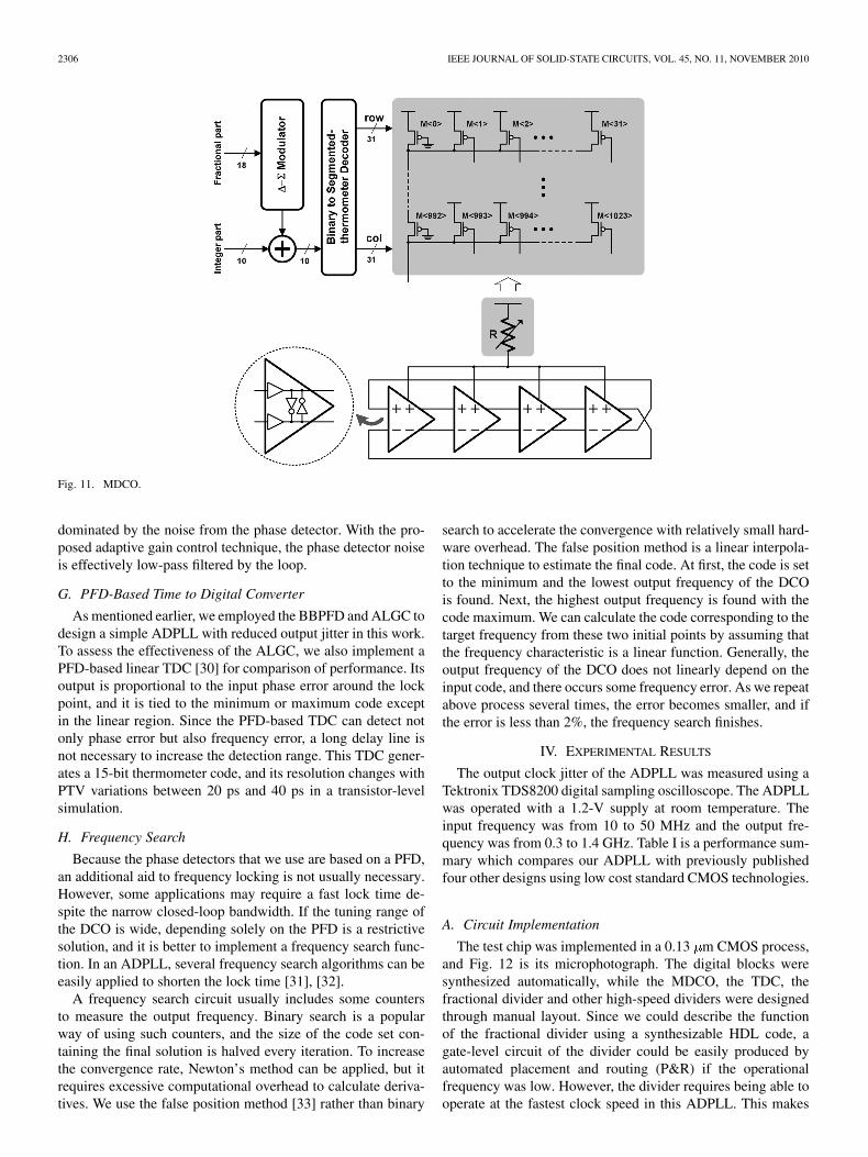
F. Digitally Controlled Oscillator
The MDCO consists of a differential 4-stage ring oscillatorand a digitally controlled resistor (DCR) [10]. Fig. 11 shows the
Fig. 9. Forward and backward phase switching.
Fig. 10. Example operation of the fractional divider using an 8-phase clock.
block diagram of the MDCO, which generates the 8-phase clockrequired to operate the fractional divider. Each stage of the ringoscillator is the typical starved-inverter-based delay cell plus apseudo-differential output buffer. The supply voltage of the ringoscillator, which is controlled by the DCR, changes the outputfrequency. The DCR is composed of many digitally controllablepMOS transistors arranged in a 32 32 matrix. Some of thesetransistors are always turned on to guarantee minimum currentpath. The input code to the DCR is dithered by a first-order
modulator operating at the quarter of the output frequency.The modulator generates the 1-bit dither sequence fromthe 18-bit fractional part of the DLF output. This sequence isadded to the 10-bit integer part of the DLF output, and fed intoa decoder. We implement the segmented-thermometer controlscheme in the DCR to obtain better linearity than the binarycontrol scheme using relatively small hardware [10].
The noise of the MDCO operating at 1.4 GHz is smaller thanthe quantization noise of the phase detector [29] or the effect ofthe fractional spur. Therefore, the output jitter performance is
2306 IEEE JOURNAL OF SOLID-STATE CIRCUITS, VOL. 45, NO. 11, NOVEMBER 2010
Fig. 11. MDCO.
dominated by the noise from the phase detector. With the pro-posed adaptive gain control technique, the phase detector noiseis effectively low-pass filtered by the loop.
G. PFD-Based Time to Digital Converter
As mentioned earlier, we employed the BBPFD and ALGC todesign a simple ADPLL with reduced output jitter in this work.To assess the effectiveness of the ALGC, we also implement aPFD-based linear TDC [30] for comparison of performance. Itsoutput is proportional to the input phase error around the lockpoint, and it is tied to the minimum or maximum code exceptin the linear region. Since the PFD-based TDC can detect notonly phase error but also frequency error, a long delay line isnot necessary to increase the detection range. This TDC gener-ates a 15-bit thermometer code, and its resolution changes withPTV variations between 20 ps and 40 ps in a transistor-levelsimulation.
H. Frequency Search
Because the phase detectors that we use are based on a PFD,an additional aid to frequency locking is not usually necessary.However, some applications may require a fast lock time de-spite the narrow closed-loop bandwidth. If the tuning range ofthe DCO is wide, depending solely on the PFD is a restrictivesolution, and it is better to implement a frequency search func-tion. In an ADPLL, several frequency search algorithms can beeasily applied to shorten the lock time [31], [32].
A frequency search circuit usually includes some countersto measure the output frequency. Binary search is a popularway of using such counters, and the size of the code set con-taining the final solution is halved every iteration. To increasethe convergence rate, Newton’s method can be applied, but itrequires excessive computational overhead to calculate deriva-tives. We use the false position method [33] rather than binary
search to accelerate the convergence with relatively small hard-ware overhead. The false position method is a linear interpola-tion technique to estimate the final code. At first, the code is setto the minimum and the lowest output frequency of the DCOis found. Next, the highest output frequency is found with thecode maximum. We can calculate the code corresponding to thetarget frequency from these two initial points by assuming thatthe frequency characteristic is a linear function. Generally, theoutput frequency of the DCO does not linearly depend on theinput code, and there occurs some frequency error. As we repeatabove process several times, the error becomes smaller, and ifthe error is less than 2%, the frequency search finishes.
IV. EXPERIMENTAL RESULTS
The output clock jitter of the ADPLL was measured using aTektronix TDS8200 digital sampling oscilloscope. The ADPLLwas operated with a 1.2-V supply at room temperature. Theinput frequency was from 10 to 50 MHz and the output fre-quency was from 0.3 to 1.4 GHz. Table I is a performance sum-mary which compares our ADPLL with previously publishedfour other designs using low cost standard CMOS technologies.
A. Circuit Implementation
The test chip was implemented in a 0.13 m CMOS process,and Fig. 12 is its microphotograph. The digital blocks weresynthesized automatically, while the MDCO, the TDC, thefractional divider and other high-speed dividers were designedthrough manual layout. Since we could describe the functionof the fractional divider using a synthesizable HDL code, agate-level circuit of the divider could be easily produced byautomated placement and routing (P&R) if the operationalfrequency was low. However, the divider requires being able tooperate at the fastest clock speed in this ADPLL. This makes

KIM et al.: A 0.3–1.4 GHz ALL-DIGITAL FRACTIONAL-N PLL WITH ADAPTIVE LOOP GAIN CONTROLLER 2307
TABLE ICOMPARATIVE PERFORMANCE OF FIVE ADPLLS
Estimated from the phase noise plot
Fig. 12. Microphotograph.
it vital to minimize the critical path delay, and therefore wehandle the layout of the divider manually.
Fig. 12 shows that the BBPFD is much smaller than the TDC,and the BBPFD requires least custom optimization. It was de-signed using CMOS gates from a standard cell library, exceptfor the simple arbiter which is composed of several transistors.Since the structure is simple, the BBPFD is more reusable andwe need little effort to design it compared with designing theTDC. Conversely, the PFD-based linear TDC requiring 15 sam-plers and 16 delay cells can realize finer resolution, but the gainof TDC which is related with its resolution changes dependingon the PVT variation. The contents of the digital core includean ALGC, a DLF, a modulator, and a multi-modulus di-vider. The core has many controllable parameters, which allowthe circuit to be configured in many different ways, and aninterface was implemented to manage these parameters.
B. Frequency-Locking Behavior
We measured the frequency-locking behavior of the proposedADPLL by using LeCroy WaveRunner 6200 A digital oscil-loscope. Fig. 13 shows the change of output frequency whenthe reference frequency is 50 MHz and the output frequency
Fig. 13. Frequency-locking behavior.
is 1.35 GHz. This figure shows that frequency search is com-pleted after 6 iterations, and the duration of each iteration is32 reference cycle. The locking behavior with the ALGC isshown in a solid line and the lock-time is about 7.5 s. Thelocking behavior with the TDC is shown in a dotted line and thelock-time is about 6 s. In the steady state, the output frequencyis 1.35 GHz, but large frequency fluctuation arising from periodjitter has been observed due to the noise injected from the mea-surement environment.
C. Effect of ALGC on Jitter
We assessed the effectiveness of the ALGC by measuring theoutput jitter. The multiplication factor is 27 with the referencefrequency of 50 MHz and the output frequency of 1.35 GHzfor the measurement. The FCLK frequency is 150 MHz and theratio of the FCLK frequency to the reference frequency is 3 in

2308 IEEE JOURNAL OF SOLID-STATE CIRCUITS, VOL. 45, NO. 11, NOVEMBER 2010
Fig. 14. Measured output jitter histogram: (a) using the BBPFD without theALGC (4.8 ps ); (b) using the BBPFD with the ALGC (3.7 ps ); and(c) using the TDC (3.8 ps ).
this case. Fig. 14(a) shows a histogram of output clock jitter,measured with the BBPFD and the ALGC deactivated. Whenthe filter coefficients and were respectively and ,the RMS and the peak-to-peak jitter were measured as 4.8 ps and40 ps, respectively. Fig. 14(b) shows the equivalent histogramwith the same filter coefficients and with the ALGC activated.The ALGC coefficients and were and , respec-tively. In the locked state, the gain of the ALGC approaches
according to (7) and the effective and approachand , respectively. However, is limited to becausethe fractional part of the DLF output is 18-bits wide. The RMS
Fig. 15. Measured output spectrum: (a) using the BBPFD without the ALGC;(b) using the BBPFD with the ALGC.
and the peak-to-peak jitter were 3.7 ps and 32 ps, respectively.The application of the ALGC shows about 30% improvementon the jitter performance. The output spectrum of each case isshown in Fig. 15. We can observe that the spurs are reduced andthe jitter performance is improved when the ALGC is turned on.As explained in Section III, we can confirm that the ALGC sup-presses the nonlinear property of the BBPFD and can reduce thejitter in its locked state.
Beside the BBPFD, the PFD-based linear TDC was imple-mented in the proposed ADPLL to compare the performance ofthe BBPFD supported by the ALGC with that of a linear TDC.Fig. 14(c) shows a measured output clock jitter histogram whenthe TDC is selected for a phase detector and resulting RMSand peak-to-peak jitter were 3.8 ps and 33 ps. The filter coef-ficients and were and , respectively. Although thesteady-state output jitter is around the minimum resolution ofthe TDC, the output of the TDC will not become a mere bang-bang signal due to the phase error generated by the dual-mod-ulus divider in a fractional-N synthesizer. In this case, the quan-tization noise is smaller than that of the BBPFD, so the TDC will

KIM et al.: A 0.3–1.4 GHz ALL-DIGITAL FRACTIONAL-N PLL WITH ADAPTIVE LOOP GAIN CONTROLLER 2309
Fig. 16. Jitter performance: (a) with the fixed output frequency (1.35 GHz);(b) with the fixed multiplication factor (29.79); (c) with the fixed reference fre-quency (16 MHz).
show better jitter performance. In an integer-N case, the TDCcan turn into bang-bang mode. However, the transient behaviorof the BBPFD is restricted due to its limited output range, andthere occurs a trade-off between the lock time and the jitter per-formance. Therefore, using the BBPFD may require increasingthe loop parameters in some case, and the TDC can show betterperformance than the BBPFD depending on the condition. Theoutput clock jitter histogram when the BBPFD is used with theALGC is already shown in Fig. 14(b). These two measurementsshow almost the same result and agree with the HDL simula-tion in Section III. Consequently, the BBPFD cooperated withthe ALGC is a good substitute for a linear TDC so that subtlecustom optimization can be avoided.
D. Jitter Performance
The jitter performance as a function of the input frequency isshown in Fig. 16(a). The output frequency is fixed at 1.35 GHzand the multiplication factor is changed accordingly. Althoughwe can find some fluctuation in jitter performance, total vari-ation is restricted within 10%. Fig. 16(b) shows the jitter per-formance when the multiplication factor is fixed at 29.79 andthe output frequency is varied for the same loop parameters.Fig. 16(c) shows the jitter performance when the reference fre-quency is fixed at 16 MHz. Although the jitter increases as theoutput frequency decreases, the ratio of the jitter to the outputperiod is better at low frequencies.
Fig. 17. Active area of each synthesized block.
Fig. 18. Power dissipation of each circuit block.
E. Area and Power Consumption
The size of the ADPLL is 1.02 mm 0.41 mm but the corearea related with the operation of the ADPLL excluding theTDC for comparison, the interface, and decoupling capaci-tors is only 0.2 mm . The active area of each synthesized blockis shown in Fig. 17. In this figure, only the area of the logic gatesis taken into account, and the overhead caused by timing androuting constraints that come out during P&R are not consid-ered. Practically, the size of digital block increases after P&R.We set the core utilization to 50% at the floor planning step,and thus realized circuits occupied about twice larger area thanshown in this figure. The area of the BBPFD plus the ALGCis about 0.029 mm whereas that of the TDC is only about0.012 mm because we keep the number of the delay elementsas small as possible without any margin.
The ADPLL consumes 16.5 mW with a 1.2-V supply. Fig. 18shows the power dissipation of each circuit block as a functionof the output frequency. To change the output frequency, the di-vision ratio of feedback divider is fixed, and the input frequencyis varied from 15 to 50 MHz. The total power consumption of

2310 IEEE JOURNAL OF SOLID-STATE CIRCUITS, VOL. 45, NO. 11, NOVEMBER 2010
the ADPLL was proportional to the output frequency. Becausethe fractional divider and other dividers operate at the fastestclock frequency, they consume considerable amount of the totalpower. The logic power marked with circles includes the powerconsumption of the BBPFD, the TDC, the digital core and thebuffers of digital input/output pads. In a simulation, the powerconsumption of the BBPFD is 0.028 mW and that of the ALGCis 0.3 mW, while that of the TDC is 0.31 mW when the referencefrequency is 50 MHz and the FCLK frequency is 150 MHz.
Our priority in designing the digital blocks was flexibility,and thus the circuits are somewhat over-specified. In the presentdesign, the digital blocks take relatively large area and the logicpower dissipation is more than 50% of the total, but it couldreadily be reduced in line with a more defined specification.
V. CONCLUSION
We have presented an ADPLL with a BBPFD incorporatedwith an ALGC, a fractional divider, and a fast frequency searchalgorithm. Simulated and measured results show how the ALGCis able to suppress the nonlinearity of the bang-bang design. The1/8-resolution fractional divider reduces the large phase error atthe input of the ADPLL and fast frequency lock is achieved byapplying the false position method. The measurements show ac-ceptable performances, and this demonstrates the practical ap-plicability of the proposed architecture.
REFERENCES
[1] B. Razavi, “The role of PLLs in future wireline transmitters,” IEEETrans. Circuits Syst. I: Reg. Papers, vol. 56, no. 8, pp. 1786–1793, Aug.2009.
[2] J. Kim, J.-K. Kim, B.-J. Lee, N. Kim, D.-K. Jeong, and W. Kim, “A20-GHz phase-locked loop for 40-Gb/s serializing transmitter in 0.13-�m CMOS,” IEEE J. Solid-State Circuits, vol. 41, no. 4, pp. 899–908,Apr. 2006.
[3] J. L. Sonntag and J. Stonick, “A digital clock and data recovery archi-tecture for multi-gigabit/s binary links,” IEEE J. Solid-State Circuits,vol. 41, no. 8, pp. 1867–1875, Aug. 2006.
[4] W. Rhee, H. Ainspan, D. J. Friedman, T. Rasmus, S. Garvin, and C.Cranford, “A continuously tunable LC-VCO PLL with bandwidthlinearization techniques for PCI express gen2 applications,” IEEK J.Semiconductor Technology and Science, vol. 8, no. 3, pp. 200–209,Sep. 2008.
[5] J. A. Tierno, A. V. Rylyakov, and D. J. Friedman, “A wide powersupply range, wide tuning range, all static CMOS all digital PLL in65 nm SOI,” IEEE J. Solid-State Circuits, vol. 43, no. 1, pp. 42–51,Jan. 2008.
[6] J. Lin et al., “A PVT tolerant 0.18 MHz to 600 MHz self-calibrateddigital PLL in 90 nm CMOS process,” in IEEE Int. Solid-State CircuitsConf. Dig. Tech. Papers, San Francisco, CA, 2004, pp. 488–489.
[7] T. Watanabe and S. Yamauchi, “An all-digital PLL for frequency multi-plication by 4 to 1022 with seven-cycle lock time,” IEEE J. Solid-StateCircuits, vol. 38, no. 2, pp. 198–204, Feb. 2003.
[8] R. B. Staszewski, J. Wallberg, C.-M. Hung, G. Feygin, M. Entezari,and D. Leipold, “LMS-based calibration of an RF digitally-controlledoscillator for mobile phones,” IEEE Trans. Circuits Syst. II: ExpressBriefs, vol. 53, no. 3, pp. 225–229, Mar. 2006.
[9] P.-H. Hsieh and C.-K. K. Yang, “Technique to reduce the resolutionrequirement of digitally controlled oscillators for digital PLLs,” IEEETrans. Circuits Syst. II: Express Briefs, vol. 54, no. 3, pp. 237–241,Mar. 2007.
[10] D.-H. Oh, D.-S. Kim, S. Kim, D.-K. Jeong, and W. Kim, “A 2.8 Gb/sall-digital CDR with a 10 b monotonic DCO,” in IEEE Int. Solid-StateCircuits Conf. Dig. Tech. Papers, San Francisco, CA, 2007, pp.222–223.
[11] E. Temporiti, C. Weltin-Wu, D. Baldi, R. Tonietto, and F. Svelto, “A3 GHz fractional all-digital PLL with a 1.8 MHz bandwidth imple-menting spur reduction techniques,” IEEE J. Solid-State Circuits, vol.44, no. 3, pp. 824–834, Mar. 2009.
[12] R. B. Staszewski et al., “All-digital PLL and transmitter for mobilephones,” IEEE J. Solid-State Circuits, vol. 40, no. 12, pp. 2469–2482,Dec. 2005.
[13] J. Lee and B. Kim, “A low-noise fast-lock phase-locked loop with adap-tive bandwidth control,” IEEE J. Solid-State Circuits, vol. 35, no. 8, pp.1137–1145, Aug. 2000.
[14] L. Xiu, W. Li, J. Meiners, and R. Padakanti, “A novel all-digital PLLwith software adaptive filter,” IEEE J. Solid-State Circuits, vol. 39, no.3, pp. 476–483, Mar. 2004.
[15] H. Brügel and P. F. Driessen, “Variable bandwidth DPLL bit synchro-nizer with rapid acquisition implemented as a finite state machine,”IEEE Trans. Commun., vol. 42, no. 9, pp. 2751–2759, Sep. 1994.
[16] B. Chun, Y. H. Lee, and B. Kim, “Design of variable loop gains of dual-loop DPLL,” IEEE Trans. Commun., vol. 45, no. 12, pp. 1520–1522,Dec. 1997.
[17] M. Lee and A. A. Abidi, “A 9 b, 1.25 ps resolution coarse-fine time-to-digital converter in 90 nm CMOS that amplifies a time residue,” IEEEJ. Solid-State Circuits, vol. 43, no. 4, pp. 769–777, Apr. 2008.
[18] T. Olsson and P. Nilsson, “A digitally controlled PLL for SoC applica-tions,” IEEE J. Solid-State Circuits, vol. 39, no. 5, pp. 751–760, May2004.
[19] N. D. Dalt, “A design-oriented study of the nonlinear dynamics of dig-ital bang-bang PLLs,” IEEE Trans. Circuits Syst. I: Reg. Papers, vol.52, no. 1, pp. 21–31, Jan. 2005.
[20] J. M. Rabaey, A. Chandrakasan, and B. Nikolic, Digital IntegratedCircuits—A Design Perspective. Hoboken, NJ: Pearson Education,2003, pp. 538–539.
[21] R. B. Staszewski, C. Fernando, and T. Balsara, “Event-driven simu-lation and modeling of phase noise of an RF oscillator,” IEEE Trans.Circuits Syst. I: Reg. Papers, vol. 52, no. 4, pp. 723–733, Apr. 2005.
[22] J. Lee, K. S. Kundert, and B. Razavi, “Analysis and modeling of bang-bang clock and data recovery circuits,” IEEE J. Solid-State Circuits,vol. 39, no. 9, pp. 1571–1580, Sep. 2004.
[23] N. D. Dalt, “Markov chains-based derivation of the phase detector gainin bang-bang PLLs,” IEEE Trans. Circuits Syst. II: Express Briefs, vol.53, no. 11, pp. 1195–1199, Nov. 2006.
[24] B. Chun and M. P. Kennedy, “Statistical properties of first-order bang-bang PLL with nonzero loop delay,” IEEE Trans. Circuits Syst. II: Ex-press Briefs, vol. 55, no. 10, pp. 1016–1020, Oct. 2008.
[25] M. Zanuso, D. Tasca, S. Levantino, A. Donadel, C. Samori, and A.L. Lacaita, “Noise analysis and minimization in bang-bang digitalPLLs,” IEEE Trans. Circuits Syst. II: Express Briefs, vol. 56, no. 11,pp. 835–839, Nov. 2009.
[26] J. Craninckx and M. S. J. Steyaert, “A 1.75-GHz/3-V dual-modulusdivide-by-128/129 prescaler in 0.7-�m CMOS,” IEEE J. Solid-StateCircuits, vol. 31, no. 7, pp. 890–897, Jul. 1996.
[27] K. Shu, E. Sánchez-Sinencio, J. Silva-Martínez, and S. H. K. Embabi,“A 2.4-GHz monolithic fractional-N frequency synthesizer with robustphase-switching prescaler and loop capacitance multiplier,” IEEE J.Solid-State Circuits, vol. 38, no. 6, pp. 866–874, Jun. 2003.
[28] C. C. Boon, M. A. Do, K. S. Yeo, and J. G. Ma, “Fully integrated CMOSfractional-N frequency divider for wideband mobile applications withspurs reduction,” IEEE Trans. Circuits Syst. I: Reg. Papers, vol. 52, no.6, pp. 1042–1048, Jun. 2005.
[29] R. B. Staszewski, D. Leipold, C.-M. Hung, and P. T. Balsara,“TDC-based frequency synthesizer for wireless applications,” in IEEERadio Frequency Integrated Circuits Symp. Dig. Papers, Fort Worth,TX, 2004, pp. 215–218.
[30] D.-H. Oh, K.-J. Choo, and D.-K. Jeong, “Phase-frequency detectingtime-to-digital converter,” IET Electronics Lett., vol. 45, no. 4, pp.201–202, Dec. 2009.
[31] J. Dunning, G. Garcia, J. Lundberg, and E. Nuckolls, “An all-digitalphase-locked loop with 50-cycle lock time suitable for high-perfor-mance microprocessors,” IEEE J. Solid-State Circuits, vol. 30, no. 4,pp. 412–422, Apr. 1995.
[32] P.-L. Chen, C.-C. Chung, J.-N. Yang, and C.-Y. Lee, “A clock gener-ator with cascaded dynamic frequency counting loops for wide multi-plication range applications,” IEEE J. Solid-State Circuits, vol. 41, no.6, pp. 1275–1285, Jun. 2006.
[33] T. L. Chow, Mathematical Methods for Physicists—A Concise In-troduction. Cambridge, U.K.: Cambridge Univ. Press, 2000, pp.459–462.
[34] V. Kratyuk, P. K. Hanumolu, U.-K. Moon, and K. Mayaram, “A de-sign procedure for all-digital phase-locked loops based on a charge-pump phase-locked-loop analogy,” IEEE Trans. Circuits Syst. II: Ex-press Briefs, vol. 54, no. 3, pp. 247–251, Mar. 2007.

KIM et al.: A 0.3–1.4 GHz ALL-DIGITAL FRACTIONAL-N PLL WITH ADAPTIVE LOOP GAIN CONTROLLER 2311
[35] K.-H. Choi, J.-B. Shin, J.-Y. Sim, and H.-J. Park, “An interpolatingdigitally controlled oscillator for a wide-range all-digital PLL,” IEEETrans. Circuits Syst. I: Reg. Papers, vol. 56, no. 9, pp. 2055–2063, Sep.2009.
[36] S.-Y. Lin and S.-I. Liu, “A 1.5 GHz all-digital spread-spectrum clockgenerator,” IEEE J. Solid-State Circuits, vol. 44, no. 11, pp. 3111–3119,Nov. 2009.
[37] W. Grollitsch, R. Nonis, and N. D. Dalt, “A 1.4 ps -period-jitterTDC-less fractional-N digital PLL with digitally controlled ring os-cillator in 65 nm CMOS,” in IEEE Int. Solid-State Circuits Conf. Dig.Tech. Papers, San Francisco, CA, 2010, pp. 478–479.
Deok-Soo Kim received the B.S. and M.S. degreesin electrical engineering and computer science fromSeoul National University, Seoul, Korea, in 2003 and2005, respectively, where he is currently working to-ward the Ph.D. degree.
His research interests include high-speed I/O cir-cuits, clock multiplication and frequency-synthesistechniques, and low-power mixed signal circuitdesign.
Heesoo Song received the B.S. and M.S. degreesin electrical engineering and computer science fromSeoul National University, Seoul, Korea, in 2002 and2004, respectively, where he is currently workingtoward the Ph.D. degree.
His research interests include PLL/DLL,high-speed I/O interface, and low power CMOScircuit design.
Taeho Kim was born in Changwon, Korea, in 1984.He received the B.S. and M.S. degrees in electricalengineering and computer science from Seoul Na-tional University, Seoul, Korea, in 2007 and 2009, re-spectively. He is currently working toward the Ph.D.degree at the same university.
His current research interests include high-speedI/O interface and VLSI system design.
Suhwan Kim (SM’07) received the B.S. and M.S.degrees in electrical engineering and computerscience from Korea University, Seoul, Korea, in1990 and 1992, respectively, and the Ph.D. degreein electrical engineering and computer science fromthe University of Michigan, Ann Arbor, in 2001.
From 1993 to 1999, he was with LG Electronics,Seoul, Korea. From 2001 to 2004, he was a ResearchStaff Member in IBM T. J. Watson Research Center,Yorktown Heights, NY. In 2004, Dr. Kim joinedSeoul National University, Seoul, Korea, where he
is currently an Associate Professor of Electrical Engineering. His researchinterests encompass high-performance and low-power analog and mixed signalintegrated circuits and technology, digitally compensated analog circuits, andhigh-speed I/O circuits.
Deog-Kyoon Jeong received the B.S. and M.S. de-grees in electronics engineering from Seoul NationalUniversity, Seoul, Korea, in 1981 and 1984, respec-tively, and the Ph.D. degree in electrical engineeringand computer sciences from the University of Cali-fornia, Berkeley, in 1989.
From 1989 to 1991, he was with Texas Instru-ments, Dallas, Texas, as a Member of the TechnicalStaff and worked on the modeling and design ofBiCMOS gates and the single-chip implementationof the SPARC architecture. He joined the faculty of
the Department of Electronics Engineering and Inter-University SemiconductorResearch Center, Seoul National University, where he is currently a Professor.He has published more than 80 technical papers and holds 52 U.S. patents.He is one of the co-founders of Silicon Image, which specializes in digitalinterface circuits for video displays such as DVI and HDMI. His main researchinterests include the design of high-speed I/O circuits, phase-locked loops, andnetwork switch architectures.
Dr. Jeong is one of recipients of ISSCC Takuo Sugano Award in 2005 forOutstanding Far-East Paper.