
2008 JINST 3 S08004 - CERN Document Server
361
2008 JINST 3 S08004 PUBLISHED BY I NSTITUTE OF PHYSICS PUBLISHING AND SISSA RECEIVED: January 9, 2008 ACCEPTED: May 18, 2008 PUBLISHED: August 14, 2008 THE CERN LARGE HADRON COLLIDER:ACCELERATOR AND EXPERIMENTS The CMS experiment at the CERN LHC CMS Collaboration ABSTRACT: The Compact Muon Solenoid (CMS) detector is described. The detector operates at the Large Hadron Collider (LHC) at CERN. It was conceived to study proton-proton (and lead- lead) collisions at a centre-of-mass energy of 14 TeV (5.5 TeV nucleon-nucleon) and at luminosi- ties up to 10 34 cm -2 s -1 (10 27 cm -2 s -1 ). At the core of the CMS detector sits a high-magnetic- field and large-bore superconducting solenoid surrounding an all-silicon pixel and strip tracker, a lead-tungstate scintillating-crystals electromagnetic calorimeter, and a brass-scintillator sampling hadron calorimeter. The iron yoke of the flux-return is instrumented with four stations of muon detectors covering most of the 4π solid angle. Forward sampling calorimeters extend the pseudo- rapidity coverage to high values (|η |≤ 5) assuring very good hermeticity. The overall dimensions of the CMS detector are a length of 21.6 m, a diameter of 14.6 m and a total weight of 12500 t. KEYWORDS: Instrumentation for particle accelerators and storage rings - high energy; Gaseous detectors; Scintillators, scintillation and light emission processes; Solid state detectors; Calorimeters; Gamma detectors; Large detector systems for particle and astroparticle physics; Particle identification methods; Particle tracking detectors; Spectrometers; Analogue electronic circuits; Control and monitor systems online; Data acquisition circuits; Data acquisition concepts; Detector control systems; Digital electronic circuits; Digital signal processing; Electronic detector readout concepts; Front-end electronics for detector readout; Modular electronics; Online farms and online filtering; Optical detector readout concepts; Trigger concepts and systems; VLSI circuits; Analysis and statistical methods; Computing; Data processing methods; Data reduction methods; Pattern recognition, cluster finding, calibration and fitting methods; Software architectures; Detector alignment and calibration methods; Detector cooling and thermo-stabilization; Detector design and construction technologies and materials; Detector grounding; Manufacturing; Overall mechanics design; Special cables; Voltage distributions. © 2008 IOP Publishing Ltd and SISSA http://www.iop.org/EJ/jinst/
-
Upload
khangminh22 -
Category
Documents
-
view
3 -
download
0
Transcript of 2008 JINST 3 S08004 - CERN Document Server

2008 JINST 3 S08004
PUBLISHED BY INSTITUTE OF PHYSICS PUBLISHING AND SISSA
RECEIVED: January 9, 2008ACCEPTED: May 18, 2008
PUBLISHED: August 14, 2008
THE CERN LARGE HADRON COLLIDER: ACCELERATOR AND EXPERIMENTS
The CMS experiment at the CERN LHC
CMS Collaboration
ABSTRACT: The Compact Muon Solenoid (CMS) detector is described. The detector operates atthe Large Hadron Collider (LHC) at CERN. It was conceived to study proton-proton (and lead-lead) collisions at a centre-of-mass energy of 14 TeV (5.5 TeV nucleon-nucleon) and at luminosi-ties up to 1034 cm−2s−1 (1027 cm−2s−1). At the core of the CMS detector sits a high-magnetic-field and large-bore superconducting solenoid surrounding an all-silicon pixel and strip tracker, alead-tungstate scintillating-crystals electromagnetic calorimeter, and a brass-scintillator samplinghadron calorimeter. The iron yoke of the flux-return is instrumented with four stations of muondetectors covering most of the 4π solid angle. Forward sampling calorimeters extend the pseudo-rapidity coverage to high values (|η | ≤ 5) assuring very good hermeticity. The overall dimensionsof the CMS detector are a length of 21.6 m, a diameter of 14.6 m and a total weight of 12500 t.
KEYWORDS: Instrumentation for particle accelerators and storage rings - high energy; Gaseousdetectors; Scintillators, scintillation and light emission processes; Solid state detectors;Calorimeters; Gamma detectors; Large detector systems for particle and astroparticle physics;Particle identification methods; Particle tracking detectors; Spectrometers; Analogue electroniccircuits; Control and monitor systems online; Data acquisition circuits; Data acquisition concepts;Detector control systems; Digital electronic circuits; Digital signal processing; Electronic detectorreadout concepts; Front-end electronics for detector readout; Modular electronics; Online farmsand online filtering; Optical detector readout concepts; Trigger concepts and systems; VLSIcircuits; Analysis and statistical methods; Computing; Data processing methods; Data reductionmethods; Pattern recognition, cluster finding, calibration and fitting methods; Softwarearchitectures; Detector alignment and calibration methods; Detector cooling andthermo-stabilization; Detector design and construction technologies and materials; Detectorgrounding; Manufacturing; Overall mechanics design; Special cables; Voltage distributions.
© 2008 IOP Publishing Ltd and SISSA http://www.iop.org/EJ/jinst/

2008 JINST 3 S08004
CMS Collaboration
Yerevan Physics Institute, Yerevan, ArmeniaS. Chatrchyan, G. Hmayakyan, V. Khachatryan, A.M. Sirunyan
Institut für Hochenergiephysik der OeAW, Wien, AustriaW. Adam, T. Bauer, T. Bergauer, H. Bergauer, M. Dragicevic, J. Erö, M. Friedl, R. Frühwirth,V.M. Ghete, P. Glaser, C. Hartl, N. Hoermann, J. Hrubec, S. Hänsel, M. Jeitler, K. Kast-ner, M. Krammer, I. Magrans de Abril, M. Markytan, I. Mikulec, B. Neuherz, T. Nöbauer,M. Oberegger, M. Padrta, M. Pernicka, P. Porth, H. Rohringer, S. Schmid, T. Schreiner, R. Stark,H. Steininger, J. Strauss, A. Taurok, D. Uhl, W. Waltenberger, G. Walzel, E. Widl, C.-E. Wulz
Byelorussian State University, Minsk, BelarusV. Petrov, V. Prosolovich
National Centre for Particle and High Energy Physics, Minsk, BelarusV. Chekhovsky, O. Dvornikov, I. Emeliantchik, A. Litomin, V. Makarenko, I. Marfin, V. Mossolov,N. Shumeiko, A. Solin, R. Stefanovitch, J. Suarez Gonzalez, A. Tikhonov
Research Institute for Nuclear Problems, Minsk, BelarusA. Fedorov, M. Korzhik, O. Missevitch, R. Zuyeuski
Universiteit Antwerpen, Antwerpen, BelgiumW. Beaumont, M. Cardaci, E. De Langhe, E.A. De Wolf, E. Delmeire, S. Ochesanu, M. Tasevsky,P. Van Mechelen
Vrije Universiteit Brussel, Brussel, BelgiumJ. D’Hondt, S. De Weirdt, O. Devroede, R. Goorens, S. Hannaert, J. Heyninck, J. Maes,M.U. Mozer, S. Tavernier, W. Van Doninck,1 L. Van Lancker, P. Van Mulders, I. Villella,C. Wastiels, C. Yu
Université Libre de Bruxelles, Bruxelles, BelgiumO. Bouhali, O. Charaf, B. Clerbaux, P. De Harenne, G. De Lentdecker, J.P. Dewulf, S. Elgammal,R. Gindroz, G.H. Hammad, T. Mahmoud, L. Neukermans, M. Pins, R. Pins, S. Rugovac,J. Stefanescu, V. Sundararajan, C. Vander Velde, P. Vanlaer, J. Wickens
– ii –

2008 JINST 3 S08004
Ghent University, Ghent, BelgiumM. Tytgat
Université Catholique de Louvain, Louvain-la-Neuve, BelgiumS. Assouak, J.L. Bonnet, G. Bruno, J. Caudron, B. De Callatay, J. De Favereau De Jeneret,S. De Visscher, P. Demin, D. Favart, C. Felix, B. Florins, E. Forton, A. Giammanco, G. Grégoire,M. Jonckman, D. Kcira, T. Keutgen, V. Lemaitre, D. Michotte, O. Militaru, S. Ovyn, T. Pierzchala,K. Piotrzkowski, V. Roberfroid, X. Rouby, N. Schul, O. Van der Aa
Université de Mons-Hainaut, Mons, BelgiumN. Beliy, E. Daubie, P. Herquet
Centro Brasileiro de Pesquisas Fisicas, Rio de Janeiro, BrazilG. Alves, M.E. Pol, M.H.G. Souza
Instituto de Fisica - Universidade Federal do Rio de Janeiro,Rio de Janeiro, BrazilM. Vaz
Universidade do Estado do Rio de Janeiro, Rio de Janeiro, BrazilD. De Jesus Damiao, V. Oguri, A. Santoro, A. Sznajder
Instituto de Fisica Teorica-Universidade Estadual Paulista,Sao Paulo, BrazilE. De Moraes Gregores,2 R.L. Iope, S.F. Novaes, T. Tomei
Institute for Nuclear Research and Nuclear Energy, Sofia, BulgariaT. Anguelov, G. Antchev, I. Atanasov, J. Damgov, N. Darmenov,1 L. Dimitrov, V. Genchev,1
P. Iaydjiev, A. Marinov, S. Piperov, S. Stoykova, G. Sultanov, R. Trayanov, I. Vankov
University of Sofia, Sofia, BulgariaC. Cheshkov, A. Dimitrov, M. Dyulendarova, I. Glushkov, V. Kozhuharov, L. Litov, M. Makariev,E. Marinova, S. Markov, M. Mateev, I. Nasteva, B. Pavlov, P. Petev, P. Petkov, V. Spassov,Z. Toteva,1 V. Velev, V. Verguilov
Institute of High Energy Physics, Beijing, ChinaJ.G. Bian, G.M. Chen, H.S. Chen, M. Chen, C.H. Jiang, B. Liu, X.Y. Shen, H.S. Sun, J. Tao,J. Wang, M. Yang, Z. Zhang, W.R. Zhao, H.L. Zhuang
Peking University, Beijing, ChinaY. Ban, J. Cai, Y.C. Ge, S. Liu, H.T. Liu, L. Liu, S.J. Qian, Q. Wang, Z.H. Xue, Z.C. Yang, Y.L. Ye,J. Ying
– iii –

2008 JINST 3 S08004
Shanghai Institute of Ceramics, Shanghai, China (Associated Institute)P.J. Li, J. Liao, Z.L. Xue, D.S. Yan, H. Yuan
Universidad de Los Andes, Bogota, ColombiaC.A. Carrillo Montoya, J.C. Sanabria
Technical University of Split, Split, CroatiaN. Godinovic, I. Puljak, I. Soric
University of Split, Split, CroatiaZ. Antunovic, M. Dzelalija, K. Marasovic
Institute Rudjer Boskovic, Zagreb, CroatiaV. Brigljevic, K. Kadija, S. Morovic
University of Cyprus, Nicosia, CyprusR. Fereos, C. Nicolaou, A. Papadakis, F. Ptochos, P.A. Razis, D. Tsiakkouri, Z. Zinonos
National Institute of Chemical Physics and Biophysics, Tallinn, EstoniaA. Hektor, M. Kadastik, K. Kannike, E. Lippmaa, M. Müntel, M. Raidal, L. Rebane
Laboratory of Advanced Energy Systems,Helsinki University of Technology, Espoo, FinlandP.A. Aarnio
Helsinki Institute of Physics, Helsinki, FinlandE. Anttila, K. Banzuzi, P. Bulteau, S. Czellar, N. Eiden, C. Eklund, P. Engstrom,1 A. Heikkinen,A. Honkanen, J. Härkönen, V. Karimäki, H.M. Katajisto, R. Kinnunen, J. Klem, J. Kortesmaa,1
M. Kotamäki, A. Kuronen,1 T. Lampén, K. Lassila-Perini, V. Lefébure, S. Lehti, T. Lindén,P.R. Luukka, S. Michal,1 F. Moura Brigido, T. Mäenpää, T. Nyman, J. Nystén, E. Pietarinen,K. Skog, K. Tammi, E. Tuominen, J. Tuominiemi, D. Ungaro, T.P. Vanhala, L. Wendland,C. Williams
Lappeenranta University of Technology, Lappeenranta, FinlandM. Iskanius, A. Korpela, G. Polese,1 T. Tuuva
Laboratoire d’Annecy-le-Vieux de Physique des Particules,IN2P3-CNRS, Annecy-le-Vieux, FranceG. Bassompierre, A. Bazan, P.Y. David, J. Ditta, G. Drobychev, N. Fouque, J.P. Guillaud, V. Her-mel, A. Karneyeu, T. Le Flour, S. Lieunard, M. Maire, P. Mendiburu, P. Nedelec, J.P. Peigneux,M. Schneegans, D. Sillou, J.P. Vialle
– iv –

2008 JINST 3 S08004
DSM/DAPNIA, CEA/Saclay, Gif-sur-Yvette, FranceM. Anfreville, J.P. Bard, P. Besson,∗ E. Bougamont, M. Boyer, P. Bredy, R. Chipaux, M. De-jardin, D. Denegri, J. Descamps, B. Fabbro, J.L. Faure, S. Ganjour, F.X. Gentit, A. Givernaud,P. Gras, G. Hamel de Monchenault, P. Jarry, C. Jeanney, F. Kircher, M.C. Lemaire, Y. Lemoigne,B. Levesy,1 E. Locci, J.P. Lottin, I. Mandjavidze, M. Mur, J.P. Pansart, A. Payn, J. Rander,J.M. Reymond, J. Rolquin, F. Rondeaux, A. Rosowsky, J.Y.A. Rousse, Z.H. Sun, J. Tartas,A. Van Lysebetten, P. Venault, P. Verrecchia
Laboratoire Leprince-Ringuet, Ecole Polytechnique,IN2P3-CNRS, Palaiseau, FranceM. Anduze, J. Badier, S. Baffioni, M. Bercher, C. Bernet, U. Berthon, J. Bourotte, A. Busata,P. Busson, M. Cerutti, D. Chamont, C. Charlot, C. Collard,3 A. Debraine, D. Decotigny, L. Do-brzynski, O. Ferreira, Y. Geerebaert, J. Gilly, C. Gregory,∗ L. Guevara Riveros, M. Haguenauer,A. Karar, B. Koblitz, D. Lecouturier, A. Mathieu, G. Milleret, P. Miné, P. Paganini, P. Poilleux,N. Pukhaeva, N. Regnault, T. Romanteau, I. Semeniouk, Y. Sirois, C. Thiebaux, J.C. Vanel,A. Zabi4
Institut Pluridisciplinaire Hubert Curien,IN2P3-CNRS, Université Louis Pasteur Strasbourg, France, andUniversité de Haute Alsace Mulhouse, Strasbourg, FranceJ.L. Agram,5 A. Albert,5 L. Anckenmann, J. Andrea, F. Anstotz,6 A.M. Bergdolt, J.D. Berst,R. Blaes,5 D. Bloch, J.M. Brom, J. Cailleret, F. Charles,∗ E. Christophel, G. Claus, J. Cof-fin, C. Colledani, J. Croix, E. Dangelser, N. Dick, F. Didierjean, F. Drouhin1,5, W. Dulinski,J.P. Ernenwein,5 R. Fang, J.C. Fontaine,5 G. Gaudiot, W. Geist, D. Gelé, T. Goeltzenlichter,U. Goerlach,6 P. Graehling, L. Gross, C. Guo Hu, J.M. Helleboid, T. Henkes, M. Hoffer, C. Hoff-mann, J. Hosselet, L. Houchu, Y. Hu,6 D. Huss,6 C. Illinger, F. Jeanneau, P. Juillot, T. Kachelhoffer,M.R. Kapp, H. Kettunen, L. Lakehal Ayat, A.C. Le Bihan, A. Lounis,6 C. Maazouzi, V. Mack,P. Majewski, D. Mangeol, J. Michel,6 S. Moreau, C. Olivetto, A. Pallarès,5 Y. Patois, P. Prala-vorio, C. Racca, Y. Riahi, I. Ripp-Baudot, P. Schmitt, J.P. Schunck, G. Schuster, B. Schwaller,M.H. Sigward, J.L. Sohler, J. Speck, R. Strub, T. Todorov, R. Turchetta, P. Van Hove, D. Vintache,A. Zghiche
Institut de Physique Nucléaire,IN2P3-CNRS, Université Claude Bernard Lyon 1, Villeurbanne, FranceM. Ageron, J.E. Augustin, C. Baty, G. Baulieu, M. Bedjidian, J. Blaha, A. Bonnevaux, G. Boudoul,P. Brunet, E. Chabanat, E.C. Chabert, R. Chierici, V. Chorowicz, C. Combaret, D. Contardo,1
R. Della Negra, P. Depasse, O. Drapier, M. Dupanloup, T. Dupasquier, H. El Mamouni, N. Estre,J. Fay, S. Gascon, N. Giraud, C. Girerd, G. Guillot, R. Haroutunian, B. Ille, M. Lethuillier,N. Lumb, C. Martin, H. Mathez, G. Maurelli, S. Muanza, P. Pangaud, S. Perries, O. Ravat,E. Schibler, F. Schirra, G. Smadja, S. Tissot, B. Trocme, S. Vanzetto, J.P. Walder
Institute of High Energy Physics and Informatization,Tbilisi State University, Tbilisi, GeorgiaY. Bagaturia, D. Mjavia, A. Mzhavia, Z. Tsamalaidze
– v –

2008 JINST 3 S08004
Institute of Physics Academy of Science, Tbilisi, GeorgiaV. Roinishvili
RWTH Aachen University, I. Physikalisches Institut, Aachen, GermanyR. Adolphi, G. Anagnostou, R. Brauer, W. Braunschweig, H. Esser, L. Feld, W. Karpinski,A. Khomich, K. Klein, C. Kukulies, K. Lübelsmeyer, J. Olzem, A. Ostaptchouk, D. Pan-doulas, G. Pierschel, F. Raupach, S. Schael, A. Schultz von Dratzig, G. Schwering, R. Siedling,M. Thomas, M. Weber, B. Wittmer, M. Wlochal
RWTH Aachen University, III. Physikalisches Institut A, Aachen, GermanyF. Adamczyk, A. Adolf, G. Altenhöfer, S. Bechstein, S. Bethke, P. Biallass, O. Biebel, M. Bonte-nackels, K. Bosseler, A. Böhm, M. Erdmann, H. Faissner,∗ B. Fehr, H. Fesefeldt, G. Fetchenhauer,1
J. Frangenheim, J.H. Frohn, J. Grooten, T. Hebbeker, S. Hermann, E. Hermens, G. Hilgers,K. Hoepfner, C. Hof, E. Jacobi, S. Kappler, M. Kirsch, P. Kreuzer, R. Kupper, H.R. Lampe,D. Lanske,∗ R. Mameghani, A. Meyer, S. Meyer, T. Moers, E. Müller, R. Pahlke, B. Philipps,D. Rein, H. Reithler, W. Reuter, P. Rütten, S. Schulz, H. Schwarthoff, W. Sobek, M. Sowa,T. Stapelberg, H. Szczesny, H. Teykal, D. Teyssier, H. Tomme, W. Tomme, M. Tonutti, O. Tsigenov,J. Tutas,∗ J. Vandenhirtz, H. Wagner, M. Wegner, C. Zeidler
RWTH Aachen University, III. Physikalisches Institut B, Aachen, GermanyF. Beissel, M. Davids, M. Duda, G. Flügge, M. Giffels, T. Hermanns, D. Heydhausen, S. Kalinin,S. Kasselmann, G. Kaussen, T. Kress, A. Linn, A. Nowack, L. Perchalla, M. Poettgens, O. Pooth,P. Sauerland, A. Stahl, D. Tornier, M.H. Zoeller
Deutsches Elektronen-Synchrotron, Hamburg, GermanyU. Behrens, K. Borras, A. Flossdorf, D. Hatton, B. Hegner, M. Kasemann, R. Mankel, A. Meyer,J. Mnich, C. Rosemann, C. Youngman, W.D. Zeuner1
University of Hamburg, Institute for Experimental Physics,Hamburg, GermanyF. Bechtel, P. Buhmann, E. Butz, G. Flucke, R.H. Hamdorf, U. Holm, R. Klanner, U. Pein,N. Schirm, P. Schleper, G. Steinbrück, R. Van Staa, R. Wolf
Institut für Experimentelle Kernphysik, Karlsruhe, GermanyB. Atz, T. Barvich, P. Blüm, F. Boegelspacher, H. Bol, Z.Y. Chen, S. Chowdhury, W. De Boer,P. Dehm, G. Dirkes, M. Fahrer, U. Felzmann, M. Frey, A. Furgeri, E. Gregoriev, F. Hartmann,1
F. Hauler, S. Heier, K. Kärcher, B. Ledermann, S. Mueller, Th. Müller, D. Neuberger, C. Piasecki,G. Quast, K. Rabbertz, A. Sabellek, A. Scheurer, F.P. Schilling, H.J. Simonis, A. Skiba, P. Steck,A. Theel, W.H. Thümmel, A. Trunov, A. Vest, T. Weiler, C. Weiser, S. Weseler,∗ V. Zhukov7
Institute of Nuclear Physics "Demokritos", Aghia Paraskevi, GreeceM. Barone, G. Daskalakis, N. Dimitriou, G. Fanourakis, C. Filippidis, T. Geralis, C. Kalfas,K. Karafasoulis, A. Koimas, A. Kyriakis, S. Kyriazopoulou, D. Loukas, A. Markou, C. Markou,
– vi –

2008 JINST 3 S08004
N. Mastroyiannopoulos, C. Mavrommatis, J. Mousa, I. Papadakis, E. Petrakou, I. Siotis, K. The-ofilatos, S. Tzamarias, A. Vayaki, G. Vermisoglou, A. Zachariadou
University of Athens, Athens, GreeceL. Gouskos, G. Karapostoli, P. Katsas, A. Panagiotou, C. Papadimitropoulos
University of Ioánnina, Ioánnina, GreeceX. Aslanoglou, I. Evangelou, P. Kokkas, N. Manthos, I. Papadopoulos, F.A. Triantis
KFKI Research Institute for Particle and Nuclear Physics,Budapest, HungaryG. Bencze,1 L. Boldizsar, G. Debreczeni, C. Hajdu,1 P. Hidas, D. Horvath,8 P. Kovesarki, A. Laszlo,G. Odor, G. Patay, F. Sikler, G. Veres, G. Vesztergombi, P. Zalan
Institute of Nuclear Research ATOMKI, Debrecen, HungaryA. Fenyvesi, J. Imrek, J. Molnar, D. Novak, J. Palinkas, G. Szekely
University of Debrecen, Debrecen, HungaryN. Beni, A. Kapusi, G. Marian, B. Radics, P. Raics, Z. Szabo, Z. Szillasi,1 Z.L. Trocsanyi, G. Zilizi
Panjab University, Chandigarh, IndiaH.S. Bawa, S.B. Beri, V. Bhandari, V. Bhatnagar, M. Kaur, J.M. Kohli, A. Kumar, B. Singh,J.B. Singh
University of Delhi, Delhi, IndiaS. Arora, S. Bhattacharya,9 S. Chatterji, S. Chauhan, B.C. Choudhary, P. Gupta, M. Jha, K. Ranjan,R.K. Shivpuri, A.K. Srivastava
Bhabha Atomic Research Centre, Mumbai, IndiaR.K. Choudhury, D. Dutta, M. Ghodgaonkar, S. Kailas, S.K. Kataria, A.K. Mohanty, L.M. Pant,P. Shukla, A. Topkar
Tata Institute of Fundamental Research — EHEP, Mumbai, IndiaT. Aziz, Sunanda Banerjee, S. Bose, S. Chendvankar, P.V. Deshpande, M. Guchait,10 A. Gurtu,M. Maity,11 G. Majumder, K. Mazumdar, A. Nayak, M.R. Patil, S. Sharma, K. Sudhakar
Tata Institute of Fundamental Research — HECR, Mumbai, IndiaB.S. Acharya, Sudeshna Banerjee, S. Bheesette, S. Dugad, S.D. Kalmani, V.R. Lakkireddi,N.K. Mondal, N. Panyam, P. Verma
Institute for Studies in Theoretical Physics & Mathematics (IPM),Tehran, IranH. Arfaei, M. Hashemi, M. Mohammadi Najafabadi, A. Moshaii, S. Paktinat Mehdiabadi
– vii –

2008 JINST 3 S08004
University College Dublin, Dublin, IrelandM. Felcini, M. Grunewald
Università di Bari, Politecnico di Bari e Sezione dell’ INFN, Bari, ItalyK. Abadjiev, M. Abbrescia, L. Barbone, P. Cariola, F. Chiumarulo, A. Clemente, A. Colaleo,1
D. Creanza, N. De Filippis,25 M. De Palma, G. De Robertis, G. Donvito, R. Ferorelli, L. Fiore,M. Franco, D. Giordano, R. Guida, G. Iaselli, N. Lacalamita, F. Loddo, G. Maggi, M. Maggi,N. Manna, B. Marangelli, M.S. Mennea, S. My, S. Natali, S. Nuzzo, G. Papagni, C. Pinto, A. Pom-pili, G. Pugliese, A. Ranieri, F. Romano, G. Roselli, G. Sala, G. Selvaggi, L. Silvestris,1 P. Tem-pesta, R. Trentadue, S. Tupputi, G. Zito
Università di Bologna e Sezione dell’ INFN, Bologna, ItalyG. Abbiendi, W. Bacchi, C. Battilana, A.C. Benvenuti, M. Boldini, D. Bonacorsi, S. Braibant-Giacomelli, V.D. Cafaro, P. Capiluppi, A. Castro, F.R. Cavallo, C. Ciocca, G. Codispoti, M. Cuf-fiani, I. D’Antone, G.M. Dallavalle, F. Fabbri, A. Fanfani, S. Finelli, P. Giacomelli,12 V. Gior-dano, M. Giunta, C. Grandi, M. Guerzoni, L. Guiducci, S. Marcellini, G. Masetti, A. Montanari,F.L. Navarria, F. Odorici, A. Paolucci, G. Pellegrini, A. Perrotta, A.M. Rossi, T. Rovelli, G.P. Siroli,G. Torromeo, R. Travaglini, G.P. Veronese
Università di Catania e Sezione dell’ INFN, Catania, ItalyS. Albergo, M. Chiorboli, S. Costa, M. Galanti, G. Gatto Rotondo, N. Giudice, N. Guardone,F. Noto, R. Potenza, M.A. Saizu,48 G. Salemi, C. Sutera, A. Tricomi, C. Tuve
Università di Firenze e Sezione dell’ INFN, Firenze, ItalyL. Bellucci, M. Brianzi, G. Broccolo, E. Catacchini, V. Ciulli, C. Civinini, R. D’Alessandro, E. Fo-cardi, S. Frosali, C. Genta, G. Landi, P. Lenzi, A. Macchiolo, F. Maletta, F. Manolescu, C. Marchet-tini, L. Masetti,1 S. Mersi, M. Meschini, C. Minelli, S. Paoletti, G. Parrini, E. Scarlini, G. Sguazzoni
Laboratori Nazionali di Frascati dell’ INFN, Frascati, ItalyL. Benussi, M. Bertani, S. Bianco, M. Caponero, D. Colonna,1 L. Daniello, F. Fabbri, F. Felli,M. Giardoni, A. La Monaca, B. Ortenzi, M. Pallotta, A. Paolozzi, C. Paris, L. Passamonti, D. Pier-luigi, B. Ponzio, C. Pucci, A. Russo, G. Saviano
Università di Genova e Sezione dell’ INFN, Genova, ItalyP. Fabbricatore, S. Farinon, M. Greco, R. Musenich
Laboratori Nazionali di Legnaro dell’ INFN,Legnaro, Italy (Associated Institute)S. Badoer, L. Berti, M. Biasotto, S. Fantinel, E. Frizziero, U. Gastaldi, M. Gulmini,1 F. Lelli,G. Maron, S. Squizzato, N. Toniolo, S. Traldi
– viii –

2008 JINST 3 S08004
INFN e Universita Degli Studi Milano-Bicocca, Milano, ItalyS. Banfi, R. Bertoni, M. Bonesini, L. Carbone, G.B. Cerati, F. Chignoli, P. D’Angelo, A. De Min,P. Dini, F.M. Farina,1 F. Ferri, P. Govoni, S. Magni, M. Malberti, S. Malvezzi, R. Mazza,D. Menasce, V. Miccio, L. Moroni, P. Negri, M. Paganoni, D. Pedrini, A. Pullia, S. Ragazzi,N. Redaelli, M. Rovere, L. Sala, S. Sala, R. Salerno, T. Tabarelli de Fatis, V. Tancini, S. Taroni
Istituto Nazionale di Fisica Nucleare de Napoli (INFN), Napoli, ItalyA. Boiano, F. Cassese, C. Cassese, A. Cimmino, B. D’Aquino, L. Lista, D. Lomidze, P. Noli,P. Paolucci, G. Passeggio, D. Piccolo, L. Roscilli, C. Sciacca, A. Vanzanella
Università di Padova e Sezione dell’ INFN, Padova, ItalyP. Azzi, N. Bacchetta,1 L. Barcellan, M. Bellato, M. Benettoni, D. Bisello, E. Borsato, A. Can-delori, R. Carlin, L. Castellani, P. Checchia, L. Ciano, A. Colombo, E. Conti, M. Da Rold,F. Dal Corso, M. De Giorgi, M. De Mattia, T. Dorigo, U. Dosselli, C. Fanin, G. Galet, F. Gas-parini, U. Gasparini, A. Giraldo, P. Giubilato, F. Gonella, A. Gresele, A. Griggio, P. Guaita,A. Kaminskiy, S. Karaevskii, V. Khomenkov, D. Kostylev, S. Lacaprara, I. Lazzizzera, I. Lippi,M. Loreti, M. Margoni, R. Martinelli, S. Mattiazzo, M. Mazzucato, A.T. Meneguzzo, L. Modenese,F. Montecassiano,1 A. Neviani, M. Nigro, A. Paccagnella, D. Pantano, A. Parenti, M. Passaseo,1
R. Pedrotta, M. Pegoraro, G. Rampazzo, S. Reznikov, P. Ronchese, A. Sancho Daponte, P. Sartori,I. Stavitskiy, M. Tessaro, E. Torassa, A. Triossi, S. Vanini, S. Ventura, L. Ventura, M. Verlato,M. Zago, F. Zatti, P. Zotto, G. Zumerle
Università di Pavia e Sezione dell’ INFN, Pavia, ItalyP. Baesso, G. Belli, U. Berzano, S. Bricola, A. Grelli, G. Musitelli, R. Nardò, M.M. Necchi,D. Pagano, S.P. Ratti, C. Riccardi, P. Torre, A. Vicini, P. Vitulo, C. Viviani
Università di Perugia e Sezione dell’ INFN, Perugia, ItalyD. Aisa, S. Aisa, F. Ambroglini, M.M. Angarano, E. Babucci, D. Benedetti, M. Biasini,G.M. Bilei,1 S. Bizzaglia, M.T. Brunetti, B. Caponeri, B. Checcucci, R. Covarelli, N. Dinu,L. Fanò, L. Farnesini, M. Giorgi, P. Lariccia, G. Mantovani, F. Moscatelli, D. Passeri, A. Piluso,P. Placidi, V. Postolache, R. Santinelli, A. Santocchia, L. Servoli, D. Spiga1
Università di Pisa, Scuola Normale Superiore e Sezione dell’ INFN, Pisa, ItalyP. Azzurri, G. Bagliesi,1 G. Balestri, A. Basti, R. Bellazzini, L. Benucci, J. Bernardini, L. Berretta,S. Bianucci, T. Boccali, A. Bocci, L. Borrello, F. Bosi, F. Bracci, A. Brez, F. Calzolari, R. Castaldi,U. Cazzola, M. Ceccanti, R. Cecchi, C. Cerri, A.S. Cucoanes, R. Dell’Orso, D. Dobur, S. Dutta,F. Fiori, L. Foà, A. Gaggelli, S. Gennai,13 A. Giassi, S. Giusti, D. Kartashov, A. Kraan,L. Latronico, F. Ligabue, S. Linari, T. Lomtadze, G.A. Lungu,48 G. Magazzu, P. Mammini,F. Mariani, G. Martinelli, M. Massa, A. Messineo, A. Moggi, F. Palla, F. Palmonari, G. Petragnani,G. Petrucciani, A. Profeti, F. Raffaelli, D. Rizzi, G. Sanguinetti, S. Sarkar, G. Segneri, D. Sentenac,A.T. Serban, A. Slav, P. Spagnolo, G. Spandre, R. Tenchini, S. Tolaini, G. Tonelli,1 A. Venturi,P.G. Verdini, M. Vos, L. Zaccarelli
– ix –

2008 JINST 3 S08004
Università di Roma I e Sezione dell’ INFN, Roma, ItalyS. Baccaro,14 L. Barone, A. Bartoloni, B. Borgia, G. Capradossi, F. Cavallari, A. Cecilia,14
D. D’Angelo, I. Dafinei, D. Del Re, E. Di Marco, M. Diemoz, G. Ferrara,14 C. Gargiulo, S. Guerra,M. Iannone, E. Longo, M. Montecchi,14 M. Nuccetelli, G. Organtini, A. Palma, R. Paramatti,F. Pellegrino, S. Rahatlou, C. Rovelli, F. Safai Tehrani, A. Zullo
Università di Torino e Sezione dell’ INFN, Torino, ItalyG. Alampi, N. Amapane, R. Arcidiacono, S. Argiro, M. Arneodo,15 R. Bellan, F. Benotto, C. Bi-ino, S. Bolognesi, M.A. Borgia, C. Botta, A. Brasolin, N. Cartiglia, R. Castello, G. Cerminara,R. Cirio, M. Cordero, M. Costa, D. Dattola, F. Daudo, G. Dellacasa, N. Demaria, G. Dughera,F. Dumitrache, R. Farano, G. Ferrero, E. Filoni, G. Kostyleva, H.E. Larsen, C. Mariotti,M. Marone, S. Maselli, E. Menichetti, P. Mereu, E. Migliore, G. Mila, V. Monaco, M. Musich,M. Nervo, M.M. Obertino,15 R. Panero, A. Parussa, N. Pastrone, C. Peroni, G. Petrillo, A. Romero,M. Ruspa,15 R. Sacchi, M. Scalise, A. Solano, A. Staiano, P.P. Trapani,1 D. Trocino, V. Vaniev,A. Vilela Pereira, A. Zampieri
Università di Trieste e Sezione dell’ INFN, Trieste, ItalyS. Belforte, F. Cossutti, G. Della Ricca, B. Gobbo, C. Kavka, A. Penzo
Chungbuk National University, Chongju, KoreaY.E. Kim
Kangwon National University, Chunchon, KoreaS.K. Nam
Kyungpook National University, Daegu, KoreaD.H. Kim, G.N. Kim, J.C. Kim, D.J. Kong, S.R. Ro, D.C. Son
Wonkwang University, Iksan, KoreaS.Y. Park
Cheju National University, Jeju, KoreaY.J. Kim
Chonnam National University, Kwangju, KoreaJ.Y. Kim, I.T. Lim
Dongshin University, Naju, KoreaM.Y. Pac
Seonam University, Namwon, KoreaS.J. Lee
– x –

2008 JINST 3 S08004
Konkuk University, Seoul, KoreaS.Y. Jung, J.T. Rhee
Korea University, Seoul, KoreaS.H. Ahn, B.S. Hong, Y.K. Jeng, M.H. Kang, H.C. Kim, J.H. Kim, T.J. Kim, K.S. Lee, J.K. Lim,D.H. Moon, I.C. Park, S.K. Park, M.S. Ryu, K.-S. Sim, K.J. Son
Seoul National University, Seoul, KoreaS.J. Hong
Sungkyunkwan University, Suwon, KoreaY.I. Choi
Centro de Investigacion y de Estudios Avanzados del IPN, Mexico City, MexicoH. Castilla Valdez, A. Sanchez Hernandez
Universidad Iberoamericana, Mexico City, MexicoS. Carrillo Moreno
Universidad Autonoma de San Luis Potosi, San Luis Potosi, MexicoA. Morelos Pineda
Technische Universiteit Eindhoven, Eindhoven, Netherlands (Associated Institute)A. Aerts, P. Van der Stok, H. Weffers
University of Auckland, Auckland, New ZealandP. Allfrey, R.N.C. Gray, M. Hashimoto, D. Krofcheck
University of Canterbury, Christchurch, New ZealandA.J. Bell, N. Bernardino Rodrigues, P.H. Butler, S. Churchwell, R. Knegjens, S. Whitehead,J.C. Williams
National Centre for Physics, Quaid-I-Azam University, Islamabad, PakistanZ. Aftab, U. Ahmad, I. Ahmed, W. Ahmed, M.I. Asghar, S. Asghar, G. Dad, M. Hafeez,H.R. Hoorani, I. Hussain, N. Hussain, M. Iftikhar, M.S. Khan, K. Mehmood, A. Osman,H. Shahzad, A.R. Zafar
National University of Sciences And Technology,Rawalpindi Cantt, Pakistan (Associated Institute)A. Ali, A. Bashir, A.M. Jan, A. Kamal, F. Khan, M. Saeed, S. Tanwir, M.A. Zafar
Institute of Nuclear Physics, Polish Academy of Sciences, Cracow, PolandJ. Blocki, A. Cyz, E. Gladysz-Dziadus, S. Mikocki, M. Rybczynski, J. Turnau, Z. Wlodarczyk,P. Zychowski
– xi –

2008 JINST 3 S08004
Institute of Experimental Physics, Warsaw, PolandK. Bunkowski, M. Cwiok, H. Czyrkowski, R. Dabrowski, W. Dominik, K. Doroba, A. Kali-nowski, K. Kierzkowski, M. Konecki, J. Krolikowski, I.M. Kudla, M. Pietrusinski, K. Pozniak,16
W. Zabolotny,16 P. Zych
Soltan Institute for Nuclear Studies, Warsaw, PolandR. Gokieli, L. Goscilo, M. Górski, K. Nawrocki, P. Traczyk, G. Wrochna, P. Zalewski
Warsaw University of Technology, Institute of Electronic Systems,Warsaw, Poland (Associated Institute)K.T. Pozniak, R. Romaniuk, W.M. Zabolotny
Laboratório de Instrumentação e Física Experimental de Partículas,Lisboa, PortugalR. Alemany-Fernandez, C. Almeida, N. Almeida, A.S. Araujo Vila Verde, T. Barata Monteiro,M. Bluj, S. Da Mota Silva, A. David Tinoco Mendes, M. Freitas Ferreira, M. Gallinaro, M. Huse-jko, A. Jain, M. Kazana, P. Musella, R. Nobrega, J. Rasteiro Da Silva, P.Q. Ribeiro, M. Santos,P. Silva, S. Silva, I. Teixeira, J.P. Teixeira, J. Varela,1 G. Varner, N. Vaz Cardoso
Joint Institute for Nuclear Research, Dubna, RussiaI. Altsybeev, K. Babich, A. Belkov,∗ I. Belotelov, P. Bunin, S. Chesnevskaya, V. Elsha, Y. Er-shov, I. Filozova, M. Finger, M. Finger Jr., A. Golunov, I. Golutvin, N. Gorbounov, I. Gramenitski,V. Kalagin, A. Kamenev, V. Karjavin, S. Khabarov, V. Khabarov, Y. Kiryushin, V. Konoplyanikov,V. Korenkov, G. Kozlov, A. Kurenkov, A. Lanev, V. Lysiakov, A. Malakhov, I. Melnitchenko,V.V. Mitsyn, K. Moisenz, P. Moisenz, S. Movchan, E. Nikonov, D. Oleynik, V. Palichik, V. Pere-lygin, A. Petrosyan, E. Rogalev, V. Samsonov, M. Savina, R. Semenov, S. Sergeev,17 S. Shmatov,S. Shulha, V. Smirnov, D. Smolin, A. Tcheremoukhine, O. Teryaev, E. Tikhonenko, A. Urkinbaev,S. Vasil’ev, A. Vishnevskiy, A. Volodko, N. Zamiatin, A. Zarubin, P. Zarubin, E. Zubarev
Petersburg Nuclear Physics Institute, Gatchina (St Petersburg), RussiaN. Bondar, Y. Gavrikov, V. Golovtsov, Y. Ivanov, V. Kim, V. Kozlov, V. Lebedev, G. Makarenkov,F. Moroz, P. Neustroev, G. Obrant, E. Orishchin, A. Petrunin, Y. Shcheglov, A. Shchetkovskiy,V. Sknar, V. Skorobogatov, I. Smirnov, V. Sulimov, V. Tarakanov, L. Uvarov, S. Vavilov,G. Velichko, S. Volkov, A. Vorobyev
High Temperature Technology Center of Research & Development Institute of Power Engi-neering, (HTTC RDIPE),Moscow, Russia (Associated Institute)D. Chmelev, D. Druzhkin,1 A. Ivanov, V. Kudinov, O. Logatchev, S. Onishchenko, A. Orlov,V. Sakharov, V. Smetannikov, A. Tikhomirov, S. Zavodthikov
– xii –

2008 JINST 3 S08004
Institute for Nuclear Research, Moscow, RussiaYu. Andreev, A. Anisimov, V. Duk, S. Gninenko, N. Golubev, D. Gorbunov, M. Kirsanov,N. Krasnikov, V. Matveev, A. Pashenkov, A. Pastsyak, V.E. Postoev, A. Sadovski, A. Skassyrskaia,Alexander Solovey, Anatoly Solovey, D. Soloviev, A. Toropin, S. Troitsky
Institute for Theoretical and Experimental Physics, Moscow, RussiaA. Alekhin, A. Baldov, V. Epshteyn, V. Gavrilov, N. Ilina, V. Kaftanov,∗ V. Karpishin, I. Kiselevich,V. Kolosov, M. Kossov,1 A. Krokhotin, S. Kuleshov, A. Oulianov, A. Pozdnyakov, G. Safronov,S. Semenov, N. Stepanov, V. Stolin, E. Vlasov,1 V. Zaytsev
Moscow State University, Moscow, RussiaE. Boos, M. Dubinin,18 L. Dudko, A. Ershov, G. Eyyubova, A. Gribushin, V. Ilyin, V. Klyukhin,O. Kodolova, N.A. Kruglov, A. Kryukov, I. Lokhtin, L. Malinina, V. Mikhaylin, S. Petrushanko,L. Sarycheva, V. Savrin, L. Shamardin, A. Sherstnev, A. Snigirev, K. Teplov, I. Vardanyan
P.N. Lebedev Physical Institute, Moscow, RussiaA.M. Fomenko, N. Konovalova, V. Kozlov, A.I. Lebedev, N. Lvova, S.V. Rusakov, A. Terkulov
State Research Center of Russian Federation - Institute for High Energy Physics, Protvino,RussiaV. Abramov, S. Akimenko, A. Artamonov, A. Ashimova, I. Azhgirey, S. Bitioukov, O. Chikilev,K. Datsko, A. Filine, A. Godizov, P. Goncharov, V. Grishin,1 A. Inyakin,19 V. Kachanov, A. Kalinin,A. Khmelnikov, D. Konstantinov, A. Korablev, V. Krychkine, A. Krinitsyn, A. Levine, I. Lobov,V. Lukanin, Y. Mel’nik, V. Molchanov, V. Petrov, V. Petukhov, V. Pikalov, A. Ryazanov, R. Ryutin,V. Shelikhov, V. Skvortsov, S. Slabospitsky, A. Sobol, A. Sytine, V. Talov, L. Tourtchanovitch,S. Troshin, N. Tyurin, A. Uzunian, A. Volkov, S. Zelepoukine20
Electron National Research Institute, St Petersburg, Russia (Associated Institute)V. Lukyanov, G. Mamaeva, Z. Prilutskaya, I. Rumyantsev, S. Sokha, S. Tataurschikov, I. Vasilyev
Vinca Institute of Nuclear Sciences, Belgrade, SerbiaP. Adzic, I. Anicin,21 M. Djordjevic, D. Jovanovic,21 D. Maletic, J. Puzovic,21 N. Smiljkovic1
Centro de Investigaciones Energeticas Medioambientales y Tecnologicas (CIEMAT), Madrid,SpainE. Aguayo Navarrete, M. Aguilar-Benitez, J. Ahijado Munoz, J.M. Alarcon Vega, J. Alberdi,J. Alcaraz Maestre, M. Aldaya Martin, P. Arce,1 J.M. Barcala, J. Berdugo, C.L. Blanco Ramos,C. Burgos Lazaro, J. Caballero Bejar, E. Calvo, M. Cerrada, M. Chamizo Llatas, J.J. Cher-coles Catalán, N. Colino, M. Daniel, B. De La Cruz, A. Delgado Peris, C. Fernandez Bedoya,A. Ferrando, M.C. Fouz, D. Francia Ferrero, J. Garcia Romero, P. Garcia-Abia, O. Gonza-lez Lopez, J.M. Hernandez, M.I. Josa, J. Marin, G. Merino, A. Molinero, J.J. Navarrete, J.C. Oller,J. Puerta Pelayo, J.C. Puras Sanchez, J. Ramirez, L. Romero, C. Villanueva Munoz, C. Willmott,C. Yuste
– xiii –

2008 JINST 3 S08004
Universidad Autónoma de Madrid, Madrid, SpainC. Albajar, J.F. de Trocóniz, I. Jimenez, R. Macias, R.F. Teixeira
Universidad de Oviedo, Oviedo, SpainJ. Cuevas, J. Fernández Menéndez, I. Gonzalez Caballero,22 J. Lopez-Garcia, H. Naves Sordo,J.M. Vizan Garcia
Instituto de Física de Cantabria (IFCA), CSIC-Universidad de Cantabria, Santander, SpainI.J. Cabrillo, A. Calderon, D. Cano Fernandez, I. Diaz Merino, J. Duarte Campderros, M. Fernan-dez, J. Fernandez Menendez,23 C. Figueroa, L.A. Garcia Moral, G. Gomez, F. Gomez Casade-munt, J. Gonzalez Sanchez, R. Gonzalez Suarez, C. Jorda, P. Lobelle Pardo, A. Lopez Garcia,A. Lopez Virto, J. Marco, R. Marco, C. Martinez Rivero, P. Martinez Ruiz del Arbol, F. Matorras,P. Orviz Fernandez, A. Patino Revuelta,1 T. Rodrigo, D. Rodriguez Gonzalez, A. Ruiz Jimeno,L. Scodellaro, M. Sobron Sanudo, I. Vila, R. Vilar Cortabitarte
Universität Basel, Basel, SwitzerlandM. Barbero, D. Goldin, B. Henrich, L. Tauscher, S. Vlachos, M. Wadhwa
CERN, European Organization for Nuclear Research, Geneva, SwitzerlandD. Abbaneo, S.M. Abbas,24 I. Ahmed,24 S. Akhtar, M.I. Akhtar,24 E. Albert, M. Alidra, S. Ashby,P. Aspell, E. Auffray, P. Baillon, A. Ball, S.L. Bally, N. Bangert, R. Barillère, D. Barney,S. Beauceron, F. Beaudette,25 G. Benelli, R. Benetta, J.L. Benichou, W. Bialas, A. Bjorkebo,D. Blechschmidt, C. Bloch, P. Bloch, S. Bonacini, J. Bos, M. Bosteels, V. Boyer, A. Bran-son, H. Breuker, R. Bruneliere, O. Buchmuller, D. Campi, T. Camporesi, A. Caner, E. Cano,E. Carrone, A. Cattai, J.P. Chatelain, M. Chauvey, T. Christiansen, M. Ciganek, S. Cittolin,J. Cogan, A. Conde Garcia, H. Cornet, E. Corrin, M. Corvo, S. Cucciarelli, B. Curé, D. D’Enterria,A. De Roeck, T. de Visser, C. Delaere, M. Delattre, C. Deldicque, D. Delikaris, D. Deyrail,S. Di Vincenzo,26 A. Domeniconi, S. Dos Santos, G. Duthion, L.M. Edera, A. Elliott-Peisert,M. Eppard, F. Fanzago, M. Favre, H. Foeth, R. Folch, N. Frank, S. Fratianni, M.A. Freire,A. Frey, A. Fucci, W. Funk, A. Gaddi, F. Gagliardi, M. Gastal, M. Gateau, J.C. Gayde, H. Ger-wig, A. Ghezzi, D. Gigi, K. Gill, A.S. Giolo-Nicollerat, J.P. Girod, F. Glege, W. Glessing,R. Gomez-Reino Garrido, R. Goudard, R. Grabit, J.P. Grillet, P. Gutierrez Llamas, E. Gutier-rez Mlot, J. Gutleber, R. Hall-wilton, R. Hammarstrom, M. Hansen, J. Harvey, A. Hervé, J. Hill,H.F. Hoffmann, A. Holzner, A. Honma, D. Hufnagel, M. Huhtinen, S.D. Ilie, V. Innocente,W. Jank, P. Janot, P. Jarron, M. Jeanrenaud, P. Jouvel, R. Kerkach, K. Kloukinas, L.J. Kottelat,J.C. Labbé, D. Lacroix, X. Lagrue,∗ C. Lasseur, E. Laure, J.F. Laurens, P. Lazeyras, J.M. Le Goff,M. Lebeau,28 P. Lecoq, F. Lemeilleur, M. Lenzi, N. Leonardo, C. Leonidopoulos, M. Letheren,M. Liendl, F. Limia-Conde, L. Linssen, C. Ljuslin, B. Lofstedt, R. Loos, J.A. Lopez Perez,C. Lourenco, A. Lyonnet, A. Machard, R. Mackenzie, N. Magini, G. Maire, L. Malgeri, R. Ma-lina, M. Mannelli, A. Marchioro, J. Martin, F. Meijers, P. Meridiani, E. Meschi, T. Meyer,A. Meynet Cordonnier, J.F. Michaud, L. Mirabito, R. Moser, F. Mossiere, J. Muffat-Joly, M. Mul-ders, J. Mulon, E. Murer, P. Mättig, A. Oh, A. Onnela, M. Oriunno, L. Orsini, J.A. Osborne,
– xiv –

2008 JINST 3 S08004
C. Paillard, I. Pal, G. Papotti, G. Passardi, A. Patino-Revuelta, V. Patras, B. Perea Solano,E. Perez, G. Perinic, J.F. Pernot, P. Petagna, P. Petiot, P. Petit, A. Petrilli, A. Pfeiffer, C. Piccut,M. Pimiä, R. Pintus, M. Pioppi, A. Placci, L. Pollet, H. Postema, M.J. Price, R. Principe, A. Racz,E. Radermacher, R. Ranieri, G. Raymond, P. Rebecchi, J. Rehn, S. Reynaud, H. Rezvani Naraghi,D. Ricci, M. Ridel, M. Risoldi, P. Rodrigues Simoes Moreira, A. Rohlev, G. Roiron, G. Rolandi,27
P. Rumerio, O. Runolfsson, V. Ryjov, H. Sakulin, D. Samyn, L.C. Santos Amaral, H. Sauce,E. Sbrissa, P. Scharff-Hansen, P. Schieferdecker, W.D. Schlatter, B. Schmitt, H.G. Schmuecker,M. Schröder, C. Schwick, C. Schäfer, I. Segoni, P. Sempere Roldán, S. Sgobba, A. Sharma,P. Siegrist, C. Sigaud, N. Sinanis, T. Sobrier, P. Sphicas,28 M. Spiropulu, G. Stefanini, A. Strandlie,F. Szoncsó, B.G. Taylor, O. Teller, A. Thea, E. Tournefier, D. Treille, P. Tropea, J. Troska,E. Tsesmelis, A. Tsirou, J. Valls, I. Van Vulpen, M. Vander Donckt, F. Vasey, M. Vazquez Acosta,L. Veillet, P. Vichoudis, G. Waurick, J.P. Wellisch, P. Wertelaers, M. Wilhelmsson, I.M. Willers,M. Winkler, M. Zanetti
Paul Scherrer Institut, Villigen, SwitzerlandW. Bertl, K. Deiters, P. Dick, W. Erdmann, D. Feichtinger, K. Gabathuler, Z. Hochman, R. Ho-risberger, Q. Ingram, H.C. Kaestli, D. Kotlinski, S. König, P. Poerschke, D. Renker, T. Rohe,T. Sakhelashvili,29 A. Starodumov30
Institute for Particle Physics, ETH Zurich, Zurich, SwitzerlandV. Aleksandrov,31 F. Behner, I. Beniozef,31 B. Betev, B. Blau, A.M. Brett, L. Caminada,32
Z. Chen, N. Chivarov,31 D. Da Silva Di Calafiori, S. Dambach,32 G. Davatz, V. Delachenal,1
R. Della Marina, H. Dimov,31 G. Dissertori, M. Dittmar, L. Djambazov, M. Dröge, C. Eggel,32
J. Ehlers, R. Eichler, M. Elmiger, G. Faber, K. Freudenreich, J.F. Fuchs,1 G.M. Georgiev,31
C. Grab, C. Haller, J. Herrmann, M. Hilgers, W. Hintz, Hans Hofer, Heinz Hofer, U. Horis-berger, I. Horvath, A. Hristov,31 C. Humbertclaude, B. Iliev,31 W. Kastli, A. Kruse, J. Kuipers,∗
U. Langenegger, P. Lecomte, E. Lejeune, G. Leshev, C. Lesmond, B. List, P.D. Luckey, W. Lus-termann, J.D. Maillefaud, C. Marchica,32 A. Maurisset,1 B. Meier, P. Milenovic,33 M. Milesi,F. Moortgat, I. Nanov,31 A. Nardulli, F. Nessi-Tedaldi, B. Panev,34 L. Pape, F. Pauss, E. Petrov,31
G. Petrov,31 M.M. Peynekov,31 D. Pitzl, T. Punz, P. Riboni, J. Riedlberger, A. Rizzi, F.J. Ronga,P.A. Roykov,31 U. Röser, D. Schinzel, A. Schöning, A. Sourkov,35 K. Stanishev,31 S. Stoenchev,31
F. Stöckli, H. Suter, P. Trüb,32 S. Udriot, D.G. Uzunova,31 I. Veltchev,31 G. Viertel, H.P. von Gun-ten, S. Waldmeier-Wicki, R. Weber, M. Weber, J. Weng, M. Wensveen,1 F. Wittgenstein,K. Zagoursky31
Universität Zürich, Zürich, SwitzerlandE. Alagoz, C. Amsler, V. Chiochia, C. Hoermann, C. Regenfus, P. Robmann, T. Rommerskirchen,A. Schmidt, S. Steiner, D. Tsirigkas, L. Wilke
National Central University, Chung-Li, TaiwanS. Blyth, Y.H. Chang, E.A. Chen, A. Go, C.C. Hung, C.M. Kuo, S.W. Li, W. Lin
– xv –

2008 JINST 3 S08004
National Taiwan University (NTU), Taipei, TaiwanP. Chang, Y. Chao, K.F. Chen, Z. Gao,1 G.W.S. Hou, Y.B. Hsiung, Y.J. Lei, S.W. Lin, R.S. Lu,J.G. Shiu, Y.M. Tzeng, K. Ueno, Y. Velikzhanin, C.C. Wang, M.-Z. Wang
Cukurova University, Adana, TurkeyS. Aydin, A. Azman, M.N. Bakirci, S. Basegmez, S. Cerci, I. Dumanoglu, S. Erturk,36 E. Eskut,A. Kayis Topaksu, H. Kisoglu, P. Kurt, K. Ozdemir, N. Ozdes Koca, H. Ozkurt, S. Ozturk,A. Polatöz, K. Sogut,37 H. Topakli, M. Vergili, G. Önengüt
Middle East Technical University, Physics Department, Ankara, TurkeyH. Gamsizkan, S. Sekmen, M. Serin-Zeyrek, R. Sever, M. Zeyrek
Bogaziçi University, Department of Physics, Istanbul, TurkeyM. Deliomeroglu, E. Gülmez, E. Isiksal,38 M. Kaya,39 O. Kaya,39 S. Ozkorucuklu,40 N. Sonmez41
Institute of Single Crystals of National Academy of Science,Kharkov, UkraineB. Grinev, V. Lyubynskiy, V. Senchyshyn
National Scientific Center, Kharkov Institute of Physics and Technology, Kharkov,UKRAINEL. Levchuk, S. Lukyanenko, D. Soroka, P. Sorokin, S. Zub
Centre for Complex Cooperative Systems, University of the West of England, Bristol,United Kingdom (Associated Institute)A. Anjum, N. Baker, T. Hauer, R. McClatchey, M. Odeh, D. Rogulin, A. Solomonides
University of Bristol, Bristol, United KingdomJ.J. Brooke, R. Croft, D. Cussans, D. Evans, R. Frazier, N. Grant, M. Hansen, R.D. Head,G.P. Heath, H.F. Heath, C. Hill, B. Huckvale, J. Jackson,42 C. Lynch, C.K. Mackay, S. Metson,S.J. Nash, D.M. Newbold,42 A.D. Presland, M.G. Probert, E.C. Reid, V.J. Smith, R.J. Tapper,R. Walton
Rutherford Appleton Laboratory, Didcot, United KingdomE. Bateman, K.W. Bell, R.M. Brown, B. Camanzi, I.T. Church, D.J.A. Cockerill, J.E. Cole,J.F. Connolly,∗ J.A. Coughlan, P.S. Flower, P. Ford, V.B. Francis, M.J. French, S.B. Galagedera,W. Gannon, A.P.R. Gay, N.I. Geddes, R.J.S. Greenhalgh, R.N.J. Halsall, W.J. Haynes, J.A. Hill,F.R. Jacob, P.W. Jeffreys, L.L. Jones, B.W. Kennedy, A.L. Lintern, A.B. Lodge, A.J. Maddox,Q.R. Morrissey, P. Murray, G.N. Patrick, C.A.X. Pattison, M.R. Pearson, S.P.H. Quinton,G.J. Rogers, J.G. Salisbury, A.A. Shah, C.H. Shepherd-Themistocleous, B.J. Smith, M. Sproston,R. Stephenson, S. Taghavi, I.R. Tomalin, M.J. Torbet, J.H. Williams, W.J. Womersley, S.D. Worm,F. Xing
– xvi –

2008 JINST 3 S08004
Imperial College, University of London, London, United KingdomM. Apollonio, F. Arteche, R. Bainbridge, G. Barber, P. Barrillon, J. Batten, R. Beuselinck,P.M. Brambilla Hall, D. Britton, W. Cameron, D.E. Clark, I.W. Clark, D. Colling, N. Cripps,G. Davies, M. Della Negra, G. Dewhirst, S. Dris, C. Foudas, J. Fulcher, D. Futyan, D.J. Graham,S. Greder, S. Greenwood, G. Hall, J.F. Hassard, J. Hays, G. Iles, V. Kasey, M. Khaleeq,J. Leaver, P. Lewis, B.C. MacEvoy, O. Maroney, E.M. McLeod, D.G. Miller, J. Nash,A. Nikitenko,30 E. Noah Messomo, M. Noy, A. Papageorgiou, M. Pesaresi, K. Petridis,D.R. Price, X. Qu, D.M. Raymond, A. Rose, S. Rutherford, M.J. Ryan, F. Sciacca, C. Seez,P. Sharp,1 G. Sidiropoulos,1 M. Stettler,1 M. Stoye, J. Striebig, M. Takahashi, H. Tallini, A. Tapper,C. Timlin, L. Toudup, T. Virdee,1 S. Wakefield, P. Walsham, D. Wardrope, M. Wingham, Y. Zhang,O. Zorba
Brunel University, Uxbridge, United KingdomC. Da Via, I. Goitom, P.R. Hobson, D.C. Imrie, I. Reid, C. Selby, O. Sharif, L. Teodorescu,S.J. Watts, I. Yaselli
Boston University, Boston, Massachusetts, U.S.A.E. Hazen, A. Heering, A. Heister, C. Lawlor, D. Lazic, E. Machado, J. Rohlf, L. Sulak,F. Varela Rodriguez, S. X. Wu
Brown University, Providence, Rhode Island, U.S.A.A. Avetisyan, T. Bose, L. Christofek, D. Cutts, S. Esen, R. Hooper, G. Landsberg, M. Narain,D. Nguyen, T. Speer, K.V. Tsang
University of California, Davis, Davis, California, U.S.A.R. Breedon, M. Case, M. Chertok, J. Conway, P.T. Cox, J. Dolen, R. Erbacher, Y. Fisyak, E. Friis,G. Grim, B. Holbrook, W. Ko, A. Kopecky, R. Lander, F.C. Lin, A. Lister, S. Maruyama, D. Pellett,J. Rowe, M. Searle, J. Smith, A. Soha, M. Squires, M. Tripathi, R. Vasquez Sierra, C. Veelken
University of California, Los Angeles, Los Angeles, California, U.S.A.V. Andreev, K. Arisaka, Y. Bonushkin, S. Chandramouly, D. Cline, R. Cousins, S. Erhan,1
J. Hauser, M. Ignatenko, C. Jarvis, B. Lisowski,∗ C. Matthey, B. Mohr, J. Mumford, S. Otwinowski,Y. Pischalnikov, G. Rakness, P. Schlein,∗ Y. Shi, B. Tannenbaum, J. Tucker, V. Valuev, R. Wallny,H.G. Wang, X. Yang, Y. Zheng
University of California, Riverside, Riverside, California, U.S.A.J. Andreeva, J. Babb, S. Campana, D. Chrisman, R. Clare, J. Ellison, D. Fortin, J.W. Gary,W. Gorn, G. Hanson, G.Y. Jeng, S.C. Kao, J.G. Layter, F. Liu, H. Liu, A. Luthra, G. Pasztor,43
H. Rick, A. Satpathy, B.C. Shen,∗ R. Stringer, V. Sytnik, P. Tran, S. Villa, R. Wilken, S. Wimpenny,D. Zer-Zion
University of California, San Diego, La Jolla, California, U.S.A.J.G. Branson, J.A. Coarasa Perez, E. Dusinberre, R. Kelley, M. Lebourgeois, J. Letts, E. Lipeles,
– xvii –

2008 JINST 3 S08004
B. Mangano, T. Martin, M. Mojaver, J. Muelmenstaedt, M. Norman, H.P. Paar, A. Petrucci, H. Pi,M. Pieri, A. Rana, M. Sani, V. Sharma, S. Simon, A. White, F. Würthwein, A. Yagil
University of California, Santa Barbara, Santa Barbara, California, U.S.A.A. Affolder, A. Allen, C. Campagnari, M. D’Alfonso, A. Dierlamm,23 J. Garberson, D. Hale,J. Incandela, P. Kalavase, S.A. Koay, D. Kovalskyi, V. Krutelyov, S. Kyre, J. Lamb, S. Lowette,M. Nikolic, V. Pavlunin, F. Rebassoo, J. Ribnik, J. Richman, R. Rossin, Y.S. Shah, D. Stuart,S. Swain, J.R. Vlimant, D. White, M. Witherell
California Institute of Technology, Pasadena, California, U.S.A.A. Bornheim, J. Bunn, J. Chen, G. Denis, P. Galvez, M. Gataullin, I. Legrand, V. Litvine, Y. Ma,R. Mao, D. Nae, I. Narsky, H.B. Newman, T. Orimoto, C. Rogan, S. Shevchenko, C. Steenberg,X. Su, M. Thomas, V. Timciuc, F. van Lingen, J. Veverka, B.R. Voicu,1 A. Weinstein, R. Wilkin-son, Y. Xia, Y. Yang, L.Y. Zhang, K. Zhu, R.Y. Zhu
Carnegie Mellon University, Pittsburgh, Pennsylvania, U.S.A.T. Ferguson, D.W. Jang, S.Y. Jun, M. Paulini, J. Russ, N. Terentyev, H. Vogel, I. Vorobiev
University of Colorado at Boulder, Boulder, Colorado, U.S.A.M. Bunce, J.P. Cumalat, M.E. Dinardo, B.R. Drell, W.T. Ford, K. Givens, B. Heyburn, D. Johnson,U. Nauenberg, K. Stenson, S.R. Wagner
Cornell University, Ithaca, New York, U.S.A.L. Agostino, J. Alexander, F. Blekman, D. Cassel, S. Das, J.E. Duboscq, L.K. Gibbons, B. Helt-sley, C.D. Jones, V. Kuznetsov, J.R. Patterson, D. Riley, A. Ryd, S. Stroiney, W. Sun, J. Thom,J. Vaughan, P. Wittich
Fairfield University, Fairfield, Connecticut, U.S.A.C.P. Beetz, G. Cirino, V. Podrasky, C. Sanzeni, D. Winn
Fermi National Accelerator Laboratory, Batavia, Illinois, U.S.A.S. Abdullin,1 M.A. Afaq,1 M. Albrow, J. Amundson, G. Apollinari, M. Atac, W. Badgett,J.A. Bakken, B. Baldin, K. Banicz, L.A.T. Bauerdick, A. Baumbaugh, J. Berryhill, P.C. Bhat,M. Binkley, I. Bloch, F. Borcherding, A. Boubekeur, M. Bowden, K. Burkett, J.N. Butler,H.W.K. Cheung, G. Chevenier,1 F. Chlebana, I. Churin, S. Cihangir, W. Dagenhart, M. De-marteau, D. Dykstra, D.P. Eartly, J.E. Elias, V.D. Elvira, D. Evans, I. Fisk, J. Freeman, I. Gaines,P. Gartung, F.J.M. Geurts, L. Giacchetti, D.A. Glenzinski, E. Gottschalk, T. Grassi, D. Green,C. Grimm, Y. Guo, O. Gutsche, A. Hahn, J. Hanlon, R.M. Harris, T. Hesselroth, S. Holm,B. Holzman, E. James, H. Jensen, M. Johnson, U. Joshi, B. Klima, S. Kossiakov, K. Kousouris,J. Kowalkowski, T. Kramer, S. Kwan, C.M. Lei, M. Leininger, S. Los, L. Lueking, G. Lukhanin,S. Lusin,1 K. Maeshima, J.M. Marraffino, D. Mason, P. McBride, T. Miao, S. Moccia, N. Mokhov,S. Mrenna, S.J. Murray, C. Newman-Holmes, C. Noeding, V. O’Dell, M. Paterno, D. Petravick,R. Pordes, O. Prokofyev, N. Ratnikova, A. Ronzhin, V. Sekhri, E. Sexton-Kennedy, I. Sfiligoi,
– xviii –

2008 JINST 3 S08004
T.M. Shaw, E. Skup, R.P. Smith,∗ W.J. Spalding, L. Spiegel, M. Stavrianakou, G. Stiehr,A.L. Stone, I. Suzuki, P. Tan, W. Tanenbaum, L.E. Temple, S. Tkaczyk,1 L. Uplegger, E.W. Vaan-dering, R. Vidal, R. Wands, H. Wenzel, J. Whitmore, E. Wicklund, W.M. Wu, Y. Wu, J. Yarba,V. Yarba, F. Yumiceva, J.C. Yun, T. Zimmerman
University of Florida, Gainesville, Florida, U.S.A.D. Acosta, P. Avery, V. Barashko, P. Bartalini, D. Bourilkov, R. Cavanaugh, S. Dolinsky,A. Drozdetskiy, R.D. Field, Y. Fu, I.K. Furic, L. Gorn, D. Holmes, B.J. Kim, S. Klimenko,J. Konigsberg, A. Korytov, K. Kotov, P. Levchenko, A. Madorsky, K. Matchev, G. Mitselmakher,Y. Pakhotin, C. Prescott, L. Ramond, P. Ramond, M. Schmitt, B. Scurlock, J. Stasko, H. Stoeck,D. Wang, J. Yelton
Florida International University, Miami, Florida, U.S.A.V. Gaultney, L. Kramer, L.M. Lebolo, S. Linn, P. Markowitz, G. Martinez, J.L. Rodriguez
Florida State University, Tallahassee, Florida, U.S.A.T. Adams, A. Askew, O. Atramentov, M. Bertoldi, W.G.D. Dharmaratna,49 Y. Gershtein,S.V. Gleyzer, S. Hagopian, V. Hagopian, C.J. Jenkins, K.F. Johnson, H. Prosper, D. Simek,J. Thomaston
Florida Institute of Technology, Melbourne, Florida, U.S.A.M. Baarmand, L. Baksay,44 S. Guragain, M. Hohlmann, H. Mermerkaya, R. Ralich, I. Vodopiyanov
University of Illinois at Chicago (UIC), Chicago, Illinois, U.S.A.M.R. Adams, I. M. Anghel, L. Apanasevich, O. Barannikova, V.E. Bazterra, R.R. Betts, C. Dragoiu,E.J. Garcia-Solis, C.E. Gerber, D.J. Hofman, R. Hollis, A. Iordanova, S. Khalatian, C. Mironov,E. Shabalina, A. Smoron, N. Varelas
The University of Iowa, Iowa City, Iowa, U.S.A.U. Akgun, E.A. Albayrak, A.S. Ayan, R. Briggs, K. Cankocak,45 W. Clarida, A. Cooper, P. Deb-bins, F. Duru, M. Fountain, E. McCliment, J.P. Merlo, A. Mestvirishvili, M.J. Miller, A. Moeller,C.R. Newsom, E. Norbeck, J. Olson, Y. Onel, L. Perera, I. Schmidt, S. Wang, T. Yetkin
Iowa State University, Ames, Iowa, U.S.A.E.W. Anderson, H. Chakir, J.M. Hauptman, J. Lamsa
Johns Hopkins University, Baltimore, Maryland, U.S.A.B.A. Barnett, B. Blumenfeld, C.Y. Chien, G. Giurgiu, A. Gritsan, D.W. Kim, C.K. Lae, P. Maksi-movic, M. Swartz, N. Tran
The University of Kansas, Lawrence, Kansas, U.S.A.P. Baringer, A. Bean, J. Chen, D. Coppage, O. Grachov, M. Murray, V. Radicci, J.S. Wood,V. Zhukova
– xix –

2008 JINST 3 S08004
Kansas State University, Manhattan, Kansas, U.S.A.D. Bandurin, T. Bolton, K. Kaadze, W.E. Kahl, Y. Maravin, D. Onoprienko, R. Sidwell, Z. Wan
Lawrence Livermore National Laboratory, Livermore, California, U.S.A.B. Dahmes, J. Gronberg, J. Hollar, D. Lange, D. Wright, C.R. Wuest
University of Maryland, College Park, Maryland, U.S.A.D. Baden, R. Bard, S.C. Eno, D. Ferencek, N.J. Hadley, R.G. Kellogg, M. Kirn, S. Kunori, E. Lock-ner, F. Ratnikov, F. Santanastasio, A. Skuja, T. Toole, L. Wang, M. Wetstein
Massachusetts Institute of Technology, Cambridge, Massachusetts, U.S.A.B. Alver, M. Ballintijn, G. Bauer, W. Busza, G. Gomez Ceballos, K.A. Hahn, P. Harris, M. Klute,I. Kravchenko, W. Li, C. Loizides, T. Ma, S. Nahn, C. Paus, S. Pavlon, J. Piedra Gomez, C. Roland,G. Roland, M. Rudolph, G. Stephans, K. Sumorok, S. Vaurynovich, E.A. Wenger, B. Wyslouch
University of Minnesota, Minneapolis, Minnesota, U.S.A.D. Bailleux, S. Cooper, P. Cushman, A. De Benedetti, A. Dolgopolov, P.R. Dudero, R. Egeland,G. Franzoni, W.J. Gilbert, D. Gong, J. Grahl, J. Haupt, K. Klapoetke, I. Kronkvist, Y. Kubota,J. Mans, R. Rusack, S. Sengupta, B. Sherwood, A. Singovsky, P. Vikas, J. Zhang
University of Mississippi, University, Mississippi, U.S.A.M. Booke, L.M. Cremaldi, R. Godang, R. Kroeger, M. Reep, J. Reidy, D.A. Sanders, P. Sonnek,D. Summers, S. Watkins
University of Nebraska-Lincoln, Lincoln, Nebraska, U.S.A.K. Bloom, B. Bockelman, D.R. Claes, A. Dominguez, M. Eads, M. Furukawa, J. Keller, T. Kelly,C. Lundstedt, S. Malik, G.R. Snow, D. Swanson
State University of New York at Buffalo, Buffalo, New York, U.S.A.K.M. Ecklund, I. Iashvili, A. Kharchilava, A. Kumar, M. Strang
Northeastern University, Boston, Massachusetts, U.S.A.G. Alverson, E. Barberis, O. Boeriu, G. Eulisse, T. McCauley, Y. Musienko,46 S. Muzaffar,I. Osborne, S. Reucroft, J. Swain, L. Taylor, L. Tuura
Northwestern University, Evanston, Illinois, U.S.A.B. Gobbi, M. Kubantsev, A. Kubik, R.A. Ofierzynski, M. Schmitt, E. Spencer, S. Stoynev,M. Szleper, M. Velasco, S. Won
University of Notre Dame, Notre Dame, Indiana, U.S.A.K. Andert, B. Baumbaugh, B.A. Beiersdorf, L. Castle, J. Chorny, A. Goussiou, M. Hildreth,C. Jessop, D.J. Karmgard, T. Kolberg, J. Marchant, N. Marinelli, M. McKenna, R. Ruchti,M. Vigneault, M. Wayne, D. Wiand
– xx –

2008 JINST 3 S08004
The Ohio State University, Columbus, Ohio, U.S.A.B. Bylsma, L.S. Durkin, J. Gilmore, J. Gu, P. Killewald, T.Y. Ling, C.J. Rush, V. Sehgal,G. Williams
Princeton University, Princeton, New Jersey, U.S.A.N. Adam, S. Chidzik, P. Denes,47 P. Elmer, A. Garmash, D. Gerbaudo, V. Halyo, J. Jones,D. Marlow, J. Olsen, P. Piroué, D. Stickland, C. Tully, J.S. Werner, T. Wildish, S. Wynhoff,∗ Z. Xie
University of Puerto Rico, Mayaguez, Puerto Rico, U.S.A.X.T. Huang, A. Lopez, H. Mendez, J.E. Ramirez Vargas, A. Zatserklyaniy
Purdue University, West Lafayette, Indiana, U.S.A.A. Apresyan, K. Arndt, V.E. Barnes, G. Bolla, D. Bortoletto, A. Bujak, A. Everett, M. Fahling,A.F. Garfinkel, L. Gutay, N. Ippolito, Y. Kozhevnikov,1 A.T. Laasanen, C. Liu, V. Maroussov,S. Medved, P. Merkel, D.H. Miller, J. Miyamoto, N. Neumeister, A. Pompos, A. Roy, A. Sedov,I. Shipsey
Purdue University Calumet, Hammond, Indiana, U.S.A.V. Cuplov, N. Parashar
Rice University, Houston, Texas, U.S.A.P. Bargassa, S.J. Lee, J.H. Liu, D. Maronde, M. Matveev, T. Nussbaum, B.P. Padley, J. Roberts,A. Tumanov
University of Rochester, Rochester, New York, U.S.A.A. Bodek, H. Budd, J. Cammin, Y.S. Chung, P. De Barbaro,1 R. Demina, G. Ginther, Y. Gotra,S. Korjenevski, D.C. Miner, W. Sakumoto, P. Slattery, M. Zielinski
The Rockefeller University, New York, New York, U.S.A.A. Bhatti, L. Demortier, K. Goulianos, K. Hatakeyama, C. Mesropian
Rutgers, the State University of New Jersey, Piscataway, New Jersey, U.S.A.E. Bartz, S.H. Chuang, J. Doroshenko, E. Halkiadakis, P.F. Jacques, D. Khits, A. Lath,A. Macpherson,1 R. Plano, K. Rose, S. Schnetzer, S. Somalwar, R. Stone, T.L. Watts
University of Tennessee, Knoxville, Tennessee, U.S.A.G. Cerizza, M. Hollingsworth, J. Lazoflores, G. Ragghianti, S. Spanier, A. York
Texas A&M University, College Station, Texas, U.S.A.A. Aurisano, A. Golyash, T. Kamon, C.N. Nguyen, J. Pivarski, A. Safonov, D. Toback, M. Wein-berger
– xxi –

2008 JINST 3 S08004
Texas Tech University, Lubbock, Texas, U.S.A.N. Akchurin, L. Berntzon, K.W. Carrell, K. Gumus, C. Jeong, H. Kim, S.W. Lee, B.G. Mc Gonag-ill, Y. Roh, A. Sill, M. Spezziga, R. Thomas, I. Volobouev, E. Washington, R. Wigmans, E. Yazgan
Vanderbilt University, Nashville, Tennessee, U.S.A.T. Bapty, D. Engh, C. Florez, W. Johns, T. Keskinpala, E. Luiggi Lopez, S. Neema, S. Nordstrom,S. Pathak, P. Sheldon
University of Virginia, Charlottesville, Virginia, U.S.A.D. Andelin, M.W. Arenton, M. Balazs, M. Buehler, S. Conetti, B. Cox, R. Hirosky, M. Humphrey,R. Imlay, A. Ledovskoy, D. Phillips II, H. Powell, M. Ronquest, R. Yohay
University of Wisconsin, Madison, Wisconsin, U.S.A.M. Anderson, Y.W. Baek, J.N. Bellinger, D. Bradley, P. Cannarsa, D. Carlsmith, I. Crotty,1
S. Dasu, F. Feyzi, T. Gorski, L. Gray, K.S. Grogg, M. Grothe, M. Jaworski, P. Klabbers, J. Klukas,A. Lanaro, C. Lazaridis, J. Leonard, R. Loveless, M. Magrans de Abril, A. Mohapatra, G. Ott,W.H. Smith, M. Weinberg, D. Wenman
Yale University, New Haven, Connecticut, U.S.A.G.S. Atoian, S. Dhawan, V. Issakov, H. Neal, A. Poblaguev, M.E. Zeller
Institute of Nuclear Physics of the Uzbekistan Academy of Sciences, Ulugbek, Tashkent,UzbekistanG. Abdullaeva, A. Avezov, M.I. Fazylov, E.M. Gasanov, A. Khugaev, Y.N. Koblik, M. Nishonov,K. Olimov, A. Umaraliev, B.S. Yuldashev
1Also at CERN, European Organization for Nuclear Research, Geneva, Switzerland2Now at Universidade Federal do ABC, Santo Andre, Brazil3Now at Laboratoire de l’Accélérateur Linéaire, Orsay, France4Now at CERN, European Organization for Nuclear Research, Geneva, Switzerland5Also at Université de Haute-Alsace, Mulhouse, France6Also at Université Louis Pasteur, Strasbourg, France7Also at Moscow State University, Moscow, Russia8Also at Institute of Nuclear Research ATOMKI, Debrecen, Hungary9Also at University of California, San Diego, La Jolla, U.S.A.
10Also at Tata Institute of Fundamental Research - HECR, Mumbai, India11Also at University of Visva-Bharati, Santiniketan, India12Also at University of California, Riverside, Riverside, U.S.A.13Also at Centro Studi Enrico Fermi, Roma, Italy14Also at ENEA - Casaccia Research Center, S. Maria di Galeria, Italy15Now at Università del Piemonte Orientale, Novara, Italy
– xxii –

2008 JINST 3 S08004
16Also at Warsaw University of Technology, Institute of Electronic Systems,Warsaw, Poland
17Also at Fermi National Accelerator Laboratory, Batavia, U.S.A.18Also at California Institute of Technology, Pasadena, U.S.A.19Also at University of Minnesota, Minneapolis, U.S.A.20Also at Institute for Particle Physics, ETH Zurich, Zurich, Switzerland21Also at Faculty of Physics of University of Belgrade, Belgrade, Serbia22Now at Instituto de Física de Cantabria (IFCA), CSIC-Universidad de Cantabria,
Santander, Spain23Also at Institut für Experimentelle Kernphysik, Karlsruhe, Germany24Also at National Centre for Physics, Quaid-I-Azam University, Islamabad, Pakistan25Also at Laboratoire Leprince-Ringuet, Ecole Polytechnique, IN2P3-CNRS,
Palaiseau, France26Also at Alstom Contracting, Geneve, Switzerland27Also at Scuola Normale Superiore and Sezione INFN, Pisa, Italy28Also at University of Athens, Athens, Greece29Also at Institute of High Energy Physics and Informatization, Tbilisi State University,
Tbilisi, Georgia30Also at Institute for Theoretical and Experimental Physics, Moscow, Russia31Also at Central Laboratory of Mechatronics and Instrumentation, Sofia, Bulgaria32Also at Paul Scherrer Institut, Villigen, Switzerland33Also at Vinca Institute of Nuclear Sciences, Belgrade, Serbia34Also at Institute for Nuclear Research and Nuclear Energy, Sofia, Bulgaria35Also at State Research Center of Russian Federation - Institute for High Energy Physics,
Protvino, Russia36Also at Nigde University, Nigde, Turkey37Also at Mersin University, Mersin, Turkey38Also at Marmara University, Istanbul, Turkey39Also at Kafkas University, Kars, Turkey40Also at Suleyman Demirel University, Isparta, Turkey41Also at Ege University, Izmir, Turkey42Also at Rutherford Appleton Laboratory, Didcot, United Kingdom43Also at KFKI Research Institute for Particle and Nuclear Physics, Budapest, Hungary44Also at University of Debrecen, Debrecen, Hungary45Also at Mugla University, Mugla, Turkey46Also at Institute for Nuclear Research, Moscow, Russia47Now at Lawrence Berkeley National Laboratory, Berkeley, U.S.A.48Now at National Institute of Physics and Nuclear Engineering, Bucharest, Romania49Also at University of Ruhuna, Matara, Sri Lanka∗Deceased
Corresponding author: Roberto Tenchini ([email protected])
– xxiii –

2008 JINST 3 S08004
Contents
CMS collaboration ii
1 Introduction 11.1 General concept 2
2 Superconducting magnet 62.1 Overview 62.2 Main features of the magnet components 6
2.2.1 Superconducting solenoid 62.2.2 Yoke 112.2.3 Electrical scheme 122.2.4 Vacuum system 132.2.5 Cryogenic plant 132.2.6 Other ancillaries 13
2.3 Operating test 142.3.1 Cool-down 152.3.2 Charge and discharge cycles 152.3.3 Cold mass misalignment 172.3.4 Electrical measurements 182.3.5 Yoke mechanical measurements 232.3.6 Coil stability characteristics 232.3.7 Coil warm-up 25
3 Inner tracking system 263.1 Introduction 26
3.1.1 Requirements and operating conditions 273.1.2 Overview of the tracker layout 293.1.3 Expected performance of the CMS tracker 303.1.4 Tracker system aspects 32
3.2 Pixel detector 333.2.1 Pixel system general 333.2.2 Sensor description 353.2.3 Pixel detector read-out 373.2.4 The pixel barrel system 433.2.5 The forward pixel detector 463.2.6 Power supply 533.2.7 Cooling 543.2.8 Slow controls 54
3.3 Silicon strip tracker 553.3.1 Silicon sensors 55
– xxiv –

2008 JINST 3 S08004
3.3.2 Read-out system 563.3.3 Silicon modules 623.3.4 Tracker Inner Barrel and Disks (TIB/TID) 643.3.5 Tracker Outer Barrel (TOB) 673.3.6 Tracker EndCaps (TEC) 733.3.7 Geometry and alignment 783.3.8 Detector control and safety system 813.3.9 Operating experience and test results 82
4 Electromagnetic calorimeter 904.1 Lead tungstate crystals 904.2 The ECAL layout and mechanics 924.3 Photodetectors 96
4.3.1 Barrel: avalanche photodiodes 964.3.2 Endcap: vacuum phototriodes 98
4.4 On-detector electronics 1004.5 Off-detector electronics 103
4.5.1 Global architecture 1034.5.2 The trigger and read-out paths 1044.5.3 Algorithms performed by the trigger primitive generation 1054.5.4 Classification performed by the selective read-out 105
4.6 Preshower detector 1064.6.1 Geometry 1064.6.2 Preshower electronics 107
4.7 ECAL detector control system 1084.7.1 Safety system 1094.7.2 Temperature 1094.7.3 Dark current 1094.7.4 HV and LV 110
4.8 Detector calibration 1104.9 Laser monitor system 113
4.9.1 Laser-monitoring system overview 1144.10 Energy resolution 116
5 Hadron calorimeter 1225.1 Barrel design (HB) 1225.2 Endcap design (HE) 1315.3 Outer calorimeter design (HO) 1385.4 Forward calorimeter design (HF) 1455.5 Read-out electronics and slow control 1495.6 HF luminosity monitor 154
6 Forward detectors 156
– xxv –

2008 JINST 3 S08004
6.1 CASTOR 1566.2 Zero degree calorimeter (ZDC) 159
7 The muon system 1627.1 Drift tube system 165
7.1.1 General description 1657.1.2 Technical design 1687.1.3 Electronics 1747.1.4 Chamber assembly, dressing, and installation 1807.1.5 Chamber performance 185
7.2 Cathode strip chambers 1977.2.1 Chamber mechanical design 2007.2.2 Electronics design 2027.2.3 Performance 207
7.3 Resistive Plate Chamber system 2167.3.1 Detector layout 2177.3.2 Readout electronics 2227.3.3 Low voltage and high voltage systems 2237.3.4 Temperature control system 2257.3.5 Gas system 2257.3.6 Chamber construction and testing 230
7.4 Optical alignment system 2357.4.1 System layout and calibration procedures 2367.4.2 Geometry reconstruction 2437.4.3 System commissioning and operating performance 243
8 Trigger 2478.1 Calorimeter trigger 2488.2 Muon trigger 2518.3 Global Trigger 2588.4 Trigger Control System 259
9 Data Acquisition 2619.1 Sub-detector read-out interface 2639.2 The Trigger Throttling System and sub-detector fast-control interface 2659.3 Testing 2679.4 The Event Builder 2679.5 The Event Filter 2719.6 Networking and Computing Infrastructure 2739.7 DAQ software, control and monitor 2749.8 Detector Control System 279
10 Detector infrastructures and safety systems 28310.1 Detector powering 283
– xxvi –

2008 JINST 3 S08004
10.2 Detector cooling 28510.2.1 Front-end electronics cooling 28510.2.2 Cryogenics 285
10.3 Detector cabling 28610.4 Detector moving system 287
10.4.1 Sliding system 28710.4.2 Pulling system 287
10.5 The Detector Safety System 28710.5.1 DSS Requirements 28810.5.2 DSS Architecture 28910.5.3 CMS Implementation of DSS 290
10.6 Beam and Radiation Monitoring systems 29010.6.1 Introduction 29010.6.2 Protection systems 29110.6.3 Monitoring systems 293
11 Computing 29711.1 Overview 29711.2 Application framework 29811.3 Data formats and processing 29911.4 Computing centres 30111.5 Computing services 30311.6 System commissioning and tests 305
12 Conclusions 307
CMS acronym list 309
Bibliography 317
– xxvii –

2008 JINST 3 S08004
Chapter 1
Introduction
The Compact Muon Solenoid (CMS) detector is a multi-purpose apparatus due to operate at theLarge Hadron Collider (LHC) at CERN. The LHC is presently being constructed in the alreadyexisting 27-km LEP tunnel in the Geneva region. It will yield head-on collisions of two pro-ton (ion) beams of 7 TeV (2.75 TeV per nucleon) each, with a design luminosity of 1034 cm−2s−1
(1027 cm−2s−1). This paper provides a description of the design and construction of the CMS detec-tor. CMS is installed about 100 metres underground close to the French village of Cessy, betweenLake Geneva and the Jura mountains.
The prime motivation of the LHC is to elucidate the nature of electroweak symmetry break-ing for which the Higgs mechanism is presumed to be responsible. The experimental study of theHiggs mechanism can also shed light on the mathematical consistency of the Standard Model atenergy scales above about 1 TeV. Various alternatives to the Standard Model invoke new symme-tries, new forces or constituents. Furthermore, there are high hopes for discoveries that could pavethe way toward a unified theory. These discoveries could take the form of supersymmetry or extradimensions, the latter often requiring modification of gravity at the TeV scale. Hence there aremany compelling reasons to investigate the TeV energy scale.
The LHC will also provide high-energy heavy-ion beams at energies over 30 times higherthan at the previous accelerators, allowing us to further extend the study of QCD matter underextreme conditions of temperature, density, and parton momentum fraction (low-x).
Hadron colliders are well suited to the task of exploring new energy domains, and the regionof 1 TeV constituent centre-of-mass energy can be explored if the proton energy and the luminosityare high enough. The beam energy and the design luminosity of the LHC have been chosen inorder to study physics at the TeV energy scale. A wide range of physics is potentially possiblewith the seven-fold increase in energy and a hundred-fold increase in integrated luminosity overthe previous hadron collider experiments. These conditions also require a very careful design ofthe detectors.
The total proton-proton cross-section at√
s = 14 TeV is expected to be roughly 100 mb. Atdesign luminosity the general-purpose detectors will therefore observe an event rate of approxi-mately 109 inelastic events/s. This leads to a number of formidable experimental challenges. Theonline event selection process (trigger) must reduce the huge rate to about 100 events/s for storageand subsequent analysis. The short time between bunch crossings, 25 ns, has major implicationsfor the design of the read-out and trigger systems.
– 1 –

2008 JINST 3 S08004
At the design luminosity, a mean of about 20 inelastic collisions will be superimposed on theevent of interest. This implies that around 1000 charged particles will emerge from the interactionregion every 25 ns. The products of an interaction under study may be confused with those fromother interactions in the same bunch crossing. This problem clearly becomes more severe whenthe response time of a detector element and its electronic signal is longer than 25 ns. The effect ofthis pile-up can be reduced by using high-granularity detectors with good time resolution, resultingin low occupancy. This requires a large number of detector channels. The resulting millions ofdetector electronic channels require very good synchronization.
The large flux of particles coming from the interaction region leads to high radiation levels,requiring radiation-hard detectors and front-end electronics.
The detector requirements for CMS to meet the goals of the LHC physics programme can besummarised as follows:
• Good muon identification and momentum resolution over a wide range of momenta andangles, good dimuon mass resolution (≈ 1% at 100 GeV), and the ability to determine un-ambiguously the charge of muons with p < 1 TeV;
• Good charged-particle momentum resolution and reconstruction efficiency in the innertracker. Efficient triggering and offline tagging of τ’s and b-jets, requiring pixel detectorsclose to the interaction region;
• Good electromagnetic energy resolution, good diphoton and dielectron mass resolution (≈1% at 100 GeV), wide geometric coverage, π0 rejection, and efficient photon and leptonisolation at high luminosities;
• Good missing-transverse-energy and dijet-mass resolution, requiring hadron calorimeterswith a large hermetic geometric coverage and with fine lateral segmentation.
The design of CMS, detailed in the next section, meets these requirements. The main distin-guishing features of CMS are a high-field solenoid, a full-silicon-based inner tracking system, anda homogeneous scintillating-crystals-based electromagnetic calorimeter.
The coordinate system adopted by CMS has the origin centered at the nominal collision pointinside the experiment, the y-axis pointing vertically upward, and the x-axis pointing radially inwardtoward the center of the LHC. Thus, the z-axis points along the beam direction toward the Juramountains from LHC Point 5. The azimuthal angle φ is measured from the x-axis in the x-y planeand the radial coordinate in this plane is denoted by r. The polar angle θ is measured from the z-axis. Pseudorapidity is defined as η =− ln tan(θ/2). Thus, the momentum and energy transverse tothe beam direction, denoted by pT and ET , respectively, are computed from the x and y components.The imbalance of energy measured in the transverse plane is denoted by Emiss
T .
1.1 General concept
An important aspect driving the detector design and layout is the choice of the magnetic fieldconfiguration for the measurement of the momentum of muons. Large bending power is needed
– 2 –

2008 JINST 3 S08004
C ompac t Muon S olenoid
Pixel Detector
Silicon Tracker
Very-forwardCalorimeter
ElectromagneticCalorimeter
HadronCalorimeter
Preshower
MuonDetectors
Superconducting Solenoid
Figure 1.1: A perspective view of the CMS detector.
to measure precisely the momentum of high-energy charged particles. This forces a choice ofsuperconducting technology for the magnets.
The overall layout of CMS [1] is shown in figure 1.1. At the heart of CMS sits a 13-m-long, 6-m-inner-diameter, 4-T superconducting solenoid providing a large bending power (12 Tm)before the muon bending angle is measured by the muon system. The return field is large enoughto saturate 1.5 m of iron, allowing 4 muon stations to be integrated to ensure robustness and fullgeometric coverage. Each muon station consists of several layers of aluminium drift tubes (DT)in the barrel region and cathode strip chambers (CSC) in the endcap region, complemented byresistive plate chambers (RPC).
The bore of the magnet coil is large enough to accommodate the inner tracker and thecalorimetry inside. The tracking volume is given by a cylinder of 5.8-m length and 2.6-m di-ameter. In order to deal with high track multiplicities, CMS employs 10 layers of silicon microstripdetectors, which provide the required granularity and precision. In addition, 3 layers of siliconpixel detectors are placed close to the interaction region to improve the measurement of the impactparameter of charged-particle tracks, as well as the position of secondary vertices. The expectedmuon momentum resolution using only the muon system, using only the inner tracker, and usingboth sub-detectors is shown in figure 1.2.
The electromagnetic calorimeter (ECAL) uses lead tungstate (PbWO4) crystals with cov-erage in pseudorapidity up to |η | < 3.0. The scintillation light is detected by silicon avalanchephotodiodes (APDs) in the barrel region and vacuum phototriodes (VPTs) in the endcap region. Apreshower system is installed in front of the endcap ECAL for π0 rejection. The energy resolution
– 3 –

2008 JINST 3 S08004
[GeV/c]T
p10 210 310
T)/
pT
(p∆
-210
-110
1
Muon system only
Full system
Inner tracker only
< 0.8η0 <
[GeV/c]T
p10 210 310
T)/
pT
(p∆
-210
-110
1
Muon system only
Full system
Inner tracker only
< 2.4η1.2 <
Figure 1.2: The muon transverse-momentum resolution as a function of the transverse-momentum(pT ) using the muon system only, the inner tracking only, and both. Left panel: |η | < 0.8, rightpanel: 1.2 < |η |< 2.4.
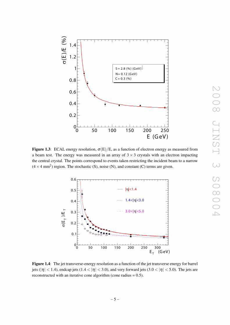
of the ECAL, for incident electrons as measured in a beam test, is shown in figure 1.3; the stochas-tic (S), noise (N), and constant (C) terms given in the figure are determined by fitting the measuredpoints to the function (
σ
E
)2=(
S√E
)2
+(
NE
)2
+C2 . (1.1)
The ECAL is surrounded by a brass/scintillator sampling hadron calorimeter (HCAL) with cov-erage up to |η | < 3.0. The scintillation light is converted by wavelength-shifting (WLS) fibresembedded in the scintillator tiles and channeled to photodetectors via clear fibres. This light isdetected by photodetectors (hybrid photodiodes, or HPDs) that can provide gain and operate inhigh axial magnetic fields. This central calorimetry is complemented by a tail-catcher in the bar-rel region (HO) ensuring that hadronic showers are sampled with nearly 11 hadronic interactionlengths. Coverage up to a pseudorapidity of 5.0 is provided by an iron/quartz-fibre calorime-ter. The Cerenkov light emitted in the quartz fibres is detected by photomultipliers. The forwardcalorimeters ensure full geometric coverage for the measurement of the transverse energy in theevent. An even higher forward coverage is obtained with additional dedicated calorimeters (CAS-TOR, ZDC, not shown in figure 1.1) and with the TOTEM [2] tracking detectors. The expected jettransverse-energy resolution in various pseudorapidity regions is shown in figure 1.4.
The CMS detector is 21.6-m long and has a diameter of 14.6 m. It has a total weight of 12500t. The ECAL thickness, in radiation lengths, is larger than 25 X0, while the HCAL thickness, ininteraction lengths, varies in the range 7–11 λI (10–15 λI with the HO included), depending on η .
– 4 –
2008 JINST 3 S08004
E (G eV )0 50 100 150 200 250
σ(E
)/E
(%
)
0
0.2
0.4
0.6
0.8
1
1.2
1.4
S = 2.8 (%) (G eV )
N= 0.12 (G eV )
C = 0.3 (%)
12_
Figure 1.3: ECAL energy resolution, σ(E)/E, as a function of electron energy as measured froma beam test. The energy was measured in an array of 3× 3 crystals with an electron impactingthe central crystal. The points correspond to events taken restricting the incident beam to a narrow(4×4 mm2) region. The stochastic (S), noise (N), and constant (C) terms are given.
(G eV )TE0 50 100 150 200 250 300
T)/
ET
(Eσ
0
0.1
0.2
0.3
0.4
0.5
0.6
|<1.4|η
|<3.01.4<|η
|<5.03.0<|η
Figure 1.4: The jet transverse-energy resolution as a function of the jet transverse energy for barreljets (|η |< 1.4), endcap jets (1.4 < |η |< 3.0), and very forward jets (3.0 < |η |< 5.0). The jets arereconstructed with an iterative cone algorithm (cone radius = 0.5).
– 5 –

2008 JINST 3 S08004
Chapter 2
Superconducting magnet
2.1 Overview
The superconducting magnet for CMS [3–6] has been designed to reach a 4-T field in a free boreof 6-m diameter and 12.5-m length with a stored energy of 2.6 GJ at full current. The flux is re-turned through a 10 000-t yoke comprising 5 wheels and 2 endcaps, composed of three disks each(figure 1.1). The distinctive feature of the 220-t cold mass is the 4-layer winding made from astabilised reinforced NbTi conductor. The ratio between stored energy and cold mass is high (11.6KJ/kg), causing a large mechanical deformation (0.15%) during energising, well beyond the valuesof previous solenoidal detector magnets. The parameters of the CMS magnet are summarised intable 2.1. The magnet was designed to be assembled and tested in a surface hall (SX5), prior tobeing lowered 90 m below ground to its final position in the experimental cavern. After provi-sional connection to its ancillaries, the CMS Magnet has been fully and successfully tested andcommissioned in SX5 during autumn 2006.
2.2 Main features of the magnet components
2.2.1 Superconducting solenoid
The superconducting solenoid (see an artistic view in figure 2.1 and a picture taken during assemblyin the vertical position in SX5 in figure 2.2) presents three new features with respect to previousdetector magnets:
• Due to the number of ampere-turns required for generating a field of 4 T (41.7 MA-turn), thewinding is composed of 4 layers, instead of the usual 1 (as in the Aleph [7] and Delphi [8]coils) or maximum 2 layers (as in the ZEUS [9] and BaBar [10] coils);
• The conductor, made from a Rutherford-type cable co-extruded with pure aluminium (theso-called insert), is mechanically reinforced with an aluminium alloy;
• The dimensions of the solenoid are very large (6.3-m cold bore, 12.5-m length, 220-t mass).
For physics reasons, the radial extent of the coil (∆R) had to be kept small, and thus theCMS coil is in effect a “thin coil” (∆R/R ∼ 0.1). The hoop strain (ε) is then determined by the
– 6 –

2008 JINST 3 S08004
Figure 2.1: General artistic view of the 5 modules composing the cold mass inside the cryostat,with details of the supporting system (vertical, radial and longitudinal tie rods).
magnetic pressure (P = B20
2µ0= 6.4 MPa), the elastic modulus of the material (mainly aluminium
with Y = 80 GPa) and the structural thickness (∆Rs = 170 mm i.e., about half of the total coldmass thickness), according to PR
∆Rs= Y ε , giving ε = 1.5× 10⁻³. This value is high compared to
the strain of previous existing detector magnets. This can be better viewed looking at a moresignificant figure of merit, i.e. the E/M ratio directly proportional to the mechanical hoop strainaccording to E
M = PR2∆Rsδ
∆Rs∆R = ∆Rs
∆RY ε
2δ, where δ is the mass density. Figure 2.3 shows the values of
E/M as function of stored energy for several detector magnets. The CMS coil is distinguishablyfar from other detector magnets when combining stored energy and E/M ratio (i.e. mechanicaldeformation). In order to provide the necessary hoop strength, a large fraction of the CMS coilmust have a structural function. To limit the shear stress level inside the winding and preventcracking the insulation, especially at the border defined by the winding and the external mandrel,the structural material cannot be too far from the current-carrying elements (the turns). On the basisof these considerations, the innovative design of the CMS magnet uses a self-supporting conductor,by including in it the structural material. The magnetic hoop stress (130 MPa) is shared betweenthe layers (70%) and the support cylindrical mandrel (30%) rather than being taken by the outermandrel only, as was the case in the previous generation of thin detector solenoids. A cross sectionof the cold mass is shown in figure 2.4.
The construction of a winding using a reinforced conductor required technological develop-ments for both the conductor [11] and the winding. In particular, for the winding many problemshad to be faced mainly related to the mandrel construction [12], the winding method [13], and themodule-to-module mechanical coupling. The modular concept of the cold mass had to face theproblem of the module-to-module mechanical connection. These interfaces (figure 2.5) are critical
– 7 –

2008 JINST 3 S08004
Table 2.1: Main parameters of the CMS magnet.
General parametersMagnetic length 12.5 mCold bore diameter 6.3 mCentral magnetic induction 4 TTotal Ampere-turns 41.7 MA-turnsNominal current 19.14 kAInductance 14.2 HStored energy 2.6 GJ
Cold massLayout Five modules mechanically and
electrically coupledRadial thickness of cold mass 312 mmRadiation thickness of cold mass 3.9 X0
Weight of cold mass 220 tMaximum induction on conductor 4.6 TTemperature margin wrt operating temperature 1.8 KStored energy/unit cold mass 11.6 kJ/kg
Iron yokeOuter diameter of the iron flats 14 mLength of barrel 13 mThickness of the iron layers in barrel 300, 630 and 630 mmMass of iron in barrel 6000 tThickness of iron disks in endcaps 250, 600 and 600 mmMass of iron in each endcap 2000 tTotal mass of iron in return yoke 10 000 t
because they have to transmit the large magnetic axial force corresponding to 14 700 t, withoutallowing local displacements due to possible gaps. These displacements can be partially convertedinto heat, causing a premature quench. A construction method which involved the machining ofthe upper surface of the modules and a local resin impregnation during the mechanical mountingallowed us to get an excellent mechanical coupling between the modules.
– 8 –

2008 JINST 3 S08004
Figure 2.2: The cold mass mounted vertically before integration with thermal shields and insertionin the vacuum chamber.
Figure 2.3: The energy-over-mass ratio E/M, for several detector magnets.
– 9 –

2008 JINST 3 S08004
Figure 2.4: Cross section of the cold mass with the details of the 4-layer winding with reinforcedconductor.
Figure 2.5: Detail of the interface region between 2 modules. In order to guarantee mechanicalcontinuity, false turns are involved. The modules are connected through bolts and pins fixed throughthe outer mandrels.
– 10 –

2008 JINST 3 S08004
Figure 2.6: A view of the yoke at an early stage of magnet assembly at SX5. The central barrelsupports the vacuum chamber of the superconducting coil. At the rear, one of the closing end capdisks is visible.
2.2.2 Yoke
The yoke (figure 2.6) is composed of 11 large elements, 6 endcap disks, and 5 barrel wheels,whose weight goes from 400 t for the lightest up to 1920 t for the central wheel, which includesthe coil and its cryostat. The easy relative movement of these elements facilitates the assemblyof the sub-detectors. To displace each element a combination of heavy-duty air pads plus greasepads has been chosen. This choice makes the system insensitive to metallic dust on the floor andallows transverse displacements. Two kinds of heavy-duty high-pressure air pads with a capacityof either 250 t (40 bars) or 385 t (60 bars) are used. This is not favourable for the final approachwhen closing the detector, especially for the YE1 endcap that is protruding into the vacuum tank.A special solution has been adopted: for the last 100 mm of approach, flat grease-pads (workingpressure 100 bar) have been developed in order to facilitate the final closing of the detector. Oncethey touch the axially-installed z-stops, each element is pre-stressed with 100 t to the adjacentelement. This assures good contact before switching on the magnet. In the cavern the elementswill be moved on the 1.23% inclined floor by a strand jacking hydraulic system that ensures safeoperation for uphill pulling as well as for downhill pushing by keeping a retaining force. Themaximum movements possible in the cavern are of the order of 11 meters; this will take one hour.
To easily align the yoke elements, a precise reference system of about 70 points was installedin the surface assembly hall. The origin of the reference system is the geometrical center of thecoil. The points were made after loading the coil cryostat with the inner detectors, the hadronicbarrel in particular which weights 1000 t. A mark on the floor was made showing the position ofeach foot in order to pre-position each element within a± 5 mm tolerance. Finally, all the elementswere aligned with an accuracy of 2 mm with respect to the ideal axis of the coil.
– 11 –

2008 JINST 3 S08004
Figure 2.7: The electrical scheme of the magnet with the protection circuit. One of the maincomponents of the protection is the dump resistor, made of three elements.
2.2.3 Electrical scheme
The CMS solenoid can be represented as a 14 H inductance mutually coupled with its externalmandrel. This inductive coupling allows for the so-called quench back effect, as the eddy currents,induced in the external mandrel at the trigger of a current fast discharge, heat up the whole coilabove the superconducting critical temperature. This is the fundamental basis of the protectionsystem, which, in case of a superconducting to resistive transition of the coil, aims at keepingthe lowest possible thermal gradients and temperature increase in the superconducting windings,and prevents the occurrence of local overheating, hence reducing the thermal stresses inside thewinding. A diagram of the powering circuit with protection is shown in figure 2.7.
A bipolar thyristor power converter rated at 520 kW with passive L-C filters is used to powerthe CMS solenoid. It covers a range of voltages from +26 V to -23 V, with a nominal DC currentof 19.1 kA. In case of a sudden switch off of the power converter, the current decays naturally inthe bus-bar resistance and through the free-wheel thyristors until the opening of the main breakers.Inside the power converter, an assembly of free-wheel thyristors, mounted on naturally air-cooledheat sinks, is installed. In case of non-opening of the main switch breakers, the thyristors arerated to support 20 kA DC for 4 minutes. The current discharge is achieved by disconnecting theelectrical power source by the use of two redundant 20 kA DC normally-open switch breakers,leaving the solenoid in series with a resistor, in a L-R circuit configuration. The stored magneticenergy is therefore extracted by thermal dissipation in the so-called dump resistor. This resistor isexternal to the solenoid cryostat and is designed to work without any active device. It is positioned
– 12 –

2008 JINST 3 S08004
outdoors taking advantage of natural air convection cooling. The fast discharge (FD) is automat-ically triggered by hardwired electronics only in case of a superconductive-to-resistive transition,a so-called quench, and for unrecoverable faults which require fast current dumping. The FD timeconstant is about 200 s. An emergency FD button is also available to the operator in case of need.As the coil becomes resistive during the FD, energy is dissipated inside the coil, which heats up.As a consequence, this necessitates a post-FD cool-down of the coil. The FD is performed on a30 mΩ dump resistor, as a compromise to keep the dump voltage lower than 600 V, and to limitthe coil warm-up and subsequent cool-down time. For faults involving the 20 kA power source, aslow discharge (SD) is triggered through hardwired electronics on a 2 mΩ dump resistor. The SDcurrent evolution is typically exponential, and its time constant is 7025 s, but the coil stays in thesuperconducting state as the heat load, about 525 W, is fully absorbed by the cooling refrigerator.For current lower than 4 kA, a FD is performed in any case, as the heat load is small enough for therefrigerator. The same resistor is used in both cases for the FD and the SD, using normally opencontactors, leaving the dump resistor modules either in series (FD) or in parallel (SD). For othercases, and depending on the alarms, the coil current can be adjusted by the operator, or rampeddown to zero, taking advantage of the two-quadrant converter.
2.2.4 Vacuum system
The vacuum system has been designed to provide a good insulation inside the 40 m3 vacuumvolume of the coil cryostat. It consists of 2 double-primary pumping stations, equipped with 2rotary pumps and 2 Root’s pumps, that provide the fore vacuum to the two oil diffusion pumpslocated at the top of CMS and connected to the coil cryostat via the current leads chimney and thehelium phase separator. The rotary pumps have a capacity of 280 m3/h while the two Root’s pumpshave a flow of 1000 m3/h. The biggest oil diffusion pump, installed via a DN 400 flange on thecurrent leads chimney, has a nominal flow of 8000 l/s at 10−4 mbar of fore vacuum. The smallestone delivers 3000 l/s at the phase separator.
2.2.5 Cryogenic plant
The helium refrigeration plant for CMS is specified for a cooling capacity of 800 W at 4.45 K, 4500W between 60 and 80 K, and simultaneously 4 g/s liquefaction capacity. The primary compressorsof the plant have been installed, in their final position, while the cold box, as well as the intermedi-ate cryostat which interfaces the phase separator and the thermo-syphon, were moved undergroundafter the completion of the magnet test. These components were commissioned with the help of atemporary heat load of 6.5 kW that simulated the coil cryostat which was not yet available. Theperformance of the cold box has been measured in cool-down mode and in nominal and operationmode.
2.2.6 Other ancillaries
• Current leads. The two 20-kA current leads are made of a high purity copper braid, havinga cross section of 1800 mm2 and RRR (Residual Resistivity Ratio) of 130, placed inside aconduit and cooled by circulating helium gas. Without cooling, the current leads are able
– 13 –

2008 JINST 3 S08004
Figure 2.8: The layout for the surface test at SX5, showing only the central barrel. The magnet isconnected to the cryoplant (through the proximity cryogenics), the vacuum and the power systems.
to hold a current of 20 kA for 5 minutes, followed by a FD without any damage, as thetemperature at the hot spot stays below 400 K [14].
• Grounding circuit. The grounding circuit is connected across the solenoid terminals. It fixesthe coil circuit potential, through a 1 kΩ resistor, dividing by two the potential to ground.The winding insulation quality is monitored by continuously measuring the leakage currentthrough a 10 Ω grounding resistor.
• Quench detection system. The quench detection system is a key element of the Magnet SafetySystem (MSS). The role of the quench detection system is to detect a resistive voltage be-tween two points of the coil, whose value and duration are compared to adjustable thresholds.The voltage taps are protected by 4.7 kΩ, 6 W resistors. There are 2 redundant systems, withresistor bridge detectors and differential detectors. For each system, there are 5 detectors.Each resistor bridge detector spans two modules and one detector spans the whole solenoid.Each coil module is compared with two other modules through two differential detectors.
2.3 Operating test
The magnet and all its ancillaries were assembled for testing in SX5 and ready for cool-down inJanuary 2006. Figure 2.8 shows the test layout.
– 14 –

2008 JINST 3 S08004
Figure 2.9: Graph of the coil minimum and maximum temperatures during the cool-down fromroom temperature to 4.5 K.
2.3.1 Cool-down
The cool-down of the solenoid started on February, the 2nd, 2006 and in a smooth way brought thecold mass to 4.6 K in 24 days. Figure 2.9 shows the cool-down curve. The only glitch was due toan overpressure on a safety release valve that stopped cooling for one night before the system wasrestarted.
One important aspect monitored during the cool-down was the amount of coil shrinkage. Inorder to explain this point, we refer to the coil suspension system inside the cryostat (figure 2.1),made of longitudinal, vertical, and axial tie-rods in Ti alloy. The magnet is supported by 2× 9longitudinal tie rods, 4 vertical tie rods, and 8 radial tie rods. The tie rods are equipped withcompensated strain gauges to measure the forces on 2×3 longitudinal, plus the vertical and radialtie rods. The tie rods are loaded in tension and flexion. To measure the tension and flexion strain,3 strain gauges are placed on the tie rods at 0, 90, and 180.
The measured stresses in the tie bars due to the cool-down, causing a shrinkage of the coldmass and putting the tie-bars in tension, are shown in table 2.2. A comparison with the expectedvalues is provided as well. The measured axial and radial shrinkage of the cold mass is shown infigure 2.10.
2.3.2 Charge and discharge cycles
The magnetic tests took place during August 2006, with additional tests during the magnet fieldmapping campaign in October 2006. The current ramps for the field mapping are detailed in fig-ure 2.11. The tests were carried out through magnet charges to progressively higher currents,setting increasing dI/dt, followed by slow or fast discharges. During these current cycles all therelevant parameters related to electrical, magnetic, thermal, and mechanical behaviours have been
– 15 –

2008 JINST 3 S08004
Table 2.2: Calculated and measured cold mass displacements and related stresses on tie-rods dueto the cool-down to 4.5 K.
Expected value Measured valueCold Mass ShrinkageLongitudinal 26 mm 27 mmRadial 14 mm 15 mmTie rod stress due to cool-downVertical 315 MPa 310±45 MPaRadial 167 MPa 153±20 MPaLongitudinal 277 MPa 260±20 MPa
Figure 2.10: Axial (a) and radial (b) shrinkage of the cold mass from 300 K to 4.5 K.
– 16 –

2008 JINST 3 S08004
Figure 2.11: Magnet cycles during the CMS magnet tests in October 2006.
recorded. Depending on the level of the current at the trigger of a fast discharge, the time neededfor re-cooling the coil can be up to 3 days.
2.3.3 Cold mass misalignment
The support system is designed to withstand the forces created by a 10 mm magnetic misalign-ment, in any direction of the cold mass with respect to the iron yoke. Geometrical surveys wereperformed at each step of the magnet assembly to ensure a good positioning. Nevertheless, themonitoring of the coil magnetic misalignment is of prime importance during magnet power test.The misalignment can be calculated either by analysing the displacement of the cold mass or thestresses of the tie rods when the coil is energised. The displacement is measured at several loca-tions and directions at both ends of the coil with respect to the external vacuum tank wall, by theuse of rectilinear potentiometers. Results are displayed in figures 2.12 and 2.13. The displacementof the coil’s geometric centre is found to be 0.4 mm in z, in the +z direction. According to thecomputations, such a displacement indicates that the coil centre should be less than 2 mm off themagnetic centre in +z. As the coil supporting system is hyper-static, the tie rods are not all ini-tially identically loaded. But the force increase during energising is well distributed, as shown infigure 2.14 and figure 2.15, giving the force measurements on several tie rods. These figures alsoindicate the forces computed in the case of a 10-mm magnetic misalignment, together with forcescalculated for the ideally-centred model, showing there is no noticeable effect of misalignment onthe forces.
Using the strain gauges glued on the cold mass (outer mandrel of the central module, CB0),one can determine the Von Mises stress. The cold mass Von Mises stress versus the coil current isgiven in figure 2.16. The measured value of Von Mises stress at 4.5 K and zero current is 23 MPa.The value at 19.1 kA is 138 MPa. These values are in agreement with computations done duringdesign [3, 6].
– 17 –

2008 JINST 3 S08004
Figure 2.12: Axial displacement in Z at both ends of the coil in different positions during energis-ing.
Figure 2.13: Radial displacement at both ends of the coil in different positions during energising.
2.3.4 Electrical measurements
The apparent coil inductance measured through the inductive voltage V = LdI/dt is decreasingwhile increasing the current, as the iron yoke reaches the saturation region. From voltage measure-ments at the coil ends in the cryostat, while ramping up the coil current at a regulated dI/dt, theinductance is calculated and results are given in figure 2.17. Initially the apparent inductance of thecoil is 14.7 H at zero current, and then it decreases to 13.3 H at 18 kA. The 21 resistive electricaljoints, which connect the 5 modules together and, for each module, the 4 layers, are positioned ex-ternally to the coil, on the outer radius of the external mandrel, in low magnetic field regions. The
– 18 –

2008 JINST 3 S08004
Figure 2.14: Force increase on several axial tie rods; the average force at zero current is 45 t.
Figure 2.15: Force increase on several radial tie rods; the average force at zero current is 15 tons.
resistance measurements of the joints indicate values ranging from 0.7 nΩ to 1.6 nΩ at 19.1 kA,corresponding to a maximum dissipation in the joint of 0.6 W. The specific joint cooling system isfully efficient to remove this local heat deposit in order to avoid that the resistive joints generate alocal quench of the conductor. As mentioned above, the fast discharge causes a quench of the coil,through the quench-back process. The typical current decay at the nominal current of 19.14 kA isgiven in figure 2.18.
The effect of the mutual coupling of the coil with the external mandrel is clearly visible atthe beginning of the current fast discharge as shown in the zoomed detail of figure 2.18. It appearsclearly that a high dI/dt of about 500 A/s occurs at the very beginning of the discharge. The
– 19 –

2008 JINST 3 S08004
Figure 2.16: Stresses measured on the CB0 module as a function of the current.
Figure 2.17: Coil inductance as a function of the magnet current.
minimum and maximum temperatures of the coil are displayed in figure 2.19 for a fast dischargeat 19.14 kA. A maximum temperature difference of 32 K is measured on the coil between thewarmest part, located on the coil central module internal radius, and the coldest part, located on theexternal radius of the mandrel. It should be noted that the thermal gradient is mainly radial. Thetemperature tends to equilibrate over the whole coil 2 hours after the trigger of the fast discharge.The average cold mass temperature after a fast discharge at 19 kA is 70 K.
During a magnet discharge, the dump resistor warms up, with a maximum measured temper-ature increase of 240°C, resulting in an increase of the total dump resistance value by up to 19%.Also the coil internal electrical resistance is increased by up to 0.1 Ω at the end of a FD at 19.14 kA.
– 20 –

2008 JINST 3 S08004
Figure 2.18: Magnet current during fast discharge at the nominal field of 4 T. The insert shows thedetails at the beginning of the discharge.
Figure 2.19: Minimum and maximum temperatures detected on the cold mass during the fastdischarge from 19.1 kA.
The effect of both the dump resistor and the magnet electrical resistance increasing was revealedthrough the measurement of the discharge time constant, which was equal to 177 s, 203 s, 263 s,348 s and 498 s for fast discharges respectively at 19 kA, 17.5 kA, 15 kA, 12.5 kA and 7.5 kA. Thisis visible in figure 2.20. The temperature recovery of the dump resistor is achieved in less than 2hours after the trigger of a fast dump. It is 5 hours after the trigger of a slow dump.
In the case of a fast dump at 19.14 kA, typically half of the total energy (1250 MJ) is dissipatedas heat in the external dump resistor. The energy dissipated in the dump resistor as a function of the
– 21 –

2008 JINST 3 S08004
Figure 2.20: The normalised discharge current as a function of time for different initial currents,showing the effect of the increase in magnet and external dump resistance with current.
Figure 2.21: Energy dissipated in the external dump resistor and the mean and maximum temper-atures of the coil during FD.
magnet current at the trigger of a FD was measured for each FD performed during the magnet testsand is given in figure 2.21. The magnet current is precisely measured by the use of two redundantDCCTs (DC current transformer). The peak-to-peak stability of the current is 7 ppm with a voltageripple of 2.5% (0.65 V). In order to gain on the operation time, an acceleration of the slow dumphas been tested and validated by switching to the fast dump configuration at 4 kA. It has beenchecked that the cryogenic refrigerator can take the full heat load, and the magnet stays in thesuperconducting state. This Slow Dump Accelerated (SDA) mode was tested in semi-automaticmode through the cryogenics supervisory system and the magnet control system, and it will befully automatic for the final installation in the cavern.
– 22 –
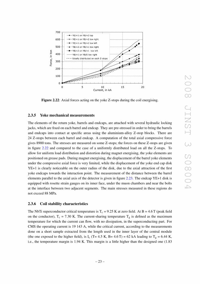
2008 JINST 3 S08004
Figure 2.22: Axial forces acting on the yoke Z-stops during the coil energising.
2.3.5 Yoke mechanical measurements
The elements of the return yoke, barrels and endcaps, are attached with several hydraulic lockingjacks, which are fixed on each barrel and endcap. They are pre-stressed in order to bring the barrelsand endcaps into contact at specific areas using the aluminium-alloy Z-stop blocks. There are24 Z-stops between each barrel and endcap. A computation of the total axial compressive forcegives 8900 tons. The stresses are measured on some Z-stops; the forces on these Z-stops are givenin figure 2.22 and compared to the case of a uniformly distributed load on all the Z-stops. Toallow for uniform load distribution and distortion during magnet energising, the yoke elements arepositioned on grease pads. During magnet energising, the displacement of the barrel yoke elementsunder the compressive axial force is very limited, while the displacement of the yoke end cap diskYE+1 is clearly noticeable on the outer radius of the disk, due to the axial attraction of the firstyoke endcaps towards the interaction point. The measurement of the distance between the barrelelements parallel to the axial axis of the detector is given in figure 2.23. The endcap YE+1 disk isequipped with rosette strain gauges on its inner face, under the muon chambers and near the boltsat the interface between two adjacent segments. The main stresses measured in these regions donot exceed 88 MPa.
2.3.6 Coil stability characteristics
The NbTi superconductor critical temperature is Tc = 9.25 K at zero field. At B = 4.6 T (peak fieldon the conductor), Tc = 7.30 K. The current-sharing temperature Tg is defined as the maximumtemperature for which the current can flow, with no dissipation, in the superconducting part. ForCMS the operating current is 19 143 A, while the critical current, according to the measurementsdone on a short sample extracted from the length used in the inner layer of the central module(the one exposed to the higher field), is Ic (T= 4.5 K, B= 4.6 T) = 62 kA leading to Tg = 6.44 K,i.e., the temperature margin is 1.94 K. This margin is a little higher than the designed one (1.83
– 23 –

2008 JINST 3 S08004
Figure 2.23: Measured displacement of the yoke during the coil energising.
Figure 2.24: The minimum and maximum temperatures and voltage of the coil as a function oftime, with only a few amperes of current, showing the superconducting-to-resistive-state transitionat around 9.3 K.
K) because the nominal current is less than the one used in this kind of computation (19.5 kA)and the expected conductor critical current was from 7% to 10% lower than the real one obtainedthrough advanced and qualified processes. The Tc value was confirmed at 9.3 K during cryogenicrecovery tests (figure 2.24) at zero field. The conductor pure-aluminium stabilizer RRR, deducedfrom electrical measurements during cool-down, is found to be above 1800.
– 24 –

2008 JINST 3 S08004
Figure 2.25: Measurements of the coil warm-up behaviour as a function of time; the Y-axis scaleis common for all the three curves.
2.3.7 Coil warm-up
Following the test of the magnet on the surface, the cold mass had to be warmed up to room tem-perature before lowering. The coil, inside its cryostat, was attached to the central barrel YB0 toavoid any risk due to vacuum degradation during the transport operations. The warm-up was per-formed using a dedicated power supply (200 V-300 A DC) to maintain integrity of the coil/mandrelinterface. Knowing the temperature dependence of both the electrical resistivity and the specificheat of the coil materials, the temperature increase for a given electrical power is calculated. Tak-ing into account the capacity of the warm-up supply, and limiting the temperature increase to 1K/hour, the warm-up was performed as shown in figure 2.25. As the warm-up was done after a fastdischarge, the coil temperature was already at 70 K. Nevertheless, the warm-up took place onlyat night as the yoke was opened to continue integration activities inside the detector. Ultimately,the warm-up lasted only 3 weeks. The maximum temperature gradient across the coil during thewarm-up exercise was less than 9 K.
– 25 –

2008 JINST 3 S08004
Chapter 3
Inner tracking system
3.1 Introduction
The inner tracking system of CMS is designed to provide a precise and efficient measurementof the trajectories of charged particles emerging from the LHC collisions, as well as a precisereconstruction of secondary vertices. It surrounds the interaction point and has a length of 5.8mand a diameter of 2.5m. The CMS solenoid provides a homogeneous magnetic field of 4 T overthe full volume of the tracker. At the LHC design luminosity of 1034 cm−2 s−1 there will be onaverage about 1000 particles from more than 20 overlapping proton-proton interactions traversingthe tracker for each bunch crossing, i.e. every 25ns. Therefore a detector technology featuring highgranularity and fast response is required, such that the trajectories can be identified reliably andattributed to the correct bunch crossing. However, these features imply a high power density ofthe on-detector electronics which in turn requires efficient cooling. This is in direct conflict withthe aim of keeping to the minimum the amount of material in order to limit multiple scattering,bremsstrahlung, photon conversion and nuclear interactions. A compromise had to be found in thisrespect. The intense particle flux will also cause severe radiation damage to the tracking system.The main challenge in the design of the tracking system was to develop detector components ableto operate in this harsh environment for an expected lifetime of 10 years. These requirements ongranularity, speed and radiation hardness lead to a tracker design entirely based on silicon detectortechnology. The CMS tracker is composed of a pixel detector with three barrel layers at radiibetween 4.4cm and 10.2cm and a silicon strip tracker with 10 barrel detection layers extendingoutwards to a radius of 1.1m. Each system is completed by endcaps which consist of 2 disks inthe pixel detector and 3 plus 9 disks in the strip tracker on each side of the barrel, extending theacceptance of the tracker up to a pseudorapidity of |η | < 2.5. With about 200m2 of active siliconarea the CMS tracker is the largest silicon tracker ever built [15, 16].
The construction of the CMS tracker, composed of 1440 pixel and 15 148 strip detectormodules, required the development of production methods and quality control procedures that arenew to the field of particle physics detectors. A strong collaboration of 51 institutes with almost500 physicists and engineers succeeded over a period of 12 to 15 years to design, develop and buildthis unique device.
– 26 –

2008 JINST 3 S08004
3.1.1 Requirements and operating conditions
The expected LHC physics program [17] requires a robust, efficient and precise reconstruction ofthe trajectories of charged particles with transverse momentum above 1GeV in the pseudorapidityrange |η |< 2.5. A precise measurement of secondary vertices and impact parameters is necessaryfor the efficient identification of heavy flavours which are produced in many of the interestingphysics channels. Together with the electromagnetic calorimeter and the muon system the trackerhas to identify electrons and muons, respectively. Tau leptons are a signature in several discoverychannels and need to be reconstructed in one-prong and three-prong decay topologies. In order toreduce the event rate from the LHC bunch crossing rate of 40MHz to about 100Hz which can bepermanently stored, tracking information is heavily used in the high level trigger of CMS.
The operating conditions for a tracking system at the LHC are very challenging. As alreadymentioned, each LHC bunch crossing at design luminosity creates on average about 1000 particleshitting the tracker. This leads to a hit rate density of 1MHz/mm2 at a radius of 4cm, falling to60 kHz/mm2 at a radius of 22cm and 3 kHz/mm2 at a radius of 115cm. In order to keep theoccupancy at or below 1% pixelated detectors have to be used at radii below 10cm. For a pixelsize of 100×150 µm2 in r-φ and z, respectively, which is driven by the desired impact parameterresolution, the occupancy is of the order 10−4 per pixel and LHC bunch crossing. At intermediateradii (20cm < r < 55cm) the reduced particle flux allows the use of silicon micro-strip detectorswith a typical cell size of 10cm×80 µm, leading to an occupancy of up to 2–3% per strip and LHCbunch crossing. In the outer region (55cm < r < 110cm) the strip pitch can be further increased.Given the large areas that have to be instrumented in this region, also the strip length has to beincreased in order to limit the number of read-out channels. However, the strip capacitance scaleswith its length and therefore the electronics noise is a linear function of the strip length as well. Inorder to maintain a good signal to noise ratio of well above 10, CMS uses thicker silicon sensorsfor the outer tracker region (500 µm thickness as opposed to the 320 µm in the inner tracker) withcorrespondingly higher signal. These thicker sensors would in principle have a higher depletionvoltage. But since the radiation levels in the outer tracker are smaller, a higher initial resistivity canbe chosen such that the initial depletion voltages of thick and thin sensors are in the same range of100 V to 300 V. In this way cell sizes up to about 25cm×180 µm can be used in the outer region ofthe tracker, with an occupancy of about 1%. These occupancy-driven design choices for the striptracker also satisfy the requirements on position resolution.
CMS is the first experiment using silicon detectors in this outer tracker region. This novelapproach was made possible by three key developments:
• sensor fabrication on 6 inch instead of 4 inch wafers reduced the sensor cost to5–10 CHF/cm2 and allowed the coverage of the large required surfaces with silicon sensors,
• implementation of the front-end read-out chip in industry-standard deep sub-micron technol-ogy led to large cost savings and to an improved signal-to-noise performance,
• automation of module assembly and use of high throughput wire bonding machines.
The radiation damage introduced by the high particle fluxes at the LHC interaction regionsis a severe design constraint. Table 3.1 shows the expected fast hadron fluence and radiation dose
– 27 –

2008 JINST 3 S08004
Table 3.1: Expected hadron fluence and radiation dose in different radial layers of the CMS tracker(barrel part) for an integrated luminosity of 500fb−1 (≈ 10 years). The fast hadron fluence is agood approximation to the 1MeV neutron equivalent fluence [17].
Radius Fluence of fast hadrons Dose Charged particle flux(cm) (1014 cm−2) (kGy) (cm−2s−1)
4 32 840 108
11 4.6 19022 1.6 70 6×10⁶
75 0.3 7115 0.2 1.8 3×10⁵
in the CMS barrel tracker for an integrated luminosity of 500fb−1 corresponding to about 10 yearsof LHC operation [15, 17]. Neutrons generated by hadronic interactions in the ECAL crystalsmake up a substantial contribution to the fast hadron fluence, which actually dominates in the outertracker close to the ECAL surface. The uncertainties on these estimates due to the extrapolationerror of the inelastic proton proton cross-section, momentum distributions and multiplicities to√
s = 14TeV and in the Monte Carlo description of the cascade development lead to a safety factorof 1.5 (2 in regions where the neutron contribution dominates) which was applied to these estimatesin order to define the design requirements for the tracker.
Three different effects had to be considered in the design of a radiation tolerant silicon tracker.Surface damage is created when the positively charged holes, generated by the passage of an ion-izing particle, get trapped in a silicon oxide layer. This is mostly a concern for the front-end chipswhere this additional space charge changes for instance the characteristics of MOS structures. Sur-face damage simply scales with the absorbed dose. The silicon sensors are mainly affected by bulkdamage, i.e. modifications to the silicon crystal lattice which are caused by non-ionizing energyloss (NIEL) and lead to additional energy levels in the band gap. NIEL is a complicated process,depending on particle type and energy, but is found to scale approximately with the fast hadron flu-ence. The consequences are an increase of the leakage current (linear in fluence), a change in thedoping from n- to p-type with a corresponding change in depletion voltage by a few hundred voltsover the lifetime of the tracker, and the creation of additional trapping centers which will reducethe signal by roughly 10% after 10 years of LHC running [18]. The design of the silicon sensorsand the read-out electronics has to take this into account and assure a signal-to-noise ratio of 10:1or better over the full lifetime of the detector, in order to guarantee a robust hit recognition at anacceptable fake hit rate. Finally, transient phenomena due to the generation of charge by ionizingparticles in the electronic circuitry can change for instance the state of memory cells and thereforedisturb or even stop the correct functioning of the read-out (single event upset, SEU).
The increased detector leakage current can lead to a dangerous positive feedback of the selfheating of the silicon sensor and the exponential dependence of the leakage current on temperature,called thermal runaway. This has to be avoided by efficient coupling of the silicon sensors tothe cooling system and by a low operating temperature. For this reason it is foreseen that thewhole tracker volume will be operated at or slightly below −10°C. After 10 years of operation it is
– 28 –

2008 JINST 3 S08004
expected that this will require a cooling fluid temperature of about−27°C which in turn means thatall structures in the tracker have to survive temperature cycles between room temperature and about−30°C. A second effect, called reverse annealing, requires to keep the silicon sensors permanentlywell below 0°C except for short maintenance periods. This effect is caused by the interaction ofradiation induced defects in the silicon sensors which can lead to more serious damage and to aneven stronger change in depletion voltage with fluence. Experimentally it is found that reverseannealing becomes insignificant for temperatures roughly below 0°C [18].
The read-out chips employed in the CMS tracker are fabricated in standard 0.25 µm CMOStechnology which is inherently radiation hard due to the thin gate oxide (and special design rules).The lifetime of the silicon strip tracker is therefore limited by the radiation damage to the siliconsensors. For efficient charge collection they always need to be over-depleted, requiring bias volt-ages up to 500 V after 10 years of LHC operation. This reaches the limit of the typical high voltagestability of current sensor layouts. Furthermore, the increased leakage currents of the sensors willat some point lead to thermal runaway. All tests have shown that the silicon strip tracker will re-main fully operational for 10 years of LHC running. For the pixel detector on the other hand, whichhas to survive even higher radiation doses, under-depleted operation is possible due to a differentsensor layout. Its lifetime reaches from at least 2 years at full LHC luminosity for the innermostlayer to more than 10 years for the third layer.
The ultimate position resolution of the pixel and strip sensors is degraded by multiple scatter-ing in the material that is necessary to precisely hold the sensors, to supply the electrical power (intotal about 60 kW for the CMS tracker) and to cool the electronics and the silicon sensors. Nuclearinteractions of pions and other hadrons in this material reduce significantly the tracking efficiencyfor these particles. In addition, this material leads to photon conversion and bremsstrahlung whichadversely affect the measurement accuracy of the electromagnetic calorimeter. It was therefore arequirement to keep the amount of this material to a minimum.
3.1.2 Overview of the tracker layout
A schematic drawing of the CMS tracker is shown in figure 3.1. At radii of 4.4,7.3 and 10.2cm,three cylindrical layers of hybrid pixel detector modules surround the interaction point. They arecomplemented by two disks of pixel modules on each side. The pixel detector delivers three highprecision space points on each charged particle trajectory. It is described in detail in section 3.2. Intotal the pixel detector covers an area of about 1m2 and has 66 million pixels.
The radial region between 20cm and 116cm is occupied by the silicon strip tracker, whichis described in detail in section 3.3. It is composed of three different subsystems. The TrackerInner Barrel and Disks (TIB/TID) extend in radius towards 55cm and are composed of 4 barrellayers, supplemented by 3 disks at each end. TIB/TID delivers up to 4 r-φ measurements on atrajectory using 320 µm thick silicon micro-strip sensors with their strips parallel to the beam axisin the barrel and radial on the disks. The strip pitch is 80 µm on layers 1 and 2 and 120 µm onlayers 3 and 4 in the TIB, leading to a single point resolution of 23 µm and 35 µm, respectively.In the TID the mean pitch varies between 100 µm and 141 µm. The TIB/TID is surrounded bythe Tracker Outer Barrel (TOB). It has an outer radius of 116cm and consists of 6 barrel layers of500 µm thick micro-strip sensors with strip pitches of 183 µm on the first 4 layers and 122 µm on
– 29 –

2008 JINST 3 S08004
TEC+TEC-
TOB
TOB
TIB
TIB
TID
TIDTID
TID
PIXEL
-2600 -2200 -1800 -1400 -1000 -600 -200 200 600 1000 1400 1800 2200 2600-1200
-1000
-800
-600
-400
-200
0
200
400
600
800
1000
1200
z (mm)
r (mm)
0.1 0.3 0.5 0.7 0.9 1.1 1.3 1.5
1.7
1.9
2.1
2.32.5-2.5
-2.3
-2.1
-1.9
-1.7
-1.5 -1.3 -1.1 -0.9 -0.7 -0.5 -0.3 -0.1 0.1
η
Figure 3.1: Schematic cross section through the CMS tracker. Each line represents a detectormodule. Double lines indicate back-to-back modules which deliver stereo hits.
layers 5 and 6. It provides another 6 r-φ measurements with single point resolution of 53 µm and35 µm, respectively. The TOB extends in z between ±118cm. Beyond this z range the TrackerEndCaps (TEC+ and TEC- where the sign indicates the location along the z axis) cover the region124cm < |z|< 282cm and 22.5cm < |r|< 113.5cm. Each TEC is composed of 9 disks, carryingup to 7 rings of silicon micro-strip detectors (320 µm thick on the inner 4 rings, 500 µm thickon rings 5-7) with radial strips of 97 µm to 184 µm average pitch. Thus, they provide up to 9 φ
measurements per trajectory.In addition, the modules in the first two layers and rings, respectively, of TIB, TID, and
TOB as well as rings 1, 2, and 5 of the TECs carry a second micro-strip detector module which ismounted back-to-back with a stereo angle of 100 mrad in order to provide a measurement of thesecond co-ordinate (z in the barrel and r on the disks). The achieved single point resolution of thismeasurement is 230 µm and 530 µm in TIB and TOB, respectively, and varies with pitch in TIDand TEC. This tracker layout ensures at least ≈ 9 hits in the silicon strip tracker in the full range of|η |< 2.4 with at least≈ 4 of them being two-dimensional measurements (figure 3.2). The ultimateacceptance of the tracker ends at |η | ≈ 2.5. The CMS silicon strip tracker has a total of 9.3 millionstrips and 198 m2 of active silicon area.
Figure 3.3 shows the material budget of the CMS tracker in units of radiation length. Itincreases from 0.4 X0 at η ≈ 0 to about 1.8 X0 at |η | ≈ 1.4, beyond which it falls to about 1 X0 at|η | ≈ 2.5.
3.1.3 Expected performance of the CMS tracker
For single muons of transverse momenta of 1, 10 and 100 GeV figure 3.4 shows the expected reso-lution of transverse momentum, transverse impact parameter and longitudinal impact parameter, asa function of pseudorapidity [17]. For high momentum tracks (100GeV) the transverse momentumresolution is around 1−2% up to |η | ≈ 1.6, beyond which it degrades due to the reduced lever arm.At a transverse momentum of 100GeV multiple scattering in the tracker material accounts for 20 to
– 30 –

2008 JINST 3 S08004
0
2
4
6
8
10
12
14
16
0 0.25 0.5 0.75 1 1.25 1.5 1.75 2 2.25 2.5η
N p
oint
s
Figure 3.2: Number of measurement points in the strip tracker as a function of pseudorapidity η .Filled circles show the total number (back-to-back modules count as one) while open squares showthe number of stereo layers.
η-4 -3 -2 -1 0 1 2 3 4
0x/
X
0
0.2
0.4
0.6
0.8
1
1.2
1.4
1.6
1.8
2
η-4 -3 -2 -1 0 1 2 3 4
0x/
X
0
0.2
0.4
0.6
0.8
1
1.2
1.4
1.6
1.8
2
Tracker Material Budget
OutsideTECTOBTIB+TIDPixelBeam Pipe
η-4 -3 -2 -1 0 1 2 3 4
0x/
X
0
0.2
0.4
0.6
0.8
1
1.2
1.4
1.6
1.8
2
η-4 -3 -2 -1 0 1 2 3 4
0x/
X
0
0.2
0.4
0.6
0.8
1
1.2
1.4
1.6
1.8
2
Tracker Material Budget
OutsideOtherSupportCoolingCablesElectronicsSensitiveBeam Pipe
Figure 3.3: Material budget in units of radiation length as a function of pseudorapidity η for thedifferent sub-detectors (left panel) and broken down into the functional contributions (right panel).
30% of the transverse momentum resolution while at lower momentum it is dominated by multiplescattering. The transverse impact parameter resolution reaches 10 µm for high pT tracks, domi-nated by the resolution of the first pixel hit, while at lower momentum it is degraded by multiplescattering (similarly for the longitudinal impact parameter). Figure 3.5 shows the expected trackreconstruction efficiency of the CMS tracker for single muons and pions as a function of pseudo-rapidity. For muons, the efficiency is about 99% over most of the acceptance. For |η | ≈ 0 the effi-ciency decreases slightly due to gaps between the ladders of the pixel detector at z≈ 0. At high η
the efficiency drop is mainly due to the reduced coverage by the pixel forward disks. For pions andhadrons in general the efficiency is lower because of interactions with the material in the tracker.
– 31 –

2008 JINST 3 S08004
η0 0.5 1 1.5 2
η0 0.5 1 1.5 2
) [%
]t
/p t pδ(σ
1
10 , pt=1GeVµ
, pt=10GeVµ
, pt=100GeVµ
η0 0.5 1 1.5 2
η0 0.5 1 1.5 2
m]
µ) [ 0
dδ(σ
10
210
, pt=1GeVµ
, pt=10GeVµ
, pt=100GeVµ
η0 0.5 1 1.5 2
η0 0.5 1 1.5 2
m]
µ) [ 0
zδ(σ
10
210
310
, pt=1GeVµ
, pt=10GeVµ
, pt=100GeVµ
Figure 3.4: Resolution of several track parameters for single muons with transverse momenta of 1,10 and 100 GeV: transverse momentum (left panel), transverse impact parameter (middle panel),and longitudinal impact parameter (right panel).
|η|0 0.5 1 1.5 2
|η|0 0.5 1 1.5 2
Glo
bal E
ffici
ency
0.7
0.75
0.8
0.85
0.9
0.95
1
, pt=1GeVµ
, pt=10GeVµ
, pt=100GeVµ
|η|0 0.5 1 1.5 2
|η|0 0.5 1 1.5 2
Glo
bal E
ffici
ency
0.5
0.6
0.7
0.8
0.9
1
, pt=1GeVπ
, pt=10GeVπ
, pt=100GeVπ
Figure 3.5: Global track reconstruction efficiency for muons (left panel) and pions (right panel)of transverse momenta of 1, 10 and 100 GeV.
3.1.4 Tracker system aspects
All elements of the CMS tracker are housed in the tracker support tube, which is suspended on theHCAL barrel. The tracker support tube is a large cylinder 5.30 m long with an inner diameter of2.38 m. The 30-mm-thick wall of the cylinder is made by two 950-1/T300 carbon fiber compositeskins, 2 mm in thickness, sandwiching a 26-mm-high Nomex core. Over the entire length of thetube’s inner surface, two carbon fiber rails are attached on the horizontal plane. The tracker outerbarrel (TOB) and both endcaps (TEC+ and TEC-) rest on these rails by means of adjustable slidingpads. The tracker inner barrel and disks (TIB/TID) are in turn supported by the TOB. The anglebetween the guiding elements of these rails is controlled to better than 0.183 mrad, correspondingto a parallelism between the guides better than ±0.5mm in all directions over the full length.
An independent support and insertion system for the pixel detectors, the central section ofthe beam pipe and the inner elements of the radiation monitor system spans the full length of thetracker at its inner radius. This is composed of three long carbon fiber structures, joined togetherduring tracker assembly to form two continuous parallel planes, on which precision tracks forthe installation, support and positioning of each element are machined. The central element isa 2266.5-mm-long and 436-mm-wide cylinder which is connected with flanges to the TIB/TIDdetector. This element provides support and accurate positioning to the pixel detectors. Two 2420-
– 32 –

2008 JINST 3 S08004
mm-long side elements are coupled to it only by very precise pinned connections, bridging thegap between the faces of the TIB/TID and the closing flanges of the tracker without direct contactto the TEC detectors. These side elements are therefore structurally decoupled from the siliconstrip detectors and can be installed and removed at any time with no impact on the strip detectors.They serve several purposes: they provide support and alignment features for the central sectionof the beam pipe, they allow the installation of the inner elements of the radiation monitor system,and they are used for installation and removal of all the components permanently or temporarilyhoused in the inner region of the tracker: beam pipe, bake-out equipment, pixel barrel, pixel disksand radiation monitor. This system of permanent tracks, light but very stiff and stable, installedin the core of the tracker will allow for the quickest possible intervention in this region duringmaintenance, inducing no disturbance to the volume occupied by the silicon strip detectors. Thisfeature will be extremely valuable after some years of operation, when activation of componentsand radiation damage on sensors will start becoming an issue.
The outer surface of the tracker tube faces the electromagnetic calorimeter, which is operatedat room temperature and requires good temperature stability. The surface of the electromagneticcalorimeter must be kept at (18± 4)°C while the tracker volume needs to be cooled to below−10°C. In order to achieve this thermal gradient over a very limited radial thickness, the insidesurface of the tracker support tube is lined with an active thermal screen. It ensures a temperaturebelow−10°C inside the tracker volume even when the sub-detectors and their cooling are switchedoff, while maintaining a temperature above +12°C on the outer surface of the support tube in orderto avoid condensation. It also reduces the thermal stress across the support tube structure. Thethermal screen consists of 32 panels. On the inside, cold fluid is circulated in a thin aluminiumplate whilst, separated by 8mm of Rohacell foam, several polyimide-insulated resistive circuitsare powered to heat up the outer surface to the required temperature. The system is feed-backcontrolled, based on 64 temperature sensors.
The total power dissipation inside the tracker volume is expected to be close to 60 kW. Mainlyfor robustness in operation, the CMS tracker is equipped with a mono-phase liquid cooling system.The liquid used for refrigeration of the silicon strip and pixel detector as well as the thermal screenis C6F14. It has a sufficiently low viscosity even at the lowest required temperature, excellentbehaviour under irradiation and is extremely volatile (with practically no residues) thus minimizingeventual damages from accidental leaks. The cooling system provides up to 77m3/hour of C6F14
liquid to the tracker, at a temperature of down to −35°C and with a pressure drop of up to 8 bar.This corresponds to a cooling capacity of up to 128 kW.
The full tracker volume (about 25m3) is flushed with pre-chilled dry nitrogen gas at a rate ofup to one volume exchange per hour.
3.2 Pixel detector
3.2.1 Pixel system general
The pixel system is the part of the tracking system that is closest to the interaction region. Itcontributes precise tracking points in r-φ and z and therefore is responsible for a small impactparameter resolution that is important for good secondary vertex reconstruction. With a pixel cell
– 33 –

2008 JINST 3 S08004
Effi
cien
cy (
z 2
Hits
)
Pseudorapidity η
Rad
ius
Figure 3.6: Geometrical layout of the pixel detector and hit coverage as a function ofpseudorapidity.
size of 100×150 µm2 emphasis has been put on achieving similar track resolution in both r-φ andz directions. Through this a 3D vertex reconstruction in space is possible, which will be importantfor secondary vertices with low track multiplicity. The pixel system has a zero-suppressed readout scheme with analog pulse height read-out. This improves the position resolution due to chargesharing and helps to separate signal and noise hits as well as to identify large hit clusters fromoverlapping tracks.
The pixel detector covers a pseudorapidity range −2.5< η <2.5, matching the acceptanceof the central tracker. The pixel detector is essential for the reconstruction of secondary verticesfrom b and tau decays, and forming seed tracks for the outer track reconstruction and high leveltriggering. It consists of three barrel layers (BPix) with two endcap disks (FPix). The 53-cm-longBPix layers will be located at mean radii of 4.4, 7.3 and 10.2 cm. The FPix disks extending from≈6 to 15 cm in radius, will be placed on each side at z=±34.5 and z=±46.5 cm. BPix (FPix)contain 48 million (18 million) pixels covering a total area of 0.78 (0.28) m2. The arrangementof the 3 barrel layers and the forward pixel disks on each side gives 3 tracking points over almostthe full η-range. Figure 3.6 shows the geometric arrangement and the hit coverage as a functionof pseudorapidity η . In the high η region the 2 disk points are combined with the lowest possibleradius point from the 4.4 cm barrel layer.
The vicinity to the interaction region also implies a very high track rate and particle fluencesthat require a radiation tolerant design. For the sensor this led to an n+ pixel on n-substrate detectordesign that allows partial depleted operation even at very high particle fluences. For the barrellayers the drift of the electrons to the collecting pixel implant is perpendicular to the 4 T magneticfield of CMS. The resulting Lorentz drift leads to charge spreading of the collected signal chargeover more than one pixel. With the analog pulse height being read out a charge interpolation allows
– 34 –

2008 JINST 3 S08004
to achieve a spatial resolution in the range of 15–20 µm. The forward detectors are tilted at 20 in aturbine-like geometry to induce charge-sharing. The charge-sharing is mainly due to the geometriceffect of particles entering the detector at an average angle of 20 away from normal incidence [19];charge-sharing is also enhanced by the ~E×~B drift. A position resolution of approximately 15 µmin both directions can be achieved with charge-sharing between neighbouring pixels. The reductionin the depletion depth or the increase in bias voltage will lead to a reduction of charge-sharing andtherefore a degradation of the spatial resolution with radiation damage.
In order to allow a replacement of the innermost layers the mechanics and the cabling of thepixel system has been designed to allow a yearly access if needed. At full LHC luminosity weexpect the innermost layer to stay operational for at least 2 years. The 3 layer barrel mechanicsas well as the forward disks are divided into a left and a right half. This is required to allowinstallation along the beam pipe and to pass beyond the beam pipe support wires at z=± 1632 mm.The 6 individual mechanical pieces are referenced to each other through precisely machined railsinside the TIB cylinder. Power, cooling, the optical controls as well as the optical read-out linesare brought to the detector through supply tube shells. In case of the barrel pixel system the supplytubes have a flexible connection that needs to bend by a few degrees during insertion following theslightly curved rails around the beam pipe support ring.
The pixel system is inserted as the last sub-detector of CMS after the silicon strip tracker hasbeen installed and after the central section of the beam pipe has been installed and baked out.
3.2.2 Sensor description
Technological choices
The sensors for the CMS-pixel detector adopt the so called n-on-n concept. The pixels consistof high dose n-implants introduced into a high resistance n-substrate. The rectifying pn-junctionis placed on the back side of the sensor surrounded by a multi guard ring structure. Despite thehigher costs due to the double sided processing this concept was chosen as the collection of elec-trons ensures a high signal charge at moderate bias voltages (< 600V) after high hadron fluences.Furthermore the double sided processing allows a guard ring scheme keeping all sensor edges atground potential.
The isolation technique applied for the regions between the pixel electrodes was developedin close collaboration with the sensor vendors. Open p-stops [20] were chosen for the disks andmoderated p-spray [21] for the barrel. Both types of sensors showed sufficient radiation hardnessduring an extensive qualification procedure including several test beams [22, 23].
Disk sensors
The disk sensors use the p-stop technique for interpixel isolation. To maximize the charge collec-tion efficiency and minimize the pixel capacitance within the design rules of the vendor a widthof 8 µm for the p-stop rings and a distance of 12 µm between implants was chosen. Figure 3.7shows a photograph of 4 pixel cells. The open ring p-stops, the bump-bonding pad and the contactbetween the aluminium and the implanted collecting electrode are highlighted.
– 35 –

2008 JINST 3 S08004
Figure 3.7: Picture of four pixels in the same double column for a pixel disk sensor.
Aluminium p−Implant
Bias dotBias grid
Contact viaBump (In)
Full p−spray doseReduced p−spray
Figure 3.8: Photograph of four pixel cells. The Indium bumps are already deposited but not yetreflown.
The opening on the p-stop rings provides a low resistance path until full depletion is reachedto allow IV (current-voltage) characterization of the sensor on wafer and a high resistance pathwhen the sensor is over-depleted (10–20 V over-depletion) to assure interpixel isolation.
The process is completely symmetric with five photolithographic steps on each side to mini-mize the mechanical stress on the silicon substrate and the potential bowing of the diced sensors.
The sensors were all fabricated in 2005 on 4 inch wafers. The depletion voltage is 45–50 Vand the leakage current is less than 10 nA per cm2. The 7 different sensor tiles needed to populatea disk blade, ranging from 1× 2 read-out chips (ROCs) to 2× 5 ROCs, are implemented on asingle wafer.
A production yield higher than 90% has been achieved and 150 good sensors for each of theseven flavours are available to the project for module assembly.
Barrel sensors
The sensors for the pixel barrel use the moderated p-spray technique for interpixel isolation. Aphotograph of four pixels in a barrel sensor is shown in figure 3.8. Most area of a pixel is coveredwith the collecting electrode formed by the n-implant. The gap between the n-implants is keptsmall (20 µm) to provide a homogeneous drift field which leads to a relatively high capacitance ofthe order of 80-100 fF per pixel.
– 36 –

2008 JINST 3 S08004
In one corner of each pixel the so called bias dot is visible. They provide a high resistancepunch-through connection to all pixels which allows on-wafer IV measurements which are impor-tant to exclude faulty sensors from the module production.
The dark frame around the pixel implants visible in figure 3.8 indicates the opening in thenitride covering the thermal oxide. In this region the p-spray dose reaches the full level. Closeto the lateral pn-junction between the pixel implant and the p-sprayed inter-pixel region the borondose is reduced.
The sensor shown in figure 3.8 has undergone the bump deposition process. The Indiumbumps are visible as roughly 50 µm wide octagons.
The sensors are processed on n-doped DOFZ-silicon [24] with 〈111〉 orientation and a resis-tivity of about 3.7kΩcm (after processing). This leads to a full depletion voltage of 50-60 V ofthe 285 µm thick sensors. All wafers for the production of the barrel sensors come from the samesilicon ingot to provide the best possible homogeneity of all material parameters.
The pixel barrel requires two different sensor geometries, 708 full (2×8 ROCs) and 96 halfmodules (1×8 ROCs). They were processed in 2005 and 2006 using two different mask sets.
3.2.3 Pixel detector read-out
System overview
The pixel read-out and control system [25] consists of three parts: a read-out data link from themodules/blades to the pixel front end driver (pxFED), a fast control link from the pixel front endcontroller (pFEC) to the modules/blades and a slow control link from a standard FEC to the supplytube/service cylinder. The latter is used to configure the ASICs on the supply tube/service cylinderthrough a I2C protocol. Figure 3.9 shows a sketch of the system.
The front end consists of a Token Bit Manager (TBM) chip which controls several read-outchips (ROCs). The pFEC sends the 40MHz clock and fast control signals (e.g. trigger, reset) to thefront end and programs all front end devices. The pxFED receives data from the front end, digitizesit, formats it and sends it to the CMS-DAQ event builder. The pFEC, FEC and pxFED are VMEmodules located in the electronics room and are connected to the front end through 40 MHz opticallinks. The various components are described in the following sections.
Read-out chip
Sensor signals are read out by ROCs bump bonded to the sensors. A ROC is a full custom ASICfabricated in a commercial 0.25-µm 5-metal-layer CMOS process and contains 52×80 pixels [26].Its main purposes are:
• Amplification and buffering of the charge signal from the sensor.
• Zero suppression in the pixel unit cell. Only signals above a certain threshold will be readout. This threshold can be adjusted individually for each pixel by means of four trim bits.The trim bits have a capacitive protection against single event upset (SEU), which has shownto reduce SEUs by 2 orders of magnitude [26]. The mean threshold dispersion after trimmingat T=−10°C is 90 electrons equivalent with a noise of 170 electrons.
– 37 –

2008 JINST 3 S08004
PLLCCULVDSmux
mDOH AOH
pxFEC
BARREL ENDFLANGE /ADAPTER CARD
SUPPLY TUBE / SERVICE CYLINDER
COUNTINGROOM
ALT
I2C
L1A(trig, cal, sync, reset)
CLK
CLK
I2C
AnalogOut
HardReset
CL
K
L1A
Analog out
DOH
DATA CLK
Slow I2C Delay
LCDS drivers
LCDS driversGate-Keeper
electricalopticalDATA
SlowI2C
MODULE / PANEL
pxFEDFEC
SlowI2C
SlowI2C
TBMROCs
Figure 3.9: Block diagram of the pixel control and read-out system.
• Level 1 trigger verification. Hit information without a corresponding L1 trigger is aban-doned.
• Sending hit information and some limited configuration data (analog value of last addressedDAC) to the TBM chip. Pixel addresses are transferred as 6 level analog encoded digitalvalues within 5 clock cycles (125ns) while the pulse height information is truly analog.
• Adjusting various voltage levels, currents and offsets in order to compensate for chip-to-chipvariations in the CMOS device parameters. There are a total of 29 DACs on the chip.
The ROC needs two supply voltages of 1.5 V and 2.5 V. There are 6 on chip voltage regulators.They compensate for differences in supply voltage due to voltage drops in module cables of dif-ferent lengths, improve AC power noise rejection and strongly reduce intermodule cross-talk. Anon-chip temperature sensor allows the monitoring of the module temperature online. The ROC iscontrolled through a modified I2C interface running at 40 MHz. The configuration data can bedownloaded without stopping data acquisition.
There are a few architecture inherent data loss mechanisms. The particle detection ineffi-ciency has been measured in a high-rate pion beam. It is in fairly good agreement with expectationsand reaches 0.8%, 1.2% and 3.8% respectively for the three layers at a luminosity of 1034 s−1cm−2
and 100 kHz L1 trigger rate.The power consumption depends on the pixel hit rate. At the LHC design luminosity, the
ROC contributes with 34 µW per pixel about 88% (62%) to the total pixel detector front end powerbudget before (after) the detector has received a total fluence of 6×10¹⁴/cm2.
– 38 –

2008 JINST 3 S08004
Token Bit Manager chip
The TBM [27] controls the read-out of a group of pixel ROCs. The TBM is designed to be locatedon the detector near to the pixel ROCs. In the case of the barrel, they will be mounted on thedetector modules and will control the read-out of 8 or 16 ROCs depending upon the layer radius.In the case of the forward disks, they will be mounted on the disk blades and will control the read-out of 21 or 24 ROCs depending on blade side. A TBM and the group of ROCs that it controls willbe connected to a single analog optical link over which the data will be sent to the front end driver,a flash ADC module located in the electronics house. The principal functions of the TBM includethe following:
• It will control the read-out of the ROCs by initiating a token pass for each incoming Level-1trigger.
• On each token pass, it will write a header and a trailer word to the data stream.
• The header will contain an 8 bit event number and the trailer will contain 8 bits of errorstatus. These will be transferred as 2 bit analog encoded digital.
• It will distribute the Level-1 triggers, and clock to the ROCs.
Each arriving Level-1 trigger will be placed on a 32-deep stack awaiting its associated token pass.Normally the stack will be empty but is needed to accommodate high burst rates due to noise,high track density events, or trigger bursts. Since there will be two analog data links per modulefor the inner two layers of the barrel, the TBMs will be configured as pairs in a Dual TBM Chip.In addition to two TBMs, this chip also contains a Control Network. The Hub serves as a portaddressing switch for control commands that are sent from the DAQ to the front end TBMs andROCs. These control commands will be sent over a digital optical link from a front end controllerin the electronics house to the front end Hubs. The commands will be sent using a serial protocol,running at a speed of 40 MHz. This high speed is mandated by the need to rapidly cycle througha refreshing of the pixel threshold trim bits that can become corrupted due to single event upsets.There are four external, write only ports on each Hub for communicating with the ROCs and thereis one internal read/write port for communicating with the TBMs within the chip. The first byte ofeach command will contain a 5-bit Hub address and a 3-bit port address. When a Hub is addressed,it selects the addressed port, strips off the byte containing the Hub/port address and passes theremainder of the command stream unmodified onto the addressed port. The outputs of the externalports consist of two low voltage differential lines for sending clock and data.
Analog chain
The hit information is read out serially through analog links in data packets containing all hitsbelonging to a single trigger. Within such packets a new analog value is transmitted every 25 nsand digitized in the Front End Driver (pxFED) at the same rate. Each pixel hit uses 6 values, or150 ns. Five values are used to encode the address of a pixel inside a ROC and the sixth valuerepresents the signal charge. Only the charge signals are truly analog while headers and addressesare discrete levels generated by DACs. No ROC IDs are sent but every ROC adds a header, whether
– 39 –

2008 JINST 3 S08004
it has hits or not in order to make the association of hits to ROCs possible. The sequential read-outis controlled by a token bit which is emitted by the TBM, passed from ROC to ROC and back to theTBM. The differential electrical outputs of the ROCs are multiplexed by the TBM onto either one ortwo output lines. On the same lines the TBM transmits a header before starting the ROC read-out.After receiving the token back from the last ROC in the chain the TBM sends a trailer containingstatus information. From the TBM to the end ring of the pixel barrel the read-out uses the moduleKapton cable. The Kapton cable has a ground mesh on the back side and the differential analoglines are separated by quiet lines from the fast digital signals. Nevertheless, cross-talk from LVDSsignals was found to be unacceptable and a low swing digital protocol is being used instead. Onthe end ring the analog signals are separated from the digital and all analog signals of the sector aresent on a separate Kapton cable to a printed circuit board that houses the Analog Optical Hybrids(AOH). The signal path between TBM and AOH is designed with a constant impedance of 40 Ω
and terminated on the AOH. The optical links of the pixel system are identical to those used in thesilicon strip tracker. An ASIC that adapts the output levels of the pixel modules to those expectedby the laser driver has been added to the AOH of the pixel system. A clean identification of the sixlevels used for encoding pixel addresses is crucial for the reconstruction of hits. The ratio of RMSwidth to separation of the digitized levels after the full read-out chain is 1:30. The rise-time at thedigitizer input is 3 ns which makes corrections from previously transmitted levels negligible. Thefull read-out chain adds a noise equivalent to 300 electrons to the analog pulse height, dominatedby baseline variations of the laser drivers.
Front End Driver
Optical signals from the pixel front end electronics (ROCs and TBMs) are digitized using thepixel Front End Digitizer (pxFED). A pxFED is a 9U VME module. It has 36 optical inputs eachequipped with an optical receiver and an ADC. The ADC converts at LHC frequency supplied bythe TTC system which can be adjusted by an individually programmed phase shift (16 steps within25 ns) for precise timing. A programmable offset voltage to compensate bias shifts can also beset. The output of the 10 bit-ADC is processed by a state machine to deliver pixel event fragmentsconsisting of header, trailer, input channel number, ROC numbers, double column numbers andaddresses and amplitudes of hit pixels all at a subject-dependent resolution of 5 to 8 bits. Eventfragments are strobed into FIFO-1 (1k deep× 36 bit wide) which can be held on demand to enableread-out via VME. In normal processing mode FIFO-1 is open and data of 4 (5) combined inputchannels are transmitted to 8 FIFO-2 memories (8k × 72 bits). In order to determine thresholdsand levels required for the state machine, FIFO-1 can alternatively be operated in a transparentmode making unprocessed ADC output data available. The output from FIFO-2 is clocked intotwo FIFO-3 memories (8k × 72 bits) whose outputs are combined to provide the data now at afrequency of 80 MHz (twice the common operating pxFED-frequency) to the S-Link interfaceacting as a point-to-point link with the CMS-DAQ system. Parallel to the data flow spy FIFOsare implemented (restricted in size) to hold selected event fragments and make them available forchecking data integrity. Error detection takes place in the data stream from FIFO-1 to FIFO-2 andcorresponding flags are embedded in the event trailer and also accessible from VME. A selectedDAC output from each ROC (on default representing the ROC’s temperature) is available as well.
– 40 –

2008 JINST 3 S08004
In addition, errors are directly transmitted to the CMS-TTS system using a dedicated connectoron the S-Link supplementary card. A histogramming feature has been implemented to monitorthe rate of double column hits. This histogram is intended to be read out via VME periodically tocheck for dead or overloaded columns. The pxFED houses an internal test system which, whenenabled, replaces the normal ADC input by a pattern of 256 clocked analog levels simulating anormal pixel event. There are three test DACs (10-bit) available to generate such a pattern meaningthat every third input channel receives the same simulated event. This test system allows to testmost of the features of the pxFED without the need of external optical input signals. All FIFOs, thestate machine with its adjustable parameters, the VME protocol, error detection and histogrammingfeatures are integrated into several FPGAs mounted on daughter cards making the pxFED flexibleto changes and improvements. The corresponding firmware can be downloaded via VME or using aJTAG bus connector mounted on the mother board. The whole pixel read-out system will consist of40 pxFED modules (32 for the barrel and 8 for the forward) set up in three 9U VME crates locatedin the electronics room. Individual modules can be accessed by VME geographical addressing.
Front End Controller
The Pixel Front End Controller (pFEC) supplies clock and trigger information to the front end, andprovides a data path to the front end for configuration settings over a fiber optic connection. ThepFEC uses the same hardware as the standard CMS FEC-CCS [28]. The firmware which definesthe behaviour of the mezzanine FEC (mFEC) module has been replaced by a pixel specific version,converting the FEC into a pFEC. Each mFEC board becomes two command links to the front end.The Trigger Encoder performs all trigger transmission functions, encoding TTC triggers to matchthe pixel standard, block triggers to a given channel, generate internal triggers, either singly, orcontinuously, for testing purposes. Within each command link are a one kilobyte output buffer fordata transmission, and a two kilobyte input buffer for data receiving. All data, whether write orread operations, are retransmitted back from the front end for possible verification. To minimizethe VME data transfer time, the pFEC uses several data transfer modes. When transferring pixeltrim values to the front end, the pFEC calculates the row number information for a given columnof pixels on the fly. This results in nearly a 50% reduction in the time required to transfer trimvalues over VME to a given command link buffer. In this way, the entire pixel front end trims canbe reloaded in 12 s. Another 2 s are used to load the other configuration registers, for a total of14 s to reload the front end completely. This column mode is also the reason that the return bufferis twice as big as the transmit buffer. The return buffer receives the row number as well as thetrim value for each pixel. Once data is loaded into an output buffer, the transfer may be initiatedeither by computer control, or by a signal from the TTC system. Since single event upsets areexpected to occur in the front end registers, it is anticipated that periodic updates will be necessary.Since updating the front end may disrupt data taking, it is preferable to perform small updatessynchronized to orbit gaps or private orbits. This is done through the TTC initiated downloads.For transmission verification purposes, the number of bytes transmitted is compared to the numberof bytes returned from the front end. Also, the returning Hub/port address is compared to thetransmitted address. Status bits are set with the results of this comparison, and these values arestored, for possible review, should an error condition occur.
– 41 –

2008 JINST 3 S08004
LVDS
MUX
CCU
DataIn+Clock
DataOut+Clock
Primary
RingCCU node 1
I C
2 Re
se
ts
DataIn+Clock
DataOut+Clock
Secondary
Ring
LVDS
MUX
CCU
CCU node 2
I C
2 Re
se
ts
LVDS
MUX
CCU
CCU node 4/8
I C
2 Re
se
ts
LVDS
MUX
CCU
Dummy CCU node
Au
x
LVDS
MUX
CCU
CCU node 3/7
I C
2 Re
se
ts
I C2
I C2
LVDS
Buffer
CCU Board
Digital
Optohybrids
Reset
Figure 3.10: Block diagram of the Pixel front end control system. Note that the total number ofCCU nodes is 9 for the BPix and 5 for the FPix.
The detector front end control system
The CMS Pixel detector front end control system for both the barrel (BPix) and the forward (FPix)detectors consists of four communication and control unit boards (CCU Boards). Each CCU boardcontrols a quarter of the detector with eight Barrel read-out sectors or twelve Forward port cards.Figure 3.10 shows the block diagram of a CCU Board. The same ring topology configured as alocal area network as in the silicon strip tracker is used. The front end controller (FEC) moduleis the master of the network and uses two optical fibers to send the timing and data signals to anumber of slave CCU nodes, and another two fibers to receive return communication traffic. Thetwo receiver channels on the digital optohybrid (DOH) transmit the 40 MHz clock and controldata at 40 Mbit/s in the direction from the FEC to the ring of communication and control units(CCUs). The two transmitter channels send clock and data back to the FEC from the ring ofCCUs. The CCU is the core component developed for the slow control, monitoring and timingdistribution in the tracking system [29]. To improve system reliability against a single componentfailure a redundant interconnection scheme based on doubling signal paths and bypassing of faultyCCUs is implemented. An additional “dummy” CCU node allows to mitigate a single DOH failurepreserving complete functionality. A CCU node failure leads to a loss of communication to allelectronics attached to that CCU. The first two CCU nodes in the ring provide also the I2C datachannels necessary to control the digital optohybrids on the CCU boards.
In the BPix each read-out sector is controlled by a separate CCU node. Eight active and onedummy CCU node build a single control ring. One I2C data channel is used to access and controlthe front end read-out electronics and three output channels generate the necessary signals to resetthe digital and the analog optohybrids as well as the read-out chips (ROCs) in one read-out sector.The FPix control ring consists of four active and one dummy CCU node. Each of the active CCUnodes control 3 port cards, which constitute a 45 sector in the detector coverage at one end. Aconnection between a CCU and a port card includes a bi-directional 100 KHz I2C communicationchannel and two reset signals. One reset signal is for the port card electronics, and the other onegoes to the read-out chips on the detector panels.
– 42 –

2008 JINST 3 S08004
Figure 3.11: Complete support structure half shell with the three detector layers.
3.2.4 The pixel barrel system
The pixel barrel system as installed inside CMS comprises the barrel itself, i.e. detector modulesmounted on their cylindrical support structure, as well as supply tubes on both sides. The barrelwith its length of 570 mm is much shorter than the Silicon Strip Tracker inside which it is installed.Supply tubes carry services along the beam pipe from patch panels located outside of the trackervolume to the barrel. The supply tubes also house electronics for read-out and control. The lengthof the full system is 5.60 m. Support structure and supply tubes are split vertically to allow in-stallation in the presence of the beam-pipe and its supports. Electrically the +z and −z sides ofthe barrel are separated. Each side is divided in 16 sectors which operate almost independently,sharing only the slow control system.
Pixel barrel support structure
The detector support structure for the three layers at the radii of four, seven and eleven centimetersequipped with silicon pixel modules has a length of 570 mm ranging from −285 mm to +285 mmclosest to the CMS interaction region. Figure 3.11 shows a sketch of a complete support structurehalf shell.
Aluminium cooling tubes with a wall thickness of 0.3 mm are the backbones of the supportstructure. Carbon fiber blades with a thickness of 0.24 mm are glued onto the top or bottom of twoadjacent cooling tubes in such a way that their normal directions alternate pointing either to thebeam or away from it. The tubes have trapezoidal cross sections defined by the azimuthal anglesof the ladders they hold.
Four to five of these tubes are laser welded to an aluminium container which distributes thecooling fluid. The resulting manifold provides the necessary cooling of the detector modules to
– 43 –
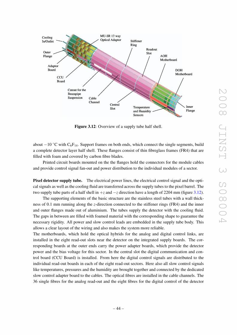
2008 JINST 3 S08004
Figure 3.12: Overview of a supply tube half shell.
about −10 C with C6F14. Support frames on both ends, which connect the single segments, builda complete detector layer half shell. These flanges consist of thin fibreglass frames (FR4) that arefilled with foam and covered by carbon fibre blades.
Printed circuit boards mounted on the the flanges hold the connectors for the module cablesand provide control signal fan-out and power distribution to the individual modules of a sector.
Pixel detector supply tube. The electrical power lines, the electrical control signal and the opti-cal signals as well as the cooling fluid are transferred across the supply tubes to the pixel barrel. Thetwo supply tube parts of a half shell in +z and−z direction have a length of 2204 mm (figure 3.12).
The supporting elements of the basic structure are the stainless steel tubes with a wall thick-ness of 0.1 mm running along the z-direction connected to the stiffener rings (FR4) and the innerand outer flanges made out of aluminium. The tubes supply the detector with the cooling fluid.The gaps in between are filled with foamed material with the corresponding shape to guarantee thenecessary rigidity. All power and slow control leads are embedded in the supply tube body. Thisallows a clear layout of the wiring and also makes the system more reliable.The motherboards, which hold the optical hybrids for the analog and digital control links, areinstalled in the eight read-out slots near the detector on the integrated supply boards. The cor-responding boards at the outer ends carry the power adapter boards, which provide the detectorpower and the bias voltage for this sector. In the central slot the digital communication and con-trol board (CCU Board) is installed. From here the digital control signals are distributed to theindividual read-out boards in each of the eight read-out sectors. Here also all slow control signalslike temperatures, pressures and the humidity are brought together and connected by the dedicatedslow control adapter board to the cables. The optical fibres are installed in the cable channels. The36 single fibres for the analog read-out and the eight fibres for the digital control of the detector
– 44 –

2008 JINST 3 S08004
Figure 3.13: Exploded view (middle panel) of a barrel pixel detector full module (right panel) andpicture of an assembled half module (left panel).
modules will then be connected through the MUSR connector to the optical ribbon cable. Theseadapters are mounted at the circumference in the first part of the supply tube. The length of eachsupply tube is 2204 mm. Only a flexible mechanical connection is made between the barrel andthe supply tube.
Pixel barrel detector modules
The barrel part of the CMS pixel detector consists of about 800 detector modules. While themajority of the modules (672) are full modules as seen in figure 3.13 on the right, the edges of thesix half-shells are equipped with 16 half-modules each (96 in total, see figure 3.13 on the left).
Geometry and components. A module is composed of the following components (figure 3.13).One or two basestrips made from 250 µm thick silicon nitride provide the support of the module.The front end electronics consists of 8 to 16 read-out chips with 52×80 pixels of size 100×150 µm2
each, which are bumpbonded to the sensor. The chips are thinned down to 180 µm . The HighDensity Interconnect, a flexible low mass 3 layer PCB with a trace thickness of 6 µm equippedwith a Token Bit Manager chip that controls the read-out of the ROCs, forms the upper layerof a module and distributes signals and power to the chips. The signals are transferred over animpedance matched 2 layer Kapton/copper compound cable with 21 traces and 300 µm pitch. Themodule is powered via 6 copper coated aluminium wires of 250 µm diameter.
– 45 –

2008 JINST 3 S08004
3210−1−2−30
0.025
0.05
0.075
0.1
0.125
0.15
0.175
0.2
η
X/X
0
Sensors & ChipsCablingStructure & Cooling
Figure 3.14: Material budget of the pixel barrel in units of radiation length versus rapidity. Theplot does not contain contributions from the pixel support cylinder, the supply tube and cablingfrom the detector end flange to the supply tube.
A completed full-module has the dimensions 66.6×26.0 mm2, weights 2.2 g plus up to 1.3 gfor cables, and consumes 2 W of power. The material of the pixel barrel amounts to 5 percentof a radiation length in the central region. Sensors and read-out chips contribute one third of thematerial while support structure and cooling fluid contribute about 50 percent. The distribution ofmaterial as a function of pseudorapidity is shown in figure 3.14.
3.2.5 The forward pixel detector
The FPix detector consists of two completely separate sections, one on each side of the interac-tion region. They are located inside the BPix supply tube but are mounted on separate insertionrails. Each section is split vertically down the middle so the detector can be installed around thebeam-pipe and its vertical support wire and so it can also be removed for servicing during ma-jor maintenance periods without disturbing the beam-pipe. Each of these four sections is called ahalf-cylinder.
Mechanics of a half-cylinder
Each half-cylinder consists of a carbon fiber shell with two half-disks located at its front end, oneat 34.5 cm from the IP and the other at 46.5 cm. The half-disks support the actual pixel detectorsthat extend from 6 cm to 15 cm in radius from the beam.
The half-disk has 12 cooling channels (each in the shape of a “U”) assembled between a halfring shown in figure 3.15. The assembly requires three slightly different types of cooling channels.Each channel is made by Al-brazing two blocks of Al with the channel for the cooling fluid already
– 46 –

2008 JINST 3 S08004
Figure 3.15: The FPix half-disk cooling channels mounted in the outer half-ring structure. Theturbine-like geometry is apparent. Panels are mounted on both sides of the cooling channels.
machined in the two parts. The brazed parts are then machined to their final shape. The walls ofthe channels are 0.5 mm thick. The average weight of the channels is 8.21 g.
All channels passed a Helium leak test at 1.33×10⁻⁸ mbar-litre/s. The pressure drop of theindividual cooling channels for a flow of 2600 sccm of dry N2 is 0.49 ± 0.02 mbar. Six daisy-chained cooling channels form a cooling loop. The pressure drop over a loop (for a flow rate of1230 sccm) of dry N2 is 0.96±0.13 mbar. For C6F14 at −20°C with a rate of 12cc-s the pressuredrop is 294 mbar.
Each of the twelve cooling channels of a half-disk has trapezoidal beryllium panels attachedto each side. The panels support the sensors and read-out chips that constitute the actual particledetectors. As explained above, the cooling channels are rotated to form a turbine-like geometryto enhance charge-sharing. The panels are made of 0.5mm beryllium. The beryllium provides astrong, stable and relatively low-mass support for the actual pixel detectors. The cooling channelsare supplied with C6F14 at about −15°C. A single cooling channel with panels mounted on bothsides forms a subassembly called a blade. There are 24 panels, forming 12 blades, in each half-disk.
Powering up the electronics on one blade increases the temperature by ≈2°C. The tempera-ture of each ROC is part of the information available for each event. Each panel also has a resistancetemperature detection sensor. The pixel sensors have fiducial marks visible with a coordinate mea-suring machine (CMM). Their position is then related to reference marks mounted on the half-diskunits.
After installing the half-disks in the half-cylinder, the disk position is measured relative tothe half-cylinder using a CMM and also by photogrammetry. This permits relating the positionof the sensors to the CMS detector. The detector is surveyed at room temperature but operated at
– 47 –
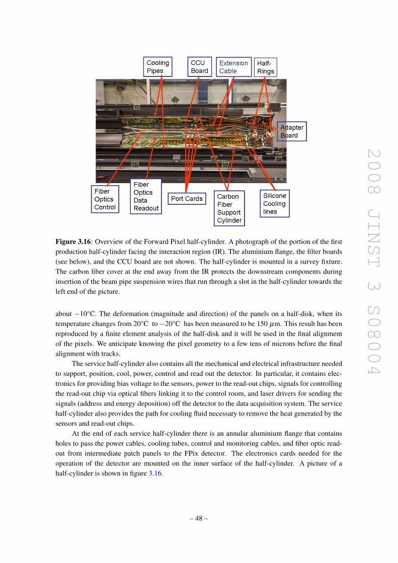
2008 JINST 3 S08004
Figure 3.16: Overview of the Forward Pixel half-cylinder. A photograph of the portion of the firstproduction half-cylinder facing the interaction region (IR). The aluminium flange, the filter boards(see below), and the CCU board are not shown. The half-cylinder is mounted in a survey fixture.The carbon fiber cover at the end away from the IR protects the downstream components duringinsertion of the beam pipe suspension wires that run through a slot in the half-cylinder towards theleft end of the picture.
about −10°C. The deformation (magnitude and direction) of the panels on a half-disk, when itstemperature changes from 20°C to −20°C has been measured to be 150 µm. This result has beenreproduced by a finite element analysis of the half-disk and it will be used in the final alignmentof the pixels. We anticipate knowing the pixel geometry to a few tens of microns before the finalalignment with tracks.
The service half-cylinder also contains all the mechanical and electrical infrastructure neededto support, position, cool, power, control and read out the detector. In particular, it contains elec-tronics for providing bias voltage to the sensors, power to the read-out chips, signals for controllingthe read-out chip via optical fibers linking it to the control room, and laser drivers for sending thesignals (address and energy deposition) off the detector to the data acquisition system. The servicehalf-cylinder also provides the path for cooling fluid necessary to remove the heat generated by thesensors and read-out chips.
At the end of each service half-cylinder there is an annular aluminium flange that containsholes to pass the power cables, cooling tubes, control and monitoring cables, and fiber optic read-out from intermediate patch panels to the FPix detector. The electronics cards needed for theoperation of the detector are mounted on the inner surface of the half-cylinder. A picture of ahalf-cylinder is shown in figure 3.16.
– 48 –

2008 JINST 3 S08004
Figure 3.17: Sketches of the two types of FPix panels showing the different sizes and numbers ofthe plaquettes on each (left side). A photograph of an actual 3-plaquette panel (right side).
Forward pixel detection elements - the plaquettes
The basic unit of construction for the forward pixel detector is the plaquette. A plaquette consistsof a single pixel sensor bump-bonded to an appropriate number of Read-Out Chips (ROCs) andwire-bonded to a very-high-density-interconnect (VHDI) that provides power, control, and dataconnections.
In order to cover the trapezoidal or pie-shaped panels without leaving cracks, five differentsizes of plaquettes are needed. These are respectively 1×2, 2×3, 2×4, 1×5, 2×5, where the firstdigit refers to the number of rows and the second to the number of columns of read-out chips thatare attached to a given sensor. The largest plaquette, the 2×5, has dimensions of 16 mm × 35 mm.The panels on the side of the cooling channel closest to the IP contain 1×2, 2×3, 2×4, and 1×5plaquettes or a total of 21 ROCs. The panels on the side of the cooling channels farthest from theIP contain 2×3, 2×4 and 2×5 type plaquettes with a total of 24 ROCs. The sensors are offset onthe upstream and downstream panels so that there are no cracks in the coverage due to the ROCread-out periphery. The two types of panels are shown in figure 3.17. A total of 672 plaquettes areneeded.
The joining, or hybridization, of the pixel sensors and the pixel unit cells of the ROC isachieved by fine-pitch bumping using Pb/Sn solder and then flip-chip mating. The bumping isdone on the 8” ROC wafers and the 4” sensor wafers. After bumping, the ROC wafers are thinnedby backside grinding to 150 µm and then diced. Finally, each of the 5 different types of sensors aremated to the appropriate number of ROCs. The sensor with its ROCs bump-bonded to it is calleda module. For FPix, the hybridization was done in industry. The fraction of broken, bridged, ormissing bumps is at the level of a few 10−3.
After delivery from the vendor, the bump-bonded pixel detector module is then installed ona Very High Density Interconnect (VHDI). The VHDI is a two-layer flexible printed circuit, lam-inated to a 300 µm thick silicon substrate, whose trace geometry and characteristics (impedance,low intrinsic capacitance, and low cross-talk) have been optimized for the intended use of convey-ing digital control and analog output signals to and from the sensors and ROCs.
– 49 –

2008 JINST 3 S08004
The VHDI is made as follows. A bulk 6” silicon wafer is laminated to a flexible sheet con-taining several VHDI circuits. Passive components are also attached using surface-mount soldertechniques. The wafer of populated circuits is then diced into individual circuits using a diamondsaw. The circuits are then electrically tested.
The hybridized pixel module is attached and wire bonded to a populated VHDI to become aplaquette. The joining is made using parallel plate fixtures aligned on linear rails. The alignmentof components is inspected using a coordinate measuring machine. A flexible plate is used forfine adjustments on the fixtures resulting in alignments between joined components within 100µm. The adhesive bond between plaquette components is made in a vacuum at 60°C, to softenthe adhesive and prevent air entrapment. An air cylinder applies and controls the mating pressure,which is limited by the compression allowed on the bump-bonds.
The effects of thermal cycling and radiation on the assembled plaquettes have been exten-sively tested. The tests demonstrate that the adhesive and the application method mitigate warpingdue to temperature changes, and provide reliable strength and thermal conductivity.
Once plaquettes are mechanically joined, they are clamped in cassettes that accommodateall processing steps such as wirebonding which provides electrical connections between the ROCsand the VHDI. After wirebonding we encapsulate the feet of wirebonds. This encapsulation isnecessary due to periodic I~dl × ~B forces expected to occur during actual CMS operation. Theencapsulant acts as a damping force on the wire, preventing large resonant oscillations to workharden the wire and cause eventual breakage [30]. Finally the plaquettes undergo quick testingat room temperature. During this test the quality of the plaquettes is evaluated in terms of thecharacteristics of the sensor, the read-out chip, the number of bad pixels and missing bonds. Theassembly and testing rate is optimized for a rate of six plaquettes per day.
The completed plaquettes are subjected to a quick plug-in test. Then they are loaded into aBurn-In Box where they undergo 10 temperature cycles between 20°C and −15°C. These cyclescan take up to 2 days to complete, depending upon the thermal load. During these cycles, theplaquettes are monitored for electrical operation. We have seen no failures during the cycling.After the burn-in process is completed, the plaquettes are subjected to a series of electrical teststo ensure their suitability for their eventual mounting on a panel. These tests, at the operatingtemperature of −15°C, include the functionality of the ROC, the integrity of the bump-bond, andthe I-V characteristics of the sensor. Other tests measure the thresholds and noise characteristicsof each pixel on the entire plaquette assembly, and the individual pixel thresholds are trimmed viathe ROC capability. We have found that the pixel trim values from the plaquette test on each pixelremain valid even after subsequent steps of the assembly process. After testing the plaquette datais loaded into the Pixel Construction Database and the plaquettes are graded. We have three maincategories of grades:
• A - the plaquette is available for immediate mounting on a panel;
• B - potential issues have been found during testing and need further analysis;
• C - the plaquettes are unsuitable for mounting.
The data on each B-grade plaquette are examined carefully. In many cases, the plaquettesare found to have missed being classified as A-grade due to very minor deficiencies (e.g. slightly
– 50 –

2008 JINST 3 S08004
Figure 3.18: Sketch of a plaquette mounted on a panel showing its several layers.
too many noisy pixels) which will not be significant when an entire panel’s quality is assessed.These are “promoted” to A-grade and declared usable on panels. Current plaquette yields, basedon an original grade of A or a promotion to A-grade from B, are in the 80% range, varying slightlyaccording to plaquette size.
Panel assembly
A panel is formed from three or four plaquettes attached to an assembly of a High Density In-terconnect (HDI) laminated to a beryllium plate. The HDI is a three-layer flexible printed circuitwhose trace geometry and characteristics (impedance, low cross-talk) have been optimized for theintended use of transferring digital control and analog output signals.
The process by which a panel is assembled is as follows. A single HDI circuit is laminated toa trapezoidal-shaped 0.5 mm thick beryllium plate. Passive components are attached using surface-mount solder techniques. The Token Bit Manager (TBM) is attached to the corner tab of the HDIusing a die attach method and wire-bonding. After functional and burn-in tests with only the TBM,the individual plaquettes are attached to the HDI using adhesive for mechanical attachment andwire-bonds for electrical connection.
There are four types of panels, a right and left 3-plaquette version, and a right and left 4-plaquette version. The right and left handed versions have their TBMs on opposite sides of thepanel centerline. Both types are required so that no panel part projects past a line in the verticalplane. The reason for the “3” and “4” type panels is that they are eventually mounted on oppositeside of a blade, and the gaps between plaquettes on one type are covered by the active area of theother.
A panel is built up out of several layers of components. These are shown in figure 3.18. Thetotal number of panels in all eight half-disks is 192.
Final detector assembly validation
The panels are attached onto the front and back of the half-disk cooling channels. The 4-plaquettepanels are mounted on the side closest to the interaction region (IR), and the 3-plaquette versionson the opposite side. The half-disk assembly is mounted onto the half-service cylinder and is againtested.
– 51 –

2008 JINST 3 S08004
Electronics chain
Each HDI is connected to another flexible printed circuit board, the adapter board. Each adapterboard serves three blades (or 6 panels). One important purpose of the adapter board is to send andreceive signals from the panels, which are mounted perpendicular to the axis of the service cylinderto and from the electronics mounted on the inner surface of the service cylinder. This is done by apigtail at the end of each panel that plugs into connectors on the fingers of the adapter board.
The adapter board has three types of ASICs mounted on it. These are used to pass the clock,trigger and control data signals to each panel and return the received control signals back to thepFEC.
The adapter board is connected to another printed circuit board, the port card, by a light-weight extension cable. These cables are of two types, a power cable which distributes the powerto the ROCs and TBMs, and the HV bias to the sensors. The other cable is to transmit the pixeldata and control signals to the panel from the port card. The port card is a low-mass printed circuitboard. It houses the electronics needed to interface the front-end chips with the VME electronics(the pFEC and pxFED) and power supplies located in the counting room. The port card transmitsthe clock signal, L1 trigger and slow control signals to the front end electronics. It distributes thepower and bias voltages to the chips and sensors. It also monitors the currents and voltages as wellas the temperature on some panels. These functions are done by various ASICs that are commonto the CMS tracker. These ASICs include the DCU for monitoring, the TPLL for regenerating thetrigger and timing signal, the gatekeeper for keeping the optical up and down links open as needed.
To control and monitor the various ancillary chips and optohybrids, there is a CCU board foreach half service cylinder, as described above.
The port card contains the Analog Optohybrid (AOH). Each of the 6 laser diodes of the AOHchip receives data from one panel via its TBM and sends it over its own optical fiber to the Frontend Driver (FED).
The control of the ROCs is achieved through the Pixel Front End Controller. Optical signalsare sent from it to the Digital Optohybrids on the port card, through the extension cables to theadapter board, then to the TBM on the panel, through the HDI and the VHDI to the ROCs.
Power and monitoring
Power connections are made from CAEN power supplies via cables that run through the flange atthe end of the half-cylinder away from the IR into a set of power/filter boards. From these boards,it is sent along wires to the port card, in the case of low voltages, and directly to the adapter boardin the case of the sensor bias voltage.
Monitoring points for temperature are distributed throughout the service cylinder. There arealso humidity sensors. Additional temperature sensors are mounted on the panels. High and lowvoltage and detector monitoring are connected to the DCS system described below.
Testing
Testing is a key element of quality assurance in the assembly process. While rework is possible, itis difficult and error prone. At every step, we confirm that we are using only “known good parts”.
– 52 –

2008 JINST 3 S08004
Testing must keep up with the driving assembly step, plaquette production. Full characterizationof a plaquette requires hundreds of thousands of measurements. To accomplish this, we havedeveloped special read-out hardware and software that can carry out these measurements quicklyand efficiently. A software using a USB-based data acquisition scheme is employed when flexibilityis needed to develop measurement programs of modest complexity and duration, such as the burn-inprocedure. For the most extensive measurements, including plaquette testing and characterization,we use a PCI-based system and a software program called Renaissance [31].
Final testing is performed using the real data-acquisition and control hardware and prototypedata-acquisition software and constitutes an end-to-end system test. Detailed testing also estab-lishes an initial set of parameters for the many DACs and thresholds in the system.
3.2.6 Power supply
All needed high and low DC voltages are generated by means of a commercial modular systemof the type CAEN-EASY4000 . This system is also employed by the CMS silicon strip trackerfor which the main regulating cards (A4601H) were custom designed [32]. Only small changes inhard- and firmware were necessary for adaptation to the pixel project.
The core of this system, accessed through LAN, is located in the detector control room(USC55) and consists of one main controller (SY1527) containing 3 branch controllers (A1676A).The actual power supply cards are placed in two racks of 5 crates in close proximity to the detectorthanks to their radiation tolerance and magnetic field resistance. This has been chosen in order toreduce power loss in the cables. The power supply crates are connected by flat cables (≈ 100 m) tothe branch controllers. They are fed by local 3-phase 230 VAC to 48 VDC master converters of each2 kW (A3486H) also suited for operation at hostile environments.
The crates house two types of electronic cards, one of 4 channels of 2.5 V/7 A (A4602)feeding the service electronics on the supply tubes (auxiliary power), while the other (A4603H)deliver 2 complex channels of each 2 low (1.75 V/7 A and 2.5 V/15 A) and 2 high voltage lines(−600 V/20 mA) for ROC and sensor biasing respectively. Each of these channels contains float-ing pulse-width-modulated DC/DC switching transformers with a common ground return for the1.75 and 2.5 V lines. The isolation resistance (ground return versus earth on the racks) is typically100 Ω at 5 MHz. Every card is controlled by an optically decoupled microprocessor for setting andmeasuring voltages, currents, ramp times, trip parameters, interlocks and others.
The DC levels are regulated over sense lines. The reaction time of the sensing circuit (typi-cally 200 µs) is subject to fine tuning to comply with capacitive load, cable impedance and length(typically 50 m). The line drop in the cables amounts to roughly 2 V, while the regulators wouldallow for a maximum of 6 V. Fourteen A4602 cards, yielding 40 independent channels of auxiliarypower, feed the 32 slots of the barrel service tubes with each 2 DOHs and 6 AOHs as well as 4groups of each 12 port cards of the forward half disks. The main supplies of 112 complex LV andHV channels (56 A4603H cards) feed the 64 barrel groups (192 ROCs, this contains groups withhalf size modules) of each 12 detector modules, and 48 forward groups (135 ROCs) of each 3 diskblades. Each of these groups draws a typical current of 4.6 A on the analogue (1.75 V) and 9 A onthe digital (2.5 V) line respectively. The large current reserve of the supplies is needed to complywith conditions during bootstrapping where the ROCs remain briefly in an undefined state. It was
– 53 –

2008 JINST 3 S08004
verified that the regulators undergo a smooth transition from the constant-voltage to the constant-current regime if the programmed current limits are approached. Beside microprocessor controlledactions (1 s) fast over-current security is guaranteed by various solid state fuses (10 ms) as well ascrowbars (100 µs) for over-voltage.
Noise levels are typically 5 mVpp on the LV and 50 mVpp on the HV outputs which can easilybe accepted thanks to the LV regulators in the ROCs and the intrinsically small sensor capacitancesrespectively. Of major concern in the overall design were fast drops in the digital current con-sumption (2.5 V line) in case of low ROC activity like in orbit gaps. Due to the cable inductancea typical current drop of 2 A per group generates over-voltage spikes at the module level in theorder of some Volts depending on local buffer capacitors. The integrity of the cable-module-ROCcircuit was therefore checked by a full simulation in SPICE together with measurements on pulsedcurrent loads. This served for the designs of the cables and the electronic layout, e.g. groundingor HV distribution. (In one sector layer-1 modules are fed by one line while layer-2,3 modulesare commonly fed by the other.) Finally a 6×4 mm2 shielded copper cable was chosen for the40 m from the power supply cards to the patch panel (PP1) located in the HCAL with alternatingcurrent directions between adjacent lines. Two twisted pair lines for the senses and a bunch of 10commonly shielded lines for HV are contained in the same cable complex (0.1 mm2).
Inductance, capacitance and characteristic impedance between two of the main lines weremeasured to be 6 µH/m, 0.13 nF/m and 24 Ω respectively. The 4 m connection between PP1 andPP0 (tracker bulkhead) uses Al conductors in the cable. The auxiliary power cable is also shieldedand contains 26×0.75 mm2 and 4 twisted pair copper lines with 0.1 mm2 for the sense wires.
3.2.7 Cooling
The power consumption per pixel amounts to around 55 µW, including about 13 µW from thesensor leakage current at final fluences of 6×10¹⁴/cm2. For the total of ≈ 66 million pixels thisadds up to 3.6 kW. The power load on the aluminium cooling tubes is therefore expected to be about50 W/m. The sensor temperature will be maintained at around −10°C. As for the strip detectors,liquid phase cooling with C6F14 is used. To keep the temperature increase of the coolant below2°C, a total flow rate of 1 litre/s is required.
The pixel system is cooled by a total of 18 cooling loops: 10 for the barrel and 4 for each ofthe two end disk systems. For the barrel, the coolant enters at +z and exits at −z, or vice versa.The coolant for the two disk sets on each side of the interaction region is supplied and reclaimedfrom the same z side. One barrel loop feeds in parallel 9 thin-walled aluminium pipes, each cooling8 modules in series. One disk loop cools in parallel one quarter of each of the 2 disks; inside thequarter disks the 6 blade loops are connected serially. The coolant flow at the pixel modules isturbulent. The total lengths of the cooling loops starting from and returning to the pixel coolingrack amount to about 80 m, resulting in pressure drops of below 2 bar.
3.2.8 Slow controls
The safe operation of the barrel and forward pixel detectors is guaranteed by the CMS Pixel slowcontrols system (DCS). Its tasks are to monitor temperatures and humidities at different locations
– 54 –

2008 JINST 3 S08004
of the detector and to monitor and control the high and low voltages necessary for operation of theon-detector electronics.
The monitoring of temperatures and humidities is based on a commercial Siemens S7–300modular mini Programmable Logic Controller (PLC) system. The Siemens S7–300 system mon-itors a total of 192 temperature and 8 humidity sensors installed in the Pixel barrel and forwardendcap disks. For the temperature sensors, platinum resistance temperature detection sensors witha nominal resistance of 1 kΩ (Pt1000 RTD) have been chosen. The measurement of humidity isbased on detecting the water vapor induced shear stress in a small polymer element that is con-nected to a Wheatstone Bridge piezoresistor circuit [33]. This circuit provides a small (mV) outputsignal that is linearly proportional to relative humidity (RH) between the full range of 0% to 100%RH and is amplified by the same kind of conditioning electronics that is used by the silicon striptracker. The PLC of the Siemens S7–300 system is programmed in the Statement List (STL)language [34] to convert the currents and voltages of the temperature and humidity sensors intocalibrated physical units (i.e. degrees Celsius for temperatures and percentages for humidities).For the purpose of avoiding damage to the detector in case the cooling system (dry air supply)fails, routines are programmed within the PLC to interlock the CAEN power supplies (shut-off thecooling) in that case.
An additional 96 Pt1000 temperature sensors are read out via the data-acquisition (DAQ)system, together with the temperature dependent voltage sources integrated into each one of thepixel read-out chips. The temperatures recorded by the DAQ system are passed to the slow controlssystem by means of a dedicated software interface [35].
The Barrel and Forward Pixel slow controls system is integrated into the PVSS graphical userinterface (chapter 9) of the main CMS DCS.
3.3 Silicon strip tracker
3.3.1 Silicon sensors
The sensor elements in the strip tracker are single sided p-on-n type silicon micro-strip sen-sors [36, 37]. They have been manufactured on 6 inch wafers in a standard planar process, leadingto significant cost reduction per unit area when compared to the more traditional 4 inch wafers.The base material is n doped float zone silicon with 〈100〉 crystal orientation. This crystal ori-entation was preferred over the more common 〈111〉 orientation because measurements [38] haveshown that the built-up of surface charge on 〈100〉 wafers due to irradiation is much smaller andconsequently irradiation causes less inter-strip capacitance increase on this material.
In TIB/TID and on the inner 4 rings of the TECs (figure 3.1), thin sensors of (320±20)µmwafer thickness are used, with substrate resistivity of ρ = 1.55− 3.25kΩcm. TOB and the outer3 rings of the TECs are equipped with thicker sensors of (500± 20)µm thickness, with substrateresistivity of ρ = 4−8kΩcm. Due to the single sided processing, these sensors show a significantbow, which is required to be less than 100 µm.
A uniform n+ implantation on the back side of the wafers, covered by aluminium, forms anohmic contact which is connected to positive voltage up to about 500 V. Those sensors which arepenetrated by the beams of the laser alignment system (section 3.3.7) feature a 10 mm hole in the
– 55 –

2008 JINST 3 S08004
back side metalization, as well as anti-reflective coating in order to achieve transmission throughup to four sensors with a sufficient signal on a fifth sensor.
On the front side, strip shaped diodes are formed by p+ implantation into the n type bulk.Due to the radiation damage to the crystal lattice, the bulk material will undergo type inversion andchange to p type. At this point, the pn junction moves from the strip side of the wafer to the rearside contact. Each implanted strip is covered by an aluminium strip from which it is electricallyinsulated by means of a silicon oxide and nitride multilayer. This integrated capacitor allows for ACcoupling of the signals from the strips to the read-out electronics, which is thus protected from thehigh leakage currents after irradiation. Each metal strip has two bond pads on each end, which areused to make a wire bond connection to the read-out chip and in case of the daisy chained sensorsto make a wire bond connection between the two sensors in one detector module. For testingpurposes there is also a DC pad connected to the p+ implant. Each strip implant is connected via a(1.5±0.5) MΩ polysilicon bias resistor to a p+ bias ring which encloses the strip region and alsodefines the active area of the sensor.
For all sensors in the CMS strip tracker the ratio of p+ implant width over strip pitch isw/p = 0.25, leading to a uniform total strip capacitance per unit length of about 1.2 pF/cm across allsensor geometries [38]. The actual w/p value was chosen in order to minimize the strip capacitancewhile still maintaining a good high voltage behaviour of the sensor. The aluminium strips featurea metal overhang of 4 to 8 µm on each side of the strip which pushes the high field region into thesilicon oxide where the breakdown voltage is much higher, leading to stable high voltage operation.For the same reason, the bias ring is surrounded by a floating guard ring p+ implant. It graduallydegrades the electric field between the n+ implant at the cut edge of the sensor and the bias ring,which are at backplane potential (high voltage) and ground, respectively. Figure 3.19 shows thelayout of a corner of the active region of a sensor.
In order to equip all regions in the CMS tracker, 15 different sensor geometries areneeded [36] (figure 3.19): two rectangular sensor types each for TIB and TOB, and 11 wedge-shaped sensor types for TEC and TID. They have either 512 or 768 strips, reflecting the read-outmodularity of 256 channels (two 128-channel front-end chips multiplexed to one read-out channel).Since the sensors are fabricated on 6 inch wafers, they can be made rather large. Typical dimen-sions are for instance about 6× 12cm2 and 10× 9cm2 in the inner and outer barrel, respectively.The total number of silicon sensors in the strip tracker is 24 244, making up a total active area of198m2, with about 9.3 million of strips [36].
3.3.2 Read-out system
The signals from the silicon sensors are amplified, shaped, and stored by a custom integrated cir-cuit, the APV25 [39]. Upon a positive first level trigger decision the analogue signals of all chan-nels are multiplexed and transmitted via optical fibers to Front End Driver (FED) boards in theservice cavern where the analogue to digital conversion takes place. This read-out scheme bringsthe full analogue information to a place where it can be used for accurate pedestal and commonmode subtraction as well as data sparsification. Clock, trigger, and control signals are transmittedby optical links as well. A schematic view of the silicon strip tracker read-out scheme is given infigure 3.20. This analogue read-out scheme was chosen for several reasons: optimal spatial reso-
– 56 –

2008 JINST 3 S08004
Guard ring
Bias ring
Biasresistors
DC pads
AC pads
Figure 3.19: Left panel: drawing of one corner of the active region of a wedge-shaped siliconstrip sensor for the tracker endcaps. Right panel: silicon sensor geometries utilized in the CMStracker. In the outer layers the sensors are paired to form a single module, as shown in the figure.The Inner Barrel and Outer Barrel sensors exist in two types, of same area and different pitch. Thesensors utilized for the first inner ring exist in two different versions, one for TID and one for TEC,respectively. (Only the TEC version is shown.)
Figure 3.20: Read-out scheme of the CMS tracker.
lution from charge sharing, operational robustness and ease of monitoring due to the availabilityof the full analogue signal, robustness against possible common mode noise, less custom radiationhard electronics and reduced material budget as the analogue to digital conversion and its powerneeds are shifted out of the tracker volume.
– 57 –

2008 JINST 3 S08004
Front-end ASICs
The APV25 has been designed in an IBM 0.25 µm bulk CMOS process. Compared to processeswith bigger feature sizes, the thin gate oxide inherent to this deep sub-micron process is much lessaffected by radiation induced charge-up and thereby, in conjunction with special design techniques,ensures radiation tolerance [40]. The APV25 has 128 read-out channels, each consisting of a lownoise and power charge sensitive pre-amplifier, a 50ns CR-RC type shaper and a 192 elementdeep analogue pipeline which samples the shaped signals at the LHC frequency of 40MHz. Thispipeline is used to store the data for a trigger latency of up to 4 µs and to buffer it. A subsequentstage can either pass the signal as sampled at the maximum of the 50ns pulse (peak mode) or forma weighted sum of three consecutive samples which effectively reduces the shaping time to 25ns(deconvolution mode). The latter is needed at high luminosity in order to confine the signals to thecorrect LHC bunch crossing. The pulse shape depends linearly (linearity better than 5%) on thesignal up to a charge corresponding to 5 minimum ionizing particles (MIPs, one MIP is equivalentto 25 000 electrons in this case), with a gradual fall off beyond. When a trigger is received, theanalogue data from all 128 channels of the appropriate time slice in the pipeline are multiplexed andoutput at a rate of 20 MS/s (mega-samples per second) as a differential bi-directional current signal,together with a digital header. Due to the tree structure of the analogue multiplexer the order inwhich the channels are output is non-consecutive and therefore re-ordering is necessary prior to theactual data processing. An internal calibration circuit allows to inject charge with programmableamplitude and delay into the amplifier inputs in order to be able to monitor the pulse shape.
The APV25 needs supply voltages of 1.25 V and 2.5 V with a typical current consumptionof about 65 mA and 90 mA respectively, leading to a total power consumption of typically around300 mW for one APV25 or 2.3 mW per channel. The noise of the analogue read-out chain isdominated by the front end MOSFET transistor in the APV25. Measurements have shown thatthe total noise for an APV25 channel depends linearly on the connected detector capacitance Cdet.The equivalent noise charge is found to be ENCpeak = 270e + 38e/pF ·Cdet in peak mode andENCdeconv = 430e+61e/pF ·Cdet in deconvolution mode, both measured at room temperature [39].Mainly due to the MOSFET characteristics, the noise reduces with temperature approximately asENC ∼
√T . Therefore, the noise at operating temperature is about 10% lower.
More than 100 APV25 chips from all production lots have been irradiated with X-rays to10 Mrad ionizing dose, in excess of the expectation for 10 years of LHC operation. No significantdegradation in pulse shape or noise level has been observed.
The APV25 is fabricated on 8 inch wafers with 360 chips per wafer. More than 600 waferscorresponding to 216 000 chips have been manufactured and probe-tested. After initial yield prob-lems were solved, an average yield of 88% was achieved.
Another custom ASIC, the APVMUX, is used to multiplex the data streams from two APV25chips onto one optical channel by interleaving the two 20 MS/s streams into one 40 MS/s stream,which is then sent to a laser driver of the optical links. One APVMUX chip contains 4 suchmultiplexers.
– 58 –

2008 JINST 3 S08004
Optical links
Analogue optical links are used to transmit the data streams from the tracker to the service cavernover a distance of about 100 m at 40 MS/s. Likewise, the digital timing and control signals (seebelow) are transmitted by digital optical links running at 40 Mb/s [41]. Optical links are superior toan electrical distribution scheme mainly since they have minimal impact on the material budget andare immune to electrical interference. The transmitters are commercially available multi-quantum-well InGaAsP edge-emitting devices, selected for their good linearity, low threshold current andproven reliability. Epitaxially grown planar InGaAs photo-diodes are used as receivers. The opticalfiber itself is a standard, single-mode, non dispersion shifted telecommunication fiber. The fibersare grouped in ribbons of 12 fibers which in turn are packaged in a stack of 8 inside a 96-wayribbon cable, which features a small diameter (< 10mm) and a low bending radius (8cm). For theanalogue data link up to three transmitters are connected to a laser driver ASIC on an AnalogueOpto-Hybrid (AOH), one of which sits close to each detector module. The electrical signals fromthe APVMUX are transmitted differentially over a distance of a few centimeters to the laser driver,which modulates the laser diode current accordingly and provides a programmable bias current tothe diode. For the bi-directional digital optical link a set of two receivers and two transmitters ismounted on a Digital Opto-Hybrid (DOH), converting the optical signals to electrical LVDS [42]and vice versa.
Front End Drivers
The strip tracker Front End Driver (FED) is a 9U VME module which receives data from 96 opticalfibres, each corresponding to 2 APV25 or 256 detector channels [45]. All 96 fibres are processedin parallel. The optical signals are converted to electrical levels by opto-receivers [43] and thendigitized by a 40MHz, 10 bit ADC. The ADC sampling point for each fibre can be programmedindependently in 1 ns steps. After auto-synchronization to the APV data stream, pedestal correc-tions are applied and the common mode subtracted. The common mode correction is calculatedfor each trigger and each APV separately. The samples are then re-ordered to restore the physicalsequence of detector channels which is essential for the following step of cluster finding. Pedestalvalues for each detector channel and thresholds for cluster finding are stored in look up tables. Thedigital functionality of the FED is implemented in FPGAs and can therefore be adjusted with con-siderable flexibility. In zero suppression mode, which is the standard for normal data taking, theoutput of the FED is a list of clusters with address information and signal height (8-bit resolution)for each strip in the cluster, thus passing to the central DAQ only those objects which are relevantfor track reconstruction and physics analysis. In this way an input data rate per FED of about3.4 GB/s, at LHC design luminosity, is reduced to roughly 50 MB/s per percent strip occupancy.Other modes are, however, available which suppress one or more steps in the processing chain andtherefore transmit additional data to the central DAQ to be used mainly for debugging and systemanalysis. There are a total of 450 FEDs in the final system.
– 59 –

2008 JINST 3 S08004
Control and monitoring
Clock, trigger and control data are transmitted to the tracker by Front End Controller (FEC)cards [44]. These are VME modules, located in the service cavern, as close as possible to thetracker in order to reduce trigger latency. They receive clock and trigger signals from the globalTiming Trigger and Command (TTC) system and distribute those as well as control signals via dig-ital optical links and the digital opto-hybrids to LVDS token ring networks (control rings) insidethe tracker volume. Several Communication and Control Units (CCU) [46] participate in one tokenring. These are custom ASICs which interface the ring network to the front-end chips. One CCUis mounted on a Communication and Control Unit Module (CCUM) and is dedicated to a set ofdetector modules. A combined clock and trigger signal is distributed to Phase Locked Loop (PLL)chips [47] on each detector module while the industry standard I2C protocol [48] is used to sendcontrol signals to the APV chips as well as to the other ancillary chips. One CCU can control up to16 units so that one FEC ring typically controls a set of several tens of detector modules. The PLLchips decode the trigger signals and provide a very low jitter, phase adjustable clock signal to thelocal electronics.
Detector Control Unit (DCU) ASICs [49] on the detector modules are used to monitor thelow voltages on the hybrid, the silicon sensor leakage current, and the temperatures of the siliconsensors, the hybrid and the DCU itself. For this purpose, each DCU contains eight 12 bit ADCs.The DCUs are read out through the control rings and digital links so that these readings are onlyavailable when the control rings and the detector modules are powered.
Hybrids
The front-end read-out electronics for a detector module is mounted onto a multi chip modulecalled hybrid [50]. Due to the different detector module geometries 12 different types of hybridsare needed in the CMS silicon strip tracker. Each hybrid carries 4 or 6 APV25 read-out chipswhich are mounted as bare dies, and one APVMUX chip, one PLL chip and one DCU chip whichare packaged components. The main features of the hybrid are to distribute and filter the supplyvoltages to the chips, to route clock, control and data lines between the chips and to remove the heatfrom the chips into the cooling system. No high voltage is present on the CMS tracker hybrids. Thehybrid substrate is fabricated as a four layer polyimide copper multilayer flex circuit (figure 3.21).It is laminated onto a ceramic (Al2O3) carrier plate using double sided acrylic adhesive. A poly-imide cable is integrated into the layout of the hybrid. The minimal feature sizes are 120 µm for viadiameter and line width. Large metalized through holes under the chips transfer the heat to the un-derlying ceramic plate, from where it is removed through the frame of the module into the coolingsystem. Three different flex circuit types (one each for TIB/TID, TOB and TEC) combined withdifferent geometries of the ceramic plates, different connector orientations and different number ofAPV25 chips (4 or 6) make up the total of 12 different hybrid flavours.
Power supplies
Silicon strip modules are grouped into 1944 detector power groups in order to share the powerservices. Each group is supplied by a power supply unit (PSU) [32], featuring two low-voltage
– 60 –

2008 JINST 3 S08004
Figure 3.21: Front-end hybrid layout (example for TEC shown on the left) and arrangement oflayers.
regulators, respectively 1.25 V (up to 6 A) and 2.5 V (up to 13 A), and two high-voltage regu-lators (0-600 V, up to 12 mA). All regulators are “floating” (return line isolated from the localearth). The two low-voltage channels share the same return line and use the sensing wire tech-nique to compensate, up to 4 V, the voltage drop along the cables. The two high-voltage regulatorsare fanned out at the PSU exit into 8 lines; each silicon strip sensor is connected to one of theselines. Two PSU are combined into one power supply module (PSM, A4601H model). In total984 A4601H boards are needed to power the detector groups; they are located on 129 EASY 4000crates, disposed on 29 racks, around 10 m away from the beam crossing region, and operate in a“hostile” radiation and magnetic field environment, powering the detector through ≈ 50-m-longlow impedance cables [32]. The 356 control rings require a separate power at 2.5 V. This is pro-vided by a different set of 110 control power supply modules (A4602, four 2.5 V channels permodule), fully integrated in the same system of the A4601H units and located on the same crates.Both A4601H and A4602 units require two distinct 48V power sources, one source (48Vp) for theregulators, the other (48Vs) for the service electronics. They are both provided by AC-DC convert-ers, CAENs A3486 (“MAO”), disposed on the same racks. Each EASY 4000 crate hosts up to 9boards (A4601H mixed to A4602) and provides 48Vp and 48Vs rails, interlock and general resetbus lines. The first slot in the crate (slot 0) hosts one interlock-card, which interfaces the interlockand reset lines to the control and safety systems (section 3.3.8). The average power consumption ofeach silicon strip module with 6 (4) APV25 chips is about 2662 mW (1845 mW). The total powersupplied by A4601H and A4602 boards is approximately 68 kW, of which nearly 50% is dissipatedon power cables. The power consumption is foreseen to increase with the aging of the detector; thepower supply system is dimensioned to cope with up to 60% increase of the low-voltage currents,corresponding to a total consumption of nearly 150 kW.
– 61 –

2008 JINST 3 S08004
silicon sensors
front-end hybrid
frame(carbon fibre)
Kapton foil
cross piece (graphite)
ceramic
pitch adapter
far sensor
near sensor
Figure 3.22: Left panel: exploded view of a module housing two sensors. Right panel: photographof a TEC ring 6 module, mounted on a carrier plate.
3.3.3 Silicon modules
Module design
The silicon strip tracker is composed of 15 148 detector modules distributed among the four differ-ent subsystems (TIB, TID, TOB, TEC). Each module carries either one thin (320 µm) or two thick(500 µm) silicon sensors from a total of 24 244 sensors. All modules are supported by a framemade of carbon fiber or graphite, depending on the position in the tracker. A Kapton circuit layeris used to insulate the silicon from the module frame and to provide the electrical connection to thesensor back plane, i.e. bias voltage supply and temperature probe read-out. In addition the moduleframe carries the front-end hybrid and the pitch adapter. Figure 3.22 shows an exploded view anda photograph of a TEC module.
Modules for the inner barrel, the inner disks and rings 1 to 4 in the endcaps are equipped withone sensor, modules in the outer barrel and rings 5 to 7 in the endcaps have two sensors. In the caseof two sensors, their corresponding strips are connected electrically via wire bonds. Depending onthe geometry and number of sensors the active area of a module varies between 6243.1 mm2 (TEC,ring 1) and 17202.4 mm2 (TOB module). In total 29 different module designs, 15 different sensordesigns and twelve different hybrid designs are used in TIB, TOB, TID and TEC. For alignmentpurposes special modules are prepared with etched holes in the aluminium back plane to allow alaser ray to traverse up to five modules.
The module frame provides the stability, safety and heat removal capability needed in thesensor support and carries the read-out electronics. In addition it has to remove the heat generatedin the electronics and the silicon sensor(s) into the cooling points. In the endcaps the frame for theone-sensor modules is U-shaped and made of (780±5) µm thick graphite (FE779 carbon). For thetwo-sensor modules a similar U-shaped support structure is obtained by gluing two (640±40) µmthick carbon fiber legs (K13D2U CFC, 5×125 µm fabric, cyanate ester resin (CE3)) on a 800 µmthick graphite cross-piece (FE779 carbon) which holds the front end electronics. In the inner barrela 550 µm thick carbon fiber frame that surrounds the silicon sensor on all sides is used . Forthe TOB, U-shaped module frames are obtained by gluing two carbon fiber legs (K13D2U CFC,5× 125 µm fabric, cyanate ester resin (CE3)) on a carbon fiber cross piece made of the samematerial.
– 62 –

2008 JINST 3 S08004
Both graphite and carbon fiber fulfil the requirements of high stiffness, low mass, efficientheat removal from the sensors, and radiation hardness. Differences in the expansion coefficientsneed to be compensated by the glue joint between the frames and the silicon. Several types of gluesare used in module construction which all comply with the requirements of radiation hardness,good thermal conductivity and thermal stability. Among them are e. g. Epoxy AW 106 (Araldit,Novartis), silicone glue RTV 3140 (Dow Corning) to compensate for different thermal expansioncoefficients and the conductive glue EE 129-4 (Polytec) between the silicon sensor back plane andthe HV lines on the Kapton bias strips (see below).
Different types of aluminium inserts and precision bushings in the module frames are usedto position and attach the modules to the larger support structures with high precision. TIB/TIDand TEC modules are mounted using four points, two being high precision bushings that allowfor a mounting precision of better than 20 µm while all four provide thermal contact between themodule and the cooling pipes. For TOB modules two Cu-Be springs give the precision positioningand four screws ensure thermal contact.
The high voltage supply to the silicon back plane is provided by Kapton bias circuits runningalong the legs of the modules between the silicon sensor and the carbon fiber support frame. Theconnection of the bias voltage to the back plane is done via wire bonds. Thermal probes are placedon the Kapton foil to measure the temperature of the silicon. The glue joint between the temperaturesensor and the back plane is done with the silicone glue RTV 3140.
The pitch adapter between the front end hybrid and the silicon sensor adjusts the strip pitchof the sensor (80 µm–205 µm depending on sensor type) to the APV pitch of 44 µm. It also allowsplacing the heat producing front end electronics farther away from the silicon sensors. A pitchadapter for TOB and TEC consists of a 550 µm thick glass substrate (Schott D263 glass), cut tothe correct dimensions, with a pattern of low resistivity aluminium strips. For TIB 300 µm thickglass (Corning 1737F or G glass) is used. The 10 µm narrow lines are etched on a (1.0–1.5) µmthick aluminium layer deposited on a chromium base, resulting in less than 25 mΩ/.
Module assembly and testing
Sensors and front end hybrids are glued to the frames by high precision gantry robots. The compo-nents are aligned by cameras surveying special fiducial marks with a pattern recognition algorithm.In total seven institutes shared the responsibility for the assembly of all modules. The assembly ratewas about 20 modules per day per gantry robot. A positioning precision of approximately 10 µm(RMS) has been achieved and one example from the quality control can be seen in figure 3.23.
Thin wire wedge bonding is used in several places on the modules to make electrical con-nections: APV chip to front-end hybrid, APV chip to pitch adapter, pitch adapter to sensor, sensorto sensor (in case of two-sensor-modules), bias voltage connection to the sensor back plane. Intotal 15 institutes (bonding centers) shared the responsibility for wire bonding all modules. Thebonding rate was approximately 1 Hz. Bonding wire (99% aluminium, 1% silicon) with a diameterof 25 µm was used for all connections.
For the TEC and TOB modules the line of bonding wires connecting the hybrid pitch adapterto the silicon strips, and in the case of two sensor modules the strips of the two sensors, can bedamaged by vibration during transport. As a protection for the TEC modules the silicon is glued
– 63 –

2008 JINST 3 S08004
Figure 3.23: A typical residual distribution (in µm) for a reference point on the modules is shownfor the different module assembly centers, indicating a precision of 10 µm (RMS) in the moduleproduction.
to a supporting strip (400 µm thin ceramic Al2O3) which in the case of the pitch adapter-sensorconnection is also glued to the graphite cross piece. The reinforcement for the TOB modules wasdone by dispensing Sylgard 186 glue on the backside of the modules, between the two sensors andbetween the near sensor and the edge of the hybrid. For the TOB modules the sensor-sensor bondsand the backside APV bondings are encapsulated by Sylgard 186 glue across the bonding wires.For TIB modules no reinforcement was done.
After wire bonding each module was tested and graded, using the ARC system [51]. Adetailed description of all tests performed and the acceptance criteria for good channels is given inthe reference. Modules were graded A if fewer than 1% of the channels were failing the qualityacceptance criteria (due to high noise, open bondings, oxide defects) and B if the failure rate wasless than 2%. The remaining modules were graded C and were not used in the experiment. Otherreasons to reject modules were imperfect mechanical precision or poor high voltage behaviour. Allrelevant test results are stored in the central CMS tracker data base. The yield of module productionwas greater than 97%.
3.3.4 Tracker Inner Barrel and Disks (TIB/TID)
Introduction and mechanics
The Tracker Inner Barrel (TIB) consists of four concentric cylinders placed at radii of 255.0 mm,339.0 mm, 418.5 mm, and 498.0 mm respectively from the beam axis that extend from−700 mm to+700 mm along the z axis. The two innermost layers host double sided modules with a strip pitchof 80 µm, while the outer two layers host single sided modules with a strip pitch of 120 µm. Eachcylinder is subdivided into four sub-assemblies (±z, up/down) for ease of handling and integration.Each of these sub-assemblies (half-shells) hosts an independent array of services from cooling toelectronics and thus can be fully equipped and tested before being mechanically coupled to eachother during final assembly.
– 64 –

2008 JINST 3 S08004
TIB/TID + with the margherita.
Layer 4 shells
Service cylinder
(disks are
hidden inside)
Electrical power
patch panels
Optical fibres
patch panel
Silicon
detectors
Figure 3.24: Schematic drawing of the TIB/TID+ subassembly. This structure and its twin(TIB/TID-) nest inside the Tracker Outer Barrel (TOB), one for each end. Services routed outfrom the margherita consist of copper cables for powering and slow controls, optical fibers forsignals and controls and also cooling fluid supply lines made of aluminium tubing.
Two service cylinders are coupled to the ends of TIB± (referring to +z or −z) which endin a service distribution disk called the margherita (see below). These service cylinders play adual role: one is to route out services from the shells to the margherita, the other is to support theTracker Inner Disks (TID) which sit inside them. Figure 3.24 shows a schematic drawing of onehalf TIB/TID structure together with its corresponding margherita.
The TID± are assemblies of three disks placed in z between ±800mm and ±900mm. Thedisks are identical and each one consists of three rings which span the radius from roughly 200 mmto 500 mm. The two innermost rings host back-to-back modules while the outer one hosts singlesided ones. Just like the TIB shells each individual ring can be fully equipped and tested inde-pendently of the others before final assembly. Together the full TIB/TID guarantee hermeticalcoverage up to pseudorapidity η = 2.5.
All mechanical parts like shells, disks and service cylinders are made of high strength lowdeformation carbon fiber chosen both for its lightness and its low material budget. The margheritais instead made of conventional G-10 fiber epoxy with 30 µm copper on both sides.
The silicon detector modules are mounted directly on the structure’s shells and rings. Thus,while a large number of modules has to be integrated and tested at any one time, the approachchosen allows for far greater precision of assembly. The individual components of a TIB shell,
– 65 –
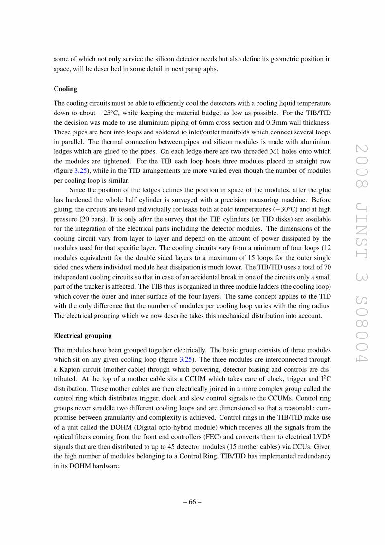
2008 JINST 3 S08004
some of which not only service the silicon detector needs but also define its geometric position inspace, will be described in some detail in next paragraphs.
Cooling
The cooling circuits must be able to efficiently cool the detectors with a cooling liquid temperaturedown to about −25°C, while keeping the material budget as low as possible. For the TIB/TIDthe decision was made to use aluminium piping of 6mm cross section and 0.3mm wall thickness.These pipes are bent into loops and soldered to inlet/outlet manifolds which connect several loopsin parallel. The thermal connection between pipes and silicon modules is made with aluminiumledges which are glued to the pipes. On each ledge there are two threaded M1 holes onto whichthe modules are tightened. For the TIB each loop hosts three modules placed in straight row(figure 3.25), while in the TID arrangements are more varied even though the number of modulesper cooling loop is similar.
Since the position of the ledges defines the position in space of the modules, after the gluehas hardened the whole half cylinder is surveyed with a precision measuring machine. Beforegluing, the circuits are tested individually for leaks both at cold temperatures (−30°C) and at highpressure (20 bars). It is only after the survey that the TIB cylinders (or TID disks) are availablefor the integration of the electrical parts including the detector modules. The dimensions of thecooling circuit vary from layer to layer and depend on the amount of power dissipated by themodules used for that specific layer. The cooling circuits vary from a minimum of four loops (12modules equivalent) for the double sided layers to a maximum of 15 loops for the outer singlesided ones where individual module heat dissipation is much lower. The TIB/TID uses a total of 70independent cooling circuits so that in case of an accidental break in one of the circuits only a smallpart of the tracker is affected. The TIB thus is organized in three module ladders (the cooling loop)which cover the outer and inner surface of the four layers. The same concept applies to the TIDwith the only difference that the number of modules per cooling loop varies with the ring radius.The electrical grouping which we now describe takes this mechanical distribution into account.
Electrical grouping
The modules have been grouped together electrically. The basic group consists of three moduleswhich sit on any given cooling loop (figure 3.25). The three modules are interconnected througha Kapton circuit (mother cable) through which powering, detector biasing and controls are dis-tributed. At the top of a mother cable sits a CCUM which takes care of clock, trigger and I2Cdistribution. These mother cables are then electrically joined in a more complex group called thecontrol ring which distributes trigger, clock and slow control signals to the CCUMs. Control ringgroups never straddle two different cooling loops and are dimensioned so that a reasonable com-promise between granularity and complexity is achieved. Control rings in the TIB/TID make useof a unit called the DOHM (Digital opto-hybrid module) which receives all the signals from theoptical fibers coming from the front end controllers (FEC) and converts them to electrical LVDSsignals that are then distributed to up to 45 detector modules (15 mother cables) via CCUs. Giventhe high number of modules belonging to a Control Ring, TIB/TID has implemented redundancyin its DOHM hardware.
– 66 –

2008 JINST 3 S08004
i
Figure 3.25: Three TIB modules mounted on a layer 3 shell. The Kapton mother cable runsunderneath. A CCUM module at the end of the string interfaces the modules to the control ring.Also visible are the three analog opto-hybrids (see text) and fibers.
Modules have been grouped together to keep the number of power supplies down to a man-ageable level. The smallest power group consists of three modules (one mother cable) while thelargest comprises up to 12 modules (four mother cables). Power groups are contained within a con-trol ring (i.e. there is no straddling across control ring boundaries) and are fed by a specific powersupply unit (PSU) developed for the tracker which also supplies HV biasing for the detectors.
Analog signals from the detector front end are converted to optical by analog opto-hybridswhich sit next to the silicon modules and are connected directly to the front end hybrids. Thusthe system is completely optically decoupled from the DAQ which helps preserve signal integritywhile avoiding ground loops.
Grounding of the TIB/TID relies on the cooling circuits which are made of aluminium. Thereturn current wires are connected to the cooling manifolds for all mother cables and DOHMs. Thecooling inlet and outlet pipes run along the service cylinder across the margherita, making electricalcontact with it. Outside the tracker volume these pipes are then connected to the CMS detectorground. Power cable shields are connected to the margherita which hosts all of the connectors. Alldetector modules have their own carbon fiber frame directly connected to the front end hybrid localground. The shells are grounded through the cooling manifolds.
3.3.5 Tracker Outer Barrel (TOB)
Mechanical structure and layout
The Tracker Outer Barrel consists of a single mechanical structure (wheel) supporting 688 self-contained sub-assemblies, called rods.
The wheel is composed by four identical disks joined by three outer and three inner cylin-ders (figure 3.26). Disks and cylinders are made of carbon fiber epoxy laminate. The cylindershave a core of aramid-fiber honeycomb. The joints between disks and cylinders are realized withaluminium elements glued to the carbon fiber parts on precision fixtures, and then bolted together.Each of the disks contains 344 openings, in which the rods are inserted. Each rod is supported bytwo disks, and two rods cover the whole length of the TOB along the z axis. The wheel has a lengthof 2180 mm, and inner and outer radii of 555 mm and 1160 mm, respectively. With cabling at itstwo ends the TOB has a total length of 2360 mm. The openings in the disks form six detectionlayers with average radii of 608, 692, 780, 868, 965, 1080 mm. Within each layer, the centers ofgravity of the rods are displaced by ±16 mm with respect to the average radius of the layer, thusallowing for overlap in φ and therefore full coverage within each layer. The rod mechanics aredesigned in such a way to implement overlap of the silicon sensors at z = 0. In each layer, the
– 67 –

2008 JINST 3 S08004
Figure 3.26: Picture of the TOB wheel.
overlap in the r-φ view between neighboring rods is always larger than 1.5 mm or 12 strips, whilethe overlap around z = 0 is precisely 1.5 mm. Inside the disk openings, the rod support spheresare held by precision elements made of polyetherimide plastic that are glued to the carbon fiberstructure. The four disks have all been assembled in a temperature-controlled room on one singleprecision table, ensuring a precision on the relative positions of the rod holding elements and thealuminium elements joining disks and cylinder of 100 µm, and a reproducibility between differentdisks at the 10 µm level.
The wheel is equipped with targets for measurements of the geometrical precision of theassembled structure. Photogrammetry, theodolites, and 3D coordinate measurement systems havebeen used for survey and alignment of the wheel structure. Some of these targets remain visibleafter insertion of the TOB in the tracker support tube, for a precise measurement of the TOBpositioning in the tracker reference frame, and even after integration of TIB, to monitor possiblemovements due to deformations of the loaded structure. The wheel mechanics has been thoroughlymeasured before starting rod integration, and the relative positioning of the precision elements hasbeen found to be typically within 100 µm of nominal values over the whole TOB dimensions, withmaximum deviations observed around 200 µm.
The rod mechanics
The rods are self-contained assemblies providing support and cooling for 6 or 12 silicon detectormodules, together with their interconnection and read-out electronics.
The mechanical structure consists of two 1130 mm long carbon fiber C-shaped profiles, joinedby several transverse carbon fiber ribs and plates. All rod components are contained in an envelopeof 159× 1130× 22 mm3, except the four supporting spheres that stick out laterally in correspon-dence of the two disks of the wheel, and the z-stops that block the rod against the outer disk surfaceafter insertion in the wheel.
– 68 –

2008 JINST 3 S08004
A U-shaped cooling pipe runs around the rod, inside the C-profiles; 24 aluminium inserts areglued through openings along the profiles to the carbon fiber and around the cooling pipe; theseinserts provide support and cooling to the detector modules, that are mounted in six positions alongthe rod, three per side. Each detector is supported by four inserts, two close to the read-out hybrid,and two close to the sensor-to-sensor bonds. The two inserts close to the hybrid implement pins onwhich the Cu-Be springs on the module frame are clamped, determining the precision of the mod-ule positioning; all four inserts have a threaded hole for the fixation of the module to the rod: cup-shaped washers together with a calibrated torque used in tightening the screw ensure efficient cool-ing contact between the aluminium heat spreader on the module frame and the rod support inserts.On the cooling pipe side, the shape and the size of the inserts is optimized to minimize the thermalimpedance of the contact, which in turn allows to minimize the cross section of the cooling pipe.
In single-sided rods, which populate layers 3–6, one detector module is mounted in each ofthe six positions, with the strips facing the central plane of the rod. In double-sided rods, whichpopulate layers 1 and 2, two detectors are mounted in each position, the inner one as in single-sidedrods and the outer one with the backplane facing the backplane of the first module. The distancebetween the sensor and the middle plane of the rod is ±3.3 mm in single-sided rods, ±3.3 mm and±7.6 mm in double-sided rods.
The rod cooling pipes, and the manifolds housed on the outer disks of the wheel, are realizedin CuNi 70/30 alloy. This material is chosen for its corrosion resistance, and as it allows reliablesolder joints to be made relatively easily, avoiding the use of o-rings or ferrules in the pipe connec-tions; the reliability of the cooling circuits is a crucial issue for the tracker, and particularly so forthe TOB, which is the most inaccessible subsystem once the detector is fully integrated. The ratherhigh density of the material (its radiation length of about 1.4 cm is 6 times shorter than that of alu-minium) is compensated by the reduced thickness of the walls that this technology allows: rod pipesand manifolds have 100 µm and 200 µm wall thickness, respectively. In addition the design of thecooling circuit has been optimized (as already mentioned above), to minimize the cross section ofthe pipes (the cooling fluid also gives a non-negligible contribution to the material budget), and tomaximize the number of rod pipes served by a single manifold (within the constraints of the desiredcooling performance). An outer diameter of 2.2 mm is chosen for single-sided rod pipes (providingcooling to 6 detectors), 2.5 mm for double-sided rod pipes (providing cooling to 12 detectors), and6 mm for the manifolds; one manifold serves on average more than 15 rod pipes, the actual numbervarying between 8 and 22 depending on the region of the TOB. Overall, the whole TOB is servedby 44 cooling lines, giving an average of 118 detectors, or 550 read-out chips, per line.
Rod electrical design
The 6 or 12 modules housed in a rod form a power group, i.e. they are supplied by a single powersupply unit. The low voltage lines supplying the front-end hybrids and the Analogue Opto-Hybrids(AOHs) run in the Inter-Connect-Bus (ICB), a 700 mm long printed circuit board sitting in themiddle plane of the rod (figure 3.27). The Communication and Control Unit Module (CCUM)is plugged to one end of the ICB. The clock and the control signals issued by the CCUM arealso routed to the final destinations through the ICB. The distribution of power, clock and sig-nals to front-end hybrids and AOHs proceeds through four other PCBs, the Inter-Connect-Cards
– 69 –

2008 JINST 3 S08004
Figure 3.27: Photo of a rod frame equipped with electronics components, ready to receive silicondetector modules.
(ICCs). Two ICCs serve one module position and two other ICCs serve two module positions.ICCs have different design in single-sided rods and double-sided rods, which have one and twomodules mounted in each module position, respectively; therefore there are in total four differentICC flavours in the TOB.
The ICB is held in place by small transverse carbon fiber plates; the ICCs and the CCUM areplugged to the ICB and screwed to the aluminium module support inserts (on the opposite side ofthe module), which also provide a good cooling contact to those boards. The AOHs are supportedand cooled only by the connector that plugs to the ICCs. In addition to distributing LV power andCTRL signals, the ICCs receive the data lines from the read-out hybrid and route them to the AOHs(a few cm away) where they are converted to optical signals. The ICCs also receive lines carryingtemperature information from the module frame Kapton circuit and route them to the ICB. Theoptical fibers leaving the AOHs travel inside the carbon fiber profiles, guided by dedicated plasticholders. The only electrical lines not integrated in the ICB/ICCs distribution system are the biaslines for the sensors. These run in dedicated wires (size AWG 26) housed in the carbon fiberprofiles, while the line with the return current is integrated in the ICB. There are six lines in single-sided rods (one per module), and 8 lines in double-sided rods (four serving one module each, andfour serving two modules each). The LV lines and the HV lines go in separate connectors in the rodend-panel, each of which also hosts some temperature lines, and then run all together to the back-end in one multi-service cable plus low-impedance cable. At the power supply backplane the six oreight bias lines are connected to the two independent high-voltage supply lines in such a way thateach line powers one side of the rod. The clock and control lines as well as the LV lines poweringthe CCUM leave the rod through a short cable which plugs into the next rod of the control ring. Thefirst and the last rod of a control ring are connected to the Digital Opto-Hybrid Module (DOHM).This board houses the digital opto-hybrids optically connected to the remote control system anddistributes the clock and the control signals through a token-ring 40 MHz LVDS-based protocol tothe connected rods (up to 10). The length of the optical fibers coming from the AOHs is chosen sothat all fibers end at the same location near the CCUM, where the connectors of the 12-fiber ribbonsare integrated (figure 3.28). The choice of including the optical patch panel inside the rod volumewas made to reduce the thickness of the TOB services on the TOB end-flanges, so minimizing theinactive volume between TOB and TEC.
– 70 –

2008 JINST 3 S08004
Figure 3.28: Top panel: photo of an assembled double-sided rod, showing the CCUM side, withthe 12-way optical ribbons connected to the AOH fibers. Bottom panel: double-sided rod beingprepared for insertion in the TOB mechanics; the side opposite to the CCUM is shown.
Electrical and read-out grouping
The grouping of the rods into control rings is designed primarily to avoid having control ringsspanning across two different cooling segments, while maximizing the size of a control ring (toreduce cost and material budget) within the recommended limit of 10 CCUMs per ring. This logicresults in two or three control rings per cooling segment, with a single exception of a coolingsegment containing one control ring only. The average number of CCUMs (i.e. of rods) per ringin the TOB is 7.5. Within a control ring, rods are clustered in groups that are read out by the sameFED. Again, a read-out group never spans over two control rings, and the grouping is optimized tominimize the number of unused channels in the FEDs (to reduce cost). The average FED occupancyin the TOB is 94%. In summary, the TOB is made of 688 rods read out by 134 FEDs, controlledby 92 DOHMs, and cooled by 44 independent lines.
Grounding
In each rod the return line of LV and bias is connected inside the CCUM to the return line ofthe LV power of DOHM and CCUMs, and connected through a short multi-wire cable to thecooling manifold serving the rod: this is the main ground connection of the rod. The grounding isimproved by additional ground connections in each ICC, implemented through metalization aroundthe mounting holes.
The DOHMs, mounted on the TOB end-flange (figure 3.29), are protected by alodyned alu-minium plates of 0.5 mm thickness, which are locally connected to the power return line.
– 71 –

2008 JINST 3 S08004
Figure 3.29: Photo of the completed z+ side of the TOB. The DOHMs form the outer layer of theservices on the TOB end flange. Optical ribbons (green) run out, grouped in 16 channels. Powercables and feeding pipes run parallel to each other on the thermal screen panels.
The cooling circuits of the different segments are then connected electrically through shortmulti-wire cables soldered to the radial pipes feeding the manifolds (or to the manifolds themselves,for the outer layer) and screwed to the ground rings: an alodyned aluminium bar of 10×10 mm2
square section bent to round shape and equipped all along with threaded holes, which is installedat the outer radius of the TOB, on both sides. Gold-coated copper strips of 30 mm width and0.2 mm thickness connect the ground ring to the carbon fiber structure of the outer cylinder, ineight locations in φ . The connection to the carbon fiber is realized with conductive araldite. Thesame strip material is used to realize the electrical connections between outer cylinders and disks,and inner cylinders and disks, again in eight locations in φ . In addition, copper strips as long as thewhole TOB are added on the outer surface of the outer cylinder (visible in figure 3.26); for the innercylinder instead, which is inside the tracking volume, it was decided to rely on the conductivity ofthe carbon fiber.
Such design of the grounding scheme ensures good electrical connection of mechanical struc-tures and power return lines making efficient use of the existing conductive materials (cooling pipesand carbon fiber parts), with minimal amount of added metallic elements.
– 72 –

2008 JINST 3 S08004
3.3.6 Tracker EndCaps (TEC)
Mechanical structure
The endcaps extend radially from 220 mm to 1135 mm and from ±1240 mm to ±2800 mm alongthe z-direction. The two endcaps are called TEC+ and TEC- (according to their location in z in theCMS coordinate system). Each endcap consists of nine disks that carry substructures on which theindividual detector modules are mounted plus an additional two disks serving as front/back termi-nation. A sketch of one endcap and a photograph of the completed TEC+ is shown in figures 3.30and 3.31. Eight U-profiles, referred to as service channels because all services are grouped in theirvicinity, join the disks together along their outer periphery, while at its inner diameter each disk isattached at four points to an inner support tube. To preserve the envelope necessary for the insertionof the pixel detector, the last six disks have a larger inner radius (309 mm) as compared to the firstthree (229 mm).
The disks are Carbon Fiber Composite (CFC) / honeycomb structures. The honeycomb coreis 16 mm thick NOMEX, 3.2-92 with a border of epoxy potting. On either side of the core thereis a symmetric layup of CFC skins (0.4 mm thickness). The skin material is CF-fabric THENAXHTA 5131,3K (T300) impregnated with EP121 epoxy resin. The same material is used for theservice channels and the inner support tube. The latter has a thickness of 3 mm and is azimuthallysegmented into four 90 segments. Each of these segments is attached to the disks and the gaps atthe joints between segments are filled with epoxy glue so that they are gas tight. A thin cylindricalskin made of 0.5 mm thick CFC panels surrounds the endcaps on the outside and serves as a gasenvelope for the atmosphere of dry nitrogen. The front plate has the same function and consists ofa 5 mm NOMEX core with 0.2 mm CFC skins on each side. The back plate provides an additionalthermal shielding for the cold silicon volume and is considerably thicker. The NOMEX core is45 mm with each CFC skin 1.5 mm thick. The back plate also serves to make the overall structurerigid in the z-direction. The back plate is covered by another carbon fibre disk, the bulkhead, whichis, however, mechanically detached from the TEC and supported by the tracker support tube. Thebulkhead carries the outer connectors of all TEC cables, thereby forming a patch panel for theelectrical connection of the TEC to the external power cables. It is covered by panels with heatingfoils which close the thermal screen at the end face of the tracker support tube.
Ten different module types are arranged in rings around the beam pipe. For reasons of mod-ularity they are mounted on substructures called petals, which in turn are mounted on the disks.Disks 1 to 3 carry seven rings of modules, ring 1 is missing on disks 4 to 6, rings 1 and 2 are miss-ing on disks 7 and 8, and disk 9 carries rings 4 to 7 only. Rings 1, 2 and 5 are built up of so-calleddouble sided modules: two modules are mounted back-to-back with a stereo angle of 100 mrad.This provides space information perpendicular and parallel to the strip orientation.
Petals
To allow easy access to the detector modules they are mounted on modular elements, the petals(figures 3.32 and 3.33). Petals can be individually removed from the endcaps without uncablingand/or disassembling the entire structure. A total of 16 petals are mounted on each of the ninedisks of one endcap, eight on the front face of the disk — as seen from the interaction point —
– 73 –

2008 JINST 3 S08004
Figure 3.30: Left panel: Sketch of one tracker endcap. Modules are arranged in rings around thebeam axis. They are mounted on trapezoidal sub-structures called petals. One sector, indicatedwith a line, consists of nine front petals mounted on the disk sides facing the interaction point (3FD13, 3 FD46, 2 FD78, 1 FD9) and nine back petals mounted in the opposite side of a disk (3BD13, 3 BD46, 2 BD78, 1 BD9). Right panel: Photograph of a TEC as seen from the interactionpoint. The diameter of the TECs is 2.3 m.
Figure 3.31: Side view of a TEC.
(front petals) and eight on the back face (back petals). Mechanically there are two types each offront and back petals, long petals for disks 1–3 and short ones for disks 4–9. As described above,the front and back petals on disks 1–3 carry all seven rings of modules and are labelled FD13 andBD13, respectively. Petals on disks 4–6 carry rings 2 to 7 (FD46/BD46), those on disks 7 and 8carry rings 3 to 7 (FD78/BD78), and on disk 9 the petals carry rings 4 to 7 (FD9/BD9). The petalshave a structure similar to the disks, consisting of a 10 mm NOMEX core sandwiched between
– 74 –

2008 JINST 3 S08004
0.4 mm CFC skins. As viewed from the interaction point the modules belonging to rings 1, 3, 5, 7are mounted on the petal front side (A-side and C-side for the front and back petals, respectively),while modules in rings 2, 4, 6 are mounted on the back side of each petal (B-side and D-side forthe front and back petals, respectively). On a given disk the front petals overlap azimuthally withthe back petals, as do, for a given petal, detector modules belonging to the same ring. Detectors inadjacent rings are arranged to overlap radially, thus providing full coverage. Each petal is mountedon inserts in the main disks using a three point fixation: one point fixed in x, y and z, one fixed onlyin phi, and one fixed only in z.
Cooling
The heat generated by all electronic components on a petal must be removed efficiently. In additionthe silicon sensors must be operated at a temperature of about −10C to reduce the effects ofradiation damage. The silicon sensors and front end hybrids are cooled via the CFC frames ofthe detector modules, for which carbon fiber of high thermal conductivity is used (800 W/(m K)).The aluminium inserts for positioning the modules serve at the same time for the coupling to thecooling pipe. The two inserts along the legs of the module frame provide primarily for the coolingof the sensors, while the inserts on the frame base are heat sinks for the front end hybrid. Each petalcontains two cooling circuits traversing the petal longitudinally and meandering from one coolingpoint to the next. The cooling pipes are made of titanium with an outer diameter of 3.9 mm and awall thickness of 0.25 mm. They are embedded in the petal and serve to cool the components onboth back and front side. The tubing is pre-bent into the proper shape. The input/output manifoldsare laser welded onto the cooling pipes. After having milled the corresponding grooves and holesinto the petals, the tubing is inserted. Gluing jigs are used to position the cooling inserts and toglue them to the pipes and to the petal. To close the grooves and re-establish the integrity of thepetal a CFC skin with holes at the location of the inserts is glued onto the petal face. The insertsare then machined to the precision required for module positioning. The maximum heat load fromthe electronics on a petal is about 87 W, including the heating of the sensors after ten years of LHCoperation. In these conditions a mass flow of 2.3 kg/min of the C6F14 coolant gives a temperaturedifference of 2C between petal inlet and outlet. The connection of the petal circuits to the pipingrunning along z is done at the outer periphery of the petal. These connections can be undone easilyin case the petal needs to be removed. A pair of longitudinal pipes serves either 4 or 5 petals, whichare connected in parallel. A total of 64 longitudinal stainless steel pipes with 11 mm inner diameterare used per endcap.
Electrical system design
The silicon modules, AOHs and CCUMs on the petals are connected to motherboards, called In-terConnect Boards or ICBs, which are mounted on both sides of the petal. In figure 3.32 photosof a bare front petal equipped with ICBs only are shown. There are five individual boards: themain board ICB−46 on side B/D, which carries all the connectors for the cables and two CCUMboards and transmits power and signals to the modules of rings 4 and 6, and four smaller boards,which provide the power and signals for the other rings (ICB−2 on side B/D and ICB−1, ICB−3and ICB−57 on side A/C, where the numbers correspond to the number of the ring to which the
– 75 –
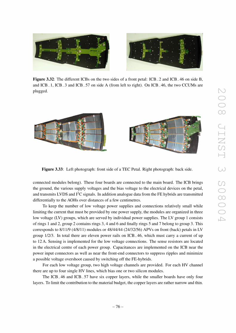
2008 JINST 3 S08004
Figure 3.32: The different ICBs on the two sides of a front petal: ICB−2 and ICB−46 on side B,and ICB−1, ICB−3 and ICB−57 on side A (from left to right). On ICB−46, the two CCUMs areplugged.
Figure 3.33: Left photograph: front side of a TEC Petal. Right photograph: back side.
connected modules belong). These four boards are connected to the main board. The ICB bringsthe ground, the various supply voltages and the bias voltage to the electrical devices on the petal,and transmits LVDS and I2C signals. In addition analogue data from the FE hybrids are transmitteddifferentially to the AOHs over distances of a few centimetres.
To keep the number of low voltage power supplies and connections relatively small whilelimiting the current that must be provided by one power supply, the modules are organized in threelow voltage (LV) groups, which are served by individual power supplies. The LV group 1 consistsof rings 1 and 2, group 2 contains rings 3, 4 and 6 and finally rings 5 and 7 belong to group 3. Thiscorresponds to 8/11/9 (4/8/11) modules or 48/44/44 (24/32/56) APVs on front (back) petals in LVgroup 1/2/3. In total there are eleven power rails on ICB−46, which must carry a current of upto 12 A. Sensing is implemented for the low voltage connections. The sense resistors are locatedin the electrical centre of each power group. Capacitances are implemented on the ICB near thepower input connectors as well as near the front-end connectors to suppress ripples and minimizea possible voltage overshoot caused by switching off the FE-hybrids.
For each low voltage group, two high voltage channels are provided. For each HV channelthere are up to four single HV lines, which bias one or two silicon modules.
The ICB−46 and ICB−57 have six copper layers, while the smaller boards have only fourlayers. To limit the contribution to the material budget, the copper layers are rather narrow and thin.
– 76 –

2008 JINST 3 S08004
The layer thickness amounts to 17 and 25 µm for the inner four and outer two layers, respectively,except for the innermost layer of boards ICB−1, ICB−3 and ICB−57 on front petals and ICB−1,ICB−2 and ICB−3 on back petals, which has a thickness of 35 µm. Digital and data traces areshielded by power and ground layers.
Two petals, one back and one front petal, are connected in a control ring. The front petal isthe first in the control loop. Both on back and front petals, rings 1–4 and 5–7 are connected to oneCCU, respectively. The Digital Opto-Hybrid (DOH) converts the optical signals to electrical LVDSsignals and vice versa. Two DOHs are located on a separate PCB, the Digital Opto-Hybrid Module(DOHM), which is mounted on the back petal. From the DOHM, which also distributes the powerfor the DOHs, electrical signals are transmitted to the CCUMs on the petal. For the control ring, aredundancy scheme is implemented on the ICB. Each CCU can be bypassed electrically in case ofa problem, so that the functionality of the control ring is maintained. The second DOH is neededfor redundancy purposes only. To allow also the last CCU on the ring to be bypassed, a fifth CCUis located on the DOHM. It is used only in this special case. However, if two consecutive CCUsare faulty, the complete control ring is lost.
Low-pass filters are implemented for the traces of the temperature signals that are brought outvia power cables, to ensure that noise is not coupled in via these lines. In addition to the thermistorslocated on the Kapton of the silicon modules, several temperature and humidity probes are locatedon or connected to the ICB. Two 10 kΩ NTC thermistors are located on ICB_46 on front petalsand read out via the power cable of low voltage group 2. Both on front and back petals, four 10 kΩ
NTC thermistors are glued to the cooling inserts of the ring 6 modules. They are read out via theDCU that is present on each CCUM. On both petal types, a humidity sensor can be connected toICB_46. For back petals, this sensor is read out via the power cable of LV group 2. On each z-side in total 12 hardwired humidity sensors are distributed over the TEC volume. For front petals,the humidity sensor is read out via the DCU on the CCUM. Front petals of all disks of the topand bottom sectors carry these additional humidity sensors, providing detailed information on therelative humidity along the z-direction.
Kapton cables of about 15 cm length are used to link the petals inside one control ring witheach other and with the DOHM, providing the electrical digital signals and the power for theCCUMs. These cables consist of two copper layers with a thickness of 35 µm each, separatedby a 100 µm thick polyimide layer.
Each TEC LV group is supplied by one so-called multiservice cable, which transmits theanalogue power and the bias voltage and brings out signals from temperature or humidity sensors.Inside the tracker support tube, power cables are arranged around the main TEC cooling pipes thatrun along the z direction, and end at the bulkhead. These cables implement silver-plated aluminiumconductors to minimize the impact on the material budget. Typical currents per cable range fromabout 5 A to 11 A, depending on the number of APVs connected. Therefore three cable types exist,with wire cross-sections tailored to the differing needs.
The connection from the bulkhead to the so-called patch panel 1, located outside of the trackervolume, is provided by power cables implementing tinned copper conductors. The control poweris transmitted via separate cables, which also break at the bulkhead. In this case tinned copperconductors are used both inside and outside the tracker volume.
– 77 –

2008 JINST 3 S08004
The grounding scheme
The so-called TEC common ground is located at the back end of each TEC. It is realized by meansof a 5 cm wide and 150 µm thick copper ring, which is glued to the outer radius of each backdisk and tied to the brackets that connect the tracker support tube to the hadron calorimeter. Thematerial of the hadron calorimeter represents a very solid ground. The shields of all cables, thereference points of all power groups, the cooling manifolds that are used to connect the coolingpipes of the petals to the main tubes that are mounted on the TEC, the CF skins of the disks andpetals and the outer aluminium shields of the TEC are connected to this TEC common ground. Onthe petal side, one common analogue ground is implemented per petal. This so-called local petalground is distributed via a 2 cm wide and 20 µm thick copper path along the ICBs as a referencerail. The LV and HV supplies of all power groups are referenced to this local petal ground at thegeometrical/electrical centre of each group. The digital ground of a control group is referencedonce to the local petal ground. The local petal ground of each petal is connected to the TECcommon ground. Copper strips glued to the outer radii of the disks and along the service channelsthat connect all disks with the back disk provide the electrical connection to the TEC commonground. These copper strips are connected via short copper braids to the ICBs on the petals. Thecarbon frames of the silicon detectors are connected via a conductive glue spot to the bias Kaptonand finally via the ICB to the FE hybrid ground. To avoid ground loops, the frames are electricallyinsulated from the cooling pipes by an anodized layer between the cooling inserts and the pipe.
3.3.7 Geometry and alignment
The deviation of true position and orientation of tracker modules from their nominal values asspecified in the engineering drawings depends on many factors with different origin, some of themtime-dependent: the achieved assembly precision, deformation due to tracker cooling, stress fromaccess and magnetic field, out-gassing of components in dry nitrogen. This leads to a degradationof the track parameter resolution (figure 3.4), which needs to be recovered by determining truemodule position and orientation, called alignment.
Alignment of the tracker relies on three key components: the various data about assemblygathered during the integration process, the Laser Alignment System and the alignment with tracks,ordered by increasing precision and availability with time.
For alignment purposes, modules with two sensors are treated as they would have one largesensor with identical active area coverage. This is justified by sensor mask design [36] and achievedsensor placement accuracy (figure 3.23).
The CMS tracker alignment task thus consists of the determination of three translational andthree rotational parameters for each of the 15 148 tracker modules. To achieve ultimate precision,it might be necessary to consider additional parameters, e.g. the sensor bow due to single-sidedprocessing.
Geometry
Two methods are mainly used for measuring tracker component assembly precision: survey withcoordinate measurement machines with a typical accuracy of a few µm to a few tens of µm, and
– 78 –

2008 JINST 3 S08004
Table 3.2: Estimated assembly precision (RMS, in µm) of tracker components. Values are givenwith respect to the next level in the hierarchy, e.g. the position accuracy of sensors in modules is10 µm.
TIB TID TOB TECSensor
10Sensor
10Sensor
10Sensor
10Module
180Module
54Module
30Module
20Shell
450Ring
185Rod
100Petal
70Cylinder
750Disc
350Wheel
140 (rφ ), 500 (z)Disc
150Tube Cylinder
450Tube
1000TEC
600Tube CMS Tube
photogrammetry with an accuracy of 150 µm (80 µm) under good (optimal) conditions for relativemeasurements. The measured and expected mounting precision from those data are summarized intable 3.2. It should be noted that structure deformations due to loading as well as temperature andhumidity variations have not been taken into account.
The software description of the position and orientation of the active detector volumes hasbeen validated with survey data and reconstructed tracks from test beams and cosmic muonsrecorded in various test and integration setups.
Laser Alignment System
The Laser Alignment System (LAS, figure 3.34) uses infrared laser beams with a wavelengthλ = 1075 nm to monitor the position of selected tracker modules. It operates globally on trackersubstructures (TIB, TOB and TEC discs) and cannot determine the position of individual modules.The goal of the system is to generate alignment information on a continuous basis, providing ge-ometry reconstruction of the tracker substructures at the level of 100 µm, which is mandatory fortrack pattern recognition and for the High Level Trigger. In addition, possible tracker structuremovements can be monitored at the level of 10 µm, providing additional input for the track basedalignment.
In each TEC, laser beams cross all nine TEC discs in ring 6 (ray 2) and ring 4 (ray 3) on backpetals, equally distributed in φ . Here special silicon sensors with a 10 mm hole in the backsidemetalization and an anti-reflective coating are mounted. The beams are used for the internal align-ment of the TEC discs. The other eight beams (ray 4), distributed in φ , are foreseen to align TIB,TOB, and both TECs with respect to each other. Finally, there is a link to the Muon system (ray 1),which is established by 12 laser beams (six on each side) with precise position and orientation inthe tracker coordinate system.
The signal induced by the laser beams in the silicon sensors decreases in height as the beamspenetrate through subsequent silicon layers in the TECs and through beam splitters in the align-
– 79 –

2008 JINST 3 S08004
Figure 3.34: Overview of the CMS Laser Alignment System.
ment tubes that partly deflect the beams on TIB and TOB sensors. To obtain optimal signals onall sensors, a sequence of laser pulses with increasing intensities, optimized for each position, isgenerated. Several triggers per intensity are taken and the signals are averaged. In total, a fewhundred triggers are needed to get a full picture of the alignment of the tracker structure. Since thetrigger rate for the alignment system is around 100 Hz, this will take only a few seconds. Thesedata will be taken at regular intervals, both in dedicated runs and during physics data taking.
Alignment with tracks
CMS pursues the development of two novel track-based alignment algorithms that allow to quicklysolve the system of linear equations of order O(100 000). The first is an extension to the well-known global Millepede algorithm [52], that takes all correlations into account and has been shownto successfully align the most sensitive 50 000 parameters. The second is a novel approach usinga Kalman Filter [53], which bridges the gap between global and local algorithms by taking intoaccount the most important correlations. In addition the HIP [54] algorithm, which is local in thesense that it takes into account only correlations of parameters within a module, is developed inparallel. In this algorithm, correlations between modules are dealt with implicitly by iterating thealignment many times. All three methods are expected to be able to provide alignment constantsfor the full silicon pixel and strip tracker.
Experience from other experiments has shown that collision data are not sufficient to constraincertain correlated module movements well enough to obtain a unique set of alignment constants.Therefore complementary data and constraints need to be exploited. Examples are tracks fromcosmic muons (with and without magnetic field) that constrain the tracker barrel modules, or beamhalo muons for the endcap. Beam gas and minimum bias events are also under consideration.Typical examples of constraints are a vertex constraint for decay particles e.g. from Z → µ+µ−
or jets, mass constraints, measurements from the Laser Alignment System, and survey constraints.First studies indicate that those data will provide a unique alignment parameter set.
– 80 –

2008 JINST 3 S08004
disk number1 2 3 4 5 6 7 8 9
[m
rad
]φ∆
-0.2
-0.15
-0.1
-0.05
-0
0.05
0.1
0.15
0.2
disk number1 2 3 4 5 6 7 8 9
x [m
m]
∆
-0.3
-0.2
-0.1
0
0.1
0.2
0.3
disk number1 2 3 4 5 6 7 8 9
y [m
m]
∆
-0.3
-0.2
-0.1
0
0.1
0.2
0.3LASSurveyCosmics
Figure 3.35: TEC+ disk rotation ∆φ (around the beam axis) and displacements ∆x,∆y (in the diskplane) as determined from survey, LAS and cosmic muon tracks.
During integration of the TEC+, deviation of disk positions and rotations from nominal val-ues have been determined from survey with photogrammetry, the LAS, and tracks from cosmicmuons. Figure 3.35 shows the results from the three complementary methods. The global degreesof freedom (absolute position and orientation, torsion and shear around the symmetry axis) havebeen fixed by requiring the average displacement and rotation as well as torsion and shear to bezero. The values agree within 60 µm and 80 µrad with each other, which can be taken as an uppervalue on the precision of each method.
3.3.8 Detector control and safety system
The Tracker Detector Safety System (TDSS) and tracker Detector Control System (tracker DCS) isa two pillar system. The TDSS ensures independently the safety, with a large PLC (ProgrammableLogical Controller) system, occupying 6 LHC racks. A limited set of around 1000 hardwiredtemperature and humidity sensors are evaluated and out of limit states interlock power supplies.The tracker DCS, as a complementary partner, controls, monitors and archives all importantparameters. The heart of the DCS is composed out of an industrial SCADA program (SupervisoryControl And Data Acquisition) PVSS (Prozessvisualisierungs- und Steuerungssystem from ETMAustria, chapter 9) together with a Finite State Machine written in SMI++, a derivative of theformer DELPHI control software; thus using the standard control software framework for allLHC experiments. The main task of the DCS is to control about 2000 power supplies for siliconmodule low and high voltage power and about 100 low voltage control power supplies via theOPC (OLE for Process Automation) protocol. Detector interdependencies of control, low andhigh voltages are handled, as well as fast ramp downs in case of higher than allowed temperaturesor currents in the detector, experimental cavern problems, etc. All this is ensured by evaluating104 power supply parameters, 103 data points from DSS via a Siemens S7 driver and 105 readingsfrom the DCUs situated on all front end hybrids and control units CCUs. Several passive alarmsand warning levels are defined for temperature, relative humidity, voltages, currents, etc. and arereported in a global warning panel as well as limits that, if surpassed, would result in automaticshutdown. Information from the tracker cooling plant, the thermal screen, beam conditions andthe dry gas system are crucial for safe running and are accessible from the tracker DCS and TDSS.
– 81 –

2008 JINST 3 S08004
All parameters are archived to ORACLE. The TDSS (tracker DCS) system is fully implementedin the global CMS DSS (DCS) and Run Control system.
3.3.9 Operating experience and test results
Performance in test beam experiments
The system performance of integrated structures of the silicon strip tracker and its data acquisitionchain as well as the performance of the silicon strip modules themselves has been studied in varioustest beam experiments at CERN and the Paul Scherrer Institut (PSI), Villigen (CH). In test beamcampaigns, performed in May and October 2004 at the X5 test beam complex in the CERN westarea, large substructures of TIB, TOB and TEC were exposed to a secondary pion beam with anenergy of 120 GeV and a tertiary muon beam with muon energies ranging from 70 to 120 GeV.The TIB setup comprised a prototype half-shell structure of layer 3, equipped with eight single-sided strings, plus four double-sided strings, mounted on a custom support structure. For the TOB,the so-called cosmic rack, a precise mechanical telescope-like structure equipped with four single-sided and two double-sided rods, was used in the beam tests. The TEC setup consisted of oneback and one front petal [55]. These setups corresponded to about 1% of the complete TIB, TOBand TEC detectors, respectively. The TOB and TEC setups were operated at a temperature below−10°C, while the TIB setup was operated at room temperature. Typical primary trigger rates forthe pion beam were 600 000 pions per spill (a 2.2 s long period within a 12 s long SPS cycle duringwhich particles are delivered) corresponding to a mean occupancy of 15 Hz/cm2.
In the strip-cluster finding the cuts for the signal-to-noise ratio, S/N, of the cluster seed /neighbour strips / total cluster are 4/3/5 for TIB, 5/2/5 for TOB and 3/2/5 for TEC, respectively.The cluster noise is calculated by adding the single strip noise values in quadrature (TIB, TEC) orby taking the seed noise as the cluster noise (TOB). To determine the most probable value for theS/N of a module, a Landau distribution convoluted with a Gaussian is fitted to the signal-to-noisedistribution, and the most probable value of the fitted function is quoted as the S/N.
The mean most probable S/N values for all module types, together with their strip length,pitch and abbreviations used in the following, are summarized in table 3.3. For thin (thick) TECsensors, most probable S/N values of 29–33 (36–42) in peak mode and 19–22 (20–24) in deconvo-lution mode have been observed [55]. For the thick TOB OB1 (OB2) modules a S/N of typically 36(38) and 25 (27) was found in peak and deconvolution mode, respectively [17], while the thin TIBIB1 (IB2) modules exhibited a S/N of 26 (30) in peak mode and 18 (20) in deconvolution mode.
Assuming that a MIP creates 24 000 electrons in a 300 µm thick layer of silicon [16], andassuming that the beam particles can be treated as MIPs, the S/N can be used to calculate theequivalent noise charge, ENC. The common mode subtracted noise depends on the capacitanceof the sensor, which depends linearly on the strip length and the ratio between strip width andpitch, w/p [16]. Since w/p = 0.25 for all sensor types, the ENC varies between different moduletypes according to the strip length. Results for all module types except W1TID are summarized intable 3.3. Measurements performed at low temperature (for the TEC, typically hybrid temperaturesof +10°C and 0°C were reached for hybrids with six and four APVs, respectively) are plottedversus the strip length in figure 3.36. A linear fit to these data yields the following dependence of
– 82 –

2008 JINST 3 S08004
the ENC on the strip length L:
ENCpeak = (36.6±1.9)e−/cm ·L+(405±27)e−,
ENCdec = (49.9±3.2)e−/cm ·L+(590±47)e−.
The common mode noise is the standard deviation of the common mode, calculated per APVfrom a certain number of events. The mean common mode noise has been evaluated and amounts to(173±38) and (299±76) electrons for TEC (mean from all APVs in the setup) and (265±36) and(300± 19) electrons for TIB (mean from all APVs of TIB2 modules) in peak and deconvolutionmode, respectively.
Although no dedicated beam telescope was available, efficiency studies have been performedboth with the TOB and TEC setups, exploiting the fact that in both cases the beam penetratedseveral layers of modules. Efficiencies of above 99% have been observed in all such studies.
The uniformity of the module performance along and perpendicular to the strip direction hasbeen studied in 2003 with several TIB modules in a test beam experiment at the X5 complex. Twosingle-sided strings equipped with IB2 modules were mounted on a structure corresponding to aportion of a layer 3 half-shell, and operated at room temperature. To study the uniformity across thestrips, the strips read out by three APVs (on two different modules) were exposed to a pion beam,and between 1000 and 8000 events were collected per strip. A cluster was associated to a strip if thecentre of gravity x of the cluster was reconstructed within (n−0.5) · p < x < (n+0.5) · p for strip nand pitch p. The uniformity, defined as the ratio between the RMS and the mean of the respectivedistribution, was 1.3% for the cluster noise, with an increase close to the APV chip edges. Thecluster charge uniformity was of the order of 1.4%, but dropped to 0.5% if calculated separatelyfor groups of 32 adjacent strips. A uniformity of the S/N of 1.6% on average and of 1.0% forgroups of 32 strips was measured. To investigate the uniformity along the strips, a muon beam wasused for its uniform particle density. The cluster position along the strip could be obtained from theTOB setup that was operated in the same test beam, since the strip direction of the TOB moduleswas perpendicular to that of the TIB modules. The clusters were binned in 24 intervals accordingto their centre of gravity, corresponding to length intervals of 5 mm, and about 1500 events wereaccumulated per bin. Both the uniformity of cluster charge and S/N were found to be 1.4%.
Performance during integration
Testing during integration consisted typically of checks of the control ring functionality, tests of theI2C communication of all chips, tests of the gain of the optical connections, commissioning (i.e.tuning of chip operation parameters), pedestal runs in peak and deconvolution mode, bias voltageramping up to 450 V, read-out of currents and module and hybrid temperatures through the DCUs,and a functionality check of the temperature and humidity sensors.
In the following sections the performance of TEC, TIB/TID and TOB during integration isdescribed. Two comments apply to all three sub-detectors:
• Numbers of dead and noisy strips are given below. While dead strips can be identified reli-ably, the noisiness of strips depends on external conditions such as grounding and the APVread-out mode and the figures given should be regarded as estimates only. APV edge strips
– 83 –

2008 JINST 3 S08004
Table 3.3: Pitch, strip length, signal-to-noise ratio and equivalent noise charge after commonmode subtraction for different module types. The TEC and TOB measurements are for hybridtemperatures of below 0 C, the TIB measurements were performed at room temperature. Sensorsof type IB1 and IB2 are used in TIB, layers 1 and 2 and layers 3 and 4, respectively. In theTOB, layers 1–4 are equipped with OB2 sensors, layers 5 and 6 with OB1 sensors. The sensorgeometries abbreviated with W are wedge-shaped sensors used in TEC and TID, with the numbercorresponding to the ring. W1 sensors have a slightly different geometry in TID and TEC.
Module Pitch Strip length S/N S/N ENC [e−] ENC [e−]type [µm] [mm] Peak mode Dec. mode Peak mode Dec. modeIB1 80 116.9 25.8 ± 1.3 18.3 ± 0.5 931 ± 48 1315 ± 37IB2 120 116.9 29.5 ± 1.4 20.3 ± 0.6 815 ± 37 1182 ± 31OB1 122 183.2 36 25 1110 ± 47 1581 ± 75OB2 183 183.2 38 27 1057 ± 17 1488 ± 22W1TEC 81–112 85.2 33.1 ± 0.7 21.9 ± 0.6 714 ± 23 1019 ± 37W2 113–143 88.2 31.7 ± 0.5 20.7 ± 0.4 741 ± 25 1068 ± 51W3 123–158 110.7 29.2 ± 0.6 20.0 ± 0.4 802 ± 16 1153 ± 48W4 113–139 115.2 28.6 ± 0.5 19.2 ± 0.3 819 ± 21 1140 ± 26W5 126–156 144.4 42.2 ± 1.1 24.1 ± 1.1 971 ± 29 1354 ± 57W6 163–205 181.0 37.8 ± 0.6 23.0 ± 0.4 1081 ± 26 1517 ± 47W7 140–172 201.8 35.5 ± 1.0 20.3 ± 1.1 1155 ± 40 1681 ± 107
Strip length [cm]8 10 12 14 16 18 20
]-Co
mm
on m
ode
subt
ract
ed n
oise
[e
700
800
900
1000
1100
1200
/ ndf 2χ 4.428 / 7p0 27.34± 405 p1 1.942± 36.55
/ ndf 2χ 4.428 / 7p0 27.34± 405 p1 1.942± 36.55
Peak mode
Strip length [cm]8 10 12 14 16 18 20
]-Co
mm
on m
ode
subt
ract
ed n
oise
[e
1000
1100
1200
1300
1400
1500
1600
1700
1800
/ ndf 2χ 4.567 / 7p0 47.23± 589.9 p1 3.2± 49.88
/ ndf 2χ 4.567 / 7p0 47.23± 589.9 p1 3.2± 49.88
Deconvolution mode
Figure 3.36: Equivalent noise charge after common mode subtraction versus strip length for allTOB and TEC module types, in peak (left panel) and deconvolution mode (right panel).
show typically an increased noise and are frequently flagged as noisy, especially when afixed noise cut is used for all strips. These edge strips are included in the numbers of flaggedstrips, although they are usually fully efficient.
• Although all components (petals, rods, single modules in case of the TIB/TID) were testedbefore insertion and components not fulfilling strict quality criteria were rejected, severaldefects have been observed during integration. Typical defects are broken optical fibers, badAPVs (i.e. with many noisy or dead strips), and missing or unreliable I2C communication
– 84 –

2008 JINST 3 S08004
of complete modules or single chips. Most of the problems are assumed to be caused bymishandling during insertion or cabling. Since the exchange of components bears a consid-erable risk, not all defective components have been exchanged. Additional defects could beintroduced by any following handling step, such as cabling of the tracker. The numbers givenbelow should thus be regarded as a snapshot reflecting the situation right after integration ofthe single sub-detectors.
TEC Performance during integration
The TEC petals were integrated sector-wise, where one sector corresponds to one eighth of a TECin φ , and comprises 18 petals that share nine control rings and four cooling circuits. After integra-tion of one sector, a read-out test of the full sector was performed at room temperature, with thecoolant at +15°C and mean silicon and hybrid temperatures of about +23°C and +33°C, respec-tively.
During integration a flaw in the crimping of the connectors of the multiservice power cableswas found. After all such connectors had been replaced on both TECs, the system performanceobserved during integration was very robust. In figure 3.37, left side, the common mode subtractednoise of all strips of both TECs is shown for deconvolution mode. Since the measured noisedepends on the gain of the optical chain, the noise was normalized to the digital output of theAPV (scale on upper x-axis in figure 3.37). In addition, the number of ADC counts in the FED wasconverted to ENC according to the following method: with a nominal digital APV output of± 4 mAand a nominal APV gain of 1 MIP/mA for thin sensors, the height of the digital output correspondsto 8 MIPs or 200 000 electrons. This method allows a direct comparison of the measurements fromdifferent optical channels and delivers an approximate absolute calibration of the equivalent noisecharge. Cross-checks with cosmic muon data performed during TIB/TID integration indicate thatthis scaling agrees with the real ENC within 10–20%. Furthermore, the noise depends on the stripcapacitance and thus on the strip length, i.e. on the module type. For this reason the noise of allstrips was normalized to the strip length of modules of ring 1 (8.52 cm). In addition a correction wasapplied to TEC- data to account for the fact that they were taken with other chip parameter settingsthan TEC+ data. The common mode subtraction was performed assuming a constant commonmode per APV. To extract the mean noise, a gaussian was fitted to the distribution. The resultingmean common mode subtracted noise amounts to 1693 ± 75 electrons in this normalization.
The mean common mode noise, calculated per APV, amounts to (22± 4)% and (21± 3)%of the mean intrinsic noise in peak and deconvolution mode, respectively (figure 3.38, left, for allnon-defective APVs of TEC+).
The flatness of the noise across the APV is a good indicator for the quality of the grounding.The relative spread of the total noise (before common mode subtraction), i.e. the RMS of the noisedivided by the mean noise, both calculated per APV, can be used to quantify the flatness. Therelative spread is (2.5± 0.2)% in both read-out modes, as shown in figure 3.38, right, indicatingthat the grounding scheme implemented by the TEC works well.
Strips are counted as noisy or dead if their noise is more than five times the RMS of thenoise above or below the mean noise of the respective APV. Edge strips are counted as noisy, if
– 85 –

2008 JINST 3 S08004
]-Scaled noise [e0 500 1000 1500 2000 2500 3000 3500 4000
Num
ber
of st
rips
1
10
210
310
410
5103861760 entries Mean = 1693 e - Width = 75 e -
[ADC counts]0 2 4 6 8 10 12
]-Scaled noise [e0 500 1000 1500 2000 2500 3000 3500 4000
Num
ber
of st
rips
1
10
210
310
410
510
]-Scaled noise [e0 500 1000 1500 2000 2500 3000 3500 4000
Num
ber
of st
rips
1
10
210
310
410
510 3081216 entries-Mean = 2049 e
-Width = 112 e
[ADC counts]0 2 4 6 8 10 12
Figure 3.37: Normalized common mode subtracted noise of all strips (scaled to the strip lengthof ring 1 sensors) of both TECs (left panel) and the TOB (right panel), in deconvolution mode.Details are described in the text.
Relative common mode noise0 0.1 0.2 0.3 0.4 0.5 0.6 0.7 0.8 0.9 1
Num
ber
of A
PVs
1
10
210
310
410Number of entries = 15070
Peak Mode 0.04)±Mean = (0.22
Deconvolution Mode 0.03)±Mean = (0.21
Relative RMS of total noise0 0.02 0.04 0.06 0.08 0.1
Num
ber
of A
PVs
1
10
210
310
410Number of entries = 15070
Peak Mode 0.002)±Mean = (0.025
Deconvolution Mode 0.002)±Mean = (0.025
Figure 3.38: Ratio between common mode noise and mean intrinsic noise (left panel) and ratiobetween the RMS of the total noise and the mean total noise (right panel), calculated per APV, inpeak and deconvolution mode for all non-defective APVs of TEC+.
their noise is more than seven sigma above the mean noise. In total, there are 3.0 per mille of badchannels in TEC+, while TEC- has 2.7 per mille of bad channels.
TIB and TID performance during integration
During TIB/TID integration [56], modules and AOHs were assembled onto half layers and disksand tested extensively for functionality, including pedestals, once a mother cable was completed(corresponding to a string in the TIB and three single-sided or five double-sided modules in theTID). Completed disks and half layers were then subjected to a burn-in in a climatic chamber,during which the structures were operated at a silicon sensor temperature of about −15°C. Thecomplete half layers and disks were read out during these tests. Typically, the structures underwent2–3 cooling cycles during a five day measurement period. After-wards disks and half layers wereassembled into the complete TIB/TID+ and TIB/TID- structures and shipped to CERN, where thelast integration operations were performed, such as connection of fibers to the final ribbons andcabling of the margherita.
– 86 –

2008 JINST 3 S08004
After optimization of the grounding scheme, the noise performance observed in the TIB andTID structures was very good. For the TIB and TID structures the scaled common mode subtractednoise of all strips, except for two TIB half-shells for which data were taken under non-final runningconditions and three half-shells for which the proper grounding scheme was not yet implemented,is shown in figure 3.39 for deconvolution mode. Scaling and common mode subtraction have beenimplemented as previously described in this section. These data have been taken under nominalCMS conditions, with a mean silicon sensor temperature of about −15°C, hybrid temperaturesranging from −4°C (TID double-sided modules) to −14°C (TIB single-sided modules) and APVparameters set as intended for this temperature range. The mean noise, taken from a gaussianfit, amounts to (1233± 87) electrons in the TIB and (1246± 76) electrons in the TID. Measure-ments with a silicon sensor temperature of about +10°C and hybrid temperatures of +10C to+30°C show a mean noise about 20% larger. In contrast to the TEC, a strip is flagged as deadif its noise is below 75% of the average noise of the APV, and APV edge strips are not treateddifferently. The total number of bad channels is 4.4 per mille in TIB/TID+ and 3.4 per mille inTIB/TID-.
TOB performance during integration
Fully equipped and tested rods were integrated cooling segment-wise. After a first functional test,the cooling connection was soldered and a leak test was performed. Then the cooling segment wascabled, and a full read-out test, including pedestals, was performed at room temperature. Duringthese measurements, the silicon sensor temperature was about +24°C and the hybrid temperatureabout +30°C.
During integration, a sensitivity to pick-up noise has been observed, which leads to non-flat,wing-like common mode subtracted noise distributions. This sensitivity is especially pronouncedfor layers 3 and 4, which are equipped with single-sided 4 APV modules, and within these layersthe effect is worst for modules mounted closest to the CCUM. Defining as a figure of merit the ratioof the highest noise amplitude (taken from a parabola fit to the noise distribution) to the flat noisebaseline, and counting all APVs with a ratio above 1.25 as “in the wings”, the fraction of APVs inthe wings is about 30% in layers 3 and 4 and about 7% and 1% in layers 1/2 and 5/6, respectively.In total, 11.4% of all APVs are found to be in the wings according to this criterion. It has beenverified that either with adjusted cluster cuts or with a linear online common mode subtraction theincrease in the cluster width and occupancy is negligible.
The normalized noise of all TOB strips is shown in figure 3.37, right. The tail to high noisevalues comes from the non-flat noise distributions. The mean noise from a gaussian fit amounts to(2049±112) electrons.
Due to this wing-like noise structure, a special algorithm has been adopted to evaluate thenumber of dead and noisy strips. A parabola is fitted to the noise distribution of each APV in aniterative procedure, and strips are flagged as bad if their noise deviates more than ten times theRMS of the distribution of fit residuals from the fitted function.
Only very few permanent defects, corresponding to 0.6 per mille of lost channels, have beenintroduced during TOB integration. Including the number of noisy and dead strips, the number ofbad channels amounts to 0.6 per mille in TOB+ and 1.9 per mille in TOB-.
– 87 –

2008 JINST 3 S08004
Figure 3.39: Normalized common mode subtracted single strip noise for TIB (left panel) and TID(right panel), in deconvolution mode. Details are described in the text.
Irradiation studies
As already discussed in detail in section 3.1.1, the silicon strip tracker will suffer from a severelevel of radiation during its 10 year long lifetime: up to 1.8×10¹⁴ neqcm−2 for TIB/TID and TECand up to 0.5×10¹⁴ neqcm−2 for TOB, assuming an integrated luminosity of 500 fb−1. The radialand z dependence of the fluence both for fast hadrons and neutrons is described in detail in [15, 16].Hadrons are expected to dominate in the inner part of the tracker, up to a radius of about 0.5 m,while neutrons backscattered off the electromagnetic calorimeter dominate further outside. Safetyfactors of 1.5 and 2.0 on the fluence are typically applied for TIB/TID and TOB/TEC, respectively.
To ensure that both the FE electronics and the silicon sensors can be operated safely andwith satisfactory performance after such an irradiation, several irradiation tests with neutrons andprotons have been carried out. Neutron irradiation was usually performed at the isochronous cy-clotron of the Centre de Recherches du Cyclotron, Louvain-la-Neuve, which delivers neutrons witha mean energy of 20 MeV (hardness factor 1.95 relative to 1 MeV neutrons [58]). Proton irradiationhas been carried out e.g. at the compact cyclotron of the Forschungszentrum Karlsruhe, where a26 MeV proton beam (hardness factor 1.85 relative to 1 MeV neutrons) with a current of 100 µAand a beam spot diameter of 1 cm is available.
To study the performance of complete irradiated modules, several OB1 and OB2 modules(table 3.3 for explanation) were irradiated with a proton fluence ranging from 0.1×10¹⁴ neqcm−2
to 0.7 × 10¹⁴ neqcm−2, and one OB2 module was subjected to a neutron fluence of about1.2 × 1014 neqcm−2 [57]. Two TEC W5 modules were irradiated with a proton fluence ofabout 1.1× 10¹⁴ neqcm−2, and three TIB IB1 modules were subjected to a proton fluence of0.5× 1014 neqcm−2 to 2.1× 10¹⁴ neqcm−2. The effect of annealing was simulated by heating themodules for 80 minutes at 60°C and afterwards storing them at room temperature for at least twohours. To prevent uncontrolled annealing, the modules were stored at −20°C between the irradia-tion or annealing steps. Measurements were performed at −15°C.
As expected from inversion from n- to p-type doping, the full depletion voltage increasedwith the fluence, as shown in figure 3.40 (left). However, the required depletion voltage staysbelow 500 V, which is the maximum depletion voltage for which the sensors are specified. Thedependence of the depletion voltage on annealing time was studied as well and found to be in
– 88 –

2008 JINST 3 S08004
]2/cmeq n14Fluence [100 0.5 1 1.5 2 2.5
Dep
letio
n vo
ltage
[V]
0
100
200
300
400
500
600
]2/cmeqn14Fluence [100 0.2 0.4 0.6 0.8 1 1.2 1.4
]3Cu
rren
t den
sity
[mA/
cm
0
0.5
1
1.5
2
2.5
3
3.5
4
4.5
5
Figure 3.40: Left panel: Variation of depletion voltage with fluence for OB1 (triangles), OB2and W5 (dots on upper curve) and IB2 (dots on lower curve) modules, after an annealing time of80 minutes after each irradiation step. The curves correspond to calculations for 500 µm (uppercurve) and 320 µm (lower curve) sensors for an annealing time of 80 minutes at 60°C. Right panel:Current density, scaled to 20°C, versus fluence after annealing for 80 minutes at 60°C.
]2/cmeqn14Fluence [100 0.2 0.4 0.6 0.8 1 1.2 1.4
Sign
al-to
-noi
se ra
tio
0
5
10
15
20
25
30
35
SNR versus fluence proton irradiated (peak)proton irradiated (dec)neutron irradiated (peak)neutron irradiated (dec)
]2/cmeqn14Fluence [100 0.5 1 1.5 2 2.5
Sign
al-to
-noi
se ra
tio
0
5
10
15
20
25
30
SNR versus fluence peak modedeconvolution mode
Figure 3.41: Signal-to-noise ratio versus fluence for modules with 500 µm (left panel) and 320 µmthick sensors (right panel) in peak (filled symbols) and deconvolution mode (open symbols).
excellent agreement with the Hamburg model [59], with a minimum at 80 minutes annealing time,corresponding to a 10 day shut down period at room temperature.
The leakage current is expected to increase with fluence, leading to a larger heat dissipationand increased noise. In figure 3.40 (right) the dependence of the current density on the fluence isshown. The current related damage rate, defined as the current increase, scaled to 20°C, per sensorvolume and equivalent neutron fluence, amounts to (3.79±0.27)×10−17 A/cm, which is in goodagreement with literature and measurements from test structures.
Measurements of the signal-to-noise ratio, S/N, of irradiated modules have been performedwith a 90Sr source. Due to an increase of the noise and a decrease of the charge collection efficiency,the S/N is expected to decrease with fluence. The dependence of the S/N on the accumulatedfluence for thick and thin sensors in both read-out modes is shown in figure 3.41. For thick sensors,the S/N decreased from 23 (35) to 15 (21) in deconvolution (peak) mode, while for thin sensorsa decrease from 18 (24) to 13 (18) was observed. These figures ensure a hit finding efficiency ofabove 95% even after 10 years of operation at the LHC [60, 61].
– 89 –

2008 JINST 3 S08004
Chapter 4
Electromagnetic calorimeter
The electromagnetic calorimeter of CMS (ECAL) is a hermetic homogeneous calorimeter made of61200 lead tungstate (PbWO4) crystals mounted in the central barrel part, closed by 7324 crys-tals in each of the two endcaps. A preshower detector is placed in front of the endcap crystals.Avalanche photodiodes (APDs) are used as photodetectors in the barrel and vacuum phototriodes(VPTs) in the endcaps. The use of high density crystals has allowed the design of a calorimeterwhich is fast, has fine granularity and is radiation resistant, all important characteristics in the LHCenvironment. One of the driving criteria in the design was the capability to detect the decay to twophotons of the postulated Higgs boson. This capability is enhanced by the good energy resolutionprovided by a homogeneous crystal calorimeter.
4.1 Lead tungstate crystals
The characteristics [62] of the PbWO4 crystals make them an appropriate choice for operation atLHC. The high density (8.28 g/cm3), short radiation length (0.89 cm) and small Molière radius(2.2 cm) result in a fine granularity and a compact calorimeter. In recent years, PbWO4 scintil-lation properties and other qualities have been progressively improved, leading to the mass pro-duction of optically clear, fast and radiation-hard crystals [63, 64]. The scintillation decay timeof these production crystals is of the same order of magnitude as the LHC bunch crossing time:about 80% of the light is emitted in 25 ns. The light output is relatively low and varies with tem-perature (−2.1%C−1 at 18°C [65]): at 18°C about 4.5 photoelectrons per MeV are collected inboth APDs and VPTs. The crystals emit blue-green scintillation light with a broad maximum at420–430 nm [64, 66]. Longitudinal optical transmission and radioluminescence spectra are shownin figure 4.1.
To exploit the total internal reflection for optimum light collection on the photodetector, thecrystals are polished after machining. For fully polished crystals, the truncated pyramidal shapemakes the light collection non-uniform along the crystal length. The effect is large because of thehigh refractive index (n = 2.29 around the peak wavelength [67]) and the needed uniformity [68]is achieved by depolishing one lateral face. In the endcaps, the light collection is naturally moreuniform because the crystal faces are nearly parallel. Pictures of barrel and endcap crystals withthe photodetectors attached are shown in figure 4.2.
– 90 –

2008 JINST 3 S08004
Figure 4.1: Longitudinal optical transmission (1, left scale) and radioluminescence intensity (2,right scale) for production PbWO4 crystals.
Figure 4.2: PbWO4 crystals with photodetectors attached. Left panel: A barrel crystal with theupper face depolished and the APD capsule. In the insert, a capsule with the two APDs. Rightpanel: An endcap crystal and VPT.
The crystals have to withstand the radiation levels and particle fluxes [69] anticipated through-out the duration of the experiment. Ionizing radiation produces absorption bands through theformation of colour centres due to oxygen vacancies and impurities in the lattice. The practicalconsequence is a wavelength-dependent loss of light transmission without changes to the scintil-lation mechanism, a damage which can be tracked and corrected for by monitoring the opticaltransparency with injected laser light (section 4.9). The damage reaches a dose-rate dependentequilibrium level which results from a balance between damage and recovery at 18°C [64, 70].
– 91 –

2008 JINST 3 S08004
To ensure an adequate performance throughout LHC operation, the crystals are required to exhibitradiation hardness properties quantified as an induced light attenuation length (at high dose rate)greater than approximately 3 times the crystal length even when the damage is saturated. Hadronshave been measured to induce a specific, cumulative reduction of light transmission, but the ex-trapolation to LHC conditions indicates that the damage will remain within the limits required forgood ECAL performance [71, 72].
4.2 The ECAL layout and mechanics
The barrel part of the ECAL (EB) covers the pseudorapidity range |η | < 1.479. The barrel gran-ularity is 360-fold in φ and (2×85)-fold in η , resulting in a total of 61200 crystals. The crystalshave a tapered shape, slightly varying with position in η . They are mounted in a quasi-projectivegeometry to avoid cracks aligned with particle trajectories, so that their axes make a small angle(3o) with respect to the vector from the nominal interaction vertex, in both the φ and η projec-tions. The crystal cross-section corresponds to approximately 0.0174 × 0.0174 in η-φ or 22×22mm2 at the front face of crystal, and 26×26 mm2 at the rear face. The crystal length is 230 mmcorresponding to 25.8 X0. The barrel crystal volume is 8.14 m3 and the weight is 67.4 t.
The centres of the front faces of the crystals are at a radius 1.29 m. The crystals are containedin a thin-walled alveolar structure (submodule). The alveolar wall is 0.1 mm thick and is made of analuminium layer, facing the crystal, and two layers of glass fibre-epoxy resin. To avoid oxidation,a special coating is applied to the aluminium surface. The nominal crystal to crystal distance is0.35 mm inside a submodule, and 0.5 mm between submodules. To reduce the number of differenttypes of crystals, each submodule contains only a pair of shapes, left and right reflections of a singleshape. In total, there are 17 such pairs of shapes. The submodules are assembled into modules ofdifferent types, according to the position in η , each containing 400 or 500 crystals. Four modules,separated by aluminium conical webs 4-mm thick, are assembled in a supermodule, which contains1700 crystals (figures 4.3 and 4.4).
In each module, the submodules are held in partial cantilever by an aluminium grid, whichsupports their weight from the rear. At the front the submodule free ends are connected togetherby pincers that cancel the relative tangential displacements. The submodule cantilever is reducedby the action of a 4-mm thick cylindrical plate where the front of the submodules are supportedby setpins. Not all the submodules are connected to the cylindrical plate but only four rows in φ
from a total of ten. The portion of the submodule load taken at the front by the cylindrical plateis transmitted to the aluminium grids of the different modules via the conical webs interspacedbetween the modules [73]. Each module is supported and positioned in the supermodule at therear end through the grid by a spine beam. The spine is provided with pads which slide into railshoused on the front face of the HCAL barrel, allowing the installation and support of each singlesupermodule. The cylindrical plate in front of the supermodule also provides the fixation of themonitoring system (see below) and the holes for its optical fibres.
All services, cooling manifolds and cables converge to a patch panel at the external end ofthe supermodule. Eighteen supermodules, each covering 20 in φ , form a half barrel.
The endcaps (EE) cover the rapidity range 1.479 < |η | < 3.0. The longitudinal distancebetween the interaction point and the endcap envelope is 315.4 cm, taking account of the estimated
– 92 –

2008 JINST 3 S08004
Crossplate
Crossplate
AluminumGrid
Alveolarstructure
TabletModule 1
Module 2
Module 4
Module 3
Connectors
Crystals
Web 1F
Web 1R
Web 2
Web 3
Web 4
Web 1F
Web 1R
Web 2
Web 3
Web 4
Cylindricalplate
Figure 4.3: Layout of the ECAL barrel mechanics.
shift toward the interaction point by 1.6 cm when the 4-T magnetic field is switched on. The endcapconsists of identically shaped crystals grouped in mechanical units of 5×5 crystals (supercrystals,or SCs) consisting of a carbon-fibre alveola structure. Each endcap is divided into 2 halves, orDees. Each Dee holds 3 662 crystals. These are contained in 138 standard SCs and 18 specialpartial supercrystals on the inner and outer circumference. The crystals and SCs are arranged in arectangular x-y grid, with the crystals pointing at a focus 1 300 mm beyond the interaction point,giving off-pointing angles ranging from 2 to 8 degrees. The crystals have a rear face cross section30×30 mm2, a front face cross section 28.62×28.62 mm2 and a length of 220 mm (24.7 X0). Theendcaps crystal volume is 2.90 m3 and the weight is 24.0 t. The layout of the calorimeter is shownin figure 4.5. Figure 4.6 shows the barrel already mounted inside the hadron calorimeter, whilefigure 4.7 shows a picture of a Dee.
The number of scintillation photons emitted by the crystals and the amplification of the APDare both temperature dependent. Both variations are negative with increasing temperature. Theoverall variation of the response to incident electrons with temperature has been measured in testbeam [74] to be (−3.8±0.4)%C−1. The temperature of the system has therefore to be maintainedconstant to high precision, requiring a cooling system capable of extracting the heat dissipated bythe read-out electronics and of keeping the temperature of crystals and photodetectors stable within±0.05C to preserve energy resolution. The nominal operating temperature of the CMS ECAL is18°C. The cooling system has to comply with this severe thermal requirement. The system employswater flow to stabilise the detector. In the barrel, each supermodule is independently supplied
– 93 –
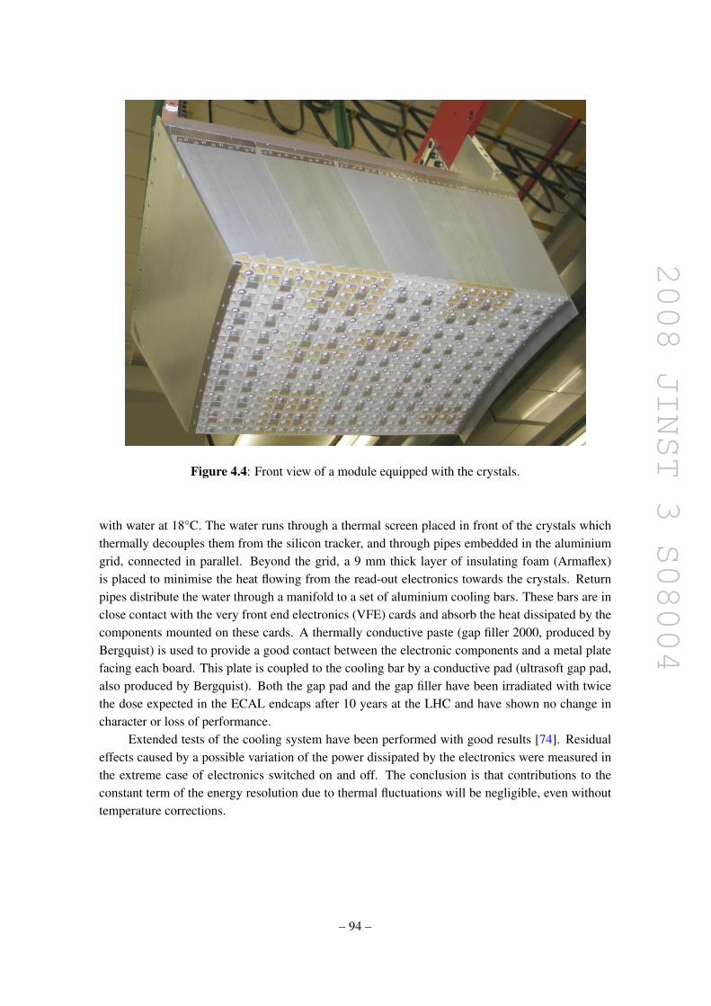
2008 JINST 3 S08004
Figure 4.4: Front view of a module equipped with the crystals.
with water at 18°C. The water runs through a thermal screen placed in front of the crystals whichthermally decouples them from the silicon tracker, and through pipes embedded in the aluminiumgrid, connected in parallel. Beyond the grid, a 9 mm thick layer of insulating foam (Armaflex)is placed to minimise the heat flowing from the read-out electronics towards the crystals. Returnpipes distribute the water through a manifold to a set of aluminium cooling bars. These bars are inclose contact with the very front end electronics (VFE) cards and absorb the heat dissipated by thecomponents mounted on these cards. A thermally conductive paste (gap filler 2000, produced byBergquist) is used to provide a good contact between the electronic components and a metal platefacing each board. This plate is coupled to the cooling bar by a conductive pad (ultrasoft gap pad,also produced by Bergquist). Both the gap pad and the gap filler have been irradiated with twicethe dose expected in the ECAL endcaps after 10 years at the LHC and have shown no change incharacter or loss of performance.
Extended tests of the cooling system have been performed with good results [74]. Residualeffects caused by a possible variation of the power dissipated by the electronics were measured inthe extreme case of electronics switched on and off. The conclusion is that contributions to theconstant term of the energy resolution due to thermal fluctuations will be negligible, even withouttemperature corrections.
– 94 –

2008 JINST 3 S08004
Crystals in asupermodule
Preshower
Supercrystals
Modules
Preshower
End-cap crystals
Dee
Figure 4.5: Layout of the CMS electromagnetic calorimeter showing the arrangement of crystalmodules, supermodules and endcaps, with the preshower in front.
Figure 4.6: The barrel positioned inside the hadron calorimeter.
– 95 –

2008 JINST 3 S08004
Figure 4.7: An endcap Dee, fully equipped with supercrystals.
4.3 Photodetectors
The photodetectors need to be fast, radiation tolerant and be able to operate in the longitudinal 4-Tmagnetic field. In addition, because of the small light yield of the crystals, they should amplifyand be insensitive to particles traversing them (nuclear counter effect). The configuration of themagnetic field and the expected level of radiation led to different choices: avalanche photodiodesin the barrel and vacuum phototriodes in the endcaps. The lower quantum efficiency and internalgain of the vacuum phototriodes, compared to the avalanche photodiodes, is offset by their largersurface coverage on the back face of the crystals.
4.3.1 Barrel: avalanche photodiodes
In the barrel, the photodetectors are Hamamatsu type S8148 reverse structure (i.e., with the bulkn-type silicon behind the p-n junction) avalanche photodiodes (APDs) specially developed for theCMS ECAL. Each APD has an active area of 5×5 mm2 and a pair is mounted on each crystal.They are operated at gain 50 and read out in parallel. The main properties of the APDs at gain 50and 18°C are listed in table 4.1.
The sensitivity to the nuclear counter effect is given by the effective thickness of 6 µm, whichtranslates into a signal from a minimum ionizing particle traversing an APD equivalent to about100 MeV deposited in the PbWO4.
– 96 –

2008 JINST 3 S08004
Table 4.1: Properties of the APDs at gain 50 and 18°C.
Sensitive area 5×5 mm2
Operating voltage 340–430 VBreakdown voltage - operating voltage 45 ± 5 VQuantum efficiency (430 nm) 75 ± 2%Capacitance 80 ± 2 pFExcess noise factor 2.1 ± 0.2Effective thickness 6 ± 0.5 µmSeries resistance < 10 Ω
Voltage sensitivity of the gain (1/M ·dM/dV ) 3.1 ± 0.1%/VTemperature sensitivity of the gain (1/M ·dM/dT ) −2.4 ± 0.2%/CRise time < 2 nsDark current < 50 nATypical dark current 3 nADark current after 2×10¹³ n/cm2 5 µA
For ECAL acceptance each APD was required to be fully depleted and to pass through ascreening procedure involving 5 kGy of 60Co irradiation and 1 month of operation at 80C. EachAPD was tested to breakdown and required to show no significant noise increase up to a gainof 300. The screening and testing aimed to ensure reliable operation for 10 years under highluminosity LHC conditions for over 99% of the APDs installed in the ECAL [75]. Based on testswith hadron irradiations [76] it is expected that the dark current after such operation will haverisen to about 5 µA, but that no other properties will have changed. Small samples of APDs wereirradiated with a 251Cf source to monitor the effectiveness of the screening procedure in selectingradiation resistant APDs.
The gain stability directly affects the ECAL energy resolution. Since the APD gain has a highdependence on the bias voltage (αV = 1/MdM/dV ' 3.1%/V at gain 50), to keep this contributionto the resolution at the level of per mille, the APDs require a very stable power supply system: thestability of the voltage has to be of the order of few tens of mV. This requirement applies to all theelectrical system characteristics: noise, ripple, voltage regulation and absolute precision, for shortand long term periods. A custom high voltage (HV) power supply system has been designed forthe CMS ECAL in collaboration with the CAEN Company [77]. To remain far from high doses ofradiation, the HV system is located in the CMS service cavern, some 120 m away from the detector.The HV channels are floating and use sense wires to correct for variations in the voltage drop onthe leads. The system is based on a standard control crate (SY1527) hosting 8 boards expresslydesigned for this application (A1520E). The SY1527 integrate a PC capable of communicatingwith the board controller via an internal bus and different interfaces are available to integrate theSY1527 on the ECAL detector control system (DCS). The board design is based on a modularconcept so that each HV channel is implemented on a separate module and up to 9 channels can behosted on a single A1520E board. Each channel can give a bias voltage to 50 APD pairs from 0 to500 V with maximum current of 15 mA. In total, there are 18 crates and 144 boards. Temperature
– 97 –

2008 JINST 3 S08004
drift compensation is possible due to the presence on the crate of temperature probes that can beused to monitor the environment temperature for adjustments of the voltage setting.
The operating gain of 50 requires a voltage between 340 and 430 V. The APDs are sortedaccording to their operating voltage into bins 5 V wide, and then paired such that each pair hasa mean gain of 50. Each pair is mounted in parallel in a capsule, a moulded receptacle withfoam, which is then glued on the back of each crystal. The capsules are connected to the read-outelectronics by Kapton flexible printed circuit boards of variable length, dictated by the capsule’sposition within the submodule. Each capsule receives the bias voltage through an RC filter networkand a protection resistor.
One 100kΩ negative temperature coefficient thermistor from Betatherm, used as temperaturesensor, is embedded in every tenth APD capsule. There are twenty-two different types of capsules,differing by the Kapton length and by the presence of the thermistor.
4.3.2 Endcap: vacuum phototriodes
In the endcaps, the photodetectors are vacuum phototriodes (VPTs) (type PMT188 from NationalResearch Institute Electron in St. Petersburg). Vacuum phototriodes are photomultipliers havinga single gain stage. These particular devices were developed specially for CMS [78] and have ananode of very fine copper mesh (10 µm pitch) allowing them to operate in the 4-T magnetic field.Each VPT is 25 mm in diameter, with an active area of approximately 280 mm2; one VPT is gluedto the back of each crystal. One Betatherm thermistor is embedded into each supercrystal. TheVPTs have a mean quantum efficiency of the bialkali photocathode (SbKCs) of 22% at 430 nm,and a mean gain of 10.2 at zero field. When placed in a strong axial magnetic field, the responseis slightly reduced and there is a modest variation of response with the angle of the VPT axis withrespect to the field over the range of angles relevant to the CMS endcaps (6 to 26). The meanresponse in a magnetic field of 4 T, with the VPT axis at 15 to the field direction, is typically> 90% of that in zero field [79].
All VPTs are tested by the manufacturer before delivery, without an applied magnetic field.All VPTs are also tested on receipt by CMS to determine their response as a function of magneticfield up to 1.8 T. Each device is measured at a set of angles with respect to the applied field,spanning the range of angles covered by the endcaps. In addition, at least 10% of the tubes, selectedat random, are also tested in a 4-T superconducting magnet, at a fixed angle of 15, to verifysatisfactory operation at the full field of CMS.
The estimated doses and particle fluences for 10 years of LHC operation are 0.5 kGy and5×1013 n/cm2 at the outer circumference of the endcaps and 20 kGy and 7×10¹⁴ n/cm2 at |η | = 2.6.Sample faceplates from every glass production batch were irradiated with a 60Co source to 20 kGy.The faceplates were required to show a transmission loss, integrated over the wavelength rangecorresponding to PbWO4 emission, of less than 10%. Irradiation of VPTs in a nuclear reactor to7× 1014 n/cm2 showed a loss in anode sensitivity entirely consistent with discolouration of thefaceplate caused by the accompanying gamma dose (100 kGy) [80]. Irradiations of tubes biasedto the working voltage, with both gammas and neutrons showed no adverse effects, apart from anincrease in anode current, attributable to the production of Cerenkov light in the faceplates.
– 98 –

2008 JINST 3 S08004
The VPTs are operated with the photocathode at ground potential and the dynode and anodebiased at +600 V and +800 V respectively. The high voltage system is based (like the APDsystem) on CAEN SY1527 standard control crates, although for the VPTs, the crates are equippedwith standard 12-channel A1735P boards, each channel rated at 1.5 kV and 7 mA. At the operatingbias, the VPT gain is close to saturation thus the voltages do not have to be controlled very precisely.However, care must be taken to minimise ripple and noise, since these would feed directly into theinput of the sensitive preamplifier that is connected to the anode. Filtering is achieved with RCnetworks mounted inside the supercrystals (SC), close to the VPTs. An entire endcap is biasedusing one SY1527 crate equipped with just two A1735P boards. On each board, only eight ofthe twelve output channels will initially be used, leaving four spare channels. The spare outputsmay be used at a later stage, if noisy channels develop which can be recovered by operating at alower bias voltage. The HV from the CAEN power supplies is transmitted to the SCs via a customdesigned HV distribution system which provides hard-wired protection against over-voltage andover-current, and sensitive current monitoring. For each endcap, this system is housed in fivecrates. Each crate hosts up to five input cards, receiving the HV from the power supplies, and up tosix output cards, with each output card serving up to twelve SCs. The HV supplies and distributionsystem are mounted in two racks (one for each endcap) located in the Service Cavern. Each SCis served by two coaxial cables (one for the anode, one for the dynode) running from the ServiceCavern to the detector, via intermediate patch panels. The total cable length is approximately 120 mand the cable capacitance forms part of the filter network. Inside an SC the HV is distributed to theVPTs via five filter cards, each serving five VPTs. The spread in anode sensitivity among the VPTsis 25% (RMS). They are therefore sorted into six groups which are distributed on the endcaps withthe highest sensitivities at the outer circumference grading to the lowest sensitivities at the innercircumference. This arrangement provides a roughly constant sensitivity to the transverse energyacross the endcaps.
The anode sensitivity of a VPT may show a dependence on count rate (anode current) undercertain conditions. For example, in the absence of a magnetic field, if the count rate falls to a fewHz, following a period of high rate operation, the anode sensitivity may rise suddenly and takeseveral hours to return to the nominal value. The magnitude of the effect may vary from a fewpercent to a few tens of percent. In the presence of a strong magnetic field (as in normal CMSoperation), the effect is strongly suppressed or absent. Nevertheless, it has been judged prudent toincorporate a light pulser system on the ECAL endcaps. This delivers a constant background rateof at least 100 Hz of pulses of approximately 50 GeV equivalent energy to all VPTs, thus ensuringthat they are kept “active”, even in the absence of LHC interactions.
The system consists of a control and trigger unit located in the Service Cavern, and sets ofpulsed light sources mounted on the circumference of each Dee. The light is produced by LuxeonIII light emitting diodes (type LXHL-PR09), whose peak emission wavelength is 455 nm. TheLEDs are driven by high output current op-amps (LT6300 from Linear Technology). The drivepulses have amplitudes of 1.2 A and a widths of 80 ns. A single light source consists of a cluster ofseven LEDs and associated drive-circuits. These are configured singly or in pairs, with the drive-circuits and LEDs mounted on double-sided printed circuit boards housed within metal enclosures.There are four such enclosures distributed around the circumference of each Dee, housing 19 lightsources. A schematic representation of the system for distributing the light pulses is shown infigure 4.8.
– 99 –

2008 JINST 3 S08004
Distribution system for VPT stabilisation light pulses
To ~ 250 crystals
PbWO4 Crystal
LED light source
(from laser monitoring distribution system)
VPT
'Level 1' diffusing sphere
Figure 4.8: Distribution system for VPT stabilisation light pulses.
An all-silica optical fibre (CF01493-43 from OFS (Furukawa)) is inserted into a hole drilledinto the lens of each LED and collects light by proximity focusing. The seven fibres from a givenlight source are combined into a single bundle that transports light to a diffusing sphere which hasa dual role, acting also as part of the distribution network of the laser monitoring system. Lightfrom each diffusing sphere is distributed to up to 220 individual detector channels through the setof optical fibres that also carry the laser monitoring pulses. Light is injected via the rear face of acrystal, which carries the VPT, and reaches the VPT via reflection from the front of the crystal. Thesystem is synchronized to pulse during a fraction of the 3 µs abort gaps that occur during every 89µs cycle of the LHC circulating beams.
4.4 On-detector electronics
The ECAL read-out has to acquire the small signals of the photo-detectors with high speed andprecision. Every bunch crossing digital sums representing the energy deposit in a trigger tower aregenerated and sent to the trigger system. The digitized data are stored during the Level-1 triggerlatency of ≈ 3 µs.
The on-detector electronics has been designed to read a complete trigger tower ( 5×5 crystalsin η ×φ ) or a super-crystal for EB and EE respectively. It consists of five Very Front End (VFE)boards, one Front End (FE) board, two (EB) or six (EE) Gigabit Optical Hybrids (GOH), one LowVoltage Regulator card (LVR) and a motherboard.
The motherboard is located in front of the cooling bars. It connects to 25 photo-detectorsand to the temperature sensors using Kapton flexible printed circuit boards and coaxial cables forEB and EE respectively. In the case of the EB the motherboard distributes and filters the APDbias voltage. Two motherboards are connected to one CAEN HV supply located at a distance ofabout 120m with remote sensing. In the case of the EE the operating voltages for the VPTs aredistributed and filtered by a separate HV filter card, hosting as well the decoupling capacitor forthe anode signals. Five of these cards serving five VPTs each are installed into each super-crystal.One LVR and five VFE cards plug into the motherboard.
Each LVR card [81] uses 11 radiation-hard low voltage regulators (LHC4913) developed byST-microelectronics and the RD49 project at CERN. The regulators have built in over-temperature
– 100 –

2008 JINST 3 S08004
40 ns shaping
40 MHz sampling
MGPA
Preamp
Gain LVDS 12
6
1
ADC
ADC
ADC
Photo detector
Logic
12 bits
2 bits
LVDS
CMOS
LVDS
Pipeline 256 words
Event Buffer
GOH
GOH
TPG
control ring
1
25
1
25
800 Mbps
800 Mbps
CTR
L da
ta
ADC
data
m
erge
CLK
TRG
Figure 4.9: Schematic view of the on-detector electronics: the scintillation light is collected byphotodetectors (in the figure the case of APD is presented), the signal is shaped by a Multi-GainPre-Amplifier and digitized by 40-MHz ADC; a radiation-hard buffer (LVDS) adapts the ADCoutput to the FE card, where data pipeline and Trigger Primitives Generation (TPG) are performed;trigger words are sent at 25 ns rate, while data are transmitted on receipt of a Level-1 trigger; GOHsprovide in both cases the data serializer and the laser diode, sending the signals on a fibre to theoff-detector electronics over a distance of about 100 m. A control token ring connects groups ofFE cards, providing Level-1 trigger (TRG) and clock (CLK) signals, together with control data inand out (CTRL data).
protection, output current limitation and an inhibit input. The output voltages of 2.5V are dis-tributed to the FE card and via the motherboard to the VFE cards. Three Detector Control Unit(DCU) ASICs on each LVR card, interfaced to the FE card, monitor all input and output voltages.All regulators, excluding the one providing power to the control interface of the FE card, can bepowered down remotely by an external inhibit. Four LVR cards are connected by a passive lowvoltage distribution (LVD) block to one radiation and magnetic field tolerant Wiener low voltagepower supply located about 30 m away in racks attached to the magnet yoke.
The signals are pre-amplified and shaped and then amplified by three amplifiers with nominalgains of 1, 6 and 12. This functionality is built into the Multi Gain Pre-Amplifier (MGPA) [82], anASIC developed in 0.25 µm technology. The full scale signals of the APDs and VPTs are 60 pCand 12.8 pC corresponding to≈ 1.5 TeV and 1.6–3.1 TeV for EB and EE respectively. The shapingis done by a CR-RC network with a shaping time of≈ 40 ns. The MGPA has a power consumptionof 580 mW at 2.5 V. The output pulse non-linearity is less than 1%. The noise for gain 12 is about8000e− for the APD configuration and about 4000e− for the VPT configuration. The MGPAcontains three programmable 8-bit DACs to adjust the baseline to the ADC inputs. An integratedtest-pulse generator with an amplitude adjustable by means of an 8-bit DAC allows a test of theread-out electronics over the full dynamic range.
A schematic view of the signal read-out is given in figure 4.9. The 3 analog output signals ofthe MGPA are digitized in parallel by a multi-channel, 40-MHz, 12-bit ADC, the AD41240 [83],developed in 0.25 µm technology. It has an effective number of bits of 10.9. An integrated logic
– 101 –
2008 JINST 3 S08004
selects the highest non-saturated signal as output and reports the 12 bits of the corresponding ADCtogether with two bits coding the ADC number.
If the read-out switches to a lower gain as the pulse grows, it is prevented from immediatelyreverting to the higher gain when the pulse falls: once the pulse has declined to the point where itcould be read out at the higher gain again, the read-out is then forced to continue reading out at thelower gain for the next five samples.
A radiation-hard buffer (LVDS_RX) developed in 0.25 µm technology, adapts the low voltagedifferential output signals of the AD41240 to the single ended CMOS inputs on the FE card. Fiveidentical read-out channels are integrated into a VFE card, together with a Detector Control Unit(DCU) for the measurement of the APD leakage currents and the read-out of the thermistors. Thenoise obtained with the VFE cards installed into supermodules is typically 1.1, 0.75 and 0.6 ADCcounts for gains 12, 6 and 1 respectively. This corresponds to ≈ 40 MeV for gain 12.
The FE card [84] stores the digitized data during the Level-1 trigger latency in 256-word-deep dual-ported memories, so called pipelines. Five such pipelines and the logic to calculate theenergy sum of the 5 channels once every bunch crossing are integrated into an ASIC developedin 0.25 µm technology called FENIX. Each VFE card is serviced by a FENIX chip. Thus theenergy is summed in strips of 5 crystals along φ . In the case of the EE the five strip sums aretransmitted by five GOHs (see below) to the off-detector electronics Trigger Concentrator Card(TCC), while in the case of the EB a sixth FENIX sums the five strip sums and calculates the“fine-grain” electromagnetic bit, set to identify electromagnetic shower candidates on the basis ofthe energy profile of the trigger tower. The trigger tower energy sum together with the fine-grainbit is transmitted using one GOH to the TCC. On receipt of a Level-1 trigger the correspondingdata, ten 40-MHz samples per channel, are transmitted in ≈ 7.5 µs to the off-detector electronicsData Concentrator Card (DCC) using an identical GOH. The Clock and Control Unit (CCU) ASICtogether with the LVDS_MUX ASIC provide the interface to the token rings.
The ECAL serial digital data links are based on the technology developed for the CMSTracker analog links (section 3.3). The GOH consists of a data serializer and laser driver chip,the GOL, and a laser diode with an attached fibre pigtail. Fibres, fibre interconnections and a12-channel NGK receiver module complete the optical link system. It uses single mode fibres op-erating at 1310 nm wavelength over a distance of about 100 m. The fibre attenuation of ≈ 0.04dBis negligible. The optical links are operated at 800Mbit/s.
The VFE and FE electronics are controlled using a 40-MHz digital optical link system, con-trolled by the off-detector Clock and Control System (CCS) boards. A 12-fibre ribbon is connectedto the token ring link board, generating an electrical control ring, the token ring. Each supermodulehas 8 token rings which connect to groups of eight to ten FE cards including the two FE cards of thelaser monitoring electronics module (MEM). The system has redundancy, as long as there are notwo consecutive FE cards malfunctioning, by means of two independent bi-directional optical links,using 4 fibres each. It provides fast and slow control functions. While the fast control transmits thelevel one trigger information and the 40-MHz clock, the slow control comprises the configurationof the FE and VFE electronics as well as the read-out of status information, temperatures, voltagesand APD leakage currents.
– 102 –

2008 JINST 3 S08004
TCC9 SLBs
CCS8mFECs
FE DCC
TriggerData
DAQData
TTS
RCT Data DAQ Data
SRP
Oneset per SM
TTC
TCC9 SLBs
TCC9 SLBs
CCS8mFECs
CCS8mFECs
FEFE DCCDCC
TriggerData
DAQData
TTS
RCT Data DAQ Data
SRPSRP
Oneset per SM
TTC
Figure 4.10: Schematic view of ECAL off-detector electronics.
4.5 Off-detector electronics
4.5.1 Global architecture
The ECAL off-detector read-out and trigger architecture [85, 86] is illustrated schematically in fig-ure 4.10. The system is composed of different electronic boards sitting in 18 VME-9U crates (theCCS, TCC and DCC modules) and in 1 VME-6U crate (the selective read-out processor, SRP, sys-tem). The system serves both the DAQ and the trigger paths. In the DAQ path, the DCC performsdata read-out and data reduction based on the selective read-out flags computed by the SRP system.In the trigger path, at each bunch crossing, trigger primitive generation started in the FE boards isfinalized and synchronized in the TCC before transmission to the regional calorimeter trigger.
The clock and control system (CCS) board distributes the system clock, trigger and broadcastcommands, configures the FE electronics and provides an interface to the trigger throttling system.The TTC signals are translated and encoded by suppression of clock edges and sent to the mezza-nine Front End Controller cards (mFEC). The mFEC interfaces optically with a FE token ring. The8 mFECs of the CCS board control a supermodule.
The trigger concentration card (TCC) [87] main functionalities include the completion ofthe trigger primitive generation and their transmission to the synchronization and link board (SLB)mezzanines [88] at each bunch crossing, the classification of each trigger tower and its transmissionto the Selective Read-out Processor at each Level-1 trigger accept signal, and the storage of thetrigger primitives during the Level-1 latency for subsequent reading by the DCC.
Each TCC collects trigger data from 68 FE boards in the barrel, corresponding to a super-module, and from 48 FE boards in the endcaps corresponding to the inner or outer part of a 20 φ
sector. In the endcaps, trigger primitive computation is completed in the TCCs, which must per-form a mapping between the collected pseudo-strips trigger data from the different supercrystalsand the associated trigger towers. The encoded trigger primitives (8 bits for the nonlinear represen-tation of the trigger tower ET plus the fine-grain bit) are time aligned and sent to the regional triggerprocessors by the SLB. The trigger primitives are stored in the TCC during the Level-1 latency forsubsequent reading by the DCC. In the barrel region a single TCC is interfaced with 1 DCC. In theendcap region, a DCC serves 4 TCCs covering a 40 sector.
– 103 –

2008 JINST 3 S08004
The data concentration card (DCC) [89, 90] is responsible for collecting crystal data from upto 68 FE boards. Two extra FE links are dedicated to the read-out of laser monitoring data (PNdiodes). The DCC also collects trigger data transmitted from the TCC modules and the selectiveread-out flags transmitted from the SRP system. A data suppression factor near 20 is attainedusing a programmable selective read-out algorithm. When operating in the selective read-out modethe SRP flags indicate the level of suppression that must be applied to the crystal data of a givenFE read-out. For the application of zero suppression, time samples pass through a finite impulseresponse filter with 6 consecutive positions and the result is compared to a threshold. If any timesample of the 6 has been digitized at a gain other than the maximum, then zero suppression is notapplied to the channel.
Data integrity is checked, including verification of the event-fragment header, in particular thedata synchronization check, verification of the event-fragment word count and verification of theevent-fragment parity bits. Identified error conditions, triggered by input event-fragment checks,link errors, data timeouts or buffer memory overflows are flagged in the DCC error registers andincremented in associated error counters. Error conditions are flagged in the DCC event header.
Input and output memory occupancy is monitored to prevent buffer overflows. If a first oc-cupancy level is reached, the Trigger Throttling System (TTS) signal Warning Overflow is issued,requesting a reduction of the trigger rate. In a second level a TTS signal Busy inhibits new trig-gers and empty events (events with just the header words and trailer) are stored. DCC events aretransmitted to the central CMS DAQ using a S-LINK64 data link interface at a maximum data rateof 528 MB/s, while an average transmission data flow of 200 MB/s is expected after ECAL datareduction. Laser triggers (for crystal transparency monitoring) will occur with a programmablefrequency and synchronously with the LHC gap. No data reduction is applied for these events,which are read-out following a TTC test enable command. A VME memory is used for local DAQ,allowing VME access to physics events and laser events in spy mode.
The selective read-out processor (SRP) [91] is responsible for the implementation of the se-lective read-out algorithm. The system is composed by a single 6U-VME crate with twelve iden-tical algorithm boards (AB). The AB computes the selective read-out flags in different calorimeterpartitions. The flags are composed of 3 bits, indicating the suppression level that must be appliedto the associated read-out units.
4.5.2 The trigger and read-out paths
The ECAL data, in the form of trigger primitives, are sent to the Level-1 calorimeter trigger proces-sor, for each bunch crossing. The trigger primitives each refer to a single trigger tower and consistof the summed transverse energy deposited in the tower, and the fine-grain bit, which characterizesthe lateral profile of the electromagnetic shower. The accept signal, for accepted events, is returnedfrom the global trigger in about 3µs. The selected events are read out through the data acquisitionsystem to the Filter Farm where further rate reduction is performed using the full detector data.
The read-out system is structured in sets of 5×5 crystals. The FE card stores the data, in 256-clock cycles deep memory banks, awaiting a Level-1 trigger decision during at most 128 bunchcrossings after the collision occurred. It implements most of the Trigger Primitives Generation(TPG) pipeline (section 4.5.3).
– 104 –

2008 JINST 3 S08004
In the barrel, these 5×5 crystal sets correspond to the trigger towers. Each trigger toweris divided into 5 φ -oriented strips, whose energy deposits are summed by the FE board triggerpipeline to give the total transverse energy of the tower, called the main trigger primitive. Each FEis served by two optical links for sending the data and trigger primitives respectively and a thirdelectrical serial link which transmits the clock, control and Level-1 trigger signals.
In the endcaps, the read-out modularity maps onto the 5×5 mechanical units (supercrystals).However the sizes of the trigger towers vary in order to approximately follow the η , φ geometry ofthe HCAL and Level-1 trigger processor. The supercrystals are divided into groups of 5 contiguouscrystals. These groups are of variable shape and referred to as pseudo-strips. The trigger towersare composed of several pseudo-strips and may extend over more than one supercrystal. Sincethe read-out structure does not match the trigger structure, only the pseudo-strip summations areperformed on the detector. The total transverse energy of the trigger tower is computed by theoff-detector electronics. Hence, each endcap FE board is served by 6 optical links, 5 of them beingused to transmit the trigger primitives. As in the barrel an electrical serial link transmits the clock,control and Level-1 trigger signals.
After time alignment the ECAL trigger primitives are sent at 1.2 Gb/s to the regional calorime-ter trigger, via 10-m-long electrical cables, where together with HCAL trigger primitives, the elec-tron/photon and jets candidates are computed as well as the total transverse energy.
4.5.3 Algorithms performed by the trigger primitive generation
The TPG logic implemented on the FE boards combines the digitized samples delivered by theVFE boards to determine the trigger primitives and the bunch crossing to which they should beassigned. The logic must reconstruct the signal amplitude to be assigned to each bunchcrossingfrom the continuous stream of successive digitizations.
The TPG logic is implemented as a pipeline, operated at the LHC bunch crossing frequency.The trigger primitives are delivered to the regional calorimeter trigger after a constant latency of52 clock cycles, of which 22 are used for transmission over the optical fibres and cables. Thesignal processing performed in the VFE and FE barrel electronics has a total duration of only 17clock cycles. The remaining part of the latency is mainly due to formatting and time alignmentof the digital signals. Ideally, the output of this processing should be a stream of zeroes, unlessthere is a signal in the tower resulting from a bunch crossing exactly 17 clock cycles before. Inthis case the output is a word encoding the summed transverse energy in the tower together withthe fine-grain bit. The endcap pipeline is split between the on-detector and off-detector electronicsand implements very similar algorithms. The trigger primitives are expected to be delivered to theregional calorimeter trigger in 50 clock cycles in the endcap case.
4.5.4 Classification performed by the selective read-out
About 100kB per event has been allocated for ECAL data. The full ECAL data for an event,if all channels are read out, exceeds this target by a factor of nearly 20. Reduction of the datavolume, selective read-out, can be performed by the Selective Read-out Processor [86, 91] so thatthe suppression applied to a channel takes account of energy deposits in the vicinity. For themeasure of the energy in a region, the trigger tower sums are used. In the barrel the read-out
– 105 –

2008 JINST 3 S08004
modularity corresponds exactly to the 5×5-crystal trigger towers. In the endcap, the situation ismore complex. The simplified and illustrative description below is given for the barrel case.
The selective read-out algorithm classifies the trigger towers of the ECAL into 3 classesusing the Level-1 trigger primitives. The energy deposited in each trigger tower is compared to 2thresholds. Trigger towers with an energy above the higher threshold are classified as high interesttrigger towers, those with an energy between the 2 thresholds as medium interest, and those withan energy below the lower threshold as low interest trigger towers.
These classifications can be used flexibly to implement a range of algorithms by using differ-ent thresholds to define the classes, and different suppression levels for the read-out of the channelswithin each class. The algorithm currently used in the simulation provides adequate data reductioneven at high luminosity. The algorithm functions as follows: if a trigger tower belongs to the highinterest class (ET > 5 GeV) then the crystals of this trigger tower and of its neighbour trigger towers(225 crystals in total in the barrel case) are read with no zero suppression. If a trigger tower belongsto the medium interest class (ET > 2.5 GeV), then the crystals of this trigger tower (25 crystals inthe barrel case) are read with no suppression. If a trigger tower belongs to the low interest classand it is not the neighbour of a high interest trigger tower, then the crystals in it are read with zerosuppression at about 3σnoise.
For debugging purposes, the selective read-out can be deactivated and either a global zerosuppression (same threshold for every channel) or no zero suppression applied. Even when theselective read-out is not applied the selective read-out flags are inserted into the data stream andcan be used offline for debugging purposes.
4.6 Preshower detector
The principal aim of the CMS Preshower detector is to identify neutral pions in the endcaps withina fiducial region 1.653 < |η | < 2.6. It also helps the identification of electrons against minimumionizing particles, and improves the position determination of electrons and photons with highgranularity.
4.6.1 Geometry
The Preshower is a sampling calorimeter with two layers: lead radiators initiate electromagneticshowers from incoming photons/electrons whilst silicon strip sensors placed after each radia-tor measure the deposited energy and the transverse shower profiles. The total thickness of thePreshower is 20 cm.
The material thickness of the Preshower traversed at η = 1.653 before reaching the firstsensor plane is 2 X0, followed by a further 1 X0 before reaching the second plane. Thus about 95%of single incident photons start showering before the second sensor plane. The orientation of thestrips in the two planes is orthogonal. A major design consideration is that all lead is covered bysilicon sensors, including the effects of shower spread, primary vertex spread etc. For optimumLevel-1 trigger performance the profile of the outer edge of the lead should follow the shape of theECAL crystals behind it. For the inner radius the effect of the exact profiling of the lead is far less
– 106 –

2008 JINST 3 S08004
Figure 4.11: Photograph of a complete type-1 ladder, with an inset showing details of a micro-module.
critical, and thus a circular shape has been chosen. The lead planes are arranged in two Dees, oneon each side of the beam pipe, with the same orientation as the crystal Dees.
Each silicon sensor measures 63×63 mm2, with an active area of 61×61 mm2 divided into32 strips (1.9 mm pitch). The nominal thickness of the silicon is 320 µm; a minimum ionizingparticle (MIP) will deposit 3.6 fC of charge in this thickness (at normal incidence). The sensorsare precisely glued to ceramic supports, which also support the front-end electronics assembly (seebelow), and this is in turn glued to an aluminium tile that allows a 2 mm overlap of the active partof the sensors in the direction parallel to the strips. In order to improve noise performance the tileis constructed in two parts, with a glass fibre insulation in between. The combination of sensor +front-end electronics + supports is known as a micromodule.
The micromodules are placed on baseplates in groups of 7, 8 or 10 that, when coupled toan electronics system motherboard (SMB) placed above the micromodules, form a ladder. Thespacing between silicon strips (at the edges) in adjacent micromodules within a ladder is 2.4 mm,whilst the spacing between strips in adjacent ladders is normally 2.5 mm. For the region where thetwo Dees join this spacing is increased to 3.0 mm.
Figure 4.11 shows a complete ladder (Type-1 for 8 micromodules) and an inset shows themicromodule.
The ladders are attached to the radiators in an x-y configuration. Around 500 ladders arerequired, corresponding to a total of around 4 300 micromodules and 137000 individual read-outchannels. Further details of the layout can be found in [92].
4.6.2 Preshower electronics
Each silicon sensor is DC-coupled to a front-end ASIC (PACE3 [93]) that performs preamplifica-tion, signal shaping and voltage sampling. Data is clocked into an on-chip high dynamic range192-cell deep analogue memory at 40 MHz.
– 107 –

2008 JINST 3 S08004
For each Level-1 trigger received, 3 consecutive cells of the memory, corresponding to timesamples on the baseline, near the peak and after the peak, are read out for all 32 channels througha 20 MHz multiplexer. The PACE3 has a switchable gain:
• Low gain: For normal physics running with a large dynamic range (0-1600 fC) with a S/Nof around 3 for a single MIP;
• High gain: For MIP calibration purposes [94], with a reduced dynamic range (0-200 fC) butwith a S/N approaching 10 for a single MIP.
The PACE3 are soldered to front-end hybrids that contain embedded polyimide cables to connectto the SMBs. The SMBs contain AD41240 12-bit ADCs that digitize the data from 1 or 2 PACE3.The digital data are then formatted and packaged by a second Preshower ASIC known as theK-chip [95]. The K-chip also performs synchronization checks on the data, adds bunch/eventcounter information to the data packets and transmits the data to the Preshower-DCC (see below)via gigabit optical hybrids (GOH). The SMB also contains an implementation of the CMS trackercontrol system.
Groups of up to 12 ladders are connected via polyimide cables to form control rings. Off-detector CCS cards (identical to those of the ECAL except not all FEC mezzanines are mountedfor the Preshower) communicate via digital optical hybrids (DOH) mounted on 2 of the SMBs ineach control ring. The full Preshower comprises 4 planes of 12 control rings each.
The Preshower-DCC [96] is based on the DCC of the ECAL except it is a modular designincorporating a VME host board mounted with optoRx12 [97] mezzanines. The modular designhas allowed a development collaboration with the TOTEM experiment which uses the same com-ponents but in a different manner. The optoRx12 incorporates an NGK 12-way optical receiver andan Altera Stratix GX FPGA that performs data deserialization, pedestal subtraction, common-modenoise reduction, bunch crossing assignment, charge reconstruction and zero suppression [98]. Thesparsified data from up to 3 optoRx12 are merged by another FPGA on the host board that thentransmits data packets to the event builder via an Slink64 interface. The host board also providesdata spying as well as TTC and VME interfaces. A provision has been made on the host boardto allow the plug-in of an additional mezzanine board mounted with FPGAs/processors that couldprovide more data reduction power if necessary in the future.
4.7 ECAL detector control system
The ECAL Detector Control System (DCS) comprises the monitoring of the detector status, inparticular various kinds of environmental parameters, as well as the ECAL safety system (ESS),which will generate alarms and hardwired interlocks in case of situations which could lead todamaging the detector hardware. It consists of the following sub-systems: ECAL Safety System(ESS), Precision Temperature Monitoring (PTM), Humidity Monitoring (HM), High Voltage (HV),Low Voltage (LV) and monitoring of the laser operation, the cooling system and of the parameters(temperatures in capsules, temperatures on the printed circuit boards, APD leakage currents) readout by the DCUs on the VFE and LVR boards. Further details on the ECAL DCS are available [99].
– 108 –

2008 JINST 3 S08004
The whole DCS software is based on the commercial SCADA package PVSS II (chapter 9).A distributed system is built out of several applications dedicated to the DCS sub-systems. Everyapplication is implemented as a Finite State Machine (FSM) and linked to a supervisory level,which summarizes the overall ECAL DCS status and itself incorporates a FSM. Finally, this ECALDCS supervisor is linked to the general CMS DCS supervisory node, in order to communicate thestatus and alarms and to receive commands which are propagated down to the relevant sub-systems.
4.7.1 Safety system
The purpose of the ESS [100] is to monitor the air temperature of the VFE and FE environment(expected to be around 25–30°C) and the water leakage detection cable, which is routed inside theelectronics compartment, to control the proper functioning of the cooling system and to automati-cally perform pre-defined safety actions and generate interlocks in case of any alarm situation. Onepair of temperature sensors is placed at the centre of each module. The read-out system, with fullbuilt-in redundancy, is independent of the DAQ and control links and based on a ProgrammableLogic Controller (PLC) situated in the Service Cavern. In case of any critical reading hardwiredinterlock signals will be routed to the relevant crates in order to switch off the HV and LV and/orthe cooling PLC in order to stop the water flow on a certain cooling line. The proper functioningof the ESS PLC itself is monitored by the general CMS detector safety system.
4.7.2 Temperature
The number of scintillation photons emitted by the crystals and the amplification of the APD areboth temperature dependent, as described in section 4.2. Therefore a major task for the ECAL DCSis the monitoring of the system’s temperature and the verification that the required temperaturestability of (18± 0.05)°C of the crystal volume and the APDs is achieved. The PTM is designedto read out thermistors, placed on both sides of the crystal volume, with a relative precision betterthan 0.01°C. In total there are ten sensors per supermodule. Two immersion probes measure thetemperature of the incoming and outgoing cooling water, whereas two sensors per module, one onthe grid and one on the thermal screen side of the crystal volume, monitor the crystal temperature.The read-out is based on the Embedded Local Monitoring Board (ELMB) developed by ATLASwhich functions completely independently of the DAQ and control links. In addition, sensors fixedto the back surface of every tenth crystal in the barrel, and one in 25 crystals in the endcap, are readout by the DCUs placed on the VFE boards. With this temperature monitoring it has been shownthat the water cooling system can indeed ensure the required temperature stability [74].
4.7.3 Dark current
The APD dark current will increase during CMS operation due to bulk damage of the siliconstructure by neutrons. Part of this damage anneals, but the overall effect will be an increase inelectronics noise, due to an increasing dark current, over the lifetime of the detector. The darkcurrent of all APD channels will be continuously monitored.
– 109 –

2008 JINST 3 S08004
4.7.4 HV and LV
The DCS system operates the CAEN HV system via an OPC server. The functionalities includethe independent configuration of the HV channels with various set of voltages, the monitor of thevoltage and the current delivered by each channel and the database recording of the settings. TheECAL Safety System can switch off the HV via the individual board interlocks.
The ECAL amplification and digitization electronics located on the VFE electronics cardsrequire a very stable low voltage to maintain constant signal amplification. The system uses LowVoltage Regulators that guarantee the required stability of the signal amplification. The Low Volt-age Regulator Boards are equipped with DCUs that measure the voltages and these measurementsare read via the Token Ring. Overall the power is supplied by MARATON crates (WIENER),which are operated and monitored by the DCS.
4.8 Detector calibration
Calibration is a severe technical challenge for the operation of the CMS ECAL. Many small effectswhich are negligible at low precision need to be treated with care as the level of precision of a fewper mille is approached. ECAL calibration is naturally seen as composed of a global component,giving the absolute energy scale, and a channel-to-channel relative component, which is referred toas intercalibration. The essential issues are uniformity over the whole ECAL and stability, so thatshowers in different locations in the ECAL in data recorded at different times are accurately relatedto each other.
The main source of channel-to-channel response variation in the barrel is the crystal-to-crystalvariation of scintillation light yield which has an RMS of ≈ 8% within most supermodules, al-though the total variation among all barrel crystals is ≈ 15%. In the endcap the VPT signal yield,the product of the gain, quantum efficiency and photocathode area, has an RMS variation of al-most 25%. Preliminary estimates of the intercalibration coefficients are obtained from laboratorymeasurements of crystal light yield and photodetector/electronics response [101]. Applying thisinformation reduces the channel-to-channel variation to less than 5% in the barrel and less than10% in the endcaps.
All 36 supermodules were commissioned in turn by operating them on a cosmic ray standfor a period of about one week. A muon traversing the full length of a crystal deposits an energyof approximately 250 MeV, permitting intercalibration information to be obtained for the barrelECAL [102]. In 2006, nine supermodules were intercalibrated with high energy electrons (90 and120 GeV), in a geometrical configuration that reproduced the incidence of particles during CMSoperation. One of the supermodules was exposed to the beam on two occasions, separated by aninterval of one month. The resulting sets of inter-calibration coefficients are in close agreement,the distribution of differences having an RMS spread of 0.27%, indicating a reproducibility withinthe statistical precision of the individual measurements (figure 4.12).
A comparison of the cosmic ray and high energy electron data demonstrates that the precisionof the cosmic ray inter-calibration is better than 1.5% over most of the volume of a supermodule,rising to just above 2% at the outer end (corresponding to η ≈ 1.5). The mean value of the precision
– 110 –

2008 JINST 3 S08004
Entr
ies p
er
bin
2(CA
-CS)/(C
A+C
S)
entries 1446
mean 1.4x 10⁻⁴
sigma 2.7x 10⁻³
A August
S September
Figure 4.12: Distribution of differences of inter-calibration coefficients from a supermodule ex-posed to a high energy electron beam on two occasions, separated by a period of one month. Thereproducibility of the intercalibration coefficients (RMS/
√2) is measured to be 0.2%.
of the cosmic intercalibration, averaged over all the channels in the nine supermodules for which acomparison with electrons can be made, is 1.5% (figure 4.13).
The ultimate intercalibration precision will be achieved in situ with physics events. As afirst step, imposing the φ -independence of the energy deposited in the calorimeter can be used torapidly confirm, and possibly improve on, the start-up intercalibration within fixed η regions. Theintercalibration method that has been investigated in the most detail uses the momentum of isolatedelectrons measured in the tracker. These electrons, mainly from W → eν , are abundant (σ ≈ 20 nb)and have a similar pT to the photons of the benchmark channel H→ γγ . A complementary method,not relying on the tracker momentum measurement, is based on π0→ γγ and η → γγ mass recon-struction. Most methods of intercalibration will be local to a region of the ECAL, and a further stepintercalibrating these regions to one another will be needed. This is a consequence of the significantsystematic variations that occur as a function of pseudorapidity such as (or including): the largevariation of the thickness of the tracker material, the variation of the structure of the ECAL (boththe major differences between the barrel and endcap, and the small continuous variation of the ge-ometry along the length of the barrel), and the variation of background characteristics for π0→ γγ .
Over the period of time in which the physics events used to provide an intercalibration aretaken the response must remain stable to high precision. Where there is a source of significantvariation, as in the case of the changes in crystal transparency caused by irradiation and subsequentannealing, the variation must be precisely tracked by an independent measurement. The changesin crystal transparency are tracked and corrected using the laser monitoring system.
– 111 –

2008 JINST 3 S08004
Entr
ies p
er
bin
(1- Ccosm/ Cbeam)
Mean 0.000
Sigma 0.015
Figure 4.13: Distribution of the relative differences between the inter-calibration coefficients mea-sured with high energy electrons and those obtained from cosmic ray muons.
The final goal of calibration is to achieve the most accurate energy measurements for elec-trons and photons. Different reconstruction algorithms are used to estimate the energy of differentelectromagnetic objects, i.e., unconverted photons, electrons and converted photons, each of themhaving their own correction functions. At present these “algorithmic” corrections are obtainedfrom the simulated data by accessing the generated parameters of the Monte Carlo simulation. Forsome of the corrections, for example the containment corrections, this is an acceptable procedureprovided that test beam data is used to verify the simulation, so that, in effect, the simulation isbeing used only as a means of interpolating and extrapolating from data taken in the test beam. Inother cases, where the test beam provides no useful information, for example in issues related toconversions and bremsstrahlung radiation in the tracker material, it will be important to find waysof using information that can be obtained from data taken in situ with the running detector. Twoparticularly useful channels which can be used to obtain such information, and also assist in thestep of intercalibrating regions of the ECAL to one another, are under investigation: Z → e+e−,and Z→ µ+µ−γ (the photon coming from inner bremsstrahlung).
– 112 –

2008 JINST 3 S08004
Figure 4.14: Simulation of crystal transparency evolution at LHC based on test-beam results.For this illustrative example a luminosity of L = 2×1033 cm−2s−1 was assumed, together with amachine cycle consisting of a 10 hour coast followed by 2 hours filling time. The crystal behaviourunder irradiation was modeled on data taken during a crystal irradiation in the test beam.
4.9 Laser monitor system
Although radiation resistant, ECAL PbWO4 crystals show a limited but rapid loss of optical trans-mission under irradiation due to the production of colour centres which absorb a fraction of thetransmitted light. At the ECAL working temperature (18°C) the damage anneals and the balancebetween damage and annealing results in a dose-rate dependent equilibrium of the optical trans-mission, if the dose rate is constant. In the varying conditions of LHC running the result is a cyclictransparency behaviour between LHC collision runs and machine refills (figure 4.14). The magni-tude of the changes is dose-rate dependent, and is expected to range from 1 or 2 per cent at lowluminosity in the barrel, to tens of per cent in the high η regions of the endcap at high luminosity.The performance of the calorimeter would be unacceptably degraded by these radiation inducedtransparency changes were they not measured and corrected for.
The evolution of the crystal transparency is measured using laser pulses injected into thecrystals via optical fibres. The response is normalized by the laser pulse magnitude measuredusing silicon PN photodiodes. PN type photodiodes were chosen because of their very narrow de-pletion zone (≈ 7 µm with +4 V reverse bias), making them much less sensitive to type inversionthan the faster PIN photodiodes. Thus R(t) = APD(t)/PN(t) is used as the measure of the crystaltransparency. The laser monitoring system [69] performing this task is briefly outlined in the nextsection. Because of the different optical paths and spectra of the injected laser pulses and the scin-tillation light, the changes in crystal transparency cause a change in response to the laser light whichis not necessarily equal to the change in response to scintillation light. For attenuations < 10% the
– 113 –
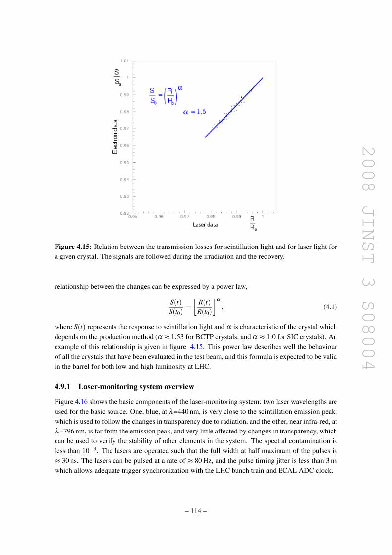
2008 JINST 3 S08004
Figure 4.15: Relation between the transmission losses for scintillation light and for laser light fora given crystal. The signals are followed during the irradiation and the recovery.
relationship between the changes can be expressed by a power law,
S(t)S(t0)
=[
R(t)R(t0)
]α
, (4.1)
where S(t) represents the response to scintillation light and α is characteristic of the crystal whichdepends on the production method (α ≈ 1.53 for BCTP crystals, and α ≈ 1.0 for SIC crystals). Anexample of this relationship is given in figure 4.15. This power law describes well the behaviourof all the crystals that have been evaluated in the test beam, and this formula is expected to be validin the barrel for both low and high luminosity at LHC.
4.9.1 Laser-monitoring system overview
Figure 4.16 shows the basic components of the laser-monitoring system: two laser wavelengths areused for the basic source. One, blue, at λ=440 nm, is very close to the scintillation emission peak,which is used to follow the changes in transparency due to radiation, and the other, near infra-red, atλ=796 nm, is far from the emission peak, and very little affected by changes in transparency, whichcan be used to verify the stability of other elements in the system. The spectral contamination isless than 10−3. The lasers are operated such that the full width at half maximum of the pulses is≈ 30 ns. The lasers can be pulsed at a rate of ≈ 80 Hz, and the pulse timing jitter is less than 3 nswhich allows adequate trigger synchronization with the LHC bunch train and ECAL ADC clock.
– 114 –

2008 JINST 3 S08004
!"
#$%&"!'"()*'"+,-.'../".0.-1"22$34! !'"5/"67."89:";.)<"'6-=>6=-."?@A$"B=//5/("67."C)'.-"',=->.")6"2D"9E"<.)/'"5/F.>65/("C)'.-"*=C'.'"5/"%G",+"67.")0)5C);C."()*'$"H7."C)'.-"<,/56,-5/("
'1'6.<"5/I.*./I./6C1"<.)'=-.'"67."5/F.>6.I"C5(76"+,-".)>7"*=C'."I5'6-5;=6.I"6,")"(-,=*",+"
61*5>)CC1"4DD">-1'6)C'"='5/("*)5-'",+"-)I5)65,/"7)-I"JK"*7,6,I5,I.'"-.)IL,=6"05)"I.I5>)6.I"
+-,/6L./I".C.>6-,/5>'$"H7.">-1'6)C",*65>)C"6-)/'<5''5,/">,--.>65,/'")-."<)I."='5/("67."-)65,",+"
67.">-1'6)CM'"NJO"PQJH"+,-"67."./IL>)*'R"-.'*,/'."/,-<)C5E.I";1"67.")'',>5)6.I"(-,=*M'"JK"
-.'*,/'.$"H7."'1'6.<"5'"+,-.'../"6,">,/65/=,='C1">1>C.",0.-"67.">)C,-5<.6.-".C.<./6'S"(505/("
)"6-)/'*)-./>1"<.)'=-.<./6".0.-1"4D"6,"!D"<5/=6.'$"H7.">,<*,/./6'",+"67."<,/56,-5/("
'1'6.<"<,=/6.I",/"67.">)C,-5<.6.-")-."I.'5(/.I"6,";."-)I5)65,/"7)-IT"+=CC"89:"C=<5/,'561"
-=//5/(",0.-"%D"1.)-'S"I.*./I5/("=*,/")/(C.S"U5CC".V*,'."67.<"6,"I,'.'",+"61*5>)CC1"#"WX1S"
)/I"/.=6-,/"+C=./>.'",+"4V%D%#"/Y><
4"?ZA$"[--)I5)65,/"6.'6"-.'=C6'")-."I5'>=''.I"5/"'.>65,/"#$""
!
"Figure 1. !"#$%&'(")*+),&-$.)%*/('*.(/0)-1-'$%2)3&-$.)45,-$-)0$/$.&'$6)&')'#$)-*5."$)7&8*9$:)&.$)6(-'.(85'$6)'*)
(/6(9(65&,)"&,*.(%$'$.)$,$%$/'-)9(&)*/$)*+);;)4.(%&.1)+(8$.-2)<#$)45,-$-)&.$)'#$/)6(-'.(85'$6)*/)'#$)6$'$"'*.)9(&)
&)'=*),$9$,)+&/>*5')-1-'$%?)(/@$"'(/0)'#$),(0#')(/'*)0.*54-)*+)'14("&,,1)ABB)".1-'&,-)78*''*%:)&/6)(/)4&.&,,$,)(/'*)
&--*"(&'$6)4&(.-)*+).$+$.$/"$)CD)4#*'*6(*6$-2))
"
"
"
"
Tertiary 1 x 200 Fanout
Secondary 1 x 7
Fanout
Trigger
PN
FE
PN
FE
FEM
PbWO4 Crystal
APDs
VFE
MEM
L2
L1
~ 2.7m
~ 0.6 m
440 (495) nm
440 (495) nm
796 (709) nm
LASERS
Primary distribution fibers : 90 – 130 m
3 x 1 Switch
Atten & Diagnostics
1 x 88 Switch
ECAL DAQ
ECAL DAQ
LIGHT SOURCE & HIGH LEVEL DISTRIBUTION SYSTEM (Laser Barrack)
Figure 4.16: The components of the laser monitoring system.
The pulse energy of 1 mJ/pulse at the principal monitoring wavelength corresponds to ≈1.3 TeV, and a linear attenuator allows 1% steps down to 13 GeV. The pulse intensity instability isless than 10% which guarantees a monitoring precision of 0.1% by using the PN silicon photodiodenormalization.
There are 3 light sources, 2 blue and 1 near infrared. The duplication of the blue sourceprovides fault tolerance and allows maintenance of one while the other is in use, ensuring that asource at the wavelength used to track changes in transparency is always available. Each sourceconsists of an Nd:YLF pump laser, its power supply and cooler unit and corresponding transformer,a Ti:Sapphire laser and its controller, and a NESLAB cooler for an LBO crystal in the Ti:S laser.Each pair of the YLF and Ti:S lasers and their corresponding optics are mounted on an optical table.Each source has its own diagnostics, 2 fibre-optic switches, internal monitors and correspondingPC based controllers. Further details can be found in [103].
The monitoring light pulses are distributed via a system of optical fibres. A fibre optic switchat the laser directs the laser pulses to 1 of 88 calorimeter regions (72 half supermodules in thebarrel and 8 regions in each endcap). A two-stage distribution system mounted on each calorimeterregion delivers the light to each crystal.
To provide continuous monitoring, about 1% of the 3.17 µs beam gap in every 88.924 µsLHC beam cycle will be used to inject monitoring light pulses into crystals. The time needed toscan the entire ECAL is expected to be about 30 minutes.
The first laser system was installed in the CERN H4 test beam site in August 2001. The othertwo laser systems were installed at H4 in August, 2003. All three laser systems have been used in
– 115 –

2008 JINST 3 S08004
!"#
##
Figure 36. !"#$%&'"()%$*&#&%+(*"%,""-(.$&/(01(/"1"/"-2"(34(.50%06&06")(70-&%0/&-8(9::(2/+)%$#)(;<=(>:(706?#"(
@A(7"$)?/"6(&-($?%?7-(9::B($%(%5"(CD!4(%")%(*"$7(1$2&#&%+E(!=<()./"$6(0'"/(FEG(6$+H)(0."/$%&0-(&)(:EFB(I(>:JBE(
#
!
!!
Figure 37. <%$*&#&%+(01(2/+)%$#(%/$-)7&))&0-(7"$)?/"7"-%)($%(BB:(-7(;*#?"(#$)"/A(0'"/(>>EG(6$+K)(0."/$%&0-(($%(
CD!4(%")%(*"$7(1$2&#&%+(&)((LEFL(I(>:JB(!=<(10/($(706?#"(01(9::(-0-J&//$6&$%"6(2/+)%$#)(;<=(>:(706?#"(@AE(
#
"#"# $%&'()*+!,--./,.(,01!(+2(!.1/!3-)2(.4!(-.12*.-+13)!+1+-5)!30--+3(,01#!
#
$%&'()*#+'#,%)#-./*,&0#,.&'*1&.)'-/#23)#,4#.&2+&,+4'#2&5&()#24#'4,#&66)-,#,%)#&510+,32)#46#,%)#
789#*+('&0#:#64.#&'#)0)-,.45&('),+-#*%4;).#+'#)<&-,0/#,%)#*&5)#;&/#&*#+,#&66)-,*#,%)#789#
*+('&0#64.#+'=)-,)2#0&*).#130*)*#>?#@%+*#+*#1.+'-+1&00/#23)#,4#2+66).)',#5)&'#0+(%,#1&,%*#+'#,%)#
,;4#-&*)*?#@%)#)66)-,#-&'#A)#*))'#+'#B+(?#!"#;%).)#.)0&,+C)#*+'(0)#8ADEF#-./*,&0#.)*14'*)*#,4#
A4,%#GHI#J)K#)0)-,.4'*#:L:I#&'2#+'=)-,)2#0&*).#0+(%,#6.45#,%)#54'+,4.+'(#*/*,)5#>L>I#&.)#
Figure 4.17: Relative stability between a pair of reference PN photodiodes monitoring 200 crystalsmeasured in autumn 2004 at the CERN test beam facility.
the ECAL test beam program since their installation, and more than 10 000 laser hours have beencumulated.
The relative stability between a pair of reference PN photodiodes monitoring the same groupof 200 crystals is shown in figure 4.17. The system achieves 0.0074% RMS over 7.5 days operation.
The response to injected laser light (normalized by the reference PN photodiodes) is presentedin figure 4.18 for a group of 200 crystals measured for 11.5 days at the wavelength of 440 nm,showing that a stability of 0.068% is achieved at the scintillation wavelength.
The effect of the monitor correction procedure is presented in figure 4.19, showing that elec-tron signals taken during an irradiation test at H4 are effectively corrected using laser monitor runstaken during the same data-taking period, providing an equalisation of the corrected response atthe level of few per mille [104] .
4.10 Energy resolution
For energies below about 500 GeV, where shower leakage from the rear of the calorimeter starts tobecome significant, the energy resolution can be parametrized as in equation (1.1) (chapter 1.1),that is repeated for convenience here:(
σ
E
)2=(
S√E
)2
+(
NE
)2
+C2 , (4.2)
where S is the stochastic term, N the noise term, and C the constant term. The individual contribu-tions are discussed below.
– 116 –

2008 JINST 3 S08004
!"#
##
Figure 36. !"#$%&'"()%$*&#&%+(*"%,""-(.$&/(01(/"1"/"-2"(34(.50%06&06")(70-&%0/&-8(9::(2/+)%$#)(;<=(>:(706?#"(
@A(7"$)?/"6(&-($?%?7-(9::B($%(%5"(CD!4(%")%(*"$7(1$2&#&%+E(!=<()./"$6(0'"/(FEG(6$+H)(0."/$%&0-(&)(:EFB(I(>:JBE(
#
!
!!
Figure 37. <%$*&#&%+(01(2/+)%$#(%/$-)7&))&0-(7"$)?/"7"-%)($%(BB:(-7(;*#?"(#$)"/A(0'"/(>>EG(6$+K)(0."/$%&0-(($%(
CD!4(%")%(*"$7(1$2&#&%+(&)((LEFL(I(>:JB(!=<(10/($(706?#"(01(9::(-0-J&//$6&$%"6(2/+)%$#)(;<=(>:(706?#"(@AE(
#
"#"# $%&'()*+!,--./,.(,01!(+2(!.1/!3-)2(.4!(-.12*.-+13)!+1+-5)!30--+3(,01#!
#
$%&'()*#+'#,%)#-./*,&0#,.&'*1&.)'-/#23)#,4#.&2+&,+4'#2&5&()#24#'4,#&66)-,#,%)#&510+,32)#46#,%)#
789#*+('&0#:#64.#&'#)0)-,.45&('),+-#*%4;).#+'#)<&-,0/#,%)#*&5)#;&/#&*#+,#&66)-,*#,%)#789#
*+('&0#64.#+'=)-,)2#0&*).#130*)*#>?#@%+*#+*#1.+'-+1&00/#23)#,4#2+66).)',#5)&'#0+(%,#1&,%*#+'#,%)#
,;4#-&*)*?#@%)#)66)-,#-&'#A)#*))'#+'#B+(?#!"#;%).)#.)0&,+C)#*+'(0)#8ADEF#-./*,&0#.)*14'*)*#,4#
A4,%#GHI#J)K#)0)-,.4'*#:L:I#&'2#+'=)-,)2#0&*).#0+(%,#6.45#,%)#54'+,4.+'(#*/*,)5#>L>I#&.)#
Figure 4.18: Stability of crystal transmission measurements at 440 nm (blue laser) over 11.5 daysoperation for a module of 200 crystals.
5 Effectiveness of the correction procedureThe ultimate goal of the laser monitoring procedure is the correction for the loss due to the radiation damage
in order to reach a stable response over many LHC cycles. From Equation (1) it follows that this correction can be
expressed as
(8)
where represents the direct measure at the time . To test the precision that can be achieved with this
procedure, we have corrected all the data collected in 2003 with the mean value of , , derived during
2002 test beam analysis for the blue laser source. This allows us to test the correction procedure on an independent
sample of crystals belonging to a different production batch with respect to the one used to determine . The
procedure has been tested using the from the blue laser, because it was the only available wavelenght in 2002.
Green and red lasers have been tested only on two crystals and there are not enough data to check the effectiveness
of the correction. The infrared laser comes, instead, into a region where the scintillation light spectrum of PbWO
is vanishing. Unfortunately, in this region the transparency of the crystal is slightly affected and therefore the
infrared laser can be more useful to control the stability of the system, provided that that the effects of radiation
damage are accounted for. The correction with the blue laser is anyway already sufficient to guarantee the required
stability and the other lasers will provide redundant information at the LHC.
Figure 6 on the left reports both the raw response and the response after the correction with the blue laser for
a sample crystal during the irradiation with electrons. The stability of the corrected response is at the level of
0.15% and it does not depend on the time. Similarly, on the right, the raw and the corrected response for both
irradiations with electrons and pions are shown. The stability of the response is again at the 0.15% level and time
independent. Moreover, since the value in Equation (8) is determined before the first irradiation, it can be seen
that the laser effectively tracks the recovery of the crystals response between the two irradiations. The level of
accuracy reported above are confirmed by the analysis of the whole sample of the crystals in the supermodule that
underwent irradiations, as shown in Figure 7.
time (h)0 1 2 3 4 5 6
S (
AD
C c
ou
nts
)
5200
5250
5300
5350
5400
5450
5500
5550
5600
time(h)0 20 40 60 80
S (
AD
C c
ou
nts
)
5200
5250
5300
5350
5400
5450
5500
5550
5600
Figure 6: Dependence of the raw response (full dots) and corrected response (open dots) on the time. On the left:
irradiation with electrons. On the right: irradiation with electrons at the beginning and with pions at the end.
6 ConclusionsThe response of several ECAL crystals under electron and pion irradiation at dose rates comparable to the ones
expected in the ECAL barrel at the LHC has been studied. The evolution of their response was monitored with a
reference electron beam of 120 GeV/c momentum and compared to the response of the laser monitoring system.
We have reported the results of the data analysis, which corroborates the reliability of the laser monitoring showing
that the response loss observed under pion and electron irradiation is adequately followed by the monitoring system
by means of an universal relation. Our results compare well to earlier studies of radiation effects under electron
irradiation on different crystal production batches. It is concluded that the response of each single crystal in ECAL
can be stabilized during operation at the LHC with an accuracy at the 0.2% level.
8
Figure 4.19: Effect of the monitor correction procedure on test beam data: full black points referto signals measured during test beam irradiation, open red points are the same after the monitorcorrections.
The stochastic term
There are three basic contributions to the stochastic term:
1. event-to-event fluctuations in the lateral shower containment,
– 117 –

2008 JINST 3 S08004
2. a photostatistics contribution of 2.1%,
3. fluctuations in the energy deposited in the preshower absorber (where present) with respectto what is measured in the preshower silicon detector.
The contribution to the stochastic term coming from fluctuations in the lateral containment isexpected to be about 1.5% when energy is reconstructed by summing an array of 5×5 crystals, andabout 2% when using 3×3 crystals.
The photostatistics contribution is given by:
ape =
√F
Npe(4.3)
where Npe is the number of primary photoelectrons released in the photodetector per GeV, and Fis the excess noise factor which parametrizes fluctuations in the gain process. This factor has avalue close to 2 for the APDs, and is about 2.5 for the VPTs. A value of Npe ≈ 4500 pe/GeV isfound for the barrel, giving ≈ 2.1% for the photostatistics contribution to the stochastic term. Inthe endcap the photostatistics contribution is similar, since the larger collection area of the VPTlargely compensates for the reduced quantum efficiency of the photocathode.
The contribution to the energy resolution from the preshower device can be approximatelyparametrized as a stochastic term with a value of 5%/
√E, where E is in GeV. But, because it
samples only the beginning of the shower, the resolution is, in fact, predicted to vary like σ/E ∝
1/E0.75. A beam test in 1999 [105] verified this prediction.
The constant term
The most important contributions to the constant term may be listed as follows:
1. non-uniformity of the longitudinal light collection,
2. intercalibration errors,
3. leakage of energy from the back of the crystal.
The effects of the longitudinal light collection curve have been studied in detail. Quite stringentrequirements are made on the crystal longitudinal uniformity. Requiring the constant term contri-bution due to non-uniformity be less than 0.3%, sets a limit on the slope of the longitudinal lightcollection curve in the region of the shower maximum of ≈ 0.35% per radiation length. A smallincrease in response towards the rear of the crystal helps to compensate the rear leakage from latedeveloping showers, which would otherwise cause a low energy tail. The required response isachieved in the barrel by depolishing one long face of the crystals to a designated roughness. Thissurface treatment is incorporated into the crystal production process.
The effect of rear leakage is very small. Charged particles leaking from the back of thecrystals can also give a direct signal in the APDs (nuclear counter effect), but test beam data showthat this effect is negligible for isolated electromagnetic showers: no tails on the high side of theenergy distribution are observed even at the highest electron energy tested (280 GeV).
– 118 –

2008 JINST 3 S08004
The noise term
There are three contributions to the noise term:
1. electronics noise,
2. digitization noise,
3. pileup noise.
The signal amplitude in the test beam is reconstructed using a simple digital filter. Thenoise measured, after this amplitude reconstruction, for channels in barrel supermodules is ≈40 MeV/channel in the highest gain range. This noise includes both electronics and digitizationnoise. The amplitude reconstruction makes use of an event-by-event baseline subtraction using3 digitization samples taken directly before the signal pulse. This procedure removes the smallchannel-to-channel correlated noise. Its success is evidenced by the fact that, after this procedure,the noise in the sum of 25 channels is almost exactly 5 times the noise in a single channel [106].
In the endcap it is intended to sort the VPTs in bins of overall signal yield, which includes thephotocathode area, the quantum efficiency and the VPT gain. The VPTs with higher overall signalyield are used for the larger radius regions of the endcap. This has the result that the transverseenergy equivalent of the noise will be more or less constant, with a value of σET ≈ 50 MeV.
Neutron irradiation of the APDs in the barrel induces a leakage current which contributes tothe electronics noise. The evolution of the leakage current and induced noise over the lifetime of theexperiment has been extensively studied. The expected contribution is equivalent to 8 MeV/channelafter one year of operation at L = 1033 cm−2s−1, and 30 MeV/channel at the end of the first yearof operation at L = 1034 cm−2s−1 [69].
The shaped signals from the preamplifier output will extend over several LHC bunch cross-ings. When using a multi-weights method to reconstruct the signal amplitude [106], up to 8 timesamples are used. Pileup noise will occur if additional particles reaching the calorimeter causesignals which overlap these samples.
The magnitude of pileup noise expected at low luminosity (L = 2× 1033 cm−2s−1) has beenstudied using detailed simulation of minimum bias events generated between −5 and +3 bunchcrossings before and after the signal. The average number of minimum bias events per bunchcrossing was 3.5. Figure 4.20 shows the reconstructed amplitude observed with and without pileupin the absence of any signal. The fraction of events with a signal beyond the Gaussian distributionof the electronics noise is small, showing that at low luminosity the pileup contribution to noise issmall.
Energy resolution in the test beam
In 2004 a fully equipped barrel supermodule was tested in the CERN H4 beam. The energy res-olution measured with electron beams having momenta between 20 and 250 GeV/c confirmed theexpectations described above [107]. Since the electron shower energy contained in a finite crystalmatrix depends on the particle impact position with respect to the matrix boundaries, the intrinsicperformance of the calorimeter was studied by using events where the electron was limited to a4× 4 mm2 region around the point of maximum containment (central impact). Figure 1.3 shows
– 119 –

2008 JINST 3 S08004
E (GeV)-0.5 -0.4 -0.3 -0.2 -0.1 -0 0.1 0.2 0.3 0.4 0.5
Entri
es/0
.001
7 G
eV
10
210
310
410
510
Figure 4.20: Reconstructed amplitude in ECAL barrel channels in the absence of a signal, withoutpileup (dashed histogram) and with pileup (solid histogram). A Gaussian of width 40 MeV issuperimposed on the dashed histogram.
the resolution as a function of energy when the incident electrons were restricted in this way. Theenergy is reconstructed by summing 3×3 crystals. A typical energy resolution was found to be:(
σ
E
)2=(
2.8%√E
)2
+(
0.12E
)2
+(0.30%)2 ,
where E is in GeV. This result is in agreement with the expected contributions detailed in the earlierpart of this section. (Results from beam-test runs taken in 2006, using the final VFE card, show a10% improvement of the noise performance.)
The energy resolution was also measured with no restriction on the lateral position of the in-cident electrons except that provided by the 20×20 mm2 trigger. The trigger was roughly centred(±3 mm) on the point of maximum response of a crystals. In this case a shower containment cor-rection was made as a function of incident position, as measured from the distribution of energiesin the crystal, to account for the variation of the amount of energy contained in the matrix. Forenergy reconstruction in either a 3×3 or a 5×5 matrix an energy resolution of better than 0.45%is found for 120 GeV electrons after correction for containment. Figure 4.21 shows an example ofthe energy distributions before and after correction for the case of reconstruction in a 5×5 matrix,where the correction is smaller than for the 3×3 case.
The energy resolution has also been measured for a series of 25 runs where the beam wasdirected at locations uniformly covering a 3×3 array of crystals. In this case a resolution of 0.5%was measured for 120 GeV electrons.
– 120 –

2008 JINST 3 S08004
Energy (GeV)114 116 118 120 122 124
Num
ber o
f eve
nts
0
1000
2000
3000
4000
5000
6000Fit results:
m = 120.0 GeV
= 0.53 GeV!
/ m = 0.44 %!
Without correction
With correction
5 crystals×5
Figure 4.21: Distribution of energy reconstructed in a 5×5 matrix, before and after correction forcontainment, when 120 GeV electrons are incident over a 20 × 20mm2 area.
– 121 –

2008 JINST 3 S08004
Chapter 5
Hadron calorimeter
The CMS detector is designed to study a wide range of high-energy processes involving diversesignatures of final states. The hadron calorimeters are particularly important for the measurementof hadron jets and neutrinos or exotic particles resulting in apparent missing transverse energy [1].
Figure 5.1 shows the longitudinal view of the CMS detector. The dashed lines are at fixed η
values. The hadron calorimeter barrel and endcaps sit behind the tracker and the electromagneticcalorimeter as seen from the interaction point. The hadron calorimeter barrel is radially restrictedbetween the outer extent of the electromagnetic calorimeter (R = 1.77 m) and the inner extent ofthe magnet coil (R = 2.95 m). This constrains the total amount of material which can be put into absorb the hadronic shower. Therefore, an outer hadron calorimeter or tail catcher is placedoutside the solenoid complementing the barrel calorimeter. Beyond |η | = 3, the forward hadroncalorimeters placed at 11.2 m from the interaction point extend the pseudorapidity coverage downto |η |= 5.2 using a Cherenkov-based, radiation-hard technology. The following sections describethese subdetectors in detail.
5.1 Barrel design (HB)
The HB is a sampling calorimeter covering the pseudorapidity range |η |< 1.3. The HB is dividedinto two half-barrel sections (figure 5.2), each half-section being inserted from either end of thebarrel cryostat of the superconducting solenoid and subsequently hung from rails in the medianplane. Since the HB is very rigid compared to the cryostat, great care has been taken to ensure thatthe barrel load is distributed evenly along the rails [108].
Absorber geometry
The HB consists of 36 identical azimuthal wedges which form the two half-barrels (HB+ andHB–). The wedges are constructed out of flat brass absorber plates (table 5.1) aligned parallelto the beam axis. The numbering scheme of the wedges is shown in figure 5.3. Each wedge issegmented into four azimuthal angle (φ ) sectors. The plates are bolted together in a staggeredgeometry resulting in a configuration that contains no projective dead material for the full radialextent of a wedge (figure 5.4). The innermost and outermost plates are made of stainless steel forstructural strength. The plastic scintillator is divided into 16 η sectors, resulting in a segmentation
– 122 –

2008 JINST 3 S08004
HF
HE
HB
HO
Figure 5.1: Longitudinal view of the CMS detector showing the locations of the hadron barrel(HB), endcap (HE), outer (HO) and forward (HF) calorimeters.
Table 5.1: Physical properties of the HB brass absorber, known as C26000/cartridge brass.
chemical composition 70% Cu, 30% Zndensity 8.53 g/cm3
radiation length 1.49 cminteraction length 16.42 cm
(∆η ,∆φ) = (0.087,0.087). The wedges are themselves bolted together, in such a fashion as tominimize the crack between the wedges to less than 2 mm.
The absorber (table 5.2) consists of a 40-mm-thick front steel plate, followed by eight 50.5-mm-thick brass plates, six 56.5-mm-thick brass plates, and a 75-mm-thick steel back plate. Thetotal absorber thickness at 90 is 5.82 interaction lengths (λI). The HB effective thickness increaseswith polar angle (θ ) as 1/sinθ , resulting in 10.6 λI at |η | = 1.3. The electromagnetic crystalcalorimeter [69] in front of HB adds about 1.1 λI of material.
Scintillator
The active medium uses the well known tile and wavelength shifting fibre concept to bring out thelight. The CMS hadron calorimeter consists of about 70 000 tiles. In order to limit the number ofindividual elements to be handled, the tiles of a given φ layer are grouped into a single mechanicalscintillator tray unit. Figure 5.5 shows a typical tray. The tray geometry has allowed for construc-tion and testing of the scintillators remote from the experimental installation area. Furthermore,
– 123 –

2008 JINST 3 S08004
Figure 5.2: Assembled HCAL half-barrel in SX5, the above ground assembly hall.
individual scintillator trays may be replaced without disassembly of the absorber in the event ofcatastrophic damage. Each HB wedge has four φ divisions (φ -index = 1–4). Trays with segmenta-tion of φ -index 2 and 3 go into the center of a wedge while trays with segmentation of φ -index 1and 4 go into the edge slots in a wedge (figure 5.4). Each layer has 108 trays. Figure 5.6 shows across section of the tray.
– 124 –

2008 JINST 3 S08004
Table 5.2: Absorber thickness in the HB wedges.
layer material thicknessfront plate steel 40 mm1-8 brass 50.5 mm9-14 brass 56.5 mmback plate steel 75 mm
Figure 5.3: Numbering scheme for the HB wedges. Wedge 1 is on the inside (+x direction) of theLHC ring.
The HB baseline active material is 3.7-mm-thick Kuraray SCSN81 plastic scintillator, chosenfor its long-term stability and moderate radiation hardness. The first layer of scintillator (layer 0)is located in front of the steel support plate. It was originally foreseen to have a separate read-out [108] and is made of 9-mm-thick Bicron BC408. The scintillators are summarized in table 5.3.The purpose of layer zero is to sample hadronic showers developing in the inert material betweenthe EB and HB. The larger thickness of layer 16 serves to correct for late developing showersleaking out the back of HB.
A tray is made of individual scintillators with edges painted white and wrapped in Tyvek1073D which are attached to a 0.5-mm-thick plastic substrate with plastic rivets. Light from eachtile is collected with a 0.94-mm-diameter green double-cladded wavelength-shifting fibre (KurarayY-11) placed in a machined groove in the scintillator. For calibration purposes, each tray has 1-mm-diameter stainless steel tubes, called source tubes, that carry Cs137 (or optionally Co60) radioactivesources through the center of each tile. An additional quartz fibre is used to inject ultraviolet(337 nm) laser light into the layer 9 tiles. The top of the tray is covered with 2-mm-thick whitepolystyrene. The cover is grooved to provide routing paths for fibres to the outside of the tray and
– 125 –

2008 JINST 3 S08004
Figure 5.4: Isometric view of the HB wedges, showing the hermetic design of the scintillatorsampling.
Figure 5.5: Scintillator trays.
also to accommodate the tubes for moving radioactive sources.After exiting the scintillator, the wavelength shifting fibres (WLS) are spliced to clear fibres
(Kuraray double-clad). The clear fibre goes to an optical connector at the end of the tray. An opticalcable takes the light to an optical decoding unit (ODU). The ODU arranges the fibres into read-outtowers and brings the light to a hybrid photodiode (HPD) [109]. An additional fibre enters each
– 126 –

2008 JINST 3 S08004
Figure 5.6: Cross-sectional view of a scintillator tray.
Table 5.3: Scintillator in the HB wedges.
layer material thickness0 Bicron BC408 9 mm1-15 Kuraray SCSN81 3.7 mm16 Kuraray SCSN81 9 mm
HPD for direct injection of light using either the laser or a light emitting diode (LED). A schematicof the fibre optics is shown in figure 5.7 and the actual cabling is shown in figure 5.8.
The HPD consists of a photocathode held at a HV of −8 kV at a distance of approximately3.3 mm from a pixelated silicon photodiode. The ionization produced by the accelerated photo-electron in the diode results in a gain of the HPD of approximately 2000. There are 19 hexagonal20-mm2 pixels in a single HPD, the centermost of which is not read-out. A cross sectional view ofan HPD is shown in figure 5.9.
During the production and assembly process, the WLS fibres are cut, polished, and mirrored.The reflectivity of the mirror is checked by measuring test fibres which are mirrored along withthe fibres used in the calorimeter. Measuring the reflectivity of the mirror is done with a computercontrolled UV scanner with the fibres read out by photodiodes. Clear fibres are spliced onto WLSfibres with a fusion splicer. The transmission across the splice is checked by splicing a sample ofWLS fibres onto WLS fibres. The splice region is measured with the UV scanner. The transmissionacross the splice is 92.6% with an RMS of 1.8%. Next, the optical fibres are glued into a 10 fibreconnector. This configuration is called a pigtail. In order to get the fibre lengths correct, the pigtailis assembled in a template. The connector is diamond polished. The fibres are measured with the
– 127 –

2008 JINST 3 S08004
Figure 5.7: Schematic of the HB optics.
UV scanner. The scanner checks the green fibre, clear fibre, splice, and mirror. The RMS of thelight from the fibres is 1.9%. After the pigtail is inserted into the tray, the completed tray is checkedwith an automated source scanner using a Cs137 source inside a lead collimator. This yields a 4 cmdiameter source spot on the tray. The collimator is moved with a computer controlled x-y motor.From the scanner we determine the relative light yield of each tile and the uniformity of each tray.The light yield of the individual tiles has an RMS of 4.6%, while the transverse uniformity of thetile is 4.5%. A Cs137 wire source is run through the 4 source tubes and the light yield is measured.The RMS of the ratio of collimated source to wire source is 1.3%. This means the line sources,which can be used when the calorimeter is completely assembled, can calibrate individual tilesto better than 2%. In addition to the moving wire source, there are laser and LED light injectionsystems.
Longitudinal segmentation
The η towers 1–14 have a single longitudinal read-out. The η towers closest to the endcap transi-tion region (15 and 16) are segmented in depth. The front segment of tower 15 contains either 12or 13 scintillators, due to the placement of the read-out box and the staggering of the layers (layers0–11 for the middle two φ sectors and 0–12 layers for the outer two φ sectors). The rear segment oftower 15 has three scintillators. Tower 16, which is in front of the endcap (HE) has one scintillatorsin the front segment and seven in the rear. The front segment of tower 16 does not have a layer-0scintillator. The tower segmentation is summarized in figure 5.10 and table 5.4.
– 128 –

2008 JINST 3 S08004
Figure 5.8: Close up view of the assembled HB wedges, showing the optical cabling.
Figure 5.9: Cross sectional view of an HPD.
– 129 –

2008 JINST 3 S08004
Figure 5.10: The HCAL tower segmentation in the r,z plane for one-fourth of the HB, HO, andHE detectors. The shading represents the optical grouping of scintillator layers into different lon-gitudinal readouts.
Table 5.4: Tower data for HB. The given thicknesses correspond to the center of the tower. Notethat tower 16 overlaps with HE.
tower η range thickness (λI)1 0.000 – 0.087 5.392 0.087 – 0.174 5.433 0.174 – 0.261 5.514 0.261 – 0.348 5.635 0.348 – 0.435 5.806 0.435 – 0.522 6.017 0.522 – 0.609 6.268 0.609 – 0.696 6.579 0.696 – 0.783 6.9210 0.783 – 0.870 7.3211 0.870 – 0.957 7.7912 0.957 – 1.044 8.3013 1.044 – 1.131 8.8914 1.131 – 1.218 9.5415 1.218 – 1.305 10.316 1.305 – 1.392 overlaps with HE
– 130 –

2008 JINST 3 S08004
HE
Figure 5.11: Hadron endcap (HE) calorimeter mounted on the endcap iron yoke.
5.2 Endcap design (HE)
The hadron calorimeter endcaps (HE) [108] cover a substantial portion of the rapidity range,1.3 < |η |< 3 (13.2% of the solid angle), a region containing about 34% of the particles produced inthe final state. The high luminosity of the LHC (1034 cm−2 s−1) requires HE to handle high (MHz)counting rates and have high radiation tolerance (10 MRad after 10 years of operation at designluminosity) at |η | ' 3. Since the calorimeter is inserted into the ends of a 4-T solenoidal magnet,the absorber must be made from a non-magnetic material. It must also have a maximum number ofinteraction lengths to contain hadronic showers, good mechanical properties and reasonable cost,leading to the choice of C26000 cartridge brass. The endcaps are attached to the muon endcap yokeas shown in figures 5.11 and 5.12. Only a small part of the calorimeter structure can be used forthe fixation to the magnet iron, because the majority of the space between HE and muon absorberis occupied with muon cathode strip chambers. A 10-t electromagnetic calorimeter (EE) with a2-t preshower detector (ES) is attached at the front face of HE. The large weight involved (about300 t) and a strict requirement to minimize non-instrumented materials along particle trajectories,has made the design of HE a challenge to engineers. An interface kinematic scheme was devel-oped in order to provide precise positioning of the endcap detectors with respect to the adjacentmuon station, and to minimize the influence of deformation under magnetic forces. The interfacekinematic contains a sliding joint between the interface tube, and HE back-flange and the hingeconnection between brackets and the iron disk (YE1). Structural materials used in the interfacesystem are non-magnetic in order not to distort the axial magnetic field of up to 4 T.
– 131 –

2008 JINST 3 S08004
Figure 5.12: Partially assembled HE-minus absorber in the CMS surface hall (SX5). Scintillatortrays can be seen to be inserted in some of the outer sectors.
Absorber geometry
The design of the absorber is driven by the need to minimize the cracks between HB and HE,rather than single-particle energy resolution, since the resolution of jets in HE will be limited bypileup, magnetic field effects, and parton fragmentation [110, 111]. The plates are bolted togetherin a staggered geometry resulting in a configuration that contains no projective “dead” material(figure 5.13). The design provides a self-supporting hermetic construction. The brass plates are79-mm-thick with 9-mm gaps to accommodate the scintillators. The total length of the calorimeter,including electromagnetic crystals, is about 10 interaction lengths (λI).
The outer layers of HE have a cutout region for installation of the photodetectors and front-end electronics. To compensate for the resulting reduction of material, an extra layer (−1) is addedto tower 18 [112]. The outer layers are fixed to a 10-cm-thick stainless steel support plate. Theoptical elements are inserted into the gaps after the absorber is completely assembled; therefore,the optical elements must have a rigid structure to allow insertion from any position.
Scintillator trays
The scintillation light is collected by wavelength shifting (WLS) fibres [113, 114]. The designminimizes dead zones because the absorber can be made as a solid piece without supportingstructures while at the same time the light can be easily routed to the photodetectors. Trapezoidal-
– 132 –

2008 JINST 3 S08004
Figure 5.13: Mechanical structure of the HE absorber. Particles enter the calorimeter from thebottom.
shaped scintillators (figure 5.14), 3.7-mm-thick SCSN81 for layers 1–17 and 9-mm-thick BicronBC408 for layer 0, have grooves in which the WLS fibres are inserted. The ends of the fibres aremachined with a diamond fly cutter and one end is covered with aluminium to increase the lightcollection. The other end is spliced to a clear fibre, which is terminated in an optical connector.The connector with the glued fibres is also machined by a diamond fly cutter. The scintillator ispainted along the narrow edges and put into a frame to form a tray. The total number of tiles forboth HE calorimeters is 20 916 and the number of trays is 1368. The design of a tray is presentedin figure 5.15. The numbering scheme in η is shown in figure 5.16, and the CMS convention for φ
as applied to HE is shown in figure 5.17. The scintillators are wrapped with Tyvek and sandwichedbetween sheets of duraluminum. The stack contains holes for fibres which are terminated withoptical connectors. The gap between the duraluminum plates is fixed by brass spacers screwedtogether. The granularity of the calorimeters is ∆η × ∆φ = 0.087× 0.087 for |η | < 1.6 and∆η×∆φ ≈ 0.17×0.17 for |η | ≥ 1.6.
The tray design is very robust and reliable. The trays are relatively stiff which is very im-portant for insertion into the absorber. To control the scintillator tray quality, a UV nitrogen laserwas used to excite the scintillators. The light is fed by quartz fibres to the connector and is fannedout as shown in figure 5.15. These fibres are terminated with aluminium reflectors and distributethe light to all tiles. The light signal produced by a UV flash in the scintillator is similar to thesignal induced by a charged particle. This allows a performance check of the entire optical routefrom scintillator to electronics, providing an important technique to track possible degradation oftransparency due to radiation damage. For further calibration and monitoring, a radioactive sourcemoving in a stainless steel tube is used to study the time-dependence of calibration coefficients.
The trays are inserted into the gaps in the absorber and fixed by screws. At the back of thecalorimeter, boxes with photodetectors and electronics are located in the notch shown in figure 5.18.Optical cables transfer signals from the scintillator trays to the photodetectors. The partially assem-bled HE is shown in figure 5.12. Multipixel hybrid photodiodes (HPDs) are used as photodetectorsdue to their low sensitivity to magnetic fields and their large dynamical range.
– 133 –

2008 JINST 3 S08004
Figure 5.14: a) Basic structure of a scintillator tile with a groove to fix wavelength shifting fibre,b) cross section of the 3.7-mm-thick scintillator for layers 1–17, and c) cross section of the 9-mm-thick scintillator for layer zero. Two layers of reflecting paint cover the side surfaces of the tile.
Longitudinal segmentation
The longitudinal segmentation of HE (figure 5.10) is, in part, motivated by the radiation environ-ment. Correction of the calibration coefficients after scintillator degradation can be applied, inorder to restore the energy resolution. The towers nearest the beam line (27 and 28 plus guardring “29”) have 3 divisions in depth which are read-out separately. The other towers (except 16and 17 which overlap with the electromagnetic barrel calorimeter) have two longitudinal readoutsfor potential use during the time period when the electromagnetic endcap calorimeter (EE) maynot yet be available. A special scintillator layer of 9 mm BC408 (layer 0) is installed in front ofthe absorber to partially correct for the different response of EE to electrons and hadrons and forparticle absorption in the mechanical structure supporting EE.
– 134 –

2008 JINST 3 S08004
Figure 5.15: The design of the calorimeter scintillator trays: a) front view of a tray without upperaluminium cover, b) cut out view of the layer-0 tray with two fibres from a tile, c) cut out view ofa tray for layers 1–17.
– 135 –

2008 JINST 3 S08004
Figure 5.16: Numbering scheme for the tiles in adjacent scintillator trays.
Figure 5.17: Numbering scheme for the HE wedges as viewed from the interaction point. The +xdirection points to the center of the LHC ring.
– 136 –
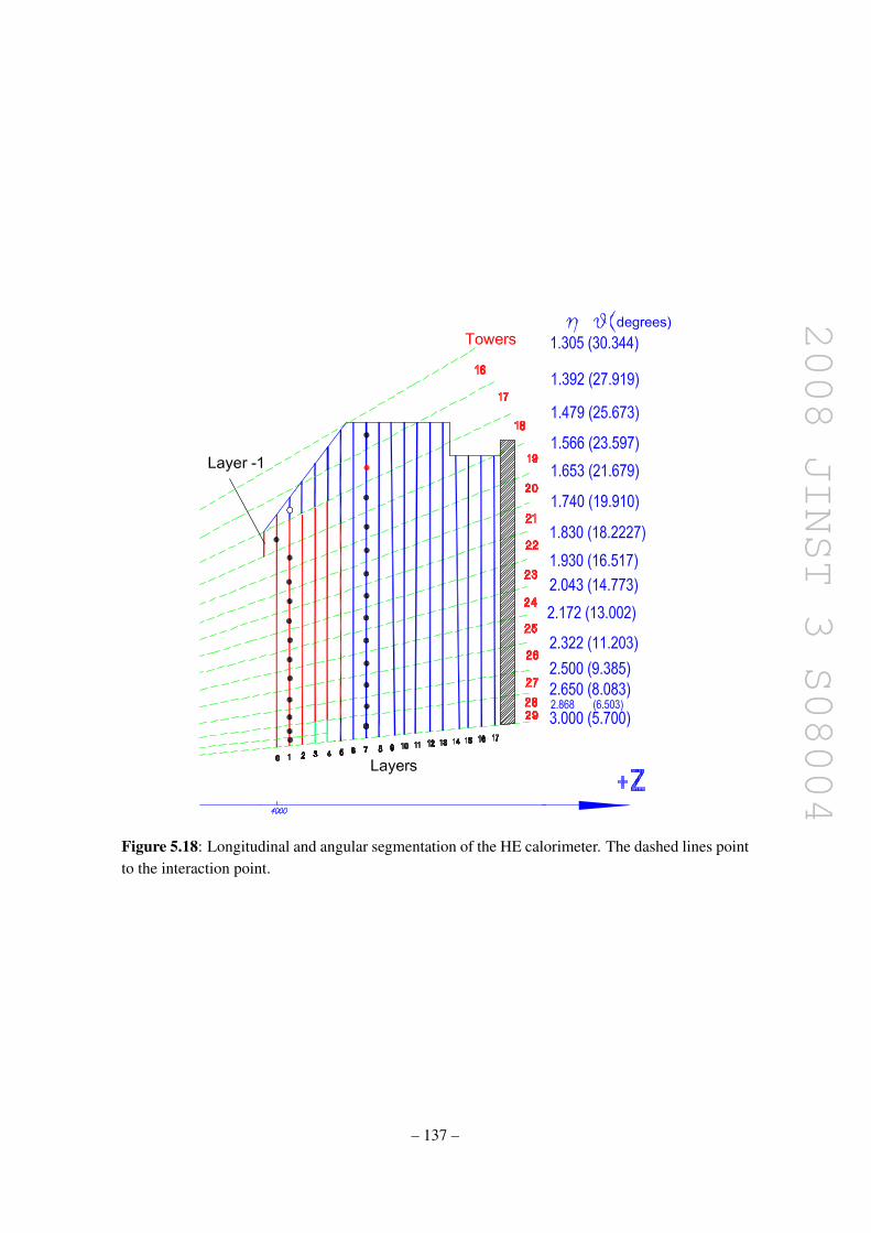
2008 JINST 3 S08004
Figure 5.18: Longitudinal and angular segmentation of the HE calorimeter. The dashed lines pointto the interaction point.
– 137 –

2008 JINST 3 S08004
Figure 5.19: Longitudinal and transverse views of the CMS detector showing the position of HOlayers.
5.3 Outer calorimeter design (HO)
In the central pseudorapidity region, the combined stopping power of EB plus HB does not providesufficient containment for hadron showers. To ensure adequate sampling depth for |η | < 1.3, thehadron calorimeter is extended outside the solenoid with a tail catcher called the HO or outercalorimeter. The HO utilises the solenoid coil as an additional absorber equal to 1.4/sinθ interactionlengths and is used to identify late starting showers and to measure the shower energy depositedafter HB.
Outside the vacuum tank of the solenoid, the magnetic field is returned through an iron yokedesigned in the form of five 2.536 m wide (along z-axis) rings. The HO is placed as the firstsensitive layer in each of these five rings. The rings are identified by the numbers −2, −1, 0,+1, +2. The numbering increases with z and the nominal central z positions of the five rings arerespectively −5.342 m, −2.686 m, 0, +2.686 m and +5.342 m. At η = 0, HB has the minimalabsorber depth. Therefore, the central ring (ring 0) has two layers of HO scintillators on either sideof a 19.5 cm thick piece of iron (the tail catcher iron) at radial distances of 3.82 m and 4.07 m,respectively. All other rings have a single HO layer at a radial distance of 4.07 m. The total depthof the calorimeter system is thus extended to a minimum of 11.8 λI except at the barrel-endcapboundary region.
The HO is constrained by the geometry of the muon system. Figure 5.19 shows the positionof HO layers in the rings of the muon stations in the overall CMS setup. The segmentation of thesedetectors closely follows that of the barrel muon system. Each ring has 12 identical φ -sectors.The 12 sectors are separated by 75-mm-thick stainless steel beams which hold successive layers ofiron of the return yoke as well as the muon system. The space between successive muon rings inthe η direction and also the space occupied by the stainless steel beams in the φ direction are notavailable for HO. In addition, the space occupied by the cryogenic “chimneys” in sector 3 of ring−1, and sector 4 of ring +1 are also not available for HO. The chimneys are used for the cryogenictransfer lines and power cables of the magnet system. Finally, the mechanical structures needed toposition the scintillator trays further constrain HO along φ .
– 138 –

2008 JINST 3 S08004
In the radial direction each HO layer has been allocated a total of 40 mm, of which only16 mm is available for the detector layer, the rest being used for the aluminium honeycomb supportstructures. In addition, the HO modules are independently supported from the steel beams locatedon either side of each φ sector. The thickness and position of the iron ribs in the yoke structurefurther constrain the shape and segmentation of the HO.
The sizes and positions of the tiles in HO are supposed to roughly map the layers of HBto make towers of granularity 0.087× 0.087 in η and φ . The HO consists of one (rings ±1 and±2) or two (ring 0) layers of scintillator tiles located in front of the first layer of the barrel muondetector. Scintillation light from the tiles is collected using multi-clad Y11 Kuraray wavelengthshifting (WLS) fibres of diameter 0.94 mm, and transported to the photo detectors located on thestructure of the return yoke by splicing a multi-clad Kuraray clear fibre (also of 0.94 mm diameter)with the WLS fibre. In order to simplify installation of HO, the scintillator tiles are packed into asingle unit called a tray. Each tray corresponds to one φ slice (5 wide in φ ). However, along the z(η) direction, a tray covers the entire span of a muon ring. Figure 5.20 shows a schematic view of aHO tray where one tile is mapped to a tower of HB and the optical cable from the tray is connectedto the read-out box.
The physics impact of HO has been studied [115] using a simulation of the CMS detector.Single pions of fixed energies are shot at specific η values and the resulting energy deposits in theelectromagnetic calorimeter and in the layers of the hadron calorimeter are combined to measurethe energy. Figure 5.21 shows distributions of the measured energy scaled to the incident energyfor 200 GeV pions at η = 0 and 225 GeV at η = 0.5 (pointing towards the middle of ring 1). Thesolid and dashed lines in the figure indicate measurements without and with HO, respectively. Ascan be seen in figure 5.21, there is an excess in Energy/Eincident < 1 for measurements without HO,because of leakage. The measurements with HO are more Gaussian in nature indicating that theaddition of HO recovers the effect of leakage. The effect of leakage is visible at η = 0 (ring 0)from 70 GeV, increasing with energy. The mean fraction of energy in HO increases from 0.38% for10 GeV pions to 4.3% for 300 GeV pions. There is some evidence of leakage without HO in ring1 but it is reduced due to the greater HB thickness at larger |η |. The amount of leakage in ring 2 isfound to be negligible at energies below 300 GeV.
The effect of shower leakage has a direct consequence on the measurement of missing trans-verse energy (Emiss
T ). Study of QCD events shows that the cross section for those events, whereat least one particle has ET above 500 GeV, is several pb. For these events the HO is useful todecrease the leakage and improve the Emiss
T measurement. Figure 5.22 shows the dijet integratedcross section for Emiss
T above a certain value. It is clear from the figure that the inclusion of HOreduces the dijet rate by a factor of 1.5 or more for moderate Emiss
T values, a region important forsearches of supersymmetric particles.
Module specification
HO is physically divided into 5 rings in η conforming to the muon ring structure. The rings arenumbered−2,−1, 0, +1 and +2 with increasing η . Each ring of the HO is divided into 12 identicalφ sectors and each sector has 6 slices (numbered 1 to 6 counting clockwise) in φ . The φ slices of alayer are identical in all sectors. The widths of the slices along φ are given in table 5.5. In each φ
– 139 –
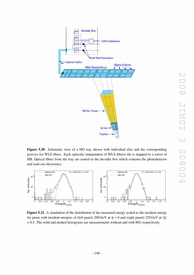
2008 JINST 3 S08004
Figure 5.20: Schematic view of a HO tray shown with individual tiles and the correspondinggrooves for WLS fibres. Each optically independent (4 WLS fibres) tile is mapped to a tower ofHB. Optical fibres from the tray are routed to the decoder box which contains the photodetectorand read-out electronics.
1
10
10 2
0 0.2 0.4 0.6 0.8 1 1.2 1.4 1.6 1.8 2Energy/EIncident
No.
of E
vent
s
without HO
with HO
E = 200 GeV η = 0.0
1
10
10 2
0 0.2 0.4 0.6 0.8 1 1.2 1.4 1.6 1.8 2Energy/EIncident
No.
of E
vent
s
without HO
with HO
E = 225 GeV η = 0.5
Figure 5.21: A simulation of the distribution of the measured energy scaled to the incident energyfor pions with incident energies of (left panel) 200 GeV at η = 0 and (right panel) 225 GeV at |η |= 0.5. The solid and dashed histograms are measurements without and with HO, respectively.
– 140 –

2008 JINST 3 S08004
10-2
10-1
1
0 200 400 600 800
with HOwithout HO
Missing ET Cut (GeV)
σ (p
b)
Figure 5.22: Integrated cross section above threshold for intrinsically balanced QCD dijet eventsas a function of missing ET with or without HO.
Table 5.5: Dimension of tiles along φ for different trays. Each tray corresponds to one φ -slice in aφ sector.
Ring Layer Width along φ in mmTray 1 Tray 2 Tray 3 Tray 4 Tray 5 Tray 6
0 0 274 343 332 327 327 2680 1 300 364 352 347 347 292
±1, ±2 1 317 366 354 349 349 406
slice, there is a further division along η . The smallest scintillator unit in HO thus obtained is calleda tile. The scintillator tiles in each φ sector belong to a plane. The perpendicular distance of thisplane from the z-axis is 3.82 m for layer 0 and 4.07 m for layer 1. The tiles in each φ slice of a ringare mechanically held together in the form of a tray.
Both layers of ring 0 have 8 η-divisions (i.e. 8 tiles in a tray): −4, −3, −2, −1, +1, +2, +3,+4. Ring 1 has 6 divisions: 5· · ·10 and ring 2 has 5 divisions: 11· · ·15. Ring −1 and ring −2 havethe same number of divisions as rings 1 and 2 but with −ve indices. The η-dimension of any tilewith −ve tower number is the same as the one with +ve number. The tile dimensions along η areshown in table 5.6.
Figure 5.23 shows the final layout of all the HO trays in the CMS detector. The length of afull tray is 2510 mm whereas the shorter trays, the sizes of which are constrained because of thechimney (trays 4 and 5 in sector 4 of ring +1 and trays 3, 4, 5 and 6 in sector 3 of ring −1), are2119-mm long. The shorter trays are constructed without the tile corresponding to tower number±5. Because of the constraints imposed by the gap between ring 0 and rings ±1, the η boundariesof HO tower 4 do not match the barrel η boundaries; therefore, part of HO tower 5 overlaps withtower 4 in the barrel.
– 141 –
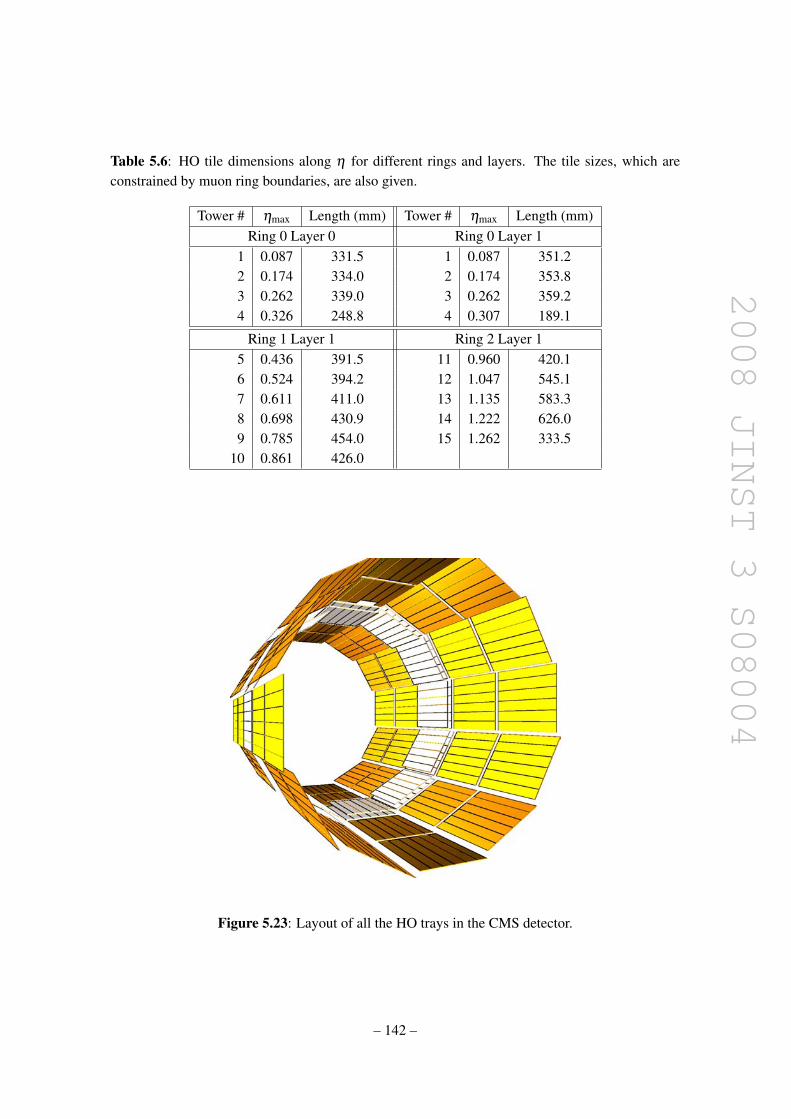
2008 JINST 3 S08004
Table 5.6: HO tile dimensions along η for different rings and layers. The tile sizes, which areconstrained by muon ring boundaries, are also given.
Tower # ηmax Length (mm) Tower # ηmax Length (mm)Ring 0 Layer 0 Ring 0 Layer 1
1 0.087 331.5 1 0.087 351.22 0.174 334.0 2 0.174 353.83 0.262 339.0 3 0.262 359.24 0.326 248.8 4 0.307 189.1
Ring 1 Layer 1 Ring 2 Layer 15 0.436 391.5 11 0.960 420.16 0.524 394.2 12 1.047 545.17 0.611 411.0 13 1.135 583.38 0.698 430.9 14 1.222 626.09 0.785 454.0 15 1.262 333.5
10 0.861 426.0
Figure 5.23: Layout of all the HO trays in the CMS detector.
– 142 –
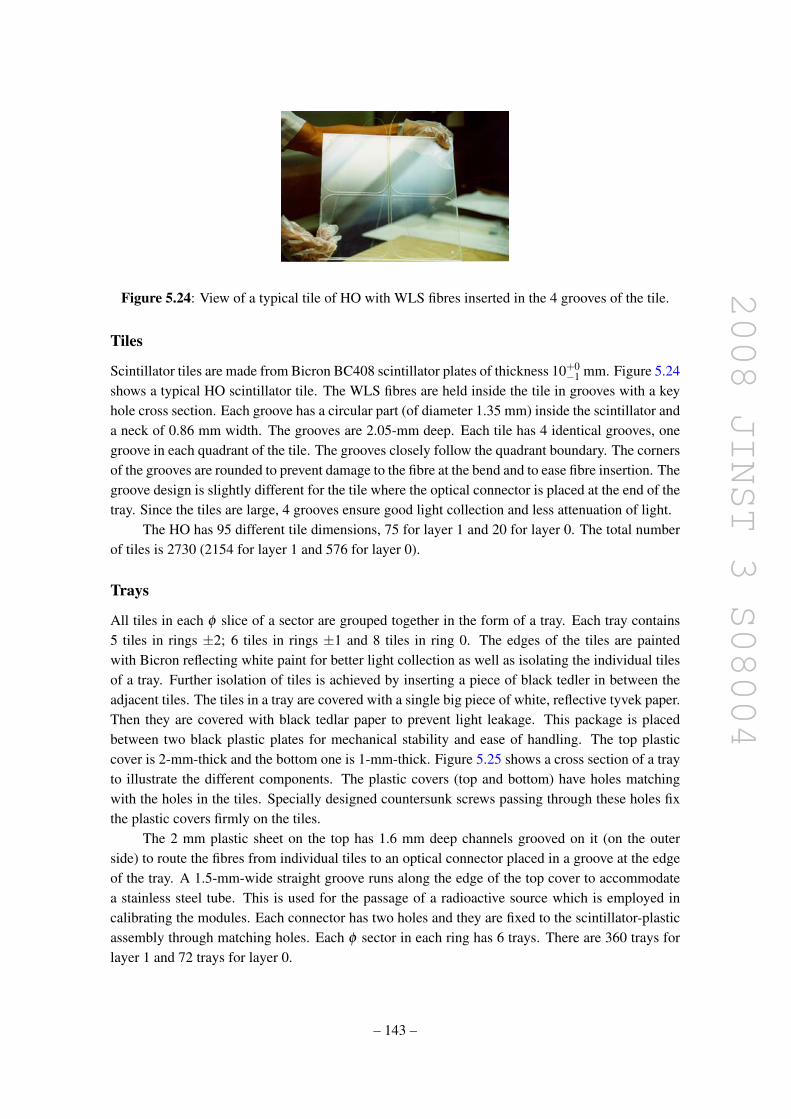
2008 JINST 3 S08004
Figure 5.24: View of a typical tile of HO with WLS fibres inserted in the 4 grooves of the tile.
Tiles
Scintillator tiles are made from Bicron BC408 scintillator plates of thickness 10+0−1 mm. Figure 5.24
shows a typical HO scintillator tile. The WLS fibres are held inside the tile in grooves with a keyhole cross section. Each groove has a circular part (of diameter 1.35 mm) inside the scintillator anda neck of 0.86 mm width. The grooves are 2.05-mm deep. Each tile has 4 identical grooves, onegroove in each quadrant of the tile. The grooves closely follow the quadrant boundary. The cornersof the grooves are rounded to prevent damage to the fibre at the bend and to ease fibre insertion. Thegroove design is slightly different for the tile where the optical connector is placed at the end of thetray. Since the tiles are large, 4 grooves ensure good light collection and less attenuation of light.
The HO has 95 different tile dimensions, 75 for layer 1 and 20 for layer 0. The total numberof tiles is 2730 (2154 for layer 1 and 576 for layer 0).
Trays
All tiles in each φ slice of a sector are grouped together in the form of a tray. Each tray contains5 tiles in rings ±2; 6 tiles in rings ±1 and 8 tiles in ring 0. The edges of the tiles are paintedwith Bicron reflecting white paint for better light collection as well as isolating the individual tilesof a tray. Further isolation of tiles is achieved by inserting a piece of black tedler in between theadjacent tiles. The tiles in a tray are covered with a single big piece of white, reflective tyvek paper.Then they are covered with black tedlar paper to prevent light leakage. This package is placedbetween two black plastic plates for mechanical stability and ease of handling. The top plasticcover is 2-mm-thick and the bottom one is 1-mm-thick. Figure 5.25 shows a cross section of a trayto illustrate the different components. The plastic covers (top and bottom) have holes matchingwith the holes in the tiles. Specially designed countersunk screws passing through these holes fixthe plastic covers firmly on the tiles.
The 2 mm plastic sheet on the top has 1.6 mm deep channels grooved on it (on the outerside) to route the fibres from individual tiles to an optical connector placed in a groove at the edgeof the tray. A 1.5-mm-wide straight groove runs along the edge of the top cover to accommodatea stainless steel tube. This is used for the passage of a radioactive source which is employed incalibrating the modules. Each connector has two holes and they are fixed to the scintillator-plasticassembly through matching holes. Each φ sector in each ring has 6 trays. There are 360 trays forlayer 1 and 72 trays for layer 0.
– 143 –

2008 JINST 3 S08004
Figure 5.25: Cross section of a HO tray showing the different components.
Figure 5.26: The arrangement of scintillation tiles, plastic covers and connectors in a tray. Thecomponents are slightly displaced from their true positions to show their matching designs.
Pigtails
The light collected by the WLS fibres inserted in the tiles needs to be transported to photodetectorslocated far away on the muon rings. The captive ends of the WLS fibres, which reside inside thegroove, are polished, aluminized and protected using a thin polymer coating. The other end of theWLS fibre comes out of the tile through a slot made on the 2-mm-thick black plastic cover sheet.To minimise the loss of light in transportation, the WLS fibre (attenuation length of ≈ 1.8 m) isspliced to a clear fibre (attenuation length of ≈ 8.0 m). A fibre is spliced only if the potential WLSlight loss is larger than the light loss at a spliced joint. Thus depending on tile length (along η)2–3 fibres in each pigtail are made only of WLS fibres. The clear fibres from each tile follow theguiding grooves on the top plastic to the optical connector at the end. Each tray has two opticalconnectors mounted on one end of the tray. In a tray, the grooves of the tiles form two rows alongη . The fibres from all grooves on one row terminate on one connector (figure 5.26). The numberof fibres from trays in different rings are given in table 5.7.
The bunch of fibres fixed to the optical connector is called a pigtail (figure 5.27). Each trayhas 2 pigtails and there are 864 pigtails in total: 720 for layer 1 and 144 for layer 0. Each fibre ina pigtail is cut to the proper length to match the groove length in the scintillator plus the distancefrom the scintillator to the optical connector at the end of the tray.
– 144 –

2008 JINST 3 S08004
Table 5.7: Tray specifications for different rings of HO.
Ring # Tiles/tray Fibres/tray Fibres/connector0 8 32 16±1 6 24 12±2 5 20 10
Figure 5.27: Illustration of an assembled pigtail (not drawn to scale).
5.4 Forward calorimeter design (HF)
The forward calorimeter will experience unprecedented particle fluxes. On average, 760 GeV perproton-proton interaction is deposited into the two forward calorimeters, compared to only 100 GeVfor the rest of the detector. Moreover, this energy is not uniformly distributed but has a pronouncedmaximum at the highest rapidities. At |η |= 5 after an integrated luminosity of 5×10⁵ pb−1 (≈ 10years of LHC operation), the HF will experience ≈ 10 MGy. The charged hadron rates will alsobe extremely high. For the same integrated luminosity, inside the HF absorber at 125 cm from thebeam-line, the rate will exceed 1011 per cm2 [108]. This hostile environment presents a consider-able challenge to calorimetry, and the design of the HF calorimeter was first and foremost guidedby the necessity to survive in these harsh conditions, preferably for at least a decade. Successfuloperation critically depends on the radiation hardness of the active material. This was the principalreason why quartz fibres (fused-silica core and polymer hard-cladding) were chosen as the activemedium.
The signal is generated when charged shower particles above the Cherenkov threshold (E ≥190 keV for electrons) generate Cherenkov light, thereby rendering the calorimeter mostly sensitiveto the electromagnetic component of showers [116]. A small fraction of the generated light iscaptured, ftrap = NA/2n2
core, where NA is the numerical aperture (NA = 0.33± 0.02) and ncore
is the refractive index of the quartz core. Only light that hits the core-cladding interface at anangle larger than the critical angle (71) contributes to the calorimeter signal. The half-angle θ =19 is determined by the refractive indices of the core (ncore) and the cladding (nclad), sinθ =√
n2core−n2
clad. The fibres measure 600±10 µm in diameter for the fused-silica core, 630+5−10 µm
with the polymer hard-cladding, and 800± 30 µm with the protective acrylate buffer. Over 1000km of fibres are used in the HF calorimeters. The fibres are cleaved at both ends by a diamondcutter. The attenuation length of these fibres is measured to be ≈15 m using high energy electronsat 90 to the fibres.
– 145 –

2008 JINST 3 S08004
The optical attenuation at a wavelength λ in these types of fibres scales as a(λ )(D/D0)b(λ )
where D is the accumulated dose, which is normalized to a reference dose (D0 = 1 MGy) for con-venience. For example, at a wavelength λ = 450 nm at the accumulated dose of D = 1 MGy, theinduced attenuation is ≈ 1.5 dB/m, thus defining a. The a and b parameters characterize the radi-ation hardness of a given fibre. For high OH− (300–500 ppm) HF fibres at 450 nm, the measuredvalues are a≈ 1.5 and b≈ 0.3 [117–119]. An accumulated dose of 10 MGy will result in a loss ofoptical transmission by a half, which is the worst case for HF after a decade.
The calorimeter consists of a steel absorber structure that is composed of 5 mm thick groovedplates. Fibres are inserted in these grooves. The detector is functionally subdivided into two lon-gitudinal segments. Half of the fibres run over the full depth of the absorber (165 cm ≈ 10λI)while the other half starts at a depth of 22 cm from the front of the detector. These two sets offibres are read out separately. This arrangement makes it possible to distinguish showers gener-ated by electrons and photons, which deposit a large fraction of their energy in the first 22 cm,from those generated by hadrons, which produce nearly equal signals in both calorimeter seg-ments on average. The long fibre section is referred as L (measuring the total signal), and theshort fibre section as S (measuring the energy deposition after 22 cm of steel). The absorberhas grooves (0.90+0.12
−0 mm wide and 1.06+0.6−0 mm in depth) which make a square grid separated
by 5.0± 0.1 mm center-to-center. Long and short fibres alternate in these grooves. The pack-ing fraction by volume (fibre/total) in the first 22 cm is 0.57% and is twice as large beyond thatdepth.
The forward calorimeter is essentially a cylindrical steel structure with an outer radius of130.0 cm. The front face of the calorimeter is located at 11.2 m from the interaction point. The holefor the beam pipe is cylindrical, with radius 12.5 cm from the center of the beam line. This structureis azimuthally subdivided into 20 modular wedges. Thirty-six such wedges (18 on either side ofthe interaction point) make up the HF calorimeters. A cross sectional view of the HF is shownin figure 5.28. The fibres run parallel to the beam line, and are bundled to form 0.175×0.175(∆η × ∆φ) towers (figure 5.29 and table 5.8). The detector is housed in a hermetic radiationshielding which consists of layers of 40 cm thick steel, 40 cm of concrete, and 5 cm of polyethylene.A large plug structure in the back of the detector provides additional shielding.
Bundled fibres are held in ferrules which illuminate one end of the air-core light guides thatpenetrate through 42.5 cm of the shielding matrix (steel, lead, and polyethylene). This shieldingis necessary to protect the photomultipliers and the front-end electronics housed in the read-outboxes. The air-core light guide consists of a hollow tube lined on the inside with highly reflectivecustom-made sheets. These metal-coated reflectors are designed to be very efficient (> 90%) inthe visible spectrum at the relevant angles (≈ 70 degrees from normal). Light typically makes fivebounces before reaching the photocathode and nearly half the light is lost in this transport. Eachlight guide is coupled to a standard bialkaline, 8-stage photomultiplier tube with a borosilicate glasswindow. A read-out box (RBX) houses 24 PMTs and services half of a wedge (10 in φ ).
The entire calorimeter system, with its shielding components, is mounted on a rigid tablewhich supports more than 240 t with less than 1 mm deflection. The absorber alone weighs 108 t.The table is also designed for horizontal separation of the detector into two sections to clear thebeam pipe at installation and removal. It is possible to align the forward calorimeters within±1 mmwith respect to the rest of the CMS experiment.
– 146 –
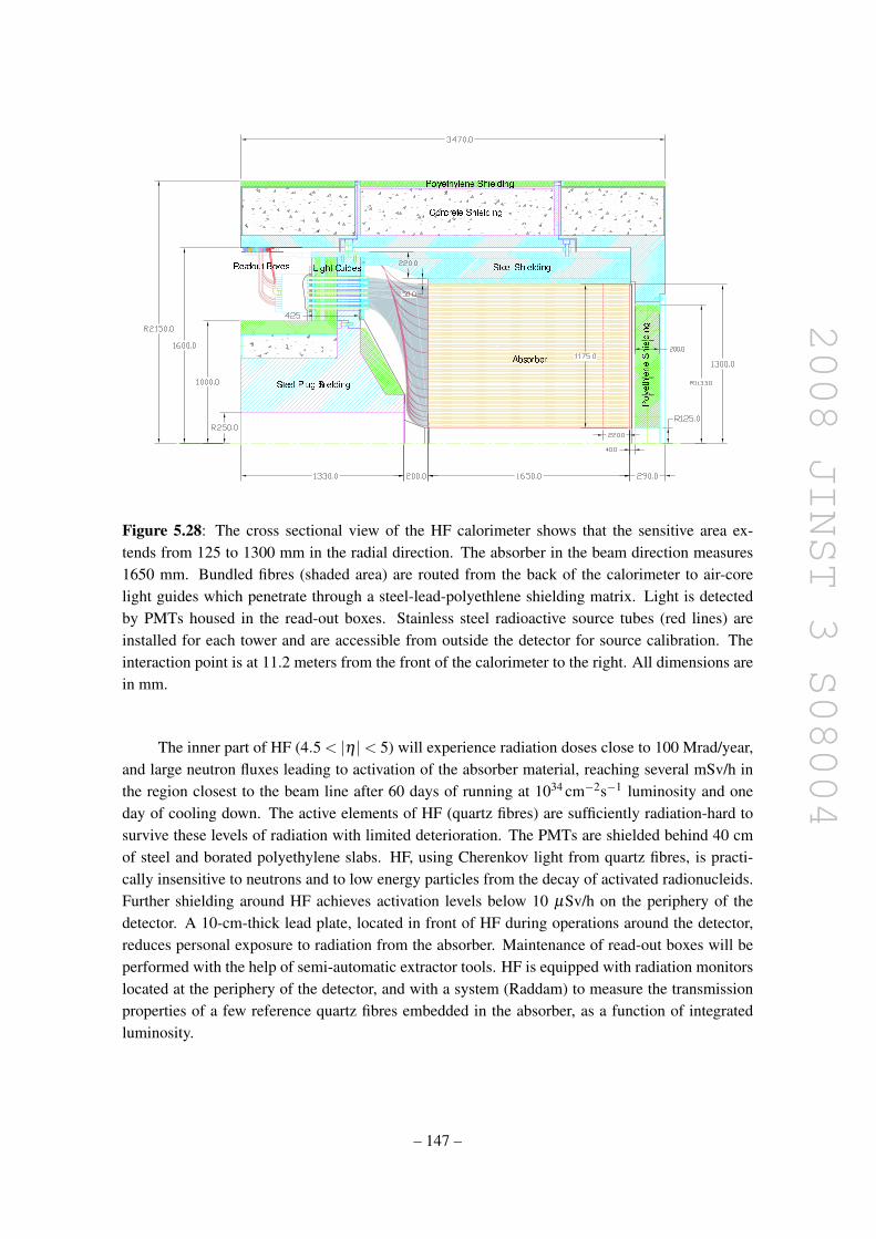
2008 JINST 3 S08004
Figure 5.28: The cross sectional view of the HF calorimeter shows that the sensitive area ex-tends from 125 to 1300 mm in the radial direction. The absorber in the beam direction measures1650 mm. Bundled fibres (shaded area) are routed from the back of the calorimeter to air-corelight guides which penetrate through a steel-lead-polyethlene shielding matrix. Light is detectedby PMTs housed in the read-out boxes. Stainless steel radioactive source tubes (red lines) areinstalled for each tower and are accessible from outside the detector for source calibration. Theinteraction point is at 11.2 meters from the front of the calorimeter to the right. All dimensions arein mm.
The inner part of HF (4.5 < |η |< 5) will experience radiation doses close to 100 Mrad/year,and large neutron fluxes leading to activation of the absorber material, reaching several mSv/h inthe region closest to the beam line after 60 days of running at 1034 cm−2s−1 luminosity and oneday of cooling down. The active elements of HF (quartz fibres) are sufficiently radiation-hard tosurvive these levels of radiation with limited deterioration. The PMTs are shielded behind 40 cmof steel and borated polyethylene slabs. HF, using Cherenkov light from quartz fibres, is practi-cally insensitive to neutrons and to low energy particles from the decay of activated radionucleids.Further shielding around HF achieves activation levels below 10 µSv/h on the periphery of thedetector. A 10-cm-thick lead plate, located in front of HF during operations around the detector,reduces personal exposure to radiation from the absorber. Maintenance of read-out boxes will beperformed with the help of semi-automatic extractor tools. HF is equipped with radiation monitorslocated at the periphery of the detector, and with a system (Raddam) to measure the transmissionproperties of a few reference quartz fibres embedded in the absorber, as a function of integratedluminosity.
– 147 –

2008 JINST 3 S08004
Figure 5.29: a) Transverse segmentation of the HF towers. b) An expanded view of the wedgeshows the squared out groove holding the radioactive source tube.
Table 5.8: The tower sizes, number of fibres, bundle sizes and the percentage of photocathode areautilized are listed below for each tower. The air-core light guides are tapered to better match thephotocathode area for towers 1, 2 and 3.
Ring No (rin,rout) ∆η ∆φ Nfib AbundleAbundle
Aphotocathode
[mm] [degree] [mm2]1 (1162–1300) 0.111 10 594 551 1.142 (975–1162) 0.175 10 696 652 1.333 (818–975) 0.175 10 491 469 0.964 (686–818) 0.175 10 346 324 0.665 (576–686) 0.175 10 242 231 0.476 (483–576) 0.175 10 171 167 0.347 (406–483) 0.175 10 120 120 0.258 (340–406) 0.175 10 85 88 0.189 (286–340) 0.175 10 59 63 0.1310 (240–286) 0.175 10 41 46 0.9411 (201–240) 0.175 10 30 35 0.7112 (169–201) 0.175 20 42 52 0.1113 (125–169) 0.300 20 45 50 0.10
– 148 –

2008 JINST 3 S08004
ShieldWall
HPD
FE MODULE
12 HTR,2 DCCper crate
FRONT-ENDRBXReadout Box (On detector)
READ-OUT Crate(in UXA)
Trigger Primitives
Fibers at 1.6 Gb/s3 QIE-channels per fiber
QIE
QIE
QIE
QIE
QIE
QIE
CC
A
GOL
DCC
TTC
GOL
CC
A
HTR
CALREGIONALTRIGGER
32 bits@ 40 MHz
16 bits@ 80 MHz
CC
A
SLINK-64
Rack CPU HTR
HTR
HTR
HTR
HTR
CLK
DCC
HTR
HTR
HTR
HTR
HTR
HTR
64 bits@ 25 MHz(ave. rate)
25 MByte/s(ave. rate)
VME
Figure 5.30: Overview of HCAL read-out electronics.
5.5 Read-out electronics and slow control
The overview of the full HCAL read-out chain is shown in figure 5.30. The read-out consists of anoptical to electrical transducer followed by a fast charge-integrating ADC. The digital output of theADC is transmitted for every bunch over a gigabit digital optical fibre to the service cavern, housingthe off-detector electronics. In the service cavern, the signal is deserialized and used to constructtrigger primitives which are sent to the calorimeter trigger. The data and trigger primitives are alsopipelined for transmission to the DAQ upon a Level-1 Accept (L1A) decision.
The optical signals from the scintillator-based detectors (HB/HE/HO) are converted to elec-trical signals using multichannel hybrid photodiodes (HPDs) which provide a gain of ≈ 2000. Adetailed view of the scintillator-based front-end read-out chain is given in figure 5.31. The opticalsignals from individual sampling layers are brought out on clear fibres. The fibres correspond-ing to a projective calorimeter tower are mapping via an optical decoding unit (ODU) to a cookiethat interfaces to individual pixels on the HPD. In the forward calorimeter, where the magneticfields are much smaller than in the central detector, conventional photomultiplier tubes (Hama-matsu R7525HA) are used and quartz-fibre bundles are routed directly to the phototube windows.
An overview of the HCAL controls is given in figure 5.32. Several PCs in the CMS controlroom operated through PVSS are used to control high and low voltages. The control system alsodownloads pedestal DAC and timing parameters to front-ends and controls many of the calibrationand monitoring systems including the source calibration drivers, the LED pulsers, and the lasersystem. These systems record temperature, humidity and other constants useful for correlationstudies of detector/calibration stability.
The configuration database contains the relationships or mapping for all HCAL detector com-ponents: wedges, layers, read-out boxes (RBX), cables, HCAL Trigger (HTR) cards, and calibra-
– 149 –

2008 JINST 3 S08004
Figure 5.31: Overview of HCAL read-out/trigger chain and connections to database.
HVLaser
Source motor drivers
RBX parameters
DB LV1
HV
RadMon
Figure 5.32: Overview of HCAL detector controls.
tion parameters for various components e.g. RBX, QIE, source types and strength. The condi-tions database has the slow-controls logging, the calibration constants (pedestals, gains, timinginformation, etc.) and the configuration database downloaded to the read-out system during theinitialization.
The analogue signal from the HPD or photomultiplier is converted to a digital signal by acharge-integrating ADC ASIC called the QIE (Charge-Integrator and Encoder). The QIE internallycontains four capacitors which are connected in turn to the input, one during each 25 ns period.The integrated charge from the capacitors is converted to a seven-bit non-linear scale to cover the
– 150 –

2008 JINST 3 S08004
Figure 5.33: Contribution of the FADC quantization error to the resolution, compared with arepresentative HCAL resolution curve.
large dynamic range of the detector. The ADC is designed so its contribution to the detector energyresolution over its multi-range operation is negligible, as shown in figure 5.33. The QIE inputcharacteristics were chosen from test beam data to optimize speed and noise performance. Thisresulted in a per channel RMS noise of 4600 electrons (0.7 fC) corresponding to about 180 MeV.
The digital outputs of three QIE channels are combined with some monitoring information tocreate a 32-bit data word. The 32-bit data, at a rate of 40 MHz, is fed into the Gigabit Optical Link(GOL) chip and transmitted using 8b/10b encoding off the detector to the service cavern. In theservice cavern, the data is received by the HCAL Trigger/Read-out (HTR) board. The HTR boardcontains the Level-1 pipeline and also constructs the trigger primitives for HCAL. These triggerprimitives are sent to the Regional Calorimeter trigger via Serial Link Board mezzanine cards. TheHTR board receives data for 48 channels (16 data fibres) and may host up to six SLBs.
When a L1A is received by the HTR through the TTC system, it prepares a packet of datafor the DAQ including a programmable number of precision read-out values and trigger primitivesaround the triggered bunch crossing. For normal operations, the HTR will transmit 7 time samplesfor each non-zero channel and a single trigger primitive for every trigger tower. These packets ofdata, each covering 24 channels, are transmitted by LVDS to the HCAL Data Concentrator Card(DCC). The DCC is the HCAL Front-End Driver (FED) and concentrates the data from up to 360channels for transmission into the DAQ.
The Level-1 trigger primitives (TPG) are calculated in the HTR modules. The QIE data arelinearized and converted to transverse energy with a single look up table. Two or more consecutivetime samples are summed. A sum over depth is made for those towers having longitudinal segmen-tation. A final look up table is used to compress the data before sending the data across the triggerlink to the regional calorimeter trigger. Table 5.9 summarizes the geometry of the trigger towers.The HF towers are summed in η and φ before being sent to the trigger.
– 151 –
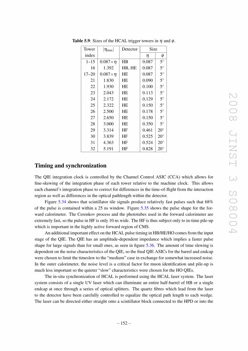
2008 JINST 3 S08004
Table 5.9: Sizes of the HCAL trigger towers in η and φ .
Tower |ηmax| Detector Sizeindex η φ
1–15 0.087×η HB 0.087 5
16 1.392 HB, HE 0.087 5
17–20 0.087×η HE 0.087 5
21 1.830 HE 0.090 5
22 1.930 HE 0.100 5
23 2.043 HE 0.113 5
24 2.172 HE 0.129 5
25 2.322 HE 0.150 5
26 2.500 HE 0.178 5
27 2.650 HE 0.150 5
28 3.000 HE 0.350 5
29 3.314 HF 0.461 20
30 3.839 HF 0.525 20
31 4.363 HF 0.524 20
32 5.191 HF 0.828 20
Timing and synchronization
The QIE integration clock is controlled by the Channel Control ASIC (CCA) which allows forfine-skewing of the integration phase of each tower relative to the machine clock. This allowseach channel’s integration phase to correct for differences in the time-of-flight from the interactionregion as well as differences in the optical pathlength within the detector.
Figure 5.34 shows that scintillator tile signals produce relatively fast pulses such that 68%of the pulse is contained within a 25 ns window. Figure 5.35 shows the pulse shape for the for-ward calorimeter. The Cerenkov process and the phototubes used in the forward calorimeter areextremely fast, so the pulse in HF is only 10 ns wide. The HF is thus subject only to in-time pile-upwhich is important in the highly active forward region of CMS.
An additional important effect on the HCAL pulse timing in HB/HE/HO comes from the inputstage of the QIE. The QIE has an amplitude-dependent impedance which implies a faster pulseshape for large signals than for small ones, as seen in figure 5.36. The amount of time slewing isdependent on the noise characteristics of the QIE, so the final QIE ASICs for the barrel and endcapwere chosen to limit the timeslew to the “medium” case in exchange for somewhat increased noise.In the outer calorimeter, the noise level is a critical factor for muon identification and pile-up ismuch less important so the quieter “slow” characteristics were chosen for the HO QIEs.
The in-situ synchronization of HCAL is performed using the HCAL laser system. The lasersystem consists of a single UV laser which can illuminate an entire half-barrel of HB or a singleendcap at once through a series of optical splitters. The quartz fibres which lead from the laserto the detector have been carefully controlled to equalize the optical path length to each wedge.The laser can be directed either straight onto a scintillator block connected to the HPD or into the
– 152 –

2008 JINST 3 S08004
Figure 5.34: Measured single event pulse shape from the scintillator tiles, representative ofHB/HE/HO pulse shapes.
Figure 5.35: Measured pulse shape, energy collected vs. time, for HF.
wedge. Within layer 9 of each wedge is an arrangement of optical fibres which mimic the time-of-flight from the interaction region. This arrangement allows the timing of HCAL to be flattened andmonitored, as has been demonstrated in test beam data taking, which verified the timing determinedby the laser using the synchronized beam. In the HO and HF detectors, only the photodetector canbe illuminated so the alignment will be based on construction and test beam data.
– 153 –

2008 JINST 3 S08004
Particle energy (GeV)1 10 210 310
Sig
nal
tim
e d
elay
(n
s)
0
2
4
6
8
10
12
14
16 Noise = 3800 e
Noise = 5420 e
Noise = 6900 e
Testbeam 2003
Figure 5.36: Pulse time variation as a function of signal amplitude as measured on the bench(solid points) for several input amplifier configurations compared with test beam measurementsfrom 2003.
The channel-by-channel bunch synchronization of HCAL will be determined using a his-togramming procedure in the serial link boards (SLBs) which determine the bunch synchroniza-tion using the beam structure of the LHC. The event and bunch synchronization is monitored usingfast control signals originating from the TTC system which are transmitted in the data stream be-tween the front-ends and the HTR. On a global scale, the bunch and event synchronization betweenthe HCAL and other detector subsystems is determined using muons and other correlated physicssignals.
5.6 HF luminosity monitor
The CMS luminosity measurement will be used to monitor the LHC’s performance on a bunch-by-bunch basis in real time and to provide an overall normalization for physics analyses. The designgoal for the real-time measurement is to determine the average luminosity with a 1% statisticalaccuracy with an update rate of 1 Hz. For offline analyses, the design goal is a systematic accuracyof 5%, although every reasonable effort will be made to produce a more accurate result. Both ofthese requirements must be met over a very large range of luminosities, extending from roughly1028 cm−2s−1 to 1034 cm−2s−1, and possibly beyond.
A number of techniques capable of providing suitable luminosity information in real timehave been identified [17]. One technique employs signals from the forward hadron calorimeter(HF) while another, called the Pixel Luminosity Telescope (PLT), uses a set of purpose-built parti-cle tracking telescopes based on single-crystal diamond pixel detectors. At the time of writing, thePLT has not been formally approved, but is under study. The methods based on signals from theHF are the ones being most vigorously pursued.
– 154 –

2008 JINST 3 S08004
Two methods for extracting a real-time relative instantaneous luminosity with the HF havebeen studied. The first method is based on zero counting in which the average fraction of emptytowers is used to infer the mean number of interactions per bunch crossing. The second methodexploits the linear relationship between the average transverse energy per tower and the luminosity.
Outputs of the QIE chips used to digitize the signals from the HF PMTs on a bunch-by-bunchbasis are routed to a set of 36 HCAL Trigger and Read-out (HTR) boards, each of which services 24HF physical towers. In order to derive a luminosity signal from the HTR, an additional mezzanineboard called the HF luminosity transmitter (HLX) is mounted on each of the HTR boards. The HLXtaps into the raw HF data stream and collects channel occupancy and ET -sum data and transmitsthem to a central collector node over standard 100-Mbps Ethernet. The HLX boards have the sameform factor as the Synchronization and Link Boards (SLBs) used to interface the ECAL and HCALreadouts to the Regional Calorimeter Trigger (RCT) system.
Although all HF channels can be read by the HLX, MC studies indicate that the best linearityfor occupancy histograms is obtained using just two η rings. Hence two sets of two rings areused for the occupancy histograms. Four rings are combined to form the ET -sum histogram. Thealgorithm has been optimized to minimize sensitivity to pedestal drifts, gain changes and otherrelated effects. Each of the two sets of rings sends 12 bits of data to the HLX. There are threeoccupancy histograms dedicated to each of the following possible states for each tower: enabled-below-threshold, over-threshold-1, over-threshold-2. In addition, a 15-bit ET sum value is sent tothe HLX and a further histogram based on all 13 HF η rings is filled for use by the LHC. As a result,the input to the HLX is used to create eight histograms: two sets of three occupancy histograms,one ET -sum histogram, and one additional occupancy histogram.
Each histogram has 3564 bins, one for each bunch in the LHC orbit. Each occupancy-histogram bin uses two bytes, and there are four bytes per bin in the ET sum histogram. Thebaseline design is to add the results from all desirable channels into a single set of histograms.
The histograms are transmitted as UDP (User Datagram Protocol) packets from the HLXcards once roughly every 0.37 s, which is safely within the 1.45 s (worst case) histogram overflowtime. The Ethernet core in the HLX automatically packages the data to make optimal use of net-work bandwidth. Each histogram spans several Ethernet packets, the precise number dependingon the type of histogram. The eight sets of histograms comprise about 70 kB of data, which istransmitted at a rate of approximately 1.6 Mbps to an Ethernet switch that aggregates the data frommultiple HLX boards. The switch multi-casts the data to a pair of luminosity server nodes. Oneof the servers is responsible for publishing the luminosity information to various clients, such asthe CMS and LHC control rooms and the Fermilab Remote Operations Center (ROC). The secondserver archives the data for each luminosity section (one luminosity section corresponds to 220 or-bits, or about 93 s). An XDAQ layer on this server makes it possible to communicate with otherCMS DAQ systems.
– 155 –

2008 JINST 3 S08004
Chapter 6
Forward detectors
6.1 CASTOR
The CASTOR (Centauro And Strange Object Research) detector is a quartz-tungsten samplingcalorimeter [120], designed for the very forward rapidity region in heavy ion and proton-protoncollisions at the LHC. Its physics motivation is to complement the nucleus-nucleus physics pro-gramme [122], developed essentially in the baryon-free mid-rapidity region, and also the diffractiveand low-x physics in pp collisions [123]. CASTOR will be installed at 14.38 m from the interactionpoint, covering the pseudorapidity range 5.2 < |η | < 6.6. Figure 6.1 shows the location of CAS-TOR in the CMS forward region. The calorimeter will be constructed in two halves surroundingthe beam pipe when closed, as shown in figure 6.2. The calorimeter and its readout are designed insuch a way as to permit the observation of the cascade development of the impinging particles asthey traverse the calorimeter. The typical total and electromagnetic energies in the CASTOR accep-tance range (about 180 TeV and 50 TeV, respectively, according to HIJING [121] Pb-Pb simulationsat 5.5 TeV) can be measured with a resolution better than ≈1%.
The main advantages of quartz calorimeters are radiation hardness, fast response and com-pact detector dimensions [124], making them suitable for the experimental conditions encounteredin the very forward region at the LHC. The typical visible transverse sizes of hadronic and elec-tromagnetic showers in quartz calorimeters are 5–10 cm and about 10 mm respectively (for 95%signal containement), i.e. are a factor 3 to 4 times narrower than those in “standard” (scintillation)calorimeters [124]. A detailed description of the operation principle (including optimal geomet-rical specifications of the quartz and tungsten plates, and performances of light-guides, reflectorsand photodetectors) can be found in references [125, 126].
Tungsten-Quartz plates
The CASTOR detector is a Cerenkov-based calorimeter, similar in concept to the HF. It is con-structed from layers of tungsten (W) plates (alloy density ≈ 18.5 g/cm3) as absorber and fusedsilica quartz (Q) plates as active medium. For the electromagnetic (EM) section, the W plates havea thickness of 5.0 mm and the Q plates 2.0 mm. For the hadronic (HAD) section, the W and Qplates have thicknesses of 10.0 mm and 4.0 mm, respectively. The W/Q plates are inclined 45
with respect to the direction of the impinging particles, in order to maximize the Cerenkov light
– 156 –
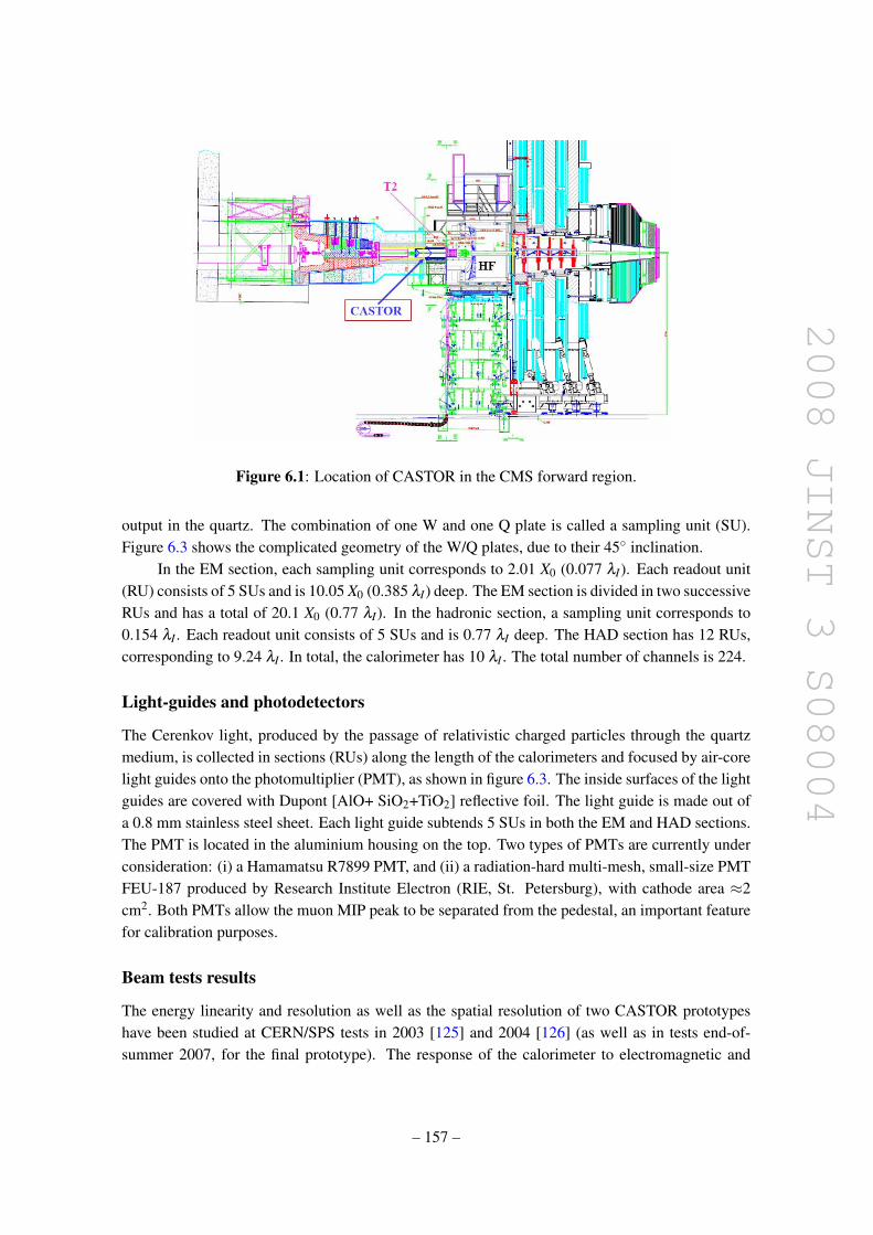
2008 JINST 3 S08004
Figure 6.1: Location of CASTOR in the CMS forward region.
output in the quartz. The combination of one W and one Q plate is called a sampling unit (SU).Figure 6.3 shows the complicated geometry of the W/Q plates, due to their 45 inclination.
In the EM section, each sampling unit corresponds to 2.01 X0 (0.077 λI). Each readout unit(RU) consists of 5 SUs and is 10.05 X0 (0.385 λI) deep. The EM section is divided in two successiveRUs and has a total of 20.1 X0 (0.77 λI). In the hadronic section, a sampling unit corresponds to0.154 λI . Each readout unit consists of 5 SUs and is 0.77 λI deep. The HAD section has 12 RUs,corresponding to 9.24 λI . In total, the calorimeter has 10 λI . The total number of channels is 224.
Light-guides and photodetectors
The Cerenkov light, produced by the passage of relativistic charged particles through the quartzmedium, is collected in sections (RUs) along the length of the calorimeters and focused by air-corelight guides onto the photomultiplier (PMT), as shown in figure 6.3. The inside surfaces of the lightguides are covered with Dupont [AlO+ SiO2+TiO2] reflective foil. The light guide is made out ofa 0.8 mm stainless steel sheet. Each light guide subtends 5 SUs in both the EM and HAD sections.The PMT is located in the aluminium housing on the top. Two types of PMTs are currently underconsideration: (i) a Hamamatsu R7899 PMT, and (ii) a radiation-hard multi-mesh, small-size PMTFEU-187 produced by Research Institute Electron (RIE, St. Petersburg), with cathode area ≈2cm2. Both PMTs allow the muon MIP peak to be separated from the pedestal, an important featurefor calibration purposes.
Beam tests results
The energy linearity and resolution as well as the spatial resolution of two CASTOR prototypeshave been studied at CERN/SPS tests in 2003 [125] and 2004 [126] (as well as in tests end-of-summer 2007, for the final prototype). The response of the calorimeter to electromagnetic and
– 157 –

2008 JINST 3 S08004
Figure 6.2: CASTOR calorimeter and support.
Figure 6.3: Details of the components and geometry of the CASTOR calorimeter.
hadronic showers has been analysed with E = 20–200 GeV electrons, E = 20–350 GeV pions, andE = 50, 150 GeV muons. Good energy linearity for electrons and pions in the full range tested isobserved. For the EM section, the constant term of the energy resolution, that limits performanceat high energies, is less than 1%, whereas the stochastic term is ≈ 50%. The measured spatialresolution of the electron (pion) showers is σEM(HAD) = 1.7 (6.4) mm.
– 158 –

2008 JINST 3 S08004
Figure 6.4: The side view of the ZDC show-ing the EM and HAD sections.
Figure 6.5: Photograph of the ZDC HADsection.
6.2 Zero degree calorimeter (ZDC)
A set of two zero degree calorimeters [127, 128], with pseudorapidity coverage of |η | ≥ 8.3 forneutral particles, are designed to complement the CMS very forward region, especially for heavyion and pp diffractive studies. Each ZDC has two independent parts: the electromagnetic (EM)and hadronic (HAD) sections. Two identical ZDCs will be located between the two LHC beampipes at ≈140 m on each side of the CMS interaction region at the detector slot of 1 m length, 96mm width and 607 mm height inside the neutral particle absorber TAN [129]. The TAN is locatedin front of the D2 separation dipole. It was designed to protect magnets and detectors againstdebris generated in the pp collisions, and against beam halo and beam losses. During heavy ionrunning the combined (EM + HAD) calorimeter should allow the reconstruction of the energy of2.75 TeV spectator neutrons with a resolution of 10–15%. Sampling calorimeters using tungstenand quartz fibers have been chosen for the detection of the energy in the ZDCs with a design similarto HF and CASTOR. The quartz-quartz fibers [127] can withstand up to 30 GRad with only a fewpercent loss in transparency in the wavelength range 300–425 nm. During the low-luminosity pp(1033 cm−2s−1) and design-luminosity Pb-Pb (1027 cm−2s−1) runs, the expected average absorbedradiation doses is about 180 MGy and 300 kGy, respectively, per data-taking year.
Figure 6.4 shows a side view of the ZDC with the EM section in front and the HAD sectionbehind. A photo of the HAD section is shown in figure 6.5. The total depth of the combined systemis ≈7.5 hadronic interaction lengths (λI). The configuration includes 9 mm Cu plates in the frontand back of each section. For the TAN’s final detector configuration an LHC real-time luminositymonitor (BRAN, Beam RAte of Neutrals [130]) will be mounted in the 120 mm space between theZDC’s calorimetric sections. The HAD section consists of 24 layers of 15.5 mm thick tungstenplates and 24 layers of 0.7 mm diameter quartz fibers (6.5 λI). The tungsten plates are tilted by 45
to optimize Cerenkov-light output. The EM section is made of 33 layers of 2-mm-thick tungstenplates and 33 layers of 0.7-mm-diameter quartz fibers (19 X0). The tungsten plates are orientedvertically. The fibers are laid in ribbons. The hadronic section of each ZDC requires 24 fiberribbons. After exiting the tungsten plates the fibers from 6 individual ribbons are grouped togetherto form a readout bundle. This bundle is compressed and glued with epoxy into a tube. From there,
– 159 –

2008 JINST 3 S08004
an optical air-core light guide will carry the light through radiation shielding to the photomultipliertube. The full hadronic section will consist of four identical towers divided in the longitudinaldirection. For the electromagnetic section, fibers from all 33 fiber ribbons will be divided in thehorizontal direction into five identical fiber bundles. These 5 bundles will form five horizontaltowers and each fiber bundle will be mounted with a 0.5 mm air gap from the photocathode of aphototube. The EM and HAD sections will be instrumented with the same type of phototube as theHF: Hamamatsu R7525 phototubes with a bi-alkali photocathode, resulting in an average quantumefficiency for Cerenkov light of about 10%.
There are a total of 18 readout channels for the two ZDCs. The signals from the ZDCsare transmitted through a long (210 m) coaxial cable to the front-end HCAL VME crates in theunderground counting room (USC55). The signal from each channel will be split, with 90% goingto the QIE (Charge Integrator and Encoder) while 10% will be used for making trigger signals.An analog sum, proportional to the total energy deposition in each detector, will provide the basicLevel 1 trigger in the heavy-ion running mode: the coincidence of (neutron) signals from both sidesof the interaction point is sensitive to most of the nuclear and electromagnetic cross section. A left-right timing coincidence will also be used as a fast vertex trigger, to suppress beam-gas eventsin the heavy ion runs. Information from scalers will be used for tuning the interaction of beamsand for defining the real-time luminosity. Finally it may be possible to improve the overall energyresolution of the system by looking at the correlation between the ZDC and the BRAN detector,which sits between the electromagnetic and hadronic sections, near the shower maximum.
The response of the ZDC EM and HAD sections has been studied in beam tests at theCERN/SPS in 2006 [131] and 2007. The calorimeter is found to be linear within 2% in the rangefrom 20 GeV to 100 GeV. The energy resolution obtained for the different positron energies can beparametrized as (
σ
E
)2=(
70%√E
)2
+(8%)2 (6.1)
where E is in GeV. Positive pions with energies of 150 GeV and 300 GeV were used to measure theresponse of the combined EM+HAD system. The pion energy resolution, obtained by a Landau fit,can be parametrized as
σ
E=
138%√E
+13% (6.2)
where E, again, is in GeV. The width of EM showers is ≈5 mm. Such a good position resolutionwill allow measurement of the beam crossing angle with a resolution of ≈10 mrad.
The performance of both the left and right ZDCs has been studied with electron, pion andmuon beams in 2007. Figure 6.6 shows online plots for positrons entering the electromagneticsection of one calorimeter.
– 160 –

2008 JINST 3 S08004
0
200
400
600
800
0 50 100 150Positron Energy, GeV
Res
pons
e, a
.u.
0
5
10
15
20
25
0 50 100 150Positron Energy, GeV
Res
olut
ion,
%
Figure 6.6: Online results for positrons from the 2007 test beam. The top panel shows the responselinearity, while the bottom panel gives the energy resolution as a function of the incoming positronbeam energy.
– 161 –

2008 JINST 3 S08004
Chapter 7
The muon system
Muon detection is a powerful tool for recognizing signatures of interesting processes over the veryhigh background rate expected at the LHC with full luminosity. For example, the predicted decay ofthe Standard Model Higgs boson into ZZ or ZZ∗, which in turn decay into 4 leptons, has been called“gold plated” for the case in which all the leptons are muons. Besides the relative ease in detectingmuons, the best 4-particle mass resolution can be achieved if all the leptons are muons because theyare less affected than electrons by radiative losses in the tracker material. This example, and othersfrom SUSY models, emphasize the discovery potential of muon final states and the necessity forwide angular coverage for muon detection.
Therefore, as is implied by the experiment’s middle name, the detection of muons is of centralimportance to CMS: precise and robust muon measurement was a central theme from its earliestdesign stages. The muon system has 3 functions: muon identification, momentum measurement,and triggering. Good muon momentum resolution and trigger capability are enabled by the high-field solenoidal magnet and its flux-return yoke. The latter also serves as a hadron absorber for theidentification of muons. The material thickness crossed by muons, as a function of pseudorapidity,is shown in figure 7.1.
The CMS muon system is designed to have the capability of reconstructing the momentumand charge of muons over the the entire kinematic range of the LHC. CMS uses 3 types of gaseousparticle detectors for muon identification [132]. Due to the shape of the solenoid magnet, themuon system was naturally driven to have a cylindrical, barrel section and 2 planar endcap regions.Because the muon system consists of about 25 000 m2 of detection planes, the muon chambers hadto be inexpensive, reliable, and robust.
In the barrel region, where the neutron-induced background is small, the muon rate is low,and the 4-T magnetic field is uniform and mostly contained in the steel yoke, drift chambers withstandard rectangular drift cells are used. The barrel drift tube (DT) chambers cover the pseudora-pidity region |η | < 1.2 and are organized into 4 stations interspersed among the layers of the fluxreturn plates. The first 3 stations each contain 8 chambers, in 2 groups of 4, which measure themuon coordinate in the r-φ bending plane, and 4 chambers which provide a measurement in thez direction, along the beam line. The fourth station does not contain the z-measuring planes. The2 sets of 4 chambers in each station are separated as much as possible to achieve the best angularresolution. The drift cells of each chamber are offset by a half-cell width with respect to their
– 162 –

2008 JINST 3 S08004
η0 0. 5 1 1. 5 2 2. 5 3
Inte
ract
ion
leng
ths
0
5
10
15
20
25
30
E C AL
HCAL H FH O
MB1ME11
ME12
ME13
MB2
ME21
ME22
MB3
ME31ME32
MB4
ME41
1st Muon Station
3rd Muon Station
2nd Muon Station
4th Muon Station
Figure 7.1: Material thickness in interaction lengths at various depths, as a function of pseudora-pidity.
neighbor to eliminate dead spots in the efficiency. This arrangement also provides a convenientway to measure the muon time with excellent time resolution, using simple meantimer circuits,for efficient, standalone bunch crossing identification. The number of chambers in each stationand their orientation were chosen to provide good efficiency for linking together muon hits fromdifferent stations into a single muon track and for rejecting background hits.
In the 2 endcap regions of CMS, where the muon rates and background levels are high andthe magnetic field is large and non-uniform, the muon system uses cathode strip chambers (CSC).With their fast response time, fine segmentation, and radiation resistance, the CSCs identify muonsbetween |η | values of 0.9 and 2.4. There are 4 stations of CSCs in each endcap, with chamberspositioned perpendicular to the beam line and interspersed between the flux return plates. Thecathode strips of each chamber run radially outward and provide a precision measurement in ther-φ bending plane. The anode wires run approximately perpendicular to the strips and are alsoread out in order to provide measurements of η and the beam-crossing time of a muon. Each 6-layer CSC provides robust pattern recognition for rejection of non-muon backgrounds and efficientmatching of hits to those in other stations and to the CMS inner tracker.
Because the muon detector elements cover the full pseudorapidity interval |η |< 2.4 with noacceptance gaps, muon identification is ensured over the range corresponding to 10 < θ < 170.Offline reconstruction efficiency of simulated single-muon samples (figure 7.2) is typically 95–99%except in the regions around |η |= 0.25 and 0.8 (the regions between 2 DT wheels) and |η |= 1.2(the transition region between the DT and CSC systems), where the efficiency drops. Negligiblepunchthrough reaches the system due to the amount of material in front of the muon system, whichexceeds 16 interaction lengths [132].
Due to multiple-scattering in the detector material before the first muon station, the offlinemuon momentum resolution of the standalone muon system is about 9% for small values of η and pfor transverse momenta up to 200 GeV [17]. At 1 TeV the standalone momentum resolution variesbetween 15% and 40%, depending on |η |. A global momentum fit using also the inner tracker
– 163 –

2008 JINST 3 S08004
|η|0 0.5 1 1.5 2 2.5
Eff
icie
ncy
0.8
0.82
0.84
0.86
0.88
0.9
0.92
0.94
0.96
0.98
1
= 10 GeV/cT
pμ
= 50 GeV/cT
pμ
= 100 GeV/cT
pμ
= 500 GeV/cT
pμ
= 1000 GeV/cT
pμ
|η|0 0.5 1 1.5 2 2.5
Eff
icie
ncy
0.8
0.82
0.84
0.86
0.88
0.9
0.92
0.94
0.96
0.98
1
= 10 GeV/cT
pμ
= 50 GeV/cT
pμ
= 100 GeV/cT
pμ
= 500 GeV/cT
pμ
= 1000 GeV/cT
pμ
Figure 7.2: Muon reconstruction efficiency as a function of pseudorapidity for selected values ofpT . Left panel: standalone reconstruction (using only hits from the muon system with a vertexconstraint). Right panel: global reconstruction (using hits from both the muon system and thetracker).
improves the momentum resolution by an order of magnitude at low momenta. At high momenta(1 TeV) both detector parts together yield a momentum resolution of about 5% (figure 1.2). Notethat the muon system and the inner tracker provide independent muon momentum measurements;this redundancy enhances fault finding and permits cross-checking between the systems.
A crucial characteristic of the DT and CSC subsystems is that they can each trigger on thepT of muons with good efficiency and high background rejection, independent of the rest of thedetector. The Level-1 trigger pT resolution is about 15% in the barrel and 25% in the endcap.
Because of the uncertainty in the eventual background rates and in the ability of the muonsystem to measure the correct beam-crossing time when the LHC reaches full luminosity, a com-plementary, dedicated trigger system consisting of resistive plate chambers (RPC) was added inboth the barrel and endcap regions. The RPCs provide a fast, independent, and highly-segmentedtrigger with a sharp pT threshold over a large portion of the rapidity range (|η |< 1.6) of the muonsystem. The RPCs are double-gap chambers, operated in avalanche mode to ensure good operationat high rates. They produce a fast response, with good time resolution but coarser position reso-lution than the DTs or CSCs. They also help to resolve ambiguities in attempting to make tracksfrom multiple hits in a chamber.
A total of 6 layers of RPCs are embedded in the barrel muon system, 2 in each of the first 2stations, and 1 in each of the last 2 stations. The redundancy in the first 2 stations allows the triggeralgorithm to work even for low-pT tracks that may stop before reaching the outer 2 stations. In theendcap region, there is a plane of RPCs in each of the first 3 stations in order for the trigger to usethe coincidences between stations to reduce background, to improve the time resolution for bunchcrossing identification, and to achieve a good pT resolution.
Finally, a sophisticated alignment system measures the positions of the muon detectors withrespect to each other and to the inner tracker, in order to optimize the muon momentum resolution.
– 164 –

2008 JINST 3 S08004
7.1 Drift tube system
7.1.1 General description
The CMS barrel muon detector consists of 4 stations forming concentric cylinders around the beamline: the 3 inner cylinders have 60 drift chambers each and the outer cylinder has 70. There areabout 172 000 sensitive wires. It is possible to use drift chambers as the tracking detectors for thebarrel muon system because of the low expected rate and the relatively low strength of the localmagnetic field.
The wire length, around 2.4 m in the chambers measured in an r-φ projection, is constrainedby the longitudinal segmentation of the iron barrel yoke. The transverse dimension of the drift cell,i.e., the maximum path and time of drift, was chosen to be 21 mm (corresponding to a drift time of380 ns in a gas mixture of 85% Ar + 15% CO2). This value is small enough to produce a negligibleoccupancy and to avoid the need for multi-hit electronics, yet the cell is large enough to limit thenumber of active channels to an affordable value. A tube was chosen as the basic drift unit to obtainprotection against damage from a broken wire and to partially decouple contiguous cells from theelectromagnetic debris accompanying the muon itself.
The amount of iron in the return yoke was dictated by the decision to have a large and intensesolenoidal magnetic field at the core of CMS. Two detector layers, one inside the yoke and theother outside, would be insufficient for reliable identification and measurement of a muon in CMS.Therefore, 2 additional layers are embedded within the yoke iron (figure 7.3). In each of the 12sectors of the yoke there are 4 muon chambers per wheel, labeled MB1, MB2, MB3, and MB4.The yoke-iron supports that are between the chambers of a station generate 12 unavoidable deadzones in the φ coverage, although the supports are placed so as not to overlap in φ .
A drift-tube (DT) chamber is made of 3 (or 2) superlayers (SL, see figure 7.4), each made of4 layers of rectangular drift cells staggered by half a cell. The SL is the smallest independent unitof the design.
The wires in the 2 outer SLs are parallel to the beam line and provide a track measurementin the magnetic bending plane (r-φ ). In the inner SL, the wires are orthogonal to the beam lineand measure the z position along the beam. This third, z-measuring, SL is not present in the fourthstation, which therefore measures only the φ coordinate. A muon coming from the interactionpoint first encounters a φ -measuring SL, passes through the honeycomb plate, then crosses the z-measuring SL and the second φ -measuring SL. In this scenario, there still exist limited regions ofη in which the combined effect of the φ and z discontinuities limits to only 2 (out of 4), the numberof stations crossed by a muon.
At high momenta (≥40 GeV), the probability of electromagnetic cascades accompanying theparent muon becomes relevant. A reliable way to cope with this effect in the regions where only2 stations are available is to have a good tracking efficiency in each station even in the presenceof electromagnetic debris. Redundancy is also needed to cope with the uncorrelated backgroundhits generated by neutrons and photons whose rate is much larger than that from prompt muons.Redundancy is obtained by having several layers of separated drift cells per station. The separation,i.e., the thickness of the tube walls, should be large enough to decouple the basic units against low-energy electrons. The relatively thick wall of the DTs, 1.5 mm, gives an effective decoupling among
– 165 –

2008 JINST 3 S08004
µ
TC
TC
TC
TC
TC
TC
TC
TC
TC
TC
TC
TC
COIL
HB
EB
YB/Z/1/4
YB/Z/2/4
YB/Z/3/4
MB/Z/1/4
MB/Z/2/4
MB/Z/3/4
MB/Z/4/4
YB/Z/1/5YB/Z/2/5
YB/Z/3/5
MB/Z/1/5MB/Z/2/5
MB/Z/3/5
MB/Z/4/5
YB/Z
/1/6
YB/Z
/2/6
YB/Z
/3/6
MB/
Z/1/
6
MB/
Z/2/
6
MB/
Z/3/
6
MB/
Z/4/
6
YB
/Z/1
/7
YB
/Z/2
/7
YB
/Z/3
/7
MB
/Z/1
/7
MB
/Z/2
/7
MB
/Z/3
/7
MB
/Z/4
/7
YRB/
Z/1/
8YB
/Z/2
/8YB
/Z/3
/8
MB/
Z/1/
8M
B/Z/
2/8
MB/
Z/3/
8
MB/
Z/4/
8
YB/Z/1/9
YB/Z/2/9
YB/Z/3/9
MB/Z/1/9
MB/Z/2/9
MB/Z/3/9
MB/Z/4/9
YB/Z/1/10
YB/Z/2/10
YB/Z/3/10
MB/Z/1/10
MB/Z/2/10
MB/Z/3/10
MB/Z/4/10
YB/Z/1/11YB/Z/2/11
YB/Z/3/11
MB/Z/1/11MB/Z/2/11
MB/Z/3/11
MB/Z/4/11
YB/Z/1/12
YB/Z/2/12
YB/Z/3/12
MB/Z/1/12
MB/Z/2/12
MB/Z/3/12
MB/Z/4/12
YB
/Z/1/1
YB
/Z/2/1
YB
/Z/3/1
MB
/Z/2/1
MB
/Z/3/1
MB
/Z/4/1
YB/Z/1/2YB/Z/2/2
YB/Z/3/2
MB/Z/1/2
MB/Z/2/2
MB/Z/3/2
MB/Z/4/2
YB/Z/1/3
YB/Z/2/3
YB/Z/3/3
MB/Z/1/3
MB/Z/2/3
MB/Z/3/3
MB/Z/4/3
X
TowardsCenter of LHC
ϕ
Z+
Y
MB
/Z/1/1
Figure 7.3: Layout of the CMS barrel muon DT chambers in one of the 5 wheels. The chambers ineach wheel are identical with the exception of wheels –1 and +1 where the presence of cryogenicchimneys for the magnet shortens the chambers in 2 sectors. Note that in sectors 4 (top) and 10(bottom) the MB4 chambers are cut in half to simplify the mechanical assembly and the globalchamber layout.
the several layers of tubes inside the same station. With this design, the efficiency to reconstruct ahigh pT muon track with a momentum measurement delivered by the barrel muon system alone isbetter than 95% in the pseudorapidity range covered by 4 stations, i.e., η < 0.8. The constraints ofmechanical stability, limited space, and the requirement of redundancy led to the choice of a tubecross section of 13 × 42 mm2.
The many layers of heavy tubes require a robust and light mechanical structure to avoid sig-nificant deformations due to gravity in the chambers, especially in those that lie nearly horizontal.The chosen structure is basically frameless and for lightness and rigidity uses an aluminium honey-comb plate that separates the outer superlayer(s) from the inner one (figure 7.4). The SLs are gluedto the outer faces of the honeycomb. In this design, the honeycomb serves as a very light spacer,
– 166 –

2008 JINST 3 S08004
RPCRPC
RPCRPC
Figure 7.4: A DT chamber in position inside the iron yoke; the view is in the (r-φ ) plane. One cansee the 2 SLs with wires along the beam direction and the other perpendicular to it. In between isa honeycomb plate with supports attached to the iron yoke. Not shown are the RPCs, which areattached to the DT chambers via support plates glued to the bottom and/or top faces, depending onchamber type.
with rigidity provided by the outer planes of tubes. A thick spacer also helps to improve angularresolution within a station. Table 7.1 provides a summary of the general DT chamber parameters.
One SL, that is, a group of 4 consecutive layers of thin tubes staggered by half a tube, givesexcellent time-tagging capability, with a time resolution of a few nanoseconds. This capabilityprovides local, stand-alone, and efficient bunch crossing identification. The time tagging is delayedby a constant amount of time equal to the maximum possible drift-time, which is determined bythe size of the tube, the electrical field, and the gas mixture. Within the angular range of interest,the time resolution was shown to be largely independent of the track angle, but this requires thecell optics to maintain a linear relationship between the distance from the wire of the crossing trackand the drift-time of the electrons along the entire drift path. bunch crossing tagging is performedindependently in each of the 3 SLs by fast pattern-recognition circuitry. Together with the bunchcrossing assignment, this circuit delivers the position of the centre of gravity of the track segmentand its angle in the SL reference system with precisions of 1.5 mm and 20 mrad, respectively.This information is used by the first-level muon trigger for the time and transverse momentumassignment.
The goal of the mechanical precision of the construction of a chamber was to achieve aglobal resolution in r-φ of 100 µm. This figure makes the precision of the MB1 chamber (theinnermost layer) comparable to the multiple scattering contribution up to pT = 200 GeV. The 100-µm target chamber resolution is achieved by the 8 track points measured in the two φ SLs, since
– 167 –

2008 JINST 3 S08004
Table 7.1: Chambers of the CMS DT system. Notation: MB/wheel/station/sector. W stands for all5 wheels (numbered –2, –1, 0, 1, and 2) and S means any sector (1 to 12, see figure 7.3). The SLsof type Φ(Θ) measure the φ (z) coordinate in the CMS coordinate system.
chamber No. of No. of No. of No. of ch. No. of ch. Wire length Wire length Sum oftype chambers SL Φ SL Θ SL Φ SL Θ Φ (mm) Θ (mm) ch.
MB/W/1/S 58 2 1 196 228 2379 2038 35960MB/1/1/4 1 2 1 196 190 1989 2038 582
MB/-1/1/3 1 2 1 196 190 1989 2038 582MB/W/2/S 58 2 1 238 228 2379 2501 40832MB/1/2/4 1 2 1 238 190 1989 2501 666
MB/-1/2/3 1 2 1 238 190 1989 2501 666MB/W/3/S 58 2 1 286 228 2379 3021 46400MB/1/3/4 1 2 1 286 190 1989 3021 762
MB/-1/3/3 1 2 1 286 190 1989 3021 762MB/W/4/S 29 2 0 382 0 2379 0 22156MB/-1/4/3 1 2 0 382 0 1989 0 764MB/W/4/4 8 2 0 286 0 2379 0 4576MB/1/4/4 2 2 0 286 0 1989 0 1144
MB/W/4/8,12 10 2 0 372 0 2379 0 7440MB/W/4/9,11 10 2 0 190 0 2379 0 3800
MB/W/4/10 10 2 0 238 0 2379 0 4760total 250 171852
the single wire resolution is better than 250 µm. To avoid corrections to the primary TDC data(section 7.1.3), the deviation from linearity of the space-time relation in each drift cell must beless than 100–150 µm. This figure matches well with the requirements of linearity for the bunchcrossing (section 7.1.3) identifier. The cell design includes 5 electrodes, 1 anode wire, 2 fieldshaping strips, and 2 cathode strips (figure 7.5 and section 7.1.2). The requirements of 250-µmresolution and 150-µm nonlinearity can be obtained by operating the tubes at atmospheric pressurewith an Ar/CO2 gas mixture and by keeping the CO2 concentration in the 10–20% range. Themulti-electrode design also ensures this performance in the presence of the stray magnetic fieldpresent in some regions of the chambers. It is worth noting that to reach this local performance ina single tube, the precision requirement on the position of the field-shaping electrodes, includingthe wires, is about 300 µm, which is considerably less demanding than the 100 µm required forthe mechanical construction.
7.1.2 Technical design
Drift cell
Figure 7.5 shows the drift lines in a cell. The anode is a 50-µm-diameter gold-plated stainless-steel wire. The field electrode is made of a 16-mm-wide, 50-µm thick aluminium tape, glued on a100-µm thick, 23-mm-wide mylar tape that insulates the electrode with respect to the aluminiumplate set to ground. Both the conductive and insulating ribbons are self-adhesive with a pressure-activated glue. Field electrodes are positioned at the top and bottom of the drift cell. Cathodes
– 168 –

2008 JINST 3 S08004
Figure 7.5: Sketch of a cell showing drift lines and isochrones. The plates at the top and bottomof the cell are at ground potential. The voltages applied to the electrodes are +3600V for wires,+1800V for strips, and −1200V for cathodes.
Figure 7.6: Exploded view of the cathodeelectrodes, glued on the I-beams.
Figure 7.7: Exploded view of the end part ofthe drift cells showing the different end-plugsand spring contacts for high voltage connec-tions.
are placed on both sides of the I-beams (figure 7.6) following a technique similar to that used forthe strip electrodes on the aluminium plates. A cathode consists of a 50-µm-thick, 11.5-mm-widealuminium tape insulated from the I-beam by 19-mm-wide, 100-µm-thick mylar tape. This designallows for at least 3.5 mm separation of the electrode from the sides of the grounded I-beam. Atthe extremities the mylar tape is cut flush with respect to the I-beam ends while the aluminium tapeis recessed by 5 mm. Special tools were designed and built to glue the electrode strips to both theplates and the I-beams. The only difference between the tapes used for the electrode strips and the
– 169 –

2008 JINST 3 S08004
ones just described is the width: the mylar tape used for the electrode strips is 23-mm wide andthe aluminium tape is 16-mm wide. These strips are set to a positive voltage and help to improvethe shaping of the electric field and the linearity of the space-time relation, most noticeably in thepresence of magnetic fields.
The cathode and wire end-plugs were designed to protect against discharges from the borderat the end of the cathode strips and to house the wire holder, which is crucial for the wire positionprecision. The wire holders protrude inside the cell providing 12 mm of additional protectionaround the wire. The I-beam and wire end-plug pieces, as well as the springs connecting theelectrodes to the high voltage, are shown in figure 7.7. The Ar-CO2 mixture and the drift-celloptics described above provide a linear relationship between time and drift path. This is an essentialrequirement for the use of the chamber as a first-level trigger device [133]. A calculation of thedrift velocity using GARFIELD [134] showed that drift velocity saturation occurs between 1 and2 kV/cm (figure 7.8). This may be compared to the the drift velocity as measured with the DriftVelocity Chamber (VdC) (figure 7.9).
The drift cells will operate at a gas gain of 105, allowing them to work within an efficiencyplateau with a wide threshold range, which is convenient for the operation of large chambers in theenvironment expected at CMS. A computation of equipotential lines [136] (figure 7.10) is usefulfor better understanding of the role of each electrode. The position of the 0 V equipotential in theregion between the central strips and the cathodes is mainly determined by the size of the electrodesand not by their voltage values. The gas gain is mainly determined by the voltage drop from thewire to the nearest electrode, the strips. The wire/strip voltage difference must be kept between 1.75and 1.85 kV to achieve a gain not far from the expected value of 105. Under the rough assumptionof a uniform drift field of 1.5 kV/cm, the distances between the various electrodes imply that thestrips should be set to a voltage larger than or equal to 1.7 kV and the cathodes to around −1 kV.As described below, during the chamber commissioning in laboratories and at CERN (with B=0),satisfactory performance was obtained with the voltages of cathodes, strips, and wires set to −1.2,+1.8, and +3.6 kV, respectively.
Chamber mechanics and services
A chamber is assembled by gluing 3 (or 2) SLs to an aluminium honeycomb plate to ensure therequired stiffness. Each SL is made of 5 aluminium sheets, 1.5-mm thick, separated by 11.5-mm-high, 1-mm-thick aluminium I-beams, as described in section 7.1.2. The cell pitch is 42 mm,while the layer pitch is 13 mm. For the construction of the SLs, a full layer of cells is built atthe same time by gluing together 2 aluminium plates separated by an array of parallel aluminiumI-beams. The pitch and height of an I-beam determine the larger and smaller dimensions of a cell,respectively. An SL has an independent gas and electronics enclosure. Each SL is assembled andtested individually before being glued to the honeycomb plate and/or to the other SL to form achamber.
HV connections to the cells and the front-end electronics are located at opposite ends of thewires. The HV is fed into each SL via two 52-pin custom connectors and distributed to the driftcells via printed-circuit HV boards (HVB). Each HVB is mounted along the edge of the aluminiumplate separating 2 layers of drift cells and serves the 8 cells above and the 8 cells below it. One
– 170 –
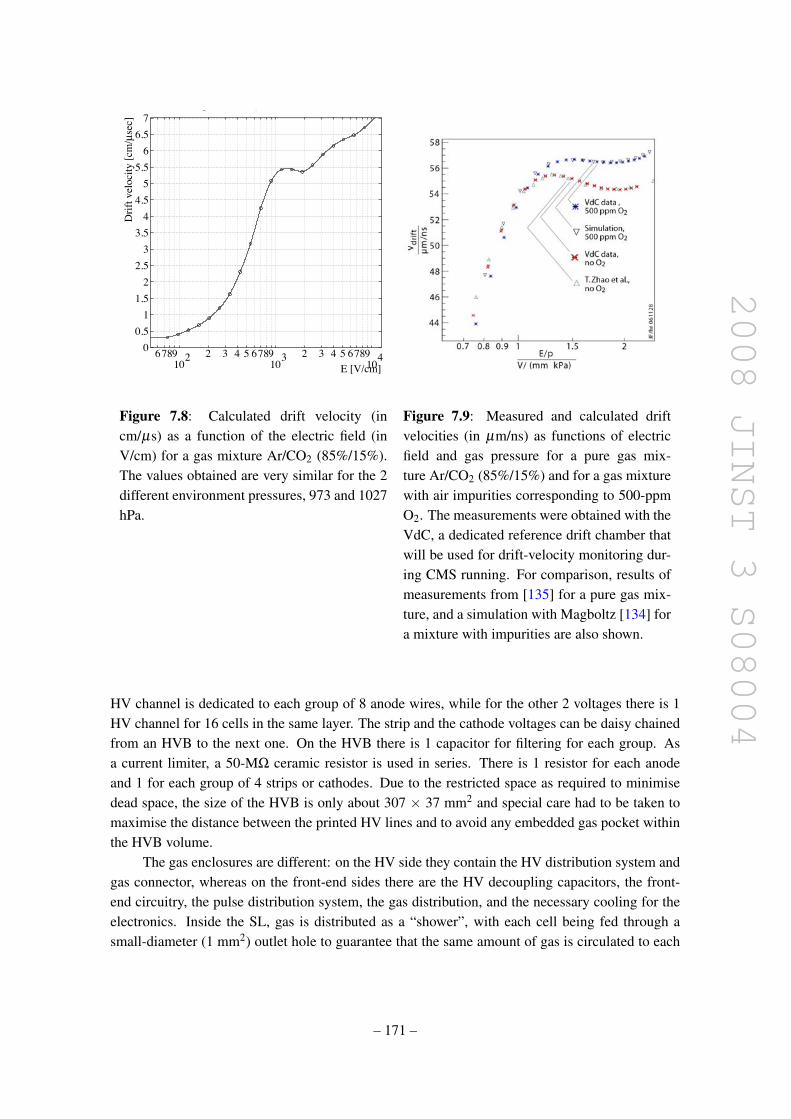
2008 JINST 3 S08004
678910
2 2 3 4 5 678910
3 2 3 4 5 678910
4
20
40
60
80
100
120
140
160
180
200
220
240
260
280
300
320
340
Diffusion coefficients vs E
E [V/cm]
Dif
fusi
on
[µm
fo
r 1
cm
]
Gas: Ar 85%, CO2 15%, T=293 K, p=1 atm
0.2
0.4
0.6
0.8
1 1.2
1.4
1.6
1.8
10-7
10-6
10-5
10-4
10-3
10-2
10-1
Cluster size distribution
Number of pairs in a cluster
!1
03
Pro
bab
ilit
y
Under: 0, in: 1, over: 0Gas: Ar 85%, CO2 15%, T=293 K, p=1 atm
Origin: LANDAU
Figure 3: (Left) Transverse (dashed) and longitudinal (solid) diffusion coefficients versus electric field, calculated
by HEED in the absence of magnetic field. (Right) Cluster size distribution for the simulated cell.
0.2
0.4
0.6
0.8
1 1.2
1.4
1.6
1.8
20
0.1
0.2
0.3
0.4
0.5
0.6
0.7
0.8
0.9
1
1.1
1.2
Contours of V
x-Axis [cm]
y-A
xis
[cm
]
Cell: Test MB Cell
-1000-1000-1000
-1000
-1000
-1000
-800
-800
-800
-800
-600
-600
-600
-600
-400
-400
-400
-400
-400
-400
-400
-400
-400
-400-200-200
-200
-200
-200
-200-2
00
0
00
00
200
200
200
200
200
200
200
400
400
400
400
400
400
600
600
600
600
600
600
600
800
800
800
800
800
800
800
1000
1000
1000
1000
1200
1200
1200
1200
1400
1400
1400
1400
1600
1600
160016
00
1600
1800
1800
2000
2000
2000
2000
2200
2200
2200
2200 2
4002
400
2400
2600
2600
678910
2 2 3 4 5 678910
3 2 3 4 5 678910
40
0.5
1
1.5
2
2.5
3
3.5
4
4.5
5
5.5
6
6.5
7
Drift velocity vs E
E [V/cm]
Dri
ft v
eloci
ty [c
m/µ
sec]
Gas: Ar 85%, CO2 15%, T=293 K, p=1 atm
Figure 4: (Left) Equipotential lines computed by GARFIELD for a half-cell. (Right) Drift velocity of electrons as
function of the electric field along the cell.
8
Figure 7.8: Calculated drift velocity (incm/µs) as a function of the electric field (inV/cm) for a gas mixture Ar/CO2 (85%/15%).The values obtained are very similar for the 2different environment pressures, 973 and 1027hPa.
Figure 7.9: Measured and calculated driftvelocities (in µm/ns) as functions of electricfield and gas pressure for a pure gas mix-ture Ar/CO2 (85%/15%) and for a gas mixturewith air impurities corresponding to 500-ppmO2. The measurements were obtained with theVdC, a dedicated reference drift chamber thatwill be used for drift-velocity monitoring dur-ing CMS running. For comparison, results ofmeasurements from [135] for a pure gas mix-ture, and a simulation with Magboltz [134] fora mixture with impurities are also shown.
HV channel is dedicated to each group of 8 anode wires, while for the other 2 voltages there is 1HV channel for 16 cells in the same layer. The strip and the cathode voltages can be daisy chainedfrom an HVB to the next one. On the HVB there is 1 capacitor for filtering for each group. Asa current limiter, a 50-MΩ ceramic resistor is used in series. There is 1 resistor for each anodeand 1 for each group of 4 strips or cathodes. Due to the restricted space as required to minimisedead space, the size of the HVB is only about 307 × 37 mm2 and special care had to be taken tomaximise the distance between the printed HV lines and to avoid any embedded gas pocket withinthe HVB volume.
The gas enclosures are different: on the HV side they contain the HV distribution system andgas connector, whereas on the front-end sides there are the HV decoupling capacitors, the front-end circuitry, the pulse distribution system, the gas distribution, and the necessary cooling for theelectronics. Inside the SL, gas is distributed as a “shower”, with each cell being fed through asmall-diameter (1 mm2) outlet hole to guarantee that the same amount of gas is circulated to each
– 171 –

2008 JINST 3 S08004
0.2
0.4
0.6
0.8
1 1.2
1.4
1.6
1.8
20
0.1
0.2
0.3
0.4
0.5
0.6
0.7
0.8
0.9
1
1.1
1.2
x-Axis [cm]
z-Axis[
cm]
-1000-1000-1000
-1000
-1000
-1000
-800
-800
-800-800
-600-600
-600
-600-400
-400
-400
-400
-400
-400
-400-400
-400
-400-200-200
-200
-200
-200
-200-200
0
0000
200200
200
200
200200
200
400
400
400400
400
400
600
600
600
600
600
600600
800800
800
800
800
800800
1000
10001000
1000
1200
12001200
1200
1400
1400
14001400
1600
1600
160016001600
1800
1800
2000
2000
20002000
2200
2200
22002200 24
002400240026002600
Figure 7.10: Equipotential lines in half of a drift cell. The anode wire is on the right side. Thelines are labeled with the potentials in volts (the x-axis is perpendicular to the wires on the wireplane, while the z-axis is orthogonal to the wire plane).
channel. The distance between the position where the wire enters the end plug and the outer faceof the gas enclosure, which determines the SL dead area, corresponds to 60 mm on both the HVand the front-end side (corresponding to ≈10% dead space).
It is very important that the individual SLs of the DT chambers are gas tight because contami-nation by nitrogen (from air) changes the drift velocity by a sizeable amount, while oxygen reducesthe signal efficiency, when its contamination exceeds 2000 ppm. Contamination by air including1000 ppm of O2 changes the maximum drift time by about 2% with respect to no contamination,with a sizeable effect on the trigger performance of the detector. In the DT chambers, the gas tight-ness of the SLs is obtained by gluing profiles to the outer aluminium skins. Along 2 sides of the SL,C-shaped profiles are used and the ends of these profiles are glued to reference blocks (figure 7.11),forming the corners of the SL box. The front and back of the box have L-shaped profiles gluedalong the plate border to form an open frame, which is then closed with removable long coverplates that contain all necessary gas connectors, HV connectors, and signal outputs, equipped withO-rings that seal the structure. A 3-dimensional computer model of the gas enclosure for one SL,where the outer aluminium plates have been removed to expose all details of the gas enclosure, isshown in figure 7.12. With this type of gas enclosure we can obtain a level of oxygen contaminationof 10–20 ppm, downstream of the 3 SLs flushed in parallel with about 1 volume change per day.
During SL assembly, before the fifth aluminium plate is glued closing the structure, referenceblocks are glued such that their positions with respect to the wires can be measured precisely. Thus,when the chamber is completed, the wire positions may be determined by measuring the reference
– 172 –

2008 JINST 3 S08004
Figure 7.11: Corner blocks of an SL. Thesepieces also carry the reference marks with re-spect to which the wire positions are mea-sured.
Figure 7.12: A 3-dimensional computermodel of the gas enclosure of the SLs.
marks on the blocks. Pressure and temperature monitoring probes, ground straps that connectall the aluminium planes to form a unique ground reference, and a Faraday cage for the signals,front-end electronics, and HV distribution complete the equipment that is in the gas enclosures ofeach SL.
Each SL is fully independent with respect to gas tightness, HV, and front-end electronics;hence an SL can be fully tested before it is glued to form a DT chamber. SLs are glued to ahoneycomb panel (figure 7.4) that sustains and gives rigidity to the chamber and provides thefixation points from which it is suspended in the CMS barrel steel yoke (two Φ-type SLs and oneΘ-type SL in the case of layers 1, 2, and 3; and two Φ-type SLs for layer 4). The panel thicknessvaries from 125 mm for the first three stations, to 178 mm for the fourth station. It is delivered withthe correct dimensions and equipped with the C-shaped profiles at the periphery that are used forthe supports and for part of the electronics.
The space for the chamber supports and attachments, the passages for alignment, and thelocal read-out and trigger electronics is provided by a channel running around the border of thehoneycomb plate. The channel is approximately as wide and deep as the honeycomb plate thick-ness. The 2 channels parallel to the beam line and to the yoke steel supports house the kinematicfixations to the yoke supports themselves, and the longitudinal alignment passages. One of the 2remaining sides houses the read-out and trigger electronics that collect the full chamber informa-tion (minicrates). To ease chamber handling, all services are connected on the same side of thechamber. All the general services for the chambers are located around each barrel wheel on the 4balconies along the walls of the CMS cavern where there is space for the racks and crates. Eachwheel is thus an independent, large subsystem.
– 173 –

2008 JINST 3 S08004
Figure 7.13: Block diagram of the DT electronic system.
7.1.3 Electronics
The DT electronics is a complex, heavily integrated system, which includes L1 trigger logic, read-out data handling, and service electronics, such as the LV and HV systems. A description ofthe electronic system layout together with the functions associated to each sub-task is shown infigure 7.13 and briefly summarized, whereas detailed information will be described in the followingsections.
Front-end electronics and HV distribution are physically embedded in the chamber gas vol-ume. Amplified and shaped signals are directly fed to the minicrates. A minicrate, as describedpreviously, is an aluminium structure attached to the honeycomb of the drift tube chambers thathouses both the first level of the read-out and of the trigger electronics. The trigger boards locatedin the minicrates are the Trigger Boards (TRB) and the Server Boards (SB), as described in detailin section 8.2. In each TRB are located the Bunch Crossing and Track Identifier (BTI), whichprovides independent segments from each chamber SL, and the Track Correlator (TRACO), whichcorrelates φ segments in the same chamber by requiring a spatial matching between segments oc-curring at the same bunch crossing (BX). TRB output signals are fed to the Server Board (SB)which selects the best two tracks from all TRACO candidates and sends the data out of the min-icrate. In parallel to the trigger signals, chamber data are fed to the read-out system through theRead Out Boards (ROB), which are in charge of the time digitization of chamber signals relatedto the Level-1 Accept (L1A) trigger decision and the data merging to the next stages of the dataacquisition chain. The Chamber Control Board (CCB) located at the centre of the minicrate, allowsROB and TRB configuration and monitoring. It works together with the CCB link board, on oneof the minicrate ends, that receives data from the Slow Control and global experiment Timing andTrigger Control (TTC) system. Among other tasks, the CCB distributes the LHC 40.08 MHz clockand other TTC signals to every board in the minicrate.
– 174 –

2008 JINST 3 S08004
Trigger and data signals coming out of the minicrates are collected by VME electronics in-stalled in the iron balconies attached to the DT wheels, respectively to the Sector Collector (SC,section 8.2) and to the Read Out Server (ROS, section 7.1.3) where data merging is performed.From the wheel balconies, data are sent via optical links, both to the CMS central acquisition sys-tem through the Detector Dependent Unit (DDU) (section 7.1.3) and to the CMS L1 system throughthe Sector Collector (SC) and the Drift Tube Track Finder (DTTF, section 8.2).
Front-end electronics
The front-end electronics for the barrel muon detector must satisfy many stringent requirements. Itsfunctions are to amplify the signals produced by the detector, compare them with a threshold, andsend the results to the trigger and read-out chains located on the chamber. Analog signal processingmust use a short shaping time to achieve a high spatial resolution while introducing minimal noise;this allows low-gain operation of the drift tubes, thus improving reliability and chamber lifetime.The downstream comparator has to be very fast and precise to allow the use of low threshold values,which reduce the influence of the signal amplitude on the time response. The output driver alsomust be very fast, and it must deliver differential levels that minimise mutual interferences and canbe transmitted through low-cost cables. Besides the above functions, several features that simplifythe control and monitoring of the data acquisition have been implemented. The large number ofchannels and the resulting need for both high reliability and low cost, limited space, and concernsabout power consumption led to the necessity to integrate the front-end electronics as much aspossible.
The resulting custom front-end application specific integrated circuit chip (ASIC), namedMAD, was developed using 0.8 µm BiCMOS technology [138]. This chip integrates signal pro-cessing for 4 channels (4 drift tubes) plus some ancillary functions in a 2.5 × 2.5 mm2 die and80 000 pieces were produced with a fabrication yield better than 95%. Figure 7.14 shows the ASICblock diagram and the pinout of the TQFP44 package used for it. Each of the 4 identical analogchains begins with a charge preamplifier that uses a single gain stage, folded/unfolded cascode,having a GBW product in excess of 1 GHz (result from simulation). The feedback time constant is33 ns while input impedance is ≈100 Ω in the range 5–200 MHz.
The shaper that follows is a low-gain integrator with a small time constant. Its output isdirectly connected to 1 input of a latched discriminator made of 2 differential gain stages, theother input being connected to the external threshold pin Vth, common to all channels. Auxiliarycircuits allow the masking of individual channels at the shaper input (pins A_ENn in high state)thus stopping the propagation of excessive noise background to the trigger and DAQ electronics.A similar but faster enable/disable function was implemented on the cable-driver stage to selectchannels that output signals in response to a test input. A temperature probe was also included formonitoring the operating conditions of the detector.
The ASIC operates with 2 distinct supply voltages, 5 V for the analog section and 2.5 V forthe output stage, with a total power consumption of 100 mW (25 mW/ch) equally split betweenthe 2 voltages and almost independent of the temperature and signal rate. Several tests have beencarried out on the MAD ASIC both on the bench and in the field in various configurations. For theanalog section an average gain of about 3.7 mV/fC was found for bare chips with (1370±48)/pF
– 175 –

2008 JINST 3 S08004
SHAPER
BLR
BLR
SHAPER
SHAPER
BLR
BLR
SHAPER
TEMPPROBE
DISCR
PA
LATCH
LATCH
LATCH
LATCH
DISCR
DISCR
DISCR
ONESHOT
LVDSDRIV
ONESHOT
ONESHOT
ONESHOT
LVDSDRIV
LVDSDRIV
LVDSDRIV
WIDTH CTRL
PA
PA
PA
In1
A_En1
A_En2
A_En3
A_En4
In2
In3
In4
GNA
Vcc
GNA
GNA
GNA
Vcc
Vcc <T> Vth Vref Vcc GNA GND Vdd
VddT_OUT T_En
D_EnR1 D_EnR2
D_EnL1 D_EnL2GND
GND
GND
BYP
Outp1
Outn1
Outn2
Outp2
Outp3
Outn3
Outn4
Outp4
BIAS
W_CTRL Vcc GNA
Figure 7.14: Block diagram of the MAD ASIC.
electrons ENC. Another key characteristic for operation with low signals is the crosstalk, whichis less than 0.1%; moreover, the baseline restorer and the comparator offsets sum up to less than±2 mV total error.
The chip performance is somewhat degraded when it is mounted on a front-end board (fig-ure 7.15): the gain reduces to 3.4 mV/fC and noise and crosstalk increase to (1850±60)/pF elec-trons and 0.2%, respectively. These effects are caused by the input protection network, which ismade of an external resistor and diodes that together with 100 µm gaps included in the PCB arecapable of dissipating the energy stored in the 470 pF capacitors that connect the detector wires(biased at 3.6 kV) to the ASIC inputs. This protection is effective even in the case of repeatedsparks (ASICs survive >105 sparks at 3.6 kV amplitude with 1 spark/s on all channels).
The above figures enable front-end operation at a threshold well below 10 fC (the value usedduring test beams was 5 fC) when connected to the detector, which has a maximum capacitance of40 pF. The propagation delay of the chip is less than 5 ns with little dependence on signal amplitude(time walk is less than 7 ns). The rate capability of the MAD ASIC largely exceeds demand: 800 fCcharge pulses (just below saturation) at 2 MHz rate do not affect the efficiency in detecting 5 fCinterleaved signals, so there is a wide safety margin with respect to the total rate (about 10 kHz)foreseen per drift tube during CMS operation.
– 176 –
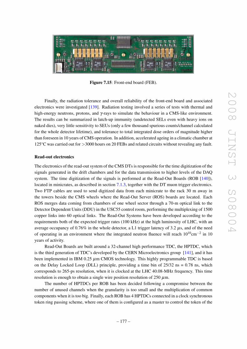
2008 JINST 3 S08004
Figure 7.15: Front-end board (FEB).
Finally, the radiation tolerance and overall reliability of the front-end board and associatedelectronics were investigated [139]. Radiation testing involved a series of tests with thermal andhigh-energy neutrons, protons, and γ-rays to simulate the behaviour in a CMS-like environment.The results can be summarized in latch-up immunity (undetected SELs even with heavy ions onnaked dies), very little sensitivity to SEUs (only a few thousand spurious counts/channel calculatedfor the whole detector lifetime), and tolerance to total integrated dose orders of magnitude higherthan foreseen in 10 years of CMS operation. In addition, accelerated ageing in a climatic chamber at125°C was carried out for >3000 hours on 20 FEBs and related circuits without revealing any fault.
Read-out electronics
The electronics of the read-out system of the CMS DTs is responsible for the time digitization of thesignals generated in the drift chambers and for the data transmission to higher levels of the DAQsystem. The time digitization of the signals is performed at the Read-Out Boards (ROB [140]),located in minicrates, as described in section 7.1.3, together with the DT muon trigger electronics.Two FTP cables are used to send digitized data from each minicrate to the rack 30 m away inthe towers beside the CMS wheels where the Read-Out Server (ROS) boards are located. EachROS merges data coming from chambers of one wheel sector through a 70-m optical link to theDetector Dependent Units (DDU) in the USC55 control room, performing the multiplexing of 1500copper links into 60 optical links. The Read-Out Systems have been developed according to therequirements both of the expected trigger rates (100 kHz) at the high luminosity of LHC, with anaverage occupancy of 0.76% in the whole detector, a L1 trigger latency of 3.2 µs, and of the needof operating in an environment where the integrated neutron fluence will reach 1010cm−2 in 10years of activity.
Read-Out Boards are built around a 32-channel high performance TDC, the HPTDC, whichis the third generation of TDC’s developed by the CERN Microelectronics group [141], and it hasbeen implemented in IBM 0.25 µm CMOS technology. This highly programmable TDC is basedon the Delay Locked Loop (DLL) principle, providing a time bin of 25/32 ns = 0.78 ns, whichcorresponds to 265-ps resolution, when it is clocked at the LHC 40.08-MHz frequency. This timeresolution is enough to obtain a single wire position resolution of 250 µm.
The number of HPTDCs per ROB has been decided following a compromise between thenumber of unused channels when the granularity is too small and the multiplication of commoncomponents when it is too big. Finally, each ROB has 4 HPTDCs connected in a clock synchronoustoken ring passing scheme, where one of them is configured as a master to control the token of the
– 177 –

2008 JINST 3 S08004
TTC+Slow control
to ROSLink
board
MINICRATE
TRB TRB
CCB
Power supply
3.3V @ 40A
5V @ 1.5A
40 MHz CLOCK
ROB ROB
RO-
Link
boardROB
RO-link
ROBUSCh
amber sig
nalsTRBSB
ROSCTRL
ROSMEM VME
CEROS 0CEROS 0 CEROS 1CEROS 1 CEROS 2CEROS 2 CEROS 3CEROS 3
GOL
MEMORY
Token schemeStar topology
Event number
CEROS 4CEROS 4+ TSC + TSC
Event & bunch FIFOs
Figure 7.16: Sketch of the read-out and triggerelectronics located inside a minicrate.
Figure 7.17: Sketch of the splitting of the 25channels in four groups.
read-out data chain. The token ring scheme is designed following a failsafe mechanism, whichavoids that the failure in one of the TDCs interrupts the whole ROB operation. Both hardware andsoftware bypassing systems have been implemented.
Depending on the chamber type, the number of channels is different and accordingly, thenumber of ROBs per minicrate. The smallest minicrate has 3 ROBs and the biggest has 7. Theyare all connected to the Control Board (CCB) that manages, among others, the Timing and TriggerControl (TTC) signals. As can be seen in figure 7.16, Trigger Boards (TRB), located inside theminicrate are connected to the ROBs to receive TTL translated hit signals. As described at thebeginning of this section, FTP cables connect the output of the ROBs to the ROS boards [142].Located in the barrel tower racks there are 60 ROS boards, 12 per wheel, 1 per sector (four tofive minicrates), so each ROS receives 25 channels of the LVDS copper ROB-ROS link. These9U boards have to multiplex data coming from the ROBs, adding necessary information of ROBnumber, link status and other information, and send them to the DDU through a fast link. Anotherfeature of the ROS board is that it also includes a power supply protection circuitry, current andtemperature monitoring, and a 512 kB memory to test and perform data flow snapshots for trace-ability in case of transmission errors. In Figure 7.17 it can be seen how the 25 channels are splitin four groups of six channels each, so-called CEROS, controlled by an FPGA that manages theFIFO read-out performing a pooling search for the next event to be read. These FPGAs also filterthe events, discarding headers and trailers of those channels without timing or error information,reducing accordingly the data overhead.
A test performed on 10 prototypes, keeping them in an oven at 125°C for 2000 hours, in orderto simulate 10 years of CMS activity, gave no faults. The DT Front-End-Driver (FED, also calledDDU [143]) is the last component of the DT read-out electronics. The DT FED system consistsof 5 VME64X 9U boards housed in the CMS service cavern; each board collects data throughserial optical connections from 12 ROS, corresponding to an entire DT wheel, and transmits aformatted event fragment to the CMS common DAQ through a S-Link transmitter module. Thesynchronization with the trigger system is guaranteed by the TTC network, providing the LHCtiming signal, the L1 trigger accept and fast commands, that are distributed to the different parts ofthe FED board. The layout of the board is depicted in figure 7.18.
– 178 –

2008 JINST 3 S08004
Figure 7.18: Scheme of the DDU architecture.
The data rate in each DT FED board is limited by the maximum rate the CMS DAQ canaccept from an S-Link connection (about 200 Mbytes/s). The number of boards has been chosento deal with the expected DT event size (7 kbytes/event) at 100 kHz trigger rate.
High Voltage and Low Voltage systems
The CAEN SY1527 universal multichannel power supply systems are used to supply high and lowvoltages (HV and LV) to the muon DT chambers. The basic modules of the DT HV system consistof A876 master boards and A877 remote boards. A maximum of 8 A876 master boards can behoused in the SY1527 mainframe. Each of them supplies high voltages and low voltages, controlsand monitoring, to a maximum of 4 independent A877 remote boards, each one powering one DTchamber (two in the case of MB4 of Sectors 4 or 10). The A877 remote boards are located in aseparate non-powered mechanical crate sitting in racks on the towers next to the wheels. The A876delivers to each A877 HV board: a positive HV in the range from 0 to +4.2 kV (2.5 mA maximumoutput current), a negative HV in the range from 0 to −2.2 kV (1 mA maximum output current), adual LV of ±15V (1.5 A maximum output current). The A877 HV outputs are subdivided into 12groups (8 for the special A877 boards powering the MB4 chambers) conventionally called macro-channels. Each macro-channel supplies 4 HV channels per layer: 2 anodes (the wires of each layerare divided into 2 groups), 1 strip and 1 cathode. For all HV channels, the maximum output currentis hardware limited to 100 µA.
The DT LV system uses three different types of CAEN Easy3000 modules: the A3009 toprovide VCC and VDD voltages to the chamber front-end electronics and the VCC voltage to themini-crates, the A3050 for the mini-crate VDD and the A3100 to power the Sector Collector Crates.The control of the Easy3000 power supply system is done remotely using a branch controller(Mod. A1676A) plugged in a SY1527 mainframe located in the control room. Each A1676A
– 179 –

2008 JINST 3 S08004
time [ns]-200 0 200 400 600 800
Entri
es
0
50
100
150
200
250
300
350
time [ns]-200 0 200 400 600 800
Entri
es
0
20
40
60
80
100
120
140
Figure 7.19: Drift Time distribution of a goodcell. Wire position corresponds to time 0.
Figure 7.20: Drift Time distribution of a cellwith a disconnected cathode.
branch controller can handle up to 6 Easy3000 crates. The Easy3000 crate is powered by external48 V DC that is provided by the CAEN AC/DC converter A3486S module. The following voltagesare delivered:
• VCCMC = 5.8 V, software current limit i0 = 3 A;
• VDDMC = 4 V, software current limit i0 = 30 A;
• VCCFE = 5.2 V, software current limit i0 = 3 A;
• VDDFE = 2.6 V, software current limit i0 = 4 A;
• VSC = 2.6 V, the current limit depends on the number of SC and ROS boards plugged in thecrate.
7.1.4 Chamber assembly, dressing, and installation
Chamber assembly
Mass chamber assembly was started in January 2002 and was fully completed (spares included) inJune 2006, with a constant production rate for all the four production sites involved. The collectionof a good sample of cosmic muons allowed full testing of a constructed chamber, before sendingit to CERN. In each laboratory cosmic-ray events were triggered by an external scintillator systemwhich covered the full acceptance of the chamber. Since final minicrate electronics was not avail-able during chamber assembly, drift times were measured with external TDCs and a custom DAQ.Typical trigger rates were 50–100 Hz, resulting in ≈106 events in a few hours. With such a largedata sample it was possible to spot and cure problems which could not be detected in previous tests,like disconnected cathodes (figures 7.19 and 7.20) and disconnected strips (figure 7.21).
Beside efficiencies, other relevant working parameters are measured from cosmic-ray data, ascalibration stability (drift velocity measured to be stable within ±5%), deviation from linear driftparametrization, measured to be well within 100 µm (figure 7.22), wire positions and comparisonwith CCD measurements during assembly, relative alignment of layers, and noise (typically below100 Hz per cell, see figure 7.23).
– 180 –

2008 JINST 3 S08004
position (mm)-25 -20 -15 -10 -5 0 5 10 15 20 25
position (mm)-25 -20 -15 -10 -5 0 5 10 15 20 25
effic
ienc
y
0.8
0.85
0.9
0.95
1
distance from wire [mm]0 2 4 6 8 10 12 14 16 18 20
Mea
n re
sidu
al [m
m]
-0.3
-0.2
-0.1
0
0.1
0.2
0.3
Figure 7.21: Single cell efficiency for a goodcell (red dots) and for a cell with a disconnectedstrip (green dots).
Figure 7.22: Residuals as a function of thedistance from the wire, indicating a linear de-pendence well within ±100 µm in the full cellrange.
cell n.0 10 20 30 40 50 60 70 80 90
No
ise [
Hz]
0102030405060708090
Figure 7.23: Typical hit rate distribution in one layer, as measured during the test of a SuperLayerwith cosmic rays. This rate is dominated by noise and is typically below 100 Hz per cell.
Chamber dressing
All chambers, built and fully tested at the production sites, were sent to CERN for final testingand commissioning prior to installation in the experiment. Since the arrival of the first chamber atCERN (an MB2 type chamber arrived in summer 2000, prepared for a test beam [144]), a total of272 more chambers (including spares) have been received from all four production sites, leadingto a continuous workflow of dressing and testing.
At a first stage chambers are assigned to a particular position in CMS, depending on theirorientation. Before any test, each chamber undergoes the optical alignment procedure describedin section 7.1.4. After going through the alignment procedure, chambers are equipped with gascomponents (cooling pipes, gas manifolds, PADC pressure meters), HV cables and additional itemslike stickers, protectors, grounding straps, etc. Basically all components except for the minicrates(section 7.1.3), minicrates-related items and external protections are installed at this stage.
After dressing the chamber the following tests were performed:
• High voltage long term tests;
• Gas tightness tests;
– 181 –

2008 JINST 3 S08004
• Cosmic-muon tests.
The high voltage long term test consists of a continuous monitoring of the high voltage per-formance (electric current) under the nominal values for all components (3600 V for wires, 1800 Vfor strips, and−1200 V for cathodes) for a minimum of 6 weeks. The time constant of the chamberwith the final gas connections is also computed as a measurement of gas tightness. No significantdegradation has been observed with respect to the values measured at the sites.
Finally a cosmic test stand has been set up with trigger scintillators, independent cabling, LVand HV supplies and several HPTDCs, capable of measuring one chamber at a time, and registeringseveral millions of triggers in a few hours. The later analysis of these data allows the recognitionof almost all kind of problems related to the chamber itself and its internal electronics.
Once this first certification step is passed, the chamber dressing is completed and the chamberis declared ready for minicrate installation (section 7.1.3). All signal cables from the chamber tothe minicrate are installed and tested, and then the minicrate itself is inserted. The performanceof the minicrate is tested at this stage for the first time together with a real chamber. All internalconnections are checked, as well as configurability and data processing performance of the fulllocal electronics chain.
At this point the chamber has passed all tests and can be considered ready to install. Lastdressing steps are performed (installation of carters and additional protections) and then DT cham-bers are coupled together to RPCs, forming an installable barrel muon package.
Chamber survey
To determine the chamber positions in the CMS coordinate system and to follow their movements aposition monitoring Alignment System was built (section 7.4). All the 250 DT-chambers positionsare recorded by this system via optical connections using LED light sources mounted on the cham-bers and specially designed video-cameras fixed to the return yoke of the barrel. Four LED-holderscalled forks are mounted on the side-profile of the honeycomb structure (two per side), using therectangular 50× 65 mm2 tube as the light-passage. Each fork has 10 LEDs, 6 and 4 respectively,on each side of the fork. The control of the LEDs (on-off, current) is performed via I2C bus systemintegrated in the minicrate.
The primary aim of the alignment is to give the positions of the anode wires but this is notdirectly possible. On the other hand all the wire positions are measured with respect to the SLcorner during the chamber construction. To establish the connection between the LEDs and thecorner blocks a calibration bench was built at the CERN ISR site (figure 7.24). This bench hadtwo functions. The first one was to measure the corner block positions with respect to each other,allowing the full-chamber geometry, including the relative positions of the superlayers in 3D andtheir planarity, to be measured. The second function was to measure the LED positions in thechamber coordinate system stretched on the corner blocks. The bench contained video-cameras thatcould observe the LEDs and photogrammetry targets to measure the corner blocks with respect tothe LEDs by photogrammetric methods. The bench allowed us to measure all the types of chambersfrom MB1 to MB4. The full bench was calibrated and recalibrated before each chamber calibrationcampaign by the CERN survey group. Also, additional LEDs were mounted on the bench to detectany significant deformation of the bench itself. The precision of the bench measurements for thelocations of the corner blocks was σ <40 µm and the position of the forks relative to the chamber
– 182 –

2008 JINST 3 S08004
Entries 264
Mean -0.04883
RMS 0.2285
X [mm]∆-1.5 -1 -0.5 0 0.5 1
Nu
mb
er
of
ch
am
be
rs
0
10
20
30
40
50
Entries 264
Mean -0.04883
RMS 0.2285
Figure 7.24: The chamber calibration bench inthe CERN ISR Lab.
Figure 7.25: Distribution of the φ -deviationfrom the nominal design value for the two Φ-type superlayers.
was σ <70 µm. Both values are within the acceptable range defined by physics requirements.Figure 7.25 shows the result of the residual distributions of Φ-type SL corner block positions forall measured chambers.
Gas system
For the DT chambers a safe and inexpensive gas mixture is used, namely Ar/CO2 in the ratio 85/15volume. The gas is distributed in parallel to all drift cells in four steps: (1) the main line is splitinto 5 lines to feed each of the 5 barrel wheels; (2) on the wheel it is split into 50 lines to feed the50 chambers on the wheel; (3) on the chambers it is split into 3 lines to feed the 3 SuperLayers; (4)within the SL a long tube with small holes distributes the gas over the drift cells. The nominal flowis 50 l/h for each chamber. Due to the large total number of 250 chambers, a closed loop circuitwith a cleaning station is used. It is foreseen to add about 10% fresh gas daily. The gas system isrun at constant absolute pressure inside the chambers, to avoid any variation of the drift velocityinside the chamber. The pressure is regulated for each wheel. There are flowmeters at the inlet andoutlet of each line at the gas distribution rack on the wheel. The gas pressure is also measured withtwo sensors at the inlet and outlet gas manifolds on the chambers, amounting to 1000 sensors intotal. They should ensure a safe and redundant measurement of the pressure at every chamber, asneeded for unaccessible chambers. To be able to analyze the gas actually present in every chamber,a return line brings a sample to the gas room. There is one such line per wheel and a remotelycontrolled multiway valve permits the selection of the desired chamber or the gas arriving at thewheel, for analysis.
The gas is also analysed independently for each of the 5 wheels and consists of a measurementof the oxygen and of the humidity content of the gas, as well as a direct measurement of the mainparameter of the DT chambers, the drift velocity. The drift velocity is measured with a small driftchamber (VdC), which features a very homogeneous, constant, known and adjustable electric fieldin a region where two thin beams of electrons from a beta-source cross the chamber volume and
– 183 –

2008 JINST 3 S08004
Figure 7.26: Installation of MB1 station on Wheel -2. The yellow frame is the cradle used toinsert the chamber in its location inside the iron slot.
trigger a counter outside the chamber. The distribution of times between the trigger signal andthe signal from the anode wire of the chamber is recorded. The distance between the two beamsbeing well known by construction, by measuring the distance in time between the peaks from thetwo sources, one reads directly the drift velocity. Variations of the drift velocity can be monitoredaccurately by accumulating data for about 5 min. The data shown in figure 7.8 demonstrate that theabsolute values measured with the VdC agree with the expectation. The special merit of a directmonitoring of the drift velocity is that one does not need to know which impurities are affectingthe drift velocity to monitor it.
Chamber installation in CMS
The main installation tool is a platform (cradle) with the same support rail as in the iron pocketsthat can be anchored to interface pads mounted on the wheel (figure 7.26). Pneumatic movementsallow the precise alignment of the chamber with respect to the iron pockets. Once the rails onthe cradle and those in the iron pockets are aligned, the chamber is pushed into position with anelectric motor. The installation of the chamber in the MB1 station of Wheel -2 sector 11 is shownin figure 7.26.
The first chambers were installed in the bottom sectors of Wheel +2 in July 2004 and thesurface installation was completed in Wheel -2 in December 2006. Installation completion, forsectors 1 and 7, which could not be filled on the surface since these parts of the wheel were reservedfor handling during the heavy lowering operation, was made underground.
– 184 –

2008 JINST 3 S08004
Entries 81512 2685. / 22
Constant 0.1125E+05Mean 385.8Sigma 3.826
T[ns]
Entries
0
2000
4000
6000
8000
10000
12000
300 320 340 360 380 400 420
Distance to the wire [mm]
Y (c
ham
ber)
- Y (s
ilico
n) [
mm
]
!=0 deg!=15 deg
HV:3600/1800/-1200 V-0.4
-0.2
0
0.2
0.4
20 17.5 15 12.5 10 7.5 5 2.5 0
Figure 7.27: Gaussian fitted MT distributionwith σt = 170 µm. The position of the MTpeak allows the determination of an averagedrift velocity of 54.4 µm/ns.
Figure 7.28: Deviation from linearity as a func-tion of the distance to the wire for tracks withangles of incidence α=0o and 15o. The cathodeis centred at 21 mm.
7.1.5 Chamber performance
Chamber and trigger performances have been thoroughly analyzed at various stages, on prototypesbefore mass production (with and without external magnetic field [145]), on final chambers withtest beams and with the CERN Gamma Irradiation Facility [144, 146, 147], with cosmic-raysboth at production sites and at the commissioning of the installed chambers, and finally with theso-called Magnet Test and Cosmic Challenge (MTCC) in 2006, where part of the DT system,completely installed and equipped with final hardware, was tested together with the final CMSDAQ system.
Test beam data: chamber performance
Several dedicated muon test beam runs were set up in order to test chamber performance underdifferent conditions. Single cell spatial resolution could be determined [144] simply by the dis-persion of the MT = (t1 + t3)/2 + t2 distribution, MT being the meantime obtained from the timeof the signals (t1, t2, t3) generated by the incoming muon in 3 consecutive, staggered layers. Thesmoothness of the drift time box and the fast drop of the trailing edge (figure 7.19) are both signs ofthe saturation of the drift velocity. Under the assumption that the time resolution is the same in alllayers σt =
√23 · σMT, one can easily observe an average spatial resolution of 170 µm (figure 7.27).
Using a Silicon Beam Telescope, it was possible to measure the deviation from the extrapolated hiton the SL and the reconstructed position. As can be seen in figure 7.28 deviations from linearityare within ± 100 µm, which corresponds to a trigger jitter smaller than 5 ns.
Silicon Beam Telescope data can also be used to measure precisely the chamber efficiency(figure 7.29). The geometrical acceptance associated with the presence of the I-beam is clearly seenby the drop of efficiency in that region. In the rest of the cell the efficiency is always higher than
– 185 –

2008 JINST 3 S08004
Figure 7.29: Efficiency as a function of the distance to the wire (top), for tracks orthogonal tochamber surface; (bottom) with an expanded scale excluding the I-beam region.
99.5%. The typical intrinsic average noise, as measured during chamber construction or during atest beam in dedicated random trigger runs [146], is shown in figure 7.30. It is reasonably stable,at values of ≈50 Hz, and does not vary much with channel number. Also the effect of higher noiselevels, generated at the CERN Irradiation Facility, by photo-conversion in the chamber aluminumwalls at chosen rates, both on reconstruction and trigger efficiency, was studied. The SL segmentreconstruction efficiency is shown in figure 7.31 for various filter values of the gamma source,showing no significant dependence of the reconstruction algorithm on the gamma irradiation level,even at noise rates higher than the maximum levels expected in any DT chamber during normalLHC operations. Since the chambers are operated in the iron yoke of CMS, where importantstray magnetic fields are present, the impact of the radial and longitudinal components of the fieldwere carefully simulated (finite element analysis program ANSYS, figure 7.32), and tested both atdedicated muon test beams where the chambers were operated inside a magnetic field [145, 146],and during the CMS Magnet Test and Cosmic Challenge, with comsic rays. The distortion of theelectron drift lines caused by a field of 0.5 T parallel to the wires can be seen in figure 7.33. Thisdistortion can be roughly approximated by a rotation of the drift lines around the wire, simulatinga rotation of the drift cell with respect to the direction of the incident particles. A change in themaximum drift path and time is generated, together with a drop of efficiency for inclined trackswhich go through the I-beam region where the drift lines do not reach the wire. The staggeringof the four layers minimizes the impact on track measurement of this last effect. In the case of
– 186 –

2008 JINST 3 S08004
Cell SL !
Noi
se ra
te (H
z/ce
ll)
Cell SL "1 Cell SL "21
10
10 2
10 20 30 0 20 40 60 0 20 40 60
log10(source filter)
SL-!
1 Effi
cien
cy (%
)
99.7
99.8
99.9
100
1 2 3 4 5 6
Figure 7.30: The noise cell occupancy as afunction of the cell number, for the three SLs.
Figure 7.31: The cell efficiency in superlayerΦ1 as a function of the irradiation filter value.The smallest filter value provides a backgrounda factor 2 larger than the maximum one to beexpected during LHC operation in any of theDT chambers in CMS.
Figure 7.32: Radial (Br) and longitudinal (Bz) components of the CMS magnetic field in theregions where the barrel chambers are placed as a function of the position along the beam direction(the centre of the detector is at z=0). Vertical bands indicate the separation between chamber wheels(in these particular regions Bz becomes significant). The biggest Br values (0.7–0.8 T) occur in theMB1 region near the endcaps.
– 187 –

2008 JINST 3 S08004
Anode wire
13 mm
42 mm
Electrode strips
Cathode strip
0 deg
B [T]
Drift
vel
ocity
[ µ
m/n
s]
15 deg
B [T]
Drift
vel
ocity
[ µ
m/n
s]
50
51
52
53
54
55
56
57
-0.2 0 0.2 0.4 0.6 0.8 1
Figure 7.33: Simulation of the distortion pro-duced in the drift lines by a 0.5 T magnetic fieldparallel to the wires.
Figure 7.34: Drift velocity for several magneticfields for perpendicular (0) and inclined (15)tracks.
a homogeneous magnetic field along the wire, the main consequence would be an effective lowerdrift velocity, but in CMS the magnetic field is not homogeneous. Figure 7.34 shows the driftvelocity values obtained for several magnetic field values in the case of perpendicular tracks. Avariation in the drift velocity of around 3% is observed from B=0 to 0.5 T. This corresponds to achange in the maximum drift time of less than 12 ns, which is acceptable both for reconstructionand trigger efficiency. The effects of the magnetic field on linearity are not very important below0.3 T but increase dramatically for higher fields, mainly near the I-beams. The resolution is alsoslightly deteriorated by low magnetic fields, but it is still better than 300 µm below 0.3 T. In CMSthe magnetic field component parallel to the wires measuring the coordinate in the bending planeis expected to be below 0.1 T, with only very limited regions reaching 0.3 T. In such conditions, theresults obtained confirm that the performance of the drift tube chambers fulfil the requirements.
Test beam data: trigger performance
Like the chamber performance, the DT local trigger has also been tested extensively using test beamfacilities at CERN [147, 148]. In particular, to fully test the performance of the trigger electronics,bunched beams having the same time structure as the LHC were used at the CERN SPS, producinghigh momentum muon tracks separated by multiples of 25 ns.
The bunch crossing (BX) identification efficiency is defined as the fraction of selected singlemuon events for which the local trigger delivered at least one trigger segment at the correct BX. Thisquantity was measured as a function of the muon momentum, and results are shown in figure 7.35.The measurement was also performed after inserting iron slabs, for a total depth of 15 cm, in frontof the muon chamber. The effect of the iron absorber is the enhancement of the probability for ahigh momentum muon to produce electromagnetic showers. Such a probability also increases as afunction of the muon momentum. This has the effect to decrease the BX identification efficiency.Results are also shown in figure 7.35, superimposed on results without iron absorber. Ghostsare copies of the trigger segment at the correct BX, as well as fake triggers at the wrong BX.They may originate from wrong alignment of hits in a DT muon station, due to the presence ofextra hits produced by electromagnetic cascades and δ -rays, or from redundancies in the triggerelectronics. In the case of single muon events, if two trigger segments are delivered at the same
– 188 –

2008 JINST 3 S08004
Energy (GeV)50 100 150 200 250 300
Effic
ienc
y (%
)
90
91
92
93
94
95
96
97
98
99
100
With IronNo Iron
Figure 7.35: BX identification efficiency in a muon station in single muon events, as a function ofthe incident muon momentum, for events with and without the iron absorber placed in front of themuon station.
BX by the local trigger system in a muon station, the second trigger is considered a ghost copyof the first one. Although generally with a poorer quality, ghosts at the correct BX reproducethe characteristics of the main trigger segment in terms of position and angle. The productionof segments associated to a wrong BX, arising from wrong hit alignment, is intrinsic to the BTIalgorithm (section 8.2). In addition there are also cases in which the hit alignment is spoiled byδ -ray production or electromagnetic showering. Such fake triggers, which are called out-of-timeghosts, are almost entirely uncorrelated low quality segments, and are distributed over a wide rangeof BXs. The fraction of ghost triggers at the correct BX as a function of incident muon momentum,and the fraction of out-of-time triggers, as defined above, are shown respectively in figures 7.36and 7.37 as a function of the incident muon momentum, for events with and without the ironabsorber. The performance of the Φ Track Finder (PHTF, section 8.2) was also tested within thesame muon test beam at CERN [148]. The PHTF was used to reconstruct muon trigger candidatesusing both muon stations, using φ -view local trigger primitives. Figure 7.38 shows the distributionof the BX assigned to the tracks found by the PHTF. The BX is correctly identified when its valueis 24. Superimposed are the distributions of the same quantity determined independently by thelocal trigger in MB1 and MB3, as well as the distribution of the determined BX when a triggersegment with the same BX was delivered in coincidence in MB1 and MB3. It can be seen thatthe PHTF is fully efficient to deliver track candidates at the correct BX, whereas for out-of-timetriggers the corresponding PHTF trigger rate is suppressed at the level of 1% or less.
A large fraction of the out-of-time triggers is due to real muons crossing the experimentalapparatus at a BX different from 24, and which are correctly reconstructed by the PHTF. This isconfirmed by the fact that the trigger segments that are matched together to form such tracks, aremainly of the type HH (four hits in both Φ-type SL), thus indicating a real muon track. Figure 7.39shows the PHTF efficiency to reconstruct a trigger track in events with a MB1 and MB3 coincidenceas a function of the BX. Superimposed are the efficiency to reconstruct a trigger track when thetwo trigger segments are both of HH type, and both of L (three out of four hits in a SL) quality
– 189 –

2008 JINST 3 S08004
Energy (GeV)50 100 150 200 250 300
Frac
tion
of 2
nd/1
st tr
igge
rs (%
)
0
1
2
3
4
5
6
7
With IronNo Iron
E nergy (G eV )50 100 150 200 250 300
Fra
ctio
n
of
ou
t o
f ti
me
trig
ger
s (%
)
0
10
20
30
40
50
60
70
80
90
100
With Iron
No Iron
Figure 7.36: Fraction of ghost triggers ob-served in a muon station in single muonevents, defined as the ratio of the number ofsecond tracks over the number of first tracks,delivered by the local trigger at the correctBX, as a function of the muon momentum, forevents with and without the iron absorber.
Figure 7.37: The fraction of out-of-time trig-gers in a muon station in single muon events,defined as the number of out-of-time triggersegments divided by the number of selectedsingle muon events, as a function of the muonmomentum, for events with and without theiron absorber.
respectively. The correct BX is 24. The PHTF efficiency for HH coincidences is 99.7±0.1% andis practically constant for any BX. This fits with the expectations, as such tracks are real muonscrossing the apparatus. On the other hand, when the trigger segments have a low quality, whichis typical for fake triggers, the PHTF ghost suppression is very effective. The rejection power forghosts (L coincidences at BX 6= 24) is 9.5±0.4. Therefore, although the out-of-time local triggerrate in a single station is rather high (as shown for example in figure 7.37), the PHTF is veryeffective in ghost rejection.
Commissioning of installed chambers
After installation in their final positions in the five CMS barrel wheels in the CMS surface hall, thechambers, including read-out and trigger electronics, were tested again with the goal of identifyingpotential problems before final cabling. Given the previous testing stages, it was mainly a test of theelectronics and connections. Possible damage or loose connections as a consequence of installation(where chambers undergo some mechanical movement) could also be detected at this stage. Thiscommissioning step was performed before final cabling (since the cables cover the minicrates andwould prevent access for potential repairs) and involved all chambers in the ten sectors (84% of thefull system). The commissioning consisted in the following steps:
1. connection to the power supplies and to the test-stand, which handled the trigger and read-out, in order to verify the functionality of the connectors and cabling of the chamber;
2. check of the minicrate performance by testing the internal connections and by monitoringthe electronics boards inside the minicrate;
– 190 –

2008 JINST 3 S08004
B X Number0 5 10 15 20 25 30 35
O
ccu
pan
cy
-410
-310
-210
-110
1
S egments in MB 1
S egments in MB 3
C oincidences in MB 1 & MB 3
P HT F E xtrapolation
B X Number0 5 10 15 20 25 30 35
E
ffic
ien
cy
0
0.2
0.4
0.6
0.8
1
Figure 7.38: Distribution of the BX assignedto the tracks found by the PHTF. The BX iscorrectly identified when its value is 24. Su-perimposed are the distributions of the samequantity determined independently by the lo-cal trigger in MB1 and MB3, as well as thedistribution of the determined BX when a trig-ger segment at the same BX was delivered incoincidence in MB1 and MB3.
Figure 7.39: Efficiency to reconstruct a trig-ger track by the PHTF, as a function of the BX(white), in events with a two stations (MB1-MB3) coincidence. The correct BX is 24. Su-perimposed are the efficiency to reconstructa trigger track when there is a coincidenceof two trigger segments both of HH quality(black), and a coincidence of two trigger seg-ments both of L quality (light green).
3. T0 determination (the starting point) of the drift time spectrum with test pulses. The T0 isspecific for every cell, its cell-to-cell variation within a chamber is of the order of ≈1–2 ns;
4. cosmics data taking in different trigger configurations;
5. analysis of the cosmics data and verification of the chamber and electronics performance.
Depending on the amount of repairs, between two and five chambers per week were commis-sioned. Cosmic muon tracks were recorded in auto-trigger mode in different trigger configurations.Trigger rates varied from 80 Hz to 600 Hz per chamber depending on the sector inclination, thetrigger configuration, and the chamber type. Higher level trigger components (tower electronics) aswell as RPC connections were not tested at this stage since they required full cabling to the towerelectronics.
The chamber orientation with respect to incoming cosmic-rays is purely horizontal only insectors 4 and 10. This yields a reduction in the occupancy near the edges of the Φ-type superlayerfor sectors near the vertical. An example comparing the bottom sectors 8, 9, 11 and 12 is shown infigure 7.40, where the occupancy per wire is summed over the four layers of superlayer Φ2. Thereduced geometrical acceptance at the chamber edges is caused by the combination of two effects:i) the direction of cosmic rays, which is mainly vertical, and ii) the shielding of the iron yoke onsoft muons.
Data recorded with highly selective trigger condition, 4 hits in both Φ-type superlayers or 3hits in one and 4 in the other, are used to calculate the efficiency. The cell efficiency is calculated
– 191 –

2008 JINST 3 S08004
Figure 7.40: Sum of the occupancy of the four layers in MB1 Φ2 superlayer for sectors 8, 9, 11and 12. The sectors have different inclinations as shown on the right. Material inside the yokealong with the iron yoke itself shield partly the soft cosmic ray muons.
from reconstructed tracks with hits found in the traversed cell or its 2 neighbours (Nh), normalizedto the total reconstructed tracks traversing the considered layer (Ntrack):
εLayer = Nh/Ntrack (7.1)
requiring ≥5 hits in φ and ≥3 hits in z. Figure 7.41 (left panel) illustrates the combined track fitin the case of the φ projection. Because of the normalization to the number of tracks, the reducedoccupancy near the chamber edges does not play a role. The cell efficiency is almost constantacross the chamber, usually ≥98%, as seen, for example, in figure 7.41 (right panel).
Similarly the reconstruction efficiency is determined as the fraction of reconstructed trackswhen requiring ≥7 hits per track, an example of which can be seen in figure 7.42. Here weshould remark that the overall number of dead cells, as measured during chamber commission-ing at CERN, amounts to ≈0.2% of the total number of channels (298 out of 171 852).
Results from Magnet Test and Cosmic Challenge
A further important test of the muon system with emphasis on integration into the overall CMSDAQ and Trigger system, is the aforementioned Magnet Test and Cosmic Challenge (MTCC), per-formed at CERN during summer 2006. For the first time, the three muon subsystems were operatedtogether. The DT system made use of the complete read-out and trigger chain with final hardware,and the recorded data allowed the study of cosmic muon tracks in magnetic field. Another im-portant task was the generation of a cosmic-muon trigger for the read-out of all CMS subsystemsparticipating in the MTCC. Several goals were accomplished by the DT system during the MTCC:
1. Check of chamber performance and read-out
– 192 –

2008 JINST 3 S08004
cell5 10 15 20 25 30 35 40 45
effic
ienc
y
0.5
0.6
0.7
0.8
0.9
1
wheel 2 chamber 1 sector 2 sl 1 layer 3
cell5 10 15 20 25 30 35 40 45
effic
ienc
y
0.5
0.6
0.7
0.8
0.9
1
wheel 2 chamber 1 sector 2 sl 1 layer 2
Figure 7.41: Cell efficiencies for two of the four layers of Φ1, MB1 sector 2.
sector0 2 4 6 8 10 12 14
Reco
nstru
ctio
n ef
ficie
ncy
0.6
0.65
0.7
0.75
0.8
0.85
0.9
0.95
1
1.05
1.1Wheel -1, at least 1 track with hits required by trigger
MB1 MB2 MB3 MB4
Figure 7.42: Reconstruction efficiency with 7 points in both Φ-type superlayers, according to thetrigger condition, requiring either two 4-hit segments in both of the two Φ-type superlayers or one4-hit and one 3-hit segment.
• check the effect of the fringe field on chamber performance in terms of HV behaviour,drift velocity, position resolution, and efficiency;
• exercise the complete read-out chain from the chamber through the ROS-25 up to theDDU;
• test of HV and LV in the final set-up. Integrate HV and LV control into central CMSservices.
2. Trigger
• operate the complete trigger chain with final hardware;
• provide a cosmic-ray trigger to CMS;
• check the effect of magnetic field on trigger timing (i.e. bunch crossing identification),requiring the RPC trigger to set a reference T0.
3. Software
• integration of DAQ and Data Quality Monitoring;
– 193 –

2008 JINST 3 S08004
T C
TC
TC
TC
TC
TC
TC
TC
TC
T C
T C
T C
C O IL
H B
E B
Y B /Z /1 /4
Y B /Z /2 /4
Y B /Z /3 /4
M B /Z /1 /4
M B /Z /2 /4
M B /Z /3 /4
M B /Z /4 /4
Y B/Z /1 /5
Y B/Z /2 /5
Y B/Z /3 /5
M B /Z/1 /5M B /Z
/2 /5
M B /Z/3 /5
M B /Z/4 /5
YB/Z/1/6
YB/Z/2/6
YB/Z/3/6
MB/Z/1/6
MB/Z/2/6
MB/Z/3/6
MB/Z/4/6
YB/Z/1/7
YB/Z/2/7
YB/Z/3/7
MB/Z/1/7
MB/Z/2/7
MB/Z/3/7
MB/Z/4/7
YRB/Z/1/8
YB/Z/2/8
YB/Z/3/8 M
B/Z/1/8
MB/Z/2/8
MB/Z/3/8
MB/Z/4/8
YB/Z/1/9
YB/Z/2/9
YB/Z/3/9
MB/Z/1/9
MB/Z/2/9
MB/Z/3/9
MB/Z/4/9
YB/Z/1/10
YB/Z/2/10
YB/Z/3/10
MB/Z/1/10
MB/Z/2/10
MB/Z/3/10
MB/Z/4/10
YB/Z/1/11 YB/Z/2/11YB/Z/3/11
MB/Z/1/11 MB/Z/2/11 MB/Z/3/11MB/Z/4/11
YB/Z/1/12
YB/Z/2/12
YB/Z/3/12
MB/Z/1/12
MB/Z/2/12
MB/Z/3/12
MB/Z/4/12
YB/Z/1/1
YB/Z/2/1
YB/Z/3/1
MB/Z/2/1
MB/Z/3/1
MB/Z/4/1
YB/Z/1 /2
YB/Z/2 /2
YB/Z/3 /2M
B/Z/1 /2
MB/Z/2 /2
MB/Z/3 /2
MB/Z/4 /2
Y B /Z /1 /3
Y B /Z /2 /3
Y B /Z /3 /3
M B /Z /1 /3
M B /Z /2 /3
M B /Z /3 /3
M B /Z /4 /3
Barrel wheels YB+2 (S10, S11) and YB+1 (S10)
X!
Z +
Y
MB/Z/1/1
YB
/11 /11 /11
YB/Z/3/1
MB/Z/
/11
MB/Z/4/1
YB
YB
M
M
M
CTC MBCCTC
0 100 YB/Z/1/1
10 10 YB/Z/2/1
10 10 YB/Z/3/1
/1000000 MB/Z/1/
/10 MB/Z/2/
/10 MB/Z/3/
1/110 MB/Z/4/
11 /11 11
YB/Z/1/1
11 /11 11
B/Z/2/1
11 /11 1111 11 111
B/Z/1/1
2/11
MB/Z/2/1
3/11/3/1
CC
YB
1
MB/
Z/3MYYB
BB
M
M
Figure 7.43: The MTCC exploited in the barrel region three sectors in wheels YB+1 (sector 10)and YB+2 (sectors 10, 11) instrumented with DTs and RPCs.
Figure 7.44: Event displays from the MTCC. Left panel: muon reconstructed in a DT sector inconjunction with Tracker activity. Right panel: muon track passing through both DT and CSCchambers.
• exercise the reconstruction software under realistic conditions.
4. Take data with other CMS subsystems.
For the DTs (as well as for the barrel RPCs) three instrumented sectors were read-out, the bottomsector 10 and the adjacent sector 11, both in YB+2, along with sector 10 in YB+1 (figure 7.43). Thisaccounted for 14 DT chambers, corresponding to about 10 000 channels. Beside the cross-check ofchamber performance previously carried out in test beams, MTCC data provided a unique oppor-tunity to test the reconstruction algorithms for different magnetic field strengths (figure 7.44(left))and to observe for the first time tracks combined in different detectors (figure 7.44(right)). As de-
– 194 –

2008 JINST 3 S08004
scribed in section 7.1.5, because of the radial component of the magnetic field between the solenoidand endcap disks, the electron drift direction in the r-φ view changes, acquiring a Lorentz angle.The angle is increasingly larger as the B radial component increases along z. Thus signals gener-ated by muon hits in a r-φ drift tube at a given distance from the wire but at different z positionswill appear at different times. The effect has implications both for the trigger synchronization andfor the muon track reconstruction and it should be calibrated out before LHC start-up. Duringthe MTCC a total of 159 million cosmic-muon events (48 million DT triggered) were collectedat several values of the B field. Data were collected at 0 T (as a reference), then at 2, 3, 3.5, 3.8,and 4 T (93 million events at 3.8 and 4 T), which allowed a detailed mapping of the Lorentz angleeffect in an MB1 and an MB2 chamber. Some 15 million events at 0 T and 3.8 T (1.6 million DTtriggered) have been taken with the MB1 local trigger configured to select only muon segmentspointing to the centre of the CMS barrel (LHC beam interaction point): this sample is specific fortrigger timing studies in the DT-CSC overlap, in particular also the muon time-of-flight is the sameas in a LHC run.
While procedures for the synchronization of the DT system in stand-alone were studied inPhase I of the MTCC, in Phase II (during the magnetic field mapping operations) effort was putin tools for fine inter-synchronization of the muon detectors (DT, CSC and RPC). In particularthe analysis of the DT trigger data at the chamber output as function of RPC-originated L1A hasproven to be sensitive to desynchronization by a few nanoseconds.
To study the efficiency of the DT Local Trigger (DTLT), events were selected by requiringthe presence of the RPC triggers RBC1 (for wheel YB+1) or RBC2 (for RPCs in wheel YB+2)triggers. In such events, track segments were reconstructed in each muon station independently,whenever possible, using TDC hits. If more than one track segment was reconstructed in a givenstation, the one with the largest number of associated hits was taken. The efficiency of the DTLTwas computed for each muon station separately, by counting events with a reconstructed muonsegment, and comparing them with events which also had a trigger segment at any BX in thesame muon station. Accepting a trigger regardless of its BX position was dictated by the fact thatcosmic rays are likely to generate triggers in nearby BXs, as with non-bunched particles the systemis intrinsically not synchronized. Only correlated trigger segments, namely of quality High-High(HH), High-Low (HL) or Low-Low (LL), as defined in section 7.1.5, were released by the triggersector collector and thus used to compute the DTLT efficiency.
This efficiency was found to be about 65–70% in all stations, independent of the magneticfield. The measurements obtained using 40 MHz bunched muon beams [148] provided a muchhigher efficiency, of the order of 85% or more, and for which only triggers at the correct BX wereconsidered.
The observed lower efficiency of the DTLT can be explained by the fact that, while the triggersystem is clocked every 25 ns, cosmic rays occur at any time. In bunched beams the BTIs can beproperly synchronized by choosing the best phase which maximizes the number of HH triggerswith respect to higher level triggers. In the case of cosmic rays, this is not possible, due to therandom arrival time of the muons thus making the BTI synchronization itself meaningless. Insuch conditions the rate of Low-quality trigger segments released by the BTIs increases, and alsothe associated BX can easily fluctuate. As only correlated trigger segments were released by thetrigger Sector Collector in each station, we also expect an increase in TRACOs (section 8.2) failing
– 195 –

2008 JINST 3 S08004
T0 correction (ns)
-50 -40 -30 -20 -10 0 10 20 30 40 50
tra
ck
s /
ns
0
100
200
300
400
500
All tracks
tracks with trigger
T0 correction (ns)-30 -20 -10 0 10 20 30
DT
LT
eff
icie
nc
y
0
0.2
0.4
0.6
0.8
1
Figure 7.45: Left panel: distribution of t0 for all track segments in a station, for events triggeredby RPC (solid line). The distribution of the same quantity for events also triggered by the DT issuperimposed (dashed line). Right panel: DT local trigger efficiency as a function of the quantityt0, obtained by the ratio of the two histograms shown on the left.
to correlate segments among the two superlayers of a given station, with respect to a perfectlysynchronized system, which will turn into a DTLT efficiency loss.
Consequently, one expects that muons crossing the detector at the “correct time” (for whichthe BTIs behave as perfectly synchronized to the clock) will be detected with the highest efficiency,as such a condition is the same as in the bunched beam tests. On the other hand, muons crossingthe detector out of such a “correct time” will be detected with lower efficiency, as for them thesynchronization of the system is not optimised.
The quantity t0 is the time correction to be added to the tTrig of the event to obtain the ef-fective time at which the given muon crossed the detector. It can be computed event-by-event byminimizing the space resolution of the reconstructed track segment in a station. Figure 7.45 (left)shows the distribution of the t0 correction of the reconstructed track segments in events triggeredby the barrel RPC, superimposed to the one for events which also had a DT local trigger. Thebest trigger efficiency is obtained only at some preferred t0 values. This can be seen in figure 7.45(right) which shows the DTLT efficiency as a function of the t0-correction time, obtained as theratio of the two distributions previously described. Two peaks at efficiency around 90% are visible.They correspond to the case in which the muon crosses the detector at the “correct time” for whichBTIs are synchronized. The two peaks correspond to two adjacent BXs. For other t0 values, theefficiency can be very low, as in this case the system is not synchronized. The observed DTLTefficiency is therefore explained by the fact that cosmic rays occur at random time with respect tothe “correct time” at which the BTIs have maximum efficiency.
The magnetic field modifies the shape of the field lines in the drift cell, thus affecting theeffective drift velocity, as discussed in section 7.1.5. The largest effect in the barrel is expected tooccur in station MB1 in Wheels +2 and -2. From the point of view of the DTLT, a change of theeffective drift velocity, if large enough, could make the BX determination less precise, and shift itsvalue by one unit.
Figure 7.46 shows this effect for the two MB1 stations in Wheel 2, displaying the BX valuedetermined by the DTLT as a function of the z-position of the track in the chamber, with and
– 196 –

2008 JINST 3 S08004
segment position in Theta SL (cm)
-150 -100 -50 0 50 100
trig
ge
r B
X
7.6
7.8
8
8.2
8.4
8.6
8.8
9
9.2
9.4
B = 0
B = 4T
MB1, wheel 1
segment position in Theta SL (cm)-150 -100 -50 0 50 100
trig
ge
r B
X
7.6
7.8
8
8.2
8.4
8.6
8.8
9
9.2
9.4
B = 0
B = 4T
MB1, wheel 2
Figure 7.46: BX determined by the DTLT as a function of the track position in the z-direction ofthe muon station, with and without magnetic field, for MB1 in Wheel 1 on the left, where no effectof the B-field is expected. On the right, the same quantities are shown for MB1 in Wheel 2, wherean influence of the magnetic field on the drift velocity is expected.
without magnetic field. While no clear effect is visible in MB1-Wheel 1, in MB1-Wheel 2 thereis a slight delay of the average BX value which tends to increase as the track approaches the edgeof the wheel, corresponding to larger values of z, where the stray field components are larger. Thisdelay is at most of the order of 0.3 units of BX.
7.2 Cathode strip chambers
At the time of the LHC start-up, the CMS Endcap Muon system will consist of 468 cathode stripchambers (CSC) arranged in groups as follows: 72 ME1/1, 72 ME1/2, 72 ME1/3, 36 ME2/1, 72ME2/2, 36 ME3/1, 72 ME3/2, and 36 ME4/1 (figures 7.47 and 7.48). The de-scoped 72 ME4/2chambers will not be available during early years of CMS operation. The chambers are trapezoidaland cover either 10 or 20 in φ ; all chambers, except for the ME1/3 ring, overlap and providecontiguous φ -coverage. A muon in the pseudorapidity range 1.2 < |η |< 2.4 crosses 3 or 4 CSCs.In the endcap-barrel overlap range, 0.9 < |η | < 1.2, muons are detected by both the barrel drifttubes (DT) and endcap CSCs. In the baseline design, muons with |η | < 2.1 are also detected byresistive plate chambers (RPC); however, in the initial detector this coverage is reduced to |η |< 1.6.
The CSCs are multiwire proportional chambers comprised of 6 anode wire planes interleavedamong 7 cathode panels (figure 7.49). Wires run azimuthally and define a track’s radial coordinate.Strips are milled on cathode panels and run lengthwise at constant ∆φ width. Following the originalCSC idea [149], the muon coordinate along the wires (φ in the CMS coordinate system) is obtainedby interpolating charges induced on strips (figure 7.50). The largest chambers, ME2/2 and ME3/2,are about 3.4× 1.5 m2 in size. The overall area covered by the sensitive planes of all chambersis about 5000 m2, the gas volume is >50 m3, and the number of wires is about 2 million. Thereare about 9000 high-voltage channels in the system, about 220 000 cathode strip read-out channelswith 12-bit signal digitisation, and about 180 000 anode wire read-out channels.
– 197 –

2008 JINST 3 S08004
7.380 m 7.100 m
5.975 m
4.885 m
4.020 m 3.800 m
2.950 m 2.864 m
1.930 m
1.300 m 1.200 m
00 0.5 1(meters)
14.9
80 m
14.5
80 m
10.8
80 m
10.6
00 m
9.77
0 m
8.51
5 m
8.26
0 m
6.70
0 m
6.50
0 m
5.70
0 m
3.88
0 m
3.15
0 m
2.80
0 m 0
Figure 7.47: Quarter-view of the CMS detector. Cathode strip chambers of the Endcap Muonsystem are highlighted.
Figure 7.48: The ME2 station of CSCs. The outer ring consists of 36 ME2/2 chambers, eachspanning 10 in φ , and the inner ring of eighteen 20 ME2/1 chambers. The chambers overlap toprovide contiguous coverage in φ .
– 198 –

2008 JINST 3 S08004
Figure 7.49: Layout of a CSC made of 7 trape-zoidal panels. The panels form 6 gas gaps with-planes of sensitive anode wires. The cut-out inthe top panel reveals anode wires and cathodestrips. Only a few wires are shown to indicatetheir azimuthal direction. Strips of constant∆φ run lengthwise (radially). The 144 largestCSCs are 3.4 m long along the strip directionand up to 1.5 m wide along the wire direction.
Figure 7.50: A schematic view of a single gapillustrating the principle of CSC operation. Byinterpolating charges induced on cathode stripsby avalanche positive ions near a wire, one canobtain a precise localisation of an avalanchealong the wire direction.
The CSCs provide the functions of precision muon measurement and muon trigger in onedevice. They can operate at high rates and in large and non-uniform magnetic fields. They do notrequire precise gas, temperature, or pressure control. Moreover, a radial fan-shaped strip pattern,natural for measurements in the endcap region, can be easily arranged on the cathode planes.
The performance requirements for the CMS cathode strip chamber system include the fol-lowing:
• Reliable and low-maintenance operation for at least 10 years at the full LHC luminosity, i.e.,at estimated random hit rates up to 1 kHz/cm2;
• At least 99% efficiency per chamber for finding track stubs by the first-level trigger;
• At least 92% probability per chamber of identifying correct bunch crossings by the first-level trigger. With such an efficiency per chamber and 3–4 CSCs on a muon track path, asimple majority rule ensures that the reconstructed muons will be assigned the correct bunchcrossing number in more than 99% of cases;
• About 2 mm resolution in r-φ at the first-level trigger.
• About 75 µm off-line spatial resolution in r-φ for ME1/1 and ME1/2 chambers and about150 µm for all others.
– 199 –

2008 JINST 3 S08004
Figure 7.51: Mechanical design of the CMS cathode strip chambers (exploded view).
7.2.1 Chamber mechanical design
The 72 ME1/1 chambers and the larger 396 chambers have somewhat different mechanical designs.Below, we describe the design of the larger chambers using ME2/2 as an example and, then, at theend of this section, summarise the ME1/1-specific features that distinguish them from the otherchambers.
The mechanical structure is based on seven 16.2-mm-thick trapezoidal panels (figure 7.51).The panels are made of a 12.7-mm-thick polycarbonate honeycomb core with two 1.6-mm FR4skins commercially glued on each side. FR4 is a fire-retardant fibreglass/epoxy material widelyused for printed circuit boards. The FR4 skins are clad with 36-µm-thick copper on their outersurfaces, forming the cathode planes.
FR4 cathode gap bars are glued to both sides of every other panel (panels 1, 3, 5, 7 in fig-ure 7.51) so that when the panels are stacked together, these cathode bars define 6 gas gaps of9.5 mm. To provide additional support, there are 4 spacers placed between panels along the cham-ber centreline. When all 7 panels are put together, the entire stack is tightened down with boltsalong the chamber perimeter (through holes in the cathode gap bars) and at 4 points along thechamber centreline (through holes in the spacers). Such an arrangement ensures that no panel hasmore than 60 cm of unsupported length. Measurements show that most of the panels are flat withinthe required ±300 µm on such spans. This specification arises from the desire to keep gas-gainvariations within a factor of 2.
Six of the panels have a pattern of 80 strips milled on one side. Strips, being radial, havea pitch that varies from 8.4 mm at the narrow chamber end to 16 mm at the wide end. The gap
– 200 –

2008 JINST 3 S08004
between strips is about 0.5 mm. The precision of milling was better than 50 µm (rms). Millingwas done with a cutter tilted at 45 to make the groove edges smoother (otherwise, sharp edges andburrs might provoke sparking and discharges).
Three of the panels are so-called anode panels (panels 2, 4, 6 in figure 7.51) around which an-ode wires were wound (these panels do not have gap bars). A specially designed winding machinewound wires directly on a panel by rotating it around its long axis at a speed of about 5 turns perminute; one panel could be completed (about 1000 wires on each side) in less than 4 hours. Thewire spacing of about 3.2 mm was defined by combs: threaded rods running the full panel lengthand attached to the panel edges during winding. Gold-plated tungsten wires, 50 µm in diameter,were stretched at 250-g tension (about 70% of the elastic limit) and run their full length up to 1.2 mwithout any intermediate supports. The electrostatic stability limit for the longest wires is above6 kV (the nominal operational point is 3.6 kV). Based on measurements during production, thewire tension non-uniformity does not exceed ±10%, while wire spacing variations are less than±150 µm. Wires found to fall outside of these specifications were replaced.
After winding, the wires were first glued and then soldered to anode bars 4.75 mm in height(half of the gas gap). The anode bars are made of copper-clad FR4 and carry the electric artwork.An automated soldering machine allowed for soldering at a speed of 3.5 s per joint. Groups of 16wires make 1 anode read-out channel with a width of about 5 cm. High voltage (HV) is distributedto the wire groups on one end and signals are read out on the other end via 1 nF blocking capacitors.
Each wire plane is sub-divided by spacer bars into 5 independent HV segments, which allowsus to independently regulate or turn off HV on any of the 5 sections. In places where the spacerbars were inserted (and prior to their installation), 8 wires were removed. Two gold-plated 200-µmguard wires were inserted in place of the first and eighth thin wires that were removed to eliminateedge effects. The very first and last wires in each plane are also thicker. If the edge thin wireswere to be left unguarded, the electric field on them would be much larger than for the rest of thewires, which would provoke discharges. Such plane segmentation, because of the intermediatepanel supports and the individual HV control over smaller wire-plane sections, makes the overallchamber performance very robust.
After stacking the panels and tightening the bolts (with O-rings), continuous beads of RTVsealant were applied along the outer seams between the panels and gap bars. The O-rings aroundthe bolts and the RTV seal make the chambers hermetic. Should it be necessary, a chamber can beopened, serviced, and resealed. Gas enters into one of the outer gas gaps via an inlet in a cathodegap bar, flows from one plane to another in a zigzag manner via special holes in the panels, thenexits from the last gas gap via an outlet in a gap bar. The leak rate, measured during production andafter installation of the chambers, was required to be <1% of the chamber volume per day at anover-pressure of 7.5 mbar (e.g., <2 cm3/min for the largest chambers whose gas volume is about200 litres).
Side plates made of 3.2-mm-thick Al extrusions were attached around the chamber perimeter.They stiffen the chamber and connect the top and bottom copper skins to form a Faraday cage.
The nominal gas mixture is 40%Ar+50%CO2 +10%CF4. The CO2 component is a non-flammable quencher needed to achieve large gas gains, while the main function of the CF4 isto prevent polymerisation on wires. A detailed discussion of the gas optimisation can be foundelsewhere [150].
– 201 –

2008 JINST 3 S08004
Figure 7.52: Left panel: CSC gas gain vs. high voltage. Right panel: ME2/1 chamber singles ratevs. high voltage (the overall sensitive area of all 6 planes in this chamber is ≈9.5 m2).
Figure 7.52 (left) shows the chamber gas gain vs. high voltage. The nominal operating HVwas chosen to be 3.6 kV, which corresponds to a gas gain on the order of 7× 10⁴. A minimumionising particle (MIP) produces about 100 electrons in a gas gap, thus the charge per MIP inan avalanche is about 1 pC. As is shown below, at this operational point, the cathode and anodeelectronics have a very high efficiency and an adequate signal-to-noise ratio. The operational rangeof the chambers extends to 3.9 kV. Typically, we start seeing a sharp rise in the rate of spuriouspulses at about 3.9–4.0 kV (figure 7.52 (right)).
The 72 ME1/1 chambers have differences in their mechanical design with respect to the otherCSCs. The gas gap is 7 mm, wire diameter is 30 µm, and wire spacing is 2.5 mm, so the nominalHV for these chambers is somewhat lower: 2.9 kV. Most notably, the ME1/1 anode wires are notazimuthal, but are tilted by an angle αL = 29 (figure 7.53). Unlike the other CSCs, the ME1/1chambers are inside the CMS solenoid and see its strong and uniform 4 T axial field. The wire tiltcompensates for the Lorentz angle so that electrons drift parallel to the strips, enabling a precisemeasurement of the r-φ -coordinate.
7.2.2 Electronics design
Figure 7.54 shows a schematic layout of the custom-made trigger and read-out electronic boardsdeveloped for the CSC system.
An anode front-end board (AFEB) has one 16-channel amplifier-discriminator application-specific integrated circuit (ASIC). The amplifier has a 30-ns shaper (semi-Gaussian with 2-exponent tail cancellation designed to suppress the slow signal component associated with a driftof positive ions away from the anode wires), about 7 mV/fC sensitivity, and 1.4 fC noise at a typicalwire group capacitance of 180 pF for the largest chambers. With the 30-ns shaping time, an AFEBsees about 12% of the total avalanche charge, i.e., an average of about 130 fC. A typical chambersignal as seen at the output of this amplifier is shown in figure 7.55 (left). The constant-fraction dis-criminator has a threshold nominally set at 20 fC (input equivalent charge) and its slewing time isless than 3 ns for the 60–600 fC signal range. Depending on chamber size, there are 12 to 42 AFEBsper chamber. Further details on the AFEB design and performance can be found elsewhere [151].
– 202 –

2008 JINST 3 S08004
Figure 7.53: Left panel: if the ME1/1 wires were not tilted, ionisation electrons, as they drifttoward the anode wires in the strong magnetic field normal to the plane of the drawing, would becarried sideways by the Lorentz force. The direction and size of the shift would depend on whetherthe electrons drift upwards or downwards and on how far away they were from the wires to beginwith. These sideways displacements would spread the charge over the anode wires. Right panel:by tilting the wires at the Lorentz angle αL, all ionisation electrons arrive near the same point.
Figure 7.54: Schematic layout of the CSC trigger and read-out electronics.
– 203 –

2008 JINST 3 S08004
Figure 7.55: Left panel: muon signals as seen at the AFEB amplifier output. Right panel: aschematic event display showing anode signals in the 6 planes of a CSC (small dark squares). TheALCT board FPGA logic is programmed to scan the chamber and search for hits falling insidepredefined patterns (grey cells) consistent with muons originating from the interaction point. Hitsmust be present in at least 4 planes for an ALCT pattern to be found.
Every 25 ns, in synchronization with the LHC collisions, all AFEB outputs, 40-ns-long steppulses, are sampled by an FPGA-based anode local charged track (ALCT) board, 1 board perchamber. The recorded yes/no information is stored in a FIFO. Upon receiving a CMS-wide Level-1 Accept (L1A) trigger command, the recorded information within the proper time window isextracted and reported to the DAQ. The latency of the L1A command with respect to the time ofa collision is 3.2 µs. The temporal length of the raw-hit record transmitted to the DAQ can be aslarge as 800 ns.
The ALCT board has another important function. Based on the information from all anodechannels, the FPGA code constantly (every 25 ns) searches for patterns of hits among the 6 planesthat would be consistent with muon tracks originating from the interaction point. For a patternto be valid, we require that hits from at least 4 planes be present in the pattern. Figure 7.55(right) illustrates how patterns are identified in the presence of spurious single-plane hits. Due to alarge neutron-induced photon background, a substantial rate of such single-plane hits is expected.However, these hits, being completely uncorrelated, would not typically line up to form track-like patterns. Found patterns, called ALCTs, are trigger primitives. They are transmitted furtherdownstream to the muon Level-1 trigger electronics that builds muon track candidates from theseprimitives. The time it takes to form an anode track trigger primitive is 225 ns (including drifttime). Each ALCT board can find up to 2 such patterns per bunch crossing, which is adequate forthe expected chamber track occupancy at the nominal LHC luminosity.
For the cathode strips, 1 cathode front-end board (CFEB) serves (6 planes)×(16 strips) = 96channels and has 6 parallel chains of the following chips (figure 7.56 (left)): 16-channel amplifier-shaper ASIC, 16-channel switched capacitor array (SCA) ASIC, 12-bit 1-channel ADC, and 16-channel comparator ASIC. There are 4 to 5 CFEBs per chamber.
– 204 –

2008 JINST 3 S08004
Figure 7.56: Left panel: basic functional diagram of a CFEB and the CFEB amplifier-shaperresponse to a δ -function input pulse. The undershoot is intended to compensate for the long tailpresent in muon hit signals resulting from the slow drift of positive ions away from the anodewires. Right panel: signals from a muon track on 6 contiguous strips in a layer. The 4 curvesare oscilloscope traces and the 6 lines of dots are digitised outputs. The signals have an arbitraryvertical offset for ease of viewing.
The amplifier-shaper ASIC has 100-ns shaping time and a sensitivity of 0.85 mV/fC over alinear range up to 1 V. The equivalent noise level at ≈300-pF strip capacitance is typically 1.5 fC.The shaping is based on a semi-Gaussian transfer function with an undershoot designed to com-pensate for the 1/t signal tail due to the slow drift of positive ions. After convolution with thecurrent pulse produced in a chamber by a muon, the amplifier-shaper signal peaks around 150 nsand has no tail (figure 7.56 (right)). The CFEB sees about 8% of the total avalanche charge, i.e.,about 100 fC on average.
The output from this chip is split into 2 pathways. One leads to the SCA chip [152], whichsamples the waveform of each strip signal every 50 ns in sync with the LHC clock and stores thisanalog information on its capacitors. The depth of this analog memory is 96 capacitor cells perchannel, or 96 × 50 ns = 4.8 µs. Upon receiving the L1A command 3.2 µs following a collision,8 or 16 consecutive samples from the proper time range among the SCA capacitors are retrievedand digitised individually by the 12-bit flash ADCs. The digital information is passed to the DAQvia an intermediate digital data buffer. For the digitisation and subsequent read-out by the DAQto happen, the L1A signal must be in coincidence with the cathode local charged track (CLCT)primitive decision described below.
– 205 –

2008 JINST 3 S08004
Figure 7.57: Left panel: a simplified schematic of the idea behind the comparator network. Foreach group of 3 adjacent strips, comparators compare the central strip signal Qc with a thresholdand with the central-to-left Qc−Ql , central-to-right Qc−Qr, and right-to-left Qr−Ql strip signaldifferences. If Qc > threshold, Qc−Ql > 0, Qc−Qr > 0, and Qr−Ql > 0 (as shown here), thehit position is somewhere within the right half of the central strip. Right panel: a cathode localcharged track is a pattern of half-strip hits consistent with a muon track.
The second amplifier-shaper output goes to the comparator network. This chip comparessignals on triplets of adjacent strips at the time when signals reach their maximum amplitude. Bymeans of such comparisons, the comparator network can identify a muon hit location to within onehalf of a strip width, independent of the signal amplitude, the induced charge shape (as long as it is“bell”-like), and the strip width itself [153] (figure 7.57 (left)).
Comparator half-strip hits are sent to the trigger motherboard (TMB). Like the ALCT board,the TMB searches for patterns of half-strip comparator hits that would be consistent with muontracks of interest (figure 7.57 (right)). There is 1 TMB per chamber and up to 2 CLCTs per bunchcrossing can be found per TMB. As in the ALCT pattern search, for a CLCT pattern to be found,half-strip hits must be present from at least 4 planes. Unlike the ALCT boards, the TMBs are notmounted on the chambers, but are in peripheral VME crates mounted along the outer rim of theendcap steel disks.
The TMB also matches ALCT and CLCT patterns found within a chamber to make correlated2-dimensional LCTs (2D-LCT = ALCT×CLCT), up to 2 per bunch crossing. These 2D-LCTs aresent to muon port cards (MPC), each of which serves 9 chambers covering either 60- or 30-sectors in φ . For each bunch crossing, an MPC performs a preliminary sorting of all receivedcorrelated 2D-LCTs and finds the 3 best-quality candidates — these are then sent further upstreamto the muon L1-trigger electronics.
Raw data are collected by the DAQ motherboards (DMB) located in the peripheral crates.There is one DMB for each chamber. The data consist of anode and comparator hits within atime window up to 32 bunch crossings long, ALCT and CLCT decisions in the same window, and
– 206 –

2008 JINST 3 S08004
digitised strip signal waveforms (eight or sixteen 50-ns time samples). The status of the variouselectronic boards is also a part of the event record. The data collected by the DMB are passed toa detector-dependent unit (DDU) board, then to a data concentration card (DCC), and finally tothe CMS filter farm to be processed by the CMS high-level trigger (HLT) software. The expectedevent size per chamber is about 5 kBytes.
It is important to note that the CSC read-out is intrinsically zero-suppressed. The anode rawdata in a particular chamber are passed downstream only if there is an ALCT pattern in coincidencewith the L1A signal. Likewise, the cathode information, comparator hits and digitised strip signalwaveforms, are passed downstream to the DAQ only if there was a similar CLCT×L1A coinci-dence. The coincidence window is programmable, but is nominally set at 75 ns, i.e., ±1 bunchcrossing.
At the design LHC luminosity, we expect on average to find track stubs in 2 chambers foreach L1A signal. With the maximum CMS L1A rate of 100 kHz, the data flow rate from CSCs toHLT is estimated to be around 1 GB/s.
Operation of the peripheral VME crates is supported by clock-control boards (CCB) andcustom crate controllers. As its name implies, the CCB distributes the LHC clock and all CMScontrol commands (like L1A signals).
The HV system is custom made and provides channel-by-channel regulated voltage up to4.0 kV with about 10 V precision. Currents of less than 10 µA can be measured with a precisionof 100 nA, while the precision for larger currents is about 1%. The system can provide more than100 µA current for individual channels as long as the average consumption does not exceed 40 µAper channel. The maximum expected current at the design LHC luminosity for the most-loadedHV segment is <10 µA.
7.2.3 Performance
The results presented in this section come from tests conducted with final-design CSCs in high-energy muon beams at CERN, with cosmic-ray muons in a lab or in situ after installation, and atthe Gamma Irradiation Facility (GIF).
A high-energy muon beam provides a test environment with maximum control, but it canexpose only a small portion of a chamber. We typically used 100–300 GeV beams, which alsoallowed us to study chamber performance in the presence of bremsstrahlung radiation. To studyperformance over the entire chamber area, for many years we have tested individual large chamberswith cosmic-ray muons at various research laboratories.
During the CMS Magnet Test and Cosmic Challenge (MTCC) in 2006, a substantial partof CMS was operated as a unified system. The CSC subsystem was represented by a 60 sector,or 36 chambers. This allowed us to obtain in situ performance results for a large number of CSCsoperating simultaneously with other CMS subsystems. Figure 7.58 shows a muon event as detectedby CSCs at the MTCC.
At the design LHC luminosity, we expect a large neutron flux in the underground cavern,which upon thermalization and capture is predicted to result in a substantial flux of ≈1 MeV pho-tons. Of the photons that enter a chamber, about 1% will convert to electrons. These electronswill give rise to large rates of random hits up to 1 kHz/cm2 in the CSCs. The GIF at CERN has a
– 207 –

2008 JINST 3 S08004
Figure 7.58: Part of a CMS event display showing a muon event detected by CSCs during theMTCC. Only those chambers containing muon hits are displayed.
Cs-137 source of 0.7 MeV photons with an intensity of ≈0.7×10¹² Bq. Tests at the GIF allowedus to study the chamber performance in an environment of high random-hit rates. We also usedthese facilities for chamber-ageing studies.
Trigger primitives
It is important to note that the efficiency of finding trigger primitives (LCTs) directly affects notonly the muon trigger, but also the DAQ path. As was described earlier, the CSC read-out is drivenby an LCT×L1A coincidence. If an LCT is not found, there will not be a coincidence, and no rawhits will be recorded and available for the offline reconstruction.
The anode signal efficiency of a single plane is shown in figure 7.59 (left). The same figurealso shows the efficiency for finding ALCTs, patterns of hits in 6 planes consistent with a muontrack. The desired ALCT-finding efficiency of 99% is reached above 3.4 kV. At 3.6 kV, the ALCT-finding efficiency is about 99.9%. These results were obtained for test-beam muons going througha small area of a chamber free of dead zones. For CLCT patterns, similar results are achieved atabout 50 V higher. This is because the cathode signal is somewhat smaller than the anode signal.
The overall efficiency of finding 2D-LCT patterns (ALCT×CLCT) averaged over the entirearea of many chambers was studied with cosmic-ray muons at the MTCC. At the nominal HV of 3.6kV, the average 2D-LCT efficiency in 6 ME2/2 chambers was found to be (99.93±0.03)%. For the0.07% of events with missing 2D-LCTs in ME2/2 chambers, the majority of tracks (reconstructed
– 208 –

2008 JINST 3 S08004
Figure 7.59: Left panel: single-plane anode signal efficiency (open circles) and ALCT patternfinding efficiency (filled circles) vs. high voltage. Right panel: predicted position of muon tracksin ME2/2 chambers for events when no LCT was found in these chambers (superimposed results for6 chambers). The dashed lines indicate where wire planes of the ME2/2 chambers have inefficientbands separating independent HV segments.
using the ME1 and ME3 LCT stubs) were found to cross ME2/2 chambers in inefficient bandsseparating the chamber high-voltage segments (figure 7.59 (right)).
To test whether the found LCTs are indeed associated with the muons going through thechambers, we looked at the relative distance between the (x,y) coordinates of 2D-LCTs found inME2/2 chambers and the muon track (x,y) coordinates in the ME2 station as predicted from the2D-LCTs in the ME1 and ME3 stations. (Here x and y are the local chamber coordinates acrossthe cathode strips and anode wires, respectively.) The 2D-residuals between the measured andpredicted (x,y) coordinates are shown in figure 7.60 (left). The observed spread of ≈0.5 cm alongthe x axis is consistent with the expected multiple scattering of cosmic-ray muons penetrating theendcap steel disks. As is shown below, the intrinsic precision of CLCT localisation is better thanthat. The distribution along the y axis is noticeably broader due to a much coarser wire groupsegmentation of 5 cm, which defines the precision of ALCT localisation in these chambers.
For studying the intrinsic CLCT-localisation precision, we used a test chamber in a muonbeam and a telescope of Si micro-strip detectors to precisely determine the position of a muon goingthrough the test chamber. To achieve the best results, a given CLCT pattern is assigned an x coordi-nate corresponding to the average of all muons that can generate such a pattern. Figure 7.60 (right)shows the residuals between the Si-based track coordinate and the CLCT-based coordinate. Thedistribution is Gaussian and has σ ≈ 0.11 in strip width units, which is better than the desired 2 mmfor even the widest 16-mm strips. In the more conservative approach currently implemented in themuon trigger firmware, CLCT patterns are localised within a half-strip. Therefore, in this approachthe CLCT spatial resolution is approximately (w/2)/
√12≈ 0.14w, where w is the strip width.
The time distribution of anode signals from a single chamber plane (figure 7.61 (left, top)) hasan RMS of about 11 ns. Clearly this is too wide for a chamber hit to be assigned unambiguously to
– 209 –

2008 JINST 3 S08004
Figure 7.60: Left panel: 2D-coordinate residuals between LCTs found in ME2/2 chambers andmuon-track positions. The x axis runs along the wires and the y axis along the strips. The observedspread is consistent with multiple scattering of cosmic-ray muons in the steel disks and the expectedCLCT and ALCT spatial resolutions. Right panel: residuals between the CLCT pattern-definedmuon coordinate and the coordinate predicted by the Si beam telescope in a 300-GeV muon beam.The residuals are shown in units of strip width.
Figure 7.61: Left panel: time distributions of the response of a single plane to a passing muon(top) and for the 3rd earliest hit in an ALCT pattern (bottom). The horizontal scale has an arbitraryoffset. The shaded band indicates the 25-ns window, the time between bunch crossings at the LHC.Right panel: probability for correct bunch crossing tagging vs. relative phase shift between the25-ns clock on an ALCT board and the LHC 25-ns clock.
– 210 –

2008 JINST 3 S08004
Figure 7.62: Left panel: ALCT-finding efficiency vs. rate of random hits per wire group. Rightpanel: efficiency of correct bunch tagging vs. rate of random hits per wire group. The shaded areasshow the range of rates expected in different chambers at full LHC luminosity.
the correct bunch crossing. We overcome this problem by making use of all 6 planes in a chamber.The time distribution for the 3rd earliest hit in an ALCT pattern (figure 7.61 (left, bottom)) is amuch narrower Gaussian with σ < 5 ns, the use of which results in a bunch-tagging efficiencyof 98–99%, well above the desired 92% level. Figure 7.61 (right) shows the accuracy required foraligning the phase of the 25-ns clock on an ALCT board with the LHC clock. The acceptable rangeof phase misalignment is ±5 ns. CLCTs tend to have slightly worse timing properties due to theslower CFEB shaping time and smaller amplitude of strip signals, so we assign the time tagged bythe ALCT pattern to the matched 2D-LCT.
Results obtained from a CSC irradiated with 0.7 MeV photons in a muon beam at the GIF(figure 7.62) show that the ALCT-finding and bunch-tagging efficiencies remain very robust evenat random-hit rates far exceeding those expected at full LHC luminosity.
During 300-GeV muon-beam tests, a 30-cm-thick steel slab was moved in front of the testchamber to study the effect of bremsstrahlung radiation on the reconstruction of muon stubs at thetrigger level. In offline analysis of strip data, we classified each muon as either “clean” (multiplecharge clusters observed in only 1 plane) or otherwise “contaminated.” Without the steel slab,the fraction of “clean” muons was 94% and CLCT patterns were formed from half-strips with a99.5% efficiency. With the steel slab, the fraction of “clean” muons dropped to 80%, while theCLCT-finding efficiency remained very high (98.9%). Figure 7.63 shows an example of a badly“contaminated” muon where the muon track is nevertheless successfully identified.
– 211 –

2008 JINST 3 S08004
Figure 7.63: A sample CSC event of a muon accompanied by substantial bremsstrahlung radiation.The left side of the plot shows the charge (blocks just above the axes) on each of the 32 strips in eachof the 6 chamber layers, while the right side shows the information from the anode wire groups.Strips with charge above the trigger threshold are marked with light shading below the axes, whilethe half-strip “peaks” are marked with dark squares. The vertical line at λ = 17.56 shows the trackposition extrapolated from the Si beam telescope. This event was assigned a 6-layer CLCT codethat corresponds to an average track position λ = 17.59.
Spatial resolution based on digitised strip signals
An avalanche on a wire induces charge on a cathode plane. In a first approximation, the shape ofthe induced charge can be parameterized by the so-called Gatti function [155]:
1Q
dQdλ
= K1
[1− tanh2(K2λ )
1+K3 tanh2(K2λ )
], (7.2)
where λ = x/h, in which x is the coordinate across a strip and h is the cathode-anode spacing, andthe coefficients K1, K2, and K3 are defined by the chamber geometry.
Given the geometry of the CSCs, most of the induced charge is shared among 3–4 strips.As described earlier, a strip signal waveform is sampled and digitised every 50 ns. The signalpeaks in about 150 ns and comes back very close to the baseline within the next 150 ns so that the
– 212 –

2008 JINST 3 S08004
Figure 7.64: Left panel: ME1/1 chamber single-plane resolution vs. HV. Right panel: ultimatelarge CSC offline resolutions per plane for different muon passage points across a strip for areaswith different strip widths for data (closed symbols) and simulation (solid lines). The expectedoverall 6-plane CSC resolutions are shown by open symbols and dashed lines.
overall pulse duration is roughly 300 ns. Such a 2-dimensional charge cluster can be fit to obtainthe spatial coordinate, time, and cluster charge. To achieve the best possible resolution, we takeinto account empirical corrections for the induced charge shape, the time structure of the signalwaveform, strip-to-strip cross-talk, electronic-noise correlations between nearby time samples, andelectronic pedestal and gain calibrations.
By design, ME1/1 and ME1/2 chambers have narrower strips and thus deliver better resolu-tion. The ME1/1 single-plane resolution (figure 7.64 (left)) is about 80 µm at nominal HV. The6-plane chamber resolution is estimated to be ≈80/
√6 = 33 µm, plus alignment errors. Clearly,
the desired resolution of 75 µm per 6-plane chamber is within reach.The single-plane spatial resolution of the larger CSCs (with very wide strips up to 16 mm)
depends very strongly on the muon coordinate across a strip. Muons that pass through a stripcentre will be measured poorly (and the wider the strip, the worse the measurement). On the otherhand, muons hitting between strips will be measured nearly equally well for any strip width. Wetook advantage of this feature in our design. In the larger chambers, strips in adjacent planesare staggered by one half of the strip pitch. High-energy muons, for which we need the bestchamber resolution, appear as nearly straight-through tracks. If such a muon goes through areaswith poor resolution in odd planes, it will have very good measurements in even planes, and viceversa. Therefore, by combining measurements from 6 planes with proper weighting, a muon tracksegment is accurately localised. Figure 7.64 (right) shows single-plane resolutions, σi, for chamberregions with different strip widths and the resulting combined 6-plane resolution, σCSC, which isestimated by
1σ2
CSC(x/w)= ∑
1σ2
i (x/w). (7.3)
– 213 –

2008 JINST 3 S08004
Figure 7.65: Left panel: deterioration of spatial resolution (ME1/1 chambers) with increasing rateof signals. The resolution remains well within the design specs even at rates far exceeding thoseexpected at the LHC. Right panel: expected 6-plane chamber resolution for nearly perpendiculartracks vs. muon coordinate across a strip as evaluated from the single-plane resolution obtainedwith a simplified and fast reconstruction specifically targeted for the HLT.
The expected combined resolution for a 6-plane chamber is ≈80 µm almost independent ofthe hit position in a chamber, better than the 150-µm goal.
Even at the highest rates expected at the LHC, the CSC resolution will stay well withinthe design specifications (figure 7.65 (left)). A simplified algorithm for hit-position reconstruc-tion that does not use any fitting, iterative procedures, or chamber- or electronics-specific correc-tions/calibrations was tested on the 12 largest chambers in the MTCC cosmic-ray runs. Beingsimple and fast, this algorithm is specifically targeted for the HLT. First, 2D-track segments in thechambers are identified by directly accessing the ALCT- and CLCT-pattern records available in theDAQ. Then, the coordinate is calculated by using a simple analytical function fw(r) of the ratio rbuilt from the charges Q on 3 adjacent strips (centre, right, and left strips):
(x/w)measured = fw(r), where r =12
[Qright−Qleft
Qcentre−min(Qright,Qleft)
]. (7.4)
This algorithm localises muon stubs in a chamber with a precision of <200 µm (figure 7.65(right)), which is more than adequate for the HLT. The highest muon pT threshold used by theHLT is 40 GeV. Due to the muon multiple scattering in the calorimeters and in the steel disks,for muons with transverse momenta pT < 40 GeV, one need not measure muon coordinates witha precision much better than ≈0.5 mm. This holds true for a muon momentum measurement inthe stand-alone muon system, for associating stand-alone muons with tracks in the central tracker,and for the ultimate muon momentum measurement, which is achieved by means of combininginformation from the central tracker and the muon system.
– 214 –

2008 JINST 3 S08004
Radiation tolerance
The high radiation rates at the LHC could result in devastating problems; thus, the detectors andelectronics were designed to be robust. To validate the design, we carried out a series of detailedtests of chamber ageing and electronic board radiation damage.
Ageing studies were conducted [156] by irradiating CSCs at the GIF for several months. Theprototype gas system operated in recycling mode as envisioned for full-system operation (2 gasvolume exchanges per day with about 5% fresh gas added in each 1-volume cycle). The chambersshowed little change in gas gain, dark current, and spurious pulse rate. The total accumulatedcharge on the wires was about 0.4 C/cm, corresponding to about 50 years of operation at full LHCluminosity in the worst areas closest to the beam line. Upon opening the chambers, we observed alayer of deposits on the cathode surfaces, but not on the anode wires. The deposits on the cathodes,being slightly conductive (established by a small reduction of resistance between strips), did notaffect performance (e.g., by the Malter effect [157]).
To test the stability of electronic board performance, we dealt separately with 2 distinct radi-ation components: total ionisation dose and neutron fluence. The total ionising dose for 10 LHCyears is ≈20 Gy for on-chamber boards and 2 Gy for peripheral crate electronics. The integratedneutron flux over 10 years ranges from about 1010 to 1012 cm−2. Analog components of the elec-tronics may suffer a steady and permanent deterioration in performance, while the main danger fordigital electronics are Single Event Effects (SEE), including Single Event Upsets (SEU) and SingleEvent Latching (SEL). Upon an SEE occurrence, the electronics can typically be reset by reload-ing the FPGAs or cycling the power: SEEs can thus be characterised by the meantime betweenoccurrences.
All electronic chips and components were tested with radiation doses far exceeding the 10LHC-year equivalent [158]. For final-design boards, no significant deterioration in analog per-formance was observed (noise, gain, threshold, etc.). All digital-electronic FPGAs were tested forSEEs using typical fluences of≈3×1011 cm−2. No SEL was observed on any FPGA during testing.SEU rates were dominated by the control logic on the CFEB boards. The SEU rate was loweredsignificantly by introducing a design with triple-voting logic. The mean time between SEEs on asingle CFEB was measured and extrapolated to be 700 h at the LHC neutron fluence. With ≈2400CFEBs in our system, a single CFEB will fail due to an SEU about every 30 min during LHCrunning, which is an acceptable rate, and will need to be reset.
Reliability
Extensive testing of prototypes has shown that the CMS Endcap Muon System based on CSCtechnology would meet all performance requirements and could be built within the constraints ofthe construction budget. There are 468 six-plane CSCs in the system, with CSC planes comprising≈5000 m2 of sensitive area. The total number of read-out channels is about 400000. Duringthe years of construction and commissioning, the CMS CSCs have proven to be very reliable inoperation (e.g., not a single wire out of about 2000000 in the system has ever snapped) and haveconfirmed the expected performance. As an example, analyses of the first data taken in situ with36 chambers and cosmic-ray muons showed that chambers had a 99.9% efficiency to detect muon-
– 215 –

2008 JINST 3 S08004
Figure 7.66: Layout of a double-gap RPC.
Table 7.2: Basic construction parameters.
Bakelite thickness 2 mmBakelite bulk resistivity 1–2 ×10¹⁰ Ω·cmGap width 2 mm
track segments (input to the Level-1 trigger) and the spatial resolution attainable at the high-leveltrigger and offline was ≈150 µm.
7.3 Resistive Plate Chamber system
Resistive Plate Chambers (RPC) are gaseous parallel-plate detectors that combine adequate spatialresolution with a time resolution comparable to that of scintillators [159, 160]. An RPC is capableof tagging the time of an ionising event in a much shorter time than the 25 ns between 2 consecutiveLHC bunch crossings (BX). Therefore, a fast dedicated muon trigger device based on RPCs canidentify unambiguously the relevant BX to which a muon track is associated even in the presence ofthe high rate and background expected at the LHC. Signals from such devices directly provide thetime and position of a muon hit with the required accuracy. A trigger based on RPCs has to providethe BX assignment to candidate tracks and estimate the transverse momenta with high efficiencyin an environment where rates may reach 103 Hz/cm2.
The CMS RPC basic double-gap module consists of 2 gaps, hereafter referred as up anddown gaps, operated in avalanche mode with common pick-up read-out strips in between (fig-ure 7.66) [161, 162]. The total induced signal is the sum of the 2 single-gap signals. This allowsthe single-gaps to operate at lower gas gain (lower high voltage) with an effective detector effi-ciency higher than for a single-gap. Table 7.2 lists the basic construction and operating parametersof the CMS double-gap RPCs.
– 216 –

2008 JINST 3 S08004
Extensive ageing tests have been performed over the past years with both neutron and gammasources to verify long term detector performance in the LHC background environment [163, 164].Results confirm that over a period equivalent to 10 CMS-operation years, no efficiency degradationis expected while all other characteristic parameters stay well within the project specifications. Sixlayers of RPC chambers are embedded in the barrel iron yoke, 2 located in each of the first andsecond muon stations and 1 in each of the 2 last stations. The redundancy in the first 2 stationsallows the trigger algorithm to perform the reconstruction always on the basis of 4 layers, even forlow pT particles, which may stop inside the iron yoke. In the endcap region, the baseline designforesees the instrumentation of the iron disks with 4 layers of RPCs to cover the region up to η =2.1. However, in the first phase, due to budget limitations, only 3 layers up to η = 1.6 are built.In addition, the background rate in the high η region is significantly higher, well beyond the limitreached during the ageing test. Additional R&D to certify the detector performance under suchconditions is ongoing.
7.3.1 Detector layout
Barrel system
In the barrel iron yoke, the RPC chambers form 6 coaxial sensitive cylinders (all around the beamaxis) that are approximated with concentric dodecagon arrays arranged into 4 stations (figure 7.67).
In the first and second muon stations there are 2 arrays of RPC chambers located internallyand externally with respect to the Drift Tube (DT) chambers: RB1in and RB2in at smaller radiusand RB1out and RB2out at larger radius. In the third and fourth stations there are again 2 RPCchambers, both located on the inner side of the DT layer (named RB3+ and RB3–, RB4+ andRB4–). A special case is RB4 in sector 4, which consists of 4 chambers: RB4++, RB4+, RB4–,and RB4– –. Finally, in sectors 9 and 11 there is only 1 RB4 chamber.
In total there are 480 rectangular chambers (table 7.3), each one 2455 mm long in the beamdirection. Exceptions are the chambers in sector 3 of wheel –1 and sector 4 of wheel +1, whichare 2055 mm long to allow passage of the magnet cooling chimney. Chambers RB1, RB2, andRB3 have widths 2080, 2500, and 1500 mm, respectively. The widths of the RB4 chambers (whichdepend on location) are given in table 7.4.
Physics requirements demand that the strips always run along the beam direction and aredivided into 2 parts for chambers RB1, RB3, and RB4. The RB2 chambers, a special case for thetrigger algorithm, have strips divided into 2 parts (RB2in in wheels +2 and –2 and RB2out in wheels+1, 0, and –1) and into 3 parts (RB2out in wheels +2 and –2 and RB2in in wheels +1, 0, and –1).Each chamber therefore consists of either 2 or 3 double-gap modules mounted sequentially in thebeam direction to cover the active area. For each double-gap module (up to 96 strips/double-gap),the front-end electronics boards are located at the strip end, which minimises the signal arrival timewith respect to the interaction point. The strip widths increase accordingly from the inner stationsto the outer ones to preserve projectivity (each strip covers 5/16 in φ ). Figures 7.68 and 7.69 showschematic views of chamber modules with 2 and 3 double-gaps, respectively. Table 7.5 lists someglobal information regarding the barrel detector.
– 217 –

2008 JINST 3 S08004
Figure 7.67: Schematic layout of one of the 5 barrel wheels, which are labeled –2, –1, 0, +1, and+2, respectively. Each wheel is divided into 12 sectors that are numbered as shown.
Table 7.3: Number of RPCs for different wheels.
RPC W+2 W+1 W0 W–1 W–2 Total
RB1in 12 12 12 12 12 60RB1out 12 12 12 12 12 60RB2/2in 12 - - - 12 24RB2/2out - 12 12 12 - 36RB2/3in - 12 12 12 - 36RB2/3out 12 - - - 12 24RB3 24 24 24 24 24 120RB4 24 24 24 24 24 120
Total 96 96 96 96 96 480
Endcap system
In the forward and backward regions of the CMS detector, 3 iron disks constitute the endcap yokes.Like in the barrel, 2 complementary muon detector systems are deployed for robust muon identifi-
– 218 –

2008 JINST 3 S08004
Table 7.4: Widths of the RB4 chambers.
Sector RB4+ RB4++ RB4– RB4– – RB4
S1–S3S5–S7 2000 mm 2000 mmS8 1500 mm 2000 mmS12 2000 mm 1500 mmS9, S11 2000 mmS10 2500 mm 2500 mmS4 1500 mm 1500 mm 1500 mm 1500 mm
Figure 7.68: Schematic layout of chamber module with 2 double-gaps.
Table 7.5: Barrel RPC system global parameters.
Number of stations 480Total surface area 2400 m2
Number of double-gaps 1020Number of strips 80 640
cation: cathode strip chambers (CSC) and RPCs. They are mounted on both faces of the disks toyield 4 CSC stations (ME1–4) and, for the initial detector, 3 RPC stations (RE1–3). The double-gaps in every station have a trapezoidal shape and are arranged in 3 concentric rings as shown inthe r-φ view of figure 7.70. They overlap in φ as to avoid dead space at chamber edges. Except
– 219 –

2008 JINST 3 S08004
Figure 7.69: Schematic layout of chamber module with 3 double-gaps.
Figure 7.70: Left panel: schematic r-φ layout of RPC station RE2 on the back side of the firstendcap yoke. Right panel: RPC station RE2 on the back side of the YE-1 yoke. The inner ring hasbeen staged and is absent here.
for station 1, the chambers of the innermost ring span 20 in φ , all others span 10. As mentionedbefore, the high η part of the RPC system (beyond η ≈ 1.6) has been staged until the LHC isscheduled to deliver its design luminosity of 1034 cm−2s−1.
Station RE1 is mounted on the interaction point (IP) side of the first endcap disk (YE1),underneath the CSC chambers of ME1. Stations RE2 and 3 are mounted on the back side ofYE1 and on the IP side of YE3, respectively. They remain uncovered since the correspondingCSC stations 2 and 3 are mounted on both faces of YE2. Figure 7.71 shows a schematic layout
– 220 –

2008 JINST 3 S08004
Figure 7.71: Schematic layout of the CMS endcap for the initial muon system.
Figure 7.72: A view of an endcap RPC chamber.
of the CMS endcap defining the nomenclature of the muon stations. Each endcap RPC chamberconsists of a double-gap structure enclosed in a flat trapezoidal shaped box made of 2 aluminiumhoneycomb panels of 6 mm thickness each and a 16×16 mm2 section spacer frame (figure 7.72).The strip panel, sandwiched in between the gas gaps, has copper strip sections on a G10 support.Strips run radially and are radially segmented into 3 trigger sections for the REn/2 and REn/3chambers (n = 1–3). The 32 strips of the 10 RPC chambers are projective to the beam line,following a homothetic pattern. Besides the different mechanical shape and assembly, the front-end electronics, services, trigger, and read-out schemes of the endcap RPC system are identical tothe barrel system. To an operator, the CMS barrel and endcap RPC systems look identical.
– 221 –

2008 JINST 3 S08004
Figure 7.73: Block diagram of RPC read-out electronics.
7.3.2 Readout electronics
Front-end electronics
The read-out strips are connected to Front-End Boards (FEB). After having been amplified anddiscriminated, signals are sent unsynchronized to Link Boards (LB) placed around the detector.The LBs synchronize the signals with the 40-MHz LHC clock and transmit them to the triggerelectronics located in the CMS counting room over a 90-m optical link at 1.6 GHz, as shown in theblock diagram of figure 7.73.
The FEBs house two (barrel version) or four (endcap version) front-end chips, which arecustom ASICs designed in AMS 0.8 µm CMOS technology [165]. Each chip is made of 8 identicalchannels, each consisting of an amplifier, zero-crossing discriminator, one-shot, and LVDS driver.The preamplifier is a trans-resistance stage with 15-Ω input impedance to match the characteristicimpedance of the strips. It is followed by a gain stage to provide an overall charge sensitivity of2 mV/fC.
Since accurate RPC timing information is crucial for providing an unambiguous bunch cross-ing assignment of the event, the zero-crossing discrimination technique was adopted to make thetiming response amplitude-independent. In fact, considering that the RPC signals have a wide dy-namic range (from few tens of fC to 10 pC), the implemented architecture provides a time walkbelow 1 ns, while the simpler leading-edge discrimination technique would have provided a timewalk of ≈10 ns. The discriminator is followed by a one-shot circuit. This produces a pulse shapedat 100 ns to mask possible after-pulses that may follow the avalanche pulse. Finally, an LVDSdriver is used to send the signals to the LB in differential mode.
Gamma-irradiation tests showed no performance degradation of either the front-end chip orthe control electronics on the FEB [166]. Moreover, tests with thermal and fast reactor neutrons(0.4 eV–10 MeV) and with more energetic neutrons (65 MeV), have certified that the circuit cansustain the expected CMS operational conditions [167].
– 222 –

2008 JINST 3 S08004
Figure 7.74: Technical Trigger schematic layout.
RPC technical trigger electronics
Study of the detector performance is a crucial aspect during the detector-commissioning phase.The RPC trigger system was designed to identify muon tracks starting from the interaction point.Therefore, all interconnections among the LBs and trigger electronics were optimised to fulfil aprojective vertex geometry, not adequate for triggering on cosmic rays. Therefore, an RPC-basedtrigger (Technical Trigger in the following) has been implemented by means of 2 types of electronicboards: the RPC Balcony Collector (RBC) housed in the cavern and the Technical Trigger Unit(TTU) located in the counting room (figure 7.74) [168].
The RBC collects 96-strip OR signals from the barrel LBs and produces a “local” sector-based cosmic trigger to be used during commissioning or calibration of the detector. The RBCtransmits the ORs optically to the TTU boards in the Counting Room (30 fibres in total), where awheel-level cosmic trigger is produced and sent as a Technical Trigger to the CMS Global Trigger.A proper algorithm for searching for cosmic-muon tracks is implemented in the TTU.
7.3.3 Low voltage and high voltage systems
General requirements
The RPC power systems operate in a hostile environment due to the high magnetic field and highradiation flux. Large portions of the power systems are near the detectors on the balcony racksplaced around the barrel wheels and the endcap disks. In these areas the magnetic field can reach1 T with radiation around 5·1010 protons/cm2 and 5·1011 neutrons/cm2. In cooperation with theATLAS, ALICE, and LHCb groups, the CMS collaboration developed a new design for an RPCpower system able to operate in such conditions. The main requirements for the RPC HV and LVpower supplies are collected in table 7.6.
The HV and LV systems are both based on a master/slave architecture. The master, calledthe mainframe, is devoted to controlling and monitoring one or more slaves and is placed in a
– 223 –

2008 JINST 3 S08004
Table 7.6: HV and LV power supply requirements.
HV LVMaximum Voltage 12 kV 7 VMaximum Current 1 mA 3 ARipple <100 mV pp at load <10 mV pp at load
(freq <20 MHz) (freq <20 MHz)Programmable Voltage from 0 to 12 kV from 0 to 7 VCurrent monit. precision 0.1 µA 100 mAVoltage monit. precision <10 V 100 mV
safe and accessible area like the control room. The slaves can be located near the detector andare designed to be modular and multi-functional to accept both HV and LV boards. These haveto work in a hostile and inaccessible area and are based on radiation-tolerant and magnetic-field-tolerant electronics.
Past experience with RPC detector systems, however, suggested that it is important to havethe HV power supplies in an accessible area. In case of unsustainable high current on a detector,the possibility of removing a channel during operation should be available. Therefore, the CMSRPC collaboration decided to keep the master/slave architecture for both the HV and LV systemsbut to move all HV system components into the control room.
HV and LV system description
The system is based on the EASY (Embedded Assembly SYstem) project. It is made of a masterSY1527 (mainframe) which houses up to 16 branch controller boards (A1676A) and of EASY3000crates (slaves). The EASY3000 crate can house different boards (high and low voltage, ADC, andDAC). Each EASY3000 board operates as a channel of the A1676A and can be accessed throughthe mainframe. The EASY architecture foresees 2 independent 48-V power supplies to powerindependently the channel regulators and the control logic. The EASY system is connected to theexternal world through a serial port and an ETHERNET3 interface that allows the user to monitorand control the whole system with various software from a very easy TELNET interface to a moresophisticated OPC protocol.
HV hardware. The A3512 double-width board is equipped with 6 floating 12 kV/1 mA channelsof either positive or negative polarity. The 6 channels have an independent return to avoid groundloops. The board is designed with an output voltage that can be programmed and monitored inthe 0–12 kV range with 1 V resolution and with a monitored current resolution of 0.1 µA. Thiscurrent resolution allows the Detector Control System (DCS) to study the current behaviour ofevery chamber with an accuracy of at least 1/10 of the measured current (between 10 and 20 µAper chamber). In the barrel there is 1 HV channel per chamber, while in the endcap region 1channel supplies 2 chambers. In this last case, an upgrade of the system will depend on futurebudget availability. A summary of the HV systems is given in table 7.7.
– 224 –

2008 JINST 3 S08004
Table 7.7: Summary of HV systems.
Barrel EndcapHV channels 480 216HV boards 80 36Easy3000 Crates 14 6
Table 7.8: Summary of LV systems.
Barrel EndcapLV channels 720 432LV boards 60 36Easy3000 Crates 20 14
LV hardware. The CAEN A3009 board is a 12-channel 8V/9A power-supply board for theEASY Crate. It was developed for operation in magnetic fields and radioactive environments. Theoutput-voltage range is 1.5–8 V with 5-mV monitor resolution; channel control includes variousalarms and protections. The output current is monitored with 10-mA resolution.
Each chamber is supplied by 2 LV lines for the front-end analog (LVa) and digital (LVd)parts. To avoid ground loops on the detector, it is important to preserve, when possible, a 1-to-1correspondence between LV channel and chamber. This is achieved in the barrel system, wherethere is 1 LVa and 1 LVd channel per chamber. However, for the endcap detector, at the start-up1 LVa and 1 LVd are distributed between 2 chambers. A summary of the LV systems is given intable 7.8.
7.3.4 Temperature control system
RPC operation is sensitive to both temperature and atmospheric pressure. Therefore, the chambersare constantly monitored to compensate in real time for the detector operating point (HV value). Anetwork of 420 sensors located inside the barrel chambers is available to monitor the temperature.The AD592BN sensor (Analog Devices) can work in a hostile environment with a resolution ofabout 0.5°C, better than the CMS requirement (1°C). Sensors are read out by a 128-channel ADCequipped with a 12-V input stage.
Additional sensors are available on each front-end board; they are read out through the LBelectronics to monitor the temperature.
7.3.5 Gas system
Test results [169] showed that RPCs are suitably operated with a 3-component non-flammablemixture of 96.2% R134a (C2H2F4), 3.5% iC4H10 and 0.3% SF6. Water vapour is added to thegas mixture to maintain a relative humidity of about 45% and to avoid changes of the bakelite
– 225 –

2008 JINST 3 S08004
Table 7.9: Main gas parameters of the CMS RPC system.
Gas volume 14 m3
Gas mixture composition 96.2% R134a, 3.5% iC4H10, and 0.3% SF6
Internal chamber pressure above atmosphere 3 mbarNominal flow rate 10 m3/hFresh gas replenishing rate 0.2 m3/hNumber of gas channels 250 (barrel) + 144 (endcaps)
Figure 7.75: Closed-loop circulation system.
resistivity. The basic function of the gas system is to mix the different gas components in theappropriate proportions and to distribute the mixture to the individual chambers. The large detectorvolume and the use of a relatively expensive gas mixture make a closed-loop circulation systemmandatory. The main gas-system parameters are given in table 7.9.
The system consists of several modules: the primary gas supply, mixer and closed-loop cir-culation system, gas distributors to the chambers, purifier, pump, and gas-analysis station [132].The full closed-loop circulation system (figure 7.75) extends from the surface gas building SGX tothe USC55 service cavern and UXC55 experimental cavern.
Mixer
The primary gas supplies and the mixer are situated in the SGX building. The flow of componentgases is controlled by mass-flow meters. Flows are monitored by a computer-controlled process,
– 226 –

2008 JINST 3 S08004
Table 7.10: Chamber volumes and gas flow for a single wheel of the barrel detector.
RPCs Volume number Volume Operating total flowStation in that per RPC of gas per gas channel per station
station (l) channels channel (l) flow (l/h) type (l/h)RB1 24 20.6 12 41.2 27.5 330RB2 24 25.4 12 50.8 33.9 406RB3 12 31.4 12 31.4 20.9 251RB4 12 43.4 14 43.4 28.9 347
Total 72 50 1334
which constantly calculates and adjusts the mixture percentages supplied to the system. The gasmixture is maintained non-flammable by permanent monitoring. The gas flow is stopped auto-matically if the iC4H10 fraction increases beyond the flammability limit. For fast detector filling,parallel rotameters are used, instead of the mass-flow controllers, yielding a complete volume re-newal in about 8 hours.
Closed-loop circulation
The mixed gas is circulated in a common closed loop for the barrel and both endcaps. The circula-tion loop is distributed among 3 locations:
• the purifier, gas input, and exhaust gas connections are located in the SGX building;
• the pressure controllers, separation of barrel and endcaps systems, compressor, and analysisinstrumentation are located in the USC (accessible at any time);
• the manifolds for the chamber-gas supplies and channel flow meters are mounted in thedistribution racks near the detector.
The high density of the used mixture generates a hydrostatic pressure of about 0.3 mbar/mabove atmospheric pressure. Since the total RPC detector height is about 15 m, the barrel detector issplit into 2 zones (top and bottom) that have independent pressure regulation systems (figure 7.76).Each barrel muon station has an independent gas line. The 2 RPC chambers located in a station aresupplied in parallel from the same patch panel sitting nearby. This configuration leads to 250 gaschannels (50 per wheel) for the full barrel detector (table 7.10).
Each endcap detector consists of 3 disks, RE1, RE2, and RE3, with a total of 216 double-gap chambers. Each disk is composed of 2 concentric rings (i.e., for REn: REn/2 and REn/3) of36 chambers each. In the RE1 rings the chambers are divided in 6 φ sections of 60. A sectioncontains 6 chambers and is supplied with 2 gas lines for the up and down gaps (figure 7.77a). Thegas flow in the up gap is in the opposite sense to that in the down gap to improve the average gasquality. In the RE2 and RE3 stations, the chambers are divided into 12 φ sections of 30. Eachsection contains 3 chambers of the external ring and the corresponding 3 chambers of the internalring, i.e., an RE2 section includes 3 RE2/2 and 3 RE2/3 chambers (figure 7.77b). In RE2 and RE3
– 227 –
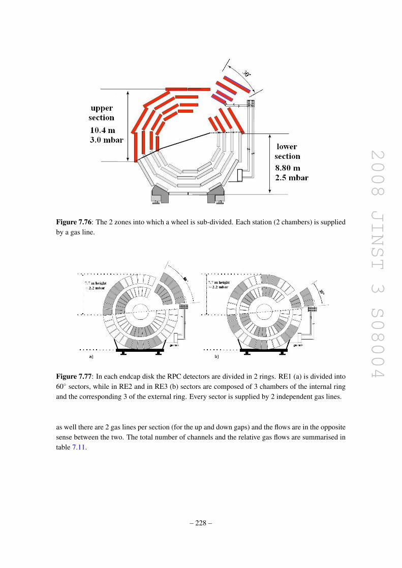
2008 JINST 3 S08004
Figure 7.76: The 2 zones into which a wheel is sub-divided. Each station (2 chambers) is suppliedby a gas line.
Figure 7.77: In each endcap disk the RPC detectors are divided in 2 rings. RE1 (a) is divided into60 sectors, while in RE2 and in RE3 (b) sectors are composed of 3 chambers of the internal ringand the corresponding 3 of the external ring. Every sector is supplied by 2 independent gas lines.
as well there are 2 gas lines per section (for the up and down gaps) and the flows are in the oppositesense between the two. The total number of channels and the relative gas flows are summarised intable 7.11.
– 228 –

2008 JINST 3 S08004
Table 7.11: Chamber volumes and gas flows for a single endcap of the CMS RPC system.
RPCs Volume Number Volume Operating Total flowModule in that per RPC of gas per gas channel per module
module (l) channels channel (l) flow (l/h) type (l/h)RE/1/2 36 5.1 12 30.6 20.4 122RE/1/3 36 7.4 12 44.4 29.6 178
RE/2/2 36 5.1 24 20.3 13.5 324RE/2/3 36 8.4
RE/3/2 36 5.1 24 20.3 13.5 324RE/3/3 36 8.4
Total 216 72 948
Pressure regulation system and gas distribution in UXC
Pressure regulation is achieved in the USC area for each of the 2 zones. Each height section has itsown pressure control and protection system consisting of bubblers located in the distribution racksat the bottom of the wheels/disks. The oil level is adjusted to account for the hydrostatic pressuredifferences in the 2 zones. The distribution racks are installed at the bottom of each wheel/disk.The supply and return lines for each station are equipped with a mass-flow meter and a needle valve(only at the inlet). The flow measurements allow the detection of possible leaks, while the needlevalves are used for the flow adjustment between different stations.
Purifier
Results from long term tests performed by CMS showed that the impurity concentrations producedin the RPC chambers are high enough to influence the detector performance if they are not properlyremoved from the mixture. Therefore, to achieve a high recycling rate the closed-loop circulationsystem is equipped with a purifier module containing 3 cleaning agents. In the first running phasethe 3 cleaning agents are contained in 2 purifiers. Both the purifiers are 24-l cartridges. The firstis filled with a 0.5-nm molecular sieve, while the second is filled with the following combination:25% Cu-Zn filter (type R12, BASF), 25% Cu filter (type R3-11G, BASF), and 50% Ni-Al2O3 filter(type 6525, Leuna). During the high luminosity running period the second purifier will be split into2 separate 24-l cartridges, the first containing the R12 and R3-11G cleaning agents and the secondcontaining the 6525 Leuna filter. Each purifier is equipped with an automatic regeneration system:2 identical cartridges are present allowing the regeneration of a cartridge while the other is in use.
Gas-quality monitoring
Two independent systems are in preparation to continuously monitor the gas quality. The gas-gain monitoring system [170] is based on several small (50× 50 cm2) single-gap RPCs whoseworking points (gain and efficiency) are continuously monitored online. The system is designed toprovide a fast and accurate determination of any shift in the working points. The small single-gap
– 229 –

2008 JINST 3 S08004
RPCs are divided into several sub-groups supplied with gas coming from different parts of the fullsystem (i.e., fresh gas mixture, input to the chambers in closed-loop circulation, and return from theclosed-loop circulation). The second gas monitoring system [171] performs both qualitative andquantitative gas chemical analyses with a set-up that includes a gas chromatograph, pH sensors,and specific fluoride electrodes. In the underground service cavern (USC), many sampling pointsequipped with manual valves allow the analysis of the gas mixtures that return from every halfwheel. In the surface gas building (SGX), sampling points are available to monitor the effectivenessas well as the status of each cartridge in the purifier module.
7.3.6 Chamber construction and testing
In view of the extremely large-scale production (a factor of 10 greater than in past experiments),impressive quality control and certification protocols were set along the production chain at manydifferent levels:
• selection of electrodes and resistivity certification;
• certification of single-gaps and double-gaps;
• chamber testing.
Details regarding the quality certification procedures have been reported elsewhere [172].Only a short summary of the chamber testing results is given below.
Chamber performance at the test sites
Several RPC test stands were in operation. Each telescope consisted of a tower in which severaldetectors could be placed horizontally and read out in coincidence with the passage of the crossingof cosmic muons. Two sets of scintillators, at the top and the bottom of the telescope, were usedfor triggering purposes. Atmospheric and environmental conditions were continuously monitoredduring the tests. These values were used to scale the applied HV for temperature and pressurevariations to evaluate the effective high voltage (HVeff) [173] at given reference values (T0 = 293 Kand P0 = 1010 mbar).
The final gas mixture (96.2% C2H2F4, 3.5% iC4H10, and 0.3% SF6) was used and watervapour was added to keep the gas relative humidity at a value of about 45%.
The tracking capabilities of the test telescope provided a full characterisation of the detectorsin terms of efficiency, cluster size, and noise rate. Also the chambers’ local efficiency and the spatialresolution were studied. Rigourous and automatic protocols were developed and systematicallyapplied at all test sites in order to accept chambers that satisfied the CMS requirements.
First, the chamber efficiency was studied with the “coincidence” method by evaluating theratio between the number of events in which an RPC module had at least 1 fired strip in the triggerwindow (100 ns) and the total number of recorded events. In figure 7.78 the distribution of themaximum efficiency for all the barrel RPCs is shown. The mean value of the distribution is 97.2%.In figure 7.79 the efficiency distribution at HV = 9.3 kV for the first 27 endcap chambers is shown.
The chamber response uniformity was also studied by performing track recognition throughthe telescope. Muon trajectories were reconstructed in 2-dimensional views, where the x coordinate
– 230 –

2008 JINST 3 S08004
Figure 7.78: Distribution of plateau efficiency for all the barrel chambers.
Figure 7.79: Efficiency at HV = 9.3 kV for the first 27 endcap chambers.
is defined by the strip position along the chamber and the y coordinate by the chamber position inthe tower. Details about the pattern recognition algorithm have been presented elsewhere [174].The track-impact point on the chamber under test was also determined and the distance to thenearest cluster centre was evaluated. A chamber was considered efficient if the reconstructed muontrajectory matched the fired strip. A typical strip-by-strip efficiency plot is shown in figure 7.80.
The chamber cluster size is defined as the average value of the cluster-size distribution. InFigure 7.81 the profile histogram of the cluster-size distribution as a function of the HVeff is shownfor all the barrel chambers. A chamber was accepted if the cluster size was below 3 strips at theknee of the efficiency plateau.
– 231 –

2008 JINST 3 S08004
Figure 7.80: Local efficiency at HVeff = 9.6 kV for a barrel chamber.
Figure 7.81: Profile histogram of the chambers’ cluster-size distribution as a function of HVeff.The dots and bars are the average and the root-mean-square of the cluster-size distributions, re-spectively.
Magnet Test and Cosmic Challenge (MTCC)
During the summer and fall of 2006 a first integrated test of an entire CMS “slice” was performedin the SX5 experimental surface hall. For the RPC system, 3 barrel sectors and a 60 portion of thefirst positive endcap disk were involved in the test. The chambers were operated with their finalpower system configuration, and CMS DAQ software, data quality monitor (DQM), and detectorcontrol system (DCS) were implemented for the detector read-out and control.
The RPC Balcony Collector (RBC) board provided a cosmic trigger with a selectable majoritylevel of signals from the 6 RPC barrel chambers. A trigger rate of about 30 Hz/sector for a majoritylevel of 5/6, and 13 Hz/sector for a 6/6 majority was found while operating the detector on thesurface. The RBC trigger was well synchronized with the other muon detector (DT and CSC)triggers.
– 232 –

2008 JINST 3 S08004
Figure 7.82: Iguana muon reconstruction: RPC-fired strips are in red and DT hits in green.
Figure 7.83: Barrel chamber noise profile at HVeff = 9.6 kV.
Several millions of events were collected with different trigger configurations. The DQMwas used successfully during the MTCC. It allowed the online checking of the quality of the dataand the chamber behaviour in terms of cluster size, number of clusters, etc. Figure 7.82 shows theevent display of a typical cosmic muon triggered by the RBC and crossing both RPCs and DTs.
Specific runs were taken before and during the test to evaluate the noise rate. Preliminarily,all the threshold values on the front-end electronic discriminators were set to achieve the best noiseconfiguration with higher efficiency. The chamber noise rate profile for a barrel station is shownin figure 7.83 at HVeff = 9.6 kV, while figure 7.84 shows the overall noise distribution for all thebarrel strips involved in the test.
The RPC efficiency can be studied by extrapolating DT segments to the corresponding RPClayer and by requiring matching hits within an appropriate width. In figure 7.85 the chamberefficiency as a function of the HVeff is shown for some RPC stations.
Results are in agreement with those obtained during testing at construction sites and fullymeet the design specifications.
– 233 –

2008 JINST 3 S08004
Noise_Histos106_10_26_9_24_45.txt
Entries 3414Mean 0.3431RMS 1.584
Noise (Hz/cm^2)-210 -110 1 10 210 310
Entri
es
20
40
60
80
100
120
140
160
180
Noise_Histos106_10_26_9_24_45.txt
Entries 3414Mean 0.3431RMS 1.584
Noise Hz/cm2
B = 0.0 T
B = 3.5 T
Figure 7.84: Noise distributions in 2 different magnetic fields. All strips of the barrel stations areincluded in the distribution.
HV_eff(KV)8.8 9 9.2 9.4 9.6 9.8 10 10.2
Eff
icie
ncy
20
40
60
80
100
RB2IN_B
RB2OUT_B
RB2OUT_M
RB2IN_F
RB2OUT_F
Efficiency For Chambers W2 S10
Figure 7.85: Global efficiency vs. HVeff, estimated by means of DT segment extrapolation.
– 234 –

2008 JINST 3 S08004
7.4 Optical alignment system
For optimal performance of the muon spectrometer [132] over the entire momentum range up to1 TeV, the different muon chambers must be aligned with respect to each other and to the centraltracking system to within a few hundred µm in rφ . The required alignment precision for the endcapchambers is 75–200 µm, while for the barrel the precision varies from 150 µm for the inner cham-bers of Station 1 to 350 µm for the outer chambers of Station 4. To this end, after following strictchamber construction specifications, CMS combines precise survey and photogrammetry measure-ments, measurements from an opto-mechanical system, and the results of alignment algorithmsbased on muon tracks (both from cosmic rays and from pp collisions) crossing the spectrometer.
There are several potential sources of misalignment in the muon spectrometer, from chamberproduction to final detector operating conditions, including:
• Chamber construction tolerances. These are unavoidable geometrical tolerances in the pro-duction of the chamber parts, such as mis-positioning of wires or strips within a layer andrelative shifts in the layer-superlayer assembly. The relative positioning of the different in-ternal components of a chamber was measured during construction to be within the requiredtolerances (section 7.1 and 7.2). After assembly, all chambers were tested with cosmic muondata and showed good correlation between those measurements and the results of muon trackfits. Furthermore, the geometry of the DT chambers was measured at the CERN ISR assem-bly hall using optical and survey techniques. These data are compared with constructiondrawings and cosmic data to provide corrections to the nominal chamber geometry whennecessary.
• Detector assembly, closing tolerances. Gravitational distortions of the return yoke lead tostatic deformations of the steel support. This effect, together with the installation tolerances,results in displacements of the chambers in the different barrel wheels and endcap disks ofup to several millimetres with respect to their nominal detector positions. After chamberinstallation, survey and photogrammetry measurements were performed for each wheel anddisk. These measurements provide an initial geometry — position and orientation of eachmuon chamber in the different yoke structures — which absorbs installation tolerances andstatic steel deformations [175].
• Solenoid effects. Magnetic field distortions lead to almost perfect elastic deformations ofthe return yoke, at the level of a few centimetres. They result in further displacement of thechambers. The new detector geometry resulting from the magnetic forces is accessed withmeasurements of the optical system and track-based alignment techniques.
• Time-dependent effects. During operation, thermal instabilities and other time-dependentfactors can cause dynamic misalignments at the sub-millimetre level.
The Muon Alignment (MA) system was designed to provide continuous and accurate mon-itoring of the barrel and endcap muon detectors among themselves as well as alignment betweenthem and the inner tracker detector. To fulfil these tasks the system is organized in separate blocks:
– 235 –

2008 JINST 3 S08004
Figure 7.86: Schematic view of the alignment system. Left panel: longitudinal view of CMS. Thecontinuous and dotted lines show different optical light paths. Right panel: transverse view of thebarrel muon detector. The crossing lines indicate the r-z alignment planes with 60 staggering in φ .
local systems for barrel and endcap muon detectors to monitor the relative positions of the cham-bers, and a link system that relates the muon and central tracker systems and allows simultaneousmonitoring of the detectors.
The system must generate alignment information for the detector geometry with or withoutcollisions in the accelerator. The dynamic range of the system allows it to work in the solenoidalmagnetic field between 0 and 4 T. Its goal is to provide independent monitoring of the CMS track-ing detector geometry with respect to an internal light-based reference system. This will help todisentangle geometrical errors from sources of uncertainty present in the track-based alignmentapproach, e.g., knowledge of the magnetic field, material description, and drift velocity.
The basic geometrical segmentation consists of 3 r-z alignment planes with 60 staggering inφ . This segmentation is based on the 12-fold geometry of the barrel muon detector. Within eachplane, the 3 tracking sub-detectors of CMS (central tracker, barrel and endcap muon detectors)are linked together. Figure 7.86 shows schematic longitudinal and transverse views of CMS, withthe light paths indicated. Furthermore, the barrel and endcap monitoring systems can work instand-alone mode, in which they provide reconstruction of the full geometry of each independentsub-detector. The layout of the optical paths allows the monitoring of each of the 250 DT chambers,while only one sixth of selected CSCs in the 4 endcap stations are directly monitored. Alignmentsensors located in the region between the muon barrel wheels and endcap disks allow the trackerand muon detectors to be aligned with respect to each other.
7.4.1 System layout and calibration procedures
The optical network uses two types of light sources: LEDs and laser beams. It is composed of10 000 LEDs and 150 laser beams together with precise measuring devices: ≈ 900 photo-detectors
– 236 –

2008 JINST 3 S08004
and ≈ 600 analog sensors (distance sensors and inclinometers), complemented by temperature,humidity and Hall probes. The system is structured into three basic blocks whose main featuresare described below.
Muon barrel alignment
The monitoring of the barrel muon detector (figure 7.87) is based on the measurement of all the250 DT chamber positions with respect to a floating network of 36 rigid reference structures, calledMABs (Module for the Alignment of Barrel). The MAB design was optimised to achieve adequatemechanical rigidity of the structures under load and in thermal and humidity gradients. Longterm measurements showed deviations below 100 µm and 50 µrad [176]. The MABs are fixedto the barrel yoke forming 12 r-z planes parallel to the beam line and distributed in φ every 60.Each structure contains 8 specially designed video cameras that observe LED sources mountedon the DT chambers. Extra light sources and video-cameras in specific MABs serve to connectMABs in different planes forming a closed optical network (called diagonal connections). TheMAB positions in the z coordinate are measured with respect to 6 calibrated carbon-fibre bars (z-bars) sitting on the outer surface of the vacuum tank of the solenoid. The MABs in the externalwheels, YB±2, are equipped with extra alignment sensors and light sources that connect the barrelmonitoring system with the endcap and tracker detectors.
The 4 corners of the DTs are equipped with LED light sources. Four LED-holders, or forks,are rigidly mounted on the side-profile of the honeycomb structure (2 per side) and use the rect-angular 50 × 65 mm2 tube as a light passage. Each fork contains 10 LEDs, 6 and 4, respectively,on each side. There are 10 000 light sources mounted on the DT chambers. The position of theforks with respect to the chamber geometry was measured on a dedicated bench with a precisionof < 70 µm. As an important by-product, the calibration also provides the full geometry, includingthe planarity, trapezoidity, and the relative positions of superlayers for each DT chamber with < 40µm precision, as described in section 7.1.4. Each LED-holder and video-sensor was individuallycalibrated before its assembly on the DT chambers or MABs and z-bars. LED-holders were mea-sured and the position of the light centroid was determined with respect to the holder mechanicswith an accuracy of 10 µm. Long term measurements showed good stability of the centroids andlight intensity distributions. CMOS miniature video sensors, containing 384 × 288 pixels with 12× 12 µm2 pixel size, were calibrated to absorb residual response non-uniformities and the intensitynonlinearities. The video cameras, consisting of a video sensor and a single-element lens assem-bled in an aluminium box, were also calibrated to determine their inner geometrical parameters.Fully instrumented MABs containing the necessary number of survey fiducials were calibrated ona special bench, where the whole geometry of the structure, positions, and orientations of elementswere determined with overall accuracies of 70 µm and 50 µrad.
Once MABs were installed (figure 7.88), the initial MAB positions on the barrel wheels weredetermined by photogrammetry measurements.
The control, read-out, and data preprocessing [177] are performed by a network of localminicomputers (1 per MAB, 36 in total) that makes it possible to run the full system in parallel. Theminicomputers are connected to the main control PC via an Ethernet network capable of working inmagnetic fields. The main control PC synchronizes the operation of the light sources mounted on
– 237 –

2008 JINST 3 S08004
Figure 7.87: Schematic view of the barrel monitoring system showing the optical network amongthe MAB structures.
Figure 7.88: Installation of the MABs on wheel YB+2.
– 238 –

2008 JINST 3 S08004
the DT chambers and the read-out of the images taken by the cameras. The minicomputers controlthe light sources mounted on the MABs and the z-bars, read out the temperature and humiditysensors, perform the image read-out and digitisation, and calculate the image centroids of the lightsources. The results are transferred to the main control PC, which is connected to the correspondingcentral CMS units.
Based on simulation, the barrel monitoring system should provide a stand-alone measurementof the barrel chambers with an average r-φ position accuracy of 100 µm for chambers in the samesector and about 250 µm between barrel sectors. The current understanding of its performance isdiscussed in section 7.4.3.
Muon endcap alignment
The muon endcap alignment system [178] is designed to continuously and accurately monitorthe actual positions of the 486 CSCs relative to each other, relative to the tracking system, andultimately within the absolute coordinates of CMS. Due to the large magnetic field, the chambersmounted on the endcap yoke undergo substantial motion and deformation, on the order of a fewcentimetres, when the field is switched on and off. The alignment system must measure the diskdeformation and monitor the absolute positions of the CSCs in the r-φ plane and in z. Fromsimulations, the required absolute alignment accuracies were found to run from 75 to 200 µm inr-φ . Because the r and r-φ accuracies are directly coupled, the required accuracy in the r-positionis ≈400 µm. The z displacement due to the deformation of the iron yoke disks caused by thestrong and non-uniform magnetic field in the endcaps requires the alignment sensors to be able toaccommodate a dynamic range of ≈2 cm with an accuracy of ≈1 mm.
The system uses a complex arrangement of 5 types of sensors for the transferring and moni-toring of φ , r, and z coordinates (figure 7.89). The system measures one sixth of all endcap cham-bers. The main monitoring tools within the r-φ plane are the Straight Line Monitors (SLM). EachSLM consist of 2 cross-hair lasers, which emit a nearly radial laser beam across 4 chambers fromeach end, and provide straight reference lines that are picked up by 2 optical sensors (Digital CCDOptical Position Sensors, DCOPS [179]). This arrangement provides references for the chamberpositions relative to the laser lines. Figure 7.90 shows a photograph of a complete SLM on sta-tion ME+2. The figure also indicates r-sensors for monitoring radial chamber positions, z-sensorsfor axial distance measurements between stations, and a clinometer for monitoring the tilt of themechanical support assembly (transfer plate) onto which lasers, reference DCOPS, and z-sensorsare mounted. The inset in figure 7.90 shows the location of proximity sensors on the outer ring ofthe ME+1 station, which monitor the azimuthal distance between neighbouring chambers. Theseare necessary because the outer ring of ME1 chambers is the only ring for which the CSCs do notoverlap in φ . Furthermore, every CSC and alignment device is equipped with photogrammetrytargets to allow absolute magnet-off measurements.
The φ coordinate alignment is handled by optical SLMs and transfer lines. Transfer laser linesrun parallel to the CMS z-axis along the outer cylindrical envelope of CMS at 6 points separated by60 in φ . The SLMs run across the surface of one sixth of all the CSCs, along radial directions, andlink transfer lines on opposite sides of a disk. Both laser lines have a similar basic configuration:a laser beam defines a direction in space that is picked up by several DCOPS precisely mounted
– 239 –

2008 JINST 3 S08004
Figure 7.89: Visualisation of the geometry and components of the muon endcap alignment system.The square objects represent optical sensors (DCOPS) for monitoring 3 straight laser lines acrosseach endcap station.
on CSCs or transfer plates to reference their own positions. Mounting accuracies due to tolerancesof dowel pins and dowel holes are ≈50 µm. Every DCOPS comprises 4 linear CCDs, each with2048 pixels and 14 µm pixel pitch. The CCDs are basically arranged in the shape of a square andcan be illuminated by cross-hair lasers from either side. The r and z coordinate measurements areperformed by analog linear potentiometers and optical distance devices in contact with aluminiumtubes of calibrated length.
All analog sensors were calibrated with a 1D precision linear mover with 6.4 µm step size.The uncertainty in the absolute distance calibration is 100 µm for r sensors and 53 µm for z sen-sors [180]. Calibration for optical DCOPS consisted in determining the distance from the surfaceof the mount hole for a reference dowel pin to the first active CCD pixel and measuring the pro-jected pixel pitch of each of the 4 CCDs. This was done on a calibration bench where a fibre-bundlevariable light source at the focus of a parabolic mirror illuminated a mask with 8 optical slits. Asimple geometry reconstruction, based on coordinate-measuring-machine data for the calibrationmask and sensor mounts, determined the physical pixel positions. Calibration errors were typically30 to 50 µm.
– 240 –

2008 JINST 3 S08004
Figure 7.90: Close-up of one of the 3 Straight Line Monitors (SLM) on the ME+2 station withcross-hair laser, DCOPS, and analog sensors (r, z, and Tiltmeter). The insert indicates the locationof proximity sensors on ME+1.
Link system
The purpose of the link alignment system is to measure the relative position of the muon spectrom-eter and the tracker in a common CMS coordinate system. It is designed to work in a challengingenvironment of very high radiation and magnetic field, meet tight space constraints, and providehigh precision measurements over long distances. A distributed network of opto-electronic positionsensors, ASPDs (amorphous-silicon position detectors) [181], placed around the muon spectrome-ter and tracker volumes are connected by laser lines. The entire system is divided into 3 φ -planes60 apart; this segmentation allows a direct reference of each muon barrel sector with the trackerdetector and provides a direct reference also to the endcap alignment lines in the first endcap sta-tion, ME1. Each plane consists of 4 quadrants (figure 7.86) resulting in 12 laser paths: 6 on eachz-side of the CMS detector, and generated by 36 laser sources. The system uses 3 types of refer-ence structures: rigid carbon-fibre annular structures placed at both ends of the tracker (alignmentrings, AR) and at the YE±1 wheels of the endcap muon spectrometer (link disks, LD); and theMAB structures attached at the external barrel wheels, YB±2. Figure 7.91 (left) shows the LDand AR carbon fibre structures installed in the inner η = 3 cone. The link measurement networkis complemented by electrolytic tiltmeters, proximity sensors in contact with aluminium tubes ofcalibrated length, magnetic probes, and temperature sensors.
The ARs are rigidly attached to the endcap tracker detectors, TECs, through a purely me-chanical connection with the instrumented silicon volume (section 3.3.7). Three pillars, acting assupport fixations, connect the last instrumented disk of each TEC with the corresponding AR, at
– 241 –

2008 JINST 3 S08004
Figure 7.91: Left panel: Link Disk and Alignment Ring installed in the inner η = 3 cone during thefirst closing of the detector in summer 2006, MTCC period. Right panel: Alignment Ring mountedin the TEC end flange.
both ends of the tracker volume, see figure 7.91 (right). The position and orientation of the ARswith respect to the TEC disks 9 and 10 were measured with a coordinate-measurement machineusing the external survey fiducials prior to the TEC assembly and instrumentation. Changes inangular orientations are monitored by high precision tiltmeters placed at the AR and TEC disk 10.Laser sources originating at the AR and running along the inner detector boundary reach ASPDsensors on the first endcap disk, ME1, and on the external barrel wheel.
The ASPDs are 2D semitransparent photo-sensors, which consist of 2 groups of 64 siliconmicro-strips with a pitch of 430 µm oriented perpendicularly. With ≥80% transmittance for the685 nm wavelength used in the system, they allow multi-point measurements along the light pathwithout significant distortions in the beam direction. The intrinsic position resolution is about 2µm. The location, centre position, and orientation of the ASPD with respect to reference pins intheir mechanical mount are measured with a non-contact CMM (Coordinate Measuring Machine)with an overall accuracy of 15 µm. Distance measurement devices (optical distance sensors andlinear potentiometers) already mounted in their final mechanics were calibrated using 2 µm resolu-tion linear movers and pre-measured calibration fixtures. The uncertainties in absolute and relativecalibration [182] are below 50 µm and 20 µm, respectively, for the different sensor types. Theintrinsic accuracy of the tiltmeters sensors, after calibration, is about 2 µrad; mechanical offsetsinherent to the mechanical mounts and assembly tolerances are determined by survey and pho-togrammetry techniques.
The light sources (collimators) and specific optical devices housed on the alignment referencestructures (AR, LD, and MABs) create the laser beam paths with the layout described above. Eachcollimator is focused to its working distance to ensure Gaussian beam profiles along the propa-gation path to avoid beam-shape-induced bias in the position reconstruction. The adjustment andcalibration [183] of the laser rays for the AR and LD structures were done on a dedicated benchinstrumented with a precise survey network that mimics the nominal detector geometry. Beamswere adjusted to their nominal geometry with a precision better than 100 µrad. Long term mea-surements were performed after beam adjustments. Beam pointing stability, including temperature
– 242 –

2008 JINST 3 S08004
effects, was found to be better than 30 µrad. The adjustment and calibration accuracy was limitedto 30–100 µrad due to the finite dimension of the structures combined with the intrinsic accuracyof the survey and photogrammetry measurement techniques of 70 µm.
Survey and photogrammetry measurements are also performed during the installation of thealignment structures in the detector. An installation accuracy of the order of a few millimetres andmilliradians is needed to ensure correct functionality of the system, taking into account the standardCMS assembly tolerances of the big endcap disks and barrel wheels.
The control, read-out, and data preprocessing are performed by two types of electronicboards. Analog sensors read-out and laser control use standard ELMB (embedded local monitorboard) cards [184]. For the read-out of ASPD sensors, custom made LEB (local electronic board)cards were developed. LEBs are intelligent imaging acquisition boards made to read and control upto 4 ASPD sensors. They are based on Hitachi micro-controllers. ELMB and LEB boards use theCAN communication protocol to connect the front-end electronics and the main control PC unit.
7.4.2 Geometry reconstruction
The DAQ, monitoring, and control software are integrated into the DCS (detector control system)environment. Data are recorded in an online Oracle database and subsequently converted into ntu-ples by specialised programs that perform database queries and apply calibrations to convert rawvalues into meaningful physical quantities. This provides the necessary information for globalgeometry reconstruction, which is handled by COCOA (CMS Object-Oriented Code for OpticalAlignment) [185], an offline program to simulate and reconstruct the complex optical alignmentsystem. Due to the unknown movements of different CMS structures, the sensors of the opticalalignment systems will not measure the expected nominal values. The aim of COCOA is to anal-yse the observed changes in these measurements to determine which are the displacements and/orrotations that caused them. The approach adopted by COCOA to tackle this problem is to solve thesystem of equations that relate the measurement values to all the positions, rotations, and internalparameters of all the objects that make up the system. In fact, to solve the system of equations,one does not need to know the explicit form of the equations, but only the derivatives of each mea-surement value with respect to each object parameter. COCOA uses a geometrical approximationof the propagation of light to calculate numerically these derivatives and then solves the system ofequations through a nonlinear least squares method. Due to the large number of parameters in CMS(about 30 000), big matrices are needed. COCOA matrix manipulations are based on the MeschachLibrary [186].
COCOA has proved its robustness through its extensive use in CMS for several design studies,as well as for the analysis of several test benches and magnet test results. Its output, the alignedgeometry, will be used as input geometry for track reconstruction as well as for further alignmentstudies based on muon tracks from cosmic rays and from pp collisions.
7.4.3 System commissioning and operating performance
A first test of the large superconducting solenoid magnet in the CMS detector was successfullyperformed between June and November 2006, during which stable operation at full field (4 T) wasachieved (section 3.3). The alignment sensors, read-out, and DAQ software were commissioned
– 243 –

2008 JINST 3 S08004
during this test period for about one third of the system, instrumented at the +z side of the detector.This allowed the first full-scale dynamic test of the system. The performance of the system as wellas the main features of the yoke displacement and deformation were studied. The relevant resultsare summarised below:
• Measurement of relative movements due to thermal changes.The effects of thermal changes (day-night variations) for DT and CSC chambers were re-corded for the conditions present during the test, with the detector in the surface assemblyhall and power on only ≈5% of the muon spectrometer. The measured relative movementdid not exceed 50 µm over the entire test period, with changes in position showing a goodcorrelation with temperature. Although a movement of this magnitude is not relevant fromthe physics analysis point of view, its measurement illustrates the good resolution of thealignment system.
• Measurement of the displacements and deformations of the yoke structures.
Two effects were observed. The first is the change in the original positions of the structures(the positions before any magnet operation). The displacements of the structures along thez direction towards the solenoid seem to stabilise after the first 2.5–3 T are reached. Thiscompression is permanent, meaning it is not reversed/recovered in subsequent magnet offstates, and it is interpreted as the final closing of the structures due to the magnetic forcesacting on the iron. These measured displacements are specific to the first CMS closingexperience and cannot be extrapolated to other scenarios.
The second effect is the almost perfectly elastic deformations between magnet-on and mag-net-off states, as illustrated in figure 7.92. At 4 T, the elastic deformation of the barrel yoke,measured at the end of the +z side with respect of the plane of the interaction point, is about2.5 mm. Figure 7.92 shows the elastic compression of the barrel wheels versus the magnetcurrent as recorded in the second phase of the Magnet Test period. Despite the large overallcompression of the barrel spectrometer, an important measurement was the stability of thebarrel chambers during the whole data-taking period. The relative movements in the r-φdirection did not exceed 60 µm.
The behaviour of the endcap disk is more complicated. Due to the strong gradient in themagnetic field near the end of the solenoid, strong magnetic forces pull the central portions ofthe endcap disks towards the center of the detector. As shown in figure 7.92, the nose is pulledtowards the interaction point, the magnitude of the compression is perfectly correlated withthe magnet current, reaching up to ≈16 mm at 4 T. The various z-stops, which prevent thedisks from getting pushed into each other and onto the barrel wheels, cause the endcap disksto bend into a cone shape. The z-stops between endcap and barrel, positioned at nearly halfthe disk radius, cause the side of the YE1 disk facing the barrel to compress radially aroundthem by ≈600 µm, while expanding azimuthally by ≈800 µm. This explains the radialcompression of the face of ME+1 and the larger bending angles at mid-radius than at theouter edge (figure 7.93). Endcap disk deformations are predicted by finite element analysis(FEA) using the ANSYS program [3]. The measurements are in reasonable quantitativeagreement for all displacements and deformations, as shown in figure 7.93. Note that the
– 244 –

2008 JINST 3 S08004
Figure 7.92: Deformations of endcap disks and barrel wheels vs magnet current cycling. Leftpanel: The bottom plot shows the magnet powering cycle exercised during the first phase of theMagnet Test period. The top plot shows the measured YE+1 nose compression towards the inter-action point. Right panel: The bottom plot shows the magnet powering cycle exercised during thesecond phase of the Magnet Test period. The top plot shows the calculated approximate YB+2compression towards the interaction point.
front z-stops, between the ME1 and barrel wheels, were not included in the FEA, whichexplains the difference. The difference between top and bottom is also explained by thepresence of the carts that support the disks.
The rest of the endcap stations on YE+2 and YE+3 experience a maximum bending angleof ≈2.5 mrad relative to the vertical, as sketched in figure 7.94. As in the case of the barrelchambers, with stable 4 T field, the observed relative movements were very small.
• Detector closing tolerances and reproducibility.The test of the magnet was divided into 2 phases, separated by a short period during whichthe yoke was open to extract the inner detectors, tracker, and ECAL modules. This allowed atest of the reproducibility in the closing procedure and tolerances, as well as the study of thecompatibility of measurements between the two phases. Reproducibility in the closing wasat the level of a few millimetres for the barrel wheels and about an order of magnitude higherfor the endcap disks. The particular conditions of the test did not allow the establishmentof a solid understanding of reproducibility for the process of closing the different structures.Instead, the system was able to reproduce the same magnetic-force-induced effects as mea-sured in the first period.
From this test we conclude that the system operates adequately under magnetic fields both interms of dynamic range and measurement performance. The system precision achieved is ≤ 300µm and the measurement accuracy has been validated against results from photogrammetry andcosmic ray tracks.
– 245 –

2008 JINST 3 S08004
Figure 7.93: Comparison of the YE+1 diskdeformations in the r-z plane at full magneticfield (4 T) measured by the alignment system(left panel) and predictions from finite elementanalysis (right panel). The vertical lines corre-spond to 0 magnetic field.
Figure 7.94: Current understanding of diskdeformation due to magnetic forces based onalignment system measurements. The z-stops(red) prevent the disks from getting pushedinto each other. Note that the indicated bend-ing angle is exaggerated for illustrative pur-poses. Its measured magnitude is 2.5 mrad.
– 246 –

2008 JINST 3 S08004
Chapter 8
Trigger
The LHC provides proton-proton and heavy-ion collisions at high interaction rates. For protonsthe beam crossing interval is 25 ns, corresponding to a crossing frequency of 40 MHz. Dependingon luminosity, several collisions occur at each crossing of the proton bunches (approximately 20simultaneous pp collisions at the nominal design luminosity of 1034 cm−2s−1 ). Since it is impos-sible to store and process the large amount of data associated with the resulting high number ofevents, a drastic rate reduction has to be achieved. This task is performed by the trigger system,which is the start of the physics event selection process. The rate is reduced in two steps calledLevel-1 (L1) Trigger [187] and High-Level Trigger (HLT) [188], respectively. The Level-1 Trig-ger consists of custom-designed, largely programmable electronics, whereas the HLT is a softwaresystem implemented in a filter farm of about one thousand commercial processors. The rate reduc-tion capability is designed to be at least a factor of 106 for the combined L1 Trigger and HLT. Thedesign output rate limit of the L1 Trigger is 100 kHz, which translates in practice to a calculatedmaximal output rate of 30 kHz, assuming an approximate safety factor of three. The L1 Trig-ger uses coarsely segmented data from the calorimeters and the muon system, while holding thehigh-resolution data in pipelined memories in the front-end electronics. The HLT has access to thecomplete read-out data and can therefore perform complex calculations similar to those made inthe the analysis off-line software if required for specially interesting events. Since HLT algorithmswill evolve with time and experience they are not described here. More information may be foundin [189]. For reasons of flexibility the L1 Trigger hardware is implemented in FPGA technologywhere possible, but ASICs and programmable memory lookup tables (LUT) are also widely usedwhere speed, density and radiation resistance requirements are important. A software system, theTrigger Supervisor [190], controls the configuration and operation of the trigger components.
The L1 Trigger has local, regional and global components. At the bottom end, the Local Trig-gers, also called Trigger Primitive Generators (TPG), are based on energy deposits in calorimetertrigger towers and track segments or hit patterns in muon chambers, respectively. Regional Trig-gers combine their information and use pattern logic to determine ranked and sorted trigger objectssuch as electron or muon candidates in limited spatial regions. The rank is determined as a func-tion of energy or momentum and quality, which reflects the level of confidence attributed to theL1 parameter measurements, based on detailed knowledge of the detectors and trigger electronicsand on the amount of information available. The Global Calorimeter and Global Muon Triggers
– 247 –

2008 JINST 3 S08004
Figure 8.1: Architecture of the Level-1 Trigger.
determine the highest-rank calorimeter and muon objects across the entire experiment and transferthem to the Global Trigger, the top entity of the Level-1 hierarchy. The latter takes the decisionto reject an event or to accept it for further evaluation by the HLT. The decision is based on al-gorithm calculations and on the readiness of the sub-detectors and the DAQ, which is determinedby the Trigger Control System (TCS). The Level-1 Accept (L1A) decision is communicated to thesub-detectors through the Timing, Trigger and Control (TTC) system. The architecture of the L1Trigger is depicted in figure 8.1. The L1 Trigger has to analyze every bunch crossing. The allowedL1 Trigger latency, between a given bunch crossing and the distribution of the trigger decision tothe detector front-end electronics, is 3.2 µs. The processing must therefore be pipelined in order toenable a quasi-deadtime-free operation. The L1 Trigger electronics is housed partly on the detec-tors, partly in the underground control room located at a distance of approximately 90 m from theexperimental cavern.
8.1 Calorimeter trigger
The Trigger Primitive Generators (TPG) make up the first or local step of the Calorimeter Triggerpipeline. For triggering purposes the calorimeters are subdivided in trigger towers. The TPGs sumthe transverse energies measured in ECAL crystals or HCAL read-out towers to obtain the triggertower ET and attach the correct bunch crossing number. In the region up to |η |= 1.74 each triggertower has an (η ,φ )-coverage of 0.087× 0.087. Beyond that boundary the towers are larger. TheTPG electronics is integrated with the calorimeter read-out. The TPGs are transmitted throughhigh-speed serial links to the Regional Calorimeter Trigger, which determines regional candidateelectrons/photons, transverse energy sums, τ-veto bits and information relevant for muons in theform of minimum-ionizing particle (MIP) and isolation (ISO) bits. The Global Calorimeter Triggerdetermines the highest-rank calorimeter trigger objects across the entire detector.
– 248 –

2008 JINST 3 S08004
Calorimeter trigger primitive generators
The ECAL on-detector front-end electronics boards, each serving 25 crystals, receive the ADCsignals from the very front-end electronics located at the rear of the detector modules. They containmost of the TPG pipeline in six radiation-hard 0.25 µm CMOS ASIC chips named FENIX. An off-detector Trigger Concentrator Card (TCC) collects the primitives from 68 front-end boards in thebarrel and 48 boards in the endcaps through optical links. The TCCs finalize the TPG generationand encoding, store the trigger primitives during the L1 latency time and transmit them to the RCTby dedicated daughter boards, the Synchronization and Link Boards (SLB), upon reception of aL1A signal. The SLBs synchronize the trigger data through circuits that histogram the LHC bunchcrossing structure. Each trigger tower is aligned with the bunch crossing zero signal. A DataConcentrator Card (DCC) performs the opto-electronic conversion and deserialization of the serialinput data streams and sends the read-out data collected from the front-end boards to the DAQ.Clock and Control System (CCS) boards distribute the clock, the L1A and control signals to theTCC, the DCC and the on-detector electronics. The ECAL TPG hardware is contained in twelve9U VME crates for the barrel and six for the endcaps.
The front-end modules of the hadron calorimeter contain Charge Integrator and Encoder(QIE) ADC chips to digitize the signals from the photo detectors. Optical links transmit the datato the HCAL Trigger and Readout (HTR) boards. Each HTR board processes 48 channels. It lin-earizes, filters and converts the input data to generate the HCAL trigger primitives. The energyvalues of front and back towers are added and the bunch crossing number is assigned by a peakfiltering algorithm. As for the ECAL, the primitives are sent to the RCT by SLBs, and read-outdata are collected by a DCC. The HCAL trigger electronics is contained in 26 9U VME crates.Each crate houses 18 HTR boards and one DCC.
Regional Calorimeter Trigger
The Regional Calorimeter Trigger [191] determines electron/photon candidates and transverse en-ergy sums per calorimeter region. Information relevant for muons about isolation and compatibilitywith minimally ionizing particles is also calculated. A region consists of 4×4 trigger towers exceptin HF where a region is one trigger tower. Electromagnetic and hadronic transverse energies aresummed in each tower.
The e/γ trigger algorithm (figure 8.2) starts by determining the tower with the largest energydeposit and is applied across the entire ECAL region. The energy of the tower with the next-highest deposit in one of the four broad side neighbours is then added. Isolated and non-isolatede/γ within |η | ≤ 2.5 are determined by the trigger. A non-isolated e/γ requires passing of twoshower profile vetoes. The first one is based on a fine-grain crystal energy profile reflecting thelateral extension of a shower. The fine-grain bit is set by the TPG if the shower is contained in amatrix of 2× 5 crystals. The matrix is dimensioned such that it also allows for the detection ofbremsstrahlung due to the magnetic field. The second one is based on the ratio of the depositedenergies in the hadronic and in the electromagnetic sections. A typical maximal value of 5% isallowed for that ratio. An isolated electron/photon candidate has to pass the previous vetoes forall eight neighbouring towers. In addition, at least one quiet corner made of four groups of fiveelectromagnetic towers surrounding the hit tower is required. Four isolated and four non-isolatede/γ per region are forwarded to the GCT.
– 249 –

2008 JINST 3 S08004
Figure 8.2: Electron/photon algorithm. Figure 8.3: Electron Isolation Card.
The RCT also sums the transverse energy in a given region of the central calorimeter (HF isnot included) and determines τ-veto bits for the identification of jets from one- and three-prongτ-decays, which are narrower than ordinary quark/gluon jets. A τ-veto bit is set unless the patternof active towers corresponds to at most 2×2 contiguous trigger towers within a 4×4 tower region.Jets can be classified as τ-jet only at |η |< 3.0 (not in HF).
The RCT hardware consists of 18 regional 9U VME crates and one 6U clock distributioncrate located in the underground control room. Each crate covers a region of ∆η×∆φ = 5.0 ×0.7.Receiver cards are plugged into the rear of the regional crates. Seven cards per crate receive theECAL and HCAL primitives. The HF primitives are directly received on a Jet/Summary card. Theserial input data are converted to 120 MHz parallel data, deskewed, linearized and summed beforetransmission on a 160 MHz custom monolithic backplane to seven Electron Isolation Cards (EIC)and one Jet/Summary Card (JSC) mounted at the front side of the crate. Different ASICs performthe algorithm calculations. An EIC is shown in figure 8.3.
Global Calorimeter Trigger
The Global Calorimeter Trigger determines jets, the total transverse energy, the missing transverseenergy, jet counts, and HT (the scalar transverse energy sum of all jets above a programmablethreshold). It also provides the highest-rank isolated and non-isolated e/γ candidates.
Jets are found by a four-stage clustering technique based on jet finders operating in 2× 12cells in φ and η , spanning 40 and half the detector, respectively, in these directions. The cell atη=0 is duplicated. In the first stage mini-clusters are created by summing energies within 2×3 cellsif a central cell has more energy than neighbouring cells. In the second stage the three largest mini-clusters in each of the two φ -strips are transferred in opposite φ -directions. These are comparedagainst the existing mini-clusters on the receiving φ -strip. Mini-clusters adjacent or diagonallyadjacent to a larger mini-cluster are removed. In the third and fourth stages the received mini-clusters that survive have their three adjacent cells in the receiving φ -strip combined to make a 3×3cell. A jet is classified as a τ jet if none of the corresponding RCT regions had a τ-veto bit set. Aftersorting, up to four jets and four τ jets from the central HCAL and four jets from HF are forwardedto the GT. The magnitude and direction of the missing energy and the total transverse energy are
– 250 –

2008 JINST 3 S08004
computed from the regional transverse energy sums in the two coordinates transverse to the beamwithin |η | < 5. Twelve jet counts for different programmable ET -thresholds and optionally alsodifferent (η ,φ )-regions are computed. Muon MIP/ISO bits are received from the RCT along withthe e/γ data and are forwarded to the GMT through a dedicated muon processing system. Apartfrom triggering, the GCT also acts as the read-out system for the RCT. The GCT has in addition thecapability to monitor rates for certain trigger algorithms and from those deduce information aboutthe LHC luminosity as seen by the CMS trigger system.
All GCT electronics is located in the underground control room. The large amount of datafrom the RCT crates are transmitted electronically to 63 Source Cards, which reorder the data onto252 optical fibres. The core of the GCT processing is performed by Leaf Cards, which can beconfigured as electron or jet cards. Several Leaf Cards can be connected with each other in orderto perform complex tasks such as the jet finding. There are two Leaf Cards for electrons and sixfor jets. Each electron leaf card receives the e/γ data from one half of the RCT crates on 27 fibresand sorts them. Each jet card receives 30 regional sum fibres from three RCT crates via the sourcecards. They perform the jet clustering and transmit the jet candidates to two Wheel Cards forsorting and data compression. They also calculate partial energy sums and jet counts and forwardthem to the Wheel Cards. A Concentrator Card finally collects the data from all Electron Leafand Wheel Cards and performs the final sorting for electrons/photons, completes the jet findingin the boundaries between groups of three Leaf Cards, sorts all jets, calculates the global energyand jet count quantities and sends the final results to the GT and the DAQ. In addition to the tasksinvolving e/γ’s, jets and energy sums, the GCT also handles MIP/ISO bits for muons. They areprocessed by three muon processing cards, which receive 6 muon fibres each from Source Cards.The processor design is built on an evolution of the leaf concept and uses a modular, low-latencyarchitecture based on the µTCA industry standard [193]. An active custom backplane based on theprinciple of a crosspoint switch allows a programmable routing of the 504 MIP/ISO bits, which arethen transmitted to the GMT on 24 links.
8.2 Muon trigger
All three muon systems – the DT, the CSC and the RPC – take part in the trigger. The barrel DTchambers provide local trigger information in the form of track segments in the φ -projection and hitpatterns in the η-projection. The endcap CSCs deliver 3-dimensional track segments. All cham-ber types also identify the bunch crossing from which an event originated. The Regional MuonTrigger consists of the DT and CSC Track Finders, which join segments to complete tracks andassign physical parameters to them. In addition, the RPC trigger chambers, which have excellenttiming resolution, deliver their own track candidates based on regional hit patterns. The GlobalMuon Trigger then combines the information from the three sub-detectors, achieving an improvedmomentum resolution and efficiency compared to the stand-alone systems. The initial rapiditycoverage of the muon trigger is |η | ≤ 2.1 at the startup of LHC. The design coverage is |η | ≤ 2.4.
– 251 –

2008 JINST 3 S08004
Figure 8.4: Drift Tube Local Trigger.
Drift Tube local trigger
The electronics of the DT local trigger consists of four basic components (figure 8.4): Bunchand Track Identifiers (BTI), Track Correlators (TRACO), Trigger Servers (TS) and Sector Collec-tors (SC). While the SCs are placed on the sides of the experimental cavern, all other trigger andread-out electronics is housed in minicrates on the front side of each chamber. All devices are im-plemented in custom-built integrated circuits. The BTIs are interfaced to the front-end electronicsof the chambers. Using the signals from the wires they generate a trigger at a fixed time after thepassage of the muon. Each BTI searches for coincident, aligned hits in the four equidistant planesof staggered drift tubes in each chamber superlayer. The association of hits is based on a mean-timer technique [194], which uses the fact that there is a fixed relation between the drift times ofany three adjacent planes. From the associated hits, track segments defined by position and angu-lar direction are determined. The spatial resolution of one BTI is better than 1.4 mm, the angularresolution better than 60 mrad. The BTI algorithm is implemented in a 64-pin ASIC with CMOS0.5 µm Standard Cell technology. There are a few hundred BTIs per chamber.
The DT chambers have two Φ-type superlayers, measuring φ coordinates. The TRACOattempts to correlate the track segments measured in each of them. If a correlation can be found,the TRACO defines a new segment, enhancing the angular resolution and producing a qualityhierarchy. Four BTIs in the inner Φ-type superlayer and 12 BTIs in the outer Φ-type superlayerare connected to one TRACO. The number of TRACOs is 25 for the largest muon chamber type.The TRACO is implemented in a 240-pin ASIC with CMOS 0.35 µm Gate Array technology. Thetrigger data of at most two track segments per bunch crossing reconstructed by each TRACO aretransmitted to the TS, whose purpose is to perform a track selection in a multitrack environment.
The TS has two components, one for the transverse projection (TSφ ) and the other for thelongitudinal projection (TSθ ). The first one processes the output from the TRACO, whilst thesecond uses directly the output of the BTIs of the θ view delivered by the Θ-type superlayerspresent in the three innermost muon stations. The TSφ consists itself of two components, the
– 252 –

2008 JINST 3 S08004
Track Sorter Slave (TSS) and the Track Sorter Master (TSM). The TSS preselects the tracks withthe best quality and the smallest bending angle based on a reduced preview data set coming fromthe TRACOs in order to save processing time. A select line in the TRACO with the best trackis then activated and the TRACO is allowed to send the full data to the TSM. The correspondingpreview data are also sent to the TSM for a second stage processing. The TSM analyzes up to sevenpreview words from the TSSs. The output consists of the two tracks with the highest transversemomentum. There is one TSM per muon station. In the longitudinal view the TSθ groups theinformation from the 64 BTIs per chamber. From each BTI two bits are received, a trigger bitand a quality bit. A logic OR of groups of eight bits is applied. The output data consist of 8 bitsindicating the position of the muon and 8 quality bits.
The requirement of robustness implies redundancy, which introduces, however, a certainamount of noise or duplicate tracks giving rise to false triggers. Therefore the BTIs, the TRA-COs and the different parts of the TS contain complex noise and ghost reduction mechanisms. Thetrigger and also the read-out data from each of the sixty 30-sectors of CMS are sent to Sector Col-lector (SC) units, where the trigger information — the position, transverse momentum and trackquality — is coded and transmitted to the DT regional trigger, called the Drift Tube Trigger TrackFinder (DTTF), through high-speed optical links.
Cathode Strip Chamber local trigger
The endcap regions are challenging for the trigger since many particles are present and muons ata given pT have a higher momentum than in the barrel, which gives rise to more bremsstrahlungphotons. In addition, photon conversions in a high-radiation (neutron-induced) environment occurfrequently. Therefore the CSCs consist of six layers equipped with anode wires and cathode strips,which can be correlated. Muon track segments, also called Local Charged Tracks (LCT), consistingof positions, angles and bunch crossing information are first determined separately in the nearlyorthogonal anode and cathode views. They are then correlated in time and in the number of layershit. The cathode electronics is optimized to measure the φ -coordinate, the anode electronics toidentify the bunch crossing with high efficiency.
An electric charge collected by the anode wires induces a charge of opposite sign in thecathode strips nearby. The trigger electronics determines the centre of gravity of the charge witha resolution of half a strip width, between 1.5 and 8 mm, depending on the radius. By demandingthat at least four layers are hit, the position of a muon can be determined with a resolution of 0.15strip widths. Due to the finite drift time the anode signals in the six chamber layers are spread outover an interval of more than two bunch crossings. As for the cathodes, at least four coincident hitsare required, since in contrast to neutron-induced background a real muon leaves coincident signalsin at least four layers with a probability that exceeds 99%. Actually a coincidence of two signals(pre-trigger) is used to identify the crossing, in order to allow for long drift time hits to arrive.A validation of the track occurs if in the following two bunch crossings at least four coincidentsignals are found. In order to reduce the number of trigger channels 10 to 15 anode wires areORed. Figure 8.5 shows the principles of the cathode and anode trigger electronics and the bunchcrossing assignment.
– 253 –

2008 JINST 3 S08004
1 5
55
10
Figure 8.5: Cathode Strip Chamber Local Trigger: (a) Cathode LCT formation from strips, (b)Anode LCT formation from wire group hits, (c) Bunch crossing assignment.
The track segments from the cathode and anode electronics are finally combined into three-dimensional LCTs. They are characterized by the high-precision φ -coordinate in the bending plane,the bending angle φb, a rough η-value and the bunch crossing number. The best two LCTs of eachchamber are transmitted to the regional CSC trigger, called the CSC Track Finder (CSCTF), whichjoins segments to complete tracks.
The hardware of the CSC local trigger consists of seven types of electronics boards. Cathodeand anode front-end boards (CFEB and AFEB) amplify and digitize the signals. Anode LCT-finding boards (ALCT) latch the anode hits at 40 MHz, find hit patterns in the six chamber layersthat are consistent with having originated at the vertex, and determine the bunch crossing. Theysend the anode information to the Cathode LCT-finding plus Trigger Motherboard (CLTC/TMB)cards. The CLCT circuits look for strip hit patterns consistent with high-momentum tracks. TheTMB circuits perform a time coincidence of cathode and anode LCT information. If a coincidenceis found, they send the information to the Muon Port Cards (MPC). The TMB selects up to twoLCTs based on quality cuts. In order to cancel out ghosts a coincidence with RPC hits is establishedif two or more LCTs are found. A MPC receives the LCTs from the CLTC/TMBs of one endcapmuon station sector, selects the best two or three LCTs depending on the station number and sendsthem over optical links to the CSC Track Finder. The anode and cathode LCTs and the raw hits arerecorded by DAQ motherboards (DAQMB) and transmitted to the CSC detector-dependent units(DDU) belonging to the DAQ system upon reception of a L1A signal. The LHC timing reference,the L1A decision, the bunch crossing number and bunch counter reset signals are distributed by theClock and Control Boards (CCB). The front-end boards and the ALCTs are mounted directly on thechambers. The rest of the local trigger electronics is housed in 48 peripheral crates on the endcapdisks. The optical fibres to the control room depart from there. Except for the comparator-networkASIC implemented in the CLCT module, the CSC trigger electronics is built in FPGA technology.
Resistive Plate Chamber trigger
The RPCs are dedicated trigger detectors. Several layers of double-gap RPCs are mounted on theDT and CSC tracking chambers, six in the central region (two layers on the inside and outsideof the two innermost muon stations, one on the inside of the two outermost stations) and four inthe forward parts (one layer on the inside of each station). Their main advantage is their excellent
– 254 –

2008 JINST 3 S08004
timing resolution of about 1 ns, which ensures an unambiguous bunch crossing identification. Fortriggering purposes the measurement of the momentum of a particle is also important. In themagnetic field, muons are bent in the plane transverse to the LHC beams. It is sufficient to measurethe azimuthal coordinate φ at several points along the track to determine the bending and thus thepT . Therefore the RPC strips run parallel to the beam pipe in the barrel, and radially in the endcaps.There are about 165 000 strips in total, which are connected to front-end boards (FEB) handling 16channels each.
The RPC trigger is based on the spatial and temporal coincidence of hits in several layers.It is segmented in 33 trigger towers in η , which are each subdivided in 144 segments in φ . Asopposed to the DT/CSC, there is no local processing on a chamber apart from synchronization andcluster reduction. The Pattern Comparator Trigger (PACT) logic [195] compares strip signals of allfour muon stations to predefined patterns in order to assign pT and electric charge, after having es-tablished at least three coincident hits in time in four planes. Spatially the PACT algorithm requiresa minimum number of hit planes, which varies depending on the trigger tower and on the pT ofthe muon. Either 4/6 (four out of six), 4/5, 3/4 or 3/3 hit layers are minimally required. A qualityparameter reflects the numbers of hit layers. For six planes there are typically 14 000 possiblepatterns. The outer section of the hadron calorimeter (HO) consists of scintillators placed after themagnet coil up to |η | < 1.24. Their signals can also be taken into account by the RPC trigger inorder to reduce rates and suppress background [196]. The algorithm requires HO confirmation forlow-quality RPC triggers. The optical links from the four HO HTR boards are received by the RPCtrigger boards, and the signals are treated and incorporated in the PACT logic like an additionalRPC plane, with the required number of planes hit increased by one.
The RPC signals are transmitted from the FEBs, which contain ASICs manufactured in 0.8µm BiCMOS technology, to the Link Boards (LB), where they are synchronized, multiplexed,serialized and then sent via 1732 optical links to 108 Trigger Boards in 12 trigger crates in thecontrol room. The 1640 LBs are housed in 136 Link Board Boxes. The Trigger Boards containthe complex PACT logic which fits into a large FPGA. There are 396 PACT chips in the system.Since duplicate tracks may be found due to the algorithm concept and the geometry, a ghost bustinglogic is also necessary. The RPC muon candidates are sorted separately in the barrel and forwardregions. The best four barrel and the best four forward muons are sent to the Global Muon Trigger.The RPC data record is generated on the Data Concentrator Card, which receives data from theindividual trigger boards.
Drift Tube and Cathode Strip Chamber track finders
The regional muon trigger based on the precision tracking chambers consists of the Drift TubeTrack Finder (DTTF) in the barrel [197] and the CSC Track Finder (CSCTF) in the endcaps [198].They identify muon candidates, determine their transverse momenta, locations and quality. Thecandidates are sorted by rank, which is a function of pT and quality. The DTTF and the CSCTFeach deliver up to four muons to the Global Muon Trigger.
The track finding principle relies on extrapolation from a source track segment in one muonstation to a possible target segment in another station according to a pre-calculated trajectory orig-inating at the vertex. If a compatible target segment with respect to location and bending angle is
– 255 –

2008 JINST 3 S08004
Figure 8.6: Track Finder extrapolation scheme.
found, it is linked to the source segment. A maximum number of compatible track segments in upto four muon stations is joined to form a complete track, to which parameters are then assigned.The extrapolation principle is shown in figure 8.6. While the CSCTF incorporates 3-dimensionalspatial information from the CSC chambers in the track finding procedure, the DTTF operates2-dimensionally in the φ -projection. A coarse assignment of η is nevertheless possible by deter-mining which chambers were crossed by the track. In most cases an even more refined η-valuecan be assigned using the information from the θ -superlayers. Both for the DTTF and the CSCTF,the track finder logic fits into high-density FPGAs. For the regional trigger the DT chambers areorganized in sectors and wedges. There are twelve horizontal wedges parallel to the beams. Eachwedge has six 30-sectors in φ . The central wheel has 2 × 12 half-width sectors, whereas the fourouter wheels are subdivided in 12 full-width sectors each. In the two endcaps the track finding ispartitioned in 2 × 6 60-sectors. In the overlap region between the DT and CSC chambers, around|η | ≈ 1, information from both devices is used.
In the DTTF the track finding in φ is performed by 72 sector processors, also called PhiTrack Finders (PHTF). Per chamber they receive at most two track segments from the DT localtrigger through optical links. The segment information is composed of the relative position ofthe segments inside a sector, its bending angle and a quality code. If there are two segmentspresent in a chamber, the second one is sent not at the bunch crossing from which it originatedbut at the subsequent one, provided that in that crossing no other segment occured. A tag bit toindicate this second track segment status is therefore necessary. The sector processors attemptto join track segments to form complete tracks. The parameters of all compatible segments arepre-calculated. Extrapolation windows, which are adjustable, are stored in look-up tables. Muontracks can cross sector boundaries, therefore data are exchanged between sector processors and acancellation scheme to avoid duplicated tracks has to be incorporated.
The track finding in η , with the goal to refine η-values, is performed by 12 η assignmentunits, also called Eta Track Finders (ETTF). A pattern matching rather than an extrapolationmethod is used, since for muon stations 1, 2 and 3 the η-information coming from the DT lo-
– 256 –

2008 JINST 3 S08004
cal trigger is contained in a bit pattern representing adjacent chamber areas. The tracks in η arematched with those of the φ -projection, if possible. For each wedge, the combined output of thePHTFs and the ETTFs, which consists of the transverse momentum including the electric charge,the φ - and η-values and quality for at most 12 muon candidates corresponding to a maximum oftwo track candidates per 30-sector, is delivered to a first sorting stage, the Wedge Sorter (WS).There are twelve of these sorters, which have to sort at most 144 candidates in total by pT and qual-ity. Suppression of remaining duplicate candidates found by adjacent sector processors and trackquality filtering is also performed by these units. The two highest-rank muons found in each WS,at most 24 in total, are then transmitted to the final Barrel Sorter (BS). The latter selects the bestfour candidates in the entire central region, which are then delivered to the Global Muon Triggerfor matching with the RPC and CSC candidates.
The DTTF data are recorded by the data acquisition system. A special read-out unit, theDAQ Concentrator Card (DCC) has been developed. It gathers the data from each wedge, throughsix Data Link Interface Boards (DLI). Each DLI serves two wedges. The DTTF electronics iscontained in three racks in the control room. Two racks contain six track finder crates, which eachhouse the electronics for two wedges as well as a crate controller. There is also one Timing Module(TIM) in each of these crates to distribute the clock and other timing signals. The third rack housesthe central crate containing the BS, the DCC, a TIM module and boards for interfacing with theLHC machine clock and the Trigger Control System.
As for the DTTF, the core components of the CSCTF are the sector processors. They receive,through optical links, the LCT data from the Muon Port Cards in the peripheral crates. Eachsector processor receives up to six LCTs from ME1 and three LCTs each from stations ME2,ME3 and ME4. Up to four track segments are also transmitted from DT station MB2. First thedata are latched and synchronized, and the original LCT information is converted to reflect global(η ,φ )-coordinates. Then nearly all possible pairwise combinations of track segments are tested forconsistency with a single track in the processors’ extrapolation units. In contrast to the DTTF, nodata exchange between neighbour processors is performed. Complete tracks are assembled fromthe extrapolation results and redundant tracks canceled as in the DTTF. The best three muons perprocessor are selected and assigned kinematic and quality parameters. The pT assignment, throughSRAM look-up tables, is based on the φ -information from up to three muon stations. The data arecollected in a detector-dependent unit (DDU) for the read-out. The twelve sector processors arehoused in a single crate in the counting room. This crate also contains a Clock and Control Board(CCB) similar to the ones in the local CSC trigger electronics, which distributes the clock, bunchcrossing reset, bunch crossing zero and other timing signals. Over the custom-developed GTL+backplane a maximum of 36 candidate tracks is transmitted to the forward Muon Sorter board,which determines the best four muons in the two endcaps and sends them to the GMT.
Global Muon Trigger
The purpose of the Global Muon Trigger [199] is to improve trigger efficiency, reduce trigger ratesand suppress background by making use of the complementarity and redundancy of the three muonsystems. It receives for every bunch crossing up to four muon candidates each from the DTs andbarrel RPCs, and up to four each from the CSCs and endcap RPCs. The candidate information
– 257 –

2008 JINST 3 S08004
consists of pT and charge, η , φ and a quality code. From the GCT it also receives isolation andminimally ionizing particle bits for each calorimeter region sized ∆η×∆φ = 0.35×0.35. A muonis considered isolated if its energy deposit in the calorimeter region from which it emerged is be-low a defined threshold. DT and CSC candidates are first matched with barrel and forward RPCcandidates based on their spatial coordinates. If a match is possible, the kinematic parameters aremerged. Several merging options are possible and can be selected individually for all of these pa-rameters, taking into account the strengths of the individual muon systems. Unmatched candidatesare optionally suppressed based on η and quality. Cancel-out units reduce duplication of muonsin the overlap region between the barrel and the endcaps, where the same muon may be reportedby both the DT and CSC triggers. Muons are back-extrapolated through the calorimeter regions tothe vertex, in order to retrieve the corresponding MIP and ISO bits, which are then added to theGMT output and can be taken into account by the Global Trigger. Finally, the muons are sortedby transverse momentum and quality, first separately in the barrel and forward regions, and thentogether to deliver four final candidates to the GT. A read-out processor collects the input muondata and the output record. The GMT electronics is housed in the same crate as the GT (figure 8.7).The 16 muon cables are directly connected to the GMT logic board, which has a special four VMEslot wide front panel. The logic itself, which is contained in FPGA chips, only occupies one slot.The MIP/ISO bits from the GCT are received and synchronized by three Pipeline SynchronizingBuffer (PSB) input modules, which are also used in the GT. The PSB boards receive the bits via1.4 Gbit/s serial links and are mounted at the back of the crate, behind the wide logic front panel.The MIP/ISO bits are transmitted from the PSBs to the logic board by GTL+ point-to-point linkson the GT backplane.
8.3 Global Trigger
The Global Trigger [200] takes the decision to accept or reject an event at L1 based on triggerobjects delivered by the GCT and GMT. These objects consist in candidate-particle, such as e/γ(isolated and non-isolated ), muons, central and forward hadronic jets, τ jets, as well as globalquantities: total and missing transverse energies, the scalar sum (HT ) of the transverse energies ofjets above a programmable threshold, and twelve threshold-dependent jet multiplicities. Objectsrepresenting particles and jets are ranked and sorted. Up to four objects are available. They arecharacterized by their pT or ET , (η ,φ )-coordinates, and quality. For muons, charge, MIP and ISObits are also available.
The GT has five basic stages: input, logic, decision, distribution and read-out. The corre-sponding electronics boards use FPGA technology [201]. All of them, as well as the boards ofthe GMT, are housed in one central 9U high crate, which is shown in figure 8.7. Three PipelineSynchronizing Buffer (PSB) input boards receive the calorimeter trigger objects from the GCT andalign them in time. The muons are received from the GMT through the backplane. An additionalPSB board can receive direct trigger signals from sub-detectors or the TOTEM experiment for spe-cial purposes such as calibration. These signals are called technical triggers. The core of the GTis the Global Trigger Logic (GTL) stage, in which algorithm calculations are performed. The mostbasic algorithms consist of applying pT or ET thresholds to single objects, or of requiring the jetmultiplicities to exceed defined values. Since location and quality information is available, more
– 258 –

2008 JINST 3 S08004
Figure 8.7: Global Trigger central crate.
complex algorithms based on topological conditions can also be programmed into the logic. Agraphical interface [202] is used to set up the trigger algorithm menu. The results of the algorithmcalculations are sent to the Final Decision Logic (FDL) in the form of one bit per algorithm. Thenumber of algorithms that can be executed in parallel is 128. Up to 64 technical trigger bits may inaddition be received directly from the dedicated PSB board. For normal physics data taking a singletrigger mask is applied, and the L1A decision is taken accordingly. For commissioning, calibrationand tests of individual subsystems up to eight final ORs can be applied and correspondingly eightL1A signals can be issued. The distribution of the L1A decision to the subsystems is performedby two L1A_OUT output boards, provided that it is authorized by the Trigger Control System de-scribed in section 8.4. A Timing Module (TIM) is also necessary to receive the LHC machine clockand to distribute it to the boards. Finally, the Global Trigger Frontend (GTFE) board collects theGT data records, appends the GPS event time received from the machine, and sends them to thedata acquisition for read-out.
8.4 Trigger Control System
The Trigger Control System (TCS) [203] controls the delivery of the L1A signals, depending onthe status of the sub-detector read-out systems and the data acquisition. The status is derived fromsignals provided by the Trigger Throttle System (TTS). The TCS also issues synchronization andreset commands, and controls the delivery of test and calibration triggers. It uses the Timing,Trigger and Control distribution network [204], which is interfaced to the LHC machine.
The TCS architecture is represented in figure 8.8. Different subsystems may be operatedindependently if required. For this purpose the experiment is divided into 32 partitions, each rep-resenting a subsystem or a major component of it. Each partition is assigned to a partition group,also called a TCS partition. Within such a TCS partition all connected partitions operate concur-rently. For commissioning and testing up to eight TCS partitions are available, with their own L1Asignals distributed in different time slots allocated by a priority scheme or in round robin mode.
– 259 –

2008 JINST 3 S08004
Figure 8.8: Trigger Control System architecture.
During normal physics data taking there is only one single TCS partition. Subsystems may eitherbe operated centrally as members of a partition or privately through a Local Trigger Controller(LTC). Switching between central and local mode is performed by the TTCci (TTC CMS inter-face) module, which provides the interface between the respective trigger control module and thedestinations for the transmission of the L1A signal and other fast commands for synchronizationand control. The TTC Encoder and Transmitter (TTCex) module encodes the signals received fromthe TTCci and drives optical splitters with a laser transmitter. The LHC clock is received from theTTC machine interface (TTCmi). At the destinations the TTC signals are received by TTC re-ceivers (TTCrx) containing low-jitter quartz PLLs. The Beam Synchronous Timing (BST) systemof the LHC sends the GPS time.
The central TCS module, which resides in the Global Trigger crate, is connected to the LHCmachine through the TIM module, to the FDL through the GT backplane, and to 32 TTCci mod-ules through the LA1_OUT boards. The TTS, to which it is also connected, has a synchronous(sTTS) and an asynchronous (aTTS) branch. The sTTS collects status information from the front-end electronics of 24 sub-detector partitions and up to eight tracker and preshower front-end bufferemulators. The status signals, coded in four bits, denote the conditions disconnected, overflowwarning, synchronization loss, busy, ready and error. The signals are generated by the Fast Merg-ing Modules (FMM) through logical operations on up to 32 groups of four sTTS binary signalsand are received by four conversion boards located in a 6U crate next to the GT central crate. TheaTTS runs under control of the DAQ software and monitors the behaviour of the read-out and trig-ger electronics. It receives and sends status information concerning the 8 DAQ partitions, whichmatch the TCS partitions. It is coded in a similar way as the sTTS. Depending on the meaning ofthe status signals different protocols are executed. For example, in case of warning on the use ofresources due to excessive trigger rates, prescale factors may be applied in the FDL to algorithmscausing them. A loss of synchronization would initiate a reset procedure. General trigger rules forminimal spacing of L1As are also implemented in the TCS. The total deadtime estimated at themaximum L1 output rate of 100 kHz is estimated to be below 1%. Deadtime and monitoring coun-ters are provided in the TCS. The central board sends to the DAQ Event Manager (EVM) locatedin the surface control room the total L1A count, the bunch crossing number in the range from 1 to3564, the orbit number, the event number for each TCS/DAQ partition, all FDL algorithm bits andother information.
– 260 –

2008 JINST 3 S08004
Chapter 9
Data Acquisition
The architecture of the CMS Data Acquisition (DAQ) system is shown schematically in figure 9.1.The CMS Trigger and DAQ system is designed to collect and analyse the detector information atthe LHC bunch crossing frequency of 40 MHz. The rate of events to be recorded for offline pro-cessing and analysis is on the order of a few 102 Hz. At the design luminosity of 1034 cm−2s−1,the LHC rate of proton collisions will be around 20 per bunch crossing, producing approximately1 MByte of zero-suppressed data in the CMS read-out systems. The first level trigger is designedto reduce the incoming average data rate to a maximum of 100 kHz, by processing fast triggerinformation coming from the calorimeters and the muon chambers, and selecting events with in-teresting signatures. Therefore, the DAQ system must sustain a maximum input rate of 100 kHz,for a data flow of ≈ 100 GByte/s coming from approximately 650 data sources, and must provideenough computing power for a software filter system, the High Level Trigger (HLT), to reduce therate of stored events by a factor of 1000. In CMS all events that pass the Level-1 (L1) trigger aresent to a computer farm (Event Filter) that performs physics selections, using faster versions of theoffline reconstruction software, to filter events and achieve the required output rate. The designof the CMS Data Acquisition System and of the High Level Trigger is described in detail in therespective Technical Design Report [188].
The read-out parameters of all sub-detectors are summarized in table 9.1. Each data sourceto the DAQ system is expected to deliver an average event fragment size of ≈2 kByte (for pp
Detector Front-Ends
Computing Services
ReadoutSystems
FilterSystems
Event Manager
Level 1Trigger
Control and
MonitorBuilder Network
40 MHz
105 Hz
102 Hz
100 GB/s
Figure 9.1: Architecture of the CMS DAQ system.
– 261 –

2008 JINST 3 S08004
Table 9.1: Sub-detector read-out parameters.
sub-detector number of number of number of number of data number of DAQchannels FE chips detector data links sources (FEDs) links (FRLs)
Tracker pixel ≈ 66 M 15840 ≈ 1500 40 40Tracker strips ≈ 9.3 M ≈ 72 k ≈ 36 k 440 250 (merged)Preshower 144384 4512 1128 56 56ECAL 75848 ≈ 21 k ≈ 9 k 54 54HCAL 9072 9072 3072 32 32Muons CSC ≈ 500 k ≈ 76 k 540 8 8Muons RPC 192 k ≈ 8.6 k 732 3 3Muons DT 195 k 48820 60 10 10Global Trigger n/a n/a n/a 3 3CSC, DT Track Finder n/a n/a n/a 2 2Total ≈ 55 M 626 458
RTP FECTPG
TTC
sTTS
aTTSGTP
LV1 FED
FES
DAQ
ControlTrigger &
DCS
RU
EVMRM-BM
BU
FFNFU
BDN
DCN
DSN
RCMSCSN
DSNRCN
BCN
D2SFRL-FB
column columnData Flow Control
*700
*10000
*512
*64x8
*64x8
*8
*8
*8*8
AcronymsBCNBDNBMBUCSNDCSDCNDSND2SEVMFBFECFEDFESFFNFRLFSGTPLV1RTPRMRCNRCMSRUTPGTTCsTTSaTTS
Builder Control NetworkBuilder Data NetworkBuilder ManagerBuilder UnitComputing Service NetworkDetector Control SystemDetector Control NetworkDAQ Service NetworkData to SurfaceEvent ManagerFED BuilderFront-End ControllerFront-End DriverFront-End SystemFilter Farm NetworkFront-End Readout LinkFilter SubfarmGlobal Trigger ProcessorLevel-1 Trigger ProcessorRegional Trigger ProcessorReadout ManagerReadout Control NetworkRun Control and Monitor SystemReadout UnitTrigger Primitive GeneratorTiming, Trigger and Control synchronous Trigger Throttle Systemasynchronous Trigger Throttle System
Figure 9.2: Schematic of the functional decomposition of the DAQ. The multiplicity of each entityis not shown for clarity.
collisions at design luminosity). In some case two data sources are merged in order to reach thisnominal size.
A schematic view of the components of the CMS DAQ system is shown in figure 9.2. Thevarious sub-detector front-end systems (FES) store data continuously in 40-MHz pipelined buffers.Upon arrival of a synchronous L1 trigger (3.2 µs latency) via the Timing, Trigger and Control(TTC) system [204, 207], the corresponding data are extracted from the front-end buffers andpushed into the DAQ system by the Front-End Drivers (FEDs). The data from the FEDs are read
– 262 –

2008 JINST 3 S08004
into the Front-end Read-out Links (FRLs) that are able to merge data from two FEDs. The numberof FRLs corresponding to the CMS read-out parameters of table 9.1 is 458. In the “baseline”configuration, there are 512 FRLs. These additional inputs are used for combined operation withthe TOTEM experiment [2], and for inputs from local trigger units, among others. The sub-detectorread-out and FRL electronics are located in the underground electronics room (USC).
The event builder assembles the event fragments belonging to the same L1 from all FEDs intoa complete event and transmits it to one Filter Unit (FU) in the Event Filter for further processing.The event builder is implemented in two stages (referred to as FED-builder and RU-builder) andcomprises a number of components, which are described below (section 9.4). The DAQ systemcan be deployed in up to 8 slices, each of which is a nearly autonomous system, capable of han-dling a 12.5 kHz event rate. The event builder is also in charge of transporting the data from theunderground to the surface building (SCX), where the filter farm is located.
The DAQ system includes back-pressure all the way from the filter farm through the eventbuilder to the FEDs. Back-pressure from the down-stream event-processing, or variations in thesize and rate of events, may give rise to buffer overflows in the sub-detector’s front-end electronics,which would result in data corruption and loss of synchronization. The Trigger-Throttling System(TTS) protects against these buffer overflows. It provides fast feedback from any of the sub-detectorfront-ends to the Global Trigger Processor (GTP) so that the trigger can be throttled before buffersoverflow. During operation, trigger thresholds and pre-scales will be optimized in order to fullyutilize the available DAQ and HLT throughput capacity. However, instantaneous fluctuations mightlead to L1 trigger throttling and introduce dead-time. CMS has defined a luminosity section as afixed period of time (set to 220 LHC orbits, corresponding to 93 s), during which trigger thresholdsand pre-scales are not changed. The GTP counts the live-time (in numbers of bunch crossings) foreach luminosity section and records them in the Conditions Database for later analysis.
The required computing power of the filter farm to allow the HLT algorithms to achieve thedesign rejection factor of 1000 is substantial and corresponds to O(1000) processing nodes. At theLHC luminosity of 2× 1033 cm−2s−1 it is foreseen to operate at a maximum L1 rate of 50 kHz,corresponding to 4 installed DAQ slices. It has been estimated [189] that under these conditionsthe HLT algorithms will demand a mean processing time of around 50 ms on a 3-GHz Xeon CPU-core. This implies for the 50-kHz DAQ system that an equivalent of about 2500 CPU-cores mustbe deployed for the HLT. After optimising the trigger selection for the LHC design luminosity, theestimated required computing power is expected to be roughly twice as much for 8 DAQ slicesoperating at a 100 kHz L1 rate.
For the first LHC run, the Event Filter is foreseen to comprise 720 PC-nodes (with two quad-core processors) for 50 kHz operation. Based on initial experience and evaluation of candidatehardware, the additional filter farm nodes for 100 kHz operation at design luminosity will be pro-cured. The design of the DAQ system allows for this gradual expansion in event building rate andprocessing.
9.1 Sub-detector read-out interface
The design of the FED is sub-detector specific, however, a common interface from the FED tothe central DAQ system has been implemented. The hardware of this interface is based on S-
– 263 –

2008 JINST 3 S08004
FED crateVME-PCI
FED-PC
RUI-PCI (576)Myrinet LANai 2XP
FB-RUIFibers ~ 20m
FED Builder liks6x(256x256) Switch
Input-FED Builder 6x(256x256) Switch
PMC-Link (576)Myrinet LANai 2XP
(Dual) LVDS-FED merger (576)
LVDS cable
S-Link64 LVDS adapter (680)
2x2.5 Gb/s linkOptical Cable USC-SCX ~ 200 m
DetectorFrontEnd DriverFED
Frontend Readout Link FRL
FED Buildersystem
Fig. 3. Picture of a D2S element, from the S-Link64 sender card (up-right)to the long distance link (optical fi bers).
systems respectively. The maximum sustainable output rate is
therefore 480 MB/s.
B. The FRL card
The FRL card is a CompactPCI card, developed by the DAQ
group, which receives, buffers and optionally merges the event
fragments, checks the payload CRC, and pushes the data to the
Myrinet NIC in fixed size packets. The input buffer memories
have a 64 kB size.
The FRL card has three different interfaces: an input in-
terface which handles up to four LVDS cables; an output
interface to the FED Builder implemented as a 64bit/66MHz
PCI connector for the Myrinet NIC; a configuration and
control interface which is a PCI bus interface connected to
the CompactPCI backplane.
The FRL card also provides monitoring features, like the
ability to spy on a fraction of events, via the CompactPCI bus,
and to fill histograms of fragment sizes distribution. Each of
the 512 FRL cards is expected to receive 2 kB event fragments
on average. The FRL cards push the data to the Myrinet NICs
via the internal 64bit/66MHz PCI bus. Measurements show
that a speed very close to the PCI bus limit of 528 MB/s can
be reached, depending on the FRL packet size and for event
sizes above 1 kB.
C. The FED Builder
The FED Builder is based on Myrinet technology. Myrinet
is a high performance interconnect technology for clusters,
composed by crossbar switches and NICs, connected by point
to point bi-directional links. It employs wormhole routing, and
the delivery of packets is guaranteed by a flow control at the
link level. The Myrinet switch supports hence back-pressure,
which is propagated backwards up to the FEDs.
The design choice of having 8x8 logical networks in the
FED Builders has been taken. One FED Builder is made
of 8 input NICs, two layers of two 8x8 switch networks,
8 output NICs (see Fig. 4, where only one network layer
is shown). Each rail of one Myrinet card is connected to
an independent crossbar. The FED Builder input cards are
programmed to read fragments from the FRL and to send them
to the switch, via one of the optical links, with a destination
port assigned on the basis of the fragment event number and a
predefined lookup table. The FED Builder output cards, inputs
of the RU Builders, concatenate fragments with the same event
number from all the connected input cards, building the super-
fragments.
The two network layers sit one in the underground cavern,
one in the surface DAQ room. They are implemented with
large switches, 256 external ports each, allowing for a high
reconfigurability of the FED-Builders’ network by simple
reprogramming of the switches’ routing table.
The Myrinet card can transfer at 4.0 Gbps data rate over
the two optical rails. As for the Myrinet switch performance,
measurements done with different traffic conditions show that
the 95% of the efficiency is reached with constant size events,
while it drops to 50% when transporting variable size events.
Fig. 5 shows the FED Builder performance as measured in
a test bench with an 8x8 network. Data are injected in the
system by the FRL cards generating fragments in saturation
mode. The packet size used in the FRL-NIC protocol is 4 kB.
Fig. 4. 8x8 FED Builder with a two-rail network.
Fig. 5. Throughput per node versus fragment size in a 8x8 FED Builder.
Figure 9.3: Diagram of a generic sub-detectorread-out into the FED builder.
Figure 9.4: Photograph of S-link64 sendercard, LVDS cable and compact-PCI FRL cardwith embedded LANai2XP NIC. Connected tothe NIC are fibres that go to the FED Builderinput switch.
Link64 [208]. The FED encapsulates the data received from the front-end electronics in a commondata structure by adding a header and a trailer that mark the beginning and the end of an eventfragment. The header and trailer partially consists of event information used in the event buildingprocess, such as the event number derived from the TTC L1A signals. The trailer includes aCRC (Cyclic Redundancy Check) of the data record. The payload of the event fragments is onlyinspected in the Event Filter.
The physical implementation of one element of the sub-detector read-out interface and itsFED builder port is shown in figures 9.3 and 9.4.
The S-Link64 Sender card
The S-Link64 Sender card is a custom developed Common Mezzanine Card (CMC), directlyplugged into the sub-detector FED. It receives data from the FED via an S-Link64 port and checksthe CRC in order to check transmission errors over the S-Link. The card is able to buffer up to1.6 kByte of data before generating back-pressure to the FED. The CMC has an LVDS converterto interface with a copper cable which can have a maximum length of 11 m. This cable (Multi-conductor round cable v98 manufactured by 3M) comprises 14 twisted pairs, which are individuallyshielded. The link provides feedback lines in order to signal back-pressure and to initiate an auto-matic self test. The nominal data transfer rate over the LVDS cable is 400 MByte/s (50 MHz clock,64 bits), which is twice the maximum sustained design throughput of the DAQ system.
– 264 –

2008 JINST 3 S08004
CMS: The Trigger/DAQ project Data Acquisition and High-Level TriggerTechnical Design Report, Volume II 7 Readout Column
111
The layout of the FRL card is shown in Figure 7-5. The FRL cards are housed in Compact PCI crates
sharing one PC per crate for configuration and control. By implementing test facilities into the FRL, it is
possible to test all Readout Column components “downstream” of the FRL without having to rely on
functional FEDs as data sources. This will be helpful during the commissioning phase of the system.
Table 7-4 Description of the various data fields in the FED event fragment header and trailer.
Data fieldHeader (H)
Trailer (T)
width
[bits]Description
BOE H 4 Identifier for the beginning of an event fragment.
Evt_ty H 4Event type identifier: distinguishes different kinds of events (e.g. phys-
ics, calibration).
LV1_id H 24 The level-1 event number.
BX_id H 12 The bunch crossing number. Reset on every LHC orbit.
Source_id H 1210 bits unambiguously identify the FED of the fragment. Two bits are
reserved for internal FED use.
FOV H 4 Version identifier of the FED data format.
H H 1Indicates if the following data word is an additional header word or if it
is the first word of the payload.
EOE T 4 Identifier for the trailer of the event fragment.
Evt_lgth T 24The length of the event fragment counted in 64-bit words including
header and trailer.
Evt_stat T 8 Event fragment status information.
CRC T 16 CRC code of the event fragment including header and trailer
x H/T - Indicates a reserved bit.
$ H/T - Indicates a bit used by the S-LINK64 hardware.
Figure 7-5 Layout of the FRL card. The input can be connected to one or two S-LINKs. The output interfaces
with the FBI, which is a commercial Myrinet NIC with PCI form factor plugged directly into the FRL cards internal
PCI bus. The PCI bus for initialization and control is a Compact PCI bus. The FRLs are placed into crates with a
Compact PCI backplane.
!"#$%&'()*#"&+,-".,&/
012340
5&%*#63*/(
4",/%7#(
18*'(9541:
;,#,(
0-<78=#8%*(
18*'=
)*8#8,>8?,#8%*
(,*/(-%*#&%>
@.)
@.)
A618*'1B;A(18*'
A618*'1B;A(18*'
53;1B;A(C"&D"&
Figure 9.5: FRL layout.
The Front-end Read-out Link
The FRL is a custom 6U Compact-PCI card (figure 9.5). It has three interfaces: an input interfacewhich handles up to two LVDS cables; an output interface to the FED Builder implemented as a64-bit/66-MHz PCI connector for a Network Interface Card (NIC); and a configuration and controlinterface which is a PCI bus interface connected to the Compact-PCI backplane. The function ofthe FRL board is performed by two FPGAs (Altera EP20K100EFC324-1 for the PCI bridge andEP1S10F672C6 for the main logic).
The FRL receives event fragments and checks the CRC in order to check transmission errorsover the LVDS cable. In the case where the FRL receives data from two FEDs, the two data recordsare merged. Data are buffered in memories of 64 kByte size and pushed into the NIC in fixed sizeblocks via the onboard PCI bus.
The FRL card also provides monitoring features, such as the ability to spy on a fraction ofevents via the Compact-PCI bus, and to accumulate histograms of quantities such as fragment size.
Up to 16 FRL cards are placed in a crate with a Compact-PCI backplane. Each crate isconnected to a PC via a compact PCI bridge (StarFabric CPCI/PCI system expansion board fromHartmann Elektronik), which is used for configuration, control and monitoring. There are 50 FRLcrates in total.
9.2 The Trigger Throttling System and sub-detector fast-control in-terface
The TTS provides the feedback from all FEDs and their associated front-end systems to the GTP.It is a hardwired system, acting on the dataflow with a reaction time of less than 1 µs. Each FEDprovides fast signals indicating the state of the read-out. The states Ready, Warning, Busy, Out-Of-Sync and Error are defined (listed in order of increasing priority). Ready, Warning and Busyare generated according to the amount of internal data buffering available and are used to indicateif more triggers can be accepted. Given the trigger rules (section 8.4) and a TTS latency of 1 µs,a FED has to be able to accept 2 more triggers after asserting Busy state. Out-Of-Sync and Errorindicate that synchronization was lost or an error occurred in the front-end electronics. The GTPattempts to recover automatically from these states by issuing a L1-Resync or L1-Reset command
– 265 –

2008 JINST 3 S08004
Figure 9.6: Block diagram of the FMM. Figure 9.7: Photograph of a FMM module.
via the TTC system. These fast TTS signals are transmitted over shielded RJ-45 cables with fourtwisted pairs using the LVDS signaling standard.
The Fast Merging Module
For flexibility, FEDs are grouped into 32 TTC partitions which may be operated independently ofeach other. The Level-1 Trigger Control System separately distributes triggers to these 32 TTCpartitions and separately receives trigger throttling signals for each TTC partition. TTS signalsfrom all FEDs in a TTC partition thus need to be merged with low latency. Dedicated Fast Merg-ing Modules (FMMs), have been designed for this task. These modules can merge and monitorup to 20 inputs and have quad outputs. Optionally, FMMs can be configured to merge two inde-pendent groups of 10 inputs with two independent twin outputs. For partitions with more than 20FEDs, FMMs are cascaded in two layers.
The FMM is a custom-built 6U compact-PCI card (figures 9.6 and 9.7). It has three maincomponents: a PCI Interface FPGA, a main logic FPGA and an on-board memory block. The 80MHz internal clock of the FMM is not synchronized to the LHC clock. Input signals are synchro-nized to the internal clock by requiring two successive samples in the same state. The input signalsare then merged by selecting the highest priority input signal from the enabled inputs according tothe signal priorities listed above. Optionally, Out-of-Sync input signals are only taken into accountif the number of inputs in Out-of-Sync state exceeds a programmable threshold.
The FMM also provides extensive monitoring capabilities in order to diagnose the causes fordead-times. Each state transition at the inputs is detected and stored with a time-stamp (25 nsresolution) in a circular buffer memory that can hold up to 128 k transitions. The times spent inthe states Warning and Busy are counted with 25 ns resolution for each input channel and for theoutput(s).
– 266 –

2008 JINST 3 S08004
FMM cards are configured, controlled and monitored by a PC via a compact-PCI interface(StarFabric CPCI/PCI system expansion board from Hartmann Elektronik). The total system com-prises 8 FMM crates with up to 9 FMMs in each crate. A total of 60 FMM modules are needed inorder to merge the TTS signals of all TTC partitions of CMS.
9.3 Testing
In order to test and commission the central DAQ system independently of the GTP and of the sub-detector DAQ systems, a number of additional components have been developed. These are notused in standard data taking.
The Global Trigger Processor emulator (GTPe) [205] emulates the functionality of the GTP(see figure 9.2). It reproduces the LHC beam structure, generates random or clocked triggers upto 4 MHz, respects the trigger rules, applies partitioning, transmits the GTPe data fragment overS-Link64 and receives and handles sTTS and aTTS backpressure signals. The hardware imple-mentation is based on the Generic-III PCI card [206] and an interface module GTPe-IO.
In normal data taking mode, triggers from the global trigger are distributed to the FEDs via theTTC. When using the GTPe, special test triggers are sent directly to the FRL crates via a lemo cableto a trigger distributer card which distributes the trigger over the backplane to all the FRLs in thecrate. Because the FEDs are not being used in this mode, busy signals from the FRLs are collectedby the trigger distributer card and sent to a dedicated set of FMM modules for fast merging of thissubset of sTTS signals. A dedicated mode of the FRL firmware handles the GTPe test triggersand instead of reading out the FEDs, the FRL generates data fragments with sizes according to apredefined table. In this way, the full central DAQ system can be tested.
9.4 The Event Builder
A schematic view of the Event Builder system is shown in figure 9.8. The event builder is com-posed of two stages: the FED-builder and the RU-builder. Each of the ≈512 FRLs generate eventfragments with an average size of ≈2 kByte and the FED-builder is in charge of transportingthese fragments to the surface building (SCX) and assembling them into 72 super-fragments withan average size of ≈16 kByte. The super-fragments are then stored in large buffers in Read-outUnits (RU), waiting for the second stage of event building (RU-builder), which is implementedwith multiple 72×72 networks. There can be up to 8 RU-builders, or DAQ slices, connected tothe FED-builder layer. Each FED-builder is in charge of distributing the super-fragments, on anevent by event basis, to the RU-builders and ensures that all super-fragments corresponding to oneevent go to one and only one DAQ slice, and are read by one Builder Unit (BU) of the RU-buildernetwork. The complete event is then transferred to a single unit of the Event Filter. By utilisingan architecture with two-stage event building, the full size system can be progressively deployedslice by slice while the traffic load to the second stage is optimized. The event builder is imple-mented with commodity equipment, including processing nodes, network switches and networkinterfaces. The processing nodes are server PC’s with PCI busses to host the NICs. They run theLinux operating system.
– 267 –

2008 JINST 3 S08004
Figure 9.8: Schematic view of the Event Builder.
The event builder is lossless and when necessary back-pressure is propagated up to the FRLand subsequently to the FED, which can throttle the trigger via the TTS.
The FED-Builder stage
The FED Builder is based on Myrinet [209], an interconnect technology for clusters, composed ofcrossbar switches and NICs, connected by point to point bi-directional links. It employs wormholerouting and flow control at the link level. The LANai ASIC on the NIC contains an embeddedRISC processor.
The FED-builder stage is implemented using multiple N×M FED-builders. In the baselineconfiguration, N ≤ 8 and M equals the number of DAQ slices, which is 8 for the full system.In general, one N×M FED-builder comprises N input NICs hosted by the FRL, M output NICshosted by the RU PCs, and two independent N×M switches to form 2 rails (figure 9.9). The NIC(M3F2-PCIXE-2 based on the LANai2XP) has two bi-directional fibre optic ports, with 2 Gbit/sdata rate each. Each rail of one NIC is connected to an independent switch. In practice, instead of alarge amount of small physical switches, a single large switching fabric is used per rail (see below).This 2-rail configuration doubles the bandwidth to 4 Gbit/s per FRL and provides redundancy.
The software running on the NICs has been custom developed in the C language. The FED-builder input NICs are programmed to read fragments from the FRL and to send them to the switchfabric, with a destination assigned on the basis of the fragment event number and a predefinedlook-up table. The FED-builder output NICs are hosted by the RU-builder PCs. They are pro-grammed to concatenate fragments with the same event number from all the connected input cards,
– 268 –

2008 JINST 3 S08004
Fig. 3. Picture of a D2S element, from the S-Link64 sender card (up-right)to the long distance link (optical fi bers).
systems respectively. The maximum sustainable output rate is
therefore 480 MB/s.
B. The FRL card
The FRL card is a CompactPCI card, developed by the DAQ
group, which receives, buffers and optionally merges the event
fragments, checks the payload CRC, and pushes the data to the
Myrinet NIC in fixed size packets. The input buffer memories
have a 64 kB size.
The FRL card has three different interfaces: an input in-
terface which handles up to four LVDS cables; an output
interface to the FED Builder implemented as a 64bit/66MHz
PCI connector for the Myrinet NIC; a configuration and
control interface which is a PCI bus interface connected to
the CompactPCI backplane.
The FRL card also provides monitoring features, like the
ability to spy on a fraction of events, via the CompactPCI bus,
and to fill histograms of fragment sizes distribution. Each of
the 512 FRL cards is expected to receive 2 kB event fragments
on average. The FRL cards push the data to the Myrinet NICs
via the internal 64bit/66MHz PCI bus. Measurements show
that a speed very close to the PCI bus limit of 528 MB/s can
be reached, depending on the FRL packet size and for event
sizes above 1 kB.
C. The FED Builder
The FED Builder is based on Myrinet technology. Myrinet
is a high performance interconnect technology for clusters,
composed by crossbar switches and NICs, connected by point
to point bi-directional links. It employs wormhole routing, and
the delivery of packets is guaranteed by a flow control at the
link level. The Myrinet switch supports hence back-pressure,
which is propagated backwards up to the FEDs.
The design choice of having 8x8 logical networks in the
FED Builders has been taken. One FED Builder is made
of 8 input NICs, two layers of two 8x8 switch networks,
8 output NICs (see Fig. 4, where only one network layer
is shown). Each rail of one Myrinet card is connected to
an independent crossbar. The FED Builder input cards are
programmed to read fragments from the FRL and to send them
to the switch, via one of the optical links, with a destination
port assigned on the basis of the fragment event number and a
predefined lookup table. The FED Builder output cards, inputs
of the RU Builders, concatenate fragments with the same event
number from all the connected input cards, building the super-
fragments.
The two network layers sit one in the underground cavern,
one in the surface DAQ room. They are implemented with
large switches, 256 external ports each, allowing for a high
reconfigurability of the FED-Builders’ network by simple
reprogramming of the switches’ routing table.
The Myrinet card can transfer at 4.0 Gbps data rate over
the two optical rails. As for the Myrinet switch performance,
measurements done with different traffic conditions show that
the 95% of the efficiency is reached with constant size events,
while it drops to 50% when transporting variable size events.
Fig. 5 shows the FED Builder performance as measured in
a test bench with an 8x8 network. Data are injected in the
system by the FRL cards generating fragments in saturation
mode. The packet size used in the FRL-NIC protocol is 4 kB.
Fig. 4. 8x8 FED Builder with a two-rail network.
Fig. 5. Throughput per node versus fragment size in a 8x8 FED Builder.
Figure 9.9: 8×8 FED builder with a two-rail network.
RUI-PCIMyrinet LANai 2XP
FB-RUIFibers ~ 20m
FRL-FBFibers ~ 20m
Output-FED Builder CLOS-256
Input-FED Builder CLOS-256
FRL-PCI LinkMyrinet LANai2XPUSC
SCX
2x2.5 Gb/s Optical linkUSC Optical Cable ~ 200 m
Figure 9.10: The FED builder stage switching fabric (only 1 rail is shown).
in order to build the super-fragments. The FED-builder is lossless due to a basic flow control andretransmission protocol, implemented on the RISC processor on the NIC.
The physical switching fabric is composed of six Clos-256 enclosures per rail (figure 9.10).A Clos-256 enclosure is internally composed of two layers of 16×16 (Xbar32) cross-bars. ThreeClos-256 enclosures are located in the underground electronics room (USC), while the other threeare in the surface DAQ building (SCX). They are connected by 768 200 m optical fiber pairs perrail, bundled in 12 cables. The Clos-256 enclosures are partly populated with linecards. Currently,the system has ports to accommodate a total of 576 FRLs and 576 RU PCs. In the baseline it isconfigured as 72 times 8×8 FED-builders. The use of a large switching fabric allows for a high
– 269 –

2008 JINST 3 S08004
'Side' view 'Front' view
1
Global TriggerProcessor
FED
DAQ links
FED Builders
Units
FU
288
512
FED>P
1 8
Filter
8x8 FB switches
Readout
Units
Builder
Units
Event
Manager
1 72
BU1
RU
BU
FU
BDNEVM
RU
Detector Front-Ends
Readout Builder Network
LV
1A
aTTS
TTC
sTTS
TPD
Figure 9.11: A Read-out Builder slice.
re-configurability of the FED-builders in software, which enables traffic balancing by redefiningthe super-fragment composition and traffic rerouting in case of a hardware failure.
The Myrinet NIC can transfer 4.0 Gbit/s data rate over the two optical rails. For random trafficthe network efficiency is approximately 60%, due to head-of-line blocking. An event buildingthroughput of about 300 MBbyte/s per node is achieved for variable sized fragments with a nominalaverage of 2 kBytes by using two rails [210]. Hence, the sustained aggregate throughput throughthe FED-builder stage is ≈1.4 Tbit/s, satisfying the CMS DAQ requirements. A maximum peakthroughput of ≈2 Tbit/s is possible, if fully exploiting the FRL and Myrinet bandwidth, and usingtraffic shaping in the FED-builders.
The RU-builder stage
The RU-builder stage assembles super-fragments into complete events. Each RU-builder mustcollect event superfragments of average size ≈16 kByte from 72 data sources and build them intocomplete events at a rate of 12.5 kHz. A diagram of one slice of the RU-builder, indicating itsvarious components is shown in figure 9.11. A RU-builder is made up of a number of Read-out Units (RU), Builder Units (BU) and a single Event Manager (EVM) connected together by aswitching network. The EVM supervises the data flow in the RU-builder and receives a data recordfrom the GTP via a dedicated FED-builder. The EVM allocates events on request to a BU, whichsubsequently collects the super-fragments from all RUs. From the BUs the complete events aresent to the Filter Units (FU).
In the baseline configuration the number of RUs per RU-builder is 72 and there is a factor of 4more FU nodes. The RU, BU and EVM software components can be distributed in various ways onthe PC nodes. In the baseline, there are two layers of PCs: RUs and BU-FUs. Here, the events arebuilt by the BU software component in the same PC that runs the filter unit (FU) software, referredto as BU-FU. The RU nodes are server PCs with two 2 GHz dual-core Xeon processors (e5120)and 4 GByte of main memory (Dell PowerEdge 2950). They host a Myrinet NIC (M3F2-PCIXE-2)for the input from the FED-builder and a 4-port GbE NIC (PEG4I-ROHS Quad port copper Gigabit
– 270 –

2008 JINST 3 S08004
Ethernet PCI Express Server Adapter from Silicom Ltd.). In the baseline, two links of the 4-portNIC are cabled to the network switch, which is sufficient to satisfy the throughput requirement ofat least 200 MByte/s per RU node. A single ethernet link for each BU-FU node is sufficient, as therequired throughput is 50 MByte/s. The EVB switching network is implemented with eight E-1200switches (Terascale E-1200 router from Force10), one per DAQ-slice.
The RU-builder is based on TCP/IP over Gigabit Ethernet. The design choice of TCP/IP overGigabit Ethernet has the advantage of using standard hardware and software. When operating anevent builder over Ethernet close to wire speed, typically packet loss occurs because hardware flowcontrol is not propagated from end-point to end-point through the switches. TCP/IP provides areliable transport service that removes the need for the event building application to detect and dealwith lost packets. It also provides flow control and congestion control. TCP/IP uses a substantialamount of host resources. Roughly 20% of a 2 GHz Xeon CPU core is required to transmit 1 Gbit/s,when using jumbo-frames (MTU=9000 Bytes).
For the event builder with 2 Ethernet links per RU node, a throughput of ≈240 MByte/s perRU node has been achieved at the nominal super-fragment size of 16 kBytes [211]. This can beincreased, if needed for higher trigger rate or larger event sizes, to ≈360 MByte/s per RU node byinstalling a third Ethernet link per RU node. At a nominal throughput of 60 MByte/s, correspondingto 1/4 of the RU throughput, the event building tasks consume roughly 10% of the CPU resourceson the BU-FU event filter nodes.
9.5 The Event Filter
The primary goal of the Event Filter complex is to reduce the nominal Level-1 Trigger acceptrate of 100 kHz to a manageable level for the mass storage and offline processing systems whilepreserving interesting physics events and not introducing additional experiment dead-time.
The Event Filter complex:
• collects events accepted by the Level-1 Trigger system from the Event Builder and distributesthem to worker nodes for further processing;
• performs basic consistency checks on the event data;
• runs offline-quality reconstruction modules and filters to process and select events for storage(High Level Trigger, “HLT”);
• generates, collects, and distributes Data Quality Monitoring (DQM) information resultingfrom online event processing in the HLT;
• serves a subset of the events to local and remote online consumers (EventServer, ES) forcalibration and DQM;
• routes selected events to local storage in several online streams according to their triggerconfiguration;
• transfers data from local storage at the CMS site to mass storage in the CERN data centre atthe Meyrin site.
– 271 –

2008 JINST 3 S08004
RU
BU-FU PC
EVB network (Force 10)
64 x N
FU-RB
BU
4
8
1
DQMRec.Raw
FU-EP GPN
CDR
Event Builder
BUFU
Control network (CN)
SAN
8
SM
ESP
SAN
ES
Figure 9.12: Architecture and data flow of the Filter Farm.
Architecture and data flow
The architecture of the CMS Event Filter is schematically illustrated in figure 9.12. The EventFilter hardware consists of a large farm of processors (on the order of 1000), running the HLTselection (Filter Farm), and a data logging system connected to a Storage Area Network (SAN).The Builder Unit (BU), belonging to the event builder, delivers complete events to one of multiplecopies of the Filter Unit Event Processors (FU-EP) via the Filter Unit Resource Broker (FU-RB). Alogically separate switch fabric provides the connectivity from the Filter Units to the data loggingnodes. These data logging nodes are connected to a Fibre-Channel SAN, that is capable of a peakbandwidth of 1 GByte/s and has a capacity of several hundred TBytes.
The filter farm is logically subdivided into groups of processing nodes (Builder/Filter Unit,BU-FU). Each BU-FU hosts an identical set of software modules in a distributed environment basedon the XDAQ online framework (section 9.7). As mentioned above, there are three separate appli-cations, the Builder Unit (BU), the Filter Unit “Resource Broker” (RB) and the Event Processor(EP). The RB is responsible for managing memory resources for input and output to/from the HLTprocesses, and the communication with the Event Builder and the data logger. A complete eventis handed by the RB, upon request, to the Event Processor (EP). The EP process uses the CMSreconstruction framework (CMSSW) [212] to steer the execution of reconstruction and selectioncode forming the HLT selection. Multiple EP processes can coexist in a single processor to provideconcurrent execution and thus saturate the processing CPU resources.
Event processing
The EP reconstruction and selection algorithms are configured at the start of each data-taking run,by a configuration management system based on Oracle and working under run control supervision.The reconstruction, selection, and analysis modules specified in the configuration are instructed toobtain calibration constants and other time-dependent information from an Oracle database usingstandard access methods supported by the reconstruction framework.
– 272 –

2008 JINST 3 S08004
Each reconstruction or selection algorithm runs in a predefined sequence, starting from rawdata unpacking modules, which deal with sub-detector specific raw-data formats. The binary raw-data is formatted into C++ objects associated with sub-detector channels through a channel mapusing the FED block identifiers. Reconstruction modules can attach reconstructed objects to theevent data structure. A full history of the execution of the HLT is attached to each accepted event.In addition, bookkeeping information is maintained by each EP process, and periodically collectedby a supervising system to provide full accounting of events accepted and rejected by each HLTpath. When a decision is reached, accepted events, comprising raw data and event reconstructioninformation produced by the HLT, are handed back to the RB for transfer to the data loggingprocess.
Monitoring
The operation of unpacking and reconstruction modules running in the Event Processors is mon-itored using the Physics and Data Quality Monitoring infrastructure (DQM). Additional analysismodules may be executed in the process, outside the normal selection sequences, to provide fastfeedback about the quality of the data using the same infrastructure. Information collected by theDQM on the individual FU nodes is periodically forwarded to the data logging system via the RB,providing a DQM Collector functionality (DQMC).
Data logging and Event Server
Events accepted for storage by one of the EP processes are transmitted to the RB, which forwardsthem to the Storage Manager (SM) process running in the data logger nodes via the data loggingnetwork. The SM is responsible of managing the various online streams to provide an appropriategranularity of event data for transfer, processing and bookkeeping. The data logger supports bothdisk streams for physics or calibration data, and network streams for the usage of consumer pro-cesses carrying out calibration or monitoring tasks. The network streams are created “on demand”by a consumer process connecting to the EventServer (ES) function of each SM. In normal opera-tion with multiple SMs, the ES is multiplexed across the various sub-farm SMs by a caching EventServer Proxy (ESP). File and network streams can deal transparently with event data or DQM data.
Each data logger node hosting a SM is responsible for direct management of its disk pool inthe storage area network. This includes correct interleaving of write transactions of the SM anddata transfer, via the Central Data Recording (CDR) network to the offline systems for analysis anddistribution to remote sites.
9.6 Networking and Computing Infrastructure
Networking Infrastructure
The general networking infrastructure of the experiment is based on Ethernet and is separated into:
• CMS Technical Network (CMS-TN);
• CERN general purpose network (CERN-GPN);
– 273 –

2008 JINST 3 S08004
• Connection to the Central Data Recording (CDR);
• LHC technical network (LHC-TN).
These four networks are interconnected. In addition there are the dedicated DAQ event build-ing networks (Myrinet and Ethernet) and dedicated networks for equipment control which have noconnection to any of those four.
The CMS-TN is a general purpose network connecting all machines directly related to theoperation of the experiment. It is used for system administration of all computers and for config-uration, control and monitoring of all online applications. This network is not accessible directlyfrom outside, but can be reached through dual-homed Application Gateway (AG) machines, whichhave one connection to CMS-TN and one to CERN-GPN switches. The CMS-TN is implementedas a distributed backbone with two routers located in SCX, and two in USC. Typically all comput-ers in a rack are served by a switch in that rack. Each switch has two Gigabit Ethernet uplinks to thebackbone routers. The desktop computers in the control room are also connected to the CMS-TN.
The CERN-GPN is the CERN-site network. The GPN will be used at all places to connectvisitors (wired or wireless), who will use the application gateways to connect to the CMS-TN. Thisnetwork will typically provide 1 Gbit/s connections to the GPN backbone.
The CDR connects to the Tier0 (chapter 11) system at the CERN Meyrin site using a mini-mum of 10 Gbit/s. A set of 8 triple-homed servers (one connection on the DAQ, one to CERN-TN,one on the CDR switches) are dedicated to this task. These are the Storage Manager nodes.
The LHC-TN allows data exchange between some of the CMS equipment and the LHC con-trols. The CMS-TN interconnects with the CERN-GPN and the LHC-TN using a filter imple-mented in the backbone routers.
Computing infrastructure
As previously discussed, the DAQ system comprises thousands of computing nodes. These areall rack mounted PCs. All PCs are Intel x86 based, running the CERN distribution of the RedhatLinux OS. The PC cluster includes a global file server and other services to be able to operateindependently from the CERN-GPN. System installation is done with the Quattor toolkit [213]. Inaddition around a hundred PCs are used for DCS, running Microsoft Windows.
Database services are provided by a 6-node Oracle Real Application Cluster.
9.7 DAQ software, control and monitor
As stated previously, the CMS DAQ is designed in a way such that its hardware implementation canbe staged as the LHC accelerator luminosity increases as well as the experiment’s need for higherthroughput. Thus the CMS DAQ online software must be highly scalable and must also supporta diverse hardware base. The online software encompasses a distributed processing environment,data acquisition components, the run control and the detector control system. All subsystemsof the DAQ have adopted the central online software frameworks with the philosophy of usingcommon and standardized software technologies in order to reduce the effort associated with themaintenance and evolution of the detector read-out system over the long lifetime of the experiment.
– 274 –

2008 JINST 3 S08004
XDAQ Framework
The XDAQ (Cross-Platform DAQ Framework) framework [214] is designed for the development ofdistributed data acquisition systems. XDAQ includes a distributed processing environment calledthe “executive“ that provides applications with the necessary functions for communication, con-figuration control and monitoring. Written entirely in C++, it provides applications with efficient,asynchronous communication in a platform independent way, including the use of memory poolsfor fast and predictable buffer allocation, support for zero-copy operation and a dispatching mech-anism for an event-driven processing scheme. A copy of the executive process runs on everyprocessing node in the data acquisition network.
XDAQ Applications are modeled according to a software component model [216] and followa prescribed interface. They are compiled and the object code is loaded and configured dynam-ically at run-time into a running executive using the XML schema [221]. Multiple applicationcomponents, even of the same application class, may coexist in a single executive process.
All configuration, control and monitoring can be performed through the SOAP/http [217]protocol, widely used in Web enabled applications. A rich set of data structures, including lists,vectors and histograms are exportable and can be inspected by clients through the executive SOAPservices. Additional utility components provide support for hardware and database access.
XDAQ Applications and Libraries
XDAQ components [219] developed for CMS include applications such as the distributed EventBuilder (EVB), sub-detector electronics configuration and monitoring components (FEC and FED),and central DAQ applications.
The generic event builder application consists of the main XDAQ components: a read-out unit(RU), a builder unit (BU) and an event manager (EVM). Data that are recorded by custom read-outdevices are forwarded to the read-out unit application. A RU buffers data from subsequent singleevents until it receives a control message to forward a specific event fragment to a BU. A BUcollects the event fragments belonging to a single event from all the RUs and combines them into acomplete event. The BU provides an interface to the event data processors that apply event-filteringalgorithms and provide data persistency (section 9.5). The EVM interfaces to the trigger read-outelectronics and so controls the event building process by mediating control messages betweenRUs and BUs. For efficient transmission of binary (i.e. event) data the I2O specification [218] isfollowed. The event builder is a generic application that can run on a wide range of underlyinghardware and is also used in local data acquisition systems, such as sub-detector test beams [215].
Data transmission in the XDAQ programming environment is carried out by special appli-cation components named peer transports. Peer transports register themselves with the XDAQexecutive as being capable of resolving addresses as well as transmitting and receiving data. Com-munication between XDAQ applications is then accomplished by using an executive function that,when invoked, redirects the outgoing message to the proper peer-transport that in turn deliversthe data over the associated medium. In this way the framework is independent of any transportprotocol or network and can be extended at any time to accommodate newly appearing commu-nication technologies. Baseline peer transports have been implemented for efficient binary datatransmission using an asynchronous TCP/IP protocol and for simple message handling using the
– 275 –

2008 JINST 3 S08004
and is used in local data acquisition systems, such as subdetector test beams [ref gutlebers ’03 chep paper?].
Additional components provided in the XDAQ framework include hardware support for acquiring data
over the SLINK-64 PCI adaptor, libraries that provide user access to VME and PCI modules in the C++
programming language, myrinet support packages, support for the trigger throttling systems, support for the
CMS custom front end devices (GIII access driver), persistent monitoring message support and a gateway
application to interface the XDAQ SOAP environment to the PVSS-II and JCOP framework for the
Detector Control System (see section 1.7).
An extension to the XDAQ framework, HyperDAQ [ref] exploits the SOAP protocol which creates a
natural entry into XDAQ executives. A combination of HyperDAQ and Peer to Peer technology [ref] to
discover new data content providers, takes advantage of this natural http engine and presents to the user
links to data content providers as they become available (see Figure xxx). In this way, any node in the
distributed online cluster can become an access point from which the entire distributed system can be
explored by navigating from one application to another as the links become available. The HyperDAQ
system has proved to be invaluable in debugging and monitoring the DAQ during full system integration
tests.
Figure XXX: Example HyperDAQ page. Clicking on the RU application in the HyperDAQ page brings up
monitoring information for the Readout Unit application.
Figure 9.13: Example HyperDAQ page. Clicking on the RU application in the HyperDAQ pagebrings up monitoring information for the Read-out Unit application.
SOAP XML message format, however the framework is independent of the peer transport used, sooptimisation of this layer is transparent to the rest of the XDAQ applications.
Libraries and device drivers have been developed that provide generic user access to VMEand PCI modules and support Myrinet. Additional XDAQ components include support for theCMS custom front end devices, persistent monitoring message support and a gateway applicationto interface the XDAQ SOAP environment to the Detector Control System (section 9.8).
HyperDAQ
An extension to the XDAQ framework, HyperDAQ [220], exploits the http protocol which createsan entry point into XDAQ executives. A combination of HyperDAQ and Peer-to-Peer technology,used to discover new XDAQ applications providing data content, presents to the user links tothe data content providers as they become available (figure 9.13). In this way, any node in thedistributed online cluster can become an access point from which the entire distributed systemcan be explored by navigating from one application to another as the links become available. TheHyperDAQ system has proved to be invaluable in debugging and monitoring the DAQ during fullsystem integration tests.
Run Control System
The Run Control System configures and controls the online applications of the DAQ componentsand interfaces to the Detector Control Systems. It is an interactive system furnishing diagnostic
– 276 –

2008 JINST 3 S08004
and status information and providing the entry point for control. There are O(10000) applicationsto manage, running on O(1000) PCs.
The Run Control structure is organized into eleven different sub-systems, with each sub-system corresponding to a sub-detector or self-contained component, e.g. the Hadron Calorimeter,central DAQ or global trigger. The Run Control and Monitoring System (RCMS) framework,provides a uniform API to common tasks like storage and retrieval of process configuration data,state-machine models for process control and access to the online monitoring system.
Run Control applications and services are implemented in Java as components of a commonweb application “RCMS” provided by the framework. The Run Control is designed as a scalableand distributed system to run on multiple machines, thus the system can be easily expanded byadding additional hardware.
In RCMS the basic unit is the Function Manager (section 9.7). The interfaces are specifiedwith the Web Service Description Language (WSDL) using the Axis [222] implementation of WebServices (WS). Various Web Service clients including Java, LabView and Perl have been imple-mented to provide access to the Run Control services. The publicly available official referenceimplementation of the Java Servlet technology Tomcat [223], by the Apache Software Foundation,has been chosen as the platform to run the Run Control web-applications. For persistency bothOracle and MySQL are supported by the RCMS framework.
For the baseline DAQ system, ten PCs running Linux are sufficient to control the experiment.A special copy of the XDAQ executive, the job control, is always running on each online node toaccept SOAP commands from the run control to start and configure additional XDAQ executives.One common database (Oracle) is shared by all online processes and RCMS installations. Config-uration management across sub-systems is achieved using global configuration keys (section 9.7).
The services and tools provided by RCMS comprise:
• Function Manager Framework;
• Resource and Account Management Services;
• Configurator;
• Log Message Collector.
In the following a few key components of Run Control are discussed.
Function Manager
A hierarchical control tree, with a central controller on the top and one or more controllers for eachsub-system, structures the flow of commands and state information. The controllers are writtenusing a common design paradigm, the so-called “Function Manager” (FM).
The FM has available a finite state machine, an interface for remote invocation, and a set ofservices to start, configure and control remote processes and to access configuration informationfrom a DBMS. The FM is the basic element in the control tree. A standardized state machinemodel has been adopted by the sub-system for the first level of FMs which are directly steered bythe central controller in the control tree (figure 9.14).
– 277 –

2008 JINST 3 S08004
Figure 9.14: The RC hierarchy showing the full DAQ system. The Top Function Manager controlsthe next layer (Level 1) of Function Managers who in turn control the Level 2 (sub-detector level)Function Managers. The sub-detector Function Managers are responsible for managing the onlinesystem component resources.
Resource and Account Management Services
The Resource Service (RS) stores all information necessary to start and configure the online pro-cesses of the DAQ and sub-detectors. The data is represented as Java objects which are madepersistent in the DBMS both as blobs and optionally as relational tables. RCS views the experi-ment as a collection of configurations, where a configuration is one or more groups of resourcesand one or more function manager implementations for control. The configuration is specific toeach sub-system. Each sub-system has its own schema instance of the RS in the DBMS. The re-source definition of a run is then the set of configurations of all participating sub-systems. Theconfiguration of a given sub-system is resolved via a key mechanism. The sub-systems registera “configuration key” to a given global key identifying the configuration of the global run. Allchanges to configurations and global keys are versioned and trackable.
Users have to be authenticated to get access to the RCS resources. The resource servicemanages the configurations based on RCMS user accounts. Multiple configurations by multipleusers can be run simultaneously in the same instance of the RCMS web-application.
Configurator
In order to create central DAQ configurations for different data taking scenarios, the CMS DAQconfigurator application has been developed. The configurations can be tailored for reading out
– 278 –

2008 JINST 3 S08004
specific sub-sets of FEDs with specific throughput requirements, using different FED-Builder con-figurations and different sub-sets of the available event builder hardware. The configurations canbe adapted to different versions and parameter settings of the online software components. Theprocess of parametrising tens of thousands applications on thousands of hosts is largely simplifiedby factorizing the structure of the DAQ system and of the software settings. The structural rep-resentations of the DAQ configurations are stored in the CMS DAQ hardware and configurationdatabase which also holds a representation of the available hardware components and their con-nectivity. Templates of software parameters for all software components are stored in a separatesoftware template database. The CMS DAQ configurator application reads from both databases.It automatically calculates application parameters such as those depending on the connectivity in-formation of the underlying hardware and creates the Java objects of the Resource Service. XMLconfiguration files for the XDAQ executive processes are generated from these Java objects andstored in the Resource Service database. The CMS DAQ configurator application can also be usedto generate configurations for test-bed hardware.
Log Message Collector
The Log Message Collector (LMC) is a web application to collect logging information from log4jand log4c compliant applications. The LMC has receiver modules for log4c messages used withC++ applications and log4j messages used with Java applications in XML and in binary format.Appender modules are implemented for TCP socket, TCP socket hub and JMS connections. Logmessages can be stored on files with a File Appender, or in a DBMS with a DB Appender. Appen-ders can be active concurrently. Log messages are filtered by severity in the appender modules.
Each subsystem has its own instance of a LMC. A central LMC concentrates the messages ofthe subsystems and forms the entry point for the visualization client of messages, e.g. the ApacheChainsaw log message viewer.
9.8 Detector Control System
Function
The main purpose of the Detector Control System (DCS) is to ensure the correct operation ofthe CMS experiment, so that high quality data is taken with the apparatus. The scope of DCSincludes all subsystems involved in the control and monitor of the detector, its active elements, theelectronics on and off the detector and the overall environment.
The Detector Control Systems of individual sub-detectors are connected to the central DCSSupervisor (figure 9.15) for combined operation. These sub-detector DCS subsystems handle allthe individual detector electronics such as the CAEN high-voltage power supplies and other elec-tronics both commercial and custom made. The low-voltage system and the gas system are com-mon for all sub-detectors whereas the cooling systems are built individually by each sub-detector.Additional components such as front-end detector read-out links are also monitored by the DCS.
The DCS provides both bookkeeping of detector parameters (table 9.2) and safety-relatedfunctions, including alarm handling and limiting the control of critical components via a software
– 279 –

2008 JINST 3 S08004
Figure 9.15: Outline of the Detector Control System hierarchy. Shown are all global services andECAL as an example of a sub-detector control.
access control. The alarm handling and automated actions are designed in a way to anticipatemajor problems that would otherwise initiate Detector Safety System (DSS) actions, and warn theoperator in advance that some action is needed. The alarm handling includes an SMS (mobile “textmessaging”) system that warns DCS users (for example a sub-detector expert) about abnormal sys-tem parameters. These SMS messages may require an acknowledgment by replying to the receivedalert SMS, and the status of both the alerts and acknowledgment’s is displayed in the control roomso that the operators in the control room are aware that experts are investigating the alarms. TheDCS also collects relevant information from DSS. Monitoring of DCS parameters is possible viathe Oracle Portal web pages that allow users to analyse both real time and archived data.
The DCS has to communicate with external entities as well, in particular the DAQ run control,and serves as the interface between the CMS experiment and the LHC accelerator. Many of thefeatures provided by the DCS are needed at all times, and as a result selected parts of the DCSmust function continually on a 24-hour basis during the entire year. To ensure this continuity UPSand redundant software and hardware systems are implemented in critical areas, however evennon-critical nodes can be recovered in the order of minutes thanks to a CMS specific automatedsoftware recovery system.
– 280 –

2008 JINST 3 S08004
Table 9.2: Summary of detector parameters that are specific to each sub-detector.
Sub-detector Monitored Parameters Drivers PCs /PLCs
HV: 11 k channels, 218 k params Wiener and CAEN OPCmuon CSCs LV: 8 k params custom: HV controller, Peripheral crate ctr 16
Peripheral crate controller: 24 k params CANopen-ELMB OPCHV: 15 k channels - 110 k params CAEN OPC
muon DTs LV: 1100 channels - 10 k parameters CAEN OPC 7trigger: ≈12 k params custom 5HV: 1200 channels CAEN OPC 2
muon RPCs LV: 1400 channels CAEN OPC 2sensors: 500 channels same as LVFront end: 50 k params customHV: 450 channels, 3500 params custom
HCAL LV: 270 channels, ≈1600 params CAEN OPCHSS: 220 params customFront end: 21 k paramsLV: ≈4500 params CAN (Wiener) 3HV: ≈2600 params CAEN OPC 4
ECAL Cooling: ≈200 params Simatic S7, PSX 2 / 1FE monitoring: ≈80 k params custom: PSX 1ESS: ≈600 params Simatic S7 1 / 2PTM/HM: ≈1 k params CANopen-ELMB OPC 2HV: 4 k channels CAEN OPC, Siemens S7
Strip tracker LV: 4 k channels + 365 ctrl ch, 160 k params custom: PSX 10 / 9Temperature: 1100 sensorsDCUs: 18 k channels, ≈ 100 k paramsHV: 192 channels, 384 params CAEN OPC, Siemens S7
Pixel tracker LV: 192 channels, 384 params custom: PSX 2 / 1Temperature: 200 sensorsLV: 200 channels CAEN OPC
Alignment 10 k LEDs, 150 lasers 5≈2 k sensors ELMB, custom
Central DCS rack control: 10 k params Wiener OPC, CAN, SNMPServices LHC interface: 1 k params custom: PSX 15
cooling and ventilationDSS
Implementation
The DCS software is based on the Siemens commercial SCADA package PVSS-II and the CERNJoint Controls Project (JCOP) framework [224]. Industrial controls hardware is interfaced byPVSS-II via various supported drivers OPC (OLE for Process Automation) [225] protocol, SiemensS7, SNMP, or Modbus. The JCOP framework provides common solutions to similar problemsacross all LHC experiments. This framework includes PVSS-II components to control and mon-itor the most commonly used commercial hardware (CAEN and Wiener) as well as control foradditional hardware devices designed at CERN like the widely used ELMB (Embedded Local
– 281 –

2008 JINST 3 S08004
Monitoring Board). It also provides a Data Interchange Protocol (DIP). For hardware not coveredby JCOP, PVSS-II offers the possibility of implementing new drivers and components, and CMShas developed sub-detector specific software.
The control application behaviour of all sub-detectors and support services are modeled asFinite State Machine (FSM) nodes, using the FSM toolkit provided by the JCOP framework. Thedetector controls are organized in a tree-like FSM node hierarchy representing the logical structureof the detector, where commands flow down and states and alarms are propagated up (figure 9.15).The different control systems of the experiment have been integrated into a single control tree,whose top node is referred to as the CMS DCS Supervisor. CMS has put policies into place toensure a homogeneous and coherent use of the DCS [226].
The DCS is a distributed system and comprises all control applications dedicated to sub-systems, communicating via the PVSS proprietary network protocol. In total there will be around100 PCs with the majority of them running Microsoft Windows, although Linux is also supported.
PVSS-II includes a proprietary database that is used to store in real time the values of allthe parameters defining the current state of the system (e.g. high-voltage settings, alarms, etc.).The configuration of PVSS-II itself is also stored in this database. For static and large amountsof data, an external Oracle database is used to store configuration data, and to archive measuredvalues of parameters from PVSS to Oracle tables. Selected data from DCS is exported to the CMSconditions database, which contains all the data describing the detector environment needed forthe offline reconstruction. The DCS access control system uses the LDAP and Oracle identitymanagement tools which has web support for account management.
During normal physics data taking the DCS will act as a slave to run control and will there-fore have to receive commands and send back status information. A communication mechanismbetween DCS and external entities is provided by the CMS specific PVSS SOAP interface (PSX).The PSX is a SOAP server implemented with XDAQ (section 9.7) using the PVSS native interfaceand JCOP framework, and allows access to the entire PVSS-II system via SOAP.
– 282 –

2008 JINST 3 S08004
Chapter 10
Detector infrastructures and safetysystems
The common term infrastructures includes very different systems, ranging from basic site facilitiesto more detector-specific and safety-related services. In this section, the main general systems aredescribed.
10.1 Detector powering
CMS, like any other modern particle physics detector, needs considerable electrical power for itsfront-end electronics (FEE), for electronics racks in counting rooms and in site control centres,and finally for auxiliary services (cranes, ventilation and cooling stations, lifts and access facilities,etc.). Different power sources are available on site. Uninterruptible Power Systems (UPS), forvaluable equipment that must stay on in case of power disruption, secure power for specific usersfor a short period, before being backed-up by a diesel engine. Common users are connected tostandard network power. Table 10.1 gives an overview of the power requirements for CMS.
With the exception of the cooling stations, the racks system is the most important client in
Table 10.1: Power requirements for CMS.
System Power (kW)General site services 2200Electronics racks 2300Low voltage to front-end electronics 1000Magnet and cryogenics 1250Ventilation stations 1250Surface cooling stations 4000Underground cooling stations 1500Total steady-state consumption 9000
– 283 –

2008 JINST 3 S08004
DS S
TS/EL Power distribution
RSS
TS/EL Bu s
Twido PLC
ST/MAAFDCIE
DC S
h/w RSS loopPD
C b
reak
ers
stat
us
fire extinguisher (option)
from monitoring board
Premium PLC
ther
mal
sw
itch
+ c
rate
mo
nit
ori
ng
US C
UXCCAN bus
Eth
ern
et
Figure 10.1: Control loops for rack powering.
terms of power. Rows of racks are fed by power bus-bars. Each single rack has a main breakerpiloted by a dedicated PLC, the whole system being located in a box attached to the bus-bar. Apower and a control cable run from this box to the power distributor cabinet inside each rack. Cab-inets provide single-phase, three-phase or three-phase + neutral current distribution. The breakerPLC is controlled by the Detector Control System (DCS) via a network connection. Single rackscan be switched on-off upon DCS request and the status of each breaker is known by DCS as well.Moreover, a hardwired connection to the Detector Safety System (DSS) secures the system in caseof smoke or a high temperature is detected inside a rack. Figure 10.1 describes the logic behind thepower controls.
– 284 –

2008 JINST 3 S08004
Table 10.2: Cooling power for different sub-systems.
System Power (kW)Muon Endcaps 100Muon Barrel 50HCAL and Yoke Barrel 60ECAL 300Rack system 1600Tracker, Pixel, Preshower 150
10.2 Detector cooling
10.2.1 Front-end electronics cooling
The CMS front-end electronics dissipates some 800 kW in the experimental cavern. This hugeamount of heat is intercepted by cooling water at 18°C for the ECAL, HCAL and Muon systems,and by C6F14 fluid at temperature ranging from −15°C to −25°C for the Preshower, Pixel andTracker systems. In addition, some 1600 kW are dissipated by the rack system. Table 10.2 showsthe power dissipated by each system.
Chilled water at 14°C is produced at the surface in the SU5 building and then transferredto the USC55 cooling plant, where five independent water circuits, each one with its own heat-exchangers, pumps and controls, produce and distribute water at 18°C to the experiment cavern.The Tracker, Pixel, and Preshower systems have on their primary side chilled water at 6°C, andthey have their own cooling cabinets in UXC55 to shorten the transfer lines. Cooling status ismonitored by the central DCS via ethernet connection to TS/CV control units. The DSS monitorscrucial parameters such as flow rate, temperature, and dew point, in order to take actions in caseof need. Loss of coolant is detected by measuring the fluid level in the expansion tanks of everycooling loop.
10.2.2 Cryogenics
The cryogenic plant at the CMS site has the function to cool down and keep at 4.7 K the 230 t of theCMS superconducting coil. The refrigerator system can deliver a cooling power of 800 W at 4.7K, plus 4500 W at 60 K to cool the coil’s thermal screens, in addition to the 4 g/s of liquid heliumused to cool the 20 kA coil current leads. Cooling the coil down from room temperature takes 3weeks, with a maximum thermal gradient inside the cold mass of 30 K. In case of a quench, thetemperature rises to 70 K and 3 days are necessary to bring the cold mass down to 4.7 K. A 6000 lliquid helium storage tank sits close to the coil cryostat to allow a slow discharge from full currentwithout warming up the coil.
– 285 –

2008 JINST 3 S08004
Figure 10.2: YB+2 and YE+1 cable-chains in UXC55 basement trenches.
10.3 Detector cabling
Due to the specific CMS design, with one central element (YB0) that is fixed and 6 mobile elementsfor each side moving on the cavern floor during shut-down periods, power cables, coolant, gas andoptical fibres have to run through huge cable-chains in order to open and close the detector withoutdisconnecting everything (figure 10.2).
Cables are labeled and stored in a database with web interface, that allows identification ofeach cable by sub-system, type, length, starting point, endpoint and routing. The main cable typescan be summarised as follows:
• HV cables;
• LV cables for DC power to FEE;
• FEE read-out cables;
• optical fibres read-out;
• monitoring and control (DCS) cables;
• general pourpose power cables (230-400 V AC);
• safety system cables (DSS) for hard-wired signals and interlocks.
The cable-trays include also the gas-sniffer soft-pipes. Some 30 000 cables are referenced in thedata-base.
– 286 –

2008 JINST 3 S08004
10.4 Detector moving system
The CMS moving system has been designed according to the following criteria: affordability,robustness, preciseness, easyness in handling and compactness. The boundary conditions havebeen determined on the one hand by the weight and dimensions of the assemblies and on the otherhand by the friction, the slope and the size of the cavern.
10.4.1 Sliding system
In order to limit friction and thus the power of the pulling system, CMS has chosen a heavy dutyair pad system for the long movements (10 cm to 10 m) and a flat grease pad system for thefinal approach (up to 10 cm). In addition, these systems allow, without any additional structure,movement perpendicular to the beam. The air pads (figure 10.3) have rubber sealing rings thatprevent air losses. The system can be used with compressed air bottles only. At the same time, thissealing increases somewhat the friction factor, which lies around 0.8% before moving and goesdown to around 0.4% once moving has begun. The grease pad system produces a final approachwith practically no friction.
10.4.2 Pulling system
The pulling system consists of a hydraulic strand jack system and includes 6 jacks with strands (ofwhich the two in the center are pivotable) and a strand storage mandrel. Taking into account theslope of the cavern (1.234%) and the friction of the airpads and cable chain, the system must becapable of safely pulling uphill 2.5% of the maximum load, which is 2600 t (3 endcaps together).Whereas going uphill is a pure pulling, going downhill needs a retaining force in order to producea smooth, constant movement of the load. This was integrated into the design of the hydrauliccontrol unit.
10.5 The Detector Safety System
The Detector Safety System (DSS) is a common development carried out by the 4 large LHCexperiments together with the CERN IT department. The purpose of the DSS is to protect thedetector and the experimental equipment from hazards. The DSS works complementary to theDetector Control System (DCS) and the CERN Safety System (CSS) (figure 10.4).
Normal operation of the experiments proceeds with the DCS which monitors and controlsany deviation from normal operation or the occurrence of anomalies. In this respect, the DCS isensuring a safe operation of the experiment. The DCS is designed such as to monitor and react upto a very detailed level and in a highly granular way, a necessary feature which on the other handmakes the system quite complex and thus vulnerable.
For emergency situations though, the LHC experiments are equipped with the CERN SafetySystem. The CSS is designed to reliably detect the main hazards, like smoke, flammable gas,oxygen deficiency, etc. that could endanger the human life, and will transmit a corresponding alarmto the CERN fire brigade. The CSS, however, does not foresee immediate actions for the protectionof the equipment.
– 287 –

2008 JINST 3 S08004
Figure 10.3: A transport beam for barrel rings with 4 air pads fixed on it.
Equipment protection is the purpose of the DSS which triggers automatic actions in order toavoid or to reduce eventual damage to the experimental equipment when it detects abnormal andpotentially dangerous situations. The DSS is designed to be simple and reliable and consequentlythe DSS actions have to be fast and quite coarse, e.g., cutting the power to the entire cavern in thecase that smoke is detected. In order to do so, the DSS partially recuperates signals from the CSS(e.g., smoke detection) and triggers actions on the main infrastructure, as cutting the 18 kV supply.DSS actions thus will in general disrupt the data taking, but in the long run, by avoiding damage toexperimental equipment, will increase the overall data taking efficiency of the experiment.
10.5.1 DSS Requirements
In order to fulfill its purpose, the DSS has the following characteristics:
• high reliability and availability to make the system simple and robust;
– 288 –

2008 JINST 3 S08004
Figure 10.4: Context diagram of the DSS system, showing its rôle with respect to the CERN SafetySystem (CSS), the Detector Control System (DCS) and other technical services. The interconnec-tion network is provided by the Data Interchange Protocol (DIP).
• operational independence of all other systems, running in stand alone system mode;
• autonomy from outside services, especially power supply and computer network;
• input from its own sensors and actuators (nevertheless some are owned by the CSS);
• capability of immediate and automatic actions;
• flexibility to be adopted and configured in order to adapt to the evolving needs of the experi-ments;
• full integration into the DCS.
10.5.2 DSS Architecture
The DSS consists of two main pillars: the front-end and the back-end.The front-end is a redundant array of two Siemens S7-400 H PLCs. These PLCs interpret
the signals coming from the connected sensors according to a programmable alarm-action matrix.Actuators, attached to the output of the PLCs trigger actions. The PLCs are scanning all inputchannels, processing the alarm-action matrix and modifying the state of the outputs accordingly.Such a cycle will take about 500 ms, allowing the DSS to react to any hazardous situation with aresponse time below one second. Different type of sensors can be connected to the DSS that aredigital inputs, analogue inputs (4–20 mA) and PT100 temperature probes. The front-end can oper-ate completely independent from the back-end and is thus the safety relevant part of the DSS. It isalso connected to an uninterruptible power supply which gives the DSS autonomy of several hours.
– 289 –

2008 JINST 3 S08004
The back-end of the DSS consists of a standard PC running the PVSS software. It servesas interface between the front end and the operator. The back-end provides tools for post mortemand data analysis, e.g. the possibility to retrieve and display data based on user-defined selectioncriteria, trending tools and the possibility to filter alarms according to criteria such as time, origin,alarm priority. However, it is not necessary for the user to initiate any DSS actions, as these are allperformed as automated actions in the DSS front-end.
10.5.3 CMS Implementation of DSS
Due to the rather large number of input channels for the CMS experiment, the DSS is split intotwo completely separate entities. One entity collects input channels from the equipment housedin the USC cavern and the surface buildings and one entity for the UXC cavern. Both systems,each equipped with a set of redundant PLCs, are stand alone and communicate only via hardwired input and output. The USC/surface system consists of 6 Detector Safety Units (DSU) eachhoused in a rack, where the UXC system consists of 10 DSU’s. A typical DSU is made of 224digital input channels, 64 analogue or PT100 input channels and a few digital output channels.The bulk amount of signals originates form the 230 V rack power distribution system and from thelow voltage system. The about 200 racks in the USC cavern produce each an individual smokedetection alarm and an alarm from the power distribution box (TWIDO). The about 200 racks inthe UXC cavern will give as additional signals the status of the electrical breaker inside the TWIDObox and a signal in case of an electrical fault since the racks in the UXC cavern are not accessibleduring the LHC operation. Concerning the low voltage supply for the UXC racks, the DSS receivesabout 180 status- and electrical-fault bits, and it is able to cut the low voltage power supply to eachrack individually.
In addition to the protection of the racks, the DSS also directly safeguards the sub-detectorsvia a number of sensors. These are temperature sensors placed directly on the sub-detector or inthe vicinity of them, flow meters measuring their cooling circuit, water leak detectors inside thevacuum tank of the solenoid, etc. Since the functioning of the DCS is mandatory for the operationof the DSS, every sub-detector shall send a status bit to DSS, such that DSS can take appropriateactions in case the DCS of a sub-detector or the central DCS is not functioning. The typical DSSaction is to cut the power to part of the detector equipment, but other actions can be taken as, forexample, triggering the CO2 rack extinguishing system, as well as the water mist system.
10.6 Beam and Radiation Monitoring systems
10.6.1 Introduction
The Beam and Radiation Monitoring systems (BRM) [227] perform both a monitoring and a pro-tection function for CMS. To this end, multiple and redundant systems have been installed, someof which can be used to initiate LHC beam aborts and/or CMS equipment control, others of whichcan be used for fast beam/detector optimisations. All systems will provide long term monitoringof the received radiation dose in various regions of the CMS detector.
– 290 –

2008 JINST 3 S08004
The CMS experiment sits in an unprecedentedly high radiation field for a HEP experiment andmuch effort has gone into the design and construction of systems with very high radiation tolerance.Nevertheless, the LHC is designed to run with 362 MJ of stored energy in one beam and withproton intensities in excess of 1014 per beam. Even very small fractional losses of this beam riskcausing serious damage to detector elements. Whilst the LHC itself has extensive instrumentationdesigned for machine protection, CMS requirements dictate that CMS must be able to detect beam-related problems as they develop and to assert beam aborts if required. In addition, CMS must beable to log data and perform post-mortem analyses in the case of accidents and understand theaccumulated dosage and potential longer term damage to the detector elements. To this end CMShas implemented the BRM systems.
While radiation damage can lead to long term effects, the most likely damage scenarios in-volve very fast bursts of radiation/energy-dissipation in detector elements. Thus the protectionsystems must be sensitive to very fast changes in beam conditions; the BRM systems can detectchanges at the 25 ns level, though the initially deployed protection systems will react in times oforder 3–40 µs. Additionally, the BRM systems provide monitoring and tuning data to permit op-erator intervention to diagnose and improve beam conditions. In addition, all BRM systems can beused to monitor integrated dose and detector component aging over the years of LHC operation.
In designing the BRM, CMS imposed several design constraints; namely to implement sys-tems which can stay alive at any time when beam may be in the LHC independently of the stateof CMS operations; that have readout and post-mortem capabilities extremely close to those of theLHC machine protection systems; and that offer a high degree of redundancy and a wide dynamicrange for protection and monitoring scenarios. Given these constraints, the BRM protection sys-tem, summarised in table 10.3, has been implemented. The BRM system, its nomenclature andsub-system locations in CMS are also represented in figure 10.5.
10.6.2 Protection systems
The protection systems are based on chemical vapour deposition diamond detectors [228] similarto those that have been widely used in recent collider experiments [229, 230] where they haveproven to be radiation hard [231], fast enough to match beam abort scenarios, and small enoughto be inserted into areas close to key detector components without adding substantial material orservices.
In CMS there are two protection systems foreseen for initial LHC operation. The first is theBCM1L made of four polycrystalline diamonds, each 10 × 10 × 0.4 mm3, positioned on eitherside of the IP at z values of ± 1.8 m, close to the beam pipe and the inner-tracker pixel detectors(chapter 3) at a radius of 4.5 cm. The second protection system is the BCM2L. This is a set oftwelve polycrystalline diamonds, each 10 × 10 × 0.4 mm3, on either side of the IP behind theTOTEM T2 detector at a z position of ± 14.4 m. On each side of the IP, a set of eight sensorsare deployed at an outer radius of 29 cm and an additional four at an inner radius of 5 cm. HereBCM refers to Beam Conditions Monitor, the index 1 or 2 refers to the two locations in z andL indicates that these detectors are used in a leakage current measurement mode as relative fluxmonitors, typically integrating the leakage current over µs time scales. The BCM1L diamonds arearranged on the x and y axes. The BCM2L comprise eight diamonds at 45 intervals at large radius
– 291 –

2008 JINST 3 S08004
Figure 10.5: Layout of CMS BRM sub-systems.
and four on the x,y axes at small radius. The BCM1L and inner BCM2L diamonds measure a ratewhich is dominated by pp interactions at the IP. The outer BCM2L diamonds are hidden from thebeam-spot and are expected to be largely sensitive to beam-halo rates.
The diamonds used for BCM1L and BCM2L are essentially identical, but the two systemsdiffer in the readout methods adopted. The BCM2L uses a standard LHC Beam Loss Monitor(BLM) electronics and data processing [232, 233] that is read out asynchronously with respect tothe LHC machine with 40 µs sampling. The BCM1L readout uses the same LHC BLM back-endelectronics, but uses an additional mezzanine card to provide sub-orbit sampling. The readout issynchronized with the 89-µs LHC orbit, allowing user-configurable sampling, so that the samplingcan be matched to the LHC bunch trains. In addition the BCM1L allows sampling of the LHCabort gap, which must be kept empty to avoid a spray of particles being directed at CMS during abeam dump.
Using a set of thresholds in the readout systems and a combinatorial logic to reduce sensitivityto individual noise events, a hardware beam abort signal can be generated and transmitted to theLHC machine via the Beam Interlock System [234], leading to the dumping of the beams within 3orbits. A lower threshold value can be used to send hardware signals to CMS sub-detector clientsto initiate high and/or low voltage ramp-downs.
In the event of a beam abort initiated by CMS, or by any of the other LHC (or experiment)protection systems, a full history of the BCM1L and BCM2L signals is produced and transmittedto the LHC control room.
– 292 –

2008 JINST 3 S08004
Table 10.3: The sub-systems to be deployed as part of the initial BRM. The table is ordered fromtop to bottom in increasing time resolution.
sub-system Location Sampling Time Function Readout + Interface Number(Sensor type) Distance from IP (m) LHC or CMS type of Sensors
Passives CMS and UXC ∼ months Monitoring N/A Many(TLD+Alanine)
RADMON CMS and UXC 1 s Monitoring Standard LHC 18(RadFets+SRAM)
BCM2L Behind TOTEM T2 40 µs Protection Standard LHC 24(Polycrystalline Diamond) z=±14.4 m
BCM1L Pixel Volume 5 µs Protection Standard LHC 8(Polycrystalline Diamond) z=±1.8 m
BCM2F Behind TOTEM T2 ∼ns Monitoring CMS Standalone 8(Polycrystalline Diamond) z=±14.4 m
BSC Front of HF ∼ns Monitoring CMS Standalone 32(Scintillator Tiles) z=±10.9 m
BCM1F Pixel Volume ∼ns Monitoring CMS Standalone 8(Single Crystal Diamond) z=±1.8 m
BPTX Upstream of IP5 200 ps Monitoring CMS Standalone 2(Button Beam Pickup) z=±175 m
10.6.3 Monitoring systems
Several monitoring systems are listed in table 10.3: the BCM1F and BCM2F are also based upondiamond sensors, but with readouts able to resolve the sub-bunch structure, the Beam ScintillatorCounters (BSC) are a series of scintillator tiles designed to provide hit and coincidence rates, theButton Beam Pickup (BPTX) is designed to provide precise information on the bunch structure andtiming of the beam, and the RADMON and Passives systems give calibrated information on theradiation field within the CMS cavern.
The BCM1F, BSC and BPTX are sensitive to time structure below the 25-ns level; as suchthey also provide technical trigger inputs into the global CMS trigger. In particular, the inputs fromthe BPTX and BSC provide zero- and minimum-bias triggers, respectively. Additionally, all threeof these systems are sensitive to all foreseen beam intensities including the LHC pilot beam, wherea single low intensity bunch is injected for studies or to confirm parameter settings prior to fullintensity injection.
The BCM1F consists of four single crystal diamonds, each 5×5×0.5 mm3, positioned oneither side of the IP at z values of ± 1.8 m at a radius of 4.5 cm, in close proximity to the BCM1Ldetectors. The BCM1F is used as a diagnostic tool to flag problematic beam conditions resulting in“bursts” of beam loss over very short periods of time. Such beam losses are expected to be one ofthe principle damage scenarios for the CMS detector systems. The location of the BCM1F is closeto the optimal position in terms of timing separation between ingoing and outgoing particles fromthe IP (i.e. 6.25 ns from the IP). The gated rate information from the BCM1F should therefore givea very good handle on the comparative rate of background from beam halo to that from lumonisityproducts. The sensor is connected to the JK16 radiation hard amplifier [235], after which the
– 293 –

2008 JINST 3 S08004
Figure 10.6: MIP response of BCM1F single-crystal diamond with front-end electronics, as afunction of bias voltage of the sensor. The superposition of histograms around 0-V output ampli-tude indicates the noise.
signal is transmitted to the counting room over an analog optical link built from the tracker opticalcomponents [236].
The detector is sensitive to one MIP and has a timing resolution for single hits of a fewns. The performance of the front end electronics is shown in figure 10.6. Good separation canbe seen between the signal and the noise. The pulse height was found to saturate at 100 V biasvoltage across the sensor. The back-end readout produces rate, multiplicity, timing and coincidenceinformation independently of the CMS DAQ. However, there is the possibility to feed informationinto the event stream via a standard CMS SLINK.
In a similar vein to the BCM1F, the BCM2F is composed of four diamonds at the BCM2Llocation, read out by a fast digitiser. The aim of this system is to provide additional diagnosticinformation at this location, as the digitiser can sample at 1 GHz, giving information on the sub-bunch level [237]. Whilst this will not be MIP-sensitive, it will help resolve the timing structure ofperiods of enhanced background.
The Beam Scintillator Counters (BSC) are a series of scintillator tiles designed to providehit and coincidence rates, with a design similar to those used at previous experiments [238]. Thescintillators and PMTs used for the BSC are recycled from OPAL [239]. The layout and geometryof the scintillator tiles are shown in figure 10.7. The BSC1 is located on the front of the HF,at ±10.9 m from the IP, and consists of two types of tiles. Next to the beampipe are the disks,segmented into 8 independent slices in φ , with an inner radius of 22 cm and an outer radius of45 cm. The primary function of the disks is to provide the rate information corresponding to thebeam conditions. In addition, there are four large area “paddles” further out, at a radial distance ofbetween ≈ 55 cm and ≈ 80 cm, which in addition to providing rate information, will also providecoincidence information which can be used to tag halo muons passing through the detector, forcalibration purposes. The area covered by the BSC is about 25% of the tracker; therefore these tilescan be indicative of activity within this bunch crossing, and can be used to provide a minimum-
– 294 –

2008 JINST 3 S08004
Figure 10.7: Layout of the Beam Scintillator Counters tiles. The left-hand panel shows the layoutfor BSC1, the right-hand panel for BSC2. The locations of the BCM2 sensors can also be seen inthe right-hand panel.
bias trigger for commissioning and systematic studies. The BSC2 is located behind TOTEM T2at ±14.4 m from the IP. The BSC2 consists of two tiles on each side of the IP, with a minimuminner radius of 5 cm and a maximum outer radius of 29 cm. The primary function of the BSC2 isto distinguish between ingoing and outgoing particles along the beamline, as there is a 4-ns timingdifference between them. The rates at this location can therefore be tagged as to whether they areincoming (beam halo only) or outgoing (collision products and beam halo).
The Beam Timing for the experiments (BPTX) is a beam pickup device specifically installedto provide the experiments with the timing structure of the LHC beam. This beam pickup is astandard button monitor used everywhere around the LHC ring for the beam position monitors.Two are installed for CMS: 175 m left and right upstream of the IP. At this location there are twobeampipes, and therefore the timing measurement is only of the incoming beam. To optimise thetiming measurement, the four buttons (left, right, up, down) of the pickup have been electricallyconnected together. This is done to maximise the signal strength and hence the resolution on thetiming, at the price of loosing the position information.
An oscilloscope-based read-out was chosen for the BPTX and developed in common withATLAS [240]. The BPTX will provide accurate information on the timing and phase of eachbunch and its intensity. The phases of all the experimental clocks can be compared to the measuredphase of each bunch with a precision better than 200 ps. This will also allow the interaction-point zposition to be calculated from the relative phases of the BPTX measurements on opposite sides ofthe IP. The BPTX can also detect problems with the bunch structure, and measure the proportionof beam which has drifted into the neighbouring RF bucket.
In parallel to the oscilloscope based read-out, the signals from the BPTX will also be discrim-inated and sent as three technical trigger inputs to the CMS global trigger. This will provide threeflags on each bunch crossing as to whether: a) bunch in beam 1 is occupied; b) bunch in beam 2is occupied; c) both beams are occupied. The flag where both beams are occupied is indicative ofwhether collisions can occur in this bunch crossing, and therefore provides a zero-bias trigger forcommissioning of the trigger system.
At 18 locations around the CMS cavern, RADMON [241] detectors are installed. The RAD-MON detectors each provide well calibrated measurements of: a) the dose and dose rate using
– 295 –

2008 JINST 3 S08004
RadFETs; b) the hadron flux with energies above 20 MeV and the single event upset rate usingSRAM; c) the 1-MeV-equivalent neutron fluence using pin diodes. RADMON detectors are in-stalled all around the LHC ring, and in the experimental insertions. The RADMON detectors atCMS will be integrated into and read out via the accelerator-wide RADMON system.
The integrated radiation dose throughout the CMS cavern will be measured during each runperiod with passive dosimetry. This allows to map the radiation field throughout the cavern andwill be used to validate the simulations of the anticipated doses. This gives an absolute scale to theother measurements. The dosimeters chosen are TLDs and Alanine.
– 296 –

2008 JINST 3 S08004
Chapter 11
Computing
11.1 Overview
The CMS offline computing system must support the storage, transfer and manipulation of therecorded data for the lifetime of the experiment. The system accepts real-time detector informationfrom the data acquisition system at the experimental site; ensures safe curation of the raw data;performs pattern recognition, event filtering, and data reduction; supports the physics analysisactivities of the collaboration. The system also supports production and distribution of simulateddata, and access to conditions and calibration information and other non-event data.
The users of the system, and the physical computer centres it comprises, are distributed world-wide, interconnected by high-speed international networks. Unlike previous generations of exper-iments, the majority of data storage and processing resources available to CMS lie outside the hostlaboratory. A fully distributed computing model has therefore been designed from the outset. Thesystem is based upon Grid middleware, with the common Grid services at centres defined and man-aged through the Worldwide LHC Computing Grid (WLCG) project [242], a collaboration betweenLHC experiments, computing centres, and middleware providers.
The nature of the CMS experimental programme poses several challenges for the offlinecomputing system:
• The requirement to analyse very large statistics datasets in pursuit of rare signals, coupledwith the fine granularity of the CMS detector, implies a volume of data unprecedented inscientific computing. This requires a system of large scale, supporting efficient approachesto data reduction and pattern recognition.
• The system is required to be highly flexible, allowing any user access to any data itemrecorded or calculated during the lifetime of the experiment. A software framework is re-quired which supports a wide variety of data processing tasks in a consistent way, and whichmust evolve along with the goals of the experiment. Since the CMS programme centreson discovery of new phenomena, under new experimental conditions, analysis requirementscannot be wholly defined in advance.
• A complex distributed system of such large scale must be designed from the outset for man-ageability, both in the operation of computing resources for physics, and in terms of software
– 297 –

2008 JINST 3 S08004
construction and maintenance. The longevity of the system, of 15 years or more, impliesseveral generations of underlying hardware and software, and many changes of personnel,during the lifetime of the system.
Key components of the computing system include:
• An event data model and corresponding application framework;
• Distributed database systems allowing access to non-event data;
• A set of computing services, providing tools to transfer, locate, and process large collectionsof events;
• Underlying generic Grid services giving access to distributed computing resources;
• Computer centres, managing and providing access to storage and CPU at a local level.
At each level, the design challenges have been addressed through construction of a modularsystem of loosely coupled components with well-defined interfaces, and with emphasis on scala-bility to very large event samples [243].
11.2 Application framework
The CMS application software must perform a variety of event processing, selection and analysistasks, and is used in both offline and online contexts. The software must be sufficiently modular thatit can be developed and maintained by a large group of geographically dispersed collaborators. Thechosen architecture consists of a common framework which is adaptable for each type of computingenvironment, physics modules which plug into the framework via a well-defined interface, and aservice and utility toolkit which decouples the physics modules from details of event I/O, userinterface, and other environmental constraints [212].
The central concept of the CMS data model is the Event. The Event provides access tothe recorded data from a single triggered bunch crossing, and to new data derived from it. Thismay include raw digitised data, reconstructed products, or high-level analysis objects, for real orsimulated crossings. The Event also contains information describing the origin of the raw data, andthe provenance of all derived data products. The inclusion of provenance information allows usersto unambiguously identify how each event contributing to a final analysis was produced; it includesa record of the software configuration and conditions / calibration setup used to produce each newdata product. Events are physically stored as persistent ROOT files [244].
The Event is used by a variety of physics modules, which may read data from it, or add newdata, with provenance information automatically included. Each module performs a well-definedfunction relating to the selection, reconstruction or analysis of the Event. Several module typesexist, each with a specialised interface. These include: event data producers, which add newdata products into the event; filters used in online triggering and selection; analysers, producingsummary information from an event collection; and input and output modules for both disk storageand DAQ.
– 298 –

2008 JINST 3 S08004
InputSource
Event EventSetup Database(s)
Module A1 Module AN
Module B1 Module BN
Schedule Output 1
Output 2
Output 3
ParameterSetConfig file
Figure 11.1: Modules within the CMS Application Framework.
Modules are insulated from the computing environment, execute independently from one an-other, and communicate only though the Event; this allows modules to be developed and verifiedindependently. A complete CMS application is constructed by specifying to the Framework one ormore ordered sequences of modules through which each Event must flow, along with the configu-ration for each. The Framework configures the modules, schedules their execution, and providesaccess to global services and utilities (figure 11.1).
11.3 Data formats and processing
In order to achieve the required level of data reduction, whilst maintaining flexibility, CMS makesuse of several event formats with differing levels of detail and precision. Other specialised eventformats are used for heavy-ion data. The process of data reduction and analysis takes place inseveral steps, typically carried out at different computer centres.
RAW format
RAW events contain the full recorded information from the detector, plus a record of the triggerdecision and other metadata. RAW data is accepted into the offline system at the HLT output rate(nominally 300 Hz for pp collisions). An extension of the RAW data format is used to store theoutput of CMS Monte Carlo simulation tools. The RAW data is permanently archived in safestorage, and is designed to occupy around 1.5 MB/event (2 MB/event for simulated data, due toadditional Monte Carlo truth information).
The RAW data will be classified by the online system into several distinct primary datasets,based upon the trigger signature. Event classification at the earliest possible stage has severaladvantages, including the possibility of assigning priorities for data reconstruction and transfer inthe case of backlog, and balancing of data placement at centres outside CERN. CMS will also defineone or more flexible “express streams” used for prompt calibration and rapid access to interestingor anomalous events.
– 299 –

2008 JINST 3 S08004
RECO format
Reconstructed (RECO) data is produced by applying several levels of pattern recognition and com-pression algorithms to the RAW data. These algorithms include: detector-specific filtering andcorrection of the the digitised data; cluster- and track-finding; primary and secondary vertex recon-struction; and particle ID, using a variety of algorithms operating on cross-detector information.
Reconstruction is the most CPU-intensive activity in the CMS data processing chain. The re-sulting RECO events contain high-level physics objects, plus a full record of the reconstructed hitsand clusters used to produce them. Sufficient information is retained to allow subsequent applica-tion of new calibrations or algorithms without recourse to RAW data, though basic improvementsin pattern recognition or event formats will probably require re-production of the RECO data atleast once per year. RECO events are foreseen to occupy around 0.5 MB/event.
AOD format
AOD (Analysis Object Data) is the compact analysis format, designed to allow a wide range ofphysics analyses whilst occupying sufficiently small storage so that very large event samples maybe held at many centres. AOD events contain the parameters of high-level physics objects, plussufficient additional information to allow kinematic refitting. This format will require around100 kB/event, small enough to allow a complete copy of the experimental data in AOD formatto be held at computing centres outside CERN. AOD data is produced by filtering of RECO data,either in bulk production, or in a skimming process which may also filter a primary dataset intoseveral analysis datasets.
Non-Event data
In addition to event data recorded from the detector, a variety of non-event data is required in orderto interpret and reconstruct events. CMS makes use of four types of non-event data: constructiondata, generated during the construction of the detector; equipment management data; configura-tion data, comprising programmable parameters related to detector operation; and conditions data,including calibrations, alignments and detector status information. We concentrate here on thelattermost category.
Conditions data are produced and required by both online and offline applications, and havea well-defined interval of validity (IOV). For instance, calibration constants for a given run maybe derived from prompt reconstruction of a subset of recorded events, and then used both by theHLT system and for subsequent reconstruction and analysis at computing centres around the world.Non-event data are held in a number of central Oracle databases, for access by online and offlineapplications. New conditions data, including calibration and alignment constants produced offline,may be replicated between the databases as required. Conditions data access at remote sites takesplace via the FroNTier system [245] which uses a distributed network of caching http proxy servers.
– 300 –

2008 JINST 3 S08004
Tier 1 Tier 1 Tier 1 Tier 1 Tier 1 Tier 1
CMS-CAF(CERN Analysis Facility)
Tier 0
CMSOnline(HLT)
~10 onlinestreams (RAW)
First passreconstruction
~10 onlinestreams(RAW)
~50 Datasets(RAW+RECO)
Primarytape
archive
~6 Tier-1Centres (off-site) ~25 Tier-2
Centres
Average of~8 Datasetsper Tier 1
(RAW+RECO)
Second-ary tapearchive
Skims:RECO,AOD’s
~10 onlinestreams (RAW)
Tier 2Tier 2
Tier 2
Tier 2Tier 2
Tier 2
Tier 2Tier 2
Tier 2
Tier 2Tier 2
Tier 2
Tier 2Tier 2
Tier 2
Tier 2Tier 2
Tier 2
Tier 2Tier 2
Tier 2
Tier 2Tier 2
Tier 2
Tier 2Tier 2
Tier 2
~50 Datasets(RAW+RECO)
shared amongstTier 1's
Analysis,Calibration,
Re-reconstruction,skim making...
Figure 11.2: Dataflow between CMS Computing Centres.
11.4 Computing centres
The scale of the computing system is such that it could not, even in principle, be hosted entirelyat one site. The system is built using computing resources at a range of scales, provided by col-laborating institutes around the world. CMS proposes to use a hierarchical architecture of Tieredcentres, similar to that originally devised in the MONARC working group [246], with a single Tier-0 centre at CERN, a few Tier-1 centres at national computing facilities, and several Tier-2 centresat institutes. A representation of the dataflow between centres is shown in figure 11.2.
The CMS computing model depends upon reliable and performant network links betweensites. In the case of transfers between Tier-0 and Tier-1 centres, these network links are imple-mented as an optical private network (LHC-OPN) [247]. Data transfers between Tier-1 and Tier-2centres typically takes place over general-purpose national and international research networks.
Tier-0 centre
A single Tier-0 centre is hosted at CERN. Its primary functions are to:
• Accept data from the online system with guaranteed integrity and latency, and copy it topermanent mass storage;
• Carry out prompt reconstruction of the RAW data to produce first-pass RECO datasets. Thecentre must keep pace with the average rate of data recording, and must provide sufficientinput buffering to absorb fluctuations in data rate;
• Reliably export a copy of RAW and RECO data to Tier-1 centres. Data is not considered“safe” for deletion from Tier-0 buffers until it is held at at least two independent sites. (Oneof these is CERN computing centre, playing the role of a Tier-1.)
During the LHC low-luminosity phase, the Tier-0 is intended to be available outside data-taking periods for second-pass reconstruction and other scheduled processing activities. High-luminosity running will require the use of the Tier-0 for most of the year. The Tier-0 is a commonCMS facility used only for well-controlled batch work; it is not accessible for analysis use.
– 301 –

2008 JINST 3 S08004
Tier-1 centres
A few large Tier-1 centres are hosted at collaborating national labs and computing centres aroundthe world. These centres are operated by a professional staff on a 24/365 basis, with the empha-sis on extremely reliable delivery of data-intensive processing services. Each site provides largebatch CPU facilities, a mass storage system including a robotic tape archive, and very high speedinternational network links including a dedicated link to the LHC-OPN. The primary functions ofa Tier-1 are to:
• Provide long-term safe storage of RAW data from CMS, providing a second complete copyoutside CERN distributed across the centres. Each Tier-1 takes long-term custodial respon-sibility for a fraction of the CMS dataset;
• Store and serve to Tier-2 centres simulated and derived data. Each Tier-1 holds a fraction ofthe CMS simulated and RECO data, and a complete copy of the AOD data. It can rapidlytransfers these data to any Tier-2 centre which requires them for analysis;
• Carry out second-pass reconstruction: a Tier-1 provides access to its archive of RAW data toallow reproduction of RECO datasets using improved algorithms or calibrations;
• Provide rapid access to very large data samples for skimming and data-intensive analysis:a Tier-1 can support high-statistics analysis projects which would be infeasible at a Tier-2centre.
Since each Tier-1 centre holds unique RAW and RECO datasets, it must be capable of servingdata to any CMS Tier-2. However, for the purposes of Monte Carlo data receipt and AOD dataserving, the Tier-1 serves a defined set of a few “associated” Tier-2 centres, usually defined bygeographical proximity.
Tier-2 centres
Several Tier-2 centres of varying sizes are hosted at CMS institutes. A Tier-2 centre typicallydivides its resources between the local user community and CMS as a whole. Tier-2 centres aresubject to less stringent requirements on availability and data security than a Tier-1 centre, makingthem feasible to manage with the resources available to a typical University group. The functionsof a Tier-2 centre may include:
• Support of analysis activities, including local storage of data samples transferred from Tier-1centres, and access to a flexible CPU farm; in particular, the Tier-2 centres are designed tosupport final-stage analysis requiring repeated passes over a reduced dataset;
• Support of specialised activities such as offline calibration and alignment tasks, and detectorstudies;
• Production of Monte Carlo data, and its transfer to an associated Tier-1 centre for long termstorage.
– 302 –

2008 JINST 3 S08004
Monte C
arloProduction
AnalysisT
ools
ProductionD
ata
CMS DataManagement
Dataset Bookeeping
DataLocation
Data Transferand Placement
Local FileCatalogs
Data Accessand Storage
ParameterSet
Database
OtherMisc
Support
Grid Workload
ManagementSystems
WorkloadManagement
MonitoringGrid
Grid
BookkeepingLogging and
Grid Job
and MonitoringJob Bookkeeping
Workflow ManagementCMS
Figure 11.3: Overview of the CMS Computing Services.
CERN Analysis Facility
In addition to the Tier-0 centre, CERN also hosts an Analysis Facility which combines flexibleCPU resources with rapid access to the entire CMS dataset. This centre supports fast turn-aroundanalysis when required, and a variety of other specialised functions (calibration, performance mon-itoring) related to the operation of the CMS detector. The centre effectively combines the rapid dataaccess capabilities of a Tier-1 with the flexibility of a very large Tier-2.
11.5 Computing services
Grid computing
The integration of the resources at CMS computing centres into a single coherent system reliesupon Grid middleware which presents a standardised interface to storage and CPU facilities ateach WLCG (Worldwide LHC Computing Grid) site. The Grid allows remote job submission anddata access with robust security and accounting. The detailed architecture of the Grid is describedin the WLCG Technical Design Report [242].
A number of CMS-specific distributed computing services operate above the generic Gridlayer, facilitating higher-level data and workload management functions. These services requireCMS-specific software agents to run at some sites, in addition to generic Grid services. CMSalso provides specialised user-intelligible interfaces to the Grid for analysis job submission andmonitoring, and tools for automated steering and monitoring of large-scale data production andprocessing. An overview of the CMS Computing Services components is shown in figure 11.3.
– 303 –

2008 JINST 3 S08004
Data management
CMS requires tools to catalogue the data which exist, to track the location of the correspondingphysical data files on site storage systems, and to manage and monitor the flow of data betweensites. In order to simplify the data management problem, the data management system thereforedefines higher-level concepts including: dataset, a logical collection of data grouped by physical-meaningful criteria; event collection, roughly corresponding to an experiment “run” for a givendataset definition; and file block, an aggregation of a few TB of data files, representing the smallestunit of operation of the data transfer system.
To provide the connection between abstract datasets and physical files, a multi-tiered cata-logue system is used. The Dataset Bookkeeping System provides a standardised and queryablemeans of cataloguing and describing event data [249]. It is the principle means of data discoveryfor the end user, answering the question “which data of this type exists in the system?” A sec-ond catalogue system, the Data Location Service provides the mapping between file blocks to theparticular sites at which they are located, taking into account the possibility of replicas at multiplesites. Local File Catalogues at each site map logical files onto physical files in local storage.
The data transfer and placement system is responsible for the physical movement of file-blocks between sites on demand; it is currently implemented by the PhEDEx system [248]. Thissystem must schedule, monitor and verify the movement of data in conjunction with the storageinterfaces at CMS sites, ensuring optimal use of the available bandwidth. The baseline mode ofoperation for the data management system is that the collaboration will explicitly place datasets atdefined sites, where they will remain for access by CMS applications until removed.
Workload management
Processing and analysis of data at sites is typically performed by submission of batch jobs to aremote site via the Grid workload management system. A standard job wrapper performs thenecessary setup, executes a CMSSW application upon data present on local storage at the site,arranges for any produced data to be made accessible via Grid data management tools, and provideslogging information. This process is supported by several CMS-specific services.
A parameter set management system, implemented with either global or local scope accord-ing to the application, allows the storage and tracking of the configuration of CMSSW applicationssubmitted to the Grid. A lightweight job bookkeeping and monitoring system allows users to track,monitor, and retrieve output from jobs currently submitted to and executing at remote sites [250].The system also provides a uniform interface to a variety of Grid-based and local batch-systembased submission tools. In addition, a suite of software distribution tools provide facilities forautomated installation of standard CMS applications and libraries at remote sites.
Bulk workflow management
For very large-scale data processing (including Monte Carlo production, skimming and event re-construction), a specialised bulk workflow management tool has been developed. The ProdAgentsystem comprises a collaborative distributed network of automated job managers, operating at Tier-0, Tier-1 and Tier-2 sites [250]. The system provides facilities for large-scale Grid job submission,
– 304 –

2008 JINST 3 S08004
interface to the CMS data catalogues and data management system, and handling of large flows oflogging and status information. A highly automated system such as ProdAgent is essential in orderto allow the CMS data processing system to be controlled and monitored by a moderately-sizeddata operations team.
User workflow management
For a generic CMS physicist, a dedicated tool (CRAB) for workflow management is avail-able [250]. It allows to submit user-specific jobs to a remote computing element which can accessdata previously transferred to a close storage element. CRAB takes care of interfacing with theuser environment, it provides data-discovery and data-location services, and Grid infrastructure. Italso manages status reporting, monitoring, and user job output which can be put on a user-selectedstorage element. Via a simple configuration file, a physicist can thus access data available on re-mote sites as easily as he can access local data: all infrastructure complexities are hidden to himas much as possible. There is also a client-server architecture available, so the job is not directlysubmitted to the Grid but to a dedicated CRAB server, which, in turn, handles the job on behalf ofthe user, interacting with the Grid services.
11.6 System commissioning and tests
It has been recognised since the very start of preparations for LHC that the construction and or-ganisation of the experiment computing systems would be a key challenge. Each component of thesystem must be designed with attention to both scalability and flexibility, and rigorously tested atrealistic scale. The reliance on distributed computing, using the relatively new Grid approach, hasmany advantages, but adds further complexity in controlled deployment and testing compared to asystem located primarily at a single site.
The relatively large cost of the computing system dictates that centres must build up theirresources in a carefully controlled way; the rapidly falling price of hardware dictates that full-scaleresources will only become available shortly before they are required, and that efficient use ofresources is a strong requirement. The emphasis in CMS has been on a series of increasing scalefull-system tests (“data challenges”) over the last three years, exercising all available componentsin a realistic way.
In 2006 and 2007, CMS carried out large-scale Computing, Software and Analysis challenges(CSA06, CSA07). The scale of the two tests was set at 25% and 50% of the nominal 2008 perfor-mance, respectively, with the computing system operated continuously at this level for more thanfour weeks. The challenges were carried out using realistic application software and computingtools. Typical targets for the tests were:
• Preparation of large Monte Carlo datasets (≈ 100 million events) at around twenty CMSTier-1 and Tier-2 centres in the weeks preceding the challenge, and upload to CERN;
• Playback of the MC dataset for prompt Tier-0 reconstruction at around 100 Hz, including theapplication of calibration constants from the offline database, and splitting the event sampleinto around ten datasets;
– 305 –

2008 JINST 3 S08004
Figure 11.4: Dataflow from CERN during the CSA07 Data Challenge.
• Distribution of AOD and RAW to all Tier-1 centres, and subsequent alignment / calibration,reconstruction and skimming operations at several sites;
• Transfer of skimmed data to Tier-2 centres and running of physics analysis jobs.
Overall, many of the key metrics for success in the challenges were met: the reconstructionrate at the Tier-0 exceeded 100 Hz for periods of time; an export rate of over 350 MB/s was achievedfrom CERN (figure 11.4). CMS will finalise its data challenge programme with additional scaletests during 2008, which are in the final stages of preparation at the time of writing. In parallelwith data challenges, continuous programmes are under way to deploy, commission and test theincreasing hardware resources at the computing centres, and to debug and demonstrate reliableand high-speed data network links between them. The CMS computing model itself is also underungoing review, with many new lessons expected to be learnt as detector data begins to flow.
– 306 –

2008 JINST 3 S08004
Chapter 12
Conclusions
The Compact Muon Solenoid detector has been described in detail. The expected physics perfor-mance of the apparatus has been described elsewhere [17].
At the time of this paper, the apparatus is essentially completed and installed.After more than 10 years of design and construction, the CMS magnet has been constructed
and successfully tested. Most of the magnetic, electrical, mechanical, and cryogenics parametersmeasured during the tests are in good agreement with calculated values. The CMS magnet is thelargest superconducting solenoid ever built for a physics experiment in terms of bending power forphysics, total stored energy, and stored energy per unit of cold mass.
The silicon-strip inner tracker, with about 200 m2 of active silicon, has been integrated intoits support tube, commissioned, and thoroughly tested with cosmic rays. Its performance is excel-lent, fulfilling the design specifications. The silicon tracker was installed into CMS in december2007. All the pixel modules are completed; it is planned to install the Pixel detector into CMS inmid-2008.
The ECAL, comprising over 75 000 lead tungstate crystals, is the largest crystal calorime-ter ever built. The crystals in the barrel part, comprising over 60 000 crystals, have been inter-calibrated using cosmic rays and about a third in particle beams, demonstrating the ability to mea-sure the energies ranging from those deposited by minimum ionising particles to high-energy elec-trons. An energy resolution of 0.5% for 120 GeV electrons has been attained. The ECAL barrelhas been installed in the experiment and is being commissioned. The endcaps are foreseen to beinserted into the experiment in 2008.
The entire HCAL has been completed and commissioned on the surface. The HCAL modulesare currently being commissioned in the experiment proper.
The various components of the Muon System (drift tubes, cathode strip chambers, resistiveplate chambers) have been completed. A significant fraction of the Muon System has been commis-sioned and tested on surface with cosmic rays, and it is now being integrated into the experimentand being commissioned in-situ.
In the very forward region, the Zero Degree Calorimeter has been completed and CASTORis expected to be completed in 2008.
The off-detector electronics are currently being installed and operations for trigger commis-sioning are taking place.
Common data-acquisition runs with various sub-detectors, sometimes using cosmic rays, areregularly taking place at the experiment and will continue into spring 2008 in anticipation of colli-sions at LHC in mid-2008.
– 307 –

2008 JINST 3 S08004
Acknowledgements
The design, construction, installation and commissioning of CMS would have been impossiblewithout the devoted efforts of our numerous technical colleagues from the CERN departments andfrom all the CMS Institutes. The cost of the detectors, computing infrastructure, data acquisitionand all other systems without which CMS would not be able to operate, was generously sup-ported by the financing agencies involved in the experiment. We are particularly indebted to: Aus-trian Federal Ministry of Science and Research; FNRS and FWO (Belgium); CNPq and FAPERJ(Brazil); Bulgarian Ministry of Education and Science; CERN; CAS and NSFC (China); CroatianMinistry of Science and Technology; University of Cyprus; Estonian Academy of Sciences andNICPB; Academy of Finland, Finish Ministry of Education and Helsinki Institute of Physics; CEAand CNRS/IN2P3 (France); BMBF and DESY (Germany); General Secretariat for Research andTechnology (Greece); NKTH (Hungary); DAE and DST (India); IPM (Iran); UCD (Ireland); INFN(Italy); KICOS (Korea); CINVESTAV (Mexico); PAEC (Pakistan); State Commission for Scien-tific Research (Poland); FCT (Portugal); JINR (Armenia, Belarus, Georgia, Ukraine, Uzbekistan),Ministry of Education and Science of the Russian Federation, Russian Federal Agency of AtomicEnergy; Ministry of Science and Environmental Protection of the Republic of Serbia; Oficina deCiencia y Tecnologia (Spain); ETHZ, PSI, University of Zurich (Switzerland); National ScienceCouncil (Taipei); TUBITAK and TAEK (Turkey); STFC (United Kingdom); DOE and NSF (USA).
We also acknowledge the important contributions provided by the following institutes: Re-search Institute of Applied Physical Problems, Minsk, Belarus; University for Science and Tech-nology of China, Hefei, Anhui, China; Digital and Computer Systems Laboratory, Tampere Uni-versity of Technology, Tampere, Finland; Seoul National University of Education, Seoul, Ko-rea; Benemerita Universidad Autonoma de Puebla, Puebla, Mexico; Myasishchev Design Bureau,Zhukovsky, Russia; Russian Federal Nuclear Centre, Scientific Research Institute for TechnicalPhysics, Snezhinsk, Russia; Kharkov State University, Kharkov, Ukraine; University of Strath-clyde, Glasgow, United Kingdom; Virginia Polytechnic Institute and State University, Blacksburg,Virginia, USA.
– 308 –

2008 JINST 3 S08004
CMS acronym list
AB Algorithm BoardAC Alternating CurrentADC Analog to Digital ConverterAFEB Anode Front-End Board, CSC systemAG Application GatewayALCT Anode Local Charged Track trigger primitive, CSC systemAOD Analysis Object Data - a compact event format for physics analysisAOH Analog Opto-HybridAPD Avalanche Photo-DiodeAPI Application Programming InterfaceAPV Analogue Pipeline (Voltage mode), front-end read-out chip of TrackerASIC Application Specific Integrated CircuitATLAS A Toroidal LHC ApparatuS experimentaTTS Asynchronous Trigger Throttle SystemAWG American Wire GaugeBMU Barrel Muon systemBD Back DiskBP Back PetalBPix Barrel PixelBR Branching RatioBRAN Beam RAte of NeutralsBST Beam Synchronous TimingBTI Bunch and Track Identifier trigger primitive, DT systemBU Builder UnitBX Bunch CrossingBXN Bunch Crossing NumberCASTOR Centauro And Strange Object ResearchCC Cosmic ChallengeCCS Clock and Control SystemCCU Communication and Control UnitCCUM Communication and Control Unit ModuleCDR Central Data RecordingCFC Carbon Fiber Composite
– 309 –

2008 JINST 3 S08004
CFEB Cathode Front-End Board of the CSC systemCLCT Cathode Local Charged Track trigger primitive, CSC systemCMM Coordinate Measuring MachineCMN Common Mode NoiseCMOS Complementary Metal Oxide SemiconductorCMS Compact Muon Solenoid experimentCMSSW CMS SoftWare frameworkCOSINE Consistent Online Software INtegration Environment, project integrating
online with offline softwareCPU Central Processing UnitCOCOA CMS Object-oriented Code for optical AlignmentCRAB CMS Remote Analysis BuilderCRack Cosmic Rack, a set of TOB rodsCRC Cyclic Redundancy Check error detectionCSC Cathode Strip Chamber muon systemCSCTF Cathode Strip Chamber Trigger Track FinderD2S Data to SurfaceDAC Digital to Analog ConverterDAQ Data AcquisitionDAQMB Data Acquisition Motherboard, CSC L1 triggerDBMS Database Management SystemDC Direct CurrentDCC Data Concentrator CardDCCT DC Current TransformerDCS Detector Control SystemDCU Detector Control UnitDDD Detector Description DatabaseDDL Data Description LanguageDDU Detector Dependent Unit in DAQ systemDIP Data Interchange Protocol (CERN)DMB DAQ MotherBoard of CSC systemDOFZ Diffusion Oxygenated Float ZoneDOH Digital Opto-HybridDOHM Digital Opto-Hybrid ModuleDQM Data Quality MonitoringDQMC Data Quality Monitoring CollectorDSS Detector Safety SystemDT Drift Tube muon systemDTTF Drift Tube Trigger Track Finder, DT L1 triggerEB Electromagnetic Calorimeter (Barrel)ECAL Electromagnetic CalorimeterEDM Event Data ModelEDMS Engineering Database Management System
– 310 –

2008 JINST 3 S08004
EE Electromagnetic Calorimeter (Endcap)EIC Electromagnetic Isolation Card, regional calorimeter triggerELMB Embedded Local Monitoring Board (ECAL)EMDB Equipment Management DataBaseEMU Endcap Muon systemENC Equivalent Noise ChargeEP Event ProcessorES Endcap preShower detector, also Event ServerESP Event Server ProxyESS ECAL Safety SystemETTF Eta Track Finder, DT regional muon triggerEVB EVent BuilderEVF Event Filter FarmEVM Event ManagerFB FED builderFD Front DiskFDL Final Decision Logic, L1 Global TriggerFE Front-EndFEB Front-End BoardFEC Front-End Card, Front End ControllerFED Front-End DriverFEE Front-End ElectronicsFES Front-End SystemFENIX ECAL front-end read-out ASICFEVT Event format comprising the union of RAW and RECO dataFF Filter FarmFMM Fast Merging ModuleFIFO First In First Out bufferFP Front PetalFPGA Field Programmable Gate ArrayFPix Forward PixelFRL Front-End Read-out LinkFSM Finite State MachineFTP Foil screened Twisted Pair cablesFU Filter UnitGb Gigabit (109 bits)GB Gigabyte (109 bytes)GBW Gain BandWidth productGCALOR Computer program for hadron shower calculationsGCT Global Calorimeter Trigger (L1)GIF Gamma Irradiation FacilityGMR Global Muon ReconstructorGMT Global Muon Trigger (L1)
– 311 –

2008 JINST 3 S08004
GOH Giga Optical HybridGOL Gigabit Optical LinkGPN General Purpose Network (CERN campus)GT Global Trigger (L1)GTFE Global Trigger Front-end board (L1)GTL Global Trigger Logic board (L1)GTL+ Gunning Transceiver Logic, upgraded version, developed by Fairchild
SemiconductorGTP Global Trigger ProcessorGTPe Global Trigger Processor emulatorGUI Graphical User InterfaceH2 Beamline at CERNHCAL Hadron CalorimeterHB Hadron Calorimeter (Barrel)HDI High Density InterconnectHE Hadron Calorimeter (Endcap)HF Hadron Calorimeter (Forward)HG High GainHI Heavy Ion(s)HIJING Heavy Ion Jet INteraction Generator, Monte Carlo event generator for
heavy-ion collisionsHIP Hits and Impact Point alignment method, also Highly Ionizing ParticleHLT High-Level TriggerHM Humidity MonitoringHO Hadron Calorimeter (Outer Barrel)HPD Hybrid Photo-DiodeHTML HyperText Mark-up LanguageHTR HCAL Trigger and Read-outHV High VoltageIGUANA Interactive Graphics for User ANAlysisI2C Inter-Integrated CircuitICB InterConnect Board (TEC), InterConnect Bus (TOB)ICC InterConnect CardI/O Input/OutputIOV Interval Of ValidityIP Interaction Point or Internet ProtocolISO Isolation bit in muon triggerISR Intersecting Storage Ring collider at CERNJCOP Joint controls Project at CERNJSC Jet Summary Card, in Regional Calorimeter TriggerJTAG Joint Test Action Groupkb kilobit (103 bits)kB kilobytes (103 bytes)
– 312 –

2008 JINST 3 S08004
L1 Level-1 hardware-based triggerL1A Level-1 AcceptLAN Local Area NetworkLAS Laser Alignment SystemLCG LHC Computing Grid (a common computing project)LCT Local Charged Track trigger primitive of CSC systemLDAP Lightweight Directory Access ProtocolLED Light Emitting DiodeLEP Large Electron Positron collider at CERNLG Low GainLHC Large Hadron ColliderLSB Least Significant BitLUT Lookup tableLTC Local Trigger ControllerLV Low VoltageLVD Low Voltage DistributionLVDS Low Voltage Differential SignalingLVR Low Voltage RegulatorMA Module AlignmentMAB Module Alignment of BarrelMb Megabit (106 bits)MB Muon system (Barrel), also Mother Board or Megabyte (106 bytes)MC Monte Carlo simulation program/technique, also Mini-Crate of DT systemME Muon system (Endcap) or Monitoring ElementMEM Monitoring Electronics ModulemFEC mezzanine Front End ControllerMGPA Multiple Gain Pre-Amplifier chip, ECALMILLEPEDE Algorithm for tracker alignmentMIP Minimum Ionizing ParticleMOS Metal Oxide SemiconductorMOSFET Metal Oxide Semiconductor Field Effect TransistorMPC Muon Port Card, CSC L1 triggerMSS Magnet Safety SystemMT Mean TimeMTCC Magnet Test Cosmic ChallengeMTU Maximum Transfer UnitNIC Network Interface CardNIEL Non-Ionizing Energy LossO2O Online to OfflineODBMS Object Database Management SystemOMDS Online Master Data StorageOPC OLE for Process AutomationORCOF Offline ReConstruction OFfline subset, conditions database
– 313 –

2008 JINST 3 S08004
ORCON Offline ReConstruction ONline subset, conditions databaseOS Operating SystemP5 Point 5 collision area of LHCPACE Preshower front end ASICPACT PAttern Comparator Trigger, RPC systemPB Petabyte (1015 bytes)PC Personal ComputerPCB Printed Circuit BoardPCI Peripheral Component InterconnectPD Pixel DetectorPDF Parton Density Function, also Probability Distribution FunctionPHTF Phi Track Finder, DT regional muon triggerPLC Programmable Logic ControllerPLD Programmable Logic DevicePLL Phase-Locked LoopPP Patch PanelPLT Pixel Luminosity TelescopePS Proton SynchrotronPSB Pipeline Synchronizing Buffer, L1 Global Trigger and Global Muon TriggerPSX PVSS SOAP InterfacePTM Precision Temperature Monitoring, ECALPV Primary VertexPVSS Prozessvisualisierungs- und Steuerungs-SystemQIE Charge Integrator and Decoder, ECAL frontend electronicsQPLL Quartz Phase-Locked LoopRAW Event format from the online containing full detector and trigger dataRB Read-out Unit Builder, also Resource BrokerRCT Regional Calorimeter Trigger (L1)RCS Run Control SystemRECO Event format for reconstructed objects such as tracks, vertices, jets, etc.RH Relative HumidityRISC Reduced Instruction Set ComputerRMS Root Mean SquareROB ReadOut Board, DT systemROC ReadOut Chip, pixelsROS ReadOut Server board, DT systemRPC Resistive Plate Chamber muon systemRS Resource ServiceRU Read-out UnitSAN Storage Area NetworkSC Sector Collector, DT muon L1 trigger or Super Crystal, ECALSCA Switched Capacitor Array buffer, CSC systemSCADA Supervisory Control And Data Acquisition
– 314 –

2008 JINST 3 S08004
SCX Surface Control eXperimental building at P5SDA Slow Dump AcceleratedSEL Single Event LathcupSEU Single Event UpsetSFM SubFarm ManagerSkim Subset of events selected from a larger setSLB Sychronization and Link BoardSM SuperModule (ECAL) or Storage Manager (DAQ)SMB System Mother BoardSMD Surface Mounted DeviceSMS Short Message Service (mobile phones)S/N Signal to Noise ratioSNMP Simple Network Management ProtocolSOAP Simple Object Access ProtocolSPS Super Proton SynchrotronSRP Selective Read-out ProcessorSST Silicon Strip TrackerSTL Standard Template LibrarysTTS Synchronous Trigger Throttle SystemSV Secondary VertexSX5 Surface hall at Point 5 for CMST1, T2 Tracking telescopes of TOTEMTAG Event index information such as run/event number, trigger bits, etc.Tb Terabit (1012 bits)TB Terabyte (1012 bytes)TBM Token Bit ManagerTCA Telecom Computing ArchitectureTCC Trigger Concentrator CardTCP Transmission Control ProtocolTCS Trigger Control SystemTDC Time to Digital ConverterTDR Technical Design ReportTDSS Tracker Detector Safety SystemTEC Tracker EndCapTF Track-Finder, muon L1 triggerTIB Tracker Inner BarrelTID Tracker Inner DisksTIM Timing Module, Global Trigger and Drift Tube Trigger Track FinderTMB Trigger MotherBoard, CSC L1 triggerTN Technical NetworkTOB Tracker Outer BarrelTOTEM TOTal Elastic and diffractive cross section MeasurementTPD Tracker Pixel Detector
– 315 –

2008 JINST 3 S08004
TPG Trigger Primitive GeneratorTRACO Track Correlator, DT L1 triggerTriDAS Trigger and Data Acquisition projectTRLB Token Ring Link BoardTS Trigger Server, DT L1 triggerTSM Track Sorter Master, DT L1 triggerTSS Track Sorter Slave, DT L1 triggerTTC Trigger Timing and ControlTTCex TTC Encoder and TransmitterTTCmi TTC Machine InterfaceTTCrx TTC ReceiverTTS Trigger Throttling SystemUDP User Datagram ProtocolUSC55 Underground Service Cavern at Point 5 for CMSUXC55 Underground eXperimental Cavern at Point 5 for CMSVFE Very Front EndVHDI Very High Density InterconnectVME Versa Module EurocardVPT Vacuum PhotoTriodeWAN Wide Area NetworkWLCG Worldwide LHC Computing GridWLS WaveLength ShiftingXDAQ Software framework for CMS Data AcquisitionXML eXtensible Markup LanguageYB Yoke (Barrel)YE Yoke (Endcap)ZDC Zero Degree Calorimeter
– 316 –

2008 JINST 3 S08004
Bibliography
[1] CMS collaboration, The Compact Muon Solenoid technical proposal,CERN-LHCC-94-38, http://cdsweb.cern.ch/record/290969.
[2] TOTEM collaboration, The TOTEM Experiment at the LHC, 2008 JINST 3 S08007.
[3] CMS collaboration, The CMS magnet project: technical design report,CERN-LHCC-97-010, http://cdsweb.cern.ch/record/331056.
[4] A. Hervé et al., Status of the construction of the CMS magnet, IEEE Trans. Appl.Supercond. 14 (2004) 524.
[5] A. Hervé, The CMS detector magnet, IEEE Trans. Appl. Supercond. 10 (2000) 389.
[6] F. Kircher et al., Final design of the CMS solenoid cold mass, IEEE Trans. Appl.Supercond.. 10 (2000) 407.
[7] ALEPH collaboration, ALEPH: a detector for electron-positron annihilation at LEP, Nucl.Instrum. Meth. A 294 (1990) 121.
[8] DELPHI collaboration, The DELPHI detector at LEP, Nucl. Instrum. Meth. A 303 (1991)233.
[9] ZEUS collaboration, The ZEUS detector, unpublished, available athttp://www-zeus.desy.de/bluebook/bluebook.html.
[10] BABAR collaboration, The BABAR detector, Nucl. Instrum. Meth. A 479 (2000) 1.
[11] I. Horvath et al., The CMS conductor, IEEE Trans. Appl. Supercond. 12 (2002) 345.
[12] S. Sgobba et al., Mechanical performance at cryogenic temperature of the modules of theexternal cylinder of CMS and quality controls applied during their fabrication, IEEETrans. Appl. Supercond. 14 (2004) 556.
[13] P. Fabbricatore et al., The construction of the modules composing the CMS superconductingcoil, IEEE Trans. Appl. Supercond. 14 (2004) 552.
[14] P. Fazilleau et al., Design, construction and tests of the 20kA current leads for the CMSsolenoid, IEEE Trans. Appl. Supercond. 14 (2004) 1766.
– 317 –

2008 JINST 3 S08004
[15] CMS collaboration, The CMS tracker system project: technical design report,CERN-LHCC-98-006, http://cdsweb.cern.ch/record/368412.
[16] CMS collaboration, The CMS tracker: addendum to the technical design report,CERN-LHCC-2000-016, http://cdsweb.cern.ch/record/490194.
[17] CMS collaboration, CMS Physics Technical Design Report Volume 1: DetectorPerformance and Software, CERN-LHCC-2006-001, http://cdsweb.cern.ch/record/922757;CMS collaboration, CMS Physics Technical Design Report Volume 2: PhysicsPerformance, J. Phys. G 34 (2006) 995, CERN-LHCC-2006-021,http://cdsweb.cern.ch/record/942733.
[18] ROSE collaboration, 2nd RD48 status report: R & D on silicon for future experiments,CERN-LHCC-98-039, http://cdsweb.cern.ch/record/376432.
[19] M. Atac et al., Beam test results of the US-CMS forward pixel detector, Nucl. Instrum.Meth. A 488 (2002) 271.
[20] G. Bolla et al., Design and test of pixel sensors for the CMS experiment, Nucl. Instrum.Meth. A 461 (2001) 182.
[21] J. Kemmer et al., Streifendetektor, Patentoffenlegungsschrift DE 19620081 A1, Munich,Germany, 21 October 1997.
[22] K. Arndt et al., Silicon sensors development for the CMS pixel system, Nucl. Instrum. Meth.A 511 (2003) 106.
[23] Y. Allkofer et al., Design and performance of the silicon sensors for the CMS barrel pixeldetector, Nucl. Instrum. Meth. 584 (2008) 25.
[24] G. Lindström et al., Radiation hard silicon detectors — Developments by the RD48 (ROSE)collaboration, Nucl. Instrum. Meth. A 466 (2001) 308.
[25] D. Kotlinski, The control and readout system of the CMS pixel barrel detector, Nucl.Instrum. Meth. A 565 (2006) 73.
[26] H.C. Kästli, Design and performance of the CMS pixel detector readout chip, Nucl.Instrum. Meth. A 565 (2006) 188.
[27] E. Bartz, The 0.25µm token bit manager chip for the CMS pixel readout, in Proceedings ofthe 11th Workshop on Electronics for LHC and Future Experiments, Heidelberg Germany(2005).
[28] K. Kloukinas et al., FEC-CCS: a common front-end controller card for the CMS detectorelectronics, in Proceedings of the 12th Workshop on Electronics for LHC and FutureExperiments, Valencia Spain (2006), http://cdsweb.cern.ch/record/1027434.
[29] CERN ASICS manuals, online athttp://cmstrackercontrol.web.cern.ch/cmstrackercontrol/manuals.htm.
– 318 –

2008 JINST 3 S08004
[30] G. Bolla et al., Wire-bond failures induced by resonant vibrations in the CDF silicondetector, IEEE Nucl. Sci. Symp. Conf. Rec. 3 (2003) 1641.
[31] D. Menasce, M. Turqueti and L. Uplegger, The renaissance: a test-stand for the forwardCMS pixel tracker assembly, Nucl. Instrum. Meth. A 579 (2007) 1141.
[32] S. Paoletti et al., The powering scheme of the CMS silicon strip tracker, in 10th Workshopon Electronics for LHC and future experiments, CERN-2004-010,CERN-LHCC-2004-030, http://cdsweb.cern.ch/record/814088.
[33] R. Fenner and E. Zdankiewicz, Micromachined water vapor sensors: a review of sensingtechnologies, IEEE Sens. J. 1 (2001) 309.
[34] SIEMENS, SIMATIC, Statement List (STL) for S7-300 and S7-400 programming,reference manual, Siemens ag automation and drives,http://www.fer.hr/_download/repository/S7_300_STL_programming_manual.pdf.
[35] Interface for accessing the PVSS system through SOAP XML protocol, online athttp://xdaqwiki.cern.ch/index.php/PSX.
[36] L. Borrello et al., Sensor design for the CMS silicon strip tracker, CMS-NOTE-2003-020,http://cdsweb.cern.ch/record/687861.
[37] J.L. Agram et al., The silicon sensors for the Compact Muon Solenoid tracker: design andqualification procedure, Nucl. Instrum. Meth. A 517 (2004) 77.
[38] S. Braibant et al., Investigation of design parameters for radiation hard silicon microstripdetectors, Nucl. Instrum. Meth. A 485 (2002) 343.
[39] M. Raymond et al., The CMS Tracker APV 25 0.25 µmCMOS readout chip, in Proceedingsof the 6th Workshop on Electronics for LHC Experiments, Cracow Poland (2000).
[40] A. Marchioro, Deep submicron technologies for HEP, in Proceedings of the 4th Workshopon Electronics for LHC Experiments, Rome Italy, CERN-LHCC-98-36,CERN-LHCC-40-46, http://cdsweb.cern.ch/record/405093.
[41] J. Troska et al., Optical readout and control systems for the CMS tracker, IEEE Trans.Nucl. Sci. 50 (2003) 1067.
[42] Telecommunications Industry Association, Electrical characteristics of Low VoltageDifferential Signaling (LVDS) interface circuits, ANSI/TIA/EIA-644-A-2001.
[43] F. Vasey, C. Biber, M. Sugiyama and J. Troska, A 12-channel analog optical-receivermodule, J. Lightwave Technol. 23 (2005) 4270.
[44] K. Gill et al., Progress on the CMS tracker control system, in Proceedings of the 11th
Workshop on Electronics for LHC and Future Experiments, Heidelberg Germany (2005),http://cdsweb.cern.ch/record/921198.
– 319 –

2008 JINST 3 S08004
[45] J. Coughlan et al., The CMS tracker front-end driver, in Proceedings of the 9th Workshop onElectronics for LHC Experiments, Amsterdam, The Netherlands (2003),http://cdsweb.cern.ch/record/722058.
[46] C. Ljuslin, A. Marchioro and C. Paillard, The CCU25: a network oriented communicationand control unit integrated circuit in a 0.25 µmCMOS technology, in Proceedings of the8th Workshop on Electronics for LHC Experiments, Colmar France (2002),http://cdsweb.cern.ch/record/593914.
[47] K. Kloukinas, A. Marchioro, P. Moreira and P. Placidi, A 40 MHz clock and triggerrecovery circuit for the CMS tracker fabricated in a 0.25 µmCMOS technology and using aself calibration technique, in Proceedings of the 5th Workshop on Electronics for LHCExperiments, Snowmass U.S.A. (1999).
[48] Philips Semiconductors, The I2C-bus specification, version 2.1, document order number9398 393 40011, January (2001), http://www.semiconductors.philips.com/i2c.
[49] G. Magazzu, A. Marchioro and P. Moreira, The detector control unit: an ASIC for themonitoring of the CMS silicon tracker, IEEE Trans. Nucl. Sci. 51 (2004) 1333.
[50] U. Goerlach, Industrial production of front-end hybrids for the CMS silicon tracker, inProceedings of the 9th Workshop on Electronics for LHC Experiments, Amsterdam, TheNetherlands (2003), http://cdsweb.cern.ch/record/720615.
[51] M. Axer et al., The qualification of silicon microstrip detector modules for the CMS innertracking detector, CMS-NOTE-2006-141, http://cdsweb.cern.ch/record/1000390.
[52] P. Schleper, G. Steinbrück and M. Stoye, Software alignment of the CMS tracker usingMILLEPEDE II, CMS-NOTE-2006-011, http://cdsweb.cern.ch/record/926543.
[53] E. Widl, R. Frühwirth and W. Adam, A Kalman filter for track-based alignment,CMS-NOTE-2006-022, http://cdsweb.cern.ch/record/927376.
[54] V. Karimäki, A. Heikkinen, T. Lampén and T. Lindén, Sensor alignment by tracks, inProceedings of the CHEP2003 - International Conference on Computing in High Energyand Nuclear Physics, La Jolla U.S.A. (2003), CMS-CR-2003-022,http://cdsweb.cern.ch/record/619975.
[55] R. Brauer et al., Design and test beam performance of substructures of the CMS tracker endcaps, CMS-NOTE-2005-025, http://cdsweb.cern.ch/record/927381.
[56] CMS TIB collaboration, Validation tests of CMS TIB/TID structures, in preparation.
[57] W. deBoer et al., The performance of irradiated CMS silicon micro-strip detector modules,CMS-NOTE-2006-049, http://cdsweb.cern.ch/record/951391.
[58] A. Chilingarov et al., Radiation studies and operational projections for silicon in theATLAS inner detector, Nucl. Instrum. Meth. A 360 (1995) 432.
– 320 –

2008 JINST 3 S08004
[59] CERN DETECTOR R&D collaboration RD2, E. Fretwurst et al., Reverse annealing of theeffective impurity concentration and long term operational scenario for silicon detectors infuture collider experiments, Nucl. Instrum. Meth. A 342 (1994) 119.
[60] M.M. Angarano et al., Study of radiation damage and substrate resistivity effects frombeam test of silicon microstrip detectors using LHC readout electronics,CMS-NOTE-2000-053, http://cdsweb.cern.ch/record/593000.
[61] H.W. Gu et al., High voltage operation of heavily irradiated silicon microstrip detectors,CMS-CR-1999-010, http://cdsweb.cern.ch/record/687105.
[62] PARTICLE DATA GROUP collaboration, S. Eidelman et al., Review of particle physics,Phys. Lett. B 592 (2004) 1.
[63] P. Lecoq et al, Lead tungstate (PbWO4) scintillators for LHC EM calorimetry, Nucl.Instrum. Meth. A 365 (1995) 291;S. Baccaro et al., Influence of La3+-doping on radiation hardness and thermoluminescencecharacteristics of PbWO4, Phys. Status Solidi A 160 (1997) R5;E. Auffray et al., Improvement of several properties of lead tungstate crystals with differentdoping ions, Nucl. Instrum. Meth. A 402 (1998) 75;M. Kobayashi et al., Improvement of radiation hardness of PbWO4 scintillating crystals byLa-doping, Nucl. Instrum. Meth. A 404 (1998) 149;H.F. Chen et al., Radiation damage measurements of undoped lead tungstate crystals forthe CMS electromagnetic calorimeter at LHC, Nucl. Instrum. Meth. A 414 (1998) 149;H. Hofer et al., Afterglow measurements of lead tungstate crystals, Nucl. Instrum. Meth. A433 (1999) 630;M. Kobayashi et al., Significant improvement of PbWO4 scintillating crystals by dopingwith trivalent ions, Nucl. Instrum. Meth. A 434 (1999) 412.
[64] A.A. Annenkov, M.V. Korzhik and P. Lecoq, Lead tungstate scintillation material, Nucl.Instrum. Meth. A 490 (2002) 30.
[65] I. Dafinei, E. Auffray, P. Lecoq M. Schneegans, Lead tungstate for high energy calorimetry,Mat. Res. Soc. Symp. Proc. 348 (1994) 99, also in Proceedings of Scintillator and PhosphorMaterials Symposium, San Francisco U.S.A. (1994).
[66] X.D. Qu, L.Y. Zhang and R.Y. Zhu, Radiation induced color centers and light monitoringfor lead tungstate crystals, IEEE Trans. Nucl. Sci. 47 (2000) 1741.
[67] S. Baccaro et al., Ordinary and extraordinary complex refractive index of the lead tungstate(PbWO4) crystals, Nucl. Instrum. Meth. A 385 (1997) 209.
[68] D. Graham and C. Seez, Simulation of Longitudinal Light Collection Uniformity in PbWO4crystals, CMS-NOTE-1996-002, http://cdsweb.cern.ch/record/687541.
[69] CMS collaboration, The electromagnetic calorimeter project: technical design report,CERN-LHCC-97-033, http://cdsweb.cern.ch/record/349375; Changes to CMS ECAL
– 321 –

2008 JINST 3 S08004
electronics: addendum to the technical design report, CERN-LHCC-2002-027,http://cdsweb.cern.ch/record/581342.
[70] R.Y. Zhu, Radiation damage in scintillating crystals, Nucl. Instrum. Meth. A 413 (1998)297.
[71] M. Huhtinen et al., High-energy proton induced damage in PbWO4 calorimeter crystals,Nucl. Instrum. Meth. A 545 (2005) 63.
[72] P. Lecomte et al., High-energy proton induced damage study of scintillation light outputfrom PbWO4 calorimeter crystals, Nucl. Instrum. Meth. A 564 (2006) 164.
[73] M. Lebeau, F. Mossire and H. Rezvani Naraghi, The super-basket: incorporation of conicalreinforcements in the CMS ECAL EB support structure, CMS-NOTE-2003-010,http://cdsweb.cern.ch/record/687869.
[74] THE CMS ELECTROMAGNETIC CALORIMETER group, P. Adzic et al., Results of the firstperformance tests of the CMS electromagnetic calorimeter, Eur. Phys. J. C44 (2006) S1.1
[75] K. Deiters et al., Double screening tests of the CMS ECAL avalanche photodiodes, Nucl.Instrum. Meth. A 543 (2005) 549.
[76] S. Baccaro et al., Radiation damage effect on avalanche photo diodes, Nucl. Instrum. Meth.A 426 (1999) 206.
[77] A. Bartoloni, The power supply system for CMS-ECAL APDs, in Proceedings of the 7th
Workshop on Electronics for LHC Experiments, Stockholm Sweden (2001),http://cdsweb.cern.ch/record/530694;A. Bartoloni et al., High voltage system for the CMS electromagnetic calorimeter, Nucl.Instrum. Meth. A 582 (2007) 462.
[78] K.W. Bell et al., Vacuum phototriodes for the CMS electromagnetic calorimeter endcap,IEEE Trans. Nucl. Sci. 51 (2004) 2284;N.A. Bajanov et al., Fine-mesh photodetectors for CMS endcap electromagneticcalorimeter, Nucl. Instrum. Meth. A 442 (2000) 146;Yu. Blinnikov et al., Radiation hardness, excess noise factor and short-term gain instabilityof vacuum phototriodes for the operation in pseudorapidity range 1.5≤ η ≤ 3.0 at CMSECAL, Nucl. Instrum. Meth. A 504 (2003) 228.
[79] K.W. Bell et al., The response to high magnetic fields of the vacuum photriodes for theCompact Muon Solenoid endcap electromagnetic calorimeter, Nucl. Instrum. Meth. A 504(2003) 255.
[80] Yu. I. Gusev et al., Super radiation hard vacuum phototriodes for the CMS endcap ECAL,Nucl. Instrum. Meth. A 535 (2004) 511.
[81] B. Betev et al., Low voltage supply system for the very front end readout electronics of theCMS electromagnetic calorimeter, in 9th Workshop on Electronics for LHC Experiments,
– 322 –

2008 JINST 3 S08004
Amsterdam The Netherlands (2003), CERN-LHCC-2003-055 page 353,http://cdsweb.cern.ch/record/744282.
[82] M. Raymond et al., The MGPA electromagnetic calorimeter readout chip for CMS, in 9th
Workshop on Electronics for LHC Experiments, Amsterdam The Netherlands (2003),CERN-LHCC-2003-055 page 83, http://cdsweb.cern.ch/record/712053.
[83] G. Minderico et al., A CMOS low power, quad channel, 12 bit, 40 MS/s pipelined ADC forapplications in particle physics calorimetry, in 9th Workshop on Electronics for LHCExperiments, Amsterdam The Netherlands (2003), CERN-LHCC-2003-055 page 88,http://cdsweb.cern.ch/record/712054.
[84] M. Hansen, The new readout architecture for the CMS ECAL, in 9th Workshop onElectronics for LHC Experiments, Amsterdam The Netherlands (2003),CERN-LHCC-2003-055 page 78, http://cdsweb.cern.ch/record/712052.
[85] R. Alemany et al., CMS ECAL off-detector electronics, in Proceedings of the 11th
International Conference on Calorimetry in High Energy Physics (CALOR2004), PerugiaItaly (2004), CMS-CR-2004-022, http://cdsweb.cern.ch/record/787474.
[86] R. Alemany et al., Overview of the ECAL off-detector electronics of the CMS experiment,IEEE Nucl. Sci. Symp. Conf. Rec. 2 (2004) 1053.
[87] P. Paganini et al., Tests of the boards generating the CMS ECAL trigger primitives: fromthe on-detector electronics to the off-detector electronics system, in Proceedings of the 10th
Workshop on Electronics for LHC Experiments, Boston U.S.A. (2004),CMS-CR-2004-066, http://cdsweb.cern.ch/record/814461.
[88] N. Almeida et al., Calorimeter trigger synchronization in CMS, implementation and testsystem, in Proceedings of the 10th Workshop on Electronics for LHC Experiments, BostonU.S.A. (2004), CMS-CR-2004-068, http://cdsweb.cern.ch/record/823745.
[89] N. Almeida et al., Data concentrator card and test system for the CMS ECAL readout, inProceedings of the 9th Workshop on Electronics for the LHC Experiments, Amsterdam TheNetherlands (2003), CMS-CR-2003-056, http://cdsweb.cern.ch/record/692739.
[90] R. Alemany et al., Test results of the data concentrator card of the CMS electromagneticcalorimeter readout system, in Proceedings of the 10th Workshop on Electronics for LHCExperiments, Boston U.S.A. (2004), http://cdsweb.cern.ch/record/814237.
[91] N. Almeida et al., The selective read-out processor for the CMS electromagneticcalorimeter, IEEE Nucl. Sci. Symp. Conf. Rec. 3 (2004) 1721.
[92] R. Loos et al., CMS ECAL Preshower and Endcap Engineering Design Review. v.2 -Preshower, CMS-2000-054-MEETING, CERN-ECAL-EDR-4,http://cdsweb.cern.ch/record/539819.
– 323 –

2008 JINST 3 S08004
[93] P. Aspell et al., PACE3: A large dynamic range analogue memory ASIC assembly designedfor the readout of silicon sensors in the LHC CMS preshower, in Proceedings of the 10th
Workshop on Electronics for LHC Experiments, Boston U.S.A. (2004),http://cdsweb.cern.ch/record/814076.
[94] I. Evangelou, CMS Preshower in-situ absolute calibration, in Proceedings of the 9th
ICATPP conference, Villa-Olmo, Como Italy (2005), http://cdsweb.cern.ch/record/981557.
[95] K. Kloukinas et al., Kchip: a radiation tolerent digital data concentrator chip for the CMSPreshower detector, in Proceedings of the 9th Workshop on Electronics for LHCExperiments, Amsterdam The Netherlands (2003), CERN-LHCC-2003-055 page 66,http://cdsweb.cern.ch/record/712049.
[96] G. Antchev et al., A VME-based readout system for the CMS preshower sub-detector, IEEETrans. Nucl. Sci. 54 (2007) 623.
[97] S. Reynaud and P. Vichoudis, A multi-channel optical plug-in module for gigabit datareception, in Proceedings of the 12th Workshop on Electronics for LHC and FutureExperiments, Valencia Spain (2006), CERN-LHCC-2007-006,http://cdsweb.cern.ch/record/1027469.
[98] D. Barney et al., Implementation of on-line data reduction algorithms in the CMS endcappreshower data concentrator card, 2007 JINST 2 P03001.
[99] P. Adzic et al., The detector control system for the electromagnetic calorimeter of the CMSexperiment at the LHC, in Proceedings of the 10th International Conference on Acceleratorand Large Experimental Physics Control Systems (ICALEPS2005), Geneva Switzerland,CMS-CR-2005-028, http://cdsweb.cern.ch/record/904796.
[100] P. Milenovic et al., Performance of the CMS ECAL safety system for Super Modules SM0and SM1, Nucl. Instrum. Meth. A 554 (2005) 427.
[101] F. Cavallari et al., CMS ECAL intercalibration of ECAL crystals using laboratorymeasurements, CMS-NOTE-2006-073, http://cdsweb.cern.ch/record/962038.
[102] W. Bertl et al., Feasibility of intercalibration of CMS ECAL supermodules with cosmicrays, Eur. Phys. J. C 41 (2005) S2.11;F. Ferri and P. Govoni, The CMS electromagnetic calorimeter pre-calibration with cosmicrays and test beam electrons, in Proceedings of VCI2007, Vienna Austria,CMS-CR-2007-012, http://cdsweb.cern.ch/record/1027034.
[103] L. Zhang et al., Performance of the monitoring light source for the CMS lead tungstatecrystal calorimeter, IEEE Trans. Nucl. Sci. 52 (2005) 1123;M. Anfreville et al., Laser monitoring system for the CMS lead tungstate crystalcalorimeter, CMS-NOTE-2007-028, http://cdsweb.cern.ch/record/1073694.
– 324 –

2008 JINST 3 S08004
[104] A. Ghezzi et al., Analysis of the response evolution of the CMS electromagnetic calorimeterunder electron and pion irradiation, CMS-NOTE-2006-038,http://cdsweb.cern.ch/record/934066.
[105] P. Aspell et al., Results from the 1999 beam test of a preshower prototype,CMS-NOTE-2000-001, http://cdsweb.cern.ch/record/687210.
[106] P. Adzic et al., Reconstruction of the signal amplitude of the CMS electromagneticcalorimeter, Eur. Phys. J. C 46 (2006) S1.23.
[107] P. Adzic et al., Energy resolution of the barrel of the CMS electromagnetic calorimeter,2007 JINST 2 P04004.
[108] CMS collaboration, The hadron calorimeter project: technical design report,CERN-LHCC-97-031, http://cdsweb.cern.ch/record/357153.
[109] P. Cushman, A. Heering and A. Ronzhin, Custom HPD readout for the CMS HCAL, Nucl.Instrum. Meth. A 442 (2000) 289.
[110] A. Heister et al., Measurement of jets with the CMS detector at the LHC,CMS-NOTE-2006-036, http://cdsweb.cern.ch/record/933705.
[111] H. Pi et al., Measurement of missing transverse energy with the CMS detector at the LHC,Eur. Phys. J. C 46 (2006) 45, CMS-NOTE-2006-035, http://cdsweb.cern.ch/record/933706.
[112] S. Abdullin et al., Design, performance, and calibration of CMS hadron-barrel calorimeterwedges, Eur. Phys. J. 55 (2008) 159, CMS-NOTE-2006-138,http://cdsweb.cern.ch/record/1049915.
[113] V.I. Kryshkin and A.I. Ronzhin, An optical fiber readout for scintillator calorimeters Nucl.Instrum. Meth. A 247 (1986) 583.
[114] M.G. Albrow et al., A uranium scintillator calorimeter with plastic-fibre readout, Nucl.Instrum. Meth. A 256 (1987) 23.
[115] S. Banerjee and S. Banerjee, Performance of hadron calorimeter with and without HO,CMS-NOTE-1999-063, http://cdsweb.cern.ch/record/687178.
[116] N. Akchurin and R. Wigmans, Quartz fibers as active elements in detectors for particlephysics, Rev. Sci. Instrum. 74 (2002) 2955.
[117] I. Dumanoglu et al., Radiation-hardness studies of high OH− content quartz fibersirradiated with 500 MeV electrons, Nucl. Instrum. Meth. A 490 (2002) 444.
[118] N. Akchurin et al., Effects of radiation damage and their consequences for the performanceof the forward calorimeters in the CMS experiment, Nucl. Instrum. Meth. B 187 (2002) 66.
[119] R. Thomas, Study of radiation hardness of optical fibers, M.Sc. Thesis, Texas TechUniversity, U.S.A. (2004).
– 325 –

2008 JINST 3 S08004
[120] A. Panagiotou et al., CASTOR engineering design report, CMS Note in preparation (2008).
[121] X.N. Wang and M. Gyulassy, HIJING: a Monte Carlo model for multiple jet production inpp, pA and AA collisions, Phys. Rev. D 44 (1991) 3501;X.N. Wang, A pQCD-based approach to parton production and equilibration inhigh-energy nuclear collisions, Phys. Rept. 280 (1997) 287.
[122] D. D’Enterria et al., CMS physics technical design report: addendum on high density QCDwith heavy ions, J. Phys. G 34 (2007) 2307, CERN-LHCC-2007-009,http://cdsweb.cern.ch/record/1019832.
[123] M. Albrow et al., Prospects for diffractive and forward physics at the LHC,CMS-NOTE-2007-002, CERN-LHCC-2006-039, http://cdsweb.cern.ch/record/1005180.
[124] G. Mavromanolakis, Quartz fiber calorimetry and calorimeters, physics/0412123v1.
[125] X. Aslanoglou et al., First performance studies of a prototype for the CASTOR forwardcalorimeter at the CMS experiment, arXiv:0706.2576v3.
[126] X. Aslanoglou et al., Performance studies of prototype II for the CASTOR forwardcalorimeter at the CMS experiment, Eur. Phys. J. C 52 (2007) 495[arXiv:0706.2641v2].
[127] A.S. Ayan et al., CMS Zero-Degree-Calorimeter (ZDC). Technical design report, inpreparation.
[128] O.A. Grachov et al., Status of zero degree calorimeter for CMS experiment, AIP Conf.Proc. 867 (2006) 258 [nucl-ex/0608052].
[129] E.H. Hoyer, W.C. Turner and N.V. Mokhov, Absorbers for the high luminosity insertions ofthe LHC, in Proceedings of the 6th European Particle Accelerator Conference, StockholmSweden (1998), http://accelconf.web.cern.ch/AccelConf/e98/PAPERS/MOP13C.PDF.
[130] J.-F. Beche et al., An ionization chamber shower detector for the LHC luminosity monitor,IEEE Nucl. Sci. Symp. Conf. Rec. 1 (2000) 5.
[131] O.A. Grachov et al., Measuring photons and neutrons at zero degrees in CMS,nucl-ex/0703001.
[132] CMS collaboration, The CMS muon project, technical design report,CERN-LHCC-97-032, http://cdsweb.cern.ch/record/343814.
[133] M. De Giorgi et al., Design and simulations of the trigger electronics for the CMS muonbarrel chambers, Proceedings of the first Workshop on Electronics for LHC Experiments,Lisbon Portugal (1995), CERN-LHCC-95-56, http://cdsweb.cern.ch/record/1062706.
[134] R. Veenhof, Garfield. A drift chamber simulation program user’s guide, CERN ProgramLibrary W5050 (1994).
– 326 –

2008 JINST 3 S08004
[135] T. Zhao et al., A study of electron drift velocity in Ar-CO2 and Ar-CO2-CF4 gas mixtures,Nucl. Instrum. Meth. A 340 (1994) 485.
[136] A. Benvenuti et al., Simulations in the development of the barrel muon chambers for theCMS detector at LHC, Nucl. Instrum. Meth. A 405 (1998) 20.
[137] CMS MUON group, G. Alampi et al., Electrode strip deposition for the CMS barrel drifttube system, CMS-NOTE-2006-144, http://cdsweb.cern.ch/record/1000408.
[138] F. Gonella and M. Pegoraro, A prototype frontend ASIC for the readout of the drift tubes ofCMS barrel muon chambers, in 4th Workshop on Electronics for LHC Experiments,CERN-LHCC-98-036 page 257, http://cdsweb.cern.ch/record/1062709.
[139] L. Barcellan et al., Single events effects induced by heavy ions on the frontend ASICdeveloped for the muon DT chambers, LNL Annual Report (2000) page 247,http://cdsweb.cern.ch/record/1062712.
[140] C. Fernandez Bedoya et al., Electronics for the CMS muon drift tube chambers: theread-out minicrate, IEEE Trans. Nucl. Sci. 52 (2005) 944.
[141] J. Christiansen et al., A data driven high performance time to digital converter,Proceedings of the 6th Workshop on Electronics for LHC Experiments, Cracow Poland(2000), CERN-2000-010 page 169, http://cdsweb.cern.ch/record/478865.
[142] P. Moreira et al., A radiation tolerant gigabit serializer for LHC data transmission,Proceedings of the 7th workshop on electronics for LHC experiments, Stockholm Sweden(2001), CERN-2001-005 page 145, http://cdsweb.cern.ch/record/588665.
[143] G. Dellacasa, V. Monaco and A. Staiano, DDU: the front end driver system (FED) of theCMS drifttube detector, Nucl. Phys. B 177-178 (Proc. Suppl.) (2008) 281, also inProceedings of hadron collider physics, La Biodola, Isola d’Elba Italy (2007).
[144] C. Albajar et al., Test beam analysis of the first CMS drift tube muon chamber, Nucl.Instrum. Meth. A 525 (2004) 465.
[145] M. Aguilar-Benitez et al., Study of magnetic field effects in drift tubes for the barrel muonchambers of the CMS detector at the LHC, Nucl. Instrum. Meth. A 416 (1998) 243.
[146] M. Aguilar-Benitez et al., Construction and test of the final CMS barrel drift tube muonchamber prototype, Nucl. Instrum. Meth. A 480 (2002) 658.
[147] P. Arce et al., Bunched beam test of the CMS drift tubes local muon trigger, Nucl. Instrum.Meth. A 534 (2004) 441.
[148] M. Aldaya et al., Results of the first integration test of the CMS drift tubes muon trigger,Nucl. Instrum. Meth. A 579 (2007) 951.
[149] G. Charpak and F. Sauli, High-accuracy, two-dimensional read-out in multiwireproportional chambers, Nucl. Instrum. Meth. 113 (1973) 381.
– 327 –

2008 JINST 3 S08004
[150] C. Anderson et al., Effect of gas composition on the performance of cathode strip chambersfor the CMS endcap muon system, CMS-NOTE-2004-033,http://cdsweb.cern.ch/record/837542.
[151] T. Ferguson et al., Anode front-end electronics for the cathode strip chambers of the CMSendcap muon detector, Nucl. Instrum. Meth. A 539 (2005) 386.
[152] R. Breedon et al., Performance and radiation testing of a low-noise switched capacitorarray for the CMS endcap muon system, in Proceedings of the 6th Workshop on Electronicsfor LHC Experiments, CMS-CR-2000-013, http://cdsweb.cern.ch/record/478866.
[153] M.M. Baarmand et al., Spatial resolution attainable with cathode strip chambers at thetrigger level, Nucl. Instrum. Meth. A 425 (1999) 92.
[154] V. Barashko, Performance validation tests of the cathode strip chambers for CMS muonsystem, IEEE Nucl. Sci. Symp. Conf. Rec. 2 (2005) 827.
[155] E. Gatti et al., Optimum geometry for strip cathodes on grids in MWPC for avalanchelocalization along the anode wires, Nucl. Instrum. Meth. 163 (1979) 83.
[156] D. Acosta et al., Aging tests of full scale CMS muon cathode strip chambers, Nucl. Instrum.Meth. A 515 (2003) 226.
[157] L. Malter, Thin film field emission, Phys. Rev. 50 (1936) 48.
[158] R. Breedon et al., Results of radiation test of the cathode front-end board for CMS endcapmuon chambers, Nucl. Instrum. Meth. A 471 (2001) 340.
[159] R. Santonico and R. Cardarelli, Development of resistive plate counters, Nucl. Instrum.Meth. 187 (1981) 377.
[160] R. Cardarelli, A. Di Ciaccioa and R. Santonico, Performance of a resistive plate chamberoperating with pure CF3Br, Nucl. Instrum. Meth. A 333 (1993) 399.
[161] M. Abbrescia et al., The simulation of resistive plate chambers in avalanche mode: chargespectra and efficiency, Nucl. Instrum. Meth. A 431 (1999) 413.
[162] M. Abbrescia et al., Local and global performance of double-gap resistive plate chambersoperated in avalanche mode, Nucl. Instrum. Meth. A 434 (1999) 244.
[163] M. Abbrescia et al., Study of long term performance of CMS RPC under irradiation at theCERN GIF, Nucl. Instrum. Meth. A 533 (2004) 102.
[164] M. Abbrescia et al., Neutron irradiation of the RPCs for the CMS experiment, Nucl.Instrum. Meth. A 508 (2003) 120.
[165] M. Abbrescia et al., New developments on front-end electronics for the CMS resistive platechambers, Nucl. Instrum. Meth. A 456 (2000) 143.
– 328 –

2008 JINST 3 S08004
[166] M. Abbrescia et al., Long term perfomance of double gap resistive plate chamber undergamma irradiation, Nucl. Instrum. Meth. A 477 (2002) 293.
[167] M. Abbrescia et al., Neutron induced single event upset on the RPC front-end chips for theCMS experiment, Nucl. Instrum. Meth. A 484 (2002) 494.
[168] M. Abbrescia et al., An RPC-based technical trigger for the CMS experiment, inProceedings of the 12th Workshop on Electronics for LHC and Future Experiments,Valencia Spain (2006), http://cdsweb.cern.ch/record/1000404.
[169] G. Iaselli et al., Properties of C2H2F4-based gas mixture for avalanche mode operation ofResistive Plate Chambers, Nucl. Instrum. Meth. A 398 (1997) 173.
[170] M. Abbrescia et al., Gas analysis and monitoring systems for the RPC detector of CMS atLHC, IEEE Nucl. Sci. Symp. Conf. Rec. 2 (2006) 891 [Frascati preprint LNF-06-34(P)].
[171] M. Abbrescia et al., HF production in CMS-resistive plate chambers, Nucl. Phys. B 158(Proc. Suppl.) (2006) 30.
[172] M. Abbrescia et al., The bakelite for the RPCs of the experiment CMS, Nucl. Instrum. Meth.A 456 (2000) 132;M. Abbrescia et al., Production and quality control of the Barrel RPC chambers of theCMS experiment, Nucl. Phys. B 150 (Proc. Suppl.) (2006) 290;M. Abbrescia et al., Quality control tests for the CMS barrel RPCs, Nucl. Phys. B 158(Proc. Suppl.) (2006) 73;A. Ball et al., Cosmic ray certification of the first 100 CMS endcap RPCs and thecorresponding construction database, Nucl. Phys. B 158 (Proc. Suppl.) (2006) 99;Z. Aftab et al., Production and quality control for the CMS endcap RPCs, Nucl. Phys. B158 (Proc. Suppl.) (2006) 16;Z. Aftab et al., Assembly and quality certification for the first station of the endcap RPCs(RE1), Nucl. Phys. B 158 (Proc. Suppl.) (2006) 103.
[173] M. Abbrescia et al., Resistive plate chambers performances at cosmic rays fluxes, Nucl.Instrum. Meth. A 359 (1995) 603.
[174] M. Abbrescia et al., Cosmic ray tests of double-gap resistive plate chambers for the CMSexperiment, Nucl. Instrum. Meth. A 550 (2005) 116.
[175] CMS, CMS muon detector survey documents, EDMS document CMS-00000083880,https://edms.cern.ch/cedar/plsql/cms.
[176] C. Carneiro, R. Goudard and C. Humbertclaude, CMS MAB prototype-deformation testunder load and humidity-measurements from July to October 2002, EDMS Doc.CMS-MA-UR-0001, http://cdsweb.cern.ch/record/1062715, alsohttps://edms.cern.ch/cedar/plsql/cms.
– 329 –

2008 JINST 3 S08004
[177] G. Szekely et al., Muon barrel alignment system based on a net of PC/104 boardcomputers, in Proceedings of the 9th workshop on electronics for LHC experiments,Amsterdam The Netherlands (2003), CERN-2003-006,http://cdsweb.cern.ch/record/722098.
[178] M. Hohlmann et al., Design and performance of the alignment system for the CMS muonendcaps, IEEE Nucl. Sci. Symp. Conf. Rec. 1 (2006) 489;R.H. Lee, Simulation and study of the CMS Endcap Muon alignment scheme, Ph.D. Thesis,Purdue University, U.S.A (2002).
[179] J. Moromisato et al., The development of totally transparent position sensors, Nucl.Instrum. Meth. A 538 (2005) 234.
[180] M. Ripert, Calibration of analog sensors for the alignment of muon chambers in the CMSexperiment, M.Sc. thesis, Florida Institute of Technology, U.S.A. (2005).
[181] A. Calderón et al., Large size high performance transparent amorphous silicon sensors forlaser beam position detection, Nucl. Instrum. Meth. A 565 (2006) 603.
[182] A. Lopez Virto, Caracterizacion y pruebas de validacion del sistema link de alineamientode CMS, Ph.D. Thesis, Universidad de Cantabria, Spain (2003).
[183] A. Calderón, Construccion, calibracion y evaluacion del sistema link de alineamiento delespectrometro de muones del experimento CMS, PhD Thesis, Universidad de Cantabria,Spain (2006).
[184] ELMB Boards, http://elmb.web.cern.ch/ELMB/elmb128.html.
[185] P. Arce, Object oriented software for simulation and reconstruction of big alignmentsystems, Nucl. Instrum. Meth. A 502 (2003) 696.
[186] D.E. Stewart and Z. Leyk, Meschach library, http://www.netlib.org/c/meschach/readme.
[187] CMS collaboration, The TriDAS project, technical design report. Volume 1: The level-1trigger, CERN-LHCC-2000-038, http://cdsweb.cern.ch/record/706847.
[188] CMS collaboration, The TriDAS project, technical design report. Volume 2: Dataacquisition and high-level trigger technical design report, CERN-LHCC-2002-026,http://cdsweb.cern.ch/record/578006.
[189] CMS COLLABORATION group, W. Adam et al., The CMS high level trigger, Eur. Phys. J.C 46 (2005) 605 [hep-ex/0512077].
[190] I. Magrans de Arbril, C.-E. Wulz and J. Varela, Conceptual design of the CMS triggersupervisor, IEEE Trans. Nucl. Sci. 53 (2006) 474.
[191] P. Chumney et al., Level-1 regional calorimeter trigger system for CMS, in Proceedings ofComputing in High Energy Physics and Nuclear Physics, La Jolla (2003),hep-ex/0305047.
– 330 –

2008 JINST 3 S08004
[192] See http://www.hep.ph.ic.ac.uk/cms/gct.
[193] See http://www.picmg.org/v2internal/microTCA.htm.
[194] RD5 collaboration, F. Gasparini et al., Bunch crossing identification at LHC using amean-timer technique, Nucl. Instrum. Meth. A 336 (1993) 91.
[195] M. Andlinger et al., Pattern Comparator Trigger (PACT) for the muon system of the CMSexperiment, Nucl. Instrum. Meth. A 370 (1996) 389.
[196] C. Albajar et al., Conceptual design of an improved CMS RPC muon trigger using thehadron outer scintillators, Nucl. Instrum. Meth. A 545 (2005) 97.
[197] J. Erö et al., The CMS drift tube trigger track finder, CMS-NOTE-2008-009,http://cdsweb.cern.ch/record/1103001.
[198] D. Acosta et al., Performance of a pre-production track-finding processor for the level-1trigger of the CMS endcap muon system, in Proceedings of the 10th Workshop onElectronics for LHC and Future Experiments, Boston U.S.A. (2004),http://cdsweb.cern.ch/record/814321.
[199] H. Sakulin et al., Implementation and test of the first-level global muon trigger of the CMSexperiment, in Proceedings of the 11th Workshop on Electronics for LHC and FutureExperiments, Heidelberg Germany (2005), http://cdsweb.cern.ch/record/921035.
[200] C.-E. Wulz, Concept of the first level global trigger for the CMS experiment at LHC, Nucl.Instrum. Meth. A 473 (2001) 231.
[201] A. Taurok, H. Bergauer and M. Padrta, Implementation and synchronisation of the first levelglobal trigger for the CMS experiment at LHC, Nucl. Instrum. Meth. A 473 (2001) 243.
[202] P. Glaser et al., Design and development of a graphical setup software for the CMS globaltrigger, IEEE Trans. Nucl. Sci. 53 (2006) 1282.
[203] CMS TRIGGER and DATA ACQUISITION GROUP, CMS L1 trigger control system,CMS-NOTE-2002-033, http://cdsweb.cern.ch/record/687458.
[204] B.G. Taylor, Timing distribution at the LHC, in Proceedings of the 8th Workshop onElectronics for LHC and Future Experiments, Colmar France (2002),http://cdsweb.cern.ch/record/592719.
[205] T. Geralis et al., The global trigger processor emulator system for the CMS experiment,IEEE Trans. Nucl. Sci. 52 (2005) 1679.
[206] E. Cano et al., FED-kit design for CMS DAQ system, Proceedings of the 8th Workshop onElectronics for LHC Experiments, Colmar France (2002),http://cdsweb.cern.ch/record/594312.
[207] B.G. Taylor, TTC distribution for LHC detectors, IEEE Trans. Nucl. Sci. 45 (1998) 82, see,http://www.cern.ch/TTC/intro.html.
– 331 –

2008 JINST 3 S08004
[208] A. Racz, R. McLaren and E. van der Bij, The S-Link64 bit extension specification:S-Link64, http://hsi.web.cern.ch/HSI/s-link.
[209] N.J. Boden et al., Myrinet — A gigabit per second local area network, IEEE Micro 15(1995) 29.
[210] G. Bauer et al., The Tera-bit/s super-fragment builder and trigger throttling system for theCompact Muon Solenoid experiment at CERN, IEEE Trans. Nucl. Sci. 55 (2008) 190, alsoin 15th IEEE Real Time Conference 2007, Batavia U.S.A., CMS-CR-2007-020,http://cdsweb.cern.ch/record/1046342.
[211] G. Bauer et al., CMS DAQ event builder based on gigabit ethernet, IEEE Trans. Nucl. Sci.55 (2008) 198, also in 15th IEEE real time conference 2007, Batavia U.S.A.,CMS-CR-2007-016, http://cdsweb.cern.ch/record/1046338.
[212] C.-D. Jones et al., The new CMS data model and framework, in Proocedings of theConference on Computing in High Energy Physics, Mumbai India (2006).
[213] QUATTOR is a system administration toolkit, http://www.quattor.org orhttp://quattor.web.cern.ch.
[214] J. Gutleber and L. Orsini, Software architecture for processing clusters based on I2O,Cluster Comput. 5 (2002) 55.
[215] V. Briglijevic et al., Using XDAQ in application scenarios of the CMS experiment, inProocedings of Computing in High Energy Physics, La Jolla U.S.A. (2003),CMS-CR-2003-007, http://cdsweb.cern.ch/record/687845.
[216] O. Nierstrasz, S. Gibbs and D. Tsichritzis, Component-oriented software development,Comm. ACM 35 (1992) 160.
[217] D. Box et al., Simple Object Access Protocol (SOAP) 1.1, W3C Note 08,http://www.w3.org/TR/SOAP.
[218] For the I2O standard, http://developer.osdl.org/dev/opendoc/Online/Local/I20/index.html.
[219] See http://xdaqwiki.cern.ch, and references therein.
[220] R. Arcidiacono et al., HyperDAQ — Where data acquisition meets the web, in 10th
ICALEPCS International Conference on Accelerator and Large Experimental PhysicsControl Systems, Geneva Switzerland (2005),http://accelconf.web.cern.ch/AccelConf/ica05/proceedings/pdf/O5_004.pdf.
[221] J. Boyer, Canonical XML version 1.0, W3C Recommendation, 16 August 2006,http://www.w3c.org/XML.
[222] Apache Axis is an XML based Web service framework, http://ws.apache.org/axis/.
[223] The Apache Tomcat servlet container, http://tomcat.apache.org.
– 332 –

2008 JINST 3 S08004
[224] JCOP framework, http://itcobe.web.cern.ch/itcobe/Projects/Framework/welcome.html.
[225] OLE for Process Control (OPC), http://www.opcfoundation.org/.
[226] R. Arcidiacono et al., CMS DCS design concepts, in Proceedings of the 10th InternationalConference on Accelerator and Large Experimental Physics Control Systems(ICALEPCS2005), Geneva Switzerland (2005).
[227] L. Fernandez-Hernando et al., Development of a CVD diamond beam condition monitor forCMS at the Large Hadron Collider, Nucl. Instrum. Meth. A 552 (2005) 183;A. Macpherson, Beam condition monitoring and radiation damage concerns of theexperiment, in Proceedings of the XV LHC Project Chamonix Workshop, DivonneSwitzerland (2006);D. Chong et al., Validation of synthetic diamond for a beam condition monitor for theCompact Muon solenoid experiment, IEEE Trans. Nucl. Sci. 54 (2007) 182.
[228] R.J. Tapper, Diamond detectors in particle physics, Rept. Prog. Phys. 63 (2000) 1273.
[229] R. Eusebi et al., A diamond-based beam condition monitor for the CDF experiment, IEEETrans. Nucl. Sci. 2 (2006) 709.
[230] M. Brunisma et al., CVD diamonds in the BaBar radiation monitoring system, Nucl. Phys.B 150 (Proc. Suppl.) (2006) 164.
[231] W. de Boer et al., Radiation hardness of diamond and silicon sensors compared, Phys.Status Solidi A 204 (2007) 3004.
[232] B. Dehning et al., The beam loss monitoring system, in Proceedings of the XIII LHC ProjectChamonix Workshop, Chamonix France (2004), http://cdsweb.cern.ch/record/726322;E. Effinger et al., The LHC beam loss monitoring system’s data acquisition card, inProceedings of LECC, Valencia Spain (2006), http://cdsweb.cern.ch/record/1027422;C. Zamantzas et al., The LHC beam loss monitoring system’s surface building installation,in Proceedings of LECC, Valencia Spain (2006), http://cdsweb.cern.ch/record/1020105.
[233] C. Zamantzas, The real-time data analysis and decision system for particle flux detection inthe LHC accelerator at CERN, Ph.D. Thesis, Brunel University, U.K.,CERN-THESIS-2006-037, http://cdsweb.cern.ch/record/976628.
[234] R. Schmidt et al., Beam interlocks for LHC and SPS, in Proceedings of the InternationalConference on Accelerator and Large Experimental Physics Control Systems (ICALEPCS),Gyeongju South Korea (2003), CERN-AB-2003-106-CO,http://cdsweb.cern.ch/record/693161;B. Todd, A beam interlock system for CERN high energy accelerators, Ph.D. Thesis, BrunelUniversity, U.K., CERN-THESIS-2007-019, http://cdsweb.cern.ch/record/1019495.
[235] J. Kaplon and W. Dabrowski, Fast CMOS binary front end for silicon strip detectors atLHC experiments, IEEE Trans. Nucl. Sci. 52 (2005) 2713.
– 333 –

2008 JINST 3 S08004
[236] J. Troska et al., Optical readout and control systems for the CMS tracker, IEEE Trans.Nucl. Sci. 50 (2003) 1067.
[237] J. Bol, Strahlmonitore aus Diamant für primäre Teilchenstrahlen hoher Intensität, Ph.D.Thesis, Karlsruhe University, Germany (2006), IEKP-KA-2006-8.
[238] J. Furletova, Search for exotic processes in events with large missing transverse momentumin ZEUS at HERA, Ph.D. thesis, Hamburg University, Germany, DESY-THESIS-2004-046,http://cdsweb.cern.ch/record/824243.
[239] G. Aguillion et al., Thin scintillating tiles with high light yield for the OPAL endcaps, Nucl.Instrum. Meth. A 417 (1998) 266.
[240] C. Ohm, Phase and intensity monitoring of the particle beams at the ATLAS experiment,M.Sc. thesis, Linköping University, Sweden, http://www.ep.liu.se/abstract.xsql?dbid=9614.
[241] T. Wijnands, Radiation monitoring for equipment in the LHC tunnel, functionalspecification, 2005 EDMS Document 565013,https://edms.cern.ch/file/565013/0.2/LHC-PM-ES-0006-00-10.pdf;C. Pignard and T. Wijnands, Radiation tolerant commercial of the shelf components for theremote readout of PIN diodes and Radfets, in Proceedings of the RADECS Conference, Capd’Agde France (2005).
[242] J. Knobloch et al., LHC computing grid: technical design report, CERN-LHCC-2005-024,http://cdsweb.cern.ch/record/840543.
[243] CMS collaboration, CMS computing: technical design report, CERN-LHCC-2005-023,http://cdsweb.cern.ch/record/838359.
[244] R. Brun and F. Rademakers, ROOT — An object oriented data analysis framework, Nucl.Instrum. Meth. A 389 (1997) 81, see also http://root.cern.ch.
[245] S. Kosyakov et al., FroNtier: high performance database access using standard webcomponents in a scalable multi-tier architecture, in Proceedings of the Conference onComputing in High Energy Physics, Interlaken Switzerland (2004),http://cdsweb.cern.ch/record/865676.
[246] M. Aderholz et al., Models of networked analysis at regional centres for LHC experiments(MONARC) — Phase 2 report, 24th March 2000, CERN-LCB-2000-001,http://cdsweb.cern.ch/record/510694.
[247] http://lhcopn.cern.ch.
[248] J. Rehn et al., PhEDEx high-throughput data transfer management system, in Proocedingsof the conference on computing in high energy physics, Mumbai India (2006).
[249] A. Fanfani et al., Distributed Data Management in CMS, in Proocedings of the conferenceon computing in high energy physics, Mumbai India (2006), CMS-CR-2006-013,http://cdsweb.cern.ch/record/933704.
[250] D. Spiga et al., CMS workload management, Nucl. Phys. B 172 (Proc. Suppl.) (2007) 141.
– 334 –