1 UN I~2i - DSpace@MIT Home
68
A Strategic and Financial Analysis of the DRAM Industry By Matthew A. Lo B.S.E Electrical Engineering University of Pennsylvania, 2002 SUBMITTED TO THE MIT SLOAN SCHOOL OF MANAGEMENT IN PARTIAL FULFILLMENT OF THE REQUIREMENTS FOR THE DEGREE OF ARCHIVES MASTER OF SCIENCE IN MANAGEMENT STUDIES SS USEITS NSTITUTE AT THE " Ly MASSACHUSETTS INSTITUTE OF TECHNOLOGY 1 UN I~2i JUNE 2012 LBRARIES ©2012 Matthew A. Lo. All rights reserved. The author hereby grants to MIT permission to reproduce and to distribute publicly paper and electronic copies of this thesis document in whole or in part in any medium now known or hereafter created. Signature of Author: May 11, 2012 MIT Sloan School of Management Certified by: Michael A. Cusumano SMR Distinguished Professor of Management Thesis Supervisor Accepted by: (J Michael A. Cusumano SMR Distinguished Professor of Management Program Director, M.S. in Management Studies Program MIT Sloan School of Management
-
Upload
khangminh22 -
Category
Documents
-
view
2 -
download
0
Transcript of 1 UN I~2i - DSpace@MIT Home

A Strategic and Financial Analysis of the DRAM Industry
By
Matthew A. Lo
B.S.E Electrical Engineering
University of Pennsylvania, 2002
SUBMITTED TO THE MIT SLOAN SCHOOL OF MANAGEMENT
IN PARTIAL FULFILLMENT OF THE REQUIREMENTS FOR THE
DEGREE OFARCHIVES
MASTER OF SCIENCE IN MANAGEMENT STUDIES SS USEITS NSTITUTE
AT THE " Ly
MASSACHUSETTS INSTITUTE OF TECHNOLOGY1 UN I~2i
JUNE 2012LBRARIES
©2012 Matthew A. Lo. All rights reserved.
The author hereby grants to MIT permission to reproduce and to
distribute publicly paper and electronic copies of this thesis document in
whole or in part in any medium now known or hereafter created.
Signature of Author:
May 11, 2012
MIT Sloan School of Management
Certified by:
Michael A. Cusumano
SMR Distinguished Professor of Management
Thesis Supervisor
Accepted by:
(J Michael A. Cusumano
SMR Distinguished Professor of Management
Program Director, M.S. in Management Studies Program
MIT Sloan School of Management

[Page intentionally left blank]
2

A Strategic and Financial Analysis of the DRAM Industry
By
MATTHEW A. LO
Submitted to the MIT Sloan School of Management on May 11, 2012 in
partial fulfillment of the requirements for the degree of Master of Science in
Management Studies.
ABSTRACT
The manufacturing and development of Dynamic Random Access Memory (DRAM) is a large
global industry that involves various advanced technologies and significant capital expenditures.
The industry has seen tremendous developments over the past few decades allowing for rapidly
improving product performance. The progression of the industry has also been a fantastic
model for demonstrating the basic laws of economics, including the economies of scale and
consolidation in high fixed-cost businesses.
The first part of this thesis provides a general overview of the DRAM industry, including a brief
history of the product and an overview of the essential technologies and its manufacturing
process. In addition, the key business drivers of the industry are discussed and important
lessons from two pivotal stages in the industry, the rise of Japanese manufacturers and the
ascension of Korean producers, are presented.
The second part of this thesis provides a case study on one major industry participant - Elpida
Memory Inc. A company overview is first given, and then recommendations regarding the
Company's future strategy and direction are presented.
Thesis Supervisor: Michael Cusumano
Title: SMR Distinguished Professor of Management
3

[Page intentionally left blank]
4

Acknowledgements
First and foremost, I would like to thank my parents and family members for always
supporting me during all the challenging moments in my life.
I would also like to thank Professor Michael A. Cusumano for his guidance and
flexibility during the thesis writing process.
5

[Page intentionally left blank]
6

Table of Contents
PART 1: ANALYSIS OF THE DRAM INDUSTRY................................................ 10
Section 1.1: Industry Background.................................10
Section 1.2: Technology Overview ................................................................ 15
Section 1.2.1: Technology Overview - DRAM........................................ 15
Section 1.2.2: Technology Overview - DRAM Manufacturing ......... 15
Section 1.3: DRAM Production Economics - The Importance of Technology ... 20
Section 1.4: The DRAM Cycle...................................................................... 25
Section 1.5: Lessons from Japan's Success and Failure ................................. 28
Section 1.6: Lessons from the Korean Ascension........................................... 36
PART 2: CASE STUDY: ELPIDA MEMORY INC.......................................... 42
Section 2.1: Company Overview.................................................................... 42
Section 2.2: Strategy Recommendations....................................................... 49
Section 2.2.1: Horizontal Integration ....................................................... 49
Section 2.2.2: Complimentary Asset Combination.................................. 53
Section 2.2.3: Utilize Private/Public Funds............................................ 55
Section 2.2.4: Leverage Relationships with Vertical Stakeholders........... 58
A ppendices..................................... .... . ------........................................................... 64
Appendix A: Detailed Financial Estimates .................................................... 64
B ibliography..............................--............................................................................. 65
7

List of Figures
Exhibit 1: Global Sales For Selected Chips ........................................................................... 11
Exhibit 2: Largest Semiconductor Companies..................................................................... 11
Exhibit 3: Historical Global Semiconductor Sales ............................................................... 11
Exhibit 4: DRAM Market Share by Revenue.........................................................................13
Exhibit 5: DRAM Demand by Application ........................................................................... 13
Exhibit 6: PC Breakdow n of Costs ......................................................................................... 14
Exhibit 7: Smartphone Breakdown of Costs ......................................................................... 14
Exhibit 8: Historical DRAM Percentage of Total PC Costs.....................................................14
Exhibit 9: Silicon Ingot and Wafer Production .................................................................... 17
Exhibit 10: Applying Photoresist and the Photolithography Process.................................. 19
Exhibit 11: DRAM Bits/Dollar.............................................................................................. 21
Exhibit 12: DRAM Size (half pitch in nm) ............................................................................. 21
Exhibit 13: Migration Status of DRAM Companies ............................................................. 22
Exhibit 14: DRAM Manufacturer's Technology Composition (Linewidth) .......................... 22
Exhibit 15: Cash cost com parison ......................................................................................... 23
Exhibit 16: Variable cost comparison.................................................................................. 23
Exhibit 17: DRAM Variable Cost Comparison.......................................................................23
Exhibit 18: Historical DRAM Technologies and Linewidth Trends.........................................23
Exhibit 19: 200m Processed Wafer Cost Breakdown ........................................................... 24
Exhibit 20: Wafer Fab Construction Cost Trend .................................................................. 26
Exhibit 21: Worldwide Semiconductor Industry Growth Rates .......................................... 26
Exhibit 22: DRAM Cycle (1975-1995).................................................................................. 27
Exhibit 23: DRAM Market Trends and Consolidation...........................................................27
Exhibit 24: Changing DRAM Market Leadership .................................................................. 28
Exhibit 25: DRAM Generation and Market Leadership....................................................... 29
Exhibit 26: DRAM Share by Country .................................................................................... 33
Exhibit 27: Japanese Computer Shipments ......................................................................... 33
Exhibit 28: DRAM Market Leadership - 1994-2005..............................................................37
Exhibit 29: Samsung Semiconductor's Ranks in World Market Share From 1998 to 1992......37
Exhibit 30: DRAM Yield Improvements over Successive Product Generations...........39
Exhibit 31: Developing Product-based and Process-based Technologies in Parallel ........... 40
Exhibit 32: Initiatives to Parallel Process and Technology Improvements...........................40
Exhibit 33: Income Statement of Elpida..............................................................................43
Exhibit 34: Balance Sheet of Elpida..................................................................................... 43
Exhibit 35: Historical DRAM Prices ...................................................................................... 44
Exhibit 36: Elpida Manufacturing Plant Product Mix by Production Technology ................ 45
Exhibit 37: DRAM Industry Capital Expenditures and Cash Flow ........................................ 46
Exhibit 38: Elpida Competitors Total Capital Expenditures and Cash Flow.........................47
Exhibit 39: Elpida Competitors Total Capital Expenditures and Cash Flow...........................48
Exhibit 40: DRAM Prices After Qimonda Bankruptcy ......................................................... 50
Exhibit 41: Illustrative Micron-Elpida Merger Synergies.......................................................52
Exhibit 42: Future Server-Storage Architecture with MRAM/NAND .................................... 55
8

Exhibit 43: Illustrative Private Equity Returns.......................................................................57
Exhibit 44: Illustrative Private Equity Financial Model......................................................... 58
Exhibit 45: Apple iPad Bill of Materials ............................................................................... 62
Exhibit 46: Estimated 2011 market share within PC SSDs .................................................... 63
9

PART 1: ANALYSIS OF THE DRAM INDUSTRY
Section 1.1: Industry Background
DRAM stands for Dynamic Random Access Memory and is one of the major
types of semiconductor products. Semiconductor products generally refer to
products which include the etching of many (on the scale of millions or billions) of
integrated circuits (sometimes referred to as ICs or microchips) onto silicon. These
integrated circuits could then be used for data storage, complex calculations, and other
uses. Other types of popular semiconductor products include microprocessors such
as those manufactured by Intel or AMD, which perform the tremendous amount of
calculations for today's personal computers and servers, and flash memory, which
stores information on today's computers and mobile devices. Exhibit 1 below shows
the major types of semiconductor products and their approximate market size and
Exhibit 2 shows the industry's largest participants. The semiconductor industry has
seen tremendous growth over recent decades increasing approximately 12 percent per
year from 1983 to 2009, to reach total worldwide sales of $235 billion in 2009.1
Exhibit 3 below shows historical annual growth rates for worldwide semiconductor
products sales.
To give a very brief overview of the history of the industry, the first electronic
computers actually used vacuum tubes to perform the switching of electric currents
and the amplification of signals, instead of the miniaturized integrated circuits used in
101 Ma, 2010.

today's semiconductors. However, these vacuum tubes were bulky, fragile and
consumed significant amounts of power. The first general purpose electronic
computer, the ENIAC (Electronic Numerical Integrator And Computer), developed at
the University of Pennsylvania, required 17,468 vacuum tubes, weighed more than 27
tons and was took up approximately 1800 square feet.2
Exhibit 1: Global Sales For Selected Chips(Ranked by 2010 estimated sales. In billions of dollas)
o D 20 JO 40 N) 60 11
Special purpose logicAnak
W"Acrcproceswc
Flash memny
Oploelectronics
Standard cell ogic
Dscate
Micro.cntener
sensors a E200 I
D-SP F2U
ouhr memwy
E-Esimated. F-Fcrecast DRAM-Dyna-mic random acceas rwncry DSP-Dig signal Drocesscrs
Source: Semiconductor Industry Association and S&P.
Exhibit 2: Largest Semiconductor Companies
REVENUES- (61L $) -- % CHG.
COMPANY (COUNTRY) 2009 2010 2009-101. Intel (US) 32.19 40.02 24.32. Samsung Electronics (S. Korea)' 17.50 28.14 60.83. Toshiba (Japan)
2 10.32 13.08 26.84. Texas Instruments (US)' 9.67 12.97 34.1
5. Renesas Technology (Japan) 5.15 11.84 129.86. Hynix Semiconductor (S. Korea) 6.25 10.58 69.37. STMicroelectronics (Swltz.) 8.51 10.29 20.98. Micron Technology (US) 4.29 8.85 106.29. Qualcomm (US) 3 6,41 7.20 12.3
10. Elpida Memory (Japan) 3.95 6.88 74.2
'Revenues for semiconductor segment. 2 Fiscal years endedMarch 30 of the following year. 3 Fiscal years ended September 30..
Source: iSuppli and S&P.
Exhibit 3: Historical Global Semiconductor Sales
60% --
46%42%
40% -- 38%
32%
%520% -- 212
-% -9%
0% -n a-20%
.32%
Source: IC Insights and Daw Ma.
11
2 http://en.wikipedia.org/wiki/ENIAC.

The development of smaller electric circuits allowed for rapidly-improved
computing products and the creation of the computer industry.3 In 1948, John
Bardeen, William Shockley, and Walter Brattain, invented the transistor, which replaced
vacuum tubes, allowing for computers of significantly smaller size, of less weight, and
using less power. In 1956, these three individuals won the Nobel Prize in physics for
their invention of the transistor. Further progress was achieved for computing when
in 1958, Jack Kilby of Texas Instruments combined the transistor with resistors and
capacitors to create an integrated circuit. Shortly afterwards, in 1971, Intel Corp.
created the 4004 microprocessor, the first complete CPU on a single chip, and which
was used in a calculator. In 1974, Intel released the 8080 processor, which was used
in many early microcomputers such as the MITS Altair 8800 Computer and Processor
Technology SOL-20, and in 1975, IBM released its IBM 5100 Portable Computer and in
1976, Apple Computer released its Apple 11.
DRAM was invented in 1966 by Robert Dennard at IBM, and in October 1970,
Intel released the first commercial DRAM product, the i1103, which sold for $21.4 The
following year, over 100,000 units of DRAM were sold for commercial uses.5 Today,
the DRAM market is significantly larger, accounting for $39.2 billion in sales and 14.7
billion units (1 Gb equivalent) in 2010.6 Exhibit 4 below shows the largest DRAM
manufacturers today with four companies, namely Samsung, Hynix, Elpida, and Micron,
claiming over 90% of industry revenue. Samsung, alone, has about 42% of industry
3 Montevirgen, 2011.4 Ma, 2010.s Ma, 2010.6 Park, J., chadha, R., chang, N., et al., 2011.
12

revenue. DRAM is commonly used as a form of temporary memory storage in various
electronic products including computers, servers, mobile phones, video game consoles,
digital televisions and DVD players. Exhibit 5 below shows DRAM consumption by
application, with computing applications making up approximately 50% of DRAM
demand.
Exhibit 4: DRAM Market Share by Revenue Exhibit 5: DRAM Demand by Application2011 Industrials, 7%
Rank Company Revenue($M) Share(41 Samsung 3,405 42.1%2 Hynix 1,862 23.0% Communications,3 Elpida 1.172 14.5% 14%4 Micron 861 10.6%5 Nanya 381 4.7%6 PowerChip 140 1.7% Consumers, 5%7 Winbond 121 1.5%8 ProMOS 105 1.3% Computers, s0%
Others 46 0.6%Total Market 8,092 100.0%
Peripherals, 24%
Source: Kim, 2011. Source: Kim, 2011.
It should be noted, however, that even though the DRAM market is quite large,
relative to other electronic components in an end product, DRAM makes up a relatively
small percentage of total costs. As can be seen in Exhibit 6 below, in a mainstream
laptop computer, DRAM costs current make up about six percent of total component
costs.7 This percentage is slightly below historical values, as Exhibit 8 below shows
that over the past decade, DRAM costs have made up approximately 7.5% of total PC
component expenditures.8 Smartphones have been a recent popular product and
now make up a significant end market for DRAM. However, like personal computers,
Park, J., chadha, R., chang, N., et al., 2011.8 Park, J., chadha, R., chang, N., et al., 2011.
13

DRAM costs only make up about four percent of total component costs for a
smartphone, as can be seen in Exhibit 7 below.
Exhibit 6: PC Breakdown of Costs
Mid 2011
Amount % of Total
CPU $90 21.1%
Motherboard Components 71 16.7%IDRAM (ave. 3.8 GB/hox) - 27 .6.3%
Hard disk (500 GB)DVD-ROM Combo/RWKeyboard/pointing deviceBatteryPower AdapterCasingOperating System
LCD Panel (15.1 in)OtherTotal Component Cost
FOB PriceBrand MarginRetailer Margin
Street Price
40 9.4%40 9.4%
3 0.7%20 4.7%
6 1.4%20 4.7%45 10.6%44 10.3%20 4.7%
$426 100.0%
$45010.0%15.0%
$600
Exhibit 7: Smartphone Breakdown of Costs
ProcessorCamera
Amount % of Total$15 7.2%17.6 8.5%
DRAM 9,f 4.4%
NAND FlashWireless SectionUser interface/sensorsWLAN/BT/FM/GPSPower MgmtBatteryMechanicaVElectro-MechanicalBox contentsDisplayTouch ScreenTotal Component Cost
Manufacturing CostBOM + Manufacturing
Retail Price with Contract
Source: J.P. Morga Source: IHS'iSuppti and CNET.
Exhibit 8: Historical DRAM Percentage of Total PC Costs
ussin2
12
9,
IA
3Q01 3002 3003 3004 3005 3006 3007 3008 3009 3410 3011E
- Desktop PCs - NB PCs - Average inthe past10 yean
Source: Company repotsJP, M. Lorgan estimates.
14
38.4 18.5%23.54 11.4%6.85 3.3%
6.5 3.1%7.2 3.5%5.9 2.8%33 15.9%
7 3.4%23 11.1%14 6.8%
$207 100.0%
8$215
$299
A.

Section 1.2: Technology Overview
Section 1.2.1: Technology Overview - DRAM 9
DRAM is a type of integrated circuit that stores data in a digital form. Many
references describe the operations of DRAM with an analogy to a leaky water bucket.
A DRAM memory cell, which consists of one transistor and one capacitor etched onto
silicon, stores a bit (either a "1" or "0") by filling the cell with electric charge.
Capacitors, however, lose charge - hence the analogy to a leaky water bucket, which
loses water - so the DRAM cell needs to be constantly refreshed. Typically, DRAM
cells are refreshed at least every 64 ins. It should be noted that because DRAM needs
to be constantly refreshed with electric charge, it is commonly referred to as dynamic
memory (as opposed to other forms of static memory) or volatile memory. It should
also be noted that because DRAM needs to be refreshed, it cannot serve as a form of
permanent storage, because it will lose its contents when it does not have access to
electricity. However, because the design of DRAM is relatively simple, requiring just
one transistor and one capacitor, it is one of the cheapest forms of memory and can be
manufactured at very high densities.
Section 1.2.2: Technology Overview - DRAM Manufacturingo
The production of DRAM requires numerous steps requiring very expensive equipment
operating at extraordinarily-small dimensions. As will be discussed in detail later on, DRAM
9 Shih, 2009.1 Ma, 2002; Montevirgen, 2011; and Intel corporation. 2011.
15

manufacturing requires extremely high end technology and specialized equipment, yet DRAM
products are viewed as commodities and sold for relatively cheap prices. In November 2011,
Yukio Sakamoto, chief executive officer of Elpida, one of the world's largest producers of DRAM,
commented that, "Elpida is using the state-of-the-art production technology, yet the finished
products are sold for half the price of a rice ball."" Overall, the general process of DRAM
production requires etching a circuit design onto an extremely pure silicon wafer, through
photolithography or photomasking, where light is shown through a photomask imprinting a circuit
design onto the silicon wafer. The exposed silicon is then treated with chemicals to alter the
electrical character of the silicon. After additional cleaning and chemical treatments, a
diamond-edge cutting saw is used to cut the wafer into actual chips, which are then tested and
packaged.
A more detailed description of DRAM production includes the following steps:
- Wafer preparation: All DRAM manufacturing begins with an extremely pure circular sheet of
silicon, or a wafer. This wafer is cut from a silicon ingot, which is produced from purified,
melted silicon. The ingot is usually made from adding a seed crystal to melted sand to grow a
large silicon crystal. This silicon needs to reach a purity of 99.9999999% (commonly referred
to as nine nine's purity) to qualify as Electronic Grade Silicon. In the past, these ingots were
40 or 50 mm in diameter, but today most DRAM manufacturers work with wafers of 200 or 300
mm in diameter. As will be discussed later, DRAM companies have sought larger wafer sizes to
reduce production cost per memory chip. Some DRAM manufacturers are currently preparing
to upgrade their facilities to handle 450 mm diameter wafers. A 300 mm wafer typically
161 Culpan 2011.

weighs approximately 100 kilograms (or 200 pounds).12 After a pure silicon ingot is prepared,
a specialized cutting saw is then used to slice the ingot wafers, which are polished to have a
mirror-like surface. Exhibit 9 below shows the different steps of ingot production.
Exhibit 9: Silicon Ingot and Wafer Production
Ingot from Melted Sand Finished Ingot Ingot Slicing
Source: Intel.
- Wafer Processing: After cleaning the silicon wafers, ultrapure silicon is grown as a thin layer
on the wafer surface as an epitaxial layer (or "epilayer"). This layer allows for improved
performance in the subsequent fabrication procedures, which require the wafer repeating a
cycle of processing steps 16 to 24 times to build up to 25 layers of materials for a
semiconductor chip.13 Each semiconductor manufacturer has its own proprietary method of
producing its chips, but wafer processing generally includes the following steps:
0 Layering - thin layers of insulating, semiconductor, or conductive materials are placed on
the wafer surface through a variety of methods. Some manufacturers use growing
techniques, such as oxidation, which is similar to the process of rusting. Others use
deposition methods, such as chemical vapor deposition (CVD), where gaseous
compounds in a high heat and low pressure environment allow for a thin film to be
17
12 Intel Corporation, 2011.13 Montevirgen, 2011.

deposited on the wafer. Another common deposition approach is sputtering, or physical
vapor deposition, which utilizes a physical process where charged argon gas atoms
dislodged atoms from a target material and onto the wafer's surface.
M Patterning - the wafer is coated with a light sensitive liquid, called photoresist, and then
placed into a stepper with a photomask, a quartz plate which holds the desired circuit
designs. UV light is then shown through the photomask (similar to a stencil) in a process
called photolithography or photomasking, and the parts of the photoresist that are
exposed to UV light become soluble. A lens is typically used while projecting the circuit
design onto the wafer, which will hold a design that is four times smaller than the design
on the photomask.14 The stepper then moves the wafer to print the circuit design on
another part of the wafer. Solvents are then used to remove the photoresist exposed to
UV light, and the remaining photoresist is removed with another solvent, in a process
called stripping. Exhibit 10 shows the application of photoresist and the photomasking
process.
1814 Intel Corporation. 2011.

Exhibit 10: Applying Photoresist and the Photolithography Process
Applying Photoresist Photolithography Process
Source: Intel.
" Doping - doping atoms are then applied to the wafer to create electronically active areas.
Two common methods of doping include thermal diffusion, where a dopant source
material is vaporized and then deposited onto the wafer surface, and ion implantation,
where ions are physically placed onto the wafer.
" Heat treatments - the wafers are then heated and cooled to purify or repair the wafer.
For instance, in a step called anneal, the wafer is heated to above 700 degree centigrade
to repair the damage from ion implantation.
- Wafer Cutting and Packaging. Finished wafers are then cut into pieces, called dies, and tested.
Typically more than one thousand chips can be produced from a 200 mm wafer, and
approximately 2,400 chips can be manufactured from a 300 mm wafer.15 A die bonder then
takes chips which have passed quality tests for final packaging. A wire bonder connects gold
or aluminum wire between connections on the die and the final package to allow for electrical
connectivity.
19
15 Montevirgen, 2011.

Section 1.3: DRAM Production Economics - The Importance of Technology16
Over recent decades, DRAM manufacturers have invested tremendous sums of
funds into technology development to keep their products competitive. Significant
portions of these capital expenditures have gone to putting more stored bits on a chip,
allowing for increased storage per dollar for customers. Exhibit 11 below shows the
exponential increase in storage capacity per dollar as of 2009.
To increase storage capacity per dollar, one method the DRAM industry has
focused on is decreasing integrated circuit linewidths, or the distance between
transistors, on each chip, producing denser chips for a given chip size. As the linear
distance between transistors decreases, the area a transistor occupies decreases by a
power of two - for instance, if transistor size decreases by half, the transistor occupies
only one-quarter of the surface area. This has led to Gordon Moore's prediction in
1965 that which states that the number of transistors on a chip approximately
doubles every 18 months allowing for the processing speed to double and the price to
fall by 50%. Decreased circuit size also provides the benefit of reduced power
consumption, which is becoming increasing important with the growing popularity of
mobile computer devices. As an example, Intel in 1971 released its first chip with
400 transistors, and in 2008, its Core 2 Duo microprocessor had 291 million transistors,
and in 2011, its chips each had approximately 1 billion transistors. 7 Exhibit 12
below shows the DRAM industry's historical and estimated future reduction in circuit
linewidth in 2009.
16 Ma, 2010; Shih, 2009; and Shih 2011.17 Shih, 2011.
20

Exhibit 11: DRAM Bits/Dollar Exhibit 12: DRAM Size (half pitch in nm)
100000
10000
1000
10
M L~ O 0 rV go LO f,0 M r"M 0 M 1-0r, r, Do oo 00 00 0 0) 0 0 (o 0 --4 -40W000M00000 -- MCCna 0 0 0 C
0~C c0 0' 0- 0 0 0 0 0 0 0 0 0 0 00 0 0 0 00 0 0 0 0
Source: Willy Shih. Source: Willy Shih.
Currently, the DRAM industry is quite diverse in terms of the level of
linewidths that companies are producing. To construct a new semiconductor fab
requires significant sums of capital and time, so industry participants cannot quickly
upgrade all of their facilities to match market demand. Building a DRAM fab requires
at least one year, and 70nm DRAM fabs cost over $3 billion to construct, with smaller
linewidth facilities expected to cost significantly more.' 8 Currently, Samsung and
Elpida are leading the industry, producing DRAM at 27 nm and 32 nm linewidths,
respectively, as can be seen in Exhibit 13 below. Exhibit 14 shows that the largest
DRAM manufacturers in the industry, Samsung, Hynix, Elpida, and Micron, lead the
industry in technology with smaller Taiwanese companies, such as Promos and
Powerchip, producing at 60 and 70 nm linewidths.
21
18 Shih, 2009.

Exhibit 13: Migration Status of DRAM Companies
2010 201110 20 30 40 10 20 30 40
Samsung 35nmevaHynix 44nmMicron 48nmEpida 65nmXS 4 5nfm3Nanya 58nm
Source: Nomura.
Exhibit 14: DRAM Manufacturer's Technology Composition (Linewidth)
100% T -r
80%
60%~ --- --
40% ~-
Hynix Samsung Mkron Slpida Nanya Promos Powerchip
1Oxnm+ k-9xnm N 8xnm .7xnrn M6xnm0l5xnm RP4xnm 3xnrn 02xnm
Source: DRAMeXchange, Goldman Sachs.
One should note that the manufacturing technology differences in the industry are no
small matter, and can lead to significant cost differences for industry participants. As can be seen
in Exhibits 15 and 16 below, packaging and test costs do not vary significantly for different
production technologies, but processing costs can drop dramatically with decreased linewidths.
For instance, as Exhibit 15 shows, 30 nm wafer processing costs can be approximately 40% below
that of 50 nm wafers. Given that DRAM is oftentimes viewed as commodity, particularly for
personal computer applications which do not emphasize low power consumption technologies,
this significant cost difference could have a dramatic effect on a DRAM manufacturer's revenues.
Exhibit 18 shows a partial history of DRAM technologies and their related decreasing linewidths.
22

Exhibit 15: Cash cost comparison
fuss)
18
1.4
L2~
0.4--
02 1
4Xnm 3Xnm
SWaf:erpcesscosts Packagecots Gesmtcusts.
Source: DRAMeXchange, Goldman sachs.
Exhibit 16: Variable cost comparison
(US$)1A
0.8
0.6
0.
012
5Xnm 4Xam 3XntnUWaferprocesscoss Packagecosts Testcosts
Source: DRAMeXchange, Goldman Sachs.
Exhibit 17: DRAM Variable Cost Comparison
USSI1Gb eq. 5xnm 4xnm 3xnm 2xnmFul cost 1.7 1.1 0.8 0.5Cash cost 1.1 0-7 0-5 0.4Mvbterial cost 0.7 0.4 0.3 0.2
Source: Nomura.
Exhibit 18: Historical DRAM Technologies and Linewidth Trends
DRAM TrendsProduct Year Process type Line width (pm) Transistors (K)
lKbit 1970 PMOS 8.0 4
4Kbit 1974 NMOS 8.0 8
16Kbit 1976 NMOS 5.0 16
64Kbit 1979 NMOS 3.0 66
256Kbit 1982 NMOS/ CMOS 2.0/1.50 262
IMbit 1986 CMOS 1.20 1,049
4Mbit 1988/1991/199411996 CMOS 0.8/0.50f0.35/0.3 4.194
16Mbit 1991/1994/1996 CMOS 0.50/0.35/0.30 16,777
64Mbit 1994/1996/1997/199811999/2000 CMOS 0.35/0.30/0.25/0.23/0.18/0.15 67,109
128Mbit 1997/1998/1999/2000/2001 CMOS 0.25/0.23/0.18/0. 15 0.13 131.072
256Mbit 1998/1999/2000/2001 /20022003 CMOS 0.23/0.18/0.1510.13/0.11/0.09 262,144
Source: IC Knowledge and Daw Ma.
Besides decreasing transistor linewidths to improve operating performance and product
performance, DRAM manufacturers also focus on wafer size. In manufacturing DRAM chips, the
vast majority of costs are fixed costs related to equipment, therefore producing memory chips from
a larger wafer allows for the equipment cost to be amortized over more chips per batch, reducing
processing costs per chip. Machinery and equipment expenses typically account for about 85% of
23

the set-up costs related to a $2-3 billion DRAM fab and equipment usually lasts for only two
product generations.1 Because equipment is so expensive, depreciation costs usually make up
approximately 70 percent of total wafer processing costs, as can be seen in Exhibit 18 below.
Currently, most DRAM producers are using equipment which handles 200 mm (approximately eight
inches) or 300 mm (approximately 12 inches) in diameter wafers. Using 300 mm wafer allows for
125% more chips per wafer, and reduces costs by approximately 20%.20
Exhibit 19: 200m Processed Wafer Cost Breakdown
Probe
Yied Loss
Chmicah/Gaes
Mfasks
Maintenance
Wafer
(Total Pacsed Wafer Cost $1,400)
Depreciation
$0 $100 $200 $300 $400 $500 $600 $700 $800 $900 S 1,000
Source: Future Horizons and Daw Ma.
A third factor that DRAM manufacturers focus upon is production yield, which
can dramatically affect production costs. As new equipment is brought online, a
learning curve is sometimes required to increase production efficiency. Production
defects can cause initial yields in DRAM production to be as low as one-third to
one-half of total produced chips, but yields can usually be raised to over 90% within
twelve to eighteen months.21
24
19 Ma, 2010.20 Ma, 2010.21 Ma, 2010.

Section 1.4: The DRAM Cycle
The competitive DRAM industry has seen industry participants spend
significant sums to rapidly improve their technologies and remain competitive in the
industry. Exhibit 20 below shows the large capital requirements, which have been
growing at an exponential rate, for new generations of DRAM. Because a wafer fab is
so expensive and requires a year or longer to construct, DRAM manufacturers have
rushed to expand capacity during times of strong DRAM pricing and profitability to
increase profits. It should also be noted that producers have sought to rapidly build
scale, because unit profitability increases with increasing production quantities.
Industry studies have shown a "72 percent learning curve" from empirical data,
showing that unit costs will drop by 28% as output quantity doubles.23 Thus,
producers will oftentimes run their fabrication facilities as much as possible to earn
back the facilities' large construction costs. This has caused the industry to
experience significant cyclicality in its short history because when end market demand
slows or decreases, a glut of DRAM product is left on the market and DRAM prices
collapse. This cycle has repeated numerous since the development of the first DRAM
memory chips. Exhibit 21 shows the past cycles through overall semiconductor
market growth rates. Exhibit 22 shows the past DRAM cycles of different DRAM
product generations through the mid-1990s. Exhibit 23 shows historical monthly
DRAM sales, overlaid with NAND + DRAM revenue growth rates and significant industry
events. Exhibit 23 also shows that in the mid-1990s, there were approximately 20
25
22 Shih, 2009.2 van de Gevel, 2000.

major DRAM producers, which has whittled down to four major production groups
today - demonstrating that the vicious DRAM cycle has claimed numerous causalities
in the past few decades.
Exhibit 20: Wafer Fab Construction Cost Trend
BinimUD Wafer Fab Cost Tmnd
3-50
140
1.00
0.40
0.05 0-10
70 75 80 25 90 95
IC Insights and Daw Ma.
21: Worldwide Semiconductor Industry Growth Rates
r
05* 10"
46%
38%
-9% -8%
-17%
37%
28%
9%|1
.10%
-40% --
Source: IC Insights and Daw Ma.
26
4.0
3.5
153.0
2.5
2.0
1.5
1.0
0.5
0.0
Source:
Exhibit
60% -
40%
20%
0%

DRAM Cycle (1975-1995)
k/
I'- t%- r- CO to (o CO CO 0m 0
year
1600
1400
1200
£ 1000
0= 800
600
400
200
0
Source: ICE and John A. Mathews.
Exhibit 23: DRAM Market Trends and Consolidation
Pe counies Demand fornotelbook mideveloped coidmes & PCin BRIC-s
andset demnwd from developedecoismsdraclfmRMSSw~jr
-. vimw
Global monty RAND sales (LHS)eM Global monty DRAM sales (LAS)- NAND+DRAM sales growth (yyRHS)
20
p-
11 V'
r 500
DSC. MP3, 3Gt IPOD TaiSetSD
1l DRAM
,aA
1,000-
~iel Or
78 79 80 81 82 8
Major historicd minestones
Domnat OS DOPC RAM Rqrmt 256K
Doninant IC 1bI
op-out KreenrTarmanese
ery
3 84 85 86 87 88 89 90 91 92 93 94 95 96 97 98 99 00 01 02 03 04 05 06 07 08 09 10 11
W I Japan Senic-n. Aset Asia CIsts Y2KAgreement Koran maes --
Ealaz uakeA Gi War i Iraq War (03)PIaa Ageement Gun War Japan (95.2) Taiwan (99.9)Wini.1 Win2.O Win95 Win9 WinO Win XP VISTA Win7 64bit OS
1M (US) 4M (Japan) 16M (Jaan) 64M 128M Sync 256M DDR 512M DDR2 1G DDR32G286 386 (color) 486 Penfium P2 P3 Dual Channel. AMso Santa Rosa Sandy Bridge
Source: WSTS, Nomura estimates
27
Exhibit 22:
1800 T
1K4K
16K
64K
256K
4M
16M
64M
(USSmn)
7000
6,000.
5,000
4,000
3,000 -
2,000-
(100)
(200)
IN Aj I
i
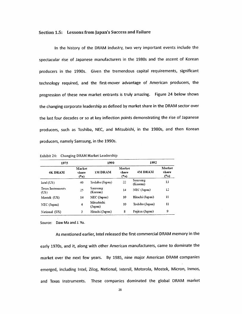
Section 1.5: Lessons from Japan's Success and Failure
in the history of the DRAM industry, two very important events include the
spectacular rise of Japanese manufacturers in the 1980s and the ascent of Korean
producers in the 1990s. Given the tremendous capital requirements, significant
technology required, and the first-mover advantage of American producers, the
progression of these new market entrants is truly amazing. Figure 24 below shows
the changing corporate leadership as defined by market share in the DRAM sector over
the last four decades or so at key inflection points demonstrating the rise of Japanese
producers, such as Toshiba, NEC, and Mitsubishi, in the 1980s, and then Korean
producers, namely Samsung, in the 1990s.
Exhibit 24: Changing DRAM Market Leadership
1975 1990 1992
Market Market -Market
4K DRAM share 1M DRAM share 4M DRAM share(%.) (%.) (%)
Intel (US) 46 Toshiba (Japan) n 13
Texas Instruments sansung 14 NEC (Japan)(US) (Korean)
Mostek (US) 14 NEC (Japan) 10 Hitachi (Japan) 11
NEC (Japan) 4 10 Toshiba (Japan) 11(Japan)
National (US) 3 Hitachi (Japan) S Fujitsu (Japan) 9
Source: Daw Ma and J. Yu.
As mentioned earlier, Intel released the first commercial DRAM memory in the
early 1970s, and it, along with other American manufacturers, came to dominate the
market over the next few years. By 1985, nine major American DRAM companies
emerged, including Intel, Zilog, National, Intersil, Motorola, Mostek, Micron, Inmos,
and Texas Instruments. These companies dominated the global DRAM market
28

claiming approximately 95% of the first generation of DRAM chips (1K) in 1971 and
about 83% of the market for second generation 4K chips in the mid-1970s.14 Exhibit
20 below shows the leadership of American DRAM producers in the early years of the
industry (and the subsequent rise of Japanese competitors). American DRAM
manufacturers thrived at this time, not only because of an early grasp of
semiconductor and DRAM technology, but because of the DRAM industry's close links
to the US military during the 1970s Cold War, which provided for a well-funded
customer base and research and development support.
Exhibit 25: DRAM Generation and Market Leadership
Device type Volume USA Japanproduction
1K 1971 95 5
4K 1974 83 17
16K 1977 59 41
64K 1979 29 71
256K 1982 8 92
1M 1985 4 96
4M 1990 2 98
16M 1997 n.a. n.a.
64M 1999 n.a. n.a.
256M 2000 na. n.a.
Source: A.J.W. van de Gevel.
However, the lead of American DRAM companies in the space decreased quite
quickly as Japanese memory producers enjoyed a tremendous rise in their market
share for the industry. As Exhibit 25 shows above, Japanese producers claimed 41%
of the DRAM market for third generation 16K chips in 1977, and later came to
dominate the market, holding 92% of fifth generation 256K DRAM chips by 1982.
29
24 van de Gevel, 2000.

Furthermore, by the mid-1980s, many American DRAM manufacturers, which had
previously led the industry, even exited the market, including Intel, Zilog, National,
Intersil, Motorola, Mostek, and Inmos.
Significant research has been performed studying the impressive climb of
Japanese DRAM producers in the 1970s and 1980s and the corporate initiatives and
strategies that lead to their success. Tilburg University professor, van de Gevel, lists
various government initiatives that supported the Japanese DRAM industry and aided
in its success: 25
- Controlled Access. Van de Gevel suggests that the Japanese government aided in
the success of Japanese companies by closing the Japanese domestic market to
foreigners, encouraging the purchase of domestic memory products; assisting
Japanese firms in acquiring memory technology, such as patents and licenses; and
implementing foreign direct investment barriers.
- Government financial support. Van de Gevel also mentions that the Japanese
government aided local companies in the DRAM space by providing research and
development subsidies, depreciation tax breaks, and subsidized loans from
government development banks.
- R&D Support. Van de Gevel also postulates that the Japanese government,
through its Ministry of Trade and Industry, also helped the Japanese memory
industry by helping to reduce the cost of risky research and development. They
did this by providing subsidies and helping to form the Very Large Scale Integration
30
25 van de Gevel, 2000.

(VLSI) project, which saw the formation of joint research among the five major
Japanese semiconductor companies (Fujitsu, Hitachi, Mitsubishi, NEC and Toshiba),
and which accounted for almost 40% of integrated circuit research and
development in the late 1970s.2 6 The government provided long-term loans to
finance $200 million for the project. This collaboration is credited with helping
the industry significantly, and produced over 1,000 patents.
Van de Gevel also mentions briefly that Japanese engineers were able realize
better technology breakthroughs because of Japan's unique corporate culture. He
mentions that because Japanese had a closer attachment to their employers, Japanese
memory manufacturers saw decreased employee turnover, which improved learning
within their organizations.
Van de Gevel also details conditions related to American semiconductor
manufacturing which hurt the competitive position of DRAM producers in the United
States - namely the separation of manufacturing from product development.
According to Van de Gevel, American DRAM manufacturers typically bifurcated their
organizations, with one group focused on innovation and product development and
another focused on production and manufacturing cost. This structure led to new
product designs which lacked input from manufacturing professionals, and products
with low "manufacturability." This, in turn, increased manufacturing errors and
reduced production yields, which as highlighted in an earlier section, can devastate a
semiconductor company, given that fixed costs related to manufacturing equipment
31
26 van de Gevel, 2000.2 van de Gevel, 2000.

are so high. To compound this problem, Van de Gevel also mentions that because
land and labour costs were rising so rapidly in the Silicon Valley area, DRAM producers
located their production and assembly groups in low-wage regions, and their research
and development teams in more expensive areas, that contained the required human
capital resources necessary to advance their semiconductor technologies.
Japanese firms on the other hand, according to Van de Gevel's research,
closely integrated product development with manufacturing, allowing for improved
production yields relative American competitors. For instance, Japanese DRAM
companies pursued more conservative circuit designs, to increase product reliability
and decrease product failure.
In addition, Van de Gevel notes that Japanese DRAM companies more closely
integrated their businesses with semiconductor equipment manufacturers. American
firms switched equipment suppliers often, and cancelled equipment orders more
rapidly when demand decreased. This behavior put financial pressure on equipment
suppliers, who would lack the adequate funding to develop new technologies for
memory production.
Lastly, Van de Gevel mentions the Keiretsu system in Japan, as another reason
for the success of Japanese DRAM producers. Van de Gevel believes the Japanese
Keiretsu corporate structure allowed for a lower cost of capital for Japanese memory
companies, giving them better access to funding for technology and product
development. Japanese companies also employed systems of Statistical Process
32

Control (SPC), Total Quality Management (TQM) and Total Preventive Maintenance
(TPM) which helped them increased their product yields and lower production costs.
However, while studying the success of Japanese DRAM manufacturers can
uncover some valuable lessons regarding technology management, studying the
industry's decline in the 1990s can also reveal some interesting lessons. In the late
1970s and 1980s, Japanese DRAM companies did enjoy a spectacular rise in the
industry, but in the 1990s, their market decline was almost rapid. Japanese DRAM
manufacturers captured approximately 80% of the global DRAM market in the
mid-1980s, but by the end of the following decade, Korean competitors surpassed their
production levels and soon held over 50% of the DRAM market by the mid-2000s. 8
Exhibit 26 below shows the decline of Japanese DRAM manufacturers.
Exhibit 26: DRAM Share by Country Exhibit 27: Japanese Computer Shipments
12 25000
Japan
US Mainframe
1975 1980 1965 1990 19s 20I 9.83 1985 1 97 1989 1911 1913 1995 1997
Year Year
Source: Yunogami, 2005.
Many theories explaining the decline of Japanese DRAM producers have been
proposed but one of the most interesting explanations comes from Takashi Yunogami
from Doshisha University. Through numerous interviews with Japanese
semiconductor engineers and managers from the 1980s, Yunogami hypothesizes that
3328 Yunogami, 2005.

Japanese DRAM companies lost their dominance in the industry not because of
technical failings, but because managers did not see the transition of DRAM end
markets from mainframe computers to personal computers, as can be seen in Exhibit
27 above. 29 According to Yunogami, Japanese firms were accustomed to extremely
stringent quality and reliability standards for their DRAM products because major
customers such as Nippon Telegram and Telephone Corp. (NTT) often required 25 year
guarantees on operating performance for the DRAM in their phone operator systems.
However, by the 1990s, when personal computer demand began to rapidly increase
and surpass the mainframe market, managers at Japanese DRAM companies did not
change the cultural focus within their firms and continued to produce DRAM products
with excessively-high quality standards, making their products uncompetitive with that
of Korean competitors on a price basis. For instance, Yunogami cites research by
Kanazawa (2000), which revealed that while Japanese DRAM producers focused on
designing DRAM technology and manufacturing processes that emphasized extended
periods of product use, competitors simplified their technology and processes to make
lower quality DRAM with fewer manufacturing steps at a faster pace. Yunogami
mentions how Micron Technology designed processes which used only two-thirds of
the number of masks that Japanese competitors required in their process flow, greatly
reducing manufacturing costs. In addition, Yunogami's research shows that as
non-Japanese DRAM companies accelerated their focus on manufacturing yield and
lower costs, Japanese producers stubbornly maintained their emphasis on excessive
34
29 Yunogami, 2005.

levels of high quality, with one Japanese semiconductor engineer proudly saying that,
"Only our factory can guarantee the quality of DRAM for over ten years,"30 despite the
lower quality requirements of personal computer DRAM. Yunogami's research also
describes how Japanese DRAM manufacturers were not content using standard
manufacturing equipment like their competitors, but instead placed orders for higher
performance customized equipment. This overemphasis on high technology by
Japanese companies likely slowed their development cycles and increased
manufacturing costs relative to peers.
However, it should be noted that politics also played a significant role in the
demise of Japanese DRAM companies. In 1986, after complaints by American DRAM
competitors that Japanese firms were dumping DRAM product in the United States and
that American firms were deprived of fair access to the Japanese market, Japan and
the United States signed the Semiconductor Trade Agreement (STA). Among the
major points of the agreement between the two countries was the promise of the
Japanese government to help American DRAM companies. In a secret side-letter to
the agreement, the Japanese government agreed to help American companies increase
their DRAM market share in Japan to slightly above 20 percent. In addition, the
Japanese government agreed to vague terms to prevent third market dumping, and
implemented this by instituting voluntary export restraints to Japanese DRAM
companies, which would attempt to raise export prices. The signing of the 1986 STA
was extremely beneficial to upcoming Korean producers in the late 1980s, as Korean
35
30 Yunogami, 2005.

DRAM companies, such as Hyundai and Samsung, had incurred enormous losses
developing their DRAM products prior to the agreement between the United States
and Japan and were even debating staying in the industry, were given an entry into the
United States market.3 According to Jung (2005), due to new limitations of the 1986
STA, Japanese manufacturers focused their resources on developing next generation
DRAM products, allowing for Korean companies to capture market demand in lower
technology DRAM segments. For instance, while Japanese manufacturers focused on
developing 1M DRAM, Samsung and Hyundai were able to become the dominant
suppliers of 64K and 256K DRAM.3 However, this market opening at the low end of
the DRAM market allowed Korean companies to develop their capabilities, and by 1991,
Samsung was also the world's largest producer of 1M DRAM chips.3 3
Section 1.6: Lessons from the Korean Ascension
After Japanese manufacturers saw an incredible rise in the DRAM space during
the 1970s and 1980s, Korean memory companies achieved enviable success in the
1980s and 1990s. Exhibit 28 shows how Korea producers, such as Samsung and Hynix
(formerly Hyundai Electronics; merged with LG Semiconductor), significantly increased
their DRAM market share in the 1990s. In 1994, Samsung had about 14% market
share of the global DRAM market, but by 2005, it more than doubled its market share
to 32%. Samsung and Hynix, together, increased their DRAM market share from 22%
in 1994 to 48% in 2005 (1994 figures exclude the market share of LG Semiconductor,
36
31 Jung, 2005.32 Jung, 2005.3 Jung, 2005.

which was merged with Hyundai Electronics in 1999). Today, Samsung and Hynix
together have approximately 65% of global DRAM market share.3 4 On a larger scale,
including other types of semiconductors such as microprocessors, Samsung saw its
ranking in the overall global semiconductor market increase from about #7 in 1988 to
#1 in 1992 (please see Exhibit 29 below).
Exhibit 28: DRAM Market Leadership - 1994-2005
1994 Market Share 0 1995 Market Share %o 1996 Market Share %o 1997 Market Share %
Samsung (Korean) 14% Sansung (Korean) 16% Samsung (Korean) 25% Samsung (Korean) 19%
NEC (Japan) 11% NEC (Japan) 11% NEC (Japan) 12% NEC (Japan) 12%
Hitachi (Japan) 10% Hitachi (Japan) 10% Hitachi (Japan) 10% Hyundai (Koreau) 10%
Toshiba (Japan) 10% Toshiba (Japan) 9% Hyundai (Korean) S% Hitachi (Japan) 10%
Hytundai (Korean) S% Hvundai (Korean) 9% Toshiba (Japan) 8% LO Semicon (Korean) 9%
1998 Market Share %?/ 1999 Market Share % 2000 Market Share % 2001 Market Share %
Samsung (Korean) 16% Samsung (Korean) 22% Samsung (Korean) 22% Samsung (Korean) 31%
Micron (US) 14% Hyundai (Korean) 21% Hyundai(Korean) 21% Micron (US) 22%
Hyundai (Korean) 10% Micron (US) I1% Micron (US) 18% Hynix (Korean) 19%
NEC (Japan) 10% NEC (Japan) 10% Infieon (Germany) 9% Infaieon (Germany) 11%
LG Semicon (Korean) 9% Infmeon (Gernany) 8% NEC (Japan) 7% Nanya (Taiwan) 5%
2002 Market Share q 2003 Market Share % 2004 Market Share % 2005 Market Share %,
Samisung (Korean) 33% Samsung (Korean) 30% Sainsung (Korean) 31% Saisung (Korean) 32%
Micron (US) 18% Micron (US) 19% Micron (US 16% Hynix (Korean) 16%
Infmieon (Germany) 13% Infimeon (Gennany) 17% -lynix (Korean) 15% Micron (US) 14%
Hynix (Korean) 13% Hynix (Korean) 14% Infineon (Gerany) 14% Qimonda (Gennany) 13%
Nanya (Taiwan) 6% Nanya (Taiwan) 5% Elpida (Japan) 6% Elpida (Japan) 8%
Source: IC Insights, iSuppli, Semico Research Corp., In-Stat, and D. Ma and J. Yu.
Exhibit 29: Samsung Semiconductor's Ranks in World Market Share From 1998 to 1992
Rank 1988 1989 1990 1991 1992I Toshiba Toshiba Toshiba Toshiba Samnsung2 NEC NEC Samsung Sainsung Toshiba
3 Fujitsu TI NEC Hitachi Hitachi
I Samsung (7th) Samlsung (5th) 1 f_
Source: Kim, Shi, and Gregory.
3 Kim, 2011.37

The impressive rise of Korean DRAM companies, such as Samsung and Hynix,
highlight numerous lessons for technology management. Much research has been
done exploring the corporate initiatives that led up to the success of Korean DRAM
companies, and this section will highlight many of them. One factor often mentioned
in the research explaining the achievements of Korean DRAM companies is the
increasingly improved manufacturing of each successive DRAM generation, which has
been labeled as the firm "learning how to learn," 35 or "double loop learning."3 6 As
Exhibit 30 illustrates, Mathews and Cho suggest that with each new generation of
DRAM, Korean companies more rapidly improved manufacturing yields. This can be
seen in the chart below with the slope of each DRAM generation's production yield
becoming steeper, showing production yields increasing faster. Furthermore, Exhibit
30 shows that when production was switched from pilot production to mass
production (the line below which intersects the four production yield lines), the
manufacturing yield was higher in each DRAM generation. This trend suggests that
Korean DRAM organizations were improving operations with each new DRAM
technology.
38
35 Mathews 1999.3 Argyris, C., 1995.

Exhibit 30: DRAM Yield Improvements over Successive Product Generations
Yidd(%)0100
nis podn
704M
256K Ii omMmmpikat podin to mzspodn
50
pikt R&D podn "
1985 1985 1991 1993 Yrofmass podn
Source: Mathews and Cho.
Another important initiative that Korean companies pursued to help them
achieve commercial success in the DRAM industry was to closely couple manufacturing
with product design, which, coincidentally, was one of the key factors leading to the
success of Japanese companies. Kim, Shi and Gregory and illustrated how Samsung
improved their process technologies and product technologies concurrently to allowing
them to achieve strong sales and profitability. This process also allowed Samsung
Semiconductor to produce memory chipsets 6-12 months faster than its nearest
competitors. The procedure is outlined in Exhibit 31 below where new product
development (NPD) is pursued alongside manufacturing improvements. Exhibit 32
below shows some of the specific organizational structures and procedures put in place
to encourage parallel improvements of both manufacturing and new product
technology, including co-location of manufacturing and design, job rotation, and
overlapping matrix structures.
39
37 Kim, 2002.

Exhibit 31: Developing Product-based and Process-based Technologies in Parallel
Source: Kim, 2002.
Exhibit 32: Initiatives to Parallel Process and Technology Improvements
Efforts Results
0 PrAWl peooect proceA vnh mziani pr *ty Eadypwduct btmdimtR&D Activity - prc maecinn wih-acmnj= . resnolspac u mm-wa f..<e y
* A Uealon ecdanlope.-al tap be een prodactwiaed -doe-based
*De-bi for protbe soh*
110Mikly of persoa&Cag p i oeimne
Organsational . catonerfe.w*0 a-bunStructure ' "*"a*""u*"".""'c ***"t**"''****"' **"****
sechologie* eacati ktaobeeiei tap betweeii prod~t-bed ~ c b~
S Recing pojec iead-timee Eadypeanct lanclung
NPD Process - proe" Wene peoces iud~.- =Mcbmiwa noxmand woe.s-i,tech logies
- Baw smanatese M t-e- pnonct-baWwanare-s-b-w
- Tmine wmks . 8Aad*npecea lead-ftme- vMa-actmn mnapaPewn * Eipeanrdt aleh m
Manufacturinr . * ene""'''** b*"**** *""-"""''***"a
Process * R ' " oe''**d**W"' * T-IA"-epcp -t ag pr*ai-t- ~*ed *chadry+rManufactming co4ocation Infctase poonct Jield raho
* Presoype auumeftwe Re-acing poductkncot. Oeem. .eta naaenfa.uaagd n, .r sVaWime-
Source: Kim, Shi, and Gregory.
Finally, many other reasons, some related to government initiatives and
country demographics, have been listed as contributing to the business achievements
of Korean DRAM manufacturers. Some of these include:33
40
Strategy
Strategy
38 Byun, 1989.
c[:: '
IF-*

- Aggressive management style of founders. It has been mentioned that many
domestic Korean semiconductor firms were managed by the companies' founders,
who had significant shareholdings and business experience. These managers
employed an effective, aggressive management style.
- High-quality, inexpensive labor. Korean DRAM manufacturers were able to benefit
from a well-educated workforce, many educated abroad, that accepted relatively
low wages. At the time, the labor cost per hour in Korea was only 11% and 22% of
that in the United States and Japan, respectively.3 9
- Support from conglomerates. Many Korean DRAM companies were part of a
larger conglomerate, which allowed them to benefit from strong financial backing
as well as in-house consumption of their memory products.
- Focus on specific products. Korean semiconductor firms as a whole targeted
select chip products, such as DRAM, SRAM, and ROM, allowing for them to develop
a competitive edge in these segments.
- Functional level support. Korean DRAM companies implemented various
initiatives to support their memory businesses, such as creating offices in Silicon
Valley, collaborative research with other domestic firms, producing OEM products,
and utilizing automation to realize better quality control.
- Government support. The Korean DRAM industry benefited from government
subsidies that allowed for improved research and development and employee
training, which companies alone would not be able to afford.
41
3 Byun, 1989.

PART 2: CASE STUDY: ELPIDA MEMORY INC.
Section 2.1: Company Overview
Elpida Memory Inc. is one the world's largest manufacturers of DRAM in the world,
making DRAM memory products for the personal computer and mobile
device/consumer electronics industries. The Company is based in Tokyo and has its
main manufacturing facilities in Hiroshima, Japan and Taiwan, through its 63%-owned
joint-venture subsidiary, Rexchip Electronics Corp. The Company was formed in 1999,
through the combination of the DRAM units of Hitachi and N.E.C, and in 2003, further
expanded its scale by acquiring Mitsubishi Electric's DRAM unit. In 2004, Elpida
became a public company when it listed on the Tokyo Stock Exchange. As of
September 2011, the Company had 5,957 employees on a consolidated base (3,206 on
a non-consolidated basis). In fiscal year ending March 31, 2011, the Company had
revenue and EBITDA of JPY 514.3 billion and JPY 161.6 billion, respectively, but industry
analysts expected a significant drop in profitability for the Company in fiscal year 2012
as Revenue contracted significantly (Exhibit 33 below). In addition, given its high debt
load of approximately JPY 300 billion (Exhibit 34 below), the Company ultimately filed
for bankruptcy in February 2012. Please see Appendix A for more detail on Elpida.
42

Exhibit 33: Income Statement of Elpida
JPY in bilions
2011 2012E
Revenue V514.3 V280.5
% Growth -45.5%
Gross Profit 101.5 -59.4
% Margin 19.7% -21.2%
EBITDA 161.6 4.2
% Margin 31.4% 1.5%
EBIT 35.8 -125.4
% Margin 7.0% -44.7%
Net Income 15.2 -138.5
% Margin 3.0% -49.4%
Source. Company data, Macquarie Research.
Exhibit 34: Balance Sheet of Elpida
JPY in bilions
CBs (unsecured) 93.3
Bonds (unsecured) 45
LT debt 147.3
Rexchip -60
Elpida in Japan -87
Capital leases 72.5
Total debt 358
Less Rexchip 298
Receivables -35
Inventories -70
PPE -490
PPE less Rexchip ~310
Cash >50
Book value of investments/other 25-30
Equity ex minority interest -190
Source: Cortpany data, Macquarie Research.
In regards to Elpida's product focus, the Company manufactures DRAM for
both personal computers and non-mobile electronic devices. The Company does not
give specific public disclosure in regards to its production output composition, but
analysts estimate that its revenue is split approximately 50-50 between PC and non-PC
Premier DRAM.40 Its Premier DRAM output includes lucrative sales of mobile DRAM
which is used for mobile devices including mobile phones and tablet PCs. Elpida is
actually one of the DRAM suppliers to Apple for its iPad and iPhone devices. While
commodity PC DRAM prices have dropped precipitously recently, as shown in Exhibit
35 below, with many producers expected to be selling near their marginal cost of
production, mobile DRAM is the main driver for DRAM companies including Elpida,
providing gross margins of approximately 30%. Analysts estimate that Elpida's mobile
4340 Thong, 2012.

DRAM sales account for about 15% of bit sales, yet make up as high as 40% of total
revenue.41
Exhibit 35: Historical DRAM Prices
a70 PC 2Gb DDR3 DRAMSpot & Contract Price Current spot: 50,50/Gb
Currem contract 0 52/Gb0,60
Souce DRA5 echane, Bensten Resarch
Z 0.45
In addition to Elpida's product mix, it should also be highlighted that the
Company has strong process technology relative to its peers as the majority of its
DRAM output utilizes 30nm technology, allowing for smaller chip sizes and lower
power consumption (please see Exhibit 36 below). Its 30 nm technology also allows
for the Company to enjoy a significant cost advantage over smaller peers, as
manufacturing costs for 30 nm products are almost 30% below that of 40 nmn DRAM
(Exhibit 17, full cost). Elpida, while smaller than competitors Hynix and Samsung, also
has significant economies of scale in the sector, having approximately 14% market
share and being the third largest DRAM producer, as was shown in Exhibit 4.
44
41 Thong, 2012.

Exhibit 36: Elpida Manufacturing Plant Product Mix by Production Technology
Mar-10 Jun-10 Sep-10 Dec-10 Mar-11 Jun-11 sep-11 Dec-11 Mar-12
Hiroshima 300mm tab 130K/mo 130KImo 130K/mo 115K/mo 120K/mo 120K/mo 120K/mo 95K/mo 95K/mo
3Xnm Slight -20% -30% -3040% >50%
4xnm -20% -30% -50% -60% -60% -50-60% -60% -50-60% <50%
5X/6Xnm -30-35% -20% -10% -5-10% ~0%
66nm XS (63nrn) -30% -40% -20-30% -30%65nm S (68nm). 70nm etc. ~50% -30% -20-30% -10%Rexchip (Taiwan) 300mm fab 85K/mo 85K/mo 85K/mo 85K/mo 85K/mo 85K/mo 85K/mo 70K/mo 65K/mo
3Xnm -None v slght ~5% -35% -70-80% -100%
4Xnm S 80% -100% -96% ~66% -20-30% ~0%
SX/6Xnm ~5% -80% -20% or NN
65nm XS (63rnm) -75% ~90% -20%65nm S (68nm), 70nrn etc. -25% -5%
Source: Thong, 2012.
Overall, Elpida has tried to be a technology leader in the industry, spending
significant sums on research and development and capital expenditures, which has
helped it develop very strong technology capabilities, but has also burdened the
Company with significant levels of debt. In regards to its leading technology, Elpida, in
2011, was the first company to complete the 25 nm manufacturing process, which it
began shipping in July 2011. In 2010, the Company developed the industry's smallest,
most current-efficient 30 nm SDRAM and in 2009, the Company led the industry with
the industry's smallest 40 nm SDRAM.
However, in racing to develop the latest technology, Elpida imprudently
funded its expenditures with debt instruments, as opposed to cash from its operations
or equity. This trend was particularly pronounced in recent years, when the Company
began to rely too heavily on new debt issuances for its funding needs. Its main
competitors, Samsung, Hynix and Micron, on the other hand, were able to fund
themselves with cash flow from non-DRAM segments or with more moderate debt
levels. Exhibit 37 below shows historical DRAM capital expenditures. As can be
seen, Elpida in every year spent heavily on capital expenditures, investing in its
45

business even when cash flows were negative. Its competitors also spent heavily, but
were able to fund their DRAM businesses with cash from other operating segments.
Exhibit 37: DRAM Industry Capital Expenditures and Cash Flow
(USD in llions)
2000 2001 2002 2003 2004 2005 2006 2007 2008 2009
Estimated DRAM Capex
Samsung $3,045 $2,000 $1,800 $2,100 $3,000 $3,210 $3,500 $4,200 $3,900 $2,200
Hynix 1,181 250 350 500 1,000 1,800 3,400 4,129 1,606 733
Micron 1,188 1,811 900 1,000 1,497 1,500 1,400 2,500 1,000 380Elpida 500 240 345 912 1,153 1,754 1,333 1,395 877 625
Total DRAM Industry Capex (1) $9,251 $7,123 $4,787 $6,781 $11,065 $13,873 $17,072 $22,834 $11,374 $5,128
% of Total Industry CapexSamsung
Hynix
32.9%12.8%
28.1%
3.5%37.6%
7.3%31.0% 27.1%
7.4% 9.0%23.1% 20.5%13.0% 19.9%
18.4% 34.3% 42.9%
18.1% 14.1% 14.3%
Micron 12.8% 25.4% 18.8% 14.7% 13.5% 10.8% 8.2% 10.9% 8.8% 7.4%
Elpida 54% 3.4% 7.2% 134% 10.4% 12.6%K' 7.8% 8 6.1% 7.7%j 12.2%
Total DRAM Industry Capex 100.0% 100.0% 100.0% 100.0% 100.0% 100.0% 100.0% 100.0% 100.0% 100.0%
Free Cash Flow (2)
Samsung $4,560 $3,595 $7,669 $11,766 $14,339 $13,016 $15,808 $15,921 $12,146 $14,527
Hynix 3,457 -333 183 1,072 2,618 2,786 3,450 3,694 -342 1,051
Micron 2,002 789 578 284 1,159 1,237 2,019 937 1,018 1,206
Elpida NA NA NA -181 -289 191 291 848 804 -517
Capex as % of Free Cash Flow
Samsung 66.8% 55.6% 23.5% 17.8% 20.9% 24.7% 22.1% 26.4% 32.1% 15.1%
Hynix 34.2% -75.2% 191.4% 46.6% 38.2% 64.6% 98.6% 111.8% -470.0% 69.7%
Micron 59.3% 229.5% 155.7% 351.9% 129.2% 121.3% 69.3% 266.8% 98.2% 31.5%Elpida NA NA NA -504.5% -399.1% 920.5% 458.0% 164.5% 109.1%7-121.0%
Source: Capital expenditures from Yoshikawa, 2009. Free cash flow from operations from Capital IQ.Note: Uses average exchanges rates from forecast-chart.corn
(1) Includes companies not presented.
(2) Estimated as Cash Flow from Operations.
Exhibit 37 above, however, does not offer a full perspective on the funding of
operations for each company listed above. This is because Elpida's main competitors
listed above also had non-DRAM capital expenditures, which would have absorbed
cash flow as well. Exhibit 38 below shows total capital expenditures and total cash
flow for Elpida's main competitors, including cash flows from non-DRAM segments.
As can be seen from Exhibit 38, even after accounting for the cash flows of non-DRAM
segments, Elpida's competitors more prudently managed their funding needs and did
not overly-extend themselves and burden themselves with excessive debt. Micron
46

and Hynix, however, have been quite aggressive in their capital spending, as Exhibit 38
shows them spending large sums of capital to expand their business even in years with
relatively little to no positive cash flow from their businesses.
Exhibit 38: Elpida Competitors Total Capital Expenditures and Cash Flow
(USD in miions)
2000 2001 2002 2003 2004 2005 2006 2007 2008 2009
Total Capex
Samsung $4,877 $4,004 $4,051 $6,460 $9,160 $11,270 $12,304 $13,188 $12,807 $6,319Hynix 2,018 393 395 687 1,658 2,692 4,845 5,554 2,563 794Micron 1,127 1,489 760 822 1,081 1,065 1,365 3,603 2,529 488
Free Cash Flow (1)Samsung $4,560 $3,595 $7,669 $11,766 $14,339 $13,016 $15,808 $15,921 $12,146 $14,527Hynix 3,457 -333 183 1,072 2,618 2,786 3,450 3,694 -342 1,051Micron 2,002 789 578 284 1,159 1,237 2,019 937 1,018 1,206
Capex as % of Free Cash FlowSamsung 107.0% 111.4% 52.8% 54.9% 63.9% 86.6% 77.8% 82.8% 105.4% 43.5%Hynix 58.4% -118.3% 216.1% 64.1% 63.3% 96.6% 140.5% 150.4% -750.2% 75.5%Micron 56.3% 188.6% 131.4% 289.1% 93.3% 86.1% 67.6% 384.5% 248.4% 40.5%
Note: Micron statistics include distortions (relative to DRAM capital expenditures due to acquisitions and divestitures.
(1) Estirated as Cash Flow from Operations.
Overall, while Elpida has been able to develop very strong technical abilities in
the DRAM space, the Company was too aggressive with its financial leverage, and
funded itself with exorbitant levels of debt. Exhibit 39 below shows Elpida's capital
raising activities, and the Company's excessive use of debt, particularly in 2008 and
2009, when the Company issued over USD 2 billion in debt obligations. A strategic
mistake by the Company's management may have been for it to rely too heavily on
DRAM products for its survival. While its peers were able to support themselves with
cash flows from non-DRAM segments, Elpida stayed focused on only the DRAM
product group, making it very susceptible to the price swings and profitability cycles in
the DRAM industry (as highlighted in section one of this thesis).
47

Exhibit 39: Elpida Competitors Total Capital Expenditures and Cash Flow
(USD in millions)
2003 2004 2005 2006 2007 2008 2009
Net Debt (1) $80 $1,143 $1,029 $597 -$378 $1,059 $1,009
Equity 507 602 956 0 1,147 12 1
Total New Capital $588 $1,745 $1,985 $597 $769 $1,070 $1,010
% of New CapitalNet Debt (1) 14% 65% 52% 100% -49% 99% 100%
Equity 86% 35% 48% 0% 149% 1% 0%
Total New Capital 100% 100% 100% 100% 100% 100% 100%
Source: Capital IQ.
Note: Uses average exchanges rates from forecast-chartcom
(1) Debt issued, net of debt repaid.
Unfortunately, Elpida's funding mismanagement came to a calamitous end
early this year in 2012, when the Company filed for bankruptcy. On February 29,
Elpida filed a petition for restructuring with the Tokyo District Court. A supervisor was
appointed that will temporary control the Company until a Trustee is appointed by the
Tokyo District Court. The court could appoint an independent Trustee, or name the
Company's current CEO, Yukio Sakamoto, as the Trustee. Some analysts expect
Sakamoto may be appointed to lead the Company, so that a faster reorganization
process can be implemented, while others have mentioned that creditors may prefer
new Company management given the surprise bankruptcy filing of the Company. It
should be noted that two provincial governors, which house Elpida's fabrication
facilities, have asked the National Government to provide financial support to Elpida.
It should be noted that the Government rescued Elpida in 2009 with a JPY 30 billion
funding package from the Development Bank of Japan. In addition, the future
restructuring process and direction of the Company is further muddied by the fact that
48

no leading creditor, oftentimes a bank, has offered to take control of the reorganization
process.
Section 2.2: Strategy Recommendations
Elpida now sits in a precarious situation, and faces being another victim of the
vicious DRAM cycle which has claimed so many causalities in the past. In 2009, a
competitor, Qimonda, a spin-off of Infineon Technologies which itself was spun-off
from Siemens AG, filed for insolvency. The Company at one point was one of the top
five DRAM manufacturers in the world, with close to 64 billion in revenue. However,
oversupply in the market and the 2008 financial crisis lead the Company to bankruptcy
and eventually complete liquidation. Today, the Company exists purely as an entity to
market its intellectual property portfolio. Elpida faces this same potential outcome,
as Qimonda's equipment was eventually sold to Texas Instruments for 18 cents on the
dollar.42 However, as dire as Elpida's situation seems, this section will discuss several
strategic options that it could pursue to benefit Company stakeholders.
Section 2.2.1: Horizontal Integration
One strategy that Elpida can pursue (or at least use as a bargaining tool while
exploring other options) is to consider horizontal integration by merging with a
competitor. This additional industry consolidation would continue the trends
discussed in earlier sections of this thesis.
49
42 Thong, 2012.

Micron Technology would be a very likely candidate as a merger partner or
acquirer of Elpida and could reap significant benefits from such a corporate event.
While Micron has seen some success as the only major American DRAM supplier today,
its position in the industry is by no means absolutely secure, given it has approximately
10% market share, and competes against Samsung (about 42% market share) and
Hynix (about 23% market share). Given the tremendous advantages of scale in this
industry, as highlighted in Section 1 of this thesis, Micron could benefit tremendously
from a combination with Elpida. Firstly, with fewer competitors in the sector, more
controlled capital spending can be implemented by companies, allowing for less
capacity surpluses and less volatile pricing during times when demand slows. In 2009,
after Qimonda went bankrupt, DRAM prices rapidly increased, as market supply
corrected and better met market demand. Exhibit 40 below shows DRAM pricing
after Qimonda's bankruptcy in 2009.
Exhibit 40: DRAM Prices After Qimonda Bankruptcy
2.50
Elovatod price sustahnd tuni 30~2,0
.0
Om ndbanrup"c
Low:$0 580 b0:00 D N
Source: DRAMeXchange, Newman, 2012.
50

Secondly, a combination of Micron and Elpida could allow Micron to expand its
product offerings. Currently, Micron has a small presence in the mobile DRAM market,
of only approximately 7.3%, while this segment offers higher-margins (gross margins of
-30%) relative to commodity PC DRAM and is growing rapidly (some analysts expect it
to grow sevenfold by 2015, from 2011 levels).4 3 Elpida has a relatively strong mobile
DRAM product, with landmark clients such as Apple, and a presence in the iPad and
iPhone.
In addition, significant cost synergies can also likely be squeezed from a
combination of Elpida and Micron allowing for improved profitability from the
combined entity. Currently, Micron as a standalone entity has approximately -3.7%
Net Margins, but assuming a combination with Elpida and an elimination of Elpida's
SG&A costs, the combined company could see Net Margins increased by approximately
100 bps to -2.8% (please see Exhibit 36 below). In addition, if the merged entity could
further decrease Elpida's R&D expenses by 50%, this would allow for a pro forma Net
Margins of approximately 0.4% (as displayed in the sensitivity tables of Exhibit 36). If
Micron and Elpida were to merge, there could also be some revenue synergies, from
Elpida selling some of Micron's NAND Flash memory products (which Elpida currently
does not produce) allowing for increased sales. Exhibit 41 below shows small
revenue synergies of 5% of Micron sales layered on top of R&D expense reductions,
which would give the combined company 3.3% Net Margins - a 600 bps increase from
Micron's standalone Net Income margin. In addition, one should highlight that the
514 The Times of India, 2012.

illustrative analysis below does not account for potential savings in capital expenditures
and the benefits of shared knowledge involving technology and manufacturing
processes, which helped Japanese and Korean manufacturers in the past to achieve
significant commercial success.
Exhibit 41: Illustrative Micron-Elpida Merger Synergies
($ in n.imns)
AdjustedMicron Elpida Elpida M+E
Revenue $8,601 $5,774 $5,774 $14,375
COGS 7,113 4,851 4,851 11,964,Gross Profit $1,489 $923 $923 $2,411% Margin 17.3% 16.0% 16.0% 16.8%
R&D 920 922 922 1,842SG&A 594 594Extraordinary Exp. 6 61Operating Profit -$31 $0 $0 -$31% Margin -0.4% 0.0% 0.0% -0.2%
Interest & Other Inc. -140 -142 -142 -282Pre-tax income -$171 -$142 -$142 -$313% Margin -2.0% -2.5% -2.5% -2.2%
Tax 39 -52 -52 -13Minority Int. (Profit) 15 0 0 15Equity in Affil. (Loss) 94 0 0 94Net income -320 -$90 -$409% Margin -3.7% -1.6% -2.8%
Pro Forma Net income Sensitivity
0.0% $0%/$ 2.5% 215Revenue 5.0% 430Synergy (1) 7.5% 645
10.0% 860
Pro Forma Net Margin Sensitivity
% R&D exp. Reduction / $ R&D exp70.0% 60.0% 50.0% 30.0% 0.0%$277 $369 $461 $645 $922$236 $144[ $52451 359 267666 574 5a881 789 697
1,097 1,004 912
% R&D exp. Reduction I
-$1321 4983 -194
298 21513 236728 451
$ R&D exp70.0% 60.0% 50.0% 30.0% 0.0%$277 $369 $461 $645 $922
0.0% $0%/$ 2.5% 215Revenue 5.0% 430Synergy (1) 7.5% 645
10.0% 860W
(1) Percentage based on iron reveme.
1.6%3.1%4.5%5.9%7.2%
1.0%1 0.4%j2.5% 1.8%3.9% 3.5.3% 4.6%6.6% 6.0%
-0.9%E -28%l0.6% -1.3%2.0% 0.1%3.4% 1.6%4.8% 3.0%
Nole: iclkdes assurM ns *om 0j. 2012
It should be noted that because the DRAM industry has consolidated so much
over recent years, other viable suitors among competitors may be limited. Samsung
already has approximately 42% market share (as shown earlier in Exhibit 4), and
anti-trust issues could be major obstacle if Samsung were to merge with Elpida.
Customers would likely protest strongly, fearing such concentration among their
suppliers. Hynix, too, with about 23% market share may also catch the attention of
anti-trust regulatory bodies, but more importantly, Hynix is more focused on its NAND
Flash business, and appears to want to want to limit further expansion of its DRAM
segment, and use it as a cash cow to create cash flow to re-invest into its NAND
52
I

business.44 The limited interested buyers of Elpida within its industry may decrease
its negotiating power as it restructures, but other options are also available as
highlighted below.
Section 2.2.2: Complimentary Asset Combination
Companies outside the DRAM space could also be appropriate suitors for
Elpida and another strategic option for it to consider. Toshiba is a possible candidate.
Toshiba is a diversified electronics company, selling products including computers,
televisions, imaging and storage systems, but does not have a presence in the DRAM
industry. The Company actually exited the DRAM industry in 2001, when it sold its
DRAM segment to Micron. The Company, however, could have an interest in Elpida
because the market appears to moving towards a combined DRAM + NAND flash
chipset as Samsung announced a combined embedded multi-chip package with both
DRAM and NAND Flash in January 2012 for mobile devices.45 Samsung's technology is
expected to allow for a simpler design process for users, as well as enhanced
performance and longer battery lives. To be competitive and have a full product mix,
Toshiba may have to re-enter the DRAM industry or at least form a partnership with a
DRAM manufacturer. Acquiring Elpida could be one strategy for it to use in
competing with Samsung in the NAND Flash space.
In addition, a purchase of Elpida by Toshiba could help it develop its own
storage business, which may involve the integration of next generation
53
44 Newman, 2012.4s Shilov, 2012.

Magnetoresistive random-access memory, or MRAM.4 MRAM is a non-volatile
memory technology which stores O's and 1's with magnets, as opposed to DRAM
technology which relies on a transistor and a capacitor. MRAMs, however, do still
utilize transistors in their design, and Toshiba, having sold its DRAM unit in 2001, has
lost its internal transistor product knowledge. Therefore, an acquisition of Elpida would
help Toshiba regain expertise in transistor technology.
Combining with Elpida and integrating Elpida's transistor technology with its
MRAM development could ultimately help Toshiba with its storage business. 47
Currently, computer architectures rely on memory feeding hard disk drive systems, but
there exists a 1,000 times speed gap in the transmission between RAM and permanent
storage HDDs.4 If Toshiba can fully develop its MRAM product, it could then insert its
MRAM and NAND product offerings, in between the DRAM and HDD storage layers of
corporate storage networks, allowing for improved speed/performance (which is
gaining in importance with the emergence of Big Data trends) and lower power
consumption. Exhibit 42 below illustrates the potential future architecture of
corporate server/storage networks.
It should also be noted that a combination of Elpida and Toshiba would imitate
one of the aforementioned strategies of Korean manufacturers, which helped them
dominate the DRAM industry. By combining with Toshiba, Elpida could become part
of a larger corporate entity, which could potentially help it get access to lower costs of
capital (particularly important as wafer fab construction costs exponentially increase)
46 Yasui, 2012.47 Yasui, 2012.48 Yasui, 2012.
54

and provide the Company with some financial support during down cycles of the
DRAM sector.
Exhibit 42: Future Server-Storage Architecture with MRAM/NAND
Speed Gap
Cache Memocy X ~10 Core iS-670x 0.005 ns $35.53.46GI-z X1.0 x 383,094
DR AM
00~o DDR3 1066MWz 0.0 12 ns Wo020MRAM 3GB X 3 x 216
HDDSequence Read
3.5" 7200RPM 3 ns $0.000091.5TB x 687 x1.0
Source: Yasui, 2012.
Section 2.2.3: Utilize Private/Public Funds
Another important strategic option Elpida could consider is a going-private
transaction with a financial sponsor (i.e. private equity investment firm). While this
option has had mixed results in Japan, at the minimal, it could provide another
bargaining chip to Elpida as it negotiates with other partners/buyers. One should
note, however, in general, Japan has been a relatively barren market in terms of private
equity deals. 4 9 Despite being one of the largest economies in the world, the Japanese
market for private equity transactions has been very limited with only about $3.8
billion of private equity deals announced in 2009.:5 Some of the largest private equity
55
49 The Economist, 2010.so The Economist, 2010.
I Devkx- lwtmacion 1MBewt I

investment firms in the world, despite opening offices in Japan, have done very few
deals - Permira opened an office in Tokyo in 2005, but completed only one deal in the
subsequent five years. Kohlberg Kravis Roberts also opened an office in Japan in 2005,
and also only completed one transaction in the following five years.
But it should be noted that some private equity transactions in Japan have led
to remarkable windfalls to their investors. In 2000, J.C. Flowers & Co. rescued
Long-Term Credit Bank in Japan in a $1.1 billion transaction, which led to a fivefold
return.s1 The transaction was later labeled by competitor, David Rubenstein of The
Carlyle Group, as the "most profitable private equity deal of all time."5 2
While competing against semiconductor industry companies in a competitive
auction may be challenging for a financial sponsor, in terms of acquiring or investing in
Elpida (given the likely operational synergies that a strategic buyer would have), a
private equity firm could potentially invest in the Company and improve its profitability
through a corporate restructuring that a more traditional, Japanese public company
would not be able to implement due to potential cultural factors that could limit large
employees layoffs. Exhibit 43 shows the returns of a hypothetical private equity
transaction assuming a $1.5 billion purchase price of the Company (based on some
media expectations of a merger with Micron at that valuation for Elpida). While the
financial model below utilizes numerous projected financial assumptions, most notably,
forward operating estimates from Macquarie Research, the general conclusion of the
analysis is that a private equity investment firm could potentially pay up to $3.5 billion
56
si The Deal, 2010.52 Mackintosh, 2010.

for Elpida, and still earn a 20.4% annual return on their investment. While this
analysis includes some aggressive forward assumptions, including EBITDA margins
expanding to approximately 38% in 2014, it should be noted that the analysis also
includes some very conservative estimates such as 2.Ox Enterprise Value to EBITDA exit
multiple valuation for Elpida. Overall, despite some significant industry headwinds
that Elpida faces now, a private equity firm could potentially earn a very rich rate of
return (if it could negotiate with current debt holders of the Company, which
effectively control Elpida today) to provide for a more appropriate capital structure for
the Company, and if the industry sees a rebound in DRAM prices and profitability in the
near term. A private equity firm may also consider following initiatives that successful
Japanese DRAM manufacturers used in the past, such as seeking government funding
to support jobs and technology development within Japan. Exhibit 44 below shows
additional detail for an illustrative financial model which calculates investment returns
related to a private equity investment in Elpida.
Exhibit 43: Illustrative Private Equity ReturnsInvestment Entry Statistics
Assumed Purchase Price $1.5
Assumed Exchange Rate 80
Purchase Price in JPY V120
2012E EBITDA V4
Enterprise Val/EBITDA 28.8x
Estimated New Debt 60
Implied Required Equity V60
Implied Required Equity $0.8
Gain on Invested Equity - Sensitivity Analysis Annual Return - Sensitivity Analysis
Assumed Exit EV/EBITDA Multiple Assumed Exit EV/EBITDA Multiple
2.Ox 2.5x 3.Ox 3.5x 4.Ox 2.Ox 2.5x 3.Ox 3.5x 4.0x
$1.50 V224 V303 V381 V460 V538 $1.50 67.9% 82.2% 94.5% 105.4% 115.2%
Assumed 2.00 194 273 351 430 508 Assumed 2.00 50.8% 64.0% 75.3% 85.4% 94.5%
Purchase 2.50 164 243 321 400 478 Purchase 2.50 38.2% 50.8% 61.5% 71.0% 79.5%
Price 3.00 134 213 291 370 448 Price 3.00 28.4% 40.5% 50.8% 59.8% 67.9%
3.50 104 183 261 340 418 3.50 20.4% 32.1% 42.0% 50.8% 58.6%
57

Exhibit 44: Illustrative Private Equity Financial Model
(JPY and USD in billions)
2011A 2012E 2013E 2014E
Revenue 4514 V280 V374 V415
% Growth -45.5% 33.2% 11.0%
Gross Profit Viol -V59 V78 V123
% Margin 19.7% -21.2% 20.8% 29.6%
EBITDA V162 V4 V123 V157
% Margin 31.4% 1.5% 32.8% 37.9%% Growth -97.4% 2846.8% 28.0%
Depreciation and amortization Y130 V112 V103Estimated Interest (1) 4 4 4
Taxable Income -4130 V6 V50
Depreciation and amortization
Taxes (2)
Capital Expenditures
Change in Working Capital
Free Cash Flow
% of Revenue
V1 30
0
-70
-40
-V110
-39.2%
V1 12
0
-25
0
V94
25.2%
V103
0
-67
5
V90
21.8%
Investment Entry Statistics
Assumed Purchase Price
Assumed Exchange Rate
$1.5
80
Implied Purchase Price in JPY V120
2012E EBITDA V4
Enterprise VaIue/EBTDA 28.8x
Estimated New Debt 60
Implied Required Equity V60
Implied Required Equity (USD) $0.8
Note: Includes forward projects from Macquarie Research, 2/29/12.
Investment Exit Statistics
Assumed Exit Multiple 4.Ox
2014E EBITDA V157
Implied Enterprise Value V628
Estimated Debt Balance 30
Est. Equity Value (3) V598
JPYGain -7i538
% Gain from Entry 897.1%
ArmuaReturn() d2%
(1) Assumes 7% interest on all new debt.(2) Assumes minima l taxes due to depreciation tax shields and potential net operating losses carry forwards.(3) Excludes accumulated cash.(4) Assumes three year investment
Section 2.2.4: Leverage Relationships with Vertical Stakeholders
Another strategic option for Elpida would be for the Company to explore
potential financial support from companies that exist in vertically-related industries,
and which have a vested interest in Elpida's survival. One group of companies that
may want to assist Elpida is its suppliers. Taiwanese Powertech Technology Inc.
focuses on memory packaging and testing, and Elpida reportedly accounts for 40-50
58

53percent of its revenues. Powertech, however, has strong profitability, with some
analysts forecasting 34% EBITDA margins for the Company in 2012, and the Company
ended its fiscal year in December 31, 2011 with over $400 million in cash and cash
equivalents, with continued cash balance increases in future years.54 Given its large
exposure to Elpida, Elpida may be able to extract funding from Powertech.
Formfactor Inc., another manufacturer of semiconductor capital equipment, had
approximately 18.2% of revenue from Elpida or Elpida-rated companies in 2011,ss and
could also be able to financially-assist Elpida. Even though the Company is projected
to have slightly negative margins and relatively small negative free cash flow in the
coming years, the Company is still forecasted to have cash balances of approximately
$250 million over the next few years56, and could possibly contribute some funds to a
rescue fund for Elpida.
In addition, larger semiconductor capital equipment such as ASML and
Applied Materials could potentially make more sizable investments into Elpida. These
companies have not publicly detailed their exposure to Elpida, but given their strong
leadership in the semiconductor capital equipment segment, it is likely Elpida is a
significant customer to them. For instance, in 2011, ASML held approximately 57
percent market share of lithography tools. 57 in addition, ASML is in an extremely solid
financial condition with approximately E2.7 billion in cash and cash equivalents as of
December 2011, and very strong profitability with operating profits of approximately
s3 wu, 2012.5 Shu, 2012.ss LaPedus, 2012.56 Muse, 2012.s7 McGrath, 2012.
59

27%.58
It should be noted that suppliers' financial support of Elpida may be
controversial given they likely supply capital equipment to Elpida's peers as well.
However, the industry for semiconductor capital equipment is relatively specialized
with relatively few participants, therefore disgruntled competitors of Elpida may not
have many other alternatives in terms of capital equipment sources. In addition, this
option could be used in conjunction with the aforementioned injection of capital from
a private equity firm, which may make the illustrative private equity deal modeled
above more viable.
Lastly, another group of vertical stakeholders which may be able to offer some
financial support to Elpida is the Company's customers. This is a particularly
interesting option given that some of the Elpida's customers source their components
from their own competitors, which may give these customers increased incentives to
support Elpida in order to increase their own competitiveness. For instance, Apple's
purchases of mobile DRAM from Elpida currently make up approximately 40 percent of
the output of Elpida's Hiroshima plant.59 However, Apple also purchases significant
amounts of DRAM and NAND memory from its competitor, Samsung, with Samsung
having over $7.8 billion of contracts with Apple in early 2011.60 But the relationship
between Apple and Samsung is becoming increasingly contentious with Apple suing
Samsung for various patent infringements including Samsung's use of its "slide to
60
58 Meunier, 2012.59 Times of India, 2012.60 Saeed, F.

unlock" feature, search features, and spell check functionality.6 1 Samsung in March
2012 counter-sued Apple, claiming Apple infringed on three of its patents involving
methods of displaying data, the user interface, and short text messages.62 Media
reports also point to Apple moving DRAM and NAND orders away from Samsung due to
patent disagreements between the two companies. If Apple wanted to decrease its
component dependency on Samsung, offering support to Elpida could help it
accomplish this given that the DRAM market is largely dominated by four companies:
Samsung, Hynix, Elpida, and Micron (Exhibit 4). By supporting Elpida, Apple would be
able to keep its DRAM costs under control, with three non-Samsung major DRAM
producers competing in the market, while also insuring continued innovation with that
component. It should be noted however that DRAM unfortunately does not make up
a significant percentage of the total costs related to manufacturing an iPad. Based on
industry estimates, the DRAM component costs of an iPad only make up about 5% or
64less of the latest iPad model. in addition, DRAM costs as a percentage of total
component costs for other electronic devices is approximately 4% to 6% (please see
Exhibits 6 and 7). Exhibit 45 below shows detailed estimates for component costs of
Apple's latest iPad.
61
61 Sherr and Vascellaro, 2012.62 Reuters, 2012.63 Lien, 2011.6 Rassweiler, 2012.

Exhibit 45: Apple iPad Bill of Materials
Correonentse Wadrdar (3rdnt GeneE 64G
RtaPrmg As of March 20s12 s33900 5529.00 $49S,00 ssn9.00 5*99,00 W629.00 72n00 5829.00TotalSOM Cost S236.95 3262.55 S306.5 5322.5 $535645 '47E55: $364.35 539795Manfacturing Cost St1S $8,45 51.09 0 10 $10.0 0 510175 510.75 110.75B5M - Manufacturg $245.10 5271.00 5316,05 32,8 S36645 S358.30 5375.1 5403 70
MemoryUAllash 516.80 516.80 5$160 53160 567.20 5160 $33,60 $67.20DRAM 57,0 $7,60 $11319 0 1190 $13,90 £1190 $1190
Display & TouchscreenDisplay 557200 557.00 587.00 87.00 $-o 587.00 $87.00 587-00Touchscren S40.00 $40.00 i40., 00 $40 4 S4400. $4S.01 549.0
Processor $1420 $14,20 $2100 S23.00 52300 523.00 $23.00 52100Comera(s} $4.10 34.10 $12.35 S12-35 512 35 :$Z$$2, 512.35 12,35Wireiness Section - BRFWPA (Modte) $2550 '5450 54I.50 54150Uter Intsrce & Sensr Combo 13 15 $15.00 100 501500 515 .X0 $15.00Module (WLAWBTRTM) - t~ $50Power Management 5285 S5955 510-C0 318.00 Stal:0 $18.00 $10100Battey 522.75 $22.75 S32.09 $3200 532.00 $32,00 $32.00 S32.100MQChcWC547-80 547.10 550-50 $55050 $5050 $50.0 550-50 50.50OthierBox Contents $5250 55355.50 $5.50 $5.5 $50 $550 $5.0Sour e ? Supp2 Reserch March 20 2
However, in Apple's case, supporting Elpida may still be advantageous to limit
the strength of its competitor Samsung. Samsung provides the display ($87) and the
processor ($23) of the new iPad, which has a total component and manufacturing cost
of approximately $375 (for the 32 GB WiFi + 4G model) (please see Exhibit 43 above).
If Elpida were to fail and Micron were to exit or become uncompetitive in DRAM
manufacturing (it currently has approximately 10% market share, Exhibit 4) then Apple
would have to rely upon Hynix and Samsung for its DRAM needs. However, Apple
may choose to support Micron in its DRAM business because Micron has a strong
presence in the NAND flash market (please see Exhibit 46 below) and supporting
Micron's DRAM endeavors could help Micron increase its DRAM + NAND operating
scale and provide a financially-sound manufacturer of DRAM and NAND, which is not
Samsung. Nonetheless, Apple currently has close to $30 billion in cash and an
infusion of $500 million (approximately 2% of its available cash) or even $100 million (if
62

done in concert with a private equity buyer for the Company) may provide a viable
strategic outcome for Elpida.
Exhibit 46: Estimated 2011 market share within PC SSDs
OCZ, Others, Kingston ,5-10% 5-10% 3-5% 3ar,
Micron,10-15%
Samsung,20-25%
SanDisk,10-15%
Intel, Toshiba,15-20% 15-20%
Source: Company daa Gartnr, Goldman Sachs Rasrch e3sumatrs.
Strategic Recommendations Summary
Overall, even though Elpida faces substantial financial stresses at the present
time, the Company does still have significant operating scale in the industry (which is
imperative for survival in the DRAM space as demonstrated in Section 1 of this thesis),
strong technology capabilities, and a strategic position in an essential component for
many electronics devices which are rapidly growing in popularity, which give it various
options for its future.
63

Appendices
Appendix A: Detailed Financial Estimates
Elpoa Memory (06 JP. Undeperorm Target Price: WO) ______________________
1444I t"714
147214 1
4146.3
4.7"A.
V10
mnsa
314344484420.4343.021 284,847843490'
090.0
fl1470-1.490 3
0.00002
1884033,1*11
0083,141.0-38900
24,833128,881.0
32352512~~
I's 401i1s- 15
4-4i 74
froem a Up"4
pro-Ta ftft
"Plo- ar~
EPanxv Z4-.1lo~e
P- Ew
4.0Pra
4
Cot450
Cz
ii t
21-t 7)a w.11
zeta zeiss
354,444.7 574.5844fl.344.8 77.4±3.8
flirt: 208.9)7.143*1,4 1*0748.3
24,4813 319,428.300 002,.2 00
-528.4443 n.t.i.s-tItti '-14.48.0
0.0 0.0~8~82 30
02 CD43240 4.7840
-1341443 3.40,4-3*32 CD
-3)4.8818 4.44853,835.0 -1 ICED
-3*3,344,8 3,458.4.rnsan isa,
-2335 2~14284 *21
at :1023-.? 2*
20 092.2 0.02,81 33828~3 338
014a3
04497041
44,*"A,
3-425
44."$8#-3062.4
its=
31!
POt sat Los Rat" 20114 2#t5*3 201se 0 t4E Casftfw Aftayso MIA5 04 ?2E m83s 201 4E
Fr.emoe 0-roeti 11 -443 23.2 1.2 4374 11123 141443D I2Lfu 8718StWlRAw Mm 4.1 -r-4 A 444 25 so t Too -tAtt 23A2= i0 -
ENT S33'23 r-'? 'PTf6 tnct'' . C3QW8r4.9 rA -3)232 -At. I IZ3 'D25.2 *8406-
P49" C vavrr tsI Na '5X;1 -t 373: -7m41 3, 4t6 233 -)8435 -.- i-1,4
Ew1 V""s 7. z9 -4 2 3 Opwrais otite a 172,361 4,*7 12A141. 131im.3
P~yitat 3 ni ', - 0 0 C-11- -790 -S!3X3 -2±351.0 -674612 SE .4' E -3 325 5O Z404383 '- .v 0 2
mAVA94145. a -11,482. -7--421.2 4.6w, -87-710 1
ROE 3. -Z.3 -Es46 2Z It' 54MRn ed z 20.0' 0?-4 to o-MFk3O *4 55 -st I 4 7 r4" 04 *n-wrio 7i 74 -f-l5'22 00
4F-2 04 2A.A4N 0.4 fa0m bes13N84 af GGER -412IL1 58,347 44ilM4
1SvTombett
UOsrst048TOWz 11' ZVemOPvTqw O &s 41x
OT
S11,8)50
32,4009&
72 .89 214k4 29'845
33A6632 4,3. 4.)
t.3 to .
40.3813"' 4:,3538 43.98741,8782 7*4,3*1,2 7w41.3s40,1007 4AX324.8 4389 1.0
tj'.871*" 2 7',4 0 iv 6482t292 49,790 t 8Z3200
C0 a 0 00St2i17.5 114,2242 1844
915,70257 :t',804 243444
41,503. 3.'00 11 81,S219z-2.821A .9 '25.12 0 -32
'741.4743s 7330412 ew
Source: Thong, 2012.
64
S.74,610
N 12381
zz6,83
GZt
90'W
a .48,43
44,4744
20
T3,10.- 00',
5,=67
C-ar o 0531t
4' horat1ceft OaatVCaAnna
ser Wq-T It r
fto-la P.*3t"v FeeroW#t wwitte
P5orifl Erag~le
470S
04173 LiwtYlg!
Rrteme Growthairr 4orwgp
As1, 4 1
-A2 -63?411 % 1-M. -322atf -1734

Bibliography
Byun, B. and Ahn, B. (1989). Growth of Korean Semiconductor Industry and itsCompetitive Strategy in the World Market. Technovation.
Chung, C. and Ahn, M. (December 13, 2010). A New Direction. Korea: Nomura.
Chung, C. and Ahn, M. (September 8, 2011). Narrowing the Cost Gap vs. IndustryLeader is the Key. Korea: Nomura.
Culpan, T. and Yang, J. (Nov 29, 2011). Chipmakers Lose Billions as IPad ChallengesComputers. Bloomberg. http://www.bloomberg.com/news/2011-11-28/chipmakers-lose-billions-as-ipad-challenges-computers-tech.html.
Intel Corporation. (April 2011) From Sand to Silicon "Making of a Chip" Illustrations, 32nm High-K/Metal Gate - Version. Retrieved from http://download.intel.com/newsroom/kits/chipmaking/pdfs/Sand-to-Silicon_32nm-Version.pdf on December14, 2011.
Jung, D. (Summer 2005). A New Context For Technological Development. Palo Alto:The Stanford Journal of East Asian Affairs.
Kanazawa, Y (2000), Wagakuni handoutaisangyo no mezasubeki tokoro (Goals of theJapanese Semiconductor Industry), Tokyo: Kikaishinko-kyokai.
Kim, S. (September 1, 2011). Worldwide CY2Q11 DRAM Market Update. IDC.
Kim, W., Shi, Y., and Gregory, M. (12th-13th September 2002) Transitionfrom Imitationto Innovation: Lessons Learntfrom a Korean Multinational Corporation. The 7thAnnual International Manufacturing Symposium.
LaPedus, M. (March 2, 2012). Elpida's Woes Cause Ripple Effect in IC Industry. Retrievedfrom http://semimd.com/blog/tag/promos/ on April 28, 2012.
Lien, J. and Shen, J. (September 22, 2011). Apple reportedly increases memorypurchases from Japan. Retrieved from http://www.digitimes.com/news/a20110921PD216.html on April 28, 2012.
Ma, D. (September 2010). Strategic Behavior in The Semiconductor Industry: The Caseof The DRAM Market. Soochow Journal of Economics and Business.
Ma, D. and Mark, J. (12th-13th September 2002). Manufacturing Strategies in theSemiconductor Industry: The Case of the DRAM Market. The 7th Annual
65

International Manufacturing Symposium.
Ma, D. and Mark, J. (25th-26th September 2003). The DRAM Market Structure: TheRise and Fall in Concentration. The 8th Annual Cambridge InternationalManufacturing Symposium.
Ma, D. and Yu, J. (2-4 Dec. 2007). Strategy Evolution and Market Leaderships: NewEvidences from Semiconductor Memory Industry. 2007 IEEE InternationalConference on Industrial Engineering and Engineering Management.
Mackintosh, P. (June 29, 2010). Financial investors in financial services. Retrieved onApril 28, 2012 from http://www.avcj.com/avcj/analysis/1719801/financial-investors-financial-services.
Mathews, J. and Cho, D. (1999) Combinative Capabilities and Organizational Learningin Latecomer Firms: The Case of the Korean Semiconductor Industry. Journal ofWorld Business.
McGrath. D. (April 3, 2012). ASML dominates litho market. Retrieved fromhttp://www.eetasia.com/ART 8800664408 480200 NT 3lf2fcd9.HTM on April 28,2012.
Meunier, F. (April 13, 2012). ASML Holding NV: ARM camp vs. Intel capex race plays out.London: Morgan Stanley Research Europe.
Montevirgen, C. (May 12, 2011). Semiconductors: Industry Surveys. Standard andPoor's.
Muse, C. (February 8, 2012). FORMFACTOR, INC. - We Continue to See Losses Through2013. New York: Barclays Capital.
Newman, M. and Kim, J. (April 10, 2012). DRAM: Positioning for the Next Round ofConsolidation. Hong Kong: Bernstein Research.
Orji, U. and Chin, S. (March 14, 2012). Micron Technology: Raising Estimates onImproved Pricing. Introducing M&A Scenarios Model. New York: UBSInvestment Research.
Park, J., Chadha, R., Chang, N., Izumi, Y., Sur, H., Hsu, R., and Jalil, S. (October 13, 2011).Global Memory Market: What Do Ultrabook And Window 8 Mean For The MemoryIndustry? New York: J.P. Morgan.
Rassweiler, A. (March 16, 2012). New iPad 32GB + 4G Carries $364.35 Bill of Materials.Retrieved from http://www.isuppli.com/Teardowns/News/pages/New-iPad-
66

32-GB-4G-Carries-364-35-Bill-of-Materials.aspx on April 28, 2012.
Reisinger, D. (October 20, 2011). iPhone 4S Parts Cost $188, Study Finds. CNET.Retrieved from http://news.cnet.com/8301-13506_3-20123112-17/iphone-4s-parts-cost-$188-study-finds/ on December 14, 2011.
Reuters. March 7, 2012. Samsung files fresh lawsuit against Apple in S.Korea. Retrievedfrom http://www.reuters.com/article/2012/03/07/samsung-apple-lawsuit-idU
SL4E8E73TZ20120307 on April 28, 2012.
Saeed, F. (September 22, 2011). Apple Moves Away From Samsung, New MemorySuppliers Would Be From Japan. Retrieved from http://www.howtoarena.com/apple-moves-away-from-samsung-new-memory-suppliers-would-be-from-ja
pan/ on April 28, 2012.
Schneider, J. (April 4, 2012). Taking a critical look at the solid state drive market - Part I:Consumer. New York: Goldman Sachs.
"Semiconductor Manufacturing Process," Retrieved from http://www.sematech.org/corporate/news/mfgproc/mfgproc.htm#steps3_8 on January 12, 2012.
Sherr, I. and Vascellaro, J. (February 13, 2012). Apple Hits Samsung Phone. New York:Wall Street Journal.
Shih, W., Chien, C., Kuppuswamy, V., and Koai, Y.. (March 12, 2009). PowerchipSemiconductor Corporation. Boston: Harvard Business School Publishing.
Shih, W. and Cheng, J. (March 30, 2011 ). Semiconductor Manufacturing InternationalCompany in 2011. Boston: Harvard Business School Publishing.
Shilov, A. (January 18, 2012). Samsung Combines DRAM and NAND Flash on Multi-ChipPackage. Retrieved from http://www.xbitlabs.com/news/memory/display/20120118233812_SamsungCombinesDRAMandNANDFlashonMulti_Chip_
Package.html on April 25, 2012.
Shin, M. and Nam, H. (September 18, 2011). Reiterate Buy Ahead Of MeaningfulRecovery. Korea: Goldman Sachs.
Shu, R. (April 13, 2012). Powertech Technology (6239.TW): Expect Significant MarginDeclinefrom 2Q12. Taiwan: Citi Investment Research & Analysis.
Steinmueller, W. (1988 ). Industry Structure and Government Policies in the U S andJapanese Integrated-Circuit Industries. "Shoven, Government Policy TowardsIndustry in the United States and Japan."
67

The Deal (October 18, 2010). The great private equity shakeout. Retrieved on April 28,2012 from http://www.thedeal.com/knowledge/global-datasite-dealwire/the-
great-private-eq uity-sha keo ut. ph p.
The Economist. (March 18, 2010). The Waiting Game. Retrieved fromhttp://www.economist.com/node/15721549 on April 28, 2012.
Thong, D., Aritomi, C., Kim, D. Elpida Memory What next? Singapore: MacquarieEquities Research.
Times of India. (April 11, 2012). Why IT cos want bankrupt Elpida. Retrieved fromhttp://articles.timesofindia.indiatimes.com/2012-04-11/strategy/31324571 1 elpida-memory-dram-chips-trendforce-corp on April 25, 2012.
van de Gevel, A. (May 29, 2000). From Confrontation to Coopetition in the GlobalizedSemiconductor Industry. Research Memorandum.
Wu, Jeffrey. (February 28, 2012). Government to reduce impact of Elpida bankruptcyfiling. Retrieved from:http://focustaiwan.tw/ShowNews/WebNewsDetail.aspx?lD=
201202280015&Type=aECO on April 28, 2012.
Yasui, K. (March 13, 2012). Toshiba: Storage business strategy meeting. Tokyo: UBSInvestment Research.
Yunogami, T. (June 2005). International Technological Competitivenessof the Japanese Semiconductor Industry. Doshisha University, Institute forTechnology, Enterprise and Competitiveness.
Yoshikawa, K. (November 17, 2009). Elpida Memory (6665) Resume Coverage at OW:S/T DRAM Price Correction Likely, but We Take Positive View of Cycle. Tokyo:Morgan Stanley Japan Securities.
68