1 2 3 4 5 7 8 - Introduction Quality and Reliability Selector ...
446
-
Upload
khangminh22 -
Category
Documents
-
view
3 -
download
0
Transcript of 1 2 3 4 5 7 8 - Introduction Quality and Reliability Selector ...


7Motorola Optoelectronics Device Data
1
2
3
4
5
7
8
Introduction
Quality and Reliability
Selector Guide
Safety Regulatory Information
Optoisolators/Optocouplers Data Sheets
POWER OPTO Isolators Data Sheets
Applications Information
9 Tape and Reel Specifications andSurface Mount Package Information
10 Appendices
11 Index and Cross Reference
6 SOIC-8 Small Outline Optoisolators Data Sheets

1–1IntroductionMotorola Optoelectronics Device Data
Section 1
Introduction
General Product Information 1-2. . . . . . . . . . . . . . . .
The Motorola Spectrum ofOptoisolators 1-2. . . . . . . . . . . . . . . . . . . . . . . . . . . . . .
Emitters 1-2. . . . . . . . . . . . . . . . . . . . . . . . . . . . . . . . . . . . .
Detectors 1-3. . . . . . . . . . . . . . . . . . . . . . . . . . . . . . . . . . . .
Optoisolators 1-4. . . . . . . . . . . . . . . . . . . . . . . . . . . . . . . .

Introduction1–2
Motorola Optoelectronics Device Data
General Product Information
The Motorola Optoelectronic Division produces optoisola-tors and power optoisolators.
Technology leadership in optoelectronic products is dem-onstrated by state-of-the-art 600 volt, zero-crossing triacdrivers (MOC3163); the industry’s only standard hightemperature Darlington isolator (MOC8080) and the indus-try’s only supplier of standard products with 7500 Vac peakisolation voltage.
The broad optoisolator line includes nearly all the transis-tor, Darlington, triac driver and Schmitt trigger devices nowavailable in the industry. Motorola optoisolators come in thestandard 6-pin DIP package, and the new small outlineSOIC-8 style, surface mount package. Each device is listedin the easy-to-use Selector Guide (Section 3) and a detaileddata sheet is presented in a succeeding chapter.
The Motorola Spectrum of OPTOISOLATORS
Optoelectronics is a special branch of semiconductortechnology which has come into prominence during the lastfifteen to twenty years. Solid state optoelectronic compo-nents have proven to be versatile design tools, offering theengineer inexpensive, reliable alternatives to their bulkypredecessors.
Solid state light emitting diodes (LEDs) in the visibleportion of the electromagnetic spectrum have virtuallyeliminated the usage of incandescent lamps as panelindicators. Infrared emitters and silicon photodetectors findapplication in optoisolators. Optoisolators are being de-signed into circuits previously using small mechanical relaysand pulse transformers.
Over the years, solid state optoelectronic technology hasadvanced dramatically. Research into new and improvedmaterials and processing techniques have led to deviceshaving higher efficiencies, improved reliability, and lower cost.
Emitters
Early emitters, both visible and infrared, suffered from lowpower output and rapid power output deterioration (degrada-tion) when compared to present day devices. Emitter chipmaterials, commonly referred to as III-V compounds, arecombinations of elements from the III and V columns of theperiodic chart. The P-N junction is formed by either diffusingor by epitaxially growing the junction. Typical materials usedfor emitters include gallium arsenide (GaAs) and galliumaluminum arsenide (GaAIAs), among others.
When a forward bias current (IF) flows through theemitter’s P-N junction, photons are emitted. This is shownschematically in Figure 1. The total output power (PO) is afunction of the forward current (IF), and is measured inmilliwatts.
Motorola’s optoisolator emitters operate at a wavelength of940 nanometers (nm). See Figure 2. This encompasses theinfrared portion of the electromagnetic frequency spectrum.The 940 nm emitters are the most cost effective. Most alloptoisolators, for example, use the 940 nm emitter.
+
–
IF
PO
Figure 1. The LED
110010009008007006005000
20
40
60
80
100
λ, WAVELENGTH (nm)
REL
ATIV
E EF
FIC
IEN
CY
(% O
F PE
AK)
1
1 GaAs 940 nm EMITTERSILICON DETECTORS
Figure 2. Emissivity versus Wavelength
Newly developed materials and refinements in chipprocessing and handling have led to more efficient and morereliable emitters. New packaging techniques have madelow–cost plastic optoisolators possible.
Advances made in LED technology over the years haveeliminated many of the problems of early-day devices. Eventhe problem of degradation of emitter power output over timehas been brought to a level which is tolerable andpredictable. When coupled to a silicon detector, today’sdevices can be expected to lead a long and useful life.

1–3IntroductionMotorola Optoelectronics Device Data
Detectors
As emitters have developed over the years, photodetectorshave also advanced dramatically. Early phototransistors andphotodiodes were soon joined by photodarlington detectors,and then by light-activated triacs. Innovations in design havecreated devices having higher sensitivity, speed and voltagecapabilities. A variety of detectors is shown in Figure 3.
Recent developments in detector technology have led tolarger and more complex circuit integration. Photodetectorsincorporating Schmitt trigger logic outputs are becomingincreasingly popular in applications requiring very fastspeed, hysteresis for noise immunity, and logic level outputs.
Future trends point to even higher performance character-istics and higher levels of circuit integration.
Optoisolators
Optoisolators, a block diagram of which is shown in Figure4, are devices which contain at least one emitter, which isoptically coupled to a photodetector through some sort of aninsulating medium. This arrangement permits the passage ofinformation from one circuit, which contains the emitter, tothe other circuit containing the detector.
Because this information is passed optically across aninsulating gap, the transfer is one-way; that is, the detectorcannot affect the input circuit. This is important because theemitter may be driven by a low voltage circuit utilizing anMPU or logic gates, while the output photodetector may bepart of a high voltage DC or even an ac load circuit. Theoptical isolation prevents interaction or even damage to theinput circuit to be caused by the relatively hostile outputcircuit.
The most popular isolator package is the general purposesix-pin DIP, or dual in-line, package. Motorola also offers asmall outline surface mountable SOIC-8 package along with6-pin surface mount leadform options. This offers answers tomany problems that have been created in the use of insertiontechnology. Printed circuit costs are lowered with thereduction of the number of board layers required andeliminates or reduces the number of plated through-holes inthe board, contributing significantly to lower PC board prices.
+
hIL
–
+
+ +
–
– –
h
hh
IL
ILOUTPUT
PHOTODIODE PHOTOTRANSISTOR
PHOTODARLINGTON PHOTO SCHMITT
Figure 3. Light Sensitive Detectors
IRED
PHOTODETECTOR
ISOLATINGDIELECTRIC(LIGHT PIPE)
Figure 4. Block Diagram of Optoisolator
Various geometric designs have been used over the yearsfor the internal light cavity between the emitter and detector.Motorola is the industry leader in isolation technology. All6-pin optoisolators are guaranteed to meet or exceed 7500Vac (pk) input-to-output isolation. See Figure 5.

Introduction1–4
Motorola Optoelectronics Device Data
ÉÉÉÉÉÉÉÉÉÉÉÉÉÉÉ
WHITE OVERMOLD (EPOXY)
LEAD FRAME DETECTOR
THICKNESS THROUGHINSULATION
LED DOME(SILICONE)
0.5 mm
Figure 5. Geometric Design for Optoisolators
The wide selection of photodetectors mentioned earlier isalso available in the isolator packages. A variety ofoptoisolators is shown in Figure 6. With the emitters anddetectors both sealed inside an ambient-protected package,the user need not be concerned with any of the opticalconsiderations necessary with separate packages. An im-portant operating parameter of the isolator is efficiency. Thisparameter defines the amount of input (emitter) current thatis required to obtain a desired detector output. In the case oftransistor or darlington output isolators, this efficiency isreferred to as “current transfer ratio,” or CTR. This is simplythe guaranteed output current divided by the required inputcurrent. In the case of trigger-type isolators, such as onehaving Schmitt trigger (logic) or triac driver output, efficiencyis defined by the amount of emitter current required to triggerthe output. This is known as “forward trigger current,” or IFT.
2
NC 4
5
3
2
6
1
1
5
6
5
4
2
1
3
6
4
NC
2
4
5
6
NC3
1
Darlington Transistor
AC Input-Transistor Output Schmitt Trigger
NC3
Figure 6. Various Optoisolator Configurations
Efficiency and isolation voltage are two of the mostimportant operating parameters of the optoisolator.
All Motorola six-pin DIP optoisolators are recognized bythe Underwriters’ Laboratories Component RecognitionProgram. It should be noted that this recognition extends upto operating voltages of 240 volts ac(rms). Under UL criteria,these devices must have passed isolation voltage tests atapproximately 5000 volts ac peak for one second. Inaddition, Motorola tests every six-pin DIP optoisolator to7500 vac peak for a period of 1 second. Also, Motorola’ssix-pin DIP optoisolators are offered in a variety of optionallead form/trim options. See the section on Package Dimen-sions for more detailed information.
All Motorola 6-pin optoisolators are approved by VDE, theoptoisolator standard which is accepted in most Europeancountries. Check the Motorola data sheet section for specificinformation on approvals to various VDE norms.
2–1Quality and ReliabilityMotorola Optoelectronics Device Data
Section 2
Quality and Reliability
Optocoupler Reliability and Quality 2–2. . . . . . . . .
Design Driven LED Degradation Model forOptoisolators 2–3. . . . . . . . . . . . . . . . . . . . . . . . . . . . . .
Dome Package Evaluation 2–7. . . . . . . . . . . . . . . . . . .
Optocoupler Process Flow and QA Inspections (Dome Package) 2–9. . . . . . . . . . . . . .
Quality and Reliability2–2
Motorola Optoelectronics Device Data
Optocoupler Reliability and Quality
Reliability Considerations
Emitter LifeThe area of optocoupler reliability that is of most concern to
users is the life of the IRED (Infrared Emitting Diode).Anything which alters the carrier-recombination process (thelight-emitting mechanism) will cause a decrease in couplingefficiency with time. There are several possible ways this canhappen, depending upon the device and process design:
1. Propagation of initial crystal stress or damage through thedevice in the vicinity of the junction can cause an increasein non-radiative recombination, since carrier lifetimes arepoor in such regions. Motorola now uses exclusively aLiquid Phase Epitaxial (LPE) process which allows astress-free growth and minimizes the effect of substrate in-tegrity, since the junction is formed some distance from thesubstrate.
2. Damage caused by assembly of the IRED chip into a pack-age can also cause degradation, usually observable in lessthan a few hundred hours of operation. Motorola uses auto-matic die attach and wire attach equipment, so that opera-tor control of pressure is eliminated. In addition, theapplication of a die passivation during assembly insuresthat the IRED chip is protected from external mechanicalstress.
3. Impurities which exist in the chip as a result of process con-tamination can be detrimental if they are mobile in galliumarsenide. Forward current bias will energize these impuri-ties and the current drift will draw them toward the junctionwhere they can affect recombination to a greater degree.Proper process design and control of equipment is neces-sary to minimize this effect. Motorola continually audits itsprocess to provide the necessary monitor on LED life char-acteristics.
4. Impurities external to the chip can be drawn into the deviceand affect recombination under certain conditions.
Detector StabilityWhile the detector has a lesser overall influence on the
reliability of an optocoupler than the IRED (due to thedifference between gallium arsenide and silicon characteris-tics), there still remain important considerations here as well.These primarily are measures of its ability to remain reliably“off” when the IRED is not energized, requiring that break-down voltages and leakage be stable.
Efficient optically sensitive semiconductors place an extraburden on the manufacturer to produce stable devices. Largesurface areas are needed to capture large amounts of light,but also give higher junction leakage. Low doping concentra-tions are necessary for long carrier lifetimes, but also createmore chance for surface inversion which leads to leakageinstability. High electrical gains magnify currents due tocaptured photons but do the same to junction leakagecurrents.
Package IntegrityThere are several packaging considerations which are
unique to an optocoupler. It is necessary, of course, that lightbe efficiently coupled from input to output. As a result, mostoptocouplers have internal constructions that are radicallydifferent than other semiconductor devices and use materialsthat are dictated by that construction. Just as parametricstability of the IRED and detector chips used in an optocoup-ler is important, so also is it important that package parametersbe stable. Areas of concern are:
1. Isolation Voltage — Together with the transmission of asignal from input to output, the ability of an optocoupler toisolate its input from high voltage at its output is probably itsmost important feature. Human safety and equipmentprotection are often critically dependent upon dielectric sta-bility under severe field conditions. Industry leading isola-tion voltage capability, both in terms of voltage level andstability, is the result. Motorola specifies all of its optocoup-lers at 7500 Vac peak isolation. Surface mount is 2500 rms.
2. Mechanical Integrity — It is also important that the pack-age be capable of withstanding vibration and temperaturestresses that may be found in the field environment.Motorola’s solid package construction and the use of re-peatable automatic ball bond wire attach equipment pro-vide this performance at rated conditions.
3. Moisture Protection — Relatively high humidity is charac-teristic of many field environments, although usually not ona continuous basis. Motorola’s chip design minimizes theeffect of moisture internal to the package, usually by cover-ing the aluminum metallizations with protective passiva-tions. The package materials typically provide stableisolation voltage after well over 1000 hours of continuousexposure to a high temperature, high humidity environmentand will provide very long term service under intermittentlyhumid conditions.

2–3Quality and ReliabilityMotorola Optoelectronics Device Data
Design Driven LED Degradation Model for Optoisolators
Results from a matrix of temperature and current stresstesting of optoisolator LEDs are presented. Extensive statisti-cal analysis of this large data base is shown, along with themethod used to define the shape of the LED degradationcurves. A basic equation was developed based on theArrhenius model for temperature dependent effects and theauthor’s experience with the physics of LED degradation.Also shown are the results of multiple regression analysis ofthe plotted points and how they were used to resolve theconstants associated with this equation. In addition, explana-tions are presented of unusual findings and their causes.This equation can be used by circuit designers to predict LEDdegradation for any time, operating current and ambienttemperature (an industry first). A graph of percent degrada-tion versus time is shown, and was derived by plugging intothe equation typical use currents and temperatures. A furtherrefinement is presented that describes degradation in termsof a “Six Sigma” distribution, giving the ability to encompassvariations encountered during production.
BackgroundLight Emitting Diodes (LEDs) are devices which use PN
junctions to convert electrical current to light. This emittedlight can be of the visible or infrared wave length. In the caseof the LEDs in Motorola’s optocouplers, this light is in theinfrared (~940 nm) wave length. The externally appliedcurrent injects minority carriers which recombine with major-ity carriers in such a way as to give off light (or photons). Thisprocess is called “radiative recombination.”1 Figure 1 depictsthe overall construction of Motorola’s 940 nm LED die.
Figure 1. Amphoterically Doped LPE Grown Junction
ÉÉÉÉÉÉ
ÇÇÇÇÇÇÇÇÇ
AlZINCDIFFUSION
PNJUNCTION
AuGe/Au
P
N (REGROWTH)
N - GaAs (SI)
The junction is an amphoterically doped liquid phaseepitaxial (LPE) grown junction on a Gallium Arsenide (GaAs)substrate. The back side of the die uses AuGe metal to forman eutectic attach to the lead frame. A very thin Zn diffusedlayer is used to spread current across the junction. The top Almetal is used to provide ohmic contact for a wire bondconnection.
LED Degradation
LED degradation occurs when the efficiency of radiativerecombination of minority carriers is decreased with time.2 AtMotorola the following processing/assembly steps havebeen found to affect LED performance as it relates to LEDdegradation (Figure 2).
1. Wafer related defectsa. Zn diffusion defectsb. Substrate dislocationsc. Surface polishingd. EPI defectse. Doping concentrationf. Junction heatingg. Ohmic contact stress
2. Assembly related defectsa. Die attach stressb. Wire bond damagec. Molding stress
Figure 2. LED Degradation Sources
OHMIC CONTACT STRESSMOLDING STRESS
ZINC DIFFUSION
ZINC DIFFUSIONDEFECTS
P-GaAs
N-GaAs
NON-RADIATIVESURFACERECOMBINATION
DIE ATTACHSTRESS
LEAD FRAME
SURFACEPOLISHINGDEFECTS
EPIDEFECTS
WIRE BONDDAMAGE
JUNCTIONHEATINGSUBSTRATE
DISLOCATIONS
Approaches
In the past, a circuit designer needing information aboutLED degradation in optoisolators (couplers) would onlyreceive curves that depicted LED degradation over time for aspecific drive current, measurement current and ambienttemperature. This forced the designer to assume a veryworst case degradation and excluded the use of couplers incircuits requiring tighter limits on the amount of allowabledegradation. No one in the Optoisolator industry supplieddata about their LED performance to allow the designer topredict the amount of LED degradation for his specificapplication.

Quality and Reliability2–4
Motorola Optoelectronics Device Data
SolutionsOver the past three years Motorola’s Optoelectronics
Operation has invested significant resources to improve LEDdegradation performance. More than thirty experiments weredesigned and performed generating some 30 megabytes ofcomputer data in an effort to identify and prove out the LEDwafer processing improvements. These improvements in-clude a number of critical wafer processing steps thatrequired change and exact control.
Initial Room Temperature TestingTransistor optocouplers (see Figure 3) samples were
assembled using the above improvements and placed onLED burn-in.
Figure 3. Transistor Optocoupler
The conditions were room temperature at a forward current(IF) stress of 50 mAdc. The transistor was not biased. Theratio of the transistor collector current (IC) to the IF current isthe measurement used to gauge LED light output. This ratiois known as Current Transfer Ratio (CTR). LED light outputwas measured at specified intervals during testing. Theconditions for measurement were:
IF = 10 mA; VCE = 10 V.
Figure 4 is a graph of the average percentage degradationover 10,000 hours. The dotted lines represent the capabili-ties of the measurement system. As can be seen, littledegradation occurred. Data generated from samples pro-vided to one of our customers confirmed these results.
Figure 4. Plot of Average LED Degradation@ IF(stress) = 50 mA; I F(meas) = 10 mA @ 25°C
105
100
95
90
85
8010000100010010
HOURS
% O
F IN
ITIA
L C
TR
Accelerated TestingIn an effort to provide customers with information that
would help them predict CTR degradation at any current andambient, a temperature and stress current matrix evaluationwas designed (see Table 1).
Ambient Stress Temperature
85°C 105°C 125°C
nt
Group A Group B Group C
urre
n
0.5 mA 30 Devices 30 Devices 30 Devices
ss C
u
Group D Group E Group F
Str
es 3 mA 30 Devices 30 Devices 30 Devices
ED
St
Group G Group H Group I
LE 50 mA 30 Devices 30 Devices 30 Devices
Table 1
This testing led to results on a total of 270 devices withmeasurements taken at 6 times (0, 71, 168, 250, 500 and1000 hours). The measurements were taken on IB and IC at 4current levels (0.5, 3, 10 and 50 mA). This produced a total ofor 12,960 data points.
The following (Table 2) is a summary of the results of thetesting expressed in average percent degradation of IC andIB from 0 to 1000 hours. IB is the transistor base photo currentgenerated by the LED light output. IC is the collector currentof the phototransistor and is related to the LED light outputmultiplied by the hFE of the transistor. Note that the 0.5 mAmeasurement results are not included. This was because thedetector current generated at 0.5 mA LED drive current wasvery low (nA range). It was determined that measurementerror was significant at this very low current.
Ambient Stress Temperature
85°C 105°C 125°C
IC IB IC IB IC IB
0.5 mA
nt
3 mA10 A
4.03 6
2.9 11.7 8.1 24.2 17.3
t n
10 mA50 mA
3.6 4.7 6.3 8.4 21.7 17.4
ent
rren 50 mA 1.0 6.8 0.7 8.2 2.4 18.3
urre
Cur
r
s C
u
0.3 mA nt C 3 mA 5.5 4.2 13.3 9.0 23.5 16.7
ess
men 10 mA 4.9 4.8 7.6 9.3 21.0 16.9
Str
e
urem 50 mA 1.2 7.7 0.8 10.6 2.1 18.2
ED
S
easu
LE 50 mA Mea 3 mA 11.1 8.1 23.0 17.2 27.1 20.3M
10 mA 8.0 8.1 17.2 15.5 21.6 19.150 mA 1.4 10.6 2.3 12.3 3.3 17.6
Table 2
Analysis of ResultsA review of the above results reveals an unusual response
for IC degradation for the 50 mA measurement current. Thepercent degradation is much less when compared to the

2–5Quality and ReliabilityMotorola Optoelectronics Device Data
10 mA IB measurement. This apparent improvement in CTRis actually a function of the phototransistor’s hFE changing.To explain, the following graph (Figure 5) represents the hFEof the transistor versus drive current (IB).
Figure 5. h FE versus Photo Generated Current (I B)
490
480
470
460
450
440
430
420
410
400656055514540332718.816.8151311.39.47.45.2
IB (µA)
IF = 50 mA
IF = 3 mA
hFE
hFEINCREASING
IF = 10 mA
What this means is that as IB decreases during stresstesting (as would be the case with LED l ight outputdecreasing) in the area of 65 to 55 µA, the hFE rises.Therefore as the LED degrades at high IF currents (50 mA)the hFE actually increases, compensating for the decrease inLED light output degradation. The overall result is that theCTR degradation appears to be less at the higher measure-ment currents.
This problem shows the need to express LED degradationmore clearly. By using a term called Differential QuantumEfficiency (DQE) a truer picture of LED degradation can beobtained. DQE can be graphically pictured (see Figure 6).
Figure 6. DQE Is Expressed as ∆IB Divided by ∆IF
IB
∆IB
LIGHT 0UT
∆IFIF
In the case of this evaluation, DQE was derived bymeasuring IB at the IF delta of 3 to 10 mA. A summary table ofthe average DQE degradation percent from 0 to 1000 hoursis shown below (Table 3). The calculated junction tempera-tures in degrees K are in parenthesis.
Ambient Stress Temperature
85°C 105°C 125°C
t
Group A Group B Group C
rren
t 0.5 mA 5.4(358)
8.5(378)
17.4(398)
s C
ur
Group D Group E Group F
Str
ess
3 mA 5.0(359)
9.4(379)
17.0(399)
LED
Group G Group H Group I
L
50 mA 8.1(371.5)
14.8(391.5)
18.6(411.1)
Table 3. Average DQE Degradation (%) 0 to 1000 Hours
A plot of these values on a graph (Figure 7) compares theDQE degradation at 1000 hours to LED junction temperature.The junction temperature was calculated based on a Theta Jof 180°C/W. Note that the percent degradation appears to beaffected only by overall junction temperature. That is, only thejunction heating due to the surrounding ambient and theheating effects of LED current cause degradation, and notthe effects due to current density (Group G ~ Group B).
Figure 7. DQE Degradation (%)
100
10
1
0.1
1000/T(°K)
3.232.82.62.42.2
84°C 40°C
DQ
E (%
)
144°C
3.4
A best fit straight line can be drawn through these pointsand its slope can be used to calculate the activation energy.A plot of the relative DQE versus time for all the groups aresimilar to B, E and H as shown in Figure 8.

Quality and Reliability2–6
Motorola Optoelectronics Device Data
Figure 8. Relative DQE Degradation (%)
1.00
0.98
0.96
0.94
0.92
0.90
0.88
0.86
0.84
0.82
REL
ATIV
E D
QE
(LIN
EAR
)
1000500250168720HOURS
B
E
H
These curves can be fit to a polynomial of the kind thatrelates temperature to DQE degradation over time. Thisrelationship can be expressed as:
Relative DQE (1)
= 1÷(1+e(A–Ea/TjK) x ln(1+t2 x e(Ea/TjK–B)))
Where:A & B = ConstantEa = Activation EnergyTJ = TA + (VF x IF x Theta J) +273K = Boltzmann’s Constant (8.617 x10⁻⁵eV/°K)3t = Time under stress testingTheta J = 180°C/WattA = 16.85, B = 29.68, Ea = 0.61
ConclusionsBy plugging in applicable junction temperatures and IF
drive currents, a prediction of degradation at any time can bemade. A few representative curves of temperature and drivecurrent are shown in Figure 9. By using this relationship, LEDdrive currents can now be much more accurately chosen atcircuit design and can assure long operating life.
Figure 9. Average Degradation
HOURS
IF = 1 mA;TA = 40°C
IF = 1 mA;TA = 70°C
IF = 50 mA;TA = 70°C
IF = 50 mA;TA = 40°C
% O
F IN
ITIA
L
10098
96
94
92
90
88
86
84
82
80100000100001000
A further refinement to the above expression was made toencompass the lot to lot variations that would be typicallyseen in a large volume production mode. This was accom-plished by adjusting the constant “A” based on the Table 2sample distributions. The six sigma points of each group inthe sample were calculated and used to adjust theiraverages downward (X bar + 6 sigma). Replotting the curvesin Figure 9 would look like those below in Figure 10. Thispredictability is made possible through the LED waferprocessing improvements implemented, and the data analy-sis presented here.
Figure 10. Six Sigma Degradation
IF = 1 mA;TA = 40°C
IF = 1 mA;TA = 70°C
IF = 50 mA;TA = 70°C
IF = 50 mA;TA = 40°C
% O
F IN
ITIA
L
100
90
80
70
60
50
HOURS
100000100001000
References
1. Motorola Applications Note AN440, Motorola Optoelec-tronics Device Data Book, Q2/89 DL118, REV 3.
2. J.R. Biard, G.E. Pittman, and T.F. Leezer. “Degradation ofQuantum Efficiency in Gallium Arsenide Light Emitters,”Proceedings of International Symposium on GaAs, Sept.1966.
3. Wayne Nelson, Accelerated Testing, 1991, John Wileyand Sons.
AcknowledgementsThe author wishes to thank Dr. Daniel L. Rode for his
valuable assistance in the physical modeling of GaAs LEDdegradation.
2–7Quality and ReliabilityMotorola Optoelectronics Device Data
Optocoupler Dome Package
ÉÉÉÉÉÉÉÉÉÉÉÉÉÉÉ
WHITE OVERMOLD (EPOXY)
LEAD FRAME
CREEPAGE PATH
DETECTOR
THICKNESS THROUGHINSULATION
CLEARANCE O.4″ ⟨ 10.16 mm)
SPECIAL“T” LEAD BEND
CLEARANCESTD.
LEAD BEND
LED DOME(SILICONE)
0.5 mm
Dome Package EvaluationPackage: 6-Pin DIP, Case 730A-04 (WHITE)
The DOME package is a manufacturing/quality improve-ment in that it represents a significant reduction in thecomplexity of the assembly steps. This is consistent withMotorola’s goal of continual quality improvement by reduc-tion in process variations (in this case through assemblysimplification).
The following reliability testing summary confirms thequality of design and material selection.
Parameters Monitored
Limits
Initial End Points
Parameter Conditions Min Max Min Max
IR VR = 3 V 100 µA 100 µAVF IF = 10 mA 1.5 V 1.5 VICEO VCE = 10 V 50 nA 50 nAICBO VCB = 10 V 20 nA 20 nAV(BR)CEO IC = 1 mA 30 V 30 VV(BR)CBO IC = 100 µA 70 V 70 VV(BR)ECO IE = 100 µA 7 V 7 VIC VCE = 120 V 2 mA 2 mA
IF = 10 mAVCE(sat) IC = 2 mA 0.5 V 0.5 V
IF = 50 mAVISO f = 60 Hz t = 1 Sec. 5.35 k —
Life and Environmental Testing Results
Rejects
Test Conditions Sample Size Limit Catastrophic
IRED Burn-In IF = 50 mA t = 1000 Hrs. 100 0 0H3TRB TA = 85°C RH = 85% 71 0 0
VCB = 50 V, t = 1000 Hrs.HTRB TA = 100°C VCB = 50 V 80 0 0
t = 1000 Hrs.Intermittent Operating Life IF = 50 mA IC = 10 mA 100 0 0
VCE = 10 V Ton = Toff = 1 Mint = 1000 Hrs.
High Temperature Storage TA = 125°C t = 1000 Hrs. 99 0 0Temperature Cycle –40°C to +125°C 58 0 0
Air-To-Air 15 Min atExtremes 1200 Cycles
Thermal Shock Liquid-To-Liquid 100 0 00°C to +100°C500 Cycles
Resistance to Solder Heat MIL-Std-750, Method 50 0 02031 260°C for 10 sec Followed by VISO
Lead Pull MIL-Std-750, Method 2036 Cond A, 2 Lbs. 1 Min 5 0 0
Quality and Reliability2–8
Motorola Optoelectronics Device Data
Optocoupler Dome Package (continued)
Dome Package EvaluationPackage: SOIC–8 8-Pin DIP, Case 846–01 (WHITE)
Parameters Monitored
Limits
Initial End Points
Parameter Conditions Min Max Min Max
IR VR = 6 V 100 µA 100 µAVF IF = 1 mA 1.3 V 1.3 VICEO VCE = 5 V 50 nA 50 nAV(BR)CEO IC = 100 mA 30 V 30 VV(BR)ECO IE = 100 µA 5 V 5 VIC VCE = 5 V 5 mA 5 mA
IF = 1 mAVCE(sat) IC = 0.5 mA 1 V 1 V
IF = 1 mA
Life and Environmental Testing Results
Rejects
Test Conditions Sample Size Limit Catastrophic
IRED Burn-In IF = 50 mA t = 1000 Hrs. 100 0 0H3TRB TA = 85°C RH = 85% 84 0 0
VCB = 30 V, t = 500 Hrs.HTRB TA = 100°C VCB = 30 V 84 0 0
t = 1000 Hrs.Operating Life IF = 1 mA IC = 5 mA 84 0 0
VCE = 20 Vt = 1000 Hrs.
High Temperature Storage TA = 100°C t = 1000 Hrs. 84 0 0Temperature Cycle –40°C to +125°C 116 0 0
Air-To-Air 15 Min atExtremes 1000 Cycles
Autoclave TA = 121°C 84 0 0Pressure = 15 psig
Solderability MIL-Std-750, Method 2026 7 0 0Steam Age = 8 Hrs.
ÎÎÎÎÎÎÎÎÎÎÎÎÎÎÎÏÏÏÏÏÏÏÏÏÏÏÏÏÏÏÏÏÏ
ÏÏÏÏÏÏÏÏÏÏÏÏÏÏÏ
ÏÏÏÏÏÏÏÏÏÏÏÏÏÏÏ
ÏÏÏÏÏÏÏÏÏÏÏÏÏÏÏ
Ï ÏÏÏÏ
ÏÏÏÏÏÏÏÏ DOME
(SILICONE)
CREEPAGE PATHWHITE OVERMOLD (EPOXY)
LED
LEADFRAME
DETECTOR

2–9Quality and ReliabilityMotorola Optoelectronics Device Data
Optocoupler Process Flow and QA Inspections(Dome Package)
1 PRE PROBE INSPECTION: A sampled microscopicinspection of class probed wafers for die related defects on thedetector and emitter.
2 POST PROBE INSPECTION: Each lot of wafers issampled and inspected microscopically and electrically toinsure quality before shipping to the die cage. This includesboth detector and emitter.
3 POST SAW INSPECTION: A sample of die is moni-tored by microscopic inspection for correct saw cut, andchecks for cracks, chips, foreign material and missing metalare made. This includes both the detector and emitter.
4 DIE BOND INSPECTION: This microscopic inspec-tion checks both die for die placement and orientation, cracks,chips and die attachment. In addition, a random sample ofboth bonded die are pushed off and the percent of remainingmaterial evaluated.
5 WIRE BOND INSPECTION: Wire bonds are checkedmicroscopically for placement, bond formation, damagedwire, lifted bonds and missing wire. In addition, a randomsample of wire from the emitter and detector are subjected toa destructive wire pull test.
6 QA INTERNAL VISUAL GATE: This is a sampled QAgate to microscopically inspect for all of the defects describedin numbers 4 and 5 above. All lots rejected are 100%rescreened before resubmitting.
7 QA VISUAL GATE: This is a sampled gate for thequality and dimensions of the dome coating operation.
8 MOLD INSPECTION: This is monitor inspection of asample of molded units for defects such as voids, incompletefills, etc.
9 LEAD TRIM AND FORM INSPECTION: The finaltrimmed and formed units are monitored through a visualinspection.
10 QA VISO GATE: This is a sampled electrical highvoltage test of the capabilities of the device and assures the100% Viso testing performed just prior is without error.
11 QA FINAL VISUAL INSPECTION: This is a finalexternal microscopic inspection for physical defects or dam-age, plating defects and lead configuration.
12 WEEKLY LED BURN-IN AND TEMPERATURECYCLING AUDIT: Current transfer ratio (CTR) is measured ona sample prior to and after the application of 72 hours of a highforward LED stress current and the percentage change iscalculated. Also a sample of completed units is subjected to300 cycles of air to air temperature cycling. This informationprovides trend data which is fed back to direct assembly/pro-cessing improvements.
13 QA VISUAL/MECHANICAL AND ELECTRICALGATE: A random sample from each final test lot is electricallytested to documented limits. In addition, marking and mechan-ical defects are gated.
14 OUTGOING FINAL INSPECTION: Outgoing lots aresample inspected for correct packing, part type, part count anddocumentation requirements.

Quality and Reliability2–10
Motorola Optoelectronics Device Data
Wafer Processing
Coupler Assembly, Test and Mark
WaferProcessing
SampleTest
100%DieTest
VacuumPack
Ship
1 2
WaferSaw
DieBond
WireBond
QAInternalVisualGate
DomeCoating
3 4 56
ElectroTin
Plate
PostMoldCure
Deflash MoldingQA
VisualGate
87
DateCode
TempCycle100%
Inter-connect
Trim
LeadForm &
Trim
100%VisoTest
10 9
QAVisualElectGate
Mark100%
ComputerTest
QAFinalVisual
100% HighCurrent
LED StressTest
121113
Warehouse
QAFinal
OutgoingGate
14
Ship toCustomer
3–1Selector GuideMotorola Optoelectronics Device Data
Section 3
Optoelectronic DevicesSelector Guide
In Brief . . .Optoisolators 5.8–5. . . . . . . . . . . . . . . . . . . . . . . . . . . . . .
6–Pin DIP Varieties and Lead Form Options 5.8–5. . . .
6–Pin Dual In–line Package Selector Guide 5.8–6. . . . . . . . . . . . . . . . . . . . . . . . . .
Small Outline — Surface Mount Selector Guide 5.8–9. . . . . . . . . . . . . . . . . . . . . . . . . .
POWER OPTO Isolators Selector Guide 5.8–10. .
Motorola’s families of optoelectronic components encompassred and infrared GaAs emitters and silicon detectors that arewell matched for a variety of applications.Optoisolators
Motorola’s “Global” 6–Pin Dual In–line Package (DIP)devices use infrared emitting diodes that are optically coupledto a wide selection of output (Transistor, Darlington, Triac, andSchmitt trigger) silicon detectors. These devices areguaranteed to provide at least 7500 volts of isolation betweenthe input and output and are 100% VISO tested. The entire lineof Motorola 6–pin DIP packages are recognized by all majorsafety regulatories including UL and VDE. This extensive lineof regulatory approvals attest to their suitability for use underthe most stringent conditions. Motorola also offers a line ofSOIC–8 small outline, surface mount devices that are ULapproved and ideally suited for high density applications.POWER OPTO Isolators
The MOC2A40 and MOC2A60 series are the firstmembers of the POWER OPTO Isolator family fromMotorola. The MOC2A40/60 are 2 Amp @ 40°C/400 or 600Vac[pk]/Zero–Crossing/Optically Coupled Triacs. Theseisolated AC output devices are ruggedized to survive theharsh operating environments inherent in IndustrialController applications. Additionally, their thermally optimizedSIP package profile allows for high density stacking on 0.200″centers and can handle 2 Amps @ 40°C (Free–Air Rating)without the need for heatsinks, thermal grease, etc.
1
2
3
4
5
6
7
8
9

Selector Guide3–2
Motorola Optoelectronics Device Data
Safety Regulatory Approvals for Motorola’s “Global” Optoisolators
Motorola’s entire line of 6–pin optoisolators are approved by all major safety regulatories.
Safety Standard Approvals for 6–Pin Optoisolators
*(1)
*(1)
*(1)
*(1)
*(1)
*(1)
*(1)
(1)
(1)
(1)
(1)
(1)
(1)
(1)
MOCXXXX
SOCXXXX
4NXXXXXX
H1XXXXXX
MCXXXXXX
TIXXXXXX
CNXXXXXX
*
*
*
*
*
*
*
*
*
*
*
*
*
*
*
*
*
*
*
*
*
*
*
*
*
*
*
*
*
*
*
*
*
*
*
*
*
*
*
*
*
*
∆ = Approved*
*
*
*
*
*
*
*
GlobalOptoisolator
Regulatory Approval Certification IndexRegulatory Agency Certificate File Number
VDE(0883) 41853 (expired 12/31/91)
VDE(0884)(1) 62054 (replaces VDE0883)
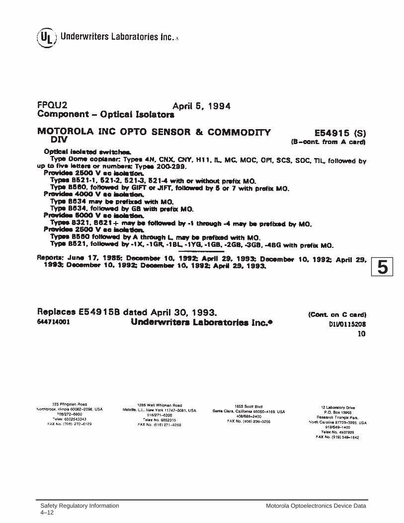
UL (isolation) E54915
UL (flammability) E–8436
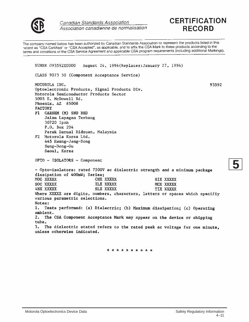
CSA CA93952
FIMKO 41990
SEMKO 9313138
DEMKO Approved per SEMKO
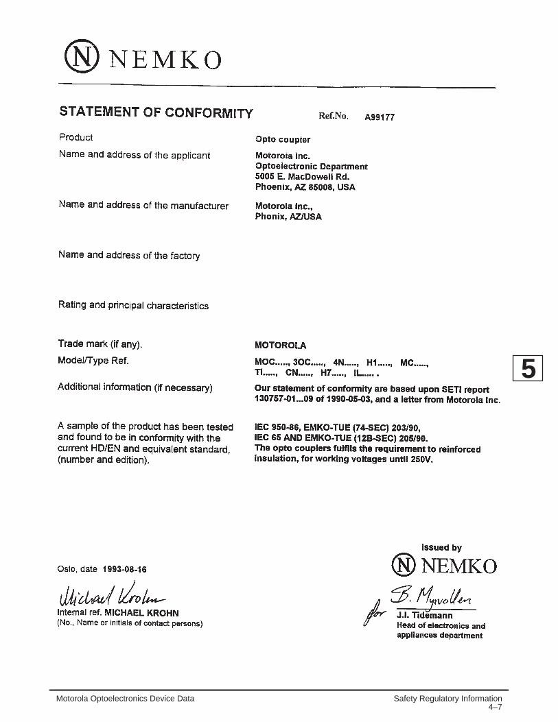
NEMKO A99177
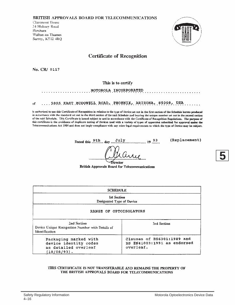
BABT CR/0117
AUSTEL 03 887 0711
Note: Motorola’s 8–pin surface mount optocouplers are approved by UL only and have a guaranteed isolationvoltage of 3000 Vac(rms).
All Motorola 6–pin optocouplers are 100% tested for isolation voltage and are guaranteed to 7500 Vac(peak).
UL Flammability Rating = 94VO (File number E–8436) for all optocouplers.
(1) VDE 0884 testing is an option; the suffix letter “V” must be added to the standard part number.

3–3Selector GuideMotorola Optoelectronics Device Data
VDE Approved OptoisolatorsVDE has approved Motorola’s entire portfolio of 6–pin DIP
optoisolators against their new components standardVDE 0884 which replaces VDE 0883. The VDE 0884components standard requires additional electrical testing toa stringent isolation partial discharge test.
The VDE 0883 specification expired 12/31/91. Motorolaoptoisolators can now be ordered to comply with theVDE 0884 specification.
VDE approval is based on mechanical and electricalperformance of the Motorola package, shown in Figure 3. This6–Pin DIP package incorporates specially developedmaterials and assembly processes optimizing thermal andmoisture stability while maintaining the high level of LED lifeand isolation voltage. All Motorola 6–pin DIP optoisolators aremade in this package, and have these approvals.
Optoisolators, a block diagram of which is shown inFigure 1, are devices which contain at least one emitter, whichis optically coupled to a photo–detector through some sort ofan insulating medium. This arrangement permits the passageof information from one circuit, which contains the emitter, tothe other circuit containing the detector.
Because this information is passed optically across aninsulating gap, the transfer is one–way; that is, the detectorcannot affect the input circuit. This is important because theemitter may be driven by a low voltage circuit utilizing an MPUor logic gates, while the output photo–detector may be part ofa high voltage dc or even an ac load circuit. The opticalisolation prevents interaction or even damage to the inputcircuit to be caused by the relatively hostile output circuit.
VDE 0884 Component Standard (replaces VDE 0883)
Electrical ratings in this standard are:Input–to–Output Voltage, 1 secondVPr1 = 1.6 VIDRM, Partial Discharge < 5 picocouloumbs,
VPr1 = 1280 V(pk)Maximum operating peak voltage, VIDRM = 800 V(pk)
Isolation resistance: VI–O = 500 Vdc, 1011 Ω, TA = 100°C.Note: The isolation partial discharge test VPr1, is performed
after the completion of the high voltage withstand (hipot) tests.
VDE 0883 Component Standard (expired 12/31/91)
Electrical ratings in this standard were:Isolation withstand voltages:
3750 VRMS, 1 min, TA = 100°C
5300 Vdc, 1 min, TA = 100°CIsolation surge withstand voltage:
10 kV per IEC 65, 50 dischargesIsolation resistance:
1011 Ω, 500 Vdc, TA = 100°C
NOTE: VDE 0884/8.87 testing is an option ; the suffix letter“V” must be added to the standard part number. (See below.)Standard thru hole — MOC3063V0.4″ wide spaced leadform — MOC3063TV (to satisfy 8 mmspacing requirement)Standard–profile surface mount — MOC3063SVTape and Reel for surface mount — MOC3063S/SR2V
IRED
PHOTODETECTOR
ISOLATINGDIELECTRIC(LIGHT PIPE)
Figure 1. Block Diagram of Optoisolator
Various geometric designs have been used over the yearsfor the internal light cavity between the emitter and detector.Motorola is the industry leader in isolation technology. All6–pin optoisolators are guaranteed to meet or exceed 7500Vac (pk) input–to–output isolation. See Figure 2.
ÉÉÉÉÉÉÉÉÉÉÉÉÉÉÉÉÉÉ
WHITE OVERMOLD (EPOXY)
LEAD FRAME DETECTOR
THICKNESS THROUGHINSULATION
LED
DOME(SILICONE)
0.5 mm
Figure 2. Geometric Design for Optoisolators
Selector Guide3–4
Motorola Optoelectronics Device Data
VDE Approved Optoisolators (continued)Equipment Standards Compliance
With the approval of the Motorola package to thesecomponent standards, combined with its VDE approvalratings, a wide range of Equipment Standards are covered.The table below summarizes these Equipment Standardcoverages.
Two levels of electrical interface, or insulation, are used:1. Reinforced, or safe, insulation; 2. Basic insulation.
Reinforced Insulation (sometimes referred to as “safe”electrical isolation) is required in an optoisolator interfacingbetween a hazardous voltage circuit, like an ac line, and atouchable s afe extra low voltage (SELV) circuit.
Basic Insulation is required in an optoisolator whichinterfaces between a hazardous voltage circuit and anon–touchable, e xtra low voltage (ELV) circuit.
The 6–pin DIP optoisolators are suitable for both levels ofelectrical interface. The smaller SOIC–8 optoisolators complywith basic Insulation standards only.
Mechanical ratings are shown in the table below.
ÉÉÉÉÉÉÉÉÉÉÉÉÉÉÉÉÉÉ
3
1
2
3
WHITE OVERMOLD (EPOXY)
LEAD FRAME
CREEPAGE PATH
DETECTOR
THICKNESS THROUGHINSULATION
CLEARANCE 0.4″SPECIAL
“T” LEAD BEND
CLEARANCESTD.
LEAD BEND
LED DOME(SILICONE)
0.5 mm
Figure 3. “DOME” Package
Examples for Safety Applications for Motorola VDE Approved Optoisolators
Standard (2)
Requirements for reinforced (double) or safe insulation forequipment with an operating voltage up to 250 Vrms
(line voltage to ELV or SELV interfaces)
VDE (5)DINIEC Equipment Creepage
Clearance(1)
IsolationBarrier
DielectricStrength
IsolationResistance
[mm] [mm] [mm] [kV RMS] [Ω ]0806 950 Office Machines 8.0 8.0 0.5 3.75 7 x 10⁶
0805 950 Data Processing 8.0 8.0 — 3.75 7 x 10⁶
0804 — Telecommunication 8.0 8.0 — 2.5 2 x 10⁶
0860 65 Electrical Household 6.0 6.0 0.4 3.0 (10)* 4 x 106
0113 204 Industrial Controls 8.0 8.0 — 2.5 1 x 10⁶
0160 — Power Installations with Electronic Equipment 8.0 8.0 — 2.7 1 x 10⁶
0832 — Traffic Light Controls 8.0 8.0 — 2.5 4 x 10⁶
0883 — Alarm Systems 8.0 8.0 — 2.5 2 x 10⁶
0831 — Electrical Signal System for Railroads 8.0 8.0 — 2.0 2 x 10⁶
0110 — General Std. for Electrical Equipment 8.0 8.0 — 2.0 —
0883 — Optoisolator Component Standard(obsolete 12/31/91)
8.5 8.3 (10)(1)
0.5 3.75 (10)* 10 x 1011
0884(4) — Optoisolator Component Standard >7.5 >7.5 0.5 — 10 x 1012
(replaces VDE0883) VDE Rating for Motorola 6–pin DIP Optoisolators
All Motorola 6–pin DIP Optoisolators meet or exceed the requirements of above listed VDE and DIN IEC Standards.* Impulse discharge withstand voltage.(1) To satisfy 8.0 mm creepage path on a PC board Motorola offers a special lead bend of 0.4 inch on all 6–pin dual in–line optoisolators. Order by attaching “T” to(1) the end of the Motorola part number.(2) VDE standards (translated into English language) and IEC standards can be ordered from the American National Standard Institute ANSI, 1430 Broadway, N.Y.,N. Y. 10018, Sales Department, 212–642–4900.(3) Creepage path distances are measured from lead to lead across the top, bottom and ends of the package body.(4) VDE 0884 testing is an option; the suffix letter “V” must be added to the standard number.(5) For more information regarding the use of VDE approved devices, refer to “VDE Circuit Board Layout Design Rules” in the Applications Information section.

3–5Selector GuideMotorola Optoelectronics Device Data
Optoisolators 6–Pin DIP Varieties and Lead Form Options
1
2
3 4
5
6
4
561
2
3
4
5
61
2
3 4
5
61
2
3 4
5
61
2
4
5
61
2
3
1
2
Zero CrossingCircuit
NC
NC NC
NC
NC NC
NC NC
CASE 730A–04
Transistor Darlington
Resistor Darlington
Style 1 Style 3
Transistor Darlington AC InputTransistor Output
Schmitt Triggers
Style 5
Random PhaseTriac Driver
Zero CrossingTriac Driver
Style 6
AC InputResistor–Darlington
Output
Style 8
1
2
3
6
5
4
1
2
3 NC 4
5
6
3 NC
1
2
3 4
5
6
4
5
6
3 NC
An optoisolator consists of a gallium arsenide infraredemitting diode, IRED, optically coupled to a monolithic siliconphotodetector in a wide array of standard devices andencourages the use of special designs and selections forspecial applications. All Motorola optoisolators have VISOrating of 7500 Vac(pk), exceeding all other industry standardratings.
Motorola offers global regulatory approvals, including UL,CSA, AUSTEL, NEMKO, BABT, SETI, SEMKO, and DEMKO.VDE(1) approved per standard 0884/8.87, with additionalapprovals to DIN IEC950 and IEC380/VDE 0806,IEC435/VDE 0805, IEC65/VDE 0860, VDE 110b, alsocovering all other standards with equal or less stringentrequirements, including IEC204/VDE 0113, VDE 0160, VDE0832, VDE 0833.(1) VDE 0884/8.87 testing is an option; the suffix “V” must be added to the
standard part number (see VDE Approved Optoisolators in Section 3).
(S) CASE 730C–04Surface–mountable
gull–wing option
CASE730A–04
(T) CASE 730D–05Wide–spaced (0.400)
lead form option
S T
Motorola’s 6–pin, dual in–line optoisolators can beordered in either a surface–mountable, gull–wing leadform or a wide–spaced 0.400″ through–hole lead form,which is used to satisfy 8 mm PC board spacingrequirements. Please first consult factory regardingavailability for your lead form option, prior toordering!
• Attach “S” to any Motorola 6–pin, dual in–line partnumber for surface–mountable, gull–wing lead form.
• Attach “T” to any Motorola 6–pin, dual in–line partnumber for wide–spaced 0.400” through–hole leadform.
OptoisolatorLead Form Options:
Tape and Reel Options:• Attach “SR2” suffix to any Motorola 6–pin, dual
in–line part number for tape and reeled,surface–mountable, gull–wing lead form.

Selector Guide3–6
Motorola Optoelectronics Device Data
6–Pin Dual In–Line PackageTable 1. Transistor OutputPinout: 1–Anode, 2–Cathode, 3–N.C., 4–Emitter, 5–Collector, 6–Base (Style 1)
Current TransferRatio (CTR) VCE(sat)
tr / tf or t on* / toff *Typ
VVF
Device%
MinIF
mA@VCEVolts
Volts
Max
IFmA
@IC
mA µs
ICmA
@ VCCVolts
RLΩ
IFmA
V(BR)CEOVoltsMin
VoltsMax
IFmA@
TIL111 8 16 0.4 0.4 16 2 5/5 2 10 100 30 1.4 164N27 10 10 10 0.5 50 2 1.2/1.3 10 10 100 30 1.5 104N28 10 10 10 0.5 50 2 1.2/1.3 10 10 100 30 1.5 104N38,A 20 20 1 1 20 4 1.6/2.2 10 10 100 80 1.5 104N25,A 20 10 10 0.5 50 2 1.2/1.3 10 10 100 30 1.5 104N26 20 10 10 0.5 50 2 1.2/1.3 10 10 100 30 1.5 10MCT2 20 10 10 0.4 16 2 1.2/1.3 5 2k 15 30 1.5 20MCT2E 20 10 10 0.4 16 2 1.2/1.3 2 10 100 30 1.5 20CNY17–1 40–80 10 5 0.4 10 2.5 1.6/2.3″ 5 75 10 70 1.65 60MCT271 45–90 10 10 0.4 16 2 4.9*/4.5* 2 5 100 30 1.5 20MOC8100 50 1 5 0.5 1 0.1 3.8/5.6 2 10 100 30 1.4 1H11A1 50 10 10 0.4 10 0.5 1.2/1.3 2 10 100 30 1.5 10H11A550 50 10 10 0.4 20 2 5*/5* 2 10 100 30 1.5 10TIL117 50 10 10 0.4 10 0.5 5/5 2 10 100 30 1.4 16TIL126 50 10 10 0.4 10 1 2/2 2 10 100 30 1.4 10SL5501 45–250 10 0.4 0.4 20 2 20*/50* 5 1k 16 30 1.3 20CNY17–2 63–125 10 5 0.4 10 2.5 1.6/2.3 5 75 10 70 1.65 60MCT275 70–210 10 10 0.4 16 2 4.5*/3.5* 2 5 100 80 1.5 20MCT272 75–150 10 10 0.4 16 2 6*/5.5* 2 5 100 30 1.5 204N35 100 10 10 0.3 10 0.5 3.2/4.7 2 10 100 30 1.5 104N36 100 10 10 0.3 10 0.5 3.2/4.7 2 10 100 30 1.5 104N37 100 10 10 0.3 10 0.5 3.2/4.7 2 10 100 30 1.5 10CNY17–3 100–200 10 5 0.4 10 2.5 1.6/2.3 5 75 10 70 1.65 60H11AV1 100–300 10 10 0.4 20 2 5*/4* 2 10 100 70 1.5 10H11AV2 50 10 10 0.4 20 2 5*/4* 2 10 100 70 1.5 10MCT273 125–250 10 10 0.4 16 2 7.6*/6.6* 2 5 100 30 1.5 20
Table 2. Transistor Output with No Base ConnectionPinout: 1–Anode, 2–Cathode, 3–N.C., 4–Emitter, 5–Collector, 6–Base (Style 3)
MOC8101 50–80 10 10 0.4 5 0.5 3.2/4.7 2 10 100 30 1.5 10MOC8102 73–117 10 10 0.4 5 0.5 3.2/4.7 2 10 100 30 1.5 10MOC8103 108–173 10 10 0.4 5 0.5 3.2/4.7 2 10 100 30 1.5 10MOC8104 160–256 10 10 0.4 5 0.5 3.2/4.7 2 10 100 30 1.5 10MOC8105 65–133 10 10 0.4 5 0.5 3.2/4.7 2 10 100 30 1.5 10MOC8111 20 10 10 0.4 10 0.5 3.2/4.7 2 10 100 30 1.5 10MOC8112 50 10 10 0.4 10 0.5 3.2/4.7 2 10 100 30 1.5 10MOC8113 100 10 10 0.4 10 0.5 3.2/4.7 2 10 100 30 1.5 10
Table 3. AC Input – Transistor OutputPinout: 1–LED 1 Anode/LED 2 Cathode, 2–LED 1 Cathode/LED 2 Anode, 3–N.C., 4–Emitter, 5–Collector, 6–Base (Style 8)
Current TransferRatio (CTR) VCE(sat)
tr / tf or t on* / toff *Typ
VVF
Device%
MinIF
mA@VCEVolts
Volts
Max
IFmA
@IC
mA µs
ICmA
@ VCCVolts
RLΩ
IFmA
V(BR)CEOVoltsMin
VoltsMax
IFmA@
H11AA1 20 ±10 10 0.4 ±10 0.5 30 1.5 ±10H11AA2 10 ±10 10 0.4 ±10 0.5 30 1.8 ±10H11AA3 50 ±10 10 0.4 ±10 0.5 30 1.5 ±10H11AA4 100 ±10 10 0.4 ±10 0.5 30 1.5 ±10
Devices listed in bold, italic are Motorola preferred devices.
CASE 730A–04

3–7Selector GuideMotorola Optoelectronics Device Data
6–Pin Dual In–Line Package (continued)
Table 4. Darlington OutputPinout: 1–Anode, 2–Cathode, 3–N.C., 4–Emitter, 5–Collector, 6–Base (Style 1)
Current TransferRatio (CTR) VCE(sat)
tr / tf or t on* / toff *Typ
VVF
Device%
MinIF
mA@VCEVolts
Volts
Max
IFmA
@IC
mA µs
ICmA
@ VCCVolts
RLΩ
IFmA
V(BR)CEOVoltsMin
VoltsMax
IFmA@
4N31 50 10 10 1.2 8 2 0.6*/17* 50 10 200 30 1.5 104N29,A 100 10 10 1 8 2 0.6*/17* 50 10 200 30 1.5 104N30 100 10 10 1 8 2 0.6*/17* 50 10 200 30 1.5 10MCA231 200 1 1 1.2 10 50 80 10 10 100 30 1.5 20TIL113 300 10 1.25 1 50 125 300 125 15 100 30 1.5 104N32 500 10 10 1 8 2 0.6*/45* 50 10 200 30 1.5 104N33 500 10 10 1 8 2 0.6*/45* 50 10 200 30 1.5 10H11B1 500 1 5 1 1 1 1/2 10 10 100 25 1.5 10MOC8080 500 10 5 1 1 1 1/2 10 100 5 55 1.5 10
Table 5. Darlington Output with No Base ConnectionPinout: 1–Anode, 2–Cathode, 3–N.C., 4–Emitter, 5–Collector, 6–N.C. (Style 3)
MOC119 300 10 2 1 10 10 1/2 2.5 10 100 30 1.5 10MOC8030 300 10 1.5 1/2 50 100 10 80 2 10MOC8020 500 10 5 1/2 50 100 10 50 2 10MOC8050 500 10 1.5 1/2 50 100 10 80 2 10MOC8021 1000 10 5 1/2 50 100 10 50 2 10
Table 6. Resistor Darlington OutputPinout: 1–Anode, 2–Cathode, 3–N.C., 4–Emitter, 5–Collector, 6–Base (Style 1)
H11G1 1000 10 1 1 1 1 5*/100* 5 100 10 100 1.5 10H11G2 1000 10 1 1 1 1 5*/100* 5 100 10 80 1.5 10H11G3 200 1 5 1.2 50 20 5*/100* 5 100 10 55 1.5 10
Table 7. High Voltage Transistor OutputPinout: 1–Anode, 2–Cathode, 3–N.C., 4–Emitter, 5–Collector, 6–Base (Style 1)
MOC8204 20 10 10 0.4 10 0.5 5*/5* 2 10 100 400 1.5 10
H11D1 20 10 10 0.4 10 0.5 5*/5* 2 10 100 300 1.5 10
H11D2 20 10 10 0.4 10 0.5 5*/5* 2 10 100 300 1.5 10
Devices listed in bold, italic are Motorola preferred devices.
CASE 730A–04

Selector Guide3–8
Motorola Optoelectronics Device Data
6–Pin Dual In–Line Package (continued)
Table 8. Triac Driver OutputPinout: 1–Anode, 2–Cathode, 3–N.C., 4–Main Terminal, 5–Substrate, 6–Main Terminal (Style 6)
Device
Peak BlockingVoltage
Min
LED TriggerCurrent–I FT(VTM = 3 V)
mA Max
Zero CrossingInhibit Voltage(at rated I FT)
Volts Max
OperatingVoltage
Vacdv/dt
V/µs Typ
MOC3010 250 15 — 125 10MOC3011 250 10 — 125 10MOC3012 250 5 — 125 10MOC3021 400 15 — 125/280 10MOC3022 400 10 — 125/280 10MOC3023 400 5 — 125/280 10MOC3051* 600 15 — 125/280 2000MOC3052* 600 10 — 125/280 2000MOC3031 250 15 20 125 2000MOC3032 250 10 20 125 2000MOC3033 250 5 20 125 2000MOC3041 400 15 20 125/280 2000MOC3042 400 10 20 125/280 2000MOC3043 400 5 20 125/280 2000MOC3061 600 15 20 125/280 1500MOC3062 600 10 20 125/280 1500MOC3063 600 5 20 125/280 1500MOC3162* 600 10 15 125/280 1000MOC3163* 600 5 15 125/280 1000MOC3081 800 15 20 125/280/320 1500MOC3082 800 10 20 125/280/320 1500MOC3083 800 5 20 125/280/320 1500
* New Device Offering
Table 9. Schmitt Trigger OutputPinout: 1–Anode, 2–Cathode, 3–N.C., 4–Output, 5–Ground, 6–V CC (Style 5)
ThresholdCurrent On
ThresholdCurrent Off IF(off) /IF(on) VCC tr, tf
Device mA Max mA Min Min Max Min Max µs Typ
H11L1 1.6 0.3 0.5 0.9 3 16 0.1H11L2 10 0.3 0.5 0.9 3 16 0.1MOC5007 1.6 0.3 0.5 0.9 3 16 0.1MOC5008 4 0.3 0.5 0.9 3 16 0.1MOC5009 10 0.3 0.5 0.9 3 16 0.1
Devices listed in bold, italic are Motorola preferred devices.
CASE 730A–04

3–9Selector GuideMotorola Optoelectronics Device Data
Small Outline — Surface Mount
Table 10. Transistor OutputPinout: 1–Anode, 2–Cathode, 3–N.C., 4–N.C., 5–Emitter, 6–Collector, 7–Base, 8–N.C. (Style 1)
Current TransferRatio (CTR)
VCE(sat) tr / tf Typ
V(BR)CEO
VF
% IF@VCE Volts I F@
IC ICA
@ VCC RLV(BR)CEO
Volts Volts I F@Device Marking Min mA
@Volts Max mA
@mA µs mA
@Volts Ω Min Max mA
@
MOC205,R2 205 40–80 10 10 0.4 10 2 1.6 2 10 100 70 1.5 10MOC206,R2 206 63–125 10 10 0.4 10 2 1.6 2 10 100 70 1.5 10MOC207,R2 207 100–200 10 10 0.4 10 2 1.6 2 10 100 70 1.5 10MOC211,R2 211 20 10 10 0.4 10 2 3.2 2 10 100 30 1.5 10MOC212,R2 212 50 10 10 0.4 10 2 3.2 2 10 100 30 1.5 10MOC213,R2 213 100 10 10 0.4 10 2 3.2 2 10 100 30 1.5 10MOC215,R2 215 20 1 5 0.4 1 0.1 3.2 2 10 100 30 1.3 1MOC216,R2 216 50 1 5 0.4 1 0.1 3.2 2 10 100 30 1.3 1MOC217,R2 217 100 1 5 0.4 1 0.1 3.2 2 10 100 30 1.3 1
Table 11. Darlington OutputPinout: 1–Anode, 2–Cathode, 3–N.C., 4–N.C., 5–Emitter, 6–Collector, 7–Base, 8–N.C. (Style 1)
MOC223,R2 223 500 1 5 1 1 0.5 2 5 10 100 30 1.3 1MOC263,R2* 263 500 1 5 1 1 0.5 2 5 10 100 30 1.3 1
All devices are shipped in tape and reel format. (See Tape and Reel Specifications Section for more information.)*No Base Connection to Pin 7
Table 12. AC Input – Transistor Output (Single Channel) (Style 2)
MOC256,R2 256 20 ±10 10 0.4 ±10 0.5 30 1.5 ±10
Table 13. Transistor Output (Dual Channel) (Style 3)
MOCD207,R2 D207 100–200 10 10 0.4 10 2 1.6 2 10 100 70 1.5 10MOCD208,R2 D208 45–125 10 10 0.4 10 2 1.6 2 10 100 70 1.5 10MOCD211,R2 D211 20 10 10 0.4 10 2 3.2 2 10 100 30 1.5 10MOCD213,R2 D213 100 10 10 0.4 10 2 3.2 2 10 100 70 1.5 10MOCD217,R2 D217 100 1 5 0.4 1 0.1 3.2 2 10 100 30 1.5 1
Table 14. Darlington Output (Dual Channel) (Style 3)
MOCD223,R2 D223 500 1 5 1 1 0.5 2 5 10 100 30 1.3 1
R2 devices are shipped in tape and reel format. (See Tape and Reel Specifications Section for more information.)
Devices listed in bold, italic are Motorola preferred devices.
CASE 846–01SO–8 DEVICES

CASE 417-02PLASTIC PACKAGE
CASE 417B-01PLASTIC PACKAGE
CASE 417A-02PLASTIC PACKAGE
Selector Guide3–10
Motorola Optoelectronics Device Data
POWER OPTO Isolators
Table 15. POWER OPTO Isolator 2 Amp Zero–Cross or Random Phase Triac OutputsPinout: (1,4,5,6,8 No Pin), 2 – LED Cathode, 3– LED Anode, 7–Main Terminal, 9–Main Terminal
Device
Peak BlockingVoltage (Volts)
Min
Led TriggerCurrent If T
(VTM = 2 V) mAMax
On State VoltageVTM (Rated IFTITM = 2 A) (Volts)
Max
Zero CrossingInhibit Voltage(IF = Rated IFT)
(Volts) Max
OperatingVoltage
Vac Pk (Volts)
dv/dt (static)v/µs (VIN = 200 V)
(V/µs)Min
MOC2A40-5 400 5 1.3 10 125 400MOC2A40-10 400 10 1.3 10 125 400MOC2A60-5 600 5 1.3 10 125/220 400MOC2A60-10 600 10 1.3 10 125/220 400
All devices are shipped in rails.No suffix = Case 417–02/Style 2 (Standard Heat Tab),“F” suffix = Case 417–02/Style 1 (Flush Mount Heat Tab) ”C” suffix = Case 417B–01/Style 1 (Cut Tab)
Devices listed in bold, italic are Motorola preferred devices.

3–11Selector GuideMotorola Optoelectronics Device Data

4–1Safety Regulatory InformationMotorola Optoelectronics Device Data
Section 4
Safety Regulatory Information
Safety Standards Information 4–2. . . . . . . . . . . . . .
Safety Regulatory Approval Documents 4–3. . .
VDE Approved Optoisolators 4–21. . . . . . . . . . . . . . .
VDE 0884 Approved Optocouplers 4–23. . . . . . . . .
VDE Circuit Board Layout Design Rules 4–30. . .
Definition of Terms 4–34. . . . . . . . . . . . . . . . . . . . . . . . .

Safety Regulatory Information4–2
Motorola Optoelectronics Device Data
Safety Regulatory Approvals for Motorola’s “Global” Optoisolators
Motorola’s entire line of 6–pin optoisolators are approved by all major safety regulatories.
Safety Standard Approvals for 6–Pin Optoisolators
*(1)
*(1)
*(1)
*(1)
*(1)
*(1)
*(1)
(1)
(1)
(1)
(1)
(1)
(1)
(1)
MOCXXXX
SOCXXXX
4NXXXXXX
H1XXXXXX
MCXXXXXX
TIXXXXXX
CNXXXXXX
*
*
*
*
*
*
*
*
*
*
*
*
*
*
*
*
*
*
*
*
*
*
*
*
*
*
*
*
*
*
*
*
*
*
*
*
*
*
*
*
*
*
∆ = Approved*
*
*
*
*
*
*
*
GlobalOptoisolator
Regulatory Approval Certification IndexRegulatory Agency Certificate File Number
VDE(0883) 41853 (expired 12/31/91)
VDE(0884)(1) 62054 (replaces VDE0883)
UL (isolation) E54915
UL (flammability) E–8436
CSA CA93952
FIMKO 41990
SEMKO 9313138
DEMKO Approved per SEMKO
NEMKO A99177
BABT CR/0117
AUSTEL 03 887 0711
Note: Motorola’s 8–pin surface mount optocouplers are approved by UL only and have a guaranteed isolationvoltage of 3000 Vac(rms).
All Motorola 6–pin optocouplers are 100% tested for isolation voltage and are guaranteed to 7500 Vac(peak).
UL Flammability Rating = 94VO (File number E–8436) for all optocouplers.
(1) VDE 0884 testing is an option; the suffix letter “V” must be added to the standard part number.
5

4–3Safety Regulatory InformationMotorola Optoelectronics Device Data
SAFETY REGULATORYAPPROVAL DOCUMENTATIONS
5

Safety Regulatory Information4–4
Motorola Optoelectronics Device Data
5

4–5Safety Regulatory InformationMotorola Optoelectronics Device Data
5
Safety Regulatory Information4–6
Motorola Optoelectronics Device Data
5
4–7Safety Regulatory InformationMotorola Optoelectronics Device Data
5

Safety Regulatory Information4–8
Motorola Optoelectronics Device Data
5

4–9Safety Regulatory InformationMotorola Optoelectronics Device Data
5

Safety Regulatory Information4–10
Motorola Optoelectronics Device Data
5
4–11Safety Regulatory InformationMotorola Optoelectronics Device Data
5
Safety Regulatory Information4–12
Motorola Optoelectronics Device Data
5

4–13Safety Regulatory InformationMotorola Optoelectronics Device Data
5

Safety Regulatory Information4–14
Motorola Optoelectronics Device Data
5

4–15Safety Regulatory InformationMotorola Optoelectronics Device Data
5
Safety Regulatory Information4–16
Motorola Optoelectronics Device Data
5
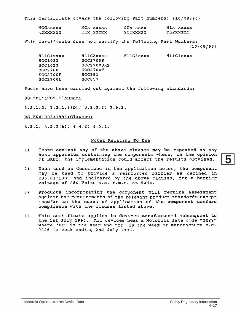
4–17Safety Regulatory InformationMotorola Optoelectronics Device Data
5

Safety Regulatory Information4–18
Motorola Optoelectronics Device Data
5

4–19Safety Regulatory InformationMotorola Optoelectronics Device Data
5

Safety Regulatory Information4–20
Motorola Optoelectronics Device Data
5

4–21Safety Regulatory InformationMotorola Optoelectronics Device Data
VDE Approved OptoisolatorsVDE has approved Motorola’s entire portfolio of 6–pin DIP
optoisolators against their new components standardVDE 0884 which replaces VDE 0883. The VDE 0884 compo-nents standard requires additional electrical testing to a strin-gent isolation partial discharge test.
The VDE 0883 specification expired 12/31/91. Motorolaoptoisolators can now be ordered to comply with theVDE 0884 specification.
VDE approval is based on mechanical and electrical per-formance of the Motorola package, shown in Figure 3. This6–Pin DIP package incorporates specially developed materi-als and assembly processes optimizing thermal and moisturestability while maintaining the high level of LED life and isola-tion voltage. All Motorola 6–pin DIP optoisolators are made inthis package, and have these approvals.
VDE 0884 Component Standard (replaces VDE 0883)
Electrical ratings in this standard are:Input–to–Output Voltage, 1 secondVPr1 = 1.6 VIDRM, Partial Discharge < 5 picocouloumbs,
VPr1 = 1280 V(pk)Maximum operating peak voltage, VIDRM = 800 V(pk)
Isolation resistance: VI–O = 500 Vdc, 1011 Ω, TA = 100°C.Note: The isolation partial discharge test VPr1, is performedafter the completion of the high voltage withstand (hipot) tests.
VDE 0883 Component Standard (expired 12/31/91)
Electrical ratings in this standard were:Isolation withstand voltages:
3750 VRMS, 1 min, TA = 100°C5300 Vdc, 1 min, TA = 100°C
Isolation surge withstand voltage:10 kV per IEC 65, 50 discharges
Isolation resistance:1011 Ω, 500 Vdc, TA = 100°C
NOTE: VDE 0884/8.87 testing is an option ; the suffix letter“V” must be added to the standard part number. (See below.)Standard thru hole — MOC3063V0.4″ wide spaced leadform — MOC3063TV (to satisfy 8 mmspacing requirement)Standard–profile surface mount — MOC3063SVTape and Reel for surface mount — MOC3063S/SR2V
Optoisolators, a block diagram of which is shown inFigure 1, are devices which contain at least one emitter,which is optically coupled to a photo–detector through somesort of an insulating medium. This arrangement permits thepassage of information from one circuit, which contains theemitter, to the other circuit containing the detector.
Because this information is passed optically across aninsulating gap, the transfer is one–way; that is, the detectorcannot affect the input circuit. This is important because theemitter may be driven by a low voltage circuit utilizing anMPU or logic gates, while the output photo–detector may bepart of a high voltage dc or even an ac load circuit. Theoptical isolation prevents interaction or even damage to theinput circuit to be caused by the relatively hostile outputcircuit.
IRED
PHOTODETECTOR
ISOLATINGDIELECTRIC(LIGHT PIPE)
Figure 1. Block Diagram of Optoisolator
Various geometric designs have been used over the yearsfor the internal light cavity between the emitter and detector.Motorola is the industry leader in isolation technology. All6–pin optoisolators are guaranteed to meet or exceed 7500Vac (pk) input–to–output isolation. See Figure 2.
ÉÉÉÉÉÉÉÉÉÉÉÉÉÉÉ
WHITE OVERMOLD (EPOXY)
LEAD FRAME DETECTOR
THICKNESS THROUGHINSULATION
LED
DOME(SILICONE)
0.5 mm
Figure 2. Geometric Design for Optoisolators
5

Safety Regulatory Information4–22
Motorola Optoelectronics Device Data
VDE Approved Optoisolators (continued)
Equipment Standards Compliance
With the approval of the Motorola package to these com-ponent standards, combined with its VDE approval ratings, awide range of Equipment Standards are covered. The tablebelow summarizes these Equipment Standard coverages.
Two levels of electrical interface, or insulation, are used:1. Reinforced, or safe, insulation; 2. Basic insulation.
Reinforced Insulation (sometimes referred to as “safe”electrical isolation) is required in an optoisolator interfacingbetween a hazardous voltage circuit, like an ac line, and atouchable s afe extra low voltage (SELV) circuit.
Basic Insulation is required in an optoisolator which inter-faces between a hazardous voltage circuit and a non–touchable, e xtra low voltage (ELV) circuit.
The 6–pin DIP optoisolators are suitable for both levels ofelectrical interface. The smaller SOIC–8 optoisolators com-ply with basic Insulation standards only.
Mechanical ratings are shown in the table below.
ÉÉÉÉÉÉÉÉÉÉÉÉÉÉÉ
3
1
2
3
WHITE OVERMOLD (EPOXY)
LEAD FRAME
CREEPAGE PATH
DETECTOR
THICKNESS THROUGHINSULATION
CLEARANCE 0.4″SPECIAL
“T” LEAD BEND
CLEARANCESTD.
LEAD BEND
LED DOME(SILICONE)
0.5 mm
Figure 3. “DOME” Package
Examples for Safety Applications for Motorola VDE Approved Optoisolators
Standard (2)
Requirements for reinforced (double) or safe insulation forequipment with an operating voltage up to 250 Vrms
(line voltage to ELV or SELV interfaces)
VDE (5)DINIEC Equipment Creepage
Clearance(1)
IsolationBarrier
DielectricStrength
IsolationResistance
[mm] [mm] [mm] [kV RMS] [Ω ]0806 950 Office Machines 8.0 8.0 0.4 3.75 7 x 10⁶
0805 950 Data Processing 8.0 8.0 0.4 3.75 7 x 10⁶
0804 — Telecommunication 8.0 8.0 — 2.5 2 x 10⁶
0860 65 Electrical Household 6.0 6.0 0.4 3.0 (10)* 4 x 106
0113 204 Industrial Controls 8.0 8.0 — 2.5 1 x 10⁶
0160 — Power Installations with Electronic Equipment 8.0 8.0 — 2.7 1 x 10⁶
0832 — Traffic Light Controls 8.0 8.0 — 2.5 4 x 10⁶
0883 — Alarm Systems 8.0 8.0 — 2.5 2 x 10⁶
0831 — Electrical Signal System for Railroads 8.0 8.0 — 2.0 2 x 10⁶
0110 — General Std. for Electrical Equipment 8.0 8.0 — 2.0 —
0883 — Optoisolator Component Standard(obsolete 12/31/91)
8.5 8.3 (10)(1)
0.5 3.75 (10)* 10 x 1011
0884(4) — Optoisolator Component Standard >7.5 >7.5 0.5 — 10 x 1012
(replaces VDE0883) VDE Rating for Motorola 6–pin DIP Optoisolators
All Motorola 6–pin DIP Optoisolators meet or exceed the requirements of above listed VDE and DIN IEC Standards.* Impulse discharge withstand voltage.(1) To satisfy 8.0 mm creepage path on a PC board Motorola offers a special lead bend of 0.4 inch on all 6–pin dual in–line optoisolators. Order by attaching “T” to(1) the end of the Motorola part number.(2) VDE standards (translated into English language) and IEC standards can be ordered from the American National Standard Institute ANSI, 1430 Broadway, N.Y., N. Y. 10018, Sales Department, 212–642–4900.(3) Creepage path distances are measured from lead to lead across the top, bottom and ends of the package body.(4) VDE 0884 testing is an option; the suffix letter “V” must be added to the standard number.(5) For more information regarding the use of VDE approved devices, refer to “VDE Circuit Board Layout Design Rules” in the Applications Information section.
5

4–23Safety Regulatory InformationMotorola Optoelectronics Device Data
Prepared by: Horst GempeDiscrete Applications Engineering
INTRODUCTION
In mid–1990 Motorola received VDE 0884 approval for alloptocouplers in a dome package. This opens an even widerrange of safe isolation applications than with the formerapproval against VDE 0883. For example, optocouplerswhich have VDE 0884 approval are now accepted inappliances, and it is expected that many other equipmentstandards will follow.
VDE 0884 is a new optocoupler standard for safe isolation.In many parts it has the same tests as the older VDE 0883optocoupler standard, but there are two significant additionsin safety philosophy which make this standard uniqueagainst all others. These additions are the introduction of thepartial discharge test and the specification of the safetytemperature, current and power dissipation ratings. Bothcontribute to an even safer isolation and avoid confusion ofworst case conditions in order to still guarantee the safeisolation of optocouplers over the lifetime of the equipment.
Many parameters and classifications of this new optoiso-lator standard are harmonized with the newest basic safetystandards such as isolation coordination standardsVDE 0109, IEC664, and IEC664A, as well as equipment
standards such as those for office machines and dataprocessing equipment DIN/IEC950.
These new standards define and classify the environmentto which the insulation system is exposed. The major newvariables are the installation category and the pollutiondegree. Optocouplers are now rated to these new criteria.VDE plans to incorporate the partial discharge criterion intothe basic standards, as well as into the individual equipmentstandards in the near future.
While the new standards are much better defined than theolder ones, they demand intimate knowledge from the equip-ment designer about all conditions to which the equipment isexposed and detailed information about the safety parame-ters and ratings of the optoisolator.
This application note informs the user of Motorola optoiso-lators about the VDE safety ratings, classification and perfor-mance, and gives guidance in applying these ratings to therequirements of the individual equipment standards.VDE Data Sheet
Table 1 shows the Motorola Dome Optocouplers for safeelectrical isolation in accordance with VDE 0884.
Table 1. VDE 0884 Ratings for Motorola Dome Optocouplers – VDE Approval Document No. 62054
Description Symbol Rating Unit
Installation category (DIN VDE 0109, 12/83, Table 1)
Rated line voltage < 600 Vrms — I to III —
Rated line voltage < 300 Vrms — I to IV —
Climatic category (DIN IEC 68 part 1/09.80) — 55/100/21 —
Pollution degree (DIN VDE 0109, 12 /83) — 2 —
Creepage path between input and output — > 7.5 mm
Clearance between input and output —
Standard leadform 0.3″ — > 7.5 mm
Special leadform 0.4″ — > 10 mm
Thickness through insulation (insulation barrier) — 0.5 mm
Comparative tracking index (DIN IEC 112/VDE 303 part 1/ 06.84) CTI 175 —
Isolation group per VDE 0109 — IIIa —
5

Safety Regulatory Information4–24
Motorola Optoelectronics Device Data
Table 1. VDE 0884 Ratings for Motorola Dome Optocouplers – VDE Approval Document No. 62054 (cont)
Description UnitRatingSymbol
Isolation resistance at VI/O = 500 Vdc
TA = 25°C Riso 1012 Ω
TA = 100°C Riso 1011 Ω
TA = 175°C Riso 109 Ω
Maximum operating peak voltage VIORM 800 Vpk
Production input to output test voltage, 1 secondVpr1 = 1.6 x VIORM, Partial discharge < 5 pC
Vpr1(1) 1280 Vpk
Qualification input to ouptut test voltage, 1 minuteVpr2 = 1.2 VIORM, Partial discharge < 5 pC
Vpr2(1) 960 Vpk
Maximum transient overvoltage Vtr = 10 seconds Qualification Test Vtr 6000 Vpk
Operating Temperature TA –55 to +100 °C
Storage Temperature Tstg –55 to +150 °C
Maximum Safety Temperature, Power and Current Ratings in Case of a Single Fault Condition
Description Symbol Rating Unit
Maximum package safety temperature Tsi 175 °C
Maximum LED safety input current, Psi = 0, TA = 25°C(Linear derate from 25°C to zero at TA = Tsi = 175°C)
Isi 400 mA
Maximum detector safety power dissipation, TA = 25°C(Linear derate from 25°C to zero at TA = Tsi = 175°C)
Psi 800 mW
1. The isolation partial discharge tests Vpr1, Vpr2 in accordance with VDE 0884 are performed after high voltage withstand (hipot) tests.
Explanation of VDE 0884 ratings
Installation Category
The four installation categories are based on the principlesof insulation coordination as found in VDE 0109 and IEC 664.These standards categorize and specify the expected linetransients to earth ground within an ac line installation anddistribution system.
The highest transients are expected at installation cate-gory four, which is the primary supply level from overheadlines or underground cable systems and its associated sparkgap and over-current protection equipment. The locationsare the main fuse and the service entrance. For a 380 V acrms system, the peak transient voltage may be up to 6000Vpk.
Installation category three follows installation category fourand is the fixed electrical installation with its individual circuitbreakers for each branch within a bui lding. For a380/220 Vrms installation peak, transients of 4000 V areexpected.
Installation category two is portable equipment such asappliances which use the outlets of the fixed electrical instal-lation. Transients of up to 2500 Vpk are expected.
Installation category one is special equipment or individualcircuits within portable equipment which operate on thesecondary voltage of a power supply or transformer with max60 V ac or dc peak. Examples are telecommunication, dataprocessing and other electronic equipment. Even in these
cases, transients of up to 500 Vpk in respect to earth groundare possible, unless transient suppression is provided.
Climatic Category 55/100/21
These numbers specify the environmental condition for theapproval test. The temperature range is –55 to +100°C with a21–day humidity soak.
Pollution Degree
There are four pollution degrees. Pollution degree onespecifies non-conductive or only dry non-conductive pollu-tion which is found inside most electronic equipment in acontrolled environment such as an office.
Pollution degree 2 assumes normally dry, non-conductivepollution with occasional temporary conductivity caused bycondensation. Examples are appliances like washers, dish-washers and equipment in non-temperature controlled envi-ronments.
Pollution degree three has expected conductive pollution,and pollution degree four assumes persistent conductivepollution as found in an outside environment such as rain orsnow.
Creepage and Clearance
The creepage path is the shortest distance on the surfaceof the optocoupler package between input and output leads.The clearance is the shortest distance between input andoutput leads through air. A special lead bend is availablewhich increases this distance and guarantees an adequatecreepage part on the circuit board.
5

4–25Safety Regulatory InformationMotorola Optoelectronics Device Data
Comparative Tracking Index
This index indicates a insulator’s withstand capability tosurface deterioration caused by sparks or leakage currentsover the creepage path. This may be the case when conduc-tive pollution occurs. CTI is a relative number and is used tocompare insulation materials. The higher the number, thebetter the resistance to deterioration. Glass and ceramics arevery resistant and have a CTI of >600. Some circuit boardmaterials are <100.
Isolation Group
The isolation group characterizes insulators to their resis-tance to tracking. Insulators which remain unaffected by theCTI test belong to isolation group I; insulators which erode ordecompose with carbon residues are found in isolation groupIII.
• CTI –rating Isolation group
• ≥ 600 I
• 100–600 II
• 175–400 IIIa
• 100–175 IIIb
Isolation Resistance
In the qualification test this parameter is measured afterthe environment’s 21-day humidity soak and a short surfacedry at ambient temperature at 500 Vdc, and at the maximumsafety temperature Tsi = 175°C. Motorola tests this parameterin production during the transient withstand test (hipot test).
Maximum Operating Peak Voltage V IORM
This is the maximum repetitive peak voltage for safe isola-tion. In some equipment, it is not necessarily the peak linevoltage. Switching power supplies, for example, may developrepetitive peak voltages between primary and secondarycircuits exceeding the ac peak voltage by superimposinginductive voltage transients of the flyback transformer ontothe line voltage.
Safe isolation of the insulation material is guaranteed whenthe optocoupler is operated within this rating, since partialdischarge which might destroy the insulation barrier is guar-anteed not to be present.
Partial Discharge Test Voltage V pr1 and Vpr2
Partial discharge is a corona discharge in a part of theinsulation barrier caused by voids or locally high electricalfield gradients. Partial discharge may decompose or erodethe insulation material over time and lead to a permanentinsulation failure. The VDE 0884 safety philosophy demandsthat the peak repetitive operating voltage is lower than thepartial discharge initiation and extinction voltage of the opto-coupler, thus avoiding the cause of an isolation degradationor breakdown over time. All optocouplers have to pass apartial discharge test at 1280 V ac peak for one second.During this time the device is monitored for partial dischargeby a highly sensitive narrow band RF circuit and the device isrejected when a part ial discharge act iv i ty of 5 picocouloumbs or larger is recorded.
Maximum Transient Overvoltage, V trThis is the classical hipot test which may lead to erosion,
decomposition and consequent breakdown of the insulationbarrier when the device is exposed over a long period of time.The qualification test is 10 seconds and must be consideredto weaken the insulation barrier.
Many standards still demand the hipot test. To comply withthese standards, Motorola tests 100 percent of all optocoup-lers for one second to a minimum of 6000 V ac peak (4200 Vac rms), while monitoring the leakage current. After this test,the devices have to pass the 1 second partial discharge test.
Maximum Safety Temperature, Power andSafety Ratings
The user of the optocoupler has to take care that thedevice is never operated above the specified maximumsafety values. These ratings exceed the maximum ratings forproper electrical function of the part. The safety ratings onlyguarantee safe isolation under a single failure mode; they donot mean normal operating conditions.
Partial Discharge Theory and Test
The partial discharge only bridges a part of the insulationbarrier between two conductors. These discharges may beadjacent to one of the conductors or within the insulationbarrier. They may occur in cavities within the insulation or inlayers with different dielectric properties. Sharp edges onconductors, cavities in solid insulation, or air gaps between aconductor and the insulation material, and layers withdifferent dielectric materials do create highly localized elec-trical fields which lead to discharges. The energies of thesedischarges are very small, but over time they may lead toprogressive deterioration of the dielectric properties of theinsulation barrier until breakdown occurs. The length of timeto destruction of the insulation barrier depends on thedischarge energies involved and the insulation materialswithstand capability to the discharges.
Figure 1a. Corona Discharge on a Needle Point
HV
5

Safety Regulatory Information4–26
Motorola Optoelectronics Device Data
Figure 1a shows that corona discharge is induced into theair by a sharp needlepoint electrode which creates a highfield gradient very close to the point. The voltage necessaryto initiate corona discharge depends on the radius of theneedle point, the polarity, the properties of the surroundinggas and its pressure. In this example, corona dischargesstart at 2700 V with positive charge and 2000 V with negativecharge into the air at sea level atmospheric pressure and aneedlepoint with a curvature radius of ~1 mil. Very sharp
needlepoints show discharges already at ~500 V.Figure 1b shows corona, or partial discharge between two
glass plates. Since this discharge finds place only within apart of the insulation barrier, it is defined as partial discharge.The electrical field gradient in the air between the glassplates is much higher than within the glass plates because ofthe difference of the dielectric constant between glass andair. This arrangement is used to produce ozone, whichdemonstrates the resistance of glass to corona discharge.
Figure 1b. Corona Discharge Between Two Glass Plates
HV
Figure 1c. Corona Discharge in the Void of an Insulator
HV
Figure 1c shows a solid insulator with an enclosed void.Corona discharge is initiated in this void by the same mecha-nism as seen in Figure 1b.
Partial discharge in any test object has measurable quanti-ties such as a charge (q) which is expressed in pico cou-lombs and a repetition rate (n.) per time unit which could be1/2 cycle or one second.
Wideband Test Method
Figure 2 shows a simple detection method which consistsof a variable partial discharge free high voltage transformer, acurrent limiting resistor, R1, a coupling capacitor, C1 and aload resistor R2. The partial discharge can be observeddirectly with an oscilloscope which should have a 100 MHzbandwidth and a sensitivity of 1 mv/div. Partial dischargesgenerate short current pulses with a fast rise time in the nsregion which generates a signal on the load resistor.Coupling capacitor C1 is so dimensioned that it appears as avery low impedance to the fast rising discharge pulses. Forshort discharge pulses, the signal amplitude on the loadresistor is proportional to the discharge energy within thedevice under test.
Narrowband Test Method
In Figure 3, R2 is replaced by an LC resonance tankcircuit. The partial discharge pulses generate a dampenedoscillatory waveform at the resonance frequency of the tankcircuit. The capacitive leakage current of the device undertest is now depressed due to the low impedance of the tankcircuit at line frequency. Narrowband test methods are usedbecause of their lower noise levels.
Calibration of the Detection Circuit
Discharges within the DUT cannot be directly measured,but they produce a signal on the terminal of the load resistoror LC tank circuit with an amplitude proportional to thedischarge energy within the insulation. This energy or chargeis defined as the apparent charge q. Apparent charge q canbe simulated by charges instantaneously injected into thetest circuit. It is now possible to correlate the response of thedetection circuit to known charges and calibrate the outputresponse signal amplitude to pico coulombs.
The energy q stored in a capacitor C at a voltage V is:q = V x C.
5

4–27Safety Regulatory InformationMotorola Optoelectronics Device Data
SCOPE PROBE
R1
DUT
R2
C1
Figure 2. Wideband Partial Discharge Test Circuit
SCOPE PROBE
R1
DUT
C1
Figure 3. Narrowband Partial Discharge Test Circuit
Figure 4 shows a calibration generator consisting of aknown capacitance Cc and a square wave generator withfast rise time (100 ns or less) and a known amplitude Vp anda repetition rate of 120 Hz. Calibration of the entire detection
circuit is performed with the high voltage switched off. Bychoosing Cc = 10 pf and a square generator with an adjust-able peak voltage of 0.1 – 10 V, a partial discharge detectionsystems response can be calibrated from 1 pC to 100 pC.
PULSE GENERATOR
Cc
SCOPE PROBE
R1
DUT
C1
Figure 4. Narrowband Partial Discharge Test Circuit with Calibrator
Partial Discharge Measurement
A very important parameter of partial discharge besides itsapparent charge q is the voltage at which it occurs, which iscalled initiation voltage, and the voltage at which it disap-pears, which is called extinction voltage. In most cases the
extinction voltage is found to be about 10 – 20% lower thanthe initiation voltage. For measurement of the initiationvoltage, the ac voltage of the device under test is slowlyraised until partial discharge is observed. When the voltage is
5

Safety Regulatory Information4–28
Motorola Optoelectronics Device Data
raised further, more discharges per half cycle may beobserved. Also an increase of the energy of each individualdischarge may be noted. By lowering the ac voltage, thedischarges will subside and the extinction voltage is found.
Great care must be taken that all high voltage conductorsare smooth and without sharp edges. This avoids coronadischarge into the surrounding air. Also incomplete galvaniccontact to the device under test might lead to micro arcswhich falsify the test results. The high voltage transformermust be absolutely free of partial discharge and protectedfrom line transients and noise.
It is important to note that all partial discharge measure-ments for optocouplers are performed with an ac sinusoidalvoltage of 50 or 60 Hz. Measurements of partial dischargewith dc voltage show different results in initiation, extinctionand repetition rates of the discharges.
VDE Standard Test Circuit
VDE uses the narrowband test method as shown inFigure 3 and a calibration circuit as shown in Figure 4. Thecenter frequency of the tank circuit may be any value from
150 kHz up to 5 MHz, but the 3 dB bandwidth must be 15kHz. Tank circuits with the center frequency of the AM IF of455 kHz are commonly used in combination with a parallelresistor to set the bandwidth. Calibrator rise time is 50 ns maxand fall time between 100 – 1000 µs. Coupling capacitor Cmust be 1 nF or greater. Partial discharge pulses of 1 pCmust still be detectable.
VDE Partial Discharge Qualification Test
This test is performed after the environmental stress asdescribed in Chapter 5 VDE qualification, test lot 1. The acvoltage is raised with 100 V/sec. to Vinitial, which is themaximum transient withstand voltage Vtr specified by themanufacturer, and applied for 10 seconds. Partial dischargemay occur under this condition. The voltage is then loweredto the manufacturer’s specified voltage Vpr2, (which is 20%higher than the specified operating voltage) and maintainedfor 62 seconds. Partial discharge is monitored after a settlingtime of one second. No discharges above 5 pC may occur.See Figure 5.
Figure 5. Voltage Curve in the Partial Discharge Voltage Measurement
Vpr
VIORM
VINITIALV
Ve
VIORM
t
t
V
Voltage curve (ac) for type testing using environmental tests.
Voltage curve in the partial discharge voltage measurement.
Test voltage curve (ac) for routine tests.
5

4–29Safety Regulatory InformationMotorola Optoelectronics Device Data
Manufacturer Production Test
The test voltage is suddenly raised to Vpr1 which is 1.6times the operating voltage VIORM; partial discharge is moni-tored for one second. Devices with a partial discharge above5 pC are rejected.
Explanation of the Comparative TrackingIndex (CTI) Test
This test classifies insulation materials to their resistanceto deterioration caused by surface leakage currents in thepresence of conductive pollutants.
Platinum electrodes are placed onto samples of the moldcompound material used for the optocoupler’s package. Aconductive pollutant consisting of a solution of NH4 Cl and DIwater is dropped between two platinum electrodes which areconnected to an ac power source and a 0.5 A current circuitbreaker. The number of drops which can be applied until thematerial under test decomposes and forms a conductivecreepage path depends on the electrode voltage and thematerial itself. CTI is the voltage a test specimen can with-stand without tracking, which means without tripping thecircuit breaker when 50 drops are applied. CTI is found statis-tically by conducting many tests with different voltages wherethe amount of drops until the circuit breaker opens arerecorded. Short tests for verification of a CTI rating keep theelectrode voltage constant. Several samples have to pass 50drops without signs of tracking.
VDE 0884 Qualification Test
Manufacturers of optocouplers must supply samples toVDE and pass all tests as shown below.
Sample size 80 units
• Visual inspection
• Isolation voltage (@ Vpr1 = 1.6 VIORM)
• Functional test
• Creepage and clearance measurements
• Isolation resistance (@500 Vdc)
• Resistance to solder heat (260°C, 5 sec.)
Lot 1, 20 units
• 5 temperature cycles, dwell 3 hrs. at specified min., max.storage temperature
• Vibration, 10 to 2000 Hz, 0.75 mm, 10 g
• Shock, 100 g, 6 ms
• Dry heat, 16 Hr, TA = 100°C, Viso = VIORM or min 700 Vpk• 1 humid cycle @ TA = 55°C• Cold storage, 2 Hr., @ min. storage temperature
• Humid heat, 21 days, 40°C, RH 93%
• End test after room temp. dry of 6 Hrs. for partialdischarge @ VIORM x 1.2, 5 pC max., isolation resistance1012 Ω @ 500 Vdc max 25°C
• Isolation surge voltage 10 KV 50 discharges 1 nF
• Isolation resistance min.109 Ω
Lot 2, 30 units
• Input overload safety test, t = 72 hrs., TA = Tsi, I = Isi• End test for partial discharge @ VIORM, 5 pC max
Lot 3, 30 units
• Output overload safety test, t = 72 Hrs., TA = Tsi, P = Psi• End test for partial discharge @ VIORM, 5 pC max
5

Safety Regulatory Information4–30
Motorola Optoelectronics Device Data
VDE Circuit Board Layout Design Rules
The most demanding and stringent safety requirements areon interfaces between a safety low–voltage circuit [SELV] anda hazardous voltage (240 V power line). The requirements forcreepage path and clearance dimensioning are different foreach individual equipment norm and also depend on the isola-tion group and safety class of the equipment and the circuitboard’s resistance to tracking. Isolation materials are classi-fied for their resistance to tracking creepage current stabilityfrom KB 100 to KB 600 (see VDE 303). On circuit board ma-terials with a low KB value, the creepage path distance re-quirements are higher than for materials with a high KB value.In the following examples we therefore show creepage path di-mensions for KB 100, the lowest value which is easily met bymost circuit board materials.
The least stringent requirements on optocouplers, as wellas printboard layouts, are within and in between SELV or ELVloops or circuits. (ELV = Electrical Low Voltage which does notmeet the safety low voltage requirements.)
In studying the individual equipment norms, the designerwill discover that optocouplers are not mentioned in most ofthe norms. He has to use the requirements for transformers orpotted components instead.
Spacing requirements between two live tracks on a PCboard within a low or high voltage loop (circuit) should general-ly meet the VDE requirements for minimum clearance andcreepage path dimensions. If they do not, the circuit has toshow some sort of current limiting (fuse, high–impedance,etc.) which prevents fire hazard due to an eventual short orsparkover between the two tracks. The VDE testing institutewill conduct, in this case, a shorting test and a tracking test(arcing). See VDE 804. Classical cases are rectifiers, thyris-tors and high–voltage transistors which, sometimes due totheir close pinout, might not meet the VDE equipment require-ments at a certain voltage.
PRINTED CIRCUIT BOARD LAYOUT FORSELV–POWER INTERFACES
The circuit board layout examples shown here are dimen-sioned so that they provide a safe electrical isolation betweenmetal parts carrying line voltage (called Power Interface) andconductors connected to a SELV circuit.
The required thickness through insulation for the optocoup-ler can be found in the individual VDE equipment norms. (Seeexamples for safety applications, Table 1.)
Many Class I equipment norms permit the use of parts (mod-ules, PC boards) which meet the Safety Class II dimensionand isolation requirements. This enables the designer to takeadvantage of the less complex and space demanding designof the Class II PC board layout also in Class I classified equip-ment.
Optocoupler Mounting on PC Boards for Safety Class I
SELV transformers for Class I equipment have a Faradayshield which is connected to earth ground between primaryand secondary windings. This is not applicable to optocoup-lers, but creepage path and clearance requirements fromsafety Class II can be applied. Class I also demands an earthground track on the circuit board between SELV — and powercircuit. Applying the Class I rules, this earth ground trackshould be between the coupler input and output. However, this
cannot be done without violating the minimum creepage pathand clearance requirements. A possible solution is shown onFigure 9 and Figure 10.
Figure 1.
54
3
RL
Fuse
21
1 — Clearance and creepage path must meet min require-ments*
2 — Current limited due to fuse3, 4 — Current limited due to RL and fuse
5 — Current limited due to IGT, RL and fuse
2, 3, 4, 5 — Clearance and creepage path may be smaller thanVDE min requirements but must meet fire hazard re-quirements due to short and arcing between thetracks. There shall be no flames or explosion duringthe test.
Figure 2.
Low–VoltageCircuit
High–Voltage Circuit
RX
5
41
RL
31 2
1 Clearance and creepage path must meet min requirements*2 Current limited due to RL3 Current limited due to RL4 Current limited due to IGT5 Current limited due to IGT and RX
* See Table 1 and Appendix Table 2 and 3 for minimum spacings andvoltage requirements.
The earth ground track itself has to show a minimum dis-tance to the equipment body (i.e., frame, circuit board enclo-sure) or to any inactive, active or hazardous track on the circuitboard. According to many VDE equipment norms, this creep-age path distance for 250 V Max is 4 mm. A mechanically un-secured circuit board which can be plugged in and out withouta tool and is electrically connected through a standard PCboard connector, has to show an isolation of the earth groundtrack to Class II, which is 8 mm. This is because a standard PCconnector, as shown in Figure 9, does not guarantee earthingcontact before there is termination of the life 220 V tracks onthe circuit board when plugged in. Another reason for in-creased spacing is when the circuit board metal enclosure isnot securely earth grounded. This is the case when the con-nection is done with the PC module mounting screws throughlacquer or oxide layers to a grounded rack or frame. (See Fig-ure 10.) PC board designs per Figures 9 and 10 account forthese possibilities and, therefore, show dimensions M, N andA, B and D as 8 mm instead of 4 mm.
5

4–31Safety Regulatory InformationMotorola Optoelectronics Device Data
Table 1. Examples for Safety Applications for Motorola VDE Approved Optoisolators
Standard (2)
Requirements for reinforced (double) or safe insulation forequipment with an operating voltage up to 250 Vrms
(line voltage to ELV or SELV interfaces)
VDEDINIEC Equipment Creepage
Clearance(1)
IsolationBarrier
DielectricStrength
IsolationResistance
[mm] [mm] [mm] [kV RMS] [Ω ]0806 950 Office Machines 8.0 8.0 0.5 3.75 7 x 10⁶
0805 950 Data Processing 8.0 8.0 — 3.75 7 x 10⁶
0804 — Telecommunication 8.0 8.0 — 2.5 2 x 10⁶
0860 65 Electrical Household 6.0 6.0 0.4 3.0 (10)* 4 x 106
0113 204 Industrial Controls 8.0 8.0 — 2.5 1 x 10⁶
0160 — Power Installations with Electronic Equipment 8.0 8.0 — 2.7 1 x 10⁶
0832 — Traffic Light Controls 8.0 8.0 — 2.5 4 x 10⁶
0883 — Alarm Systems 8.0 8.0 — 2.5 2 x 10⁶
0831 — Electrical Signal System for Railroads 8.0 8.0 — 2.0 2 x 10⁶
0110 — General Std. for Electrical Equipment 8.0 8.0 — 2.0 —
0883 — Optoisolator Component Standard(obsolete 12/31/91)
8.5 8.3 (10)(1)
0.5 3.75 (10)* 10 x 1011
0884(4) — Optoisolator Component Standard >7.5 >7.5 0.5 — 10 x 1012(replaces VDE0883) VDE Rating for Motorola 6–pin DIP Optoisolators
All Motorola 6–pin DIP Optoisolators meet or exceed the requirements of above listed VDE and DIN IEC Standards.* Impulse discharge withstand voltage.1. To satisfy 8.0 mm creepage path on a PC board Motorola offers a special lead bend of 0.4 inch on all 6–pin dual–in–line optoisolators. Order by attaching “T”
to the end of the Motorola part number.2. VDE standards (translated into English language) and IEC standards can be ordered from the American National Standard Institute ANSI 1430 Broadway, N. Y.,
N. Y. 10018, Sales Department 212–642–4900.3. Creepage path distances are measured from lead to lead across the top, bottom and ends of the package body.4. VDE 0884 testing is an option; the suffix letter “V” must be added to the standard number.
G = 8 mmH = 2 mmP 6 mm
PC–Connector
Power–Interface
Circuit
SELV–Control–
G = 8 mm
Power–Interface
SELV– Control–Circuit
G
G
Figure 3. Optocoupler Mounting on PCBoards for Safety Class II with Creepage
Path and Clearance
Figure 4. Optocoupler Mounting on PCBoards for Safety Class II with Clearance
Application forVDE 0805 DIN/IEC 950VDE 0806 DIN/IEC 950VDE 0113VDE 0160 Part 1 and 2VDE 0804 and 0804dVDE 08031/0832/0833VDE 0860 DIN/IEC 65VDE 110b
G G G G G G
GG
G G G G G G
PC-C
onne
ctor
Application forwith Slit — VDE 0860without Slit — VDE 0804dwith/without — VDE 0110b
Optocoupler Mounting on PC–Boards for Safety Class II withclearance P 6 mm and creepage path G = 8 mm and Slit inthe PC–Board with Slit length = 12.7 mm and Slit thickness H = 2 mm
G
G G GH
P
5
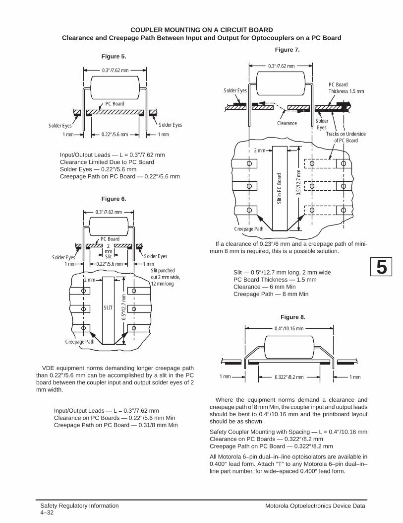
Safety Regulatory Information4–32
Motorola Optoelectronics Device Data
COUPLER MOUNTING ON A CIRCUIT BOARDClearance and Creepage Path Between Input and Output for Optocouplers on a PC Board
1 mm
Solder Eyes Solder Eyes
1 mm0.22″/5.6 mm
PC Board
0.3″/7.62 mm
Figure 5.
Input/Output Leads — L = 0.3″/7.62 mmClearance Limited Due to PC BoardSolder Eyes — 0.22″/5.6 mmCreepage Path on PC Board — 0.22″/5.6 mm
Slit punchedout 2 mm wide,12 mm long
Figure 6.
2 mm
2mmSlit
SLIT
Creepage Path
Solder Eyes1 mm 0.22″/5.6 mm
Solder Eyes
1 mm
PC Board
0.3″/7.62 mm
0.5”
/12.
7 m
m
VDE equipment norms demanding longer creepage paththan 0.22″/5.6 mm can be accomplished by a slit in the PCboard between the coupler input and output solder eyes of 2mm width.
Input/Output Leads — L = 0.3″/7.62 mmClearance on PC Boards — 0.22″/5.6 mm MinCreepage Path on PC Board — 0.31/8 mm Min
PC Board Thickness 1.5 mm
SolderEyes
Tracks on Undersideof PC Board
Clearance
0.3″/7.62 mm
Solder Eyes
2 mm
Creepage Path
Figure 7.
Slit
in P
C B
oard
0.5”
/12.
7 m
m
If a clearance of 0.23″/6 mm and a creepage path of mini-mum 8 mm is required, this is a possible solution.
Slit — 0.5″/12.7 mm long, 2 mm widePC Board Thickness — 1.5 mmClearance — 6 mm MinCreepage Path — 8 mm Min
Figure 8.
0.322″/8.2 mm
0.4″/10.16 mm
1 mm 1 mm
Where the equipment norms demand a clearance andcreepage path of 8 mm Min, the coupler input and output leadsshould be bent to 0.4″/10.16 mm and the printboard layoutshould be as shown.
Safety Coupler Mounting with Spacing — L = 0.4″/10.16 mmClearance on PC Boards — 0.322″/8.2 mmCreepage Path on PC Board — 0.322″/8.2 mm
All Motorola 6–pin dual–in–line optoisolators are available in0.400″ lead form. Attach “T” to any Motorola 6–pin dual–in–line part number, for wide–spaced 0.400″ lead form.
5

4–33Safety Regulatory InformationMotorola Optoelectronics Device Data
W
G = 8 mmM = 8 mmN = 8 mm
Application forVDE 0113VDE 0160P1VDE 0160P2VDE 0804VDE 0804dVDE 0831VDE 0832VDE 0833VDE 0860VDE 0110dVDE 0805VDE 0806
SELV–Control–Circuit
Figure 9. Optocoupler Mounting on PC BoardAccording to Safety Class I with Only One PC
Board Plug Connection
R2
PowerInterface
SELV–Control– Circuit
SELV–Control–Circuit
QR1
Applicable for
VDE 0804 without Slit VDE 0110b with/without Slit
SELV–Wire
SELV–Control Circuit–Area
A
PC–Board–Frame
Safety–Wireon backside
B
G = 8 mmK = 8 mmA = 8 mmB = 8 mmD = 8 mmH = 2 mmI = 5.6 mm
BR2
R1
L
B
H
E
KF
GW
W
D
D
E, L, W depends on theApplication
N N N
NNNM
M
M
M M
M
G
M
SELV–Control–Circuit–Area
PC C
onne
ctor
M
B
VDE
Appr
oved
Con
nect
or
PC C
onne
ctor
Figure 10. Optocoupler Mounting on PC BoardAccording to Safety Class I with One Plug–
Connection for the SELV–Control Circuit andOne Screw–Connection for the Power–Interface
Pow
erIn
terfa
ce
SELV
-Inte
rface
G
5

Safety Regulatory Information4–34
Motorola Optoelectronics Device Data
DEFINITION OF TERMSThe following paragraphs define terms used by the regula-
tories and international standard initiators. A separate discus-sion is given for:
1. Creepage and Clearance 4. Circuits2. Voltage 5. Equipment3. Insulations
1. CREEPAGE AND CLEARANCE
ISOLATION CREEPAGE PATHDenotes the shortest path between two conductive parts
measured along the surface of the insulation, i.e., on the opto-couplers, it is the shortest distance on the surface of the pack-age between the input and output leads. On the circuit boardin which the coupler is mounted, it is the shortest distanceacross the surface on the board between the solder eyes ofthe coupler input/output leads. Coupler and circuit boardcreepage path have to meet the minimum specified distancesfor the individual VDE equipment norms.
(C)
(B)(A)
Figure 11.
10 mm
9 mm
8.9 mm
*Approximate measurements. For minimummeasurements required, see Table 1.
CLEARANCEDenotes the shortest distance between two conductive
parts or between a conductive part and the bonding surface ofthe equipment, measured through air.
Figure 12.
2. VOLTAGES
HAZARDOUS VOLTAGE: A voltage exceeding 42.4 Vpeak or dc, existing in a circuit which does not meet the re-quirements for a limited current circuit.
WORKING VOLTAGE shall be the voltage which existsacross the insulation under normal working conditions. Wherethe rms value is used, a sinusoidal ac waveform shall be as-sumed. Where the dc value is used, the peak value of any su-perimposed ripple shall be considered.
EXTRA–LOW VOLTAGE (ELV): A voltage between con-ductors or between a conductor and earth not exceeding 42.4V peak or dc, existing in a secondary circuit which is separatedfrom hazardous voltages by at least basic insulation, but whichdoes not meet the requirements for a SELV circuit nor thosefor a limited current circuit.
ISOLATION WITHSTAND VOLTAGE: An ac or dc test volt-age insulation has to withstand without breakdown or dam-age. It should not be confused with working or operatingvoltage.
ISOLATION SURGE VOLTAGE: A positive or negativetransient voltage of defined energy and rise and fall timeswhich the insulation has to withstand without breakdown ordamage.
3. INSULATIONS
INSULATION, OPERATIONAL (functional): Insulationwhich is necessary for the correct operation of the equipment.— Between parts of different potential.— Between ELV or SELV circuits and earthed conductive
parts.
INSULATION, BASIC: Insulation to provide basic protec-tion against electric shock.— Between a part at hazardous voltage and an earthed con-
ductive part.— Between a part at hazardous voltage and a SELV circuit
which relies on being earthed for its integrity.— Between a primary power conductor and the earthed
screen or core for a primary power transformer.— As an element of double insulation.
INSULATION, SUPPLEMENTARY: Independent insulationapplied in addition to basic insulation in order to ensure protec-tion against electric shock in the event of a failure of the basicinsulation.— Between an accessible conductive part and a part which
could assume a hazardous voltage in the event of a failureof basic insulation.
— Between the outer surface of handles, knobs, grips andthe like, and their shafts unless earthed.
— Between a floating non–SELV secondary circuit and anunearthed conductive part of the body.
INSULATION, DOUBLE: Insulation comprising both basicinsulation and supplementary insulation.
INSULATION, REINFORCED: A single insulation systemwhich provides a degree of protection against electric shockequivalent to double insulation under the conditions specifiedin the standard.
SAFE ELECTRICAL ISOLATION: Denotes an insulationsystem isolating a hazardous voltage circuit from a SELV cir-cuit such that an insulation breakdown either is unlikely ordoes not cause a hazardous condition on the SELV circuit.— Between an unearthed accessible conductive part or a
floating SELV circuit, and a primary circuit.
5

4–35Safety Regulatory InformationMotorola Optoelectronics Device Data
4. CIRCUITS
PRIMARY CIRCUIT: An internal circuit which is directly con-nected to the external supply mains or other equivalent source(such as motor–alternator set) which supplies the electricpower. It includes the primary windings of transformers, mo-tors, other loading devices and the means of connection to thesupply mains.
SECONDARY CIRCUIT: A circuit which has no direct con-nection to primary power and derives its power from a trans-former, converter or equivalent isolation device situated withinthe equipment.
SAFETY EXTRA–LOW VOLTAGE (SELV) CIRCUIT: A cir-cuit which is so designed and protected that under normal andsingle fault conditions the voltage between any two accessibleparts, one of which may be the body or earth, does not exceeda safe value.
5. EQUIPMENTS
CLASS I EQUIPMENT: denotes equipment in which protec-tion against electric shock does not rely on basic insulation
only, but which includes an additional safety precaution in thatoperator–accessible conductive parts are connected to theprotective earthing conductor in the fixed wiring of the installa-tion in such a way that the operator–accessible conductiveparts cannot become hazardous in the event of a failure of thebasic insulation.
Class I equipment may have parts with double insulation orreinforced insulation, or parts operating at safety extra–lowvoltage.
CLASS II EQUIPMENT denotes equipment in which protec-tion against electric shock does not rely on basic insulationonly, but in which additional safety precautions, such asdouble insulation or reinforced insulation, are provided, therebeing no provision for protective earthing or reliance uponinstallation conditions.
CLASS III EQUIPMENT: Equipment in which protectionagainst electric shock relies upon supply from SELV circuitsand in which hazardous voltages are not generated.
Table 2. Minimum Rating Requirements for a Working Voltage up to 250 Vrms
InsulationCreepage
[mm]Clearance
[mm]
IsolationBarrier[mm]
Diel. Strength[kV ac rms]
IsolationResistance
Ω
OperationalBasicSupplementaryReinforced
2.5348
3448
——
– to 2– to 2*
0.51.52.5
2.5 to 3.75*
—2 106
5 106
7 106
* See Table 1 for details.
Table 3. Electrical Interfaces and Required Insulation
Bare Metal Parts notTouchable
Bare Metal PartsTouchable
PrimaryCircuit
(Line Voltage)
ELVSecondary Circuit
42.4 V
SELVSecondary Circuit
42.4 VEarth Ground
Case
1.
2.
3.
4.
5.
6.
7.
F
NHot
B
R
B
B
S
S
Class III Equipment
F
F
Class II Equipment
Class I Equipment
B = Basic Insulation F = Functional (Operation Insulation)
R = Reinforced or Safe Insulation S = Supplementary Insulation
5

Safety Regulatory Information4–36
Motorola Optoelectronics Device Data
5

5–1Motorola Optoelectronics Device Data
Section 5
Optoisolators/Optocouplers
CASE 730A–04 CASE 730C–04
CASE 730D–05
Lead Form Test Options 5–3. . . . . . . . . . . . . . . . . . .
Package Dimensions 4. . . . . . . . . . . . . . . . . . . . . . .
AC Input CouplerH11AA1 Series 30. . . . . . . . . . . . . . . . . . . . . . . . . . . . . .
Phototransistor Couplers4N25 Series 5–6. . . . . . . . . . . . . . . . . . . . . . . . . . . . . . . 4N29 Series 10. . . . . . . . . . . . . . . . . . . . . . . . . . . . . . . . 4N35 Series 14. . . . . . . . . . . . . . . . . . . . . . . . . . . . . . . . 4N38 Series 18. . . . . . . . . . . . . . . . . . . . . . . . . . . . . . . . CNY17-1 Series 22. . . . . . . . . . . . . . . . . . . . . . . . . . . . . H11A1 Series 26. . . . . . . . . . . . . . . . . . . . . . . . . . . . . . . H11AV1 Series 33. . . . . . . . . . . . . . . . . . . . . . . . . . . . . . H11D1 Series 41. . . . . . . . . . . . . . . . . . . . . . . . . . . . . . . MCT2 51. . . . . . . . . . . . . . . . . . . . . . . . . . . . . . . . . . . . . . MOC8100 111. . . . . . . . . . . . . . . . . . . . . . . . . . . . . . . . . . . MOC8101 Series 115. . . . . . . . . . . . . . . . . . . . . . . . . . . . . MOC8111 Series 118. . . . . . . . . . . . . . . . . . . . . . . . . . . . . MOC8204 Series 5–122. . . . . . . . . . . . . . . . . . . . . . . . . . .
Darlington CouplersH11B1 Series 37. . . . . . . . . . . . . . . . . . . . . . . . . . . . . . . H11G1 Series 44. . . . . . . . . . . . . . . . . . . . . . . . . . . . . . . MOC119 55. . . . . . . . . . . . . . . . . . . . . . . . . . . . . . . . . . . MOC8020 99. . . . . . . . . . . . . . . . . . . . . . . . . . . . . . . . . . MOC8030 103. . . . . . . . . . . . . . . . . . . . . . . . . . . . . . . . . . MOC8080 107. . . . . . . . . . . . . . . . . . . . . . . . . . . . . . . . . .
Schmidt TriggerH11L1 Series 48. . . . . . . . . . . . . . . . . . . . . . . . . . . . . . . MOC5007 Series 96. . . . . . . . . . . . . . . . . . . . . . . . . . . .
Triac DriversMOC3010 Series 59. . . . . . . . . . . . . . . . . . . . . . . . . . . . MOC3020 Series 63. . . . . . . . . . . . . . . . . . . . . . . . . . . . MOC3051 Series 67. . . . . . . . . . . . . . . . . . . . . . . . . . . . MOC3031 Series 73. . . . . . . . . . . . . . . . . . . . . . . . . . . . MOC3041 Series 77. . . . . . . . . . . . . . . . . . . . . . . . . . . . MOC3061 Series 81. . . . . . . . . . . . . . . . . . . . . . . . . . . . MOC3162 Series 85. . . . . . . . . . . . . . . . . . . . . . . . . . . . MOC3081 Series 92. . . . . . . . . . . . . . . . . . . . . . . . . . . .
5–2 Motorola Optoelectronics Device Data
GlobalOptoisolator
Motorola’s optoisolators satisfy the broad range ofregulatory requirements imposed throughout the world.
“Global” optoisolators are your “passport” to the world marketplace.
Motorola 6-PIN DIP Optoisolators Feature:
“Global” Safety Regulatory Approvals: VDE(1), UL, CSA, SETI, SEMKO, DEMKO, NEMKO,AUSTEL and BABT
The Industry’s Highest Input-Output Voltage Isolation, Guaranteed and 100% tested — 7500 VacPeak.
VDE approved per standard 0884/8.87(1) (Certificate number 62054), with additional approval toDIN IEC950/VDE0806 & VDFE0805, IEC65/VDE0860, VDE110b, covering all other standards withequal or less stringent requirements, including IEC204/VDE0113, VDE0160, VDE0832, VDE0833.
Special leadform available to satisfy VDE0884/8.87 requirement for 8 mm minimum creepagedistance between input and output solder pads (add suffix “T” to part number). VDE 0884 testing isan option.
Surface mount leadforming is available for all 6-PIN DIP devices. To obtain the Surface Mountleadform option (0.020–0.025 inches stand off height), simply add the suffix “S” to the end of thepart number (i.e., MOC8104S). Note: Consult factory to determine device availability prior toordering .
Tape and Reel (1,000 pieces per reel) is available for “S” (Surface Mount leadform option) byadding the suffix “R2” (i.e., MOC8104SR2).
Available in a wide variety of output types — Transistor, Darlington, Schmitt Trigger, and ZeroCross/Random Phase Triac Drivers.
(1) VDE 0884 testing is an option; the suffix letter “V” must be added to the part number.

5–3Motorola Optoelectronics Device Data
Leadform and Test Options for DIP–6 Optoisolators
Leadform Option(s):
Motorola OPTO offers a variety of leadform options for their DIP–6 Optoisolators. Add the following suffix(s) tothe standard device type to specify leadform option. Please consult factory prior to ordering for availability!
Standard Leadform
CASE 730A–04
“S” suffix = gull–winged, surface mountableS
(S) CASE 730C–04Surface–mountable
gull–wing option
“T” suffix = wide spaced leadform (0.400″)T
(T) CASE 730D–03Wide–spaced (0.400 ″)
leadform option
“SR2” suffix = gull–winged, surface mountable, in 13″ tape and reel.
VDE 0884/8.87 Test Option:
To specify VDE 0884/8.87 testing, add the suffix letter “V” to the standard part number. Example:
Standard through hole MOC3163V
0.400” wide spaced leadform MOC3163TV (satisfies 8mm spacing)
Surface mount MOC3163SV
Surface mount (tape and reeled) MOC3163SR2V

5–4 Motorola Optoelectronics Device Data
PACKAGE DIMENSIONS
CASE 730A–04ISSUE G
NOTES:1. DIMENSIONING AND TOLERANCING PER ANSI
Y14.5M, 1982.2. CONTROLLING DIMENSION: INCH.3. DIMENSION L TO CENTER OF LEAD WHEN
FORMED PARALLEL.6 4
1 3
–A–
–B–
SEATINGPLANE
–T–
4 PLF
K
CN
G
6 PLD6 PLE
MAM0.13 (0.005) B MT
L
M
6 PLJMBM0.13 (0.005) A MT
DIM MIN MAX MIN MAXMILLIMETERSINCHES
A 0.320 0.350 8.13 8.89B 0.240 0.260 6.10 6.60C 0.115 0.200 2.93 5.08D 0.016 0.020 0.41 0.50E 0.040 0.070 1.02 1.77F 0.010 0.014 0.25 0.36G 0.100 BSC 2.54 BSCJ 0.008 0.012 0.21 0.30K 0.100 0.150 2.54 3.81L 0.300 BSC 7.62 BSCM 0 15 0 15 N 0.015 0.100 0.38 2.54
STYLE 3:PIN 1. ANODE
2. CATHODE3. NC4. EMITTER5. COLLECTOR6. NC
STYLE 5:PIN 1. ANODE
2. CATHODE3. NC4. OUTPUT5. GROUND6. VCC
STYLE 6:PIN 1. ANODE
2. CATHODE3. NC4. MAIN TERMINAL5. SUBSTRATE6. MAIN TERMINAL
STYLE 8:PIN 1. LED 1 ANODE/LED 2 CATHODE
2. LED 1 CATHODE/LED 2 ANODE3. NC4. EMITTER5. COLLECTOR6. BASE
STYLE 1:PIN 1. ANODE
2. CATHODE3. NC4. EMITTER5. COLLECTOR6. BASE
CASE 730C–04ISSUE D
–A–
–B–
SEATINGPLANE
–T–J
K
L
6 PL
MBM0.13 (0.005) A MT
C
D 6 PL
MAM0.13 (0.005) B MT
H
GE 6 PL
F 4 PL
31
46NOTES:
1. DIMENSIONING AND TOLERANCING PER ANSIY14.5M, 1982.
2. CONTROLLING DIMENSION: INCH.
DIM MIN MAX MIN MAXMILLIMETERSINCHES
A 0.320 0.350 8.13 8.89B 0.240 0.260 6.10 6.60C 0.115 0.200 2.93 5.08D 0.016 0.020 0.41 0.50E 0.040 0.070 1.02 1.77F 0.010 0.014 0.25 0.36G 0.100 BSC 2.54 BSCH 0.020 0.025 0.51 0.63J 0.008 0.012 0.20 0.30K 0.006 0.035 0.16 0.88L 0.320 BSC 8.13 BSCS 0.332 0.390 8.43 9.90

5–5Motorola Optoelectronics Device Data
NOTES:1. DIMENSIONING AND TOLERANCING PER ANSI
Y14.5M, 1982.2. CONTROLLING DIMENSION: INCH.3. DIMENSION L TO CENTER OF LEAD WHEN
FORMED PARALLEL.
CASE 730D–05ISSUE D
6 4
1 3
–A–
–B–
N
C
KG
F 4 PL
SEATING
D 6 PL
E 6 PL
PLANE
–T–
MAM0.13 (0.005) B MT
L
J
DIM MIN MAX MIN MAXMILLIMETERSINCHES
A 0.320 0.350 8.13 8.89B 0.240 0.260 6.10 6.60C 0.115 0.200 2.93 5.08D 0.016 0.020 0.41 0.50E 0.040 0.070 1.02 1.77F 0.010 0.014 0.25 0.36G 0.100 BSC 2.54 BSCJ 0.008 0.012 0.21 0.30K 0.100 0.150 2.54 3.81L 0.400 0.425 10.16 10.80N 0.015 0.040 0.38 1.02

5–6 Motorola Optoelectronics Device Data
The 4N25/A, 4N26, 4N27 and 4N28 devices consist of a gallium arsenideinfrared emitting diode optically coupled to a monolithic silicon phototransistordetector.
• Most Economical Optoisolator Choice for Medium Speed, Switching Applications
• Meets or Exceeds All JEDEC Registered Specifications
• To order devices that are tested and marked per VDE 0884 requirements, thesuffix ”V” must be included at end of part number. VDE 0884 is a test option.
Applications
• General Purpose Switching Circuits
• Interfacing and coupling systems of different potentials and impedances
• I/O Interfacing
• Solid State Relays
MAXIMUM RATINGS (TA = 25°C unless otherwise noted)
Rating Symbol Value Unit
INPUT LED
Reverse Voltage VR 3 Volts
Forward Current — Continuous IF 60 mA
LED Power Dissipation @ TA = 25°Cwith Negligible Power in Output Detector
Derate above 25°C
PD 120
1.41
mW
mW/°C
OUTPUT TRANSISTOR
Collector–Emitter Voltage VCEO 30 Volts
Emitter–Collector Voltage VECO 7 Volts
Collector–Base Voltage VCBO 70 Volts
Collector Current — Continuous IC 150 mA
Detector Power Dissipation @ TA = 25°Cwith Negligible Power in Input LED
Derate above 25°C
PD 150
1.76
mW
mW/°C
TOTAL DEVICE
Isolation Surge Voltage(1)
(Peak ac Voltage, 60 Hz, 1 sec Duration)VISO 7500 Vac(pk)
Total Device Power Dissipation @ TA = 25°CDerate above 25°C
PD 2502.94
mWmW/°C
Ambient Operating Temperature Range(2) TA –55 to +100 °C
Storage Temperature Range(2) Tstg –55 to +150 °C
Soldering Temperature (10 sec, 1/16″ from case) TL 260 °C
1. Isolation surge voltage is an internal device dielectric breakdown rating.1. For this test, Pins 1 and 2 are common, and Pins 4, 5 and 6 are common.2. Refer to Quality and Reliability Section in Opto Data Book for information on test conditions.
Preferred devices are Motorola recommended choices for future use and best overall value.GlobalOptoisolator is a trademark of Motorola, Inc.
Order this documentby 4N25/D
SEMICONDUCTOR TECHNICAL DATA
GlobalOptoisolator
*Motorola Preferred Devices
SCHEMATIC
PIN 1. LED ANODE2. LED CATHODE3. N.C.4. EMITTER5. COLLECTOR6. BASE
1
2
3
6
5
4
[CTR = 20% Min]
[CTR = 10% Min]
STANDARD THRU HOLECASE 730A–04
STYLE 1 PLASTIC
61
Motorola, Inc. 1995
REV 5
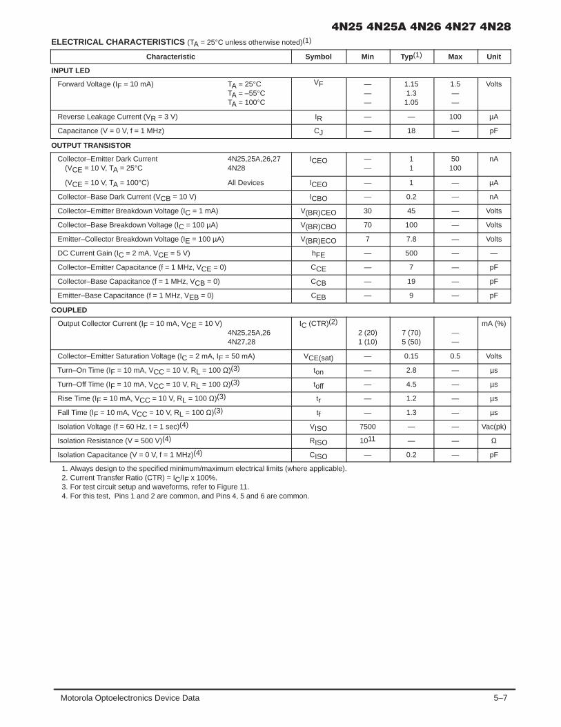
5–7Motorola Optoelectronics Device Data
ELECTRICAL CHARACTERISTICS (TA = 25°C unless otherwise noted)(1)
Characteristic Symbol Min Typ (1) Max Unit
INPUT LED
Forward Voltage (IF = 10 mA) TA = 25°CTA = –55°CTA = 100°C
VF ———
1.151.31.05
1.5——
Volts
Reverse Leakage Current (VR = 3 V) IR — — 100 µA
Capacitance (V = 0 V, f = 1 MHz) CJ — 18 — pF
OUTPUT TRANSISTOR
Collector–Emitter Dark Current 4N25,25A,26,27(VCE = 10 V, TA = 25°C 4N28
ICEO ——
11
50100
nA
(VCE = 10 V, TA = 100°C) All Devices ICEO — 1 — µA
Collector–Base Dark Current (VCB = 10 V) ICBO — 0.2 — nA
Collector–Emitter Breakdown Voltage (IC = 1 mA) V(BR)CEO 30 45 — Volts
Collector–Base Breakdown Voltage (IC = 100 µA) V(BR)CBO 70 100 — Volts
Emitter–Collector Breakdown Voltage (IE = 100 µA) V(BR)ECO 7 7.8 — Volts
DC Current Gain (IC = 2 mA, VCE = 5 V) hFE — 500 — —
Collector–Emitter Capacitance (f = 1 MHz, VCE = 0) CCE — 7 — pF
Collector–Base Capacitance (f = 1 MHz, VCB = 0) CCB — 19 — pF
Emitter–Base Capacitance (f = 1 MHz, VEB = 0) CEB — 9 — pF
COUPLED
Output Collector Current (IF = 10 mA, VCE = 10 V)4N25,25A,264N27,28
IC (CTR)(2)
2 (20)1 (10)
7 (70)5 (50)
——
mA (%)
Collector–Emitter Saturation Voltage (IC = 2 mA, IF = 50 mA) VCE(sat) — 0.15 0.5 Volts
Turn–On Time (IF = 10 mA, VCC = 10 V, RL = 100 Ω)(3) ton — 2.8 — µs
Turn–Off Time (IF = 10 mA, VCC = 10 V, RL = 100 Ω)(3) toff — 4.5 — µs
Rise Time (IF = 10 mA, VCC = 10 V, RL = 100 Ω)(3) tr — 1.2 — µs
Fall Time (IF = 10 mA, VCC = 10 V, RL = 100 Ω)(3) tf — 1.3 — µs
Isolation Voltage (f = 60 Hz, t = 1 sec)(4) VISO 7500 — — Vac(pk)
Isolation Resistance (V = 500 V)(4) RISO 1011 — — Ω
Isolation Capacitance (V = 0 V, f = 1 MHz)(4) CISO — 0.2 — pF
1. Always design to the specified minimum/maximum electrical limits (where applicable).2. Current Transfer Ratio (CTR) = IC/IF x 100%.3. For test circuit setup and waveforms, refer to Figure 11.4. For this test, Pins 1 and 2 are common, and Pins 4, 5 and 6 are common.

5–8 Motorola Optoelectronics Device Data
I C, O
UTP
UT
CO
LLEC
TOR
CU
RR
ENT
(NO
RM
ALIZ
ED)
TYPICAL CHARACTERISTICS
Figure 1. LED Forward Voltage versus Forward Current
2
1.8
1.6
1.4
1.2
11 10 100 1000
10
1
0.1
0.01 0.5 1IF, LED FORWARD CURRENT (mA)
2 5 10 20 50IF, LED INPUT CURRENT (mA)
V F, F
OR
WAR
D V
OLT
AGE
(VO
LTS)
25°C
100°C
TA = –55°C
NORMALIZED TO:IF = 10 mA
Figure 2. Output Current versus Input Current
PULSE ONLYPULSE OR DC
10
75
2
10.70.5
0.2
0.1–60 –40 –20 0 20 40 60 80 100
TA, AMBIENT TEMPERATURE (°C)I C, O
UTP
UT
CO
LLEC
TOR
CU
RR
ENT
(NO
RM
ALIZ
ED)
1
10
100
0.10 20 40 60 80 100
TA, AMBIENT TEMPERATURE (°C)
t, TI
ME
(s)
I
100
50
20
10
5
2
10.1 0.2 0.5 1 2 5 10 20 50 100
IF, LED INPUT CURRENT (mA)
CEO
, CO
LLEC
TOR
–EM
ITTE
R D
ARK
CU
RR
ENT
(NO
RM
ALIZ
ED)
µ
VCE = 30 V
10 V
tf
tr
tr
tf
0
VCE, COLLECTOR–EMITTER VOLTAGE (VOLTS)
I C, C
OLL
ECTO
R C
UR
REN
T (m
A)
4
8
12
16
20
24
28
5 mA
2 mA
1 mA
0 1 2 3 4 5 6 7 8 9 10
Figure 3. Collector Current versusCollector–Emitter Voltage
Figure 4. Output Current versus Ambient Temperature
Figure 5. Dark Current versus Ambient Temperature Figure 6. Rise and Fall Times(Typical Values)
IF = 10 mA NORMALIZED TO TA = 25°C
NORMALIZED TO:VCE = 10 VTA = 25°C
VCC = 10 V
RL = 1000
RL = 100

5–9Motorola Optoelectronics Device Data
1007050
20
1075
2
10.1 0.2 0.5 0.7 1 2 5 7 10 20 50 70 100
IF, LED INPUT CURRENT (mA)
RL = 1000
100
10
1007050
20
1075
2
10.1 0.2 0.5 0.7 1 2 5 7 10 20 50 70 100
IF, LED INPUT CURRENT (mA)
RL = 1000
100
10
t, T
UR
N–O
FF T
IME
(s)
off
µ
t, T
UR
N–O
N T
IME
(s)
onµ
Figure 7. Turn–On Switching Times(Typical Values)
Figure 8. Turn–Off Switching Times(Typical Values)
VCC = 10 V VCC = 10 V
6
6 µA
C, C
APAC
ITAN
CE
(pF)
Figure 9. DC Current Gain (Detector Only) Figure 10. Capacitances versus Voltage
20
18
16
14
12
10
8
4
2
0
CCE
f = 1 MHz
0.05 0.1 0.2 0.5 1 2 5 10 20 50
V, VOLTAGE (VOLTS)
CLED
CCB
CEB
5 µA
4 µA
3 µA
2 µA
1 µA
4
3
2
1
0 2 4 6 8 10 12 14 16 18 20
VCE, COLLECTOR–EMITTER VOLTAGE (VOLTS)
I C, T
YPIC
AL C
OLL
ECTO
R C
UR
REN
T (m
A)
IB = 7 µAIF = 0
TEST CIRCUIT
VCC = 10 V
IF = 10 mA
INPUT
RL = 100 Ω
OUTPUT
WAVEFORMS
10%
90%
ton
INPUT PULSE
OUTPUT PULSE
tf
toff
tr
Figure 11. Switching Time Test Circuit and Waveforms

5–10 Motorola Optoelectronics Device Data
PACKAGE DIMENSIONS
CASE 730A–04ISSUE G
NOTES:1. DIMENSIONING AND TOLERANCING PER ANSI
Y14.5M, 1982.2. CONTROLLING DIMENSION: INCH.3. DIMENSION L TO CENTER OF LEAD WHEN
FORMED PARALLEL.
STYLE 1:PIN 1. ANODE
2. CATHODE3. NC4. EMITTER5. COLLECTOR6. BASE
6 4
1 3
–A–
–B–
SEATINGPLANE
–T–
4 PLF
K
CN
G
6 PLD6 PLE
MAM0.13 (0.005) B MT
L
M
6 PLJMBM0.13 (0.005) A MT
DIM MIN MAX MIN MAXMILLIMETERSINCHES
A 0.320 0.350 8.13 8.89B 0.240 0.260 6.10 6.60C 0.115 0.200 2.93 5.08D 0.016 0.020 0.41 0.50E 0.040 0.070 1.02 1.77F 0.010 0.014 0.25 0.36G 0.100 BSC 2.54 BSCJ 0.008 0.012 0.21 0.30K 0.100 0.150 2.54 3.81L 0.300 BSC 7.62 BSCM 0 15 0 15 N 0.015 0.100 0.38 2.54
CASE 730C–04ISSUE D
–A–
–B–
SEATINGPLANE
–T–J
K
L
6 PL
MBM0.13 (0.005) A MT
C
D 6 PL
MAM0.13 (0.005) B MT
H
GE 6 PL
F 4 PL
31
46
NOTES:1. DIMENSIONING AND TOLERANCING PER ANSI
Y14.5M, 1982.2. CONTROLLING DIMENSION: INCH.
DIM MIN MAX MIN MAXMILLIMETERSINCHES
A 0.320 0.350 8.13 8.89B 0.240 0.260 6.10 6.60C 0.115 0.200 2.93 5.08D 0.016 0.020 0.41 0.50E 0.040 0.070 1.02 1.77F 0.010 0.014 0.25 0.36G 0.100 BSC 2.54 BSCH 0.020 0.025 0.51 0.63J 0.008 0.012 0.20 0.30K 0.006 0.035 0.16 0.88L 0.320 BSC 8.13 BSCS 0.332 0.390 8.43 9.90
*Consult factory for leadform option availability
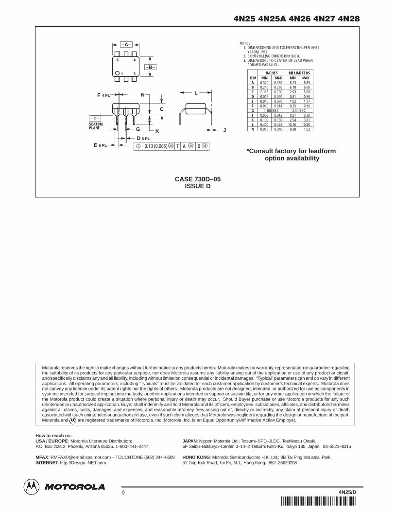
5–11Motorola Optoelectronics Device Data
*Consult factory for leadform option availability
NOTES:1. DIMENSIONING AND TOLERANCING PER ANSI
Y14.5M, 1982.2. CONTROLLING DIMENSION: INCH.3. DIMENSION L TO CENTER OF LEAD WHEN
FORMED PARALLEL.
CASE 730D–05ISSUE D
6 4
1 3
–A–
–B–
N
C
KG
F 4 PL
SEATING
D 6 PL
E 6 PL
PLANE
–T–
MAM0.13 (0.005) B MT
L
J
DIM MIN MAX MIN MAXMILLIMETERSINCHES
A 0.320 0.350 8.13 8.89B 0.240 0.260 6.10 6.60C 0.115 0.200 2.93 5.08D 0.016 0.020 0.41 0.50E 0.040 0.070 1.02 1.77F 0.010 0.014 0.25 0.36G 0.100 BSC 2.54 BSCJ 0.008 0.012 0.21 0.30K 0.100 0.150 2.54 3.81L 0.400 0.425 10.16 10.80N 0.015 0.040 0.38 1.02
Motorola reserves the right to make changes without further notice to any products herein. Motorola makes no warranty, representation or guarantee regardingthe suitability of its products for any particular purpose, nor does Motorola assume any liability arising out of the application or use of any product or circuit,and specifically disclaims any and all liability, including without limitation consequential or incidental damages. “Typical” parameters can and do vary in differentapplications. All operating parameters, including “Typicals” must be validated for each customer application by customer’s technical experts. Motorola doesnot convey any license under its patent rights nor the rights of others. Motorola products are not designed, intended, or authorized for use as components insystems intended for surgical implant into the body, or other applications intended to support or sustain life, or for any other application in which the failure ofthe Motorola product could create a situation where personal injury or death may occur. Should Buyer purchase or use Motorola products for any suchunintended or unauthorized application, Buyer shall indemnify and hold Motorola and its officers, employees, subsidiaries, affiliates, and distributors harmlessagainst all claims, costs, damages, and expenses, and reasonable attorney fees arising out of, directly or indirectly, any claim of personal injury or deathassociated with such unintended or unauthorized use, even if such claim alleges that Motorola was negligent regarding the design or manufacture of the part.Motorola and are registered trademarks of Motorola, Inc. Motorola, Inc. is an Equal Opportunity/Affirmative Action Employer.
How to reach us:USA / EUROPE: Motorola Literature Distribution; JAPAN : Nippon Motorola Ltd.; Tatsumi–SPD–JLDC, Toshikatsu Otsuki,P.O. Box 20912; Phoenix, Arizona 85036. 1–800–441–2447 6F Seibu–Butsuryu–Center, 3–14–2 Tatsumi Koto–Ku, Tokyo 135, Japan. 03–3521–8315
MFAX: [email protected] – TOUCHTONE (602) 244–6609 HONG KONG: Motorola Semiconductors H.K. Ltd.; 8B Tai Ping Industrial Park, INTERNET: http://Design–NET.com 51 Ting Kok Road, Tai Po, N.T., Hong Kong. 852–26629298
4N25/D
◊

5–12 Motorola Optoelectronics Device Data
The 4N29/A, 4N30, 4N31, 4N32(1) and 4N33(1) devices consist of a galliumarsenide infrared emitting diode optically coupled to a monolithic siliconphotodarlington detector.
This series is designed for use in applications requiring high collector outputcurrents at lower input currents.
• Higher Sensitivity to Low Input Drive Current
• Meets or Exceeds All JEDEC Registered Specifications
• To order devices that are tested and marked per VDE 0884 requirements, thesuffix ”V” must be included at end of part number. VDE 0884 is a test option.
Applications• Low Power Logic Circuits
• Interfacing and coupling systems of different potentials and impedances
• Telecommunications Equipment
• Portable Electronics
• Solid State Relays
MAXIMUM RATINGS (TA = 25°C unless otherwise noted)
Rating Symbol Value Unit
INPUT LED
Reverse Voltage VR 3 Volts
Forward Current — Continuous IF 60 mA
LED Power Dissipation @ TA = 25°CDerate above 25°C
PD 1201.41
mWmW/°C
OUTPUT DETECTOR
Collector–Emitter Voltage VCEO 30 Volts
Emitter–Collector Voltage VECO 5 Volts
Collector–Base Voltage VCBO 30 Volts
Collector Current — Continuous IC 150 mA
Detector Power Dissipation @ TA = 25°CDerate above 25°C
PD 1501.76
mWmW/°C
TOTAL DEVICE
Isolation Surge Voltage(2)
(Peak ac Voltage, 60 Hz, 1 sec Duration)VISO 7500 Vac(pk)
Total Device Power Dissipation @ TA = 25°CDerate above 25°C
PD 2502.94
mWmW/°C
Ambient Operating Temperature Range(3) TA –55 to +100 °C
Storage Temperature Range(3) Tstg –55 to +150 °C
Soldering Temperature (10 sec, 1/16″ from case) TL 260 °C
1. Difference in 4N32 and 4N33 is JEDEC Registration for VISO only. All Motorola 6–Pin devicesexceed JEDEC specification and are 7500 Vac(pk). The same applies for 4N29 and 4N30.
2. Isolation surge voltage is an internal device dielectric breakdown rating. For this test, Pins 1 and2 are common, and Pins 4, 5 and 6 are common.
3. Refer to Quality and Reliability Section in Opto Data Book for information on test conditions.Preferred devices are Motorola recommended choices for future use and best overall value.GlobalOptoisolator is a trademark of Motorola, Inc.
Order this documentby 4N29/D
SEMICONDUCTOR TECHNICAL DATA
GlobalOptoisolator
*Motorola Preferred Devices
SCHEMATIC
[CTR = 100% Min]
[CTR = 500% Min]
STANDARD THRU HOLECASE 730A–04
STYLE 1 PLASTIC
[CTR = 50% Min]
PIN 1. LED ANODE2. LED CATHODE3. N.C.4. EMITTER5. COLLECTOR6. BASE
1
2
3
6
5
4
61
Motorola, Inc. 1995
REV 4

5–13Motorola Optoelectronics Device Data
ELECTRICAL CHARACTERISTICS (TA = 25°C unless otherwise noted)(1)
Characteristic Symbol Min Typ (1) Max Unit
INPUT LED
*Reverse Leakage Current (VR = 3 V, RL = 1 M ohms) IR — 0.05 100 µA
*Forward Voltage (IF = 10 mA) VF — 1.34 1.5 Volts
Capacitance (VR = 0 V, f = 1 MHz) C — 1.8 — pF
OUTPUT DETECTOR (TA = 25°C and IF = 0, unless otherwise noted)
*Collector–Emitter Dark Current(VCE = 10 V, Base Open)
ICEO — — 100 nA
*Collector–Base Breakdown Voltage(IC = 100 µA, IE = 0)
V(BR)CBO 30 — — Volts
*Collector–Emitter Breakdown Voltage(IC = 100 µA, IB = 0)
V(BR)CEO 30 — — Volts
*Emitter–Collector Breakdown Voltage(IE = 100 µA, IB = 0)
V(BR)ECO 5 — — Volts
DC Current Gain(VCE = 5 V, IC = 500 µA)
hFE — 16K — —
COUPLED (TA = 25°C unless otherwise noted)
*Collector Output Current (3) 4N32, 4N33(VCE = 10 V, IF = 10 mA) 4N29, 4N30
4N31
IC (CTR)(2) 50 (500)10 (100)5 (50)
———
———
mA (%)
Isolation Surge Voltage(4,5) 4N29/A, 4N30, 31, 32, 33(60 Hz ac Peak, 1 Second) *4N29, 4N32
*4N30, 4N31, 4N33
VISO 750025001500
———
———
Vac(pk)
Isolation Resistance(4)
(V = 500 V)RISO — 1011 — Ohms
*Collector–Emitter Saturation Voltage(3) 4N31(IC = 2 mA, IF = 8 mA) 4N29, 4N30, 4N32, 4N33
VCE(sat) ——
——
1.21
Volts
Isolation Capacitance(4)
(V = 0 V, f = 1 MHz)CISO — 0.2 — pF
Turn–On Time(6)
(IC = 50 mA, IF = 200 mA, VCC = 10 V)ton — 0.6 5 µs
Turn–Off Time(6)
(IC = 50 mA, IF = 200 mA, VCC = 10 V) 4N29, 30, 314N32, 33
toff——
1745
40100
µs
* Indicates JEDEC Registered Data. All Motorola 6–pin devices have VISO rating of 7500 Vac(pk).1. Always design to the specified minimum/maximum electrical limits (where applicable).2. Current Transfer Ratio (CTR) = IC/IF x 100%.3. Pulse Test: Pulse Width = 300 µs, Duty Cycle 2%.4. For this test, Pins 1 and 2 are common and Pins 4, 5 and 6 are common.5. Isolation Surge Voltage, VISO, is an internal device dielectric breakdown rating.6. For test circuit setup and waveforms, refer to Figure 11.

5–14 Motorola Optoelectronics Device Data
TYPICAL CHARACTERISTICS
TA = 25°C
TA = –55°C THRU
+70°C+100°C
+25°C
Figure 1. LED Forward Voltage versus Forward Current Figure 2. Output Current versus Input Current
2
1.8
1.6
1.4
1.2
11 10 100 1000
IF, LED FORWARD CURRENT (mA)
25°C
100°C
V F, F
OR
WAR
D V
OLT
AGE
(VO
LTS)
I C, O
UTP
UT
CO
LLEC
TOR
CU
RR
ENT
(NO
RM
ALIZ
ED)
10
1
0.1
0.010.5 1 2 5 10 20 50
IF, LED INPUT CURRENT (mA)
NORMALIZED TO: IF = 10 mA
TA = –55°C
PULSE ONLYPULSE OR DC
20
0
Figure 3. Collector Current versusCollector–Emitter Voltage
0
VCE, COLLECTOR–EMITTER VOLTAGE (VOLTS)
40
60
80
100
120
140
1 2 3 4 5 6 7 8 9 10
5 mA
2 mA
1 mA
10
75
2
10.70.5
0.2
0.1–60
Figure 4. Output Current versus Ambient Temperature
–40 –20
C, OU
TPU
T C
OLL
ECTO
R C
UR
REN
T (N
OR
MAL
IZED
)
0 20 40 60 80 100TA, AMBIENT TEMPERATURE (°C)I
–60
Figure 5. Collector–Emitter Voltage versusAmbient Temperature
0.7
TA, AMBIENT TEMPERATURE (°C)V CE
, CO
LLEC
TOR
–EM
ITTE
R V
OLT
AGE
(NO
RM
ALIZ
ED)
–40 –20 0 20 40 60 80 100
0.8
0.9
1
1.1
1.2
1.3
0
Figure 6. Collector–Emitter Dark Current versusAmbient Temperature
1
TA, AMBIENT TEMPERATURE (°C)
I
10
102
103
104
105
20 40 60 80 100
NORMALIZED TO: VCE = 10 VNORMALIZED TO: TA = 25°C
30 V
10 V
CEO
, CO
LLEC
TOR
–EM
ITTE
R D
ARK
CU
RR
ENT
(NO
RM
ALIZ
ED)
IF = 10 mANORMALIZED TO TA = 25°C
NORMALIZED TO TA = 25°C
CI, C
OLL
ECTO
R C
UR
REN
T (m
A)

5–15Motorola Optoelectronics Device Data
0.1
Figure 7. Turn–On Switching Times
1
IF, LED INPUT CURRENT (mA)
t, TI
ME
(s)
10
100
1000
µ
0.2 0.5 1 2 5 10 20 50 100
RL = 1000
100
10
0.11
IF, LED INPUT CURRENT (mA)
10
100
1000
0.2 0.5 1 2 5 10 20 50 100
RL = 1000
100
10
t, TI
ME
(s)µ
Figure 8. Turn–Off Switching Times
VCC = 10 V
VCC = 10 V
, TYP
ICAL
CO
LLEC
TOR
CU
RR
ENT
(mA)
0
Figure 9. DC Current Gain (Detector Only)
IB = 0.7 µA
0
VCE, COLLECTOR–EMITTER VOLTAGE (VOLTS)
I
2
4
6
8
10
12
14
2 4 6 8 10 12 14 16 18 20
IF = 0
C
0.6 µA
0.5 µA
0.4 µA
0.3 µA
0.2 µA
0.1 µA
0.01
Figure 10. Capacitances versus Voltage
1
V, VOLTAGE (VOLTS)
C, C
APAC
ITAN
CE
(pF)
10
100
0.1 1 10 100
CEB
CCB
CLED
f = 1 MHz
CCE
TEST CIRCUIT
VCC = 10 V
IF = 200 mA
INPUT
RL
OUTPUT
WAVEFORMS
10%
90%
ton
INPUT PULSE
OUTPUT PULSE
tf
toff
tr
Figure 11. Switching Time Test Circuit and Waveforms
PULSE WIDTH< 1 ms
IC = 50 mA

5–16 Motorola Optoelectronics Device Data
PACKAGE DIMENSIONS
CASE 730A–04ISSUE G
NOTES:1. DIMENSIONING AND TOLERANCING PER ANSI
Y14.5M, 1982.2. CONTROLLING DIMENSION: INCH.3. DIMENSION L TO CENTER OF LEAD WHEN
FORMED PARALLEL.
STYLE 1:PIN 1. ANODE
2. CATHODE3. NC4. EMITTER5. COLLECTOR6. BASE
6 4
1 3
–A–
–B–
SEATINGPLANE
–T–
4 PLF
K
CN
G
6 PLD6 PLE
MAM0.13 (0.005) B MT
L
M
6 PLJMBM0.13 (0.005) A MT
DIM MIN MAX MIN MAXMILLIMETERSINCHES
A 0.320 0.350 8.13 8.89B 0.240 0.260 6.10 6.60C 0.115 0.200 2.93 5.08D 0.016 0.020 0.41 0.50E 0.040 0.070 1.02 1.77F 0.010 0.014 0.25 0.36G 0.100 BSC 2.54 BSCJ 0.008 0.012 0.21 0.30K 0.100 0.150 2.54 3.81L 0.300 BSC 7.62 BSCM 0 15 0 15 N 0.015 0.100 0.38 2.54
CASE 730C–04ISSUE D
–A–
–B–
SEATINGPLANE
–T–J
K
L
6 PL
MBM0.13 (0.005) A MT
C
D 6 PL
MAM0.13 (0.005) B MT
H
GE 6 PL
F 4 PL
31
46
NOTES:1. DIMENSIONING AND TOLERANCING PER ANSI
Y14.5M, 1982.2. CONTROLLING DIMENSION: INCH.
DIM MIN MAX MIN MAXMILLIMETERSINCHES
A 0.320 0.350 8.13 8.89B 0.240 0.260 6.10 6.60C 0.115 0.200 2.93 5.08D 0.016 0.020 0.41 0.50E 0.040 0.070 1.02 1.77F 0.010 0.014 0.25 0.36G 0.100 BSC 2.54 BSCH 0.020 0.025 0.51 0.63J 0.008 0.012 0.20 0.30K 0.006 0.035 0.16 0.88L 0.320 BSC 8.13 BSCS 0.332 0.390 8.43 9.90
*Consult factory for leadform option availability

5–17Motorola Optoelectronics Device Data
*Consult factory for leadform option availability
NOTES:1. DIMENSIONING AND TOLERANCING PER ANSI
Y14.5M, 1982.2. CONTROLLING DIMENSION: INCH.3. DIMENSION L TO CENTER OF LEAD WHEN
FORMED PARALLEL.
CASE 730D–05ISSUE D
6 4
1 3
–A–
–B–
N
C
KG
F 4 PL
SEATING
D 6 PL
E 6 PL
PLANE
–T–
MAM0.13 (0.005) B MT
L
J
DIM MIN MAX MIN MAXMILLIMETERSINCHES
A 0.320 0.350 8.13 8.89B 0.240 0.260 6.10 6.60C 0.115 0.200 2.93 5.08D 0.016 0.020 0.41 0.50E 0.040 0.070 1.02 1.77F 0.010 0.014 0.25 0.36G 0.100 BSC 2.54 BSCJ 0.008 0.012 0.21 0.30K 0.100 0.150 2.54 3.81L 0.400 0.425 10.16 10.80N 0.015 0.040 0.38 1.02
Motorola reserves the right to make changes without further notice to any products herein. Motorola makes no warranty, representation or guarantee regardingthe suitability of its products for any particular purpose, nor does Motorola assume any liability arising out of the application or use of any product or circuit,and specifically disclaims any and all liability, including without limitation consequential or incidental damages. “Typical” parameters can and do vary in differentapplications. All operating parameters, including “Typicals” must be validated for each customer application by customer’s technical experts. Motorola doesnot convey any license under its patent rights nor the rights of others. Motorola products are not designed, intended, or authorized for use as components insystems intended for surgical implant into the body, or other applications intended to support or sustain life, or for any other application in which the failure ofthe Motorola product could create a situation where personal injury or death may occur. Should Buyer purchase or use Motorola products for any suchunintended or unauthorized application, Buyer shall indemnify and hold Motorola and its officers, employees, subsidiaries, affiliates, and distributors harmlessagainst all claims, costs, damages, and expenses, and reasonable attorney fees arising out of, directly or indirectly, any claim of personal injury or deathassociated with such unintended or unauthorized use, even if such claim alleges that Motorola was negligent regarding the design or manufacture of the part.Motorola and are registered trademarks of Motorola, Inc. Motorola, Inc. is an Equal Opportunity/Affirmative Action Employer.
How to reach us:USA / EUROPE: Motorola Literature Distribution; JAPAN : Nippon Motorola Ltd.; Tatsumi–SPD–JLDC, Toshikatsu Otsuki,P.O. Box 20912; Phoenix, Arizona 85036. 1–800–441–2447 6F Seibu–Butsuryu–Center, 3–14–2 Tatsumi Koto–Ku, Tokyo 135, Japan. 03–3521–8315
MFAX: [email protected] – TOUCHTONE (602) 244–6609 HONG KONG: Motorola Semiconductors H.K. Ltd.; 8B Tai Ping Industrial Park, INTERNET: http://Design–NET.com 51 Ting Kok Road, Tai Po, N.T., Hong Kong. 852–26629298
4N29/D
◊

5–18 Motorola Optoelectronics Device Data
The 4N35, 4N36 and 4N37 devices consist of a gallium arsenide infraredemitting diode optically coupled to a monolithic silicon phototransistor detector.
• Current Transfer Ratio — 100% Minimum @ Specified Conditions
• Guaranteed Switching Speeds
• Meets or Exceeds all JEDEC Registered Specifications
• To order devices that are tested and marked per VDE 0884 requirements, thesuffix ”V” must be included at end of part number. VDE 0884 is a test option.
Applications
• General Purpose Switching Circuits
• Interfacing and coupling systems of different potentials and impedances
• Regulation Feedback Circuits
• Monitor & Detection Circuits
• Solid State Relays
MAXIMUM RATINGS (TA = 25°C unless otherwise noted)
Rating Symbol Value Unit
INPUT LED
Reverse Voltage VR 6 Volts
Forward Current — Continuous IF 60 mA
LED Power Dissipation @ TA = 25°Cwith Negligible Power in Output Detector
Derate above 25°C
PD 120
1.41
mW
mW/°C
OUTPUT TRANSISTOR
Collector–Emitter Voltage VCEO 30 Volts
Emitter–Base Voltage VEBO 7 Volts
Collector–Base Voltage VCBO 70 Volts
Collector Current — Continuous IC 150 mA
Detector Power Dissipation @ TA = 25°Cwith Negligible Power in Input LED
Derate above 25°C
PD 150
1.76
mW
mW/°C
TOTAL DEVICE
Isolation Source Voltage(1)
(Peak ac Voltage, 60 Hz, 1 sec Duration)VISO 7500 Vac(pk)
Total Device Power Dissipation @ TA = 25°CDerate above 25°C
PD 2502.94
mWmW/°C
Ambient Operating Temperature Range(2) TA –55 to +100 °C
Storage Temperature Range(2) Tstg –55 to +150 °C
Soldering Temperature (10 sec, 1/16″ from case) TL 260 °C
1. Isolation surge voltage is an internal device dielectric breakdown rating.1. For this test, Pins 1 and 2 are common, and Pins 4, 5 and 6 are common.2. Refer to Quality and Reliability Section in Opto Data Book for information on test conditions.Preferred devices are Motorola recommended choices for future use and best overall value.
GlobalOptoisolator is a trademark of Motorola, Inc.
Order this documentby 4N35/D
SEMICONDUCTOR TECHNICAL DATA
GlobalOptoisolator
Motorola, Inc. 1995
*Motorola Preferred Device
SCHEMATIC
PIN 1. LED ANODE2. LED CATHODE3. N.C.4. EMITTER5. COLLECTOR6. BASE
[CTR = 100% Min]
STANDARD THRU HOLECASE 730A–04
STYLE 1 PLASTIC
1
2
3
6
5
4
61
REV 2

5–19Motorola Optoelectronics Device Data
ELECTRICAL CHARACTERISTICS (TA = 25°C unless otherwise noted)(1)
Characteristic Symbol Min Typ (1) Max Unit
INPUT LED
Forward Voltage (IF = 10 mA) TA = 25°CTA = –55°CTA = 100°C
VF 0.80.90.7
1.151.31.05
1.51.71.4
V
Reverse Leakage Current (VR = 6 V) IR — — 10 µA
Capacitance (V = 0 V, f = 1 MHz) CJ — 18 — pF
OUTPUT TRANSISTOR
Collector–Emitter Dark Current (VCE = 10 V, TA = 25°C)Collector–Emitter Dark Current (VCE = 30 V, TA = 100°C)
ICEO ——
1—
50500
nAµA
Collector–Base Dark Current (VCB = 10 V) TA = 25°CTA = 100°C
ICBO — 0.2100
20—
nA
Collector–Emitter Breakdown Voltage (IC = 1 mA) V(BR)CEO 30 45 — V
Collector–Base Breakdown Voltage (IC = 100 µA) V(BR)CBO 70 100 — V
Emitter–Base Breakdown Voltage (IE = 100 µA) V(BR)EBO 7 7.8 — V
DC Current Gain (IC = 2 mA, VCE = 5 V) hFE — 400 — —
Collector–Emitter Capacitance (f = 1 MHz, VCE = 0) CCE — 7 — pF
Collector–Base Capacitance (f = 1 MHz, VCB = 0) CCB — 19 — pF
Emitter–Base Capacitance (f = 1 MHz, VEB = 0) CEB — 9 — pF
COUPLED
Output Collector Current TA = 25°C(IF = 10 mA, VCE = 10 V) TA = –55°C
TA = 100°C
IC (CTR)(2) 10 (100)4 (40)4 (40)
30 (300)——
———
mA (%)
Collector–Emitter Saturation Voltage (IC = 0.5 mA, IF = 10 mA) VCE(sat) — 0.14 0.3 V
Turn–On Time ton — 7.5 10 µs
Turn–Off Time (IC = 2 mA, VCC = 10 V,(3)
toff — 5.7 10
Rise Time
( C CCRL = 100 Ω)(3) tr — 3.2 —
Fall Time tf — 4.7 —
Isolation Voltage (f = 60 Hz, t = 1 sec) VISO 7500 — — Vac(pk)
Isolation Current(4) (VI–O = 3550 Vpk) 4N35Isolation Current (VI–O = 2500 Vpk) 4N36Isolation Current (VI–O = 1500 Vpk) 4N37
IISO ———
——8
100100100
µA
Isolation Resistance (V = 500 V)(4) RISO 1011 — — Ω
Isolation Capacitance (V = 0 V, f = 1 MHz)(4) CISO — 0.2 2 pF
1. Always design to the specified minimum/maximum electrical limits (where applicable).2. Current Transfer Ratio (CTR) = IC/IF x 100%.3. For test circuit setup and waveforms, refer to Figure 11.4. For this test, Pins 1 and 2 are common, and Pins 4, 5 and 6 are common.

5–20 Motorola Optoelectronics Device Data
I C, O
UTP
UT
CO
LLEC
TOR
CU
RR
ENT
(NO
RM
ALIZ
ED)
TYPICAL CHARACTERISTICS
Figure 1. LED Forward Voltage versus Forward Current
2
1.8
1.6
1.4
1.2
11 10 100 1000
10
1
0.1
0.01 0.5 1IF, LED FORWARD CURRENT (mA)
2 5 10 20 50IF, LED INPUT CURRENT (mA)
V F, F
OR
WAR
D V
OLT
AGE
(VO
LTS)
25°C
100°C
TA = –55°C
NORMALIZED TO:IF = 10 mA
Figure 2. Output Current versus Input Current
PULSE ONLYPULSE OR DC
10
75
2
10.70.5
0.2
0.1–60 –40 –20 0 20 40 60 80 100
TA, AMBIENT TEMPERATURE (°C)
1
10
100
0.10 20 40 60 80 100
TA, AMBIENT TEMPERATURE (°C)
t, TI
ME
(s)
I
100
50
20
10
5
2
10.1 0.2 0.5 1 2 5 10 20 50 100
IF, LED INPUT CURRENT (mA)
CEO
, CO
LLEC
TOR
–EM
ITTE
R D
ARK
CU
RR
ENT
(NO
RM
ALIZ
ED)
µ
NORMALIZED TO:VCE = 10 VTA = 25°C
VCE = 30 V
10 V
tf
tr
tr
tf
IF = 10 mA
0
VCE, COLLECTOR–EMITTER VOLTAGE (VOLTS)
I C, C
OLL
ECTO
R C
UR
REN
T (m
A)
4
8
12
16
20
24
28
5 mA
2 mA
1 mA
0 1 2 3 4 5 6 7 8 9 10
Figure 3. Collector Current versusCollector–Emitter Voltage
Figure 4. Output Current versus Ambient Temperature
Figure 5. Dark Current versus Ambient Temperature Figure 6. Rise and Fall Times(Typical Values)
RL = 100RL = 1000
NORMALIZED TO TA = 25°C
VCC = 10 V
I C, O
UTP
UT
CO
LLEC
TOR
CU
RR
ENT
(NO
RM
ALIZ
ED)

5–21Motorola Optoelectronics Device Data
1007050
20
1075
2
10.1 0.2 0.5 0.7 1 2 5 7 10 20 50 70 100
IF, LED INPUT CURRENT (mA)
RL = 1000
100
10
1007050
20
1075
2
10.1 0.2 0.5 0.7 1 2 5 7 10 20 50 70 100
IF, LED INPUT CURRENT (mA)
RL = 1000
100
Figure 7. Turn–On Switching Times Figure 8. Turn–Off Switching Times
10
VCC = 10 V VCC = 10 V
, TU
RN
–OFF
TIM
E (
s)t o
ffµ
, TU
RN
–ON
TIM
E (
s)t o
nµ
C, C
APAC
ITAN
CE
(pF)
Figure 9. DC Current Gain (Detector Only) Figure 10. Capacitances versus Voltage
20
18
16
14
12
10
8
6
4
2
0
CCE
f = 1 MHz
0.05 0.1 0.2 0.5 1 2 5 10 20 50V, VOLTAGE (VOLTS)
CLED
CCB
CEB
5 µA
4 µA
3 µA
2 µA
1 µA
4
3
2
1
0 2 4 6 8 10 12 14 16 18 20VCE, COLLECTOR–EMITTER VOLTAGE (VOLTS)
I C, T
YPIC
AL C
OLL
ECTO
R C
UR
REN
T (m
A)
IF = 0
6 µA
TEST CIRCUIT
VCC = 10 V
INPUT
RL = 100 Ω
OUTPUT
WAVEFORMS
10%
90%
ton
INPUT PULSE
OUTPUT PULSE
tf
toff
tr
Figure 11. Switching Time Test Circuit and Waveforms
INPUT CURRENT ADJUSTEDTO ACHIEVE IC = 2 mA.
IB = 7 µA
IC

5–22 Motorola Optoelectronics Device Data
PACKAGE DIMENSIONS
CASE 730A–04ISSUE G
NOTES:1. DIMENSIONING AND TOLERANCING PER ANSI
Y14.5M, 1982.2. CONTROLLING DIMENSION: INCH.3. DIMENSION L TO CENTER OF LEAD WHEN
FORMED PARALLEL.
STYLE 1:PIN 1. ANODE
2. CATHODE3. NC4. EMITTER5. COLLECTOR6. BASE
6 4
1 3
–A–
–B–
SEATINGPLANE
–T–
4 PLF
K
CN
G
6 PLD6 PLE
MAM0.13 (0.005) B MT
L
M
6 PLJMBM0.13 (0.005) A MT
DIM MIN MAX MIN MAXMILLIMETERSINCHES
A 0.320 0.350 8.13 8.89B 0.240 0.260 6.10 6.60C 0.115 0.200 2.93 5.08D 0.016 0.020 0.41 0.50E 0.040 0.070 1.02 1.77F 0.010 0.014 0.25 0.36G 0.100 BSC 2.54 BSCJ 0.008 0.012 0.21 0.30K 0.100 0.150 2.54 3.81L 0.300 BSC 7.62 BSCM 0 15 0 15 N 0.015 0.100 0.38 2.54
CASE 730C–04ISSUE D
–A–
–B–
SEATINGPLANE
–T–J
K
L
6 PL
MBM0.13 (0.005) A MT
C
D 6 PL
MAM0.13 (0.005) B MT
H
GE 6 PL
F 4 PL
31
46
NOTES:1. DIMENSIONING AND TOLERANCING PER ANSI
Y14.5M, 1982.2. CONTROLLING DIMENSION: INCH.
DIM MIN MAX MIN MAXMILLIMETERSINCHES
A 0.320 0.350 8.13 8.89B 0.240 0.260 6.10 6.60C 0.115 0.200 2.93 5.08D 0.016 0.020 0.41 0.50E 0.040 0.070 1.02 1.77F 0.010 0.014 0.25 0.36G 0.100 BSC 2.54 BSCH 0.020 0.025 0.51 0.63J 0.008 0.012 0.20 0.30K 0.006 0.035 0.16 0.88L 0.320 BSC 8.13 BSCS 0.332 0.390 8.43 9.90
*Consult factory for leadform option availability

5–23Motorola Optoelectronics Device Data
*Consult factory for leadform option availability
NOTES:1. DIMENSIONING AND TOLERANCING PER ANSI
Y14.5M, 1982.2. CONTROLLING DIMENSION: INCH.3. DIMENSION L TO CENTER OF LEAD WHEN
FORMED PARALLEL.
CASE 730D–05ISSUE D
6 4
1 3
–A–
–B–
N
C
KG
F 4 PL
SEATING
D 6 PL
E 6 PL
PLANE
–T–
MAM0.13 (0.005) B MT
L
J
DIM MIN MAX MIN MAXMILLIMETERSINCHES
A 0.320 0.350 8.13 8.89B 0.240 0.260 6.10 6.60C 0.115 0.200 2.93 5.08D 0.016 0.020 0.41 0.50E 0.040 0.070 1.02 1.77F 0.010 0.014 0.25 0.36G 0.100 BSC 2.54 BSCJ 0.008 0.012 0.21 0.30K 0.100 0.150 2.54 3.81L 0.400 0.425 10.16 10.80N 0.015 0.040 0.38 1.02
Motorola reserves the right to make changes without further notice to any products herein. Motorola makes no warranty, representation or guarantee regardingthe suitability of its products for any particular purpose, nor does Motorola assume any liability arising out of the application or use of any product or circuit,and specifically disclaims any and all liability, including without limitation consequential or incidental damages. “Typical” parameters can and do vary in differentapplications. All operating parameters, including “Typicals” must be validated for each customer application by customer’s technical experts. Motorola doesnot convey any license under its patent rights nor the rights of others. Motorola products are not designed, intended, or authorized for use as components insystems intended for surgical implant into the body, or other applications intended to support or sustain life, or for any other application in which the failure ofthe Motorola product could create a situation where personal injury or death may occur. Should Buyer purchase or use Motorola products for any suchunintended or unauthorized application, Buyer shall indemnify and hold Motorola and its officers, employees, subsidiaries, affiliates, and distributors harmlessagainst all claims, costs, damages, and expenses, and reasonable attorney fees arising out of, directly or indirectly, any claim of personal injury or deathassociated with such unintended or unauthorized use, even if such claim alleges that Motorola was negligent regarding the design or manufacture of the part.Motorola and are registered trademarks of Motorola, Inc. Motorola, Inc. is an Equal Opportunity/Affirmative Action Employer.
How to reach us:USA / EUROPE: Motorola Literature Distribution; JAPAN : Nippon Motorola Ltd.; Tatsumi–SPD–JLDC, Toshikatsu Otsuki,P.O. Box 20912; Phoenix, Arizona 85036. 1–800–441–2447 6F Seibu–Butsuryu–Center, 3–14–2 Tatsumi Koto–Ku, Tokyo 135, Japan. 03–3521–8315
MFAX: [email protected] – TOUCHTONE (602) 244–6609 HONG KONG: Motorola Semiconductors H.K. Ltd.; 8B Tai Ping Industrial Park, INTERNET: http://Design–NET.com 51 Ting Kok Road, Tai Po, N.T., Hong Kong. 852–26629298
4N35/D
◊

5–24 Motorola Optoelectronics Device Data
The 4N38 and 4N38A(1) devices consist of a gallium arsenide infraredemitting diode optically coupled to a monolithic silicon phototransistor detector.
• Guaranteed 80 Volt Collector–to–Emitter Breakdown ((BR)CEO)) Minimum
• Meets or Exceeds All JEDEC Registered Specifications
• To order devices that are tested and marked per VDE 0884 requirements, thesuffix ”V” must be included at end of part number. VDE 0884 is a test option.
Applications
• General Purpose Switching Circuits
• Interfacing and coupling systems of different potentials and impedances
• Monitor and Detection Circuits
MAXIMUM RATINGS (TA = 25°C unless otherwise noted)
Rating Symbol Value Unit
INPUT LED
Reverse Voltage VR 3 Volts
Forward Current — Continuous IF 80 mA
Forward Current — Pk (PW = 300 µs, 2% duty cycle) IF(pk) 3 A
LED Power Dissipation @ TA = 25°Cwith Negligible Power in Output Detector
Derate above 25°C
PD 150
1.41
mW
mW/°C
OUTPUT TRANSISTOR
Collector–Emitter Voltage VCEO 80 Volts
Emitter–Collector Voltage VECO 7 Volts
Collector–Base Voltage VCBO 80 Volts
Collector Current — Continuous IC 100 mA
Detector Power Dissipation @ TA = 25°Cwith Negligible Power in Input LED
Derate above 25°C
PD 150
1.76
mW
mW/°C
TOTAL DEVICE
Isolation Surge Voltage(2)
(Peak ac Voltage, 60 Hz, 1 sec Duration)VISO 7500 Vac(pk)
Total Device Power Dissipation @ TA = 25°CDerate above 25°C
PD 2502.94
mWmW/°C
Ambient Operating Temperature Range(3) TA –55 to +100 °C
Storage Temperature Range(3) Tstg –55 to +150 °C
Soldering Temperature (10 sec, 1/16″ from case) TL 260 °C
1. 4N38 does not require UL approval; 4N38A does. Otherwise both parts are identical. Both parts1. built by Motorola have UL approval.2. Isolation surge voltage is an internal device dielectric breakdown rating.1. For this test, Pins 1 and 2 are common, and Pins 4, 5 and 6 are common.3. Refer to Quality and Reliability Section in Opto Data Book for information on test conditions.
Preferred devices are Motorola recommended choices for future use and best overall value.
GlobalOptoisolator is a trademark of Motorola, Inc.
Order this documentby 4N38/D
SEMICONDUCTOR TECHNICAL DATA
GlobalOptoisolator
Motorola, Inc. 1995
*Motorola Preferred Device
SCHEMATIC
[CTR = 20% Min]
STANDARD THRU HOLECASE 730A–04
STYLE 1 PLASTIC
PIN 1. LED ANODE2. LED CATHODE3. N.C.4. EMITTER5. COLLECTOR6. BASE
1
2
3
6
5
4
61
REV 2

5–25Motorola Optoelectronics Device Data
ELECTRICAL CHARACTERISTICS (TA = 25°C unless otherwise noted)(1)
Characteristic Symbol Min Typ Max Unit
INPUT LED
Forward Voltage (IF = 10 mA) TA = 25°CTA = –55°CTA = 100°C
VF ———
1.151.31.05
1.5——
Volts
Reverse Leakage Current (VR = 3 V) IR — — 100 µA
Capacitance (V = 0 V, f = 1 MHz) CJ — 18 — pF
OUTPUT TRANSISTOR
Collector–Emitter Dark Current (VCE = 60 V, TA = 25°C)(VCE = 60 V, TA = 100°C)
ICEO ——
206
50—
nAµA
Collector–Base Dark Current (VCB = 60 V) ICBO — 2 20 nA
Collector–Emitter Breakdown Voltage (IC = 1 mA) V(BR)CEO 80 120 — Volts
Collector–Base Breakdown Voltage (IC = 1 µA) V(BR)CBO 80 120 — Volts
Emitter–Collector Breakdown Voltage (IE = 100 µA) V(BR)ECO 7 7.8 — Volts
DC Current Gain (IC = 2 mA, VCE = 5 V) hFE — 400 — —
Collector–Emitter Capacitance (f = 1 MHz, VCE = 0) CCE — 8 — pF
Collector–Base Capacitance (f = 1 MHz, VCB = 0) CCB — 21 — pF
Emitter–Base Capacitance ( f = 1 MHz, VEB = 0) CEB — 8 — pF
COUPLED
Output Collector Current (IF = 20 mA, VCE = 1 V) IC (CTR)(2) 4 (20) 7 (35) — mA (%)
Collector–Emitter Saturation Voltage (IC = 4 mA, IF = 20 mA) VCE(sat) — — 1 Volts
Turn–On Time (IC = 2 mA, VCC = 10 V, RL = 100 Ω)(3) ton — 5 — µs
Turn–Off Time (IC = 2 mA, VCC = 10 V, RL = 100 Ω)(3) toff — 4 — µs
Rise Time (IC = 2 mA, VCC = 10 V, RL = 100 Ω)(3) tr — 2 — µs
Fall Time (IC = 2 mA, VCC = 10 V, RL = 100 Ω)(3) tf — 3 — µs
Isolation Voltage (f = 60 Hz, t = 1 sec)(4) VISO 7500 — — Vac(pk)
Isolation Resistance (V = 500 V)(4) RISO 1011 — — Ω
Isolation Capacitance (V = 0 V, f = 1 MHz)(4) CISO — 0.2 — pF
1. Always design to the specified minimum/maximum electrical limits (where applicable).2. Current Transfer Ratio (CTR) = IC/IF x 100%.3. For test circuit setup and waveforms, refer to Figure 11.4. For this test, Pins 1 and 2 are common, and Pins 4, 5 and 6 are common.
I C, O
UTP
UT
CO
LLEC
TOR
CU
RR
ENT
(NO
RM
ALIZ
ED)
TYPICAL CHARACTERISTICS
Figure 1. LED Forward Voltage versus Forward Current
2
1.8
1.6
1.4
1.2
11 10 100 1000
10
1
0.1
0.010.5 1
IF, LED FORWARD CURRENT (mA)2 5 10 20 50
IF, LED INPUT CURRENT (mA)
V F, F
ORW
ARD
VO
LTAG
E (V
OLT
S)
25°C
100°C
TA = –55°C
Figure 2. Output Current versus Input Current
PULSE ONLYPULSE OR DC
0.20.1 100
NORMALIZED TO:IF = 10 mA

5–26 Motorola Optoelectronics Device Data
t, T
UR
N–O
FF T
IME
(s)
off
µ
t, T
UR
N–O
N T
IME
(s)
onµ
10
2
0
Figure 3. Collector Current versusCollector–Emitter Voltage
0
VCE, COLLECTOR–EMITTER VOLTAGE (VOLTS)
4
6
8
10
12
14
1 2 3 4 5 6 7 8 9 10
5 mA
2 mA1 mA
75
2
10.70.5
0.2
0.1–60
Figure 4. Output Current versusAmbient Temperature
–40 –20
C, OU
TPU
T C
OLL
ECTO
R C
UR
REN
T (N
OR
MAL
IZE D
0 20 40 60 80 100TA, AMBIENT TEMPERATURE (°C)I
0
Figure 5. Dark Current versusAmbient Temperature
10–1
TA, AMBIENT TEMPERATURE (°C)
I
102
103
20 40 60 80 100
10 V
CEO
, CO
LLEC
TOR
–EM
ITTE
R D
ARK
CU
RR
ENT
(NO
RM
ALIZ
ED)
101
100
VCE = 70 V
t, TI
ME
(s)
100
50
20
10
5
2
10.1 0.2 0.5 1 2 5 10 20 50 100
IF, LED INPUT CURRENT (mA)
µ
tr
tr
tf
Figure 6. Rise and Fall Times (Typical Values)
, CO
LLEC
TOR
CU
RR
ENT
(mA)
I C
100
50
20
5
2
10.1 0.2 0.5 1 2 5 10 20 50 100
IF, LED INPUT CURRENT (mA)
100
Figure 7. Turn–On Switching Times(Typical Values)
10
10
100
50
20
5
2
10.1 0.2 0.5 1 2 5 10 20 50 100
IF, LED INPUT CURRENT (mA)
Figure 8. Turn–Off Switching Times(Typical Values)
10
RL = 1000
100
30 V
NORMALIZED TO:VCE = 10 VTA = 25°C
tf
RL = 1000
NORMALIZED TO TA = 25°C
IF = 10 mA
VCC = 10 V
VCC = 10 V VCC = 10 V
RL = 1000RL = 100

5–27Motorola Optoelectronics Device Data
‘
C, C
APAC
ITAN
CE
(pF)
20
18
16
14
12
10
8
6
4
2
0
CCE
f = 1 MHz
0.5 0.1 0.2 0.5 1 2 5 10 20 50V, VOLTAGE (VOLTS)
CLED
CEB
TEST CIRCUIT
VCC = 10 V
INPUT
RL = 100 Ω
OUTPUT
WAVEFORMS
10%
90%
ton
INPUT PULSE
OUTPUT PULSE
tf
toff
trINPUT CURRENT ADJUSTEDTO ACHIEVE IC = 2 mA.
IC
7 µA
6 µA
5 µA
4 µA
3 µA
2 µA
1 µA
4
3
2
1
0 2 4 6 8 10 12 14 16 18 20VCE, COLLECTOR–EMITTER VOLTAGE (VOLTS)
I,
C
Figure 9. DC Current Gain (Detector Only)
TYPI
CAL
CO
LLEC
TOR
CU
RR
ENT
(mA) IB = 8 µAIF = 0
CCB
Figure 10. Capacitances versus Voltage
Figure 11. Switching Time Test Circuit and Waveforms

5–28 Motorola Optoelectronics Device Data
PACKAGE DIMENSIONS
CASE 730A–04ISSUE G
NOTES:1. DIMENSIONING AND TOLERANCING PER ANSI
Y14.5M, 1982.2. CONTROLLING DIMENSION: INCH.3. DIMENSION L TO CENTER OF LEAD WHEN
FORMED PARALLEL.
STYLE 1:PIN 1. ANODE
2. CATHODE3. NC4. EMITTER5. COLLECTOR6. BASE
6 4
1 3
–A–
–B–
SEATINGPLANE
–T–
4 PLF
K
CN
G
6 PLD6 PLE
MAM0.13 (0.005) B MT
L
M
6 PLJMBM0.13 (0.005) A MT
DIM MIN MAX MIN MAXMILLIMETERSINCHES
A 0.320 0.350 8.13 8.89B 0.240 0.260 6.10 6.60C 0.115 0.200 2.93 5.08D 0.016 0.020 0.41 0.50E 0.040 0.070 1.02 1.77F 0.010 0.014 0.25 0.36G 0.100 BSC 2.54 BSCJ 0.008 0.012 0.21 0.30K 0.100 0.150 2.54 3.81L 0.300 BSC 7.62 BSCM 0 15 0 15 N 0.015 0.100 0.38 2.54
CASE 730C–04ISSUE D
–A–
–B–
SEATINGPLANE
–T–J
K
L
6 PL
MBM0.13 (0.005) A MT
C
D 6 PL
MAM0.13 (0.005) B MT
H
GE 6 PL
F 4 PL
31
46
NOTES:1. DIMENSIONING AND TOLERANCING PER ANSI
Y14.5M, 1982.2. CONTROLLING DIMENSION: INCH.
DIM MIN MAX MIN MAXMILLIMETERSINCHES
A 0.320 0.350 8.13 8.89B 0.240 0.260 6.10 6.60C 0.115 0.200 2.93 5.08D 0.016 0.020 0.41 0.50E 0.040 0.070 1.02 1.77F 0.010 0.014 0.25 0.36G 0.100 BSC 2.54 BSCH 0.020 0.025 0.51 0.63J 0.008 0.012 0.20 0.30K 0.006 0.035 0.16 0.88L 0.320 BSC 8.13 BSCS 0.332 0.390 8.43 9.90
*Consult factory for leadform option availability

5–29Motorola Optoelectronics Device Data
*Consult factory for leadform option availability
NOTES:1. DIMENSIONING AND TOLERANCING PER ANSI
Y14.5M, 1982.2. CONTROLLING DIMENSION: INCH.3. DIMENSION L TO CENTER OF LEAD WHEN
FORMED PARALLEL.
CASE 730D–05ISSUE D
6 4
1 3
–A–
–B–
N
C
KG
F 4 PL
SEATING
D 6 PL
E 6 PL
PLANE
–T–
MAM0.13 (0.005) B MT
L
J
DIM MIN MAX MIN MAXMILLIMETERSINCHES
A 0.320 0.350 8.13 8.89B 0.240 0.260 6.10 6.60C 0.115 0.200 2.93 5.08D 0.016 0.020 0.41 0.50E 0.040 0.070 1.02 1.77F 0.010 0.014 0.25 0.36G 0.100 BSC 2.54 BSCJ 0.008 0.012 0.21 0.30K 0.100 0.150 2.54 3.81L 0.400 0.425 10.16 10.80N 0.015 0.040 0.38 1.02
Motorola reserves the right to make changes without further notice to any products herein. Motorola makes no warranty, representation or guarantee regardingthe suitability of its products for any particular purpose, nor does Motorola assume any liability arising out of the application or use of any product or circuit,and specifically disclaims any and all liability, including without limitation consequential or incidental damages. “Typical” parameters can and do vary in differentapplications. All operating parameters, including “Typicals” must be validated for each customer application by customer’s technical experts. Motorola doesnot convey any license under its patent rights nor the rights of others. Motorola products are not designed, intended, or authorized for use as components insystems intended for surgical implant into the body, or other applications intended to support or sustain life, or for any other application in which the failure ofthe Motorola product could create a situation where personal injury or death may occur. Should Buyer purchase or use Motorola products for any suchunintended or unauthorized application, Buyer shall indemnify and hold Motorola and its officers, employees, subsidiaries, affiliates, and distributors harmlessagainst all claims, costs, damages, and expenses, and reasonable attorney fees arising out of, directly or indirectly, any claim of personal injury or deathassociated with such unintended or unauthorized use, even if such claim alleges that Motorola was negligent regarding the design or manufacture of the part.Motorola and are registered trademarks of Motorola, Inc. Motorola, Inc. is an Equal Opportunity/Affirmative Action Employer.
How to reach us:USA / EUROPE: Motorola Literature Distribution; JAPAN : Nippon Motorola Ltd.; Tatsumi–SPD–JLDC, Toshikatsu Otsuki,P.O. Box 20912; Phoenix, Arizona 85036. 1–800–441–2447 6F Seibu–Butsuryu–Center, 3–14–2 Tatsumi Koto–Ku, Tokyo 135, Japan. 03–3521–8315
MFAX: [email protected] – TOUCHTONE (602) 244–6609 HONG KONG: Motorola Semiconductors H.K. Ltd.; 8B Tai Ping Industrial Park, INTERNET: http://Design–NET.com 51 Ting Kok Road, Tai Po, N.T., Hong Kong. 852–26629298
4N38/D
◊

5–30 Motorola Optoelectronics Device Data
The CNY17–1, CNY17–2 and CNY17–3 devices consist of a galliumarsenide infrared emitting diode optically coupled to a monolithic siliconphototransistor detector.
• Closely Matched Current Transfer Ratio (CTR) to Minimize Unit–to–Unit Variation
• Guaranteed 70 Volt V(BR)CEO Minimum
• To order devices that are tested and marked per VDE 0884 requirements, thesuffix ”V” must be included at end of part number. VDE 0884 is a test option.
Applications
• Feedback Control Circuits, Open Loop Gain Control in Power Supplies
• Interfacing and coupling systems of different potentials and impedances
• General Purpose Switching Circuits
• Monitor and Detection Circuits
MAXIMUM RATINGS (TA = 25°C unless otherwise noted)
Rating Symbol Value Unit
INPUT LED
Reverse Voltage VR 6 Volts
Forward Current — Continuous IF 60 mA
Forward Current — Pk (PW = 1 µs, 330 pps) IF(pk) 1.5 A
LED Power Dissipation @ TA = 25°Cwith Negligible Power in Output Detector
Derate above 25°C
PD 120
1.41
mW
mW/°C
OUTPUT TRANSISTOR
Collector–Emitter Voltage VCEO 70 Volts
Emitter–Base Voltage VEBO 7 Volts
Collector–Base Voltage VCBO 70 Volts
Collector Current — Continuous IC 100 mA
Detector Power Dissipation @ TA = 25°Cwith Negligible Power in Input LED
Derate above 25°C
PD 150
1.76
mW
mW/°C
TOTAL DEVICE
Isolation Surge Voltage(1)
(Peak ac Voltage, 60 Hz, 1 sec Duration)VISO 7500 Vac(pk)
Total Device Power Dissipation @ TA = 25°CDerate above 25°C
PD 2502.94
mWmW/°C
Ambient Operating Temperature Range(2) TA –55 to +100 °C
Storage Temperature Range(2) Tstg –55 to +150 °C
Soldering Temperature (10 sec, 1/16″ from case) TL 260 °C
1. Isolation surge voltage is an internal device dielectric breakdown rating.1. For this test, Pins 1 and 2 are common, and Pins 4, 5 and 6 are common.2. Refer to Quality and Reliability Section in Opto Data Book for information on test conditions.Preferred devices are Motorola recommended choices for future use and best overall value.GlobalOptoisolator is a trademark of Motorola, Inc.
Order this documentby CNY17–1/D
SEMICONDUCTOR TECHNICAL DATA
GlobalOptoisolator
Motorola, Inc. 1995
*Motorola Preferred Devices
SCHEMATIC
[CTR = 40 – 80%]
STANDARD THRU HOLECASE 730A–04
STYLE 1 PLASTIC
[CTR = 63 – 125%]
[CTR = 100 – 200%]
PIN 1. LED ANODE2. LED CATHODE3. N.C.4. EMITTER5. COLLECTOR6. BASE
1
2
3
6
5
4
61
REV 1

5–31Motorola Optoelectronics Device Data
ELECTRICAL CHARACTERISTICS (TA = 25°C unless otherwise noted)(1)
Characteristic Symbol Min Typ Max Unit
INPUT LED
Forward Voltage (IF = 60 mA) TA = 25°CTA = –55°CTA = 100°C
VF ———
1.351.51.25
1.65——
Volts
Reverse Leakage Current (VR = 6 V) IR — — 10 µA
Capacitance (V = 0, f = 1 MHz) CJ — 18 — pF
OUTPUT TRANSISTOR
Collector–Emitter Dark Current CNY17–1,2(VCE = 10 V, TA = 25°C) CNY17–3
ICEO ——
55
50100
nA
(VCE = 10 V, TA = 100°C) All devices ICEO — 1.6 — µA
Collector–Base Dark Current (VCB = 10 V) ICBO — 0.5 — nA
Collector–Emitter Breakdown Voltage (IC = 1 mA) V(BR)CEO 70 120 — Volts
Collector–Base Breakdown Voltage (IC = 100 µA) V(BR)CBO 70 120 — Volts
Emitter–Base Breakdown Voltage (IE = 100 µA) V(BR)EBO 7 7.8 — Volts
DC Current Gain (IC = 2 mA, VCE = 5 V) (Typical Value) hFE — 400 — —
Collector–Emitter Capacitance (f = 1 MHz, VCE = 0) CCE — 8 — pF
Collector–Base Capacitance (f = 1 MHz, VCB = 0) CCB — 21 — pF
Emitter–Base Capacitance (f = 1 MHz, VEB = 0) CEB — 8 — pF
COUPLED
Output Collector Current CNY17–1(IF = 10 mA, VCE = 5 V) CNY17–2
CNY17–3
IC (CTR)(2) 4 (40)6.3 (63)10 (100)
6 (60)10 (100)15 (150)
8 (80)12.5 (125)20 (200)
mA (%)
Collector–Emitter Saturation Voltage (IC = 2.5 mA, IF = 10 mA) VCE(sat) — 0.18 0.4 Volts
Delay Time (IF = 10 mA, VCC = 5 V, RL = 75 Ω, Figure 11) td — 1.6 5.6 µs
Rise Time (IF = 10 mA, VCC = 5 V, RL = 75 Ω, Figure 11) tr — 1.6 4 µs
Storage Time (IF = 10 mA, VCC = 5 V, RL = 75 Ω, Figure 11) ts — 0.7 4.1 µs
Fall Time (IF = 10 mA, VCC = 5 V, RL = 75 Ω, Figure 11) tf — 2.3 3.5 µs
Delay Time(IF = 20 mA, VCC = 5 V, RL = 1 kΩ)(3) CNY17–1(IF = 10 mA, VCC = 5 V, RL = 1 kΩ)(3) CNY17–2,3
td——
1.21.8
5.58
µs
Rise Time(IF = 20 mA, VCC = 5 V, RL = 1 kΩ)(3) CNY17–1(IF = 10 mA, VCC = 5 V, RL = 1 kΩ)(3) CNY17–2,3
tr——
3.35
46
µs
Storage Time(IF = 20 mA, VCC = 5 V, RL = 1 kΩ)(3) CNY17–1(IF = 10 mA, VCC = 5 V, RL = 1 kΩ)(3) CNY17–2,3
ts——
4.42, 7
3439
µs
Fall Time(IF = 20 mA, VCC = 5 V, RL = 1 kΩ)(3) CNY17–1(IF = 10 mA, VCC = 5 V, RL = 1 kΩ)(3) CNY17–2,3
tf——
9.79.4, 20
2024
µs
Isolation Voltage (f = 60 Hz, t = 1 sec)(4) VISO 7500 — — Vac(pk)
Isolation Resistance (V = 500 V)(4) RISO 1011 — — Ω
Isolation Capacitance (V = 0, f = 1 MHz)(4) CISO — 0.2 0.5 pF
1. Always design to the specified minimum/maximum electrical limits (where applicable).2. Current Transfer Ratio (CTR) = IC/IF x 100%.3. For test circuit setup and waveforms, refer to Figure 11.4. For this test, Pins 1 and 2 are common, and Pins 4, 5 and 6 are common.

5–32 Motorola Optoelectronics Device Data
TYPICAL CHARACTERISTICS
Figure 1. LED Forward Voltage versus Forward Current
2
1.8
1.6
1.4
1.2
11 10 100 1000
IF, LED FORWARD CURRENT (mA)
V F, F
OR
WAR
D V
OLT
AGE
(VO
LTS)
25°C
100°C
TA = –55°C
PULSE ONLYPULSE OR DC
I C, O
UTP
UT
CO
LLEC
TOR
CU
RR
ENT
(NO
RM
ALIZ
ED)
10
1
0.1
0.010.5 1 2 5 10 20 50
IF, LED INPUT CURRENT (mA)
NORMALIZED TO:IF = 10 mA
Figure 2. Output Current versus Input Current
0.20.1 100
2
0
Figure 3. Collector Current versusCollector–Emitter Voltage
0
VCE, COLLECTOR–EMITTER VOLTAGE (VOLTS)
4
6
8
10
12
14
1 2 3 4 5 6 7 8 9 10
5 mA
2 mA1 mA
75
2
10.70.5
0.2
0.1–60
Figure 4. Output Current versusAmbient Temperature
–40 –20
C, O
UTP
UT
CO
LLEC
TOR
CU
RR
ENT
(NO
RM
ALIZ
ED)
0 20 40 60 80 100
TA, AMBIENT TEMPERATURE (°C)
I
, CO
LLEC
TOR
CU
RR
ENT
(mA)
I C
0
Figure 5. Dark Current versusAmbient Temperature
10–1
TA, AMBIENT TEMPERATURE (°C)
I
102
103
20 40 60 80 100
10 V
CEO
, CO
LLEC
TOR
–EM
ITTE
R D
ARK
CU
RR
ENT
(NO
RM
ALIZ
ED)
101
100
VCE = 70 V
t, TI
ME
(s)
100
50
20
10
5
2
10.1 0.2 0.5 1 2 5 10 20 50 100
IF, LED INPUT CURRENT (mA)
µ
tf
tr
tr
tf
Figure 6. Rise and Fall TimesCNY17–1 and CNY17–2
RL = 100
RL = 1000
30 V
NORMALIZED TO:VCE = 10 VTA = 25°C
IF = 10 mA
NORMALIZED TO TA = 25°C
VCC = 5 V

5–33Motorola Optoelectronics Device Data
, TU
RN
–OFF
TIM
E (
s)t o
ffµ
, TU
RN
–ON
TIM
E (
s)t o
nµ
100
50
20
10
5
2
10.1 0.2 0.5 1 2 5 10 20 50 100
VCC = 5 V
100
10
IF, LED INPUT CURRENT (mA)
Figure 7. Turn–On Switching Times
100
100
50
70
10
5
2
10.1 0.2 0.5 1 2 5 10 20 50
VCC = 5 V
100
RL = 1000
10
IF, LED INPUT CURRENT (mA)
Figure 8. Turn–Off Switching TimesCNY17–1 and CNY17–2
7 µA
6 µA
5 µA
4 µA
3 µA
2 µA
1 µA
4
3
2
1
0 2 4 6 8 10 12 14 16 18 20VCE, COLLECTOR–EMITTER VOLTAGE (VOLTS)
I,
C
20
18
16
14
12
10
8
6
4
2
0
CCE
f = 1 MHz
0.5 0.1 0.2 0.5 1 2 5 10 20 50V, VOLTAGE (VOLTS)
Figure 9. DC Current Gain (Detector Only)
C, C
APAC
ITAN
CE
(pF)
Figure 10. Capacitances versus Voltage
TEST CIRCUIT
VCC = 5 V
IF
INPUT
IC RL = 100 Ω
OUTPUT
WAVEFORMS
10%
90%td
ton
TYPI
CAL
CO
LLEC
TOR
CU
RR
ENT
(mA) IB = 8 µAIF = 0
INPUT PULSE
OUTPUT PULSE
tstf
toff
tr
Figure 11. Switching Time Test Circuit and Waveforms
CLED
CEB
CCB
RL = 1000
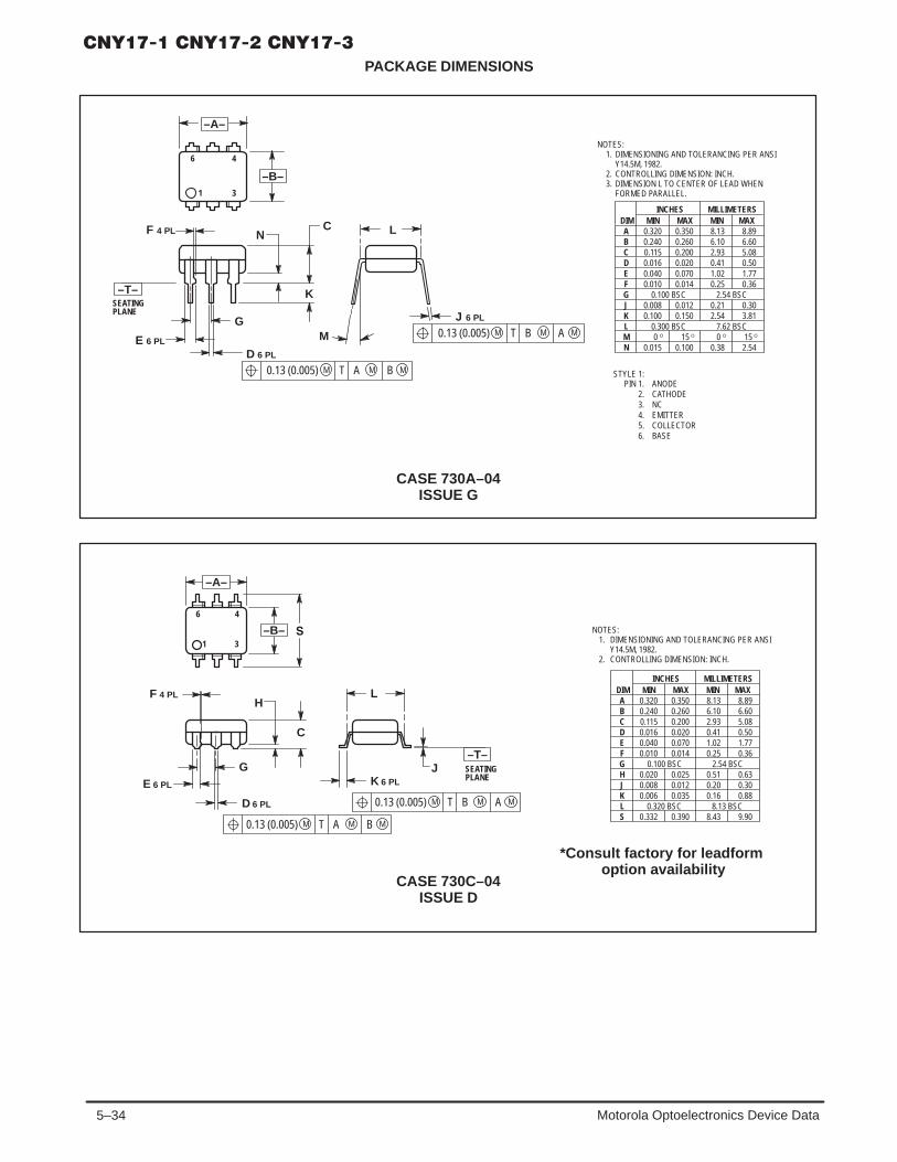
5–34 Motorola Optoelectronics Device Data
PACKAGE DIMENSIONS
CASE 730A–04ISSUE G
NOTES:1. DIMENSIONING AND TOLERANCING PER ANSI
Y14.5M, 1982.2. CONTROLLING DIMENSION: INCH.3. DIMENSION L TO CENTER OF LEAD WHEN
FORMED PARALLEL.
STYLE 1:PIN 1. ANODE
2. CATHODE3. NC4. EMITTER5. COLLECTOR6. BASE
6 4
1 3
–A–
–B–
SEATINGPLANE
–T–
4 PLF
K
CN
G
6 PLD6 PLE
MAM0.13 (0.005) B MT
L
M
6 PLJMBM0.13 (0.005) A MT
DIM MIN MAX MIN MAXMILLIMETERSINCHES
A 0.320 0.350 8.13 8.89B 0.240 0.260 6.10 6.60C 0.115 0.200 2.93 5.08D 0.016 0.020 0.41 0.50E 0.040 0.070 1.02 1.77F 0.010 0.014 0.25 0.36G 0.100 BSC 2.54 BSCJ 0.008 0.012 0.21 0.30K 0.100 0.150 2.54 3.81L 0.300 BSC 7.62 BSCM 0 15 0 15 N 0.015 0.100 0.38 2.54
CASE 730C–04ISSUE D
–A–
–B–
SEATINGPLANE
–T–J
K
L
6 PL
MBM0.13 (0.005) A MT
C
D 6 PL
MAM0.13 (0.005) B MT
H
GE 6 PL
F 4 PL
31
46
NOTES:1. DIMENSIONING AND TOLERANCING PER ANSI
Y14.5M, 1982.2. CONTROLLING DIMENSION: INCH.
DIM MIN MAX MIN MAXMILLIMETERSINCHES
A 0.320 0.350 8.13 8.89B 0.240 0.260 6.10 6.60C 0.115 0.200 2.93 5.08D 0.016 0.020 0.41 0.50E 0.040 0.070 1.02 1.77F 0.010 0.014 0.25 0.36G 0.100 BSC 2.54 BSCH 0.020 0.025 0.51 0.63J 0.008 0.012 0.20 0.30K 0.006 0.035 0.16 0.88L 0.320 BSC 8.13 BSCS 0.332 0.390 8.43 9.90
*Consult factory for leadform option availability

5–35Motorola Optoelectronics Device Data
*Consult factory for leadform option availability
NOTES:1. DIMENSIONING AND TOLERANCING PER ANSI
Y14.5M, 1982.2. CONTROLLING DIMENSION: INCH.3. DIMENSION L TO CENTER OF LEAD WHEN
FORMED PARALLEL.
CASE 730D–05ISSUE D
6 4
1 3
–A–
–B–
N
C
KG
F 4 PL
SEATING
D 6 PL
E 6 PL
PLANE
–T–
MAM0.13 (0.005) B MT
L
J
DIM MIN MAX MIN MAXMILLIMETERSINCHES
A 0.320 0.350 8.13 8.89B 0.240 0.260 6.10 6.60C 0.115 0.200 2.93 5.08D 0.016 0.020 0.41 0.50E 0.040 0.070 1.02 1.77F 0.010 0.014 0.25 0.36G 0.100 BSC 2.54 BSCJ 0.008 0.012 0.21 0.30K 0.100 0.150 2.54 3.81L 0.400 0.425 10.16 10.80N 0.015 0.040 0.38 1.02
Motorola reserves the right to make changes without further notice to any products herein. Motorola makes no warranty, representation or guarantee regardingthe suitability of its products for any particular purpose, nor does Motorola assume any liability arising out of the application or use of any product or circuit,and specifically disclaims any and all liability, including without limitation consequential or incidental damages. “Typical” parameters can and do vary in differentapplications. All operating parameters, including “Typicals” must be validated for each customer application by customer’s technical experts. Motorola doesnot convey any license under its patent rights nor the rights of others. Motorola products are not designed, intended, or authorized for use as components insystems intended for surgical implant into the body, or other applications intended to support or sustain life, or for any other application in which the failure ofthe Motorola product could create a situation where personal injury or death may occur. Should Buyer purchase or use Motorola products for any suchunintended or unauthorized application, Buyer shall indemnify and hold Motorola and its officers, employees, subsidiaries, affiliates, and distributors harmlessagainst all claims, costs, damages, and expenses, and reasonable attorney fees arising out of, directly or indirectly, any claim of personal injury or deathassociated with such unintended or unauthorized use, even if such claim alleges that Motorola was negligent regarding the design or manufacture of the part.Motorola and are registered trademarks of Motorola, Inc. Motorola, Inc. is an Equal Opportunity/Affirmative Action Employer.
How to reach us:USA / EUROPE: Motorola Literature Distribution; JAPAN : Nippon Motorola Ltd.; Tatsumi–SPD–JLDC, Toshikatsu Otsuki,P.O. Box 20912; Phoenix, Arizona 85036. 1–800–441–2447 6F Seibu–Butsuryu–Center, 3–14–2 Tatsumi Koto–Ku, Tokyo 135, Japan. 03–3521–8315
MFAX: [email protected] – TOUCHTONE (602) 244–6609 HONG KONG: Motorola Semiconductors H.K. Ltd.; 8B Tai Ping Industrial Park, INTERNET: http://Design–NET.com 51 Ting Kok Road, Tai Po, N.T., Hong Kong. 852–26629298
CNY17–1/D
◊

5–36 Motorola Optoelectronics Device Data
The H11A1 device consists of a gallium arsenide infrared emitting diodeoptically coupled to a monolithic silicon phototransistor detector.
• Current Transfer Ratios (CTR) 30% and 50%
• Economical Optoisolators for General Purpose/High Volume Applications
• To order devices that are tested and marked per VDE 0884 requirements, thesuffix ”V” must be included at end of part number. VDE 0884 is a test option.
Applications
• General Purpose Switching Circuits
• Interfacing and coupling systems of different potentials and impedances
• Monitor and Detection Circuits
MAXIMUM RATINGS (TA = 25°C unless otherwise noted)
Rating Symbol Value Unit
INPUT LED
Reverse Voltage VR 3 Volts
Forward Current — Continuous IF 60 mA
LED Power Dissipation @ TA = 25°Cwith Negligible Power in Output Detector
Derate above 25°C
PD 120
1.41
mW
mW/°C
OUTPUT TRANSISTOR
Collector–Emitter Voltage VCEO 30 Volts
Emitter–Collector Voltage VECO 7 Volts
Collector–Base Voltage VCBO 70 Volts
Collector Current — Continuous IC 150 mA
Detector Power Dissipation @ TA = 25°Cwith Negligible Power in Input LED
Derate above 25°C
PD 150
1.76
mW
mW/°C
TOTAL DEVICE
Isolation Surge Voltage(1)
(Peak ac Voltage, 60 Hz, 1 sec Duration)VISO 7500 Vac(pk)
Total Device Power Dissipation @ TA = 25°CDerate above 25°C
PD 2502.94
mWmW/°C
Ambient Operating Temperature Range(2) TA –55 to +100 °C
Storage Temperature Range(2) Tstg –55 to +150 °C
Soldering Temperature (10 sec, 1/16″ from case) TL 260 °C
1. Isolation surge voltage is an internal device dielectric breakdown rating.1. For this test, Pins 1 and 2 are common, and Pins 4, 5 and 6 are common.2. Refer to Quality and Reliability Section in Opto Data Book for information on test conditions.
Preferred devices are Motorola recommended choices for future use and best overall value.
GlobalOptoisolator is a trademark of Motorola, Inc.
Order this documentby H11A1/D
SEMICONDUCTOR TECHNICAL DATA
GlobalOptoisolator
Motorola, Inc. 1995
*Motorola Preferred Device
SCHEMATIC
STANDARD THRU HOLECASE 730A–04
STYLE 1 PLASTIC
PIN 1. LED ANODE2. LED CATHODE3. N.C.4. EMITTER5. COLLECTOR6. BASE
1
2
3
6
5
4
61
[CTR = 50% Min]
REV 1

5–37Motorola Optoelectronics Device Data
ELECTRICAL CHARACTERISTICS (TA = 25°C unless otherwise noted)(1)
Characteristic Symbol Min Typ (1) Max Unit
INPUT LED
Forward Voltage (IF = 10 mA, TA = 25°C)TA = –55°CTA = 100°C
VF ———
1.151.31.05
1.5——
Volts
Reverse Leakage Current (VR = 3 V) IR — 0.01 10 µA
Capacitance (V = 0 V, f = 1 MHz) CJ — 18 — pF
OUTPUT TRANSISTOR
Collector–Emitter Dark Current (VCE = 10 V) TA = 25°CTA = 100°C
ICEO ——
11
50—
nAµA
Collector–Base Dark Current (VCB = 10 V) TA = 25°CTA = 100°C
ICBO ——
0.2100
20—
nA
Collector–Emitter Breakdown Voltage (IC = 10 mA) V(BR)CEO 30 45 — Volts
Collector–Base Breakdown Voltage (IC = 100 µA) V(BR)CBO 70 100 — Volts
Emitter–Collector Breakdown Voltage (IE = 100 µA) V(BR)ECO 7 7.8 — Volts
DC Current Gain (IC = 5 mA, VCE = 5 V) (Typical Value) hFE — 500 — —
Collector–Emitter Capacitance (f = 1 MHz, VCE = 0 V) CCE — 7 — pF
Collector–Base Capacitance (f = 1 MHz, VCB = 0 V) CCB — 19 — pF
Emitter–Base Capacitance (f = 1 MHz, VEB = 0 V) CEB — 9 — pF
COUPLED
Output Collector Current (IF = 10 mA, VCE = 10 V) H11A1 IC (CTR)(2) 5 (50) 12 (120) — mA (%)
Collector–Emitter Saturation Voltage (IC = 0.5 mA, IF = 10 mA) VCE(sat) — 0.1 0.4 Volts
Turn–On Time (IF = 10 mA, VCC = 10 V, RL = 100 Ω)(3) ton — 2.8 — µs
Turn–Off Time (IF = 10 mA, VCC = 10 V, RL = 100 Ω)(3) toff — 4.5 — µs
Rise Time (IF = 10 mA, VCC = 10 V, RL = 100 Ω)(3) tr — 1.2 — µs
Fall Time (IF = 10 mA, VCC = 10 V, RL = 100 Ω)(3) tf — 1.3 — µs
Isolation Voltage (f = 60 Hz, t = 1 sec)(4) VISO 7500 — — Vac(pk)
Isolation Resistance (V = 500 V)(4) RISO 1011 — — Ω
Isolation Capacitance (V = 0 V, f = 1 MHz)(4) CISO — 0.2 — pF
1. Always design to the specified minimum/maximum electrical limits (where applicable).2. Current Transfer Ratio (CTR) = IC/IF x 100%.3. For test circuit setup and waveforms, refer to Figure 11.4. For this test, Pins 1 and 2 are common, and Pins 4, 5 and 6 are common.

5–38 Motorola Optoelectronics Device Data
I C, O
UTP
UT
CO
LLEC
TOR
CU
RR
ENT
(NO
RM
ALIZ
ED)
TYPICAL CHARACTERISTICS
Figure 1. LED Forward Voltage versus Forward Current
2
1.8
1.6
1.4
1.2
11 10 100 1000
10
1
0.1
0.01 0.5 1IF, LED FORWARD CURRENT (mA)
2 5 10 20 50IF, LED INPUT CURRENT (mA)
V F, F
OR
WAR
D V
OLT
AGE
(VO
LTS)
25°C
100°C
TA = –55°C
NORMALIZED TO:IF = 10 mA
Figure 2. Output Current versus Input Current
PULSE ONLYPULSE OR DC
10
75
2
10.70.5
0.2
0.1–60 –40 –20 0 20 40 60 80 100
TA, AMBIENT TEMPERATURE (°C)
1
10
100
0.10 20 40 60 80 100
TA, AMBIENT TEMPERATURE (°C)
t, TI
ME
(s)
I
100
50
20
10
5
2
10.1 0.2 0.5 1 2 5 10 20 50 100
IF, LED INPUT CURRENT (mA)
CEO
, CO
LLEC
TOR
–EM
ITTE
R D
ARK
CU
RR
ENT
(NO
RM
ALIZ
ED)
µ
NORMALIZED TO:VCE = 10 VTA = 25°C
VCE = 30 V
10 V
tf
tr
tr
tf
IF = 10 mA
0
VCE, COLLECTOR–EMITTER VOLTAGE (VOLTS)
I C, C
OLL
ECTO
R C
UR
REN
T (m
A)
4
8
12
16
20
24
28
5 mA
2 mA
1 mA
0 1 2 3 4 5 6 7 8 9 10
Figure 3. Collector Current versusCollector–Emitter Voltage
Figure 4. Output Current versus Ambient Temperature
Figure 5. Dark Current versus Ambient Temperature Figure 6. Rise and Fall Times(Typical Values)
RL = 100 RL = 1000
NORMALIZED TO TA = 25°C
VCC = 10 V
I C, O
UTP
UT
CO
LLEC
TOR
CU
RR
ENT
(NO
RM
ALIZ
ED)

5–39Motorola Optoelectronics Device Data
t, T
UR
N–O
FF T
IME
(s)
off
µ
t, T
UR
N–O
N T
IME
(s)
onµ
1007050
20
1075
2
10.1 0.2 0.5 0.7 1 2 5 7 10 20 50 70 100
IF, LED INPUT CURRENT (mA)
RL = 1000
100
10
1007050
20
1075
2
10.1 0.2 0.5 0.7 1 2 5 7 10 20 50 70 100
IF, LED INPUT CURRENT (mA)
RL = 1000
100
10
Figure 7. Turn–On Switching Times(Typical Values)
Figure 8. Turn–Off Switching Times(TypicalValues)
VCC = 10 V VCC = 10 V
VCC = 10 V
RL = 100 Ω
OUTPUT
C, C
APAC
ITAN
CE
(pF)
Figure 9. DC Current Gain (Detector Only) Figure 10. Capacitances versus Voltage
20
18
16
14
12
10
8
6
4
2
0
CCE
f = 1 MHz
0.05 0.1 0.2 0.5 1 2 5 10 20 50V, VOLTAGE (VOLTS)
CLED
CCB
CEB
5 µA
4 µA
3 µA
2 µA
1 µA
4
3
2
1
0 2 4 6 8 10 12 14 16 18 20VCE, COLLECTOR–EMITTER VOLTAGE (VOLTS)
I,
CTY
PIC
AL C
OLL
ECTO
R C
UR
REN
T (m
A) IF = 0
6 µA
TEST CIRCUIT
IF = 10 mA
INPUT
WAVEFORMS
10%
90%
ton
INPUT PULSE
OUTPUT PULSE
tf
toff
tr
Figure 11. Switching Time Test Circuit and Waveforms
IB = 7 µA

5–40 Motorola Optoelectronics Device Data
PACKAGE DIMENSIONS
CASE 730A–04ISSUE G
NOTES:1. DIMENSIONING AND TOLERANCING PER ANSI
Y14.5M, 1982.2. CONTROLLING DIMENSION: INCH.3. DIMENSION L TO CENTER OF LEAD WHEN
FORMED PARALLEL.
STYLE 1:PIN 1. ANODE
2. CATHODE3. NC4. EMITTER5. COLLECTOR6. BASE
6 4
1 3
–A–
–B–
SEATINGPLANE
–T–
4 PLF
K
CN
G
6 PLD6 PLE
MAM0.13 (0.005) B MT
L
M
6 PLJMBM0.13 (0.005) A MT
DIM MIN MAX MIN MAXMILLIMETERSINCHES
A 0.320 0.350 8.13 8.89B 0.240 0.260 6.10 6.60C 0.115 0.200 2.93 5.08D 0.016 0.020 0.41 0.50E 0.040 0.070 1.02 1.77F 0.010 0.014 0.25 0.36G 0.100 BSC 2.54 BSCJ 0.008 0.012 0.21 0.30K 0.100 0.150 2.54 3.81L 0.300 BSC 7.62 BSCM 0 15 0 15 N 0.015 0.100 0.38 2.54
CASE 730C–04ISSUE D
–A–
–B–
SEATINGPLANE
–T–J
K
L
6 PL
MBM0.13 (0.005) A MT
C
D 6 PL
MAM0.13 (0.005) B MT
H
GE 6 PL
F 4 PL
31
46
NOTES:1. DIMENSIONING AND TOLERANCING PER ANSI
Y14.5M, 1982.2. CONTROLLING DIMENSION: INCH.
DIM MIN MAX MIN MAXMILLIMETERSINCHES
A 0.320 0.350 8.13 8.89B 0.240 0.260 6.10 6.60C 0.115 0.200 2.93 5.08D 0.016 0.020 0.41 0.50E 0.040 0.070 1.02 1.77F 0.010 0.014 0.25 0.36G 0.100 BSC 2.54 BSCH 0.020 0.025 0.51 0.63J 0.008 0.012 0.20 0.30K 0.006 0.035 0.16 0.88L 0.320 BSC 8.13 BSCS 0.332 0.390 8.43 9.90
*Consult factory for leadform option availability

5–41Motorola Optoelectronics Device Data
*Consult factory for leadform option availability
NOTES:1. DIMENSIONING AND TOLERANCING PER ANSI
Y14.5M, 1982.2. CONTROLLING DIMENSION: INCH.3. DIMENSION L TO CENTER OF LEAD WHEN
FORMED PARALLEL.
CASE 730D–05ISSUE D
6 4
1 3
–A–
–B–
N
C
KG
F 4 PL
SEATING
D 6 PL
E 6 PL
PLANE
–T–
MAM0.13 (0.005) B MT
L
J
DIM MIN MAX MIN MAXMILLIMETERSINCHES
A 0.320 0.350 8.13 8.89B 0.240 0.260 6.10 6.60C 0.115 0.200 2.93 5.08D 0.016 0.020 0.41 0.50E 0.040 0.070 1.02 1.77F 0.010 0.014 0.25 0.36G 0.100 BSC 2.54 BSCJ 0.008 0.012 0.21 0.30K 0.100 0.150 2.54 3.81L 0.400 0.425 10.16 10.80N 0.015 0.040 0.38 1.02
Motorola reserves the right to make changes without further notice to any products herein. Motorola makes no warranty, representation or guarantee regardingthe suitability of its products for any particular purpose, nor does Motorola assume any liability arising out of the application or use of any product or circuit,and specifically disclaims any and all liability, including without limitation consequential or incidental damages. “Typical” parameters can and do vary in differentapplications. All operating parameters, including “Typicals” must be validated for each customer application by customer’s technical experts. Motorola doesnot convey any license under its patent rights nor the rights of others. Motorola products are not designed, intended, or authorized for use as components insystems intended for surgical implant into the body, or other applications intended to support or sustain life, or for any other application in which the failure ofthe Motorola product could create a situation where personal injury or death may occur. Should Buyer purchase or use Motorola products for any suchunintended or unauthorized application, Buyer shall indemnify and hold Motorola and its officers, employees, subsidiaries, affiliates, and distributors harmlessagainst all claims, costs, damages, and expenses, and reasonable attorney fees arising out of, directly or indirectly, any claim of personal injury or deathassociated with such unintended or unauthorized use, even if such claim alleges that Motorola was negligent regarding the design or manufacture of the part.Motorola and are registered trademarks of Motorola, Inc. Motorola, Inc. is an Equal Opportunity/Affirmative Action Employer.
How to reach us:USA / EUROPE: Motorola Literature Distribution; JAPAN : Nippon Motorola Ltd.; Tatsumi–SPD–JLDC, Toshikatsu Otsuki,P.O. Box 20912; Phoenix, Arizona 85036. 1–800–441–2447 6F Seibu–Butsuryu–Center, 3–14–2 Tatsumi Koto–Ku, Tokyo 135, Japan. 03–3521–8315
MFAX: [email protected] – TOUCHTONE (602) 244–6609 HONG KONG: Motorola Semiconductors H.K. Ltd.; 8B Tai Ping Industrial Park, INTERNET: http://Design–NET.com 51 Ting Kok Road, Tai Po, N.T., Hong Kong. 852–26629298
H11A1/D
◊

5–42 Motorola Optoelectronics Device Data
The H11AA1, H11AA2, H11AA3, H11AA4 devices consist of two gallium–arsenide infrared emitting diodes connected in inverse parallel, opticallycoupled to a monolithic silicon phototransistor detector.
• Built–In Protection for Reverse Polarity
• Guaranteed CTR Minimum Values as High as 100%
• Guaranteed Minimum/Maximum Symmetry Limits
• To order devices that are tested and marked per VDE 0884 requirements, thesuffix ”V” must be included at end of part number. VDE 0884 is a test option.
Applications
• Detecting or Monitoring ac Signals
• AC Line/Digital Logic Isolation
• Programmable Controllers
• Interfacing and coupling systems of different potentials and impedances
• AC/DC — Input Modules
MAXIMUM RATINGS (TA = 25°C unless otherwise noted)
Rating Symbol Value Unit
INPUT LED
Forward Current — Continuous (RMS) IF 60 mA
LED Power Dissipation @ TA = 25°Cwith Negligible Power in Output Detector
Derate above 25°C
PD 120
1.41
mW
mW/°C
OUTPUT TRANSISTOR
Collector–Emitter Voltage VCEO 30 Volts
Emitter–Base Voltage VEBO 5 Volts
Collector–Base Voltage VCBO 70 Volts
Collector Current — Continuous IC 150 mA
Detector Power Dissipation @ TA = 25°Cwith Negligible Power in Input LEDs
Derate above 25°C
PD 150
1.76
mW
mW/°C
TOTAL DEVICE
Isolation Surge Voltage(1)
(Peak ac Voltage, 60 Hz, 1 sec Duration)VISO 7500 Vac(pk)
Total Device Power Dissipation @ TA = 25°CDerate above 25°C
PD 2502.94
mWmW/°C
Ambient Operating Temperature Range(2) TA –55 to +100 °C
Storage Temperature Range(2) Tstg –55 to +150 °C
Soldering Temperature (10 sec, 1/16″ from case) TL 260 °C
1. Isolation surge voltage is an internal device dielectric breakdown rating.1. For this test, Pins 1 and 2 are common, and Pins 4, 5 and 6 are common.2. Refer to Quality and Reliability Section in Opto Data Book for information on test conditions.Preferred devices are Motorola recommended choices for future use and best overall value.GlobalOptoisolator is a trademark of Motorola, Inc.
Order this documentby H11AA1/D
SEMICONDUCTOR TECHNICAL DATA
GlobalOptoisolator
Motorola, Inc. 1995
*Motorola Preferred Devices
SCHEMATIC
[CTR = 50% Min]
STANDARD THRU HOLECASE 730A–04
STYLE 8 PLASTIC
[CTR = 20% Min]
[CTR = 10% Min]
[CTR = 100% Min]
PIN 1. INPUT LED2. INPUT LED3. NO CONNECTION4. EMITTER5. COLLECTOR6. BASE
2
3
6
5
4NC
1
61
REV 1
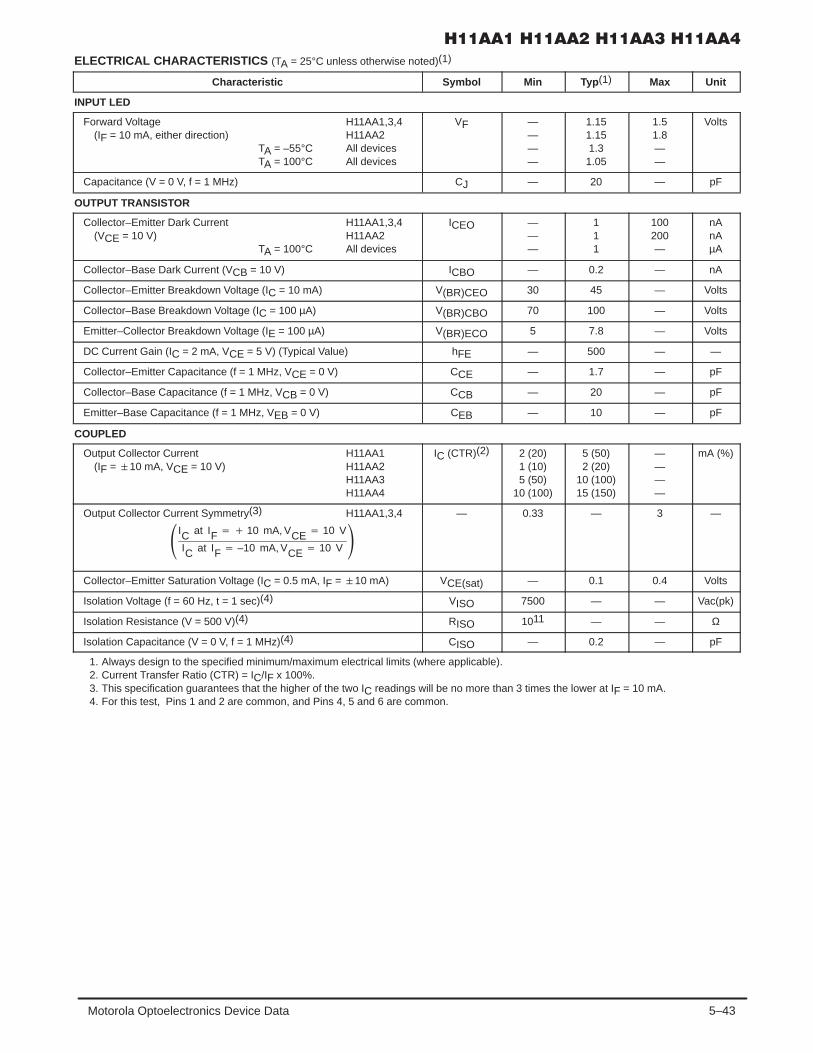
5–43Motorola Optoelectronics Device Data
ELECTRICAL CHARACTERISTICS (TA = 25°C unless otherwise noted)(1)
Characteristic Symbol Min Typ (1) Max Unit
INPUT LED
Forward Voltage H11AA1,3,4(IF = 10 mA, either direction) H11AA2
TA = –55°C All devicesTA = 100°C All devices
VF ————
1.151.151.31.05
1.51.8——
Volts
Capacitance (V = 0 V, f = 1 MHz) CJ — 20 — pF
OUTPUT TRANSISTOR
Collector–Emitter Dark Current H11AA1,3,4(VCE = 10 V) H11AA2
TA = 100°C All devices
ICEO ———
111
100200—
nAnAµA
Collector–Base Dark Current (VCB = 10 V) ICBO — 0.2 — nA
Collector–Emitter Breakdown Voltage (IC = 10 mA) V(BR)CEO 30 45 — Volts
Collector–Base Breakdown Voltage (IC = 100 µA) V(BR)CBO 70 100 — Volts
Emitter–Collector Breakdown Voltage (IE = 100 µA) V(BR)ECO 5 7.8 — Volts
DC Current Gain (IC = 2 mA, VCE = 5 V) (Typical Value) hFE — 500 — —
Collector–Emitter Capacitance (f = 1 MHz, VCE = 0 V) CCE — 1.7 — pF
Collector–Base Capacitance (f = 1 MHz, VCB = 0 V) CCB — 20 — pF
Emitter–Base Capacitance (f = 1 MHz, VEB = 0 V) CEB — 10 — pF
COUPLED
Output Collector Current H11AA1(IF = 10 mA, VCE = 10 V) H11AA2
H11AA3H11AA4
IC (CTR)(2) 2 (20)1 (10)5 (50)
10 (100)
5 (50)2 (20)
10 (100)15 (150)
————
mA (%)
Output Collector Current Symmetry(3) H11AA1,3,4
IC at IF 10 mA, VCE 10 V
IC at IF –10 mA, VCE 10 V
— 0.33 — 3 —
Collector–Emitter Saturation Voltage (IC = 0.5 mA, IF = 10 mA) VCE(sat) — 0.1 0.4 Volts
Isolation Voltage (f = 60 Hz, t = 1 sec)(4) VISO 7500 — — Vac(pk)
Isolation Resistance (V = 500 V)(4) RISO 1011 — — Ω
Isolation Capacitance (V = 0 V, f = 1 MHz)(4) CISO — 0.2 — pF
1. Always design to the specified minimum/maximum electrical limits (where applicable).2. Current Transfer Ratio (CTR) = IC/IF x 100%.3. This specification guarantees that the higher of the two IC readings will be no more than 3 times the lower at IF = 10 mA.4. For this test, Pins 1 and 2 are common, and Pins 4, 5 and 6 are common.

5–44 Motorola Optoelectronics Device Data
Figure 1. Input Voltage versus Input Current
–2.4
–1000iF, INSTANANEOUS INPUT CURRENT (mA)
, IN
PUT
VOLT
AGE
(VO
LTS)
–600 –200 0 200 600 1000
–1.6
–0.8
0
0.8
1.6
2.4 PULSE ONLYPULSE OR DC
V in
Figure 2. Output Characteristics
INPUT CURRENTWAVEFORM
MAXIMUMPEAK OUTPUTCURRENT (1)
MINIMUMPEAK OUTPUTCURRENT (1)
TYPICAL CHARACTERISTICS
10
75
2
10.70.5
0.2
0.1–60 –40 –20 0 20 40 60 80 100
TA, AMBIENT TEMPERATURE (°C)
I C, O
UTP
UT
CO
LLEC
TOR
CU
RR
ENT
(NO
RM
ALIZ
E D
1
10
100
0.10 20 40 60 80 100
TA, AMBIENT TEMPERATURE (°C)
I CEO
, CO
LLEC
TOR
–EM
ITTE
R D
ARK
CU
RR
ENT
(NO
RM
ALIZ
ED)
NORMALIZED TO:VCE = 10 VTA = 25°C
VCE = 30 V
10 V
IF = 10 mA
0
VCE, COLLECTOR–EMITTER VOLTAGE (VOLTS)
I C, C
OLL
ECTO
R C
UR
REN
T (m
A)
4
8
12
16
20
24
28
5 mA
2 mA
1 mA
0 1 2 3 4 5 6 7 8 9 10
Figure 3. Collector Current versusCollector–Emitter Voltage
Figure 4. Output Current versus Ambient Temperature
Figure 5. Dark Current versus Ambient Temperature Figure 6. Capacitances versus Voltage
00.01
V, VOLTAGE (VOLTS)
C, C
APAC
ITAN
CE
(pF)
CCE
0.1 1 10 100
2
4
6
8
10
12
14
16
18
2022
CEB
CCB f = 1 MHz
CLED
NORMALIZED TO TA = 25°C

5–45Motorola Optoelectronics Device Data
PACKAGE DIMENSIONS
CASE 730A–04ISSUE G
NOTES:1. DIMENSIONING AND TOLERANCING PER ANSI
Y14.5M, 1982.2. CONTROLLING DIMENSION: INCH.3. DIMENSION L TO CENTER OF LEAD WHEN
FORMED PARALLEL.
6 4
1 3
–A–
–B–
SEATINGPLANE
–T–
4 PLF
K
CN
G
6 PLD6 PLE
MAM0.13 (0.005) B MT
L
M
6 PLJMBM0.13 (0.005) A MT
DIM MIN MAX MIN MAXMILLIMETERSINCHES
A 0.320 0.350 8.13 8.89B 0.240 0.260 6.10 6.60C 0.115 0.200 2.93 5.08D 0.016 0.020 0.41 0.50E 0.040 0.070 1.02 1.77F 0.010 0.014 0.25 0.36G 0.100 BSC 2.54 BSCJ 0.008 0.012 0.21 0.30K 0.100 0.150 2.54 3.81L 0.300 BSC 7.62 BSCM 0 15 0 15 N 0.015 0.100 0.38 2.54
STYLE 8:PIN 1. LED 1 ANODE/LED 2 CATHODE
2. LED 1 CATHODE/LED 2 ANODE3. NC4. EMITTER5. COLLECTOR6. BASE
CASE 730C–04ISSUE D
–A–
–B–
SEATINGPLANE
–T–J
K
L
6 PL
MBM0.13 (0.005) A MT
C
D 6 PL
MAM0.13 (0.005) B MT
H
GE 6 PL
F 4 PL
31
46
NOTES:1. DIMENSIONING AND TOLERANCING PER ANSI
Y14.5M, 1982.2. CONTROLLING DIMENSION: INCH.
DIM MIN MAX MIN MAXMILLIMETERSINCHES
A 0.320 0.350 8.13 8.89B 0.240 0.260 6.10 6.60C 0.115 0.200 2.93 5.08D 0.016 0.020 0.41 0.50E 0.040 0.070 1.02 1.77F 0.010 0.014 0.25 0.36G 0.100 BSC 2.54 BSCH 0.020 0.025 0.51 0.63J 0.008 0.012 0.20 0.30K 0.006 0.035 0.16 0.88L 0.320 BSC 8.13 BSCS 0.332 0.390 8.43 9.90
*Consult factory for leadform option availability

5–46 Motorola Optoelectronics Device Data
*Consult factory for leadform option availability
NOTES:1. DIMENSIONING AND TOLERANCING PER ANSI
Y14.5M, 1982.2. CONTROLLING DIMENSION: INCH.3. DIMENSION L TO CENTER OF LEAD WHEN
FORMED PARALLEL.
CASE 730D–05ISSUE D
6 4
1 3
–A–
–B–
N
C
KG
F 4 PL
SEATING
D 6 PL
E 6 PL
PLANE
–T–
MAM0.13 (0.005) B MT
L
J
DIM MIN MAX MIN MAXMILLIMETERSINCHES
A 0.320 0.350 8.13 8.89B 0.240 0.260 6.10 6.60C 0.115 0.200 2.93 5.08D 0.016 0.020 0.41 0.50E 0.040 0.070 1.02 1.77F 0.010 0.014 0.25 0.36G 0.100 BSC 2.54 BSCJ 0.008 0.012 0.21 0.30K 0.100 0.150 2.54 3.81L 0.400 0.425 10.16 10.80N 0.015 0.040 0.38 1.02

5–47Motorola Optoelectronics Device Data
Motorola reserves the right to make changes without further notice to any products herein. Motorola makes no warranty, representation or guarantee regardingthe suitability of its products for any particular purpose, nor does Motorola assume any liability arising out of the application or use of any product or circuit,and specifically disclaims any and all liability, including without limitation consequential or incidental damages. “Typical” parameters can and do vary in differentapplications. All operating parameters, including “Typicals” must be validated for each customer application by customer’s technical experts. Motorola doesnot convey any license under its patent rights nor the rights of others. Motorola products are not designed, intended, or authorized for use as components insystems intended for surgical implant into the body, or other applications intended to support or sustain life, or for any other application in which the failure ofthe Motorola product could create a situation where personal injury or death may occur. Should Buyer purchase or use Motorola products for any suchunintended or unauthorized application, Buyer shall indemnify and hold Motorola and its officers, employees, subsidiaries, affiliates, and distributors harmlessagainst all claims, costs, damages, and expenses, and reasonable attorney fees arising out of, directly or indirectly, any claim of personal injury or deathassociated with such unintended or unauthorized use, even if such claim alleges that Motorola was negligent regarding the design or manufacture of the part.Motorola and are registered trademarks of Motorola, Inc. Motorola, Inc. is an Equal Opportunity/Affirmative Action Employer.
How to reach us:USA / EUROPE: Motorola Literature Distribution; JAPAN : Nippon Motorola Ltd.; Tatsumi–SPD–JLDC, Toshikatsu Otsuki,P.O. Box 20912; Phoenix, Arizona 85036. 1–800–441–2447 6F Seibu–Butsuryu–Center, 3–14–2 Tatsumi Koto–Ku, Tokyo 135, Japan. 03–3521–8315
MFAX: [email protected] – TOUCHTONE (602) 244–6609 HONG KONG: Motorola Semiconductors H.K. Ltd.; 8B Tai Ping Industrial Park, INTERNET: http://Design–NET.com 51 Ting Kok Road, Tai Po, N.T., Hong Kong. 852–26629298
H11AA1/D
◊

5–48 Motorola Optoelectronics Device Data
The H11AV1,A and H11AV2,A devices consist of a gallium arsenide infraredemitting diode optically coupled to a monolithic silicon phototransistor detector.
• Guaranteed 70 Volt V(BR)CEO Minimum
• ‘A’ Suffix = 0.400 ″ Wide Spaced Leadform (Same as ‘T’ Suffix. Refer to LeadformOptions Section in Opto Data Book.)
• To order devices that are tested and marked per VDE 0884 requirements, thesuffix ”V” must be included at end of part number. VDE 0884 is a test option.
Applications
• General Purpose Switching Circuits
• Interfacing and coupling systems of different potentials and impedances
• Monitor and Detection Circuits
• Regulation and Feedback Circuits
• Solid State Relays
MAXIMUM RATINGS (TA = 25°C unless otherwise noted)
Rating Symbol Value Unit
INPUT LED
Reverse Voltage VR 6 Volts
Forward Current — Continuous IF 60 mA
LED Power Dissipation @ TA = 25°Cwith Negligible Power in Output Detector
Derate above 25°C
PD 120
1.41
mW
mW/°C
OUTPUT TRANSISTOR
Collector–Emitter Voltage VCEO 70 Volts
Emitter–Base Voltage VEBO 7 Volts
Collector–Base Voltage VCBO 70 Volts
Collector Current — Continuous IC 150 mA
Detector Power Dissipation @ TA = 25°Cwith Negligible Power in Input LED
Derate above 25°C
PD 150
1.76
mW
mW/°C
TOTAL DEVICE
Isolation Surge Voltage(1)
(Peak ac Voltage, 60 Hz, 1 sec Duration)VISO 7500 Vac(pk)
Total Device Power Dissipation @ TA = 25°CDerate above 25°C
PD 2502.94
mWmW/°C
Ambient Operating Temperature Range(2) TA –55 to +100 °C
Storage Temperature Range(2) Tstg –55 to +150 °C
Soldering Temperature (10 sec, 1/16″ from case) TL 260 °C
1. Isolation surge voltage is an internal device dielectric breakdown rating.1. For this test, Pins 1 and 2 are common, and Pins 4, 5 and 6 are common.2. Refer to Quality and Reliability Section in Opto Data Book for information on test conditions.
Preferred devices are Motorola recommended choices for future use and best overall value.GlobalOptoisolator is a trademark of Motorola, Inc.
Order this documentby H11AV1/D
SEMICONDUCTOR TECHNICAL DATA
GlobalOptoisolator
Motorola, Inc. 1995
*Motorola Preferred Devices
SCHEMATIC
[CTR = 50% Min]
STANDARD THRU HOLECASE 730A–04
STYLE 1 PLASTIC
[CTR = 100% Min]
PIN 1. LED ANODE2. LED CATHODE3. N.C.4. EMITTER5. COLLECTOR6. BASE
1
2
3
6
5
4
61
REV 1

5–49Motorola Optoelectronics Device Data
ELECTRICAL CHARACTERISTICS (TA = 25°C unless otherwise noted)(1)
Characteristic Symbol Min Typ (1) Max Unit
INPUT LED
Forward Voltage (IF = 10 mA) TA = 25°CTA = –55°CTA = 100°C
VF 0.80.90.7
1.151.31.05
1.51.71.4
Volts
Reverse Leakage Current (VR = 6 V) IR — — 10 µA
Capacitance (V = 0 V, f = 1 MHz) CJ — 18 — pF
OUTPUT TRANSISTOR
Collector–Emitter Dark Current (VCE = 10 V) ICEO — 5 50 nA
Collector–Base Dark Current (VCB = 10 V) ICBO — 0.5 — nA
Collector–Emitter Breakdown Voltage (IC = 1 mA) V(BR)CEO 70 100 — Volts
Collector–Base Breakdown Voltage (IC = 100 µA) V(BR)CBO 70 100 — Volts
Emitter–Collector Breakdown Voltage (IE = 100 µA) V(BR)ECO 7 8 — Volts
DC Current Gain (IC = 2 mA, VCE = 10 V) (Typical Value) hFE — 500 — —
Collector–Emitter Capacitance (f = 1 MHz, VCE = 10 V) CCE — 4.5 — pF
COUPLED
Output Collector Current (IF = 10 mA, VCE = 10 V)H11AV1, H11AV1AH11AV2, H11AV2A
IC (CTR)(2)
10 (100)5 (50)
15 (150)10 (100)
30 (300)—
mA (%)
Collector–Emitter Saturation Voltage (IC = 2 mA, IF = 20 mA) VCE(sat) — 0.15 0.4 Volts
Turn–On Time (IC = 2 mA, VCC = 10 V, RL = 100 Ω)(3) ton — 5 15 µs
Turn–Off Time (IC = 2 mA, VCC = 10 V, RL = 100 Ω)(3) toff — 4 15 µs
Isolation Voltage (f = 60 Hz, t = 1 sec)(4) VISO 7500 — — Vac(pk)
Isolation Resistance (V = 500 V)(4) RISO 1011 — — Ω
Isolation Capacitance (V = 0 V, f = 1 MHz)(4) CISO — 0.2 0.5 pF
1. Always design to the specified minimum/maximum electrical limits (where applicable).2. Current Transfer Ratio (CTR) = IC/IF x 100%.3. For test circuit setup and waveforms, refer to Figure 11.4. For this test, Pins 1 and 2 are common, and Pins 4, 5 and 6 are common.
I C, O
UTP
UT
CO
LLEC
TOR
CU
RR
ENT
(NO
RM
ALIZ
ED)
TYPICAL CHARACTERISTICS
Figure 1. LED Forward Voltage versus Forward Current
2
1.8
1.6
1.4
1.2
11 10 100 1000
10
1
0.1
0.010.5 1
IF, LED FORWARD CURRENT (mA)2 5 10 20 50
IF, LED INPUT CURRENT (mA)
V F, F
ORW
ARD
VO
LTAG
E (V
OLT
S)
25°C
100°C
TA = –55°C
NORMALIZED TO:IF = 10 mA
Figure 2. Output Current versus Input Current
PULSE ONLYPULSE OR DC
0.20.1 100

5–50 Motorola Optoelectronics Device Data
t, T
UR
N–O
FF T
IME
(s)
off
µ
t, T
UR
N–O
N T
IME
(s)
onµ
10
2
0
Figure 3. Collector Current versusCollector–Emitter Voltage
0
VCE, COLLECTOR–EMITTER VOLTAGE (VOLTS)
4
6
8
10
12
14
1 2 3 4 5 6 7 8 9 10
5 mA
2 mA1 mA
75
2
10.70.5
0.2
0.1–60
Figure 4. Output Current versusAmbient Temperature
–40 –20C, O
UTP
UT
CO
LLEC
TOR
CU
RR
ENT
(NO
RM
ALIZ
ED)
0 20 40 60 80 100TA, AMBIENT TEMPERATURE (°C)I
IF = 10 mA
0
Figure 5. Dark Current versusAmbient Temperature
10–1
TA, AMBIENT TEMPERATURE (°C)
I
102
103
20 40 60 80 100
10 V
CEO
, CO
LLEC
TOR
–EM
ITTE
R D
ARK
CU
RR
ENT
(NO
RM
ALIZ
ED)
101
100
VCE = 70 V
t, TI
ME
(s)
100
50
20
10
5
2
10.1 0.2 0.5 1 2 5 10 20 50 100
IF, LED INPUT CURRENT (mA)
µtf
tr
tr
tf
Figure 6. Rise and Fall Times(Typical Values)
RL = 100
RL = 1000
, CO
LLEC
TOR
CU
RR
ENT
(mA)
I C
30 V
100
50
20
5
2
10.1 0.2 0.5 1 2 5 10 20 50 100
IF, LED INPUT CURRENT (mA)
100
Figure 7. Turn–On Switching Times
RL = 1000
10
10
100
50
20
5
2
10.1 0.2 0.5 1 2 5 10 20 50 100
IF, LED INPUT CURRENT (mA)
100
Figure 8. Turn–Off Switching Times
RL = 1000
10
NORMALIZED TO:VCE = 10 VTA = 25°C
NORMALIZED TO TA = 25°C
VCC = 10 V
VCC = 10 VVCC = 10 V

5–51Motorola Optoelectronics Device Data
7 µA
6 µA
5 µA
4 µA
3 µA
2 µA
1 µA
4
3
2
1
0 2 4 6 8 10 12 14 16 18 20VCE, COLLECTOR–EMITTER VOLTAGE (VOLTS)
I,
C
20
18
16
14
12
10
8
6
4
2
0
CCE
f = 1 MHz
0.5 0.1 0.2 0.5 1 2 5 10 20 50V, VOLTAGE (VOLTS)
Figure 9. DC Current Gain (Detector Only)
C, C
APAC
ITAN
CE
(pF)
Figure 10. Capacitances versus Voltage
TEST CIRCUIT
VCC = 10 V
INPUT
IC RL = 100 Ω
OUTPUT
WAVEFORMS
10%
90%
ton
TYPI
CAL
CO
LLEC
TOR
CU
RR
ENT
(mA) IB = 8 µAIF = 0
INPUT PULSE
OUTPUT PULSE
tftoff
tr
Figure 11. Switching Time Test Circuit and Waveforms
CLED
CEB
INPUT CURRENT ADJUSTEDTO ACHIEVE IC = 2 mA.
CCB

5–52 Motorola Optoelectronics Device Data
PACKAGE DIMENSIONS
CASE 730A–04ISSUE G
NOTES:1. DIMENSIONING AND TOLERANCING PER ANSI
Y14.5M, 1982.2. CONTROLLING DIMENSION: INCH.3. DIMENSION L TO CENTER OF LEAD WHEN
FORMED PARALLEL.
STYLE 1:PIN 1. ANODE
2. CATHODE3. NC4. EMITTER5. COLLECTOR6. BASE
6 4
1 3
–A–
–B–
SEATINGPLANE
–T–
4 PLF
K
CN
G
6 PLD6 PLE
MAM0.13 (0.005) B MT
L
M
6 PLJMBM0.13 (0.005) A MT
DIM MIN MAX MIN MAXMILLIMETERSINCHES
A 0.320 0.350 8.13 8.89B 0.240 0.260 6.10 6.60C 0.115 0.200 2.93 5.08D 0.016 0.020 0.41 0.50E 0.040 0.070 1.02 1.77F 0.010 0.014 0.25 0.36G 0.100 BSC 2.54 BSCJ 0.008 0.012 0.21 0.30K 0.100 0.150 2.54 3.81L 0.300 BSC 7.62 BSCM 0 15 0 15 N 0.015 0.100 0.38 2.54
CASE 730C–04ISSUE D
–A–
–B–
SEATINGPLANE
–T–J
K
L
6 PL
MBM0.13 (0.005) A MT
C
D 6 PL
MAM0.13 (0.005) B MT
H
GE 6 PL
F 4 PL
31
46
NOTES:1. DIMENSIONING AND TOLERANCING PER ANSI
Y14.5M, 1982.2. CONTROLLING DIMENSION: INCH.
DIM MIN MAX MIN MAXMILLIMETERSINCHES
A 0.320 0.350 8.13 8.89B 0.240 0.260 6.10 6.60C 0.115 0.200 2.93 5.08D 0.016 0.020 0.41 0.50E 0.040 0.070 1.02 1.77F 0.010 0.014 0.25 0.36G 0.100 BSC 2.54 BSCH 0.020 0.025 0.51 0.63J 0.008 0.012 0.20 0.30K 0.006 0.035 0.16 0.88L 0.320 BSC 8.13 BSCS 0.332 0.390 8.43 9.90
*Consult factory for leadform option availability

5–53Motorola Optoelectronics Device Data
*Consult factory for leadform option availability
NOTES:1. DIMENSIONING AND TOLERANCING PER ANSI
Y14.5M, 1982.2. CONTROLLING DIMENSION: INCH.3. DIMENSION L TO CENTER OF LEAD WHEN
FORMED PARALLEL.
CASE 730D–05ISSUE D
6 4
1 3
–A–
–B–
N
C
KG
F 4 PL
SEATING
D 6 PL
E 6 PL
PLANE
–T–
MAM0.13 (0.005) B MT
L
J
DIM MIN MAX MIN MAXMILLIMETERSINCHES
A 0.320 0.350 8.13 8.89B 0.240 0.260 6.10 6.60C 0.115 0.200 2.93 5.08D 0.016 0.020 0.41 0.50E 0.040 0.070 1.02 1.77F 0.010 0.014 0.25 0.36G 0.100 BSC 2.54 BSCJ 0.008 0.012 0.21 0.30K 0.100 0.150 2.54 3.81L 0.400 0.425 10.16 10.80N 0.015 0.040 0.38 1.02
Motorola reserves the right to make changes without further notice to any products herein. Motorola makes no warranty, representation or guarantee regardingthe suitability of its products for any particular purpose, nor does Motorola assume any liability arising out of the application or use of any product or circuit,and specifically disclaims any and all liability, including without limitation consequential or incidental damages. “Typical” parameters can and do vary in differentapplications. All operating parameters, including “Typicals” must be validated for each customer application by customer’s technical experts. Motorola doesnot convey any license under its patent rights nor the rights of others. Motorola products are not designed, intended, or authorized for use as components insystems intended for surgical implant into the body, or other applications intended to support or sustain life, or for any other application in which the failure ofthe Motorola product could create a situation where personal injury or death may occur. Should Buyer purchase or use Motorola products for any suchunintended or unauthorized application, Buyer shall indemnify and hold Motorola and its officers, employees, subsidiaries, affiliates, and distributors harmlessagainst all claims, costs, damages, and expenses, and reasonable attorney fees arising out of, directly or indirectly, any claim of personal injury or deathassociated with such unintended or unauthorized use, even if such claim alleges that Motorola was negligent regarding the design or manufacture of the part.Motorola and are registered trademarks of Motorola, Inc. Motorola, Inc. is an Equal Opportunity/Affirmative Action Employer.
How to reach us:USA / EUROPE: Motorola Literature Distribution; JAPAN : Nippon Motorola Ltd.; Tatsumi–SPD–JLDC, Toshikatsu Otsuki,P.O. Box 20912; Phoenix, Arizona 85036. 1–800–441–2447 6F Seibu–Butsuryu–Center, 3–14–2 Tatsumi Koto–Ku, Tokyo 135, Japan. 03–3521–8315
MFAX: [email protected] – TOUCHTONE (602) 244–6609 HONG KONG: Motorola Semiconductors H.K. Ltd.; 8B Tai Ping Industrial Park, INTERNET: http://Design–NET.com 51 Ting Kok Road, Tai Po, N.T., Hong Kong. 852–26629298
H11AV1/D
◊

5–54 Motorola Optoelectronics Device Data
!
The H11B1 and H11B3 devices consist of a gallium arsenide infrared emittingdiode optically coupled to a monolithic silicon photodarlington detector. Theyare designed for use in applications requiring high output current (IC) at low LEDinput currents (IF).
• High Sensitivity to Low Input Drive Current (IF = 1 mA)
• To order devices that are tested and marked per VDE 0884 requirements, thesuffix ”V” must be included at end of part number. VDE 0884 is a test option.
Applications
• Appliances, Measuring Instruments
• I/O Interfaces for Computers
• Programmable Controllers
• Interfacing and coupling systems of different potentials and impedances
• Solid State Relays
• Portable Electronics
MAXIMUM RATINGS (TA = 25°C unless otherwise noted)
Rating Symbol Value Unit
INPUT LED
Reverse Voltage VR 3 Volts
Forward Current — Continuous IF 60 mA
LED Power Dissipation @ TA = 25°Cwith Negligible Power in Output Detector
Derate above 25°C
PD 150
1.41
mW
mW/°C
OUTPUT DETECTOR
Collector–Emitter Voltage VCEO 25 Volts
Emitter–Base Voltage VEBO 7 Volts
Collector–Base Voltage VCBO 30 Volts
Collector Current — Continuous IC 100 mA
Detector Power Dissipation @ TA = 25°Cwith Negligible Power in Input LED
Derate above 25°C
PD 150
1.76
mW
mW/°C
TOTAL DEVICE
Isolation Surge Voltage(1)
(Peak ac Voltage, 60 Hz, 1 sec Duration)VISO 7500 Vac(pk)
Total Device Power Dissipation @ TA = 25°CDerate above 25°C
PD 2502.94
mWmW/°C
Ambient Operating Temperature Range(2) TA –55 to +100 °C
Storage Temperature Range(2) Tstg –55 to +150 °C
Soldering Temperature (10 sec, 1/16″ from case) TL 260 °C1. Isolation surge voltage is an internal device dielectric breakdown rating.1. For this test, Pins 1 and 2 are common, and Pins 4, 5 and 6 are common.2. Refer to Quality and Reliability Section in Opto Data Book for information on test conditions.Preferred devices are Motorola recommended choices for future use and best overall value.GlobalOptoisolator is a trademark of Motorola, Inc.
Order this documentby H11B1/D
SEMICONDUCTOR TECHNICAL DATA
GlobalOptoisolator
Motorola, Inc. 1995
*Motorola Preferred Device
SCHEMATIC
[CTR = 100% Min]
STANDARD THRU HOLECASE 730A–04
STYLE 1 PLASTIC
[CTR = 500% Min]
PIN 1. LED ANODE2. LED CATHODE3. N.C.4. EMITTER5. COLLECTOR6. BASE
1
2
3
6
5
4NC
61
REV 1

5–55Motorola Optoelectronics Device Data
ELECTRICAL CHARACTERISTICS (TA = 25°C unless otherwise noted)(1)
Characteristic Symbol Min Typ (1) Max Unit
INPUT LED
Forward Voltage (IF = 10 mA) H11B1 VF — 1.15 1.5 Volts
Forward Voltage (IF = 50 mA) H11B3 VF — 1.34 1.5 Volts
Reverse Leakage Current (VR = 3 V) IR — — 10 µA
Capacitance (V = 0 V, f = 1 MHz) CJ — 18 — pF
OUTPUT DETECTOR
Collector–Emitter Dark Current (VCE = 10 V) ICEO — 5 100 nA
Collector–Emitter Breakdown Voltage (IC = 10 mA) V(BR)CEO 25 80 — Volts
Collector–Base Breakdown Voltage (IC = 100 µA) V(BR)CBO 30 100 — Volts
Emitter–Collector Breakdown Voltage (IE = 100 µA) V(BR)ECO 7 — — Volts
DC Current Gain (IC = 5 mA, VCE = 5 V) (Typical Value) hFE — 16K — —
Collector–Emitter Capacitance (f = 1 MHz, VCE = 5 V) CCE — 4.9 — pF
Collector–Base Capacitance (f = 1 MHz, VCB = 5 V) CCB — 6.3 — pF
Emitter–Base Capacitance (f = 1 MHz, VEB = 5 V) CEB — 3.8 — pF
COUPLED
Output Collector Current (IF = 1 mA, VCE = 5 V) H11B1H11B3
IC (CTR)(2) 5 (500)1 (100)
——
——
mA (%)
Collector–Emitter Saturation Voltage (IC = 1 mA, IF = 1 mA) VCE(sat) — 0.7 1 Volts
Turn–On Time (IF = 5 mA, VCC = 10 V, RL = 100 Ω)(3) ton — 3.5 — µs
Turn–Off Time (IF = 5 mA, VCC = 10 V, RL = 100 Ω)(3) toff — 95 — µs
Rise Time (IF = 5 mA, VCC = 10 V, RL = 100 Ω)(3) tr — 1 — µs
Fall Time (IF = 5 mA, VCC = 10 V, RL = 100 Ω)(3) tf — 2 — µs
Isolation Voltage (f = 60 Hz, t = 1 sec)(4) VISO 7500 — — Vac(pk)
Isolation Resistance (V = 500 V)(4) RISO 1011 — — Ω
Isolation Capacitance (V = 0 V, f = 1 MHz)(4) CISO — 0.2 — pF
1. Always design to the specified minimum/maximum electrical limits (where applicable).2. Current Transfer Ratio (CTR) = IC/IF x 100%.3. For test circuit setup and waveforms, refer to Figure 11.4. For this test, Pins 1 and 2 are common, and Pins 4, 5 and 6 are common.
TYPICAL CHARACTERISTICS
TA = –55°C THRU
+70°C+100°C
+25°C
Figure 1. LED Forward Voltage versus Forward Current Figure 2. Output Current versus Input Current
2
1.8
1.6
1.4
1.2
11 10 100 1000
IF, LED FORWARD CURRENT (mA)
25°C
100°C
V F, F
ORW
ARD
VO
LTAG
E (V
OLT
S)
I C, O
UTP
UT
CO
LLEC
TOR
CU
RR
ENT
(NO
RM
ALIZ
ED)
10
1
0.1
0.010.5 1 2 5 10 20 50
IF, LED INPUT CURRENT (mA)
NORMALIZED TO: IF = 10 mA
TA = –55°C
TA = 25°C
PULSE ONLYPULSE OR DC

5–56 Motorola Optoelectronics Device Data
, CO
LLEC
TOR
CU
RR
ENT
(mA)
20
0
Figure 3. Collector Current versusCollector–Emitter Voltage
IF = 10 mA
0
VCE, COLLECTOR–EMITTER VOLTAGE (VOLTS)
I C
40
60
80
100
120
140
1 2 3 4 5 6 7 8 9 10
5 mA
2 mA
1 mA
10
75
2
10.70.5
0.2
0.1–60
Figure 4. Output Current versus Ambient Temperature
–40 –20C, O
UTP
UT
CO
LLEC
TOR
CU
RR
ENT
(NO
RM
ALIZ
ED)
0 20 40 60 80 100TA, AMBIENT TEMPERATURE (°C)
I
–60
Figure 5. Collector–Emitter Voltage versusAmbient Temperature
0.7
TA, AMBIENT TEMPERATURE (°C)V CE
, CO
LLEC
TOR
–EM
ITTE
R V
OLT
AGE
(NO
RM
ALIZ
ED)
–40 –20 0 20 40 60 80 100
0.8
0.9
1
1.1
1.2
1.3
0
Figure 6. Collector–Emitter Dark Current versusAmbient Temperature
1
TA, AMBIENT TEMPERATURE (°C)
I
10
102
103
104
105
20 40 60 80 100
NORMALIZED TO:VCE = 10 VTA = 25°C
VCE = 30 V
10 V
CEO
, CO
LLEC
TOR
–EM
ITTE
R D
ARK
CU
RR
ENT
0.1
Figure 7. Turn–On Switching Times(Typical Values)
1
IF, LED INPUT CURRENT (mA)
t, TI
ME
(s)
10
100
1000
µ
0.2 0.5 1 2 5 10 20 50 100
RL = 1000
100
10
0.11
IF, LED INPUT CURRENT (mA)
10
100
1000
0.2 0.5 1 2 5 10 20 50 100
RL = 1000
100
10
t, TI
ME
(s)µ
Figure 8. Turn–Off Switching Times(Typical Values)
(NO
RM
ALIZ
ED)
NORMALIZED TO TA = 25°C
VCC = 10 V
NORMALIZED TO TA = 25°C
VCC = 10 V

5–57Motorola Optoelectronics Device Data
, TYP
ICAL
CO
LLEC
TOR
CU
RR
ENT
(mA)
0
Figure 9. DC Current Gain (Detector Only)
IB = 0.7 µA
0
VCE, COLLECTOR–EMITTER VOLTAGE (VOLTS)
I
2
4
6
8
10
12
14
2 4 6 8 10 12 14 16 18 20
IF = 0C
0.6 µA
0.5 µA
0.4 µA
0.3 µA
0.2 µA
0.1 µA
0.01
Figure 10. Capacitance versus Voltage
1
V, VOLTAGE (VOLTS)
C, C
APAC
ITAN
CE
(pF)
10
100
0.1 1 10 100
CEB
CCB
CLED
TEST CIRCUIT
VCC = 10 V
IF = 5 mA
INPUT
RL = 100 Ω
OUTPUT
WAVEFORMS
10%
90%
ton
INPUT PULSE
OUTPUT PULSE
tf
toff
tr
Figure 11. Switching Time Test Circuit and Waveforms
f = 1 MHz
CCE

5–58 Motorola Optoelectronics Device Data
PACKAGE DIMENSIONS
CASE 730A–04ISSUE G
NOTES:1. DIMENSIONING AND TOLERANCING PER ANSI
Y14.5M, 1982.2. CONTROLLING DIMENSION: INCH.3. DIMENSION L TO CENTER OF LEAD WHEN
FORMED PARALLEL.
STYLE 1:PIN 1. ANODE
2. CATHODE3. NC4. EMITTER5. COLLECTOR6. BASE
6 4
1 3
–A–
–B–
SEATINGPLANE
–T–
4 PLF
K
CN
G
6 PLD6 PLE
MAM0.13 (0.005) B MT
L
M
6 PLJMBM0.13 (0.005) A MT
DIM MIN MAX MIN MAXMILLIMETERSINCHES
A 0.320 0.350 8.13 8.89B 0.240 0.260 6.10 6.60C 0.115 0.200 2.93 5.08D 0.016 0.020 0.41 0.50E 0.040 0.070 1.02 1.77F 0.010 0.014 0.25 0.36G 0.100 BSC 2.54 BSCJ 0.008 0.012 0.21 0.30K 0.100 0.150 2.54 3.81L 0.300 BSC 7.62 BSCM 0 15 0 15 N 0.015 0.100 0.38 2.54
CASE 730C–04ISSUE D
–A–
–B–
SEATINGPLANE
–T–J
K
L
6 PL
MBM0.13 (0.005) A MT
C
D 6 PL
MAM0.13 (0.005) B MT
H
GE 6 PL
F 4 PL
31
46
NOTES:1. DIMENSIONING AND TOLERANCING PER ANSI
Y14.5M, 1982.2. CONTROLLING DIMENSION: INCH.
DIM MIN MAX MIN MAXMILLIMETERSINCHES
A 0.320 0.350 8.13 8.89B 0.240 0.260 6.10 6.60C 0.115 0.200 2.93 5.08D 0.016 0.020 0.41 0.50E 0.040 0.070 1.02 1.77F 0.010 0.014 0.25 0.36G 0.100 BSC 2.54 BSCH 0.020 0.025 0.51 0.63J 0.008 0.012 0.20 0.30K 0.006 0.035 0.16 0.88L 0.320 BSC 8.13 BSCS 0.332 0.390 8.43 9.90
*Consult factory for leadform option availability

5–59Motorola Optoelectronics Device Data
*Consult factory for leadform option availability
NOTES:1. DIMENSIONING AND TOLERANCING PER ANSI
Y14.5M, 1982.2. CONTROLLING DIMENSION: INCH.3. DIMENSION L TO CENTER OF LEAD WHEN
FORMED PARALLEL.
CASE 730D–05ISSUE D
6 4
1 3
–A–
–B–
N
C
KG
F 4 PL
SEATING
D 6 PL
E 6 PL
PLANE
–T–
MAM0.13 (0.005) B MT
L
J
DIM MIN MAX MIN MAXMILLIMETERSINCHES
A 0.320 0.350 8.13 8.89B 0.240 0.260 6.10 6.60C 0.115 0.200 2.93 5.08D 0.016 0.020 0.41 0.50E 0.040 0.070 1.02 1.77F 0.010 0.014 0.25 0.36G 0.100 BSC 2.54 BSCJ 0.008 0.012 0.21 0.30K 0.100 0.150 2.54 3.81L 0.400 0.425 10.16 10.80N 0.015 0.040 0.38 1.02
Motorola reserves the right to make changes without further notice to any products herein. Motorola makes no warranty, representation or guarantee regardingthe suitability of its products for any particular purpose, nor does Motorola assume any liability arising out of the application or use of any product or circuit,and specifically disclaims any and all liability, including without limitation consequential or incidental damages. “Typical” parameters can and do vary in differentapplications. All operating parameters, including “Typicals” must be validated for each customer application by customer’s technical experts. Motorola doesnot convey any license under its patent rights nor the rights of others. Motorola products are not designed, intended, or authorized for use as components insystems intended for surgical implant into the body, or other applications intended to support or sustain life, or for any other application in which the failure ofthe Motorola product could create a situation where personal injury or death may occur. Should Buyer purchase or use Motorola products for any suchunintended or unauthorized application, Buyer shall indemnify and hold Motorola and its officers, employees, subsidiaries, affiliates, and distributors harmlessagainst all claims, costs, damages, and expenses, and reasonable attorney fees arising out of, directly or indirectly, any claim of personal injury or deathassociated with such unintended or unauthorized use, even if such claim alleges that Motorola was negligent regarding the design or manufacture of the part.Motorola and are registered trademarks of Motorola, Inc. Motorola, Inc. is an Equal Opportunity/Affirmative Action Employer.
How to reach us:USA / EUROPE: Motorola Literature Distribution; JAPAN : Nippon Motorola Ltd.; Tatsumi–SPD–JLDC, Toshikatsu Otsuki,P.O. Box 20912; Phoenix, Arizona 85036. 1–800–441–2447 6F Seibu–Butsuryu–Center, 3–14–2 Tatsumi Koto–Ku, Tokyo 135, Japan. 03–3521–8315
MFAX: [email protected] – TOUCHTONE (602) 244–6609 HONG KONG: Motorola Semiconductors H.K. Ltd.; 8B Tai Ping Industrial Park, INTERNET: http://Design–NET.com 51 Ting Kok Road, Tai Po, N.T., Hong Kong. 852–26629298
H11B1/D
◊

5–60 Motorola Optoelectronics Device Data
! ! ! ! "!"! !
The H11D1 and H11D2 consist of gallium arsenide infrared emitting diodesoptically coupled to high voltage, silicon, phototransistor detectors in a standard6–pin DIP package. They are designed for high voltage applications and areparticularly useful in copy machines and solid state relays.
• To order devices that are tested and marked per VDE 0884 requirements, thesuffix ”V” must be included at end of part number. VDE 0884 is a test option.
Applications
• Copy Machines
• Interfacing and coupling systems of different potentials and impedances
• Monitor and Detection Circuits
• Solid State Relays
MAXIMUM RATINGS (TA = 25°C unless otherwise noted)
Rating Symbol Value Unit
INPUT LED
Forward Current — Continuous IF 60 mA
Forward Current — PeakPulse Width = 1 µs, 330 pps
IF 1.2 Amps
LED Power Dissipation @ TA = 25°CDerate above 25°C
PD 1201.41
mWmW/°C
OUTPUT TRANSISTOR
Collector–Emitter Voltage VCER 300 Volts
Emitter–Collector Voltage VECO 7 Volts
Collector–Base Voltage VCBO 300 Volts
Collector Current — Continuous IC 100 mA
Detector Power Dissipation @ TA = 25°CDerate above 25°C
PD 1501.76
mWmW/°C
TOTAL DEVICE
Total Device Power Dissipation @ TA = 25°CDerate above 25°C
PD 2502.94
mWmW/°C
Operating Temperature Range(3) TJ –55 to +100 °C
Storage Temperature Range(3) Tstg –55 to +150 °C
Soldering Temperature (10 s) TL 260 °C
Isolation Surge VoltagePeak ac Voltage, 60 Hz, 1 Second Duration(1)
VISO 7500 Vac(pk)
1. Isolation surge voltage is an internal device dielectric breakdown rating. For this test, Pins 1 and 21. are common, and Pins 4, 5 and 6 are common.2. H11D1 is rated @ 5656 Volts peak (VISO). H11D2 is rated @ 3535 Volts peak (VISO)1. Otherwise they are identical, both parts built by Motorola are rated @ 7500 Volts peak (VISO)3. Refer to Quality and Reliability Section in Opto Data Book for information on test conditions.Preferred devices are Motorola recommended choices for future use and best overall value.GlobalOptoisolator is a trademark of Motorola, Inc.
Order this documentby H11D1/D
SEMICONDUCTOR TECHNICAL DATA
GlobalOptoisolator
Motorola, Inc. 1995
*Motorola Preferred Device
SCHEMATIC
[CTR = 20% Min]
STANDARD THRU HOLECASE 730A–04
STYLE 1 PLASTIC
PIN 1. ANODE2. CATHODE3. N.C.4. EMITTER5. COLLECTOR6. BASE
1
2
3
6
5
4
61
REV 1

5–61Motorola Optoelectronics Device Data
ELECTRICAL CHARACTERISTICS (TA = 25°C unless otherwise noted)(1)
Characteristic Symbol Min Typ (1) Max Unit
INPUT LED (TA = 25°C unless otherwise noted)
Reverse Leakage Current(VR = 6 V)
IR — — 10 µA
Forward Voltage(IF = 10 mA)
VF — 1.2 1.5 Volts
Capacitance(V = 0 V, f = 1 MHz)
C — 18 — pF
OUTPUT TRANSISTOR (TA = 25°C and IF = 0 unless otherwise noted)
Collector–Emitter Dark Current (RBE = 1 MΩ )(VCE = 200 V, TA = 25°C) H11D1,2(TA = 100°C) H11D1,2
ICER——
——
100250
nAµA
Collector–Base Breakdown Voltage(IC = 100 µA) H11D1,2
V(BR)CBO— — 300
Volts
Collector–Emitter Breakdown Voltage(IC = 1 mA, RBE = 1 MΩ) H11D1,2
V(BR)CER— — 300
Volts
Emitter–Base Breakdown Voltage(IE = 100 µA)
V(BR)EBO 7 — — Volts
COUPLED (TA = 25°C unless otherwise noted)
Output Collector Current(VCE = 10 V, IF = 10 mA, RBE = 1 MΩ) H11D1,2
IC (CTR)(2)
2 (20) — —mA (%)
Surge Isolation Voltage (Input to Output)(3)
Peak ac Voltage, 60 Hz, 1 secVISO 7500 — — Vac(pk)
Isolation Resistance(3)
(V = 500 V)RISO — 1011 — Ohms
Collector–Emitter Saturation Voltage(IC = 0.5 mA, IF = 10 mA, RBE = 1 MΩ)
VCE(sat) — — 0.4 Volts
Isolation Capacitance(3)
(V = 0, f = 1 MHz)CISO — 0.2 — pF
Turn–On TimeVCC = 10 V IC = 2 mA RL = 100 Ω
ton — 5 — µs
Turn–Off TimeVCC = 10 V, IC = 2 mA, RL = 100 Ω
toff — 5 —
1. Always design to the specified minimum/maximum electrical limits (where applicable).2. Current Transfer Ratio (CTR) = IC/IF x 100%.3. For this test, Pins 1 and 2 are common, and Pins 4, 5 and 6 are common.
I CER
, OU
TPU
T C
UR
REN
T (m
A)
Figure 1. Output Current versus LED Input Current
1–60
Figure 2. Output Current versus Temperature
–40 –20
CER
, OU
TPU
T C
UR
REN
T (m
A)
0 20 40 60 80 100TA, AMBIENT TEMPERATURE (°C)
I
0.1
IF, LED INPUT CURRENT (mA)
RBE = 106 ΩVCE = 10 VTA = 25°C
1
0.2
0.5
1
2
5
10
20
50
2 5 10 20 50
2
5
10
20
RBE = 106 ΩVCE = 10 V
IF = 20 mA
IF = 10 mA
IF = 5 mA
TYPICAL CHARACTERISTICS

5–62 Motorola Optoelectronics Device Data
–600
TA, AMBIENT TEMPERATURE (°C)
I CBO
, CO
LLEC
TOR
–BAS
E C
UR
REN
T (
A)
–40 –20 0 20 40 60 80 100
2
1.8
1.6
1.4
1.2
11 10 100 1000
IF, LED FORWARD CURRENT (mA)
V F, F
OR
WAR
D V
OLT
AGE
(VO
LTS)
25°C
100°C
TA = –55°C
PULSE ONLYPULSE OR DC
Figure 3. Output Characteristics
0.005
VCE, COLLECTOR VOLTAGE (VOLTS)
I
0.01
0.050.1
0.51
510
40
0.1 0.5 1 5 10 50 100 300
RBE = 106 ΩTA = 25°C
IF = 5 mA
IF = 10 mA
IF = 50 mAC
ER, O
UTP
UT
CU
RR
ENT
(mA)
1
TA, AMBIENT TEMPERATURE (°C)
I
10
20 40 60 90 100
VCE = 300 VC
ER, D
ARK
CU
RR
ENT
(nA)
60
120
180
240
300
RBE = 106 ΩVCE = 10 V
IF = 50 mA
IF = 10 mA
IF = 5 mA
100
1000
30 70 80
10.01
V, VOLTAGE (VOLTS)
C, C
APAC
ITAN
CE
(pF)
10CCB
100
0.1 1 10 100
CLED
f = 1 MHz
µ
Figure 4. Forward Characteristics
Figure 5. Collector–Base Current versus Temperature Figure 6. Dark Current versus Temperature
Figure 7. Capacitance versus Voltage
50
VCE = 50 V
VCE = 100 VRBE = 106 Ω

5–63Motorola Optoelectronics Device Data
PACKAGE DIMENSIONS
CASE 730A–04ISSUE G
NOTES:1. DIMENSIONING AND TOLERANCING PER ANSI
Y14.5M, 1982.2. CONTROLLING DIMENSION: INCH.3. DIMENSION L TO CENTER OF LEAD WHEN
FORMED PARALLEL.STYLE 1:PIN 1. ANODE
2. CATHODE3. NC4. EMITTER5. COLLECTOR6. BASE
6 4
1 3
–A–
–B–
SEATINGPLANE
–T–
4 PLF
K
CN
G
6 PLD6 PLE
MAM0.13 (0.005) B MT
L
M
6 PLJMBM0.13 (0.005) A MT
DIM MIN MAX MIN MAXMILLIMETERSINCHES
A 0.320 0.350 8.13 8.89B 0.240 0.260 6.10 6.60C 0.115 0.200 2.93 5.08D 0.016 0.020 0.41 0.50E 0.040 0.070 1.02 1.77F 0.010 0.014 0.25 0.36G 0.100 BSC 2.54 BSCJ 0.008 0.012 0.21 0.30K 0.100 0.150 2.54 3.81L 0.300 BSC 7.62 BSCM 0 15 0 15 N 0.015 0.100 0.38 2.54
CASE 730C–04ISSUE D
–A–
–B–
SEATINGPLANE
–T–J
K
L
6 PL
MBM0.13 (0.005) A MT
C
D 6 PL
MAM0.13 (0.005) B MT
H
GE 6 PL
F 4 PL
31
46
NOTES:1. DIMENSIONING AND TOLERANCING PER ANSI
Y14.5M, 1982.2. CONTROLLING DIMENSION: INCH.
DIM MIN MAX MIN MAXMILLIMETERSINCHES
A 0.320 0.350 8.13 8.89B 0.240 0.260 6.10 6.60C 0.115 0.200 2.93 5.08D 0.016 0.020 0.41 0.50E 0.040 0.070 1.02 1.77F 0.010 0.014 0.25 0.36G 0.100 BSC 2.54 BSCH 0.020 0.025 0.51 0.63J 0.008 0.012 0.20 0.30K 0.006 0.035 0.16 0.88L 0.320 BSC 8.13 BSCS 0.332 0.390 8.43 9.90
*Consult factory for leadform option availability

5–64 Motorola Optoelectronics Device Data
*Consult factory for leadform option availability
NOTES:1. DIMENSIONING AND TOLERANCING PER ANSI
Y14.5M, 1982.2. CONTROLLING DIMENSION: INCH.3. DIMENSION L TO CENTER OF LEAD WHEN
FORMED PARALLEL.
CASE 730D–05ISSUE D
6 4
1 3
–A–
–B–
N
C
KG
F 4 PL
SEATING
D 6 PL
E 6 PL
PLANE
–T–
MAM0.13 (0.005) B MT
L
J
DIM MIN MAX MIN MAXMILLIMETERSINCHES
A 0.320 0.350 8.13 8.89B 0.240 0.260 6.10 6.60C 0.115 0.200 2.93 5.08D 0.016 0.020 0.41 0.50E 0.040 0.070 1.02 1.77F 0.010 0.014 0.25 0.36G 0.100 BSC 2.54 BSCJ 0.008 0.012 0.21 0.30K 0.100 0.150 2.54 3.81L 0.400 0.425 10.16 10.80N 0.015 0.040 0.38 1.02

5–65Motorola Optoelectronics Device Data
Motorola reserves the right to make changes without further notice to any products herein. Motorola makes no warranty, representation or guarantee regardingthe suitability of its products for any particular purpose, nor does Motorola assume any liability arising out of the application or use of any product or circuit,and specifically disclaims any and all liability, including without limitation consequential or incidental damages. “Typical” parameters can and do vary in differentapplications. All operating parameters, including “Typicals” must be validated for each customer application by customer’s technical experts. Motorola doesnot convey any license under its patent rights nor the rights of others. Motorola products are not designed, intended, or authorized for use as components insystems intended for surgical implant into the body, or other applications intended to support or sustain life, or for any other application in which the failure ofthe Motorola product could create a situation where personal injury or death may occur. Should Buyer purchase or use Motorola products for any suchunintended or unauthorized application, Buyer shall indemnify and hold Motorola and its officers, employees, subsidiaries, affiliates, and distributors harmlessagainst all claims, costs, damages, and expenses, and reasonable attorney fees arising out of, directly or indirectly, any claim of personal injury or deathassociated with such unintended or unauthorized use, even if such claim alleges that Motorola was negligent regarding the design or manufacture of the part.Motorola and are registered trademarks of Motorola, Inc. Motorola, Inc. is an Equal Opportunity/Affirmative Action Employer.
How to reach us:USA / EUROPE: Motorola Literature Distribution; JAPAN : Nippon Motorola Ltd.; Tatsumi–SPD–JLDC, Toshikatsu Otsuki,P.O. Box 20912; Phoenix, Arizona 85036. 1–800–441–2447 6F Seibu–Butsuryu–Center, 3–14–2 Tatsumi Koto–Ku, Tokyo 135, Japan. 03–3521–8315
MFAX: [email protected] – TOUCHTONE (602) 244–6609 HONG KONG: Motorola Semiconductors H.K. Ltd.; 8B Tai Ping Industrial Park, INTERNET: http://Design–NET.com 51 Ting Kok Road, Tai Po, N.T., Hong Kong. 852–26629298
H11D1/D
◊

5–66 Motorola Optoelectronics Device Data
! ! ! "!"! !
The H11G1, H11G2 and H11G3 devices consist of gallium arsenide IREDsoptically coupled to silicon photodarlington detectors which have integralbase–emitter resistors. The on–chip resistors improve higher temperatureleakage characteristics. Designed with high isolation, high CTR, high voltageand low leakage, they provide excellent performance.
• High CTR, H11G1 & H11G2 — 1000% (@ IF = 10 mA), 500% (@ IF = 1 mA)
• High V(BR)CEO, H11G1 — 100 Volts, H11G2 — 80 Volts
• To order devices that are tested and marked per VDE 0884 requirements, thesuffix ”V” must be included at end of part number. VDE 0884 is a test option.
Applications
• Interfacing and coupling systems of different potentials and impedances
• Phase and Feedback Controls
• General Purpose Switching Circuits
• Solid State Relays
MAXIMUM RATINGS (TA = 25°C unless otherwise noted)
Rating Symbol Value Unit
INPUT LED
Reverse Voltage VR 6 Volts
Forward Current — Continuous IF 60 mA
Forward Current — PeakPulse Width = 300 µs, 2% Duty Cycle
IF 3 Amps
LED Power Dissipation @ TA = 25°CDerate above 25°C
PD 1201.41
mWmW/°C
OUTPUT DETECTOR
Collector–Emitter Voltage H11G1H11G2H11G3
VCEO 1008055
Volts
Emitter–Base Voltage VEBO 7 Volts
Collector Current — Continuous IC 150 mA
Detector Power Dissipation @ TA = 25°CDerate above 25°C
PD 1501.76
mWmW/°C
TOTAL DEVICE
Total Device Power Dissipation @ TA = 25°CDerate above 25°C
PD 2502.94
mWmW/°C
Operating Junction Temperature Range(2) TA –55 to +100 °C
Storage Temperature Range(2) Tstg –55 to +150 °C
Soldering Temperature (10 s) TL 260 °C
Isolation Surge Voltage(1)
(Peak ac Voltage, 60 Hz, 1 sec Duration)VISO 7500 Vac(pk)
1. Isolation surge voltage is an internal device dielectric breakdown rating.1. For this test, Pins 1 and 2 are common, and Pins 4, 5 and 6 are common.2. Refer to Quality and Reliability Section in Opto Data Book for information on test conditions.Preferred devices are Motorola recommended choices for future use and best overall value.GlobalOptoisolator is a trademark of Motorola, Inc.
Order this documentby H11G1/D
SEMICONDUCTOR TECHNICAL DATA
GlobalOptoisolator
Motorola, Inc. 1995
*Motorola Preferred Devices
SCHEMATIC
[CTR = 1000% Min]
STANDARD THRU HOLECASE 730A–04
STYLE 1 PLASTIC
[CTR = 1000% Min]
[CTR = 200% Min]
PIN 1. ANODE2. CATHODE3. N.C.4. EMITTER5. COLLECTOR6. BASE
1
2
3
6
5
4
61
REV 1

5–67Motorola Optoelectronics Device Data
ELECTRICAL CHARACTERISTICS (TA = 25°C unless otherwise noted)(1)
Characteristic Symbol Min Typ (1) Max Unit
INPUT LED
Reverse Leakage Current (VR = 3 V) IR — 0.05 10 µA
Forward Voltage IF = 10 mA) VF — 1.1 1.5 Volts
Capacitance (V = 0 V, f = 1 MHz) CJ — 18 — pF
DARLINGTON OUTPUT (TA = 25°C and IF = 0 unless otherwise noted)
Collector–Emitter Breakdown Current(IC = 1 mA, IF = 0) H11G1
H11G2H11G3
V(BR)CEO1008055
———
———
Volts
Collector–Base Breakdown Voltage(IC = 100 µA, IF = 0) H11G1
H11G2H11G3
V(BR)CBO1008055
———
———
Volts
Emitter–Base Breakdown Voltage (IE = 100 µA, IF = 0) V(BR)EBO 7 — — Volts
Collector–Emitter Dark Current(VCE = 80 V) H11G1(VCE = 80 V, TA = 80°C) H11G1(VCE = 60 V) H11G2(VCE = 60 V, TA = 80°C) H11G2(VCE = 30 V) H11G3
ICEO—————
—————
100100100100100
nAµAnAµAnA
Capacitance (VCB = 10 V, f = 1 MHz) CCB — 6 — pF
COUPLED (TA = 25°C unless otherwise noted)
Collector Output Current(VCE = 1 V, IF = 10 mA) H11G1, 2(VCE = 5 V, IF = 1 mA) H11G1, 2(VCE = 5 V, IF = 1 mA) H11G3
IC (CTR)(2)
100 (1000)5 (500)2 (200)
———
———
mA (%)
Collector–Emitter Saturation Voltage(IF = 1 mA, IC = 1 mA) H11G1, 2(IF = 16 mA, IC = 50 mA) H11G1, 2(IF = 20 mA, IC = 50 mA) H11G3
VCE(sat)———
0.750.850.85
11
1.2
Volts
Isolation Surge Voltage(3,4) (60 Hz ac Peak, 1 Second) VISO 7500 — — Vac(pk)
Isolation Resistance(3) (V = 500 Vdc) — 1011 — Ohms
Isolation Capacitance(3) (V = 0 V, f = 1 MHz) CIO — 2 — pF
SWITCHING (TA = 25°C)
Turn–On Time (IF = 10 mA, VCC = 5 V, RL = 100 Ω, ton — 5 — µs
Turn–Off Time
( F CC LPulse Width 300 µs, f = 30 Hz) toff — 100 —
1. Always design to the specified minimum/maximum electrical limits (where applicable).2. Current Transfer Ratio (CTR) = IC/IF x 100%.3. For this test, Pins 1 and 2 are common, and Photodarlington Pins 4 and 5 are common.4. Isolation Surge Voltage, VISO, is an internal device dielectric breakdown rating.
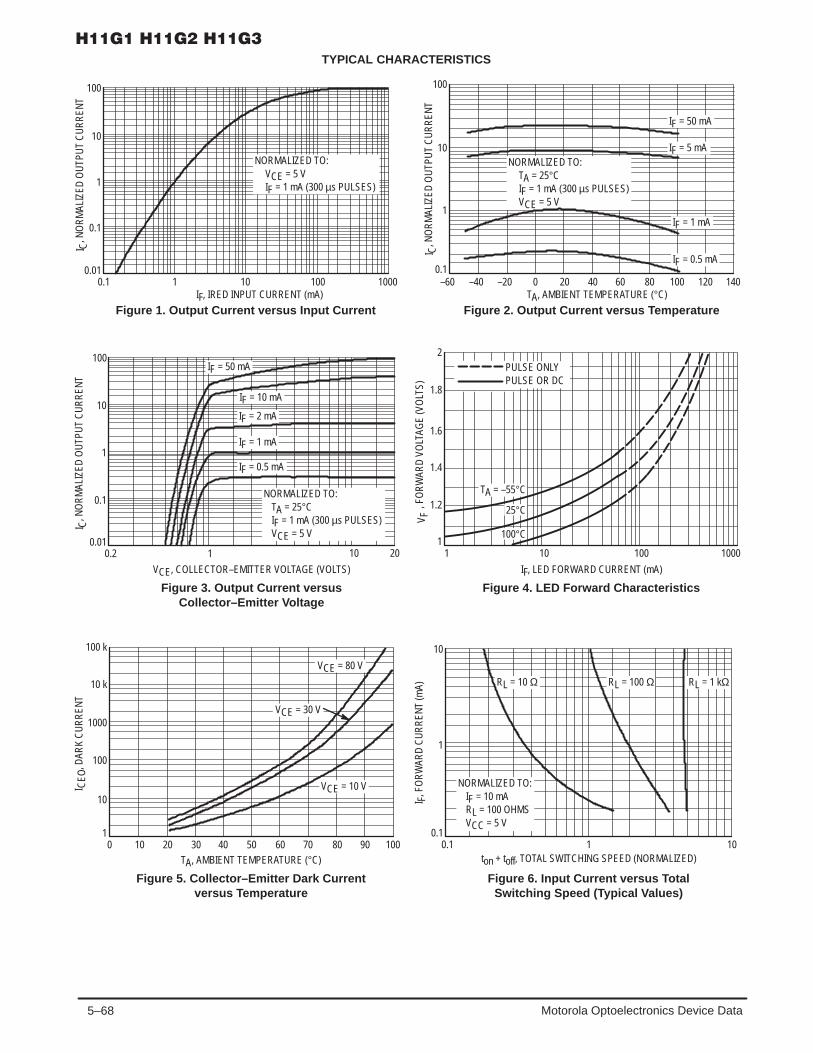
5–68 Motorola Optoelectronics Device Data
0.1–60
TA, AMBIENT TEMPERATURE (°C)–40 –20 0 20 40 60 80 100 120 140
1
10
100
0.1
0.010.1
IF, IRED INPUT CURRENT (mA)
Figure 1. Output Current versus Input Current
I C, N
OR
MAL
IZED
OU
TPU
T C
UR
REN
T
1 10 100 1000
NORMALIZED TO:VCE = 5 VIF = 1 mA (300 µs PULSES)1
10
100
I C, N
OR
MAL
IZED
OU
TPU
T C
UR
REN
T
NORMALIZED TO:TA = 25°CIF = 1 mA (300 µs PULSES)VCE = 5 V
IF = 50 mA
IF = 0.5 mA
Figure 2. Output Current versus Temperature
IF = 5 mA
IF = 1 mA
TYPICAL CHARACTERISTICS
0.010.2
VCE, COLLECTOR–EMITTER VOLTAGE (VOLTS)
Figure 3. Output Current versusCollector–Emitter Voltage
I C, N
OR
MAL
IZED
OU
TPU
T C
UR
REN
T
0.1
1
10
100
1 10 20
IF = 10 mA
IF = 2 mA
IF = 1 mA
IF = 0.5 mA
NORMALIZED TO:TA = 25°CIF = 1 mA (300 µs PULSES)VCE = 5 V
IF = 50 mA
10
TA, AMBIENT TEMPERATURE (°C)
I CEO
, DAR
K C
UR
REN
T
10
100
1000
10 k
100 k
10 20 30 40 50 60 70 80 90 100
VCE = 30 V
VCE = 80 V
VCE = 10 V
0.10.1
ton + toff, TOTAL SWITCHING SPEED (NORMALIZED)
I F, F
ORW
ARD
CU
RR
ENT
(mA)
1
10
1 10
NORMALIZED TO:IF = 10 mARL = 100 OHMSVCC = 5 V
RL = 10 Ω RL = 100 Ω RL = 1 kΩ
2
1.8
1.6
1.4
1.2
11 10 100 1000
IF, LED FORWARD CURRENT (mA)
V F, F
ORW
ARD
VO
LTAG
E (V
OLT
S)
25°C
100°C
TA = –55°C
Figure 4. LED Forward Characteristics
Figure 5. Collector–Emitter Dark Currentversus Temperature
Figure 6. Input Current versus TotalSwitching Speed (Typical Values)
PULSE ONLYPULSE OR DC

5–69Motorola Optoelectronics Device Data
RELAY GROUND
TO 1
TO 2
R
CMOS
VDD
TO 1
TO 2
180 Ω1/4 W
TTL
5 V
1
2
3 4
5
6
1000 Ω
–50 V
1N400450 mA
H11Gx
INTERFACING TTL OR CMOS LOGIC TO 50–VOLT, 1000–OHMS RELAYFOR TELEPHONY APPLICATIONS
In order to interface positive logic to negative–powered electromechanical relays, a change in voltage level and polarity pluselectrical isolation are required. The H11Gx can provide this interface and eliminate the external amplifiers and voltage dividernetworks previously required. The circuit below shows a typical approach for the interface.

5–70 Motorola Optoelectronics Device Data
PACKAGE DIMENSIONS
CASE 730A–04ISSUE G
NOTES:1. DIMENSIONING AND TOLERANCING PER ANSI
Y14.5M, 1982.2. CONTROLLING DIMENSION: INCH.3. DIMENSION L TO CENTER OF LEAD WHEN
FORMED PARALLEL.
STYLE 1:PIN 1. ANODE
2. CATHODE3. NC4. EMITTER5. COLLECTOR6. BASE
6 4
1 3
–A–
–B–
SEATINGPLANE
–T–
4 PLF
K
CN
G
6 PLD6 PLE
MAM0.13 (0.005) B MT
L
M
6 PLJMBM0.13 (0.005) A MT
DIM MIN MAX MIN MAXMILLIMETERSINCHES
A 0.320 0.350 8.13 8.89B 0.240 0.260 6.10 6.60C 0.115 0.200 2.93 5.08D 0.016 0.020 0.41 0.50E 0.040 0.070 1.02 1.77F 0.010 0.014 0.25 0.36G 0.100 BSC 2.54 BSCJ 0.008 0.012 0.21 0.30K 0.100 0.150 2.54 3.81L 0.300 BSC 7.62 BSCM 0 15 0 15 N 0.015 0.100 0.38 2.54
CASE 730C–04ISSUE D
–A–
–B–
SEATINGPLANE
–T–J
K
L
6 PL
MBM0.13 (0.005) A MT
C
D 6 PL
MAM0.13 (0.005) B MT
H
GE 6 PL
F 4 PL
31
46
NOTES:1. DIMENSIONING AND TOLERANCING PER ANSI
Y14.5M, 1982.2. CONTROLLING DIMENSION: INCH.
DIM MIN MAX MIN MAXMILLIMETERSINCHES
A 0.320 0.350 8.13 8.89B 0.240 0.260 6.10 6.60C 0.115 0.200 2.93 5.08D 0.016 0.020 0.41 0.50E 0.040 0.070 1.02 1.77F 0.010 0.014 0.25 0.36G 0.100 BSC 2.54 BSCH 0.020 0.025 0.51 0.63J 0.008 0.012 0.20 0.30K 0.006 0.035 0.16 0.88L 0.320 BSC 8.13 BSCS 0.332 0.390 8.43 9.90
*Consult factory for leadform option availability
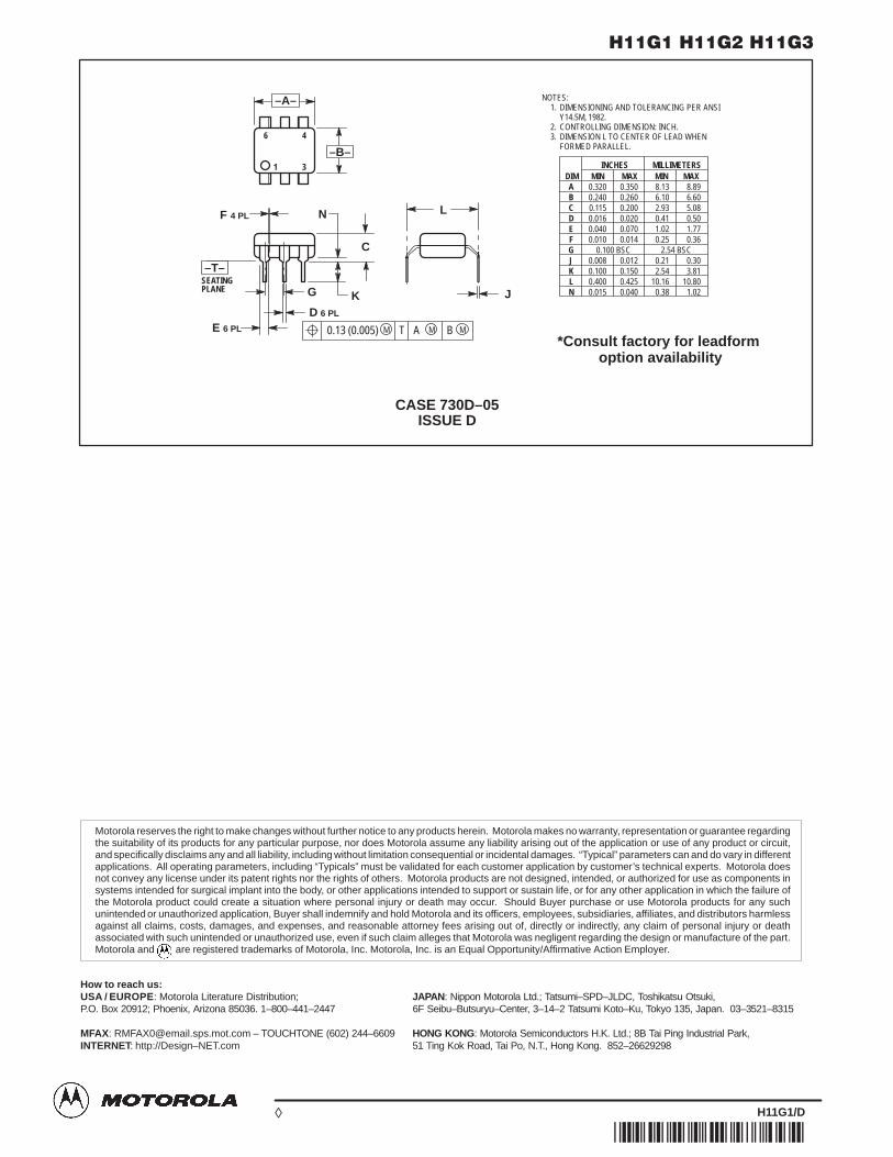
5–71Motorola Optoelectronics Device Data
*Consult factory for leadform option availability
NOTES:1. DIMENSIONING AND TOLERANCING PER ANSI
Y14.5M, 1982.2. CONTROLLING DIMENSION: INCH.3. DIMENSION L TO CENTER OF LEAD WHEN
FORMED PARALLEL.
CASE 730D–05ISSUE D
6 4
1 3
–A–
–B–
N
C
KG
F 4 PL
SEATING
D 6 PL
E 6 PL
PLANE
–T–
MAM0.13 (0.005) B MT
L
J
DIM MIN MAX MIN MAXMILLIMETERSINCHES
A 0.320 0.350 8.13 8.89B 0.240 0.260 6.10 6.60C 0.115 0.200 2.93 5.08D 0.016 0.020 0.41 0.50E 0.040 0.070 1.02 1.77F 0.010 0.014 0.25 0.36G 0.100 BSC 2.54 BSCJ 0.008 0.012 0.21 0.30K 0.100 0.150 2.54 3.81L 0.400 0.425 10.16 10.80N 0.015 0.040 0.38 1.02
Motorola reserves the right to make changes without further notice to any products herein. Motorola makes no warranty, representation or guarantee regardingthe suitability of its products for any particular purpose, nor does Motorola assume any liability arising out of the application or use of any product or circuit,and specifically disclaims any and all liability, including without limitation consequential or incidental damages. “Typical” parameters can and do vary in differentapplications. All operating parameters, including “Typicals” must be validated for each customer application by customer’s technical experts. Motorola doesnot convey any license under its patent rights nor the rights of others. Motorola products are not designed, intended, or authorized for use as components insystems intended for surgical implant into the body, or other applications intended to support or sustain life, or for any other application in which the failure ofthe Motorola product could create a situation where personal injury or death may occur. Should Buyer purchase or use Motorola products for any suchunintended or unauthorized application, Buyer shall indemnify and hold Motorola and its officers, employees, subsidiaries, affiliates, and distributors harmlessagainst all claims, costs, damages, and expenses, and reasonable attorney fees arising out of, directly or indirectly, any claim of personal injury or deathassociated with such unintended or unauthorized use, even if such claim alleges that Motorola was negligent regarding the design or manufacture of the part.Motorola and are registered trademarks of Motorola, Inc. Motorola, Inc. is an Equal Opportunity/Affirmative Action Employer.
How to reach us:USA / EUROPE: Motorola Literature Distribution; JAPAN : Nippon Motorola Ltd.; Tatsumi–SPD–JLDC, Toshikatsu Otsuki,P.O. Box 20912; Phoenix, Arizona 85036. 1–800–441–2447 6F Seibu–Butsuryu–Center, 3–14–2 Tatsumi Koto–Ku, Tokyo 135, Japan. 03–3521–8315
MFAX: [email protected] – TOUCHTONE (602) 244–6609 HONG KONG: Motorola Semiconductors H.K. Ltd.; 8B Tai Ping Industrial Park, INTERNET: http://Design–NET.com 51 Ting Kok Road, Tai Po, N.T., Hong Kong. 852–26629298
H11G1/D
◊

5–72 Motorola Optoelectronics Device Data
The H11L1 and H11L2 have a gallium arsenide IRED optically coupled to ahigh–speed integrated detector with Schmitt trigger output. Designed forapplications requiring electrical isolation, fast response time, noise immunityand digital logic compatibility.
• Guaranteed Switching Times — ton, toff < 4 µs
• Built–In On/Off Threshold Hysteresis
• High Data Rate, 1 MHz Typical (NRZ)
• Wide Supply Voltage Capability
• Microprocessor Compatible Drive
• To order devices that are tested and marked per VDE 0884 requirements, thesuffix ”V” must be included at end of part number. VDE 0884 is a test option.
Applications
• Interfacing Computer Terminals to Peripheral Equipment
• Digital Control of Power Supplies
• Line Receiver — Eliminates Noise
• Digital Control of Motors and Other Servo Machine Applications
• Logic to Logic Isolator
• Logic Level Shifter — Couples TTL to CMOS
MAXIMUM RATINGS (TA = 25°C unless otherwise noted)
Rating Symbol Value Unit
INPUT LED
Reverse Voltage VR 6 Volts
Forward Current — ContinuousForward Current — PeakPulse Width = 300 µs, 2% Duty Cycle
IF 601.2
mAAmp
LED Power Dissipation @ TA = 25°CDerate above 25°C
PD 1201.41
mWmW/°C
OUTPUT DETECTOR
Output Voltage Range Vo 0–16 Volts
Supply Voltage Range VCC 3–16 Volts
Output Current IO 50 mA
Detector Power Dissipation @ TA = 25°CDerate above 25°C
PD 1501.76
mWmW/°C
TOTAL DEVICE
Total Device Dissipation @ TA = 25°CDerate above 25°C
PD 2502.94
mWmW/°C
Maximum Operating Temperature(2) TA –40 to +85 °C
Storage Temperature Range(2) Tstg –55 to +150 °C
Soldering Temperature (10 s) TL 260 °C
Isolation Surge Voltage(Pk ac Voltage, 60 Hz, 1 Second Duration)(1)
VISO 7500 Vac(pk)
1. Isolation surge voltage is an internal device dielectric breakdown rating.1. For this test, Pins 1 and 2 are common, and Pins 4, 5 and 6 are common.2. Refer to Quality and Reliability Section in Opto Data Book for information on test conditions.Preferred devices are Motorola recommended choices for future use and best overall value.GlobalOptoisolator is a trademark of Motorola, Inc.
Order this documentby H11L1/D
SEMICONDUCTOR TECHNICAL DATA
GlobalOptoisolator
Motorola, Inc. 1995
*Motorola Preferred Device
SCHEMATIC
[IF(on) = 10 mA Max]
STANDARD THRU HOLECASE 730A–04
STYLE 5 PLASTIC
[IF(on) = 1.6 mA Max]
PIN 1. ANODE2. CATHODE3. NC4. OPEN COLLECTOR
OUTPUT5. GND6. VCC
1
2
3
6
5
4
61
REV 1

5–73Motorola Optoelectronics Device Data
ELECTRICAL CHARACTERISTICS (TA = 25°C unless otherwise noted)(1)
Characteristic Symbol Min Typ (1) Max Unit
INPUT LED
Reverse Leakage Current (VR = 3 V, RL = 1 MΩ) IR — 0.05 10 µA
Forward Voltage (IF = 10 mA)(IF = 0.3 mA)
VF —0.75
1.20.95
1.5—
Volts
Capacitance (VR = 0 V, f = 1 MHz) C — 18 — pF
OUTPUT DETECTOR
Operating Voltage VCC 3 — 15 Volts
Supply Current (IF = 0, VCC = 5 V) ICC(off) — 1 5 mA
Output Current, High (IF = 0, VCC = Vo = 15 V) IOH — — 100 µA
COUPLED
Supply Current (IF = IF(on), VCC = 5 V) ICC(on) — 1.6 5 mA
Output Voltage, Low (RL = 270 Ω, VCC = 5 V, IF = IF(on)) VOL — 0.2 0.4 Volts
Threshold Current, ON H11L1(RL = 270 Ω, VCC = 5 V) H11L2
IF(on) ——
1.2—
1.610
mA
Threshold Current, OFF H11L1(RL = 270 Ω, VCC = 5 V) H11L2
IF(off) 0.30.3
0.75—
——
mA
Hysteresis Ratio (RL = 270 Ω, VCC = 5 V) IF(off)IF(on)
0.5 0.75 0.9
Isolation Voltage(2) 60 Hz, AC Peak, 1 second, TA = 25°C VISO 7500 — — Vac(pk)
Turn–On TimeRL = 270 Ω(3)
ton — 1.2 4 µs
Fall TimeRL = 270 Ω(3)
VCC = 5 V, tf — 0.1 —
Turn–Off TimeCC
IF = IF(on)TA = 25°C
toff — 1.2 4
Rise TimeTA = 25°C
tr — 0.1 —
1. Always design to the specified minimum/maximum electrical limits (where applicable).2. For this test, IRED Pins 1 and 2 are common and Output Gate Pins 4, 5, 6 are common.3. RL value effect on switching time is negligible.
Vin
tr = tf = 0.01 µsZ = 50 Ω
IF (on)
trtf
Figure 1. Switching Test Circuit
toffton
Vo
2
1
IF
5
6
4
RL
ICC
270 Ω
5 V
VO (OPEN COLLECTOR OUTPUT)

5–74 Motorola Optoelectronics Device Data
0.1
F(on
), I F
(off)
, TH
RES
HO
LD C
UR
REN
T (N
OR
MAL
IZED
)
Figure 2. Transfer Characteristics for H11L1
0IF, INPUT CURRENT (mA)
IF(off)
V
0
VOH
VOL1
2
3
4
5
6
0.75 1 2
IF(on)
RL = 270 ΩVCC = 5 VTA = 25°C
O, O
UTP
UT
VOLT
AGE
(VO
LTS)
Figure 3. Threshold Current versus Supply Voltage
0.4
0VCC, SUPPLY VOLTAGE (VOLTS)
I
TURN OFF THRESHOLD
IF NORMALIZED TOIF(on) AT VCC = 5 VTA = 25°C
0.6
0.8
1
1.2
1.4
1.6
2 4 6 8 10 12 14
F, T
HR
ESH
OLD
CU
RR
ENT
(NO
RM
ALIZ
ED)
Figure 4. Threshold Current versus Temperature
0.6
I
–50 –25 0 25 50 75 100
0.8
1
1.2
1.4
1.6
Figure 5. Output Voltage, Low versus Load Current
0.02
1IO, LOAD CURRENT (mA)
V
2 5 10 20 50 100
0.05
0.2
0.5
1
OL,
OU
TPU
T VO
LTAG
E, L
OW
(VO
LTS)
NORMALIZED TOVCC = 5 VTA = 25°C
I C, S
UPP
LY C
UR
REN
T (m
A)
Figure 6. Supply Current versus Supply Voltage
2
VCC, SUPPLY VOLTAGE (VOLTS)0
4
6
TA, TEMPERATURE (°C)
2 4 6 8 10 12 14 16
TA = 0°C25°C70°C
0IF = 0 mA
IF = 5 mA
0°C25°C70°C
TYPICAL CHARACTERISTICS
TURN ON THRESHOLD

5–75Motorola Optoelectronics Device Data
PACKAGE DIMENSIONS
CASE 730A–04ISSUE G
NOTES:1. DIMENSIONING AND TOLERANCING PER ANSI
Y14.5M, 1982.2. CONTROLLING DIMENSION: INCH.3. DIMENSION L TO CENTER OF LEAD WHEN
FORMED PARALLEL.
6 4
1 3
–A–
–B–
SEATINGPLANE
–T–
4 PLF
K
CN
G
6 PLD6 PLE
MAM0.13 (0.005) B MT
L
M
6 PLJMBM0.13 (0.005) A MT
DIM MIN MAX MIN MAXMILLIMETERSINCHES
A 0.320 0.350 8.13 8.89B 0.240 0.260 6.10 6.60C 0.115 0.200 2.93 5.08D 0.016 0.020 0.41 0.50E 0.040 0.070 1.02 1.77F 0.010 0.014 0.25 0.36G 0.100 BSC 2.54 BSCJ 0.008 0.012 0.21 0.30K 0.100 0.150 2.54 3.81L 0.300 BSC 7.62 BSCM 0 15 0 15 N 0.015 0.100 0.38 2.54
STYLE 5:PIN 1. ANODE
2. CATHODE3. NC4. OUTPUT5. GROUND6. VCC
CASE 730C–04ISSUE D
–A–
–B–
SEATINGPLANE
–T–J
K
L
6 PL
MBM0.13 (0.005) A MT
C
D 6 PL
MAM0.13 (0.005) B MT
H
GE 6 PL
F 4 PL
31
46
NOTES:1. DIMENSIONING AND TOLERANCING PER ANSI
Y14.5M, 1982.2. CONTROLLING DIMENSION: INCH.
DIM MIN MAX MIN MAXMILLIMETERSINCHES
A 0.320 0.350 8.13 8.89B 0.240 0.260 6.10 6.60C 0.115 0.200 2.93 5.08D 0.016 0.020 0.41 0.50E 0.040 0.070 1.02 1.77F 0.010 0.014 0.25 0.36G 0.100 BSC 2.54 BSCH 0.020 0.025 0.51 0.63J 0.008 0.012 0.20 0.30K 0.006 0.035 0.16 0.88L 0.320 BSC 8.13 BSCS 0.332 0.390 8.43 9.90
*Consult factory for leadform option availability

5–76 Motorola Optoelectronics Device Data
*Consult factory for leadform option availability
NOTES:1. DIMENSIONING AND TOLERANCING PER ANSI
Y14.5M, 1982.2. CONTROLLING DIMENSION: INCH.3. DIMENSION L TO CENTER OF LEAD WHEN
FORMED PARALLEL.
CASE 730D–05ISSUE D
6 4
1 3
–A–
–B–
N
C
KG
F 4 PL
SEATING
D 6 PL
E 6 PL
PLANE
–T–
MAM0.13 (0.005) B MT
L
J
DIM MIN MAX MIN MAXMILLIMETERSINCHES
A 0.320 0.350 8.13 8.89B 0.240 0.260 6.10 6.60C 0.115 0.200 2.93 5.08D 0.016 0.020 0.41 0.50E 0.040 0.070 1.02 1.77F 0.010 0.014 0.25 0.36G 0.100 BSC 2.54 BSCJ 0.008 0.012 0.21 0.30K 0.100 0.150 2.54 3.81L 0.400 0.425 10.16 10.80N 0.015 0.040 0.38 1.02

5–77Motorola Optoelectronics Device Data
Motorola reserves the right to make changes without further notice to any products herein. Motorola makes no warranty, representation or guarantee regardingthe suitability of its products for any particular purpose, nor does Motorola assume any liability arising out of the application or use of any product or circuit,and specifically disclaims any and all liability, including without limitation consequential or incidental damages. “Typical” parameters can and do vary in differentapplications. All operating parameters, including “Typicals” must be validated for each customer application by customer’s technical experts. Motorola doesnot convey any license under its patent rights nor the rights of others. Motorola products are not designed, intended, or authorized for use as components insystems intended for surgical implant into the body, or other applications intended to support or sustain life, or for any other application in which the failure ofthe Motorola product could create a situation where personal injury or death may occur. Should Buyer purchase or use Motorola products for any suchunintended or unauthorized application, Buyer shall indemnify and hold Motorola and its officers, employees, subsidiaries, affiliates, and distributors harmlessagainst all claims, costs, damages, and expenses, and reasonable attorney fees arising out of, directly or indirectly, any claim of personal injury or deathassociated with such unintended or unauthorized use, even if such claim alleges that Motorola was negligent regarding the design or manufacture of the part.Motorola and are registered trademarks of Motorola, Inc. Motorola, Inc. is an Equal Opportunity/Affirmative Action Employer.
How to reach us:USA / EUROPE: Motorola Literature Distribution; JAPAN : Nippon Motorola Ltd.; Tatsumi–SPD–JLDC, Toshikatsu Otsuki,P.O. Box 20912; Phoenix, Arizona 85036. 1–800–441–2447 6F Seibu–Butsuryu–Center, 3–14–2 Tatsumi Koto–Ku, Tokyo 135, Japan. 03–3521–8315
MFAX: [email protected] – TOUCHTONE (602) 244–6609 HONG KONG: Motorola Semiconductors H.K. Ltd.; 8B Tai Ping Industrial Park, INTERNET: http://Design–NET.com 51 Ting Kok Road, Tai Po, N.T., Hong Kong. 852–26629298
H11L1/D
◊

5–78 Motorola Optoelectronics Device Data
The MCT and MCT2E devices consist of a gallium arsenide infrared emittingdiode optically coupled to a monolithic silicon phototransistor detector.
Applications
• General Purpose Switching Circuits
• Interfacing and coupling systems of different potentials and impedances
• I/O Interfacing
• Solid State Relays
• Monitor and Detection Circuits
• To order devices that are tested and marked per VDE 0884 requirements, thesuffix ”V” must be included at end of part number. VDE 0884 is a test option.
MAXIMUM RATINGS (TA = 25°C unless otherwise noted)
Rating Symbol Value Unit
INPUT LED
Reverse Voltage VR 3 Volts
Forward Current — Continuous IF 60 mA
LED Power Dissipation @ TA = 25°Cwith Negligible Power in Output Detector
Derate above 25°C
PD 120
1.41
mW
mW/°C
OUTPUT TRANSISTOR
Collector–Emitter Voltage VCEO 30 Volts
Emitter–Collector Voltage VECO 7 Volts
Collector–Base Voltage VCBO 70 Volts
Collector Current — Continuous IC 150 mA
Detector Power Dissipation @ TA = 25°Cwith Negligible Power in Input LED
Derate above 25°C
PD 150
1.76
mW
mW/°C
TOTAL DEVICE
Isolation Surge Voltage(1)
(Peak ac Voltage, 60 Hz, 1 sec Duration)VISO 7500 Vac(pk)
Total Device Power Dissipation @ TA = 25°CDerate above 25°C
PD 2502.94
mWmW/°C
Ambient Operating Temperature Range(2) TA –55 to +100 °C
Storage Temperature Range(2) Tstg –55 to +150 °C
Soldering Temperature (10 sec, 1/16″ from case) TL 260 °C
1. Isolation surge voltage is an internal device dielectric breakdown rating.1. For this test, Pins 1 and 2 are common, and Pins 4, 5 and 6 are common.2. Refer to Quality and Reliability Section in Opto Data Book for information on test conditions.
GlobalOptoisolator is a trademark of Motorola, Inc.
Order this documentby MCT2/D
SEMICONDUCTOR TECHNICAL DATA
GlobalOptoisolator
Motorola, Inc. 1995
SCHEMATIC
[CTR = 20% Min]
STANDARD THRU HOLECASE 730A–04
STYLE 1 PLASTIC
PIN 1. LED ANODE2. LED CATHODE3. N.C.4. EMITTER5. COLLECTOR6. BASE
1
2
3
6
5
4
61
REV 1

5–79Motorola Optoelectronics Device Data
ELECTRICAL CHARACTERISTICS (TA = 25°C unless otherwise noted)(1)
Characteristic Symbol Min Typ (1) Max Unit
INPUT LED
Forward Voltage (IF = 20 mA) TA = 25°CTA = –55°CTA = 100°C
VF ———
1.231.351.15
1.5——
Volts
Reverse Leakage Current (VR = 3 V) IR — 0.01 10 µA
Capacitance (V = 0 V, f = 1 MHz) CJ — 18 — pF
OUTPUT TRANSISTOR
Collector–Emitter Dark Current (VCE = 10 V) TA = 25°CTA = 100°C
ICEO ——
11
50—
nAµA
Collector–Base Dark Current (VCB = 10 V) TA = 25°CTA = 100°C
ICBO ——
0.2100
20—
nA
Collector–Emitter Breakdown Voltage (IC = 1 mA) V(BR)CEO 30 45 — Volts
Collector–Base Breakdown Voltage (IC = 10 µA) V(BR)CBO 70 100 — Volts
Emitter–Collector Breakdown Voltage (IE = 100 µA) V(BR)ECO 7 7.8 — Volts
DC Current Gain (IC = 5 mA, VCE = 5 V) hFE — 500 — —
Collector–Emitter Capacitance (f = 1 MHz, VCE = 0 V) CCE — 7 — pF
Collector–Base Capacitance (f = 1 MHz, VCB = 0 V) CCB — 19 — pF
Emitter–Base Capacitance (f = 1 MHz, VEB = 0 V) CEB — 9 — pF
COUPLED
Output Collector Current (IF = 10 mA, VCE = 10 V) IC (CTR)(2) 2 (20) 7 (70) — mA (%)
Collector–Emitter Saturation Voltage (IC = 2 mA, IF = 16 mA) VCE(sat) — 0.19 0.4 Volts
Turn–On Time (IF = 10 mA, VCC = 10 V, RL = 100 Ω)(3) ton — 2.8 — µs
Turn–Off Time (IF = 10 mA, VCC = 10 V, RL = 100 Ω,)(3) toff — 4.5 — µs
Rise Time (IF = 10 mA, VCC = 10 V, RL = 100 Ω)(3) tr — 1.2 — µs
Fall Time (IF = 10 mA, VCC = 10 V, RL = 100 Ω)(3) tf — 1.3 — µs
Isolation Voltage (f = 60 Hz, t = 1 sec)(4) VISO 7500 — — Vac(pk)
Isolation Resistance (V = 500 V)(4) RISO 1011 — — Ω
Isolation Capacitance (V = 0 V, f = 1 MHz)(4) CISO — 0.2 — pF
1. Always design to the specified minimum/maximum electrical limits (where applicable).2. Current Transfer Ratio (CTR) = IC/IF x 100%.3. For test circuit setup and waveforms, refer to Figure 11.4. For this test, Pins 1 and 2 are common, and Pins 4, 5 and 6 are common.

5–80 Motorola Optoelectronics Device Data
I C, O
UTP
UT
CO
LLEC
TOR
CU
RR
ENT
(NO
RM
ALIZ
ED)
TYPICAL CHARACTERISTICS
Figure 1. LED Forward Voltage versus Forward Current
2
1.8
1.6
1.4
1.2
11 10 100 1000
10
1
0.1
0.01 0.5 1IF, LED FORWARD CURRENT (mA)
2 5 10 20 50IF, LED INPUT CURRENT (mA)
V F, F
OR
WAR
D V
OLT
AGE
(VO
LTS)
25°C
100°C
TA = –55°C
NORMALIZED TO:IF = 10 mA
Figure 2. Output Current versus Input Current
PULSE ONLYPULSE OR DC
10
75
2
10.70.5
0.2
0.1–60 –40 –20 0 20 40 60 80 100
TA, AMBIENT TEMPERATURE (°C)
I C, O
UTP
UT
CO
LLEC
TOR
CU
RR
ENT
(NO
RM
ALIZ
ED)
1
10
100
0.10 20 40 60 80 100
TA, AMBIENT TEMPERATURE (°C)
t, TI
ME
(s)
I
100
50
20
10
5
2
10.1 0.2 0.5 1 2 5 10 20 50 100
IF, LED INPUT CURRENT (mA)
CEO
, CO
LLEC
TOR
–EM
ITTE
R D
ARK
CU
RR
ENT
(NO
RM
ALIZ
ED)
µ
NORMALIZED TO:VCE = 10 VTA = 25°C
VCE = 30 V
10 V
tf
tr
tr
tf
IF = 10 mA
0
VCE, COLLECTOR–EMITTER VOLTAGE (VOLTS)
I C, C
OLL
ECTO
R C
UR
REN
T (m
A)
4
8
12
16
20
24
28
5 mA
2 mA
1 mA
0 1 2 3 4 5 6 7 8 9 10
Figure 3. Collector Current versusCollector–Emitter Voltage
Figure 4. Output Current versus Ambient Temperature
Figure 5. Dark Current versus Ambient Temperature Figure 6. Rise and Fall Times(Typical Values)
RL = 100RL = 1000
NORMALIZED TO TA = 25°C
VCC = 10 V

5–81Motorola Optoelectronics Device Data
t, T
UR
N–O
FF T
IME
(s)
off
µ
t, T
UR
N–O
N T
IME
(s)
onµ
1007050
20
1075
2
10.1 0.2 0.5 0.7 1 2 5 7 10 20 50 70 100
IF, LED INPUT CURRENT (mA)
RL = 1000
100
10
1007050
20
1075
2
10.1 0.2 0.5 0.7 1 2 5 7 10 20 50 70 100
IF, LED INPUT CURRENT (mA)
RL = 1000
100
10
Figure 7. Turn–On Switching Times(Typical Values)
Figure 8. Turn–Off Switching Times(Typical Values)
VCC = 10 VVCC = 10 V
6 µA
C, C
APAC
ITAN
CE
(pF)
Figure 9. DC Current Gain (Detector Only) Figure 10. Capacitances versus Voltage
20
18
16
14
12
10
8
6
4
2
0
CCE
f = 1 MHz
0.05 0.1 0.2 0.5 1 2 5 10 20 50V, VOLTAGE (VOLTS)
CLED
CCB
CEB
5 µA
4 µA
3 µA
2 µA
1 µA
4
3
2
1
0 2 4 6 8 10 12 14 16 18 20VCE, COLLECTOR–EMITTER VOLTAGE (VOLTS)
I,
CTY
PIC
AL C
OLL
ECTO
R C
UR
REN
T (m
A) IB = 7 µAIF = 0
TEST CIRCUIT
VCC = 10 V
IF = 10 mA
INPUT
RL = 100 Ω
OUTPUT
WAVEFORMS
10%
90%
ton
INPUT PULSE
OUTPUT PULSE
tf
toff
tr
Figure 11. Switching Time Test Circuit and Waveforms

5–82 Motorola Optoelectronics Device Data
PACKAGE DIMENSIONS
CASE 730A–04ISSUE G
NOTES:1. DIMENSIONING AND TOLERANCING PER ANSI
Y14.5M, 1982.2. CONTROLLING DIMENSION: INCH.3. DIMENSION L TO CENTER OF LEAD WHEN
FORMED PARALLEL.
STYLE 1:PIN 1. ANODE
2. CATHODE3. NC4. EMITTER5. COLLECTOR6. BASE
6 4
1 3
–A–
–B–
SEATINGPLANE
–T–
4 PLF
K
CN
G
6 PLD6 PLE
MAM0.13 (0.005) B MT
L
M
6 PLJMBM0.13 (0.005) A MT
DIM MIN MAX MIN MAXMILLIMETERSINCHES
A 0.320 0.350 8.13 8.89B 0.240 0.260 6.10 6.60C 0.115 0.200 2.93 5.08D 0.016 0.020 0.41 0.50E 0.040 0.070 1.02 1.77F 0.010 0.014 0.25 0.36G 0.100 BSC 2.54 BSCJ 0.008 0.012 0.21 0.30K 0.100 0.150 2.54 3.81L 0.300 BSC 7.62 BSCM 0 15 0 15 N 0.015 0.100 0.38 2.54
CASE 730C–04ISSUE D
–A–
–B–
SEATINGPLANE
–T–J
K
L
6 PL
MBM0.13 (0.005) A MT
C
D 6 PL
MAM0.13 (0.005) B MT
H
GE 6 PL
F 4 PL
31
46
NOTES:1. DIMENSIONING AND TOLERANCING PER ANSI
Y14.5M, 1982.2. CONTROLLING DIMENSION: INCH.
DIM MIN MAX MIN MAXMILLIMETERSINCHES
A 0.320 0.350 8.13 8.89B 0.240 0.260 6.10 6.60C 0.115 0.200 2.93 5.08D 0.016 0.020 0.41 0.50E 0.040 0.070 1.02 1.77F 0.010 0.014 0.25 0.36G 0.100 BSC 2.54 BSCH 0.020 0.025 0.51 0.63J 0.008 0.012 0.20 0.30K 0.006 0.035 0.16 0.88L 0.320 BSC 8.13 BSCS 0.332 0.390 8.43 9.90
*Consult factory for leadform option availability

5–83Motorola Optoelectronics Device Data
*Consult factory for leadform option availability
NOTES:1. DIMENSIONING AND TOLERANCING PER ANSI
Y14.5M, 1982.2. CONTROLLING DIMENSION: INCH.3. DIMENSION L TO CENTER OF LEAD WHEN
FORMED PARALLEL.
CASE 730D–05ISSUE D
6 4
1 3
–A–
–B–
N
C
KG
F 4 PL
SEATING
D 6 PL
E 6 PL
PLANE
–T–
MAM0.13 (0.005) B MT
L
J
DIM MIN MAX MIN MAXMILLIMETERSINCHES
A 0.320 0.350 8.13 8.89B 0.240 0.260 6.10 6.60C 0.115 0.200 2.93 5.08D 0.016 0.020 0.41 0.50E 0.040 0.070 1.02 1.77F 0.010 0.014 0.25 0.36G 0.100 BSC 2.54 BSCJ 0.008 0.012 0.21 0.30K 0.100 0.150 2.54 3.81L 0.400 0.425 10.16 10.80N 0.015 0.040 0.38 1.02
Motorola reserves the right to make changes without further notice to any products herein. Motorola makes no warranty, representation or guarantee regardingthe suitability of its products for any particular purpose, nor does Motorola assume any liability arising out of the application or use of any product or circuit,and specifically disclaims any and all liability, including without limitation consequential or incidental damages. “Typical” parameters can and do vary in differentapplications. All operating parameters, including “Typicals” must be validated for each customer application by customer’s technical experts. Motorola doesnot convey any license under its patent rights nor the rights of others. Motorola products are not designed, intended, or authorized for use as components insystems intended for surgical implant into the body, or other applications intended to support or sustain life, or for any other application in which the failure ofthe Motorola product could create a situation where personal injury or death may occur. Should Buyer purchase or use Motorola products for any suchunintended or unauthorized application, Buyer shall indemnify and hold Motorola and its officers, employees, subsidiaries, affiliates, and distributors harmlessagainst all claims, costs, damages, and expenses, and reasonable attorney fees arising out of, directly or indirectly, any claim of personal injury or deathassociated with such unintended or unauthorized use, even if such claim alleges that Motorola was negligent regarding the design or manufacture of the part.Motorola and are registered trademarks of Motorola, Inc. Motorola, Inc. is an Equal Opportunity/Affirmative Action Employer.
How to reach us:USA / EUROPE: Motorola Literature Distribution; JAPAN : Nippon Motorola Ltd.; Tatsumi–SPD–JLDC, Toshikatsu Otsuki,P.O. Box 20912; Phoenix, Arizona 85036. 1–800–441–2447 6F Seibu–Butsuryu–Center, 3–14–2 Tatsumi Koto–Ku, Tokyo 135, Japan. 03–3521–8315
MFAX: [email protected] – TOUCHTONE (602) 244–6609 HONG KONG: Motorola Semiconductors H.K. Ltd.; 8B Tai Ping Industrial Park, INTERNET: http://Design–NET.com 51 Ting Kok Road, Tai Po, N.T., Hong Kong. 852–26629298
MCT2/D
◊

5–84 Motorola Optoelectronics Device Data
The MOC119 device consists of a gallium arsenide infrared emitting diode opticallycoupled to a monolithic silicon photodarlington detector. The chip to Pin 6 connectionhas been eliminated for better performance when used in high noise environments.
It is designed for use in applications requiring high improved noise immunity.
• Provides Higher Output Collector Current (IC) with Lower Values of Input Drive Current (IF)
• To order devices that are tested and marked per VDE 0884 requirements, thesuffix ”V” must be included at end of part number. VDE 0884 is a test option.
Applications• Appliance, Measuring Instruments
• Interfacing and coupling systems of different potentials and impedances
• Monitor and Detection Circuits
• I/O Interfaces for Computers
• Solid State Relays
• Portable Electronics
• Programmable Controllers
MAXIMUM RATINGS (TA = 25°C unless otherwise noted)
Rating Symbol Value Unit
INPUT LED
Reverse Voltage VR 3 Volts
Forward Current — Continuous IF 60 mA
LED Power Dissipation @ TA = 25°Cwith Negligible Power in Output Detector
Derate above 25°C
PD 120
1.41
mW
mW/°C
OUTPUT DETECTOR
Collector–Emitter Voltage VCEO 30 Volts
Emitter–Collector Voltage VECO 7 Volts
Detector Power Dissipation @ TA = 25°Cwith Negligible Power in Input LED
Derate above 25°C
PD 150
1.76
mW
mW/°C
TOTAL DEVICE
Isolation Surge Voltage(1)
(Peak ac Voltage, 60 Hz, 1 sec Duration)VISO 7500 Vac(pk)
Total Device Power Dissipation @ TA = 25°CDerate above 25°C
PD 2502.94
mWmW/°C
Ambient Operating Temperature Range(2) TA –55 to +100 °C
Storage Temperature Range(2) Tstg –55 to +150 °C
Soldering Temperature (10 sec, 1/16″ from case) TL 260 °C
1. Isolation surge voltage is an internal device dielectric breakdown rating.1. For this test, Pins 1 and 2 are common, and Pins 4 and 5 are common.2. Refer to Quality and Reliability Section in Opto Data Book for information on test conditions.
GlobalOptoisolator is a trademark of Motorola, Inc.
Order this documentby MOC119/D
SEMICONDUCTOR TECHNICAL DATA
GlobalOptoisolator
Motorola, Inc. 1995
SCHEMATIC
[CTR = 300% Min]
STANDARD THRU HOLECASE 730A–04
STYLE 3 PLASTIC
PIN 1. LED ANODE2. LED CATHODE3. N.C.4. EMITTER5. COLLECTOR6. N.C.
1
2
3
6
5
4
61
REV 2

5–85Motorola Optoelectronics Device Data
ELECTRICAL CHARACTERISTICS (TA = 25°C unless otherwise noted)(1)
Characteristic Symbol Min Typ (1) Max Unit
INPUT LED
Reverse Leakage Current(VR = 3 V)
IR — 0.05 100 µA
Forward Voltage(IF = 10 mA)
VF — 1.15 1.5 Volts
Capacitance(VR = 0 V, f = 1 MHz)
C — 18 — pF
PHOTOTRANSISTOR (TA = 25°C and IF = 0 unless otherwise noted)
Collector–Emitter Dark Current(VCE = 10 V)
ICEO — — 100 nA
Collector–Emitter Breakdown Voltage(IC = 100 µA)
V(BR)CEO 30 — — Volts
Emitter–Collector Breakdown Voltage(IE = 10 µA)
V(BR)ECO 7 — — Volts
COUPLED (TA = 25°C unless otherwise noted)
Collector Output Current(3)
(VCE = 2 V, IF = 10 mA)IC (CTR)(2) 30 (300) 45 (450) — mA (%)
Isolation Surge Voltage(4,5), 60 Hz ac Peak, 1 Second VISO 7500 — — Vac(pk)
Isolation Resistance(4)
(V = 500 V)RISO — 1011 — Ohms
Collector–Emitter Saturation Voltage(3)
(IC = 10 mA, IF = 10 mA)VCE(sat) — — 1 Volt
Isolation Capacitance(4)
(V = 0 V, f = 1 MHz)CISO — 0.2 — pF
SWITCHING (Figures 4, 5)
Turn–On Time
(6)
ton — 3.5 — µs
Turn–Off TimeVCE = 10 V RL = 100 Ω IF = 5 mA(6)
toff — 95 —
Rise TimeVCE = 10 V, RL = 100 Ω, IF = 5 mA(6)
tr — 1 —
Fall Time tf — 2 —
1. Always design to the specified minimum/maximum electrical limits (where applicable).2. Current Transfer Ratio (CTR) = IC/IF x 100%.3. Pulse Test: Pulse Width = 300 µs, Duty Cycle 2%.4. For this test, LED Pins 1 and 2 are common and Phototransistor Pins 4 and 5 are common.5. Isolation Surge Voltage, VISO, is an internal device dielectric breakdown rating.6. For test circuit setup and waveforms, refer to Figure 9.
TYPICAL CHARACTERISTICS
TA = 25°C
TA = –55°C THRU
+70°C+100°C
+25°C
Figure 1. LED Forward Voltage versus Forward Current Figure 2. Output Current versus Input Current
2
1.8
1.6
1.4
1.2
11 10 100 1000
IF, LED FORWARD CURRENT (mA)
25°C
100°C
V F, F
ORW
ARD
VO
LTAG
E (V
OLT
S)
I C, O
UTP
UT
CO
LLEC
TOR
CU
RR
ENT
(NO
RM
ALIZ
ED)
10
1
0.1
0.010.5 1 2 5 10 20 50
IF, LED INPUT CURRENT (mA)
NORMALIZED TO: IF = 10 mA
TA = –55°C
PULSE ONLYPULSE OR DC

5–86 Motorola Optoelectronics Device Data
, CO
LLEC
TOR
CU
RR
ENT
(mA)
20
0
Figure 3. Collector Current versusCollector–Emitter Voltage
IF = 10 mA
0
VCE, COLLECTOR–EMITTER VOLTAGE (VOLTS)
I C
40
60
80
100
120
140
1 2 3 4 5 6 7 8 9 10
5 mA
2 mA
1 mA
10
75
2
10.70.5
0.2
0.1–60
Figure 4. Output Current versus Ambient Temperature
–40 –20C, O
UTP
UT
CO
LLEC
TOR
CU
RR
ENT
(NO
RM
ALIZ
ED)
0 20 40 60 80 100TA, AMBIENT TEMPERATURE (°C)I
–60
Figure 5. Collector–Emitter Voltage versusAmbient Temperature
NORMALIZED TO TA = 25°C
0.7
TA, AMBIENT TEMPERATURE (°C)V CE
, CO
LLEC
TOR
–EM
ITTE
R V
OLT
AGE
(NO
RM
ALIZ
ED)
–40 –20 0 20 40 60 80 100
0.8
0.9
1
1.1
1.2
1.3
0
Figure 6. Collector–Emitter Dark Current versusAmbient Temperature
1
TA, AMBIENT TEMPERATURE (°C)
I
10
102
103
104
105
20 40 60 80 100
NORMALIZED TO:VCE = 10 VTA = 25°C
VCE = 30 V
CEO
, CO
LLEC
TOR
–EM
ITTE
R D
ARK
CU
RR
ENT
0.1
Figure 7. Turn–On Switching Times
1
IF, LED INPUT CURRENT (mA)
t, TI
ME
(s)
10
100
1000
µ
0.2 0.5 1 2 5 10 20 50 100
RL = 1000
100
10
0.11
IF, LED INPUT CURRENT (mA)
10
100
1000
0.2 0.5 1 2 5 10 20 50 100
10
t, TI
ME
(s)µ
Figure 8. Turn–Off Switching Times
(NO
RM
ALIZ
ED)
10 V
RL = 1000
100
NORMALIZED TO TA = 25°C
VCC = 10 V
VCC = 10 V

5–87Motorola Optoelectronics Device Data
TEST CIRCUIT
VCC = 10 V
IF = 5 mA
INPUT
RL = 100 Ω
OUTPUT
WAVEFORMS
10%
90%
ton
INPUT PULSE
OUTPUT PULSE
tf
toff
tr
Figure 9. Switching Time Test Circuit and Waveforms

5–88 Motorola Optoelectronics Device Data
PACKAGE DIMENSIONS
CASE 730A–04ISSUE G
NOTES:1. DIMENSIONING AND TOLERANCING PER ANSI
Y14.5M, 1982.2. CONTROLLING DIMENSION: INCH.3. DIMENSION L TO CENTER OF LEAD WHEN
FORMED PARALLEL.
6 4
1 3
–A–
–B–
SEATINGPLANE
–T–
4 PLF
K
CN
G
6 PLD6 PLE
MAM0.13 (0.005) B MT
L
M
6 PLJMBM0.13 (0.005) A MT
DIM MIN MAX MIN MAXMILLIMETERSINCHES
A 0.320 0.350 8.13 8.89B 0.240 0.260 6.10 6.60C 0.115 0.200 2.93 5.08D 0.016 0.020 0.41 0.50E 0.040 0.070 1.02 1.77F 0.010 0.014 0.25 0.36G 0.100 BSC 2.54 BSCJ 0.008 0.012 0.21 0.30K 0.100 0.150 2.54 3.81L 0.300 BSC 7.62 BSCM 0 15 0 15 N 0.015 0.100 0.38 2.54
STYLE 3:PIN 1. ANODE
2. CATHODE3. NC4. EMITTER5. COLLECTOR6. NC
CASE 730C–04ISSUE D
–A–
–B–
SEATINGPLANE
–T–J
K
L
6 PL
MBM0.13 (0.005) A MT
C
D 6 PL
MAM0.13 (0.005) B MT
H
GE 6 PL
F 4 PL
31
46
NOTES:1. DIMENSIONING AND TOLERANCING PER ANSI
Y14.5M, 1982.2. CONTROLLING DIMENSION: INCH.
DIM MIN MAX MIN MAXMILLIMETERSINCHES
A 0.320 0.350 8.13 8.89B 0.240 0.260 6.10 6.60C 0.115 0.200 2.93 5.08D 0.016 0.020 0.41 0.50E 0.040 0.070 1.02 1.77F 0.010 0.014 0.25 0.36G 0.100 BSC 2.54 BSCH 0.020 0.025 0.51 0.63J 0.008 0.012 0.20 0.30K 0.006 0.035 0.16 0.88L 0.320 BSC 8.13 BSCS 0.332 0.390 8.43 9.90
*Consult factory for leadform option availability

5–89Motorola Optoelectronics Device Data
*Consult factory for leadform option availability
NOTES:1. DIMENSIONING AND TOLERANCING PER ANSI
Y14.5M, 1982.2. CONTROLLING DIMENSION: INCH.3. DIMENSION L TO CENTER OF LEAD WHEN
FORMED PARALLEL.
CASE 730D–05ISSUE D
6 4
1 3
–A–
–B–
N
C
KG
F 4 PL
SEATING
D 6 PL
E 6 PL
PLANE
–T–
MAM0.13 (0.005) B MT
L
J
DIM MIN MAX MIN MAXMILLIMETERSINCHES
A 0.320 0.350 8.13 8.89B 0.240 0.260 6.10 6.60C 0.115 0.200 2.93 5.08D 0.016 0.020 0.41 0.50E 0.040 0.070 1.02 1.77F 0.010 0.014 0.25 0.36G 0.100 BSC 2.54 BSCJ 0.008 0.012 0.21 0.30K 0.100 0.150 2.54 3.81L 0.400 0.425 10.16 10.80N 0.015 0.040 0.38 1.02
Motorola reserves the right to make changes without further notice to any products herein. Motorola makes no warranty, representation or guarantee regardingthe suitability of its products for any particular purpose, nor does Motorola assume any liability arising out of the application or use of any product or circuit,and specifically disclaims any and all liability, including without limitation consequential or incidental damages. “Typical” parameters can and do vary in differentapplications. All operating parameters, including “Typicals” must be validated for each customer application by customer’s technical experts. Motorola doesnot convey any license under its patent rights nor the rights of others. Motorola products are not designed, intended, or authorized for use as components insystems intended for surgical implant into the body, or other applications intended to support or sustain life, or for any other application in which the failure ofthe Motorola product could create a situation where personal injury or death may occur. Should Buyer purchase or use Motorola products for any suchunintended or unauthorized application, Buyer shall indemnify and hold Motorola and its officers, employees, subsidiaries, affiliates, and distributors harmlessagainst all claims, costs, damages, and expenses, and reasonable attorney fees arising out of, directly or indirectly, any claim of personal injury or deathassociated with such unintended or unauthorized use, even if such claim alleges that Motorola was negligent regarding the design or manufacture of the part.Motorola and are registered trademarks of Motorola, Inc. Motorola, Inc. is an Equal Opportunity/Affirmative Action Employer.
How to reach us:USA / EUROPE: Motorola Literature Distribution; JAPAN : Nippon Motorola Ltd.; Tatsumi–SPD–JLDC, Toshikatsu Otsuki,P.O. Box 20912; Phoenix, Arizona 85036. 1–800–441–2447 6F Seibu–Butsuryu–Center, 3–14–2 Tatsumi Koto–Ku, Tokyo 135, Japan. 03–3521–8315
MFAX: [email protected] – TOUCHTONE (602) 244–6609 HONG KONG: Motorola Semiconductors H.K. Ltd.; 8B Tai Ping Industrial Park, INTERNET: http://Design–NET.com 51 Ting Kok Road, Tai Po, N.T., Hong Kong. 852–26629298
MOC119/D
◊

5–90 Motorola Optoelectronics Device Data
" ! ! (250 Volts Peak)
The MOC3010 Series consists of gallium arsenide infrared emitting diodes,optically coupled to silicon bilateral switch and are designed for applicationsrequiring isolated triac triggering, low–current isolated ac switching, highelectrical isolation (to 7500 Vac peak), high detector standoff voltage, smallsize, and low cost.
• To order devices that are tested and marked per VDE 0884 requirements, thesuffix ”V” must be included at end of part number. VDE 0884 is a test option.
Recommended for 115 Vac(rms) Applications:
• Solenoid/Valve Controls
• Lamp Ballasts
• Interfacing Microprocessors to 115 Vac Peripherals
• Motor Controls
• Static ac Power Switch
• Solid State Relays
• Incandescent Lamp Dimmers
MAXIMUM RATINGS (TA = 25°C unless otherwise noted)
Rating Symbol Value Unit
INFRARED EMITTING DIODE
Reverse Voltage VR 3 Volts
Forward Current — Continuous IF 60 mA
Total Power Dissipation @ TA = 25°CNegligible Power in Transistor
Derate above 25°C
PD 100
1.33
mW
mW/°C
OUTPUT DRIVER
Off–State Output Terminal Voltage VDRM 250 Volts
Peak Repetitive Surge Current(PW = 1 ms, 120 pps)
ITSM 1 A
Total Power Dissipation @ TA = 25°CDerate above 25°C
PD 3004
mWmW/°C
TOTAL DEVICE
Isolation Surge Voltage(1)
(Peak ac Voltage, 60 Hz, 1 Second Duration)VISO 7500 Vac(pk)
Total Power Dissipation @ TA = 25°CDerate above 25°C
PD 3304.4
mWmW/°C
Junction Temperature Range TJ –40 to +100 °C
Ambient Operating Temperature Range(2) TA –40 to +85 °C
Storage Temperature Range(2) Tstg –40 to +150 °C
Soldering Temperature (10 s) TL 260 °C1. Isolation surge voltage, VISO, is an internal device dielectric breakdown rating.1. For this test, Pins 1 and 2 are common, and Pins 4, 5 and 6 are common.2. Refer to Quality and Reliability Section in Opto Data Book for information on test conditions.Preferred devices are Motorola recommended choices for future use and best overall value.GlobalOptoisolator is a trademark of Motorola, Inc.
Order this documentby MOC3010/D
SEMICONDUCTOR TECHNICAL DATA
GlobalOptoisolator
Motorola, Inc. 1995
*Motorola Preferred Device
COUPLER SCHEMATIC
[IFT = 15 mA Max]
STANDARD THRU HOLECASE 730A–04
[IFT = 10 mA Max]
[IFT = 5 mA Max]
1. ANODE2. CATHODE3. NC4. MAIN TERMINAL5. SUBSTRATE
DO NOT CONNECT6. MAIN TERMINAL
1
2
3
6
5
4
STYLE 6 PLASTIC
61
(Replaces MOC3009/D)

5–91Motorola Optoelectronics Device Data
ELECTRICAL CHARACTERISTICS (TA = 25°C unless otherwise noted)
Characteristic Symbol Min Typ Max Unit
INPUT LED
Reverse Leakage Current(VR = 3 V)
IR — 0.05 100 µA
Forward Voltage(IF = 10 mA)
VF — 1.15 1.5 Volts
OUTPUT DETECTOR (IF = 0 unless otherwise noted)
Peak Blocking Current, Either Direction(Rated VDRM(1))
IDRM — 10 100 nA
Peak On–State Voltage, Either Direction(ITM = 100 mA Peak)
VTM — 1.8 3 Volts
Critical Rate of Rise of Off–State Voltage (Figure 7, Note 2) dv/dt — 10 — V/µs
COUPLED
LED Trigger Current, Current Required to Latch Output(Main Terminal Voltage = 3 V(3)) MOC3010
MOC3011MOC3012
IFT———
853
15105
mA
Holding Current, Either Direction IH — 100 — µA
1. Test voltage must be applied within dv/dt rating.2. This is static dv/dt. See Figure 7 for test circuit. Commutating dv/dt is a function of the load–driving thyristor(s) only.3. All devices are guaranteed to trigger at an IF value less than or equal to max IFT. Therefore, recommended operating IF lies between max3. IFT (15 mA for MOC3010, 10 mA for MOC3011, 5 mA for MOC3012) and absolute max IF (60 mA).
–800
TYPICAL ELECTRICAL CHARACTERISTICSTA = 25°C
Figure 1. LED Forward Voltage versus Forward Current
2
1.8
1.6
1.4
1.2
11 10 100 1000
IF, LED FORWARD CURRENT (mA)
V F, F
ORW
ARD
VO
LTAG
E (V
OLT
S)
PULSE ONLYPULSE OR DC
85°C
25°C
Figure 2. On–State Characteristics
–3VTM, ON–STATE VOLTAGE (VOLTS)
I
–400
0
+400
+800
–2 –1 0 1 2 3
TM, O
N-S
TATE
CU
RR
ENT
(mA)
TA = –40°C

5–92 Motorola Optoelectronics Device Data
0.7
Figure 3. Trigger Current versus Temperature
–40TA, AMBIENT TEMPERATURE (°C)
0.9
1.1
1.3
1.5
–20 0 20 40 60 80
FTN
OR
MAL
IZED
I
0.5100
5
1PWin, LED TRIGGER WIDTH (µs)
10
15
20
25
2 5 2010 500
100
FTI, N
OR
MAL
IZED
LED
TR
IGG
ER C
UR
REN
T
NORMALIZED TO:PWin 100 µs
Figure 4. LED Current Required to Trigger versusLED Pulse Width
2
40TA, AMBIENT TEMPERATURE (°C)
4
6
8
10
25 30 50 7060 80
µdv
/dt,
STAT
IC (V
/
010090
12
STATIC dv/dtCIRCUIT IN FIGURE 6
s)
Figure 5. dv/dt versus Temperature
+250Vdc
PULSEINPUT MERCURY
WETTEDRELAY
RTEST
CTEST
R = 10 kΩ
X100SCOPEPROBED.U.T.
APPLIED VOLTAGEWAVEFORM 158 V
0 VOLTSRC
Vmax = 250 V
dvdt 0.63 Vmax
RC 158
RC
1. The mercury wetted relay provides a high speed repeatedpulse to the D.U.T.
2. 100x scope probes are used, to allow high speeds andvoltages.
3. The worst–case condition for static dv/dt is established bytriggering the D.U.T. with a normal LED input current, thenremoving the current. The variable RTEST allows the dv/dt to begradually increased until the D.U.T. continues to trigger inresponse to the applied voltage pulse, even after the LEDcurrent has been removed. The dv/dt is then decreased untilthe D.U.T. stops triggering. RC is measured at this point andrecorded.
Figure 6. Static dv/dt Test Circuit

5–93Motorola Optoelectronics Device Data
TYPICAL APPLICATION CIRCUITS
NOTE: This optoisolator should not be used to drive a load directly.It is intended to be a trigger device only. Additionalinformation on the use of the MOC3010/3011/3012 isavailable in Application Note AN–780A.
VCC Rin 1
2
6
4
180RL
120 V60 HzMOC3010
MOC3011MOC3012
VCC Rin 1
2
6
4
180120 V60 Hz
MOC3010MOC3011MOC3012
2.4 k
0.1 µF C1
VCC Rin 1
2
6
4
180
ZL
120 V60 HzMOC3010
MOC3011MOC3012
1.2 k
0.2 µF C1
Figure 7. Resistive Load Figure 8. Inductive Load with Sensitive Gate Triac(IGT 15 mA)
Figure 9. Inductive Load with Non–Sensitive Gate Triac(15 mA IGT 50 mA)
ZL

5–94 Motorola Optoelectronics Device Data
PACKAGE DIMENSIONS
CASE 730A–04ISSUE G
NOTES:1. DIMENSIONING AND TOLERANCING PER ANSI
Y14.5M, 1982.2. CONTROLLING DIMENSION: INCH.3. DIMENSION L TO CENTER OF LEAD WHEN
FORMED PARALLEL.
6 4
1 3
–A–
–B–
SEATINGPLANE
–T–
4 PLF
K
CN
G
6 PLD6 PLE
MAM0.13 (0.005) B MT
L
M
6 PLJMBM0.13 (0.005) A MT
DIM MIN MAX MIN MAXMILLIMETERSINCHES
A 0.320 0.350 8.13 8.89B 0.240 0.260 6.10 6.60C 0.115 0.200 2.93 5.08D 0.016 0.020 0.41 0.50E 0.040 0.070 1.02 1.77F 0.010 0.014 0.25 0.36G 0.100 BSC 2.54 BSCJ 0.008 0.012 0.21 0.30K 0.100 0.150 2.54 3.81L 0.300 BSC 7.62 BSCM 0 15 0 15 N 0.015 0.100 0.38 2.54
STYLE 6:PIN 1. ANODE
2. CATHODE3. NC4. MAIN TERMINAL5. SUBSTRATE6. MAIN TERMINAL
CASE 730C–04ISSUE D
–A–
–B–
SEATINGPLANE
–T–J
K
L
6 PL
MBM0.13 (0.005) A MT
C
D 6 PL
MAM0.13 (0.005) B MT
H
GE 6 PL
F 4 PL
31
46
NOTES:1. DIMENSIONING AND TOLERANCING PER ANSI
Y14.5M, 1982.2. CONTROLLING DIMENSION: INCH.
DIM MIN MAX MIN MAXMILLIMETERSINCHES
A 0.320 0.350 8.13 8.89B 0.240 0.260 6.10 6.60C 0.115 0.200 2.93 5.08D 0.016 0.020 0.41 0.50E 0.040 0.070 1.02 1.77F 0.010 0.014 0.25 0.36G 0.100 BSC 2.54 BSCH 0.020 0.025 0.51 0.63J 0.008 0.012 0.20 0.30K 0.006 0.035 0.16 0.88L 0.320 BSC 8.13 BSCS 0.332 0.390 8.43 9.90
*Consult factory for leadform option availability

5–95Motorola Optoelectronics Device Data
*Consult factory for leadform option availability
NOTES:1. DIMENSIONING AND TOLERANCING PER ANSI
Y14.5M, 1982.2. CONTROLLING DIMENSION: INCH.3. DIMENSION L TO CENTER OF LEAD WHEN
FORMED PARALLEL.
CASE 730D–05ISSUE D
6 4
1 3
–A–
–B–
N
C
KG
F 4 PL
SEATING
D 6 PL
E 6 PL
PLANE
–T–
MAM0.13 (0.005) B MT
L
J
DIM MIN MAX MIN MAXMILLIMETERSINCHES
A 0.320 0.350 8.13 8.89B 0.240 0.260 6.10 6.60C 0.115 0.200 2.93 5.08D 0.016 0.020 0.41 0.50E 0.040 0.070 1.02 1.77F 0.010 0.014 0.25 0.36G 0.100 BSC 2.54 BSCJ 0.008 0.012 0.21 0.30K 0.100 0.150 2.54 3.81L 0.400 0.425 10.16 10.80N 0.015 0.040 0.38 1.02
Motorola reserves the right to make changes without further notice to any products herein. Motorola makes no warranty, representation or guarantee regardingthe suitability of its products for any particular purpose, nor does Motorola assume any liability arising out of the application or use of any product or circuit,and specifically disclaims any and all liability, including without limitation consequential or incidental damages. “Typical” parameters can and do vary in differentapplications. All operating parameters, including “Typicals” must be validated for each customer application by customer’s technical experts. Motorola doesnot convey any license under its patent rights nor the rights of others. Motorola products are not designed, intended, or authorized for use as components insystems intended for surgical implant into the body, or other applications intended to support or sustain life, or for any other application in which the failure ofthe Motorola product could create a situation where personal injury or death may occur. Should Buyer purchase or use Motorola products for any suchunintended or unauthorized application, Buyer shall indemnify and hold Motorola and its officers, employees, subsidiaries, affiliates, and distributors harmlessagainst all claims, costs, damages, and expenses, and reasonable attorney fees arising out of, directly or indirectly, any claim of personal injury or deathassociated with such unintended or unauthorized use, even if such claim alleges that Motorola was negligent regarding the design or manufacture of the part.Motorola and are registered trademarks of Motorola, Inc. Motorola, Inc. is an Equal Opportunity/Affirmative Action Employer.
How to reach us:USA / EUROPE: Motorola Literature Distribution; JAPAN : Nippon Motorola Ltd.; Tatsumi–SPD–JLDC, Toshikatsu Otsuki,P.O. Box 20912; Phoenix, Arizona 85036. 1–800–441–2447 6F Seibu–Butsuryu–Center, 3–14–2 Tatsumi Koto–Ku, Tokyo 135, Japan. 03–3521–8315
MFAX: [email protected] – TOUCHTONE (602) 244–6609 HONG KONG: Motorola Semiconductors H.K. Ltd.; 8B Tai Ping Industrial Park, INTERNET: http://Design–NET.com 51 Ting Kok Road, Tai Po, N.T., Hong Kong. 852–26629298
MOC3010/D
◊

5–96 Motorola Optoelectronics Device Data
" ! ! (400 Volts Peak)
The MOC3020 Series consists of gallium arsenide infrared emitting diodes,optically coupled to a silicon bilateral switch.
• To order devices that are tested and marked per VDE 0884 requirements, thesuffix ”V” must be included at end of part number. VDE 0884 is a test option.
They are designed for applications requiring isolated triac triggering.
Recommended for 115/240 Vac(rms) Applications:
• Solenoid/Valve Controls • Static ac Power Switch
• Lamp Ballasts • Solid State Relays
• Interfacing Microprocessors to 115 Vac Peripherals • Incandescent Lamp Dimmers
• Motor Controls
MAXIMUM RATINGS (TA = 25°C unless otherwise noted)
Rating Symbol Value Unit
INFRARED EMITTING DIODE
Reverse Voltage VR 3 Volts
Forward Current — Continuous IF 60 mA
Total Power Dissipation @ TA = 25°CNegligible Power in Triac Driver
Derate above 25°C
PD 100
1.33
mW
mW/°C
OUTPUT DRIVER
Off–State Output Terminal Voltage VDRM 400 Volts
Peak Repetitive Surge Current(PW = 1 ms, 120 pps)
ITSM 1 A
Total Power Dissipation @ TA = 25°CDerate above 25°C
PD 3004
mWmW/°C
TOTAL DEVICE
Isolation Surge Voltage(1)
(Peak ac Voltage, 60 Hz, 1 Second Duration)VISO 7500 Vac(pk)
Total Power Dissipation @ TA = 25°CDerate above 25°C
PD 3304.4
mWmW/°C
Junction Temperature Range TJ –40 to +100 °C
Ambient Operating Temperature Range(2) TA –40 to +85 °C
Storage Temperature Range(2) Tstg –40 to +150 °C
Soldering Temperature (10 s) TL 260 °C
1. Isolation surge voltage, VISO, is an internal device dielectric breakdown rating.1. For this test, Pins 1 and 2 are common, and Pins 4, 5 and 6 are common.2. Refer to Quality and Reliability Section in Opto Data Book for information on test conditions.
Preferred devices are Motorola recommended choices for future use and best overall value.GlobalOptoisolator is a trademark of Motorola, Inc.
Order this documentby MOC3020/D
SEMICONDUCTOR TECHNICAL DATA
GlobalOptoisolator
Motorola, Inc. 1995
*Motorola Preferred Device
SCHEMATIC
[IFT = 15 mA Max]
STANDARD THRU HOLECASE 730A–04
[IFT = 10 mA Max]
[IFT = 5 mA Max]
1. ANODE2. CATHODE3. NC4. MAIN TERMINAL5. SUBSTRATE5. DO NOT CONNECT6. MAIN TERMINAL
1
2
3
6
5
4
61
STYLE 6 PLASTIC
REV 1

5–97Motorola Optoelectronics Device Data
ELECTRICAL CHARACTERISTICS (TA = 25°C unless otherwise noted)
Characteristic Symbol Min Typ Max Unit
INPUT LED
Reverse Leakage Current(VR = 3 V)
IR — 0.05 100 µA
Forward Voltage(IF = 10 mA)
VF — 1.15 1.5 Volts
OUTPUT DETECTOR (IF = 0 unless otherwise noted)
Peak Blocking Current, Either Direction(Rated VDRM(1))
IDRM — 10 100 nA
Peak On–State Voltage, Either Direction(ITM = 100 mA Peak)
VTM — 1.8 3 Volts
Critical Rate of Rise of Off–State Voltage (Figure 7, Note 2) dv/dt — 10 — V/µs
COUPLED
LED Trigger Current, Current Required to Latch Output(Main Terminal Voltage = 3 V(3)) MOC3021
MOC3022MOC3023
IFT———
8——
15105
mA
Holding Current, Either Direction IH — 100 — µA
1. Test voltage must be applied within dv/dt rating.2. This is static dv/dt. See Figure 7 for test circuit. Commutating dv/dt is a function of the load–driving thyristor(s) only.3. All devices are guaranteed to trigger at an IF value less than or equal to max IFT. Therefore, recommended operating IF lies between max3. IFT (15 mA for MOC3021, 10 mA for MOC3022, 5 mA for MOC3023) and absolute max IF (60 mA).
–800
TYPICAL ELECTRICAL CHARACTERISTICS
TA = 25°C
Figure 1. LED Forward Voltage versus Forward Current
2
1.8
1.6
1.4
1.2
11 10 100 1000
IF, LED FORWARD CURRENT (mA)
V F, F
ORW
ARD
VO
LTAG
E (V
OLT
S)
85°C
25°C
Figure 2. On–State Characteristics
–3VTM, ON–STATE VOLTAGE (VOLTS)
I
–400
0
+400
+800
–2 –1 0 1 2 3
TM, O
N-S
TATE
CU
RR
ENT
(mA)
TA = –40°C
PULSE ONLYPULSE OR DC

5–98 Motorola Optoelectronics Device Data
TA, AMBIENT TEMPERATURE (°C)– 40
100
1– 30 – 20 –10 0 10 20 30 40 50 60 70 80
10
I DR
M, L
EAKA
GE
CU
RR
ENT
(nA)
0.7
Figure 3. Trigger Current versus Temperature
–40
TA, AMBIENT TEMPERATURE (°C)
0.8
1.1
1.3
1.4
–20 0 20 40 60 80
FTI
0.6100
5
1
PWin, LED TRIGGER WIDTH (µs)
10
15
20
25
2 5 2010 500
100
FTI, N
OR
MAL
IZED
LED
TR
IGG
ER C
UR
REN
T
NORMALIZED TO:PWin 100 µs
Figure 4. LED Current Required to Triggerversus LED Pulse Width
2
40
TA, AMBIENT TEMPERATURE (°C)
4
6
8
10
25 30 50 7060 800
10090
12
STATIC dv/dtCIRCUIT IN FIGURE 7
Figure 5. dv/dt versus Temperature
+400Vdc
PULSEINPUT MERCURY
WETTEDRELAY
RTEST
CTEST
R = 10 kΩ
X100SCOPEPROBED.U.T.
APPLIED VOLTAGEWAVEFORM 252 V
0 VOLTSRC
Vmax = 400 V
dvdt 0.63 Vmax
RC 252
RC
1. The mercury wetted relay provides a high speed repeatedpulse to the D.U.T.
2. 100x scope probes are used, to allow high speeds andvoltages.
3. The worst–case condition for static dv/dt is established bytriggering the D.U.T. with a normal LED input current, thenremoving the current. The variable RTEST allows the dv/dt to begradually increased until the D.U.T. continues to trigger inresponse to the applied voltage pulse, even after the LEDcurrent has been removed. The dv/dt is then decreased untilthe D.U.T. stops triggering. RC is measured at this point andrecorded.
, TR
IGG
ER C
UR
REN
T –
NO
RM
ALIZ
ED
0.9
1
1.2
µdv
/dt,
STAT
IC (V
/s)
Figure 6. Leakage Current, I DRMversus Temperature
Figure 7. Static dv/dt Test Circuit

5–99Motorola Optoelectronics Device Data
Rin 1
2
6
4
360
MOC3021/3022/3023
470
0.05 µF
Figure 8. Typical Application Circuit
3
5
0.01 µF
39
HOT
240VAC
GROUNDLOAD
VCC
* This optoisolator should not be used to drive a load directly. It is in-tended to be a trigger device only.
In this circuit the “hot” side of the line is switched and theload connected to the cold or ground side.
The 39 ohm resistor and 0.01 µF capacitor are for snub-bing of the triac, and the 470 ohm resistor and 0.05 µF ca-pacitor are for snubbing the coupler. These componentsmay or may not be necessary depending upon the particu-lar triac and load used.
Additional information on the use of optically coupled triacdrivers is available in Application Note AN–780A.

5–100 Motorola Optoelectronics Device Data
PACKAGE DIMENSIONS
CASE 730A–04ISSUE G
NOTES:1. DIMENSIONING AND TOLERANCING PER ANSI
Y14.5M, 1982.2. CONTROLLING DIMENSION: INCH.3. DIMENSION L TO CENTER OF LEAD WHEN
FORMED PARALLEL.
6 4
1 3
–A–
–B–
SEATINGPLANE
–T–
4 PLF
K
CN
G
6 PLD6 PLE
MAM0.13 (0.005) B MT
L
M
6 PLJMBM0.13 (0.005) A MT
DIM MIN MAX MIN MAXMILLIMETERSINCHES
A 0.320 0.350 8.13 8.89B 0.240 0.260 6.10 6.60C 0.115 0.200 2.93 5.08D 0.016 0.020 0.41 0.50E 0.040 0.070 1.02 1.77F 0.010 0.014 0.25 0.36G 0.100 BSC 2.54 BSCJ 0.008 0.012 0.21 0.30K 0.100 0.150 2.54 3.81L 0.300 BSC 7.62 BSCM 0 15 0 15 N 0.015 0.100 0.38 2.54
STYLE 6:PIN 1. ANODE
2. CATHODE3. NC4. MAIN TERMINAL5. SUBSTRATE6. MAIN TERMINAL
CASE 730C–04ISSUE D
–A–
–B–
SEATINGPLANE
–T–J
K
L
6 PL
MBM0.13 (0.005) A MT
C
D 6 PL
MAM0.13 (0.005) B MT
H
GE 6 PL
F 4 PL
31
46
NOTES:1. DIMENSIONING AND TOLERANCING PER ANSI
Y14.5M, 1982.2. CONTROLLING DIMENSION: INCH.
DIM MIN MAX MIN MAXMILLIMETERSINCHES
A 0.320 0.350 8.13 8.89B 0.240 0.260 6.10 6.60C 0.115 0.200 2.93 5.08D 0.016 0.020 0.41 0.50E 0.040 0.070 1.02 1.77F 0.010 0.014 0.25 0.36G 0.100 BSC 2.54 BSCH 0.020 0.025 0.51 0.63J 0.008 0.012 0.20 0.30K 0.006 0.035 0.16 0.88L 0.320 BSC 8.13 BSCS 0.332 0.390 8.43 9.90
*Consult factory for leadform option availability

5–101Motorola Optoelectronics Device Data
*Consult factory for leadform option availability
NOTES:1. DIMENSIONING AND TOLERANCING PER ANSI
Y14.5M, 1982.2. CONTROLLING DIMENSION: INCH.3. DIMENSION L TO CENTER OF LEAD WHEN
FORMED PARALLEL.
CASE 730D–05ISSUE D
6 4
1 3
–A–
–B–
N
C
KG
F 4 PL
SEATING
D 6 PL
E 6 PL
PLANE
–T–
MAM0.13 (0.005) B MT
L
J
DIM MIN MAX MIN MAXMILLIMETERSINCHES
A 0.320 0.350 8.13 8.89B 0.240 0.260 6.10 6.60C 0.115 0.200 2.93 5.08D 0.016 0.020 0.41 0.50E 0.040 0.070 1.02 1.77F 0.010 0.014 0.25 0.36G 0.100 BSC 2.54 BSCJ 0.008 0.012 0.21 0.30K 0.100 0.150 2.54 3.81L 0.400 0.425 10.16 10.80N 0.015 0.040 0.38 1.02
Motorola reserves the right to make changes without further notice to any products herein. Motorola makes no warranty, representation or guarantee regardingthe suitability of its products for any particular purpose, nor does Motorola assume any liability arising out of the application or use of any product or circuit,and specifically disclaims any and all liability, including without limitation consequential or incidental damages. “Typical” parameters can and do vary in differentapplications. All operating parameters, including “Typicals” must be validated for each customer application by customer’s technical experts. Motorola doesnot convey any license under its patent rights nor the rights of others. Motorola products are not designed, intended, or authorized for use as components insystems intended for surgical implant into the body, or other applications intended to support or sustain life, or for any other application in which the failure ofthe Motorola product could create a situation where personal injury or death may occur. Should Buyer purchase or use Motorola products for any suchunintended or unauthorized application, Buyer shall indemnify and hold Motorola and its officers, employees, subsidiaries, affiliates, and distributors harmlessagainst all claims, costs, damages, and expenses, and reasonable attorney fees arising out of, directly or indirectly, any claim of personal injury or deathassociated with such unintended or unauthorized use, even if such claim alleges that Motorola was negligent regarding the design or manufacture of the part.Motorola and are registered trademarks of Motorola, Inc. Motorola, Inc. is an Equal Opportunity/Affirmative Action Employer.
How to reach us:USA / EUROPE: Motorola Literature Distribution; JAPAN : Nippon Motorola Ltd.; Tatsumi–SPD–JLDC, Toshikatsu Otsuki,P.O. Box 20912; Phoenix, Arizona 85036. 1–800–441–2447 6F Seibu–Butsuryu–Center, 3–14–2 Tatsumi Koto–Ku, Tokyo 135, Japan. 03–3521–8315
MFAX: [email protected] – TOUCHTONE (602) 244–6609 HONG KONG: Motorola Semiconductors H.K. Ltd.; 8B Tai Ping Industrial Park, INTERNET: http://Design–NET.com 51 Ting Kok Road, Tai Po, N.T., Hong Kong. 852–26629298
MOC3020/D
◊

5–102 Motorola Optoelectronics Device Data
! ! " (600 Volts Peak)
The MOC3051 Series consists of a GaAs infrared LED optically coupled to anon–Zero–crossing silicon bilateral AC switch (triac). The MOC3051 Seriesisolates low voltage logic from 115 and 240 Vac lines to provide random phasecontrol of high current triacs or thyristors. The MOC3051 Series features greatlyenhanced static dv/dt capability to ensure stable switching performance ofinductive loads.
• To order devices that are tested and marked per VDE 0884 requirements, thesuffix ”V” must be included at end of part number. VDE 0884 is a test option.
Recommended for 115/240 Vac(rms) Applications:
• Solenoid/Valve Controls • Solid State Relays
• Lamp Ballasts • Incandescent Lamp Dimmers
• Static AC Power Switch • Temperature Controls
• Interfacing Microprocessors to 115 and 240 Vac • Motor ControlsPeripherals
MAXIMUM RATINGS (TA = 25°C unless otherwise noted)
Rating Symbol Value Unit
INFRARED EMITTING DIODE
Reverse Voltage VR 3 Volts
Forward Current — Continuous IF 60 mA
Total Power Dissipation @ TA = 25°CNegligible Power in Triac Driver
Derate above 25°C
PD 100
1.33
mW
mW/°C
OUTPUT DRIVER
Off–State Output Terminal Voltage VDRM 600 Volts
Peak Repetitive Surge Current(PW = 100 µs, 120 pps)
ITSM 1 A
Total Power Dissipation @ TA = 25°CDerate above 25°C
PD 3004
mWmW/°C
TOTAL DEVICE
Isolation Surge Voltage (1)(Peak ac Voltage, 60 Hz, 1 Second Duration)
VISO 7500 Vac(pk)
Total Power Dissipation @ TA = 25°CDerate above 25°C
PD 3304.4
mWmW/°C
Junction Temperature Range TJ –40 to +100 °C
Ambient Operating Temperature Range (2) TA –40 to +85 °C
Storage Temperature Range(2) Tstg –40 to +150 °C
Soldering Temperature (10 s) TL 260 °C1. Isolation surge voltage, VISO, is an internal device dielectric breakdown rating.1. For this test, Pins 1 and 2 are common, and Pins 4, 5 and 6 are common.2. Refer to Quality and Reliability Section in Opto Data Book for information on test conditions.Preferred devices are Motorola recommended choices for future use and best overall value.GlobalOptoisolator is a trademark of Motorola, Inc.
Order this documentby MOC3051/D
SEMICONDUCTOR TECHNICAL DATA
GlobalOptoisolator
Motorola, Inc. 1995
*Motorola Preferred Device
[IFT = 10 mA Max]
[IFT = 15 mA Max]
COUPLER SCHEMATIC
STANDARD THRU HOLECASE 730A–04
1. ANODE2. CATHODE3. NC4. MAIN TERMINAL5. SUBSTRATE
DO NOT CONNECT6. MAIN TERMINAL
1
2
3
6
5
4
61
STYLE 6 PLASTIC
(Replaces MOC3050/D)

5–103Motorola Optoelectronics Device Data
ELECTRICAL CHARACTERISTICS (TA = 25°C unless otherwise noted)
Characteristic Symbol Min Typ Max Unit
INPUT LED
Reverse Leakage Current(VR = 3 V)
IR — 0.05 100 µA
Forward Voltage(IF = 10 mA)
VF — 1.15 1.5 Volts
OUTPUT DETECTOR (IF = 0 unless otherwise noted)
Peak Blocking Current, Either Direction(Rated VDRM, Note 1) @ IFT per device
IDRM — 10 100 nA
Peak On–State Voltage, Either Direction(ITM = 100 mA Peak)
VTM — 1.7 2.5 Volts
Critical Rate of Rise of Off–State Voltage @ 400 V(Refer to test circuit, Figure 10)
dv/dtstatic
1000 — — V/µs
COUPLED
LED Trigger Current, Either Direction, Current Required to Latch Output(Main Terminal Voltage = 3 V, Note 2) MOC3051
MOC3052
IFT——
——
1510
mA
Holding Current, Either Direction IH — 280 — µA
1. Test voltage must be applied within dv/dt rating.2. All devices are guaranteed to trigger at an IF value less than or equal to max IFT. Therefore, recommended operating IF lies between max2. 15 mA for MOC3051, 10 mA for 3052 and absolute max IF (60 mA).
1000
800
600
400
200
0
– 200
– 400
– 600
– 800
–1000– 6 – 4 – 2 0 2 4 6
Figure 1. LED Forward Voltage versusForward Current
IF, LED FORWARD CURRENT (mA)
1000100101
V , F
FORW
ARD
VO
LTAG
E (V
OLT
S)
2
1.8
1.6
1.4
1.2
1
25°C
Figure 2. On–State Characteristics
VTM, ON–STATE VOLTAGE (VOLTS)
I TM
, ON
–STA
TE C
UR
REN
T (m
A)
85°C
TA = – 40°C
PULSE OR DCPULSE ONLY
TYPICAL ELECTRICAL CHARACTERISTICS
TA = 25°C
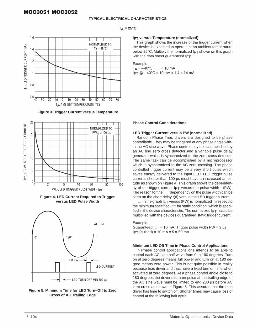
5–104 Motorola Optoelectronics Device Data
TYPICAL ELECTRICAL CHARACTERISTICS
TA = 25°C
Figure 3. Trigger Current versus Temperature
TA, AMBIENT TEMPERATURE (°C)
– 40
1.6
1.4
1.2
1
0.8
0.6– 30 – 20 –10 0 10 20 30 40 50 60 70 80
NORMALIZED TOTA = 25°C
I FT,
LED
TR
IGG
ER C
UR
REN
T (m
A)
Figure 4. LED Current Required to Triggerversus LED Pulse Width
PWin, LED TRIGGER PULSE WIDTH (µs)
1
25
20
15
10
5
02 5 10 20 50 100
NORMALIZED TO:PWin ≥ 100 µs
I FT,
NO
RM
ALIZ
ED L
ED T
RIG
GER
CU
RR
ENT
Figure 5. Minimum Time for LED Turn–Off to ZeroCross of AC Trailing Edge
AC SINE
0° 180°
LED PW
LED CURRENT
LED TURN OFF MIN 200 µs
IFT versus Temperature (normalized)This graph shows the increase of the trigger current when
the device is expected to operate at an ambient temperaturebelow 25°C. Multiply the normalized IFT shown on this graphwith the data sheet guaranteed IFT.
Example:TA = –40°C, IFT = 10 mAIFT @ –40°C = 10 mA x 1.4 = 14 mA
Phase Control Considerations
LED Trigger Current versus PW (normalized)Random Phase Triac drivers are designed to be phase
controllable. They may be triggered at any phase angle with-in the AC sine wave. Phase control may be accomplished byan AC line zero cross detector and a variable pulse delaygenerator which is synchronized to the zero cross detector.The same task can be accomplished by a microprocessorwhich is synchronized to the AC zero crossing. The phasecontrolled trigger current may be a very short pulse whichsaves energy delivered to the input LED. LED trigger pulsecurrents shorter than 100 µs must have an increased ampli-tude as shown on Figure 4. This graph shows the dependen-cy of the trigger current IFT versus the pulse width t (PW).The reason for the IFT dependency on the pulse width can beseen on the chart delay t(d) versus the LED trigger current.
IFT in the graph IFT versus (PW) is normalized in respect tothe minimum specified IFT for static condition, which is speci-fied in the device characteristic. The normalized IFT has to bemultiplied with the devices guaranteed static trigger current.
Example:Guaranteed IFT = 10 mA, Trigger pulse width PW = 3 µsIFT (pulsed) = 10 mA x 5 = 50 mA
Minimum LED Off Time in Phase Control ApplicationsIn Phase control applications one intends to be able to
control each AC sine half wave from 0 to 180 degrees. Turnon at zero degrees means full power and turn on at 180 de-gree means zero power. This is not quite possible in realitybecause triac driver and triac have a fixed turn on time whenactivated at zero degrees. At a phase control angle close to180 degrees the driver’s turn on pulse at the trailing edge ofthe AC sine wave must be limited to end 200 µs before ACzero cross as shown in Figure 5. This assures that the triacdriver has time to switch off. Shorter times may cause loss ofcontrol at the following half cycle.

5–105Motorola Optoelectronics Device Data
Figure 6. Holding Current, I Hversus Temperature
TA, AMBIENT TEMPERATURE (°C)
– 40
1
0.9
0– 30 – 20 –10 0 10 20 30 40 50 60 70 80
I H, H
OLD
ING
CU
RR
ENT
(mA) 0.8
0.7
0.6
0.5
0.4
0.3
0.2
0.1
Figure 7. Leakage Current, I DRMversus Temperature
TA, AMBIENT TEMPERATURE (°C)
– 40
100
1– 30 – 20 –10 0 10 20 30 40 50 60 70 80
10
I DR
M, L
EAKA
GE
CU
RR
ENT
(nA)
TYPICAL ELECTRICAL CHARACTERISTICS
TA = 25°C
Figure 8. ED Trigger Current, I FT, versus dv/dt
dv/dt (V/µs)
0.001
1.5
0.510000
NORMALIZED TO:IFT at 3 V
I FT,
LED
TR
IGG
ER C
UR
REN
T (N
OR
MAL
IZED
)
1.4
1.3
1.2
1.1
1
0.9
0.8
0.7
0.6
0.01 0.1 1 10 100 1000
IFT versus dv/dtTriac drivers with good noise immunity (dv/dt static) have
internal noise rejection circuits which prevent false triggeringof the device in the event of fast raising line voltage tran-sients. Inductive loads generate a commutating dv/dt thatmay activate the triac drivers noise suppression circuits. Thisprevents the device from turning on at its specified triggercurrent. It will in this case go into the mode of “half waving” ofthe load. Half waving of the load may destroy the power triacand the load.
Figure 8 shows the dependency of the triac drivers IFT ver-sus the reapplied voltage rise with a Vp of 400 V. This dv/dtcondition simulates a worst case commutating dv/dt ampli-tude.
It can be seen that the IFT does not change until a commu-tating dv/dt reaches 1000 V/µs. Practical loads generate acommutating dv/dt of less than 50 V/µs. The data sheet spe-cified IFT is therefore applicable for all practical inductiveloads and load factors.
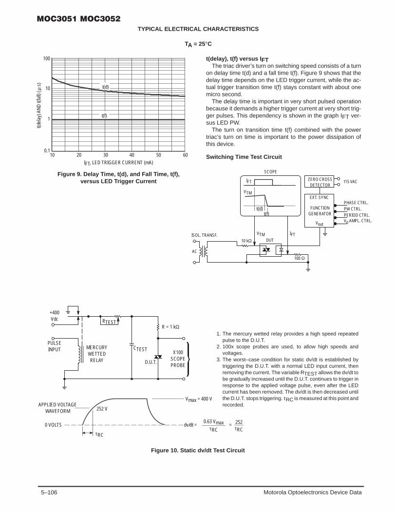
5–106 Motorola Optoelectronics Device Data
TYPICAL ELECTRICAL CHARACTERISTICS
TA = 25°C
Figure 9. Delay Time, t(d), and Fall Time, t(f),versus LED Trigger Current
IFT, LED TRIGGER CURRENT (mA)
100
0.110 20 30 40 50 60
10
t(del
ay) A
ND
t(fa
ll) (
s)µ
1t(f)
t(d)
t(delay), t(f) versus I FTThe triac driver’s turn on switching speed consists of a turn
on delay time t(d) and a fall time t(f). Figure 9 shows that thedelay time depends on the LED trigger current, while the ac-tual trigger transition time t(f) stays constant with about onemicro second.
The delay time is important in very short pulsed operationbecause it demands a higher trigger current at very short trig-ger pulses. This dependency is shown in the graph IFT ver-sus LED PW.
The turn on transition time t(f) combined with the powertriac’s turn on time is important to the power dissipation ofthis device.
Switching Time Test Circuit
1. The mercury wetted relay provides a high speed repeatedpulse to the D.U.T.
2. 100x scope probes are used, to allow high speeds andvoltages.
3. The worst–case condition for static dv/dt is established bytriggering the D.U.T. with a normal LED input current, thenremoving the current. The variable RTEST allows the dv/dt tobe gradually increased until the D.U.T. continues to trigger inresponse to the applied voltage pulse, even after the LEDcurrent has been removed. The dv/dt is then decreased untilthe D.U.T. stops triggering. τRC is measured at this point andrecorded.
Figure 10. Static dv/dt Test Circuit
+400Vdc
PULSEINPUT
RTEST
CTEST
R = 1 kΩ
MERCURYWETTEDRELAY D.U.T.
X100SCOPEPROBE
APPLIED VOLTAGEWAVEFORM
Vmax = 400 V
dv/dt =0.63 Vmax
τRC
252τRC
=
τRC
252 V
0 VOLTS
SCOPE
IFT
VTM
t(d)t(f)
ZERO CROSSDETECTOR
EXT. SYNC
Vout
FUNCTIONGENERATOR
PHASE CTRL.PW CTRL.PERIOD CTRL.Vo AMPL. CTRL.
IFTVTM10 kΩ DUT
100 Ω
ISOL. TRANSF.
AC
115 VAC

5–107Motorola Optoelectronics Device Data
APPLICATIONS GUIDE
Basic Triac Driver CircuitThe new random phase triac driver family MOC3052 and
MOC3051 are very immune to static dv/dt which allowssnubberless operations in all applications where externalgenerated noise in the AC line is below its guaranteed dv/dtwithstand capability. For these applications a snubber circuitis not necessary when a noise insensitive power triac isused. Figure 11 shows the circuit diagram. The triac driver isdirectly connected to the triac main terminal 2 and a seriesResistor R which limits the current to the triac driver. Currentlimiting resistor R must have a minimum value which restrictsthe current into the driver to maximum 1A.
R = Vp AC/ITM max rep. = Vp AC/1A
The power dissipation of this current limiting resistor andthe triac driver is very small because the power triac carriesthe load current as soon as the current through driver andcurrent limiting resistor reaches the trigger current of thepower triac. The switching transition times for the driver isonly one micro second and for power triacs typical four microseconds.
Triac Driver Circuit for Noisy EnvironmentsWhen the transient rate of rise and amplitude are expected
to exceed the power triacs and triac drivers maximum ratingsa snubber circuit as shown in Figure 12 is recommended.Fast transients are slowed by the R–C snubber and exces-sive amplitudes are clipped by the Metal Oxide Varistor MOV.
Triac Driver Circuit for Extremely Noisy Environments,as specified in the noise standards IEEE472 and IEC255–4.
Industrial control applications do specify a maximum tran-sient noise dv/dt and peak voltage which is superimposedonto the AC line voltage. In order to pass this environmentnoise test a modified snubber network as shown in Figure 13is recommended.
Figure 11. Basic Driver Circuit
Figure 12. Triac Driver Circuit for Noisy Environments
Figure 13. Triac Driver Circuit for Extremely NoisyEnvironments
VCC
RET.
RLED TRIAC DRIVER POWER TRIAC
AC LINE
LOAD
R
QCONTROL
R
TRIAC DRIVER POWER TRIACRLEDVCC
RET.
CONTROL
RS
CS
MOV
LOAD
AC LINE
RTRIAC DRIVER
POWER TRIAC
RS
CS
MOV
LOAD
AC LINE
VCC
RET.
CONTROL
RLED
RLED = (VCC – VF LED – Vsat Q)/IFTR = Vp AC line/ITSM
Typical Snubber values RS = 33 Ω, CS = 0.01 µFMOV (Metal Oxide Varistor) protects triac anddriver from transient overvoltages >VDRM max.
Recommended snubber to pass IEEE472 and IEC255–4 noise testsRS = 47 W, CS = 0.01 mF

5–108 Motorola Optoelectronics Device Data
PACKAGE DIMENSIONS
CASE 730A–04ISSUE G
NOTES:1. DIMENSIONING AND TOLERANCING PER ANSI
Y14.5M, 1982.2. CONTROLLING DIMENSION: INCH.3. DIMENSION L TO CENTER OF LEAD WHEN
FORMED PARALLEL.
STYLE 6:PIN 1. ANODE
2. CATHODE3. NC4. MAIN TERMINAL5. SUBSTRATE6. MAIN TERMINAL
6 4
1 3
–A–
–B–
SEATINGPLANE
–T–
4 PLF
K
CN
G
6 PLD6 PLE
MAM0.13 (0.005) B MT
L
M
6 PLJMBM0.13 (0.005) A MT
DIM MIN MAX MIN MAXMILLIMETERSINCHES
A 0.320 0.350 8.13 8.89B 0.240 0.260 6.10 6.60C 0.115 0.200 2.93 5.08D 0.016 0.020 0.41 0.50E 0.040 0.070 1.02 1.77F 0.010 0.014 0.25 0.36G 0.100 BSC 2.54 BSCJ 0.008 0.012 0.21 0.30K 0.100 0.150 2.54 3.81L 0.300 BSC 7.62 BSCM 0 15 0 15 N 0.015 0.100 0.38 2.54
CASE 730C–04ISSUE D
–A–
–B–
SEATINGPLANE
–T–J
K
L
6 PL
MBM0.13 (0.005) A MT
C
D 6 PL
MAM0.13 (0.005) B MT
H
GE 6 PL
F 4 PL
31
46
NOTES:1. DIMENSIONING AND TOLERANCING PER ANSI
Y14.5M, 1982.2. CONTROLLING DIMENSION: INCH.
DIM MIN MAX MIN MAXMILLIMETERSINCHES
A 0.320 0.350 8.13 8.89B 0.240 0.260 6.10 6.60C 0.115 0.200 2.93 5.08D 0.016 0.020 0.41 0.50E 0.040 0.070 1.02 1.77F 0.010 0.014 0.25 0.36G 0.100 BSC 2.54 BSCH 0.020 0.025 0.51 0.63J 0.008 0.012 0.20 0.30K 0.006 0.035 0.16 0.88L 0.320 BSC 8.13 BSCS 0.332 0.390 8.43 9.90
*Consult factory for leadform option availability

5–109Motorola Optoelectronics Device Data
*Consult factory for leadform option availability
NOTES:1. DIMENSIONING AND TOLERANCING PER ANSI
Y14.5M, 1982.2. CONTROLLING DIMENSION: INCH.3. DIMENSION L TO CENTER OF LEAD WHEN
FORMED PARALLEL.
CASE 730D–05ISSUE D
6 4
1 3
–A–
–B–
N
C
KG
F 4 PL
SEATING
D 6 PL
E 6 PL
PLANE
–T–
MAM0.13 (0.005) B MT
L
J
DIM MIN MAX MIN MAXMILLIMETERSINCHES
A 0.320 0.350 8.13 8.89B 0.240 0.260 6.10 6.60C 0.115 0.200 2.93 5.08D 0.016 0.020 0.41 0.50E 0.040 0.070 1.02 1.77F 0.010 0.014 0.25 0.36G 0.100 BSC 2.54 BSCJ 0.008 0.012 0.21 0.30K 0.100 0.150 2.54 3.81L 0.400 0.425 10.16 10.80N 0.015 0.040 0.38 1.02
Motorola reserves the right to make changes without further notice to any products herein. Motorola makes no warranty, representation or guarantee regardingthe suitability of its products for any particular purpose, nor does Motorola assume any liability arising out of the application or use of any product or circuit,and specifically disclaims any and all liability, including without limitation consequential or incidental damages. “Typical” parameters can and do vary in differentapplications. All operating parameters, including “Typicals” must be validated for each customer application by customer’s technical experts. Motorola doesnot convey any license under its patent rights nor the rights of others. Motorola products are not designed, intended, or authorized for use as components insystems intended for surgical implant into the body, or other applications intended to support or sustain life, or for any other application in which the failure ofthe Motorola product could create a situation where personal injury or death may occur. Should Buyer purchase or use Motorola products for any suchunintended or unauthorized application, Buyer shall indemnify and hold Motorola and its officers, employees, subsidiaries, affiliates, and distributors harmlessagainst all claims, costs, damages, and expenses, and reasonable attorney fees arising out of, directly or indirectly, any claim of personal injury or deathassociated with such unintended or unauthorized use, even if such claim alleges that Motorola was negligent regarding the design or manufacture of the part.Motorola and are registered trademarks of Motorola, Inc. Motorola, Inc. is an Equal Opportunity/Affirmative Action Employer.
How to reach us:USA / EUROPE: Motorola Literature Distribution; JAPAN : Nippon Motorola Ltd.; Tatsumi–SPD–JLDC, Toshikatsu Otsuki,P.O. Box 20912; Phoenix, Arizona 85036. 1–800–441–2447 6F Seibu–Butsuryu–Center, 3–14–2 Tatsumi Koto–Ku, Tokyo 135, Japan. 03–3521–8315
MFAX: [email protected] – TOUCHTONE (602) 244–6609 HONG KONG: Motorola Semiconductors H.K. Ltd.; 8B Tai Ping Industrial Park, INTERNET: http://Design–NET.com 51 Ting Kok Road, Tai Po, N.T., Hong Kong. 852–26629298
MOC3051/D
◊

5–110 Motorola Optoelectronics Device Data
(250 Volts Peak)
The MOC3031, MOC3032 and MOC3033 devices consist of gallium arsenideinfrared emitting diodes optically coupled to a monolithic silicon detectorperforming the function of a Zero Voltage crossing bilateral triac driver.
They are designed for use with a triac in the interface of logic systems toequipment powered from 115 Vac lines, such as teletypewriters, CRTs, printers,motors, solenoids and consumer appliances, etc.
• Simplifies Logic Control of 115 Vac Power
• Zero Voltage Crossing
• dv/dt of 2000 V/µs Typical, 1000 V/µs Guaranteed
• To order devices that are tested and marked per VDE 0884 requirements, thesuffix ”V” must be included at end of part number. VDE 0884 is a test option.
Recommended for 115 Vac(rms) Applications:
• Solenoid/Valve Controls • Temperature Controls
• Lighting Controls • E.M. Contactors
• Static Power Switches • AC Motor Starters
• AC Motor Drives • Solid State Relays
MAXIMUM RATINGS (TA = 25°C unless otherwise noted)
Rating Symbol Value Unit
INFRARED LED
Reverse Voltage VR 3 Volts
Forward Current — Continuous IF 60 mA
Total Power Dissipation @ TA = 25°CNegligible Power in Output Driver
Derate above 25°C
PD 120
1.41
mW
mW/°C
OUTPUT DRIVER
Off–State Output Terminal Voltage VDRM 250 Volts
Peak Repetitive Surge Current(PW = 100 µs, 120 pps)
ITSM 1 A
Total Power Dissipation @ TA = 25°CDerate above 25°C
PD 1501.76
mWmW/°C
TOTAL DEVICE
Isolation Surge Voltage(1)(Peak ac Voltage, 60 Hz, 1 Second Duration)
VISO 7500 Vac(pk)
Total Power Dissipation @ TA = 25°CDerate above 25°C
PD 2502.94
mWmW/°C
Junction Temperature Range TJ –40 to +100 °C
Ambient Operating Temperature Range(2) TA –40 to +85 °C
Storage Temperature Range(2) Tstg –40 to +150 °C
Soldering Temperature (10 s) TL 260 °C1. Isolation surge voltage, VISO, is an internal device dielectric breakdown rating.1. For this test, Pins 1 and 2 are common, and Pins 4, 5 and 6 are common.2. Refer to Quality and Reliability Section in Opto Data Book for information on test conditions.Preferred devices are Motorola recommended choices for future use and best overall value.GlobalOptoisolator is a trademark of Motorola, Inc.
Order this documentby MOC3031/D
SEMICONDUCTOR TECHNICAL DATA
GlobalOptoisolator
Motorola, Inc. 1995
*Motorola Preferred Device
COUPLER SCHEMATIC
[IFT = 15 mA Max]
STANDARD THRU HOLECASE 730A–04
[IFT = 10 mA Max]
[IFT = 5 mA Max]
1. ANODE2. CATHODE3. NC4. MAIN TERMINAL5. SUBSTRATE5. DO NOT CONNECT6. MAIN TERMINAL
1
2
3
6
5
4ZERO
CROSSINGCIRCUIT
61
STYLE 6 PLASTIC
(Replaces MOC3030/D)

5–111Motorola Optoelectronics Device Data
ELECTRICAL CHARACTERISTICS (TA = 25°C unless otherwise noted)
Characteristic Symbol Min Typ Max Unit
INPUT LED
Reverse Leakage Current(VR = 3 V)
IR — 0.05 100 µA
Forward Voltage(IF = 30 mA)
VF — 1.3 1.5 Volts
OUTPUT DETECTOR (IF = 0 unless otherwise noted)
Leakage with LED Off, Either Direction(Rated VDRM(1))
IDRM1 — 10 100 nA
Peak On–State Voltage, Either Direction(ITM = 100 mA Peak)
VTM — 1.8 3 Volts
Critical Rate of Rise of Off–State Voltage dv/dt 1000 2000 — V/µs
COUPLED
LED Trigger Current, Current Required to Latch Output(Main Terminal Voltage = 3 V(2)) MOC3031
MOC3032MOC3033
IFT———
———
15105
mA
Holding Current, Either Direction IH — 250 — µA
Isolation Voltage (f = 60 Hz, t = 1 sec) VISO 7500 — — Vac(pk)
ZERO CROSSING
Inhibit Voltage(IF = Rated IFT, MT1–MT2 Voltage above which device will nottrigger.)
VIH — 5 20 Volts
Leakage in Inhibited State(IF = Rated IFT, Rated VDRM, Off State)
IDRM2 — — 500 µA
1. Test voltage must be applied within dv/dt rating.2. All devices are guaranteed to trigger at an IF value less than or equal to max IFT. Therefore, recommended operating IF lies between max2. IFT (15 mA for MOC3031, 10 mA for MOC3032, 5 mA for MOC3033) and absolute max IF (60 mA).
Figure 1. On–State Characteristics
–3VTM, ON–STATE VOLTAGE (VOLTS)
I
–400
0
+400
+800
–2 –1 0 1 2 3
TM, O
N-S
TATE
CU
RR
ENT
(mA)
–600
–800
–200
+200
+600
4–4
OUTPUT PULSE WIDTH – 80 µsIF = 30 mAf = 60 HzTA = 25°C
0.7
Figure 2. Trigger Current versus Temperature
–40TA, AMBIENT TEMPERATURE (°C)
0.8
1.1
1.3
–20 0 20 40 60 80
FTN
OR
MAL
IZED
I
100
0.9
1
1.2
NORMALIZED TOTA = 25°C
TYPICAL ELECTRICAL CHARACTERISTICS
TA = 25°C
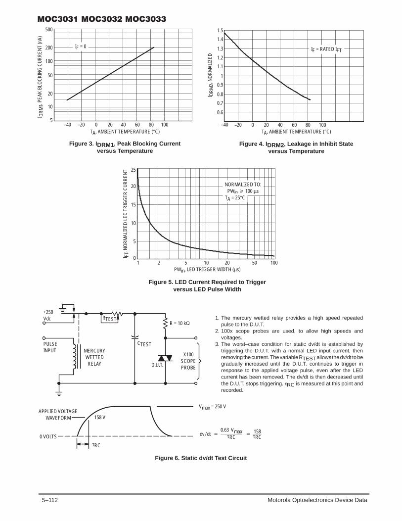
5–112 Motorola Optoelectronics Device Data
5
1PWin, LED TRIGGER WIDTH (µs)
10
15
20
25
2 5 2010 500FTI
, NO
RM
ALIZ
ED L
ED T
RIG
GER
CU
RR
ENT
NORMALIZED TO:PWin 100 µs
+250Vdc
PULSEINPUT MERCURY
WETTEDRELAY
RTEST
CTEST
R = 10 kΩ
X100SCOPEPROBED.U.T.
APPLIED VOLTAGEWAVEFORM 158 V
0 VOLTSRC
Vmax = 250 V
dvdt 0.63 Vmax
RC 158
RC
1. The mercury wetted relay provides a high speed repeatedpulse to the D.U.T.
2. 100x scope probes are used, to allow high speeds andvoltages.
3. The worst–case condition for static dv/dt is established bytriggering the D.U.T. with a normal LED input current, thenremoving the current. The variable RTEST allows the dv/dt to begradually increased until the D.U.T. continues to trigger inresponse to the applied voltage pulse, even after the LEDcurrent has been removed. The dv/dt is then decreased untilthe D.U.T. stops triggering. RC is measured at this point andrecorded.
5–40
TA, AMBIENT TEMPERATURE (°C)
I
–20 0 20 40 60 80 100
10
20
50
100
200
500
DR
M1,
PEA
K BL
OC
KIN
G C
UR
REN
T (n
A)
0.6
–40TA, AMBIENT TEMPERATURE (°C)
I
IF = RATED IFT
0.7
0.8
0.9
1
1.1
1.2
1.3
1.4
1.5
–20 0 20 40 60 80 100
DR
M2,
NO
RM
ALIZ
ED
TA = 25°C
IF = 0
Figure 3. I DRM1, Peak Blocking Currentversus Temperature
Figure 4. I DRM2, Leakage in Inhibit Stateversus Temperature
Figure 5. LED Current Required to Triggerversus LED Pulse Width
Figure 6. Static dv/dt Test Circuit
100

5–113Motorola Optoelectronics Device Data
Rin 1
2
6
4
180 Ω
MOC3031/3032/3033
3
5
NOTE: This optoisolator should not be used to drive a load directly.It is intended to be a trigger device only.
1 k
39
0.01
115 VAC
HOT
NEUTRALLOAD
Typical circuit for use when hot line switching is required.In this circuit the “hot” side of the line is switched and theload connected to the cold or neutral side. The load may beconnected to either the neutral or hot line.
Rin is calculated so that IF is equal to the rated IFT of thepart, 5 mA for the MOC3033, 10 mA for the MOC3032, or15 mA for the MOC3031. The 39 ohm resistor and 0.01 µFcapacitor are for snubbing of the triac and may or may notbe necessary depending upon the particular triac and loadused.
Rin
R1
2
6
4
MOC3031/3032/3033
3
5
VCC
R2
LOAD
180 Ω
D1
1
SCRSCR
D2
115 VAC
Suggested method of firing two, back–to–back SCR’s,with a Motorola triac driver. Diodes can be 1N4001; resis-tors, R1 and R2, are optional 1 k ohm.
* For highly inductive loads (power factor < 0.5), change this value to360 ohms.
Figure 7. Hot–Line Switching Application Circuit
Figure 8. Inverse–Parallel SCR Driver Circuit
VCC

5–114 Motorola Optoelectronics Device Data
PACKAGE DIMENSIONS
CASE 730A–04ISSUE G
NOTES:1. DIMENSIONING AND TOLERANCING PER ANSI
Y14.5M, 1982.2. CONTROLLING DIMENSION: INCH.3. DIMENSION L TO CENTER OF LEAD WHEN
FORMED PARALLEL.
6 4
1 3
–A–
–B–
SEATINGPLANE
–T–
4 PLF
K
CN
G
6 PLD6 PLE
MAM0.13 (0.005) B MT
L
M
6 PLJMBM0.13 (0.005) A MT
DIM MIN MAX MIN MAXMILLIMETERSINCHES
A 0.320 0.350 8.13 8.89B 0.240 0.260 6.10 6.60C 0.115 0.200 2.93 5.08D 0.016 0.020 0.41 0.50E 0.040 0.070 1.02 1.77F 0.010 0.014 0.25 0.36G 0.100 BSC 2.54 BSCJ 0.008 0.012 0.21 0.30K 0.100 0.150 2.54 3.81L 0.300 BSC 7.62 BSCM 0 15 0 15 N 0.015 0.100 0.38 2.54
STYLE 6:PIN 1. ANODE
2. CATHODE3. NC4. MAIN TERMINAL5. SUBSTRATE6. MAIN TERMINAL
CASE 730C–04ISSUE D
–A–
–B–
SEATINGPLANE
–T–J
K
L
6 PL
MBM0.13 (0.005) A MT
C
D 6 PL
MAM0.13 (0.005) B MT
H
GE 6 PL
F 4 PL
31
46
NOTES:1. DIMENSIONING AND TOLERANCING PER ANSI
Y14.5M, 1982.2. CONTROLLING DIMENSION: INCH.
DIM MIN MAX MIN MAXMILLIMETERSINCHES
A 0.320 0.350 8.13 8.89B 0.240 0.260 6.10 6.60C 0.115 0.200 2.93 5.08D 0.016 0.020 0.41 0.50E 0.040 0.070 1.02 1.77F 0.010 0.014 0.25 0.36G 0.100 BSC 2.54 BSCH 0.020 0.025 0.51 0.63J 0.008 0.012 0.20 0.30K 0.006 0.035 0.16 0.88L 0.320 BSC 8.13 BSCS 0.332 0.390 8.43 9.90
*Consult factory for leadform option availability

5–115Motorola Optoelectronics Device Data
*Consult factory for leadform option availability
NOTES:1. DIMENSIONING AND TOLERANCING PER ANSI
Y14.5M, 1982.2. CONTROLLING DIMENSION: INCH.3. DIMENSION L TO CENTER OF LEAD WHEN
FORMED PARALLEL.
CASE 730D–05ISSUE D
6 4
1 3
–A–
–B–
N
C
KG
F 4 PL
SEATING
D 6 PL
E 6 PL
PLANE
–T–
MAM0.13 (0.005) B MT
L
J
DIM MIN MAX MIN MAXMILLIMETERSINCHES
A 0.320 0.350 8.13 8.89B 0.240 0.260 6.10 6.60C 0.115 0.200 2.93 5.08D 0.016 0.020 0.41 0.50E 0.040 0.070 1.02 1.77F 0.010 0.014 0.25 0.36G 0.100 BSC 2.54 BSCJ 0.008 0.012 0.21 0.30K 0.100 0.150 2.54 3.81L 0.400 0.425 10.16 10.80N 0.015 0.040 0.38 1.02
Motorola reserves the right to make changes without further notice to any products herein. Motorola makes no warranty, representation or guarantee regardingthe suitability of its products for any particular purpose, nor does Motorola assume any liability arising out of the application or use of any product or circuit,and specifically disclaims any and all liability, including without limitation consequential or incidental damages. “Typical” parameters can and do vary in differentapplications. All operating parameters, including “Typicals” must be validated for each customer application by customer’s technical experts. Motorola doesnot convey any license under its patent rights nor the rights of others. Motorola products are not designed, intended, or authorized for use as components insystems intended for surgical implant into the body, or other applications intended to support or sustain life, or for any other application in which the failure ofthe Motorola product could create a situation where personal injury or death may occur. Should Buyer purchase or use Motorola products for any suchunintended or unauthorized application, Buyer shall indemnify and hold Motorola and its officers, employees, subsidiaries, affiliates, and distributors harmlessagainst all claims, costs, damages, and expenses, and reasonable attorney fees arising out of, directly or indirectly, any claim of personal injury or deathassociated with such unintended or unauthorized use, even if such claim alleges that Motorola was negligent regarding the design or manufacture of the part.Motorola and are registered trademarks of Motorola, Inc. Motorola, Inc. is an Equal Opportunity/Affirmative Action Employer.
How to reach us:USA / EUROPE: Motorola Literature Distribution; JAPAN : Nippon Motorola Ltd.; Tatsumi–SPD–JLDC, Toshikatsu Otsuki,P.O. Box 20912; Phoenix, Arizona 85036. 1–800–441–2447 6F Seibu–Butsuryu–Center, 3–14–2 Tatsumi Koto–Ku, Tokyo 135, Japan. 03–3521–8315
MFAX: [email protected] – TOUCHTONE (602) 244–6609 HONG KONG: Motorola Semiconductors H.K. Ltd.; 8B Tai Ping Industrial Park, INTERNET: http://Design–NET.com 51 Ting Kok Road, Tai Po, N.T., Hong Kong. 852–26629298
MOC3031/D
◊

5–116 Motorola Optoelectronics Device Data
! (400 Volts Peak)
The MOC3041, MOC3042 and MOC3043 devices consist of gallium arsenideinfrared emitting diodes optically coupled to a monolithic silicon detectorperforming the function of a Zero Voltage Crossing bilateral triac driver.
They are designed for use with a triac in the interface of logic systems toequipment powered from 115 Vac lines, such as solid–state relays, industrialcontrols, motors, solenoids and consumer appliances, etc.
• Simplifies Logic Control of 115 Vac Power
• Zero Voltage Crossing
• dv/dt of 2000 V/µs Typical, 1000 V/µs Guaranteed
• To order devices that are tested and marked per VDE 0884 requirements, thesuffix ”V” must be included at end of part number. VDE 0884 is a test option.
Recommended for 115/240 Vac(rms) Applications:
• Solenoid/Valve Controls • Temperature Controls
• Lighting Controls • E.M. Contactors
• Static Power Switches • AC Motor Starters
• AC Motor Drives • Solid State Relays
MAXIMUM RATINGS (TA = 25°C unless otherwise noted)
Rating Symbol Value Unit
INFRARED EMITTING DIODE
Reverse Voltage VR 6 Volts
Forward Current — Continuous IF 60 mA
Total Power Dissipation @ TA = 25°CNegligible Power in Output Driver
Derate above 25°C
PD 120
1.41
mW
mW/°C
OUTPUT DRIVER
Off–State Output Terminal Voltage VDRM 400 Volts
Peak Repetitive Surge Current(PW = 100 µs, 120 pps)
ITSM 1 A
Total Power Dissipation @ TA = 25°CDerate above 25°C
PD 1501.76
mWmW/°C
TOTAL DEVICE
Isolation Surge Voltage(1)(Peak ac Voltage, 60 Hz, 1 Second Duration)
VISO 7500 Vac(pk)
Total Power Dissipation @ TA = 25°CDerate above 25°C
PD 2502.94
mW mW/°C
Junction Temperature Range TJ –40 to +100 °C
Ambient Operating Temperature Range(2) TA –40 to +85 °C
Storage Temperature Range(2) Tstg –40 to +150 °C
Soldering Temperature (10 s) TL 260 °C1. Isolation surge voltage, VISO, is an internal device dielectric breakdown rating.1. For this test, Pins 1 and 2 are common, and Pins 4, 5 and 6 are common.2. Refer to Quality and Reliability Section in Opto Data Book for information on test conditions.Preferred devices are Motorola recommended choices for future use and best overall value.GlobalOptoisolator is a trademark of Motorola, Inc.
Order this documentby MOC3041/D
SEMICONDUCTOR TECHNICAL DATA
GlobalOptoisolator
Motorola, Inc. 1995
*Motorola Preferred Device
COUPLER SCHEMATIC
[IFT = 15 mA Max]
STANDARD THRU HOLECASE 730A–04
[IFT = 10 mA Max]
[IFT = 5 mA Max]
1. ANODE2. CATHODE3. NC4. MAIN TERMINAL5. SUBSTRATE5. DO NOT CONNECT6. MAIN TERMINAL
1
2
3
6
5
4ZERO
CROSSINGCIRCUIT
61
STYLE 6 PLASTIC
(Replaces MOC3040/D)

5–117Motorola Optoelectronics Device Data
ELECTRICAL CHARACTERISTICS (TA = 25°C unless otherwise noted)
Characteristic Symbol Min Typ Max Unit
INPUT LED
Reverse Leakage Current(VR = 6 V)
IR — 0.05 100 µA
Forward Voltage(IF = 30 mA)
VF — 1.3 1.5 Volts
OUTPUT DETECTOR (IF = 0 unless otherwise noted)
Leakage with LED Off, Either Direction(Rated VDRM(1))
IDRM1 — 2 100 nA
Peak On–State Voltage, Either Direction(ITM = 100 mA Peak)
VTM — 1.8 3 Volts
Critical Rate of Rise of Off–State Voltage(3) dv/dt 1000 2000 — V/µs
COUPLED
LED Trigger Current, Current Required to Latch Output(Main Terminal Voltage = 3 V(2)) MOC3041
MOC3042MOC3043
IFT———
———
15105
mA
Holding Current, Either Direction IH — 250 — µA
Isolation Voltage (f = 60 Hz, t = 1 sec) VISO 7500 — — Vac(pk)
ZERO CROSSING
Inhibit Voltage(IF = Rated IFT, MT1–MT2 Voltage above which device willnot trigger.)
VIH — 5 20 Volts
Leakage in Inhibited State(IF = Rated IFT, Rated VDRM, Off State)
IDRM2 — — 500 µA
1. Test voltage must be applied within dv/dt rating.2. All devices are guaranteed to trigger at an IF value less than or equal to max IFT. Therefore, recommended operating IF lies between IFT2. (15 mA for MOC3041, 10 mA for MOC3042, 5 mA for MOC3043) and absolute max IF (60 mA).3. This is static dv/dt. See Figure 7 for test circuit. Commutating dv/dt is a function of the load–driving thyristor(s) only.
Figure 1. On–State Characteristics
–3VTM, ON–STATE VOLTAGE (VOLTS)
I
–400
0
+400
+800
–2 –1 0 1 2 3
TM, O
N-S
TATE
CU
RR
ENT
(mA)
–600
–800
–200
+200
+600
4–4
0.7
Figure 2. Trigger Current versus Temperature
–40TA, AMBIENT TEMPERATURE (°C)
0.8
1.1
1.3
–20 0 20 40 60 80
FTN
OR
MAL
IZED
I
0.9
1
1.2
1.41.5
NORMALIZED TOTA = 25°C
OUTPUT PULSE WIDTH – 80 µs
5
IF = 30 mAf = 60 HzTA = 25°C
TYPICAL ELECTRICAL CHARACTERISTICS
TA = 25°C

5–118 Motorola Optoelectronics Device Data
5
1PWin, LED TRIGGER PULSE WIDTH (µs)
10
15
20
25
2 5 2010 500FTI
, NO
RM
ALIZ
ED L
ED T
RIG
GER
CU
RR
ENT
TA, AMBIENT TEMPERATURE (°C)–40
+400Vdc
PULSEINPUT MERCURY
WETTEDRELAY
RTEST
CTEST
R = 10 kΩ
X100SCOPEPROBED.U.T.
APPLIED VOLTAGEWAVEFORM 252 V
0 VOLTSRC
Vmax = 400 V
dvdt 0.63 Vmax
RC 252
RC
1. The mercury wetted relay provides a high speed repeatedpulse to the D.U.T.
2. 100x scope probes are used, to allow high speeds andvoltages.
3. The worst–case condition for static dv/dt is established bytriggering the D.U.T. with a normal LED input current, thenremoving the current. The variable RTEST allows the dv/dt to begradually increased until the D.U.T. continues to trigger inresponse to the applied voltage pulse, even after the LEDcurrent has been removed. The dv/dt is then decreased untilthe D.U.T. stops triggering. RC is measured at this point andrecorded.
5–40
TA, AMBIENT TEMPERATURE (°C)
I
–20 0 20 40 60 80 100
10
20
50
100
200
500
DR
M1,
PEA
K BL
OC
KIN
G C
UR
REN
T (n
A)
0.6
–40TA, AMBIENT TEMPERATURE (°C)
I
IF = RATED IFT
0.7
0.8
0.9
1
1.1
1.2
1.3
1.4
1.5
–20 0 20 40 60 80 100
DR
M2,
NO
RM
ALIZ
ED
I FT,
NO
RM
ALIZ
ED
0.70.8
0.9
1
1.1
1.21.3
1.4
1.5 NORMALIZED TOTA = 25°C
–20 0 20 40 60 80 100
IF = 0
Figure 3. I DRM1, Peak Blocking Currentversus Temperature
Figure 4. I DRM2, Leakage in Inhibit Stateversus Temperature
Figure 5. Trigger Current versus Temperature Figure 6. LED Current Required to Triggerversus LED Pulse Width
Figure 7. Static dv/dt Test Circuit
100
NORMALIZED TO:PWin 100 µsTA = 25°C
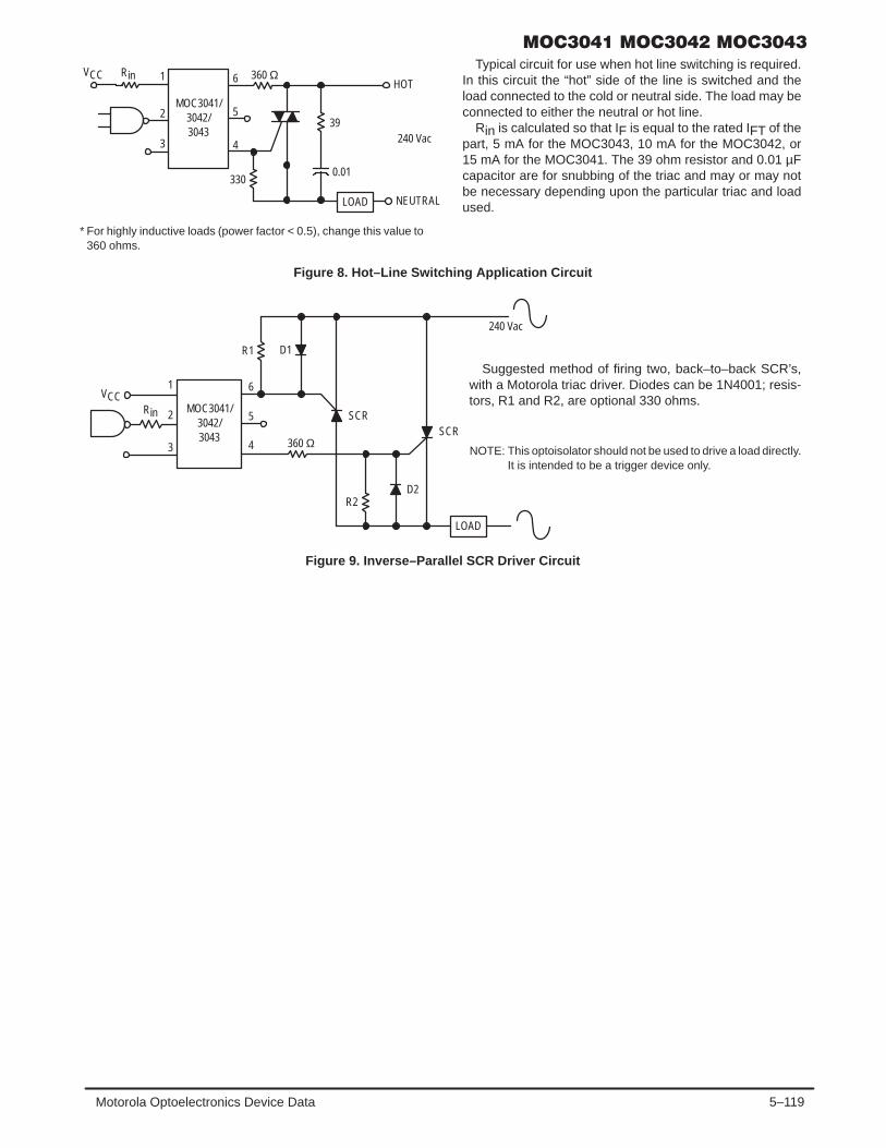
5–119Motorola Optoelectronics Device Data
Rin 1
2
6
4
360 Ω
MOC3041/3042/3043
3
5
VCC
NOTE: This optoisolator should not be used to drive a load directly.It is intended to be a trigger device only.
330
39
0.01
240 Vac
HOT
NEUTRALLOAD
Typical circuit for use when hot line switching is required.In this circuit the “hot” side of the line is switched and theload connected to the cold or neutral side. The load may beconnected to either the neutral or hot line.
Rin is calculated so that IF is equal to the rated IFT of thepart, 5 mA for the MOC3043, 10 mA for the MOC3042, or15 mA for the MOC3041. The 39 ohm resistor and 0.01 µFcapacitor are for snubbing of the triac and may or may notbe necessary depending upon the particular triac and loadused.
Rin
R1
2
6
43
5
VCC
R2
LOAD
360 Ω
D1
1
SCRSCR
D2
240 Vac
Suggested method of firing two, back–to–back SCR’s,with a Motorola triac driver. Diodes can be 1N4001; resis-tors, R1 and R2, are optional 330 ohms.
* For highly inductive loads (power factor < 0.5), change this value to360 ohms.
Figure 8. Hot–Line Switching Application Circuit
Figure 9. Inverse–Parallel SCR Driver Circuit
MOC3041/3042/3043

5–120 Motorola Optoelectronics Device Data
PACKAGE DIMENSIONS
CASE 730A–04ISSUE G
NOTES:1. DIMENSIONING AND TOLERANCING PER ANSI
Y14.5M, 1982.2. CONTROLLING DIMENSION: INCH.3. DIMENSION L TO CENTER OF LEAD WHEN
FORMED PARALLEL.
6 4
1 3
–A–
–B–
SEATINGPLANE
–T–
4 PLF
K
CN
G
6 PLD6 PLE
MAM0.13 (0.005) B MT
L
M
6 PLJMBM0.13 (0.005) A MT
DIM MIN MAX MIN MAXMILLIMETERSINCHES
A 0.320 0.350 8.13 8.89B 0.240 0.260 6.10 6.60C 0.115 0.200 2.93 5.08D 0.016 0.020 0.41 0.50E 0.040 0.070 1.02 1.77F 0.010 0.014 0.25 0.36G 0.100 BSC 2.54 BSCJ 0.008 0.012 0.21 0.30K 0.100 0.150 2.54 3.81L 0.300 BSC 7.62 BSCM 0 15 0 15 N 0.015 0.100 0.38 2.54
STYLE 6:PIN 1. ANODE
2. CATHODE3. NC4. MAIN TERMINAL5. SUBSTRATE6. MAIN TERMINAL
CASE 730C–04ISSUE D
–A–
–B–
SEATINGPLANE
–T–J
K
L
6 PL
MBM0.13 (0.005) A MT
C
D 6 PL
MAM0.13 (0.005) B MT
H
GE 6 PL
F 4 PL
31
46
NOTES:1. DIMENSIONING AND TOLERANCING PER ANSI
Y14.5M, 1982.2. CONTROLLING DIMENSION: INCH.
DIM MIN MAX MIN MAXMILLIMETERSINCHES
A 0.320 0.350 8.13 8.89B 0.240 0.260 6.10 6.60C 0.115 0.200 2.93 5.08D 0.016 0.020 0.41 0.50E 0.040 0.070 1.02 1.77F 0.010 0.014 0.25 0.36G 0.100 BSC 2.54 BSCH 0.020 0.025 0.51 0.63J 0.008 0.012 0.20 0.30K 0.006 0.035 0.16 0.88L 0.320 BSC 8.13 BSCS 0.332 0.390 8.43 9.90
*Consult factory for leadform option availability

5–121Motorola Optoelectronics Device Data
*Consult factory for leadform option availability
NOTES:1. DIMENSIONING AND TOLERANCING PER ANSI
Y14.5M, 1982.2. CONTROLLING DIMENSION: INCH.3. DIMENSION L TO CENTER OF LEAD WHEN
FORMED PARALLEL.
CASE 730D–05ISSUE D
6 4
1 3
–A–
–B–
N
C
KG
F 4 PL
SEATING
D 6 PL
E 6 PL
PLANE
–T–
MAM0.13 (0.005) B MT
L
J
DIM MIN MAX MIN MAXMILLIMETERSINCHES
A 0.320 0.350 8.13 8.89B 0.240 0.260 6.10 6.60C 0.115 0.200 2.93 5.08D 0.016 0.020 0.41 0.50E 0.040 0.070 1.02 1.77F 0.010 0.014 0.25 0.36G 0.100 BSC 2.54 BSCJ 0.008 0.012 0.21 0.30K 0.100 0.150 2.54 3.81L 0.400 0.425 10.16 10.80N 0.015 0.040 0.38 1.02
Motorola reserves the right to make changes without further notice to any products herein. Motorola makes no warranty, representation or guarantee regardingthe suitability of its products for any particular purpose, nor does Motorola assume any liability arising out of the application or use of any product or circuit,and specifically disclaims any and all liability, including without limitation consequential or incidental damages. “Typical” parameters can and do vary in differentapplications. All operating parameters, including “Typicals” must be validated for each customer application by customer’s technical experts. Motorola doesnot convey any license under its patent rights nor the rights of others. Motorola products are not designed, intended, or authorized for use as components insystems intended for surgical implant into the body, or other applications intended to support or sustain life, or for any other application in which the failure ofthe Motorola product could create a situation where personal injury or death may occur. Should Buyer purchase or use Motorola products for any suchunintended or unauthorized application, Buyer shall indemnify and hold Motorola and its officers, employees, subsidiaries, affiliates, and distributors harmlessagainst all claims, costs, damages, and expenses, and reasonable attorney fees arising out of, directly or indirectly, any claim of personal injury or deathassociated with such unintended or unauthorized use, even if such claim alleges that Motorola was negligent regarding the design or manufacture of the part.Motorola and are registered trademarks of Motorola, Inc. Motorola, Inc. is an Equal Opportunity/Affirmative Action Employer.
How to reach us:USA / EUROPE: Motorola Literature Distribution; JAPAN : Nippon Motorola Ltd.; Tatsumi–SPD–JLDC, Toshikatsu Otsuki,P.O. Box 20912; Phoenix, Arizona 85036. 1–800–441–2447 6F Seibu–Butsuryu–Center, 3–14–2 Tatsumi Koto–Ku, Tokyo 135, Japan. 03–3521–8315
MFAX: [email protected] – TOUCHTONE (602) 244–6609 HONG KONG: Motorola Semiconductors H.K. Ltd.; 8B Tai Ping Industrial Park, INTERNET: http://Design–NET.com 51 Ting Kok Road, Tai Po, N.T., Hong Kong. 852–26629298
MOC3041/D
◊

5–122 Motorola Optoelectronics Device Data
(600 Volts Peak)
The MOC3061, MOC3062 and MOC3063 devices consist of gallium arsenideinfrared emitting diodes optically coupled to monolithic silicon detectorsperforming the functions of Zero Voltage Crossing bilateral triac drivers.
They are designed for use with a triac in the interface of logic systems toequipment powered from 115/240 Vac lines, such as solid–state relays,industrial controls, motors, solenoids and consumer appliances, etc.
• Simplifies Logic Control of 115/240 Vac Power• Zero Voltage Crossing• dv/dt of 1500 V/µs Typical, 600 V/µs Guaranteed• To order devices that are tested and marked per VDE 0884 requirements, the
suffix ”V” must be included at end of part number. VDE 0884 is a test option.Recommended for 115/240 Vac(rms) Applications:
• Solenoid/Valve Controls • Temperature Controls
• Lighting Controls • E.M. Contactors
• Static Power Switches • AC Motor Starters
• AC Motor Drives • Solid State Relays
MAXIMUM RATINGS
Rating Symbol Value Unit
INFRARED EMITTING DIODE
Reverse Voltage VR 6 Volts
Forward Current — Continuous IF 60 mA
Total Power Dissipation @ TA = 25°CNegligible Power in Output Driver
Derate above 25°C
PD 120
1.41
mW
mW/°C
OUTPUT DRIVER
Off–State Output Terminal Voltage VDRM 600 Volts
Peak Repetitive Surge Current(PW = 100 µs, 120 pps)
ITSM 1 A
Total Power Dissipation @ TA = 25°CDerate above 25°C
PD 1501.76
mWmW/°C
TOTAL DEVICE
Isolation Surge Voltage(1)
(Peak ac Voltage, 60 Hz, 1 Second Duration)VISO 7500 Vac(pk)
Total Power Dissipation @ TA = 25°CDerate above 25°C
PD 2502.94
mWmW/°C
Junction Temperature Range TJ –40 to +100 °C
Ambient Operating Temperature Range(2) TA –40 to +85 °C
Storage Temperature Range(2) Tstg –40 to +150 °C
Soldering Temperature (10 s) TL 260 °C1. Isolation surge voltage, VISO, is an internal device dielectric breakdown rating.1. For this test, Pins 1 and 2 are common, and Pins 4, 5 and 6 are common.2. Refer to Quality and Reliability Section in Opto Data Book for information on test conditions.Preferred devices are Motorola recommended choices for future use and best overall value.GlobalOptoisolator is a trademark of Motorola, Inc.
Order this documentby MOC3061/D
SEMICONDUCTOR TECHNICAL DATA
GlobalOptoisolator
Motorola, Inc. 1995
*Motorola Preferred Device
COUPLER SCHEMATIC
[IFT = 15 mA Max]
STANDARD THRU HOLECASE 730A–04
[IFT = 10 mA Max]
[IFT = 5 mA Max]
1. ANODE2. CATHODE3. NC4. MAIN TERMINAL5. SUBSTRATE
DO NOT CONNECT6. MAIN TERMINAL
1
2
3
6
5
4ZERO
CROSSINGCIRCUIT
61
STYLE 6 PLASTIC
(Replaces MOC3060/D)

5–123Motorola Optoelectronics Device Data
ELECTRICAL CHARACTERISTICS (TA = 25°C unless otherwise noted)
Characteristic Symbol Min Typ Max Unit
INPUT LED
Reverse Leakage Current(VR = 6 V)
IR — 0.05 100 µA
Forward Voltage(IF = 30 mA)
VF — 1.3 1.5 Volts
OUTPUT DETECTOR (IF = 0)
Leakage with LED Off, Either Direction(Rated VDRM(1))
IDRM1 — 60 500 nA
Critical Rate of Rise of Off–State Voltage(3) dv/dt 600 1500 — V/µs
COUPLED
LED Trigger Current, Current Required to Latch Output(Main Terminal Voltage = 3 V(2)) MOC3061
MOC3062MOC3063
IFT———
———
15105
mA
Peak On–State Voltage, Either Direction(ITM = 100 mA, IF = Rated IFT)
VTM — 1.8 3 Volts
Holding Current, Either Direction IH — 250 — µA
Inhibit Voltage (MT1–MT2 Voltage above which device will not trigger.)(IF = Rated IFT)
VINH — 5 20 Volts
Leakage in Inhibited State(IF = Rated IFT, Rated VDRM, Off State)
IDRM2 — — 500 µA
Isolation Voltage (f = 60 Hz, t = 1 sec) VISO 7500 — — Vac(pk)
1. Test voltage must be applied within dv/dt rating.2. All devices are guaranteed to trigger at an IF value less than or equal to max IFT. Therefore, recommended operating IF lies between max2. IFT (15 mA for MOC3061, 10 mA for MOC3062, 5 mA for MOC3063) and absolute max IF (60 mA).3. This is static dv/dt. See Figure 7 for test circuit. Commutating dv/dt is a function of the load–driving thyristor(s) only.
Figure 1. On–State Characteristics
–3VTM, ON–STATE VOLTAGE (VOLTS)
I
–400
0
+400
+800
–2 –1 0 1 2 3
TM, O
N–S
TATE
CU
RR
ENT
(mA)
–600
–800
–200
+200
+600
4–4
0.7
Figure 2. Inhibit Voltage versus Temperature
–40TA, AMBIENT TEMPERATURE (°C)
0.8
1.1
1.3
–20 0 20 40 60 80
, NO
RM
ALIZ
ED
100
0.9
1
1.2
1.4
1.5
5
0.60.5
VIN
H
NORMALIZED TOTA = 25°C
OUTPUT PULSE WIDTH – 80 µsIF = 30 mAf = 60 HzTA = 25°C
TYPICAL CHARACTERISTICS
TA = 25°C

5–124 Motorola Optoelectronics Device Data
5
1PWin, LED TRIGGER PULSE WIDTH (µs)
10
15
20
25
2 5 2010 500FTI
, NO
RM
ALIZ
ED L
ED T
RIG
GER
CU
RR
ENT
NORMALIZED TO:PWin 100 µs
TA, AMBIENT TEMPERATURE (°C)–40
+400Vdc
PULSEINPUT MERCURY
WETTEDRELAY
RTEST
CTEST
R = 10 kΩ
X100SCOPEPROBED.U.T.
APPLIED VOLTAGEWAVEFORM 252 V
0 VOLTSRC
Vmax = 400 V
dvdt 0.63 Vmax
RC 378
RC
1. The mercury wetted relay provides a high speed repeatedpulse to the D.U.T.
2. 100x scope probes are used, to allow high speeds andvoltages.
3. The worst–case condition for static dv/dt is established bytriggering the D.U.T. with a normal LED input current, thenremoving the current. The variable RTEST allows the dv/dt to begradually increased until the D.U.T. continues to trigger inresponse to the applied voltage pulse, even after the LEDcurrent has been removed. The dv/dt is then decreased untilthe D.U.T. stops triggering. RC is measured at this point andrecorded.
5–40
TA, AMBIENT TEMPERATURE (°C)
I
–20 0 20 40 60 80 100
10
20
50
100
200
500
DR
M1,
PEA
K BL
OC
KIN
G C
UR
REN
T (n
A)
0.6
–40TA, AMBIENT TEMPERATURE (°C)
I
IF = RATED IFT
0.7
0.8
0.9
1
1.1
1.2
1.3
1.4
1.5
–20 0 20 40 60 80 100
DR
M2,
NO
RM
ALIZ
ED
I FT,
NO
RM
ALIZ
ED
0.70.8
0.9
1
1.1
1.21.3
1.4
1.5 NORMALIZED TOTA = 25°C
–20 0 20 40 60 80 100
IF = 0
Figure 3. Leakage with LED Offversus Temperature
Figure 4. I DRM2, Leakage in Inhibit Stateversus Temperature
Figure 5. Trigger Current versus Temperature Figure 6. LED Current Required to Triggerversus LED Pulse Width
Figure 7. Static dv/dt Test Circuit
100

5–125Motorola Optoelectronics Device Data
Rin 1
2
6
4
360 Ω
MOC3061–63
3
5
VCC
NOTE: This optoisolator should not be used to drive a load directly.It is intended to be a trigger device only.
360
39
0.01
240 Vac
HOT
NEUTRALLOAD
Typical circuit for use when hot line switching is required.In this circuit the “hot” side of the line is switched and theload connected to the cold or neutral side. The load may beconnected to either the neutral or hot line.
Rin is calculated so that IF is equal to the rated IFT of thepart, 15 mA for the MOC3061, 10 mA for the MOC3062,and 5 mA for the MOC3063. The 39 ohm resistor and 0.01µF capacitor are for snubbing of the triac and may or maynot be necessary depending upon the particular triac andload used.
Rin
R1
2
6
43
5
VCC
R2
LOAD
360 Ω
D1
1
SCRSCR
D2
240 Vac
Suggested method of firing two, back–to–back SCR’s,with a Motorola triac driver. Diodes can be 1N4001; resis-tors, R1 and R2, are optional 330 ohms.
Figure 8. Hot–Line Switching Application Circuit
Figure 9. Inverse–Parallel SCR Driver Circuit
MOC3061–63

5–126 Motorola Optoelectronics Device Data
PACKAGE DIMENSIONS
CASE 730A–04ISSUE G
NOTES:1. DIMENSIONING AND TOLERANCING PER ANSI
Y14.5M, 1982.2. CONTROLLING DIMENSION: INCH.3. DIMENSION L TO CENTER OF LEAD WHEN
FORMED PARALLEL.
6 4
1 3
–A–
–B–
SEATINGPLANE
–T–
4 PLF
K
CN
G
6 PLD6 PLE
MAM0.13 (0.005) B MT
L
M
6 PLJMBM0.13 (0.005) A MT
DIM MIN MAX MIN MAXMILLIMETERSINCHES
A 0.320 0.350 8.13 8.89B 0.240 0.260 6.10 6.60C 0.115 0.200 2.93 5.08D 0.016 0.020 0.41 0.50E 0.040 0.070 1.02 1.77F 0.010 0.014 0.25 0.36G 0.100 BSC 2.54 BSCJ 0.008 0.012 0.21 0.30K 0.100 0.150 2.54 3.81L 0.300 BSC 7.62 BSCM 0 15 0 15 N 0.015 0.100 0.38 2.54
STYLE 6:PIN 1. ANODE
2. CATHODE3. NC4. MAIN TERMINAL5. SUBSTRATE6. MAIN TERMINAL
CASE 730C–04ISSUE D
–A–
–B–
SEATINGPLANE
–T–J
K
L
6 PL
MBM0.13 (0.005) A MT
C
D 6 PL
MAM0.13 (0.005) B MT
H
GE 6 PL
F 4 PL
31
46
NOTES:1. DIMENSIONING AND TOLERANCING PER ANSI
Y14.5M, 1982.2. CONTROLLING DIMENSION: INCH.
DIM MIN MAX MIN MAXMILLIMETERSINCHES
A 0.320 0.350 8.13 8.89B 0.240 0.260 6.10 6.60C 0.115 0.200 2.93 5.08D 0.016 0.020 0.41 0.50E 0.040 0.070 1.02 1.77F 0.010 0.014 0.25 0.36G 0.100 BSC 2.54 BSCH 0.020 0.025 0.51 0.63J 0.008 0.012 0.20 0.30K 0.006 0.035 0.16 0.88L 0.320 BSC 8.13 BSCS 0.332 0.390 8.43 9.90
*Consult factory for leadform option availability

5–127Motorola Optoelectronics Device Data
*Consult factory for leadform option availability
NOTES:1. DIMENSIONING AND TOLERANCING PER ANSI
Y14.5M, 1982.2. CONTROLLING DIMENSION: INCH.3. DIMENSION L TO CENTER OF LEAD WHEN
FORMED PARALLEL.
CASE 730D–05ISSUE D
6 4
1 3
–A–
–B–
N
C
KG
F 4 PL
SEATING
D 6 PL
E 6 PL
PLANE
–T–
MAM0.13 (0.005) B MT
L
J
DIM MIN MAX MIN MAXMILLIMETERSINCHES
A 0.320 0.350 8.13 8.89B 0.240 0.260 6.10 6.60C 0.115 0.200 2.93 5.08D 0.016 0.020 0.41 0.50E 0.040 0.070 1.02 1.77F 0.010 0.014 0.25 0.36G 0.100 BSC 2.54 BSCJ 0.008 0.012 0.21 0.30K 0.100 0.150 2.54 3.81L 0.400 0.425 10.16 10.80N 0.015 0.040 0.38 1.02
Motorola reserves the right to make changes without further notice to any products herein. Motorola makes no warranty, representation or guarantee regardingthe suitability of its products for any particular purpose, nor does Motorola assume any liability arising out of the application or use of any product or circuit,and specifically disclaims any and all liability, including without limitation consequential or incidental damages. “Typical” parameters can and do vary in differentapplications. All operating parameters, including “Typicals” must be validated for each customer application by customer’s technical experts. Motorola doesnot convey any license under its patent rights nor the rights of others. Motorola products are not designed, intended, or authorized for use as components insystems intended for surgical implant into the body, or other applications intended to support or sustain life, or for any other application in which the failure ofthe Motorola product could create a situation where personal injury or death may occur. Should Buyer purchase or use Motorola products for any suchunintended or unauthorized application, Buyer shall indemnify and hold Motorola and its officers, employees, subsidiaries, affiliates, and distributors harmlessagainst all claims, costs, damages, and expenses, and reasonable attorney fees arising out of, directly or indirectly, any claim of personal injury or deathassociated with such unintended or unauthorized use, even if such claim alleges that Motorola was negligent regarding the design or manufacture of the part.Motorola and are registered trademarks of Motorola, Inc. Motorola, Inc. is an Equal Opportunity/Affirmative Action Employer.
How to reach us:USA / EUROPE: Motorola Literature Distribution; JAPAN : Nippon Motorola Ltd.; Tatsumi–SPD–JLDC, Toshikatsu Otsuki,P.O. Box 20912; Phoenix, Arizona 85036. 1–800–441–2447 6F Seibu–Butsuryu–Center, 3–14–2 Tatsumi Koto–Ku, Tokyo 135, Japan. 03–3521–8315
MFAX: [email protected] – TOUCHTONE (602) 244–6609 HONG KONG: Motorola Semiconductors H.K. Ltd.; 8B Tai Ping Industrial Park, INTERNET: http://Design–NET.com 51 Ting Kok Road, Tai Po, N.T., Hong Kong. 852–26629298
MOC3061/D
◊

5–128 Motorola Optoelectronics Device Data
(600 Volts Peak)
The MOC3162 and MOC3163 devices consist of gallium arsenide infraredemitting diodes optically coupled to monolithic silicon detectors performing thefunctions of Zero Voltage Crossing bilateral triac drivers.
They are designed for use with a triac in the interface of logic systems toequipment powered from 115/240 Vac lines, such as solid–state relays,industrial controls, motors, solenoids and consumer appliances, etc.
• Simplifies Logic Control of 115/240 Vac Power• Zero Voltage Turn–On• dv/dt of 1000 V/µs Guaranteed Minimum @ 600 V Peak• IFT Insensitive to Static dv/dt (Within Rated VDRM)• To order devices that are tested and marked per VDE 0884 requirements, the
suffix ”V” must be included at end of part number. VDE 0884 is a test option.Recommended for 115/240 Vac(rms) Applications:• Solenoid/Valve Controls • Temperature Controls• Lighting Controls • E.M. Contactors
• Static Power Switches • AC Motor Starters
• AC Motor Drives • Solid State Relays• Static AC Power Switch
MAXIMUM RATINGS (TA = 25°C unless otherwise noted)
Rating Symbol Value Unit
INFRARED EMITTING DIODE
Reverse Voltage VR 6.0 Volts
Forward Current — Continuous IF 60 mA
Total Power Dissipation @ TA = 25°CNegligible Power in Output Driver
Derate above 25°C
PD 120
1.60
mW
mW/°C
OUTPUT DRIVER
Off–State Output Terminal Voltage VDRM 600 Volts
Peak Repetitive Surge Current(PW = 100 µs, 120 pps)
ITSM 1.0 A
Total Power Dissipation @ TA = 25°CDerate above 25°C
PD 1502.0
mWmW/°C
TOTAL DEVICE
Isolation Surge Voltage (1)(Peak ac Voltage, 60 Hz, 1 Second Duration)
VISO 7500 Vac(pk)
Total Power Dissipation @ TA = 25°CDerate above 25°C
PD 2503.3
mWmW/°C
Junction Temperature Range TJ –40 to +100 °C
Ambient Operating Temperature Range (2) TA –40 to +35 °C
Storage Temperature Range(2) Tstg –40 to +150 °C
Soldering Temperature (10 s) TL 260 °C1. Isolation surge voltage, VISO, is an internal device dielectric breakdown rating.1. For this test, Pins 1 and 2 are common, and Pins 4, 5 and 6 are common.2. Refer to Quality and Reliability Section in Opto Data Book for information on test conditions.Preferred devices are Motorola recommended choices for future use and best overall value.GlobalOptoisolator is a trademark of Motorola, Inc.
Order this documentby MOC3162/D
SEMICONDUCTOR TECHNICAL DATA
GlobalOptoisolator
Motorola, Inc. 1995
*Motorola Preferred Device
[IFT = 5 mA Max]
[IFT = 10 mA Max]
COUPLER SCHEMATIC
STANDARD THRU HOLECASE 730A–04
1. ANODE2. CATHODE3. NC4. MAIN TERMINAL5. SUBSTRATE DO NOT CONNECT6. MAIN TERMINAL
1
2
3
6
5
4Zero
CrossingCircuit
61
STYLE 6 PLASTIC
(Replaces MOC3160/D)

5–129Motorola Optoelectronics Device Data
ELECTRICAL CHARACTERISTICS (TA = 25°C unless otherwise noted)
Characteristic Symbol Min Typ Max Unit
INPUT LED
Reverse Leakage Current(VR = 6.0 V)
IR — 0.05 100 µA
Forward Voltage(IF = 30 mA)
VF — 1.15 1.5 Volts
OUTPUT DETECTOR (IF = 0)
Leakage with LED Off, Either Direction(Rated VDRM, Note 1)
IDRM — 10 100 nA
Critical Rate of Rise of Off–State Voltage (Note 3) @ 600 V Peak dv/dt 1000 — — V/µs
COUPLED
LED Trigger Current, Current Required to Latch Output(Main Terminal Voltage = 3.0 V, Note 2) MOC3162
MOC3163
IFT——
——
105.0
mA
Peak On–State Voltage, Either Direction(ITM = 100 mA Peak, IF = Rated IFT)
VTM — 1.7 3.0 Volts
Holding Current, Either Direction IH — 200 — µA
Inhibit Voltage (MT1–MT2 Voltage Above Which Device Will Not Trigger)(IF = Rated IFT)
VINH — 8.0 15 Volts
Leakage in Inhibited State(IF = 10 mA Maximum, at Rated VDRM, Off State)
IDRM2 — 250 500 µA
1. Test voltage must be applied within dv/dt rating.2. All devices are guaranteed to trigger at an IF value less than or equal to max IFT. Therefore, recommended operating IF lies between max2. IFT (10 mA for MOC3162, 5.0 mA for MOC3163) and absolute max IF (60 mA).3. This is static dv/dt. See Figure 9 for test circuit. Commutating dv/dt is a function of the load–driving thyristor(s) only.
1000
800
600
400
200
0
– 200
– 400
– 600
– 800
–1000– 6 – 4 – 2 0 2 4 6
Figure 1. On–State Characteristics
VTM, ON–STATE VOLTAGE (VOLTS)
I TM
, ON
–STA
TE C
UR
REN
T (m
A)
1.5
1.3
1.1
0.9
0.7
0.5– 40 – 25 0 25 50 75
Figure 2. Inhibit Voltage versus Temperature
TA, AMBIENT TEMPERATURE (°C)
V IN
H, V
OLT
S N
OR
MAL
IZED
NORMALIZED TOTA = 25°C
100
TYPICAL ELECTRICAL CHARACTERISTICS
TA = 25°C

5–130 Motorola Optoelectronics Device Data
Figure 3. Leakage with LED Off versus Temperature
I H, H
OLD
ING
CU
RR
ENT
(A)
NO
RM
ALIZ
ED) 3.0
2.0
1.5
1.0
0.5
0
µ
2.5
– 40 – 25 0 25 50 75 100
Figure 4. I DRM2, Leakage in Inhibit State versus Temperature
IF, LED FORWARD CURRENT (mA)1000100101.0
V , F
FORW
ARD
VO
LTAG
E (V
OLT
S)
2.0
1.8
1.6
1.4
1.2
1.0
PULSE OR DCPULSE ONLY
Figure 5. Trigger Current versus Temperature
1.6
0.2
I FT,
(mA)
NO
RM
ALIZ
ED
1.4
1.2
1.0
0.8
0.6
0.4
0.0– 40 – 25 0 25 50 75 100
Figure 6. LED Forward Voltage versusForward Current
1.6
0.0
0.8
I DR
M2,
( A
) NO
RM
ALIZ
EDµ
1.4
1.2
1.0
0.6
0.4
0.2
– 40 – 25 0 25 50 75 100
Figure 7. Holding Current, I H versus Temperature
TA, AMBIENT TEMPERATURE (°C)
1000
10
1
I DR
M1,
PEA
K BL
OC
KIN
G C
UR
REN
T (n
A)
– 40 – 25 0 25 50 75 100
100
IFT versus Temperature (Normalized)
This graph shows the increase of the trigger currentwhen the device is expected to operate at an ambienttemperature below 25°C. Multiply the normalized IFTshown on this graph with the data sheet guaranteed IFT.
Example:TA = – 40°C, IFT = 10 mAIFT @ – 40°C = 10 mA x 1.4 = 14 mA
TYPICAL ELECTRICAL CHARACTERISTICS
TA = 25°C
TA = – 40°C
25°C85°C
VDRM = 600 V
VDRM = 600 VIF = 10 mA
NORMALIZED TOTA = 25°C
NORMALIZED TOTA = 25°C
NORMALIZED TOTA = 25°C
TA, AMBIENT TEMPERATURE (°C)
TA, AMBIENT TEMPERATURE (°C)
TA, AMBIENT TEMPERATURE (°C)
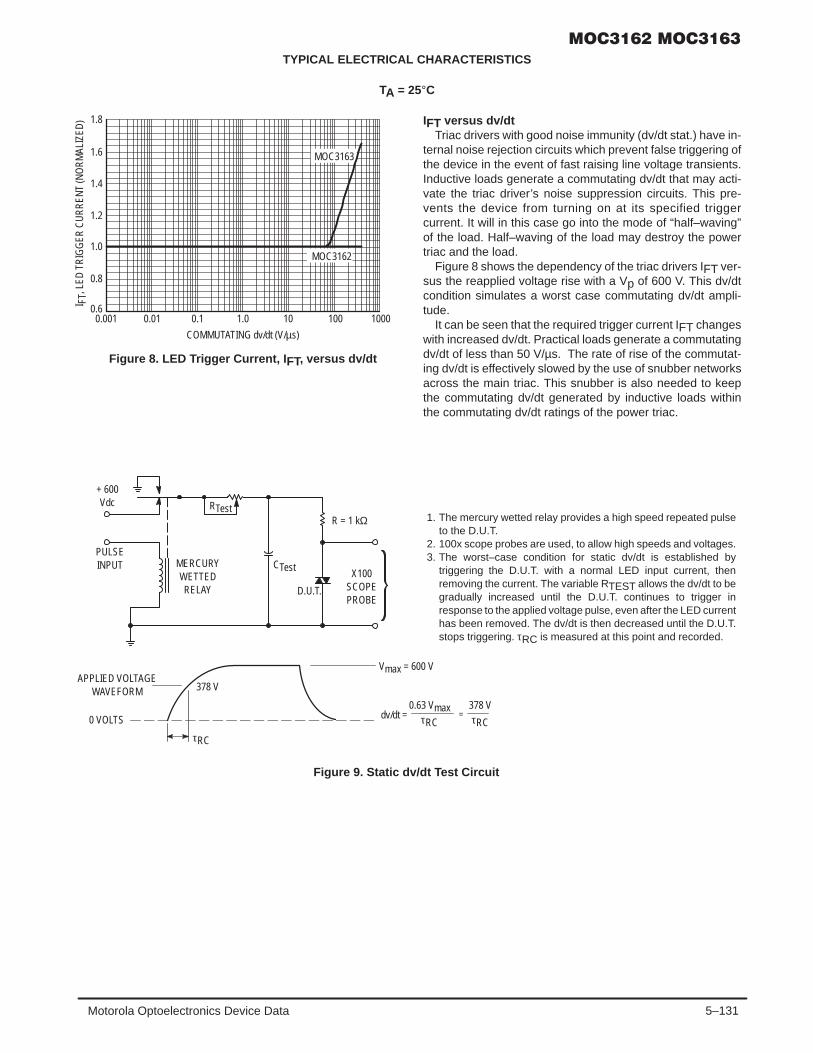
5–131Motorola Optoelectronics Device Data
TYPICAL ELECTRICAL CHARACTERISTICS
TA = 25°C
Figure 8. LED Trigger Current, I FT, versus dv/dt
COMMUTATING dv/dt (V/µs)
0.001
1.8
1.6
1.4
1.2
1.0
0.60.01 0.1 1.0 10 1000
I FT,
LED
TR
IGG
ER C
UR
REN
T (N
OR
MAL
IZED
)
0.8
100
MOC3163
MOC3162
IFT versus dv/dtTriac drivers with good noise immunity (dv/dt stat.) have in-
ternal noise rejection circuits which prevent false triggering ofthe device in the event of fast raising line voltage transients.Inductive loads generate a commutating dv/dt that may acti-vate the triac driver’s noise suppression circuits. This pre-vents the device from turning on at its specified triggercurrent. It will in this case go into the mode of “half–waving”of the load. Half–waving of the load may destroy the powertriac and the load.
Figure 8 shows the dependency of the triac drivers IFT ver-sus the reapplied voltage rise with a Vp of 600 V. This dv/dtcondition simulates a worst case commutating dv/dt ampli-tude.
It can be seen that the required trigger current IFT changeswith increased dv/dt. Practical loads generate a commutatingdv/dt of less than 50 V/µs. The rate of rise of the commutat-ing dv/dt is effectively slowed by the use of snubber networksacross the main triac. This snubber is also needed to keepthe commutating dv/dt generated by inductive loads withinthe commutating dv/dt ratings of the power triac.
1. The mercury wetted relay provides a high speed repeated pulseto the D.U.T.
2. 100x scope probes are used, to allow high speeds and voltages.3. The worst–case condition for static dv/dt is established by
triggering the D.U.T. with a normal LED input current, thenremoving the current. The variable RTEST allows the dv/dt to begradually increased until the D.U.T. continues to trigger inresponse to the applied voltage pulse, even after the LED currenthas been removed. The dv/dt is then decreased until the D.U.T.stops triggering. τRC is measured at this point and recorded.
Figure 9. Static dv/dt Test Circuit
+ 600Vdc
PULSEINPUT
RTest
CTest
R = 1 kΩ
MERCURYWETTEDRELAY D.U.T.
X100SCOPEPROBE
APPLIED VOLTAGEWAVEFORM
Vmax = 600 V
dv/dt =0.63 Vmax
τRC
378 VτRC
=
τRC
378 V
0 VOLTS
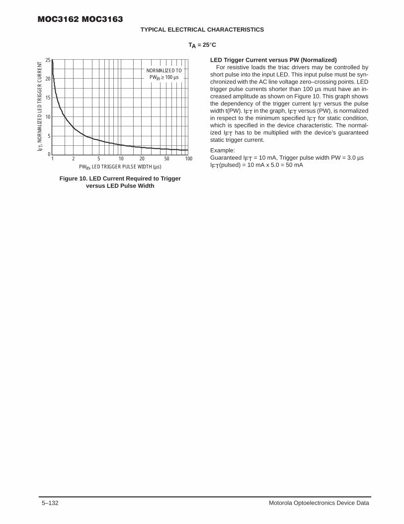
5–132 Motorola Optoelectronics Device Data
TYPICAL ELECTRICAL CHARACTERISTICS
TA = 25°C
Figure 10. LED Current Required to Triggerversus LED Pulse Width
PWin, LED TRIGGER PULSE WIDTH (µs)
1
25
20
15
10
5
02 5 10 20 50 100
NORMALIZED TOPWin ≥ 100 µs
I FT,
NO
RM
ALIZ
ED L
ED T
RIG
GER
CU
RR
ENT LED Trigger Current versus PW (Normalized)
For resistive loads the triac drivers may be controlled byshort pulse into the input LED. This input pulse must be syn-chronized with the AC line voltage zero–crossing points. LEDtrigger pulse currents shorter than 100 µs must have an in-creased amplitude as shown on Figure 10. This graph showsthe dependency of the trigger current IFT versus the pulsewidth t(PW). IFT in the graph, IFT versus (PW), is normalizedin respect to the minimum specified IFT for static condition,which is specified in the device characteristic. The normal-ized IFT has to be multiplied with the device’s guaranteedstatic trigger current.
Example:Guaranteed IFT = 10 mA, Trigger pulse width PW = 3.0 µsIFT(pulsed) = 10 mA x 5.0 = 50 mA

5–133Motorola Optoelectronics Device Data
APPLICATIONS GUIDE
BASIC APPLICATIONS
Basic Triac Driver CircuitZero–cross triac drivers are very immune to static dv/dt.
This allows snubberless operations in all applications wherethe external generated noise amplitude and rate of rise in theAC line is not exceeding the devices’ guaranteed limits. Forthese applications a snubber circuit is not necessary when anoise insensitive power triac is used. Figure 11 shows the cir-cuit diagram. The triac driver is directly connected to the triacmain terminal 2 and a series Resistor R which limits the cur-rent to the triac driver. Current limiting resistor R could bevery small for normal operation since the triac driver can beonly switched on within the zero–cross window. Worst caseconsideration, however, considers accidental turn on at thepeak of the line voltage due to a line transient exceeding thedevices’ maximum ratings. For this reason R should be cal-culated to limit the current to Idrm max at the peak of the linevoltage.
R = Vp AC/ITM max rep. = Vp AC/1A
The power dissipation of this current limiting resistor andthe triac driver is very small because the power triac carriesthe load current as soon as the current through driver andcurrent limiting resistor reaches the trigger current of thepower triac. The switching transition time for the driver is onlyone micro second and for power triacs typical four micro se-conds.
Triac Driver Circuit for Noisy EnvironmentsWhen the transient rate of rise and amplitude are expected
to exceed the power triacs and triac drivers maximum ratingsa snubber circuit as shown in Figure 12 is recommended.Fast transients are slowed by the R–C snubber and exces-sive amplitudes are clipped by the Metal Oxide Varistor MOV.
Triac Driver Circuit for Extremely Noisy EnvironmentsNoisy environments for this circuit are defined in the noise
standards IEEE472, IEC255–4 and IEC801–4.Industrial control applications, for example, do specify a
maximum expected transient noise dv/dt and peak voltagewhich is superimposed onto the AC line voltage. Figure 13shows a split snubber network which enhances the circuitsnoise immunity by protecting the triac driver with optimizedefficiency.
Figure 11. Basic Driver Circuit
Figure 12. Triac Driver Circuit for Noisy Environments
Figure 13. Triac Driver Circuit for ExtremelyNoisy Environments
VCC
RETURN
RLED TRIAC DRIVER POWER TRIAC
AC LINE
LOAD
R
QCONTROL
R
RLEDVCC
RS
CS
MOV
LOAD
RTRIAC DRIVER
POWER TRIAC
RS
CS
MOV
LOAD
VCC RLED
RLED = (VCC – VF LED – Vsat Q)/IFTR = Vp AC line/ITSMThe load may be placed on either side ofthe AC line.
Traditional snubber configurationTypical Snubber values RS = 33 Ω, CS = 0.01 µFMOV (Metal Oxide Varistor) protects triac and driverfrom transient overvoltages >VDRM max
Recommended snubber values RS = 10 W, CS = 0.033 mF
Q
Q
TRIAC DRIVER POWER TRIAC
AC LINE
RETURN
CONTROL
CONTROL
RETURN
AC LINE

5–134 Motorola Optoelectronics Device Data
APPLICATIONS GUIDE
Hot–Line Switching Application CircuitTypical circuit for use when hot–line switching is required.
In this circuit the “hot” side of the line is switched and the loadconnected to the cold or neutral side. The load may be con-nected to either the neutral or hot–line.
Rin is calculated so that IF is equal to the rated IFT of thepart, 10 mA for the MOC3162, and 5.0 mA for the MOC3163.The 39 ohm resistor and 0.01 µF capacitor are for snubbingof the triac and may or may not be necessary dependingupon the particular triac and load used.
Inverse Parallel SCR Driver CircuitTwo inverse parallel SCR’s are controlled by one triac driv-
er with a minimum component count as shown in Figure 15.A snubber network and a MOV across the main terminals ofthe SCR’s protects the semiconductors from transients onthe AC line.
Figure 14. Hot–Line Switching Application Circuit
Figure 15. Inverse Parallel SCR Driver Circuit
MOC3162/MOC3163
360 ΩRinVCC
39
HOT
RTRIAC DRIVER
RS
CS
MOV
LOAD
AC LINE
VCC
RETURN
CONTROL
RLED
LOAD
240 Vac
NEUTRAL
1
2
3
6
5
4
Q
SCRSCR
0.01

5–135Motorola Optoelectronics Device Data
PACKAGE DIMENSIONS
CASE 730A–04ISSUE G
NOTES:1. DIMENSIONING AND TOLERANCING PER ANSI
Y14.5M, 1982.2. CONTROLLING DIMENSION: INCH.3. DIMENSION L TO CENTER OF LEAD WHEN
FORMED PARALLEL.
STYLE 6:PIN 1. ANODE
2. CATHODE3. NC4. MAIN TERMINAL5. SUBSTRATE6. MAIN TERMINAL
6 4
1 3
–A–
–B–
SEATINGPLANE
–T–
4 PLF
K
CN
G
6 PLD6 PLE
MAM0.13 (0.005) B MT
L
M
6 PLJMBM0.13 (0.005) A MT
DIM MIN MAX MIN MAXMILLIMETERSINCHES
A 0.320 0.350 8.13 8.89B 0.240 0.260 6.10 6.60C 0.115 0.200 2.93 5.08D 0.016 0.020 0.41 0.50E 0.040 0.070 1.02 1.77F 0.010 0.014 0.25 0.36G 0.100 BSC 2.54 BSCJ 0.008 0.012 0.21 0.30K 0.100 0.150 2.54 3.81L 0.300 BSC 7.62 BSCM 0 15 0 15 N 0.015 0.100 0.38 2.54
CASE 730C–04ISSUE D
–A–
–B–
SEATINGPLANE
–T–J
K
L
6 PL
MBM0.13 (0.005) A MT
C
D 6 PL
MAM0.13 (0.005) B MT
H
GE 6 PL
F 4 PL
31
46
NOTES:1. DIMENSIONING AND TOLERANCING PER ANSI
Y14.5M, 1982.2. CONTROLLING DIMENSION: INCH.
DIM MIN MAX MIN MAXMILLIMETERSINCHES
A 0.320 0.350 8.13 8.89B 0.240 0.260 6.10 6.60C 0.115 0.200 2.93 5.08D 0.016 0.020 0.41 0.50E 0.040 0.070 1.02 1.77F 0.010 0.014 0.25 0.36G 0.100 BSC 2.54 BSCH 0.020 0.025 0.51 0.63J 0.008 0.012 0.20 0.30K 0.006 0.035 0.16 0.88L 0.320 BSC 8.13 BSCS 0.332 0.390 8.43 9.90
*Consult factory for leadform option availability

5–136 Motorola Optoelectronics Device Data
*Consult factory for leadform option availability
NOTES:1. DIMENSIONING AND TOLERANCING PER ANSI
Y14.5M, 1982.2. CONTROLLING DIMENSION: INCH.3. DIMENSION L TO CENTER OF LEAD WHEN
FORMED PARALLEL.
CASE 730D–05ISSUE D
6 4
1 3
–A–
–B–
N
C
KG
F 4 PL
SEATING
D 6 PL
E 6 PL
PLANE
–T–
MAM0.13 (0.005) B MT
L
J
DIM MIN MAX MIN MAXMILLIMETERSINCHES
A 0.320 0.350 8.13 8.89B 0.240 0.260 6.10 6.60C 0.115 0.200 2.93 5.08D 0.016 0.020 0.41 0.50E 0.040 0.070 1.02 1.77F 0.010 0.014 0.25 0.36G 0.100 BSC 2.54 BSCJ 0.008 0.012 0.21 0.30K 0.100 0.150 2.54 3.81L 0.400 0.425 10.16 10.80N 0.015 0.040 0.38 1.02

5–137Motorola Optoelectronics Device Data
Motorola reserves the right to make changes without further notice to any products herein. Motorola makes no warranty, representation or guarantee regardingthe suitability of its products for any particular purpose, nor does Motorola assume any liability arising out of the application or use of any product or circuit,and specifically disclaims any and all liability, including without limitation consequential or incidental damages. “Typical” parameters can and do vary in differentapplications. All operating parameters, including “Typicals” must be validated for each customer application by customer’s technical experts. Motorola doesnot convey any license under its patent rights nor the rights of others. Motorola products are not designed, intended, or authorized for use as components insystems intended for surgical implant into the body, or other applications intended to support or sustain life, or for any other application in which the failure ofthe Motorola product could create a situation where personal injury or death may occur. Should Buyer purchase or use Motorola products for any suchunintended or unauthorized application, Buyer shall indemnify and hold Motorola and its officers, employees, subsidiaries, affiliates, and distributors harmlessagainst all claims, costs, damages, and expenses, and reasonable attorney fees arising out of, directly or indirectly, any claim of personal injury or deathassociated with such unintended or unauthorized use, even if such claim alleges that Motorola was negligent regarding the design or manufacture of the part.Motorola and are registered trademarks of Motorola, Inc. Motorola, Inc. is an Equal Opportunity/Affirmative Action Employer.
How to reach us:USA / EUROPE: Motorola Literature Distribution; JAPAN : Nippon Motorola Ltd.; Tatsumi–SPD–JLDC, Toshikatsu Otsuki,P.O. Box 20912; Phoenix, Arizona 85036. 1–800–441–2447 6F Seibu–Butsuryu–Center, 3–14–2 Tatsumi Koto–Ku, Tokyo 135, Japan. 03–3521–8315
MFAX: [email protected] – TOUCHTONE (602) 244–6609 HONG KONG: Motorola Semiconductors H.K. Ltd.; 8B Tai Ping Industrial Park, INTERNET: http://Design–NET.com 51 Ting Kok Road, Tai Po, N.T., Hong Kong. 852–26629298
MOC3162/D
◊

5–138 Motorola Optoelectronics Device Data
! (800 Volts Peak)
The MOC3081, MOC3082 and MOC3083 devices consist of gallium arsenideinfrared emitting diodes optically coupled to monolithic silicon detectorsperforming the function of Zero Voltage Crossing bilateral triac drivers.
They are designed for use with a triac in the interface of logic systems toequipment powered from 240 Vac lines, such as solid–state relays, industrialcontrols, motors, solenoids and consumer appliances, etc.
• Simplifies Logic Control of 240 Vac Power• Zero Voltage Crossing• dv/dt of 1500 V/µs Typical, 600 V/µs Guaranteed• To order devices that are tested and marked per VDE 0884 requirements, the
suffix ”V” must be included at end of part number. VDE 0884 is a test option.Recommended for 240 Vac(rms) Applications:• Solenoid/Valve Controls • Temperature Controls
• Lighting Controls • E.M. Contactors
• Static Power Switches • AC Motor Starters
• AC Motor Drives • Solid State Relays
MAXIMUM RATINGS
Rating Symbol Value Unit
INPUT LED
Reverse Voltage VR 6 Volts
Forward Current — Continuous IF 60 mA
Total Power Dissipation @ TA = 25°CNegligible Power in Output Driver
Derate above 25°C
PD 120
1.41
mW
mW/°C
OUTPUT DRIVER
Off–State Output Terminal Voltage VDRM 800 Volts
Peak Repetitive Surge Current(PW = 100 µs, 120 pps)
ITSM 1 A
Total Power Dissipation @ TA = 25°CDerate above 25°C
PD 1501.76
mWmW/°C
TOTAL DEVICE
Isolation Surge Voltage(1)
(Peak ac Voltage, 60 Hz, 1 Second Duration)VISO 7500 Vac(pk)
Total Power Dissipation @ TA = 25°CDerate above 25°C
PD 2502.94
mWmW/°C
Junction Temperature Range TJ –40 to +100 °C
Ambient Operating Temperature Range(2) TA –40 to +85 °C
Storage Temperature Range(2) Tstg –40 to +150 °C
Soldering Temperature (10 s) TL 260 °C1. Isolation surge voltage, VISO, is an internal device dielectric breakdown rating.1. For this test, Pins 1 and 2 are common, and Pins 4, 5 and 6 are common.2. Refer to Quality and Reliability Section in Opto Data Book for information on test conditions.Preferred devices are Motorola recommended choices for future use and best overall value.GlobalOptoisolator is a trademark of Motorola, Inc.
Order this documentby MOC3081/D
SEMICONDUCTOR TECHNICAL DATA
GlobalOptoisolator
Motorola, Inc. 1995
*Motorola Preferred Device
COUPLER SCHEMATIC
[IFT = 15 mA Max]
STANDARD THRU HOLECASE 730A–04
[IFT = 10 mA Max]
[IFT = 5 mA Max]
1. ANODE2. CATHODE3. NC4. MAIN TERMINAL5. SUBSTRATE
DO NOT CONNECT6. MAIN TERMINAL
1
2
3
6
5
4ZERO
CROSSINGCIRCUIT
61
STYLE 6 PLASTIC
REV 1

5–139Motorola Optoelectronics Device Data
ELECTRICAL CHARACTERISTICS (TA = 25°C unless otherwise noted)
Characteristic Symbol Min Typ Max Unit
INPUT LED
Reverse Leakage Current (VR = 6 V) IR — 0.05 100 µA
Forward Voltage (IF = 30 mA) VF — 1.3 1.5 Volts
OUTPUT DETECTOR (IF = 0)
Leakage with LED Off, Either Direction (VDRM = 800 V(1)) IDRM1 — 80 500 nA
Critical Rate of Rise of Off–State Voltage(3) dv/dt 600 1500 — V/µs
COUPLED
LED Trigger Current, Current Required to Latch Output(Main Terminal Voltage = 3 V(2)) MOC3081
MOC3082MOC3083
IFT———
———
15105
mA
Peak On–State Voltage, Either Direction(ITM = 100 mA, IF = Rated IFT)
VTM — 1.8 3 Volts
Holding Current, Either Direction IH — 250 — µA
Inhibit Voltage (MT1–MT2 Voltage above which device will nottrigger)
(IF = Rated IFT)
VINH — 5 20 Volts
Leakage in Inhibited State(IF = Rated IFT, VDRM = 800 V, Off State)
IDRM2 — 300 500 µA
1. Test voltage must be applied within dv/dt rating.2. All devices are guaranteed to trigger at an IF value less than or equal to max IFT. Therefore, recommended operating IF lies between max2. IFT (15 mA for MOC3081, 10 mA for MOC3082, 5 mA for MOC3083) and absolute max IF (60 mA).3. This is static dv/dt. See Figure 7 for test circuit. Commutating dv/dt is a function of the load–driving thyristor(s) only.
Figure 1. On–State Characteristics
–3VTM, ON–STATE VOLTAGE (VOLTS)
I
–400
0
+400
+800
–2 –1 0 1 2 3
TM, O
N-S
TATE
CU
RR
ENT
(mA)
–600
–800
–200
+200
+600
4–4
0.7
Figure 2. Inhibit Voltage versus Temperature
–40TA, AMBIENT TEMPERATURE (°C)
0.8
1.1
1.3
–20 0 20 40 60 80
, NO
RM
ALIZ
ED
100
0.9
1
1.2
1.4
1.5
5
0.60.5
VIN
H
NORMALIZED TOTA = 25°C
OUTPUT PULSE WIDTH – 80 µsIF = 30 mAf = 60 HzTA = 25°C
TYPICAL CHARACTERISTICS

5–140 Motorola Optoelectronics Device Data
5
1PWin, LED TRIGGER PULSE WIDTH (µs)
10
15
20
25
2 5 2010 500FTI
, NO
RM
ALIZ
ED L
ED T
RIG
GER
CU
RR
ENT
NORMALIZED TO:PWin 100 µs
TA, AMBIENT TEMPERATURE (°C)–40
+400Vdc
PULSEINPUT MERCURY
WETTEDRELAY
RTEST
CTEST
10 kΩ
X100SCOPEPROBED.U.T.
APPLIED VOLTAGEWAVEFORM 252 V
0 VOLTSRC
Vmax = 400 V
dvdt 0.63 Vmax
RC 504
RC
1. The mercury wetted relay provides a high speed repeated pulseto the D.U.T.
2. 100x scope probes are used, to allow high speeds and voltages.3. The worst–case condition for static dv/dt is established by
triggering the D.U.T. with a normal LED input current, thenremoving the current. The variable RTEST allows the dv/dt to begradually increased until the D.U.T. continues to trigger inresponse to the applied voltage pulse, even after the LEDcurrent has been removed. The dv/dt is then decreased until theD.U.T. stops triggering. RC is measured at this point andrecorded.
5–40
TA, AMBIENT TEMPERATURE (°C)
I
–20 0 20 40 60 80 100
10
20
50
100
200
500
DR
M1,
PEA
K BL
OC
KIN
G C
UR
REN
T (m
A)
0.6
TA, AMBIENT TEMPERATURE (°C)
I
IF = RATED IFT
0.7
0.8
0.9
1
1.1
1.2
1.3
1.4
1.5
–20 0 20 40 60 80 100
DR
M2,
NO
RM
ALIZ
ED
I FT,
NO
RM
ALIZ
ED
0.70.8
0.9
1
1.1
1.21.3
1.4
1.5 NORMALIZED TOTA = 25°C
–20 0 20 40 60 80 100
VDRM = 800 V
Figure 3. Leakage with LED Offversus Temperature
Figure 4. I DRM2, Leakage in Inhibit Stateversus Temperature
Figure 5. Trigger Current versus Temperature Figure 6. LED Current Required to Triggerversus LED Pulse Width
Figure 7. Static dv/dt Test Circuit
100
–40

5–141Motorola Optoelectronics Device Data
Rin 1
2
6
4
360 Ω
MOC3081–83
3
5
VCC
NOTE: This device should not be used to drive a load directly. It isintended to be a trigger device only.
330
39
0.01
240 Vac
HOT
NEUTRALLOAD
Typical circuit for use when hot line switching is required.In this circuit the “hot” side of the line is switched and theload connected to the cold or neutral side. The load may beconnected to either the neutral or hot line.
Rin is calculated so that IF is equal to the rated IFT of thepart, 15 mA for the MOC3081, 10 mA for the MOC3082,and 5 mA for the MOC3083. The 39 ohm resistor and 0.01µF capacitor are for snubbing of the triac and may or maynot be necessary depending upon the particular triac andload used.
Rin
R1
2
6
43
5
VCC
R2
LOAD
360 Ω
D1
1
SCRSCR
D2
240 Vac
Suggested method of firing two, back–to–back SCR’s,with a Motorola triac driver. Diodes can be 1N4001; resis-tors, R1 and R2, are optional 330 ohms.
* For highly inductive loads (power factor < 0.5), change this value to360 ohms.
Figure 8. Hot–Line Switching Application Circuit
Figure 9. Inverse–Parallel SCR Driver Circuit
MOC3081–83

5–142 Motorola Optoelectronics Device Data
PACKAGE DIMENSIONS
CASE 730A–04ISSUE G
NOTES:1. DIMENSIONING AND TOLERANCING PER ANSI
Y14.5M, 1982.2. CONTROLLING DIMENSION: INCH.3. DIMENSION L TO CENTER OF LEAD WHEN
FORMED PARALLEL.
6 4
1 3
–A–
–B–
SEATINGPLANE
–T–
4 PLF
K
CN
G
6 PLD6 PLE
MAM0.13 (0.005) B MT
L
M
6 PLJMBM0.13 (0.005) A MT
DIM MIN MAX MIN MAXMILLIMETERSINCHES
A 0.320 0.350 8.13 8.89B 0.240 0.260 6.10 6.60C 0.115 0.200 2.93 5.08D 0.016 0.020 0.41 0.50E 0.040 0.070 1.02 1.77F 0.010 0.014 0.25 0.36G 0.100 BSC 2.54 BSCJ 0.008 0.012 0.21 0.30K 0.100 0.150 2.54 3.81L 0.300 BSC 7.62 BSCM 0 15 0 15 N 0.015 0.100 0.38 2.54
STYLE 6:PIN 1. ANODE
2. CATHODE3. NC4. MAIN TERMINAL5. SUBSTRATE6. MAIN TERMINAL
CASE 730C–04ISSUE D
–A–
–B–
SEATINGPLANE
–T–J
K
L
6 PL
MBM0.13 (0.005) A MT
C
D 6 PL
MAM0.13 (0.005) B MT
H
GE 6 PL
F 4 PL
31
46
NOTES:1. DIMENSIONING AND TOLERANCING PER ANSI
Y14.5M, 1982.2. CONTROLLING DIMENSION: INCH.
DIM MIN MAX MIN MAXMILLIMETERSINCHES
A 0.320 0.350 8.13 8.89B 0.240 0.260 6.10 6.60C 0.115 0.200 2.93 5.08D 0.016 0.020 0.41 0.50E 0.040 0.070 1.02 1.77F 0.010 0.014 0.25 0.36G 0.100 BSC 2.54 BSCH 0.020 0.025 0.51 0.63J 0.008 0.012 0.20 0.30K 0.006 0.035 0.16 0.88L 0.320 BSC 8.13 BSCS 0.332 0.390 8.43 9.90
*Consult factory for leadform option availability

5–143Motorola Optoelectronics Device Data
*Consult factory for leadform option availability
NOTES:1. DIMENSIONING AND TOLERANCING PER ANSI
Y14.5M, 1982.2. CONTROLLING DIMENSION: INCH.3. DIMENSION L TO CENTER OF LEAD WHEN
FORMED PARALLEL.
CASE 730D–05ISSUE D
6 4
1 3
–A–
–B–
N
C
KG
F 4 PL
SEATING
D 6 PL
E 6 PL
PLANE
–T–
MAM0.13 (0.005) B MT
L
J
DIM MIN MAX MIN MAXMILLIMETERSINCHES
A 0.320 0.350 8.13 8.89B 0.240 0.260 6.10 6.60C 0.115 0.200 2.93 5.08D 0.016 0.020 0.41 0.50E 0.040 0.070 1.02 1.77F 0.010 0.014 0.25 0.36G 0.100 BSC 2.54 BSCJ 0.008 0.012 0.21 0.30K 0.100 0.150 2.54 3.81L 0.400 0.425 10.16 10.80N 0.015 0.040 0.38 1.02
Motorola reserves the right to make changes without further notice to any products herein. Motorola makes no warranty, representation or guarantee regardingthe suitability of its products for any particular purpose, nor does Motorola assume any liability arising out of the application or use of any product or circuit,and specifically disclaims any and all liability, including without limitation consequential or incidental damages. “Typical” parameters can and do vary in differentapplications. All operating parameters, including “Typicals” must be validated for each customer application by customer’s technical experts. Motorola doesnot convey any license under its patent rights nor the rights of others. Motorola products are not designed, intended, or authorized for use as components insystems intended for surgical implant into the body, or other applications intended to support or sustain life, or for any other application in which the failure ofthe Motorola product could create a situation where personal injury or death may occur. Should Buyer purchase or use Motorola products for any suchunintended or unauthorized application, Buyer shall indemnify and hold Motorola and its officers, employees, subsidiaries, affiliates, and distributors harmlessagainst all claims, costs, damages, and expenses, and reasonable attorney fees arising out of, directly or indirectly, any claim of personal injury or deathassociated with such unintended or unauthorized use, even if such claim alleges that Motorola was negligent regarding the design or manufacture of the part.Motorola and are registered trademarks of Motorola, Inc. Motorola, Inc. is an Equal Opportunity/Affirmative Action Employer.
How to reach us:USA / EUROPE: Motorola Literature Distribution; JAPAN : Nippon Motorola Ltd.; Tatsumi–SPD–JLDC, Toshikatsu Otsuki,P.O. Box 20912; Phoenix, Arizona 85036. 1–800–441–2447 6F Seibu–Butsuryu–Center, 3–14–2 Tatsumi Koto–Ku, Tokyo 135, Japan. 03–3521–8315
MFAX: [email protected] – TOUCHTONE (602) 244–6609 HONG KONG: Motorola Semiconductors H.K. Ltd.; 8B Tai Ping Industrial Park, INTERNET: http://Design–NET.com 51 Ting Kok Road, Tai Po, N.T., Hong Kong. 852–26629298
MOC3081/D
◊

5–144 Motorola Optoelectronics Device Data
The MOC5007, MOC5008 and MOC5009 have a gallium arsenide IREDoptically coupled to a high–speed integrated detector with Schmitt triggeroutput. Ideal for applications requiring electrical isolation, fast response time,noise immunity and digital logic compatibility.
• Guaranteed Switching Times — ton, toff 4 < µs• Built–In ON/OFF Threshold Hysteresis• High Data Rate, 1 MHz Typical (NRZ)• Wide Supply Voltage Capability• Microprocessor Compatible Drive• To order devices that are tested and marked per VDE 0884 requirements, the
suffix ”V” must be included at end of part number. VDE 0884 is a test option.
Applications• Interfacing Computer Terminals to Peripheral Equipment• Digital Control of Power Supplies• Line Receiver — Eliminates Noise• Digital Control of Motors and Other Servo Machine Applications• Logic to Logic Isolator• Logic Level Shifter — Couples TTL to CMOS
MAXIMUM RATINGS (TA = 25°C unless otherwise noted)
Rating Symbol Value Unit
INPUT LED
Reverse Voltage VR 6 Volts
Forward Current — ContinuousForward Current — Peak
Pulse Width = 300 µs, 2% Duty Cycle
IF 601.2
mAAmp
LED Power Dissipation @ TA = 25°CDerate above 25°C
PD 1201.41
mWmW/°C
OUTPUT DETECTOR
Output Voltage Range Vo 0–16 Volts
Supply Voltage Range VCC 3–16 Volts
Output Current IO 50 mA
Detector Power Dissipation @ TA = 25°CDerate above 25°C
PD 1501.76
mWmW/°C
TOTAL DEVICE
Total Device Power Dissipation @ TA = 25°CDerate above 25°C
PD 2502.94
mWmW/°C
Maximum Operating Temperature(2) TA –40 to +85 °C
Storage Temperature Range(2) Tstg –55 to +150 °C
Soldering Temperature (10 s) TL 260 °C
Isolation Surge Voltage(1)
(Peak ac Voltage, 60 Hz, 1 Second Duration)VISO 7500 Vac(pk)
1. Isolation surge voltage is an internal device dielectric breakdown rating.1. For this test, Pins 1 and 2 are common, and Pins 4, 5 and 6 are common.2. Refer to Quality and Reliability Section in Opto Data Book for information on test conditions.Preferred devices are Motorola recommended choices for future use and best overall value.GlobalOptoisolator is a trademark of Motorola, Inc.
Order this documentby MOC5007/D
SEMICONDUCTOR TECHNICAL DATA
GlobalOptoisolator
Motorola, Inc. 1995
*Motorola Preferred Device
SCHEMATIC
[IF(on) = 1.6 mA Max]
STANDARD THRU HOLECASE 730A–04
STYLE 5 PLASTIC
[IF(on) = 4 mA Max]
[IF(on) = 10 mA Max]
PIN 1. ANODE2. CATHODE3. NC4. OPEN COLLECTOR
OUTPUT5. GROUND6. VCC
1
2
3
6
5
4
61
REV 1

5–145Motorola Optoelectronics Device Data
ELECTRICAL CHARACTERISTICS (TA = 25°C unless otherwise noted)(1)
Characteristic Symbol Min Typ1) Max Unit
INPUT LED
Reverse Leakage Current (VR = 3 V, RL = 1 MΩ) IR — 0.05 10 µA
Forward Voltage (IF = 10 mA)Forward Voltage (IF = 0.3 mA)
VF —0.75
1.20.95
1.5—
Volts
Capacitance (VR = 0 V, f = 1 MHz) C — 18 — pF
OUTPUT DETECTOR
Operating Voltage VCC 3 — 15 Volts
Supply Current (IF = 0, VCC = 5 V) ICC(off) — 1 5 mA
Output Current, High (IF = 0, VCC = Vo = 15 V) IOH — — 100 µA
COUPLED
Supply Current (IF = IF(on), VCC = 5 V) ICC(on) — 1.6 5 mA
Output Voltage, Low (RL = 270 Ω, VCC = 5 V, IF = IF(on)) VOL — 0.2 0.4 Volts
Threshold Current, ON MOC5007(RL = 270 Ω, VCC = 5 V) MOC5008
MOC5009
IF(on) ———
1.2——
1.6410
mA
Threshold Current, OFF MOC5007(RL = 270 Ω, VCC = 5 V) MOC5008, 5009
IF(off) 0.30.3
0.75—
——
mA
Hysteresis Ratio (RL = 270 Ω, VCC = 5 V) IF(off)IF(on)
0.5 0.75 0.9
Isolation Voltage(2) 60 Hz, AC Peak, 1 second, TA = 25°C VISO 7500 — — Vac(pk)
Turn–On TimeRL = 270 Ω(3)
ton — 1.2 4 µs
Fall TimeRL = 270 Ω(3)
VCC = 5 V, tf — 0.1 —
Turn–Off TimeCC
IF = IF(on)TA = 25°C
toff — 1.2 4
Rise TimeTA = 25°C
tr — 0.1 —
1. Always design to the specified minimum/maximum electrical limits (where applicable).2. For this test, IRED Pins 1 and 2 are common and Output Gate Pins 4, 5, 6 are common.3. RL value effect on switching time is negligible.
Vin
tr = tf = 0.01 µsZ = 50 Ω
IF (on)
trtf
Figure 1. Switching Test Circuit
toffton
Vo
2
1
IF
5
6
4
RL
ICC
270 Ω
5 V
VO (OPEN COLLECTOR OUTPUT)

5–146 Motorola Optoelectronics Device Data
0.1
F(on
), I F
(off)
, TH
RES
HO
LD C
UR
REN
T (N
OR
MAL
IZED
)
Figure 2. Transfer Characteristics for MOC5007
0IF, INPUT CURRENT (mA)
IF(off)
V
0
VOH
VOL1
2
3
4
5
6
0.75 1 2
IF(on)
RL = 270 ΩVCC = 5 VTA = 25°C
O, O
UTP
UT
VOLT
AGE
(VO
LTS)
Figure 3. Threshold Current versus Supply Voltage
0.4
0VCC, SUPPLY VOLTAGE (VOLTS)
I
TURN ON THRESHOLD
TURN OFF THRESHOLD
IF NORMALIZED TOIF(on) AT VCC = 5 VTA = 25°C
0.6
0.8
1
1.2
1.4
1.6
2 4 6 8 10 12 14
F, T
HR
ESH
OLD
CU
RR
ENT
(NO
RM
ALIZ
ED)
Figure 4. Threshold Current versus Temperature
0.6
I
–50 –25 0 25 50 75 100
0.8
1
1.2
1.4
1.6
Figure 5. Output Voltage, Low versus Load Current
0.02
1IO, LOAD CURRENT (mA)
V
2 5 10 20 50 100
0.05
0.2
0.5
1
OL,
OU
TPU
T VO
LTAG
E, L
OW
(VO
LTS)
NORMALIZED TOVCC = 5 VTA = 25°C
I C, S
UPP
LY C
UR
REN
T (m
A)
Figure 6. Supply Current versus Supply Voltage
2
VCC, SUPPLY VOLTAGE (VOLTS)0
4
6
TA, TEMPERATURE (°C)
2 4 6 8 10 12 14 16
TA = 0°C25°C70°C
0IF = 0 mA
IF = 5 mA
0°C25°C70°C
TYPICAL CHARACTERISTICS

5–147Motorola Optoelectronics Device Data
PACKAGE DIMENSIONS
CASE 730A–04ISSUE G
NOTES:1. DIMENSIONING AND TOLERANCING PER ANSI
Y14.5M, 1982.2. CONTROLLING DIMENSION: INCH.3. DIMENSION L TO CENTER OF LEAD WHEN
FORMED PARALLEL.
6 4
1 3
–A–
–B–
SEATINGPLANE
–T–
4 PLF
K
CN
G
6 PLD6 PLE
MAM0.13 (0.005) B MT
L
M
6 PLJMBM0.13 (0.005) A MT
DIM MIN MAX MIN MAXMILLIMETERSINCHES
A 0.320 0.350 8.13 8.89B 0.240 0.260 6.10 6.60C 0.115 0.200 2.93 5.08D 0.016 0.020 0.41 0.50E 0.040 0.070 1.02 1.77F 0.010 0.014 0.25 0.36G 0.100 BSC 2.54 BSCJ 0.008 0.012 0.21 0.30K 0.100 0.150 2.54 3.81L 0.300 BSC 7.62 BSCM 0 15 0 15 N 0.015 0.100 0.38 2.54
STYLE 5:PIN 1. ANODE
2. CATHODE3. NC4. OUTPUT5. GROUND6. VCC
CASE 730C–04ISSUE D
–A–
–B–
SEATINGPLANE
–T–J
K
L
6 PL
MBM0.13 (0.005) A MT
C
D 6 PL
MAM0.13 (0.005) B MT
H
GE 6 PL
F 4 PL
31
46
NOTES:1. DIMENSIONING AND TOLERANCING PER ANSI
Y14.5M, 1982.2. CONTROLLING DIMENSION: INCH.
DIM MIN MAX MIN MAXMILLIMETERSINCHES
A 0.320 0.350 8.13 8.89B 0.240 0.260 6.10 6.60C 0.115 0.200 2.93 5.08D 0.016 0.020 0.41 0.50E 0.040 0.070 1.02 1.77F 0.010 0.014 0.25 0.36G 0.100 BSC 2.54 BSCH 0.020 0.025 0.51 0.63J 0.008 0.012 0.20 0.30K 0.006 0.035 0.16 0.88L 0.320 BSC 8.13 BSCS 0.332 0.390 8.43 9.90
*Consult factory for leadform option availability

5–148 Motorola Optoelectronics Device Data
*Consult factory for leadform option availability
NOTES:1. DIMENSIONING AND TOLERANCING PER ANSI
Y14.5M, 1982.2. CONTROLLING DIMENSION: INCH.3. DIMENSION L TO CENTER OF LEAD WHEN
FORMED PARALLEL.
CASE 730D–05ISSUE D
6 4
1 3
–A–
–B–
N
C
KG
F 4 PL
SEATING
D 6 PL
E 6 PL
PLANE
–T–
MAM0.13 (0.005) B MT
L
J
DIM MIN MAX MIN MAXMILLIMETERSINCHES
A 0.320 0.350 8.13 8.89B 0.240 0.260 6.10 6.60C 0.115 0.200 2.93 5.08D 0.016 0.020 0.41 0.50E 0.040 0.070 1.02 1.77F 0.010 0.014 0.25 0.36G 0.100 BSC 2.54 BSCJ 0.008 0.012 0.21 0.30K 0.100 0.150 2.54 3.81L 0.400 0.425 10.16 10.80N 0.015 0.040 0.38 1.02

5–149Motorola Optoelectronics Device Data
Motorola reserves the right to make changes without further notice to any products herein. Motorola makes no warranty, representation or guarantee regardingthe suitability of its products for any particular purpose, nor does Motorola assume any liability arising out of the application or use of any product or circuit,and specifically disclaims any and all liability, including without limitation consequential or incidental damages. “Typical” parameters can and do vary in differentapplications. All operating parameters, including “Typicals” must be validated for each customer application by customer’s technical experts. Motorola doesnot convey any license under its patent rights nor the rights of others. Motorola products are not designed, intended, or authorized for use as components insystems intended for surgical implant into the body, or other applications intended to support or sustain life, or for any other application in which the failure ofthe Motorola product could create a situation where personal injury or death may occur. Should Buyer purchase or use Motorola products for any suchunintended or unauthorized application, Buyer shall indemnify and hold Motorola and its officers, employees, subsidiaries, affiliates, and distributors harmlessagainst all claims, costs, damages, and expenses, and reasonable attorney fees arising out of, directly or indirectly, any claim of personal injury or deathassociated with such unintended or unauthorized use, even if such claim alleges that Motorola was negligent regarding the design or manufacture of the part.Motorola and are registered trademarks of Motorola, Inc. Motorola, Inc. is an Equal Opportunity/Affirmative Action Employer.
How to reach us:USA / EUROPE: Motorola Literature Distribution; JAPAN : Nippon Motorola Ltd.; Tatsumi–SPD–JLDC, Toshikatsu Otsuki,P.O. Box 20912; Phoenix, Arizona 85036. 1–800–441–2447 6F Seibu–Butsuryu–Center, 3–14–2 Tatsumi Koto–Ku, Tokyo 135, Japan. 03–3521–8315
MFAX: [email protected] – TOUCHTONE (602) 244–6609 HONG KONG: Motorola Semiconductors H.K. Ltd.; 8B Tai Ping Industrial Park, INTERNET: http://Design–NET.com 51 Ting Kok Road, Tai Po, N.T., Hong Kong. 852–26629298
MOC5007/D
◊ CODELINE TO BE PLACED HERE

5–150 Motorola Optoelectronics Device Data
! ! ! "!"! !
The MOC8020 and MOC8021 devices consist of a gallium arsenide infraredemitting diode optically coupled to a monolithic silicon photodarlington detector.The chip to Pin 6 base connection has been eliminated to improve the device’soutput performance in higher noise environments.• No Base Connection for Improved Noise Immunity• Higher Sensitivity to Low Input Drive Current• To order devices that are tested and marked per VDE 0884 requirements, the
suffix ”V” must be included at end of part number. VDE 0884 is a test option.Applications• Appliances, Measuring Instruments• I/O Interfaces for Computers• Programmable Controllers• Portable Electronics• Interfacing and coupling systems of different potentials and impedances• Solid State Relays• Circuits Exposed to High Noise Environments
MAXIMUM RATINGS (TA = 25°C unless otherwise noted)
Rating Symbol Value Unit
INPUT LED
Reverse Voltage VR 3 Volts
Forward Current — Continuous IF 60 mA
LED Power Dissipation @ TA = 25°Cwith Negligible Power in Output Detector
Derate above 25°C
PD 120
1.41
mW
mW/°C
OUTPUT DETECTOR
Collector–Emitter Voltage VCEO 50 Volts
Collector Current Continuous IC 150 mA
Emitter–Collector Voltage VECO 5 Volts
Detector Power Dissipation @ TA = 25°Cwith Negligible Power in Input LED
Derate above 25°C
PD 150
1.76
mW
mW/°C
TOTAL DEVICE
Isolation Surge Voltage(1)
(Peak ac Voltage, 60 Hz, 1 sec Duration)VISO 7500 Vac(pk)
Total Device Power Dissipation @ TA = 25°CDerate above 25°C
PD 2502.94
mWmW/°C
Ambient Operating Temperature Range(2) TA –55 to +100 °C
Storage Temperature Range(2) Tstg –55 to +150 °C
Soldering Temperature (10 sec, 1/16″ from case) TL 260 °C
1. Isolation surge voltage is an internal device dielectric breakdown rating.1. For this test, Pins 1 and 2 are common, and Pins 4 and 5 are common.2. Refer to Quality and Reliability Section in Opto Data Book for information on test conditions.GlobalOptoisolator is a trademark of Motorola, Inc.
Order this documentby MOC8020/D
SEMICONDUCTOR TECHNICAL DATA
GlobalOptoisolator
Motorola, Inc. 1995
SCHEMATIC
[CTR = 1000% Min]
STANDARD THRU HOLECASE 730A–04
STYLE 3 PLASTIC
PIN 1. LED ANODE2. LED CATHODE3. N.C.4. EMITTER5. COLLECTOR6. N.C.
[CTR = 500% Min]
1
2
3
6
5
4
61
REV 1

5–151Motorola Optoelectronics Device Data
ELECTRICAL CHARACTERISTICS (TA = 25°C unless otherwise noted)(1)
Characteristic Symbol Min Typ (1) Max Unit
INPUT LED
Reverse Leakage Current(VR = 3 V)
IR — 0.05 10 µA
Forward Voltage(IF = 10 mA)
VF — 1.15 2 Volts
Capacitance(V = 0 V, f = 1 MHz)
C — 18 — pF
PHOTODARLINGTON (TA = 25°C and IF = 0, unless otherwise noted)
Collector–Emitter Dark Current (VCE = 10 V)
ICEO — — 100 nA
Collector–Emitter Base Breakdown Voltage (IC = 1 mA)
V(BR)CEO 50 — — Volts
Emitter–Collector Breakdown Voltage(IE = 100 µA)
V(BR)ECO 5 — — Volts
COUPLED (TA = 25°C unless otherwise noted)
Collector Output Current(VCE = 5 V, IF = 10 mA) MOC8020
MOC8021
IC (CTR)(2)
50 (500)100 (1000)
——
——
mA (%)
Isolation Surge Voltage(3,4), 60 Hz Peak ac, 1 Second VISO 7500 — — Vac(pk)
Isolation Resistance(3)
(V = 500 V)RISO — 1011 — Ohms
Isolation Capacitance(3)
(V = 0, f = 1 MHz)CISO — 0.2 — pF
SWITCHING
Turn–On Time ton — 3.5 — µs
Turn–Off TimeVCC = 10 V RL = 100 Ω IF = 5 mA(5)
toff — 95 —
Rise TimeVCC = 10 V, RL = 100 Ω, IF = 5 mA(5)
tr — 1 —
Fall Time tf — 2 —
1. Always design to the specified minimum/maximum electrical limits (where applicable).2. Current Transfer Ratio (CTR) = IC/IF x 100%.3. For this test, LED Pins 1 and 2 are common and Phototransistor Pins 4 and 5 are common.4. Isolation Surge Voltage, VISO, is an internal device dielectric breakdown rating.5. For test circuit setup and waveforms, refer to Figure 9.
TYPICAL CHARACTERISTICS
TA = –55°C THRU
+100°C
+25°C
Figure 1. LED Forward Voltage versus Forward Current Figure 2. Output Current versus Input Current
2
1.8
1.6
1.4
1.2
11 10 100 1000
IF, LED FORWARD CURRENT (mA)
25°C
100°C
V F, F
ORW
ARD
VO
LTAG
E (V
OLT
S)
I C, O
UTP
UT
CO
LLEC
TOR
CU
RR
ENT
(NO
RM
ALIZ
ED)
10
1
0.1
0.010.5 1 2 5 10 20 50
IF, LED INPUT CURRENT (mA)
NORMALIZED TO: IF = 10 mA
TA = –55°C
+70°C
TA = 25°C
PULSE ONLYPULSE OR DC

5–152 Motorola Optoelectronics Device Data
, CO
LLEC
TOR
CU
RR
ENT
(mA)
20
0
Figure 3. Collector Current versusCollector–Emitter Voltage
IF = 10 mA
0
VCE, COLLECTOR–EMITTER VOLTAGE (VOLTS)
I C
40
60
80
100
120
140
1 2 3 4 5 6 7 8 9 10
5 mA
2 mA
1 mA
10
75
2
10.70.5
0.2
0.1– 60
Figure 4. Output Current versus Ambient Temperature
– 40 – 20C, O
UTP
UT
CO
LLEC
TOR
CU
RR
ENT
(NO
RM
ALIZ
ED)
0 20 40 60 80 100TA, AMBIENT TEMPERATURE (°C)
I
– 60
Figure 5. Collector–Emitter Voltage versusAmbient Temperature
NORMALIZED TO TA = 25°C
0.7
TA, AMBIENT TEMPERATURE (°C)V CE
, CO
LLEC
TOR
–EM
ITTE
R V
OLT
AGE
(NO
RM
ALIZ
ED)
– 40 – 20 0 20 40 60 80 100
0.8
0.9
1
1.1
1.2
1.3
0
Figure 6. Collector–Emitter Dark Current versusAmbient Temperature
1
TA, AMBIENT TEMPERATURE (°C)
I
10
102
103
104
105
20 40 60 80 100
CEO
, CO
LLEC
TOR
–EM
ITTE
R D
ARK
CU
RR
ENT
0.1
Figure 7. Turn–On Switching Times(Typical Value)
1
IF, LED INPUT CURRENT (mA)
t, TI
ME
(s)
10
100
1000
µ
0.2 0.5 1 2 5 10 20 50 100
100
10
0.11
IF, LED INPUT CURRENT (mA)
10
100
1000
0.2 0.5 1 2 5 10 20 50 100
10
t, TI
ME
(s)µ
Figure 8. Turn–Off Switching Times(Typical Value)
(NO
RM
ALIZ
ED)
10 V
NORMALIZED TO:VCE = 10 VTA = 25°C
VCE = 30 V
RL = 1000100
RL = 1000
NORMALIZED TO TA = 25°C
VCC = 10 V
VCC = 10 V

5–153Motorola Optoelectronics Device Data
TEST CIRCUIT
VCC = 10 V
IF = 5 mA
INPUT
RL = 100 Ω
OUTPUT
WAVEFORMS
10%
90%
ton
INPUT PULSE
OUTPUT PULSE
tf
toff
tr
Figure 9. Switching Time Test Circuit and Waveforms

5–154 Motorola Optoelectronics Device Data
PACKAGE DIMENSIONS
CASE 730A–04ISSUE G
NOTES:1. DIMENSIONING AND TOLERANCING PER ANSI
Y14.5M, 1982.2. CONTROLLING DIMENSION: INCH.3. DIMENSION L TO CENTER OF LEAD WHEN
FORMED PARALLEL.
6 4
1 3
–A–
–B–
SEATINGPLANE
–T–
4 PLF
K
CN
G
6 PLD6 PLE
MAM0.13 (0.005) B MT
L
M
6 PLJMBM0.13 (0.005) A MT
DIM MIN MAX MIN MAXMILLIMETERSINCHES
A 0.320 0.350 8.13 8.89B 0.240 0.260 6.10 6.60C 0.115 0.200 2.93 5.08D 0.016 0.020 0.41 0.50E 0.040 0.070 1.02 1.77F 0.010 0.014 0.25 0.36G 0.100 BSC 2.54 BSCJ 0.008 0.012 0.21 0.30K 0.100 0.150 2.54 3.81L 0.300 BSC 7.62 BSCM 0 15 0 15 N 0.015 0.100 0.38 2.54
STYLE 3:PIN 1. ANODE
2. CATHODE3. NC4. EMITTER5. COLLECTOR6. NC
CASE 730C–04ISSUE D
–A–
–B–
SEATINGPLANE
–T–J
K
L
6 PL
MBM0.13 (0.005) A MT
C
D 6 PL
MAM0.13 (0.005) B MT
H
GE 6 PL
F 4 PL
31
46
NOTES:1. DIMENSIONING AND TOLERANCING PER ANSI
Y14.5M, 1982.2. CONTROLLING DIMENSION: INCH.
DIM MIN MAX MIN MAXMILLIMETERSINCHES
A 0.320 0.350 8.13 8.89B 0.240 0.260 6.10 6.60C 0.115 0.200 2.93 5.08D 0.016 0.020 0.41 0.50E 0.040 0.070 1.02 1.77F 0.010 0.014 0.25 0.36G 0.100 BSC 2.54 BSCH 0.020 0.025 0.51 0.63J 0.008 0.012 0.20 0.30K 0.006 0.035 0.16 0.88L 0.320 BSC 8.13 BSCS 0.332 0.390 8.43 9.90
*Consult factory for leadform option availability

5–155Motorola Optoelectronics Device Data
*Consult factory for leadform option availability
NOTES:1. DIMENSIONING AND TOLERANCING PER ANSI
Y14.5M, 1982.2. CONTROLLING DIMENSION: INCH.3. DIMENSION L TO CENTER OF LEAD WHEN
FORMED PARALLEL.
CASE 730D–05ISSUE D
6 4
1 3
–A–
–B–
N
C
KG
F 4 PL
SEATING
D 6 PL
E 6 PL
PLANE
–T–
MAM0.13 (0.005) B MT
L
J
DIM MIN MAX MIN MAXMILLIMETERSINCHES
A 0.320 0.350 8.13 8.89B 0.240 0.260 6.10 6.60C 0.115 0.200 2.93 5.08D 0.016 0.020 0.41 0.50E 0.040 0.070 1.02 1.77F 0.010 0.014 0.25 0.36G 0.100 BSC 2.54 BSCJ 0.008 0.012 0.21 0.30K 0.100 0.150 2.54 3.81L 0.400 0.425 10.16 10.80N 0.015 0.040 0.38 1.02
Motorola reserves the right to make changes without further notice to any products herein. Motorola makes no warranty, representation or guarantee regardingthe suitability of its products for any particular purpose, nor does Motorola assume any liability arising out of the application or use of any product or circuit,and specifically disclaims any and all liability, including without limitation consequential or incidental damages. “Typical” parameters can and do vary in differentapplications. All operating parameters, including “Typicals” must be validated for each customer application by customer’s technical experts. Motorola doesnot convey any license under its patent rights nor the rights of others. Motorola products are not designed, intended, or authorized for use as components insystems intended for surgical implant into the body, or other applications intended to support or sustain life, or for any other application in which the failure ofthe Motorola product could create a situation where personal injury or death may occur. Should Buyer purchase or use Motorola products for any suchunintended or unauthorized application, Buyer shall indemnify and hold Motorola and its officers, employees, subsidiaries, affiliates, and distributors harmlessagainst all claims, costs, damages, and expenses, and reasonable attorney fees arising out of, directly or indirectly, any claim of personal injury or deathassociated with such unintended or unauthorized use, even if such claim alleges that Motorola was negligent regarding the design or manufacture of the part.Motorola and are registered trademarks of Motorola, Inc. Motorola, Inc. is an Equal Opportunity/Affirmative Action Employer.
How to reach us:USA / EUROPE: Motorola Literature Distribution; JAPAN : Nippon Motorola Ltd.; Tatsumi–SPD–JLDC, Toshikatsu Otsuki,P.O. Box 20912; Phoenix, Arizona 85036. 1–800–441–2447 6F Seibu–Butsuryu–Center, 3–14–2 Tatsumi Koto–Ku, Tokyo 135, Japan. 03–3521–8315
MFAX: [email protected] – TOUCHTONE (602) 244–6609 HONG KONG: Motorola Semiconductors H.K. Ltd.; 8B Tai Ping Industrial Park, INTERNET: http://Design–NET.com 51 Ting Kok Road, Tai Po, N.T., Hong Kong. 852–26629298
MOC8020/D
◊

5–156 Motorola Optoelectronics Device Data
! ! ! "!"! !
The MOC8030 and MOC8050 devices consist of gallium arsenide infraredemitting diodes optically coupled to monolithic silicon photodarlington detec-tors. The chip to Pin 6 base connection has been eliminated to improve outputperformance in high noise environments.
They are best suited for use in applications susceptible to high EMI levels.
• No Base Connection for Improved Noise Immunity• High Collector–Emitter Breakdown Voltage — 80 Volts Minimum• Higher Sensitivity to Low Input Drive Current• To order devices that are tested and marked per VDE 0884 requirements, the
suffix ”V” must be included at end of part number. VDE 0884 is a test option.Applications• Appliances, Measuring Instruments• I/O Interfaces for Computers• Programmable Controllers• Portable Electronics• Interfacing and coupling systems of different potentials and impedance• Solid State Relays
MAXIMUM RATINGS (TA = 25°C unless otherwise noted)
Rating Symbol Value Unit
INPUT LED
Reverse Voltage VR 3 Volts
Forward Current — Continuous IF 60 mA
LED Power Dissipation @ TA = 25°Cwith Negligible Power in Output Detector
Derate above 25°C
PD 120
1.41
mW
mW/°C
OUTPUT DETECTOR
Collector–Emitter Voltage VCEO 80 Volts
Collector Current Continuous IC 150 mA
Emitter–Collector Voltage VECO 5 Volts
Detector Power Dissipation @ TA = 25°Cwith Negligible Power in Input LED
Derate above 25°C
PD 150
1.76
mW
mW/°C
TOTAL DEVICE
Isolation Surge Voltage(1)
(Peak ac Voltage, 60 Hz, 1 sec Duration)VISO 7500 Vac(pk)
Total Device Power Dissipation @ TA = 25°CDerate above 25°C
PD 2502.94
mWmW/°C
Ambient Operating Temperature Range(2) TA –55 to +100 °C
Storage Temperature Range(2) Tstg –55 to +150 °C
Soldering Temperature (10 sec, 1/16″ from case) TL 260 °C1. Isolation surge voltage is an internal device dielectric breakdown rating.1. For this test, Pins 1 and 2 are common, and Pins 4 and 5 are common.2. Refer to Quality and Reliability Section in Opto Data Book for information on test conditions.Preferred devices are Motorola recommended choices for future use and best overall value.GlobalOptoisolator is a trademark of Motorola, Inc.
Order this documentby MOC8050/D
SEMICONDUCTOR TECHNICAL DATA
GlobalOptoisolator
Motorola, Inc. 1995
SCHEMATIC
[CTR = 500% Min]
STANDARD THRU HOLECASE 730A–04
STYLE 3 PLASTIC
[CTR = 300% Min]
Motorola Preferred Devices
PIN 1. LED ANODE2. LED CATHODE3. N.C.4. EMITTER5. COLLECTOR6. N.C.
1
2
3
6
5
4
61
REV 2

5–157Motorola Optoelectronics Device Data
ELECTRICAL CHARACTERISTICS (TA = 25°C unless otherwise noted)(1)
Characteristic Symbol Min Typ (1) Max Unit
INPUT LED
Reverse Leakage Current(VR = 3 V)
IR — 0.05 10 µA
Forward Voltage(IF = 10 mA)
VF — 1.15 2 Volts
Capacitance(VR = 0 V, f = 1 MHz)
C — 18 — pF
PHOTODARLINGTON (TA = 25°C and IF = 0, unless otherwise noted)
Collector–Emitter Dark Current(VCE = 60 V)
ICEO — — 1 µA
Collector–Emitter Breakdown Voltage(IC = 1 mA)
V(BR)CEO 80 — — Volts
Emitter–Collector Breakdown Voltage(IE = 100 µA)
V(BR)ECO 5 — — Volts
COUPLED (TA = 25°C unless otherwise noted)
Collector Output Current(VCE = 1.5 V, IF = 10 mA) MOC8030
MOC8050
IC (CTR)(2)
30 (300)50 (500)
——
——
mA (%)
Isolation Surge Voltage(3,4), 60 Hz Peak ac, 5 Second VISO 7500 — — Vac(pk)
Isolation Resistance(3)
(V = 500 V)RISO — 1011 — Ohms
Isolation Capacitance(3)
(V = 0 V, f = 1 MHz)CISO — 0.2 — pF
SWITCHING
Turn–On Time ton — 3.5 — µs
Turn–Off TimeVCC = 10 V RL = 100 Ω IF = 5 mA(5)
toff — 95 —
Rise TimeVCC = 10 V, RL = 100 Ω, IF = 5 mA(5)
tr — 1 —
Fall Time tf — 2 —
1. Always design to the specified minimum/maximum electrical limits (where applicable).2. Current Transfer Ratio (CTR) = IC/IF x 100%.3. For this test, LED Pins 1 and 2 are common and Phototransistor Pins 4 and 5 are common.4. Isolation Surge Voltage, VISO, is an internal device dielectric breakdown rating.5. For test circuit setup and waveforms, refer to Figure 9.
TA = –55°C THRU
+70°C+100°C
+25°C
Figure 1. LED Forward Voltage versus Forward Current Figure 2. Output Current versus Input Current
2
1.8
1.6
1.4
1.2
11 10 100 1000
IF, LED FORWARD CURRENT (mA)
25°C
100°C
V F, F
ORW
ARD
VO
LTAG
E (V
OLT
S)
I C, O
UTP
UT
CO
LLEC
TOR
CU
RR
ENT
(NO
RM
ALIZ
ED)
10
1
0.1
0.010.5 1 2 5 10 20 50
IF, LED INPUT CURRENT (mA)
PULSE ONLYPULSE OR DC
TA = –55°C
TYPICAL CHARACTERISTICS
TA = 25°CNORMALIZED TO: IF = 10 mA

5–158 Motorola Optoelectronics Device Data
, CO
LLEC
TOR
CU
RR
ENT
(mA)
20
0
Figure 3. Collector Current versusCollector–Emitter Voltage
IF = 10 mA
0
VCE, COLLECTOR–EMITTER VOLTAGE (VOLTS)
I C
40
60
80
100
120
140
1 2 3 4 5 6 7 8 9 10
5 mA
2 mA
1 mA
10
75
2
10.70.5
0.2
0.1–60
Figure 4. Output Current versus Ambient Temperature
–40 –20C, O
UTP
UT
CO
LLEC
TOR
CU
RR
ENT
(NO
RM
ALIZ
ED)
0 20 40 60 80 100TA, AMBIENT TEMPERATURE (°C)I
–60
Figure 5. Collector–Emitter Voltage versusAmbient Temperature
0.7
TA, AMBIENT TEMPERATURE (°C)V CE
, CO
LLEC
TOR
–EM
ITTE
R V
OLT
AGE
(NO
RM
ALIZ
ED)
–40 –20 0 20 40 60 80 100
0.8
0.9
1
1.1
1.2
1.3
0
Figure 6. Collector–Emitter Dark Current versusAmbient Temperature
1
TA, AMBIENT TEMPERATURE (°C)
I
10
102
103
104
105
20 40 60 80 100
NORMALIZED TO: VCE = 10 VNORMALIZED TO: TA = 25°C
CEO
, CO
LLEC
TOR
–EM
ITTE
R D
ARK
CU
RR
ENT
(NO
RM
ALIZ
ED)
0.1
Figure 7. Turn–On Switching Times(Typical Values)
1
IF, LED INPUT CURRENT (mA)
t, TI
ME
(s)
10
100
1000
µ
0.2 0.5 1 2 5 10 20 50 100
VCC = 10 V
100
10
0.11
IF, LED INPUT CURRENT (mA)
10
100
1000
0.2 0.5 1 2 5 10 20 50 100
RL = 1000
100
10
t, TI
ME
(s)µ
VCC = 10 V
Figure 8. Turn–Off Switching Times(Typical Values)
VCE = 55 V
10 V
30 V
RL = 1000
NORMALIZED TO TA = 25°C
NORMALIZED TO TA = 25°C

5–159Motorola Optoelectronics Device Data
TEST CIRCUIT
VCC = 10 V
IF = 5 mA
INPUT
RL = 100 Ω
OUTPUT
WAVEFORMS
10%
90%
ton
INPUT PULSE
OUTPUT PULSE
tf
toff
tr
Figure 9. Switching Time Test Circuit and Waveforms

5–160 Motorola Optoelectronics Device Data
PACKAGE DIMENSIONS
CASE 730A–04ISSUE G
NOTES:1. DIMENSIONING AND TOLERANCING PER ANSI
Y14.5M, 1982.2. CONTROLLING DIMENSION: INCH.3. DIMENSION L TO CENTER OF LEAD WHEN
FORMED PARALLEL.
6 4
1 3
–A–
–B–
SEATINGPLANE
–T–
4 PLF
K
CN
G
6 PLD6 PLE
MAM0.13 (0.005) B MT
L
M
6 PLJMBM0.13 (0.005) A MT
DIM MIN MAX MIN MAXMILLIMETERSINCHES
A 0.320 0.350 8.13 8.89B 0.240 0.260 6.10 6.60C 0.115 0.200 2.93 5.08D 0.016 0.020 0.41 0.50E 0.040 0.070 1.02 1.77F 0.010 0.014 0.25 0.36G 0.100 BSC 2.54 BSCJ 0.008 0.012 0.21 0.30K 0.100 0.150 2.54 3.81L 0.300 BSC 7.62 BSCM 0 15 0 15 N 0.015 0.100 0.38 2.54
STYLE 3:PIN 1. ANODE
2. CATHODE3. NC4. EMITTER5. COLLECTOR6. NC
CASE 730C–04ISSUE D
–A–
–B–
SEATINGPLANE
–T–J
K
L
6 PL
MBM0.13 (0.005) A MT
C
D 6 PL
MAM0.13 (0.005) B MT
H
GE 6 PL
F 4 PL
31
46
NOTES:1. DIMENSIONING AND TOLERANCING PER ANSI
Y14.5M, 1982.2. CONTROLLING DIMENSION: INCH.
DIM MIN MAX MIN MAXMILLIMETERSINCHES
A 0.320 0.350 8.13 8.89B 0.240 0.260 6.10 6.60C 0.115 0.200 2.93 5.08D 0.016 0.020 0.41 0.50E 0.040 0.070 1.02 1.77F 0.010 0.014 0.25 0.36G 0.100 BSC 2.54 BSCH 0.020 0.025 0.51 0.63J 0.008 0.012 0.20 0.30K 0.006 0.035 0.16 0.88L 0.320 BSC 8.13 BSCS 0.332 0.390 8.43 9.90
*Consult factory for leadform option availability

5–161Motorola Optoelectronics Device Data
*Consult factory for leadform option availability
NOTES:1. DIMENSIONING AND TOLERANCING PER ANSI
Y14.5M, 1982.2. CONTROLLING DIMENSION: INCH.3. DIMENSION L TO CENTER OF LEAD WHEN
FORMED PARALLEL.
CASE 730D–05ISSUE D
6 4
1 3
–A–
–B–
N
C
KG
F 4 PL
SEATING
D 6 PL
E 6 PL
PLANE
–T–
MAM0.13 (0.005) B MT
L
J
DIM MIN MAX MIN MAXMILLIMETERSINCHES
A 0.320 0.350 8.13 8.89B 0.240 0.260 6.10 6.60C 0.115 0.200 2.93 5.08D 0.016 0.020 0.41 0.50E 0.040 0.070 1.02 1.77F 0.010 0.014 0.25 0.36G 0.100 BSC 2.54 BSCJ 0.008 0.012 0.21 0.30K 0.100 0.150 2.54 3.81L 0.400 0.425 10.16 10.80N 0.015 0.040 0.38 1.02
Motorola reserves the right to make changes without further notice to any products herein. Motorola makes no warranty, representation or guarantee regardingthe suitability of its products for any particular purpose, nor does Motorola assume any liability arising out of the application or use of any product or circuit,and specifically disclaims any and all liability, including without limitation consequential or incidental damages. “Typical” parameters can and do vary in differentapplications. All operating parameters, including “Typicals” must be validated for each customer application by customer’s technical experts. Motorola doesnot convey any license under its patent rights nor the rights of others. Motorola products are not designed, intended, or authorized for use as components insystems intended for surgical implant into the body, or other applications intended to support or sustain life, or for any other application in which the failure ofthe Motorola product could create a situation where personal injury or death may occur. Should Buyer purchase or use Motorola products for any suchunintended or unauthorized application, Buyer shall indemnify and hold Motorola and its officers, employees, subsidiaries, affiliates, and distributors harmlessagainst all claims, costs, damages, and expenses, and reasonable attorney fees arising out of, directly or indirectly, any claim of personal injury or deathassociated with such unintended or unauthorized use, even if such claim alleges that Motorola was negligent regarding the design or manufacture of the part.Motorola and are registered trademarks of Motorola, Inc. Motorola, Inc. is an Equal Opportunity/Affirmative Action Employer.
How to reach us:USA / EUROPE: Motorola Literature Distribution; JAPAN : Nippon Motorola Ltd.; Tatsumi–SPD–JLDC, Toshikatsu Otsuki,P.O. Box 20912; Phoenix, Arizona 85036. 1–800–441–2447 6F Seibu–Butsuryu–Center, 3–14–2 Tatsumi Koto–Ku, Tokyo 135, Japan. 03–3521–8315
MFAX: [email protected] – TOUCHTONE (602) 244–6609 HONG KONG: Motorola Semiconductors H.K. Ltd.; 8B Tai Ping Industrial Park, INTERNET: http://Design–NET.com 51 Ting Kok Road, Tai Po, N.T., Hong Kong. 852–26629298
MOC8050/D
◊

5–162 Motorola Optoelectronics Device Data
The MOC8080 device consists of a gallium arsenide infrared emitting diodeoptically coupled to a monolithic silicon photodarlington detector. They aredesigned for use in applications requiring high gain at specified input currents.
• High Output Collector Current (IC)
• Low, Stable Leakage Current at Elevated Temperature
• To order devices that are tested and marked per VDE 0884 requirements, thesuffix ”V” must be included at end of part number. VDE 0884 is a test option.
Applications
• Appliances, Measuring Instruments
• General Purpose Switching Circuits
• Programmable Controllers
• Portable Electronics
• Interfacing and coupling systems of different potentials and impedances
• Solid State Relays
MAXIMUM RATINGS (TA = 25°C unless otherwise noted)
Rating Symbol Value Unit
INPUT LED
Reverse Voltage VR 6 Volts
Forward Current — Continuous IF 60 mA
LED Power Dissipation @ TA = 25°Cwith Negligible Power in Output Detector
Derate above 25°C
PD 120
1.41
mW
mW/°C
OUTPUT DETECTOR
Collector–Emitter Voltage VCEO 55 Volts
Emitter–Collector Voltage VECO 5 Volts
Collector–Base Voltage VCBO 55 Volts
Collector Current — Continuous IC 150 mA
Detector Power Dissipation @ TA = 25°Cwith Negligible Power in Input LED
Derate above 25°C
PD 150
1.76
mW
mW/°C
TOTAL DEVICE
Isolation Surge Voltage(1)
(Peak ac Voltage, 60 Hz, 1 sec Duration)VISO 7500 Vac(pk)
Total Device Power Dissipation @ TA = 25°CDerate above 25°C
PD 2502.94
mWmW/°C
Ambient Operating Temperature Range(2) TA –55 to +100 °C
Storage Temperature Range(2) Tstg –55 to +150 °C
Soldering Temperature (10 sec, 1/16″ from case) TL 260 °C
1. Isolation surge voltage is an internal device dielectric breakdown rating.1. For this test, Pins 1 and 2 are common, and Pins 4, 5 and 6 are common.2. Refer to Quality and Reliability Section in Opto Data Book for information on test conditions.
Preferred devices are Motorola recommended choices for future use and best overall value.GlobalOptoisolator is a trademark of Motorola, Inc.
Order this documentby MOC8080/D
SEMICONDUCTOR TECHNICAL DATA
GlobalOptoisolator
Motorola, Inc. 1995
SCHEMATIC
STANDARD THRU HOLECASE 730A–04
1
STYLE 1 PLASTIC
[CTR = 500% Min]
Motorola Preferred Device
PIN 1. LED ANODE2. LED CATHODE3. N.C.4. EMITTER5. COLLECTOR6. BASE
1
2
3
6
5
4
61
REV 1

5–163Motorola Optoelectronics Device Data
ELECTRICAL CHARACTERISTICS (TA = 25°C unless otherwise noted)(1)
Characteristic Symbol Min Typ (1) Max Unit
INPUT LED
Forward Voltage (IF = 10 mA) TA = 25°CTA = –55°CTA = 100°C
VF 0.80.90.7
1.151.31.05
1.51.71.4
V
Reverse Leakage Current (VR = 3 V) IR — — 100 µA
Capacitance (V = 0 V, f = 1 MHz) C — 18 — pF
OUTPUT DETECTOR
Collector–Emitter Dark Current (VCE = 10 V) TA = 25°CTA = 100°C
ICEO ——
55
100100
nAµA
Collector–Base Dark Current (VCB = 10 V) TA = 25°CTA = 100°C
ICBO ——
1100
20—
nA
Collector–Emitter Breakdown Voltage (IC = 1 mA) V(BR)CEO 55 80 — V
Collector–Base Breakdown Voltage (IC = 100 µA) V(BR)CBO 55 100 — V
Emitter–Collector Breakdown Voltage (IE = 100 µA) V(BR)ECO 5 7 — V
DC Current Gain (IC = 5 mA, VCE = 5 V) (Typical) hFE — 16 k — —
Collector–Emitter Capacitance (f = 1 MHz, VCE = 5 V) CCE — 3.9 — pF
Collector–Base Capacitance (f = 1 MHz, VCB = 5 V) CCB — 6.3 — pF
Emitter–Base Capacitance (f = 1 MHz, VEB = 5 V) CEB — 3.8 — pF
COUPLED
Output Collector Current (IF = 10 mA, VCE = 5 V) IC (CTR)(2) 50 (500) 117 (1117) — mA (%)
Collector–Emitter Saturation Voltage (IC = 1 mA, IF = 1 mA) VCE(sat) — 0.6 1 V
Turn–On Time
(3)
ton — 3.5 — µs
Turn–Off TimeVCC = 10 V RL = 100 Ω IF = 5 mA(3)
toff — 95 —
Rise TimeVCC = 10 V, RL = 100 Ω, IF = 5 mA(3)
tr — 1 —
Fall Time tf — 2 —
Isolation Voltage (f = 60 Hz, t = 1 sec)(4) VISO 7500 — — Vac(pk)
Isolation Resistance (V = 500 V)(4) RISO 1011 — — Ω
Isolation Capacitance (V = 0 V, f = 1 MHz)(4) CISO — 0.2 2 pF
1. Always design to the specified minimum/maximum electrical limits (where applicable).2. Current Transfer Ratio (CTR) = IC/IF x 100%.3. For test circuit setup and waveforms, refer to Figure 11.4. For this test, Pins 1 and 2 are common, and Pins 4, 5 and 6 are common.
+25°C
Figure 1. LED Forward Voltage versus Forward Current Figure 2. Output Current versus Input Current
2
1.8
1.6
1.4
1.2
11 10 100 1000
IF, LED FORWARD CURRENT (mA)
25°C
100°C
V F, F
ORW
ARD
VO
LTAG
E (V
OLT
S)
I C, O
UTP
UT
CO
LLEC
TOR
CU
RR
ENT
(NO
RM
ALIZ
ED) 10
1
0.1
0.010.5 1 2 5 10 20 50
IF, LED INPUT CURRENT (mA)
TA = –55°C
TYPICAL CHARACTERISTICS
PULSE ONLYPULSE OR DC
+100°C+70°C
TA = –55°C THRU
NORMALIZED TO: IF = 10 mATA = 25°C
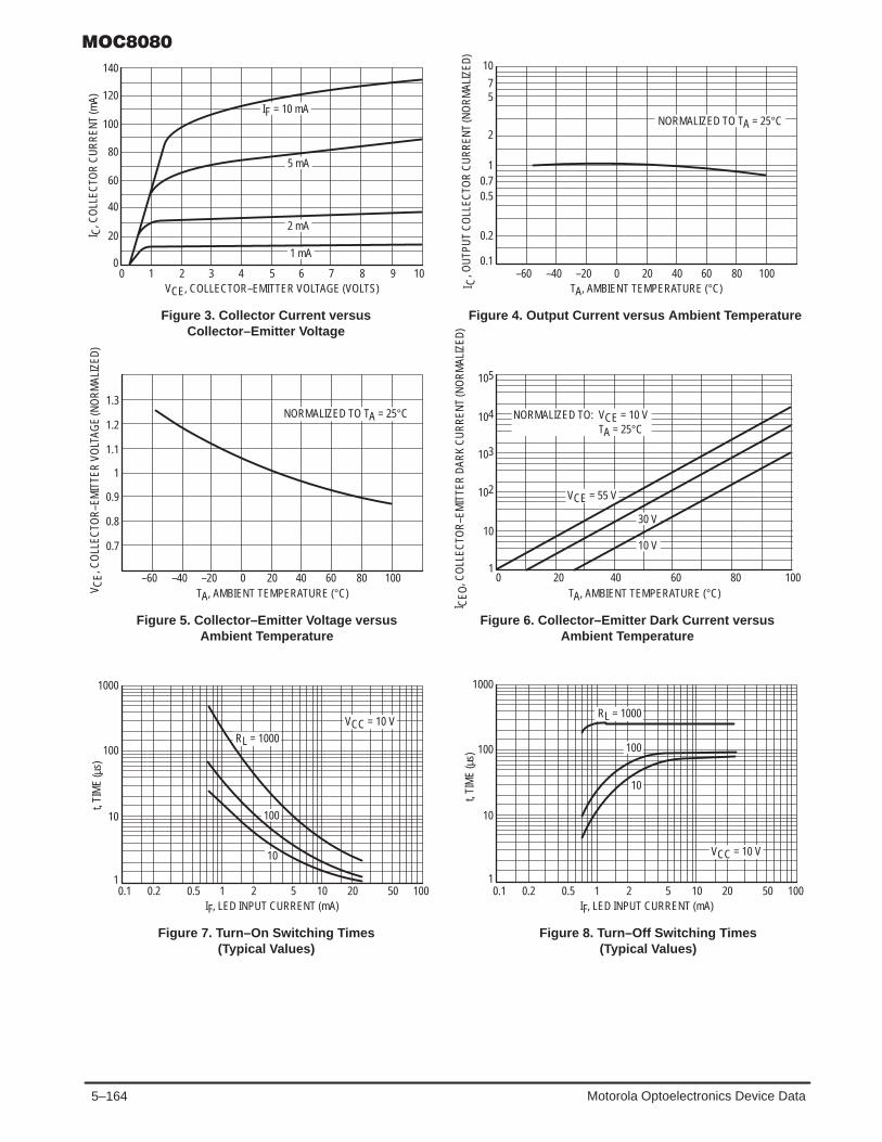
5–164 Motorola Optoelectronics Device Data
, CO
LLEC
TOR
CU
RR
ENT
(mA)
20
0
Figure 3. Collector Current versusCollector–Emitter Voltage
IF = 10 mA
0
VCE, COLLECTOR–EMITTER VOLTAGE (VOLTS)
I C
40
60
80
100
120
140
1 2 3 4 5 6 7 8 9 10
5 mA
2 mA
1 mA
10
75
2
10.70.5
0.2
0.1–60
Figure 4. Output Current versus Ambient Temperature
–40 –20
C, O
UTP
UT
CO
LLEC
TOR
CU
RR
ENT
(NO
RM
ALIZ
ED)
0 20 40 60 80 100TA, AMBIENT TEMPERATURE (°C)I
NORMALIZED TO TA = 25°C
–60
Figure 5. Collector–Emitter Voltage versusAmbient Temperature
NORMALIZED TO TA = 25°C
0.7
TA, AMBIENT TEMPERATURE (°C)V CE
, CO
LLEC
TOR
–EM
ITTE
R V
OLT
AGE
(NO
RM
ALIZ
ED)
–40 –20 0 20 40 60 80 100
0.8
0.9
1
1.1
1.2
1.3
0
Figure 6. Collector–Emitter Dark Current versusAmbient Temperature
1
TA, AMBIENT TEMPERATURE (°C)
I
10
102
103
104
105
20 40 60 80 100
NORMALIZED TO: VCE = 10 VNORMALIZED TO: TA = 25°C
CEO
, CO
LLEC
TOR
–EM
ITTE
R D
ARK
CU
RR
ENT
(NO
RM
ALIZ
ED)
0.1
Figure 7. Turn–On Switching Times(Typical Values)
1
IF, LED INPUT CURRENT (mA)
t, TI
ME
(s)
10
100
1000
µ
0.2 0.5 1 2 5 10 20 50 100
VCC = 10 V
100
10
0.11
IF, LED INPUT CURRENT (mA)
10
100
1000
0.2 0.5 1 2 5 10 20 50 100
10
t, TI
ME
(s)µ
VCC = 10 V
Figure 8. Turn–Off Switching Times(Typical Values)
VCE = 55 V
10 V
30 V
100RL = 1000
RL = 1000

5–165Motorola Optoelectronics Device Data
, TYP
ICAL
CO
LLEC
TOR
CU
RR
ENT
(mA)
0
Figure 9. DC Current Gain (Detector Only)
IB = 0.7 µA
0
VCE, COLLECTOR–EMITTER VOLTAGE (VOLTS)
I
2
4
6
8
10
12
14
2 4 6 8 10 12 14 16 18 20
IF = 0C
0.6 µA
0.5 µA
0.4 µA
0.3 µA
0.2 µA
0.1 µA
0.05
Figure 10. Detector Capacitances versus Voltage
2
VE, VOLTAGE (VOLTS)
C, C
APAC
ITAN
CE
(pF)
10
20
0.1 1 10 50
TEST CIRCUIT
VCC = 10 V
IF = 5 mA
INPUT
RL = 100 Ω
OUTPUT
WAVEFORMS
10%
90%
ton
INPUT PULSE
OUTPUT PULSE
tf
toff
tr
Figure 11. Switching Time Test Circuit and Waveforms
CEB
f = 1 MHzCCB
4
6
8
12
14
16
18
CCE
0.2 0.5 52 20

5–166 Motorola Optoelectronics Device Data
PACKAGE DIMENSIONS
CASE 730A–04ISSUE G
NOTES:1. DIMENSIONING AND TOLERANCING PER ANSI
Y14.5M, 1982.2. CONTROLLING DIMENSION: INCH.3. DIMENSION L TO CENTER OF LEAD WHEN
FORMED PARALLEL.
6 4
1 3
–A–
–B–
SEATINGPLANE
–T–
4 PLF
K
CN
G
6 PLD6 PLE
MAM0.13 (0.005) B MT
L
M
6 PLJMBM0.13 (0.005) A MT
DIM MIN MAX MIN MAXMILLIMETERSINCHES
A 0.320 0.350 8.13 8.89B 0.240 0.260 6.10 6.60C 0.115 0.200 2.93 5.08D 0.016 0.020 0.41 0.50E 0.040 0.070 1.02 1.77F 0.010 0.014 0.25 0.36G 0.100 BSC 2.54 BSCJ 0.008 0.012 0.21 0.30K 0.100 0.150 2.54 3.81L 0.300 BSC 7.62 BSCM 0 15 0 15 N 0.015 0.100 0.38 2.54
STYLE 1:PIN 1. ANODE
2. CATHODE3. NC4. EMITTER5. COLLECTOR6. BASE
CASE 730C–04ISSUE D
–A–
–B–
SEATINGPLANE
–T–J
K
L
6 PL
MBM0.13 (0.005) A MT
C
D 6 PL
MAM0.13 (0.005) B MT
H
GE 6 PL
F 4 PL
31
46
NOTES:1. DIMENSIONING AND TOLERANCING PER ANSI
Y14.5M, 1982.2. CONTROLLING DIMENSION: INCH.
DIM MIN MAX MIN MAXMILLIMETERSINCHES
A 0.320 0.350 8.13 8.89B 0.240 0.260 6.10 6.60C 0.115 0.200 2.93 5.08D 0.016 0.020 0.41 0.50E 0.040 0.070 1.02 1.77F 0.010 0.014 0.25 0.36G 0.100 BSC 2.54 BSCH 0.020 0.025 0.51 0.63J 0.008 0.012 0.20 0.30K 0.006 0.035 0.16 0.88L 0.320 BSC 8.13 BSCS 0.332 0.390 8.43 9.90
*Consult factory for leadform option availability

5–167Motorola Optoelectronics Device Data
*Consult factory for leadform option availability
NOTES:1. DIMENSIONING AND TOLERANCING PER ANSI
Y14.5M, 1982.2. CONTROLLING DIMENSION: INCH.3. DIMENSION L TO CENTER OF LEAD WHEN
FORMED PARALLEL.
CASE 730D–05ISSUE D
6 4
1 3
–A–
–B–
N
C
KG
F 4 PL
SEATING
D 6 PL
E 6 PL
PLANE
–T–
MAM0.13 (0.005) B MT
L
J
DIM MIN MAX MIN MAXMILLIMETERSINCHES
A 0.320 0.350 8.13 8.89B 0.240 0.260 6.10 6.60C 0.115 0.200 2.93 5.08D 0.016 0.020 0.41 0.50E 0.040 0.070 1.02 1.77F 0.010 0.014 0.25 0.36G 0.100 BSC 2.54 BSCJ 0.008 0.012 0.21 0.30K 0.100 0.150 2.54 3.81L 0.400 0.425 10.16 10.80N 0.015 0.040 0.38 1.02
Motorola reserves the right to make changes without further notice to any products herein. Motorola makes no warranty, representation or guarantee regardingthe suitability of its products for any particular purpose, nor does Motorola assume any liability arising out of the application or use of any product or circuit,and specifically disclaims any and all liability, including without limitation consequential or incidental damages. “Typical” parameters can and do vary in differentapplications. All operating parameters, including “Typicals” must be validated for each customer application by customer’s technical experts. Motorola doesnot convey any license under its patent rights nor the rights of others. Motorola products are not designed, intended, or authorized for use as components insystems intended for surgical implant into the body, or other applications intended to support or sustain life, or for any other application in which the failure ofthe Motorola product could create a situation where personal injury or death may occur. Should Buyer purchase or use Motorola products for any suchunintended or unauthorized application, Buyer shall indemnify and hold Motorola and its officers, employees, subsidiaries, affiliates, and distributors harmlessagainst all claims, costs, damages, and expenses, and reasonable attorney fees arising out of, directly or indirectly, any claim of personal injury or deathassociated with such unintended or unauthorized use, even if such claim alleges that Motorola was negligent regarding the design or manufacture of the part.Motorola and are registered trademarks of Motorola, Inc. Motorola, Inc. is an Equal Opportunity/Affirmative Action Employer.
How to reach us:USA / EUROPE: Motorola Literature Distribution; JAPAN : Nippon Motorola Ltd.; Tatsumi–SPD–JLDC, Toshikatsu Otsuki,P.O. Box 20912; Phoenix, Arizona 85036. 1–800–441–2447 6F Seibu–Butsuryu–Center, 3–14–2 Tatsumi Koto–Ku, Tokyo 135, Japan. 03–3521–8315
MFAX: [email protected] – TOUCHTONE (602) 244–6609 HONG KONG: Motorola Semiconductors H.K. Ltd.; 8B Tai Ping Industrial Park, INTERNET: http://Design–NET.com 51 Ting Kok Road, Tai Po, N.T., Hong Kong. 852–26629298
MOC8080/D
◊

5–168 Motorola Optoelectronics Device Data
The MOC8100 device consists of a gallium arsenide infrared emitting diodeoptically coupled to a monolithic silicon phototransistor detector. It is designedfor applications requiring higher output collector current (IC) with lower inputdrive current (IF).
• Current Transfer Ratio Guaranteed to be > 50% at 1 mA LED Drive Level
• To order devices that are tested and marked per VDE 0884 requirements, thesuffix ”V” must be included at end of part number. VDE 0884 is a test option.
Applications
• Appliances, Measuring Instruments
• General Purpose Switching Circuits
• Programmable Controllers
• Portable Electronics
• Interfacing and coupling systems of different potentials and impedances
• Low Power Logic Circuits
• Telecommunications Equipment
MAXIMUM RATINGS (TA = 25°C unless otherwise noted)
Rating Symbol Value Unit
INPUT LED
Reverse Voltage VR 6 Volts
Forward Current — Continuous IF 60 mA
LED Power Dissipation @ TA = 25°Cwith Negligible Power in Output Detector
Derate above 25°C
PD 120
1.41
mW
mW/°C
OUTPUT TRANSISTOR
Collector–Emitter Voltage VCEO 30 Volts
Emitter–Base Voltage VEBO 7 Volts
Collector–Base Voltage VCBO 70 Volts
Collector Current — Continuous IC 150 mA
Detector Power Dissipation @ TA = 25°Cwith Negligible Power in Input LED
Derate above 25°C
PD 150
1.76
mW
mW/°C
TOTAL DEVICE
Isolation Surge Voltage(1)
(Peak ac Voltage, 60 Hz, 1 sec Duration)VISO 7500 Vac(pk)
Total Device Power Dissipation @ TA = 25°CDerate above 25°C
PD 2502.94
mWmW/°C
Ambient Operating Temperature Range(2) TA –55 to +100 °C
Storage Temperature Range(2) Tstg –55 to +150 °C
Soldering Temperature (10 sec, 1/16″ from case) TL 260 °C1. Isolation surge voltage is an internal device dielectric breakdown rating.1. For this test, Pins 1 and 2 are common, and Pins 4, 5 and 6 are common.2. Refer to Quality and Reliability Section in Opto Data Book for information on test conditions.GlobalOptoisolator is a trademark of Motorola, Inc.
Order this documentby MOC8100/D
SEMICONDUCTOR TECHNICAL DATA
GlobalOptoisolator
Motorola, Inc. 1995
SCHEMATIC
STANDARD THRU HOLECASE 730A–04
STYLE 1 PLASTIC
[CTR = 50% Min]
PIN 1. LED ANODE2. LED CATHODE3. N.C.4. EMITTER5. COLLECTOR6. BASE
1
2
3
6
5
4
61
REV 1
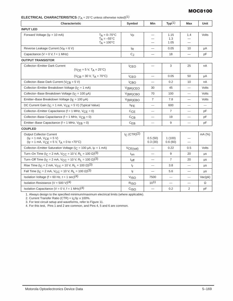
5–169Motorola Optoelectronics Device Data
ELECTRICAL CHARACTERISTICS (TA = 25°C unless otherwise noted)(1)
Characteristic Symbol Min Typ (1) Max Unit
INPUT LED
Forward Voltage (IF = 10 mA) TA = 0–70°CTA = –55°CTA = 100°C
VF ———
1.151.31.05
1.4——
Volts
Reverse Leakage Current (VR = 6 V) IR — 0.05 10 µA
Capacitance (V = 0 V, f = 1 MHz) CJ — 18 — pF
OUTPUT TRANSISTOR
Collector–Emitter Dark Current ICEO — 3 25 nA(VCE = 5 V, TA = 25°C)
(VCB = 30 V, TA = 70°C) ICEO — 0.05 50 µA
Collector–Base Dark Current (VCB = 5 V) ICBO — 0.2 10 nA
Collector–Emitter Breakdown Voltage (IC = 1 mA) V(BR)CEO 30 45 — Volts
Collector–Base Breakdown Voltage (IC = 100 µA) V(BR)CBO 70 100 — Volts
Emitter–Base Breakdown Voltage (IE = 100 µA) V(BR)EBO 7 7.8 — Volts
DC Current Gain (IC = 1 mA, VCE = 5 V) (Typical Value) hFE — 600 — —
Collector–Emitter Capacitance (f = 1 MHz, VCE = 0) CCE — 7 — pF
Collector–Base Capacitance (f = 1 MHz, VCB = 0) CCB — 19 — pF
Emitter–Base Capacitance (f = 1 MHz, VEB = 0) CEB — 9 — pF
COUPLED
Output Collector Current(IF = 1 mA, VCE = 5 V)(IF = 1 mA, VCE = 5 V, TA = 0 to +70°C)
IC (CTR)(2)
0.5 (50)0.3 (30)
1 (100)0.6 (60)
——
mA (%)
Collector–Emitter Saturation Voltage (IC = 100 µA, IF = 1 mA) VCE(sat) — 0.22 0.5 Volts
Turn–On Time (IC = 2 mA, VCC = 10 V, RL = 100 Ω)(3) ton — 9 20 µs
Turn–Off Time (IC = 2 mA, VCC = 10 V, RL = 100 Ω)(3) toff — 7 20 µs
Rise Time (IC = 2 mA, VCC = 10 V, RL = 100 Ω)(3) tr — 3.8 — µs
Fall Time (IC = 2 mA, VCC = 10 V, RL = 100 Ω)(3) tf — 5.6 — µs
Isolation Voltage (f = 60 Hz, t = 1 sec)(4) VISO 7500 — — Vac(pk)
Isolation Resistance (V = 500 V)(4) RISO 1011 — — Ω
Isolation Capacitance (V = 0 V, f = 1 MHz)(4) CISO — 0.2 2 pF
1. Always design to the specified minimum/maximum electrical limits (where applicable).2. Current Transfer Ratio (CTR) = IC/IF x 100%.3. For test circuit setup and waveforms, refer to Figure 11.4. For this test, Pins 1 and 2 are common, and Pins 4, 5 and 6 are common.

5–170 Motorola Optoelectronics Device Data
TYPICAL CHARACTERISTICS
Figure 1. LED Forward Voltage versus Forward Current
2
1.8
1.6
1.4
1.2
11 10 100 1000
IF, LED FORWARD CURRENT (mA)
V F, F
OR
WAR
D V
OLT
AGE
(VO
LTS)
25°C
100°C
TA = –55°C
Figure 2. Output Current versus Input Current
PULSE ONLYPULSE OR DC
10
75
2
10.70.5
0.2
0.1–60 –40 –20 0 20 40 60 80 100
TA, AMBIENT TEMPERATURE (°C)
I C, O
UTP
UT
CO
LLEC
TOR
CU
RR
ENT
(NO
RM
ALIZ
ED)
1
10
100
0.10 20 40 60 80 100
TA, AMBIENT TEMPERATURE (°C)
t, TI
ME
(s)
I
100
50
20
10
5
2
10.1 0.2 0.5 1 2 5 10 20 50 100
IF, LED INPUT CURRENT (mA)
CEO
, CO
LLEC
TOR
–EM
ITTE
R D
ARK
CU
RR
ENT
(NO
RM
ALIZ
ED)
µ
NORMALIZED TO:VCE = 10 VTA = 25°C
VCE = 30 V
10 V
VCC = 10 V
tf
tr
tr
tf
NORMALIZED TO TA = 25°CIF = 10 mA
0
VCE, COLLECTOR–EMITTER VOLTAGE (VOLTS)
I C, C
OLL
ECTO
R C
UR
REN
T (m
A)
4
8
12
16
20
24
28
5 mA
2 mA
1 mA
0 1 2 3 4 5 6 7 8 9 10
Figure 3. Collector Current versusCollector–Emitter Voltage
Figure 4. Output Current versus Ambient Temperature
Figure 5. Dark Current versus Ambient Temperature Figure 6. Rise and Fall Times(Typical Values)
RL = 100 RL = 1000
C
IF, LED INPUT CURRENT (mA)5210.50.20.10.05
0.1
1
10
0.001
I, O
UTP
UT
CO
LLEC
TOR
CU
RR
ENT
(NO
RM
ALIZ
ED)
NORMALIZED TO:IF = 1 mA

5–171Motorola Optoelectronics Device Data
t, T
UR
N–O
FF T
IME
(s)
off
µ
t, T
UR
N–O
N T
IME
(s)
onµ
1007050
20
1075
2
10.1 0.2 0.5 0.7 1 2 5 7 10 20 50 70 100
IF, LED INPUT CURRENT (mA)
RL = 1000
VCC = 10 V
100
10
1007050
20
1075
2
10.1 0.2 0.5 0.7 1 2 5 7 10 20 50 70 100
IF, LED INPUT CURRENT (mA)
RL = 1000
VCC = 10 V
100
10
Figure 7. Turn–On Switching Times Figure 8. Turn–Off Switching Times
C, C
APAC
ITAN
CE
(pF)
Figure 9. DC Current Gain (Detector Only) Figure 10. Capacitances versus Voltage
20
18
16
14
12
10
8
6
4
2
0
CCE
f = 1 MHz
0.05 0.1 0.2 0.5 1 2 5 10 20 50V, VOLTAGE (VOLTS)
CLED
CCB
CEB
5 µA
4 µA
3 µA
2 µA
1 µA
4
3
2
1
0 2 4 6 8 10 12 14 16 18 20VCE, COLLECTOR–EMITTER VOLTAGE (VOLTS)
I C, T
YPIC
AL C
OLL
ECTO
R C
UR
REN
T (m
A) IF = 0
6 µA
TEST CIRCUIT
VCC = 10 V
INPUT
RL = 100 Ω
OUTPUT
WAVEFORMS
10%
90%
ton
INPUT PULSE
OUTPUT PULSE
tf
toff
tr
Figure 11. Switching Time Test Circuit and Waveforms
INPUT CURRENT ADJUSTEDTO ACHIEVE IC = 2 mA.
IC
IB = 7 µA
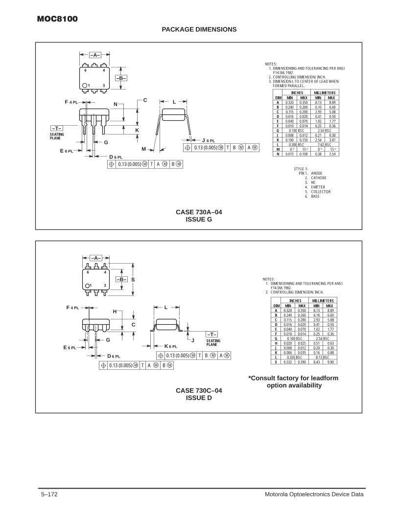
5–172 Motorola Optoelectronics Device Data
PACKAGE DIMENSIONS
CASE 730A–04ISSUE G
NOTES:1. DIMENSIONING AND TOLERANCING PER ANSI
Y14.5M, 1982.2. CONTROLLING DIMENSION: INCH.3. DIMENSION L TO CENTER OF LEAD WHEN
FORMED PARALLEL.
6 4
1 3
–A–
–B–
SEATINGPLANE
–T–
4 PLF
K
CN
G
6 PLD6 PLE
MAM0.13 (0.005) B MT
L
M
6 PLJMBM0.13 (0.005) A MT
DIM MIN MAX MIN MAXMILLIMETERSINCHES
A 0.320 0.350 8.13 8.89B 0.240 0.260 6.10 6.60C 0.115 0.200 2.93 5.08D 0.016 0.020 0.41 0.50E 0.040 0.070 1.02 1.77F 0.010 0.014 0.25 0.36G 0.100 BSC 2.54 BSCJ 0.008 0.012 0.21 0.30K 0.100 0.150 2.54 3.81L 0.300 BSC 7.62 BSCM 0 15 0 15 N 0.015 0.100 0.38 2.54
STYLE 1:PIN 1. ANODE
2. CATHODE3. NC4. EMITTER5. COLLECTOR6. BASE
CASE 730C–04ISSUE D
–A–
–B–
SEATINGPLANE
–T–J
K
L
6 PL
MBM0.13 (0.005) A MT
C
D 6 PL
MAM0.13 (0.005) B MT
H
GE 6 PL
F 4 PL
31
46
NOTES:1. DIMENSIONING AND TOLERANCING PER ANSI
Y14.5M, 1982.2. CONTROLLING DIMENSION: INCH.
DIM MIN MAX MIN MAXMILLIMETERSINCHES
A 0.320 0.350 8.13 8.89B 0.240 0.260 6.10 6.60C 0.115 0.200 2.93 5.08D 0.016 0.020 0.41 0.50E 0.040 0.070 1.02 1.77F 0.010 0.014 0.25 0.36G 0.100 BSC 2.54 BSCH 0.020 0.025 0.51 0.63J 0.008 0.012 0.20 0.30K 0.006 0.035 0.16 0.88L 0.320 BSC 8.13 BSCS 0.332 0.390 8.43 9.90
*Consult factory for leadform option availability

5–173Motorola Optoelectronics Device Data
*Consult factory for leadform option availability
NOTES:1. DIMENSIONING AND TOLERANCING PER ANSI
Y14.5M, 1982.2. CONTROLLING DIMENSION: INCH.3. DIMENSION L TO CENTER OF LEAD WHEN
FORMED PARALLEL.
CASE 730D–05ISSUE D
6 4
1 3
–A–
–B–
N
C
KG
F 4 PL
SEATING
D 6 PL
E 6 PL
PLANE
–T–
MAM0.13 (0.005) B MT
L
J
DIM MIN MAX MIN MAXMILLIMETERSINCHES
A 0.320 0.350 8.13 8.89B 0.240 0.260 6.10 6.60C 0.115 0.200 2.93 5.08D 0.016 0.020 0.41 0.50E 0.040 0.070 1.02 1.77F 0.010 0.014 0.25 0.36G 0.100 BSC 2.54 BSCJ 0.008 0.012 0.21 0.30K 0.100 0.150 2.54 3.81L 0.400 0.425 10.16 10.80N 0.015 0.040 0.38 1.02
Motorola reserves the right to make changes without further notice to any products herein. Motorola makes no warranty, representation or guarantee regardingthe suitability of its products for any particular purpose, nor does Motorola assume any liability arising out of the application or use of any product or circuit,and specifically disclaims any and all liability, including without limitation consequential or incidental damages. “Typical” parameters can and do vary in differentapplications. All operating parameters, including “Typicals” must be validated for each customer application by customer’s technical experts. Motorola doesnot convey any license under its patent rights nor the rights of others. Motorola products are not designed, intended, or authorized for use as components insystems intended for surgical implant into the body, or other applications intended to support or sustain life, or for any other application in which the failure ofthe Motorola product could create a situation where personal injury or death may occur. Should Buyer purchase or use Motorola products for any suchunintended or unauthorized application, Buyer shall indemnify and hold Motorola and its officers, employees, subsidiaries, affiliates, and distributors harmlessagainst all claims, costs, damages, and expenses, and reasonable attorney fees arising out of, directly or indirectly, any claim of personal injury or deathassociated with such unintended or unauthorized use, even if such claim alleges that Motorola was negligent regarding the design or manufacture of the part.Motorola and are registered trademarks of Motorola, Inc. Motorola, Inc. is an Equal Opportunity/Affirmative Action Employer.
How to reach us:USA / EUROPE: Motorola Literature Distribution; JAPAN : Nippon Motorola Ltd.; Tatsumi–SPD–JLDC, Toshikatsu Otsuki,P.O. Box 20912; Phoenix, Arizona 85036. 1–800–441–2447 6F Seibu–Butsuryu–Center, 3–14–2 Tatsumi Koto–Ku, Tokyo 135, Japan. 03–3521–8315
MFAX: [email protected] – TOUCHTONE (602) 244–6609 HONG KONG: Motorola Semiconductors H.K. Ltd.; 8B Tai Ping Industrial Park, INTERNET: http://Design–NET.com 51 Ting Kok Road, Tai Po, N.T., Hong Kong. 852–26629298
MOC8100/D
◊

5–174 Motorola Optoelectronics Device Data
! #&"%" &"$%"$ "($ '## ) ## &"!%" % "!!&"!
The MOC8101, MOC8102, MOC8103, MOC8104 and MOC8105 devicesconsist of a gallium arsenide LED optically coupled to a silicon phototransistorin a dual–in–line package.
• Closely Matched Current Transfer Ratio (CTR) Minimizes Unit–to–Unit Variation
• Narrow (CTR) Windows that translate to a Narrow and Predictable Open Loop GainWindow
• Very Low Coupled Capacitance along with No Chip to Pin 6 Base Connection for Minimum Noise Susceptibility
• To order devices that are tested and marked per VDE 0884 requirements, thesuffix “V” must be included at end of part number. VDE 0884 is a test option.
Applications• Switchmode Power Supplies (Feedback Control)
• AC Line/Digital Logic Isolation
• Interfacing and coupling systems of different potentials and impedances
MAXIMUM RATINGS (TA = 25°C unless otherwise noted)
Rating Symbol Value Unit
INPUT LED
Forward Current — Continuous IF 60 mA
Forward Current — Peak (PW = 100 µs, 120 pps) IF(pk) 1 A
Reverse Voltage VR 6 Volts
LED Power Dissipation @ TA = 25°CDerate above 25°C
PD 1201.41
mWmW/°C
OUTPUT TRANSISTOR
Collector–Emitter Voltage VCEO 30 Volts
Emitter–Collector Voltage VECO 7 Volts
Collector Current — Continuous IC 150 mA
Detector Power Dissipation @ TA = 25°CDerate above 25°C
PD 1501.76
mWmW/°C
TOTAL DEVICE
Input–Output Isolation Voltage(1)
(f = 60 Hz, t = 1 sec.)VISO 7500 Vac(pk)
Total Device Power Dissipation @ TA = 25°CDerate above 25°C
PD 2502.94
mWmW/°C
Ambient Operating Temperature Range(2) TA –55 to +100 °C
Storage Temperature Range(2) Tstg –55 to +150 °C
Lead Soldering Temperature(1/16″ from case, 10 sec. duration)
TL 260 °C
1. Input–Output Isolation Voltage, VISO, is an internal device dielectric breakdown rating.1. For this test, Pins 1 and 2 are common, and Pins 4 and 5 are common.2. Refer to Quality and Reliability Section in Opto Data Book for information on test conditions.Preferred devices are Motorola recommended choices for future use and best overall value.GlobalOptoisolator is a trademark of Motorola, Inc.
Order this documentby MOC8101/D
SEMICONDUCTOR TECHNICAL DATA
GlobalOptoisolator
*Motorola Preferred Device
[CTR = 108–173%]
[CTR = 160–256%]
[CTR = 65–133%]
STANDARD THRU HOLECASE 730A–04
STYLE 3 PLASTIC
61
SCHEMATIC
PIN 1. ANODE2. CATHODE3. NO CONNECTION4. EMITTER5. COLLECTOR6. NO CONNECTION
1
2
3
6
5
4NC
NC
[CTR = 50–80%]
[CTR = 73–117%]
REV 1

5–175Motorola Optoelectronics Device Data
ELECTRICAL CHARACTERISTICS (TA = 25°C unless otherwise noted)(1)
Characteristic Symbol Min Typ (1) Max Unit
INPUT LED
Forward Voltage (IF = 10 mA) VF 1.0 1.15 1.5 V
Reverse Leakage Current (VR = 5.0 V) IR — 0.05 10 µA
Capacitance C — 18 — pF
OUTPUT TRANSISTOR
Collector–Emitter Dark Current (VCE = 10 V, TA = 25°C) ICEO1 — 1.0 50 nA
(VCE = 10 V, TA = 100°C) ICEO2 — 1.0 — µA
Collector–Emitter Breakdown Voltage (IC = 1.0 mA) V(BR)CEO 30 45 — V
Emitter–Collector Breakdown Voltage (IE = 100 µA) V(BR)ECO 7.0 7.8 — V
Collector–Emitter Capacitance (f = 1.0 MHz, VCE = 0) CCE — 7.0 — pF
COUPLED
Output Collector Current MOC8101(IF = 10 mA, VCE = 10 V) MOC8102
MOC8103MOC8104MOC8105
IC (CTR)(2) 5.0 (50)7.3 (73)
10.8 (108)16 (160)6.5 (65)
6.5 (65)9.0 (90)14 (140)20 (200)10 (100)
8.0 (80)11.7 (117)17.3 (173)25.6 (256)13.3 (133)
mA (%)
Collector–Emitter Saturation Voltage (IC = 500 µA, IF = 5.0 mA) VCE(sat) — 0.15 0.4 V
Turn–On Time (IC = 2.0 mA, VCC = 10 V, RL = 100 Ω)(3) ton — 7.5 20 µs
Turn–Off Time (IC = 2.0 mA, VCC = 10 V, RL = 100 Ω)(3) toff — 5.7 20 µs
Rise Time (IC = 2.0 mA, VCC = 10 V, RL = 100 Ω)(3) tr — 3.2 — µs
Fall Time (IC = 2.0 mA, VCC = 10 V, RL = 100 Ω)(3) tf — 4.7 — µs
Isolation Voltage (f = 60 Hz, t = 1.0 sec.)(4) VISO 7500 — — Vac(pk)
Isolation Resistance (VI–O = 500 V)(4) RISO 1011 — — Ω
Isolation Capacitance (VI–O = 0, f = 1.0 MHz)(4) CISO — 0.2 — pF
1. Always design to the specified minimum/maximum electrical limits (where applicable).2. Current Transfer Ratio (CTR) = IC/IF x 100%.3. For test circuit setup and waveforms, refer to Figure 7.4. For this test, Pins 1 and 2 are common, and Pins 4 and 5 are common.
I C, O
UTP
UT
CO
LLEC
TOR
CU
RR
ENT
(NO
RM
ALIZ
ED)
TYPICAL CHARACTERISTICS
Figure 1. LED Forward Voltage versus Forward Current
2
1.8
1.6
1.4
1.2
11 10 100 1000
1
0.1
0.010.5 1
IF, LED FORWARD CURRENT (mA)2 5 10 20 50
IF, LED INPUT CURRENT (mA)
V F, F
ORW
ARD
VO
LTAG
E (V
OLT
S)
25°C
100°C
TA = –55°C
NORMALIZED TO:IF = 10 mA
Figure 2. Output Current versus Input Current
PULSE ONLYPULSE OR DC
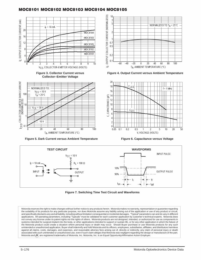
5–176 Motorola Optoelectronics Device Data
10
75
2
10.70.5
0.2
0.1–60 –40 –20 0 20 40 60 80 100
TA, AMBIENT TEMPERATURE (°C)I C, O
UTP
UT
CO
LLEC
TOR
CU
RR
ENT
(NO
RM
ALIZ
ED)
1
10
100
0.10 20 40 60 80 100
TA, AMBIENT TEMPERATURE (°C)
C, C
APAC
ITAN
CE
(pF)
I
20
10
2
00.1 0.2 0.5 1 2 5 10 20 50
V, VOLTAGE (VOLTS)
CEO
, CO
LLEC
TOR
–EM
ITTE
R D
ARK
CU
RR
ENT
(NO
RM
ALIZ
ED)
NORMALIZED TO:VCE = 10 VTA = 25°C
VCE = 30 V
NORMALIZED TO TA = 25°C
Figure 3. Collector Current versusCollector–Emitter Voltage
Figure 4. Output Current versus Ambient Temperature
Figure 5. Dark Current versus Ambient Temperature Figure 6. Capacitance versus Voltage
f = 1 MHz
0.05
4
6
8
12
14
16
18
10 V
CLED
CCE
TEST CIRCUIT
VCC = 10 V
INPUT
RL = 100 Ω
OUTPUT
WAVEFORMS
10%
90%
ton
INPUT PULSE
OUTPUT PULSE
tf
toff
tr
Figure 7. Switching Time Test Circuit and Waveforms
IF = 10 mA
4
IF = 10 mA
0
VCE, COLLECTOR-EMITTER VOLTAGE (VOLTS)
I C, O
UTP
UT
CO
LLEC
TOR
CU
RR
ENT
(mA)
8
12
16
20MOC8104
0 1 2 3 4 5 6 7 8 9 10
MOC8102
MOC8101
MOC8103
MOC8105
Motorola reserves the right to make changes without further notice to any products herein. Motorola makes no warranty, representation or guarantee regardingthe suitability of its products for any particular purpose, nor does Motorola assume any liability arising out of the application or use of any product or circuit,and specifically disclaims any and all liability, including without limitation consequential or incidental damages. “Typical” parameters can and do vary in differentapplications. All operating parameters, including “Typicals” must be validated for each customer application by customer’s technical experts. Motorola doesnot convey any license under its patent rights nor the rights of others. Motorola products are not designed, intended, or authorized for use as components insystems intended for surgical implant into the body, or other applications intended to support or sustain life, or for any other application in which the failure ofthe Motorola product could create a situation where personal injury or death may occur. Should Buyer purchase or use Motorola products for any suchunintended or unauthorized application, Buyer shall indemnify and hold Motorola and its officers, employees, subsidiaries, affiliates, and distributors harmlessagainst all claims, costs, damages, and expenses, and reasonable attorney fees arising out of, directly or indirectly, any claim of personal injury or deathassociated with such unintended or unauthorized use, even if such claim alleges that Motorola was negligent regarding the design or manufacture of the part.Motorola and are registered trademarks of Motorola, Inc. Motorola, Inc. is an Equal Opportunity/Affirmative Action Employer.

5–177Motorola Optoelectronics Device Data
PACKAGE DIMENSIONS
CASE 730A–04ISSUE G
NOTES:1. DIMENSIONING AND TOLERANCING PER ANSI
Y14.5M, 1982.2. CONTROLLING DIMENSION: INCH.3. DIMENSION L TO CENTER OF LEAD WHEN
FORMED PARALLEL.
6 4
1 3
–A–
–B–
SEATINGPLANE
–T–
4 PLF
K
CN
G
6 PLD6 PLE
MAM0.13 (0.005) B MT
L
M
6 PLJMBM0.13 (0.005) A MT
DIM MIN MAX MIN MAXMILLIMETERSINCHES
A 0.320 0.350 8.13 8.89B 0.240 0.260 6.10 6.60C 0.115 0.200 2.93 5.08D 0.016 0.020 0.41 0.50E 0.040 0.070 1.02 1.77F 0.010 0.014 0.25 0.36G 0.100 BSC 2.54 BSCJ 0.008 0.012 0.21 0.30K 0.100 0.150 2.54 3.81L 0.300 BSC 7.62 BSCM 0 15 0 15 N 0.015 0.100 0.38 2.54
STYLE 3:PIN 1. ANODE
2. CATHODE3. NC4. EMITTER5. COLLECTOR6. NC
CASE 730C–04ISSUE D
–A–
–B–
SEATINGPLANE
–T–J
K
L
6 PL
MBM0.13 (0.005) A MT
C
D 6 PL
MAM0.13 (0.005) B MT
H
GE 6 PL
F 4 PL
31
46NOTES:
1. DIMENSIONING AND TOLERANCING PER ANSIY14.5M, 1982.
2. CONTROLLING DIMENSION: INCH.
DIM MIN MAX MIN MAXMILLIMETERSINCHES
A 0.320 0.350 8.13 8.89B 0.240 0.260 6.10 6.60C 0.115 0.200 2.93 5.08D 0.016 0.020 0.41 0.50E 0.040 0.070 1.02 1.77F 0.010 0.014 0.25 0.36G 0.100 BSC 2.54 BSCH 0.020 0.025 0.51 0.63J 0.008 0.012 0.20 0.30K 0.006 0.035 0.16 0.88L 0.320 BSC 8.13 BSCS 0.332 0.390 8.43 9.90
How to reach us:USA / EUROPE: Motorola Literature Distribution; JAPAN : Nippon Motorola Ltd.; Tatsumi–SPD–JLDC, Toshikatsu Otsuki,P.O. Box 20912; Phoenix, Arizona 85036. 1–800–441–2447 6F Seibu–Butsuryu–Center, 3–14–2 Tatsumi Koto–Ku, Tokyo 135, Japan. 03–3521–8315
MFAX: [email protected] – TOUCHTONE (602) 244–6609 HONG KONG: Motorola Semiconductors H.K. Ltd.; 8B Tai Ping Industrial Park, INTERNET: http://Design–NET.com 51 Ting Kok Road, Tai Po, N.T., Hong Kong. 852–26629298
MOC8101/D
◊

5–178 Motorola Optoelectronics Device Data
! ! ! "!"! !
The MOC8111, MOC8112 and MOC8113 devices consist of a galliumarsenide infrared emitting diode optically coupled to a monolithic siliconphototransistor detector. The internal base–to–Pin 6 connection has beeneliminated for improved noise immunity.
• To order devices that are tested and marked per VDE 0884 requirements, thesuffix ”V” must be included at end of part number. VDE 0884 is a test option.
Applications
• Appliances, Measuring Instruments
• Regulation and Feedback Control
• Programmable Controllers
• Interfacing and coupling systems of different potentials and impedances
• General Purpose Switching Circuits
• High Noise Environments
MAXIMUM RATINGS (TA = 25°C unless otherwise noted)
Rating Symbol Value Unit
INPUT LED
Reverse Voltage VR 6 Volts
Forward Current — Continuous IF 60 mA
LED Power Dissipation @ TA = 25°Cwith Negligible Power in Output Detector
Derate above 25°C
PD 120
1.41
mW
mW/°C
OUTPUT TRANSISTOR
Collector–Emitter Voltage VCEO 30 Volts
Emitter–Collector Voltage VECO 7 Volts
Collector Current — Continuous IC 150 mA
Detector Power Dissipation @ TA = 25°Cwith Negligible Power in Input LED
Derate above 25°C
PD 150
1.76
mW
mW/°C
TOTAL DEVICE
Isolation Surge Voltage(1)
(Peak ac Voltage, 60 Hz, 1 sec Duration)VISO 7500 Vac(pk)
Total Device Power Dissipation @ TA = 25°CDerate above 25°C
PD 2502.94
mWmW/°C
Ambient Operating Temperature Range(2) TA –55 to +100 °C
Storage Temperature Range(2) Tstg –55 to +150 °C
Soldering Temperature (10 sec, 1/16″ from case) TL 260 °C
1. Isolation surge voltage is an internal device dielectric breakdown rating.1. For this test, Pins 1 and 2 are common, and Pins 4 and 5 are common.2. Refer to Quality and Reliability Section in Opto Data Book for information on test conditions.Preferred devices are Motorola recommended choices for future use and best overall value.GlobalOptoisolator is a trademark of Motorola, Inc.
Order this documentby MOC8111/D
SEMICONDUCTOR TECHNICAL DATA
GlobalOptoisolator
Motorola, Inc. 1995
*Motorola Preferred Devices
SCHEMATIC
[CTR = 20% Min]
STANDARD THRU HOLECASE 730A–04
STYLE 3 PLASTIC
[CTR = 50% Min]
[CTR = 100% Min]
PIN 1. LED ANODE2. LED CATHODE3. N.C.4. EMITTER5. COLLECTOR6. N.C.
1
2
3
6
5
4
61
REV 1

5–179Motorola Optoelectronics Device Data
ELECTRICAL CHARACTERISTICS (TA = 25°C unless otherwise noted)(1)
Characteristic Symbol Min Typ (1) Max Unit
INPUT LED
Forward Voltage (IF = 10 mA) TA = 25°CTA = –55°CTA = 100°C
VF — 1.151.31.05
1.5 Volts
Reverse Leakage Current (VR = 6 V) IR — 0.05 10 µA
Capacitance (V = 0, f = 1 MHz) CJ — 18 — pF
OUTPUT TRANSISTOR
Collector–Emitter Dark Current ICEO — 1 50 nA(VCE = 10 V, TA = 25°C)
(VCE = 10 V, TA = 100°C) ICEO — 1 — µA
Collector–Emitter Breakdown Voltage (IC = 1 mA) V(BR)CEO 30 45 — Volts
Emitter–Collector Breakdown Voltage (IE = 100 µA) V(BR)ECO 7 7.8 — Volts
Collector–Emitter Capacitance (f = 1 MHz, VCE = 0) CCE — 7 — pF
COUPLED
Output Collector Current MOC8111(IF = 10 mA, VCE = 10 V) MOC8112
MOC8113
IC (CTR)(2) 2 (20)5 (50)
10 (100)
5 (50)10 (100)20 (200)
———
mA (%)
Collector–Emitter Saturation Voltage (IC = 500 µA, IF = 10 mA) VCE(sat) — 0.15 0.4 Volts
Turn–On Time (IC = 2 mA, VCC = 10 V, RL = 100 Ω)(3) ton — 7.5 20 µs
Turn–Off Time (IC = 2 mA, VCC = 10 V, RL = 100 Ω)(3) toff — 5.7 20 µs
Rise Time (IC = 2 mA, VCC = 10 V, RL = 100 Ω)(3) tr — 3.2 — µs
Fall Time (IC = 2 mA, VCC = 10 V, RL = 100 Ω)(3) tf — 4.7 — µs
Isolation Voltage (f = 60 Hz, t = 1 sec)(4) VISO 7500 — — Vac(pk)
Isolation Resistance (V = 500 V)(4) RISO 1011 — — Ω
Isolation Capacitance (V = 0, f = 1 MHz)(4) CISO — 0.2 — pF
1. Always design to the specified minimum/maximum electrical limits (where applicable).2. Current Transfer Ratio (CTR) = IC/IF x 100%.3. For test circuit setup and waveforms, refer to Figure 10.4. For this test, Pins 1 and 2 are common, and Pins 4 and 5 are common.
I C, O
UTP
UT
CO
LLEC
TOR
CU
RR
ENT
(NO
RM
ALIZ
ED)
TYPICAL CHARACTERISTICS
Figure 1. LED Forward Voltage versus Forward Current
2
1.8
1.6
1.4
1.2
11 10 100 1000
10
1
0.1
0.01 0.5 1IF, LED FORWARD CURRENT (mA)
2 5 10 20 50IF, LED INPUT CURRENT (mA)
V F, F
ORW
ARD
VO
LTAG
E (V
OLT
S)
25°C
100°C
TA = –55°C
NORMALIZED TO:IF = 10 mA
Figure 2. Output Current versus Input Current
PULSE ONLYPULSE OR DC

5–180 Motorola Optoelectronics Device Data
t, T
UR
N–O
FF T
IME
(s)
off
µ
t, T
UR
N–O
N T
IME
(s)
onµ
10
75
2
10.70.5
0.2
0.1–60 –40 –20 0 20 40 60 80 100
TA, AMBIENT TEMPERATURE (°C)I C, O
UTP
UT
CO
LLEC
TOR
CU
RR
ENT
(NO
RM
ALIZ
ED)
1
10
100
0.10 20 40 60 80 100
TA, AMBIENT TEMPERATURE (°C)
t, TI
ME
(s)
I
100
50
20
10
5
2
10.1 0.2 0.5 1 2 5 10 20 50 100
IF, LED INPUT CURRENT (mA)
1007050
20
1075
2
10.1 0.2 0.5 0.7 1 2 5 7 10 20 50 70 100
CEO
, CO
LLEC
TOR
–EM
ITTE
R D
ARK
CU
RR
ENT
(NO
RM
ALIZ
ED)
IF, LED INPUT CURRENT (mA)
RL = 1000
VCC = 10 V
100
10
1007050
20
1075
2
10.1 0.2 0.5 0.7 1 2 5 7 10 20 50 70 100
IF, LED INPUT CURRENT (mA)
RL = 1000
VCC = 10 V
100
10
µ
NORMALIZED TO:VCE = 10 VTA = 25°C
VCE = 30 V
10 V
VCC = 10 V
tf
tr
tr
tf
NORMALIZED TO TA = 25°CIF = 10 mA
0
VCE, COLLECTOR–EMITTER VOLTAGE (VOLTS)
I C, C
OLL
ECTO
R C
UR
REN
T (m
A)
4
8
12
16
20
24
28
5 mA
2 mA
1 mA
0 1 2 3 4 5 6 7 8 9 10
Figure 3. Collector Current versusCollector–Emitter Voltage
Figure 4. Output Current versus Ambient Temperature
Figure 5. Dark Current versus Ambient Temperature Figure 6. Rise and Fall Times(Typical Values)
Figure 7. Turn–On Switching Times Figure 8. Turn–Off Switching Times
RL = 100 RL = 1000

5–181Motorola Optoelectronics Device Data
C, C
APAC
ITAN
CE
(pF)
Figure 9. Capacitances versus Voltage
20
18
16
14
12
10
8
6
4
2
0
f = 1 MHz
0.05 0.1 0.2 0.5 1 2 5 10 20 50V, VOLTAGE (VOLTS)
CLED
CCE
TEST CIRCUIT
VCC = 10 V
INPUT
RL = 100 Ω
OUTPUT
WAVEFORMS
10%
90%
ton
INPUT PULSE
OUTPUT PULSE
tf
toff
tr
Figure 10. Switching Time Test Circuit and Waveforms
INPUT CURRENT ADJUSTEDTO ACHIEVE IC = 2 mA.
IC

5–182 Motorola Optoelectronics Device Data
PACKAGE DIMENSIONS
CASE 730A–04ISSUE G
NOTES:1. DIMENSIONING AND TOLERANCING PER ANSI
Y14.5M, 1982.2. CONTROLLING DIMENSION: INCH.3. DIMENSION L TO CENTER OF LEAD WHEN
FORMED PARALLEL.
6 4
1 3
–A–
–B–
SEATINGPLANE
–T–
4 PLF
K
CN
G
6 PLD6 PLE
MAM0.13 (0.005) B MT
L
M
6 PLJMBM0.13 (0.005) A MT
DIM MIN MAX MIN MAXMILLIMETERSINCHES
A 0.320 0.350 8.13 8.89B 0.240 0.260 6.10 6.60C 0.115 0.200 2.93 5.08D 0.016 0.020 0.41 0.50E 0.040 0.070 1.02 1.77F 0.010 0.014 0.25 0.36G 0.100 BSC 2.54 BSCJ 0.008 0.012 0.21 0.30K 0.100 0.150 2.54 3.81L 0.300 BSC 7.62 BSCM 0 15 0 15 N 0.015 0.100 0.38 2.54
STYLE 3:PIN 1. ANODE
2. CATHODE3. NC4. EMITTER5. COLLECTOR6. NC
CASE 730C–04ISSUE D
–A–
–B–
SEATINGPLANE
–T–J
K
L
6 PL
MBM0.13 (0.005) A MT
C
D 6 PL
MAM0.13 (0.005) B MT
H
GE 6 PL
F 4 PL
31
46
NOTES:1. DIMENSIONING AND TOLERANCING PER ANSI
Y14.5M, 1982.2. CONTROLLING DIMENSION: INCH.
DIM MIN MAX MIN MAXMILLIMETERSINCHES
A 0.320 0.350 8.13 8.89B 0.240 0.260 6.10 6.60C 0.115 0.200 2.93 5.08D 0.016 0.020 0.41 0.50E 0.040 0.070 1.02 1.77F 0.010 0.014 0.25 0.36G 0.100 BSC 2.54 BSCH 0.020 0.025 0.51 0.63J 0.008 0.012 0.20 0.30K 0.006 0.035 0.16 0.88L 0.320 BSC 8.13 BSCS 0.332 0.390 8.43 9.90
*Consult factory for leadform option availability

5–183Motorola Optoelectronics Device Data
*Consult factory for leadform option availability
NOTES:1. DIMENSIONING AND TOLERANCING PER ANSI
Y14.5M, 1982.2. CONTROLLING DIMENSION: INCH.3. DIMENSION L TO CENTER OF LEAD WHEN
FORMED PARALLEL.
CASE 730D–05ISSUE D
6 4
1 3
–A–
–B–
N
C
KG
F 4 PL
SEATING
D 6 PL
E 6 PL
PLANE
–T–
MAM0.13 (0.005) B MT
L
J
DIM MIN MAX MIN MAXMILLIMETERSINCHES
A 0.320 0.350 8.13 8.89B 0.240 0.260 6.10 6.60C 0.115 0.200 2.93 5.08D 0.016 0.020 0.41 0.50E 0.040 0.070 1.02 1.77F 0.010 0.014 0.25 0.36G 0.100 BSC 2.54 BSCJ 0.008 0.012 0.21 0.30K 0.100 0.150 2.54 3.81L 0.400 0.425 10.16 10.80N 0.015 0.040 0.38 1.02
Motorola reserves the right to make changes without further notice to any products herein. Motorola makes no warranty, representation or guarantee regardingthe suitability of its products for any particular purpose, nor does Motorola assume any liability arising out of the application or use of any product or circuit,and specifically disclaims any and all liability, including without limitation consequential or incidental damages. “Typical” parameters can and do vary in differentapplications. All operating parameters, including “Typicals” must be validated for each customer application by customer’s technical experts. Motorola doesnot convey any license under its patent rights nor the rights of others. Motorola products are not designed, intended, or authorized for use as components insystems intended for surgical implant into the body, or other applications intended to support or sustain life, or for any other application in which the failure ofthe Motorola product could create a situation where personal injury or death may occur. Should Buyer purchase or use Motorola products for any suchunintended or unauthorized application, Buyer shall indemnify and hold Motorola and its officers, employees, subsidiaries, affiliates, and distributors harmlessagainst all claims, costs, damages, and expenses, and reasonable attorney fees arising out of, directly or indirectly, any claim of personal injury or deathassociated with such unintended or unauthorized use, even if such claim alleges that Motorola was negligent regarding the design or manufacture of the part.Motorola and are registered trademarks of Motorola, Inc. Motorola, Inc. is an Equal Opportunity/Affirmative Action Employer.
How to reach us:USA / EUROPE: Motorola Literature Distribution; JAPAN : Nippon Motorola Ltd.; Tatsumi–SPD–JLDC, Toshikatsu Otsuki,P.O. Box 20912; Phoenix, Arizona 85036. 1–800–441–2447 6F Seibu–Butsuryu–Center, 3–14–2 Tatsumi Koto–Ku, Tokyo 135, Japan. 03–3521–8315
MFAX: [email protected] – TOUCHTONE (602) 244–6609 HONG KONG: Motorola Semiconductors H.K. Ltd.; 8B Tai Ping Industrial Park, INTERNET: http://Design–NET.com 51 Ting Kok Road, Tai Po, N.T., Hong Kong. 852–26629298
MOC8111/D
◊

5–184 Motorola Optoelectronics Device Data
#"#!" # !""#! $# $# #"
The MOC8204, MOC8205 and MOC8206 devices consist of gallium arsenideinfrared emitting diodes optically coupled to high voltage, silicon, phototransis-tor detectors in a standard 6–pin DIP package. They are designed for highvoltage applications and are particularly useful in copy machines and solid staterelays.
• To order devices that are tested and marked per VDE 0884 requirements, thesuffix ”V” must be included at end of part number. VDE 0884 is a test option.
Applications
• Copy Machines
• Interfacing and coupling systems of different potentials and impedances
• Monitor and Detection Circuits
• Solid State Relays
MAXIMUM RATINGS (TA = 25°C unless otherwise noted)
Rating Symbol Value Unit
INPUT LED
Forward Current — Continuous IF 60 mA
Forward Current — PeakPulse Width = 1 µs, 330 pps
IF 1.2 Amp
LED Power Dissipation @ TA = 25°CDerate above 25°C
PD 1201.41
mWmW/°C
OUTPUT TRANSISTOR
Collector–Emitter Voltage VCER 400 Volts
Emitter–Collector Voltage VECO 7 Volts
Collector–Base Voltage VCBO 400 mA
Collector Current (Continuous) IC 100 mA
Detector Power Dissipation @ TA = 25°CDerate above 25°C
PD 1501.76
mWmW/°C
TOTAL DEVICE
Total Device Power Dissipation @ TA = 25°CDerate above 25°C
PD 2502.94
mWmW/°C
Operating Temperature Range(2) TJ –55 to +100 °C
Storage Temperature Range(2) Tstg –55 to +150 °C
Soldering Temperature (10 s) TL 260 °C
Isolation Surge VoltagePeak ac Voltage, 60 Hz, 1 Second Duration(1)
VISO 7500 Vac(pk)
1. Isolation surge voltage is an internal device dielectric breakdown rating.1. For this test, Pins 1 and 2 are common, and Pins 4, 5 and 6 are common.2. Refer to Quality and Reliability Section in Opto Data Book for information on test conditions.Preferred devices are Motorola recommended choices for future use and best overall value.GlobalOptoisolator is a trademark of Motorola, Inc.
Order this documentby MOC8204/D
SEMICONDUCTOR TECHNICAL DATA
GlobalOptoisolator
Motorola, Inc. 1995
*Motorola Preferred Device
SCHEMATIC
[CTR = 20% Min]
STANDARD THRU HOLECASE 730A–04
STYLE 1 PLASTIC
[CTR = 10% Min]
[CTR = 5% Min]
PIN 1. ANODE2. CATHODE3. N.C.4. EMITTER5. COLLECTOR6. BASE
1
2
3
6
5
4
61
REV 1

5–185Motorola Optoelectronics Device Data
ELECTRICAL CHARACTERISTICS (TA = 25°C unless otherwise noted)(1)
Characteristic Symbol Min Typ (1) Max Unit
INPUT LED (TA = 25°C unless otherwise noted)
Reverse Leakage Current(VR = 6 V)
IR — — 10 µA
Forward Voltage(IF = 10 mA)
VF — 1.2 15 Volts
Capacitance(V = 0 V, f = 1 MHz)
CJ — 18 — pF
OUTPUT TRANSISTOR (TA = 25°C and IF = 0 unless otherwise noted)
Collector–Emitter Dark Current (RBE = 1 MΩ)(VCE = 300 V) TA = 25°C
TA = 100°C
ICER——
——
100250
nAµA
Collector–Base Breakdown Voltage(IC = 100 µA)
V(BR)CBO 400 — — Volts
Collector–Emitter Breakdown Voltage(IC = 1 mA, RBE = 1 MΩ)
V(BR)CER 400 — — Volts
Emitter–Base Breakdown Voltage(IE = 100 µA)
V(BR)EBO 7 — — Volts
COUPLED (TA = 25°C unless otherwise noted)
Output Collector Current(VCE = 10 V, IF = 10 mA, RBE = 1 MΩ) MOC8204
MOC8205MOC8206
IC (CTR)(2)
2 (20)1 (10)0.5 (5)
———
———
mA (%)
Collector–Emitter Saturation Voltage(IC = 0.5 mA, IF = 10 mA, RBE = 1 MΩ)
VCE(sat) — — 0.4 Volts
Surge Isolation Voltage (Input to Output)(3)
Peak ac Voltage, 60 Hz, 1 secVISO 7500 — — Vac(pk)
Isolation Resistance(3 )
(V = 500 V)RISO — 1011 — Ohms
Isolation Capacitance(1)
(V = 0 V, f = 1 MHz)CISO — 0.2 — pF
Turn–On TimeVCC = 10 V IC = 2 mA RL = 100 Ω
ton — 5 — µs
Turn–Off TimeVCC = 10 V, IC = 2 mA, RL = 100 Ω
toff — 5 —
1. Always design to the specified minimum/maximum electrical limits (where applicable).2. Current Transfer Ratio (CTR) = IC/IF x 100%.3. For this test LED Pins 1 and 2 are common and phototransistor Pins 4, 5 and 6 are common.
Figure 1. Output Current versus LED Input Current
0.11
IF, LED INPUT CURRENT (mA)
I
0.2
0.5
1
2
5
10
20
50
2 5 10 20 50
CER
, OU
TPU
T C
UR
REN
T (m
A)
RBE = 106 ΩVCE = 10 VTA = 25°C
1–60
TA, AMBIENT TEMPERATURE (°C)
I CER
, OU
TPU
T C
UR
REN
T (m
A)
IF = 20 mA
IF = 10 mA
IF = 5 mA2
5
10
20
–40 –20 0 20 40 60 80 100
RBE = 106 ΩVCE = 10 V
Figure 2. Output Current versus Temperature
TYPICAL CHARACTERISTICS

5–186 Motorola Optoelectronics Device Data
–600
TA, AMBIENT TEMPERATURE (°C)
I CBO
, CO
LLEC
TOR
-BAS
E C
UR
REN
T (
A)
–40 –20 0 20 40 60 80 100
2
1.8
1.6
1.4
1.2
11 10 100 1000
IF, LED FORWARD CURRENT (mA)
V F, F
OR
WAR
D V
OLT
AGE
(VO
LTS)
25°C
100°C
TA = –55°C
0.005
VCE, COLLECTOR–EMITTER VOLTAGE (VOLTS)
I
0.01
0.051
51.0
5.010
40
0.1 0.5 1 5 10 50 100 300
RBE = 106 ΩTA = 25°C
IF = 5 mA
IF = 10 mA
IF = 50 mAC
ER, O
UTP
UT
CU
RR
ENT
(mA)
1
TA, AMBIENT TEMPERATURE (°C)
I
10
20 40 60 90 100
VCE = 300 V
CER
, DAR
K C
UR
REN
T (n
A)
60
120
180
240
300
RBE = 106 ΩVCE = 10 V
IF = 50 mA
IF = 10 mA
IF = 5 mA
100100
1000
30 50 70 80
µ
VCE = 100 V RBE = 106 Ω
VCE = 50 V
PULSE ONLYPULSE OR DC
Figure 3. Output Characteristics Figure 4. Forward Characteristics
Figure 5. Collector–Base Current versus Temperature Figure 6. Dark Current versus Temperature
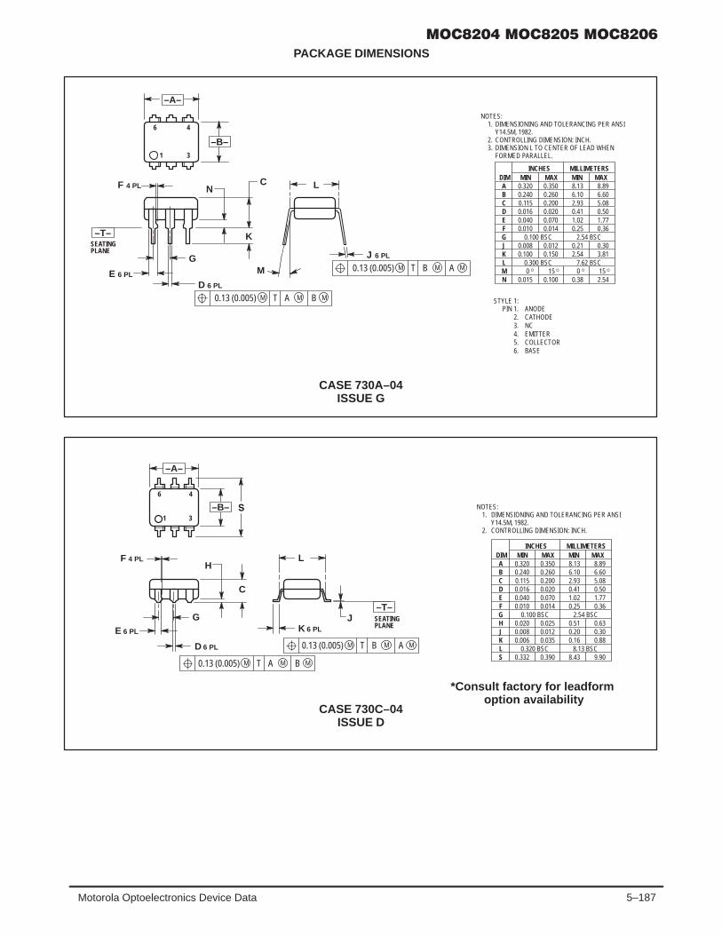
5–187Motorola Optoelectronics Device Data
PACKAGE DIMENSIONS
CASE 730A–04ISSUE G
NOTES:1. DIMENSIONING AND TOLERANCING PER ANSI
Y14.5M, 1982.2. CONTROLLING DIMENSION: INCH.3. DIMENSION L TO CENTER OF LEAD WHEN
FORMED PARALLEL.
STYLE 1:PIN 1. ANODE
2. CATHODE3. NC4. EMITTER5. COLLECTOR6. BASE
6 4
1 3
–A–
–B–
SEATINGPLANE
–T–
4 PLF
K
CN
G
6 PLD6 PLE
MAM0.13 (0.005) B MT
L
M
6 PLJMBM0.13 (0.005) A MT
DIM MIN MAX MIN MAXMILLIMETERSINCHES
A 0.320 0.350 8.13 8.89B 0.240 0.260 6.10 6.60C 0.115 0.200 2.93 5.08D 0.016 0.020 0.41 0.50E 0.040 0.070 1.02 1.77F 0.010 0.014 0.25 0.36G 0.100 BSC 2.54 BSCJ 0.008 0.012 0.21 0.30K 0.100 0.150 2.54 3.81L 0.300 BSC 7.62 BSCM 0 15 0 15 N 0.015 0.100 0.38 2.54
CASE 730C–04ISSUE D
–A–
–B–
SEATINGPLANE
–T–J
K
L
6 PL
MBM0.13 (0.005) A MT
C
D 6 PL
MAM0.13 (0.005) B MT
H
GE 6 PL
F 4 PL
31
46
NOTES:1. DIMENSIONING AND TOLERANCING PER ANSI
Y14.5M, 1982.2. CONTROLLING DIMENSION: INCH.
DIM MIN MAX MIN MAXMILLIMETERSINCHES
A 0.320 0.350 8.13 8.89B 0.240 0.260 6.10 6.60C 0.115 0.200 2.93 5.08D 0.016 0.020 0.41 0.50E 0.040 0.070 1.02 1.77F 0.010 0.014 0.25 0.36G 0.100 BSC 2.54 BSCH 0.020 0.025 0.51 0.63J 0.008 0.012 0.20 0.30K 0.006 0.035 0.16 0.88L 0.320 BSC 8.13 BSCS 0.332 0.390 8.43 9.90
*Consult factory for leadform option availability

5–188 Motorola Optoelectronics Device Data
*Consult factory for leadform option availability
NOTES:1. DIMENSIONING AND TOLERANCING PER ANSI
Y14.5M, 1982.2. CONTROLLING DIMENSION: INCH.3. DIMENSION L TO CENTER OF LEAD WHEN
FORMED PARALLEL.
CASE 730D–05ISSUE D
6 4
1 3
–A–
–B–
N
C
KG
F 4 PL
SEATING
D 6 PL
E 6 PL
PLANE
–T–
MAM0.13 (0.005) B MT
L
J
DIM MIN MAX MIN MAXMILLIMETERSINCHES
A 0.320 0.350 8.13 8.89B 0.240 0.260 6.10 6.60C 0.115 0.200 2.93 5.08D 0.016 0.020 0.41 0.50E 0.040 0.070 1.02 1.77F 0.010 0.014 0.25 0.36G 0.100 BSC 2.54 BSCJ 0.008 0.012 0.21 0.30K 0.100 0.150 2.54 3.81L 0.400 0.425 10.16 10.80N 0.015 0.040 0.38 1.02

5–189Motorola Optoelectronics Device Data
Motorola reserves the right to make changes without further notice to any products herein. Motorola makes no warranty, representation or guarantee regardingthe suitability of its products for any particular purpose, nor does Motorola assume any liability arising out of the application or use of any product or circuit,and specifically disclaims any and all liability, including without limitation consequential or incidental damages. “Typical” parameters can and do vary in differentapplications. All operating parameters, including “Typicals” must be validated for each customer application by customer’s technical experts. Motorola doesnot convey any license under its patent rights nor the rights of others. Motorola products are not designed, intended, or authorized for use as components insystems intended for surgical implant into the body, or other applications intended to support or sustain life, or for any other application in which the failure ofthe Motorola product could create a situation where personal injury or death may occur. Should Buyer purchase or use Motorola products for any suchunintended or unauthorized application, Buyer shall indemnify and hold Motorola and its officers, employees, subsidiaries, affiliates, and distributors harmlessagainst all claims, costs, damages, and expenses, and reasonable attorney fees arising out of, directly or indirectly, any claim of personal injury or deathassociated with such unintended or unauthorized use, even if such claim alleges that Motorola was negligent regarding the design or manufacture of the part.Motorola and are registered trademarks of Motorola, Inc. Motorola, Inc. is an Equal Opportunity/Affirmative Action Employer.
How to reach us:USA / EUROPE: Motorola Literature Distribution; JAPAN : Nippon Motorola Ltd.; Tatsumi–SPD–JLDC, Toshikatsu Otsuki,P.O. Box 20912; Phoenix, Arizona 85036. 1–800–441–2447 6F Seibu–Butsuryu–Center, 3–14–2 Tatsumi Koto–Ku, Tokyo 135, Japan. 03–3521–8315
MFAX: [email protected] – TOUCHTONE (602) 244–6609 HONG KONG: Motorola Semiconductors H.K. Ltd.; 8B Tai Ping Industrial Park, INTERNET: http://Design–NET.com 51 Ting Kok Road, Tai Po, N.T., Hong Kong. 852–26629298
MOC8204/D
◊

6–1Motorola Optoelectronics Device Data
Section 6
SOIC–8 Small OutlineOptoisolators
CASE 846–01
Package Dimensions 2. . . . . . . . . . . . . . . . . . . . . . . .
Single ChannelMOC205 Series 3. . . . . . . . . . . . . . . . . . . . . . . . . . . . . .
(Transistor Output)MOC211 Series 6. . . . . . . . . . . . . . . . . . . . . . . . . . . . . .
(Transistor Output)MOC215 Series 9. . . . . . . . . . . . . . . . . . . . . . . . . . . . . . . .
(Transistor Output)MOC223 12. . . . . . . . . . . . . . . . . . . . . . . . . . . . . . . . . . . .
(Darlington Output)MOC256 15. . . . . . . . . . . . . . . . . . . . . . . . . . . . . . . . . . . .
(AC Input)MOC263 18. . . . . . . . . . . . . . . . . . . . . . . . . . . . . . . . . . . .
(Darlington Output)
Dual ChannelMOCD207 Series 21. . . . . . . . . . . . . . . . . . . . . . . . . . . .
(Transistor Output)MOCD208 Series 21. . . . . . . . . . . . . . . . . . . . . . . . . . . .
(Transistor Output) MOCD211 24. . . . . . . . . . . . . . . . . . . . . . . . . . . . . . . . . .
(Transistor Output)MOCD213 27. . . . . . . . . . . . . . . . . . . . . . . . . . . . . . . . . . .
(Transistor Output)MOCD217 30. . . . . . . . . . . . . . . . . . . . . . . . . . . . . . . . . . .
(Transistor Output)MOCD223 33. . . . . . . . . . . . . . . . . . . . . . . . . . . . . . . . . . .
(Darlington Output)
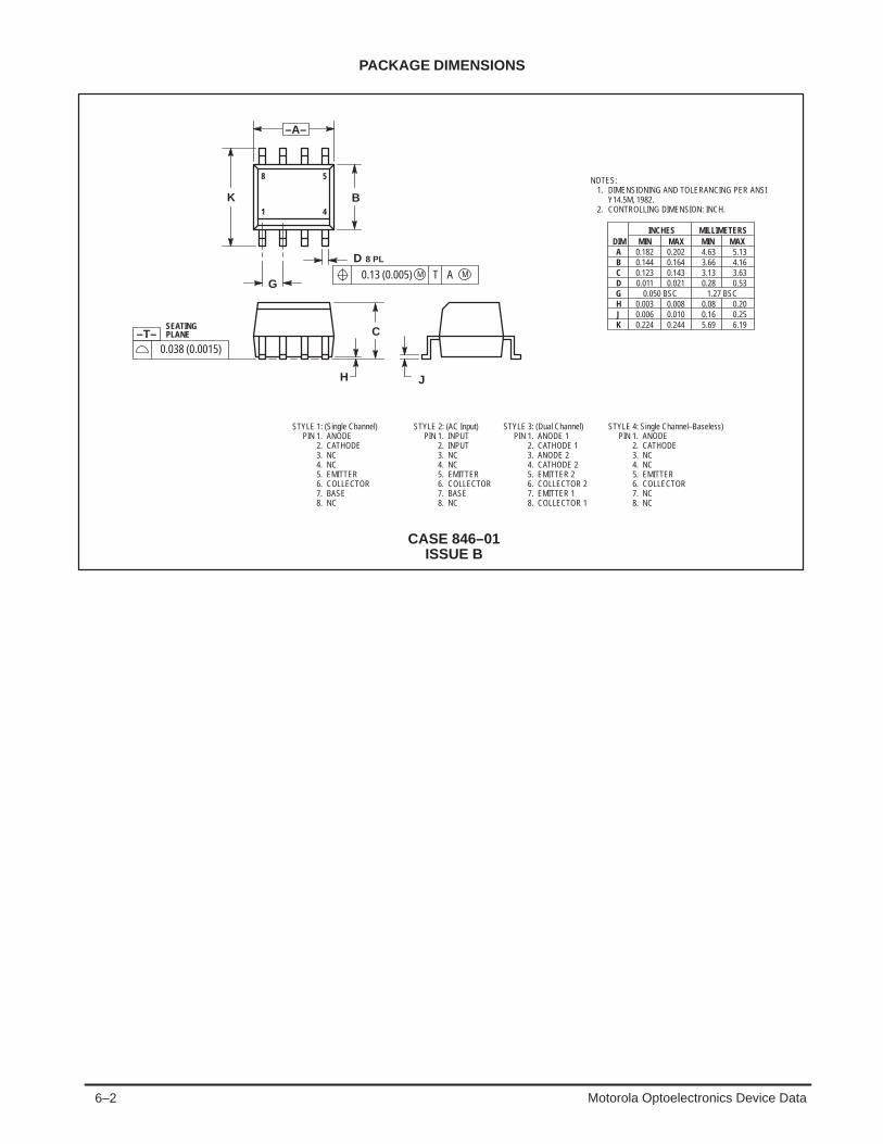
6–2 Motorola Optoelectronics Device Data
PACKAGE DIMENSIONS
STYLE 4: Single Channel–Baseless)PIN 1. ANODE
2. CATHODE3. NC4. NC5. EMITTER6. COLLECTOR7. NC8. NC
STYLE 1: (Single Channel)PIN 1. ANODE
2. CATHODE3. NC4. NC5. EMITTER6. COLLECTOR7. BASE8. NC
STYLE 2: (AC Input)PIN 1. INPUT
2. INPUT3. NC4. NC5. EMITTER6. COLLECTOR7. BASE8. NC
STYLE 3: (Dual Channel)PIN 1. ANODE 1
2. CATHODE 13. ANODE 24. CATHODE 25. EMITTER 26. COLLECTOR 27. EMITTER 18. COLLECTOR 1
DIMA
MIN MAX MIN MAXMILLIMETERS
0.182 0.202 4.63 5.13
INCHES
B 0.144 0.164 3.66 4.16C 0.123 0.143 3.13 3.63D 0.011 0.021 0.28 0.53G 0.050 BSC 1.27 BSCH 0.003 0.008 0.08 0.20J 0.006 0.010 0.16 0.25K 0.224 0.244 5.69 6.19
NOTES:1. DIMENSIONING AND TOLERANCING PER ANSI
Y14.5M, 1982.2. CONTROLLING DIMENSION: INCH.
BK
D
G
8 PL
0.13 (0.005) M T A M
JH
CSEATINGPLANE
0.038 (0.0015)
CASE 846–01ISSUE B
1
8 5
4
–A–
–T–

6–3Motorola Optoelectronics Device Data
Transistor Output
These devices consist of a gallium arsenide infrared emitting diode opticallycoupled to a monolithic silicon phototransistor detector, in a surface mountable,small outline, plastic package. They are ideally suited for high densityapplications, and eliminate the need for through–the–board mounting.
• Convenient Plastic SOIC–8 Surface Mountable Package Style
• Closely Matched Current Transfer Ratios
• Minimum V(BR)CEO of 70 Volts Guaranteed
• Standard SOIC–8 Footprint, with 0.050″ Lead Spacing
• Shipped in Tape and Reel, which Conforms to EIA Standard RS481A
• Compatible with Dual Wave, Vapor Phase and IR Reflow Soldering
• High Input–Output Isolation of 3000 Vac (rms) Guaranteed
• UL Recognized File #E54915
Ordering Information:
• To obtain MOC205, 206, 207, 208 in Tape and Reel, add R2 suffix to device numbers:R2 = 2500 units on 13″ reel
• To obtain MOC205, 206, 207, 208 in quantities of 50 (shipped in sleeves) — No Suffix
Marking Information:
• MOC205 = 205
• MOC206 = 206
• MOC207 = 207
• MOC208 = 208
Applications:
• Feedback Control Circuits
• Interfacing and coupling systems of different potentials and impedances
• General Purpose Switching Circuits
• Monitor and Detection Circuits
MAXIMUM RATINGS (TA = 25°C unless otherwise noted)
Rating Symbol Value Unit
INPUT LED
Forward Current — Continuous IF 60 mA
Forward Current — Peak (PW = 100 µs, 120 pps) IF(pk) 1.0 A
Reverse Voltage VR 6.0 V
LED Power Dissipation @ TA = 25°CDerate above 25°C
PD 900.8
mWmW/°C
OUTPUT TRANSISTOR
Collector–Emitter Voltage VCEO 70 V
Collector–Base Voltage VCBO 70 V
Emitter–Collector Voltage VECO 7.0 V
Collector Current — Continuous IC 150 mA
Detector Power Dissipation @ TA = 25°CDerate above 25°C
PD 1501.76
mWmW/°C
NOTE: Thickness through insulation between input and output ≥ 0.5 mm.
Preferred devices are Motorola recommended choices for future use and best overall value.
Order this documentby MOC205/D
SEMICONDUCTOR TECHNICAL DATA
Motorola, Inc. 1995
*Motorola Preferred Devices
[CTR = 40 – 80%]
[CTR = 63 – 125%]
[CTR = 100 – 200%]
[CTR = 40 – 125%]
SMALL OUTLINEOPTOISOLATORS
TRANSISTOR OUTPUT
CASE 846–01, STYLE 1PLASTIC
SCHEMATIC
1. LED ANODE2. LED CATHODE3. NO CONNECTION4. NO CONNECTION5. EMITTER6. COLLECTOR7. BASE8. NO CONNECTION
1
2
3
8
6
54
7
REV 1

6–4 Motorola Optoelectronics Device Data
MAXIMUM RATINGS — continued (TA = 25°C unless otherwise noted)
Rating Symbol Value Unit
TOTAL DEVICE
Input–Output Isolation Voltage(1,2)
(60 Hz, 1.0 sec. duration)VISO 3000 Vac(rms)
Total Device Power Dissipation @ TA = 25°CDerate above 25°C
PD 2502.94
mWmW/°C
Ambient Operating Temperature Range(3) TA –55 to +100 °C
Storage Temperature Range(3) Tstg –55 to +150 °C
Lead Soldering Temperature (1/16″ from case, 10 sec. duration) — 260 °C
ELECTRICAL CHARACTERISTICS (TA = 25°C unless otherwise noted)(4)
Characteristic Symbol Min Typ (4) Max Unit
INPUT LED
Forward Voltage (IF = 10 mA) VF — 1.15 1.5 V
Reverse Leakage Current (VR = 6.0 V) IR — 0.1 100 A
Capacitance C — 18 — pF
OUTPUT TRANSISTOR
Collector–Emitter Dark Current (VCE = 10 V, TA = 25°C) ICEO1 — 1.0 50 nA
(VCE = 10 V, TA = 100°C) ICEO2 — 1.0 — µA
Collector–Emitter Breakdown Voltage (IC = 100 µA) V(BR)CEO 70 120 — V
Emitter–Collector Breakdown Voltage (IE = 100 µA) V(BR)ECO 7.0 7.8 — V
Collector–Emitter Capacitance (f = 1.0 MHz, VCE = 0) CCE — 7.0 — pF
COUPLED
Output Collector Current MOC205(IF = 10 mA, VCE = 10 V) MOC206
MOC207MOC208
IC (CTR)(5) 4.0 (40)6.3 (63)10 (100)4.0 (40)
6.0 (60)9.4 (94)15 (150)8.0 (80)
8.0 (80)12.5 (125)20 (200)
12.5 (125)
mA (%)
Collector–Emitter Saturation Voltage (IC = 2.0 mA, IF = 10 mA) VCE(sat) — 0.15 0.4 V
Turn–On Time (IC = 2.0 mA, VCC = 10 V, RL = 100 Ω) ton — 3.0 — µs
Turn–Off Time (IC = 2.0 mA, VCC = 10 V, RL = 100 Ω) toff — 2.8 — µs
Rise Time (IC = 2.0 mA, VCC = 10 V, RL = 100 Ω) tr — 1.6 — µs
Fall Time (IC = 2.0 mA, VCC = 10 V, RL = 100 Ω) tf — 2.2 — µs
Input–Output Isolation Voltage (f = 60 Hz, t = 1.0 sec.)(1,2) VISO 3000 — — Vac(rms)
Isolation Resistance (VI–O = 500 V)(2) RISO 1011 — — Ω
Isolation Capacitance (VI–O = 0, f = 1.0 MHz)(2) CISO — 0.2 — pF
1. Input–Output Isolation Voltage, VISO, is an internal device dielectric breakdown rating.2. For this test, pins 1 and 2 are common, and pins 5, 6 and 7 are common.3. Refer to Quality and Reliability Section in Opto Data Book for information on test conditions.4. Always design to the specified minimum/maximum electrical limits (where applicable).5. Current Transfer Ratio (CTR) = IC/IF x 100%.

6–5Motorola Optoelectronics Device Data
TYPICAL CHARACTERISTICS
C IF, LED INPUT CURRENT (mA)5020105210.5
0.1
1
10
Figure 1. LED Forward Voltage versus Forward Current
IF, LED FORWARD CURRENT (mA)101
2
10001001
1.2
1.4
1.6
1.8
Figure 2. Output Current versus Input Current
V F, F
OR
WAR
D V
OLT
AGE
(VO
LTS)
I, O
UTP
UT
CO
LLEC
TOR
CU
RR
ENT
(NO
RM
ALIZ
ED)
PULSE ONLYPULSE OR DC
TA = – 55°C
25°C
100°C
NORMALIZED TO:IF = 10 mA
0.01
1001010.10.01
20
TA, AMBIENT TEMPERATURE (°C)
100800 20 40
103
60
TA, AMBIENT TEMPERATURE (°C)
120100806040200–20–40–600.1
1
10
Figure 3. Output Current versusCollector–Emitter Voltage
VCE, COLLECTOR–EMITTER VOLTAGE (VOLTS)
10980 1 2 3 4 5 6
16
7
10–1
100
101
102
0
2
4
6
8
10
12
14
18
16
14
12
10
8
6
4
V, VOLTAGE (VOLTS)
2
I C, OU
TPU
T C
OLL
ECTO
R C
UR
REN
T (m
A)
I C, O
UTP
UT
CO
LLEC
TOR
CU
RR
ENT
(NO
RM
ALIZ
E D
I CEO
, CO
LLEC
TOR
–EM
ITTE
R D
ARK
CU
RR
ENT
(NO
RM
ALIZ
ED)
C, C
APAC
ITAN
CE
(pF)
Figure 4. Output Current versusAmbient Temperature
Figure 5. Dark Current versus Ambient TemperatureFigure 6. Capacitance versus Voltage
NORMALIZED TO:TA = 25°C
IF = 10 mA
MOC206
MOC205
MOC207
NORMALIZED TO:VCE = 10 VTA = 25°C
VCE = 70 V
30 V
10 V
CLED
CCE
f = 1 MHz

6–6 Motorola Optoelectronics Device Data
PACKAGE DIMENSIONS
STYLE 1:PIN 1. ANODE
2. CATHODE3. NC4. NC5. EMITTER6. COLLECTOR7. BASE8. NC
DIMA
MIN MAX MIN MAXMILLIMETERS
0.182 0.202 4.63 5.13
INCHES
B 0.144 0.164 3.66 4.16C 0.123 0.143 3.13 3.63D 0.011 0.021 0.28 0.53G 0.050 BSC 1.27 BSCH 0.003 0.008 0.08 0.20J 0.006 0.010 0.16 0.25K 0.224 0.244 5.69 6.19
NOTES:1. DIMENSIONING AND TOLERANCING PER ANSI
Y14.5M, 1982.2. CONTROLLING DIMENSION: INCH.
BK
D
G
8 PL
0.13 (0.005) M T A M
JH
CSEATINGPLANE
0.038 (0.0015)
CASE 846–01
1
8 5
4
–A–
–T–
ISSUE B
Motorola reserves the right to make changes without further notice to any products herein. Motorola makes no warranty, representation or guarantee regardingthe suitability of its products for any particular purpose, nor does Motorola assume any liability arising out of the application or use of any product or circuit,and specifically disclaims any and all liability, including without limitation consequential or incidental damages. “Typical” parameters can and do vary in differentapplications. All operating parameters, including “Typicals” must be validated for each customer application by customer’s technical experts. Motorola doesnot convey any license under its patent rights nor the rights of others. Motorola products are not designed, intended, or authorized for use as components insystems intended for surgical implant into the body, or other applications intended to support or sustain life, or for any other application in which the failure ofthe Motorola product could create a situation where personal injury or death may occur. Should Buyer purchase or use Motorola products for any suchunintended or unauthorized application, Buyer shall indemnify and hold Motorola and its officers, employees, subsidiaries, affiliates, and distributors harmlessagainst all claims, costs, damages, and expenses, and reasonable attorney fees arising out of, directly or indirectly, any claim of personal injury or deathassociated with such unintended or unauthorized use, even if such claim alleges that Motorola was negligent regarding the design or manufacture of the part.Motorola and are registered trademarks of Motorola, Inc. Motorola, Inc. is an Equal Opportunity/Affirmative Action Employer.
How to reach us:USA / EUROPE: Motorola Literature Distribution; JAPAN : Nippon Motorola Ltd.; Tatsumi–SPD–JLDC, Toshikatsu Otsuki,P.O. Box 20912; Phoenix, Arizona 85036. 1–800–441–2447 6F Seibu–Butsuryu–Center, 3–14–2 Tatsumi Koto–Ku, Tokyo 135, Japan. 03–3521–8315
MFAX: [email protected] – TOUCHTONE (602) 244–6609 HONG KONG: Motorola Semiconductors H.K. Ltd.; 8B Tai Ping Industrial Park, INTERNET: http://Design–NET.com 51 Ting Kok Road, Tai Po, N.T., Hong Kong. 852–26629298
MOC205/D
◊

6–7Motorola Optoelectronics Device Data
Transistor Output
These devices consist of a gallium arsenide infrared emitting diode opticallycoupled to a monolithic silicon phototransistor detector, in a surface mountable,small outline, plastic package. They are ideally suited for high densityapplications, and eliminate the need for through–the–board mounting.
• Convenient Plastic SOIC–8 Surface Mountable Package Style
• Standard SOIC–8 Footprint, with 0.050″ Lead Spacing
• Shipped in Tape and Reel, which Conforms to EIA Standard RS481A
• Compatible with Dual Wave, Vapor Phase and IR Reflow Soldering
• High Input–Output Isolation of 3000 Vac (rms) Guaranteed
• UL Recognized File #E54915
Ordering Information:
• To obtain MOC211, 212 and 213 in Tape and Reel, add R2 suffix to device numbers:R2 = 2500 units on 13″ reel
• To obtain MOC211, 212 and 213 in quantities of 50 (shipped in sleeves) — No Suffix
Marking Information:
• MOC211 = 211
• MOC212 = 212
• MOC213 = 213
Applications:
• General Purpose Switching Circuits
• Interfacing and coupling systems of different potentials and impedances
• Regulation Feedback Circuits
• Monitor and Detection Circuits
MAXIMUM RATINGS (TA = 25°C unless otherwise noted)
Rating Symbol Value Unit
INPUT LED
Forward Current — Continuous IF 60 mA
Forward Current — Peak (PW = 100 µs, 120 pps) IF(pk) 1.0 A
Reverse Voltage VR 6.0 V
LED Power Dissipation @ TA = 25°CDerate above 25°C
PD 900.8
mWmW/°C
OUTPUT TRANSISTOR
Collector–Emitter Voltage VCEO 30 V
Collector–Base Voltage VCBO 70 V
Emitter–Collector Voltage VECO 7.0 V
Collector Current — Continuous IC 150 mA
Detector Power Dissipation @ TA = 25°CDerate above 25°C
PD 1501.76
mWmW/°C
NOTE: Thickness through insulation between input and output is ≥ 0.5 mm.
Preferred devices are Motorola recommended choices for future use and best overall value.
Order this documentby MOC211/D
SEMICONDUCTOR TECHNICAL DATA
Motorola, Inc. 1995
Motorola Preferred Devices
[CTR = 20% Min]
[CTR = 50% Min]
SMALL OUTLINEOPTOISOLATORS
TRANSISTOR OUTPUT
CASE 846–01, STYLE 1PLASTIC
SCHEMATIC
1. LED ANODE2. LED CATHODE3. NO CONNECTION4. NO CONNECTION5. EMITTER6. COLLECTOR7. BASE8. NO CONNECTION
1
2
3
8
6
54
7
[CTR = 100% Min]
REV 1

6–8 Motorola Optoelectronics Device Data
MAXIMUM RATINGS — continued (TA = 25°C unless otherwise noted)
Rating Symbol Value Unit
TOTAL DEVICE
Input–Output Isolation Voltage(1,2)
(60 Hz, 1.0 sec. duration)VISO 3000 Vac(rms)
Total Device Power Dissipation @ TA = 25°CDerate above 25°C
PD 2502.94
mWmW/°C
Ambient Operating Temperature Range(3) TA –55 to +100 °C
Storage Temperature Range(3) Tstg –55 to +150 °C
Lead Soldering Temperature (1/16″ from case, 10 sec. duration) — 260 °C
ELECTRICAL CHARACTERISTICS (TA = 25°C unless otherwise noted)(4)
Characteristic Symbol Min Typ (4) Max Unit
INPUT LED
Forward Voltage (IF = 10 mA) VF — 1.15 1.5 V
Reverse Leakage Current (VR = 6.0 V) IR — 0.1 100 A
Capacitance C — 18 — pF
OUTPUT TRANSISTOR
Collector–Emitter Dark Current (VCE = 10 V, TA = 25°C) ICEO1 — 1.0 50 nA
(VCE = 10 V, TA = 100°C) ICEO2 — 1.0 — µA
Collector–Emitter Breakdown Voltage (IC = 100 µA) V(BR)CEO 30 90 — V
Emitter–Collector Breakdown Voltage (IE = 100 µA) V(BR)ECO 7.0 7.8 — V
Collector–Emitter Capacitance (f = 1.0 MHz, VCE = 0) CCE — 7.0 — pF
COUPLED
Output Collector Current MOC211(IF = 10 mA, VCE = 10 V) MOC212
MOC213
IC (CTR)(5) 2.0 (20)5.0 (50)10 (100)
6.5 (65)9.0 (90)14 (140)
———
mA (%)
Collector–Emitter Saturation Voltage (IC = 2.0 mA, IF = 10 mA) VCE(sat) — 0.15 0.4 V
Turn–On Time (IC = 2.0 mA, VCC = 10 V, RL = 100 Ω) ton — 7.5 — µs
Turn–Off Time (IC = 2.0 mA, VCC = 10 V, RL = 100 Ω) toff — 5.7 — µs
Rise Time (IC = 2.0 mA, VCC = 10 V, RL = 100 Ω) tr — 3.2 — µs
Fall Time (IC = 2.0 mA, VCC = 10 V, RL = 100 Ω) tf — 4.7 — µs
Input–Output Isolation Voltage (f = 60 Hz, t = 1.0 sec.)(1,2) VISO 3000 — — Vac(rms)
Isolation Resistance (VI–O = 500 V)(2) RISO 1011 — — Ω
Isolation Capacitance (VI–O = 0, f = 1.0 MHz)(2) CISO — 0.2 — pF
1. Input–Output Isolation Voltage, VISO, is an internal device dielectric breakdown rating.2. For this test, pins 1 and 2 are common, and pins 5, 6 and 7 are common.3. Refer to Quality and Reliability Section in Opto Data Book for information on test conditions.4. Always design to the specified minimum/maximum electrical limits (where applicable).5. Current Transfer Ratio (CTR) = IC/IF x 100%.

6–9Motorola Optoelectronics Device Data
C
IF, LED INPUT CURRENT (mA)5020105210.5
0.1
1
10
Figure 1. LED Forward Voltage versus Forward CurrentIF, LED FORWARD CURRENT (mA)
101
2
0.011000100
1
1.2
1.4
1.6
1.8
Figure 2. Output Current versus Input Current
V F, F
OR
WAR
D V
OLT
AGE
(VO
LTS)
I, O
UTP
UT
CO
LLEC
TOR
CU
RR
ENT
(NO
RM
ALIZ
ED)
PULSE ONLYPULSE OR DC
TYPICAL CHARACTERISTICS
NORMALIZED TO:IF = 10 mA
TA = – 55°C
25°C
100°C
1001010.10.01
20
TA, AMBIENT TEMPERATURE (°C)
120100806040200–20–40–600.1
1
10
Figure 3. Output Current versusCollector–Emitter Voltage
VCE, COLLECTOR–EMITTER VOLTAGE (VOLTS)
10980 1 2 3 4 5 6
16
70
2
4
6
8
10
12
14
18
16
14
12
10
8
6
4
V, VOLTAGE (VOLTS)
2
I C, OU
TPU
T C
OLL
ECTO
R C
UR
REN
T (m
A)
I C, OU
TPU
T C
OLL
ECTO
R C
UR
REN
T (N
OR
MAL
IZED
)C
, CAP
ACIT
ANC
E (p
F)
1
10
100
0.10 20 40 60 80 100
TA, AMBIENT TEMPERATURE (°C)
I
C
EO, C
OLL
ECTO
R–E
MIT
TER
DAR
K C
UR
REN
T(N
OR
MAL
IZED
)
Figure 4. Output Current versusAmbient Temperature
Figure 5. Dark Current versus Ambient Temperature Figure 6. Capacitance versus Voltage
NORMALIZED TO:TA = 25°C
IF = 10 mA
MOC211
MOC213
NORMALIZED TO:VCE = 10 VTA = 25°C
VCE = 30 V
10 V
CLED
CCE
f = 1 MHz
MOC212

6–10 Motorola Optoelectronics Device Data
PACKAGE DIMENSIONS
STYLE 1:PIN 1. ANODE
2. CATHODE3. NC4. NC5. EMITTER6. COLLECTOR7. BASE8. NC
DIMA
MIN MAX MIN MAXMILLIMETERS
0.182 0.202 4.63 5.13
INCHES
B 0.144 0.164 3.66 4.16C 0.123 0.143 3.13 3.63D 0.011 0.021 0.28 0.53G 0.050 BSC 1.27 BSCH 0.003 0.008 0.08 0.20J 0.006 0.010 0.16 0.25K 0.224 0.244 5.69 6.19
NOTES:1. DIMENSIONING AND TOLERANCING PER ANSI
Y14.5M, 1982.2. CONTROLLING DIMENSION: INCH.
BK
D
G
8 PL
0.13 (0.005) M T A M
JH
CSEATINGPLANE
0.038 (0.0015)
CASE 846–01
1
8 5
4
–A–
–T–
ISSUE B
Motorola reserves the right to make changes without further notice to any products herein. Motorola makes no warranty, representation or guarantee regardingthe suitability of its products for any particular purpose, nor does Motorola assume any liability arising out of the application or use of any product or circuit,and specifically disclaims any and all liability, including without limitation consequential or incidental damages. “Typical” parameters can and do vary in differentapplications. All operating parameters, including “Typicals” must be validated for each customer application by customer’s technical experts. Motorola doesnot convey any license under its patent rights nor the rights of others. Motorola products are not designed, intended, or authorized for use as components insystems intended for surgical implant into the body, or other applications intended to support or sustain life, or for any other application in which the failure ofthe Motorola product could create a situation where personal injury or death may occur. Should Buyer purchase or use Motorola products for any suchunintended or unauthorized application, Buyer shall indemnify and hold Motorola and its officers, employees, subsidiaries, affiliates, and distributors harmlessagainst all claims, costs, damages, and expenses, and reasonable attorney fees arising out of, directly or indirectly, any claim of personal injury or deathassociated with such unintended or unauthorized use, even if such claim alleges that Motorola was negligent regarding the design or manufacture of the part.Motorola and are registered trademarks of Motorola, Inc. Motorola, Inc. is an Equal Opportunity/Affirmative Action Employer.
How to reach us:USA / EUROPE: Motorola Literature Distribution; JAPAN : Nippon Motorola Ltd.; Tatsumi–SPD–JLDC, Toshikatsu Otsuki,P.O. Box 20912; Phoenix, Arizona 85036. 1–800–441–2447 6F Seibu–Butsuryu–Center, 3–14–2 Tatsumi Koto–Ku, Tokyo 135, Japan. 03–3521–8315
MFAX: [email protected] – TOUCHTONE (602) 244–6609 HONG KONG: Motorola Semiconductors H.K. Ltd.; 8B Tai Ping Industrial Park, INTERNET: http://Design–NET.com 51 Ting Kok Road, Tai Po, N.T., Hong Kong. 852–26629298
MOC211/D
◊

6–11Motorola Optoelectronics Device Data
Transistor Output (Low Input Current)
These devices consist of a gallium arsenide infrared emitting diode opticallycoupled to a monolithic silicon phototransistor detector, in a surface mountable,small outline, plastic package. They are ideally suited for high densityapplications, and eliminate the need for through–the–board mounting.
• Convenient Plastic SOIC–8 Surface Mountable Package Style
• Low LED Input Current Required, for Easier Logic Interfacing
• Standard SOIC–8 Footprint, with 0.050″ Lead Spacing
• Shipped in Tape and Reel, which Conforms to EIA Standard RS481A
• Compatible with Dual Wave, Vapor Phase and IR Reflow Soldering
• High Input–Output Isolation of 3000 Vac (rms) Guaranteed
• UL Recognized File #E54915
Ordering Information:
• To obtain MOC215, 216, 217 in Tape and Reel, add R2 suffix to device numbers:R2 = 2500 units on 13″ reel
• To obtain MOC215, 216, 217 in quantities of 50 (shipped in sleeves) — No Suffix
Marking Information:
• MOC215 = 215
• MOC216 = 216
• MOC217 = 217
Applications:
• Low power Logic Circuits
• Interfacing and coupling systems of different potentials and impedances
• Telecommunications equipment
• Portable electronics
MAXIMUM RATINGS (TA = 25°C unless otherwise noted)
Rating Symbol Value Unit
INPUT LED
Forward Current — Continuous IF 60 mA
Forward Current — Peak (PW = 100 µs, 120 pps) IF(pk) 1.0 A
Reverse Voltage VR 6.0 V
LED Power Dissipation @ TA = 25°CDerate above 25°C
PD 900.8
mWmW/°C
OUTPUT TRANSISTOR
Collector–Emitter Voltage VCEO 30 V
Collector–Base Voltage VCBO 70 V
Emitter–Collector Voltage VECO 7.0 V
Collector Current — Continuous IC 150 mA
Detector Power Dissipation @ TA = 25°CDerate above 25°C
PD 1501.76
mWmW/°C
NOTE: Thickness through insulation between input and output is ≥ 0.5 mm.
Preferred devices are Motorola recommended choices for future use and best overall value.
Order this documentby MOC215/D
SEMICONDUCTOR TECHNICAL DATA
Motorola, Inc. 1995
Motorola Preferred Devices
[CTR = 20% Min]
[CTR = 50% Min]
[CTR = 100% Min]
SMALL OUTLINEOPTOISOLATORS
TRANSISTOR OUTPUT
CASE 846–01, STYLE 1PLASTIC
SCHEMATIC
1. LED ANODE2. LED CATHODE3. NO CONNECTION4. NO CONNECTION5. EMITTER6. COLLECTOR7. BASE8. NO CONNECTION
1
2
3
8
6
54
7
REV 1

6–12 Motorola Optoelectronics Device Data
MAXIMUM RATINGS — continued (TA = 25°C unless otherwise noted)
Rating Symbol Value Unit
TOTAL DEVICE
Input–Output Isolation Voltage(1,2)
(60 Hz, 1.0 sec. duration)VISO 3000 Vac(rms)
Total Device Power Dissipation @ TA = 25°CDerate above 25°C
PD 2502.94
mWmW/°C
Ambient Operating Temperature Range(3) TA –55 to +100 °C
Storage Temperature Range(3) Tstg –55 to +150 °C
Lead Soldering Temperature (1/16″ from case, 10 sec. duration) — 260 °C
ELECTRICAL CHARACTERISTICS (TA = 25°C unless otherwise noted)(4)
Characteristic Symbol Min Typ (4) Max Unit
INPUT LED
Forward Voltage (IF = 1.0 mA) VF — 1.05 1.3 V
Reverse Leakage Current (VR = 6.0 V) IR — 0.1 100 A
Capacitance C — 18 — pF
OUTPUT TRANSISTOR
Collector–Emitter Dark Current (VCE = 5.0 V, TA = 25°C) ICEO1 — 1.0 50 nA
(VCE = 5.0 V, TA = 100°C) ICEO2 — 1.0 — µA
Collector–Emitter Breakdown Voltage (IC = 100 µA) V(BR)CEO 30 90 — V
Emitter–Collector Breakdown Voltage (IE = 100 µA) V(BR)ECO 7.0 7.8 — V
Collector–Emitter Capacitance (f = 1.0 MHz, VCE = 0) CCE — 7.0 — pF
COUPLED
Output Collector Current MOC215(IF = 1.0 mA, VCE = 5.0 V) MOC216
MOC217
IC (CTR)(5) 200 (20)500 (50)1.0 (100)
500(50)800 (80)1.3 (130)
———
µA (%)µA (%)mA (%)
Collector–Emitter Saturation Voltage (IC = 100 µA, IF = 1.0 mA) VCE(sat) — 0.35 0.4 V
Turn–On Time (IC = 2.0 mA, VCC = 10 V, RL = 100 Ω) ton — 7.5 — µs
Turn–Off Time (IC = 2.0 mA, VCC = 10 V, RL = 100 Ω) toff — 5.7 — µs
Rise Time (IC = 2.0 mA, VCC = 10 V, RL = 100 Ω) tr — 3.2 — µs
Fall Time (IC = 2.0 mA, VCC = 10 V, RL = 100 Ω) tf — 4.7 — µs
Input–Output Isolation Voltage (f = 60 Hz, t = 1.0 sec.)(1,2) VISO 3000 — — Vac(rms)
Isolation Resistance (VI–O = 500 V)(2) RISO 1011 — — Ω
Isolation Capacitance (VI–O = 0, f = 1.0 MHz)(2) CISO — 0.2 — pF
1. Input–Output Isolation Voltage, VISO, is an internal device dielectric breakdown rating.2. For this test, pins 1 and 2 are common, and pins 5, 6 and 7 are common.3. Refer to Quality and Reliability Section in Opto Data Book for information on test conditions.4. Always design to the specified minimum/maximum electrical limits (where applicable).5. Current Transfer Ratio (CTR) = IC/IF x 100%.

6–13Motorola Optoelectronics Device Data
C
IF, LED INPUT CURRENT (mA)5210.50.20.10.05
0.1
1
10
Figure 1. LED Forward Voltage versus Forward CurrentIF, LED FORWARD CURRENT (mA)
101
2
0.0011000100
1
1.2
1.4
1.6
1.8
Figure 2. Output Current versus Input Current
V F, F
OR
WAR
D V
OLT
AGE
(VO
LTS)
I, O
UTP
UT
CO
LLEC
TOR
CU
RR
ENT
(NO
RM
ALIZ
ED)
PULSE ONLYPULSE OR DC
TYPICAL CHARACTERISTICS
NORMALIZED TO:IF = 1 mA
TA = – 55°C
25°C
100°C
1001010.10.01
20
TA, AMBIENT TEMPERATURE (°C)
120100806040200–20–40–600.1
1
10
Figure 3. Output Current versusCollector–Emitter Voltage
18
16
14
12
10
8
6
4
V, VOLTAGE (VOLTS)
2
I C, O
UTP
UT
CO
LLEC
TOR
CU
RR
ENT
(NO
RM
ALIZ
ED)
C, C
APAC
ITAN
CE
(pF)
1
10
100
0.10 20 40 60 80 100
TA, AMBIENT TEMPERATURE (°C)
I
C
EO, C
OLL
ECTO
R–E
MIT
TER
DAR
K C
UR
REN
T(N
OR
MAL
IZED
)
Figure 4. Output Current versusAmbient Temperature
Figure 5. Dark Current versus Ambient Temperature Figure 6. Capacitance versus Voltage
2
1.8
1.6
1.4
1.2
1
0.8
0.6
0
VCE, COLLECTOR–EMITTER VOLTAGE (VOLTS)
10980 1 2 3 4 5 6 7
0.4
0.2
I C, OU
TPU
T C
OLL
ECTO
R C
UR
REN
T (m
A)
NORMALIZED TO:TA = 25°C
IF = 1 mA
MOC216
MOC215
MOC217
NORMALIZED TO:VCE = 10 VTA = 25°C
VCE = 30 V
10 V
CLED
CCE
f = 1 MHz

6–14 Motorola Optoelectronics Device Data
PACKAGE DIMENSIONS
STYLE 1:PIN 1. ANODE
2. CATHODE3. NC4. NC5. EMITTER6. COLLECTOR7. BASE8. NC
DIMA
MIN MAX MIN MAXMILLIMETERS
0.182 0.202 4.63 5.13
INCHES
B 0.144 0.164 3.66 4.16C 0.123 0.143 3.13 3.63D 0.011 0.021 0.28 0.53G 0.050 BSC 1.27 BSCH 0.003 0.008 0.08 0.20J 0.006 0.010 0.16 0.25K 0.224 0.244 5.69 6.19
NOTES:1. DIMENSIONING AND TOLERANCING PER ANSI
Y14.5M, 1982.2. CONTROLLING DIMENSION: INCH.
BK
D
G
8 PL
0.13 (0.005) M T A M
JH
CSEATINGPLANE
0.038 (0.0015)
CASE 846–01
1
8 5
4
–A–
–T–
ISSUE B
Motorola reserves the right to make changes without further notice to any products herein. Motorola makes no warranty, representation or guarantee regardingthe suitability of its products for any particular purpose, nor does Motorola assume any liability arising out of the application or use of any product or circuit,and specifically disclaims any and all liability, including without limitation consequential or incidental damages. “Typical” parameters can and do vary in differentapplications. All operating parameters, including “Typicals” must be validated for each customer application by customer’s technical experts. Motorola doesnot convey any license under its patent rights nor the rights of others. Motorola products are not designed, intended, or authorized for use as components insystems intended for surgical implant into the body, or other applications intended to support or sustain life, or for any other application in which the failure ofthe Motorola product could create a situation where personal injury or death may occur. Should Buyer purchase or use Motorola products for any suchunintended or unauthorized application, Buyer shall indemnify and hold Motorola and its officers, employees, subsidiaries, affiliates, and distributors harmlessagainst all claims, costs, damages, and expenses, and reasonable attorney fees arising out of, directly or indirectly, any claim of personal injury or deathassociated with such unintended or unauthorized use, even if such claim alleges that Motorola was negligent regarding the design or manufacture of the part.Motorola and are registered trademarks of Motorola, Inc. Motorola, Inc. is an Equal Opportunity/Affirmative Action Employer.
How to reach us:USA / EUROPE: Motorola Literature Distribution; JAPAN : Nippon Motorola Ltd.; Tatsumi–SPD–JLDC, Toshikatsu Otsuki,P.O. Box 20912; Phoenix, Arizona 85036. 1–800–441–2447 6F Seibu–Butsuryu–Center, 3–14–2 Tatsumi Koto–Ku, Tokyo 135, Japan. 03–3521–8315
MFAX: [email protected] – TOUCHTONE (602) 244–6609 HONG KONG: Motorola Semiconductors H.K. Ltd.; 8B Tai Ping Industrial Park, INTERNET: http://Design–NET.com 51 Ting Kok Road, Tai Po, N.T., Hong Kong. 852–26629298
MOC215/D
◊

6–15Motorola Optoelectronics Device Data
Darlington Output
These devices consist of a gallium arsenide infrared emitting diode opticallycoupled to a monolithic silicon photodarlington detector, in a surface mountable,small outline, plastic package. They are ideally suited for high densityapplications, and eliminate the need for through–the–board mounting.
• Convenient Plastic SOIC–8 Surface Mountable Package Style
• High Current Transfer Ratio (CTR) at Low LED Input Current, for Easier Logic Interfacing
• Standard SOIC–8 Footprint, with 0.050″ Lead Spacing
• Shipped in Tape and Reel, which Conforms to EIA Standard RS481A
• Compatible with Dual Wave, Vapor Phase and IR Reflow Soldering
• High Input–Output Isolation of 3000 Vac (rms) Guaranteed
• UL Recognized File #E54915
Ordering Information:
• To obtain MOC223 in Tape and Reel, add R2 suffix to device numbers:R2 = 2500 units on 13″ reel
• To obtain MOC223 in quantities of 50 (shipped in sleeves) — No Suffix
Marking Information:
• MOC223 = 223
Applications:
• Low power Logic Circuits
• Interfacing and coupling systems of different potentials and impedances
• Telecommunications equipment
• Portable electronics
MAXIMUM RATINGS (TA = 25°C unless otherwise noted)
Rating Symbol Value Unit
INPUT LED
Forward Current — Continuous IF 60 mA
Forward Current — Peak (PW = 100 µs, 120 pps) IF(pk) 1.0 A
Reverse Voltage VR 6.0 V
LED Power Dissipation @ TA = 25°CDerate above 25°C
PD 900.8
mWmW/°C
OUTPUT DARLINGTON
Collector–Emitter Voltage VCEO 30 V
Collector–Base Voltage VCBO 70 V
Emitter–Collector Voltage VECO 7.0 V
Collector Current — Continuous IC 150 mA
Detector Power Dissipation @ TA = 25°CDerate above 25°C
PD 1501.76
mWmW/°C
NOTE: Thickness through insulation between input and output is ≥ 0.5 mm.
Preferred devices are Motorola recommended choices for future use and best overall value.
Order this documentby MOC223/D
SEMICONDUCTOR TECHNICAL DATA
Motorola, Inc. 1995
Motorola Preferred Device
[CTR = 500% Min]
SMALL OUTLINEOPTOISOLATORS
DARLINGTON OUTPUT
CASE 846–01, STYLE 1PLASTIC
SCHEMATIC
1. LED ANODE2. LED CATHODE3. NO CONNECTION4. NO CONNECTION5. EMITTER6. COLLECTOR7. BASE8. NO CONNECTION
1
2
3
8
6
54
7
(Replaces MOC221/D)

6–16 Motorola Optoelectronics Device Data
MAXIMUM RATINGS — continued (TA = 25°C unless otherwise noted)
Rating Symbol Value Unit
TOTAL DEVICE
Input–Output Isolation Voltage(1,2)
(60 Hz, 1.0 sec. duration)VISO 3000 Vac(rms)
Total Device Power Dissipation @ TA = 25°CDerate above 25°C
PD 2502.94
mWmW/°C
Ambient Operating Temperature Range(3) TA –55 to +100 °C
Storage Temperature Range(3) Tstg –55 to +150 °C
Lead Soldering Temperature(1/16″ from case, 10 sec. duration)
— 260 °C
ELECTRICAL CHARACTERISTICS (TA = 25°C unless otherwise noted)(4)
Characteristic Symbol Min Typ (4) Max Unit
INPUT LED
Forward Voltage (IF = 1.0 mA) VF — 1.05 1.3 V
Reverse Leakage Current (VR = 6.0 V) IR — 0.1 100 A
Capacitance C — 18 — pF
OUTPUT DARLINGTON
Collector–Emitter Dark Current (VCE = 5.0 V, TA = 25°C) ICEO1 — 1.0 50 nA
(VCE = 5.0 V, TA = 100°C) ICEO2 — 1.0 — µA
Collector–Emitter Breakdown Voltage (IC = 100 µA) V(BR)CEO 30 90 — V
Emitter–Collector Breakdown Voltage (IE = 100 µA) V(BR)ECO 7.0 7.8 — V
Collector–Emitter Capacitance (f = 1.0 MHz, VCE = 0) CCE — 5.5 — pF
COUPLED
Output Collector Current(IF = 1.0 mA, VCE = 5.0 V)
IC (CTR)(5) 5.0 (500) 10 (1000) — mA (%)
Collector–Emitter Saturation Voltage (IC = 500 µA, IF = 1.0 mA) VCE(sat) — — 1.0 V
Turn–On Time (IF = 5.0 mA, VCC = 10 V, RL = 100 Ω) ton — 3.5 — µs
Turn–Off Time (IF = 5.0 mA, VCC = 10 V, RL = 100 Ω) toff — 95 — µs
Rise Time (IF = 5.0 mA, VCC = 10 V, RL = 100 Ω) tr — 1.0 — µs
Fall Time (IF = 5.0 mA, VCC = 10 V, RL = 100 Ω) tf — 2.0 — µs
Input–Output Isolation Voltage (f = 60 Hz, t = 1.0 sec.)(1,2) VISO 3000 — — Vac(rms)
Isolation Resistance (VI–O = 500 V)(2) RISO 1011 — — Ω
Isolation Capacitance (VI–O = 0, f = 1.0 MHz)(2) CISO — 0.2 — pF
1. Input–Output Isolation Voltage, VISO, is an internal device dielectric breakdown rating.2. For this test, pins 1 and 2 are common, and pins 5, 6 and 7 are common.3. Refer to Quality and Reliability Section in Opto Data Book for information on test conditions.4. Always design to the specified minimum/maximum electrical limits (where applicable).5. Current Transfer Ratio (CTR) = IC/IF x 100%.
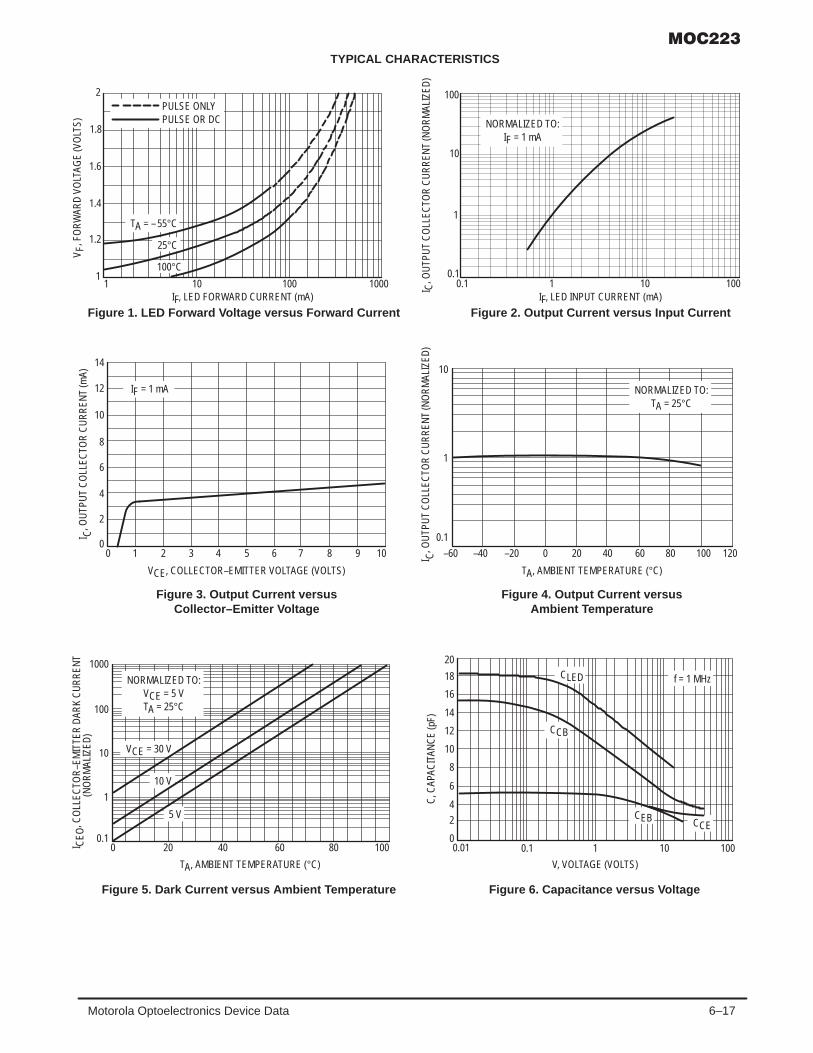
6–17Motorola Optoelectronics Device Data
C
Figure 1. LED Forward Voltage versus Forward CurrentIF, LED FORWARD CURRENT (mA)
101
2
10001001
1.2
1.4
1.6
1.8
Figure 2. Output Current versus Input Current
V F, F
OR
WAR
D V
OLT
AGE
(VO
LTS)
I, O
UTP
UT
CO
LLEC
TOR
CU
RR
ENT
(NO
RM
ALIZ
ED)
PULSE ONLYPULSE OR DC
TYPICAL CHARACTERISTICS
100
10
1
0.11 100.1
IF, LED INPUT CURRENT (mA)100
NORMALIZED TO:IF = 1 mA
TA = – 55°C
25°C
100°C
10
1
0.1
100 120–60 –40
Figure 3. Output Current versusCollector–Emitter Voltage
VCE, COLLECTOR–EMITTER VOLTAGE (VOLTS)
109870 1 2 3 4 5
14
60
2
4
6
8
10
12
TA, AMBIENT TEMPERATURE (°C)
806040200–20
I C, O
UTP
UT
CO
LLEC
TOR
CU
RR
ENT
(mA)
I C, OU
TPU
T C
OLL
ECTO
R C
UR
REN
T (N
OR
MAL
IZED
)
Figure 4. Output Current versusAmbient Temperature
V, VOLTAGE (VOLTS)
0.01 0.1 1 10200 80
Figure 5. Dark Current versus Ambient Temperature
201000
40 60 1000
2
4
6
8
10
12
14
16
18
TA, AMBIENT TEMPERATURE (°C)
0.1
1
10
100
100
C, C
APAC
ITAN
CE
(pF)
I CEO
, CO
LLEC
TOR
–EM
ITTE
R D
ARK
CU
RR
ENT
(NO
RM
ALIZ
ED)
Figure 6. Capacitance versus Voltage
NORMALIZED TO:TA = 25°C
IF = 1 mA
NORMALIZED TO:VCE = 5 VTA = 25°C
VCE = 30 V
10 V
CLED
CCE
f = 1 MHz
5 V
CCB
CEB

6–18 Motorola Optoelectronics Device Data
PACKAGE DIMENSIONS
STYLE 1:PIN 1. ANODE
2. CATHODE3. NC4. NC5. EMITTER6. COLLECTOR7. BASE8. NC
DIMA
MIN MAX MIN MAXMILLIMETERS
0.182 0.202 4.63 5.13
INCHES
B 0.144 0.164 3.66 4.16C 0.123 0.143 3.13 3.63D 0.011 0.021 0.28 0.53G 0.050 BSC 1.27 BSCH 0.003 0.008 0.08 0.20J 0.006 0.010 0.16 0.25K 0.224 0.244 5.69 6.19
NOTES:1. DIMENSIONING AND TOLERANCING PER ANSI
Y14.5M, 1982.2. CONTROLLING DIMENSION: INCH.
BK
D
G
8 PL
0.13 (0.005) M T A M
JH
CSEATINGPLANE
0.038 (0.0015)
CASE 846–01
1
8 5
4
–A–
–T–
ISSUE B
Motorola reserves the right to make changes without further notice to any products herein. Motorola makes no warranty, representation or guarantee regardingthe suitability of its products for any particular purpose, nor does Motorola assume any liability arising out of the application or use of any product or circuit,and specifically disclaims any and all liability, including without limitation consequential or incidental damages. “Typical” parameters can and do vary in differentapplications. All operating parameters, including “Typicals” must be validated for each customer application by customer’s technical experts. Motorola doesnot convey any license under its patent rights nor the rights of others. Motorola products are not designed, intended, or authorized for use as components insystems intended for surgical implant into the body, or other applications intended to support or sustain life, or for any other application in which the failure ofthe Motorola product could create a situation where personal injury or death may occur. Should Buyer purchase or use Motorola products for any suchunintended or unauthorized application, Buyer shall indemnify and hold Motorola and its officers, employees, subsidiaries, affiliates, and distributors harmlessagainst all claims, costs, damages, and expenses, and reasonable attorney fees arising out of, directly or indirectly, any claim of personal injury or deathassociated with such unintended or unauthorized use, even if such claim alleges that Motorola was negligent regarding the design or manufacture of the part.Motorola and are registered trademarks of Motorola, Inc. Motorola, Inc. is an Equal Opportunity/Affirmative Action Employer.
How to reach us:USA / EUROPE: Motorola Literature Distribution; JAPAN : Nippon Motorola Ltd.; Tatsumi–SPD–JLDC, Toshikatsu Otsuki,P.O. Box 20912; Phoenix, Arizona 85036. 1–800–441–2447 6F Seibu–Butsuryu–Center, 3–14–2 Tatsumi Koto–Ku, Tokyo 135, Japan. 03–3521–8315
MFAX: [email protected] – TOUCHTONE (602) 244–6609 HONG KONG: Motorola Semiconductors H.K. Ltd.; 8B Tai Ping Industrial Park, INTERNET: http://Design–NET.com 51 Ting Kok Road, Tai Po, N.T., Hong Kong. 852–26629298
MOC223/D
◊

6–19Motorola Optoelectronics Device Data
The MOC256 is an AC input phototransistor optocoupler. The device consistsof two infrared emitters connected in anti–parallel and coupled to a silicon NPNphototransistor detector. They are designed for applications requiring thedetection or monitoring of AC signals. These devices are constructed with astandard SOIC–8 footprint.
• Guaranteed Current Transfer Ratio CTR of 20% at IF=10 mA
• UL Recognized. File Number E54915
• Industry Standard SOIC–8 Surface Mountable Package
• Standard Lead Spacing of 0.050 inches
• Available in Tape and Reel Option (Conforms to EIA Standard RS481A)
• Bidirectional AC Input (Protection Against Reversed DC Bias)
• Guaranteed CTR Symmetry of 2:1 Maximum
• High Input–Output Isolation of 3000 Vac (rms) Guaranteed
MAXIMUM RATINGS (TA = 25°C unless otherwise noted)
Rating Symbol Value Unit
INPUT LED
Forward Current — Continuous IF 60 mA
Forward Current — Peak (PW = 100 µs, 120 pps) IF(pk) 1 A
Reverse Voltage VR 6 V
LED Power Dissipation @ TA = 25°CDerate above 25°C
PD 900.8
mWmW/°C
OUTPUT TRANSISTOR
Collector–Emitter Voltage VCEO 30 V
Emitter–Base Voltage VECO 7 V
Collector Current — Continuous IC 150 mA
Detector Power Dissipation @ TA = 25°CDerate above 25°C
PD 1501.76
mWmW/°C
TOTAL DEVICE
Input–Output Isolation Voltage(1)
(60 Hz, 1 sec Duration)VISO 3000 Vac(rms)
Total Device Power Dissipation @ TA = 25°CDerate above 25°C
PD 2502.94
mWmW/°C
Ambient Operating Temperature Range(2) TA –55 to +100 °C
Storage Temperature Range(2) Tstg –55 to +150 °C
Lead Soldering Temperature (10 sec, 1/16″ from case) — 260 °C
1. Input–output isolation voltage is an internal device dielectric breakdown rating.1. For this test, Pins 1 and 2 are common, and Pins 5, 6 and 7 are common.2. Refer to Quality and Reliability Section in Opto Data Book for information on test conditions.
NOTE: Thickness through insulation between input and output is ≥ 0.5 mm.
Preferred devices are Motorola recommended choices for future use and best overall value.
Order this documentby MOC256/D
SEMICONDUCTOR TECHNICAL DATA
Motorola, Inc. 1995
Motorola Preferred Device
SMALL OUTLINEOPTOISOLATORS
AC INPUTTRANSISTOR OUTPUT
CASE 846–01, STYLE 2PLASTIC
SCHEMATIC
PIN 1. AC IN2. AC IN3. N.C.4. N.C.5. EMITTER6. COLLECTOR7. BASE8. N.C.
2
3
7
6
5
1 8
4
REV 1

6–20 Motorola Optoelectronics Device Data
ELECTRICAL CHARACTERISTICS (TA = 25°C unless otherwise noted)(1)
Characteristic Symbol Min Typ (1) Max Unit
INPUT LED
Forward Voltage(IF = 10 mA, either direction)
VF — 1.15 1.5 Volts
Capacitance (V = 0 V, f = 1 MHz) CJ — 20 — pF
OUTPUT TRANSISTOR
Collector–Emitter Dark Current(VCE = 10 V)TA = 100°C
ICEO —
—
1
1
100
—
nA
µA
Collector–Base Dark Current (VCB = 10 V) ICBO — 0.2 — nA
Collector–Emitter Breakdown Voltage (IC = 10 mA) V(BR)CEO 30 45 — Volts
Collector–Base Breakdown Voltage (IC = 100 µA) V(BR)CBO 70 100 — Volts
Emitter–Collector Breakdown Voltage (IE = 100 µA) V(BR)ECO 5 7.8 — Volts
DC Current Gain (IC = 2 mA, VCE = 5 V) hFE — 500 — —
Collector–Emitter Capacitance (f = 1 MHz, VCE = 0 V) CCE — 7 — pF
Collector–Base Capacitance (f = 1 MHz, VCB = 0 V) CCB — 20 — pF
Emitter–Base Capacitance (f = 1 MHz, VEB = 0 V) CEB — 10 — pF
COUPLED
Output Collector Current (IF = 10 mA, VCE = 10 V)
IC (CTR)(5) 2 (20) 15 (150) — mA (%)
Output Collector Current Symmetry(3)
IC at IF 10 mA, VCE 10 V
IC at IF –10 mA, VCE 10 V
— 0.5 1.0 2.0 —
Collector–Emitter Saturation Voltage (IC = 0.5 mA, IF = 10 mA) VCE(sat) — 0.1 0.4 Volts
Input–Output Isolation Voltage (f = 60 Hz, t = 1 sec)(4,5) VISO 3000 — — Vac(rms)
Isolation Resistance (V = 500 V)(5) RISO 1011 — — Ω
Isolation Capacitance (V = 0 V, f = 1 MHz)(5) CISO — 0.2 — pF
1. Always design to the specified minimum/maximum electrical limits (where applicable).2. Current Transfer Ratio (CTR) = IC/IF x 100%.3. This specification guarantees that the higher of the two IC readings will be no more than 3 times the lower at IF = 10 mA.4. Input–Output Isolation Voltage, VISO, is an internal device dielectric breakdown rating.5. For this test, pins 1 and 2 are common, and pins 5, 6 and 7 are common.

6–21Motorola Optoelectronics Device Data
Figure 1. Input Voltage versus Input Current
–4.0–1000
iF, INSTANTANEOUS INPUT CURRENT (mA)
, IN
PUT
VOLT
AGE
(VO
LTS)
–500 0 500 1000
–2.0
0
2.0
4.0
V in
Figure 2. Output Characteristics
INPUT CURRENTWAVEFORM
MAXIMUMPEAK OUTPUTCURRENT (1)
MINIMUMPEAK OUTPUTCURRENT (1)
TYPICAL CHARACTERISTICS
– 55°C25°C
TA = 85°C
– 55°C 25°C
85°C
25
20
15
10
5
0–60 –30 0 30 60 90 100
TA, AMBIENT TEMPERATURE (°C)
I C, O
UTP
UT
CO
LLEC
TOR
CU
RR
ENT
(mA)
1
10
100
0.10 20 40 60 80 100
TA, AMBIENT TEMPERATURE (°C)
I CEO
, CO
LLEC
TOR
–EM
ITTE
R D
ARK
CU
RR
ENT
(nA)
0
VCE, COLLECTOR–EMITTER VOLTAGE (VOLTS)
I C, C
OLL
ECTO
R C
UR
REN
T (m
A)
2
4
6
8
10
12
14
0 1 2 3 4 5 6 7 8 9 10
Figure 3. Collector Current versusCollector–Emitter Voltage
Figure 4. Output Current versusAmbient Temperature
Figure 5. Dark Current versus Ambient Temperature Figure 6. Capacitances versus Voltage
50
V, VOLTAGE (VOLTS)
C, C
APAC
ITAN
CE
(pF)
CCE
10 20 30
10
15
20
25
CCB
CEB
IF = 10 mAVCE = 10 V
IF = 10 mA
VCE = 30 V
10 V
5 mA
2 mA
1 mA

6–22 Motorola Optoelectronics Device Data
PACKAGE DIMENSIONS
DIMA
MIN MAX MIN MAXMILLIMETERS
0.182 0.202 4.63 5.13
INCHES
B 0.144 0.164 3.66 4.16C 0.123 0.143 3.13 3.63D 0.011 0.021 0.28 0.53G 0.050 BSC 1.27 BSCH 0.003 0.008 0.08 0.20J 0.006 0.010 0.16 0.25K 0.224 0.244 5.69 6.19
NOTES:1. DIMENSIONING AND TOLERANCING PER ANSI
Y14.5M, 1982.2. CONTROLLING DIMENSION: INCH.
BK
D
G
8 PL
0.13 (0.005) M T A M
JH
CSEATINGPLANE
0.038 (0.0015)
CASE 846–01
1
8 5
4
–A–
–T–
ISSUE B
STYLE 2:PIN 1. INPUT
2. INPUT3. NC4. NC5. EMITTER6. COLLECTOR7. BASE8. NC
Motorola reserves the right to make changes without further notice to any products herein. Motorola makes no warranty, representation or guarantee regardingthe suitability of its products for any particular purpose, nor does Motorola assume any liability arising out of the application or use of any product or circuit,and specifically disclaims any and all liability, including without limitation consequential or incidental damages. “Typical” parameters can and do vary in differentapplications. All operating parameters, including “Typicals” must be validated for each customer application by customer’s technical experts. Motorola doesnot convey any license under its patent rights nor the rights of others. Motorola products are not designed, intended, or authorized for use as components insystems intended for surgical implant into the body, or other applications intended to support or sustain life, or for any other application in which the failure ofthe Motorola product could create a situation where personal injury or death may occur. Should Buyer purchase or use Motorola products for any suchunintended or unauthorized application, Buyer shall indemnify and hold Motorola and its officers, employees, subsidiaries, affiliates, and distributors harmlessagainst all claims, costs, damages, and expenses, and reasonable attorney fees arising out of, directly or indirectly, any claim of personal injury or deathassociated with such unintended or unauthorized use, even if such claim alleges that Motorola was negligent regarding the design or manufacture of the part.Motorola and are registered trademarks of Motorola, Inc. Motorola, Inc. is an Equal Opportunity/Affirmative Action Employer.
How to reach us:USA / EUROPE: Motorola Literature Distribution; JAPAN : Nippon Motorola Ltd.; Tatsumi–SPD–JLDC, Toshikatsu Otsuki,P.O. Box 20912; Phoenix, Arizona 85036. 1–800–441–2447 6F Seibu–Butsuryu–Center, 3–14–2 Tatsumi Koto–Ku, Tokyo 135, Japan. 03–3521–8315
MFAX: [email protected] – TOUCHTONE (602) 244–6609 HONG KONG: Motorola Semiconductors H.K. Ltd.; 8B Tai Ping Industrial Park, INTERNET: http://Design–NET.com 51 Ting Kok Road, Tai Po, N.T., Hong Kong. 852–26629298
MOC256/D
◊

6–23Motorola Optoelectronics Device Data
Darlington Output (No Base Connection)
These devices consist of a gallium arsenide infrared emitting diode opticallycoupled to a monolithic silicon photodarlington detector, in a surface mountable,small outline, plastic package. No base connection for improved noiseimmunity.
• Convenient Plastic SOIC–8 Surface Mountable Package Style
• High Current Transfer Ratio (CTR) at Low LED Input Current, for Easier Logic Interfacing
• Standard SOIC–8 Footprint, with 0.050″ Lead Spacing
• Shipped in Tape and Reel, which Conforms to EIA Standard RS481A
• Compatible with Dual Wave, Vapor Phase and IR Reflow Soldering
• High Input–Output Isolation of 3000 Vac (rms) Guaranteed
• UL Recognized File #E54915
Ordering Information:
• To obtain MOC263 in Tape and Reel, add R2 suffix to device numbers:R2 = 2500 units on 13″ reel
• To obtain MOC263 in quantities of 50 (shipped in sleeves) — No Suffix
Marking Information:
• MOC263 = 263
Applications:
• Low Power Logic Circuits
• Interfacing and coupling systems of different potentials and impedances
• Telecommunications equipment
• Portable electronics
MAXIMUM RATINGS (TA = 25°C unless otherwise noted)
Rating Symbol Value Unit
INPUT LED
Forward Current — Continuous IF 60 mA
Forward Current — Peak (PW = 100 µs, 120 pps) IF(pk) 1.0 A
Reverse Voltage VR 6.0 V
LED Power Dissipation @ TA = 25°CDerate above 25°C
PD 900.8
mWmW/°C
OUTPUT DARLINGTON
Collector–Emitter Voltage VCEO 30 V
Emitter–Collector Voltage VECO 7.0 V
Collector Current — Continuous IC 150 mA
Detector Power Dissipation @ TA = 25°CDerate above 25°C
PD 1501.76
mWmW/°C
NOTE: Thickness through insulation between input and output is ≥ 0.5 mm.
Preferred devices are Motorola recommended choices for future use and best overall value.
Order this documentby MOC263/D
SEMICONDUCTOR TECHNICAL DATA
Motorola, Inc. 1995
Motorola Preferred Device
[CTR = 500% Min]
SMALL OUTLINEOPTOISOLATORS
DARLINGTON OUTPUTNO BASE CONNECTION
CASE 846–01, STYLE 1PLASTIC
SCHEMATIC
1. LED ANODE2. LED CATHODE3. NO CONNECTION4. NO CONNECTION5. EMITTER6. COLLECTOR7. NO CONNECTION8. NO CONNECTION
1
2
3
8
6
54
7

6–24 Motorola Optoelectronics Device Data
MAXIMUM RATINGS — continued (TA = 25°C unless otherwise noted)
Rating Symbol Value Unit
TOTAL DEVICE
Input–Output Isolation Voltage(1,2)
(60 Hz, 1.0 sec. duration)VISO 3000 Vac(rms)
Total Device Power Dissipation @ TA = 25°CDerate above 25°C
PD 2502.94
mWmW/°C
Ambient Operating Temperature Range(3) TA –55 to +100 °C
Storage Temperature Range(3) Tstg –55 to +150 °C
Lead Soldering Temperature(1/16″ from case, 10 sec. duration)
— 260 °C
ELECTRICAL CHARACTERISTICS (TA = 25°C unless otherwise noted)(4)
Characteristic Symbol Min Typ (4) Max Unit
INPUT LED
Forward Voltage (IF = 1.0 mA) VF — 1.05 1.3 V
Reverse Leakage Current (VR = 6.0 V) IR — 0.1 100 A
Capacitance C — 18 — pF
OUTPUT DARLINGTON
Collector–Emitter Dark Current (VCE = 5.0 V, TA = 25°C) ICEO1 — 1.0 50 nA
(VCE = 5.0 V, TA = 100°C) ICEO2 — 1.0 — µA
Collector–Emitter Breakdown Voltage (IC = 100 µA) V(BR)CEO 30 90 — V
Emitter–Collector Breakdown Voltage (IE = 100 µA) V(BR)ECO 7.0 7.8 — V
Collector–Emitter Capacitance (f = 1.0 MHz, VCE = 0) CCE — 5.5 — pF
COUPLED
Output Collector Current(IF = 1.0 mA, VCE = 5.0 V)
5.0 (500) 10 (1000) — mA (%)
Collector–Emitter Saturation Voltage (IC = 500 µA, IF = 1.0 mA) VCE(sat) — — 1.0 V
Turn–On Time (IF = 5.0 mA, VCC = 10 V, RL = 100 Ω) ton — 3.5 — µs
Turn–Off Time (IF = 5.0 mA, VCC = 10 V, RL = 100 Ω) toff — 95 — µs
Rise Time (IF = 5.0 mA, VCC = 10 V, RL = 100 Ω) tr — 1.0 — µs
Fall Time (IF = 5.0 mA, VCC = 10 V, RL = 100 Ω) tf — 2.0 — µs
Input–Output Isolation Voltage (f = 60 Hz, t = 1.0 sec.)(1,2) VISO 3000 — — Vac(rms)
Isolation Resistance (VI–O = 500 V)(2) RISO 1011 — — Ω
Isolation Capacitance (VI–O = 0, f = 1.0 MHz)(2) CISO — 0.2 — pF
1. Input–Output Isolation Voltage, VISO, is an internal device dielectric breakdown rating.2. For this test, pins 1 and 2 are common, and pins 5, 6 and 7 are common.3. Refer to Quality and Reliability Section in Opto Data Book for information on test conditions.4. Always design to the specified minimum/maximum electrical limits (where applicable).5. Current Transfer Ratio (CTR) = IC/IF x 100%.

6–25Motorola Optoelectronics Device Data
C
Figure 1. LED Forward Voltage versus Forward CurrentIF, LED FORWARD CURRENT (mA)
101
2
10001001
1.2
1.4
1.6
1.8
Figure 2. Output Current versus Input Current
V F, F
OR
WAR
D V
OLT
AGE
(VO
LTS)
I, O
UTP
UT
CO
LLEC
TOR
CU
RR
ENT
(NO
RM
ALIZ
ED)
PULSE ONLYPULSE OR DC
TYPICAL CHARACTERISTICS
100
10
1
0.11 100.1
IF, LED INPUT CURRENT (mA)100
NORMALIZED TO:IF = 1 mA
TA = – 55°C
25°C
100°C
10
1
0.1
100 120–60 –40
Figure 3. Output Current versusCollector–Emitter Voltage
VCE, COLLECTOR–EMITTER VOLTAGE (VOLTS)
109870 1 2 3 4 5
14
60
2
4
6
8
10
12
TA, AMBIENT TEMPERATURE (°C)
806040200–20
I C, O
UTP
UT
CO
LLEC
TOR
CU
RR
ENT
(mA)
I C, OU
TPU
T C
OLL
ECTO
R C
UR
REN
T (N
OR
MAL
IZED
Figure 4. Output Current versusAmbient Temperature
200 80
Figure 5. Dark Current versus Ambient Temperature
1000
40 60
TA, AMBIENT TEMPERATURE (°C)
0.1
1
10
100
100I CEO
, CO
LLEC
TOR
–EM
ITTE
R D
ARK
CU
RR
ENT
(NO
RM
ALIZ
ED)
Figure 6. Capacitance versus Voltage
NORMALIZED TO:TA = 25°C
IF = 1 mA
NORMALIZED TO:VCE = 5 VTA = 25°C
VCE = 30 V
10 V
5 V
V, VOLTAGE (VOLTS)
0.01 0.1 1 10
20
1000
2
4
6
8
10
12
14
16
18
C, C
APAC
ITAN
CE
(pF)
CLED
CCE
f = 1 MHz
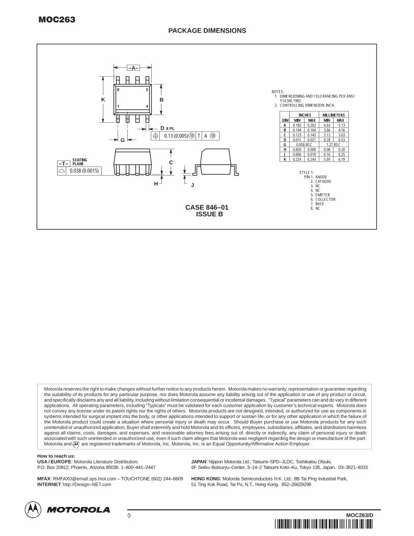
6–26 Motorola Optoelectronics Device Data
PACKAGE DIMENSIONS
CASE 846–01ISSUE B
STYLE 1:PIN 1. ANODE
2. CATHODE3. NC4. NC5. EMITTER6. COLLECTOR7. BASE8. NC
DIMA
MIN MAX MIN MAXMILLIMETERS
0.182 0.202 4.63 5.13
INCHES
B 0.144 0.164 3.66 4.16C 0.123 0.143 3.13 3.63D 0.011 0.021 0.28 0.53G 0.050 BSC 1.27 BSCH 0.003 0.008 0.08 0.20J 0.006 0.010 0.16 0.25K 0.224 0.244 5.69 6.19
NOTES:1. DIMENSIONING AND TOLERANCING PER ANSI
Y14.5M, 1982.2. CONTROLLING DIMENSION: INCH.
BK
D
G
8 PL
0.13 (0.005) M T A M
JH
CSEATINGPLANE
0.038 (0.0015)
1
8 5
4
–A–
–T–
Motorola reserves the right to make changes without further notice to any products herein. Motorola makes no warranty, representation or guarantee regardingthe suitability of its products for any particular purpose, nor does Motorola assume any liability arising out of the application or use of any product or circuit,and specifically disclaims any and all liability, including without limitation consequential or incidental damages. “Typical” parameters can and do vary in differentapplications. All operating parameters, including “Typicals” must be validated for each customer application by customer’s technical experts. Motorola doesnot convey any license under its patent rights nor the rights of others. Motorola products are not designed, intended, or authorized for use as components insystems intended for surgical implant into the body, or other applications intended to support or sustain life, or for any other application in which the failure ofthe Motorola product could create a situation where personal injury or death may occur. Should Buyer purchase or use Motorola products for any suchunintended or unauthorized application, Buyer shall indemnify and hold Motorola and its officers, employees, subsidiaries, affiliates, and distributors harmlessagainst all claims, costs, damages, and expenses, and reasonable attorney fees arising out of, directly or indirectly, any claim of personal injury or deathassociated with such unintended or unauthorized use, even if such claim alleges that Motorola was negligent regarding the design or manufacture of the part.Motorola and are registered trademarks of Motorola, Inc. Motorola, Inc. is an Equal Opportunity/Affirmative Action Employer.
How to reach us:USA / EUROPE: Motorola Literature Distribution; JAPAN : Nippon Motorola Ltd.; Tatsumi–SPD–JLDC, Toshikatsu Otsuki,P.O. Box 20912; Phoenix, Arizona 85036. 1–800–441–2447 6F Seibu–Butsuryu–Center, 3–14–2 Tatsumi Koto–Ku, Tokyo 135, Japan. 03–3521–8315
MFAX: [email protected] – TOUCHTONE (602) 244–6609 HONG KONG: Motorola Semiconductors H.K. Ltd.; 8B Tai Ping Industrial Park, INTERNET: http://Design–NET.com 51 Ting Kok Road, Tai Po, N.T., Hong Kong. 852–26629298
MOC263/D
◊

6–27Motorola Optoelectronics Device Data
Transistor Output
These devices consist of two gallium arsenide infrared emitting diodesoptically coupled to two monolithic silicon phototransistor detectors, in a surfacemountable, small outline, plastic package. They are ideally suited for highdensity applications and eliminate the need for through–the–board mounting.
• Dual Channel Coupler
• Convenient Plastic SOIC–8 Surface Mountable Package Style
• Closely Matched Current Transfer Ratios to Minimize Unit–to–Unit Variation
• Minimum V(BR)CEO of 70 Volts Guaranteed
• Standard SOIC–8 Footprint, with 0.050″ Lead Spacing
• Shipped in Tape and Reel, which Conforms to EIA Standard RS481A
• Compatible with Dual Wave, Vapor Phase and IR Reflow Soldering
• High Input–Output Isolation of 3000 Vac (rms) Guaranteed
• Meets U.L. Regulatory Requirements, File #E54915
Ordering Information:
• To obtain MOCD207, 208 in tape and reel, add R2 suffix to device numbers as follows:R2 = 2500 units on 13″ reel
• To obtain MOCD207, 208 in quantities of 50 (shipped in sleeves) — no suffix
Marking Information:
• MOCD207 = D207
• MOCD208 = D208
Applications:
• Feedback Control Circuits
• Interfacing and Coupling Systems of Different Potentials and Impedances
• General Purpose Switching Circuits
• Monitor and Detection Circuits
MAXIMUM RATINGS (TA = 25°C unless otherwise noted)
Rating Symbol Value Unit
INPUT LED
Forward Current — Continuous IF 60 mA
Forward Current — Peak (PW = 100 µs, 120 pps) IF(pk) 1.0 A
Reverse Voltage VR 6.0 V
LED Power Dissipation @ TA = 25°CDerate above 25°C
PD 900.8
mWmW/°C
OUTPUT TRANSISTOR
Collector–Emitter Voltage VCEO 70 V
Collector–Base Voltage VCBO 70 V
Emitter–Collector Voltage VECO 7.0 V
Collector Current — Continuous IC 150 mA
Detector Power Dissipation @ TA = 25°CDerate above 25°C
PD 1501.76
mWmW/°C
NOTE: Thickness through insulation between input and output is ≥ 0.5 mm.
Preferred devices are Motorola recommended choices for future use and best overall value.
Order this documentby MOCD207/D
SEMICONDUCTOR TECHNICAL DATA
Motorola, Inc. 1995
Motorola Preferred Devices
[CTR = 100 – 200%]
[CTR = 40 – 125%]
DUAL CHANNELSMALL OUTLINEOPTOISOLATORS
TRANSISTOR OUTPUT
CASE 846–01, STYLE 3PLASTIC
SCHEMATIC
1. ANODE 12. CATHODE 13. ANODE 24. CATHODE 25. EMITTER 26. COLLECTOR 27. EMITTER 18. COLLECTOR 1
1
2
3
8
6
54
7
REV 1

6–28 Motorola Optoelectronics Device Data
MAXIMUM RATINGS—continued (TA = 25°C unless otherwise noted)
Rating Symbol Value Unit
TOTAL DEVICE
Input–Output Isolation Voltage)(1,2) (60 Hz, 1.0 sec. duration) VISO 3000 Vac(rms)
Total Device Power Dissipation @ TA = 25°CDerate above 25°C
PD 2502.94
mWmW/°C
Ambient Operating Temperature Range TA –55 to +100 °C
Storage Temperature Range Tstg –55 to +150 °C
Lead Soldering Temperature (1/16″ from case, 10 sec. duration) — 260 °C
ELECTRICAL CHARACTERISTICS (TA = 25°C unless otherwise noted)(3)
Characteristic Symbol Min Typ (3) Max Unit
INPUT LED
Forward Voltage (IF = 30 mA) VF — 1.2 1.55 V
Reverse Leakage Current (VR = 6.0 V) IR — 0.1 100 A
Capacitance C — 18 — pF
OUTPUT TRANSISTOR
Collector–Emitter Dark Current (VCE = 10 V, TA = 25°C) ICEO1 — 1.0 50 nA
(VCE = 10 V, TA = 100°C) ICEO2 — 1.0 — µA
Collector–Emitter Breakdown Voltage (IC = 100 µA) V(BR)CEO 70 120 — V
Emitter–Collector Breakdown Voltage (IE = 100 µA) V(BR)ECO 7.0 7.8 — V
Collector–Emitter Capacitance (f = 1.0 MHz, VCE = 0) CCE — 7.0 — pF
COUPLED
Output Collector Current MOCD207(IF = 10 mA, VCE = 5 V) MOCD208
IC (CTR)(4) 10 (100)4.0 (40)
15 (150)—
20 (200)12.5 (125)
mA (%)
Output Collector Current MOCD207(IF = 1 mA, VCE = 5 V) MOCD208
IC 3.41.3
7.03.0
——
mA
Collector–Emitter Saturation Voltage (IC = 2.0 mA, IF = 10 mA) VCE(sat) — 0.15 0.4 V
Turn–On Time (IC = 2.0 mA, VCC = 10 V, RL = 100 Ω) ton — 3.0 — µs
Turn–Off Time (IC = 2.0 mA, VCC = 10 V, RL = 100 Ω) toff — 2.8 — µs
Rise Time (IC = 2.0 mA, VCC = 10 V, RL = 100 Ω) tr — 1.6 — µs
Fall Time (IC = 2.0 mA, VCC = 10 V, RL = 100 Ω) tf — 2.2 — µs
Input–Output Isolation Voltage (f = 60 Hz, t = 1.0 sec)(1,2) VISO 3000 — — Vac(rms)
Isolation Resistance (VI–O = 500 V)(2) RISO 1011 — — Ω
Isolation Capacitance (VI–O = 0, f = 1.0 MHz)(2) CISO — 0.2 — pF
1. Input–Output Isolation Voltage, VISO, is an internal device dielectric breakdown rating.2. For this test, pins 1, 2, 3 and 4 are common, and pins 5, 6 and 7 are common.3. Always design to the specified minimum/maximum electrical limits (where applicable).4. Current Transfer Ratio (CTR) = IC/IF x 100%.

6–29Motorola Optoelectronics Device Data
TYPICAL CHARACTERISTICS
Figure 1. LED Forward Voltage versus Forward CurrentIF, LED FORWARD CURRENT (mA)
101
2
10001001
1.2
1.4
1.6
1.8
Figure 2. Output Current versus Input Current
V F, F
OR
WAR
D V
OLT
AGE
(VO
LTS)
PULSE ONLYPULSE OR DC
C IF, LED INPUT CURRENT (mA)5020105210.5
0.1
1
10
0.01
I, O
UTP
UT
CO
LLEC
TOR
CU
RR
ENT
(NO
RM
ALIZ
ED)
NORMALIZED TO:IF = 10 mA
TA = – 55°C
25°C
100°C
TA, AMBIENT TEMPERATURE (°C)120100806040200–20–40–60
0.1
1.0
10
Figure 3. Output Current versusCollector–Emitter Voltage
VCE, COLLECTOR–EMITTER VOLTAGE (VOLTS)10980 1 2 3 4 5 6
16
70
2
4
6
8
10
12
14
I C, O
UTP
UT
CO
LLEC
TOR
CU
RR
ENT
(mA)
I C, O
UTP
UT
CO
LLEC
TOR
CU
RR
ENT
(NO
RM
ALIZ
ED)
Figure 4. Output Current versusAmbient Temperature
1001010.10.01
20
TA, AMBIENT TEMPERATURE (°C)
100800 20 40
103
60
10–1
100
101
102
18
16
14
12
10
8
6
4
V, VOLTAGE (VOLTS)
2
I CEO
, CO
LLEC
TOR
–EM
ITTE
R D
ARK
CU
RR
ENT
(NO
RM
ALIZ
ED)
C, C
APAC
ITAN
CE
(pF)
Figure 5. Dark Current versus Ambient Temperature Figure 6. Capacitance versus Voltage
NORMALIZED TO:TA = 25°C
IF = 10 mAMOCD207
NORMALIZED TO:VCE = 10 VTA = 25°C
VCE = 70 V
30 V
10 V
CLED
CCE
f = 1 MHz
MOCD208

6–30 Motorola Optoelectronics Device Data
PACKAGE DIMENSIONS
DIMA
MIN MAX MIN MAXMILLIMETERS
0.182 0.202 4.63 5.13
INCHES
B 0.144 0.164 3.66 4.16C 0.123 0.143 3.13 3.63D 0.011 0.021 0.28 0.53G 0.050 BSC 1.27 BSCH 0.003 0.008 0.08 0.20J 0.006 0.010 0.16 0.25K 0.224 0.244 5.69 6.19
NOTES:1. DIMENSIONING AND TOLERANCING PER ANSI
Y14.5M, 1982.2. CONTROLLING DIMENSION: INCH.
BK
D
G
8 PL
0.13 (0.005) M T A M
JH
CSEATINGPLANE
0.038 (0.0015)
CASE 846–01
1
8 5
4
–A–
–T–
ISSUE B
STYLE 3:PIN 1. ANODE 1
2. CATHODE 13. ANODE 24. CATHODE 25. EMITTER 26. COLLECTOR 27. EMITTER 18. COLLECTOR 1
Motorola reserves the right to make changes without further notice to any products herein. Motorola makes no warranty, representation or guarantee regardingthe suitability of its products for any particular purpose, nor does Motorola assume any liability arising out of the application or use of any product or circuit,and specifically disclaims any and all liability, including without limitation consequential or incidental damages. “Typical” parameters can and do vary in differentapplications. All operating parameters, including “Typicals” must be validated for each customer application by customer’s technical experts. Motorola doesnot convey any license under its patent rights nor the rights of others. Motorola products are not designed, intended, or authorized for use as components insystems intended for surgical implant into the body, or other applications intended to support or sustain life, or for any other application in which the failure ofthe Motorola product could create a situation where personal injury or death may occur. Should Buyer purchase or use Motorola products for any suchunintended or unauthorized application, Buyer shall indemnify and hold Motorola and its officers, employees, subsidiaries, affiliates, and distributors harmlessagainst all claims, costs, damages, and expenses, and reasonable attorney fees arising out of, directly or indirectly, any claim of personal injury or deathassociated with such unintended or unauthorized use, even if such claim alleges that Motorola was negligent regarding the design or manufacture of the part.Motorola and are registered trademarks of Motorola, Inc. Motorola, Inc. is an Equal Opportunity/Affirmative Action Employer.
How to reach us:USA / EUROPE: Motorola Literature Distribution; JAPAN : Nippon Motorola Ltd.; Tatsumi–SPD–JLDC, Toshikatsu Otsuki,P.O. Box 20912; Phoenix, Arizona 85036. 1–800–441–2447 6F Seibu–Butsuryu–Center, 3–14–2 Tatsumi Koto–Ku, Tokyo 135, Japan. 03–3521–8315
MFAX: [email protected] – TOUCHTONE (602) 244–6609 HONG KONG: Motorola Semiconductors H.K. Ltd.; 8B Tai Ping Industrial Park, INTERNET: http://Design–NET.com 51 Ting Kok Road, Tai Po, N.T., Hong Kong. 852–26629298
MOCD207/D
◊

6–31Motorola Optoelectronics Device Data
Transistor Output
The MOCD211 device consists of two gallium arsenide infrared emittingdiodes optically coupled to two monolithic silicon phototransistor detectors, in asurface mountable, small outline, plastic package. It is ideally suited for highdensity applications and eliminates the need for through–the–board mounting.
• Dual Channel Coupler
• Convenient Plastic SOIC–8 Surface Mountable Package Style
• Minimum V(BR)CEO of 30 Volts Guaranteed
• Standard SOIC–8 Footprint, with 0.050″ Lead Spacing
• Shipped in Tape and Reel, which conforms to EIA Standard RS481A
• Compatible with Dual Wave, Vapor Phase and IR Reflow Soldering
• High Input–Output Isolation of 3000 Vac (rms) Guaranteed
• Meets U.L. Regulatory Requirements, File #E54915
Ordering Information:
• To obtain MOCD211 in tape and reel, add R2 suffix to device number as follows:R2 = 2500 units on 13″ reel
• To obtain MOCD211 in quantities of 50 (shipped in sleeves) — no suffix
Marking Information:
• MOCD211 = D211
MAXIMUM RATINGS (TA = 25°C unless otherwise noted)
Rating Symbol Value Unit
INPUT LED
Forward Current — Continuous IF 60 mA
Forward Current — Peak (PW = 100 µs, 120 pps) IF(pk) 1.0 A
Reverse Voltage VR 6.0 V
LED Power Dissipation @ TA = 25°CDerate above 25°C
PD 900.8
mWmW/°C
OUTPUT TRANSISTOR
Collector–Emitter Voltage VCEO 30 V
Collector–Base Voltage VCBO 70 V
Emitter–Collector Voltage VECO 7.0 V
Collector Current — Continuous IC 150 mA
Detector Power Dissipation @ TA = 25°CDerate above 25°C
PD 1501.76
mWmW/°C
NOTE: Thickness through insulation between input and output is ≥ 0.5 mm.
Preferred devices are Motorola recommended choices for future use and best overall value.
Order this documentby MOCD211/D
SEMICONDUCTOR TECHNICAL DATA
Motorola, Inc. 1995
Motorola Preferred Device
DUAL CHANNELSMALL OUTLINEOPTOISOLATOR
TRANSISTOR OUTPUT
CASE 846–01, STYLE 3PLASTIC
SCHEMATIC
[CTR = 20% Min]
1. ANODE 12. CATHODE 13. ANODE 24. CATHODE 25. EMITTER 26. COLLECTOR 27. EMITTER 18. COLLECTOR 1
1
2
3
8
6
54
7
REV 1

6–32 Motorola Optoelectronics Device Data
MAXIMUM RATINGS — continued (TA = 25°C unless otherwise noted)
Rating Symbol Value Unit
TOTAL DEVICE
Input–Output Isolation Voltage(1,2)
(60 Hz, 1.0 sec. duration)VISO 3000 Vac(rms)
Total Device Power Dissipation @ TA = 25°CDerate above 25°C
PD 2502.94
mWmW/°C
Ambient Operating Temperature Range(3) TA –55 to +100 °C
Storage Temperature Range(3) Tstg –55 to +150 °C
Lead Soldering Temperature(1/16″ from case, 10 sec. duration)
— 260 °C
ELECTRICAL CHARACTERISTICS (TA = 25°C unless otherwise noted)(4)
Characteristic Symbol Min Typ (4) Max Unit
INPUT LED
Forward Voltage (IF = 1.0 mA) VF — 1.15 1.5 V
Reverse Leakage Current (VR = 6.0 V) IR — 0.1 100 A
Capacitance C — 18 — pF
OUTPUT TRANSISTOR
Collector–Emitter Dark Current (VCE = 5.0 V, TA = 25°C) ICEO1 — 1.0 50 nA
(VCE = 5.0 V, TA = 100°C) ICEO2 — 1.0 — µA
Collector–Emitter Breakdown Voltage (IC = 100 µA) V(BR)CEO 30 90 — V
Emitter–Collector Breakdown Voltage (IE = 100 µA) V(BR)ECO 7.0 7.8 — V
Collector–Emitter Capacitance (f = 1.0 MHz, VCE = 0) CCE — 7.0 — pF
COUPLED
Output Collector Current MOCD211(IF = 10 mA, VCE = 10 V)
IC (CTR)(5) 2.0 (20) 6.5 (65) — mA (%)
Collector–Emitter Saturation Voltage (IC = 2.0 mA, IF = 1.0 mA) VCE(sat) — 0.15 0.4 V
Turn–On Time (IC = 2.0 mA, VCC = 10 V, RL = 100 Ω) ton — 7.5 — µs
Turn–Off Time (IC = 2.0 mA, VCC = 10 V, RL = 100 Ω) toff — 5.7 — µs
Rise Time (IC = 2.0 mA, VCC = 10 V, RL = 100 Ω) tr — 3.2 — µs
Fall Time (IC = 2.0 mA, VCC = 10 V, RL = 100 Ω) tf — 4.7 — µs
Input–Output Isolation Voltage (f = 60 Hz, t = 1.0 sec.)(1,2) VISO 3000 — — Vac(rms)
Isolation Resistance (VI–O = 500 V)(2) RISO 1011 — — Ω
Isolation Capacitance (VI–O = 0, f = 1.0 MHz)(2) CISO — 0.2 — pF
1. Input–Output Isolation Voltage, VISO, is an internal device dielectric breakdown rating.2. For this test, pins 1, 2, 3 and 4 are common, and pins 5, 6, 7 and 8 are common.3. Refer to Quality and Reliability Section in Opto Data Book for information on test conditions.4. Always design to the specified minimum/maximum electrical limits (where applicable).5. Current Transfer Ratio (CTR) = IC/IF x 100%.

6–33Motorola Optoelectronics Device Data
Figure 1. LED Forward Voltage versus Forward Current
IF, LED FORWARD CURRENT (mA)
101
2
10001001
1.2
1.4
1.6
1.8
Figure 2. Output Current versus Input Current
V F, F
OR
WAR
D V
OLT
AGE
(VO
LTS)
PULSE ONLYPULSE OR DC
TYPICAL CHARACTERISTICS
TA = – 55°C
25°C
100°C
C IF, LED INPUT CURRENT (mA)5020105210.5
0.1
1
10
0.01
I, O
UTP
UT
CO
LLEC
TOR
CU
RR
ENT
(NO
RM
ALIZ
ED)
NORMALIZED TO:IF = 10 mA
1001010.10.01
20
TA, AMBIENT TEMPERATURE (°C)
120100806040200–20–40–600.1
1
10
Figure 3. Output Current versusCollector–Emitter Voltage
18
16
14
12
10
8
6
4
V, VOLTAGE (VOLTS)
2
I C, O
UTP
UT
CO
LLEC
TOR
CU
RR
ENT
(NO
RM
ALIZ
ED)
C, C
APAC
ITAN
CE
(pF)
1
10
100
0.10 20 40 60 80 100
TA, AMBIENT TEMPERATURE (°C)
I
C
EO, C
OLL
ECTO
R–E
MIT
TER
DAR
K C
UR
REN
T(N
OR
MAL
IZED
)
Figure 4. Output Current versusAmbient Temperature
Figure 5. Dark Current versus Ambient Temperature Figure 6. Capacitance versus Voltage
VCE, COLLECTOR–EMITTER VOLTAGE (VOLTS)10980 1 2 3 4 5 6
16
70
2
4
6
8
10
12
14
I C, OU
TPU
T C
OLL
ECTO
R C
UR
REN
T (m
A)
IF = 10 mA
MOCD211
NORMALIZED TO:TA = 25°C
NORMALIZED TO:VCE = 10 VTA = 25°C
VCE = 30 V
10 V
CLED
CCE
f = 1 MHz

6–34 Motorola Optoelectronics Device Data
PACKAGE DIMENSIONS
DIMA
MIN MAX MIN MAXMILLIMETERS
0.182 0.202 4.63 5.13
INCHES
B 0.144 0.164 3.66 4.16C 0.123 0.143 3.13 3.63D 0.011 0.021 0.28 0.53G 0.050 BSC 1.27 BSCH 0.003 0.008 0.08 0.20J 0.006 0.010 0.16 0.25K 0.224 0.244 5.69 6.19
NOTES:1. DIMENSIONING AND TOLERANCING PER ANSI
Y14.5M, 1982.2. CONTROLLING DIMENSION: INCH.
BK
D
G
8 PL
0.13 (0.005) M T A M
JH
CSEATINGPLANE
0.038 (0.0015)
CASE 846–01
1
8 5
4
–A–
–T–
ISSUE B
STYLE 3:PIN 1. ANODE 1
2. CATHODE 13. ANODE 24. CATHODE 25. EMITTER 26. COLLECTOR 27. EMITTER 18. COLLECTOR 1
Motorola reserves the right to make changes without further notice to any products herein. Motorola makes no warranty, representation or guarantee regardingthe suitability of its products for any particular purpose, nor does Motorola assume any liability arising out of the application or use of any product or circuit,and specifically disclaims any and all liability, including without limitation consequential or incidental damages. “Typical” parameters can and do vary in differentapplications. All operating parameters, including “Typicals” must be validated for each customer application by customer’s technical experts. Motorola doesnot convey any license under its patent rights nor the rights of others. Motorola products are not designed, intended, or authorized for use as components insystems intended for surgical implant into the body, or other applications intended to support or sustain life, or for any other application in which the failure ofthe Motorola product could create a situation where personal injury or death may occur. Should Buyer purchase or use Motorola products for any suchunintended or unauthorized application, Buyer shall indemnify and hold Motorola and its officers, employees, subsidiaries, affiliates, and distributors harmlessagainst all claims, costs, damages, and expenses, and reasonable attorney fees arising out of, directly or indirectly, any claim of personal injury or deathassociated with such unintended or unauthorized use, even if such claim alleges that Motorola was negligent regarding the design or manufacture of the part.Motorola and are registered trademarks of Motorola, Inc. Motorola, Inc. is an Equal Opportunity/Affirmative Action Employer.
How to reach us:USA / EUROPE: Motorola Literature Distribution; JAPAN : Nippon Motorola Ltd.; Tatsumi–SPD–JLDC, Toshikatsu Otsuki,P.O. Box 20912; Phoenix, Arizona 85036. 1–800–441–2447 6F Seibu–Butsuryu–Center, 3–14–2 Tatsumi Koto–Ku, Tokyo 135, Japan. 03–3521–8315
MFAX: [email protected] – TOUCHTONE (602) 244–6609 HONG KONG: Motorola Semiconductors H.K. Ltd.; 8B Tai Ping Industrial Park, INTERNET: http://Design–NET.com 51 Ting Kok Road, Tai Po, N.T., Hong Kong. 852–26629298
MOCD211/D
◊

6–35Motorola Optoelectronics Device Data
Transistor Output
This device consists of two gallium arsenide infrared emitting diodes opticallycoupled to two monolithic silicon phototransistor detectors, in a surfacemountable, small outline, plastic package. It is ideally suited for high densityapplications and eliminates the need for through–the–board mounting.
• Dual Channel Coupler
• Convenient Plastic SOIC–8 Surface Mountable Package Style
• Minimum Current Transfer Ratio 100% with Input Current of 10 mA
• Minimum V(BR)CEO of 70 Volts Guaranteed
• Standard SOIC–8 Footprint, with 0.050″ Lead Spacing
• Shipped in Tape and Reel, which Conforms to EIA Standard RS481A
• Compatible with Dual Wave, Vapor Phase and IR Reflow Soldering
• High Input–Output Isolation of 3000 Vac (rms) Guaranteed
• Meets U.L. Regulatory Requirements, File #E54915
Ordering Information:
• To obtain MOCD213 in tape and reel, add R2 suffix to device number as follows:R2 = 2500 units on 13″ reel
• To obtain MOCD213 in quantities of 50 (shipped in sleeves) — no suffix
Marking Information:
• MOCD213 = D213
Applications:• Feedback Control Circuits
• Interfacing and Coupling Systems of Different Potentials and Impedances
• General Purpose Switching Circuits
• Monitor and Detection Circuits
MAXIMUM RATINGS (TA = 25°C unless otherwise noted)
Rating Symbol Value Unit
INPUT LED
Forward Current — Continuous IF 60 mA
Forward Current — Peak (PW = 100 µs, 120 pps) IF(pk) 1.0 A
Reverse Voltage VR 6.0 V
LED Power Dissipation @ TA = 25°CDerate above 25°C
PD 900.8
mWmW/°C
OUTPUT TRANSISTOR
Collector–Emitter Voltage VCEO 70 V
Collector–Base Voltage VCBO 70 V
Emitter–Collector Voltage VECO 7.0 V
Collector Current — Continuous IC 150 mA
Detector Power Dissipation @ TA = 25°CDerate above 25°C
PD 1501.76
mWmW/°C
NOTE: Thickness through insulation between input and output is ≥ 0.5 mm.
Order this documentby MOCD213/D
SEMICONDUCTOR TECHNICAL DATA
Motorola, Inc. 1995
DUAL CHANNELSMALL OUTLINEOPTOISOLATOR
TRANSISTOR OUTPUT
CASE 846–01, STYLE 3PLASTIC
SCHEMATIC
[CTR = 100% Min]
1. ANODE 12. CATHODE 13. ANODE 24. CATHODE 25. EMITTER 26. COLLECTOR 27. EMITTER 18. COLLECTOR 1
1
2
3
8
6
54
7
REV 2

6–36 Motorola Optoelectronics Device Data
MAXIMUM RATINGS—continued (TA = 25°C unless otherwise noted)
Rating Symbol Value Unit
TOTAL DEVICE
Input–Output Isolation Voltage(1,2)(60 Hz, 1.0 sec. duration)
VISO 3000 Vac(rms)
Total Device Power Dissipation @ TA = 25°CDerate above 25°C
PD 2502.94
mWmW/°C
Ambient Operating Temperature Range(3) TA –55 to +100 °C
Storage Temperature Range(3) Tstg –55 to +150 °C
Lead Soldering Temperature (1/16″ from case, 10 sec. duration) — 260 °C
ELECTRICAL CHARACTERISTICS (TA = 25°C unless otherwise noted)(4)
Characteristic Symbol Min Typ (4) Max Unit
INPUT LED
Forward Voltage (IF = 30 mA) VF — 1.2 1.55 V
Reverse Leakage Current (VR = 6.0 V) IR — 0.1 100 A
Capacitance C — 18 — pF
OUTPUT TRANSISTOR
Collector–Emitter Dark Current (VCE = 10 V, TA = 25°C) ICEO1 — 1.0 50 nA
(VCE = 10 V, TA = 100°C) ICEO2 — 1.0 — µA
Collector–Emitter Breakdown Voltage (IC = 100 µA) V(BR)CEO 70 120 — V
Emitter–Collector Breakdown Voltage (IE = 100 µA) V(BR)ECO 7.0 7.8 — V
Collector–Emitter Capacitance (f = 1.0 MHz, VCE = 0) CCE — 7.0 — pF
COUPLED
Output Collector Current MOCD213(IF = 10 mA, VCE = 5 V)
IC (CTR)(5) 10 (100) — — mA (%)
Collector–Emitter Saturation Voltage (IC = 2.0 mA, IF = 10 mA) VCE(sat) — 0.15 0.4 V
Turn–On Time (IC = 2.0 mA, VCC = 10 V, RL = 100 Ω) ton — 3.0 — µs
Turn–Off Time (IC = 2.0 mA, VCC = 10 V, RL = 100 Ω) toff — 2.8 — µs
Rise Time (IC = 2.0 mA, VCC = 10 V, RL = 100 Ω) tr — 1.6 — µs
Fall Time (IC = 2.0 mA, VCC = 10 V, RL = 100 Ω) tf — 2.2 — µs
Input–Output Isolation Voltage (f = 60 Hz, t = 1.0 sec)(1,2) VISO 3000 — — Vac(rms)
Isolation Resistance (VI–O = 500 V)(2) RISO 1011 — — Ω
Isolation Capacitance (VI–O = 0, f = 1.0 MHz)(2) CISO — 0.2 — pF
1. Input–Output Isolation Voltage, VISO, is an internal device dielectric breakdown rating.2. For this test, pins 1, 2, 3, and 4 are common, and pins 5, 6, 7 and 8 are common.3. Refer to Quality and Reliability Section in Opto Data Book for information on test conditions.4. Always design to the specified minimum/maximum electrical limits (where applicable).5. Current Transfer Ratio (CTR) = IC/IF x 100%.

6–37Motorola Optoelectronics Device Data
TYPICAL CHARACTERISTICS
C IF, LED INPUT CURRENT (mA)5020105210.5
0.1
1
10
Figure 1. LED Forward Voltage versus Forward Current
IF, LED FORWARD CURRENT (mA)101
2
0.011000100
1
1.2
1.4
1.6
1.8
Figure 2. Output Current versus Input Current
V F, F
OR
WAR
D V
OLT
AGE
(VO
LTS)
I, O
UTP
UT
CO
LLEC
TOR
CU
RR
ENT
(NO
RM
ALIZ
ED)
PULSE ONLYPULSE OR DC
TA = – 55°C
25°C
100°C
NORMALIZED TO:IF = 10 mA
TA, AMBIENT TEMPERATURE (°C)
120100806040200–20–40–600.1
1.0
10
Figure 3. Output Current versusCollector–Emitter Voltage
VCE, COLLECTOR–EMITTER VOLTAGE (VOLTS)
10980 1 2 3 4 5 6
16
70
2
4
6
8
10
12
14
I C, OU
TPU
T C
OLL
ECTO
R C
UR
REN
T (m
A)
I C, O
UTP
UT
CO
LLEC
TOR
CU
RR
ENT
(NO
RM
ALIZ
ED
Figure 4. Output Current versusAmbient Temperature
1001010.10.01
20
TA, AMBIENT TEMPERATURE (°C)
100800 20 40
103
60
10–1
100
101
102
18
16
14
12
10
8
6
4
V, VOLTAGE (VOLTS)
2
I CEO
, CO
LLEC
TOR
–EM
ITTE
R D
ARK
CU
RR
ENT
(NO
RM
ALIZ
ED)
C, C
APAC
ITAN
CE
(pF)
Figure 5. Dark Current versus Ambient Temperature Figure 6. Capacitance versus Voltage
IF = 10 mANORMALIZED TO:
TA = 25°C
NORMALIZED TO:VCE = 10 VTA = 25°C
VCE = 70 V
10 V
30 V
CLED
CCE
f = 1 MHz

6–38 Motorola Optoelectronics Device Data
PACKAGE DIMENSIONS
DIMA
MIN MAX MIN MAXMILLIMETERS
0.182 0.202 4.63 5.13
INCHES
B 0.144 0.164 3.66 4.16C 0.123 0.143 3.13 3.63D 0.011 0.021 0.28 0.53G 0.050 BSC 1.27 BSCH 0.003 0.008 0.08 0.20J 0.006 0.010 0.16 0.25K 0.224 0.244 5.69 6.19
NOTES:1. DIMENSIONING AND TOLERANCING PER ANSI
Y14.5M, 1982.2. CONTROLLING DIMENSION: INCH.
BK
D
G
8 PL
0.13 (0.005) M T A M
JH
CSEATINGPLANE
0.038 (0.0015)
CASE 846–01
1
8 5
4
–A–
–T–
ISSUE B
STYLE 3:PIN 1. ANODE 1
2. CATHODE 13. ANODE 24. CATHODE 25. EMITTER 26. COLLECTOR 27. EMITTER 18. COLLECTOR 1
Motorola reserves the right to make changes without further notice to any products herein. Motorola makes no warranty, representation or guarantee regardingthe suitability of its products for any particular purpose, nor does Motorola assume any liability arising out of the application or use of any product or circuit,and specifically disclaims any and all liability, including without limitation consequential or incidental damages. “Typical” parameters can and do vary in differentapplications. All operating parameters, including “Typicals” must be validated for each customer application by customer’s technical experts. Motorola doesnot convey any license under its patent rights nor the rights of others. Motorola products are not designed, intended, or authorized for use as components insystems intended for surgical implant into the body, or other applications intended to support or sustain life, or for any other application in which the failure ofthe Motorola product could create a situation where personal injury or death may occur. Should Buyer purchase or use Motorola products for any suchunintended or unauthorized application, Buyer shall indemnify and hold Motorola and its officers, employees, subsidiaries, affiliates, and distributors harmlessagainst all claims, costs, damages, and expenses, and reasonable attorney fees arising out of, directly or indirectly, any claim of personal injury or deathassociated with such unintended or unauthorized use, even if such claim alleges that Motorola was negligent regarding the design or manufacture of the part.Motorola and are registered trademarks of Motorola, Inc. Motorola, Inc. is an Equal Opportunity/Affirmative Action Employer.
How to reach us:USA / EUROPE: Motorola Literature Distribution; JAPAN : Nippon Motorola Ltd.; Tatsumi–SPD–JLDC, Toshikatsu Otsuki,P.O. Box 20912; Phoenix, Arizona 85036. 1–800–441–2447 6F Seibu–Butsuryu–Center, 3–14–2 Tatsumi Koto–Ku, Tokyo 135, Japan. 03–3521–8315
MFAX: [email protected] – TOUCHTONE (602) 244–6609 HONG KONG: Motorola Semiconductors H.K. Ltd.; 8B Tai Ping Industrial Park, INTERNET: http://Design–NET.com 51 Ting Kok Road, Tai Po, N.T., Hong Kong. 852–26629298
MOCD213/D
◊

6–39Motorola Optoelectronics Device Data
Transistor Output (Low Input Current)
The MOCD217 device consists of two gallium arsenide infrared emittingdiodes optically coupled to two monolithic silicon phototransistor detectors, in asurface mountable, small outline, plastic package. It is ideally suited for highdensity applications and eliminates the need for through–the–board mounting.
• Dual Channel Coupler
• Convenient Plastic SOIC–8 Surface Mountable Package Style
• Low Input Current (Specified @ 1 mA)
• Minimum V(BR)CEO of 30 Volts Guaranteed
• Standard SOIC–8 Footprint, with 0.050″ Lead Spacing
• Shipped in Tape and Reel, which conforms to EIA Standard RS481A
• Compatible with Dual Wave, Vapor Phase and IR Reflow Soldering
• High Input–Output Isolation of 3000 Vac (rms) Guaranteed
• Meets U.L. Regulatory Requirements, File #E54915
Ordering Information:
• To obtain MOCD217 in tape and reel, add R2 suffix to device number as follows:R2 = 2500 units on 13″ reel
• To obtain MOCD217 in quantities of 50 (shipped in sleeves) — no suffix
Marking Information:
• MOCD217 = D217
MAXIMUM RATINGS (TA = 25°C unless otherwise noted)
Rating Symbol Value Unit
INPUT LED
Forward Current — Continuous IF 60 mA
Forward Current — Peak (PW = 100 µs, 120 pps) IF(pk) 1.0 A
Reverse Voltage VR 6.0 V
LED Power Dissipation @ TA = 25°CDerate above 25°C
PD 900.8
mWmW/°C
OUTPUT TRANSISTOR
Collector–Emitter Voltage VCEO 30 V
Collector–Base Voltage VCBO 70 V
Emitter–Collector Voltage VECO 7.0 V
Collector Current — Continuous IC 150 mA
Detector Power Dissipation @ TA = 25°CDerate above 25°C
PD 1501.76
mWmW/°C
NOTE: Thickness through insulation between input and output is ≥ 0.5 mm.
Preferred devices are Motorola recommended choices for future use and best overall value.
Order this documentby MOCD217/D
SEMICONDUCTOR TECHNICAL DATA
Motorola, Inc. 1995
Motorola Preferred Device
DUAL CHANNELSMALL OUTLINEOPTOISOLATOR
TRANSISTOR OUTPUT
CASE 846–01, STYLE 3PLASTIC
SCHEMATIC
[CTR = 100% Min]
1. ANODE 12. CATHODE 13. ANODE 24. CATHODE 25. EMITTER 26. COLLECTOR 27. EMITTER 18. COLLECTOR 1
1
2
3
8
6
54
7
REV 2

6–40 Motorola Optoelectronics Device Data
MAXIMUM RATINGS — continued (TA = 25°C unless otherwise noted)
Rating Symbol Value Unit
TOTAL DEVICE
Input–Output Isolation Voltage(1,2)
(60 Hz, 1.0 sec. duration)VISO 3000 Vac(rms)
Total Device Power Dissipation @ TA = 25°CDerate above 25°C
PD 2502.94
mWmW/°C
Ambient Operating Temperature Range(3) TA –55 to +100 °C
Storage Temperature Range(3) Tstg –55 to +150 °C
Lead Soldering Temperature(1/16″ from case, 10 sec. duration)
— 260 °C
ELECTRICAL CHARACTERISTICS (TA = 25°C unless otherwise noted)(4)
Characteristic Symbol Min Typ (4) Max Unit
INPUT LED
Forward Voltage (IF = 1.0 mA) VF — 1.05 1.3 V
Reverse Leakage Current (VR = 6.0 V) IR — 0.1 100 A
Capacitance C — 18 — pF
OUTPUT TRANSISTOR
Collector–Emitter Dark Current (VCE = 5.0 V, TA = 25°C) ICEO1 — 1.0 50 nA
(VCE = 5.0 V, TA = 100°C) ICEO2 — 1.0 — µA
Collector–Emitter Breakdown Voltage (IC = 100 µA) V(BR)CEO 30 90 — V
Emitter–Collector Breakdown Voltage (IE = 100 µA) V(BR)ECO 7.0 7.8 — V
Collector–Emitter Capacitance (f = 1.0 MHz, VCE = 0) CCE — 7.0 — pF
COUPLED
Output Collector Current MOCD217(IF = 1.0 mA, VCE = 5.0 V)
IC (CTR)(5) 1.0 (100) 1.3 (130) — mA (%)
Collector–Emitter Saturation Voltage (IC = 100 µA, IF = 1.0 mA) VCE(sat) — 0.35 0.4 V
Turn–On Time (IC = 2.0 mA, VCC = 10 V, RL = 100 Ω) ton — 7.5 — µs
Turn–Off Time (IC = 2.0 mA, VCC = 10 V, RL = 100 Ω) toff — 5.7 — µs
Rise Time (IC = 2.0 mA, VCC = 10 V, RL = 100 Ω) tr — 3.2 — µs
Fall Time (IC = 2.0 mA, VCC = 10 V, RL = 100 Ω) tf — 4.7 — µs
Input–Output Isolation Voltage (f = 60 Hz, t = 1.0 sec.)(1,2) VISO 3000 — — Vac(rms)
Isolation Resistance (VI–O = 500 V)(2) RISO 1011 — — Ω
Isolation Capacitance (VI–O = 0, f = 1.0 MHz)(2) CISO — 0.2 — pF
1. Input–Output Isolation Voltage, VISO, is an internal device dielectric breakdown rating.2. For this test, pins 1, 2, 3 and 4 are common, and pins 5, 6, 7 and 8 are common.3. Refer to Quality and Reliability Section in Opto Data Book for information on test conditions.4. Always design to the specified minimum/maximum electrical limits (where applicable).5. Current Transfer Ratio (CTR) = IC/IF x 100%.

6–41Motorola Optoelectronics Device Data
C
IF, LED INPUT CURRENT (mA)
5210.50.20.10.05
0.1
1
10
Figure 1. LED Forward Voltage versus Forward Current
IF, LED FORWARD CURRENT (mA)
101
2
0.0011000100
1
1.2
1.4
1.6
1.8
Figure 2. Output Current versus Input Current
V F, F
OR
WAR
D V
OLT
AGE
(VO
LTS)
I, O
UTP
UT
CO
LLEC
TOR
CU
RR
ENT
(NO
RM
ALIZ
ED)
PULSE ONLYPULSE OR DC
TYPICAL CHARACTERISTICS
TA = – 55°C
25°C
100°C
NORMALIZED TO:IF = 1 mA
1001010.10.01
20
TA, AMBIENT TEMPERATURE (°C)
120100806040200–20–40–600.1
1
10
Figure 3. Output Current versusCollector–Emitter Voltage
18
16
14
12
10
8
6
4
V, VOLTAGE (VOLTS)
2
I C, OU
TPU
T C
OLL
ECTO
R C
UR
REN
T (N
OR
MAL
IZED
C, C
APAC
ITAN
CE
(pF)
1
10
100
0.10 20 40 60 80 100
TA, AMBIENT TEMPERATURE (°C)
I
C
EO, C
OLL
ECTO
R–E
MIT
TER
DAR
K C
UR
REN
T(N
OR
MAL
IZED
)
Figure 4. Output Current versusAmbient Temperature
Figure 5. Dark Current versus Ambient Temperature Figure 6. Capacitance versus Voltage
2
1.8
1.6
1.4
1.2
1
0.8
0.6
0
VCE, COLLECTOR–EMITTER VOLTAGE (VOLTS)
10980 1 2 3 4 5 6 7
0.4
0.2
I C, O
UTP
UT
CO
LLEC
TOR
CU
RR
ENT
(mA) IF = 1 mA
NORMALIZED TO:TA = 25°C
NORMALIZED TO:VCE = 10 VTA = 25°C
VCE = 30 V
10 V
CLED
CCE
f = 1 MHz
MOCD217

6–42 Motorola Optoelectronics Device Data
PACKAGE DIMENSIONS
SO–8 SMALL OUTLINE OPTOISOLATOR
DIMA
MIN MAX MIN MAXMILLIMETERS
0.182 0.202 4.63 5.13
INCHES
B 0.144 0.164 3.66 4.16C 0.123 0.143 3.13 3.63D 0.011 0.021 0.28 0.53G 0.050 BSC 1.27 BSCH 0.003 0.008 0.08 0.20J 0.006 0.010 0.16 0.25K 0.224 0.244 5.69 6.19
NOTES:1. DIMENSIONING AND TOLERANCING PER ANSI
Y14.5M, 1982.2. CONTROLLING DIMENSION: INCH.
BK
D
G
8 PL
0.13 (0.005) M T A M
JH
CSEATINGPLANE
0.038 (0.0015)
CASE 846–01
1
8 5
4
–A–
–T–
ISSUE B
STYLE 3:PIN 1. ANODE 1
2. CATHODE 13. ANODE 24. CATHODE 25. EMITTER 26. COLLECTOR 27. EMITTER 18. COLLECTOR 1
Motorola reserves the right to make changes without further notice to any products herein. Motorola makes no warranty, representation or guarantee regardingthe suitability of its products for any particular purpose, nor does Motorola assume any liability arising out of the application or use of any product or circuit,and specifically disclaims any and all liability, including without limitation consequential or incidental damages. “Typical” parameters can and do vary in differentapplications. All operating parameters, including “Typicals” must be validated for each customer application by customer’s technical experts. Motorola doesnot convey any license under its patent rights nor the rights of others. Motorola products are not designed, intended, or authorized for use as components insystems intended for surgical implant into the body, or other applications intended to support or sustain life, or for any other application in which the failure ofthe Motorola product could create a situation where personal injury or death may occur. Should Buyer purchase or use Motorola products for any suchunintended or unauthorized application, Buyer shall indemnify and hold Motorola and its officers, employees, subsidiaries, affiliates, and distributors harmlessagainst all claims, costs, damages, and expenses, and reasonable attorney fees arising out of, directly or indirectly, any claim of personal injury or deathassociated with such unintended or unauthorized use, even if such claim alleges that Motorola was negligent regarding the design or manufacture of the part.Motorola and are registered trademarks of Motorola, Inc. Motorola, Inc. is an Equal Opportunity/Affirmative Action Employer.
How to reach us:USA / EUROPE: Motorola Literature Distribution; JAPAN : Nippon Motorola Ltd.; Tatsumi–SPD–JLDC, Toshikatsu Otsuki,P.O. Box 20912; Phoenix, Arizona 85036. 1–800–441–2447 6F Seibu–Butsuryu–Center, 3–14–2 Tatsumi Koto–Ku, Tokyo 135, Japan. 03–3521–8315
MFAX: [email protected] – TOUCHTONE (602) 244–6609 HONG KONG: Motorola Semiconductors H.K. Ltd.; 8B Tai Ping Industrial Park, INTERNET: http://Design–NET.com 51 Ting Kok Road, Tai Po, N.T., Hong Kong. 852–26629298
MOCD217/D
◊

6–43Motorola Optoelectronics Device Data
Darlington Output
The MOCD223 device consists of two gallium arsenide infrared emittingdiodes optically coupled to two monolithic silicon phototransistor darlingtondetectors, in a surface mountable, small outline, plastic package. It is ideallysuited for high density applications that require low input current and eliminatesthe need for through–the–board mounting.
• Dual Channel Coupler
• Convenient Plastic SOIC–8 Surface Mountable Package Style
• High Output Current (IC) (500% min) @ 1 mA Input Current
• Minimum V(BR)CEO of 30 Volts Guaranteed
• Standard SOIC–8 Footprint, with 0.050″ Lead Spacing
• Shipped in Tape and Reel, which conforms to EIA Standard RS481A
• Compatible with Dual Wave, Vapor Phase and IR Reflow Soldering
• High Input–Output Isolation of 3000 Vac (rms) Guaranteed
• Meets U.L. Regulatory Requirements, File #E54915
Ordering Information:
• To obtain MOCD223 in tape and reel, add R2 suffix to device number as follows:R2 = 2500 units on 13″ reel
• To obtain MOCD223 in quantities of 50 (shipped in sleeves) — no suffix
Marking Information:
• MOCD223 = D223
MAXIMUM RATINGS (TA = 25°C unless otherwise noted)
Rating Symbol Value Unit
INPUT LED
Forward Current — Continuous IF 60 mA
Forward Current — Peak (PW = 100 µs, 120 pps) IF(pk) 1.0 A
Reverse Voltage VR 6.0 V
LED Power Dissipation @ TA = 25°CDerate above 25°C
PD 900.8
mWmW/°C
OUTPUT DARLINGTON
Collector–Emitter Voltage VCEO 30 V
Collector–Base Voltage VCBO 70 V
Emitter–Collector Voltage VECO 7.0 V
Collector Current — Continuous IC 150 mA
Detector Power Dissipation @ TA = 25°CDerate above 25°C
PD 1501.76
mWmW/°C
NOTE: Thickness through insulation between input and output is ≥ 0.5 mm.
Preferred devices are Motorola recommended choices for future use and best overall value.
Order this documentby MOCD223/D
SEMICONDUCTOR TECHNICAL DATA
Motorola, Inc. 1995
Motorola Preferred Device
DUAL CHANNELSMALL OUTLINEOPTOISOLATOR
DARLINGTON OUTPUT
CASE 846–01, STYLE 3PLASTIC
SCHEMATIC
[CTR = 500% Min]
1. LED 1 ANODE2. LED 1 CATHODE3. LED 2 ANODE4. LED 2 CATHODE5. EMITTER 26. COLLECTOR 27. EMITTER 18. COLLECTOR 1
1
2
8
3
4
7
6
5
REV 2

6–44 Motorola Optoelectronics Device Data
MAXIMUM RATINGS — continued (TA = 25°C unless otherwise noted)
Rating Symbol Value Unit
TOTAL DEVICE
Input–Output Isolation Voltage(1,2)
(60 Hz, 1.0 sec. duration)VISO 3000 Vac(rms)
Total Device Power Dissipation @ TA = 25°CDerate above 25°C
PD 2502.94
mWmW/°C
Ambient Operating Temperature Range(3) TA –55 to +100 °C
Storage Temperature Range(3) Tstg –55 to +150 °C
Lead Soldering Temperature(1/16″ from case, 10 sec. duration)
— 260 °C
ELECTRICAL CHARACTERISTICS (TA = 25°C unless otherwise noted)(4)
Characteristic Symbol Min Typ(4) Max Unit
INPUT LED
Forward Voltage (IF = 1.0 mA) VF — 1.05 1.3 V
Reverse Leakage Current (VR = 6.0 V) IR — 0.1 100 A
Capacitance C — 18 — pF
OUTPUT DARLINGTON
Collector–Emitter Dark Current (VCE = 5.0 V, TA = 25°C) ICEO1 — 1.0 50 nA
(VCE = 5.0 V, TA = 100°C) ICEO2 — 1.0 — µA
Collector–Emitter Breakdown Voltage (IC = 100 µA) V(BR)CEO 30 90 — V
Emitter–Collector Breakdown Voltage (IE = 100 µA) V(BR)ECO 7.0 7.8 — V
Collector–Emitter Capacitance (f = 1.0 MHz, VCE = 0) CCE — 5.5 — pF
COUPLED
Output Collector Current MOCD223(IF = 1.0 mA, VCE = 5.0 V)
IC (CTR)(5) 5.0 (500) 10 (1000) — mA (%)
Collector–Emitter Saturation Voltage (IC = 500 µA, IF = 1.0 mA) VCE(sat) — — 1.0 V
Turn–On Time (IF = 5.0 mA, VCC = 10 V, RL = 100 Ω) ton — 3.5 — µs
Turn–Off Time (IF = 5.0 mA, VCC = 10 V, RL = 100 Ω) toff — 95 — µs
Rise Time (IF = 5.0 mA, VCC = 10 V, RL = 100 Ω) tr — 1.0 — µs
Fall Time (IF = 5.0 mA, VCC = 10 V, RL = 100 Ω) tf — 2.0 — µs
Input–Output Isolation Voltage (f = 60 Hz, t = 1.0 sec.)(1,2) VISO 3000 — — Vac(rms)
Isolation Resistance (VI–O = 500 V)(2) RISO 1011 — — Ω
Isolation Capacitance (VI–O = 0, f = 1.0 MHz)(2) CISO — 0.2 — pF
1. Input–Output Isolation Voltage, VISO, is an internal device dielectric breakdown rating.2. For this test, pins 1, 2, 3 and 4 are common, and pins 5, 6, 7 and 8 are common.3. Refer to Quality and Reliability Section in Opto Data Book for information on test conditions.4. Always design to the specified minimum/maximum electrical limits (where applicable).5. Current Transfer Ratio (CTR) = IC/IF x 100%.

6–45Motorola Optoelectronics Device Data
C
Figure 1. LED Forward Voltage versus Forward Current
IF, LED FORWARD CURRENT (mA)
101
2
10001001
1.2
1.4
1.6
1.8
Figure 2. Output Current versus Input Current
V F, F
OR
WAR
D V
OLT
AGE
(VO
LTS)
I, O
UTP
UT
CO
LLEC
TOR
CU
RR
ENT
(NO
RM
ALIZ
ED)
PULSE ONLYPULSE OR DC
TYPICAL CHARACTERISTICS
100
10
1
0.11 100.1
IF, LED INPUT CURRENT (mA)
100
TA = – 55°C
25°C
100°C
NORMALIZED TO:IF = 1 mA
10
1
0.1
100 120–60 –40
Figure 3. Output Current versusCollector–Emitter Voltage
VCE, COLLECTOR–EMITTER VOLTAGE (VOLTS)
109870 1 2 3 4 5
14
60
2
4
6
8
10
12
TA, AMBIENT TEMPERATURE (°C)
806040200–20
I C, OU
TPU
T C
OLL
ECTO
R C
UR
REN
T (m
A)
I C, OU
TPU
T C
OLL
ECTO
R C
UR
REN
T (N
OR
MAL
IZED
Figure 4. Output Current versusAmbient Temperature
V, VOLTAGE (VOLTS)
0.01 0.1 1 10200 80
Figure 5. Dark Current versus Ambient Temperature
201000
40 60 1000
2
4
6
8
10
12
14
16
18
TA, AMBIENT TEMPERATURE (°C)
0.1
1
10
100
100
C, C
APAC
ITAN
CE
(pF)
I
C
EO, C
OLL
ECTO
R–E
MIT
TER
DAR
K C
UR
REN
T(N
OR
MAL
IZED
)
Figure 6. Capacitance versus Voltage
IF = 1 mANORMALIZED TO:
TA = 25°C
NORMALIZED TO:VCE = 10 VTA = 25°C
VCE = 30 V
10 V
CLED
CCE
f = 1 MHz
MOCD223
10 V
5 VCEB
CCB

6–46 Motorola Optoelectronics Device Data
PACKAGE DIMENSIONS
DIMA
MIN MAX MIN MAXMILLIMETERS
0.182 0.202 4.63 5.13
INCHES
B 0.144 0.164 3.66 4.16C 0.123 0.143 3.13 3.63D 0.011 0.021 0.28 0.53G 0.050 BSC 1.27 BSCH 0.003 0.008 0.08 0.20J 0.006 0.010 0.16 0.25K 0.224 0.244 5.69 6.19
NOTES:1. DIMENSIONING AND TOLERANCING PER ANSI
Y14.5M, 1982.2. CONTROLLING DIMENSION: INCH.
BK
D
G
8 PL
0.13 (0.005) M T A M
JH
CSEATINGPLANE
0.038 (0.0015)
CASE 846–01
1
8 5
4
–A–
–T–
ISSUE B
STYLE 3:PIN 1. ANODE 1
2. CATHODE 13. ANODE 24. CATHODE 25. EMITTER 26. COLLECTOR 27. EMITTER 18. COLLECTOR 1
Motorola reserves the right to make changes without further notice to any products herein. Motorola makes no warranty, representation or guarantee regardingthe suitability of its products for any particular purpose, nor does Motorola assume any liability arising out of the application or use of any product or circuit,and specifically disclaims any and all liability, including without limitation consequential or incidental damages. “Typical” parameters can and do vary in differentapplications. All operating parameters, including “Typicals” must be validated for each customer application by customer’s technical experts. Motorola doesnot convey any license under its patent rights nor the rights of others. Motorola products are not designed, intended, or authorized for use as components insystems intended for surgical implant into the body, or other applications intended to support or sustain life, or for any other application in which the failure ofthe Motorola product could create a situation where personal injury or death may occur. Should Buyer purchase or use Motorola products for any suchunintended or unauthorized application, Buyer shall indemnify and hold Motorola and its officers, employees, subsidiaries, affiliates, and distributors harmlessagainst all claims, costs, damages, and expenses, and reasonable attorney fees arising out of, directly or indirectly, any claim of personal injury or deathassociated with such unintended or unauthorized use, even if such claim alleges that Motorola was negligent regarding the design or manufacture of the part.Motorola and are registered trademarks of Motorola, Inc. Motorola, Inc. is an Equal Opportunity/Affirmative Action Employer.
How to reach us:USA / EUROPE: Motorola Literature Distribution; JAPAN : Nippon Motorola Ltd.; Tatsumi–SPD–JLDC, Toshikatsu Otsuki,P.O. Box 20912; Phoenix, Arizona 85036. 1–800–441–2447 6F Seibu–Butsuryu–Center, 3–14–2 Tatsumi Koto–Ku, Tokyo 135, Japan. 03–3521–8315
MFAX: [email protected] – TOUCHTONE (602) 244–6609 HONG KONG: Motorola Semiconductors H.K. Ltd.; 8B Tai Ping Industrial Park, INTERNET: http://Design–NET.com 51 Ting Kok Road, Tai Po, N.T., Hong Kong. 852–26629298
MOCD223/D
◊

6–47Motorola Optoelectronics Device Data
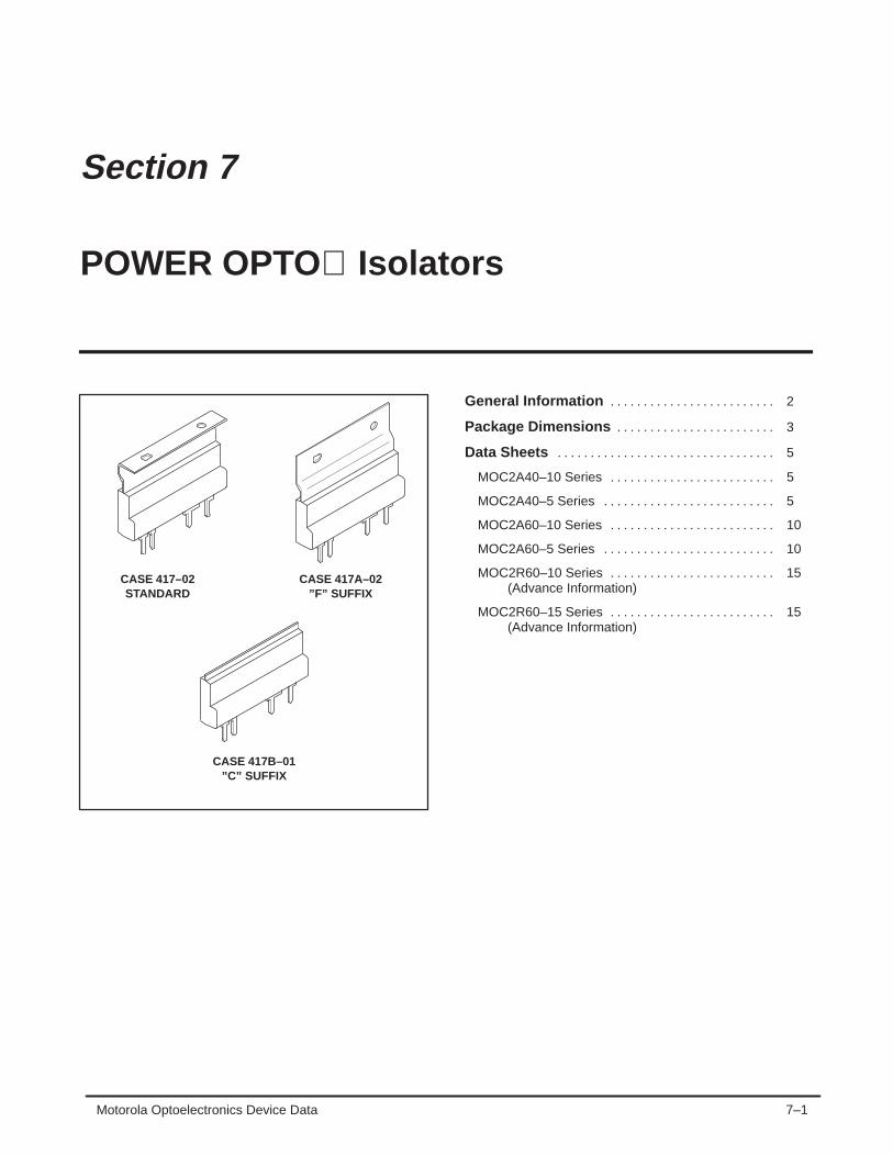
7–1Motorola Optoelectronics Device Data
Section 7
POWER OPTO Isolators
CASE 417–02STANDARD
CASE 417A–02”F” SUFFIX
CASE 417B–01”C” SUFFIX
General Information 2. . . . . . . . . . . . . . . . . . . . . . . . .
Package Dimensions 3. . . . . . . . . . . . . . . . . . . . . . . .
Data Sheets 5. . . . . . . . . . . . . . . . . . . . . . . . . . . . . . . . .
MOC2A40–10 Series 5. . . . . . . . . . . . . . . . . . . . . . . . .
MOC2A40–5 Series 5. . . . . . . . . . . . . . . . . . . . . . . . . .
MOC2A60–10 Series 10. . . . . . . . . . . . . . . . . . . . . . . . .
MOC2A60–5 Series 10. . . . . . . . . . . . . . . . . . . . . . . . . .
MOC2R60–10 Series 15. . . . . . . . . . . . . . . . . . . . . . . . . (Advance Information)
MOC2R60–15 Series 15. . . . . . . . . . . . . . . . . . . . . . . . . (Advance Information)
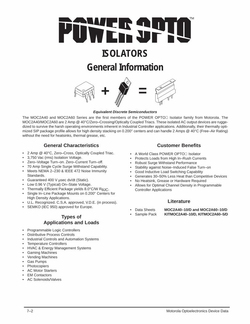
7–2 Motorola Optoelectronics Device Data
=+Equivalent Discrete Semiconductors
ISOLATORSGeneral Information
The MOC2A40 and MOC2A60 Series are the first members of the POWER OPTO Isolator family from Motorola. TheMOC2A40/MOC2A60 are 2 Amp @ 40°C/Zero–Crossing/Optically Coupled Triacs. These isolated AC output devices are rugge-dized to survive the harsh operating environments inherent in Industrial Controller applications. Additionally, their thermally opti-mized SIP package profile allows for high density stacking on 0.200″ centers and can handle 2 Amps @ 40°C (Free–Air Rating)without the need for heatsinks, thermal grease, etc.
General Characteristics• 2 Amp @ 40°C, Zero–Cross, Optically Coupled Triac.• 3,750 Vac (rms) Isolation Voltage.• Zero–Voltage Turn–on. Zero–Current Turn–off.• 70 Amp Single Cycle Surge Withstand Capability.• Meets NEMA 2–230 & IEEE 472 Noise Immunity
Standards.• Guaranteed 400 V µsec dv/dt (Static).• Low 0.96 V (Typical) On–State Voltage.• Thermally Efficient Package yields 8.0°C/W RθJC.• Single In–Line Package Mounts on 0.200″ Centers for
High Density Applications.• U.L. Recognized. C.S.A. approved, V.D.E. (in process).• SEMKO (IEC 950) approved for Europe.
Types ofApplications and Loads
• Programmable Logic Controllers• Distributive Process Controls• Industrial Controls and Automation Systems• Temperature Controllers• HVAC & Energy Management Systems• Gaming Machines• Vending Machines• Gas Pumps• Photocopiers• AC Motor Starters• EM Contactors• AC Solenoids/Valves
Customer Benefits
• A World Class POWER OPTO Isolator• Protects Loads from High In–Rush Currents• Robust Surge Withstand Performance• Stability against Noise–Induced False Turn–on• Good Inductive Load Switching Capability• Generates 30–50% Less Heat than Competitive Devices• No Heatsink, Grease or Hardware Required• Allows for Optimal Channel Density in Programmable
Controller Applications
Literature
• Data Sheets MOC2A40–10/D and MOC2A60–10/D• Sample Pack KITMOC2A40–10/D, KITMOC2A60–5/D

7–3Motorola Optoelectronics Device Data
PACKAGE DIMENSIONS
CASE 417–02PLASTIC
STANDARD HEAT TABISSUE C
NOTES:1. DIMENSIONING AND TOLERANCING PER ANSI
Y14.5M, 1982.2. CONTROLLING DIMENSION: INCH.
STYLE 2:PIN 2. LED CATHODE
3. LED ANODE7. TRIAC MT9. TRIAC MT
2 973
–A–
LV
G
4 PLD
N
K
P
S
–T–SEATINGPLANE
–B–
MAM0.13 (0.005) B MT
H
J
E
C
DIM MIN MAX MIN MAXMILLIMETERSINCHES
A 0.965 1.005 24.51 25.53B 0.416 0.436 10.57 11.07C 0.170 0.190 4.32 4.83D 0.025 0.035 0.64 0.89E 0.040 0.060 1.02 1.52G 0.400 BSC 10.16 BSCH 0.040 0.060 1.02 1.52J 0.012 0.018 0.30 0.46K 0.134 0.154 3.40 3.91L 0.200 BSC 5.08 BSCN 0.190 0.210 4.83 5.33P 0.023 0.043 0.58 1.09S 0.695 0.715 17.65 18.16V 0.100 BSC 2.54 BSC
CASE 417A–02PLASTIC
FLUSH MOUNT HEAT TABISSUE A
NOTES:1. DIMENSIONING AND TOLERANCING PER ANSI
Y14.5M, 1982.2. CONTROLLING DIMENSION: INCH.
STYLE 1:PIN 2. LED CATHODE
3. LED ANODE7. TRIAC MT9. TRIAC MT
2 973
–A–
LV G
4 PLD
N
K
P
S
–T–SEATINGPLANE
–B–
MAM0.13 (0.005) B MT
H
J
E
C
U W
Y Q
R
RADIUSZ
X
DIM MIN MAX MIN MAXMILLIMETERSINCHES
A 0.965 1.005 24.51 25.53B 0.416 0.436 10.57 11.07C 0.170 0.190 4.32 4.83D 0.025 0.035 0.64 0.89E 0.040 0.060 1.02 1.52G 0.400 BSC 10.16 BSCH 0.040 0.060 1.02 1.52J 0.012 0.018 0.30 0.46K 0.134 0.154 3.40 3.91L 0.200 BSC 5.08 BSCN 0.190 0.210 4.83 5.33P 0.023 0.043 0.58 1.09Q 0.057 0.067 1.45 1.70R 0.734 0.754 18.64 19.15S 0.840 0.870 21.34 22.10U 0.593 0.613 15.06 15.57V 0.100 BSC 2.54 BSCW 0.074 0.094 1.88 2.39X 0.265 0.295 6.73 7.49Y 0.079 0.089 2.01 2.26Z 0.026 0.036 0.66 0.91
ORDER “F” SUFFIXHEAT TAB OPTION
(EX: MOC2A60–10F)

7–4 Motorola Optoelectronics Device Data
PACKAGE DIMENSIONS — CONTINUED
CASE 417B–01PLASTIC
CUT HEAT TABISSUE O
DIMA
MIN MAX MIN MAXMILLIMETERS
0.965 1.005 24.51 25.53
INCHES
B 0.416 0.436 10.57 11.07C 0.170 0.190 4.32 4.83D 0.025 0.035 0.64 0.89E 0.040 0.060 1.02 1.52G 0.400 BSC 10.16 BSCH 0.040 0.060 1.02 1.52J 0.012 0.060 0.30 0.46K 0.134 0.154 3.40 3.91L 0.200 BSC 5.08 BSCN 0.190 0.210 4.83 5.33P 0.023 0.043 0.58 1.09S 0.439 0.529 11.15 13.44V 0.100 BSC 2.54 BSC
NOTES:6. DIMENSIONING AND TOLERANCING PER ANSI
Y14.5M, 1982.7. CONTROLLING DIMENSION: INCH.
STYLE 1:PIN 2. LED CATHODE
3. LED ANODE 7. TRIAC MT9. TRIAC MT
B0.13 (0.005) M T A M M
9
K
4 PL
PS
V L
D
H
72 3 N
J
C
E–A–
–B–
–T–SEATING
PLANE
G
ORDER “C” SUFFIXHEAT TAB OPTION
(EX: MOC2A60–10C)

7–5Motorola Optoelectronics Device Data
2 Amp Zero–Cross Triac Output
This device consists of a gallium arsenide infrared emitting diode opticallycoupled to a zero–cross triac driver circuit and a power triac. It is capable of drivinga load of up to 2 amp (rms) directly, on line voltages from 20 to 140 volts ac (rms).
• Provides Normally Open Solid State A.C. Output With 2 Amp Rating
• 60 Amp Single Cycle Surge Capability
• Zero–Voltage Turn–on and Zero–Current Turn–off
• High Input–Output Isolation of 3750 vac (rms)
• Static dv/dt Rating of 400 Volts/µs Guaranteed
• 2 Amp Pilot Duty Rating Per UL508 117 (Overload Test) and 118 (Endurance Test) [File No. 129224]
• CSA Approved [File No. CA77170–1].
• SEMKO Approved Certificate #9507228
• Exceeds NEMA 2–230 and IEEE472 Noise Immunity Test Requirements (See Fig.15)
DEVICE RATINGS (TA = 25°C unless otherwise noted)
Rating Symbol Value Unit
INPUT LED
Forward Current — Maximum Continuous IF 50 mA
Forward Current — Maximum Peak(PW = 100µs, 120 pps)
IF(pk) 1.0 A
Reverse Voltage — Maximum VR 6.0 V
OUTPUT TRIAC
Off–State Output Terminal Voltage — Maximum(1) VDRM 400 Vac(pk)
Recommended Operating Voltage Range (f = 47 – 63 Hz)
VT 20 to 140 Vac(rms)
On–State Current Range (Free Air, Power Factor ≥ 0.3) IT(rms) 0.01 to 2.0 A
Non–Repetitive Peak Overcurrent — Max(f = 60 Hz, t = 1.0 sec)
ITSM1 24 A
Non–Repetitive Single Cycle Surge Current —Maximum Peak (t = 16.7 ms)
ITSM2 70 A
Main Terminal Fusing Current (t = 8.3 ms) I2T 26 A2sec
Load Power Factor Range PF 0.3 to 1.0 —
Junction Temperature Range TJ – 40 to 125 °C
TOTAL DEVICE
Input–Output Isolation Voltage — Maximum(2)
47 – 63 Hz, 1 sec DurationVISO 3750 Vac(rms)
Thermal Resistance — Power Triac Junction to Case (See Fig. 16)
RθJC 8.0 °C/W
Ambient Operating Temperature Range Toper – 40 to +100 °C
Storage Temperature Range Tstg – 40 to +150 °C
Lead Soldering Temperature — Maximum(1/16″ From Case, 10 sec Duration)
— 260 °C
1. Test voltages must be applied within dv/dt rating.2. Input–Output isolation voltage, VISO, is an internal device dielectric breakdown rating. For this2. test, pins 2, 3 and the heat tab are common, and pins 7 and 9 are common.POWER OPTO is a trademark of Motorola, Inc.
Preferred devices are Motorola recommended choices for future use and best overall value.
Order this documentby MOC2A40–10/D
SEMICONDUCTOR TECHNICAL DATA
Motorola, Inc. 1995
*Motorola Preferred Device
OPTOISOLATOR2 AMP ZERO CROSS
TRIAC OUTPUT400 VOLTS
DEVICE SCHEMATIC
CASE 417–02Style 2
PLASTIC PACKAGE
CASE 417A–02Style 1
PLASTIC PACKAGE
CASE 417B–01Style 1
PLASTIC PACKAGE
2 37
9
ZVA*
1, 4, 5, 6, 8. NO PIN2. LED CATHODE3. LED ANODE7. MAIN TERMINAL 29. MAIN TERMINAL 1
* Zero Voltage Activate Circuit
9
7
3
2
REV 2

7–6 Motorola Optoelectronics Device Data
ELECTRICAL CHARACTERISTICS (TA = 25°C unless otherwise noted)
Characteristic Symbol Min Typ Max Unit
INPUT LED
Forward Voltage (IF = 10 mA) VF 1.00 1.17 1.50 V
Reverse Leakage Current (VR = 6.0 V) IR — 1.0 100 µA
Capacitance C — 18 — pF
OUTPUT TRIAC
Off–State Leakage, Either Direction (IF = 0, VDRM = 400 V) IDRM — 0.25 10 µA
Critical Rate of Rise of Off–State Voltage (Static)Vin = 200 vac(pk))(1)(2)
dv/dt(s) 400 — — V/µs
Holding Current, Either Direction (IF = 0, VD = 12 V, IT = 200 mA) IH — 10 — mA
COUPLED
LED Trigger Current Required to Latch Output MOC2A40–10Either Direction (Main Terminal Voltage = 2.0 V)(3)(4) MOC2A40–5
IFT(on)IFT(on)
——
7.03.5
105.0
mAmA
On–State Voltage, Either Direction (IF = Rated IFT(on), ITM = 2.0 A) VTM — 0.96 1.3 V
Inhibit Voltage, Either Direction (IF = Rated IFT(on))(5)
(Main Terminal Voltage above which device will not Trigger)VINH — 8.0 10 V
Commutating dv/dt (Rated VDRM, IT = 30 mA – 2.0 A(rms),TA = – 40 ± 100°C, f = 60 Hz)(2)
dv/dt (c) 5.0 — — V/µS
Common–mode Input–Output dv/dt(2) dv/dt(cm) — 40,000 — V/µS
Input–Output Capacitance (V = 0, f = 1.0 MHz) CISO — 1.3 — pF
Isolation Resistance (VI–O = 500 V) RISO 1012 1014 — Ω
1. Per EIA/NARM standard RS–443, with VP = 200 V, which is the instantaneous peak of the maximum operating voltage.2. Additional dv/dt information, including test methods, can be found in Motorola applications note AN1048/D, Figure 43.3. All devices are guaranteed to trigger at an IF value less than or equal to the max IFT. Therefore, the recommended operating IF lies between3. the device’s maximum IFT(on) limit and the Maximum Rating of 50 mA.4. Current–limiting resistor required in series with LED.5. Also known as “Zero Voltage Turn–On”.
1.40
0.80–40 –20 20 40 80 120
100
80
60
40
20
0
, FO
RWAR
D V
OLT
AGE
(V)
VF
Figure 1. Maximum Allowable Forward LEDCurrent versus Ambient Temperature
, FO
RWAR
D L
ED C
UR
REN
T (m
A)
TA, AMBIENT TEMPERATURE (°C)
Figure 2. LED Forward Voltageversus LED Forward Current
2.00
1.80
1.60
1.00
1
IF, FORWARD CURRENT (mA)
10 100 1000
I F
0 60 100
1.20
TYPICAL CHARACTERISTICS
TA = – 40°C
25°C
100°C
PULSE OR DCPULSE ONLY

7–7Motorola Optoelectronics Device Data
1.20
0.60
2.20
1.40
1.60
0.80
ITM, INSTANTANEOUS ON–STATE CURRENT (A)
0.1 1.0
2.00
1.80
1.00
0.03
PULSE OR DCPULSE ONLY
TJ = 25°C
100°C
V TM
, MAI
N T
ERM
INAL
VO
LTAG
E (V
)
P D, P
OW
ER D
ISSI
PATI
ON
(WAT
TS)
,JU
NC
TIO
N T
EMPE
RAT
UR
E (
C)
°T J
20
TA, AMBIENT TEMPERATURE (°C)
1.2
0.0
2.5
2.0
1.0
0.5
0.0
– 40 0 20 6040 120
1.60
1.50
1.40
1.30
1.20
1.10
0.80
IT, MAIN TERMINAL CURRENT (A)
, TER
MIN
AL C
UR
REN
T (A
)I T
Figure 3. Forward LED Trigger Currentversus Ambient Temperature
, FO
RWAR
D T
RIG
GER
CU
RR
ENT
Figure 4. Maximum Allowable On–State RMS OutputCurrent (Free Air) versus Ambient Temperature
2.4
2.0
1.6
0.8
TA, AMBIENT TEMPERATURE (°C)
Figure 5. On–State Voltage Drop versusOutput Terminal Current
Figure 6. Power Dissipationversus Main Terminal Current
IT, MAIN TERMINAL CURRENT (A)
Figure 7. Junction Temperature versus MainTerminal RMS Current (Free Air)
0.01 0.1 1 10
0.01 0.1 1 10
I IFT
120
100
80
60
40
0
1.00
0.90
– 20 80 100
0.4
– 40 0 20 6040 120– 20 80 100
1.5
WORST CASE UNITNORMALIZED TO
TA = 25°C
TA = 25°C
MAXIMUM
MEAN

7–8 Motorola Optoelectronics Device Data
1000
(V/
S)
µ
40
TA, AMBIENT TEMPERATURE (°C)
I DR
M,L
EAKA
GE
CU
RR
ENT
(NO
RM
ALIZ
ED)
0.01– 40 – 20 0 20 80 120
100
10
1
0.1
Figure 8. Leakage with LED Off versusAmbient Temperature
TA, AMBIENT TEMPERATURE (°C)
Figure 9. Holding Current versusAmbient Temperature
Figure 10. dv/dt versus Ambient Temperature Figure 11. Operating Waveforms
Figure 12. Typical Application Circuit
10
0– 40 – 20 0 20 80 120
60 10040
60 100
LED INPUT
VOLTAGEPIN 7 TO 9
TURN ONPOINTS
VCC
*ZERO VOLTAGE ACTIVATE CIRCUIT
LOAD
MOVR2
C1R1
MOC2A40
ZVA*
Select the value of R1 according to the following formulas:[1] R1 = (VCC – VF) / Max. IFT (on) per spec.[2] R1 = (VCC – VF) / 0.050
Typical values for C1 and R2 are 0.01 µF and 39 Ω, respec-tively. You may adjust these values for specific applications.The maximum recommended value of C1 is 0.022 µF. Seeapplication note AN1048 for additional information on compo-nent values.
The MOV may or may not be needed depending upon thecharacteristics of the applied ac line voltage. For applicationswhere line spikes may exceed the 400 V rating of theMOC2A40, an MOV is required.
100
dv/d
t
NORMALIZED TOTA = 25°C
1.40
0.00
2.00
1.80
1.60
1.20
– 40TA, AMBIENT TEMPERATURE (°C)
– 20 0 + 25 + 40 + 60
1.00
+ 80
0.60
0.80
0.40
0.20
NORMALIZED TO25°C
I H, H
OLD
ING
CU
RR
ENT
(mA)
+ 100
COMMUTATING
STATIC
IT = 30 mA – 2A(RMS)F = 60 Hz

7–9Motorola Optoelectronics Device Data
0.315″ MIN [8 MM MIN]
Thermal measurements of RθJCare referenced to the point onthe heat tab indicated with an‘X’. Measurements should betaken with device orientatedalong its vertical axis.
Use care to maintain the minimum spacings as shown.Safety and regulatory requirements dictate a minimumof 8.0 mm between the closest points between inputand output conducting paths, Pins 3 and 7. Also, 0.070inches distance is required between the two outputPins, 7 and 9.
Keep pad sizes on Pins 7 and 9 as large as possiblefor optimal performance.
0.070″ MIN
Each device, when installed in the circuit shownin Figure 15, shall be capable of passing the fol-lowing conducted noise tests:
• IEEE 472 (2.5 KV)
• Lamp Dimmer (NEMA Part DC33, 3.4.2.1)
• NEMA ICS 2–230.45 Showering Arc
• MIL–STD–461A CS01, CS02 and CS06
JUNCTIONTEMPERATURE OF
MOC2A40 . . .OUTPUT CHIP
WITH ADDITIONAL HEATSINK
RθJC
RθCA
RθSARθCS
RθJC
NO ADDITIONAL HEATSINK
AMBIENT AIRTEMPERATURE
HEAT FLOW
Z LOAD0.022µF
10Ω150VMOV
ACSUPPLY
NOISESOURCE
2
DEVICE UNDER TEST
3 7 9
Terms in the model signify:
TA = Ambient temperatureTS = Optional additionalTS = heat sink temperatureTC = Case temperatureTJ = Junction temperaturePD = Power dissipation
RθSA = Thermal resistance, heat sink to ambientRθCA = Thermal resistance, case to ambientRθCS = Thermal resistance, heat sink to caseRθJC = Thermal resistance, junction to case
Values for thermal resistance components are: RθCA = 36°C/W/in maximumValues for thermal resistance components are: RθJC = 8.0°C/W maximumThe design of any additional heatsink will determine the values of RθSA and RθCS.TC – TA = PD (RθCA)TC – TA = PD (RθJC) + RθSA), where PD = Power Dissipation in Watts.
IF = RATED IF
TJ TC TA
TJ TC TATS
Figure 13. PC Board Layout Recommendations
Figure 14. Test Circuit for Conducted Noise Tests
Figure 15. Approximate Thermal Circuit Model

7–10 Motorola Optoelectronics Device Data
PACKAGE DIMENSIONS
CASE 417–02PLASTIC
STANDARD HEAT TABISSUE C
NOTES:1. DIMENSIONING AND TOLERANCING PER ANSI
Y14.5M, 1982.2. CONTROLLING DIMENSION: INCH.
STYLE 2:PIN 2. LED CATHODE
3. LED ANODE7. TRIAC MT9. TRIAC MT
2 973
–A–
LV
G
4 PLD
N
K
P
S
–T–SEATINGPLANE
–B–
MAM0.13 (0.005) B MT
H
J
E
C
DIM MIN MAX MIN MAXMILLIMETERSINCHES
A 0.965 1.005 24.51 25.53B 0.416 0.436 10.57 11.07C 0.170 0.190 4.32 4.83D 0.025 0.035 0.64 0.89E 0.040 0.060 1.02 1.52G 0.400 BSC 10.16 BSCH 0.040 0.060 1.02 1.52J 0.012 0.018 0.30 0.46K 0.134 0.154 3.40 3.91L 0.200 BSC 5.08 BSCN 0.190 0.210 4.83 5.33P 0.023 0.043 0.58 1.09S 0.695 0.715 17.65 18.16V 0.100 BSC 2.54 BSC
CASE 417A–02PLASTIC
FLUSH MOUNT HEAT TABISSUE A
NOTES:1. DIMENSIONING AND TOLERANCING PER ANSI
Y14.5M, 1982.2. CONTROLLING DIMENSION: INCH.
STYLE 1:PIN 2. LED CATHODE
3. LED ANODE7. TRIAC MT9. TRIAC MT
2 973
–A–
LV G
4 PLD
N
K
P
S
–T–SEATINGPLANE
–B–
MAM0.13 (0.005) B MT
H
J
E
C
U W
Y Q
R
RADIUSZ
X
DIM MIN MAX MIN MAXMILLIMETERSINCHES
A 0.965 1.005 24.51 25.53B 0.416 0.436 10.57 11.07C 0.170 0.190 4.32 4.83D 0.025 0.035 0.64 0.89E 0.040 0.060 1.02 1.52G 0.400 BSC 10.16 BSCH 0.040 0.060 1.02 1.52J 0.012 0.018 0.30 0.46K 0.134 0.154 3.40 3.91L 0.200 BSC 5.08 BSCN 0.190 0.210 4.83 5.33P 0.023 0.043 0.58 1.09Q 0.057 0.067 1.45 1.70R 0.734 0.754 18.64 19.15S 0.840 0.870 21.34 22.10U 0.593 0.613 15.06 15.57V 0.100 BSC 2.54 BSCW 0.074 0.094 1.88 2.39X 0.265 0.295 6.73 7.49Y 0.079 0.089 2.01 2.26Z 0.026 0.036 0.66 0.91
ORDER “F” SUFFIXHEAT TAB OPTION
(EX: MOC2A60–10F)

7–11Motorola Optoelectronics Device Data
PACKAGE DIMENSIONS — CONTINUED
CASE 417B–01PLASTIC
CUT HEAT TABISSUE O
DIMA
MIN MAX MIN MAXMILLIMETERS
0.965 1.005 24.51 25.53
INCHES
B 0.416 0.436 10.57 11.07C 0.170 0.190 4.32 4.83D 0.025 0.035 0.64 0.89E 0.040 0.060 1.02 1.52G 0.400 BSC 10.16 BSCH 0.040 0.060 1.02 1.52J 0.012 0.060 0.30 0.46K 0.134 0.154 3.40 3.91L 0.200 BSC 5.08 BSCN 0.190 0.210 4.83 5.33P 0.023 0.043 0.58 1.09S 0.439 0.529 11.15 13.44V 0.100 BSC 2.54 BSC
NOTES:8. DIMENSIONING AND TOLERANCING PER ANSI
Y14.5M, 1982.9. CONTROLLING DIMENSION: INCH.
STYLE 1:PIN 2. LED CATHODE
3. LED ANODE 7. TRIAC MT9. TRIAC MT
B0.13 (0.005) M T A M M
9
K
4 PL
PS
V L
D
H
72 3 N
J
C
E–A–
–B–
–T–SEATING
PLANE
G
ORDER “C” SUFFIXHEAT TAB OPTION
(EX: MOC2A60–10C)

7–12 Motorola Optoelectronics Device Data
Motorola reserves the right to make changes without further notice to any products herein. Motorola makes no warranty, representation or guarantee regardingthe suitability of its products for any particular purpose, nor does Motorola assume any liability arising out of the application or use of any product or circuit,and specifically disclaims any and all liability, including without limitation consequential or incidental damages. “Typical” parameters can and do vary in differentapplications. All operating parameters, including “Typicals” must be validated for each customer application by customer’s technical experts. Motorola doesnot convey any license under its patent rights nor the rights of others. Motorola products are not designed, intended, or authorized for use as components insystems intended for surgical implant into the body, or other applications intended to support or sustain life, or for any other application in which the failure ofthe Motorola product could create a situation where personal injury or death may occur. Should Buyer purchase or use Motorola products for any suchunintended or unauthorized application, Buyer shall indemnify and hold Motorola and its officers, employees, subsidiaries, affiliates, and distributors harmlessagainst all claims, costs, damages, and expenses, and reasonable attorney fees arising out of, directly or indirectly, any claim of personal injury or deathassociated with such unintended or unauthorized use, even if such claim alleges that Motorola was negligent regarding the design or manufacture of the part.Motorola and are registered trademarks of Motorola, Inc. Motorola, Inc. is an Equal Opportunity/Affirmative Action Employer.
How to reach us:USA / EUROPE: Motorola Literature Distribution; JAPAN : Nippon Motorola Ltd.; Tatsumi–SPD–JLDC, Toshikatsu Otsuki,P.O. Box 20912; Phoenix, Arizona 85036. 1–800–441–2447 6F Seibu–Butsuryu–Center, 3–14–2 Tatsumi Koto–Ku, Tokyo 135, Japan. 03–3521–8315
MFAX: [email protected] – TOUCHTONE (602) 244–6609 HONG KONG: Motorola Semiconductors H.K. Ltd.; 8B Tai Ping Industrial Park, INTERNET: http://Design–NET.com 51 Ting Kok Road, Tai Po, N.T., Hong Kong. 852–26629298
MOC2A40–10/D
◊ CODELINE TO BE PLACED HERE

7–13Motorola Optoelectronics Device Data
2 Amp Zero–Cross Triac Output
This device consists of a gallium arsenide infrared emitting diode opticallycoupled to a zero–cross triac driver circuit and a power triac. It is capable ofdriving a load of up to 2 amps (rms) directly, on line voltages from 20 to 280 voltsac (rms).
• Provides Normally Open Solid State AC Output with 2 Amp Rating
• 70 Amp Single Cycle Surge Capability
• Zero–Voltage Turn–on and Zero–Current Turn–off
• High Input–Output Isolation of 3750 vac (rms)
• Static dv/dt Rating of 400 Volts/µs Guaranteed
• 2 Amp Pilot Duty Rating Per UL508 117 (Overload Test) and 118 (Endurance Test) [File No. 129224]
• CSA Approved [File No. CA77170–1].
• SEMKO Approved Certificate #9507228
• Exceeds NEMA 2–230 and IEEE472 Noise Immunity Test Requirements (See Fig.14)
DEVICE RATINGS (TA = 25°C unless otherwise noted)
Rating Symbol Value Unit
INPUT LED
Forward Current — Maximum Continuous IF 50 mA
Forward Current — Maximum Peak(PW = 100µs, 120 pps)
IF(pk) 1.0 A
Reverse Voltage — Maximum VR 6.0 V
OUTPUT TRIAC
Output Terminal Voltage — Maximum Transient (1) VDRM 600 V(pk)
Operating Voltage Range — Maximum Continuous(f = 47 – 63 Hz)
VT 20 to 280 Vac(rms)
On–State Current Range(Free Air, Power Factor ≥ 0.3)
IT(rms) 0.03 to 2.0 A
Non–Repetitive Single Cycle Surge Current —Maximum Peak (t = 16.7 ms)
ITSM 70 A
Main Terminal Fusing Current (t = 8.3 ms) I2T 26 A2sec
Load Power Factor Range PF 0.3 to 1.0 —
Junction Temperature Range TJ – 40 to 125 °C
TOTAL DEVICE
Input–Output Isolation Voltage — Maximum(2)
47 – 63 Hz, 1 sec DurationVISO 3750 Vac(rms)
Thermal Resistance — Power Triac Junction to Case (See Fig. 15)
RθJC 8.0 °C/W
Ambient Operating Temperature Range Toper – 40 to +100 °C
Storage Temperature Range Tstg – 40 to +150 °C
Lead Soldering Temperature — Maximum(1/16″ from Case, 10 sec Duration)
TL 260 °C
1. Test voltages must be applied within dv/dt rating.2. Input–Output isolation voltage, VISO, is an internal device dielectric breakdown rating. For this2. test, pins 2, 3 and the heat tab are common, and pins 7 and 9 are common.
POWER OPTO is a trademark of Motorola, Inc.
Preferred devices are Motorola recommended choices for future use and best overall value.
Order this documentby MOC2A60–10/D
SEMICONDUCTOR TECHNICAL DATA
Motorola, Inc. 1995
*Motorola Preferred Device
OPTOISOLATOR2 AMP ZERO CROSS
TRIAC OUTPUT600 VOLTS
DEVICE SCHEMATIC
CASE 417–02Style 2
PLASTIC PACKAGE
CASE 417A–02Style 1
PLASTIC PACKAGE
CASE 417B–01Style 1
PLASTIC PACKAGE
2 37
9
* Zero Voltage Activate Circuit
1, 4, 5, 6, 8. NO PIN2. LED CATHODE3. LED ANODE7. MAIN TERMINAL 29. MAIN TERMINAL 1
ZVA*
7
9
3
2
REV 2

7–14 Motorola Optoelectronics Device Data
ELECTRICAL CHARACTERISTICS (TA = 25°C unless otherwise noted)
Characteristic Symbol Min Typ Max Unit
INPUT LED
Forward Voltage (IF = 10 mA) VF 1.00 1.17 1.50 V
Reverse Leakage Current (VR = 6.0 V) IR — 1.0 100 µA
Capacitance C — 18 — pF
OUTPUT TRIAC
Off–State Leakage, Either Direction(IF = 0, VDRM = 600 V)
IDRM — 0.25 10 µA
Critical Rate of Rise of Off–State Voltage (Static)Vin = 400 vac(pk)) (1)(2)
dv/dt(s) 400 — — V/µs
Holding Current, Either Direction (IF = 0, VD = 12 V, IT = 200 mA) IH — 10 — mA
COUPLED
LED Trigger Current Required to Latch Output MOC2A60–10Either Direction (Main Terminal Voltage = 2.0 V)(3)(4) MOC2A60–5
IFT(on)IFT(on)
——
7.03.5
105.0
mAmA
On–State Voltage, Either Direction (IF = Rated IFT(on), ITM = 2.0 A) VTM — 0.96 1.3 V
Inhibit Voltage, Either Direction (IF = Rated IFT(on))(5)
(Main Terminal Voltage above which device will not trigger)VINH — 8.0 10 V
Commutating dv/dt (Rated VDRM, IT = 30 mA – 2.0 A(rms),TA = – 40 ± 100°C, f = 60 Hz)(2)
dv/dt (c) 5.0 — — V/µS
Common–mode Input–Output dv/dt(2) dv/dt(cm) — 40,000 — V/µS
Input–Output Capacitance (V = 0, f = 1.0 MHz) CISO — 1.3 — pF
Isolation Resistance (VI–O = 500 V) RISO 1012 1014 — Ω
1. Per EIA/NARM standard RS–443, with VP = 200 V, which is the instantaneous peak of the maximum operating voltage.2. Additional dv/dt information, including test methods, can be found in Motorola applications note AN1048/D, Figure 43.3. All devices are guaranteed to trigger at an IF value less than or equal to the max IFT. Therefore, the recommended operating IF lies between3. the device’s maximum IFT(on) limit and the Maximum Rating of 50 mA.4. Current–limiting resistor required in series with LED.5. Also known as “Zero Voltage Turn–On.”
1.40
0.80–40 –20 20 40 80 120
100
80
60
40
20
0
, FO
RWAR
D V
OLT
AGE
(V)
VF
Figure 1. Maximum Allowable Forward LEDCurrent versus Ambient Temperature
, FO
RWAR
D L
ED C
UR
REN
T (m
A)
TA, AMBIENT TEMPERATURE (°C)
Figure 2. LED Forward Voltageversus LED Forward Current
2.00
1.80
1.60
1.00
1
IF, FORWARD CURRENT (mA)
10 100 1000
I F
0 60 100
1.20
TYPICAL CHARACTERISTICS
TA = – 40°C
25°C
100°C
PULSE OR DCPULSE ONLY

7–15Motorola Optoelectronics Device Data
TA, AMBIENT TEMPERATURE (°C)
1.2
0.0–40 0 20 6040 120
1.60
1.50
1.40
1.30
1.20
1.10
0.80
, TER
MIN
AL C
UR
REN
T (A
)I T
Figure 3. Forward LED Trigger Currentversus Ambient Temperature
, FO
RWAR
D T
RIG
GER
CU
RR
ENT
Figure 4. Maximum Allowable On–State RMS OutputCurrent (Free Air) versus Ambient Temperature
2.4
2.0
1.6
0.8
TA, AMBIENT TEMPERATURE (°C)
10
I IFT
1.00
0.90
–20 80 100
0.4
–40 0 20 6040 120–20 80 100
1.20
0.60
2.20
1.40
1.60
0.80
ITM, INSTANTANEOUS ON–STATE CURRENT (A)
0.1 1.0
2.00
1.80
1.00
0.03
Figure 5. On–State Voltage Drop versusOutput Terminal Current
V TM
, MAI
N T
ERM
INAL
VO
LTAG
E (V
)
2.5
2.0
1.0
0.5
0.0
Figure 6. Power Dissipationversus Main Terminal Current
IT, MAIN TERMINAL CURRENT (A)0.01 0.1 1.0
1.5
PD, P
OW
ER D
ISSI
PATI
ON
(WAT
TS)
20
IT, MAIN TERMINAL CURRENT (A)
Figure 7. Junction Temperature versus MainTerminal RMS Current (Free Air)
0.01 0.1 1
120
100
80
60
40
0
T J, J
UN
CTI
ON
TEM
PER
ATU
RE
(C
)°
0.01– 40 – 20 0 20 80 120
100
10
1.0
0.1
Figure 8. Leakage with LED Off versusAmbient Temperature
TA, AMBIENT TEMPERATURE (°C)60 10040
I DR
M, L
EAKA
GE
CU
RR
ENT
(NO
RM
ALIZ
ED)
10
WORST CASE UNITNORMALIZED TO
TA = 25°C
PULSE OR DCPULSE ONLY
TJ = 25°C
100°C
MAXIMUM
MEAN
TA = 25°C
NORMALIZED TOTA = 25°C

7–16 Motorola Optoelectronics Device Data
VCC
*ZERO VOLTAGE ACTIVATE CIRCUIT
LOAD
MOVR2
C1R1
MOC2A60
ZVA*
Select the value of R1 according to the following formulas:[1] R1 = (VCC – VF) / Max. IFT (on) per spec.[2] R1 = (VCC – VF) / 0.050
Typical values for C1 and R2 are 0.01 µF and 39 Ω, respec-tively. You may adjust these values for specific applications.The maximum recommended value of C1 is 0.022 µF. Seeapplication note AN1048 for additional information on com-ponent values.
The MOV may or may not be needed depending upon thecharacteristics of the applied ac line voltage. For applica-tions where line spikes may exceed the 600 V rating of theMOC2A60, an MOV is required.
1.40
0.00
2.00
1.80
1.60
1.20
– 40TA, AMBIENT TEMPERATURE (°C)
– 20 0 + 25 + 40 + 60
1.00
+ 80
0.60
0.80
0.40
0.20
Figure 9. Holding Current versusAmbient Temperature
I H, H
OLD
ING
CU
RR
ENT
(mA)
1000
(V/
S)
dvdt
µ
40
TA, AMBIENT TEMPERATURE (°C)
Figure 10. dv/dt versus Ambient Temperature
10
0– 40 – 20 0 20 80 12060 100
100
/
Figure 11. Operating Waveforms
LED INPUT
VOLTAGEPIN 7 TO 9
TURN ONPOINTS
Figure 12. Typical Application Circuit
+ 100
NORMALIZED TOTA = 25°C
COMMUTATING
STATIC
IT = 30 mA – 2A(RMS)F = 60 Hz

7–17Motorola Optoelectronics Device Data
0.315″ MIN [8 MM MIN]
Thermal measurements of RθJCare referenced to the point onthe heat tab indicated with an‘X’. Measurements should betaken with device orientatedalong its vertical axis.
Use care to maintain the minimum spacings as shown.Safety and regulatory requirements dictate a minimumof 8.0 mm between the closest points between inputand output conducting paths, Pins 3 and 7. Also, 0.070inches distance is required between the two outputPins, 7 and 9.
Keep pad sizes on Pins 7 and 9 as large as possiblefor optimal performance.
0.070″ MIN
Each device, when installed in the circuit shownin Figure 14, shall be capable of passing the fol-lowing conducted noise tests:
• IEEE 472 (2.5 KV)
• Lamp Dimmer (NEMA Part DC33, 3.4.2.1)
• NEMA ICS 2–230.45 Showering Arc
• MIL–STD–461A CS01, CS02 and CS06
JUNCTIONTEMPERATURE OF
MOC2A60 . . .OUTPUT CHIP
WITH ADDITIONAL HEATSINK
RθJC
RθCA
RθSARθCS
RθJC
NO ADDITIONAL HEATSINK
AMBIENT AIRTEMPERATURE
HEAT FLOW
Z LOAD0.022µF
10Ω150VMOV
ACSUPPLY
NOISESOURCE
2
DEVICE UNDER TEST
3 7 9
Terms in the model signify:
TA = Ambient temperatureTS = Optional additionalTS = heat sink temperatureTC = Case temperatureTJ = Junction temperaturePD = Power dissipation
RθSA = Thermal resistance, heat sink to ambientRθCA = Thermal resistance, case to ambientRθCS = Thermal resistance, heat sink to caseRθJC = Thermal resistance, junction to case
Values for thermal resistance components are: RθCA = 36°C/W/in maximumValues for thermal resistance components are: RθJC = 8.0°C/W maximumThe design of any additional heatsink will determine the values of RθSA and RθCS.TC – TA = PD (RθCA)TC – TA = PD (RθJC) + RθSA), where PD = Power Dissipation in Watts.
IF = RATED IF
TJ TC TA
TJ TC TATS
Figure 13. PC Board Layout Recommendations
Figure 14. Test Circuit for Conducted Noise Tests
Figure 15. Approximate Thermal Circuit Model

7–18 Motorola Optoelectronics Device Data
PACKAGE DIMENSIONS
CASE 417–02PLASTIC
STANDARD HEAT TABISSUE C
NOTES:1. DIMENSIONING AND TOLERANCING PER ANSI
Y14.5M, 1982.2. CONTROLLING DIMENSION: INCH.
STYLE 2:PIN 2. LED CATHODE
3. LED ANODE7. TRIAC MT9. TRIAC MT
2 973
–A–
LV
G
4 PLD
N
K
P
S
–T–SEATINGPLANE
–B–
MAM0.13 (0.005) B MT
H
J
E
C
DIM MIN MAX MIN MAXMILLIMETERSINCHES
A 0.965 1.005 24.51 25.53B 0.416 0.436 10.57 11.07C 0.170 0.190 4.32 4.83D 0.025 0.035 0.64 0.89E 0.040 0.060 1.02 1.52G 0.400 BSC 10.16 BSCH 0.040 0.060 1.02 1.52J 0.012 0.018 0.30 0.46K 0.134 0.154 3.40 3.91L 0.200 BSC 5.08 BSCN 0.190 0.210 4.83 5.33P 0.023 0.043 0.58 1.09S 0.695 0.715 17.65 18.16V 0.100 BSC 2.54 BSC
CASE 417A–02PLASTIC
FLUSH MOUNT HEAT TABISSUE A
NOTES:1. DIMENSIONING AND TOLERANCING PER ANSI
Y14.5M, 1982.2. CONTROLLING DIMENSION: INCH.
STYLE 1:PIN 2. LED CATHODE
3. LED ANODE7. TRIAC MT9. TRIAC MT
2 973
–A–
LV G
4 PLD
N
K
P
S
–T–SEATINGPLANE
–B–
MAM0.13 (0.005) B MT
H
J
E
C
U W
Y Q
R
RADIUSZ
X
DIM MIN MAX MIN MAXMILLIMETERSINCHES
A 0.965 1.005 24.51 25.53B 0.416 0.436 10.57 11.07C 0.170 0.190 4.32 4.83D 0.025 0.035 0.64 0.89E 0.040 0.060 1.02 1.52G 0.400 BSC 10.16 BSCH 0.040 0.060 1.02 1.52J 0.012 0.018 0.30 0.46K 0.134 0.154 3.40 3.91L 0.200 BSC 5.08 BSCN 0.190 0.210 4.83 5.33P 0.023 0.043 0.58 1.09Q 0.057 0.067 1.45 1.70R 0.734 0.754 18.64 19.15S 0.840 0.870 21.34 22.10U 0.593 0.613 15.06 15.57V 0.100 BSC 2.54 BSCW 0.074 0.094 1.88 2.39X 0.265 0.295 6.73 7.49Y 0.079 0.089 2.01 2.26Z 0.026 0.036 0.66 0.91
ORDER “F” SUFFIXHEAT TAB OPTION
(EX: MOC2A60–10F)
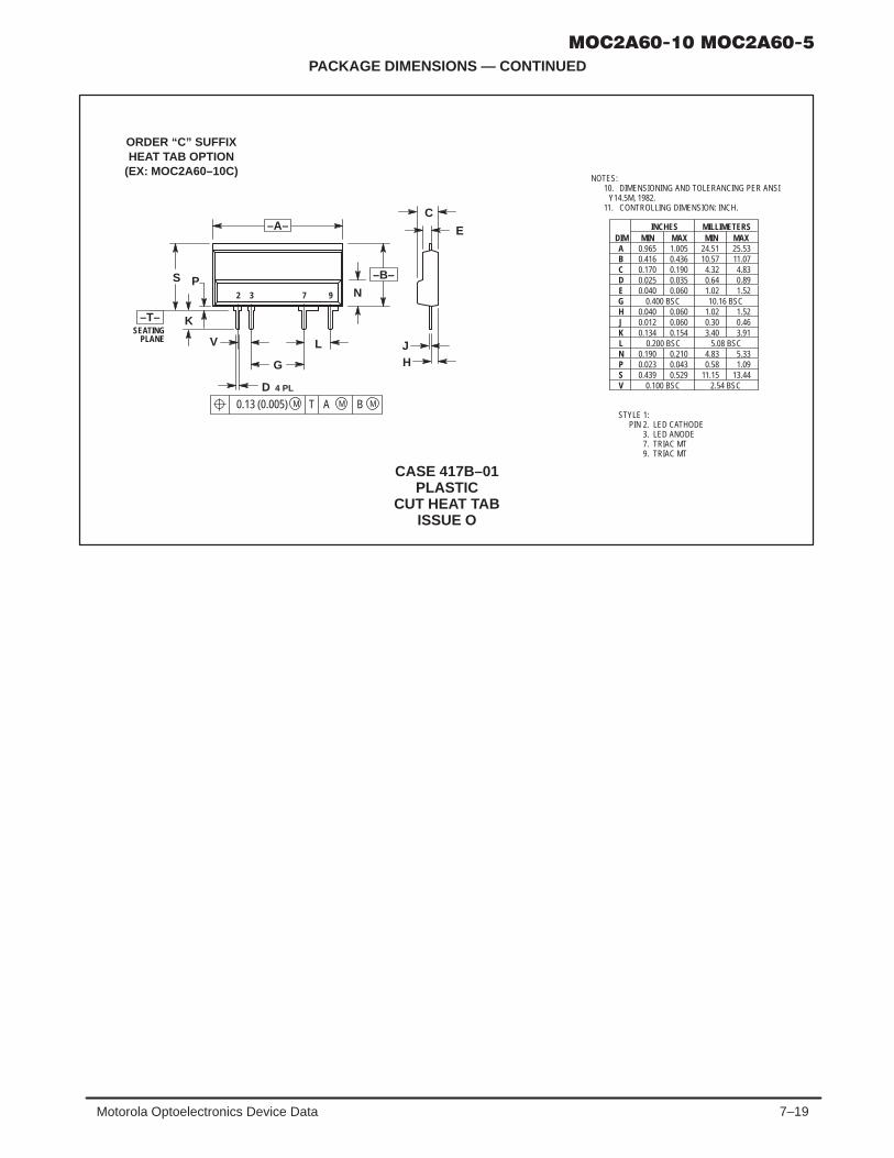
7–19Motorola Optoelectronics Device Data
PACKAGE DIMENSIONS — CONTINUED
CASE 417B–01PLASTIC
CUT HEAT TABISSUE O
DIMA
MIN MAX MIN MAXMILLIMETERS
0.965 1.005 24.51 25.53
INCHES
B 0.416 0.436 10.57 11.07C 0.170 0.190 4.32 4.83D 0.025 0.035 0.64 0.89E 0.040 0.060 1.02 1.52G 0.400 BSC 10.16 BSCH 0.040 0.060 1.02 1.52J 0.012 0.060 0.30 0.46K 0.134 0.154 3.40 3.91L 0.200 BSC 5.08 BSCN 0.190 0.210 4.83 5.33P 0.023 0.043 0.58 1.09S 0.439 0.529 11.15 13.44V 0.100 BSC 2.54 BSC
NOTES:10. DIMENSIONING AND TOLERANCING PER ANSI
Y14.5M, 1982.11. CONTROLLING DIMENSION: INCH.
STYLE 1:PIN 2. LED CATHODE
3. LED ANODE 7. TRIAC MT9. TRIAC MT
B0.13 (0.005) M T A M M
9
K
4 PL
PS
V L
D
H
72 3 N
J
C
E–A–
–B–
–T–SEATING
PLANE
G
ORDER “C” SUFFIXHEAT TAB OPTION
(EX: MOC2A60–10C)

7–20 Motorola Optoelectronics Device Data
Motorola reserves the right to make changes without further notice to any products herein. Motorola makes no warranty, representation or guarantee regardingthe suitability of its products for any particular purpose, nor does Motorola assume any liability arising out of the application or use of any product or circuit,and specifically disclaims any and all liability, including without limitation consequential or incidental damages. “Typical” parameters can and do vary in differentapplications. All operating parameters, including “Typicals” must be validated for each customer application by customer’s technical experts. Motorola doesnot convey any license under its patent rights nor the rights of others. Motorola products are not designed, intended, or authorized for use as components insystems intended for surgical implant into the body, or other applications intended to support or sustain life, or for any other application in which the failure ofthe Motorola product could create a situation where personal injury or death may occur. Should Buyer purchase or use Motorola products for any suchunintended or unauthorized application, Buyer shall indemnify and hold Motorola and its officers, employees, subsidiaries, affiliates, and distributors harmlessagainst all claims, costs, damages, and expenses, and reasonable attorney fees arising out of, directly or indirectly, any claim of personal injury or deathassociated with such unintended or unauthorized use, even if such claim alleges that Motorola was negligent regarding the design or manufacture of the part.Motorola and are registered trademarks of Motorola, Inc. Motorola, Inc. is an Equal Opportunity/Affirmative Action Employer.
How to reach us:USA / EUROPE: Motorola Literature Distribution; JAPAN : Nippon Motorola Ltd.; Tatsumi–SPD–JLDC, Toshikatsu Otsuki,P.O. Box 20912; Phoenix, Arizona 85036. 1–800–441–2447 6F Seibu–Butsuryu–Center, 3–14–2 Tatsumi Koto–Ku, Tokyo 135, Japan. 03–3521–8315
MFAX: [email protected] – TOUCHTONE (602) 244–6609 HONG KONG: Motorola Semiconductors H.K. Ltd.; 8B Tai Ping Industrial Park, INTERNET: http://Design–NET.com 51 Ting Kok Road, Tai Po, N.T., Hong Kong. 852–26629298
MOC2A60–10/D
◊

7–21Motorola Optoelectronics Device Data
! # "!"!
This device consists of a gallium arsenide infrared emitting diode optically coupledto a random phase triac driver circuit and a power triac. It is capable of driving a loadof up to 2 amps (rms) directly, on line voltages from 20 to 280 volts AC (rms).
• Provides Normally Open Solid State AC Output with 2 Amp Rating
• 70 Amp Single Cycle Surge Capability
• Phase Controllable
• High Input-Output Isolation of 3750 vac (rms)
• Static dv/dt Rating of 400 Volts/µs Guaranteed
• 2 Amp Pilot Duty Rating Per UL508 117 (Overload Test) and 118 (Endurance Test) [File No. 129224]
• CSA Approved [File No. CA77170-1]. VDE Approval in Process.
• Exceeds NEMA 2-230 and IEEE472 Noise Immunity Test Requirements(See Figure 17)
DEVICE RATINGS (TA = 25°C unless otherwise noted)
Rating Symbol Value Unit
INPUT LED
Forward Current — Maximum Continuous IF 50 mA
Forward Current — Maximum Peak(PW = 100µs, 120 pps)
IF(pk) 1.0 A
Reverse Voltage — Maximum VR 6.0 V
OUTPUT TRIAC
Output Terminal Voltage — Maximum Transient (1) VDRM 600 V(pk)
Operating Voltage Range — Maximum Continuous(f = 47–63 Hz)
VT 20 to 280 Vac(rms)
On-State Current Range(Free Air, Power Factor ≥ 0.3)
IT(rms) 0.03 to 2.0 A
Non-Repetitive Single Cycle Surge Current —Maximum Peak (t = 16.7 ms)
ITSM 70 A
Main Terminal Fusing Current (t = 8.3 ms) I2T 26 A2sec
Load Power Factor Range PF 0.3 to 1.0 —
Junction Temperature Range TJ – 40 to 125 °C
TOTAL DEVICE
Input-Output Isolation Voltage — Maximum (2)47–63 Hz, 1 sec Duration
VISO 3750 Vac(rms)
Thermal Resistance — Power Triac Junction toCase (See Figure 18)
RθJC 8.0 °C/W
Ambient Operating Temperature Range Toper – 40 to +100 °C
Storage Temperature Range Tstg – 40 to +150 °C
Lead Soldering Temperature — Maximum(1/16″ From Case, 10 sec Duration)
TL 260 °C
1. Test voltages must be applied within dv/dt rating.2. Input-Output isolation voltage, VISO, is an internal device dielectric breakdown rating. (2)For this test, pins 2, 3 and the heat tab are common, and pins 7 and 9 are common.POWER OPTO is a trademark of Motorola, Inc.This document contains information on a new product. Specifications and information herein are subject to change without notice.Preferred devices are Motorola recommended choices for future use and best overall value.
Order this documentby MOC2R60–10/D
SEMICONDUCTOR TECHNICAL DATA
DEVICE SCHEMATIC
OPTOISOLATOR2 AMPS
RANDOM–PHASETRIAC OUTPUT
600 VOLTS
1, 4, 5, 6, 8. NO PIN2. LED CATHODE3. LED ANODE7. MAIN TERMINAL 29. MAIN TERMINAL 1
7
9
3
2
CASE 417-02Style 2
PLASTIC PACKAGE
CASE 417A-02Style 1
PLASTIC PACKAGE
CASE 417B-01Style 1
PLASTIC PACKAGE
2 37
9
*Motorola Preferred Devices
Motorola, Inc. 1995
REV 1

7–22 Motorola Optoelectronics Device Data
ELECTRICAL CHARACTERISTICS (TA = 25°C unless otherwise noted)
Characteristic Symbol Min Typ Max Unit
INPUT LED
Forward Voltage (IF = 10 mA) VF 1.00 1.17 1.50 V
Reverse Leakage Current (VR = 6.0 V) IR — 1.0 100 µA
Capacitance C — 18 — pF
OUTPUT TRIAC
Off-State Leakage, Either Direction(IF = 0, VDRM = 400 V)
IDRM(1) — 0.25 100 µA
Critical Rate of Rise of Off-State Voltage (Static)(Vin = 400 vac(pk)) (1) (2)
dv/dt(s) 400 — — V/µs
Holding Current, Either Direction (IF = 0, VD = 12 V, IT = 200 mA) IH — 10 — mA
COUPLED
LED Trigger Current Required to Latch Output MOC2R60-10Either Direction (Main Terminal Voltage = 2.0 V) (3) (4) MOC2R60-15
IFT(on) — 7.012
1015
mA
On-State Voltage, Either Direction (IF = Rated IFT(on), ITM = 2.0 A) VTM — 0.96 1.3 V
Commutating dv/dt (Rated VDRM, IT = 30 mA – 2.0 A(rms),TA = – 40 + 100°C, f = 60 Hz) (2)
dv/dt (c) 5.0 — — V/µS
Common-mode Input-Output dv/dt (2) dv/dt(cm) — 40,000 — V/µS
Input-Output Capacitance (V = 0, f = 1.0 MHz) CISO — 1.3 — pF
Isolation Resistance (VI-O = 500 V) RISO 1012 1014 — Ω
1. Per EIA/NARM standard RS–443, with VP = 200 V, which is the instantaneous peak of the maximum operating voltage.2. Additional dv/dt information, including test methods, can be found in Motorola applications note AN1048/D.3. All devices are guaranteed to trigger at an IF value less than or equal to the max IFT. Therefore, the recommended operating IF lies between3. the device’s maximum IFT(on) limit and the Maximum Rating of 50 mA.4. Current–limiting resistor required in series with LED.
1.40
0.80– 40 – 20 20 40 80 120
100
80
60
40
20
0
Figure 1. Maximum Allowable Forward LEDCurrent versus Ambient Temperature
TA, AMBIENT TEMPERATURE (°C)
Figure 2. LED Forward Voltageversus LED Forward Current
2.00
1.80
1.60
1.00
1
IF, FORWARD CURRENT (mA)
10 100 10000 60 100
1.20
TYPICAL CHARACTERISTICS
I F, F
ORW
ARD
LED
CU
RR
ENT
(mA)
V , F
FORW
ARD
VO
LTAG
E (V
)
25°C
100°C
Pulse OnlyPulse or DC
TA = – 40°C
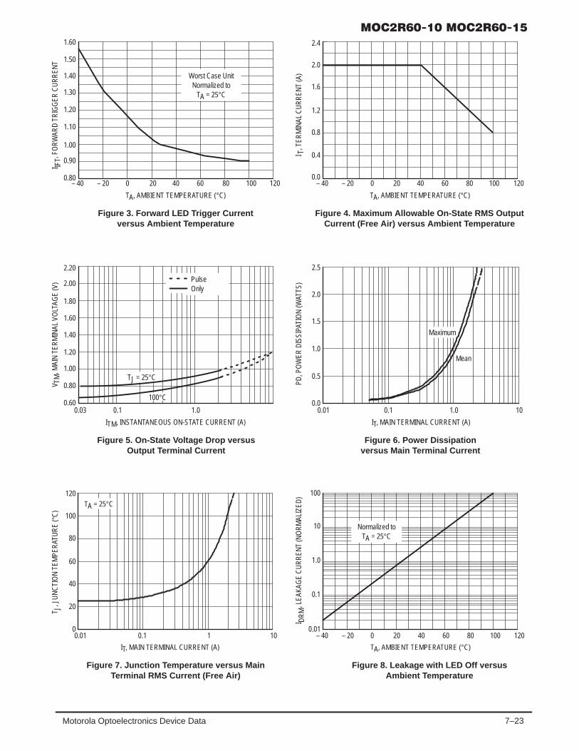
7–23Motorola Optoelectronics Device Data
1.20
0.60
2.20
1.40
1.60
0.80
ITM, INSTANTANEOUS ON-STATE CURRENT (A)
0.1 1.0
2.00
1.80
1.00
0.03
Pulse or DCPulseOnly
TJ = 25°C
0.01– 40 – 20 0 20 80 120
100
10
1.0
0.1
Figure 3. Forward LED Trigger Currentversus Ambient Temperature
TA, AMBIENT TEMPERATURE (°C)
60 10040
20
IT, MAIN TERMINAL CURRENT (A)
Figure 4. Maximum Allowable On-State RMS OutputCurrent (Free Air) versus Ambient Temperature
0.01 0.1 1 10
120
100
80
60
40
0
2.5
2.0
1.0
0.5
0.0
Figure 5. On-State Voltage Drop versusOutput Terminal Current
IT, MAIN TERMINAL CURRENT (A)
0.01 0.1 1.0 10
1.5
Figure 6. Power Dissipationversus Main Terminal Current
TA, AMBIENT TEMPERATURE (°C)
1.2
0.0– 40 0 20 6040 120
1.60
1.50
1.40
1.30
1.20
1.10
0.80
Figure 7. Junction Temperature versus MainTerminal RMS Current (Free Air)
Figure 8. Leakage with LED Off versusAmbient Temperature
2.4
2.0
1.6
0.8
TA, AMBIENT TEMPERATURE (°C)
1.00
0.90
– 20 80 100
0.4
– 40 0 20 6040 120– 20 80 100
Mean
Maximum
I IFT, F
ORW
ARD
TR
IGG
ER C
UR
REN
T
I T, T
ERM
INAL
CU
RR
ENT
(A)
V TM
, MAI
N T
ERM
INAL
VO
LTAG
E (V
)
PD, P
OW
ER D
ISSI
PATI
ON
(WAT
TS)
T J, J
UN
CTI
ON
TEM
PER
ATU
RE
(C
)°
I DR
M, L
EAKA
GE
CU
RR
ENT
(NO
RM
ALIZ
ED)
100°C
Normalized toTA = 25°C
Worst Case UnitNormalized to
TA = 25°C
TA = 25°C

7–24 Motorola Optoelectronics Device Data
1.40
0.00
2.00
1.80
1.60
1.20
– 40
TA, AMBIENT TEMPERATURE (°C)
– 20 0 + 25 + 40 + 60
1.00
+ 80
0.60
0.80
0.40
0.20
Figure 9. Holding Current versusAmbient Temperature
1000
(V/
S)
dvdt
µ
40
TA, AMBIENT TEMPERATURE (°C)
Figure 10. dv/dt versus Ambient Temperature
10
0– 40 – 20 0 20 80 12060 100
100
/
+ 100
I H, H
OLD
ING
CU
RR
ENT
(mA)
Static
Normalizedat 25°C
Commutating
IT = 30 mA – 2A(RMS)F = 60 Hz
Phase Control Considerations
LED Trigger Current versus PW (normalized)
The Random Phase POWER OPTO Isolators are designedto be phase controllable. They may be triggered at any phaseangle within the AC sine wave. Phase control may be accom-plished by an AC line zero cross detector and a variable pulsedelay generator which is synchronized to the zero cross de-tector. The same task can be accomplished by a microproces-sor which is synchronized to the AC zero crossing. The phasecontrolled trigger current may be a very short pulse whichsaves energy delivered to the input LED. LED trigger pulsecurrents shorter than 100 µs must have an increased ampli-tude as shown on Figure 11. This graph shows the dependen-cy of the trigger current IFT versus the pulse width t (PW). Thereason for the IFT dependency on the pulse width can be seenon the chart delay t(d) versus the LED trigger current.
IFT in the graph IFT versus (PW) is normalized in respect tothe minimum specified IFT for static condition, which is speci-fied in the device characteristic. The normalized IFT has to bemultiplied with the devices guaranteed static trigger current.
Example:Guaranteed IFT = 10 mA, Trigger pulse width PW = 3 µsIFT (pulsed) = 10 mA x 5 = 50 mA
Minimum LED Off Time in Phase Control Applications
In phase control applications one intends to be able to con-trol each AC sine half wave from 0 to 180 degrees. Turn on atzero degrees means full power, and turn on at 180 degreesmeans zero power. This is not quite possible in reality be-cause triac driver and triac have a fixed turn on time whenactivated at zero degrees. At a phase control angle close to180 degrees the turn on pulse at the trailing edge of the ACsine wave must be limited to end 200 µs before AC zerocross as shown in Figure 12. This assures that the devicehas time to switch off. Shorter times may cause loss off con-trol at the following half cycle.
Figure 11. LED Current Required to Triggerversus LED Pulse Width
PWin, LED TRIGGER PULSE WIDTH (µs)
1
25
20
15
10
5
02 5 10 20 50 100
NORMALIZED TO:PWin ≥ 100 µs
I FT,
NO
RM
ALIZ
ED L
ED T
RIG
GER
CU
RR
ENT
Figure 12. Minimum Time for LED Turn-Off toZero Cross of AC Trailing Edge
AC SINE
0° 180°
LED PW
LED CURRENT
LED TURN OFF MIN 200 µs

7–25Motorola Optoelectronics Device Data
Figure 13. Delay Time, t(d), and Fall Time, t(f),versus LED Trigger Current
IFT, LED TRIGGER CURRENT (mA)
100
0.110 20 30 40 50 60
10
t(del
ay) A
ND
t(fa
ll) (
s)µ
1
t(d)
t(f)
t(delay), t(f) versus I FTThe POWER OPTO Isolators turn on switching speed con-
sists of a turn on delay time t(d) and a fall time t(f). Figure 13shows that the delay time depends on the LED trigger cur-rent, while the actual trigger transition time t(f) stays constantwith about one micro second.
The delay time is important in very short pulsed operationbecause it demands a higher trigger current at very short trig-ger pulses. This dependency is shown in the graph IFT ver-sus LED PW.
The turn on transition time t(f) combined with the powertriacs turn on time is important to the power dissipation of thisdevice.
SCOPE
IFT
VTM
t(d)t(f)
ZERO CROSSDETECTOR
EXT. SYNC
Vout
FUNCTIONGENERATOR
PHASE CTRL.PW CTRL.PERIOD CTRL.Vo AMPL. CTRL.
IFTVTM10 kΩ DU
T
100 Ω
ISOL. TRANSF.
AC
115VAC
Figure 14. Switching Time Test Circuit
Figure 15. Typical Application Circuit
VCC
Load
MOVR2
C1R1
MOC2R60 Select the value of R1 according to the following formulas:(1) R1 = (VCC – VF) / Max. IFT (on) per spec.(2) R1 = (VCC – VF) / 0.050
Typical values for C1 and R2 are 0.01 µF and 39 Ω,respectively. You may adjust these values for specificapplications. The maximum recommended value of C1 is0.022 µF. See application note AN1048 for additionalinformation on component values.
The MOV may or may not be needed depending upon thecharacteristics of the applied AC line voltage. Forapplications where line spikes may exceed the 600 voltsrating of the MOC2R60, an MOV is required.

7–26 Motorola Optoelectronics Device Data
0.315” min [8 mm min]
Figure 16. PC Board Layout Recommendations
Thermal measurementsof RθJC are referenced tothe point on the heat tabindicated with an ‘X’.Measurements should betaken with device orientatedalong its vertical axis.
Use care to maintain the minimum spacings asshown. Safety and regulatory requirements dictatea minimum of 8.0 mm between the closest pointsbetween input and output conducting paths,Pins 3 and 7. Also, 0.070 inches distance isrequired between the two output Pins, 7 and 9.
Keep pad sizes on Pins 7 and 9 as large as possible foroptimal performance.
Figure 17. Test Circuit for Conducted Noise Tests
0.070” MIN
Each device, when installed in the circuitshown in Figure 17, shall be capable ofpassing the following conducted noise tests:
Figure 18. Approximate Thermal Circuit Model
• IEEE 472 (2.5 KV)• Lamp Dimmer (NEMA Part DC33, 3.4.2.1)• NEMA ICS 2-230.45 Showering Arc• MIL-STD-461A CS01, CS02 and CS06
TCTJ TS TA
TATCTJ
JunctionTemperature ofMOC2R60 . . .Output Chip
With Additional Heatsink
RθJC
RθCA
RθSARθCS
RθJC
No Additional Heatsink
Ambient AirTemperature
Heat Flow
Z Load= Rated IFFI 0.022 µF
10 Ω150 VMOV
ACSupply
NoiseSource
2
Device Under Test
3 7 9
Terms in the model signify:
TA = Ambient temperatureTS = Optional additional heat sink temperatureTC = Case temperatureTJ = Junction temperaturePD = Power dissipation
RθSA = Thermal resistance, heat sink to ambientRθCA = Thermal resistance, case to ambientRθCS = Thermal resistance, heat sink to caseRθJC = Thermal resistance, junction to case
Values for thermal resistance components are: RθCA = 36°C/W/in maximumRθJC = 8.0°C/W maximum
The design of any additional heatsink will determine the values of RθSA and RθCS.
TC – TA = PD (RθCA)
= PD (RθJC) + RθSA), where PD = Power Dissipation in Watts.
X

7–27Motorola Optoelectronics Device Data
PACKAGE DIMENSIONS
CASE 417–02PLASTIC
STANDARD HEAT TABISSUE C
NOTES:1. DIMENSIONING AND TOLERANCING PER ANSI
Y14.5M, 1982.2. CONTROLLING DIMENSION: INCH.
STYLE 2:PIN 2. LED CATHODE
3. LED ANODE7. TRIAC MT9. TRIAC MT
2 973
–A–
LV
G
4 PLD
N
K
P
S
–T–SEATINGPLANE
–B–
MAM0.13 (0.005) B MT
H
J
E
C
DIM MIN MAX MIN MAXMILLIMETERSINCHES
A 0.965 1.005 24.51 25.53B 0.416 0.436 10.57 11.07C 0.170 0.190 4.32 4.83D 0.025 0.035 0.64 0.89E 0.040 0.060 1.02 1.52G 0.400 BSC 10.16 BSCH 0.040 0.060 1.02 1.52J 0.012 0.018 0.30 0.46K 0.134 0.154 3.40 3.91L 0.200 BSC 5.08 BSCN 0.190 0.210 4.83 5.33P 0.023 0.043 0.58 1.09S 0.695 0.715 17.65 18.16V 0.100 BSC 2.54 BSC
CASE 417A–02PLASTIC
FLUSH MOUNT HEAT TABISSUE A
NOTES:1. DIMENSIONING AND TOLERANCING PER ANSI
Y14.5M, 1982.2. CONTROLLING DIMENSION: INCH.
STYLE 1:PIN 2. LED CATHODE
3. LED ANODE7. TRIAC MT9. TRIAC MT
2 973
–A–
LV G
4 PLD
N
K
P
S
–T–SEATINGPLANE
–B–
MAM0.13 (0.005) B MT
H
J
E
C
U W
Y Q
R
RADIUSZ
X
DIM MIN MAX MIN MAXMILLIMETERSINCHES
A 0.965 1.005 24.51 25.53B 0.416 0.436 10.57 11.07C 0.170 0.190 4.32 4.83D 0.025 0.035 0.64 0.89E 0.040 0.060 1.02 1.52G 0.400 BSC 10.16 BSCH 0.040 0.060 1.02 1.52J 0.012 0.018 0.30 0.46K 0.134 0.154 3.40 3.91L 0.200 BSC 5.08 BSCN 0.190 0.210 4.83 5.33P 0.023 0.043 0.58 1.09Q 0.057 0.067 1.45 1.70R 0.734 0.754 18.64 19.15S 0.840 0.870 21.34 22.10U 0.593 0.613 15.06 15.57V 0.100 BSC 2.54 BSCW 0.074 0.094 1.88 2.39X 0.265 0.295 6.73 7.49Y 0.079 0.089 2.01 2.26Z 0.026 0.036 0.66 0.91
ORDER “F” SUFFIXHEAT TAB OPTION(EX: MOC2R60–10F)

7–28 Motorola Optoelectronics Device Data
PACKAGE DIMENSIONS — CONTINUED
CASE 417B–01PLASTIC
CUT HEAT TABISSUE O
DIMA
MIN MAX MIN MAXMILLIMETERS
0.965 1.005 24.51 25.53
INCHES
B 0.416 0.436 10.57 11.07C 0.170 0.190 4.32 4.83D 0.025 0.035 0.64 0.89E 0.040 0.060 1.02 1.52G 0.400 BSC 10.16 BSCH 0.040 0.060 1.02 1.52J 0.012 0.060 0.30 0.46K 0.134 0.154 3.40 3.91L 0.200 BSC 5.08 BSCN 0.190 0.210 4.83 5.33P 0.023 0.043 0.58 1.09S 0.439 0.529 11.15 13.44V 0.100 BSC 2.54 BSC
NOTES:12. DIMENSIONING AND TOLERANCING PER ANSI
Y14.5M, 1982.13. CONTROLLING DIMENSION: INCH.
STYLE 1:PIN 2. LED CATHODE
3. LED ANODE 7. TRIAC MT9. TRIAC MT
B0.13 (0.005) M T A M M
9
K
4 PL
PS
V L
D
H
72 3 N
J
C
E–A–
–B–
–T–SEATING
PLANE
G
ORDER “C” SUFFIXHEAT TAB OPTION(EX: MOC2R60–10C)
Motorola reserves the right to make changes without further notice to any products herein. Motorola makes no warranty, representation or guarantee regardingthe suitability of its products for any particular purpose, nor does Motorola assume any liability arising out of the application or use of any product or circuit,and specifically disclaims any and all liability, including without limitation consequential or incidental damages. “Typical” parameters can and do vary in differentapplications. All operating parameters, including “Typicals” must be validated for each customer application by customer’s technical experts. Motorola doesnot convey any license under its patent rights nor the rights of others. Motorola products are not designed, intended, or authorized for use as components insystems intended for surgical implant into the body, or other applications intended to support or sustain life, or for any other application in which the failure ofthe Motorola product could create a situation where personal injury or death may occur. Should Buyer purchase or use Motorola products for any suchunintended or unauthorized application, Buyer shall indemnify and hold Motorola and its officers, employees, subsidiaries, affiliates, and distributors harmlessagainst all claims, costs, damages, and expenses, and reasonable attorney fees arising out of, directly or indirectly, any claim of personal injury or deathassociated with such unintended or unauthorized use, even if such claim alleges that Motorola was negligent regarding the design or manufacture of the part.Motorola and are registered trademarks of Motorola, Inc. Motorola, Inc. is an Equal Opportunity/Affirmative Action Employer.
How to reach us:USA / EUROPE: Motorola Literature Distribution; JAPAN : Nippon Motorola Ltd.; Tatsumi–SPD–JLDC, Toshikatsu Otsuki,P.O. Box 20912; Phoenix, Arizona 85036. 1–800–441–2447 6F Seibu–Butsuryu–Center, 3–14–2 Tatsumi Koto–Ku, Tokyo 135, Japan. 03–3521–8315
MFAX: [email protected] – TOUCHTONE (602) 244–6609 HONG KONG: Motorola Semiconductors H.K. Ltd.; 8B Tai Ping Industrial Park, INTERNET: http://Design–NET.com 51 Ting Kok Road, Tai Po, N.T., Hong Kong. 852–26629298
MOC2R60–10/D
◊

8–1Motorola Optoelectronics Device Data
Section 8
Applications Information
Applications Circuits 2. . . . . . . . . . . . . . . . . . . . . . . .
Optoisolator Application Circuits 5. . . . . . . . . . . . . . . .
Applications Information 10. . . . . . . . . . . . . . . . . . . .
AN571A Isolation Techniques Using OpticalCouplers 10. . . . . . . . . . . . . . . . . . . . . . . . . . . .
AN780A Applications of the MOC3011Triac Driver 18. . . . . . . . . . . . . . . . . . . . . . . . .
AN982 Applications of Zero Voltage CrossingOptically Isolated Triac Drivers 24. . . . . . . . .
AN1048 RC Snubber Networks For ThyristorPower Control and TransientSuppression 34. . . . . . . . . . . . . . . . . . . . . . . . .
AN1511 Applications of the MOC2A40 andMOC2A60 Series POWER OPTO Isolators 56. . . . . . . . . . . . . . . . . . . . . . . . . . . .
AN1515 Optically Isolated Phase ControllingCircuit Solution 67. . . . . . . . . . . . . . . . . . . . . .
AN1538 Water Level Control for Wells Using Small Surface Mount Devices 72. . . . . . . . .
Optoisolators for Switching Power Supplies 76. . . . . . . . . . . . . . . . . . . . . . . . . . . . . . . . . .
Definition of Terms 78. . . . . . . . . . . . . . . . . . . . . . . . . .
Application Note Abstracts 84. . . . . . . . . . . . . . . . . .

8–2 Motorola Optoelectronics Device Data
Optoisolator (Transistor Output) Application Circuits
+
–
OPAMP
–
+
OPAMP
R4 R5 R6R2
Vin
+ VCC1
– VCC1
– VCC1VR1
R3
R1
+ VCC2 R7
+ VCC2
– VCC2
Vout
Figure 1. Isolation Amplifier
R1 C1 SECONDARYPRIMARY
NOISE
TWISTED LINE
Figure 2. Noise Protection Circuits
Figure 3. Noise Protection Circuits
PRIMARY SECONDARY
Circuit A
PRIMARY SECONDARY
Circuit B
The circuit in Figure 1 is a non–modulated isolationamplifier that operates with low–frequency signals.The optoisolator input is biased by a DC forward cur-rent superimposed on a low–frequency signal. TheDC bias current is adjusted by VR.
The circuit in Figure 2 includes the parallel connec-tion of a Resistor (R1) and capacitor (C1) across theinput of the optoisolator useful when relatively longsignal lines are connected (i.e., between a computeand terminal). The larger the value of C1 the more theeffect, with a sacrifice to signal propagation.
In Figure 3, Circuit A is effective against noise, butsacrifices response time. Circuit B is also effectiveagainst noise with a sacrifice in CTR due to the baseresistor. If the optoisolator is operated in a switchingmode, it is best to use isolators without the base–chipto pin connection (i.e., MOC8101 series).

8–3Motorola Optoelectronics Device Data
Optoisolator (Transistor Output) Application Circuits (continued)
Figure 4. Current Monitor Circuit
VFR1
R3
4N35
R4
VCC
LEDINDICATOR
R2
Figure 5. Level Conversion Circuit
MOS
VCC
TTL
MOC8100
R2
R1
– V
Figure 6. Dial Pulse Monitor Circuit
TELEPHONELINE
DIAL PULSEOUTPUT
MCT2
The circuit in Figure 4 is designed to detect anyleakage current in a circuit. The LED indicator turnson if the leak current exceeds the VF/R1 value.
The circuit in Figure 5 shows a simple level convert-er using an optoisolator. This circuit converts the MOSlevel to TTL levels. Because of the small currents sup-plied from the MOS IC, an optoisolator with a highCTR at low input current is required.
The circuit in Figure 6 shows an optoisolator thatis actuated by dial pulse currents when connected tothe telephone line. The output is used as a dial pulsemonitor.

8–4 Motorola Optoelectronics Device Data
Optoisolator (Transistor Output) Application Circuits (continued)
MOC8112
R2R1
VCC
CONTROLINPUT
R3
– VCC1
PRINTER
– VCC2
R4
CURRENT
MOC8100MOC8100
POSITIVE ELECTRODEDETECTION OUTPUT
NEGATIVE ELECTRODEDETECTION OUTPUT
Figure 7. Telephone Line Polarity Detection Circuit
The circuit in Figure 7 shows an example of an op-toisolator used to detect the polarity on a telephoneline.
The circuit in Figure 8 shows an electrostatic printercontrol circuit utilizing an optoisolator. The high volt-age print head driving circuit is optically isolated fromthe low voltage control input.
Figure 8. Print Head Circuit Control

8–5Motorola Optoelectronics Device Data
Optoisolator (AC Input/Transistor Output)Application Circuits
Figure 1. Load Monitor and Alarm
ALARMINPUT TO LOGIC
IO ALOAD
0.33 Ω
LEDALARMLIGHT
390Ω
180 Ω
10 k
220 Ω
8.2 k
H11AA+ 5 V
–
120 VAC
MONITORSWITCH
POWER SWITCH
D29E2
Figure 2. Ring Detector
AC H11AA4
3.6 k10 Ω 1 µF 270
120 Vac
12 k R1 R2
BATTERY+
D45H8
2N5308
C
H11AA
TO INVERTEROR ENGINESTARTER
Figure 3. UPS Solid State Turn–On Switch
The circuit in Figure 1 is a simple AC power monitorthat will light an alarm lamp and provide a “1” input toa microprocessor if either of the following occurs:
1) Load dropout due to filament burn out, fusing, etc.2) Uncalled–for load power due to switch failure.
The optoisolator provides complete electrical isolationbetween logic and power levels.
The circuit in Figure 2 will detect the presence of anincoming ring signal causing the output transistor to beturned on.
The circuit in Figure 3 detects when the 120 Vacpower line is interrupted causing the output transistorto turn off. This allows C to change and turn on the2N5308–D45H8 combination which then activates theauxiliary power supply. A fixed number of “droppedcycles” can be ignored by the choice of value C.

8–6 Motorola Optoelectronics Device Data
Optoisolator (AC Input/Transistor Output) Application Circuits (continued)
TELEPHONELINE H11AA
VCC
AC
LOAD
Figure 4. Power Control by Bell Signal Circuit
The circuit in Figure 4 is an application example for ON/OFF switching of AC loads by a telephone bell signal.

8–7Motorola Optoelectronics Device Data
Optoisolator (Triac Driver) Application Circuits
CO
NTR
OL
CIR
CU
ITN
ETW
OR
K
MOC3163
MOC3163
MOC3163
MOC3163
MOC3163
MOC3163
H
G
N
AC INPUT
H
G
N
RC. L.
RC. L.
RC. L.
RC. L.
RC. L.
RC. L.
Figure 1. Line Voltage Regulator (Tap Switching)
• Step Up or Step Down Regulation• Regulated up to 240 Vac• Isolated Control Network Built–In• Zero Crossing Control Limiting Current Surges
REGULATED OUTPUT

8–8 Motorola Optoelectronics Device Data
Optoisolator (Triac Driver) Application Circuits (continued)
1
HOTVALVE
COLDVALVE
PUMPHEATER
DRIER
MOC2A60 MOC2A60 MOC2A–60 MOC2A–60MOC3163
DOORSOLENOID
1 1 1 1 1MICROCONTROLLER
&
ASSOCIATEDCONTROL LOGIC
1RS
CS
220 V60 Hz
Figure 2. Commercial Appliance Control (Dishwasher/Washing Machine/Dryer) Application
• Microprocessor Controlled and Isolated from AC Power• Zero–Crossing Protection• Limits Surge Currents Protecting Hardware Added• Noise Immunity (Passes NEMA 2–230, IEEE472)
MO
C2A
60
MO
C2A
60
MO
C2A
60
MO
C31
63
MO
C31
63
MO
C31
63
MAC 218
MAC 218
MAC 218
LOGIC & CONTROL CIRCUITRY
LARGERINCANDESCENTLAMPTO 100 WATT
SOLENOIDSBELLS
HORNS, etc.
120 VAC INPUT
LAMPS<30 mA
Figure 3. Gaming Machine or Lamp Control Application
• Low Cost Solid–State Control• Multiple Purpose Zero Cross Switching• Isolated for Control Circuit Protection

8–9Motorola Optoelectronics Device Data
Optoisolator (Triac Driver) Application Circuits (continued)
FORWARDCONTROLCIRCUIT
REVERSECONTROLCIRCUIT
300 Ω 300 Ω
N
RS
CS
MT2
MT1
MT2
MT1
MOC3163
MOC3163
1
2
6
4
1
26
4
MOTORSCHEMATIC
FWD. RVS.
120 Vac
MOC3163 MOC3163
Figure 4. Reversing Motor Application
• Ideal for Up/Down or Forward/Reversing Applications• Security Gates• Recliner Chairs• Hospital Beds
• Zero Crossing Control
RS
CS

8–10 Motorola Optoelectronics Device Data
Prepared by: Francis Christian
INTRODUCTION
The optical coupler is a venerable device that offers the de-sign engineer new freedoms in designing circuits and sys-tems. Problems such as ground loop isolation, common modenoise rejection, power supply transformations, and manymore problems can be solved or simplified with the use of anoptical coupler.
Operation is based on the principle of detecting emittedlight. The input to the coupler is connected to a light emitterand the output is a photodector, the two elements being sepa-rated by a transparent insulator and housed in a light–exclud-ing package. There are many types of optical couplers; forexample, the light source could be an incandescent lamp ora light emitting diode (LED). Also, the detector could be photo-voltaic cell, photoconductive cell, photodiode, phototransistor,or a light–sensitive SCR. By various combinations of emittersand detectors, a number of different types of optical couplerscould be assembled.
Once an emitter and detector have been assembled as acoupler, the optical portion is permanently established so thatdevice use is only electronic in nature. This eliminates theneed for the circuit designer to have knowledge of optics.However, for effective application, he must know something ofthe electrical characteristics, capabilities, and limitations ofthe emitter and detector.
COUPLER CHARACTERISTICS
The 4N25 is an optical coupler consisting of a gallium arse-nide (GaAs) LED and a silicon phototransistor. (For more in-formation on LEDs and phototransistors, see References 1and 2.)
The coupler’s characteristics are given in the following se-quence: LED characteristics, phototransistor characteristics,coupled characteristics, and switching characteristics. Table1 shows all four for the 4N25 series.
INPUT
For most applications the basic LED parameters IF and VFare all that are needed to define the input. Figure 1 showsthese forward characteristics, providing the necessary in-formation to design the LED drive circuit. Most circuit applica-tions will require a current limiting resistor in series with theLED input. The circuit in Figure 2 is a typical drive circuit.
The current limiting resistor can be calculated from the fol-lowing equation:
RVIN–VF
IF,
where VF = diode forward voltageIF = diode forward current
Figure 1. Input Diode Forward Characteristic
IF, Instantaneous Forward Current (mA)
1.01.0
IFVin
R
Figure 2. Simple Drive Circuit for an LED
2.0 5.0 2010 50 100 200 500 1000
2.0
1.8
1.6
1.4
1.2
v F, I
nsta
ntan
eous
For
war
d Vo
ltage
(Vol
ts)
TJ = 25°C
REV 1
Order this documentby AN571A/D
SEMICONDUCTOR APPLICATION NOTE
Motorola, Inc. 1995

8–11Motorola Optoelectronics Device Data
LED CHARACTERISTICS (TA = 25°C unless otherwise noted)
Characteristic Symbol Min Typ Max Unit
*Reverse Leakage Current(VR = 3.0 V, RL = 1.0 M ohms)
IR — 0.05 100 µA
*Forward Voltage(IF = 50 mA)
VF — 1.2 1.5 Volts
Capacitance(VR = 0 V, f = 1.0 MHz)
C — 150 — pF
PHOTOTRANSISTOR CHARACTERISTICS (TA = 25°C and IF = 0 unless otherwise noted)
Characteristic Symbol Min Typ Max Unit
*Collector–Emitter Dark Current(VCE = 10 V, Base Open)
4N25, 4N26, 4N274N28
ICEO ——
3.5—
50100
nA
*Collector–Base Dark Current(VCB = 10 V, Emitter Open)
ICBO — — 20 nA
*Collector–Base Breakdown Voltage(IC = 100 µA, IE = 0)
V(BR)CBO 70 — — Volts
*Collector–Emitter Breakdown Voltage(IC = 1.0 mA, IB = 0)
V(BR)CEO 30 — — Volts
*Emitter–Collector Breakdown Voltage(IE = 100 µA, IB = 0)
V(BR)ECO 7.0 — — Volts
DC Current Gain(VCE = 5.0 V, IC = 500 µA)
hFE — 250 — —
COUPLED CHARACTERISTICS (TA = 25°C unless otherwise noted)
Characteristic Symbol Min Typ Max Unit
*Collector Output Current(1)
(VCE = 10 V, IF = 10 mA, IB = 0)4N25, 4N264N27, 4N28
IC 2.01.0
5.03.0
——
mA
*Isolation Voltage(2) 4N254N26, 4N27
4N28
VISO 25001500500
———
———
Volts
Isolation Resistance(2)
(V = 500 V)— — 1011 — Ohms
*Collector–Emitter Saturation(IC = 2.0 mA, IF = 50 mA)
VCE(sat) — 0.2 0.5 Volts
Isolation Capacitance(2)
(V = 0, f = 1.0 MHz)— — 1.3 — pF
Bandwidth(3)
(IC = 2.0 mA, RL = 100 ohms, Figure 11)— — 300 — kHz
SWITCHING CHARACTERISTICSDelay Time
(IC = 10 mA, VCC = 10 V)4N25, 4N264N27, 4N28
td ——
0.070.10
——
µs
Rise Time Figures 6 and 8 4N25, 4N264N27, 4N28
tr ——
0.82.0
——
µs
Storage Time(IC = 10 mA, VCC = 10 V)
4N25, 4N264N27, 4N28
ts ——
4.02.0
——
µs
Fall Time Figures 7 and 8 4N25, 4N264N27, 4N28
tf ——
7.03.0
——
µs
* Indicates JEDEC Registered Data 1. Pulse Test: Pulse Width = 300 µs, Duty Cycle 2.0%.2. For this test LED pins 1 and 2 are common and Photo Transistor pins 4, 5 and 6 are common.3. IF adjusted to yield IC = 2.0 mA and IC = 2.0 mAp p at 10 kHz.
OUTPUT
The output of the coupler is the phototransistor. The basicparameters of interest are the collector current IC and collectoremitter voltage, VCE. Figure 3 is a curve of VCE(sat) versus ICfor two different drive levels.
COUPLING
To fully characterize the coupler, a new parameter, the dccurrent transfer ratio or coupling efficiency (η) must be de-fined. This is the ratio of the transistor collector current to diodecurrent IC/IF. Figures 4A and 4B show the typical dc currenttransfer functions for the couplers at VCE = 10 volts. Note thatη varies with IF and VCE.
4N274N28
IF = 25 ICIF = 50 ICTJ = 25°C
4N254N26
Figure 3. Collector Saturation Voltage
0.05
1.0
0.8
0.6
0.4
0
0.2
IC, Collector Current (mA)5020105.02.01.00.50.20.1
VC
E (s
at),
Col
lect
or-E
mitt
erSa
tura
tion
Volta
ge (V
olts
)

8–12 Motorola Optoelectronics Device Data
Once the required output collector current IC is known, theinput diode current can be calculated by
IF = IC/,
where IF is the forward diode currentIC is the collector currentη is the coupling efficiency or transfer ratio.
10
1.0
4N27, 4N28
100
50
20
10
5.0
1.0
2.0
0.5
0.2
0.10.5 1.0 2.0 5.0 10 20 50 100 200 500
0.5 5.0 10 20 50 100
VCE = 10 V
TJ = –55°C
Figure 4B. DC Current Transfer Ratio
IF, Forward Diode Current (mA)
Figure 4A. DC Current Transfer Ratio
100°C
25°C
TJ = –55°C
VCE = 10 V
4N25, 4N26
IF, Forward Diode Current (mA)
5.0
100
20
50
2.0
1.0
0.2
0.5
2.00.1
500200
I C, C
olle
ctor
Cur
rent
(mA)
I C, C
olle
ctor
Cur
rent
(mA)
100°C
25°C
RESPONSE TIME
The switching times for the couplers are shown in Figures5A and 5B. The speed is fairly slow compared to switchingtransistors, but is typical of phototransistors because of thelarge base–collector area. The switching time or bandwidth ofthe coupler is a function of the load resistor RL because of theRLCO time constant where CO is the parallel combination ofthe device and load capacitances. Figure 6 is a curve of fre-quency response versus RL.
4N25, 4N264N27, 4N28
Figure 6. Frequency Response
0.5
1.0
2.0
5.0tr
TA = 25°C
f, Frequency (kHz)
20
10
0.2
0.1
0.05
0.5 0.7 1.0 2.0 3.0 5.0 7.0 10 20 30 50
tf
ts
3.0
2.0
1.0
0.7
0.5
0.3
0.2
10000.1
700500300200100705030
200
100
50
20
10
5.0
2.0
1.0
0.5
0.2
TURN–OFF TIME
500 Ω
IC, Collector Current (mA)503020107.05.03.02.01.00.70.5
IC, Collector Current (mA)
Figure 5A. Switching Times
TURN–ON TIME
Figure 5B. Switching Times
t, Ti
me
(
td
4N25, 4N264N27, 4N28
µs)
t, Ti
me
( µs)
i c, C
olle
ctor
Out
put C
urre
nt (N
orm
aliz
ed)
VCC = 10 VIF = 20 ICTJ = 25°C
VCC = 10 VIF = 20 ICTJ = 25°C
RL = 100 Ω
1000 Ω
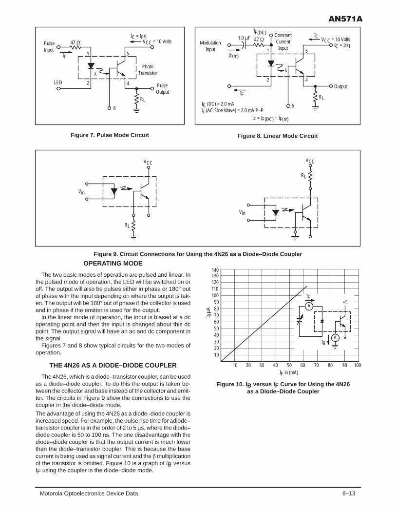
8–13Motorola Optoelectronics Device Data
Figure 7. Pulse Mode Circuit
VCC = 10 VoltsIC = IFη
PhotoTransistor
PulseOutput
λ
47 Ω
IF
PulseInput
2
RL
51
4
6
1
2
IF
6
Figure 8. Linear Mode Circuit
4
λ
5
RL
IF = IF(DC) + IF(m)
IC (DC) = 2.0 mAic (AC Sine Wave) = 2.0 mA P–P
1.0 µF 47 ΩConstantCurrentInput
Output
IF(m)
VCC = 10 VoltsIC = IFη
ICModulation
Input
IF(DC)
LED
Figure 9. Circuit Connections for Using the 4N26 as a Diode–Diode Coupler
VCC
RL
Vin
VCC
Vin
RL
OPERATING MODE
The two basic modes of operation are pulsed and linear. Inthe pulsed mode of operation, the LED will be switched on oroff. The output will also be pulses either in phase or 180° outof phase with the input depending on where the output is tak-en. The output will be 180° out of phase if the collector is usedand in phase if the emitter is used for the output.
In the linear mode of operation, the input is biased at a dcoperating point and then the input is changed about this dcpoint. The output signal will have an ac and dc component inthe signal.
Figures 7 and 8 show typical circuits for the two modes ofoperation.
THE 4N26 AS A DIODE–DIODE COUPLER
The 4N26, which is a diode–transistor coupler, can be usedas a diode–diode coupler. To do this the output is taken be-tween the collector and base instead of the collector and emit-ter. The circuits in Figure 9 show the connections to use thecoupler in the diode–diode mode.
The advantage of using the 4N26 as a diode–diode coupler isincreased speed. For example, the pulse rise time for adiode–transistor coupler is in the order of 2 to 5 µs, where the diode–diode coupler is 50 to 100 ns. The one disadvantage with thediode–diode coupler is that the output current is much lowerthan the diode–transistor coupler. This is because the basecurrent is being used as signal current and the multiplicationof the transistor is omitted. Figure 10 is a graph of IB versusIF using the coupler in the diode–diode mode.
IF in (mA)
+5IF
10 1009080706050
140130
110120
20
20 4030
10090807060504030
10
Figure 10. I B versus I F Curve for Using the 4N26as a Diode–Diode Coupler
A
IBA
I BµA

8–14 Motorola Optoelectronics Device Data
+5 V
54N26R*
RL
IF
2
GateSignal
6 4MTTL
Flip–Flop
250
IF = 50 mA
Figure 12. Opto Coupler in a Load to LogicTranslation
1Induct.Load
MCR106–6AC1N4005
2
1
+ V5
4
6
4N26 1 k
Figure 11. Coupler–Driven SCR
R * V0.05 A
V
APPLICATIONS
The following circuits are presented to give the designerideas of how the 4N26 can be used. The circuits have beenbread–boarded and tested, but the values of the circuit com-ponents have not been selected for optimum performanceover all temperatures.
Figure 11 shows a coupler driving a silicon controlled rectifi-er (SCR). The SCR is used to control an inductive load, andthe SCR is driven by a coupler. The SCR used is a sensitivegate device that requires only 1 mA of gate current and thecoupler has a minimum current transfer ratio of 0.2 so the inputcurrent to the coupler, IF, need only be 5 mA. The 1 k resistorconnected to the gate of the SCR is used to hold off the SCR.The 1N4005 diode is used to supress the self–induced voltagewhen the SCR turns off.
Figure 12 is a circuit that couples a high voltage load to a lowvoltage logic circuit. To ensure that the voltage to the MTTL
flip–flop exceeds the logic–one level, the coupler output cur-rent must be at least 10 mA. To guarantee 10 mA of output cur-rent, the input current to the LED must be 50 mA. The currentlimiting resistor R can be calculated from the equation
RV–VF0.05
. If the power supply voltage, V, is much greater
than VF, the equation for R reduces to R V0.05
.
The circuit of Figure 13 shows a coupler driving an opera-tional amplifier. In this application an ac signal is passedthrough the coupler and then amplified by the op amp. To passan ac signal through the coupler with minimum distortion, it isnecessary to bias the LED with a dc current. The ac signal issummed with the dc current so the output voltage of the cou-pler will have an ac and a dc component. Since the op amp iscapacitively coupled to the coupler, only the ac signal will ap-pear at the output.
Figure 13. Coupling an AC Signal to an Operational Amplifier
Vout
100 k
MC1741+
–
IDC = 10 mA
4N26
10 k1 µF
100
46
5
+15 V
+5 V
47
510
2
1
22 µF
Av = –10
IAC (peak)5 mA

8–15Motorola Optoelectronics Device Data
The circuit of Figure 14 shows the 4N26 being used as a diode–diode coupler, the output being taken from the collector–basediode. In this mode of operation, the emitter is left open, the load resistor is connected between the base and ground, and thecollector is tied to the positive voltage supply. Using the coupler in this way reduces the switching time from 2 to 3 µs to 100 ns.
Figure 14. Using the 4N26 as a Diode–Diode Coupler
1.0 µs
tr 10–90100 ns
InputPulse
0
0.6 V
0
3 V
90
10
Input
4N26
1 k
Vout
Output
+647
50
50IL
2 6
4
+6 V
–6 VMC1733
AV = 200
+
–
1 5
0.1 µF
The circuit of Figure 15 is a standard two–transistor one–shot, with one transistor being the output transistor of the coupler.The trigger to the one–shot is the LED input to the coupler. A pulse of 3 µs in duration and 15 mA will trigger the circuit. Theoutput pulse width (PWO) is equal to 0.7 RC + PW1 + 6 µs where PW1 is the input pulse width and 6 µs is the turn–off delay ofthe coupler. The amplitude of the output pulse is a function of the power supply voltage of the output side and independent of theinput.
InputIF = 15 mAPWin 3 µs(Minimum)
Figure 15. Pulse Stretcher
5 V
VO
+5 V
R = 47 k 4.7 k
0.03 µF
C
MPS6515
100 k
5
6
4
4.7 k
Input
4N26
2
1IF
PW = 0.7 RC
OutputPWout = 0.7 RC + PWmin
PWmin = PWin + 6 µsVO(Low) = 0.2 VVO(High) = 5.0 V (for R 4.7 k)
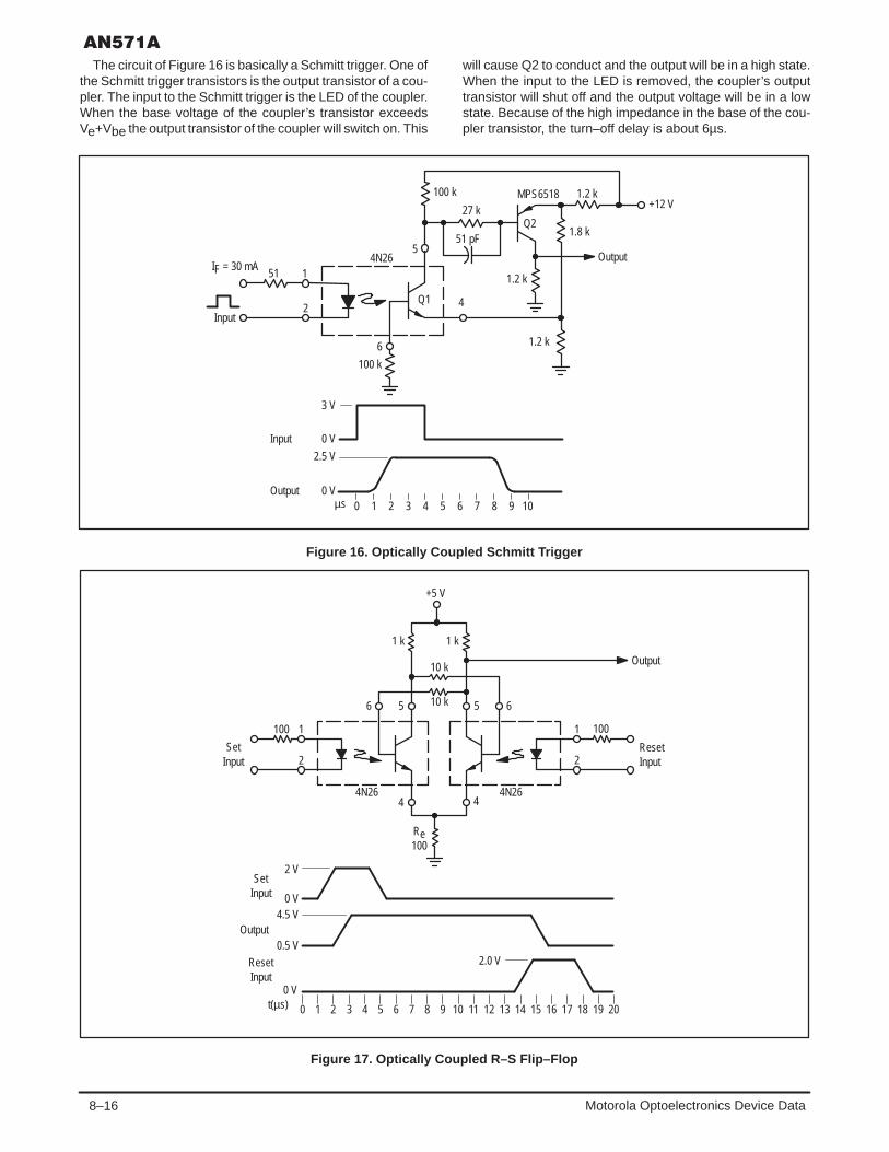
8–16 Motorola Optoelectronics Device Data
The circuit of Figure 16 is basically a Schmitt trigger. One ofthe Schmitt trigger transistors is the output transistor of a cou-pler. The input to the Schmitt trigger is the LED of the coupler.When the base voltage of the coupler’s transistor exceedsVe+Vbe the output transistor of the coupler will switch on. This
will cause Q2 to conduct and the output will be in a high state.When the input to the LED is removed, the coupler’s outputtransistor will shut off and the output voltage will be in a lowstate. Because of the high impedance in the base of the cou-pler transistor, the turn–off delay is about 6µs.
2.0 V
0t(µs)
ResetInput
Output
SetInput
0 V
0.5 V
4.5 V0 V
2 V
ResetInput
Output
1001
2
Re100
1 k1 k
6556
4
Output
Input
Figure 16. Optically Coupled Schmitt Trigger
2
100 1
4
00 V
2.5 V
0 V
51
Input
3 V
IF = 30 mA
+12 VMPS6518
Output
2
1
51 pF
1.2 k
1.2 k
1.8 kQ2
27 k
100 k
54N26
4Q1
6
100 k
1.2 k
2019181716151413121110987654321
SetInput
4N26
+5 V
4N26
10 k
10 k
1098765432µs 1
Figure 17. Optically Coupled R–S Flip–Flop

8–17Motorola Optoelectronics Device Data
The high base impedance (100 k ohms) represents a com-promise between sensitivity (input drive required) and frequen-cy response. A low value base resistor would improve speedbut would also increase the drive requirements.
The circuit in Figure 17 can be used as an optically coupledR–S flip–flop. The circuit uses two 4N26 couplers crosscoupled to produce two stable states. To change the outputfrom a low state to a high state requires a positive 2 V pulseat the set input. The minimum width of the set pulse is 3 µs. Toswitch the output back to the low state needs only a pulse onthe reset input. The reset–operation is similar to the set opera-tion.
Motorola integrated voltage regulators provide an input forthe express purpose of shutting the regulator off. For large
systems, various subsystems may be placed in a stand–bymode to conserve power until actually needed. Or the powermay be turned OFF in response to occurrences such as over-heating, over–voltage, shorted output, etc.
With the use of the 4N26 optically coupler, the regulator canbe shut down while the controlling signal is isolated from theregulator. The circuit of Figure 18 shows a positive regulatorconnected to an optical coupler.
To ensure that the drive to the regulator shut down controlis 1 mA, (the required current), it is necessary to drive the LEDin the coupler with 5 mA of current, an adequate level for logiccircuits.
0.1 µF
4 µs
50 1
IF = 15 mA
4N265
2
4
100 k
6
10 k
100 k
10 pF
47 pF
MPS6515
27 k
2.0 V
Out
10 k
5 V2 µs
4 µs
Output
tr 0.5 µs
+5
2
IF = 5 mA
1
6
4N26
4
5
R* = Vin – 1.7 V kΩ
2
R2 =5.8 k
R1
8
9MC1569RMC1469R
Case
6
3 1
4
5
7
2N706R*
0.001 µF
C01.0 µF
+
RL
+VORsc
Figure 19. Simple Pulse Amplifier
Io = 1 mA
Figure 18. Optical Coupler Controlling the Shut Downof MC1569 Voltage Regulator
Input
The circuit in Figure 19 is a simple pulse amplifier using pos-itive, ac feedback into the base of the 4N26. The advantageof the feedback is in faster switching time. Without the feed-back, the pulse rise time is about 2.0 µs, but with the positivefeedback, the pulse rise time is about 0.5 µs. Figure 17Ashows the input and output wave–forms of the pulse amplifier.
REFERENCES
1. “Theory and Characteristics of Phototransistors,“ MotorolaApplication Note AN440.
2. “Motorola Switching Transistor Handbook.“
3. Deboo, G.J. and C.N. Burrous, Integrated Circuits andSemiconductor Devices Theory and Application. NewYork: McGraw–Hill, 1971.

8–18 Motorola Optoelectronics Device Data
Motorola reserves the right to make changes without further notice to any products herein. Motorola makes no warranty, representation or guarantee regardingthe suitability of its products for any particular purpose, nor does Motorola assume any liability arising out of the application or use of any product or circuit,and specifically disclaims any and all liability, including without limitation consequential or incidental damages. “Typical” parameters can and do vary in differentapplications. All operating parameters, including “Typicals” must be validated for each customer application by customer’s technical experts. Motorola doesnot convey any license under its patent rights nor the rights of others. Motorola products are not designed, intended, or authorized for use as components insystems intended for surgical implant into the body, or other applications intended to support or sustain life, or for any other application in which the failure ofthe Motorola product could create a situation where personal injury or death may occur. Should Buyer purchase or use Motorola products for any suchunintended or unauthorized application, Buyer shall indemnify and hold Motorola and its officers, employees, subsidiaries, affiliates, and distributors harmlessagainst all claims, costs, damages, and expenses, and reasonable attorney fees arising out of, directly or indirectly, any claim of personal injury or deathassociated with such unintended or unauthorized use, even if such claim alleges that Motorola was negligent regarding the design or manufacture of the part.Motorola and are registered trademarks of Motorola, Inc. Motorola, Inc. is an Equal Opportunity/Affirmative Action Employer.

8–19Motorola Optoelectronics Device Data
How to reach us:USA / EUROPE: Motorola Literature Distribution; JAPAN : Nippon Motorola Ltd.; Tatsumi–SPD–JLDC, Toshikatsu Otsuki,P.O. Box 20912; Phoenix, Arizona 85036. 1–800–441–2447 6F Seibu–Butsuryu–Center, 3–14–2 Tatsumi Koto–Ku, Tokyo 135, Japan. 03–3521–8315
MFAX: [email protected] – TOUCHTONE (602) 244–6609 HONG KONG: Motorola Semiconductors H.K. Ltd.; 8B Tai Ping Industrial Park, INTERNET: http://Design–NET.com 51 Ting Kok Road, Tai Po, N.T., Hong Kong. 852–26629298
AN571A/D
◊

8–20 Motorola Optoelectronics Device Data
Prepared by: Pat O’Neil
DESCRIPTIONS OF THE MOC3011
Construction
The MOC3011 consists of a gallium arsenide infrared LEDoptically exciting a silicon detector chip, which is especiallydesigned to drive triacs controlling loads on the 115 Vac powerline. The detector chip is a complex device which functions inmuch the same manner as a small triac, generating the signalsnecessary to drive the gate of a larger triac. The MOC3011 al-lows a low power exciting signal to drive a high power load witha very small number of components, and at the same time pro-vides practically complete isolation of the driving circuitry fromthe power line.
Basic Electrical Description
The GaAs LED has nominal 1.3 V forward drop at 10 mAand a reverse breakdown voltage greater than 3 V. The maxi-mum current to be passed through the LED is 50 mA.
The detector has a minimum blocking voltage of 250 Vdc ineither direction in the off state. In the on state, the detector willpass 100 mA in either direction with less than 3 V drop acrossthe device. Once triggered into the on (conducting) state, thedetector will remain there until the current drops below theholding current (typically 100 µA) at which time the detector re-verts to the off (non–conducting) state. The detector may betriggered into the on state by exceeding the forward blocking
voltage, by voltage ramps across the detector at rates exceed-ing the static dv/dt rating, or by photons from the LED. TheLED is guaranteed by the specifications to trigger the detectorinto the on state when 10 mA or more is passed through theLED. A similar device, the MOC3010, has exactly the samecharacteristics except it requires 15 mA to trigger.
Since the MOC3011 looks essentially like a small opticallytriggered triac, we have chosen to represent it as shown onFigure 1.
Figure 1. Schematic Representationof MOC3011 and MOC3010
λ
Order this documentby AN780A/D
SEMICONDUCTOR APPLICATION NOTE
Motorola, Inc. 1995

8–21Motorola Optoelectronics Device Data
Figure 2. Simple Triac Gating Circuit
MOC301110mA
1
2 R1
4
6VCC
150115 Vac
Vin
RLoad
180R1
2
1
7400
C1
6 R2
4 115Vac
ZL300
MOC3011
5 VVCC
TRIAC
IGT R2 C
15 mA 2400 0.1
30 mA 1200 0.2
50 mA 800 0.3
NOTE: Circuit supplies 25 mA drive to gate of triacat Vin = 25 V and TA 70°C.
Figure 3. Logic to Inductive Load Interface
USING THE MOC3011 AS A TRIAC DRIVER
Triac Driving Requirements
Figure 2 shows a simple triac driving circuit using theMOC3011. The maximum surge current rating of theMOC3011 sets the minimum value of R1 through the equation:
R1(min) = Vin(pk)/1.2 A
If we are operating on the 115 Vac nominal line voltage,Vin(pk) = 180 V, then
R1(min) = Vin(pk)/1.2 A = 150 ohms.
In practice, this would be a 150 or 180 ohm resistor. If thetriac has IGT = 100 mA and VGT = 2 V, then the voltage Vinnecessary to trigger the triac will be given by VinT = R1 IGT+ VGT + VTM = 20 V.
Resistive LoadsWhen driving resistive loads, the circuit of Figure 2 may be
used. Incandescent lamps and resistive heating elements arethe two main classes of resistive loads for which 115 Vac is uti-lized. The main restriction is that the triac must be properlychosen to sustain the proper inrush loads. Incandescentlamps can sometimes draw a peak current known as “flash-over“ which can be extremely high, and the triac should be pro-tected by a fuse or rated high enough to sustain this current.
Line Transients–Static dv/dtOccasionally transient voltage disturbance on the ac line
will exceed the static dv/dt rating of the MOC3011. In this case,it is possible that the MOC3011 and the associated triac willbe triggered on. This is usually not a problem, except in unusu-ally noisy environments, because the MOC3011 and its triacwill commute off at the next zero crossing of the line voltage,and most loads are not noticeably affected by an occasionalsingle half–cycle of applied power. See Figure 4 for typical dv/dt versus temperature curves.
Inductive Loads–Commutating dv/dtInductive loads (motors, solenoids, magnets, etc.) present
a problem both for triacs and for the MOC3011 because thevoltage and current are not in phase with each other. Since thetriac turns off at zero current, it may be trying to turn off whenthe applied current is zero but the applied voltage is high. Thisappears to the triac like a sudden rise in applied voltage, whichturns on the triac if the rate of rise exceeds the commutatingdv/dt of the triac or the static dv/dt of the MOC3011.
Snubber NetworksThe solution to this problem is provided by the use of “snub-
ber“ networks to reduce the rate of voltage rise seen by the de-vice. In some cases, this may require two snubbers–one forthe triac and one for the MOC3011. The triac snubber is de-pendent upon the triac and load used and will not be discussedhere. In many applications the snubber used for the MOC3011will also adequately protect the triac.
In order to design a snubber properly, one should reallyknow the power factor of the reactive load, which is defined asthe cosine of the phase shift caused by the load. Unfortunate-ly, this is not always known, and this makes snubbing networkdesign somewhat empirical. However, a method of designinga snubber network may be defined, based upon a typical pow-er factor. This can be used as a “first cut” and later modifiedbased upon experiment.
Assuming an inductive load with a power factor of PF = 0.1is to be driven. The triac might be trying to turn off when theapplied voltage is given by
Vto = Vpksin Vpk 180 V
First, one must choose R1 (Figure 3) to limit the peak capac-itor discharge current through the MOC3011. This resistor isgiven by
R1 = Vpk/Imax = 180/1.2 A = 150
A standard value, 180 ohm resistor can be used in practicefor R1.

8–22 Motorola Optoelectronics Device Data
It is necessary to set the time constant for = R2C. Assum-ing that the triac turns off very quickly, we have a peak rate ofrise at the MOC3011 given by
dv/dt = Vto/ = Vto/R2C
Setting this equal to the worst case dv/dt (static) for theMOC3011 which we can obtain from Figure 4 and solving forR2C:
dv/dt(TJ = 70°C) = 0.8 V/µs = 8 105
R2C = Vto/(dv/dt) = 180/(8 105) 230 10–6
Figure 4. dv/dt versus Temperature
Commutatingdv/dt
dv/dt = 8.9 f Vin
Staticdv/dt
+ 5 V
0 V
dv/dt Test Circuit
MOC3011
VCC Rin 1
2
6
4
Vin
RL
2N3904
10 kRL = 510 Ω
25
24
2.0
1.6
1.2
0.8
0.4
0.24
030 50 60 70 80 90 100
0
0.04
0.08
0.12
0.16
0.20
40
TA, AMBIENT TEMPERATURE (°C)
Static dv/dtCommutating dv/dt
RL = 2 kΩ
dv/d
t, ST
ATIC
, (V/
µs)
dv/d
t, C
OM
MU
TATI
NG
(V/µ
s)
The largest value of R2 available is found, taking into con-sideration the triac gate requirements. If a sensitive gate triacis used, such as a 2N6071B, IGT = 15 mA @ –40°C. If the triacis to be triggered when Vin 40 V
(R1 + R2) Vin/IGT 40/0.015 2.3 k
If we let R2 = 2400 ohms and C = 0.1 µF, the snubbing re-quirements are met. Triacs having less sensitive gates will re-quire that R2 be lower and C be correspondingly higher asshown in Figure 3.
INPUT CIRCUITRY
Resistor InputWhen the input conditions are well controlled, as for exam-
ple when driving the MOC3011 from a TTL, DTL, or HTL gate,only a single resistor is necessary to interface the gate to theinput LED of the MOC3011. The resistor should be chosen toset the current into the LED to be a minimum of 10 mA but nomore than 50 mA. 15 mA is a suitable value, which allows forconsiderable degradation of the LED over time, and assures
a long operating life for the coupler. Currents higher than 15mA do not improve performance and may hasten the agingprocess inherent in LED’s. Assuming the forward drop to be1.5 V at 15 mA allows a simple formula to calculate the inputresistor.
Ri = (VCC – 1.5)/0.015
Examples of resistive input circuits are seen in Figures 1and 5.
Increasing Input SensitivityIn some cases, the logic gate may not be able to source or
sink 15 mA directly. CMOS, for example, is specified to haveonly 0.5 mA output, which must then be increased to drive theMOC3011. There are numerous ways to increase this currentto a level compatible with the MOC3011 input requirements;an efficient way is to use the MC14049B shown in Figure 5.Since there are six such buffers in a single package, the usercan have a small package count when using severalMOC3011’s in one system.

8–23Motorola Optoelectronics Device Data
Figure 5. MOS to ac Load Interface
115 Vac
2N6071B0.1 µF
4
5MOC3011
3
2
Load2.4 k180
VCC
R 61
1/6 Hex Buffer
VCC R HEX BUFFER
5.0 V 220 Ω MC75492
10 V 600 Ω MC75492
15 V 910 Ω MC14049B
Input Protection CircuitsIn some applications, such as solid state relays, in which the
input voltage varies widely the designer may want to limit thecurrent applied to the LED of the MOC3011. The circuit shownin Figure 6 allows a non–critical range of input voltages toproperly drive the MOC3011 and at the same time protects theinput LED from inadvertent application of reverse polarity.
Figure 6. MOC3011 Input Protection Circuit
+
MOC3011
–
3–30Vdc
150
1N4002
2N3904
51 3
2
1
4
5
6
LED LifetimeAll light emitting diodes slowly decrease in brightness dur-
ing their useful life, an effect accelerated by high temperaturesand high LED currents. To allow a safety margin and ensure
long service life, the MOC3011 is actually tested to trigger ata value lower than the specified 10 mA input threshold current.The designer can therefore design the input circuitry to supply10 mA to the LED and still be sure of satisfactory operationover a long operating lifetime. On the other hand, care shouldbe taken to ensure that the maximum LED input current (50mA) is not exceeded or the lifetime of the MOC3011 may beshortened.
APPLICATIONS EXAMPLES
Using the MOC3011 on 240 Vac LinesThe rated voltage of a MOC3011 is not sufficiently high for
it to be used directly on 240 Vac line; however, the designermay stack two of them in series. When used this way, two re-sistors are required to equalize the voltage dropped acrossthem as shown in Figure 7.
Remote Control of ac VoltageLocal building codes frequently require all 115 Vac light
switch wiring to be enclosed in conduit. By using a MOC3011,a triac, and a low voltage source, it is possible to control a largelighting load from a long distance through low voltage signalwiring which is completely isolated from the ac line. Such wir-ing usually is not required to be put in conduit, so the cost sav-ings in installing a lighting system in commercial or residentialbuildings can be considerable. An example is shown in Figure8. Naturally, the load could also be a motor, fan, pool pump,etc.

8–24 Motorola Optoelectronics Device Data
Figure 7. 2 MOC3011 Triac Drivers in Series to Drive 240 V Triac
115 Vac
2N6342A
180
MOC3011
λ
Non–Conduit #22Wire
5 V
360
Figure 8. Remote Control of ac Loads Through Low Voltage Non–Conduit Cable
240 Vac
Load
1 k
180
1 M
1 MMOC3011
MOC3011
150+5 V
λ
λ
Solid State RelayFigure 9 shows a complete general purpose, solid state
relay snubbed for inductive loads with input protection. Whenthe designer has more control of the input and output condi-tions, he can eliminate those components which are not need-ed for his particular application to make the circuit more costeffective.
Interfacing Microprocessors to 115 Vac PeripheralsThe output of a typical microcomputer input–output (I/O)
port is a TTL–compatible terminal capable of driving one ortwo TTL loads. This is not quite enough to drive the MOC3011,nor can it be connected directly to an SCR or triac, because
computer common is not normally referenced to one side ofthe ac supply. Standard 7400 series gates can provide aninput compatible with the output of an MC6820, MC6821,MC6846 or similar peripheral interface adaptor and candirectly drive the MOC3011. If the second input of a 2 inputgate is tied to a simple timing circuit, it will also provideenergization of the triac only at the zero crossing of the ac linevoltage as shown in Figure 10. This technique extends the lifeof incandescent lamps, reduces EMI generated by loadswitching. Of course, zero crossing can be generated withinthe microcomputer itself, but this requires considerablesoftware overhead and usually just as much hardware togenerate the zero–crossing timing signals.

8–25Motorola Optoelectronics Device Data
MC6820or
MC6821or
MC6846I/O
MC6800or
MC6802MPU
115 Vac(Resistive Load)
115 Vac(Inductive Load)2N6071B
0.1 µF
2.4 k180 Motor
200 W
180
2N6071
Opto TriacDrivers
+5 V
300
300
Optional Zero–CrossingCircuitry
5 Vac
7400
2N3904
100 k
3 k
6.3Vac
115 Vac
+5 V
1 k
Data
Address
Figure 9. Solid–State Relay
115 Vac2N6071B
0.1 µF
10 k
2.4 k180
λ
MOC3011
150
2N3904
2 W1N4002
47
Figure 10. Interfacing an M6800 Microcomputer System to 115 Vac Loads
MO
C30
11M
OC
3011

8–26 Motorola Optoelectronics Device Data
Motorola reserves the right to make changes without further notice to any products herein. Motorola makes no warranty, representation or guarantee regardingthe suitability of its products for any particular purpose, nor does Motorola assume any liability arising out of the application or use of any product or circuit,and specifically disclaims any and all liability, including without limitation consequential or incidental damages. “Typical” parameters can and do vary in differentapplications. All operating parameters, including “Typicals” must be validated for each customer application by customer’s technical experts. Motorola doesnot convey any license under its patent rights nor the rights of others. Motorola products are not designed, intended, or authorized for use as components insystems intended for surgical implant into the body, or other applications intended to support or sustain life, or for any other application in which the failure ofthe Motorola product could create a situation where personal injury or death may occur. Should Buyer purchase or use Motorola products for any suchunintended or unauthorized application, Buyer shall indemnify and hold Motorola and its officers, employees, subsidiaries, affiliates, and distributors harmlessagainst all claims, costs, damages, and expenses, and reasonable attorney fees arising out of, directly or indirectly, any claim of personal injury or deathassociated with such unintended or unauthorized use, even if such claim alleges that Motorola was negligent regarding the design or manufacture of the part.Motorola and are registered trademarks of Motorola, Inc. Motorola, Inc. is an Equal Opportunity/Affirmative Action Employer.

8–27Motorola Optoelectronics Device Data
How to reach us:USA / EUROPE: Motorola Literature Distribution; JAPAN : Nippon Motorola Ltd.; Tatsumi–SPD–JLDC, Toshikatsu Otsuki,P.O. Box 20912; Phoenix, Arizona 85036. 1–800–441–2447 6F Seibu–Butsuryu–Center, 3–14–2 Tatsumi Koto–Ku, Tokyo 135, Japan. 03–3521–8315
MFAX: [email protected] – TOUCHTONE (602) 244–6609 HONG KONG: Motorola Semiconductors H.K. Ltd.; 8B Tai Ping Industrial Park, INTERNET: http://Design–NET.com 51 Ting Kok Road, Tai Po, N.T., Hong Kong. 852–26629298
AN780A/D
◊
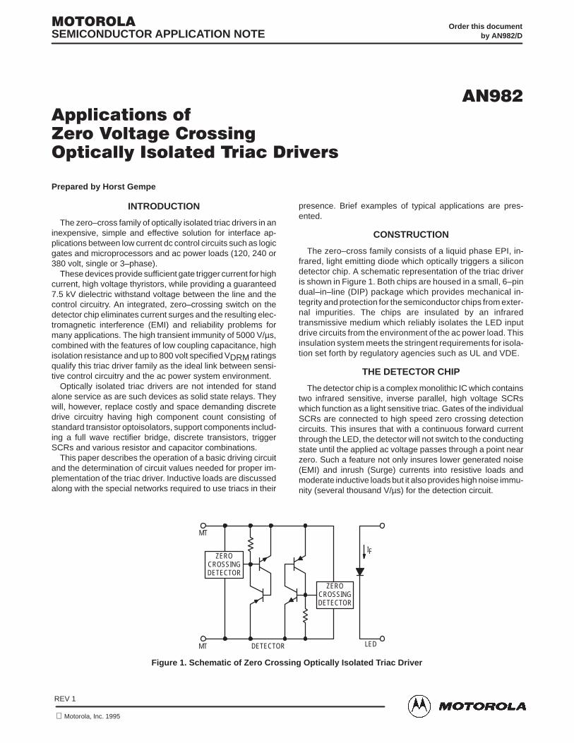
8–28 Motorola Optoelectronics Device Data
Prepared by Horst Gempe
INTRODUCTION
The zero–cross family of optically isolated triac drivers in aninexpensive, simple and effective solution for interface ap-plications between low current dc control circuits such as logicgates and microprocessors and ac power loads (120, 240 or380 volt, single or 3–phase).
These devices provide sufficient gate trigger current for highcurrent, high voltage thyristors, while providing a guaranteed7.5 kV dielectric withstand voltage between the line and thecontrol circuitry. An integrated, zero–crossing switch on thedetector chip eliminates current surges and the resulting elec-tromagnetic interference (EMI) and reliability problems formany applications. The high transient immunity of 5000 V/µs,combined with the features of low coupling capacitance, highisolation resistance and up to 800 volt specified VDRM ratingsqualify this triac driver family as the ideal link between sensi-tive control circuitry and the ac power system environment.
Optically isolated triac drivers are not intended for standalone service as are such devices as solid state relays. Theywill, however, replace costly and space demanding discretedrive circuitry having high component count consisting ofstandard transistor optoisolators, support components includ-ing a full wave rectifier bridge, discrete transistors, triggerSCRs and various resistor and capacitor combinations.
This paper describes the operation of a basic driving circuitand the determination of circuit values needed for proper im-plementation of the triac driver. Inductive loads are discussedalong with the special networks required to use triacs in their
presence. Brief examples of typical applications are pres-ented.
CONSTRUCTION
The zero–cross family consists of a liquid phase EPI, in-frared, light emitting diode which optically triggers a silicondetector chip. A schematic representation of the triac driveris shown in Figure 1. Both chips are housed in a small, 6–pindual–in–line (DIP) package which provides mechanical in-tegrity and protection for the semiconductor chips from exter-nal impurities. The chips are insulated by an infraredtransmissive medium which reliably isolates the LED inputdrive circuits from the environment of the ac power load. Thisinsulation system meets the stringent requirements for isola-tion set forth by regulatory agencies such as UL and VDE.
THE DETECTOR CHIP
The detector chip is a complex monolithic IC which containstwo infrared sensitive, inverse parallel, high voltage SCRswhich function as a light sensitive triac. Gates of the individualSCRs are connected to high speed zero crossing detectioncircuits. This insures that with a continuous forward currentthrough the LED, the detector will not switch to the conductingstate until the applied ac voltage passes through a point nearzero. Such a feature not only insures lower generated noise(EMI) and inrush (Surge) currents into resistive loads andmoderate inductive loads but it also provides high noise immu-nity (several thousand V/µs) for the detection circuit.
IF
DETECTOR LED
MT
MT
Figure 1. Schematic of Zero Crossing Optically Isolated Triac Driver
ZEROCROSSINGDETECTOR
ZEROCROSSINGDETECTOR
Order this documentby AN982/D
SEMICONDUCTOR APPLICATION NOTE
Motorola, Inc. 1995
REV 1

8–29Motorola Optoelectronics Device Data
MT
MT
ZEROCROSSINGDETECTOR
IF
VF
V
IDRM
IDRM VDRM
A2–
Figure 2. Simplified Schematic of Isolator
Q1BLOCKING
STATEVDRMIH
A2+
ON STATE
IH–
ON STATE
BLOCKING STATEQ111
Figure 3. Triac Voltage–Current Characteristic
I
IV
ELECTRICAL CHARACTERISTICS
A simplified schematic of the optically isolated triac driver isshown in Figure 2. This model is sufficient to describe all im-portant characteristics. A forward current flow through theLED generates infrared radiation which triggers the detector.This LED trigger current (IFT) is the maximum guaranteed cur-rent necessary to latch the triac driver and ranges from 5 mAfor the MOC3063 to 15 mA for the MOC3061. The LED’s for-ward voltage drop at IF = 30 mA is 1.5 V maximum. Voltage–current characteristics of the triac are identified in Figure 3.
Once triggered, the detector stays latched in the “on state”until the current flow through the detector drops below theholding current (IH) which is typically 100 µA. At this time, thedetector reverts to the “off” (non–conducting) state. The detec-tor may be triggered “on” not only by IFT but also by exceedingthe forward blocking voltage between the two main terminals(MT1 and MT2) which is a minimum of 600 volts for allMOC3061 family members. Also, voltage ramps (transients,noise, etc.) which are common in ac power lines may triggerthe detector accidentally if they exceed the static dV/dt rating.Since the fast switching, zero–crossing switch provides aminimum dV/dt of 500 V/µs even at an ambient temperatureof 70°C, accidental triggering of the triac driver is unlikely. Ac-cidental triggering of the main triac is a more likely occurrence.Where high dV/dt transients on the ac line are anticipated, aform of suppression network commonly called a “snubber”
must be used to prevent false “turn on” of the main triac. A de-tailed discussion of a “snubber” network is given under thesection “Inductive and Resistive Loads.”
Figure 4 shows a static dV/dt test circuit which can be usedto test triac drivers and power triacs. The proposed test meth-od is per EIA/NARM standard RS–443.
Tests on the MOC3061 family of triac drivers using the testcircuit of Figure 4 have resulted in data showing the effects oftemperature and voltage transient amplitude on static dV/dt.Figure 5 is a plot of dV/dt versus ambient temperature whileFigure 6 is a similar plot versus transient amplitude.
BASIC DRIVING CIRCUIT
Assuming the circuit shown in Figure 7 is in the blocking or“off” state (which means IF is zero), the full ac line voltage ap-pears across the main terminals of both the triac and the triacdriver. When sufficient LED current (IFT) is supplied and the acline voltage is below the inhibit voltage (IH in Figure 3), the triacdriver latches “on.” This action introduces a gate current in themain triac triggering it from the blocking state into full conduc-tion. Once triggered, the voltage across the main terminalscollapses to a very low value which results in the triac driveroutput current decreasing to a value lower than its holding cur-rent, thus forcing the triac driver into the “off” state, even whenIFT is still applied.
Figure 4. Static dV/dt Test Circuit
0
τRC
HV
470 Ω
10 k
DUT
–15 V
P8
SCOPE PROBE 100:1
0.001 µF
150 kΩ10 Ω
HV15 V
MERCURYWETTEDRELAY
100 ΩSIGNAL IN
50% DUTY CYCLE0
HV
16 ms
0.63HV
VOLTAGE APPLIED TO DUT –
TEST PROCEDURE –Turn the D.U.T. on, while applying sufficient dV/dt to ensure that it remains on, even after the trigger current is re-
moved. Then decrease dV/dt until the D.U.T. turns off. Measure τRC, the time it takes to rise to 0.63 HV, and divide 0.63HV by τRC to get dV/dt.

8–30 Motorola Optoelectronics Device Data
TRANSIENT AMPLITUDE (V)600500400300200100
500
1000
2000
5000
10000
TA, AMBIENT TEMPERATURE (°C)
100755025
600
TRANSIENT AMPLITUDE= 600 V
Figure 5. Static dV/dt versus Temperature Figure 6. Static dV/dt versus Transient Amplitude
dV/d
t [V/
µs]
dV/d
t [V/
µs]
The power triac remains in the conducting state until theload current drops below the power triac’s holding current, asituation that occurs every half cycle. The actual duty cycle forthe triac driver is very short (in the 1 to 3 µs region). When IFTis present, the power triac will be retriggered every half cycleof the ac line voltage until IFT is switched “off” and the powertriac has gone through a zero current point. (See Figure 8).
Resistor R (shown in Figure 7) is not mandatory when RL isa resistive load since the current is limited by the gate triggercurrent (IGT) of the power triac. However, resistor R (in com-bination with R–C snubber networks that are described in thesection “Inductive and Resistive Loads”) prevents possibledestruction of the triac driver in applications where the load ishighly inductive.
Unintentional phase control of the main triac may happen ifthe current limiting resistor R is too high in value. The functionof this resistor is to limit the current through the triac driver incase the main triac is forced into the non–conductive stateclose to the peak of the line voltage and the energy stored ina “snubber” capacitor is discharged into the triac driver. A cal-culation for the current limiting resistor R is shown below for
a typical 220 volt application: Assume the line voltage is 220volts RMS. Also assume the maximum peak repetitive drivercurrent (normally for a 10 micro second maximum time inter-val) is 1 ampere. Then
RVpeak
Ipeak
220 2 volts1 amp
311 ohms
One should select a standard resistor value >311 ohms 330 ohms.
The gate resistor RG (also shown in Figure 7) is only neces-sary when the internal gate impedance of the triac or SCR isvery high which is the case with sensitive gate thyristors.These devices display very poor noise immunity and thermalstability without RG. Value of the gate resistor in this caseshould be between 100 and 500. The circuit designer shouldbe aware that use of a gate resistor increases the required trig-ger current (IGT) since RG drains off part of IGT. Use of a gateresistor combined with the current limiting resistor R can resultin an unintended delay or phase shift between the zero–crosspoint and the time the power triac triggers.
IL
RLMT1RG
4
5
6
Figure 7. Basic Driving Circuit — Triac Driver,Triac and Load
MT2R
II
IFT
POWERTRIACTRIAC DRIVER
ZEROCROSSING
CIRCUIT
1
2
3
ACINPUT
IGT
IFT
AC LINE VOLTAGE
TRIAC DRIVER CURRENT I = IGT + II
V – ACROSS MAIN TRIAC
IL
Figure 8. Waveforms of a Basic Driving Circuit
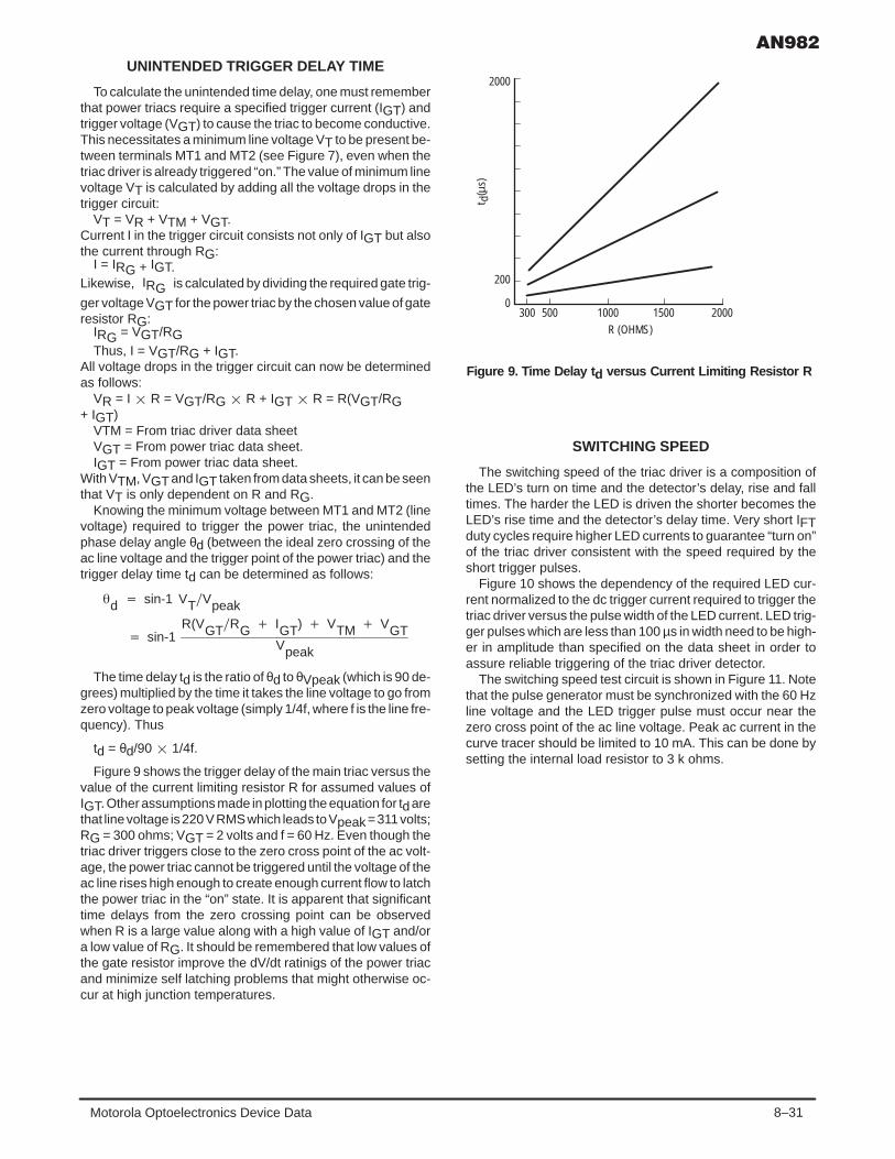
8–31Motorola Optoelectronics Device Data
UNINTENDED TRIGGER DELAY TIME
To calculate the unintended time delay, one must rememberthat power triacs require a specified trigger current (IGT) andtrigger voltage (VGT) to cause the triac to become conductive.This necessitates a minimum line voltage VT to be present be-tween terminals MT1 and MT2 (see Figure 7), even when thetriac driver is already triggered “on.” The value of minimum linevoltage VT is calculated by adding all the voltage drops in thetrigger circuit:
VT = VR + VTM + VGT.Current I in the trigger circuit consists not only of IGT but alsothe current through RG:
I = IRG + IGT.Likewise, IRG is calculated by dividing the required gate trig-
ger voltage VGT for the power triac by the chosen value of gateresistor RG:
IRG = VGT/RGThus, I = VGT/RG + IGT.
All voltage drops in the trigger circuit can now be determinedas follows:
VR = I R = VGT/RG R + IGT R = R(VGT/RG+ IGT)
VTM = From triac driver data sheetVGT = From power triac data sheet.IGT = From power triac data sheet.
With VTM, VGT and IGT taken from data sheets, it can be seenthat VT is only dependent on R and RG.
Knowing the minimum voltage between MT1 and MT2 (linevoltage) required to trigger the power triac, the unintendedphase delay angle θd (between the ideal zero crossing of theac line voltage and the trigger point of the power triac) and thetrigger delay time td can be determined as follows:
d sin-1 VTVpeak
sin-1R(VGTRG IGT) VTM VGT
Vpeak
The time delay td is the ratio of θd to θVpeak (which is 90 de-grees) multiplied by the time it takes the line voltage to go fromzero voltage to peak voltage (simply 1/4f, where f is the line fre-quency). Thus
td = θd/90 1/4f.
Figure 9 shows the trigger delay of the main triac versus thevalue of the current limiting resistor R for assumed values ofIGT. Other assumptions made in plotting the equation for td arethat line voltage is 220 V RMS which leads to Vpeak = 311 volts;RG = 300 ohms; VGT = 2 volts and f = 60 Hz. Even though thetriac driver triggers close to the zero cross point of the ac volt-age, the power triac cannot be triggered until the voltage of theac line rises high enough to create enough current flow to latchthe power triac in the “on” state. It is apparent that significanttime delays from the zero crossing point can be observedwhen R is a large value along with a high value of IGT and/ora low value of RG. It should be remembered that low values ofthe gate resistor improve the dV/dt ratinigs of the power triacand minimize self latching problems that might otherwise oc-cur at high junction temperatures.
15001000300 500R (OHMS)
2000
200
02000
Figure 9. Time Delay t d versus Current Limiting Resistor R
tµs
)d(
SWITCHING SPEED
The switching speed of the triac driver is a composition ofthe LED’s turn on time and the detector’s delay, rise and falltimes. The harder the LED is driven the shorter becomes theLED’s rise time and the detector’s delay time. Very short IFTduty cycles require higher LED currents to guarantee “turn on”of the triac driver consistent with the speed required by theshort trigger pulses.
Figure 10 shows the dependency of the required LED cur-rent normalized to the dc trigger current required to trigger thetriac driver versus the pulse width of the LED current. LED trig-ger pulses which are less than 100 µs in width need to be high-er in amplitude than specified on the data sheet in order toassure reliable triggering of the triac driver detector.
The switching speed test circuit is shown in Figure 11. Notethat the pulse generator must be synchronized with the 60 Hzline voltage and the LED trigger pulse must occur near thezero cross point of the ac line voltage. Peak ac current in thecurve tracer should be limited to 10 mA. This can be done bysetting the internal load resistor to 3 k ohms.

8–32 Motorola Optoelectronics Device Data
Motorola isolated triac drivers are trigger devices and de-signed to work in conjunction with triacs or reverse parallelSCRs which are able to take rated load current. However, assoon as the power triac is triggered there is no current flowthrough the triac driver. The time to turn the triac driver “off” de-pends on the switching speed of the triac, which is typically onthe order of 1–2 µs.
1 2 1005001
20
5
5 10 20
10
15
25
Figure 10. I FT Normalized to I FT dc As Specified on theData Sheet
LED TRIGGER PULSE WIDTH (µs)
I FT,
NO
RM
ALIZ
ED L
ED T
RIG
GER
CU
RR
ENT
NORMALIZED TO:PW IN 100 µs
ZEROCROSSING
CIRCUIT
10 Ω
DUTAMPLITUDE CONTROL
DELAY CONTROL
PULSE WIDTH CONTROL
Figure 11. Test Circuit for LED Forward Trigger Current versus Pulse Width
AC LINESYNC
IFMONITOR
SCOPE
PULSEGENERATOR
3
2
1
4
6
5
RL
CURVETRACER (AC MODE)
INDUCTIVE AND RESISTIVE LOADS
Inductive loads (motors, solenoids, etc.) present a problemfor the power triac because the current is not in phase with thevoltage. An important fact to remember is that since a triac canconduct current in both directions, it has only a brief intervalduring which the sine wave current is passing through zero torecover and revert to its blocking state. For inductive loads, thephase shift between voltage and current means that at thetime the current of the power handling triac falls below theholding current and the triac ceases to conduct, there existsa certain voltage which must appear across the triac. If thisvoltage appears too rapidly, the triac will resume conductionand control is lost. In order to achieve control with certain in-ductive loads, the rate of rise in voltage (dV/dt) must be limitedby a series RC network placed in parallel with the power triac.The capacitor Cs will limit the dV/dt across the triac.
The resistor Rs is necessary to limit the surge current fromCs when the triac conducts and to damp the ringing of the ca-pacitance with the load inductance LL. Such an RC network iscommonly referred to as a “snubber.”
Figure 12 shows current and voltage wave forms for thepower triac. Commutating dV/dt for a resistive load is typically
only 0.13 V/µs for a 240 V, 50 Hz line source and 0.063 V/µsfor a 120 V, 60 Hz line source. For inductive loads the “turn off”time and commutating dV/dt stress are more difficult to defineand are affected by a number of variables such as back EMFof motors and the ratio of inductance to resistance (power fac-tor). Although it may appear from the inductive load that therate or rise is extremely fast, closer circuit evaluation revealsthat the commutating dV/dt generated is restricted to some fi-nite value which is a function of the load reactance LL and thedevice capacitance C but still may exceed the triac’s criticalcommuting dV/dt rating which is about 50 V/µs. It is generallygood practice to use an RC snubber network across the triacto limit the rate of rise (dV/dt) to a value below the maximumallowable rating. This snubber network not only limits the volt-age rise during commutation but also suppresses transientvoltages that may occur as a result of ac line disturbances.
There are no easy methods for selecting the values for Rsand Cs of a snubber network. The circuit of Figure 13 is adamped, tuned circuit comprised of Rs, Cs, RL and LL, and toa minor extent the junction capacitance of the triac. When thetriac ceases to conduct (this occurs every half cycle of the linevoltage when the current falls below the holding current), the

8–33Motorola Optoelectronics Device Data
load current receives a step impulse of line voltage which de-pends on the power factor of the load. A given load fixes RLand LL; however, the circuit designer can vary Rs and Cs.Commutating dV/dt can be lowered by increasing CS while Rscan be increased to decrease resonant “over ringing” of thetuned circuit. Generally this is done experimentally beginningwith values calculated as shown in the next section and, then,adjusting Rs and Cs values to achieve critical damping and alow critical rate of rise of voltage.
Less sensitive to commutating dV/dt are two SCRs in an in-verse parallel mode often referred to as a back–to–back SCRpair (see Figure 15). This circuit uses the SCRs in an alternat-
ing mode which allows each device to recover and turn “off”during a full half cycle. Once in the “off” state, each SCR canresist dV/dt to the critical value of about 100 V/µs. Opticallyisolated triac drivers are ideal in this application since bothgates can be triggered by one triac driver which also providesisolation between the low voltage control circuit and the acpower line.
It should be mentioned that the triac driver detector does notsee the commutating dV/dt generated by the inductive loadduring its commutation; therefore, the commutating dV/dt ap-pears as a static dV/dt across the two main terminals of thetriac driver.
AC CURRENT THROUGHPOWER TRIAC
TIME
VOLTAGE ACROSS POWER TRIAC
Figure 12. Current and Voltage Waveforms During Commutation
Inductive Load
VOLTAGE ACROSS POWER TRIAC
AC LINE VOLTAGE
0
t0
IF(OFF)IF(ON)
Resistive Load
t0TIME
d
AC CURRENT
AC LINE VOLTAGE
IF(OFF)
IF(ON)
COMMUTATINGdV/dt
COMMUTATINGdV/dt

8–34 Motorola Optoelectronics Device Data
SNUBBER DESIGN — THE RESONANT METHOD
If R, L and C are chosen to resonate, the voltage waveformon dV/dt will look like Figure 14. This is the result of a dampedquarter–cycle of oscillation. In order to calculate the compo-nents for snubbing, the dV/dt must be related to frequency.Since, for a sine wave,
V(t) = VP sin tdV/dt = VP cost tdV/dt(max) = VP = VP 2f
f dVdt
2VA(max)
Where dV/dt is the maximum value of off state dV/dt speci-fied by the manufacturer.
From:
C 1(2f)2L
f 12 LC
We can choose the inductor for convenience. Assuming theresistor is chosen for the usual 30% overshoot:
R LC
Assuming L is 50 µH, then:
f (dVdt)min2VA(max)
50 Vµs
2(294 V) 27 kHz
C 1(2f)2L
0.69 µF
R LC 50 µH
0.69 µF 8.5 Ω
ZEROCROSSING
CIRCUIT
RS
CS
R
LL RL
1
LOAD
Figure 13. Triac Driving Circuit — with Snubber
2
3
5
6
4
AC
STEP FUNCTIONVOLTAGE ACROSS TRIAC
RG RS
CS
RRG
AC LINE
RLLL
ZEROCROSSING
CIRCUIT
1
V
2
3
5
6
4
CONTROL
Figure 14. Voltage Waveform After Step VoltageRise – Resonant Snubbing
Figure 15. A Circuit Using Inverse Parallel SCRs

8–35Motorola Optoelectronics Device Data
INRUSH (SURGE) CURRENTS
The zero crossing feature of the triac driver insures lowergenerated noise and sudden inrush currents on resistiveloads and moderate inductive loads. However, the user shouldbe aware that many loads even when started at close to theac zero crossing point present a very low impedance. For ex-ample, incandescent lamp filaments when energized at thezero crossing may draw ten to twenty times the steady statecurrent that is drawn when the filament is hot. A motor whenstarted pulls a “locked rotor” current of, perhaps, six times itsrunning current. This means the power triac switching theseloads must be capable of handling current surges withoutjunction overheating and subsequent degradation of its elec-trical parameters.
Almost pure inductive loads with saturable ferromagneticcores may display excessive inrush currents of 30 to 40 timesthe operating current for several cycles when switched “on” atthe zero crossing point. For these loads, a random phase triac
driver (MOC3020 family) with special circuitry to provide initial“turn on” of the power triac at ac peak voltage may be the opti-mized solution.
ZERO CROSS, THREE PHASE CONTROL
The growing demand for solid state switching of ac powerheating controls and other industrial applications has resultedin the increased use of triac circuits in the control of threephase power. Isolation of the dc logic circuitry from the ac line,the triac and the load is often desirable even in single phasepower control applications. In control circuits for poly phasepower systems, this type of isolation is mandatory becausethe common point of the dc logic circuitry cannot be referredto a common line in all phases. The MOC3061 family’s charac-teristics of high off–state blocking voltage and high isolationcapability make the isolated triac drivers devices for a simpli-fied, effective control circuit with low component count asshown in Figure 16. Each phase is controlled individually by
ZEROCROSSING
CIRCUIT
ZEROCROSSING
CIRCUIT
Figure 16. 3 Phase Control Circuit
B AND C SWITCH OFF,A FOLLOWS
LED CURRENT
3 PHASE LINE VOLTAGE
A
RL(3 PLACES)
R
CS
RS
RG
A
R
CS
RS
RG
B
6
4
2
3
5
ZEROCROSSING
CIRCUIT
1
RG
R6
1
5
3
2
4
1
2
3
CB
4
C
6
5
B
RS
C SWITCHES ON
A AND B SWITCH ON
CS
A
C
RL(3 PLACES)

8–36 Motorola Optoelectronics Device Data
ZEROCROSSING
CIRCUIT
BRIDGE∆ V = 2 mV/°C
–
+
RLR
4.7 k
6
4
1
2
+12 V
Ro
3
4.7 m
VTEMP
TEMP.SENS.
14 MC33074A
1 µF
TEMP. SET
VD OSC
Co
100 k
RG
14 MC33074A
5
GND
RIFT
Figure 17. Proportional Zero Voltage Switching Temperature Controller
100 k
AC
100 k
–
+
–
+
4.7 k
COMPARATOR
VOLTAGE CONTROLLED PULSE WIDTH MODULATOR
OSCILLATOR
4.7 k4.7 k
1N4001
GAIN STAGEAV = 1000
Vo = 2 V/°C
10 k
1N40001
14 MC33074A
a power triac with optional snubber network (Rs, Cs) and anisolated triac driver with current limiting resistor R. All LEDsare connected in series and can be controlled by one logicgate or controller. An example is shown in Figure 17.
At startup, by applying IF, the two triac drivers which seezero voltage differential between phase A and B or A and C orC and B (which occurs every 60 electrical degrees of the acline voltage) will switch “on” first. The third driver (still in the“off” state) switches “on” when the voltage difference betweenthe phase to which it is connected approaches the same volt-age as the sum voltage (superimposed voltage) of the phasesalready switched “on.” This guarantees zero current “turn on”of all three branches of the load which can be in Y or Delta con-figuration. When the LEDs are switched “off,” all phasesswitch “off” when the current (voltage difference) between anytwo of the three phases drops below the holding current of thepower triacs. Two phases switched “off” create zero current.In the remaining phase, the third triac switches “off” at thesame time.
PROPORTIONAL ZERO VOLTAGE SWITCHING
The built–in zero voltage switching feature of the zero–cross triac drivers can be extended to applications in which itis desirable to have constant control of the load and a mini-mization of system hysteresis as required in industrial heaterapplications, oven controls, etc. A closed loop heater controlin which the temperature of the heater element or the chamberis sensed and maintained at a particular value is a good exam-ple of such applications. Proportional zero voltage switchingprovides accurate temperature control, minimizes overshootsand reduces the generation of line noise transients.
Figure 17 shows a low cost MC33074 quad op amp whichprovides the task of temperature sensing, amplification, volt-age controlled pulse width modulation and triac driver LEDcontrol. One of the two 1N4001 diodes (which are in a Wheat-stone bridge configuration) senses the temperature in theoven chamber with an output signal of about 2 mV/°C. Thissignal is amplified in an inverting gain stage by a factor of

8–37Motorola Optoelectronics Device Data
1000 and compared to a triangle wave generated by an os-cillator. The comparator and triangle oscillator form a volt-age controlled pulse width modulator which controls thetriac driver. When the temperature in the chamber is belowthe desired value, the comparator output is low, the triacdriver and the triac are in the conducting state and full poweris applied to the load. When the oven temperature comesclose to the desired value (determined by the “temp set” po-tentiometer), a duty cycle of less than 100% is introducedproviding the heater with proportionally less power untilequilibrium is reached. The proportional band can be con-trolled by the amplification of the gain stage — more gainprovides a narrow band; less gain a wider band. Typical wa-veforms are shown in Figure 18.
VTEMP.
VOSC
VAC(ACROSS RL)
ILED
Vo COMP.
FINE REG.TOO HOTFINE REG.TOO COLD
Figure 18. Typical Waveforms of Temperature Controller
Motorola reserves the right to make changes without further notice to any products herein. Motorola makes no warranty, representation or guarantee regardingthe suitability of its products for any particular purpose, nor does Motorola assume any liability arising out of the application or use of any product or circuit,and specifically disclaims any and all liability, including without limitation consequential or incidental damages. “Typical” parameters can and do vary in differentapplications. All operating parameters, including “Typicals” must be validated for each customer application by customer’s technical experts. Motorola doesnot convey any license under its patent rights nor the rights of others. Motorola products are not designed, intended, or authorized for use as components insystems intended for surgical implant into the body, or other applications intended to support or sustain life, or for any other application in which the failure ofthe Motorola product could create a situation where personal injury or death may occur. Should Buyer purchase or use Motorola products for any suchunintended or unauthorized application, Buyer shall indemnify and hold Motorola and its officers, employees, subsidiaries, affiliates, and distributors harmlessagainst all claims, costs, damages, and expenses, and reasonable attorney fees arising out of, directly or indirectly, any claim of personal injury or deathassociated with such unintended or unauthorized use, even if such claim alleges that Motorola was negligent regarding the design or manufacture of the part.Motorola and are registered trademarks of Motorola, Inc. Motorola, Inc. is an Equal Opportunity/Affirmative Action Employer.
How to reach us:USA / EUROPE: Motorola Literature Distribution; JAPAN : Nippon Motorola Ltd.; Tatsumi–SPD–JLDC, Toshikatsu Otsuki,P.O. Box 20912; Phoenix, Arizona 85036. 1–800–441–2447 6F Seibu–Butsuryu–Center, 3–14–2 Tatsumi Koto–Ku, Tokyo 135, Japan. 03–3521–8315
MFAX: [email protected] – TOUCHTONE (602) 244–6609 HONG KONG: Motorola Semiconductors H.K. Ltd.; 8B Tai Ping Industrial Park, INTERNET: http://Design–NET.com 51 Ting Kok Road, Tai Po, N.T., Hong Kong. 852–26629298
AN982/D
◊

8–38 Motorola Optoelectronics Device Data
!
By George TempletonThyristor Applications Engineer
INTRODUCTION
RC networks are used to control voltage transients thatcould falsely turn-on a thyristor. These networks are calledsnubbers.
The simple snubber consists of a series resistor andcapacitor placed around the thyristor. These componentsalong with the load inductance form a series CRL circuit.Snubber theory follows from the solution of the circuit’sdifferential equation.
Many RC combinations are capable of providing accept-able performance. However, improperly used snubbers cancause unreliable circuit operation and damage to thesemiconductor device.
Both turn-on and turn-off protection may be necessaryfor reliability. Sometimes the thyristor must function with arange of load values. The type of thyristors used, circuitconfiguration, and load characteristics are influential.
Snubber design involves compromises. They include cost,voltage rate, peak voltage, and turn-on stress. Practicalsolutions depend on device and circuit physics.
STATIC dVdt
WHAT IS STATIC dVdt
?
Static dVdt
is a measure of the ability of a thyristor to retain a
blocking state under the influence of a voltage transient.
dVdt
s DEVICE PHYSICS
Static dVdt
turn-on is a consequence of the Miller effect and
regeneration (Figure 1). A change in voltage across thejunction capacitance induces a current through it. This
current is proportional to the rate of voltage change dVdt . It
triggers the device on when it becomes large enough to raisethe sum of the NPN and PNP transistor alphas to unity.
Figure 1. ModeldVdt
s
IA CJ
dVdt
1 (N p)
CEFFCJ
1(Np)
IBP
IJ
IJ
IK
IBN
ICN
I1
I2
ICP
IA
TWO TRANSISTOR MODELOF
SCR
CJN
CJP
PNP
A
C
G
CJ
NE
PB
NB
PEV
tGNPN
INTEGRATEDSTRUCTURE
K
A
K
dvdt
CONDITIONS INFLUENCING dVdt
s
Transients occurring at line crossing or when there is noinitial voltage across the thyristor are worst case. Thecollector junction capacitance is greatest then because thedepletion layer widens at higher voltage.
Small transients are incapable of charging theself-capacitance of the gate layer to its forward biasedthreshold voltage (Figure 2). Capacitance voltage divider
PEAK MAIN TERMINAL VOLTAGE (VOLTS)
700 800
80
60
MAC 228-10 TRIACTJ = 110°C
600500400300200
100
120
140
160
201000
180
40
STAT
IC
(
V/
s) µdV dt
Figure 2. Exponential versus Peak VoltagedVdt
s
REV 1
Motorola, Inc. 1995
Order this documentby AN1048/D
SEMICONDUCTOR TECHNICAL DATA

8–39Motorola Optoelectronics Device Data
action between the collector and gate-cathode junctions andbuilt-in resistors that shunt current away from the cathodeemitter are responsible for this effect.
Static dVdt
does not depend strongly on voltage for
operation below the maximum voltage and temperaturerating. Avalanche multiplication will increase leakage current
and reduce dVdt
capability if a transient is within roughly 50
volts of the actual device breakover voltage.
A higher rated voltage device guarantees increased dVdt
at
lower voltage. This is a consequence of the exponentialrating method where a 400 V device rated at 50 V/µs has a
higher dVdt
to 200 V than a 200 V device with an identical
rating. However, the same diffusion recipe usually applies forall voltages. So actual capabilities of the product are notmuch different.
Heat increases current gain and leakage, lowering dVdt
s,
the gate trigger voltage and noise immunity (Figure 3).
Figure 3. Exponential versus TemperaturedVdt
s
STAT
IC
(
V/
s) µdV dt
170
150
130
110
30
50
70
90
100 115 130 14585705540
MAC 228-10VPK = 800 V
TJ, JUNCTION TEMPERATURE (°C)
2510
dVdt
s
FAILURE MODE
Occasional unwanted turn-on by a transient may beacceptable in a heater circuit but isn’t in a fire preventionsprinkler system or for the control of a large motor. Turn-on isdestructive when the follow-on current amplitude or rate isexcessive. If the thyristor shorts the power line or a chargedcapacitor, it will be damaged.
Static dVdt
turn-on is non-destructive when series imped-
ance limits the surge. The thyristor turns off after a half-cycle
of conduction. High dVdt
aids current spreading in the thyristor,
improving its ability to withstand dIdt
. Breakdown turn-on does
not have this benefit and should be prevented.
IMPROVING dVdt
s
Static dVdt
can be improved by adding an external resistor
from the gate to MT1 (Figure 4). The resistor provides a path
for leakage and dVdt
induced currents that originate in the
drive circuit or the thyristor itself.
Figure 4. Exponential versusGate to MT 1 Resistance
dVdt
s
STAT
IC
(
V/
s) µdV dt
20
100 10000
10 10,000GATE-MT1 RESISTANCE (OHMS)
MAC 228-10800 V 110°C
40
60
80
100
120
140
RINTERNAL = 600 Ω
Non-sensitive devices (Figure 5) have internal shortingresistors dispersed throughout the chip’s cathode area. Thisdesign feature improves noise immunity and high tempera-ture blocking stability at the expense of increased trigger andholding current. External resistors are optional for non-sensi-tive SCRs and TRIACs. They should be comparable in sizeto the internal shorting resistance of the device (20 to 100ohms) to provide maximum improvement. The internalresistance of the thyristor should be measured with anohmmeter that does not forward bias a diode junction.
Figure 5. Exponential versusJunction Temperature
dVdt
s
STAT
IC
(
V/
s) µdV dt
800
1000
1200
1400
130120110100
2000
2200
1800
1600
9080706050600
TJ, JUNCTION TEMPERATURE (°C)
MAC 16-8VPK = 600 V

8–40 Motorola Optoelectronics Device Data
Sensitive gate TRIACs run 100 to 1000 ohms. With an
external resistor, their dVdt
capability remains inferior to
non-sensitive devices because lateral resistance within thegate layer reduces its benefit.
Sensitive gate SCRs (IGT 200 µA) have no built-inresistor. They should be used with an external resistor. Therecommended value of the resistor is 1000 ohms. Higher
values reduce maximum operating temperature and dVdt
s(Figure 6). The capability of these parts varies by more than100 to 1 depending on gate-cathode termination.
GAT
E-C
ATH
OD
E R
ESIS
TAN
CE
(OH
MS)
Figure 6. Exponential versus
Gate-Cathode Resistance
dVdt
s
10MEG
1MEG
100K
0.01 100
1010K
0.1 1
MCR22-2 TA = 65°C
0.001
KG
A10V
STATIC dVdt
(Vs)
Figure 7. Exponential versus Gate
to MT1 Capacitance
dVdt
s
STAT
IC
(
V/
s) µdV dt
GATE TO MT1 CAPACITANCE (µF)
130
120
110
100
90
80
70
60
MAC 228-10800 V 110°C
10.10.010.001
A gate-cathode capacitor (Figure 7) provides a shunt pathfor transient currents in the same manner as the resistor. Italso filters noise currents from the drive circuit and enhancesthe built-in gate-cathode capacitance voltage divider effect.The gate drive circuit needs to be able to charge the
capacitor without excessive delay, but it does not need tosupply continuous current as it would for a resistor that
increases dVdt
the same amount. However, the capacitor
does not enhance static thermal stability.
The maximum dVdt
s improvement occurs with a short.
Actual improvement stops before this because of spread-ing resistance in the thyristor. An external capacitor ofabout 0.1 µF allows the maximum enhancement at ahigher value of RGK.
One should keep the thyristor cool for the highest
dVdt
s. Also devices should be tested in the application
circuit at the highest possible temperature using thyristorswith the lowest measured trigger current.
TRIAC COMMUTATING dVdt
WHAT IS COMMUTATING dVdt
?
The commutating dVdt
rating applies when a TRIAC has
been conducting and attempts to turn-off with an inductiveload. The current and voltage are out of phase (Figure 8).The TRIAC attempts to turn-off as the current drops belowthe holding value. Now the line voltage is high and in theopposite polarity to the direction of conduction. Successfulturn-off requires the voltage across the TRIAC to rise to theinstantaneous line voltage at a rate slow enough to preventretriggering of the device.
TIMEΦ
i
PHASEANGLE
iVLINE G
1
2R L
TIME
VLINE
MT2
-1V
VOLT
AGE/
CU
RR
ENT
Figure 8. TRIAC Inductive Load Turn-Off dVdt
c
dIdt
c
dVdt
c
VMT2-1
dVdt
c DEVICE PHYSICS
A TRIAC functions like two SCRs connected in inverse-parallel. So, a transient of either polarity turns it on.
There is charge within the crystal’s volume because ofprior conduction (Figure 9). The charge at the boundaries of

8–41Motorola Optoelectronics Device Data
STORED CHARGEFROM POSITIVECONDUCTION
PreviouslyConducting Side
NP
+ –
LATERAL VOLTAGEDROP
REVERSE RECOVERYCURRENT PATH
G MT1
TOP
MT2
N N N
N
N N N
Figure 9. TRIAC Structure and Current Flowat Commutation
the collector junction depletion layer responsible for dVdt
s is
also present. TRIACs have lower dVdt
c than dV
dt
sbecause of this additional charge.
The volume charge storage within the TRIAC depends onthe peak current before turn-off and its rate of zero crossing
dIdt
c. In the classic circuit, the load impedance and line
frequency determine dIdt
c. The rate of crossing for sinusoi-
dal currents is given by the slope of the secant line betweenthe 50% and 0% levels as:
dIdt
c
6 fITM1000
Ams
where f = line frequency and ITM = maximum on-state currentin the TRIAC.
Turn-off depends on both the Miller effect displacement
current generated by dVdt
across the collector capacitance
and the currents resulting from internal charge storage within
CHARGE DUE TOdV/dt
Figure 10. TRIAC Current and Voltage at Commutation
didt
c
dVdt
c
TIME
IRRMVOLUME
STORAGECHARGE
VMT2-1
0
VOLT
AGE/
CU
RR
ENT
the volume of the device (Figure 10). If the reverse recoverycurrent resulting from both these components is high, thelateral IR drop within the TRIAC base layer will forward bias
the emitter and turn the TRIAC on. Commutating dVdt
capability is lower when turning off from the positive directionof current conduction because of device geometry. The gateis on the top of the die and obstructs current flow.
Recombination takes place throughout the conductionperiod and along the back side of the current wave as itdeclines to zero. Turn-off capability depends on its shape. If
the current amplitude is small and its zero crossing dIdt
c is
low, there is little volume charge storage and turn-off
becomes limited by dVdt
s. At moderate current amplitudes,
the volume charge begins to influence turn-off, requiring alarger snubber. When the current is large or has rapid zero
crossing, dVdt
c has little influence. Commutating dI
dt and
delay time to voltage reapplication determine whether turn-offwill be successful or not (Figures 11, 12).
MAI
N T
ERM
INAL
VO
LTAG
E (V
)
Figure 11. Snubber Delay Time
E
td0
VT
TIME
EV
NO
RM
ALIZ
ED D
ELAY
TIM
E
Figure 12. Delay Time To Normalized Voltage
0.2
DAMPING FACTOR
0.02
0.03
0.05
0.1
0.2
0.5
10.50.30.001 0.002 0.005 0.01 0.02 0.2
0.1
0.05
0.02
0.01
0.05 0.1
(t *
= W
d0
0.005VTE
RL = 0M = 1IRRM = 0
t d)

8–42 Motorola Optoelectronics Device Data
CONDITIONS INFLUENCING dVdt
c
Commutating dVdt
depends on charge storage and
recovery dynamics in addition to the variables influencing
static dVdt
. High temperatures increase minority carrier
life-time and the size of recovery currents, making turn-offmore difficult. Loads that slow the rate of current zero-crossing aid turn-off. Those with harmonic content hinderturn-off.
Figure 13. Phase Controlling a Motor in a Bridge
LR8.3 s
+
t
i
CRS
60 Hz
LS
–R L
DC MOTOR
i
dIdtc
Circuit Examples
Figure 13 shows a TRIAC controlling an inductive load in abridge. The inductive load has a time constant longer thanthe line period. This causes the load current to remainconstant and the TRIAC current to switch rapidly as the linevoltage reverses. This application is notorious for causing
TRIAC turn-off difficulty because of high dIdt
c.
High currents lead to high junction temperatures and ratesof current crossing. Motors can have 5 to 6 times the normalcurrent amplitude at start-up. This increases both junctiontemperature and the rate of current crossing, leading toturn-off problems.
The line frequency causes high rates of current crossing in400 Hz applications. Resonant transformer circuits aredoubly periodic and have current harmonics at both theprimary and secondary resonance. Non-sinusoidal currentscan lead to turn-off difficulty even if the current amplitude islow before zero-crossing.
dVdt
c FAILURE MODE
dVdt
c failure causes a loss of phase control. Temporary
turn-on or total turn-off failure is possible. This can bedestructive if the TRIAC conducts asymmetrically causing adc current component and magnetic saturation. The windingresistance limits the current. Failure results because ofexcessive surge current and junction temperature.
IMPROVING dVdt
c
The same steps that improve dVdt
s aid dV
dt
c except
when stored charge dominates turn-off. Steps that reducethe stored charge or soften the commutation are necessarythen.
Larger TRIACs have better turn-off capability than smallerones with a given load. The current density is lower in thelarger device allowing recombination to claim a greaterproportion of the internal charge. Also junction temperaturesare lower.
TRIACs with high gate trigger currents have greaterturn-off ability because of lower spreading resistance in thegate layer, reduced Miller effect, or shorter lifetime.
The rate of current crossing can be adjusted by adding acommutation softening inductor in series with the load. Smallhigh permeability “square loop” inductors saturate causingno significant disturbance to the load current. The inductorresets as the current crosses zero introducing a largeinductance into the snubber circuit at that time. This slowsthe current crossing and delays the reapplication of blockingvoltage aiding turn-off.
The commutation inductor is a circuit element thatintroduces time delay, as opposed to inductance, into the
circuit. It will have little influence on observed dVdt
at the
device. The following example illustrates the improvementresulting from the addition of an inductor constructed bywinding 33 turns of number 18 wire on a tape wound core(52000-1A). This core is very small having an outsidediameter of 3/4 inch and a thickness of 1/8 inch. The delaytime can be calculated from:
ts (N A B 108)
Ewhere:
ts = time delay to saturation in seconds.B = saturating flux density in GaussA = effective core cross sectional area in cm2N = number of turns.
For the described inductor:
ts (33 turns) (0.076 cm2) (28000 Gauss) (1 108)
(175 V) 4.0 s.
The saturation current of the inductor does not need to bemuch larger than the TRIAC trigger current. Turn-off failurewill result before recovery currents become greater than thisvalue. This criterion allows sizing the inductor with thefollowing equation:
Is Hs ML0.4 N
where :
Hs = MMF to saturate = 0.5 OerstedML = mean magnetic path length = 4.99 cm.
Is (.5) (4.99).4 33
60 mA.

8–43Motorola Optoelectronics Device Data
SNUBBER PHYSICS
UNDAMPED NATURAL RESONANCE
0ILC
Radianssecond
Resonance determines dVdt
and boosts the peak capacitor
voltage when the snubber resistor is small. C and L are
related to one another by ω02. dVdt
scales linearly with ω0when the damping factor is held constant. A ten to one
reduction in dVdt
requires a 100 to 1 increase in either
component.
DAMPING FACTOR
ρ R2
CL
The damping factor is proportional to the ratio of the circuitloss and its surge impedance. It determines the trade off
between dVdt
and peak voltage. Damping factors between
0.01 and 1.0 are recommended.
The Snubber Resistor
Damping and dVdt
When ρ 0.5, the snubber resistor is small, and dVdt
depends mostly on resonance. There is little improvement indVdt
for damping factors less than 0.3, but peak voltage and
snubber discharge current increase. The voltage wave has a
1-COS (θ) shape with overshoot and ringing. Maximum dVdt
occurs at a time later than t = 0. There is a time delay beforethe voltage rise, and the peak voltage almost doubles.
When ρ 0.5, the voltage wave is nearly exponential in
shape. The maximum instantaneous dVdt
occurs at t = 0.
There is little time delay and moderate voltage overshoot.
When ρ 1.0, the snubber resistor is large and dVdt
depends mostly on its value. There is some overshoot eventhrough the circuit is overdamped.
High load inductance requires large snubber resistors andsmall snubber capacitors. Low inductances imply smallresistors and large capacitors.
Damping and Transient Voltages
Figure 14 shows a series inductor and filter capacitorconnected across the ac main line. The peak to peak voltageof a transient disturbance increases by nearly four times.Also the duration of the disturbance spreads because ofringing, increasing the chance of malfunction or damage tothe voltage sensitive circuit. Closing a switch causes thisbehavior. The problem can be reduced by adding a dampingresistor in series with the capacitor.
V (V
OLT
S)
Figure 14. Undamped LC Filter Magnifies andLengthens a Transient
V0.1µF
100 µH 0.05
0 10 µs
340 VVOLTAGESENSITIVECIRCUIT
0
+ 700
– 700
TIME (µs)0 2010
dIdt
Non-Inductive Resistor
The snubber resistor limits the capacitor discharge current
and reduces dIdt
stress. High dIdt
destroys the thyristor even
though the pulse duration is very short.The rate of current rise is directly proportional to circuit
voltage and inversely proportional to series inductance. Thesnubber is often the major offender because of its lowinductance and close proximity to the thyristor.
With no transient suppressor, breakdown of the thyristorsets the maximum voltage on the capacitor. It is possible toexceed the highest rated voltage in the device seriesbecause high voltage devices are often used to supply lowvoltage specifications.
The minimum value of the snubber resistor depends on thetype of thyristor, triggering quadrants, gate current amplitude,voltage, repetitive or non-repetitive operation, and requiredlife expectancy. There is no simple way to predict the rate ofcurrent rise because it depends on turn-on speed of thethyristor, circuit layout, type and size of snubber capacitor,and inductance in the snubber resistor. The equations inAppendix D describe the circuit. However, the valuesrequired for the model are not easily obtained except bytesting. Therefore, reliability should be verified in the actualapplication circuit.
Table 1 shows suggested minimum resistor values esti-mated (Appendix A) by testing a 20 piece sample from thefour different TRIAC die sizes.
Table 1. Minimum Non-inductive Snubber Resistorfor Four Quadrant Triggering.
TRIAC TypePeak VC
VoltsRs
Ohms
dIdt
A/µs
Non-SensitiveGate
(IGT 10 mA)8 to 40 A(RMS)
200300400600800
3.36.8113951
170250308400400

8–44 Motorola Optoelectronics Device Data
Reducing dIdt
TRIAC dIdt
can be improved by avoiding quadrant 4
triggering. Most optocoupler circuits operate the TRIAC inquadrants 1 and 3. Integrated circuit drivers use quadrants 2and 3. Zero crossing trigger devices are helpful because theyprohibit triggering when the voltage is high.
Driving the gate with a high amplitude fast rise pulse
increases dIdt
capability. The gate ratings section defines the
maximum allowed current.Inductance in series with the snubber capacitor reduces
dIdt
. It should not be more than five percent of the load
inductance to prevent degradation of the snubber’s dVdt
suppression capability. Wirewound snubber resistorssometimes serve this purpose. Alternatively, a separateinductor can be added in series with the snubber capacitor.It can be small because it does not need to carry the loadcurrent. For example, 18 turns of AWG No. 20 wire on aT50-3 (1/2 inch) powdered iron core creates a non-saturat-ing 6.0 µH inductor.
A 10 ohm, 0.33 µF snubber charged to 650 volts resulted
in a 1000 A/µs dIdt
. Replacement of the non-inductive
snubber resistor with a 20 watt wirewound unit lowered therate of rise to a non-destructive 170 A/µs at 800 V. Theinductor gave an 80 A/µs rise at 800 V with the non-inductive resistor.
The Snubber CapacitorA damping factor of 0.3 minimizes the size of the snubber
capacitor for a given value of dVdt
. This reduces the cost and
physical dimensions of the capacitor. However, it raisesvoltage causing a counter balancing cost increase.
Snubber operation relies on the charging of the snubbercapacitor. Turn-off snubbers need a minimum conductionangle long enough to discharge the capacitor. It should be atleast several time constants (RS CS).
STORED ENERGY
Inductive Switching Transients
E 12
L I02 Watt-seconds or Joules
I0 = current in Amperes flowing in the inductor att = 0.
Resonant charging cannot boost the supply voltage atturn-off by more than 2. If there is an initial current flowing inthe load inductance at turn-off, much higher voltages arepossible. Energy storage is negligible when a TRIAC turns offbecause of its low holding or recovery current.
The presence of an additional switch such as a relay,thermostat or breaker allows the interruption of load currentand the generation of high spike voltages at switch opening.The energy in the inductance transfers into the circuitcapacitance and determines the peak voltage (Figure 15).
dVdt
IC
VPK I LC
Figure 15. Interrupting Inductive Load Current
VPK
C
L
I
FAST
SLOW
(b.) Unprotected Circuit(a.) Protected Circuit
OPTIONALR
Capacitor Discharge
The energy stored in the snubber capacitor
Ec 12
CV2 transfers to the snubber resistor and thyristor
every time it turns on. The power loss is proportional tofrequency (PAV = 120 Ec @ 60 Hz).
CURRENT DIVERSION
The current flowing in the load inductor cannot changeinstantly. This current diverts through the snubber resistor
causing a spike of theoretically infinite dVdt
with magnitude
equal to (IRRM R) or (IH R).
LOAD PHASE ANGLE
Highly inductive loads cause increased voltage and
dVdt
c at turn-off. However, they help to protect the
dVdt
M = 0.25
M = 0.5
M = 0.75
VPK
1.3
E
0.4
0.2
00 0.2 0.4 0.6 0.8 1
0.9
1
1.1
1.2
1.4
1.5
1.6
1.7
1.4
1.2
1
0.8
0.6
2.2
2.1
2
1.9
1.8
DAMPING FACTOR
M = 0
M = RS / (RL + RS)
M = 1
dV dt( )
0
NO
RM
ALIZ
EDdV dt
M RESISTIVE DIVISION RATIO RS
RL RS
IRRM 0
Figure 16. 0 To 63% dVdt
/ (E
W )
NO
RM
ALIZ
ED P
EAK
VOLT
AGE
V
/EPK

8–45Motorola Optoelectronics Device Data
thyristor from transients and dVdt
s. The load serves as
the snubber inductor and limits the rate of inrush current if
the device does turn on. Resistance in the load lowers dVdt
and VPK (Figure 16).
CHARACTERISTIC VOLTAGE WAVES
Damping factor and reverse recovery current determinethe shape of the voltage wave. It is not exponential whenthe snubber damping factor is less than 0.5 (Figure 17) orwhen significant recovery currents are present.
V
(VO
LTS)
MT 2-
1
063% dVdt
s 100 Vs, E 250 V,
RL 0, IRRM 0
Figure 17. Voltage Waves For DifferentDamping Factors
ρ = 0
1
TIME (µs)
0.30.1
0
ρ = 0.1
ρ = 0.3 ρ = 1
3.52.82.1 4.2 4.9 5.6 6.30.70
100
200
300
400500
1.4 70
NO
RM
ALIZ
ED P
EAK
VOLT
AGE
AND
dV dt
(RL 0, M 1, IRRM 0)
NORMALIZED dVdt
dVdtE 0
NORMALIZED VPK VPK
E
Figure 18. Trade-Off Between V PK and dVdt
DAMPING FACTOR (ρ)0
0–63%E
1
10–63%
0.80.60.40.2 1.2 1.81.4 1.6 2
2.8
2.6
2.4
2.2
1.8
1.6
1.4
2
1
1.2
0.80.6
0.4
0.2
0
dVdt
dVdt
o
VPKdVdt
10–63%
dVdtMAX
A variety of wave parameters (Figure 18) describe dVdt
Some are easy to solve for and assist understanding. These
include the initial dVdt
, the maximum instantaneous dVdt
, and
the average dVdt
to the peak reapplied voltage. The 0 to 63%
dVdt
s and 10 to 63% dV
dt
c definitions on device data
sheets are easy to measure but difficult to compute.
NON-IDEAL BEHAVIORS
CORE LOSSES
The magnetic core materials in typical 60 Hz loadsintroduce losses at the snubber natural frequency. Theyappear as a resistance in series with the load inductance and
winding dc resistance (Figure 19). This causes actual dVdt
to
be less than the theoretical value.
Figure 19. Inductor Model
L R
C
L DEPENDS ON CURRENT AMPLITUDE, CORESATURATION
R INCLUDES CORE LOSS, WINDING R. INCREASESWITH FREQUENCY
C WINDING CAPACITANCE. DEPENDS ONINSULATION, WIRE SIZE, GEOMETRY
COMPLEX LOADS
Many real-world inductances are non-linear. Their corematerials are not gapped causing inductance to vary withcurrent amplitude. Small signal measurements poorlycharacterize them. For modeling purposes, it is best tomeasure them in the actual application.
Complex load circuits should be checked for transientvoltages and currents at turn-on and off. With a capacitiveload, turn-on at peak input voltage causes the maximumsurge current. Motor starting current runs 4 to 6 times thesteady state value. Generator action can boost voltagesabove the line value. Incandescent lamps have cold startcurrents 10 to 20 times the steady state value. Transform-ers generate voltage spikes when they are energized.Power factor correction circuits and switching devicescreate complex loads. In most cases, the simple CRLmodel allows an approximate snubber design. However,there is no substitute for testing and measuring the worstcase load conditions.

8–46 Motorola Optoelectronics Device Data
SURGE CURRENTS IN INDUCTIVE CIRCUITS
Inductive loads with long L/R time constants causeasymmetric multi-cycle surges at start up (Figure 20).Triggering at zero voltage crossing is the worst casecondition. The surge can be eliminated by triggering at thezero current crossing angle.
i (AM
PER
ES)
Figure 20. Start-Up Surge For Inductive Circuit
240VAC
20 MHY
i 0.1Ω
TIME (MILLISECONDS)
40
ZERO VOLTAGE TRIGGERING, IRMS = 30 A
0
90
80 160120 200
Core remanence and saturation cause surge currents.They depend on trigger angle, line impedance, core charac-teristics, and direction of the residual magnetization. Forexample, a 2.8 kVA 120 V 1:1 transformer with a 1.0 ampereload produced 160 ampere currents at start-up. Soft startingthe circuit at a small conduction angle reduces this current.
Transformer cores are usually not gapped and saturateeasily. A small asymmetry in the conduction angle causesmagnetic saturation and multi-cycle current surges.
Steps to achieve reliable operation include:
1. Supply sufficient trigger current amplitude. TRIACs havedifferent trigger currents depending on their quadrant ofoperation. Marginal gate current or optocoupler LEDcurrent causes halfwave operation.
2. Supply sufficient gate current duration to achievelatching. Inductive loads slow down the main terminalcurrent rise. The gate current must remain above thespecified IGT until the main terminal current exceeds thelatching value. Both a resistive bleeder around the loadand the snubber discharge current help latching.
3. Use a snubber to prevent TRIAC dVdt
c failure.
4. Minimize designed-in trigger asymmetry. Triggering mustbe correct every half-cycle including the first. Use astorage scope to investigate circuit behavior during thefirst few cycles of turn-on. Alternatively, get the gatecircuit up and running before energizing the load.
5. Derive the trigger synchronization from the line insteadof the TRIAC main terminal voltage. This avoidsregenerative interaction between the core hysteresis andthe triggering angle preventing trigger runaway, halfwaveoperation, and core saturation.
6. Avoid high surge currents at start-up. Use a currentprobe to determine surge amplitude. Use a soft startcircuit to reduce inrush current.
DISTRIBUTED WINDING CAPACITANCE
There are small capacitances between the turns andlayers of a coil. Lumped together, they model as a singleshunt capacitance. The load inductor behaves like a capaci-tor at frequencies above its self-resonance. It becomes
ineffective in controlling dVdt
and VPK when a fast transient
such as that resulting from the closing of a switch occurs.This problem can be solved by adding a small snubberacross the line.
SELF-CAPACITANCE
A thyristor has self-capacitance which limits dVdt
when the
load inductance is large. Large load inductances, high powerfactors, and low voltages may allow snubberless operation.
SNUBBER EXAMPLES
WITHOUT INDUCTANCE
Power TRIAC Example
Figure 21 shows a transient voltage applied to a TRIACcontrolling a resistive load. Theoretically there will be aninstantaneous step of voltage across the TRIAC. The onlyelements slowing this rate are the inductance of the wiringand the self-capacitance of the thyristor. There is anexponential capacitor charging component added along witha decaying component because of the IR drop in the snubberresistor. The non-inductive snubber circuit is useful when theload resistance is much larger than the snubber resistor.
e(t o) E RSRS RL
et (1 et)
Figure 21. Non-Inductive Snubber Circuit
Vstep ERS
RS RL
RESISTORCOMPONENT
TIMEt = 0
eE
τ = (RL + RS) CS
e
CS
RS
RL
E
CAPACITORCOMPONENT

8–47Motorola Optoelectronics Device Data
Opto-TRIAC Examples
Single Snubber, Time Constant Design
Figure 22 illustrates the use of the RC time constantdesign method. The optocoupler sees only the voltageacross the snubber capacitor. The resistor R1 supplies thetrigger current of the power TRIAC. A worst case designprocedure assumes that the voltage across the powerTRIAC changes instantly. The capacitor voltage rises to63% of the maximum in one time constant. Then:
R1 CS 0.63 E
dVdts
where dVdt
sis the rated static dV
dt
for the optocoupler.
dVdt
(Vs)
Power TRIAC Optocoupler
0.99 0.35
The optocoupler conducts current only long enough totrigger the power device. When it turns on, the voltagebetween MT2 and the gate drops below the forwardthreshold voltage of the opto-TRIAC causing turn-off. The
optocoupler sees dVdt
s when the power TRIAC turns off
later in the conduction cycle at zero current crossing.Therefore, it is not necessary to design for the lower
optocoupler dVdt
c rating. In this example, a single snubber
designed for the optocoupler protects both devices.
Figure 23. Anti-Parallel SCR Driver
(50 V/µs SNUBBER, ρ = 1.0)
120 V400 Hz
1 MHY
MCR265–4
430
100
MCR265–4
1N4001
0.022µF
1
51
1N4001
100VCC
6
5
4
3
2
MO
C30
31
Optocouplers with SCRs
Anti-parallel SCR circuits result in the same dVdt
across the
optocoupler and SCR (Figure 23). Phase controllable opto-
couplers require the SCRs to be snubbed to their lower dVdt
rating. Anti-parallel SCR circuits are free from the chargestorage behaviors that reduce the turn-off capability ofTRIACs. Each SCR conducts for a half-cycle and has thenext half cycle of the ac line in which to recover. The
turn-off dVdt
of the conducting SCR becomes a static for-
ward blocking dVdt
for the other device. Use the SCR data
sheet dVdt
s rating in the snubber design.
A SCR used inside a rectifier bridge to control an ac loadwill not have a half cycle in which to recover. The availabletime decreases with increasing line voltage. This makesthe circuit less attractive. Inductive transients can besuppressed by a snubber at the input to the bridge oracross the SCR. However, the time limitation still applies.
OPTO dVdt
c
Zero-crossing optocouplers can be used to switch induc-tive loads at currents less than 100 mA (Figure 24). However a power TRIAC along with the optocouplershould be used for higher load currents.
LOAD
CU
RR
ENT
(mA
RM
S)
Figure 24. MOC 3062 Inductive Load Current versus T A
CS = 0.01
CS = 0.001
NO SNUBBER
(RS = 100 Ω, VRMS = 220 V, POWER FACTOR = 0.5)
TA, AMBIENT TEMPERATURE (°C)
020
80
70
60
50
40
30
20
10
100908030 40 50 60 70
A phase controllable optocoupler is recommended witha power device. When the load current is small, a MAC97TRIAC is suitable.
Unusual circuit conditions sometimes lead to unwanted
operation of an optocoupler in dVdt
c mode. Very large
currents in the power device cause increased voltagesbetween MT2 and the gate that hold the optocoupler on.Use of a larger TRIAC or other measures that limit inrushcurrent solve this problem.
Very short conduction times leave residual charge in theoptocoupler. A minimum conduction angle allows recoverybefore voltage reapplication.
DESIGN dVdt
(0.63) (170)
(2400) (0.1 F) 0.45 Vs
Figure 22. Single Snubber For Sensitive Gate TRIACand Phase Controllable Optocoupler
(ρ = 0.67)
φ CNTL
MOC3020/3021
10 V/µs
TIME240 µs
0.63 (170)
L = 318 MHY
1 A, 60 Hz
RinVCC
C10.1 µF
170 V6 2.4 k1801T2322D1 V/µs
4
2
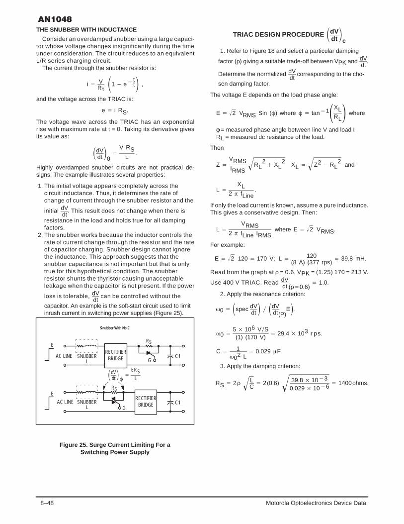
8–48 Motorola Optoelectronics Device Data
THE SNUBBER WITH INDUCTANCE
Consider an overdamped snubber using a large capaci-tor whose voltage changes insignificantly during the timeunder consideration. The circuit reduces to an equivalentL/R series charging circuit.
The current through the snubber resistor is:
i VR
1 et ,
and the voltage across the TRIAC is:
e i RS.
The voltage wave across the TRIAC has an exponentialrise with maximum rate at t = 0. Taking its derivative givesits value as:
dVdt
0
V RSL
.
Highly overdamped snubber circuits are not practical de-signs. The example illustrates several properties:
1. The initial voltage appears completely across thecircuit inductance. Thus, it determines the rate ofchange of current through the snubber resistor and the
initial dVdt
. This result does not change when there is
resistance in the load and holds true for all dampingfactors.
2. The snubber works because the inductor controls therate of current change through the resistor and the rateof capacitor charging. Snubber design cannot ignorethe inductance. This approach suggests that thesnubber capacitance is not important but that is onlytrue for this hypothetical condition. The snubberresistor shunts the thyristor causing unacceptableleakage when the capacitor is not present. If the power
loss is tolerable, dVdt
can be controlled without the
capacitor. An example is the soft-start circuit used to limitinrush current in switching power supplies (Figure 25).
Figure 25. Surge Current Limiting For aSwitching Power Supply
dVdt
ERSL
SNUBBERL G
RS
E
Snubber With No C
E
C1AC LINERECTIFIER
BRIDGE
SNUBBERL
AC LINERECTIFIER
BRIDGE C1G
RS
TRIAC DESIGN PROCEDURE dVdt
c
1. Refer to Figure 18 and select a particular damping
factor (ρ) giving a suitable trade-off between VPK and dVdt
.
Determine the normalized dVdt
corresponding to the cho-
sen damping factor.
The voltage E depends on the load phase angle:
E 2 VRMS Sin () where tan1XLRL where
φ = measured phase angle between line V and load IRL = measured dc resistance of the load.
Then
Z VRMSIRMS
RL2 XL
2 XL Z2RL2 and
L XL
2 fLine.
If only the load current is known, assume a pure inductance.This gives a conservative design. Then:
L VRMS
2 fLine IRMSwhere E 2 VRMS.
For example:
E 2 120 170 V; L 120(8 A) (377 rps)
39.8 mH.
Read from the graph at ρ = 0.6, VPK = (1.25) 170 = 213 V.
Use 400 V TRIAC. Read dVdt (ρ0.6)
1.0.
2. Apply the resonance criterion:
0 spec dVdt dV
dt(P)E.
0 5 106 VS(1) (170 V)
29.4 103 r ps.
C 102 L
0.029 F
3. Apply the damping criterion:
RS 2ρ LC 2(0.6) 39.8 103
0.029 106 1400ohms.

8–49Motorola Optoelectronics Device Data
dVdt
c SAFE AREA CURVE
Figure 26 shows a MAC16 TRIAC turn-off safe operatingarea curve. Turn-off occurs without problem under the curve.
The region is bounded by static dVdt
at low values of dIdt
cand delay time at high currents. Reduction of the peakcurrent permits operation at higher line frequency. ThisTRIAC operated at f = 400 Hz, TJ = 125°C, and ITM = 6.0amperes using a 30 ohm and 0.068 µF snubber. Low
damping factors extend operation to higher dIdt
c, but
capacitor sizes increase. The addition of a small, saturablecommutation inductor extends the allowed current rate byintroducing recovery delay time.
dV dt( )
(V/
s)
µc
dIdt
cAMPERESMILLISECOND
Figure 26. versus T J = 125°CdVdt
cdIdt
c
100
10
0.15010
1
WITH COMMUTATION L
3014 18 22 26 34 38 42 46
– ITM = 15 A
dIdt
c 6 f ITM 103 Ams
MAC 16-8, COMMUTATIONAL L 33 TURNS # 18,52000-1A TAPE WOUND CORE 34 INCH OD
STATIC dVdt DESIGN
There is usually some inductance in the ac main andpower wiring. The inductance may be more than 100 µH ifthere is a transformer in the circuit or nearly zero when ashunt power factor correction capacitor is present. Usuallythe line inductance is roughly several µH. The minimum
Figure 27. Snubbing For a Resistive Load
50 V/µs
0.33 µF10
LS1
100 µH20 A
340V 12 Ω
HEATER
inductance must be known or defined by adding a seriesinductor to insure reliable operation (Figure 27).
One hundred µH is a suggested value for starting thedesign. Plug the assumed inductance into the equation for C.Larger values of inductance result in higher snubber resis-
tance and reduced dIdt
. For example:
Given E = 240 2 340 V.
Pick ρ = 0.3.
Then from Figure 18, VPK = 1.42 (340) = 483 V.
Thus, it will be necessary to use a 600 V device. Using thepreviously stated formulas for ω0, C and R we find:
0 50 106 VS(0.73) (340 V)
201450 rps
C 1(201450)2 (100 106)
0.2464 F
R 2 (0.3) 100 106
0.2464 106 12 ohms
VARIABLE LOADS
The snubber should be designed for the smallest load
inductance because dVdt
will then be highest because of its
dependence on ω0. This requires a higher voltage device foroperation with the largest inductance because of thecorresponding low damping factor.

8–50 Motorola Optoelectronics Device Data
Figure 28 describes dVdt
for an 8.0 ampere load at various
power factors. The minimum inductance is a component
added to prevent static dVdt
firing with a resistive load.
ρR L Vstep VPK
dvdtρ
Ω MHY V V V/µs
0.75 15 0.1 170 191 86
0.03 0 39.8 170 325 4.0
0.04 10.6 28.1 120 225 3.3
0.06 13.5 17.3 74 136 2.6
EXAMPLES OF SNUBBER DESIGNS
Table 2 describes snubber RC values for dVdt
s. Figures
31 and 32 show possible R and C values for a 5.0 V/µs
dVdt
c assuming a pure inductive load.
Table 2. Static Designs
(E = 340 V, Vpeak = 500 V, ρ = 0.3)
dVdt
5.0 V/µs 50 V/µs 100 V/µs
LµH
CµF
ROhm
CµF
ROhm
CµF
ROhm
47 0.15 10100 0.33 10 0.1 20220 0.15 22 0.03
347
500 0.068
51 0.015
110
1000
3.0 11 0.033
100
TRANSIENT AND NOISE SUPPRESSION
Transients arise internally from normal circuit operation orexternally from the environment. The latter is particularlyfrustrating because the transient characteristics are unde-fined. A statistical description applies. Greater or smallerstresses are possible. Long duration high voltage transientsare much less probable than those of lower amplitude andhigher frequency. Environments with infrequent lightningand load switching see transient voltages below 3.0 kV.
Figure 29. Snubber Resistor For = 5.0 V/ µsdVdtc
R
(OH
MS)
S
80 A
40 A
20 A
0
0.6 A RMS 2.5 A
5 A
DAMPING FACTOR
10.90.80.70.60.50.40.30.20.1
10K
100
1000
10
10 A
PURE INDUCTIVE LOAD, V 120 VRMS,IRRM 0
Figure 30. Snubber Capacitor For = 5.0 V/ µsdVdtc
C
( F
)S
µ
0.001
2.5 A0.01
0.6 A
5 A
10 A
20 A
1
0.1
80 A RMS
40 A
0
DAMPING FACTOR
10.90.80.70.60.50.40.30.20.1
PURE INDUCTIVE LOAD, V 120 VRMS,IRRM 0
Figure 28. Snubber For a Variable Load
LRMAC 218-6
8 A LOAD
68 Ω 120 V60 Hz
0.033 µF
dVdt
s 100 Vs dV
dt
c 5 Vs

8–51Motorola Optoelectronics Device Data
The natural frequencies and impedances of indoor ac wiringresult in damped oscillatory surges with typical frequenciesranging from 30 kHz to 1.5 MHz. Surge amplitude depends onboth the wiring and the source of surge energy. Disturbancestend to die out at locations far away from the source. Spark-over(6.0 kV in indoor ac wiring) sets the maximum voltage whentransient suppressors are not present. Transients closer to theservice entrance or in heavy wiring have higher amplitudes,longer durations, and more damping because of the lowerinductance at those locations.
The simple CRL snubber is a low pass filter attenuatingfrequencies above its natural resonance. A steady statesinusoidal input voltage results in a sine wave output at thesame frequency. With no snubber resistor, the rate of roll offapproaches 12 dB per octave. The corner frequency is at thesnubber’s natural resonance. If the damping factor is low, theresponse peaks at this frequency. The snubber resistordegrades filter characteristics introducing an up-turn at ω = 1/ (RC). The roll-off approaches 6.0 dB/octave at frequenciesabove this. Inductance in the snubber resistor furtherreduces the roll-off rate.
Figure 32 describes the frequency response of thecircuit in Figure 27. Figure 31 gives the theoreticalresponse to a 3.0 kV 100 kHz ring-wave. The snubberreduces the peak voltage across the thyristor. However,
the fast rise input causes a high dVdt
step when series
inductance is added to the snubber resistor. Limiting theinput voltage with a transient suppressor reduces the step.
Figure 31. Theoretical Response of Figure 33 Circuitto3.0 kV IEEE 587 Ring Wave (R SC = 27.5 Ω)
V
(VO
LTS)
MT 2-
1
400
WITH 5 µHY
450 V MOVAT AC INPUT
WITH 5 µHY ANDWITHOUT 5 µHY
654210
TIME (µs)
3– 400
0
Figure 32. Snubber Frequency Response VoutVin
VOLT
AGE
GAI
N (d
B)
FREQUENCY (Hz)10K
WITH 5 µHY
WITHOUT 5µHY
– 40
0.33 µF
10
5 µH
12
Vin
100 µH
1M
+ 10
0
100K
– 30
– 20
– 10
Vout
The noise induced into a circuit is proportional to dVdt
when
coupling is by stray capacitance, and dIdt
when the coupling is
by mutual inductance. Best suppression requires the use of avoltage limiting device along with a rate limiting CRL snubber.
The thyristor is best protected by preventing turn-on fromdVdt
or breakover. The circuit should be designed for what can
happen instead of what normally occurs.In Figure 30, a MOV connected across the line protects
many parallel circuit branches and their loads. The MOV
defines the maximum input voltage and dIdt
through the load.
With the snubber, it sets the maximum dVdt
and peak voltage
across the thyristor. The MOV must be large because there islittle surge limiting impedance to prevent its burn-out.
Figure 33. Limiting Line Voltage
VMAX
In Figure 32, there is a separate suppressor across eachthyristor. The load impedance limits the surge energydelivered from the line. This allows the use of a smallerdevice but omits load protection. This arrangement protectseach thyristor when its load is a possible transientsource.
Figure 34. Limiting Thyristor Voltage
It is desirable to place the suppression device directly acrossthe source of transient energy to prevent the induction of energyinto other circuits. However, there is no protection for energyinjected between the load and its controlling thyristor. Placingthe suppressor directly across each thyristor positively limits
maximum voltage and snubber discharge dIdt
.

8–52 Motorola Optoelectronics Device Data
Figure 35. 3 Phase Reversing Motor
MOC3081
SNUBBERALL MOV’S ARE 275VRMSALL TRIACS AREMAC218-10
0.15µF
22 Ω2 W
WIREWOUND
43
4
6
G1
2
91
1/3 HP208 V
3 PHASE
100 µH
REV
φ1
91
G
12
300
6
FWD
4
SNUBBER
N
φ2
φ3
MOC3081
91
G
12
300
64
SNUBBER
MOC3081
91
G
12
300
64
SNUBBER
MOC3081
91
G
12
300
46
SNUBBER
REV
FWD
100 µHMOC3081
SNU
BBER
EXAMPLES OF SNUBBER APPLICATIONS
In Figure 35, TRIACs switch a 3 phase motor on and offand reverse its rotation. Each TRIAC pair functions as aSPDT switch. The turn-on of one TRIAC applies thedifferential voltage between line phases across theblocking device without the benefit of the motor impedanceto constrain the rate of voltage rise. The inductors are
added to prevent static dVdt
firing and a line-to-line short.
Figure 36 shows a split phase capacitor-run motor withreversing accomplished by switching the capacitor inseries with one or the other winding. The forward andreverse TRIACs function as a SPDT switch. Reversing themotor applies the voltage on the capacitor abruptly acrossthe blocking thyristor. Again, the inductor L is added to
prevent dVdt
s firing of the blocking TRIAC. If turn-on
occurs, the forward and reverse TRIACs short thecapacitors (Cs) resulting in damage to them. It is wise toadd the resistor RS to limit the discharge current.

8–53Motorola Optoelectronics Device Data
Figure 36. Split Phase Reversing Motor
5.6
3.75330 V
MOTOR1/70 HP0.26 A
T2323D
115
500 µH
LS
REV
46 V/µsMAX
FWD
0.191
CS
0.1
RS
91
Figure 37 shows a “ tap changer.” This circuit allows theoperation of switching power supplies from a 120 or 240 vacline. When the TRIAC is on, the circuit functions as aconventional voltage doubler with diodes D1 and D2conducting on alternate half-cycles. In this mode of opera-
tion, inrush current and dIdt
are hazards to TRIAC reliability.
Series impedance is necessary to prevent damage to theTRIAC.
The TRIAC is off when the circuit is not doubling. In thisstate, the TRIAC sees the difference between the line voltageand the voltage at the intersection of C1 and C2. Transients
on the line cause dVdt
s firing of the TRIAC. High inrush
current, dIdt
, and overvoltage damage to the filter capacitor
are possibilities. Prevention requires the addition of a RCsnubber across the TRIAC and an inductor in series withthe line.
Figure 37. Tap Changer For Dual VoltageSwitching Power Supply
–C1
+
RL
0 G
CSRS
120 V
240 V
SNUBBER INDUCTOR
120 VACOR
240 VAC
D1D2
D4D3
–C2
+
THYRISTOR TYPES
Sensitive gate thyristors are easy to turn-on because oftheir low trigger current requirements. However, they have
less dVdt
capability than similar non-sensitive devices. A
non-sensitive thyristor should be used for high dVdt
.
TRIAC commutating dVdt
ratings are 5 to 20 times less than
static dVdt
ratings.
Phase controllable optocouplers have lower dVdt
ratings
than zero crossing optocouplers and power TRIACs.These should be used when a dc voltage component ispresent, or to prevent turn-on delay.
Zero crossing optocouplers have more dVdt
capability
than power thyristors; and they should be used in place ofphase controllable devices in static switchingapplications.
APPENDIX A
TESTING SNUBBER DISCHARGE dIdt
The equations in Appendix D do not consider thethyristor’s turn-on time or on-state resistance, thus, they
predict high values of dIdt
.
Figure 38 shows the circuit used to test snubber dischargedIdt
. A MBS4991 supplies the trigger pulse while the quad-
rants of operation are switch selectable. The snubber wasmounted as close to the TRIAC under test as possible toreduce inductance, and the current transformer remained inthe circuit to allow results to be compared with the measureddIdt
value.
What should the peak capacitor voltage be? A conserva-tive approach is to test at maximum rated VDRM, or the clampvoltage of the MOV.
What is the largest capacitor that can be used withoutlimiting resistance? Figure 39 is a photo showing the currentpulse resulting from a 0.001 µF capacitor charged to 800 V.
The 1200 A/µs dIdt
destroyed the TRIAC.
Is it possible for MOV self-capacitance to damage theTRIAC? A large 40 Joule, 2200 A peak current rated MOVwas tested. The MOV measured 440 pF and had an 878volt breakover voltage. Its peak discharge current (12 A)was half that of a 470 pF capacitor. This condition wassafe.

8–54 Motorola Optoelectronics Device Data
Figure 38. Snubber Discharge dl/dt Test
OPTIONAL PEARSON411 CURRENT
TRANSFORMER
120 VAC 60 Hz
500 W
2000
SWEEP FORDESIRED VCi
VTC5–50
2.5 kV5000200 W
X100V PROBE
RS
CS
TRIACUNDER TEST
MT1
50 Ω
G
MT2
91
56
VMT2-1
QUADRANTMAP
2
3 4
1
VG Q1,3
12 V
QUADRANTSWITCH
Q2,41µF
MBS4991
3000
OPT
ION
AL M
OV
APPENDIX B
MEASURING dVdt
s
Figure 40 shows a test circuit for measuring the static dVdt
of power thyristors. A 1000 volt FET switch insures that thevoltage across the device under test (D.U.T.) rises rapidlyfrom zero. A differential preamp allows the use of aN-channel device while keeping the storage scopechassis at ground for safety purposes. The rate of voltagerise is adjusted by a variable RC time constant. Thecharging resistance is low to avoid waveform distortionbecause of the thyristor’s self-capacitance but is large
enough to prevent damage to the D.U.T. from turn-on dIdt
.
Mounting the miniature range switches, capacitors, andG-K network close to the device under test reduces strayinductance and allows testing at more than 10 kV/µs.
Figure 39. Discharge Current From 0.001 µF Capacitor
HORIZONTAL SCALE — 50 ms/DIV.VERTICAL SCALE — 10 A/DIV.
CS = 0.001 µF, VCi = 800 V, RS = 0, L = 250 mH, RTRAIC = 10 OHMS

8–55Motorola Optoelectronics Device Data
Figure 40. Circuit For Static Measurement of Power ThyristorsdVdt
X100 PROBE
X100 PROBE
DIFFERENTIALPREAMP
MOUNT DUT ONTEMPERATURE CONTROLLEDCµ PLATE
DUT
2
1G
RGK
2 W20 k
VDRM/VRRM SELECT 2 W
27
0.33 1000 V 0.0471000 V
100010 WATT
WIREWOUND
10001/4 W
562 W
VERNIER
822 W
1002 W
470 pF
0.001
0.005
0.01
0.047
0.1
0.47
1.2 MEG2 W EACH1 MEG
POWER2 W
TEST
MTP1N100
ALL COMPONENTS ARE NON-INDUCTIVE UNLESS OTHERWISE SHOWN
0–1000 V10 mA
1N967A18 V
1N914
f = 10 HzPW = 100 µs50 Ω PULSEGENERATOR
20 V
dVdt
APPENDIX C
MEASURING dVdt
c
A test fixture to measure commutating dVdt
is shown in
Figure 41. It is a capacitor discharge circuit with the loadseries resonant. The single pulse test aids temperaturecontrol and allows the use of lower power components.The limited energy in the load capacitor reduces burn andshock hazards. The conventional load and snubber circuitprovides recovery and damping behaviors like those in theapplication.
The voltage across the load capacitor triggers the D.U.T.It terminates the gate current when the load capacitorvoltage crosses zero and the TRIAC current is at its peak.
Each VDRM, ITM combination requires different compo-nents. Calculate their values using the equations given inFigure 41.
Commercial chokes simplify the construction of the neces-sary inductors. Their inductance should be adjusted byincreasing the air gap in the core. Removal of the magneticpole piece reduces inductance by 4 to 6 but extends thecurrent without saturation.
The load capacitor consists of a parallel bank of 1500 Vdcnon-polar units, with individual bleeders mounted at eachcapacitor for safety purposes.
An optional adjustable voltage clamp prevents TRIACbreakdown.
To measure dVdt
c, synchronize the storage scope on the
current waveform and verify the proper current amplitude andperiod. Increase the initial voltage on the capacitor tocompensate for losses within the coil if necessary. Adjust thesnubber until the device fails to turn off after the firsthalf-cycle. Inspect the rate of voltage rise at the fastestpassing condition.

8–56 Motorola Optoelectronics Device Data
–
+
–
+
2 W51+ 5CS
2N3904
0.1
2.2 k1/2SYNC
TRIACUNDERTEST
562 WATT
CASECONTROLLED
HEATSINK
0.1
2N3906
– 5 G1
2
PEARSON301 X
2N3904
1/2 W120
2N3906
1201/2 W
2N39062N3904RS
1/2 W
– +
0.22270 k 1N5343
7.5 V
0.22Q1Q3
2N3906
2N3904
1/2 W360
1 k
– 5 + 5
NON-INDUCTIVERESISTOR DECADE
0–10 k, 1 Ω STEP
2 W51 k
51 k2 W
HG = W AT LOW LD10-1000-1000
+ CLAMP
MR760
– CLAMP
62 µF1 kV
LL
6.2 MEG 2 W
150 k
910 k2 W
2 W
910 k
RL
Q3 Q1
70 mA
1.5 kV
TRIAD C30X50 H, 3500 Ω
2 W51
6.2 MEG 2 W
360
1 k
270 k
2N39042N3906
Q3 Q1
0-1
kV 2
0 m
A
C
(NO
N-P
OLA
R)
L
MR
760
MR
760
2.2
M2.
2 M
2.2
M, 2
W
2.2
M, 2
W2.
2 M
2.2
M
0.01
Figure 41. Test Circuit For Power TRIACsdVdt
c
µ
CL IPK
W0 VCi
Ip T
2 VCiLL
VCiW0 IPK
T2
4 2 CLW0
I
LLdIdtc 6f IPK 106
As
dVdt
CAP
ACIT
OR
DEC
ADE
1–10
F
, 0.0
1–1
F,
100
pF–
0.0
1
Fµ
µ
0.01

8–57Motorola Optoelectronics Device Data
APPENDIX DdVdt
DERIVATIONS
DEFINITIONS
1.0 RT RL RS Total Resistance
1.1 M RSRT
Snubber Divider Ratio
1.2 0 1L CS Undamped Natural Frequency
Damped Natural Frequency
1.3 RT2 L
Wave Decrement Factor
1.4 χ2 12 LI2
12 CV2
Initial Energy In InductorFinal Energy In Capacitor
1.5 χ IE
LC Initial Current Factor
1.6 ρ RT2
CL
0 Damping Factor
1.7 V0L ERS I Initial Voltage drop at t 0across the load
1.8 ICS
E RL
L
dVdt
0 Initial instantaneous dV
dtat t 0, ignoring
any initial instantaneous voltage step att 0 because of IRRM
1.9 dVdt
0 VOL
RTL . For all damping conditions
2.0 When I 0, dVdt
0
E RSL
dVdt
max Maximum instantaneous dV
dt
tmax Time of maximum instantaneous dVdt
tpeak Time of maximum instantaneous peakvoltage across thyristor
Average dVdt
VPK tPK Slope of the secant line
from t 0 through VPKVPK Maximum instantaneous voltage across the
thyristor.
CONSTANTS (depending on the damping factor):
2.1 No Damping (ρ 0) 0RT ρ 0
2.2 Underdamped (0 ρ 1)
02 2 0 1 ρ2
2.3 Critical Damped (ρ 1)
0, 0, R 2 LC , C 2
RT
2.4 Overdamped (ρ 1)
2 02 0 ρ2 1Laplace transforms for the current and voltage in Figure 42are:
3.0 i(S)ELSI
S2SRTL 1
LC
; e ES
S V0L
S2RTL
S 1LC
INITIAL CONDITIONSI IRRMVCS 0
Figure 42. Equivalent Circuit for Load and Snubber
t = 0I
RL L
CS
RSe
The inverse laplace transform for each of the conditionsgives:
UNDERDAMPED (Typical Snubber Design)
4.0 e E V0LCos (t)
sin (t)e t
sin (t) et
4.1 dedt
V0L2Cos (t)
(2 2)
sin (t)et
Cos (t)
sin (t) et
4.2 tPK 1 tan1
2 V0L
V0L22
When M 0, RS 0, I 0 : tPK
4.3 VPK E 0
tPK 02 V0L
2 2 V0L 2When I 0, RL 0, M 1:
4.4VPK
E (1 e tPK)
Average dVdt
VPKtPK

8–58 Motorola Optoelectronics Device Data
4.5 tmax1
ATN (2 V0L (2 32))
V0L(3 32) (2 2)
4.6 dVdt
max V0L
2022 V0L 2 e– tmax
NO DAMPING
5.0 e E (1 Cos (0t)) IC 0
sin (0t)
5.1 dedt
E 0 sin (0t) IC
Cos (0t)
5.2 dVdt
0 I
C 0 when I 0
5.3 tPK tan1 I
CE 0
0
5.4 VPK E E2 I2
02C2
5.5 dVdtAVG
VPKtPK
5.6 tmax 10tan10 EC
I 1
02
when I 0
5.7 dVdt
max I
CE202 C2I2 0E when I 0
CRITICAL DAMPING
6.0 e E V0L(1 t)et tet
6.1 dedt
VOL (2 t) (1 t)et
6.2 tPK
2
2 V0L
V0L
6.3 VPK E – V0L (1– tPK)– tPK e– tPK
6.4 Average dVdt
VPKtPK
When I 0, RS 0, M 0
e(t) rises asymptotically to E. tPK and average dVdt
do not exist.
6.5 tmax 3V0L 2
2V0L
When I 0, tmax 0
ForRSRT
34,
then dVdt max
dVdt
0
6.6 dVdt
max
V0L (2– tmax) (1– tmax) e– tmax
APPENDIX E
SNUBBER DISCHARGE dIdt
DERIVATIONS
OVERDAMPED
1.0 i VCS LS
–t sinh (t)
1.1 iPK VCS
CSLS e– tPK
1.2 tPK 1 tanh –1
CRITICAL DAMPED
2.0 i VCSLS
te–t
2.1 iPK 0.736VCSRS
2.2 tPK 1
UNDERDAMPED
3.0 i VCS LS
e–t sin (t)
3.1 iPK VCS
CSLS e– tPK
3.2 tPK 1 tan –1

8–59Motorola Optoelectronics Device Data
Figure 43. Equivalent Circuit for Snubber Discharge
LSRS
CSVCS i
t = 0
INITIAL CONDITIONS :i 0, VCS INITIAL VOLTAGE
NO DAMPING
4.0 iVCS LS
sin (t)
4.1 iPK VCS
CSLS
4.2 tPK
2
BIBLIOGRAPHY
Bird, B. M. and K. G. King. An Introduction To PowerElectronics. John Wiley & Sons, 1983, pp. 250–281.
Blicher, Adolph. Thyristor Physics. Springer-Verlag, 1976.
Gempe, Horst. “Applications of Zero Voltage CrossingOptically Isolated TRIAC Drivers,” AN982, Motorola Inc.,1987.
“Guide for Surge Withstand Capability (SWC) Tests,” ANSI337.90A-1974, IEEE Std 472–1974.
“IEEE Guide for Surge Voltages in Low-Voltage AC PowerCircuits,” ANSI/IEEE C62.41-1980, IEEE Std 587–1980.
Ikeda, Shigeru and Tsuneo Araki. “The dIdt
Capability of
Thyristors,” Proceedings of the IEEE, Vol. 53, No. 8, August1967.
Kervin, Doug. “The MOC3011 and MOC3021,” EB-101,Motorola Inc., 1982.
McMurray, William. “Optimum Snubbers For Power Semicon-ductors,” IEEE Transactions On Industry Applications, Vol.IA-8, September/October 1972.
Rice, L. R. “Why R-C Networks And Which One For YourConverter,” Westinghouse Tech Tips 5-2.
“Saturable Reactor For Increasing Turn-On Switching Capa-bility,” SCR Manual Sixth Edition, General Electric, 1979.
Zell, H. P. “Design Chart For Capacitor-Discharge PulseCircuits,” EDN Magazine, June 10, 1968.

8–60 Motorola Optoelectronics Device Data
Motorola reserves the right to make changes without further notice to any products herein. Motorola makes no warranty, representation or guarantee regardingthe suitability of its products for any particular purpose, nor does Motorola assume any liability arising out of the application or use of any product or circuit, andspecifically disclaims any and all liability, including without limitation consequential or incidental damages. “Typical” parameters can and do vary in differentapplications. All operating parameters, including “Typicals” must be validated for each customer application by customer’s technical experts. Motorola doesnot convey any license under its patent rights nor the rights of others. Motorola products are not designed, intended, or authorized for use as components insystems intended for surgical implant into the body, or other applications intended to support or sustain life, or for any other application in which the failure ofthe Motorola product could create a situation where personal injury or death may occur. Should Buyer purchase or use Motorola products for any suchunintended or unauthorized application, Buyer shall indemnify and hold Motorola and its officers, employees, subsidiaries, affiliates, and distributors harmlessagainst all claims, costs, damages, and expenses, and reasonable attorney fees arising out of, directly or indirectly, any claim of personal injury or deathassociated with such unintended or unauthorized use, even if such claim alleges that Motorola was negligent regarding the design or manufacture of the part.Motorola and are registered trademarks of Motorola, Inc. Motorola, Inc. is an Equal Opportunity/Affirmative Action Employer.

8–61Motorola Optoelectronics Device Data
How to reach us:USA / EUROPE: Motorola Literature Distribution; JAPAN : Nippon Motorola Ltd.; Tatsumi–SPD–JLDC, Toshikatsu Otsuki,P.O. Box 20912; Phoenix, Arizona 85036. 1–800–441–2447 6F Seibu–Butsuryu–Center, 3–14–2 Tatsumi Koto–Ku, Tokyo 135, Japan. 03–3521–8315
MFAX: [email protected] – TOUCHTONE (602) 244–6609 HONG KONG: Motorola Semiconductors H.K. Ltd.; 8B Tai Ping Industrial Park, INTERNET: http://Design–NET.com 51 Ting Kok Road, Tai Po, N.T., Hong Kong. 852–26629298
AN1048/D
◊

8–62 Motorola Optoelectronics Device Data
"! " !
Prepared by: Horst GempeDiscrete Applications Engineering
INTRODUCTION
Electronic controls of AC power loads based on micro–processor controllers, digital or linear sensor circuits areincreasing in popularity. Consequently, there is an increasingneed for a simple and robust interface between the low voltagecontrol circuitry and the AC line and loads. This interface mustgalvanically isolate the AC power line and its superimposedtransients from the noise sensitive, low–voltage dc control
circuits. It also must be simple to use, regulatory approved,consume little PC board space and be able to switch the mostcommon loads such as small motors, power relays, incandes-cent lights and resistive loads without generating excessiveheat.
The MOC2A40 and MOC2A60 POWER OPTO Isolatorfamilies meet all the above requirements and offer an idealsystem solution.
Optically ReflectiveMold CompoundPatented Co–Planar
Optical Dome Construction
Gallium ArsenideLight Emitting Diode
MOC Series Zero–CrossTriac Driver Chip
Meets VDE 8mmMin. Creepage
8 Amp PowerTriac Chip
Heavy Duty WireBond System
Patented ThermalManagement System
Electrically IsolatedHeat Tab
Nominal dimensions1.0″ (L) x 0.7″ (H) x 0.18″ (W)
Figure 1. Internal Construction of the POWER OPTO Isolator
POWER OPTO is a trademark of Motorola, Inc.
Order this documentby AN1511/D
SEMICONDUCTOR APPLICATION NOTE
Motorola, Inc. 1995

8–63Motorola Optoelectronics Device Data
PRODUCT DESCRIPTION
The Motorola AC POWER OPTO Isolator is a hybrid devicecontaining three individual active semiconductor chips.Figure 1 shows the internal structure of this device. An infraredlight emitting diode on the input side converts the input currentsignal of several milliamps into an infrared radiation of 940 nm.This is transferred through a transparent isolation barrier ontothe photo sensitive area of an AC compatible detector whichcontrols the gate of a power triac. This creates galvanic isola-tion between the dc input control circuit and the output AC linevoltage potential. The light sensitive detector contains a ACzero voltage detector which allows turn on of the detector chipby the LED only when the AC line voltage is below the speci-fied inhibit voltage of ±10 V. This feature guarantees turn on ofthe load close to the AC line zero cross point and preventsexcessive inrush surge currents for most loads. High inrushcurrents are still experienced for loads such as motor startupand inductors which saturate at turn–on. For this reason, aguaranteed inrush surge current capability of 60 A is provided.This extremely high surge capability can be attributed to therugged 120 x 120 mil power triac chip which is mounted on alarge internal copper heat spreader. A patented interdigitatedinterface between the internal heat spreader and the devicesintegral heat tab provides optimized heat transfer and meetsthe regulatory requirements for safe (reinforced) isolation.This regulatory requirement mandates an external 8.0 mmcreepage and clearance between the input and output leadsand the isolated heat tab of the device. A 0.4 mm thick isolationbarrier which must be able to withstand a surge voltage of3750 Vrms is also mandated. The isolation barrier between dcinput and the AC output leads is formed by the silicone opticaldome. The isolation barrier for the integral heat sink is formed
by the package epoxy which isolates the interlaced internalheat spreader from the external heat tab. A heavy duty 15 milaluminum wire bond on the output side of the power triacensures high surge capability.
Equivalent Electrical Circuit Diagram
Figure 2 shows in detail the internal circuitry of theMOC2A40 and MOC2A60 POWER OPTO Isolator families.Details of the of the triac driver ICs internal circuitry is shownand discussed to explain the theory of operation for thesedevices.
LED D1 emits light which is received by the detector lightsensitive integrated circuit which is commonly named triacdriver. PNP transistor, Q1, and light sensitive NPN transistor,Q2, form a light sensitive SCR with a gate resistor R1. Diode,D2, and FET, Q3, form the inhibiting network. The leakagecurrent of D2 transfers the main terminal voltage to the FETgate and Zener diode, D3, clamps this voltage to about 15 Vto prevent gate oxide breakdown when the main terminalvoltage rises with the line voltage. A voltage on the main termi-nals above the gate threshold voltage of Q3 switches FET Q3on, which shorts the photo sensitive gate and inhibits it to latchon. Q1’, Q2′, Q3′, R1′, D2′, D3′ form the same circuit asdescribed above.
The two circuits are connected inverse parallel and may bedescribed as two inverse parallel light sensitive photo SCRswith zero cross voltage detectors. This circuit can be furthersimplified and described as an optically controlled small signaltriac with an AC zero cross detection circuit. The triac drivercontrols the gate of the main triac. Resistor R2 limits thecurrent through the triac driver.
Figure 2. 2 Amp Optocoupler Circuit
TRIAC DRIVER
INPUT
h h h
h
D1
D3
Q1
Q2
R1
Q3
Q1
Q2
R1
Q3
D3
D2
R2
Q4
8 AMP TRIACLED
D2

8–64 Motorola Optoelectronics Device Data
0X 0X
h h
Opto Inverse Parallel SCR Opto Triac
0X
Figure 3. Triac Driver Simplified Circuits
OPERATION
An LED current of several mA will generate a photo currentof several tens of micro amps in the collector base junctionsof the NPN transistors of the triac driver chip. The SCR formedby the NPN–PNP transistor combination latches on when thephoto generated current is present and the line voltage isbelow the inhibit voltage window, or in other words, within thezero cross window. Once the triac driver is latched on it allowssufficient current flow to the gate of the main triac which in turnlatches on and carries the load current.
If the LED is turned on at a time when the line voltageexceeds the inhibit voltage, the driver is effectively disabledand will wait to latch on until the line voltage falls below theinhibit voltage. The driver and triac, however, are not able toswitch on at absolute zero line voltage because they need aminimum voltage and current to be able to latch on. Forexample, if the LED is switched on when the line voltage iszero, the LED flux generates a photo current in the detector ofseveral tens of micro amps, but the triac driver is not able to
latch on until the line voltage rises to the driver’s minimummain terminal voltage of about 1.0 V and a latching currentof several 100 µA is present. A further increase in line voltageis necessary to trigger the main triac because its minimumgate voltage requirement in respect to MT1 voltage is alsoabout 1.0 V and has to be added to the voltage drop across thetriac driver. The main triac is able to turn on when at least 2.0V are across its main terminals and enough gate current isgenerated to meet the triacs gate trigger current requirement.This is the earliest possible turn–on point within the zero–cross window. Conversely, the maximum inhibit voltage repre-sents the last possible opportunity to turn on within thezero–cross window.
When the main triac is triggered, the voltage across its mainterminals collapses to about 1.0 V. Figure 4 shows the zerovoltage turn–on characteristic of a POWER OPTO Isolator asobserved with an oscilloscope by monitoring the voltageacross the main terminals of the device. Figure 5 shows acurve tracer plot which gives information about the voltage andcurrent characteristic.

8–65Motorola Optoelectronics Device Data
ÍÍÍÍÍÍÍÍÍÍÍÍÍÍÍÍ
INITIALTURN–ON
SUBSEQUENTTURN–ON
ON STATE
MAX ON–STATEVOLTAGE DROP
(Vpk)PERMISSIBLE
TURN–ON WINDOW
EARLIESTPOSSIBLETURN–ON
CONTROLSIGNAL APPLIED
MAX INHIBITVOLTAGE LINE
VOLTAGE(1/2 CYCLE)
ON STATE
0 V
Figure 4. Zero–Voltage Turn–On Voltage Characteristics
OFF STATE

8–66 Motorola Optoelectronics Device Data
ÎÎÎÎÎÎÎÎ
Q3
ÎÎÎÎÎÎÎÎÎÎÎÎÎÎÎÎ
Q1
Driver VTM
I+
I–
VTM+VTM–Triac Igt Q1
1V/div
Figure 5. Curve Tracer Voltage versus Current Plot
Triac VTM
Triac Igt Q3
50 m
A/di
v
After the power triac is turned on, the triac driver conductsonly several hundred micro amps when the LED is still on butswitches off and stays off when the LED current is removed.The main triac remains latched on until the load current fallsbelow the triacs holding current. After this transition point, thedriver will exclusively conduct the load current until the currentfalls below several 100 micro amps. At this point only the photogenerated current of several tens of micro amps remains.Triac driver and main triac are switched off and are retriggeredevery half cycle until the LED is turned off. As the LED isswitched off the triac driver is switched off, and the main triacfalls out of conduction when the load current falls below themain triac’s holding current ( typically 20 mA).
The fact that the triac driver has an extremely low holdingcurrent allows the minimum load currents to be below the maintriac trigger and holding current. In this triac driver only mode,the main triac never conducts and the load is only carried bythe triac driver. In this low current triac driver only mode,commutating dv/dt is no longer a function of the main triaccommutating capability, but is dependent on the triac driverscommutating dv/dt capability. This is only about 0.5 V/µs andshould be considered marginal. Therefore, the use of asnubber is absolutely mandatory when switching loads in triacdriver only mode is anticipated.
APPLICATIONS
Snubber Requirements
The application of the 2 amp POWER OPTO Isolators isvery simple. Most loads ranging from 30 mA up to 2 A rms,including complex loads as discussed below, may becontrolled without the use of a snubber network. Snubbers arerequired when the static and commutating dv/dt either gener-ated by the load switched by the POWER OPTO Isolators orgenerated elsewhere on the AC line exceed the device’s dv/dtratings. In industrial environments where large inductive loadsare switched on and off by contactors, transients may begenerated which surpass the devices static dv/dt rating or themaximum VDRM rating. For these cases a snubber consistingof a resistor and a capacitor will attenuate the rate of rise of thetransient. A voltage clipping device (Metal Oxide VaristorMOV) which limits the amplitude of the transients should beused when the amplitude of the transients exceed the devicesVDRM ratings. Snubber and transient suppressors areconnected across the main terminals of the POWER OPTOIsolator as shown in Figure 6.
load
Cs
RsMOV
Rin
Vin AC line
Figure 6. Application with Snubber and MOV

8–67Motorola Optoelectronics Device Data
Typical values for the snubber capacitor C’s and snubberresistor R’s are 0.01 µF and 39 Ω respectively. These valuesmay be adjusted for specific applications. See ApplicationNote AN1048 for detailed information about snubber designconsiderations.
The placement of the load has no influence on the opto–coupler‘s performance. It may be switched from the lineneutral to the phase (hot) side or from the phase to neutral.
Figure 7. Size No. 4 Contactor Inrush Current
ÎÎÎÎÎÎÎÎÎÎÎÎÎÎÎÎ
ÎÎÎÎÎÎÎÎÎÎ
ÎÎÎ
ÎÎÎ
ÎÎÎÎÎÎÎÎÎÎÎÎÎÎÎ
Amp
10
20
30
40
ÎÎÎÎÎÎ
ÎÎÎ
ÎÎÎÎÎÎÎÎÎ
Input Current Requirement
It is very important to supply the data sheet specified inputcurrent to the device. Less input current may prevent turn–onof either both light sensitive SCRs or worse, be able to turn ononly one SCR due to slight differences in IFT for the positiveand negative AC half wave. This situation causes half–wavingof the load. Most inductive loads draw excessive current underthis condition which may destroy either the load or the opto-coupler. Low temperature operation requires increased inputLED current as shown on the data sheet’s IFT vs. Temperaturegraph .
For example:The IFT for a MOC2A40–10 at 25°C is 10 mA, but is at –40°C
15,5 mA (IFT @ 25°C*factor 1.55 as shown on the graph).This minimum control current requirement dictates the
value of the input current limiting resistor Rin for a given inputvoltage.
Rin(max)Vin– VF(LED)
IFT(on)
Rin(min)Vin– VFL(LED)
IFmax
Vin = Input VoltageVF(LED) = voltage drop across LED = 1.3 V
IFT(on) = specified LED trigger current*factor for low temper-ature operation
IF(max) = maximum continues LED forward current (50mA)
Complex Loads
Surge Currents in Inductive LoadsInductive loads may cause very high inrush surge currents
because their magnetic core is forced into saturation asobserved with transformers or the inductance is low at theinitial startup which is typical for relays, solenoids and motors.
Example 1: Size No. 4 Contactor Control
The MOC2A40 has demonstrated its ability to handle largeinrush currents by driving a size No. 4 contactor out to 2 millioncycles without failure. The device is cycled one second on andone second off. The 115 Vrms input coil generates a 50 A peakin the first half cycle, and 20 A peak in the second half cycleas shown in Figure 7. The RMS steady state current is below1 A. A MOC2A40 in free air is able to control this load withoutadditional heat sinking and without the use of a snubber.
Two million device cycles without failure represent a reli-ability of M.T.B.F of >19.8 million device cycles.
Example 2: Transformer Inrush Current
It is mandatory in this application to make certain that theinrush current does not exceed the maximum 60 A specifiedsurge current of the device. Residual core magnetizationcombined with zero cross turn–on may force the transformerinto saturation with only the winding resistance left as effectiveload current limitation. For example, a 150 VA transformer witha 1.5 Ω winding resistance may draw in the first half–cycle upto 80 A of surge current. This excessive surge current can beavoided by using a NTC thermistor in series with the load asshown in Figure 8. A negative temperature coefficient therm-istor has a relative high initial resistance when cold, which fastbecomes lower due to self–heating in the steady–state opera-tion.
Cs
Rs
Transformer
NTC
Rin
AC lineVin
Figure 8. Thermistor Limits Excessive Inrush Current
Example 3: Surge Currents in Capacitive Loads
A rectifier bridge or a single diode in combination with a largecapacitor in the micro Farad range represent a very low imped-ance at startup when the capacitor is being charged. Whenthis type of load is switched on at the peak of the line voltage,the inrush peak current is only limited by the wiring resistanceand the ESR of the capacitor. However, the maximum inrush

8–68 Motorola Optoelectronics Device Data
current Ip at zero voltage turn–on is limited by the AC linefrequency and the peak line voltage and can be calculated asIp= C 2π f Vp, where C is the capacitance in Farad, f the linefrequency in Hertz and Vp the peak line voltage. For an AC linevoltage of 120 Vrms 60 Hz and a capacitor of 100 µF, the surgecurrent Ip is 6.4 A.
The above calculation for Ip applies to absolute zero voltageturn–on. Turn–on within the zero cross window voltage rangeof the POWER OPTO Isolators generates considerable higherinrush currents. A 100 µF capacitor switched on at 5.0 Valready produced an inrush current of 25 A. Accidental turn–on of the device at the peak of the line voltage charging a 100µF capacitor without current limitation leads to certain destruc-tion of the power triac. Turn on outside the zero–cross windowmay be caused by line transients exceeding the devices VTMor dv/dt ratings. A inrush current limiting resistor or NTCThermistor connected in series to the AC side of the rectifierand the POWER OPTO Isolators output can prevent thispotential problem.
External100 kΩBleederResistor
Figure 9. AC–DC Solenoid with Integral Diode
Example 4: AC–DC Solenoid withInternal Rectifier Diode
Some AC–DC relays and solenoids are made ac–dccompatible by using an internal rectifier diode in series with thecoil. This poses a problem to a zero–crossing switch becausethe rectifier diode allows a dc build up across the input termi-nals. This DC forces the zero–cross switch into the inhibitmode which prevents the load from being switched on. A100 K bleeder resistor across the input terminals of this typeof load prevents dc build up thus allowing proper control. Thewattage rating of this resistor is
where P = 1/2 W for 220 Vrms and1/4 W for 115 Vrms
P Vms2R
Example 5: Controlling an Inductive Load in aRectifier Bridge
This configuration may cause triac switch off difficultieswhen the L/R time constant of the inductor to be switched islonger than 1/2 cycle of the line AC. In this case, the loadcurrent is not sinusoidal but constant, which causes thecurrent to be switched off rapidly as the line voltage changespolarity. The resulting high commutating di/dt may prevent thetriac from turning off. The effect of this commutating dv/dt can
be minimized by using a snubber across the device incombination with a commutating softening inductor Ls asshown in Figure 10. Ls is a small high permeability “squareloop” inductor which can be constructed by using a ferritetorroid of 3/4″ outside diameter with 33 turns of a number 18gauge wire. Its core saturates when the load current is high butadds a high inductance when the load current falls below theholding current of the triac. This arrangement slows the rapiddi/dt and delays the reapplication of the line voltage whichimproves the dv/dt capability of the triac.
Thermal Management
To insure proper and reliable operation of the isolated 2 Apower switch, it is mandatory to operate the junction of thepower triac within or below the maximum specified junctiontemperature. Temperatures above 125°C may lead to apossible loss of control (permanent latch on) and shortenedlife of the semiconductors. Junction over temperature prob-lems can be avoided in the application when the devicesthermal ratings are properly observed.
Free Standing Power RatingThe 2 Amp POWER OPTO Isolator device families are
designed to be able to switch 2 A of AC rms and dissipate 2W at an ambient free air temperature of up to 40°C without anyadditional heat sink. The single device rating only applieswhen free air circulation around the device – i.e., natural airconvection is allowed. There are major differences in effectiveair convection and the resulting temperature drop between thejunction–to–air, depending on the amount and position of thedevices on the PC board, and the PC board itself in respect tothe natural air flow. Other power dissipating devices in closevicinity of the power switch will raise the ambient temperaturewhich means less power can be dissipated by the switch. Thisalso holds true for enclosures which inhibit or restrict the freeair flow around the power switch and result in an increasedambient temperature. The maximum allowed power dissipa-tion versus the increase of ambient temperature is shown inFigure 11. A horizontally positioned PC board with the devicein its center will restrict natural air convection, while a verticalpositioned PC board with the device positioned along thevertical axis will result in an optimized air convection. Free airflow around the epoxy body of the device and its heat sinkcreates a thermal air convection that cools the power semicon-ductor junction. Pin 7 conducts some of the generated heat tothe PC board because it is part of the internal power semicon-ductor heat spreader. This heat transfer can be enhancedwhen one allows a large metalized area on the PC board at thevicinity of this pin for increased heat spreading.
Thermal Resistances of the Device
The heat of the power semiconductor junction is conductedto the internal heat spreader where it is then distributed to theepoxy body and the integral and electrically isolated heat tabof the device. Some of the heat in the heat spreader is trans-ferred to the printed circuit board through main terminal pin 7.The epoxy body, integral heat sink and the PC board transferthis heat to the ambient air. Each heat path has its own thermalresistance. All these thermal resistances are in parallel andgrouped together in the device’s thermal rating of RθJA whichis 40°C/W for a free–standing, single device mounted on a PCboard.

8–69Motorola Optoelectronics Device Data
Ls
Rs
AC in
Ls
Rs
Cs
AC in
M
Inductive Load with Bridge Rectifier and L/R >1/f DC Motor with AC Bridge Rectifier and L/R >1/f
VOLTAGE
CURRENT
Cs
Figure 10. Inductive Loads with Bridge Rectifier
Thermal resistances are as follows:RθJA Thermal resistance from junction to ambient
air = 40°C/WRθJC Thermal resistance junction to case
(epoxy body back side and heat tab) = 8°C/WRθJT Thermal resistance junction to heat tab only
~14°C/W. (This is not specified in the data sheet)RθJ p7 Junction to pin 7 (thermocouple on pin 7)
~10°C/W (This is not specified in the data sheet).RθSA Thermal resistance of additional
heat sink to ambient.The junction temperature for a free standing single device
is calculated as follows:
TJ = (VTM*Irms*RθJA) + TA.
Power dissipation equals P = VTM*Irms which is approxi-mately 1 W per Ampere RMS flowing through the main termi-nals of the device. For exact calculation use the data sheetVTM value for a given current.
The maximum power dissipation for a free standing deviceis
P(max)TJ(max)–TA
RθJA
For example, the maximum power dissipation for a freestanding MOC2A40 at an ambient temperature of 70°C is
P(max)125°C–70°C
40°CW 1.375 W or I(max) is 1.37 A.
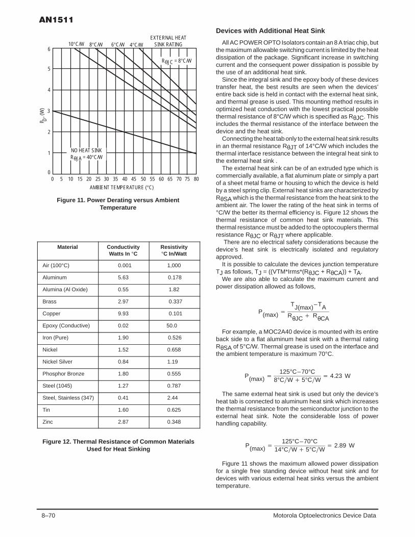
8–70 Motorola Optoelectronics Device Data
10°C/W 8°C/W 6°C/W 4°C/WEXTERNAL HEAT
SINK RATING6
P, (
W)
5
4
3
2
1
00 45 50 55 60 65 70 75 80403530252015105
RθJC = 8°C/W
Figure 11. Power Derating versus AmbientTemperature
AMBIENT TEMPERATURE (°C)
D
NO HEAT SINKRθJA = 40°C/W
Material ConductivityWatts In °C
Resistivity°C In/Watt
Air (100°C) 0.001 1,000
Aluminum 5.63 0.178
Alumina (Al Oxide) 0.55 1.82
Brass 2.97 0.337
Copper 9.93 0.101
Epoxy (Conductive) 0.02 50.0
Iron (Pure) 1.90 0.526
Nickel 1.52 0.658
Nickel Silver 0.84 1.19
Phosphor Bronze 1.80 0.555
Steel (1045) 1.27 0.787
Steel, Stainless (347) 0.41 2.44
Tin 1.60 0.625
Zinc 2.87 0.348
Figure 12. Thermal Resistance of Common MaterialsUsed for Heat Sinking
Devices with Additional Heat Sink
All AC POWER OPTO Isolators contain an 8 A triac chip, butthe maximum allowable switching current is limited by the heatdissipation of the package. Significant increase in switchingcurrent and the consequent power dissipation is possible bythe use of an additional heat sink.
Since the integral sink and the epoxy body of these devicestransfer heat, the best results are seen when the devices’entire back side is held in contact with the external heat sink,and thermal grease is used. This mounting method results inoptimized heat conduction with the lowest practical possiblethermal resistance of 8°C/W which is specified as RθJC. Thisincludes the thermal resistance of the interface between thedevice and the heat sink.
Connecting the heat tab only to the external heat sink resultsin an thermal resistance RθJT of 14°C/W which includes thethermal interface resistance between the integral heat sink tothe external heat sink .
The external heat sink can be of an extruded type which iscommercially available, a flat aluminum plate or simply a partof a sheet metal frame or housing to which the device is heldby a steel spring clip. External heat sinks are characterized byRθSA which is the thermal resistance from the heat sink to theambient air. The lower the rating of the heat sink in terms of°C/W the better its thermal efficiency is. Figure 12 shows thethermal resistance of common heat sink materials. Thisthermal resistance must be added to the optocouplers thermalresistance RθJC or RθJT where applicable.
There are no electrical safety considerations because thedevice’s heat sink is electrically isolated and regulatoryapproved.
It is possible to calculate the devices junction temperatureTJ as follows, TJ = ((VTM*Irms*(RθJC + RθCA)) + TA.
We are also able to calculate the maximum current andpower dissipation allowed as follows,
P(max)TJ(max)–TA
RθJC RθCA
For example, a MOC2A40 device is mounted with its entireback side to a flat aluminum heat sink with a thermal ratingRθSA of 5°C/W. Thermal grease is used on the interface andthe ambient temperature is maximum 70°C.
P(max)125°C–70°C
8°CW 5°CW 4.23 W
The same external heat sink is used but only the device’sheat tab is connected to aluminum heat sink which increasesthe thermal resistance from the semiconductor junction to theexternal heat sink. Note the considerable loss of powerhandling capability.
P(max)125°C–70°C
14°CW 5°CW 2.89 W
Figure 11 shows the maximum allowed power dissipationfor a single free standing device without heat sink and fordevices with various external heat sinks versus the ambienttemperature.

8–71Motorola Optoelectronics Device Data
ÎÎÎÎÎÎÎÎÎÎÎÎÎÎÎÎÎÎÎÎÎÎÎÎÎÎÎÎÎÎÎÎÎÎÎÎÎÎÎÎ
ÎÎÎÎÎÎÎÎÎÎÎÎÎÎÎÎÎÎÎÎÎÎÎÎ
ÎÎÎÎ
ÎÎ
ÎÎÎÎ
ÎÎ
ÎÎÎÎÎÎÎÎÎÎÎÎÎÎÎÎÎÎÎÎÎÎ
ÎÎÎÎÎÎÎÎÎÎÎÎÎÎÎÎ
ÎÎÎÎÎÎÎÎÎÎÎÎÎÎÎÎ
ÎÎÎÎÎÎÎÎÎÎÎÎÎÎÎÎ
ÎÎÎÎÎÎÎÎÎÎÎÎÎÎÎÎ
ÎÎ
ÎÎÎÎÎÎÎÎÎ
ÎÎÎÎÎÎ
ÎÎÎÎÎÎ
ÎÎÎÎÎÎ
ÎÎ
ÎÎÎÎÎÎ
ÎÎÎÎÎÎ
ÎÎÎÎÎÎ
ÎÎÎÎÎÎ
ÎÎ
ÎÎÎÎÎÎ
ÎÎÎÎÎÎ
ÎÎÎÎÎÎ
ÎÎÎÎÎÎ
ÎÎ
ÎÎÎÎÎÎ
ÎÎÎ
ÎÎÎÎÎÎ
ÎÎÎÎÎÎ
ÎÎÎÎÎÎÎÎÎÎÎÎÎÎÎÎÎÎÎÎÎÎÎÎÎÎÎÎÎÎÎÎÎÎÎÎÎÎÎÎÎÎÎÎÎÎÎÎÎÎÎÎÎÎÎÎÎÎ
ÎÎ
ÎÎÎÎÎÎ
ÎÎÎÎÎÎ
ÎÎÎÎÎÎ
ÎÎÎÎÎÎ
ÎÎÎÎ
ÎÎÎÎÎÎ
ÎÎÎÎÎÎ
ÎÎÎÎÎÎ
ÎÎÎÎÎÎ
ÎÎ
ÎÎÎÎÎÎ
ÎÎÎ
ÎÎÎÎÎÎ
ÎÎÎÎÎÎ
ÎÎ
ÎÎÎÎÎÎÎÎÎ
ÎÎÎÎÎÎ
ÎÎÎÎÎÎ
ÎÎÎÎÎÎ
#4
#3
Restricted Air Flow
Air Flow
Cluster with PC Board in Vertical Position
Cluster with PC Board in Horizontal Position
ÎÎÎÎÎÎÎÎÎÎÎÎÎÎÎÎÎÎÎÎÎÎÎÎÎÎÎÎÎÎÎÎÎÎÎÎÎÎÎÎÎÎÎÎ
Optimized Air Flow
#1 #2 #3
#1 #2
Figure 13. Clusters of Devices on a PC Board

8–72 Motorola Optoelectronics Device Data
Devices Stacked in Clusters withMinimal Spacing of 200 Mils
One of the great advantages of the 2 A optocoupler familyis its small footprint on a PC board. This enables the user tocluster many devices in one row with only 200 mil spacing fromlead to lead as shown in Figure 13. Devices in this closeapproximation influence each other thermally by heat transferthrough the epoxy bodies, the integral heat sinks and by heatconduction through pin 7 to the PC board. Prudence wouldsuggests that clustered devices are running much hotter thana single free standing device and the maximum powerhandling must be derated when all devices within this clusterare switched on. It can be also predicted that devices in thecenter of the cluster run much hotter than the devices at eachend. This also means the individual devices within the clusterare not able to dissipate the full rated power but must be ther-mally derated. The following study with clusters show theimpact of this derating. Of course, the position of this cluster inrespect to the natural air convection is also very important.Clusters on a horizontal positioned circuit board run muchhotter than devices on a vertical oriented circuit board. Verticalorientation of the devices and the circuit board allow optimizedheat flow due to the “chimney” effect. Figure 14 shows the heatdistribution for each individual device in a cluster of 10 devicesfor vertical and horizontal circuit board positions. All devicesare conducting 1 A of current which is about 1 W of power dis-
sipation. As predicted, the devices in the center of the clustershow the highest temperature, while the devices at the end runcooler but are still much hotter than the stand alone ratingwould predict. The graph also demonstrates the importance offree air flow versus restricted air flow caused by a horizontalpositioned PC board. It is important to note that the junctiontemperature of the center devices on the vertical positionedboard exceeds the maximum rating of 125°C with a inputpower of only 1 watt! The dissipated power for these deviceshas to be lowered in order to stay within their maximum junc-tion temperature rating.
It is now of interest to know the maximum power dissipa–tion allowed for devices in various sized clusters or the maxi–mum power allowed for devices within a large cluster versusthe amount of devices switched on at the same time. Thegraph in Figure 15 is taken from a cluster of 25 devices wherethe X axis shows the number of units which are turned on withthe same power dissipation and the Y axis shows the resultingmaximum allowed power dissipation for each unit. The poweris first applied to device#1 then to device#1 and device #2 thento device#1 and 2 and 3, and so on. The junction temperatureof the hottest unit in the cluster (which is always in the centerof the units turned on within the cluster) is the limiting factor. Itis also interesting to note that the power derating is not a linearfunction of the cluster size but asymptotically levels out to asteady value for cluster sizes exceeding 20 devices.
Board Vertical
Board HorizontalTJ maxexceeded
JUN
CTI
ON
TEM
PER
ATU
RE
T[
C]
J°
145
125
105
85
65
45
251 2 3 4 5 6 7 8 9 10
UNIT
Figure 14. Cluster T J Junction TemperatureDistribution in a Cluster of 10 T A = 25°C, All
Devices on with I = 1 Arms
2.0
1.5
1.0
0.5
0
1 6 11 16 21 26
PDM
AX[W
]
2.5
Figure 15. Maximum Allowed Power Dissipation perDevice versus Cluster Size

8–73Motorola Optoelectronics Device Data
Motorola reserves the right to make changes without further notice to any products herein. Motorola makes no warranty, representation or guarantee regardingthe suitability of its products for any particular purpose, nor does Motorola assume any liability arising out of the application or use of any product or circuit, andspecifically disclaims any and all liability, including without limitation consequential or incidental damages. “Typical” parameters can and do vary in differentapplications. All operating parameters, including “Typicals” must be validated for each customer application by customer’s technical experts. Motorola doesnot convey any license under its patent rights nor the rights of others. Motorola products are not designed, intended, or authorized for use as components insystems intended for surgical implant into the body, or other applications intended to support or sustain life, or for any other application in which the failure ofthe Motorola product could create a situation where personal injury or death may occur. Should Buyer purchase or use Motorola products for any suchunintended or unauthorized application, Buyer shall indemnify and hold Motorola and its officers, employees, subsidiaries, affiliates, and distributors harmlessagainst all claims, costs, damages, and expenses, and reasonable attorney fees arising out of, directly or indirectly, any claim of personal injury or deathassociated with such unintended or unauthorized use, even if such claim alleges that Motorola was negligent regarding the design or manufacture of the part.Motorola and are registered trademarks of Motorola, Inc. Motorola, Inc. is an Equal Opportunity/Affirmative Action Employer.
How to reach us:USA / EUROPE: Motorola Literature Distribution; JAPAN : Nippon Motorola Ltd.; Tatsumi–SPD–JLDC, Toshikatsu Otsuki,P.O. Box 20912; Phoenix, Arizona 85036. 1–800–441–2447 6F Seibu–Butsuryu–Center, 3–14–2 Tatsumi Koto–Ku, Tokyo 135, Japan. 03–3521–8315
MFAX: [email protected] – TOUCHTONE (602) 244–6609 HONG KONG: Motorola Semiconductors H.K. Ltd.; 8B Tai Ping Industrial Park, INTERNET: http://Design–NET.com 51 Ting Kok Road, Tai Po, N.T., Hong Kong. 852–26629298
AN1511/D
◊

8–74 Motorola Optoelectronics Device Data
Prepared by: Ludy LiuOptoelectronic and Signal Products DivisionSemiconductor Products Sector
INTRODUCTION
Optocouplers simplify logic isolation from the ac line, powersupply transformations, and the control of polyphase powersystems. They help solve problems by kunidueeping ac linenoise and transients out of sensitive logic. Motorola’s 6–PinDip Optocoupler family, with high surge voltage capability(7500 volts peak ac, 60 HZ, 1 second duration), allows design-ers to achieve their goals. This paper presents a power triacphase control circuit and contrasts it with the traditional zero–crossing circuit. The example circuit isolates the low level con-trol circuitry from the ac line. It is able to control the speed ofa universal motor or brilliance of a lamp. The universal motoris capable of high starting torque and wide speed range —commonly used in mixers, blenders, floor polishers, electrichand and woodworking tools, etc.
ZERO–CROSSING AND RANDOMPHASE TRIAC DRIVERS
The zero–crossing triac driver optocouplers are theMOC3162/3 and MOC3081/2/3 series. The random phase
optocouplers are the MOC3012, MOC3023 and MOC3051/2series. All families have the same type of gallium arsenideinfrared light–emitting diode but optically couple to differentmonolithic silicon detector chips. The zero–cross family isdesigned for interface applications between control circuit andpower loads. The advantage of using zero–crossing switchingis less surge current and resulting electromagnetic interfer-ence (EMI). This reduces reliability problems in manyapplications such as solid–state relay, industrial controls,motors, solenoids and consumer appliances. The high–speed zero–crossing switch provides a minimum dv/dt from500 V/µs to 2000 V/µs, protecting the device from accidentaltriggering by ac power line transients.
The circuit in Figure 1 is the basic circuit for on–off powercontrol. With a continuous forward current through the LED,the detector of the zero–crossing optocoupler switches to theconducting state only when the applied ac voltage passesthrough a point near zero. Phase control applications, such ascontrolling the speed of a motor or brilliance of a lamp, requiretriggering at points along the ac voltage wave. This necessi-tates a random phase triac driver optocoupler.
Figure 1. Zero–Cross Switching Using MOC3061
HOT
C
R
VCC
LOAD
RIN
CONTROL SIGNAL
NEUTRAL
1
2
4
6 R
DESIGN RULE: Vpeak / I peak = 180 /1 amp = 180 ohms (Assume the line voltage is 115 volts RMS)
MOC3162
Order this documentby AN1515/D
SEMICONDUCTOR APPLICATION NOTE
Motorola, Inc. 1995
REV 1
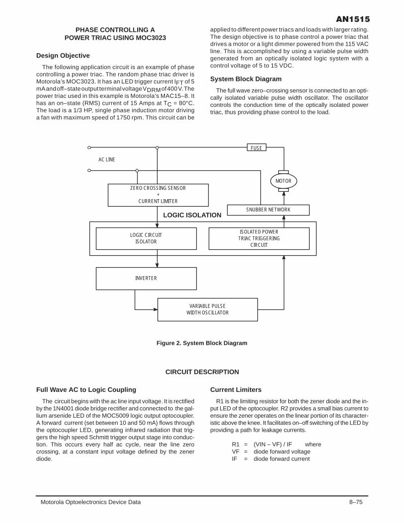
8–75Motorola Optoelectronics Device Data
PHASE CONTROLLING APOWER TRIAC USING MOC3023
Design Objective
The following application circuit is an example of phasecontrolling a power triac. The random phase triac driver isMotorola’s MOC3023. It has an LED trigger current IFT of 5mA and off–state output terminal voltage VDRM of 400 V. Thepower triac used in this example is Motorola’s MAC15–8. Ithas an on–state (RMS) current of 15 Amps at TC = 80°C.The load is a 1/3 HP, single phase induction motor drivinga fan with maximum speed of 1750 rpm. This circuit can be
applied to different power triacs and loads with larger rating.The design objective is to phase control a power triac thatdrives a motor or a light dimmer powered from the 115 VACline. This is accomplished by using a variable pulse widthgenerated from an optically isolated logic system with acontrol voltage of 5 to 15 VDC.
System Block Diagram
The full wave zero–crossing sensor is connected to an opti-cally isolated variable pulse width oscillator. The oscillatorcontrols the conduction time of the optically isolated powertriac, thus providing phase control to the load.
Figure 2. System Block Diagram
SNUBBER NETWORK
INVERTER
MOTOR
FUSE
AC LINE
ZERO CROSSING SENSOR+
CURRENT LIMITER
LOGIC CIRCUITISOLATOR
LOGIC ISOLATION
ISOLATED POWERTRIAC TRIGGERING
CIRCUIT
VARIABLE PULSEWIDTH OSCILLATOR
CIRCUIT DESCRIPTION
Full Wave AC to Logic Coupling
The circuit begins with the ac line input voltage. It is rectifiedby the 1N4001 diode bridge rectifier and connected to the gal-lium arsenide LED of the MOC5009 logic output optocoupler.A forward current (set between 10 and 50 mA) flows throughthe optocoupler LED, generating infrared radiation that trig-gers the high speed Schmitt trigger output stage into conduc-tion. This occurs every half ac cycle, near the line zerocrossing, at a constant input voltage defined by the zenerdiode.
Current Limiters
R1 is the limiting resistor for both the zener diode and the in-put LED of the optocoupler. R2 provides a small bias current toensure the zener operates on the linear portion of its character-istic above the knee. It facilitates on–off switching of the LED byproviding a path for leakage currents.
R1 = (VIN – VF) / IF whereVF = diode forward voltageIF = diode forward current

8–76 Motorola Optoelectronics Device Data
Figure 3. Schematic DiagramPhase Controlling a Power Triac Using MOC3023
D51N5248
R75.6 K
MT2
115 Vac MT2
MT1
R9 R8
180180
MT1
R6300RESETVCC
10 K
VR14
38
7
6
2
1
TRIGGER
R45.6 K
C10.22µFVCC
R51 K DISCHARGE
11 V
R110 K3W
(D1 – D4)1N4001
R213.5 K
MOC5009
6
54
MAC15–8
VTRIAC
C20.033 µF
Q1MPSA40
A
MOC3023
ACMOTOR
VCC
Vtd
R310 K
MC1455
Optically Isolated Triggering of the Variable PulseWidth Oscillator
A dc signal with a pulse width of 720 µs is generated at theoutput detector of the MOC5009. The purpose of the MPSA40NPN transistor is to generate an inverted signal, which goesinto the trigger pin 2 of the MC1455 monolithic timing circuit.See Figure 4 for the input trigger pulse versus the line voltage.
The Variable Pulse Width Oscillator
At every falling edge of the input trigger signal, the MC1455monolithic timing circuit generates a positive going pulse withduty cycle controlled by C1, VR1 and R5. The pulse durationis measured in time constants of t = 1.1* (VR1+R5)*C1. SeeFigure 5 for the voltage across capacitor C1 versus the inputtrigger signal of the MC1455.
Isolated Triac Triggering
The output signal (Vtd) from the oscillator goes to theMOC3023 triac driver LED. When sufficient LED current (IFT)passes through the LED, the triac driver latches on and gener-ates a gate current in the power triac, triggering it into the con-ducting state.
Once the power triac latches on, the triac driver will beforced into off–state even when IFT is applied. The power triacMT2 to gate voltage falls to a low value below the optocoup-ler’s threshold voltage and cannot hold the optocoupler on.See Figure 8 for voltage across the power triac terminals(VTRIAC) versus power triac gate trigger signal (Vtd).
Minimum Load Power for Phase Control
The average power applied to the load is modulated by theduration of the waveform input to the triac driver. The longerthe phase delay, the smaller the conduction angle and powerdelivered to the load. R5, VR1 and C1 set the minimum loadpower. This ensures power triac latching and optocouplerturn–off. This prevents optocoupler commutating dv/dt failure.The circuit in Figure 3 has a minimum conduction angle of 12degrees. See Figure 9 for the voltage across the power triacterminals versus the input signal of the triac driver.

8–77Motorola Optoelectronics Device Data
Time: 5 ms/divCH1: C1 starts to discharge when voltage
reaches 2/3 of the VCC (2 V/div)CH2: Power triac gate trigger signal (Vtd)
with pulse duration of 4.7 ms (2 V/div)
Time: 5 ms/divCH1: Output signal measured at Pin 3 of the
MC1455 (2 V/div)CH2: Input trigger pulse to MC1455 (5 V/div)
Figure 4. Zero Cross AC to Logic Coupling Figure 5. Capacitor C1 starts to charge up atthe falling edge of the input trigger pulsewith a time constant equal to 1.1*R5*C1
Figure 6. Square Wave with Pulse Width of 4.2 msGenerated at Output Pin of the MC1455
Figure 7. Capacitor Voltage versusPower Triac Gate Trigger Signal
Time: 2 ms/divCH1: Line voltage waveform (100 V/div)CH2: Trigger signal measured at Pin 2 of the MC1455
CH2 GNDCH2 GND
CH2 GND
CH1 GND
CH2 GND
CH1 GND
CH1 GND
CH1 GND
720 ms 4.7 ms
4.05 ms 4.7 ms
Time: 5 ms/divCH1: Output voltage across C1 (2 V/div)CH2: Input trigger pulse to MC1455 (5 V/div)

8–78 Motorola Optoelectronics Device Data
Figure 8. Power Triac Figure 9. Minimum Load Power
Time: 5 ms/divCH1: Voltage across the power triac
terminals (VTRIAC) (100 V/div)CH2: Power triac gate trigger signal,
Vtd (5 V/div)
CH2 GND CH2 GND
CH1 GND CH1 GND
1.05 ms 550 ms
Time: 5 ms/divCH1: Voltage across the power triac
terminals (VTRIAC) (100 V/div)CH2: Power triac gate trigger, Vtd (5 V/div)
Snubber Network
The power triac can be switched on unintentionally if therate of rise in applied voltage exceeds its dv/dt or the dv/dtof the triac driver. To prevent this false triggering, a singlesnubber limits the maximum dv/dt seen by the power triac andoptocoupler. Snubber networks can be defined by assuminga power factor for the inductive load and modified later bymeasuring the actual dv/dt and adjusting the snubber as re-quired. The snubber network used in Figure 3 results in aworst case dv/dt at the coupler of:
dv/dt = Vto / (R9 * C2) = 180 / (180 * 0.033)= 30.3 V/ µs
Vto = instantaneous peak line voltage
The presence of load inductance (for example, when theload is a motor) results in significantly lower values of dv/dt.For details on designing the snubber network, refer to Motoro-la application note AN1048.
R8 limits the peak capacitor discharge current through thetriac driver. Its minimum value calculates as:
R8 = Vpk / Imax = 180 / 1.2 A = 150 ohm (1/2 W)Vpk – gate trigger required voltageImax – rated surge current of the optocoupler
The author selected 180 ohms for the limiting resistor.
CONCLUSION
This application note demonstrates the use of triac driversand power triacs in an ac logic isolation phase control applica-tion. The circuit designs are easily accomplished with relative-ly few components.
ACKNOWLEDGMENTS
The author expresses her appreciation to Horst Gempe,George Templeton, John Salina, Andy Williams and Niraj Koh-li for extensive constructive discussions on the device theoryfor optocouplers and power triac. The author also wishes tothank Sharon Mason for supporting the setup of the experi-ments.

8–79Motorola Optoelectronics Device Data
Motorola reserves the right to make changes without further notice to any products herein. Motorola makes no warranty, representation or guarantee regardingthe suitability of its products for any particular purpose, nor does Motorola assume any liability arising out of the application or use of any product or circuit,and specifically disclaims any and all liability, including without limitation consequential or incidental damages. “Typical” parameters can and do vary in differentapplications. All operating parameters, including “Typicals” must be validated for each customer application by customer’s technical experts. Motorola doesnot convey any license under its patent rights nor the rights of others. Motorola products are not designed, intended, or authorized for use as components insystems intended for surgical implant into the body, or other applications intended to support or sustain life, or for any other application in which the failure ofthe Motorola product could create a situation where personal injury or death may occur. Should Buyer purchase or use Motorola products for any suchunintended or unauthorized application, Buyer shall indemnify and hold Motorola and its officers, employees, subsidiaries, affiliates, and distributors harmlessagainst all claims, costs, damages, and expenses, and reasonable attorney fees arising out of, directly or indirectly, any claim of personal injury or deathassociated with such unintended or unauthorized use, even if such claim alleges that Motorola was negligent regarding the design or manufacture of the part.Motorola and are registered trademarks of Motorola, Inc. Motorola, Inc. is an Equal Opportunity/Affirmative Action Employer.
How to reach us:USA / EUROPE: Motorola Literature Distribution; JAPAN : Nippon Motorola Ltd.; Tatsumi–SPD–JLDC, Toshikatsu Otsuki,P.O. Box 20912; Phoenix, Arizona 85036. 1–800–441–2447 6F Seibu–Butsuryu–Center, 3–14–2 Tatsumi Koto–Ku, Tokyo 135, Japan. 03–3521–8315
MFAX: [email protected] – TOUCHTONE (602) 244–6609 HONG KONG: Motorola Semiconductors H.K. Ltd.; 8B Tai Ping Industrial Park, INTERNET: http://Design–NET.com 51 Ting Kok Road, Tai Po, N.T., Hong Kong. 852–26629298
AN1515/D
◊
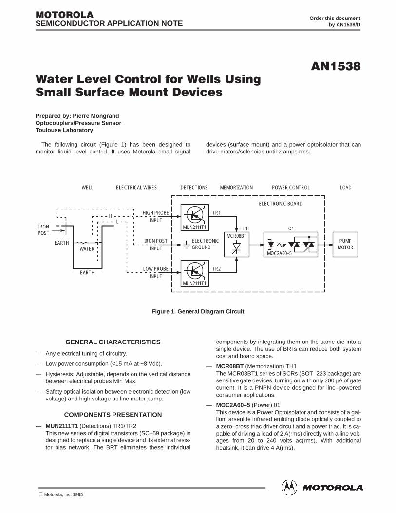
8–80 Motorola Optoelectronics Device Data
Prepared by: Pierre MongrandOptocouplers/Pressure SensorToulouse Laboratory
The following circuit (Figure 1) has been designed tomonitor liquid level control. It uses Motorola small–signal
devices (surface mount) and a power optoisolator that candrive motors/solenoids until 2 amps rms.
IRONPOST
HIGH PROBEINPUT
IRON POST
INPUT
LOW PROBEINPUT
WATER
EARTH
EARTH
HL
MUN2111T1
MUN2111T1
ELECTRONICGROUND
MCR08BT
TR1
TR2
TH1
MOC2A60–5
O1
PUMPMOTOR
ELECTRONIC BOARD
WELL ELECTRICAL WIRES DETECTIONS MEMORIZATION POWER CONTROL LOAD
Figure 1. General Diagram Circuit
GENERAL CHARACTERISTICS
— Any electrical tuning of circuitry.
— Low power consumption (<15 mA at +8 Vdc).
— Hysteresis: Adjustable, depends on the vertical distancebetween electrical probes Min Max.
— Safety optical isolation between electronic detection (lowvoltage) and high voltage ac line motor pump.
COMPONENTS PRESENTATION
— MUN2111T1 (Detections) TR1/TR2This new series of digital transistors (SC–59 package) isdesigned to replace a single device and its external resis-tor bias network. The BRT eliminates these individual
components by integrating them on the same die into asingle device. The use of BRTs can reduce both systemcost and board space.
— MCR08BT (Memorization) TH1The MCR08BT1 series of SCRs (SOT–223 package) aresensitive gate devices, turning on with only 200 µA of gatecurrent. It is a PNPN device designed for line–poweredconsumer applications.
— MOC2A60–5 (Power) 01This device is a Power Optoisolator and consists of a gal-lium arsenide infrared emitting diode optically coupled toa zero–cross triac driver circuit and a power triac. It is ca-pable of driving a load of 2 A(rms) directly with a line volt-ages from 20 to 240 volts ac(rms). With additionalheatsink, it can drive 4 A(rms).
Order this documentby AN1538/D
SEMICONDUCTOR APPLICATION NOTE
Motorola, Inc. 1995

8–81Motorola Optoelectronics Device Data
DETAILED CIRCUIT DESCRIPTION
Electronic Board Detection
The two detection stages TR1(max) and TR2(min) are ex-actly the same. Without polarization on bases (+V supply),TR1, TR2 collectors are grounded. In the same way, whenTR1, TR2 bases are grounded, devices TR1/TR2 turn on.
Levels Configurations1. With bases TR1 and TR2 equal to V supply, the two PNP
transistors turn off.TR1 collector voltage equals zero (ground), and thereforethe SCR TH1 sees its gate trigger voltage at the same po-tential as the TR1 collector. TH1 is like an open switch.
2. TR2(min) base is grounded, but TR1(max) is always at Vsupply.TR2 turns on, TR1 and TH1 stay OFF. No current flowsthrough the light–emitting diode D4 and the LED power op-toisolator MOC2A60–5.
3. TR1 and TR2 bases are grounded. The devices turn on.TR1 collector voltage moves to VCC–VCE(sat), and D3 turnson. TH1 turns on also (gate trigger voltage is around 0.7volts). D4 turns on. MOC2A60–5 turns on.
4. TR2 base stays grounded, but TR1 base becomes at Vsupply.TR1 turns off, D3 turns off and prevents gate SCRs voltagefrom passing to zero. Without D3, TH1 is off. D4 andMOC2A60–5 stay on.
5. To stop the conduction of D4 and MOC2A60–5, it is neces-sary to put TR2 base to +V supply.
Here is a synthesis of well levels configurations:
Probe L Probe H TR1 TR2 TH1 D4/01Open Open Off Off Off OffEarth Open Off On Off OffEarth Earth On On On OnEarth Open Off On On OnOpen Open Off Off Off Off
Output Power StageFor safety reasons, it is important to prevent any direct con-
tact between the ac main power and water environment of thewell earth. To maintain full isolation between the detection cir-cuitry and the main power, the solid state relay is placed be-tween the low voltage circuit (detection/memorization) and theac line used by the motor pump. TR2 (MUN2111T1) and TH1(MCR08BT) are used to drive the LED of the MOC2A60–5.Resistor R4 limits the current into the opto–LED around 12 mAand guarantees a perfect drive of the solid state relay. D4 isan indicator light. It turns on when the load is under power.
The solid state relay MOC2A60–5 is an opto triac driving apower triac. This detection is a zero crossing which limits thepower line disturbance problems when fast switching selficloads. An RC network placed in parallel with the output of thesolid state relay is not mandatory, but to prevent any voltagespikes coming from the inductive load commutation, it is agood design practice to use it.
As defined on the components presentation, theMOC2A60–5 can drive 4 A(rms) on the main ac line (220volts). If more power is required >4 A(rms), this device mustbe replaced by an opto triac driver (MOC3163) that will drivea power triac (MACH16N). (See Figure 2.)
MOC2A60–5 MOC3163 MACH16N
< = To 4 A or 880 WATTS From 4 A until 16 A
MOTOR MOTOR3
2
3
2
9
7
6
4RC RC
1000
220 Vac 220 Vac
MT2
MT1G
330
Figure 2.

8–82 Motorola Optoelectronics Device Data
Electrical Well Layout: Iron Post/Wires Probes
Iron PostThe probe is very important and must be connected to elec-
tronic ground (must be different from ac main line ground).
Length probe: around 45 to 65 centimeters vertically buried inthe earth.
Location: near the well (up to 30 centimeters).
Wires ProbesThese two probes consist of electrical wires isolated (lay
bare wire strip which may be in contact with the water around5 to 8 centimeters) hanging vertically inside the well, not incontact with the well walls.
To obtain a good standing of the wires:
Tie the wires mechanically at the top of the well; they must beperfectly isolated and connected respectively at the electronicset level low (L) and high (H).
Load the other ends (which will be in contact with the water)with little weights.
How to Adjust Wires LevelsFirst, it is necessary to be familiar with the well: the average
maximum level of water and the flow (the two parameters de-pend on the seasons).
Place the low level wire probe (L) just above the stainer ofthe pump.
Place the high level wire probe (H) just below the maximumaverage water (10 to 15 centimeters).
Remark: High level is critical sometimes: Filling the well isslow, and the maximum water level changes. For these rea-sons, this probe (H) must be adjusted.
How to Check Your Probes ElectricallyThis paragraph is very important. The resistance between
the iron post probe and the two others can influence the opera-tion of the level circuit.
Two solutions to check:
1. With an ohmeter/voltmeter controller, take a few measure-ments.Values found between the iron post and probe L or probeH (when they are in the water) must be equal or lower than30 k ohms. If not, the earth is too resistive for the applica-tion.To resolve this unusual problem, increase the length of theiron post in the earth. If this is not enough, move this probein the bottom of the well.When probes are in contact with the water and connectedwith the circuit board, voltage between the iron probe andthe two others, respectively, must be equal or lower than5.3 V. With these last two conditions, the current througheach probe (L/H) must be higher than 180 microamperes.This limit guarantees an LED opto triac current of 12 mA.
2. If a measurement cannot be performed:Connect the three probes to the circuit. Turn on the powermain line. Verify that the two probes L and H are in the wa-ter. LED D4 must light (for this test, a motor is not neces-sary).If nothing appears, shortcircuit the electronic circuit boardand probes L and H with an electronic ground to be surethat the problem comes from the iron probe post. D4 turnson. In this case, go to line.

8–83M
otorola Optoelectronics D
evice Data
+8 Vdc
TR2
10 K
L PROBE MIN.
R4
10 K
MOTOR PUMP
RC
3
2
9
7
TH1D3
R2
R3
TR1
10 K
10 KHPROBE MAX.
R1
220 Vac LINE TRD1 D2~ ~
–
+ +
C1REG. +8 Vdc
IRON POST(NEAR THE WELL)
EARTH
WATER
ELECTRICALWIRESPROBES
EARTH
EARTH
L
H
Electronic ground must be different fromac line ground.
+8 Vdc
220 Vac LINE
LOW LEVEL DETECTION
WELL
MOC2A60–5
O1
D4
HIGH LEVEL DETECTION MEMORIZATION
DC POWER SUPPLY
Probe LOpenEarthEarthEarthOpen
Probe HOpen
EarthOpen
TR1OffOffOnOffOff
TR2OffOnOnOnOff
TH1OffOffOnOnOff
D4 / 01OffOffOnOnOff
ELECTRONIC LEVELR1 = 5.6 K R2 = 4.7 K R3 = 1 K R4 = 330(All Resistors: CMS 1/4 watts)
D1 = BAW56LT1D3 = BAS16LT1REG = MC78L08ACD (8 Vdc)TR1, TR2 = MUN2111T1C1 = 47 F 40 VO1 = MOC2A60–5TR = TRANSFORMER 220 V/9 V/1 VA
µ
D2 = BAV74LT1D4 = MLED96
TH1 = MCR08BT
COMPONENTS DESCRIPTION
Figure 3. Water Level Control for Wells Using Small Surface Mount Devices
OpenOpen

8–84 Motorola Optoelectronics Device Data
Motorola reserves the right to make changes without further notice to any products herein. Motorola makes no warranty, representation or guarantee regardingthe suitability of its products for any particular purpose, nor does Motorola assume any liability arising out of the application or use of any product or circuit,and specifically disclaims any and all liability, including without limitation consequential or incidental damages. “Typical” parameters can and do vary in differentapplications. All operating parameters, including “Typicals” must be validated for each customer application by customer’s technical experts. Motorola doesnot convey any license under its patent rights nor the rights of others. Motorola products are not designed, intended, or authorized for use as components insystems intended for surgical implant into the body, or other applications intended to support or sustain life, or for any other application in which the failure ofthe Motorola product could create a situation where personal injury or death may occur. Should Buyer purchase or use Motorola products for any suchunintended or unauthorized application, Buyer shall indemnify and hold Motorola and its officers, employees, subsidiaries, affiliates, and distributors harmlessagainst all claims, costs, damages, and expenses, and reasonable attorney fees arising out of, directly or indirectly, any claim of personal injury or deathassociated with such unintended or unauthorized use, even if such claim alleges that Motorola was negligent regarding the design or manufacture of the part.Motorola and are registered trademarks of Motorola, Inc. Motorola, Inc. is an Equal Opportunity/Affirmative Action Employer.

8–85Motorola Optoelectronics Device Data
How to reach us:USA / EUROPE: Motorola Literature Distribution; JAPAN : Nippon Motorola Ltd.; Tatsumi–SPD–JLDC, Toshikatsu Otsuki,P.O. Box 20912; Phoenix, Arizona 85036. 1–800–441–2447 6F Seibu–Butsuryu–Center, 3–14–2 Tatsumi Koto–Ku, Tokyo 135, Japan. 03–3521–8315
MFAX: [email protected] – TOUCHTONE (602) 244–6609 HONG KONG: Motorola Semiconductors H.K. Ltd.; 8B Tai Ping Industrial Park, INTERNET: http://Design–NET.com 51 Ting Kok Road, Tai Po, N.T., Hong Kong. 852–26629298
AN1538/D
◊

8–86 Motorola Optoelectronics Device Data
Prepared by: Larry HayesWarren SchultzDiscrete Applications Engineering
In switching power supplies, optoisolators usually provideisolated feedback for the regulation loop. In this application,they do an excellent job of isolation, minimizing circuit com-plexity and reducing cost. The trade–offs are wide unit–to–unitvariations in current transfer ratio, noise susceptibility, andlong–term gain stability. But by using devices specifically de-signed for power supplies, these deficiencies can be mini-mized. A new series of devices, MOC8103 throughMOC8105, combines an application–specific approach withtechnology improvements. The result is a significant perfor-mance increase in switching power supplies.
The biggest design challenge associated with optoisolatorsis the large unit–to–unit variation in current–transfer ratio(CTR). The statistical distribution of CTR within a given lot ischaracteristically large, and most standard devices are speci-fied with only a minimum CTR, or at best, with a widely spaced
minimum and maximum. This is a first–order design issue be-cause open–loop gain is directly proportional to the optoisola-tor’s CTR.
Consider a typical 100–W flyback power supply. Total loopgain is found by multiplying the individual gains of each stage.For this power supply, the loop gain, Av, is equal to the productof the individual gains of the error amplifier (Ae), comparator(Ac), power stage (Aps), TL431 (gm) and optoisolator (CTR).Looking at only the TL431 and optoisolator together, the gainis expressed as:
(R11 R12)
(R11 R12) (gm)(CTR) (R5 R6)
(R5 R6)
RECTIFIERSAND INPUT/
OUTPUT FILTERSFLYBACK
TRANSFORMERRECTIFIERSAND FILTERS
+5 VDC POWER SUPPLY
RECTIFIERSAND FILTERS
GENERAL–PURPOSEOPTOISOLATOR
GATE LEADSUSCEPTIBLE
TO NOISE PICKUP
4N26
REPLACES
APPLICATION–SPECIFICOPTOISOLATORS
ERROR AMPLIFIERAND COMPARATOR
DRIVERTRANSFORMER
AND POWER SWITCH R5
R6
AC HOT
AC RET
GND
115/230VAC INPUT
MOC810X FAMILY
COM
R12
R11RS
TL431
NC
NC
6
5
4
1
2
3
1 µf
+15 VDC
OUTPUTVOLTAGE
+5 VDC
Original design of 100–W flyback power supply has aconventional 4N26 optoisolator in the feedback loop. Pin6 of the 4N26 is wired to the receiver base and acts likean antenna to pick up unwanted noise. The new Motoro-la MOC810X family of optoisolators replaces the 4N26,eliminates the base lead, and reduces noise pickup.
6
5
4NC
1
2
3
Figure 1. 100–Watt Flyback Power Supply
+15 VDC POWER SUPPLY
NC
SEMICONDUCTOR APPLICATION NOTE
Motorola, Inc. 1995
REV 1

8–87Motorola Optoelectronics Device Data
ÉÉÉÉÉÉÉÉÉÉÉÉÉÉÉ
3
1
2
3
WHITE OVERMOLD (EPOXY)
LEAD FRAME
CREEPAGE PATH
DETECTOR
THICKNESS THROUGHINSULATION
CLEARANCE 0.4″SPECIAL
“T” LEAD BEND
CLEARANCESTD.
LEAD BEND
LED DOME(SILICONE)
0.5 mm
Noise is further reduced by coplanar die placementof the LED and phototransistor. This reduces theinternal capacitance to 0.2 pF and minimizes thecoupled noise injected by the optoisolator.
Figure 2. Coplanar Die Placement
Plugging in values for the resistors, gm, CTR, and gains ofthe other amplifiers, the product yields a loop gain of 7,100 or77 dB.
When minimum and maximum values for the optoisolator’sCTR are factored into this calculation, the results are eyeopening. For the widely used 4N26, the specified minimum is0.2, and no maximum is guaranteed. The CTR can be as highas the upper limit of the supplier’s statistical distribution; thus,values as high as 6.0 are common. Plugging this range backinto the open–loop gain calculation results in a minimum of3,500 (71 dB) and a maximum of 106,000 (101 dB). Becauseload regulation is proportional to open–loop gain, the same30:1 variation follows through directly to output performance.In other words, a disturbance that produces a 1–mV changein the 101 dB supply will product a 30 mV change in the 71 dBunit.
Motorola Optoisolator CTR
Part Number Minimum Maximum
MOC8105 65% 133%
MOC8103 108% 173%
MOC8104 160% 256%
Current–transfer ratios (CTRs) for the new family of optoi-solators have a guaranteed range of values, unlike the 4N26that had a guaranteed minimum of 0.2, but no maximum. De-signers can now better predict loop gains and overall controlperformance.
The new MOC810X series devices, manufactured specifi-cally for switching supplies, improves the situation by morethan an order of magnitude. The result is better regulation,additional gain margin, or a combination of the two.
General–purpose optoisolators, such as 4N26, use a5–lead configuration. Here, the optotransistor’s base ispinned out to provide flexibility for the general–purpose user.However, in switching supplies, the internal chip–to–pin wireand the external lead together act as an antenna to pick upswitching noise, which is introduced into the feedback loop. Tominimize this problem, noise–decoupling networks are oftenadded from base to emitter. Another approach is to cut off theexternal pin 6 (base) lead, which provides a partial improve-ment, but still leaves the internal chip–to–pin connected insidethe package.
The MOC810X series optoisolators minimizes noise sus-ceptibilty by eliminating the base connection. Only anode,cathode, collector, and emitter connections are provided, re-sulting in a four–terminal device that is housed in a six–pin DIPwith two unconnected pins. The need for the extra passivecomponents is eliminated, along with added cost and com-plexity.
Noise is further minimized by coplanar die placement, whichputs the LED and phototransistor end to end, rather than oneabove the other. The result is a mere 0.2 pF coupled capaci-tance (Ciso), which minimizes the amount of capacitivelycoupled noise injected by the optoisolator.
In addition to the rather large unit–to–unit CTR variation, op-toisolators have been known to exhibit CTR degradation overtime. Fortunately, improvements in gallium–arsenide (GaAs)processing and handling now virtually eliminate this concern.These recent improvements have been incorporated into theMOC810X family.
The MOC810X series devices have remarkable gain stabil-ity. Under the strongly accelerated LED drive condition of IF =50 mA continuous, MOC810X series devices have now com-pleted a total of 5,000 h of operation with a mean gain shift ofonly 0.7%.

8–88 Motorola Optoelectronics Device Data
VDE Circuit Board Layout Design Rules
The most demanding and stringent safety requirements areon interfaces between a safety low–voltage circuit [SELV] anda hazardous voltage (240 V power line). The requirements forcreepage path and clearance dimensioning are different foreach individual equipment norm and also depend on the isola-tion group and safety class of the equipment and the circuitboard’s resistance to tracking. Isolation materials are classi-fied for their resistance to tracking creepage current stabilityfrom KB 100 to KB 600 (see VDE 303). On circuit board ma-terials with a low KB value, the creepage path distance re-quirements are higher than for materials with a high KB value.In the following examples we therefore show creepage pathdimensions for KB 100, the lowest value which is easily metby most circuit board materials.
The least stringent requirements on optocouplers, as wellas printboard layouts, are within and in between SELV or ELVloops or circuits. (ELV = Electrical Low Voltage which does notmeet the safety low voltage requirements.)
In studying the individual equipment norms, the designerwill discover that optocouplers are not mentioned in most ofthe norms. He has to use the requirements for transformers orpotted components instead.
Spacing requirements between two live tracks on a PCboard within a low or high voltage loop (circuit) should general-ly meet the VDE requirements for minimum clearance andcreepage path dimensions. If they do not, the circuit has toshow some sort of current limiting (fuse, high–impedance,etc.) which prevents fire hazard due to an eventual short orsparkover between the two tracks. The VDE testing institutewill conduct, in this case, a shorting test and a tracking test(arcing). See VDE 804. Classical cases are rectifiers, thyris-tors and high–voltage transistors which, sometimes due totheir close pinout, might not meet the VDE equipment require-ments at a certain voltage.
PRINTED CIRCUIT BOARD LAYOUT FORSELV–POWER INTERFACES
The circuit board layout examples shown here are dimen-sioned so that they provide a safe electrical isolation betweenmetal parts carrying line voltage (called Power Interface) andconductors connected to a SELV circuit.
The required thickness through insulation for the optocoup-ler can be found in the individual VDE equipment norms. (Seeexamples for safety applications, Table 1.)
Many Class I equipment norms permit the use of parts (mod-ules, PC boards) which meet the Safety Class II dimension andisolation requirements. This enables the designer to take advan-tage of the less complex and space demanding design of theClass II PC board layout also in Class I classified equipment.
Optocoupler Mounting on PC Boards for Safety Class ISELV transformers for Class I equipment have a Faraday
shield which is connected to earth ground between primaryand secondary windings. This is not applicable to optocoup-lers, but creepage path and clearance requirements fromsafety Class II can be applied. Class I also demands an earthground track on the circuit board between SELV — and powercircuit. Applying the Class I rules, this earth ground trackshould be between the coupler input and output. However, this
cannot be done without violating the minimum creepage pathand clearance requirements. A possible solution is shown onFigure 9 and Figure 10.
Figure 1.
54
3
RL
Fuse
21
1 — Clearance and creepage path must meet min require-ments*
2 — Current limited due to fuse3, 4 — Current limited due to RL and fuse
5 — Current limited due to IGT, RL and fuse2, 3, 4, 5 — Clearance and creepage path may be smaller than
VDE min requirements but must meet fire hazard re-quirements due to short and arcing between thetracks. There shall be no flames or explosion duringthe test.
Figure 2.
Low–VoltageCircuit
High–Voltage Circuit
RX
5
41
RL
31 2
1 Clearance and creepage path must meet min requirements*2 Current limited due to RL3 Current limited due to RL4 Current limited due to IGT5 Current limited due to IGT and RX* See Table 1 and Appendix Table 2 and 3 for minimum spacings and
voltage requirements.
The earth ground track itself has to show a minimum dis-tance to the equipment body (i.e., frame, circuit board enclo-sure) or to any inactive, active or hazardous track on the circuitboard. According to many VDE equipment norms, this creep-age path distance for 250 V Max is 4 mm. A mechanically un-secured circuit board which can be plugged in and out withouta tool and is electrically connected through a standard PCboard connector, has to show an isolation of the earth groundtrack to Class II, which is 8 mm. This is because a standard PCconnector, as shown in Figure 9, does not guarantee earthingcontact before there is termination of the life 220 V tracks onthe circuit board when plugged in. Another reason for in-creased spacing is when the circuit board metal enclosure isnot securely earth grounded. This is the case when the con-nection is done with the PC module mounting screws throughlacquer or oxide layers to a grounded rack or frame. (See Fig-ure 10.) PC board designs per Figures 9 and 10 account forthese possibilities and, therefore, show dimensions M, N andA, B and D as 8 mm instead of 4 mm.

8–89Motorola Optoelectronics Device Data
Table 1. Examples for Safety Applications for Motorola VDE Approved Optoisolators
Standard (2)
Requirements for reinforced (double) or safe insulation forequipment with an operating voltage up to 250 Vrms
(line voltage to ELV or SELV interfaces)
VDEDINIEC Equipment Creepage
Clearance(1)
IsolationBarrier
DielectricStrength
IsolationResistance
[mm] [mm] [mm] [kV RMS] [Ω ]0806 950 Office Machines 8.0 8.0 0.4 3.75 7 x 10⁶
0805 950 Data Processing 8.0 8.0 0.4 3.75 7 x 10⁶
0804 — Telecommunication 8.0 8.0 — 2.5 2 x 10⁶
0860 65 Electrical Household 6.0 6.0 0.4 3.0 (10)* 4 x 106
0113 204 Industrial Controls 8.0 8.0 — 2.5 1 x 10⁶
0160 — Power Installations with Electronic Equipment 8.0 8.0 — 2.7 1 x 10⁶
0832 — Traffic Light Controls 8.0 8.0 — 2.5 4 x 10⁶
0883 — Alarm Systems 8.0 8.0 — 2.5 2 x 10⁶
0831 — Electrical Signal System for Railroads 8.0 8.0 — 2.0 2 x 10⁶
0110 — General Std. for Electrical Equipment 8.0 8.0 — 2.0 —
0883 — Optoisolator Component Standard(obsolete 12/31/91)
8.5 8.3 (10)(1)
0.5 3.75 (10)* 10 x 1011
0884(4) — Optoisolator Component Standard >7.5 >7.5 0.5 — 10 x 1012(replaces VDE0883) VDE Rating for Motorola 6–pin DIP Optoisolators
All Motorola 6–pin DIP Optoisolators meet or exceed the requirements of above listed VDE and DIN IEC Standards.* Impulse discharge withstand voltage.
1. To satisfy 8.0 mm creepage path on a PC board Motorola offers a special lead bend of 0.4 inch on all 6–pin dual–in–line optoisolators. Order by attaching “T”to the end of the Motorola part number.
2. VDE standards (translated into English language) and IEC standards can be ordered from the American National Standard Institute ANSI 1430 Broadway, N.Y., N. Y. 10018, Sales Department 212–642–4900.
3. Creepage path distances are measured from lead to lead across the top, bottom and ends of the package body.4. VDE 0884 testing is an option; the suffix letter “V” must be added to the standard number.
G = 8 mmH = 2 mmP 6 mm
PC–Connector
Power–Interface
Circuit
SELV–Control–
G = 8 mm
Power–Interface
SELV– Control–Circuit
G
G
Figure 3. Optocoupler Mounting on PCBoards for Safety Class II with Creepage
Path and Clearance
Figure 4. Optocoupler Mounting on PCBoards for Safety Class II with Clearance
Application forVDE 0805 DIN/IEC 950VDE 0806 DIN/IEC 950VDE 0113VDE 0160 Part 1 and 2VDE 0804 and 0804dVDE 08031/0832/0833VDE 0860 DIN/IEC 65VDE 110b
G G G G G G
GG
G G G G G G
PC-C
onne
ctor
Application forwith Slit — VDE 0860without Slit — VDE 0804dwith/without — VDE 0110b
Optocoupler Mounting on PC–Boards for Safety Class II withclearance P 6 mm and creepage path G = 8 mm and Slit inthe PC–Board with Slit length = 12.7 mm and Slit thickness H = 2 mm
G
G G GH
P

8–90 Motorola Optoelectronics Device Data
COUPLER MOUNTING ON A CIRCUIT BOARDClearance and Creepage Path Between Input and Output for Optocouplers on a PC Board
1 mm
Solder Eyes Solder Eyes
1 mm0.22″/5.6 mm
PC Board
0.3″/7.62 mm
Figure 5.
Input/Output Leads — L = 0.3″/7.62 mmClearance Limited Due to PC BoardSolder Eyes — 0.22″/5.6 mmCreepage Path on PC Board — 0.22″/5.6 mm
Slit punchedout 2 mm wide,12 mm long
Figure 6.
2 mm
2mmSlit
SLIT
Creepage Path
Solder Eyes1 mm 0.22″/5.6 mm
Solder Eyes
1 mm
PC Board
0.3″/7.62 mm
0.5”
/12.
7 m
m
VDE equipment norms demanding longer creepage paththan 0.22″/5.6 mm can be accomplished by a slit in the PCboard between the coupler input and output solder eyes of 2mm width.
Input/Output Leads — L = 0.3″/7.62 mmClearance on PC Boards — 0.22″/5.6 mm MinCreepage Path on PC Board — 0.31/8 mm Min
PC Board Thickness 1.5 mm
SolderEyes
Tracks on Undersideof PC Board
Clearance
0.3″/7.62 mm
Solder Eyes
2 mm
Creepage Path
Figure 7.
Slit
in P
C B
oard
0.5”
/12.
7 m
m
If a clearance of 0.23″/6 mm and a creepage path of mini-mum 8 mm is required, this is a possible solution.
Slit — 0.5″/12.7 mm long, 2 mm widePC Board Thickness — 1.5 mmClearance — 6 mm MinCreepage Path — 8 mm Min
Figure 8.
0.322″/8.2 mm
0.4″/10.16 mm
1 mm 1 mm
Where the equipment norms demand a clearance andcreepage path of 8 mm Min, the coupler input and output leadsshould be bent to 0.4″/10.16 mm and the printboard layoutshould be as shown.
Safety Coupler Mounting with Spacing — L = 0.4″/10.16 mmClearance on PC Boards — 0.322″/8.2 mmCreepage Path on PC Board — 0.322″/8.2 mm
All Motorola 6–pin dual–in–line optoisolators are available in0.400″ lead form. Attach “T” to any Motorola 6–pin dual–in–line part number, for wide–spaced 0.400″ lead form.

8–91Motorola Optoelectronics Device Data
W
G = 8 mmM = 8 mmN = 8 mm
Application forVDE 0113VDE 0160P1VDE 0160P2VDE 0804VDE 0804dVDE 0831VDE 0832VDE 0833VDE 0860VDE 0110dVDE 0805VDE 0806
SELV–Control–Circuit
Figure 9. Optocoupler Mounting on PC BoardAccording to Safety Class I with Only One PC
Board Plug Connection
R2
PowerInterface
SELV–Control– Circuit
SELV–Control–Circuit
QR1
Applicable for
VDE 0804 without Slit VDE 0110b with/without Slit
SELV–Wire
SELV–Control Circuit–Area
A
PC–Board–Frame
Safety–Wireon backside
B
G = 8 mmK = 8 mmA = 8 mmB = 8 mmD = 8 mmH = 2 mmI = 5.6 mm
BR2
R1
L
B
H
E
KF
GW
W
D
D
E, L, W depends on theApplication
N N N
NNNM
M
M
M M
M
G
M
SELV–Control–Circuit–Area
PC C
onne
ctor
M
B
VDE
Appr
oved
Con
nect
or
PC C
onne
ctor
Figure 10. Optocoupler Mounting on PC BoardAccording to Safety Class I with One Plug–
Connection for the SELV–Control Circuit andOne Screw–Connection for the Power–Interface
Pow
erIn
terfa
ce
SELV
-Inte
rface
G

8–92 Motorola Optoelectronics Device Data
DEFINITION OF TERMSThe following paragraphs define terms used by the regula-
tories and international standard initiators. A separate discus-sion is given for:
1. Creepage and Clearance 4. Circuits2. Voltage 5. Equipment3. Insulations
1. CREEPAGE AND CLEARANCE
ISOLATION CREEPAGE PATHDenotes the shortest path between two conductive parts
measured along the surface of the insulation, i.e., on the opto-couplers, it is the shortest distance on the surface of the pack-age between the input and output leads. On the circuit boardin which the coupler is mounted, it is the shortest distanceacross the surface on the board between the solder eyes ofthe coupler input/output leads. Coupler and circuit boardcreepage path have to meet the minimum specified distancesfor the individual VDE equipment norms.
(C)
(B)(A)
Figure 11.
10 mm
9 mm
8.9 mm
*Approximate measurements. For minimummeasurements required, see Table 1.
CLEARANCEDenotes the shortest distance between two conductive
parts or between a conductive part and the bonding surfaceof the equipment, measured through air.
Figure 12.
2. VOLTAGES
HAZARDOUS VOLTAGE: A voltage exceeding 42.4 Vpeak or dc, existing in a circuit which does not meet the re-quirements for a limited current circuit.
WORKING VOLTAGE shall be the voltage which existsacross the insulation under normal working conditions. Wherethe rms value is used, a sinusoidal ac waveform shall be as-sumed. Where the dc value is used, the peak value of any su-perimposed ripple shall be considered.
EXTRA–LOW VOLTAGE (ELV): A voltage between con-ductors or between a conductor and earth not exceeding 42.4V peak or dc, existing in a secondary circuit which is separatedfrom hazardous voltages by at least basic insulation, but whichdoes not meet the requirements for a SELV circuit nor thosefor a limited current circuit.
ISOLATION WITHSTAND VOLTAGE: An ac or dc test volt-age insulation has to withstand without breakdown or dam-age. It should not be confused with working or operatingvoltage.
ISOLATION SURGE VOLTAGE: A positive or negativetransient voltage of defined energy and rise and fall timeswhich the insulation has to withstand without breakdown ordamage.
3. INSULATIONS
INSULATION, OPERATIONAL (functional): Insulationwhich is necessary for the correct operation of the equipment.— Between parts of different potential.— Between ELV or SELV circuits and earthed conductive
parts.
INSULATION, BASIC: Insulation to provide basic protec-tion against electric shock.— Between a part at hazardous voltage and an earthed con-
ductive part.— Between a part at hazardous voltage and a SELV circuit
which relies on being earthed for its integrity.— Between a primary power conductor and the earthed
screen or core for a primary power transformer.— As an element of double insulation.
INSULATION, SUPPLEMENTARY: Independent insula-tion applied in addition to basic insulation in order to ensureprotection against electric shock in the event of a failure of thebasic insulation.— Between an accessible conductive part and a part which
could assume a hazardous voltage in the event of a failureof basic insulation.
— Between the outer surface of handles, knobs, grips andthe like, and their shafts unless earthed.
— Between a floating non–SELV secondary circuit and anunearthed conductive part of the body.
INSULATION, DOUBLE: Insulation comprising both basicinsulation and supplementary insulation.
INSULATION, REINFORCED: A single insulation systemwhich provides a degree of protection against electric shockequivalent to double insulation under the conditions specifiedin the standard.
SAFE ELECTRICAL ISOLATION: Denotes an insulationsystem isolating a hazardous voltage circuit from a SELV cir-cuit such that an insulation breakdown either is unlikely ordoes not cause a hazardous condition on the SELV circuit.— Between an unearthed accessible conductive part or a
floating SELV circuit, and a primary circuit.

8–93Motorola Optoelectronics Device Data
4. CIRCUITS
PRIMARY CIRCUIT: An internal circuit which is directlyconnected to the external supply mains or other equivalentsource (such as motor–alternator set) which supplies the elec-tric power. It includes the primary windings of transformers,motors, other loading devices and the means of connection tothe supply mains.
SECONDARY CIRCUIT: A circuit which has no direct con-nection to primary power and derives its power from a trans-former, converter or equivalent isolation device situated withinthe equipment.
SAFETY EXTRA–LOW VOLTAGE (SELV) CIRCUIT: A cir-cuit which is so designed and protected that under normal andsingle fault conditions the voltage between any two accessibleparts, one of which may be the body or earth, does not exceeda safe value.
5. EQUIPMENTS
CLASS I EQUIPMENT: denotes equipment in whichprotection against electric shock does not rely on basic insula-
tion only, but which includes an additional safety precaution inthat operator–accessible conductive parts are connected tothe protective earthing conductor in the fixed wiring of theinstallation in such a way that the operator–accessible con-ductive parts cannot become hazardous in the event of a fail-ure of the basic insulation.
Class I equipment may have parts with double insulation orreinforced insulation, or parts operating at safety extra–lowvoltage.
CLASS II EQUIPMENT denotes equipment in whichprotection against electric shock does not rely on basic insula-tion only, but in which additional safety precautions, such asdouble insulation or reinforced insulation, are provided, therebeing no provision for protective earthing or reliance uponinstallation conditions.
CLASS III EQUIPMENT: Equipment in which protectionagainst electric shock relies upon supply from SELV circuitsand in which hazardous voltages are not generated.
Table 2. Minimum Rating Requirements for a Working Voltage up to 250 Vrms
InsulationCreepage
[mm]Clearance
[mm]
IsolationBarrier[mm]
Diel. Strength[kV ac rms]
IsolationResistance
Ω
OperationalBasicSupplementaryReinforced
2.5348
3448
——
– to 2– to 2*
0.51.52.5
2.5 to 3.75*
—2 106
5 106
7 106
* See Table 1 for details.
Table 3. Electrical Interfaces and Required Insulation
Bare Metal Parts notTouchable
Bare Metal PartsTouchable
PrimaryCircuit
(Line Voltage)
ELVSecondary Circuit
42.4 V
SELVSecondary Circuit
42.4 VEarth Ground
Case
1.
2.
3.
4.
5.
6.
7.
F
NHot
B
R
B
B
S
S
Class III Equipment
F
F
Class II Equipment
Class I Equipment
B = Basic Insulation F = Functional (Operation Insulation)R = Reinforced or Safe Insulation S = Supplementary Insulation

8–94 Motorola Optoelectronics Device Data
Application Note Abstracts(Application Notes are available upon request.)
AN1126 Evaluation Systems for RemoteControl Devices on an Infrared Link
The discussion provides information for constructing thebasic building blocks for evaluation of both the IR transmitter/receiver and the most popular remote control devices. Sche-matics and single–sided PC board layouts are presentedwhich enable the designer to put together a basic control linkand evaluate its suitability in terms of data rate, effective dis-tance, error rate, and cost.
AN1078 New Components Simplify BrushDC Motor Drives
Brush motor drive design is simplified by combining multiplepower MOSFETs, a new MOS turn–off device and gain stableopto level shifters. The discussion describes circuits whichcan be combined to make practical drive circuits which controlspeed in both directions and operate from a single powersupply.
AN703 Designing Digitally–ControlledPower Supplies
Two design approaches are discussed: basic low voltagesupply using an inexpensive MC1723 voltage regulator and ahigh current, high voltage supply using the MC1466 floatingregulator with optoelectronic isolation. Various circuit optionsare shown to allow the designer maximum flexibility in any ap-plication.
AN575A Variable Speed Control Systemfor Induction Motors
This note describes a method of controlling the speed ofstandard induction motors above and below their ratedspeeds. A unique variable frequency drive system is used tomaintain the rated output torque at speeds below the name-plate rating.

9–1Tape/Reel and Surface Mount InformationMotorola Optoelectronics Device Data
Section 9
Tape and Reel Specifications andSurface Mount Package Information
SO–8 and 6–Pin Optocoupler Tape and Reel Specifications 9–2. . . . . . . . . . . . . .
Surface Mount Package Information 9–5. . . . . . . .
Bar Code Information 9–7. . . . . . . . . . . . . . . . . . . . . . .

Tape/Reel and Surface Mount Information9–2
Motorola Optoelectronics Device Data
SO–8 and 6–Pin OptocouplersTape and Reel Specifications
Motorola has now added the convenience of Tape and Reelpackaging for our growing family of Opto products. The pack-aging fully conforms to the latest EIA–481 standard. The con-
ductive embossed tape provides a secure cavity, sealed with apeel–back anti–static cover tape.
TYPICAL
USER DIRECTION OF FEED
OptoSO–8
MECHANICAL POLARIZATION
Package Tape Width (mm) Device (1) per Reel Reel Size (mm) Device Suffix
Opto SO–8 12 2,500 330 R2
1. Minimum order quantity is one reel. Distributors/OEM customers may break lots or reels at their option; however, broken reels may not be1. returned.
SO–8K0
t
d
W1
P2 P0
W
F
E
P D1
D0
A0
B0
USER DIRECTION OF FEED

9–3Tape/Reel and Surface Mount InformationMotorola Optoelectronics Device Data
SO–8 AND 6–PIN TAPE AND REEL SPECIFICATIONS (continued)
All 6–Pin surface mount devices are available in Tape & Reel format.
Standard–profile
0.51 – 0.63 mm
PackageTape Width
(mm)Device (1)
per ReelReel Size
(mm)DeviceSuffix
6–Pin Optoisolators 24 1,000 330 R2
1. Minimum order quantity is one reel. Distributors/OEM customers may break lots or reels at their option; however, broken reels may not bereturned.
Add the following suffix to the standard DIP–6 part number to obtain the following option:
Standard–profile surface mount Tape & Reel option = “SR2”
6–PIN OPTO DOME COUPLERS
USER DIRECTION OF FEED
K0t
d
W1
P2 P0
W
F
E
P
D1
D0
A0
B0
Description Symbol Dimensions in mm SO–8 Dimensions in mm 6 Pin
Tape Width W 12 ± 0.3 24 ± 0.3
Tape Thickness t 0.3 max 0.3 max
Sprocket Hole Pitch P0 4 ± 0.1 4 ± 0.1
Sprocket Hole Dia. D0 1.5 min 1.5 min
Sprocket Hole Location E 1.75 ± 0.1 1.75 ± 0.1
Pocket Location F 5.5 ± 0.05 11.5 ± 1.0
P2 2 ± 0.05 2 ± 0.05
Pocket Pitch P 8 ± 0.1 16 ± 0.1
Pocket Dimensions A0 6.4 ± 0.2 10.1 ± 0.2
B0 5.2 ± 0.2 9.1 ± 0.2
K0 3.5 ± 0.2 4.5 ± 0.2
Pocket Hole Dia. D1 1.5 + 0.1/–0 1.5 + 0.1/–0
Cover Tape Width W1 8.3 ± 0.1 21 ± 0.1
Cover Tape Thickness d 0.1 max 0.1 max
Max. Component Rotation or Tilt 15° 10°
Min. Bending Radius R 30 30

Tape/Reel and Surface Mount Information9–4
Motorola Optoelectronics Device Data
SO–8 AND 6–PIN TAPE AND REEL SPECIFICATIONS (continued)
* TOP COVERTAPE THICKNESS (t1)0.10 mm MAX.
EMBOSSMENT
EMBOSSEDCARRIER
R MIN
BENDING RADIUS
MAXIMUM COMPONENT ROTATION
TYPICALCOMPONENT CAVITYCENTER LINE
TYPICALCOMPONENTCENTER LINE
100 mm
250 mm1 mm MAX
1 mm MAX
10°
TAPE AND COMPONENTSSHALL PASS AROUND RADIUS “R”WITHOUT DAMAGE
TAPE
CAMBER (TOP VIEW)ALLOWABLE CAMBER TO BE 1 mm/100 mm NONACCUMULATIVE OVER 250 mm
BAR CODELABEL
EMBOSSED TAPE AND REEL DATA FOR OPTO
Reel DimensionsMetric Dimensions Given
330 mm
FULL RADIUS
T MAX
G
20.2 mm MIN
1.5 mm MIN13.0 mm ± 0.5 mm
50 mm MIN
OUTSIDE DIMENSIONMEASURED AT EDGE
INSIDE DIMENSIONMEASURED NEAR HUB

9–5Tape/Reel and Surface Mount InformationMotorola Optoelectronics Device Data
Surface Mount Package InformationSOLDER STENCIL GUIDELINES
Prior to placing surface mount components onto a printedcircuit board, solder paste must be applied to the pads. Asolder stencil is required to screen the optimum amount ofsolder paste onto the footprint. The stencil is made of brass
or stainless steel with a typical thickness of 0.008 inches.The stencil opening size for the SOIC–8 package should bethe same as the pad size on the printed circuit board, i.e., a1:1 registration.
SOLDERING PRECAUTIONSThe melting temperature of solder is higher than the rated
temperature of the device. When the entire device is heatedto a high temperature, failure to complete soldering within ashort time could result in device failure. Therefore, thefollowing items should always be observed in order to mini-mize the thermal stress to which the devices are subjected.• Always preheat the device.• The delta temperature between the preheat and soldering
should be 100°C or less.*• When preheating and soldering, the temperature of the
leads and the case must not exceed the maximum temper-ature ratings as shown on the data sheet. When usinginfrared heating with the reflow soldering method, thedifference shall be a maximum of 10°C.
• The soldering temperature and time shall not exceed260°C for more than 10 seconds.
• When shifting from preheating to soldering, the maximumtemperature gradient shall be 5°C or less.
• After soldering has been completed, the device should beallowed to cool naturally for at least three minutes. Gradualcooling should be used as the use of forced cooling willincrease the temperature gradient and result in latentfailure due to mechanical stress.
• Mechanical stress or shock should not be applied duringcooling
* Soldering a device without preheating can cause exces-sive thermal shock and stress which can result in damage tothe device.
TYPICAL SOLDER HEATING PROFILEFor any given circuit board, there will be a group of control
settings that will give the desired heat pattern. The operatormust set temperatures for several heating zones, and afigure for belt speed. Taken together, these control settingsmake up a heating “profile” for that particular circuit board.On machines controlled by a computer, the computerremembers these profiles from one operating session to thenext. Figure 1 shows a typical heating profile for use whensoldering a surface mount device to a printed circuit board.This profile will vary among soldering systems but it is a goodstarting point. Factors that can affect the profile include thetype of soldering system in use, density and types of compo-nents on the board, type of solder used, and the type ofboard or substrate material being used. This profile showstemperature versus time. The line on the graph shows the
actual temperature that might be experienced on the surfaceof a test board at or near a central solder joint. The twoprofiles are based on a high density and a low density board.The Vitronics SMD310 convection/infrared reflow solderingsystem was used to generate this profile. The type of solderused was 62/36/2 Tin Lead Silver with a melting pointbetween 177–189°C. When this type of furnace is used forsolder reflow work, the circuit boards and solder joints tend toheat first. The components on the board are then heated byconduction. The circuit board, because it has a large surfacearea, absorbs the thermal energy more efficiently, thendistributes this energy to the components. Because of thiseffect, the main body of a component may be up to 30degrees cooler than the adjacent solder joints.
100°C
STEP 1PREHEATZONE 1“RAMP”
STEP 2VENT
“SOAK”
STEP 3HEATING
ZONES 2 & 5“RAMP”
STEP 4HEATING
ZONES 3 & 6“SOAK”
STEP 5HEATING
ZONES 4 & 7“SPIKE”
STEP 6VENT
STEP 7COOLING
200°C
150°C
100°C
50°C
TIME (3 TO 7 MINUTES TOTAL) TMAX
SOLDER IS LIQUID FOR40 TO 80 SECONDS
(DEPENDING ONMASS OF ASSEMBLY)
205° TO219°C
PEAK ATSOLDER
JOINT
DESIRED CURVE FOR LOWMASS ASSEMBLIES
150°C
160°C
170°C
140°C
Figure 1. Typical Solder Heating Profile
DESIRED CURVE FOR HIGHMASS ASSEMBLIES

Tape/Reel and Surface Mount Information9–6
Motorola Optoelectronics Device Data
SURFACE MOUNT PACKAGE INFORMATION (continued)
Footprints for Soldering
OPTO SO–8SMALL OUTLINE SURFACE MOUNT
0.405 (MAX)
0.045 (± 0.005)
0.300 (± 0.005)
0.100 (TYP)0.040
(± 0.005)(INCHES)
“S” Suffix OptionSurface Mount
6–PIN DIPGULL–WING
0.0601.52
0.0240.6
0.0501.270
inchesmm
0.1554.0
0.2757.0
9–7Tape/Reel and Surface Mount InformationMotorola Optoelectronics Device Data
Bar Code LabelingThe Intermediate Package Label shall contain, as a mini-
mum, the Motorola part number, Motorola lot number, Moto-rola manufacturing date (date code), and quantity as shownin Figure 1. Customer part number (CPN) label, Figure 2,shall be added when CPN is available.
Data Identifier Codes
Data identifier codes shall be included on the IntermediateLabels. On these labels a data identifier code in the first posi-tion following the start code of the bar code symbol is used toidentify the information to follow. This character is not to beincluded in the human readable line, but is shown in the hu-man readable title for the appropriate data area. See Figures1 and 2.
No additional bar code symbols will be placed on the Inter-mediate Package Label unless it contains a data identifier todifferentiate it from other bar code symbols.
Motorola had initially attempted to standardize on a set ofdata identifiers which it believed to be the preferred standard.However, with the establishment of the EIA STANDARDEIA–556A, Electronic Industries Association Shipping Con-tainer Bar Code Label Standard and their adoption of the“Standard of the Federation of Automated Coding Technolo-gies” (FACT) identifiers, we have altered our standards tocomply with this new Industry Standard. Therefore, the fol-lowing identifiers will be used to identify data found on our la-bels:
P — Customer Product Identification —(Customer part number)
1P — Motorola Part NumberQ — Quantity9D — Manufacturing Date (Date Code — YYWW)1T — Motorola Manufacturing Lot Number for traceabilityV — Vendor Code assigned by Customer2V — Vendor Code, UCC Code, the Universal Product
Code Manufacturing ID Number assigned to Motorola(0784990) by the Uniform Code Council, Inc.
Example:
Motorola part number in human readable form = MOC8103
Bar code symbol for Motorola part number = MOC8103
Customer part number in human readable form =406520940
Bar code symbol for Customer part number = 406520940
The human readable part number characters shall be boldand a minimum 3 mm high. The bar code symbol of the partnumber shall be directly below the human readable charac-
ters and shall be a minimum 6.35 mm high. Depending onthe nominal dimension of the narrow bar code elements, partnumbers of varying lengths can be printed on one line. Themaximum length of any bar code symbol should not exceed89 mm. The part number shall be designated by Motorola forStandard Devices or by the customer for Special Devices.The maximum length anticipated for the part number is six-teen (16) characters plus the data identifier (“P” for CustomerPart Number or “1P” for Motorola Part Number).
Bar Code Symbology
Bar Codes shall be of the 3–of–9 (Code 39) type and shallconform to the Bar Code Symbology Standard for 3–of–9 BarCodes published by EIA–556A. In addition to this symbologyspecification, the following paragraphs cover specific re-quirements for the Motorola Intermediate and Shipping La-bels.
Code Configuration
The Code 39 configuration is in accordance with (AIM)USS 39 Symbol specification.
Code Density and Dimensions
The bar heights shall be a minimum of 6.35 mm. The widthof the narrow elements (“X” dimension) shall be within therange of 0.18 to 0.41 mm. The ratio of the nominal width ofthe wide to narrow elements shall be 3:1, with an allowablerange of 2.8:1 to 3.2:1.
Check Digits
Check digits shall not be used in the bar codes.
Reflectivity and Contrast
The printed bar code symbols shall meet the contrast andreflectivity requirements specified in EIA–556A, at all electro-magnetic wave lengths from B633 to B900 nanometers.
Quiet Zone
The minimum quiet zone for each bar coded data elementshall be 6.35 mm.
Special Labels
While we hope that these specifications will cover most sit-uations, there will be circumstances where requirements willdictate special arrangements between customers and Moto-rola. Every effort to minimize these situations should be agoal of all so that complexities and costs are not added.

Tape/Reel and Surface Mount Information9–8
Motorola Optoelectronics Device Data
Figure 1. Motorola “Internal Use” Intermediate Container Label
Figure 2. Customer Part Number Intermediate Container Label
CUSTOMER PART NUMBER INTERMEDIATE CONTAINER LABEL(Added to container when customer part number is available)
Label size may be adjusted to fit intermediate packing, but it shall contain all Bar Codeinformation shown above as a minimum.

10–1AppendicesMotorola Optoelectronics Device Data
Section 10
Appendices
Appendix 1 10–2. . . . . . . . . . . . . . . . . . . . . . . . . . . . . . . . .
Marking Information for Optoelectronic Products 10–2. . . . . . . . . . . . . . . . . . . . . . . . . . . . . . . . .
Appendix 2 10–3. . . . . . . . . . . . . . . . . . . . . . . . . . . . . . . . .
Reference Table for Optoelectronic Deviceswithout Individual Data Sheets 10–3. . . . . . . . . . . . . .
Appendix 3 10–4. . . . . . . . . . . . . . . . . . . . . . . . . . . . . . . . .
Definitions, Characteristics, and Ratings 10–4. . . . . . . .
Appendix 4 10–5. . . . . . . . . . . . . . . . . . . . . . . . . . . . . . . . .
Standard Warranty Clause 10–5. . . . . . . . . . . . . . . . . . . .
Appendix 5 10–6. . . . . . . . . . . . . . . . . . . . . . . . . . . . . . . . .
Soldering Techniques for StandardOptoelectronic Components 10–6. . . . . . . . . . . . . . . .

Appendices10–2
Motorola Optoelectronics Device Data
APPENDIX 1
Marking Information for Optoelectronic Products
Optoisolators/OptocouplersMotorola 6–PIN DIP and SOIC–8 devices are NOT marked with the various option suffixes listed below:
Suffix Description
“S” Standard profile surface mount leadform (6–PIN only)“SR2” Tape and Reel for standard profile S/M (6–PIN only)
“T” Wide spaced 0.400″ leadform (6–PIN only)“V” VDE 0884(1) tested and marked (6–PIN only)*
“R2” 2500 piece Tape and Reel (SOIC–8 only)
NOTE: All of the above special option suffixes will be marked on Reels, and boxes.* “V” suffix devices have a special partial discharge test and are marked with the VDE logo and 0884. The “V” will not be marked on the device.
Standard 6–PIN Optoisolator Marking “V” Suffix 6–PIN Optoisolator(VDE0884 Marking)
Small Outline SOIC–8Optoisolator Marking
MOC81039321
Motorola or CustomerPart Number
Year Date Code2 Digit Work Week
0 88 4
MOC81039321
2 Digit Work WeekYear Date Code
VDE Logo
9321205
2 Digit Work WeekYear Date Code
Motorola or CustomerPart Number (ie MOC205)
Motorola or CustomerPart Number
Device No. Marking
MOC205 205MOC206 206MOC207 207MOC208 208MOC211 211MOC213 213MOC215 215MOC216 216MOC217 217MOC223 223MOC256 256MOC263 263
Dual Channel
MOCD207 D207MOCD208 D208MOCD211 D211MOCD213 D213MOCD217 D217MOCD223 D223

10–3AppendicesMotorola Optoelectronics Device Data
APPENDIX 2
The following devices are included in the Motorola Optoisolator portfolio, however they do not have individual dedicated DataSheets. Refer to the suggested standard Data Sheet for typical electrical values and complete graphs.
Device Number Refer to Data Sheet Page #
TIL111 4N25 5–6MCT2 4N25 5–6MCT2E 4N25 5–6MCT271 CNY17–1 5–22TIL117 MOC8100 5–111
Device Number Refer to Data Sheet Page #
MCT275 CNY17–2 5–22MCT272 MOC8100 5–111MCA231 H11B2 5–37TIL113 4N32 5–10

Appendices10–4
Motorola Optoelectronics Device Data
APPENDIX 3
Definitions, Characteristics, and Ratings
CTR Current Transfer Ratio — The ratio of output current to input current, at a specified bias, of an opto coupler.CTR = Detector Output Current (IC) / LED Input Current (IF) * 100%
dv/dt Commutating dv/dt — A measure of the ability of a triac to block a rapidly rising voltage immediately after conductionof the opposite polarity.Coupled dv/dt — A measure of the ability of an opto thyristor coupler to block when the coupler is subjected torapidly changing isolation voltage.
ICEO Collector Dark Current — The maximum current through the collector terminal of the device measured under darkconditions, (H ≈ 0), with a stated collector voltage, load resistance, and ambient temperature. (Base open)
ID Dark Current — The maximum reverse leakage current through the device measured under dark conditions, (H ≈ 0), with a stated reverse voltage, load resistance, and ambient temperature.
IFT Input Trigger Current — Emitter current necessary to trigger the coupled thyristor.
Rs Series Resistance — The maximum dynamic series resistance measured at stated forward current and ambienttemperature.
SCR Silicon Controlled Rectifier — A reverse blocking thyristor which can block or conduct in forward bias, conductionbetween the anode and cathode being initiated by forward bias of the gate cathode junction.
Triac A thyristor which can block or conduct in either polarity. Conduction is initiated by forward bias of a gate–MTI junc-tion.
Tstg Storage Temperature
V(BR)R Reverse Breakdown Voltage — The minimum dc reverse breakdown voltage at stated diode current and ambienttemperature.
V(BR)CBO Collector–Base Breakdown Voltage — The minimum dc breakdown voltage, collector to base, at stated collectorcurrent and ambient temperature (Emitter open and H ≈ 0)
V(BR)CEO Collector–Emitter Breakdown Voltage — The minimum dc breakdown voltage, collector to emitter, at statedcollector current and ambient temperature. (Base open and H ≈ 0)
V(BR)ECO Emitter–Collector Breakdown Voltage — The minimum dc breakdown voltage, emitter to collector, at stated emittercurrent and ambient temperature. (Base open and H ≈ 0)
VCBO Collector–Base Voltage — The maximum allowable value of the collector–base voltage which can be applied tothe device at the rated temperature. (Base open)
VCEO Collector–Emitter Voltage — The maximum allowable value of collector–emitter voltage which can be applied tothe device at the rated temperature. (Base open)
VECO Emitter–Collector Voltage — The maximum allowable value of emitter–collector voltage which can be applied tothe device at the rated temperature. (Base open)
VF Forward Voltage — The maximum forward voltage drop across the diode at stated diode current and ambienttemperature.
VISO Isolation Surge Voltage — The dielectric withstanding voltage capability of an optocoupler under defined conditionsand time.
VR Reverse Voltage — The maximum allowable value of dc reverse voltage which can be applied to the device at therated temperature.

10–5AppendicesMotorola Optoelectronics Device Data
APPENDIX 4
Standard Warranty ClauseSeller warrants that its products sold hereunder will at the time of shipment be free from defects inmaterial and workmanship, and will conform to Seller’s approved specifications. If products are notas warranted, Seller shall, at its option and as Buyer’s exclusive remedy, either refund the purchaseprice, or repair, or replace the product, provided proof of purchase and written notice ofnonconformance are received within the applicable periods noted below and provided saidnonconforming products are, with Seller’s written authorization, returned in protected shippingcontainers FOB Seller’s plant within thirty (30) days after expiration of the warranty period unlessotherwise specified herein. If product does not conform to this warranty, Seller will pay for thereasonable cost of transporting the goods to and from Seller’s plant. This warranty shall not applyto any products Seller determines have been, by Buyer or otherwise, subjected to improper testing,or have been the subject of mishandling or misuse.
THIS WARRANTY EXTENDS TO BUYER ONLY AND MAY BE INVOKED BY BUYER ONLY FORITS CUSTOMERS. SELLER WILL NOT ACCEPT WARRANTY RETURNS DIRECTLY FROMBUYER’S CUSTOMERS OR USERS OF BUYER’S PRODUCTS. THIS WARRANTY IS IN LIEU OFALL OTHER WARRANTIES WHETHER EXPRESS, IMPLIED OR STATUTORY INCLUDINGIMPLIED WARRANTIES OF MERCHANTABILITY OR FITNESS FOR A PARTICULAR PURPOSE.
Seller’s warranty shall not be enlarged, and no obligation or liability shall arise out of Seller’srendering of technical advice and/or assistance.
A. Time periods, products, exceptions and other restrictions applicable to the above warranty are:
(1) Unless otherwise stated herein, products are warranted for a period of one (1) year from dateof shipment.
(2) Device Chips/Wafers. Seller warrants that device chips or wafers have, at shipment, beensubjected to electrical test/probe and visual inspection. Warranty shall apply to productsreturned to Seller within ninety (90) days from date of shipment. This warranty shall not applyto any chips or wafers improperly removed from their original shipping container and/orsubjected to testing or operational procedures not approved by Seller in writing.
B. Development products and Licensed Programs are licensed on an “AS IS” basis. IN NO EVENTSHALL SELLER BE LIABLE FOR ANY INCIDENTAL OR CONSEQUENTIAL DAMAGES.
Appendices10–6
Motorola Optoelectronics Device Data
APPENDIX 5
Soldering Techniques for Standard OptoIsolator Components
SOLDER STENCIL GUIDELINES
Prior to placing surface mount components onto a printedcircuit board, solder paste must be applied to the pads. Asolder stencil is required to screen the optimum amount ofsolder paste onto the footprint. The stencil is made of brass
or stainless steel with a typical thickness of 0.008 inches.The stencil opening size for the SOIC-8 package should bethe same as the pad size on the printed circuit board, i.e., a1:1 registration.
SOLDERING PRECAUTIONS
The melting temperature of solder is higher than the ratedtemperature of the device. When the entire device is heatedto a high temperature, failure to complete soldering within ashort time could result in device failure. Therefore, thefollowing items should always be observed in order tominimize the thermal stress to which the devices aresubjected.• Always preheat the device.• The delta temperature between the preheat and soldering
should be 100°C or less.*• When preheating and soldering, the temperature of the
leads and the case must not exceed the maximum temper-ature ratings as shown on the data sheet. When usinginfrared heating with the reflow soldering method, thedifference shall be a maximum of 10°C.
• The soldering temperature and time shall not exceed260°C for more than 10 seconds.
• When shifting from preheating to soldering, the maximumtemperature gradient shall be 5°C or less.
• After soldering has been completed, the device should beallowed to cool naturally for at least three minutes. Gradualcooling should be used as the use of forced cooling willincrease the temperature gradient and result in latentfailure due to mechanical stress.
• Mechanical stress or shock should not be applied duringcooling
* Soldering a device without preheating can cause exces-sive thermal shock and stress which can result in damage tothe device.
TYPICAL SOLDER HEATING PROFILE
For any given circuit board, there will be a group ofcontrol settings that will give the desired heat pattern. Theoperator must set temperatures for several heating zones,and a figure for belt speed. Taken together, these controlsettings make up a heating “profile” for that particularcircuit board. On machines controlled by a computer, thecomputer remembers these profiles from one operatingsession to the next. Figure 1 shows a typical heatingprofile for use when soldering a surface mount device to aprinted circuit board. This profile will vary among solderingsystems but it is a good starting point. Factors that canaffect the profile include the type of soldering system inuse, density and types of components on the board, typeof solder used, and the type of board or substrate materialbeing used. This profile shows temperature versus time.
The line on the graph shows the actual temperature thatmight be experienced on the surface of a test board at ornear a central solder joint. The two profiles are based on ahigh density and a low density board. The VitronicsSMD310 convection/infrared reflow soldering system wasused to generate this profile. The type of solder used was62/36/2 Tin Lead Silver with a melting point between177–189°C. When this type of furnace is used for solderreflow work, the circuit boards and solder joints tend to heatfirst. The components on the board are then heated byconduction. The circuit board, because it has a largesurface area, absorbs the thermal energy more efficiently,then distributes this energy to the components. Because ofthis effect, the main body of a component may be up to 30degrees cooler than the adjacent solder joints.

10–7AppendicesMotorola Optoelectronics Device Data
SOLDERING TECHNIQUES FOR OPTOISOLATORS (continued)
100°C
STEP 1PREHEATZONE 1“RAMP”
STEP 2VENT
“SOAK”
STEP 3HEATING
ZONES 2 & 5“RAMP”
STEP 4HEATING
ZONES 3 & 6“SOAK”
STEP 5HEATING
ZONES 4 & 7“SPIKE”
STEP 6VENT
STEP 7COOLING
200°C
150°C
100°C
50°C
TIME (3 TO 7 MINUTES TOTAL) TMAX
SOLDER IS LIQUID FOR40 TO 80 SECONDS
(DEPENDING ONMASS OF ASSEMBLY)
205° TO219°C
PEAK ATSOLDER
JOINT
DESIRED CURVE FOR LOWMASS ASSEMBLIES
150°C
160°C
170°C
140°C
Figure 1. Typical Solder Heating Profile
DESIRED CURVE FOR HIGHMASS ASSEMBLIES
Footprints for Soldering
OPTO SO-8
0.405 (MIN)
0.045 (± 0.005)
0.300 (± 0.005)
0.100 (TYP)0.040
(± 0.005)(INCHES)
Standard “S” Option
6-PIN DIPGULL-WING
0.0601.52
0.0240.6
0.0501.270
inchesmm
0.1554.0
0.2757.0

Appendices10–8
Motorola Optoelectronics Device Data

11–1Index and Cross ReferenceMotorola Optoelectronics Device Data
Section 11
Index and Cross Reference

IndustryPart Number
MotorolaNearest
Replacement
MotorolaSimilar
ReplacementPage
NumberIndustry
Part Number
MotorolaNearest
Replacement
MotorolaSimilar
ReplacementPage
Number
Index and Cross Reference11–2
Motorola Optoelectronics Device Data
Index and Cross ReferenceThe following table represents a cross-reference guide for all Opto devices which are manufactured by Motorola. Where theMotorola part number differs from the Industry part number, the Motorola device is a “form, fit and function” replacement for theIndustry part number; however, some differences in characteristics and/or specifications may exist.
4N25 4N25 5–64N29A 4N29A 5–104N36 4N36 5–14CLI–10 4N33 5–10CNY17–N CNY17–3 5–22CNY47A MCT271
CQY40 4N26 5–6FCD825C TIL117FCD836 4N28 5–6GE3011 MOC3011 5–59GFH600 III CNY17–3 5–22H11G3 H11G3 5–44
H11L2 H11L2 5–48IL12 4N35 5–14IL207 MOC207 6–3MCA11G1 H11G1 5–44MCP3012 MOC3012 5–59MCP3032 MOC3032 5–73
MCT2 MCT2 5–51MCT271 MCT271MCT2E MCT2E 5–51MOC1003 4N28 5–6MOC207 MOC207 6–3MOC3040 MOC3041 5–77
MOC3063 MOC3063 5–81MOC5009 MOC5009 5–96MOC604A 4N35 5–14MOC627A MOC8050 5–103MOC635A MOC3022 5–63MOC661B MOC3061 5–81
MOC8100 MOC8100 5–111MOC8113 MOC8113 5–118OPI2250 4N28 5–6OPI2501 H11AA1 5–30OPI3022 MOC3022 5–63OPI3041 MOC3041 5–77
OPI3250 4N33 5–10OPI6100 MOC8204 5–122SPX103 4N35 5–14SPX36 4N35 5–14SPX7272 CNY17–2 5–22TIL156 4N32 5–10
TIL190 MOC8020 5–99TLP155 4N35 5–14TLP3041 MOC3041 5–77TLP503 4N25 5–6TLP635F CNY17–2T 5–22TLP665G MOC3022 5–63
TLP676 MOC8020 5–99H11AV1A H11AV1A 5–33IL410 MOC3063 5–81MOC3021 MOC3021 5–63TIL115 4N35 5–144N25A 4N25A 5–6
4N26 4N26 5–64N27 4N27 5–64N28 4N28 5–64N29 4N29 5–104N30 4N30 5–104N31 4N31 5–10
4N32 4N32 5–104N32 4N32 5–104N33 4N33 5–104N35 4N35 5–144N37 4N37 5–144N38 4N38 5–18
CLI–2 4N38 5–18CLI–3 4N35 5–14CLI–5 4N26 5–6CNY17G–F–1 CNY17–1 5–22CNY17G–F–2 CNY17–2 5–22CNY17G–F–3 CNY17–3 5–22
CNY17–1 CNY17–1 5–22CNY17–2 CNY17–2 5–22CNY17–3 CNY17–3 5–22CNY17–4 CNY17–3 5–22CNY17–L CNY17–2 5–22CNY17–M CNY17–3 5–22
CNY18 4N25 5–6CNY21 4N25 5–6CNY33 H11D1 5–41CNY35 H11AA2 5–30CNY47 MCT271CNY48 4N32 5–10
CNY51 CNY17–3 5–22CQY13 4N26 5–6CQY14 4N25 5–6CQY15 4N26 5–6CQY41 4N26 5–6CQY80 4N26 5–6
EP2 4N26 5–6FCD810 4N28 5–6FCD810A 4N28 5–6FCD810B 4N28 5–6FCD810C 4N28 5–6FCD810D 4N28 5–6
FCD825 TIL117FCD825A TIL117FCD825B TIL117FCD825D TIL117FCD836C 4N28 5–6FCD836D 4N28 5–6
FCD850 4N29 5–10FCD850C 4N29 5–10FCD850D 4N29 5–10GE3010 MOC3010 5–59GE3012 MOC3012 5–59GE3023 MOC3023 5–63

IndustryPart Number
MotorolaNearest
Replacement
MotorolaSimilar
ReplacementPage
NumberIndustry
Part Number
MotorolaNearest
Replacement
MotorolaSimilar
ReplacementPage
Number
11–3Index and Cross ReferenceMotorola Optoelectronics Device Data
GEPS2001 GFH600 I CNY17–2 5–22GFH600 II CNY17–3 5–22GFH601 I CNY17–1 5–22GFH601 II CNY17–2 5–22GFH601 III CNY17–3 5–22
GFH601 IV CNY17–3 5–22H11A1 H11A1 5–26H11A5 H11AA1 H11AA1 5–30H11AA2 H11AA2 5–30H11AA3 H11AA3 5–30
H11AA4 H11AA4 5–30H11AV1 H11AV1 5–33H11AV2 H11AV2 5–33H11AV2A H11AV2A 5–33H11B1 H11B1 5–37H11B3 H11B3 5–37
H11D1 H11D1 5–41H11D2 H11D2 5–41H11D3 H11D1 5–41H11D4 H11D2 5–41H11G1 H11G1 5–44H11G2 H11G2 5–44
H11J1 MOC3011 5–59H11J2 MOC3010 5–59H11J3 MOC3011 5–59H11J4 MOC3010 5–59H11J5 MOC3010 5–59H11L1 H11L1 5–48
H74A1 4N26 5–6H74C1 MOC5008 5–96IL1 4N25 5–6IL16 4N25 5–6IL2 CNY17–3 5–22IL201 CNY17–2 5–22
IL202 CNY17–3 5–22IL205 MOC205 6–3IL206 MOC206 6–3IL211 MOC211 6–6IL212 MOC212 6–6IL213 MOC213 6–6
IL215 MOC215 6–9IL216 MOC216 6–9IL217 MOC217 6–9IL223 MOC223 6–12IL250 H11AA1 5–30IL251 H11AA1 5–30
IL252 H11AA4 5–30IL256 MOC256 6–15IL31 MCA231IL5 4N25 5–6IL74 4N35 5–14ILA30 4N33 5–10
ILA55 4N33 5–10MCA11G2 H11G2 5–44MCA11G3 H11G3 5–44MCA2231 4N33 5–10MCA2255 4N33 5–10MCA231 MCA231
MCP3010 MOC3010 5–59MCP3011 MOC3011 5–59MCP3021 MOC3021 5–63MCP3022 MOC3022 5–63MCP3023 MOC3023 5–63MCP3030 MOC3031 5–73
MCP3031 MOC3031 5–73MCP3033 MOC3033 5–73MCP3040 MOC3041 5–77MCP3041 MOC3041 5–77MCP3042 MOC3042 5–77MCP3043 MOC3043 5–77
MCT210 4N35 5–14MCT2200 4N35 5–14MCT2201 4N35 5–14MCT2202 CNY17–2 5–22MCT26 4N26 5–6MCT270 4N35 5–14
MCT272 MCT272MCT273 MCT273MCT276 CNY17–1 5–22MCT277 4N35 5–14MCT5200 CNY17–3 5–22MCT5201 CNY17–3 5–22
MOC1000 4N26 5–6MOC1001 4N25 5–6MOC1002 4N27 5–6MOC1005 4N26 5–6MOC1006 4N38 5–18MOC119 MOC119 5–55
MOC1200 4N29 5–10MOC205 MOC205 6–3MOC206 MOC206 6–3MOC208 MOC208 6–3MOC211 MOC211 6–6MOC212 MOC212 6–6
MOC213 MOC213 6–6MOC215 MOC215 6–9MOC216 MOC216 6–9MOC217 MOC217 6–9MOC223 MOC223 6–12MOC3010 MOC3010 5–59
MOC3011 MOC3011 5–59MOC3012 MOC3012 5–59MOC3022 MOC3022 5–63MOC3023 MOC3023 5–63MOC3030 MOC3031 5–73MOC3031 MOC3031 5–73
MOC3032 MOC3032 5–73MOC3033 MOC3033 5–73MOC3041 MOC3041 5–77MOC3042 MOC3042 5–77MOC3043 MOC3043 5–77MOC3051 MOC3051 5–67
MOC3052 MOC3052 5–67MOC3060 MOC3061 5–81MOC3061 MOC3061 5–81MOC3062 MOC3062 5–81MOC3080 MOC3081 5–92MOC3081 MOC3081 5–92

IndustryPart Number
MotorolaNearest
Replacement
MotorolaSimilar
ReplacementPage
NumberIndustry
Part Number
MotorolaNearest
Replacement
MotorolaSimilar
ReplacementPage
Number
Index and Cross Reference11–4
Motorola Optoelectronics Device Data
MOC3082 MOC3082 5–92MOC3083 MOC3083 5–92MOC5007 MOC5007 5–96MOC5008 MOC5008 5–96MOC601A 4N27 5–6MOC601B 4N27 5–6
MOC602A 4N26 5–6MOC602B 4N26 5–6MOC603A 4N35 5–14MOC603B 4N35 5–14MOC604B 4N35 5–14MOC622A 4N29 5–10
MOC623A 4N32 5–10MOC624A 4N32 5–10MOC625A H11G2 5–44MOC626A MOC8030 5–103MOC628A MOC8050 5–103MOC629A MOC8021 5–99
MOC634A MOC3021 5–63MOC634B MOC3021 5–63MOC635B MOC3022 5–63MOC640A MOC3041 5–77MOC640B MOC3041 5–77MOC641A MOC3041 5–77
MOC641B MOC3041 5–77MOC660B MOC3061 5–81MOC662B MOC3062 5–81MOC680B MOC3081 5–92MOC681B MOC3081 5–92MOC682B MOC3082 5–92
MOC8020 MOC8020 5–99MOC8021 MOC8021 5–99MOC8030 MOC8030 5–103MOC8050 MOC8050 5–103MOC8080 MOC8080 5–107MOC8101 MOC8101 5–115
MOC8102 MOC8102 5–115MOC8103 MOC8103 5–115MOC8104 MOC8104 5–115MOC8111 MOC8111 5–118MOC8112 MOC8112 5–118MOC8204 MOC8204 5–122
MOC8205 MOC8204 5–122MOC8206 MOC8204 5–122OPI2150 4N28 5–6OPI2151 4N28 5–6OPI2152 4N26 5–6OPI2153 TIL117
OPI2154 4N26 5–6OPI2155 4N35 5–14OPI2251 4N28 5–6OPI2252 4N26 5–6OPI2253 TIL117OPI2254 4N26 5–6
OPI2255 4N35 5–14OPI2500 H11AA1 5–30OPI3010 MOC3010 5–59OPI3011 MOC3011 5–59OPI3012 MOC3012 5–59OPI3021 MOC3021 5–63
OPI3023 MOC3023 5–63OPI3030 MOC3031 5–73OPI3031 MOC3031 5–73OPI3032 MOC3032 5–73OPI3033 MOC3033 5–73OPI3040 MOC3041 5–77
OPI3042 MOC3042 5–77OPI3043 MOC3043 5–77OPI3150 4N33 5–10OPI3151 4N33 5–10OPI3153 H11B1 5–37OPI3251 4N33 5–10
OPI3253 H11B1 5–37OPI6000 MOC8204 5–122OPI8015 MOC5009 5–96PC503 4N26 5–6SFH600–0 CNY17–1 5–22SFH600–1 CNY17–2 5–22
SFH600–2 CNY17–3 5–22SFH601G–2 CNY17–2T 5–22SFH601G–3 CNY17–3T 5–22SFH601–1 CNY17–1 5–22SFH601–2 CNY17–2 5–22SFH601–3 CNY17–3 5–22
SFH609–1 CNY17–1 5–22SFH609–2 CNY17–2 5–22SFH609–3 CNY17–3 5–22SPX103 4N35 5–14SPX2 4N35 5–14SPX26 4N27 5–6
SPX28 4N27 5–6SPX2E 4N35 5–14SPX35 4N35 5–14SPX37 4N35 5–14SPX4 4N35 5–14SPX5 4N35 5–14
SPX53 H11A550SPX6 4N35 5–14SPX7271 CNY17–1 5–22SPX7273 CNY17–3 5–22TFH601–L CNY17–2 5–22TFH601–M CNY17–3 5–22
TIL111 TIL111TIL113 TIL113TIL114 4N35 5–14TIL117 TIL117TIL118 4N35 5–14TIL124 4N35 5–14
TIL125 4N35 5–14TIL127 4N33 5–10TIL128 MOC8111 5–118TIL128A 4N32 5–10TIL153 4N35 5–14TIL154 4N35 5–14
TIL155 4N35 5–14TIL157 4N32 5–10TIL157A 4N32 5–10TIL181 CNY17–1 5–22TIL186 H11AA1 5–30TIL189 MOC8080 5–107

IndustryPart Number
MotorolaNearest
Replacement
MotorolaSimilar
ReplacementPage
NumberIndustry
Part Number
MotorolaNearest
Replacement
MotorolaSimilar
ReplacementPage
Number
11–5Index and Cross ReferenceMotorola Optoelectronics Device Data
TLP153 4N35 5–14TLP154 4N35 5–14TLP3010 MOC3010 5–59TLP3011 MOC3011 5–59TLP3012 MOC3012 5–59TLP3021 MOC3021 5–63
TLP3022 MOC3022 5–63TLP3023 MOC3023 5–63TLP3031 MOC3031 5–73TLP3032 MOC3032 5–73TLP3033 MOC3033 5–73TLP3042 MOC3042 5–77
TLP3043 MOC3043 5–77TLP3051 MOC3051 5–67TLP3052 MOC3052 5–67TLP3061 MOC3061 5–81TLP3062 MOC3062 5–81TLP3063 MOC3063 5–81
TLP501 4N27 5–6TLP504 4N25 5–6TLP504 4N25 5–6TLP535 CNY17–1 5–22TLP575 MOC8080 5–107TLP576 MOC8020 5–99
TLP635 CNY17–2 5–22TLP636 MOC8112 5–118TLP637 CNY17–3 5–22
TLP637F CNY17–3T 5–22TLP639 H11AA2 5–30TLP666G MOC3042 5–77
TLP666GF MOC3042T 5–77TLP666J MOC3062 5–81TLP666JF MOC3062T 5–81TLP675 MOC8080 5–107TLP675F MOC8080T 5–107TLP676F MOC8020T 5–99
TLP677 H11G1 5–44TLP735 CNY17–2 5–22TLP735F CNY17–2T 5–22
MOC256 6–15MOC2A40–10 7–5MOC2A40–5 7–5
MOC2A60–10 7–10MOC2A60–5 7–10MOC3163 5–85MOC8105 5–115MOC8205 5–122MOC8206 5–122
ILD207 MOCD207 6–21MOCD208 6–21MOCD211 6–24
ILD213 MOCD213 6–27MOCD217 6–30
ILD223 MOCD223 6–36

Index and Cross Reference11–6
Motorola Optoelectronics Device Data

NO POSTAGENECESSARY
IF MAILEDIN THE
UNITED STATES
FIRST CLASS PERMIT NO. 2565 PHOENIX, ARIZONA
POSTAGE WILL BE PAID BY ADDRESSEE:
Motorola Semiconductor Products SectorP.O. Box 20912Phoenix, Arizona 85036-9938
Attn: Mail Drop Z207, OSPD Marketing
NO POSTAGENECESSARY
IF MAILEDIN THE
UNITED STATES
FIRST CLASS PERMIT NO. 2565 PHOENIX, ARIZONA
POSTAGE WILL BE PAID BY ADDRESSEE:
Motorola Semiconductor Products SectorP.O. Box 20912Phoenix, Arizona 85036-9938
Attn: Mail Drop Z207, OSPD Marketing

Please help us improve our service and the usefulness of this book by sending us your comments.Check those boxes that apply:
Sections Good Moderate Poor Comments
General Information
Device Description
Device Data
Application Notes
Quality & Reliability
Case Outline
I would rate this data book.
This book could be most improved by (or other comments).
Add my name to the OPTO mailing list.
Name:
Title:
Company:
Dept. or Mail Stop:
Address:
City:
State/Zip:
Please forward your comments to us bydropping this postage paid reply card inthe mail. The OPTO team appreciatesany comments you may have.Thank you.
DL118/D, REV 5