05226787
10
IEEE SENSORS JOURNAL, VOL. 9, NO. 10, OCTOBER 2009 1209 A High Dynamic Range CMOS Image Sensor for Scientific Imaging Applications Jian Guo, Student Member, IEEE, and Sameer Sonkusale, Member, IEEE Abstract—This paper presents a high dynamic range CMOS image sensor that utilizes a combined linear-logarithmic readout scheme with built-in linear-logarithmic switching point detection for scientific imaging applications. The proposed readout archi- tecture adjusts each individual pixel to operate in either linear or logarithmic readout mode according to the input illumination level. This realizes direct high-throughput image reconstruction enabling a hybrid combination of linear and logarithmic pixel outputs in the same image frame without introducing complicated post-signal processing. A novel feature of fine-tuning the overall dynamic range and contrast of the output image is also achieved using this readout method. An image sensor chip consisting of a 16 16 7-T pixel array with n-well/p-sub photodiodes and the proposed readout architecture has been implemented in CMOS technology. The sensor chip has been evaluated through both electrical and optical characterizations, demonstrating an overall dynamic range of 121 dB. As a proof of concept, scientific imaging results on clusters of nano particles and optical fiber sensor are presented and discussed. Index Terms—CMOS image sensor, high dynamic range, linear- logarithmic switching point, scientific imaging. I. INTRODUCTION I N scientific imaging applications such as biophysics and ra- diography, high dynamic range (DR) sensors are favored for their ability to distinguish low contrast signal from high back- ground illumination and to reconstruct an image that covers a wide illumination range from various light emitting objects. Tra- ditional 3-T active pixel sensors (APS) [1] have good signal-to- noise ratio (SNR) but suffer from low DR due to linear op- tical-electrical conversion and limited charge well-capacity of the silicon photodetector used. Logarithmic (log) mode APS on the other hand [2], increase the DR by logarithmically encoding the optical signal, but have serious drawbacks such as high fixed pattern noise (FPN) due to threshold voltage variation of the readout transistor and poor SNR for low light detection [3]. Many techniques have been proposed to improve the DR per- formance beyond log mode APS, these include: 1) well-capacity adjustment [4] that splits the integration process into a subset of short integration intervals to allow for increased maximum de- tectable photocurrent; 2) a digital pixel structure [5] that con- Manuscript received March 20, 2009; revised April 24, 2009; accepted June 02, 2009. Current version published August 28, 2009. The associate editor coordinating the review of this paper and approving it for publication was Prof. Gerald Gerlach. The authors are with the Department of Electrical and Computer Engineering, Tufts University, Medford, MA 02155 USA (e-mail: [email protected]). Color versions of one or more of the figures in this paper are available online at http://ieeexplore.ieee.org. Digital Object Identifier 10.1109/JSEN.2009.2029814 verts the photocurrent into a sequence of pulse-width modu- lated digital outputs by using a self-reset feedback loop; 3) a digital pixel architecture that combines time-to-digital converter with a fine 6-bit ADC to enhance the DR performance while keeping the SNR high [6]; and 4) a multicapture scheme that performs multiple readout from pixel array at different integra- tion times [7]–[9] with final image reconstructed using a combi- nation of wide dynamic range pixel outputs. All the techniques mentioned above require either complicated pixel level opera- tion or time-consuming post-signal processing or even both, re- sulting in low throughput image readout and high-power con- sumption due to intensive use of digital and mixed-signal cir- cuitry. It is desirable to perform the DR enhancement algorithm directly at the pixel level and possibly within analog domain for further reducing power consumption and low-level hardware complexity. Reported work [10] has introduced a combined linear-log op- eration at pixel level. This technique realizes high DR readout operation by acquiring both linear and log mode outputs from each pixel in the array, and uses post-signal processing to determine the linear-log switching point for image reconstruc- tion. The final high DR image is obtained by replacing the saturated linear pixel outputs, as determined by the switching point, with log mode outputs, giving extended DR while not degrading the SNR performance for low light detection. This process is computationally expensive and data intensive. In this paper, we are proposing a new readout method that provides relief from the complexity of post-signal processing and also improves the throughput of image readout by directly inte- grating the linear-log switching operation at chip level. This is accomplished by inserting a switching point detection feedback loop into the pixel readout path. The built-in detection circuit consists of a comparator that periodically compares the linear mode pixel output with an externally controllable reference voltage, which defines the linear-log switching point. There- fore, the dynamic operating ranges for both linear and log mode readout is determined with significantly reduced complexity of post-signal processing. We have also demonstrated a novel feature of fine-tuning the DR and contrast of an output image by controlling the switching point, thus adjusting the density of linear and log pixel outputs in a given image frame. The proposed readout architecture has been implemented using minimum number of transistors at pixel level and sharing the readout circuits among the entire pixel array, leading to further reduced hardware complexity. The fabricated sensor chip has been successfully applied to a few test cases of scientific imaging applications, during which both sensor functionality and performance were evaluated. 1530-437X/$26.00 © 2009 IEEE
Transcript of 05226787
IEEE SENSORS JOURNAL, VOL. 9, NO. 10, OCTOBER 2009 1209
A High Dynamic Range CMOS Image Sensor forScientific Imaging Applications
Jian Guo, Student Member, IEEE, and Sameer Sonkusale, Member, IEEE
Abstract—This paper presents a high dynamic range CMOSimage sensor that utilizes a combined linear-logarithmic readoutscheme with built-in linear-logarithmic switching point detectionfor scientific imaging applications. The proposed readout archi-tecture adjusts each individual pixel to operate in either linearor logarithmic readout mode according to the input illuminationlevel. This realizes direct high-throughput image reconstructionenabling a hybrid combination of linear and logarithmic pixeloutputs in the same image frame without introducing complicatedpost-signal processing. A novel feature of fine-tuning the overalldynamic range and contrast of the output image is also achievedusing this readout method. An image sensor chip consisting of a16 16 7-T pixel array with n-well/p-sub photodiodes and theproposed readout architecture has been implemented in � � �CMOS technology. The sensor chip has been evaluated throughboth electrical and optical characterizations, demonstrating anoverall dynamic range of 121 dB. As a proof of concept, scientificimaging results on clusters of nano particles ������� andoptical fiber sensor are presented and discussed.
Index Terms—CMOS image sensor, high dynamic range, linear-logarithmic switching point, scientific imaging.
I. INTRODUCTION
I N scientific imaging applications such as biophysics and ra-diography, high dynamic range (DR) sensors are favored for
their ability to distinguish low contrast signal from high back-ground illumination and to reconstruct an image that covers awide illumination range from various light emitting objects. Tra-ditional 3-T active pixel sensors (APS) [1] have good signal-to-noise ratio (SNR) but suffer from low DR due to linear op-tical-electrical conversion and limited charge well-capacity ofthe silicon photodetector used. Logarithmic (log) mode APS onthe other hand [2], increase the DR by logarithmically encodingthe optical signal, but have serious drawbacks such as high fixedpattern noise (FPN) due to threshold voltage variation of thereadout transistor and poor SNR for low light detection [3].Many techniques have been proposed to improve the DR per-formance beyond log mode APS, these include: 1) well-capacityadjustment [4] that splits the integration process into a subset ofshort integration intervals to allow for increased maximum de-tectable photocurrent; 2) a digital pixel structure [5] that con-
Manuscript received March 20, 2009; revised April 24, 2009; accepted June02, 2009. Current version published August 28, 2009. The associate editorcoordinating the review of this paper and approving it for publication wasProf. Gerald Gerlach.
The authors are with the Department of Electrical and Computer Engineering,Tufts University, Medford, MA 02155 USA (e-mail: [email protected]).
Color versions of one or more of the figures in this paper are available onlineat http://ieeexplore.ieee.org.
Digital Object Identifier 10.1109/JSEN.2009.2029814
verts the photocurrent into a sequence of pulse-width modu-lated digital outputs by using a self-reset feedback loop; 3) adigital pixel architecture that combines time-to-digital converterwith a fine 6-bit ADC to enhance the DR performance whilekeeping the SNR high [6]; and 4) a multicapture scheme thatperforms multiple readout from pixel array at different integra-tion times [7]–[9] with final image reconstructed using a combi-nation of wide dynamic range pixel outputs. All the techniquesmentioned above require either complicated pixel level opera-tion or time-consuming post-signal processing or even both, re-sulting in low throughput image readout and high-power con-sumption due to intensive use of digital and mixed-signal cir-cuitry. It is desirable to perform the DR enhancement algorithmdirectly at the pixel level and possibly within analog domainfor further reducing power consumption and low-level hardwarecomplexity.
Reported work [10] has introduced a combined linear-log op-eration at pixel level. This technique realizes high DR readoutoperation by acquiring both linear and log mode outputs fromeach pixel in the array, and uses post-signal processing todetermine the linear-log switching point for image reconstruc-tion. The final high DR image is obtained by replacing thesaturated linear pixel outputs, as determined by the switchingpoint, with log mode outputs, giving extended DR while notdegrading the SNR performance for low light detection. Thisprocess is computationally expensive and data intensive. In thispaper, we are proposing a new readout method that providesrelief from the complexity of post-signal processing and alsoimproves the throughput of image readout by directly inte-grating the linear-log switching operation at chip level. This isaccomplished by inserting a switching point detection feedbackloop into the pixel readout path. The built-in detection circuitconsists of a comparator that periodically compares the linearmode pixel output with an externally controllable referencevoltage, which defines the linear-log switching point. There-fore, the dynamic operating ranges for both linear and log modereadout is determined with significantly reduced complexityof post-signal processing. We have also demonstrated a novelfeature of fine-tuning the DR and contrast of an output imageby controlling the switching point, thus adjusting the densityof linear and log pixel outputs in a given image frame. Theproposed readout architecture has been implemented usingminimum number of transistors at pixel level and sharing thereadout circuits among the entire pixel array, leading to furtherreduced hardware complexity. The fabricated sensor chiphas been successfully applied to a few test cases of scientificimaging applications, during which both sensor functionalityand performance were evaluated.
1530-437X/$26.00 © 2009 IEEE
1210 IEEE SENSORS JOURNAL, VOL. 9, NO. 10, OCTOBER 2009
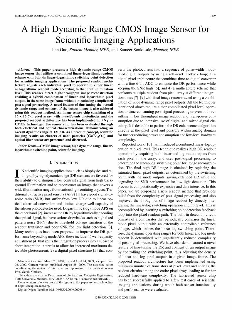
Fig. 1. Architecture of image sensor with proposed built-in linear-log switching point detection circuit.
This paper is organized as follows. Section II explainsthe system level operation of the high DR image readout withbuilt-in linear-log switching point detection, showing the essen-tial circuit blocks. Section III provides circuitry implementationin detail at both pixel and chip level. Section IV shows chipcharacterization results and the image reconstruction method,followed by two scientific imaging experiments. Section Vconcludes the accomplished work.
II. IMAGE SENSOR ARCHITECTURE
The image sensor architecture is shown in Fig. 1. The sensorchip consists of a 16 16 array of pixels with n-well/p-sub pho-todiodes and a seven-transistor (7-T) structure. The chip levelreadout amplifier was implemented using a shared structure toreduce the number of transistor at each pixel [10]. The sharedoperational amplifier (Shared OTA) is partly switched on and offfor adjusting the pixel operation between linear and log modereadout, and this will be explained in the following section.Other units of the CMOS image sensor include two switched-ca-pacitor (SC) sample-and-hold circuits for sampling linear andlog mode outputs, and a global comparator connected in a feed-back loop between the pixel’s linear output and Shared OTA asa built-in linear-log switching point detection block. Since theaim of our prototype was to provide a proof of concept, we kepta small pixel count to keep the area of the chip smallfor cost and complexity reasons. Next, we explain the readoutoperation of an individual pixel.
The pixel starts by working in linear mode as a conventionalAPS. The Shared OTA reconfigures itself as a source follower
whose output vlin is connected to a sample-and-hold SC cir-cuit for final readout. The global comparator takes the linearmode output (Output_lin) from each pixel and compares it withan external reference voltage that decides the switchingpoint for the image sensor to go automatically from linear to logreadout mode. If the detected illumination intensity exceeds thethreshold level pre-defined by , a low voltage control signalis generated and fed back into Shared OTA, reconfiguring thepixel readout mode into log operation. The output is then sam-pled via a second SC circuit; and, if the detected illuminationfalls below the switching point, the pixel readout is completeand linear output will be used for final image reconstruction.Within a given frame, only pixels sensing high input opticalpower will operate in dual linear-log mode and this foregoesthe need for pixels sensing low light to enter into log mode op-eration, as is required in [10] due to their image reconstructionprocess. Therefore our readout method leads to reduced powerconsumption with minimum post-signal processing ahead andimproved readout throughput especially at low light detection.Also note that the externally controllable reference voltageadjusts the number of linear mode pixel outputs and the numberof log mode pixel outputs across the pixel array under any givenbackground illumination by controlling the switching point, re-sulting in a final reconstructed image whose contrast and overallDR can be finely tuned to achieve good image quality. Thissets our design apart from other similar readout methods whoselinear-log switching is also carried out at chip level but all havea fixed switching point [11], [12] . The image reconstructionprocess of our design including setting the switching point willbe explained in detail in Section IV.
GUO AND SONKUSALE: A HIGH DYNAMIC RANGE CMOS IMAGE SENSOR FOR SCIENTIFIC IMAGING APPLICATIONS 1211
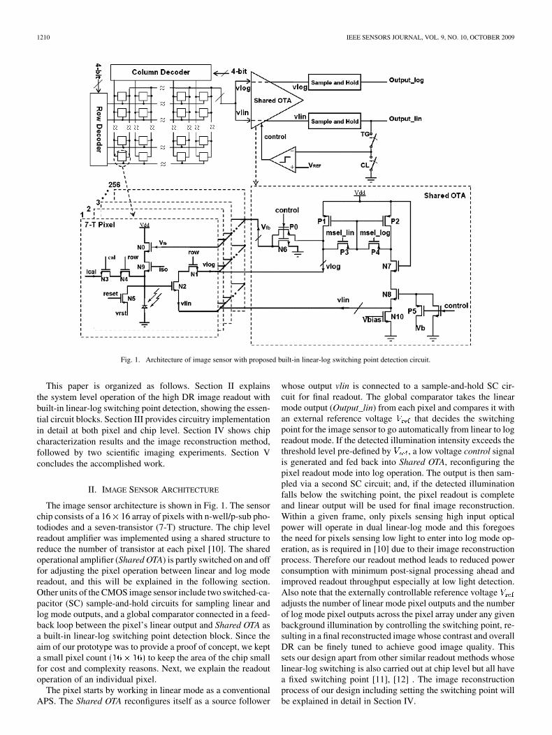
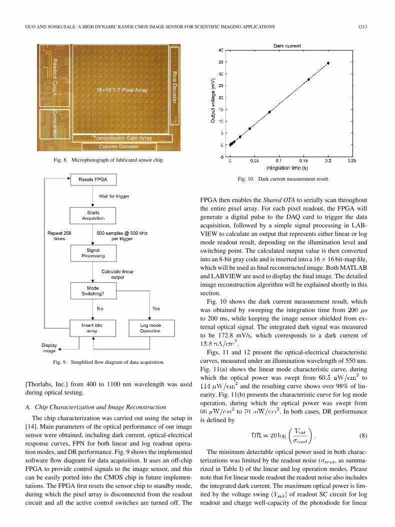
Fig. 2. Simplified timing diagram of linear-log readout operation.
Fig. 3. Simplified schematic of linear mode operation.
III. CIRCUIT IMPLEMENTATION
A. Pixel Implementation
As mentioned earlier, a complete pixel readout structure con-sists of two parts: one that resides inside pixel array as 7-T pixeland one that is a Shared OTA utilized by all the pixels duringserial pixel readout. This allows for reduced transistor count ateach pixel given the level of complexity of readout operation,thus facilitating a high fill factor implementation. It can be seenfrom Fig. 1 that transistors N1 and N2 from Shared OTA areborrowed from each individual pixel, which is time multiplexedto connect with Shared OTA during readout. To understand thelinear-log readout operation, please see Fig. 2 for the simplifiedtiming diagram. Initially, two nonoverlapping mode selectionsignals msel_lin (low) and msel_log (high) are applied to theShared OTA, forcing the pixel into conventional linear mode op-eration. CL resets the global comparator by connecting its nega-tive input to ground, generating a mode switching signal control(high) back into the Shared OTA. Transistors N9 and N0 are thenturned off to minimize their leakage current contribution to thephotocurrent during photodiode integration operation. The gateof N8 is connected to ground by control, which disables the rightbranch (P2, N7, and N8) of the Shared OTA. The left branch ofthe Shared OTA now works as a source follower (N2, N10) withdiode connected load (P1). Linear integration of the photocur-rent at this source follower input produces a linear mode outputvlin that is sampled and held by the following SC circuit. Thesimplified schematic of linear mode pixel readout is shown inFig. 3.
The linear mode output Output_lin after the SC circuit iscompared with . If the background illumination reaches thethreshold value defined by switching point, Output_lin will ex-ceed and the comparator will then generate a low voltage
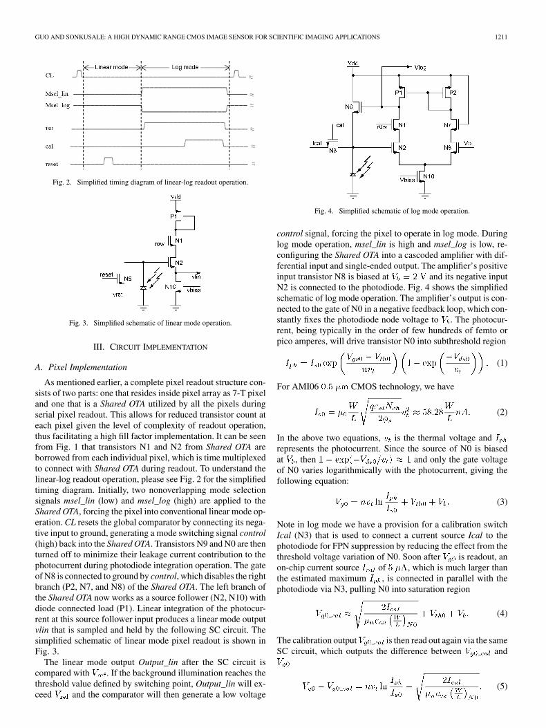
Fig. 4. Simplified schematic of log mode operation.
control signal, forcing the pixel to operate in log mode. Duringlog mode operation, msel_lin is high and msel_log is low, re-configuring the Shared OTA into a cascoded amplifier with dif-ferential input and single-ended output. The amplifier’s positiveinput transistor N8 is biased at and its negative inputN2 is connected to the photodiode. Fig. 4 shows the simplifiedschematic of log mode operation. The amplifier’s output is con-nected to the gate of N0 in a negative feedback loop, which con-stantly fixes the photodiode node voltage to . The photocur-rent, being typically in the order of few hundreds of femto orpico amperes, will drive transistor N0 into subthreshold region
(1)
For AMI06 CMOS technology, we have
(2)
In the above two equations, is the thermal voltage andrepresents the photocurrent. Since the source of N0 is biasedat , then and only the gate voltageof N0 varies logarithmically with the photocurrent, giving thefollowing equation:
(3)
Note in log mode we have a provision for a calibration switchIcal (N3) that is used to connect a current source Ical to thephotodiode for FPN suppression by reducing the effect from thethreshold voltage variation of N0. Soon after is readout, anon-chip current source of , which is much larger thanthe estimated maximum , is connected in parallel with thephotodiode via N3, pulling N0 into saturation region
(4)
The calibration output is then read out again via the sameSC circuit, which outputs the difference between and
(5)
1212 IEEE SENSORS JOURNAL, VOL. 9, NO. 10, OCTOBER 2009
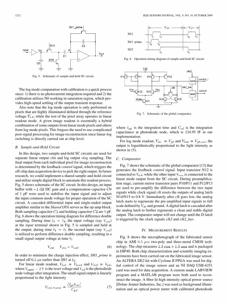
Fig. 5. Schematic of sample-and-hold SC circuit.
The log mode computation with calibration is a quick processsince: 1) there is no photocurrent integration required and 2) thecalibration utilizes N0 working in saturation region, which pro-vides high-speed settling of the output transient response.
Also note that the log mode operation is only performed onpixels that are highly illuminated defined through the referencevoltage , while the rest of the pixel array operates in linearreadout mode. A given image readout is essentially a hybridcombination of some outputs from linear mode pixels and othersfrom log mode pixels. This forgoes the need to use complicatedpost-signal processing for image reconstruction since linear-logswitching is directly carried out at chip level.
B. Sample-and-Hold Circuit
In this design, two sample-and-hold SC circuits are used forseparate linear output vlin and log output vlog sampling. Thefinal output from each individual pixel for image reconstructionis determined by the feedback control signal, which triggers theoff-chip data acquisition device to pick the right output. In futureresearch, we could implement a shared sample-and-hold circuitand utilize simple digital block to automate this readout process.Fig. 5 shows schematic of the SC circuit. In this design, an inputbuffer with DC gain and a compensation capacitorof 1 pF were used to stabilize the input signal and to adjustthe input common-mode voltage for proper operation of the SCcircuit. A cascoded differential input and single-ended outputamplifier similar to the Shared OTA serves as the op-amp block.Both sampling capacitor and holding capacitor are 1 pF.Fig. 6 shows the operation timing diagram for difference doublesampling. During time , the input voltage (say )at the input terminal shown in Fig. 5 is sampled and held atthe output; during time the second input (say )is utilized to perform difference double sampling, resulting in asmall signal output voltage at time
(6)
In order to minimize the charge injection effect, SH1_prime isturned off earlier than SH1 at .
For linear mode readout, and ,where is the reset voltage and is the photodiodenode voltage after integration. The small signal output is linearlyproportional to the light intensity
(7)
Fig. 6. Operation timing diagram of sample-and-hold SC circuit.
Fig. 7. Schematic of the global comparator.
where is the integration time and is the integrationcapacitance at photodiode node, which is 124.95 fF in ourimplementation.
For log mode readout, and , theoutput is logarithmically proportional to the light intensity asshown in (5).
C. Comparator
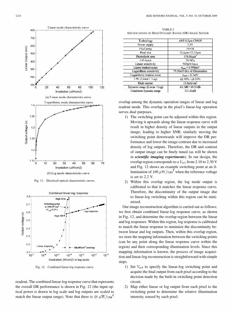
Fig. 7 shows the schematic of the global comparator [13] thatgenerates the feedback control signal. Input transistor N12 isconnected to , while the other input is connected to thelinear mode output from the SC circuit. During preamplifica-tion stage, current mirror transistor pairs P10/P11 and P12/P13are used to pre-amplify the difference between the two inputsignals while clock signal clk resets the outputs of analog latchN14/N15 to 0.8 V. Immediately after clk goes low, the analoglatch starts to regenerate the pre-amplified input signals to fullscale defined by and ground. A digital latch is cascaded afterthe analog latch to further regenerate a clean and stable digitaloutput. The comparator output will not change until the D-latchis triggered by the clock signals clk2 and clk2_bar.
IV. MEASUREMENT RESULTS
Fig. 8 shows the microphotograph of the fabricated sensorchip in AMI two-poly and three-metal CMOS tech-nology. The chip measures and is packagedin DIP40. Both chip characterization and scientific imaging ex-periments have been carried out on the fabricated image sensor.An ALTERA DE2 kit with Cyclone II FPGA was used for dig-ital control of the image sensor and an NI DAQ USB-6251card was used for data acquisition. A custom made LABVIEWprogram and a MATLAB program were both used to recon-struct the image. A fiber-lit high intensity optical power source[Dolan–Jenner Industries, Inc.] was used as background illumi-nation and an optical power meter with calibrated photodiode
GUO AND SONKUSALE: A HIGH DYNAMIC RANGE CMOS IMAGE SENSOR FOR SCIENTIFIC IMAGING APPLICATIONS 1213
Fig. 8. Microphotograph of fabricated sensor chip.
Fig. 9. Simplified flow diagram of data acquisition.
[Thorlabs, Inc.] from 400 to 1100 nm wavelength was usedduring optical testing.
A. Chip Characterization and Image Reconstruction
The chip characterization was carried out using the setup in[14]. Main parameters of the optical performance of our imagesensor were obtained, including dark current, optical-electricalresponse curves, FPN for both linear and log readout opera-tion modes, and DR performance. Fig. 9 shows the implementedsoftware flow diagram for data acquisition. It uses an off-chipFPGA to provide control signals to the image sensor, and thiscan be easily ported into the CMOS chip in future implemen-tations. The FPGA first resets the sensor chip to standby mode,during which the pixel array is disconnected from the readoutcircuit and all the active control switches are turned off. The
Fig. 10. Dark current measurement result.
FPGA then enables the Shared OTA to serially scan throughoutthe entire pixel array. For each pixel readout, the FPGA willgenerate a digital pulse to the DAQ card to trigger the dataacquisition, followed by a simple signal processing in LAB-VIEW to calculate an output that represents either linear or logmode readout result, depending on the illumination level andswitching point. The calculated output value is then convertedinto an 8-bit gray code and is inserted into a 16 16 bit-map file,which will be used as final reconstructed image. Both MATLABand LABVIEW are used to display the final image. The detailedimage reconstruction algorithm will be explained shortly in thissection.
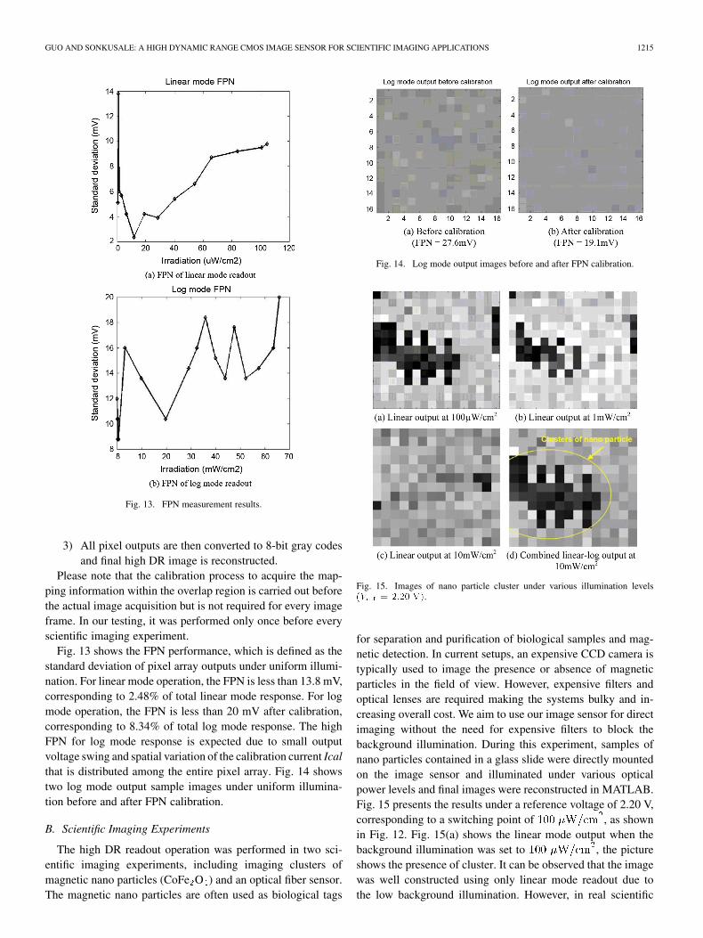
Fig. 10 shows the dark current measurement result, whichwas obtained by sweeping the integration time fromto 200 ms, while keeping the image sensor shielded from ex-ternal optical signal. The integrated dark signal was measuredto be 172.8 mV/s, which corresponds to a dark current of
.Figs. 11 and 12 present the optical-electrical characteristic
curves, measured under an illumination wavelength of 550 nm.Fig. 11(a) shows the linear mode characteristic curve, duringwhich the optical power was swept from to
and the resulting curve shows over 98% of lin-earity. Fig. 11(b) presents the characteristic curve for log modeoperation, during which the optical power was swept from
to . In both cases, DR performanceis defined by
(8)
The minimum detectable optical power used in both charac-terizations was limited by the readout noise ( , as summa-rized in Table I) of the linear and log operation modes. Pleasenote that for linear mode readout the readout noise also includesthe integrated dark current. The maximum optical power is lim-ited by the voltage swing of readout SC circuit for logreadout and charge well-capacity of the photodiode for linear
1214 IEEE SENSORS JOURNAL, VOL. 9, NO. 10, OCTOBER 2009
Fig. 11. Electrical-optical characteristic curves.
Fig. 12. Combined linear-log response curve.
readout. The combined linear-log response curve that representsthe overall DR performance is shown in Fig. 12 (the input op-tical power is drawn in log scale and log outputs are scaled tomatch the linear output range). Note that there is
TABLE ISPECIFICATIONS OF HIGH DYNAMIC RANGE (DR) IMAGE SENSOR
overlap among the dynamic operation ranges of linear and logreadout mode. This overlap in the pixel’s linear-log operationserves dual purposes.
1) The switching point can be adjusted within this region.Moving it upwards along the linear response curve willresult in higher density of linear outputs in the outputimage, leading to higher SNR; similarly moving theswitching point downwards will improve the DR per-formance and lower the image contrast due to increaseddensity of log outputs. Therefore, the DR and contrastof output image can be finely tuned (as will be shownin scientific imaging experiments). In our design, theoverlap region corresponds to a from 2.10 to 2.30 Vand Fig. 12 shows an example switching point at an il-lumination of when the reference voltageis set to 2.2 V.
2) Within this overlap region, the log mode output iscalibrated so that it matches the linear response curve.Therefore, the discontinuity of the output image dueto linear-log switching within this region can be mini-mized.
Our image reconstruction algorithm is carried out as follows:we first obtain combined linear-log response curve, as shownin Fig. 12, and determine the overlap region between the linearand log responses. Within this region, log response is calibratedto match the linear response to minimize the discontinuity be-tween linear and log outputs. Then, within this overlap region,we store the mapping information between the switching points(can be any point along the linear response curve within theregion) and their corresponding illumination levels. Since thismapping information is known, the process of image acquisi-tion and linear-log reconstruction is straightforward with simplesteps.
1) Set to specify the linear-log switching point andacquire the final output from each pixel according to thedecision made by the built-in switching point detectioncircuit.
2) Map either linear or log output from each pixel to theswitching point to determine the relative illuminationintensity sensed by each pixel.
GUO AND SONKUSALE: A HIGH DYNAMIC RANGE CMOS IMAGE SENSOR FOR SCIENTIFIC IMAGING APPLICATIONS 1215
Fig. 13. FPN measurement results.
3) All pixel outputs are then converted to 8-bit gray codesand final high DR image is reconstructed.
Please note that the calibration process to acquire the map-ping information within the overlap region is carried out beforethe actual image acquisition but is not required for every imageframe. In our testing, it was performed only once before everyscientific imaging experiment.
Fig. 13 shows the FPN performance, which is defined as thestandard deviation of pixel array outputs under uniform illumi-nation. For linear mode operation, the FPN is less than 13.8 mV,corresponding to 2.48% of total linear mode response. For logmode operation, the FPN is less than 20 mV after calibration,corresponding to 8.34% of total log mode response. The highFPN for log mode response is expected due to small outputvoltage swing and spatial variation of the calibration current Icalthat is distributed among the entire pixel array. Fig. 14 showstwo log mode output sample images under uniform illumina-tion before and after FPN calibration.
B. Scientific Imaging Experiments
The high DR readout operation was performed in two sci-entific imaging experiments, including imaging clusters ofmagnetic nano particles (CoFe O ) and an optical fiber sensor.The magnetic nano particles are often used as biological tags
Fig. 14. Log mode output images before and after FPN calibration.
Fig. 15. Images of nano particle cluster under various illumination levels�� � ���� ��.
for separation and purification of biological samples and mag-netic detection. In current setups, an expensive CCD camera istypically used to image the presence or absence of magneticparticles in the field of view. However, expensive filters andoptical lenses are required making the systems bulky and in-creasing overall cost. We aim to use our image sensor for directimaging without the need for expensive filters to block thebackground illumination. During this experiment, samples ofnano particles contained in a glass slide were directly mountedon the image sensor and illuminated under various opticalpower levels and final images were reconstructed in MATLAB.Fig. 15 presents the results under a reference voltage of 2.20 V,corresponding to a switching point of , as shownin Fig. 12. Fig. 15(a) shows the linear mode output when thebackground illumination was set to , the pictureshows the presence of cluster. It can be observed that the imagewas well constructed using only linear mode readout due tothe low background illumination. However, in real scientific
1216 IEEE SENSORS JOURNAL, VOL. 9, NO. 10, OCTOBER 2009
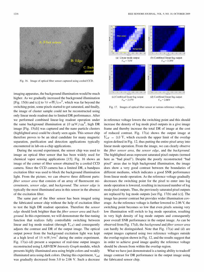
Fig. 16. Image of optical fiber sensor captured using cooled CCD.
imaging apparatus, the background illumination would be muchhigher. As we gradually increased the background illumination[Fig. 15(b) and (c)] to , which was far beyond theswitching point, some pixels started to get saturated, and finally,the image of cluster sample could not be reconstructed usingonly linear mode readout due to limited DR performance. Afterwe performed combined linear-log readout operation underthe same background illumination at , high DRimage [Fig. 15(d)] was captured and the nano particle clusters(highlighted area) could be clearly seen again. This sensor chiptherefore proves to be an ideal candidate for many magneticseparation, purification and detection applications typicallyencountered in lab-on-a-chip applications.
During the second experiment, the sensor chip was used toimage an optical fiber sensor that has been widely used forchemical vapor sensing applications [15]. Fig. 16 shows animage of the corner of fiber sensor obtained by a cooled CCDcamera. Since the CCD camera has a limited DR, a bandpassexcitation filter was used to block the background illuminationlight. From the picture, we can observe three different parts:fiber sensor area that consists of an array of fluorescent mi-crosensors, sensor edge, and background. The sensor edge istypically the most illuminated area in this sensor in the absenceof the excitation filter.
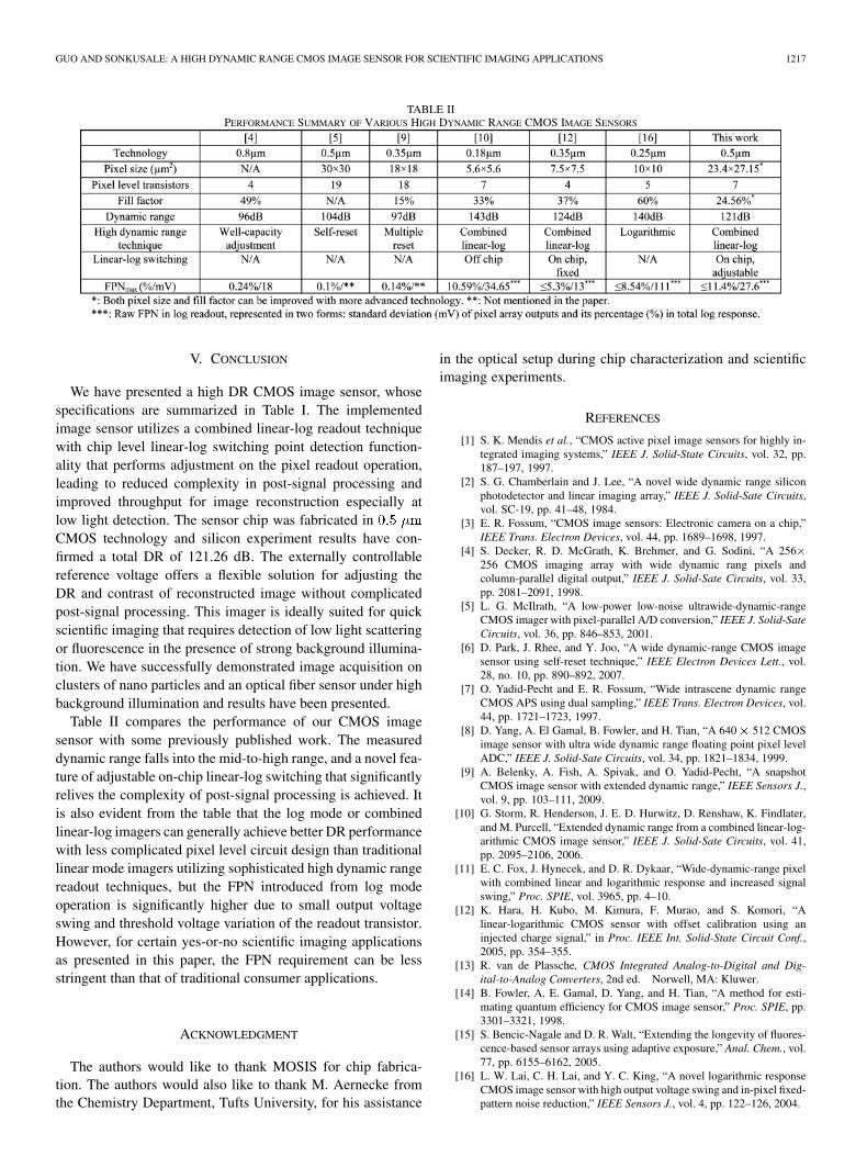
The same part of the fiber sensor has been imaged usingthe fabricated sensor chip without the help of excitation filterto test the high DR readout operation. Therefore the sensoredge should look brighter than the fiber sensor area and back-ground. In this experiment, we will demonstrate the fine-tuningfunction that realizes fully controllable switching betweenlinear and log mode readout (through ) and consequentlyadjusts the contrast and DR of the output image. The opticaloutput power from the background excitation light was keptat a high level of during the entire experiment.Fig. 17(a)–(d) present a sequence of real-time output imagesreconstructed using LABVIEW Intensity Graph module, whichpresents highly illuminated area using bright colors and weaklyilluminated area using dark colors. During this experiment,was gradually decreased from 3.0 to 2.06 V. Such a decrease
Fig. 17. Images of optical fiber sensor at various reference voltages.
in reference voltage lowers the switching point and this shouldincrease the density of log mode pixel outputs in a give imageframe and thereby increase the total DR of image at the costof reduced contrast. Fig. 17(a) shows the output image at
, which exceeds the upper limit of the overlapregion defined in Fig. 12, thus putting the entire pixel array intolinear mode operation. From the image, we can clearly observethe fiber sensor area, the sensor edge, and the background.The highlighted areas represent saturated pixel outputs (termedhere as “bad pixel”). Despite the poorly reconstructed “badpixel” areas due to high background illumination, the imagedoes show a very good contrast between the boundaries ofdifferent mediums, which indicates a good SNR performancefrom linear mode operation. As the reference voltage graduallydecreases the switching point for the pixel to enter into logmode operation is lowered, resulting in increased number of logmode pixel outputs. Thus, the previously saturated pixel outputsare replaced by log mode outputs [see Fig. 17(b) and (c)]. Theimage has poorer contrast but provides wider illumination cov-erage. As the reference voltage is further lowered to 2.06 V, theswitching point becomes so low that even pixels sensing verylow illumination will switch to log mode operation, resultingin very high density of log mode outputs and consequentlypoor overall SNR performance in the output image. As can beobserved from Fig. 17(d), the background and fiber sensor areacan hardly be distinguished. Note that Fig. 17(a) and (d) areoutput images captured using two reference voltages outsidethe overlap region shown in Fig. 12, and the results suggest thatin order to achieve good image quality the reference voltageshould be chosen from within the overlap region.
What we have just demonstrated is a tuning ability to tradeoffimage contrast for DR performance in the output image usingthe fabricated sensor chip.
GUO AND SONKUSALE: A HIGH DYNAMIC RANGE CMOS IMAGE SENSOR FOR SCIENTIFIC IMAGING APPLICATIONS 1217
TABLE IIPERFORMANCE SUMMARY OF VARIOUS HIGH DYNAMIC RANGE CMOS IMAGE SENSORS
V. CONCLUSION
We have presented a high DR CMOS image sensor, whosespecifications are summarized in Table I. The implementedimage sensor utilizes a combined linear-log readout techniquewith chip level linear-log switching point detection function-ality that performs adjustment on the pixel readout operation,leading to reduced complexity in post-signal processing andimproved throughput for image reconstruction especially atlow light detection. The sensor chip was fabricated inCMOS technology and silicon experiment results have con-firmed a total DR of 121.26 dB. The externally controllablereference voltage offers a flexible solution for adjusting theDR and contrast of reconstructed image without complicatedpost-signal processing. This imager is ideally suited for quickscientific imaging that requires detection of low light scatteringor fluorescence in the presence of strong background illumina-tion. We have successfully demonstrated image acquisition onclusters of nano particles and an optical fiber sensor under highbackground illumination and results have been presented.
Table II compares the performance of our CMOS imagesensor with some previously published work. The measureddynamic range falls into the mid-to-high range, and a novel fea-ture of adjustable on-chip linear-log switching that significantlyrelives the complexity of post-signal processing is achieved. Itis also evident from the table that the log mode or combinedlinear-log imagers can generally achieve better DR performancewith less complicated pixel level circuit design than traditionallinear mode imagers utilizing sophisticated high dynamic rangereadout techniques, but the FPN introduced from log modeoperation is significantly higher due to small output voltageswing and threshold voltage variation of the readout transistor.However, for certain yes-or-no scientific imaging applicationsas presented in this paper, the FPN requirement can be lessstringent than that of traditional consumer applications.
ACKNOWLEDGMENT
The authors would like to thank MOSIS for chip fabrica-tion. The authors would also like to thank M. Aernecke fromthe Chemistry Department, Tufts University, for his assistance
in the optical setup during chip characterization and scientificimaging experiments.
REFERENCES
[1] S. K. Mendis et al., “CMOS active pixel image sensors for highly in-tegrated imaging systems,” IEEE J. Solid-State Circuits, vol. 32, pp.187–197, 1997.
[2] S. G. Chamberlain and J. Lee, “A novel wide dynamic range siliconphotodetector and linear imaging array,” IEEE J. Solid-Sate Circuits,vol. SC-19, pp. 41–48, 1984.
[3] E. R. Fossum, “CMOS image sensors: Electronic camera on a chip,”IEEE Trans. Electron Devices, vol. 44, pp. 1689–1698, 1997.
[4] S. Decker, R. D. McGrath, K. Brehmer, and G. Sodini, “A 256�256 CMOS imaging array with wide dynamic rang pixels andcolumn-parallel digital output,” IEEE J. Solid-Sate Circuits, vol. 33,pp. 2081–2091, 1998.
[5] L. G. McIlrath, “A low-power low-noise ultrawide-dynamic-rangeCMOS imager with pixel-parallel A/D conversion,” IEEE J. Solid-SateCircuits, vol. 36, pp. 846–853, 2001.
[6] D. Park, J. Rhee, and Y. Joo, “A wide dynamic-range CMOS imagesensor using self-reset technique,” IEEE Electron Devices Lett., vol.28, no. 10, pp. 890–892, 2007.
[7] O. Yadid-Pecht and E. R. Fossum, “Wide intrascene dynamic rangeCMOS APS using dual sampling,” IEEE Trans. Electron Devices, vol.44, pp. 1721–1723, 1997.
[8] D. Yang, A. El Gamal, B. Fowler, and H. Tian, “A 640 � 512 CMOSimage sensor with ultra wide dynamic range floating point pixel levelADC,” IEEE J. Solid-Sate Circuits, vol. 34, pp. 1821–1834, 1999.
[9] A. Belenky, A. Fish, A. Spivak, and O. Yadid-Pecht, “A snapshotCMOS image sensor with extended dynamic range,” IEEE Sensors J.,vol. 9, pp. 103–111, 2009.
[10] G. Storm, R. Henderson, J. E. D. Hurwitz, D. Renshaw, K. Findlater,and M. Purcell, “Extended dynamic range from a combined linear-log-arithmic CMOS image sensor,” IEEE J. Solid-Sate Circuits, vol. 41,pp. 2095–2106, 2006.
[11] E. C. Fox, J. Hynecek, and D. R. Dykaar, “Wide-dynamic-range pixelwith combined linear and logarithmic response and increased signalswing,” Proc. SPIE, vol. 3965, pp. 4–10.
[12] K. Hara, H. Kubo, M. Kimura, F. Murao, and S. Komori, “Alinear-logarithmic CMOS sensor with offset calibration using aninjected charge signal,” in Proc. IEEE Int. Solid-State Circuit Conf.,2005, pp. 354–355.
[13] R. van de Plassche, CMOS Integrated Analog-to-Digital and Dig-ital-to-Analog Converters, 2nd ed. Norwell, MA: Kluwer.
[14] B. Fowler, A. E. Gamal, D. Yang, and H. Tian, “A method for esti-mating quantum efficiency for CMOS image sensor,” Proc. SPIE, pp.3301–3321, 1998.
[15] S. Bencic-Nagale and D. R. Walt, “Extending the longevity of fluores-cence-based sensor arrays using adaptive exposure,” Anal. Chem., vol.77, pp. 6155–6162, 2005.
[16] L. W. Lai, C. H. Lai, and Y. C. King, “A novel logarithmic responseCMOS image sensor with high output voltage swing and in-pixel fixed-pattern noise reduction,” IEEE Sensors J., vol. 4, pp. 122–126, 2004.
1218 IEEE SENSORS JOURNAL, VOL. 9, NO. 10, OCTOBER 2009
Jian Guo (S’07) was born in Wuhan, Hubei, China,1983. He received the B.S. degree in electrical engi-neering at Shanghai Jiao Tong University, Shanghai,China, in 2006. He is currently working towards thePh.D. degree at the Nanoscale Integrated Sensors andCircuits Laboratory, Department of Electrical andComputer Engineering, Tufts University, Medford,MA.
In 2008, he joined GE Sensing and Inspections,Inc., North Billerica, MA, as a summer intern, duringwhich he worked as an Embedded System Engineer.
His research interests include analog and mixed-signal integrated circuits,with special focus on CMOS image sensors and low-power analog to digitalconverters.
Sameer Sonkusale (S’97–M’02) received theB.E. (Hons) degree in electrical and electronicsengineering from Birla Institute of Technology andScience (BITS), Pilani, India, in 1996, and the M.S.and Ph.D. degrees in electrical engineering from theUniversity of Pennsylvania, Philadelphia, in 1999and 2003, respectively.
From 1996 to 1997, he worked as an IC DesignEngineer at Texas Instruments, Bangalore, India, andas an intern during summers of 1998–2000 in the dataconverters group in Dallas, TX and Warren, NJ. From
2002 to 2004, he was with Texas A&M University as an Assistant Professorof Electrical and Computer Engineering conducting research on Nyquist ratedata converters. Since 2004, he has been on the faculty of the Department ofElectrical and Computer Engineering, Tufts University, Medford, MA, wherehe directs the Nanoscale Integrated Sensors and Circuits Laboratory.
Dr. Sonkusale serves as member of the Analog Signal Processing TechnicalCommittee, and the BioCAS Technical Committee of the IEEE Circuits andSystems Society and also serves as a member of Technical Program Committeefor the IEEE Sensors Conference, the IEEE System on Chip Conference, theIEEE Engineering in Medicine and Biology Conference, the Great Lakes Sym-posium on VLSI Circuits, and the IEEE International Symposium on Circuitsand Systems. His research interests are in the area of high-performance, low-power analog and mixed signal circuit design with special emphasis on inte-grated sensors and microanalytical instrumentation for biomedical and life sci-ences application.