Deposited in the Library, University of California, San Francisco
Upload
khangminh22Category
view
0download
0
“SOME STUDIES ON THE SYNTHESIS AND CHARACTERI-
ZATION OF NCD/UNCD THIN FILMS DEPOSITED OVER
VARIOUS SUBSTRATES”
By
JAGANNATH DATTA
(CHEM01201004009)
Bhabha Atomic Research Centre
Mumbai 400085, India
A thesis submitted to the
Board of Studies in Chemical Sciences
In partial fulfillment of requirements
for the Degree of
DOCTOR OF PHILOSOPHY
of
HOMI BHABHA NATIONAL INSTITUTE
NOVEMBER, 2014


STATEMENT BY AUTHOR
This dissertation has been submitted in partial fulfillment of requirements for an advanced
degree at Homi Bhabha National Institute (HBNI) and is deposited in the Library to be made
available to borrowers under rules of the HBNI.
Brief quotations from this dissertation are allowable without special permission, provided that
accurate acknowledgement of source is made. Requests for permission for extended quotation
from or reproduction of this manuscript in whole or in part may be granted by the Competent
Authority of HBNI when in his or her judgment the proposed use of the material is in the in-
terests of scholarship. In all other instances, however, permission must be obtained from the
author.
(JAGANNATH DATTA)

DECLARATION
I, hereby declare that the investigation presented in the thesis has been carried out by me. The
work is original and has not been submitted earlier as a whole or in part for a degree / diploma at
this or any other Institution / University.
(JAGANNATH DATTA)
List of Publications arising from the thesis
Journal
1. "Structure of Hydrogenated diamond like carbon by Micro-Raman Spectroscopy″, Ja-
gannath Datta, Nihar R Ray, Pintu Sen, Hari S Biswas, and Erwin A Vogler, Mate-
rials Letters, 2012, Vol. 71, Pages 131–133 (DOI : 10.1016/j.matlet.2011.12.041).
2. "Study of depth profile of hydrogen in hydrogenated diamond like carbon thin film by
ion beam analysis techniques″, J. Datta, H.S. Biswas, P. Rao, G.L.N. Reddy, S. Ku-
mar, N.R. Ray, D.P. Chowdhury, and A.V.R. Reddy, Nuclear Instruments and Me-
thods in Physics Research B, 2014, Vol. 328, 27-32 (DOI :
10.1016/j.nimb.2014.02.127).
3. "Signature of Misoriented Bilayer Graphenelike and Graphanelike Structure in the
Hydrogenated Diamond-Like Carbon Film″, Nihar R. Ray, Jagannath Datta, Hari S.
Biswas and Someswar Datta, IEEE Transactions on Plasma Science, 2012, Vol. 40,
Issue 7, Pages 1789-1793 (DOI: 10.1109/TPS.2012.2201176).
Conferences
1. "Formation of Atomically Thin Film of Coherent Domains of sp2 C=C and sp3 C-H
carbons at the surface of Hydrogenated Diamond like Carbon Substrate″, N.R. Ray, J.
Datta, P. Sen, H.S. Biswas, E.A. Vogler, XXX International Conference on Pheno-
mena in Ionized Gases (ICPIG), August 28th – September 2nd 2011, Belfast, Northern
Ireland, UK.
2. "On the Thin Film of Nanocrytalline Graphite Clusters″; N.R. Ray, J. Datta, H. S.
Biswas, and S Datta, 4th International Symposium on Advanced Plasma Science and

its Applications for Nitrides and Nanomaterials (ISPlasma 2012), March 04 - 08,
2012, Aichi, Japan.
3. "Formation of Continuous Thin Film of Nanocrytalline Graphite Clusters″, H. S. Bis-
was, J. Datta, N.R. Ray, S Datta, and U.C. Ghosh, International Conference on Na-
noscience and Technology (ICONSAT - 2012) January 20 - 23, 2012, Hyderabad, In-
dia.
4. "Development of Hydrogenated Diamond like Carbon as Hydrogen Storage Material″
Jagannath Datta, Sanjiv Kumar, D.P. Chowdhury, A.V.R. Reddy and Nihar Ranjan
Ray, Satellite Conference on 100 Years of Science in India, during January 9 – 10,
2013 at SINP, Kolkata.
5. "Study of depth profile of Hydrogen in Hydrogenated Diamond like Carbon thin film
by Ion Beam Analysis techniques″, J. Datta, H.S. Biswas, S. Kumar, D.P. Chowd-
hury, N.R. Ray, A.V.R. Reddy, In the proceedings of DAE-BRNS Fifth Symposium on
Nuclear Analytical Chemistry (NAC-V) during January 20-24, 2014, at Bhabha Atom-
ic Research Centre, Trombay, Mumbai, India.
(JAGANNATH DATTA)

Journal contributions NOT included in this thesis
1.
Langmuir, 2010, Vol. 26
(22), Pages 17413–17418.
2. Ceria associated manganese oxide nanoparticles: synthesis, characterization and ar-
senic (V) sorption behavior, Kaushik Gupta, Sayan Bhattacharya, Aniruddha Mukho-
padhyay, Harishankar Biswas, Jagannath Dutta, Nihar Ranjan Roy, Uday Chand
Ghosh, Chemical Engineering Journal, 2011, Vol. 172, Pages 219-229.
3. Raman spectra of electrochemically hydrogenated diamond like carbon surface; Hari
Shankar Biswas, Jagannath Datta, Pintu Sen, Uday Chand Ghosh, Nihar Ranjan
Ray, Chemical Physics Letters 2014, Vol. 600, Pages 10-14.
4. Covalently bound Bovine Serum Albumin (BSA) protein modified Hydrogenated Di-
amond Like Carbon (HDLC) surface as biosensor application; Hari Shankar Biswas,
Kausik Gupta, Jagannath Datta, Uday Chand Ghosh, Nihar Ranjan Ray, preprint
arXiv:1404.0553 (2014).


Dedicated to my
mother


ACKNOWLEDGEMENTS
It is a great pleasure to express my deep sense of gratitude and regards to Professor
N. R. Ray, Plasma Physics Division, Saha Institute of Nuclear Physics, Kolkata, for giving
me the opportunity of doing this research work under his constant guidance. I sincerely
thank him for his encouragement and useful suggestions.
I am grateful to Dr. A.V.R. Reddy, Head, Analytical Chemistry Division, Bhabha
Atomic Research Centre (BARC), Mumbai for granting me the official permission to get
myself registered under HBNI for the Ph.D. thesis.
I am extremely grateful to Professor D.K. Srivastava, Director, Variable Energy
Cyclotron Centre (VECC), Kolkata for allowing me to carry out my research work using
the Cyclotron machine and other experimental facilities.
I sincerely express my thanks to Director, Saha Institute of Nuclear Physics for his
support and guidance in performing this thesis work in SINP, Kolkata.
I am especially thankful to Dr. S.K. Das and Dr. R. Guin, Radiochemistry Division
(RCD), BARC, Dr. M. K. Das, Board of Radiation and Isotope Technology (BRIT), Dr. S.
K. Bandyopadhyay, Dr. P. Sen, VECC, Kolkata for their valuable suggestions and encou-
ragement during the course of my work.
Grateful thanks are due to Dr. R. Verma, Dr. (Mrs.) S. D. Kumar, Analytical Chemi-
stry Division, BARC, Mumbai and Dr. S. Kumar, and his team, National Centre for Com-
positional Characterization of Materials (NCCCM), Hyderabad with whom a part of the
experimental work was successfully carried out.
I owe my thanks to Professor S. Datta, Bio-ceramic and Coating Division, CSIR-
Centre for Glass and Ceramic Research Institute (CSIR-CGCRI), Kolkata for their collabo-
ration and help in providing me with some valuable samples.

I would like to thank S.S. Sil, U.S. Sil, and A.A. Mallick for their technical help dur-
ing the experimental works.
I sincerely express my thanks to Dr. D.P. Chowdhury, my mentor, and Head, Nuc-
lear Method Group, ACD, BARC, at VECC, Kolkata for his encouragement and inspira-
tion.
I owe my thanks to Mr. H.S. Biswas, Co-worker and friends, SINP, Kolkata for their
help in providing me during the sample imaging and analysis.
I wish to thanks all my colleagues and friends of VECC, Kolkata, and Analytical
Chemistry Division, BARC, Mumbai for their help and co-operation at various stages of
my work.
Finally, I wish to express my deep sense of gratitude to my family and relatives who
have sacrificed immensely in their own ways and had been a constant source of my inspira-
tion and moral support throughout the tenure of this study.
NOV, 2014 (JAGANNATH DATTA)
CONTENTS
SYNOPSIS………………………………………………………………………….. I
LIST OF FIGURES………………………………………………………………… XI
LIST OF TABLES…………………………………………………………………..XVII
CHAPTER – 1
Introduction
1.0 Introduction 1
1.1 Literature reviews on NCD and UNCD 1
1.1.1 Classification of NCD and UNCD 1
1.1.2 Applications of NCD and UNCD 3
1.1.3 Synthesis of NCD and UNCD 5
1.1.4 Growth chemistry and mechanism of NCD and UNCD synthesis 7
1.1.5 Hydrogenated diamond like carbon (HDLC) and its characterization 13
1.1.5.1 Characterization using IR, NMR, XPS, and XANES 15
1.1.5.2 Characterization using Raman spectroscopy 18
1.1.5.3 Characterization using NRA and RBS 25
1.1.5.4 Characterization using I-V measurement 28
1.2 Objectives 29

CHAPTER – 2
Experimental set-up for the synthesis of HDLC films on various substrates at room temperature
2.0 Introduction 32
2.1 History of ‘Diamond’ and ‘Low Pressure Diamond Synthesis’ 35
2.2 General methods for Diamond Like Carbon Synthesis 36
2.2.1 Physical Vapor Deposition (PVD) 36
2.2.2 Chemical Vapor Deposition (CVD) 36
2.3 PECVD System 38
2.3.1 Description of the System 38
2.3.2 Description of System Operation 40
2.3.3 Synthesis of Hydrogenated Diamond Like Carbon thin film onto 45
2.3.3.1 (a) Silicon (b) Quartz substrates 45
2.3.3.2 stainless steel 47
2.3.4 Description of the major parts of the System 50
2.4 Annealing of HDLC samples 51
2.5 HDLC samples preparation for IBA study 54

CHAPTER – 3
Characterization Tools
3.0 Introduction 56
3.1 High resolution transmission electron microscope 57
3.1.1 Imaging using HRTEM 57
3.1.2 Transmission electron energy loss spectroscopy 59
3.2 Raman spectroscopy 63
3.2.1 Classical model for the interpretation of Raman lines 63
3.2.3 Quantum model for Raman lines 65
3.2.3 Second order Raman Spectra 68
3.2.4 Micro-Raman Spectrometer 69
3.2.5 Peak fitting and analysis 73
3.3 Scanning Probe Microscopy 78
3.3.1 Scanning tunneling microscopy 78
3.3.2 Atomic force microscopy 79
3.4 Scanning Electron Microscopy 82
3.5 Pelletron Accelerator 84
3.5.1 Nuclear Reaction Analysis 89
3.5.1.1 Methodology and Technical Details 93
3.5.2 Rutherford Backscattering Spectroscopy 98

3.6 Keithley Source Meter 99
3.6.1 Experimental arrangements for measuring I-V characteristics 99
3.7 Olympus Digital Camera 103
3.8 Dielectric Measurement 104
CHAPTER – 4
Results and Discussions
4.0 Results and discussion 107
4.1 Results and discussion using HRTEM/TEELS, SEM, AFM 107
4.2 Results and discussion with micro-Raman spectroscopic measurements 112
4.2.1 First-, Second- and Higher-order Raman features 113
4.2.2 Stress computation from Raman spectra 119
4.2.3 Experimental signature of bilayer Graphene like and Graphane like
structure in the Hydrogenated Diamond Like Carbon film 121
4.3 Results and discussion using NRA and RBS 130
4.3.1 Results of NRA measurements 130
4.3.2 Results of RBS measurements 136
4.4 Results and discussion with STM measurements 143
4.5 Results and discussion using I-V characteristics measurements 144
4.6 Results and discussion with the optical photograph of HDLC surface 146

4.7 Reminiscence of investigations of HDLC film by HRTEM, SEM, AFM, mRS, STM,
IBA, I vs. V measurements and optical imaging measurements 148
4.8 Typical Raman spectrum of HDLC film onto different substrates 149
CHAPTER – 5
Summary and Conclusions
5.1 Summary and Conclusions 156
References 158
Reprints 176

Abbreviations:
DLC – Diamond Like Carbon
HDLC –Hydrogenated Diamond Like Carbon
HD - Hydrogenated Diamond
ND - NanoDiamond
NCD – Nano-Crystralline Diamond
UNCD – Ultra Nano-crystalline Diamond
a-C - Amorphous carbon
a-C:H - Hydrogenated amorphous carbon
N-UNCD – Nitrogen-incorporated ultrananocrystalline diamond
B-NCD- Boron-doped NCD
SCCM – Standard Cubic Centimeter per minute
MFC – Mass flow controller
CVD – Chemical Vapor Deposition
PECVD - Plasma Enhanced Chemical Vapor Deposition
MPCVD – Microwave Plasma Chemical Vapor Deposition
MPACVD – Microwave Plasma Assisted Chemical Vapor Deposition
HFCVD – Hot Filament Chemical Vapor Deposition
HOPG – Highly Oriented Pyrolytic Graphite
S.S – Stainless Steel
RT – Room Temperature

BEN – Biased Enhanced Nucleation
BEG – Biased Enhanced Growth
RF – Radio Frequency
RH- Relative Humidity
COF-Coefficient of friction
TCR - Temperature Coefficient of Resistivity
TEC-Thermal Expansion Coefficient
RMS - Root Mean Square
mRS – micro-Raman Spectroscopy
HRTEM - High Resolution Transmission Electron Microscope
AFM - Atomic Force Microscope
STM - Scanning Tunneling Microscope
SEM - Scanning Electron Microscope
XPS – X-ray Photoelectron Spectroscopy
XANES - X-ray absorption near-edge spectroscopy
ESCA - Electron Spectroscopy for Chemical Analysis
SIMS – Secondary Ionization Mass Spectroscopy
Vac FTIR – Vacuum Fourier Transform Infra-red
UV-Vis – Ultra Violet Visible
IBA – Ion Beam Analysis
NRA –Nuclear Reaction Analysis

RBS –Rutherford Back Scattering
ERDA - Elastic Recoil Detection Analysis
EELS- Electron Energy Loss Spectroscopy
NMR - Nuclear Magnetic Resonance
NEMS /MEMS – Nano-Electro Mechanical System/ Micro-Electro Mechanical System
SET – Single Electron Transistor
CB - Coulomb blockade
TB - Tunneling barrier
2-D - Two Dimension

Units :
Speed of light (c) = 3×1010 cm/s
Planck Constant (h) = 6.67×10⁻²⁷ erg.s
Electron charge (e) = 1.602×10⁻¹⁹ coulomb= 4.803×10⁻¹⁰ esu
Avogadro Number (NA)=6.02×10²³ mol−1
Molar gas constant (R)= 8.314×10⁷ erg mol−1K−1
Conductance quantum (G0) = (2e2/h)= 7.748×10⁻⁵ S
Farad (F)= 1×10²¹ Zeptofarad (zF)= 1012 Picofarad (pF)
1 Radians (rad) =57.295 degrees (deg)= 63.662 grad
1 atm. =760 Torr =1.013 Bar=1.013×10⁶ dynes/cm2
Temp (oC) = 273 K
1 nm =10−3 µm =10−9 met =10−7 cm
1 g =106 µg
1 MeV =106 eV =1.602×10⁻¹³ J
1 A0 = 10−8 cm
1 fm= 10−13 cm
1 cal = 4.2 J

SYNOPSIS
i
Title of the Thesis:
Some studies on the synthesis and characterization of NCD/UNCD thin films
deposited over various substrates
Preamble
The interest in the chemical vapor deposition (CVD) of diamond films is due to diamond’s
unique mechanical, thermal and electronic properties [1]. The dissociation of carbon containing
gas precursor onto solid substrate is the key technique involved in the CVD of diamond films.
The substrate can be either bulk diamond (natural or synthetic) or a non-diamond substrate. The
resulting films, in the first case, are said to be homoepitaxial or single crystalline, in opposition
to heteroepitaxial or polycrystalline films in the latter case. The technological challenges, issues,
achievements of depositing CVD diamond films onto foreign substrates are the major areas of
research worldwide since the early 1980’s [2]. In spite of remarkable properties of diamond, the
high surface roughness of CVD diamond films is not suitable for their widespread use in various
applications such as machining and wear, field-emission or optical applications, transistor
applications etc. [3, 4]. The reduction of the film grain size (from micrometres to nanometres) by
means of the growth chemistry, and the surface temperature is one, out of different approaches
followed to overcome the problem of high surface roughness of CVD diamond films [2, 5].
These diamond films, commonly referred to as nanocrystalline diamond (NCD) films are grown
in hydrogen-rich CVD environments, and have grain size 30-100 nm (increasing with the film
thickness). A second category of NCD, known as ultra-nanocrystalline diamond (UNCD) films,
are grown in argon-rich, hydrogen poor CVD environments, and have a typical grain size of 3–5
nm, independent of the film thickness. The nanograins are embedded in a non-diamond matrix,

SYNOPSIS
ii
and the films show a significant content of sp2-bonded carbon (up to 5%) [6]. NCD and UNCD
films have, in general, high Young’s modulus, high hardness and a low macroscopic friction
coefficient, due to their low surface roughness, and are optically transparent. The UNCD films
are also electrically conductive, due to the non-diamond matrix. Both NCD and UNCD films are
usually deposited on non-diamond substrates, such as silicon wafers. Other materials like SiC,
SiO2 can also be used as substrates.
The growth of NCD/UNCD films from the vapor phase on non-diamond substrates at practical
rates was accomplished with the development of thermal- and plasma-enhanced CVD methods
[7-10] in which a hydrocarbon gas (usually methane) mixed in low concentrations with hydrogen
is energized thermally or in a plasma, prior to contact with a heated substrate.
In order to achieve good adhesion of NCD/UNCD films onto foreign substrate, heat-assisted
bias-enhanced nucleation (BEN)/ bias enhanced growth (BEG) technique, was found to be very
successful in terms of achieving diamond nanograins (3–5 nm), with smoother surfaces (6 nm
rms) and higher growth rate (1 m/h) of the film [11]. In the BEN/BEG technique, there is a
speculative atomic model of possible diamond/graphite/Si interface, causing a very good
adhesion of the film onto the Si substrate due to minimum lattice mismatch [12].
While the technology of diamond deposition develops, interest turned to related materials such as
Diamond like Carbon (DLC). DLC is a dense, metastable form of amorphous carbon (a-C) or
hydrogenated amorphous carbon (a-C:H) containing a significant sp3 C-H bonding. The sp3
bonding confers valuable ’diamond-like’ properties such as mechanical hardness, low friction,
optical transparency, and chemical inertness. Although DLC films have poorer properties than

SYNOPSIS
iii
diamond films, they have some advantages, notably deposition at room temperature, deposition
onto Fe or plastic substrates and superior surface smoothness.
Using asymmetrically coupled RF (13.56 MHz) discharge, a dc negative self-bias can be
produced continuously during deposition of Hydrogenated Diamond like Carbon (HDLC) thin
film onto substrates like Si(100), steel etc. at room temperature, with ultrasmooth surface (~
0.0175 nm rms) [13, 14]. The sp3 C-H contents and presence of NCD in the HDLC films depend
on the ratio of flow rates of hydrogen (H2) and methane (CH4) for a given deposition conditions
like pressure, dc negative bias, deposition time etc. [15]. A high resolution transmission electron
microscope (HRTEM) image of MeV nitrogen ion irradiated HDLC film, clearly shows
existence of crystalline graphite with lattice spacing of 0.34 nm in the HDLC film, although the
crystallographic planes are somewhat distorted compared to the perfect graphite structure [16].
All these properties of HDLC films in the early works [13-16], motivated me, for PhD
thesis works, to investigate the structural composition of HDLC films by Micro-Raman
spectroscopy and High Resolution Transmission Electron Microscope (HRTEM), depth profile
of hydrogen in the HDLC film by ion beam analysis (IBA) techniques, surface smoothness by
Atomic Force Microscope (AFM) and Scanning Electron Microscope (SEM), surface
conductance property of HDLC film from the current (I) vs. voltage (V) characteristics by
Keithley source meter. By these investigations on HDLC films, I have addressed the key issues
like ultrasmoothness of HDLC surface, compatibility of BEN model [12] in the structural
composition of HDLC, new information about the surface conductance of HDLC in comparison
to that of hydrogenated diamond (HD) film.

SYNOPSIS
iv
The thesis has been organized into five chapters, elaborating on the work carried out on the
above-mentioned themes.
Chapter 1: Introduction
Chapter 1 gives an introduction on the growing role of various new forms of
NCD/UNCD films as tribological coating, electrochemical devices, coatings for MEMS devices,
and in modern electronics industry. In this part, we shall subdivide the nanocrystalline diamond
into two broad categories based on their microstructure, growth chemistries, and properties. The
controlled synthesis of nanocrystalline diamond film to overcome and minimize the non-
diamond carbon or amorphous carbon is discussed. A brief overview of various types of DLC
thin films containing NCD, their classifications and properties are given. The basic differences
between the various deposition methods of DLC thin film using modern technology are
discussed. This chapter describes some unique advantage of the in situ BEN-BEG mechanism
using plasma enhanced CVD (PECVD) deposition onto substrate at room temperature for the
synthesis of HDLC films. The unique characterization techniques of HDLC films for its various
parameters used in the literature are described. This chapter also provides a short introduction
on: (i) Visible Micro-Raman spectroscopy for the estimation of sp2 and sp3 carbons and their
structure in the HDLC thin films (ii) Nuclear Reaction Analysis, Rutherford backscattering
spectrometry for measurement of depth profile of hydrogen in the HDLC films (ii) Measurement
of current vs. voltage characteristics of the HDLC surface to address the issue of surface
conductance property.
Chapter 2: Experimental set-up for the synthesis of HDLC films on various
substrates at room temperature

SYNOPSIS
v
Chapter 2 describes schematic and picture for the synthesis of HDLC thin film in details
with introduction, experimental, and results and discussion. The introduction gives the
potentiality of Plasma Enhanced Chemical Vapor deposition (PECVD) technique for the
synthesis of hydrogenated diamond like carbon thin films. The ‘experimental’ gives the
description of production of dc negative self bias in asymmetrically coupled RF (13.56 MHz)
discharge and their role in depositing thin films onto substrate at room temperature. That the dc
negative self bias in a controlled manner, a biased enhanced nucleation/growth (BEN/BEG),
plays the key role in depositing the thin films is described in the ‘results and discussion’.
Chapter 3: Description of Characterization tools used in the present works
3.1 High resolution transmission electron microscope (HRTEM)
The methodology for the cross sectional view and the morphology of the HDLC surface by
HRTEM have been described. The cross sectional/planer views of the samples prepared by the
TEM sample preparation equipments are described.
3.2. Micro Raman spectrometer:
The acquisition and analysis of Raman spectra of HDLC samples by Micro-Raman spectrometer
(LabRAM HR vis. Horiba Jobin Yvon SAS France) are described herein.
3.3. Atomic Force Microscope (AFM)
The morphology of HDLC surface from the atomic force microscope (AFM) image and height
profile along a given line of the AFM image using multimode scanning probe microscope
(Agilent AFM 5500 series) is described herein.

SYNOPSIS
vi
3.4. Scanning Electron Microscope (SEM)
The measurement of surface continuity and ultra smoothness of the HDLC film, as obtained
from AFM results, by Scanning Electron Microscopy (SEM) (FEI Quanta 200f), is described
herein.
3.5. Pelletron Accelerator:
The acquisition and analysis of data for the interaction of ion beam of Pelletron accelerator
(National Center for Compositional Characterization of Materials (NCCCM), Hyderabad, India)
with thin film samples, in general, are described herein. Necessarily of using Nuclear reaction
analysis (NRA) and Rutherford backscattering spectroscopy (RBS) techniques for studying
HDLC samples (as-prepared and annealed) is also described, in particular, herein.
3.5.1. Nuclear Reaction Analysis
Nuclear reaction analysis (NRA) technique for depth profiling of hydrogen in the as prepared
and annealed HDLC samples is described herein.
3.5.2. Rutherford Backscattering Spectroscopy
Rutherford backscattering spectroscopy (RBS) technique to measure the thickness of HDLC
films (as prepared and annealed) is described herein.
3.6. Keithley Source Meter:
The acquisition and analysis of I-V characteristics on the HDLC surface at RT (295K) ambient
condition using a Keithley 2635 source meter is described herein.
Chapter 4 : Results and Discussions

SYNOPSIS
vii
4.1. The typical results on HDLC films obtained by HRTEM, AFM, and SEM are displayed and
critical discussions are made based upon the results herein.
4.2. The typical results on HDLC films obtained by Micro-Raman spectrometer are displayed
and critical discussions are made based upon the results herein.
4.3. The typical results on HDLC films (as-prepared and annealed) obtained by NRA and RBS
techniques are displayed and critical discussions are made based upon the results herein.
4.4. The typical results on HDLC films (as-prepared and annealed) obtained by current (I) vs.
(V) characteristics onto the HDLC surface are displayed and critical discussions are made about
the surface conductance mechanisms, based upon the results herein.
4.5. Taken all the results together, described in sec. 4.1. to sec. 4.4., a discussion is made herein,
in order to arrive a plausible conclusion about our HDLC thin films.
Chapter 5 : Summary and Conclusions
Summary and conclusions are described herein based upon the following key results in the
investigation of HDLC films:
1. Coherency of sp3 C-H and sp2 C=C carbons in the HDLC film can produce a continuous,
non-porous thin film having atomically smooth surface, instead of discrete uniform grains
as in the case of UNCD films, is a new result [17].
2. The depth profiles of hydrogen in the as-prepared and annealed HDLC thin films are
indicative of the prevalence of graphitic carbon near the film-substrate interface and
supporting experimentally for the first time, the theoretical model of diamond-graphite-Si
structure under BEN deposition at room temperature [18].

SYNOPSIS
viii
3. Current (I) vs. Voltage (V) characteristics between two ohmic Cu contacts onto the
HDLC surface is controllable via a third ohmic Cu contact in between, indicating
possible quantum effects viz., quantum confinement, electron tunneling and coulomb
blockade, in the nanostructure HDLC thin film composed of coherently coupled sp2 C=C
and sp3C-H carbons [19,20].
The following SCI journal publications cover the present thesis works :
(1) Structure of hydrogenated diamond like carbon by Micro-Raman spectroscopy; Jagannath
Datta, Nihar R. Ray, Pintu Sen, Hari S. Biswas, and Erwin A. Vogler; Materials Letters, 71
(2012) Pages 131–133 (DOI : 10.1016/j.matlet.2011.12.041).
(2) Study of depth profile of hydrogen in hydrogenated diamond like carbon thin film using ion
beam analysis techniques; J. Datta, H.S. Biswas, P. Rao, G.L.N. Reddy, S. Kumar, N.R. Ray,
D.P. Chowdhury, and A.V.R. Reddy; ‘Nuclear Instruments and Methods in Physics Research, B,
328 (2014) Pages 27-32 (DOI :10.1016/j.nimb.2014.02.127) .
(3) Signature of Misoriented Bilayer Graphenelike and Graphanelike Structure in the
Hydrogenated Diamond-Like Carbon Film; Nihar R. Ray, Jagannath Datta, Hari S. Biswas,
and Someswar Datta; IEEE Transactions on Plasma Science, 40(7) (2012) Pages 1789-1793
(DOI: 10.1109/TPS.2012.2201176).
References
1. J. C. Angus, A. Argoitia, R. Gat, Z. Li, M. Sunkara, L. Wang, and Y. Wang, Philos.
Trans. R. Soc. London Ser. A 342 (1993) 195 - 208

SYNOPSIS
ix
2. J. J. Gracio, Q. H. Fan, and J. C. Madalenol, J. Phys. D: Appl. Phys. 43 (2010) 374017
- 22.
3. M. Kamo, Y. Sato, S. Matsumoto, and N. Setaka, J. Cryst. Growth 62 (1983) 642 - 644
4. A. K. Gangopadhyay and M. A. Tamor, Wear 169 (1993) 221 - 229.
5. J. E. Butler and A. V. Sumant, J. Chem. Vapor Depos. 14 (2008) 145-160.
6. D. M. Gruen, Annu. Rev. Mater. Sci. 29 (1999) 211 - 259.
7. S. Matsumoto, Y. Sato, M. Kamo, and N. Setaka, Japan. J. Appl. Phys. 21(4) (1982)
L183 - L185.
8. S. Matsumoto, Y. Sato, M. Tsutsumi, and N. Setaka, J. Mater. Sci. 17 (1982) 3106 -
3112
9. H. Yoshikawa, C. Morel, and Y. Koga, Diam Relat Mater. 10 (2001) 1588 - 1591.
10. S. Matsumoto, J. Mater. Sci. Lett. 4 (1985) 600 - 602.
11. Y. C. Chen, X. Y. Zhong, A. R. Konicek, D. S. Grierson, N. H. Tai, I. N. Lin, B.
Kabius, J. M. Hiller, A. V. Sumant, R. W. Carpick, and O. Auciello, Appl. Phys. Lett.
92 (2008) 133113-3.
12. J. Robertson, J. Gerber, S. Sattel, M. Weiler, K. Jung, and H. Ehrhardt, Appl. Phys.
Lett. 66(24) (1995) 3287 - 3289.
13. N. R. Ray and A. N. S. Iyengar, Proceedings of the Sixth International Conference on
Reactive Plasmas and 23rd Symposium on Plasma Processing, 24–27 January 2006,
Matshushima/Sendai, Japan, 2006, edited by R. Hatakeyama and S. Samukawa (ICRP-
6/SPP-23), p. 583

SYNOPSIS
x
14. K. Kumari, S. Benerjee, T. K. Chini, and N. R. Ray, Bull. Mater. Sci., Vol. 32, No. 6,
December 2009, 563–567.
15. A. Singha, A. Ghosh, A. Roy, and N. R. Ray, J. Appl. Phys. 100 (2006) 044910-8.
16. S. Mathew, U. M. Bhatta, A. K. M. M. Islam, M. Mukherjee, N. R. Ray, and B. N.
Dev, Appl. Surf. Sci. 225(9) (2009) 4796-4800.
17. J. Datta, N. R Ray, P. Sen, H. S. Biswas, and E. A. Vogler, Materials Letters 71 (2012)
131–133.
18. J. Datta, H.S. Biswas, P. Rao, G. L. N. Reddy, S. Kumar, N. R. Ray, D. P. Chowdhury,
and A. V. R. Reddy, Nucl. Inst. and Meth. in Phys. Res. B 328 (2014) 27-32.
19. N. R. Ray, J. Datta, H. S. Biswas, and S. Datta, IEEE Trans. on Plasma Sci. 40(7)
(2012) 1789-1793.
20. N. R. Ray, J. Datta, H. S. Biswas, P. Sen, and K. Bagani, preprint arXiv:1306.6477
(2013).

XI
List of Figures Page No.
Chapter 1 Figure 1.1 Tetrahedral carbon clusters for nanocrystalline diamond. The boundary
carbon atoms were saturated with hydrogen atoms.
Figure 1.2 Carbon motions in the (a) G mode and (b) D mode
Figure 1.3 Comparison of typical first-order Raman spectra of different forms of
carbon
Figure 1.4 Schematic variation showing amorphization trajectory
Chapter 2 Figure 2.1 Phase diagram of carbon
Figure 2.2 Spatial arrangements of carbon sp3, sp2 and sp hybrid orbital (σ bonds)
Figure 2.3 Ternary phase diagram of bonding of amorphous carbons. The corners
represents to diamond (sp3), graphite (sp2) and hydrogen (H)
Figure 2.4 Experimental facility for synthesis of HDLC at Saha Institute of Nuclear
Physics
Figure 2.5 Schematic block diagram of the PECVD Instrument
Figure 2.6 Original sine wave function of the RF power supply
Figure 2.7 Resulting shape of the sine wave after application of RF power supply to
the system
Figure 2.8 Picture of the film (golden color) deposited by PECVD method on 10
mm dia mirror polished silicon substrate
2
18
21
24
33
34
38
41
42
44
44
49

XII
Figure 2.9 Pictures of the films (yellow color) deposited by PECVD method on 25
mm×25 mm quartz substrate
Figure 2.10 HINDHIVAC vacuum and sample heating control unit 52
Figure 2.11 HINDHIVAC Vacuum sample heating chamber
Figure 2.12 Picture of experimental arrangement for IBA study
Chapter 3 Figure 3.1.1 Schematic illustration of a TEELS profile
Figure 3.2.1 The electromagnetic spectrum on the wavelength scale in meters
Figure 3.2.2 Schematic representation of Raman scattering
Figure 3.2.3 Schematic representation of electronic excitation
Figure 3.2.4 Image of Micro-Raman spectrometer LabRAM HR800 Vis. Horiba
Jobin Yvon SAS France
Figure 3.2.5 Calibration of micro-Raman spectrometer using standard silicon sample
Figure 3.2.6 Typical Raman spectrum of HDLC film onto silicon substrate over the
range 50-4000 cm−1
Figure 3.2.7 Fitting of Raman data using Origin software with a Lorentzian equation
Figure 3.3.1 Image of Atomic Force Microscope (Agilent AFM 5500 series, U.S.A.)
Figure 3.4.1 Schematic layout of Scanning Electron Microscope
Figure 3.5.1 Schematic layout of Tandem Accelerator
Figure 3.5.2 Flowchart for Duoplasmatron ion source for RBS study
53
49
52
55
63
66
67
70
73
74
77
81
83
87
86
60

XIII
Figure 3.5.1.1 Schematic of depth profiling having resonance energy ER and width
Γ for the incident beam of energy Ein
Figure 3.5.1.2 A schematic representation of the experimental system used to
measure the hydrogen depth profiles. Sample viewing window and other complex
parts are not shown here. A 19F3+ beam from the accelerator bombards the sample
mounted on a manual rotatable (X, Z, θ) sample wheel, and the characteristic
gamma rays are measured with an BGO detector placed behind the sample
Figure 3.5.1.3 The pulse height spectrum recorded for 250 nC charge of 19F3+ ion
beam during hydrogen depth profiling of a typical as prepared HDLC film of 70
SCCM. The inset picture showing the peak of energy 6.1 MeV, and its single, and
double escape peaks
Figure 3.5.1.4 Picture of HDLC sample mounting holder
Figure 3.5.1.5 Picture of HDLC samples placed onto the holder
Figure 3.5.1.6 Picture of experimental arrangement for IBA study
Figure 3.6.1 Picture and Schematic layout of sample. (a) A picture of three ohmic
contacts on the surface of HDLC thin film and the connecting wires from these
contacts. (b) A schematic view of layers of Si (100) substrate, thin film of HDLC
and ohmic contacts: source (S), and drain (D), corresponding to contacts in the
picture, onto the surface of HDLC sample
Figure 3.6.2 Picture of Keithley source meter (2635 Single Channel)
Figure 3.6.3 Picture of experimental arrangement I-V study using Keithley source
meter
Figure 3.8.1 Dielectric Interface instrument (model 1296 and 1260)
90
92
93
95
96
97
100
101
102
106

XIV
Figure 3.8.2 Sample holder of Dielectric Interface instrument
Chapter 4 Figure 4.1.1 Typical HRTEM cross sectional view of the HDLC film
Figure 4.1.2 Typical TEELS spectra recorded for HDLC film. Numbers in the
legend indicate approximate distance of the probe from the interface
Figure 4.1.3 Non-contact mode AFM topography image of HDLC surface: scan
size 2.5 µm × 2.5 µm
Figure 4.1.4 Typical FESEM image of HDLC film surface recorded at 80,000X
Figure 4.2.1 Typical Raman spectrum of HDLC film over the range 50-4000 cm−1
Figure 4.2.2 First-order Raman spectrum of HDLC film over the range 1000-1800
cm−1
Figure 4.2.3 Second-order Raman spectrum of HDLC film over the range 2600-
2750 cm-1
Figure 4.2.4 Higher-order Raman spectrum of HDLC film over the range 2800-3300
cm−1
Figure 4.2.5 (a) Raman spectrum of as-prepared HDLC film. (b) Raman spectrum of
annealed HDLC film
Figure 4.2.6 First-order Raman spectrum of as-prepared HDLC film over the region
1050-1800 cm−1
Figure 4.2.7 First-order Raman spectrum of annealed HDLC film over the region
1050-1800 cm−1
106
108
110
111
112
114
116
122
117
123
124
107

XV
Figure 4.2.8 Second order Raman spectrum of as-prepared HDLC film
Figure 4.2.9 Second order Raman spectrum of annealed HDLC film
Figure 4.3.1 The typical NRA profile of as prepared HDLC sample-A is shown.
Both raw data of 6.1 MeV prompt γ-ray yields per µC of charge Vs. difference of
incident beam energy and resonance energy (6.4 MeV), and corresponding
hydrogen concentration (at.%) Vs. depth (nm) into HDLC sample are shown above
Figure 4.3.2 NRA measurements on HDLC sample-B thin films onto Si backing
materials (30 SCCM, both as prepared and annealed at 750 and 1050 0C) were
carried out with 19F3+ ion beam at beam current of 3 nA. For each of the above
measurements fresh samples were annealed
Figure 4.3.3 Hydrogen concentration distribution observed in NRA measurements
for as prepared HDLC samples (A-D) deposited in different flow rate (SCCM-
standard cubic centimeter per minute) with 19F3+ ion beam at beam current of 3 nA
Figure 4.3.4 The γ-ray counts/µC vs. charge (µC) (Bottom) or fluence of 19F3+ ion
beam (Top) during hydrogen depth profiling for as prepared (at two different
regions of 5 mm apart) and annealed at 750 0C of HDLC samples-A at beam
current of 3 nA and also Si3N4 standard at beam current of 3 nA observed in NRA
technique
Figure 4.3.5 RBS measurements on as prepared HDLC thin films onto Si backing
materials prepared at different flow of methane were carried out with 1.0 MeV
proton beam. The backscattered particles were detected by a silicon surface barrier
(SSB) detector at an angle of 1700
Figure 4.3.6 RBS measurements on HDLC thin films B onto Si backing materials
(30 SCCM, both as prepared and annealed at 750 and 1050 0C) were carried out
127
128
130
132
134
136
137

XVI
with 1.0 MeV proton beam from Tandetron accelerator. The backscattered particles
were detected by a silicon surface barrier (SSB) detector at an angle of 1700. For
each of the above measurements fresh samples were annealed
Figure 4.4.1 STM image of annealed HDLC film
Figure 4.4.2 (a) Hydrogenated graphene layer, (b) partially removed hydrogen from
the hydrogenated graphene layer
Figure 4.5.1 Multiple step current (IDS) vs. voltage (VDS) characteristic of the as-
prepared HDLC sample on Si(100) substrate at 300 K
Figure 4.6.1 The image of the sp2C=C sites excited under visible light from a
focused light source
Figure 4.8.1 Typical Raman spectrum of HDLC film onto stainless steel substrate
over the range 50-4000 cm−1
Figure 4.8.2 Typical Raman spectrum of (a) HDLC film onto quartz substrate (b)
bare quartz over the range 50-4000 cm−1
Figure 4.8.3 Typical transmittance spectra of quartz and HDLC films deposited on
quartz over the 200 – 2500 nm
Figure 4.8.4 Typical Raman spectrum of (a) HDLC film onto carbon foam
substrate (b) bare carbon foam over the range 50-4000 cm−1
138
143
144
145
147
149
151
152
153

XVII
List of Tables Page No.
Chapter 1
Table 1.1 List for outstanding properties and possible applications of CVD diamond 10
Table 1.2 Comparison of growth conditions and properties of various forms of
carbon thin films
Table 1.3 Comparison of deposition techniques, properties, and applications of
different forms of NCD and UNCD films
Table 1.4 Methods to determine hydrogen and sp3 content and its limitations 14
Table 1.5 Raman features in the range between 500 - 3500 cm−1 are listed 23
Table 1.6 Comparison of different techniques of hydrogen depth profiling 26
Table 1.7 Comparison of hydrogen depth profiling using nuclear reaction with
different projectiles
Chapter 2
Table 2.1 Electronic Configuration of Elements 34
Table 2.2 Comparison of the PECVD deposition conditions on different substances 47
Chapter 3
Table 3.2.1 Classification of possible types Raman spectra 69
Table 3.8.1 Dielectric Interface 1296 Specification 104
Chapter 4
Table 4.2.1 Assignment of vibrational bands for HDLC Raman spectra 117
Table 4.2.2 Comparisons of the fitting data for annealed samples 125
11
12
27

XVIII
Table 4.3.1 Atomic fraction of hydrogen in the HDLC films (A-D) as a function of
flow rate of methane
Table 4.3.2 Comparison of depth of hydrogen by NRA and thickness of the as
prepared films (A-D) by RBS technique
Table 4.3.3 Effect of annealing on the thickness of the HDLC thin films 141
140
140

Chapter 1
Introduction

1.0 Introduction
Today’s, nanotechnology is an interdisciplinary technique, employed to interlink a wide
range of exploration, preparation and application of these nanostructures. Additionally, nano
technology is not straightforwardly functioning at just nanometer range dimensions. It
preferably operates at the nano scale empowering scientists to take advantage of the unique
physical, chemical, mechanical, optical, and electrical properties of materials which are
observed at the nanometer dimensions. Nanotechnology is the understanding and control of
matter at the nanoscale. When the materials are grown with the dimensions of about 1 to 100
nanometers (one millionth of a meter), the materials properties change significantly from
those at bulk materials. It is now established that in the nanometer dimensions where so-
called ‘quantum effects’ dominate the behavior and characteristic properties of the particles
and other physical effects viz. large surface area. The properties of the materials are function
of size of the particle when its sizes are brought down to nanometer dimension, viz. color,
melting point, fluorescence, optical transparency, electrical conductivity, magnetic
permeability, and chemical reactivity. Earlier, it was believed that all the biological events
occur at the smallest dimension that is now taken into the consideration for developing and
betterment of functioning of chemical catalysis, targeted drugs, materials synthesis,
computing, imaging, printing, and other fields. The intention of the scientist leading to the
tunability of properties of the material of interest viz. by changing the size of the particle is
the attractive result of quantum effect.
1.1 Literature reviews on NCD and UNCD
1.1.1 Classification of NCD and UNCD
We shall divide the nanocrystalline diamond into two main categories : (1)
Ultrananocrystalline Diamond (UNCD) (2) Nanocrystalline Diamond (NCD). According to

2
cluster model [1], tetrahedral carbon clusters based on the diamond lattice is called NCD;
wherein boundary carbon atoms are saturated with hydrogen atoms for each cluster; a typical
example of such cluster is shown below:
Figure 1.1 Tetrahedral carbon clusters for nanocrystalline diamond. The boundary
carbon atoms were saturated with hydrogen atoms.
These classifications are based on their microstructure, growth chemistries, and properties.
Based on microstructure, UNCD is generally having crystalline size of the order of 2-5 nm
grains, surface roughness 5-25 nm surrounded by a layer of non-diamond carbons bounding
the grains and the nature of these carbon is found to be significantly sp3 bonded (95-98%) and
(~5%) sp2 bonded. UNCD is a very fine-grained material grown with Ar rich hydrogen poor
plasmas/gas phase reaction. The UNCD has very different structure due to the Ar-rich
plasmas growth chemistry, very high re-nucleation density, and controlling the re-nucleation
of diamond during the deposition. The surface roughness 5-25 nm is independent of film
thickness as there are no columnar structures. Consequently, UNCD can be grown to any
thickness with no appreciable increase in roughness.

3
NCD thin film has grain sizes ranging from 10-100 nm, surface roughness 5-100 nm with
very low to moderate amount of non-diamond carbon remained in the grain boundaries. The
highest quality of NCD is having ~0.1% sp2 but the sp2 carbon content sometimes may rise to
~50% with the high methane input during the deposition. NCD films are grown mainly in
hydrogen rich carbon poor CVD gas/plasmas environment. NCD film grown with a very high
initial nucleation density and its grain size and hence roughness increases with film thickness
due to their columnar growth. Consequently, the roughness increases with the film thickness
for NCD films. There may be a little or no re-nucleation and above a certain thickness (~1
μm) the film becomes microcrystalline. The difference between the micro- or poly-
crystalline diamond films is related to the grain size and thickness of the films. Therefore, the
smaller grains are most preferable and grain sizes of NCD are generally quoted below 500
nm. The conventional microcrystalline diamond is generated from the NCD after a certain
thickness during growth and roughness of microcrystalline is proportional to its thickness.
The grain size of polycrystalline diamond is generally in the range of 0.5-1 µm.
1.1.2 Applications of NCD and UNCD
The two very different forms of diamond namely Nanocrystalline Diamond (NCD) and
Ultrananocrystalline Diamond (UNCD) are having unique properties and applications. They
not only render unique characteristics of diamond, viz., high hardness, chemical stability,
stiffness and strength, but also have the advantages of nanomaterials, viz., large surface to
volume ratio and high adsorption capacity. Over the last three decades the NCD and UNCD
thin films have found enormous applications. NCD finds suitable applications for X-ray
window, X-ray lithography. The bio-compatibility of nano-diamonds and their application in
the drug delivery systems have been shown by Y Zhu and co-workers [2] from their in vitro
and in vivo safety assessments. The various functional groups of drugs, targeting molecules,
bio-imaging, protein mimics, and tissue engineering, loaded onto the Nanodiamonds (ND)

4
through assembly mechanism, help to build ND based versatile drug delivery system [3].
This type of drug delivery system would serve as the principal for modeling and developing
of ND based drug delivery systems with efficient treatment for various cancers leaving
behind lesser level of toxicity. The high performance Microelectromechanical systems based
on silicon (MEMS) devices are not ideally robust, reliable, and suitable as MEMS
components especially in harsh environmental condition. Panda and co-worker [4] has
studied the tribological properties of UNCD in nitrogen and ambient atmosphere and reported
the decrease in coefficient of friction (COF) with the decrease of relative humidity (RH) for
understanding the environmental dependency of tribological properties. Liang et al. [5] have
studied the Microwave Plasma Assisted Chemical Vapor Deposition (MPACVD) for
undoped and Boron-doped nanocrystalline diamond in ambient air. It was reported that wear
rate of B-doped NCD is ~10 times higher than that of undoped films and COF decreases with
increasing normal loads. A major disadvantage of Si-based MEMS devices is due to poor
flexural strength, fracture toughness, mechanical and tribological properties of silicon
compared to diamond and NCD/UNCD films. The potential of NCD/UNCD have been
employed [6-8] at both macro and micro/nanometer range as a structural materials due to its
excellent mechanical, chemical and electrical properties for tribological applications. These
are use as a coating materials in the seals of rotating shafts [9], as structural material for
inkjets for corrosive liquids, micromechanical switches, and MEMS/NEMS as higher
frequency high Q mechanical resonator. The diamond-based MEMS technology could be
extended for applications in the field of bio-medicine, sensors, actuators for space
applications. F. Buja [10] fabricated and tested the nitrogen incorporated UNCD for the
development of next generation micro-actuators. The highly stable and sensitive platform for
sensing biologically active molecules and DNA onto biologically or chemically modified
NCD and UNCD diamond surfaces is now established. Yang et al. [11] showed the

5
covalently immobilization of the DNA molecules to the nanocrystalline diamond surface
grown on silicon substrate via an amine group which serve as sites for DNA attachment.
Comparison of biologically modified UNCD/NCD surfaces [12-13] with commonly used
surface for the same purpose suggests that diamond films may be an ideal substrate for
integration of microelectronics with biological modification and sensing.
1.1.3 Synthesis of NCD and UNCD
NCD/UNCD films are grown mostly on silicon wafer, silicon dioxide, silicon carbide, silicon
nitride, metals or even sometime refractory materials. The high quality NCD materials start
with a high areal density of diamond seeds, or nucleating sites where nanometer (nm) size
diamond region growth starts in a columnar manner. NCD deposited on silicon or other
refractory materials are treated or seeded to increase diamond nucleation density. The seeding
or treatment is carried out to initiate and also to enhance the nucleation sites to diamond. Few
typical methods are polishing of the substrate with diamond powder, ultrasonic treatment of
the substrate with the slurry of nm sized diamond, coating of the wafer with diamond like
substrate (ex-situ nucleation processes). Rotter and co-workers [14-15] developed a two stage
nucleation method towards seeding of UNCD/NCD films. First stage was the deposition of
amorphous carbon layer. Secondly, the ultrasonic treatment of amorphous carbon layer using
nanodiamond powders which enables the nm size particles stick at to the carbon layer. Sharda
and co-worker [16-17] utilized the bias enhanced nucleation (BEN) and bias enhanced
growth (BEG) methods for growing NCD films with a steady DC bias (200-260 V) during
the Microwave plasma chemical vapor deposition (MPCVD) processes (in-situ nucleation
processes). Noticeably, they have used moderate (2-6%) CH4 percent compared to 0.1-0.5%
CH4 in H2 used by other groups [18-19] The unique advantages of this technique are that it
does not require any pretreatment or pronunciation stage with the suitability of wide range of
substrates. The mechanism behind this is believed to be an extension of Rotter’s multistage

6
deposition process, due to the bombardment of highly energetic carbon ions. Consequently,
the film having good adhesion properties and high hardness. Corvin and co-workers [20]
introduce N2 with CH4/H2 reactants helps to reduce the grain size of NCD, via increased
stacking faults in the NCD structure due to higher CN concentrations. Zhang et al. [21]
studied the effect of direct ion beam deposition technique with Ar/H2/CH4 as the reactant
gases to induce nucleation on mirror-polished Si substrates on diamond nucleation. This
detailed investigation were found very helpful for the evaluation of the mechanism of bias-
enhanced nucleation
One of the most important nucleation techniques that can be widely utilized by several groups
around the world is the in-situ biased enhanced nucleation (BEN). We have also purposefully
performed the deposition of HDLC films onto substrate at room temperature due to the
unique advantages of the in-situ BEN-BEG mechanism using plasma enhanced CVD
(PECVD) technique. During BEN, the substrate is negatively biased by 100-300 V DC with
respect to the ground (chamber or other internal electrode). The nanocrystalline diamond
films are produced by biased enhanced nucleation-biased enhanced growth (BEN-BEG)
using microwave plasma chemical vapor deposition method [17, 22], hot filament CVD
(HFCVD) [23]. A different regime of growth process typical for growth by energetic species
reveals in the films deposited by BEN-BEG technique which may be a combination of
surface and subsurface processes. The maximum concentration of nanocrystalline diamond
with the hardness approaching towards the hardness of natural diamond thus grown at various
conditions using BEN-BEG in MPCVD are well reported. The advantages of in-situ BEN
process over the other commonly used ex-situ processes for nucleation are (i) completely
consolidated dry nucleation and growth technique using plasma processing, (ii) stronger
adhesion towards substrate, (iii) enhanced efficiency.

7
1.1.4 Growth chemistry and mechanism of NCD and UNCD synthesis
To predict and correlate the nature of the deposits, with the chemical environment that the
substrate is exposed during the deposition process; characterization of plasma species is
needed. However, in low pressure plasma CVD process, the gas phase chemistry is negligible
or limited to a few precursors. It has been found that hydrogen specifically atomic hydrogen
plays a crucial role [24] in the various diamond CVD processes in typical hydrogen (99%)
hydrocarbon (1%) mixtures. The growth of diamond from a mixture of radicals, ions, and
molecules impinging on the substrate despite the fact that may depend on the nature and
composition of reactants. Hydrogen is produced homogeneously in the plasma mixture of the
plasma-enhanced systems viz. microwave, RF, or DC-arc plasmas. The electrons in the
plasma gets energized from external input energy
H2 + e- H + H + e-
However, the homogeneous recombination of hydrogen is slow process and neglected under
typical low pressure CVD diamond conditions [25]. However, recombination of hydrogen is
affected by the presence of few percent of hydrocarbons. Like many reaction mechanisms,
the growth mechanisms of diamond films from various hydrocarbons remain mysterious.
Many of the postulates focus on one or more principal species viz. C2H2, CH3, CH4, and
C2H4. These species were detected in a simple system with methane in H2 (0.1%) and with
various gases mixtures by measurements of the gas phases during the depositions diamond
films. The species responsible for the growth of the films, were suggested based upon the
emission spectra on plasma environments during diamond growth. The most abundant
species (CH3, C2H2) have no prominent visible emission bands whereas few of the other less

8
abundant radicals viz. C2, CH may have visible emission. Therefore, it is quite difficult to
predict convincingly about the responsible species for the film growth from the emission
spectra only. In the system of CVD diamond CH3 and C2H2 were believed to be the principal
growth species. However, the optical emission spectra suggest the observation of C2 as
dominant species during UNCD synthesis [26]. The synthesis of UNCD from C60 and Ar
precursors in microwave or high methane concentration may lead to the production of C2
radical viz. the following reactants.
C60 + Ar+ C60+ + Ar
C60+ + e- C58 + C2
2CH4 C2H2 + 3H2
C2H2 C2 + H2
The measurements of the absolute concentration of C2 species were performed using cavity
ring down spectroscopy in Ar/CH4/H2 and He/CH4/H2 plasmas [27]. The C2 radical can
directly insert into C-H bonds of pre-existing diamond seeding due to low activation barrier
(~ 5 Kcal.mol-1) making very high heterogeneous re-nucleation rates in UNCD synthesis.
Moreover, the dominant additive species was found to be C2H2 under typical diamond CVD
conditions [25] based on first order kinetic model. However, the 13C labelled hydrocarbon
suggests the methane-based growth chemistry were in consistent with the deposited diamond
film than acetylene-based mechanism. The rate determining step for diamond nucleation was
the breaking of C-H bonds by C2 which has been confirmed by deuterium substitution using
emission spectroscopy during the diamond synthesis in microwave plasma system.

9
The role of atomic hydrogen is rationalized based on the facts that diamond is more stable
towards atomic hydrogen than graphite in a typical CVD deposition from the source of
volatile hydrocarbon and an abundant source of hydrogen. Therefore, if we consider the
replacement of two neighboring carbons from diamond structure the resulting structure is still
sp3 hybridized, whereas the similar replacement from the graphite structure changes the ring
structure. Thus, the growth of diamond from carbon containing hydrocarbons/sources diluted
in hydrogen involves two processes. (1) Atomic hydrogen guides the hydrogen abstraction
reactions and arranges for the CH3 adsorption site by removing a hydrogen atom from the
hydrogen terminated diamond surface; and (2) also remove the atomic hydrogen from the
adsorbed CH3. Consequently, carbon atom move into the position corresponding to an
addition of the diamond network. Moreover, the atomic hydrogen preferentially etches the
graphitic phase. Therefore, it is sufficiently promising to grow diamond films free from non-
diamond phases by using a plasma conditioning of 98-99% H2. The grain size can be reduced
to 50-100 nm and the film roughness is correspondingly reduced, by increasing the CH4/H2
ratio in the plasma. Unfortunately, atomic hydrogen also etches the diamond phase and
resulting non-diamond carbon phases or intergranular voids.
Table 1.1 list for outstanding properties and possible applications of CVD diamond due to the
extreme properties of diamond (i) strong C-C covalent bond, and (ii) short range bonds of
smaller carbon atoms.

10
Table 1.1 List for outstanding properties and possible applications of CVD diamond
[25, 28]
Properties Value Applications
Hardness 100 GPa Coatings for cutting and drilling tools
Coefficient of
friction 0.1 in air
Wear resistant abrasive coatings on windows and bearing
under vacuum
Thermal
conductivity
20 W
cm−1K-1
Heat sink for electronic devices, laser packages, heat
spreading films in RF systems
Electrical
Resistivity 1016 Ω.cm Good electrical insulator
Acid Resistant Inert Coating for reactor vessel, diamond electrode
Radiation
resistant - High power microwave devices
Young’s Modulus 1.2×10¹²
Nm-1 MEMS components, stiff membrane for lithography
Band Gap 5.45 eV Solid state detectors, High temperature devices, High
power devices
Reflective index 2.41 Optical wave guide, optical filters, Windows for lens
materials in UV-Vis-IR and microwave system
Thermal
expansion
coefficient
0.8×10⁻⁶
K-1 Thermally stable substrates, X-ray lithography masks
Work function -Ve Light emitters, display

11
Table 1.2 Comparison of growth conditions and properties of various forms of carbon thin films [25, 29-53]
Properties DLC NCD UNCD Diamond (CVD)
Graphite
Reactants CnHy/H2 CH4/H2 CH4/Ar CH4/H2 allotropes of
carbon
Deposition Temp (0C) 25-800 450-950 400-800 700-1000 -
Bonding Character 80 % sp3 50 % sp2 2-5% sp2 (grain boundary) 100% sp3 100% sp2
H content <1%-60% <1% <1% <0.25% 0
Growth Species C CH3 C2 C C
Density (g/cm3) 1.5-2.5 3.3-3.52 3.05 3.0-3.51 2.27
Grain Size (nm) variable 5-100 5-25 nm depends
on nucleation density & thickness
Variable -
Surface Roughness (nm)@ 0.05-100 5-100 5-25
Depends on preparation conditions
~ 0.3
Band Gap (eV) 1.0-4.0 3.2-4.3 5-5-5.65 5.45 ~0.04
Hardness (GPa) 1-80 20-80 98 30-110 ~0.01 Flexural strength (MPa) - 3-4 GPa 5.4 GPa 2944 6.9-100
Fracture Toughness (MPa.m1/2) 4.4-10.1 - 4.7-7.2 5.3 0.4-2.4
Poisson’s ratio 0.22 0.12 0.057 0.1-0.3 0.17-0.23
Young’s Modulus (GPa) 60-850
500-1120 depends on nucleation
density
790 250-1050 1050 (in-plane) 36 (z-axis)
Macroscopic Friction Coefficient 0.01-0.5 0.02-0.05 0.02-0.05 0.05-0.15 0.1
Thermal expansion coefficient (×10−6K-1) 1.5-7.0 1.0-2.25 - 0.7-1 ∼1 (in-plane)
29 (z-axis)
UV-Vis Transmissions Transparent/ Opaque Transparent Semi-opaque Transparent Opaque
Crystallinity
Mixed diamond
&/or amorphous
Mixed diamond &
non-diamond Equiaxed diamond Columnar Hexagonal layer
structure
Thermal Conductivity (W.m-1.K-1) 0.56-3.5 1370 10-20 900-2200 25-470
Resistivity (Ω.cm) 106-108 1×10⁻² 143-3 ×10⁻² (N-UNCD) 1013 (40-80)×10−6
Adhesion Energy (mj.m-2) 48.5 10 10-59.2 40–45 40-150

12
Table 1.3 Comparison of deposition techniques, properties, and applications of different
forms of NCD and UNCD films
NCD/UNCD
Films [Ref] Deposition technique and conditions Properties Applications
Diamond [9. 28]
HFCVD technique; filament temp. 2200-2500 0C; CH4(1%)/H2, Pressure 5.3-12 kPa; Temperature 950-1050 0C;
Density 3.515; Hardness 98; Reflective Index 2.42; Band gap 5.45 eV; Thermal conductivity 20 W cm−1K-1; Dielectric Constant 5.5; Resistivity 1013 Ω.Cm; COF 0.05-0.15†;TEC 1.1×10⁻⁶/0C; Young’s Modulus 1200 GPa; Hardness 100 GPa; Fracture Toughness 5.3, Wear rate 1.8×10⁻⁷ mm3/Nm‡
High power and high temp. devices, Diamond -MEMS
NCD [54]
HFCVD, filament temp. 2200 0C; Nucleation in-situ BEN; R-CH4(0.3%)/H2/N2; S-Si(100); T-740 0C; P-1.5 kPa;
Thickness 2.0-8.0 µm; Grain size 60 nm; ±Roughness 50-60 nm;Young’s Modulus 800- 980 GPa; Fracture Strength 3 GPa;
MEMS devices
UNCD [9]
MPCVD; 2.45 GHz; CH4(1%)/H2, P 100 torr, T 350-800 0C; Growth species C2 ;
Equiaxed diamond; Grain size 2-5 nm; Roughness 20-40 nm; 2-5% sp2 ; H content <1%; COF 0.02-0.03; Hardness 88 GPa; Young’s Modulus 980 GPa; Wear rate 0.02×10⁻⁶ mm3
UNCD-MEMS moving mechanical assembly devices
UNCD [4]
MPECVD; Ultrasonication with nano diamond powder (5 nm) & titanium powders (325 nm) in methanol, Substrate Si(100), Reactants CH4(6%)/ N2, Temperature 550 0C, Pressure 50 torr; Power 1200 W
Thickness 1 µm; sp2/sp3 0.6; I(G)/I(G*) 1.92#; COF 0.52†;
MEMS/NEMS
UNCD [55]
MPCVD; Polishing & Ultrasonication with diamond nano powders (10 nm) in methanol, Substrate SiO2, Reactants CH4(1.6%)/Ar, Temperature 800 0C, Pressure 150 mbar; Power 800-1200 W, Duration 4 h;
Thickness 0.35 µm; Grain size 2-7 nm; Roughness 7-11 nm; Young’s Modulus 980 GPa; Hardness 95 GPa;
Tribological applications
B-NCD [5]
MPCVD; ultrasonic agitation by diamond particle in water; Substrate Titanium alloy; Reactants CH4/H2/N2/B2H6 (~0.03%); Temperature 780 0C; Pressure 4.67 KPa; Power 850 W; Duration 2.5 h;
Thickness 2.5-3.0 µm; Grain size 36 nm; ±Roughness 35 nm; COF 0.05; Wear rate ~ 2.45×10⁻⁹ mm3/Nm
AFM probes, MEMS devices and biomedical sensors
N-UNCD [10]
MPCVD; 915 MHz, sputtering and ultrasonic agitation by diamond nano particle; Substrate tungsten; Reactants CH4(1%)/Ar(79%)/N2 (1-20%); Temperature 850 0C; Power 10 kW, Duration 10 h; Growth rate 0.3µm/h; growth species C-N and C2;
Thickness 3.3 µm; Y-700 GPa; Internal Stress 17.5 GPa; Electrical Conductivity ∼143 Ω−1
cm−1; Thermal conductivity 8.6-16.6 Wm-1K-1
; TCR (−)0.000345 0C−1 ; TEC 1.5 × 10⁻⁶/0C;
Bio-medicine, optics, sensors and actuators for space applications

13
MPECVD-Microwave plasma enhanced chemical vapor deposition; N-UNCD – Nitrogen-
incorporated ultrananocrystalline diamond; MPCVD-Microwave plasma chemical vapor
deposition; B-NCD- Boron-doped NCD;
S-substrate; R-reactants; T-deposition temperature; P- Pressure; Pw- Power input; t-
deposition time;
d-Thickness; #using 632.8 nm laser, †in ambient air; COF-Coefficient of friction; ‡in humid
air; Y-Young’s Modulus; H-Hardness; F-Fracture Toughness; IS-Internal Stress; EC-
Electrical Conductivity; TC-Thermal conductivity; TCR - temperature coefficient of
resistivity; TEC-Thermal expansion coefficient; ±Surface RMS roughness;
1.1.5 Hydrogenated diamond like carbon (HDLC) and its characterization
Diamond Like Carbon (DLC) films can be defined as composites of amorphous carbon
and/or nanocrystalline diamond with/without hydrogen which is required to passivate the
dangling bonds of carbon. Some of the beneficial properties (viz., hardness) are like Diamond
and hence this is called Diamond like carbon. The films with 20 - 50 % of hydrogen content
are commonly known as hydrogenated DLC (HDLC) films. DLC films are usually composed
of amorphous carbon with a significant amount of sp3 bonds and sometime more than 85%
sp3 content are known as tetrahedral amorphous carbon (ta-C) rather than DLC. Again, the
amorphous carbon can have sp3 (diamond-like), sp2 (graphite-like) and even sp1 sites.
Moreover, the presence of NCD in DLC/HDLC films results in a special characteristic of
these materials compared to graphite or diamond. The unique characteristics of HDLC
depends on various key parameters viz. sp3 content, clustering of sp2 phases, hydrogen
content, bond disorder, sp2/sp3 ratio. A variety of techniques that can be used to distinguish
the bonding in amorphous carbon (a-C) or hydrogenated amorphous carbon (a-C:H). The
hydrogen content can be found by Nuclear reaction analysis (NRA) [56], Rutherford

14
Backscattering spectrometry (RBS) [57], Elastic recoil detection analysis (ERDA) [58],
Nuclear magnetic resonance (NMR), combustion analysis, and sometimes using
photoluminescence spectroscopy. The estimation of sp3 fraction is carried out directly by
NMR [59], EELS [60], XPS [55, 61], and RBS or indirectly from IR spectra or Raman
spectroscopy [61]. A real time or in-situ measurements of the sp3 fraction and thickness of the
growing film is the spectroscopic Ellipsometry method. The mechanical properties of
diamond like carbon viz. hardness, elastic modulus, friction, and wear stress yield are of great
interest for its use as a coating. The strength and rigidity of these materials are because of
their strong, directional σ-bond. Table 1.4 listed various routine methods to determine the sp3
content and hydrogen content along with the advantages and disadvantages remaining with
the methods [62].
Table 1.4 Methods to determine hydrogen and sp3 content and its limitations
Method Property/Limitation
NMR Large sample needed, 13C, dephasing
NRA & RBS Widely used but special facility required
EELS destructive and time consuming
ERDA All atoms can be done, requires suitable detector and
sophisticated system
Spectroscopic Ellipsometry
Useable in-situ, but spectra range
Diffraction Time consuming
ESCA Small peak shift due to homoplaner bonding
Vis-Raman Non-destructive, but indirect and sp3 sites are invisible

15
IR Only sites bonded to hydrogen
UV-Raman Future method of choice
XPS Limited to near surface
1.1.5.1 Characterization using IR, NMR, XPS, and XANES
Thermal evolution method has difficulty to determine hydrogen content by the fact that
hydrogen evolves from C-H bond not only in H2 form but also sometime evolve specially as
CH4 or C3H8. The C-H bond stretching mode ~ 2900 cm−1 in IR spectrum is used to measure
hydrogen content by using absorption strength (A). This method of estimation of hydrogen is
not recommended now because of the wide variation of A (2×1020 cm-2 for poly a-C: H to
8.5×1020 cm-2 for diamond like a-C: H) in various types of C-H bonds. The proton decoupling
is to separate the carbons bonded to carbon and hydrogen required in the NMR study for the
determination of hydrogen content. This method has the unique ability to determine the each
type of carbon elastic detection hydrogen site, number of bonded hydrogen and hybridization
of carbon atoms. NMR has the advantages of determination of the areal density of both
carbon and hydrogen and the ratio H/C simultaneously. However, this method requires
special facility but widely used. It is also quite difficult to determine the hydrogen content in
hydrogenated DLC from visible Raman spectra as C-H stretching lies above ~ 3000 cm−1 and
C-H bending at 1290-1400 cm−1 which is masked by D-band. However, due to the
recombination of electron hole pair with sp2 bonded clusters in HDLC films, hydrogen
content in films gives rise to a strong PL background. Casiraghi et al. [63] showed that the
ratio of slope with the PL background to the fitted Gaussian intensity of the G-peak, increases
exponentially with hydrogen content. The simple quantitative formula for the hydrogen
content

16
(1.1)
The sp2 and sp3 hybridized carbon ratio of is an important parameter in characterizing the
quality of NCD, UNCD and DLC thin film, as the properties and quality of the films are the
function of the ratio of hybridized carbon. Furthermore, the sp2/sp3 ratio varies depending on
the deposition methodologies and conditions, ratio of the H2 and other reactants and also with
the other elements in the film. The quantification of the sp3 fraction is more challenging. The
sp2 and sp3hybrized carbons give distinct chemically shifted peaks in the solid state 13C magic
angle NMR spectrum measurements. It is possible to compare the relative contribution of sp2
and sp3 sites in the films from the intensities of the two peaks in the NMR spectra.
Hydrogenated amorphous carbon film prepared by glow discharge and ion beam sputtering,
is reported to give chemical shifts centered at ~130 ppm due to graphitic carbon atoms and
~40 ppm due to tetrahedral carbon atoms, relative to the carbon signal from tetramethylsilane
[59]. These shifts are similar to those for diamond peak (sp3) centered at 39 ppm and graphite
peak (sp2) centered at 158 ppm.
Ferrari et at. [60] showed that sp3 content determined directly from NMR and EELS are in
agreement with the sp3 content derived from Raman spectroscopy. Thus Raman spectroscopy
is a valuable method to obtain sp3 content for the hydrogenated DLC films. An empirical
relation obtained by [61] by fitting all experimental data of sp3 content (as presented in ref 60
obtained by other measurements, viz. NMR, EELS) with ωG (G peak position between 1515-
1580 cm−1) using a polynomial equation was given below.
(1.2)
For ωG at 1580 cm−1 (i.e., 0.1580 µm-1), the sp3 fraction will be 0.24
The X-ray photoelectron spectroscopy (XPS) can also used to measure the sp3 content. The
high resolution XPS C 1s shows peak for C-H bonding at 284.85 eV, which is very close to

17
that of pure carbon C-C bonding at 284.7 eV, as obtained in high resolution photoemission
study with single crystal diamond with and without H termination [55]. Moreover, high
resolution C 1s spectrum shows C-C bond peak to be at 284.7 eV which is indicative of sp2
hybridized carbon, such as graphite or amorphous carbon, is consistent with the XPS
measurement reported in the literature [64]. However, the detecting the state of hybridization
quantitatively using XPS is a controversial issue, because diamond and graphite show same
binding energy (284.7 eV) [65]. The sample surface charging can also shift the peak position
in XPS measurements. Therefore, rely on Auger electron spectroscopy (AES) or X-ray
absorption near-edge spectroscopy (XANES) to detect small changes in the carbon
hybridization is recommended. Singha et al. [61] reported the peak at around 284.3 eV and
285.3 eV correspond to sp2 carbon atoms and sp3 C-C bond, respectively of C 1s spectra of
HDLC films. The presence of other features at 283 eV and 286.6 eV indicates that carbon
atoms are bonded to Si and C-O formed on the film surface due to air exposure respectively
[61]. The limitation on XPS technique while analyzing HDLC lies due to the fact that XPS is
a surface sensitive probe [66]. Therefore, if the sample thickness is more than that of mean
free path of electron (50 Å), it may results under estimation of sp3 fraction in XPS
measurement.
The X-ray absorption near-edge spectroscopy (XANES) is particularly useful for probing
changes in hybridization in carbon based materials, as well as other chemical bonding states,
because of their strong correlation with the unoccupied states on the local environment. It is
equally sensitive to sp3 and sp2 bonded carbons as well as other bonding states, in contrast to
Raman spectroscopy. XANES spectra for a single crystal diamond sample indicate distinct
and well recognized spectral features that are commonly associated with crystalline sp3
bonding including diamond excitation at 289.3 eV and the C 1s σ* transition starting at
289.5 eV which include the second band gap of diamond that produces a pronounced dip at

18
302 eV. The C 1s π* transition peak at 285 eV is associated with sp2 bonding. The UNCD
spectra include exciton peak at 289.3 eV and is slightly broader and diminished intensity
compared to that for single crystal diamond due to the confinement in the nanocrystalline
grain of the exciton. The sp2 fraction of UNCD is calculated from C 1s π* transition.
Sumant et al. [55] have estimated the sp2 content of the top side (3%) and underside (7%) of a
freestanding UNCD film. This reveals the increased presence of non-diamond carbon on the
underside of a typical UNCD films.
1.1.5.2 Characterization using Raman spectroscopy
Raman spectroscopy is a routine and non destructive technique which is utilized to
characterize and differentiate diamond, nanocrystalline diamond, diamond-like carbon,
graphite, or polymer like carbon films. The origin and interpretation of the Raman features in
the 1000-3000 cm−1 region of various carbon films deposited at room temperature is explored
in this section. Visible Raman spectroscopy is 50-230 times more intense to sp2 sites, as
visible photons preferentially excite their π states. It is seen that the visible Raman spectrum
depends fundamentally on the ordering of sp2 sites and only indirectly on the fraction of sp3
sites. The high photon energy of 5.1 eV, excites both σ and π states in UV-Raman
spectroscopy. Consequently, UV-Raman spectroscopy is able to probe both sp2 and sp3 sites,
providing a direct probe of the sp3 bonds.
(a) (b)
i
ii

19
Figure 1.2 Carbon motions in the (a) G mode and (b) D mode
The Raman spectra of single benzene ring exhibit peak at 1588 cm−1 and this feature is also
seen in all aromatic rings, and condensed benzene rings. The G mode in the Raman spectra of
graphite and other forms of carbon may be due to the stretching vibration of any pair of sp2
sites, irrespective of the position/pair of sp2 sites, viz. olefinic chains, or conjugated carbon
chains or in aromatic rings at about 1620 cm−1. This occurs in ethylene (H2C=CH2) as well as
graphite (at higher wavenumber). Thus G does not only mean ‘Graphite’. Moreover, the
position of the G peak is complicated by the hydrogen content, local environment and sp2
bonding and strongly depends on the stress in the film. The D mode is breathing mode of
those sp2 sites only in rings, not in chains. In the case of the interpretation of D peak, the
interaction force constant effects have to be considered. If two or more oscillators in a
molecule or solid are discrete from equilibrium, they may be able to affect each other’s
restoring forces to several degrees, due to changes in the electronic arrangement. The
interaction force constant (is the second force constant and) can be either positive or negative.
The presence of a peak at 1350 cm−1 proves the presence of aromatic or benzene clusters
embedded in the amorphous (hydrogenated) carbon films. Moreover, if a Raman spectrum of
a carbon film reveals a peak at 1350 cm−1 this peak may as well have its origin in the phonon
DOS contribution of highly disordered graphite structure. The nomenclature of so called D
peak for ‘disordered’ is not meaningful for a-C:H film because D peak is present in
condensed benzene ring even a small as one benzene ring.
The visible Raman spectra of cubic diamond have a single sharp Raman active mode at 1332
cm−1, which is the zone center mode of T2g symmetry. This band is used as the characteristic
signature of the diamond structure. Raman spectrum of hexagonal diamond (Lonsdaleite) is
distinct from that of cubic diamond and allows it to be recognized. The hexagonal diamond

20
exhibits a single band at 1319 cm−1. The Raman spectroscopy is more sensitive for graphitic
carbon than that for diamond carbon. Consequently, the presence of sharp Raman lines
allows effective means of detecting cubic diamond in the diamond film against a
background/presence of graphitic carbon. Single crystal graphite or microcrystalline graphite
has a single Raman active mode, which is the zone center mode at 1580 cm−1 of E2g
symmetry labelled as G band (there is a second Raman active E2g mode at 42 cm−1 due to
inter-planar vibrations). Disordered graphite has a second mode at around 1350 cm−1 of A1g
symmetry labeled "D″ for disorder. It is to be noted that stronger features at 1350 cm−1 in the
spectra of glassy carbon is not observed in the spectra of large crystals.
The Raman line width and D/G intensity ratio both vary depending on the structure of carbon
and have been related to the structural order. It was experimentally observed that the relative
intensity of 1355 cm−1 mode with respect to the 1580 cm−1 mode varies as the inverse of the
crystal flattened dominion size La. This observation can be used to determine the crystal
planar domain size using Raman spectra data as shown by Nemanich et al. [67]. The Raman
spectra of the sample from microcrystalline graphite to hydrogenated amorphous carbon (a-
C:H) exhibit first order 1580 cm−1 and also the 1355 cm−1 line due to the small sp2 domain
size. Furthermore, the position of G peak is slightly dependent on domain size and may shift
to higher frequency side by 10 cm−1 for the smallest La. The small shifts in the band
wavenumber have been related to the stress of the deposited film onto the hard substrate viz.
alumina, carbide. In addition to G band and D band, a zone-boundary phonon appears at 1620
cm−1 in some carbon and may affect the wavenumber of the G band. A peak at 1140 cm−1 was
attributed to nanocrystalline diamond or hexagonal diamond or sp3 rich phase [68]. Schwan et
al. [69] showed that 1180 cm−1 line correlates to the sp3 content in the film prepared by
magnetron sputtering and can be attributed to sp3 bonded carbon.

21
Figure 1.3 Comparison of typical first-order Raman spectra of different forms of
carbon.
The other features observed by Raman spectroscopy in the 1000 – 1650 cm−1 region are
considered to have their origin in sp2 bonded carbon. Alternatively, Ferrari et al. [70]
critically examined peaks near 1150 and 1450 cm−1 in the Raman spectra of low quality CVD
diamond. They suggested that 1150 cm−1and 1450 cm−1peaks should not be assigned to

22
nanocrystalline diamond or other sp3 bonded phase, as it disperses with excitation energy and
its intensity decreases with increasing energy. The 1150 cm−1 peak is accompanied by 1450
cm−1 peak and these peaks are assigned to trans-polyacetylene (trans-PA) lying at grain
boundaries and surface.
There is a sharp second order Raman line of diamond at 2450 cm−1 and its resonance
scattering, line width and temperature dependency have been reported [71-73]. The second
order spectrum of single crystal graphite shows several strong peaks in the frequency range
2450-3250 cm−1. The second order spectra also exhibit interesting dependence on crystallite
size. The features broaden as the crystalline domain size is decreased. All structural features
are lost (at 2700 cm−1) and single broad peak is observed; a new feature at 2950 cm−1 grows
with decreasing crystal size. The interesting 2950 cm−1 feature has been reported by Wright et
al. [74] and Tsu et al. [75]. They have reported that 2950 cm−1 mode was due to a
combination of the zone-boundary 1355 cm−1 mode and zone-center 1580 cm−1 mode. Tsu et
al. have suggested that 2950 cm−1 feature is due to the impurities. The origin of 2950 cm−1 is
sometimes more complicated by the fact that sum of the 1355 cm−1 and 1620 cm−1 mode is
very near to the 2950 cm−1 value of the new features in the second-order spectra. It is
believed that strongest features at 2950 cm−1 arise from a combination of the strong density of
states at 1350 cm−1 and 1600 cm−1. Many times the features at 3248 cm−1 in the Raman
spectra of single crystal graphite are observed which is a strong evidence for overtone
scattering from highest frequency features at 1620 cm−1 in the density of states, and 2450
cm−1 features correspond to the overtone of Raman bands in the region of 1100-1300 cm−1.
The Raman features in the region of 500-3500 cm−1are listed in Table 1.5.

23
Table 1.5 Raman features in the range between 500 - 3500 cm−1 are listed [61, 69-70].
Possible interpretations of these features are given
Raman Features
(cm−1) Possible Interpretation (/Assigned to)
800 Hydrogen free carbon structure
1140-1180 Trans-polyacetylene (ν1), Nanocrystalline diamond; hexagonal
diamond; or sp3 rich phase
1305-1320 Hexagonal diamond
1332 Cubic diamond
1350 D peak of microcrystalline graphite or glassy carbon, or alternating
ring stretch vibration on benzene or condensed benzene rings
1450-1490
Trans-polyacetylene (ν3), in case of a-C:H contribution of C-H
vibration at 1500 cm−1or contribution from the phonon density of
state in finite size crystal of graphite or semicircle ring stretch
vibration of benzene or condensed benzene rings
1580
G peak of graphite, sp2 ring stretch vibration in benzene or
condensed benzene rings, or sp2 stretch vibration of
olefinic/conjugated chains
1950 Second-order combination scattering of two main structures at 550
and 1550 cm−1
2420 Two phonon excitation from the 1100 - 1300 cm−1 region
2710-2724 Two phonon band 2×1357 cm−1 that appears in the spectrum of
natural graphite crystal, HOPG, Polycrystalline graphite
2930 Combination of the zone center 1580 cm−1 mode and the zone
boundary 1355 cm−1 mode

24
The Raman spectrum can be correlated to the structure through (a) the wavenumber of G
band (b) band width of G band (c) D/G intensity ratio and (d) band width of the second order
phonon. It is generally observed that first order Raman lines relate to structure order within
the carbon sheets whereas the second order lines relate to the stacking disorder along the
crystallographic c-axis.
The Raman spectra of all types carbon films can be described with in a three stage model of
increasing disorder [60]. As the hybridization, bond-angle, and bond-length disorder change
from graphite structure to nanocrystalline graphite to amorphous carbon and finally to sp3
bonded ta-C (or diamond), the sp2 groups become first smaller, then topologically disordered
and finally lost the ring structure. This amorphization trajectory consists of the following
three stages as shown below by the schematic diagram.
Figure 1.4 Schematic variation showing amorphization trajectory
The main effects on the Raman spectra in the first stage :
(i) The average G peak position changes from 1580 to 1600 cm−1. (ii) The D peak takes shape
and D/G intensity ratio increases according to Tuinstra and Koening relation .
(iii) There is no dispersion of the G peak
The main effects of topological disorder into the graphite layer in the second stage :
(i) The average G peak position changes from 1600 to 1510 cm−1. (ii) The D/G intensity ratio
decreases towards low or zero value and the Tuinstra and Koening relation becomes invalid
but i.e. is proportional to the number of aromatic rings. (iii) Increasing dispersion
of the G peak occurs.
Graphite Nanocrystalline Graphite
Amorphous Carbon
Amorphous tetrahedral Carbon
1 2 3

25
The main effects on the Raman spectra in the third stage :
In this stage, sp3 content rises and sp2 content gradually decreases as the configuration
changes from ring structure to chain structure. (i) The G band rises from 1510 cm−1to 1570
cm−1. (ii) the D/G intensity ratio equal to zero as there is no ring structure. (iii) Dispersion of
the G peak occurs. The detailed description of Micro-Raman spectrometer, data acquisition,
and analysis of Raman spectra of HDLC samples by Micro-Raman spectrometer (LabRAM
HR vis. Horiba Jobin Yvon SAS France) are described in chapter 3 (section 2). The typical
results on HDLC films obtained by Micro-Raman spectrometer and critical discussions are
made based upon the results are given in chapter 4 (section 2).
1.1.5.3 Characterization using NRA and RBS
There are few methods, such as nuclear based methods, Nuclear resonance reaction analysis
(NRRA commonly known as NRA), and Elastic recoil detection analysis (ERDA),
spectroscopic methods like Secondary ion mass spectroscopy (SIMS), and Auger electron
spectroscopy (AES) have been reported for their effectiveness towards hydrogen depth
profiling. The NRA method utilizes the nuclear resonance reaction between the element of
interest and the chosen projectile. The isotope is produced having high energy gamma ray
and or proton/alpha particles that are detected by the suitable detectors. Hydrogen depth
profiling by ERDA through the bombardment with He ion [76] or heavy ions on the sample
and the recoils were recorded in a detector. The depth scale can be generated in the recoil
energy spectrum from the rate of energy loss of the incident and recoiled ions in the sample.
These methods have some advantages and disadvantages with respect to the depth profiling
of hydrogen. For example, SIMS suffers due to the mobility of hydrogen under high vacuum
of the system, NRA has a minor problem of desorption under the impact of high energy of the
beam. We have used NRA technique, which is easy, rapid, and sequential for the depth
profiling of hydrogen in different types of sample, and standard.

26
The detection of hydrogen and its depth profiling is of wide interest. Indirect methods (like
Infrared spectroscopy, Raman spectroscopy, etc.) of measuring hydrogen concentration
exploit a standard calibrator for quantification. The conventional direct methods of hydrogen
profiling are Secondary ionization mass spectroscopy (SIMS) [77-78], Nuclear reaction
analysis (NRA) [79] and Elastic recoil detection analysis (ERDA) [76, 80]. This chapter
mainly reports on the nuclear techniques of hydrogen profiling using the ion beams from
Tandetron pelletron accelerator using resonance reaction. This method of hydrogen profiling
has some advantages and disadvantages compared to other methods. Comparisons of
different techniques of hydrogen depth profiling are reported in Table 1.6.
Table 1.6 Comparison of different techniques of hydrogen depth profiling
Techniques for Hydrogen
depth profile
Destructive
Reference/ Standard
*Depth resolution
(nm)
Sensitivity (at%)
Probing Depth (µm)
Multi-element
detection
NRA NO NO 5-10 0.1 <3 NO
ERDA with He NO YES 30-40 0.1 ~1 NO
ERDA with HI NO NO 30-40 <0.01 5-10 YES
SIMS YES YES ~3 0.01 ~1 YES
*Depth resolution at surface; HI – Heavy Ions
SIMS is a very popular technique for depth profiling. The main drawback of SIMS is because
of its destructive nature of analysis. The problems are the need of suitable reference standard
having similar nature to that of the sample to be analyzed. The sensitivity for hydrogen (0.1
at% under ultra-high vacuum) is also dependent on ultimate vacuum in the SIMS apparatus.
The rearrangement of hydrogen under the high vacuum of the system can’t be ruled out in
this method. The probing depth of this method is approximately ~ 1 µm and better depth
resolution (~ 3 nm) than that of NRA (5-10 nm). It is also capable of multi-elemental
detection. On contradictory, NRA is non destructive nature. The NRA has comparable

27
probing depth with ERDA, but the latter is having superior depth resolution (0.01 at%).
However, both the methods are unable for multi-elemental detection.
Nuclear reaction analysis (NRA) is a non-destructive nuclear method for the quantitative
determination and depth profiling of selected light elements and isotopes. Whereas
Rutherford backscattering (RBS) is the method of choice for the detection, and depth
profiling of medium to heavy elements. In case of depth profiling of light element in a
substrate of heavy element, NRA prefers over RBS because of the complex spectra of RBS.
Table 1.7 Comparison of hydrogen depth profiling using nuclear reaction with different
projectiles
Reaction 1H(19F,αγ)16O 1H(15N,αγ)12C
Resonance energy
(ER , MeV) 6.40 6.38
Peak cross section
(σ0 , mb) 88 1650
Resonance Width
(Γ, keV) 44 1.8
σ0 Γ (mb.keV) 3870 2970
Energy of the Gamma
(Eγ , MeV) 6.1, 6.9, and 7.1 4.43
Energy of the next
resonance (MeV) 9.1 13.4
Therefore, the yield of the reaction 1H(19F,αγ)16O is superior than that of 1H(15N,αγ)12C
reaction, and hence better sensitivity for the analysis of hydrogen. Nuclear reaction analysis
(NRA) technique for depth profiling of hydrogen in the as prepared and annealed HDLC
samples is described in chapter 3 (section 5.1). Rutherford backscattering spectroscopy

28
(RBS) technique to measure the thickness of HDLC films (as prepared and annealed) is
described in chapter 3 (section 5.2). The typical results on HDLC films (as-prepared and
annealed) obtained by NRA and RBS techniques and critical discussions are made based
upon the results are given in chapter 4 (section 3).
1.1.5.4 Characterization using I-V measurement
The electrical properties of NCD and UNCD have been investigated due to unique
applications, including electrochemical electrodes, conducting and insulating layers in
MEMS devices etc. The electrical properties of NCD depend of pretreatment methods,
deposition conditions and also impurity or doping concentration. The intrinsic NCD has
electrical properties sometimes approaching toward single crystal diamond. The intrinsic
conductivity after removal of surface conductivity due to hydrogen is <10-11 Ω−1cm−1, with
breakdown voltage over 9×10⁶ V.cm−1 and dielectric less ~0.004 [18]. Boron doped NCD’s
(B conc. level 1015 – 1021 cm−3) conductivity lies 0.1-1 S.m−1. The electrical conductivity of
UNCD was enhanced by more than four orders of magnitude with the addition of nitrogen
doping agent. Four point probe and Hall measurement gave room temperature thermal
conductivity of 140-260 Ω−1.cm−1of a UNCD film containing ~0.2% nitrogen [18]. The
electrical properties of UNCD driven by the properties of intragranular material and
electronic states of the grain boundaries, whereas, the grain and grain boundary controls the
electrical properties of NCD and are similar to the electrical properties of bulk or single
crystal diamond.
The single electron transistor (SET) switches on and off every time an electron is added to
conducting island, called coulomb blockade (CB), isolated from two metallic leads, called
source (S) and drain (D), by insulator, called tunnel barrier (TB). In order to avoid thermally
induced random tunneling events, the minimum size of CB has to be smaller than ~ 1 nm for

29
room temperature (RT) operation of SET [81]. The present conventional micro-fabrication
process limits the size of CB within a few tens of nm [82-83]. The nature of the CB i.e.
metallic nanostructures, semiconducting, or quantum dot – is irrelevant for creation of SET,
in first order approximation. Hauf et al. [84] showed that although bulk diamond is a good
electrical insulator, but may exhibits a high surface conductivity in air when the surface is
hydrogen terminated. They experimentally demonstrated the two dimensional character of
surface conductivity of diamond using in-plane gated FET in an nm sized device having
laterally confined Source (S) - Drain (D) channel. They observed the CB effects of multiple
quantity island varying size with gate voltage which is the direct result of the two
dimensional character of the conductive channel formed by hydrogen terminated diamond
surfaces. The electrical conductance properties of our HDLC film from current (I) vs. voltage
(V) characteristics have been investigated using Keithley source meter. The acquisition and
analysis of I-V characteristics on the HDLC surface at RT (300 K) in ambient condition using
a Keithley 2635 source meter is described in chapter 3 (section 6) and the typical results on
HDLC films obtained by current (I) vs. (V) characteristics onto the HDLC surface and
critical discussions are made about the surface conductance mechanisms, based upon the
results are given in chapter 4 (section 4).
1.2 Objectives
NCD and UNCD films have, in general, high Young’s modulus, high hardness and a low
macroscopic friction coefficient, and are also electrically conductive. Both NCD and UNCD
films are usually deposited on non-diamond substrates, viz. silicon wafers, SiC, SiO2. The
growth of NCD/UNCD films from the vapor phase on non-diamond substrates at practical
rates was accomplished with the development of thermal- and plasma-enhanced CVD
methods [85-88] in which a hydrocarbon gas (usually methane) mixed in low concentrations
with hydrogen is energized thermally or in a plasma, prior to contact with a heated substrate.

30
In order to achieve good adhesion of NCD/UNCD films onto foreign substrate, heat-assisted
bias-enhanced nucleation (BEN)/bias enhanced growth (BEG) technique, was found to be
very successful in terms of achieving diamond nano-grains (3–5 nm), with smoother surfaces
(6 nm rms) and higher growth rate (1 m/h) of the film [22]. In the BEN/BEG technique, there
is a speculative atomic model of possible diamond/graphite/Si interface, causing a very good
adhesion of the film onto the Si substrate due to minimum lattice mismatch [89].
In my thesis works I have used asymmetrically capacitively coupled RF (13.56 MHz)
discharge wherein a dc negative self-bias can be produced continuously during deposition of
Hydrogenated Diamond like Carbon (HDLC) thin film onto substrates like Si(100), quartz,
steel etc. at room temperature, with ultrasmooth surface (~ 0.0175 nm rms) [61, 90-91]. The
sp3 C-H contents and presence of NCD in the HDLC films depend on the ratio of flow rates
of hydrogen (H2) and methane (CH4) for a given deposition conditions like pressure, dc
negative bias, deposition time etc. [61]. A high resolution transmission electron microscope
(HRTEM) image of MeV nitrogen ion irradiated HDLC film, clearly shows existence of
crystalline graphite with lattice spacing of 0.34 nm in the HDLC film, although the
crystallographic planes are somewhat distorted compared to the perfect graphite structure
[92]. In the characterization of HDLC thin film by high resolution transmission electron
microscope (HRTEM), it was observed that indexing of electron diffraction pattern with
different orientation gives same hexagonal lattice parameters a=2.62 Å and c=6.752 Å (may
be termed as Hexagonal HDLC, i.e. HHDLC), which are different from the hexagonal
graphene/graphite structure [93]. These HRTEM characterization results do not reveal why
the lattice parameters are different from the hexagonal graphene/graphite structure and if the
nanocrystalline/ultra-nanocrystalline structures are embedded in the hexagonal HDLC film.
All these properties of HDLC films in the early works [61, 90-92], motivated me, for
PhD thesis works, to investigate the structural composition of hexagonal HDLC films by

31
Micro-Raman spectroscopy and High resolution transmission electron microscope (HRTEM),
depth profile of hydrogen in the HDLC film by ion beam analysis (IBA) techniques,
morphology of HDLC surface by Atomic force microscope (AFM) and Scanning electron
microscope (SEM), electrical conductance property of HDLC film from the current (I) vs.
voltage (V) characteristics by Keithley source meter, optical property of HDLC surface by
measuring the images of reflected light using Olympus digital camera, measurement of
dielectric constant of HDLC film at frequency less than 1 Hz using Solartron 1296 dielectric
interface instrument. By these investigations on HDLC films, I have addressed the key issues
like ultrasmoothness of HDLC surface, compatibility of BEN model [89] in the structural
composition of HDLC, electronic properties of HDLC film, new information about the
surface conductance of HDLC in comparison to that of hydrogenated diamond (HD) film and
applicability of HDLC as optical device.
My thesis works are arranged as follows: (i) chapter 1 describes literatures survey on the
synthesis, characterization and applications of NCD/UNCD films (ii) chapter 2 describes
experimental set-up for the synthesis of HDLC films onto various substrate at room
temperature (iii) chapter 3 describes characterization tools (iv) chapter 4 describes results and
discussions (v) chapter 5 describes summary and conclusions.

Chapter 2
Experimental set-up for the synthesis of HDLC films on various substrates at room temperature

32
2.0 Introduction
Over three decaeds of research in science and engineering technology have been performed
into understanding, developing, and applying low pressure diamond deposition/coating onto
the materials of immense interest for industrial, medical and technological fields. A unique
method at low pressure diamond synthesis is designated to as the ‘New Diamond
Technology’ to discriminate it from ‘High Pressure and High Temperature’ (HPHT) diamond
synthesis. In new diamond technologoy, at low atomospheric pressure and at ordinary
temperature, the typical sources of carbon, viz. methane, carbon monooxide, is changed by
chemical vapor deposition of diamond. Technologically, the layers of diamond over large
surface area can be synthesized. The deposited diamond layer on the wide variety of host
materials is accompanied by the exceptional properties of diamond (viz. extreme hardness,
high thermal conductivity, high corrosion resistant, low coefficient of friction, low infrared
and microwave absorption, and wide band semiconductor) suitable for a particular
applications. The deposition of diamond films using new technology is made possible by an
improved scinetific knowledge and by the research and development of CVD systems
espcially designed for the deposition of diamond. There are few efficient methods for making
low pressure diamond depositions. To correlate the quality of the films and for better
understanding of the characteristic properties of the films, the deposition conditions, methods
of depositions, and the type of equipments are needed to be studied immensely [94].
Phase diagram of carbon is shown in Figure 2.1. From the diagram it is seen that diamond is
the stable form of cabon at high pressure (thousands of atmospheres) and high temeratures
(thousands of degree celsius). It may be seen that graphite is the stable form of carbon under
ordinary temperature and pressure. The artificial synthesis of diamond from graphite is under
the conditions of ~55000 atm. and temperature ~2000 0C was first reported by General

33
Figure 2.1 Phase diagram of carbon
Electric group viz. Bundy et at. in 1955 [95]. A metastable state is not the mimimum energy
arrangement of the atoms. Diamond at ordinary temperature and pressure is metastable state
of carbon. However, carbon atom in diamond lattice dose not spontaneously convert to
graphite under low pressue and temperature. Therefore, under suitable deposition condition,
synthesis of diamond seems to be feasible from nascent carbon containing species under
metastable conditions and thus inviting the new era in the preparation of diamond film
coatings. The possibility of new applications of diamond films are mainly due to the
exceptional properties of diamond.

34
Table 2.1 Electronic Configuration of Elements
Element Atomic Number Electronic Configuration Pictorial Representation
H 1 1s1
C 6 1s2 2s2 2p2
In order to explain the formation of four equivalent covalent bonds by carbon it was assumed
that prior to reactions, one of the two equivalent 2s electrons of carbon is promoted to the
third 2p level giving the excited state configuration:
Then the mixing of one 2s and three 2p orbitals provide the four equivalent sp3 hybrid
orbitals with one electron in each. All the bond lengths and angles are equal when bonded to
the same atoms.
Figure 2.2 Spatial arrangements of carbon sp3, sp2 and sp hybrid orbital (σ bonds)
Carbon forms variety of crystalline and disordered structures because it is able to exist in
three hybridization states, viz. sp3, sp2, and sp (Fig. 2.2). In the sp3 hybridization, as in
diamond, a carbon atom forms four strong σ bonds along the tetrahedral directions using four
valence electrons. In the three fold coordinated sp2 hybridization, as in graphite; three valence
sp3 sp2 sp

35
electrons forms trigonally directed planer sp2 orbital’s which forms σ–bonds in a plane. The
fourth electron of the carbon atoms lies in a pπ orbital which forms a weaker π-bond with the
neighboring atoms. This π bond lies normal to the σ–bonding plane. In sp hybridization, two
of the four valence electrons enter σ–orbital’s, each forming a σ–bond along the X-axis and
other two electrons enter pyπ and pzπ orbital’s in Y and Z direction make two π-bonding with
orbital of neighboring atoms. The π-bonds are perpendicular to each other and also
perpendicular to the σ–bond plane.
2.1 History of ‘Diamond’ and ‘Low Pressure Diamond Synthesis’
The synthesis of ‘Diamond’ has been undertaken considering the two principal facts in the
primary stage of diamond synthesis. They are (a) diamond and charcoal are made from same
elemental carbon and (b) diamond is denser than charcoal. Therefore, compression at high
pressure seems to be a viable route to achieveing diamond synthesis. Lewis and Randall [96]
in 1915 showed that at room temperature and ~ 1 GPa pressure, diamond-graphite
equilibrium exist. Soon after that, General Electric Corporation in 1955 first sucessfully
synthesized diamond from graphite in molten metals at temperature 1700-2000 K and
pressure from 7-10 GPa. Willam G. Eversole [97] for the first time proposed that the
synthesis of diamond at low pressure from carbon monoxide on a diamond seed, considering
the regions of metastability of diamond and graphite (Fig. 2.1 dashed line). Lander and
Morrison et al. [98] crucially recognized the critical and significant role of hydrogen in
epitaxial growth of diamond on diamond. Hydrogen creates a kinetic barrier to graphitization.
Angus and his coworker [99] showed the role of hydrogen, the machanism for diamond
growth, kinetics, and proposed the growth on surface sites. The numerous research
established the unique and unmatched role of hydrogen which etched out the graphitic carbon
structure preferentially than diamond and hence supress the nucleation and growth of

36
graphite. Consequently this results in the synthesis of diamond at low pressure inspite of its
thermodynamic unstability.
2.2 General methods for Diamond Like Carbon Synthesis
2.2.1 Physical Vapor Deposition (PVD) :
Physical Vapor Deposition (PVD) is a general term used to describe variety of methods to
deposit thin films by the condensation of a vaporized form of the desired film material onto
various surfaces (e.g., onto semiconductor wafers). The coating process involves purely
physical process for example high temperature vacuum evaporation. Few typical examples
are given below
Cathodic Arc Deposition:
In which high power arc discharge at the target materials blasts away some into highly
ionized vapor.
Pulsed Laser Deposition:
In which a high power laser ablates materials from the target into a vapor.
Sputter Deposition:
In which a glow discharge bombards the material sputtering some away as a vapor.
Electron Beam Physical Vapor Deposition:
In which material to be deposited is heated to a high vapor pressure by electron
bombardment in high vacuum.
2.2.2 Chemical Vapor Deposition (CVD) :
Chemical Vapor Deposition (CVD) is a general term used to describe variety of methods [25-
26, 85-88, 100-101] to deposit thin films from one or more volatile precursors, which react

37
and/or decompose to produce the desired deposit onto various surfaces (e.g.,
onto semiconductor wafers). Frequently, volatile by-products are also produced, which are
removed by gas flow through the reaction chamber. Follwing are the different types of CVD
methods
Atmospheric pressure CVD (APCVD)
Chemical vapor deposition at atmospheric pressure
Plasma Enhanced Chemical Vapour Deposition (PECVD)
CVD process that utlilize plasma to enhance chemical reaction rate of the precursors.
PECVD process allows deposition at lower temperature ( e.g., Room temperature).
Microwave Plasma-Assisted CVD (MPCVD)
Microwave is used to create the plasma
Metalorganic Chemical Vapor Deposition (MOCVD)
Metalorganic chemical vapor deposition based on metalo-organic precursors e.g., tri-
methyl gallium

38
Figure 2.3 Ternary phase diagram of bonding of amorphous carbons. The corners
represents to diamond (sp3), graphite (sp2) and hydrogen (H)
It is very convenient to display the composition of various forms of carbon films (C-H) on a
ternary phase diagram as shown in Figure 2.3. The different deposition methods have been
developed to produce carbon film with different degree of sp3/sp2 bonding. A range of
deposition methods are able to reach in the different locations of the ternary phase diagram is
also shown in Figure 2.3. For example, PECVD is able to reach into the interior of the
triangle. In this chapter, brief introduction is given to HDLC film depositon using PECVD
technique.
2.3 PECVD System
2.3.1 Description of the System
The experimental facility for synthesis of HDLC thin film at Saha Institute of Nuclear
Physics is shown in Figure 2.4, and the schematic block diagram of the PECVD instrument is

39
shown in Figure 2.5 to explain the operation procedures. This instrument is a stat-of-art single
chamber depostion system, which is indiginously designed and developed by my guide, Dr.
Nihar Rajan Ray, to produce high quality PECVD films. Two major gas sources are available
but we have used only one for our work which is methane (CH4) for deposition of the film.
The system also possesses other gases viz. Hydrogen (H2), Helium (He), and Nitrogen (N2).
The hydrogen gas is used for both the pretreatment and deposition processes. The role of
hydrogen and importance of hydrogen has been described in introduction part of chapter 1.
The nitrogen is used as a purging gas and must be utilized during the deposition process to
prevent the explosion. These gases are introduced into the chamber in a controlled manner
using a Mass flow controller (MFC) units. The Si(100) substrates of ~10 mm diameter and 1
mm thick disc are always cleaned using isopropyl alcohol with a ultrasonic bath for 10
minutes, and then ultrasonically cleaned with milipore water and then used for deposition of
the films. The loading and unloading of substrates can be done via a hinged door port located
at the front of the deposition chamber. The other ports are provided in the chamber to view
the substate and progress during the deposition. Those ports can be used in future for analysis
of plasma emission spectra and electron temperature, electron density and electric potential of
the plasma using a Langmuir probe. The substrates were always placed on the cathode
(marked as 1 in Fig. 2.5). The cathode is 250 mm dia. of metallic electrode connected to the
RF matching circuit and power supply. The substrate can be floated or biased, depending on
bias requirement on the substrate. The system consists of two types of pumping systems.
Mechanical pump is first, switched on for making the chamber pressure from atmospheric to
~ 0.1 mbar. Small traces of oil are absorbed by the chemical filter which prevents the
contamination during the processes of deposition. Subsequently a Roots pump is switched on
when the pressure is ~0.1 mbar and continued until the pressure reaches desired value (~10−4
mbar). The exhaust connection of the chamber rotary vane pump is connected to an effluent

40
scrubber system. As a safety feature, a diaphragm pump is used to ensure that air is never
pumped into the gas scrubber system. The RF power is generated from a RF generator. There
is a RF matching circuit that optimizes the input power on the deposition chamber. The
sample, cathode plate and related RF electronic equipments are cooled with the help of the
closed loop cooled water circulation system.
2.3.2 Description of System Operation
Our PECVD facility is a typical representation of deposition system with all components
required for the synthesis of HDLC film is shown in Figure 2.4. The violet hydrogen plasma
is clearly observed through the front glass view port of the system. For a typical deposition,
we used the following gases : Helium (He, 1500 SCCM) (SCCM-Standard Cubic Centimeter
Per Minute), hydrogen (H2, 500 SCCM) and methane (CH4, varying 90-10 SCCM). The
substrate in most cases is Si(100) or sometime quartz, stainless steel, carbon foam etc. To run
the system and deposit films, the chamber is evacuated through mechanical and roots pumps
and cooled the substrate and electronic parts using closed loop cooled water circulation
system. Then the gases are introduced into the chamber through MFC using a electronically
controlled system. The chamber pressure is controlled by electronically adjusting the valves
opening. The hydrogen gas is first introducd in the chamber for removal of any surface
contamination and oxide layer onto the substrate. This etching of mirror polished Si(100)
substrate of 10 mm diameter for 15 min is carried out in a pure hydrogen (H2 flow rate ∼ 500
SCCM) plasma (light pink in color), at a pressure of 0.193 mbar, produced by 30 W RF
forward power producing dc self-negative bias (~ -200V) with a impedance matching circuit,
to remove any oxide layer from the surface of Si(100). The in-situ biased enhanced
nucleation (BEN) process using helium (He flow rate ~1500 SCCM) plasma is produced by
50 W RF power producing dc self-negative bias (~ -200 V), with H2 (flow rate ~500 SCCM)
and CH4 (flow rate~50 SCCM) gases at a total pressure of 0.756 mbar and at substrate

41
temperature ~ 14 0C, for 30 min deposition time. Table 2.1 list the experimental parameters
used for the deposition of various films.
Experimental facility for synthesis of HDLC at SINP :
Figure 2.4 Experimental facility for synthesis of HDLC at Saha Institute of Nuclear
Physics
Picture of our Plasma Enhanced Chemical Vapor Deposition (PECVD) Instruments for
HDLC Synthesis. This instrument is indigenously developed by Prof. N. R. Ray, Plasma
Physics Division, Saha Institute of Nuclear Physics. For this work, Prof. Ray got
appreciation by Dr. A.P.J. Abdul Kalam, in the year of 2006.
2
3
4
6
7
9
10

42
Figure 2.5 Schematic block diagram of the PECVD Instrument
Different parts of the System
1 – Cathode
2 – Anode
3 – RF-Matching Circuit
4 – RF Power Supply
5 –Drain (Collector)
6 – Vacuum Pumps (Mechanical and Roots pump)
7
10 9

43
7 – Cooled Water Circulation System
8 – Vacuum Gauge
9 – MFC (Mass Flow Controller)
10 – Gases (Hydrogen, Helium, Methane, Nitrogen, etc. )
The mechanism for plasma formation is discussed herein. In the beginning of the process, it
is assumed that there are some electrons already exists inside the chamber. Under the
acceleration of high voltage from the RF generator (13.56 MHz), they also oscillate very
quickly among the gaseous atoms viz. He. Within very short time, they attain very high
energy and momentum which are then trasferred to the atoms to ionize them. The resulting
electrons then follow the same path, i.e. furthur ionize the atoms. This multiple ionization
process proceeds very fast and resultant plasma is formed. The power supply from a RF
generator is coupled through a capacitor to the cathode as shown in Figure 2.5. As a result, a
negative dc self-bias is induced on the cathode and on an ungrounded substate Si(100). The
bias on the cathode is controlled through RF impedence matching circuit and kept constant at
~ -200 V. The heavy and positive radicals/ions viz. C2H2, CH3, CH4, C2H4, C2, and CH due to
their low mobility, cannot be in phase with the RF power supply. However, due to the dc self-
bias voltage on the target, make is possible the deposition of the film. Consequetly, the
magnitude of the bias on the substrate has an important effect on the formation of thin film. It
also affets the film composition and properties of the films.
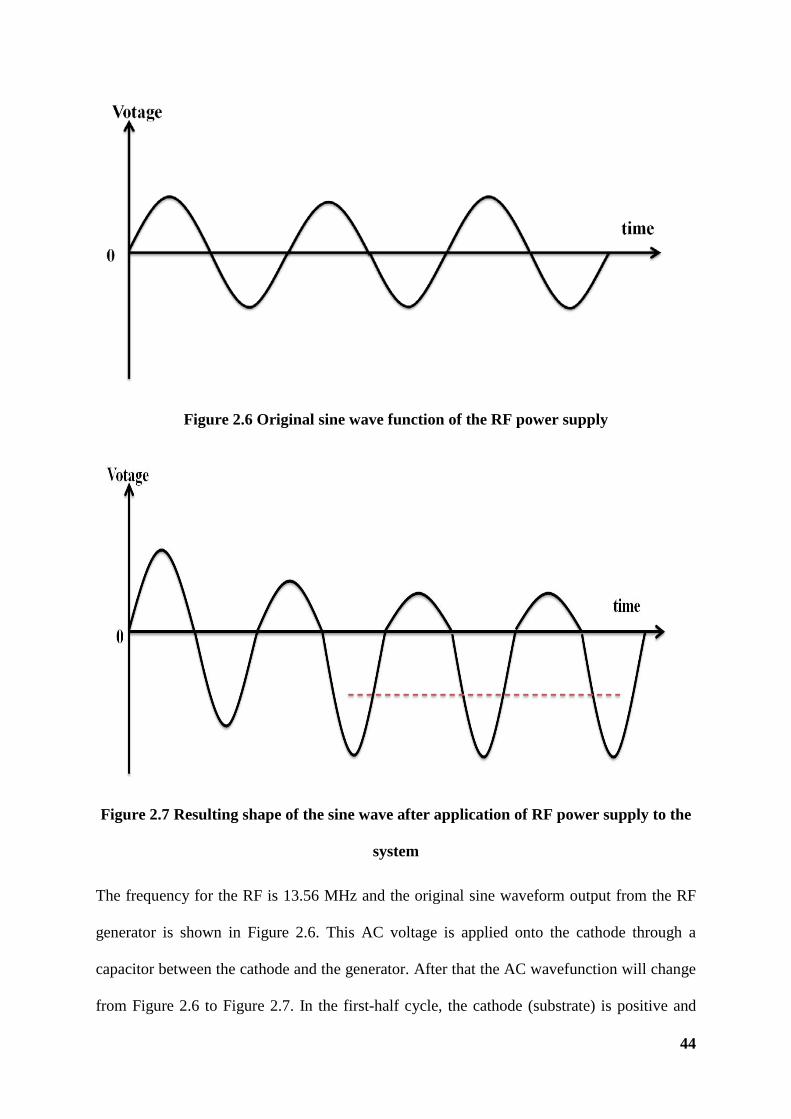
44
Figure 2.6 Original sine wave function of the RF power supply
Figure 2.7 Resulting shape of the sine wave after application of RF power supply to the
system
The frequency for the RF is 13.56 MHz and the original sine waveform output from the RF
generator is shown in Figure 2.6. This AC voltage is applied onto the cathode through a
capacitor between the cathode and the generator. After that the AC wavefunction will change
from Figure 2.6 to Figure 2.7. In the first-half cycle, the cathode (substrate) is positive and

45
starts to accumulate electrons. During the next-half cycle the cathode is negative and begins
to collect positive ions from the plasma. The number of electrons collected in first half cycle
is very high compared to the number of positive ions collceted in the rest half cycle. Because
of the higher mobility of the electrons (>102 times than that of positive ions), a net negative
charge accumulates on the target as there is a capacitor between the target and the RF
generator. The electrons collected on the target stay on the surface of the target for sometime.
In the first half of the second cycle, the fewer number of electrons will accumulate, as prior
gathered electrons still exist there. In the second half of the second cycle, the flux of positive
ions will be larger than that of the first cycle. After few cycles, the elctron flux will be equal
to the ion current, and the system reaches the state of equilibrium. After equilibrium state,
most of the time the cathode voltage is negative, but remains positive for a short fraction of
time of each cycle. Therefore, Figure 2.7 shows that the target is effectively biased by a
negative dc potential with respect to ground. This bias enhanced nucleation (BEN) and bias
enhanced growth (BEG) methods are very crutial for growing NCD films with a steady self-
biased dc voltage (200-260 V) during the PECVD and MPCVD processes (in-situ nucleation
processes). The unique advantages of this technique are that it does not require any
pretreatment or pronunciation stage with the suitability of wide range of substrates. More
detailed discussion are given in introduction part of chapter 1.
2.3.3 Synthesis of Hydrogenated Diamond Like Carbon thin film onto
2.3.3.1 (a) Silicon (b) Quartz substrates
PECVD is used to deposit thin films from a gas state to a solid state on a substrate. Chemical
reactions are involved in the process, which occur after creation of plasma of reacting gases.
The plasma is generally created by RF (AC) frequency discharge between two electrodes, the
space between which is filled with the reacting gases.

46
The deposition process consists of two steps:
(1) Etching of mirror polished Si(100)/quartz substrate of 10 mm diameter for 15 min. in
a pure hydrogen (H2 flow rate ∼ 500 SCCM) plasma (light pink in color), at a
pressure of 0.193 mbar, by 30 W RF forward power producing dc self-negative bias
(~ -200 V) with a impedance matching circuit, to remove any oxide layer from the
surface of Si(100).
(2) in situ Biased Enhanced Nucleation (BEN) process using helium (He flow rate ~1500
SCCM) plasma by 50 W RF power generating dc self-negative bias (~ -200 V), with
H2 (flow rate ~500 SCCM) and CH4 (flow rate ~ 50 SCCM) gases at a total pressure
of 0.756 mbar and at substrate temperature ~ 14 0C, for 30 min. deposition time.
The reactive unexploited gases are taken out from the deposition chamber during the
deposition process and purged out to the environment after mixing with nitrogen gas.
Experimental Parameters (Deposition Conditions) at a glance :
1. RF : RF-Frequency 13.56 MHz;
2. RF-Power : 30 ± 2 Watt during etching process and 50 ± 2 Watt during deposition
process.
3. Pressure : 0.20 ± 0.02 mbar during etching and 0.75 ± 0.05 mbar during deposition
4. Substrate : Si(100)/Quartz
5. Pre-treatment : By hydrogen plasma for 15 min. at 0.2 mbar
6. Gas Mixture : CH4 (50 SCCM), H2 (500 SCCM) and He (1500 SCCM) (SCCM -
Standard Cubic Centimeter Per Minute)
7. Deposition time : 30 min.
8. Temperature : 14 0C
9. Nitrogen Flow : 500 SCCM

47
2.3.3.2 Stainless steel
The stainless steel substrate (15 mm × 15 mm) was cleaned with NaOH followed by HNO3
and then rinsed with millipore water. After cleaning, the argon ion sputtering was used to
remove the passive chromium oxide layer for 15 minutes. The typical conditions used for
sputtering were : flow rate of Ar gas 100 SCCM, total pressure 0⋅3 mbar, RF power 30 watts,
dc self-bias –150 volts. After the sputtering, the steel surface was pre-treated with hydrogen
plasma discharge. The typical conditions for this pre-treatment and deposition of HDLC over
stainless steel substrate were tabulated in Table 2.1. Kumari et al. [91] have studied the
HDLC coating over stainless steel using field effect and cross-sectional SEM (FESEM and
XSEM) and energy dispersive X-ray analysis (EDX). They have reported the formation of a
very smooth, continuous, non-poros, and homogeneous HDLC thin film coating with good
adhesion properties. Therefore, i have not carried out any further study of HDLC film onto
stainless steel substrate for my thesis work.
Table 2.2 Comparison of the PECVD deposition conditions on different substances
Parameters Substrate
Silicon Quartz Stainless Steel
RF Frequency (MHz) 13.56 13.56 13.56
Pre-treatment
RF Power (Watt) 30 30 25
Gases and Flow
rate (SCCM) H2 (500) H2 (500) *Ar (100) H2 (500)
Pressure (mbar) 0.19 0.20 0.30
Time (min.) 15 15 15
Deposition RF Power (Watt) 50 50 50

48
Bias (V) - 200 - 200 - 200
Pressure (mbar) 0.75 0.75 0.70
Time (min.) 30 30 25
Gases and flow
rate (SCCM) He (1500), H2
(500), CH4 (50) He (1500), H2
(500), CH4 (50) He (1500), H2
(500), CH4 (50)
Temp (0C) 14 14 14
Nitrogen Flow (SCCM) 500 500 500
*Sputtering condition : RF power 30 watts, dc self bias 150 volts, total pressure 0.3 mbar,
time 15 min.

49
Figure 2.8 Picture of the film (golden color) deposited by PECVD method on 10 mm dia
mirror polished silicon substrate
Figure 2.9 Pictures of the films (yellow color) deposited by PECVD method on 25
mm×25 mm quartz substrate
10 mm 10 mm
25 mm 25 mm
25 m
m

50
2.3.4 Description of the major parts of the System
Cathode : 250 mm dia. of metallic electrode connected to the RF matching circuit and power
supply
Anode : Aluminum walled body connected to the ground as a anode and always at zero
potential. Each wall side of the body is 50 cm × 50 cm.
RF-Matching Circuit : Contains an induction and capacitance circuit for matching the
impedance between the input (RF circuit) and output (Plasma) systems
Vacuum pumps :
(a) Mechanical pump is switched on for making the chamber pressure from atmospheric
to ~ 0.1 mbar. Small traces of oil are absorbed by the chemical filter which prevents
the contamination during the processes of deposition.
(b) Roots pump is switched on when the pressure is ~0.1 mbar and continued until the
pressure reaches desired value (~10−4 mbar)
Closed loop cooled water circulation system : Cooling of the substrate and cathode using a
cooler maintained at 10 0C.

51
2.4 Annealing of HDLC samples
A few number of HDLC samples were prepared by PECVD method by varying the flow rate
of methane 20, 30, 40, 50, 70, and 90 SCCM. Few sets of such HDLC samples were heated
at a fixed temperature of 100, 250, 750, 900, and 1050 0C for 30 minutes in high vacuum
~1×10⁻⁶ torr and cooled to room temperature after heating in one set of experiment. The as
prepared and annealed HDLC sample at 1050 0C were analyzed using confocal micro Raman
spectra, current-voltage characteristics in ambient air, topographic image of the sample using
AFM, and STM measurements under constant tunneling current mode. The results and
discussion based upon the above measurements are given in chapter 4. The annealing
experiments were carried out in Bioceramic and Coating Division, in CSIR-Centre of Glass
and Ceramic Research Institute, Kolkata, India. The pictures of the HINDHIVAC instrument
for annealing of HDLC samples at high temperature and high vacuum are shown below.
HINDHIVAC Instrument
Instrument Controller
Controlled Parameters at a glance
1) Temperature : 100 0C to 1050 0C (maximum)
2) Pressure : 1 × 10⁻⁶ torr
3) Annealing time : 30 minutes (for all samples)
4) Healing rate : 5 0C/min.
5) Cooling rate : 3 0C/min.

52
Figure 2.10 HINDHIVAC vacuum and sample heating control unit

53
Figure 2.11 HINDHIVAC Vacuum sample heating chamber

54
2.5 HDLC samples preparation for IBA study
Another few sets of samples were prepared by PECVD method at flow rate of methane 20,
30, 40, and 70 SCCM, by varying CH4 to H2 ratio at room temperature. One such set of
samples was heated at a heating rate 5 0C/min under vacuum (1×10⁻⁷ torr) at temperature 750
0C and 1050 0C. These films are kept in the above desired target temperature for 30 minutes
before cooling them to room temperature at a cooling rate of 3 0C/min. The as-prepared and
annealed HDLC films have been depth profiled for hydrogen using the nuclear resonance at
6.44 MeV in 1H(19F,αγ)16O nuclear reaction by heavy ion beam. The Rutherford
backscattering (RBS) on the as-prepared and annealed samples, with 1.0 MeV proton ion
beam is carried out to measure the thickness of HDLC films. Both NRA and RBS
measurements are carried out by a 3 MV Tandetron accelerator at the surface and profile
measurement laboratory of the National Center for Compositional Characterization of
Materials (NCCCM), Hyderabad, India. The results and discussion based upon the above
measurement are given in chapter 4 (section 3). The picture of the NRA/RBS measurement
instrument for depth profiling HDLC samples is shown below.

55
Figure 2.12 Picture of experimental arrangement for IBA study

Chapter 3
Characterization Tools

56
3.0 Introduction
The unique properties of diamond are expected to have many future applications due
to the advancement of diamond coating technology developed various chemical vapor
deposition (CVD) methods. These CVD methods of diamond like carbon deposition may
result in different types of DLC films based on their inherent composition of the film, growth
chemistry, structure, grain size, etc
The natural diamonds as well as the synthetic diamond are both highly precious. The coatings
of the materials with these diamonds have been found to be not suitable from applications
point of view. However, coating of the materials with diamond like carbon films have been
found to be possesses unique properties that can be utilized in many applications. These DLC
coatings are most commonly used as coating in cutting tools and wear resistant components
because of its high hardness. The diamond and diamond like carbon coatings are suitable for
bio-medical applications because of its chemical inertness, bio-compatibility, high melting
point, and high thermal conductivity. These DLC coatings find its applications in heat sink.
These coatings are well known to be optically transparent from the far infrared region to
ultraviolet region and hence used in inert optical window. Therefore, the detailed
understanding the film structure and the controlling parameters for their nucleation, growth,
micro-structure of the films as needed for important applications to be implemented for
practical uses.
57
3.1 High Resolution Transmission Electron Microscope 3.1.1. Imaging using HRTEM
The optical microscopy techniques are limited by diffraction effects, which depend
approximately on the wavelength of light, and these techniques are used to obtain the
exhaustive information on the physical environment of the surface. The one of the most
important techniques is Transmission Electron Microscopy (TEM) for much higher
resolution and it is very rich to provide information of the surface of the specimen. TEM
utilizes signal of elastically scattered electrons for re-construction of structural and defects
image information. The imaging mode TEM provides real space information while
diffraction mode of TEM gives reciprocal space almost simultaneously, and this is a major
advantage of TEM over the other microscope. One of the powerful imaging modes of the
transmission electron microscopy for studying the properties of material on the atomic
dimension is called high resolution transmission electron microscope (HRTEM). HRTEM is
commonly utilized to make quantitative measurements on nm scale features due to its
excellent image resolution, high precision, and accuracy. In TEM, when a beam of electrons
is transmitted through a film, it interacts with the electrons in a few nanometers thin films. A
direct image of the atomic structure of the film is generated based on that interactions of the
electrons transmitted through the film. The effect of electron beam interaction with the
sample increases generally with the square root of the atomic number (Z) of the specimen.
The nature of the type of interactions is distinctly different from that of neutron or X-Ray
radiation. The image is stored in a suitable detector, e.g. CCD. With the development of high-
end technology, improvements of TEM were implemented by different groups around the
world. After the innovative modernization of cold field electron emission, Albert Crewe et al.

58
published a paper in Science journal in 1970 on “Visibility of Single atom”, which showed a
single heavy atom on carbon substrate [102]. Meyer and co-workers elaborated the imaging
and dynamics of light atoms on graphene for the first time using TEM in 2008 for
visualization of carbon and hydrogen [103]. HRTEM can offer spatial resolution in general
better than 0.2 nm, and it can go as high as 0.05 nm, as reported in 2008 by C. Kisielowki and
co-workers [104] in “Microscopy Microanalysis”. The imaging of light atoms with the
improved resolution of microscope is attainable due to the less efficient scattering of electron
by the lighter atoms. Due to its resolving power in atomic scale, TEM therefore it finds
applications in the field of nano-materials, semiconductors, material science, medical
research, and sp2 –bonded carbon such as nanotubes and graphene. Few classical highly
useful applications of HRTEM are include the determination of particle size, shape
distribution, structural defects, interface, grain boundaries, and crystallographic phases,
diffusion, decompositions, and phase transformation in thermodynamic systems,
characteristic features of nano-crystallinity in amorphous films.
The potentiality of the TEM can be furthermore widened by improving the stages, providing
additional stages, and detectors that can be incorporated on the same microscope. A TEM
system can be redesigned into a Scanning transmission electron microscope (STEM) by
adding a raster system which helps the beam raster across the sample to form the image, with
a suitable detector. In case of low voltage electron microscope (LVEM) [105-106] which is
employed at relatively low electron accelerating voltage of 5 KV. The advantages of LVEM
are the combination of TEM, SETM, and SEM in one instrument. This low voltage is
especially essential for biological samples. Moreover, low voltage increases the image
contrast. However, LVEM system requires thinner samples compared to that of general TEM
system. Another modern TEM is the CryoTEM, which is an electron cryomicroscope capable
of providing a facility to maintain the specimen at liquid nitrogen or helium temperatures.

59
The low temperature allows the proteins and macromolecules to remain unchanged, i.e. to
protect the denaturation of protein and biomolecules. The finest TEM manufacturers
incorporate incident monochromatic beams which reduce the energy spread of the incident
electron beam. The modern TEM can also perform the aberration corrections to minimize the
distortion in the image.
3.1.2 Transmission electron energy loss spectroscopy (TEELS)
Electron energy loss spectroscopy (EELS) is a complementary technique to energy
dispersive X-ray spectroscopy (EDX) and it being available on many electron microscopes is
commonly used for spectroscopic study. EDX is particularly sensitive to heavier elements for
analyzing the atomic composition of materials, whereas EELS is, in principle, capable of
measuring atomic composition, chemical bonding, valance and conduction band electronic
properties for low Z elements. The excitation edges tend to be sharp, and well defined in
EELS. With time EELS has been established as a most successful spectroscopic technique to
study the chemical state of an element, particularly in the range from carbon to zinc. For
carbon, its presence among diamond, graphite, amorphous carbon, and mineral carbon can be
easily differentiated from fine features of their EELS spectra. The spectra of 3d transition
metals can be probed to distinguish the oxidation states of the atoms. In the transmission
electron microscope, most of the electrons generally pass through the sample without
suffering an inelastic scattering event (i.e. no energy loss). However, when an electron beam
transmits through solid, the incident electrons can inelastically scatter off the electrons bound
to atom of solid material. Consequently, the inelastic scattered electrons have their path
slightly and randomly deflected. The amount of energy loss can be measured via an electron
spectrometer (which may be termed as transmission electron energy loss spectroscopy
TEELS). A typical TEELS spectrum is shown in Figure 3.1.1.

60
Figure 3.1.1 Schematic illustration of a TEELS profile
The inelastic interactions include phonon excitation, intra and inter band transition, plasmon
excitations, inner shell ionizations, and Cherenkov radiation. The low loss region generally
corresponds to roughly below 50 eV and the dominant features of the spectrum are zero loss
peak (ZLP) and plasmon resonance. The remaining part of the spectrum is called as the core-
loss regime. The ZLP region of the spectrum contains both electrons that are unscattered
(vast majority of all electrons that pass through a thin specimen) and elastically scattered. The
plasmon region contains electrons that have undergone loss of small amount of energy (< 50
eV). This energy loss includes interactions of the electrons in the beam with outer shell
electrons to a bound atom in crystalline lattice (phonon effects) and with a compounds
electronic band gap structure. The core-loss regime involves the ionization of inner shell
electrons. The energy requirement in inner shell ionization depends on the type of atoms
involved and its oxidation states. The distribution of electrons as a function of energy is
measured using energy filters. The imaging mode is called “energy filtered transmission
electron microscope” (EFTEM) and the spectroscopy mode is referred to as “electron energy

61
loss spectroscopy” (EELS). If the incident electrons have a kinetic energy of a few hundred
electron volts and are reflected from the surface of the specimen, the technique is called high-
resolution EELS (HREELS). In TEM, the energy of the electrons employed is generally in
the range of 100-300 keV. Because of their high energy, electrons can pass completely
through a specimen, provided its thickness is below 1 μm. The electromagnetic lenses of the
TEM can be used to focus them into a very small diameter (~ 1 nm) and produce a
transmitted-electron image of the specimen, with a spatial resolution down to atomic
dimensions. As a result, EELS carried out in a TEM is capable of investigation with a very
high spatial resolution. As, TEELS can be combined with transmission electron imaging,
electron diffraction, and energy dispersive X-ray spectroscopy in the same instrument, this
method has become very potential and versatile technique for studying the physical and
chemical characteristics of materials. The energy resolution of EDXS is of the order of 150
eV, whereas EELS has a resolution of the order of 1 eV or better (0.1 eV) if an electron-beam
monochromator is used.
The modern TEM instrument with EELS is capable of providing structural information and
chemical bonding in the solids. Murooka et al. [107] studied the microscopic structure of the
carbon film, prepared by electron cyclotron resonance (ECR) plasma sputtering by EELS
using 200 kV TEM (JEM 2010) attached with an electron microscope. The TEELS spectra of
the films and graphite show two charactistic peaks in low energy region. The broad peak at ~
20 eV is the (π+σ) plasmon, i. e. the bulk plasmon, which is due to collective exication of all
(π+σ) electrons. The peak positions are dependent on the density of (π+σ) electron in the
films. Another peak is at ~ 4 eV which is due to the π plasmon. This corresponds to the π
π* tranitions and its implies the presence of carbon clusters based on the sp2 bonding. EELS
spectra of diamond shows a broad peak centred at ~ 31 eV, whereas in graphite, two
resonance peaks are observed at 7 eV and 27 eV [108]. Eberlein et al. [109] observed the π

62
and (π+σ) suface plasmon modes in free-standing single sheets graphene at 4.7 and 14.6 eV,
which are red-shifted substantially from their values in graphite. Therefore, we can say that
TEELS is a powerful analytical technique to distinguish between hydrogenated amorphous
carbon (a-C) and hexagonal hydrogenated diamond like carbon (HHDLC) and one can
analyze collective excitations of π and σ electrons in multilayered HHDLC films by this
technique.
The high energy electrons from the HRTEM undergo elastic scattering as well as inelastic
scattering. Elastically scattered electrons are used for imaging purposes like imaging of cross-
sectional view of our HDLC film as carried out in the present thesis works. Energy loss upto
50 eV in the inelastically scattered electrons is dominated by collective excitations of valence
electrons (plasmon) of samples like HDLC samples of the present thesis works. These results
are given in chapter 4 (section 1). The measurements of HDLC samples were performed in a
JEOL EM-2010 (with LaB6 filament) at 200 kV accelerating voltage fitted with a Gatan
Image Filter for parallel EELS of Materials Research Institute, The Pennsylvania State
University, USA. The experimental conditions were :
(i) Ion-milled cross section sample
(ii) Accelerating voltage: 200 kV
(iii) Probe size: ~ 30 nm
(iv) Collection semi-angle: 12 mrad
(v) Convergence semi-angle: 6.4 mrad

63
3.2 Raman Spectroscopy When beam of monochromatic light from the visible portion of the spectrum is passed
through a substance under study, nearly all of it is transmitted and a portion of it is scattered
in all directions. If the scattered light in a direction perpendicular to the direction of the
incident beam is spectrographed, it is found that not only a line is contain corresponding to
frequency of the incident light called Rayleigh line after the name of Lord Rayleigh, but also
there is a pattern of relatively weak line on the low frequency side of the incident light and a
similar part of still weak lines on the high frequency side called Raman lines after the name
of C. V. Raman.
The phenomenon of inelastic scattering of light was first predicted by Adolf Smekal
in 1923 and first observed experimentally by means of sun light in 1928 by C.V. Raman and
Krishnan. Since then, the phenomenon has been referred to as Raman effect. In the original
experiment sun light was focused by a telescope onto a sample. Raman got the Noble Prize in
Physics in 1930 for this discovery.
Figure 3.2.1 The electromagnetic spectrum on the wavelength scale in meters
3.2.1 Classical model for the interpretation of Raman lines
The Raman spectra are observed when there occurs a periodic change in the polarizability of
molecule due to its vibrational or rotational oscillation. The above fact may be explained
classically as follows.

64
In the presence of a static electric field, a molecule is polarized, i.e. the positively
charged nuclei and the negatively charged electron cloud are attracted towards the respective
oppositely charged pole of the electric field. Consequently, the molecule acquires an induced
dipole moment which is given by
EPind α= (3.2.1)
where α is the polarizability of the molecule.
In the presence of a beam of radiation, the molecule also acquires an induced dipole moment
due to the electrical component of the incident light/laser. This electrical component is not
static but varies as per the sine (or cosine) wave according to the equation
)2sin(0 tEE πν= (3.2.2)
where ν is the frequency of radiation and t is the time. Consequently, the induced dipole
moment also oscillates according to the equation
)2sin(0 tEEPind πναα == (3.2.3)
According to the electromagnetic theory, an oscillating dipole emits radiation of its
frequency. This explains the occurrence of Rayleigh line in the light scattered by the
substance. The presence of Raman lines is due to the periodic change in the value of α due to
the internal vibrational or rotational motion according to the equation
)2sin(0 tiπνζζααα
∂∂
+= (3.2.4)
where the ζ is the change in polarizability with the displacement coordinate ζ, νi the
frequency of internal motion, and α0 is the polarizability in the equilibrium position ζ0. The

65
periodic change in polarizability will also change periodically the induced dipole moment.
Hence, equation 3.2.4, and 3.2.3 can be written as
])(2cos)(2[cos21)2sin(
)2sin()2sin()2sin(
)2sin()2sin(.
0000
0000
000
ttEtE
ttEtE
tEtP
ii
i
iind
ννπννπζζαπνα
πνπνζζαπνα
πνπνζζαα
+−−
∂∂
+=
∂∂
+=
∂∂
+=
(3.2.5)
that is, the induced dipole moment of the molecule oscillates with the frequencies ν, )( iνν −
and )( iνν + . Therefore, the oscillating dipole will emit radiations of frequencies ν, )( iνν −
and )( iνν + . These frequencies appear as the Raman lines in the scattered light of a
substance under study.
If there occurs no change in the polarizability during the vibrational or rotational motion, i.e.
is zero, then the above equation 3.2.5 remains a single term. Hence the molecule will
oscillate with one frequency related to the incident light. This frequency corresponds to the
Rayleigh line (ν) and no other Raman lines are observed. Therefore the molecule is Raman
inactive. Hence the Raman active molecules will emit three frequencies. Besides the Rayleigh
line, )( iνν − frequency is known as Stokes line and (ν+νi) frequency is known as anti-Stokes
line.
3.2.2 Quantum model for Raman lines
The photon from the light source collides with the molecule through elastic or inelastic mode.
If the collision is elastic, the photon energy before and after collision remains unchanged. In
other words, the molecule remains in the same energy state which it had before collision.
This scattered photon is known as Rayleigh scattering (ν). Again, if the scattering is inelastic,

66
the photon energy as well as the energy of the molecule will alter. If the scattered photon is
having lower energy than that of incident light, then the difference of energy is utilized to
promote the molecule to one of the higher energy level as permitted by the selection rule.
This scattered photon is known as Stokes scattering )( iνν − and they are at lower frequency
side of Rayleigh scattering (ν). On the contrary, if the scattered photon is having higher
energy than that of incident light then the difference of energy is obtained from the molecule
has demotes to one of the lower energy level as permitted by the selection rule. This scattered
photon is known as anti-Stokes scattering and they are at higher frequency side of Rayleigh
scattering (ν).
Schematic representation of Raman Scattering
(a) Rayleigh Scattering (b) Stokes Scattering (c) anti-Stokes Scattering with ∆ν=0 with ∆ν =ν-νi <0 with ∆ν=ν+νi >0
Figure 3.2.2 Schematic representation of Raman scattering
Since most of the photons undergo Rayleigh scattering process, hence Rayleigh lines will be
the most intense. The intensities of the other lines will depend on the population of the initial
energy level where from the molecules are promoted or demoted to the final level. According
to the Boltzmann distribution law, the population of the lower energy level is more than that
of the higher energy level. Therefore, out of the Stokes and anti-Stokes lines, the former will
n=0, ν=1
n=0, ν=0
n=1

67
be more intense than the latter. Consequently, the Stokes lines are recorded commonly in the
Raman spectrometry.
The Raman effect, should not be confused with the absorption (e.g. fluorescence) process.
Since Raman effect, is a light scattering phenomenon, molecules are excited to the virtual
energy state. In contrast, molecules are excited to a discrete energy level (not virtual) in the
absorption processes. Again, the difference between Raman and Infra-red absorption process
is that Raman scattering requires a transitorily distortion of the electrons cloud distribution;
the IR absorption requires a change of dipole moment during the vibrational or rotational
motion of the molecule. Only then can be the radiation of same frequency to interact with the
molecule and promotes it to an excited vibrational state.
Figure 3.2.3 Schematic representation of electronic excitation
Ground State
Virtual State
Electronic State
IR Rayleigh Stokes
anti Stokes Fluorescence

68
Typically, the intensity of Rayleigh line is 10−3 with respect to excitation radiation, whereas
the intensity of Raman lines are 10−3 order less than Rayleigh line. Raman frequencies called
as Raman shift are measured relative to that of excitation frequency. The excitation frequency
can be imagined at the origin of the abscissa, the Raman shift will be on abscissa at ±ν0
Raman scattering of gases at low pressure consists of vibrational-rotational line spectra. At
higher pressure, Raman lines become broaden, similar to liquid. In solid having crystalline
nature, the Raman bands are sharp and band width depends on anharmonicity of molecular
vibration. Further broadening of Raman bands are due to other imperfections in the crystal
lattice, vacancies, or other impurities. In general, the Raman spectra of amorphous substrates
are characterized by broad spectral features. Classification of possible types Raman spectra is
given in Table 3.2.1. The concept of group frequency is very important for the calculation of
force constant and also for the interpretation of Raman vibration spectra of molecules. Some
general principles apply on Raman vibrational modes generated from localized normal
vibrations; a primary bond stretching band is more intense than for an angular deformation.
The intensity increases with the bond orders and increases with the atomic number of the
bonded atoms.
3.2.3 Second-order Raman Spectra
In all the above the scattering described in earlier paragraph is “first-order” scattering, i.e. the
excitation of only one phonon. However, it can be also a “second-order” scattering, i.e. two
phonons can be excited. According to the equation 3.2.4, the second-order derivative 22
2ζ
ζα
∂∂
of the Taylor series expansion refers to the appearance of higher frequency bands to account
for the polarizability in crystals. These bands are designated as second-order Raman bands.
The second-order spectra of single crystals and highly oriented pyrolytic graphite are
continuous and exhibit several well defined bands. The wavelength selection rule in this case

69
is that the two phonons must have equal wave vectors (or wavelength) but must be travelling
in opposite directions. Second-order scattering is usually weak, but can be enhanced by
various things. It is very difficult to distinguish between the overtones in the first-order
Raman effect and the second-order Raman effect. In both cases, the polarization is
proportional to the exciting field strength. Overtones appear when the system being excited is
mechanically anharmonic and second-order Raman bands appear when it is electrically
anharmonic. Second-order Raman bands, sometimes may be stronger than the first-order
bands, and the two may be distinguished by the intensity of second-order bands due to its
higher temperature sensitivity.
Table 3.2.1 Classification of possible types Raman spectra
Specimen Possible types Raman spectra
Gases
Pure rotational
Rotational-vibrational
Overtones, combination tones, difference tones
Liquids Vibrational
Overtones, combination tones, difference tones
Crystals
Lattice
Internal-vibrational
Overtones, combination tones, difference tones
Amorphous Mixed
3.2.4 Micro-Raman Spectrometer

70
The first experimental observation of the inelastic scattering of light was made by Raman and
Krishnan (1928). The experimental setup consists of a light source-a focused, filtered beam
of sunlight, a sample, a detector and a phototube or photographic plate. The basic
experimental design of current Raman spectrometer has not been changed significantly.
Presently, the micro Raman spectroscopic systems are designed with the capability of single
point analysis, line analysis, Raman imaging (mapping) etc.
Figure 3.2.4 Image of Micro-Raman spectrometer LabRAM HR800 Vis. Horiba Jobin
Yvon SAS France
The HR800 is an integrated laser line scanning imaging Raman system. The instrument is
capable of recording Raman spectra of solid, liquid, or even gaseous samples. It is
recommended to use a microscope objective with a large depth of focus (for example a 10X,
NA=0.25) so that it will collect the signal from a bigger volume of the sample in case of

71
homogeneous sample. On the contrary, it is better to use microscope objective with a high
numerical aperture (100X, NA=0.9) so that the solid angle (NA=n.sinα where n is the
refractive index of the medium between the object and the lens, and α is half the angular
aperture) is bigger to obtain a maximum Raman signal. The microscope is coupled confocally
to a 800 mm focal length spectrograph equipped with two switchable gratings viz. 1800
g/mm (scanning range 0-950 nm) and 600 g/mm (scanning range 0-2850 nm). Gratings are
mounted on kinematically interchangeable holders driven by Sinus arm that is linear in
wavelength. There is the provision for camera which is used for the observation of the
sample.
The excitation wavelength 632.8 nm is supplied by an internal standard He-Ne laser (20 mW
power, polarized 500 : 1) positioned at back side of the instrument. Another external laser of
488 nm Ar (max 50 W power) is also kept for analysis of various types of samples, at the
back side of the instrument. Obviously, the changing of laser requires the change of the notch
filter which is specific for one wavelength, which is necessary for filtering the exciting light.
In the LabRam HR800 super notch plus is used as a dichroic mirror and the drop off stokes
edge is <120 cm−1. The laser is totally reflected by the notch filter towards the sample under
microscope by a suitable objective viz. 10X (Numerical Aperture, NA= 0.25) 50X (NA=
0.7), and 100X (NA= 0.9). The scattering light is totally transmitted through the notch filter
towards the confocal hole and entrance silt of the spectrograph. There is an adjustable
confocal hole which can vary between the ranges of 0 to 1000 µm. The diverging beam
coming from the slits is reflected by the two mirrors and then becomes parallel after the
spherical mirror of 800 mm focal length. The spherical mirror reflects the parallel beam onto
the grating. The diffracted first-order is collected by another spherical mirror of 800 mm
focal length and focused onto the CCD detector. The spectrographic box contains the CCD
detector that forms a spectrum. The CCD detector is having the pixel size of 1024×256 and

72
cooled by Peltier effect. The main advantage of our micro-Raman spectrometer is due to the
confocal sampling which is responsible for considerable reduction of the signal from an
inclusion against the signal coming from the surrounding medium and also able to separate
the signal from each layer of a layered sample. Consequently, confocality reduces the depth
of focus and thus an increased Z discrimination. The closing of confocal hole, however, while
decreasing the depth of focus, decreases the Raman signal. Thus confocality is always a
compromise between signal and resolution. With a NA = 0.9 100X objective, the confocality
is ~ 2 μm and with a NA=0.25 10X objective, the best confocality is increased to 183 μm. In
the range between 450 - 850 nm, the wavenumber accuracy is ± 1 cm−1with 1800 g/mm
grating. Under normal conditions of temperature stability (± 1 °C), the repeatability is 1 pixel
with 1024×256 pixels of 26 microns CCD.
The instrument is always operated using standard operating procedures. The Raman
microscope was kept ideal for 30 minutes before recording any data. Calibration is done most
of the time using standard silicon sample whenever the instrument is started and the grating is
changed. All the time standards and samples were focused using the objective 10X and
position was set using joystick in X-Y directions. Coarse focus was done manually using the
knob inside the microscope, only for the 10X objective. The instrument was focused at 10X,
switched to 50X and then fine focused, then repeat was made at 100X. Silicon has a
characteristic Raman shift at 520.7 cm−1. The Koeff parameter was adjusted until the peak on
the display was at 520.7 cm−1. After the calibration (Figure 3.2.5) instrument was ready to
record the spectra. The LabSpec5 software provides a control of HORIBA Jobin-Yvon's
Raman instruments, complete data acquisition, and analysis package using Windows 2000 or
Windows XP-PRO operating software in a desktop computer. The control panel of the
software contains information which is directly related to the system configuration and easy
modification of the acquisition parameters. Real Time Display (RTD) acquisition mode

73
allows adjustment quickly the focusing and optimizing other experimental conditions to
maximize the Raman signal. The exposure time in seconds to be used for the accumulation of
sufficient counts of Raman signal and repetitions were performed to remove any spike of the
cosmic line recorded during the acquisition. The spectra generally acquired with multiple
accumulations covering the entire region 50-4000 cm−1 using extended spectral ranges
acquisition, i.e. multi-window mode. Using motorized XY microscope sample stage for point
by point Raman imaging, each spectrum was acquired with a particular varied parameter
including the autofocus attachment for automatic Z-axis imaging (depth profiling)
Figure 3.2.5 Calibration of micro-Raman spectrometer using standard silicon sample
3.2.5 Peak fitting and analysis

74
The typical Raman spectra of HDLC sample (Fig. 3.2.6) deposited onto the silicon substrate
for the range from 50-4000 cm−1 and recorded using micro-Raman spectrometer, is described
above. The increasing PL background of each spectrum is a typical signature of hydrogenated
diamond like carbon films [61]. A broad peak first-order Raman spectra in the range 1000-
2000 cm−1 was observed for all of the synthesized HDLC samples described in chapter 2. To
know more information about the fine and inner structure of the carbon films, the Raman
spectra should be deconvoluted. However, the fitting of the Raman spectra may leads to
complex nature due to the manifold combination of the carbon and carbon-hydrogen structure
in the films.
Figure 3.2.6 Typical Raman spectrum of HDLC film onto silicon substrate over the
range 50-4000 cm−1

75
The most widely used methods of Raman spectra fitting is to make use of two Gaussian peaks
with linear/ non–linear background subtraction with the D peak centered at 1350 cm−1 and
that of G peak centered at 1580 cm−1 [110]. This analysis is based on the assumption that the
amorphous carbon films are composed of disordered sp2 and sp3 networks. This fittings lead
to an estimate of the La that reflects the in-plane crystallite size from the ratio of the fitted
peak intensity of D and G bands. In order to analyze the Raman spectra quantitatively,
Prawer et al. [111] utilizes a Breit-Winger-Fano (BWF) line shape and linear background
subtraction methods using a least squares computer programme. The BWF line shape is
described by
]
)-(2[1
] Q
)-(2+[1 I
)(20
200
Γ+
Γ=ωω
ωω
ωI (3.2.6)
Where I(ω) is the intensity as a function of frequency, I0 is the maximum peak intensity , ω0
peak position, and Γ is the full width at half maximum (FWHM), Q is the BWF coupling
coefficient. In the limit when 1/Q approaches to zero or negligible, the Lorentzian line shape
is regained. Therefore, a total of six variables is essential to best fit the data, viz. I0, ω0, Q,
and Γ and two parameters for the linear background. Prawer et al. [111] showed that Raman
spectra of DLC films deposited at the carbon ion enerties 10-1000 eV is possible to fit with a
single BWF lineshape, no need to include an extra peak at 1350 cm−1, except for the films
deposited at 200 keV for which it was necessary to include a two BWF line shpae in order to
fit the data. To obtain a better fit, some other peaks are generally taken into consideration
apart from G and D peaks.
Following aspects were considered during the deconvolution of Raman spectra using
Lorentzian and Gaussian line profiles : (1) All molecules behaving in the same way results a

76
Lorentz line shape. Transit time broadening, pressure broadening, natural lifetime broadening
are few typical examples. (2) All molecules behaving differently (resulting a distribution)
results a Gaussian line shape. Few examples are Doppler broadening, power broadening etc.
The Raman scattering is known to be due to the inelastic collisions between the light photons
and the atoms. These inelastic collisions broaden the Lorentzian shape of spectra lines. The
shift in peak frequency in elastic collisions to lower or higher values depending on the nature
of the interaction potential. Hence, a Gaussian profile describes broadening effect due to
randomly distributed Raman signals from the sample, with no associated shift, while a
Lorentzian profile describes both effects- broadening and shift, due to the structure of the
sample interacting coherently. Raman spectra are deconvolved in expectation of multiple
chemical environments within the HDLC film, which is a graphite-based system [112].
Lorentzian peak shapes are used for all Raman modes, resulting in best fits of the broad
spectral envelope. Keeping in mind the possibility of the presence of different phases of
carbon, we have deconvoluted each spectrum with six Lorentzian functions (shown by solid
lines in chapter 4) keeping intensities, width and peak positions as free fitting parameters.
The asymmetric BWF line shape is usually used to fit the G-peak which appears due to
asymmetry of the vibrational density of states of graphite towards lower wavenumber. The
tail of BWF line takes into consideration the Raman modes between 1100 and 1400 cm−1,
without giving rise to extra peaks. It is to be noted that the intensities of the D-peak and other
low frequency peaks are quite less than the intensity of the G-peak. Thus, if we deconvolute
each spectrum with all low frequency components to obtain the information of individual
modes, there is an inherent difficulty in using BWF line shape for the G-peak. For this
reason, we have used Lorentzian line shapes for all modes to analyze our spectra. In chapter 4
we describe the details of experimental data, deconvoluted lines and net fitted spectrum for
our HDLC sample and the properties of the films obtained from above Raman data

77
deconvolution. We have used origin software (v7.03) for deconvolution. The used Lorentzian
equation and the fitting wizard are shown below.
220
0)(4
..2wxx
wAyy+−
+=π (4.2.7)
where, y0 baseline offset, A total area under the curve from the baseline, X0 center of the peak
w full width of the peak at half height
Figure 3.2.7 Fitting of Raman data using Origin software with a Lorentzian equation

78
3.3 Scanning Probe Microscopy The two most popular and widely used scanning probe microscopy (SPM) techniques are viz.
Scanning tunneling microscopy and Atomic force microscope for the scientists and
researchers for the investigation of structural characterization of thin films. The discussion of
each SPM is given below.
3.3.1 Scanning tunneling microscopy
Scanning tunneling microscopy, a novel technique based on quantum tunneling of
current, has already become a useful tool in surface science due to its ability to characterize
surfaces of metals and semiconductors [113-114]. As the name Scanning tunneling
microscopy (STM) suggests that it is based on the concept of quantum tunneling. An object
with a very small mass viz. electron has wavelike characteristic which permits it to pass
through an impenetrable barrier. Such an event is referred to as tunneling. A STM is an
instrument for topographic imaging of surfaces at atomic level in real space. A good STM
(with lateral resolution 0.1 nm and depth resolution 0.01 nm) is capable of routinely imaging
and mapping of individual atoms within the materials. STM inventors (G. Binning and H.
Rohrer) got the Noble prize in 1986 for the development of this technique and its
applications. When a conducting (metal) tip is brought closer to the surface of our interest,
with a bias voltage applied between the two, can allow electrons to tunnel through the
vacuum between them. This tunneling current is strongly dependent on the distance between
the tip and sample surface, applied voltage, and the nature of the sample. The image is
constructed from the measured tunneling current. There are two very popular modes of STM
viz. constant current and constant height mode. In constant current mode, a feedback loop
tries to keep the current between tip and sample constant while scanning viz. the Z-
piezoelectric height control mechanism. This gives constant charge density i.e. contrast of the

79
image due to variations in charge density. In constant height mode, height is kept constant
while current is measured during scanning over the surface. This leads to an image of current
changes over the surface. STMs have already been operated in vacuum, air, oil, liquid
nitrogen, and water. It can be operated in most gases and liquids and at temperatures ranging
from few Kelvin to a few hundred Kelvin.
Using STM under the constant tunneling current mode, topographic image of the
sample was obtained by multimode scanning probe microscope (Agilent AFM 5500 series
system, USA) having multipurpose small scanner with scan range Z: 0-2 µm, noise level Z: <
0.02 nm RMS. In this instrument a feedback loop maintains a constant tunneling current
during scanning by vertically moving the scanner at each (X-Y) data point until reaches a
given set point value (0.5 nA). The computer stores the vertical position of the scanner at
each (X-Y) data point to form the topographic image of the sample surface which is to be
conductive or semiconductive in nature.
3.3.2 Atomic force microscope
The requirement of sample conductivity is one of the major limitations of STM. In
1986, G. Binnig, C. Quate, and Ch. Gerber have overcome this limitation and proposed a new
type of microscope [115]. They have measured the forces on an atomic scale, instead of
measuring tunneling currents between a probing tip and sample. Atomic force microscopy
(AFM) is a very high-resolution type of scanning probe microscopy, with resolution (1000
times higher than the optical diffraction limit) in the order of fractions of a nanometer. The
basic principle of this microscope is to measure forces or interactions between a sharp
probing tip and sample surface. The AFM probe/cantilever having a sharp tip (mostly silicon
or silicon nitride materials) at its end is used to scan the specimen surface. The cantilever is
typically a tip with radius of curvature in the order of nanometers. When the tip is brought
closer to a sample surface, in response to the force between tip and sample, the cantilever is

80
deflected. Typically, the deflection is measured using a laser spot reflected from the top
surface of the cantilever into an array of photodiodes. Images are taken by scanning the
sample relative to the probing tip and digitizing the deflection of the cantilever or the z-
movement of the piezo as a function of the lateral position x, y. The AFM can be operated in
different modes depending on the applications. In general, possible imaging modes are
divided into contact modes and non-contact (tapping) modes. In contact mode, surface is
scanned at a constant height, hence a risk would exist that the tip may collide with the
surface, causing damage. A feedback mechanism is therefore employed to adjust the tip-
sample distance to maintain a constant force between them using piezoelectric scanner. In
non-contact mode, the tip of the cantilever oscillates either at its amplitude modulation (<10
nanometer - picometers) or at resonance frequency (frequency modulation). The decrease in
resonance frequency, of the cantilever may be due to the van der Waals forces (acts in the
range 1 - 10 nm) or any other long-range force above the surface [116]. This decrease in
frequency combined with the feedback loop system, maintains a constant oscillation
amplitude or frequency by adjusting the average tip-to sample distance. The scanning
software thus constructs a topographic image of the sample surface after recording the tip-
sample distance at each (x,y) data point.
An AFM topography image of our HDLC surface was obtained in contact and
noncontact mode depending of the nature of sample surface by Agilent’s open- and closed-
loop scanners. The scanner provides (scan ranges : 90 μm x 90 μm, or 8 μm x 8 μm) excellent
linearity, accuracy, and ease of use in air or liquid and also under controlled temperature and
environmental conditions. The relative position of the laser spot was kept fixed in relation to
the cantilever throughout the scan cycle in order to deliver high-resolution image. Our
multimode scanning probe microscope (Agilent AFM 5500 series, U.S.A.) having a
multipurpose small and large scanner are capable of scan range: XY: 8 μm x 8 μm; Z range :

81
2 μm, vertical noise level: Z<0.02 nm rms (root mean square) and scan range: XY: 90 μm x
90 μm; noise level XY<0.05 nm rms.
Figure 3.3.1 Image of Atomic Force Microscope (Agilent AFM 5500 series, U.S.A.)

82
3.4 Scanning Electron Microscopy Like TEM, a scanning electron microscope (SEM) [117] is a type of electron
microscope that scans the sample in a raster scan pattern by a focused beam of electrons and
thus generates an image of the sample in combined with the detected signal. The electrons
interact with the electrons of atoms in the sample and consequently produce various signals
that can be detected. The types of signals produced by a SEM include secondary electrons
(SE), back-scattered electrons (BSE), Auger electrons, characteristic X-rays, etc [118]. The
most common mode of signal detection is by secondary electrons emitted by the host atoms
excited by the electron beam. An image displaying the topography of the surface is created by
detecting the secondary electrons during scanning the sample. SEM can provide resolution
better than 1 nanometer. The conventional SEM operates under a vacuum of 10−6 torr or less.
Specimens must be clean, dry and either electrically conductive or electrically grounded to
prevent the accumulation of electrostatic charge at the non conductive surfaces. Schematic
layout of SEM instrument is shown Figure 3.4.1
The surface continuity and ultra smoothness of our synthesized HDLC film have been
analyzed by SEM. A typical SEM image of the HDLC film was recorded with a FEI Quanta
200f operating at 10 kV in low vacuum mode to avoid sample charging of the un-coated
specimen.

83
Figure 3.4.1 Schematic layout of Scanning Electron Microscope

84
3.5 Pelletron Accelerator The accelerators are the machine to accelerate charged particles in high vacuum and
high voltage potential system for million electron volts (MeV) to giga electron volts (GeV)
energy range. The accelerating electrodes are arranged in a linear path called linear
accelerator (LINAC), or repeated acceleration in a circular path called Cyclotrons /
Synchrotrons. The very first machine used to produce high energy charged particles by
accelerator is Van-de Graaff electrostatic accelerator by R. J. Van de Graaff, of
Massachusetts Institute of Technology in 1929. The most recent and powerful one is the
European Organization for Nuclear Research, known as CERN which is a network of six
accelerators and a decelerator, for high-energy physics experiment in search of the origin of
Universe.
In the past few decades, the research and development works based upon the
accelerators were evolved enormously in the field of namely Archaeology, Engineering,
Environment science, Geology, Material science, Physics, Forensic science, Biology,
Biomedical etc. The research activities have been performed with tandem accelerator for the
application of ion beam analysis to various disciplines of materials, medical sciences, and
industrial applications. In the recent R&D study using ion beam include nuclear reactions,
Rutherford Backscattering Spectroscopy (RBS), Particle Induced X-ray Emission (PIXE),
Elastic Recoil Detection Analysis (ERDA), High Resolution X-ray Spectroscopy (HR XPS),
Time of Flight (TOF) measurements, Ion Implantation, and Ion Microprobe studies.
A tandem accelerator accomplishes the acceleration of charged particle in two stages
by converting their charge state on the high voltage terminal. Generally, a negative ion is
accelerated more advantageously than that of the acceleration of positive ions. The
maintenance work becomes very difficult, if a positive ion source is employed, because, the

85
ion source is to be placed within the high voltage terminal. In the two stage tandem Van de
Graaff, negative ions are generated by electron bombardment, and are accelerated toward the
positive high voltage terminal which is located near the center of the pressure tube. Inside the
terminal the negative ions, having energy in the range of MeV, travel through the stripper foil
or a gas-filled column, and are therefore stripped off electrons. The positive ions
consequently produced, are further accelerated towards the ground potential in the usual way.
The ion beams with current in the order of few milliamp’s are produced in the two stage
tandem which are commercially available.
In our tandem accelerator system, the negative ions with energy EEXT (due to
extraction voltage, here -3 kV) are extracted from an ion source, analyzed, and then injected
into the accelerator, where it was accelerated in two steps. First, the injected negative ions are
extracted due to the applied electrostatic field (+ voltage) on the terminal in the middle of
accelerating tube. The Q-snout which is a pre-accelerating electrode mounted on the low
energy side of the accelerator, acts with the same line of the first stage of the accelerator in
order to collimate and the incoming negative particle is focused towards the center of
accelerator. In the terminal, the injected monovalent negative ions are stripped off one or
several electrons through charge exchange processes. The stripping off the ions is done using
nitrogen gas, injected separately in the middle of the accelerating tube. The beam is now
composed of positive ions with distribution of charge states and these ions are accelerated
towards ground potential. The acceleration of each ion depends on its charge state z. The
final energy E of the emerging positive ions with charge state z is given by equation
(4.5.1)
where EEXTV is the energy of the injected negative ions from ion source, and ETV is the energy
of the charged particle by the terminal voltage. The above equation states that, the particle
can be accelerated to the higher energy by charge conversion during the acceleration. A

86
focusing electrostatic quadrupole doublet is mounted at the end terminal in the high energy
side of the accelerator system, for focusing of the positive ion beam onto the samples together
with an analyzing magnet and proper X and Y steering system.
The schematic layout of the system is shown in Figure 3.5.1
Accelerating column
Bending magnet
Injector assembly
Duoplasmatron source SNICs source
switching magnet
Beam lines
+30o +15o 0o -15o -15o
Experimental end stations Accelerator tank
Figure 3.5.1 Schematic layout of Tandem Accelerator
(1) Ion Sources
(a) Source of Negative Ions by Cesium ion sputter (SNICS) : source of heavy ions viz. F, C,
N, O, etc.
(b) Duoplasmatron ion source : Source of H, He ions for RBS study

87
Figure 3.5.2 Flowchart for Duoplasmatron ion source for RBS study
(2) Low Energy Magnet
After the ion source to bend the beam 900 to get into accelerating tube
Parameter for 19F−1 ion beam (before striper foil)
I (current)=18.59 amp
q=charge of F ion 1
m=18.99 (mass of F)
E=(3+15) keV
R= 0.4306 meter
(3) Accelerator tube
1×10⁻⁷mbar
(4) Electrostatic Steerers
(5) Stripper
Nitrogen gas
(6) High Energy Magnet
Focus the beam into target
88
Parameter for 19F3+ ion beam
I (current)= 29.3 amp
q=charge of F ion 3
m=18.99 (mass of F)
E=(6400+18) keV
R=1.489 meter
(7) Faraday Cup
Measure the current
The high energy side of the tandem is having four beam lines. Each of them is dedicated to
Nuclear Reaction Analysis/Particle Induced Gamma Ray Emission study, Rutherford
backscattering study, Particle Induced X-ray Emission study, and Activation/Channeling
RBS applications.
The most multipurpose negative ion source currently available is the SNICS II type which is
widely used on pelletron accelerator and many other accelerators worldwide. The SNICS
source generates a negatively charged ion beam by 3KV cesium ion sputtering. The cesium
(Melting point 28 0C, Boiling point 678 0C) vaporized from the cesium oven into the vapor
and remains between the cathode and heated (1100-1200 0C) ionizing material called ionizer.
The ionizer is heated by DC current to ~1100 0C. The cesium atoms get ionize on the hot
surface of the ionizer, whereas some probability exists that cesium atoms may come closer to
the cooled part of the cathode and condensed into a cesium layer. However, ionized cesium
gets energized on acceleration towards cathode. The cathode is at -3 KV potential. The
energized Cs will sputter more and more atoms which pick up electrons from the nearby
surroundings. For studying the hydrogenated diamond like carbon thin films using nuclear

89
reaction analysis techniques fluorine ion beam was chosen. For this purpose, sodium fluoride
salt mixed with the graphite powder and placed on the cathode. The cesium ion sputtering
results fluoride ion (F−) along with the other ions (C-, Na-, C2- etc). The negatively charged
ions are extracted from the ion source with the potential of -15 KV (Extraction Voltage).
They are analyzed and separated with a low energy magnet (90 degree bend) for selectively
isolate the fluoride ions (19F-). The related parameters for low energy analytical magnet are,
Charge and Mass of fluorine q =1, and m=18.99, respectively, Energy =-18 keV, Radius
R=0.4306 met., k=0.433, Current I=18.59 0A. An upgrade of the systems is now available in
the form of Multi-Cathode SNICS (MC-SNICS type).
We have a relatively inexpensive, direct extraction Duoplasmatron ion sources which is
simple, reliable, and capable of performing routine operation. The system is useful in
producing modest currents of negative ions from many molecular gases such as H- and He-
with the help of sideways displacement of the intermediate (Zwischen) electrode. The H- ion
beam generated from this duoplasmatron ion source is used subsequently for Rutherford
backscattering spectrometry study to measure the thickness of the HDLC films and carbon
content different films. The ion source is cooled primarily by Freon and followed by water.
3.5.1 Nuclear Reaction Analysis The synthesis of HDLC film in detailed is described in chapter 2. Four samples for which the
CH4 flow rates are 20, 30, 40 and 70 SCCM, thus grown with varying H2 to CH4 ratio during
deposition at room temperature (RT), will be represented as samples A, B, C and D,
respectively, in the rest of the article. The samples A–D, annealed at high temperatures 750
0C and 1050 0C in high vacuum (~1×10⁻⁷ torr) furnace, in order to study removal of hydrogen
from the samples, will be represented as annealed (750 0C or 1050 0C) samples A–D in the
rest of the article. Raman spectra of all these samples were recorded using a confocal micro-

90
Raman Spectrometer (LabRAM HR Vis. Horiba Jobin Yvon SAS France). The detailed
description of operation is given in chapter 3 (section 2).
NRA has the ability to separate the respective contributions of surface and bulk in a non
destructive way. The cross section for the off resonance is more than two orders of magnitude
smaller than the peak, which provides a better depth profiling of the thin film. The sample is
bombarded with more than 6.4 MeV 19F3+ ion beam from the accelerator for depth profiling
of hydrogen and the gamma rays produced from resonance reaction, were detected. When the
incident energy of 19F3+ ion bean is 6.4 MeV it provides the hydrogen content at the surface
of sample. The incident ion energy is then increased above 6.4 MeV in order to determine the
hydrogen within the sample. As the ion traverses the sample its energy decreases due to the
coulombic interaction with the target material, and reaches the resonance energy only at a
certain depth inside the surface. The corresponding γ-ray yield measured provides the
hydrogen content at that depth, where it undergoes the reaction and produces those
characteristic gamma rays. The difference of incident ion energy and resonance energy along
with the stopping power data provides the depth scale as shown in Figure 3.5.1.1. Likewise
the bombarding energy of the ion beam is increased at steps to measure hydrogen content as
per depth for the entire thickness of the sample.
Figure 3.5.1.1 Schematic of depth profiling having resonance energy ER and width Γ for
the incident beam of energy Ein
NRA measurements were carried out by a 3 MV Tandetron accelerator at the surface and
profile measurement laboratory of the National Centre for Compositional Characterisation of
Ein
ER
∆E= (Ein-ER)
Γ
91
Materials (CCCM), Hyderabad, India. Depth profiling of HDLC was accomplished by
bombarding the specimens at normal incidence with a well-collimated (dia. 2 mm, current 2
nA) tripositive fluorine ion (19F3+) beam. The characteristic gamma rays for the reaction
1H(19F,αγ)16O were monitored by a 3″×3″ size Bismuth Germanate (BGO) semi-conductor
detector. The characteristic gamma lines from the produced isotope 16O are 6.1, 6.9 and 7.1
MeV. These gamma lines are detected by BGO detector at a distance of 2 cm behind the
targets along the direction of the incident beam. The beam current was intergrated in the
chamber, which is electrically insulated from the beam line. This gives total number of
positive ions incident on the sample. The integrated counts between 4.8 and 6.3 MeV energy
window of the PC-based multichannel analyzer, served as the yield of the reaction. This is
found to give significant counts in the present experimental set. Due to poor electrical
conductivity of the samples and backing semiconductor silicon material, small electrical
conductor were attached at the top surface before putting in the beam line vacuum (better
than 10-6 torr). A guard ring, with a bias of 900 V was positioned in front of the target to
suppress secondary electrons. The beam current incident on the sample is measured by
Faraday cup arrangement [56]. The experimental set up in the laboratory for depth profiling
of hydrogen is given in Figure 3.5.1.2.

92
Figure 3.5.1.2 A schematic representation of the experimental system used to measure
the hydrogen depth profiles. Sample viewing window and other complex parts are not
shown here. A 19F3+ beam from the accelerator bombards the sample mounted on a
manual rotatable (X, Z, θ) sample wheel, and the characteristic gamma rays are
measured with an BGO detector placed behind the sample.
Depth profiling of hydrogen was carried out by bombarding the targets with 19F3+ ions. The
measurements were also performed in the off-resonance region (beam energy below 6.4
MeV) to have the contribution of the background for each the samples as well as with silicon
in all the measurements. The energy of the ion beam was increased in steps of 20 and 40 keV
above the resonance energy, i.e. 6.4 MeV. The energy was increased until the integrated
counts in the region of interest are equal or less than that of the off-resonance counts. The
typical beam currents on the sample and standard were of the order of 2 and 3 nA over a ~ 2
mm diameter spot. Two sets of measurement (in steps of 20 and 40 keV) are carried out for
each sample in the different regions to get the reproducibility of the results. The desorption
phenomenon is studied for our specimen and standard which are treated at the same
19F3+
beam
BGO Detector Insulation coupling Variable
apertures
Valve Liquid N2 cold trap
Sample Wheel Sample

93
conditions of the beam and the integrated counts in the multichannel analyzer are recorded in
every 250 nC, until total charge in the Faraday cup is 5000 nC.
Figure 3.5.1.3 The pulse height spectrum recorded for 250 nC charge of 19F3+ ion beam
during hydrogen depth profiling of a typical as prepared HDLC film of 70 SCCM. The
inset picture showing the peak of energy 6.1 MeV, and its single, and double escape
peaks.
Three categories of samples are used for calibration purpose because of the long time stability
of the composition under ultra-high vacuum (1) Chemical composite containing hydride in
stoichiometric proportions, e.g., plastics and other organic compounds [119-120] (2)
Hydrogen implanted targets viz. silicon [78], and (3) Metal hydrides [121].
3.5.1.1 Methodology and Technical Details :
Expression for Hydrogen content determination using NRA technique : The atomic
fraction of Hydrogen in the HDLC film (considering as a binary film, CxHy) was estimated by
the following equation [122]
(3.5.1.1)
Region within MCA window
6.1 MeV + (Single +Double) escape peaks
).(.
HHDLC
CHDLC
HStdstd
CHDLC
HStdH
HDLCfY
ff
εεε
ε
−+=
94
where Y ratio of gamma yields for standard and sample, f atomic fraction of hydrogen in the
film material given in subscript, εStd and εi stands for the stopping power for the standard and
the ith element having in the superscript. The ratio of yields, Y is obtained from the γ-ray
yields in the NRA measurements. The stopping power and atomic fraction of hydrogen for
the standard Mylar C10H8O4 εstd 1.841×10² eV/(1015 at/cm2) and fHstd 0.3636, respectively, are
known. The stopping power data in this work is calculation using SRIM-2008.04 [123].
The depth χR is related to the incident beam energy Ei by the equation
εχ Ri
REE −
= (3.5.1.2)
where ER is the resonance energy and ε is the stopping power.
The depth in at./cm2 is converted into linear dimension using density (3.0 gm/cc [93]) of the
film of known film thickness determined by other methods.
The stopping power of a multi-elemental film using Bragg’s law of linear additively can be
written as
∑=
=N
iiif
1
.εε (3.5.1.3)
where fi and εi are the atomic fraction and the atomic stopping power of the ith constituent,
respectively and N is the total no of constituent in the film.
The depth resolution (∆χR) was estimated from the equation given below [56]
(3.5.1.4) ε
χ21
22 ])([ ER
∆+Γ=∆

95
where Γ is the resonance width, ∆E = ( )21
222DBS EEE ∆+∆+∆ is the fluctuations in the energy of
the bombarding ions at a depth of χR , ∆ES is the energy straggling of the beam, ∆EB is the
energy spread of the incident ion beam, ∆ED is the Doppler energy broadening in the thin
film. The ∆χR represents the measured FWHM of an infinitely thin spike of hydrogen at some
depth. The depth resolution of 19F3+ ion for hydrogen profiling techniques is ~ 20 nm
(considering the ∆ES ≅0; ∆EB ≅0.3 keV, ∆ED ≅12 keV), compound using stopping power from
the elemental fraction of the film. To calculate the concentration the following values were
used.
Stopping power for Hydrogen, εH=2.327×10² eV/(1015 at/cm2)
Stopping power for Carbon, εC=7.82×10 eV/(1015 at/cm2)
Figure 3.5.1.4 Picture of HDLC sample mounting holder
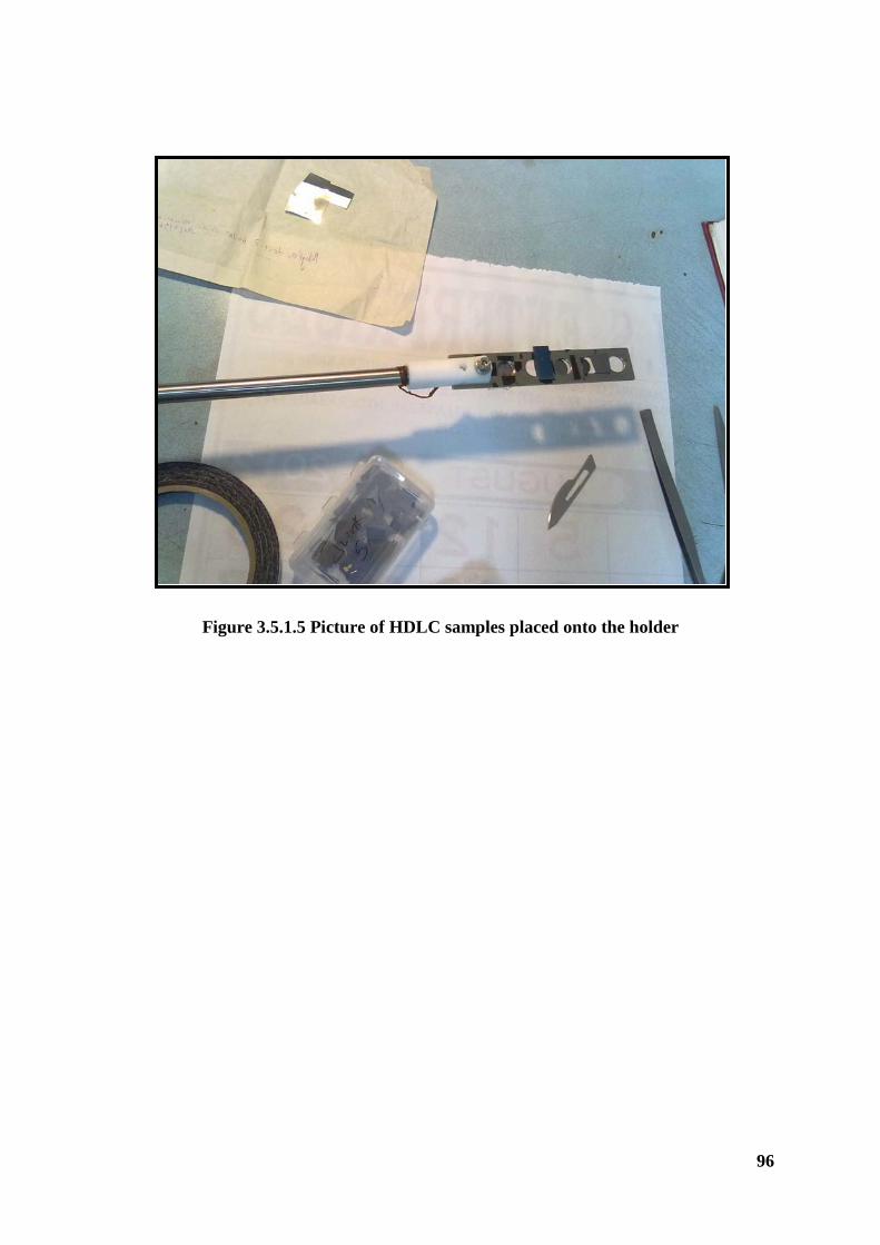
96
Figure 3.5.1.5 Picture of HDLC samples placed onto the holder

97
Figure 3.5.1.6 Picture of experimental arrangement for IBA study
(given in chapter 2 and also shown here for convenience)

98
3.5.2 Rutherford Backscattering Spectroscopy RBS measurements on HDLC thin films (as prepared and annealed) are carried out with 1.0
MeV proton beam from the 3 MV Tandetron accelerator described earlier. The backscattered
particles are detected by a silicon surface barrier (SSB) detector at an angle of 1700. The
scattering chamber is pumped down to ~5×10⁻⁶ mbar by turbo-molecular pump.
Expression for thickness determination using RBS technique : The energy loss of a 1.0
MeV proton beam in a thin film of thickness t is related to the stopping power of the material
is given below [124-125].
[ ]i
Etε∆
= (3.5.2.1)
[ ]outin
ii dX
dEdXdEK
+
=
21 cos1
cos θθε
(3.5.2.2)
where, t is the thickness, ∆E is the FWHM of the peak, εi is the stopping power of the ith
element and the subscripts ‘‘in’’ and ‘‘out’’ refer to the (constant) values of stopping power
(dE/dX) along the inward and outward paths, θ1 and θ2 are the angles between the sample
normal and the direction of the incident beam and of the scattered particle respectively. We
have taken θ1 = 00 ; θ2 = 100 ; C
MeVindXdE
0.1,
=51.88 keV/µm and C
MeVoutdXdE
726.0,
=63.66 keV/µm; [ε]C = 102.29 keV/µm, FWHM for 70 SCCM RT sample 14.713 ± 0.20
keV, giving the thickness of the carbon thin film 144 ± 8 nm. The mass density of the film
can be estimated using areal density and thickness obtained by RBS and NRA techniques,
respectively.
99
3.6 Keithley Source Meter The current–voltage (I−V ) characteristics in ambient air, of the as-prepared HDLC and
annealed HDLC films, were measured in the form of series current (I)-versus-voltage (V)
measurement with a simple bias current using a Keithley 2635 single-channel current source
meter.
The experimental data of Single Electron Transistor (SET) at room temperature, based upon
diamond like carbon (DLC) is not reported in the literature [126-128]. The HDLC thin film
grown onto a large area (12 cm×12 cm) substrate Si (100), behaves as a 2-D graphitic film,
having both p-type and n-type surface conduction. A picture of ohmic contacts of Cu as
source, and drain onto the HDLC surface [128-129] is shown in Figure 3.6.1a. The schematic
layout of HDLC sample and ohmic contacts are shown in Figure 3.6.1b. Biswas et al. [130]
have applied electrochemical method, in order to reduce the size of the domain of conducting
(sp2 C=C) carbons isolated by the domains of non-conducting (sp3C-H) carbons, for
hydrogenation of sp2 C=C bond on the as-prepared HDLC surface, and thus produce
electrochemically hydrogenated diamond like carbon (ECHDLC) surface. A confocal Micro-
Raman spectrometer is used to measure Raman spectra of the HDLC samples to see any
change of Raman spectra due to the electrochemical processes. The Keithley source meter
(2635 Single Channel) instrument is shown below in Figure 3.6.2 and the experimental
arrangement for I-V study using Keithley source meter is shown below in Figure 3.6.3. The
typical results on HDLC films (as-prepared and annealed) obtained by current (I) vs. (V)
characteristics onto the HDLC surface are displayed and critical discussion is made about the
surface conductance mechanisms, based upon the results are given in chapter 4 (section 4).
3.6.1 Experimental arrangements for measuring I-V characteristics :

100
Figure 3.6.1 Picture and Schematic layout of sample. (a) A picture of three ohmic
contacts on the surface of HDLC thin film and the connecting wires from these contacts.
(b) A schematic view of layers of Si (100) substrate, thin film of HDLC and ohmic
contacts: source (S), and drain (D), corresponding to contacts in the picture, onto the
surface of HDLC sample.

101
Figure 3.6.2 Picture of Keithley source meter (2635 Single Channel)

102
Figure 3.6.3 Picture of experimental arrangement I-V study using Keithley source
meter
Specification conditions
The source and measurement accuracies are specified at the Source Meters® CHANNEL A
2635 terminals under the following conditions:
1. 23°C ± 5°C, < 70% relative humidity.
2. After two-hour warm-up.
3. Speed normal
4. A/D auto-zero enabled.
5. Remote sense operation or properly zeroed local operation.
6. Calibration period: one year.

103
3.7 Olympus Digital Camera The parameters of the digital camera used for taking the photograph of the sp2 C=C sites
excited under visible light from a focused light source is given below
Equipment Make : Olypus Optical Co. Ltd.
Camera Model : C4040Z
Creation software : v552p-A78
Color representation : sRGB
Flash used : No
Focal length : 25.4 mm & 35.7 mm
F-number : F/6.3 & F/2.6
Exposure time : 1 sec
Metering mode : Spot and pattern

104
3.8 Dielectric measurement Our HDLC as-prepared films have the properties of low conductivity (high
impedance) and low loss. Therefore, our as-prepared HDLC films may be considered to a
dielectric material. One important technique for analyzing such material is impedance
spectroscopy, i.e. measuring the electrical impedance over a range of frequencies. The
impedance is related to the conductivity and capacitance of the material and these parameters
can easily determined using this technique. Dielectric characterizations were carried out over
our HDLC samples as a function of frequency using an LCR meter (HIOKI) in the frequency
range from below 1 Hz at room temperature. The instrument is shown in Figure 3.8.1 and the
sample holder in Figure 3.8.2. The Solartron 1296 dielectric interface enhances its
capabilities with Solartron 1260 frequency response analyzer (FRA) to cope with ultra-low
current and capacitance levels experienced in analyzing dielectric materials.
Table 3.8.1 Dielectric Interface 1296 Specification
Parameter Model (1296+1260)
Frequency Range 10μHz to 10 MHz
Signal Amplitude up to 7 Vrms
DC Bias up to 40V
The 1296 software requires knowledge of the geometry of the sample. The thickness of the
sample can be read from a micrometer digital display and the area of the sample is calculated
manually. These dimensions are used in the 1296 PC software to calculate the permittivity of
the material (which is independent of the size of the sample), using the formula:
ε = C.d/A
where ε = permittivity (F/m)

105
C = capacitance (F)
d = thickness (m)
A = area (m2)
This allows results from materials of different sizes to be compared. Results can be displayed
using the 1296 software as absolute or relative permittivity. Relative permittivity of the
material, also known as the “dielectric constant” is calculated as:
εr = ε / ε0
where: εr = relative permittivity
ε = permittivity of sample
εο = permittivity of free space (8.85419×10⁻¹² F/m)

106
Figure 3.8.1 Dielectric Interface instrument (model 1296 and 1260)
Figure 3.8.2 Sample holder of Dielectric Interface instrument

Chapter 4
Results and Discussions

107
4.0 Results and Discussions
The detail characterization of the HDLC sample is performed different spectroscopic and
microscopic techniques viz. high resolution transmission electron microscopy (HRTEM),
transmission electron energy loss spectroscopy (TEELS), atomic force microscopy (AFM),
scanning tunneling microscopy (STM), scanning electron microscopy (SEM), micro Raman
spectroscopy (mRS), nuclear reaction analysis (NRA), and Rutherford backscattering (RBS)
measurements, current(I) vs voltage measurements etc.. The results of each of them are discussed
below.
4.1 Results and discussion with HRTEM/TEELS, SEM, and AFM measurements
Figure 4.1.1 Typical HRTEM cross sectional view of the HDLC film

108
Typical cross-sectional view of HDLC sample is shown in Figure 4.1.1, which shows the typical
thickness of the film is ~ 168 nm.
Figure 4.1.2 Typical TEELS spectra recorded for HDLC film. Numbers in the legend
indicate approximate distance of the probe from the interface
Figure 4.1.2 describes typical TEELS spectra for HDLC film, showing the two characteristic
peaks in low energy range (< 50 eV). Following the comparisons of TEELS spectra of
graphitized carbon and amorphous carbon in the literatures [107, 109], we can explain our
experimental results (Fig. 4.1.2). The broad peak at about 24 eV is the (π+σ) plasmon i.e. the
bulk plasmon, which corresponds to collective excitation of all (π+σ) electrons; the other peak at
~ 6 to 7 eV is the π plasmon, which corresponds to collective excitation of all π electrons. All the

109
spectra were recorded at different distance of the probe from the interface. Except very close to
the interface, there is no observed variation of the spectra. Above 3 nm from interface upto top of
the HDLC film, the plasmon structures correspond to multilayered graphene i.e. hexagonal
graphite structure and near the interface i.e. below 3 nm, the plasmon structure correspond to a
few layer graphene, with slight red shift and reduced intensity of the plasmon peak of (π+σ)
electrons [109]. Thus near the interface between Si(100) substrate and bulk graphitic structure
we can assume a few layer graphene corresponding to sp2 bonded C and this result supports the
BEN model [89]. The density of valence electrons ‘n’ of a thin film can be measured from the
low-loss spectrum through the measured value of plasmon energy Ep = ( 4πn/ɛo m)1/2 from the
low-loss spectra, where ɛo is dielectric constant of vacuum and m is effective mass of an
electron. Thus we can say that the density of (π+σ) electrons is much higher in the bulk than in
the interface of HDLC film which was measured to be of single crystalline nature different from
the hexagonal graphene/graphite structure [93].
The morphology of the surface of the HDLC films has been analyzed by AFM and SEM
respectively.

110
Figure 4.1.3 Non-contact mode AFM topography image of HDLC surface: scan size 2.5 µm
× 2.5 µm
Figure 4.1.3 is a typical AFM topography image of the HDLC surface, giving its roughness value
(~ 0.07 nm).

111
Figure 4.1.4 Typical FESEM image of HDLC film surface recorded at 80,000X
Figure 4.1.4 is a typical featureless secondary electron (SE) image of the HDLC surface. These
results (Fig. 4.1.1, 4.1.2, 4.1.3, and 4.1.4) are consistent with an atomically smooth, non-porous
continuous film. It may be referred [22] that ultra-nanocrystalline diamond of uniform grain size
(3-5 nm) can produce continuous film having surface roughness ~ 7-15 nm only after achieving
its thickness greater than 300 nm. Also, hydrogenated carbon films having hexagonal graphite
and diamond as coherent domains were reported in earlier works [131]. Therefore our results
seem to show that instead of discrete grains, coherent domains of σ bonded sp3 C-H and π
bonded sp2 C=C carbons, can produce continuous, non-porous thin film having atomically
smooth surface at lower thickness (~ 168 nm) of the film. This is a new result to the best of
knowledge of author.
300 nm

112
4.2 Results and discussion with micro-Raman spectroscopic measurements
Typical Raman spectrum of the as-prepared HDLC film is shown in Figure 4.2.1 over the
50-4000 cm−1. The spectrum shows significant increase of photoluminescence background with
the higher wave number along the abscissa due to the disorder carbon (sp2) structures [132-133].
The single crystal silicon is characterized by a sharp peak at 512 cm−1 which is observed in most
of our HDLC samples. Raman spectrum of HDLC film shows the Si peak (at 512 cm−1) is
downshifted by 8.7 cm−1 than that of standard silicon peak (Fig. 3.2.5). This may be attributed
due to the stress generated between the Si(100) substrate and the interfacial graphitic layer [89].
Figure 4.2.1 Typical Raman spectrum of HDLC film over the range 50-4000 cm−1
113
Moreover, in the Raman spectra of HDLC samples, there is one broad peak at ~ 1000 cm−1,
which is due to the second order of silicon. These peaks are the signature of the backing silicon
materials upon which the HDLC thin film was deposited.
4.2.1 First- , Second- and Higher-order Raman features
In general, the broad Raman spectra are the characteristics of different types of
amorphous carbon thin films. The amorphous carbon can have sp3 carbon (diamond-like) and sp2
(graphite-like). In the case of a disordered hydrogenated carbon sample we can expect various
effects on the position and broadening of G and D bands etc. [112, 133]. These two modes,
namely G-band (sp2 mode, commonly known as Graphitic band) and D-band (commonly known
as disorder allowed zone edge mode of graphite) in the Raman spectrum of graphite are due to
the zone center E2g phonon mode at 1580 cm−1 and K-point phonons at 1350 cm−1. Therefore
first-, second- and higher order Raman spectra of HDLC are explored considering the effect of
partial hydrogenation of hexagonal sp2 (C=C) carbons on the characteristic G and D bands of
graphitic materials. Thus as per our expectation, the broad peak envelops corresponding to first- ,
second- and higher-order Raman features after subtraction of the photoluminescence background
are shown below in Figure 4.2.2, 4.2.3, and 4.2.4, respectively.

114
Figure 4.2.2 First-order Raman spectrum of HDLC film over the range 1000-1800 cm-1
We have deconvoluted first order Raman spectrum using six Lorentzian functions (as shown in
Fig. 4.2.2) keeping intensities, widths and peak positions as variable fitting parameters. The first
order Raman spectra of the as-prepared HDLC film shows typical Raman modes of amorphous
carbon having a broad asymmetric peak at ~1540 cm−1 (G-band), along with the other peaks at
1366 cm−1 (D-band) due to disorder in crystalline graphite, 1255 cm−1 (Nano crystalline diamond
NCD line) due to hydrogenation of sp2C=C into sp3C-H, 1145 cm−1 (trans poly acetylene mode)
due to C-H wagging modes, 1593 cm−1 dumbbell defect in the NCD line. In the first-order
Raman spectrum (Fig. 4.2.2) of HDLC, there is red-shifted G band (1540±1 cm−1) to lower
frequencies follows a 1/n dependence on the number of sp2 carbon layers n [134] and is a
signature of strained carbon-carbon bonds [135]; the D band (~ 1366±1 cm−1) is a signature of
lattice motion away from the center of the Brillouin zone lying between 1270 and 1450 cm−1

115
depending upon the excitation wavelength and indicating symmetry breaking i.e. disorder
induced in the hexagonal sp2 carbons due to hydrogenation [136]; presence of nanocrystalline
diamond (NCD) line (~ 1255 cm−1) having significant downshift (∆ν ~ 77 cm−1) with respect to
pure diamond (sp3 C-C) line (~ 1332 cm−1) signifies the conversion of sp2 C=C into sp3 C-H
(diamond like) due to hydrogenation and large broadening (full width at half maximum, FWHM
~173±16 cm−1) of the Raman line interpreted as phonon confinement in NCD (sp3 C-H) domains
of less than 1 nm in size [137]; the estimated ratio of G and D band intensities (ID/IG) being less
than 1 can be interpreted as size of defects should be less than 1 nm in size [133] i.e. if we
assume sp3 C-H domains as defects in the sp2 C=C carbon matrix, then our above interpretations
of broadening of Raman line and ratio of G and D band intensities seem to be plausible. The sum
and difference in combinations of C=C chain stretching and C-H wagging modes [ν1 and ν3
modes of trans-polyacetylene (trans-PA)] appear at ~1145±4 cm−1 and ~1485±3 cm−1
respectively [137]. The dumbbell defect in NCD, called D′ appears at ~1593±1 cm−1 [70]. Thus
the first-order Raman spectrum (Fig. 4.2.2) signifies effects of (i) strain in carbon-carbon bonds,
(ii) multilayer of sp3 C-H carbons embedded in sp2 C=C carbon matrix and (iii) disorder induced
in the sp2 C=C carbon matrix by its hydrogenation.
All the above as described in earlier paragraph is “first order” scattering, i.e. the
excitation of only one phonon. However, it can be also “second order” scattering, i.e. two
phonons can be excited. The second order spectra of single crystals and highly oriented pyrolytic
graphite are featureless continuous and exhibit several well defined bands which can enrich the
features in the vibration states. For the second order Raman scattering, the sum of the phonon
wave vectors must be equal to the wave vector transferred in the light scattering incident, but
must be travelling in opposite directions. Second order scattering is usually weak, but can be

116
enhanced by various things. The second order spectrum broadens significantly with decreasing
crystal size.
Figure 4.2.3 Second-order Raman spectrum of HDLC film over the range 2600-2750 cm−1
We have deconvoluted second order Raman spectra after subtraction of photoluminescence
background similar to the first order Raman spectrum using four Lorentzian functions (as shown
in Fig. 4.2.3) keeping intensities, widths and peak positions as variables fitting parameters. The
second-order Raman spectrum (Fig. 4.2.3) comprising of four overlapping Lorentzian peaks is a
signature of four possible double resonance (DR) Raman scattering processes in the hexagonal
sp2 C=C carbon matrix [136]. The four bands 2701±4 cm−1, 2644±3 cm−1, 2677±2 cm−1 and
2733±4 cm−1 correspond to that for pristine monolayer of graphite (PMG), red-shifted 2D band
due to high and low strain on PMG, and blue shifted 2D band of multilayer of sp3 C-H carbons
embedded in sp2 C=C carbon matrix respectively [133, 135]. This result on second-order Raman
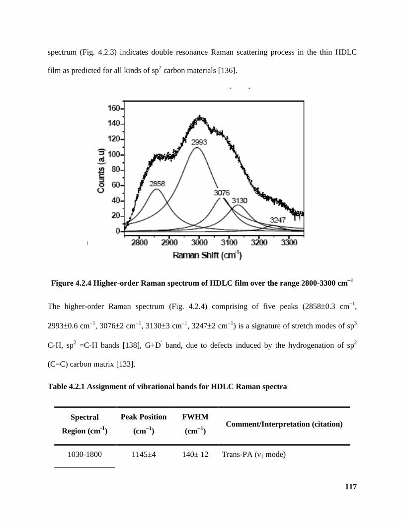
117
spectrum (Fig. 4.2.3) indicates double resonance Raman scattering process in the thin HDLC
film as predicted for all kinds of sp2 carbon materials [136].
Figure 4.2.4 Higher-order Raman spectrum of HDLC film over the range 2800-3300 cm−1
The higher-order Raman spectrum (Fig. 4.2.4) comprising of five peaks (2858±0.3 cm−1,
2993±0.6 cm−1, 3076±2 cm−1, 3130±3 cm−1, 3247±2 cm−1) is a signature of stretch modes of sp3
C-H, sp2 =C-H bands [138], G+D′ band, due to defects induced by the hydrogenation of sp2
(C=C) carbon matrix [133].
Table 4.2.1 Assignment of vibrational bands for HDLC Raman spectra
Spectral
Region (cm-1)
Peak Position
(cm−1)
FWHM
(cm−1) Comment/Interpretation (citation)
1030-1800 1145±4 140± 12 Trans-PA (ν1 mode)

118
Thus Raman spectroscopy suggests that our HDLC carbon film is made of multilayer of
coherent domains of sp3 C-H and sp2 C=C carbons. From the position of G band in the Raman
spectrum of HDLC film we can estimate, using an empirical relation sp3 content = 0.24-
1255±2 173±16 NC diamond
1366±1 157±10 D band due to laser wavelength 488nm
1485±3 119±8 Trans-PA (ν3 mode)
1540±1 110±7 Red-shifted G band for 2.8% strain
1593±1 79±6 Dumbbell defect in NCD: D' band
2600-2750
2644±3 39±6 Red-shifted 2D band for 2% strain
2677±2 48±7 Red-shifted 2D band for 0.8% strain
2701±4 27±6 2D band for pristine graphene
2733±4 69±17 Blue shifted 2D band
2800-3300
2858±0.3 103±2 Hydrogenated sp3 carbon (graphane
like): C-H stretch mode
2993±0.6 145±2 Hydrogenated sp3 carbon (graphane
like): C-H stretch mode
3076±2 90±5 sp2 carbon, =C-H stretch mode
3130±3 98±8 (G+D') band due to defects introduced
into the graphene by hydrogenation
3247±2 75±10 sp1 carbon, ≡C-H stretch mode

119
48.9(ωG–0.1580), approximately 45% sp3 and 55% sp2 carbons in the film [61]. Our result is
similar to the 40:60 ratio of sp3/ sp2 as observed in amorphous hydrogenated carbon films having
hexagonal graphite and diamond as coherent domains [131].
4.2.2 Stress computation from Raman spectra
Bagilo et al. [139] exploited Raman spectroscopy and photoluminescence (PL) to
examine systematically the sources and nature of stress and also investigated the effect with
respect to the type and distribution of defects and impurities in thin diamond films grown on
silicon substrates. The types of defects and even the impurities which were detected in the
diamond films are the sp2‐type bonding of the graphitic phase and nitrogen, silicon respectively.
Furthermore, the stress magnitude exhibits a strong mutual relation with the graphitic phase
indicating that the sp2 bonding creates a dominant compressive stress field. The stress produced
during hydrogenation of hexagonal sp2 carbon matrix deposited onto Si(100) substrate has been
studied from the shape and width of Raman lines [140]. Accordingly, stress σ (GPa) within the
HDLC film is estimated from the Raman shift ∆ν (cm−1) of the NCD line using the relationship
given below in equation (4.2.1)
∆ν = ν -νo = -ασ (4.2.1)
Where α is pressure coefficient and νo is taken to be the Raman peak position (~ 1332 cm−1) of
natural diamond when no pressure is applied. The NCD line near ν ~ 1255 cm−1 is less than νo,
indicating a positive tensile film stress. Net stress within a deposited film σnet has been construed
to arise from three potential contributions following the simple additivity relationship as given
below in equation (4.2.2)
σnet = σTH + ΣσIN + σlm (4.2.2)

120
Where σTH is thermal stress (TH), ΣσIN is the sum of all internal stresses (IN), and σlm is stress
due to lattice mismatch (lm). Raman spectra of HDLC are consistent with tensile stress,
suggesting that σTH does not dominate σnet and accordingly σTH can be neglected as a first-order
approximation. Furthermore, we observe that the Raman shift associated with lattice stress is
only 77 cm−1, to be compared to 200 cm−1 anticipated for large lattice mismatches. Thus, it is
apparent that σlm is small compared to σnet and that σlm could be ignored as a first-order
approximation. Collectively, these considerations led to the conclusion that total tensile stress in
HDLC film is due primarily to ΣσIN. Bagilo et al. [139] states that ΣσIN is due to attractive forces
across grain-boundaries and that ΣσIN can rise to GPa proportions for nanometer-sized
crystallites, sufficient to cause grain coalescence. In our case, sp2 and sp3 carbons exist
coherently in the film as concluded from Raman analysis and thus the internal stress in the film
should develop as a result of partial conversion of sp2 C=C into sp3 C-H. Indeed, using α ≈ 1.9
cm−1/GPa and ∆ν ≈ 77 cm−1, we estimate the σnet associated with the NCD line in HDLC to be
tens of GPa. It implies that sp3 C-H domains within HDLC must be nanometer in dimension,
consistent with Raman analysis above [140]. Furthermore, FWHM of the 1255 cm−1 NCD line (~
173±16 cm−1) is consistent with phonon confinement in nanometer-sized regions [140]. All
evidence taken together led us to conclude that internal tensile stress within HDLC film is caused
due to partial hydrogenation of sp2 C=C carbon matrix, to sp3 C-H carbons.

121
4.2.3 Experimental signature of bilayer Graphene like and Graphane like structure in the
Hydrogenated Diamond Like Carbon film
The signature of misoriented bilayer graphene like and graphene like structure in the
HDLC film is described below, by studying Raman spectra of the as-deposited and annealed
(1050 0C) HDLC films.
The results on the lattice parameters a=2.62 Å and C=6.752 Å of our HDLC film as described
above, seem to correspond to hydrogenation of hexagonal structure of carbon atoms, called
graphane [141]. Graphene is a crystalline allotrope of one-atom thick carbon with 2-dimensional
characteristics. Technically, stability of graphene's is due to a tightly packed, periodic array of
carbon atoms and a sp2 orbital hybridization - a hybridization of orbitals s, px and py that
constitute the σ-bond. The rest pz electron forms π-bond, which is the key source that permits
free-moving electrons. Although, there is strong σ-bonds in a particular layer, the weak bonding
between the layers, which facilitates the easy removal of layers. The Raman spectroscopy is
especially useful for our case because the Raman spectrum shows characteristic dependence of
thickness of graphite film. Moreover, it is possible to identify and compare of single, bi, and
multilayers of graphite from the Raman spectra. This possibility arises due to the fact that the
evolution of Raman lines is directly related to the electronic structure. As it is known to us, that
the most prominent line of graphite is G-band, at ~1580 cm−1, and a very weak D-band at ~ 2700
cm−1. The relative intensity of D-band enhances with the number of layers. Again, the line shape
and position sensitive to the number of graphene layers for the 2D-band and is also sensitive to
the chemical doping/defects. In bi-layer graphene, there are two inequivalent sub lattices which
split into four bands [142-143] due to splitting in electronic bands. The motivation of this work is
to explore the distinction between pure multilayered graphene film and HDLC film which is

122
composed of multilayer of coherent domains of sp3 C-H (graphane-like) and sp2 C=C carbons
(graphene-like).
Figure 4.2.5 (a) Raman spectrum of as-prepared HDLC film. (b) Raman spectrum of
annealed HDLC film
A typical comparison of Raman spectrum of the (a) as-prepared HDLC film and (b)
annealed (at 1050 0C) HDLC film is shown in Figure 4.2.5 over the 500-4000 cm−1. The
significant difference is the presence of photoluminescence (PL) background in the former and
the disappearance of PL background in the latter. Moreover, the PL spectrum (Fig. 4.2.5a)
superimposes on the Raman spectrum (Fig. 4.2.5b) in the annealed HDLC samples. These
observations clearly indicate the significant loss of bonded hydrogen atom from the as prepared

123
HDLC sample due to annealing effect at temperature 1050 0C and in high vacuum ~1×10⁻⁶ torr.
It is known [132] showed that PL results from the recommbination of electron-hole pairs within
sp2 bonded clusters in a sp3 bonded hydrogenated carbon matrix.
Figure 4.2.6 First-order Raman spectrum of as-prepared HDLC film over the region 1050-
1800 cm−1
We have deconvoluted first order Raman spectra after subtraction of photoluminescence
background using six Lorentzian functions (as shown above) keeping intensities, widths and
peak positions as variables fitting parameters for obtaining best fit results. On deconvolution, the
first-order Raman spectrum (Fig. 4.2.6) is comprised of six overlapping Lorentzian peaks;

124
namely a broad asymmetric peak at 1546 ± 0.6 cm-1 known as G-band, a shoulder at 1366 ± 0.5
cm−1 known as D-peak, 1245 ± 0.9 cm−1 known as nanocrystalline diamond line (NCD line)
[70]; features near 1121 ± 1 cm−1 and its companion mode 1450 ± 2.4 cm−1 appear due to sum
and difference in combinations of C=C chain stretching and C-H wagging modes [v1 and v3
modes of trans polyacetylene (Trans-PA)] lying in the grain boundary [70]; and the dumbbell
defect in NCD, appears at ~1598 ± 1.3 cm−1 [61].
Figure 4.2.7 First-order Raman spectrum of annealed HDLC film over the region 1050-
1800 cm−1

125
The first order Raman spectra of the annealed HDLC film shows typical Raman modes at 1357 ±
0.5 cm−1 and 1601 ± 0.5 cm−1 which corresponds to the interlayer disorder mode, and
characteristic G-band, respectively, in the turbostatic structure of graphitic material [67, 144-
145]. These results in Figure 4.2.6 and 4.2.7 signify that the HDLC film, having been found to be
a hydrogenated hexagonal crystal structure of carbon atoms, is composed of layers of graphite
like crystalline structures which have parallel c-axes and which are connected to one another by
disordered regions. In fact, the measured value of interlayer separation [93] c/2 ~ 3.376 Å for
HDLC is larger than that for crystalline graphite which is 3.354 Å, signifying the existence of
interlayer disorder regions in the HDLC sample. The interlayer disorder mode (D-band) and the
G-band are active for crystallites of finite size in the nanometer range, and the ratio ID/IG
inversely varies with their diameter; the D-band and G-band do not depend upon the mutual
arrangement of graphite planes [67, 144-145]. Table 4.2.2 provides all parameters, which we
have obtained in this analysis during the fittings of various annealed samples.
Table 4.2.2 Comparisons of the fitting data for annealed samples
Sample
(Redχ2 , R2) Peak Error Width Error Intensity Error ID/IG
A50-250C
(161,
0.9992)
1121 1.2 69.7 5.4 7495 779
1245 0.9 145 3.8 68948 3145
1366 0.54 164 3.4 144929 4562 0.766
1495 2.4 95 5.1 54669 12474

126
1546 0.66 104.6 6.46 189010 26121
1598 1.27 84 4.7 70543 11327
A50-7500C
(164,
0.99916)
1121 1.2 75 5.4 8372 840
1240 1.0 146 5.0 56854 3403
1368 0.5 179 3.4 183646 5362 1.067
1496 2.3 97 5.1 48207 9141
1550.5 0.6 97.5 4.7 172012 18692
1597.6 0.8 74 3.2 74170 8756
A50-10500C
(1388,
0.998)
1357 0.28 119.44 0.96 312646.8 3702.183 1.93
1601 0.18 61.95 0.47 162303.6 2340.695
1522 0.82 139.8 2.87 298050.2 8344.839
A comparison between the results in Figure 4.2.6 and 4.2.7 shows the following: (1) The ratio
ID/IG increases from 0.8 to 2.0 (approximately), indicating a reduction of size of the domain of
crystallinity; (2) the intensities of the peaks at 1245 ± 0.9 cm−1, 1121 ± 1.2 cm−1, 1495 ± 2.4
cm−1, and 1598 ±1.3 cm−1 in Figure 4.2.6 significantly disappeared in Figure 4.2.7, indicating
loss of sp3 C–H in the HDLC; and (3) the frequency shift ∼57 cm−1 toward higher wave number
is found for the G-band in Figure 4.2.7, indicating a reduction of size of the domain of

127
crystallinity. It has been observed that sp2 C = C and sp3 C–H carbons exist coherently, and the
size of the sp3 C–H domains in the HDLC is reduced due to the annealing effect, by the loss of
bonded hydrogen atoms in the hydrogenated hexagonal crystal structure of carbon atoms. Hence,
the aforementioned results (1)–(3) seem to be plausible for the annealed HDLC.
Analysis of second order Raman Spectra
Figure 4.2.8 Second order Raman spectrum of as-prepared HDLC film
The second-order Raman spectrum of the as-prepared HDLC (Fig. 4.2.8), and that of the
annealed sample at 1050 0C (Fig. 4.2.9), shows the presence of G'-band and the second order of
the D-band, respectively [112]. The D- and G'-bands originate from a double-resonance Raman
process in 2-D graphite [146]. Therefore, the present results, as shown in Figure 4.2.8 and 4.2.9,

128
signify the HDLC sample, having turbostatic behavior as found from the first-order Raman
spectra, to behave as 2-D graphite due to interlayer disorder regions between the layers having
been
Figure 4.2.9 Second order Raman spectrum of annealed HDLC film
separated by 3.376 Å. Since the G'-band is very sensitive to the stacking order of the graphene
layers along the c-axis and identification of the number of layers in the turbostatic graphite is
done by the number of peaks in the G'-band [147], we have deconvoluted the G'-band with best
fits by Lorentzian peaks. Both Figure 4.2.8 and Figure 4.2.9 show the following: 1) Four Raman
modes aside from the peak at ~2700 cm−1 correspond to single-layer graphene; 2) full-width at
half-maximum for all the five modes lies in the range of 15–40 cm−1; and 3) IG'/IG « 1. These
results correspond to turbostatic multilayer graphene in general. According to the calculation of
Latil et al. [148], a Bernal bilayer (AB) and a rotationally disordered graphene (A') should

129
simply exhibit the sum of the spectra from a bilayer (i.e. a broadband with four components) plus
the unique peak of graphene. Our experimental results, as shown in Figure 4.2.8 and 4.2.9,
correspond to that theoretically predicted and experimentally confirmed for misoriented bilayer
graphene [149]. Thus, from all evidences taken together from the first- and second-order Raman
spectra [Fig. 4.2.8–4.2.9], we can say that the layers of the hexagonal structure of carbon atoms
in the HDLC sample stay perfectly parallel but their mutual orientation along the c-axis is
random (turbostatic) due to the existence of interlayer disorder; as a result, the 3-D crystallinity
of the HDLC should be lost, while only the 2-D crystallinity should be preserved. Therefore, the
as-prepared HDLC film can be assumed to have misoriented bilayer graphane like structure, and
the annealed HDLC film can be assumed to have misoriented bilayer graphene like and graphane
like structure within the coherent structure of the film. The Raman spectra [Fig. 4.2.8–4.2.9] do
not tell us about why and how the interlayer disorder region is created in the HDLC film.

130
4.3. Results and discussion using NRA and RBS
4.3.1 Results of NRA measurements
Figure 4.3.1 The typical NRA profile of as-prepared HDLC sample-A is shown. Both raw
data of 6.1 MeV prompt γ-ray yields per µC of charge Vs. difference of incident beam
energy and resonance energy (6.4 MeV), and corresponding hydrogen concentration (at.%)
Vs. depth (nm) into HDLC sample are shown above
Figure 4.3.1 shows typical γ-ray yield (due to nuclear reaction 1H(19F,αγ)16O), as a function of (i)
energy difference between energy of incident 19F ion beam (Ein) and the resonance energy (ER)
as recorded in a PC-based multichannel analyzer, (ii) hydrogen concentration at different depth
of the film, estimated using stopping power value of HDLC. For Ein < ER, the γ-ray yield

131
corresponds to ‘background yield’ and for Ein = ER the γ-ray yield corresponds to the presence of
hydrogen atoms onto the surface of HDLC sample. With the increase of energy of the beam
penetrating into the sample, the γ-ray yield starts decreasing from the surface of the target, as
evident in Figure 4.3.1. The typical behavior of declining of γ-ray yield at different depth of as-
prepared and annealed HDLC sample are observed to be similar. Figure 4.3.1 shows typical γ-ray
yield (due to nuclear reaction 1H(19F,αγ)16O), as a function of (i) energy difference between
energy of incident 19F ion beam (Ein) and the resonance energy (ER) as recorded in a PC-based
multichannel analyzer, (ii) hydrogen concentration at different depth of the film, estimated using
stopping power value of HDLC. For Ein < ER, the γ-ray yield corresponds to ‘background yield’
and for Ein = ER the γ-ray yield corresponds to the presence of hydrogen atoms onto the surface
of HDLC sample. With the increase of energy of the beam penetrating into the sample, the γ-ray
yield starts decreasing from the surface of the target, as evident in Figure 4.3.1. The typical
behavior of declining of γ-ray yield at different depth of as-prepared and annealed HDLC sample
are observed to be similar.
The as-prepared samples (A to D) when annealed at different temperatures 750 0C and 1050 0C
in high vacuum, show that the yields, and hence the hydrogen content of the annealed films, in
all the cases, are lower than that of the as-prepared samples. A typical result for the as-prepared
sample B is shown in Figure 4.3.2. As expected, the hydrogen content should decrease with the
increase of the annealing temperature. Therefore, the results in Figure 4.3.2 clearly indicate
significant loss of bonded hydrogen atoms from the HDLC sample due to annealing effect. Since
the decades, it has been well known that the heating of amorphous hydrogenated carbon above
300 0C will produce the exo-diffusion of hydrogen molecules through the recombination of small
sized hydrogen atoms within the bulk of the materials. Such formation of H2 molecules is

132
favorable due to the higher bond energy of H-H than that of the C-H bond. Therefore, annealing
leads to the transformation of sp3C-H sites into sp2 sites. Consequently, there is the reduction of
the photoluminescence background. It is also to be noted from the Figure 4.3.2 that the
maximum depth at which the yields of hydrogen content are more or less equal to the
background counts (210, 152 and 148 counts/µC for as-prepared and annealed sample at 750 and
1050 0C respectively) depends upon the annealing temperature; these depths are ~ 83 nm for the
Figure 4.3.2 NRA measurements on HDLC sample-B thin films onto Si backing materials
(30 SCCM, both as-prepared and annealed at 750 and 1050 0C) were carried out with 19F3+
ion beam at beam current of 3 nA. For each of the above measurements fresh samples were
annealed
133
as-prepared sample, ~ 68 nm for annealing temperature 750 0C and ~ 59 nm for annealing
temperature 1050 0C. It is well established that the diamond is metastable and graphite is
thermodynamically stable, and therefore, diamond and/ nano-crystalline Diamond (NCD) are
converted into graphite when heated at elevated temperature ca 1300 0C [150-152]. Therefore,
our results showing decreasing of depth of hydrogen content in the HDLC sample with
increasing annealing temperature, may be attributed to conversion of sp3 C-H (diamond like) to
sp2 C=C (graphite like) structure in the HDLC sample.
The variation of hydrogen content with the depth of the as-prepared samples (A-D) is
shown in Figure 4.3.3. The hydrogen concentration is maximum just inside the surface which is
approximately within 10 nm from the surface in most of the samples. This result may indicate
that the unsaturated bonds of carbon are being terminated by hydrogen, thus leaving almost no
unsaturated bonds in the samples at the end of their deposition. From the Figure 4.3.3, it is
evident that at a given depth within the sample, the hydrogen content increases with the increase
of flow rate of methane at a constant flow rate of hydrogen (500 SCCM) during deposition of
samples (A-D). This result is in accordance with our earlier results as reported Singha et al.
(2006) [61]. The continuing decrease of the hydrogen with depth of the samples (A-D) indicates
that the films having higher graphitic nature towards the interface between the HDLC film and
Si(100) substrate. This observation could be explained considering the fact that, in a bias
enhanced nucleation of diamond on Si, there is always one intermediate buffer layer of SiC or
graphite as shown in a model of diamond/graphite/Si(100) interface [89, 153]. This model
provides the minimal lattice mismatch and minimal interfacial energy.

134
Figure 4.3.3 Hydrogen concentration distribution observed in NRA measurements for as-
prepared HDLC samples (A-D) deposited in different flow rate (SCCM-standard cubic
centimeter per minute) with 19F3+ ion beam at beam current of 3 nA
The maximum depth of hydrogen content in the HDLC film depends upon flow rate of methane
(Fig. 4.3.3) and for a given as-prepared HDLC film the maximum depth of hydrogen content
decreases with increasing annealing temperature (Fig. 4.3.2). Therefore, the direction of flow out
of hydrogen during annealing of HDLC sample is from the interface towards the surface. E.
Vainonen-Ahlgren et al. (1997) [56] and Thomas et al. [154] have studied the migration of
hydrogen in DLC films by NRA, RBS, and SIMS techniques and found migration of hydrogen
towards the interface between the film and substrate and also release of hydrogen from the

135
surface region. On contrary to this observation, the migration of hydrogen towards surface from
the interface in our HDLC sample seems to be plausible due to the fact that during the annealing
process, the heat is transferred from the sample holder to the backing silicon material and then
into the sample; hence, the interface of the sample and the Si is at higher temperature than the
surface of the HDLC samples. Therefore, there might be a possible chance of little
rearrangement of hydrogen bonds through the process of dehydrogenation and hydrogenation
[155] within the sample. In some hydrogenous carbon materials loss of hydrogen under ion
irradiation is reported earlier [156-157]. Due care, therefore, is to be taken while carried out the
hydrogen determination. In such cases, the concentration of hydrogen should be measured as a
function of ion dose and the initial hydrogen content can be obtained by extrapolation to the zero
dose condition. This result is shown in Figure 4.3.4. The yields at zero dose condition are also
shown along the dotted line for the as-prepared and annealed samples. These values were
obtained from the polynomial fitting of the γ-ray yields vs. charge density. The stability of the
standard samples under ion beam irradiation has already been studied [119]. This can be
minimized by using the lower mass of the projectiles, which don’t transfer large electronic
energy as excitation energy in the sample. Nearly constant integrated counts (as shown in Fig.
4.3.4) for every 250 nC charge, were observed for the standards (Si3N4) for total 20 number of
times exposure at primary beam energy of ~ 6.5 MeV. In contrary, the counts were slowly
decreased for annealed samples and rapidly for the as-prepared samples as shown in Figure
4.3.4. This could be explained if we assume that the hydrogen is present in the film as bonded by
chemical forces and also as non-bonded due to physical forces or weak Vander Wall forces.
Therefore, the weakly bonded hydrogen readily desorbs from the thin films on heating. This
desorption is maximum for the as-prepared films compared to annealed films.

136
Figure 4.3.4 The γ-ray counts/µC vs. charge (µC) (Bottom) or fluence of 19F3+ ion beam
(Top) during hydrogen depth profiling for as-prepared (at two different regions of 5 mm
apart) and annealed at 750 0C of HDLC samples-A at beam current of 3 nA and also Si3N4
standard at beam current of 3 nA observed in NRA technique
4.3.2 Results of RBS measurements
The backscattered spectra for as-prepared samples are recorded using 1.0 MeV proton beam and
are shown in Figure 4.3.5. The higher channel number (i.e. higher energy) side of the RBS
spectrum is due to the backing silicon materials (thickness ~0.5 mm). The Si-edge of sample A
was different compared to sample B. There are two factors responsible, one is channeling and
other is cross section which is even more non-Rutherford in this energy range. Again the cross
section varies sharply at the Si-edge. The sharp peak is observed over the broad plateau of silicon

137
is due to the carbon. It is clear from the inset picture where there is no peak for the virgin silicon
sample but sharp peaks for carbon onto silicon. The sharp peaks of carbon in the inset of Figure
4.3.5, show increase of peak area from 417±24 to 774±34 to 1936±65 counts/µC, and FWHM
from 10.7±0.5 to 11.2±0.7 to 14.71±0.8 keV with the increase of flow rates of methane in the as-
prepared samples viz., A, B, D respectively. Therefore, the thickness of the film increases with
flow rates of methane.
Figure 4.3.5 RBS measurements on as-prepared HDLC thin films onto Si backing materials
prepared at different flow of methane were carried out with 1.0 MeV proton beam. The
backscattered particles were detected by a silicon surface barrier (SSB) detector at an
angle of 1700
The RBS spectra for the as-prepared and annealed HDLC samples are measured. The FWHM for
samples B (30 SCCM) both as-prepared and annealed at 750 and 1050 0C were 11.2±0.7,

138
11.1±0.5, 10.4±0.5 keV at 722±3 keV and the integrated area under the peaks are 813±46,
774±34, 670±27 counts/µC respectively. These values were obtained using Lorentzian fittings. It
is observed that the as-prepared films have higher peak yields and higher FWHM compared to
that of annealed one as shown in Figure 4.3.6. This result indicates thickness of as-prepared
samples is larger than that for annealed one.
Figure 4.3.6 RBS measurements on HDLC thin films B onto Si backing materials (30
SCCM, both as-prepared and annealed at 750 and 1050 0C) were carried out with 1.0 MeV
proton beam from Tandetron accelerator. The backscattered particles were detected by a
silicon surface barrier (SSB) detector at an angle of 1700. For each of the above
measurements fresh samples were annealed

139
Kazunori et al. (1999) [158] and Wang et al. (1997) [159] have studied the erosion behavior of
deuterated soft amorphous carbon thin film by heat treatment in air and vacuum, using elastic
recoil detection (ERD) and proton enhanced scattering (PES) techniques. When the films are
heated in air above 550K for 1 h, the film thickness, and the areal densities of carbon and
deuterium both decrease. Moreover oxygen is incorporated into the films. Nevertheless, when
annealed in vacuum, erosion starts at above 600K and decrease in thickness along with the
decrease of all other components. Thermal desorption spectroscopy of the soft films reveals the
evolution of hydrocarbon. They have also studied the thermal erosion behavior of hard a-C:H
thin films under vacuum. This showed predominantly the release of hydrogen molecule to give
semi-hard a-C:H films with very low hydrogen content. This implies that the soft films sublimate
and hard film desorbs in vacuum during annealing. We have also observed the similar desorption
and decrease in at% of hydrogen and that in thickness for HDLC thin film, when treated under
vacuum at high temperature. The diagnosis by NRA measures the content of hydrogen whereas
RBS techniques measures content of carbon. Therefore, the decrease of HDLC film thickness
due to annealing (Fig. 4.3.6) should be caused by removal of carbon and hydrogen both.
Estimation of hydrogen content and thickness of HDLC sample
The atomic fraction of Hydrogen in the as-prepared HDLC film is estimated using equation
(3.5.1.1) based upon NRA measurements. The results are given in Table 4.3.1.
The thickness of the as-prepared HDLC film along with their uncertainties is measured by NRA
using equation (3.5.1.2) and by RBS using equation (3.5.2.1). These results are given in Table
4.3.2. The experimental detection limit of the sample has been estimated on the basis of three
times standard deviation value (3s) of background counts in the region of a peak of the γ-ray
spectrum of samples as per our experimental parameters and the value is ~ 3.0 at%.

140
Table 4.3.1 Atomic fraction of hydrogen in the HDLC films (A-D) as a function of flow rate
of methane
Table 4.3.2 Comparison of depth of hydrogen by NRA and thickness of the as-prepared
films (A-D) by RBS technique
Sample Flow rate of methane
(SCCM)
Hydrogen content
At.%
A 20 30.1±3.2
B 30 30.5±3.4
C 40 32.9±3.5
D 70 34.1±3.9
Sample Flow rate of
CH4 (SCCM)
Depth of hydrogen
in the film by NRA
(nm)
Thickness of the
film by RBS
(nm)
A 20 52±10 124±15
B 30 83±10 130±16
C 40 98±12 134±17
D 70 158±17 144±20
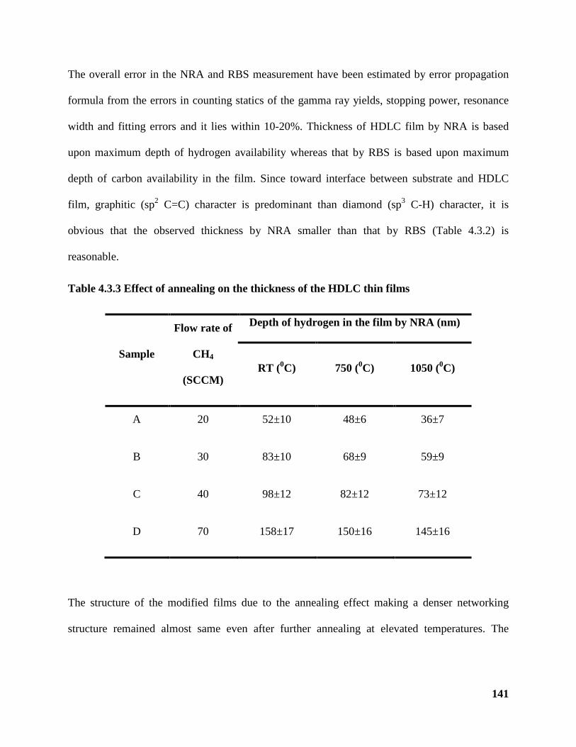
141
The overall error in the NRA and RBS measurement have been estimated by error propagation
formula from the errors in counting statics of the gamma ray yields, stopping power, resonance
width and fitting errors and it lies within 10-20%. Thickness of HDLC film by NRA is based
upon maximum depth of hydrogen availability whereas that by RBS is based upon maximum
depth of carbon availability in the film. Since toward interface between substrate and HDLC
film, graphitic (sp2 C=C) character is predominant than diamond (sp3 C-H) character, it is
obvious that the observed thickness by NRA smaller than that by RBS (Table 4.3.2) is
reasonable.
Table 4.3.3 Effect of annealing on the thickness of the HDLC thin films
Sample
Flow rate of
CH4
(SCCM)
Depth of hydrogen in the film by NRA (nm)
RT (0C) 750 (0C) 1050 (0C)
A 20 52±10 48±6 36±7
B 30 83±10 68±9 59±9
C 40 98±12 82±12 73±12
D 70 158±17 150±16 145±16
The structure of the modified films due to the annealing effect making a denser networking
structure remained almost same even after further annealing at elevated temperatures. The
142
minute change in the thickness is due to removal of hydrogen (Table 4.3.3). Hence there are not
significant different of thickness of the films when annealed at 750 and 1050 0C.
Investigation of as-prepared and annealed HDLC samples by ion beam analysis (IBA)
techniques, comprised of NRA and RBS measurements, reveals the following : the hydrogen
content decreases with the depth of the film i.e. there is predominant character of graphitic layer
towards the interface between the substrate Si(100) and HDLC film.; this result matches with the
BEN model [89] of diamond/graphite/Si(100) interface which minimizes the lattice mismatch
and interfacial energy. Therefore our HDLC film may be considered a graphene/graphitic
structure, sandwiched between the top diamond like structure (hydrogenated graphene: sp3C–H)
and silicon substrate. Hydrogenated graphenes (also called graphane) are expected to have a
tunable band gap via the extent of hydrogenation [160].

143
4.4 Results and discussion with STM measurements
Figure 4.4.1 STM image of annealed HDLC film
It is observed that measurement of constant-current STM image of as-prepared sample is not
possible but that of annealed one is possible as shown in Figure 4.4.1. These results support that
as-prepared HDLC film is resistive but the annealed one is conductive at different places of it.
Therefore we proposed the schematic structures of as-prepared sample and annealed one,
described in Figure 4.4.2 (a&b). Figure 4.4.2a shows only the presence of σ bonded electrons,
giving resistive nature of the as-prepared HDLC film whereas; Figure 4.4.2b shows primarily the
presence of π bonded electrons, giving conductive nature of the annealed HDLC film at different
places of it. The observed bright spots in Figure 4.4.1 seem to correspond the simulated constant-
current STM image of the unoccupied states in the honeycomb lattice of the A′ face of ABA′
system [148]. Occupied states in the honeycomb lattice in the form of dark spots are also seen in

144
Figure 4.4.1. Bright spots are interconnected by dark spots indicating the HDLC film comprising
of coherent domains of sp2 and sp3 carbons.
Figure 4.4.2 (a) Hydrogenated graphene layer, (b) partially removed hydrogen from the
hydrogenated graphene layer
4.5 Results and discussion using I-V characteristics measurements
The typical I vs. V characteristic on the as-prepared HDLC surface (Fig. 4.5.1) shows
step-like structures of non-uniform gaps. This result seems to describe the characteristic electron
transport behavior in the HDLC surface, wherein conducting islands of sp2C=C sites, (bright
spots in Fig. 4.4.1) of different sizes in nm range are interconnected by the non-conducting sp3 C-
H sites (black spots in Fig. 4.4.1).

145
Figure 4.5.1 Multiple step current (IDS) vs. voltage (VDS) characteristic of the as-prepared
HDLC sample on Si(100) substrate at 300 K
The step-like I-V characteristics were observed in diamond like carbon films [161] and it was
suggested that the transport mechanism is tunneling between conducting nanoparticles (sp2C=C
carbons) embedded in the insulating matrix of sp3 carbons in the films [62] and thus the
observation of step-like structures is a manifestation of Coulomb blockades [162] in these films.
Our result (Fig. 4.5.1) and the earlier works [161] show the typical general form of the solid state
structure in the form of metal-barrier-particles-barrier-metal , as required for observing
coulomb blockade effect resulting in step-like structure in the I-V characteristics [163]. The

146
‘Coulomb blockade’ is evidenced in our experimental result (Fig. 4.5.1) from the observation of
‘increment of current (∆I)’ due to ‘break down of Coulomb blockade’ and thus producing ‘step -
like’ structure in the ‘I-V characteristic’. Whether the charging of the conducting ‘particle’ i.e.
‘sp2 carbon’ is due to ‘single electron’ in our result (Fig. 4.5.1) can be confirmed by estimating
‘q’ using the simple formula q/C = V, where C = 8 εr ε0 r, if we assume the ‘particles’ to be
spherical capacitors of radii r, embedded in ‘insulating sp3 carbon matrix’ having dielectric
constant εr and V is the required voltage for ∆I. There are sp2 carbons of different sizes (Fig. 4
.4.1) in the range of few nm. The measured value of dielectric constant of HDLC film, for
frequency less than 1 Hz, is typically εr = 3±1. The estimated value of C, for r = 1 to 10 nm, is ~
10-18 F and typical measured value of ∆V required for current increment ∆I, is 425± 25 mV.
Thus the estimated order of magnitude value of q is ~ 10-19 C, single electron’s charge. Thus it is
reasonable to belief that the result in Fig. 4.5.1 is a manifestation of Coulomb blockades in our
HDLC films at room temperature (300 K).
4.6 Results and discussion with the optical photograph of HDLC surface
The typical image of the reflected light under the exposure of white light source onto the HDLC
surface (Fig. 4.6.1) taken by Olympus digital camera, shows multiple colors from different
points over the surface. This result seems to describe the characteristic behavior of confined
conducting electrons in islands of sp2C=C sites, (bright spots in Fig. 4.4.1) of different sizes in
nm range, interconnected by the non-conducting sp3 C-H sites (black spots in Fig. 4.4.1); here we
may think of collective excitation of the conducting electrons in the nanostructured sp2C=C sites
of different sizes due to exposure of different wavelengths in white light, may result in emission
of multiple colors. Such type of optical property was observed in noble metallic nanostructured
particles, called ‘particle plasmons’ [164]. According to semi-classical model, collective

147
excitation of conducting electrons in noble metal nanoparticles, called particle Plasmon, occurs
when the diameter of a nanoparticle is on the order of penetration depth of electromagnetic (EM)
wave in the conducting material; the electric field of the interacting EM wave shifts the
conduction electrons collectively with respect to the fixed positive charge of the
Figure 4.6.1 The image of the sp2C=C sites excited under visible light from a focused light
source
lattice ions due to which separation of positive and negative charges occurs. Since the electrons
are collectively under restoring force by the positive charges, therefore collective oscillation is
produced. If the frequency of the excitation light field is in resonance with the eigen frequency of

148
this collective oscillation, even a small exciting field leads to a strong oscillation. An oscillating
dipole radiates electromagnetic waves called plasmons. Therefore our result (Fig. 4.6.1.) is well
understood by this semi-classical model.
4.7 Reminiscence of investigations of HDLC film by HRTEM, SEM, AFM, mRS, STM,
IBA, I vs. V measurements and optical imaging measurements
Coherency of σ bonded sp3 C-H and π bonded sp2 C=C carbons of sub nanometer sizes of the
domains of each, can produce a continuous, non-porous multilayered HDLC thin film (thickness
~ 50 – 168 nm) having atomically smooth surface, instead of discrete uniform grains (sizes 5-10
nm) as in the case of ultra-nanocrystalline diamond film of thickness greater than 300 nm. From
the attempts of depositing HDLC films onto various substrates like Si(100), quartz, steel etc., it
is found that synthesis of coherently coupled σ bonded sp3 C-H and π bonded sp2 C=C carbon
film according to BEN model [89], as described above, should be possible for the single
crystalline Si(100) type substrate. These multilayered HHDLC film may be considered a
graphene/graphitic structure, sandwiched between the top diamond like structure (hydrogenated
graphene: sp3 C–H) and silicon substrate. Due to existence of interlayer disorder between the
layers, the 3-D crystallinity of the HHDLC film should be lost, while only the 2-D crystallinity
should be preserved. As a result, our HHDLC film onto Si(100) should behave as 2-D material
composed of coherently coupled sp3 C-H and sp2 C=C carbons at different ratio under different
deposition conditions. As a new characteristic behavior on the electron transport and optical
property of our 2-D HHDLC film onto large area Si(100) substrate we observed respectively: (i)
step-like I vs. V characteristic, indicating manifestation of Coulomb blockade effect, and (ii)
different colors in the optical image, indicating existence of particle plasmons, as observed in the
case of noble metallic nanostructures.

149
4.8 Typical Raman spectrum of HDLC film onto different substrates
The deposition conditions of HDLC thin film onto stainless steel substrate is given in chapter 2.
The detiled analysis of the HDLC film is reported by Kumari et al. [91].Therefore, i have not
carried out any further study for the characterization of HDLC film onto stainless steel substrate.
A typical Raman spectrum of HDLC film onto stainless steel substrate is shown in Figure 4.8.1.
Figure 4.8.1 Typical Raman spectrum of HDLC film onto stainless steel substrate over the
range 50-4000 cm−1
It has been observed that our HDLC thin films are typically uniform, smooth, scratch resistant,
hard, continuous surface with no-observable porosity, and gold-coloured thin films over stainless

150
steel substrate. Kumari et al. [91] reported the presence of much higher content of carbon in the
HDLC film than that of in the bare stainless steel, as observed from the energy dispersive X-ray
(EDX) analysis of bare stainless steel and HDLC coated stainless steel. Gowri et al. [165]
demonstrated the synthesis of diamond film onto various steel substrates using a three-stage
growth process. In the first stage, a high substrate temperature and a high CH4 percent were used
to achieve faster accumulation critical carbon content. Secondly, the substrate was made to
undergo ultrasonic scratching in diamond slurry outside reactor chamber, and finally deposition
of diamond film was carried out under conventional HFCVD process. In contrast to that, we
have deposited directly HDLC films onto stainless steel substrate without the need for an extra
ex-situ pre-treatment step or interfacial layer(s) [91].
Typical Raman spectrum of HDLC film onto quartz substrate is shown in Figure 4.8.2a and that
of bare quartz is shown in Figure 4.8.2b. Yang et al. [167] and Joseph [168] et al. studied the
growth of highly transparent NCD and UNCD films coatings on quartz-glass substrates using
conventional MWECVD method by CH4 and H2 or Ar gas mixtures. Although, they have used
two stage pre-treatment before depositing the required films via with diamond powder (ex-situ)
and pure H2 plasma. But, we have used single stage pre-treatment method for the depositing the
thin film. Raman spectra is used to differentiate the nanocrystalline diamond (via. 1140 cm−1), a
broad peak at ~1350 cm−1 for NCD/UNCD as the crystalline size decreases and also non-
diamond carbon. It has been observed that increased content of non-diamond carbon was
responsible for the poor transmittance of the deposit. The control of optimum quantity of CH4
makes the film as protective coating for optical components due to the very smooth surface
characteristics, good averaged transmittance, and hardness. Our low temperature growth process

151
Figure 4.8.2 Typical Raman spectrum of (a) HDLC film onto quartz substrate (b) bare
quartz over the range 50-4000 cm−1
of NCD/UNCD films on quartz using PECVD method provides a new successful method to
grow transparent NCD/UNCD films through heating the substrate or pre-treatment [167, 168].
Moreover, the grain size of UNCD/NCD films critically controls the higher transmission
properties of UNCD as compared to that of NCD and Micro-crystalline diamond (MCD). This
opens up new directions for the preparation of NCD or UNCD film for the applications of
transparent window. Typical transmittance spectra of quartz and HDLC films deposited on
a
b

152
quartz over the 200 – 2500 nm are shown in Figure 4.8.3. These measurements were carried out
in PerkinElmer UV/VIS/NIR Spectrometer (Model Lambda 950) at Variable Energy Cyclotron
Centre, Kolkata, India.
Figure 4.8.3 Typical transmittance spectra of quartz and HDLC films deposited on quartz
over the 200 – 2500 nm

153
Typical Raman spectrum of HDLC film onto carbon foam substrate is shown Figure 4.8.4a and
that of bare carbon foam is shown in Figure 4.8.4b.
Figure 4.8.4 Typical Raman spectrum of (a) HDLC film onto carbon foam substrate (b)
bare carbon foam over the range 50-4000 cm−1
Comparative analysis between HDLC films on various substrates
NCD/UNCD/Diamond thin films have been deposited on a variety of substrates. However the
dominant substrate has been single crystal silicon onto which the films was made for the present
work. The diamond nucleation rates and adhesions vary with the tendency to form intermediate
carbide layers. Gracio et al. [25] has classified the various substrates for CVD diamond
a
b

154
deposition into three major groups based on the interaction of carbon with various substrates.
According to these interactions, the substrates have been classified as having (a) strong tendency
towards carbide formation, (b) poor or no carbon solubility or reaction, (c) weak carbide
formation, but strong carbon dissolving substrate. Consequently, the above carbide-substrate
interaction may lead to different adhesion behaviors which may be attributed due to the different
film structures in carbide-substrate interface.
The class (a) substrates with strong carbide formation include Si, Ti, Nb, Ta, Cr, Mo, W and rare
earth metals. Si is widely used as a substrate for growing diamond for different uses. Silicon has
sufficiently high melting point (1683 K), and hence it forms a localized carbide layer which has a
relatively low thermal expansion coefficient. The other silicon compounds commonly used
include SiO2, quartz, and Si3N4 that also form strong carbide layers. Hence, due to this strong
carbide layer (SiC, TiC, WC etc.), the NCD/UNCD coating on these materials is expected to
exhibit good adhesion. Consequently, it causes the stress in the film and substrate, which is
evident by the Raman shift when we compare standard silicon sample and coated thin films. As
an extension of the formation of strong carbon layers, Si and Ti are commonly used as
interlayer’s for obtaining adherent coatings on substrate of class (b) (for example Copper), and
class (c) (for example stainless steel). The class (b) substrates include Cu, Sn, Pb, Ag, and Au.
They render the category of substrates for making free-standing films. They have very low
carbon affinity and consequently adhesions of UNCD/NCD coatings are expected to be very
weak. In fact, the films can be easily removed from Copper surface after deposition and become
free-standing. There are significant variations of grain size along the film depth profile. The
grain size generally increases from the interface towards the surface. This is due to the fact that
initially smaller nucleation particles grow on the substrate surface directly, latter as the growth

155
continues the particle grains coalesce each other to become bigger in size in perpendicular
direction. As a result of growth competition, some preferential grains become larger and larger.
Consequently the Raman spectra of backside are higher graphitic nature then that of top surface
side. The class (c) includes substrates viz. Pt, Pd, Rh, Fe and Ni, which act as carbon dissolving
leading to a significant amount of carbon diffusion in the substrate during UNCD/NCD film
growth process. There is the delay of nucleation due to transport of carbon to the bulk from
surface. One has to remember the above processes during the growth of typical diamond films on
steel. The weak adhesion of the films to steel substrates may lead to the delamination of the
grown films. Nevertheless, the characteristics of steel may be changed due to heavy carbon
diffusion. Again, there is large difference in thermal properties of substrate and film may cause
residue stress in the film. Buijnsters et al. [166] studied the direct deposition of diamond on steel
substrate, and showed that without any pre-treatment procedure, the formation of interlayer
consists of a mixture of graphite, amorphous carbon (a-C), and iron carbide prior to diamond
film growth. The competitive growth of non-diamond phase leads to the partial embedding of the
formed diamond grains of the deposited films.
The deposition conditions of HDLC thin film onto quartz substrate is given in chapter 2.
The Raman spectrum of HDLC film onto quartz and carbon foam substrates are shown in Figure
4.8.2a and 4.8.4a. The Raman spectrums are found to be similar in nature. Therefore, it is
expected that nature of these films are also to be similar to that of HDLC films onto silicon. In
this small space of thesis work, i have not wished to analyze in detailed the HDLC film onto
these substrates. Nevertheless, this can be taken as future directions of research.

Chapter 5
Summary and Conclusions

156
5.1 Summary and Conclusions:
Hexagonal HDLC (HHDLC) thin films onto different substrates (Si(100), quartz,
steel, carbon foam) were synthesized using an asymmetric capacitively coupled RF (13.56
MHz) discharge at room temperature (RT) for 30 min. deposition time with a flow of helium,
methane, and hydrogen and different combination of processing parameters were used to vary
the composition of the elements (C, H) in the HHDLC thin films. We have established that
our HHDLC films synthesized on silicon substrate are basically UNCD/NCD film. We have
demonstrated that the films having large specific surface area ~1012 nm2/g. It has been
reported in earlier works that the ultra-nanocrystalline diamond (grain size ~ 3-5 nm,
roughness ~ 7-15 nm) can produce continuous film having thickness > 300 nm. Our
observation show that coherent domains of sub-nanometer sizes of sp3C-H and sp2C=C can
produce continuous, non-porous HHDLC thin film having atomically smooth surface and this
is a new result. This result was published in SCI journal and is given in ref [169]. The non-
uniform depth distribution of hydrogen in the as prepared films is observed and it decreases
with depth. A significant desorption of hydrogen has been found from the films during
annealing in vacuum. The films also experience a mild loss of carbon during high vacuum
annealing. The depth profiles of hydrogen in the annealed films are indicative of the
prevalence of graphitic carbon near film – substrate interface. Thus I have established this
work as an experimental verification of the BEN model [89] for the first time. This work was
published in SCI journal [170]. The typical result on the measurement of TEELS of HHDLC
film is described in the present thesis work. The nature of two peaks in the low-energy region
of the TEELS spectrum corresponds to hexagonal character of our HDLC film. This
observation corresponds to the new experimental signature [171] of misoriented bilayer
graphene like and graphane like structure in the film having interlayer disorder regions. Due
to existence of interlayer disorder between the layers, the 3-D crystallinity of the HHDLC

157
film should be lost, while only the 2-D crystallinity should be preserved. As a result, our
HHDLC film onto Si(100) should behave as 2-D material composed of coherently coupled
sp3 C-H and sp2 C=C carbons at different ratio under different deposition conditions. The
signature of HHDLC as 2-D material is observed in the measurement of I vs. V characteristic
which shows ‘step-like’ behavior indicating manifestation of Coulomb blockade effect. In
conformity with the TEELS spectrum of HHDLC, different colors in the optical image is also
reported in the present work. This result indicates existence of particle plasmons, as observed
in the case of noble metallic nanostructures. Deposition of HDLC film onto quartz, steel,
carbon foam with characteristic Raman spectra is also described in the present thesis works.
Based upon above mentioned summary of my thesis works, I may conclude the following:
• That coherency of sp3 C-H and sp2 C=C carbons can produce continuous, non-porous,
atomically smooth hexagonal HDLC thin film onto large area Si(100) substrate at
room temperature, has been shown in my thesis works.
• That HHDLC behaves as a 2-D material has been shown in my thesis works.
• Electron transport property of the 2-D HHDLC implies ‘coulomb blockade’ effect,
indicating application as single electron transistor (SET) device at room temperature.
• Optical property of the 2-D HHDLC implies that this material can be used as
‘photonic material’
• As a future course of research and development, I propose to use the 2-D HHDLC
material in application to SET device as well as ‘plasmonic device’
_____________ _____
−: END :−

References

159
References
1. D. Zhang, and R. Q. Zhang. "Signature of nanodiamond in Raman spectra: a density
functional theoretical study." J. Phys. Chem. B. 109 (18) (2005): 9006-9013.
2. Y. Zhu, et al. "The Biocompatibility of Nanodiamonds and Their Application in Drug
Delivery Systems." Theranostics 2 (3) (2012): 302-312.
3. V. N. Mochalin, O. Shenderova, D. Ho, and Y. Gogotsi. "The properties and applications
of nanodiamonds." Nat. Nanotechnol. 7 (2012): 11-23.
4. K. Panda, et al. "Tribological properties of ultrananocrystalline diamond and diamond
nanorod films." Surf. Coatings Technol. 207 (2012): 535-545.
5. Q. Liang, A. Stanishevsky, and A. K. Vohra. "Tribological properties of undoped and
boron-doped nanocrystalline diamond films." Thin Solid Films 517 (2008): 800-804.
6. A. V. Sumant, O. Aucielllo, M. Liao, and O. A. Williams. "MEMS/NEMS based on
mono-, nano-, and ultrananocrystalline diamond films." MRS Bulletin 39 (2014): 511-
516.
7. A. V. Sumant, O. Aucielllo, R. W. Carpick, S. Srinivasan, and J. E. Butler.
"Ultrananocrystalline and Nanocrystalline Diamond Thin Films for MEMS/NEMS
Applications." MRS Bulletin 35 (2010): 281-288.
8. O. Auciello, et al. "Materials science and fabrication processes for a new MEMS
technology based on ultrananocrystalline diamond thin films." J. Phys.: Condens. Matter
16 (2004): R539-R552.
9. A. R. Krauss, et al. "Ultrananocrystalline diamond thin films for MEMS and moving
mechanical assembly devices." Diamond Relat. Mater. 10 (2001): 1952-1961.

160
10. F. Buja, A. V. Sumant, J. Kokorian, and W. M. van Spengena. "Electrically conducting
ultrananocrystalline diamond for the development of a next generation of micro-
actuators." Sensors and Actuators A 214 (2014): 259-266.
11. W. Yang, et al. "DNA-modified nanocrystalline diamond thin films as stable,
biologically active substrates." Nat. Mater. 1 (2002): 253-257.
12. W. Yang, J. E. Butler, J. N. Russell, and R. J. Hamers. "Direct electrical detection of
antigen–antibody binding on diamond and silicon substrates using electrical impedance
spectroscopy." Analyst 132 (2007): 296-306.
13. W. Yang, J. E. Butler, J. N. Russell, and R. J. Hamers. "Interfacial Electrical Properties
of DNA-Modified Diamond Thin Films: Intrinsic Response and Hybridization-Induced
Field Effects." Langmuir 20 (16) (2004): 6778-6787.
14. S. Rotter, and J. C. Madaleno. "Diamond CVD by a combined plasma pretreatment and
seeding procedure." Chem. Vap. Deposition 15 (2009): 209-216.
15. R. S. Edelstein, I. Gouzman, M. Folman, S. Rotter, and A. Hoffman. "Surface carbon
saturation as a means of CVD diamond nucleation enhancement." Diamond Relat.
Mater. 8 (1999): 139-145.
16. T. Sharda, T. Soga, T. Jimbo, and M. Umeno. "Highly stressed carbon film coatings on
silicon: Potential applications." Appl. Phys. Lett. 80 (2002): 2880-2882.
17. T. Sharda, M. Umeno, T. Soga, and T. Jimbo. "Growth of nanocrystalline diamond films
by biased enhanced microwave chemical vapor deposition: A different regime of
growth." Appl. Phys. Lett. 77 (26) (2000): 4304-4306.
18. J. E. Butler, and A. V. Sumant. "The CVD of Nanodiamond Materials." J. Chem. Vapor
Depos. 14 (2008): 145-160.

161
19. J. Philip, et al. "Elastic, mechanical, and thermal properties of nanocrystalline diamond
films." J. Appl. Phys. 93 (4) (2003): 2164-2171.
20. R. B. Corvin, J. G. Harrison, S. A. Catledge, and Y. K. Vohra. "Gas-phase
thermodynamic models of nitrogen-induced nanocrystallinity in chemical vapor-
deposited diamond." Appl. Phys. Lett. 80 (14) (2002): 2550-2552.
21. W. J. Zhang, et al. "Diamond nucleation enhancement by direct low-energy ion-beam
deposition." Phys. Rev. B 61 (8) (2000): 5579-5586.
22. Y. C. Chen, et al. "Synthesis and characterization of smooth ultrananocrystalline
diamond films via low pressure bias-enhanced nucleation and growth." App. Phys. Lett.
92 (2008): 133113-3.
23. W. Zhu, F. R. Sivazlian, B. R. Stoner, and J. T. Glass. "Nucleation and selected area
deposition of diamond by biased hot filament chemical vapor deposition." J. Mater. Res.
10 (2) (1995): 425-430.
24. J. C. Angus, et al. "Chemical Vapour Deposition of Diamond." Philos. Trans. R. Soc.
London Ser. A 342 (1993): 195 - 208.
25. J. J. Gracio, Q. H. Fan, and J. C. Madalenol. "Diamond growth by chemical vapour
deposition." J. Phys. D: Appl. Phys.43 (2010): 374017-22.
26. D. M. Gruen, "Nanocrystalline Diamond Films." Annu. Rev. Mater. Sci. 29 (1999): 211-
259.
27. P. John, J. R. Rabeau, and J. I. B. Wilson. "The cavity ring-down spectroscopy of C2 in a
microwave plasma." Diamond Relat. Mater. 11 (2002): 806-811.
28. K. E. Spear, "Diamond-Ceramic coating of the future." J. Am. Ceram. Soc. 72 (2) (1989):
171-191.

162
29. A. K. Gangopadhyay, and M. A. Tamor. "Friction and wear behavior of diamond films
against steel and ceramics." Wear 169 (1993): 221-229.
30. http://www.azom.com/article.aspx?ArticleID=1630.
31. http://www.azom.com/article.aspx?ArticleID=516.
32. P. J. Gielisse, V. I. Ivanov-Omskii, G. Popovici, and M. Prelas. Diamond and Diamond-
Like Film Applications. Pennsylvania, USA: Technomic publication, 1998, p 495.
33. Z. H. Shen, et al. "Mechanical properties of nanocrystalline diamond films." J. Appl.
Phys. 99 (2006): 124302-6.
34. V. P. Adiga, "Mechanical stiffness and dissipation in ultrananocrystalline diamond films.
" Publicly accessible Penn Dissertations, 2010, p 413.
35. X. Peng, L, Z. H. Barber, and T. W. Clyne. "Surface roughness of diamond-like carbon
films prepared using various techniques." Surf. Coating Technol. 138 (2001): 23-32.
36. T. A. Yoshitake, Nagano, M. Itakura, N. Kuwano, T. Hara, and K. Nagayama. "Spectral
Absorption Properties of Ultrananocrystalline Diamond/Amorphous Carbon Composite
Thin Films Prepared by Pulsed Laser Deposition." Jpn. J. Appl. Phys. 46 (10L) (2007):
L936-L938.
37. http://www.thinfilmsblog.com.
38. S. Wang, Y. Zhang, N. Abidi, and L. Cabrales. "Wettability and surface free energy of
graphene films." Langmuir 25 (18) (2009): 11078-11081.
39. L. Wang, J. Liu, L. Ren, Q. Su, W. Shi, and Xia Y. "Effect of carbon concentration on
the optical properties of nanocrystalline diamond films deposited by hot-filament
chemical vapor deposition method." J. Nanosci. Nanotechnol. 8 (5) (2008): 2534-2539.

163
40. K. Jonnalagadda, S. W. Cho, I. Chasiotis, T. Friedmann, and J. Sullivan. "Effect of
intrinsic stress gradient on the effective mode-I fracture toughness of amorphous
diamond-like carbon films for MEMS." J. Mech. Phys. Solids 56 (2) (2009): 388-401.
41. M. Nastasi, P. Kodali, K. C. Walter, J. D. Embury, R. Raj, and Y. Nakamura. "Fracture
toughness of diamondlike carbon coatings." J. Mater. Res. 14 (5) (1999): 2173-2180.
42. S. J. Cho, K. R. Lee, K. Yong Eun, J. Hee Hahn, and D. H. Ko. "Determination of elastic
modulus and Poisson’s ratio of diamond-like carbon films." Thin Solid Films 341 (1)
(1999): 207-210.
43. C. Donnet, and A. Grill. "Friction control of diamond-like carbon coatings." Surf.
Coatings Technol. 94 (1997): 456-462.
44. J. A. Heimberg, K. J. Wahl, I. L. Singer, and A. Erdemir. "Superlow friction behavior of
diamond-like carbon coatings: Time and speed effects." Appl. Phys. Lett. 78 (17) (2001):
2449-2451.
45. Ilan A. Blech, and P. Wood. "Linear thermal expansion coefficient and biaxial elastic
modulus of diamondlike carbon films." J. Vac. Sci. Technol. A 11 (3) (1993): 728-729.
46. F. C. Marques, R. G. Lacerda, A. Champi, V. Stolojan, D. C. Cox, and S. R. P. Silva.
"Thermal expansion coefficient of hydrogenated amorphous carbon." Appl. Phys. Lett.
83 (15) (2003): 3099-3101.
47. M. Shamsa, W. L. Liu, A. A. Balandina, C. Casiraghi, W. I. Milne, and A. C. Ferrari.
"Thermal conductivity of diamond-like carbon films." Appl. Phys. Lett. 89 (16) (2006):
161921-3.
48. N. Woehrl, T. Hirte, O. Posth, and V. Buck. "Investigation of the coefficient of thermal
expansion in nanocrystalline diamond films." Diam. Rel. Mater. 18 (2009): 224-228.

164
49. X. Xiao, B.W. Sheldon, E. Konca, L. C. Lev, and M. J. Lukitsch. "The failure
mechanism of chromium as the interlayer to enhance the adhesion of nanocrystalline
diamond coatings on cemented carbide." Diam. Rel. Mater. 18 (2009): 1114–1117.
50. M. J. Mirtich, J. S. Sovey, and A. B. Banks. "Deposition of diamondlike carbon films."
U.S. Patent 4.490.229. Dec. 1984.
51. K. K. Chan, S. R. P. Silva, and G. A. J. Amaratunga. "Electronic properties of
semiconducting diamond-like carbon-diamond." Thin Solid Films 212 (1992): 232-239.
52. M. Björling, R. Larsson, and P. Marklund. "The Effect of DLC Coating Thickness on
Elstohydrodynamic Friction." Tribol. Lett. 55 (2014): 353-362.
53. M. Shamsa, S. Ghosh, I. Calizo, V. Ralchenko, A. Popovich, and A. A. Balandin.
"Thermal conductivity of nitrogenated ultrananocrystalline diamond films on silicon." J.
Appl. Phys. 103 (8) (2008): 083538-8.
54. F. J. H. Guillén, K. Janischowsky, J. Kusterer, W. Ebert, and E. Kohn. "Mechanical
characterization and stress engineering of nanocrystalline diamonds films for MEMS
applications." Diamond Rel. Mater. 14 (2005): 411-415.
55. A. V. Sumant, D. S. Grierson, J. E. Gerbi, J. A. Carlisle, O. Auciello, and R. W. Carpick.
"Surface chemistry and bonding configuration of ultrananocrystalline diamond surfaces
and their effects on nanotribological properties." Phys. Rev. B 76 (23) (2007): 235429-
11.
56. W. A. Lanford, "Use of nuclear reaction analysis to characterize the elemental
composition and density of thin film amorphous silicon." Solar Cells 2 (1980): 351-363.
57. E. Vainonen, J. Likonen, T. Ahlgren, P. Haussalo, J. Keinonen, and C. H. Wu.
"Hydrogen migration in diamond-like carbon films." J. Appl. Phys. 82 (8) (1997): 3791-
3796.
165
58. J. W. Zou, K. Reiehelt, K. Schmidt, and B. Dischler. "The deposition and study of hard
carbon films." J. Appl. Phys. 65 (10) (1989): 3914-3918.
59. S. Kaplan, F. Jansen, and J. Machonkin. "Characterization of amorphous
carbon‐hydrogen films by solid‐state nuclear magnetic resonance." Appl. Phys. Lett. 47
(7) (1985): 750-753.
60. A. C. Ferrari, and J. Robertson. "Interpretation of Raman spectra of disordered and
amorphous carbon." Phys. Rev. B 60 (20) (2000): 14095-14107
61. A. Singha, A. Ghosh, N. R. Ray, and A. Roy, "Quantitative Analysis of Hydrogenated
DLC Films by Visible Raman Spectroscopy.” J. Appl. Phys. 100 (4) (2006): 044910-8.
62. J. Robertson, "Diamond like amorphous carbon." Mater. Sci. Eng. Rep. 37 (2002): 129-
281.
63. C. Casiraghi, A. C. Ferrari, and J. Robertson. "Raman spectroscopy of hydrogenated
amorphous carbons." Phys. Rev. B 72 (8) (2005): 085401-14.
64. F. R. McFeely, S. P. Kowalczyk, L. Ley, R. G. Cavell, R. A. Pollak, and D. A. Shirley.
"X-ray photoemission studies of diamond, graphite, and glassy carbon valence bands."
Phys. Rev. B 9 (12) (1974): 5268-5278.
65. B. B. Pate, "The diamond surface: atomic and electronic structure." Surf. Sci. 165 (1)
(1986): 83-142.
66. K. W. Nebesny, B. L. Maschhoff, and N. R. Armstrong. "Quantitation of Auger and X-
ray Photoelectron Spectroscopies." Anal. Chem. 61 (1989): 469A-477A.
67. R. J. Nemanich, and S. A. Solin. "First- and second-order Raman scattering from finite-
size crystals of graphite." Phys. Rev. B, Condens. Matter Mater. Phys. 20 (2) (1979):
392-401.

166
67. R. J. Nemanich, and S. A. Solin. "First- and second-order Raman scattering from finite-
size crystals of graphite." Phys. Rev. B, Condens. Matter Mater. Phys. 20 (2) (1979):
392-401.
68. J. R. Nemanich, J. T. Glass, G. Lucovsky, and R. E. Shroder. "Raman scattering
characterization of carbon bonding in diamond and diamondlike thin films." J. Vac. Sci.
Technol. A 6 (3) (1988): 1783-1787.
69. J. Schwan, S. Ulrich, V. Batori, H. Ehrhardt, and S. R. P. Silva. "Raman spectroscopy on
amorphous carbon films." J. Appl. Phys. 440 (1) (1996): 440-447
70. A. C. Ferrari, and J. Robertson. "Origin of the 1150 cm−1 Raman mode in the
nanocrystalline diamond." Phys. Rev. B 63 (2001): 121405-1-4.
71. J. M. Calleja, J. Kuhl, and M. Cardona. "Resonant Raman scattering in diamond." Phys.
Rev. B 17 (2) (1978): 876-883.
72. S. A. Solin, and A. K. Ramdas. "Raman Spectrum of Diamond." Phys. Rev. B 1 (4)
(1970): 1687-1698.
73. M. A. Washington, and H. Z. Cummins. "Linewidth of the sharp two-phonon Raman
peak in diamond." Phys. Rev. B 15 (12) (1977): 5840-5842.
74. R. B. Wright, R. Varma, and D. M. Gruen. "Raman scattering and SEM studies of
graphite and silicon carbide surfaces bombarded with energetic protons, deuterons and
helium ions." J. Nucl. Mater. 63 (1976): 415-421.
75. R. Tsu, J. H. González, and C. I. Hernández, "Observation of splitting of the E2g mode
and two-phonon spectrum in graphites." Solid State Commun. 27 (5) (1978): 507-510.
76. B. L. Doyle, and P. S. Peercy. "Technique for profiling 1H with 2.5‐MeV Van de Graaff
accelerators." Appl. Phys. Lett. 34 (11) (1979): 811-813.

167
77. H. Liebl, "Beam optics in secondary ion mass spectrometry." Nucl. Instrum. Meth. Phys.
Res. 187 (1) (1981): 143-151.
78. W. Magee, and C. P. Wu. "Hydrogen ion implantation profiles as determined by SIMS."
Nucl. Instrum Meth. 149 (1978): 529-533.
79. D. A. Liech, and T. A. Tombrello. "A technique for measuring hydrogen concentration
versus depth in solid samples." Nucl. Inst. Meth. 108 (1973): 67-71.
80. J. L'ecuyer, C. Brassard, C. Cardinal, and B. Terreault. "The use of 6Li and 35Cl ion
beams in surface analysis." Nucl. Instrum. Meth. 149 (1978): 271-277.
81. M. A. Kastner, "The single electron transistor and artificial atoms." Ann. Phys. (Leipzig)
9 (2000): 885-894.
82. K. Matsumoto, M. Ishii, K. Segawa, Y. Oka, B. J. Vartanian, and J. S. Harris. "Room
temperature operation of a single electron transistor made by the scanning tunneling
microscope nanooxidation process for the TiOx/Ti system." Appl. Phys. Lett. 68 (1)
(1996): 34-36.
83. P. S. K. Karre, P. L. Bergstrom, G. Mallick, and S. P. Karna. "Room temperature
operational single electron transistor fabricated by focused ion beam deposition." J. Appl.
Phys. 102 (2007): 024316-1-4.
84. M. V. Hauf, P. Simon, M. Seifert, A. W. Holleitner, M. Stutzmann, and J. A. Garrido.
"Low dimensionality of the surface conductivity of diamond." Phys. Rev. B. 89 (11)
(2014): 115426-5.
85. S. Matsumoto, Y. Sato, M. Kamo, and N. Setaka. "Vapor Deposition of Diamond
Particles from Methane." Jpn. J. Appl. Phys. 21 (4) (1982): L183-L185.

168
86. S. Matsumoto, Y. Sato, M. Tsutsumi, and N. Setaka. "Growth of diamond particles from
methane-hydrogen gas." J. Mater. Sci. 17 (1982): 3106-3112.
87. H. Yoshikawa, C. Morel, and Y. Koga. "Synthesis of nanocrystalline diamond films
using microwave plasma CVD." Diam. Relat. Mater. 10 (2001): 1588-1591.
88. S. Matsumoto, "Chemical vapour deposition of diamond in RF glow discharge." J.
Mater. Sci. Lett. 4 (1985): 600-602.
89. J. Robertson, J. Gerber, S. Sattel, M. Weiler, K. Jung, and H. Ehrhardt. "Mechanism of
bias-enhanced nucleation of diamond on Si." Appl. Phys. Lett. 64 (24) (1995): 3287-
3289.
90. N. R. Ray, and A. N. S. Iyengar. Edited by R. Hatakeyama and S. Samukawa.
Proceedings of the Sixth International Conference on Reactive Plasmas and 23rd
Symposium on Plasma Processing. Matshushima/Sendai, Japan, 24-27 Jan. 2006. 583.
91. K. Kumari, S. Benerjee, T. K. Chini, and N. R. Ray. "Preparation of diamond like carbon
thin film on stainless steel and its SEM characterization." Bull. Mater. Sci. 32 (6) (
2009): 563-567.
92. S. Mathew, U. M. Bhatta, A. K. M. M. Islam, M. Mukherjee, N. R. Ray, and B. N. Dev.
"Structural modifications of diamond like carbon films induced by MeV nitrogen ion
irradiation." Appl. Surf. Sci. 225 (9) (2009): 4796-4800.
93. H. S. Biswas, et al. "Covalent Immobilization of Protein onto a functionalized
Hydrogenated Diamond-like Carbon Substrate." Langmuir 26 (22) (2010): 17413–
17418.
94. J. Asmussen, and D.K. Reinhard, Diamond Films Handbook. New York: Marcel Dekker,
Inc., 2002.

169
95. F. P. Bundy, H. T. Hall, H. M. Strong, and R. H. Wentorf Jr. "Man-made Diamonds."
Nature 176 (1955): 51-55.
96. G. N. Lewis, and M. Randall. "The free energy of some carbon compounds." J. Am.
Chem. Soc. 37 (3) (1915): 458-470.
97. W. G. Eversole, Synthesis of diamond. U.S. Patent 3030,188. Apr. 1962.
98. J. J. Lander, and J. Morrison. "Low energy electron diffraction study of the (111)
diamond surface." Surf. Sci 4 (3) (1966): 241-246.
99. S. P. Chauhan, J. C. Angus, and N. C. Gardner. "Kinetics of carbon deposition on
diamond powder." J. Appl. Phys. 47 (11) (1976): 4746-4754.
100. W. A. Yarbrough, and R. Messier. "Current Issues and Problems in the Chemical Vapor
Deposition of Diamond." Science 247 (1990): 688-696.
101. M. Kamo, Y. Sato, S. Matsumoto, and N. Setaka. "Diamond synthesis from gas phase in
microwave plasma." J. Cryst. Growth 62 (1983): 642-644.
102. A. V. Crewe, J. Wall, and J. Langmore. "Visibility of a single atom." Science 168 (3937)
(1970): 1338-1340.
103. J. C. Meyer, C. O. Dirit, M. F. Crommie, and A. Zettl. "Imaging and dynamics of light
atoms and molecules on graphene." Nature 454 (7202) (2008): 319-322.
104. C. Kisielowski, et al. "Detection of single atoms and buried defects in three dimensions
by aberration-corrected electron microscopy with 0.5 Å information limit." Microscopy
and Microanalysis 14 (2008): 469–477.
105. J. Nebesářová, and M. Vancová. "How to Observe Small Biological Objects in Low-
Voltage Electron Microscope." Microscopy and Microanalysis 13 (3) (2007): 248–249.

170
106. L. F. Drummy, J. Yang, and D. C. Martin. "Low-voltage electron microscopy of
polymer and organic molecular thin films." Ultramicroscopy 99 (4) (2004): 247-256.
107. Y. Murooka, N. Tanaka, S. Hirono, and M. Hibino. "Electron energy loss spectroscopy
of carbon films prepared by electron cyclotron resonance plasma sputtering." Mater.
Trans. 43 (8) (2002): 2092-2096.
108. R. F. Egerton, "Electron energy-loss spectroscopy in TEM." Rep. Prog. Phys. 72 (2009):
016502-25.
109. T. Eberlein, et al. "Plasmon spectroscopy of free-standing graphene films." Phys. Rev.
B. 77 (2008): 233406-4.
110. P. K. Chu, and L. Liuhe. "Characterization of amorphous and nanocrystalline carbon
films.” Mater. Chem. Phys. 96 (2006): 253-277.
111. S. Prawer, et al. "Systematic variation of the Raman spectra of DLC films as a function
of sp2:sp3 composition." Diamond Relat. Mater. 5 (1996): 433-438.
112. M. A. Pimenta, G Dresselhaus, M S Dresselhaus, L G Cancado, A Jorio, and R Saito.
"Studying disorder in graphite-based systems by Raman spectroscopy." Phys. Chem.
Chem. Phys. 9 (2007): 1276-1291.
113. P. K. Hansma, and J. Tersoff. "Scanning tunneling microscopy." J. Appl. Phys. 61 (2)
(1987): R1-R23.
114. G. Binnig, and H. Rohrer. "Scanning tunneling microscopy." Surf. Sci. 126 (1983): 236-
244.
115. G. Binnig, C. F. Quate, and Ch. Gerber. "Atomic Force Microscope." Phys. Rev. Lett. 56
(9) (1986): 930-933.
116. E. Meyer, "Atomic force microscopy." Prog. Surf. Sci. 41 (1992): 3-49.

171
117. H. Todokoro, and M. Ezumi. Scanning electron microscope. United States Patent
5,872,358. Feb. 1999.
118. D. A. Skoog, F. J. Holler, and S. R. Crouch. "Surface characterization by spectroscopy
and microscopy." In Instrumental Analysis, by D. A. Skoog, F. J. Holler and S. R.
Crouch, 647-684. Delhi: Cengage Learning, 2007.
119. S. Kumar, J. V. Ramana, C. David, V. S. Raju, and S. Gangadharan. "Polyaniline, a
conducting polymer, as a standard for hydrogen profiling on material surfaces." Nucl.
Inst. Meth. Phys. Res. B 142 (1998): 549-554.
120. L. Westerberg, L. E. Svensson, E. Karlsson, M. W. Richardson, and K. Lundstrom.
"Stable absolute calibration standards for hydrogen profile analysis using nuclear
resonance techniques." Nucl. Inst. Meth. Phys. Res. B 9 (1985): 49-54.
121. B. Hjörvarsson, J. Rydén, T. Ericsson, and E. Karlsson. "Hydrogenated tantalum: A
convenient calibration substance for hydrogen profile analysis using nuclear resonance
reactions." Nucl. Inst. and Meth. in Phys. Res. B 42 (1989): 257-263.
122. S. Kumar, J. V. Ramana, C. David, V. S. Raju, and S. Gangadharan. "Ion beam analysis
of porous silicon layers." Nucl. Inst. Meth. Phys. Res. B 179 (2001): 113-120.
123. J. F. Ziegler, M. D. Ziegler, and J. P. Biersack. The Stopping and Range of Ions in
Matter, SRIM – Version 2008.04. 2008. www.SRIM.org.
124. W. K. Chu, J. W. Mayer, and M. A. Nicolet. Backscattering spectrometry. New York:
Academic Press, 1978.
125. J. F. Ziegler, et al. "Profiling hydrogen in materials using ion beams." Nucl. Inst. and
Meth. 149 (1978): 19-39.

172
126. Y. Wu, et al. "High-frequency, scaled graphene transistors on diamond like carbon."
Nature 472 (2011): 74-78.
127. J. C. Angus, and C. C. Hayman. "Low-Pressure, Metastable Growth of Diamond and
"Diamondlike" Phases." Science 241 (1988): 913-921.
128. K. Tsugawa, et al. "High-performance diamond surface-channel field-effect transistors
and their operation mechanism." Diamond Relat. Mater. 8 (1999): 927-933.
129. N. R. Ray, J. Datta, H. S. Biswas, P. Sen, and K. Bagani. "Room temperature
operational single electron transistor on the macroscopic surface of hydrogenated
diamond like carbon." arXiv preprint arXiv:1306.6477, 2013.
130. H. S. Biswas, J. Datta, P. Sen, U. C. Ghosh, and N. R. Ray. "Raman spectra of
electrochemically hydrogenated diamond like carbon surface." Chem. Phys. Lett. 600
(2014): 10-14.
131. N. Yoshizawa, Y. Yamada, and M. Shiraishi. "Structure of amorphous carbon film
prepared from RF plasma deposition." Carbon 31 (7) (1993): 1049–1055.
132. B. Marchon, J Gui, Grannen K, C, Rauch G, J W AgerIII, and S R P Silva.
"Photoluminescence and Raman spectroscopy in hydrogenated carbon films." IEEE
Trans. Magn. 33 (5) (1997): 3148-3150.
133. M. S. Dresselhaus, A. Jorio, M. Hofmann, G. Dresselhaus, and R. Saito. "Perspectives
on carbon nanotubes and graphene Raman spectroscopy." Nano Lett. 10 (3) (2010): 751-
758.
134. M. S. Dresselhaus, A. Jorio, and M. Hofmann. "Raman spectroscopy as a probe of
graphene and carbon nanotubes." Phil. Trans. R. Soc. A 366 (2008): 231-236.

173
135. Z. H. Ni, T. Yu, Y.H. Lu, Y.Y. Wang, Y.P. Feng, and Z.X. Shan. "Uniaxial strain on
graphene: Raman spectroscopy study and band gap opening." ACS Nano 2 (2008): 2301-
2305.
136. C. Thomson, and S. Reich. "Double resonance Raman scattering in graphite." Phys. Rev.
Lett. 85 (2000): 5214-5217.
137. J. Robertson, "Hard amorphous (diamond like) carbons." Prog. Solid State Chem. 21
(1991): 199-333.
138. C. William, "Organic Spectroscopy." 58-88. New York: Palgrave, 2005.
139. J. A. Bagilo, B. C. Farnsworth, S. Hankin, G. Hamill, and D. O'Nill. "Studies of stress
related issues in microwave CVD diamond on <100> silicon substrates." Thin Solid
Films 212 (1992): 180-185.
140. L. Bergman, and R. J. Nemanich. "Raman and photoluminescence analysis of stress
state and impurity distribution in diamond thin films." J. Appl. Phys. 78 (11) (1995):
6709-6719.
141. M. Z. S. Flores, R.S. Autreto P, B, Legoas S, and S, Galvao D. "Graphene to graphane-a
theoretical study." Nanotechnol. 20 (2009): 465704-465709.
142. A. C. Ferrari, et al. "Raman Spectrum of Graphene and Graphene Layers." Phys. Rev.
Lett. 97 (2006): 187401-4.
143. I. Childres, L. A. Jauregui, W. Park, H. Cao, and Y.P. Chen. "Raman spectroscopy of
graphene and related materials." Chap. 19 in New Developments in Photon and Materials
Research, edited by J.I. Jang. Binghamton, NY, USA: Nova Science Publishers, 2013.
144. F. Tuinstra, and J. L. Koenig. "Raman spectrum of graphite." J. Chem. Phys. 53 (1970):
1126-1130.

174
145. M. I. Nathan, J. E. Smith Jr., and K. N. Tu. "Raman spectra of glassy carbon." J. Appl.
Phys. 45 (5) (1974): 2370.
146. V. Zólyomi, J. Koltai, and J. Kürti. "Resonance Raman spectroscopy of graphite and
graphene." Phys. Stat. Sol. B 248 (11) (2011): 2435–2444.
147. L. M. Malard, M. A. Pimenta, G. Dresselhaus, and M. S. Dresselhaus. "Raman
spectroscopy in graphene." Phys. Rep. 473 (5/6) (2009): 51–87.
148. S. Latil, V. Meunier, and L. Henrard. "Massless fermions in multilayer graphitic systems
with misoriented layers: Ab initio calculations and experimental fingerprints." Phys. Rev.
B, Condens. Matter Mater. Phys. 76 (20) (2007): 201402-4.
149. P. Poncharal, A. Ayari, T. Michel, and J. L. Sauvajol. "Raman spectra of misoriented
bilayer graphene." Phys. Rev. B, Condens. Matter Mater. 78 (11) (2008): 113407-4.
150. http://en.wikipedia.org/wiki/Man-made diamond.
151. F. P. Bundy, and J. S. Kasper. "Hexagonal Diamond—A New Form of Carbon." J.
Chem. Phys. 46 (1967): 3437-3446.
152. T. Yagi, and W. Utsumi. "High-pressure in situ x-ray-diffraction study of the phase
transformation from graphite to hexagonal diamond at room temperature." Phys. Rev. B
46 (1992): 6031-6039.
153. X. Jiang, and C. L. Jia. "Direct Local Epitaxy of Diamond on Si(100) and Surface-
Roughening-Induced Crystal Misorientation." Phys. Rev. Lett. 84 (2000): 3658-3661.
154. J. P. Thomas, M. Fallavier, and J. Tousset. "Hydrogen mobility under beam impact when
using the 1H(15N, αγ)12C nuclear reaction for material analysis." Nucl. Inst. Meth. 187
(1981): 573-580.

175
155. J. Biener, A. Schenk, B. Winter, C. Lutterloh, U. A. Schubert, and J. Küppers.
"Hydrogenation of amorphous C : H surfaces by thermal H (D) atoms." Surf. Sci. 307-
309 (1994): 228-234.
156. V. D. Vankar, and N. Dilawar. "Ion irradiation effects in diamond and diamond like
carbon thin films." Vacuum 41 (11) (1996): 1275-1280.
157. D. C. Ingram, and A. W. McCormick. "The effect of Mev ion irradiation on the
hydrogen content and resistivity of direct ion beam deposited diamondlike carbon." Nucl.
Inst. Meth. Phys. Res. B 34 (1988): 68-73.
158. K. Maruyama, W. Jacob, and J. Roth. "Erosion behavior of soft, amorphous deuterated
carbon films by heat treatment in air and under vacuum." J. Nucl. Mater. 264 (1999): 56-
70.
159. W. Wang, W. Jacob, and J. Roth. "Oxidation and hydrogen isotope exchange in
amorphous, deuterated carbon films." J. Nucl. Mater. 245 (1997): 66-71.
160. M. Pumera, and C. H. A. Wong. "Graphane and hydrogenated graphene." Chem. Soc.
Rev. 42 (2013): 5987-5995.
161. S. S. Tinchev, S. Alexandrova, and E. Valcheva. "Single electron tunneling as a plausible
mechanism in diamond like carbon films." eprint arXiv 2008: 0804.2164.
162. K. K. Likharev, "Single-electron devices and their applications." Proc. IEEE 87 (1999):
606-632.
163. J. B. Barner, and S. T. Ruggiero. "Observation of the incremental charging of Ag
particles by single electrons." Phys. Rev. Lett. 59 (7) (1987): 807-810.
164. Carsten Sönnichsen. "Plasmons in metal nanostructures." dissertation, physics dept.,
Ludwig-Maximilians-University of Munich, 2001.

176
165. M. Gowri, H. Li, J. J. Schermer, W. J. P. van Enckevort, and J. J. ter Meulen.
"Direct deposition of diamond films on steel using a three-step process.″ Diamond Relat.
Mater. 15 (2006): 498 – 501.
166. J. G. Buijnsters, P. Shankar, and J. J. Ter Meulen. "Direct deposition of polycrystalline
diamond onto steel substrates.″ Surf. Coatings Technol. 201 (2007): 8955–8960.
167. W. B. Yang, F. X. Lu, and Z. X. Cao. "Growth of nanocrystalline diamond protective
coatings on quartz glass. ″ Appl. Phys. Lett. 91 (12) (2002): 10068-10073
168. P. T. Joseph, Nyan-Hwa Tai, Yi-Chun Chen, Hsiu-Fung Cheng, and I-Nan Lin.
"Transparent ultrananocrystalline diamond films on quartz substrate.″ Diamond Relat.
Mater. 17 (2008): 476–480.
169. J. Datta, N. R. Ray, P. Sen, H. S. Biswas, and E. A. Vogler. "Structure of Hydrogenated
diamond like carbon by Micro-Raman Spectroscopy." Mater. Lett. 71 (2012): 131-133.
170. J. Datta, et al. "Study of depth profile of hydrogen in hydrogenated diamond like carbon
thin film by ion beam analysis techniques." Nucl. Instr. Meth. Phys. Res. B 328 (2014):
27-32.
171. N. R. Ray, J. Datta, H. S. Biswas, and S. Datta. "Signature of Misoriented Bilayer
Graphenelike and Graphanelike Structure in the Hydrogenated Diamond-Like Carbon
Film." IEEE Trans. Plasma Sci. 40 (7) (2012): 1789-1793.

Author's personal copy
Structure of hydrogenated diamond like carbon by Micro-Raman spectroscopy
Jagannath Datta a, Nihar R. Ray a,⁎, Pintu Sen b, Hari S. Biswas a, Erwin A. Vogler c
a Nanocrystalline Diamond like Carbon Synthesis Laboratory, Plasma Physics Division, Saha Institute of Nuclear Physics, 1/AF, Bidhannagar, Kolkata-700 064, Indiab Physics Department, Variable Energy Cyclotron Center, 1/AF, Bidhannagar, Kolkata-700 064, Indiac Department of Materials Science and Engineering, The Pennsylvania State University, University Park, PA, 16802, USA
a b s t r a c ta r t i c l e i n f o
Article history:Received 20 June 2011Accepted 9 December 2011Available online 16 December 2011
Keywords:Atomically thin carbon filmHydrogenated diamond like carbon filmUltrananocrystalline diamond filmCoherent domains
The first-, second- and higher order Raman spectra of hydrogenated diamond like carbon (HDLC) are ana-lyzed considering the effect of partial hydrogenation of hexagonal sp2 (C_C) carbons on the characteristicG and D bands of graphitic materials. That coherency of sp3 C\H and sp2 C_C carbons in HDLC can producea continuous, non-porous thin film having atomically smooth surface is reported as a new result.
© 2011 Elsevier B.V. All rights reserved.
1. Introduction
The reactive chemical groups (C_C, C\H) present in the hydroge-nated diamond like carbon (HDLC) film, provide a model substrate forprotein immobilization onto it and its biosensing properties [1]. Theseunique characteristics of HDLC have been characterized by MicroRaman spectroscopy in the present work.
2. Experimental
The synthesis of HDLC film is described elsewhere [1]. The cross sec-tional viewand also themorphology of the surface of theHDLCfilmhavebeen analyzed by transmission electron microscopy (TEM), and atomicforce microscopy (AFM), scanning electron microscopy (SEM) respec-tively. Raman spectrawere obtained using a confocalMicro Raman spec-trometer (LabRAM HR Vis. Horiba Jobin Yvon SAS France). For theexcitationwavelength 488 nm, grating 1800 g/mm, 100×objective hav-ing numerical aperture (NA) 0.9 giving the best confocality i.e. the depthof focus ~2 μm, there is no loss of Raman signal with the confocal holesize 100±5 μm. Since the maximum diameter of the illuminated spot(~1.22×λ/NA) on the HDLC sample is less than 1 μm, there is hardlyany loss of Raman signal from the sample under the above mentionedoperating conditions of the spectrometer. Also the depth of focus(~2 μm) beingmuch larger than the thickness (~168 nm) of the sampleas shown in the TEM cross-sectional view (Fig. 1), the Raman spectrummeasures bulk of the sample. The observed Raman spectrum (Fig. 2A),recorded at exposure 10s and repetitions 10, extends over a range of
frequencies with a non-zero line width. In addition, it's center shiftedfrom its well defined central frequency (~1580 cm−1). A Gaussian pro-file describes broadening effect due to randomly distributed Raman sig-nals from the sample, with no associated shift, while a Lorentzian profiledescribes both effects— broadening and shift, due to the structure of thesample interacting coherently. Raman spectra are deconvolved in ex-pectation of multiple chemical environments within the HDLC film, agraphite-based system [2]. Lorentzian peak shapes are used for allRaman modes, resulting in best fits of the broad spectral envelope.
3. Results and discussion
Typical Raman spectrum of HDLC film over the 1000–4000 cm−1
range (Fig. 2A) exhibits an increasing photoluminescence back-ground which is typical of disordered sp2 carbon structure [3,4]. Inthe case of a disordered hydrogenated carbon sample we can expectvarious effects on the position and broadening of G and D bands etc.[2,4]. Thus as per our expectation, the broad peak envelops corre-sponding to first-, second- and higher-order Raman features aftersubtraction of the photoluminescence background are shown inFig. 2B–D respectively.
The first-order Raman spectrum (Fig. 2B) is comprised of six over-lapping Lorentzian peaks; the red-shifted G band (~1540±1 cm−1)to lower frequencies follows a 1/n dependence on the number of sp2
carbon layers n [5] and is a signature of strained carbon–carbon bonds[6]; the D band (~1366±1 cm−1) is a signature of lattice motionaway from the center of the Brillouin zone lying between 1270 and1450 cm−1 depending upon the excitation wavelength and indicatingsymmetry breaking i.e. disorder induced in the hexagonal sp2 carbonsdue to hydrogenation [7]; presence of nanocrystalline diamond (NCD)line (~1255 cm−1) having significant downshift (Δν~77 cm−1) w.r.t
Materials Letters 71 (2012) 131–133
⁎ Corresponding author. Fax: +91 33 23374637.E-mail address: [email protected] (N.R. Ray).
0167-577X/$ – see front matter © 2011 Elsevier B.V. All rights reserved.doi:10.1016/j.matlet.2011.12.041
Contents lists available at SciVerse ScienceDirect
Materials Letters
j ourna l homepage: www.e lsev ie r .com/ locate /mat le t

Author's personal copy
pure diamond (sp3 C\C) line (~1332 cm−1) signifies conversion of sp2
C_C into sp3 C\H due to hydrogenation and large broadening (fullwidth at half maximum, FWHM ~173±16 cm−1) of the Raman lineis interpreted as phonon confinement in NCD (sp3 C\H) domainsof less than 1 nm in size [8]; the estimated ratio of G and D band in-tensities (ID/IG) being less than 1 can be interpreted as size of defectsshould be less than 1 nm in size [4] i.e. if we assume sp3 C\H do-mains as defects in the sp2 C_C carbon matrix, then our above in-terpretations from broadening of Raman line and ratio of G and Dband intensities seem to be plausible. The sum and difference in combi-nations of C_C chain stretching and C\H wagging modes [ν1 and ν2modes of trans-polyacetylene (trans-PA)] appear at ~1145±4 cm−1
and ~1485±3 cm−1 respectively [9]. The dumbbell defect in NCD,called D′ appears at ~1593±1 cm−1 [8]. Thus the first-order Ramanspectrum (Fig. 2B) signifies effects of (i) strain in carbon–carbonbonds, (ii)multilayer of sp3 C\H carbons embedded in sp2 C_C carbonmatrix and (iii) disorder induced in the sp2 C_C carbon matrix by itshydrogenation.
The second-order Raman spectrum (Fig. 2C) comprising of 4 over-lapping Lorentzian peaks is a signature of four possible double reso-nance (DR) Raman scattering processes in the hexagonal sp2 C_Ccarbon matrix [7]. The four bands 2701±4 cm−1, 2644±3 cm−1,2677±2 cm−1 and 2733±4 cm−1 correspond to that for pristinemonolayer of graphite (PMG), red-shifted 2D band due to high andlow strain on PMG, and blue shifted 2D band of multilayer of sp3 C\Hcarbons embedded in sp2 C_C carbonmatrix respectively [4,6]. This re-sult on second-order Raman spectrum (Fig. 2C) indicates double reso-nance Raman scattering process in the thin HDLC film as predicted forall kinds of sp2 carbon materials [7].
The higher-order Raman spectrum (Fig. 2D) comprising of five peaks(2858±0.3 cm−1, 2993±0.6 cm−1, 3076±2 cm−1, 3130±3 cm−1,3247±2 cm−1) is a signature of stretch modes of sp3 C\H, sp2=C_Hbands [10], G+D′ band, due to defects introduced by the hydrogenationof sp2 (C_C) carbon matrix [4].
Thus Raman spectroscopy suggests that HDLC carbon film is madeof multilayer of coherent domains of sp3 C\H and sp2 C_C carbons.
From the position of G band in the Raman spectrum of HDLC filmwe can estimate, using an empirical relation sp3 content=0.24–48.9(ωG–0.1580), approximately 45% sp3 and 55% sp2 carbons in the film[11]. Our result is similar to the 40:60 ratio observed in amorphoushydrogenated carbon films having hexagonal graphite and diamondas coherent domains [12].
Hydrogenation of hexagonal sp2 carbon matrix deposited onto Si(1 0 0) substrate should produce stress in the film, which can be stud-ied from the shape and width of Raman lines [13]. Accordingly, stress
168nm
Glue
Si- Substrate
Fig. 1. Typical TEM cross sectional view of the HDLC film measured with a Philips CM200 kV TEMmachine operated at 200 kV with LaB6 filament; the cross sectional samplewas prepared by the TEM sample preparation equipments of Gatan, USA.
Fig. 2. A. Typical Raman spectrum of HDLC film over the range 1000–4000 cm−1. B. First-order Raman spectrum of HDLC film over the range 1030–1800 cm−1. C. Second-orderRaman spectrum of HDLC film over the range2600–2750 cm−1. D. Higher-order Raman spectrum of HDLC film over the range 2800–3300 cm−1.
132 J. Datta et al. / Materials Letters 71 (2012) 131–133

Author's personal copy
σ (GPa) within the HDLC film is estimated from the Raman shift Δν(cm−1) of the NCD line using the relationship Δν=ν−νo=−ασ,where α is pressure coefficient and νo is taken to be the Ramanpeak position (~1332 cm−1) of natural diamond when no pressureis applied. The NCD line near ν~1255 cm−1 is less than νo, indicatinga positive tensile film stress. Net stress within a deposited film σnet
has been construed to arise from three potential contributions follow-ing the simple additivity relationship σnet=σTH+ΣσIN+σlm; whereσTH is thermal stress, ΣσIN is the sum of all internal stresses, andσlm is stress due to lattice mismatch. HDLC Raman spectra are consis-tent with tensile stress, suggesting that σTH does not dominate σnet
and we have consequently assumed that σTH can be neglected as afirst-order approximation. Furthermore, we observe that the Ramanshift associated with lattice stress is only 77 cm−1, to be compared to200 cm−1 anticipated for large lattice mismatches. Thus, it is apparentthat σlm is small compared to σnet and that σlm could be ignored as afirst-order approximation. Collectively, these considerations led to theconclusion that total tensile stress in HDLC film is due primarily to ΣσIN.Bagilo et al. [14] states that ΣσIN is due to attractive forces across grain-boundaries and that ΣσIN can rise to GPa proportions for nanometer-sized crystallites, sufficient to cause grain coalescence. In our case, sp2
and sp3 carbons exist coherently in the film as concluded from Ramananalysis above and thus the internal stress in the film should develop asa result of partial conversion of sp2 C_C into sp3 C\H. Indeed, usingα≈1.9 cm−1/GPa and Δν≈77 cm−1, we estimate the σnet associatedwith the NCD line in HDLC to be tens of GPa, implying that sp3 C\H do-mains within HDLC must be nanometer in dimension, consistent withRaman analysis above [13]. Furthermore, FWHM of the 1255 cm−1
NCD line (~173±16 cm−1) is consistent with phonon confinement innanometer-sized regions [13]. All evidence taken together led us to con-clude that internal tensile stresswithinHDLC film is caused due to partialhydrogenation of sp2 C_C carbon matrix, resulting in sp3 C\H carbons.
Fig. 3A is typical featureless secondary electron (SE) image of theHDLC surface and Fig. 3B is typical AFM topography image of theHDLC surface, giving its roughness value (~0.01 nm). These results(Fig. 3A and B) are consistent with an atomically smooth, non-porouscontinuous film. It may be referred [15] that ultrananocrystalline di-amond of uniform grain size (3–5 nm) can produce continuous filmhaving surface roughness ~7–15 nm only after achieving its thick-ness greater than 300 nm. Therefore our results show that insteadof discrete grains, coherent domains of sp3 C\H and sp2 C\C carbonscan produce continuous, non-porous thin film having atomically smoothsurface.
4. Conclusions
In conclusion, that coherency of sp3 C\H and sp2 C_C carbons inthe HDLC can produce a continuous, non-porous thin film havingatomically smooth surface, instead of discrete uniform grains as inthe case of ultrananocrystalline diamond film, is a new result.
Acknowledgments
NRR thanks the Department of Atomic Energy, Govt. of India, forfunding XI plan project Diamond Nanotechnology for Bioapplications.We thank Prof. T. K. Chini andMr. S. Banerjee for recording SEM images,Dr. A K Srivastava for recording cross-sectional TEM view and Mr. S. S.Sil and U. S. Sil for technical help.
References
[1] Biswas HS, Datta J, Chowdhury DP, Reddy AVR, Ghosh UC, Srivastava AK, et al. Covalentimmobilization of protein onto a functionalized hydrogenated diamond-like carbonsubstrate. Langmuir 2010;26(12):17413–8.
[2] Pimenta MA, Dresselhaus G, Dresselhaus MS, Cancado LG, Jorio A, Saito R. Studyingdisorder in graphite-based systems by Raman spectroscopy. Phys Chem Chem Phys2007;9:1276–91.
[3] Marchon B,Gui J, GrannenK, RauchGC, AgerIII JW, Silva SRP, et al. PhotoluminescenceandRaman spectroscopy inhydrogenated carbonfilms. IEEE TransMagn1997;33(5):3148–50.
[4] Dresselhaus MS, Jorio A, Hofmann M, Dresselhaus G, Saito R. Perspectives on carbonnanotubes and graphene Raman spectroscopy. Nano Lett 2010;10:751–8.
[5] DresselhausMS, Dresselhaus G, Hofmann. Raman spectroscopy as a probe of grapheneand carbon nanotubes. Philos Trans R Soc A 2008;366:231–6.
[6] Ni ZH, Yu T, Lu YH, Wang YY, Feng YP, Shan ZX. Uniaxial strain on graphene:Raman spectroscopy study and band gap opening. ACS Nano 2008;2(11):2301–5.
[7] Thomson C, Reich S. Double resonance Raman scattering in graphite. Phys Rev Lett2000;85:5214–7.
[8] Ferrari AC, Robertson J. Origin of the 1150 cm−1 Raman mode in nanocrystallinediamond. Phys Rev B 2001;63(12):121405-1-4.
[9] Robertson J. Hard amorphous (diamond like) carbons. Prog Solid State Chem1981;21(4):199–333.
[10] Camp William. Organic Spectroscopy. New York: Palgrave; 2005. p. 58–88.[11] Singha A, Ghosh A, Roy A, Ray NR. Quantative analysis of hydrogenated diamondlike
carbon films by visible Raman spectroscopy. J Appl Phys 2006;100:044910-1-8.[12] Yoshizawa N, Yamada Y, Shiraishi M. Structure of amorphous carbon film prepared
from RF plasma deposition. Carbon 1993;31(7):1049–55.[13] Bergman L, Nemanich RJ. Raman and photoluminescence analysis of stress state and
impurity distribution in diamond thin films. J Appl Phys 1995;78(11):6709–19.[14] Bagilo JA, Farnsworth BC, Hankin S, Hamill G, O'Nill D. Studies of stress related issues
inmicrowave CVD diamondon b100> silicon substrates. Thin Solid Films 1992;212:180–5.
[15] Chen YC, Zhong XY, Konicek AR, Grierson DS, Tai NH, Lin IN, et al. Synthesis andcharacterization of smooth ultrananocrystalline diamond films via low pressurebias-enhanced nucleation and growth. Appl Phys Lett 2008;92:133113-1-3.
nm
0
5
10
15
20
25
30
35
400 0.5 1 1.5 2 2.5 3 3.5 µm
µm
0
0.25
0.5
0.75
1
1.25
1.5
1.75
2
2.25
2.5
2.75
3
3.25
3.5
A
300 nm
B
Fig.3. A. SEM image of HDLC film recorded with an FEI Quanta 200f operating at 10 kV in low-vacuum mode to avoid sample charging of the un-coated specimen. The HDLC surfaceis smooth and contiguous at 80,000× by SEM. B. Non-contact mode AFM topography image of HDLC surface: scan size 3.5 μm×3.5 μm.
133J. Datta et al. / Materials Letters 71 (2012) 131–133

Nuclear Instruments and Methods in Physics Research B 328 (2014) 27–32
Contents lists available at ScienceDirect
Nuclear Instruments and Methods in Physics Research B
journal homepage: www.elsevier .com/locate /n imb
Study of depth profile of hydrogen in hydrogenated diamond like carbonthin film using ion beam analysis techniques
http://dx.doi.org/10.1016/j.nimb.2014.02.1270168-583X/ 2014 Elsevier B.V. All rights reserved.
⇑ Corresponding author. Tel.: +91 9836645969; fax: +91 3323374637.
J. Datta a, H.S. Biswas b, P. Rao c, G.L.N. Reddy c, S. Kumar c, N.R. Ray d,⇑, D.P. Chowdhury a, A.V.R. Reddy e
a Analytical Chemistry Division, BARC, Variable Energy Cyclotron Centre, 1/AF, Bidhan Nagar, Kolkata 700064, Indiab Dept. of Chemistry, Surendranath College, Kolkata 700009, Indiac National Centre for Compositional Characterization of Materials, BARC, ECIL Post, Hyderabad 500062, Indiad Surface Physics Material Science Division, Saha Institute of Nuclear Physics, 1/AF, Bidhan Nagar, Kolkata 700064, Indiae Analytical Chemistry Division, Bhabha Atomic Research Centre, Trombay, Mumbai 400085, India
a r t i c l e i n f o a b s t r a c t
Article history:Received 28 November 2013Received in revised form 24 February 2014Accepted 24 February 2014
Keywords:HydrogenDepth profileDiamond like carbonThin filmIon beam analysis
The Hydrogenated Diamond Like Carbon (HDLC) thin films are deposited on Silicon substrate at roomtemperature using asymmetric capacitively coupled RF plasma with varying flow rates of methane. Thesefilms are undergone annealing at high vacuum (107 torr) and high temperature (750 and 1050 C)furnace. The as-prepared and annealed HDLC films have been depth profiled for hydrogen using theresonance at 6.44 MeV in 1H(19F,ac)16O nuclear reaction. The as prepared films exhibit non-uniformdepth distribution of hydrogen: it decreases with depth. Annealing in vacuum brings about is a significantdesorption of hydrogen from the films. Loss of hydrogen, albeit in much lower proportions, is alsoinduced by the bombarding beam. The films also experience a mild loss of carbon, as shown by protonbackscattering spectrometry, during high vacuum annealing. The depth profiles of hydrogen in theannealed films are indicative of the prevalence of graphitic carbon near film–substrate interface.
2014 Elsevier B.V. All rights reserved.
1. Introduction
In recent years, diamond like carbon (DLC) films has attracted agreat deal of research interest as they have enormous possibilityfor technological applications [1,2]. Depending upon atomic struc-ture of DLC films, the behavior of the film is diamond like. Forexample, opaque samples with hardness one-fifth of that ofdiamond and the transparent ones nearly as dense and hard as dia-mond [3] have considered as DLC films. The films with 20–40% ofhydrogen content are commonly known as hydrogenated DLC(HDLC) films. In general, the physical and chemical properties ofcarbon materials, having sp3 (diamond like) and sp2 (graphite like)bonds in different ratio in the carbon matrix, may be different com-pared to pure graphite or diamond. We have demonstrated earlier[4,5] that HDLC films, deposited onto Si (100) substrate by reactivegas-plasma process, are composed of an ordered hexagonal struc-ture of carbon atoms with lattice parameters a = 2.62 Å andc = 6.752 Å different to those present in a hexagonal graphite struc-ture. Further structural investigation by confocal micro Ramanspectroscopy [5,6] shows that coherency of sp3 C–H and sp2 C@Ccarbons in the HDLC can produce a continuous nonporous thin film
(thickness 168 nm) having atomically smooth surface. Recently,the signature of interlayer disorder region in the HDLC film hasbeen observed when Raman spectra of as-prepared HDLC andannealed HDLC samples are compared [5,6]. Due to existence ofinterlayer disorder, the 3D crystallinity of the HDLC should be lost,while only the 2D crystallinity should be preserved [7]. The Ramanspectra do not tell us about why and how the interlayer disorderregion is created in the HDLC film. The main effect of hydrogenin HDLC films is to modify its C–C network at different depth ofthe film. How these modifications occur at various depth of theHDLC film during its synthesis onto Si(100) substrate cannot bestudied by Raman spectroscopy or X-ray photoelectron (XP) spec-troscopy method, because (i) the skin depth of the 488 nm excita-tion source, which we have used in Raman measurements, is6 lm and using this technique we get information for the wholematerial rather than at different depth of the thin film havingthickness 168 nm (ii) XP spectroscopy [8,9] is a surface sensitiveprobe in our case, because here the skin depth for X-rays is 5 nm.These earlier works [5–7] motivate us to explore the distribution ofhydrogen in the film along its depth by ion beam analysis (IBA)techniques, viz., nuclear reaction analysis (NRA), Rutherfordbackscattering (RBS) techniques, in order to know how hydrogenmodify C–C network in the HDLC film onto Si(100) substrate.

28 J. Datta et al. / Nuclear Instruments and Methods in Physics Research B 328 (2014) 27–32
2. Experimental
The HDLC thin films are deposited on mirror-polished Si (100)substrate at room temperature using asymmetric capacitively cou-pled RF 13.56 MHz plasma system. The depositions are made sys-tematically as follows: a pretreatment of the bare mirror-polishedSi(100) substrate has been done for 15 min using pure hydrogenplasma at pressure of 0.2 mbar and dc self-bias of 200 V. Thedeposition has been made for 30 min at pressure of 0.7 mbar keep-ing the flow rate of helium (He) at 1500 SCCM (SCCM denotes cubiccentimeter per minute at STP), hydrogen (H2) at 500 SCCM, andvarying the flow rate of methane (CH4).
Four samples for which the CH4 flow rates are 20, 30, 40 and 70SCCM, thus grown with varying H2 to CH4 ratio during depositionat room temperature (RT), will be represented as samples A, B, Cand D, respectively, in the rest of the article. The samples A–D,annealed at high temperatures 750 C and 1050 C in high vacuum(1 107 torr) furnace, in order to study removal of hydrogenfrom the samples, will be represented as annealed (750 C/1050 C) samples A–D in the rest of the article.
Nuclear reaction analysis (NRA) [10,11], a non-destructivenuclear method for depth profiling, has been applied for the quan-titative determination of hydrogen at different depths of theas-prepared and annealed samples A–D, using the resonance at6.44 MeV for the reaction 1H(19F,ac)16O in the present experiment.The Rutherford backscattering (RBS) [12–14] on the as-preparedand annealed samples A–D, with 1.0 MeV proton beam is carriedout to measure the thickness of HDLC films. Both NRA and RBSmeasurements are carried out by a 3 MV Tandetron acceleratorat the surface and profile measurement laboratory of the NationalCenter for Compositional Characterization of Materials (NCCCM),Hyderabad, India.
2.1. NRA measurements
Depth profiling of hydrogen in the samples A–D are accom-plished by bombarding the sample at normal incidence with awell-collimated (dia. 2 mm, current 3 nA) tripositive fluorine ion(19F3+) beam in the scattering chamber under vacuum 106 mbar.The characteristic gamma rays for the reaction 1H(19F,ac)16O aremonitored using a bismuth germanate (BGO) semi-conductordetector having efficiency 10% and placed at a distance of 2 cmbehind the sample along the direction of the incident beam. Thecharacteristic gamma rays from the produced isotope 16O are 6.1,6.9 and 7.1 MeV. A guard ring, with a bias of 900 V is positionedin front of the sample to suppress secondary electrons. The beamcurrent incident on the sample is measured by Faraday cuparrangement [15]. The c-ray yield of the reaction was obtainedfrom the integrated counts between 4.8 and 7.1 MeV energy win-dow of the PC-based multichannel analyzer, and this is found togive significant counts in the present experimental set.
The measurements for depth profiling in the sample and stan-dard (viz., mylar) [16–18] are performed in the following steps:(i) c-yield is measured at off-resonance region (beam energy below6.44 MeV) to have the contribution of the background for eachsample (ii) energy of the incident ion beam is increased in stepsof 20 keV/40 keV above the resonance energy 6.44 MeV till theintegrated counts in the region of interest are equal or less thanthat of the off-resonance counts. In the above two steps, the typicalbeam currents for both sample and standard are of the order of 3and 2 nA over a 2 mm diameter spot. Two sets of measurement(in steps of 20 and 40 keV) are carried out for each sample in thedifferent regions to get the reproducibility of the results. Thedesorption phenomenomenon is studied for our specimen andstandard which are treated at the same conditions of the beam
and the integrated counts in the multichannel analyzer arerecorded in every 250 nC, until total charge in the Faraday cup is5000 nC.
2.2. RBS measurements
RBS measurements on HDLC thin films (as prepared andannealed) are carried out in the scattering chamber under vacuum5 106 mbar by with 1.0 MeV proton beam from the sameTandetron accelerator. The backscattered particles are detectedby a silicon surface barrier (SSB) detector at an angle of 170.
2.3. Methodology and technical details
2.3.1. Expression for hydrogen content determination using NRAtechnique
The atomic fraction of hydrogen in the HDLC film (consideringas a binary film, CxHy) is estimated by the following equation [19]
f HHDLC ¼
f HStd eC
HDLC
YeStd þ f HStd ðeC
HDLC eHHDLCÞ
ð1Þ
where Y is the ratio of gamma yields for standard and sample, f isthe atomic fraction of hydrogen in the film material given insubscript, eStd and ei are the stopping power for the standard andthe ith element having in the superscript. The ratio of yields, Y isobtained from the c-ray yields in the NRA measurements. The stop-ping power and atomic fraction of hydrogen for the standard Mylarestd 1.841 102 eV/(1015 at./cm2) and fH
Std 0.3636, respectively, areknown. The stopping power data in this work is calculated usingSRIM-2008.04 [20].
The depth vR is related to the incident beam energy Ei by theequation
vR ¼Ei ER
eð2Þ
where ER is the resonance energy and e is the stopping power. Thedepth in at./cm2 is converted into linear dimension using density(3.0 gm/cc [4]) of the film of known film thickness determined byother methods.
The stopping power of a multi-elemental film using Bragg’s lawof linear additively can be written as
e ¼XN
i¼1
fi:ei ð3Þ
where fi and ei are the atomic fraction and the atomic stoppingpower of the ith constituent, respectively and N is the total no. ofconstituents in the film.
2.3.2. Expression for thickness determination using RBS techniqueThe energy loss of a 1.0 MeV proton beam in a thin film of thick-
ness t, related to the stopping power of the material is given below[13–14]
t ¼ DE½ei
ð4Þ
½ei ¼Ki
cos h1
dEdX
inþ 1
cos h2
dEdX
out
ð5Þ
where t is the thickness, DE is the FWHM of the peak, ei is the stop-ping power of the ith element and the subscripts ‘‘in’’ and ‘‘out’’refer to the (constant) values of stopping power (dE/dX) along theinward and outward paths, h1 and h2 are the angles betweenthe sample normal and the direction of the incident beam and ofthe scattered particle respectively.

Fig. 2. NRA measurements on HDLC sample-B thin films onto Si backing materials(30 SCCM, both as prepared and annealed at 750 and 1050 C) were carried out with19F3+ ion beam at beam current of 3 nA. For each of the above measurements freshsamples were annealed.
J. Datta et al. / Nuclear Instruments and Methods in Physics Research B 328 (2014) 27–32 29
3. Results and discussions
3.1. NRA measurements
Fig. 1 shows typical c-ray yield (due to nuclear reaction 1H(19-
F,ac)16O), as a function of (i) energy difference between energyof incident 19F ion beam (Ein) and the resonance energy (ER) asrecorded in a PC-based multichannel analyzer, (ii) hydrogen con-centration at different depth of the film, estimated using stoppingpower value of HDLC. For Ein < ER, the c-ray yield corresponds to‘background yield’ and for Ein = ER the c-ray yield corresponds tothe presence of hydrogen atoms onto the surface of HDLC sample.With the increase of energy of the beam penetrating into the sam-ple, the c-ray yield starts decreasing from the surface of the target,as evident in Fig. 1. The typical behavior of declining of c-ray yieldat different depth of as prepared and annealed HDLC sample areobserved to be similar.
The as-prepared samples (A–D) when annealed at differenttemperatures 750 C and 1050 C in high vacuum, show that theyields, and hence the hydrogen content of the annealed films, inall the cases, are lower than that of the as-prepared samples. A typ-ical result for the as-prepared sample B is shown in Fig. 2. As ex-pected, the hydrogen content should decrease with the increaseof the annealing temperature. Therefore, the results in Fig. 2 clearlyindicate significant loss of bonded hydrogen atoms from the HDLCsample due to annealing effect. Since the decades, it has been wellknown that the heating of amorphous hydrogenated carbon above300 C will produce the exo-diffusion of hydrogen moleculesthrough the recombination of small sized hydrogen atoms withinthe bulk of the materials. Such formation of H2 molecules is favor-able due to the higher bond energy of H–H than that of the C–Hbond. Therefore, annealing leads to the transformation of sp3C–Hsites into sp2 sites. Consequently, there is the reduction of the pho-toluminescence background, validated in our earlier results [5]. Itis also to be noted from the Fig. 2 that the maximum depth atwhich the yields of hydrogen content are more or less equal tothe background counts (210, 152 and 148 counts/lC for as pre-pared and annealed sample at 750 and 1050 C, respectively)depends upon the annealing temperature; these depths are83 nm for the as prepared sample, 68 nm for annealing temper-ature 750 C and 59 nm for annealing temperature 1050 C. It iswell established that the diamond is metastable and graphite isthermodynamically stable, and therefore, diamond and/nano-crys-talline Diamond (NCD) are converted into graphite when heated atelevated temperature ca 1300 C [21–23]. Therefore, our results
Fig. 1. The typical NRA profile of as prepared HDLC sample-A is shown. Both rawdata of 6.1 MeV prompt c-ray yields per lC of charge vs. difference of incident beamenergy and resonance energy (6.4 MeV), and corresponding hydrogen concentra-tion (at%) vs. depth (nm) into HDLC sample are shown above.
showing decreasing of depth of hydrogen content in the HDLCsample with increasing annealing temperature, may be attributedto conversion of sp3 C–H (diamond like) to sp2 C@C (graphite like)structure in the HDLC sample.
The variation of hydrogen content with the depth of the as-pre-pared samples (A–D) is shown in Fig. 3. The hydrogen concentra-tion is maximum just inside the surface which is approximatelywithin 10 nm from the surface in most of the samples. This resultmay indicate that the unsaturated bonds of carbon are being termi-nated by hydrogen, thus leaving almost no unsaturated bonds inthe samples at the end of their deposition. From the Fig. 3, it is evi-dent that at a given depth within the sample, the hydrogen contentincreases with the increase of flow rate of methane at a constantflow rate of hydrogen (500 SCCM) during deposition of samples(A–D). This result is in accordance with our earlier results as re-ported Singha et al. [24]. The continuing decrease of the hydrogenwith depth of the samples (A–D) indicates that the films havinghigher graphitic nature towards the interface between the HDLCfilm and Si(100) substrate. This observation could be explainedconsidering the fact that, in a bias enhanced nucleation of diamondon Si, there is always one intermediate buffer layer of SiC or graph-ite as shown in a model of diamond/graphite/Si(100) interface[25,26]. This model provides the minimal lattice mismatch andminimal interfacial energy.
Fig. 3. Hydrogen concentration distribution observed in NRA measurements for asprepared HDLC samples (A–D) deposited in different flow rate (SCCM-standardcubic centimeter per minute) with 19F3+ ion beam at beam current of 3 nA.

30 J. Datta et al. / Nuclear Instruments and Methods in Physics Research B 328 (2014) 27–32
The maximum depth of hydrogen content in the HDLC filmdepends upon flow rate of methane (Fig. 3) and for a given as-pre-pared HDLC film the maximum depth of hydrogen contentdecreases with increasing annealing temperature (Fig. 2). There-fore, the direction of flow out of hydrogen during annealing ofHDLC sample is from the interface towards the surface. Vainonenet al. [27,28] and Thomas et al. [29] have studied the migrationof hydrogen in DLC films by NRA, RBS, and SIMS techniques andfound migration of hydrogen towards the interface between thefilm and substrate and also release of hydrogen from the surfaceregion. On contrary to this observation, the migration of hydrogentowards surface from the interface in our HDLC sample seems to beplausible due to the fact that during the annealing process, the heatis transferred from the sample holder to the backing silicon mate-rial and then into the sample; hence, the interface of the sampleand the Si is at higher temperature than the surface of the HDLCsamples. Therefore, there might be a possible chance of littlerearrangement of hydrogen bonds through the process of dehydro-genation and hydrogenation [30] within the sample. In somehydrogenous carbon materials loss of hydrogen under ion irradia-tion is reported earlier [31,32]. Due care, therefore, is to be takenwhile carried out the hydrogen determination. In such cases, theconcentration of hydrogen should be measured as a function ofion dose and the initial hydrogen content can be obtained byextrapolation to the zero dose condition. This result is shown inFig. 4. The yields at zero dose condition are also shown along thedotted line for the as-prepared and annealed samples. These valueswere obtained from the polynomial fitting of the c-ray yields vs.charge density. The stability of the standard samples under ionbeam irradiation has already been studied [16]. This can beminimized by using the lower mass of the projectiles, which don’ttransfer large electronic energy as excitation energy in the sample.Nearly constant integrated counts (as shown in Fig. 4) for every250 nC charge, were observed for the standards (Si3N4) for total20 number of times exposure at primary beam energy of6.5 MeV. In contrary, the counts were slowly decreased forannealed samples and rapidly for the as-prepared samples asshown in Fig. 4. This could be explained if we assume that thehydrogen is present in the film as bonded by chemical forces andalso as non-bonded due to physical forces or weak Vander Wallforces. Therefore, the weakly bonded hydrogen readily desorbsfrom the thin films on heating. This desorption is maximum forthe as-prepared films compared to annealed films.
Fig. 4. The c-ray counts/lC vs. charge (lC) (Bottom) or fluence of 19F3+ ion beam(Top) during hydrogen depth profiling for as prepared (at two different regions of5 mm apart) and annealed at 750 C of HDLC samples-A at beam current of 3 nA andalso Si3N4 standard at beam current of 3 nA observed in NRA technique.
3.2. RBS measurements
The backscattered spectra for as prepared and annealedsamples are recorded using 1.0 MeV proton beam and are shownin Fig. 5. The higher channel number (i.e., higher energy) side ofthe RBS spectrum is due to the backing silicon materials (thickness2000 nm). The Si-edge of sample A was different compared tosample B. There are two factors responsible, one is channelingand other is cross section which is even more non-Rutherford inthis energy range. Again the cross section varies sharply at theSi-edge. The sharp peak is observed over the broad plateau of sili-con is due to the carbon. It is clear from the inset picture wherethere is no peak for the virgin silicon sample but sharp peaks forcarbon onto silicon. The sharp peaks of carbon in the inset ofFig. 5, show increase of peak area from 417 ± 24 to 774 ± 34 to1936 ± 65 counts/lC, and FWHM from 10.7 ± 0.5 to 11.2 ± 0.7 to14.71 ± 0.8 keV with the increase of flow rates of methane in theas-prepared samples viz., A, B, D, respectively. Therefore, the thick-ness of the film increases with flow rates of methane.
The RBS spectra for the as prepared and annealed HDLC samplesare measured. The FWHM for samples B (30 SCCM) both as pre-pared and annealed at 750 and 1050 C were 11.2 ± 0.7,11.1 ± 0.5, 10.4 ± 0.5 keV at 722 ± 3 keV and the integrated areaunder the peaks are 813 ± 46, 774 ± 34, 670 ± 27 counts/lC respec-tively. These values were obtained using Lorentzian fittings. It isobserved that the as prepared films have higher peak yields andhigher FWHM compared to that of annealed one as shown inFig. 6. This result indicates thickness of as-prepared samples islarger than that for annealed one.
Kazunori et al. [33] and Wang et al. [34] have studied theerosion behavior of deuterated soft amorphous carbon thin filmby heat treatment in air and vacuum, using elastic recoil detection(ERD) and proton enhanced scattering (PES) techniques. When thefilms are heated in air above 550 K for 1 h, the film thickness, andthe areal densities of carbon and deuterium both decrease. More-over oxygen is incorporated into the films. But when annealed invacuum, erosion starts at above 600 K and decrease in thicknessalong with the decrease of all other components. Thermal desorp-tion spectroscopy of the soft films reveals the evolution of hydro-carbon. They have also studied the thermal erosion behavior ofhard a-C:H thin films under vacuum. This showed predominantlythe release of hydrogen molecule to give semi-hard a-C:H filmswith very low hydrogen content. This implies that the soft filmssublimate and hard film desorbs in vacuum during annealing. Wehave also observed the similar desorption and decrease in at.% of
Fig. 5. RBS measurements on as prepared HDLC thin films onto Si backing materialsprepared at different flow of methane were carried out with 1.0 MeV proton beam.The backscattered particles were detected by a silicon surface barrier (SSB) detectorat an angle of 170.

Fig. 6. RBS measurements on HDLC thin films B onto Si backing materials (30 SCCM,both as prepared and annealed at 750 and 1050 C) were carried out with 1.0 MeVproton beam from Tandetron accelerator. The backscattered particles were detectedby a silicon surface barrier (SSB) detector at an angle of 170. For each of the abovemeasurements fresh samples were annealed.
Table 3Effect of annealing on the thickness of the HDLC thin films.
Sample Flow rate of CH4 (SCCM) Depth of hydrogen in the film by NRA(nm)
RT (C) 750 (C) 1050 (C)
A 20 52 ± 10 48 ± 6 36 ± 7B 30 83 ± 10 68 ± 9 59 ± 9C 40 98 ± 12 82 ± 12 73 ± 12D 70 158 ± 17 150 ± 16 145 ± 16
J. Datta et al. / Nuclear Instruments and Methods in Physics Research B 328 (2014) 27–32 31
hydrogen and that in thickness for HDLC thin film, when treatedunder vacuum at high temperature. The diagnosis by NRAmeasures the content of hydrogen whereas RBS techniques mea-sures content of carbon. Therefore, the decrease of HDLC film thick-ness due to annealing (Fig. 6) should be caused by removal ofcarbon and hydrogen both.
3.3. Estimation of hydrogen content and thickness of HDLC sample
The atomic fraction of hydrogen in the as prepared HDLC film isestimated using Eq. (1) based upon NRA measurements. The resultsare given in Table 1.
The thickness of the as prepared HDLC film along with theiruncertainties is measured by NRA using Eq. (2) and by RBS usingEq. (5). These results are given in Table 2. The experimental detec-tion limit of the sample has been estimated on the basis of threetimes standard deviation value (3s) of background counts in theregion of a peak of the c-ray spectrum of samples as per our exper-imental parameters and the value is 3.0 at.%.
The overall error in the NRA and RBS measurement have beenestimated by error propagation formula from the errors in
Table 1Atomic fraction of hydrogen in the HDLC films (A–D) as a function of flow rate ofmethane.
Sample Flow rate of methane (SCCM) Hydrogen content (at.%)
A 20 30.1 ± 3.2B 30 30.5 ± 3.4C 40 32.9 ± 3.5D 70 34.1 ± 3.9
Table 2Comparison of depth of hydrogen by NRA and thickness of the as prepared films(A–D) by RBS technique.
Sample Flow rate ofCH4 (SCCM)
Depth of hydrogen in thefilm by NRA (nm)
Thickness of the filmby RBS (nm)
A 20 52 ± 10 124 ± 15B 30 83 ± 10 130 ± 16C 40 98 ± 12 134 ± 17D 70 158 ± 17 144 ± 20
counting statics of the gamma ray yields, stopping power, reso-nance width and fitting errors and it lies within 10–20%. Thicknessof HDLC film by NRA is based upon maximum depth of hydrogenavailability whereas that by RBS is based upon maximum depthof carbon availability in the film. Since toward interface betweensubstrate and HDLC film, graphitic (sp2 C@C) character is predom-inant than diamond (sp3 C–H) character, it is obvious that theobserved thickness by NRA smaller than that by RBS (Table 2) isreasonable.
The structure of the modified films due to the annealing effectmaking a denser networking structure remained almost same evenafter further annealing at elevated temperatures. The minutechange in the thickness is due to removal of hydrogen (Table 3).Hence there are not significant different of thickness of the filmswhen annealed at 750 and 1050 C.
4. Conclusions
We conclude that HDLC is composed of coherently coupledsp3C–H and sp2C@C carbons producing a continuous non-porousatomically smooth surface [5,6]. As prepared and annealed HDLCfilms, have been investigated by IBA techniques as described aboveby determining the depth profiling of hydrogen of the films and itsthickness. This study reveals the nature of attachment of hydrogenatom to the carbon network of the film and also shows that thehydrogen content is maximum at the surface of the films. Thishydrogen terminates the unsaturated bonds of carbon in the filmsurface at the end of their deposition. The hydrogen contentincreases with the increase of flow rate of methane at a constantflow rate of hydrogen and helium. The predominant character ofgraphitic layer towards the interface between the substrate andHDLC film have been substantiated from the thickness measure-ments by IBA techniques having high depth resolution of10 nm. The hydrogen content decreases with the depth of thefilms. This result matches with the Robertson model [25] of dia-mond/graphite/Si(100) interface which minimizes the lattice mis-match and interfacial energy. Therefore our HDLC film may beconsidered a graphene/graphitic structure, sandwich between thetop diamond like structure (hydrogenated graphene: sp3C–H) andsilicon substrate. Hydrogenated graphenes (also called graphane)are expected to have a tunable band gap via the extent of hydroge-nation [35]. This material has been predicted to be a semiconduc-tor in contrast to metallic graphene, thus finding applications inelectronic devices such as transistors [36]. The studies describedabove, satisfactorily corroborate the expected variation in thick-nesses of the film, both as prepared and annealed. These studiesalso exhibit the chemical phenomena like desorption of hydrogenfrom the film during both annealing process and bombardmentwith ion beams. Thus IBA techniques are very useful tools for thecharacterization of HDLC thin film. The denser networking struc-ture, composed of carbon and hydrogen, remained almost the sameeven after the irradiation. This property should be useful for theirapplication as protective coatings in the construction of radiationdetectors.
32 J. Datta et al. / Nuclear Instruments and Methods in Physics Research B 328 (2014) 27–32
Acknowledgement
NRR thanks the Department of Atomic Energy, Govt. of India, forfinancial assistance. We thank Mr. S.S. Sil and Mr. U.S. Sil, SINP fortheir technical help in this work.
References
[1] J. Robertson, Diamond like amorphous carbon, Mater. Sci. Eng. Rep. 37 (2002)129–281.
[2] Y. Wu, Yu-Ming Lin, A.A. Bol, K.A. Jenkins, F. Xia, D.B. Farmer, Yu Zhu, P.Avouris, High-frequency scaled graphene transistors on diamond like carbon,Nature 472 (2011) 74–78.
[3] M.A. Tamor, W.C. Vassell, Raman ‘‘fingerprinting’’ of amorphous carbon films, J.Appl. Phys. 76 (6) (1994) 3823–3830.
[4] H.S. Biswas, J. Datta, D.P. Chowdhury, A.V.R. Reddy, U.C. Ghosh, A.K. Srivastava,N.R. Ray, Covalent immobilization of protein onto a functionalizedhydrogenated diamond-like carbon substrate, Langmuir 26 (22) (2010)17413–17418.
[5] J. Datta, N.R. Ray, P. Sen, H.S. Biswas, E.A. Vogler, Structure of hydrogenateddiamond like carbon by micro-Raman spectroscopy, Mater. Lett. 71 (2012)131–133.
[6] N.R. Ray, J. Datta, H.S. Biswas, S. Datta, Signature of misoriented bilayergraphenelike and graphane like structure in the hydrogenated diamond-likecarbon film, IEEE Trans. Plasma Sci. 40 (7) (2012) 1789–1793.
[7] F. Tuinstra, J.L. Koenig, Raman spectrum of graphite, J. Chem. Phys. 53 (1970)1126–1130.
[8] K.W. Nebesny, B.L. Maschhoff, N.R. Armstrong, Quantitation of Auger and X-rayphotoelectron spectroscopies, Anal. Chem. 61 (1989) 469A–477A.
[9] D.A. Skoog, F.J. Holler, T.A. Nieman, Principles of Instrumental Analysis, fifthed., Thomson, Singapore, 2005. 535–562.
[10] D.A. Liech, T.A. Tombrello, A technique for measuring hydrogen concentrationversus depth in solid samples, Nucl. Inst. Meth. 108 (1973) 67–71.
[11] W.A. Lanford, H.P. Trantvetter, J.F. Ziegler, Keller, New precision technique formeasuring the concentration versus depth of hydrogen in solids, J. Appl. Phys.Lett. 28 (9) (1976) 566–568.
[12] E. Rauhala, Proton elastic scattering cross sections of carbon, nitrogen andsilicon for backscattering analysis in the energy range 0.7–2.5 MeV, Nucl. Inst.Meth. Phys. Res. B 12 (1985) 447–452.
[13] W.K. Chu, J.W. Mayer, M.A. Nicolet, Backscattering Spectrometry, AcademicPress, New York, 1978.
[14] J.F. Ziegler, C.P. Wu, P. Williams, C.W. White, B. Terreault, B.M.U. Scherzer, R.L.Schulte, E.J. Schneid, C.W. Magee, E. Ligeon, J.L. ‘Ecuyer, W.A. Lanford, F.J.Kuehne, E.A. Kamykowski, W.O. Hofer, A. Guivarc’h, Profiling hydrogen inmaterials using ion beams, Nucl. Inst. Meth. 149 (1978) 19–39.
[15] W.A. Lanford, Use of nuclear reaction analysis to characterize the elementalcomposition and density of thin film amorphous silicon, Solar Cells 2 (1980)351–363.
[16] S. Kumar, J.V. Ramana, C. David, V.S. Raju, S. Gangadharan, Polyaniline, aconducting polymer, as a standard for hydrogen profiling on material surfaces,Nucl. Inst. Meth. Phys. Res. B 142 (1998) 549–554.
[17] L. Westerberg, L.E. Svensson, E. Karlsson, M.W. Richardson, K. Lundstrom,Stable absolute calibration standards for hydrogen profile analysis usingnuclear resonance techniques, Nucl. Inst. Meth. Phys. Res. B 9 (1985) 49–54.
[18] B. Hjörvarsson, J. Rydén, T. Ericsson, E. Karlsson, Hydrogenated tantalum: aconvenient calibration substance for hydrogen profile analysis using nuclearresonance reactions, Nucl. Inst. Meth. Phys. Res. B 42 (1989) 257–263.
[19] S. Kumar, J.V. Ramana, C. David, V.S. Raju, Ion beam analysis of porous siliconlayers, Nucl. Inst. Meth. Phys. Res. B 179 (2001) 113–120.
[20] J.F. Ziegler, M.D. Ziegler, J.P. Biersack, The Stopping and Range of Ions in Matter,SRIM – Version 2008.04 (2008) <www.SRIM.org>.
[21] <http://en.wikipedia.org/wiki/Man-made diamond>.[22] F.P. Bundy, J.S. Kasper, Hexagonal diamond—a new form of carbon, J. Chem.
Phys. 46 (1967) 3437–3446.[23] T. Yagi, W. Utsumi, High-pressure in situ X-ray-diffraction study of the phase
transformation from graphite to hexagonal diamond at room temperature,Phys. Rev. B 46 (1992) 6031–6039.
[24] A. Singha, A. Ghosh, N.R. Ray, A. Roy, Quantitative analysis of hydrogenatedDLC films by visible Raman spectroscopy, J. Appl. Phys. 100 (4) (2006) 044910–044918.
[25] J. Robertson, J. Gerber, S. Sattel, M. Weiler, K. Jung, H. Ehrhardt, Mechanism ofbias-enhanced nucleation of diamond on Si, Appl. Phys. Lett. 66 (1995) 3287–3289.
[26] X. Jiang, C.L. Jia, Direct local epitaxy of diamond on Si(100) and surface-roughening-induced crystal misorientation, Phys. Rev. Lett. 84 (2000) 3658–3661.
[27] E. Vainonen, J. Likonen, T. Ahlgren, P. Haussalo, J. Keinonen, C.H. Wu, Hydrogenmigration in diamond-like carbon films, J. Appl. Phys. 82 (8) (1997) 3791–3796.
[28] E. Vainonen-Ahlgren, P. Tikkanen, J. Likonen, E. Rauhala, J. Keinonen, Hydrogenin diamondlike carbon films, J. Nucl. Mater. 266–269 (1999) 975–979.
[29] J.P. Thomas, M. Fallavier, J. Tousset, Hydrogen mobility under beam impactwhen using the 1H(15N, ac)12C nuclear reaction for material analysis, Nucl.Inst. Meth. 187 (1981) 573–580.
[30] J. Biener, A. Schenk, B. Winter, C. Lutterloh, U.A. Schubert, J. Küppers,Hydrogenation of amorphous C:H surfaces by thermal H (D) atoms, Surf Sci.307–309 (1994) 228–234.
[31] V.D. Vankar, N. Dilawar, Ion irradiation effects in diamond and diamond likecarbon thin films, Vacuum 47 (11) (1996) 1275–1280.
[32] D.C. Ingram, A.W. McCormick, The effect of MeV ion irradiation on thehydrogen content and resistivity of direct ion beam deposited diamond likecarbon, Nucl. Inst. Meth. Phys. Res. B 34 (1988) 68–73.
[33] K. Maruyama, W. Jacob, J. Roth, Erosion behavior of soft, amorphousdeuterated carbon films by heat treatment in air and under vacuum, J. Nucl.Mater. 264 (1999) 56–70.
[34] W. Wang, W. Jacob, J. Roth, Oxidation and hydrogen isotope exchange inamorphous, deuterated carbon films, J. Nucl. Mater. 245 (1997) 66–71.
[35] M. Pumera, C.H.A. Wong, Graphane and hydrogenated graphene, Chem. Soc.Rev. 42 (2013) 5987.
[36] A. Savchenko, Transforming graphene, Science 323 (2009) 589.

IEEE TRANSACTIONS ON PLASMA SCIENCE, VOL. 40, NO. 7, JULY 2012 1789
Signature of Misoriented Bilayer Graphenelike andGraphanelike Structure in the Hydrogenated
Diamond-Like Carbon FilmNihar R. Ray, Jagannath Datta, Hari S. Biswas, and Someswar Datta
Abstract—In the present experimental work, we have describedthe signature of misoriented bilayer graphenelike and graphane-like structure in the hydrogenated diamond-like carbon film hav-ing interlayer disorder region and high specific surface area.Our new results have implications for bilayer graphene/graphaneelectronic devices.
Index Terms—Graphane, graphite, high-field-effect mobility,hydrogenated diamond-like carbon (HDLC), interlayer disorder,misoriented bilayer graphene, Raman spectroscopy.
I. INTRODUCTION
GRAPHENE IS a promising material for future electronicapplications, due to its high-field-effect mobility and
optical transparency [1]. The highest performing graphene sam-ples produced by mechanical exfoliation of graphite [2] seemto be not very good for device applications, because of verylow specific surface area on the order of few tens of squarenanometers per gram. We have demonstrated earlier [3] thathydrogenated diamond-like carbon (HDLC) films, having largespecific surface area ∼1012 nm2/g deposited onto a Si (100)substrate and produced by reactive gas–plasma process, arecomposed of an ordered hexagonal structure of carbon atomswith lattice parameters a = 2.62 Å and c = 6.752 Å differentto those present in a hexagonal graphite structure. These lat-tice parameters are similar under different orientations of thesample. These results seem to correspond to hydrogenation ofthe hexagonal structure of carbon atoms, called graphane [4].Further structural investigation by micro Raman spectroscopy[5] shows that coherency of sp3 C–H and sp2 C = C carbons inthe HDLC can produce a continuous nonporous thin film (thick-ness ∼168 nm) having atomically smooth surface. These earlierworks [3], [5] motivate us to explore the structure of HDLCfilms, in order to address the issues related to graphene-based
Manuscript received February 7, 2012; revised April 13, 2012; acceptedMay 17, 2012. Date of publication June 13, 2012; date of current versionJuly 5, 2012. The work of N. R. Ray was supported by the Departmentof Atomic Energy, Government of India, through XI plan project DiamondNanotechnology for Bioapplications.
N. R. Ray is with the Plasma Physics Division, Saha Institute of NuclearPhysics, Kolkata 700 064, India (e-mail: [email protected]).
J. Datta is with the Analytical Chemistry Division, BARC, Variable EnergyCyclotron Center, Kolkata 700 064, India (e-mail: [email protected]).
H. S. Biswas is with the Department of Chemistry, Surendranath College,Kolkata 700 009, India (e-mail: [email protected]).
S. Datta is with the Bioceramic and Coating Division, CGCRI, Kolkata700 032, India (e-mail: [email protected]).
Color versions of one or more of the figures in this paper are available onlineat http://ieeexplore.ieee.org.
Digital Object Identifier 10.1109/TPS.2012.2201176
Fig. 1. (a) Raman spectrum of as-prepared HDLC film. (b) Raman spectrumof annealed HDLC film.
materials. In this paper, we report the experimental signaturesof misoriented bilayer graphanelike and graphenelike structurein the as-deposited HDLC film, having some interesting elec-tronic properties.
II. EXPERIMENT
The HDLC film [3], [5] was heated at a fixed tempera-ture of 1050 C for 30 min in high vacuum ∼1× 10⁻⁶ torrand cooled to room temperature after heating. Raman spectrawere obtained using a confocal micro Raman spectrometer(LabRAM HR Vis., Horiba Jobin Yvon S.A.S., France). Un-der the operating conditions of the spectrometer as describedelsewhere [5], the Raman spectrum measures bulk of the sam-ple. The current–voltage (I−V ) characteristics in ambient air,of the as-prepared HDLC and annealed HDLC films, weremeasured in the form of series current (I)-versus-voltage (V )measurement with a simple bias current using a Keithley 2635single-channel current source meter. Using scanning tunnelingmicroscopy (STM) under the constant-tunneling-current mode,a topographic image of the sample was obtained by a multi-mode scanning probe microscope (Agilent AFM 5500 seriessystem, USA) having a multipurpose small scanner with a scanrange Z of 0–2 mm and a noise level Z of < 0.02 nm rms. Inthis instrument, a feedback loop maintains a constant tunnelingcurrent during scanning by vertically moving the scanner ateach (X−Y ) data point until reaching a given set-point value(0.5 nA). The computer stores the vertical position of thescanner at each (X − Y ) data point to form the topographic
0093-3813/$31.00 © 2012 IEEE

1790 IEEE TRANSACTIONS ON PLASMA SCIENCE, VOL. 40, NO. 7, JULY 2012
Fig. 2. (a) First-order Raman spectrum of as-prepared HDLC film. (b) Second-order Raman spectrum of as-prepared HDLC film. (c) First-order Raman spectrumof annealed HDLC film. (d) Second-order Raman spectrum of annealed HDLC film.
image of the sample surface which is to be conductive orsemiconductive.
III. RESULTS AND DISCUSSION
A typical Raman spectrum of the as-prepared HDLC film[Fig. 1(a)] and that of the annealed sample at 1050 C[Fig. 1(b)] clearly show the presence of photoluminescence(PL) background and the disappearance of PL background,respectively, superimposed upon the Raman scattering spec-trum. These results clearly indicate significant loss of bondedhydrogen atoms from the HDLC sample due to annealingeffect, since it is thought that PL is due to recombinationof electron–hole pairs within sp2-bonded clusters in an sp3-bonded hydrogenated carbon matrix [6].
The first-order Raman spectrum [Fig. 2(a)] of the as-preparedHDLC film shows typical Raman modes of amorphous car-bon having a broad asymmetric peak at ∼1546± 0.66 cm−1
(G-band [5], [7]) along with other peaks at 1366± 0.54 cm−1
(D-band [8]), 1245± 0.9 cm−1 (nanocrystalline diamond(NCD) line [5], [9] due to hydrogenation of sp2 C = C intosp3 C–H), 1121± 1 cm−1 and 1495± 2.4 cm−1 (trans-PA
modes [5], [10] due to C–H wagging modes), and 1598±1.3 cm−1 (dumbbell defect in the NCD line [5], [11]). The first-order Raman spectrum [Fig. 2(c)] of the annealed HDLC filmshows typical Raman modes at 1357± 0.57 cm−1 and 1601±0.57 cm−1 which correspond to interlayer “disorder mode” andcharacteristic G-band, respectively, in the turbostatic structureof graphitic material [12]–[14]. These results in Fig. 2(a) and(c) signify that the HDLC film, having been found to be ahydrogenated hexagonal crystal structure of carbon atoms [3],[4], is composed of layers of graphitelike crystalline structureswhich have parallel c-axes and which are connected to oneanother by disordered regions. In fact, the measured value ofinterlayer separation [3] c/2 ∼ 3.376 Å for HDLC is larger thanthat for crystalline graphite which is 3.354 Å, signifying theexistence of interlayer disorder regions in the HDLC sample.The interlayer disorder mode (D-band) and the G-band areactive for crystallites of finite size in the nanometer range,and the ratio ID/IG inversely varies with their diameter; theD-band and G-band do not depend upon the mutual arrange-ment of graphite planes [12]–[14].
A comparison between the results in Fig. 2(a) and (c) showsthe following: 1) The ratio ID/IG increases from 0.8 to 2.0

RAY et al.: SIGNATURE OF BILAYER GRAPHENELIKE AND GRAPHANELIKE STRUCTURE 1791
Fig. 3. (a) Current (I)-versus-voltage (V ) curve for the as-prepared HDLC film. (b) Current (I)-versus-voltage (V ) curve for the annealed HDLC film.
(approximately), indicating a reduction of size of the domainof crystallinity [12]; 2) the intensities of the peaks at 1245±0.9 cm−1, 1121± 1.2 cm−1, 1495± 2.4 cm−1, and 1598±1.3 cm−1 in Fig. 2(a) significantly disappeared in Fig. 2(c),indicating loss of sp3 C–H in the HDLC [9]–[11]; and 3) thefrequency shift ∼54 cm−1 toward higher wavenumber is foundfor the G-band in Fig. 2(c), indicating a reduction of size ofthe domain of crystallinity [12]. In our earlier studies [5], it isseen that sp2 C = C and sp3 C–H carbons exist coherently, anddue to the annealing effect, in the present work, the size of thesp3 C–H domains in the HDLC is reduced by the loss of bondedhydrogen atoms in the hydrogenated hexagonal crystal structureof carbon atoms. Hence, the aforementioned results 1)–3) seemto be plausible for the annealed HDLC.
The second-order Raman spectrum of the as-prepared HDLCfilm [Fig. 2(b)] and that of the annealed sample at 1050 C[Fig. 2(d)] show the presence of G′-band and the second orderof the D-band, respectively [15]. The D- and G′-bands originatefrom a double-resonance Raman process [16] in 2-D graphite.Therefore, the present results, as shown in Fig. 2(b) and (d),signify the HDLC sample, having turbostatic behavior as foundfrom the first-order Raman spectra, to behave as 2-D graphitedue to interlayer disorder regions between the layers havingbeen separated by 3.376 Å. Since the G′-band is very sensitiveto the stacking order of the graphene layers along the c-axis[13]–[15] and identification of the number of layers in theturbostatic graphite is done by the number of peaks in theG′-band [17], we have deconvoluted the G′-band with bestfits by Lorentzian peaks. Both Fig. 2(b) and Fig. 2(d) showthe following: 1) Four Raman modes aside from the peak at∼2700 cm−1 correspond to single-layer graphene; 2) full-widthat half-maximum for all the five modes lies in the range of15–40 cm−1; and 3) I ′G/IG 1. These results correspondto turbostatic multilayer graphene in general [17]. Accordingto the calculation of Latil et al. [19], a Bernal bilayer (AB)and a rotationally disordered graphene (A′) should simplyexhibit the sum of the spectra from a bilayer (i.e., a broadbandwith four components) plus the unique peak of graphene. Ourexperimental results, as shown in Fig. 2(b) and (d), correspond
Fig. 4. STM image of annealed HDLC film.
Fig. 5. (a) Schematic drawing of hydrogenated graphene layer. (b) Schematicdrawing of partially removed hydrogen from the hydrogenated graphene layer.
to that theoretically predicted and experimentally confirmed formisoriented bilayer graphene [18], [19].
Thus, from all evidences taken together from the first- andsecond-order Raman spectra [Fig. 2(a)–(d)], we can say that

1792 IEEE TRANSACTIONS ON PLASMA SCIENCE, VOL. 40, NO. 7, JULY 2012
Fig. 6. (a) Tunneling current versus distance for the annealed HDLC film. (b) Semilogarithmic plot of tunneling current versus distance for the annealedHDLC film.
the layers of the hexagonal structure of carbon atoms in theHDLC sample [3]–[5] stay perfectly parallel but their mutualorientation along the c-axis is random (turbostatic) due to theexistence of interlayer disorder; as a result, the 3-D crystallinityof the HDLC should be lost, while only the 2-D crystallinityshould be preserved [12]. Therefore, the as-prepared HDLCfilm can be assumed to have misoriented bilayer graphanelikestructure, and the annealed HDLC film can be assumed to havemisoriented bilayer graphenelike and graphanelike structurewithin the coherent structure of the film. The Raman spectra[Fig. 2(a)–(d)] do not tell us about why and how the interlayerdisorder region is created in the HDLC film.
The typical I−V characteristic of the as-prepared HDLCfilm, as shown in Fig. 3(a), shows the following: 1) Ambipolarconductance with wide bandgap (∼4.5 eV) indicates a typ-ical wide-bandgap semiconductor property, and 2) the ratioof negative current (due to sp3 C–H as electron acceptor) topositive current (due to sp2 C–H as electron donor) is ∼0.13.Comparing these results 1) and 2) to the I−V characteristicof a p-doped Si (100) substrate having a bandgap less than1 eV, as shown in the inset of Fig. 3(a), it may be said thatmajority carriers of current in the as-prepared HDLC film areelectrons and those in the p-doped Si (100) substrate are holes.The typical I−V characteristic of the annealed HDLC film, asshown in Fig. 3(b), shows correspondence to an ohmic curveof a conductor having zero bandgap. From the observed resultson the I−V characteristics of the as-prepared HDLC film andannealed HDLC film, it is plausible that the former one shouldbehave as an n-type wide-bandgap semiconductor and the latterone should behave as a metallic conductor.
The constant-current STM image of the as-prepared samplecannot be measured, but that of the annealed one is possible,as shown in Fig. 4. These results support that the as-preparedHDLC film is resistive but the annealed one is conductive. Astructure to understand schematically the resistive nature of theas-prepared HDLC film is shown in Fig. 5(a), where, primarily,the presence of σ-bonded electrons is shown, and similarly,that to understand the conductive nature of the annealed HDLCfilm is shown in Fig. 5(b), where, primarily, the presence of
π-bonded electrons is shown. The observed bright spots inFig. 4 seem to correspond to the simulated constant-currentSTM image of the unoccupied states in the honeycomb latticeof the A′ face of the ABA′ system [19]. Occupied states in thehoneycomb lattice in the form of dark spots are also seen inFig. 4. Bright spots are interconnected by dark spots indicatingthe HDLC film [5] comprising coherent domains of sp2 and sp3
carbons.A typical tunneling-current-versus-distance characteristic
and a semilogarithmic plot of this characteristic for the annealedHDLC film are shown in Fig. 6(a) and (b), respectively. Thisresult corresponds to a typical current-versus-height relation,in the absence of a condensate on the surface of electrodes inSTM measurements, indicating approximately an exponentialdecay with a characteristic length of a few angstroms [20].The estimated work function of the film from the slope ofthe curve [Fig. 6(b)] ∼0.013 eV is about 350 times less thanthe work function of a free-standing graphene film which is∼4.5 eV [21]. Reduction of the work function of free-standinggraphene by several orders of magnitude is predicted to be dueto the presence of adsorbate in the electrodes [20]. Recently,it has been found that interaction of graphene with a metallicor insulating substrate may shift the Fermi energy level, caus-ing significant change of work function [21], [22]. The workfunction of the annealed HDLC film seems to be less than4.5 eV. The estimated value of tunnel-current density in air∼100 μA/cm2, using constant-current value ∼0.5 nA and STMprobe diameter ∼0.25 mm, and the observed value of workfunction of the annealed HDLC film tell us that the annealedHDLC can be expected to be a good high-field-effect electroncurrent emitter in high vacuum.
IV. CONCLUSION
That the HDLC thin film grown onto large substrate area∼25 mm × 25 mm behaves as a 2-D graphitic film has beendemonstrated in the present experimental work. The new ex-perimental signatures of misoriented bilayer graphenelike andgraphanelike structures in the HDLC film having thickness

RAY et al.: SIGNATURE OF BILAYER GRAPHENELIKE AND GRAPHANELIKE STRUCTURE 1793
∼168 nm and their properties as mentioned previously createscientific interest for their electronic applications. Knowledgeof electronic properties like temperature-dependent Hall effect,carrier mobilities, and change of work function due to differentkinds of substrates will tell us the possible unique applicationsof our 2-D graphitic film in electronic devices. We have plannedto measure these electronic properties in the future.
ACKNOWLEDGMENT
The authors would like to thank S. S. Sil and U. S. Sil fortheir technical help in the present work.
REFERENCES
[1] M. S. Fuhrer, C. N. Lau, and A. H. MacDonald, “Graphene: Materiallybetter carbon,” MRS Bull., vol. 35, no. 4, pp. 289–295, Apr. 2010.
[2] K. S. Novoselov, D. Jiang, F. Schedin, T. J. Booth, V. V. Khotkevich,S. V. Morozov, and A. K. Geim, “Two-dimensional atomic crystals,” Proc.Nat. Acad. Sci. USA, vol. 102, no. 30, pp. 10 451–10 453, Jul. 2005.
[3] H. S. Biswas, J. Datta, D. P. Chowdhury, A. V. R. Reddy, U. C. Ghosh,A. K. Srivastava, and N. R. Ray, “Covalent immobilization of protein ontoa functionalized hydrogenated diamond-like carbon substrate,” Langmuir,vol. 26, no. 22, pp. 17 413–17 418, Nov. 2010.
[4] M. Z. S. Flores, P. R. S. Autreto, S. B. Legoas, and D. S. Galvao,“Graphene to graphane—A theoretical study,” Nanotechnology, vol. 20,no. 46, pp. 465 704–465 709, Nov. 2009.
[5] J. Datta, N. R. Ray, P. Sen, H. S. Biswas, and E. A. Vogler, “Structureof hydrogenated diamond like carbon by micro-Raman spectroscopy,”Mater. Lett., vol. 71, pp. 131–133, Mar. 2012.
[6] B. Marchon, J. Gui, K. Grannen, G. C. Rauch, J. W. Ager, S. R. P.Silva, and J. Robertson, “Photoluminescence and Raman spectroscopy inhydrogenated carbon films,” IEEE Trans. Magn., vol. 33, no. 5, pp. 3148–3150, Sep. 1997.
[7] Z. H. Ni, T. Yu, Y. H. Lu, Y. Y. Wang, Y. P. Feng, and Z. X. Shan, “Uniaxialstrain on graphene: Raman spectroscopy study and band gap opening,”ACS Nano, vol. 2, no. 11, pp. 2301–2305, Nov. 2008.
[8] C. Thomson and S. Reich, “Double resonance Raman scattering ingraphite,” Phys. Rev. Lett., vol. 85, no. 24, pp. 5214–5217, Dec. 2000.
[9] A. C. Ferrari and J. Robertson, “Origin of the 1150 cm−1 Ramanmode in the nanocrystalline diamond,” Phys. Rev. B, vol. 63, no. 12,pp. 121405-1–121405-4, Mar. 2001.
[10] J. Robertson, “Hard amorphous (diamond like) carbons,” Prog. Solid StateChem., vol. 21, no. 4, pp. 199–333, 1991.
[11] A. Singha, A. Ghosh, A. Roy, and N. R. Ray, “Quantitative analysis ofhydrogenated diamond like carbon films by visible Raman spectroscopy,”J. Appl. Phys., vol. 100, no. 4, pp. 044910-1–044910-8, Aug. 2006.
[12] F. Tuinstra and J. L. Koenig, “Raman spectrum of graphite,” J. Chem.Phys., vol. 53, pp. 1126–1130, Aug. 1970.
[13] R. J. Nemanich and S. A. Solin, “First- and second-order Raman scatter-ing from finite-size crystals of graphite,” Phys. Rev. B, Condens. MatterMater. Phys., vol. 20, no. 2, pp. 392–401, Jul. 1979.
[14] M. I. Nathan, J. E. Smith, Jr., and K. N. Tu, “Raman spectra of glassycarbon,” J. Appl. Phys., vol. 45, no. 5, p. 2370, May 1974.
[15] M. A. Pimenta, G. Dresselhaus, M. S. Dresselhaus, L. G. Cancado,A. Jorio, and R. Saito, “Studying disorder in graphite-based systems byRaman spectroscopy,” Phys. Chem. Chem. Phys., vol. 9, no. 11, pp. 1276–1291, Jan. 2007.
[16] V. Zólyomi, J. Koltai, and J. Kürti, “Resonance Raman spectroscopy ofgraphite and graphene,” Phys. Stat. Sol. (B), vol. 248, no. 11, pp. 2435–2444, Nov. 2011.
[17] L. M. Malard, M. A. Pimenta, G. Dresselhaus, and M. S. Dresselhaus,“Raman spectroscopy in graphene,” Phys. Rep., vol. 473, no. 5/6, pp. 51–87, Apr. 2009.
[18] P. Poncharal, A. Ayari, T. Michel, and J. L. Sauvajol, “Raman spectraof misoriented bilayer graphene,” Phys. Rev. B, Condens. Matter Mater.Phys. , vol. 78, no. 11, pp. 113407-1–113407-4, Sep. 2008.
[19] S. Latil, V. Meunier, and L. Henrard, “Massless fermions in multilayergraphitic systems with misoriented layers: Ab initio calculations andexperimental fingerprints,” Phys. Rev. B, Condens. Matter Mater. Phys.,vol. 76, no. 20, pp. 201402-1–201402-4, Nov. 2007.
[20] [Online]. Available: http://www.ntmdt.com/spm-basics/view/current-distance-characteristic
[21] Y. J. Yu, Y. Zhao, S. Ryu, L. E. Brau, K. S. Kim, and P. Kim, “Tuningthe graphene work function by electric field,” Nano Lett., vol. 9, no. 10,pp. 3430–3434, Aug. 2009.
[22] G. Giovannetti, P. A. Khomyakov, G. Brocks, V. M. Karpan, J. van denBrink, and P. J. Kelly, “Doping graphene with metal clusters,” Phys. Rev.Lett., vol. 101, pp. 026803-1–026803-4, Jul. 2008.
Nihar R. Ray was born in Burdwan, India, on April 24, 1952. He received theB.Sc.(Hons.) degree in physics, the M.Sc. degree in physics with spectroscopyas special paper, and the Ph.D.(Sc.) degree from the University of Calcutta,Kolkata, India, in 1973, 1975, and 1989, respectively.
He is currently a Professor with the Plasma Physics Division, Saha Instituteof Nuclear Physics, Kolkata. His current research project is Diamond Nanotech-nology for Bioapplications.
Jagannath Datta, photograph and biography not available at the time ofpublication.
Hari S. Biswas, photograph and biography not available at the time ofpublication.
Someswar Datta, photograph and biography not available at the time ofpublication.
Copyright © 2022 FDOKUMEN