X-ray Nanodiffraction on a Single SiGe Quantum Dot inside a Functioning Field-Effect Transistor
6
Published: May 31, 2011 r2011 American Chemical Society 2875 dx.doi.org/10.1021/nl2013289 | Nano Lett. 2011, 11, 2875–2880 LETTER pubs.acs.org/NanoLett X-ray Nanodiffraction on a Single SiGe Quantum Dot inside a Functioning Field-Effect Transistor Nina Hrauda,* ,† Jianjun Zhang, †,# Eugen Wintersberger, †,r Tanja Etzelstorfer, † Bernhard Mandl, † Julian Stangl, † Dina Carbone, ‡ Vaclav Hol y, § Vladimir Jovanovi c, ||, O Cleber Biasotto, ||, [ Lis K. Nanver, || J€ urgen Moers, ^ Detlev Gr€ utzmacher, ^ and G€ unther Bauer † † Institute for Semiconductor Physics, Johannes Kepler University Linz, Altenberger Strasse 69, A-4040 Linz, Austria ‡ European Synchotron Radiation Facility (ESRF), B.P. 220, F-38043 Grenoble Cedex, France § Faculty of Mathematics and Physics, Charles University Prague, Ke Karlovu 5, 12116 Praha, Czech Republic ) DIMES, TU Delft, Feldmannweg 17, 2628CT, The Netherlands ^ Halbleiter-Nanoelektronik (IBN-1) Forschungszentrum J€ ulich GmbH, D-52425 J€ ulich, Germany T he design of advanced electronic and optoelectronic devices is increasingly based on nanostructures. To tune device characteristics at the frontiers of scaling, strain engineering is a versatile tool to overcome restrictions or tailor material properties. 1,2 Despite the fact that the understanding and application of strain are vital to several research fields, 39 it is still quite challenging to precisely assess strain and its influence on device characteristics. Transmission electron microscopy (TEM) is often considered the only available technique providing at the same time the required spatial and strain resolution to map strains at the nanoscale, within single devices or single nanostructures. 10,11 Especially in the case of fully processed devices, the drawback of these methods is the necessity of a specific sample preparation (use of grids, lamellaes) and the impossibility of accessing nanostruc- tures in their functional environment, with a nondestructive approach. X-ray diffraction (XRD) techniques are nondestruc- tive and compatible with thick heterogeneous samples and offer elemental sensitivity, large penetration depth, and high strain resolution. For devices, where structures are buried below insulat- ing and contacting layers, the fact that X-rays easily penetrate such layers makes them an ideal tool to investigate buried nanostruc- tures. However, analysis so far has required large ensembles of identical structures due to the typical size of X-ray beams being so large that many nanostructures contribute to the scattered X-ray intensities, leading to ensemble-averaged data. Often, the interesting part of the device is built around a single nanostructure and represents only a very small portion of the area. In this case the scattering signal contributed by the object of interest is averaged out or hidden by the scattering from the rest of the area. With focused X-rays this usually insufficient spatial resolution of XRD can be overcome. Recent development of X-ray sources, focusing of hard X-rays, 12 and experimental setups for nanopo- sitioning enable the exclusive probing of very small areas in the submicrometer range, while maintaining the advantages of XRD: in particular these methods are nondestructive with high strain resolution below 0.1%. 1315 Focused beams with sizes rang- ing from a few micrometers down to below 100 nm are currently available on several beamlines at third generation synchotron sources and are used to gain valuable information on single nan- ostructures 1621 or small ensembles, e.g., SiGe quantum dot molecules, 22 or to map strain and composition within a single nanostructure 23 or device (in this case with a spatial resolution in the range of 2 μm). 24 Here, we apply this advanced characterization method to explore the structural properties and the strain field in a fully processed strained Si n-channel metaloxidesemiconductor Received: April 20, 2011 Revised: May 20, 2011 ABSTRACT: For advanced electronic, optoelectronic, or me- chanical nanoscale devices a detailed understanding of their structural properties and in particular the strain state within their active region is of utmost importance. We demonstrate that X-ray nanodiffraction represents an excellent tool to investigate the internal structure of such devices in a nondes- tructive way by using a focused synchotron X-ray beam with a diameter of 400 nm. We show results on the strain fields in and around a single SiGe island, which serves as stressor for the Si- channel in a fully functioning Simetaloxide semiconductor field-effect transistor. KEYWORDS: X-ray nanodiffraction, semiconductor nanostructures, structural investigations, finite element simulations, ordered island growth, silicon germanium
Transcript of X-ray Nanodiffraction on a Single SiGe Quantum Dot inside a Functioning Field-Effect Transistor

Published: May 31, 2011
r 2011 American Chemical Society 2875 dx.doi.org/10.1021/nl2013289 |Nano Lett. 2011, 11, 2875–2880
LETTER
pubs.acs.org/NanoLett
X-ray Nanodiffraction on a Single SiGe Quantum Dot inside aFunctioning Field-Effect TransistorNina Hrauda,*,† Jianjun Zhang,†,# Eugen Wintersberger,†,r Tanja Etzelstorfer,† Bernhard Mandl,†
Julian Stangl,† Dina Carbone,‡ Vaclav Hol�y,§ Vladimir Jovanovi�c,||,O Cleber Biasotto,||,[
Lis K. Nanver,|| J€urgen Moers,^ Detlev Gr€utzmacher,^ and G€unther Bauer†
†Institute for Semiconductor Physics, Johannes Kepler University Linz, Altenberger Strasse 69, A-4040 Linz, Austria‡European Synchotron Radiation Facility (ESRF), B.P. 220, F-38043 Grenoble Cedex, France§Faculty of Mathematics and Physics, Charles University Prague, Ke Karlovu 5, 12116 Praha, Czech Republic
)DIMES, TU Delft, Feldmannweg 17, 2628CT, The Netherlands^Halbleiter-Nanoelektronik (IBN-1) Forschungszentrum J€ulich GmbH, D-52425 J€ulich, Germany
The design of advanced electronic and optoelectronic devicesis increasingly based on nanostructures. To tune device
characteristics at the frontiers of scaling, strain engineering is aversatile tool to overcome restrictions or tailormaterial properties.1,2
Despite the fact that the understanding and application of strain arevital to several research fields,3�9 it is still quite challenging toprecisely assess strain and its influence on device characteristics.Transmission electron microscopy (TEM) is often consideredthe only available technique providing at the same time therequired spatial and strain resolution to map strains at thenanoscale, within single devices or single nanostructures.10,11
Especially in the case of fully processed devices, the drawback ofthesemethods is the necessity of a specific sample preparation (useof grids, lamellaes) and the impossibility of accessing nanostruc-tures in their functional environment, with a nondestructiveapproach. X-ray diffraction (XRD) techniques are nondestruc-tive and compatible with thick heterogeneous samples and offerelemental sensitivity, large penetration depth, and high strainresolution. For devices, where structures are buried below insulat-ing and contacting layers, the fact that X-rays easily penetrate suchlayers makes them an ideal tool to investigate buried nanostruc-tures. However, analysis so far has required large ensembles ofidentical structures due to the typical size of X-ray beams beingso large that many nanostructures contribute to the scatteredX-ray intensities, leading to ensemble-averaged data. Often, the
interesting part of the device is built around a single nanostructureand represents only a very small portion of the area. In this casethe scattering signal contributed by the object of interest isaveraged out or hidden by the scattering from the rest of the area.With focused X-rays this usually insufficient spatial resolution ofXRD can be overcome. Recent development of X-ray sources,focusing of hard X-rays,12 and experimental setups for nanopo-sitioning enable the exclusive probing of very small areas in thesubmicrometer range, while maintaining the advantages of XRD:in particular these methods are nondestructive with high strainresolution below 0.1%.13�15 Focused beams with sizes rang-ing from a few micrometers down to below 100 nm are currentlyavailable on several beamlines at third generation synchotronsources and are used to gain valuable information on single nan-ostructures16�21 or small ensembles, e.g., SiGe quantum dotmolecules,22 or to map strain and composition within a singlenanostructure23 or device (in this case with a spatial resolution inthe range of 2 μm).24
Here, we apply this advanced characterization method toexplore the structural properties and the strain field in a fullyprocessed strained Si n-channel metal�oxide�semiconductor
Received: April 20, 2011Revised: May 20, 2011
ABSTRACT: For advanced electronic, optoelectronic, or me-chanical nanoscale devices a detailed understanding of theirstructural properties and in particular the strain state withintheir active region is of utmost importance. We demonstratethat X-ray nanodiffraction represents an excellent tool toinvestigate the internal structure of such devices in a nondes-tructive way by using a focused synchotron X-ray beam with adiameter of 400 nm. We show results on the strain fields in andaround a single SiGe island, which serves as stressor for the Si-channel in a fully functioning Si�metal�oxide semiconductor field-effect transistor.
KEYWORDS: X-ray nanodiffraction, semiconductor nanostructures, structural investigations, finite element simulations, orderedisland growth, silicon germanium

2876 dx.doi.org/10.1021/nl2013289 |Nano Lett. 2011, 11, 2875–2880
Nano Letters LETTER
field-effect transistor (MOSFET). To speed up Si transistors,depending on the geometry of the device either tensile (forn-type) or compressive strain (for p-type) can be applied to thesilicon channel ofMOSFETs.4,6 Tensile strain values are typicallyof the order of 0.3% for transistors utilizing Si1�xGex stressors
6,7
and even higher for devices with both Si1�xGex underneath the Sichannel and Si1�yCy in the source drain regions.
8 To enhance thetensile strain, a concept has been proposed which relies on a SiGedot (“dot”, derived from the term quantum dot, although due tothe size of those structures, no 3D carrier confinement effectsoccur) positioned below the channel of a Si transistor as illustratedin Figure 1a. The 3D geometry of the dot enables a higher degreeof elastic relaxation for the Si1�xGex alloy and therefore providesmuch larger tensile strain to the Si lattice on top of it withoutintroducing dislocations. This enhanced tensile strain significantlyaffects the conduction band structure and enhances the mobility ofelectrons in the channel, giving this type ofMOSFET, the so-calleddotFET a better speed performance.25,26 The electrical evaluationof this transistor was performed by comparing it to nonstrainedreference devices processed on the same wafers but without dots:the dotFET showed an increase of drain current between 20 and60% (see Figure 1c).27 The quantum dots required for this devicehave to be grown on a regularly patterned Si substrate, as followingprocessing steps have to be tuned precisely to the position of onespecific island. Therefore, unlike previous investigations by XRD,it becomesmandatory to perform the diffraction experiment onlyon one single island. Additionally it is required that specifically theisland below the transistor gate must be aligned into the X-raybeam. Beside this precise alignment, a further challenge for thesuccess of this experiment is the small scattering volume providedby a single SiGe island with a diameter of 250 nm and a height of52 nm.We show that we were able to find the desired single islandby means of scanning X-ray diffraction (SXD)16 techniques andrecord the reciprocal space maps (RSM) needed to base straincalculations on. We also gain insight on how device fabricationaffects the structural properties of the Si channel between sourceand drain.
For the fabrication of the devices, 4 in. Si(001) wafers wereused with a sample layout fitting the requirements for both islandgrowth and subsequent transistor processing:27
• Patterning of the Si substrate: within square-shaped fields of300 μm sidelength 2D arrays of pits with a period of 800 nmwere defined by electron beam lithography (EBL) andreactive ion etching (RIE). On one such field, one transistordevice is situated.
• Epitaxial growth by MBE: the successive growth of a 36 nmSi buffer layer (at a temperature increasing from 450 to550 �C) and 6ML of Ge at 720 �C resulted in the formationof dome-shaped SiGe islands with a diameter of 250 nm anda height of 52 nm (aspect ratio 0.2) with one island per pit.28
The capping with 30 nm Si was performed at a lowertemperature (360 �C) to avoid intermixing with the buriedSiGe island.29�31
• Deposition of a SiO2 isolation layer by plasma-enhancedchemical vapor deposition (PECVD) at 400 �C, removal ofthe isolation by RIE in the source, gate, and drain areas.
• Gatestack: the gate consists of a 15 nm thick SiOxNy gatedielectric (deposited by inductive coupled plasma enhancedchemical vapor deposition at 250 �C) and the 150 nmAl(1%Si) gate layer deposited by physical vapor deposition (PVD)at 50 �C.
• To activate the source/drain areas, they were implanted withAsþ ions at a dose of 1015 cm�2. A single shot from a XeClexcimer laser (λ = 308 nm) was applied to melt andrecrystallize the damaged Si volume.
• After the removal of excessive gate material, a second800 nm thick SiO2 isolation layer was deposited by PECVDat 400 �C. The source and drain area were then opened againand contacted by depositing a 905 nm thick Al(1% Si) layer at350 �C. To connect the device to the metal pads, Al(1% Si)metal tracks with a thickness of 1.4 μm were fabricated asseen in the SEM image shown in Figure 3a.
A sketch of the transistor is shown in Figure 1a. The wholedevice setup is precisely centered around a single island, thealignment of the gate finger with respect to that island can be seenin the scanning electron microscopy (SEM) image in Figure 1b.
Figure 1. Sketch of the transistor layout. (a) The blue area within the Sicap layer represents the conducting, As-implanted areas. (b) A SEMimage of the central part of the transistor junction. The image was takenafter the etching of the gate finger (light blue) which is aligned preciselyto one of the islands. The As-implanted silicon cap layer correspondingto the source and drain area (gray) is yet free without contacts attached,so the pattern of the buried quantum dot array is still visible. The violetmarked area is the SiO2 isolation layer, the region marked yellow theremaining SiOxNy dielectric. (c) Output characteristics at three differentsource�gate voltages for such a device with a gate length of 150 nm anda gate width of 300 nm are shown (blue) in comparison to a referenceFET without SiGe dot as stressor for the channel (magenta).
Figure 2. Schematics of the focusing setup and the sample as it wasmounted on the sample stage with respect to the beam direction. On theprimary beam side, a setup consisting of a beamstop (BS), a Fresnel zoneplate (FZP), and an order sorting aperture (OSA) was applied to focusthe beam and eliminate higher diffraction orders of the zone plate. Anoptical microscope (OM) was mounted for a rough alignment of thesample. The sample itself is mounted on a piezo stage for precisepositioning with respect to the incident X-ray beam for both lateraldirections (x and y translation) as well as in vertical direction.

2877 dx.doi.org/10.1021/nl2013289 |Nano Lett. 2011, 11, 2875–2880
Nano Letters LETTER
X-ray experiments were carried out at beamline ID01 at theESRF in Grenoble at an energy of 8 keV. The setup is sketched inFigure 2: A gold Fresnel zone plate (FZP) of 200 μm diameterand 100 nm outmost zone width is used as focusing element.32
The individual zones of the FZP introduce a phase shift of π forthe part of radiation traversing through the Au rings, thus actingas a phase grating. A 60 μmdiameter beamstop is placed before theFZP to eliminate the transmitted beam. A 50 μm order sortingaperture (OSA) is placed close to the sample position to blockhigher diffraction orders from the FZP.23 The resulting effectivefocus diameter, which is also influenced by beamline instabilitiessuch as mutual vibrations of FZP and sample stage, was 400 nmFWHM. At an incidence angle of 34.7� for the Si(004) or 79.6�for the (224) Bragg peak, the footprint of the beam on the sampleis smaller than the period of the patterned SiGe dot array, whichwas 800 nm. This is true for the intense central part of the focusedbeam, but especially at lower incidence angles a very smallcontribution to the scattered intensities may arise due to neighbor-ing islands illuminated by the beam tails. For the alignment of thesetup and recording reciprocal space maps a Maxipix CCDcamera was employed.
Several challenges are inherent to the diffraction experimenton a single island: first of all, the diffracted intensity is rather atthe limit of detection due to the small island volume.33 Anothercrucial part of the experiment is the identification of the islandbeneath the transistor gate as the alignment has to be done usingthe focused X-ray beam itself. Thus a characteristic signal of thestructure of interest has to be identified and the sample positionscanned to determine the position of the X-ray focus on thesample. In this case it is straightforward to directly use the Braggpeak of the Si and SiGe alloy, respectively.16 In order to locate thetransistor, the diffractometer angles are first tuned to the diffusescattering signal around the Si (004)/(224) bulk peak. With the
goniometer thus tuned to the Si peak, the sample is thentranslated laterally (denoted as x and y translation in Figure 2)while recording the peak intensity. Panels a�c of Figure 3 showSEM images of scanned areas with the according SXD mapsunderneath them. As the Si signal is attenuated when metal linesof the transistor are moved into the incident beam, such a scanresults in a real-space map of the sample surface as seen inFigure 3d. The four square-shaped metal patches used as contactsfor the device are clearly visible as darker green/blue areas of lowintensity, and hence the center of the transistor can be located. Ina second step, the goniometer was tuned to the expected positionof the scattering signal originating from the SiGe islands, and byagain mapping the intensity distribution in real space, thelocation of the islands was detected (Figure 3e,f). Note thatalong the vertical axis of the SDX image (Figure 3f) the dotsignals appear weaker in SXD, due to absorption by the thickermetalization layers on top of them.
With the center dot located, the sample position was kept fixedto record a reciprocal space map as shown in Figure 4. The mapincludes the Si (224) bulk peak (labeled Si) which is used asinternal standard for data correction. The rather diffuse signal(SiGe) in the lower left section of the RSM originates from theSiGe island. From the position of this signal in reciprocal space anaverage Ge content of 45% was derived. The oscillations of thecrystal truncation rod (CTR) indicate a thickness of about 24 nmfor the Si-capping layer. The streak (DS) marked by an arrowindicates the position of the CCD detector in reciprocal space,those specific frames with higher intensity are a result of enhancedair scattering when the goniometer passes the position of theintense silicon Bragg peak during the scan. Due to the hollow-cone-like property of the focused incident beam, well-definedfeatures such as the CTR, the Si bulk peak, or the detector streak(DS) appear to be split in lateral direction.
To quantify the strain in the Si channel above the island in thetransistor, we used the COMSOL Multiphysics34 package forfinite element method (FEM) calculations. To verify the straindata, simulations of the X-ray intensity distribution using kinema-tical diffraction theory35 were performed based on the displace-ment fields obtained by the FEM calculations for comparison with
Figure 3. (a�c) SEM images of the investigated dotFET device atdifferent magnifications. The irregular spotty surface is due to a thin Aulayer deposited prior to SEM measurements to avoid charging. Panelsd�f show according images obtained in scanning X-ray diffraction(SXD) mode at the same scale. For the first map shown in (d) thediffractometer was tuned to the diffuse Si signal around (004) to findthe transistor junction with the focused beam. The fine-tuning was doneusing the SiGe (224) dot signal as shown in (e) and (f) to locate theisland positions. Image (e) shows a further alignment map to findthe center of the transistor junction. The source and drain patches arevisible as dark areas where the signal from the dots is attenuated. Inimage (f) the individual island positions are visible as well-defined spotsof higher intensity (marked by circles). The position of the center dot(orange circle) can be clearly determined, it is weaker due to absorptionby the gate stack on top of the dot.
Figure 4. Reciprocal space map around the vicinity of the (224) Braggpeak measured on the SiGe dot beneath the transistor gate. The mapincludes the Si (224) bulk peak (labeled Si) as well as the SiGe dot signal(SiGe) in the lower left section of the map. The feature along the verticaldirection marked by the dashed-dotted line represents the crystaltruncation rod (CTR). The detector streak (DS) marked by an arrowindicates frames with higher intensity due to enhanced air scatteringwhen the goniometer passes the position of the intense Si Bragg peakduring the scan. The color bar shows the decadic logarithm of theintensity in counts per second. Qz and Qx denote reciprocal spacecoordinates along the [001] and [110] directions, respectively.
2878 dx.doi.org/10.1021/nl2013289 |Nano Lett. 2011, 11, 2875–2880
Nano Letters LETTER
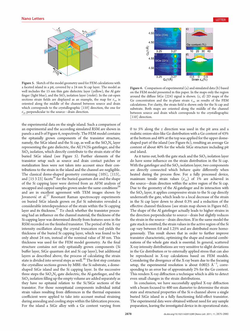
the experimental data on the single island. Such a comparison ofan experimental and the according simulated RSM are shown inpanels a and b of Figure 6, respectively. The FEMmodel containsthe epitaxially grown components of the transistor structure,namely, the SiGe island and the Si cap, as well as the SiOxNy layerrepresenting the gate dielectric, the Al(1%)Si-gatefinger, and theSiO2 isolation, which directly contribute to the strain state of theburied SiGe island (see Figure 5). Further elements of thetransistor setup such as source and drain contact patches ormetalization lines were not taken into account since their con-tributions to the strain in the island and the channel are negligible.The classical dome-shaped geometry containing {105}, {113},and {15 3 23} facets36 for the buried quantum dot and the shapeof the Si capping layer were derived from an AFM analysis ofuncapped and capped samples grown under the same conditions28
and are in excellent agreement with TEM images shown byJovanovi�c et al.27 Resonant Raman spectroscopy experimentson buried SiGe islands grown on flat Si substrates revealed aconsiderable interdependence of the strain within the Si cappinglayer and its thickness.37 To check whether the transistor proces-sing had an influence on the channel material, the thickness of theSi-capping layer was determined directly from features seen in theRSM recorded on the finished transistor. The period of the X-rayintensity oscillation along the crystal truncation rod yields thethickness of the buried Si capping layer, which was found to beonly about 24 nm, instead of the nominal value of 30 nm. Thisthickness was used for the FEM model geometry. As the finalstructure contains not only epitaxially grown components (Sibuffer layer, SiGe quantum dot and Si cap layer), but additionallayers as described above, the process of calculating the strainstate is divided into several steps as well.38 The first step containsthe crystalline sections grown by MBE: the Si substrate, a dome-shaped SiGe island and the Si capping layer. In the successivethree steps the SiOxNy-gate dielectric, the Al-gatefinger, and theSiO2 isolation filling up the empty volume are added separately asthey have no epitaxial relation to the Si/SiGe sections of thetransistor. For those nonepitaxial components individual initialstrain values resulting from differences in the thermal expansioncoefficient were applied to take into account mutual strainingduring annealing and cooling steps within the fabrication process.For the island a SiGe alloy with a Ge content varying from
0 to 5% along the z direction was used in the pit area and arealistic onion-skin-like Ge distribution with a Ge content of 43%at the bottom and 48% at the top was applied for the upper dome-shaped part of the island (see Figure 6c), resulting an average Gecontent of about 40% for the whole SiGe structure including pitand island.
As it turns out, both the gate stack and the SiO2 isolation layerdo have some influence on the strain distribution in the Si cap.With the gatefinger and the SiO2 isolation layer, two componentsare directly connected which behave quite differently whenheated during the process flow. For a fully processed device,maximum tensile strain values (εxx) of 1% are achieved inthe source�drain direction within the active region of the Si cap.Due to the geometry of the Al-gatefinger and its interaction withthe SiO2 layer, it applies compressive strain to the Si cap directlyunderneath the gate, which leads to a local decrease of the strainin the Si cap layer down to about 0.3% and a reduction of theeffective channel thickness (see strain map shown in Figure 6d).The shape of the Al gatefinger actually leads to higher strains inthe direction perpendicular to source�drain but slightly reducesthe strain in the source�drain direction. If in the same model thegate stack is omitted, the strain values in the active region of the Sicap vary between 0.8 and 1.25% and are distributed more homo-geneously. This result shows that in order to further improvetransistor characteristic, optimizing the shape and material combi-nations of the whole gate stack is essential. In general, scatteredX-ray intensity distributions are very sensitive to slight deviationsin the Ge distribution or to externally applied stress that can alsobe reproduced in X-ray calculations based on FEM models.Considering the divergence of the X-ray beam due to the focusingsetup, the experimental resolution is about 0.0025 Å�1, corre-sponding to an error bar of approximately 2% for the Ge content.This renders X-ray diffraction a technique which is able to detecteven small changes in the strain distributions.
In conclusion, we have successfully applied X-ray diffractionwith a beam focused to 400 nm diameter to determine the strainstate and structural properties of the Si n-channel above a singleburied SiGe island in a fully functioning field-effect transistor.The experimental data were obtained without need for any samplepreparation, leaving the investigated device in its operational state.
Figure 6. Comparison of experimental (a) and simulated data (b) basedon the FEM model presented in this paper. In the maps only the regionaround the diffuse SiGe (224) signal is shown. (c, d) 2D maps of theGe concentration and the in-plane strain εxx as results of the FEMcalculations. For clarity, the strain field is shown only for the Si cap andsubstrate. Both maps are oriented along the middle of the channelbetween source and drain which corresponds to the crystallographic[110] direction.
Figure 5. Sketch of the model geometry used for FEM calculations witha faceted island in a pit, covered by a 24 nm Si cap layer. The model aswell includes the 15 nm thin gate dielectric layer (yellow), the Al gatefinger (light blue), and the SiO2 isolation layer (violet). In the cut-opensections strain fields are displayed as an example, the map for εxx isoriented along the middle of the channel between source and drainwhich corresponds to the crystallographic [110] direction, the one forεyy perpendicular to the source�drain direction.

2879 dx.doi.org/10.1021/nl2013289 |Nano Lett. 2011, 11, 2875–2880
Nano Letters LETTER
Tensile strain values up to 1% along the source�drain directionwere determined in the Si channel using reciprocal space mappingand finite element calculations. With the method presented in thispaper valuable insight is gained into the interactions of nanostruc-tures with additional components necessary for operationaldevices. This information can be used to optimize future devicegenerations. The presented work opens the road for further, evenmore advanced studies like monitoring devices during operationor the investigation of processes in devices during breakdown atelevated current levels or temperatures. Even the modificationsduring particular process steps, especially high-temperature ones,can be assessed “online”. Such studies will become even morepowerful when using advanced analysis schemes such as model-free phase retrieval approaches by exploiting the coherenceproperties of nanofocused X-ray beams.39
’AUTHOR INFORMATION
Corresponding Author*E-mail: [email protected].
Present Addresses#IFW Dresden, Helmholtzstrasse 20, 01069 Dresden, Germany.rHASYLAB at DESY, Notkestrasse 85, 22607 Hamburg,Germany.OFER, University of Zagreb, Unska 3, 10000 Zagreb, Croatia.[1)CCS, State University of Campinas, Rua Jo~ao PandiaCal�ogeras, 90, Caixa Postal 6061, CEP 13083-979, Campinas,S~ao Paulo, Brazil.
’ACKNOWLEDGMENT
The authors thank the entire crew at ID01 for their excellentsupport, Martin Arndt for SEM sample preparation, and PhilippeCaroff for fruitful discussions and help with the manuscript. Thiswork was supported by the EC d-DOTFET project (012150-2)and the FWF Vienna (SFB025 IR-On).
’REFERENCES
(1) Coleman, J. J. Strained-layer InGaAs quantum-well heterostruc-ture lasers. IEEE J. Sel. Top. Quantum Electron. 2000, 6, 1008–1013.(2) Sun, Y.; Thompson, S. E.; Nishida, T. Physics of strain effects in
semiconductors and metal-oxide-semiconductor field-effect transistors.J. Appl. Phys. 2007, 101, 104503.(3) Ieong, M.; Doris, B.; Kedzierski, J.; Rim, K.; Yang, M. Silicon
Device Scaling to the Sub-10-nmRegime. Science 2004, 306, 2057–2060.(4) Thompson, S. E.; et al. A 90-nm logic technology featuring
strained-silicon. IEEE Trans. Electron Devices 2004, 51, 1790–1797.(5) Dhar, S.; Kosina, H.; Palankovski, V.; Ungersboeck, S. E.;
Selberherr, S. Electron mobility model-for strained-Si devices. IEEETransactions On Electron Devices 2005, 52, 527–533.(6) Donaton, R. A.; Chidambarrao, D.; Johnson, J.; Chang, P.; Liu,
Y.; Henson, W. K.; Holt, J.; Li, X.; Li, J.; Domenicucci, A.; Madan, A.;Rim, K.; Wann, C. Design and fabrication of MOSFETs with a reverseembedded SiGe (Rev. e-SiGe) structure. Tech. Dig.—Int. ElectronDevices Meet. 2006, 1–4.(7) Ang, K. W.; Tung, C. H.; Balasubramanian, N.; Samudra, G. S.;
Yeo, Y. C. Strained n-channel transistors with silicon source and drainregions and embedded silicon/germanium as strain-transfer structure.IEEE Electron. Device Lett. 2007, 28, 609–612.(8) Ang, K. W.; Lin, J.; Tung, C. H.; Balasubramanian, N.; Samudra,
G. S.; Yeo, Y. C. Strained n-MOSFET with embedded Source/Drainstressors and strain-transfer structure (STS) for enhanced transistorperformance. IEEE Trans. Electron Devices 2008, 55, 850–857.
(9) Packan, P.; et al. High performance 32 nm logic technologyfeaturing 2nd generation high-k þ metal gate transistors. Tech. Dig.—Int. Electron Devices Meet. (IEDM 2009) 2009, 4.
(10) Hytch, M.; Houdellier, F.; Hue, F.; Snoeck, E. Nanoscaleholographic interferometry for strain measurements in electronic de-vices. Nature 2008, 453, 1086–U5.
(11) Hue, F.; Hytch, M.; Bender, H.; Houdellier, F.; Claverie, A.Direct mapping of strain in a strained silicon transistor by high-resolutionelectron microscopy. Phys. Rev. Lett. 2008, 100, 156602.
(12) Snigireva, I.; Snigirev, A. X-Ray microanalytical techniquesbased on synchrotron radiation. J. Environ. Monit. 2006, 8, 33–42.
(13) The intrinsic strain resolution is reduced due to beam conver-gence when X-rays are focused but is still in the range of 10�4 to 10�3,depending on details of focusing and experimental setup.
(14) Robinson, I.; Harder, R. Coherent X-ray diffraction imaging ofstrain at the nanoscale. Nat. Mater. 2009, 8, 291–298.
(15) Stangl, J.; Holy, V.; Bauer, G. Structural properties of self-organized semiconductor nanostructures. Rev. Mod. Phys. 2004, 76,725–783.
(16) Mocuta, C.; Stangl, J.; Mundboth, K.;Metzger, T. H.; Bauer, G.;Vartanyants, I. A.; Schmidbauer, M.; Boeck, T. Beyond the ensembleaverage: X-ray microdiffraction analysis of single SiGe islands. Phys. Rev.B 2008, 77, 245425.
(17) Hanke, M.; Dubslaff, M.; Schmidbauer, M.; Boeck, T.; Schoder,S.; Burghammer, M.; Riekel, C.; Patommel, J.; Schroer, C. G. Scanningx-ray diffraction with 200 nm spatial resolution. Appl. Phys. Lett. 2008,92, 193109.
(18) Biermanns, A.; Davydok, A.; Paetzelt, H.; Diaz, A.; Gottschalch,V.; Metzger, T. H.; Pietsch, U. Individual GaAs nanorods imaged bycoherent X-ray diffraction. J. Synchrotron Radiat. 2009, 16, 796–802.
(19) Scheler, T.; Rodrigues, M.; Cornelius, T. W.; Mocuta, C.;Malachias, A.; Magalhaes-Paniago, R.; Comin, F.; Chevrier, J.; Metzger,T. H. Probing the elastic properties of individual nanostructures bycombining in situ atomic force microscopy and micro-x-ray diffraction.Appl. Phys. Lett. 2009, 94, 023109.
(20) Rodrigues, M. S.; Cornelius, T. W.; Scheler, T.; Mocuta, C.;Malachias, A.; Magalhaes-Paniago, R.; Dhez, O.; Comin, F.; Metzger,T. H.; Chevrier, J. In situ observation of the elastic deformation of asingle epitaxial SiGe crystal by combining atomic force microscopy andmicro x-ray diffraction. J. Appl. Phys. 2009, 106, 103525.
(21) Newton, M. N.; Leake, S. J.; Harder, R.; Robinson, I. K. Three-dimensional imaging of strain in a single ZnO nanorod (vol 9, pg 120,2010). Nat. Mater. 2010, 9, 279–279.
(22) Dubslaff, M.; Hanke, M.; Schoder, S.; Burghammer, M.; Boeck,T.; Patommel, J. X-ray nanodiffraction at individual SiGe/Si(001) dotmolecules and its numerical description based on kinematical scatteringtheory. Appl. Phys. Lett. 2010, 96, 133107.
(23) Diaz, A.; Mocuta, C.; Stangl, J.; Vila-Comamala, J.; David, C.;Metzger, T. H.; Bauer, G. Spatially resolved strain within a single SiGeisland investigated by X-ray scanning microdiffraction. Phys. Status SolidiA 2009, 206, 1829–1832.
(24) Mino, L.; Gianolio, D.; Agostini, G.; Piovano, A.; Truccato, M.;Agostino, A.; Cagliero, S.; Martinez-Criado, G.; Codato, S.; Lamberti, C.Structural Characterization of Multi-Quantum Wells in Electroabsorp-tion-Modulated Lasers by using Synchrotron Radiation Micrometer-Beams. Adv. Mater. 2010, 22, 2050
(25) Schmidt, O. G.; Eberl, K. Self-Assembled Ge/Si Dots for FasterField-Effect Transistors. IEEE Trans. Electron Devices 2001, 48, 1175.
(26) Fregonese, S.; Zhuang, Y.; Burghartz, J. N.Modeling of strainedCMOS on disposable SiGe dots: Shape impacts on electrical/thermalcharacteristics. Solid-State Electron. 2008, 52, 919–925.
(27) Jovanovi�c, V.; Biasotto, C.; Nanver, L.K.;Moers, J.; Grutzmacher,D.; Gerharz, J.; Mussler, G.; van der Cingel, J.; Zhang, J. J.; Bauer, G.;Schmidt, O. G.; Miglio, L. n-Channel MOSFETs Fabricated on SiGeDots for Strain-Enhanced Mobility. IEEE Electron Device Lett. 2010,31, 1083–1085.
(28) Zhang, J. J.; Stoffel, M.; Rastelli, A.; Schmidt, O. G.; Jovanovic,V.; Nanver, L. K.; Bauer, G. SiGe growth on patterned Si(001)

2880 dx.doi.org/10.1021/nl2013289 |Nano Lett. 2011, 11, 2875–2880
Nano Letters LETTER
substrates: Surface evolution and evidence of modified island coarsen-ing. Appl. Phys. Lett. 2007, 91, 173115.(29) Hesse, A.; Stangl, J.; Holy, V.; Roch, T.; Bauer, G.; Schmidt,
O. G.; Denker, U.; Struth, B. Effect of overgrowth on shape, composi-tion, and strain of SiGe islands on Si(001). Phys. Rev. B: Condens. MatterMater. Phys. 2002, 66 (8), 85321.(30) Stangl, J.; Hesse, A.; Holy, V.; Zhong, Z.; Bauer, G.; Denker, U.;
Schmidt, O. G. Effect of overgrowth temperature on shape, strain, andcomposition of buried Ge islands deduced from x-ray diffraction. Appl.Phys. Lett. 2003, 82, 2251–2253.(31) Stoffel, M.; Rastelli, A.; Schmidt, O. G. Surface evolution and
three-dimensional shape changes of SiGe/Si(001) islands during cap-ping at various temperatures. Surf. Sci. 2007, 601, 3052–3059.(32) David, C.; Bruder, J.; Rohbeck, T.; Grunzweig, C.; Kottler, C.;
Diaz, A.; Bunk, O.; Pfeiffer, F. Fabrication of diffraction gratings for hardX-ray phase contrast imaging. Microelectron. Eng. 2007, 84, 1172–1177.(33) Stangl, J.; Mocuta, C.; Diaz, A.; Metzger, T. H.; Bauer, G. X-Ray
Diffraction as a Local Probe Tool. Chem. Phys. Chem. 2009, 10,2923–2930.(34) www.comsol.com, Comsol Multiphysics Package.(35) Pietsch, U.; Holy, V.; Baumbach, T. High-resolution X-ray scatter-
ing from thin films and multilayers, 2nd ed.; Springer: Berlin, 2004; p 408.(36) Ross, F. M.; Tromp, R. M.; Reuter, M. C. Transition states
between pyramids and domes during Ge/Si island growth. Science 1999,286, 1931–1934.(37) Bonera, E.; Pezzoli, F.; Picco, A.; Vastola, G.; Stoffel, M.; Grilli,
E.; Guzzi, M.; Rastelli, A.; Schmidt, O. G.; Miglio, L. Strain in a singleultrathin silicon layer on top of SiGe islands: Raman spectroscopy andsimulations. Phys. Rev. B 2009, 79, 075321.(38) Hrauda, N.; Zhang, J. J.; Stangl, J.; Rehman-Khan, A.; Bauer, G.;
Stoffel, M.; Schmidt, O. G.; Jovanovic, V.; Nanver, L. K. X-rayinvestigation of buried SiGe islands for devices with strain-enhancedmobility. J. Vac. Sci. Technol., B 2009, 27, 912–918.(39) Diaz, A.; Chamard, V.; Mocuta, C.; Magalhaes-Paniago, R.;
Stangl, J.; Carbone, D.; Metzger, T. H.; Bauer, G. Imaging the displace-ment field within epitaxial nanostructures by coherent diffraction: afeasibility study. New J. Phys. 2010, 12, 035006.