
Inequalities and many phase transitions in ferromagnetic systems
1
Valence-band structure of
ferromagnetic semiconductor (InGaMn)As
Shinobu Ohya
*, Iriya Muneta, Yufei Xin, Kenta Takata, and Masaaki Tanaka
†
Department of Electrical Engineering and Information Systems, The University of Tokyo,
7-3-1 Hongo, Bunkyo-ku, Tokyo, Japan 113-8656
Abstract
To clarify the whole picture of the valence-band structures of prototype ferromagnetic
semiconductors (III,Mn)As (III: In and Ga), we perform systematic experiments of the
resonant tunneling spectroscopy on [(In0.53Ga0.47)1-xMnx]As (x=0.06-0.15) and
In0.87Mn0.13As grown on AlAs/ In0.53Ga0.47As:Be/ p+InP(001). We show that the
valence band of [(In0.53Ga0.47)1-xMnx]As almost remains unchanged from that of the host
semiconductor (In0.53Ga0.47)As, that the Fermi level exists in the band gap, and that the
p-d exchange splitting in the valence band is negligibly small in (InGaMn)As. In the
In0.87Mn0.13As sample, although the resonant peaks are very weak due to the large strain
induced by the lattice mismatch between InP and InMnAs, our results also indicate that
the Fermi level exists in the band gap and that the p-d exchange splitting in the valence
band is negligibly small. These results are quite similar to those of GaMnAs obtained
by the same method, meaning that there are no holes in the valence band, and that the
impurity-band holes dominate the transport and magnetism both in the
[(In0.53Ga0.47)1-xMnx]As and In0.87Mn0.13As films. This band picture of (III,Mn)As is
remarkably different from that of II-VI-based diluted magnetic semiconductors.
PACS Number(s): 85.75.Mm, 72.25.Dc, 73.40.Gk, 75.50.Pp

2
I. INTRODUCTION
Understanding the physics of ferromagnetic semiconductors (FMS) InMnAs1,2
and
GaMnAs3,4
is one of the central issues in solid state physics, and it is vitally important
for developing spin-related functionalities in semiconductors. A lot of unique features
found in these material systems are promising for novel semiconductor devices utilizing
spin-degrees of freedom.5-14
However, basic understanding of FMSs, especially on the
band structure and the origin of ferromagnetism, is still under debate. Generally, it has
been believed that the ferromagnetism in InMnAs and GaMnAs is induced by the
spin-polarized valence-band (VB) holes interacting with the localized Mn 3d
spin-polarized electrons. It has been assumed that the Fermi level exists in VB which
is largely spin-split by the p-d exchange interaction and that the VB is merged with the
Mn-induced impurity band (IB) as shown in Fig 1 (a).15-18
This VB conduction picture
could explain wide variety of phenomena such as the Curie temperature (TC), magnetic
anisotropy, and so on.19-23
Recently, however, contradictory results were obtained in
many experiments on GaMnAs such as the hot-electron photoluminescence, infrared
absorption, and magnetic circular dichroism.24-33
These experiments strongly suggest
that the Fermi level exists in IB in the band gap of GaMnAs, as shown in Fig. 1 (b). In
this case, the ferromagnetism is stabilized by hopping of the IB holes, which is quite
different from the VB conduction picture mentioned above.
There are several problems specific to GaMnAs which prevents a clear
determination of the energy-band structure and the Fermi-level position; small energy
distance between VB and IB (less than ~100 meV), broadening of the optical spectra
due to the small dispersion of IB, and the random distribution of the Mn atoms
responsible for the inhomogeneous depletion depth at the surface. These features
made the understanding of this material difficult even by the angle-resolved
photoemission spectroscopy34
and scanning tunneling microscopy,35
which are
sometimes very powerful for other material systems.
The resonant tunneling spectroscopy is a very useful method to clarify the VB
structure of (III,Mn)As (III=In and Ga). As explained later, the advantage of this
method is that we can detect energy bands only with the same wave-function symmetry
as that of the p-wave functions of the VB holes. Also, it is sensitive to the effective
mass of the energy bands. Thus, we can distinguish VB from IB. Furthermore, by
carefully analyzing the quantum-well (QW) thickness dependence of the resonant levels,
we can avoid the unwanted effect induced at the surface mentioned above. Previously,
using this technique, we successfully obtained the VB structure of GaMnAs.36,37
We
found that the Fermi level exists in the band gap, that the p-d exchange split in the VB is
negligibly small [3-5 meV for the light hole (LH) band], and that the almost unaffected
VB of GaAs is still remaining in GaMnAs. These findings indicate that the VB holes
do not play any crucial role in giving rise to the ferromagnetism in GaMnAs.
3
From the viewpoint of both physics and applications, it is quite important to
investigate the difference of the band structures of FMSs with different host materials.
Such studies will give us a guideline on how to design heterostructures to accomplish
intended functionalities. Also, it is useful to understand the whole band picture of
FMSs. Especially, it is quite important to understand the (III,Mn)As (III=In and Ga)
systems, which are the most prototypical FMSs. By increasing the In content in
InGaAs, the binding energy of Mn is decreased from ~110 (GaAs) to ~30 meV (InAs).38
This difference of the binding energies may affect the way of the IB formation or the
VB deformation by Mn doping. There have been conflicting reports about the
understanding of the VB structure of InMnAs. For example, the cyclotron resonance
experiments suggest the VB conduction in InMnAs.39,40
On the other hand, infrared
optical absorption measurements on InMnAs show the double-exchange-like
component, suggesting the IB conduction.41 Therefore, further systematic experiments
are needed to investigate the VB structures of (InGaMn)As42-44
and InMnAs.
II. EXPERIMENTAL
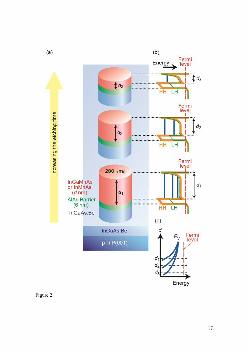
Figure 2(a) shows the schematic device structures investigated in this study; mesa
diodes with 200 µm in diameter composed of [(In0.53Ga0.47)1-xMnx]As or In0.87Mn0.13As
(d nm) / AlAs (6 nm)/ In0.53Ga0.47As:Be (100 nm, Be concentration: 1×10¹⁸
cm-3
) grown
on p+InP(001). The Mn composition x in [(In0.53Ga0.47)1-xMnx]As was varied from 0.06
to 0.15. Table I shows the details of the samples used in this study. The TC values of
the (InGaMn)As films (sample A-F) were estimated from the Arrott plot using the data
of the magnetic-field dependence of magnetic circular dichroism measured for these
samples before etching. The TC value of the InMnAs sample (sample G), which has a
strong in-plane magnetic anisotropy due to the strong compressive strain induced by the
lattice mismatch (~3%) between InMnAs and InP, was determined by the planar Hall
effect measurements. Some samples were annealed after the growth with the
conditions shown in Table I. The (InGaMn)As (or InMnAs) thickness d was precisely
controlled by changing the etching time from mesa to mesa.37
Figure 2(b) shows the
schematic VB profiles of these diode devices shown in (a). The thick orange solid
curves, thin green solid curves, red dash-dotted lines, and blue lines indicate the
heavy-hole (HH) band, light-hole (LH) band, Fermi level, and resonant levels,
respectively. Here, the exchange splitting is neglected for simplicity. Due to the
large lattice mismatch (~3.6%) between AlAs and InP, the HH and LH bands are largely
split in the AlAs layer. We note that this strain also generates the large band offset
between (InGaMn)As (or InMnAs) and AlAs, which results in the effective
confinement of the VB holes in the (InGaMn)As (or InMnAs) QW. Since
(InGaMn)As has a little larger lattice constant than that of InGaAs due to the Mn doping,
the HH and LH bands are slightly split in the (InGaMn)As layer. This splitting

4
between HH and LH bands is larger in InMnAs due to the larger strain. The resonant
levels are formed by the VB holes confined by the AlAs barrier and the surface
Schottky barrier with the estimated thickness of ~1 nm (depending on the hole
concentration) induced by Fermi-level pinning at the surface. These resonant levels
can be detected only when holes are injected from the bottom p-type InGaAs:Be layer
because the injected holes have small in-plane wave vectors k|| due to the low hole
concentration (1×10¹⁸
cm-3
) of the InGaAs:Be electrode.11
As shown in Fig. 2(c), the
resonant tunneling energies expressed by the blue curves converge to the VB top energy
EV of the bulk (InGaMn)As (or InMnAs) with increasing d. Since the Fermi level
corresponds to the zero bias condition, the Fermi level position can be determined by
measuring the d dependence of the resonant levels. All the measurements were done
in the cryostat cooled at 3.4 - 3.5 K. Direct current was used to measure the I-V
characteristics, and d2I/dV
2 values were numerically obtained from the I-V data. The
bias polarity is defined by the voltage of the top (InGaMn)As (or InMnAs) electrode
with respect to the substrate.
III. RESULTS
In Fig. 3, we show the experimental data of the (InGaMn)As and InMnAs resonant
tunneling diodes investigated here. The black solid curves in Fig. 3(a)-(f) correspond
to the d2I/dV
2-V curves obtained for various d at 3.5 K in sample A-F (InGaMnAs
samples), respectively. [In (a), (e), and (f), only a part of the d region is shown due to
the low yield of our current device fabrication process.] Oscillations are clearly seen
in almost all the curves in Fig. 3(a)-(f). The oscillation-peak bias voltages get smaller,
and the period of the oscillation becomes short with increasing d except for the large d
region in (a) where a very sharp increase in resistance-area (RA) occurs in the large d
region with d>16 nm due to the interstitial Mn diffusion to the surface during the
low-temperature annealing. [For details, see Fig. 5(a).] As mentioned in the
Discussion section, these phenomena observed in Fig. 3(a)-(f) are the quite typical
QW-thickness dependence of the resonant tunneling effect. This is the first
observation of the resonant tunneling in (InGaMn)As. Here, HHn and LHn (n:
1,2,3…) represent resonant tunneling through the nth level of the HH and LH bands in
the (InGaMn)As QW, respectively. They are assigned by the theoretical analyses
mentioned below. In Fig. 3(b), (c), and (d), we see that the resonant levels are
converged at a certain bias voltage corresponding to EV with increasing d. Also, in Fig.
3(a), (e), and (f), we can see similar tendencies except for the large d region with d> 16
nm with the sharp RA increase in (a). Considering that Fermi level corresponds to the
zero bias condition, we conclude that Fermi level exists in the band gap in all the
samples. We see a specific feature that the converged bias position becomes farther
away from the origin with increasing the Mn composition x [from Fig. 3(a) to (d)],

5
which means that the Fermi level becomes farther away from EV with increasing x.
If there were large p-d exchange splitting, the resonant levels would be split and the
splitting energy would increase with increasing TC or x. However, such behavior is not
observed in Fig. 3(a)-(f). Therefore, the p-d exchange splitting in VB is negligibly
small. This result is almost the same as those obtained in GaMnAs.37
In a resonant
tunneling diode with a paramagnetic ZnMnSe QW, clear spin-splitting of the resonant
level was observed, and this splitting energy increased with a magnetic field.45
Our
results mean that (III,Mn)As has a quite different band picture from that of II-VI diluted
magnetic semiconductors.46
The black solid curves in Fig. 3(g) correspond to the d2I/dV
2-V curves in the small
bias region (V from -0.1 to 0 V) for various d at 3.5 K in sample D. Three peaks,
which do not strongly depend on d, are observed at roughly around -0.015, -0.045, and
-0.06 V. We note that the similar peaks were observed in the GaMnAs diode devices
at around -0.02, -0.05, and -0.065 V. (See the d region from 6 to 16 nm of Fig. 6c in
Ref. 37.) Since these peaks were enhanced with increasing x or TC, it is expected that
these peaks are related to the Mn induced states or a part of the Mn induced IB. These
peak positions observed in (InGaMn)As are almost the same as those in (GaMn)As,
which means that there is a quite similar electronic structure in the band gap both in
GaMnAs and (InGaMn)As. The intensity of these peaks in Fig. 3(g) is much smaller
than those of the resonant levels of VB shown in Fig. 3(d), which probably means that
these states are mainly composed of the Mn d electrons and that they may have a weak
component of the p wave-function.
The black solid curves in Fig. 3(h) correspond to the d2I/dV
2-V curves obtained for
various d at 3.4 K in sample G (InMnAs). When d is less than 6 nm, we see two
resonant peaks [HH1 and (HH2 or LH1)] which get close to a certain negative bias
voltage with increasing d. Therefore, the Fermi level exists in the band gap in
In0.87Mn0.13As. We do not see any spin-splitting peaks, which would move parallel to
the LH peak with increasing d if any.36
This means that the p-d exchange splitting is
negligibly small also in In0.87Mn0.13As. We see that these peaks disappear when d is
larger than 6 nm, which is probably due to the lattice relaxation of the InMnAs layer
due to the strong strain. We investigated other InMnAs resonant tunneling diodes with
lower Mn concentrations (not shown), but resonant peaks were not clearly observed in
them. We think that it is probably due to the stronger strain effect in these InMnAs
layers. For more systematic study on VB of InMnAs, it is necessary to use
higher-quality strain-free heterostructures.
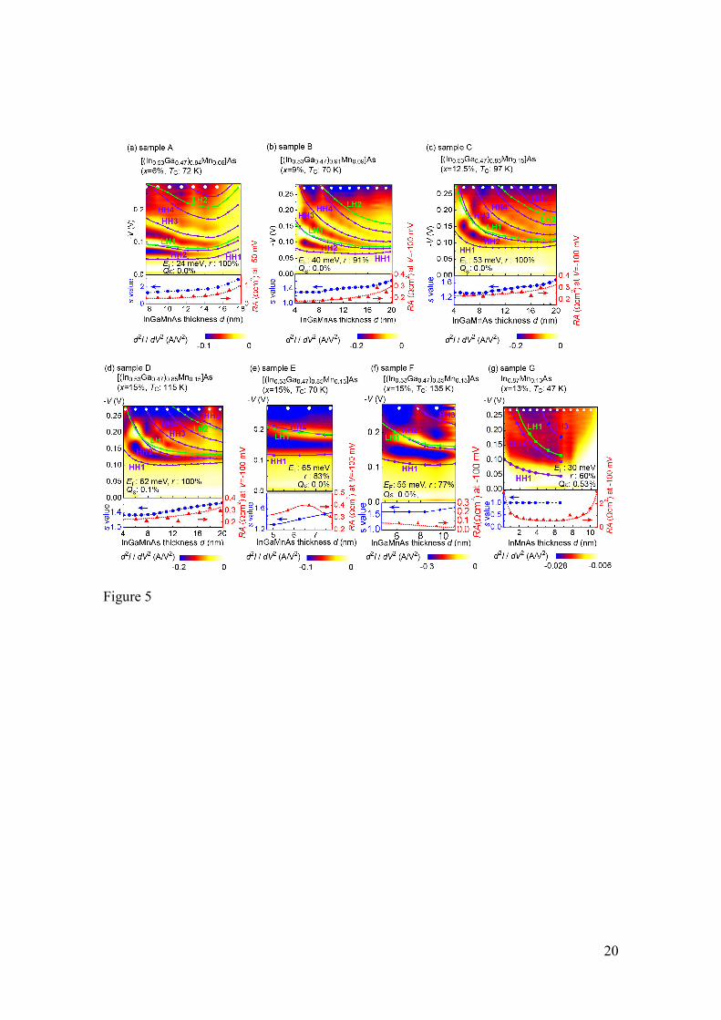
IV. COMPARISON WITH THEORETICAL CALCULATIONS
With a multiband transfer matrix technique developed in ref. 47 with the
Luttinger-Kohn 6×6 k·p Hamiltonian and the strain Hamiltonian,16
we calculated the

6
quantum levels in these heterostructures. The Luttinger parameters γ1, γ2, and γ3 of
(InGaMn)As (or InMnAs) assumed in our study are 13.4 (20.0), 5.3 (8.5), and 6.0 (9.2),
respectively.48
The shear deformation potential b of (InGaMn)As (or InMnAs) was
assumed to be the same as that of InGaAs (InAs); b=-1.7 (-1.8).48
To reproduce the
experimental data of the resonant peak bias voltages VR, we assumed the VB diagrams
of (InGaMn)As and InMnAs resonant tunneling diodes shown in Fig. 4(a) and (b),
respectively. Here, the green (thin black) and orange (thick gray) lines express the LH
and HH bands, respectively. Since the p-d exchange split was negligibly small, we
neglected the p-d exchange interaction in our calculations. We divided the surface
Schottky barrier region into three equally spaced regions and assumed that the band is
flat in each region. EF is defined as the energy difference between the Fermi level and
the HH band at the Γ point in (InGaMn)As (or InMnAs). We used EF and the
deformation anisotropic term49
Qε as fitting parameters. These parameters were
determined so that the relationship between the calculated resonant tunneling energy ER
(relative to the Fermi level) and measured VR becomes linear, and that VR-ER goes
through the origin; VR=sER, where s is a fitting parameter corresponding to the slope of
VR-ER.19,36,49,50
The d values for the calculated data were slightly corrected so that the
experimental data were reproduced well, where r corresponds to the correction ratio of
the etching rate estimated by this procedure to that estimated experimentally.
The color-coded d2I/dV
2 intensities of samples A-G are shown in the top figures of
Fig. 5(a)-(g), respectively. Here, these color-coded intensities are extrapolated from
the measured data at the d values corresponding to the white dots shown at the top of
these figures. The calculated VR values of the HH and LH resonant levels as a function
of d are expressed by the connected violet and green dots, respectively. In all the
samples, the calculated HH and LH resonant levels show good agreement with the
measured data. In the bottom figures of Fig. 5(a)-(g), blue and red dots express the s
value used in the fitting and RA, respectively. The RA value changes as a function of d,
which can be attributed to the diffusion of the interstitial Mn atoms to the surface.
Therefore, we changed s gradually with increasing d. In most cases, we see a similar
behavior between the RA-d and s-d curves, but their shapes are not perfectly the same.
In our experiments, there is also a tunneling sequence where the holes injected in the
VB quantum levels lose their energy and drop to IB by scattering in the (InGaMn)As (or
InMnAs) QW. Therefore, the observed RA values include the contribution of the
conduction of the IB holes, whose details have not been clarified. On the other hand, s
is determined just by the energy positions of the VB resonant levels. These probably
cause the different behavior between the RA-d and s-d curves. In the cases of
(InGaMn)As devices (sample A-F), the resonant peaks observed in all of our samples
are well reproduced by our model, which supports our conclusion that the resonant
levels are formed by the quantization of the VB holes in (InGaMn)As layers. In the
case of InMnAs (sample G), although the calculation can reproduce the experimental
7
resonant peaks, the obtained r value is much less than that in other samples and the
higher resonant levels (LH1 and HH3) are not clearly observed in the experiments.
The reason of these results is not clear, but it is probably due to the degradation of the
crystallinity of InMnAs induced by the strong strain. In fact, the obtained Qε (~0.53%)
was much less than the expected value (~6.53%), which implies that the lattice of the
InMnAs layer is almost relaxed. For more systematic and precise analysis, strain-free
heterostructures are necessary for InMnAs, although it is very difficult to achieve them
using the typical III-V materials.
In Fig. 6(a), the triangular red, circular blue, and rectangular green points show the
EF values of Ga1-xMnxAs,37
[(In0.53Ga0.47)1-xMnx]As, and In0.87Mn0.13As obtained in this
study, respectively, where the values next to the data points are the TC values. The
characters in the parentheses are the sample names. We see that EF decreases with
increasing the In content, which can be attributed to the reduction of the binding energy
of the Mn states with increasing the In content. In both GaMnAs and (InGaMn)As, EF
decreases with increasing TC when x is fixed, which can be explained by the increase of
the IB hole concentration as shown in Fig. 6(b). Also, EF increases with increasing x,
which can be qualitatively explained by the IB broadening as shown in Fig. 6(c).
Similar behavior was theoretically expected in Ref. 51 and 52. These results are
consistent with the IB conduction picture shown in Fig. 1(b). For more detailed
discussions, we need to know further information of the precise IB characteristics which
we cannot obtain by our method due to the orbital selectivity of the resonant tunneling
spectroscopy.
V. DISCUSSION
Here, we show that one can rule out the possibility that these oscillations observed
in Fig. 3(a)-(f) are induced by the quantized two-dimensional hole-gas states between
the AlAs and InGaAs:Be.53,54
We see that the observed results in Fig. 3(a)-(f) and (h)
are typical features of the QW thickness dependence of resonant tunneling. For
example, these oscillations clearly tend to be weakened with increasing d. This
behavior can be understood by weakening of the quantization. Other essential feature
is that the VB gradually branches out to sub-band levels with decreasing d. For
instance, in Fig. 3(b) and (c), HH1 and LH1 (or HH2) levels are nearly merged at
around 14-16 nm. These features are quite different from those of the quantized
two-dimensional hole-gas states at AlAs/InGaAs:Be, if any. Also, if these oscillations
were induced by quantized two-dimensional hole-gas states, the oscillation peak bias
voltage would be proportional to RA as mentioned in Ref. 53. However, as can be seen
in Fig. 5(a)-(d), some oscillation peak voltages become smaller even when RA increases
with increasing d. Furthermore, as shown in our previous paper,54
we did not see any
clear oscillations induced by resonant tunneling in the d2I/dV
2-V curves of the tunnel
8
device composed of GaMnAs/ AlAs (5nm)/ GaAs:Be (1×10¹⁸
cm-3
) when the surface
GaMnAs thickness was 30 nm, where the quantization of the holes in GaMnAs is very
weak. If the d2I/dV
2 oscillations observed in our study were induced by the quantized
two-dimensional hole-gas states, the oscillation would be observed even when the
GaMnAs thickness is 30 nm. This result means that it is impossible to detect the
quantized two-dimensional hole-gas states in our experimental setup when the Be
doping level is 1×10¹⁸
cm-3
.
The quantized two-dimensional hole-gas states formed at the AlAs/GaAs:Be
interface have been observed when the Be concentration is extremely low (for example,
6×10¹⁴
cm-3
in Ref. 55 ). With increasing the Be concentration, however, the
quantization of these states becomes weak. Also, as shown in Ref. 53, the energy
separation between these states is only several meV when the Be concentration is
1×10¹⁸
cm-3
. These are the reasons why we did not detect any quantized
two-dimensional hole-gas states in our experiments. Also, we do not see any clear
signals related to these states at AlAs/(GaAs:Be or a thin GaAs spacer) in the studies of
the similar p-type GaAs-based resonant tunneling structures with the Be concentration
of as high as ~1018
cm-3
.19,50,56
Therefore, we conclude that these oscillations in Fig.
3(a)-(f) and (h) are attributed to the resonant tunneling in the (InGaMn)As (or InMnAs)
QW layers.
VI. SUMMARY
We performed the resonant tunneling spectroscopy on a series of
[(In0.53Ga0.47)1-xMnx]As films with x from 6 to 15% and with TC from 70 to 135 K, and
on the In0.87Mn0.13As film with TC of 47 K. Resonant tunneling was clearly observed
in the (InGaMn)As and InMnAs films for the first time. In the cases of the
(InGaMn)As films, by analyzing these resonant peak bias positions, we found that the
almost unaffected VB of the host semiconductor InGaAs is still remaining in
(InGaMn)As. In all the [(In0.53Ga0.47)1-xMnx]As and In0.87Mn0.13As films investigated
in this study, the p-d exchange splitting was not observed, which means that the p-d
exchange splitting is negligibly small in VB. (probably several meV expected from our
previous studies.11,36
) The Fermi level exists in the band gap in all the
[(In0.53Ga0.47)1-xMnx]As and In0.87Mn0.13As samples. We found that EF decreases with
increasing the In content, which can be attributed to the reduction of the binding energy
of the Mn atoms at high In content. EF decreases with increasing TC when x is fixed.
Also, EF increases with increasing x. These results are consistent with the IB
conduction picture. Our results strongly suggest that these are common features in
(III,Mn)As (III=In and Ga). Our findings mean that the holes in VB are hardly related
to the ferromagnetism, but the IB holes dominate the transport and magnetism of
(III,Mn)As.

9
ACKNOWLEDGMENTS
This work was partly supported by Grants-in-Aids for Scientific Research, particularly
Grant-in-Aid for Specially Promoted Research, the Special Coordination Program for
Promoting Science and Technology, FIRST Program of the JSPS, PRESTO of the JST,
and Asahi Glass Foundation.

10
References
1 H. Munekata, H. Ohno, S. von Molnar, Armin Segmüller, L. L. Chang, and L. Esaki,
Phys. Rev. Lett. 63, 1849 (1989). 2 H. Ohno, H. Munekata, T. Penney, S. von Molnár, and L. L. Chang, Phys. Rev. Lett.
68, 2664 (1992). 3 H. Ohno, J. Magn. Magn. Mater. 200, 110 (1999); H. Ohno, A. Shen, F. Matsukura, A.
Oiwa, A. Endo, S. Katsumoto, and Y. Iye, Appl. Phys. Lett. 69, 363 (1996). 4 M. Tanaka, J. Vac. Sci. Technol. B 16, 2267 (1998); T. Hayashi, M. Tanaka, T.
Nishinaga, H. Shimada, H. Tsuchiya, Y. Otuka, J. Cryst. Growth 175–176, 1063
(1997). 5 H. Ohno, D. Chiba, F. Matsukura, T. Omiya, E. Abe, T. Dietl1, Y. Ohno & K. Ohtani,
Nature 408, 944 (2000). 6 M. Tanaka and Y. Higo, Phys. Rev. Lett. 87, 026602 (2001).
7 C. Rüster, C. Gould, T. Jungwirth, J. Sinova, G. M. Schott, R. Giraud, K. Brunner, G.
Schmidt, and L. W. Molenkamp, Phys. Rev. Lett. 94, 027203 (2005). 8 M. Yamanouchi, D. Chiba, F. Matsukura, T. Dietl, and H. Ohno, Phys. Rev. Lett. 96,
096601 (2006) 9 D. Chiba, M. Yamanouchi, F. Matsukura, and H. Ohno, Science 301, 943 (2003).
10 Y. Hashimoto, S. Kobayashi, and H. Munekata, Phys. Rev. Lett. 100, 067202 (2008).
11 S. Ohya, P. N. Hai, Y. Mizuno, and M. Tanaka, Phys. Rev. B 75, 155328 (2007).
12 D. Chiba, M. Sawicki, Y. Nishitani, Y. Nakatani, F. Matsukura, and H. Ohno, Nature
455, 515 (2008). 13
A. Chernyshov, M. Overby, X. Liu, J. K. Furdyna, Y. Lyanda-Geller, and L. P.
Rokhinson, Nat. Phys. 5, 656 (2009). 14
S. Ohya, I. Muneta, and M. Tanaka, Appl. Phys. Lett. 96, 052505 (2010). 15
T. Dietl, H. Ohno, F. Matsukura, J. Cibert, and D. Ferrand, Science 287, 1019 (2000). 16
T. Dietl, H. Ohno, and F. Matsukura, Phys. Rev. B 63, 195205 (2001). 17
T. Jungwirth, Jairo Sinova, A. H. MacDonald, B. L. Gallagher, V. Novák, K. W.
Edmonds, A. W. Rushforth, R. P. Campion, C. T. Foxon, L. Eaves, E. Olejník, J.
Mašek, S.-R. Eric Yang, J. Wunderlich, C. Gould, L. W. Molenkamp, T. Dietl, and H.
Ohno, Phys. Rev. B 76, 125206 (2007). 18
T. Dietl, Nat. Mater. 9, 965 (2010). 19
H. Ohno, N. Akiba, F. Matsukura, A. Shen, K. Ohtani, and Y. Ohno, Appl. Phys. Lett.
73, 363 (1998). 20
T. Jungwirth, K. Y. Wang, J. Mašek, K. W. Edmonds, Jürgen König, Jairo Sinova, M.
Polini, N. A. Goncharuk, A. H. MacDonald, M. Sawicki, A. W. Rushforth, R. P.
Campion, L. X. Zhao, C. T. Foxon, and B. L. Gallagher, Phys. Rev. B 72, 165204
(2005). 21
M. Sawicki, D. Chiba, A. Korbecka, Y. Nishitani, Jacek A. Majewski, F. Matsukura,
T. Dietl, and H. Ohno, Nat. Phys. 6, 22 (2010). 22
Y. Nishitani, D. Chiba, M. Endo, M. Sawicki, F. Matsukura, T. Dietl, and H. Ohno,
Phys. Rev. B 81, 045208 (2010). 23
D. Neumaier, M. Turek, U. Wurstbauer, A. Vogl, M. Utz, W. Wegscheider, and D.
Weiss, Phys. Rev. Lett. 103, 087203 (2009). 24
K. Hirakawa, S. Katsumoto, T. Hayashi, Y. Hashimoto, and Y. Iye, Phys. Rev. B 65,

11
193312 (2002). 25
V. F. Sapega, M. Moreno, M. Ramsteiner, L. Däweritz, and K. H. Ploog, Phys. Rev.
Lett. 94, 137401 (2005). 26
K. S. Burch, D. B. Shrekenhamer, E. J. Singley, J. Stephens, B. L. Sheu, R. K.
Kawakami, P. Schiffer, N. Samarth, D. D. Awschalom, and D. N. Basov, Phys. Rev.
Lett. 97, 087208 (2006). 27
K. Ando, H. Saito, K. C. Agarwal, M. C. Debnath, and V. Zayets, Phys. Rev. Lett.
100, 067204 (2008). 28
K. Alberi, K. M. Yu, P. R. Stone, O. D. Dubon, W. Walukiewicz, T. Wojtowicz, X.
Liu, and J. K. Furdyna, Phys. Rev. B 78, 075201 (2008). 29
M. A. Mayer, P. R. Stone, N. Miller, H. M. Smith, O. D. Dubon, E. E. Haller, K. M.
Yu, W. Walukiewicz, X. Liu, and J. K. Furdyna, Phys. Rev. B 81, 045205 (2010). 30
M. Yildirim, S. March, R. Mathew, A. Gamouras, X. Liu, M. Dobrowolska, J. K.
Furdyna, and K. C. Hall, Phys. Rev. B 84, 121202(R) (2011). 31
Q. Song, K. H. Chow, Z. Salman, H. Saadaoui, M. D. Hossain, R. F. Kiefl, G. D.
Morris, C. D. P. Levy, M. R. Pearson, T. J. Parolin, I. Fan, T. A. Keeler, M. Smadella,
D. Wang, K. M. Yu, X. Liu, J. K. Furdyna, and W. A. MacFarlane, Phys. Rev. B 84,
054414 (2011). 32
B. C. Chapler, R. C. Myers, S. Mack, A. Frenzel, B. C. Pursley, K. S. Burch, E. J.
Singley, A. M. Dattelbaum, N. Samarth, D. D. Awschalom, and D. N. Basov, Phys.
Rev. B 84, 081203(R) (2011). 33
M. Dobrowolska, K. Tivakornsasithorn, X. Liu, J. K. Furdyna, M. Berciu, K. M. Yu,
and W.Walukiewicz, Nature Mater. 11, 444 (2012). 34
J. Okabayashi, A. Kimura, O. Rader, T. Mizokawa, A. Fujimori, T. Hayashi, and M.
Tanaka, Phys. Rev. B 64, 125304 (2001). 35
A. Richardella, P. Roushan, S. Mack, B. Zhou, D. A. Huse, D. D. Awschalom, and A.
Yazdani, Science 327, 665 (2010). 36
S. Ohya, I. Muneta, P. N. Hai, and M. Tanaka, Phys. Rev. Lett. 104, 167204 (2010). 37
S. Ohya, K. Takata, and M. Tanaka, Nat. Phys. 7, 342 (2011). 38
F. Marczinowski, J. Wiebe, J.-M. Tang, M. E. Flatté, F. Meier, M. Morgenstern, and
R. Wiesendanger, Phys. Rev. Lett. 99, 157202 (2007). 39
G. D. Sanders, Y. Sun, C. J. Stanton, G. A. Khodaparast, J. Kono, D. S. King, Y. H.
Matsuda, S. Ikeda, N. Miura, A. Oiwa , and H. Munekata, Physica E 20, 378 (2004). 40
Y. H. Matsuda, G. A. Khodaparast, M. A. Zudov, J. Kono, Y. Sun, F. V. Kyrychenko,
G. D. Sanders, C. J. Stanton, N. Miura, S. Ikeda, Y. Hashimono, S. Katsumoto, and H.
Munekata, Phys. Rev. B 70, 195211 (2004). 41
K. Hirakawa, A. Oiwa, and H. Munekata, Physica E 10, 215 (2001). 42
S. Ohya, H. Shimizu, Y. Higo, J. Sun, and M. Tanaka, Jpn. J. Appl. Phys. 41, L24
(2002). 43
T. Slupinski, H. Munekata, and A. Oiwa, Appl. Phys. Lett. 80, 1592 (2002) 44
S. Ohya, H. Kobayashi, and M. Tanaka, Appl. Phys. Lett. 83, 2175 (2003). 45
A. Slobodskyy, C. Gould, T. Slobodskyy, C. R. Becker, G. Schmidt, and L. W.
Molenkamp, Phys. Rev. Lett. 90, 246601 (2003). 46
J. K. Furdyna, J. Appl. Phys. 64, R29 (1988). 47
A. G. Petukhov, A.N. Chantis, and D. O. Demchenko, Phys. Rev. Lett. 89, 107205
12
(2002). 48
These values are linearly extrapolated from the values of GaAs and InAs. 49
M. Tran, J. Peiro, H. Jaffrès, J.-M. George, O. Mauguin, L. Largeau, and A. Lemaître,
Appl. Phys. Lett. 95, 172101 (2009). 50
M. Elsen, H. Jaffrès, R. Mattana, M. Tran, J.-M. George, A. Miard, and A. Lemaître,
Phys. Rev. Lett. 99, 127203 (2007). 51
K. Alberi, K. M. Yu, P. R. Stone, O. D. Dubon, W. Walukiewicz, T. Wojtowicz, X.
Liu, and J. K. Furdyna, Phys. Rev. B 78, 075201 (2008). 52
R. Bouzerar and G. Bouzerar, Europhys. Lett. 92, 47006 (2010). 53
T. Dietl and D. Sztenkiel, arXiv:1102.3267v2. 54
S. Ohya, K. Takata, I. Muneta, P. N. Hai, and M. Tanaka, arXiv:1102.4459v3. 55
T. W. Hickmott, Phys. Rev. B 46, 15169 (1992). 56
E. E. Mendez, W. I. Wang, B. Ricco, and L. Esaki, Appl. Phys. Lett. 47, 415 (1985).

13
TABLE I. Sample parameters, characteristics, and estimated EF of the
[(In0.53Ga0.47)1-xMnx]As (sample A-F) and InMnAs (sample G) resonant tunneling diodes
investigated in this study. a is the initial (InGaMn)As (or InMnAs) film thickness
before etching. TS is the growth temperature. TA is the annealing temperature, and tA
is the annealing time. We did not anneal sample E. The TC values were estimated
from the Arrott plot using the data of the magnetic field dependence of magnetic
circular dichroism or from the planar Hall effect measured for these samples before
etching. EF is defined in the main text.
Sample x (%) a (nm) TS (ºC) TA (ºC) tA
(hours) TC (K) EF (meV)
A (InGaMnAs) 6 21 200 160 95 72 24
B (InGaMnAs) 9 20 190 160 25 70 40
C (InGaMnAs) 12.5 22 180 160 23 97 53
D (InGaMnAs) 15 23 180 160 16 115 62
E (InGaMnAs) 15 11.5 180 --- --- 70 65
F (InGaMnAs) 15 11.5 180 160 5 135 55
G (InMnAs) 13 11.5 200 160 20 47 30

14
Figure captions
Figure 1 (a) General understanding of the density of states (DOSs) in (III,Mn)As
(III=In and Ga) as a function of the electron energy. The top of the VB is largely
deformed and merged with IB by Mn doping. The Fermi level, shown by red
dash-dotted line, exists in the merged VB. (b) The schematic VB pictures of InMnAs
and GaMnAs strongly suggested in our study, where the energy dependence of DOS and
the wave vector kx,y,z dependence of the energy bands are schematically depicted in the
left and right figures, respectively. The IBs of InMnAs and GaMnAs are expressed by
the blue and orange areas sandwiched by the dotted curves (or lines) of each color,
respectively. The Fermi levels of InMnAs and GaMnAs are expressed by the blue and
orange dashed-dotted lines, respectively. Although we could not obtain clear evidence
of the existence of IB, it is highly expected that it exists near the Fermi level. VB is
not merged with IB and not largely affected by Mn doping. The Fermi level exists in
IB in the band gap. The p-d exchange splitting is expected to be ~5 meV for the LH
band.
Figure 2 (a) Schematic structures of our devices investigated in this study. The
(InGaMn)As (or InMnAs) thickness d (= d1, d2, and d3) is varied by precise etching.
(b) The VB profiles corresponding to the devices shown in (a). Here, orange (green)
curves express the HH (LH) band when the quantum-size effect is neglected in the
(InGaMn)As (or InMnAs) layers. The blue lines are the resonant levels. The red
dash-dotted lines express the Fermi level. (c) The schematic graph of the ideal d
dependence of the resonant energy levels, where they converge at the VB top energy EV.
Figure 3 (a)-(g) Black solid curves correspond to the d2I/dV
2–V characteristics of the
[(In0.53Ga0.47)1-xMnx]As resonant tunneling devices of (a) sample A (x=6%, TC: 72 K),
(b) sample B (x=9%, TC: 70 K), (c) sample C (x=12.5%, TC: 97 K), (d) sample D
(x=15%, TC: 115 K), (e) sample E (x=15%, TC: 70 K), (f) sample F (x=15%, TC: 135 K),
and (g) sample D (x=15%, TC: 115K). The measurement temperature was 3.5 K. (h)
Black solid curves correspond to the d2I/dV
2–V characteristics of the In0.87Mn0.13As
resonant tunneling device (sample G) measured at 3.4 K. Note that the scale of -V in
(g) is different from those of (a)-(f) and (h). The dashed curves trace the positions of
the resonant peaks. Here, HHn and LHn (n: 1,2,3…) represent resonant tunneling
through the nth level of the HH and LH sub-bands in (InGaMn)As or InMnAs,
respectively. Colors in these graphs express the d2I/dV
2 intensity extrapolated from the
measured data.
Figure 4 VB diagram of the (a) (InGaMn)As and (b) InMnAs resonant tunneling
devices assumed in our calculations. Here, the thin green (black) and thick orange

15
(gray) lines express the VB of the LH and HH bands at the Γ point, respectively. The
red dash-dotted line corresponds to the Fermi level.
Figure 5 (a)-(g) The upper graphs show the comparison between the calculated
resonant levels and the experimentally obtained d2I/dV
2 data of sample A-G, as
functions of -V and d. The d2I/dV
2 intensity is expressed by color. Here, these color
intensities are extrapolated from the measured data with d corresponding to the white
dots shown at the top of these figures. The connected violet and green dots are the
calculated resonant peak bias voltages VR of the HH and LH bands, respectively. EF, r,
and Qε are defined in the main text. In the lower graphs, blue and red dots express the
s value used in the fitting and the resistance area RA, respectively.
Figure 6 (a) Triangular red ,circular blue, and rectangular green dots are the EF values
of GaMnAs, (InGaMn)As, and InMnAs respectively. The data of GaMnAs are those
obtained in Ref. 37. The values next to the data points in this figure are the TC values.
The characters in the parentheses are the sample names. (b) Schematic pictures
showing how EF decreases with increasing TC or hole concentration when x is fixed.
(c) Schematic pictures showing how EF increases with increasing x. Here, CB means
the conduction band.

16
Figure 1
17
Figure 2

18
Figure 3

19
Figure 4
20
Figure 5

21
Figure 6
Copyright © 2022 FDOKUMEN