Using the TPS59650EVM-753 Intel™ IMVP-7 3-Phase CPU/2 ...
73
User's Guide SLUU896 – March 2012 Using the TPS59650EVM-753 Intel™ IMVP-7 3-Phase CPU/2-Phase GPU SVID Power System The TPS59650EVM-753 evaluation module (EVM) is a complete solution for Intel™ IMVP7 Serial VID(SVID) Power System from a 9V-20V input bus. This EVM uses the TPS59650 for IMVP7 - 3-Phase CPU and 2-Phase GPU Vcore controller, the TPS51219 for 1.05VCCIO, TPS51916 for DDR3L/DDR4 Memory rail (1.2VDDQ, 0.6VTT and 0.6VTTREF) and also uses the (CSD87350Q5D) a 5mm x 6mm TI’s power block MOSFETs that uses Powerstack™ technology with high-side and low-side MOSFETs for high power density and superior thermal performance. Contents 1 Description ................................................................................................................... 5 1.1 Typical Applications ................................................................................................ 5 1.2 Features ............................................................................................................. 5 2 TPS59650EVM-753 Power System Block Diagram .................................................................... 6 3 Electrical Performance Specifications .................................................................................... 7 4 Test Setup ................................................................................................................... 8 4.1 Test Equipment ..................................................................................................... 8 4.2 Recommended Wire Gauge ...................................................................................... 9 4.3 Recommended Test Setup ....................................................................................... 9 4.4 USB Cable Connections ......................................................................................... 10 4.5 Input Connections ................................................................................................ 10 4.6 Output Connections .............................................................................................. 11 5 Configuration ............................................................................................................... 11 5.1 CPU and GPU Configuration ................................................................................... 11 5.2 1.2VDDQ, 0.6V VTT and 0.6V VTTREF Configuration ...................................................... 13 5.3 1.05V VCCIO Configuration ..................................................................................... 13 6 Test Procedure ............................................................................................................ 14 6.1 Line/Load Regulation and Efficiency Measurement Procedure ............................................ 14 6.2 Equipment Shutdown ............................................................................................ 17 7 Performance Data and Typical Characteristic Curves ................................................................ 18 7.1 CPU 3-Phase Operation ......................................................................................... 18 7.2 CPU 2-Phase Operation ......................................................................................... 21 7.3 CPU1-Phase Operation .......................................................................................... 25 7.4 GPU 2 Phase Operation ......................................................................................... 29 7.5 GPU 1 Phase Operation ......................................................................................... 32 7.6 1.05V VCCIO ...................................................................................................... 36 7.7 1.2V VDDQ ........................................................................................................ 39 8 EVM Assembly Drawings and PCB Layout ............................................................................ 42 9 Bill of Materials ............................................................................................................. 47 10 Schematics ................................................................................................................. 50 List of Figures 1 TPS59650EVM-753 Power System Block Diagram .................................................................... 6 2 TPS59650EVM-753 EVM Illustration ..................................................................................... 7 Powerstack is a trademark of Texas Instruments. Intel is a trademark of Intel. All other trademarks are the property of their respective owners. 1 SLUU896 – March 2012 Using the TPS59650EVM-753 Intel™ IMVP-7 3-Phase CPU/2-Phase GPU SVID Power System Submit Documentation Feedback Copyright © 2012, Texas Instruments Incorporated
-
Upload
khangminh22 -
Category
Documents
-
view
4 -
download
0
Transcript of Using the TPS59650EVM-753 Intel™ IMVP-7 3-Phase CPU/2 ...
User's GuideSLUU896–March 2012
Using the TPS59650EVM-753 Intel™ IMVP-7 3-PhaseCPU/2-Phase GPU SVID Power System
The TPS59650EVM-753 evaluation module (EVM) is a complete solution for Intel™ IMVP7 SerialVID(SVID) Power System from a 9V-20V input bus. This EVM uses the TPS59650 for IMVP7 - 3-PhaseCPU and 2-Phase GPU Vcore controller, the TPS51219 for 1.05VCCIO, TPS51916 for DDR3L/DDR4Memory rail (1.2VDDQ, 0.6VTT and 0.6VTTREF) and also uses the (CSD87350Q5D) a 5mm x 6mm TI’spower block MOSFETs that uses Powerstack™ technology with high-side and low-side MOSFETs for highpower density and superior thermal performance.
Contents1 Description ................................................................................................................... 5
1.1 Typical Applications ................................................................................................ 51.2 Features ............................................................................................................. 5
2 TPS59650EVM-753 Power System Block Diagram .................................................................... 63 Electrical Performance Specifications .................................................................................... 74 Test Setup ................................................................................................................... 8
4.1 Test Equipment ..................................................................................................... 84.2 Recommended Wire Gauge ...................................................................................... 94.3 Recommended Test Setup ....................................................................................... 94.4 USB Cable Connections ......................................................................................... 104.5 Input Connections ................................................................................................ 104.6 Output Connections .............................................................................................. 11
5 Configuration ............................................................................................................... 115.1 CPU and GPU Configuration ................................................................................... 115.2 1.2VDDQ, 0.6V VTT and 0.6V VTTREF Configuration ...................................................... 135.3 1.05V VCCIO Configuration ..................................................................................... 13
6 Test Procedure ............................................................................................................ 146.1 Line/Load Regulation and Efficiency Measurement Procedure ............................................ 146.2 Equipment Shutdown ............................................................................................ 17
7 Performance Data and Typical Characteristic Curves ................................................................ 187.1 CPU 3-Phase Operation ......................................................................................... 187.2 CPU 2-Phase Operation ......................................................................................... 217.3 CPU1-Phase Operation .......................................................................................... 257.4 GPU 2 Phase Operation ......................................................................................... 297.5 GPU 1 Phase Operation ......................................................................................... 327.6 1.05V VCCIO ...................................................................................................... 367.7 1.2V VDDQ ........................................................................................................ 39
8 EVM Assembly Drawings and PCB Layout ............................................................................ 429 Bill of Materials ............................................................................................................. 4710 Schematics ................................................................................................................. 50
List of Figures
1 TPS59650EVM-753 Power System Block Diagram.................................................................... 6
2 TPS59650EVM-753 EVM Illustration..................................................................................... 7
Powerstack is a trademark of Texas Instruments.Intel is a trademark of Intel.All other trademarks are the property of their respective owners.
1SLUU896–March 2012 Using the TPS59650EVM-753 Intel™ IMVP-7 3-Phase CPU/2-Phase GPUSVID Power SystemSubmit Documentation Feedback
Copyright © 2012, Texas Instruments Incorporated
www.ti.com
3 USB Cable ................................................................................................................... 8
4 TPS59650EVM-753 Recommended Test Set Up..................................................................... 10
5 TPS59650EVM-753 CPU GUI set up Window ........................................................................ 15
6 TPS59650EVM-753 GPU GUI set up Window ........................................................................ 16
7 CPU3 Efficiency ........................................................................................................... 18
8 CPU3 Load regulation .................................................................................................... 18
9 CPU3 Enable Turn on .................................................................................................... 18
10 CPU3 Enable Turn off .................................................................................................... 18
11 CPU3 Switching Node(Ripple) .......................................................................................... 18
12 CPU3 Dynamic VID: SetVID-Slow/Slow................................................................................ 18
13 CPU3 Dynamic VID:SetVID-Fast/Fast ................................................................................. 19
14 CPU3 Dynamic VID:SetVID-Decay/Fast ............................................................................... 19
15 CPU3 Output Load Insertion with OSR/USR middle level .......................................................... 19
16 CPU3 Output Load Release with OSR/USR middle level............................................................ 19
17 CPU3 Bode Plot at 12Vin, 1.05V/60A .................................................................................. 20
18 CPU3 MOSFET ........................................................................................................... 20
19 CPU3 IC .................................................................................................................... 20
20 CPU2 Efficiency ........................................................................................................... 21
21 CPU2 Load regulation .................................................................................................... 21
22 CPU2 Enable Turn on .................................................................................................... 21
23 CPU2 Enable Turn off .................................................................................................... 21
24 CPU2 Switching Node(Ripple) .......................................................................................... 22
25 CPU2 Dynamic VID: SetVID-Slow/Slow................................................................................ 22
26 CPU2 Dynamic VID:SetVID-Fast/Fast ................................................................................. 22
27 CPU2 Dynamic VID:SetVID-Decay/Fast ............................................................................... 22
28 CPU2 Output Load Insertion with OSR/USR middle level .......................................................... 23
29 CPU2 Output Load Release with OSR/USR middle level............................................................ 23
30 CPU2 Bode Plot at 12Vin, 1.05V/55A .................................................................................. 24
31 CPU2 MOSFET ........................................................................................................... 24
32 CPU2 IC .................................................................................................................... 24
33 CPU1 Efficiency ........................................................................................................... 25
34 CPU1 Load regulation .................................................................................................... 25
35 CPU1 Enable Turn on .................................................................................................... 25
36 CPU1 Enable Turn off .................................................................................................... 25
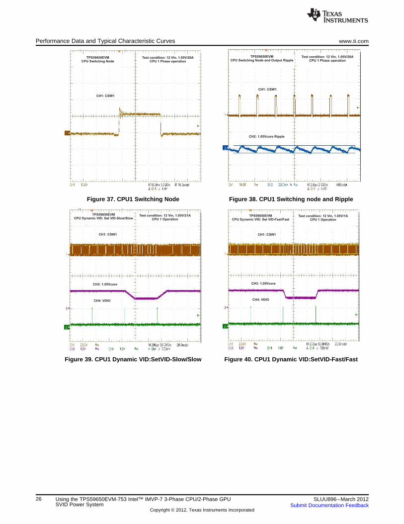
37 CPU1 Switching Node ................................................................................................... 25
38 CPU1 Switching node and Ripple ...................................................................................... 25
39 CPU1 Dynamic VID:SetVID-Slow/Slow ................................................................................ 26
40 CPU1 Dynamic VID:SetVID-Fast/Fast ................................................................................. 26
41 CPU1 Dynamic VID:SetVID-Decay/Fast ............................................................................... 26
42 CPU1 Output Load Insertion with OSR/USR middle level .......................................................... 26
43 CPU1 Output Load Release with OSR/USR middle level............................................................ 27
44 CPU1 Bode Plot at 12Vin, 1.05V/33A .................................................................................. 28
45 CPU1 MOSFET ........................................................................................................... 28
46 CPU1 IC .................................................................................................................... 28
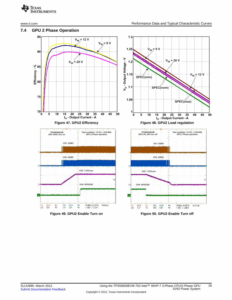
47 GPU2 Efficiency .......................................................................................................... 29
48 GPU2 Load regulation .................................................................................................... 29
49 GPU2 Enable Turn on ................................................................................................... 29
50 GPU2 Enable Turn off ................................................................................................... 29
51 GPU2 Switching Node and Ripple ..................................................................................... 29
2 Using the TPS59650EVM-753 Intel™ IMVP-7 3-Phase CPU/2-Phase GPU SLUU896–March 2012SVID Power System Submit Documentation Feedback
Copyright © 2012, Texas Instruments Incorporated

www.ti.com
52 GPU2 Dynamic VID:SetVID-Slow/Slow ................................................................................ 29
53 GPU2 Dynamic VID:SetVID-Fast/Fast ................................................................................. 30
54 GPU2 Dynamic VID:SetVID-Decay/Fast ............................................................................... 30
55 GPU2 Output Load Insertion with OSR/USR OFF ................................................................... 30
56 GPU2 Output Load Release with OSR/USR OFF .................................................................... 30
57 GPU2 Bode Plot at 12Vin, 1.23V/50A .................................................................................. 31
58 GPU2 MOSFET ........................................................................................................... 31
59 GPU2 IC .................................................................................................................... 31
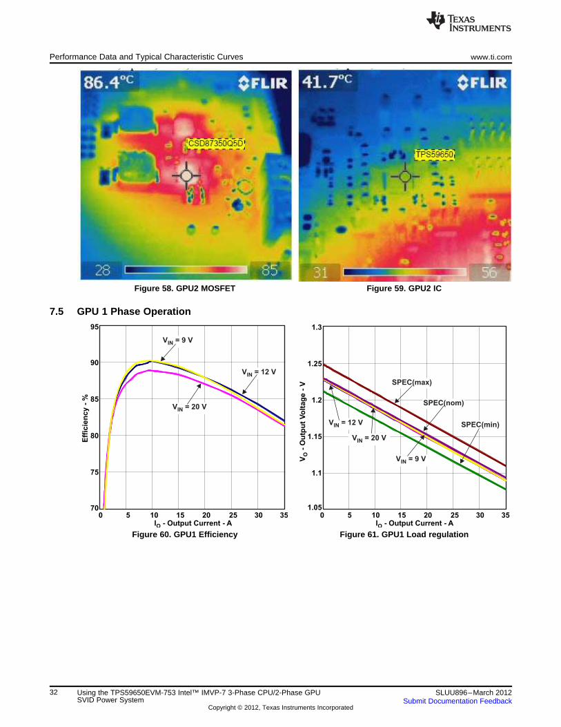
60 GPU1 Efficiency .......................................................................................................... 32
61 GPU1 Load regulation .................................................................................................... 32
62 GPU1 Enable Turn on ................................................................................................... 32
63 GPU1 Enable Turn off ................................................................................................... 32
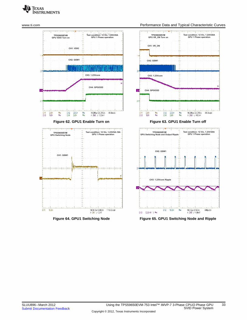
64 GPU1 Switching Node ................................................................................................... 33
65 GPU1 Switching Node and Ripple ..................................................................................... 33
66 GPU1 Dynamic VID:SetVID-Slow/Slow ................................................................................ 33
67 GPU1 Dynamic VID:SetVID-Fast/Fast ................................................................................. 33
68 GPU1 Dynamic VID:SetVID-Decay/Fast .............................................................................. 34
69 GPU1 Output Load Insertion with OSR/USR OFF.................................................................... 34
70 GPU1 Output Load Release with OSR/USR OFF .................................................................... 34
71 GPU1 Bode Plot at 12Vin, 1.23V/33A .................................................................................. 35
72 GPU1 MOSFET ........................................................................................................... 35
73 GPU1 IC .................................................................................................................... 35
74 1.05V Efficiency ........................................................................................................... 36
75 1.05V Load regulation .................................................................................................... 36
76 1.05V Enable Turn on .................................................................................................... 36
77 1.05V Enable Turn off .................................................................................................... 36
78 1.05V Switching Node ................................................................................................... 37
79 1.05V Ripple ............................................................................................................... 37
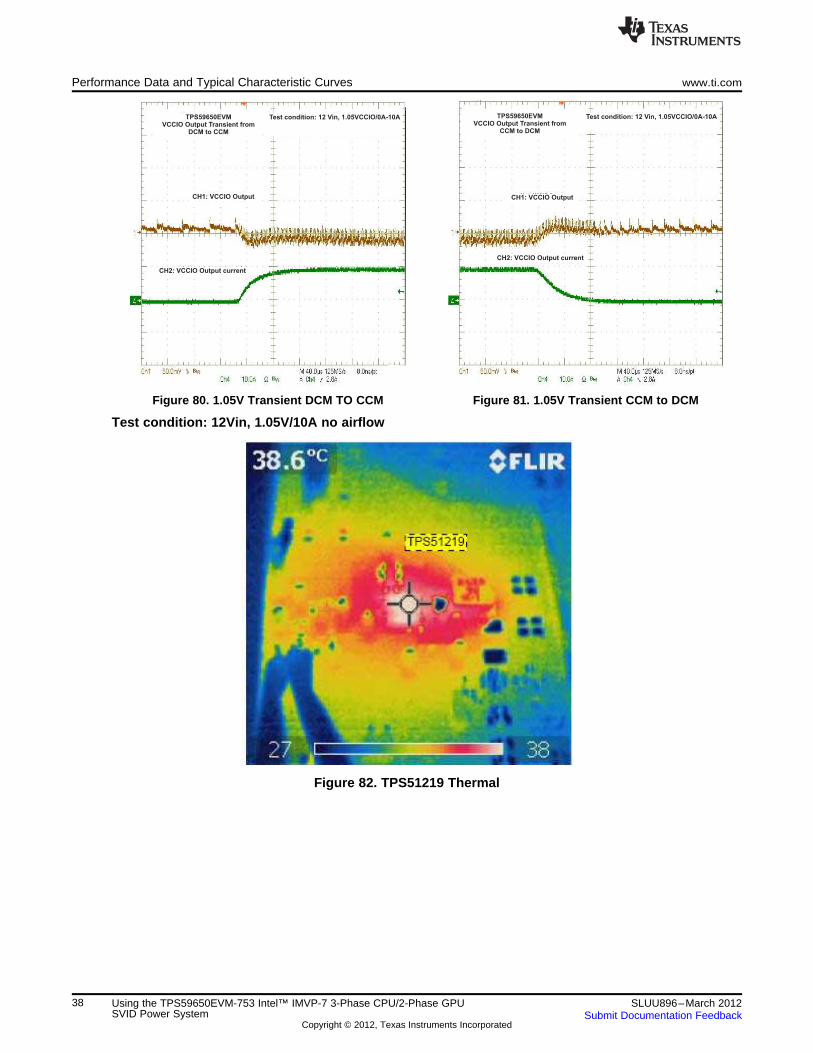
80 1.05V Transient DCM TO CCM ......................................................................................... 37
81 1.05V Transient CCM to DCM ........................................................................................... 37
82 TPS51219 Thermal........................................................................................................ 38
83 1.2V Efficiency ............................................................................................................ 39
84 1.2V Load regulation ...................................................................................................... 39
85 1.2V Enable Turn on ..................................................................................................... 39
86 1.2V Enable Turn off ..................................................................................................... 39
87 1.2V Switching Node ..................................................................................................... 39
88 1.2V Ripple ................................................................................................................. 39
89 1.2V Transient DCM TO CCM .......................................................................................... 40
90 1.2V Transient CCM to DCM ............................................................................................ 40
91 TPS51916 Thermal........................................................................................................ 41
92 TPS59650EVM-753 Top Layer Assembly Drawing (Top view) ..................................................... 42
93 TPS59650EVM-753 Bottom Assembly Drawing (Bottom view) ..................................................... 42
94 TPS59650EVM-753 Top Copper ....................................................................................... 43
95 TPS59650EVM-753 Bottom Copper ................................................................................... 43
96 TPS59650EVM-753 Internal Layer 2 .................................................................................. 44
97 TPS59650EVM-753 Internal Layer 3 .................................................................................. 44
98 TPS59650EVM-753 Internal Layer 4 .................................................................................. 45
99 TPS59650EVM-753 Internal Layer 5 ................................................................................... 45
3SLUU896–March 2012 Using the TPS59650EVM-753 Intel™ IMVP-7 3-Phase CPU/2-Phase GPUSVID Power SystemSubmit Documentation Feedback
Copyright © 2012, Texas Instruments Incorporated
www.ti.com
100 TPS59650EVM-753 Internal Layer 6 ................................................................................... 46
101 TPS59650EVM-753 Internal Layer 7 ................................................................................... 46
List of Tables
1 TPS59650EVM-753 Electrical Performance Specifications ........................................................... 7
2 Current Limit Trip Selection .............................................................................................. 11
3 CPU Frequency Selection ................................................................................................ 11
4 GPU Frequency Selection ............................................................................................... 12
5 F2808 DSP Program Mode Selection .................................................................................. 12
6 5Vin Bias Voltage Option (J33) .......................................................................................... 12
7 On Board Dynamic Load Selection ..................................................................................... 12
8 VR_ON Enable Selection................................................................................................. 13
9 VDDQ S3, S5 Enable Selection ........................................................................................ 13
10 1.05V Enable Selection .................................................................................................. 13
11 VCCIO Output Voltage Selection ....................................................................................... 13
12 On Board Dynamic Load Enable/Disable selection .................................................................. 14
13 EVM Major Components List ............................................................................................ 47
4 Using the TPS59650EVM-753 Intel™ IMVP-7 3-Phase CPU/2-Phase GPU SLUU896–March 2012SVID Power System Submit Documentation Feedback
Copyright © 2012, Texas Instruments Incorporated

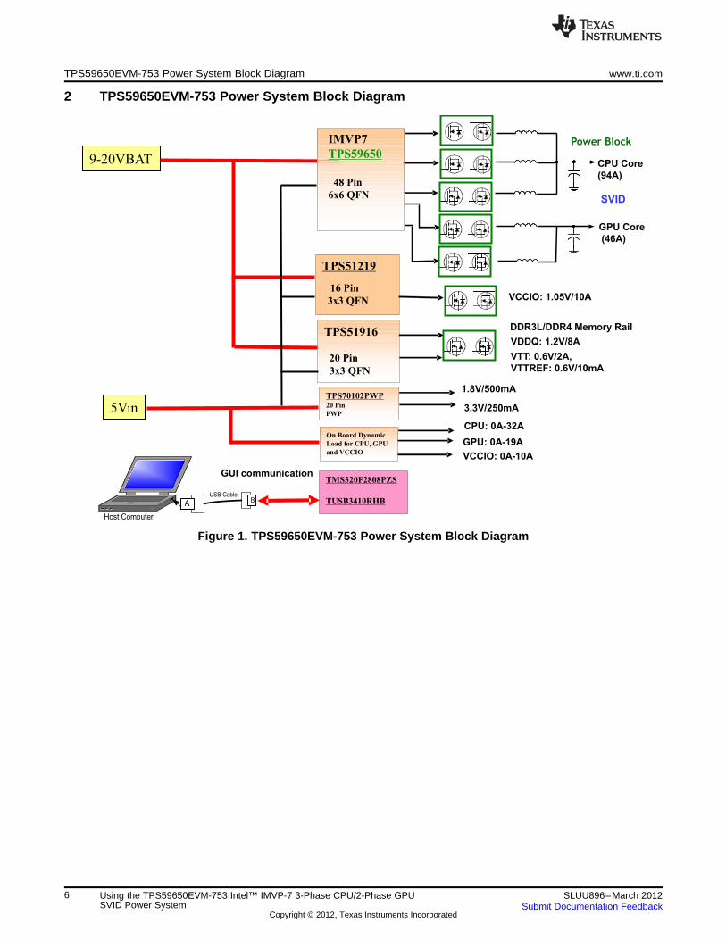
www.ti.com Description
1 Description
The TPS59650EVM-753 is designed to use a 9V-20V Input bus to produce 6 regulated outputs for IMVP7SVID CPU/GPU Power System. The TPS59650EVM-753 is specially designed to demonstrate theTPS59650 full IMVP7 mobile feature while providing GUI communication programing and a number of testpoints to evaluate the static and dynamic performance of TPS59650.
1.1 Typical Applications• IMVP7 Vcore Applications for Adapter, Battery, NVDC or 3V/5V/12V rails
1.2 Features
The TPS59650EVM-753 features:
• Complete solution for 9V-20V Input Intel IMVP7 SVID Power System
• GUI communication to demonstrate full IMVP7 Mobile feature
• 3-Phase CPU Vcore can support up to 94A output current
• 2-Phase GPU Vcore can support up to 46A output current
• 8 Selectable Switching frequency for CPU and GPU power
• 8 Levels selectable current limit for CPU and GPU power
• Switches or Jumpers for each output enable
• On Board Dynamic Load for CPU, GPU Vcore and VCCIO output
• High efficiency and high density by using TI power block MOSFET
• Convenient test points for probing critical waveforms
• Eight Layer PCB with 1oz copper
5SLUU896–March 2012 Using the TPS59650EVM-753 Intel™ IMVP-7 3-Phase CPU/2-Phase GPUSVID Power SystemSubmit Documentation Feedback
Copyright © 2012, Texas Instruments Incorporated
9-20VBAT CPU Core
(94A)
GPU Core
(46A)
Power BlockIMVP7
TPS59650
48 Pin
6x6 QFN
TPS51219
16 Pin
3x3 QFN VCCIO: 1.05V/10A
TPS70102PWP20 Pin
PWP
TPS51916
20 Pin
3x3 QFN
TMS320F2808PZS
TUSB3410RHB
VCCIO: 0A-10A
VDDQ: 1.2V/8A
VTT: 0.6V/2A,
VTTREF: 0.6V/10mA
1.8V/500mA
GPU: 0A-19AOn Board Dynamic
Load for CPU, GPU
and VCCIO
CPU: 0A-32A
SVID
5Vin 3.3V/250mA
Host Computer
BUSB Cable
A
GUI communication
DDR3L/DDR4 Memory Rail
TPS59650EVM-753 Power System Block Diagram www.ti.com
2 TPS59650EVM-753 Power System Block Diagram
Figure 1. TPS59650EVM-753 Power System Block Diagram
6 Using the TPS59650EVM-753 Intel™ IMVP-7 3-Phase CPU/2-Phase GPU SLUU896–March 2012SVID Power System Submit Documentation Feedback
Copyright © 2012, Texas Instruments Incorporated
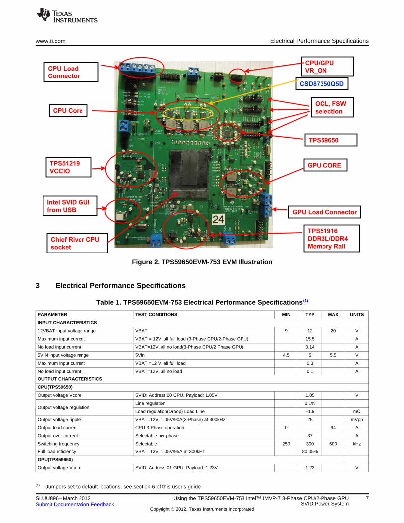
CPU Core
GPU CORETPS51219
VCCIO
TPS59650
Chief River CPU
socket
OCL, FSW
selection
TPS51916
DDR3L/DDR4
Memory Rail
Intel SVID GUI
from USB
CPU/GPU
VR_ONCPU Load
Connector
CSD87350Q5D
GPU Load Connector
www.ti.com Electrical Performance Specifications
Figure 2. TPS59650EVM-753 EVM Illustration
3 Electrical Performance Specifications
Table 1. TPS59650EVM-753 Electrical Performance Specifications (1)
PARAMETER TEST CONDITIONS MIN TYP MAX UNITS
INPUT CHARACTERISTICS
12VBAT input voltage range VBAT 9 12 20 V
Maximum input current VBAT = 12V, all full load (3-Phase CPU/2-Phase GPU) 15.5 A
No load input current VBAT=12V, all no load(3-Phase CPU/2 Phase GPU) 0.14 A
5VIN input voltage range 5Vin 4.5 5 5.5 V
Maximum input current VBAT =12 V, all full load 0.3 A
No load input current VBAT=12V, all no load 0.1 A
OUTPUT CHARACTERISTICS
CPU(TPS59650)
Output voltage Vcore SVID: Address:00 CPU, Payload: 1.05V 1.05 V
Line regulation 0.1%Output voltage regulation
Load regulation(Droop) Load Line –1.9 mΩ
Output voltage ripple VBAT=12V, 1.05V/90A(3-Phase) at 300kHz 25 mVpp
Output load current CPU 3-Phase operation 0 94 A
Output over current Selectable per phase 37 A
Switching frequency Selectable 250 300 600 kHz
Full load efficiency VBAT=12V, 1.05V/95A at 300kHz 80.05%
GPU(TPS59650)
Output voltage Vcore SVID: Address:01 GPU, Payload: 1.23V 1.23 V
(1) Jumpers set to default locations, see section 6 of this user’s guide
7SLUU896–March 2012 Using the TPS59650EVM-753 Intel™ IMVP-7 3-Phase CPU/2-Phase GPUSVID Power SystemSubmit Documentation Feedback
Copyright © 2012, Texas Instruments Incorporated

Test Setup www.ti.com
Table 1. TPS59650EVM-753 Electrical Performance Specifications (1) (continued)
PARAMETER TEST CONDITIONS MIN TYP MAX UNITS
Line regulation 0.1%Output voltage regulation
Load regulation(Droop) Load Line –3.9 mΩ
Output voltage ripple VBAT=12V, 1.23V/50A 2 Phase at 385kHz 30 mVpp
Output load current 0 50 A
Output over current Selectable per phase 37 A
Switching frequency Selectable 275 385 660 kHz
Full load efficiency VBAT=12V, 1.23V/50A 2 Phase at 385KHz 86.58%
1.05V VCCIO (TPS51219)
Output voltage 1.05 V
Line regulation 0.1%Output voltage regulation
Load regulation 0.1%
Output voltage ripple VBAT=12V, 1.05V/10A 30 mVpp
Output load current 0 10 A
Output over current 16 A
Switching frequency Selectable 500 kHz
Full load efficiency VBAT=12V, 1.05V/10A 89.87%
DDR3L/DDR4 Memory Rail (TPS51916)
Output voltage 1.2 V
Line regulation 0.1%Output voltage regulation
Load regulation 0.1%
Output voltage ripple VBAT=12V, 1.2V/8A 30 mVpp
Output load current 0 8 A
Output over current 10 A
Switching frequency Selectable 500 kHz
Full load efficiency VBAT=12V, 1.2V/8A 89.07%
Operating temperature 25 °C
4 Test Setup
4.1 Test Equipment
4.1.1 PC Computer (Host Computer)
Microsoft Windows XP or newer with available USB port
4.1.2 USB Cable
The USB Cable: Standard USB_A to USB_B 5 Pin Mini-B cable. See Figure 3 .
Figure 3. USB Cable
8 Using the TPS59650EVM-753 Intel™ IMVP-7 3-Phase CPU/2-Phase GPU SLUU896–March 2012SVID Power System Submit Documentation Feedback
Copyright © 2012, Texas Instruments Incorporated
www.ti.com Test Setup
4.1.3 TPS59650 USB driver and SVID GUI Installation1. Copy the both files: setup.exe and setup.msi to the host computer.
2. Run this setup.exe.
3. Following installation Instructions, this will install the driver and the Texas Instruments SVID GUI.
4. It will add the below icon
4.1.4 DC Source
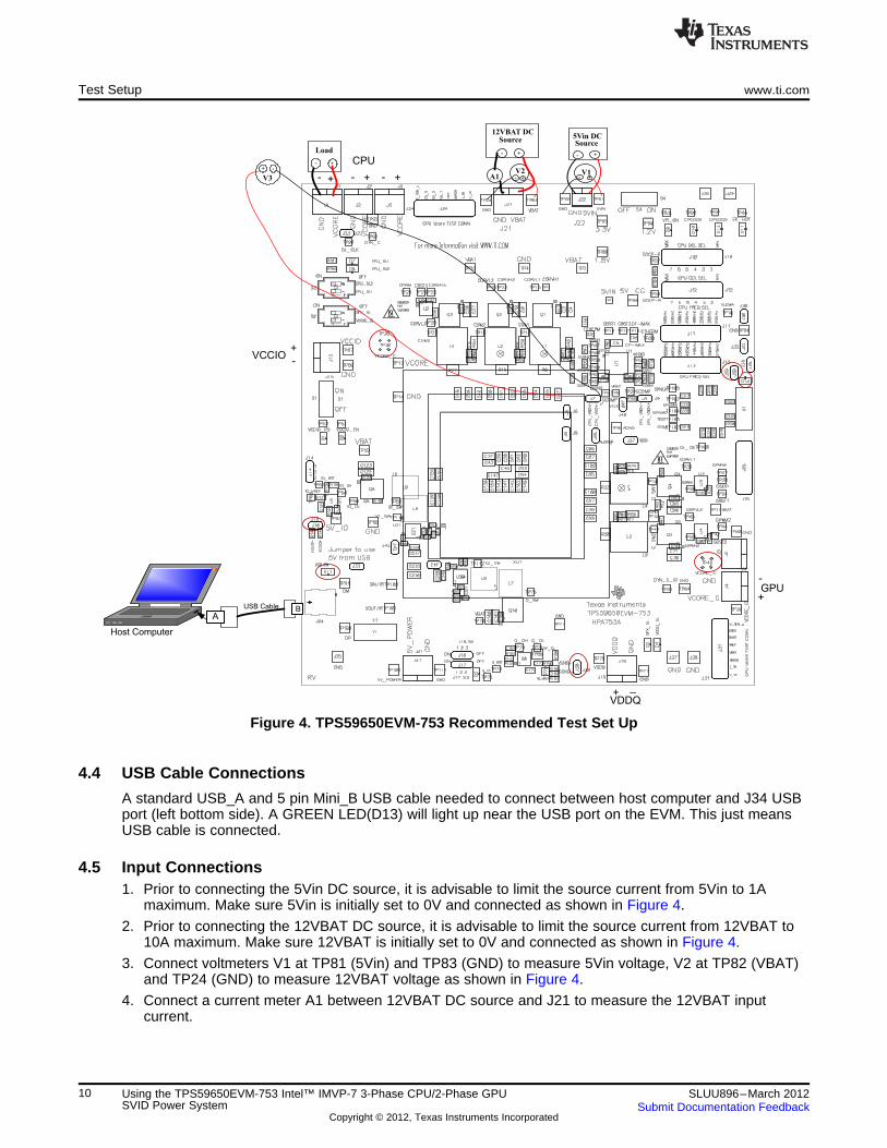
12VBAT DC Source: The 12VBAT DC source should be a 0-20V variable DC source capable ofsupplying 20Adc current. Connect 12VBAT to J21 as shown in Figure 4.
5Vin DC Source: The 5Vin DC source should be a 0-5V variable DC source capable of supplying 1Adccurrent. Connect 5Vin to J22 as shown in Figure 4.
4.1.5 Meters• V1: 5Vin at TP81(5Vin) and TP83(GND)
• V2: 12VBAT at TP82(VBAT) and TP24(GND)
• V3: CPU Vcore sense voltage at J7; GPU Vcore sense voltage at J9; VDDQ sense voltage at J20,VCCIO sense voltage at J16
• A1: 12VBAT input current
4.1.6 Load
The output load should be an electronic constant current load capable of 0-90Adc.
4.1.7 Oscilloscope
A digital or analog oscilloscope can be used to measure the output ripple. The oscilloscope should be setfor 1MΩ impedance, 20MHz Bandwidth, AC coupling, 2us/division horizontal resolution, 50mV/divisionvertical resolution. Test point TP30 and TP46 can be used to measure the output ripple voltage for CPUand GPU. Do not use a leaded ground connection as this may induce additional noise due to the largeground loop.
4.2 Recommended Wire Gauge1. V5in to J22(5V input):
The recommended wire size is 1x AWG #18 per input connection, with the total length of wire less than4 feet (2 feet input, 2 feet return).
2. 12VBAT to J21(12V input):The recommended wire size is 1x AWG #16 per input connection, with the total length of wire less than4 feet (2 feet input, 2 feet return).
3. J1, J2, J3(CPU) to LOAD or J4, J5 (GPU) to LOAD or J19 (VDDQ) to LOAD or J15(VCCIO) toLOAD:The minimum recommended wire size is 2x AWG #16, with the total length of wire less than 4 feet (2feet output, 2 feet return)
4.3 Recommended Test Setup
Figure 4 is the recommended test set up to evaluate the TPS59650EVM-753.Working at an ESDworkstation, make sure that any wrist straps, bootstraps or mats are connected referencing the user toearth ground before handling the EVM.
9SLUU896–March 2012 Using the TPS59650EVM-753 Intel™ IMVP-7 3-Phase CPU/2-Phase GPUSVID Power SystemSubmit Documentation Feedback
Copyright © 2012, Texas Instruments Incorporated
Host Computer
BUSB Cable
A
CPUV1
- +
5Vin DC
Source
+-
V2- +A1
12VBAT DC
Source
+-
- + ++ --
Load
+
-
V3
+
-
VCCIO+
-
GPU-
+
VDDQ
_+
Test Setup www.ti.com
Figure 4. TPS59650EVM-753 Recommended Test Set Up
4.4 USB Cable Connections
A standard USB_A and 5 pin Mini_B USB cable needed to connect between host computer and J34 USBport (left bottom side). A GREEN LED(D13) will light up near the USB port on the EVM. This just meansUSB cable is connected.
4.5 Input Connections1. Prior to connecting the 5Vin DC source, it is advisable to limit the source current from 5Vin to 1A
maximum. Make sure 5Vin is initially set to 0V and connected as shown in Figure 4.
2. Prior to connecting the 12VBAT DC source, it is advisable to limit the source current from 12VBAT to10A maximum. Make sure 12VBAT is initially set to 0V and connected as shown in Figure 4.
3. Connect voltmeters V1 at TP81 (5Vin) and TP83 (GND) to measure 5Vin voltage, V2 at TP82 (VBAT)and TP24 (GND) to measure 12VBAT voltage as shown in Figure 4.
4. Connect a current meter A1 between 12VBAT DC source and J21 to measure the 12VBAT inputcurrent.
10 Using the TPS59650EVM-753 Intel™ IMVP-7 3-Phase CPU/2-Phase GPU SLUU896–March 2012SVID Power System Submit Documentation Feedback
Copyright © 2012, Texas Instruments Incorporated

www.ti.com Configuration
4.6 Output Connections1. Connect Load to J1, J2, J3 and set Load to constant resistance mode to sink 0Adc before 5Vin and
12VBAT are applied. This is for CPU operation.
2. Connect a voltmeter V3 at J7 to measure CPU Vcore sense voltage.
5 Configuration
All Jumper selections should be made prior to applying power to the EVM. User can configure this EVMper following configurations.
5.1 CPU and GPU Configuration
5.1.1 CPU/GPU Current Limit Trip Selection (J10 for CPU and J12 for GPU)
The current limit trip can be set by J10(COCP) and J12(GOCP).
Default setting: Level 5 for both CPU and GPU.
Table 2. Current Limit Trip Selection
Jumper set to Connected Resistor COCP/GOCP Limit (Typ.)
Left (1-2 pin shorted) 150k Max
2nd(3-4 pin shorted) 100k Level 7
3rd(5-6 pin shorted) 75k Level 6
4th(7-8 pin shorted) 56.2k Level 5
5th(9-10 pin shorted) 39.2k Level 4
6th(11-12 pin shorted) 30.1k Level 3
7th(13-14 pin shorted) 24.3k Level 2
Right(15-16 pin shorted) 20.0k Min
5.1.2 CPU Frequency Selection (J11)
The operating frequency can be set by J11
Default setting: 300 kHz for CPU
Table 3. CPU Frequency Selection
Jumper set to Connected Resistor CPU
Left (1-2 pin shorted) 150k 600 kHz
2nd(3-4 pin shorted) 100k 550 kHz
3rd(5-6 pin shorted) 75k 500 kHz
4th(7-8 pin shorted) 56.2k 450 kHz
5th(9-10 pin shorted) 39.2k 400 kHz
6th(11-12 pin shorted) 30.1k 350 kHz
7th(13-14 pin shorted) 24.3k 300 kHz
Right(15-16 pin shorted) 20.0k 250 kHz
11SLUU896–March 2012 Using the TPS59650EVM-753 Intel™ IMVP-7 3-Phase CPU/2-Phase GPUSVID Power SystemSubmit Documentation Feedback
Copyright © 2012, Texas Instruments Incorporated

Configuration www.ti.com
5.1.3 GPU Frequency Selection (J13)
The operating frequency can be set by J13
Default setting: 385 kHz for GPU.
Table 4. GPU Frequency Selection
Jumper set to Connected Resistor GPU
Left (1-2 pin shorted) 150k 660 kHz
2nd(3-4 pin shorted) 100k 605 kHz
3rd(5-6 pin shorted) 75k 550 kHz
4th(7-8 pin shorted) 56.2k 495 kHz
5th(9-10 pin shorted) 39.2k 440 kHz
6th(11-12 pin shorted) 30.1k 385 kHz
7th(13-14 pin shorted) 24.3k 330 kHz
Right(15-16 pin shorted) 20.0k 275 kHz
5.1.4 F2808 DSP Program Mode Selection (J39)
The F2808 DSP Program Mode(GUI) Selection can be set by J39.
Default setting: No Jumper shorts on J39 for normal operation
Table 5. F2808 DSP Program Mode Selection
Jumper set to Program Mode Selection
No Jumper on J39 Normal Operation
Jumper on J39 Flash the DSP program to the EVM
5.1.5 5Vin Bias Voltage Option (J33)
The 5Vin Bias Voltage can be used from USB or Externally
Default setting: No Jumper shorts on J33
Table 6. 5Vin Bias Voltage Option (J33)
Jumper set to Selection
No Jumper 5Vin Bias from J22 external
Jumper on J39 5Vin Bias from USB, 5Vin from J22 should not be connected
5.1.6 On Board Dynamic Load Selection (S3 for CPU, S2(upper) for GPU, S2(lower) for VCCIO)
The on board dynamic load can be set by S2 and S3.
Default setting: Push S2 and S3 to “OFF” position to disable the on board dynamic load
Table 7. On Board Dynamic Load Selection
Switch set to Dynamic Load Selection
Push S3 to “ON” position Enable 32A on board dynamic load at CPU
Push S3 to “OFF” position Disable 32A on board dynamic load at CPU
Push S2(upper) to “ON” position Enable 19A on board dynamic load at GPU
Push S2(upper) to “OFF” position Disable 19A on board dynamic load at GPU
Push S2(lower) to “ON” position Enable 10A on board dynamic load at VCCIO
Push S2(lower) to “OFF” position Disable 10A on board dynamic load at VCCIO
12 Using the TPS59650EVM-753 Intel™ IMVP-7 3-Phase CPU/2-Phase GPU SVID SLUU896–March 2012Power System Submit Documentation Feedback
Copyright © 2012, Texas Instruments Incorporated
www.ti.com Configuration
5.1.7 IMVP-7 VR_ON Enable Selection (S4)
The IMVP-7 CPU/GPU can be enabled and disabled by S4
Default setting: Push S4 to “OFF” position to disable both CPU and GPU
Table 8. VR_ON Enable Selection
Switch set to VR_ON Selection
Push S4 to “ON” position Enable IMVP-7 CPU/GPU Vcore
Push S4 to “OFF” position Disable IMVP-7 CPU/GPU Vcore
5.2 1.2VDDQ, 0.6V VTT and 0.6V VTTREF Configuration
5.2.1 VDDQ S3, S5 Enable Selection
The controller can be enabled and disabled by J18 and J17.
Default setting: Jumper shorts on Pin2 and Pin3 of J18,Def ault setti ng : Jumper shorts on Pin2 and Pin3 of J17
Table 9. VDDQ S3, S5 Enable Selection
State J17 (S3) set to J18(S5) set to VDDQ VTTREF VTT
S0 ON position ON position ON ON ON
S3 OFF position ON position ON ON OFF(High-Z)
S4/S5 OFF position OFF position OFF(Discharge) OFF(Discharge) OFF(Discharge)
5.3 1.05V VCCIO Configuration
5.3.1 1.05V Enable Selection (S1)
1.05V Enable can be set by S1
Default setting: Push S1 to ”OFF” position
Table 10. 1.05V Enable Selection
Jumper set to Selection
Push S1 to “ON” position 1.05V Enabled
Push S1 to “OFF” position 1.05V Disabled
5.3.2 VCCIO Output Voltage Selection (J14)
The VCCIO Output Voltage can be selected by J14
Default setting: Jumper shorts Pin1 and Pin2 of J14
Table 11. VCCIO Output Voltage Selection
Jumper set to Selection
Jumper shorts on Pin1 and Pin2 VCCIO: 1.05V
Jumper shorts on Pin2 and Pin3 VCCIO: 1.00V
13SLUU896–March 2012 Using the TPS59650EVM-753 Intel™ IMVP-7 3-Phase CPU/2-Phase GPUSVID Power SystemSubmit Documentation Feedback
Copyright © 2012, Texas Instruments Incorporated

Test Procedure www.ti.com
5.3.3 On Board Dyanamic Load Enable Pin (J23)
The on board dynamic load can be enabled or disabled by J23
Default setting: Jumper shorts on J23
Table 12. On Board Dynamic Load Enable/Disable selection
Jumper set to Selection
Jumper shorts Enable on board dynamic load
No Jumper short Disable on board dynamic load
6 Test Procedure
6.1 Line/Load Regulation and Efficiency Measurement Procedure
6.1.1 CPU1. Set up EVM as described in Section 4.3 through Section 4.6 and Figure 4.
2. Ensure J39 no Jumper shorts on
3. Ensure all other Jumpers configuration setting by Section 5 before 5Vin and 12VBAT are applied.
4. Ensure Load is set to constant resistance mode and to sink 0Adc
5. Ensure S1 and S4 are in “OFF” position
6. Add scope probe on the TP30 for CPU Vcore ripple measurement
7. Ensure USB Cable is connected between host computer and USB port(J34) on the EVM
8. Increase 5Vin from 0V to 5V. Using V1 to measure 5Vin input voltage.
9. Increase 12VBAT from 0V to 12V. Using V2 to measure 12VBAT input voltage.
10. Double-Click the icon to launch the GUI program. The GUI window shown in Figure 5.
11. Push S4 to “ON” position to enable the VR_ON of TPS59650. VR_ON LED will light up.
12. Now the user is ready to send SVID commends. The GUI at start-up defaults:Address: 00 CPU, Commend: SetVIDslow, Payload: 1.05V (The user can select the SVID commend byusing the pull-down menu”)
13. Click “send Commend” and CPU CPGOOD LED will light up, See the GUI window as Figure 5.
14. Measure V3: CPU Vcore at J7 and A1: 12VBAT input current
15. Vary CPU LOAD from 0Adc to 94Adc, CPU Vcore must remain in load line
16. Vary 12VBAT from 9V to 20V CPU Vcore must remain in line regulation
17. Push S4 to “OFF” position to disable CPU Vcore controller.
18. Decrease LOAD to 0A and disconnect the LOAD from terminal J1, J2, J3
19. Disconnect V3 from J7.
20. Disconnect scope probe from TP30
14 Using the TPS59650EVM-753 Intel™ IMVP-7 3-Phase CPU/2-Phase GPU SLUU896–March 2012SVID Power System Submit Documentation Feedback
Copyright © 2012, Texas Instruments Incorporated

www.ti.com Test Procedure
Figure 5. TPS59650EVM-753 CPU GUI set up Window
6.1.2 GPU1. Connect the LOAD to GPU terminal J4, J5 and V3 at J9. Ensure correct polarity.
2. Add scope probe on the TP46 for GPU Vcore_G ripple measurement
3. Push S4 to “ON” position to enable the VR_ON of TPS59650. The VR_ON LED will light up.
4. Now you are ready to send SVID commends for GPU. Using pull-down menu:Address: 01 GPU, Commend: SetVIDslow, Payload: 1.23V
5. Click “send Commend” and GPU GPOOD LED will light up, See the GUI window as Figure 6.
15SLUU896–March 2012 Using the TPS59650EVM-753 Intel™ IMVP-7 3-Phase CPU/2-Phase GPUSVID Power SystemSubmit Documentation Feedback
Copyright © 2012, Texas Instruments Incorporated

Test Procedure www.ti.com
Figure 6. TPS59650EVM-753 GPU GUI set up Window
6. Measure V3: GPU Vcore_G at J9 and A1: 12VBAT input current
7. Vary GPU LOAD from 0Adc to 50Adc, GPU Vcore must remain in load line
8. Vary 12VBAT from 9V to 20V GPU Vcore must remain in line regulation
9. Push S4 to “OFF” position to disable GPU Vcore controller.
10. Decrease LOAD to 0A and disconnect the LOAD from terminal J11
11. Disconnect V3 from J9.
12. Disconnect scope probe from TP46
13. Exit SVID GUI window: click File → click Exit
14. Disconnect the USB cable between host Computer and EVM
16 Using the TPS59650EVM-753 Intel™ IMVP-7 3-Phase CPU/2-Phase GPU SLUU896–March 2012SVID Power System Submit Documentation Feedback
Copyright © 2012, Texas Instruments Incorporated
www.ti.com Test Procedure
6.1.3 VDDQ1. Connect the LOAD to VDDQ terminal J19 and V3 at J20. Ensure correct polarity.
2. Remove Jumper from J17, J18 from pin2 and pin3 and put this Jumper on pin1 and pin 2 of J18, J17to enable S5 of VDDQ controller. VDDQ PGOOD LED will light up.
3. Measure V3: VDDQ at J20 and A1: 12Vin input current
4. Vary VDDQ LOAD from 0Adc to 8Adc, VDDQ must remain in the load regulation
5. Vary 12VBAT from 9V to 20V, VDDQ must remain in the line regulation
6. Remove Jumper of J17, J18 and shorts back on pin2 and pin3 of J17, J18 to disable VDDQ controller.
7. Decrease LOAD to 0A and disconnect the LOAD from terminal J19
8. Disconnect V3 from J20.
6.1.4 VCCIO1. Connect the LOAD to VCCIO terminal J15 and V3 at J16. Ensure correct polarity.
2. Push S1 to “ON” position to enable the VCCIO controller. VCCIO EN and PGOOD LED will light up.
3. Measure V3: VCCIO at J16 and A1: 12Vin input current
4. Vary VDDQ LOAD from 0Adc to 10Adc, VCCIO must remain in the load regulation
5. Vary 12VBAT from 9V to 20V, VCCIO must remain in the line regulation
6. Push S1 to “OFF” position to disable VCCIO controller.
7. Decrease LOAD to 0A and disconnect the LOAD from terminal J15
8. Disconnect V3 from J16.
6.2 Equipment Shutdown1. Shut down Load
2. Shut down 12VBAT and 5Vin
3. Shut down oscilloscope
4. Shut down host computer
17SLUU896–March 2012 Using the TPS59650EVM-753 Intel™ IMVP-7 3-Phase CPU/2-Phase GPUSVID Power SystemSubmit Documentation Feedback
Copyright © 2012, Texas Instruments Incorporated
0.8
0.85
0.9
0.95
1
1.05
1.1
V-
Ou
tpu
t V
olt
ag
e -
VO
0 10 20 30 40 50 60 70 80 90 100I - Output Current - AO
V = 12 VIN
V = 20 VIN
V = 9 VIN
SPEC(min)
SPEC(nom)
SPEC(max)
65
70
75
80
85
90
95
Eff
icie
nc
y -
%
0 10 20 30 40 50 60 70 80 90 100I - Output Current - AO
V = 12 VIN
V = 20 VIN
V = 9 VIN
TPS59650EVM
CPU VR_ON Turn off
Test condition: 12 Vin, 1.05V/60A
CPU 3 Phase operation
CH4: CPGOOD
CH1: CSW1
CH2: CSW2
CH3: 1.05V core
TPS59650EVM
CPU VDIO Turn on
Test condition: 12 Vin, 1.05V/60A
CPU 3 Phase operation
CH1: CSW1
CH2: CSW2
CH3: 1.05V core
CH4: CPGOOD
Performance Data and Typical Characteristic Curves www.ti.com
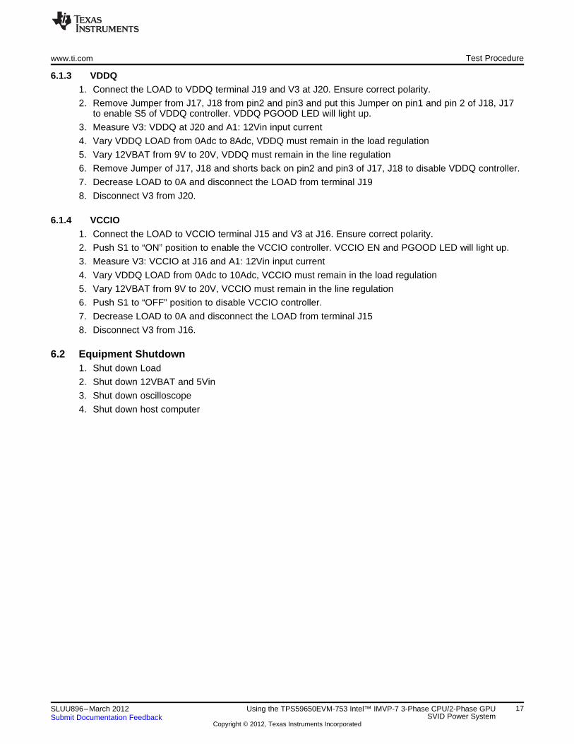
7 Performance Data and Typical Characteristic Curves
Figure 7 through Figure 91 present typical performance curves for TPS59650EVM-753. Jumpers set todefault locations, see section 6 of this user’s guide.
7.1 CPU 3-Phase Operation
Figure 7. CPU3 Efficiency Figure 8. CPU3 Load regulation
Figure 9. CPU3 Enable Turn on Figure 10. CPU3 Enable Turn off
18 Using the TPS59650EVM-753 Intel™ IMVP-7 3-Phase CPU/2-Phase GPU SLUU896–March 2012SVID Power System Submit Documentation Feedback
Copyright © 2012, Texas Instruments Incorporated
Test condition: 12 Vin, 1.05V/60ACPU 3 Phase operation
CH1: CSW1
CH2: CSW2
TPS59650EVMCPU Switching node and Output Ripple
CH3: CSW3
CH4: 1.05V core Ripple
TPS59650EVM
CPU Dynamic VID: Set VID-Slow/Slow
Test condition: 12 Vin, 1.05V/1A
CPU 3 Operation
CH4: VDIO
CH1: CSW1
CH2: CSW2
CH3: 1.05V core
Test condition: 12 Vin, 1.05V/1A
CPU 3 Operation
CH4: VDIO
CH1: CSW1
CH2: CSW2
CH3: 1.05V core
TPS59650EVM
CPU Dynamic VID: Set VID-Fast/fast
TPS59650EVM
CPU Dynamic VID: Set VID-Decay/Fast
Test condition: 12 Vin, 1.05V/1A
CPU 3 Operation
CH4: VDIO
CH1: CSW1
CH2: CSW2
CH3: 1.05V core
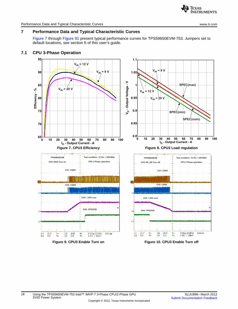
www.ti.com Performance Data and Typical Characteristic Curves
Figure 11. CPU3 Switching Node(Ripple) Figure 12. CPU3 Dynamic VID: SetVID-Slow/Slow
Figure 13. CPU3 Dynamic VID:SetVID-Fast/Fast Figure 14. CPU3 Dynamic VID:SetVID-Decay/Fast
19SLUU896–March 2012 Using the TPS59650EVM-753 Intel™ IMVP-7 3-Phase CPU/2-Phase GPUSVID Power SystemSubmit Documentation Feedback
Copyright © 2012, Texas Instruments Incorporated

CH1: CSW1
CH2: CSW2
TPS59650EVMCPU Output Load Releas with
OSR/USR middle level
Test condition: 12 Vin, 1.05V/0A-51ACPU 3 Phase on board dynamic load
CH3: CSW3
CH4: 1.05V core
TPS59650EVMCPU Output Load Insertion with
OSR/USR middle level
Test condition: 12 Vin, 1.05V/0A-51ACPU 3 Phase on board dynamic load
CH1: CSW1
CH2: CSW2
CH4: 1.05V core
CH3: CSW3
Performance Data and Typical Characteristic Curves www.ti.com
Figure 15. CPU3 Output Load Insertion with OSR/USR Figure 16. CPU3 Output Load Release with OSR/USRmiddle level middle level
Figure 17. CPU3 Bode Plot at 12Vin, 1.05V/60A
Test condition: CPU3 12Vin, 1.05V/60A no airflow
20 Using the TPS59650EVM-753 Intel™ IMVP-7 3-Phase CPU/2-Phase GPU SLUU896–March 2012SVID Power System Submit Documentation Feedback
Copyright © 2012, Texas Instruments Incorporated
0.85
0.9
0.95
1
1.05
1.1
V-
Ou
tpu
t V
olt
ag
e -
VO
0 5 10 15 20 25 30 35 40 45 50 55I - Output Current - AO
SPEC(min)
SPEC(nom)
SPEC(max)
V = 9 VIN
V = 20 VIN
V = 12 VIN
65
70
75
80
85
90
95
Eff
icie
nc
y -
%
0 5 10 15 20 25 30 35 40 45 50 55I - Output Current - AO
V = 12 VIN
V = 9 VIN
V = 20 VIN
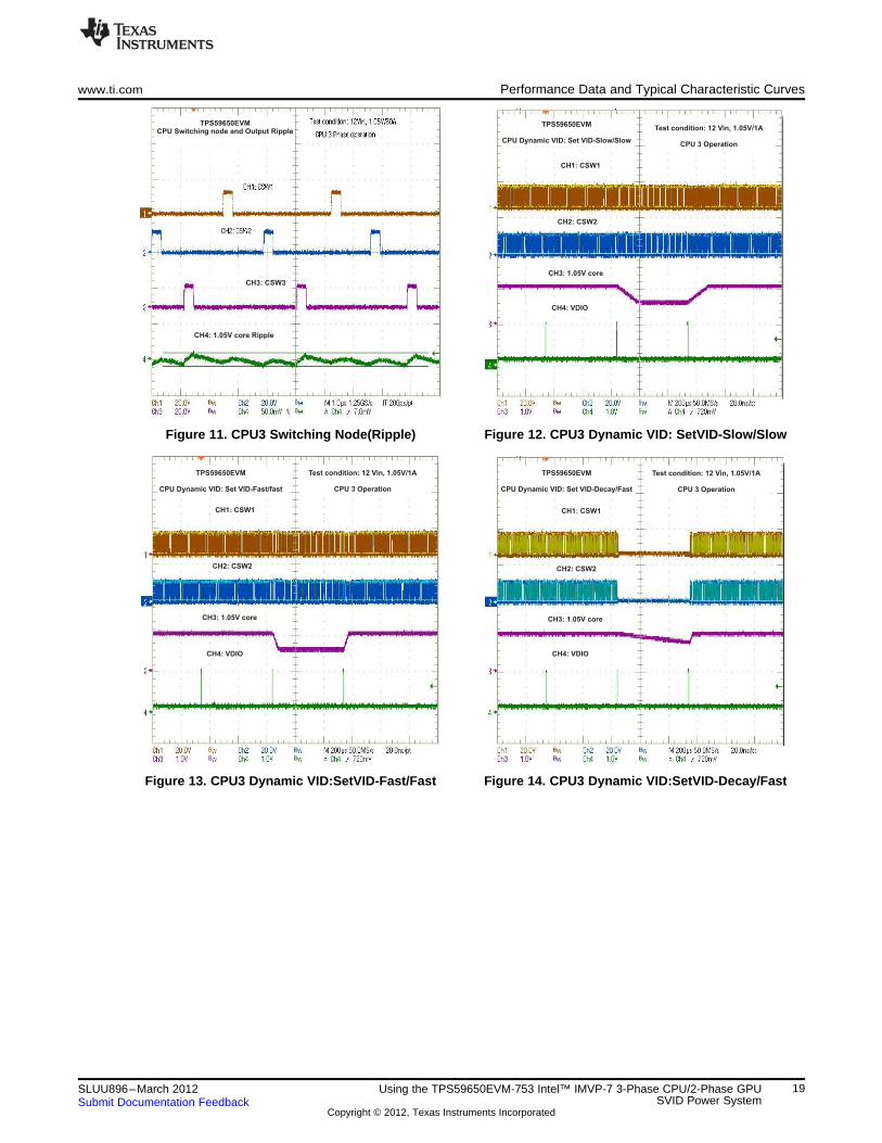
www.ti.com Performance Data and Typical Characteristic Curves
Figure 18. CPU3 MOSFET Figure 19. CPU3 IC
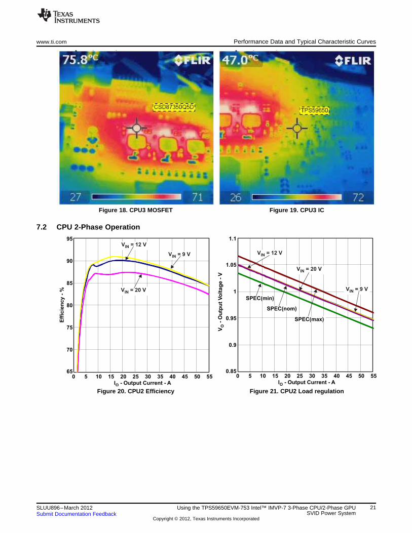
7.2 CPU 2-Phase Operation
Figure 20. CPU2 Efficiency Figure 21. CPU2 Load regulation
21SLUU896–March 2012 Using the TPS59650EVM-753 Intel™ IMVP-7 3-Phase CPU/2-Phase GPUSVID Power SystemSubmit Documentation Feedback
Copyright © 2012, Texas Instruments Incorporated
CH1: CSW1
CH2: CSW2
CH3: 1.05V core
CH4: CPGOOD
TPS59650EVM
CPU VDIO Turn on
Test condition: 12 Vin, 1.05V/40A
CPU 2 Phase Operation
TPS59650EVM
CPU VR_ON Turn off
Test condition: 12 Vin, 1.05V/40A
CPU 2 Phase Operation
CH4: CPGOOD
CH3: 1.05V core
CH2: CSW2
CH1: CSW1
TPS59650EVM
CPU Switching node and Output Ripple
Test condition: 12 Vin, 1.05V/40A
CPU 2 Phase Operation
CH4: 1.05Vcore
CH3: CSW2
CH2: CSW1
TPS59650EVM
CPU Dynamic VID: Set VID-Slow/Slow
Test condition: 12 Vin, 1.05V/1A
CPU 2 Operation
CH1: CSW1
CH2: CSW2
CH3: 1.05Vcore
CH4: VDIO
Performance Data and Typical Characteristic Curves www.ti.com
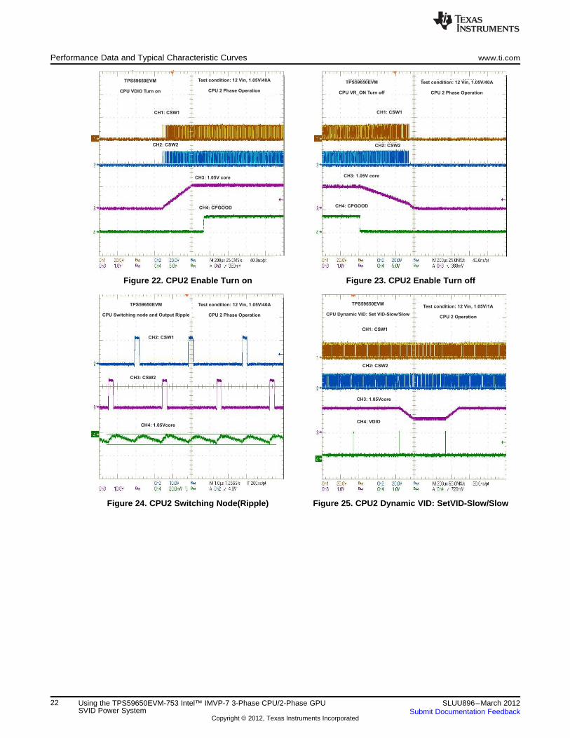
Figure 22. CPU2 Enable Turn on Figure 23. CPU2 Enable Turn off
Figure 24. CPU2 Switching Node(Ripple) Figure 25. CPU2 Dynamic VID: SetVID-Slow/Slow
22 Using the TPS59650EVM-753 Intel™ IMVP-7 3-Phase CPU/2-Phase GPU SLUU896–March 2012SVID Power System Submit Documentation Feedback
Copyright © 2012, Texas Instruments Incorporated
TPS59650EVM
CPU Dynamic VID: Set VID-Decay/Fast
Test condition: 12 Vin, 1.05V/1A
CPU 2 Operation
CH1: CSW1
CH2: CSW2
CH3: 1.05Vcore
CH4: VDIO
TPS59650EVM
CPU Dynamic VID: Set VID-Slow/Slow
Test condition: 12 Vin, 1.05V/1A
CPU 2 Operation
CH1: CSW1
CH2: CSW2
CH3: 1.05Vcore
CH4: VDIO
CH3: CSW2
CH4: 1.05Vcore
TPS59650EVMCPU Output Load Release with
OSR/USR middle level
Test condition: 12 Vin, 1.05V/0A-51ACPU 3 Phase on board dynamic load
CH2: CSW1
CH1: DYN_C
CH3: CSW2
CH4: 1.05Vcore
TPS59650EVMCPU Output Load Insertion with
OSR/USR middle level
Test condition: 12 Vin, 1.05V/0A-51ACPU 3 Phase on board dynamic load
CH1: DYN_C
CH2: CSW1
www.ti.com Performance Data and Typical Characteristic Curves
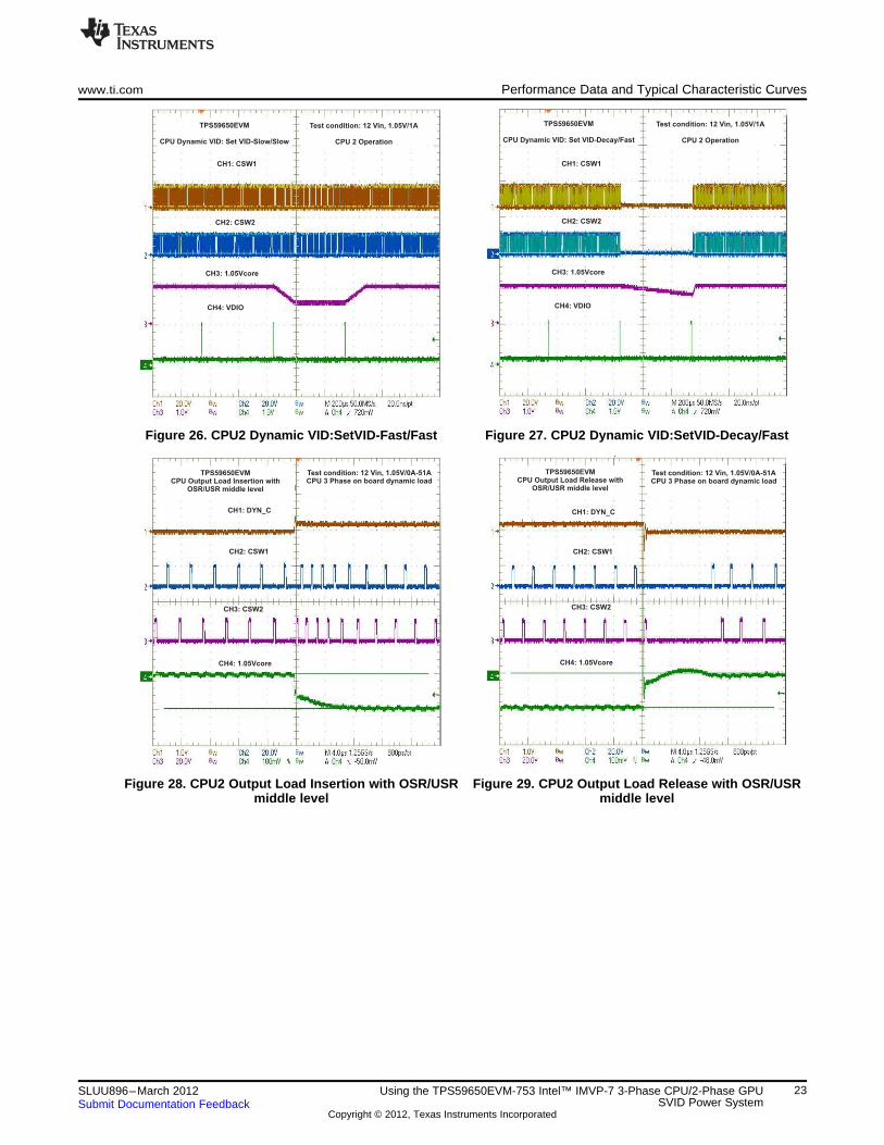
Figure 26. CPU2 Dynamic VID:SetVID-Fast/Fast Figure 27. CPU2 Dynamic VID:SetVID-Decay/Fast
Figure 28. CPU2 Output Load Insertion with OSR/USR Figure 29. CPU2 Output Load Release with OSR/USRmiddle level middle level
23SLUU896–March 2012 Using the TPS59650EVM-753 Intel™ IMVP-7 3-Phase CPU/2-Phase GPUSVID Power SystemSubmit Documentation Feedback
Copyright © 2012, Texas Instruments Incorporated
Performance Data and Typical Characteristic Curves www.ti.com
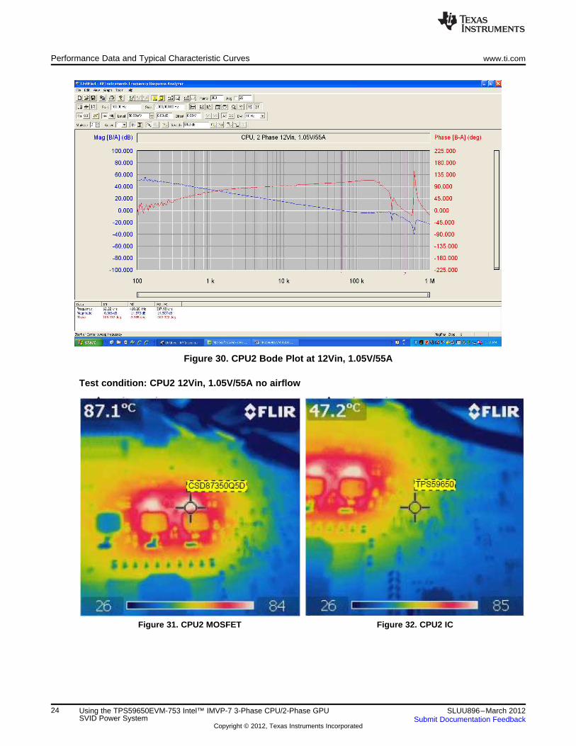
Figure 30. CPU2 Bode Plot at 12Vin, 1.05V/55A
Test condition: CPU2 12Vin, 1.05V/55A no airflow
Figure 31. CPU2 MOSFET Figure 32. CPU2 IC
24 Using the TPS59650EVM-753 Intel™ IMVP-7 3-Phase CPU/2-Phase GPU SLUU896–March 2012SVID Power System Submit Documentation Feedback
Copyright © 2012, Texas Instruments Incorporated
0 5 10 15 20 25 30 35I - Output Current - AO
70
75
80
85
90
95E
ffic
ien
cy -
%
V = 12 VIN
V = 9 VIN
V = 20 VIN
0.9
0.95
1
1.05
1.1
V-
Ou
tpu
t V
olt
ag
e -
VO
0 5 10 15 20 25 30 35I - Output Current - AO
V = 9 VIN
SPEC(max)
SPEC(nom)
SPEC(min)
V = 20 VIN
V = 12 VIN
CH4: CPGOOD
TPS59650EVMCPU VDIO Turn on
Test condition: 12 Vin, 1.05V/20ACPU 3 Phase on board dynamic load
CH2: CSW1
CH1: VDIO
CH3: 1.05Vcore CH3: 1.05Vcore
CH1: VR_ON
TPS59650EVMCPU VR_ON Turn off
Test condition: 12 Vin, 1.05V/20ACPU 1 Phase operation
CH2: CSW1
CH4: CPGOOD
www.ti.com Performance Data and Typical Characteristic Curves
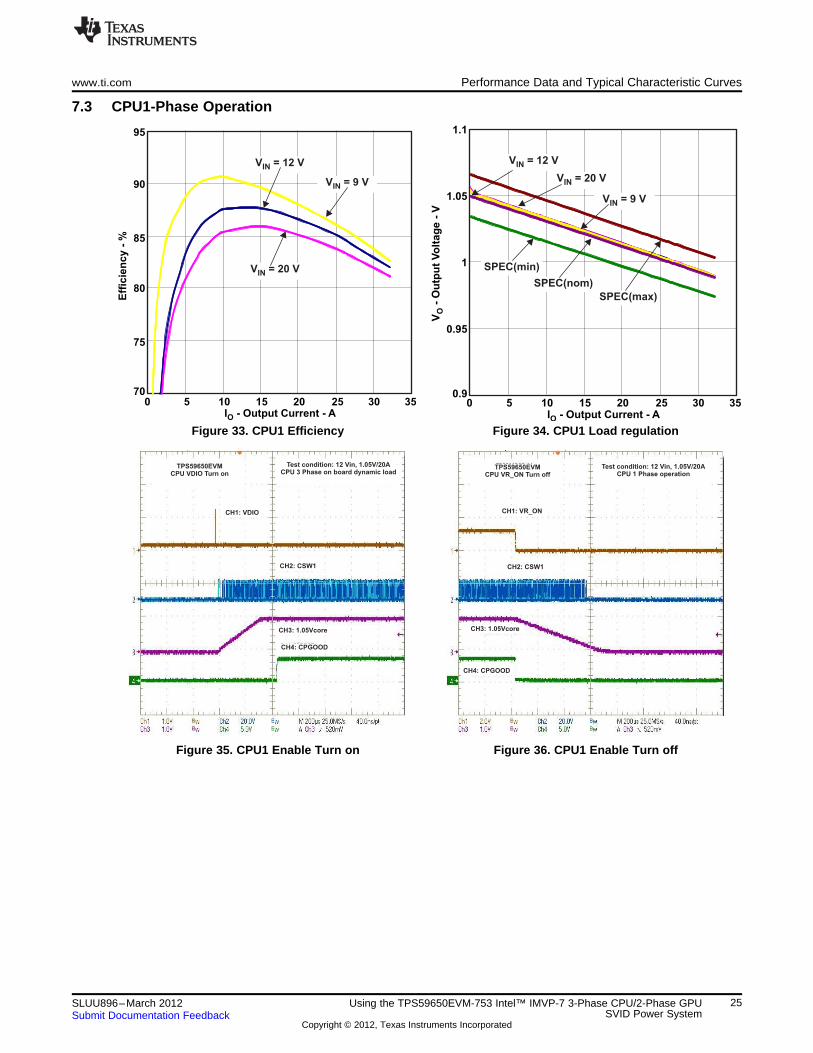
7.3 CPU1-Phase Operation
Figure 33. CPU1 Efficiency Figure 34. CPU1 Load regulation
Figure 35. CPU1 Enable Turn on Figure 36. CPU1 Enable Turn off
25SLUU896–March 2012 Using the TPS59650EVM-753 Intel™ IMVP-7 3-Phase CPU/2-Phase GPUSVID Power SystemSubmit Documentation Feedback
Copyright © 2012, Texas Instruments Incorporated
TPS59650EVMCPU Switching Node
Test condition: 12 Vin, 1.05V/20ACPU 1 Phase operation
CH1: CSW1
CH2: 1.05Vcore Ripple
CH1: CSW1
TPS59650EVMCPU Switching Node and Output Ripple
Test condition: 12 Vin, 1.05V/20ACPU 1 Phase operation
CH3: 1.05Vcore
CH4: VDIO
TPS59650EVMCPU Dynamic VID: Set VID-Fast/Fast
Test condition: 12 Vin, 1.05V/1ACPU 1 Operation
CH1: CSW1
CH3: 1.05Vcore
CH4: VDIO
TPS59650EVMCPU Dynamic VID: Set VID-Slow/Slow
Test condition: 12 Vin, 1.05V/21ACPU 1 Operation
CH1: CSW1
Performance Data and Typical Characteristic Curves www.ti.com
Figure 37. CPU1 Switching Node Figure 38. CPU1 Switching node and Ripple
Figure 39. CPU1 Dynamic VID:SetVID-Slow/Slow Figure 40. CPU1 Dynamic VID:SetVID-Fast/Fast
26 Using the TPS59650EVM-753 Intel™ IMVP-7 3-Phase CPU/2-Phase GPU SLUU896–March 2012SVID Power System Submit Documentation Feedback
Copyright © 2012, Texas Instruments Incorporated

CH3: 1.05Vcore
CH4: VDIO
TPS59650EVMCPU Dynamic VID: Set VID-Decay/Fast
Test condition: 12 Vin, 1.05V/1ACPU 1 Operation
CH1: CSW1
CH3: 1.05Vcore
TPS59650EVMCPU Output Load Insertion with
OSR/USR middle level
Test condition: 12 Vin, 1.05V/0A-27ACPU 1 Phase on board dynamic load
CH2: CSW1
CH1: DYN_C
CH3: 1.05Vcore
TPS59650EVMCPU Output Load Releas with
OSR/USR middle level
Test condition: 12 Vin, 1.05V/0A-27ACPU 1 Phase on board dynamic load
CH2: CSW1
CH1: DYN_C
www.ti.com Performance Data and Typical Characteristic Curves
Figure 41. CPU1 Dynamic VID:SetVID-Decay/Fast Figure 42. CPU1 Output Load Insertion with OSR/USRmiddle level
Figure 43. CPU1 Output Load Release with OSR/USR middle level
27SLUU896–March 2012 Using the TPS59650EVM-753 Intel™ IMVP-7 3-Phase CPU/2-Phase GPUSVID Power SystemSubmit Documentation Feedback
Copyright © 2012, Texas Instruments Incorporated

Performance Data and Typical Characteristic Curves www.ti.com
Figure 44. CPU1 Bode Plot at 12Vin, 1.05V/33A
Test condition: CPU1 12Vin, 1.05V/33A no airflow
Figure 45. CPU1 MOSFET Figure 46. CPU1 IC
28 Using the TPS59650EVM-753 Intel™ IMVP-7 3-Phase CPU/2-Phase GPU SLUU896–March 2012SVID Power System Submit Documentation Feedback
Copyright © 2012, Texas Instruments Incorporated
70
75
80
85
90
95E
ffic
ien
cy
- %
V = 20 VIN
V = 12 VIN
V = 9 VIN
0 5 10 15 20 25 30 35 40 45 50I - Output Current - AO
V-
Ou
tpu
t V
olt
ag
e -
VO
0 5 10 15 20 25 30 35 40 45 50I - Output Current - AO
1
1.05
1.1
1.15
1.2
1.25
1.3
V = 12 VIN
V = 9 VIN
V = 20 VIN
SPEC(min)
SPEC(max)
SPEC(nom)
CH3: 1.23Vcore
TPS59650EVMGPU VDIO Turn on
Test condition: 12 Vin, 1.23V/40AGPU 2 Phase operation
CH2: GSW2
CH4: GPGOOD
CH1: GSW1
CH3: 1.23Vcore
CH1: GSW1
Test condition: 12 Vin, 1.23V/40AGPU 2 Phase operation
CH2: GSW2
CH4: GPGOOD
TPS59650EVMGPU VR_ON Turn off
www.ti.com Performance Data and Typical Characteristic Curves
7.4 GPU 2 Phase Operation
Figure 47. GPU2 Efficiency Figure 48. GPU2 Load regulation
Figure 49. GPU2 Enable Turn on Figure 50. GPU2 Enable Turn off
29SLUU896–March 2012 Using the TPS59650EVM-753 Intel™ IMVP-7 3-Phase CPU/2-Phase GPUSVID Power SystemSubmit Documentation Feedback
Copyright © 2012, Texas Instruments Incorporated
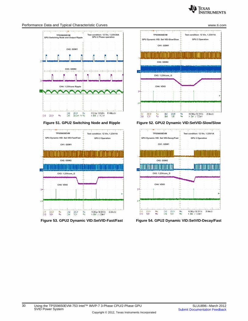
CH3: GSW2
CH4: 1.23Vcore Ripple
TPS59650EVMGPU Switching Node and Output Ripple
Test condition: 12 Vin, 1.23V/20AGPU 2 Phase operation
CH2: GSW1
Test condition: 12 Vin, 1.23V/1A
GPU 2 Operation
CH2: GSW2
TPS59650EVM
GPU Dynamic VID: Set VID-Slow/Slow
CH1: GSW1
CH3: 1.23Vcore_G
CH4: VDIO
TPS59650EVM
GPU Dynamic VID: Set VID-Decay/Fast
CH1: GSW1
CH3: 1.23Vcore_G
CH4: VDIO
Test condition: 12 Vin, 1.23V/1A
GPU 2 Operation
CH2: GSW2
TPS59650EVM
GPU Dynamic VID: Set VID-Fast/Fast
CH1: GSW1
CH3: 1.23Vcore_G
CH4: VDIO
Test condition: 12 Vin, 1.23V/1A
GPU 2 Operation
CH2: GSW2
Performance Data and Typical Characteristic Curves www.ti.com
Figure 51. GPU2 Switching Node and Ripple Figure 52. GPU2 Dynamic VID:SetVID-Slow/Slow
Figure 53. GPU2 Dynamic VID:SetVID-Fast/Fast Figure 54. GPU2 Dynamic VID:SetVID-Decay/Fast
30 Using the TPS59650EVM-753 Intel™ IMVP-7 3-Phase CPU/2-Phase GPU SLUU896–March 2012SVID Power System Submit Documentation Feedback
Copyright © 2012, Texas Instruments Incorporated
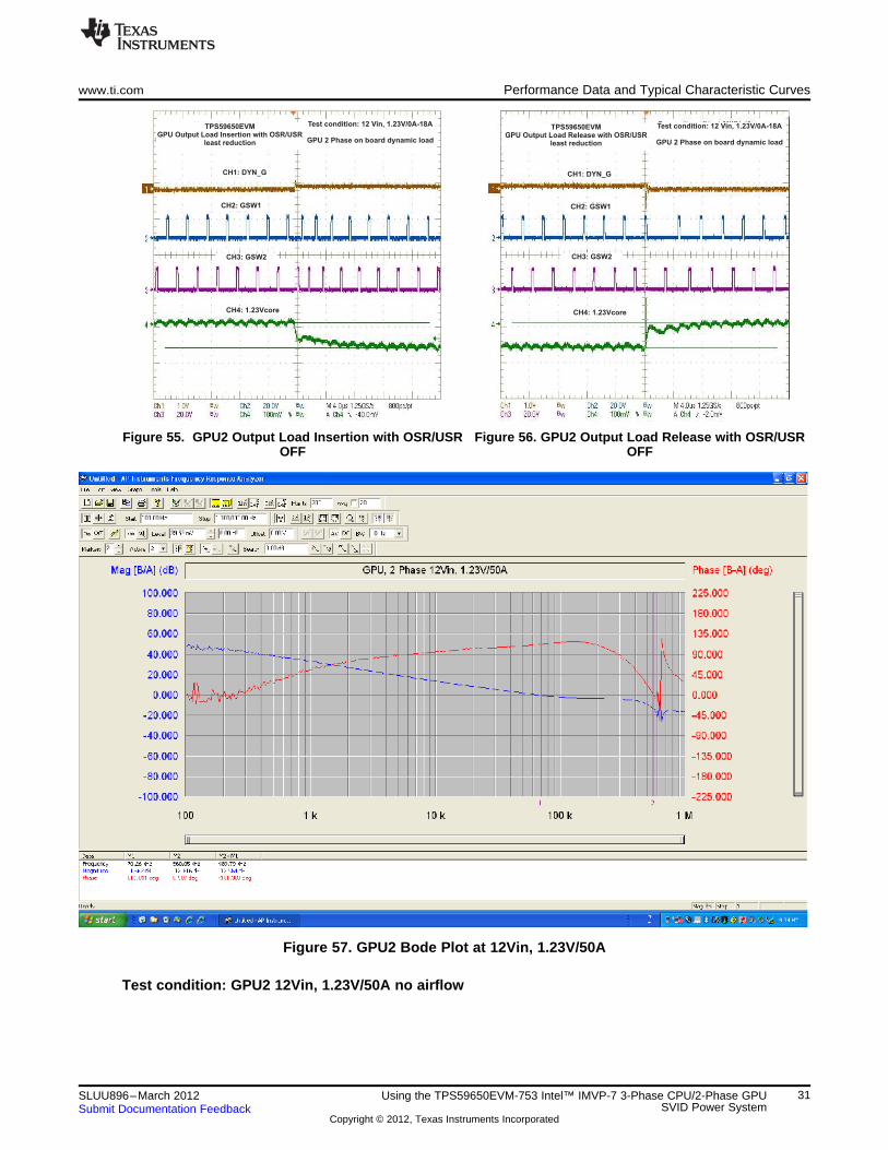
TPS59650EVMGPU Output Load Insertion with OSR/USR
least reduction
CH4: 1.23Vcore
CH3: GSW2
Test condition: 12 Vin, 1.23V/0A-18A
GPU 2 Phase on board dynamic load
CH2: GSW1
CH1: DYN_G CH1: DYN_G
TPS59650EVMGPU Output Load Release with OSR/USR
least reduction
Test condition: 12 Vin, 1.23V/0A-18A
GPU 2 Phase on board dynamic load
CH2: GSW1
CH4: 1.23Vcore
CH3: GSW2
www.ti.com Performance Data and Typical Characteristic Curves
Figure 55. GPU2 Output Load Insertion with OSR/USR Figure 56. GPU2 Output Load Release with OSR/USROFF OFF
Figure 57. GPU2 Bode Plot at 12Vin, 1.23V/50A
Test condition: GPU2 12Vin, 1.23V/50A no airflow
31SLUU896–March 2012 Using the TPS59650EVM-753 Intel™ IMVP-7 3-Phase CPU/2-Phase GPUSVID Power SystemSubmit Documentation Feedback
Copyright © 2012, Texas Instruments Incorporated
V = 9 VIN
V = 20 VIN
V = 12 VIN
70
75
80
85
90
95
Eff
icie
nc
y -
%
0 5 10 15 20 25 30 35I - Output Current - AO
1.05
1.1
1.15
1.2
1.25
1.3
V = 9 VIN
SPEC(max)
SPEC(nom)
SPEC(min)
V = 20 VIN
V = 12 VIN
0 5 10 15 20 25 30 35I - Output Current - AO
V-
Ou
tpu
t V
olt
ag
e -
VO
Performance Data and Typical Characteristic Curves www.ti.com
Figure 58. GPU2 MOSFET Figure 59. GPU2 IC
7.5 GPU 1 Phase Operation
Figure 60. GPU1 Efficiency Figure 61. GPU1 Load regulation
32 Using the TPS59650EVM-753 Intel™ IMVP-7 3-Phase CPU/2-Phase GPU SLUU896–March 2012SVID Power System Submit Documentation Feedback
Copyright © 2012, Texas Instruments Incorporated
CH3: 1.23Vcore
CH1: VDIO
TPS59650EVMGPU VDIO Turn on
Test condition: 12 Vin, 1.05V/20AGPU 1 Phase operation
CH2: GSW1
CH4: GPGOOD
CH3: 1.23Vcore
CH1: VR_ON
TPS59650EVMGPU VR_ON Turn on
Test condition: 12 Vin, 1.23V/20AGPU 1 Phase operation
CH2: GSW1
CH4: GPGOOD
TPS59650EVMGPU Switching Node
Test condition: 12 Vin, 1.23V/0A-18AGPU 1 Phase operation
CH1: GSW1
TPS59650EVMGPU Switching Node and Output Ripple
Test condition: 12 Vin, 1.23V/20AGPU 1 Phase operation
CH2: GSW1
CH3: 1.23Vcore Ripple
www.ti.com Performance Data and Typical Characteristic Curves
Figure 62. GPU1 Enable Turn on Figure 63. GPU1 Enable Turn off
Figure 64. GPU1 Switching Node Figure 65. GPU1 Switching Node and Ripple
33SLUU896–March 2012 Using the TPS59650EVM-753 Intel™ IMVP-7 3-Phase CPU/2-Phase GPUSVID Power SystemSubmit Documentation Feedback
Copyright © 2012, Texas Instruments Incorporated
TPS59650EVM
CPU Dynamic VID: Set VID-Fast/Fast
Test condition: 12 Vin, 1.23V/1A
GPU 1 Operation
CH1: CSW1
CH3: 1.23Vcore_G
CH4: VDIO
TPS59650EVM
GPU Dynamic VID: Set VID-Slow/Slow
CH1: GSW1
CH3: 1.23Vcore_G
CH4: VDIO
Test condition: 12 Vin, 1.23V/1A
GPU 1 Operation
TPS59650EVM
GPU Dynamic VID: Set VID-Decay/Fast
Test condition: 12 Vin, 1.23V/1A
GPU 1 Operation
CH1: GSW1
CH3: 1.23Vcore_G
CH4: VDIO
CH1: DYN_G
TPS59650EVMGPU Output Load Insertion with OSR/USR
least reduction
Test condition: 12 Vin, 1.23V/0A-18A
GPU 1 Phase on board dynamic load
CH2: GSW1
CH3: 1.23Vcore
Performance Data and Typical Characteristic Curves www.ti.com
Figure 66. GPU1 Dynamic VID:SetVID-Slow/Slow Figure 67. GPU1 Dynamic VID:SetVID-Fast/Fast
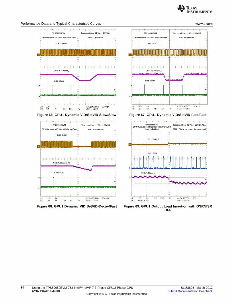
Figure 68. GPU1 Dynamic VID:SetVID-Decay/Fast Figure 69. GPU1 Output Load Insertion with OSR/USROFF
34 Using the TPS59650EVM-753 Intel™ IMVP-7 3-Phase CPU/2-Phase GPU SLUU896–March 2012SVID Power System Submit Documentation Feedback
Copyright © 2012, Texas Instruments Incorporated
CH1: DYN_G
TPS59650EVMGPU Output Load Release with OSR/USR
least reduction
Test condition: 12 Vin, 1.23V/0A-18A
GPU 1 Phase on board dynamic load
CH2: GSW1
CH3: 1.23Vcore
www.ti.com Performance Data and Typical Characteristic Curves
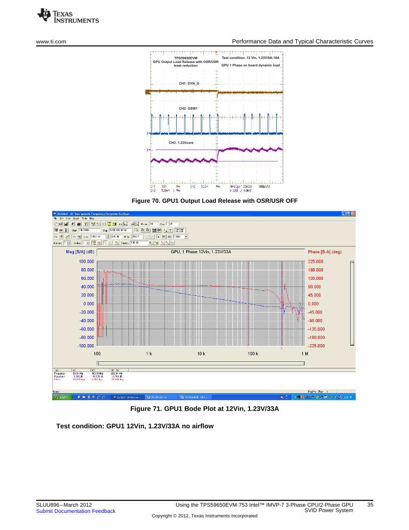
Figure 70. GPU1 Output Load Release with OSR/USR OFF
Figure 71. GPU1 Bode Plot at 12Vin, 1.23V/33A
Test condition: GPU1 12Vin, 1.23V/33A no airflow
35SLUU896–March 2012 Using the TPS59650EVM-753 Intel™ IMVP-7 3-Phase CPU/2-Phase GPUSVID Power SystemSubmit Documentation Feedback
Copyright © 2012, Texas Instruments Incorporated

I - Output Current - AO
0.001 0.01 0.1 1 10 1000
10
20
30
40
50
60
70
80
90
100
Eff
icie
nc
y -
%
V = 9 VIN
V = 20 VIN
V = 12 VIN
0 2 4 6 8 10I - Output Current - AO
1.02
1.04
1.06
1.08
V-
Ou
tpu
t V
olt
ag
e -
VO
V = 9 VIN
V = 20 VIN
V = 12 VIN
Performance Data and Typical Characteristic Curves www.ti.com
Figure 72. GPU1 MOSFET Figure 73. GPU1 IC
7.6 1.05V VCCIO
Figure 74. 1.05V Efficiency Figure 75. 1.05V Load regulation
36 Using the TPS59650EVM-753 Intel™ IMVP-7 3-Phase CPU/2-Phase GPU SLUU896–March 2012SVID Power System Submit Documentation Feedback
Copyright © 2012, Texas Instruments Incorporated

CH3: VCCIO_PG
CH1: VCCIO_EN
TPS59650EVMVCCIO Enable Turn on
Test condition: 12 Vin, 1.05VCCIO/10A
CH2: 1.05VCCIO
CH3: VCCIO_PG
CH1: VCCIO_EN
TPS59650EVMVCCIO Enable Turn off
Test condition: 12 Vin, 1.05VCCIO/10A
CH2: 1.05VCCIO
CH1: SW
TPS59650EVMVCCIO Switching Node
Test condition: 12 Vin, 1.05VCCIO/10A
CH1: VCCIO Output Ripple
TPS59650EVMVCCIO Output Ripple
Test condition: 12 Vin, 1.05VCCIO/10A
www.ti.com Performance Data and Typical Characteristic Curves
Figure 76. 1.05V Enable Turn on Figure 77. 1.05V Enable Turn off
Figure 78. 1.05V Switching Node Figure 79. 1.05V Ripple
37SLUU896–March 2012 Using the TPS59650EVM-753 Intel™ IMVP-7 3-Phase CPU/2-Phase GPUSVID Power SystemSubmit Documentation Feedback
Copyright © 2012, Texas Instruments Incorporated
CH1: VCCIO Output
TPS59650EVMVCCIO Output Transient from
DCM to CCM
Test condition: 12 Vin, 1.05VCCIO/0A-10A
CH2: VCCIO Output current
CH1: VCCIO Output
TPS59650EVMVCCIO Output Transient from
CCM to DCM
Test condition: 12 Vin, 1.05VCCIO/0A-10A
CH2: VCCIO Output current
Performance Data and Typical Characteristic Curves www.ti.com
Figure 80. 1.05V Transient DCM TO CCM Figure 81. 1.05V Transient CCM to DCM
Test condition: 12Vin, 1.05V/10A no airflow
Figure 82. TPS51219 Thermal
38 Using the TPS59650EVM-753 Intel™ IMVP-7 3-Phase CPU/2-Phase GPU SLUU896–March 2012SVID Power System Submit Documentation Feedback
Copyright © 2012, Texas Instruments Incorporated
0
10
20
30
40
50
60
70
80
90
100E
ffic
ien
cy -
%
I - Output Current - AO
0.001 0.01 0.1 1 10
V = 9 VIN
V = 20 VIN
V = 12 VIN
0 2 4 6 8I - Output Current - AO
1.14
1.16
1.18
1.20
1.22
1.24
1.26
V-
Ou
tpu
t V
olt
ag
e -
VO
V = 9 VIN
V = 20 VIN
V = 12 VIN
CH3: VTTREF
CH1: VDDQ S5
TPS59650EVMVDDQ S5 Turn on
Test condition: 12 Vin, 1.2VDDQ/8A
CH2: VDDQ
CH4: VDDQ_PG
CH4: VDDQ_PG
CH3: VTTREF
CH2: VDDQ
CH1: VDDQ S5
Test condition: 12 Vin, 1.2VDDQ/8ATPS59650EVMVDDQ S5 Turn off
www.ti.com Performance Data and Typical Characteristic Curves
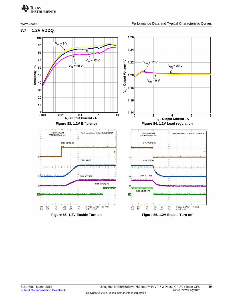
7.7 1.2V VDDQ
Figure 83. 1.2V Efficiency Figure 84. 1.2V Load regulation
Figure 85. 1.2V Enable Turn on Figure 86. 1.2V Enable Turn off
39SLUU896–March 2012 Using the TPS59650EVM-753 Intel™ IMVP-7 3-Phase CPU/2-Phase GPUSVID Power SystemSubmit Documentation Feedback
Copyright © 2012, Texas Instruments Incorporated
CH1: VDDQ Output Ripple
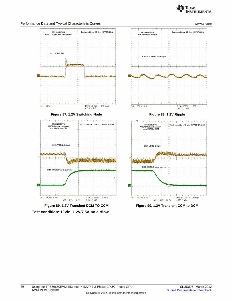
Test condition: 12 Vin, 1.2VDDQ/8ATPS59650EVMVDDQ Output Ripple
CH1: VDDQ SW
Test condition: 12 Vin, 1.2VDDQ/8ATPS59650EVMVDDQ Output Switching Node
CH4: VDDQ Output current
CH1: VDDQ Output
TPS59650EVMVDDQ Output transient
from DCM to CCM
Test condition: 12 Vin, 1.2VDDQ/0A-8A
CH4: VDDQ Output current
CH1: VDDQ Output
Test condition: 12 Vin, 1.2VDDQ/0A-8ATPS59650EVMVDDQ Output transient
from CCM to DCM
Performance Data and Typical Characteristic Curves www.ti.com
Figure 87. 1.2V Switching Node Figure 88. 1.2V Ripple
Figure 89. 1.2V Transient DCM TO CCM Figure 90. 1.2V Transient CCM to DCM
Test condition: 12Vin, 1.2V/7.5A no airflow
40 Using the TPS59650EVM-753 Intel™ IMVP-7 3-Phase CPU/2-Phase GPU SLUU896–March 2012SVID Power System Submit Documentation Feedback
Copyright © 2012, Texas Instruments Incorporated
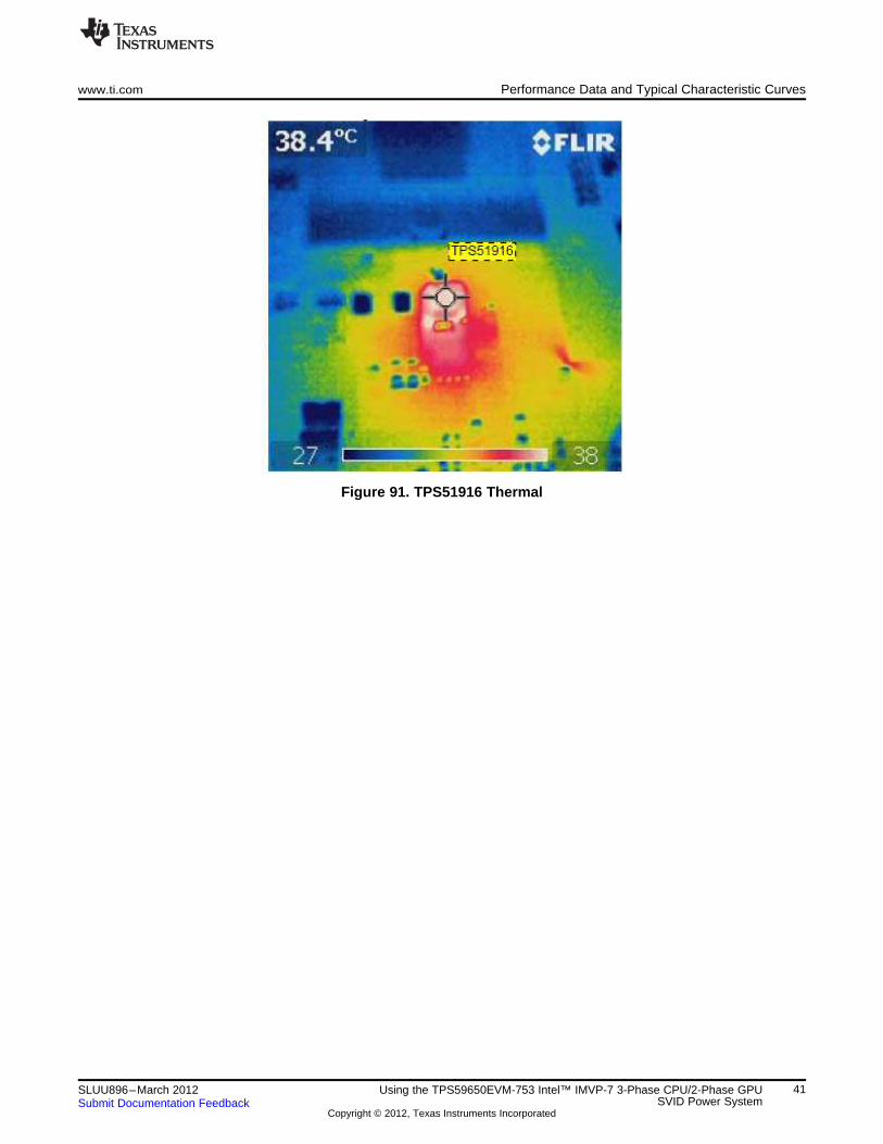
www.ti.com Performance Data and Typical Characteristic Curves
Figure 91. TPS51916 Thermal
41SLUU896–March 2012 Using the TPS59650EVM-753 Intel™ IMVP-7 3-Phase CPU/2-Phase GPUSVID Power SystemSubmit Documentation Feedback
Copyright © 2012, Texas Instruments Incorporated

EVM Assembly Drawings and PCB Layout www.ti.com
8 EVM Assembly Drawings and PCB Layout
The following figures (Figure 92 through Figure 101) show the design of the TPS59650EVM-753 printedcircuit board. The EVM has been designed using 8 Layers circuit board with 1oz copper on outside layers.
Figure 92. TPS59650EVM-753 Top Layer Assembly Drawing (Top view)
Figure 93. TPS59650EVM-753 Bottom Assembly Drawing (Bottom view)
42 Using the TPS59650EVM-753 Intel™ IMVP-7 3-Phase CPU/2-Phase GPU SLUU896–March 2012SVID Power System Submit Documentation Feedback
Copyright © 2012, Texas Instruments Incorporated

www.ti.com EVM Assembly Drawings and PCB Layout
Figure 94. TPS59650EVM-753 Top Copper
Figure 95. TPS59650EVM-753 Bottom Copper
43SLUU896–March 2012 Using the TPS59650EVM-753 Intel™ IMVP-7 3-Phase CPU/2-Phase GPUSVID Power SystemSubmit Documentation Feedback
Copyright © 2012, Texas Instruments Incorporated
EVM Assembly Drawings and PCB Layout www.ti.com
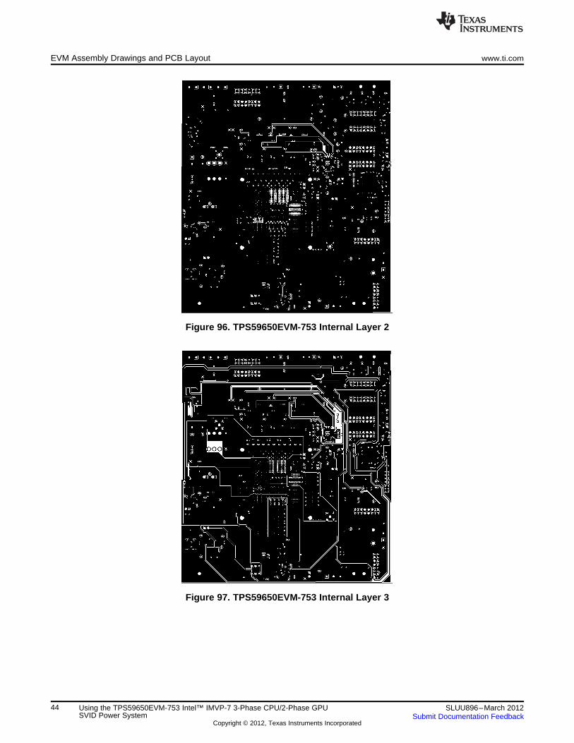
Figure 96. TPS59650EVM-753 Internal Layer 2
Figure 97. TPS59650EVM-753 Internal Layer 3
44 Using the TPS59650EVM-753 Intel™ IMVP-7 3-Phase CPU/2-Phase GPU SLUU896–March 2012SVID Power System Submit Documentation Feedback
Copyright © 2012, Texas Instruments Incorporated
www.ti.com EVM Assembly Drawings and PCB Layout
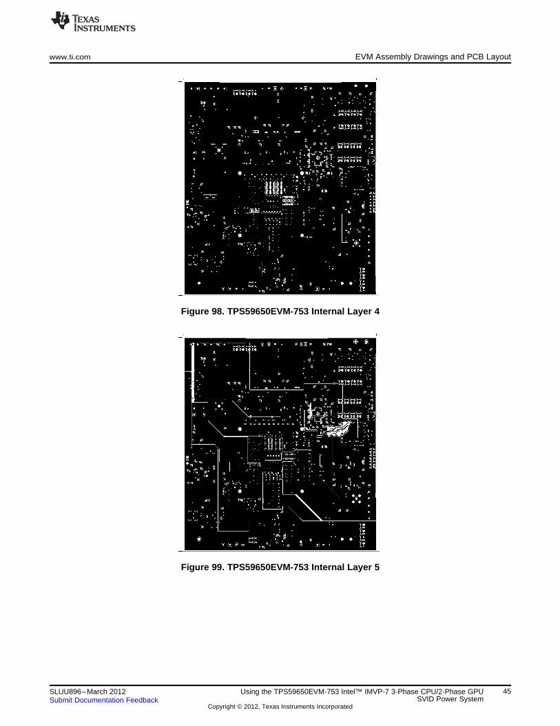
Figure 98. TPS59650EVM-753 Internal Layer 4
Figure 99. TPS59650EVM-753 Internal Layer 5
45SLUU896–March 2012 Using the TPS59650EVM-753 Intel™ IMVP-7 3-Phase CPU/2-Phase GPUSVID Power SystemSubmit Documentation Feedback
Copyright © 2012, Texas Instruments Incorporated
EVM Assembly Drawings and PCB Layout www.ti.com
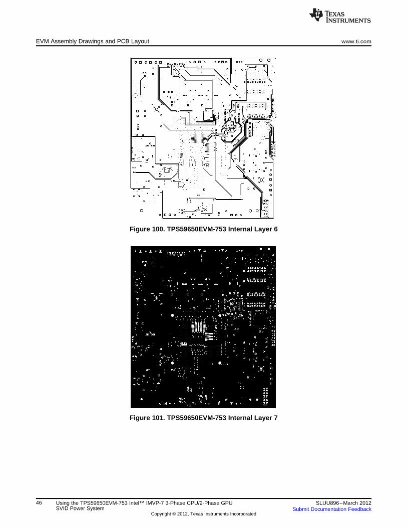
Figure 100. TPS59650EVM-753 Internal Layer 6
Figure 101. TPS59650EVM-753 Internal Layer 7
46 Using the TPS59650EVM-753 Intel™ IMVP-7 3-Phase CPU/2-Phase GPU SLUU896–March 2012SVID Power System Submit Documentation Feedback
Copyright © 2012, Texas Instruments Incorporated
www.ti.com Bill of Materials
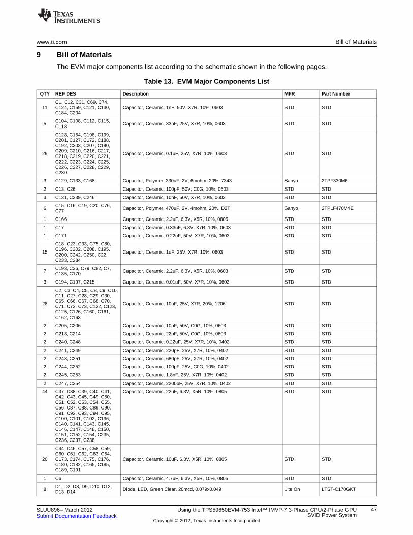
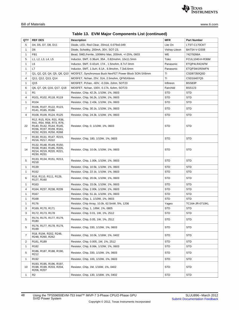
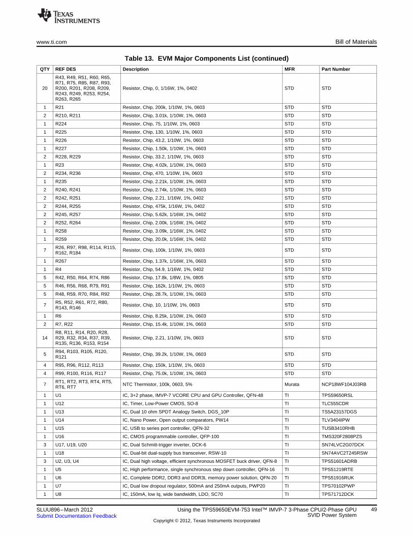
9 Bill of Materials
The EVM major components list according to the schematic shown in the following pages.
Table 13. EVM Major Components List
QTY REF DES Description MFR Part Number
C1, C12, C31, C69, C74,11 C124, C159, C121, C130, Capacitor, Ceramic, 1nF, 50V, X7R, 10%, 0603 STD STD
C184, C204
C104, C108, C112, C115,5 Capacitor, Ceramic, 33nF, 25V, X7R, 10%, 0603 STD STDC118
C128, C164, C198, C199,C201, C127, C172, C188,C192, C203, C207, C190,C209, C210, C216, C217,29 Capacitor, Ceramic, 0.1uF, 25V, X7R, 10%, 0603 STD STDC218, C219, C220, C221,C222, C223, C224, C225,C226, C227, C228, C229,C230
3 C129, C133, C168 Capacitor, Polymer, 330uF, 2V, 6mohm, 20%, 7343 Sanyo 2TPF330M6
2 C13, C26 Capacitor, Ceramic, 100pF, 50V, C0G, 10%, 0603 STD STD
3 C131, C239, C246 Capacitor, Ceramic, 10nF, 50V, X7R, 10%, 0603 STD STD
C15, C16, C19, C20, C76,6 Capacitor, Polymer, 470uF, 2V, 4mohm, 20%, D2T Sanyo 2TPLF470M4EC77
1 C166 Capacitor, Ceramic, 2.2uF, 6.3V, X5R, 10%, 0805 STD STD
1 C17 Capacitor, Ceramic, 0.33uF, 6.3V, X7R, 10%, 0603 STD STD
1 C171 Capacitor, Ceramic, 0.22uF, 50V, X7R, 10%, 0603 STD STD
C18, C23, C33, C75, C80,C196, C202, C208, C195,15 Capacitor, Ceramic, 1uF, 25V, X7R, 10%, 0603 STD STDC200, C242, C250, C22,C233, C234
C193, C36, C79, C82, C7,7 Capacitor, Ceramic, 2.2uF, 6.3V, X5R, 10%, 0603 STD STDC135, C170
3 C194, C197, C215 Capacitor, Ceramic, 0.01uF, 50V, X7R, 10%, 0603 STD STD
C2, C3, C4, C5, C8, C9, C10,C11, C27, C28, C29, C30,C65, C66, C67, C68, C70,28 Capacitor, Ceramic, 10uF, 25V, X7R, 20%, 1206 STD STDC71, C72, C73, C122, C123,C125, C126, C160, C161,C162, C163
2 C205, C206 Capacitor, Ceramic, 10pF, 50V, C0G, 10%, 0603 STD STD
2 C213, C214 Capacitor, Ceramic, 22pF, 50V, C0G, 10%, 0603 STD STD
2 C240, C248 Capacitor, Ceramic, 0.22uF, 25V, X7R, 10%, 0402 STD STD
2 C241, C249 Capacitor, Ceramic, 220pF, 25V, X7R, 10%, 0402 STD STD
2 C243, C251 Capacitor, Ceramic, 680pF, 25V, X7R, 10%, 0402 STD STD
2 C244, C252 Capacitor, Ceramic, 100pF, 25V, C0G, 10%, 0402 STD STD
2 C245, C253 Capacitor, Ceramic, 1.8nF, 25V, X7R, 10%, 0402 STD STD
2 C247, C254 Capacitor, Ceramic, 2200pF, 25V, X7R, 10%, 0402 STD STD
44 C37, C38, C39, C40, C41, Capacitor, Ceramic, 22uF, 6.3V, X5R, 10%, 0805 STD STDC42, C43, C45, C49, C50,C51, C52, C53, C54, C55,C56, C87, C88, C89, C90,C91, C92, C93, C94, C95,C100, C101, C102, C136,C140, C141, C143, C145,C146, C147, C148, C150,C151, C152, C154, C235,C236, C237, C238
C44, C46, C57, C58, C59,C60, C61, C62, C63, C64,
20 C173, C174, C175, C176, Capacitor, Ceramic, 10uF, 6.3V, X5R, 10%, 0805 STD STDC180, C182, C165, C185,C189, C191
1 C6 Capacitor, Ceramic, 4.7uF, 6.3V, X5R, 10%, 0805 STD STD
D1, D2, D3, D9, D10, D12,8 Diode, LED, Green Clear, 20mcd, 0.079x0.049 Lite On LTST-C170GKTD13, D14
47SLUU896–March 2012 Using the TPS59650EVM-753 Intel™ IMVP-7 3-Phase CPU/2-Phase GPUSVID Power SystemSubmit Documentation Feedback
Copyright © 2012, Texas Instruments Incorporated
Bill of Materials www.ti.com
Table 13. EVM Major Components List (continued)
QTY REF DES Description MFR Part Number
5 D4, D5, D7, D8, D11 Diode, LED, Red Clear, 20mcd, 0.079x0.049 Lite On LTST-C170CKT
1 D6 Diode, Schottky, 200mA, 30V, SOT-23, Vishay-Liteon BAT54-V-GS08
1 FB1 Bead, SMD,Ferrite, 100MHz Max, 200mA, +/-25%, 0603 WE 74279266A
5 L1, L2, L3, L4, L5 Inductor, SMT, 0.36uH, 35A , 0.82mohm, 10x11.5mm Toko FCUL1040-H-R36M
1 L6 Inductor, SMT, 0.42uH, 17A , 1.5mohm, 8.7x7.0mm Panasonic ETQP4LR42AFM
1 L7 Inductor, SMT, 1.0uH, 8.1A , 6.9mohm, 7.3x6.6mm Panasonic ETQP3W1R0WFN
7 Q1, Q2, Q3, Q4, Q5, Q8, Q10 MOSFET, Synchronous Buck NexFET Power Block SON 5X6mm TI CSD87350Q5D
4 Q11, Q12, Q13, Q14 MOSFET, Nchan, 25V, 31A, 2.5mohm, QFN5X6mm TI CSD16407Q5
1 Q15 MOSFET, Pchan, -60V, -0.33A, 2ohm, SOT23 Infineon BSS83P
6 Q6, Q7, Q9, Q16, Q17, Q18 MOSFET, Nchan, 100V, 0.17A, 6ohm, SOT23 Fairchild BSS123
1 R1 Resistor, Chip, 42.2k, 1/10W, 1%, 0603 STD STD
4 R101, R102, R118, R119 Resistor, Chip, 56.2k, 1/10W, 1%, 0603 STD STD
1 R104 Resistor, Chip, 2.43k, 1/10W, 1%, 0603 STD STD
R106, R107, R122, R123,7 Resistor, Chip, 30.1k, 1/10W, 1%, 0603 STD STDR141, R165, R166
4 R108, R109, R124, R125 Resistor, Chip, 24.3k, 1/10W, 1%, 0603 STD STD
R12, R15, R24, R31, R36,R41, R54, R58, R73, R76,
22 R140, R142, R144, R145, Resistor, Chip, 0, 1/10W, 1%, 0603 STD STDR156, R157, R159, R161,R232, R233, R250, R268
R130, R131, R147, R215,7 Resistor, Chip, 180, 1/10W, 1%, 0603 STD STDR216, R217, R222
R132, R148, R149, R150,R158, R183, R185, R205,14 Resistor, Chip, 10.0k, 1/10W, 1%, 0603 STD STDR214, R219, R220, R221,R230, R231
R133, R134, R151, R213,5 Resistor, Chip, 1.00k, 1/10W, 1%, 0603 STD STDR218
1 R139 Resistor, Chip, 10.5k, 1/10W, 1%, 0603 STD STD
1 R152 Resistor, Chip, 22.1k, 1/10W, 1%, 0603 STD STD
R16, R110, R111, R126,6 Resistor, Chip, 20.0k, 1/10W, 1%, 0603 STD STDR127, R160
1 R163 Resistor, Chip, 15.0k, 1/10W, 1%, 0603 STD STD
4 R164, R237, R238, R239 Resistor, Chip, 2.00k, 1/10W, 1%, 0603 STD STD
1 R167 Resistor, Chip, 51.1k, 1/10W, 1%, 0603 STD STD
1 R168 Resistor, Chip, 1, 1/10W, 1%, 0603 STD STD
1 R176 Resistor, Chip Array, 10.0k, 62.5mW, 5%, 1206 Yageo TC164-JR-0710KL
3 R169, R170, R171 Resistor, Chip, 1, 1/8W, 1%, 0805 STD STD
3 R172, R173, R178 Resistor, Chip, 0.01, 1W, 1%, 2512 STD STD
R174, R175, R177, R179,5 Resistor, Chip, 0.05, 1W, 1%, 2512 STD STDR180
R176, R177, R178, R179,5 Resistor, Chip, 330, 1/10W, 1%, 0603 STD STDR199
R18, R194, R202, R246,7 Resistor, Chip, 10.0k, 1/16W, 1%, 0402 STD STDR248, R260, R262
2 R181, R189 Resistor, Chip, 0.005, 1W, 1%, 2512 STD STD
1 R182 Resistor, Chip, 8.06k, 1/10W, 1%, 0603 STD STD
R186, R187, R188, R190,5 Resistor, Chip, 330, 1/10W, 1%, 0603 STD STDR212
1 R192 Resistor, Chip, 100, 1/10W, 1%, 0603 STD STD
R193, R195, R196, R197,10 R198, R199, R203, R204, Resistor, Chip, 1M, 1/16W, 1%, 0402 STD STD
R206, R207
1 R2 Resistor, Chip, 130, 1/16W, 1%, 0402 STD STD
48 Using the TPS59650EVM-753 Intel™ IMVP-7 3-Phase CPU/2-Phase GPU SLUU896–March 2012SVID Power System Submit Documentation Feedback
Copyright © 2012, Texas Instruments Incorporated
www.ti.com Bill of Materials
Table 13. EVM Major Components List (continued)
QTY REF DES Description MFR Part Number
R43, R49, R51, R60, R65,R71, R75, R85, R87, R93,
20 R200, R201, R208, R209, Resistor, Chip, 0, 1/16W, 1%, 0402 STD STDR243, R249, R253, R254,R263, R265
1 R21 Resistor, Chip, 200k, 1/10W, 1%, 0603 STD STD
2 R210, R211 Resistor, Chip, 3.01k, 1/10W, 1%, 0603 STD STD
1 R224 Resistor, Chip, 75, 1/10W, 1%, 0603 STD STD
1 R225 Resistor, Chip, 130, 1/10W, 1%, 0603 STD STD
1 R226 Resistor, Chip, 43.2, 1/10W, 1%, 0603 STD STD
1 R227 Resistor, Chip, 1.50k, 1/10W, 1%, 0603 STD STD
2 R228, R229 Resistor, Chip, 33.2, 1/10W, 1%, 0603 STD STD
1 R23 Resistor, Chip, 4.02k, 1/10W, 1%, 0603 STD STD
2 R234, R236 Resistor, Chip, 470, 1/10W, 1%, 0603 STD STD
1 R235 Resistor, Chip, 2.21k, 1/10W, 1%, 0603 STD STD
2 R240, R241 Resistor, Chip, 2.74k, 1/10W, 1%, 0603 STD STD
2 R242, R251 Resistor, Chip, 2.21, 1/16W, 1%, 0402 STD STD
2 R244, R255 Resistor, Chip, 475k, 1/16W, 1%, 0402 STD STD
2 R245, R257 Resistor, Chip, 5.62k, 1/16W, 1%, 0402 STD STD
2 R252, R264 Resistor, Chip, 2.00k, 1/16W, 1%, 0402 STD STD
1 R258 Resistor, Chip, 3.09k, 1/16W, 1%, 0402 STD STD
1 R259 Resistor, Chip, 20.0k, 1/16W, 1%, 0402 STD STD
R26, R97, R98, R114, R115,7 Resistor, Chip, 100k, 1/10W, 1%, 0603 STD STDR162, R184
1 R267 Resistor, Chip, 1.37k, 1/16W, 1%, 0603 STD STD
1 R4 Resistor, Chip, 54.9, 1/16W, 1%, 0402 STD STD
5 R42, R50, R64, R74, R86 Resistor, Chip, 17.8k, 1/8W, 1%, 0805 STD STD
5 R46, R56, R68, R79, R91 Resistor, Chip, 162k, 1/10W, 1%, 0603 STD STD
5 R48, R59, R70, R84, R92 Resistor, Chip, 28.7k, 1/10W, 1%, 0603 STD STD
R5, R52, R61, R72, R80,7 Resistor, Chip, 10, 1/10W, 1%, 0603 STD STDR143, R146
1 R6 Resistor, Chip, 8.25k, 1/10W, 1%, 0603 STD STD
2 R7, R22 Resistor, Chip, 15.4k, 1/10W, 1%, 0603 STD STD
R8, R11, R14, R20, R28,14 R29, R32, R34, R37, R39, Resistor, Chip, 2.21, 1/10W, 1%, 0603 STD STD
R135, R136, R153, R154
R94, R103, R105, R120,5 Resistor, Chip, 39.2k, 1/10W, 1%, 0603 STD STDR121
4 R95, R96, R112, R113 Resistor, Chip, 150k, 1/10W, 1%, 0603 STD STD
4 R99, R100, R116, R117 Resistor, Chip, 75.0k, 1/10W, 1%, 0603 STD STD
RT1, RT2, RT3, RT4, RT5,7 NTC Thermistor, 100k, 0603, 5% Murata NCP18WF104J03RBRT6, RT7
1 U1 IC, 3+2 phase, IMVP-7 VCORE CPU and GPU Controller, QFN-48 TI TPS59650RSL
1 U12 IC, Timer, Low-Power CMOS, SO-8 TI TLC555CDR
1 U13 IC, Dual 10 ohm SPDT Analogy Switch, DGS_10P TI TS5A23157DGS
1 U14 IC, Nano Power, Open output comparators, PW14 TI TLV3404IPW
1 U15 IC, USB to series port controller, QFN-32 TI TUSB3410RHB
1 U16 IC, CMOS programmable controller, QFP-100 TI TMS320F2808PZS
3 U17, U19, U20 IC, Dual Schmitt-trigger inverter, DCK-6 TI SN74LVC2G07DCK
1 U18 IC, Dual-bit dual-supply bus transceiver, RSW-10 TI SN74AVC2T245RSW
3 U2, U3, U4 IC, Dual high voltage, efficient synchronous MOSFET buck driver, QFN-8 TI TPS51601ADRB
1 U5 IC, High performance, single synchronous step down controller, QFN-16 TI TPS51219RTE
1 U6 IC, Complete DDR2, DDR3 and DDR3L memory power solution, QFN-20 TI TPS51916RUK
1 U7 IC, Dual low dropout regulator, 500mA and 250mA outputs, PWP20 TI TPS70102PWP
1 U8 IC, 150mA, low Iq, wide bandwidth, LDO, SC70 TI TPS71712DCK
49SLUU896–March 2012 Using the TPS59650EVM-753 Intel™ IMVP-7 3-Phase CPU/2-Phase GPUSVID Power SystemSubmit Documentation Feedback
Copyright © 2012, Texas Instruments Incorporated
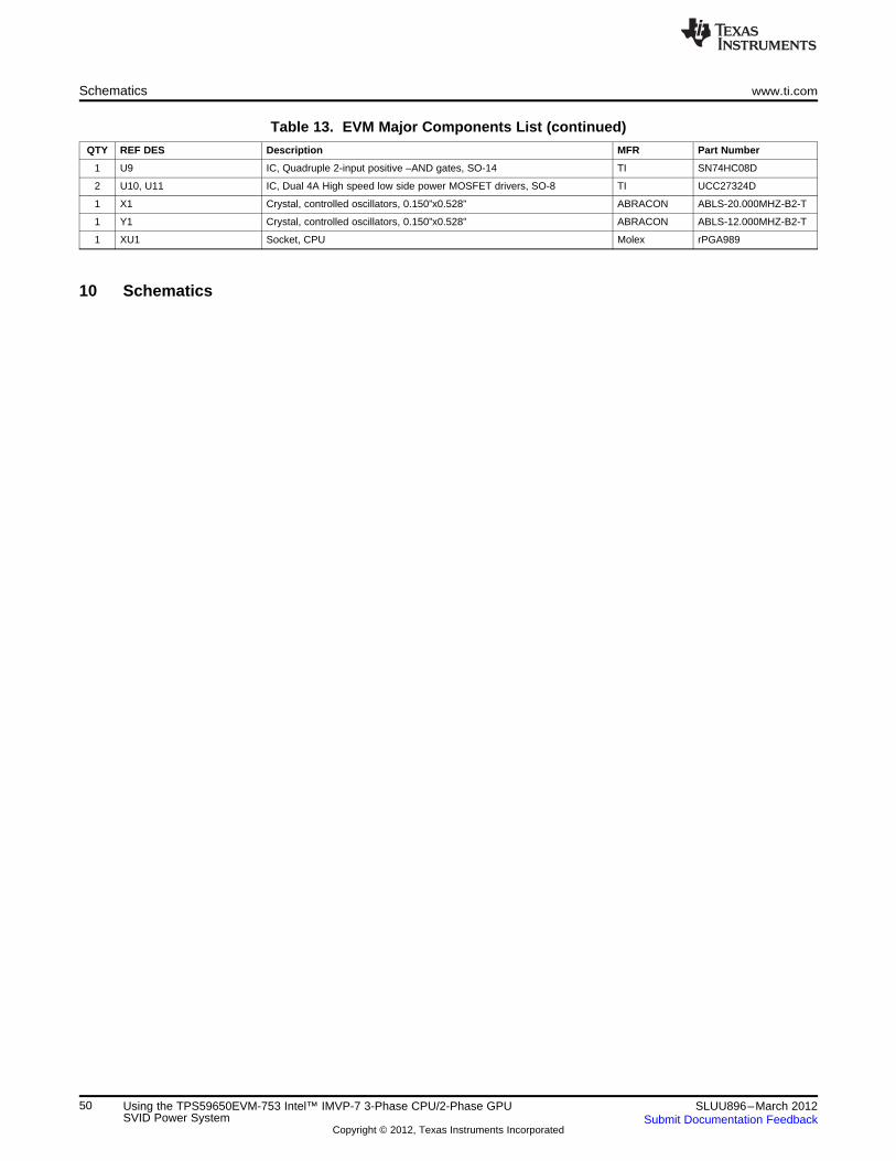
Schematics www.ti.com
Table 13. EVM Major Components List (continued)
QTY REF DES Description MFR Part Number
1 U9 IC, Quadruple 2-input positive –AND gates, SO-14 TI SN74HC08D
2 U10, U11 IC, Dual 4A High speed low side power MOSFET drivers, SO-8 TI UCC27324D
1 X1 Crystal, controlled oscillators, 0.150”x0.528” ABRACON ABLS-20.000MHZ-B2-T
1 Y1 Crystal, controlled oscillators, 0.150”x0.528” ABRACON ABLS-12.000MHZ-B2-T
1 XU1 Socket, CPU Molex rPGA989
10 Schematics
50 Using the TPS59650EVM-753 Intel™ IMVP-7 3-Phase CPU/2-Phase GPU SLUU896–March 2012SVID Power System Submit Documentation Feedback
Copyright © 2012, Texas Instruments Incorporated
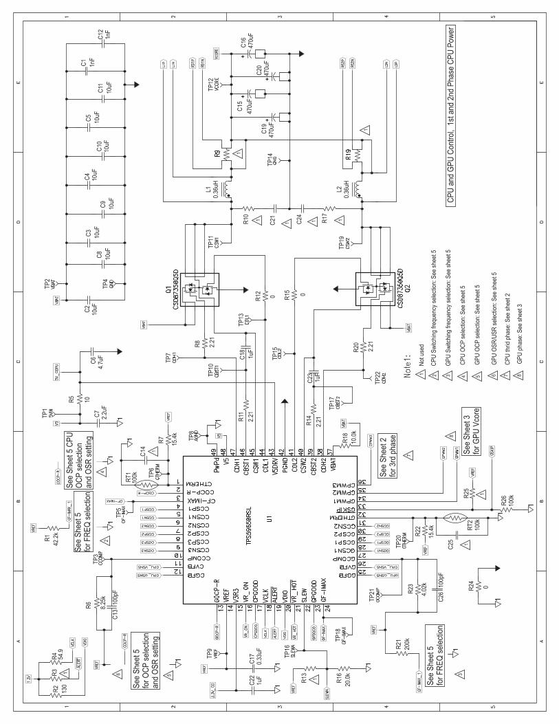
3
1
51
1
54
11
1
6
1
2
1
7
1
1
C13
100pF
876321
130
R2
TP
18
TP
16
C17
0.33
uF
54.9
R4
4.02
k
R23
TP
21
TP
20
R25
TP
5
8
10.0
k
R18TP
8
4
2.21
R142.
21
R11TP
1
R5
10
Not
used2.
21
R20
C18
1uF
TP
7
R15
0
TP
13
TP
19
C24
R10
1+
470uF
C15
R21
200k
TP
9
8.25
k
R6
C25
TP
3
R26
100k
Se
eS
he
et2
for
3rd
ph
ase
C14
TP
6
TP
17
2.2u
FC
7C
64.
7uF
TP
10
TP
152.
21
R8
R12
0
C2
10uF
C8
10uF T
P11
R17
10uF
C9
C21
C10
10uF
TP
14
10uF
C5
1nF
C1
+
C20
470uF
R24 0
Se
eS
he
et5
for
FR
EQ
sele
ctio
nC
26
100pF
15.4
k
R22
R13
C22
1uF
R3
Se
eS
he
et3
for
GP
UV
core
TP
22
C23
1uF
15.4
k
R7
Se
eS
he
et5
CP
UO
CP
sele
ctio
na
nd
OS
Rse
ttin
g
0.36
uHL2
TP
4
TP
2
+
470uF
C16
20.0
k
R16
RT
2100k
Se
eS
he
et5
for
OC
Pse
lect
ion
an
dO
SR
sett
ing
42.2
k
R1
RT
1100k
0.36
uHL1
10uF
C3
C4
10uF
+C
19470uF
C11
10uF
C12
1nF
TP
12
GP
Uph
ase:
See
shee
t3
CP
Uth
ridph
ase:
See
shee
t2
GP
UO
CP
sele
ctio
n:S
ee
sheet5
CP
UO
CP
sele
ctio
n:S
eesh
eet 5
GP
US
witc
hing
freq
uenc
yse
lect
ion:
See
shee
t 5
CP
US
witc
hing
freq
uenc
yse
lect
ion:
See
shee
t 5
GP
UO
SR
/US
Rse
lect
ion:
See
shee
t5
Se
eS
he
et5
for
FR
EQ
sele
ctio
n
CP
Ua
nd
GP
UC
on
tro
l,1
sta
nd
2n
dP
ha
seC
PU
Po
we
r
1
11
1
1
1
C37
22uF
C38
22uF
C53
22uF
TP
26
C54
22uF
C40
22uF
Notuse
d
C41
22uF
C36
2.2
uF
C42
22uF
C57
10uF
C58
10uF
C44
10uF
R31
0
TP
24
C45
22uFC
28
10uF
C46
10uF
C61
10uF
1
10uF
C29
C6
2
10uF
C48
C3
1
1nF
C49
22uF
C64
10uF
1
C50
22uF
+C
32
+C
34
1uF
C33
TP
25
TP
23
TP
27
0.3
6uH
L3
22
uF
C51
22uF
C52
C3
9
22uF
C55
22uF
TP
29
C56
22uF
C43
22uF
C59
10uF
C60
10uF
TP
28
C27
10uF
C47
C6
3
10uF
C35
10uF
C30
R2
9
2.2
1
R28
2.2
1
CP
U3
rdP
ha
seP
ow
er
R30
11
1
11
111
1
1
1
1
1
22uF
C94
TP
38
C95
22uF
TP
44
TP
42
TP
37
TP
34
C65
10uF
C97
R37
2.2
1C67
10uF
C98
C68
10uF
22uF
C100
1
TP
43T
P3
6
C70
10uF
C101
22uF
TP
45
TP
39
C71
10uF
C73
10uF
1
R40
TP
41R
35
TP
33
0.3
6uH
L4
TP
35
C83
TP
32
TP
31
C85
C86
R32
2.2
1
2.2
uF
C82
22uF
C88
22uF
C89
R39
2.2
1
22uF
C92
Notuse
d
C81
C7
8T
P4
0
C96
22uF
C93
C80
1uF
C66
10uF
GN
D_
PW
R
C99
C102
22uF0R
41
2.2
uF
C79
R34
2.2
1
C69
1nF
C72
10uF
C74
1nF
GP
UP
ow
er
+
470uF
C76
C84
22uF
C87
C75
1uF
C90
22uF
C91
22uF
R36
0
0.3
6uH
L5
+
C77
470uF
11
1
111
1
1
91
1
1
1 11
11
1
111
1
1
1
R66
R4
5
1
1
1
1
1
R91
162k
R74
17.8
k R79
162k
17.8
k
R64
17.8
k
R50R
46
162k
33
nF
C118
33nF
C115
33nF
C108
C1
04
33nF
R49
0
R4
4
1 11
1C113
1 C1111
1C103
11
C114
1
C110
1
TP
50
TP
49
R83
R4
7
9
0R
76
0R
73
0R
54
0R
58
R8
2
1
R86
17.8
kR56
162k
R68
162k
R42
17.8
k
C112
33nF
R67
C116
C11
9
C1
05
C1
07
C11
7
C1
20
C1
06
R89
R5
5
R6
9
R6
3
0R
93
0R
85
Notused
To
co
ntr
olle
r
R92
28.7
k
RT
6100k
RT
5100k
R59
28.7
k
RT
3100k
R90
R8
8
TP
56
TP
55
0R
75
R7
8
R7
7T
P5
4TP
52
TP
51
C109
TP
48
To
pro
ce
sso
r
R80
10
R81
J8
R72
10
To
pro
ce
sso
rJ6
To
co
ntr
olle
rJ9
J7
R84
28.7
k
RT
7100k
R48
28.7
k
RT
4100k
R70
28.7
k
R87
0
TP
53T
P4
7
R62
R5
210
R61
10
R60
0
R87,R
93
=0
for
DC
Rsense
R88,R
90
=0
for
Resis
tor
Sense
R75,R
85
=0
for
DC
Rsense
R77,R
78
=0
for
Resis
tor
Sense
R71
0
R65,R
71
=0
for
DC
Rsense
R66,R
67
=0
for
Resis
tor
Sense
R65
0
R5
7
0R
51
R43,R
49
=0
for
DC
Rsense
R44,R
45
=0
for
Resis
tor
Sense
Cu
rre
ntF
ee
db
ack
Se
lectio
na
nd
Filt
eri
ng
Diffe
ren
tia
lV
olta
ge
Fe
ed
ba
ck
an
dte
rmin
atio
n
Aphase
can
be
dis
able
dby
pulli
ng
the
corr
espondin
gxC
SP
xpin
to3.3
V.
Defa
ult
settin
gfo
rC
PU
:3
phase
opera
tion
Dafa
ult
settin
gfo
rG
PU
:2
phase
opera
tion
CP
U:
Phase
dis
able
can
be
done
inre
vers
eord
er.P
hase
3,th
en
2,th
en
1.
1.C
PU
3P
hase
opera
tion:R
47,R
55,R
69
open
2.C
PU
2P
hase
opera
tion:R
69
used
0ohm
3.C
PU
1P
hase
opera
tion:R
47,R
55
used
0ohm
GP
U:
1.G
PU
2P
hase
opera
tion:R
83,R
89
open
2.G
PU
1P
hase
opera
tion:R
89
used
0ohm
R53
R51,R
60
=0
for
DC
Rsense
R53,R
57
=0
for
Resis
tor
Sense
R43
0
13
1
12
1
10
R125
24.3
k
R119
56.2
k
R113
150k
R109
24.3
k
R102
56.2
k
R96
150k
13101
11
R117
75.0
k
R121
39.2
k
R123
30.1
k
R111
20.0
k
R98
100k
R100
75.0
k
R105
39.2
k
R107
30.1
k
11
12
R128 R
129
R127
20.0
k
R115
100k
TP
57
TP
58
39.2
k
R94
66
0kH
z(M
AX
)6
05
kH
z5
50
kH
z4
95
kH
z4
40
kH
z3
85
kH
z3
30
kH
z2
75
kH
z(M
IN)
SW
ITC
HIN
GF
RE
QU
EN
CY
SE
LE
CT
ION
Notused
Over-
Shoot/U
nder-
ShootR
eduction
Sele
ction:
1.C
PU
OS
R/U
SR
Defa
ult
Settin
g:O
SR
/US
RR
eduction
mid
dle
level
2.G
PU
OS
R/U
SR
Defa
ult
Settin
g:O
SR
/US
RR
eduction
off
R110
20.0
k
R97
100k
R99
75.0
k
R101
56.2
k
R103
39.2
k
R106
30.1
k
Op
tionalpart
sfo
rusin
gT
PS
51640
R95
150k
R108
24.3
k
Le
ve
l8
(MA
X)
Le
ve
l7
Le
ve
l6
Le
ve
l5
Le
ve
l4
Le
ve
l3
Le
ve
l2
Le
ve
l1
(MIN
)
R104
2.4
3k
Le
ve
l8
(MA
X)
Le
ve
l7
Le
ve
l6
Le
ve
l5
Le
ve
l4
Le
ve
l3
Le
ve
l2
Le
ve
l1
(MIN
)
R124
24.3
k
R118
56.2
k
R112
150k
OV
ER
-CU
RR
EN
TP
RO
TE
CT
ION
SE
LE
CT
ION
OS
R/U
SR
SE
TT
ING
Sw
itchin
gF
requency
Sele
ction:
1.C
PU
Sw
itchin
gF
requency
Defa
ult
Settin
g:Jum
per
short
son
pin
13
and
pin
14
toset300kH
z2.G
PU
Sw
itchin
gF
requency
Defa
ult
Settin
g:Jum
per
short
son
pin
11
and
pin
12
toset385kH
z
R120
39.2
k
R122
30.1
k
Fre
qu
en
cy
an
dO
CP
SE
LE
CT
ION
Sfo
rC
PU
an
dG
PU
R126
20.0
k
Over
Curr
entP
rote
ction
Sele
ction:
1.C
PU
Over
Curr
entP
rote
ction
Per
Phase
Defa
ult
Settin
g:Jum
per
short
son
pin
7and
pin
8to
level5
(set40A
)2.G
PU
Over
Curr
entP
rote
ction
Per
Phase
Defa
ult
Settin
g:Jum
per
short
son
pin
7and
pin
8to
level5
(set40A
)
60
0kH
z(M
AX
)5
50
kH
z5
00
kH
z4
50
kH
z4
00
kH
z3
50
kH
z3
00
kH
z2
50
kH
z(M
IN)
R114
100k
R116
75.0
k
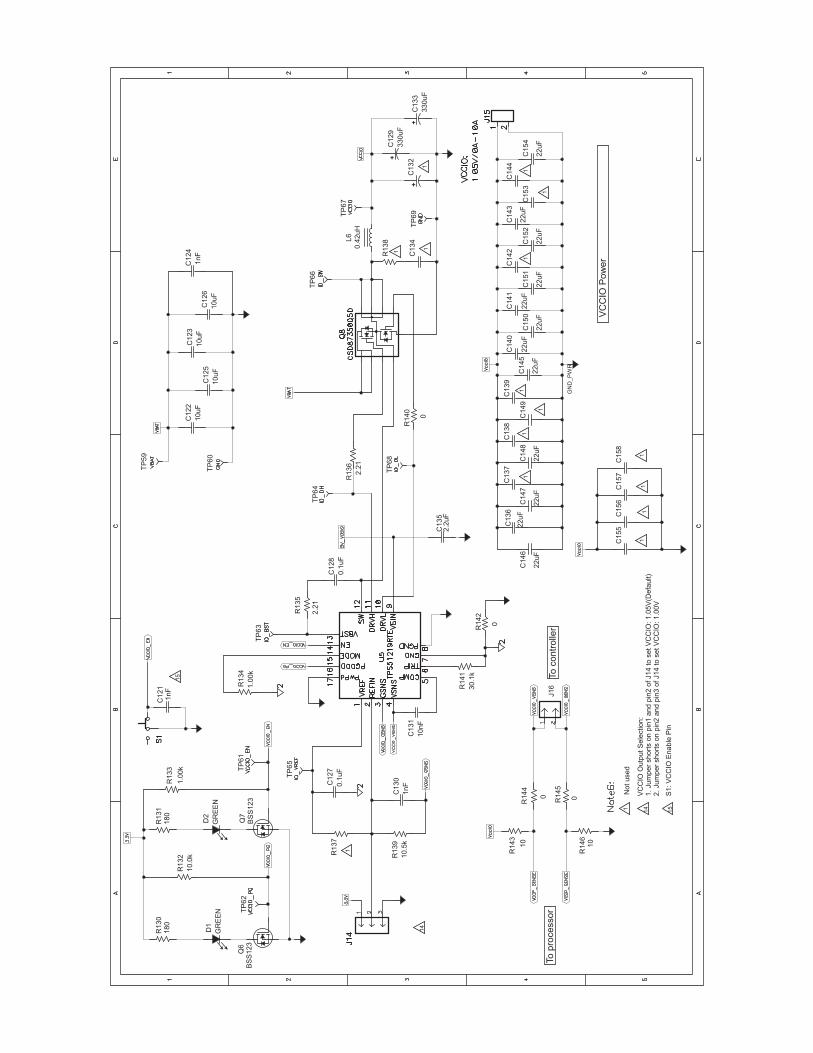
15
141
11
1
1
1
1
15
1
1
1
Notused
11
1
1
1
14
TP
62
TP
65
TP
61
R133
1.0
0k
J16
C131
10nF
C121
1nF
To
co
ntr
olle
r
C156
C135
2.2
uF
C158
R136
2.2
1
TP
60
GN
D_P
WR
C134
1
TP
66
TP
67
R143
10
R146
10
R139
10.5
k
R137
C130
1nFC
127
0.1
uF
TP
63
C128
0.1
uF
C136
22uF
C147
22uF
C148
22uF
C138
TP
68
TP
59
C13910uF
C125
C1
50
22uF
C142
R1
38
C1
24
1nF
C153
+
330uF
C129
S1:V
CC
IOE
nable
Pin
To
pro
ce
sso
rR
145
0
R130
180
R131
180
R132
10.0
k
C155
C157
0
R142R
135
2.2
1
R134
1.0
0k
VC
CIO
Pow
er
R140
0
TP
69
0.4
2uH
L6
+C
132
+C
133
330uF
R144
0
GR
EE
N
D1
D2
GR
EE
N
Q6
BS
S123
BS
S123
Q7
R141
30.1
k
22uF
C146
C137
TP
64
C149
C1
45
22uF
C140
22uF
C141
22uF
C151
22uF
C152
22uF
C143
22uF
C122
10uF
C123
10uF
C126
10uF
C144
C1
54
22uF
VC
CIO
Ou
tputS
ele
ction:
1.Jum
per
short
son
pin
1and
pin
2ofJ14
tosetV
CC
IO:
1.0
5V
(Defa
ult)
2.Jum
per
short
son
pin
2and
pin
3ofJ14
tosetV
CC
IO:
1.0
0V
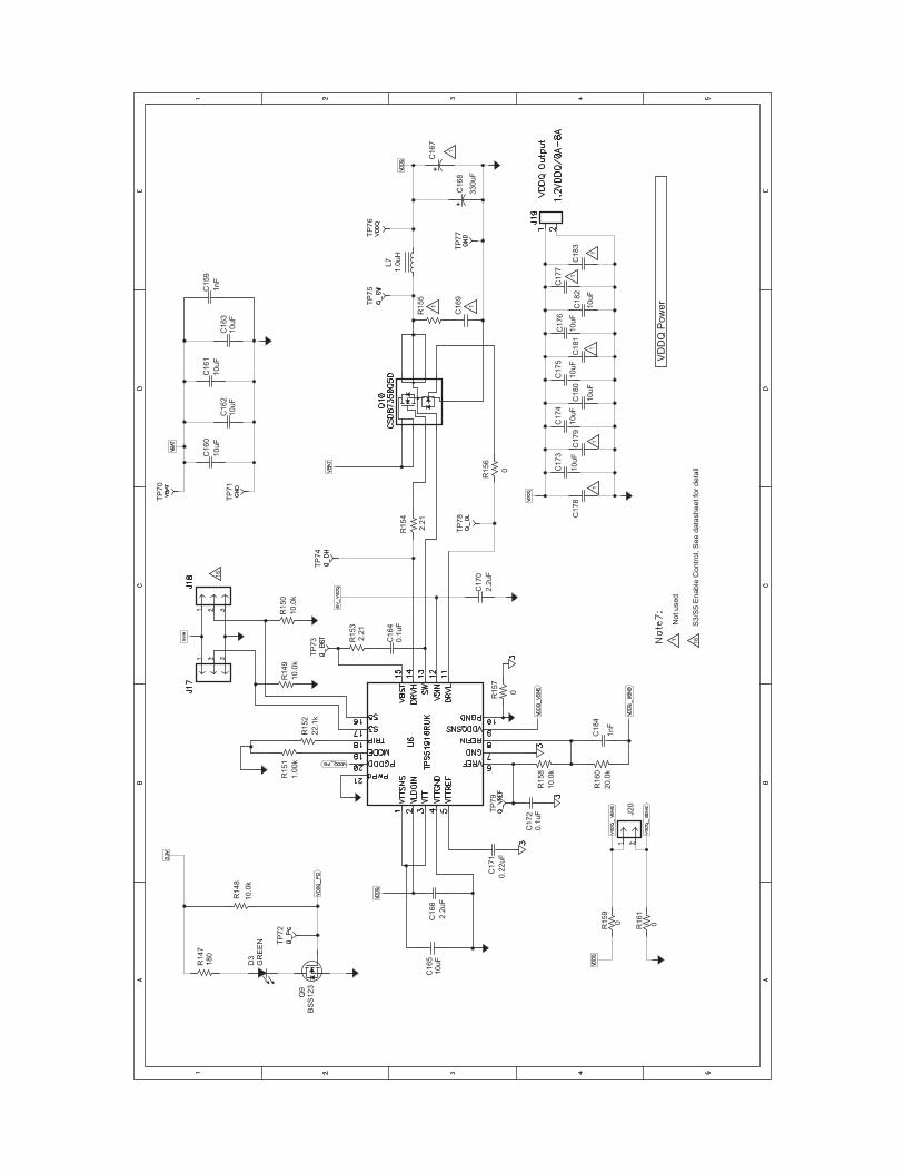
16
11
1
1
1
R159
0
TP
72
C171
0.2
2uF
R160
20.0
k
R158
10.0
k
TP
79
C184
1nF
16C164
0.1
uF
TP
73 2
.21
R153
C1
70
2.2
uF
TP
74
TP
78
R154
2.2
1
C174
10uF
C160
10uF
C175
10uF
C161
10uF
C177
C1
69
11
1nF
C159
1
TP
77
1
R161
0
R152
22.1
k
C178T
P7
1
TP
70
C179
C1
81
C1
82
10uF
R155
TP
75
TP
76
+C
167
J20
C172
0.1
uF
D3
GR
EE
N
R147
180
Notused
R149
10.0
k
R150
10.0
k
VD
DQ
Pow
er
C176
10uF
C173
10uF
R156
0
1.0
uH
L7
+
330uF
C168
Q9
BS
S123
R148
10.0
k
C166
2.2
uF
C165
10uF
R157
0
R151
1.0
0k
C180
10uF
C183
C1
62
10uF
C163
10uF
S3/S
5E
nable
Contr
ol,
See
data
sheetfo
rdeta
il
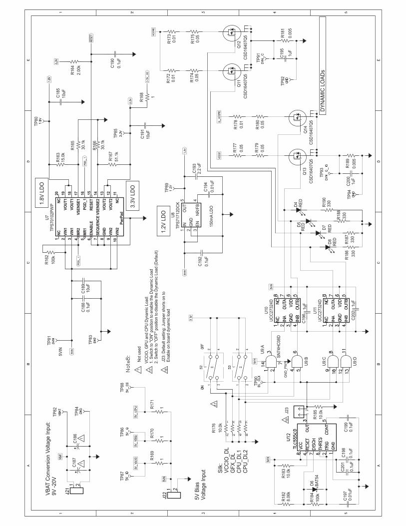
11
18
17
GN
D_
PW
R
171
8.0
6k
R182
10.0
kR
183
J23
TP
82
U9:C
U9:B
18
TP
83
TP
81
R188
330
1.2
VL
DO
C194
0.0
1uF
TP
89
R179
0.0
5
R166
30.1
k
R163
15.0
k
R180
0.0
5
TP
92
R172
0.0
1R
173
0.0
1
R184
100k
C201
0.1
uF
+C
187
TP
87
R170
1
+C
186 TP
86
R171
1
TP
84
C189
10uF
330
R186
C192
0.1
uF
R162
100k
RE
D
D7D
5R
ED
C200
1uF
TP
94
R177
0.0
5
R189
0.0
05
R165
30.1
k
R167
51.1
k
R178
0.0
1
TP
80
R174
0.0
5
R181
0.0
05
R175
0.0
5
R176
10.0
k
Notuse
d
5V
IN
1.8
VL
DO
TP
90
VB
AT
Co
nve
rsio
nV
olta
ge
Inp
ut:
9V
-20
V
D8
RE
D
C196
1uF
J23:D
efa
ult
settin
g:Ju
mper
short
son
toE
nable
on
board
dyn
am
iclo
ad
VC
CIO
,G
PU
and
CP
UD
ynam
icLoad:
1.S
witc
hto
"ON
"posi
tion
toenable
the
Dyn
am
icLoad
2.S
witc
hto
"OF
F"
posi
tion
todis
able
the
Dyn
am
icLoad
(Defa
ult)
R190
330
TP
93
CS
D16407Q
5
Q14
CS
D16407Q
5
Q13
D4
RE
D
3.3
VL
DO
C191
10uF
1
R168
C185
10uF
TP
91
C197
0.0
1uF
D6
BA
T54
C199
0.1
uF
10.0
k
R185
C198
0.1
uF
5V
Bia
sV
olta
ge
Inp
ut
R169
1
TP
88
UC
C27324D
U10
UC
C27324D
U11
R187
330
1uF
C202C
188
0.1
uF
C193
2.2
uF
TP
85
1uF
C195
C190
0.1
uF
R164
2.0
0k
Silk
:V
CC
IO_D
LG
FX
_D
LC
PU
_D
L1
CP
U_
DL
2C
SD
16407Q
5
Q12
DY
NA
MIC
LO
AD
s
150m
ALD
O
U9:D
SN
74H
C08D
U9:A
5O
UT
4N
R/F
B
1IN
3E
N
2G
ND
U8
TP
S71712D
CK
3V
IN
1
2V
IN
1
7S
EQ
UE
NC
E
8G
ND
9V
IN
2
10
VIN
2
1N
C
11
NC
12
VO
UT
2
13
VO
UT
2
14
VS
EN
SE
2
16
PG
D_1
17
VS
EN
SE
1
18
VO
UT
1
19
VO
UT
1
20
NC
Pw
rP
ad
4M
R2
5M
R1
6E
NA
BL
E15
RE
SE
T
TP
S70102P
WP
U7
CS
D16407Q
5
Q11
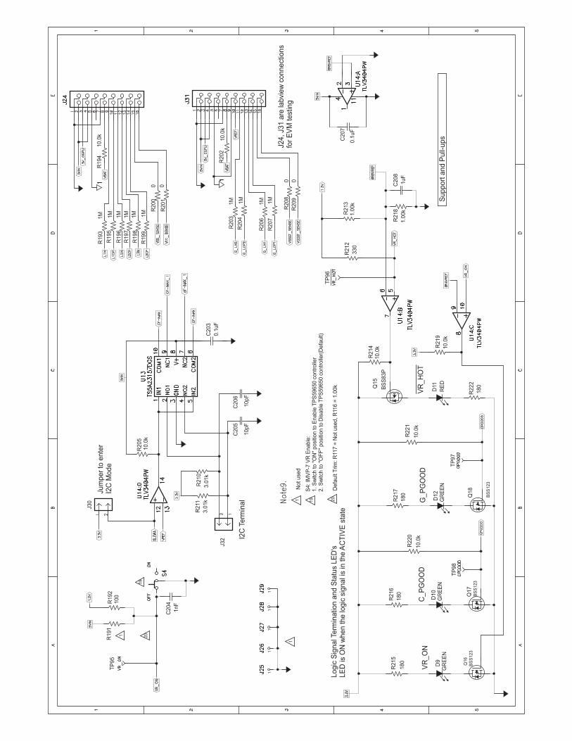
1
19
20
1 19
1
1M
R204
VR
_O
N
180
R215
20
R216
180
TP
98
R217
180
3.0
1k
R211
J30
TP
97
C205
10pF
C206
10pF
R218
1.0
0kR213
1.0
0k1
MR
206
1M
R207
C2
07
0.1
uF
TP
95
C204
1nFR
192
100
R214
10.0
k
TP
96
1M
R203
C_P
GO
OD
G_
PG
OO
D
0R
201
1M
R195
10.0
k
R220
R2
22
180
VR
_H
OT
R2
21
10.0
k
Notuse
d
S4:IM
VP
-7V
RE
nable
:1.S
witc
hto
"ON
"posi
tion
toE
nable
TP
S59650
contr
olle
r2.S
witc
hto
"OF
F"
posi
tion
toD
isable
TP
S59650
contr
olle
r(D
efa
ult)
3.0
1k
R210
C2
03
0.1
uF
R205
10.0
k
Jum
pe
rto
en
ter
I2C
Mo
de
Su
pp
ort
an
dP
ull-
up
s
C208
1uF
33
0
R212
R2
08
0 0R
209
0R
200
1M
R198
1M
R199
10.0
kR
194
1M
R193
Q17
BS
S1
23
D10
GR
EE
ND
9G
RE
EN
Q1
6
BS
S1
23
J32
R191
R2
19
10.0
k
D11
RE
D
Q15
BS
S83P
Defa
ult
Trim
:R
117
=N
otuse
d,R
116
=1.0
0k
10
.0k
R202
1M
R196
1M
R197
I2C
Term
ina
l
Lo
gic
Sig
na
l Te
rmin
atio
na
nd
Sta
tus
LE
D's
LE
Dis
ON
wh
en
the
log
icsi
gn
al i
sin
the
AC
TIV
Est
ate
D12
GR
EE
N
BS
S1
23
Q18
J24
,J3
1a
rela
bvi
ew
con
ne
ctio
ns
for
EV
Mte
stin
g

175.0
R224
R2
25
130
1N
otuse
d
R226
43.2
R223
uC
So
cke
tM
ain
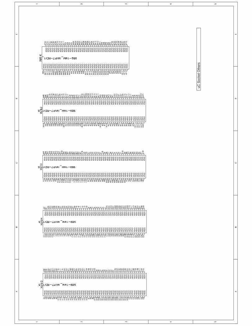
uC
So
cke
tO
the
rs
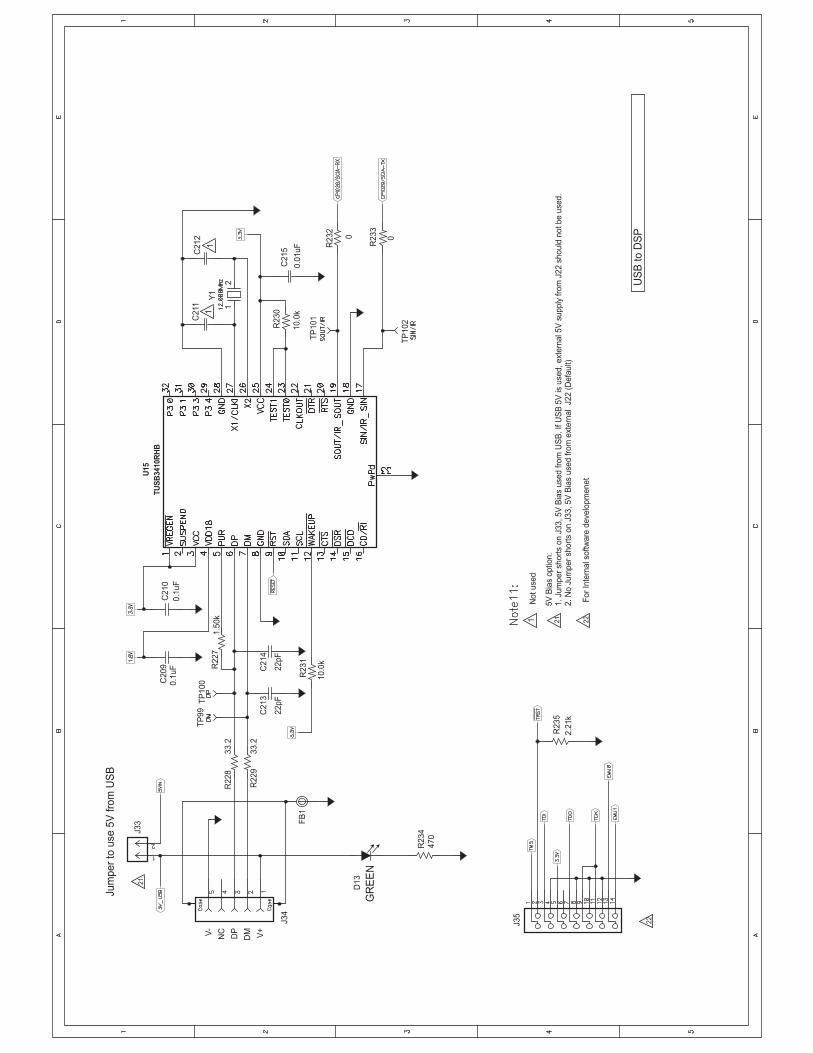
21
1
1
22
22
21
Notuse
d
GR
EE
N
D13
TP
99
C214
22pF
21
Y1
1
C211
0
R232
0
R233
FB
1
R235
2.2
1k
C209
0.1
uF
R231
10.0
k
0.1
uF
C210
R234
470
R229
33.2
33.2
R228
Jum
pe
rto
use
5V
fro
mU
SB
J33
Fo
rIn
tern
al s
oftw
are
deve
lopm
enet
C213
22pF
1.5
0k
R227
TP
100
US
Bto
DS
P
0.0
1uF
C215
R230
10.0
k
C212
J35
NC
V+
DP
DMV-
J34
TP
102
TP
101
5V
Bia
soptio
n:
1.Ju
mper
short
son
J33,5V
Bia
suse
dfr
om
US
B.If
US
B5V
isuse
d,ext
ern
al 5
Vsu
pply
from
J22
should
notbe
use
d.
2.N
oJu
mper
short
son
J33,5V
Bia
suse
dfr
om
ext
ern
al
J22
(Defa
ult)
TU
SB
3410R
HB
U15
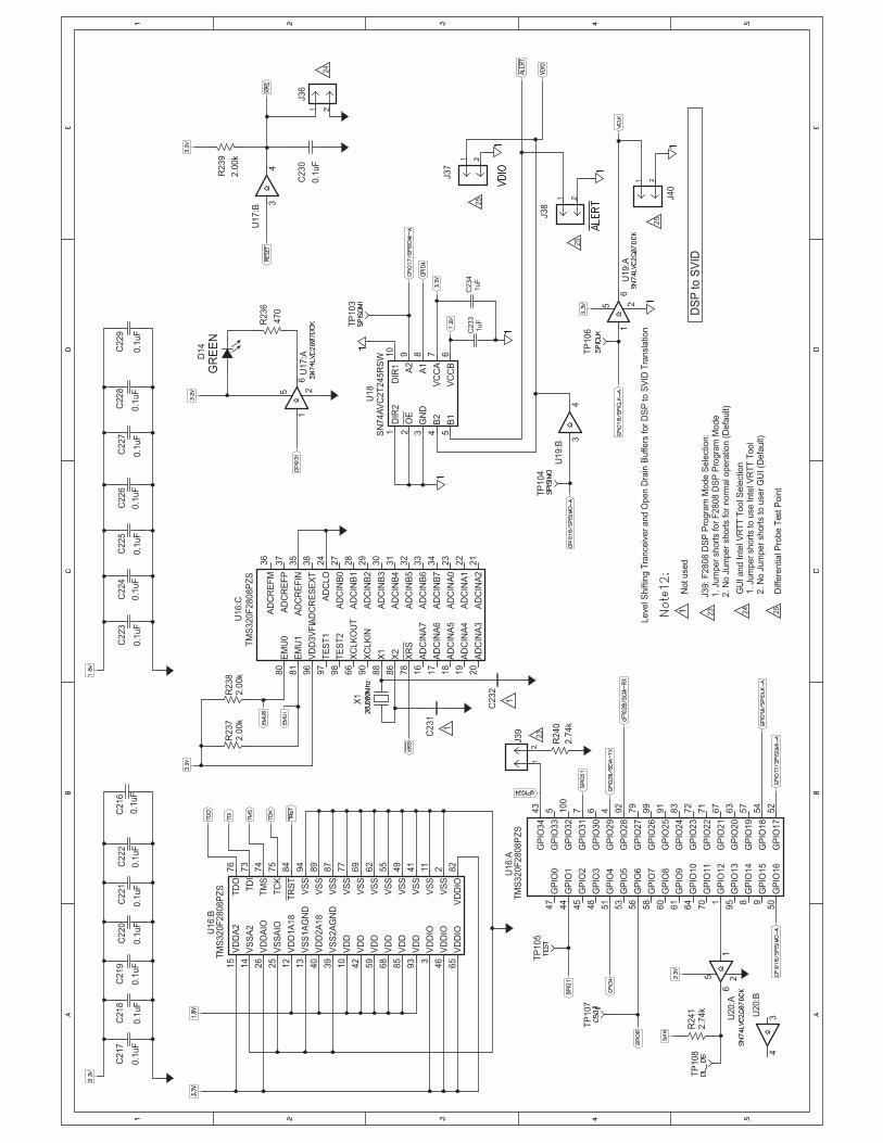
23
24
1
241
Notuse
d
25
25
25
0.1
uF
C217
C218
0.1
uF
TP
105
0.1
uF
C219
C220
0.1
uF
C221
0.1
uF
C222
0.1
uF
C216
0.1
uF
R240
2.7
4k1
X1
R237
2.0
0k
25
23
0.1
uF
C223
0.1
uF
C225
TP
104
C226
0.1
uF
C228
0.1
uF
C2
33
1u
F
0.1
uF
C229
J40
J37
0.1
uF
C230
R239
2.0
0k
J36
34
U20:B
R241
2.7
4k
TP
107
C231
TP
106
TP
103
R236
470
16
5 2U
20:A
TP
108
Diff
ere
ntia
l Pro
be
Tes
tP
oin
t
R238
2.0
0k
C224
0.1
uF
DS
Pto
SV
ID
16
5 2U
19:A
J38
34
U19:B
C2
34
1u
F
16
5 2U
17:AD
14
GR
EE
N
C227
0.1
uF
60
GP
IO8
53
GP
IO5
45
GP
IO2
56
GP
IO6
58
GP
IO7
47
GP
IO0
44
GP
IO1
48
GP
IO3
51
GP
IO4
8G
PIO
14
70
GP
IO11
57
GP
IO1
9
71
GP
IO2
2
91
GP
IO2
5
92
GP
IO2
8
7G
PIO
31
43
GP
IO3
4
1G
PIO
12
95
GP
IO1
3
9G
PIO
15
61
GP
IO9
54
GP
IO1
8
63
GP
IO2
0
67
GP
IO2
1
83
GP
IO2
4
99
GP
IO2
6
79
GP
IO2
7
6G
PIO
30
100
GP
IO3
2
5G
PIO
33
64
GP
IO1
0
50
GP
IO1
652
GP
IO1
7
72
GP
IO2
3
4G
PIO
29
TM
S320F
2808P
ZS
U16:A
39
VS
S2A
GN
D
12
VD
D1A
18
14
VS
SA
2
13
VS
S1A
GN
D40
VD
D2A
18
10
VD
D
15
VD
DA
2
26
VD
DA
IO25
VS
SA
IO
65
VD
DIO
93
VD
D
59
VD
D
82
VD
DIO
41
VS
S
62
VS
S
87
VS
S
84
TR
ST
73
TD
I
68
VD
D85
VD
D
3V
DD
IO46
VD
DIO
42
VD
D
2V
SS
11V
SS
49
VS
S
55
VS
S
69
VS
S
77
VS
S
89
VS
S
94
VS
S
75
TC
K
74
TM
S
76
TD
O
TM
S320F
2808P
ZS
U16:B
C232
J39
5B
1
2O
E
1D
IR2
3G
ND
4B
26
VC
CB
9A
2
7V
CC
A
8A
1
10
DIR
1
SN
74A
VC
2T
245R
SW
U18
19
AD
CIN
A4
16
AD
CIN
A7
88
X1
98
TE
ST
2
81
EM
U1
22
AD
CIN
A1
33
AD
CIN
B6
30
AD
CIN
B3
27
AD
CIN
B0
35
AD
CR
EF
IN
17
AD
CIN
A6
18
AD
CIN
A5
20
AD
CIN
A3
66
XC
LK
OU
T90
XC
LK
IN
86
X2
80
EM
U0
96
VD
D3V
FL
21
AD
CIN
A2
23
AD
CIN
A0
34
AD
CIN
B7
31
AD
CIN
B4
29
AD
CIN
B2
28
AD
CIN
B1
38
AD
CR
ES
EX
T
37
AD
CR
EF
P
36
AD
CR
EF
M
78
XR
S
97
TE
ST
1
32
AD
CIN
B5
24
AD
CLO
TM
S320F
2808P
ZS
U16:C
J39:F
2808
DS
PP
rogra
mM
ode
Sele
ction:
1.Ju
mper
short
sfo
rF
2808
DS
PP
rogra
mM
ode
2.N
oJu
mper
short
sfo
rnorm
al o
pera
tion
(Defa
ult)
Leve
l Shift
ing
Tra
nce
iver
and
Open
Dra
inB
uffers
for
DS
Pto
SV
IDT
ransl
atio
n
GU
Iand
Inte
lVR
TT
ToolS
ele
ctio
n1.Ju
mper
short
sto
use
Inte
lVR
TT
Tool
2.N
oJu
mper
short
sto
use
rG
UI(D
efa
ult)
34
U17:B
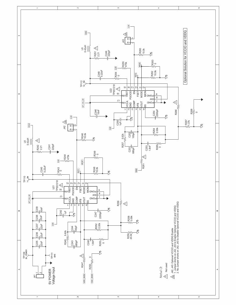
1
1
1
1
1
1
1
1
26
26
26
1 2
J41
R259
20.0
k
C236
22uF
C237
22uF
C242
1uFC
239
10nF
R243
0C240
0.2
2uF
C253
1.8
nF
1
C251
680pF
R242
2.2
1
R267
1.3
7k
C252
100pF
R268
0
R266
TP
112
R263
0
R255
475k
J43
0.4
2uH
L9
TP
111
TP
10
9
C244
100pF
R252
2.0
0k
C247
2200pF
R248
10.0
k
R265
0
R249
0
220pF
C241
R2
64
2.0
0kJ4
2
C246
10nF
10.0
k
R260
R2
61
Notuse
d
R258
3.0
9k
R253
0
R247
0R
250
5.6
2k
R245
C2
35
22uF
C238
22uF
R256
R257
5.6
2k
R246
10.0
k
R262
10.0
k
C248
0.2
2uF
C249
220pF
5V
PO
WE
RV
olta
ge
Inp
ut
C243
680pF
C245
1.8
nF
2 GN
D
14
PG
OO
D
5 VO
UT
11
MO
DE 9
PGND16
VIN
17VIN
3 CO
MP
6 SS
1
VC
CA
4 VF
B
10
IMO
N
13
EN
12
FS
ET
8SW
7PGND
15
VB
STU21
TP
S51318
R244
475k
0.4
2uH
L8
TP
110
C254
2200pF
R251
2.2
1
R254
0C
250
1uF
2 GN
D
14
PG
OO
D
5 VO
UT
11
MO
DE 9
PGND16
VIN
17VIN
3 CO
MP
6 SS
1
VC
CA
4 VF
B
10
IMO
N
13
EN
12
FS
ET
8SW
7PGND
15
VB
ST
TP
S51318
U22
Op
tio
na
l So
lutio
nfo
rV
CC
IOa
nd
VD
DQ
J42,J4
3:O
ptio
nal V
CC
IOand
VD
DQ
Enable
1.Ju
mper
short
son
J42,J4
3to
Enable
Op
tional V
CC
IOand
VD
DQ
2.N
oJu
mper
short
son
J42,J4
3to
Dis
able
Op
tional V
CC
IOand
VD
DQ

EVALUATION BOARD/KIT/MODULE (EVM) ADDITIONAL TERMS
Texas Instruments (TI) provides the enclosed Evaluation Board/Kit/Module (EVM) under the following conditions:
The user assumes all responsibility and liability for proper and safe handling of the goods. Further, the user indemnifies TI from all claimsarising from the handling or use of the goods.
Should this evaluation board/kit not meet the specifications indicated in the User’s Guide, the board/kit may be returned within 30 days fromthe date of delivery for a full refund. THE FOREGOING LIMITED WARRANTY IS THE EXCLUSIVE WARRANTY MADE BY SELLER TOBUYER AND IS IN LIEU OF ALL OTHER WARRANTIES, EXPRESSED, IMPLIED, OR STATUTORY, INCLUDING ANY WARRANTY OFMERCHANTABILITY OR FITNESS FOR ANY PARTICULAR PURPOSE. EXCEPT TO THE EXTENT OF THE INDEMNITY SET FORTHABOVE, NEITHER PARTY SHALL BE LIABLE TO THE OTHER FOR ANY INDIRECT, SPECIAL, INCIDENTAL, OR CONSEQUENTIALDAMAGES.
Please read the User's Guide and, specifically, the Warnings and Restrictions notice in the User's Guide prior to handling the product. Thisnotice contains important safety information about temperatures and voltages. For additional information on TI's environmental and/or safetyprograms, please visit www.ti.com/esh or contact TI.
No license is granted under any patent right or other intellectual property right of TI covering or relating to any machine, process, orcombination in which such TI products or services might be or are used. TI currently deals with a variety of customers for products, andtherefore our arrangement with the user is not exclusive. TI assumes no liability for applications assistance, customer product design,software performance, or infringement of patents or services described herein.
REGULATORY COMPLIANCE INFORMATION
As noted in the EVM User’s Guide and/or EVM itself, this EVM and/or accompanying hardware may or may not be subject to the FederalCommunications Commission (FCC) and Industry Canada (IC) rules.
For EVMs not subject to the above rules, this evaluation board/kit/module is intended for use for ENGINEERING DEVELOPMENT,DEMONSTRATION OR EVALUATION PURPOSES ONLY and is not considered by TI to be a finished end product fit for general consumeruse. It generates, uses, and can radiate radio frequency energy and has not been tested for compliance with the limits of computingdevices pursuant to part 15 of FCC or ICES-003 rules, which are designed to provide reasonable protection against radio frequencyinterference. Operation of the equipment may cause interference with radio communications, in which case the user at his own expense willbe required to take whatever measures may be required to correct this interference.
General Statement for EVMs including a radio
User Power/Frequency Use Obligations: This radio is intended for development/professional use only in legally allocated frequency andpower limits. Any use of radio frequencies and/or power availability of this EVM and its development application(s) must comply with locallaws governing radio spectrum allocation and power limits for this evaluation module. It is the user’s sole responsibility to only operate thisradio in legally acceptable frequency space and within legally mandated power limitations. Any exceptions to this are strictly prohibited andunauthorized by Texas Instruments unless user has obtained appropriate experimental/development licenses from local regulatoryauthorities, which is responsibility of user including its acceptable authorization.
For EVMs annotated as FCC – FEDERAL COMMUNICATIONS COMMISSION Part 15 Compliant
Caution
This device complies with part 15 of the FCC Rules. Operation is subject to the following two conditions: (1) This device may not causeharmful interference, and (2) this device must accept any interference received, including interference that may cause undesired operation.
Changes or modifications not expressly approved by the party responsible for compliance could void the user's authority to operate theequipment.
FCC Interference Statement for Class A EVM devices
This equipment has been tested and found to comply with the limits for a Class A digital device, pursuant to part 15 of the FCC Rules.These limits are designed to provide reasonable protection against harmful interference when the equipment is operated in a commercialenvironment. This equipment generates, uses, and can radiate radio frequency energy and, if not installed and used in accordance with theinstruction manual, may cause harmful interference to radio communications. Operation of this equipment in a residential area is likely tocause harmful interference in which case the user will be required to correct the interference at his own expense.

FCC Interference Statement for Class B EVM devices
This equipment has been tested and found to comply with the limits for a Class B digital device, pursuant to part 15 of the FCC Rules.These limits are designed to provide reasonable protection against harmful interference in a residential installation. This equipmentgenerates, uses and can radiate radio frequency energy and, if not installed and used in accordance with the instructions, may causeharmful interference to radio communications. However, there is no guarantee that interference will not occur in a particular installation. Ifthis equipment does cause harmful interference to radio or television reception, which can be determined by turning the equipment off andon, the user is encouraged to try to correct the interference by one or more of the following measures:
• Reorient or relocate the receiving antenna.• Increase the separation between the equipment and receiver.• Connect the equipment into an outlet on a circuit different from that to which the receiver is connected.• Consult the dealer or an experienced radio/TV technician for help.
For EVMs annotated as IC – INDUSTRY CANADA Compliant
This Class A or B digital apparatus complies with Canadian ICES-003.
Changes or modifications not expressly approved by the party responsible for compliance could void the user’s authority to operate theequipment.
Concerning EVMs including radio transmitters
This device complies with Industry Canada licence-exempt RSS standard(s). Operation is subject to the following two conditions: (1) thisdevice may not cause interference, and (2) this device must accept any interference, including interference that may cause undesiredoperation of the device.
Concerning EVMs including detachable antennas
Under Industry Canada regulations, this radio transmitter may only operate using an antenna of a type and maximum (or lesser) gainapproved for the transmitter by Industry Canada. To reduce potential radio interference to other users, the antenna type and its gain shouldbe so chosen that the equivalent isotropically radiated power (e.i.r.p.) is not more than that necessary for successful communication.
This radio transmitter has been approved by Industry Canada to operate with the antenna types listed in the user guide with the maximumpermissible gain and required antenna impedance for each antenna type indicated. Antenna types not included in this list, having a gaingreater than the maximum gain indicated for that type, are strictly prohibited for use with this device.
Cet appareil numérique de la classe A ou B est conforme à la norme NMB-003 du Canada.
Les changements ou les modifications pas expressément approuvés par la partie responsable de la conformité ont pu vider l’autorité del'utilisateur pour actionner l'équipement.
Concernant les EVMs avec appareils radio
Le présent appareil est conforme aux CNR d'Industrie Canada applicables aux appareils radio exempts de licence. L'exploitation estautorisée aux deux conditions suivantes : (1) l'appareil ne doit pas produire de brouillage, et (2) l'utilisateur de l'appareil doit accepter toutbrouillage radioélectrique subi, même si le brouillage est susceptible d'en compromettre le fonctionnement.
Concernant les EVMs avec antennes détachables
Conformément à la réglementation d'Industrie Canada, le présent émetteur radio peut fonctionner avec une antenne d'un type et d'un gainmaximal (ou inférieur) approuvé pour l'émetteur par Industrie Canada. Dans le but de réduire les risques de brouillage radioélectrique àl'intention des autres utilisateurs, il faut choisir le type d'antenne et son gain de sorte que la puissance isotrope rayonnée équivalente(p.i.r.e.) ne dépasse pas l'intensité nécessaire à l'établissement d'une communication satisfaisante.
Le présent émetteur radio a été approuvé par Industrie Canada pour fonctionner avec les types d'antenne énumérés dans le manueld’usage et ayant un gain admissible maximal et l'impédance requise pour chaque type d'antenne. Les types d'antenne non inclus danscette liste, ou dont le gain est supérieur au gain maximal indiqué, sont strictement interdits pour l'exploitation de l'émetteur.
SPACER
SPACER
SPACER
SPACER
SPACER
SPACER
SPACER
SPACER
【【Important Notice for Users of this Product in Japan】】This development kit is NOT certified as Confirming to Technical Regulations of Radio Law of Japan
If you use this product in Japan, you are required by Radio Law of Japan to follow the instructions below with respect to this product:
1. Use this product in a shielded room or any other test facility as defined in the notification #173 issued by Ministry of Internal Affairs andCommunications on March 28, 2006, based on Sub-section 1.1 of Article 6 of the Ministry’s Rule for Enforcement of Radio Law ofJapan,
2. Use this product only after you obtained the license of Test Radio Station as provided in Radio Law of Japan with respect to thisproduct, or
3. Use of this product only after you obtained the Technical Regulations Conformity Certification as provided in Radio Law of Japan withrespect to this product. Also, please do not transfer this product, unless you give the same notice above to the transferee. Please notethat if you could not follow the instructions above, you will be subject to penalties of Radio Law of Japan.
Texas Instruments Japan Limited(address) 24-1, Nishi-Shinjuku 6 chome, Shinjukku-ku, Tokyo, Japan
http://www.tij.co.jp
【ご使用にあたっての注】
本開発キットは技術基準適合証明を受けておりません。
本製品のご使用に際しては、電波法遵守のため、以下のいずれかの措置を取っていただく必要がありますのでご注意ください。1. 電波法施行規則第6条第1項第1号に基づく平成18年3月28日総務省告示第173号で定められた電波暗室等の試験設備でご使用いただく。2. 実験局の免許を取得後ご使用いただく。3. 技術基準適合証明を取得後ご使用いただく。
なお、本製品は、上記の「ご使用にあたっての注意」を譲渡先、移転先に通知しない限り、譲渡、移転できないものとします。
上記を遵守頂けない場合は、電波法の罰則が適用される可能性があることをご留意ください。
日本テキサス・インスツルメンツ株式会社東京都新宿区西新宿6丁目24番1号西新宿三井ビルhttp://www.tij.co.jp
SPACER
SPACER
SPACER
SPACER
SPACER
SPACER
SPACER
SPACER
SPACER
SPACER
SPACER
SPACER
SPACER
SPACER
SPACER
SPACER
EVALUATION BOARD/KIT/MODULE (EVM)WARNINGS, RESTRICTIONS AND DISCLAIMERS
For Feasibility Evaluation Only, in Laboratory/Development Environments. Unless otherwise indicated, this EVM is not a finishedelectrical equipment and not intended for consumer use. It is intended solely for use for preliminary feasibility evaluation inlaboratory/development environments by technically qualified electronics experts who are familiar with the dangers and application risksassociated with handling electrical mechanical components, systems and subsystems. It should not be used as all or part of a finished endproduct.
Your Sole Responsibility and Risk. You acknowledge, represent and agree that:
1. You have unique knowledge concerning Federal, State and local regulatory requirements (including but not limited to Food and DrugAdministration regulations, if applicable) which relate to your products and which relate to your use (and/or that of your employees,affiliates, contractors or designees) of the EVM for evaluation, testing and other purposes.
2. You have full and exclusive responsibility to assure the safety and compliance of your products with all such laws and other applicableregulatory requirements, and also to assure the safety of any activities to be conducted by you and/or your employees, affiliates,contractors or designees, using the EVM. Further, you are responsible to assure that any interfaces (electronic and/or mechanical)between the EVM and any human body are designed with suitable isolation and means to safely limit accessible leakage currents tominimize the risk of electrical shock hazard.
3. You will employ reasonable safeguards to ensure that your use of the EVM will not result in any property damage, injury or death, evenif the EVM should fail to perform as described or expected.
4. You will take care of proper disposal and recycling of the EVM’s electronic components and packing materials.
Certain Instructions. It is important to operate this EVM within TI’s recommended specifications and environmental considerations per theuser guidelines. Exceeding the specified EVM ratings (including but not limited to input and output voltage, current, power, andenvironmental ranges) may cause property damage, personal injury or death. If there are questions concerning these ratings please contacta TI field representative prior to connecting interface electronics including input power and intended loads. Any loads applied outside of thespecified output range may result in unintended and/or inaccurate operation and/or possible permanent damage to the EVM and/orinterface electronics. Please consult the EVM User's Guide prior to connecting any load to the EVM output. If there is uncertainty as to theload specification, please contact a TI field representative. During normal operation, some circuit components may have case temperaturesgreater than 60°C as long as the input and output are maintained at a normal ambient operating temperature. These components includebut are not limited to linear regulators, switching transistors, pass transistors, and current sense resistors which can be identified using theEVM schematic located in the EVM User's Guide. When placing measurement probes near these devices during normal operation, pleasebe aware that these devices may be very warm to the touch. As with all electronic evaluation tools, only qualified personnel knowledgeablein electronic measurement and diagnostics normally found in development environments should use these EVMs.
Agreement to Defend, Indemnify and Hold Harmless. You agree to defend, indemnify and hold TI, its licensors and their representativesharmless from and against any and all claims, damages, losses, expenses, costs and liabilities (collectively, "Claims") arising out of or inconnection with any use of the EVM that is not in accordance with the terms of the agreement. This obligation shall apply whether Claimsarise under law of tort or contract or any other legal theory, and even if the EVM fails to perform as described or expected.
Safety-Critical or Life-Critical Applications. If you intend to evaluate the components for possible use in safety critical applications (suchas life support) where a failure of the TI product would reasonably be expected to cause severe personal injury or death, such as deviceswhich are classified as FDA Class III or similar classification, then you must specifically notify TI of such intent and enter into a separateAssurance and Indemnity Agreement.
Mailing Address: Texas Instruments, Post Office Box 655303, Dallas, Texas 75265Copyright © 2012, Texas Instruments Incorporated

EVALUATION BOARD/KIT/MODULE (EVM) ADDITIONAL TERMSTexas Instruments (TI) provides the enclosed Evaluation Board/Kit/Module (EVM) under the following conditions:
The user assumes all responsibility and liability for proper and safe handling of the goods. Further, the user indemnifies TI from all claimsarising from the handling or use of the goods.
Should this evaluation board/kit not meet the specifications indicated in the User’s Guide, the board/kit may be returned within 30 days fromthe date of delivery for a full refund. THE FOREGOING LIMITED WARRANTY IS THE EXCLUSIVE WARRANTY MADE BY SELLER TOBUYER AND IS IN LIEU OF ALL OTHER WARRANTIES, EXPRESSED, IMPLIED, OR STATUTORY, INCLUDING ANY WARRANTY OFMERCHANTABILITY OR FITNESS FOR ANY PARTICULAR PURPOSE. EXCEPT TO THE EXTENT OF THE INDEMNITY SET FORTHABOVE, NEITHER PARTY SHALL BE LIABLE TO THE OTHER FOR ANY INDIRECT, SPECIAL, INCIDENTAL, OR CONSEQUENTIALDAMAGES.
Please read the User's Guide and, specifically, the Warnings and Restrictions notice in the User's Guide prior to handling the product. Thisnotice contains important safety information about temperatures and voltages. For additional information on TI's environmental and/or safetyprograms, please visit www.ti.com/esh or contact TI.
No license is granted under any patent right or other intellectual property right of TI covering or relating to any machine, process, orcombination in which such TI products or services might be or are used. TI currently deals with a variety of customers for products, andtherefore our arrangement with the user is not exclusive. TI assumes no liability for applications assistance, customer product design,software performance, or infringement of patents or services described herein.
REGULATORY COMPLIANCE INFORMATIONAs noted in the EVM User’s Guide and/or EVM itself, this EVM and/or accompanying hardware may or may not be subject to the FederalCommunications Commission (FCC) and Industry Canada (IC) rules.
For EVMs not subject to the above rules, this evaluation board/kit/module is intended for use for ENGINEERING DEVELOPMENT,DEMONSTRATION OR EVALUATION PURPOSES ONLY and is not considered by TI to be a finished end product fit for general consumeruse. It generates, uses, and can radiate radio frequency energy and has not been tested for compliance with the limits of computingdevices pursuant to part 15 of FCC or ICES-003 rules, which are designed to provide reasonable protection against radio frequencyinterference. Operation of the equipment may cause interference with radio communications, in which case the user at his own expense willbe required to take whatever measures may be required to correct this interference.
General Statement for EVMs including a radioUser Power/Frequency Use Obligations: This radio is intended for development/professional use only in legally allocated frequency andpower limits. Any use of radio frequencies and/or power availability of this EVM and its development application(s) must comply with locallaws governing radio spectrum allocation and power limits for this evaluation module. It is the user’s sole responsibility to only operate thisradio in legally acceptable frequency space and within legally mandated power limitations. Any exceptions to this are strictly prohibited andunauthorized by Texas Instruments unless user has obtained appropriate experimental/development licenses from local regulatoryauthorities, which is responsibility of user including its acceptable authorization.
For EVMs annotated as FCC – FEDERAL COMMUNICATIONS COMMISSION Part 15 Compliant
CautionThis device complies with part 15 of the FCC Rules. Operation is subject to the following two conditions: (1) This device may not causeharmful interference, and (2) this device must accept any interference received, including interference that may cause undesired operation.
Changes or modifications not expressly approved by the party responsible for compliance could void the user's authority to operate theequipment.
FCC Interference Statement for Class A EVM devicesThis equipment has been tested and found to comply with the limits for a Class A digital device, pursuant to part 15 of the FCC Rules.These limits are designed to provide reasonable protection against harmful interference when the equipment is operated in a commercialenvironment. This equipment generates, uses, and can radiate radio frequency energy and, if not installed and used in accordance with theinstruction manual, may cause harmful interference to radio communications. Operation of this equipment in a residential area is likely tocause harmful interference in which case the user will be required to correct the interference at his own expense.
FCC Interference Statement for Class B EVM devicesThis equipment has been tested and found to comply with the limits for a Class B digital device, pursuant to part 15 of the FCC Rules.These limits are designed to provide reasonable protection against harmful interference in a residential installation. This equipmentgenerates, uses and can radiate radio frequency energy and, if not installed and used in accordance with the instructions, may causeharmful interference to radio communications. However, there is no guarantee that interference will not occur in a particular installation. Ifthis equipment does cause harmful interference to radio or television reception, which can be determined by turning the equipment off andon, the user is encouraged to try to correct the interference by one or more of the following measures:
• Reorient or relocate the receiving antenna.• Increase the separation between the equipment and receiver.• Connect the equipment into an outlet on a circuit different from that to which the receiver is connected.• Consult the dealer or an experienced radio/TV technician for help.
For EVMs annotated as IC – INDUSTRY CANADA Compliant
This Class A or B digital apparatus complies with Canadian ICES-003.
Changes or modifications not expressly approved by the party responsible for compliance could void the user’s authority to operate theequipment.
Concerning EVMs including radio transmitters
This device complies with Industry Canada licence-exempt RSS standard(s). Operation is subject to the following two conditions: (1) thisdevice may not cause interference, and (2) this device must accept any interference, including interference that may cause undesiredoperation of the device.
Concerning EVMs including detachable antennasUnder Industry Canada regulations, this radio transmitter may only operate using an antenna of a type and maximum (or lesser) gainapproved for the transmitter by Industry Canada. To reduce potential radio interference to other users, the antenna type and its gain shouldbe so chosen that the equivalent isotropically radiated power (e.i.r.p.) is not more than that necessary for successful communication.
This radio transmitter has been approved by Industry Canada to operate with the antenna types listed in the user guide with the maximumpermissible gain and required antenna impedance for each antenna type indicated. Antenna types not included in this list, having a gaingreater than the maximum gain indicated for that type, are strictly prohibited for use with this device.
Cet appareil numérique de la classe A ou B est conforme à la norme NMB-003 du Canada.
Les changements ou les modifications pas expressément approuvés par la partie responsable de la conformité ont pu vider l’autorité del'utilisateur pour actionner l'équipement.
Concernant les EVMs avec appareils radio
Le présent appareil est conforme aux CNR d'Industrie Canada applicables aux appareils radio exempts de licence. L'exploitation estautorisée aux deux conditions suivantes : (1) l'appareil ne doit pas produire de brouillage, et (2) l'utilisateur de l'appareil doit accepter toutbrouillage radioélectrique subi, même si le brouillage est susceptible d'en compromettre le fonctionnement.
Concernant les EVMs avec antennes détachables
Conformément à la réglementation d'Industrie Canada, le présent émetteur radio peut fonctionner avec une antenne d'un type et d'un gainmaximal (ou inférieur) approuvé pour l'émetteur par Industrie Canada. Dans le but de réduire les risques de brouillage radioélectrique àl'intention des autres utilisateurs, il faut choisir le type d'antenne et son gain de sorte que la puissance isotrope rayonnée équivalente(p.i.r.e.) ne dépasse pas l'intensité nécessaire à l'établissement d'une communication satisfaisante.
Le présent émetteur radio a été approuvé par Industrie Canada pour fonctionner avec les types d'antenne énumérés dans le manueld’usage et ayant un gain admissible maximal et l'impédance requise pour chaque type d'antenne. Les types d'antenne non inclus danscette liste, ou dont le gain est supérieur au gain maximal indiqué, sont strictement interdits pour l'exploitation de l'émetteur.
SPACER
SPACER
SPACER
SPACER
SPACER
SPACER
SPACER
SPACER

【【Important Notice for Users of this Product in Japan】】This development kit is NOT certified as Confirming to Technical Regulations of Radio Law of Japan
If you use this product in Japan, you are required by Radio Law of Japan to follow the instructions below with respect to this product:
1. Use this product in a shielded room or any other test facility as defined in the notification #173 issued by Ministry of Internal Affairs andCommunications on March 28, 2006, based on Sub-section 1.1 of Article 6 of the Ministry’s Rule for Enforcement of Radio Law ofJapan,
2. Use this product only after you obtained the license of Test Radio Station as provided in Radio Law of Japan with respect to thisproduct, or
3. Use of this product only after you obtained the Technical Regulations Conformity Certification as provided in Radio Law of Japan withrespect to this product. Also, please do not transfer this product, unless you give the same notice above to the transferee. Please notethat if you could not follow the instructions above, you will be subject to penalties of Radio Law of Japan.
Texas Instruments Japan Limited(address) 24-1, Nishi-Shinjuku 6 chome, Shinjuku-ku, Tokyo, Japan
http://www.tij.co.jp
【ご使用にあたっての注】
本開発キットは技術基準適合証明を受けておりません。
本製品のご使用に際しては、電波法遵守のため、以下のいずれかの措置を取っていただく必要がありますのでご注意ください。1. 電波法施行規則第6条第1項第1号に基づく平成18年3月28日総務省告示第173号で定められた電波暗室等の試験設備でご使用いただく。2. 実験局の免許を取得後ご使用いただく。3. 技術基準適合証明を取得後ご使用いただく。
なお、本製品は、上記の「ご使用にあたっての注意」を譲渡先、移転先に通知しない限り、譲渡、移転できないものとします。
上記を遵守頂けない場合は、電波法の罰則が適用される可能性があることをご留意ください。
日本テキサス・インスツルメンツ株式会社東京都新宿区西新宿6丁目24番1号西新宿三井ビルhttp://www.tij.co.jp
SPACER
SPACER
SPACER
SPACER
SPACER
SPACER
SPACER
SPACER
SPACER
SPACER
SPACER
SPACER
SPACER
SPACER
SPACER
SPACER

EVALUATION BOARD/KIT/MODULE (EVM)WARNINGS, RESTRICTIONS AND DISCLAIMERS
For Feasibility Evaluation Only, in Laboratory/Development Environments. Unless otherwise indicated, this EVM is not a finishedelectrical equipment and not intended for consumer use. It is intended solely for use for preliminary feasibility evaluation inlaboratory/development environments by technically qualified electronics experts who are familiar with the dangers and application risksassociated with handling electrical mechanical components, systems and subsystems. It should not be used as all or part of a finished endproduct.
Your Sole Responsibility and Risk. You acknowledge, represent and agree that:
1. You have unique knowledge concerning Federal, State and local regulatory requirements (including but not limited to Food and DrugAdministration regulations, if applicable) which relate to your products and which relate to your use (and/or that of your employees,affiliates, contractors or designees) of the EVM for evaluation, testing and other purposes.
2. You have full and exclusive responsibility to assure the safety and compliance of your products with all such laws and other applicableregulatory requirements, and also to assure the safety of any activities to be conducted by you and/or your employees, affiliates,contractors or designees, using the EVM. Further, you are responsible to assure that any interfaces (electronic and/or mechanical)between the EVM and any human body are designed with suitable isolation and means to safely limit accessible leakage currents tominimize the risk of electrical shock hazard.
3. You will employ reasonable safeguards to ensure that your use of the EVM will not result in any property damage, injury or death, evenif the EVM should fail to perform as described or expected.
4. You will take care of proper disposal and recycling of the EVM’s electronic components and packing materials.
Certain Instructions. It is important to operate this EVM within TI’s recommended specifications and environmental considerations per theuser guidelines. Exceeding the specified EVM ratings (including but not limited to input and output voltage, current, power, andenvironmental ranges) may cause property damage, personal injury or death. If there are questions concerning these ratings please contacta TI field representative prior to connecting interface electronics including input power and intended loads. Any loads applied outside of thespecified output range may result in unintended and/or inaccurate operation and/or possible permanent damage to the EVM and/orinterface electronics. Please consult the EVM User's Guide prior to connecting any load to the EVM output. If there is uncertainty as to theload specification, please contact a TI field representative. During normal operation, some circuit components may have case temperaturesgreater than 60°C as long as the input and output are maintained at a normal ambient operating temperature. These components includebut are not limited to linear regulators, switching transistors, pass transistors, and current sense resistors which can be identified using theEVM schematic located in the EVM User's Guide. When placing measurement probes near these devices during normal operation, pleasebe aware that these devices may be very warm to the touch. As with all electronic evaluation tools, only qualified personnel knowledgeablein electronic measurement and diagnostics normally found in development environments should use these EVMs.
Agreement to Defend, Indemnify and Hold Harmless. You agree to defend, indemnify and hold TI, its licensors and their representativesharmless from and against any and all claims, damages, losses, expenses, costs and liabilities (collectively, "Claims") arising out of or inconnection with any use of the EVM that is not in accordance with the terms of the agreement. This obligation shall apply whether Claimsarise under law of tort or contract or any other legal theory, and even if the EVM fails to perform as described or expected.
Safety-Critical or Life-Critical Applications. If you intend to evaluate the components for possible use in safety critical applications (suchas life support) where a failure of the TI product would reasonably be expected to cause severe personal injury or death, such as deviceswhich are classified as FDA Class III or similar classification, then you must specifically notify TI of such intent and enter into a separateAssurance and Indemnity Agreement.
Mailing Address: Texas Instruments, Post Office Box 655303, Dallas, Texas 75265Copyright © 2012, Texas Instruments Incorporated

IMPORTANT NOTICE AND DISCLAIMERTI PROVIDES TECHNICAL AND RELIABILITY DATA (INCLUDING DATA SHEETS), DESIGN RESOURCES (INCLUDING REFERENCE DESIGNS), APPLICATION OR OTHER DESIGN ADVICE, WEB TOOLS, SAFETY INFORMATION, AND OTHER RESOURCES “AS IS” AND WITH ALL FAULTS, AND DISCLAIMS ALL WARRANTIES, EXPRESS AND IMPLIED, INCLUDING WITHOUT LIMITATION ANY IMPLIED WARRANTIES OF MERCHANTABILITY, FITNESS FOR A PARTICULAR PURPOSE OR NON-INFRINGEMENT OF THIRD PARTY INTELLECTUAL PROPERTY RIGHTS.These resources are intended for skilled developers designing with TI products. You are solely responsible for (1) selecting the appropriate TI products for your application, (2) designing, validating and testing your application, and (3) ensuring your application meets applicable standards, and any other safety, security, regulatory or other requirements.These resources are subject to change without notice. TI grants you permission to use these resources only for development of an application that uses the TI products described in the resource. Other reproduction and display of these resources is prohibited. No license is granted to any other TI intellectual property right or to any third party intellectual property right. TI disclaims responsibility for, and you will fully indemnify TI and its representatives against, any claims, damages, costs, losses, and liabilities arising out of your use of these resources.TI’s products are provided subject to TI’s Terms of Sale or other applicable terms available either on ti.com or provided in conjunction with such TI products. TI’s provision of these resources does not expand or otherwise alter TI’s applicable warranties or warranty disclaimers for TI products.TI objects to and rejects any additional or different terms you may have proposed. IMPORTANT NOTICE
Mailing Address: Texas Instruments, Post Office Box 655303, Dallas, Texas 75265Copyright © 2021, Texas Instruments Incorporated