
Intel 8080 Microcomputer Systems Users Manual
262
-
Upload
khangminh22 -
Category
Documents
-
view
4 -
download
0
Transcript of Intel 8080 Microcomputer Systems Users Manual


In December 1973 Intel shipped the first 8-bit, N-channel microprocessor,the 8080. Since then it has become the most widely used microprocessor inthe industry. Applications of the 8080 span from large, intelligent systemsterminals to decompression computers for deep sea divers.
This 8080 Microcomputer Systems User's Manual presents all of the8080 system components. Over twenty-five devices are described in detail.These new devices further enhance the 8080 system:
8080A - 8-Bit Central Processor UnitFunctionally and Electrically Compatible with the 8080.TTL Drive Capability.Enhanced Timing.
8224 - Clock Generator for 8080A.Single 16 Pin (DIP) Package.Auxiliary Timing Functions.Power-On Reset.
8228 - System Controller for 8080A.Single 28 Pin (DIP) Package.Single Interrupt Vector (RST 7) .
. Multi-Byte Interrupt Instruction Capability (e.g. CALL).Direct Data and Control Bus Connect to all 8080 System. I/O
and Memory Components.
8251 - Programmable Communication Interface.ASYNC or SYNC (including IBM bi·SYNC).Single 28 Pin Package.Single +5 Volt Power Supply.
8255 - Programmable Peripheral Interface.Three 8-Bit Ports.Bit Set/Reset Capability.Interrupt Generation.Single 40 Pin Package.Single +5 Volt Power Supply.
In addition, new memory components include: 8708, 8K Erasable PROM;8316A, High Density Mask ROM; and 5101, Low Power CMOS RAM.
intel® Microcomputers. First from thebeginning.

CONTENTS
INTRODUCTIONGeneral .Advantages of Designing with Microcomputers . . iiMicrocomputer Design Aids iiiApplication Example . . . . . . . . . . . . . . . . . . . iiiApplication Table .. . . . . . . . . . . . . . . . . . . . iv
CHAPTER 1-THE FUNCTIONS OF A COMPUTER
A Typical Computer System 1-1The Architecture of a CPU 1-1Computer Operations. . . . . . . . . . . . . . . . . . . 1-3
CHAPTER 2-THE 8080 CENTRAL PROCESSING UNIT
General . . . . . . . . . . . . . . . . . . . . . . . . . . .. 2-1Architectu.re of the 8080 CPU . . . . . . . . . . . .. 2-2The Processor Cycle . . . . . . . . . . . . . . . . . . .. 2-3Interrupt Sequences. . . . . . . . . . . . . . . . . . .. 2-11Hold Sequences. . . . . . . . . . . . . . . . . . . . . .. 2-12Halt Sequences . . . . . . . . . . . . . . . . . . . . . .. 2-13Start-u p of the 8080 CPU . . . . . . . . . . . . . . .. 2-13
CHAPTER 3INTERFACING THE 8080
General . . . . . . . . . . . . . . . . . . . . . . . . . . .. 3-1Basic System Operation 3-1CPU Module Design . . . . . . . . . . . . . . . . . . .. 3-2Interfacing the 8080 to Memory andI/O Devices 3-6
CHAPTER 4INSTRUCTION SET
General . . . . . . . . . . . . . . . . . . . . . . . . . . .. 4-1Data Transfer Group 4-4Arithmetic Group . . . . . . . . . . . . . . . . . . . .. 4-6Branch Group. . . . . . . . . . . . . . . . . . . . . . .. 4-11Stack, I/O and Machine Control Group .. . . . .. 4-13Summary Table. . . . . . . . . . . . . . . . . . . . . .. 4-15
CHAPTER 5-8080 MICROCOMPUTER SYSTEM COMPONENTSCPU Group
8224 Clock GeneratorFunctional Description andSystem Applications 5-1Data Sheet . . . . . . . . . . . . . . . . . . . . . . .. 5-4
8228 System ControllerFunctional Description andSystem Applications. . . . . . . . . . . . . . . . .. 5-7Data Sheet. . . . . . . . . . . . . . . . . . . . . . .. 5-11
S080A Central ProcessorData Sheet . . . . . . . . . . . . . . . . . . . . . . .. 5-13
8080A-1 Central Processor (1.3,us)Data Sheet. . . . . . . . . . . . . . . . . . . . . . .. 5-20
8080A-2 Central Processor (1.5,us)Data Sheet. . . . . . . . . . . . . . . . . . . . . . .. 5-24
M80SOA Central Processor (-55° to +125°C)Data Sheet . . . . . . . . . . . . . . . . . . . . . . .. 5-29
Intel Corporation assumes no responsibility for the use of any circuitry other than circuitry embodied in an Intel product. No other circuit patent licenses are implied.

ROMs8702A Erasable PROM (256 x 8)
Data Sheet . . . . . . . . . . . . . . . . . . . . . . .. 5-378708/8704 Erasable PROM (1 K x 8)
Data Sheet . . . . . . . . . . . . . . . . . . . . . . .. 5-458302 Mask ROM (256 x 8)
Data Sheet . . . . . . . . . . . . . . . . . . . . . . .. 5-518308 Mask ROM (1 K x 8)
Data Sheet . . . . . . . . . . . . . . . . . . . . . . .. 5-598316A Mask ROM (2K x 8)
Data Sheet . . . . . . . . . . . . . . . . . . . . . . .. 5-61RAMs
8101-2 Static RAM (256 x 4)Data Sheet. . . . . . . . . . . . . . . . . . . . . . .. 5-67
8111-2 Static RAM (256 x 4)
Data Sheet . . . . . . . . . . . . . . . .. . . . . . .. 5-718102-2 Static RAM (1K x 1)
Data Sheet 0 5-758102A-4 Static RAM (1 K x 1)
Data Sheet . . . . . . . . . . . . . . . . . . . . . . .. 5-7981078-4 Dynamic RAM (4K x 1)
Data Sheet. . . . . . . . . . . . . . . . . . . . . . .. 5-835101 Static CMOS RAM (256 x 4)
Data Sheet . . . . . . . . . . . . . . . . . . . . . . .. 5-918210 Dynamic RAM Driver
Data Sheet . . . . . . . . . . . . . . . . . . . . . . .. 5-958222 Dynamic RAM Refresh Controller
New Product Announcement . . . . . . . . . . .. 5-99
I/O8212 8-Bit I/O Port
Functional Description 5-101System Applications of the 8212 5-103Data Sheet . . . . . . . . . . . . . . . . . . . . . . . . 5-109
8255 Programmable Peripheral InterfaceBasic Functional Description . . . . . . . . . . . . 5-113Detailed Operationa-I Description ~ . . . 5-116System Appl ications of the 8255 . . . . 5-127Data Sheet . . . . . . . . . . . . . . . . . . . . . . . . 5-1 30
8251 Programmable Communication InterfaceBasic Functional Description . . . . . . . . . . . . 5-135Detailed Operational Description 5-139System Applications of the 8251 5-143Data Sheet . . . . . . . . . . . . . . . . . . . . . . . . 5-144
Peripherals8205 One of 8 Decoder
Functional Description 5-147System Applications of the 8205 5-149Data Sheet 5-151
8214 Priority Interrupt Control UnitInterrupts jn Microcomputer Systems 5-153Functional Description . . . . . . . . . . . . . . . . 5-155System Appl ications of the 8214 .. . . . . . . . 5-1 57Data Sheet 5-160
8216/8226 4-Bit Bi-Directional Bus DriverFunctional Description 5-163System Applications of the 8216/8226 5-165Data Sheet . . . . . . . . . . . . . . . . . . . . . . . . 5-166
Coming Soon8253 Programmable Interval Timer . . . . . . . . . . 5-1698257 Programmable DMA Controller 5-1718259 Programmable Interrupt Controller 5-173
CHAPTER 6-PACKAGING INFORMATION....•.......... 6-1

Since their inception, digital computers have continuously become more efficient, expanding into new applications with each major technological improvement. Theadvent of minicomputers enabled the inclusion of digitalcomputers as a permanent part of various process controlsystems. Unfortunately, the size and cost of minicomputersin "dedicated" applications has limited their use. Anotherapproach has been the use of custom built systems made upof "random logic" (i .e., logic gates, flip-flops, counters, etc.).However, the huge expense and development time involvedin the design and debugging of these systems has restrictedtheir use to large volume applications where the development costs could be spread over a large number of machines.
Today, Intel offers the systems designer a new alternative ... the microcomputer. Utilizing the technologies andexperience gained in becoming the world's largest supplierof LSI memory components, Intel has made the power ofthe digital computer available at the integrated circuit level.Using the n-channel silicon gate MOS process, Intel engineers have implemented the fast (2/ls. cycle) and powerful(72 basic instructions) 8080 microprocessor on a single LSIchip. When this processor is combined with memory andI/O circuits, the computer is complete. Intel offers a varietyof random-access memory (RAM), read-only memory (ROM)and shift register circu~ts, that combine with the 8080 processor to form the MCS-80 microcomputer system, a systemthat can directly address and retrieve as many as 65,536bytes stored in the memory devices.
The 8080 processor is packaged in a 40-pin dual in-linepackage (DIP) that allows for remarkably easy interfacing.The 8080 has a 16-bit address bus, a 8-bit bidirectional databus and fully decoded, TTL-compatible control outputs. Inaddition to supporting up to 64K bytes of mixed RAM andROM memory, the 8080 can address up to 256 input portsand 256 output ports; thus allowing for virtually unlimitedsystem expansion. The 8080 instruction set includes conditional branching, decimal as well as binary arithmetic,
logical, register-to-register, stack control and memory reference instructions. In fact, the 8080 instruction set is powerful enough to rival the performance of many of the muchhigher priced minicomputers, yet the 8080 is upward software compatible with Intel's earlier 8008 microprocessor(Le., programs written for the 8008 can be assembled andexecuted on the 8080).
In addition to an extensive instruction set oriented toproblem solving, the 8080 has another significant featureSPEED. In contrast to random logic designs which tend towork in parallel, the microcomputer works by sequentiallyexecuting its program. As a result of this sequential execution, the number of tasks a microcomputer can undertakein a given period of time is directly proportional to theexecution speed of the microcomputer. The speed of execution is the limiting factor of the realm of applications ofthe microcomputer. The 8080, with instruction times asshort as 2 /lsec., is an order of magnitude faster than earliergenerations of microcomputers, and therefore has an expanded field of potential applications.
The architecture of the 8080 also shows a significantimprovement over earlier microcomputer designs. The 8080contains a 16-bit stack pointer that controls the addressingof an external stack located in memory. The pointer can beinitialized via the proper instructions such that any portionof external memory can be used as a last in/first out stack;thus enabling almost unlimited subroutine nesting. The stackpointer allows the contents of the program counter, the accumulator, the condition flags or any of the data registers tobe stored in or retrieved from the external stack. In addition, multi-level interrupt processing is possible using the8080's stack control instructions. The status of the processor can be "pushed" onto the stack when an interrupt isaccepted, then "popped" off the stack after the interrupt hasbeen serviced. This ability to save the contents of the processor's registers is possible even if an interrupt serviceroutine, itself, is interrupted.

Product definitionSystem and logic design
Debug
PC card layoutDocumentationCooling and packaging
Power distributionEngineering changes
CONVENTIONAL SYSTEM
Done with logic diagrams
Done with conventionalLab Instrumentation
Done with yellow wire
PROGRAMMED LOGIC
Simpl ified because of ease of incorporating features
Can be programmed with design aids(compilers, assemblers, editors)
Software and hardware aids reduce time
Fewe r cards to layoutLess hardware to documentReduced system size and power consumption
eases job
Less power to distributeChange program
Table 0-1. The Advantages of Using Microprocessors
ADVANTAGES OF DESIGNINGWITH MICROCOMPUTERS
Microcomputers simplify almost every phase of product development. The first step, as in any product devel
opment program, is to identify the various functions thatthe end system is expected to perform. Instead of realizingthese functions with networks of gates and flip-flops, the
functions are implemented by encoding suitable sequencesof instructions (programs) in the memory elements. Dataand certain types of programs are stored in RAM, while thebasic program can be stored in ROM. The microprocessorperforms all of the system's functions by fetching the instructions in memory, executing them and communicating
the results via the microcomputer's I/O ports. An 8080microprocessor, executing the programmed logic stored in asingle 2048-byte ROM element, can perform the same logicalfunctions that might have previously required up to 1000logic gates.
The benefits of designing a microcomputer into yoursystem go far beyond the advantages of merely simplifyingproduct development. You will also appreciate the profitmaking advantages of using a microcomputer in place ofcustom-designed random logic. The most apparent advantageis the significant savings in hardware costs. A microcomputerchip set replaces dozens of random logic elements, thus reducing the cost as well as the size of your system. In addition, production costs drop as the number of individual
components to be handled decreases, and the number ofcomplex printed circuit boards (which are difficult to layout, test and correct) is greatly reduced. Probably the mostprofitable advantage of a microcomputer is its flexibilityfor change. To modify your system, you merely re-programthe memory elements; you don't have to redesign the entiresystem. You can imagine the savings in time and moneywhen you want to upgrade your product. Reliability isanother reason to choose the microcomputer over randomlogic. As the number of components decreases, the probability of a malfunctioning element likewise decreases. All
ii
of the logical control functions formerly performed bynumerous hardware components can now be implementedin a few ROM circuits which are non-volatile; that is, thecontents of ROM will never be lost, even in the event of apower failure. Table 0-1 summarizes many of the advantages of using microcomputers.
MICROCOMPUTER DESIGN AIDS
If you're used to logic design and the idea of designingwith programmed logic seems like too radical a change, regardless of advantages, there's no need to worry because
Intel has already done most of the groundwork for you. TheINTELLEC® 8 Development Systems provide flexible, inexpensive and simplified methods for OEM product development. The INT~LLEC@ 8 provides RAM program storagemaking program loading and modification easier, a displayand control console for system monitoring and debugging,
a standard TTY interface, a PROM programming capabilityand a standard software package (System Monitor, Assembler and Test Editor). In addition to the standard softwarepackage available with the INTELLEC® 8, Intel offers aPL/MTcompiler, a cross-assembler and a simulator written inFORTRAN IV and designed to run on any large scale computer. These programs may be procured directly from Intelor from a number of nationwide computer time-sharingservices. Intel's Microcomputer Systems Group is alwaysavailable to provide assistance in every phase of your product
development.
Intel also provides complete documentation on alltheir hardware and software products. In addition to this
User's Manual, there are the:
• PL/M'~Language Reference Manual
• 8080 Assembly Language Programming Manual• INTELLEC®8/MOD 80 Operator's Manual• INTELLEC®8/MOD 80 Hardware Reference
Manual
• 8080 User's Program Library

APPLICATIONS EXAMPLE
The 8080 can be used as the basis for a wide varietyof calculation and control systems. The system configurations for particular applications will differ in the nature ofthe peripheral devices used and in the amount and the typeof memory required. The applications and solutions described in this section are presented primarily to show howmicrocomputers can be used to solve design problems. The8080 should not be considered limited either in scope orperformance to those applications listed here.
Consider an 8080 microcomputer used within an automatic computing scale for a supermarket. The basic machinehas two input devices: the weighing unit and a keyboard,used for function selection and to enter the price per unitof weight. The only output device is a display showing thetotal price, although a ticket printer might be added as anoptional output device.
The control unit must accept weight information fromthe weighing unit, function and data inputs from the keyboard, and generate the display. The only arithmetic function to be performed is a simple multiplication of weighttimes rate.
The control unit could probably be realized withstandard TTL logic. State diagrams for the various portionscould be drawn and a multiplier unit designed. The wholedesign could then be tied together, and eventually reducedto a selection of packages and a printed circuit board layout.In effect, when designing with a logic family such as TTL,the designs are "customized" by the choice of packages andthe wiring of the logic.
If, however, an 8080 microcomputer is used to realize
the control unit (as shown in Figure 0-1), the only "custom"logic will be that of the interface circuits. These circuits areusually quite simple, providing electrical buffering for theinput and output signals.
Instead of drawing state diagrams leading to logic, thesystem designer now prepares a flow chart, indicating whichinput signals must be read, what processing and computations are needed, and what output signa Is must be produced.A program is written from the flow chart. The program isthen assembled into bit patterns which are loaded into theprogram memory. Thus, this system is customized primarilyby the contents of program memory.
For this automatic scale, the program would probablyreside in read-only memory (ROM), since the microcomputer would always execute the same program, the onewhich implements the scale functions. The processor wouldconstantly monitor the keyboard and weighing unit, and update the display whenever necessary. The unit would requirevery little data memory; it would only be needed for ratestorage, intermediate results, and for storing a copy of thedisplay.
When the control portion of a product is implementedwith a microcomputer chip set, functions can be changedand features added merely by altering the program in memory. With a TTL based system, however, alterations may require extensive rewiring, alteration of PC boards, etc.
The number of applications for microcomputers islimited only by the depth of the designer's imagination. Wehave listed a few potential applications in Table 0-2, alongwith the types of peripheral devices usually associated witheach product.
,III
-J
/ / KEYBOARD PRINTER-000 00
00 DISPLAY000 CIJ00 --- ..WEIGHING 000
1':II':II':~I':ff':'1UNIT 00000 00 I II II II II I
1 1 T+IIr------
INPUT INPUT OUTPUT I OPTIONAL
I OUTPUTINTERFACE #1 INTERFACE #2 INTERFACE #1 INTERFACE #2I'---TT--
I+I 1+ ItI ItI8080 I ICPU I L..--
BUS
CONTROL It[ ItIUNIT
PROGRAM DATAMEMORY MEMORY
(PROM) (RAM)
Figure 0-1. Microcomputer Application - Automatic Scale
iii

APPLICATION PERIPHERAL DEVICES ENCOUNTERED
Intelligent Terminals Cathode Ray Tube DisplayPrinting UnitsSynchronous and Asynchronous data linesCassette Tape UnitKeyboards
Gaming Machines Keyboards, pushbuttons and switchesVarious display devicesCoin acceptorsCoin dispensers
Cash Registers Keyboard or Input Switch ArrayChange DispenserDigital DisplayTicket PrinterMagnetic Card readerCommunication interface
Accounting and Billing Machines KeyboardPrinter UnitCassette or other magnetic tape unit"Floppy" disks
Telephone Switching Control Telephone Line ScannerAnalog Switching NetworkDial RegistersClass of Service Parcel
Numerically Controlled Machines Magnetic or Paper Tape ReaderStepper MotorsOptical Shaft Encoders
Process Control Ana log-to-D igita I ConvertersDigital-to-Analog ConvertersControl SwitchesDisplays
Table 0-2. Microprocessor Applications
iv

\
This chapter introduces certain basic computer concepts. It provides background information and definitionswhich will be useful in later chapters of this manual. Thosealready familiar with computers may skip this material, attheir option.
A TYPICAL COMPUTER SYSTEM
A typical digital computer consists of:
a) A central processor unit (CPU)b) A memoryc) Input/output (I/O) ports
The memory serves as a place to store Instructions,the coded pieces of information that direct the activities ofthe CPU, and Data, the coded pieces of information that areprocessed by the CPU. A group of logically related instructions stored in memory is referred to as a Program. The CPU"reads" each instruction from memory in a logically determined sequence, and uses it to initiate processing actions.If the program sequence is coherent and logical, processingthe program will produce intelligible and useful results.
The memory is also used to store the data to be manipulated, as well as the instructions that direct that manipulation. The program must be organized such that the CPUdoes not read a non-instruction word when it expects tosee an instruction. The CPU can rapidly access any datastored in memory; but often the memory is not large enoughto store the entire data bank required for a particular application. The problem can be resolved by providing the computer with one or more Input Ports. The CPU can addressthese ports and input the data contained there. The additionof input ports enables the computer to receive informationfrom external equipment (such as a paper tape reader orfloppy disk) at high rates of speed and in large volumes.
A computer also requires one or more Output Portsthat permit the CPU to communicate the result of its processing to the outside world. The output may go to a display, for use by a human operator, to a peripheral devicethat produces "hard-copy," such as a line-pri nter, to a
1-1
peripheral storage device, such as a floppy disk unit, or theoutput may constitute process control signals that direct theoperations of another system, such as an automated assemblyline. Like input ports, output ports are addressable. Theinput and output ports together permit the processor tocommunicate with the outside world.
The CPU unifies the system. It controls the functionsperformed by the other components. The CPU must be ableto fetch instructions from memory, decode their binarycontents and execute them. It must also be able to referencememory and I/O ports as necessary in the execution of instructions. In addition, the CPU should be able to recognizeand respond to certain external control signals, such asINTERRUPT and WAIT requests. The functional unitswith in a CPU that enable it to perform these functions aredescribed below.
THE ARCHITECTURE OF A CPU
A typical central processor unit (CPU) consists of thefollowing interconnected functional units:
• Registers• Arithmetic/Logic Unit (ALU)• Control Circuitry
Registers are temporary storage units within the CPU.Some registers, such as the program counter and instructionregister, have dedicated uses. Other registers, such as the accumulator, are for more general purpose use.
Accumulator:
The accumulator usually stores one of the operandsto be manipulated by the ALU. A typical instruction mightdirect the ALU to add the contents of some other register tothe contents of the accumulator and store the result in theaccumulator itself. In general, the accumulator is both asource (operand) and a destination (result) register.
Often a CPU will include a number of additionalgeneral purpose registers that can be used to store operandsor intermediate data. The availability of general purpose

registers eliminates the need to "shuffle" intermediate results back and forth between memory and the accumulator,thus improving processing speed and efficiency.
Program Counter (Jumps, Subroutinesand the Stack):
The instructions that make up a program are storedin the system's memory. The central processor referencesthe contents of memory, in order to determine what actionis appropriate. This means that the processor must knowwhich location contains the next instruction.
Each of the locations in memory is numbered, to distinguish it from all other locations in memory. The numberwhich identifies a memory location is called its Address.
The processor maintains a counter which contains theaddress of the next program instruction. This register iscalled the Program Counter. The processor updates the program counter by adding "1" to the counter each time itfetches an instruction, so that the program counter is alwayscurrent (pointing to the next instruction).
The programmer therefore stores his instructions innumerically adjacent addresses, so that the lower addressescontain the first instructions to be executed and the higheraddresses contain later instructions. The only time the programmer may violate this sequential rule is when an instruction in one section of memory is a Jump instruction toanother section of memory.
A jump instruction contains the address of the instruction which is to follow it. The next instruction may bestored in any memory location, as long as the programmedjump specifies the correct address. During the execution ofa jump instruction, the processor replaces the contents of itsprogram counter with the address embodied in the Jump.Thus, the logical continuity of the program is ma.intained.
A special kind of program jump occurs when the storedprogram "Calls" a subroutine. In this kind of jump, the processor is required to "remember" the contents of the program counter at the time that the jump occurs. This enablesthe processor to resume execution of the main programwhen it is finished with the last instruction of the subroutine.
A Subroutine is a program within a program. Usuallyit is a general-purpose set of instructions that must be executed repeatedly in the course of a main program. Routineswhich calculate the square, the sine, or the logarithm of aprogram variable are good examples of functions oftenwritten as subroutines. Other examples might be programsdesigned for inputting or outputting data to a particularperipheral device.
The processor has a special way of handling subroutines, in order to insure an orderly return to the main
program. When the processor receives a Call instruction, itincrements the Program Counter and stores the counter'scontents in a reserved memory area known as the Stack.The Stack thus saves the address of the instruction to beexecuted after the subroutine is completed. Then the pro-
1-2
cessor loads the address specified in the Call into its Program Counter. The next instruction fetched will thereforebe the first step of the subroutine.
The last instruction in any subroutine is a Return. Suchan instruction need specify no address. When the processor
fetches a Return instruction, it simply replaces the currentcontents of the Program Counter with the address on thetop of the stack. This causes the processor to resume execution of the calling program at the point immediately foUowing the original Call Instruction.
Subroutines are often Nested; that is, one subroutinewill sometimes call a second subroutine. The second maycall a third, and so on. This is perfectly acceptable, as longas the processor has enough capacity to store the necessaryreturn addresses, and the logical provision for doing so. Inother words, the maximum depth of nesting is determinedby the depth of the stack itself. If the stack has space forstoring three return addresses, then three levels of subroutines may be accommodated.
Processors have different ways of maintaining stacks.Some have facilities for the storage of return addresses builtinto the processor itself. Other processors use a reservedarea of external memory as the stack and simply maintain aPointer register which contains the address of the mostrecent stack entry. The external stack allows virtually unlimited subroutine nesting. In addition, if the processor provides instructions that cause the contents of the accumulatorand other general purpose registers to be "pushed" onto thestack or "popped" off the stack via the address stored in thestack pointer, multi-level interrupt processing (describedlater in this chapter) is possible. The status of the processor(i.e., the contents of all the registers) can be saved in thestack when an interrupt is accepted and then restored afterthe interrupt has been serviced. This ability to save the processor's status at any given time is possible even if an interrupt service routine, itself, is interrupted.
Instruction Register and Decoder:
Every computer has a Word Length that is characteristic of that machine. A computer's word length is usuallydetermined by the size of its internal storage elements andinterconnecting paths (referred to as Busses); for example,a computer whose registers and busses can store and transfer a bits of information has a characteristic word length of8-bits and is referred to as an a-bit parallel processor. Aneight-bit parallel processor generally finds it most efficientto deal with eight-bit binary fields, and the memory associated with such a processor is therefore organized to storeeight bits in each addressable memory location. Data andinstructions are stored in memory as eight-bit binary numbers, or as numbers that are integral multiples of eight bits:
16 bits, 24 bits, and so on. This characteristic eight-bit fieldis often referred to as a Byte.
Each operation that the processor can perform isidentified by a unique byte of data known as an Instruction

Code or Operation Code. An eight-bit word used as an instruction code can distinguish between 256 alternativeactions, more than adequate for most processors.
The processor fetches an instruction in two distinctoperations. First, the processor transmits the address in itsProgram Counter to the memory. Then the memory returnsthe addressed byte to the processor. The CPU stores thisinstruction byte in a register known as the Instruction
Register, and uses it to direct activities during the remainderof the instruction execution.
The mechanism by which the processor translates aninstruction code into specific processing actions requiresmore elaboration tha~ we can here afford. The concept,however, should be intuitively clear to any logic designer.The eight bits stored in the instruction register can be decoded and used to selectively activate one of a number ofoutput lines, in this case up to 256 lines. Each line represents a set of activities associated with execution of a particular instruction code. The enabled line can be combinedw\th selected timing pulses, to develop electrical signals thatcan then be used to initiate specific actions. This translation of code into action is performed by the InstructionDecoder and by the associated control circu itry.
An eight-bit instruction code is often sufficient tospecify a particular processing action. There are times, however, when execution of the instruction requires more information than eight bits can convey.
One example of this is when the instruction references a memory location. The basic instruction code identifies the operation to be performed, but cannot specifythe object address as well. In a case like this, a two- or threebyte instruction must be used. Successive instruction bytesare stored in sequentially adjacent memory locations, andthe processor performs two or three fetches in succession toobtain the full instruction. The first byte retrieved frommemory is placed in the processor's instruction register, andsubsequent bytes are placed in temporary storage; the processor then proceeds with the execution phase. Such aninstruction is referred to as Variable Length.
Address Register(s):
A CPU may use a register or register-pair to hold theaddress of a memory location that is to be accessed for
data. If the address register is Programmable, (Le., if thereare instructions that allow the programmer to alter thecontents of the register) the program can "build" an ad-dress in the address register prior to executing a MemoryReference instruction (Le., an instruction that reads datafrom memory, writes data to memory or operates on datastored in memory).
Arithmetic/Logic Unit (ALU):
All processors contain an arithmetic/logic unit, whichis often referred to simply as the ALU. The ALU, as itsname implies, is that portion of the CPU hardware which
1-3
performs the arithmetic and logical operations on the binary
data.
The ALU must contain an Adder which is capable ofcombining the contents of two registers in accordance withthe logic of binary arithmetic. This provision permits theprocessor to perform arithmetic manipulations on the datait obtains from memory and from its other inputs.
Using only the basic adder a capable programmer canwrite routines which will subtract, multiply and divide, giving the machine complete arithmetic capabilities. In practice,however, most ALUs provide other built-in functions, including hardware subtraction, boolean logic operations, andsh ift capabi Iities.
The ALU contains Flag Bits which specify certainconditions that arise in the course of arithmetic and logicalmanipulations. 'Flags typically include Carry, Zero, Sign, andParity. It is possible to program jumps which are conditionally dependent on the status of one or more flags. Thus,for example, the program may be designed to jump to aspecial routine if the carry bit is set following an additioninstruction.
Control Circuitry:
The control circuitry is the primary functional unitwithin a CPU. Using clock inputs, the control circuitrymaintains the proper sequence of events required for anyprocessing task. After an instruction is fetched and decoded,the control circuitry issues the appropriate signals (to unitsboth internal and external to the CPU) for initiating theproper processing action. Often the control circuitry will becapable of responding to external signals, such as an interrupt or wait request. An Interrupt request will cause thecontrol circuitry to temporarily interrupt main programexecution, jump to a special routine to service the interrupting device, then automatically return to the main program.A Wait request is often issued by a memory or I/O elementthat operates slower than the CPU. The control circuitrywill idle the CPU until the memory or I/O port is ready withthe data.
COMPUTER OPERATIONS
There are certain operations that are basic to almostany computer. A sound understanding of these basic operations is a necessary prerequisite to examining the specificoperations of a particular computer.
Timing:
The activities of the central processor are cyclical. Theprocessor fetches an instruction, performs the operationsrequired, fetches the next instruction, and so on. Thisorderly sequence of events requires precise timing, and theCPU therefore requires a free running oscillator clock whichfurnishes the reference for all processor actions. The combined fetch and execution of a single instruction is referredto as an Instruction Cycle. The portion of a cycle identified

with a clearly defined activity is called a State. And the interval between pulses of the timing oscillator is referred to as aClock Period. As a general rule, one or more clock periodsare necessary for the completion of a state, and there areseveral states in a cycle.
Instruction Fetch:
The first state(s) of any instruction cycle will bededicated to fetching the next instruction. The CPU issues aread signal and the contents of the program counter are sentto memory, which responds by returning the next instruction word. The first byte of the instruction is placed in theinstruction register. If the instruction consists of more thanone byte, additional states are required to fetch each byteof the instruction. When the entire instruction is present inthe CPU, the program counter is incremented (in preparation for the next instruction fetch) and the instruction isdecoded. The operation specified in the instruction will beexecuted in the remaining states of the instruction cycle.The instruction may call for a memory read or write, aninput or output and/or an internal CPU operation, such asa register-to-register transfer or an add-registers operation.
Memory Read:
An instruction fetch is merely a special memory readoperation that brings the instruction to the CPU's instruction register. The instruction fetched may then call for datato be read from memory into the CPU. The CPU again issuesa read signal and sends the proper memory address; memoryresponds by returning the requested word. The data received is placed in the accumulator or one of the other general purpose registers (not the instruction register).
Memory Write:
A memory write operation is similar to a read except-for the direction of data flow. The CPU issues a writesignal, sends the proper memory address, then sends the dataword to be written into the addressed memory location.
Wait (memory synchronization):
As previously stated, the activities of the processorare timed by a master clock oscillator. The clock perioddetermines the timing of all processing activity.
The speed of the processing cycle, however, is limitedby the memory's Access Time. Once the processor has sent aread address to memory, it cannot proceed until the memoryhas had time to respond. Most memories are capable ofresponding much faster than the processing cycle requires.A few, however, cannot supply the addressed byte withinthe minimum time established by the processor's clock.
Therefore a processor should contain a synchronization provision, which permits the memory to request a Wait
state. When the memory rec.eives a read or write enable signal, it places a request signal on the processor's READY line,causing the CPU to idle temporarily. After the memory has
1-4
had time to respond, it frees the processor's READY line,and the instruction cycle proceeds.
Input/Output:
Input and Output operations are similar to memoryread and write operations with the exception that a peripherall/O device is addressed instead of a memory location.The CPU issues the appropriate input or output controlsignal, sends the proper device address and either receivesthe data being input or sends the data to be output.
Data can be input/output in either parallel or serialform. All data within a digital computer is represented inbinary coded form. A binary data word consists of a groupof bits; each bit is either a one or a zero. Parallel I/O consists of transferring all bits in the word at the same time,one bit per line. Serial I/O consists of transferring one bitat a time on a single line. Naturally serial I/O is muchs.lower, but it requires considerably less hardware than doesparallel I/O.
Interrupts:
Interrupt. provIsions are included on many centralprocessors, as a means of improving the processor's efficiency. Consider the case of a computer that is processing alarge volume of data, portions of which are to be outputto a printer. The CPU can output a byte of data within asingle machine cycle but it may take the printer the equivalent of many machine cycles to actually print the characterspecified by the data byte. The CPU could then remain idlewaiting until the printer can accept the next data byte. Ifan interrupt capability is implemented on the computer, theCPU can output a data byte then return to data processing.When the printer is ready to accept the next data byte, itcan request an interrupt. When the CPU acknowledges theinterrupt, it suspends main program execution and automatically branches to a routine that will output the nextdata byte. After the byte is output, the CPU continueswith main program execution. Note that this is, in principle,quite similar to a subroutine call, except that the jump isinitiated externally rather than by the program.
More complex interrupt structures are possible, inwhich several interrupting devices share the same processorbut have different priority levels. Interruptive processing isan important feature that enables maximum untilization ofa processor's capacity for high system throughput.
Hold:
Another important feature that improves the throughput of a processor is the Hold. The hold provision enablesDirect Memory Access (DMA) operations.
In ordinary input and output operations, the processoritself supervises the entire data transfer. Information to beplaced in memory is transferred from the input device to theprocessor, and then from the processor to the designatedmemory location. In similar fashion, information that goes
_...

from memory to output devices goes by way of theprocessor.
Some peripheral devices, however, are capable oftransferring information to and from memory much fasterthan the processor itself can accomplish the transfer. If anyappreciable quantity of data must be transferred to or fromsuch a device, then system throughput will be increased by
1-5
having the device accomplish the transfer directly. The processor must temporarily suspend its operation during such atransfer, to prevent conflicts that would arise if processorand peripheral device attempted to access memory simultaneously. It is for this reason that a hold provision is included on some processors.


The 8080 is a complete 8-bit parallel, central processorunit (CPU) for use in general purpose digital computer systems. It is fabricated on a single LSI chip (see Figure 2-1).using Intel's n-channel silicon gate MaS process. The 8080transfers data and internal state information via an 8-bit,bidirectional 3- state Data Bus (00-07). Memory and peripheral device addresses are transmitted over a separate 16-
bit 3-state Address Bus (AO-A 15). Six timing and controloutputs (SYNC, DBIN, WAIT,WR, HLDA and INTE) emanate from the 8080, while four control inputs (READY,HOLD, INT and RESET), four power inputs (+12v, +!5v,-5v, and GND) and two clock inputs (<1>1 and <1>2) are accepted by the 8080.
Figure 2-1.8080 Photomicrograph With Pin Designations
2-1
A,O 1GNO 2
0 4 3
Os 4
0 6 0.-.5
07 60 3 7
O2 80,0 9
DO 0 10
-5V 11
RESET 12
HOLD 13
INT 14
¢2 15
INTE 0 16
DBIN 0 17
WR 18
SYNC 19
+5V 20
40
39
38
37
36
35
34
INTE~ 3332
8080 31
30
29
28
27
26
25
24
23
22
21
A"A14
A'3
A'2o A,so Ag
Aso A7
A6
Aso A4
A3+12V
A2A,
AoWAIT
READY
tp,
HLOA

ARCHITECTURE OF THE 8080 CPU
The 8080 CPU consists of the following functionalunits:
• Register array and address logic• Arithmetic and logic unit (ALU)• Instruction register and control section• Bi-directional, 3-state data bus buffer
Figure 2-2 illustrates the functional blocks withinthe 8080 CPU.
Registers:
The register section consists of a static RAM arrayorganized into six 16-bit registers:
• Program counter (PC)• Stack pointer (SP)• Six 8-bit general purpose registers arranged in pairs,
referred to as S,C; D,E; and H,L
• A temporary register pair called W,Z
The program counter maintains the memory addressof the current program instruction and is incremented auto-
matically during every instruction fetch. The stack pointermaintains the address of the next available stack location inmemory. The stack pointer can be initialized to use anyportion of read-write memory as a stack. The stack pointeris decremented when data is "pushed" onto the stack and
incremented when data is "popped" off the stack (Le., thestack grows "downward").
The six general purpose registers can be used either as
single registers (8-bit) or as register pairs (16-bit). Thetemporary register pair, W,Z, is not program addressableand is only used for the internal execution of instructions.
Eight-bit data bytes can be transferred between theinternal bus and the register array via the register-selectmultiplexer. Sixteen-bit transfers can proceed between theregister array and the address latch or the incrementer/decrementer circu it. The address latch receives data fromany of the three register pairs and drives the 16 addressoutput buffers (AO-A 15), as well as the incrementer/decrementer circuit. The incrementer/decrementer circuitreceives data from the address latch and sends it tothe register array. The 16-bit data can be incremented or
decremented or simply transferred between registers.
81-01 RECTIONALDATA BUS
A15 -AoADDRESS BUS
RESET
W (8) Z (8)
TEMP REG. TEMP REG.
B (8) C (8)...0 REG. REG.w
INSTRUCTION ..J0 (8) E (8)w
DECODER en REG. REG.AND a:
MACHINEw H (8) L (8) REGISTER...
CYCLE en REG. REG. ARRAY
ENCODING a(16)w
a: STACK POINTER
(16)PROGRAM COUNTER
DATA BUS INTERRUPT HOLD WAITWRITE CONTROL CONTROL CONTROL CONTROL SYNC CLOCKS
ACK
POWER1-" +12VSUPPLI ES ---. +5V
---. -5V.. ---. GND
Figure 2-2. 8080 CPU Functional Block Diagram
2-2

Arithmetic and Logic Unit (ALU):
The ALU contains the following registers:
• An 8-bit accumulator
• An 8-bit temporary accumulator (ACT)
• A 5-bit flag register: zero, carry, sign, parity andauxiliary carry
• An 8-bit temporary register (TMP)
Arithmetic, logical and rotate operations are performed in the ALU. The ALU is fed by the temporaryregister (TMP) and the temporary accumulator (ACT) andcarry flip-flop. The result of the operation can be transferred to the internal bus or to the accumulator; the ALUalso feeds the flag register.
The temporary register (TMP) receives informationfrom the internal bus and can send all or portions of it tothe ALU, the flag register and the internal bus.
The accumulator (ACC) can be loaded from the ALUand the internal bus and can transfer data ~o the temporaryaccumulator (ACT) and the internal bus. The contents ofthe accumulator (ACC) and the auxiliary carry flip-flop canbe tested for decimal correction during the execution of theDAA instruction (see Chapter 4).
Instruction Register and Control:
During an instruction fetch, the first byte of an instruction (containing the OP code) is transferred from theinternal bus to the 8-bit instruction register.
The contents of the instruction register are, in turn,available to the instruction decoder. The output of thedecoder, combined with various timing signals, providesthe control signals for the register array, ALU and databuffer blocks. In addition, the outputs from the instructiondecoder and external control signals feed the timing andstate control section which generates the state and cycletiming signals.
Data Bus Buffer:
This 8-bit bidirectional 3-state buffer is used toisolate the CPU's internal bus from the external data bus.(DO through 07). In the output mode, the internal buscontent is loaded into an 8-bit latch that, in turn, drives thedata bus output buffers. The output buffers are switchedoff during input or non-transfer operations.
Dur\ng the input mode, data from the external data busis transferred to the internal bus. The internal bus is precharged at the beginning of each internal state, except forthe transfer state (T3-described later in this chapter).
2-3
THE PROCESSOR CYCLE
An instruction cycle is defined as the time requiredto fetch and execute an instruction. During the fetch, aselected instruction (one, two or three bytes) is extractedfrom memory and deposited in the CPU's instruction register. During the execution phase, the instruction is decodedand translated into specific processing activities.
Every instruction cycle consists of one, two, three,four or five machine cycles. A machine cycle is requiredeach time the CPU accesses memory or an I/O port. Thefetch portion of an instruction cycle requires one machinecycle for each byte to be fetched. The duration of the execution portion of the instruction cycle depends on the kindof instruction that has been fetched. Some instructions donot require any machine cycles other than those necessaryto fetch the instruction; other instructions, however, require additional machine cycles to write or read data to/from memory or I/O devices. The DAD instruction is anexception in that it requires two additional machine cyclesto complete an internal register-pair add (see Chapter 4).
Each machine cycle consists of three, four or fivestates. A state is the smallest unit of processing activity andis defined as the interval between two successive positive~
going transitions of the ¢1 driven clock pulse. The 8080is driven by a two-phase clock oscillator. All processing activities are referred to the period of th is clock. The two nonoverlapping clock pulses, labeled ¢1 and cP2, are furnishedby external circuitry. It is the cPl clock pulse which divideseach machine cycle into states. Timing logic within the8080 uses the clock inputs to produce a SYNC pulse,which identifies the beginning of every machine cycle. TheSYNC pulse is triggered by the low-to-high transition of cP2,as shown in Figure 2-3.
FIRST STATE OF*EVERY MACHINE
CYCLE
4>1
SYNC
*SYNC DOES NOT OCCUR IN THE SECOND AND THIRD MACHINECYCLES OF A DAD INSTRUCTION SINCE THESE MACHINE CYCLESARE USED FOR AN INTERNAL REGISTER-PAIR ADD.
Figure 2-3.1>1,</J2 And SYNC Timing
There are three exceptions to the defined duration ofa state. They are the WAIT state, the hold (H LOA) stateand the halt (HLTA) state, described later in this chapter.Because the WAIT, the HLOA, and the HLTA states dependupon external events, they are by their nature of indeterminate length. Even these exceptional states, however, must

be synchronized with the pulses of the driving clock. Thus,the duration of all states are integral multiples of the clockperiod.
To summarize then, each clock period marks a state;three to five states constitute a machine cycle; and one tofive machine cycles comprise an instruction cycle. A fullinstruction cycle requires anywhere from four to eightteen states for its completion, depending on the kind of instruction involved.
Machine Cycle Identification:
With the exception of the DAD instruction, there isjust one consideration that determines how many machinecycles are required in any given instruction cycle: the number of times that the processor must reference a memoryaddress or an addressable peripheral device, in order tofetch and execute the instruction. Like many processors,the 8080 is so constructed that it can transmit only oneaddress per machine cycle. Thus, if the fetch and executionof an instruction requires two memory references, then theinstruction cycle associated with that instruction consists oftwo machine cycles. If five such references are called for,then the instruction cycle contains five machine cycles.
Every instruction cycle has at least one reference tomemory, during which the instruction is fetched. An instruction cycle must always have a fetch, even if the execution of the instruction requires no further references tomemory. The first machine cycle in every instruction cycleis therefore a FETCH. Beyond that, there are no fast rules.It depends on the kind of instruction that is fetched.
Consider some examples. The add-register (ADD r)instruction is an instruction that requires on Iy a singlemachine cycle (FETCH) for its completion. In this one-byteinstruction, the contents of one of the CPU's six generalpurpose registers is added to the existing contents of theaccumulator. Since all the information necessary to executethe command is contained in the eight bits of the instructioncode, only one memory reference is necessary. Three statesare used to extract the instruction from memory, and oneadditional state is used to accomplish the desired addition.The entire instruction cycle thus requires only one machinecycle that consists of four states, or four periods of the external clock.
Suppose now, however, that we wish to add the contents of a specific memory location to the existing contentsof the accumulator (ADD M). Although this is quite similarin principle to the example just cited, several additionalsteps will be used. An extra machine cycle will be used, inorder to address the desired memory location.
The actual sequence is as follows. First the processorextracts from memory the one-byte instruction word addressed by its program counter. This takes three states.The eight-bit instruction word obtained during the FETCHmachine cycle is deposited in the CPU's instruction registerand used to direct activities during the remainder of theinstruction cycle. Next, the processor sends out,as an address,
2-4
the contents of its Hand L registers. The eight-bit dataword returned during this MEMORY READ machine cycleis placed in a temporary register inside the 8080 CPU. Bynow three more clock periods (states) have elapsed. In theseventh and final state, the contents of the temporary register are added to those of the accumulator. Two machinecycles, consisting of seven states in all, complete the"ADD Mil instruction cycle.
At the opposite extreme is the save Hand L registers(SHLD) instruction, which requires five machine cycles.During an "SH LD" instruction cycle, the contents of theprocessor's Hand L registers are deposited in two sequentially adjacent memory locations; the destination is indicated by two address bytes which are stored in the twomemory locations immediately following the operation codebyte. The following sequence of events occurs:
(1) A FETCH machine cycle, consisting of fourstates. During the first three states of thismachine cycle, the processor fetches the instruction indicated by its program counter. The pro
gram counter is then incremented. The fourthstate is used for internal instruction decoding.
(2) A MEMORY READ machine cycle, consistingof three states. During this machine cycle, thebyte indicated by the program counter is readfrom memory and placed in the processor'sZ register. The program counter is incrementedagain.
(3) Another MEMORY READ machine cycle, consisting of three states, in which the byte indica-
ted by the processor's program counter is readfrom memory and placed in the W register. Theprogram counter is incremented, in anticipationof the next instruction fetch.
(4) A MEMORY WRITE machine cycle, of threestates, in which the contents of the L registerare transferred to the memory location pointedto by the present contents of the Wand Z registers. The state following the transfer is used toincrement the W,Z register pair so that it indicates the next memory location to receive data.
(5) A MEMORY WRITE machine cycle, of threestates, in which the contents of the H registerare transferred to the new memory locationpointed to by the W,Z register pair.
In summary, the "SHLD" instruction cycle containsfive machine cycles and takes 16 states to execute.
Most instructions fall somewhere between the extremes typified by the "ADD r" and the "SHLD" \ostructions. The input (INP) and the output (OUT) instructions,for example, require three machine cycles: a FETCH, toobtain the instruction; a MEMORY READ, to obtain theaddress of the object peripheral; and an INPUT or an OUTPUT machine cycle, to complete the transfer.

While no one instruction cycle will consist of more
then five machine cycles, the following ten different typesof machine cycles may occur within an instruction cycle:
(1 ) FETCH (M1)
(2) MEMORY READ
(3) MEMORYWRITE
(4) STACK REAO
(5) STACK WRITE
(6) INPUT
(7) OUTPUT
(8) INTERRUPT
(9) HALT
(10) HALT. INTERRUPT
The machine cycles that actually do occur in a particular instruction cycle depend upon the kind of instruction, with the overriding stipulation that the first machinecycle in any instruction cycle is always a FETCH.
The processor identifies the machine cycle in prog
ress by transmitting an eight-bit status word during the firststate of every machine cycle. Updated status information ispresented on the 8080's data lines (00-07), during theSYNC interval. This data should be saved in latches, andused to develop control signals for external circuitry. Table2-1 shows how the positive-true status information is distributed on the processor's data bus.
Status signals are provided principally for the controlof external circuitry. Simplicity of interface, rather thanmachine cycle identification, dictates the logical definitionof individual status bits. You will therefore observe thatcertain processor machine cycles are uniquely identified bya single status bit, but that others are not. The M1 statusbit (06), for example, unambiguously identifies a FETCHmachine cycle. A STACK REAO, on the other hand, isindicated by the coincidence of STACK and MEMR signals. Machine cycle identification data is also valuable inthe test and de-bugging phases of system development.Table 2-1 lists the status bit outputs for each type ofmachine cycle.
State Transition Sequence:Every machine cycle within an instruction cycle con
sists of three to five active states (referred to as T 1, T 2, T 3,T4, T5 or TW). The actual number of states depends uponthe instruction being executed, and on the particular machine cycle within the greater instruction cycle. The statetransition diagram in Figure 2-4 shows how the 8080 proceeds from state to state in the course of a machine cycle.The diagram also shows how the READY, HOLD, andINTERRUPT lines are sampled during the machine cycle,and how the conditions on these lines may modify the
2-5
basic transition sequence. In the present discussion, we are
concerned only with the basic sequence and with theREADY function. The HOLD and INTERRUPT functionswill be discussed later.
The 8080 CPU does not directly indicate its internalstate by transmitting a"state contro'" output duringeach state; instead, the 8080 supplies direct control output(INTE, HLOA, OBIN, WR and WAIT) for use by externalcircuitry.
Recall that the 8080 passes through at least threestates in every machine cycle, with each state defined bysuccessive low-to-high transitions of the ¢1 clock. Figure2-5 shows the timing relationships in a typical FETCHmachine cycle. Events that occur in each state are referenced
to transitions of the ¢1 and ¢2 clock pulses.
The SYNC signal identifies the first state (T 1) inevery machine cycle. As shown in Figure 2-5, the SYNCsignal is related to the leading edge of the ¢2 clock. There isa delay (tOC) between the low-to-high transition of ¢2 andthe positive-going edge of the SYNC pulse. There also is acorresponding delay (also tOC) between the next ¢2 pulseand the falling edge of the SYNC signal. Status informationis displayed on 00-D7 during the same cP2 to cP2 interval.Switching of the status signals is likewise controlled by <1>2.
The rising edge of ¢2 during T 1 also loads the processor's address lines (AO-A 15). These lines become stablewithin a brief delay (tDA) of the cP2 clocking pulse, andthey remain stable until the first ¢2 pulse after state T3.Th is gives the processor ample time to read the data returned from memory.
Once the processor has sent an address to memory,there is an opportunity for the memory to request a WAIT.This it does by pulling the processor's READY line low,prior to the "Ready set-up" interval (tRS) which occursduring the (/)2 pulse within state T2 or TW. As long as theREAOY line remains low, the processor will idle, giving thememory time to respond to the addressed data request.Refer to Figure 2-5.
The processor responds to a wait request by enteringan alternative state (TW) at the end of T2, rather than proceed ing directly to the T 3 state. Entry into the TW state isindicated by a WAIT signal from the processor, acknowledging the memory's request. A low-to-high transition on theWAIT line is triggered by the rising edge of the (/)1 clock andoccurs within a brief delay (tOC) of the actual entry intothe TW state.
A wait period may be of indefinite duration. The processor remains in the waiting condition until its READY lineagain goes high. A READY indication must precede the failing edge of the (/)2 clock by a specified interval (tRS), inorder to guarantee an exit from the TW state. The cyclemay then proceed, beginning with the rising edge of thenext (/)1 clock. A WAIT interval will therefore consist of anintegral number of TW states and will always be a multipleof the clock period.
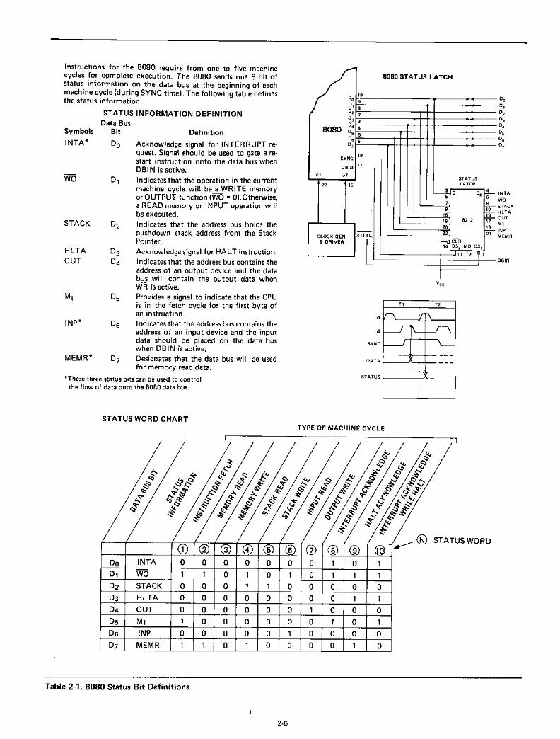
Symbols
INTA*
STACK °2HLTA °3OUT °4
M, °5INP* °6
MEMR* 0 7
Instructions for the 8080 require from one to five machinecycles for complete execution. The 8080 sends out 8 bit ofstatus informatton on the data bus at the beginning of eachmachine cycle (during SYNC time). The following table definesthe status information.
STATUS INFORMATION DEFINITIONData Bus
Bit Definition
00 Acknowledge signal for INTERRUPT request. Signal should be used to gate a restart instruction onto the data bus whenOBIN is active.
0, Indicates that the operation in the currentmachine cycle will be a WR ITE memoryor OUTPUT function (WO = O).Otherwise,a REAO memory or INPUT operation willbe executed.Indicates that the address bus holds thepushdown stack address from the StackPointer.Acknowledge signal for HALT instruction.Indicates that the address bus contains theaddress of an output device and the databus will contain the output data whenWR is active.Provides a signal to indicate that the CPUis in the fetch cycle for the first byte ofan instruction.Indicates that the address bus contains theaddress of an input device and the inputdata shou Id be placed on the data buswhen OB IN is active.Designates that the data bus will be usedfor memory read data.
*These three status bits can be used to controlthe flow of data onto the 8080 data bus.
STATUS WORD CHART
DO INTA
02 STACK
03 HLTA
04 OUT
06 INP
07 MEMR
Table 2-1. 8080 Status Bit Definitions
2-6
8080 STATUS LATCH
o 10o 9
0,o 8
2 70 3 3
8080 0 4 40 5 5
~6 67
SYNC19-
OBIN~01 02
STATUS
22 15 LATCH
--2. 0 1 DO~5 ~~ ~
9 ~16 .lL.18 8212 1720 JL-- 22 ~CLOCK GEN. (olTTl)
& DRIVER
~r;; CLR
OS2 MO OS,
13 12 Y1
I I~
T2
01
SYNC
OATA 1------''---t--t--
STATUS ......-.----+001'----1
TYPE OF MACHINE CYCLEI
INTA
W6STACKHlTAOUTM1
INPMEMR
DBIN

G)_RESETTillREADY + HLTA
HOLD
(3)
SET INTERNALHOLD F/F
RESET INTERNALHOLD F/F
INT. INTE
YES
IIII (31
I HOLDI MODEI
II
I__ .J
SET INTERNALHOLD F/F
YES
(2)
READY. HLTA
NO
READY ~~I...-------------~READY
7?~~----
YES
NO
RESET HLTA
NO
NO RESET INTERNALHOLD F/F
HOLD
SET INTERNALINT F/F
(1),NTE F/F IS RESET IF INTERNAL INT F/F IS SET.
(2),NTERNAL INT F/F IS RESET IF INTE F/F IS RESET.
(3)SEE PAGE 2-13.
Figure 2-4. CPU State Transition Diagram
2-7

The events that take place during the T3 state aredetermined by the kind of machine cycle in progress. In aFETCH machine cycle, the processor interprets the data onits data bus as an instruction. During a MEMORY READ or
a STACK READ, data on this bus is interpreted as a dataword. The processor outputs data on this bus during aMEMORY WRITE machine cycle. During I/O operations,the processor may either transmit or receive data, depending on whether an OUTPUT or an INPUT operationis involved.
Figure 2-6 illustrates the timing that is characteristicof a data input operation. As shown, the low-to-high transition of <P2 during T2 clears status information from the processor's data lines, preparing these lines for the receipt ofincoming data. The data presented to the processor musthave stabilized prior to both the "¢1-data set-up" interval
(tDS1), that precedes the falling edge of the ¢1 pulse defining state T3, and the "¢2-data set-up" interval (tDS2),
that precedes the rising edge of <P2 in state T3. This same
data must remain stable during the "data hold" interval
(tDH) that occurs following the rising edge of the <P2 pulse.Data placed on these Iines by memory or by other externaldevices will be sampled during T3.
During the input of data to the processor, the 8080generates a DBIN signal which should be used externally toenable the transfer. Machine cycles in which DB IN is available include: FETCH, MEMORY READ, STACK READ,and INTERRUPT. DBIN is initiated by the rising edge of ¢2during state T2 and terminated by the corresponding edge of<P2 during T3. Any TW phases intervening between T2 andT3 will therefore extend DBIN by one or more clockperiods.
Figure 2-7 shows the timing of a machine cycle inwh ich the processor outputs data. Output data may be destined either for memory or for peripherals. The rising edgeof <P2 within state T2 clears status information from theCPU's data lines, and loads in the data which is to be outputto external devices. This substitution takes place within the
4>1
A,S-O
SYNC
READY
WAIT
DBIN
T1 T2 Tw T3 T4 T6
n rr\ n n rl nL.-J , f , f \ I L
~ UNKNOWN
----- - --- _-..-® X L..... WRITE MODE FLOATING
-----~-----J FLOATING
I
DATA ~READMODE
STABLE
I
\
\
DATA
VSTATUSINFORMATION
DATA
A,S·0 SAMPLE READY OPTIONAL FETCH DATA OPTIONALMEMORY ADDRESS HOLD AND HALT OROR HALT INSTRUCTION INSTRUCTION1/0 DEVICE NUMBER OR OR EXECUTION
0-,,0 MEMORY WRITE DATA IF REQUIREDSTATUS INFORMATION ACCESS TIME
INTA OUT ADJUSTHLTA WOMEMR M,INP STACK
NOTE; ® Refer to Status Word Chart on Page 2-6.
Figure 2-5. Basic 8080 Instruction Cycle
2-8

~.....--.., .....--...,~ - FLOATING\. _J
BYTEONE
411 _n~---frr\~----Ifn~~n~~n,-- .........n-.--.......n,--~n~---.n~ .........n~----4~ _.J\._J\.J\.J\.L.IlLi\.~~l.-.l:1cd:J.
-~-- I\UNKNOWN BYTE X INPUT DATA TO
TWO ACCUMULATOR---..-.-+---............--....---- -, . , , . '~_~J ~ __ J
A15·0 ....._ .......
SYNC -W I I
DBIN \ LREADY
"1"
WAIT"0"
WR"1"
STATUSINFORMATION
NOTE: ® Refer to Status Word Chart on Page 2-6.
Figure 2-6. Input Instruction Cycle
0]·0
SYNC
DBIN
READY
WAIT
STATUSINFORMATION
M1 M2 ~ Ml
T1 T2 T3 T4 Tl T2 T3 Tl T2 T3 Tl
_rL-n_rL-rL-rL-rL-rL-rL-rL-rL-rL_J\.JlJlJlJ\.LJl~JlJlJ\..---J
I "\.
I ---I X' I/O DEVICEUNKNOWN
BYTE BYTE NUMBERONE TWO, ,----- ~- , 1 r ~-- X\.. I--_J
FLOATING U __ J ACCUMULATOR
-L-JI I \
"1"
"0"
,---\
~0 ~0 1~0
NOTE: ® Refer to Status Word Chart on Page 2-6.
Figure 2-7. Output Instruction Cycle
2-9

"data output delay" interval (tOO) following the </>2 clock'sleading edge. Data on the bus remains stable throughoutthe remainder of the machine cycle, until replaced by updated status information in the subsequent T1 state. Observethat a READY signal is necessary for completion of anOUTPUT machine cycle. Unless such an indication is present, the processor enters the TW state, following the T2state. Data on the output lines remains stable in theinterim, and the processing cycle will not proceed untilthe READY line again goes high.
The 8080 CPU generates a WR output for the synchronization of external transfers, during those machinecycles in which the processor outputs data. These includeMEMORY WRITE, STACK WRITE, and OUTPUT. Thenegative-going leading edge of WR is referenced to the risingedge of the first </>1 clock pulse following T2, and occurswithin a brief delay (tDC) of that event. WR remains lowuntil re-triggered by the leading edge of </>1 during thestate following T3. Note that any TW states interveningbetween T2 and T3 of the output machine cycle will neces-
sarily extend WR, in much the same way that DBrN is affected during data input operations.
All processor mach ine cycles consist of at least threestates: T1, T2, and T3 as just described. If the processor hasto wait for a response from the peripheral or memory withwhich it is communicating, then the machine cycle mayalso contain one or more TW states. During the three basicstates, data is transferred to or from the processor.
After the T3 state, however, it becomes difficult togeneralize. T4 and TS states are available, if the executionof a particular instruction requires them. But not ·all machinecycles make use of these states. It depends upon the kind ofinstruction being executed, and on the particular machinecycle within the instruction cycle. The processor will terminate any mach ine cycle as soon as its processing activitiesare completed, rather than proceeding through the T4 andTS states every time. Thus the 8080 may exit a machinecycle following the T3, the T41 or the TS state and proceed directly to the T1 state of the next mach ine cycle.
STATE
TW(optional)
T3
T4TS
(optional)
ASSOCIATED ACTIVITIES
A memory address or I/O device number isplaced on the Address Bus (A 15-0); statusinformation is placed on Data Bus (D7-0).
The CPU samples the READY and HOLD inputs and checks for halt instruction.
Processor enters wait state if READY is lowor if HALT instruction has been executed.
An instruction byte (FETCH machine cycle),data byte (MEMORY READ, STACK READ)or interrupt instruction (INTERRUPT machinecycle) is input to the CPU from the Data Bus;or a data byte (MEMORY WRITE, STACKWR ITE or OUTPUT machine cycle) is outputonto the data bus.
States T4 and TS are available if the execution of a particular instruction requires them;if not, the CPU may skip one or both ofthem. T4 and TS are only used for internalprocessor operations.
Table 2~2. State Definitions
2-10

INTERRUPT SEQUENCES
The 8080 has the built-in capacity to handle externalinterrupt requests. A peripheral device can initiate an interrupt simply by driving the processor's interrupt (INT) linehigh.
The interrupt (INT) input is asynchronous, and arequest may therefore originate at any time during anyinstruction cycle. Internal logic re-clocks the external request, so that a proper correspondence with the drivingclock is established. As Figure 2-8 shows, an interruptrequest (I NT) arriving during the time that the interruptenable line (I NTE) is high, acts in coincidence with the ~2
clock to set the internal interrupt latch. This event takesplace during the last state of the instruction cycle in wh ichthe request occurs, thus ensuring that any instruction inprogress is completed before the interrupt can be processed.
The INTERRUPT machine cycle which follows thearrival of an enabled interrupt request resembles an ordinaryFETCH machine cycle in most respects. The M1 status bitis transmitted as usual during the SYNC interval. It isaccompanied, however, by an INTA status bit (DO) whichacknowledges the external request. The contents of theprogram counter are latched onto the CPU's address linesduring T 1, but the counter itself is not incremented duringthe INTERRUPT machine cycle, as it otherwise would be.
In this way, the pre-interrupt status of the program counteris preserved, so that data in the counter may be restored bythe interrupted program after the interrupt request has beenprocessed.
The interrupt cycle is otherwise indistinguishable froman ordinary FETCH machine cycle. The processor itselftakes no further special action. It is the responsibility of theperipheral logic to see that an eight-bit interrupt instructionis "jammed" onto the processor's data bus during state T3.In a typical system, this means that the data-in bus frommemory must be temporarily disconnected from the processor's main data bus, so that the interrupting device cancommand the main bus without interference.
The 8080's instruction set provides a special one-bytecall which facilitates the processing of interrupts (the ordinary program Call takes three bytes). This is the RESTARTinstruction (RST). A variable three-bit field embedded inthe eight-bit field of .the RST enables the interrupting deviceto direct a Call to one of eight fixed memory locations. Thedecimal addresses of these dedicated locations are: 0, 8, 16,24, 32, 40, 48, and 56. Any of these addresses may be usedto store the first instruction (s) of a routine designed toservice the requirements of an interrupting device. Sincethe (RST) is a call, completion of the instruction alsostores the old program counter contents on the STACK.
A1S-0
SYNC
DBIN
RETURN M1(INTERNAL)
INTE
INT
INT F/F(INTERNAL)
INHIBIT STORE OFPC+1 (INTERNAL)
STATUSINFORMATION
M1 M2 M3
T3 T1 T2 T3 T4 Ts T1 T2 T3 T1 T2 T3
_n n r~ rLrL-rL"-rLrL-rL-rLrL_---r~U~~Ur--LLJl.LIl.J\.J\U\Wl.Lr\.Jl..Jl.
--- ~-pc·, I pc \ I sP·' X SP·2
----- ~-- 1--Do \ RST X PCH X X PCl(INTA)
I \ I rM\
'---' L-
-~ \ ,-
I~
I \
I \
0--- X\@ A\@
NOTE: ® Refer to Status Word Chart on Page 2-6.
Figure 2-8. Interrupt Timing
2-11

Mn M n + 1
l--OR~ I I
¢l_n ~ n ~n n ~ n¢2-+--sLJJlL-..rrL~LJLLJTLJJ\.lJL
! i : I I II I!
A'5·0 : I ! I -:- - - - - - - - - -:- - - - - - - - -1
1 I FLOATING I
OJ·O ~ \ .1 -I----------I----------......--~'i\.- - -..II I :
HOLD U ~ I 1REQUEST - (1)
i
HOLD .....1 '
READY
HOLD F/FINTERNAL -+- --+- +--_J
1
I
ii
HLDA I
(1) SEE ATTACHED ELECTRICAL CHARACTERISTICS. *T4 AND T5 OPERATION CAN BEDONE INTERNALLY.
I I
Figure 2-9. HOLD Operation (Read Mode)
A'5·0
HOLDREQUEST
HOLD
READY
HOLD F/FINTERNAL
HLDA
Mn M n+1 M n+2
T3 T4 T, T2 T3 T,
_V\ n n n n n n n-L.-ILL.-IL--F\...--F\...L.....JLL.-ILL.-ILL.-IL
I - ----- --jX I
I FLOATINGI, - ~----- --- X I - ----- --y-
-~--~
I
-U \I
I \
!
I
WRITE DATA
Figure 2-10. HOLD Operation (Write Mode)
2-12

HOLD SEQUENCES
The SOSOA CPU contains provisions for Direct Memory Access (DMA) operations. By applying a HO LD to theappropriate control pin on the processor, an external devicecan cause the CPU to suspend its normal operations and relinquish control of the address and data busses. The processor responds to a request of this kind by floating its addressto other devices sharing the busses. At the same time, theprocessor acknowledges the HO LD by placing a high on its
HLDA outpin pin. During an acknowledged HOLD, theaddress and data busses are under control of the peripheralwhich originated the request, enabling it to conduct memory transfers without processor intervention.
Like the interrupt, the HO LD input is synchronizedinternally. A HOLD signal must be stable prior to the "Holdset-up" interval (tHS), that precedes the rising edge of <P2.
Figures 2-9 and 2-10 illustrate the timing involved inHOLD operations. Note the delay between the asynchronousHOLD REQUEST and the re-clocked HOLD. As shown inthe diagram, a coincidence of the READY, the HOLD, andthe ¢2 clocks sets the internal hold latch. Setting the latchenables the subsequent rising edge of the ¢1 clock pulse totrigger the HLOA output.
Acknowledgement of the HOLD REQUEST precedesslightly the actual floating of the processor's address anddata lines. The processor acknowledges a HO LD at the beginning of T3, if a read or an input machine cycle is in progress(see Figure 2-9). Otherwise, acknowledgement is deferred
until the beginning of the state following T3 (see Figure2-10). In both cases, however, the HLDA goes high withina specified delay (tDC) of the rising edge of the selected ¢1clock pulse. Address and data lines are floated within abrief delay after the rising edge of the next ¢2 clock pulse.This relationship is also shown in the diagrams.
To all outward appearances, the processor has suspended its operations once the address and data busses are floated.Internally, however, certain functions may continue. If aHOLD REQUEST is acknowledged at T3, and if the processor is in the middle of a machine cycle which requiresfour or more states to complete, the CPU proceeds throughT4 and T5 before coming to a rest. Not until the end of themachine cycle is reached will processing activities cease.Internal processing is thus permitted to overlap the externalDMA transfer, improving both the efficiency and the speedof the entire system.
The processor exits the holding state through asequence similar to that by which it entered. A HOLDREQUEST is terminated asynchronously when the external
device has completed its data transfer. The H LOA output
returns to a low level following the leading edge of the next¢1 clock pulse. Normal processing resumes with the machine cycle following the last cycle that was executed.
HALT SEQUENCES
When a halt instruction (H LT) is executed, the CPUenters the ha It state (TWH) after state T2 of the next machine cycle, as shown in Figure 2-11. There are only threeways in which the 8080 can exit the halt state:
• A high on the RESET line will always reset the8080 to state T 1; RESET also clears the programcounter.
• A HOLD input will cause the 8080 to enter thehold state, as previously described. When theHOLD line goes low, the 8080 re-enters the haltstate on the rising edge of the next ¢1 clockpulse.
• An interrupt (Le., INT goes high while INTE isenabled) will cause the 8080 to exit the Halt stateand enter state T 1 on the rising edge of the next¢1 clock pulse. NOTE: The interrupt enable (INTE)flag must be set when the halt state is entered;otherwise, the 8080 will only be able to exit via aRESET signal.
Figure 2-12 illustrates halt sequencing in flow chart
form.
START-UP OF THE 8080 CPU
When power is applied initially to the 8080, the processor begins operating immediately. The contents of itsprogram counter, stack pointer, and the other working registers are naturally subject to random factors and cannot bespecified. For this reason, it will be necessary to begin thepower-up sequence with RESET.
An external RESET signal of three clock period duration (minimum) restores the processor's internal programcounter to zero. Program execution thus begins with memory location zero, following a RESET. Systems which require the processor to wait for an explicit start-up signalwill store a halt instruction (EI, HLT) in the first two locations. A manual or an automatic INTERRUPT will be usedfor starting. In other systems, the processor may begin executing its stored program immediately. Note, however, that
the RESET has no effect on status flags, or on any of theprocessor's working registers (accumulator, registers, orstack pointer). The contents of these registers remain indeterminate, until initialized explicitly by the program.
2-13

TWHTWH
,...-+---- - - - - - -
Tl
~--..-----~-- - - - - - -
T,
91
92
A1S·0 PC
07-0
SYNC
OBIN
WAIT
STATUSINFORMATION
NOTE: ® Refer to Status Word Chart on Page 2-6
Figure 2-11. HALT Timing
TO STATE NO
TW orT3
TO STATE YESTl
TO STATE Tl
Figure 2-12. HALT Sequence Flow Chart.
2-14

Tn+iTn+(i-1)Tn +3Tn+2Tn+1
~~~~t==p----~--·_-~---,--~~-----+-----""'----"'~-+---"""
Tn
(1)
cP1
A15.0~__.1
RESET
INTERNALRESET
SYNC -+- ..... ..... -+- -/~-----~---- ....-_....I
DBIN -+-----.....-----.....----....-----/~-----~---- ....-----I---.....I
STATUSINFORMATION
(0I I
11lWHEN RESET SIGNAL IS ACTIVE, ALL OF CONTROL OUTPUT SIGNALS WILL BE RESET IMMEDIATELY OR SOMECLOCK PERIODS LATER. THE RESET SIGNAL MUST BE ACTIVE FOR A MINIMUM OF THREE CLOCK CYCLES. INTHE ABOVE DIAGRAM N AND I MAY BE ANY INTEGER.
NOTE: ® Refer to Status Word Chart on Page 2·6.
Figure 2-13. Reset.
~.O
SYNC
DBIN
HOLD
HOLD F/F(INTERNAL)
HLDA
INTE
INT
INT F/F(INTERNAL)
STATUSINFORMATION
M1
TWH TWH TWH TWH TWH TWH TWH T1 T2 T3
.rL-rL-rL-..rL..-r\l.-r\l.-~~~rL..-_J\.-fn.--.Jl.J\.._JrL...J\.JrLJL--.Jl.-JTl- --- ------- ---- - -~-
" --IJ l-FLOFLOATING I
- --- " 1- _... - - - -- -- '- - -- :- - ~ - - -- -- ~ - - --\... ~ST_ J 1
I
I \ I
I LII \ I
/'~J\; \' I
II \ I,I INHIBIT INHIBIT \
INT HOLD,) , \
0 K@
I
ATING
NOTE: ® Refer to Status Word Chart on Page 2·6.
Figure 2-14. Relation between HOLD and'INT in the HALT State.
2-15

MNEMONIC OP CODE M1[1] M2
o S S S
T3T5
x
X[3]
x
OAA-A, FLAGS[10]
x
T4
x
x
x
x
x
(RP)-1 ~.
(RP) + 1 ~~
x
x
(OOO)-TMP(TMP)+l-ALU
x
(SSS)-TMP(A)-ACT
x
(OOOJ-TMP(TMP) + 1-ALU
(SSS)-TMP(A)-ACT
(A)-ACT
(SSS)-TMP(A)-ACT
(SSS)-TMP(A)-ACT
(SSS)-TMP(A)-ACT
(SSS)-TMP
(HL) ~
(SSS)-TMP
T3
PC == PC +1 INST-TMP/IR
PCOUT PC==PC+1 INST-TMP/lRSTATUS
T1
PC OUTSTATUS
o
o
o
o
o
o
o
o
o
o
o
o
o
S
o
o 0
1 0
S S S
o
o
001
o
o
1 1
o 1 0 0
1 S S S
o 1 0
o 1 0 1
o 1
o 0
o 1 1
1 0
1 0 0 1
o S S S
1 1 1 0
o S S S
o
o 1 1 0
o 1
1 0
1 0
o 0
o S S S
o 0
o
o S
o
001 0
o
000
o
o
o
o 0
o 0
o
o 0 R P
o 0 R P
o
o 0
1 0
o 0
000
o 0
000
o
1 1 1
000
000
1 0 1 0
o 0 1 0
o 0 R P
o 0
1 0 0
o 0 0 0
001
o 0 0 0
100
1 1 0 0
o 0 R P
o 0 R P
o 0 1 1
o 0
o 0 1
o 0 0 0
o 0
o 0 R P
o 0
o 1
o
o
INRM
OCR r
OCR M
INXrp
OAOrp[S]
OAA
ANAr
LHLO addr
ACI data
SBB r
SBB M
DCXrp
LOAX rp[4]
LOA addr
AOOM
AOI data
AOCr
AOCM
SUBr
SUB M
SUI data
ANAM
SBI data
INRr
AOOr
STA addr
STAX rp[4]
LXI rp, data
SHLO addr
MVI M, data
XCHG
MVI r., data
MOVM,r
MOVr1,r2
MOVr,M
SPHL
2-16

PC OUTSTATUS[6]
[9]
[9]
[9]
M3
PC = PC + 1
PC = PC + 1
PC = PC + 1
PC = PC + 1
M4
2-17
M5

MNEMONIC OP CODE Ml[l] M2
07 0 6 0 5 0 4 03 0 2 0 1 DO Tl T2[2] T3 T4 T1 T2[2] T3
ANI data 1 1 1 0 0 1 1 0 PC OUT PC = PC + 1 INST-TMP/IA (A)-ACT PC =PC + 1STATUS
XAAr 1 0 1 0 S S S (A)-ACT (ACT)+(TPM)-A(SSS)-TMP
XRAM 0 1 0 1 1 0 (A)-ACT
XRI data 1 0 1 0 (A)-ACT PC =PC + 1
ORAr 0 1 1 0 S S S (A)-ACT (ACT)+(TMP)-A(SSS)-TMP
ORAM 1 0 1 1 0 1 1 0 (A)-ACT
ORI data 0 1 0 (A)-ACT PC = PC + 1
CMPr 0 1 1 S S S (A)-ACT(SSS)-TMP
CMPM 1 0 1 1 1 1 1 0 (A)-ACT
CPI data 1 1 1 1 0 (A)-ACT PC = PC + 1
RLC 0 0 0 0 0 (A)-ALU ALU-A, CYROTATE
RRC 0 0 0 0 1 1 1 1 (A)-ALU ALU-+A, CYROTATE
RAL 0 0 0 0 (A), CY-A LU ALU-+A, CYROTATE
AAA 0 0 0 1 1 1 (A), CY-A LU ALU-+A, CYROTATE
CMA 0 0 0 1 1 (A)-A
CMC 0 0 1 1 cy-CY
STC 0 0 1 0 1 l-CY
JMP addr 1 1 0 0 0 0 X
J cond addr[17] C C C 0 0 PC =PC + 1
CALLaddr 0 0 0 1 SP =SP-1 PC =PC + 1
C cond addr[17] 1 1 C C C 0 0 PC = PC + 1
RET 0 0 0 0 X SP =SP + 1
R cond addr[17] C C C 0 0 0 INST-TMP/IA SP =SP + 1
RSTn 1 1 N N N 1 1 q,-+W SP = SP-1 Sp;: SP - 1INST-TMP/IR
PCHL 0 0 0 INST-TMP/IR (HL)
PUSHrp 1 1 A P 0 1 0 1 SP =SP-1
PUSH PSW 0 1 0 Sp;: SP - 1 Sp:: SP - 1
POPrp R P 0 0 0 X Sp;: SP + 1
POP PSW 0 0 0 X Sp;: SP + 1
XTHL 1 1 1 0 0 0 1 1 X SP;: SP + 1
IN port 1 1 0 1 0 X PC:: PC + 1
OUT port 0 0 0 X PC:: PC + 1
EI 1 0 SET INTE F/F
01 1 1 1 1 0 0 1 RESET INTE F/F
HLT 0 0 0 X
NOP 0 0 0 0 0 0 0 0 PC OUT PC:: PC + 1 INST-TMP/IA XSTATUS
2-18

M3 M4 M5
SP OUT SP :: SP + 1STATUS[15]
SP OUT SP :: SP + 1STATUS[15]
(ACT)+(TMP)-A
T1
WZOUT (WZ) + 1-PCSTATUS[ll]
PC OUT PC:: PC + 1~iA~~[ll,12]
(WZ) + 1- PCSTATUS[6]
PC OUT PC:: PC + 1~iA~~~[11]
(WZ) + 1-PCSTATUS[6]
~~~TUJS[6]PC:: PC + 1
~iA~~~[11,12](WZ) + 1-PC
~~2~JS[15]Sp:: SP + 1
~A~~~[ll](WZ) +l-PC
SPOUT Sp:: SP + 1~A~~1[11,12]
(WZ) + 1- PCSTATUS[15]
~iA~~~[11](WZ) + 1-PC
STATUS[18]
SPOUTSTATUS[15]
WZOUT
[9
[9]
2-19

NOTES:
1. The first memory cycle (M 1) is always an instructionfetch; the first (or only) byte, containing the op code, isfetched during this cycle.
2. If the READY input from memory is not high duringT2 of each memory cycle, the processor will enter a waitstate (TW) until READY is sampled as high.
3. States T4 and T5 are present, as required, for operations which are completely internal to the CPU. The contents of the internal bus during T4 and T5 are available atthe data bus; this is designed for testing purposes only. An"X" denotes that the state is present, but is only used forsuch internal operations as instruction decoding.
4. Only register pairs rp = B (registers B and C) or rp = D(registers D and E) may be specified.
5. These states are ski pped.
6. Memory read sub-cycles; an instruction or data wordwill be read.
7. Memory write sub-cycle.
8. The READY signal is not required during the secondand third sub-cycles (M2 and M3). The HOLD signal isaccepted during M2 and M3. The SYNC signal is not generated during M2 and M3. During the execution of DAD,M2 and M3 are required for an internal register-pair add;memory is not referenced.
9. The results of these arithmetic, logical or rotate instructions are not moved into the accumulator (A) untilstate T2 of the next instruction cycle. That is, A is loadedwhile the next instruction is being fetched; this overlappingof operations allows for faster processing.
10. If the value of the least significant 4-bits of the accumu
lator is greater than 9 or if the auxjliary carry bit is set, 6is added to the accumulator. If the value of the most significant 4-bits of the accumulator is now greater than 9, ~ ifthe carry bit is set, 6 is added to the most significant4-bits of the accumulator.
11. This represents the first sub-cycle (the instructionfetch) of the next instruction cycle.
2-20
12. If the condition was met, the contents of the registerpair WZ are output on the address lines (Ao-1S) instead ofthe contents of the program counter (PC).
13. If the condition was not met, sub-cycles M4 and M5are skipped; the processor instead proceeds immediately tothe instruction fetch (Ml) of the next instruction cycle.
14. If the condition was not met, sub-cycles M2 and M3are skipped; the processor instead proceeds immediately tothe instruction fetch (M 1) of the next instruction cycle.
15. Stack read sub-cycle.
16. Stack write sub-cycle.
17. CONDITION CCC
NZ - not zero (Z = 0) 000Z - zero (Z = 1) 001
NC - no carry (CY = 0) 010C - carry (CY = 1) 011
PO parity odd (P=O) 100PE parity even (P = 1) 101
P plus (S= 0) 110M minus (S = 1) 111
18. I/O sub-cycle: the I/O port's 8-bit select code is duplicated on address lines 0-7 (Ao-7) and 8-15 (AS-1S).
19. Output sub-cycle.
20. The processor will remain idle in the halt state untilan interrupt, a reset or a hold is accepted. When a hold request is accepted, the CPU enters the hold mode; after thehold mode is terminated, the processor returns to the haltstate. After a reset is accepted, the processor begins execution at memory location zero. After an interrupt is accepted,the processor executes the instruction forced onto the databus (usually a restart instruction).
SSS or DDD Value rp ValueA 111 B 00B 000 D 01C 001 H 10D 010 SP 11E 011H 100L 101

This chapter will illustrate, in detail, how to interfacethe 8080 CPU with Memory and I/O. It will also show the
benefits and tradeoffs encountered when using a variety ofsystem architectures to achieve higher throughput, decreased component count or minimization of memory size.
8080 Microcomputer system design lends itself to asimple, modular approach. Such an approach will yield thedesigner a reliable, high performance system that contains aminimum component count and is easy to manufacture andmaintain.
Control Bus A uni-directional set of signals that indicatethe type of activity in current process.
Type of activities: 1. Memory Read2. Memory Write3. I/O Read4. I/O Write5. Interrupt Acknowledge
CPU Module* Contains the Central Processing Unit, systemtiming and interface circuitry to Memoryand I/O devices.
The overall system can be thought of as a simpleblock diagram. The three (3) blocks in the diagram represent the functions common to any computer system.
*"Module" refers to a functional block, it does not reference a printed circuit board manufactured by INTE L.
t"Bus" refers to a set of signals grouped together becauseof the similarity of their functions.
CPUMODULE
Figure 3-1. Typical Computer System Block Diagram
Basic System Operation
1. The CPU Module issues an activity command on theControl Bus.
2. The CPU Module issues a binary code on the AddressBus to identify which particular Memory location orI/O device will be involved in the current processactivity.
3. The CPU Module receives or transmits data with theselected Memory location or I/O device.
4. The CPU Module returns to CD and issues the nextactivity command.
It is easy to see at this point that the CPU module isthe central element in any computer system.
Contains Read Only Memory (ROM) andRead/Write Memory (RAM) for program anddata storage.
Con"tains circuitry that allows the computersystem to communicate with devices orstructures existing outside of the CPU orMemory array.
for example: Keyboards, Floppy Disks,Paper Tape, etc.
I/O
Memory
There are three busses that interconnect these blocks:
Data Bust A bi-directional path on which data can flowbetween the CPU and Memory or I/O.
Address Bus A uni-directional group of lines that identifya particular Memory location or I/O device.
3-1

The following pages will cover the detailed design ofthe CPU Module with the 8080. The three Busses (Data,Address and Control) will be developed and the interconnection to Memory and I/O will be shown.
Design philosophies and system architectures presented in this manual are consistent with product develop-
l"M
ment programs underway at INTEL for the MCS-80. Thus,the designer who uses this manual as a guide for his totalsystem engineering is assured that all new developments incomponents and software for MCS-80 from INTEL will becompatible with his design approach.
the design and to achieve operational characteristics thatare as close as possible to those of the 8224 and 8228.Many auxiliary timing functions and features of the 8224and 8228 are too complex to practically implement instandard components, so only the basic functions of the8224 and 8228 are generated. Since significant benefits insystem timing and component count reduction can berealized by using the 8224 and 8228, this is the preferredmethod of implementation.
1. 8080 CPU
CPU Module Design
The CPU Module contains three major areas:
1. The 8080 Central Processing Unit
2. A Clock Generator and High Level Driver
3. A bi-directional Data Bus Driver and System ControlLogic
The following will discuss the design of the threemajor areas contained in the CPU Module. This design ispresented as an alternative to the Intel® 8224 Clock Generator and Intel 8228 System Controller. By studying thealternative approach, the designer can more clearly see theconsiderations involved in the specification and engineeringof the 8224 and 8228. Standard TTL components and Intelgeneral purpose peripheral devices are used to implement
2.
The operation of the 8080 CPU was covered in previous chapters of this manual, so little reference willbe made to it in the design of the Module.
Clock Generator and High Level Driver
The 8080 is a dynamic device, meaning that its internal storage elements and logic circuitry require atiming reference (Clock), supplied by external circuitry, to refresh and provide timing control signals.
The 8080 requires two (2) such Clocks. Their waveforms must be non-overlapping, and comply with thetiming and levels specified in the 8080 A.C. and D.C.Characteristics, page 5-15.
Clock Generator Design
The Clock Generator consists of a crystal controlled,
2 25GND AO AO
+5V20 26
Al Al11 27
-5V A2 A2
+12V28
A329
30A3
A4 A4
AS31
AS
A632
A68080 33CPU A7 A7
A834
A8ADDRESS BUS
13 35SYSTEM DMA REO. HOLD A9 A9
Al01
Al0
All40
All14
A12 37 A12SYSTEM INT. REO. tNT
A13 38~13
INT. ENABLE16
INTE A14 39 A14
A1536 A15
WR18
XTAL 17
0 DBIN
HLDA21
22 10ct>1 DO
15 9eJ>2 01
028
CLOCK24
WAIT 037 BI-DIREC-
WAIT REO. GENERATOR 23 3 TIONAL DATA BUS
DRIVER READY 04 BUS DRIVER412 05
SYS. RESET RESET 506
19 076
SYNC
1 STATUS STROBE SYSTEMCONTROL
Figure 3-2. 8080 CPU Interface
3-2

OSCILLATOR
CLOCK GENERATOR
7486
DB OB74163
DC OC .......--...-------'
74S04~
20MHz
330 330
~""""--01>-......------------.......--------.... OSC
7486
READY
r-----IIIIII---- SYNC
AUXILIARY FUNCTIONS
WA IT REO ------41---1 0 a74574
ClK
'----........--410
74S74
ClK 0.......-..-.-----.. tf>1A (TTL)
74HOO
10--+---------.. 4>2 (TTL)
WAVEFORMS
GND--+-~
4>1 ----u u---f 1~~~ ~50ns
4>2 --' \ 250ns , '~__-Ir-50ns~ t+- --.f r- 50ns
4>1A ---I , 250ns , , I
SYNC ---1',\,.-_---1'
\ DMAREO--~----IID a74S74
ClK
HOLD
Figure 3-3. 8080 Clock Generator
20 MHZ oscillator, a four bit counter, and gatingcircuits.
The oscillator provides a 20 MHZ signal to the inputof a four (4) bit, presettable, synchronous, binarycounter. By presetting the counter as shown in figure3-3 and clocking it with the 20 MHZ signal, a simpledecoding of the counters outputs using standard TTLgates, provides proper timing for the two (2) 8080clock inputs.
Note that the timing must actually be measured atthe output of the High Level Driver to take into account the added delays and waveform distortionswithin such a device.
positive transition when biased from the 8080 Voosupply (12V) but to achieve the low voltage specification (VILC ) .8 volts Max. the driver is biased to the8080 Vss supply (-5V). This allows the driver toswing from GND to Voo with the aid of a simpleresistor divider.
A low resistance series network is added between thedriver and the 8080 to eliminate any overshoot of thepulsed waveforms. Now a circuit is apparent that caneasily comply with the 8080 specifications. In factrise and falltimes of this design are typically less than10 ns.
Figure 3-4. High Level Driver
100n
-5V
.68 J.LF
+12V
6
6S0pF 47ncf>1
cf>1 (TTL) ---1 2MH0026 (SOSO PIN 22)
680 pFOR
¢2 (TTL)-) 4EQUIV. 5
47n¢2
(8080 PIN 15)
3
15K 15K
High Level Driver DesignThe voltage level of the clocks for the 8080 is notTTL compatible like the other signals that input tothe 8080. The voltage swing is from .6 volts (VILC )
to 11 volts (VIHC ) with risetimes and falltimes under50 ns. The Capacitive Drive is 20 pf (max.). Thus, aHigh Level Driver is required to interface the outputsof the Clock Generator (TTL) to the 8080.
The two (2) outputs of the Clock Generator are capacitivity coupled to a dual- High Level clock driver.The driver must be capable of complying with the8080 clock input specifications, page 5-15. A driverof this type usually has little problem supplying the
3-3

Auxiliary Timing Signals and Functions
The Clock Generator can also be used to provideother signals that the designer can use to simplifylarge system timing or the interface to dynamicmemories.
Functions such as power-on reset, synchronization ofexternal requests (HOLD, READY, etc.) and singlestep, could easily be added to the Clock Generator tofurther enhance its capabilities.
For instance, the 20 MHZ signal from the oscillatorcan be buffered so that it could provide the basis forcommunication baud rate generation.
The Clock Generator diagram also shows how to generate an advanced timing signal (l/>1A) that is handyto use in clocking "0" type flipflops to synchronizeexternal requests. It can also be used to generate astrobe (STSTB) that is the latching signal for the status information which is available on the Data Bus atthe beginning of each machine cycle. A simple gatingof the SYNC signal from the 8080 and the advanced(l/>1A) will do the job. See Figure 3-3.
3. Bi-Directional Bus Driver and System Control Logic
The system Memory and I/O devices communicatewith the CPU over the bi-directional Data Bus. Thesystem Control Bus is used to gate data on and offthe Data Bus within the proper timing sequences asdictated by the operation of the 8080 CPU. The datalines of the 8080 CPU, Memory and I/O devices are3-state in nature, that is, their output drivers havethe ability to be forced into a high-impedance modeand are, effectively, removed from the circuit. This '3state bus technique allows the designer to construct asystem around a single, eight (8) bit parallel, bi-directional Data Bus and simply gate the information onor off this bus by selecting or deselecting (3-stating)Memory and I/O devices with signals from the Control Bus.
Bi-Directional Data Bus Driver Design
The 8080 Data Bus (07-00) has two (2) major areasof concern for the designer:
1. Input Voltage level (V1H ) 3.3 volts minimum.
2. Output Drive Capability (tOL) 1.7 rnA maximum.
OBO
OB1
OB2
OB3
OB4
DB5
DB6
DB7
BUSEN
-DO
2,4 r- 3
015,7 r- 6
9,11r- 8216 1002
0312,14r- 13
OlEN CS
15? «1
042,4] 3
055,7 r- 6
9,11r- 8216 1006
0712,14r- 13
OlEN CS
OBIN ~I15)' ?1
...,
3 4 INTA
Q.»--I....--
5 6 WO- -0
7 8 STACK-9
821210 HLTA-
16 15 OUT
~Q.»--18 17 M1-20 191NP
22 21 MEMR
c=[y--------!1 12 [13STSTB Vee
-WR ...... 1
I...... -
---(>0.-=0--
808
Figure 3-5. 8080 System Control
3-4

The input level specification impl ies that any semiconductor memory or I/O device connected to the8080 Data Bus must be able to provide a minimum of3.3 volts in its high state. Most semiconductor memories and standard TTL I/O devices have an outputcapability of between 2.0 and 2.8 volts, obviously adirect connection onto the 8080 Data Bus would require pullup resistors, whose value should not affectthe bus speed or stress the drive capability of thememory or I/O components.
The 80S0A output drive capability (lOl) 1.9mA max.is sufficient for small systems where Memory size andI/O requirements are minimal and the entire system iscontained on a single printed circuit board. Most systems however, take advantage of the high-performance computing power of the 8080 CPU and thus amore typical system would require some form of buffering on the 80S0 Data Bus to support a larger arrayof Memory and I/O devices which are likely to be onseparate boards.
A device specifically designed to do this bufferingfunction is the INTEL® 8216, a (4) four bit bi-directional bus driver whose input voltage level is compatible with standard TTL devices and semiconductormemory components, and has output drive capabilityof 50 mAo At the 8080 side, the 8216 has a "high"output of 3.65 volts that not only meets the S080input spec but provides the designer with a worse case350 mV noise margin.
A pair of S216's are connected directly to the 8080Data Bus (07-00) as shown in figure 3-5. Note thatthe OBI N signal from the 8080 is connected to thedirection control input (01 EN) so the correct flow ofdata on the bus is maintained. The chip select (CS) of
the S216 is connected to BUS ENABLE (BUSEN) toallow for DMA activities by deselecting the Data BusBuffer and forcing the outputs of the S216's intotheir high impedance (3-state) mode. This allowsother devices to gain access to the data bus (DMA).
System Control Logic Design
The Control Bus maintains discipline of the bi-directional Data Bus, that is, it determines what type ofdevice will have access to the bus (Memory or I/O)and generates signals to assure that these devicestransfer Data with the SOSO CPU within the propertiming "windows" as dictated by the CPU operationalcharacteristics.
As described previously, the 8080 issues Status information at the beginning of each Machine Cycle on itsData Bus to indicate what operation will take placeduring that cycle. A simple (8) bit latch, like anINTEL® 8212, connected directly to the 80S0 DataBus (07-00) as shown in figure 3-5 will store the
3-5
Status information. The signal that loads the datainto the Status Latch comes from the Clock Generator, it is Status Strobe (STSTB) and occurs at thestart of each Machine Cycle.
Note that the Status Latch is connected onto theSOSO Data Bus (07-00) before the Bus Buffer. This isto maintain the integrity of the Data Bus and simplifyControl Bus timing in DMA dependent environments..
As shown in the diagram, a simple gating of the outputs of the Status Latch with the DB INand WRsignals from the S080 generate the (4) four Controlsignals that make up the basic Control Bus.
These four signals: 1. Memory Read (MEM R)
2. Memory Write (MEM W)
3. I/O Read (I/O R)
4. I/O Write (I/O W)
TM
connect directly to the MCS-80 component "family"of ROMs, RAMs and I/O devices.
A fifth signal, Interrupt Acknowledge (lNTA) isadded to the Control Bus by gating data off theStatus Latch with the DBIN signal from the S080CPU. This signal is used to enable the InterruptInstruction Port wh ich holds the RST instructiononto the Data Bus.
Other signals that are part of the Control Bus such asWO, Stack and M1 are present to aid in the testing ofthe System and also to simplify interfacing the CPUto dynamic memories or very large systems that require several levels of bus buffering.
Address Buffer Design
The Address Bus (A 15-AO) of the 8080, like the DataBus, is sufficient to support a small system that has amoderate size Memory and I/O structure, confined toa single card. To expand the size of the system thatthe Address Bus can support a simple buffer can beadded, as shown in figure 3-6. The INTEL®S212 or8216 is an excellent device for this function. Theyprovide low input loading (.25 mA), high outputdrive and insert a minimal delay in the SystemTiming.
Note that BUS ENABLE (BUSEN) is connected tothe buffers so that they are forced into their highimpedance (3-state) mode during DMA activities sothat other devices can gain access to the Address Bus.

INTERFACING THE 8080 CPU TO MEMORYAND I/O DEVICES
The 8080 interfaces with standard semiconductorMemory components and I/O devices. In the previous textthe proper control signals and buffering were developedwhich will produce a simple bus system similar to the basicsystem example shown at the beginning of this chapter.
In Figure 3-6 a simple, but exact 8080' typical systemis shown that can be used as a guide for any 8080 system,regardless of size or complexity. It is a "three bus" architecture, using the signals developed in the CPU module.
Note that Memory and I/O devices interface in thesame manner and that their isolation is only a function ofthe definition of the Read-Write signals on the Control Bus.This allows the 8080 system to be configured so that Memory and I/O are treated as a single array (memory mappedI/O) for small systems that require high thruput and haveless than 32K memory size. This approach will be broughtout later in the chapter.
This feature eliminates the need for extra equipment liketape readers and disks to load programs initially, an important aspect in small system design.
Interfacing standard ROMs, such as the devices shownin the diagram is simple and direct. The output Data linesare connected to the bi-directional Data Bus, the Addressinputs tie to the Address bus with possible decoding of themost significant bits as IIchip selects" a~d the MEMR signalfrom the Control Bus connected to a "chip select" or databuffer. Basically, the CPU issues an address during the firstportion of an instruction or data fetch (Tl & T2). Thisvalue on the Address Bus selects a specific location withinthe ROM, then depending on the ROM's delay (access time)the data stored at the addressed location is present at theData output lines. At this time (T3) the CPU Data Bus isin the "input Mode" and the control logic issues a MemoryRead command (MEMR) that gates the addressed data onto the Data Bus.
RAM INTERFACE
ROM INTERFACE
A ROM is a device that stores data in the form ofProgram or other information such as "look-up tables" andis only read from, thus the term Read Only Memory. This
type of memory is generallY' non-volatile, meaning thatwhen the power is removed the information is retained.
A RAM is a device that stores data. This data can beprogram, active "look-up tables," temporary values or external stacks. The difference between RAM and ROM isthat data can be written into such devices and are inessence, Read/Write storage elements. RAMs do not holdtheir data when power is removed so in the case where Program or "look-up tables" data is stored a method to load
HOLD REO
WR DO-D7DBIN HLDA AO-A15
{} D"---_~rl {[- DL...-.--_n '0 o::=cCONTROL BUS (6)
8102A·48107B·482108222
RAMs
5101
8101-2
8111·2
8102-2
8302
8308
8316A
ROMs
8702A
8704
8708
DATA BUS (8)
!r-:- -- -----"1I 8212 ADDRESSII 8205 BUFFERSI II DECODER IlL.83..1~ (OP~I£.N~~..J
u___LCJJ~)7 I
ADDRESS BUS (16)
8251 I/OCOMMUNICATION
INTERFACE
8212
8255I/O
PERIPHERALINTERFACE
8214
8212PRIORITY
INTERRUPT
Figure 3-6. Microcomputer System
3-6

RAM memory must be provided, such as: Floppy Disk,Paper Tape, etc.
The CPU treats RAM in exactly the same manner asROM for addressing data to be read. Writing data is verysimilar; the RAM is issued an address during the first portion of the Memory Write cycle (T1 & T2) in T3 when thedata that is to be written is output by the CPU and is stableon the bus an MEMW command is generated. The MEMWsignal is connected to the R/W input of the RAM andstrobes the data into the addressed location.
In Figure 3-7 a typical Memory system is illustratedto show how standard semiconductor components interfaceto the 8080 bus. The memory array shown has 8K bytes
• ®(8 bits/byte) of ROM storage, uSing four Intel 8216Asand 512 bytes of RAM storage, using Intel 8111 static
RAMs. The basic interface to the bus structure detailedhere is common to almost any size memory. The only addition that might have to be made for larger systems ismore buffers (8216/8212) and decoders (8205) for generating "chip selects."
The memories chosen for this example have an accesstime of 850 nS (max) to illustrate that slower, economicaldevices can be easily interfaced to the 8080 with little effect on performance. When the 8080 is operated from aclock generator with a tCY of 500 nS the required memoryaccess time is Approx. 450-550 nS. See detailed timingspecification Pg. 5-16. Using memory devices of this speedsuch as Intel@8308, 8102A, 8107A, etc. the READY inputto the· 8080 CPU can remain "high" because no "wait"states are required. Note that the bus interface to memoryshown in Figure 3-7 remains the same. However, if slowermemories are to be used, such as the devices illustrated(8316A, 8111) that have access times slower than the minimum requirement a simple logic control of the READYinput to the 8080 CPU will insert an extra "wait state" thatis equal to one or more clock periods as an access time"adjustment" deiay to compensate. The effect of the extra"wait" state is naturally a slower execution time for theinstruction. A single "wait" changes the basic instructioncycle to 2.5 microSeconds.
8K + 512
RAM
8K o
ROM
MEMORY MAP
ROM
RAM-----------, ----------....#4.:.- ...........
#3;;. ..-.
#2#1
8111
FiJW 00 1/0 1-4 AO-A7
8111
R/W 00 1/01-4 AO-A7
AO-A7
8316A
01-08
CS3CS2
AO-Al0
AllA12
_01.--_0 DATA BUS IsiJL.-..--_IJL--.------L----_DL----CONTROL BUS (6)
_-.-ill n 11_ADDRESS BUS (16)
Figure 3-7. Typical Memory Interface
3-7

I/O INTERFACE
Figure 3-9. Isolated I/O.
Memory Mapped I/O
It is easy to see that from the list of possible "new"instructions that this type of I/O architecture could have adrastic effect on increased system throughput. It is conceptually more difficult to understand than Isolated I/O and itdoes limit memory address space, but Memory Mapped I/Ocan mean a significant increase in overall speed and at thesame time reducing re~uired program memory area.
I/OR }TO I/O DEVICES
~----I/OW
MEMR } TO MEMORY__ DEVICES
~----MEMW
(I nput Port to any Register)(Output any Register to Port)(Output immediate data to Port)(I nput to ACC)(Output from ACC to Port)(1 ~ Bit Input)(16 Bit Output)(Add Port to ACC)("AND" Port with ACC)
SYSTEMCONTROL
(8228)
Examples:
MOVr, MMOV M, rMVI MLOASTALHLOSHLOADD MANAM
By assigning an area of memory address space as I/O apowerful architecture can be developed that can manipulateI/O using the same instructions that are used to manipulatememory locations. Thus, a "new" instruction set is createdthat is devoted to I/O handling.
As shown in Figure 3-10, new control signals are generated by gating the MEMR and MEMW signals with A15, themost significant address bit. The new I/O control signals connect in exactly the same manner as Isolated I/O, thus thesystem bus characteristics are unchanged.
By assigning A15 as the I/O "flag", a simple method ofI/O discipline is maintained:
If A 15 is a "zero" then Memory is active.If A15 is a "one" then I/O is active.
Other address bits can also be used for this function. A15 waschosen because it is the most significant address bit so it iseasier to control with software and because it still allowsmemory addressing of 32K.
I/O devices are still considered addressed IIports" butinstead of the Accumulator as the only transfer medium anyof the internal registers can be used. All instructions thatcould be used to operate on memory locations can be usedin I/O.
General Theory
ISOLATED I/O~--------------------I
1 ME;;RY T!o ~6 :
c:=J iI
r--------------------- j
! I MEMORY T I/O T!I MEMORY MAPPED I/O I~ J
Figure 3-8. Memory/I/O Mapping.
Isolated I/O
In Figure 3-9 the system control signals, previously detailed in this chapter, are shown. Thi~ type of I/O architectureseparates the memory address space from the I/O addressspace and uses a conceptually simple transfer to or from Accumulator technique. Such an architecture is easy to understand because I/O communicates only with the Accumulatorusing the IN or OUT instructions. Also because of the isolation of memory and I/O, the full address space (65K) is uneffected by I/O addressing.
As in any computer based system, the 8080 CPU mustbe able to communicate with devices or structures that existoutside its normal memory array. Devices like keyboards,paper tape, floppy disks, printers, displays and other controlstructures are used to 'input information into the 8080 CPUand display or store the results of the computational activity.
Probably the most important and strongest feature ofthe 8080 Microcomputer System is the flexibility and powerof its I/O structure and the components that support it. Thereare many ways to structure the I/O array so that it will "fit"the total system environment to maximize efficiency andminimize component count.
The basic operation of the I/O structure can best beviewed as an array of single byte memory locations that canbe Read from or Written into. The 8080 CPU has special instructions devoted to managing such transfers (IN, OUT).These instructions generally isolate memory and I/O arraysso that memory address space is not effected by the I/Ostructure and the general concept is that of a simple transferto or from the Accumulator with an addressed "PORT". Another method of I/O architecture is to treat the I/O structureas part of the Memory array. This is generally referred to as"Memory Mapped I/O" and provides the designer with apowerful new "instruction set" devoted to I/O manipulation.
3-8

10--------...--- MEMR
The second example uses Memory Mapped I/O andlinear select to show how thirteen devices (8255) can be addressed without the use of extra decoders. The format showncould be the second and third bytes of the LDA or STA instructions or any other instructions used to manipulate I/Ousing the Memory Mapped technique.
It is easy to see that such a flexible I/O structure, thatcan be "tailored" to the overall system environment, providesthe designer with a powerful tool to optimize efficiency andminimize component count.
}
TOMEMORYDEVICES
I/O R (MMJ-TO I/ODEVICES
I/OW (MM)
I/OR} NOT_ USEDIIOW
r>-----.---+---- MEMW
SYSTEMCONTROL
(8228)
EXAMPLE #2
} PORT SELECTS
'-- } DEVICE SELECTS
"'------------ 1/0 FLAG I =I/O0= MEMORY
DEVICE SELECTS
ADDRESSES -13 - 82555
(39 PORTS - 312 BITS)
I/O Addressing
With both systems of I/O structure the addressing ofeach device can be configured to optimize efficiency and reduce component count. One method, the most common, isto decode the address bus into exclusive "chip selects" thatenable the addressed I/O device, similar to generating chipselects in memory arrays.
Another method is called "Iinear select". In this method,instead of decoding the Address Bus, a singular bit from thebus is assigned as the exclusive enable for a specific I/0 device. This method, of course, limits the number of I/O devices that can be addressed but eliminates the need for extradecoders, an important consideration in small system design.
A simple example illustrates the power of such a flexible I/O structure. The first example illustrates the format ofthe second byte of the IN or 0 UT instruction usi ng the Isolated I/O technique. The devices used are Intel®8255 Programmable Peripheral Interface units and are linear selected.Each device has three ports and from the format it can beseen that six devices can be addressed without additional decoders.
Figure 3-10. Memory Mapped I/O.
Figure 3-12. Memory Mapped I/O - (Linear Select (8255)EXAMPLE #1
I/O Interface Example
} PORT SELECTS
'-- } DEVICE SELECTS
ADDRESSES - 6 - 82555
(18 PORTS -144 BITS)
Figure 3-11. Isolated I/O - (Linear Select) (8255)
In Figure 3-16 a typical I/O system is shown that uses avariety of devices (8212, 8251 and 8255). It could be usedto interface the peripherals around an intelligent CRT terminals; keyboards, display, and communication interface. Another application could be in a process controller to interfacesensors, relays, and motor controls. The limitation of the application area for such a circuit is solely that of the designersimagination.
The I/O structure shown interfaces to the 8080 CPUusing the bus architecture developed previously in this chapter. Either Isolated or Memory Mapped techniques can beused, depending on the system I/O environment.
The 8251 provides a serial data communication interface so that the system can transm it and receive data overcommunication links such as telephone lines.
3-9

The two (2) 8255s provide twenty four bits each ofprogrammable I/O da~a and control so that keyboards, sensors, paper tape, etc., can be interfaced to the system.
C/DCONTROL
_____________________ 8251SELECT(ACTIVE LOW)
Figure 3-13. 8251 Format.
O-DATA1-COMMAND
The three 8212s can be used to drive long lines or LEDindicators due to their high drive capability. (15mA)
________________________ 8212 #1 SELECT(ACTIVE HIGH)
___________ 8212 #2 SELECT(ACTIVE HIGH)
_____________ 8212 #3 SELECT(ACTIVE HIGH)
Figure 3-15. 8212 Format.
} PORT SELECT
'--- 8255 #1 SELECT(ACTIVE LOW)
"------- 8(~g::~~i~E~;r
OO-PORTA01-PORTB10 -PORTC11-COMMAND
Addressing the structure is described in the formats illustrated in Figures 3-13, 3-14, 3-15. Linear Select is used sothat no decoders are requ ired thus, each device has an exclusive "enable bit".
The example shows how a powerful yet flexible I/Ostructure can be created using a minimum component countwith devices that are all members of the 8080 MicrocomputerSystem.
Figure 3..14. 8255 Format.
SERIAL DATACOMMUNICATION
#18255
#28255
D~.Do cs Ao A,
DATA BUS
CONTROL BUS
8251
8212#3
8212#2
8212#1
MD MD MD
Figure 3-16. Typical I/O Interface.
3-10

A computer, no matter how sophisticated, can onlydo what it is "told" to do. One "tells" the computer whatto do via a series of coded instructions referred to as a Program. The realm of the programmer is referred to as Software, in contrast to the Hardware that comprises the actualcomputer equipment. A computer's software refers to all ofthe programs that have been written for that computer.
When a computer is designed, the engineers providethe Central Processing Unit (CPU) with the ability to perform a particular set of operations. The CPU is designedsuch that a specific operation is performed when the CPUcontrol logic decodes a particular instruction. Consequently,the operations that can be performed by a CPU define thecomputer's Instruction Set.
Each computer instruction allows the programmer toinitiate the performance of a specific operation. All computers implement certain arithmetic operations in their instruction set, such as an instruction to add the contents oftwo registers. Often logical operations (e.g., 0 R the contents of two registers) and register operate instructions (e.g.,increment a register) are included in the instruction set. Acomputer's instruction set will also have instructions thatmove data between registers, between a register and memory,and between a register and an I/O device. Most instructionsets also provide Conditional Instructions. A conditional·instruction specifies an operation to be performed only ifcertain conditions have been met; for example, jump to aparticular instruction if the result of the last operation waszero. Conditional instructions provide a program with adecision-making capability.
By logically organizing a sequence of instructions intoa coherent program, the programmer can "tell" the computer to perform a very specific and useful function.
The computer, however, can only execute programswhose instructions are in a binary coded form (Le.,· a seriesof 1's and D's), that is called Machine Code. Because itwould be extremely cumbersome to program in machinecode, programming languages have been developed. There
4-1
are programs available which convert the programming language instructions into machine code that can be interpreted by the processor.
One type of programming language is Assembly language. A unique assembly language mnemonic is assigned toeach of the computer's instructions. The programmer canwrite a program (called the Source Program) using thesemnemonics and certain operands; the source program isthen converted into machine instructions (called the ObjectCode). Each assembly language instruction is converted intoone machine code instruction (1 or more bytes) by anAssembler program. Assembly languages are usually machine dependent (Le., they are usually able to run on onlyone type of computer).
THE 8080 INSTRUCTION SET
The 8080 instruction set includes five different typesof instructions:
• Data Transfer Group-move data between registersor between memory and registers
• Arithmetic Group - add, subtract, increment ordecrement data in registers or in memory
• logical Group - AND, OR, EXCLUSIVE-OR,compare, rotate or complement data in registersor in memory
• Branch Group - conditional and unconditionaljump instructions, subroutine call instructions andreturn instructions
• Stack, I/O and Machine Control Group - includesI/O instructions, as well as instructions for maintaining the stack and internal control flags.
Instruction and Data Formats:
Memory for the 8080 is organized into 8-bit quantities, called Bytes. Each byte has a unique 16-bit binaryaddress corresponding to its sequential position in memory.
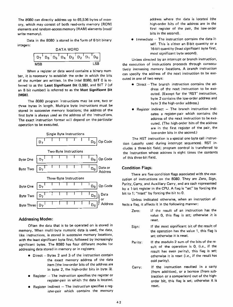
Condition Flags:
There are five condition flags associated with the execution of instructions on the 8080. They are Zero, Sign,Parity, Carry, and AuxiIiary Carry, and are each representedby a l-bit register in the CPU. A flag is "set" by forcing thebit to 1; "reset" by forcing the bit to O.
Unless indicated otherwise, when an instruction affects a flag, it affects it in the following manner:
Zero: If the result of an instruction has thevalue 0, this flag is set; otherwise it isreset.
address where the data is located (thehigh-order bits of the address are in thefirst register of the pair, the low-orderbits in the second).
• Immediate - The instruction contains the data itself. This is either an 8-bit quantity or a16-bit quantity (least significant byte first,most significant byte second).
Unless directed by an interrupt or branch instruction,the execution of instructions proceeds through consecutively increasing memory locations. A branch instructioncan specify the address of the next instruction to be executed in one of two ways:
• Direct - The branch instruction contains the address of the next instruction to be executed. (Except for the 'RST' instruction,byte 2 contains the low-order address andbyte 3 the high-order address.)
• Register indirect - The branch instruction indicates a register-pair which contains theaddress of the next instruction to be executed. (The high-order bits of the addressare in the first register of the pair, thelow-order bits in the second.)
The RST instruction is a special one-byte call instruction (usually used during interrupt sequences). RST includes a three-bit field; program control is transferred tothe instruction whose address is eight times the contentsof this three-bit field.
The 8080 can directly address up to 65,536 bytes of memory, which may consist of both read-only memory (ROM)elements and random-access memory (RAM) elements (read/write memory).
Oata in the 8080 is stored in the form of 8-bit binaryintegers:
OATA WORO
I I 1 1 I 1 I I I07 06 05 04 03 02 D1 00
MSB LSB
When a register or data word contains a binary number, it is necessary to establish the order in which the bitsof the number are written. In the Intel 8080, BIT 0 is referred to as the Least Significant Bit (LSB), and BIT 7 (ofan 8 bit number) is referred to as the Most Significant Bit(MSB).
The 8080 program instructions may be one, two orthree bytes in length. Multiple byte instructions must bestored in successive memory locations; the address of thefirst byte is always used as the address of the instructions.The exact instruction format will depend on the particularoperation to be executed.
Si ngle Byte Instructions
Two-Byte Instructions
Byte One 1_0_7_' ' I__0.......JoIOp Code
Byte Two ID7 I I Do IOata or-,-------------, Address
Three-Byte Instructions
Byte One I_D_7_1 1_0 0 IOp Code
Byte Two ID71 I Do I) Oata
or
Byte Three ID7 I I Do I Address
Addressing Modes:
Often the data that is to be operated on is stored inmemory. When multi-byte numeric data is used, the data,like instructions, is stored in successive memory locations,with the least significant byte first, followed by increasinglysignificant bytes. The 8080 has four different modes foraddressing data stored in memory or in registers:
• Oirect - Bytes 2 and 3 of the instruction containthe exact memory address of the dataitem (the low-order bits of the address arein byte 2, the high-order bits in byte 3).
• Register - The instruction specifies the register orregister-pair in wh ich the data is located.
• Register Indirect - The instruction specifies a register-pair which contains the memory
4-2
Sign:
Parity:
Carry:
If the most significant bit of the result ofthe operation has the value 1, this flag isset; otherwise it is reset.
If the modulo 2 sum of the bits of the result of the operation is 0, (Le., if theresult has even parity), this flag is set;otherwise it is reset (Le., if the result hasodd parity).
If the instruction resulted in a carry(from addition), or a borrow (from subtraction or a comparison) out of the highorder bit, th is flag is set; otherwise it isreset.

accumulator Register A
addr 16-bit address quantity
data 8-bit data quantity
Symbols and Abbreviations:The following symbols and abbreviations are used in
the subsequent description of the 8080 instructions:
SYMBOLS MEANING
Auxiliary Carry: If the instruction caused a carry outof bit 3 and into bit 4 of the resultingvalue, the auxiliary carry is set; otherwiseit is reset. This flag is affected by singleprecision additions, subtractions, increments, decrements, comparisons, and logical operations, but is principally usedwith additions and increments precedinga DAA (Decimal Adjust Accumulator)instruction.
Logical AND
Exclusive 0 R
Inclusive OR
Addition
Two's complement subtraction
Multiplication
"Is exchanged with"
The one's complement (e.g., (A))
The restart number athrough 7
The binary representation 000 through 111for restart number 0 through 7 respectively.
"1 s transferred to"
n
NNN
*
( )
/\
V
V
+
rh The first (high-order) register of a designated
register pair.
rl The second (low-order) register of a designated register pair.
PC 16-bit program counter register (PCH andPCl are used to refer to the high-order andlow-order 8 bits respectively).
SP 16-bit stack pointer register (SPH and SPLare used to refer to the high-order and loworder 8 bits respectively).
rm Bit m of the register r (bits are number 7through afrom left to right).
Z,S,P,CY,AC The condition flags:Zero,Sign,Parity,Carry,and Auxiliary Carry, respectively.
The contents of the memory location or reg
isters enclosed in the parentheses.
DOD or SSS REGISTER NAME
111 A000 B001 C010 Dall E100 H101 L
16-bit data quantity
The second byte of the instruction
The third byte of the instruction
8-bit address of an I/O device
One of the registers A,B,C,D,E,H,L
The bit pattern designating one of the registers A,B,C,D,E,H,L (DDD=destination, SSS=source):
data 16
byte 2
byte 3
port
r,rl,r2
DDD,SSS
One of the register pairs:
B represents the B,C pair with B as the highorder register and C as the low-order register;
D represents the D,E pair with D as the highorder register and E as the low-order register;
H represents the H,L pair with H as the highorder register and L as the low-order register;
SP represents the 16-bit stack pointerregister.
The bit pattern designating one of the register pairs B,D,H,SP:
rp
RP
RP
00011011
REGISTER PAIR
B-CD-EH-LSP
Description Format:
The following pages provide a detailed description ofthe instruction set of the 8080. Each instruction is described in the following manner:
1. The MAC 80 assembler format, consisting ofthe instruction mnemonic and operand fields, is
printed in BOLDFACE on the left side of the firstline.
2. The name of the instruction is enclosed in parenthesis on the right side of the fi rst line.
3. The next line(s) contain a symbolic descriptionof the operation of the instruction.
4. This is followed by a narative description of theoperation of the instruction.
5. The following line(s) contain the binary fields andpatterns that comprise the machine instruction.
4-3

6. The last four lines contain incidental informationabout the execution of the instruction. The number of machine cycles and states required to execute the instruction are listed first. If the instruction has two possible execution times, as in aConditional Jump·, both times will be listed, separated by a slash. Next, any significant data addressing modes' (see Page 4-2) are listed. The lastline lists any of the five Flags that are affected bythe execution of the instruction.
Data Transfer Group:
This group of instructions transfers data to and fromregisters and memory. Condition flags are not affected byany instruction in this group.
MVI r, data (Move Immediate)(r) ~ (byte 2)The content of byte 2 of the instruction is moved toregister r.
MVI M, data (Move to memory immediate)((H) (L))~ (byte 2)The content of byte 2 of the instruction is moved tothe memory location whose address is in registers Hand L.
MOV r1, r2 (Move Register)
(r1)"'- (r2)The content of register r2 is moved to register r1.
0I
DI
D I D S SI
S
'.1 f' . \Cyc·'es: 1States: 5
Addressing: registerFlags: none
o I 0
data
o 1 ' 1 I 0
MOV r, M (Move from memory)(r) ~ ((H) (L))
The content of the memory location, whose addressis in registers Hand L, is moved to register r.
Cycles:States:
Addressing:Flags:
310immed.lreg. indirectnone
1 I I 0
MOV M, r (Move to memory)((H)(L))~ (r)
The content of register r is moved to the memory location whose address is in registers Hand L.
o ' 1 I
Cycles:States:
Addressi ng:Flags:
27reg. indirectnone
LXI rp, data 16 (Load register pair immediate)(rh)~ (byte 3),(rl) ~ (byte 2)Byte 3 of the instruction is moved into the high-orderregister (rh) of the register pair rp. Byte 2 of the instruction is moved into the low-order register (rl) ofthe register pair rp.
o I o I R 1 p I o I o I o I 1
low-order data
high-order data
Cycles:States:
Addressing:Flags:
27reg. indirectnone
4-4
Cycles:States:
Addressing:Flags:
310immediatenone

high-order addr
o I 0 I 1 I 1 1 1 1 0 I 1 I 0
low-order addr
LOA addr (Load Accumulator direct)(A) ~ ((byte 3) (byte 2))
The content of the memory location, whose addressis specified in byte 2 and byte 3 of the instruction, ismoved to register A.
0 I 0 I 1 I 0 I 0 T 0 T 1 I 0
low-order addr
high-order addr
516directnone
Cycles:States:
Addressing:Flags:
SHLD addr (Store Hand L direct)((byte 3) (byte 2)) ~ (L)((byte 3)(byte 2) + 1) ~ (H)The content of register L is moved to the memory Jocation whose address is specified in byte 2 and byte3. The content of register H is moved to the succeeding memory location.
413directnone
Cycles:States:
Addressing:Flags:
LOAX rp (Load accumulator indirect)(A)~ ((rp))The content of the memory location, whose addressis in the register pair rp, is moved to register A. Note:only register pairs rp=B (registers B and C·) or rp=D(registers D and E) may be specified.
Cycles:States:
Addressing:Flags:
STA addr (Store Accumulator direct)
((byte 3)(byte 2)) ~ (A)The content of the accumulator is moved to thememory location whose address is specified in byte2 and byte 3 of the instruction.
0 I 0 I 1 I 1 I 0 I 0 I1 r 0
low-order addr
high-order addr
o I 0 I R p
27reg. indirectnone
Cycles:States:
Addressing:Flags:
413dire<;tnone
STAX rp (Store accumulator indirect)((rp)) ~ (A)
The content of register A is moved to the memory location whose address is in the register pair rp. Note:only register pairs rp=B (registers B and C) or rp=D(registers D and E) may be specified.
o I 0 I R
XCHG (Exchange Hand L with D and E)(H)~(D)
(L)~(E)
The contents of registers Hand L are exchanged withthe contents of registers D and E.
LHLD addr (Load Hand L direct)(L)~ ((byte 3)(byte 2))(H)~ ((byte 3) (byte 2) + 1)
The content of the memory location, whose addressis specified in byte 2 and byte 3 of the instruction, ismoved to register L. The content of the memory location at the succeeding address is moved to register H.
f
0 I 0 I 1 I 0 I 1 I 0 I1 T 0
low-order add r
high-order addr
Cycles:States:
Addressing:Flags:
I 1 I 0
27reg. indirectnone
Cycles:States:
Addressing:Flags:
516directnone
Cycles:States:
Addressing:Flags:
14registernone
4-5

ADC r (Add Register with carry)
(A)~ (A) + (r) + (CY)
The content of register r and the content of the carrybit are added to the content of the accumulator. Theresult is placed in the accumulator.
Cycles:
States:Addressing:
Flags:
Arithmetic Group:
This group of instructions performs arithmetic operations on data in registers and memory.
Unless indicated otherwise, all instructions in thisgroup affect the Zero, Sign, Parity, Carry, and AuxiliaryCarry flags accord ing to the standard rules.
All ~ubtraction operations are performed via two'scomplement arithmetic and set the carry flag to one to in
dicate a borrow and clear it to indicate no borrow.
1 I 0 I 0 o
14register
Z,S,P,CY,AC
ADD r (Add Register)
(A) ~ (A) + (r)
The content of register r is added to the content of theaccumulator. The result is placed in the accumulator.
1 I o I o o I 0
ADC M (Add memory with carry)(A)~ (A) + ((H) (L)) + (CY)
The content of the memory location whose address iscontained in the Hand L registers and the content ofthe CY flag are added to the accumulator. The resultis placed in the accumulator.
Cycles:States:
Addressing:Flags:
14registerZ,S,P,CY,AC
Cycles:
States:Addressing:
Flags:
27reg. indirectZ,S,P,CY,AC
o
ACI data (Add immediate with carry)
(A) ~ (A) + (byte 2) + (CY)
The content of the second byte of the instruction andthe content of the CY flag are added to the contentsof the accumulator. The result is placed in theaccumulator.
Cycles:
States:Addressing:
Flags:
ADD M (Add memory)
(A)...- (A) + ((H) (L))
The content of the memory location whose addressis contained in the Hand L registers is added to the
content of the accumulator. The result is placed inthe accumulator.
1 I 0 I 0 0 0 0
Cycles: 2States: 7
Addressing: reg. indirectFlags: Z,S,P,CY,AC
1 I I 0 odata
27immediateZ,S,P ,CY,AC
o
ADI data (Add immediate)
(A)~ (A) + (byte 2)
The content of the second byte of the instruction isadded to the content of the accumulator. The resultis placed in the accumulator.
1 I 1 I 0
SUB r (Subtract Register)(A) ~ (A) - (r)
The content of register r is subtracted from the content of the accumulator. The result is placed in theaccumulator.
data
Cycles:States:
Addressing:Flags:
27immediateZ,S,P,CY,AC
4-6
1 I 0I 0 0 i S
IS
IS
Cycles: 1States: 4
Addressing: registerFlags: Z,S,P,CY,AC

SUB M (Subtract memory)
(A)~ (A) - ((H) (L))
The content of the memory location whose address is
contained in the Hand L registers is subtracted from
the content of the accumulator. The result is placed
in the accumulator.
SBI data (Subtract immediate with borrow)
(A)~ (A) - (byte 2) - (CY)
The contents of the second byte of the instructionand the contents of the CY flag are both subtractedfrom the accumulator. The result is placed in the
accumulator.
Cycles:
States:
Addressi ng:
Flags:
o
2
7reg. indirect
Z,S,P,CY,AC
o 1 I I 0
data
Cycles:
States:
Addressing:Flags:
2
7
immediateZ,S,P,CY,AC
o
INR r (Increment Register)
(r) ~ (r) + 1
The content of register r is incremented by one.
Note: All condition flags except CY are affected.
SUI data (Subtract immediate)(A) ~ (A) - (byte 2)
The content of the second byte of the instruction is
subtracted from the content of the accumulator. Theresult is placed in the accumulator.
odata D 1 r 0 I 0
Cycles:
States:
Addressing:
Flags:
27immediate
Z,S,P,CY,AC
Cycles:
States:
Addressi ng:
Flags:
1
5register
Z,S,P,AC
INR M (Increment memory)
((H) (L))~ ((H) (L)) + 1
The content of the memory location whose addressis contained in the Hand L registers is incrementedby one. Note: All condition flags except CY are
affected.
SBB r (Subtract Register with borrow)(A) ~ (A) - (r) - (CY)
The content of register r and the content of the CY
flag are both subtracted from the accumulator. The
result is placed in the accumulator.
1 I 0 I 0 S IS I
S ICycles: 1States: 4
Addressing: register
Flags: Z,S,P,CY,AC
o I 0
Cycles:
States:
Addressing:
Flags:
o
310reg. indirect
Z,S,P,AC
o o
SBa M (Subtract memory with borrow)
(A)~ (A) - ((H) (L)) - (CY)
The content of the memory location whose address is
contained in the Hand L registers and the content ofthe CY flag are both subtracted from the accumulator. The result is placed in the accumulator.
1 I 0,
0 1 I 1I
1I
0 ICycles: 2States: 7
Addressing: reg. indirectFlags: Z,S,P,CY,AC
4-7
OCR r (Decrement Register)
(r) ~ (r)-1
The content of register r is decremented by one.
Note: All condition flag~ except CY are affected.
0 I 0 I D I D D I 1I 0 I 1
Cycles: 1 .f'
States: 5Addressing: register
Flags: Z,S,P,AC

OCR M (Decrement memory)((H) (L)) ..- ((H) (L)) - 1
The content of the memory location whose address iscontained in the Hand L registers is decremented byone. Note: All condition flags except CY are affected.
OAA (Decimal Adjust Accumulator)The eight-bit number in the accumulator is adjustedto form two four-bit Binary-Coded-Decimal digits by
the following process:
1. If the value of the least significant 4 bits of theaccumulator is greater than 9 or if the AC flagis set, 6 is added to the accumulator.
Cycles:States:
Addressing:Flags:
310reg. indirectZ,S,P,AC
2. If the value of the most significant 4 bits of theaccumulator is now greater than 9, or if the CYflag is set, 6 is added to the most significant 4bits of the accumulator.
NOTE: All flags are affected.
INX rp (Increment register pair)(rh) (rl) ..- (rh) (rl) + 1
The content of the register pair rp is incremented byone. Note: No condition flags are affected.
Cycles:States:Flags:
o
14Z,S,P,CY,AC
OCX rp (Decrement register pair)(rh) (rl) ..- (rh) (rl) - 1The content of the register pair rp is decremented byone. Note: No condition flags are affected.
ANA r (AND Register)(A) ~ (A) /\ (r)
The content of register r is logically anded with thecontent of the accumulator. The result is placed inthe accumulator. The CY flag is cleared.
S
14registerZ,S,P,CY,AC
a I s I s
Cycles:States:
Addressing:Flags:
Logical Group:
This group of instructions performs logical (Boolean)operations on data in registers and memory and on condition flags.
Unless indicated otherwise, all instructions in thisgroup affect the Zero, Sign, Parity, Auxiliary Carry, andCarry flags according to the standard rules.
I 1
15registernone
I 0 I
15registernone
Cycles:States:
Addressing:Flags:
Cycles:States:
Addressing:Flags:
DAD rp (Add register pair to Hand L)(H) (L) ..- (H) (L) + (rh) (rl)The content of the register pair rp is added to thecontent of the register pair Hand L. The result isplaced in the register pair Hand L. Note: Only theCY flag is affected. It is set if there is a carry out ofthe double precision add; otherwise it is reset.
. ANA M (AND memory)(A) ~ (A) /\ ((H) (L))
The contents of the memory location whose addressis contained in the Hand L registers is logically andedwith the content of the accumulator. The result isplaced in the accumulator. The CY flag is cleared.
I 0 I 1 a a I 1 , 1 I a
Cycles:States:
Addressing:Flags:
310registerCY
Cycles:States:
Addressing:Flags:
27reg. indirectZ,S,P,CY,AC
4-8

ANI data (AND immediate)(A)~ (A) /\ (byte 2)
The content of the second byte of the instruction is
logicaJly anded with the contents of the accumu lator .The result is placed in the accumulator. The CY and
AC flags are cleared.
ORA r (OR Register)(A)~ (A) V (r)
The content of register r is inclusive-OR'd with the
content of the accumulator. The result is placed in
the accumulator. The CY and AC flags are cleared.
I 1 o I 0 I 1 I 1 I 0I 0 I I 1
XRA r (Exclusive OR Register)
(A)~ (A) V (r)
The content of register r is exclusive-or'd with the
content of the accumulator. The result is placed in
the accumulator. The CY and AC flags are cleared.
ORA M (OR memory)
(A) ~ (A) V ((H) (L))
The content of the memory location whose address is
contained in the Hand L registers is inclusive-OR'd
with the content of the accumu lator. The result is
placed in the accumulator. The CY and AC flags are
cleared.
I 0I 1I 1o
14register
Z,S,P,CY,AC
I 1
Cycles:
States:Addressing:
Flags:
I a I 1
27immediate
Z,S,P,CY ,AC
data
Cycles:
States:Addressing:
Flags:
Cycles:
States:
Addressing:
Flags:
14register
Z,S,P,CY,AC
Cycles:
States:
Addressing:
Flags:
27reg. indirect
Z,S,P ,CY,AC
XRA M (Exclusive OR Memory)
(A) ~ (A) V ((H) (L))
The content of the memory location whose address
is contained in the Hand L registers is exclusive-O R'd
with the content of the accumulator. The result is
placed in the accumulator. The CY and AC flags arecleared.
ORI data (OR Immediate)
(A)~ (A) V (byte 2)
The content of the second byte of the instruction is
inclusive-OR'd with the content of the accumulator.
The result is placed in the accumulator. The CY and
AC flags are cleared.
1 1
I 0 o I 0 data
Cycles:States:
Addressing:
Flags:
27reg. indirect
Z,S,P,CY,AC
Cycles:
States:
Addressing:
Flags:
27immediate
Z,S,P,CY,AC
XRI data (Exclusive OR immediate)
(A) ~ (A) V (byte 2)
The content of the second byte of the instruction is
exclusive-O R'd with the content of the accumu lator.
The result is placed in the accumulator. The CY andAC flags are cleared.
. 1~_1_1~ 0__1--..1__' _1_1_1_1_0_
. data
CMP r (Compare Register)
(A) (r)
The content of register r is subtracted from the ac
cumulator. The accumulator remains unchanged. The
condition flags are set as a result of the subtraction.The Z flag is set to 1 if (A) = (r). The CY flag is set to1 if (A) < (r) .
I 0 I 1
Cycles:
States:Addressing:
Flags:
27immediateZ,S,P ,CY,AC
Cycles:
States:Addressing:
Flags:
14register
Z,S,P,CY,AC
4-9

CPI data (Compare immediate)(A) (byte 2)
The content of the second byte of the instruction issubtracted from the accumulator. The condition flagsare set by the result of the subtraction. The Z flag isset to 1 if (A) = (byte 2). The CY flag is set to 1 if(A) < (byte 2).
CMP M (Compare memory)
(A) ((H) (L))
The content of the memory location whose address
is contained in the Hand L registers is subtractedfrom the accumulator. The accumulator remains unchanged. The condition flags are set as a result of the
subtraction. The Z flag is set to 1 if (A) = ((H) (L)).The CY flag is set to 1 if (A) < ((H) (L)).
Cycles: 1States: 4Flags: CY
0 I 0 I 0 I 0 I , I1
I ,Cycles: 1States: 4Flags: CY
o I 1 I , I ,o I 0 I 0 I ,
RAL (Rotate left through carry)(An+,) ..- (An) ; (CY) ..- (A7)(AO)"- (CY)The content of the accumu lator is rotated left oneposition through the CY flag. The low order bit is setequal to the CY flag and the CY flag is set to thevalue shifted out of the high order bit. Only the CYflag is affected.
RRC (Rotate right)
(An) ~ (An-,); (A7)~ (AO)(CY)~ (AO)The content of the accumu lator is rotated right oneposition. The high order bit and the CY flag are bothset to the value shifted out of the low order bit position. Only the CY flag is affected.
o I27reg. indirectZ,S,P,CY,AC
Cycles:States:
Addressing:Flags:
o
, I , I
data
Cycles:
States:Addressing:
Flags:
27
immediateZ,S,P,CY,AC
RAR (Rotate right through carry)(An) ~ (An+l); (CY)..- (AO)(A7) ~ (CY)The content of the accumulator is rotated right oneposition through the CY flag. The high order bit is setto the CY flag and the CY flag is set to the valueshifted out of the low order bit. Only the CY flag isaffected.
Cycles: 1
States: 4Flags: CY
RLC (Rotate left)(An+l) ~ (An) ; (AO) ~ (A7)(CY)~ (A7)The content of the accumulator is rotated left oneposition. The low order bit and the CY flag are bothset to the value shifted out of the high order bit position. Only the CY flag is affected.
CMA (Complement accumulator)(A)~(A)
The contents of the accumulator are complemented(zero bits become 1, one bits become 0). No flags areaffected.
o I 0 I 1 I 0 I 1 I , I ,
Cycles: 1States: 4Flags: CY
Cycles: ,
States: 4Flags: none
4-10

CMC (Complement carry)
(CY)~ (CY)The CY flag is complemented. No other flags are
affected.
dress is specified in byte 3 and byte 2 of the current
instruction.
I 1 I 0 I 0 I 0 I 0 I 1 I 11
low-order addr
high-order addr
a , 0 ,
Cycles:States:Flags:
14CY
Cycles:States:
Addressing:Flags:
310immediatenone
STC (Set carry)(CY) ~ 1The CY flag is set to 1. No other flags are affected.
0 I 0 I 0 I 1 I 1
Cycles: 1States: 4Flags: CY
Jcondition addr (Conditional jump)
If (CCC),(PC)~ (byte 3) (byte 2)
If the specified condition is true, control is transferred to the instruction whose address is specified inbyte 3 and byte 2 of the current instruction; otherwise, control continues sequentially.
"
1 I 1 I C I CI
C I 0 I 1 I 0
low-order addr
high-order addr
Branch Group:
This group of instructions alter normal sequentialprogram flow.
Condition flags are not affected by any instructionin this group.
The two types of branch instructions are unconditional and conditional. Unconditional transfers simply perform the specified operation on register PC (the programcounter). Conditional transfers examine the status of one ofthe four processor flags to determi ne if the specified branchis to be executed. The conditions that may be specified areas follows:
~
1 I 1 I 0 I 0 I 1 T 1 I 0 I 1
low-order addr
high-ord~r addr
CALL addr (Call)((SP) - 1) ~ (PCH)((SP) - 2) ~ (PCl)(SP) ~ (SP) - 2(PC) ~ (byte 3) (byte 2)
The high-order eight bits of the next instruction address are moved to the memory location whoseaddress is one less than the content of register SP.The low-order eight bits of the next instruction address are moved to the memory location whoseaddress is two less than the content of register SP.The content of register SP is decremented by 2. Control is transferred to the instruction whose address isspecified in byte 3 and byte 2 of the currentinstruction.
310immediatenone
Cycles:States:
Addressing:Flags:
CCC
000001010011100101110111
NZ - not zero (Z = 0)2 - zero (2 = 1)
NC - no carry (CY = 0)
C - carry (CY = 1)PO - parity odd (P = 0)PE - parity even (P = 1)
P - plus (S = 0)
M -minus(S=1)
CONDITION
JMP addr (Jump)
(PC) ~ (byte 3) (byte 2)
Control is transferred to the instruction whose ad-
Cycles:States:
Addressing:Flags:
517immediate/reg. indirectnone
4-11

Ccondition addr (Condition call)If (CCC),
((SP) -1) ~ (PCH)
((SP) - 2) ~ (PCl)
(SP) ~ (SP) - 2(PC) ~ (byte 3) (byte 2)
If the specified condition is true, the actions specified
in the CAll instruction (see above) are performed;
otherwise, control continues sequentially.
1 ' 1 I C I C I c I 1 I o I 0
low-order addr
high-order addr
RST n (Restart)((SP) - 1) ~ (PCH)
((SP) - 2) ~ (PCl)
(SP) ~ (SP) - 2(PC)~ 8* (NNN)
The high-order eight bits of the next instruction ad
dress are moved to the memory location whose
address is one less than the content of register SP.
The low-order eight bits of the next instruction ad
dress are moved to the memory location whose
address is two less than the content of register SP.
The content of register SP is decremented by two.
Control is transferred to the instruction whose ad
dress is eight times the content of NNN.
Cycles:
States:Addressing:
Flags:
Cycles:
States:
Addressing:
Flags:
3/511/17immediate/reg. indirect
none
1 I N N I N I 1 I
311reg. indirect
none
RET (Return)
(PCl) ~ ((SP));
(PCH)~ ((SP) + 1);(SP)~ (SP) + 2;
The content of the memory location whose addressis specified in register SP is moved to the low-order
eight bits of register PC. The content of the memory
location whose address is one more than the content
of register SP is moved to the high-order eight bits of
register PC. The content of register SP is incrementedby 2.
Program Counter After Restart
1 I I 0 I 0
Cycles:
States:
Addressing:
Flags:
310reg. indirect
none
PCHL (Jump Hand l indirect - move Hand L to PC)(PCH) ~ (H)
(PCl) ~ (l)
The content of register H is moved to the high-order
eight bits of register PC. The content of register l is
moved to the low-order eight bits of register PC.
Rcondition (Conditional return)
If (CCC),
(PCl) ~ ((SP))
(PCH) ~ ((SP) + 1)
(SP)~ (SP) + 2If the specified condition is true, the actions specified
in the RET instruction (see above) are performed;
otherwise, control continues sequentially.
1 I 1 I o '
Cycles:
States:
Addressing:Flags:
o ,. 0 I 1
15registernone
1 II c c I c I 0 I 0 I 0
Cycles:
States:Addressing:
Flags:
1/35/11reg. indirect
none
4-12

Stack, I/O, and Machine Control Group: FLAG WORD
This group of instructions performs I/O, manipulatesthe Stack, and alters internal control flags.
Unless otherwise specified, condition flags are notaffected by any instructions in this group.
D1 Do
PUSH rp (Push)
((SP) - 1) ~ (rh)((SP) - 2) ~ (rl)(SP)~ (SP) - 2
The content of the high-order register of register pairrp is moved to the memory location whose address isone less than the content of register SP. The contentof the low-order register of register pair rp is movedto the memory location whose address is two lessthan the content of register SP. The cont~nt of register SP is decremented by 2. Note: Register pairrp = SP may not be specified..
POP rp (Pop)
(rl) ~((SP))
(rh) ~ ((SP) + 1)
(SP)~ (SP) + 2
The content of the memory location, whose addressis specified by the content of register SP, is moved tothe low-order register of register pair rp. The contentof the memory location, whose address is one morethan the content of register SP, is moved to the highorder register of register pair rp. The content of reg
ister SP is incremented by 2. Note: Register pairrp =SP may not be specified.
310reg. indirectnone
1 I 1 I R P I 0 0
Cycles: 3States: 11
Addressing: reg. indirectFlags: none
I 1 P
Cycles:States:
Addressi ng:Flags:
o o o I 1
PUSH PSW (Push processor status word)((SP) -1) ~ (A)
((SP) - 2)0 ..- (CY) , ((SP) - 2) 1 ~ 1
((SP) - 2)2 ~ (P), ((SP) - 2)3~ 0
((SP) - 2)4 ~ (AC) , ((SP) - 2)5 ~ 0((SP) - 2)6 ..- (Z), ((SP) - 2)7 ~ (S)(SP) ~ (SP) - 2
The content of register A is moved to the memorylocation whose address is one less than register SP.The contents of the condition flags are assembledinto a processor status word and the word is movedto the memory location whose address is two lessthan the content of register SP. The content of register SP is decremented by two.
POP PSW (Pop processor status word)
(CY) ~ ((SP))O(P) ..- ((SP))2(AC) ~ ((SP))4(Z) ~ ((SP))6(S) ~ ((SP))7(A) ...- ((SP) + 1)
(SP) ...- (SP) + 2The content of the memory location whose addressis specified by the content of register SP is used torestore the condition flags. The content of the memory location whose address is one more than thecontent of register SP is moved to register A. Thecontent of register SP is incremented by 2.
310reg. indirectZ,S,P,CY,Ae
oI 1
Cycles:
States:Addressing:
Flags:
I 1
311reg. indirectnone
Cycles:States:
Addressing:Flags:
1 I 1 I
4-13

XTHL (Exchange stack top with Hand L)(L) ~((SP))
(H) ~ ((SP) + 1)
The content of the L register is exchanged with thecontent of the memory location whose address isspecified by the content of register SP. The contentof the H register is exchanged with the content of thememory location whose address is one more than thecontent of register SP.
EI (Enable interrupts)
The interrupt system is enabled following the execution of the next instruction.
1 I I 1,
0 I 1 I 1
Cycles: 1States: 4Flags: none
1 I I 0 o o
Cycles:States:
Addressing:Flags:
518reg. indirectnone
01 (Disable interrupts)
The interrupt system is disabled immediately following the execution of the 01 instruction.
1 1 0 1 0 ' 1 1 1
SPHL (Move HL to SP)(SP) ~ (H) (L)
The contents of registers Hand L (16 bits) are movedto register SP.
Cycles: 1States: 4Flags: none
IN port (I nput)(A) ~ (data)The data placed on the eight bit bi-directional databus by the specified port is moved to register A.
1 I 1 I
Cycles:States:
Addressing:Flags:
o
15registernone
oHLT (Halt)
The processor is stopped. The registers and flags areunaffected.
0 I 1 I 0 I 1 I 1 I 0
Cycles: 1States: 7Flags: none
1 I I 0 I I 1 I 0 I 1 I 1
port
NOP (No op)No operation is performed. The registers and flagsare unaffected.
Cycles: 3States: 10
Addressing: directFlags: none
OUT port (Output)(data) ~ (A)The content of register A is placed on the eight bitbi-directional data bus for transmission to the specified port.
0 I 0 I 0 0 0 0 0 0
Cycles: 1States: 4Flags: none
oport
o
Cycles: 3States: 10
Addressing: directFlags: none
4-14

INSTRUCTION SET
Summary of Processor Instructions
Instruction Code [11 Clock 121 Instruction Code [11 Clock [21Mnemonic Description try 06 Os 04 03 02 0, DO Cycles Mnemonic Description 07 06 Os 04 03 02 0, DO Cycles
MOV r1 ,r2 Move register to register 0 1 0 0 0 S S S 5 RZ Return on zero 1 0 0 '1 0 0 0 5/11MOVM,r Move register to memory 0 1 1 1 0 S S S 7 RNZ Return on no zero 1 0 0 0 0 C 0 5/11MOVr,M Move memory to register 0 1 0 0 0 1 1 0 7 RP Return on positive 1 1 1 0 0 0 0 5/11HlT Halt 0 1 1 1 0 1 1 0 7 RM Return on minus 1 1 1 1 0 0 0 5/11MVI r Move immediate register 0 0 0 0 0 1 1 0 7 RPE Return on parity even 1 1 0 1 0 0 0 5/11MVIM Move immediate memory 0 0 1 1 0 1 1 0 10 RPO Return on parity odd 1 1 0 0 0 0 0 5/11INR r Increment register 0 0 0 0 0 1 0 0 5 RST Restart 1 A A A 1 1 1 11OCR r Decrement register 0 0 0 0 0 1 0 1 5 IN Input 1 0 1 1 0 1 1 10INR M Increment memory 0 0 1 1 0 1 0 0 10 OUT Output 1 0 1 0 0 1 1 10OCR M Decrement memory 0 0 1 1 0 1 0 1 10 lXI B load Immediate register 0 0 0 0 0 0 1 10ADOr Add register to A 1 0 0 0 0 S S S 4 Pair B& CAOCr Add register to A with carry 1 0 0 0 1 S S S 4 LXI 0 Load immediate register 10SUB r Subtract register from A 1 0 0 1 0 S S S 4 Pair 0 & ESBB r Subtract register from A 1 0 0 1 1 S S S 4 LXI H Load immediate register 10
with borrow Pair H& LANA r And register with A 0 S S S 4 lXI SP load immediate stack pointer 10XRA r Exclusive Or register with A 0 S S S 4 PUSH B Push register Pair B& C on 11OIiAr Or register with A 0 S S S 4 stackCMPr Compare register with A 0 S S S 4 PUSH 0 Push register Pair 0 & E on 11ADD M Add memory to A 0 1 1 0 7 stackAOC M Add memory to A with carry 0 1 1 0 7 PUSH H Push register Pair H& l on 11SUB M Subtract memory from A 0 1 1 0 7 stackSBB M Subtract memory from A 0 1 1 0 7 PUSH PSW Push A and Flags 11
with borrow on stackANA M And memory with A 0 0 0 POP B Pop register pair B& C off 10XRA M Exclusive Or memory with A 0 0 1 stackORA M Or memory with A 0 1 0 POP 0 Pop register pair 0 & E off 10CMPM Compare memory with A 0 1 1 stackAOI Add immediate to A 1 0 0 POP H Pop register pair H& Loff 10ACI Add immediate to A with 1 0 1 stack
carry POP PSW Pop A and Flags 10SUI Subtract immediate from A off stackSBI Subtract immediate from A STA Store A direct 13
with borrow lOA Load A direct 13ANI And immediate with A XCHG Exchange 0 & E, H& L 4XRI Exclusive Or immediate with Registers
A XTHl Exchange top of stack, H& l 1 1 1 0 0 0 1 1 18ORI Or immediate with A 1 0 SPHL H& L to stack pointer 1 1 1 1 1 0 0 1 5CPI Compare immediate with A 1 1 PCHL H& L to program counter 1 1 1 0 1 0 0 1 5RLC Rotate A left 0 0 DAD B Add B & C to H& L 0 0 0 0 1 0 0 1 10RRC Rotate A right 0 1 DAD 0 Add 0 & E to H& L l:' 0 0 1 1 0 0 1 10RAl Rotate A left through carry 0 0 DAD H Add H& L to H& L 0 0 1 0 1 0 0 1 10RAR Rotate A right through 0 1 DAD SP Add stack pointer to H& L 0 0 1 1 1 0 0 1 10
carry STAX B Store A indirect 0 0 0 0 0 0 1 0 7JMP Jump unconditional 0 0 0 0 1 1 10 STAX 0 Store A indirect 0 0 0 1 0 0 1 0 7JC Jump on carry 0 1 1 0 1 0 10 LOAX B load A indirect 0 0 0 0 1 0 1 0 7JNC Jump on no carry 0 1 0 0 1 0 10 lOAX 0 Load A indirect 0 0 0 1 1 0 1 0 7JZ Jump on zero 0 0 1 0 1 0 10 INX B Increment B& C registers 0 0 0 0 0 0 1 1 5JNZ Jump on no zero 0 0 0 0 1 0 10 INX 0 Increment 0 & E registers 0 0 0 1 0 0 1 1 5JP Jump on positive 1 1 0 0 1 0 10 INX H Increment H& L registers 0 0 1 0 0 0 1 1 5JM Jump on minus 1 1 1 0 1 0 10 INX SP Increment stack pointer 0 0 1 1 0 0 1 1 5JPE Jump on parity even 1 0 1 0 1 0 10 DCX B Decrement B&C 0 0 0 0 1 0 1 1 5JPO Jump on parity odd 1 0 0 0 1 0 10 DCX 0 Decrement 0 & E 0 0 0 1 1 0 1 1 5CALL Call unconditional 0 0 1 1 0 1 17 DCX H Decrement H& L 0 0 1 0 1 0 1 1 5CC Call on carry 0 1 1 1 0 0 11/17 DCX SP Decrement stack pointer 0 0 1 1 1 0 1 1 5CNC Call on no carry 0 1 0 1 0 0 11/17 CMA Complement A 0 0 1 0 1 1 1 1 4CZ Call on zero 0 0 1 1 0 0 11/17 STC Set carry 0 0 1 1 0 1 1 1 4CNZ Call 0 n no zero 0 0 0 1 0 0 11/17 CMC Complement carry 0 0 1 1 1 1 1 1 4CP Call on positive 1 1 0 1 0 0 11/17 OAA Decimal adjust A 0 0 1 0 0 1 1 1 4CM Call on minus 1 1 1 1 0 0 11/17 SHlD Store H& l direct 0 0 1 0 0 0 1 0 16CPE Call on parity even 1 0 1 1 0 0 11/17 LHLO load H& L direct 0 0 1 0 1 0 1 0 16CPO Call on parity odd 1 0 0 1 0 0 11/17 EI Enable Interrupts 1 1 1 1 1 0 1 1 4RET Return 0 0 1 0 0 1 10 01 Disable interrupt 1 1 1 1 0 0 1 1 4RC Return on carry 0 1 1 0 0 0 5/11 NOP No-operation 0 0 0 0 0 0 0 0 4RNC Return on no carry 0 1 0 0 0 0 5/11
NOTES: 1. DDD or SSS - 000 B - 001 C - 010 D - 011 E - 100 H - 101 L - 110 Memory - 111 A.2. Two possible cycle times, (5/11) indicate instruction cycles dependent on condition flags.
4-15

CPU Group8224 Clock Generator 5-18228 System Controller . . . . . . . . . . . . . . . . . . . . . . . 5-78080A Central Processor 5-138080A-1 Central Processor (1.3#ls) ••..•.••.••.••.• 5-208080A-2 Central Processor (1.5#ls) •...•..•..•.••.. 5-24MBOBOA Central Processor (_55° to +125°C) 5-29
ROMs8702A Erasable PROM (256 x 8) . . . . . . . . . . . . . . . . . 5-378708/8704 Erasable PROM (1 K x 8) . . . . . . . . . . . . . . . 5-458302 Mask ROM (256 x 8) 5-518308 Mask ROM (1 K x 8) . . . . . . . . . . . . . . . . . . . . . . 5-598316A Mask ROM (2K x 8) . . . . . . . . . . . . . . . . . . . . . 5-61
RAMs8101-2 Static RAM (256 x 4) 5-678111-2 Static RAM (256 x 4) 5-718102-2 Static RAM (1 K x 1) . . . . . . . . . . . . . . . . . . . . 5-758102A-4 Static RAM (1K x 1) . . . . . . . . . . . . . . . . . . . 5-7981078-4 Dynamic RAM (4K x 1) . . . . . . . . . . . . . . . . . 5-835101 Static CMOS RAM (256 x 4) . . . . . . . . . . . . . . . . 5-918210 Dynamic RAM Driver. . . . . . . . . . . . . . . . . . . . . 5-958222 Dynamic RAM Refresh Controller 5-99
I/O8212 8-Bit I/O Port . . . . . . . . . . . . . . . . . . . . . . . . . . 5-1018255 Programmable Peripheral Interface . . . 5-1138251 Programmable Communication Interface. . . . . . . . 5-135
Peripherals8205 One of Eight Decoder . . . . . . . . . . . . . . . . . . . . . 5-1478214 Priority Interrupt Control Unit 5-1538216/8226 4-8 it Bi-D irectional Bus Driver . . . . . . . . . . . 5-163
Coming Soon8253 Programmable Interval Timer. . . . . . . . . . . . . . . . 5-1698257 Programmable DMA Controller 5-1718259 Programmable Interrupt Controller . . . . . . . . . . . . 5-173

82248228
8080A
CPU Group
8080A-18080A-2
M8080-A


Schottky Bipolar 8224
CLOCK GENERATOR AND DRIVERFOR 8080A CPU
• Single Chip Clock Generator/Driverfor 8080A CPU
• Power-Up Reset for CPU• Ready Synchronizing Flip-Flop• Advanced Status Strobe
• Oscillator Output for ExternalSystem Timing
• C.rystal Controlled for Stable SystemOperation
• Reduces System Package Count
The 8224 is a single chip clock generator/driver for the 8080A CPU. It is controlled by a crystal, selected bythe designer, to meet a variety of system speed requirements.
Also included are circuits to provide power-up reset, advance status strobe and synchronization of ready.
The 8224 provides the designer with a significant reduction of packages used to generate clocks and timingfor 8080A.
PIN NAMES
RESIN RESET INPUT
RESET RESET OUTPUT
RDYIN READY INPUT
READY READY OUTPUT
SYNC SYNC INPUT
STSTB STATUSSTB(ACTIVE lOW)
rPl !8080rP2 CLOCKS
XTAl1 I CONNECTIONSXTAl2 FOR CRYSTAL
TANK USED WITH OVERTONE XTAL
OSC OSCILLATOR OUTPUT
rP2 (TTL) rP2 elK (TTL lEVEL)
Vee +5V
Voo +12V
GND OV
5-1

SCHOTTKY BIPOLAR 8224
FUNCTIONAL DESCRIPTION
General
The 8224 is a single chip Clock Generator/Driver for theS080A CPU. It contains a crystal-controlled oscillator, a"divide by nine" counter, two high-level drivers and severalauxiliary logic functions.
Oscillator
The oscillator circuit derives its basic operating frequencyfrom an external, series resonant, fundamental mode crystal.Two inputs are provided for the crystal connections (XTAL 1,XTAL2).
The selection of the external crystal frequency dependsmainly on the speed at which the 8080A is to be run at.Basically, the oscillator operates at 9 times the desired processor speed.
A simple formula to guide the crystal selection is:
Crystal Frequency =-'- times 9tCY
Example' : (500ns tCY)2mHz times 9 = 18mHz*
Example 2: (800ns tCY)'.25mHz times 9 = '1.25mHz
Another input to the oscillator is TANK. This input allowsthe use overtone mode crystals. Th is type of crystal generally has much lower IIgain" than the fundamental type soan external LC network is necessary to provide the additional"gain" for proper oscillator operation. The external LC network is connected to the TANK input and is AC coupled toground. See Figure 4.
The formula for the LC network is:
F= __l __
21TVLC
The waveforms generated by the decode gating follow asimple 2-5-2 digital pattern. See Figure 2. The clocks gen
erated; phase 1 and phase 2, can best be thought of as consisting of "units" based on the oscillator frequency. Assumethat one "unit" equals the period of the oscillator frequency.By multiplying the number of "units" that are contained ina pulse width or delay, times the period of the oscillator frequency, the approximate time in nanoseconds can be derived.
The outputs of the clock generator are connected to twohigh level drivers for direct interface to the 80S0A CPU. ATTL level phase 2 is also brought out ct>2 (TTL) for externaltiming purposes. It is' especially useful in DMA dependantactivities. This signal is used to gate the requesting device onto the bus once the 8080A CPU issues the Hold Acknowledgement (H LOA).
Several other signals are also generated internally so thatoptimum timing of the auxiliary flip-flops and status strobe(STSTB) is achieved.
The output of the oscillator is buffered and brought outon ElSC (pin 12) so that other system timing signals can bederived from this stable, crystal-controlled source.
*When using crystals above 10mHz a small amount of frequency"trimming" may be necessary to produce the exact desired frequency. The addition of a small selected capacitance (3pF - 10pF)in series with the crystal will accomplish this function.
4>,
1 UNIT = o~c.FREQ.
Clock Generator
The Clock Generator consists of a synchronous IIdivide bynine" counter and the associated decode gating to create thewaveforms of the two 8080A clocks and auxiliary timing
signals.
5-2
EXAMPLE: (8080 t CY =500ns)
OSC = 18mHz/55ns4>1 = 110ns (2 x 55ns)cP2 = 275ns (5 x 55ns)4>2-4>, =110ns (2 x 55ns)

SCHOTTKY BIPOLAR 8224
STSTB (Status Strobe)
At the beginning of each machine cycle the aOaOA CPU issues status information on its data bus. Th is informationtells what type of action will take place during that machinecycle. By bringing in the SYNC signal from the CPU, andgating it with an internal timing signal (<1>1A), an active lowstrobe can be derived that occu rs at the start of each machine cycle at the earliest possible moment that status datais stable on the bus. The STSTB signal connects directly tothe 8228 System Controller.
The power-on R-eset also generates STSTB, but of course,for a longer period of time. This feature allows the 8228 tobe automatically reset without additional pins devoted forth is fu nction.
The READY input to the 8080A CPU has certain timingspecifications such as "set-up and hold" thus, an externalsynchronizing flip-flop is required. The 8224 has this featurebuilt-in. The ROYI N input presents the asynchronous "waitrequest" to the "0" type flip-flop. By clocking the flip-flopwith <1>20, a synchronized READY signal at the correct input level, can be connected directly to the a080A.
The reason for requ iring an external flip-flop to synchronize the "wait request" rather than internally in the 8080CPU is that due to the relatively long delays of MOS logicsuch an implementation would "rob" the designer of about200ns during the time his logic is determining if a "wait"is necessary. An external bipolar circuit built into the clockgenerator eliminates most of this delay and has no effect oncomponent count.
'9
12
5
"----- STSTB (TO 8228 PIN 1)
°1r - -, 3.10pFI I (ONLV NEEDEDL_ _.J ABOVE 10 MHz)
13 14 15
11 22
10 15
4 23
8224
6
3
12
TGND
OSC
<fJ2 (TTL)
GND
,------....,1
III1
:11-=IILn7--F=-'
21rJLC
USEDONLVFOR OVERTONE
CRYSTALS
An external RC network is connected to the RESI N input.The slow transition of the power supply rise is sensed by aninternal Schmitt Trigger. Thiscircuit converts the slow transition into a clean, fast edge when its input level reaches apredetermined value. The output of the Schmitt Trigger is
connected to a "0" type flip-flop that is clocked with <1>20(an internal tim ing signal). The flip-flop is synchronouslyreset and an active high level that complies with the aOaOAinput spec is generated. For manual switch type system Reset circuits, an active low switch closing can be connectedto the RESIN input in addition to the power-on RC netnetwork.
Power-On Reset and Ready Flip-Flops
A common function in a080A Microcomputer systems is thegeneration of an automatic system reset and start-up uponinitial power-on. The 8224 has a built in feature to accomplish this feature.
5-3

SCHOTTKY BIPOLAR 8224
D.C. Characteristics
TA = O°C to 70°C; Vee = +5.0V ±5%; Voo = +12V ±5%.
LimitsSymbol Parameter Min. Typ. Max. Units Test Conditions
IF Input Current Loading -.25 rnA VF = .45V
IR Input Leakage Current 10 J.lA VR = 5.25V
Ve Input Forward Clamp Voltage 1.0 V 'e = -5mA
VIL Input"Low" Voltage .8 V Vee = 5.0V
VIH Input "High" Voltage 2.6 V Reset Input2.0 All Other Inputs
VIH-VIL REDIN Input Hysteresis .25 mV Vee = 5.0V
VOL Output"Low" Voltage .45 V (if>1,if>2), Ready, Reset, STSTBIOl =2.5mA
.45 V All Other OutputsIOl = 15mA
VOH Output "High" Voltageif>1 , if>2 9.4 V IOH = -100J.lAREADY, RESET 3.6 V IOH =-1 o0J.lAAll Other Outputs 2.4 V IOH = -lmA
Ise[1] Output Short Circuit Current -10 -60 rnA Vo =OV(All Low Voltage Outputs Only) Vee =5.0V
Icc Power Supply Current 115 rnA
100 Power Supply Current 12 rnA
Note: 1. Caution, cP1 and cP2 output drivers do not have short circuit protection
CRYSTAL REQUIREMENTS
Tolerance: .005% at O°C -70°CResonance: Series (Fundamental) *Load Capacitance: 20-35pFEquivalent Resistance: 75-20 ohmsPower Dissipation (Min): 4mW
*With tan k circu it use 3rd overtone mode.
5-4

SCHOTTKY BIPOLAR 8224
A.C. Characteristics
vcc = +5.0V ± 5%; Voo = +12.0V ± 5%; TA = O°C to 70°C
Limits Test
Symbol Parameter Min. Typ. Max. Units Conditions
tq,1 cP1 Pulse Width2tcy-- 20ns
9
t</>2 cP2 Pulse Width 5tcy _ 35ns9
t01 cP1 to cP2 Delay 0 ns
t02 cP2 to cP1 Delay2tcy CL = 20pF to 50pF--14ns
9
t03 cP1 to cP2 Delay2tcy 2tcy + 20ns
9 9
tR cP1 and cP2 Rise Time 20
tF cP1 and cP2 Fall Time 20
to</>2 cP2 to cP2 (TTL) Delay -5 +15 ns cP2TTl,Cl=30R1=300QR2=600Q
toss cP2 to STSTB Delay 6tcy _ 30ns 6tcy9 9
tpw STSTB Pulse Width tcy _ 15ns STSTB,Cl=15pF9 R1 = 2K
tORSRDYIN Setup Time to 50ns _ 4tcy R2 = 4K
Status Strobe 9
tORHRDYIN Hold Time 4tcyAfter STSTB 9
tORRDYIN or RESIN to 4tcy _ 25ns Ready & Reset
cP2 Delay 9 Cl=10pFR1=2KR2=4K
tCLK ClK Period tcy
9
f maxMaximum Oscillating
27 MHzFrequency
Cin Input Capacitance 8 pF VcC=+5.0VVoo=+12VVBIAS=2.5Vf=1 MHz
INPUT >---......----....
GND
5-5

SCHOTTKY BIPOLAR 8224
WAVEFORMS
.........----to2-----..r1'4------t</l2---~
~-------------tey---------------.I
<l>2fTTL)
SYNC(FROM 8080A)
RDYIN OR RESIN
~--------toss-------.....-----
t..-----tORH------.t
READY OUT
RESET OUT
VOLTAGE MEASUREMENT POINTS: cP1, cP2 Logic "0" = 1.0V, Logic "1" = 8.0V. All other signals measured at 1.5V.
EXAMPLE:
A.C. Characteristics (For tCY = 488.28 ns)
TA = O°C to 70°C; Voo = +qV ±5%; Voo = +12V ±5%.
LimitsSymbol Parameter Min. Typ. Max. Units Test Conditions
Q>1 Pu Ise Width-
tcy=488.28ns~1 89 ns
t4>2 Q>2 Pulse Width 236 ns
t01 Delay 4>1 to 4>2 0 ns
t02 Delay 4>2 to 4>1 95 ns _ Q>1 & Q>2 Loaded to
t03 Delay 4>, to 4>2 Leading Edges 109 129 ns CL =20 to 50pF
tr Output Rise Time 20 ns
tf Output Fall Time 20 ns-
toss Q>2 to STSTB Delay 296 326 ns
tO cP 2' 4>2 to 4>2 (TTL) Delay -5 +15 ns
tpw Status Strobe Pu Ise Width 40 nsReady & Reset Loaded
tORS RDYIN SetupTimeto STSTB -167 ns to 2mA/10pF
tORH RDYIN Hold Time after STSTB 217 ns All measurements
READY or RESET 192 ns referenced to 1.5VtOR unless specified
to Q>2 Delay otherwise.
fMAX Oscillator Frequency 18.432 . MHz
5-6
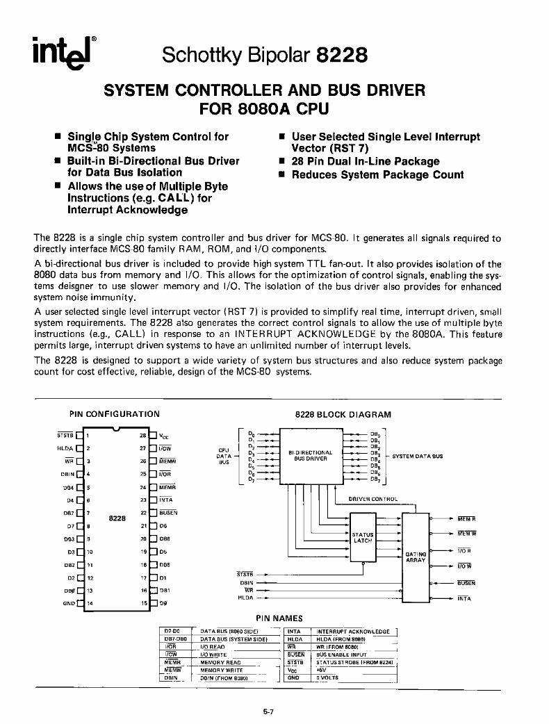
Schottky Bipolar 8228
SYSTEM CONTROLLER AND BUS DRIVERFOR 8080A CPU
• Sing.le Chip System Control forMCS:SO Systems
• Built-in Bi-Directional Bus Driverfor Data Bus Isolation
• Allows the use of Multiple ByteInstructions (e.g. CAL:L) forInterrupt Acknowledge
• User Selected Single Leve,1 InterruptVector (RST 7)
• 28 Pin Dual In-Line Package• Reduces System Package Count
The 8228 is a single chip system controller and bus driver for MCS-80. It generates all signals required todirectly interface MCS-80 family RAM, ROM, and I/O components.
A bi-directional bus driver is included to provide high system TTL fan-out. It also provides isolation of the8080 data bus from memory and I/O. This allows for the optimization of control signals, enabling the systems deisgner to use slower memory and I/O. The isolation of the bus driver also provides for enhancedsystem noise immunity.
A user selected single level interrupt vector (RST 7) is provided to simplify real time, interrupt driven, smallsystem requirements. The 8228 also generates the correct control signals to allow the use of multiple byteinstructions (e.g., CALL) in response to an INTERRUPT ACKNOWLEDGE by the 8080A. This featurepermits large, interrupt driven systems to have an unlimited number of interrupt levels.
The 8228 is designed to support a wide variety of system bus structures and also reduce system packagecount for cost effective, reliable, design of the MCS-80 systems.
STSTB ~----------
DBIN -.0--------------1WR -.0-------------011
HLDA ~-------------I
SYSTEM OATA BUS
DRIVER CONTROL
8228 BLOCK DIAGRAM
BI·DIRECTIONALBUS DRIVER
PIN CONFIGURATION
STSTB Vee
HLDA I/OW CPU
MEMWDATA
WR BUS
OBIN IIOR
OB4 MEMR
04 INTA
OB7 BUSEN
07 06
OB3 OB6
03 05
DB2 DBS
02 01
DB~ OB1
GND 0'
PIN NAMES
07·00 DATA BUS (8080 SIDE)
OB7·DBO DATA BUS (SYSTEM SIDE)
IIOR 1/0 READ
I!OW 1/0 WRITE
MEMR MEMORY READ
MEMW MEMORY WR ITE
DBIN DBIN (FROM 8080)
INTA INTERRUPT ACKNOWLEDGE
HLOA HLDA (FROM 8080)
WR WR (FROM 8080)
BUSEN BUS ENABLE INPUT
STSTB STATUS STROBE (FROM 8224)
Vee +5V
GND aVOLTS
5-7

SCHOTTKY BIPOLAR 8228
FUNCTIONAL DESCRIPTION
General
The 8228 is a single chip System Controller and Data Busdriver for the 8080 Microcomputer System. It generates allcontrol signals required to directly interface MCS-80™ familyRAM, ROM, and I/O components.
Schottky Bipolar technology is used to maintain low delaytimes and provide high output drive capability to supportsmall to medium systems.
Bi-Directional Bus DriverAn eight bit, bi-directional bus driver is provided to bufferthe 8080 data bus from Memory and I/O devices. The 8080Adata bus has an input requirement of 3.3 volts (min) andcan drive (sink) a maximum current of 1.9mA. The 8228data bus driver assures that these input requ irements willbe not only met but exceeded for enhanced noise immunity.Also, on the system side of the driver adequate drive current is available (10mA Typ.) so that a large number ofMemory and I/O devices can be directly connected to thebus.
The Bi-Directional Bus Driver is controlled by signal~ fromthe Gating Array so that proper bus flow is maintained andits outputs can be forced into their high impedance state(3-state) for DMA activities.
Status LatchAt the beginning of each machine cycle the 8080 CPU issues"status" information on its data bus that indicates the typeof activity that will occur during the cycle. The 8228 storesthis information in the Status Latch when the STSTB inputgoes "low". The output of the Status Latch is connected tothe Gating Array and is part of the Control Signal generation.
Gating ArrayThe Gating Array generates control signals (MEM R, MEM W,I/O R, I/O Wand INTA) by gating the outputs of the StatusLatch with signals from the 8080 CPU (DBIN, WR, andHLDA).
The "read" control signals (MEM R, I/O Rand INTA) arederived from the logical combination of the appropriateStatus Bit (or bits) and the DBIN input from the 8080 CPU.
The "write" control signals (MEM W, I/O W) are derivedfrom the logical combination of the appropriate Status Bit(or bits) and the WR input from the 8080 CPU.
All Control Signals are "active low" and directly interfaceto MCS-80 family RAM, ROM and I/O components.
The INTA control signal is normally used to gate the "interrupt instruction port" onto the bus. It also provides a
special feature in the 8228. If only one basic vector is needed in the interrupt structure, such as in small systems, the8228 can automatically insert a RST 7 instruction onto thebus at the proper time. To use this option, simply connectthe INTA output of the 8228 (pin 23) to the +12 voltsupply through a series resistor (1 K ohms). The voltage issensed internally by the 8228 and logic is "set-up" so thatwhen the DBIN input is active a RST 7 instruction is gatedon to the bus when an interrupt is acknowledged. Thisfeature provides a single interrupt vector with no additionalcomponents, such as an interrupt instruction port.
When using CALL as an Interrupt instruction the 8228will generate an INTA pulse for each of the three bytes.
The BUSEN (Bus Enable) input to the Gating Array is anasynchronous input that forces the data bus output buffersand control signal buffers into their high-impedance stateif it is a "one". If BUSEN is a "zero" normal operation ofthe data buffer and control signals take place.
SYSTEM DATA BUSCPU
DATABUS
8228 BLOCK DIAGRAM
BI-OIRECTIONALBUS DRIVER
DRIVER CONTROL
STSTB ----. --J
DBIN ----.-------------41WR --.-------------011
HLDA ----.--------------1
5-8
GATINGARRAY

SCHOTTKY BIPOLAR 8228
DATA BUS
INTA
MEMR
MEM W CONTROL BUS
I/O RI/OW
3
CONTROL
BUSEN__....22a
_ 18WRn-------.....,
DBINt-=-1.:....7----..-----,
HDLA ~2;.;.1~_--.
8080A °O~10~~-ICPU 011-9--l~-I
°2~8--l~~ .....
0 3 1-7--l~-I
0 4 1-3--l~-I
°51-4--l~-I0 6 .-5--l~~-I
0 7 .-6--l~~-I...._-----(FROM 8224) STATUSSTROBE--...c1II
STATUS WORD CHARTTYPE OF MACHINE CYCLE
I
STATUS WORD
DO INTA o 0 0 0 0 0 0 1 0 1
WO
STACK
HLTA
OUT
1 1 0 1 0 1 0 1 1 1
o 0 0 1 1 0 0 0 0 0
o 0 0 0 0 0 0 0 1 1
o 0 0 0 0 0 1 0 0 0
05
INP
1 0 0 0 0 0 0 1 0 1
o 0 0 0 0 1 0 0 0 0
MEMR 1 1 0 1 0 0 0 0 1 0
---INTA
L..-- (NONE)
INTA~------ I/O W
'------------ I/O R
'-------------- MEM WL...-- MEM R
'------------------ MEM WL....- MEM R
'-------------------- MEM R
_ CONTROLSIGNALS
5-9

SCHOTTKY BIPOLAR 8228
WAVEFORMS
DBIN
STATUS STROBE
INTA, lOR, MEMRDURING HLDA
HLDA --------+----+-----'1
8080 DATA BUS-----...".I'~~+--,.,.I"--------------------
lOW OR MEMW
8080 BUS DURING READ· - - - - - - - - -
8080 BUS DURING WRITE
SYSTEM BUS DURING READ
SYSTEM BUS DURING WRITE - - - - - - - - - <~we1=
SYSTEM BUS ENABLE. j 1.- tE~rSYSTEM BUS OUTPUTS - - - - - - - - - - - - - - - <t-- > - - - - - - - - - - - - - -
VOLTAGE MEASUREMENT POINTS: 00-07 (when outputs) Logic "0" = 0.8V, Logic "1" = 3.0V. All other signals measuredat 1.5V.
A.C. Characteristics TA = O°c to 70°C; Vee = 5V ±5%.
LimitsSymbol Parameter Min. Max. Units Condition
tpw Width of Status Strobe 22 ns
tss Setup Time, Status Inputs Do-D7 8 ns
tSH Hold Time, Status Inputs Do-D7 5 ns
toe Delay from STSTB to any Control Signal 20 60 ns CL = 100pF
tRR Delay from DB IN to Control Outputs 30 ns CL = 100pF
tRE Delay from DBIN to Enable/Disable 8080 Bus 45 ns CL = 25pF
tAD Delay from System Bus· to 8080 Bus during Read 30 ns CL = 25pF
tWA Delay from WR to Control Outputs 5 45 ns CL = 100pF
tWE Delay to Enable System Bus DBo-DB7 after STSTB 30 ns CL = 100pF
two Delay from 8080 Bus Do-D7 to System Bus ns CL = 100pFDBo-DB7 during Write 5 40
tE Delay from System Bus Enable to System Bus DBo-DB7 30 ns CL = 100pF
tHO HLDA to Read Status Outputs 25 ns
tos Setup Time, System Bus Inputs to HLDA 10 ns
tOH Hold Time, System Bus Inputs to HLDA 20\
ns CL = 100pF
5-10

SCHOTTKY BIPOLAR 8228
D.C. Characteristics TA = O°c to 70°C; Vee = 5V ±5%.
LimitsSymbol Parameter Min. Typ.[1] Max. Unit Test Conditions
Ve Input Clamp Voltage, All Inputs .75 -1.0 V Vee=4.75V; le=-5mA
IF Input Load Current,STSTB 500 IlA Vee=5.25V
02&06 750 IlA VF=O.45V
Do, 01, 04, Os, IlA& 07 250
All Other Inputs 250 IlA
IR Input Leakage CurrentSTSTB 100 IlA Vee=5.25V
OBo-OB7 20 IlA VR =5.25V
All Other Inputs 100 p.A
VTH Input Threshold Voltage, AU Inputs 0.8 2.0 V VCC=5V
Icc Power Supply Current 140 190 mA VCC=5.25V
VOL Output Low Voltage,
00-0 7 .45 V VCC=4.75V; IOl=2mA
All Other Outputs .45 V IOl = 10mA
VOH Output High Voltage,
00-0 7 3.6 3.8 V VcC=4.75V; IOH=-10p.A
All Other Outputs 2.4 V IOH = -1mA
los Short Circuit Current, All Outputs 15 90 mA Vec=5V
10(off) Off State Output Current,All Control Outputs 100 IlA Vce=5.25V; VO=5.25
-100 p.A VO=·45V
liNT INTA Current 5 mA (See Figure below)
Note 1: Typical values are for TA = 2Soe and nominal supply voltages.
Capacitance This parameter is periodically sampled and not 100%. test,ed.
Limits
Symbol Parameter Min. Typ.£1] Max. Unit
elN Input Capacitance 8 12 pF
GoUTOutput Capacitance
7 15 pFControl Signals
I/OI/O Capacitance
8 15 pF(0 or OB)
TEST CONDITIONS: VBIAS = 2.5V, Vcc=S.OV, TA = 2Soe, f = 1MHz.
Note 2: For 00-07: R1 = 4Kn, R2 = oon,cL = 25pF. For all other outputs:R1 = 500n, R2= 1Kn, CL = 100pF.
5-11
8228
23INTA
INTA Test Circuit (for RST 7)

SCHOTTKY BIPOLAR 8228
ADDRESS BUS
DBO
DB1
DB2
DB3DATA BUS
DB4
DBs
DB6
D~
INTA
MEM R
MEMW CONTROL BUS
I/O R
I/OW
2 25 -GND. · Ao Ao
20 26A 1+5V A111 27A2-5V A2
28 29-- A3+12V · A3
30A4A4
31AsAS
32A6A68080A 33A7CPU A7 I-
34ASAS
13 35AgSYSTEM DMA REO. · HOLD Ag
1A10A10
40A11A11
37A12
14 A12SYSTEM INT. REO. • INT 38A13A13
16 39A14INT. ENABLE ......- INTE A14
36A1SA1S 18
WR P -17
DBIN
413(')r,;D1TAl21
HDLA2114 15
2213 1110 15 13----. cP1
DO DB .12 10 15
cfJ2 9 17 16~
0 1,.
624 8 12 11~~ WAIT O2 8228
.3 8224 4 23 7 10
BI-DIRECTIONAL9
REArJY 03,.
~ CLOCK3 6 BUS DRIVER 5GENERATOR 04 .2
DRIVER 1 1219 18-..0 RESET 4 .Os9
5 21 20----.0 6
.165 19 6 8 7----.
SYNC 0 7,.
8 -- 28 ------- 23---. n --+5V~~4r 14 .....GND---'" ....,
STATUS STROBE 1 SYSTEM 26.n h
""" CONTROL ~522
~7BUSEN ·-c!"oF
RESIN
+12V
+5V
GND
TANK
OSC
cfJ2 (TTL)
RDYIN
8080A CPU Standard Interface
5-12
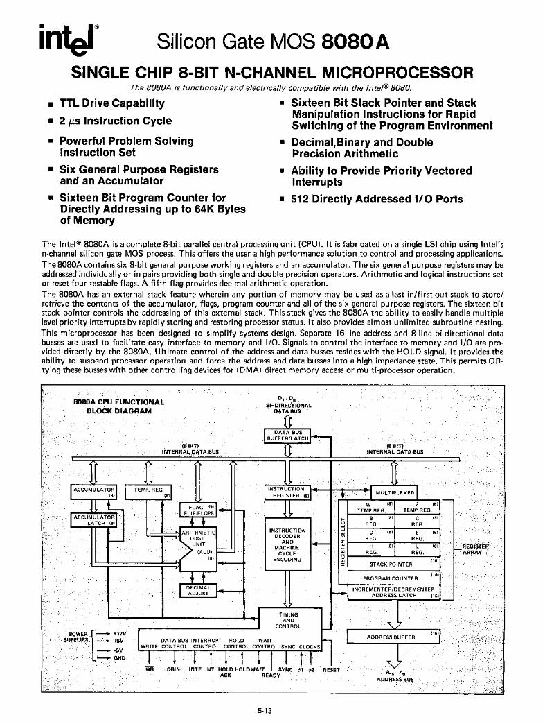
intel® Silicon Gate MOS 8080ASINGLE CHIP a-BIT N-CHANNEL MICROPROCESSOR
The 8080A is functionally and electrically compatible with the Intel® 8080.
• TTL Drive Capability
• 2 J.Ls Instruction Cycle
• Powerful Problem SolvingInstruction Set
• Six General Purpose Registersand an Accumulator
• Sixteen Bit Program Counter forDirectly Addressing up to 64K Bytesof Memory
• Sixteen Bit Stack Pointer and StackManipulation Instructions for RapidSwitching of the Program Environment
• Decimal,Binary and DoublePrecision Arithmetic
• Ability to Provide Priority VectoredInterrupts
• 512 Directly Addressed I/O Ports
The Intel® 8080A is a complete 8-bit parallel central processing unit (CPU). It is fabricated on a single LSI chip using Intel'sn-channel silicon gate MOS process. This offers the user a high performance solution to control and processing applications.The 8080A contains six 8-bit general purpose working registers and an accumulator. The six general purpose registers may beaddressed individually or in pairs providing both single and double precision operators. Arithmetic and logical instructions setor reset four testable flags. A fifth flag provides decimal arithmetic operation.The 8080A has an external stack feature wherein any portion of memory may be used as a last in/first out stack to store/retrieve the contents of the accumulator, flags, program counter and all of the six general purpose registers. The sixteen bitstack pointer controls the addressing of this external stack. This stack gives the 8080A the ability to easily handle multiplelevel priority interrupts by rapidly storing and restoring processor status. It also provides almost unlimited subroutine nesting.This microprocessor has been designed to simplify systems design. Separate 16-line address and 8-line bi-directional databusses are used to facilitate easy interface to memory and I/O. Signals to control the interface to memory and I/O are provided directly by the 8080A. Ultimate control of the address and data busses resides with the HOLD signal. It provides theability to suspend processor operation and force the address and data busses into a high impedance state. This permits ORtying these busses with other controlling devices for (DMA) direct memory access or mUlti-processor operation.
:.,.
;
.:',
".
..,
....
.,.
:/ ",',"
:·i.'
,<'.,
<:
:::.
·:i··.
:, .
W (8) Z (8)
TEMP REG. TEMP REG.
B (8) C (8)
REG. REG.
D (8) E (8)
REG. REG.
H (8) L (8) '\'
REG. REG.
STACK POINTER(16)
(16)PROGRAM COUNTER
.: ..TIMING
. '.' ...,: :'>;
'/:;):"., :;:", ': ~',:, '.;:':' ;
,.'H:.: ':~, •.' ." '.o;?oo .'H.; >::.... c·... '<1:,: ,:
,'. :.•..
'.:.:
.~:? :.
: .....•
:'..':.'t .;. ;)it~:'
'';','': ;;:"'.,.':':J :.... ::;." ..>:.~.;
..r·: ACCUMULATOR:.... (8)
./:, <~'>:'.~
ACCUMULATOR.-,;
LATCH (8)
.~
5-13

·SILICON GATE MOS 8080'A- .
8080A FUNCTIONAL PIN DEFINITION
The following describes the function of all of the 8080A I/O pins.Several of the descriptions refer to internal timing periods.
_. .
A15.AO (oU1put three-state)ADDRESS BUS;.the address bus provides the address to memory(up to 64K 8-bit words) or denotes the I/O device number for upto 256 input and 256 output devices. Ao is the least significantaddress. bit.
OJ-D.o (input/output three-state)
DATA BUS; the data bus provides bi-directional. communication.between the CPU, memory, and I/O. devices for instructions anddata transfers. Also, during the first clock cycle of each machinecycle, the 8080A outputs a status word on the data bus that de._scribes the current machine cycle. Do is the least significant bit.
SYNC (output)SYNCHRONlZING SIGNAL; the SYNC pin provides a signal toindicate the beginning-of each machine cycle.
DBIN (output)
DATA BUS IN; the DBIN signal indicates to external circuits thatthe data bus is in the input mode. This signal should be used toenable the gating of data onto the 8080A data bus from memoryor I/O.
A10 1
GNO 2
0 4 3
05 4
°6~5
0 7 6
0 3 7
O~ 8
0 1.0 9
DO 0 10-5V 11
RESET 12
HOLD 13
INT 14
4>2 15INTE 0 16OBIN 0 17
WR 18SYNC 19
+5V 20
-.
Pin Configuration
INTE~
8080A
40 __~'-JI A11
39 A14
38 A13
37 A12
36 0 A15
35 0 Ag
34 As
33 0 A732 A6
31 As30 0 A429 A3
28 +12V
27 A2
26 A1
25 Ao24 WAIT
23 READY
22 4>1
21 HLOA
REAPV (input)
READY; the READY signal indicates to the 8080A that validmemory or input data is available on the 8080A data bus. Thissignal is used to synchronize t.he CPU with slower memory or I/Odevices. If after sending an address out the 8080A does not receive a READY input, the 8080A will enter a WAIT state for aslong as the READY line is low. READY can also be used to singlestep the CPU.
YlJAIT (output)
WAIT; the WAIT signal acknowledges that th~ CPU is in a WAITs~ate.
WR (output)WRITE; the WR signal is used for memory WRITE or I/O outputcontrol. The data on the data bus is stable while the WR signal isactive low (WR = 0).
. HOLD (input)
HOLD; the HOLD signal requests' the CPU to 'enter the HOLDstate. The HOLD state allows an external device to gain controlof the 8080A address and data bus as soon as the 8080A has completed its use of these buses for the current machine cycle. It isrecognized under the following conditions:• the CPU is in the HALT state.• the CPU is in the T2 or TW state and the READY signal is active.As a result of entering the HOLD stf'te the CPU ADDRESS BUS.(A15-AO) and DATA BUS (07-00) will be in their high impedancestate. The CPU acknowledges its state with the HOLD ACKNOWLEDGE (HLDA) pin.
HLOA (output)HOLD ACKNOWLEDGE; the HLDA signal appears in responseto the HOLD' signal and !ndicates that the data and address bus
will go to the high impedance state. The HLOA signal begins at:• T3 for READ memory or input.• The Clock Period following T3 for WR ITE memory or OUT
PUT operation.
In either case, the HLOA signal appears after the rising edge of 4>1and high impedance occurs after the rising edge of 4>2.
INTE (output)INTER RUPT ENABLE; indicates the content of the internal interrupt enable flip/flop. This flip/flop may be set or reset by the Enable. and Disable Interrupt instructions and inhibits interruptsfrom being accepted by the CPU when it is reset. It is auto-
, matically reset (dfsab'ling further interrupts) -at time T1 of the in-struction fetch cycle (M 1) when an interrupt is accepted and isalso reset by the RESET signal.
INT (input)INTERR.UPT REQUEST; the CPU recognizes an interrupt request on this line at the end of the current instruction or whilehalted. If the CPU is in the HOLD state or if the Interrupt Enableflip/flop is reset it will not honor the request.
RESET (input) [1]
RESET; while the RESET signal is activated, the content of theprogram counter is cleared. After RESET, the program will startat location 0 in memory. the INTE and HLDA flip/flops are alsoreset. Note that the flags, accumulator, stack pointer, and registersare not cleared.
Vss Ground Reference.VDD +12 ± 5% Volts.Vee +5 ± 5% Volts.Vss -5 ±5% Volts (substrate bias).
,l/>1,'l/>2 2 externally supplied clock phases. (non TTL compatible)
5-14

SILICON GATE MOS 8080 A
ABSOLUTE MAXIMUM RATINGS·
Temperature Under Bias ' O°C to +70° CStorage Temperatu re . . . . . . . . . . . . . . . _65°C to +150°CAll Input or Output Voltages
With Respect to VSS -0~3V to +20V
Vcc, Voo and VSS With Respect to Vss -0.3V to +20V. Power Dissipation 1.5W
*COMMENT: Stresses above those listed under ''Absolute Maximum Ratings" may cause permanent damage to the device.This is a stress rating only and functional operation of the device at these or any other conditions above those indicated inthe operational sections of this specification is not implied. Exposure to absolute maximum rating conditions for extendedperiods may affect device reliability.
D.C. CHARACTERISTICSTA = O°C to 70°C, VOO = +12V ± 5%, Vcc = +5V ± 5%, Vss = -5V ± 5%, Vss = OV, Unless Otherwise Noted.
Symbol Parameter Min. Typ. Max. Unit Test Condition
VILC Clock Input Low Voltage Vss-1 Vss+0.8 V
VIHC Clock Input High Voltage 9.0 Voo+1 V
VIL Input Low Vol~age Vss-1 VsstO.8 V
VIH Input High Voltage 3.3 Vcc+1 V
VOL Output Low Vqltage 0.45- V } IOl = 1.9mA on all outputs,
VOH Output High Voltage 3.7 V IOH =-150~A.
100 (AV) Avg. Power Supply Current (Voo) 40 70 mA
ICC (AV) Avg. Power Supply Current (Vcc ) 60 80 mA} Operation
TCy = .48 J.1secISB(AV) Avg. Power Supply Current (Vss ) .01 1 mA
IlL Input Leakage ±10 J.1A VSS ~ VIN ~ Vcc
ICl Clock Leakage ±10 J.1A Vss ~ VCLOCK ~ VDD
IDL[2] Data Bus Leakage in Input Mode -100 ~A VSS ~VIN ~Vss +0.8V-2.0 mA
Vss+0.8V~VIN~Vcc
IFLAddress and Data Bus Leakage +10
~AVADoR/oATA = VCC
Dl:Iring HOLD -100 VADOR/DATA =Vss + 0.45V
CAPACITANCETA = 25°C VCC =Voo = Vss =OV, Vss =-5V
Symbol Parameter Typ. Max. Unit Test Condition
Cq> Clock Capacitance 17 25 pf fc = 1 MHz
CIN Input Capacitance 6 10 pf Unmeasured Pins
COUT Output Capacitance 10 20 pf Returned to Vss
NOTES:1. The RESET signal must be active for a minimum of 3 clock cycles.2. When DSIN is high and VIN > VIH an internal active pull up will
be switched onto the Data Sus.3. ~I supply / ~TA = -O.45%t C.
5-15
TYPICAL SUPPLY CURRENT VS.TEMPERATURE, NORMALIZED.[3]
1.5,..-----r-----,-----_
...zwa:a:::»(,) 1.0t----~~=------+__--~>..Ja.a.::»U)
0.50~---+2&.-5----+5"'-0---'......1+75
AMBIENT TEMPERATURE (Oe)
DATA BUS CHARACTERISTICDURING DB"IN
MAX
°O~------------~Vee

SILICON GATE MOS 8080A
A.C. CHARACTERISTICSTA =O°C to 70°C, VOO =+12V ± 5%, VCC =+5V ± 5%, Vas = -5V ± 5%, Vss =OV, Unless Otherwise Noted
Symbol Parameter Min. Max. Unit Test Condition
tCy[3] Clock Period 0.48 2.0 J1sec
t r , tf ·Clock Rise and Fall Time 0 50 nsec
~1 f/J1 Pulse Width 60 nsec
tq,2 cf>2 Pu.lse Width 220 nsec
t01 Delayep1 to ep2 0 nsec
. t02 Delay lP2 to l/>, 70 nsec
t03 Delayep, to ep2 Leading Edges 80 nsec
tOA [2] Address Output Delay From ~2 200 nsec } Cl = 100pfto.D [2] Data Output Delay From f/J2 220 nsec
toC[2] Signal 'Output Delay From ep1 , or ep2 (SYNC, WR,WArT, HLDA) 120 nsec }Cl =50pftOF [2] DBIN Delay From lP2 25 140 nsec
tOI[1] Delay for Input Bus to Enter Input Mode tOF nsec
tOS1 .Data Set~p Time During ~1 and DB IN 30 nsec
TIMING WAVEFORMS [14] (Note: Timing measurements are made at the following reference voltages: CLOCK "1" = 8.0V"0" = 1.0V; INPUTS "1" =3.3V, 110" = 0.8V; OUTPUTS "1" =2.0V, "0" =0.8V.)
(/>,
SYNC·
DBIN
READY
WAIT
HOLD
HLDA
INT
INTE
tCY -I -. to, .---.~~1
I f\ r~ JF\ iF\.-t<l>2~1
j~ }~~ ~ jJ- ....h ... F- ~~
~ ~~ H~to3..1 !O2 ~
___ I .~r. .
~tOA-.I--..;.. --- -- ---- ~----- ---- -f
tAW
~too--' ~ tOI I......... ---i toHI"'- ...-tOO-'
~ r· 4=..... -"r-DATA IN
~ .J DATA OUT,,"".J-- t 1----- - ---- -I,------- -- ~--
--. tos, ...- ~I--tow r---.
T -t- ~tOS2-'
~ tocl~ ---.. toc 1..--r 1-
~tOF~ ~tOF
----------- ~t
toc .........1 .ItHl~
------------ -I=@ t - -;f!1~-~:'J> t RS toc ..........1
t H-. .-- X- l-toc ---" 1.- t H -. 1.----J@ I
~I~;~~
--X@ ,.tiS1=-= ~~
tH--. ~
. 5-16

SILICON GATE MOS 8080A
A.C. CHARACTERISTICS (Continued)
TA = O°C to 70°C, Voo = +12V ± 5%, Vee = +5V ± 5%, Vss = -5V'± 5%, V55 = OV, Unless Otherwise Noted
Symbol Parameter Min. Max. Unit Test Condition
t052 Data Setup Time to ~2 During DBIN 150 nsec
tOH (1) Data Hold Time From ~2 During DBIN [1 ] nsec
tiE [2) INTE Output Delay From ~2 200 nsec CL'= 50pf
tRS READY Setup Time During ~2 120 nsec
tH5 HOLD Setup Time to ~2 140 nsec
tiS INT Setup Time During ~2 (During cP1 in Halt Mode) 120 nsec
tH Hold Time From ~2 (READY, INT, HOLD) 0 nsec
tFO Delay to Float During Hold (Address and Data ~us) 120 nsec
tAW [2) Address Stable Prior to WR-
[5] nsec
tow [2) Output Data Stable Prior to WR [6] nsec
tWD[2] Output Data Stable From WR [7] nsec
tWf\[2] , Address Stable From WR [7] nsec ~ CL= 100pf: Address, Data.- - CL=50pf: WR, HLDA, DBIN
tHF[2] HLDA to Float Delay [8] nsec
tWF[2] WR to Float Delay [9] nsec
tAH[2] Address Hold Time After DBIN During HLDA -20 nsec --
+5V
TYPICAL ~ OUTPUT DELAY VS. A CAPACITANCE+20 r-----~-----r----~---__.
+100
2.1K
+50o
.:1. CAPACITANCE (pf)
(CACTUAL - CSPEC )
-50
lit..s> +10«..JwC~ 0:;)Q.~:;)
-100<1
-20-100
3. tCY = t03 + tr~2 + t4>2 + tf~2 + t02 + trit>1 ;> 480ns.
8080AOUTPUT
NOTES:1. Data input should be enabled with 'OBIN status. No bus co~f1ict can then occur and data hold time is assured.
tOH =50 ns or tOF, whichever is less.2. Load Circuit.
4. The following are relevant when interfacing the 8080A to devices having VIH = 3.3V:a) Maximum output rise time from .8V to 3.3V = 100ns @ CL = SPEC.b) Output delay when measured to 3.0V == SPEC +60ns @ CL == SPEC.c) If CL "* SPEC, add .6ns/pF if CL> CSPEC, subtract .3ns/pF (from modified delay) if CL < CSPEC.
5. tAW =2 tCY -t03 -tr</>2 -140nsec.6. • tow =tCY -t03 -tr</>2 -l70nsec.7. If not HLOA, two =tWA = t03 + tr</>2 +10ns. If HLOA, two =twA =twF.8. tHF == t03 + t rc/>2 -50ns.9. twF = t03 + t rc/>2 -10ns
10. Data in must be stable for this period during OBIN ·T3. Both tOS1 and tOS2 must be satisfied.'11. Ready signal must be stable for this period during T2 or TW. (Must be externally synchronized.)12. Hold signal must be stable for this period during T2 or TW when entering hold mode, and during T3, T4, TS
and TWH when in hold mode. (External synchronization is not required.)13. Interrupt signal must be stable during this period of the last clock cycle of any instruction in order to be
recognized on the following instruction. (External synchronization is not required.)14. This timing diagram, shows timing relationships only; it does not represent any specific machine cycle.
0 7.00 ~
SYNC
OBIN
WR
toc
READY
WAIT
HOLD s-
t oc ...-HLDA
~INT
I -t:1-INTE
5-17

SILICON GATE MOS 8080 A
INSTRUCTION SET
The accumulator group instructions include arithmetic andlogical operators with direct, indirect, and immediate addressing modes.
Move, load, and· store instruction groups provide the abilityto move either a or 16 bits of data between memory,' thesix working registers and the accumulator using direct, indirect, and 'immediate addressing modes.
The ability to branch to different portions of the programis provided with jump, jump conditional, and computedjumps. Also the ability to call to and return from subroutines is provided both conditionally and unconditionally.The RESTART (or single byte call instruction) is useful forinterrupt vector operation.
OOl:Jble precision operators such as stack manipulation anddouble add instructions extend both the arithmetic andinterrupt handl ing capability of the a080A. The ability to
increment and decrement memory, the six general registersand the accumulator is provided as well as extended increment and decrement instructions to operate on the registerpairs and stack pointer. Further capability is provided bythe abil ity to rotate the accu mu lator I~ft or right throughor arou nd the carry bit.
Input and output may be accomplished using memory addresses as I/O ports or the directly addressed I/O providedfor in the 8080A instruction set.
The following special instruction group completes the 8080Ainstruction set: the NOP instruction, HALT to stop processor execution and the OAA instructions provide decimalarithmetic capabil ity. STC allows the carry flag to be directly set, and the CMC instruction allows it to be complemented. CMA complements the contents of the accumulatorand XCHG exchanges the contents of two 16-bit registerpairs directly.
Data and Instruction Formats
Data in the a080A is stored in the form of a-bit binary integers. All data transfers to the system data bus will be in thesame format.
1 0 7 06 Os 04 03 02 01 001
OATA WORO
The program instructions may be one, two, or three bytes in length. Multiple byte instructions must be storedin successive words in program memory. The instruction formats then depend on the particular operationexecuted.
One Byte Instructions
Two Byte Instructions
1 0.7 06 Os D4 °3 °2 °1 DO I OP CODE
10 7 °6 Os D4 °3 °2 °1 DO I OPERANO
Three Byte Instructions
10 7 °6 Os 04 °3 °2 °1 DO I OP COOE
10 7 °6 Os 04 °3 °2 0 1 DO I LOW ADDRESS OR OPERAND 1
10 7 06 Os 04 03 °2 °1 DO I HIGH ADDRESS OR OPERANO 2
TYPICAL INSTRUCTIONS
Register to register, memory reference, arithmetic or logical, rotate,return, push, pop, enable or disableInterrupt instructions
Immediate mode or I/O instructions
Jump, call or direct load and storeinstructions
For the 8080A a logic "1" is defined as a high level and a logic 110" is defined as a low level.
6-18

SILICON GATE MOS 8080.A
INSTRUCTION SET
Summary of Processor Instructions
Instruction Code [1 J Clock [2] Instruction Code (1) Clock[2JMnemonic Description D7 D6 Os D4 D3 02 0, Do Cycles Mnemonic Description D7 06 Os 04 Da ~ 0, Do Cycles
MOV r1 .r2 Move register to register 0 1 0 0 0 S S S 5 RZ Return on zero 1 1 0 0 , 0 0 0 5/11MOVM,r Move register to memory 0 1 1 1 0 S S S 7 RNZ Return on no zero 1 1 0 0 0 0 C 0 5/11MOVr,M Move memory to register 0 1 0 0 0 1 1 0 7 RP Return on positive 1 1 1 1 0 0 0 0 5/11
.HLT Halt 0 1 1 1 0 1 1 0 7 RM Return on minus 1 1 1 1 1 0 0 0 5/11MVI r Movi immediate register 0 0 0 0 0 1 1 0 7 RPE Return on parity even 1 1 1 0 1 0 0 0 5/11MVIM Move immediate memory 0 0 1 1 0 1 1 0 10 RPO Return on parity odd 1 1 1 0 0 0 0 0 5/11lNR r Increment register 0 0 0 0 0 1 0 0 5 RST Restart 1 1 A A A 1 1 1 11OCRr Decrement register 0 0 0 0 0 1 0 1 5 IN Input 1 1 0 1 1 0 1 1 10INR M Increment memory 0 0 1 1 0 1 0 0 10 OUT Output 1 1 0 1 0 0 1 1 10OCR M Decrement memory 0 0 1 1 0 1 0 1 10 LXIB Load immediate register 0 0 0 0 0 0 0 1 10ADD r Add register to A 1 0' 0 0 0 S S S 4 Pair B& CADCr Add register to Awith carry 1 0 0 0 1 S S S 4 LXIO Load immediate register 0 0 0 0 0 0 10SUB r Subtract register from A 1 0 0 1 0 S S S 4- Pair D& ESaB r Subtract register from A 1 0 0 1 1 S S S 4 LXIH Load immediate register 0 0 0 0 0 0 10
with borrow Pair H& LANAr And register with A 0 1 0 0 S S S ,4 LXISP Load immediate stack pointer 0 0 1 1 0 0 0 10XRAr Exclusive Or register with A 0 1 0 1 S S S 4 PUSH a Push register Pair B& Con 1 1 0 0 0 1 0 11ORAr .0r register with A 0 1 1 0 S S S 4 stackCMPr Compare register with A 0 1 1 1 S S' S 4 PUSH 0 Push register Pair 0 & Eon 0 0 0 11ADOM Add memory to A 0 0 0 0 1 1 0 7 stackADCM Add memory to Awith carry 0 0 0 1 1 1 0 7 PUSH H Push register Pair H& Lon 0 0 0 11SUB M Subtract memory from A 0 0 '1 0 1 1 0 7 stackSBB M Subtract memory from A 0 0 1 1 1 1 0 7 PUSH PSW Push Aand Flags 0 0 11
with borrow on stackANAM And memory with A 0 1 0 0 0 7 POP B Pop register pair B& Coff 0 0 0 0 0 10XRAM Exclusive 0r memory with A 0 1 O. 1 0 7 stackORAM Or memory with A 0 1 1 0 0 7 POPD Pop register pair 0 & E off 0 0 0 O' 10CMPM Compare memory with A 0 1 1 1 0 7 stackADI Add immediate to A 1 0 0 0 0 7 POP H Po.p register pair H& Loff 0 0 0 0 10ACI Add immediate to Awith 1 0 0 1 0 7 stack
carry POP PSW Pop Aand Flags 0 0 0 10SUI Subtract immediate from A 0 0 0 off stackSBI Subtract immediate from A 0 1 0 STA Store Adtrect 0 0 1 0 0 0 13
with borrow LOA Load Adirect 0 0 1 1 0 0 13ANI And immediate with A 0 0 0 XCHG Exchange 0 & E, H& L 1 1 0 1 0 1 4XRI Exclusive Or immediate with 0 1 0 Registers
A XTHL Exchang~ top of stack, H& L 1 1 1 0 0 0 1 1 18ORI Or immediate with A 1 1 1 1 0 0 7 SPHL H& Lto stack pointer 1 1 1 1 1 0 0 1 5CPI Compare immediate with A 1 1 1 1 1 0 7 PCHL H& Lto program counter 1 1 1 0 1 0 0 1 5RLC Rotate A left 0 0, 0 0 0 1 4 DAD B Add B& Cto H& L 0 0 0 0 1 0 0 1 10RRC Rotate A right 0 0 0 0 1 1 4 DAD 0 Add 0 & E to H& L 0 0 0 1 1 0 0 1 10RAL Rotate A left through carry 0 0 0 1 0 1 4 DAD H Add H& Lto H& L 0 0 1 0 1 0 0 1 10RAR Rotate A right through 0 0 0 1 l' 1 4 DAD SP Add stack pointer to H& L 0 0 1 1 1 0 0 1 10
carry STAXB Store Aindirect 0 0 0 0 0 0 1 0 7JMP Jump unconditional 1 0 0 0 0 1 1 10 STAX 0 Store Aindirect 0 0 0 1 0 0 1 0 7JC Jump on carrY 1 0 1 1 0 1 0 10 LOAXB Load A indirect 0 0 0 0 1 0 1 0 7JNC Jump on no carry 1 0 1 0 0 1 0 10 LoAXO Load A indirect 0 0 0 1 1 0 1 0 7JZ Jump on zero 1 0 0 1 0 1 0 10 INX B Increment B& Cregisters 0 0 0 0 0 0 1 1 5JNZ Jump on no zero 1 0 0 0 0 1 0 10 INX D Increment 0 & E registers 0 0 0 1 0 0 1 1 5JP Jump on positive 1 1 1 0 0 1 0 10 INX H Increment H& Lregisters 0 0 1 0 0 0 1 1 5JM Jump on minus 1 1 1 1 0 1 0 10 INXSP Increment stack pointer 0 0 1 1 0 0 1 1 '5JPE Jump on parity even 1 1 0 1 0 1 0 10 OCX B Decrement B& C 0 0 0 0 1 0 1 1 5JPO Jump on parity odd 1 1 0 0 0 1 0 .10 ,OCX 0 Decrement 0 & E 0 0 0 1 1 0 1 1 5CALL Call unconditional 1 0 0 1 1 0 1 17 OCX H Decrement H& L 0 0 1 0 1 0 1 1 5CC Call on carry 1 0 1 1 1 0 0 11/17 OCXSP Decrement stack pointer 0 O. 1 1 1 0 1 1 5CNC Call on no carry 1 0 1 0 1 0 0 11/17 CMA Complement A 0 0 1 0 1 1 1 1 4CZ Call on zero ,1 0 0 1 1 0 0 11/17 STC Set carry 0 0 1 1 0
"1 1 4
CNZ Call on no zero 1 0 0 0 1 0 0 11/17 CMC Complement carry 0 0 1 1 1 1 1 1 4CP Call on positive 1 1 1 0 1 0 0 11/17 DAA Decimal adjust A 0 0 1 0 0 1 1 ,1 4CM Call on minus 1 1 1 1 1 0 0 11/17 SHLD Store H& Ldirect 0 0 1 (} 0 0 1 0 16CPE Call on parity even 1 1 0 1 1 0 0 11/17 LHLD Load H& Ldirect 0 0 1 0 1 0 1 0 16CPO Call on parity odd 1 1 0 0 1 0 0 11/17 EI Enable Interrupts 1 1 1 1 1 0 1 1 4RET Return 1 0 0 1 0 0 1 10 01 Disable interrupt 1 1 1 1 0 0 1 1 4RC Return on carry 1 0 1 1 0, 0 0 5/11 N.OP No-operation 0 0 0 0 0 0 0 0 4RNC Return on no carry 1 0 1 0 0 0 0 5/11
NOTES:. 1. DDDorSSS-OOOB-001 C-010D-011'E-100H-101 L-110Memory....:.111 A.2. Two possible cycle times, (5/11) indicate instruction cycles dependent on condition flags.
5-19

infel® Silicon Gate MOS 8080A-1
SINGLE CHIP 8-BIT N-CHANNEL MICROPROCESSOR
• TTL Drive Capability
• 1.3 J.Ls Instruction Cycle
• Powerful Problem SolvingInstruction Set
• Six General Purpose Registersand an Accumulator
• Sixteen Bit Program Counter forDirectly Addressing up to 64K Bytesof Memory
• Sixteen Bit Stack Pointer and StackManipulation Instructions for RapidSwitching of the Program Environment
• Decimal,Binary and DoublePrecision Arithmetic
• Ability to Provide Priority VectoredInterrupts
• 512 Directly Addressed 1/0 Ports
The Intel® aOaOA is a complete a-bit parallel central processing unit (CPU). It is fabricated on a single LSI chip using Intel'sn-channel silicon gate MOS process. This offers the user a high performance solution to control and processing applications.The aOaOA contains six 8-bit general purpose working registers and an accumulator. The six general purpose registers may beaddressed individually or in pairs providing both single and double precision operators. Arithmetic and logical instructions setor reset four testable flags. A fifth flag provides decimal arithmetic operation.The aOaOA has an external stack feature wherein any portion of memory may be used as a last in/first out stack to store/retrieve the contents of the accumulator, flags, program counter and all of the six general purpose registers. The sixteen bitstack pointer controls the addressing of this external stack. This stack gives the 80aOA the ability to easily handle multiplelevel priority interrupts by rapidly storing and restoring processor status. It also provides almost unlimited subroutine nesting.This microprocessor has been designed to simplify systems design. Separate 16-line address and a-line bi-directional databusses are used to facilitate easy interface to memory and I/O. Signals to control the interface to memory and I/O are provided directly by the aOaOA. Ultimate control of the address and data busses resides with the HOLD signal. It provides theability to suspend processor operation and force the address and data busses into a high impedance state. This permits ORtying these busses with other controlling devices for (DMA) direct memory access or mUlti-processor operation.
5-20

SILICON GATE MOS 8080A-1
ABSOLUTE MAXIMUM RATINGS·
Temperature Under Bias O°C to +70° CStorage Temperature -65°C to +150°CAll Input or Output Voltages
With Respect to Vaa -0.3V to +20VVee, VOO and Vss With Respect to Vaa -0.3V to +20VPower Dissipation . . . . . . . . . . . .. 1.5W
*COMMENT: Stresses above those listed under 'Absolute Maximum Ratings" may cause permanent damage to the device.This is a stress rating only and functional operation of the device at these or any other conditions above those indicated inthe operational sections of this specification is'not implied. Exposure to absolute maximum rating conditions for extendedperiods may affect device reliability.
D.C. CHARACTERISTICSTA = O°C to 70°C, Voo = +12V ± 5%, Vce = +5V ± 5%, Vss = -5V ± 5%, Vss = OV, Unless Otherwise Noted.
Symbol Parameter Min. Typ. Max. Unit Test Condition
VILe Clock Input Low Voltage Vss-1 Vss+0.8 V
VIHC Clock Input High Voltage 9.0 Voo+1 V
VIL Input Low Voltage Vss-1 Vss+0.8 V
VIH Input High Voltage 3.3 Vec+1 V
VOL Output Low Voltage 0.45 V }'0 L = 1.9mA on all outputs,
VOH Output High Voltage 3.7 V 'OH = 150J,.lA.
100 (AV) Avg. Power Supply Current (Voo) 40 70 mA
ICC (AV) Avg. Power Supply Current (Vce) 60 80 mA} Operation
TCy = .32Jlsec'ss (AV) Avg. Power Supply Current (Vss ) .01 1 mA
IlL Input Leakage ±10 pA Vss ~ VIN ~ Vee
ICl Clock Leakage ±10 pA Vss ~ VeLOeK ~ Voo
IOL[2] Data Bus Leakage in Input Mode -100 JlA VSS~VIN ~Vss+0.8V-2.0 mA
Vss+0.8V~VIN~Vec
IFLAddress and Data Bus Leakage +10
pA VAOOR/OATA = VecDuring HOLD -100 VAOOR/OATA = VSS + 0.45V
+75+25 +500.5 ----"'-----....L..- ....J
o
TYPICAL SUPPLY CURRENT VS.TEMPERATURE, NORMALIZED.[3]
AMBIENT TEMPERATURE (OC)
1.5r------r-----~---_
~zwa:a:::>(J 1.0 1"-----=-~:------+-------4>-'Q.Q.::>en
Symbol Parameter Typ. Max. Unit Test Condition
Cf/> Clock Capacitance 17 25 pf fc = 1 MHz
CIN Input Capacitance 6 10 pf Unmeasured Pins
CO UT Output Capacitance 10 20 pf Returned to VSS
NOTES:1. The RESET signal must be active for a minimum of 3 clock cycles.2. When OSIN is high and VIN > VIH an internal active pull up will
be switched onto the Data Sus.3. aI supply I b.TA = -0.45%/ c.
CAPACITANCETA = 25°C Vee = VOO = Vss = OV, Vas =-5V
DATA BUS CHARACTERISTICDURING DBIN
MAX
°o'-------------~Vee
5-21
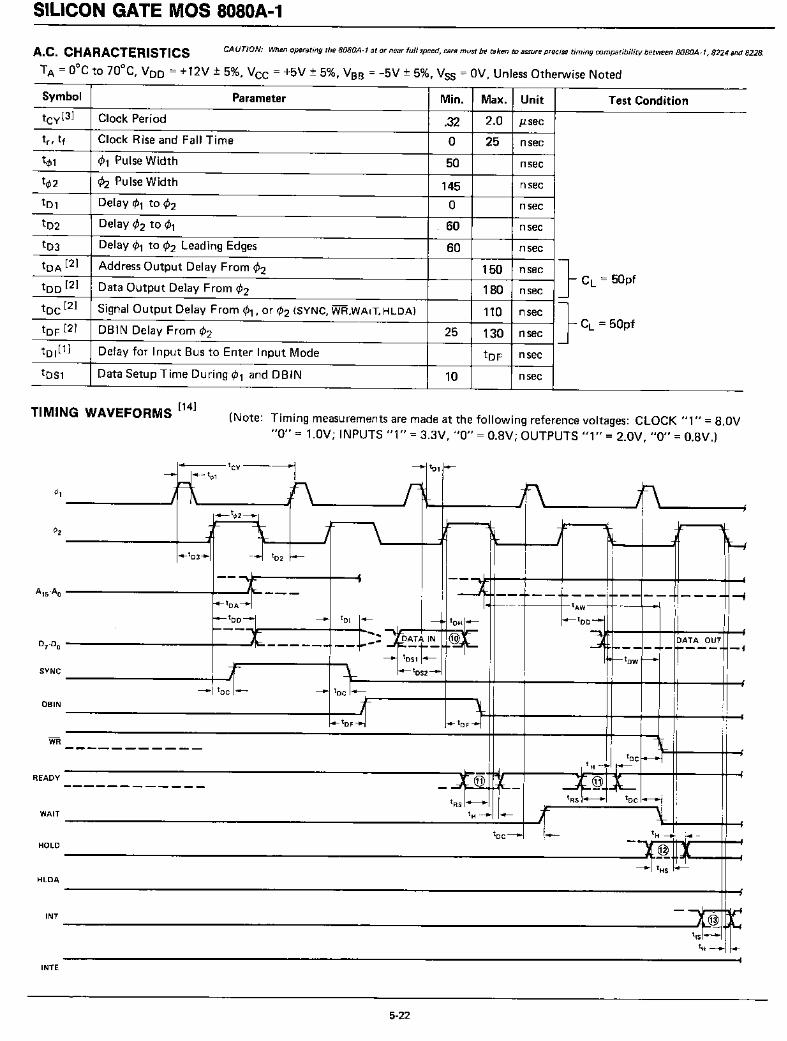
SILICON GATE MOS 8080A-1
A.c. CHARACTERISTICS CA UTlON: When operating the 8080A·l at or near full speed, care must be taken to assure precise timing compatibility between 8080A·', 8224 and 8228.
TA =O°C to 70°C, Voo =+12V ± 5%, VCC =+5V ± 5%, VSS =-5V ± 5%, VSS =OV, Unless Otherwise Noted
Symbol Parameter Min. Max. Unit Test Condition
tCy[3] Clock Period .32 2.0 J.1sec
t r , tf Clock Rise and Fall Time 0 25 nsec
t4»1 ¢1 Pulse Width 50 nsec
t4»2 ~ Pulse Width 145 nsec
t01 Delay cfJ1 to cfJ2 0 nsec
t02 Delay ¢2 to cfJ1 60 nsec
t03 Delay ¢, to ¢2 Leading Edges 60 nsec
tOA [2] Address Output Delay From ¢2 150 nsec } Cl = 50pftoo [2] Data Output Delay From ¢2 180 nsec
toc[2] Signal Output Delay From ¢" or cfJ2 (SYNC, WR.WAIT, HLOA) 110 nsec }Cl=50pftOF [2] DBIN Delay From ¢2 25 130 nsec
tOI[1] Delay for Input Bus to Enter Input Mode tOF nsec
tOS1 Data Setup Time During cfJ1 and DBIN 10 nsec
TIMING WAVEFORMS [14] (Note: Timing measurements are made at the following reference voltages: CLOCK 111" = 8.0V110" = 1.0V; INPUTS 111" = 3.3V, 1'0" = 0.8V; OUTPUTS "1" = 2.0V, "0" = O.8V.)
SYNC
DBIN
READY
WAIT
HOLD
HLDA
INT
INTE
. t CY ~I---.
~11----.Fft~l
I f\ r~ Jf\ }F\~t~2~1
-~ }~ 1~~~ -~ ..Jjl- .....,J- 1
-J ~k- I ~ "1 ~...t03"'! -.\ t02 ~
--~. -=1.
i4-- t OA-'\- ---1--- ~--- ------ ---- --f
I tAW
i4---too~1 -... t OI 1'- --t toHI'- ~tOO-"
~ r -~ .J+:..... H" DATA OUT.,._ .JrPATA IN,- -- ~-t- 1----- - 10---- -I
-... tOS1 ...- I-f--tow~
T -i- ..... toS2 .....
---. toc 1.-. .-. tocl.-
-r t~tOF:.I ... t OF
----------- ~l
toc .-.-.\L-,
I t H -ij r----_...._------~- -r@ t ~~ I-tRSI- 'RS toe -'-{ I
t H -. .- TI~
It oc ---' _ t H -.1 1.-
!@ IX~r~:~
- L
!@ ~
tiS1== ~~
tH -... ...
5-22

SILICON GATE MOS 8080A-1
A.C. CHARACTERISTICS (Continued)
TA =O°C to 70°C, Voo =+12V ± 5%, Vee = +5V ± 5%, Vss = -5V ± 5%, Vss = OV, Unless Otherwise Noted
Symbol Parameter Min. Max. Unit Test Condition
tOS2 Data Setup Time to ¢2 During DBIN 120 nsec
tOH [1] Data Hold Time From ¢2 During DBIN [1] nsec
tiE [2] INTE Output Delay From ¢2 200 nsec CL = 50pf
tRS READY Setup Time During ¢2 90 nsec
tHS HOLD Setup Time to ¢2 120 nsec
tiS INT Setup Time During ¢2 (During <t>1 in Halt Mode) 100 nsec
tH Hold Time From ¢2 (REAOY, INT, HOLD) 0 nsec
tFO Delay to Float During Hold (Address and Oata Sus) 120 nsec
tAW [2] Address Stable Prior to WR........,
[5] nsec
tOW[2] Output Data Stable Prior to WR [6] nsec
two [2] Output Data Stable From WR [7] nsec
tWA [2] Address Stable From WR [7] nsec ~ CL = 50pf: Address, DataCL=50pf: WR, HLDA, DBIN
tHF[2] H LDA to Float Delay [8] nsec
tWF[2] WR to Float Delay [9] nsec
tAH [2] Address Hold Time After DBIN During HLDA -20 nsec -NOTES:
1. Data input should be enabled with OBIN status. No bus conflict can then occur and data hold time is assured.tOH :::: 50 ns or tOF, whichever is less.
2. Load Circuit.
+5V9
+100
2.1K
+50
~ CAPACITANCE (pf)
(CACTUAL - CSPEC )
o-50
.5-> +10~...JW0~ 0::::>Q.
~::::> -100-1
3. tCY:::: t03 + t nt>2 + t4>2 + tf4>2 + t02 + t r4>1 ;> 320ns.
8080AOUTPUT
TYPICAL!:J. OUTPUT DELAY VS. ~ CAPACITANCE+20 r-------.-----------r---- -----,
A1S -AO ~
twA
0 7 -00 I- -two
SYNC
oBIN
WR
toc
READY
WAIT
HOLD I-
HLoA
INT
INTE
---. toc .--
4. The following are relevant when interfacing the 8080A to devices having VIH :::: 3.3V:a) Maximum output rise time from .8V to 3.3V = 1OOns @ CL =SPEC.b) Output delay when measured to 3.0V =SPEC +60ns @ CL =SPEC.c) If CL :f. SPEC, add .6ns/pF if CL> CSPEC, subtract .3ns/pF (from modified delay) if CL < CSPEC.
5. tAW:::: 2 tCY -t03 -tnt>2 -110nsec.6. tOW:::: tCY -t03 -tr</>2 -150nsec.7. If not HLDA, tWO:::: tWA:::: t03 + t r<P2 +10ns. If HLOA, tWO:::: twA :::: tWF.
8. t HF :::: t03 + t r<P2 -50ns.9. tWF = t03 + t r4>2 -10ns
10. Data in must be stable for this period during DB IN ·T3. Both tOS1 and tOS2 must be satisfied.11. Ready signal must be stable for this period during T2 or TW. (Must be externally synchronized.)12. Hold signal must be stable for this period during T2 or TW when entering hold mode, and during T3, T4, TS
and TWH when in hold mode. (External synchronization is not required.)13. Interrupt signal must be stable during this period of the last clock cycle of any instruction in order to be
recognized on the following instruction. (External synchronization is not requiredJ14. This timing diagram shows timing relationships only; it does not represent any s~ific machine cycle.
5-23

infel® Silicon Gate MOS 8080A-2SINGLE CHIP a-BIT N-CHANNEL MICROPROCESSOR
• TTL Drive Capability
• 1.5 J.Ls Instruction Cycle
• Powerful Problem SolvingInstruction Set
• Six General Purpose Registersand an Accumulator
• Sixteen Bit Program Counter forDirectly Addressing up to 64K Bytesof Memory
• Sixteen Bit Stack Pointer and StackManipulation Instructions for RapidSwitching of ~he Program Environment
• Decimal,Binary and DoublePrecision Arithmetic
• Ability to Provide Priority VectoredInterrupts
• 512 Directly Addressed 1/0 Ports
The Intel® aOaOA is a complete a-bit parallel central processing unit (CPU). It is fabricated on a single LSI chip using Intel'sn-channel silicon gate MOS process. This offers the user a high performance solution to control and processing appli"cations.The aOaOA contains six a-bit general purpose working registers and an accumulator. The six general purpose registers may beaddressed individually or in pairs providing both single and double precision operators. Arithmetic and logical instructions setor reset four testable flags. A fifth flag provides decimal arithmetic operation.The aOaOA has an external stack feature wherein any portion of memory may be used as a last in/first out stack to store/retrieve the contents of the accumulator, flags, program counter and all of the six general purpose registers. The sixteen bitstack pointer controls the addressing of this external stack. This stack gives the aOaOA the ability to easily handle multiplelevel priority interrupts by rapidly storing and restoring processor status. It also provides almost unlimited subroutine nesting.This microprocessor has been designed to simplify systems design. Separate 16-line address and a-line bi-directional databusses are used to facilitate easy interface to memory and I/O. Signals to control the interface to memory and I/O are provided directly by the aOaOA. Ultimate control of the address and data busses resides with the HOLD signal. It provides theability to suspend processor operation and force the address and data busses into a high impedance state. This permits ORtying these busses with other controlling devices for (DMA) direct memory access or mUlti-processor operation.
5-24

SILICON GATE MOS 8080A-2
ABSOLUTE MAXIMUM RATINGS·
Temperature Under Bias O°C to +70° CStorage Temperatu re .. . . . . . . . . . . . .. _65° C to + 150°C
All Input or Output VoltagesWith Respect to Vas -0.3V to +20V
Vee, Voo and Vss With Respect to Vss -0.3V to +20VPower Dissipation . . . . .. 1.5W
*COMMENT: Stresses above those listed under "Absolute Maximum Ratings" may cause permanent damage to the device.This is a stress rating only and functional operation of the device at these or any other conditions above those indicated inthe operational sections of this specification is not implied. Exposure to absolute maximum rating conditions for extendedperiods may affect device reliability.
D.C. CHARACTERISTICSTA = O°C to 70°C, VOO =+12V ± 5%, VCC = +5V ± 5%, Vas = -5V ± 5%, Vss = OV, Unless Otherwise Noted.
Symbol Parameter Min. Typ. Max. Unit Test Condition
VILC Clock Input Low Voltage Vss-l Vss+0.8 V
V,HC Clock Input High Voltage 9.0 Voo+l V
V,L Input Low Voltage Vss-l Vss+0.8 V
V,H Input High Voltage 3.3 Vee+ 1 V
VOL Output Low Voltage 0.45 V } IOL = 1.9mA on all outputs,
VO H Output High Voltage 3.7 V IOH = 150tlA.
100 (AV) Avg. Power Supply Current (Voo ) 40 70 mA
lee (AV) Avg. Power Supply Current (Vcc ) 60 80 mA} Operation
TCy = .38J,Lsec'ss (AV) Avg. Power Supply Current (Vss ) .01 1 mA
IlL Input Leakage ±10 J1A Vss ~ VIN ~ Vec
ICl Clock Leakage ±10 J1A Vss ~ VeLocK ~ Voo
lol[2] Data Bus Leakage in Input Mode -100 J1A VSS~VIN ~VsS+O.8V-2.0 mA
Vss+O.8V~VIN~Vee
IFlAddress and Data Bus Leakage +10
J1AVAOOR/OATA = Vec
During HOLD -100 VAOOR/OATA = VSS + O.45V
CAPACITANCETA = 25°C Vec = Voo = VSS = OV, VBS = -5V
Symbol Parameter Typ. Max. Unit Test Condition
Cq, Clock Capacitance 17 25 pf fc = 1 MHz
C,N Input Capacitance 6 10 pf Unmeasured Pins
COUT Output Capacitance 10 20 pf Returned to Vss
NOTES:
1. The RESET signal must be active for a minimum of 3 clock cycles.2. When oBIN is high and V,N > VIH an internal active pull up will
be switched onto the Data Bus.3. AI supply / ATA =-O.45%f C.
TYPICAL SUPPLY CURRENT VS.TEMPERATURE, NORMALIZED.[3]
1.5,.....-----r-----or----_
toZwa::a:::>(J 1.0 r------""""=-~---+__--~>..JQ"Q"
:>(I)
0.50-----+
2.1-.5----+5"'-0---......J+
75
AMBIENT TEMPERATURE (OC)
DATA BUS CHARACTERISTICDURING DBIN
MAX
5-25
°o~--""""'-----_----3llo--
Vee

SILICON GATE MOS 8080A-2
A.C. CHARACTERISTICSTA = O°C to 70°C, Vee = +12V ± 5%, VCC = +5V ± 5%, Vss = -5V ± 5%, Vss = OV, Unless Otherwise Noted
Symbol Parameter Min. Max. Unit Test Condition
tCy[31 Clock Period .38 2.0 /lsec
t r , tf Clock Rise and Fall Time 0 50 nsec
t¢1 (j>1 Pulse Width 60 nsec
!¢2 l/>2 Pulse Width 175 nsec
t01 Delay (j>1 to (j>2 0 nsec
t02 Delay <P2 to <P1 70 nsec
t03 Delay ~ to (j>2 Leading Edges 70 nsec
tOA [2] Address Output Delay From (j>2 175 nsec } CL = 100pftoo [2] Data Output Delay From (j>2 200 nsec
toc [2] Signal Output Delay From ¢1, or (/>2 (SYNC, WR,WAIT, HLOA) 120 nsec }CL=50pftOF [2] DSIN Delay From lP2 25 140 nsec
tOI[1] Delay for Input Bus to Enter Input Mode tOF nsec
tOS1 Data Setup Time During lP1 and DBIN 20 nsec
TIMING WAVEFORMS [14] (Note: Timing measurements are made at the following reference voltages: CLOCK "1" = 8.0V"0" = 1.0V; INPUTS "1" = 3.3V, "0" = 0.8V; OUTPUTS "1" = 2.0V, "0" = 0.8V.)
'II t CY -I -. to, ~--.ift.,
~1 J f\ r~ }\ 71\-4- t<t>2----'1
4~ }~ ~ .... -ll ~J- ~I- -
""<1>2 ~r- J ~ i ~H
...to3~1 --.1 t02 .-
-- ---- ------ ---- ~tAW--++---~·1
f4--tOO-'
) ~A!.A_O~T _,
iIIf-- t ow ,---.
-=t ---..
-. t oc 1.- ~ toc I-+--t-1P--------+~\1
OBIN /I-\-------------------+----11 ......---+o-----++---+--+--++----t+"--t~tDF-.1
SYNC---------......."""1
--"iA 1S-Ao---------........--lr------
~tOA~
..-too-'I ~ to! \.- ---l toHI"'-~ -~ IJ.....-......---H--.~...-.x= 1-........ ~,...OATA IN @I
0 7.00 ---------oo+---....."rl-.... ------ --,... ....... .J~-t-- , .....~ tos1 1.-
~ ~tOS2-'
READY -X@ t-;:r...WAIT tH_--.__~_;__...lIl
t oc --. 1..- tH -.1 1.-HOLD .-X@ IX
-----------------------------------------.......tr~; ....I~..,..I~- ..........
HLOA -------------------------------------------,t"-f_~LI~-"""""Ij,..
INT ~-----------------_-:-'Xr~ ~tt,s!=-=tH~ ...
INTE
5-26

SILICON GATE MOS 8080A-2
A.C. CHARACTERISTICS (Continued)
TA = O°C to 70°C, VOD = +12V ± 5%, Vee = +5V ± 5%, VBB = -5V ± 5%, Vss = OV, Unless Otherwise Noted
Symbol Parameter Min. Max. Unit Test Condition
tOS2 Data Setup Time to <P2 During DBIN 130 nsec
toH [1] Data Hold Time From </>2 During DBIN [1] nsec
tiE [2] INTE Output Delay From <P2 200 nsec CL = 50pf
tRS READY Setup Time During <P2 90 nsec
tHS HOLD Setup Time to ep2 120 nsec
tiS INT Setup Time During cfJ2 (During <1>1 in Halt Mode) 100 nsec
tH Hold Time From ep2 (READY, INT, HOLD) 0 nsec
tFD Delay to Float During Hold (Address and Data Bus) 120 nsec
tAW [2] Address Stable Prior to WR-
[5] nsec
tow [2] Output Data Stable Prior to WR [6] nsec
tWD[2] Output Data Stable From WR [7] nsec
tWA [2] Address Stable From WR [7] nsec CL= 100pf: Address, Data- --CL=50pf: WR, HLDA, DBIN
tHF[2] HLDA to Float Delay [8] nsec
tWF[2] WR to Float Delay [9] nsec
tAH[2] Address Hold Time After DBIN During HLDA -20 nsec -
+5V
TYPICAL ~ OUTPUT DELAY VS. ~ CAPACITANCE+20,....----.....-------,------y------.
+100
2.1K
+50
~ CAPACITANCE (pf)
(CACTUAL - CSPEC )
o-50
.=.> +10«-Jw0t- O:::>Q..t-:::> -100<1
3. tCY = t03 + t r4>2 + t4>2 + tf4>2 + t02 + t r4>1 ~ 380ns.
8080AOUTPUT
NOTES:1. Data input should be enabled with DBIN status. No bus conflict can then occur and data hold time is assured.
tOH = 50 ns or tOF. whichever is less.2. Load Circuit.
t/),
A'S-AO to-tWA
0 7 -00,. -
two
SYNC
DBIN
WR
t oc
READY
WAIT
HOLD I-
HLDA
INT
INTE I
-... t oc .-
4. The following are relevant when interfacing the 8080A to devices having V,H = 3.3V:a) Maximum output rise time from .8V to 3.3V = 100ns @ CL = SPEC.b) Output delay when measured to 3.0V = SPEC +60ns @ CL = SPEC.c) If CL #: SPEC, add .6ns/pF if CL> CSPEC, subtract .3ns/pF (from modified delay) if CL < CSPEC.
5. tAW = 2 tCY -t03 -tr</>2 -130nsec. .6. tow = tCY -t03 -tr4>2 -170n5ec.7. If not HLOA, two =twA = tD3 + t r</>2 +10n5. If HLDA, two = twA = tWF.8. t HF = t03 + t r4>2 -SOns.9. twF = t03 + t rcf)2 -10ns
10. Data in must be stable for this period during DBIN °T3. Both tOS1 and tOS2 must be satisfied.11. Ready signal must be stable for this period during T2 or TW. (Must be externally synchronized.)12. Hold signal must be stable for this period during T2 or TW when entering hold mode, and during T3, T4, T5
and TWH when in hold mode. (External synchronization is not required.)13. Interrupt signal must be uable during this period of the last clock cycle of any instruction in order to be
recognized on the followi,1g instruction. (External synchronization is not required.)14. This timing diagram shows timing relationships only; it does not represent any s~ific machine cycle.
5-27


intel®. Silicon Gate MOS M8080A
SINGLE CHIP 8-BIT N-CHANNEL MICROPROCESSOR
• Full Military Temperature Range-55°C to +125°C
• ±10% Power Supply Tolerance
• 2 J-Ls Instruction Cycle• Powerful Problem Solving
Instruction Set
• Six General Purpose Registersand an Accumulator
• Sixteen Bit Program Counter forDirectly Addressing up to 64K Bytesof Memory
• Sixteen Bit Stack Pointer and StackManipulation Instructions for RapidSwitching of the Program Environment
• Decimal,Binary and DoublePrecision Arithmetic
• Ability to Provide Priority VectoredInterrupts
• 512 Directly Addressed I/O Ports
• TTL Drive Capability
The Intel® MaOaOA is a complete a-bit parallel central processing unit (CPU). It is fabricated on a single LSI chip using Intel'sn-channel silicon gate MaS process. This offers the user a high performance solution to control and processing applications.The MaOaOA contains six a-bit general purpose working registers and an accumulator. The six general purpose registers may beaddressed individually or in pairs providing both single and double precision operators. Arithmetic and logical instructions setor reset four testable flags. A fifth flag provides decimal arithmetic operation.The MaOaOA has an external stack feature wherein any portion of memory may be used as a last in/first out stack to store/retrieve the contents of the accumulator, flags, program counter and all of the six general purpose registers. The sixteen bitstack pointer controls the addressing of this external stack. This stack gives the MaOaOA the ability to easily handle multiplelevel priority interrupts by rapidly storing and restoring processor status. It also provides almost unlimited subroutine nesting.
This microprocessor has been designed to simplify systems design. Separate l6-line address and a-line bi-directional databusses are used to facilitate easy interface to memory and I/O. Signals to control the interface to memory and I/O are provided directly by the MaOaOA. Ultimate control of the address and data busses resides with the HOLD signal. It provides theability to suspend processor operation and force the address and data busses into a high impedance state. This permits ORtying these busses with other controlling devices for (DMA) direct memory access or mUlti-processor operation.
5-29

SILICON GATE MOS M8080A
INSTRUCTION SET
The accumulator group instructions include arithmetic andlogical operators with direct, indirect, and immediate addressing modes.
Move, load, and store instruction groups provide the abilityto move either 8 or 16 bits of data between memory, thesix working registers and the accumulator using direct, indirect, and immediate addressing modes.
The abil ity to branch to different portions of the programis provided with jump, jump conditional, and computedjumps. Also the ability to call to and return from subroutines is provided both conditionally and unconditionally.The RESTART (or single byte call instruction) is useful forinterrupt vector operation.
Double precision operators such as stack manipulation anddouble add instructions extend both the arithmetic andinterrupt handling capability of the MaOaOA. The ability to
increment and decrement memory, the six general registersand the accumulator is provided as well as extended increment and decrement instructions to operate on the registerpairs and stack pointer. Further capability is provided bythe ability to rotate the accumulator left or right throughor arou nd the carry bit.
Input and output may be accomplished using memory ad- .dresses as I/O ports or the directly addressed I/O providedfor in the MaOaOA instruction set.
The following special instruction group completes theMa080A instruction set: the NOP instruction, HALT to stopprocessor execution and the DAA instructions provide decimal arithmetic capability. STC allows the carry flag to be directly set, and the CMC instruction allows it to be complemented. CMA complements the contents of the accumulatorand XCHG exchanges the contents of two 16-bit registerpairs directly.
Data and Instruction Formats
Data in the M80aOA is stored in the form of 8-bit binary integers. All data transfers to the system data bus will be in thesame format.
ID 7 D6 Ds D4 D3 D2 D1 Dol
DATA WORD
The program instructions may be one, two, or three bytes in length. Multiple byte instructions must be storedin successive words in program memory. The instruction formats then depend on the particu lar operationexecuted.
One Byte Instructions TYPICAL INSTRUCTIONS
I0 7 06 05 0 4 03 02 OLDOJ OPCOOE Register to regist~r, memory refer-ence, arithmetic or logical, rotate,return, push, pop, enable or disableInterrupt instructions
Two Byte Instru·ctions
1 0 7 D6 D5 D4 D3 D2 D, DO I OP CODE
10 7 D6 D5 D4 D3 D2 D1 DO I OPERAND Immediate mode or I/O instructions
Three Byte Instructions
1 0 7 D6 Os 04 03 D2 0 1 DO I OP CODE Jump, call or direct load and store
1 0 7 DO I LOW ADDRESS OR OPERAND 1instructions
D6 Os 04 0 3 O2 D1
10 7 D6 Ds 04 D3 D2 0 1 DO I HIGH ADDRESSOR OPERAND 2
For the M80aOA a logic "1" is defined as a high level and a logic "0" is defined as a low level.
5-30

SILICON GATE MOS M8080A
INSTRUCTION SET
Summary of Processor Instructions
Instruction Code (1) Clock (21 Instruction Code [n Clock (2)
Mnemonic Description 07 06 Os 04 03 02 0, Do Cycles Mnemonic Description 07 06 Os 04 03 02 01 00 Cycles
MOV r1 ,r2 Move register to register 0 1 0 0 0 S S S 5 RZ Return on zero 1 1 0 0 1 0 0 0 5/11MOV M,r Move register to memory 0 1 1 1 0 S S S 7 RNZ Return on no zero 1 1 0 0 0 0 C 0 5/11MOVr,M Move memory to register 0 1 0 0 0 1 1 0 7 RP Return on positive 1 1 1 1 0 0 0 0 5/11HlT Halt 0 1 1 1 0 1 1 0 7 RM Return on minus 1 1 1 1 1 0 0 0 5/11MVIr Move immediate register 0 0 0 0 0 1 1 0 7 RPE Return on parity even 1 1 1 0 1 0 0 0 5/11MVIM Move immediate memory 0 0 1 1 0 1 1 0 10 RPO Return on parity odd 1 1 1 0 0 0 0 0 5/11INR r Increment register 0 0 0 0 0 1 0 0 5 RST Restart 1 1 A A A 1 1 1 11OCR r Decrement register 0 0 0 0 0 1 0 1 5 IN Input 1 1 0 1 1 0 1 1 10INR M Increment memory 0 0 1 1 0 1 0 0 10 OUT Output 1 1 0 1 0 0 1 1 10OCR M Decrement memory 0 0 1 1 0 1 0 1 10 LXI B Load Immediate register 0 0 0 0 0 0 0 1 10ADO r Add register to A 1 0 0 0 0 S S S 4 Pair B& CADC r Add register to Awith carry 1 0 0 0 1 S S S 4 LXI 0 Load immediate register 0 10SUB r Subtract register from A 1 0 0 1 0 S S S 4 Pair 0 & ESBB r Subtract register from A 1 0 0 1 1 S S S 4 LXI H Load immediate register 10
with borrow Pair H & LANA r And register with A 0 1 0 0 S S S 4 LXISP Load immediate stack pointer 0 0 10XRA r Exclusive Or register with A 0 1 0 1 S S S 4 PUSH B Push register Pair B& C on 0 0 11ORA r Or register with A 0 1 1 0 S S S 4 stackCMPr Compare register with A 0 1 1 1 S S S 4 PUSH 0 Push register Pair 0 & E on 11ADD M Add memory to A 0 0 0 0 1 1 0 7 stackAOC M Add memory to A with carry 0 0 0 1 1 1 0 7 PUSH H Push register Pair H& Lon 11SUB M Subtract memory from A 0 0 1 0 1 1 0 7 stackSBB M Subtract memory from A 0 0 1 1 1 1 0 7 PUSH PSW Push A and Flags 0 0 11
with borrow on stackANAM And memory with A 0 1 0 0 POP B Pop register pair B& C off 0 10XRA M Exclusive ar memory with A 0 1 0 0 stackORA M Or memory with A 0 1 1 0 POP 0 Pop register pair 0 & E off 10CMPM Compare memory with A 0 1 1 0 stackADI Add immediate to A 1 0 0 0 POP H Pop register pair H& L off 10ACI Add immediate to A with 1 0 0 0 stack
carry POP PSW Pop A and Flags 10SUI Subtract immediate from A off stackSBI Subtract immediate from A STA Store A direct 0 0 0 13
with borrow LOA Load A direct 0 0 0 13ANI And immediate with A 0 0 XCHG Exchange 0 & E, H& L 1 0 1 4XRI Exclusive Or immediate with 0 0 Registers
A XTHL Exchange top of stack, H& L 1 1 1 0 0 0 1 1 18ORI Or immediate with A 1 1 1 1 0 7 SPHL H& L to stack pointer 1 1 1 1 1 0 0 1 5CPI Compare immediate with A 1 1 1 1 1 7 PCHL H& L to program counter 1 1 1 0 1 0 0 1 5RLC Rotate A left 0 0 0 0 0 4 DAD B Add B& Cto H& L 0 0 0 0 1 0 0 1 10RRC Rotate A right 0 0 0 0 1 4 DAD 0 Add 0 & E to H& L 0 0 0 1 1 0 0 1 10RAL Rotate A left through carry 0 0 0 1 0 4 DAD H Add H& L to H& L 0 0 1 0 1 0 0 1 10RAR Rotate A right through 0 0 0 1 1 4 DAD SP Add stack pointer to H& l 0 0 1 1 1 0 0 1 10
carry STAX B Store A indirect 0 0 0 0 0 0 1 0 7JMP Jump unconditional 0 0 0 0 1 1 10 STAX 0 Store A indirect 0 0 0 1 0 0 1 0 7JC Jump on carry 0 1 1 0 1 0 10 LOAX B Load A indirect 0 0 0 0 1 0 1 0 7JNC Jump on no carry 0 1 0 0 1 0 10 LOAX 0 Load A indirect 0 0 0 1 1 0 1 0 7JZ Jump on zero 0 0 1 0 1 0 10 INX B Increment B& Cregisters 0 0 0 0 0 0 1 1 5JNZ Jump on no zero 0 0 0 0 1 0 10 INX 0 Increment 0 & E registers 0 0 0 1 0 0 1 1 5JP Jump on positive 1 1 0 0 1 0 10 INX H Increment H& L registers 0 0 1 0 0 0 1 1 5JM Jump on minus 1 1 1 0 1 0 10 INX SP Increment stack pointer 0 0 1 1 0 0 1 1 5JPE Jump on parity even 1 0 1 0 1 0 10 OCX B Decrement B& C 0 0 0 0 1 0 1 1 5JPO Jump on parity odd 1 0 0 0 1 0 10 OCX 0 Decrement 0 & E 0 0 0 1 1 0 1 1 5CALL Call unconditional 0 0 1 1 0 1 17 OCX H Decrement H& L 0 0 1 0 1 0 1 1 5CC Call on carry 0 1 1 1 0 0 11/17 OCX SP Decrement stack pointer 0 0 1 1 1 0 1 1 5CNC Call on no carry 0 1 0 1 0 0 11/17 CMA Complement A 0 0 1 0 1 1 1 1 4CZ Call on zero 0 0 1 1 0 0 11/17 STC Set carry 0 0 1 1 0 1 1 1 4CNZ Call on no zero 0 0 0 1 0 0 11/17 CMC Complement carry 0 0 1 1 1 1 1 1 4CP Call on positive 1 1 0 1 0 0 11/17 OAA Decimal adjust A 0 0 1 0 0 1 1 1 4CM Call on minus 1 1 1 1 0 0 11/17 SHLD Store H& l direct 0 0 1 0 0 0 1 0 16CPE Call on parity even 1 0 1 1 0 0 llf17 LHlO Load H& L direct 0 0 1 0 1 0 1 0 16CPO Call on parity odd 1 0 0 1 0 0 l1f17 EI Enable Interrupts 1 1 1 1 1 0 1 1 4RET Return 0 0 1 0 0 1 10 01 Disable interrupt 1 1 1 1 0 0 1 1 4RC Return on carry 0 1 1 0 0 0 5/11 NOP No-operation 0 0 0 0 0 0 0 0 4RNC Return on no carry 0 1 0 0 0 0 5/11
NOTES: 1. DOD or SSS - 000 B - 001 C - 010 0 - 011 E - 100 H - 101 L - 110 Memory - 111 A.2. Two possible cycle times, (5/11) indicate instruction cycles dependent on condition flags.

SILICON GATE MOS M8080A
M8080A FUNCTIONAL PIN DEFINITION
The following describes the function of all of the M8080A I/Opi ns. Several of the descriptions refer to internal tim ing periods.
A15-AO (output' three~state)
ADDRESS BUS; the address bus provides the address to memory(up to 64K 8-bit words) or denotes the I/O device number for upto 256 input and 256 output devices. Ao is the least significantaddress bit.
07 -Do (input/output three-state)
DATA BUS; the data bus provides bi-directional communicationbetween the CPU, memory, and I/O devices for instructions anddata transfers. Also, during the first clock cycle of each machinecycle, the M8080A outputs a status word on the data bus that de-
scribes the current machine cycle. Do is the least significant bit.
SYNC (output)SYNCHRONIZING SIGNAL; the SYNC pin provides a signal toindicate the beginning of each machine cycle.
DBIN (output)
DATA BUS IN; the DBIN signal indicates to external circuits that
the data bus is in the input mode. This signal should be used toenable the gating of data onto the M8080A data bus from memory
or I/O.
READY (input)
READY; the READY signal indicates to the M8080A that validmemory or input data is available on the M8080A data bus. Thissignal is used to synchronize the CPU with slower memory or I/Odevices. If after sending an address out the M8080A does not receive a READY input, the M8080A will enter a WAIT state for aslong as the READY line is low. READY can also be used to single
step the CPU.
WAIT (output)
WAIT; the WAIT signal acknowledges that the CPU is in a WAIT
state.
WR (output)WRITE; the WR signal is used for memory WRITE or I/O outputcontrol. The data on the data bus is stable while the WR signal isactive low (WR = 0).
HOLD (input)
HO LD; the HO LD signal requests the CPU to enter the HO LDstate. The HO LD state allows an external device to gain controlof the M8080A address and data bus as soon as the M8080A hascompleted its use of these buses for the current machine cycle. It
is recognized under the following conditions:• the CPU is in the HALT state.• the CPU is in the T2 or TW state and the READY signal is active.As a result of entering the HOLD state the CPU ADDRESS BUS(A 15 -Ao ) and DATA BUS (0 7-00 ) will be in their high impedancestate. The CPU acknowledges its state with the HOLD AC
KNOWLEDGE (HLDA) pin.
HLDA (output)HOLD ACKNOWLEDGE; the HLDA signal appears in response
to the HOLD signal and indicates that the data and address bus
1 40 All2 39 A14
3 38 A13
4 37 A12
5 36 o A1S
6 35 o Ag
7 34 As8 INTE~ 33 o A7
9M8080A
32 A6
10 31 As11 30 o A4
12 29 A313 28 +12V
14 27 A2
15 26 Al16 25 Ao17 24 WAIT
WR 18 23 READY
SYNC 19 22 ¢l+5V 20 21 HLDA
Pin Configuration
will go to the high impedance state. The HLOA signal begins at:
• T3 for READ memory or input.• The Clock Period following T3 for WR ITE memory or OUT
PUT operation.
In either case, the HLOA signal appears after the rising edge of (/)1
and high impedance occurs after the rising edge of (/)2.
INTE (output)INTE RRUPT ENAB LE; indicates the content of the internal inter
rupt enable flip/flop. This flip/flop may be set or reset by the Enable and Disable Interrupt instructions and inhibits interruptsfrom being accepted by the CPU when it is reset. It is automatically reset (disabling further interrupts) at time T 1 of the in-struction fetch cycle (M 1) when an interrupt is accepted and is
also reset by the RESET signal.
INT (input)INTERRUPT REQUEST; the CPU recognizes an interrupt request on this line at the end of the current instruction or whilehalted. If the CPU is in the HOLD state or if the Interrupt Enableflip/flop is reset it will not honor the request.
RESET (input) [1]
RESET; while the RESET signal is activated, the content of theprogram counter is cleared. After RESET, the program will startat location 0 in memory. The INTE and HLDA flip/flops are alsoreset. Note that the flags, accumulator, stack pointer, and registers
are not cleared.
Vss Ground ReferenceVee +12 Volts ±10%.Vee +5 Volts ±10%.Vss -5 Volts ±10%.
¢1, ¢2 2 externally supplied clock phases. (non TTL compatible)
5-32

SILICON GATE MOS M8080A
ABSOLUTE MAXIMUM RATINGS*
Temperature Under Bias -55°C to +125°CStorage T emperatu re .. . . . . . . . . . . . . . _65° C to +150°C
All Input or Output VoltagesWith Respect to VBB -0.3V to +20V
Vcc, Voo and Vss With Respect to VBB -0.3V to +20VPower Dissipation . . . . . . . . . . . .. 1.7W
*COMMENT: Stresses above those listed under "Absolute Maximum Ratings" may cause permanent damage to the device.This is a stress rating only and functional operation of the device at these or any other conditions above those indicated inthe operational sections of this specification is not implied. Exposure to absolute maximum rating conditions for extendedperiods may affect device reliability.
D.C. CHARACTERISTICSTA = -55°C to +125°C, VOD = +12V ±10%, Vee = +5V ±10%, VBB = -5V ±10%, Vss = OV, Unless Otherwise Noted.
Symbol Parameter Min. Typ. Max. Unit Test Condition
VILC Clock Input Low Voltage Vss-l Vss+0.8 V
VIHC Clock Input High Voltage 8.5 Voo+1 V
VIL Input Low Voltage Vss-l Vss+0.8 V
VIH Input High Voltage 3.0 Vcc+1 V
VOL Output Low Voltage 0.45 V } IOL = 1.9mA on all outputs,
VO H Output High Voltage 3.7 V IOH = 150J-lA.
IOD(AV) Avg. Power Supply Current (Voo ) 50 80 rnA
ICC (AV) Avg. Power Supply Current (Vec) 60 100 mA} Operation
TCy = .48 J.1.secIBB(AV) Avg. Power Supply Current (VBB ) .01 1 mA
IlL Input Leakage ±10 J1A Vss ~ VIN ~ VccICL Clock Leakage ±10 J1A Vss ~ VCLOCK ~ VDD
IDL [2] Data Bus Leakage in Input Mode -100 J1A VSS ~VIN ~VSS +O.~V-2.0 rnA
VSS +0.8V~VIN ~VCC
IFLAddress and Data Bus Leakage +10
J1AVADDR/DATA = VCC
During HOLD -100 VADDR/DATA = Vss + O.45V
+125
AMBIENT TEMPERATURE rc)
+50-55
TYPICAL SUPPLY CURRENT VS.TEMPERATURE, NORMALIZEO.l3]
1.5,.....------r-----------,
I2~ 1.0 J---------:::::l~I------______Ia::::>u>...J8: 0.5 t------J-------______I
:::>en
Symbol Parameter Typ. Max. Unit Test Condition
C¢ Clock Capacitance 17 25 pf fc = 1 MHz
CIN Input Capacitance 6 10 pf Unmeasured Pins
COUT Output Capacitance 10 20 pf Returned to Vss
NOTES:
1. The RESET signal must be active for a minimum of 3 clock cycles.2. When DBIN is high and VIN > VIH an internal active pull up will
be switched onto the Oata Bus.3. ~ I supply / ~TA = -0.45%/ C.
CAPACITANCETA = 25°C Vec = VOD = Vss = OV, VBB =-5V
DATA BUS CHARACTERISTICDURING DBIN
MAX
°0"----------------------30--Vee

SILICON GATE MOS M8080A
A.C. CHARACTERISTICS (Continued)
TA = -55°C to +125°C, VOO =+12V ±10%, Vee =+5V ±10%, VBB = -5V ±10%, Vss = OV, Unless Otherwise Noted.
Symbol Parameter Min. Max. Unit Test Condition
tOS2 Data Setup Time to ¢2 During DBIN 130 nsee
tOH [1] Data Hold Time From ¢2 During DBIN 50 nsee
tiE (2) INTE Output Delay From ¢2 200 nsee CL = 50pf
tRS READY Setup Time During ¢2 120 nsee
tHS HOLD Setup Time to ¢2 140 nsee
tiS INT Setup Time During ¢2 (During 4>1 in Halt Mode) 120 nsee
tH Hold Time From ¢2 (READY, INT, HOLD) 0 nsee
tFD Delay to Float During Hold (Address and Data Bus) 130 nsee
tAW [2] Address Stable Prior to WR -[5] nsee
tDW[2] Output Data Stable Prior to WR [6] nsee
tWD[2] Output Data Stable From WR [7] nsee
tWA [2] Address Stable From WR [7] nsee ~ CL =50pf
tHF[2] H LOA to Float Delay [8] nsee
tWF[2] WR to Float Delay [9] nsee
tAH [2] Address Hold Time After DBIN During HLDA -20 nsee-
NOTES:1. Data input should be enabled with OBIN status. No bus conflict can then occur and data hold time is assured.
tOH = 50 ns or tOF, whichever is less.2. Load Circuit.
+5V
8080AOUTPUT
3. tey = t03 + t rq,2 + tq,2 + tfq,2 + tD2 + t rq,l ~ 480ns.
+100+50
~ CAPAC IT ANCE (pf)
(CACTUAL - CSPEC )
o-50
oS> +10«..Jw0.... 0:::JQ.....:::J -100-1
-20-100
TYPICAL ~ OUTPUT DELAY VS. ~ CAPACITANCE+20r-----~---~---_---_
..........~--- .......-----..... ---
DBIN
SYNC
READY
WAIT
HOLD fa-
HLDA
INT
INTE
~ t oe '-
4. The following are relevant when interfacing the M8080A to devices having VI H = 3.3V:
a) Maximum output r'ise time from .8V to 3.3V = lOOns @ CL = SPEC.b) Output delay when measured to 3.0V = SPEC +60n5 @ CL = SPEC.d If CL * SPEC, add .6ns/pF if CL> CSPEC, subtract .3n5/pF (from modified delay) if CL < CSPEC.
5. tAW = 2 tey -t03 -trct>2 -140nsec.6. tow =tCY -t03 -trep2 -170nsec.7. If not HLOA, two =tWA = t03 + t r¢2 +10ns. If HLOA, two = tWA = tWF·
8. t HF = t03 + t rq,2 -50ns.9. tWF = tD3 + t r<t>2 -10ns
10. Data in must be stable for this period during DBIN ·T3. Both tOS1 and tOS2 must be satisfied.11. Ready signal must be stable for this perio~ during T2 or TW. (Must be externally synchronized.)12. Hold signal must be stable for this period during T 2 or TW when entering hold mode, and during T3, T4, T 5
and TWH when in hold mode. (External synchronization is not required.~
13. Interrupt signal must be stable during this period of the last clock cycle of any instruction in order to berecognized on the following instruction. (External synchronization is not required.)
14. This timing diagram shows timing relationships only; it does not represent any specific machine cycle.
5-34

SILICON GATE MOS M8080A
A.C. CHARACTERISTICSTA =-55°C to +125°C, Voo =+12V ±10%, Vee =+5V ±10%, VBB = -5V ±10%, Vss = OV, Unless Otherwise Noted.
Symbol Parameter Min. Max. Unit Test Condition
tCy[3] Clock Period 0.48 2.0 Jisec
t r , tf Clock Rise and Fall Time 0 50 nsec
t(/>l epl Pulse Width 60 nsec
tep2 cI>2 Pulse Width 220 nsec
t01 Delay epl to 4>2 0 nsec
t02 Delay ~2 to ~1 80 nsec
t03 Delay ~1 to ~2 Leading Edges 80 nsec-
tOA [2) Address Output Delay From ~2 200 nsec
too [2] Data Output Delay From ~2 220 nsec
toc [2] Signal Output Delay From ~1, or ~2 (SYNC, WR,WAIT,HLDA) 140 nsec
tOF [2] DBIN Delay From ep2 25 150- CL =50pf
nsec-
tOI[l) Delay for Input Bus to Enter Input Mode tOF nsec
tOSl Data Setup Time During ~1 and DBIN 30 nsec
TIMING WAVEFORMS [14] (Note: Timing measurements are made at the following reference voltages: CLOCK "1" = 7.0V,"0" = 1.0V; INPUTS "1" = 3.0V, "0" = 0.8V; OUTPUTS "1" = 2.0V, "0" = 0.8V.)
SYNC
DBIN
READY
WAIT
HOLD
HLDA
INT
INTE
.. ·tey -\--.
1
01 1---.F\I
01I f\ r~ t\ Jf\
...-to2-"1....,~
7~ ~~~
I~~ r- ..,
-J ~ ..... ~ r.... t o3 .....! --.1 t02 .--
. I--x . -=1 ~~- --- -- ~--- ~----- ----...-tOA-'! --~tAW
.--too--'I -. to! 1'- --t t oHI4-- f.--tOO-' iI... r _I
)__+:=: J~~A I~ ~DATA OUT------
- 'osl1=-1~-- -- - ----- -f
..~tow ~i !
T -\- ..- tOS2-' i-. toc 14- --. tocl..- I
~ t I~toF-.1 .... toF~1 !
~tI
-~~-------- toc~IL
,tHil'-
------------ ~@ r - &~~I I I-- IRS""':' loe -I ItRsl~
t H --. .--
1- litoc -"'" _ t H -.; 1·-
I@ I~
--.r~;I~
-I~[I-
~~
tH~ ....
5-35


8702A87048708
ROMs
83028308
8316A


Silicon Gate MOS 8702A
2048 BIT ERASABLE AND ELECTRICALLYREPROGRAMMABLE READ ONLY MEMORY
• Inputs and Outputs TTL Compatible
• Three-State Output - OR-TieCapability
• Simple Memory Expansion ChipSelect Input Lead
• Access Time -1.3 ~secMax.
• Fast Programming - 2 Minutes forAll 2048 Bits
• Fully Decoded, 256 x 8 Organization• Static MOS - No Clocks Required
The 8702A is a 256 word by 8 bit electrically programmable ROM ideally suited for microcomputer systemdevelopment where fast turn-around and pattern experimentation are important. The 8702A undergoescomplete programming and functional testing on each bit position prior to shipment, thus insuring 100%programmability.
The 8702A is packaged in a 24 pin dual-in line package with a transparent quartz lid. The transparent quartzlid allows the user to expose the chip to ultraviolet light to erase the bit pattern. A new pattern can then bewritten into the device. This procedure can be repeated as many times as required.
The circuitry of the 8702A is entirely static; no clocks are required.
A pin-for-pin metal mask programmed ROM, the Intel 8302, is ideal for large volume production runs ~f
systems initially using the 8702A.
The 8702A is fabricated with silicon gate technology. This low threshold technology allows the design andproduction of higher performance MOS circuits and provides a higher functional density on a monolithicchip than conventional MOS technologies.
PIN CONFIGURATION BLOCK DIAGRAM
OUTPUTBUFFERS
2048 BITPROM MATRIX
(256 X 8)
DATA OUT 1 DATA OUT 8
PROGRAM ........
A2 Voo
A, Vee
Ao Vee
*DATA OUT 1 A3
*DATA OUT 2 A4
*DATA OUT 3 As
*DATA OUT 4 A6
*DATA OUT 5 A7
*DATA OUT 6 9 16 VGG
*DATA OUT 7 10 15 Vee
*DATA OUT 8 11 (MSB) 14 CS
Vee 12 13 PROGRAM
*THIS PIN IS THE DATA INPUT LEAD DURING PROGRAMMING.
PIN NAMES
Ao-A7 ADDRESS INPUTS
CS CHIP SELECT INPUT
001- 002 DATA OUTPUTS
5-37

SILICON GATE MOS 8702A
PIN CONNECTIONS
The external lead connections to the 8702A differ, depending on whether the device is being programmed (1) or used in read.
mode. (See following table.)
12 13 14 15 16 22 23MODE . (Vee) (Program) (CS)· (VBB ) (VGG ) (Vee) (Vee)
Read Vee Vee GND Vee VGG Vee Vee
Programming GND Program Pulse GND Vee Pulsed VGG (V, L4P ) GND GND
ABSOLUTE MAXIMUM RATINGS·
Ambient Temperature Under Bias OOC to +700C
Storage Temperature -65°C to +125 0 C
Soldering Temperature of Leads (10 sec) . . . . . . .. +300oC
Power Dissipation 2 WattsRead Operation: Input Voltages and Supply
Voltages with respect to Vee +0.5V to -20V
Program Operation: Input Voltages and Supply
Voltages with respect to Vee -48V
*COMMENT
Stresses above those listed under"Absolute Maximum Ratings" may cause permanent damage to the device. This is astress rating only and functional operation of the device atthese or at any other condition above those indicated inthe operational sections of this specification is not implied.Exposure to Absolute Maximum Rating conditions for extended periods may affect device rei iabil ity.
READ OPERATION
D.C. AND OPERATING CHARACTERISTICS. (2) .
TA =aoc to 70oC, Vee =+5V±5%, Voo =-9V±5%, VGG =-9V±5%, unless otherwise noted.
SYMBOL TEST MIN. TypJ3) MAX. UNIT CONDITIONS
III Address and Ch ip Select 10 fJA VIN = O.OV
Input Load Current
IlO Output Leakage Current 10 JJA-
VOUT = O.OV, CS = Vee -2
1000 Power Supply Current 5 10 mA VGG=Vee,CS=Vee-210l= O.OmA, T A = 2Soc
1001 Power Supply Current 35 SO mA CS=Vcc -2 ""'"
10l =O.OmA, TA = 2SoC
1002 Power Supply Current 32 46 mA CS=O.O
10l =O.OmA, TA = 2SoC> Continuous
1003 Power Supply Current 38.5 60 mA CS=Vec -2
10l =O.OmA , T A = OOCOperation
leF1 Output Clamp Current 8 14 mA VOUT = -l.QV, T A = OOC
leF2 Output Clamp Current 13 mA VOUT = -1.0V, TA
= 2SoC~
IGG Gate Supply Current 10 fJA
V,l1 Input Low Voltage for -1.0 0.65 V
n L Interface
V1L2 Input Low Voltage for Voo Vec-6 VMOS Interface
V1H Address and Chip Select Vcc -2 Vee +0.3 V
Input High Voltage
IOl Output Sink Current 1.6 4 mA VOUT = 0.45V
VOL Output Low Voltage -.7 0.45 V IOl = 1.6mA
VOH Output High Voltage 3.5 V IOH = -2001lA
Note 1: In the programming mode, the data inputs 1-8 are pins 4-11 respectively. es = GN O.Note 2: VGG may be clocked to reduce power dissipation. In this mode average 100 increases in proportion to VGG duty cycle. (See p. 5)
Note 3: Typical values are at nominal voltages and TA = 250
C.
5-38

SILICON GATE MOS 8702A
A.C. CHARACTERISTICS
TA =00 C to +70°C, Vcc =+5V ±5%, Voo = -9V ±5%, VGG =-9V ±5% unless otherwise noted
SYMBOL TEST MINIMUM TYPICAL MAXIMUM UNIT
Freq. Repetition Rate 1 MHz
tOH Previous read data val id 100 ns
tAcc Address to output delay 1.3 p.s
t ovGG Clocked VGG set up [2] 1.0 JlS
t es Chip select delay 400 ns
teo Output delay from CS 900 ns
too Output deselect 400 ns
tOHC Data out hold in clocked VGG mode (Note 1) 5 JlS
Note 1. The output will remain valid for tOHe as long as clocked VGG is at Vee. An address change may occur as soon as the output is sensed
(clocked VGG may still be at Vee). Data becomes invalid for the old address when clocked VGG is returned to VGG.
2. For this option please specify 8702AL
CAPACITANCE*
SYMBOL TEST MINIMUM TYPICAL MAXIMUM UNIT CONDITIONS
C1N Input Capacitance 8 15 pF '1N= Vee } AllCOUT Output Capacitance 10 15 pF CS = Vce unused pins
CVGG
VGG Capacitance 30 pFVOUT = Vee are at A.C.
(Clocked VGG Mode)VGG = Vce ground
~ This parameter is periodically sampled and is not 100% tested.
~~Ons
L·'·';I I
I
\--
- ---:
I
tOD~
~50ns
I
NOTE 2 -,
,,,r---;;......---7
DATAOUT
B) Clocked VGG Operation'- CYCLE: TIME - 1 FREO ~
VIHXI,0"lo xlADDRESS ~ I
._ 90% • •V1L I------------..J I~---
I 1
Cs' VIH \1
11 :I---~Ons_____'
I
V1L \1--------11-----------I I.- t
DV:
Vcc\~ : GG JCLOCKED "I /:V
GGVee; I: : (SEE NOTE 11
r---- tACC ----i -I ~. 'OHC
I II II I
DATA ~~~: \ {'
:.- tACC ---\VOl~• ..J
NOTE 1: The output will remain valid tor tOHe as long as clocked VGGis at Vee. An address change may occur as soon as the output is sensed(clocked VGG may still be at Vee!. Data becomes invalid for the oldaddress when clocked VGG is returned to VGG'
~OTE 2: It CS makes a transition from VI L to VIH while clocked VGGIS at VGG. then deselection of output occurs at too as shown in staticoperation with constant VGG.
V,Hv: DESELECTIDN OF DATA OUTPUT IN DR·TlE OPERATION
ADDRESS .AV1L 1-----------------
II
CS V
,H
'\
V1L I
~~t
VCC,\': DV
GG
CLOCKED :: /VGG I
VGG I"tl------JIII
VOH 7DATA l
OUT
I
V1H
){~10%--XIADDRESS I
~ 90%V1l I.....------------J, .......----
----I t cs ~ I_ V1H ill t-- toH--1
cs I I ':
V1l : IIII,
CYCLE TIME I/F REO
V1H ---f 10%
csV1l
I
VOH ---fe' I - too -I VDATA I
OUT I
VOL I
-l teo f-
Conditions of Test:Input pulse amplitudes: 0 to 4V; t R ' t F ::; 50 ns .Output load is 1 TTL gate; measurements made
at output of TTL gate (tpD ~ 15 ns)
A) Constant VGG
Operation
SWITCHING CHARACTERISTICS
5-39

SILICON GATE MOS 8702A
TYPICAL CHARACTERISTICS
'00 CURRENT VS. TEMPERATUREOUTPUT CURRENT VS.VDO SUPPLY VOLTAGE
OUTPUT CURRENT VS.TEMPERATURE
I'\ Vee = +5V
-r\ v oo = -9V
-r\ \ Vaa = -9V
'\ INPUTS" Vee-
I\.
\ f'\ OUTPUTS ARE OPENI I I
I" '" I~ NS=Vee
I" I" I- --~'l
CS = 0.0V'-~
I--~
I_. - .~
AMBIENT TEMPERATURE (OCI
39
38
37
36
35
1 34
~ 33
~ 32=>u 31o
_0 30
29
28
27
20 40 60 80 100 120
VCC '" +5V
VGG '" -9V ---b,......:::=I===:t__F=l~--1
VOLT A
~! -5 -6 -7 -8I- Voo SUPPLY VOLTAGE (V)~ -3 I I
~ VCC = +SV
a VGG '" -9V -I-~~iii'it---I-----j~ VOH '" O.OV
=> TA '" 25°C~ -3.5 t--+-~ -+-_~M--+----i
I-
~l=>o
%2-4L-_"""'--_.........._ ............_ .........._----'__L.-----'
~!I-
ffia:a:=>u~
zenl-
i:...:;)0~
.P
~!I-
ffia:a:=>u.wu -3a:=>0enl-
i:...=>0
%_0 -4
I I ,~
Vee" +5V
~~Voo:l -9V
Vaa:l -9V
"~VOL" +.45V-..-
cs=o.~t'-..... .............I II do0 10 20 30 50 60 70 80 90IAjBIENT TEMPERATURE (oCI
IVee' +5V IVoo =-9V I
I--- I- Vaa = -9V
VOH = O.OV
~--~~I---I---~ rr
OUTPUT SINK CURRENTVS. OUTPUT VOLTAGE
! ! I I II I-Li CLOCKED VGG
., -9V I I'" -9V -i.-I Voo[ ~1.--""~I cs '" V1H
T 4 '" 25°C.--V~ I
~".,.-
iI -' I
~ ............ ............ I if-~ I !
II-V i
V ~ I~ r ,
I----: ! i
10090807040 50 60
DUTY CYCLE 1%)
30
AVERAGE CURRENT VS. DUTYCYCLE FOR CLOCKED VGG
2010o
o+3 +4+1 +2
45~ VCC '" +5V! 12.0 40... VDD '" -9V
~ VGG '" -9V 1001 35a: 10.0a: TA '" 25°C ~=> ! 30u I
f--:ll: 8.0 025Z ..Fen CS '" O.OV w
- I-6.0 C) 20
~c(
ffi=> > 150 c(
10
'000 5
OUTPUT VOLTAGE (VOL TS)
-2 -1-3-4
ACCESS TIME VS.LOAD CAPACITANCE
ACCESS TIME VS.TEMPERATURE
1400 ----.,..-.,.----.,..-~--r--r---r--r-__r____, 1400 ---.--..----.--..----r--r--,--r---r----,
1300 ~-I--~_l_-~_+_-f--_+___If----+-___i 1300 ~--+--+-__+_-t-__+_-t--t--+---+----t
1200 ~--+--f--__+_-f--_+_-f----+-__If----+---i 1200 ~-4--.j-~-.j_~-t---+--+----t-----1
800 ~-+~I---+-____4--+-
500 I---I--~-l--~_+_-t--__+_-f---t-___i
1100 '----+--.j--+-+--~-+---t--+---+-----i
c: 1000L---L-L-~~~~~r::+=r--+----1
1 TTL LOAD::. 20 pf
700 I---t--+--+--t- Vee = +5V
600 ...--t--+---t--t- Vee = -9VVGG = -9V
500 ~-+--+--+--~__+_-f---t--t---+----t
1100 ~-4--.j-~-+---+--t---+--+----t-----1c: _.....-~~.....-~~ 1000 ~-;.-~=f--+---+--+---+---t---t----1:E~ 900 ~-+----f---t--+---t--+--_t_-t---t----tCI.l
~u 800 ~~-+---4--+--~-+---+--+---t-----tU«
1 TTL LOAD -f
Vee = +5V700 ~-4---11---+----+--+--V
oo= -9V - f-
6001---4----+--+---+--t- VGG = -9V --TA = 25°C
w:E~ 900 I---I--~_l_-~_l_-~__+_-f--_t____i
~wUUc(
00 10 20 30 40 50 60 70 80 90 100
LOAD CAPACITANCE (pF)
10 20 30 40 50 60 70 80 90
AMBIENT TEMPERATURE rc)
5·40

SILICON GATE MOS 8702A
PROGRAMMING OPERATION
D.C. AND OPERATING CHARACTERISTICS FOR PROGRAMMING OPERATION
TA = 25°C, Vee = OV, Vss = +12V ± 10%, CS = OV unless otherwise noted
SYMBOL TEST MIN. TYP. MAX. UNIT CONDITIONS
ILl1 P Address and Data Input 10 rnA VIN = -48VLoad Current
'LI2P Program and VG G 10 rnA VIN = -48VLoad Current
'ss Vss Supply Load Current .05 rnAIOOp(l) Peak 100 Supply 200 mA Voo = Vpro,7 -48V
Load Current VGG = -35VIHP Input High Voltage 0.3 VVIL1P Pulsed Data Input -46 -48 V
Low VoltageV1L2P Address Input Low -40 -48 V
VoltageVIL3P Pulsed Input Low Voo -46 -48 V
and Program VoltageVIL4P Pulsed Input Low -35 -40 V
VGG
Voltage
Note 1: lOOp flows only during VOO, VGG on time. lOOp should not be allowed to exceed 300mA for greater than 100~sec. Average powersupply current lOOp is typically 40 mA at 20% duty cycle.
A.C. CHARACTERISTICS FOR PROGRAMMING OPERATION
TAMSIENT = 25°C, Vee = OV, Vss = + 12V ± 10%, CS = OV unless otherwise noted
SYMBOL TEST MIN. TYP. MAX. UNIT CONDITIONS
Duty Cycle (Voo , VGG ) 20 %
t~pw Program Pulse Width 3 ms VGG = -35V, Voo =Vprog =-48V
tow Data Set Up Time 25 IlS
tOH Data Hold Time 10 IlS
tvw Voo , VGG Set Up 100 IlS
tvo Voo , VGG Hold 10 100 J.1S
tACW (2) Address Complement 25 IlSSet Up
tACH (2) Address Complement 25 J.1SHold
tATW Address True Set Up 10 J.1S
tATH Address True Hold 10 J.1S
Note 2. All 8 address bits must be in the complement state when pulsed Vee and VGG move to their negative levels. The addresses (0 through255) must be programmed as shown in the timing diagram for a minimum of 32 times.
5-41

SILICON GATE MOS 8702A
SWITCHING CHARACTERISTICS FOR PROGRAMMING OPERATION
PROGRAM OPERATION
Conditions of Test:
Input pulse rise and fall times :s 1J1sec
CS = OV
PROGRAM WAVEFORMS
BINARY ADDRESSOF WORD TO BE
PROGRAMMED
II I I
I ~tvoiI~ f--tATW
---.l tACH r--I I I
tACW----.l', I I
BINARY COMPLEMENT OFADDRESS OF WORD
TO BE PROGRAMMED
o------------~
o
ADDRESS
-40 to -48
-46 to-48
PULSED VooPOWER SUPPLY
0------------""'"PULSED VGG
POWER SUPPLY
-35 to-40
o--------------~
PROGRAMMINGPULSE
-46 to-48
oDATA INPUT
(DEVICEOUTPUT
LINES)--46 to -48
I II I1-tATH-----"1II
I I II I I
--'ltOHr-I
DATA STABLETIME
PROGRAMMING OPERATION OF THE 8702A
ADDRESS
When the Data Input for Then the Data Output WORD A7 A6 AS A4 A3 A2 A1 AOthe Program Mode is: during the Read Mode is:
0 0 0 0 0 0 0 0 0
V,L,P = ""-48V pulsed Logic 1 = VOH = 'P' on tape 1 0 0 0 0 0 0 0 1
I I I I I I I I II I I I I I I I I
VIHP;: "" OV Logic 0 = VOL ='N' on tape255 1 1 1 1 1 1
Address Logic Level During Read Mode: Logic 0 = VIL ("" .3V) Logic 1 = V,H ( "" 3V)
Address Logic Level During Program Mode: Logic 0 = V IL2P ( "" -40V) Logic 1 = V, HP (-- OV)
5-42
SILICON GATE MOS 8702A
PROGRAMMING INSTRUCTIONSFOR THE 8702A
I. Operation of the 8702A inProgram ModeInitially, all 2048 bits of the ROM are inthe "0" state (output low). Informationis introduced by se\ectively programming "1 "s (output high) in the properbit locations.
Word address selection is done by thesame decoding circuitry used in theREAD mode (see table on page 6 forlogic levels). All 8 address bits must bein the binary complement state whenpulsed VDD and VGG move to their negative levels. The addresses must be heldin their binary complement state for aminimum of 25 p'sec after VDD and VGG
have moved to their negative levels.The addresses must then make thetransition to their true state a minimumof 10 p'sec before the program pulseis applied. The addresses should beprogrammed in the sequenc~ 0 through255 for a minimum of 32 times. Theeight output terminals are used as datainputs to determine the informationpattern in the eight bits of each word.A low data input level (- 48V) will program a "1" and a high data input level(ground) will leave a "0" (see table onpage 6). All eight bits of one word areprogrammed simultaneously by settingthe desired bit information patterns onthe data input terminals.
During the programming, VGG, VDD andthe Program Pulse are pulsed signals.
II. Programming of the 8702A UsingIntel ® MicrocomputersIntel provides low cost program development systems which may be used toprogram its electrically programmableROMs. Note that the programmingspecifications that apply to the 8702Aare identical to those for Intel's 1702A.
A. Intellec®
The Intellec series of program development systems, the Intellec8/Mod 8 and Intellec 8/Mod 80, areused as program development toolsfor the 8008 and 8080 microprocessors respectively. As such, they areequipped with a PROM programmercard and may be used to programIntel's electrically programmableand ultraviolet erasable ROMs.
An ASR-33 teletype terminal is usedas the input device. Through use ofthe InteHec software system monitor,programs to be loaded into PROMmay be typed in directly or loadedthrough the paper tape reader. Thesystem monitor allows the programto be reviewed or altered at willprior to actually programming thePROM. For more complete information on these program developmentsystems, refer to the Intel Microcomputer Catalog or the IntellecSpecifications.
B. Users of the SIM8 microcomputerprogramming systems may alsoprogram the 8702A using theMP7-03 programmer card and theappropriate control ROMs:
SIM8 system-Control ROMsA0860, A0861 and A0863.
5-43
III. 8702A Erasing ProcedureThe 8702A may be erased by expo-sure to high intensity short-wave ultraviolet light at a wavelength of 2537A.The recommended integrated dose (Le.,UV intensity x exposure time) is6W-sec/cm2• Examples of ultravioletsources which can erase the 8702Ain 10 to 20 minutes are the ModelUVS-54 and Model S-52 short-waveultraviolet lamps manufactured byUltra-Violet Products, Inc. (5114 WalnutGrove Avenue, San Gabriel, California).The lamps should be used withoutshort-wave filters, and the 8702A tobe erased should be placed about oneinch away from the lamp tubes.

· :,

Silicon Gate MOS 8708/8704
8192/4096 BIT ERASABLE AND ELECTRICALLYREPROGRAMMABLE READ ONLY MEMORY
• 8708 1024x8 Organization• 8704 512x8 Organization
• Fast Programming -Typ. 100 sec. For All 8K Bits
• Low Power During Programming• Access Time - 450 ns• Standard Power Supplies
+12V, ±5V
• Static - No Clocks Required• Inputs and Outputs TTL
Compatible During Both Readand Program Modes
• Three-State Output- OR-TieCapability
The Intel@8708/8704 are high speed 8192/4096 bit erasable and electrically reprogrammable ROM's (EPROM) ideally suited
where fast turn around and pattern experimentation are important requirements.
The 8708/8704 are packaged in a 24 pin dual-in-line package with transparent lid. The transparent lid allows the user to expose the chip to ultraviolet light to erase the bit pattern. A new pattern can then be written into the devices.
@A pin for pin mask programmed ROM, the Intel 8308, is available for large volume production runs of systems initially using
the 8708.
The 8708/8704 is fabricated with the time proven N-channel silicon gate technology.
PIN CONFIGURATIONS BLOCK DIAGRAM
Y GATING
OUTPUT BUFFERS
64 X 128ROM ARRAY
DATA OUTPUT0, Os
I
XDECODER
YDECODER
CHIP SELECTLOGICCS/WE-
AO·Ag
ADDRESSINPUTS
A7 24 Vee
A6 2 23 As
As 3 22
A4 4 21 Vea
A3 5 20 CSIWE87081
A2 6 8704 19 Voo
A1 7 18 PROGRAM
Ao 8 17 Os
01 9 16 07
02 10 15 06
03 11 14 Os
Vss 12 13 04
*8704 =Vss8708 =Ag
PIN NAMES
Ao·Ag ADDRESS INPUTS
O,·Os DATA OUTPUTS
CSIWE CHIP SElECTIWRITE ENABLE INPUT
5-45

SILICON GATE MOS 8708/8704
Absolute Maximum Ratings~·
Temperature Under Bias ,. -25°C to +85°CStorage Temperature -~5°C to +125°C
All Input or Ou'tput Voltages with Respect to VBB(except Program) . . . . . . . . . . . . . . . . . . . . . . . . . .. +15V to -0.3V
Program Input to VBB . . . . . . . . . . . . . . . . . . . . . . . . .. +35V to -O.3VSupply Voltages Vcc and Vss with Respect to VBB. . . . . .. +15V to -O.3VVoo with Respect to VBB . . . . . . . . . . . . . . . . . . . . . .. +20V to -O.3VPower Dissipation . . . . . . . . . . . . . . . . . . . . . .. 1.5W
*COMMENTStresses above those listed under "Absolute MaximumRatings" may cause permanent damage to the device.This is a stress rating only and functional operationof the device at these or any other conditions abovethose indicated in the operational sections of thisspecification is not implied. Exposure to absolutemaximum rating conditions for extended periods mayaffect device reliability·.
READ OPERATIOND.C. and Operating CharacteristicsTA =o°c to 70°C, Vee =+5V ±5%, Voo =+12V ±5%, VeB = -5V ±5%, VSS =ov, Unless Otherwise Noted.
.Symbol Parameter Min. Typ.l1] Max. Unit Conditions
III Address and Chip Select Input Load Current 10 JlA VIN = 5.25V
Ilo Output Leakage Current 10 JlA VOUT = 5.25V, CS/WE =5V
100 Voo Supply Current 50 65 mA Worst Case Supply Currents:
lee Vee Supply Current 6 10 mA All Inputs High
IBB VBe Supply Current 30 45 mA CS/WE =5V; TA = O°C
Vil Input Low Voltage Vss 0.65 V
VIH Input High Voltage 3.0 Vee+1 V
VOL Output Low Voltage 0.45 V IOl = 1.6mA
VOH1 Output High Voltage 3.7 V IOH = -100JlA
VOH2 Output High Voltage 2.4 V IOH = -1mA
Po Power Dissipation 800 mW TA = 70°C
NOTES: 1. Typical values are for TA = 2Soe and nominal supply voltages.2. The program input (Pin 18) may be tied to VSS or Vee during the read mode.
5-46

SILICON GATE MOS 8708/8704
A.C. CharacteristicsTA =O°C to 70°C, Vee =+SV ±S%, Vo o =+12V ±S%, Vee = -SV ±S%, Vss = OV, Unless Otherwise Noted.
Symbol Parameter Min. Typ. Max. Unit
tAce Address to Output Delay 280 4S0 ns
teo Chip Select to Output Delay 120 ns
tOF Chip De-Select to Output Float 0 120 ns
tOH Address to Output Hold 0 ns
Capacitance£1] TA = 2SoC, f = 1MHz
Symbol Parameter Typ. Max. Unit Conditions
CIN Input Capacitance 4 6 pF VIN=OV
COUT Output Capacitance 8 12 pF VOUT=QV
Note 1. This parameter is periodically sampled and not 100% tested.
A.C. Test Conditions:Output Load: 1 TTL gate and CL = 100pFInput Rise and Fall Times: ~20ns
Timing Measurement Reference Levels: 0.8V and 2.8V for inputs; 0.8V and 2.4V for outputsInput Pulse Levels: O.6SV to 3.0V
Waveforms
ADDRESS ----X--------------......J'IX,.,--------C.S./WE
I 1
I I~ tOH-----'1
i ~'--------------......."A iI I.--- teo ---'1 I 1~tDF---.1
14-11----t ACC _I 1
5-47

SILICON GATE MOS 8708/8704
PROGRAMMING OPERATION
DescriptionInitially, and after each erasure, all bits of the 8708/8704 are in the "1" state (Output High). Information is introduced by selectively programming "0" into the desired bit locations.
The circuit is set up for programming operation by raising the CS/WE input (Pin 20) to +12V. The word address is selected in thesame manner as in the read mode. Data to be programmed are presented, 8-bits in parallel, to the data output lines (01-08).
Logic levels for address and data lines and the supply voltages are the same as for the read mode. After address and data set upone program pulse (Vp) per address is applied to the program input (Pin 18). One pass through all addresses to be programmed isdefined as a program loop. The number of loops (N) required is a function of the program pulse width (tpw) according toN x tpw ~ 100 ms.
For program verification, program loops and read loops may be alternated as shown in waveform B.
Program CharacteristicsTA = 25°C, Vcc = +5V ±5%, Voo = +12V ±5%, Vss = -5V ±5%, Vss = OV, CS/WE = +12V, Unless Otherwise Noted.
Symbol Parameter Min. Typ. Max. Units
tAS Address Setup Time 10 llS
tcss CS/WE Setup Time 10 llS
tos Data Setup Time 10 llS
tAH Address Hold Time 1 llS
tCH CS/WE Hold Time .5 lls
tOH Data Hold Time 1 lls
tOF Chip Deselect to Output Float Delay 0 120 ns
tOPR Program To Read Delay 10 llS
tpw Program Pulse Width .1 1.0 ms
tpR Program Pulse Rise Time .5 2.0 llS
tpF Program Pulse Fall Time .5 2.0 llS
Ip Programming Current 10 20 rnA
Vp Program Pulse Amplitude 25 27 V
NOTE: Intels standard product warranty applies only to devices programmed to specifications described herein.
Erasing Procedure
The 8708/8704 may be erased by exposu re to high intensity short-wave ultraviolet Iight at a wavelength of 2537A. The recom
mended integrated dose. (Le., UV intensity x exposure time) is 10W-sec/cm2 . Examples of ultraviolet sources which can erase the8708/8704 in 20 to 30 minutes are the Model UVS-54 and Model S-52 short-wave ultraviolet lamps manufactured by Ultra-VioletProducts, Inc. (5114 Walnut Grove Avenue, San Gabriel, California). The lamps should be used without short-wave filters, and the8708/8704 to be erased should be placed about one inch away from the lamp tubes.
5-48

SILICON GATE MOS 8708/8704
Waveforms
(Logic levels and timing reference levels same as in the Read Mode unless noted otherwise.)
A) Program Mode
CS/WE = +12V
~__AD_D_R_ESS_1_....c ~_--·-·-·----.lX'---A-D-D-RE-SS-1-0-23--~ADDRESS 0
...---------------ONEPROGRAM LOOP ---------------.!I
26V
ADDRESS
DATA°1·0S
PROGRAMPULSE
OV-------II
B) Read/Program/Read Transitions
ADDRESS
~ PR~g~:M --'1
o
tess26V
PROGRAMPULSE
0--+-------"""1
DATA°1·0 S
DATA OUT DATAVALID FLOAT
DATA INVALID
DATA INVALID
DATA OUTVALID
5-49
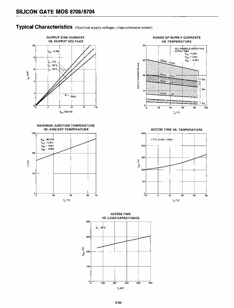
SILICON GATE MOS 8708/8704
Typical Characteristics (Nominal supply voltages unless otherwise noted):
OUTPUT SINK CURRENTVS. OUTPUT VOLTAGE
RANGE OF SUPPLY CURRENTSVS. TEMPERATURE
1008060
ALL POSSIBLE OPERATINGCONDITIONS:
Vee = 5.25VVoo =12.6V
Vaa = -5.25V
4020
pEEE]f!1EJEZPlEzz$m:=:2!:;·m··;:: }Icco'---__..I-__""'--- ...l........-_------'
o
80 .----..----,....---~--~--,
60
=i.§Cf.)...2wa:: 40a::;:)0>..J~~
;:)Cf.)
20
1.0.8.6
---SPEC
.4
TA =O°C
TA =25°C
TA =70°C ~~---#----+_'_~-+-----i
.2
Vee = 4.75V
41----t----#-i~,r;--t----+__-__i
6
81----+----t----t--~1t--~---::l~
10 r-----...----or----...----..,---,~
MAXIMUM JUNCTION TEMPERATUREVS. AMBIENT TEMPERATURE
150 r------_----..,..----,....------..
8JA =80°CIW
Vee =5.25VVoo =12.6V
Vaa =-5.25V
1001----- 4~=----+------+----i
50 t--------t-----+-----+____i
500
400
300
E.utJ
...<t
200
100
ACCESS TIME VS. TEMPERATURE
I I1 TTL LOAD + 100pF
~
~
~~
~~
80604020o-2060 704020
0'---------'----------1..----.1..------'o
ACCESS TIMEVS. LOAD CAPACITANCE
ITA =25°C
-----------
-----~~
-----So~ 200
...<t
300
400
100
oo 100 200 300 400 500
5-50

Silicon Gate MOS 8302
2048 BIT MASK PROGRAMMABLEREAD ONLY MEMORY
• Static MOS - No Clocks Required• Simple Memory Expansion - Chip
Select Input Lead• 24-Pin Dual-In-Line Hermetically
Sealed Ceramic Package
• Access Time-1 p'sec Max.• Fully Decoded, 256 x 8 Organization
• Inputs and Outputs TTL Compatible
• Three-State Output - OR-TieCapability
The Intel@8302 is a fully decoded 256 word by 8 bit metal mask ROM. It is ideal for large volume production runs of microcomputer systems initial.ly using the 8702A erasable and electrically programmable ROM.The 8302 has the same pinning as the 8702A.
The 8302 is entirely static - no clocks are required. Inputs and outputs of the 8302 are TTL compatible.The output is three-state for OR-tie capability. A separate chip select input allows easy memory expansion.The 8302 is packaged in a 24 pin dual-in-Iine hermetically sealed ceramic package.
The 8302 is fabricated with p-channel silicon gate technology. This low threshold allows the design andproduction of higher performance MOS circuits and provides a higher functional density on a monolithicchip than conventional MOS technologies.
PIN CONFIGURATION BLOCK DIAGRAM
A2 Voo DATA OUT 1 DATAOUT8
A1 2 23 Vee
es-. OUTPUTAo 3 22 Vee BUFFERS
DATA OUT 1 4 (LSB) 21 A3
DATA OUT 2 5 20 A4 2048 BITROM MATRIX
DATA OUT 3 6 19 As (256 X 8)8302
DATA OUT 4 7 18 As
DATA OUT 5 8 17 A]
DATA OUT 6 9 16 VGG
DATA OUT 7 10 15 N.C.
DATA OUT 8 11 (MSB) 14 cs
Vee 12 13 N.C.Ao A1 A]
PIN NAMES
AO' A7 ADDRESS INPUTS
CS CHIP SELECT INPUT
001· DOa DATA OUTPUTS
5-51

SILICON GATE MOS 8302
Absolute Maximum Ratings ~~
Ambient Temperature Under Bias oOc to +70oCStorage Temperature -65°C to +125 0 CSoldering Temperature of Leads (10 sec) . . . . . . .. +300oCPower Dissipation 2 WattsInput Voltages and Supply
Voltages with respect to Vcc +O.5V to -20V
*COMMENT
Stresses above those listed under IIAbsolute Maximum Ratings" may cause permanent damage to the device. This is astress rating only and functional operation of the device atthese or at any other condition above those indicated inthe operational sections of this specification is not implied.Exposure to Absolute Maximum Rating conditions for extended periods may affect device reliability.
READ OPERATIOND.C. and Operating CharacteristicsTA =DOC to 70°C, Vee =+5V±5%, Voo =-9V±5%, V6~=-9V±5%, unless otherwise noted.
SYMBOL TEST MIN. TypJ2) MAX. UNIT CONDITIONS
'll Address and Chip Select 1 JJA V,N = O.OVInput Load Current
'lO Output Leakage Current 1 J,JA VOUT = O.OV, CS = Vcc -2
'000 Power Supply Current 5 10 mA VGG=Vec,CS=Vcc-2
10l= O.OmA, TA = 25°C
1001 Power Supply Current 35 50 mA CS=Vee -2 """l
'Ol =O.OmA, TA = 25°C
'002 Power Supply Current 32 46 mA CS=O.O
'Ol =O.OmA, TA = 25°C> Continuous
'003 Power Supply Current 38.5 60 mA CS=Vec -2
'Ol =O.OmA , TA = OOCOperation
'CF1 Output Clamp Current 8 14 mA VOUT = -1.0V,TA =ooC
'CF2 Output Clamp Current 13 mA VOUT = -1.0V, T
A= 25°C
4
'GG Gate Supply Current 1 JJA
V1L1 Input Low Voltage for -1.0 0.65 VTTL Interface
V1L2 Input Low Voltage for Voo Vce -6 VMOS Interface
V ,H Address and Chip Select Vee -2 Vee +0.3 VInput High Voltage
'Ol Output Sink Current 1.6 4 mA VOUT = 0.45V
'OH Output Source Current -2.0 mA VOUT = O.OV
VOL Output Low Voltage -.7 0.45 V 'Ol = 1.6mA
VOH Output High Voltage 3.5 4.5 V 'OH = -100 fJA
Note 1. VGG may be clocked to reduce power dissipation. In this mode average 100 increases in proportion to VGG duty cycle.Note 2. Typical values are at nominal voltages and TA = 25°C.
5-52

SILICON GATE MOS 8302
A.C. CharacteristicsTA =(1J C to +70°C, Vee =+5V ±5%, Voo = -9V ±5%, VGG = -9V ±5% unless otherwise noted
SYMBOL TEST MINIMUM TYPICAL MAXIMUM UNIT
Freq. Repetition Rate 1 MHz
tOH Previous read data val id 100 ns
tACC Address to output delay .700 1 JJ.s
t ovGG Clocked VGG set up 1 JJ.s
t cs Chip select delay 200 ns
tco Output delay from CS 500 ns
too Output deselect 300 ns
t OHC Data out hold in clocked VGG mode (Note 1) 5 JJ.s
Note 1. The output will remain valid for tOHC as long as clocked VGG is at Vce. An address change may occur as soon as the output is sensed
(clocked VGG may still be at Vee). Data becomes invalid for the old address when clocked VGG is returned to VGG.
Capacitance* TA
= 25°C
SYMBOL TEST MINIMUM TYPICAL MAXIMUM UNIT CONDITIONS
C,N Input Capacitance 5 10 pF "1N= vee} AllCOUT Output Capacitance 5 10 pF CS =VCC unused pins
CVGG VGG Capacitance 30 pFVOUT =VCC are at A.C.
(Clocked VGGMode)VGG = VCC ground
*This parameter is periodically sampled and is not 100% tested.
A) Constant VGG Operation
Switching Characteristics
DATA OUTINVALID
DATA OUTINVALID
VOH-----~
DATAOUT
V,H
-v. DESELECTlDN OF DATA OUTPUT IN OR·TlE OPERATION
ADDRESS .fi.V1L 1-----------------
: NOTE 2 . _ ~ ~ ~ Ons
cs V,H~ ,',r---~----l...·......i---
'-"L I ,I I
~ "- to too --, I ~
vcc,,: : V
GG L': :CLOCKED I: III I I
VGG I I I
VGG 1-+1-----....", I II ...--~50ns---1 II I I I
V {I:DATA O~HT i-'ACC~ .
VOL ......----------1
VOL ---------r--ISr----------
NOTE 1: The output will remain valid for tOHe as long as clocked VGGis at Vee. An address change may occur as soon as the output is sensed(clocked VGG may still be at Vee). Data becomes invalid for the oldaddress when clocked VGG is returned to VGG'
NOTE 2: If CS makes a transition from VI L to VIH while clocked VGGis at VGG, then deselection of output occurs at too as shown in staticoperation with constant VGG'
B) Clocked VGG Operation~ CYCLE TIME ~ I FREO---....l
ADDRE~~H~ :: >CV1L I I
I II
VIH,,: I I
CS '\ ~~ons---{
V1L I I
_I ~tDV :.
Vee,; : GG /:..--------..\
CLOCKED '\ I / ;
VGG
VGG
I': : (SEE NOTE 1) ~---.-.- 'ACC~ --I ~ t OHC
I II II I
DATA OUTINVALID
....1·----tAcc-----·~1
V1H ---f 10%
CS
V1L1
"o~---f()1 - too ~
I UDATA IOUT I
VOL I I---l tco .-
--CYCLE TIME' I/FREO-
V ,----------_IH V 10% V
ADDRESSfi 90% AV1L 1 I ~----
--I 'cs ~ I
_ V1H n' t-- t
oH--l
cs I I I:V1L : :
I I
g~~~H --4!~--~N-~-TA-AL-~-DU-T--~\ r;-VOL t---+--
DESELECTION OF DATA OUTPUT IN OR·TlE OPERATION
AD:~:Y:: X"----VIL'~
Conditions of Test:Input pulse. amplitudes: 0 to 4V; t R , t F ~ 50 nsOutput load is 1 TTL gate; measurements made
at. output of TTL gate (tpD ::5 15 ns)
5-53

SILICON GATE MOS 8302
Typical Characteristics
100 CURRENT VS. TEMPERATUREACCESS TIME VS.
LOAD CAPACITANCEOUTPUT SINK CURRENTVS. OUTPUT VOLTAGE
I\ vee = +5V -~ v oo = -9V
-\ \ v GG = -9V
"INPUTS:: Vee
-~
\ I"OUTPUTS ARE OPEN
I I I
'\ ~ Il' NSIIVee
." '""lCS= 0.0V'
II
+1 +2 +3 +4
CiI---+---+--.! 12.0
~zau
t----+---+-- ~ 10.0::)CJ
~ 8.0en
t----+---+-- ~ 6.0~--+-~T---+-----te:;)
t----+---+-- 0
-4 -3 -2 -1
'-
1 TTL LOAD t--
Vcc =+5VI----
VOO = -9V
VGG :: -9V I--
TA ::I 250C r----
I I I
900
800
700
! 600w~ 500~
~ 400auuu 3004(
200
100
oo 10 20 30 40 50 60 70 80 90 100
LOAD CAPACITANCE (pF)
80 100 120604020o
39
38
37
36
35
i 34~ 33zauII: 32II:ju 31
0_0 30
29
28
27
AMBIENT TEMPERATURE (OC) OUTPUT VOLTAGE (VOLTSI
ACCESS TIME VS.TEMPERATURE
OUTPUT CURRENT VS.VOOSUPPLY VOLTAGE
OUTPUT CURRENT VS.TEMPERATURE
I I I~
vee· +5V
~~v oo • -9V
v GG • -9V
~~VOL· +.45V-I--
cs ..o.~~ r--......I0 10 2030 k 5060 70 80 90IAiBIENT TEMPERATURE t"CI
Vee" +5V
Voo • -9V
- -VGG - -9V
VOH " O.OV
~
~I--~
~rr- ---
;{.!~zaua:a:::)u~zen~::)~
~:J0
j
_0
Ci 0
!~zwII:a:::)UauCJ -3a:::)
S~::)~
~:J0x
_0 -4
I I
Vcc :: +5V
""" VGG = -9V ""'""
VOL :: +.45V/_ TA =.250C
- - SpecifiedOperating Range _ r--_
I I
n(I ,
-5 -6 -7 -8 -9 -10VDO SUPPLY VOLTAGE (V)
i-- I IVCC ::I +5V
VGG :: -9V
VOH ::I O.OV
TA '" 25°C
,,~
;{!~
z -3wII:II::;)UwUII::J0-3.5enI-:J~
I-:Jo
%
.9-4
10 20 30 40 50 60 70 80 90AMBI ENT TEMPERATURE (OC)
~
I---1 TTL LOAD~20pf-
Vcc II +5V -VDO .. -9V
VGG = -9V -I I
900
800
700
.: 600
w~ 500~
~ 400wuu 3004(
200
100
AVERAGE CURRENT VS. DUTYCYCLE FOR CLOCKED VGG
45
40
1001 35
C 30.!0
26_0
auCJ 204(a:w 15>4(
10
1000 5
I I I I ICLOCKED VGG :: -9V
VDD .. -9V
~----CS :: V1H ~T A .. 25°C
~~----~~.---
~~
~
--~~~
~~
---o
o 10 20 30 40 50 60
DUTY CYCLE (%)
70 80 90 100
5-54

Silicon Gate MOS 8308
8192 BIT STATIC MOS READ ONLY MEMORYOrganization --1024 Words x 8 Bits
• Fast Access - 450 ns
• Directly Compatible with 8080 CPUat Maximl)m Processor Speed
• Two Chip Select Inputs for EasyMemory Expansion
• Directly TTL Compatible - All Inputsand Outputs
• Three State Output - OR-Ti~
Capability
• ·Fully Decoded
• Standard Power Supplies+12V DC, ±5V DC
The Intel® 8308 is an 8,192 bit static MOS mask prog~ammable Read Only Memory organized as 1024 words by ~-bi~s. ThisROM is designed for 8080 microcomputer system applications where high performance, large bit storage, and simple interfacing are important design objectives. The inputs and outputs are fully TTL compatible.
A pin for pin compatible electrically programmed erasable ROM, the Intel® 8708, is available for system development andsmall quantity production use.
Two Chip Selects are provided - CS1 which is negative true, and CS2/CS2 which may be programmed either negative orpositive true at the mask level.
The 8308 read only memory is fabricated with N-channel silicon gate technology. This technology provides the designer withhigh performance, easy-to-use MOS circuits.
PIN CONFIGURATION BLOCK DIAGRAM
DATA OUT 1 DATA OUT 8A7 Vee
A6 As CS1--'OUTPUT
A5 Ag CS2/CS2. -...BUFFERS
A4 Va8
A3 CSl 811)2 BITROM MATRIX
A2 \bo (1024 X 8)
A, CS2/CS2
Ao Os
0, 07
02 06
03 05
Vss 04Ao A, Ag
PIN NAMES
AO-Ag ADDR ESS INPUTS
o,-Os DATA OUTPUTS
CS,. CS2 CHIP SELECT INPUTS
5-55

SILICON GATE MOS 8308
Absolute Maximum Ratings*Ambient Temperature Under Bias -25°C to +85°CStorage Temperature -65°·C to-i-150°CVoltage On Any Pin With Respect
To Vaa . . . . . . . . . . . . . . . . . -0..3V to 20VPower Dissipation 1.0 Watt
*COMMENTStresses above those listed under"Absolute Maximum Ratings" maycause permanent damage to the device. This is a stress rating onlyand functional operation of the device at these or any other conditions above those indicated in' the operational sections of this specification is not implied. Exposure to absolute maximum rating conditions for extended periods may affect device reliabil ity.
D.C. and Operating CharacteristicsTA =O°C to +70°C, VCC =5V ±5%; Voo = 12V ±5%, Vas =-5V ±5%, Vss =OV Unless Otherwise Specified.
LimitsSymbol Parameter
TypJ1]Unit Test Conditions
Min. Max.
ILl Input Load Current 10 J.l.A VIN = 0 to 5.25V-(All Input Pins Except CS, )
ILCL Input Load Current on CS, 1.6 rnA VIN = 0.45V
ILPC Input Peak Load Current on CS, 4 rnA VIN =0.8V to 3.3V
ILKC Input Leakage Current on CS, 10 J.l.A VIN =3.3V to 5.25V
ILO Output Leakage Current 10 J.l.A Chip Deselected
VIL Input "Low" Voltage Vss-1 0.8V V
VIH Input "H igh" Voltage 3.3 Vcc+1.0 V
VOL Output "Low" Voltage 0.45 V IOL = 2rnA
VOH' Output "High" Voltage 2.4 V IOH = -4rnA
VOH2 Output "High" Voltage 3.7 V IOH = -1rnA
Icc Power ~upplV Current Vcc .8 2 rnA
100 Power Supply Current Voo 32 60 rnA
Iss Power Supply Current Vss 10~A 1 rnA
Po Power Dissipation 775 rnW
NOTE 1: Typical values for TA = 25° C and nominal supply voltage
D.C. OUTPUT CHARACTERISTICS D.C. OUTPUT CHARACTERISTICS
2.4 2.6 2.8 3.0 3.2 3.4 3.6 3.8 4 0 .2
VOH VOLTS
'lil~, I IIt = Oto 70°C,A I I1',
'I',I I
TYPICAL
" ",'lIlI
/~~SPEf ~
~Ill..-........~ ,....."
(( 4-1
-3
-2
-8
-9
-10
-7
1-6~-5
-4
~A ::: 6to 76°C,
~
/~
~I,TYPICAL J
'('~
/~~
/
~J ~V
~
~ V ~ .........
'"I ~ SPEC
~V Ioo .1 .2 .3 .4 .5 .6 .7 .8 .9 1.0
VOL VOLTS
2
8
3
7
9
6
1 5
.1J 4
5-56

SILICON GATE MOS 8308- -
A.C. CharacteristicsTA = oo.c to'+70~C, VCC = +5V ±5%; VO_D = +12V ±5%, VBB = -5V _±5%, VSS_= OV, Unless Otherwise Specif.i~d.
Limits[2]Symbol Parameter Unit
Min. Typ. Max.
tACC Address to Output Delay Time 200- 450 ns
tC01 Chip Select 1 to Output Dela.y~ime 85 160 ns
teo 2 Chip Select 2 to O~tputDelay Time 125 220 ns
Chip Deselect to Output Data float Ti~_e_ 125 220.-
tOF ns
NOTE 2: Refer to conditions~of Test for A.C. Characteristics. ~dd 50 nanoseconds (worst case) to specified values atVOH =3.7V @ IOH =-1mA, CL =100pF.
CONDITIONS OF TEST FORA.C. CHARACTERISTICS
CAP~CI_!ANCE TA_=__~5°C, f= 1 MHz! VBB =-5V, VOO,.
Vcc and all ot~er pins ti~~ ~o Vss.
Output Load 1 TTL Gate, and CLOAO = 100pFInput Pulse Levels . . . . . . . . . . . . . . . .. .65V to 3.3VInput Pulse Rise and Fall Times 20 nsecTiming Measurement Reference Level
........ · .... · .. · .. 2.4V VIH, VOH; 0.8V VIL, VOL
LimitsSymbol Test
Typ. Max.
CIN Input Capacitance 6pF
CoUT Output C~pacitance 12pF
�4-------- tACC --------~I
----------~ADDRESS
.Ao-Ag
--------------------- --------------1..----tCo1----·1
~----------------1....-------te02------...1
---------------,
5-57

SILICON GATE MOS 8308
Typical Characteristics (Nominal supply voltages unless .otherwise noted.)
100 VS. TE""PERATURE(NORMALIZED)
A OUTPUT CAPACITANCEVS. A OUTPUT DELAY
+100+50o-50
-40 L..-__...I..-__...Io....-__.......I.-__--'
-100
+40 r-----~--_r__--~---,
~ CAPACITANCE (pF)
_ +20 t----+-----+----~<------fuW(I)
..5-
~.J~ 0 t---:---+-------:::._--""'"'"f--t::J~
t::Jo<1 -20 ~--+_--_+__----+---__t
10 20 30 40 50 60 70 80 90
AMBIENT TEMPERATURE TA (OC)
~~~
"-~~
~
::::;~
.7
.8
.9
.6
1.1
1.0
1.2
1.4
CS1 INPUTCHARACTERISTICS
TACC VS. TEMPERATURE.(NORIVIALIZ~O)
~~
~
~~
---~
.-:::i:::::=oo 10 20 30 40 50 60 70 80 90
AMBIENT TEMPERATURE TA (OC)
.6
.7
.8
.9
1.4
1.1
1.2
1.3
1.0
1.0 1.5 2.0 2.5 3.0
V1N (VOLTS)
.5
)/1~/ \
/ \\...o
o
.5
1.0
2.5
2.0
2.5
~.§ 1.5
-~
5-58

MCS™CUSTOM ROMORDER FORM
8308ROM
APp _
S# _
STO _
CUSTOMER _
P.O. NUMBER . _
OATE _
For Intel use only
PPpp---------
zz, _
00 _
OATE . _
All custom 8308 ROM orders must be submitted on this form. Programming information should be sent in the form of computerpunched cards or punched paper tape per the formats designated on this order form. Additional forms are available from Intel.
MARKING
®The marking as shown at the right must contain the Intel logo, theproduct type (P8308), the 4-digit Intel pattern number (PPPP), a datecode (XXXX), and the 2-digit chip number (DO). An optional customeridentification number may be substituted for the ch ip number (ZZ).Optional Customer Number (maximum 9 characters or spaces).CUSTOMER NUMBER _
MASK OPTION SPECIFICATIONS
• 8308I xxxx
DATE CODE
PPPP
zz
INTEL PATTERN NUMBER
CHIP NUMBER ORCUSTOMER NUMBER
A. CHIP NUMBER (CHIP SELECTOPTION)
Must be specified 0 or 1.
The chip number will be coded interms of positive logic where a logic"1" is high level input.
Chip Select Truth Table
ChipNumber CS1 CS2 Selected
0 0 0 Yes1 0 1 Yes0 1 0 No1 1 1 No
Chip Number
B. ROM Truth Table Format
Programming information should besent in the form of computer punchedcards or punched paper tape. Ineithercase, a printout of the truth tableshould be accompanied with the order.
The following general format is applicable to the programming informationsent to Intel:
• Data fields should be ordered beginning with the least significant address(0000) and ending with the most sig.nificant address (1023).
• A data field should start with themost significant bit and end with theleast significant bit.
5-59
• The data field should consist of P'sand N's. A P is to indicate a high leveloutput (most positive) and an N a lowlevel output (most negative). In termsof positive logic, a P is defined as alogic "1" and an N is defined as a iogic"0". If the programming informationis sent on a punched paper tape, thena start character, B, and an end character, F, must be used in the data field.See paragraph 2.
1. Punched Card FormatAn SO-column Hollerith card (preferably interpreted) punched by an IBM026 or 029 keypunch should be submitted. The first' card will be a titlecard; the format is as follows:

a. Title Card
MCS™ CUSTOM ROM ORPER _FOR.M_ 8308NO. OF OUTPUTS
TITLE CARD 4 or 8
DESIGNATION CUSTOMER'S INTEL P/Nl'1 CUSTOMER'S DIVISION OR 1DECIMAL NUMBER
~INDICATING THE
COMPANY NAME LOCATION CUSTOMER:S PINI' i ~ TRUTH TABLE NUMBER
~"/~ G.:"-'·i-i·iNl('·~ CORP ::.,.o#1'i:: ,-:~AI?~ \.!iLI~ h?14:' (h',
I II II I I I I I I II II II III III I I I I I
~ ~ ~ ~ ~!~, ~ ~ ~ ~~~ ~ ~ ~ ~ I~!~ ~~~~~~~~ ~~ ~ ~~~~ ~!~~~ ~~!~~~~~~~ ~~~~~~~~~~~~I~~~~'~~!~ ~ ~I~ ~~~, ~,,!1I1111111 i 11111111111111 1 1111111111111111111111111111111111111111111111111111111
2222211221121122212122222'21222122 il21112 222222222222222222212221222222 2121l2121?
I) II J3) ) ) 31 )11) ) lll) )I) ) ) )) )) ) ) ) 3l ) ) ) I) )Illl ) )1) I J3 )) )) ) ) )) ) I) )] ] )) II) ] ) ) ) ) ) ) 1))
4U44uuU4u44u44U44u4u4UUUU4U4444UU444UU4UUIU444u41U444~~44
~ ! ~ SS5SSSI ~ I S~ 5SIS SS5SSSSS5S~ SSSS555ISS 55SS~ SSSS5SSSSSSSSSs'SSSIS 5SS5S5SIS IS) SSSS
666666 &6 6 6&66661666666166666666666666666666666 &6661666666666 6 ~ &&6 666666666666666
I I " II I TI I I I I ,," I 111 I 1III I 1111 I I I I I I 11 I 111 I 1 I I 11 T111111111 I 1 I 11111' I' 11111111 j 1I
88 888818 8888 88 88 88 88 88 88 88888888888 8888 8 8888 8888888888888 8 ~ ea68 GH& U 8881118 8adB P
99 H H 919 g.~ 9 9ql9 9199 9 9919 999999999999999999199 J 9919 99 gq 9 9999 ~'J' r, q913 99q 9n 9q ~ q q q' ...... II I •• ),. 'I 'l '. J • ,.,.:.:: .LO' :\:.:' ••••, 1Q)1 J: 'J'. J\" J~ J:I)1 ,,, •• ,:.,.: l .••• ' ",••. ' \: .1", ,•• ' ,f •• • '. . .. ~. fl'!' .. •• • •
.'.l ~"'l
b. fQr_a 1024 wQrd X 8-bit organization only, cards 2 and the followingcards should be punched as shown.
MSB
DECIMAL WORD (OUTPUT 8l LSB DECIMAL NUMBERADDRESS BEGINNING (OUTPUT 1) INDICATING THE
EACH CARD 8 DATA F.IELDS TRUTH TABLE NUMBER
~ r------+--t---.L.------_ rJ,
11111111 1I11II1I 1111I1I1 11111111 11111111 11111111 11111111 111111111111100000000000000000000000000 U0000000000000000000000000000000000000000000 u0011• 11' I I" ",' " '·\'I·:III'~:·:.:.:•. I:\:::tI~10111lIJ.. nlll:III"'U'/fI""''':lIh':III:II~III6I'I.lt"'II;lhHIIU·I'I'·;,·.·j·.·I·.·· ",n
1I1111I1I1I1111111111111111I111111111111I111111111111111111I1111111111111111111I
222221111111 2121222212212 , 11 2111 22 22222222 222222? Z212222211 2'12 22 ~ 222 222; 222i ? ~ ; 2
3] J J ] )) J ) ) 1 ) ) ) ) J JJ ) ) ) ) ] ] ] JJ J j ) ) ] J) J ))) ) ] ) ] ) J J J lJ J lJ ) ] 13 J J )) )) J ) ] J J JJ J] 13J 1 ) 1 ) J J J
U 4 C.: u. U U:4 4.. H 4. 4c:: ~. t t.:.· 14 C.:: 4 44 ~ 4 H 4 4 4: 4 H 44: 4 U H: 4H: ~ 4 ~: ~:::: 4~::
~ ~ S~ ~ S~ IS11111 ~ SsSSIII ~ s)S1111. ) ;. i j II i ) Iss sill; i ; ) 1111I i iSS II) sIII ~ i ) II ~ ; II) ) ) )H H H H H 66 66b 666 6 &6Et ( i H b E~ bt 06 Ii 6& 60 t 666 t ~ b0 ~ ~ 0 ~ 660 6 ~ 0 ii£ i: DO 0 0 ~ ~ c~ ~ :: ~ 0 t bEt 0 ~ 0 ~
1111111: 11: : : : : 1111;': ; I; II: ~ 1: II; 111111111111//11111111 i 11111111: i 11/1; ...... ; I: I
868S8868Pfltg86G8888a888aci8888886~888888688666886&e8~~~Eae~li:~:i~o:~i,'~~:ii~i=:
9 h ~"O;" •q Q q H ~ ~ ~ " 9qg 9 q 0; ~ ~ It" go C q qH 99 9 q 99n 9 Q 5 ~ .; ; '...• , • ; • , ,I :.,. • ;. • .' .., .••• I ~ : I ~ : f c,.. .
Column1
2-56~30
31-3435-5455-5758-66
6768-75
76-7879-80
Column1-5
67-14
1516-23
;3334-41
4243-50
5152-59
6061-68
6970-77
7879-80
DataPunch·a TBlankCustomer Company NameBlankCustomer's Company Division or locationBlankCustomer Part NumberBlankPunch the Intel 4-digit basic part number
and in ( ) the number of output bits,e.g., ·8308(8).
Blank' .Punch a 2-digit decimal number to iden
tify the truth table number (maskprogrammed ch ip select number).
Data'Punch the 5-digit decimal equivalent of
the binary coded location which begins each card. The address is rightjustified, Le., 00000, 00008, 00016,etc.
BlankData FieldBlankData FieldBlankData FieldBlankData FieldBlankData FieldBlankData FieldBlankData FieldBlankPunch same 2-digit decimal number as in
title card.
2. Paper Tape Format
1" wide paper tape using 7- or 8-bitASCII code, such as a model 33 ASRteletype produces, or the 11/16" widepaper tape using a 5-bit Baudot code,such as a Telex produces.
The format requi rements are as follows:
a. All word fields are to be punched inconsecutive order, starting with wordfield 0 (all addresses low). There mu~t
be exactly 1024 word fields for the1024 X 8 ROM organization.
b. Each word field must begin withthe start character B and end with thestop character F. There must be exactly 8 data characters between the B
and F.
NO OTHER CHARACTERS, SUCHAS RUBOUTS, ARE ALLOWED ANYWHERE IN A WORD FIELD. If in preparing a tape an error i~ made, the entire word field, including the Band F,must be rubbed out. Within the wordfield, a P results in a high level outputand an N results in a low level output.
c. Preceding the first word field andfollowing the last word field, there
must be a leader/trailer length of atleast 25 characters. This should consistof rubout or null punches (letter keyfor Telex tapes).
d. Between word fields, comments notcontaining B's or F's may be inserted.Carriage return and line feed charactersshould be inserted as a "comment")
just before each word field (or at leastbetween every four word fields). Whenthese carriage returns, etc., are inserted,the tape may be easily listed on theteletype for purposes of error checking. The customer may also find ithelpful to insert the word number (asa comment) at least every four wordfields.
e. Incl uded in the tape before theleader should be the customer's complete Telex or TWX number and, ifmore than one pattern is being transmitted, the ROM pattern number.
f. MSB and LSB are the most and leastsignificant bit of the device outputs.Refer to the data sheet for the pi nnumbers.
Data FieldStart Character~ Stop Character I, , I I
Leader: Rubout Key for TWX and Letter B P P P N N N N N F B N N N N N N P P FKey for Telex (at least 25 frames). I ' I I
Word'Field 0 WordiField 1
5-60
MSB LSB
, +BNPNPPPNNFIi'
Word Field 1023
Trailer: Ruboul Key for TWX and LeuerKey for Telex (al leasl 25 frames),

intel® Silicon Gate MOS ROM 8316A16,384 BIT STATIC MOS READ ONLY MEMORY
Organization-2048 Words x 8 Bits-- .
Access Time-SSO ns max
• Single +5 Volts Power Supply Voltage• Directly TTL Compatible - All Inputs
and Outputs• Low Power Dissipation of 31.4 /LW/Bit
Maximum• Three Programmable Chip Select
Inputs for Easy Memory Expansion
• Three-State Output - OR-TieCapability
• Fully Decoded - On Chip AddressDecode
• Inputs Protected - All Inputs HaveProtection Against Static Charge
®The Intel 8316A is a 16,384-bit static MOS read only memory organized as 2048 words by 8 bits. This ROM isdesigned for microcomputer memory applications where high performance, large bit storage, and simple interfacing are important design objectives.
The inputs and outputs are fully TTL compatible. This device operates with a single +5V power supply. Thethree chip select inputs are programmable. Any combination of active high or low level chip select inputs can bedefined and the desired chip select code is fixed during the masking process. These three programmable chipselect inputs, as well as OR-tie compatibility on the outputs, facilitate easy memory expansion.
The 8316A read only memory is fabricated with N-channel silicon gate technology. This technology provides thedesigner with high performance, easy-to-use MOS circuits. Only a single +5V power supply is needed and alldevices are directly TTL compatible.
PIN CONFIGURATION BLOCK DIAGRAM
0, 02 03 04 as 06 07 Os
A,o
Ag
As(/)
CHIPA7
a:wI.L SELECTI.L
PROG.A6:JCD
~
As:J0...
~
A4(/)(/)w """-CS,a:
A30 16,384 BIT0« CELL MATRIX CHIP
A2 SELECT"'--CS2INPUT
A1 BUFFERS
Ao "-cs3
PIN NAMES
AO· A,o ADDRESS INPUTS
01. 0 8 OATA OUTPUTS
CS1· CS3 PROGRAMMABLE CHIP SELECT INPUTS
5-61

SI~ICON GATE MOS ROM 8316A
ABSOLUTE MAXIMUM RATINGS·
Ambient Temperature Under Bias O°C to 70°CStorage Temperature -65°C to +150°CVoltage On Any Pin With Respect
To Ground. . . . . . . . . . . . . . . . . . . . .. -0.5V to +7VPower Dissipation ~ . . 1.0 Watt
D.C. AND OPERATING CHARACTERISTICS.
TA = O°C to +70°C, Vee = 5V ±5% unless otherwise specified
*COMMENT: Stresses above those Iisted under"Absolute MaximumRatings" may cause permanent damage to the device. This is a stressrating only and functional operation of the device at these or anyother conditions above those indicated in the operational sections ofthis specification is not implied. Exposure to absolute maximum ratingconditions for extended periods may affect device reliability.
LIMITSSYMBOL PARAMETER
MIN. TYP.(1) MAX.UNIT TEST CONDITIONS
ILl Input Load Current 10 IlA VIN =0 to 5.25V(All Input Pins)
ILOH Output Leakage Current 10 IlA CS =2.2V, VOUT =4.0V
ILOL Output Leakage Current -20 IlA CS = 2.2V, VOUT =0.45V
ICC Power Supply Current 40 98 mA All inputs 5.25V Data Out Open
VIL Input"Low" Voltage -0.5 '0.8 V
VIH Input "High" Voltage 2.0 VCC+1.OV V
VOL Output"Low" Voltage 0.45 V IOl =2.0 mA
VOH Output "H igh" Voltage 2.2 V I0 H = -1 00 ,uA
(1) Typical values for TA = 25°e and nominal supply voltage.
A.C. CHARACTERISTICS
TA = O°C to +70°C, Vee =+5V ±5% unless otherwise specified
LIMITSSYMBOL PARAMETER
MIN. Typ.(1) MAX.UNIT
tA Address to Output Delay Time 400 850 nS
teo Chip Select to Output Enable Delay Time 300 nS
tOF Chip Deselect to Output Data Float Delay Time 0 300 nS
CONDITIONS OF TEST FORA.C. CHARACTERISTICS
Output Load ... 1 TTL Gate, and CLOAD = 100 pFInput Pulse Levels . . . . . . . . . . . . . . . 0.8 to 2.0VInput Pulse Rise and Fall Times. (10% to 90%) 20 nSTiming Measurement Reference Level
Input 1.5VOutput 0.45V to 2.2V
CAPACITANCE(2) TA = 25°C, f = 1 MHz
LIMITSSYMBOL TEST
TYP. MAX.
CIN 'All Pins Except Pin Under 4 pF 10 pFTest Tied to AC Ground
COUT All Pins Except Pin Under 8 pF 15 pFTest Tied to AC Ground
(2) This parameter is periodically sampled and is not 1000A» tested.
5-62

SILICON GATE MOS ROM 831.6A
WAVEFORMS
ADDRESS
PROGRAMMABLECHIP SELECTS
tOF
5-63
OU~TVALID 1111.
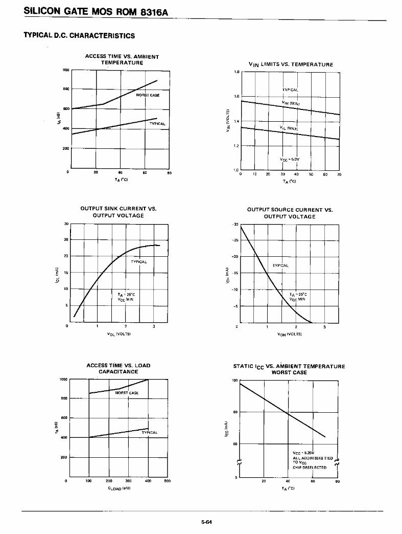
S.ILICO.N GATE MOS ROM 8316A
TYPICAL D.C. CHARACTERISTICS
ACCESS TIME VS. AMBIENTTEMPERATURE V,N LIMITS VS. TEMPERATURE
50 60 7010 20
TYPICAL
1.8 r----,r----r--.,r---r---.,r---r--_
1.6 t----1t-----t----1t---t---I----f------f
VCC:;;: 5.0V
1.2 t---t---l--t---t--------"t---t-------4
1.0 1ooo.---'1-----1_---'I--_"--_"--_.&...._--1
o
ent-l
~ 1.4 t---t------t--t---t---t---t----f
z->
806020
200 t-----t---.:..-+-----+------t
400 r-----:=--...-==----t------t------I
600 ....-~--+----t-----+---~
800 r----;----t----:::::;~--t---__I
900 .------,..---,------.-------.
OUTPUT SINK CURRENT VS.OUTPUT VOLTAGE
OUTPUT SOURCE CURRENT VS.OUTPUT VOLTAGE
3
30
25
20
<'E 15-l
9
10
o
v ~I--
./
/V TYPICAL
V/
jV TA =25°CVCCMIN
I
/
-30
-25
-20
<'E -15~
9
-10
-5
\\~
\ TYPICAL
~\ TA =25°C
I\..VCC MIN
~
~
VOL (VOLTS) VOH (VOLTS)
ACCESS T"ME VS. LOADCAPACITANCE
STATIC 'CC VS. AMBIENT TEMPERATUREWORST CASE
806020O~-------I---------
80 I-----+---~!-----+------I
6Oi------+----t-----t-------t
100 -------.........~---------.
500400
WORST CASE
200 300
CLOAO (pfd)
100o
TYPICAL
600 I------+-----+----+----+-----t
800 I-----+----+----t----t-----t
4OO1-----fl-=:;;.----+----t----t-----t
200 I-----+----I------t----t-----t
1000 ---....--~--...,.--~~-......,
5-64

MCS™CUSTOM ROMORDER FORM
8316AROM
CUSTOMER,------------------
P.O. NUMBER ----.;. _
OATE _
APp _
S# ----:.
STO _
For Intel use only
pppp--------
zz, _00 _
OATE _
All custom 8316A ROM orders must be submitted on this form. Programming information should be sent in the form of computerpunched cards or punched paper tape per the formats designated on this order form. Additional forms are available from Intel.
INTEL PATTERN NUMBER
.CHI"P"NUMBER OR
CUSTOMER NUMBER
zz
DATE. CODE
• 8316AI xxxx
MARKING
The marking as shown at the right must contain the Intel@logo, theproduct type (P8316A), the 4-digit Intel pattern number (PPPP), a datecode (XXXX), and the 2-digit chip number (DD). An optional customeridentification number may be substituted for the chip number (ZZ).Optional Customer Number (maximum 9 characters or spaces).CUSTOMER"NUMBER _
MASK OPTION SPECI FICATIONS
A. CHIP NUMBER (Must bespecified-any number from 0 through7-00).
The chip number will be coded interms of positive logic where a logicII 1" is a high level input.
Chip
Number CS3 CS2 CS1o 0 0 01 0 a 12 a 1 a3 0 1 14 100
5 1016 1 . 1 a7 111
B. ROM Truth Table Format
Programming information should besent in the form of computer punchedcards or punched paper tape. Ineithercase, a printout of the truth tableshould be accompanied with the order.
The following general format is applicable to the programming informationsent to Intel:
• Data fields·should be ordered beginning with the least significant address(0000) and ending with the most significant address (2047).
• A data field should start with themost significant bit and end with theleast significant bit.
• The data field should consist of P'sand N's. A P is to indicate a high leveloutput (most positive) and an N a lowlevel output (most negative). In termsof positive logic, a"P is defined .as alogic 111" and an N is defined as a logic110". If the programming information
is sent on a punched paper tape, the~
a start character, B, and an end character, F, must be used in the data field.
1. Punched Card Format
An SO-column Hollerith card (preferably interpreted) punched by an J8M026 or 029 keypunch should be submitted. The first card will be a titlecard; the format is as follows:
5-65

a. Title Card NO. OF OUTPUTS
TITLE CARD 4 or 8CUSTOMER'S 1DESIGNATION CUSTOMER'S INTEL PIN DECIMAL NUMBER
1DIVISION OR I
COM~ANY NAME LOCATION CUSTOMER'S PIN I INDICATING THEI' ,----....1..-------,,1 r--L-, ~ TRUTH TABLE NUMBER
r--;,~·'I·~l.~I:.~·LL[!":':_~.~·r"!:-,""·~.;~'~l~r.·)~·~CO~~R~P--:.--!;:'~,"~:i':!":,ri~~~l;L""':'t4":":"ll.~."':'C~:\L""':!I~.~....:-~l2~J~4:;.\-.l-...:.:.(h~~·.~~{J~OI II II I I I I I I II II II III III • I I I I
~ ~ ~ ~ ~!~! ~,~ I~ I~ ,~! ,~ ~ ~ ~ ~!~ ~~~~~~~~~~ ~ ~~!~~I~~~ ~~,~~~~~~~~ e~~~~e~~~~~~I~I~~~~~,!~ ~,~,~~\~~'~~!Itlllllll!II!!!!!!II!IIIIIII!!llllllllllllllllllllllll11111111111111111111111\!1
2222222222222222222122222'222222222122222222222222222 22222221222222222'22222222227
1111)) 11 311111111111 3111 311111 313313313311333313133333333333 I 333333 II 33331333333
4 U 444U4 44 444444 4 444 4444'" 4444 44 ~ U U 4 4 4 4 44 4 44 4 44 4 4 44 ~ 4 44444414 444444414 44444444
SS SS SS SSS~ SI SS SSI SSSS SS SS~ SSS SSS55SSI S55SS SS SS5S5555 S5SS5S5S551 S5SSS 55S151 SS5555
.66666666666666616666661666666666666& 66& 6&&6& 66& &6&16 66&66& 666L666666 6666666 666 66
," , 11111'11'" 111 1 r 11 11111'" 1III 11111 11111 11111 11111 11111,," 11 U 111" 111" 1"
8883881888888888888888888888888888888888888888888888888 8888e888888888881118 8888 @
999 9 ~ 99199 ~ 999199199 9991 99999999999999999991993991 9999999999 ~ ~ ~ 999999999 ~ 99q 999 q': II" '" .0"': '''''I''·I'':t:'I:''/lr.l.;'"alOlll1I1!11\.1I1111101l1:'IUhIP·'''~·,,1\;'/10':.".. ··, ... ··,:·:·:· ,,,,.,.0':":;'.', " ··t·· .•
. '''I~'1
b. For a 2048 word X 8-bit organization only, cards 2' and the followingcards should be punched as shown.
MSB
DECIMAL WORD (OUTPUT 8) LSB DECIMAL NUMBER
~~~:~~R~EGINNING I I08U::~: ~IELDS ~~~;~~I:;L~~EUMBER,L, I I· . I rl,
.':.":;.'!.' F'f1J-'rthr1rdt F'f'F'F'WthF' F'F'ftrtrtftH' f'f'F'rtttf'F'f1 F'Htf·ttff·f-'f-' t1Ufcttl'tF'F'f-' f1f1F'f-'t1tHif' f-'ttr'1f-'f'Wtf-' I,Ili'"
I1I11I11 11111111 11111111 11111111 11111111 11111111 IlIlIill 11111111
1111100000000000000000000000000000000000000000000000 0000000000000 00000000000 0011I ~ :;i;;;i'i 'i'[ 'I"; 'I' 'II '; '; 'I'~:I~: ',;1:,17:; ~~ ~ III iii ~ i l;~ ~~;II"tl;l·tlr-r';';'~l ¥;l~'t~I[~'II~'i;at"j'II~i:lt",'~::,~: ~'~. ~l j"11 :\' :Il~222 212 21211 n 2212222222222222122 ZZ222 222 222 222222222222222 22 222 222222 2222Z 22222Z
333JJ33333131333333J3333331JJJJlJ3J33333333333333333'33333333333333JJ333JJJ333JJJ
U 44 U U U 4U 4U U 44 444 ~ ~,u l •• C, ( I ••• ~ ~ 444444444 4 ~ 444444444444.4 44 ~ 4: 4H 4444 ~ ~.
~ ss 5~ 55I ~ 11111 ~ ~ 5551115 5 i S1111 )):.) j II S) 15 5S1115 :. :. :. 11111 :. ,i 5SII sSIII 5 ~ 5115 511 5) S5
,H 6&t ~ 66' £& 666 66 66 666 Et t b i: b~ lib ~ 11 61i 6ii 6 ii £6 &66£L0 ~ ~ ii ii 66 ii 6C6 ii Eii ii ii ii 0 ~ 0 ii t ii 50 0 i: &E E0L6 ii
," 111III 1; : : ? i I111 i :; I; III : 1111/111111111 II 1111111 / 111/111111111 / /111 ; ill; 11; : 1
868888888 PEt 8888888888888 Ii 888888 &a88888 8888&8888 &&e88 ~ aEaa~ 8 58&388 ~ 6Eet 560tee i c.-
"" ~ 9 ~ ~ ~ ~ s ~ q ~ ~ .q. ~ ~ ~ ~ ) ~ .~ 1.9 ~ ~. ~.~ .~ ~ ~ 9Q 0 ~ ~ ~ ~ !~ ~ 9, ~ ~ ~ ~, ~. ~ ~ ~ ~. ~ ~.i ~ , 1 ~ t t : .; .: •• ; 1 '1 '~ .1 .: ~ ~ . , .~ ••• '~ ~ ".~ ~
Column1
2-56-30
31-3435-5455-5758-66
6768-75
76-7879-80
Column1-5
67-14
1516-23
3334-41
4243-50
5152-59
6061-68
6970-77
7879-80
DataPunch aTBlankCustomer Company NameBlankCustomer's Company Division or locationBlankCustomer Part NumberBlankPunch the Intel 4-digit basic part number
and in ( ) the number of output bits,e.g., 8316A(8).
BlankPunch a 2-digit decimal number to iden
tify the truth table number (maskprogrammed ch ip select number).
DataPunch the 5-digit decimal equivalent of
the binary coded location which begins each card. The address is rightjustified, Le., 00000, 00008, 00016,etc.
BlankData FieldBlankData FieldBlankData FieldBlankData FieldBlankData FieldBlankData FieldBlankData FieldBlankPunch same 2-digit decimal number as in
title card.
2. Paper Tape Format
1" wide paper tape using 7- or 8-bitASCII code, such· as a model 33 ASRteletype produces, or the 11/16" widepaper tape usi ng a 5-bit Baudot code,such as a Telex prod uces.
The format requirements are 'as follows:
a. All word fields are to be punched inconsecutive order, starting with wordfield 0 (all addresses low). There mustbe exactly 2048 word fields for the2048 X 8 ROM organization.
b. Each word field must begin withthe start character B and end with thestop character F. There must be exactly 8 data characters between the Band F.
NO OTHER CHARACTERS, SUCHAS RUBOUTS, ARE ALLOWED ANYWHERE IN A WORD FIELD. If in prepari ng a tape an error is made, the entire word field, including the Band F,must be rubbed out. Within the wordfield, a P results in a high level outputand an N results in a low level output.
c. Preceding the first word field andfollowing the last word field, theremust be a leader/trai ler length of atleast 25 characters. This should consistof rubout or null punches -(Jetter keyfor Telex tapes).
d. Between word fields, comments notcontaining B's or F's may be inserted.Carriage return and line feed charactersshould be inserted as a "comment")
just before each word field (or at leastbetween every four word fields). Whenthese carriage returns, etc., are inserted,the tape may be easily listed on theteletype for purposes of error checking. The customer may also find ithelpful to insert the word number (asa comment) at least every four wordfields.
e. Included in the tape before theleader should be the customer's complete Telex or TWX number and, ifmore than one pattern is being transmitted, the ROM pattern number.
f. MSB and LSB are the most and leastsignificant bit of the device outputs.Refer to the data sheet for the pinnumbers.
Data Field LSB
Word Fi~'d 2048
Start Character~_ Stap Character --1, , I I
Leader: Rubout Key for TWX and Letter B P P P N N N N N F B N N N N N N P P FKey for Telex (at least 25 frames). I 1L..' ---r- ----J
Ward'Field 0 WardlField 1
5-66
MSB
t tBNPNPPPNNFI
Trailer: Rubaut Key far TWX and Let~~r
Key for Telex {at least .25 framesL

8101-28111-2
8102-28102A-4
81078-4
RAMs510182108222


Silicon Gate MOS 8101-2
1024 BIT (256 x 4) STATIC MOS RAMWITH SEPARATE 1/0
• 256 x 4 Organization to Meet Needsfor Small System Memories
• Access Time - 850 nsec Max.• Single + 5V Supply Voltage• Directly TTL Compatible - All Inputs
and Output• Static MOS - No Clocks or
Refreshing Required• Simple Memory Expansion - Chip
Enable Input
• Inputs Protected - All Inputs HaveProtection Against Static Charge
• Low Cost Packaging - 22 Pin PlasticDual-In-Line Configuration
• Low Power - Typically 150 mW
• Three-State Output - OR-TieCapability
• Output Disable Provided for Ease ofUse in Common Data Bus Systems
®The Intel 8101-2 is a 256 word by 4 bit static random access memory element using normally off N-channelMOS devices integrated on a monolithic array. It uses fully DC stable (static) circuitry and therefore requiresno clocks or refreshing to operate. The data is read out nondestructively and has the same polarity as theinput data.
The 8101-2 is designed for memory applications where high performance, low cost, large bit storage, and simple interfacing are important design objectives.
It is directly TTL compatible in all respects: inputs, outputs, and a single +5V supply. Two chip-enablesallow easy selection of an individual package when outputs are OR-tied. An output disable is provided so thatdata inputs and outputs can be tied for common I/O systems. Output disable is then used to eliminate anybidirectional logic.
®The Intel 8101-2 is fabricated with N-channel silicon gate technology. This technology allows the design and_production of high performance, easy-to-use MOS circuits and provides a higher functional density on a monolithic chip than either conventional MOS technology or P-channel silicon gate technology.
Intel's silicon gate technology also provides excellent protection against contamination. This permits the useof low cost silicone packaging.
@---0 Vee
~GND
o = PIN NUMBERS
CELL ARRAY32 ROWS
32 COLUMNS
ROWSELECT
AO
BLOCK DIAGRAM
m~-.~
CE2~---I
00 ::>--4>o-~
R/W
DIN DATA INPUT 00 OUTPUT DISABLE
Ao-A., ADDRESS INPUTS DOUT DATA OUTPUT
RIW READIWRITE INPUT Vee POWER (+5V)
m,CE2 CHIP ENABLE-
PIN CONFIGURATION LOGIC SYMBOL
A3 22 Vee Ao 01,
A2 21 A4 A, DO,
A, 20 RIWA2 012
AoA3 002
4 19 CElA4 013
As 5 18 00 As 0038101-2 A
68101-2 01
4A6 6 17 CE2A7 0°4
A7 16 0°4
GNo 8 15 014 00
01, 9 14 0°3
DO, 10 13 013
01 2 11 12 0°2RIW CE2 CEl
PIN NAMES
5-67

SILICON GATE MOS 8101-2
Absolute Maximum Ratings*
Ambient Temperature Under Bias. . . . .. O°C to 70° C
Storage Temperatu re .. . . . . . . . . . -650C to +150
0C
Voltage On Any PinWith Respect to Ground. . . . . . . .. -0.5V to +7V
Power Dissipation . . . . . . . . . . . .. 1 Watt
*COMMENT:
Stresses above those listed under ''Absolute MaximumRating"may cause permanent damage to the device. Thisis a stress rating only and functional operation of the device at these or at any other condition above those indicated in the operational sections of this specification isnot implied. Exposure to absolute maximum rating conditions for extended periods may affect device reliability.
D.C. and Operating Charact~ristics
TA = o°c to 70°C, Vee = 5V ±5% unless otherwise specified.
V,N =0 to 5.25V
V,N =5.25V, 10 = OmATA = 25°C
CE = 2.2V, VOUT = 0.45V
CE = 2.2V, VO UT = 4.0V
Test ConditionsSymbol Parameter Min. Typ.[1] Max. Unit
ILl Input Current 10 pA
ILOH 110 Leakage Current[2] 15 pA-
ILO L 1/0 Leakage Current[2] -50 J1A
lecl Power Supply Current 30 60 rnA
~I~~;--l-p~~-;s~;~~c~;~;~~ 70 mA VIN = 5.25V. 10 = OmA
--1- TA = O°C
~~:~;-_: ~_!~~~-~~~-==--------~VOL I Output "Low" Voltage +0.45 VIOL = 2.0mA
~E~~:=~utP~-t-·7~igh-~;\/oltage-~------- ---- --i2-+---=~==__~= - V____ 10H =-150 p.A
NOTE: 1. Typical values are for T A = 25() e and nominal supply voltage.
2. Input and Output tied together.
OUTPUT SOURCE CURRENT VS.OUTPUT VOLTAGE
OUTPUT SINK CURRENT VS.OUTPUT VOLTAGE
: AMBIENT TEMPERATURE I~. ~O"l: l- ---l-----.-i-.-t-.-.--: -f 25 C I I t' I
~l~t-+-- ---T~--! ! I! I
~ -10 .. _.- I .-+----+----. I !
~ , : I_0 --,- - r.'
I-_.Vu 4.75V
OUTPUT "HI(iH" TYPICAL
t.---"-'-~---+------""!I--t---+---;Io L-.-----'-_.....L.-----lo....-~_"O"- _
1
VOH IVOL lS) VOL (VOLTS)
5-68

SILICON GATE MOS 8101-2
A.C. CharacteristicsREAD CYCLE TA = o°c to 70°C, Vee = 5V ±5~/~, unless otherwise specified.
Symbol Parameter =I Min. Typ. Max. Unit Test Conditions--~--_._---
tRey Read Cycle ~ ns----- .---.--
tA Access Time 850 ns____._.__u. ___________~---~._----~._---
teo Chip Enable To Output 6~._~~ (See below)--_._-_ .._----
too Output Disable To Output r 550 ns._-----. -'----- ---_._----- ~-
200~--~~-1tOF [1] Data Output to High Z State 0--
tOHPrevious Data Read Valid I 0 ns iafter change of Address
WRITE CYCLE
Symbol Parameter I Min. Typ. Max. Unit Test Conditions
tweY Write Cycle i 850 ns
tAW Write Delay,
150 ns
tew Chip Enable To Write -T 750 ns(See below)
tDW Data Setup 1 500 ns--tOH Data Hold 100 ns
Write Pulse---_..._---- --j--------t------- ,...--'
twp ! 630 ns
tWR Write Recovery : 50 I nsi,_---L-
A. C. CONDITIONS OF TEST Capacitance TA = 25°C, f = 1MHz
Input Pulse Levels: +0.65 Volt to 2.2 Volt
Input Pulse Rise and Fall Times: 20nsec
1 TTL Gate and CL ~.: 100pF
Timing Measurement Reference Level:
Output Load:
1.5 Volt
-
Symbol TestLimits (pF)
! Typ. Max.
CIN Input Capacitance4 8
~-
(All Input Pins) V IN = OV
CoUT Output Capacitance VOUT = OV 8 12
WaveformsREAD CYCLE WRITE CYCLE l2]
ADDRESS ==:>c
CE2 - ......-....Il- t co --.
ICE2 /
-----"
DATAIN
'\ '00 ~. /'OHI '-- -..J
t A • t OF 11; .'
DATA - -1--- - - - - -y IJATAOUT
OUT __ j ..A V_A_L_ID _
ODJ• tDf' j. - - .--., t OH /.-·-
=x ~_~_~:_L_I~ -_.__...:, ttow ---
.-. tAW ;.....-- tw ~
RW '\ ~p -J ... R !. I
NOTES: 1. tDF is with respect to the trailing edge of CE1, CE2, or OD, whichever occurs first.
2. During the write cycle, 00 is a logical 1 for common 1/0 and "don't care" for sepJ~ate I/O operation.
3. 00 should be tied low for separate I/O operation.
00(COMMON lID) 131
5-69


Silicon Gate MOS 8111-2
1024 BIT (256 x 4) STATIC MOS RAMWITH COMMON I/O AND OUTPUT DISABLE
• Organization 256 Words by 4 Bits• Access Time - 850 nsec Max.• Common Data Input and Output• Single +5V Supply Voltage• Directly TTL Compatible - All Inputs
and Output• Static MOS - No Clocks or
Refreshing Required• Simple Memory Expansion - Chip
Enable Input
• Fully Decoded - On Chip AddressDecode
• Inputs Protected - All Inputs HaveProtection Against Static Charge
• Low Cost Packaging -18 Pin PlasticDual-In-Line Configuration
• Low Power - Typically 150 mW
• Three-State Output - OR-TieCapability
The Intel®8111-2 is a 256 word by 4 bit static random access memory element using normally off N-channelMOS devices integrated on a monolithic array. It uses fully DC stable (static) circuitry and therefore requiresno clocks or refreshing to operate. The data is read out nondestructively and has the same polarity as theinput data. Common input/output pins are provided.
The 8111-2 is designed for memory applications in small systems where high performance, low cost, large bitstorage, and simple interfacing are important design objectives.
It is directly TTL compatible in all respects: inputs, outputs, and a single +5V supply. Separate chip enable(CEl leads allow easy selection of an individual package when outputs are OR-tied.
The Intel®8111-2 is fabricated with N-channel silicon gate technology. This technology allows the design andproduction of high performance, easy-to-use MOS circuits and provides a higher functional density on a monolithic chip than either conventional MOS technology or P-channel silicon gate technology.
Intel's silicon gate technology also provides excellent protection against contamination. This permits the useof low cost silicone packaging.
LOGIC SYMBOL BLOCK DIAGRAM
o ' PIN NUMBERS
@-------0 Vee
~GNOMEMORY ARRAY
32 ROWS32 COLUMNS
ROWSELECT
AO
A, I/O,
Az I/Oz
A3 1/03
A4 1/04
As 8111-2
AO-A7 ADDRESS INPUTS
00 OUTPUT DISABLE
RIW READIWR ITE INPUT
CE, CHIP ENABLE 1
CE2 CHIP ENABLE 2
1/0,- 1/04 DATA INPUT/OUTPUT
PIN CONFIGURATION
A3 18 Vee
A2 17 A4
A, 16 R/W
Ao 4 15 tEl
As 5 8111-2 14 1/04
A6 6 13 1/03
A7 12 1/02
GNO 11 I/O,
00 9 10 CE2
PIN NAMES
5-71

SILICON GATE MOS 8111-2
Absolute Maximum Ratings*
Ambient Temperature Under Bias. . . . .. O°C to 70°C
Storage Temperature -65°C to +150°C
Voltage On Any PinWith Respect to Ground . . . . . . . .. -0.5V to +7V
Power Dissipation 1 Watt
*COMMENT:
Stresses above those listed under ''Absolute MaximumRating"may cause permanent damage to the device. Thisis a stress rating only and functional operation of the device at these or at any other condition above those indicated in the operational sections of this specification isnot implied. Exposure to absolute maximum rating conditions for extended periods may affect device reliability.
D.C. and Operating CharacteristicsTA =O°C to 70°C, VCC =5V ±5% , unless otherwise specified.
Symbol Parameter Min. Typ.r1] Max. Unit Test Conditions
III Input Load Current 10 J.1A VIN =0 to 5.25V
IlOH I/O Leakage Current 15 J.1A CE =2.2V, VI/O =4.0V
IlOl I/O Leakage Current -50 J1A CE =2.2V, VI/a =0.45V
ICC1 Power Supply Current 30 60 mA VIN = 5.25V
11/0 =OmA, TA = 25°C
ICC2 Power Supply Current 70 mA VIN =5.25V
11/0 =OmA, TA = O°C
VIL Input Low Voltage -0.5 +0.65 V
VIH Input High Voltage 2.2 Vcc V
Val Output Low Voltage 0.45 V 10l =2.0mA
VOH Output High Voltage 2.2 V 10H = -150 J.1A
NOTES: 1. Typical values are for T A = 25° C and nominal supply voltage.
OUTPUT SOURCE CURRENT VS.OUTPUT VOLTAGE
OUTPUT SINK CURRENT VS.OUTPUT VOLTAGE
1.51.0
VOL (VOLTS)
0.5
15 ..--+---+--+-~~--+-------t
..Jo
i 10 ~--4---+--'~-~-+--+------4
!
VOH (VOLTS)
oL----L-_..L-.-..L.---.;;;~__.._.__.-.
1
-5 .-.----+--~-
AMBIENT TEMPERATURE
-15 ~~-==--~O°C -t----+---I----+--;25°C70°C
i -10 ~----4-..-+---+--t----t--+----1!~
.2
5-72

SILICON GATE MOS 8111-2
A.C. CharacteristicsREAD CYCLE TA = o°c to 70°C, Vee = 5V ±5%, unless otherwise specified.
Symbol Parameter Min. Typ. Max. Unit Test Conditions
tRCY Read Cycle 850 ns
tA Access Time 850 ns
tco Chip Enable To Output 650 ns (See below)
too Output Disable To Output 550 ns
tOF [1] Data Output to High Z State 0 200 ns
tOHPrevious Data Read Valid 0 nsafter change of Add ress
WRITE CYCLE
Symbol Parameter Min. Typ. Max. Unit Test Conditions
twCY Write Cycle 850 ns
tAW Write Delay 150 ns
tcw Chip Enable To Write 750 ns(See below)
tow Data Setup 500 ns
tOH Data Hold 100 ns
twP Write Pulse 630 ns
tWR Write Recovery 50 ns
A. C. CONDITIONS OF TEST Capacitance TA =25°C, f = 1 MHz
Input Pulse Levels: +0.65 Volt to 2.2 Volt
Input Pulse Rise and Fall Times: 20nsec
1 TTL Gate and CL = 100pF
Timing Measurement Reference Level:
Output Load:
1.5 Volt
Symbol TestLimits (pF)
Typ. Max.
CIN Input Capacitance4 8
(All Input Pins) VIN = OV
GoUT Output Capacitance VOUT = OV 10 15
WaveformsREAD CYCLE WRITE CYCLE
DATA INSTABLE
----twey------.. I
I~ tOH
~ t OF ----.I....--tow---.
_ ........._""I..---tew---..I
OUTPUTDISABLE
DATA I/O
CHIPENABLES
ADDRESS
DATA OUTVALID
OUTPUTDISABLE
1..-------tReY-----~
CHIP - .........-""1"-- teoENABLEStCE1, CE2)
ADDRESS
DATA I/O
1~-tAW--.I""-----"I
_---+ "'" f4---lwp ------..............-tWR~READ/WRITE
NOTE: 1. tOF is with respect to the trailing edge of eEl, CE2, or 00, whichever occurs first.
5-73


Silicon Gate MOS 8102-2
• Simple Memory Expansion - ChipEnable Input
• Fully Decoded - On Chip AddressDecode
• Inputs Protected - All Inputs HaveProtection Against Static Charge
• Low Cost Packaging -16 Pin PlasticDual-In-Line Configuration
1024 BIT FULLY DECODED STATIC MOSRANDOM ACCESS MEMORY
• Access Time - 850ns Max.• Single +5 Volts Supply Voltage• Directly TTL Compatible - All Inputs
and Output• Static MOS - No Clocks or
Refreshing Required• Low Power - Typically 150 mW• Three-State Output - OR-Tie
Capability
The Intel@8102-2 is a 1024 word by one bit static random access memory element using normally offN-channel MOS devices integrated on a monolithic array. It uses fully DC stable (static) circuitry andtherefore requires no clocks or refreshing to operate. The data is read out nondestructively and has thesame polarity as the input data.
The 8102-2 is designed for microcomputer memory applications where high performance, low cost, largebit storage, and simple interfacing are important design objectives.
It is directly TTL compatible in all respects: inputs, output, and a single +5 volt supply. A separate chipenable (CE) lead allows easy selection of an individual package when outputs are OR-tied.
The Intel®8102-2 is fabricated with N-channel silicon gate technology. This technology allows the designand production of high performance, easy-to-use MOS circuits and provides a higher functional density ona monolithic chip than either conventional MOS technology or P-channel silicon gate technology.
Intel's silicon gate technology also provides excellent protection against contamrnation. This permits theuse of low cost silicone packaging.
BLOCK DIAGRAMPIN CONFIGURATION LOGIC SYMBOL
A6 16 A7
As 2 15 AsAoA,
RIW 3 14 Ag A 2 DIN
AJA, 4 13 CE A4
8102-2 As 8102-2A2 5 12 DATA OUT
A 6
AJ 6 11 DATA INA 7
As DOUT
A4 7 10 Vee Ag
Ao 8 9 GNDCER/W
PIN NAMES
DIN DATA INPUT CE CHIP ENABLE
Ao- Ag ADDRESS INPUTS DOUT OATA OUTPUT
RIW READIWRITE INPUT Vee POWER (+5V)
R/W
DATAIN
0= PIN NUMBERS
5-75
CELLARRAY
32 ROWS32 COLUMNS
COLUMN I/O CIRCUITSDATAOUT

SILICON GATE MOS 8102-2
ABSOLUTE MAXIMUM RATINGS·
Ambient Temperature Under Bias
Storage Temperature
Voltage On Any PinWith Respect To Ground
Power Dissipation
-O.5V to +7V
. 1 Watt
*COMMENT:
Stresses above those listed under "Absolute Maximum Rating" may cause permanent damage to thedevice. This is a stress rating only and functionaloperation of the device at these or at any oth~r
condition above those indicated in the operationalsections of this specification is not implied. Exposure to absolute maximum rating conditions forextended periods may affect device reliability.
D.C. AND OPERATING CHARACTERISTICS
TA = OOC to +70°C, Vee = 5V ±5% unless otherwise specified
LIMITSSYMBOL PARAMETER ~-- -- UNIT TEST CONDITIONS
MIN. TYP.(1) MAX.-- ,
III INPUT LOAD CURRENT 10 p.A VIN = 0 to 5.25V(ALL INPUT PINS)
I LOH OUTPUT LEAKAGE CURRENT 10 IJA CE = 2.2V, VOUT = 4.0V
I lOL OUTPUT LEAKAGE CURRENT -100 IJA CE = 2.2V, VOUT = O.45V
'CC1 POWER SUPPLY CURRENT 30 60
ImA ALL INPUTS = 5.25V
, DATA OUT OPENi I i
TA = 25°C
ICC2 POWER SUPPLY CURREN:=] 70
I
mA ALL INPUTS = 5.25VDATA OUT OPEN
I TA = OOCi
Vil INPUT "LOW" VOLTAGE -0.5 +0.65 I V
V1H INPUT "HIGH" VOLTAGE 2.2 Vee i V
VOL OUTPUT "LOW" VOL-rAGE +0.45 ! V 'Ol= 1.9mAIVOH OUTPUT "HIGH" VOLTAGE 2.2 I !
I V 'OH= -100IJAI
(1) Typical values are for T A = 25°C and nominal supply voltage.
TYPICAL D.C. CHARACTERISTICS
POWER SUPPLV CURRENT VS.AMBIENT TEMPERATURE
POWER SUPPLY CURRENT VS.SUPPLY VOLTAGE
654
10
50 4 - - +- - . ·l - -,-+----+---1
AMBI~NT TEMPERAl URE ~ 25°C \
40 - - ~ +_.- - -+-- --.~!-_+____f
~ I I I
Et? 30<ta:w> 20 - _ .. t<tuu
___ o~. --.-i
I II I . V =525V
--+--T~'-- cc -
~4~! I I :-'~--i---± _ I I._
n
, Y: I ,..- .. _
SPEC. iii
'-"-- POINTS 1 -
30
10~__--t.- --..I-__-----"
o 10 20 30 40 50 60 70
20 ---+.-., -+- ..----+-
80
70
~60
!w 500<{a:w> 40<{u
_u
AMBIENT TEMPERATURE (OCI Vcr; (VOLTS)
5-76

SILICON GATE MOS 8102-2
A.C. CHARACTERISTICS TA =ooe to 70oe, Vee =5V ±5% unless otherwise specified
SYMBOL
READ CYCLE
PARAMETERLIMITS--·---r----mT----
_.~~_~ ..._... l}YP._... ..L _~?<~. _._UNIT
os
ns
ns
ns
ns
--tR-e------r-R--EA~D-C-Y--C-L-E--·---------_ .. --------- 85o-·-···T -._- "--r .-_._.- --"---'-~~~~~~~---~--------~-_ .._-----~--~-- -_._----~._------ ~ --- --~
t A ACCESS TIME I 500 i 850-----~ _. -_.- ..... -.---~-.- --- -- -_. --.--.~-------.-----.--. ... - -_..---- ---1------- ----t···--- _._.-
teo CHIP ENABLE TO OUTPUT TIME : I 500_______~------_--- . ---+ .._--l-. ~---
t OH1 PREVIOUS READ DATA VALID WITH RESPECT 50 ITO ADDRESS :
----------4--------- ------·l- _.-_..-- .. ---- ---~----.
PREVIOUS READ DATA VALID WITH RESPECT a I 1
TO CHIP ENABLE i :_____"__ --J- _
WRITE CYCLE
ns
--~-C----~W-R-I-T-E-C-Y-C-L-E----------------T--8-~-r--~-~- ! M
------.----+----.----- ...--.-.-----.... --.-------------------.. -- . __ ....__ 1_ -- - .....+ . -..-.-t-------tAW ADDRESS TO WRITE SETUP TIME I 200' : ! ns
.----- ------+i..--.----+-.-.-----.--..---~---.-----~---
~_tw_p +_W-R-IT-E-P-U-L-S-E-W-IDTH I~~ L_. .+- ... -n_--li---ns_-tWR WRITE RECOVERY TIME --t 50: ! I ns
-----------1t-------------------------+------~~:------- ..~ i
__::_: -+--~_:_~_:_:_~_T_L~_P~~EEt~~~-.±--=~=~L~==--+---~-:-t cw CHIP ENABLE TO WRITE SETUP TIME I 750! ;
(1) Typical values are for T A=250 C and nominal supply voltage.
CAPACITANCE TA = 25°C, f = 1MHz
A. C. CONDITIONS OF TEST
Input Pulse Levels: +0.65 Volt to 2.2 Volt
Input Pulse Rise and Fall Times: 20nsec
Timing Measurement Reference Level: 1.5 Volt
Output Load: 1 TTL Gate and CL = 100 pF
._------_._-----
SYMBOL TESTLIMITS (pF)
TYP. MAX.---------_.- - _.--.._- --- --
CIN INPUT CAPACITANCE3 5
(ALL INPUT PINS) ViN :: OV
COUT OUTPUT CAPACITANCE7 10VOUT = OV
WAVEFORMS
READ CYCLE WRITE CYCLE
DATA STABLE
~----tow----~~
~~----twP------...I
..-----tew~----~I
t4-------twc---------I~
DATA DATA CANIN CHANGE
CHIPENABLE
READ/WRITE
teo
ADDRESS
t4-------tRC-----~
~----tA-----""
CHIPENABLE
DATAOUT
5-77

SILICON GATE MOS 8102·2
TYPICAL D.C. CHARACTERISTICS
INPUT CURRENT VS.INPUT VOLTAGE
-7.5-1
OUTPUT SINK CURRENT VS.bUTPUT VOLTAGE
1.51.0
VOL (VOLTS)
0.5
VIN (VOLTS)
EFFECTIVE INPUTCHARACTERISTIC
IVee g 5.0V
~~~b~.JVIL MAX. ( VIH MIN.
V IN (VOLTS)
+1 +2 +3 +4 +5 +6
Vee~ 5.0V
r TYPICAL
+5
-5
+2.5
OUTPUT SOURCE CURRENT VS.OUTPUT VOLTAGE
OUTPUT CURRENT VS. OUTPUTVOLTAGE WITH CHIP DISABLED
RELATIONSHIP BETWEEN OUTPUTSINK CURRENT, NUMBER OF OR-TIES,
AND OUTPUT VOLTAGE
20
12
16
vcclg 4.75~
/V
[77
/1.5
.40 .45 .50 .55 .60 .65 .70 .75
VOL (VOLTS)
4.3
3.9
3.5
ct 3.1.g~
.2 2.7
2.3
1.9
VOUT (VOLTSt
+1 +2 +3 +4 +5 +6
TYPICAL
CE g 2.2V
r"T-
+5
-20-1
-15
ct -5.g
~- -10
VOH (VOLTS)
AMBIENT TEMPERATUREoac -+--+-~_---+-_-I25°C70°C
0 ----'_---10._--1-----:::......1.-_...10.0-_...1.----'
1
-15
ct -10 t-----.~__+---+--+---+--_+_---I!
X.!'
TYPICAL A.C. CHARACTERISTICS
ACCESS TIME YS.LOAD CAPACITANCE
ACCESS TIME YS.AMBIENT TEMPERATURE
1400
1200
1000
!800
c~ 600
400
I TTA II 25°CVee II 4.75V _1 TTL LOAD
SPEC. POINT4
------~------~~l.
1400
1200
1000
~ 800
<[
~ 600
400
I IVee II 4.75V1TTL LOAD_Cl " lOOpF
SPEC. POINT
•l.....-- ."",..,-
.-.. .......~----- l-tP\CAl.
200 200
00 50 100 150 200 250 300 350 00 10 20 30 40 50 60 70
LOAD CAPACITANCE (pFI AMBIENT TEMPERATURE (OCI
5-78

Silicon Gate MOS 8102A-4
1024 BIT FULLY DECODED STATIC MOSRANDOM ACCESS MEMORY
• Access Time -450 ns Max.• Single +5 Volts Supply Voltage• Directly TTL Compatible - All Inputs
and Output• Static MOS - No Clocks or
Refreshing Required• Low Power - Typically 150 mW• Three-State Output - OR-Tie
Capability
• Simple Memory Expansion - ChipEnable Input
• Fully Decoded - On Chip AddressDecode
• Inputs Protected - All Inputs HaveProtection Against Static Charge
• Low Cost Packaging - 16 Pin PlasticDual-In-Line Configuration
The Intel®S102A-4 is a 1024 word by one bit static random access memory element using normally offN-channel MOS devices integrated on a monolithic array. It uses fully DC stable (static) circuitry and therefore requires no clocks or refreshing to operate. The data is read out nondestructively and has the samepolarity as the input data.
The 8102A-4 is designed for microcomputer memory applications where high performance, low cost, largebit storage, and simple interfacing are important design objectives.
It is directly TTL compatible in all respects: inputs, output, and a single +5 volt supply. A separate chipenable (CE) lead allows easy selection of an individual package when outputs are OR-tied.
®The Intel 81 02A-4 is fabricated with N-channel silicon gate technology. This technology allows the design andproduction of high performance, easy-to-use MOS circuits and provides a higher functional density on a monolithic chip than either conventional MOS technology or P-channel silicon gate technology.
Intel's silicon gate technology also provides excellent protection against contamination. This permits the useof low cost silicone packaging.
DATAOUT
CELLARRAY
32 ROWS32 COLUMNS
COLUMN 110 CIRCUITS
BLOCK DIAGRAM
R/W
0= PIN NUMBERS
DATAIN
DIN DATA INPUT CE CHIP ENABLE
Af}"Ag ADDRESS INPUTS DOUT OATA OUTPUT
R/W READIWRITE INPUT Vee POWER (+5V)
PIN CONFIGURATION LOGIC SYMBOL
A6 16 A7
As 2 15 AsAoA1
RIW 3 14 Ag A 2 DIN
A3A1 4 13 CE A4
8102A-4 As 8102A-4A2 5 12 DATA OUT
As
A3 6 11 DATA INA 7
As DOUT
A4 7 10 Vee Ag
Ao 8 9 GNDCER/W
PIN NAMES
5-79

SILICON GATE MOS 8102A-4
ABSOLUTE MAXIMUM RATINGS·
Ambient Temperature Under Bias
Storage Temperature
Voltage On Any PinWith Respect To Ground
Power Dissipation
-O.5V to +7V
1 Watt
*COMMENT:
Stresses above those listed under "Absolute Maximum Rating" may cause permanent damage to thedevice. This is a stress rating only and functionaloperation of the device at these or at any othercondition above those indicated in the operationalsections of this specification is not implied. Exposure to absolute maximum rating conditions forextended periods may affect device reliability.
D.C. AND OPERATING CHARACTERISTICS
TA = O°C to +70 oe, Vcc = 5V ±5% unless otherwise specified
LIMITSSYMBOL PARAMETER
TYP.c1)UNIT TEST CONDITIONS
MIN. MAX.
ILl INPUT LOAD CURRENT 10 J,J.A VIN = 0 to 5.25V(ALL INPUT PINS)
I LOH OUTPUT LEAKAGE CURRENT 5 J,J.A CE = 2.0V, vOUT = 2.4 to
I LOL OUTPUT LEAKAGE CURRENT -10 J,J.A CE = 2.0V, vOUT = 0.4V
I CC1 POWER SUPPLY CURRENT 30 60 rnA ALL INPUTS = 5.25VDATA OUT OPENTA = 25°C
I CC2 POWER SUPPLY CURRENT 70 rnA ALL INPUTS = 5.25VOATA OUT OPENTA = DoC
VIL INPUT "LOW" VOLTAGE -0.5 0.8 V
VIH INPUT "HIGH" VOLTAGE 2.0 Vcc V
VOL OUTPUT "LOW" VOLTAGE 0.4 V IOl = 2.1mA
VOH OUTPUT "HIGH" VOLTAGE 2.4 V IOH= -100J,J.A
(1) . Typical values are for T A= 250C and nominal supply voltage.
TYPICAL D.C. CHARACTERISTICS
POWER SUPPLY CURRENT VS.AMBIENT TEMPERATURE
80 __-......,.....-~---r---r--.,.----,
70-----+---+----+---~
60«..sw 50e"«a:w
40>«u
_u
30
20
60
50
40«..sw 30e"«a:w
20>«u~
10
0
POWER SUPPLY CURRENT VS.SUPPLY VOLTAGE
I I I IAMBIENT TEMPERATURE = 25°C
I
'............""o(-.(v~~
V/
10 '--__~____"_"""'O-'_..Ioo._--I..__
o 10 20 30 40 50 60 70
AMBIENT TEMPERATURE (OC)
5-80
3 4 5
Vee (VOLTS)
6

SILICON GATE MOS 8102A-4
A. C. Characteristics TA = O°C to 70°C, Vee = 5V ±5% unless otherwise specified
LimitsSymbol Parameter
TypJ1 ]Unit
Min. Max.
READ CYCLE
tRC Read Cycle 450 ns
tA Access Time 450 ns
tco Chip Enable to Output Time 230 ns
tOHl Previous Read Data Valid with Respect to Address 40 ns
tOH2 Previous Read Data Valid with Respect to Chip Enable 0 ns
WRITE CYCLE
twc Write Cycle 450 ns
tAW Address to Write Setup Time 20 ns
twP Write Pulse Width 300 ns
tWA Write Recovery Time 0 ns
tow Data Setup Time 300 ns
tOH Data Hold Time 0 ns
tcw Chip Enable to Write Setup Time 300 ns
NOTE: 1. Typical values are for TA = 25° C and nominal supply voltage.
Capacitance l21TA = 25°C, f = 1MHz
A. C. CONDITIONS OF TEST
Input Pulse Levels: 0.8 Volt to 2.0 Volt
Input Rise and Fall Times: 10nsec
Timing Measurement Inputs: 1.5 VoltsReference Levels Output: 0.8 and 2.0 Volts
Output Load: 1 TTL Gate! and CL = 100 pF
SYMBOL TESTLIMITS (pF)
Typ.,[1] MAX.
C1N INPUT CAPACITANCE3 5
(ALL INPUT PINS) V1N =: OV
COUT OUTPUT CAPACITANCE7 10
VOUT = OV
NOTE: 2. This parameter is periodically sampledand is not 100% tested.
Waveforms
READ CYCLE WRITE CYCLE
tRC twe
ADDRESS CD
teo
CHIP CHIP 'ew
ENABLE ENABLE
tA twP
DATA READIOUT WRITE
CD 1.5 VOLTS tow
® 2.0 VOLTSfj) 0.8 VOLTS
DATA DATA CANDATA STABLEIN CHANGE
5-81

SILICON GATE MOS 8102A-4
Typical D. C. and A. C. CharacteristicsPOWER SUPPLY CURRENT VS.
AMBIENT TEMPERATUREPOWER SUPPLY CURRENT VS.
SUPPLY VOLTAGE
15o 10 20 30 40 50 60 70
TA (OC) Vee (VOLTS)
If-- TA "'25°C-
V./
/ ~PICAL/r
/
I
35
51
10
15
25
30
ct! 20
I IVeeMAX.-
............-..............~
TYPICALr---___........ -
20
40
45
35
i~ 30
25
OUTPUT SOURCE CURRENT VS.OUTPUT VOLTAGE
OUTPUT SINK CURRENT VS.OUTPUT VOLTAGE
-30
-25
-20
ct! -15
%~
-10
-5
"\ ..\ TYPICAL
~TA ;: 25°C
Vee MIN.
'~
'""'"
30
25
20
15
10
~,......,.....1-
V TYPICAL
/j'
/ TA =25'C
J Vee MIN.
IVOH (VOLTS) VOL (VOLTS)
1.6...----+--_+_-
"".l
TA .. 700C
CYCLE TIME = 350ns
~
0.95
1.00
ACCESS TIME VS. VeeNORMALIZED TO Vee = 5.0V
1.05
1.2 ...----+--_+_-+---+----+--t----t
VIN LIMITS VS. TEMPERATURE1.8
~....~ 1.4...----+--_+_-+--+----+--t----t
Z>-
Vee" 5.0V
1.00 10 20 30 40 50 60 70
TA
(OC)
4.0 4.5 5.0
Vee (VOLTS)
5.5 6.0
ACCESS TIME VS.AMBIENT TEMPERATURE
ACCESS TIME VS.LOAD·CAPACITANCE
Vee MIN.1 TTL LOAD
c;. "100pF
350 ,...----,----,----r---r----'T"""'-.....,TA " 25°C
Vee MIN.1 TTL LOAD
250 t-----+--TY.......P-ICA-L-+----+----I:=........,~--1 250 t-----t------i -=T---+---+--~
TYPICALc
..-:.150 t-----+--+----+--+-----+--t----t 150 t------I----t--+---t----t---i
OUTPUT REFERENCE LEVELS: VOH '" 2.0VVOL aO.8V
5OL.-----J...._..L-----L._.....L----L_.........---'
o 10 20 30 40 50 60 70
TA
(OC)
OUTPUT REFERENCE LEVEL" , .5V
5O~---I._---I._---.l.---'-----""'"
o 100 200 300 400 500 600
CL (pF)
5-82

Silicon Gate MOS 81078·4
FULLY DECODED RANDOM ACCESS4096 BIT DYNAMIC MEMORY
* Access Time·· 270 ns max.* Read, Write Cycle Times--470 ns max.
* Refresh Period -- 2 ms• Low Cost Per Bit • Address Registers• Low Standby Power Incorporated on the Chip• Easy System Interface • Simple Memory Expansion-• Only One High Voltage Chip Select Input Lead
Input Signal-Chip Enable • Fully Decoded - On Chip• TTL Compatible -- All Address, Address Decode
Data, Write Enable, • Output is Three State andChip Select Inputs TTL Compatible
• Read-Modify-Write Cycle • Industry Standard 22-PinTime _. 590 ns Configuration
The Intel 81078 is a 4096 word by 1 bit dynamic n-channel MOS RAM. It was designed for memory applications wherevery low cost and large bit storage are important design objectives. The 81078 uses dynamic circuitry which reduces thestandby power dissipation.
Reading information from the memory is non-destructive. Refreshing is most easily accomplished by performing one readcycle on each of the 64 row addresses. Each row address must be refreshed every two milliseconds. The memory is refreshed whether Chip Select is a logic one or a logic zero.
The 81078 is fabricated with n-channel silicon gate technology. This technology allows the design and production ofhigh performance, easy to use MOS circuits and provides a higher functional density on a monolithic chip than otherMOS technologies. The 81078 uses a single transistor cell to achieve high speed and low cost. It is a replacement forthe 81078.
Ao-A" ADDRESS INPUTS* VBB POWER (-5V)
CE CHIP ENABLE Vee POWER (+5V)
CS CHIP SELECT VOO POWER (+12V)
DIN DATA INPUT Vss GROUND
DOUT DATA OUTPUT WE WRITE ENABLE
NC NOT CONNECTED
PIN CONFIGURATION81078
Vee Vss
Ag As
A,o A]
A" ~
CS Vee
o.N CE
DouT NC
Ao As
A, A.1A2 A3
Vee WE
PIN NAMES
*Refresh Address Ao-As'
LOGIC SYMBOL81078
AoA,A 2 DIN
AJA4
AsA6A] DOUT
AsAgA,o
A"
CS CE WE
5-83
BLOCK DIAGRAM
AO 0----. .......0 "beA, 0----.
MEMORY ~ VeeROW DECODE 64A2 and BUFFER
ARRAY ~ VssAJ 0----. REGISTER .......0 "BBA4
64 x 64
~ 0----.
f64TIMING COLUMN
CE 0----. CONTROL AMPLIFIERSGENERATOR
64
DIN 0----.
WE 0----. I/O
CS 0----.

SILICON GATE MOS 81078·4
Absolute Maximum Ratings*Temperature Under Bias ooc to 70°C
Storage Temperature . . . . . . . . . . . . . . . . . . . . . . . . . . . . . . . . . . . . . . . . . . . . . . . . . . . . . . . . . .. -65°C to +1500 C
All Input or Output Voltages with Respect to the most Negative Supply Voltage, Vee . . . . . . . . . . . . . . . . .. +25V to -O.3V
Supply Voltages Vee, Vcc, and Vss with Respect to Vee. . . . . . . . . . . . . . . . . . . . . . . . . . . . . . . . . . . .. +20V to -O.3V
Power Dissipation 1.25W
*COMMENT:
Stresses above those listed under ''Absolute Maximum Ratings" may cause permanent damage to the device. This is a stress ratingonly and functional operation of the device at these or any other conditions above those indicated in the operational sections ofthis specification is not implied. Exposure to absolute maximum rating conditions for extendedperiods may affect device reliability.
D.C. and Operating CharacteristicsTA = 0° C to 70° C, Voo = +12V ± 5%, Vcc = +5V ± 5%, Vss [1] = -5V ± 5%, Vss = OV, unless otherwise noted.
LimitsSymbol Parameter
Typ.[2]Unit Conditions
Min. Max.
IIIInput Load Current
.01 10 JJA VIN = VIL MIN to V,H MAX(all inputs except CE)
Ilc Input Load Current .01 10 JJA V,N = V,L MIN to V,H MAX
Illol Output Leakage Current .01 10 JJA CE = VILC or CS = V,Hfor high impedance state Vo =OV to 5.25V
1001Voo Supply Current
110 200 JJA CE =-1V to +.6Vduring CE off[3]
'002Voo Supply Current
80 100 mA CE =V,HC, TA =25°Cduring CE on
100 AV1 Average Voo Current 55 80 mA Cycletime=470ns, }tCE =300ns TA = 250C
IOOAV2 Average Voo Current 27 40 rnA Cycle time=1000ns,tCE = 300ns
ICC1 [4]Vec Supply Current -during CE off
.01 10 JJA CE = V'LC or CS = V,H
Iss VeB Supply Current 5 100 JJA
Vil Input Low Voltage -1.0 0.6 V tT= 20ns - See Figure 4
VIH Input High Voltage 2.4 VCC+l V
VllC CE Input Low Voltage -1.0 +1.0 V
VIHC CE Input High Voltage Voo-l Voo+1 V
Val Output Low Voltage 0.0 0.45 V IOl = 2.0mA
VOH Output High Voltage 2.4 Vec V 'OH = -2.0mA
NOTES:1. The only requirement for the sequence 'of applying voltage to the device is that VOO, VCC, and VSS should never be .3V more
negative than VSS.2. Typical values are for TA = 25° C and nominal power supply voltages.3. The IDO and ICC currents flow to VSS' The IBe current is the sum of all leakage currents.
4. During CE on VCC supply current is dependent on output loading, VCC is connected to output buffer only.
5-84

SILICON GATE MOS 81078·4
ADDRESS CAN CHANGE 0
14-----------tce (300)----------~
\'JH --...--~-+------------------------_t-;-.....,r_----.,...--
tAC(O)-.......-~
V,HC ----+-----+-I..-oI!""!!-----------------------.....
CE
tcO (2S0) ---------.1.._----..-- t:(~~
OoUT ..... IMP~6~NCE 1-_....iI... V_A_L_ID_-_-_-:.::=~~~:~~~:~VoL - - -II.~----------------- tACc (270) .1 tCF(O) :
ADDRESSAND~
\'IL
Read and Refresh Cycle [1) (Numbers in parentheses are for minimum cycle timing in ns)
~-------------- tCy (470) ----------------------~
------. -----..1
..-----tw'1S0)----
ADDRESS CAN CHANGE CD
- tce (300) _._--- ._----_._--~
------ tCy (470) --- ------
ADDR ESS STAB LE
..---- t AH (SO)-----.
14-------- tcw (1S0) -----4-----~
DtN CAN CHANGE
®®
DIN
V1H------~-----------~
CE
oV'LC ----.....-..11
WE CAN CHANGE
V1HC --------i-~~~----------------------.....®
\'JH------+----------~
V1L ------t--------------I--...----....-----~~------_t_---
\'JL ------t-----------~
\'JHADDRESS
ANDCS
\'JL
Write Cycle
'bH------- -----~D
OUT '-IMP~~~~CE-.~_....... --I11111111'.--- U_N_D_E_FI_N_E_D__...... _IM_P~_ri~~_CE__ '
VOL --- - - --,.-
teF(O)
NOTES: 1. For Refresh cycle row and column addresses must be stable before tAC and remain stable for entire tAH period.2. VIL MAX is the reference level for measuring timing of the addresses, CS, WE, and DIN.3. VIH MIN is the reference level for measuring timing of the addresses, CS, WE, and DIN.4. VSS +2.0V is the reference level for measuring timing of CEo5. VOO -2V is the reference level for measuring timing of CEo6. VSS +2.0V is the reference level for measuring the timing of 00UT.7. During CE high typically O.5mA will be drawn from any address pin which is switched from low to high.
5-85

SILICON GATE MOS 81078·4
A. C. Characteristics TA = oOc to 700C, Voo = 12V ± 5%, VCC = 5V ± 10%, Vaa = -5V ± 5%,
READ, WRITE, AND READ MODIFY/WRITE CYCLE vss = OV, unless otherwise noted.
Symbol Parameter Min. Max. Unit ConditionstREF Time Between Refresh 2 ms
tAC Address to CE Set Up Time 0 ns tAC is measured from end of address transition
tAH Address Hold Time 100 ns
tcc CE Off Time 130 ns
tT CE Transition Time 10 40 ns
tCF CE Off to Output 0 nsHigh Impedance-State
READ CYCLE
Symbol Parameter Min. Max. Unit Conditions
tCY Cycle Time 470 ns tT = 20ns
tCE CE On Time 300 4000 ns
tco CE Output Delay 250 ns C10ad = 50pF, Load = One TTL Gate,
tACC Address to Output Access 270 ns Ref = 2.0V.
tWL CE to WE 0 ns tACC =tAC + tco + 1tT
twc WE to CE on 0 ns
WRITE CYCLE
Symbol Parameter Min. Max. Unit Conditions
tCY Cycle Time 470 ns tT = 20ns
tCE CE On Time 300 4000 ns
tw WE to CE Off 150 ns
tcw CE to WE 150 ns
tow [2] DIN to WE Set Up 0 ns
tOH DIN Hold Time 0 ns,
twP WE Pulse Width 50 ns
Read Modify Write Cycle
Symbol Parameter Min. Max. Unit Conditions
t RwC Read Modify Write( RMW) 590 ns tT = 20nsCycle Time
tCRW CE Width During RMW 420 4000 ns
!wc WE to CE on 0 ns
tw WE to CE off 150 nsC
10ad= 50pF, Load = One TTL Gate,
twp WE Pulse Width 50 ns Ref = 2.0V
tow DIN to WE Set Up 0 ns
t OH DIN Hold Time 0 ns
tco CE to Output Delay 250 ns
tACC Access Time 270 ns tACC = tAC + tco + ltT
5-86

SILICON GATE MOS 81078·4
Typical CharacteristicsFig. 1. 100 AV VS. TEMPERATURE Fig. 2. TYPICAL 100 AVERAGE VS. CYCLE TIME
t CE = 300ns ---f'~-t--""'~_t__-___t_-__1
I ItCE = 230n5
O~-.........---....---'O""--------..--...........-----Io 200 400 600 800 1000 1200 1400
13 t----+----+--I'---;----t-....-.....;;;-.....-----I
Voo ::z 12.6V
Vee = -4.75VVCC = 5.25V
39 1-----4---+-.....-....::IIlr-+-----I1-- V1HC = 13.6V
TA = 25°C
~!> 26<to
.E
705025 .
2.0 .-------.-------...------,
1.751--------4------+-----;
0w 1.25N:::i<t:l:IX: 1.00Z
0.75
>~ 1.51----------+----- -+-----_1_0
TCY (n51
403530252015O----....--""""'----"'-----.a.--.........--10
Fig. 4. TYPICAL V,L MAX VS. CE RISE TIME1.8----,..--.....---......----,..--.....--___
1.4 fllr------+----+---+----+----+------I
1.61------+---+---+-----+---+------1
1.2
1 1.0X<{
0.8:E
.J 0.6
0.4
0.2
Fig.3. 1002 VS. TEMPERATURE2.0
1.75
N
° 1.5_0
0wN 1.25~<{:l:a:
1.00z
0.75
0.50 25 50 70
Fig. 5. TYPICAL IOH VS. VOH Fig. 6. TYPICAL IOl VS. VOL
-40 t---~f-----+-----+-
-30
~!~ -20
_0
-10
0------------'----""""'-'---01---.............o
40 r----"T"'"""----r----__--~--.....,
30 t----+-----t-----+------+:.;'~-_I
~
! 20 t----+-----+-------7fIII-:-....L..I
_0
10 1'---+-~____:IfII'9---.-_+_--_t_--_I
VOH (volts) VOL (volts)
Fig. 7. TYPICAL REFRESH VS. TEMPERATURE Fig. 8. TYPICAL ACCESS TIME VS. TEMPERATURE
~~,C'-i<
7025100~--..L-_-..L-_----~--.....
300r----"T"'"""---~-----r---_
250
. .E(J 200(J
~~
150
7025.1
1000
100
i10
II..W
~
TA I C)
5-87

SILICON GATE MOS 81078·4
Read Modify Write Cycle£1]
Symbol Parameter Min. Max. Unit Conditions
t RWC Read Modify Write( RMW) 590 ns tT = 20ns
Cycle Time
t CRW CE Width During RMW 420 3000 ns
WC WE to CE on 0 ns
tw WE to CE off 150 nsCload = 50pF, Load = One TTL Gate,
twp WE Pulse Width 50 ns Ref = 2.0V
tow DIN to WE Set Up 0 ns
t OH DIN Hold Time 0 ns
tco CE to Output Delay 250 ns
t ACC Access Time 270 ns tACC = tAC + tco + ltT
(Numbers in parentheses are for minimum cycle timing in ns.)
WE CANCHANGE
ADDRESS CAN CHANGE ®
1..-------tw(150)---------1
ADDRESS STABLE
®
.--tAC(O)~---tAH(50)----.f
~-------------tCRW (420)---------------~
14------------------- t RWc (590) CD-----------------.....I
"'H -------lI-P......------------...... 1
VIHC ----j---i-II------------------------------..l
CE
'leHADDRESSES
ANDes
~l
--. .-tow(O)
DIN CANCHANGE
HIGHIMPEDANCE
tCF(O)
DtN STABLE
-----VALlD--------.1
~-----------------I------- - --VOH---- -
..---tcO (250) -----.1
Vil ----+-.....----------~DIN CAN CHANGE
VIH ----+-.....----------~
D-O-U-T IMP~~G:NCE
VOl----!:.._ ~__~ t Acc (270) -----.1
NOTES:1. A.C. characteristics are guaranteed only if cumulative CE on time during tREF is ~65% of tR EF. For continuous Read-Modify-Write
operation, tcc and tRWC should be increased to at least 185ns and 645ns, respectively.2. V'L MAX is the reference level for measuring timing of the aadresses, CS, WE, and DIN·3. VI H MIN is the reference level for measuring timing of the addresses, CS, WE, and DIN·4. VSS +2.QV is the reference level for measuring timing of CEo5. VOO -2V is the reference level for measuring timing of CEo6. VSS +2.QV is the reference level for measuring the timing of DOUT'7. WE must be at VIH until end of tco.8. During CE high typically a.5mA will be drawn from any address pin which is switched from low to high.
5-88

SILICON GATE MOS 81078·4
Typical Current Transients Ys. Time
100 200 300 400 500 0 100 200 300 400 500
I I I I I I I I I I I
CE ~WRITE \ J READ \CYCLE CYCLE
30
20 A JIce 10(rnA)
0 V V2.0
1.5NORMALIZED
100 1.0
0.5
a
20
Iss 10(rnA)
0
-10
--f-....AP---....~~----IDo2 TYPICAL
ApplicationsRefresh
The 81078-4 is refreshed by either a read cycle, write cycle, or read-modify write cycle. Only the selected row ofniemory array is refreshed. The row address is selected by the input signals AO thru A5. Each individual rowaddress must receive at least one refresh cycle within any two milliseconds time period.
If a read cycle is used for refreshing, then the chip select input, CS, can be a logic high or a logic low. If a writecycle or read-modify write cycle is used to refresh the device, then CS must be a logic high. This will preventwriting into the memory during refresh.
Power Dissipation
The operating power dissipation of a selected device is the sum of Voo x 100AV and Vss x Iss. For a cycle of400ns and tCE of 230ns typical power dissipation is 456mW.
Standby Power
The 81078-4 is a dynamic RAM therefore when VCE = VILC very little power is dissipated. In a typical systemmost devices are in standby with VCE at VILC. During this time only leakage currents flow (Le., 1001, ICC1,Iss, 'LO', 'L1). The power dissipated during this inactive period is typically 1.4mW. The typical power dissipation required to perform refresh during standby is the refresh duty cycle, 1.3%, multiplied by the operatingpower dissipation, or 5.9mW. The total power dissipation during standby is then 7.3mW typical.
System Interfaces and Filtering
On the following page is an example of a 16K x 8 bit memory system. Device decoding is done with the CE input. All devices are unselected during refresh with CS. It is recommended that 1JJ.F high frequency, low inductance capacitors be used on double sided boards. VCC to VSS decoupling is required only on the devices locatedaround the periphery of the array. For each 36 devices a 100JJ.F tantalum or equivalent capacitor should beplaced from VOO to VSS close to the array.
5-89

SILICON GATE MOS 81078·4
Typical System
Below is an example of a 16K x 8 bit memory circuit. Device decoding is done with the CE input. All devicesare unselected during refresh with CS input. The 8210, 8205 and 8212 are standard Intel products.
REFRESH0----+0- CS
8228 {MEMWMEMR-------------
80801~~Do .-------t'\/~-----.....I I/.~-----------------~0
7-----~A~-----........J,I_-------------------~
5-90

intele
Silicon Gate CMOS 5101, 5101-3, 5101L, 5101L·3
1024 BIT (256 x 4) STATIC CMOS RAM
*Ultra Low Standby Current: 15 nA/Bit for the 5101
• Fast Access Time- 650 ns
• Single +5 V Power Supply
• CE2 Controls UnconditionalStandby Mode
• Directly TTL Compatible - AllInputs and Outputs
• Three-State Output
The Intel® 5101 and 5101-3 are ultra-low power 1024 bit (256 words x 4-bits) static RAMs fabricated with an advanced ionimplanted silicon gate CMOS technology. The devices have two chip enable inputs. When CE2 is at a low level, the minimumstandby current is drawn by these devices, regardless of any other input transitions on the addresses and other control inputs.Also, when CEl is at a high level and address and other control transitions are inhibited, the minimum standby current isdrawn by these devices. When in standby the 5101 and 5101-3 draw from the single 5 volt supply only 15 microamps and200 microamps, respectively. These devices are ideally suited for low power applications where battery operation or batterybackup for non-volatility are required.
The 5101 and 5101-3 use fully DC stable (static) circuitry; it is not necessary to pulse chip select for each address transition.The data is read out non-destructively and has the same polarity as the input data. All inputs and outputs are directly TTLcompatible. The 5101 and 5101-3 have separate data input and data output terminals. Art output disable function is providedso that the data inputs and outputs may be wire OR-ed for use in common data I/O systems.
The 5101Land 5101L-3 are identical to the 5101 and 5101-3, respectively, with the additional feature of guaranteed dataretention at a power supply voltage as low as 2.0 volts.
A pin compatible N-channel static RAM, the Intel 2101, is also available for low cost applications where a 256 x 4 organization is needed.
The Intel ion-implanted, silicon gate, complementary MOS (CMOS) allows the design and production of ultra-low power,high performance memories.
DO,
@ V~ec
~GNO
o =PIN NUMBERS
CELL ARRAY32 ROWS
32 COLUMNS
ROWDECODERS
BLOCK DIAGRAM
@00011 -014 DATA INPUT 00 OUTPUT DISABLE
Ao-A., ADDRESS INPUTS 00,- 004 OATA OUTPUTRIW READIWRITE INPUT Vee. POWER (+5VI
ffi,CE2 CHIP ENABLE
PIN CONFIGURATION LOGIC SYMBOL5101 5101
A3 22 VeeAo
A2 2 21 A4 A,
A, 3 20 RIW A2
Ao 4 19 CE1A3
A4
As 5 18 00 As
~ 6 17 CE2 ~A7
A7 7 16 004
GNO 8 15 014
01, DO,
012 002
01, 9 14 003013 003
DO, 10 13 013
014 004
00012 11 12 002 RIW CE2 CE1
PIN NAMES
5-91

SILICON GATE CMOS 5101,5101-3, 5101L, 5101L-3
Absolute Maximum Ratings *Ambient Temperature Under Bias. . . .. O°C to 70°C
Storage Temperature -65°C to +150°C
Voltage On Any PinWith Respect to Ground .... -0.3V to Vee +0.3V
Maximum Power Supply Voltage +7.0V
Power Dissipation . . . . . . . . . . . . . . . . . .. 1 Watt
*COMMENT:
Stresses above those listed under 'Absolute MaximumRating" may cause permanent damage to the device. Thisis a stress rating only and functional operation of the deviceat these or at any other condition above those indicated inthe operational sections of this specification is not implied.Exposure to absolute maximum rating conditions for extended periods may affect device reliability.
D. C. and Operating Characteristics for 5101, 5101·3, 5101L, 5101L·3TA = O°C to 70°C, Vee = 5V ±5% unless otherwise specified.
Symbol Parameter Min. Typ.ll] Max. Unit Test Conditions
'LI[2] Input Current 5 nA VIN = 0 to 5.25V
' LOH[2] Output High Leakage 1 p-A CE1 =2.2V, VOuT=Vee
ILOL[2] Output Low Leakage 1 p-A CE1 =2.2V, VOUT=O.OV
'CCl Operating Current 9 22 rnAVIN =VCC Except CE1 ~0.01V
Outputs Open
ICC2 Operating Current 13 27 rnAVIN =2.2V Except CE 1~0.65VOutputs Open
5101Standby Current 15 p-A
VIN =0 to Vec, Except'CCL [2l CE2~0.2V
5101-3Standby Current 200 p-A
VIN = 0 to Vee, Except'CCL[2] CE2 ~ 0.2V
Vil Input "Low" Voltage -0.3 0.65 V
VIH Input "High" Voltage 2.2 Vce V
VOL Output "Low" Voltage 0.4 V IOl = 2.0rnA
VOH Output "H igh" Voltage 2.4 V 'OH = 1.0mA
Low Vcc Data Retention Characteristics (For 5101 Land 5101 L-3) TA = aoe to 7aoe
Symbol Parameter Min. Typ.ll ] Max. Unit Test Conditions
VOR Vee for Data Retention 2.0 V
5101LData Retention Current 15 p-A VOR =2.0V
IceOR CE2 ~0.2V
5101 L-3Data Retention Current 200 p-A VOR =2.0V
ICCCR
teoRChip Deselect to Data Retention
0 nsTime
tR Operation Recovery Time tRC[3] ns
NOTES: 1. Typical values are TA = 250 C and nominal supply voltage. 2. Current through all inputs and outputs included in ICClmeasurement. 3. tRC = Read Cycle Time.
5-92

SILICON GATE CMOS 5101,5101-3, 5101L, 5101L-3
A.C. Characteristics for 5101, 5101· 3, 5101 L, 5101 L- 3READ CYCLE TA = o°c to 70°C, Vcc =5V ±5%, unless otherwise specified.
Symbol Parameter Min. Typ. Max. Unit Test Conditions
tAC Read Cycle 650 ns
tA Access Time 650 ns
teol Chip Enable (CE1) to Output 600 ns
Chip Enable (CE2) to Output 700(See below)
teo2 ns
too Output Disable To Output 350 ns
tOF Data Output to High Z State 0 150 ns
tOH1'Previous Read Data Valid with
0Respect to Address Change ns
tOH2Previous Read Data Valid with
0Respect to Chip Enable ns
WRITE CYCLE
Symbol Parameter Min. Typ. Max. Unit Test Conditions
twe Write Cycle 650 ns
tAW Write Delay 150 ns
tewl Chip Enable (CE1) To Write 550 ns(See below)
tCW2 Chip Enable (CE2) To Write 550 ns
tow Data Setup 400 ns
tOH Data Hold 100 ns
twP Write Pulse 400 ns
tWA Write Recovery 50 ns
tos Output Disable Setup 150 ns
A. C. CONDITIONS OF TEST C -18 [2]apaci nee TA = 25°C, f = 1 MHz
Input Pulse Levels: +0.65 Volt to 2.2 Volt
Input Pulse Rise and Fall Times: 20nsec
1 TTL Gate and CL = 100pF
Timing Measurement Reference Level:
Output Load:
1.5 Volt
Symbol TestLimits (pF)
Typ. Max.
C1N Input Capacitance4 8
(All Input Pins) V1N = OV
GoUT Output Capacitance VO UT = OV 8 12
5-93

SILICON GATE CMOS 5101,5101-3, 5101L, 5101L-3
Waveforms
WRITE CYCLE
DATA INSTABLE
14----- tew1 ---...
1..------- twe ------~
~I----- tCW2------.t
1..----tDw---~--. tAW
104----twP----.I ~__-+__
RIW
CE2
DATAIN
ADDRESS
00(COMMON I/O) (4)
CE2
DATAOUT
ADDRESS
READ CYCLE ..-- _
00(COMMON I/O) (3]
NOTES: 1. Typical values are for TA =25° C and nominal supply voltage.2. This parameter is periodically sampled and is not 100% tested.3. 00 may be tied low for separate I/O operation.4. During the write cycle, 00 is "high" for common I/O and
"don't care" for separate I/O operation.
Low VCC Data Retention
DATA RETENTIONMODE
SUPPLVVOLTAGE (Vee)
®CHIP ENABLE (CE2) @ @
W----------------
<D 4.75V
® VOR
® VIH
@ O.2V
5-94

Schottky Bipolar 8210
TTL-TO-MOS LEVEL SHIFTER ANDHIGH VOLTAGE CLOCK DRIVER
• Four Low Voltage Drivers• One High Voltage Driver• TTL and OTl Compatible Inputs• Outputs Compatible with
8107A MOS Memories
• Operates from Standard Bipolar andMOS Power Supplies
• Maximum MOS Device Protection Output Clamp Diodes
The Intel®821 0 is a Bipolar-to-MOS level shifter and high voltage driver which accepts TTL and DTL inputs.It contains four (4) low voltage drivers and one high voltage driver, each with current driving capabilitiessuitable for driving N-channel MOS memory devices. The 8210 is particularly suitable for driving the 8107AN-channel MOS memory chips. The 8210 operates from the 5 volt and 12 volt power supplies used to biasthe memory devices.
The four low voltage drivers feature two common enable inputs per pair of drivers which permits address ordata decoding. The high voltage driver swings the 12 volts required to drive the chip enable (clock) inputfor the 8107A.
The 8210 high voltage driver requires an externally connected PNP transistor. The PNP base is connectedto pin 12, the collector to pin 11, and the emitter to pin 10 or Voo . The use of a fast switching, high voltage, high current gain PNP, like the 2N5057 is recommended.
PIN CONFIGURATION LOGIC SYMBOL
°1DATA INPUT D7 18 Vee
ENABLE INPUT EA 2 17 D1 DATA INPUTEA
DATA INPUT 02 3 16 0 1 LOW VOLTAGE OUTPUTD2 0 1
DATA INPUT D3 4 15 O2 LOW VOLTAGE OUTPUT D3 °2
ENABLE INPUT EB 5 8210 14 0 3 LOW VOLTAGE OUTPUTEB °3
DATA INPUT 0 4 6 13 0 4 LOW VOLTAGE OUTPUT
0 4 0 4DATA INPUT 05 7 12 B BASE OF PNP
D7 BDATA INPUT 06 8 11 0 5 HIGH VOLTAGE OUTPUT
D5
GND 9 10 V oo0 5
°6
5-95

SCHOTTKY BIPOLAR 8210
A.C. Characteristics TA =O°C to 70°C, VCC =5.0V ± 5%, VDD = 12V ± 5%
Symbol Parameter Min. Typ. Max. Unit
tLd+ Delay Plus Rise Time for Low Voltage Drivers 5 13 20 ns
tLd- Delay Plus Fall Time for Low Voltage Drivers 5 13 20 ns
tHd+ Delay Plus Rise Time for High Voltage Driver 10 30 40 ns
tHd- Delay Plus Fall Time for High Voltage Driver 10 30 40 ns
A.C. CONDITIONS OF TEST
Symbol Test Typ. Max.
CIN Input Capacitance 6pF 12pF
*This parameter is periodically sampled and is not 100% tested.Condition of measurement is f = 1 MHz, Vbias=2V, VCC=OV,and TA = 25°C.
Test Load: CL = 200pF for Low Voltage Drivers,CL = 350pF for High Voltage Drivers
Input Pulse Amplitudes: 3.0VInput Pulse Rise and Fall Times: 5ns between
1 volt and 2 voltsMeasurement Points: See Waveforms
Waveforms Application
HIGH VOLTAGE DRIVER HIGH VOLTAGE OUTPUT CONNECTIONS
USE 2N5057 OREQUIVALENT PNPTRANSISTOR
,..-----+---- OUTPUT1.5V
t
Voo- --- - ---T- - - - - - -- - - - - - - ---2V
GND--- f---- ---T ---T-----4---tHd+-1 l~tHd--
INPUT
LOW VOLTAGE DRIVER
T---1.5V
'4--tLd--
~-------~----------------
~ 1.5V
~ I ~
GND - - -+1---T;- - - -11~ILd+-1
INPUT
5-96

SCHOTTKY BIPOLAR 8210
Absolute Maximum Ratings*Temperature Under Bias o°c to 70°CStorage Temperature -65°C to +150°CSupply Voltage, Vee -0.5 to +7VSupply Voltage, Voo -0.5 to +13V
All Input Voltages -1.0 to +5.5VOutputs for Low Voltage Drivers . . . . . . .. -0.5 to +7VOutputs for Clock Driver -1.0 to +13VPower Dissipation at 25°C 2W
*COMMENT: Stresses above those listed under "Absolute Maximum Ratings" may cause permanent damage to the device. This.is astress rating only and functional operation of the device at these or any other conditions above those indicated in the operational sections of this specification is not implied. Exposure to absolute maximum rating conditions for extended periods may affect devicereliability.
D.C. Characteristics TA =O°C to 70°C, VCC =5.QV ± 5%, VDD = 12V ± 5%
Symbol Parameter Min. Max. Unit Test Conditions.
'FO Data Input Load Current -0.25 mA VF = 0.45V
IFE Enable Input Load Current -0.50 mA VF = 0.45V
IRO Data .1 nput Leakage Current 10 p.A VR = 12.6V
IRE Enable Input Leakage Current 20 p.A VR = 12.6V
VOLOutput Low Voltage 0.45 V IOl = 3mA, V1H = 2Vfor all Drivers -1.0 V IOl = -5mA
VOH1Output High Voltage Vee -1.0 V IOH = -1 mA, Vil = 0.8Vfor Low Voltage 0 rivers VCC +1.0 V 'OH = 5mA
VOH2Output High Voltage VOO -0.75 V IOH = -1 mA, Vll = 0.8Vfor High Voltage Driver VOO + 0.5 V IOH = 5mA
101Pulsed Output Sink Current 75 mA Vo = 2V, VI H = 2Vfor Low Voltage Drivers
102Pulsed Output Sink Current 100 mA VO=3V, VIH =2Vfor High Voltage Driver
103Pulsed Output Source Current -75 mA Vo = VCC -1.5V,for Low Voltage Drivers VIL = O.8V
104Pulsed Output Source Current -100 mA Va = Voo -3V,for High Voltage Driver VIL = 0.8V
VIL Input Low Voltage, All Inputs 0.8 V
VIH Input High Voltage, All Inputs 2 V
POWER SUPPLY CURRENT DRAIN AND POWER DISSIPATIONAll driver outputs are in the state indicated
Test Conditions -- Input states to ensurethe following output states: Additional Test
Symbol Parameter Typ.l1] Max. Unit All Low Voltage High Voltage ConditionsOutputs Output
leCl Current from Vce 26 35 mA Low Low
1001 Current from Voo 12 16 mA Low Low
POl Power Dissipation 290 390 mW Low Low
ICC2 Current from Vcc 21 28 'mA Low High
1002 Current from Voo 26 35 mA Low High
P02 Power 0 issipation 450 600 mW Low High VCC =5.25V,
leC3 Current from Vec 19 25 mA High LowVoo = 12.6V
1003 Current from Voo 12 16 mA High Low
P03 Power 0 issipation 260 340 mW High Low
ICC4 Current from Vce 14 18 mA High High
1004 Current from Voo 26 35 mA High High
PD4 Power 0 issipation 410 550 mW High High
[l]This parameter is periodically sampled and is not 100% tested. Condition of measurement is TA = 25°C, VCC = 5V, VOO = 12V.
5-97

SCHOTTKY BIPOLAR 8210
Typical System
Below is an example of a 16K x 8 bit memory circuit. Device decoding is done with the CE input. All devicesare unselected during refresh with CS i~put. The 8210, 8205 and 8212 are standard Intel products.
REFRESH0-----+--1 cs
8228 {MEMWMEMR -----4__-----~
8080 f~~Do .-------i"J"I------........ I/'...-----------------~0
7-------t/',J-------J'\.I------------------~
5-98

Schottky Bipolar 8222
DYNAMIC MEMORY
REFRESH CONTROLLER
BLOCK DIAGRAM
• Internal AddressMultiplexer
• Up to 6 Ro .(64x 64,t}'
'\ff
PIN CONFIGURATION
• Adjustable RefreshRequest Oscillator
• Ideal for 8107A, 810784K RAM Refresh
START CYCLE
CYC. REQ. REFRESH ACK
BUSYREQUEST
REF. ONa LOGIC
REFREQ
CYREQ
STARTCY
ADDRESS INPUT A2 CENTER
ADDRESS INPUT A1OUTPUT
ADDRESS INPUT Ao A4 ADDRESS INPUT MUX ADDRESSES
INPUTAo-As
ADDRESS OUTPUT 00 As ADDRESS INPUT ADDRESSES
ADDRESS OUTPUT 0 1 Vee
ADDRESS OUTPUT 02 04 ADDRESS OUTPUT
cX/Rxl---REF.
GROUND 03 ADDRESS OUTPUT REa. Dosc.
I-=-
The 8222 is a refresh controller for dynamic RAMs requiring row ref.JJj"\:;; W inR,~"addresses (or 4K bits for 64 x,'<:i"~:/:, 0 , ~ '~
64 organization). The device contains an accurate refresh timer (w~~)t::,~rL, ," '" n be,,-set by an external resistor and ca-,:~\~'r',;":::--:, 0,<,:,,,:-,:<':). ,.:-~~
pacitor) plus all necessary control and I/O circuitry to provide ~~fi~~"'~\';ra~f'~t{sM'.'f~~uirem~ts of dynamic RAMs. The chip'shigh performance makes it especially suitable for use with hi9Q{(-'-~>~~":;;~~~b_,~~J;~RAIYl~1ike the 81078. The 8222 is designed
for large, asynchronously driven, dynamic memory systems. ~~';;~~;~'~"!J;F~j») eft
5-99


I/O
821282558251


Schottky Bipolar 8212
EIGHT-BIT INPUT/OUTPUT PORT
• Fully Parallel 8-Bit DataRegister and Buffer
• Service Request Flip-Flopfor Interrupt Generation
• Low Input Load Current .25 mA Max.
• Three State Outputs• Outputs Sink 1.5 mA
• 3.65V Output High Voltagefor Direct Interface to 8080CPU or 8008 CPU
• Asynchronous RegisterClear
• Replaces Buffers, Latchesand Multiplexers in Microcomputer Systems
• Reduces System PackageCount
The 8212 input/output port consists of an 8-bit latch with 3-state output buffers along with control and device selectionlogic. Also included is a service request flip-flop for the generation and control of interrupts to the microprocessor.
The device is multimode in nature. It can be used to implement latches, gated buffers or multiplexers. Thus, all of the principal peripheral and input/output functions of a microcomputer system can be implemented with this device.
PIN CONFIGURATI"ON
OS1 vee
MO INT
01, Dla
DO, OOa
012 017
0°2 0°7
01 3 016
003 0°6
01 4 015
0°4 0°5
STB CLR
GND DS2
PIN NAMES
01,.01& DATA IN
oo,-DOa DATA OUT
DSi-DS2 DEVICE SELECT
MD MODE
STB STROBE
INT INTERRUPT (ACTIVE LOW)CLR CLEAR (ACTIVE LOW)
5-101
LOGIC DIAGRAMSERVICE REQUEST FF
\DEVICE SELECTION
-~[DOS1
I!D OS2
~ MO ----+-........L-~
[i> STB ----...----
11> 013-------....................
[[> 01 4 ---------+--+-4
[9DI5-------~.......
[g> 018---------1-.......
(ACTIVE LOW)
OUTPUTBUFFER

SCHOTTKY BIPOLAR 8212
OUTPUTBUFFER
-INTERNAL SR FLIP-FLOP
CLR (OS1-0S2) STB -SR tNT
0 0 0 , ,0 , 0 , 0, 1 '- 0 0, 1 0 1 0, 0 0 1 ,1 , ~I
, 0
~D18-------~.....
~ 01 7-------+-1-1
DATA LATCH
ff§> D IS-------..............
IE>CLR-----001 ~~_.......--'(ACTIVE LOW)
~ MO ----to4'__~
[jj>STB--............
[[>012--------+-.....
DEVICE SELECTION
-~[I> OS1
[g> OS2
C'i:R - RESETS DATA LATCHSETS SR FLlP·FLOP(NO EFFECT ON OUTPUT BUFFER)
STB MD (DS,-DS2) DATA OUT EaUALS
~ 0 0 0 3-STATE, 0 0 3=STAte------0 , 0 DATA LATCH, , 0 DATA LATCH0 0 , DATA LATCH
~ 0 1---, DATA IN
0 -,- , DATA IN, , , DATA IN
SERVICE REQUEST FF
\
Service Request Flip-FlopThe (SR) flip-flop is used to generate and controlinterrupts in microcomputer systems. It is asynchronously set by the CLR input (active low). Whenthe (SR) flip-flop is.set it is in the non-interruptingstate.
The output of the (SR) flip-flop (Q) is connected toan inverting input of a "NOR" gate. The other inputto the "NOR" gate is non-inverting and is connectedto the device selection logic (081 • 082). The outputof the "NOR" gate (INT) is active low (interruptingstate) for connection to active low input prioritygenerating circuits.
STB (Strobe)This input is used as the clock (C) to the data latchfor the input mode MO = 0) and to synchronouslyreset the service request flip-flop (SR).
Note that the SR flip-flop is negative edge triggered.
5-102
Output Buffer
The outputs of the data latch (Q) are connected to3-state, non-inverting output buffers. These buffershave a common control line (EN); this control lineeither enables the buffer to transmit the data fromthe outputs of the data latch (Q) or disables thebuffer; forcing the output into a high impedancestate. (3 -state)
This high-impedance state allows the designer toconnect the 8212 directly onto the microprocessorbi-directional data bus.
Control LogicThe 8212 has control inputs 051, 052, MO andSTB. These inputs are used to control device selection, data latching, output buffer state and servicerequest flip-flop.
MD (Mode)This input is used to control the state of the outputbuffer and to determine the source of the clock input(C) to the data latch.When MO is high (output mode) the output buffersare enabled and the source of clock (C) to the datalatch is from the device selection logic (051 • OS2).When MD is low (input mode) the output buffer stateis det~rmined by the device selection logic (OS1 •OS2) and the source of clock (C) to the data latch isthe.STB (Strobe) input.
DS1, DS2 (Device Select)
These 2 inputs are used for device selection. WhenOS1 is low and OS2 is high (OS1 • OS2) the device isselected. In the selected state the output buffer isenabled and the service request flip-flop (SR) isasynchronously set.
Functional DescriptionData LatchThe 8 flip-flops that make up the data latch are of a"0" type design. The output (Q) of the flip-flop willfollow th~ data input (0) while the clock input (C) ishigh. Latching will occur when the clock (C) returnslow.The data latch is cleared by an asynchronous resetinput (CLR). (Note: Clock (C) Overides Reset (CLR).)

SCHOTTKY BIPOLAR 8212
8080 Status Latch8008 System8080 System:
8 Input Ports8 Output Ports8 Level Priority Interrupt
Applications Of The 8212 -- For Microcomputer Systems
I Basic Schematic Symbol VIIII Gated Buffer VIIIIII Bi-Directional Bus Driver IXIV Interrupting Input PortV Interrupt Instruction PortVI Output Port
I. Basic Schematic SymbolsTwo examples of ways to draw the 8212 on system as a system bus (bus containing 8 parallel lines).schematics-(1) the top being the detailed view The output to the data bus is symbolic in referencshowing pin numbers, and (2) the bottom being the ing 8 parallel lines.symbolic view showing the system input or output
BASIC SCHEMATIC SYMBOLS
INPUT DEVICE OUTPUT DEVICE
SYSTEMOUTPUT
8212
INT CLR
46810
8212 151719- --
INT CLR 21
/ MD '" 14DS2 I ~
13 2 1
Vee_---....- OUTPUT
FLAG
11~-~
3 01 STB DO579
1618202223
DATA BUS
(SYMBOLIC)
(DETAILED)
DATA BUS
8212
8212
CLR INT
GND
35 01
79161820
SYSTEMINPUT
INPUTSTROBE
8TB
"""'------C)I CLR
OUTPUTDATA(15mA)(3.65V MIN)
GATED BUFFER3-STATE
INPUTDATA 8212(250 ~A)
Vee -------..----
GATING {CONTROL(081-082) ---......--------'
II. Gated Buffer ( 3· STATE)The simplest use of the 8212 is that of a gatedbuffer. By tying the mode signal low and the strobeinput high, the data latch is acting as a straightthrough gate. The output buffers are then enabledfrom the device selection logic 051 and 052.When the device selection logic is false, the outputsare 3-state.When the device selection logic is true, the inputdata from the system is directly transferred to theoutput. The input data load is 250 micro amps. Theoutput data can sink 15 milli amps. The minimumhigh output is 3.65 volts.
5-103

SCHOTTKY BIPOLAR 8212
BI-DIRECTIONAL BUS DRIVERIII. Bi-Directional Bus DriverA pair of 8212's wired (back-to-back) can be usedas a symmetrical drive, bi-directional bus driver.The devices are controlled by the data bus inputcontrol which is connected to D81 on the first 8212and to D82 on the second. One device is active, andacting as a straight through buffer the other is in3-state mode. This is a very useful circuit in smallsystem design.
DATA---~
BUS
DATA BUSCONTROL(o= L - R)(I = R - L)
STB
8212
GND
1----'---......... OATABUS
STB
8212
GND
TO PRIORITY CKT_-...- (ACTIVE LOW)
OR .TO CPUINTERRUPT INPUT
DATABUS
STB
INTERRUPTING INPUT PORT
INPUTSTROBE
SYSTEMINPUT
SYSTEMRESET
PORT {SELECTION(DS1.DS2) --------'
IV. Interrupting Input PortThis use of an 8212 is that of a system input portthat accepts a strobe from the system input source,which in turn clears the service request flip-flopand interrupts the processor. The processor thengoes through a service routine, identifies the port,and causes the device selection logic to go true enabling the system input data onto the data bus.
V. Interrupt Instruction PortThe 8212 can be used to gate the interrupt instruction, normally RESTART instructions, onto the databus. The device is enabled from the interruptacknowledge signal from the microprocessor andfrom a port selection signal. This signal is normallytied to ground. (081 could be used to multiplex avariety of interrupt instruction ports onto a common bus).
INTERRUPT INSTRUCTION PORT
DATABUS
STB
RESTARTINSTRUCTION(RST 0- RST 7)
(DSI) PORT SELECTION - ........~
INTERRUPT ACKNOWLEDGE -...--_..........
5-104

SCHOTTKY BIPOLAR 8212
VI. Output Port (With Hand-Shaking)The 8212 can be used to transmit data from the databus to a system output. The output strobe could bea hand-shaking signal such as "reception of data"from the device that the system is outputting to. Itin turn, can interrupt the system signifying the reception of data. The selection of the port comesfrom the device selection logic. (OS1· OS2)
SYSTEMINTERRUPT
OUTPUT PORT (WITH HAND-SHAKING)
DATABUS
r----~- OUTPUT STROBE
STB
8212 SYSTEM OUTPUT
INT CLR 11.>----...-- SYSTEM RESET
}
PORT SELECTION(LATCH CONTROL)
L..-- ..._- (OS1.0S2)
VII. 8080 Status LatchHere the 8212 is used as the status latch for an 8080microcomputer system. The input to the 8212 latchis directly from the 8080 data bus. Timing showsthat when the SYNC signal is true, which is connected to the OS2 input and the phase 1 signal istrue, which is a TTL level coming from the clockgenerator; then, the status data will be latched intothe 8212.
Note: The mode signal is tied high so that the outputon the latch is active and enabled all the time.It is shown that the two areas of concern are thebidirectional data bus of the microprocessor and thecontrol bus.
8080 STATUS LATCH
OATA BUS
INTA
WO T1 T2
STACKHLTA </>1
OUTM1 BASIC </>2INP
CONTROL
MEMRBUS
SYNC
OATA
OBIN
STATUS
DO10
90,8
°2 7°3 3
8080 °4 4Os 5°6 6°7
SYNC19
OBIN 17-</>1 </>2 STATUS
22 15 LATCH
3 0, °04
"'"'--- I---
5 6
~) 7I---
-4 L-9 ~
16 J..L18 8212 1720
~
19-- 22
~
21CLOCK GEN. (</>1TTL) I---
& DRIVERI""--
r<: CLR14 OS2 MO OS,
·13 12 11
I II
12Vf\ovJ \..
5-105

SCHOTTKY BIPOLAR 8212
VIII. 8008 System
This shows the 8212 used in an 8008 microcomputersystem. They are used to multiplex the data fromthree different sources onto the 8008 input data bus.The three sources of data are: memory data, inputdata, and the interrupt instruction. The 8212 is alsoused as the uni-directional bus driver to provide aproper drive to the address latches (both low orderand high order are also 8212's) and to provide adequate drive to the output data bus. The control ofthese six 8212's in the 8008 system is provided bythe control logic and clock generator circuits. Thesecircuits consist of flip-flops, decoders, and gates togenerate the control functions necessary for 8008microcomputer systems. Also note that the inputdata port has a strobe input. This allows the proces-
sor to be interrupted from the input port directly.The control of the input bus consists of the data businput signal, control logic, and the appropriatestatus signal for bus discipline whether memoryread, input, or interrupt acknowledge. The combina-tion of these four signals determines which one ofthese three devices will have access to the inputdata bus. The bus driver, which is implemented inan 8212, is also controlled by the control logic andclock generator so it can be 3-stated when necessary and also as a control transmission device tothe address latches. Note: The address latches canbe 3-stated for DMA purposes and they provide 15miHi amps drive, sufficient for large bus systems.
8008 SYSTEM
INPUTDATABUS
BUSDRIVER ADDRESS
LATCHES
HIGH ORDER(6 BITS)
LOW ORDER(8 BITS)
------vee
I ••••••DATA BUSOUT
(04,5,6,7)
t l
SYNC
INTREADY~
¢2 I
00-07
¢1
L-..----......----0111 MEM READ
"""--'----------4----rJIII INPUT
---------4-----oIIIINT ACK I-----......-----tlDATA BUS IN b---------... WR
'-f--I------------.q,NT REO. I .. OUT
WAIT REQ.------l.MI I'- JCONTROL LOGIC& CLOCK GEN.
8212
INPUTDATA
INPUTSTROBE
MEMORYDATA
INTERRUPTINSTRUCTION
5-106

SCHOTTKY BIPOLAR 8212 .
IX. 8080 SystemThis drawing shows the 8212 used in the I/O sectionof an 8080 microcomputer system. The system consists of 8 input ports, 8 output ports, 8 level prioritysystems, and a bidirectional bus driver. (The databus within the system is darkened for emphasis).Basically, the operation would be as follows: The 8ports, for example, could be connected to 8 keyboards, each keyboard having its own priority level.The keyboard could provide a strobe input of itsown which would clear the service request flip-flop.The INT signals are connected to an 8 level priorityencoding circuit. This circuit provides a positivetrue level to the central processor (lNT) along witha three-bit code to the interrupt instruction port forthe generation of RESTART instructions. Once theprocessor has been interrupted and it acknowledgesthe reception of the interrupt, the Interrupt Acknowledge signal is generated. This signal transfers datain the form of a RESTART instruction onto the buffered data bus. When the DBIN signal is true thisRESTART instruction is gated into the microcomputer, in this case, the 8080 CPU. The 8080 then performs a software controlled interrupt service routine,saving the status of its current operation in thepush-down stack and performing an INPUT instruction. The INPUT instruction thus sets the INP status
bit, which is common to all input ports.Also present is the address of the device on the8080 address bus which in this system is connectedto an 8205, one out of eight decoder with active lowoutputs. These active low outputs will enable one ofthe input ports, the one that interrupted the processor, to put its data onto the buffered data bus to betransmitted to the CPU when the data bus inputsignal is true. The processor can also output datafrom the 8080 data bus to the buffered data buswhen the data bus input signal is false. Using thesame address selection technique from the 8205decoder and the output status bit, we can selectwith this system one of eight output ports to transmit the data to the system's output device structure.
Note: This basic I/O configuration for the 8080 canbe expanded to 256 input devices and 256 outputdevices all using 8212 and, of course, the appropriate decoding.
Note that the 8080 is a 3.3-volt minimum high inputrequirement and that the 8212 has a 3.65-volt minimum high output providing the designer with a 350milli volt noise margin worst case for 8080 systemswhen using the 8212.
5-107

SCHOTTKY BIPOLAR 8212
8080ADDRESS .:...
BUS
(See Note 1)
AO-'
A1 --+-
A2 --+- 8205
~ ~ E1 ::=:-~ --0 E2 ::-
Vee- ..E_3__..
I/O DEVICESELECTOR
ST;~;T:¢ ST:212 tt:7:::~~llllltnn~ 8212 => ~:~~T~ ;:N~~- :IIII[ _~L~ee?
INP--......----t-t-t-t-t-+--+-t------------+-6
STATUSBITS -
STROBE 2 ---. STB
INPUT~PORT 2 L-Y 8212 8212 ~ OUTPUT
W PORT 2
~ CLR
~ OUTPUTW PORT 3
~ OUTPUTW PORT 4
~ OUTPUThi" PORT 6
8212
Ill::
ttm::zb ill\:,z:Zht~y ~f y
:111 _~L:ee y
STROBE 4 --. STB
INPUT~PORT 4 L.-,I 8212
:::::
ST;~;;~¢ ST:212 ~m:~~j!II!:w::7::~3 8212 t> ~~~~~T
~ ~~~~_. I!!!! -~~e I
ST;;;;T:¢ ST:2~ ::::::::::::::::::::::~~ II::::::::::::::::::::? 8212.......------<=.11 INT CLR ~~ :~:~: ~ CLR
1G~D L-_ \l~\l -~ Vee I
IPRIORITY
ENCODER &INTERRUPT
GENERATINGLOGIC CIRCUITS
(USER DESIGNED)
_ OUT ----t------r-t-t-t-t----ir+-t-----------+--+----1~:::::f_4
ST;;;;T::: ST:212 m::ili::~Jtmm:~ 8212_----L.-,I-<~J11INT CLR 0-<1 -Y[[~\! .: CLR
. 1G~D L-_ :::[:[ ,_-.J Vee Y
8212
INTERRUPTINSTRUCTIONPORT (RST)
BUFFEREDDATABUS
8212
+--.s>GND
u
BI-DI RECTIONALBUS DRIVER
INT --------004----------1r- -,I II II
Vee I II II I
~ I 0 '1IO-++++----4~~ I 1 IO-++++-.-.....~
~ I 2 1O-++++---oIt--.....~H 3 IO-++++-.....-~- ~ 4 1O-++++---oIt---------<:::JIINT CLR ~- --I 5 1O-++++---oIt--_=: ~ 1G~D L-~
................ I I
v~e I: iGND I I
I IL __ II_ ..I
INT -----..----t:ACK
8080 --...J..
D:J:~!I. 8212
DalN-t?!NrJ I I
STROBE 7 ---+- STB
8212 8212~OUTPUTW PORT 7
SYSTEM--.....RESET
Note 1. This basic I/O configuration for the 8080 can be expanded to 256 input devices and 256 output devices all using 8212 and the appropriate decoding.
5-108

SCHOTTKY BIPOLAR 8212
Absolute Maximum Ratings·
Temperature Under Bias Plastic .. -65°C to + 75°C
Storage Temperature -65°C to +160°C
All Output or Supply Voltages - 0.5 to + 7 Volts
,All Input Voltages -1.0 to 5.5 Volts
Output Currents 125 mA
D.C. CharacteristicsTA = O°C to + 75°C 'Vee = +5V ±5°k
*COMMENT: Stresses above those listed under "Absolute Maximum Ratings"may cause permanent damage to the device. This is a stress rating only andfunctional operation of the device at these or at any other condition abovethose indicated in the operational sections of this specification is not implied.
Symbol ParameterLimits
Unit Test ConditionsMin. Typ. Max.
IF Input Load Current -.25 mA VF= .45VACK, 052, CR, Oll-Ols Inputs
IF Input Load Current -.75 mA VF= .45VMO Input
IF Input Load Current -1.0 mA VF= .45VOSI Input
IR Input Leakage Current 10 }lA VR = 5.25VACK, OS, CR, Oil-Dis Inputs
IR Input Leakage Current 30 JvtA VR = 5.25VMO Input
IR Input Leakage Current 40 {tA VR = 5.25VOSI Input
Vc Input Forward Voltage Clamp -1 V Ie = -5 mA
V1L Input "Low" Voltage .85 V
V1H Input "High" Voltage 2.0 V
VOL Output "Low" Voltage .45 V lal = 15 mA
VOH Output "High" Voltage 3.65 4.0 V 10H = -1 mA
Ise Short Circuit Output Current -15 -75 mA Va = OV
11 01 Output Leakage Current 20 {tA Va = .45V/ 5.25VHigh Impedance State
lee Power Supply Current 90 130 mA
5-109

SCHOTTKY BIPOLAR 8212
Typical Characteristics
INPUT CURRENT YS. INPUT YOLTAGE OUTPUT CURRENT VS. OUTPUT "LOW" YOLTAGE
.8.6.4.2O'---~~'-----'-----.L..------'o
«EI- 60zwa:a::::JuI-
40:;)a.....:;)0
20
100 ....----.,...----.,...----~--____.
Vee =+5.0V
801-----1----1----+--------4
+3+2+1o-1-2
r
~Vee =+5.0V
~~(;"
ITA =o°c""'"
'/ /TA =25°CV :/TA =75°CV
-300-3
-250
o
-50
« -100..=:....zw
~ -150:::JuI-:::Ja.~ -200
INPUT VOLTAGE (vt OUTPUT "LOW" VOLTAGE (V)
300250200150100
DATA TO OUTPUT DELAYYS. LOAD CAPACITANCE
50
IVee =- +5.0V
TA =25°C
.,.,-0iI'.,.,---
.,.,-
\ ++ .,.,-""-~.,.,-
~.- .,.,-~.,.,-""- -
.,.,-""-~~-'~......-
50
40
E.>et~
w 300I-:::JCLI-:::J00 20I-etI-et0
10
5.04.03.02.0
TA =75"C
1.0
OUTPUT CURRENT YS.OUTPUT "HIGH" YOLTAGE
TA = 25"C
1----+------.,~~-4---=TA = O"'C
« -10
!I-z -15wa:a::::Ju
-20I-:::>CLI-:::J0 -25
-30
-35O.
-5 I-----+----+----+------#~----I
O---.......---------------.--~-
Vee =+5.0V
OUTPUT "HIGH" VOLTAGE (V) LOAD CAPACITANCE (pF)
DATA TO OUTPUT DELAYYS. TEMPERATURE
WRITE ENABLE TO OUTPUT DELAYYS. TEMPERATURE
TVee = +5.0V
//~
1..0'/\.';,'c""
",,"~" t---~
1vee =+5.0V
I
I
\.'c~
" "filii'
--~,,-""- -\'-\.'-,---- ~----
____ f'"
5TB< .,.,- t +_052 ~... -------- ---05,<::
t-_~~ ............
--
35
22
20
III.:> 18«~
w0I-:::J
16CLI-:::J00I-et 14I-et0
12
10-25 o 25 50 75 100
40
E.>et~
wc 30I-:::JCLI-:::Jo 25oI-W~
co~ 20wwI-~~ 15
10-25 o 25 50 75 100
TEMPERATURE (OC) TEMPERATURE rc)
5-110

SCHOTTKY BIPOLAR 8212
Timing Diagram
DATA 1.5Vy----------y.5V_____ -J. I;==t
pw~I_ tH :.j'----
STB or oSl • oS2 1.5vl ''-1._5V _~twE=J
OUTPUT -/'10-: - - -- ---oSl. OS2 1.5Vj \1.5V
________l_tE_~ r _ ~E~~~W_)__ ~-t-D-~---- YVOH
OUTPUT X ~----,~t- VOL
~tpw~ fI I .5VeLR 1.5V\. 11.5V
~~~~~~~~~~~~1r-----DO ><"-:._5V _
DATA 1.SVX- - - - -- -- -- -- -- --'i1.5V_____ J . _'I~ ________--+-_--_--_-_tS_E_T_--__'-_"r- tH -j
STB or OS, • DS2 1.5V
'OUTPUT
STB
~ tPD-jJ{SV- - - - - - - - - --_______.J
-----,I \~1.5V _!--tpw
1.5V
NOTE: ALTERNATIVE TEST LOAD
~tPw-~tsI
Vcc
10K
OUT 0---....----.CL ·lK
5-111

SCHOTTKY BIPOLAR 8212
A.C. CharacteristicsTA = O°C to + 75°C Vee = +5V ± 5%
Symbol ParameterLimits
Unit Test ConditionsMin. Typ. Max.
tpw Pulse Width 30 ns
tpd Data To Output Delay 30 ns
twe Write Enable To Output Delay 40 ns
tset Data Setu·p Time 15 ns
th Data Hold Time 20 ns
tr Reset To Output Delay 40 ns
ts Set To Output Delay 30 ns
te Output Enable/Disable Time 45 ns
tc Clear To Output Delay 55 ns
CAPACITANCE * F = 1 MHz VsrAs = 2.5V Vee = +5V TA= 25°C
Symbol TestLIMITS
Typ. Max.
CIN DS I MD Input Capacitance 9 pF 12 pF
CIN DS2, CK, ACK, Oil-Dis 5 pF 9 pFInput Capacitance
COUT DOl-DOs Output Capacitance 8 pF 12 pF
*This parameter is sampled and not 100% tested.
Switching CharacteristicsCONDITIONS OF TESTInput Pulse Amplitude = 2.5 VInput Rise and Fall Times 5 nsBetween 1V and 2V Measurements made at 1.5Vwith 15 rnA &30 pF Test Load
TEST LOAD15mA & 30pF
TOD.U.T.
300
600
5-112
* INCLUDING JIG & PROBE CAPACITANCE

Silicon Gate MOS 8255
PROGRAMMABLE PERIPHERAL INTERFACE
• 24 Programmable I/O Pins• Completely TTL Compatible• Fully Comp.atible with MCS™-8 and
MCSTM'_80 Microprocessor Families
• Direct Bit Set/Reset CapabilityEasing Control Application Interface
• 40 Pin Dual In-Line Package• Reduces System Package Count
The 8255 is a general purpose programmable I/O device designed for use with both the 8008 and 8080microprocessors. It has 24 I/O pins which may be individually programmed in two groups of twelve andused in three major modes of operation. In the first mode (Mode 0), each group of twelve I/O pins may beprogrammed in sets of 4 to be input or output. In Mode 1, the second mode, each group may be programmedto have 8 lines of input or output. Of the remaining four pins three are used for handshaking and interruptcontrol signals. The third mode of operation (Mode 2) is a Bidirectional Bus mode which uses 8 lines for abidirectional bus, and five lines, borrowing one from the other group, for handshaking.
Other features of the 8255 include bit set and reset capability and the ability to source 1mA of current at1.5 volts. This allows darlington transistors to be directly driven for applications such as printers and highvoltage displays.
PIN CONFIGURATION 8255 BLOCK DIAGRAM
./'--""_ , 1/0
1'\......--.- / PBrPBo
I/~-~ 1'01'\......--.-.... / PC3·PCO
1'01'\.....-----./ PCrPC4
S~~~lEI~S 1-- +SV--GND 1'0
1'\.,....---./ PA7·PAO
Ao---I
cs------'
iffi 0
WR ---0 :~~~~A, I C~~~~~L
RESET---I
BI·DIRECTIONAl DATA BUS
PIN NAMES
PA3 1
PA2 2 39 PA5
PAl 3 38 PA6
PAO 4 37 PA7
AD 5 36 WRcs G 35 RESET
GNO 7 34 DOAl 8 33 0 1
AO 9 32 O2
PC7 10 31 03
PCG 11 8255 30 0 4
PC5 12 29 Os
PC4 13 28 0 6
PCO 14 27 ~PCl 15 26 V
CC
PC2 16 25 PB7
PC3 17 24 PB6
PBO 18 23 PB5
PB1 19 22 PB4
PB2 20 21 PB3
0 7-00 DATA BUS (BI-DIRECTIONAL)
RESET RESET INPUT
CS CHIP SELECT
RD READ INPUT
WR WRITE INPUT
AO,A1 PORT ADDRESS
PA7·PAO. PORT A (BIT)
PB7·PBO PORT B (BIT)
PC7·PCO PORT C (BIT)
VCC +5 VOLTS
GND gVOLTS
5-113

SILICON GATE MOS 8255
8255 BASIC FUNCTIONAL DESCRIPTION
General
The 8255 is a Programmable Peripheral Interface (PPI) device designed for use in 8080 Microcomputer Systems. Itsfunction is that of a general purpose I/O component to interface peripheral equipment to the 8080 system bus. Thefunctional configuration of the 8255 is programmed by thesystem software so that normally no external logic is necessary to interface peripheral devices or structures.
Data Bus Buffer
This 3-state, bi-directional, eight bit buffer is used to interface the 8255 to the 8080 system data bus. Data is transmitted or received by the buffer upon execution of INputor OUTput instructions by the 8080 cPU. Control Wordsand Status information are also transferred through the DataBus buffer.
Read/Write and Control Logic
The function of this block is to manage all of the internaland external transfers of both Data and Control or Statuswords. It accepts inputs from the 8080 CPU Address andControl busses and in turn, issues commands to both of theControl Groups.
Chip Select: A "low" on this input pin enables the communication between the 8255 and the 8080 CPU.
(RD)
Read: A II10w" on this input pin enables the 8255 to sendthe Data or Status information to the 8080 CPU on theData Bus. In essence, it allows the 8080 CPU to II read from"the 8255.
(WR)
Write: A "low" on this input pin enables the 8080 CPU towrite Data or Control words into the 8255.
(AO and A1)
Port Select 0 and Port Select 1: These input signals, in conjunction with the RD and WR inputs, control the selection ofone of the three ports or the Control Word Register. Theyare normally connected to the least significant bits of theAddress Bus (A o and A1 ).
8255 BASIC OPERATION
A1 AO RD WR CS INPUT OPERATION (READ)
0 0 0 1 0 PORT A ~ DATA BUS0 1 0 1 0 PORT B => DATA BUS1 0 0 1 0 PORT C=> DATA BUS
OUTPUT OPERATION(WRITE)
0 0 1 0 0 DATA BUS => PORT A0 1 1 0 0 DATA BUS => PORT B1 0 1 0 0 DATA BUS~ PORT C1 1 1 0 0 DATA BUS => CONTROL
DISABLE FUNCTION
X X X X 1 DATA BUS=> 3-STATE1 1 0 1 0 ILLEGAL CONDITION
8255 Block Diagram
5-114

SILICON GATE MOS 8255
(RESET)
Reset: A "high" on this input clears all internal registers including the Control Register and all ports (A, B, C) are setto the input mode.
Group A and Group B Controls
The functional configuration of each port is programmedby the systems software. In essence, the 8080 CPU "outputs" a control word to the 8255. The control word contains information such as "mode", "bit set", "bit reset"etc. that initializes the functional configuration of the 8255.
Each of the Control blocks (Group A and Group B) accepts"commands" from the Read/Write. Control Logic, receives"control words" from the internal data bus and issues theproper commands to its associated ports.
Control Group A - Port A and Port C upper (C7-C4)Control Group B - Port B and Port Clower (C3-CO)
The Control Word Register can Only be written into. NoRead operation of the Control Word Register is allowed.
8255 BLOCK DIAGRAM
Ports A, B, and C
The 8255 contains three 8-bit ports (A, S, and C). All canbe configured in a wide variety of functional characteristicsby the system software but each has its own speci al featu resor "personality" to further enhance the power and flexibil ity of the 8255.
Port A: One 8-bit data output latch/buffer and one 8-bitdata input latch.
Port B: One 8-bit data input/output latch/buffer and one8-bit data input buffer.
Port C: One 8-bit data output latch/buffer and one 8-bitdata input buffer (no latch for input). This port can be divided into two 4-bit ports under the mode control. Each 4bit port contains a 4-bit latch and it can be used for thecontrol signal outputs and status signal inputs in conjunction with Ports A and B.
PIN CONFIGURATION
5-115
PA3 1 PA4
PA2 2 39 PA5
PAl 3 38 PA6
PAO 4 37 PA7
AD 5 36 WR
cs 6 35 RESET
GNO 7 34 DOA1 8 33 0,
AO 9 32 O2
PC7 10 31 0 3
PC6 11 8255 30 0 4
PC5 12 Os
PC4 13 0 6
PCO 14 0,PC1 15 26 VCC
PC2 16 P87
PC3 17 24 P86
P80 18 23 P85
P81 19 22 P84
P82 20 21 P83
PIN NAMES
0 7-00 DATA BUS (BI-DIRECTIONAL)
RESET RESET INPUT
CS CHIP SELECT
RD READ INPUT
WR WRITE INPUT
AO,A1 PORT ADDRESS
PA7·PAO PORT A (BIT)
PB7·PBO PORT B (BIT)
PC7·PCO PORT C (SfT) j
VCC +5VOL1S 1GND "VOLTS

SILICON GATE MOS 8255
8255 DETAILED OPERATIONAL DESCRIPTION
Mode Selection
There are three basic modes of operation that can be selected by the system software:
Mode 0 - Basic Input/OutputMode 1 - Strobed Input/OutputMode 2 - Bi-Directional Bus
When the RESET input goes "high" all ports will be set tothe Input mode (Le., all 24 lines will be in the high impedance state). After the RESET is removed the 8255 canremain in the Input mode with no additional initializationrequired. During the execution of the system program anyof the other modes may be selected using a single OUTputinstruction. This allows a single 8255 to service a variety ofperipheral devices with a simple software maintenance routine.
The modes for Port A and Port B can be separately defined,while Port C is divided into two portions as required by thePort A and Port B definitions. All of the output registers, including the status fl ip-flops, will be reset whenever themode is changed. Modes may be combined so that theirfunctional definition can be "tailored" to almost any I/Ostructure. For instance; Group B can be programmed inMode 0 to monitor simple switch closings or display computational results, Group A could be programmed in Mode 1to monitor a keyboard or tape reader on an interrupt-drivenbasis.
CONTROL WORD
~ GROUPB '"
PORT C (LOWER)~ 1 = INPUT
0= OUTPUT
PORTB1 = INPUT0= OUTPUT
MODE SELECTION0= MODE 01 = MODE 1
;I' GROUP A '"
PORT C (UPPER)1 = INPUT0= OUTPUT
PORTA1 = INPUT0= OUTPUT
MODE SELECTION00= MODE 001 = MODE 11X =MODE 2
MODE SET FLAG1 =ACTIVE
Basic Mode Definitions and Bus Interface
C
MODE 1 --....rL.~~8~B-1/-o..J;itllfTm=;;;;:;;:::;:t:=::::;:::;:;:::;;J.i-~~:~I.J/O
Pa,.PBo CONTROL CONTROL PA7·pAoOR I/O OR I/O
Single Bit Set/Reset FeatureAny of the eight bits of Port C can be Set or Reset using asingle OUTput instruction. This feature reduces softwarerequirements in Control-based applications.
Mode Definition Format
The Mode definitions and possible Mode combinations mayseem confusing at first but after a cursory review of thecomplete device operation a simple, logical I/O approachwill surface. The design of the 8255 has taken into accountthings such as efficient PC board layout, control signal definition vs PC layout and complete functional flexibility tosupport almost any peripheral device with no external logic.Such design represents the maximum use of the availablepins.A r
~I.DIRECTIONALMODE 2 ~"'----rrrnmiI/O I CONtROL I
5-116

SILICON GATE MOS 8255
CONTROL WORD
r0 7 t0 6 I0 5 10 4 I 0 3 1 O2 I 0, I DO II I I L BIT SET/RESET
,x X x, 1 =SET
I 0:: RESETDON'TCARE
BIT SELECT
o 1 2 3 4 5 6 7o 1 o 1 o 1 o 1 801o 0 1 1 o 0 1 1 B,-l
o 0 o 0 1 1 1 1 B21
BIT SET/RESET FLAGOm ACTIVE
When Port C is being used as status/control for Port A or B,these bits can be set or reset by using the Bit Set/Reset operation just as if they were data output ports.
Interrupt Control Functions
When' the-' 8255 is programmed to operate in Mode 1 orMode 2, control signals are provided that can be used asinterrupt request inputs to the CPU. The interrupt requestsignals, generated from Port C, can be inhibited or enabledby setting or resetting the associated INTE flip-flop, usingthe' Bit set/reset function of Port C.
This function allows the Programmer to disallow or allow a.specific I/O device to interrupt the CPU without effectingany other device in the interrupt structure.
INTE flip-flop definition:
(BIT-SET) - INTE is SET - Interrupt enable(BIT-RESET) - INTE is RESET - Interrupt disable
Bit Set/Reset Format
Note: All Mask flip-flops are automatically reset duringmode selection and device Reset.
Operating Modes
Mode 0 (Basic Input/Output)
This functional configuratioD provides simple .1 nput andOutput operations for each ,of the three ports. No "handshaking" is required, data is simply written to or read froma specified port.
Mode 0 Basic Functional Definitions:
• Two 8-bit ports and two 4-bit ports.• Any port can be input or output.• Outputs are latched.• Inputs are not latched.• 16 different Input/Output configurations are possible
in this Mode.
---------t DELAY TIMEFROM INPUT DATA
tDELAYTIMEFROM RD
BASIC INPUTTIMING (07-00FOLLOWS INPUT, INPUT
NO LATCHING)
BASIC OUTPUTTIMING (OUTPUTSLATCHED)
OUTPUT
tDATA -.SET·UP
~ SET·UP VIOLATION-------X X------------- ------
Mode 0 Timing
5-117

SILICON GATE MOS 8255
MODE 0 PORT DEFINITION CHART
A B GROUPA GROUPB
04PORTC PORTC
03 01 DO PORTA(UPPER)
# PORT B(LOWER)
0 0 0 0 OUTPUT OUTPUT 0 OUTPUT OUTPUT
0 0 0 1 OUTPUT OUTPUT 1 OUTPUT INPUT
0 0 1 0 OUTPUT OUTPUT 2 INPUT OUTPUT
0 0 1 1 OUTPUT OUTPUT 3 INPUT INPUT
0 1 0 0 OUTPUT INPUT 4 OUTPUT OUTPUT
0 1 0 1 OUTPUT INPUT 5 OUTPUT INPUT
0 1 1 0 OUTPUT INPUT 6 INPUT OUTPUT
0 1 1 1 OUTPUT INPUT 7 INPUT INPUT
1 0 0 0 INPUT OUTPUT 8 OUTPUT OUTPUT
1 0 0 1 INPUT OUTPUT 9 OUTPUT INPUT
1 0 1 0 INPUT OUTPUT 10 INPUT OUTPUT
1 0 1 1 INPUT OUTPUT 11 INPUT INPUT
1 1 0 0 INPUT INPUT 12 OUTPUT OUTPUT
1 1 0 1 INPUT INPUT 13 OUTPUT INPUT
1 1 1 0 INPUT INPUT 14 INPUT OUTPUT
1 1 1 1 INPUT INPUT 15 INPUT INPUT
MODE 0 CONFIGURATIONS
CONTROL WORD #0
~ 0 6 0 5 04 03 O2 0, DO
A .1 8
8255
c{,4
I. .,4,
B .1 8,
CONTROL WORO #1
07 06 05 04 0 3 02 0, DO
CONTROL WORD #2
D7 0 6 05 04 03 02 0, 00
A,8,
8255
,4
c{/4 ---,
B .1 8I
CONTROL WORD #3
07 06 0 5 04 D3 O2 0, DO
A8
PA7·pAo8255
4PC,-PC4
° 7-°0 c{ °7·°0
;,4
PC3·PCO
8Ps.,.PBoB
5-118
A .1 8 -,8255
,4 -. ., c{,4
I
B ' 8I Ps.,.PBO

SILICON GATE MOS 8255
CONTROL WORD #4
A18,
8255
,4
c{ ,. •,4
-,
B1 8
I
CONTROL WORD #5
0, 05
P~.PBO
CONTROL WORD #8
0 7 0 6 Os 0 4 0 3 ,02 0, DO
A . ,8I
8255
,4
c{ ,. .,4
-,
B18-,
CONTROL WORD #9
0 7 0 6 0 5 0 4 0 3 O2 0, DO
A,8
-,
8255
,4
c{ -,. •,4,
B,8
I
CONTROL WORD #6
0 7 0 6 0 5 0 4 0 3
A,8
-,
8255
14
c{,4,
B ' 8-,
CONTROL WORD #7
0 7 0 6 0 5 0 4 0 3
PA7-PAo A . I,8
PA7·pAo8255
pc'-PC4,4
PC7·PC4c{ -,
0 7-00
PC3-PCO,4
PC3-PCO-,
P~-PBO B,8
P~.PBOI
CONTROL WORD #10
0 7 0 6 0 6 04 0 3 O2 0, DO
A,8,
8255
1 4
c{1 4,
B,8
-,
CONTROL WORD #11
0 7 0 6 0 5
A8 8
PA7·pAo A PA7·pAo8255 8255
4PC7·PC4
4
c{ c{ PC7·PC4
0 7-00 0 7.004
PC3 ·PCO4
PC3-PCO
B8
P~.PBo8
B PS,-PBo
5-119

SILICON GATE MOS 8255
CONTROL WORD #12
0 7 0 6 0 5 0 4 03 O2 01
A,8
F
8255
c{ ·,4
/
• .,4,
B,8
I ~
CONTROL WORD #13
0 7 0 6 0 5 0 4 0 3 O2 0, DO
CONTROL WORD #14
0 7 0 6 0 5 0 4 0 3 O2 0, DO
A . ,8I
8255
c{ . ,4I. •,4
B . ,8I
CONTROL WORD #15
0 7 0 6 0 5 0 4 0 3 O2 0, DO
A,8
7
8255, 4
c{ I
,47
B,8
I
A,8
8255
,4
c{ 1
,47
B,8, P~.PBO
Operating Modes
Mode 1 (Strobed Input/Output)
This functional configuration provides a means for .transferring I/O data to or from a specified port in conjunctionwith strobes or "handshaking'~ signals. In Mode 1, Port Aand Port B use the Iines on Port C to generate or acceptthese "handshaking~' signals.
5-120
Mode 1 Basic Functional Definitions:
• Two Groups (Group A and Group B)• Each group contains one 8-bit·data-port and one 4-bit
control/data port.• The 8-bit data port can be either input or output.
Both inputs and outputs are latched.• The 4-bit port is used for control and status of the
8-bit data port.

SILICON GATE MOS 8255
Input Control Signal Definition
STB (Strobe (nput)
A "low" on this input loads data into the input latch.
IBF (Input Buffer Full F/F)
A "high" on this output indicates that the data has beenloaded into the input latch; in essence, an acknowledgementISF is set by the falling edge of the STB input and is resetby the rising edge of the RD input.
INTR (Interrupt Request)
A "high" on this output can be used to interrupt the CPUwhen an input device is requesting service. INTR is set bythe rising edge of STB if IBF is a "one" and INTE is a"one". It is reset by the falling edge of RD. This procedureallows an input device to request service from the CPU bysimply strobing its data into the port.
INTE A
Controlled by bit set/reset of PC 4.
INTE B
Controlled by bit set/reset of PC2.
MODE 1 (STROBED INPUT)
BASIC TIMING
IBF(INPUT BUFFER FULL)
DATAINPUT
INTERNALINPUT LATCH
INTR
Basic Timing Input5-121
MODE 1 (PORT A)
CONTROL WORD
STBA
IBFA
INTRA
RD
I/O
MODE 1 (PORT B)
Mode 1 Input
"""""""'..........,~NO PROTECTIONFOR THIS OPERATION
\\-_--------

SILICON GATE MOS 8255
PC, OBFB
P~.PBo 8
r- - -,I INTE II A I__ .J
MODE 1 (PORT A)
MODE 1 (PORT B)
CONTROL WORD
CONTROL WORD
0 7 0 6 Os 0 4 0 3 O2 0, Do
INTEA
Controlled by bit set/reset of PC 6.
INTE B
Controlled by bit set/reset of PC 2.
Output Control Signal Definition
OBF (Output Buffer Full F/F)
The OBF output will go ~'Iow" to indicate that the CPU haswritten data out to the specified port. The OBF F/F will beset by the rising edge of the WR input and reset by the failing edge of the ACK input signal.
ACK (Acknowledge Input)
A "Iow" on this input informs the 8255 that the data fromPort A or Port B has been accepted. In essence, a responsefrom the peripheral device ind icating that it has receivedthe data output by the CPU.
INTR (Interrupt Request)
A "high" on this output can be used to interrupt the CPUwhen an output device has accepted data transmitted by theCPU. INTR is set by the rising edge of ACK if OBF is a"one" and INTE is a "one". It is reset by the falling edgeofWR.
Mode 1 Output
(OUTPUT BUFFER FULL)
/NO PROTECTIONFOR THIS OPERATION
DATA BUS
OUTPUT \~- -- - ----- - - ------
Basic Timing Output
5-122

SILICON GATE MOS 8255
Combinations of Mode 1
Port A and Port B can be individually defined as input oroutput in Mode 1 to support a wide variety of strobed I/Oapplications.
PA7-PAO 8
PC7 OBFA
PC6 -+-- ACKA
PC3 INTRA
2PC4•5 I/O
PB7 -PBo
PC2 STBB
PC, IBFB
PCo INTRB
CONTROL WORD
PC,
2PC6•7 ..-.;-.-.. I/O
P~-PBO 8
PA7 -PAo 8
PC4 STBA
PCs IBFA
PC3 INTRA
INTRB
PORT A - (STROBED INPUT)PORT B - (STROBED OUTPUT)
PORT A - (STROBED OUTPUT)PORT B - (STROBED INPUT)
Operating Modes
Mode 2 (Strobed Bi-Directional Bus I/O)
This functional configuration provides a means for communicating with a peripheral device or structure on a single8-bit bus for both transmitting and receiving data (bi-directional bus I/O). "Handshaking" signals are provided to maintain proper bus flow discipline in a similar manner to Mode1. Interrupt generation and enable/disable fu nctions arealso available.
Output Operations
OBF (Output Buffer Full)
The OBF output will go "low" to indicate that the CPU haswritten data out to Port A.
ACK (Acknowledge)
A "Iow" on this input enables the tri-state output buffer ofPort A to send out the data. Otherwise, the output bufferwill be in the high-impedance state.
Mode 2 Basic Functional Definitions:• Used in Group A only.• One 8-bit, bi-directional bus Port (Port A) and a 5-bit
control Port (Port C).• Both inputs and outputs are latched.• The 5-bit control port (Port C) is used for control
and status for the 8-bit, bi-directional bus port (PortA).
Bi-Directional Bus I/O Control Signal Definition
INTR (Interrupt Request)
A high on this output can be used to interrupt the CPU forboth input or output operations.
INTE 1 (The INTE Flip-Flop associated with OBF)
Controlled by bit set/reset of PCs.
Input Operations
STB (Strobe Input)
A "low" on this input loads data into the input latch.
IBF (Input Buffer Full F/F)
A "h igh" on th is output indicates that data has been loadedinto the input latch.
INTE 2 (The INTE Flip-Flop associated with IBF)
Controlled by bit set/reset of PC4.
5-123

SILICON GATE MOS 8255
CONTROL WORD
Mode 2 Control Word
OBFA
pC200 ACKA1 = INPUT0= OUTPUT
PORTBr--l
1 = INPUTIN;E I PC4 . STBA
0= OUTPUTL __ J
PCs IBFAWR
GROUP B MODE0= MODE 01 =MODE 1
3AD PC200
. I/
• I/O
Mode 2
INTR \'----" 1
IBF
DATA BUS
(BETWEEN I/O CHIP - - - - - - - AND I/O DEVICE)
DATAI/O DEVICE -+- I/O CHIP
Mode 2 (Bi-directional) Timing
5-124
DATAI/O CHIP -+ I/O DEVICE

SILICON GATE MOS 8255
MODE 2 AND MODE 0 (INPUT) MODE 2 AND MODE 0 (OUTPUT)
PC3 INTRA PC3 INTRA
PA7-PAO PA7-PAo
~ OBFA P~ OBFA
CONTROL WORD PC6. ACKA CONTROL WORD PC6
. ACKA
0 7 0 6 05 04 03 O2 0, DO 0 7 0 6 0 5 0 4 0 3 O2 0, DO
PC4 STBA PC4 . STBA
PC2.() PC5 IBFA PC2.() PC5 IBFA1 = INPUT 1 = INPUTO=OUTPUT 0= OUTPUT
3 3
PC2.() I/O PC2.() . II
" I/O
AD RO
P~-PBO PB7-PBO 8
WR WR
MODE 2 AND MODE 1 (OUTPUT) MODE 2 AND MODE 1 (INPUT)
PC3
A -".PA7-PAo ~ 8
'f y
PC7
° PC6
2 0, DO
1PC4
PCs
A
PB7-PBO K 8 I.....,
PC2 ..- PC,
. PCOWR
RO
CONTROLWOR
ACKB
PC3
A. ~
PA77PAo ( 8~
PC7
° PC6
2 0, DO
0PC4
PCs
t-...PB7-PBO 8 )
PC2
PC,
PCO
RO
WR
CONTROLWOR
Mode 2 Combinations
5-125

SILICON GATE MOS 8255
MODE DEFINITION SUMMARY TABLE
MODE 0IN OUT
PAO IN OUTPA1 IN OUTPA2 IN OUTPA3 IN OUTPA4 IN OUTPAS IN OUTPAe IN OUTPA7 IN OUT
PBO IN OUTP81 IN OUTPB2 IN OUTPB3 IN OUTPB4 IN OUTPB5 IN OUTPBe IN OUTPB7 IN OUT
PCO IN OUTPC, IN OUTPC2 IN OUTPC3 IN OUTPC4 IN OUTPCS IN OUTPC6 IN OUTPC7 IN OUT
MODE 1
IN OUTIN OUTIN OUTIN OUTIN OUTIN OUTIN OUTIN OUTIN OUT
IN OUTIN OUTIN OUTIN OUTIN OUTIN OUTIN OUTIN OUT
INTRB INTRBIBFB OBFB
STBB ACKBINTRA INTRASTBA I/OIBFA I/OI/O ACKAI/O OBFA
MODE 2GROUP A ONLY~ •• •... ~
... ...• •... ~
~ •... ~
----------------
I/OI/OI/O
INTRASTBA'IBFAACKAOBFA
MODE 0
OR MODE 1
ONLY
i
GROUPBi
GROUP A
I i
GROUP A GROUPS
INPUT CONFIGURATION
Os 0 3 Do
i i
GROUP A GROUP B
(DEFINED BY MODE 0 OR MODE 1 SELECTION)
OUTPUT CONFIGURATION
0 7 0 6 Os 0 4 0 3 O2 0 1 Do
Mode 1 Status Word Format
Mode 2 Status Word Format
allows the programmer to test or verify the "status" of eachperipheral device and change the program flow accordingly..
There is no special instruction to read the status information from Port C. A normal read operation of Port C isexecuted to perform this function.
Reading Port C StatusIn Mode 0, Port C transfers data to or from the peripheraldevice. When the 8255 is programmed to function in Modes1 or 2, Port C generates or accepts "hand-shaking" signalswith the peripheral device. Reading the contents of Port C
Special Mode Combination Considerations
There are several combinations of modes when not all of thebits in Port C are used for control or status. The remainingbits can be used as follows:
If Programmed as Inputs -All input lines can be accessed during a normal Port Cread.
If Programmed as Outputs -Bits in C upper (PC7-PC4) must be individually accessedusing the bit set/reset function.
Bits in Clower (PC3-PCO) can be accessed using the bitset/reset function or accessed as a threesome by writinginto Port C.
Source Current Capability on Port B and Port C
Any set of eight output buffers, selected randomly fromPorts Band C can source lmA at 1.5 volts. This featureallows the 8255 to directly drive Darlington type driversand high-voltage 'displays that require such source current.
5·126

SILICON GATE MOS 8255
Printer Interface
APPLICATIONS OF THE 8255
TERMINALADDRESS
STi
PC3-
PAo Ro
8255 PA, R,
PA2 R2 FULLY
PA3 R3DECODED
KEYBOARDPA4 R4
MODE 1 _PAs Rs
(INPUT) PA6 SHIFT
PA7 CONTROL
PC4 STROBE
PCs ACK~
-PBo BoPB, B,
PB2 B2BURROUGHSSELF·SCAN
PB3 B3 DISPLAY
PB4 B4
PBs BsMODE 1 _
PB6 BACKSPACE(OUTPUT)PB7 CLEAR
PC, DATA READY
PC2 ACK
PC6 BLANKING
PCo L.fC7 CANCEL WORD
UPT~
STiPC3 PAo Ro
PA, R,
PA2 R2
PA3 R3FULLY
MODE 1 DECODED(INPUT) - PA4 R4
KEYBOARD
PAs Rs
I PA6 SHIFT8255
PA7 CONTROL
PC4 STROBE
PCs ACKNOWLEDGE
PC6 BUSY LT
PC7 TEST LT
f-------_-- --PBo .... '0
PB, -- ~....
PB2-- 't>-- "0MODE 0 PB3 ....
(INPUT) - PB4-- ....
PBs--"",
--PB6 ....
--PB7 ....~
INTERRREQUEST
INTERRUPTREQUE
INTERRUPTREQUE
Keyboard and Display Interface
HIGH-SPEEDPRINTER
HAMMERRELAYS
DATA READY
ACK
PAPER FEED
FORWARD/REV
RIBBON
CARRIAGE SEN.
DATA READY
ACK
PAPER FEED
FORWARD/REV
CONTROL LOGIC AND DRIVERS
PC, DATA READY
PC2 ACK
8255
MODEl(OUTPUT)
MODEl(OUTPUT)
The 8255 is a very powerful tool for interfacing peripheralequipment to the 8080 microcomputer system. It representsthe optimum use of available pins and is flexible enough tointerface almost any I/O device without the need for additional external logic.
Each peripheral device in a Microcomputer system usuallyhas a "service routine" associated with it. The routine manages the software interface between the device and the CPU.The functional definition of the 8255 is programmed by theI/O service routine and becomes an extension of the systems software. By examining the I/O devices interface characteristics for both data transfer and tim ing, and matchingthis information to the examples and tables in the DetailedOperational Description, a control word can easily be developed to initialize the 8255 to exactly "fit" the application. Here are a few examples of typical applications of the8255.
INTERRUPTREQUEST
INTERRUPTREQUEST
Keyboard and Terminal Address Interface
5-127

SILICON GATE MOS 8255
STi
PC3r--
PBO Do
PB, 0,
PB2 O2PB3 0 3 FLOPPY DISK
PB4 . . 04CONTROLLER
AND DRIVEPBs DS
MODE 2- PB6 0 6
PB7 0 7
PC4 DATA STB
PCS ACK (IN)
PC7 DATA READY
_Pe6 ACK (OUT)
8255
PC2 TRACK "0" SENSOR
PCo SYNC READY
PC, INDEX
r-
PAO ENGAGE HEAD
PAl FORWARD/REV.
P~ READ ENABLE
MODE 0 _ P~ WRITE ENABLE
(OUTPUT) PA4 DISC SELECT
PAs ENABLE CRC
PAG TEST
_PA7 BUSY LT
ANALOG INPUT
ANALOG OUTPUT
IP~LSB
PAl
PA2I PA3JPA4
MODE 0 PAS f-----------..
(OUTPUT) ; PA6 12-BIT
PA7D-A ---.
CONVERTERPC4 (DAC)
PCS
8255PC6
'- PC7 MSB
,PCO STB DATA
PC, OUTPUT EN
BIT I
SET/RESETlPC2 SAMPLE EN
PC3 STB
,...-
PBO LSB
PB, 8-BITA-D
PB2 CONVERTER ..--MODE 0 PB3
(ADC)-
(INPUT) PB4PBS
PB6
P~ MSB
INTERRUPTREQUE
Digital to Analog, Analog to Digital Basic Floppy Disc Interface
8 LEVELPAPERTAPE
READER
PAo ....-----1 RO
PAl R,
PA2 R2
PA3 R3
PA4 R4
MODE 1 PAs Rs
(INPUT) - PAG RG
PA7 R7
CRT CONTROLLER
• CHARACTER GEN.
• REFRESH BUFFER
• CURSOR CONTROL
INTERRUPT
REQUEST I...-------------.--. PC3
INTERRUPT
REQUEST iPC3 ""-PAo ~------t~. Ro
PAl R,
PA2 R2
PA3 R3
PA4 R4
PAs RS
MODE 1 PA6 SHIFT
(OUTPUT) - PA7
CONTROL
PC7 I-------t~. DATA READY
PC6 ACK
PCS BLANKED
PC4 BLACK/WHITE8255 L.-
8255
PC4 ....----.... STB
PCs ACK
PCG STOP/GOL.- .... ...
MACHINE TOOL
- PC2I--------li~. ROW STB
PC, COLUMN STB
PCO CURSOR HN STB
{
PCo START/STOP
MODE 0 PC .....-----1 LIMIT SENSOR (H/V)(INPUT) 1
PC2 ....-----IOUTOF FLUID
PBOI--------t~. lMODE 0 _ PB, !
(OUTPUT) PB2 i
11
CURSOR/ROW/COLUMNPB3 :-- ADDRESSPB4 ! H & V
PBs IPB6 J
,-P~.....----_.. .._------------~
IPB CHANGE TOOL
I PB: 1--------t~.LEFT/RIGHT
JPB2 UP/DOWN
MODE 0 PB3 HOR. STEP STROBE
(OUTPUT) lPB4 VERT. STEP STROBE
PBs SLEW/STEP
PBG FLUID ENABLE
PB7 EMERGENCY STOP..... .......__.. 1._-----------_...
Basic CRT Controller Interface Machine Tool Controller Interface
5-128

~v ~V "",,-/7 "v'7
8080 MEMORY8255
CPU ROM AND 8255MODE 2RAM
A ~~..t. ~
8255MODE 2
SILICON GATE MOS 8255
I
r--- ~----
MASTER CPU
SYSTEM BUS (0, A, AND C)
I- ----, ,-- 1-- --.--- t- ----,
IIIIIII
MASTERI/O
L J
8080CPU
MEMORY
I/O
8080CPU
MEMORY
I/O
Distributed Intell igence Multi-Processor Interface
5-129

SILICON GATE MOS 8255
D.C. CHARACTERISTICS TA = o°c to 70°C; Vee = +5V ±5%; vss = OV
Symbol Parameter Min. Typ. Max. Unit Test Conditions
Vil Input Low Voltage .8 V
VIH Input High Voltage 2.0 V
Val Output Low Voltage .4 V IOl = 1.6mA
VOH Output High Voltage 2.4 V IOH = -50JlA (-1 OOJlA for D.B. Port)
IOH[1] Darlington Drive Current 2.0 rnA VOH=1.5V, REXT=390n
Ice Power Supply Current 40 rnA
NOTE:1. Available on 8 pins only.
A.C. CHARACTERISTICS TA = o°c to 70°C; Vee = +5V ±6%; Vss = OV
Symbol Parameter Min. Typ. Max. Unit Test Condition
twP Pulse Width of WR 430 ns
tow Time D.B. Stable Before WR 10 ns
two Time D.B. Stable After WR 65 ns
tAW Time Address Stable Before WR 20 ns
tWA Time Address Stable After WR 35 ns
tew Time CS Stable Before WR 20 ns
twe Time CS Stable After WR 35 ns
tWB Delay From WR To Output 500 ns
tRP Pulse Width of RD 430 ns- 50tlR RD Set-Up Time ns
tHR Input Hold Time 50 ns
tRO Delay From RD = 0 To System Bus 350 ns
too Delay From RD = 1 To System Bus 150 ns
tAR Time Address Stable Before RD 50 ns
teR Time CS Stable Before RD 50 ns
tAK Width Of ACK Pulse 500 ns
tST Width Of STB Pulse 350 ns
tps Set-Up Time For Peripheral 150 ns
tpH Hold Time For Peripheral 150 ns
tRA Hold Time for A1, Ao After RD = 1 379 ns
'IRe Hold Time For CS After RD = 1 5 ns
tAD Time From ACK = 0 To Output(Mode 2) 500 ns
tKO Time From ACK = 1 To Output Floating 300 ns
two Time From WR = 1 To OBF = 0 300 ns
tAO Time From ACK = 0 To OBF = 1 500 ns- 600tSI Time From STB = 0 To IBF ns
tRI Time From RD = 1 To IBF = 0 300 ns
5-130

SILICON GATE MOS 8255
INPUT
A1,AO
.. t RP ~
~~ 7
I[
.--t'R---' ~tHR-----"
>: KtAR ~tRA--"
~~ :~~tCR----' t RC
\~ JV
:0------ -- -- ---- ~t RD .. too ..
Mode 0 (Basic Input)
A1,AO
cs
OUTPUT
twp ..~ {
,-- 7f--
\
~tDW~ ~twD--'
)( KtAW .. twA ..
)( JK.. t cw .. twc ~
\\ r--J
)(. twB -------.
Mode 0 (Basic Output)
5-131
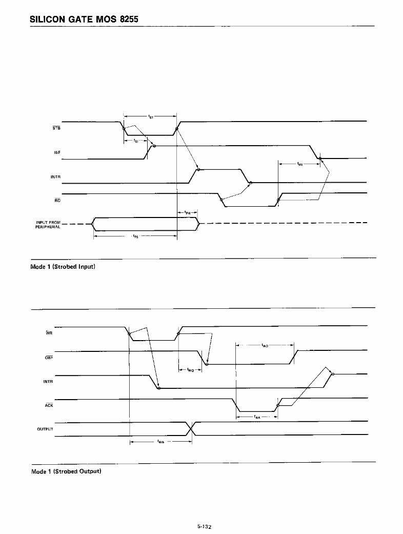
SILICON GATE MOS 8255
IBF
~tRI
INTR
INPUT FROM _PERIPHERAL
I...-----tps-----.·
Mode 1 (Strobed Input)
INTR
OUTPUT
Mode 1 (Strobed Output)
5-132

SILICON GATE MOS 8255 .
WR
tAO
OBF
INTR
ACK
STB
IBF
PERIPHERAL _
BUS
DATA FROMPERIPHERAL TO 8255
Mode 2 (Bi-directional)
5-133
DATA FROM8255 TO 8080


Silicon Gate MOS 8251
PROGRAMMABLE COMMUNICATION INTERFACE
.. Synchronous and AsynchronousOperation
• Synchronous:5-8 Bit CharactersInternal or External Character
SynchronizationAutomatic Sy.nc Insertion
• Asynchronous:5-8 Bit CharactersClock Rate -1,16 or 64 Times
Baud RateBreak Character Generation1, 11h, or 2 Stop BitsFalse Start Bit Detection
• Baud Rate - DC to 56 k Baud ( Sync Mode)DC t09.6k Baud (Async Mode)
• Full Duplex, Double Buffered,Transmitter and Receiver
• Error Detection - Parity, Overrun,and Framing
• Fully Compatible with 8080 CPU• 28-Pin DIP Package• All Inputs and Outputs Are
TTL Compatible
• Single 5 Volt Supply• Single TTL Clock
The 8251 is a Universal Synchronous/Asynchronous Receiver / Transmitter (USA RT) Chip designed for datacommunications in microcomputer systems. The USART is used as a peripheral device and is programmedby the CPU to operate using virtually any serial data transmission technique presently in use (including IBMBi-Sync). The USART accepts data characters from the CPU in parallel format and then converts them intoa continuous serial data stream for transmission. Simultaneously it can receive serial data streams and convert them into. parallel data characters for the CPU. The USART will signal the CPU whenever it can accepta new character for transmission or whenever it has received a character for the CPU. The CPU can read thecomplete status of the USART at any time. These include data transmission errors and control signals suchas SYNDET, TxEMPT. The chip is constructed using N-channel silicon gate technology.
RxRDY
RxC
RxD
TxD
..... SYNDET
TxRDY
TRANSMIT TxECONTROL
TRANSMITBUFFER
(p.... S)
BLOCK DIAGRAM
/INTERNALDATA BUS
Pin Name Pin Function
DSR Data Set ReadyDTR Data Terminal ReadySYNDET Sync DetectRTS Request to Send DataCTS Clear to Send DataTxE Transmitter Empty
Vee +5 Volt SupplyGND Ground
PIN CONFIGURATION
O2 0 1
0 3 Do
RxD Vee
GND RxC
0 4 DTR 0 7 -00
05 RTS
0 6 DSR
0 7 RESET
fXC CLK
WR TxD
CS TxEMPTY
C/O CTS
RD SYNDET
RxRDY TxRDY
Pin Name Pin Function
07-0 0 Data Bus (8 bits)C/O Control or Data is to be Written or Read
AD Read Data Command
WR Write Data or Control Command
Cs Chip EnableCLK Clock Pulse (TTL)RESET ResetTxC Transmitter ClockTxD Transmitter DataRxC Receiver ClockRxD Receiver DataRxRDY Receiver Ready (has character for 8080)TxRDY Transmitter Ready (ready for char. from 8080)
5-135

SILICON GATE MOS 8251
8251 BASIC FUNCTIONAL DESCRIPTION
General
The 8251 is a Universal Synchronous!Asynchronous Receiver/Transmitter designed specifically for the 8080 Microcomputer System. like other I!O devices in the 8080 Microcomputer System its functional configuration is programmedby the systems software for maximum flexibility. The 8251can support virtually any serial data technique currentlyin use (including IBM "bi-sync").
In a communication environment an interface device mustconvert parallel format system data into serial format fortransmission and convert incoming serial format data intoparallel system data for reception. The interface device mustalso delete or insert bits or characters that are functionallyunique to the communication technique. In essence, theinterface should appear "transparent" to the CPU, a simpleinput or output of byte-oriented system data.
Data Bus Buffer
This 3-state, bi-directional,8-bit buffer is used to interfacethe 8251 to the 8080 system Data Bus. Data is transmittedor received by the buffer upon execution of INput or OUTput instructions of the 8080 CPU. Control words, Commandwords and Status information are also transferred throughthe Data Bus Buffer.
ReadlWrite Control logic
This functional block accepts inputs from the 8080 Controlbus and generates control signals for overall device operation.It contains the Control Word Register and Command WordRegister that store the various control formats for devicefunctional definition.
RESET (Reset)
A "high" on this input forces the 8251 into an "Idie" mode.The device will remain at "Idle" until a new set of controlwords is written into the 8251 to program its functionaldefinition.
ClK (Clock)
C/D (Control/Data)
This input, in conjunction with the WR and RD inputs informs the 8251 that the word on the Data Bus is either adata character, control word or status information.1 =CONTROL 0 =DATA
CS (Chip Select)
A "low" on this input enables the 8251. No read ing or writing will occur unless the device is selected.
The ClK input is used to generate internal device timingand is normally connected to the Phase 2 (TTL) output ofthe 8224 Clock Generator. No external inputs or outputsare referenced to ClK but the frequency of ClK must begreater than 30 times the Receiver or Transmitter clock inputs for synchronous mode (4.5 times for asynchronousmode).
WR (Write)
A "Iow" on this input informs the 8251 that the CPU isoutputting data or control words, in essence, the CPU iswriting out to the 8251.
RD (Read)
A "Iow" on this input informs the 8251 that the CPU is inputting data or status information, in essence, the CPU isreading from the 8251.
5-136
c/o RD WR CS
o 0 1 0o 1 0 01 0 1 01 1 0 0X X X 1
8251 => DATA BUSDATA BUS => 8251STATUS=> DATA BUSDATA BUS=> CONTROLDATA BUS=> 3-STATE

SILICON GATE MOS 8251
Modem Control
The 8251 has a set of control inputs and outputs that canbe used to simplify the interface to almost any Modem.The modem control signals are general purpose in natureand can be used for functions other than Modem control,if necessary.
DSR (Data Set Ready)
The DSR input signal is general purpose in nature. Its condition can be tested by the CPU using a Status Read operation. The DSR input is normally used to test Modem conditions such as Data Set Ready.
DTR (Data Termin·al Ready)
The DTR output signal is general purpose in nature. It canbe set "low" by programming the appropriate bit in theCommand Instruction word. The DTR output signal is normally used for Modem control such as Data Terminal Readyor Rate Select.
RTS (Request to Send)
The RTS output signal is general purpose in nature. It canbe set "low" by programr:ning the appropriate bit in theCommand Instruction word. The RTS output signal is normally used for Modem control such as Request to Send.
CTS (Clear to Send)
A "low" on this input enables the 8251 to transmit data(serial) if the Tx EN bit in the Command byte is set to a
"one."
Transmitter Buffer
The Transmitter Buffer accepts parallel data from the DataBus Buffer, converts it to a serial bit stream, inserts the appropriate characters or bits (based on the 'communicationtechnique) and outputs a composite serial stream of data onthe TxD output pin.
Transmitter Control
The Transmitter Control manages all activities associatedwith the transmission of serial data. It accepts and issuessignals both externally and internally to accomplish thisfunction.
TxRDY (Transmitter Ready)
This output signals the CPU that the transmitter is readyto accept a data character~ It can be used as an interrupt tothe system or for the Polled operation the CPU can checkTxRDY using a status read operation. TxRDY is automatically reset when a character is loaded from the CPU.
TxE (Transmitter Empty)
When the 8251 has no characters to transm it, the T xE output will go "high". It resets automatically upon receiving acharacter from the CPU. TxE can be used to indicate theend of a transmission mode, so that the CPU "knows" whento "turn the line around" in the half-duplexed operationalmode.
In SYNChronous mode, a "high" on this output indicatesthat a character has not been loaded and the SYNC character or characters are about to be transmitted automaticallyas "fillers".
TxC (Transmitter Clock)
The Transmitter Clock controls the rate at which the character is to be transmitted. In the Synchronous transmissionmode, the frequency of TxC is equal to the actual BaudRate (1 X). In Asynchronous transmission mode, the fre
quency of TxC is a multiple of the actual Baud Rate. Aportion of the mode instruction selects the value of themultiplier; it can be 1x, 16x or 64x the Baud Rate.
For Example:
If Baud Rate equals 110 Baud,TxC equals 110 Hz (1x)TxC equals 1.76 kHz (16x)TxC equals 7.04 kHz (64x).If Baud Rate equals 9600 Baud,TxC equals 614.4 kHz (64x).
The falling edge of TxC shifts the serial data out of the8251.
5-137

For Example:
SILICON GATE MOS 8251
Receiver Buffer
The Receiver accepts serial data, converts this serial inputto parallel format, checks for bits or characters that areunique to the communication technique and sends an"assembled" character to the CPU. Serial data is input tothe RxD pin.
Receiver Control
This functional block manages all receiver-related activities.
RxRDY (Receiver Ready)
This output indicates that the 8251 contains a character thatis ready to be input to the CPU. RxRDY can be connectedto the interrupt structure of the CPU or for Polled operation the CPU can check the condition of RxRDY using astatus read operation. RxRDY is automatically reset whenthe character is read by the CPU.
RxC (Receiver Clock)
The Receiver Clock controls the rate at which the characteris to be received. In Synchronous Mode, the frequency ofRxCisequal to the actual Baud Rate (1x). In AsynchronousMode, the frequency of RxC is a multiple of the actualBaud Rate. A portion of the mode instruction selects thevalue of the multipl ier; it can be 1x, 16x or 64x the BaudRate.
If Baud Rate equals 300 Baud,RxC equals 300 Hz (1 x)RxC equals 4800 Hz (16x)RxC equals 19.2 kHz (64x).If Baud Rate equals 2400 Baud,RxC equals 2400 Hz (1 x)RxC equals 38.4 kHz (16x)RxC equals 153.6 kHz (64x).
Data is sampled into the 8251 on the rising edge of RxC.
NOTE: In most communications systems, the 8251 will behandling both the transmission and reception operations ofa single link. Consequently, the Receive and Transmit BaudRates will be the same. Both TxC and RxC will require identical frequencies for this operation and can be tied togetherand connected to a single frequency source (Baud RateGenerator) to simpl ify the interface.
SYNDET (SYNC Detect)
This pin is used in SYNChronous Mode only. It is used aseither input or output, programmable through the ControlWord. It is reset to "low" upon RESET. When used as anoutput (internal Sync mode), the SYNDET pin will go"high" to indicate that the 8251 has located the SYNCcharacter in the Receive mode. If the 8251 is programmedto use double Sync characters (bi-sync), then SYNDET willgo "high" in the middle of the last bit of the second Synccharacter. SYNDET is automatically reset upon a StatusRead operation.
When used as an input, (external SYNC detect mode), apositive going signal will cause the 8251 to start assemblingdata characters on the falling edge of the next RxC. Oncein SYNC, the "high" input signal can be removed. The duration of the high signal should be at least equal to the periodof RxC.
\ ADDRESS BUS \Ao
\ CONTROL BUS \I/O R I/OW RESET t/>2
(TTL)
\ DATA BUS \n( ~7 t'\ (
C/O cs 0 7-00 RD WR RESET ClK
8251
8251 Interface to 8080 Standard System Bus
5-138

SILICON GATE MOS 8251
DETAILED OPERATION DESCRIPTION
General
The complete functional definition of the 8251 is programmed by the systems software. A set of control words mustbe sent out by the CPU to initialize the 8251 to support thedesired communications format. These control words willprogram the: BAUD RATE, CHARACTER LENGTH,NUMBER OF STOP BITS, SYNCHRONOUS or ASYNCHRONOUS OPERATION, EVEN/ODD PARITY etc. In theSynchronous Mode, options are also provided to select eitherinternal or external character synchronization.
Once programmed~ the 8251 is ready to perform its communication functions. The TxRDY output is raised "high"to signal the CPU that the 8251 is ready to receive a character. This output (TxRDY) is reset automatically when theCPU wdtes a character into the 8251. On the other hand,the 8251 receives serial data from the MODEM or I/O device, upon receiving an entire character the RxRDY outputis raised "high" to signal the CPU that the 8251 has a complete character ready for the CPU to fetch. Rx RDY is resetautomatically upon the CPU read operation.
The 8251 cannot begin transmission until the TxEN (Transmitter Enable) bit is set in the Command Instruction andit has received a Clear To Send (CTS) input. The TxD output will be held in the marking state upon Reset.
Programming the 8251
Prior to starting data transmission or reception, the 8251must be loaded with a set of control words generated bythe CPU. These control signals define the complete functional definition of the 8251 and must immediately followa Reset operation (internal or external).
The control words are split into two formats:
1. Mode Instruction2. Command Instruction
Mode Instruction
This format defines the general operational characteristicsof the 8251. It must follow a Reset operation (internal orexternal). Once the Mode instruction has been written intothe 8251 by the CPU, SYNC characters or Command instructions may be inserted.
Command Instruction
This format defines a status word that is used to controlthe actual operation of the 8251.
Both the Mode and Command instructions must conform toa specified sequence for proper device operation. The ModeInstruction must be inserted immediately following a Resetoperation, prior to using the 8251 for data communication.
All control words written into the 8251 after the Mode Instruction will load the Command Instruction. Command Instructions can be written into the 8251 at any time in thedata block during the operation of the 8251. To return tothe Mode Instruction format a bit in the Command Instruction word can be set to initiate an internal Reset operationwhich automatically places the 8251 back into the ModeInstruction format. Command Instructions must follow theMode Instructions or Sync characters.
C/O:: 1 MODE INSTRUCTION
C/O:: 1 SYNC CHARACTER 1} SYNC MODE
C/o = 1 SYNC CHARACTER 2 ONLY·
C/D:: 1 COMMAND INSTRUCTION
C/D:: 0 DATA
C/o:: 1 COMMAND INSTRUCTION
C/o:;;: 0 DATA
C/O:::: 1 COMMAND INSTRUCTION
·The second SYNC character is skipped if MODE instructionhas programmed the 8251 to single character Internal SYNCMode. Both SYNC characters are skipped if MODE instructionhas programmed the 8251 to ASYNC mode.
Typical Data Block
5-139

SILICON GATE MOS 8251
Mode Instruction Definition
The 8251 can be used for either Asynchronous or Synchronous data communication. To understand how the ModeInstruction defines the functional operation of the 8251 thedesigner can best view the device as two separate componentssharing the same package. One Asynchronous the otherSynchronous. The format definition can be changed lionthe fly" but for explanation purposes the two formats willbe isolated.
Asynchronous Mode (Transmission)
Whenever a data character is sent by the CPU the 8251automatically adds a Start bit (low level) and the programmed number of Stop bits to each character. Also, an evenor odd Parity bit is inserted prior to the Stop bit(s), as defined by the Mode Instruction. The character is then transmitted as a serial data stream on the TxD output. The serialdata is shifted out on the falling edge of TxC at a rate equalto 1, 1/16, or 1/64 that of the TxC, as defined by the ModeInstruction. 8 REAK characters can be continuously sent tothe TxD if commanded to do so.
When no data characters have loaded into the 8251 theTxD output remains "high" (marking) unless a Break (continuously low) has been programmed.
I~ I81 IEP IPENI~ 1 L1 1 B21 B1 IL BAUD RATE FACTOR
0 1 0 1
0 0 1 1
SYNC (1X) (16X) (64X)MODE
CHARACTER LENGTH
0 1 0 1
0 0 1 1
5 6 7 8BITS BITS BITS BITS
PARITY ENABLE1 = ENABLE 0= DISABLE
EVEN PARITY GENERATION/CHE1 = EVEN 0=000
NUMBER OF STOP BITS
0 1 0 1
0 0 1 1
INVALID 1 1% 2BIT BITS BITS
Mode Instruction Format, Asynchronous Mode
CK
Asynchronous Mode (Receive)
TRANSMITTER OUTPUT
ASSEMBLED SERIAL DATA OUTPUT (TxD)
ST6;"lBrTS L
ST~BITS L
STO[]BITS
......---..a---...&----f
DATA:B\-IT_S_....-.__...
SERIAL DATA INPUT (RxD)
CPU BYTE (5·8 BITS/CHAR)
DATA C~~RACTER
DATA CHARACTER
STARTBIT
RECEIVE FORMAT
RxD
TRANSMISSION FORMAT
RECEIVER INPUT
TxD MARKING
The RxD line is normally high. A falling edge on this linetriggers the beginning of a START bit. The validity of thisSTART bit is checked by again strobing this bit at its nominal center. If a low is detected again, it is a valid STARTbit, and the bit counter will start counting. The bit counterlocates the center of the data bits, the parity bit (if it exists) and the stop bits. If parity error occurs, the parity error flag is set. Data and parity bits are sampled on the RxDpin with the rising edge of RxC. If a low level is detected asthe STOP bit, the Framing Error flag will be set. The STOPbit signals the end of a character. This character is thenloaded into the parallel I/O buffer of the 8251. The RxRDYpin is raised to signal the CPU that a character is ready tobe fetched. If a previous character has not been fetched bythe CPU, the present character replaces it in the I/O buffer, and the OVERRUN flag is raised (thus the previouscharacter is lost). All of the error flags can be reset by acommand instruction. The occurrence of any of these errors will not stop the operation of the 8251.
DATA CHARACTER STOtJBITSf----.&.---.Iooo----t
CPU BYTE (5·8 BITS/CHAR)*
DATA CH:;ACTER
*NOTE: IF CHARACTER LENGTH IS DEFINED AS 5,6 OR 7BITS THE UNUSED BITS ARE SET TO "ZERO".
Asynchronous Mode
5-140

SILICON GATE MOS 8251
o 0 1 1
5 6 7 8BITS BITS BITS BITS
L.....- -.. PARITY ENABLE(1 =ENABLE)(0 = DISABLE)
1 0
CHARACTER LENGTH
o
L.....- .. EVEN PARITY GENERATION/CHECK1 c EVEN0=000
Synchronous Mode (Transmission)
The TxD output is continuously high until the CPU sendsits first character to the 8251 which usually is a SYNCcharacter. When the CTS line goes low, the first characteris serially transmitted out. All characters are shifted out onthe falling edge of TxC. Data is shifted out at the samerate as the TxC.
Once transmission has started, the data stream at TxD output must continue at the TxC rate. If the CPU does not provide the 8251 with a character before the 8251 becomesempty, the SYNC characters (or character if in single SYNCword mode) will be automatically inserted in the TxD datastream. In this case, the TxEMPTY pin is raised high to signal that the 8251 is empty and SYNC characters are beingsent out. The TxEMPTY pin is internally reset by the nextcharacter bei ng written into the 8251.
'"-----------.. EXTERNAL SYNC DETECT1 = SYNDET IS AN INPUTo= SYNDET IS AN OUTPUT
SERIAL DATA INPUT (RxD)
RECEIVE FORMAT
DATACHAR~~C_TE_R_S ___
CPU BYTES (5-8 BITS/CHAR)
~ fDATA CH:~ACTERS
CPU BYTES (5-8 BITS/CHAR)
DATA C~~RACTERS
ASSEMBLED SERIAL DATA OUTPUT (TxD)
DATACHA~~AC_T_E_RS ~
"-------------.... SINGLE CHARACTER SYNC1 = SINGLE SYNC CHARACTER0= DOUBLE SYNC CHARACTER
Mode Instruction Format, Synchronous Mode
Synchronous Mode (Receive)
In this mode, character synchronization can be internallyor externally achieved. If the internal SYNC mode has beenprogrammed, the receiver starts in a HUNT mode. Data onthe Rx.D pin is then sampled in on the rising edge of RxC.The content of the Rx buffer is continuously comparedwith the first SYNC character until a match occurs. If the8251 has been programmed for two SYNC characters, thesubsequent received character is also compared; when bothSYNC characters have been detected, the USART ends theHUNT mode and is in character synchronization. The SYNDET pin is then set high, and is reset automatically by aSTATUS READ.
In the external SYNC mode, synchronization is achieved byapplying a high level on the SYNDET pin. The high level canbe removed after one RxC cycle.
Parity error and overrun error are both checked in the sameway as in the Asynchronous Rx mode.
The CPU can command the receiver to enter the HUNTmode if synchronization is lost.
Synchronous Mode, Transmission Format
5-141

SILICON GATE MOS 8251
COMMAND INSTRUCTION DEFINITION
Once the functional definition of the 8251 has been programmed by the Mode Instruction and the Sync Charactersare loaded (if in· Sync Mode) then the device is ready to beused for data communication. The Command Instructioncontrols the actual operation of the selected format. Functions such as: Enable Transmit/Receive, Error Reset andModem Controls are provided by the Command Instruction.
Once the Mode Instruction has been written into the 8251and Sync characters inserted, if necessary, then all further"control writes" (C/O = 1) will load the Command Instruction. A Reset operation (internal or external) willreturn the 8251 to the Mode Instruction Format.
STATUS READ DEFINITION
In data communication systems it is often necessary toexamine the "status" of the active device to ascertain iferrors have occu rred or other conditions that requ ire theprocessor's attention. The 8251 has facilities that allow theprogrammer to "read" the status of the device at any timedu ring the fu nctional operation.
A normal "read" command is issued by the CPU with theC/O input at one to accomplish this function.
Some of the bits in the Status Read Format have identicalmeanings to external output pins so that the 8251 can beused in a completely Polled environment or in an interruptdriven environment.
TRANSMIT ENABLE1 = enable0= disable SAME DEFINITIONS AS I/O PINS
DATA TERMINAL~ READY
"high" will force DTRoutput to zero
RECEIVE ENABLE'------~ 1 = enable
0= disable
SEND BREAKCHARACTER1 = forces TxD "Iow"o=normal operation
ERROR RESET-----------.. 1 =reset all error flags
PE, OE, FE
REQUEST TO SENDL.-- --.. "high" will force RTS
output to zero
INTERNAL RESETL.-- ....... "high" returns 8251 to
Mode Instruction Format
ENTER HUNT MODEL.-- --.. 1 = enable search for Sync
Characters
Command Instruction Format
PARITY ERRORThe PE flag is set when a parityerror is detected. It is reset bythe ER bit of the CommandInstruction. PE does not inhibitoperation of the 8251.
OVERRUN ERRORThe OE flag is set when the CPUdoes not read a character beforethe next one becomes available.It is reset by the ER bit of theCommand Instruction. OE doesnot inhibit operation of the 8251 ;however, the previously overruncharacter is lost.
FRAMING ERROR (Async only)The FE flag is set when a validStop bit is not detected at theend of every character. It is resetby the ER bit of the CommandInstruction. FE does not inhibitthe operation of the 8251.
Status Read Format
5-142

SILICON GATE MOS 8251
APPLICATIONS OF THE 8251
ADDRESS BUS ADDRESS BUS
CONTROL BUS CONTROL BUS
DATA BUS DATA BUS
r----'I EIA TO TTL :.
QJ)I CONVERT IPHONE(OPT)
8251 L ____ J :: ASYNC LINEMODEM INTER·
BAUD RATE CRT FACETxC GENERATOR TERMINAL 8251
Asynchronous Serial Interface to CRT Terminal,DC-9600 Baud
Asynchronous Interface to Telephone Lines
TELEPHONELINE
ADDRESS BUSL.- .....
SYNCHRONOUSTERMINAL
OR PERIPHERALDEVICE
SYNDET1-----+1
Synchronous Interface to Terminal or Peripheral Device
5-143
SYNCMODEM
Synchronous Interface to Telephone Lines
PHONELINE
INTER·FACE
TELEPHONELINE
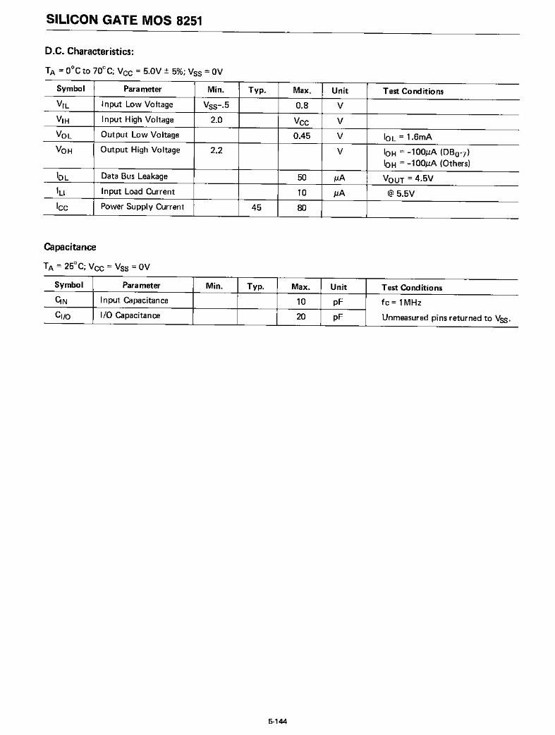
SILICON GATE MOS 8251
D.C. Characteristics:
Symbol Parameter Min. Typ. Max. Unit Test Conditions
V,L Input Low Voltage Vss-·5 0.8 V
VIH Input High Voltage 2.0 Vee V
VOL Output Low Voltage 0.45 V IOl = 1.6mA
VOH Output High Voltage 2.2 V IOH = -1001lA (DBo-7)
IOH = -1001lA (Others)
IOL Data Bus Leakage 50 IJ.A VOUT =4.5V
ILl Input Load Current 10 IlA @5.5V
Icc Power Supply Current 45 80
Capacitance
TA = 25°C; Vee = vss = OV
Symbol Parameter Min. Typ. Max. Unit Test Conditions
CtN Input Capacitance 10 pF fc = 1MHz
CliO I/O Capacitance 20 pF Unmeasured pins returned to Vss.
5-144

SILICON GATE MOS 8251
A.C. Characteristics:
TA = o°c to 70°C; VCC = 5.0V ±5%; Vss = OV
Symbol Parameter Min. Typ. Max. Unit Test Conditions
tCY Clock Period .420 1.35 JlS
t</JW Clock Pulse Width 220 300 ns
tR,tF Clock Rise and Fall Time 0 50 ns
tWR WRITE Pulse Width 430 ns
tos Data Set-Up Time for WR ITE 0 ns
tOH Data Hold Time for WR ITE 65 ns
tAW Address Stable before WR ITE 20 ns
tWA Address Hold Time for WR ITE 35 ns
tRO READ Pulse Width 430 ns
too Data Delay from READ 350 ns CL=100pF
tOF READ to Data Floating 150 ns Cl=100pF
tAR1 Address Stable before READ, CE (C/D) 50 ns
tRA1 Address Hold Time for READ, CE 5 ns
tRA2 Address Hold Time for READ, C/O 370 ns
tOTx TxD Delay from Falling Edge of TxC 1 JlS CL=100pF
tSRx Rx Data Set-Up Time to Sampling Pulse 2 J.l.S Cl=100pF
tHRx Rx Data Hold Time to Sampling Pulse 2 J.l.S CL=100pF
fTx Transmitter Input Clock Frequency1X Baud Rate DC 56 KHz16X and 64X Baud Rate DC 615 KHz
fRx Receiver Input Clock Frequency1X Baud Rate DC 56 KHz16X and 64X Baud Rate DC 615 KHz
tTx TxRDY Delay from Center of Data Bit 16 ClK Period CL=50pF
tRx RxRDY Delay from Center of Data Bit 15 20 ClK Period
tiS Internal Syndet Delay from Center of Data Bit 20 25 ClK Period
tES External Syndet Set-Up Time before Falling 15 ClK PeriodEdge of RxC
Note: The TxC and Rxe frequencies have the following Iimitation with respect to ClK.For ASYNC Mode, tTx or tRx ~ 4.5 tCYFor SYNC Mode, tTx or tRx ~ 30 tCY
5-145

SILICON GATE MOS 8251
READ AND WRITE TIMING
CID,CS. ..,1'----------------""1"---------"1'--D7-DO-----..--'I~
~-- tDS -------1~ ..--
*WRITE ------J---..:.-/'..--- twR1""-'-----...,t.......---
·WRITE AND READ PULSES HAVE NO TIMING LIMITATION WITH RESPECT TO ClK.
TRANSMITTER CLOCK AND DATA
TxC(1xBAUDI
TxC (16x BAUD) 4IlI
--~~fTxD __
I J;:-16 TxC PERIODS-------::;C _
___ x---
RECEIVER CLOCK AND DATA
RXD=..:..t_-tsRX---f:l:--tHRX--~- - - --
RxC (1x BAUD)~'-____________ \
INTERNALSAMPLING nPULSE 10- _
RXD~----STARTBIT----:r __ ~st~A~A:T_-.:-3l=- - --14111--- t SRX ~4IlI---- t HRX~
RiC (16x BAUD)
INTERNAL~~~~ING ---.1 ~~ _
Tx RDY AND Rx RDY TIMING (ASYNC MODE)
RxD ---, START BIT I DATA BITS
tRX qRXRDY___________ __
READ
WRITE
WRITE 1st BYTE WRITE 2nd BYTETx D MA'R'i<'i'NGJ START BIT -I--D-A-TA-BI-T-l~l\-----...------+--~~~~
I. 1st DATA BYTe --------.-1
Tx RDY
Tx EMPTY
INTERNAL SYNC DETECT
1......,---------- SYNC CHARACTER (01101001) ---------1·.-11RxD -----I 1st BIT 1 1 ~AST BIT ,----1-
RESET BYSYNDET tiS ~/ SOFTWARE(OUTPUT)--------------------------~ COMMAND
EXTERNAL SYNC DETECT
n
RxC---,~ ... 1~ ~~I00...-__"""'"
------1F tESSYNDET -(INPUT)
~D:==:==::::==~I~~~~~~~~~~~~~~~~I
114.,...------- 1st DATA BYTE------••11
5-146

Peripherals
82058214
8216/8226


Schottky Bipolar 8205
HIGH SPEED 1 OUT OF 8 BINARY DECODER
• 110 Port or Memory Selector
• Simple Expansion - Enable Inputs
• High Speed Schottky BipolarTechnology - 18ns Max. Delay
• Directly Compatible with TTL LogicCircuits
• Low Input Load Current - .25 mAmax., 1/6 Standard TTL Input Load
• Minimum Line Reflection - LowVoltage Diode Input Clamp
• Outputs Sink 10 mA min.• 16-Pin Dual-In-Line Ceramic or
Plastic Package
The 8205 decoder can be used for expansion of systems which utilize input ports, output ports, and memory components with active low chip select input. When the 8205 is enabled, one of its eight outputs goes"Iow", thus a single row of a memory system is selected. The 3 chip enable inputs on the 8205 allow easysystem expansion. For very large systems, 8205 decoders can be cascaded such that each decoder can driveeight other decoders for arbitrary memory expansions.
The Intel@8205 is packaged in"a standard 16 pin dual-in-line package; and its performance is specified overthe temperature range of O°C to +75°C, ambient. The use of Schottky barrier diode clamped transistors toobtain fast switching speeds results in higher performance than equivalent devices made with a gold diffusion process.
PIN CONFIGURATION LOGIC SYMBOL
Ao 16 V-cc Ao 00
A1 2 15 °0 A, 0,
A2 3 14 0 1 A2 02
E1 4 13 °2 038205 8205
E2 5 12 °3 04
E3 6 11 0 4 E, Os
0 7 7 10 °5 E2 06
GRD 8 9 °6 E3 07
PIN NAMES
AO-A2 ADDRESS INPUTSE,- E3 ENABLE INPUTS
°0.°7 DECODED OUTPUTS
ADDRESS ENABLE OUTPUTSAo A, A2 E, E2 E3 0 , 2 3 4 5 6 7
l l l l l H L H H H H H H HH L L L L H H l H H H H H HL H L l L H H H L H H H H HH H L L L H H H H L H H H HL L H L L H H H H H L H H HH L H L L H H H H H H L H Hl H H L L H H H H H H H L HH H H L L H H H H H H H H LX X X L L L H H H H ... H H HX X X H L L H H H H H H H HX X X L H L H H H H H H H HX X X H H L H H H H H H H HX X X H L H H H H H H H H HX X X L H H H H H H H H H HX X X H H H H H H H H H H H,
5-147

SCHOTTKY BIPOLAR 8205
FUNCTIONAL DESCRIPTION
Decoder
The 8205 contains a one out of eight binary decoder. It accepts a three bit binary code and by gating this input, createsan exclusive output that represents the value of the inputcode.
For example, if a binary code of 101 was present on the AO,A1 and A2 address input lines, and the device was enabled,an active low signal would appear on the 05 output line.Note that all of the other output pins are sitting at a logichigh, thus the decoded output is said to be exclusive. Thedecoders outputs will follow the truth table shown below inthe same manner for all other input variations.
Enable Gate
When using a decoder it is often necessary to gate the outputs with timing or enabling signals so that the exclusiveoutput of the decoded value is synchronous with the overallsystem.
The 8205 has a bu itt-in function for such gating. The threeenable inputs (E 1, E2, E3) are ANDed together and createa single enable signal for the decoder. The combination ofboth active "high" and active "Iow" device enable inputsprovides the designer with a powerfully flexible gating function to help reduce package count in his system.
~
I""
. l-I""
. I-.I""
....-DECODER -....
l-I""
-...............
ENABLE GATE--_"I "' (E'i·"E2·E3).!......I
ADDRESS ENABLE OUTPUTS
A o A, A 2 E, E2 E3 0 1 2 3 4 5 6 7
L L L L L H L H H H H H H HH L L L L H H L H H H H H HL H L L L H H H L H H H H HH H L L L H H H H L H H H HL L H L L H H H H H L H H HH L H L L H H H H H H L H HL H H L L H H H H H H H L HH H H L L H H H H H H H H LX X X L L L H H H H H H H HX X X H L L H H H H H H H HX X X L H L H H H H H H H HX X X H H L H H H H H H H HX X X H L H H H H H H H H HX X X L H H H H H H H H H HX X X H H H· H H H H H H H H
5-148

SCHOTTKY BIPOLAR 8205
APPLICATIONS OF THE 8205
The 8205 can be used in a wide variety of applications inmicrocomputer systems. I/O ports can be decoded from theaddress bus, chip select signals can be generated to selectmemory devices and the type of machine state such as in8008 systems can be derived from a simple decoding of thestate lines (SO, S1, S2) of the 8008 CPU.
I/O Port DecoderShown in the figure below is a typical application of the8205. Address input lines are decoded by a group of 8205s(3). Each input has a binary weight. For example, AO is assigned a value of 1 and is the LSB; A4 is assigned a value of16 and is the MSB. By connecting them to the decoders asshown, an active low signal that is exclusive in nature andrepresents the value of the input address lines, is available atthe outputs of the 8205s.
This circuit can be used to generate enable signals for I/Oports or any other decoder related application.
Note that no external gating is required to decode up to 24exclusive devices and that a simple addition of an inverteror two will allow expansion to even larger decoder networks.
ray of 8205s can be used to create a simple interface to a24K memory system.
The memory devices used can be either ROM or RAM andare 1K in storage capacity. 8308s and 8102s are the devicestypically used for this application. This type of memory device has ten (1 0) address inputs and an active "low" chipselect (CS). The lower order address bits AO-A9 which comefrom the microprocessor are "bussed" to all memory elements and the chip select to enable a specific device or groupof devices comes from t~e array of 8205s. The output ofthe 8205 is active low so it is directly compatible with thememory components.
Basic operation is that the CPU issues an address to identifya specific memory location in which it wishes to "write" or"read" data. The most significant address bits A1O-A14 aredecoded by the array of 8205s and an exclusive, active low,chip select is generated that enables a specific memory device. The least significant address bits AO-A9 identify aspecific location within the selected device. Thus, all ad:dresses throughout the entire memory array are exclusivein nature and are non-redundant.
This technique can be expanded almost indefinitely to support even larger systems with the addition of a few invertersand an extra decoder (8205).
:> ~~MORIES
Ao ~
A, 0, CS,
A2 CS2
CS38205
CS4
~ CSs
E; CS6
E3 CS;
Ao cs;A, csg
A2 CS,o
CSll CHIP8205CS'2
SELECTS
~ CSt3
e; CS'4
E3 ~
Ao CS'6
A, ~ CS17
A2 CS'8
CS'98205
CS20
e; CS2,
e; CS22
E3 CS23
A,O----~......-.-I
All ----.-..-t--I
A'2 ---""-'+--+---4
24K Memory Interface
Ao-Ag''- _
fo
fiPORT
1"2 NUMBERS
13
14GND
15
i6
17
is
f9
20
21
22
23
Chip Select Decoder
Using a very similar circuit to the I/O port decoder, an ar-
Ao Ao °0
A, A, 0,
A2 A2 °2
°38205
°4
A3 E; Os
A4 E2EN E3
Ao °0
A, 0,
A2 °2
°38205
°4
E; °5
EN ~ °6
E3
Ao
A, 0,
A2 °2
°38205
°4
~ °5
EN E2 °6
E3 °7
I/O Port Decoder
5-149
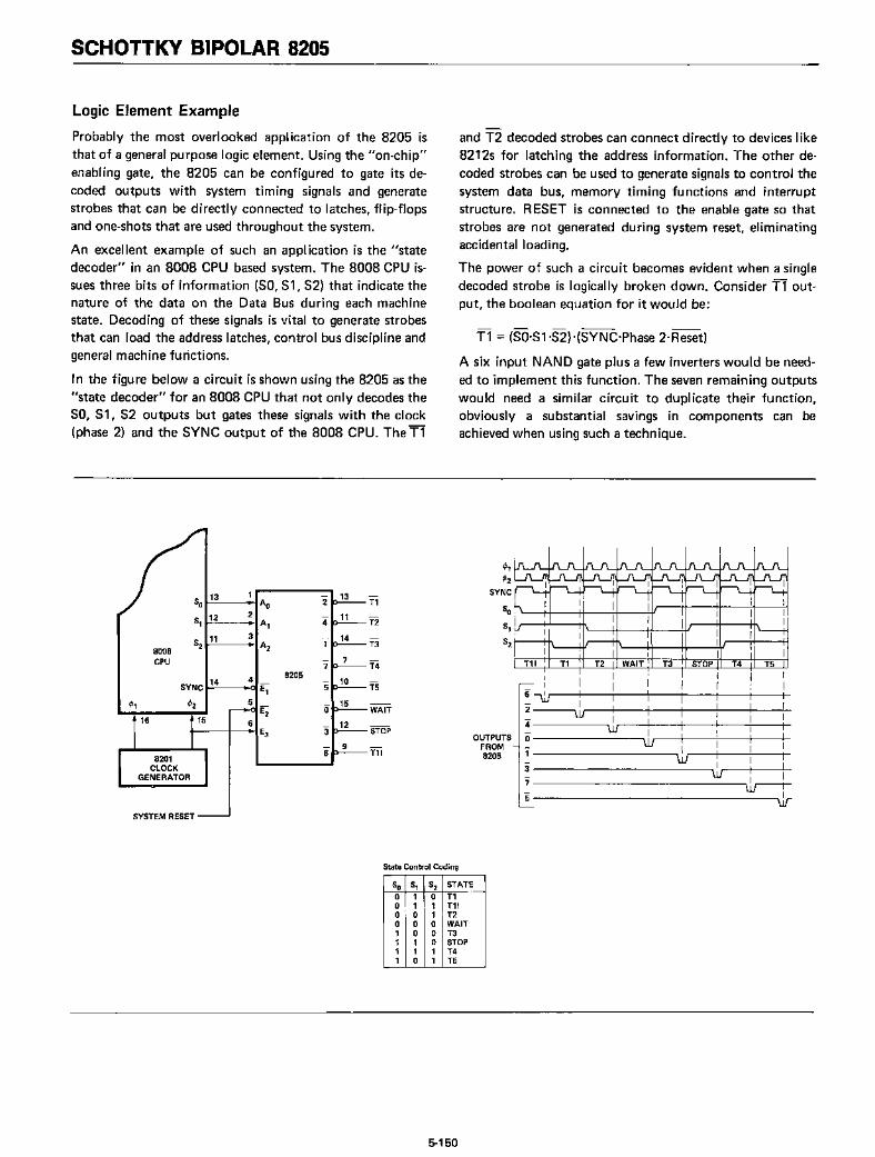
SCHOTTKY BIPOLAR 8205
Logic Element Example
Probably the most overlooked application of the 8205 isthat of a general purpose logic element. Using the lion-chip"enabl ing gate, the 8205 can be configu red to gate its decoded outputs with system timing signals and generatestrobes that can be directly connected to latches, flip-flopsand one-shots that are used throughout the system.
An excellent example of such an appl ication is the "statedecoder" in an 8008 CPU based system. The 8008 CPU issues three bits of information (SO, S1, S2) that indicate thenature of the data on the Data Bus during each machinestate. Decoding of these signals is vital to generate strobesthat can load the address latches, control bus discipline andgeneral machine functions.
In the figure below a circuit is shown using the 8205 as the"state decoder" for an 8008 CPU that not only decodes theSO, 51, 52 outputs but gates these signals with the clock(phase 2) and the SYNC output of the 8008 CPU. The T1
and T2 decoded strobes can connect directly to devices like8212s for latching the address information. The other decoded strobes can be used to generate signals to control thesystem data bus, memory timing functions and interruptstructure. RESET is connected to the enable gate so thatstrobes are not generated during system reset, eliminatingaccidental loading.
The power of such a circuit becomes evident when a singledecoded strobe is logically broken down. Consider T1 output, the boolean equation for it would be:
Tl = (SO·S1·S2)"(SYNC·Phase 2·Reset)
A six input NAND gate plus a few inverters would be needed to implement this function. The seven remaining outputswould need a similar circuit to duplicate their function,obviously a substantial savings in components can beachieved when using such a technique.
STOPT3
II-----i+----+-I
I '----++-------tM---~1
I I I II I I I 1 I
6 \lJ I I I I I I- I 1 I2~ I I I i I4" ----.....,~r----+I---+I--t-I -""'"""I""'"--Ito I ro----++-----:I--+---..-I------~\lJ I I Il------------,.wr----+\--:....1---+-13" ---------------,JJ,.--+-I----.....1
7----------------,1 I5 w--r'ill
OUTPUTSFROM8205
820~
3
2
S 13oS 12,S 11
28008CPU
SYSTEM RESET
State Control Coding
So S, S2 STATE
0 1 0 T10 1 1 T110 a 1 T2a 0 0 WAIT1 0 0 T31 1 0 STOP1 1 1 T41 0 1 T5
5-150

SCHOTTKY BIPOLAR 8205
ABSOLUTE MAXIMUM RATINGS·
Temperature Under Bias: Ceram icPlastic
Storage Temperature
All Output or Supply Voltages
All Input Voltages
Output Currents
-65°C to +125° C-65°C to +75°C
-65°C to +1600 C
-0.5 to +7 Volts
-1.0 to +5.5 Volts
125 rnA
*COMMENTStresses above those listed under "Absolute Maximum Rating" may cause permanent damage to the device. This is a stressrating only and functional operation of the device at these or atany other condition above those indicated in the operationalsections of this specification is not implied. Exposure to absolutemaximum rating conditions for extended periods may affectdevice reliability.
D.C. CHARACTERISTICS TA = OOC to +75°C, Vee = 5.0V ±5%
8205
SYMBOL PARAMETERLIMIT
UNIT TEST CONDITIONSMIN. MAX.
IF INPUT LOAD CURRENT -0.25 rnA Vee =5.25V, VF =0.45V
'R INPUT LEAKAGE CURRENT 10 ~A Vee = 5.25V, VR = 5.25V
Ve INPUT FORWARD CLAMP VOLTAGE -1.0 V Vee =4.75V, Ie = -5.0 rnA
VOL OUTPUT "LOW" VOLTAGE 0.45 V Vee =4.75V, IOl = 10.0 rnA
VOH OUTPUT HIGH VOLTAGE 2.4 V Vee =4.75V, IOH = -1.5 rnA
V1l INPUT "LOW" VOLTAGE 0.85 V Vee = 5.0V
V'H INPUT "HIGH" VOLTAGE 2.0 V Vee = 5.0V
'se OUTPUT HIGH SHORT -40 -120 rnA Vee = 5.0V, VOUT =OV
CIRCUIT CURRENT
Vox OUTPUT "LOW" VOLTAGE 0.8 V Vee = 5.0V, lox = 40 rnA@ HIGH CURRENT
'ee POWER SUPPLY CURRENT 70 rnA Vee =5.25V
TYPICAL CHARACTERISTICS
I IVee::;: 5.0V - -
- ..... TA - OOC
\~f\<TA = 2SoC-rl--..\~TA ::;: 75OC_~\ ,\
\ \ \1\ 1\ ,\. "-~
DATA TRANSFER FUNCTION
oo .2 .4 .6 .8 1.0 1.2 1.4 1.6 1.8 2.0
INPUT VOLTAGE (V)
5.0
4.0
~w~ 3.0::{......Ja>... 2.0~4-...::::>a
1.0
5.01.0 2.0 3.0 4.0
OUTPUT "HIGH" VOLTAGE (V)
OUTPUT CURRENT VS.OUTPUT "HIGH" VOLTAGE
I I I ~I(--- vee = s.ov
IfIt ~ II ......... TA ::;: 25°C
TA ::;: O°C-nrt "TA ::;: 75°C
I~,
I,I
IA
o
-10
-50o
<.§.
~ -20wa:a:~
~ -30~4...~
a -40
1.0.2 .4 .6 .8
OUTPUT "LOW" VOLTAGE (V)
0I000o-...............--1000..........----'-''''''---..1--'''''----1..----1
o
100 --.....,....----~.....--....-------
OUTPUT CURRENT VS.OUTPUT IILOW" VOLTAGE
80 t---+--+---+---+-----Ir----+---+---:.~--#-----t
«.§....z 60 t---t-----t---+---+---f~oII--_+__-f---+-~U.la:a:::>(.)
... 40 t----+--f---+--+-""""*"if---+---+---+----+-----4::>~...::>o
20 t---t---+---JT-~----lf---+---+-----+----+-----t
5-151

SCHOTTKY BIPOLAR 8205
8205 SWITCHING CHARACTERISTICS
CONDITIONS OF TEST: TEST LOAD:
Input pulse amplitudes: 2.5V
Input rise and fall times: 5 nsecbetween 1V and 2V
Measurements are made at 1.5V
390n
2K
All Transistors 2N2369 or Equivalent. eL =30 pF
---..1'1 1'---________~__t+_-_'....t++I-: =b~:.:~-I.-,..--------
I , ,, ,OUTPUT
ADDRESS OR ENABLEINPUT PULSE
TEST WAVEFORMS
A.C. CHARACTERISTICS TA =aoc to +75°C, Vee = 5.0V ±5% unless otherwise specified.
SYMBOL PARAMETER MAX. LIMIT UNIT TEST CONDITIONS
t++ 18 ns
t_+ ADDRESS OR ENABLE TO 18 ns
t+_OUTPUT DELAY 18 ns
t-- 18 ns
C,N(1; INPUT CAPACITANCE P8205 4(typ.) pF f = 1 MHz, Vee = OV
C8205 5(typ.) pF VSIAS = 2.0V, T A :: 250 e1. This parameter is penodically sampled and is not 100% tested.
TYPICAL CHARACTERISTICS
ADDRESS OR ENABLE TO OUTPUTDELAY VS. LOAD CAPACITANCE
ADDRESS OR ENABLE TO OUTPUTDELAY VS. AMBIENT TEMPERATURE
20 ,....-..-------~--........------ 20 ,....-..---...,....-----,-----
Vee = 5.0VCl = 30 pf
o 15 t------+----~I--------I1-- 1W III~..:. ~ t~_..:.~:.. _
~~ t_+ Iw..J
~~ 10
~5w CL
~50°« 51------+------+------1
Vee =5.0VTA =25"C
~ _ 15 ~----+
~ Cm-~~~ g 10 t------+---+----+:::-...-=:;;---4o I- \ ... ",
~~~50 0« 5 1------1----+-----+-----1
7525 SO
AMBIENT TEMPERATURE (OC)
OL..-----....L.....------'-------o20050 100 150
LOAD CAPACITANCE (pf)
o l-.-__..L..-__..1--__.......I...-__~
o
5-152

Schottky Bipolar 8214
PRIORITY INTERRUPT CONTROL UNIT
• Eight Priority Levels• Current Status Register• Priority Comparator
• Fully Expandable• High Performance (50ns)• 24-Pin Dual In-Line Package
The 8214 is an eight level priority interrupt control unit designed to simplify interrupt driven microcomputersystems.
The PICU can accept eight requesting levels; determine the highest priority, compare this priority to a software controlled current status register and issue an interrupt to the system along with vector information toidentify the service routine.
The 8214 is fully expandable by the use of open collector interrupt output and vector information. Controlsignals are also provided to simplify this function.
The PICU is designed to support a wide variety of vectored interrupt structures and reduce package countin interrupt driven microcomputer systems.
PIN CONFIGURATION LOGIC DIAGRAM
[TI> ElR
Bo 24 Vee [}DETlG--
REQUEST ACTIVITYB, 2 23 ECS l!P Ro (OPEN COllECTOR)B2 3 22 R7 ~ R,
~ [DITI> R;SGS 4 21 R6 ~ R; ~ CDINT 5 20 Rs
[1D ~~ ~
A2
elK 6 19 R4 ~ ~ }A8214INTE 18 R3
~ ~
Ao 8 17 R2A>B
IT> 60
}BA, 9 16 R, ED ~
A2 10 15 Ro[I> S;ED SGS PRIORITY
COMPARATORElR 11 14 ENLG ~ ECS
GND 12 13 ETLG
PIN NAMESIT> INTE------------~
[]> ClK-------------~INPUTS
Ro·R7 REQUEST LEVELS (R7 HIGHEST PRIORITY)
Bo·B2 CURRENT STATUS
SGS STATUS GROUP SELECT
ECS ENABLE CURRENT STA"fUS
INTE INTERRUPT ENABLE
CLK CLOCK (tNT F·F)
ELR ENABLE LEVEL READ
E1'\.G ENABLE THIS LEVEL GROUP
OUTPUTS:
Ao·A2 REQUEST LEVELS J-OPENINT INTERRUPT (ACT. LOW) COLLECTOR
ENLG ENABLE NEXT LEVEL GROUP
5-153

SCHOTTKY BIPOLAR 8214
INTERRUPTS IN MICROCOMPUTER SYSTEMS
Microcomputer system design requires that I/O devices suchas keyboards, displays, sensors and other components receive servicing in an efficient method so that large amountsof the total systems tasks can be assumed by the microcomputer with little or no effect on throughput.
The most common method of servicing such devices is thePolled approach. This is where the processor must test eachdevice in sequence and in effect "ask" each one if it needsservicing. It is easy to see that a large portion of the mainprogram is looping through this continuence polling cycleand that such a method would have a serious, detrimentaleffect on system throughput thus limiting the tasks thatcould be assumed by the microcomputer and reducing thecost effectiven.ess of using such devices.
A more desireable method would be one that would allowthe microprocessor to be executing its main program andonly stop to service peripheral devices when it is told to doso by the device itself. In effect, the method would providean external asynchronous input that would inform theprocessor that it should compiete whatever instruction thatis currently being executed and fetch a new routine thatwill service the requesting device. Once this servicing is complete however the processor would resume exactly where itleft off.
This method is called Interrupt. It is easy to see that systemthroughput would drastically increase, and thus more taskscould be assumed by the microcomputer to further enhanceits cost effectiveness.
The Priority Interrupt Control Unit (PICU) functions as anoverall manager in an Interrupt-Driven system environment.It accepts requests from the peripheral equipment, determines which of the incoming requests is of the highest importance (priority), ascertains whether the incoming requesthas a higher priority value than the level currently beingserviced and issues an Interrupt to the CPU based on thisdetermination.
Each peripheral devi~e or structure usually has a specialprogram or "routine" that is associated with its specificfunctional or operational requ irements; this is referred toas a "service routine". The PICU, after issuing an Interruptto the CPU, must somehow input information into the CPUthat can "point" the Program Counter to the service routine associated with the requesting device. The PICU encodes the requesting level into such information for use asa "vector" to the correct Interrupt Service Routine.
5-154
RAM
ROM
Polled Method
RAM
ROM
Interrupt Method
CPU
CPU INT
CPU·DRIVENMULTIPLEXOR
--"""'""

SCHOTTKY BIPOLAR 8214
FUNCTIONAL DESCRIPTION
General
'he 8214 is a device specifically designed for use in realtime, interrupt driven, microcomputer systems. Basically itis an eight (8) level priority control unit that can accepteight different interrupt requests, determine which has thehighest priority, compare that level to a software maintainedcurrent status register and issue an interrupt to the systembased on this comparison along with vector information toind icate the location of the service routine.
Priority Encoder
The eight requests inputs, which are active low, come intothe Priority Encoder. This circuit determines which requestinput is the most important (highest priority) as preassignedby the designer. (R7) is the highest priority input to the8214 and (RO) is the lowest. The logic of the Priority Encoder is such that if two or more input levels arrive at thesame time then the input having the highest priority will takepresidence and a three bit output, corresponding to the active level (modulo 8) will be sent out. The Priority Encoderalso contains a latch to store the request input. This latch iscontrolled by the Interrupt Disable Flip-flop so that oncean interrupt has been issued by the 8214 the request latchis no longer open. (Note that the latch does not store inactive requests. In order for a request to be monitored by the8214 it must remain present until it has been serviced.)
Current Status Register
In an interrupt driven microcomputer system it is importantto not only prioritize incom ing requests but to ascertainwhether such a request is a higher priority than the interruptcurrently being serviced.
The Current Status Register is a simple 4-bit latch that istreated as an addressable outport port by the microcomputer system. It is loaded when the ECS input goes low.
Maintenance of the Current Status Register is performed asa portion of the service routine. Basically, when an interruptis issued to the system the programmer outputs a binarycode (modulo 8) that is the compliment of the interruptlevel. This value is stored in the Current Status Register andis compared to all further prioritized incoming requests bythe Priority Comparator. In essence, a copy of the cu rrentinterrupt level is written into the 8214 to be used as a reference for comparison. There is no restriction to this maintenance, other level values can be written into this registeras references so that groups of interrupt requests may bedisallowed under complete control of the programmer.
5-155
Note that the fourth bit in the register is SGS. This input ispart of the value written out by the programmer and performs a special function. The Priority Comparator will onlyissue an output that indicates the request level is greater thanthe Current Status Register. If both comparator inputs areequal to zero no output will be present. The SGS inputallows the programmer to, in effect, disable this comparisonand allow the 8214 to issue an interrupt to the system thatis based only on the logic of the priority encoder.

SCHOTTKY BIPOLAR 8214
Control Signals
The 8214 also has several inputs that enable the designer tosynchronize the interrupt issued to the microprocessor andto allow or disallow such an issuance. Also, signals are provided that perm it simple expansion to other 8214s so thatmore than eight levels can be controlled.
INTE, elKThe INTE (Interrupt Enable) input allows the designer to"shutoff" the interrupt system under control of externallogic or possibly under software maintenance. A "zero" onthis line will not allow interrupts to be issued to the microcomputer system.
The ClK (Clock) input is actually the trigger that strobesthe Interrupt Flip-Flop. It can be connected to one of theclocks of the microprocessor so that the interrupt issuedmeets the CPU set-up time specification. Note that due tothe gating of the input to the Interrupt Flip-Flop the INToutput will only be active for the time of a single clock period, so external latching may be required to hold this signal.
ElR, ETlG, ENGl
These three signals allow 8214s to be cascaded so that morethan eight levels of interrupt requests can be controlled.
Basically, the ENLG output of one 8214 is connected tothe ETLG input of the next and so on, with the first 8214having its ETLG input pulled "high" and assigned the highest priority. When the ENlG output is "high" it indicatesthat there is no interrupt pending on that device and thatinterrupts can be monitored on the next lower priority8214.
This "cascading" can be expanded almost indefinitely toaccomodate even the largest of interrupt driven systemarch itectu res.
AO, A1, A2
In order to identify which device has interrupted the processor so that the service routine associated with it can beaddressed, a pointer or "vector" must accompany the interrupt issued to the microcomputer system.
The AD, A1 and A2 outputs represent the complement ofthe active interrupt level (modulo 8). By using these signalsto encode the special instruction, RST, the program counterof the microprocessor, can point to the location of theservice routine. Note that these three outputs are gated bythe ELR input and are open collector so that expansion issimplified.
INT
The INT output of the 8214 is the signal that is issued tothe microprocessor to initiate the interrupt sequence. Assoon a INT is active the INT DIS FF is set, inhibiting furtherrequests from entering the Request Latch. Only the writingout of the current status information by strobing the ECSinput will clear the INT DIS FF and allow requests to enterthe latch.
Note that INT is also open collector so that when cascadedto other 8214s an interrupt in any of the active devices willset alllNT DIS FFs in the entire array.
5-156

SCHOTTKY BIPOLAR 8214
APPLICATIONS OF THE 8214
8 Level Controller (8080)
The most common of applications of the 8214 is that of aneight level priority structure for 8080 or 8008 microcomputer systems.
Shown in the figure below is a detailed logic schematic of asimple circuit that will accept eight input requests, maintaincurrent status, issue the interrupt signal to the 8080 and encode the proper RST instruction to gate onto the data bus.
The eight requests are connected to the 8214 by the designer in whatever order of priority is to be preassigned. Forexample, eight keyboards could be monitored and each assigned a degree of importance (level of priority) so thatfaster processor attention or access can be assigned to thecritical or time dependent tasks.
The inputs to the Current Status Register are connected tothe Data Bus so that data can be written out into this "port".
An 8212 is used to encode the RST instruction and also toact as a 3-state gate to place the proper RST instructionwhen the 8080 Data Bus is in the input mode. Note that theINT signal from the 8214 is latched in the SR flip-flop ofthe 8212 so that proper timing is maintained. The 8212 isselected (enabled) when the INTA signal from the 8080status latch and the DB IN from the 8080 are active, this assures that the RST instruction will be placed on the DataBus at the proper time. Note that the INT output from the8212 is inverted and pulled up before it is connected to the8080. This is to generate an INT signal to the 8080 that hasthe correct polarity and meets the input voltage requ irement (3.3V).
Basic Operation
When the initial interrupt request is presented to the 8214it will issue an interrupt to the 8080 if the structure is enabled. The 8214 will encode the request into 3 bits (modulo8) and output them to the 8212. After the acknowledgement of the interrupt has been issued by the 8080 the encoded RST instruction is gated onto the Data Bus by the8212. The processor executes the instruction and points theprogram counter to the desired serviced routine. In thisroutine the programmer will probably save the status of theregister array and flags within a series of PUSH instructions(4). Then a copy of the current interrupt level (modulo 8)can be "built" in the Accumulator and output to the Current Status Register of the 8214 for use as a comparisonreference for all further incoming requests to the system.
This Vectored Eight Level Priority Interrupt Structure for8080 microcomputer systems is a powerful yet flexible circuit that is high performance and has a minimal componentcount.
I PRIORITY RST 1 1 A2 Al Ao 1 1 1REQUEST
LOWEST 0 7 1 1 1 1 1 1 1 11 6 1 1 1 1 0 1 1 12 5 1 1 1 0 1 1 1 13 4 1 1 1 0 0 1 1 14 3 1 1 0 1 1 1 1 15 2 1 1 0 1 0 1 1 16 1 1 1 0 0 1 1 1 1
HIGHEST 7 -0 1 1 0 0 0 1 1 1
-RST 0 WILL VECTOR PROGRAM COUNTER TO LOCATIONo (ZERO) AND INVOKE THE SAME ROUTINE AS "RESET"INPUT TO 8080.THIS COULD RE·INITlALIZE THE SYSTEM BASED ON THEROUTINE INVOKED.(A CAUTION TO SYSTEM PROGRAMMERS.)
8080 BI-DIRECTIONAL BUS
14)
Vee
A6 1K > <C : 1K >10KClK
>7
INTE INT b 5 11INT
.... 23STB 'J INT
(8080 PIN8212
15 _~ ~ Do 000
...!....-'6~ Fr.; ~ 0 1 0°1
617 ~ ~ 818 ::: R2 AQ ",8 9
O2 002 1019 ~ Ai
Ai .... 9 160 3 003 15
20~R;
~10 180 4 0°4 17
21 .... R5 Ai~
05 0°5 1922 ;:: R6
8214 ~0 6 0°6 21R7 0 7 0°7
ETlG13 11-
ClR....
~~ DS2 MD OSl
3 .... S;113 12 01
4~ B2.... SGS GND
E 23 ....NT .... ECSSDECODER) ElR
1~1INTA
ENABlCURRESTATU
(FROM I/O PORT
REQUESTS
INTE
rj>2 (TTL)
GND
8 Level Controller
5-157

SCHOTTKY BIPOLAR 8214
DO 8080 BI-ol RECTIONAL BUS
~ ~~ ~~ ~~ ~0
5T 04
~ I T ~~ I IT ~
I I I T 0 7
~10Kmmn ~INT p23 I I I I I I I I c4> '(808~Np1N 14)
1K~ ~ ~:
INTE • I I I I • I 7 I INTE
~2 (TIL) • I I I I ,6 cl ClK ETLG INT I:> 5 I I I ~ b 11 I STB
PRIORITYARRAY EN
(FROM I/O PORTDECODER)
GND : Do0,
7 09 2
16 ~3 8212
18 04
20 522 0 6
0 7
RESET 14 CLR
oS2 Mo os,ffl1I/OR GND
AO~Ai 9A
210
8214
~GND
~ 137 ClK ETlG
INTE - p51~ INT
,~~~17~R,1B~R2
"'::lI Ri ~~7n::3R'4 A 921 ~ R6 J! 10
?~~ 8214 2
~ ~3 ~4 B2~
2~ ..... -1ECS
ErR ENLG
~GND
~ECS
mJ-
2 ~3 ~4if;s
PRsPFlg
f5R l0PAllPR12PR13PR14PA15
PROPfi lfiR 2PR3PR4PA5PR6PR7
ENABLECURRENTSTATUS 2------~l-
(FROM I/O PORTDECODER)
ENABLECURRENTSTATUS 1
(FROM I/O PORTDECODER)
REQUESTS
16 Level Controller
5-158

SCHOTTKY BIPOLAR 8214
APPLICATIONS OF THE 8214
Cascading the 8214
When greater than eight levels of interrupts must be prioritized and serviced, the 8214 can be cascaded with other8214s to support such an .architecture.
On the previous page a simple circuit is shown that can control 16 levels of interrupt and is easily expandable to support up to 40 levels of interrupt by just cascading more
8214s.
As described previously, there are signals provided in the8214 for cascading (ELR, ETLG, ENLG) and in effect theENLG output of the first 8214 "ripples" down to the nextand so on. The entire array of 8214s regardless of size, canbe thought of as a single priority control unit, with the firsthaving the highest priority and the next 8214 having a lowerpriority and so on.
In this application, the manner in which software handlesthe servicing of the interrupt will change. Since more thaneight vectors must be generated a method other than thecommon RST instruction must be implemented. Basically,the priority control array must somehow modify the contents of the 8080 Program Counter so that it can point("vector") to one of 16 (or how many levels are to beserviced) and fetch the proper service routine. A simple ap-
proach is to treat the priority control array as a single inputport that can input a value into the Accumulator and usethis value as an offset to modify the Program Counter (Indirect Jump).
An initial CALL is needed to invoke this Indirect Jumproutine so the circuitry is configured to insert an RST 7(FFh) for all interrupts, thus the Indirect Jump Routinestarts at location (56d).
The Assembly Code for the flow chart is as follows:
RST7
SAVEPROCESSOR
STATUS
INPUTPRIORITY ARRAY
VALUE
LOADBASE VALUE
INTO H REGISTER
TRANSFERH & L REGISTER
TO PROGRAM COUNTER
SERVICE ROUTINE
IREQUEST (PR) D-7 8-15 - -0 0 0PRIORITIES EN EN A2 A, Ao
LOWEST 0 0 1 1 1 1 0 0 01 0 1 1 1 0 0 0 02 0 1 1 0 1 0 0 03 0 1 1 0 0 0 0 04 0 1 0 1 1 0 0 05 0 1 0 1 0 0 0 06 0 1 0 0 1 0 0 07 0 1 0 0 0 0 0 08 1 0 1 1 1 0 0 09 1 0 1 1 0 0 0 010 1 0 1 0 1 0 0 011 1 0 1 0 0 0 0 012 1 0 0 1 1 0 0 013 1 0 0 1 0 0 0 014 1 0 0 0 1 0 0 0
HIGHEST 15 1 0 0 0 0 0 0 0
(The execution time for the total routine is 35.5 microseconds based on an 8080 clock period of 500ns.)
Following is a basic flowchart of the priority array IndirectJump routine. Note that the last step in the routine willvector the processor to fetch the proper service routine asdictated by the interrupting level.
PUSHPUSHPUSHPUSH
INMOVMVIPCHL
:SW} (save processor status)o (22 microseconds)H
(n) (input Priority Array Value)L,A (transfer Accumulator to L register)H,(n) (load Base Address into H register)
(transfer H&L to Program Counter)
Shown in the figure above is a chart of the 16 different arrayvalues that are used to offset the Program Counter and vector to the proper service routine. These values are the onesthat are loaded into the ilL" register; the value loaded intothe "H" register with an "immediate instruction" is used toidentify the major area of memory where the service routines are stored, similar to a "course setting" and the valuein the ilL" register is used to identify a specific location,similar to a "fine setting".
Note that DO, 01, and D2 are always set to "zero", this provides the programmer eight (8) memory locations betweenthe start of each service routine so that maintenance of theassociated Current Status Register and a JUMP or CALL instruction can be implemented.
This method of interrupt control can be almost indefinitelyexpanded and provides the system designer with a powerfultool to enhance total system throughput.
5-159

SCHOTTKY BIPOLAR 8214
D.C. AND OPERATING CHARACTERISTICS
ABSOLUTE MAXIMUM RATINGS*
Temperature Under Bias O°C to 70°CStorage Temperature -65°C to +150°CAll Output and Supply Voltages. . . . . . . . . . . . . . . . . . . . . . . . . . . . . . . . . . . . . . . . . . . . . . . . . . .. -0.5V to +7VAll Input Voltages. . . . . . . . . . . . . . . . . . . . . . . . . . . . . . . . . . . . . . . . . . . . . . . . . . . . . . . . . . .. -1.0V to +5.5VOutput Currents . . . . . . . . . . . . . . . . . . . . . . . . . . . . . . . . . . . . . . . . . . . . . . . . . . . . . . . . . . . . . . . . .. 100 rnA
*COMMENT: Stresses above those listed under"Absolute Maximum Rating" may cause permanent damage to the device. This is a stress ratingonly and functional operation of the device at these or at any other condition above those indicated in the operational sections of this specifications is not implied. Exposure to absolute maximum ratings for extended periods may affect device reliability.
Symbol ParameterLimits
Unit ConditionsMin. Typ.£1] Max.
Vc Input Clamp Voltage (all inputs) -1.0 V Ic=-5mA
IF Input Forward Current: ETLG input -.15 -0.5 rnA VF=0.45Vall other inputs -.08 -0.25 rnA
IR Input Reverse Current: ETLG input 80 IlA VR=5.25Vall other inputs 40 IlA
Vil Input LOW Voltage: all inputs 0.8 V Vcc=5.0V
VIH Input HIGH Voltage: all inputs 2.0 V Vcc=5.0V
Icc Power Supply Current 90 130 rnA See Note 2.
Val Output LOW Voltage: all outputs .3 .45 V IOl =15mA
VOH Output HIGH Voltage: ENLG output 2.4 3.0 V IOH=-1mA
los Short Circuit Output Current: EN LG output -20 -35 -55 rnA VOs=OV, Vcc=5.0V
ICEX Output Leakage Current: INT and Ao-A2 100 IlA VCEx=5.25V
NOTES:1. Typical values are for T A = 25° C, VCC = 5.0V.2. 80-82, SGS, elK, RO-R4 grounded, all other inputs and all outputs open.
5-160

SCHOTTKY BIPOLAR 8214
A.C. CHARACTERISTICS AND WAVEFORMS TA =o°c to +70°C, vcc =+5V ±5%
LimitsSymbol Parameter Min. Typ.[1] Max. Unit
tCY ClK Cycle Time 80 50 ns
tpw ClK, ECS, INT Pulse Width 25 15 ns
tlSS INTE Setup Time to ClK 16 12 ns
t,SH INTE Hold Time after ClK 20 10 ns
tETCS[2] ETlG Setup Time to ClK 25 12 ns
tETCH[2] ETlG Hold Time After ClK 20 10 ns
tECCS[2] ECS Setup Time to ClK 80 50 ns
tECCH[3] ECS Hold Time After ClK 0 ns
tECRS[3] ECS Setup Time to ClK 110 70 ns
tECRH [3] ECS Hold Time After ClK 0
tECSS[2] ECS Setup Time to ClK 75 70 ns
tECSH[2] ECS Hold Time After ClK 0 ns
tOCS[2] SGS and 80-82 Setup Time to ClK 70 50 ns
tOCH[2] SGS and 80-82 Hold Time After ClK 0 ns
tRCS[31 Ro-R7 Setup Time to ClK 90 55 ns
tRCH[3] Ro-R 7 Hold Time After ClK 0 ns
tiCS INT Setup Time to ClK 55 35 ns
tCI ClK to INT Propagation Delay 15 25 ns
tRIS[41 Ro -R 7 Setup Time to INT 10 0 ns
tRIH[4] Ro-R7 Hold Time After INT 35 20 ns
tRA Ro-R 7 to Ao·A2 Propagation Delay 80 100 ns
tELA ElR to Ao-A2 Propagation Delay 40 55 ns
tECA ECS to Ao-A2 Propagation Delay 100 120 ns
tETA ETlG to Ao-A2 Propagation Delay 35 70 ns
tOECS[41 SGS and 80-82 Setup Time to ECS 15 10 ns
tOECH[4] SGS and 8 0-82 Hold Time After ECS 15 10 ns
tREN Ro-R 7 to EN lG Propagation Delay 45 70 ns
tETEN ETlG to EN lG Propagation Delay 20 25 ns
tECRN ECS to EN lG Propagation Delay 85 90 ns
tECSN ECS to EN lG Propagation Delay 35 55 ns
CAPACITANCE [5]
LimitsSymbol Parameter Min. TypJ1] Max Unit
C,N Input Capacitance 5 10 pF
COUT Output Capacitance 7 12 pF
TEST CONDITIONS: VBIAS = 2.5V, Vce =5V, TA = 25°C, f = 1 MHz
NOTE 5. This parameter is periodically sampled and not 100% tested.
5·161

SCHOTTKY BIPOLAR 8214
WAVEFORMS
ENLG -----------------"'j(-------- -J.\ _
NOTES:
(1) Typical values are for T A = 25°C ,Vee = 5.0V.
(2) Required for proper operation if ISE is enabled during next clock pulse.
(3) These times are not required for proper operation but for desired change in interrupt flip-flop.
(4) Required for new request or status to be properly loaded.
aUTO-....----.----------.
TEST CONDITIONS:
Input pulse amplitude: 2.5 volts.
Input rise and fall times: 5 ns between 1 and 2 volts.
Output loading of 15 rnA and 30 pf.
Speed measurements taken at the 1.5V levels.
5-162
TEST LOAD CI RCUIT
== 30pf
Vee)
300n
600n

Schottky Bipolar 8216/8226
4 BIT PARALLEL BIDIRECTIONAL BUS DRIVER
• Data Bus Buffer Driver for 8080 CPU• Low Input Load Current - .25 mA
Maximum• High Output Drive Capability for
Driving System Data Bus
• 3.65V Output High Voltage for DirectInterface to 8080 CPU
• Three State Outputs
• Reduces System Package Count
The 8216/8226 is a 4-bit bi-directional bus driver/receiver.
All inputs are low power TTL compatible. For driving MOS, the DO outputs provide a high 3.65V VOH, and for high capaci
tance terminated bus structures, the DB outputs provide a high 50mA IOl capability.
A non-inverting (8216) and an inverting (8226) are available to meet a wide variety of applications for buffering in micro
computer systems.
PIN CONFIGURATION
cs 16 Vee
0°0 2 15 OlEN 010
OBo 3 14 0°30°0
010 4 8216/ 13 OB3
DO, 5 8226 12 013 01,
DB, 6 11 0°2DO,
01, 7 10 OB2
GND 8 9 O~ 012
0°2
PIN NAMES 013
OBO·OB3DATA BUSBI-OIRECTIONAL
0'o.0~ DATA INPUT
000.0°3 DATA OUTPUT
OlEN DATA IN ENABLEDIRECTION CONTROL
cs CHIP SELECT
LOGIC DIAGRAM8216
010
OBo
0°0
01, ,
DB,
DO,
012
OB2
0°2
013
OB3
0°3
------+-......----n cs
LOGIC DIAGRAM8226
_----oOBO
_----0 DB,
------+.......----0 csOlEN o---_e_------J
5-163
OlEN 0---.......------1

SCHOTTKY BIPOLAR 8216/8226
FUNCTIONAL DESCRIPTION
DB,
DB,
----OOBO
------oOBO
'--------1- ----0 cs
OlEN cs0 0 Ol~ DB
1 0 OB~ DO
0 1}HIGH IMPEDANCE
1 1
013 0-------+----1 >--+--..
01, 0-------+---1 "--4--..
DO,o------t--~ I--~---'
OlEN~--------......
003o------t-----c: 1-----+-......
010 0-----.... "---1---..
OOoo------t-----c: 1-------1-_ __'
(b) 8226
OlEN
(a) 8216
010
0°0
01,
DO,
012
0°2
013
0°3
Control Gating OlEN, CSThe CS input is actually a device select. When it is "high"the output drivers are all forced to their high-impedancestate. When it is at "zero" the device is selected (enabled)and the direction of the data flow is determined by theDIEN input.
The DIEN input controls the direction of data flow (seeFigure 1) for complete truth table. This direction controlis accomplished by forcing one of the pair of buffers into itshigh impedance state and allowing the other to transmit itsdata. A simple two gate circuit is used for this function.
The 8216/8226 is a device that will reduce component countin mjcrocomputer systems and at the same time enhancenoise immunity to assure reliable, high performance operation.
Bi-Directional Driver
Each buffered Iine of the four bit driver consists of twoseparate buffers that are tri-state in nature to achieve directbus interface and bi-directional capabil ity. On one side ofthe driver the output of one buffer and the input of anotherare tied together (DB), this side is used to interface to thesystem side components such as memories, I/O, etc., because its interface is direct TTL compatible and it has highdrive (50mA). On the other side of the driver the inputsand outputs are separated to provide maximum flexibility.Of ·course, they can be tied together so that the driver canbe used to buffer a true bi-directional bus such as the 8080Data Bus. The DO outputs on this side of the driver have aspecial high voltage output drive capability (3.65V) so thatdirect interface to the 8080 and 8008 CPUs is achieved withan adequate amount of noise immunity (350mV worst case).
Microprocessors like the 8080 are MOS devices and aregenerally capable of driving a single TTL load. The same istrue for MOS memory devices. While this type of drive issufficient in small systems with few components, quite oftenit is necessary to buffer the microprocessor and memorieswhen adding components or expanding to a multi-boardsystem.
The 8216/8226 is a four bit bi-directional bus driver specifically designed to buffer microcomputer system components.
Figure 1. 8216/8226 Logic Diagrams
5-164

SCHOTTKY BIPOLAR 8216/8226APPLICATIONS OF 8216/8226 .
15
4 01 OlEN 30 0 2 DO DB OBo
7
0 16
OB15
982168226 10
D2 11 OB2
1213
DB30 3 14cs
SYSTEM
8080 OATA
15BUS
01 OlEN 3D4 OB OB4DO
6Os DBs
82168226 10
0 6 OB6
0 713
DB7CS
The 8216/8226 can be used in a wide variety of other buffering functions in microcomputer systems such as AddressBus Drivers, Drivers to peripheral devices such as printers,and as Drivers for long length cables to other peripherals orsystems.
8080 Data Bus Buffer
The 8080 CPU Data Bus is capable of driving a single TTLload and is more than adequate for small, single board systems. When expand ing such a system to more than one boardto increase I/O or Memory size, it is necessary to provide abuffer. The 8216/8226 is a device that is exactly fitted tothis application.
Shown in Figure 2 are a pair of 8216/8226 connected directly to the 8080 Data Bus and associated control signals.The buffer is bi-directional in nature and serves to isolate theCPU data bus.
On the system side, the DB lines interface with standardsemiconductor I/O and Memory components and are com-pletely TTL compatible. The DB lines also provide a highdrive capability (50mA) so that an extremely large systemcan be dirven along with possible bus termination networks.
On the 8080 side the 01 and DO lines are tied together andare directly connected to the 8080 Data Bus for bi-directionaloperation. The DO outputs of the 8216/8226 have a highvoltage output capability of 3.65 volts which allows directconnection to the 8080 whose minimum input voltage is3.3 volts. It also gives a very adequate noise margin of350mV (worst case).
The DIEN inputs to 8216/8226 is connected directly to the8080. OlEN is tied to DBIN so that proper bus flow ismaintained, and CS is tied to BUSEN so that the systemside Data Bus will be 3-stated when a Hold request has beenacknowledged during a DMA activity.
I/O
01 DO
OlEN (2) CS82168226 (2)
BUSEN ........----~
MEMORY
01 DO
OlEN (2) CS82168226 (2)
Figure 2. 8080 Data Bus Buffer.
Memory and 1/0 Interface to a Bi-directional Bus
In large microcomputer systems it is often necessary to provide Memory and I/O with their own buffers and at the sametime maintain a direct, common interface to a bi-directionalData Bus. The 8216/8226 has separated data in and dataout lines on one side and a common bi-directional set on theother to accomodate such a function.
Shown in Figure 3 is an example of how the 8216/8226 isused in this type of application.
The interface to Memory is simple and direct. The memoriesused are typically Intel® 8102, 81 02A, 8101 or 8107B-4 andhave separate data inputs and outputs. The DI and DO linesof the 8216/8226 tie to them directly and under control ofthe MEMR signal, which is connected to the DIEN input,an interface to the bi-directional Data Bus is maintained.
The interface to I/O is similar to Memory. The I/O devicesused are typically Intel® 8255s, and can be used for bothinput and output ports. The I/O R signal is connected directly to the DI EN input so that proper data flow from theI/O device to the Data Bus is maintained.
Figure 3. Memory and I/O Interface to a Bi-Directional Bus.
5-165

SCHOTTKY BIPOLAR 8216/8226
D.C. AND OPERATING CHARACTERISTICS
ABSOLUTE MAXIMUM RATINGS*
Temperature Under Bias ' O°C to 70°C
Storage Temperature -6SoC to +150°C
All Output and Supply Voltages. . . . . . . . . . . . . . . . . . . . . . . . . . . . . . . . . . . . . . . . . . . . . . . . . . .. -O.5V to +7V
All Input Voltages -1.0V to +5.5V
Output Currents . . . . . . . . . . . . . . . . . . . . . . . . . . . . . . . . . . . . . . . . . . . . . . . . . . . . . . . . . . . . . . . . .. 125 rnA
*COMMENT: Stresses above those listed under "Absolute Maximum Rating" may cause permanent damage to the device. This is a stress ratingonly and functional operation of the device at these or at any other condition above those indicated in the operational sections of this specification is not implied.
LimitsSymbol Parameter Min. Typ. Max. Unit Conditions
IF1 Input Load Current OlEN, CS -0.15 -.5 mA VF =0.45
IF2 Input Load Current All Other Inputs -0.08 -.25 mA VF =0.45
IR1 Input Leakage Current OlEN, CS 20 p.A VR =5.25V
IR2 Input Leakage Current 01 Inputs 10 p.A VR =5.25V
Vc Input Forward Voltage Clamp -1 V le= -5mA
Vil Input "Low" Voltage .95 V
VIH Input "H igh" Voltage 2.0 V
1101Output Leakage Current DO 20 p.A Vo = 0.45V/5.25V(3-State) DB 100
8216 95 130 rnAIcC Power Supply Current
8226 85 120 rnA
VOl1 Output" Low" Voltage 0.3 .45 V DO Outputs IOl=15rnADB Outputs IOl=25rnA
8216 0.5 .6 V DB Outputs IOl=55mAVOl2 Output "Low" Voltage
8226 0.5 .6 V DB Outputs IOL=50mA
VOH1 Output "High" Voltage 3.65 4.0 V DO Outputs IOH = -1 mA
VOH2 Output "High" Voltage 2.4 3.0 V DB Outputs 10H = -1 OmA
'OS Output Short Circuit Current -15 -35 -65 mA DO Outputs Vo==OV,-30 -75 -120 rnA DB Outputs Vee=5.0V
NOTE: Typical values are for TA = 25°C, Vee = 5.0V.
5-166

SCHOTTKY BIPOLAR 8216/8226
WAVEFORMS
INPUTS -'X'-:,_5V _
l--tFD
OUTPUTENABLE
.5V
---+---VOH
f VOL
.5V
A.C. CHARACTERISTICS
TA = O°C to +70°C, Vcc = +5V ±5%
Limits
Symbol Parameter Min. Typ,£1] Max. Unit Conditions
TpD1 Input to Output Delay DO Outputs 15 25 ns CL=30pF,R 1=300n
R2=600n
TpD2 Input to Output Delay DB Outputs
8216 20 30 ns C L=300pF,R 1=90n
8226 16 25 ns R2 = 180n
TE Output Enable Time
8216 45 65 ns (Note 2)
8226 35 54 ns (Note 3)
To Output Disable Time 20 35 ns (Note 4)
TEST CONDITIONS:
Input pulse amplitude of 2.5V.
Input rise and fall times of 5 ns between 1 and 2 volts.
Output loading is 5 rnA and 10 pF.
Speed measurements are made at 1.5 volt levels.
Capacitance [5]
TEST LOAD CI RCUIT
OUT 0---.......------......
LimitsSymbol Parameter Min. Typ'£1] Max. Unit
CIN Input Capacitance 4 8 pF
COUT1 Output Capacitance 6 10 pF
CO UT2 Output Capacitance 13 18 pF
TEST CONDITIONS: VB1AS =2.5V, Vcc =5.0V, TA =25°C, f = 1 MHz.
NOTES: 1. Tvpical values are for TA = 25°C, VCC = 5.0V.2. DO Outputs, CL = 30pF, R1 = 300/10 Kil, R2 = 180/1 Kil; DB Outputs, CL = 300pF, Rl = 90/10 Kil, R2 = 180/1 Kil.3. DO Outputs, CL = 30pF, Rl = 300/10 Kil, R2 = 600/1 K; DB Outputs, CL = 300pF, Rl =90/10 Kfl, R2 =180/1 Kil.4. DO Outputs, CL = 5pF, Rl =300/10 Kil, R2 = 600/1 Kil; DB Outputs, CL = 5pF, R1 = 90/10 Kil, R2 = 180/1 Kil.5. This parameter is periodically sampled and not 100% tested.
5-167


Coming Soon
825382578259


Silicon Gate MOS 8253
PROGRAMMABLE INTERVAL TIMER
GATE 0
It uses nMOS technology
~----"OUT2
ClKO
ClK2
ClK 1
...------..OUT 0
COU':;TER 14'-_ GATE 2
COUNTER#1 GATE 1
.....---. OUT 1
z. ~Jmodes'of operation arev"'."-
~O
S",9
• Count Binary or BCD
• Single +5V SUPR• 24 Pin Dual-in-li
CONTROLWORD
REGISTERAND
MODESELECTION
PIN CONFIGURATION
• 3 Independent 16-BitCounters
• DC to 3 MHz• Programmable Counter
Modes
The 8253 is a programmable counter/timer chip designed for use as an 8080 (orwith a single +5V supply and is packaged in a 24-pin plastic DIP.
It is organized as three independent 16-bit counters, each with a count ratsoftware programmable by the 8080.
INTERNAL BUS /
5-169

SILICON GATE MOS 8253
8253 PRELIMINARYFUNCTIONAL DESCRIPTION
GATE 2
GATE 0
ClK 1
CLKO
CLK2
OUT2
OUT 1
GATE 1
COUNTER#2
READ/WRITElOGIC
DATABUS
BUFFER
INTERNAL BUS
cs-------'
AD --___.aWR -----+C11
8253 Block Diagram.
In Microcomputer-based systems the most common interface is to a mechanical device such as a printer head or stepper motor. All such devices have inherent delays that mustbe accounted for if accurate and reliable performance is tobe achieved. The systems software allows for such delays byprogrammed timing loops. This type of programming requires significant ov~rhead and maintenance of multipleloops gets extremely complicated.
The 8253 Programmable Interval Timer is a single chip solution to system timing problems. In essence, it is a group ofthree 16-bit counters that are independent in nature butdriven commonly as I/O peripheral ports. Instead of settingup timing loops in the system software, the programmerconfigures the 8253 to match his requirements. The programmer initializes one of the three counters of the 8253with the quantity and mode desired then, upon command,the 8253 will count out the delay and interrupt the microcomputer when it has finished its task. It is easy to see thatthe software overhead is minimal and that multiple delayscan be easily maintained by assigned interrupt levels to different counters. Other functions that are non-delay in natureand require counters can also be implemented with the 8253.
• Programmable Baud Rate Generator
• Event Counter• Binary Rate Multiplier• Real Time Clock
System Interface
The 8253 is a component of the MC5-80 system and interfaces in the same manner as all other peripherals of thefamily. It is treated by the systems software as an array ofI/O ports; three are counters and the fourth is a controlregister for programming. The OUT lines of each counterwould normally be tied to the interrupt request inputs ofthe 8259.
The 8253 represents a significant improvement for solvingone of the most common problems in system design andreducing software overhead.
ADDRESS BUS (16)
A1 An 0 0.07
8253
COUNTER COUNTER COUNTER012I I I
lOUT GATE ClK I lOUT GATE ClK I lOUT GATE ClK I
8253 System Interface.
5..170

Silicon Gate MOS 8257
PROGRAMMABLE DMA CONTROLLER
ORO 3
oACK 2
OACK 3
ORO 2
OACK 1
OACK 0
+-- ORO 1
cl}mputer systems. Its priallow the peripheral to ac
; the system bus. It also keeps"grar11mable terminal count has
~<,
amon9,$fl'e four channels, program-for s~~tbred data transfers, an auto
/'dur!~:~i)DMA cycles. There are three
PRIORITYRESOLVER
e ¢2,.JJTL) clock of the 8080 system. It is'"Mulff;J3I'e DMA chips can be used to expand
~..,.::-,/
c~::~"t
• Auto Load Mode• Single TTL Clock «(/)21TTL)
• Single +5V SUR~~~~:W~l~\:~~ '.'.,
• Expandable
• 40 Pin Du
A4 ----1
As ----1
A6 ----1
A7 ----1
CONTROLHOLD ..........---1 LOGIC
HLDA----..
MEMR ---ClIII
MEMW ----<...JI
AEN ----1
AoSTB ----1
cs-----
REAoY----.tI
• Four Channel DMA Controller• Priority DMA Request Logic• Channel Inhibit Logic• Terminal and Modulo 256/128
Outputs
The 8257 is a Direct Memory Access (DMA) Chip which has four channels for use imary function is to generate, upon a peripheral request, a sequential memory a resscess or deposit data directly from or to memory. It uses the Hold feature of thcount of the number of DMA cycles for each channel and notifies the periphebeen reached. Other features that it has are two mode priority logic to res/mabie channel inhibit logic, an early write pulse option, a modulo 256/1matic load mode, a terminal count status register, and control signaL;:-· .types of DMA cycles: Read DMA Cycle, Write DMA Cycle and Verify,/,t
The 8257 is a 40-pin, N-channel MOS chip which uses a single ~;
designed to work in conjunction with a single 8212 8-bit, thr~
the number of channels with the aid of the 8214 Priority Inter'
TC ..........----'"
128/256 ..----------'
INTERNALBUS
5-171

SILICON GATE MOS 8257
8257 PRELIMINARY FUNCTIONAL DESCRIPTION
The transfer of data between a mass storage device such asa floppy disk or mag cassette and system RAM memory isoften limited by the speed of the microprocessor. Removingthe processor during such a transfer and letting an auxiliarydevice manage the transfer in a more efficient manner wouldgreatly improve the speed and make mass storage devicesmore attractive, even to the small system designer.
The transfer technique is called DMA (Direct Memory Access); in essence the CPU is idled so that it no longer hascontrol of the system bus and a DMA controller takes overto manage the transfer.
The 8257 Programmable DMA Controller is a single chip,four channel device that can efficiently manage DMA activities. Each channel is assigned a priority level so that ifmulti-DMA activities are required each mass storage devicecan be serviced, based on its importance in the system. In
operation, a request is made from a peri phera I device foraccess to the system bus. After its pr iority is accepted aHOLD command is ussued to the CPU, the CPU issuesa HLDA and that DMA channel has complete control of thesystem bus. Transfers can be made in blocks, suspendingthe processors operation during the entire transfer or, thetransfer can be made a few bytes at a time, hidden in theexecution states of each instruction cycle, (cycle-stealing).
The modes and priority resolving are maintained by thesystem software as well as initializing each channel as to thestarting address and length of transfer.
The system interface is si mi lar to the other peri phera Is ofthe MCS-80 but an additional 8212 is necessary to controlthe entire address bus. A special control signal BUSEN isconnected directly to the 8228 so that the data bus andcontrol bus will be released at the proper time.
ADDRESS BUS
\ ADDRESS BUS (16) \
~ CONTROL BUS \flOW ilOR HOLD RESET
~ DATA BUS (8) \As-A,5
4:/'\~MEMR MEMW READY
1/ V8
/ Ao-A3 / A4 -A7
'--- l/L-- 88212 ['r-
92(TTL)t t HLDA
BUSEN8228 I 1 "',/7
CS Ao·A3 A 4-A7 AOSTB AEN 0 7 -00 I/O MEM HOLD HLOA CLK ROYIN RESETW R if W8257
128/256 DACK ORO DACK ORO DACK ORO DACK OROMOD TC 3 3 2 2 1 1 0 0
~ ! ~ t l t l 1 l fI
OMA CHANNEL REOUESTS AND ACKNOWLEDGES
System Interface 8257.
8257AND8212
ORO 0 ......-----11
DACK 0 1------..ORO 11..-----1
DACK 1I___-----.t
ORO 2 ......----11
DACK 2 1------...ORO 3 1+------1
DACK 31--------..
DISK 1
DISK 2
SYSTEMRAM
MEMORY
OMA CONTROLLER
System Application of 8257.
DUAL FLOPPY DISK CONTROLLER
5-172

Silicon Gate MOS 8259
PROGRAMMABLE INTERRUPT CONTROLLER
r up to 64 vectored prioritytechnology and requires a
IR 04---IR 1
REQUEST IR 2LATCH 4--- IR 3 INTERRUPTMASK .-- IR 4 REQUESTS
REGISTER 4--- IR 5"'-IR6"'-IR7
READ!WRITELOGIC
• Individual Request MaskCapability
• Single +5V Sup(No Clocks)
• 28 Pin Dua ckage
o
CS-------ItCASO~--.nI
CAS1 ....--....n
CAS 2 """---.nII
SP ~--.nII CONTROLLOGIC
PIN CONFIGURATION
• Eight Level Priority Controller• Expandable to 64 Levels• Programmable Interrupt
Modes (Algorithms)
The 8259 handles up to eight vectored priority interrupts for the 8080A CPU. Iinterrupts, without additional circuitry. It will be, packaged in a 28-pin plasfsingle +5V supply. Circuitry is static, requiring no clock input.
The 8259 is designed to minimize the software and real time overhead inmodes, permitting optimization for a variety of system requirements.
INT......----I
INTA---.nI ~INTERNALBUS
5-173

SILICON GATE MOS 8259
8259 PRELIMINARYFUNCTIONAL DESCRIPTION
IINTERRUPTREQUESTS
8259
IRQ IRQ IRQ IRQ IRQ IRQ IRQ IRQ765 4 ~ 2 1 0
SLAVEPROG.
ADDRESS BUS (16)
8259 System Interface.
In microcomputer systems, the rate at which a peripheraldevice or devices can be serviced determines the total amountof system tasks that can be assigned to the control of themicroprocessor. The higher the throughput the more jobsthe microcomputer can do and the more cost effective it becomes. Interrupts have long been accepted as a key to improving system throughput by servicing a peripheral deviceonly when the device has requested it to do so. Efficientmanaging of the interrupt requests to the CPU will have asignificant effect on the overall cost effectiveness of themicrocomputer system.
The 8259 Programmable Interrupt Controller is a single-chipdevice that can manage eight levels of requests and has builtin features for expandability to other 8259s (up to 64 levels).It is programmed by the systems software as an I/O peripheral. A selection of priority algorithms is available to the programmer so that the manner in which the requests are processed by the 8259 can be configured to match his systemrequirements. The priority assignments and algorithms canbe changed or reconfigured dynamically at any time duringthe main program. This means that the oomplete interruptstructure can be defined as required, based on the total system environment.
The system interface is the same as other peripheral devicesin the MC5-80. A special input is provided (SP) to programthe 8259 as a slave or master device when expanding tomore than eight levels. Basically the master accepts INT inputs from the slaves and issues a composite request to the8080A; when it receives the INTA from the 8228 it putsthe first byte on the CALL on the bus. On subsequentINTAs the interrupting slave puts out the address of thevector.
~ ADDR ESS BUS (16) ~
\ CONTROL BUS \INT REQ
\ DATA BUS (8) \.",- to/'.. ,t./'..,t. :lo
--- --- --- --- I----
-- ~ - 1-- --- ~ - --I- ~
-- I-- - I- - -- ---I-- I----
(~v'7 ~V7 r-- ~,7 "''...1''1 ~v'7 "'v'7
""' '"
8259 8259 8259
SLAVE 2p.- I-- SLAVE 1 '" MASTER
p...t- ""' '"Sf SP SP
G!O 1 fIll f 11 G!O f f f fIlII lJJ J 1111 ,21 20 19 18 17 16 15 14 13 12 11 10 9 8 7 6 5 4 3 2 1 0
IINTERRUPT REQUESTS
Cascading the 8259 22 Level Controller (Expandable to 64 levels).
5-174

CPUGROUP
ROMs
RAMs
I/O
PERIPHERAL
COMINGSOON
Intel StandardNumber
Product PackageOf Pins
CommentsNumber Type
8224 C 0 P 16
- 8228 C 0 P 28
8080A C 40Including 8080A-1,8080A-2 and M8080A
8702A C 24
8708/4 C 24
- 8302 C P 24
8308 C P 24
8316A C P 24
8101-2 C P 22
8111-2 C P 18
8102-2 C P 16
8102A-4 C P 16-
81078-4 C P 22
5101 C P 22
8210 0 P 18
8222 D 22 New Product
8212 0 P 24
- 8255 C 40
8251 C P 28
8205 C 0 P 16
- 8214 C 0 P 24
8216/26 0 P 16
8253 24 Coming Soon
- 8257 40 Coming Soon
8259 28 Coming Soon
C = Ceramic 0 = Cerdip P = Plastic
6·1

PACKAGING INFORMATION Dimensions in inches and (millimeters).
16-LEAD CERAMIC DUAL IN-LINE PACKAGE (C) 16-LEAD CerDIP DUAL IN-LINE PACKAGE (D)
I---l-~~ TYP..11012,7941
~:[O:::JJI .735~ I
.830 121,0821
~!2.ill1_.023 10,5841
:Q!Q~-.06511.651
~~.070 (1,778)
16-LEAD PLASTIC DUAL IN-LINE PACKAGE (P) 1a-LEAD CERAMIC DUAL IN-LINE PACKAGE (C)
f----- -- --~ lli!.mlI _ .855121,7171
.050 11,271MAX.
I 1-.290~-l
?ml17'~741~
-II-, ~-1 I-~~TYP.•012 (0,3051
.-r--t==:I..lI::t.~....:::::::Io.I:=--e::s...c:~::::IiIloI~.,
I~~.29517,493)
ALTERNATE PIN ;:1 IDENT.(IF NO NOTCH AT END OF PKG.I
rr
~:~':~:1.0751t.9051 .025 10,6351l REF'r- I REF.
R,~t
.OO8~
:Di2 10,3051
I ~~ II--- .410 110.41414
1a-LEAD CerDIP DUAL IN-LINE PACKAGE (D) 1a-LEAD PLASTIC DUAL IN-LINE PACKAGE (P)
I,B50~ I.930 123,62)
C:=§'.240~:'L1
I ,905~ I.925 (23,495)
1
1-.045 /1,141 .07011,7B}
- I :07011,7BI :i1ii112..l91
i'i=i::::i"=i:=i=1=i:::1::;::::;i::::i=:::;::::::j;:::::=c::::;=;::::;::::=;=;:=r~-+ ll~~') MAX
I t
! JIO,511--r- .050 11,27}
.100 (2,541
:;so 13,81)
f20015,~ .140~
~ T.2~l~~' .- _.._-- - -- -- - - _. -LL~ I • ].075/1,905)
! I JL REF.
,057~~i4611 -l~~~• ~~ ~~ .032(0,8131' 1·15013,Bl}
.11012,794} .065/1,6511 REF.:21§~
.024 IO,610}
.10012,54}REF,
It-j
22-LEAD CERAMIC DUAL IN-LINE PACKAGE (C)
114·-------~:~~e------- ....·1PIN#lIDr
~lMW ............ 25R.REF
.4~[Lr-__.....,--,.....,--,. ,..........,.....,--,-.....,........,......,......,.-.,.......,. (NOTCH OPTIONAl)
~~.040 /1,016) ,054~
t * :oso (r0321
200 Is,oa;f ~MAX, L...i.
L1
Jl II L /I f .39Ol!.!!!!L:~:~. ~~ -.j f4-~=, Ji50 /1,271 -.ff.- .010 (()~:10,414)
~,.-----10 Ea. [email protected],540)
6-2

PACKAGING INFORMATION Dimensions in inches and (millimeters).
22-LEAD PLASTIC DUAL IN-LINE PACKAGE (P)
PIN 1
~I·34o~
.360 19.144)
.126 13.175) I
1;r==i="-.=:::::p;;;;;r==:p;;;;r=;~==p:;r=::::p;:;;;;r=:::;;:::;;r==Fr===r;;;;;:;==;:;:or="'~
.025 10,635)
I. 1.090~) I I RjF.
1.110128.194) ---l-
.02010,508) - - - - - ::r~ :tMIN. .160 14,0641
-L -.L
--r- Il .~II.15013,81) ~ --==l O'
\.--.J..'~~~l j ~ -j h j -L-i~.•,~~::~, •.'.1 ...~=.03~~p~'3) .06~~p~24)
24-LEAD CERAMIC DUAL IN-LINE PACKAGE (C)24-LEAD CerDIP DUAL IN-LINE PACKAGE (D)
~:: :::::------h
.550 113.97)
.....................................................................,..,.l1'u,I
PIN 1 -----.J L:Qg~ TYP11.060 (1,624) .
NOTE 1. 0.126 (3.176) MAX.
NOTE 2. 0.050 11,279) MAX.
~~.012 (0,305)
NOTE 1
I1.175~ U .050 llJ1ID REF
·D4~~F·'i 1.300 133.0'01~_~3.D481 #:."'" r-------.
~~~~~Tt 11~~l\-r-::..I h .032(O,813)--1h 0" -/ ~~I '1 TYP. I 15° / ~=
:~g~ TYP. ~~ TYP. BEND LINE
I__'~ 112.701__1
.800 115,241.07011.78)
.110,12.79)
...--.....-----------.... I 120-liIS.59) MAX." ..__.........__.. n
-+t t __ .~(0.20)
.020 (0.511 .012 (0.30)
.05011.27) 1_~115,24)-1.~ 12,54) .730 118,64) I.150 (3,81)
.015 (0,38)
:023 (0,581 I
.0076 (0.19) I I
.0116 (0.29) - r I~.090(2.29)r-r:iiO(2.79)
24-LEAD PLASTIC DUAL IN-LINE PACKAGE (P) 28-LEAD CERAMIC DUAL IN-LINE PACKAGE (C)
I.... ~:=~-----.I
I'1.40 13.556)
'1MAX.
D t,ill1.!.M§§J.588 (14.735)
~
j ~"30(&'''')~ MAX.-,-- -.020 (0,508) ~
MIN. I~ ~ I :1Q:Q~.015~_ .090~ .150(3.8101m 10.584) -:roo 12.6401 TYP.
(REF)
•190 14,826)-. REF.
----l..150(3.81)
REF.
.250(6,35)REF•
•200 '&,081. .07011.n8) "-MAX. REF. I-±-If ---- .145~Y *~(4,'9')
I 'I JL ---.~ .020 (0,508)
I . .032 (0,813) II -..j " MIN.
-1 f- .06011,524) REF. r-l~ .100 (2,64)REF. ~~ TYP.
•023 (0,684)
40-LEAD CERAMIC DUAL IN-LINE PACKAGE (C)2·,c:l~,34}- 1
PIN 1-r~~
.,..,,..,..,,..,..,l"T"'ll"T"'lrT"'ll"T"'l,.,..,r-r;p:iiiiii~;:;;::;~~"I""'I'''I'''''I'''I'''''W'''I'''''W' ...........~••361
I ~230 1&.6421..i- MAX...o,.r:: - j tMIN. IL I L --t...1oo~1
_ &!§~ _ ~~TYP :16013.81).02310.5841 .11012.7941'
6-3

SALES AND MARKETING OFFICES
U.S. SALES AND MARKETING OFFICESU.S. MARKETING HEADQUARTERS NATIONAL SALES MANAGER3065 Bowers Avenue Hank O'HaraSanta Clara, California 95051' 3065 Bowers AvenueTel (408) 246-7501 Sanla Clara. California 95051'TWX: 910-338-0026 Tel (408) 246·7501TELEX: 34-6372 TWX 910-338·0026
TELEX' 34-6372
U.S. REGIONAL SALES MANAGERS' OFFICESWESTERN MID-AMERICAWilliam T. O'Brien Mick Carrier1651 East 4th Street 6350 LBJ. FreewaySuite 228 SUIte 178Santa Ana, California 92701· Dallas. Texas 75240'Tel (714) 835-9642 Tel (214) 661-8829TWX. 910-595-1114 TWX 910-860-5487
NATIONAL DISTRIBUTOR MANAGERJamie Kirk3065 Bowers AvenueSanta Clara. California 95051 •Te/' (408) 246-7501TWX 910·338-0026TELEX 34-6372
GREAT LAKES REGIONHank Josefczyk8312 North Main StreetDayton. Ohio 45415Tel (513) 890-5350TELEX 288-004
EASTERNJim Saxton187 Billerica RoadChelmsford. MassaChusetts 01824Tel (617) 861-1136TWX. 710-321-0187
INTERNATIONAL DISTRIBUTORS
EUROPEAN MARKETING OFFICESEUROPEAN MARKETING HEADQUARTERSBELGIUM FRANCETom Lawrence Bernard GiroudIntel Office Intel Office216 Avenue Louise Cidex R-141Brussels B-l050 F-94534 RungisTel: (02) 649-20-03 Tel: (1) 677-60-75TELEX: 24814 TELEX: 27475
U.S. SALES OFFICESALABAMABarnhill and Associates7844 Horseshoe TrailHuntsville 35802Tel: (205) 883-9394
ARIZONASales Engineering, Inc.7155 E. Thomas Road. No.6Scottsdale 85252Tel: (602) 945-5781TWX 910-950-1288
CALIFORNIAIntel Corp.3065 Bowers AvenueSanta Clara 95051Tel: (408) 246-7501TWX: 910-338-0026Mac-IPO. Box 1420Cupertino 95014Tel (408) 257-9880Earle Associates, Inc.4433 Convoy StreetSuite ASan Diego 92111Tel: (714) 278-5441TWX: 910-335-1585In lei Corp.1651 East 4th SireelSuite 228Santa Ana 92701Tel: (714) 835-9642TWX: 910-595-1114
COLORADOIntel Corp.12075 East 45th AvenueSuite 310Denver 80239Tel: (303) 373-4920
FLORIDAIntel Corp.1090 NE 27th TerracePompano Beach 33062Tel: (305) 781-7450TWX: 510-956-9407Intel Corp.5151 Adanson Street, Suite 200-3Orlando 32804Tel: (305) 628-2393
AUSTRALIAA. J Ferguson (Adelaide) PTY, Ltd.44 Prospect Rd.Prospect 50822Tel: 269-1244TELEX: 82635
AUSTRIABacher Elektronische Gerate GmbHMeidlinger Hauptstrasse 78A 1120 ViennaTel: (0222) 836396TELEX: (01) 1532
BELGIUMInelco Belgium SAAvenue Val Ouchesse, 3B-1160 BruxellesTel: (02) 600012TELEX: 25441
ENGLANDG.E.C. Semiconductors ltd.East LaneWembleyMiddlesex HA97PPTel: (01) 904-9303TELEX: 923429
ILLINOISInlel Corp.900 Jorie BoulevardSUite 138Oakbrook 60521Tel (312)325-9510TWX 910-222-2710
INDIANASheridan Associates. Inc.4002 Meadows DriveIndianapolis 46205Tel: (317) 547-7777
KANSASSherrdan Associates. Inc.10100 Santa Fe Dr.Mark 1 Bldg .. Suite 101Overland Park 66212Tel: (913) 383-1636
MARYLANDBarnhill and Associates57 West Timonium RoadTimonium 21093Tel (301) 252-7742Barnhill and AssocialesPO. Box 251Glen Arm 21057Tel: (301)252-5610Intel Corp.57 West Timonium RoadSuite 307Timonium 21093Tel (301) 252-7742
MASSACHUSETSDalcom55 Moody StreetWaltham 02154Tel: (617) 891-4600TELEX 92-3462Intel Corp.187 Billerica RoadChelmsford 01824Tel: (617) 861-1136TWX: 710-321-0187
MICHIGANSheridan Associates. Inc.24543 Indoplex DrixeFarmington Hills 48024Tel. (313) 477-3800
DENMARKScandinavian SemiconductorSupply A/S20. NannasgadeDK-2200 Copenhagen NTel: (01) 935090TelEX: 19037
FINLANDHavulinna OyP.O. Box 468SF 00100 Helsinki 10Tel: (90) 664451TELEX: 12426
FRANCETekelec AirtronicCite des BruyeresRue Carle Vernet92 SevresTel (01) 626-02-35TELEX: 25997
Intel Corp.725 South Adams RoadSuile 288BirminQham 48011Tel: (313) 642·7018
MINNESOTAIntel Corp.475 Southgate Office Plaza5001 West 80th StreetBloomington 55437Tel (612) 835-6722TWX: 910-576-2867
MISSOURISheridan Associates. Inc.110 S Highway 140Suite 10Florissant 63033Tel (314) 837·5200
NEW YORKOssmann Components Sales Corp.395 Cleveland DriveBuffalo 14215Tel (716) 832-4271
Ossmann Components Sales Corp.280 Metro ParkRochester 14623Tel (716) 442-3290
Ossmann Components Sales Corp.1911 Vestal Parkway EVeslal 13850lei (607) 785-9949Ossmann Components Sales Corp.132 Pickard BuildingSyracuse 13211Tel (315) 454-4477TWX 710-541-1522Ossmann Components Sales Corp.140 Pine StreetKingston 12401Tel: (914) 338·5505
SCANDINAVIAJohn JohansenIntel OfficeLingbyvej 32 2nd FIDK2100 Copenhagen EastDenmarkTel: (01) 182000TELEX: 19567Lennart ErikksonIntel OfficeBox 86S-16212 Vallingby 1SwedenTel: (08) 375370TELEX: 13164 (ABCENT)
GERMANYAlfred Neye Enatachnik GmbHSchillerstrasse 142085 Ouickborn-HamburgTel: (04106) 612-1TELEX: 02-13590
ISRAELTelsys ltd.54. Jabolinsky RoadRamat • Gan 52 464Tel: (3)-739865TELEX: 32392
ITALYEledra 3SVia Ludovico da Viadana 920122 MilanoTel: (02) 860307TelEX: 32027
SPAINInterfaceRonda General Mitre ::7Barcelona 17Tel: (93) 203-53·30TELEX: 54713
NORTH CAROLINABarnhill and Associales913 Plateau LaneRaleigh 27609Tel. (919) 876·5617
OHIOSheridan Associates. Inc23224 Commerce Park Rd.Beachwood 44122Tel. (216)831-0130Sheridan Associates. Inc.Shiloh Bldg.SUite 2505045 North Main StreetDayton 45405Tel (513) 277-8911Sheridan Associates, Inc.10 Knollcresl DriveCincinnati 15237Tel (513) 761-5432TWX 810·461-2670Intel Corp.8312 Norlh Main StreetDayton 45415Tel (513) 890-5250TELEX. 288-004
OREGONES/Chase Co.POBox 626Beaverton 97005Tel (503) 649·6177
PENNSYLVANIAVantage Sales Company21 Bala AvenueBala Cynwyd 19004Tel (215) 667-0990TWX. 510-662-5846Sheridan Associates, Inc.1717 Penn AvenueSUite 5009Plllsburgh 15221Tel (412) 244·1640Inlel Corp.520 Pennsylvania Ave. Suite 102Fort Washington 19034Tel (215) 542-9444TWX 510-661-3055
EUROPEAN MARKETING OFFICESENGLANDKeith ChappleInlelOfficeBroadlield House4 Between Towns RoadCowley, Oxford OX4 3NBTel (0865) 771431TELEX. 837203
NETHERLANDSInelco Nederland BVAFD ElektronicJoan Muyskenweg 22Amsterdam 1006Tel: (020) 93-48-24TELEX: 14622
NORWAYNordisk Elektronik (Norge) A/SMuslads Vei 1Oslo 2Tel. (02) 553893TELEX: 16963
SOUTH AFRICAElectronic Building ElementsP,O. Box 4609PretoriaTel: 78-9221TELEX: 30181 SA
TENNESSEEBarnhill and Associates206 Croicasaw DriveJohnson City 37601Tel: (615) 928-0184
TEXASEvans & McDowell Associates13777 N. Central ExpresswaySuite 405Dallas 75231Tel (214) 238-7157TWX 910-867-4763Evans & McDowell Associales6610 Harwln Avenue, Suite 125Houston 77036Tel. (713) 783-2900Intel Corp.6350 LBJ. FreewaySuite 178Dallas 75240Tel (214)661-8829TWX. 910-860-5487
VIRGINIABarnhIll and AssociatesP.O. Box 11042532 Langhorne RoadLynchburg 24501Tel (703) 846-4624
WASHINGTONES/Chase Co.P.O. Box 249Edmonds 98020Tel. (206) 774-3586
CANADAMultrlek. Inc.4 Barran StreetOttawa. Ontario K2J lG2Tel (613) 825-4695TELEX 053-4585
GERMANYErling HolstIntel OfficeWolfratschauserstrasse 16908 Munchen 71Tel: (089) 798923TELEX: 5-212870Klaus KottenbrinkIntelOflice0-6272 NiedernhauserWiesenweg 26W. GermanyTel: 6127/2314
SWEDENNordisk Electronik ASFackS-103 Stockholm 7Tel: (08)-24-83-40TELEX: 10547
SWITZERLANDIndustrade AGGemsenstrasse 2Postcheck 80 - 211908021 ZurichTel: (01) 602230TELEX: 56788
UNITED KINGDOMRapid Recall. Ltd.11-14 Betterton StreetDrury LaneLondon WC2H 9BSTel: (01) 379-6741TELEX: 28752
ORIENT MARKETING OFFICESORIENT MARKETING HEADQUARTERS ORIENT DISTRIBUTORSJAPAN JAPANT. Kama Pan Elektron Inc./nlel Japan Corporation No.1 Higashikala-MachiKasahara Bldg. Midori-Ku. Yokohama 2261-6-10. Uchikanda Tel: (045) 471·8321Chiyoda-ku TelEX: 781·4773Tokyo 101Tel: (03) 295-5441TELEX: 781-28426

u.s. DISTRIBUTORS
u.s. DISTRIBUTORSWEST
ARIZONACramer/Arizona2643 East University DrivePhoenix 85034Tel: (602) 263·1112Hamilton/Avnet Electronics2615 South 21st StreetPhoenix 85034Tel: (602) 275·7851
CALIFORNIAHamilton/Avnet Electronics575 E. Middlefield RoadMounlain View 94040Tel: (415) 961·7000Hamillon/Avnet Electronics8917 Complex DriveSan Diego 92123Tel: (714) 279·2421Hamilton Electro Sales10912 W. Washington BoulevardCulver City 90230Tel: (213) 558-2121Cramer/San Francisco720 Palomar AvenueSunnyvale 94086Tel: (408) 739-3011Cramer/los Angeles17201 Daimler StreetIrvine 92705Tel: (714) 979-3000Cramer/San Diego8975 Complex DriveSan Diego 92123Tel: (714) 565·1881
COLORADOCramer/Denver5465 E. Evans PI. at HudsonDenver 80222Tel: (303) 758-2100Hamilton/Avnet Electronics5921 No. BroadwayDenver 80216Tel: (303) 534-1212
NEW MEXICOHamilton/Avnet Electronics2450 Baylor Drive. S.E.Albuquerque 87119Tel: (505) 765·1500Cramer/New Mexico137 Vermont, N.E.Albuquerque 87108Tel: (505) 265-5767
OREGONAlmac/Stroum Electronics4475 S.W. Scholls Ferry Rd.Portland 97225Tel: (503) 292-3534
UTAHCramer/Utah391 W. 2500 SouthSalt Lake City 84115Tel: (801) 487-4131Hamilton/Avnet Electronics647 W. Billinis RoadSalt Lake City 84119Tel: (801) 262-8451
WASHINGTONHamilton/Avnet Electronics13407 Northrup WayBellevue 98005Tel: (206) 746·8750Almac/Stroum Electronics5811 Sixth Ave. SouthSeattle 98108Tel: (206) 763-2300Cramer/Seattle5602 Sixth Ave. SouthSeattle 98108Tel: (206) 762·5755
MID-AMERICA
INDIANASheridan Associates. Inc.4002 Medows Dr.Indianapolis 46205Tel: (317) 547-7777
ILLINOISCramer/Chicago1911 So. Busse Rd.Mt. Prospect 60056Tel: (312) 593-8230Hamilton/Avnet Electronics3901 No. 25th Ave.Schiller Park 60176Tel: (312) 678-6310
KANSASHamilton/Avnet Electronics37 lenexa Industrial Center9900 PlIumm RoadLenexa 66215Tel: (913) 888-8900Sheridan Associates. Inc.10100 Santa Fe Dr.Mark 1 Bldg.• Suite 101Overland Park 66212Tel: (913) 383·1636
MICHIGANSheridan Sales Co.24543 Indoplex DriveFarmington Hills 48024Tel: (313) 477-3800Cramer/Detroit13193 Wayne RoadLivonia 48150Tel: (313) 425·7000TWX: 810-242-2985Hamilton/Avnet Electronics12870 Farmington RoadLivonia 48150Tel: (313) 522-4700TWX: 810-242-8775
MINNESOTAIndustrial Components. Inc.5280 West 74th StreetMinneapolis 55435Tel: (612) 831-2666Cramer/Bonn7275 Bush Lake RoadEdina 55435Tel: (612) 835-7811Hamilton/Avnet Electronics7683 Washington Avenue So.Edina 55435Tel: (612) 941-3801
MISSOURIHamilton/Avnet Electronics364 Brookes LaneHazelwood 63042Tel (314) 731-1144Sheridan Sales Co.110 South Highway 140, Suite 10Florissant 63033Tel: (314) 837·5200
OHIOHamilton/Avnet Electronics118 Westpark RoadDayton 45459Tel: (513) 433-0610TWX: 810-450-2531Sheridan Sales Co.10 Knollcrest DriveCincinnati 45222Tel: (513) 761-5432TWX: 810-461-2670Cramer/Cleveland5835 Harper RoadCleveland 44139Tel: (216) 248·8400TWX: 810-427-9407Hamilton/Avnet Electronics761 Beta DriveCleveland 44143Tel: (216) 461-1400Cramer/Tri States. Inc.666 Redna TerraceCincinnati 45215Tel. (513) 771-6441TWX: 810-461-2882Sheridan Sales Co.23224 Commerce Park RoadBeachwood 44122Tel: (216) 831-0130Sheridan Sales Co.Shiloh Building, Suite 2505045 North Main StreetDayton 45405Tel: (513) 277-8911
TEXASCramer Electronics2970 BlystoneDallas 75220Tel: (214) 350-1355Hamilton/Avnet Electronics4445 Sigma RoadDallas 75240Tel: (214) 661-8661Hamilton/Avnet Electronics1216 W. ClayHouston 77019Tel: (713) 526-4661Component Specialties, Inc.10907 Shady Trail, Suite 101Dallas 75220Tel: (214) 357-4576Component Specialties, Inc.7313 Ashcroft StreetHouston 77036Tel: (713) 771-7237
WISCONSINCramer/Wisconsin430 West Rawson AvenueOak Creek 53154Tel: (414) 764-1700
NORTHEAST
CONNECTICUTCramer/Connecticut35 Dodge AvenueNorth Haven 06473Tel: (203) 239-5641Hamilton/Avnet Electronics643 Danbury RoadGeorgetown 06829Tel: (203) 762-0361
MARYLANDCramer/EW Baltimore7255 Standard DriveHanover 21076Tel: (301) 796-5790Cramer/EW Washington16021 Industrial DriveGaithersburg 20760Tel: (301) 948-0110Hamilton/Avnet Eleclronics7255 Standard DriveHanover 21076Tel: (301) 796-5000
MASSACHUSETTSCramer Electronics Inc.85 Wells AvenueNewton 02159Tel: (617) 969-7700Hamilton/Avnet Electronics185 Cambridge StreetBurlington 01803Tel: (617) 273-2120
NEW JERSEYCramer/Pennsylvania, Inc.12 Springdale RoadCherry Hill Industrial CenterCherry Hill 08003Tel: (609) 424-5993TWX: 710-896-0908Hamilton/Avnet Electronics218 Little Falls RoadCedar Grove 07009Tel: (201) 239-0800TWX: 710-994-5787Cramer/New JerseyNo.1 Barrett AvenueMoonachie 07074Tel: (201) 935-5600Hamilton/Avnet Electronics113 Gaither DriveEast Gate Industrial ParkMt. Laurel 08057Tel: (609) 234-2133TWX: 710-897-1405
NEW YORKCramer/Binghamton3220 Watson BoulevardEndwell 13760Tel. (607) 754-6661Cramer/Rochester3000 Winton Road SouthRochester 14623Tel: (716) 275-0300Hamilton/Avnet Electronics167 Clay RoadRochester 14623Tel: (716) 442-7820Cramer/Syracuse6716 Joy RoadEast Syracuse 13057Tel: (315) 437-6671Hamilton/Avnet Electronics6500 Joy RoadE. Syracuse 13057Tel: (315) 437-2642Cramer/Long Island29 Oser AvenueHauppauge, L.J. 11787Tel: (516) 231-5600TWX: 510-227-9863Hamilton/Avnet Electronics70 State StreetWestbury, L.I. 11590Tel: (516) 333-5800TWX: 510-222-8237
PENNSYLVANIASheridan Sales Co.1717 Penn Avenue, Suite 5009Pittsburgh 15221Tel: (412) 244-1640Cramer Electronics616 Beatty DriveMonroeville 15146Tel: (412) 242-7410
SOUTHEAST
ALABAMACramer/EW Huntsville. Inc.2310 Bob Wallace Avenue. S.W.Huntsville 35805Tel: (205) 539-5722Hamilton/Avnet Electronics805 Oster Drive NWHuntsville 35805Tel: (205) 533-1170
FLORIDACramer/E.W. Hollywood4035 No. 29th AvenueHollywood 33020Tel: (305) 923·8181Hamilton/Avnet Electronics4020 No. 29th Ave.Hollywood 33021Tel: (305) 925-5401Cramer/E.W. Orlando345 No. Graham Ave.Orlando 32814Tel: (305) 894-1511
GEORGIACramer/EW Atlanta3923 Oakcliff Industrial CenterAtlanta 30340Tel: (404) 448-9050Hamilton/Avnet Electronics6700 I 85. Access Road, Suite 2BNorcross 30071Tel: (404) 448-0800
NORTH CAROLINACramer Electronics938 Burke StreetWinston-Salem 27102Tel: (919) 725-8711
CANADA
ALBERTAL. A. Varah Ltd.4742 14th Street N.E.Calgary T2E 6LTTel: (403) 276-8818Telex: 138258977
BRITISH COLUMBIAL. A. Varah Ltd.2077 Alberta StreetVancouver 10Tel: (604) 873·3211
ONTARIOCramer/Canada920 Alness Avenue, Unit No.9DownsviewToronto 392Tel: (416) 661-9222TWX: 610-492-6210Hamilton/Avnet Electronics6291-16 Dorman RoadMississauga l4V 1H2Tel: (416) 677-7432TWX: 610-492·8867Hamilton!Avnet Electronics1735 CourtwOOd CrescoOttawa K2C 3J2Tel: (613) 226-1700TWX: 610 562-1906
QUEBECHamilton/Avnet Electronics2670 PaulusSI. Laurent H45 1G2Tel: (514) 331-6443TWX: 610-421-3731


NOTES: _


NOTES: _


NOTES: _

INSTRUCTION SET
Summary of Processor Instructions
Instruction Code 11 J Clock(2) Instruction Code 11 J Clock (2)Mnemonic Description 07 06 Os 04 03 02 0, Do Cycles Mnemonic Description 07 06 Os 04 03 02 0, Do Cycles
MOV r1 •r2 Move register to register 0 1 0 0 0 S S S 5 RZ Return on zero 0 0 '1 0 0 0 5/11MOVM.r Move register to memory 0 1 1 1 0 S S S 7 RNZ Return on no zero 0 0 0 0 C 0 5/11MOVr.M Move memory to register 0 1 0 0 0 1 1 0 7 RP Return on positive 1 1 0 0 0 0 5/11HLT Halt 0 1 1 1 0 1 1 0 7 RM Return on minus 1 1 1 0 0 0 5/11MVI r Move immediate register 0 0 0 0 0 1 1 0 7 RPE Return on parity even 1 0 1 0 0 0 5/11MVIM Move immediate memory 0 0 1 1 0 1 1 0 10 RPO Return on parity odd 1 0 0 0 0 0 5/11tNR r Increment register 0 0 0 0 0 1 0 0 5 RST Restart A A A 1 1 1 11OCR r Decrement register 0 0 0 0 0 1 0 1 5 IN Input 0 1 1 0 1 1 10INR M Increment memory 0 0 1 1 0 1 0 0 10 OUT Output 0 1 0 0 1 1 10OCR M Decrement memory 0 0 1 1 0 1 0 1 10 LXI B Load Immediate register 0 0 0 0 0 1 10AOOr Add register to A 1 0 0 0 0 S S S 4 Pair B& CAOCr Add register to A with carry 1 0 0 0 1 S S S 4 LXIO Load immediate register 10SUB r Subtract register from A 1 0 0 1 0 S S S 4 Pair 0 & ESBB r Subtract register from A 1 0 0 1 1 S S S 4 LXI H Load immediate register 10
with borrow Pair H& LANAr And register with A 0 S S LXI SP Load immediate stack pointer 10XRA r Exclusive Or register with A 0 S S PUSH B Push register Pair B& C on 11ORA r Or register with A 0 S S stackCMPr Compare register with A 0 S S PUSH 0 Push register Pair 0 & E on 11ADO M Add memory to A 0 1 0 stackAOC M Add memory to A with carry 0 1 0 PUSH H Push register Pair H& Lon 11SUB M Subtract memory from A 0 1 0 stackSBB M Subtract memory from A 0 1 0 PUSH PSW Push A and Flags 11
with borrow on stackANA M And memory with A POP B Pop register pair B& C off 10XRA M Exclusive Or memory with A stackORA M Or memory with A POP 0 Pop register pair 0 & E off 10CMPM Compare memory with A stackAOI Add immediate to A POP H Pop register pair H& Loff 10ACI Add immediate to A with stack
carry POP PSW Pop A and Flags 10SUI Subtract immediate from A off stackSBI Subtract immediate from A STA Store A direct 0 13
with borrow LOA Load A direct 0 13ANI And immediate with A XCHG Exchange 0 &E. H&L 0 4XRI Exclusive Or immediate with Registers
A XTHL Excnange top of stack, H&L 1 1 1 0 0 0 1 1 18ORI Or immediate with A 1 1 1 0 7 SPHL H& L to stack pointer 1 1 1 1 1 0 0 1 5CPt Compare immediate with A 1 1 1 1 7 PCHL H& L to program counter 1 1 1 0 1 0 0 1 5RLC Rotate A left 0 0 0 0 4 DAD B Add B&C to H& L 0 0 0 0 1 0 0 1 10RRC Rotate A right 0 0 0 1 4 DAD 0 Add D & E to H& L (l 0 0 1 1 0 0 1 10RAL Rotate A left through carry 0 0 0 0 4 DAD H Add H& L to H& L 0 0 1 0 1 0 0 1 10RAR Rotate A right through 0 0 0 1 4 DAD SP Add stack pointer to H& L 0 0 1 1 1 0 0 1 10
carry STAX B Store A indirect 0 0 0 0 0 0 1 0 7JMP Jump unconditional 0 0 0 0 1 1 10 STAX 0 Store A indirect 0 0 0 1 0 0 1 0 7JC Jump on carry 0 1 1 0 1 0 10 LOAX B Load A indirect 0 0 0 0 1 0 1 0 7JNC Jump on no carry 0 1 0 0 1 0 10 LOAX 0 Load A indirect 0 0 0 1 1 0 1 0 7JZ Jump on zero 0 0 1 0 1 0 10 INX B Increment B& Cregisters 0 0 0 0 0 0 1 1 5JNZ Jump on no zero 0 0 0 0 1 0 10 INX 0 Increment 0 & E registers 0 0 0 1 0 0 1 1 5JP Jump on positive 1 1 0 0 1 0 10 INX H Increment H& Lregisters 0 0 1 0 0 0 1 1 5JM Jump on minus 1 1 1 0 1 0 10 INX SP Increment stack pointer 0 0 1 1 0 0 1 1 5JPE Jump on parity even 1 0 1 0 1 0 10 OCX B Decrement B&C 0 0 0 0 1 0 1 1 5JPO Jump on parity odd 1 0 0 0 1 0 10 OCX 0 Decrement 0 & E 0 0 0 1 1 0 1 1 5CALL Call unconditional 0 0 1 1 0 1 17 OCX H Decrement H& L 0 0 1 0 1 0 1 1 5CC Call on carry 0 1 1 1 0 0 11/17 OCX SP Decrement stack pointer 0 0 1 1 1 . 0 1 1 5CNC "Call on no carry 0 1 0 1 0 0 11/17 CMA Complement A 0 0 1 0 1 1 1 1 4CZ Call on zero 0 0 1 1 0 0 11/17 STC Set carry 0 0 1 1 0 1 1 1 4CNZ Call on no zero 0 0 0 1 0 0 11/17 CMC Complement carry 0 0 1 1 1 1 1 1 4CP Call on positive 1 1 0 1 0 0 11/17 OAA Decimal adjust A 0 0 1 0 0 1 1 1 4CM Call on minus 1 1 1 1 0 0 11/17 SHLO Store H& L direct 0 0 1 0 0 0 1 0 16CPE Call on parity even 1 0 1 1 0 0 11/17 LHLO Load H& Ldirect 0 0 1 0 1 0 1 0 16CPO Call on parity odd 1 0 0 1 0 0 11/17 EI Enable Interrupts 1 1 1 1 1 0 1 1 4RET Return 0 0 1 0 0 1 10 01 Disable interrupt 1 1 1 1 0 0 1 1 4RC Return on carry 0 1 1 0 0 0 5/11 NOP No-operation 0 0 0 0 0 0 0 0 4RNC Return on no carry 0 1 0 0 0 0 5/11
NOTES: 1. DOD or SSS - 000 B - 001 C - 010 0 - 011 E - 100 H - 101 L - 110 Memory - 111 A.2. Two possible cycle times, (5/11) indicate instruction cycles dependent on condition flags.

~INSTRUCTION SET
Summary of Processor InstructionsBy Alphabetical Order
Instrumon Cod.lll Clock121 Illstrudion Cod.(1) C1cckl2JMnemonic Desaiptioll 07 06 05 04 03 02 01 DO Cychs Mn.mollie Description 07 06 05 04 03 02 01 Do Cychs
ACI Add immediate to A with MVI M Move immediate memory 1 1 0 1 1 0 10tarry MVlr Move immediate register D D 0 1 1 0 7
AOC M Add memory to Awith tarry 1 0 0 0 1 1 7 MOVM.r Move register to memory 1 1 0 S S S 7ADCr Add register to A with carry 1 0 0 D 1 S 4 MOVr,M Move memory to register 0 D 0 1 1 0 7ADD M Add memory to A 1 0 0 0 0 1 7 MOV rt ,r2 Move register to register 0 D 0 S S S 5AOOr Add register to A 1 0 0 0 0 S 4 NOP No-operation 0 0 0 0 0 0 4AOI Add immediate to A 1 1 0 0 0 1 7 DRAM Or memory with A 1 1 0 1 1 0 7ANAM And memory with A 1 0 1 0 0 1 7 ORAr Or register with A 1 1 0 S S S 4ANAr And register with A 1 0 1 0 0 S 4 ORI Or immediate with A 1 1 0 1 1 0 7ANI And immediate with A 1 1 1 0 0 1 7 OUT Output 0 1 0 0 1 1 10CALL Call ullCondi1ional 1 1 0 0 1 1 17 PCHL H& Lto program counter 1 0 1 0 0 1 5CC Call on carry 1 1 0 1 1 1 11/17 POP 8 Pop regi$ter pair a & Coff 0 0 0 0 0 1 10CM Call on minus 1 1 1 1 1 I 11/17 stickCl1A Compliment A 0 0 1 0 1 1 4 pop 0 Pop register pair 0 & E off 10CMC Compliment carry 0 0 1 1 1 1 4 stackCMPM Compare memory with A 1 0 1 1 I 1 7 POP H Pop register pair H& Loff 10CMPr Compare register with A 1 0 1 1 1 S 4 stackCNC Call on no carry 1 1 0 1 0 1 11/17 POP PSW Pop Aand Flags 10CNZ Call on no lero 1 1 0 0 0 1 11/17 all stackCP Call on positive 1 1 1 1 0 1 11/17 PUSH 8 Push register Pa ir 8 & Con 11CPE Call on parity even 1 1 1 0 1 1 11/17 stackCPI Compare immediate with A 1 1 1 1 1 1 7 PUSH 0 Push register Pair 0 & Eon 11CPO Call on parity odd 1 1 1 0 0 1 11/17 stackCZ Call OnltrO 1 1 0 0 1 1 11/17 PUSH H Push register Pair H& Lon 11DAA Decimal adjust A 0 0 1 0 0 1 4 stackDAD a Add a & Cto H& L 0 0 0 0 1 0 10 PUSH PSW Push Aand Flags 11DAD 0 Add 0 & Eto H& L 0 0 0 1 1 0 10 on stackDAD H Add H& Lto H& L 0 0 1 0 1 0 10 RAL Rotlle A left through carryDAD SP Add stack pointer to H& L 0 0 1 1 1 0 10 RAR Rolate A right throughOCR M Decrement memory 0 0 1 1 0 1 10 carryOCR r Decrement register 0 0 0 D 0 1 5 RC Return on carry 0 1 1 0 5'11DCX 8 Decrement B& C 0 0 0 0 1 0 5 RET Return 0 0 I 0 10DCX D Decrement 0 & E 0 0 0 1 1 0 5 RLC Rotate A left 0 0 0 1 4OCX H Decrement H& L 0 0 1 0 1 0 5 RM Return on minus 1 1 1 0 5'11OCXSP Decrement stack po inter 0 0 1 1 1 0 5 RNC Return on no carry 0 1 0 0 5'1101 Disable Interrupt 1 1 1 1 0 0 4 RNZ Return on no lero 0 0 0 0 5'11EI Enable Interrupts I 1 1 1 1 0 4 RP Relurn on positive 1 1 0 0 5111HLT Halt 0 1 1 1 0 1 0 7 RPE Return on parity even 1 0 1 0 5'11IN Input 1 1 0 1 1 0 1 10 RPO Return on parity odd 1 0 0 0 5'11INR M Increment memory 0 0 1 1 0 1 0 10 RRC Rotate Aright 0 0 1 1 4INR r Increment register 0 0 0 0 D 1 0 5 RST Restart A A A 1 11INX8 Increment a & Cregisters 0 0 0 0 0 0 1 5 RZ Return on lero 0 0 1 0 5'11INX 0 Increment 0 & Eregisters 0 0 0 1 0 0 1 5 SaB M Subtract memory Irom A 0 1 1 1 7INX H Increment H& Lregisters 0 0 1 0 0 0 1 5 with borrowINXSP Increment stack pointer 0 0 1 1 0 0 1 5 SBa r Subtract register from AJC Jump on carry 1 1 0 1 1 0 0 10 with borrowJM Jump on minus 1 I 1 1 1 0 0 10 S81 Subtract immediate from AJMP Jump unconditional 1 1 0 0 0 0 1 10 with borrowJNC Jump on no carry 1 1 0 1 0 0 0 10 SHLO Slore H& Ldirect 0 0 16JNZ Jump on no lero 1 1 0 0 0 0 0 10 SPHL H& Lto stack pointer 0 1 5JP Jump on positive 1 1 1 1 0 0 0 10 STA Store Adirect 0 0 13JPE Jump on parity even 1 1 1 0 1 0 0 10 STAX 8 Slore A indirect 0 0 7JPO Jump on parity odd 1 1 1 0 0 0 0 10 STAX 0 Store A indirect 0 0 7JZ Jump onlero 1 1 0 0 1 0 0 10 STC Sel ClIrry 1 1 4LOA Load A direct 0 0 1 1 1 0 0 13 SUB M Subtract memory from A 1 0 7LOAXa Load A indirect 0 0 0 0 1 0 0 7 SU8 r Subtract register Ira mA S S 4LOAX 0 Load A indirect 0 0 0 1 1 0 0 7 SUI Subtrlct immediate from A 1 0 7LHLD Load H& Ldinct 0 0 1 0 1 0 0 16 XCHG Exchange 0 & E. H& L 0 1 4LXI8 Load immediate register 0 0 0 0 0 0 1 10 Registers
Pair a & C XRAM Exclusive Or memory with ALXIO Load immediate register 10 XRA r Exclusive Or register with A
Pair 0 & E XRI Exclusive Or immediate withLXI H Load immediate register 10 A
Pair H& L XTHL Exchange to p 01 stack, H& L 18LXI SP Load immed iate steck pointer 10
NOT ES: 1. 0 DO or SSS - 000 B - 001 C - 010 0 - 011 E - 1OOH - 101 L - 110 Memory - 111 A.2. Two possible cycle times, (5/11) indicate instruction cycles dependent on condition flags.

Dear Customer,
Please fill out the card below completely to make
sure your name is entered accurately on the MCS-BO
Registered Users List. This assures you of getting the
latest information on all new MCS-BO Product Develop
ments and Application Literature.
Any comments or suggestions regarding
MCS-BO would be appreciated.
Sincerely,
Ken McKenzie
MCS-BO Product Manager
8080 MICROCOMPUTER SYSTEMUSERS REGISTRATION CARD
(Please Print)
Name .,..-__
Title _
Company ~__---------_
Address -"'- --==__
City _
Mail Stop _
Application
State _
ZipCode _
Peripherals
D Floppy Disk D Line Printer D Stepper
D Mag Cassette D Keyboard D Servo
D Paper Tape Other:
ROM k Bytes RAM k Bytes
Inports Outports
DMA Chan~els # Interrupts #
Communication Interface D
ASYNC D Baud Rate
SYNC D Baud Rate
SDLC D Baud Rate
OTHER D Baud Rate

··1c c@ BJlt~.- eE
.S=! ~:s ..cLC
INTEL CORPORATION
Microcomputer Systems
3065 Bowers Avenue
Santa Clara, CA 95051
PLACESTAMPHERE

interINTEL CORPORATION 3065 Bowers Avenue, Santa Clara. California 95051 (408) 246-7501
Primed in U.5.A.fMC5-662-Q975/40K