SH726B CPU Board R0K5726B0C000BR User's Manual
100
User’s Manual SH726B CPU Board R0K5726B0C000BR User’s Manual Rev.1.00 Mar . 2013 Renesas 32-Bit RISC Microcomputer SuperH TM RISC engine Family / SH7260 Series All information contained in these materials, including products and product specifications, represents information on the product at the time of publication and is subject to change by Renesas Electronics Corporation without notice. Please review the latest information published by Renesas Electronics Corporation through various means, including the Renesas Electronics Corporation website (http://www.renesas.com). 32 www.renesas.com
-
Upload
khangminh22 -
Category
Documents
-
view
0 -
download
0
Transcript of SH726B CPU Board R0K5726B0C000BR User's Manual

User’s M
anual
SH726B CPU Board
R0K5726B0C000BR User’s Manual
Rev.1.00 Mar. 2013
Renesas 32-Bit RISC Microcomputer SuperHTM RISC engine Family / SH7260 Series
All information contained in these materials, including products and product specifications, represents information on the product at the time of publication and is subject to change by Renesas Electronics Corporation without notice. Please review the latest information published by Renesas Electronics Corporation through various means, including the Renesas Electronics Corporation website (http://www.renesas.com).
32
www.renesas.com

Notice 1. Descriptions of circuits, software and other related information in this document are provided only to illustrate the operation of
semiconductor products and application examples. You are fully responsible for the incorporation of these circuits, software, and information in the design of your equipment. Renesas Electronics assumes no responsibility for any losses incurred by you or third parties arising from the use of these circuits, software, or information.
2. Renesas Electronics has used reasonable care in preparing the information included in this document, but Renesas Electronics does not warrant that such information is error free. Renesas Electronics assumes no liability whatsoever for any damages incurred by you resulting from errors in or omissions from the information included herein.
3. Renesas Electronics does not assume any liability for infringement of patents, copyrights, or other intellectual property rights of third parties by or arising from the use of Renesas Electronics products or technical information described in this document. No license, express, implied or otherwise, is granted hereby under any patents, copyrights or other intellectual property rights of Renesas Electronics or others.
4. You should not alter, modify, copy, or otherwise misappropriate any Renesas Electronics product, whether in whole or in part. Renesas Electronics assumes no responsibility for any losses incurred by you or third parties arising from such alteration, modification, copy or otherwise misappropriation of Renesas Electronics product.
5. Renesas Electronics products are classified according to the following two quality grades: “Standard” and “High Quality”. The recommended applications for each Renesas Electronics product depends on the product’s quality grade, as indicated below. “Standard”: Computers; office equipment; communications equipment; test and measurement equipment; audio and visual
equipment; home electronic appliances; machine tools; personal electronic equipment; and industrial robots etc. “High Quality”: Transportation equipment (automobiles, trains, ships, etc.); traffic control systems; anti-disaster systems; anti-
crime systems; and safety equipment etc. Renesas Electronics products are neither intended nor authorized for use in products or systems that may pose a direct threat to human life or bodily injury (artificial life support devices or systems, surgical implantations etc.), or may cause serious property damages (nuclear reactor control systems, military equipment etc.). You must check the quality grade of each Renesas Electronics product before using it in a particular application. You may not use any Renesas Electronics product for any application for which it is not intended. Renesas Electronics shall not be in any way liable for any damages or losses incurred by you or third parties arising from the use of any Renesas Electronics product for which the product is not intended by Renesas Electronics.
6. You should use the Renesas Electronics products described in this document within the range specified by Renesas Electronics, especially with respect to the maximum rating, operating supply voltage range, movement power voltage range, heat radiation characteristics, installation and other product characteristics. Renesas Electronics shall have no liability for malfunctions or damages arising out of the use of Renesas Electronics products beyond such specified ranges.
7. Although Renesas Electronics endeavors to improve the quality and reliability of its products, semiconductor products have specific characteristics such as the occurrence of failure at a certain rate and malfunctions under certain use conditions. Further, Renesas Electronics products are not subject to radiation resistance design. Please be sure to implement safety measures to guard them against the possibility of physical injury, and injury or damage caused by fire in the event of the failure of a Renesas Electronics product, such as safety design for hardware and software including but not limited to redundancy, fire control and malfunction prevention, appropriate treatment for aging degradation or any other appropriate measures. Because the evaluation of microcomputer software alone is very difficult, please evaluate the safety of the final products or systems manufactured by you.
8. Please contact a Renesas Electronics sales office for details as to environmental matters such as the environmental compatibility of each Renesas Electronics product. Please use Renesas Electronics products in compliance with all applicable laws and regulations that regulate the inclusion or use of controlled substances, including without limitation, the EU RoHS Directive. Renesas Electronics assumes no liability for damages or losses occurring as a result of your noncompliance with applicable laws and regulations.
9. Renesas Electronics products and technology may not be used for or incorporated into any products or systems whose manufacture, use, or sale is prohibited under any applicable domestic or foreign laws or regulations. You should not use Renesas Electronics products or technology described in this document for any purpose relating to military applications or use by the military, including but not limited to the development of weapons of mass destruction. When exporting the Renesas Electronics products or technology described in this document, you should comply with the applicable export control laws and regulations and follow the procedures required by such laws and regulations.
10. It is the responsibility of the buyer or distributor of Renesas Electronics products, who distributes, disposes of, or otherwise places the product with a third party, to notify such third party in advance of the contents and conditions set forth in this document, Renesas Electronics assumes no responsibility for any losses incurred by you or third parties as a result of unauthorized use of Renesas Electronics products.
11. This document may not be reproduced or duplicated in any form, in whole or in part, without prior written consent of Renesas Electronics.
12. Please contact a Renesas Electronics sales office if you have any questions regarding the information contained in this document or Renesas Electronics products, or if you have any other inquiries.
(Note 1) “Renesas Electronics” as used in this document means Renesas Electronics Corporation and also includes its majority-owned subsidiaries.
(Note 2) “Renesas Electronics product(s)” means any product developed or manufactured by or for Renesas Electronics.
(2012.4)

WEEE Directive Renesas development tools and products are directly covered by the European Union's Waste Electrical and Electronic Equipment, (WEEE), Directive 2002/96/EC. As a result, this equipment, including all accessories, must not be disposed of as household waste but through your locally recognised recycling or disposal schemes. As part of our commitment to environmental responsibility Renesas also offers to take back the equipment and has implemented a Tools Product Recycling Program for customers in Europe. This allows you to return equipment to Renesas for disposal through our approved Producer Compliance Scheme. To register for the program, click here "http://www.renesas.com/weee".

This page is intentionally left blank.
About This Manual
1. Purpose and Target Readers This manual is designed to provide the user with an understanding of the functions and operating specifications of this CPU board. A basic knowledge of electrical circuits, logical circuits, and microcomputers (MCUs) is necessary in order to use this manual.
This manual is composed of an overview of the CPU board; its functional and operating specifications. Carefully read all notes described in the body of text in the manual.
The Revision History summarizes the modifications and additions to the previous versions. Refer to the text of the manual for details.
The following documents apply to the SH726B CPU Board R0K5726B0C000BR.
Document Type Description Document Title Document No.
User’s Manual Describes functions (devices, memory maps, electrical characteristics), and operating specifications (connectors, and switches)
SH726B CPU Board R0K5726B0C000BR User’s Manual
This publication
Installation Manual Describes how to set up hardware and software
SH726B CPU Board R0K5726B0C000BR Installation Manual
R20UT0603EJ
The following documents apply to the SH726B Group. Make sure to refer to the latest versions of these documents. The newest versions of the documents listed may be obtained from the Renesas Electronics website.
Document Type Description Document Title Document No.
User’s manual: Hardware Hardware specifications (pin assignments, memory maps, peripheral function specifications, electrical characteristics, timing charts) and operation description Note: The method for using peripheral functions is described in the application notes.
SH726A Group, SH726B Group User’s manual: Hardware
R01UH0202EJ
Software manual Description of CPU instruction set SH-2A, SH2A-FPU Software manual
R01US0031EJ
Application note Applications, sample programs
Renesas technical update Product specifications, updates on documents, etc.
Available from the Renesas Electronics website.

2. Frequently Used Abbreviations and Acronyms ACIA Asynchronous Communication Interface Adapter
bps Bits per second
CRC Cyclic Redundancy Check
DMA Direct Memory Access
DMAC Direct Memory Access Controller
GSM Global System for Mobile Communications
Hi-Z High Impedance
IEBus Inter Equipment bus
I/O Input/Output
IrDA Infrared Data Association
LSB Least Significant Bit
MSB Most Significant Bit
NC Non-Connection
PLL Phase Locked Loop
PWM Pulse Width Modulation
SFR Special Function Registers
SIM Subscriber Identity Module
UART Universal Asynchronous Receiver/Transmitter
VCO Voltage Controlled Oscillator
All trademarks and registered trademarks are the property of their respective owners.
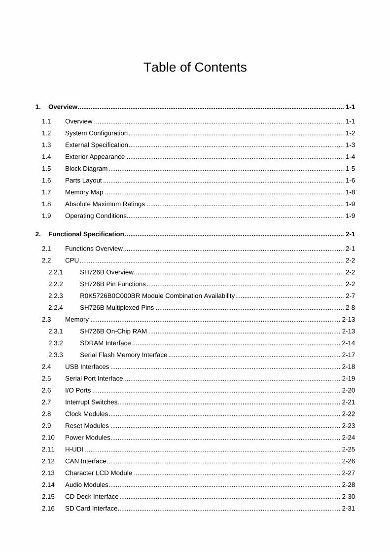
Table of Contents
1. Overview................................................................................................................................................... 1-1
1.1 Overview .......................................................................................................................................... 1-1
1.2 System Configuration....................................................................................................................... 1-2
1.3 External Specification....................................................................................................................... 1-3
1.4 Exterior Appearance ........................................................................................................................ 1-4
1.5 Block Diagram.................................................................................................................................. 1-5
1.6 Parts Layout ..................................................................................................................................... 1-6
1.7 Memory Map .................................................................................................................................... 1-8
1.8 Absolute Maximum Ratings ............................................................................................................. 1-9
1.9 Operating Conditions........................................................................................................................ 1-9
2. Functional Specification......................................................................................................................... 2-1
2.1 Functions Overview.......................................................................................................................... 2-1
2.2 CPU.................................................................................................................................................. 2-2
2.2.1 SH726B Overview.................................................................................................................... 2-2
2.2.2 SH726B Pin Functions............................................................................................................. 2-2
2.2.3 R0K5726B0C000BR Module Combination Availability............................................................ 2-7
2.2.4 SH726B Multiplexed Pins ........................................................................................................ 2-8
2.3 Memory .......................................................................................................................................... 2-13
2.3.1 SH726B On-Chip RAM .......................................................................................................... 2-13
2.3.2 SDRAM Interface ................................................................................................................... 2-14
2.3.3 Serial Flash Memory Interface ............................................................................................... 2-17
2.4 USB Interfaces ............................................................................................................................... 2-18
2.5 Serial Port Interface........................................................................................................................ 2-19
2.6 I/O Ports ......................................................................................................................................... 2-20
2.7 Interrupt Switches........................................................................................................................... 2-21
2.8 Clock Modules................................................................................................................................ 2-22
2.9 Reset Modules ............................................................................................................................... 2-23
2.10 Power Modules............................................................................................................................... 2-24
2.11 H-UDI ............................................................................................................................................. 2-25
2.12 CAN Interface................................................................................................................................. 2-26
2.13 Character LCD Module .................................................................................................................. 2-27
2.14 Audio Modules................................................................................................................................ 2-28
2.15 CD Deck Interface.......................................................................................................................... 2-30
2.16 SD Card Interface........................................................................................................................... 2-31
2.17 LAN Interface ................................................................................................................................. 2-32
2.18 External Expansion Connector 1 (J22) Interface ........................................................................... 2-33
2.19 External Expansion Connector 2 (J25) Interface ........................................................................... 2-34
2.20 External Expansion Connector 3 (J26) Interface ........................................................................... 2-35
3. Operational Specification ....................................................................................................................... 3-1
3.1 Connector Overview......................................................................................................................... 3-1
3.1.1 Application Headers (JA1, JA2, JA3, JA5 and JA6) ................................................................ 3-2
3.1.2 Common Ring Connectors (J1, J2, J3 and J4)........................................................................ 3-9
3.1.3 DC Power Jack (J5) ............................................................................................................... 3-13
3.1.4 H-UDI Port Connector (J6)..................................................................................................... 3-14
3.1.5 Character LCD connector (J7) ............................................................................................... 3-15
3.1.6 USB Connector (J8, J9 and J10) ........................................................................................... 3-16
3.1.7 SD Card Slot (J11) ................................................................................................................. 3-18
3.1.8 Serial Port Connector (J12) ................................................................................................... 3-19
3.1.9 External Power Supply Connectors (J13, J14, J15, J16 and J20) ........................................ 3-20
3.1.10 Line-out Pin Jacks (J17 and J19)........................................................................................... 3-22
3.1.11 Microphone Input Pin Jack (J18) ........................................................................................... 3-23
3.1.12 CD Deck Connector (J21)...................................................................................................... 3-24
3.1.13 LAN Connector (J23) ............................................................................................................. 3-25
3.1.14 CAN Port Connector (J24) ..................................................................................................... 3-26
3.1.15 External Expansion Connector 1 (J22) .................................................................................. 3-27
3.1.16 External Expansion Connector 2 (J25) .................................................................................. 3-28
3.1.17 External Expansion Connector 3 (J26) .................................................................................. 3-29
3.2 Operation Parts Layout .................................................................................................................. 3-30
3.2.1 Push Switches........................................................................................................................ 3-31
3.2.2 LEDs ...................................................................................................................................... 3-31
3.2.3 Potentiometer......................................................................................................................... 3-31
3.3 Dimensions..................................................................................................................................... 3-32

SH726B CPU Board R0K5726B0C000BR 1. Overview
R20UT0601EJ0100 Rev.1.00 1-1 Mar. 12, 2013
1. Overview
1.1 Overview
The R0K5726B0C000BR is a CPU Board to evaluate function s and performance of the Renesas electronics Corp. RISK microcomputer, SH726B, and to develop and evaluate application software. The features of the SH726B CPU Board are described below. • Generally includes a 16MB SDRAM (16-bit bus connection) and two 16MB serial flash memories. • Generally includes an RS-232C connector, a USB connector, a CAN connector and an SD card slot as the SH726B
peripheral function interfaces. • Includes audio interfaces such as an audio DAC and an audio CODEC, and a CD deck interface and a character type
LCD module connector, which enable advanced development for audio system. • The USB connector generally includes series A receptacles. This board has a Mini-B receptacle in substrate
configuration that can be mounted for evaluation of the USB host/function module. • Generally includes a LAN connector to enable software development and evaluation using the Ethernet. • Generally includes sixteen key input switches (4 pieces×4 AD input) which can be used as user interfaces. • The pins for the SH726B on-chip peripheral function are connected to the Renesas starter kit (RSK) common ring
connector and application headers, which enable timing evaluation for the peripheral devices using measurement hardware, and development for adequate expansion board.
• Enables to connect the on-chip emulator E10A-USB (Renesas Electronics Corp.).

SH726B CPU Board R0K5726B0C000BR 1. Overview
R20UT0601EJ0100 Rev.1.00 1-2 Mar. 12, 2013
1.2 System Configuration Figure 1.1 shows the R0K5726B0C000BR System Configuration.
H-UDI port connector
SH726B CPU boardR0K5726B0C000BR
USB
*:The devices should be prepared by users.
Debugger
Host computer *E10A-USB*
High-performance Embedded Workshop
SuperH RISC engine C/C++ compiler package
Serial port
SH726B
Application headerSD card
LAN
CD deck
MicrophoneHeadphone
Speaker
RCANport
Character LCD
**
AC adapter attached to CPU board
Application header
External expansion
connector 2
Eternal expansion
connector 3
External expansion connector 1
Figure 1.1 R0K5726B0C000BR System Configuration
SH726B CPU Board R0K5726B0C000BR 1. Overview
R20UT0601EJ0100 Rev.1.00 1-3 Mar. 12, 2013
1.3 External Specification Table 1.1 lists the R0K5726B0C000BR External Specifications. Table 1.1 R0K5726B0C000BR External Specifications
Item Description CPU SH726B
• Input (XIN) clock: 12MHz
• CPU clock (Iφ): Up to 216MHz
• Bus clock (Bφ): Up to 72MHz
• Peripheral clock (Pφ): Up to 36MHz
• On-chip memory
High-speed on-chip RAM 64KB
Large capacity on-chip RAM: 125MB
Operand cache: 8KB
• Power voltage:
- Internal: 1.25V
- I/O: 3.3V
• 144-pin QFP 0.5mm pitch (package code: PLQP0144KA-A) Memories • SDRAM: 16MB
• Serial flash memories: 16MB×2 Connectors • Common ring connector (all CPU signals), optional
• Application header (bus, I/O, VCC and GND), optional
• Serial port connector (D-sub 9-pin)
• CAN port connector (3-pin, pin header)
• Character LCD interface connector (14-pin)
• USB series A receptacle×2, included as standard
(Mini-B receptacle is available only for the port 0)
• LAN connector (RJ-45)
• SD card slot
• CD deck connector
• External expansion connector, optional
• Line-out pin jack (HP and SPK)
• Mic-in pin jack
• DC power jack LEDs, Potentiometer • Power LED: 1
• User LEDs: 4
• Potentiometer (10KΩ): 1 Switches, Jumper • Reset switch: 1
• User switches: 3 (NMI, IRQ2 (connectable to ACTRG#), and PINT7) Board specification • Dimensions: 150mm×180mm
• Mounting form: 4-layer, double-sided
• Number of board: 1

SH726B CPU Board R0K5726B0C000BR 1. Overview
R20UT0601EJ0100 Rev.1.00 1-4 Mar. 12, 2013
1.4 Exterior Appearance Figure 1.2 shows the R0K5726B0C000BR Exterior Appearance.
Figure 1.2 R0K5726B0C000BR Exterior Appearance

SH726B CPU Board R0K5726B0C000BR 1. Overview
R20UT0601EJ0100 Rev.1.00 1-5 Mar. 12, 2013
1.5 Block Diagram Figure 1.3 shows the R0K5726B0C000BR Block Diagram.
SH726B(216MHz)
Switch(NMI, IRQ2, PINT7)
H-UDI port connector(14-pin)
Serial port connector
BSC
USB
PIOH-UDI SCIF
INTC
VBUS control
Ether -Controller
Ethernet controller
PeriperalI/O
Expansion connector
16 bits
SD card slot
( 16M B × 2)(16MB × 2)
シリアルフラッシュ
Serial flash RSPI
RQSPI
SDHI
FS × 2USB
connector
SDIOExternal expansion
connector 3
SSIF
SSIF
RSPILine-outMic-in
IIC3
SCIF
SSIFLine-out
AK4353
WM8978
TxD, RxD
ADCKey input4 × 4
SCIFTxD, RxD, RTS, CTS,
TxD, RxD, RTS, CTSExternal
expansion connector 2
RJ-45
SDRAM( 16 MB)
SDRAM(16MB)EEPROM
(MAC)
EEPROM(MAC)
DAC
DAC/ADC
RCANLevel shifter
and CAN driverHA13721
SSIF
RSPI
CD connector8V
CD deckpower supply
(8V)
Expansion connector
CAN connector
External expansion
connector 1
RCAN
Character LCD
16 bits
16 bits16 bits
Figure 1.3 R0K5726B0C000BR Block Diagram
SH726B CPU Board R0K5726B0C000BR 1. Overview
R20UT0601EJ0100 Rev.1.00 1-6 Mar. 12, 2013
1.6 Parts Layout Figure 1.4 shows the R0K5726B0C000BR Parts Layout.
J5: 5
V in
put A
C a
dapt
er ja
ck
PW1: Power supply LED
J12: Serial port connector
SW
17: R
eset
sw
itch
U1SH726B
U2SDRAM
J6: H-UDI port connector
J24:
CAN
con
nect
or
J25:
Ext
erna
l exp
ansi
on
conn
ecto
r 2
J26:
Ext
erna
l exp
ansi
on
conn
ecto
r 3
J7: C
hara
cter
LC
D c
onne
ctor
J21: CD deck connector
J19: Line-out pin jack
J18: Mic-in pin jack
J22: External expansion connector 1
J23: LAN connector
J17: Line-out pin jack
U21: Audio CODEC
U20: Audio DAC
SW1
to S
W16
: U
ser s
witc
h
J8, J
10:
USB
con
nect
or
J9: U
SB
conn
ecto
r
J1 to J4: Common ring connector
JA1 to JA3, JA5, JA6: Application header
U4:
Ser
ial f
lash
mem
ory
2
SW19
: IR
Q2
switc
h
SW
18: N
MI s
witc
h
SW
20: P
INT7
sw
itch
X4: LAN controller resonator(25MHz)
U17: LAN controller
X2:
EXT
AL/X
TAL
reso
nato
r (1
2MH
z)
X3:
Aud
io o
scill
ator
(1
1.28
96M
Hz)
X1:
EXT
AL o
scill
ator
(48M
Hz)
LED1 to LED4: User LED
<Top view of the component side>
U11
: Res
et IC
U3:
Ser
ial f
lash
mem
ory
2
J11:
SD
car
d sl
ot
<Top view of the solder side>
Figure 1.4 R0K5726B0C000BR Parts Layout

SH726B CPU Board R0K5726B0C000BR 1. Overview
R20UT0601EJ0100 Rev.1.00 1-7 Mar. 12, 2013
Table 1.2 lists the R0K5726B0C000BR Main Parts. Table 1.2 R0K5726B0C000BR Main Parts
Part No. Part name Model (Manufacturer) Recommended optional parts
U1 CPU SH726B (Renesas) U2 SDRAM EDS1216AATA (Elpida) U3, U4 Serial flash memory S25FL129P (Spansion) U17 LAN controller LAN9211 (SMSC) U13 RS-232C transceiver MAX3222CPW (TI) U14 CAN transceiver HA13721RPJE (Renesas) U9 3.3V regulator LMS1587CS-ADJ (NS) U10, U12 1.25V and 1.8V regulator LM2734XMK (NS) U11 Reset IC RNA51957BFP (Renesas) X2 XIN resonator (crystal) HCM49-12.000MABJ (Citizen) X1 XIN oscillator (with socket) Optional SG-8002DC (Epson) J1 to J4 Common ring connector Optional 18 pins×dual row pin headerJA1, JA2 Application header Optional 13 pins×dual row pin headerJA3 Application header Optional 25 pins×dual row pin headerJA5, JA6 Application header Optional 12 pins×dual row pin headerJ5 DC power jack KLDX-SMT2-0202-A (Kycon) J6 H-UDI port connector (14-pin) HTST-107-01-L-DV (Samtec) J23 LAN connector (RJ-4) J3011G21DNL (Pulse) J8, J9 USB series A receptacle UBA-4R-D14T-4D (JST) J10 USB Mini-B receptacle Optional 54819-0572 (MOLEX) J11 SD card slot DM1B-DSF-PEJ (HRS) J12 Serial port connector 154188 (ERNI) J24 CAN port connector B3P-SHF-1AA (JST) J7 Character LCD connector SSM-107-LM-DV-P (Samtec) J13 to J16, J20 External power supply connector Optional A2-2PA-2.54DSA (HRS) PW1 Power LED Blue LED1 to LED4 User LED Green, Orange, Red, Red VR1 Potentiometer CT-6ETV10KΩ (Nidec Copal) SW17 Reset switch B3S-1000 (Omron) SW18 to SW20 NMI, IRQ2, PINT7 switch B3S-1000 (Omron) X4 LAN controller resonator HCM49-25.000MABJ (Citizen) X3 Audio oscillator SG8002JF_11.2896MHz J17, J19 Line-out pin jack HSJ1456-010320 (Hosiden) J18 Mic-in pin jack HSJ1456-010320 (Hosiden) J21 CD deck connector IMSA-9617S-22 (IRISO Electronics) J22, J25, J26 External expansion connector Optional TST-110-01-T-D (Samtec)
SH726B CPU Board R0K5726B0C000BR 1. Overview
R20UT0601EJ0100 Rev.1.00 1-8 Mar. 12, 2013
1.7 Memory Map Figure 1.5 shows the R0K5726B0C000BR Memory Mapping.
Figure 1.5 R0K5726B0C000BR Memory Mapping
Logical address
SH726B Logical space R0K5726B0C000BR
Memory mapping H'0000 0000
LAN controller (256B) 16-bit bus
H'0000 0100
CS0 space: 64MB
User area
H'0400 0000
CS1 space: 64MB User area
H'0800 0000
CS2 space: 64MB User area
H'0C00 0000
SDRAM (16MB) 16-bit bus
H'0D00 0000
CS3 space: 64MB
User area
H'1000 0000
CS4 space: 64MB User area User area
H'1400 0000
Reserved area (access disable)
H'1800 0000
SPI multi I/O bus space (16MB)
H'1900 0000
User area
H'1C00 0000
Large capacity on-chip RAM: 1.25MB
H'1C14 0000
Others: 192MB
Reserved area (access disable)
H'2000 0000
CS0 to CS4 space, others (cache invalid space)
CS0 to CS4 space, others (cache invalid space)
H'4000 0000
Reserved area (access disable)
Reserved area (access disable)
H'8000 0000
Reserved area (access disable)
Reserved area (access disable)
H'FFF8 0000
High-speed on-chip RAM: 64KB High-speed on-chip RAM: 64KB
H'FFF9 0000
On-chip RAM, reserved (access disable)
On-chip RAM, reserved (access disable)
H'FFFC 0000
H'FFFF FFFF On-chip peripheral module, reserved On-chip peripheral module, reserved

SH726B CPU Board R0K5726B0C000BR 1. Overview
R20UT0601EJ0100 Rev.1.00 1-9 Mar. 12, 2013
1.8 Absolute Maximum Ratings Table 1.3 lists the R0K5726B0C000BR Absolute Maximum Ratings. Table 1.3 R0K5726B0C000BR Absolute Maximum Ratings
Symbol Item Rated value Remarks 5VCC 5V system power supply voltage -0.3V to 6.0V Vss reference
3VCC *1 3.3V system power supply -0.3V to 4.0V Vss reference AVCC *2 Analog 3.3V system power
supply voltage -0.3V to 4.0V AVss reference
1.25VCC *3 1.25V system power supply -0.3V to 1.7V Vss reference Topr Operating ambient temperature *4 0°C to 50°C Do not expose to condensation or corrosive gases.Tstg Storage ambient temperature *4 -10°C to 60°C Do not expose to condensation or corrosive gases.
[Notes] *1. Scale when providing 3.3V system power supply directly from the external power supply connector. *2. Scale when providing analog 3.3V system power supply directly from the external power supply connector. *3. Scale when providing 1.25V system power supply directly from the external power supply connector. *4. The ambient temperature is the air temperature immediate to the board.
1.9 Operating Conditions Table 1.4 lists the R0K5726B0C000BR Operating Conditions. Table 1.4 R0K5726B0C000BR Operating Conditions
Symbol Item Rated value Remarks 5VCC 5V system power supply voltage 4.75V to 5.25V Vss reference
3VCC *1 3.3V system power supply 3.15V to 3.45V Vss reference AVCC *2 Analog 3.3V system power
supply voltage 3.15V to 3.45V Vss reference
1.25VCC *3 1.25V system power supply 1.19V to 1.31V Vss reference - Maximum consumption voltage
super Up to 1.5A Total of 5V, 3.3V, and 1.25V power supplies
Topr Operating ambient temperature *4 0°C to 40°C Do not expose to condensation or corrosive gases.
[Notes] *1. Scale when providing 3.3V system power supply directly from the external power supply connector. *2. Scale when providing analog 3.3V system power supply directly from the external power supply connector. *3. Scale when providing 1.25V system power supply directly from the external power supply connector. *4. The ambient temperature is the air temperature immediate to the board.
SH726B CPU Board R0K5726B0C000BR 1. Overview
R20UT0601EJ0100 Rev.1.00 1-10 Mar. 12, 2013
This page intentionally left blank.
SH726B CPU Board R0K5726B0C000BR 2. Functional Specification
R20UT0601EJ0100 Rev.1.00 2-1
Mar. 12, 2013
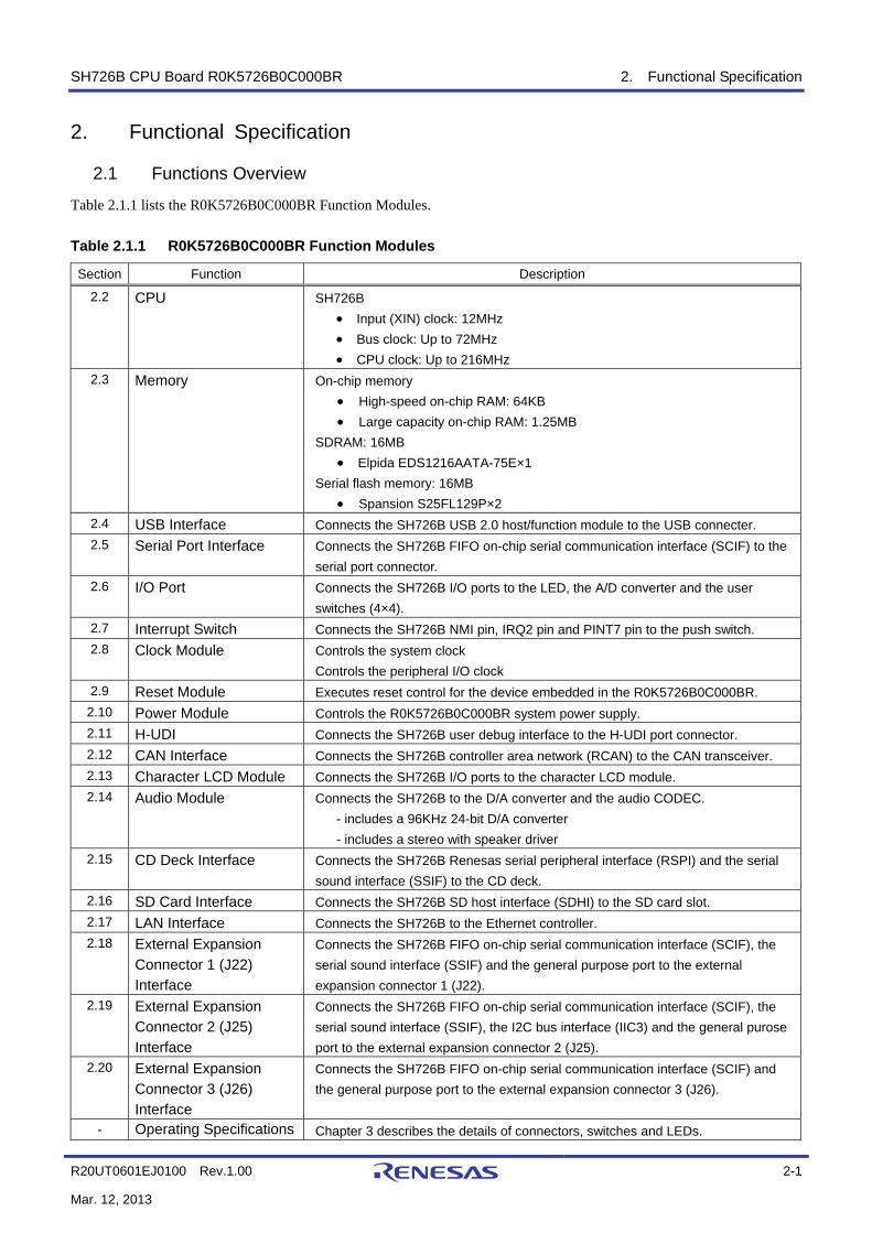
2. Functional Specification
2.1 Functions Overview
Table 2.1.1 lists the R0K5726B0C000BR Function Modules. Table 2.1.1 R0K5726B0C000BR Function Modules
Section Function Description
2.2 CPU SH726B • Input (XIN) clock: 12MHz • Bus clock: Up to 72MHz • CPU clock: Up to 216MHz
2.3 Memory On-chip memory • High-speed on-chip RAM: 64KB • Large capacity on-chip RAM: 1.25MB
SDRAM: 16MB • Elpida EDS1216AATA-75E×1
Serial flash memory: 16MB • Spansion S25FL129P×2
2.4 USB Interface Connects the SH726B USB 2.0 host/function module to the USB connecter. 2.5 Serial Port Interface Connects the SH726B FIFO on-chip serial communication interface (SCIF) to the
serial port connector. 2.6 I/O Port Connects the SH726B I/O ports to the LED, the A/D converter and the user
switches (4×4). 2.7 Interrupt Switch Connects the SH726B NMI pin, IRQ2 pin and PINT7 pin to the push switch. 2.8 Clock Module Controls the system clock
Controls the peripheral I/O clock 2.9 Reset Module Executes reset control for the device embedded in the R0K5726B0C000BR.
2.10 Power Module Controls the R0K5726B0C000BR system power supply. 2.11 H-UDI Connects the SH726B user debug interface to the H-UDI port connector. 2.12 CAN Interface Connects the SH726B controller area network (RCAN) to the CAN transceiver. 2.13 Character LCD Module Connects the SH726B I/O ports to the character LCD module. 2.14 Audio Module Connects the SH726B to the D/A converter and the audio CODEC.
- includes a 96KHz 24-bit D/A converter - includes a stereo with speaker driver
2.15 CD Deck Interface Connects the SH726B Renesas serial peripheral interface (RSPI) and the serial sound interface (SSIF) to the CD deck.
2.16 SD Card Interface Connects the SH726B SD host interface (SDHI) to the SD card slot. 2.17 LAN Interface Connects the SH726B to the Ethernet controller. 2.18 External Expansion
Connector 1 (J22) Interface
Connects the SH726B FIFO on-chip serial communication interface (SCIF), the serial sound interface (SSIF) and the general purpose port to the external expansion connector 1 (J22).
2.19 External Expansion Connector 2 (J25) Interface
Connects the SH726B FIFO on-chip serial communication interface (SCIF), the serial sound interface (SSIF), the I2C bus interface (IIC3) and the general purose port to the external expansion connector 2 (J25).
2.20 External Expansion Connector 3 (J26) Interface
Connects the SH726B FIFO on-chip serial communication interface (SCIF) and the general purpose port to the external expansion connector 3 (J26).
- Operating Specifications Chapter 3 describes the details of connectors, switches and LEDs.
SH726B CPU Board R0K5726B0C000BR 2. Functional Specification
R20UT0601EJ0100 Rev.1.00 2-2
Mar. 12, 2013
2.2 CPU
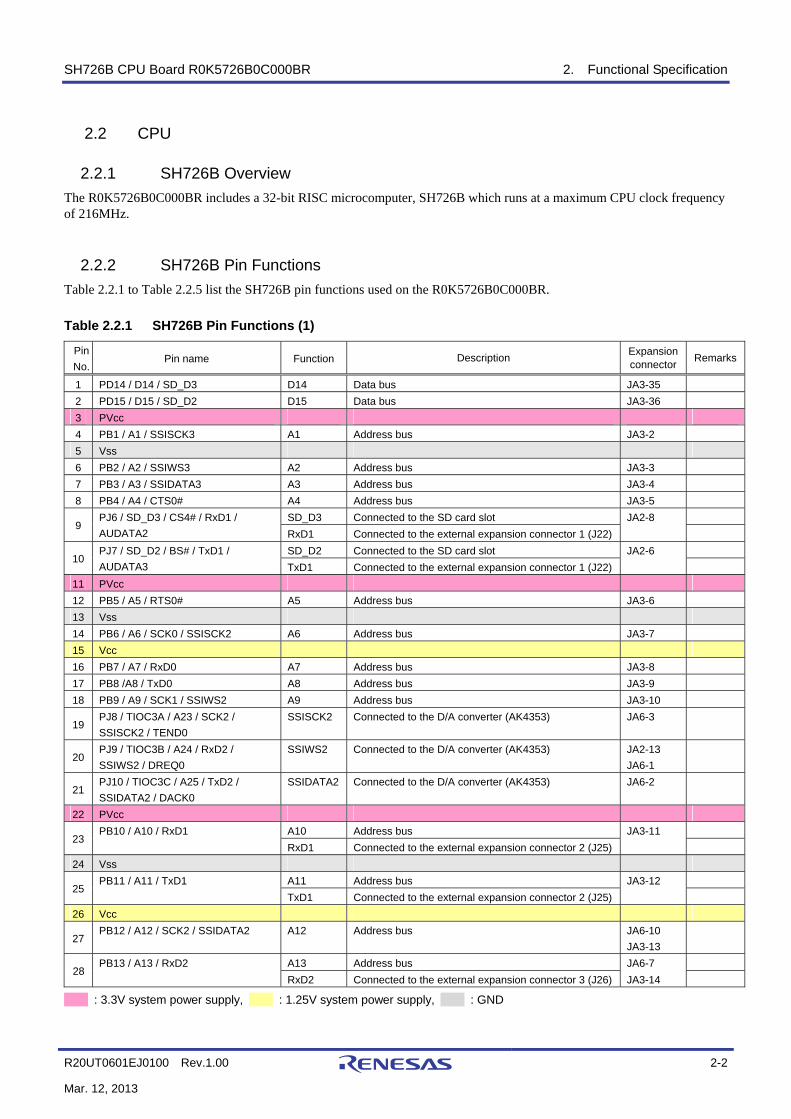
2.2.1 SH726B Overview The R0K5726B0C000BR includes a 32-bit RISC microcomputer, SH726B which runs at a maximum CPU clock frequency of 216MHz.
2.2.2 SH726B Pin Functions Table 2.2.1 to Table 2.2.5 list the SH726B pin functions used on the R0K5726B0C000BR. Table 2.2.1 SH726B Pin Functions (1)
Pin No.
Pin name Function Description Expansion connector Remarks
1 PD14 / D14 / SD_D3 D14 Data bus JA3-35 2 PD15 / D15 / SD_D2 D15 Data bus JA3-36 3 PVcc 4 PB1 / A1 / SSISCK3 A1 Address bus JA3-2 5 Vss 6 PB2 / A2 / SSIWS3 A2 Address bus JA3-3 7 PB3 / A3 / SSIDATA3 A3 Address bus JA3-4 8 PB4 / A4 / CTS0# A4 Address bus JA3-5
SD_D3 Connected to the SD card slot JA2-8 9
PJ6 / SD_D3 / CS4# / RxD1 / AUDATA2 RxD1 Connected to the external expansion connector 1 (J22)
SD_D2 Connected to the SD card slot JA2-6 10
PJ7 / SD_D2 / BS# / TxD1 / AUDATA3 TxD1 Connected to the external expansion connector 1 (J22)
11 PVcc 12 PB5 / A5 / RTS0# A5 Address bus JA3-6 13 Vss 14 PB6 / A6 / SCK0 / SSISCK2 A6 Address bus JA3-7 15 Vcc 16 PB7 / A7 / RxD0 A7 Address bus JA3-8 17 PB8 /A8 / TxD0 A8 Address bus JA3-9 18 PB9 / A9 / SCK1 / SSIWS2 A9 Address bus JA3-10
19 PJ8 / TIOC3A / A23 / SCK2 / SSISCK2 / TEND0
SSISCK2 Connected to the D/A converter (AK4353) JA6-3
20 PJ9 / TIOC3B / A24 / RxD2 / SSIWS2 / DREQ0
SSIWS2 Connected to the D/A converter (AK4353) JA2-13 JA6-1
21 PJ10 / TIOC3C / A25 / TxD2 / SSIDATA2 / DACK0
SSIDATA2 Connected to the D/A converter (AK4353) JA6-2
22 PVcc A10 Address bus JA3-11
23 PB10 / A10 / RxD1
RxD1 Connected to the external expansion connector 2 (J25) 24 Vss
A11 Address bus JA3-12 25
PB11 / A11 / TxD1 TxD1 Connected to the external expansion connector 2 (J25)
26 Vcc
27 PB12 / A12 / SCK2 / SSIDATA2 A12 Address bus JA6-10
JA3-13
A13 Address bus JA6-7 28
PB13 / A13 / RxD2 RxD2 Connected to the external expansion connector 3 (J26) JA3-14
: 3.3V system power supply, : 1.25V system power supply, : GND
SH726B CPU Board R0K5726B0C000BR 2. Functional Specification
R20UT0601EJ0100 Rev.1.00 2-3
Mar. 12, 2013
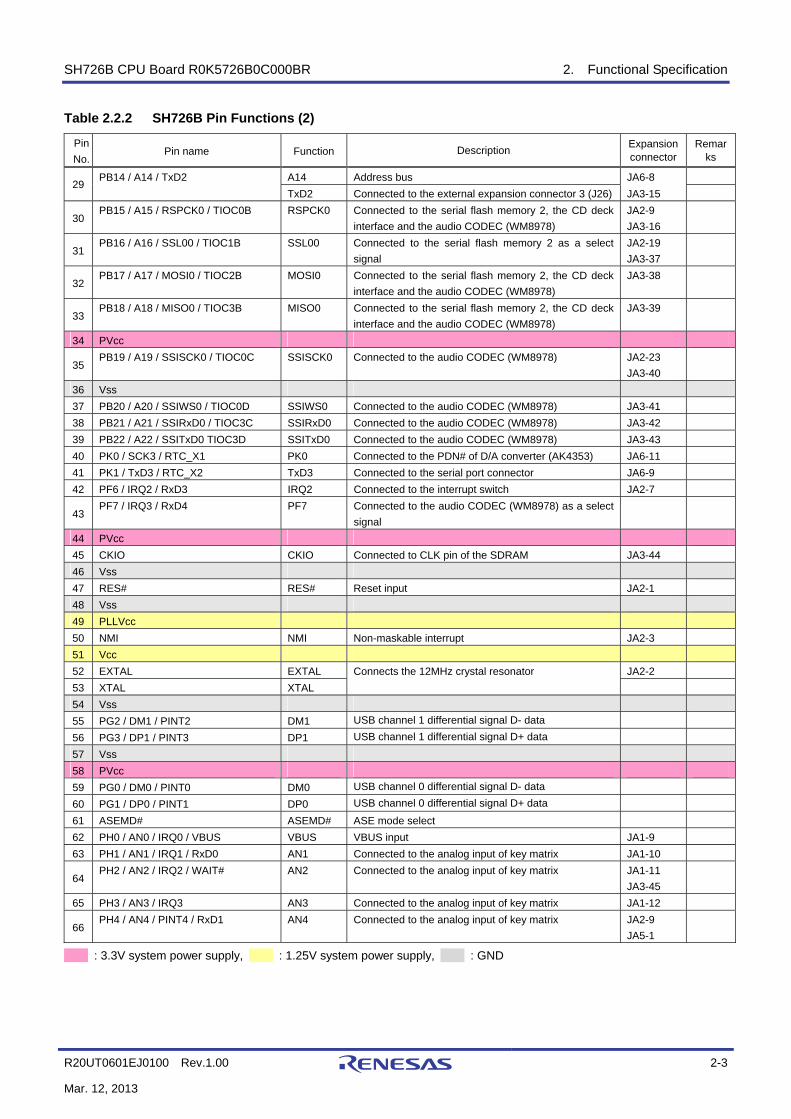
Table 2.2.2 SH726B Pin Functions (2)
Pin No.
Pin name Function Description Expansion connector
Remarks
A14 Address bus JA6-8 29
PB14 / A14 / TxD2 TxD2 Connected to the external expansion connector 3 (J26) JA3-15
30 PB15 / A15 / RSPCK0 / TIOC0B RSPCK0 Connected to the serial flash memory 2, the CD deck
interface and the audio CODEC (WM8978) JA2-9 JA3-16
31 PB16 / A16 / SSL00 / TIOC1B SSL00 Connected to the serial flash memory 2 as a select
signal JA2-19 JA3-37
32 PB17 / A17 / MOSI0 / TIOC2B MOSI0 Connected to the serial flash memory 2, the CD deck
interface and the audio CODEC (WM8978) JA3-38
33 PB18 / A18 / MISO0 / TIOC3B MISO0 Connected to the serial flash memory 2, the CD deck
interface and the audio CODEC (WM8978) JA3-39
34 PVcc
35 PB19 / A19 / SSISCK0 / TIOC0C SSISCK0 Connected to the audio CODEC (WM8978) JA2-23
JA3-40
36 Vss 37 PB20 / A20 / SSIWS0 / TIOC0D SSIWS0 Connected to the audio CODEC (WM8978) JA3-41 38 PB21 / A21 / SSIRxD0 / TIOC3C SSIRxD0 Connected to the audio CODEC (WM8978) JA3-42 39 PB22 / A22 / SSITxD0 TIOC3D SSITxD0 Connected to the audio CODEC (WM8978) JA3-43 40 PK0 / SCK3 / RTC_X1 PK0 Connected to the PDN# of D/A converter (AK4353) JA6-11 41 PK1 / TxD3 / RTC_X2 TxD3 Connected to the serial port connector JA6-9 42 PF6 / IRQ2 / RxD3 IRQ2 Connected to the interrupt switch JA2-7
43 PF7 / IRQ3 / RxD4 PF7 Connected to the audio CODEC (WM8978) as a select
signal
44 PVcc 45 CKIO CKIO Connected to CLK pin of the SDRAM JA3-44 46 Vss 47 RES# RES# Reset input JA2-1 48 Vss 49 PLLVcc 50 NMI NMI Non-maskable interrupt JA2-3 51 Vcc 52 EXTAL EXTAL JA2-2 53 XTAL XTAL
Connects the 12MHz crystal resonator
54 Vss 55 PG2 / DM1 / PINT2 DM1 USB channel 1 differential signal D- data 56 PG3 / DP1 / PINT3 DP1 USB channel 1 differential signal D+ data 57 Vss 58 PVcc 59 PG0 / DM0 / PINT0 DM0 USB channel 0 differential signal D- data 60 PG1 / DP0 / PINT1 DP0 USB channel 0 differential signal D+ data 61 ASEMD# ASEMD# ASE mode select 62 PH0 / AN0 / IRQ0 / VBUS VBUS VBUS input JA1-9 63 PH1 / AN1 / IRQ1 / RxD0 AN1 Connected to the analog input of key matrix JA1-10
64 PH2 / AN2 / IRQ2 / WAIT# AN2 Connected to the analog input of key matrix JA1-11
JA3-45
65 PH3 / AN3 / IRQ3 AN3 Connected to the analog input of key matrix JA1-12
66 PH4 / AN4 / PINT4 / RxD1 AN4 Connected to the analog input of key matrix JA2-9
JA5-1
: 3.3V system power supply, : 1.25V system power supply, : GND

SH726B CPU Board R0K5726B0C000BR 2. Functional Specification
R20UT0601EJ0100 Rev.1.00 2-4
Mar. 12, 2013
Table 2.2.3 SH726B Pin Functions (3)
Pin No.
Pin name Function Description Expansion connector
Remarks
67 PH5 / AN5 / PINT5 / RxD2 PINT5 Ethernet controller interrupt input JA2-23
JA5-2
68 AVss JA1-6
69 PH6 / AN6 / PINT6 / RxD3 RxD3 Connected to the serial port connector JA5-3
JA6-12
70 AVcc
71 PH7 / AN7 / PINT7 / RxD4 PINT7 Connected to the CD deck interface and the external
expansion connector 1 (J22) JA5-4
72 AVref AVref ADC analog reference voltage JA1-7 73 TRST# TRST# Initialization signal input port
74 ASEBRKAK#/ASEBRK# ASEBRKA
K#/ ASEBRK#
Break mode acknowledge/Break request
75 TD0 TD0 Test data output
76 TD1 TD1 Test data input
77 TMS TMS Test mode select
78 TCK TCK Test clock 79 AUDIO_X2 AUDIO_X2 Open 80 AUDIO_X1 AUDIO_X1 Connects the audio external clock 81 PVcc
PF0 Connected to the character LCD module JA1-15 82
PF0 / RSPCK0 / SPBCLK SPBCLK Connected to the serial flash memory 1
83 Vss PF1 Connected to the character LCD module JA1-16
84 PF1 / SSL00 / SPBSSL
SPBSSL Connected to the serial flash memory 1 PF2 Connected to the character LCD module JA1-17
85
PF2 / MOSI0 / SPBMO_0/SPBIO0_0 SPBMO_0
/ SPBIO0_0
Connected to the serial flash memory 1
PF3 Connected to the character LCD module JA1-18 86
PF3 / MISO0 / SPBMI_0/SPBIO1_0 SPBMI_0/
SPBIO1_0Connected to the serial flash memory 1
87 PJ11 / TIOC3D / IRQ0 / SCK4 / CRx0 / IERxD / RSPCK2
PJ11 Connected to the CD deck interface as a select signal JA1-23 JA2-14
88 PJ12 / SSISCK3 / A0 / TxD4 / CTx0 / IETxD / SSL20
SSISCK3 Connected to the CD deck interface and the external expansion connector 1 (J22)
JA3-1
89 PVcc PF4 Connected to the character LCD module JA1-19
90 PF4 / SPBIO2_0
SPBIO2_0 Connected to the serial flash memory 1 91 Vss
PF5 Connected to the character LCD module JA1-20 92
PF5 / SPBIO3_0 SPBIO3_0 Connected to the serial flash memory 1
93 Vcc PA0 Connected to the test pin (TH3)
94 PA0 / MD_CLK
MD_CLK Connected to the DIPSW as a clock mode input PA1 D+ pull-up resistor control pin while the USB channel 0
function is in operation
95 PA1 / MD_BOOT
MD_BOOT Connected to the DIPSW as a boot mode input SSIWS3 Connected to the CD deck interface and the external
expansion connector 1 (J22) JA5-8
96 PJ13 / SSIWS3 / IRQ1 / RxD4 / CRx1 / CRx0/CRx1 / MOSI2
CRx1 Connected to the CAN transceiver
: 3.3V system power supply, : 1.25V system power supply, : GND

SH726B CPU Board R0K5726B0C000BR 2. Functional Specification
R20UT0601EJ0100 Rev.1.00 2-5
Mar. 12, 2013
Table 2.2.4 SH726B Pin Functions (4)
Pin No.
Pin name Function Description Expansion connector
Remarks
SSIDATA3 Connected to the CD deck interface and the external expansion connector 1 (J22)
JA2-5 JA5-7
97
PJ14 / SSIDATA3 / WDTOVF# / CTx1 / CTx0&CTx1 / MISO2
CTx1 Connected to the CAN transceiver PJ0 Connected to the external expansion connector 1 (J22) JA5-9
98 PJ0 / SD_CD / IRQ4
SD_CD Connected to the SD card slot
99 PC0 / CS0# / TIOC4A / AUDIO_XOUT
CS0# Connected to the Ethernet controller JA2-15 JA3-27
100 PVcc RD# Connected to the Ethernet controller JA2-17
101 PC1 / RD# / TIOC4B / SPDIF_IN
PC1 Connected to the external expansion connector 3 (J26) JA3-25 102 Vss
RD/WR# Connected to the SDRAM JA2-16 103
PC2 / RD/WR# / TIOC4C / SPDIF_OUT PC2 Connected to the external expansion connector 3 (J26) JA3-26
104 Vcc WE0# /DQML
Connected to the SDRAM JA2-18 105
PC3 / WE0# /DQML / TIOC4D
PC3 Connected to the external expansion connector 3 (J26) JA3-48 WE1#/DQMU
Connected to the SDRAM JA3-47 106
PC4 / WE1#/DQMU / WDTOVF#
PC4 Connected to the external expansion connector 3 (J26) RAS# Connected to the SDRAM JA5-6 CRx0 Connected to the JA connector JA3-50 107
PC5 / RAS# / IRQ4 / CRx0 / IERxD
PC5 Connected to the external expansion connector 3 (J26) CAS# Connected to the SDRAM JA5-5 CTx0 Connected to the JA connector JA3-49 108
PC6 / CAS# / IRQ5 / CTx0 / IETxD
PC6 Connected to the external expansion connector 3 (J26) 109 PE0 / SCL0 / IRQ0 PE0 Enable signal of the character LCD
110 PE1 / SDA0 / IRQ1 PE1 Connected to the CD deck interface and the external
expansion connector 1 (J22)
111 PE2 / SCL1 / AUDIO_CLK AUDIO_C
LK Connected to the external expansion connector 2 (J25)
112 PE3 / SDA1 / ADTRG# PE3 Connected to the CD deck interface and the external
expansion connector 1 (J22) JA1-8
113 PE4 / SCL2 / TCLKA SCL2 Connected to the D/A converter (AK4353) and the
external expansion connector 2 (J25) JA2-21
114 PE5 / SDA2 / TCLKB SDA2 Connected to the D/A converter (AK4353) and the
external expansion connector 2 (J25) JA2-22
115 PE6 / SCL3 / TCLKC SCL3 Connected to the test pin (TH6) JA1-26
JA2-25
116 PE7 / SDA3 / TCLKD SDA3 Connected to the test pin (TH7) JA1-25
JA2-26
PC7 Connected to the external expansion connector 2 (J25) JA3-46 117
PC7 / CKE / IRQ6 / CRx1 / CRx0/CRx1 CKE Connected to the SDRAM
118 Vss 119 PVcc
120 PC8 / CS3# / IRQ7 / CTx1 / CTx0&CTx1
CS3# Connected to the SDRAM JA3-45
D0 Data bus JA3-17 121
PD0 / D0 / SSISCK1 / SIOFSCK / SPBMO_1/SPBIO0_1 SSISCK1 Connected to the external expansion connector 2 (J25)
D1 Data bus JA3-18 122
PD1 / D1 / SSIWS1 / SIOFSYNC / SPBMI_1/SPBIO1_1 SSIWS1 Connected to the external expansion connector 2 (J25)
: 3.3V system power supply, : 1.25V system power supply, : GND
SH726B CPU Board R0K5726B0C000BR 2. Functional Specification
R20UT0601EJ0100 Rev.1.00 2-6
Mar. 12, 2013
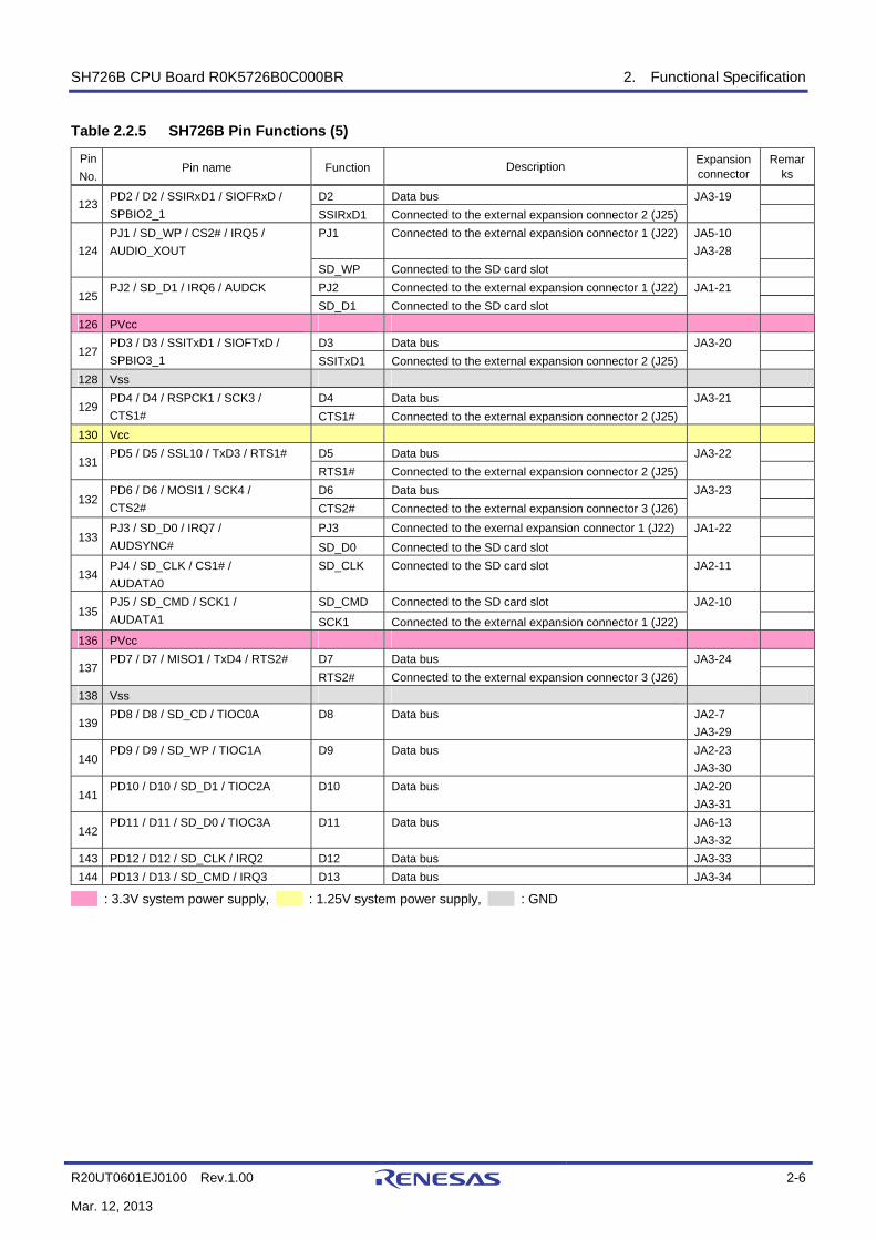
Table 2.2.5 SH726B Pin Functions (5)
Pin No.
Pin name Function Description Expansion connector
Remarks
D2 Data bus JA3-19 123
PD2 / D2 / SSIRxD1 / SIOFRxD / SPBIO2_1 SSIRxD1 Connected to the external expansion connector 2 (J25)
PJ1 Connected to the external expansion connector 1 (J22) JA5-10 JA3-28
124
PJ1 / SD_WP / CS2# / IRQ5 / AUDIO_XOUT
SD_WP Connected to the SD card slot PJ2 Connected to the external expansion connector 1 (J22) JA1-21
125 PJ2 / SD_D1 / IRQ6 / AUDCK
SD_D1 Connected to the SD card slot 126 PVcc
D3 Data bus JA3-20 127
PD3 / D3 / SSITxD1 / SIOFTxD / SPBIO3_1 SSITxD1 Connected to the external expansion connector 2 (J25)
128 Vss D4 Data bus JA3-21
129 PD4 / D4 / RSPCK1 / SCK3 / CTS1# CTS1# Connected to the external expansion connector 2 (J25)
130 Vcc D5 Data bus JA3-22
131 PD5 / D5 / SSL10 / TxD3 / RTS1#
RTS1# Connected to the external expansion connector 2 (J25) D6 Data bus JA3-23
132 PD6 / D6 / MOSI1 / SCK4 / CTS2# CTS2# Connected to the external expansion connector 3 (J26)
PJ3 Connected to the exernal expansion connector 1 (J22) JA1-22 133
PJ3 / SD_D0 / IRQ7 / AUDSYNC# SD_D0 Connected to the SD card slot
134 PJ4 / SD_CLK / CS1# / AUDATA0
SD_CLK Connected to the SD card slot JA2-11
SD_CMD Connected to the SD card slot JA2-10 135
PJ5 / SD_CMD / SCK1 / AUDATA1 SCK1 Connected to the external expansion connector 1 (J22)
136 PVcc D7 Data bus JA3-24
137 PD7 / D7 / MISO1 / TxD4 / RTS2#
RTS2# Connected to the external expansion connector 3 (J26) 138 Vss
139 PD8 / D8 / SD_CD / TIOC0A D8 Data bus JA2-7
JA3-29
140 PD9 / D9 / SD_WP / TIOC1A D9 Data bus JA2-23
JA3-30
141 PD10 / D10 / SD_D1 / TIOC2A D10 Data bus JA2-20
JA3-31
142 PD11 / D11 / SD_D0 / TIOC3A D11 Data bus JA6-13
JA3-32
143 PD12 / D12 / SD_CLK / IRQ2 D12 Data bus JA3-33 144 PD13 / D13 / SD_CMD / IRQ3 D13 Data bus JA3-34
: 3.3V system power supply, : 1.25V system power supply, : GND

SH726B CPU Board R0K5726B0C000BR 2. Functional Specification
R20UT0601EJ0100 Rev.1.00 2-7
Mar. 12, 2013
2.2.3 R0K5726B0C000BR Module Combination Availability Table 2.2.6 list the R0K5726B0C000BR Module Combination Availability. The symbol of "Y" on the table indicates that both modules can be used in combination, and the "N" indicates that combination use is not available. Table 2.2.6 R0K5726B0C000BR Module Combination Availability
SH726BPeripheralfunction
Module name S
DR
AM
Ser
ial f
lash
mem
ory
1
Ser
ial f
lash
mem
ory
2
USB
Ser
ial p
ort
Use
r sw
itch
(4×4
)
LE
D (×
4)
NM
I sw
itch
IRQ
2 sw
itch
H-U
DI (
14-p
in)
CAN
tran
scei
ver
Cha
ract
er L
CD
mod
ule
D/A
con
verte
r (A
K435
3)
Aud
io C
OD
EC
(WM
8978
)
CD
dec
k in
terfa
ce*3
SD
car
d
LA
N in
terfa
ce
Ext
erna
l ext
pans
ion
conn
ecto
r 1 *3
Ext
erna
l exp
ansi
on c
onne
ctor
2
Ext
erna
l exp
ansi
on c
onne
ctor
3
BSC SDRAM Y Y Y Y Y N Y Y Y Y Y Y Y Y Y Y Y N NSPIBSC Serial flash memory 1 (U3) Y Y Y Y Y Y Y Y Y Y *1 Y Y Y Y Y Y Y YRSPI_0 Serial flash memory 2 (U4) Y Y Y Y Y Y Y Y Y Y Y Y *2 *2 Y Y Y Y YUSB USB Y Y Y Y Y Y Y Y Y Y Y Y Y Y Y Y Y Y YSCIF_3 Serial port Y Y Y Y Y Y Y Y Y Y Y Y Y Y Y Y Y Y YADC User Switch (4×4) Y Y Y Y Y Y Y Y Y Y Y Y Y Y Y Y Y Y YI/O port LED (×4) N Y Y Y Y Y Y Y Y Y Y Y Y Y Y Y Y Y YINTC NMI switch Y Y Y Y Y Y Y Y Y Y Y Y Y Y Y Y Y Y YINTC IRQ2 switch Y Y Y Y Y Y Y Y Y Y Y Y Y Y Y Y Y Y YH-UDI H-UDI (14-pin) Y Y Y Y Y Y Y Y Y Y Y Y Y Y Y Y Y Y YRCAN_1 CAN transceiver Y Y Y Y Y Y Y Y Y Y Y Y Y N Y Y N Y YI/O port Character LCD module Y *1 Y Y Y Y Y Y Y Y Y Y Y Y Y Y Y Y YIIC3_2, SSIF_2 D/A converter (AK4353) Y Y Y Y Y Y Y Y Y Y Y Y Y Y Y Y Y Y YRSPI_0, SSIF_0 Audio CODEC (WM8978) Y Y *2 Y Y Y Y Y Y Y Y Y Y Y N Y Y Y YRSPI_0, SSIF_3 CD deck interface*3 Y Y *2 Y Y Y Y Y Y Y N Y Y Y Y Y N Y YSDHI SD card Y Y Y Y Y Y Y Y Y Y Y Y Y N Y Y N Y YBSC LAN interface Y Y Y Y Y Y Y Y Y Y Y Y Y Y Y Y Y N N SCIF_1, SSIF_3 External expansion connector 1 *3 Y Y Y Y Y Y Y Y Y Y N Y Y Y N N Y Y YSCIF_1, SSIF_1, IIC3_2 External expansion connector 2 N Y Y Y Y Y Y Y Y Y Y Y Y Y Y Y N Y YSCIF_2 External expansion connector 3 N Y Y Y Y Y Y Y Y Y Y Y Y Y Y Y N Y Y
*1: Either one can be use.*2: Make sure the select signal is under the software control when these devices are used together.*3: A zero-ohm resistor must be mounted when using the CD deck interface or the external expansion connector 1.
R0K5726B0C000BR
R0K
5726
B0C
000B
R
SH726B CPU Board R0K5726B0C000BR 2. Functional Specification
R20UT0601EJ0100 Rev.1.00 2-8
Mar. 12, 2013
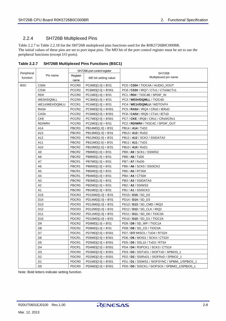
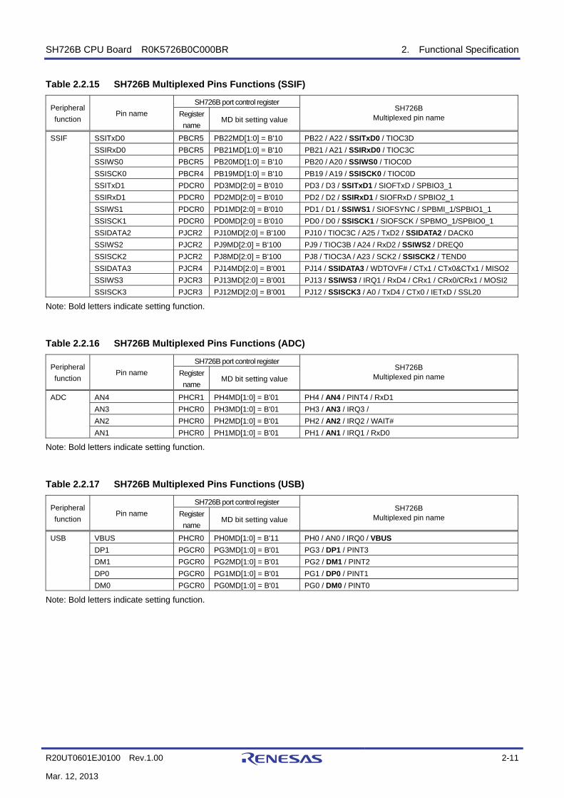
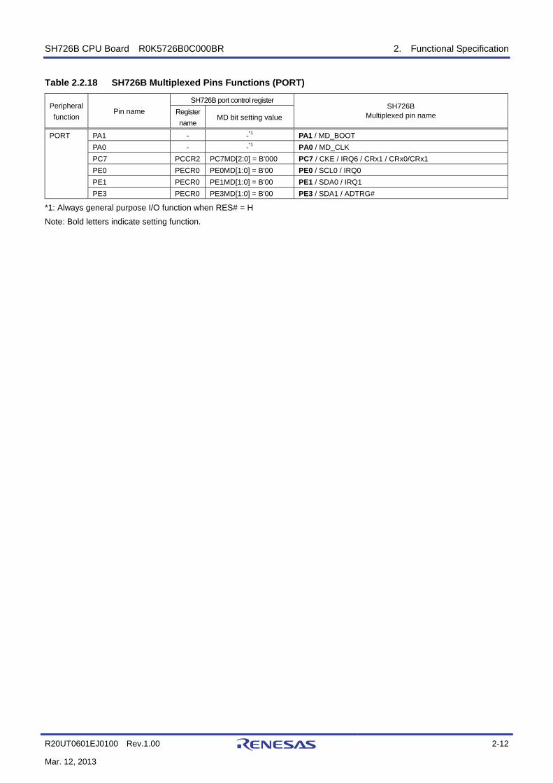
2.2.4 SH726B Multiplexed Pins Table 2.2.7 to Table 2.2.18 list the SH726B multiplexed pins functions used for the R0K5726B0C000BR. The initial values of these pins are set to port input pins. The MD bit of the port control register must be set to use the peripheral functions (except I/O ports). Table 2.2.7 SH726B Multiplexed Pins Functions (BSC1)
SH726B port control register Peripheral function
Pin name Register name
MD bit setting value SH726B
Multiplexed pin name
BSC CS0# PCCR0 PC0MD[1:0] = B'01 PC0 / CS0# / TIOC4A / AUDIO_XOUT CS3# PCCR2 PC8MD[2:0] = B'001 PC8 / CS3# / IRQ7 / CTx1 / CTx0&CTx1 RD# PCCR0 PC1MD[1:0] = B'01 PC1 / RD# / TIOC4B / SPDIF_IN WE0#/DQMLL PCCR0 PC3MD[1:0] = B'01 PC3 / WE0#/DQMLL / TIOC4D WE1#/WE#/DQMLU PCCR1 PC4MD[1:0] = B'01 PC4 / WE1#/DQMLU / WDTOVF# RAS# PCCR2 PC5MD[2:0] = B'001 PC5 / RAS# / IRQ4 / CRx0 / IERxD CAS# PCCR2 PC6MD[2:0] = B'001 PC6 / CAS# / IRQ5 / CTx0 / IETxD CKE PCCR2 PC7MD[2:0] = B'001 PC7 / CKE / IRQ6 / CRx1 / CRx0/CRx1 RD/WR# PCCR0 PC2MD[1:0] = B'01 PC2 / RD/WR# / TIOC4C / SPDIF_OUT A14 PBCR3 PB14MD[1:0] = B'01 PB14 / A14 / TxD2 A13 PBCR3 PB13MD[1:0] = B'01 PB13 / A13 / RxD2 A12 PBCR3 PB12MD[1:0] = B'01 PB12 / A12 / SCK2 / SSIDATA2 A11 PBCR2 PB11MD[1:0] = B'01 PB11 / A11 / TxD1 A10 PBCR2 PB10MD[1:0] = B'01 PB10 / A10 / RxD1 A9 PBCR2 PB9MD[1:0] = B'01 PB9 / A9 / SCK1 / SSIWS2 A8 PBCR2 PB8MD[1:0] = B'01 PB8 / A8 / TxD0 A7 PBCR1 PB7MD[1:0] = B'01 PB7 / A7 / RxD0 A6 PBCR1 PB6MD[1:0] = B'01 PB6 / A6 / SCK0 / SSISCK2 A5 PBCR1 PB5MD[1:0] = B'01 PB5 / A5 / RTS0# A4 PBCR1 PB4MD[1:0] = B'01 PB4 / A4 / CTS0# A3 PBCR0 PB3MD[1:0] = B'01 PB3 / A3 / SSIDATA3 A2 PBCR0 PB2MD[1:0] = B'01 PB2 / A2 / SSIWS3 A1 PBCR0 PB1MD[1:0] = B'01 PB1 / A1 / SSISCK3 D15 PDCR3 PD15MD[1:0] = B'01 PD15 / D15 / SD_D2 D14 PDCR3 PD14MD[1:0] = B'01 PD14 / D14 / SD_D3 D13 PDCR3 PD13MD[1:0] = B'01 PD13 / D13 / SD_CMD / IRQ3 D12 PDCR3 PD12MD[1:0] = B'01 PD12 / D12 / SD_CLK / IRQ2 D11 PDCR2 PD11MD[1:0] = B'01 PD11 / D11 / SD_D0 / TIOC3A D10 PDCR2 PD10MD[1:0] = B'01 PD10 / D10 / SD_D1 / TIOC2A D9 PDCR2 PD9MD[1:0] = B'01 PD9 / D9 / SD_WP / TIOC1A D8 PDCR2 PD8MD[1:0] = B'01 PD8 / D8 / SD_CD / TIOC0A D7 PDCR1 PD7MD[2:0] = B'001 PD7 / D7/ MISO1 / TxD4 / RTS2# D6 PDCR1 PD6MD[2:0] = B'001 PD6 / D6 / MOSI1 / SCK4 / CTS2# D5 PDCR1 PD5MD[2:0] = B'001 PD5 / D5 / SSL10 / TxD3 / RTS# D4 PDCR1 PD4MD[2:0] = B'001 PD4 / D4 / RSPCK1 / SCK3 / CTS1# D3 PDCR0 PD3MD[2:0] = B'001 PD3 / D3 / SSITxD1 / SIOFTxD / SPBIO3_1 D2 PDCR0 PD2MD[2:0] = B'001 PD2 / D2 / SSIRxD1 / SIOFRxD / SPBIO2_1 D1 PDCR0 PD1MD[2:0] = B'001 PD1 / D1 / SSIWS1 / SIOFSYNC / SPBMI_1/SPBIO1_1 D0 PDCR0 PD0MD[2:0] = B'001 PD0 / D0 / SISCK1 / SIOFSCK / SPBMO_1/SPBIO0_1
Note: Bold letters indicate setting function.

SH726B CPU Board R0K5726B0C000BR 2. Functional Specification
R20UT0601EJ0100 Rev.1.00 2-9
Mar. 12, 2013
Table 2.2.8 SH726B Multiplexed Pins Functions (INTC)
SH726B port control register Peripheral function
Pin name Register name
MD bit setting value SH726B
Multiplexed pin name
INTC IRQ2 PFCR1 PF6MD[1:0] = B'10 PF6 / IRQ2 / RxD3 PINT5 PHCR1 PH5MD[1:0] = B'10 PH5 / AN5 / PINT5 / RxD2 PINT7 PHCR1 PH7MD[1:0] = B'10 PH7 / AN7 / PINT7 / RxD4
Note: Bold letters indicate setting function. Table 2.2.9 SH726B Multiplexed Pins Functions (SCIF)
SH726B port control register Peripheral function
Pin name Register name
MD bit setting value SH726B
Multiplexed pin name
SCIF SCK1 PJCR1 PJ5MD[1:0] = B'11 PJ5 / SD_CMD / SCK1 PJCR1 PJ6MD[1:0] = B'11 PJ6 / SD_D3 / CS4# / RxD1 RxD1 PBCR2 PB10MD[1:0] = B'10 PB10 / A10 / RxD1 PJCR1 PJ7MD[1:0] = B'11 PJ7 / SD_D2 / BS# / TxD1 TxD1 PBCR2 PB11MD[1:0] = B'10 PB11 / A11 / TxD1
CTS1# PDCR1 PD4MD[2:0] = B'100 PD4 / D4 / RSPCK1 / SCK3 / CTS1# RTS1# PDCR1 PD5MD[2:0] = B'100 PD5 / D5 / SSL10 / TxD3 / RTS1# RxD2 PBCR3 PB13MD[1:0] = B'10 PB13 / A13 / RxD2 TxD2 PBCR3 PB14MD[1:0] = B'10 PB14 / A14 / TxD2 CTS2# PDCR1 PD6MD[2:0] = B'100 PD6 / D6 / MOSI1 / SCK4 / CTS2# RTS2# PDCR1 PD7MD[2:0] = B'100 PD7 / D7 / MISO1 / TxD4 / RTS2# RxD3 PHCR1 PH6MD[1:0] = B'11 PH6 / AN6 / PINT6 / RxD3 TxD3 PKCR0 PK1MD = 1 PK1/RTC_X2 / TxD3
Note: Bold letters indicate setting function. Table 2.2.10 SH726B Multiplexed Pins Functions (IIC3)
SH726B port control register Peripheral function
Pin name Register name
MD bit setting value SH726B
Multiplexed pin name
IIC3 SDA3 PECR1 PE7MD[1:0] = B'01 PE7 / SDA3 / TCLKD SCL3 PECR1 PE6MD[1:0] = B'01 PE6 / SCL3 / TCLKC SDA2 PECR1 PE5MD[1:0] = B'01 PE5 / SDA2 / TCLKB SCL2 PECR1 PE4MD[1:0] = B'01 PE4 / SCL2 / TCLKA
Note: Bold letters indicate setting function. Table 2.2.11 SH726B Multiplexed Pins Functions (RCAN)
SH726B port control register Peripheral function
Pin name Register name
MD bit setting value SH726B
Multiplexed pin name
RCAN CTx0 PCCR2 PC6MD[2:0] = B'011 PC6 / CAS# / IRQ5 / CTx0 / IETxD CRx0 PCCR2 PC5MD[2:0] = B'011 PC5 / RAS# / IRQ4 / CRx0 / IERxD CTx1 PJCR4 PJ14MD[2:0] = B'100 PJ14 / SSIDATA3 / WDTOVF# / CTx1 / CTx0&CTx1 / MISO2 CRx1 PJCR3 PJ13MD[2:0] = B'100 PJ13 / SSIWS3 / IRQ1 / RxD4 / CRx1 / CRx0/CRx1 / MOSI2
Note: Bold letters indicate setting function.

SH726B CPU Board R0K5726B0C000BR 2. Functional Specification
R20UT0601EJ0100 Rev.1.00 2-10
Mar. 12, 2013
Table 2.2.12 SH726B Multiplexed Pins Functions (RSPI)
SH726B port control register Peripheral function
Pin name Register name
MD bit setting value SH726B
Multiplexed pin name
RSPI MISO0 PBCR4 PB18MD[1:0] = B'10 PB18 / A18 / MISO0 / TIOC3B MOSI0 PBCR4 PB17MD[1:0] = B'10 PB17 / A17 / MOSI0 / TIOC2B SSL00 PBCR4 PB16MD[1:0] = B'10 PB16 / A16 / SSL00 / TIOC1B RSPCK0 PBCR3 PB15MD[1:0] = B'10 PB15 / A15 / RSPCK0 / TIOC0B
Note: Bold letters indicate setting function. Table 2.2.13 SH726B Multiplexed Pins Functions (SPIBSC)
SH726B port control register Peripheral function
Pin name Register name
MD bit setting value SH726B
Multiplexed pin name
RQSPI SPBIO3_0 PFCR1 PF5MD[1:0] = B'10 PF5 / SPBIO3_0 SPBIO2_0 PFCR1 PF4MD[1:0] = B'10 PF4 / SPBIO2_0 SPBMI_0/SPBIO1_0 PFCR0 PF3MD[1:0] = B'10 PF3 / MISO0 / SPBMI_0/SPBIO1_0 SPBMO_0/SPBIO0_0 PFCR0 PF2MD[1:0] = B'10 PF2 / MOSI0 / SPBMO_0/SPBIO0_0 SPBSSL PFCR0 PF1MD[1:0] = B'10 PF1 / SSL00 / SPBSSL SPBCLK PFCR0 PF0MD[1:0] = B'10 PF0 / RSPCK0 / SPBCLK
Note: Bold letters indicate setting function. Table 2.2.14 SH726B Multiplexed Pins Functions (SDHI)
SH726B port control register Peripheral function
Pin name Register name
MD bit setting value SH726B
Multiplexed pin name
SDHI SD_D2 PJCR1 PJ7MD[1:0] = B'01 PJ7 / SD_D2 / BS# / TxD1 SD_D3 PJCR1 PJ6MD[1:0] = B'01 PJ6 / SD_D3 / CS4# / RxD1 SD_CMD PJCR1 PJ5MD[1:0] = B'01 PJ5 / SD_CMD / SCK1 SD_CLK PJCR1 PJ4MD[1:0] = B'01 PJ4 / SD_CLK / CS1# SD_D0 PJCR0 PJ3MD[1:0] = B'01 PJ3 / SD_D0 / IRQ7 SD_D1 PJCR0 PJ2MD[1:0] = B'01 PJ2 / SD_D1 / IRQ6 SD_WP PJCR0 PJ1MD[2:0] = B'001 PJ1 / SD_WP / CS2# / IRQ5 / AUDIO_XOUT SD_CD PJCR0 PJ0MD[1:0] = B'01 PJ0 / SD_CD / IRQ4
Note: Bold letters indicate setting function.
SH726B CPU Board R0K5726B0C000BR 2. Functional Specification
R20UT0601EJ0100 Rev.1.00 2-11
Mar. 12, 2013
Table 2.2.15 SH726B Multiplexed Pins Functions (SSIF)
SH726B port control register Peripheral function
Pin name Register name
MD bit setting value SH726B
Multiplexed pin name
SSIF SSITxD0 PBCR5 PB22MD[1:0] = B'10 PB22 / A22 / SSITxD0 / TIOC3D SSIRxD0 PBCR5 PB21MD[1:0] = B'10 PB21 / A21 / SSIRxD0 / TIOC3C SSIWS0 PBCR5 PB20MD[1:0] = B'10 PB20 / A20 / SSIWS0 / TIOC0D SSISCK0 PBCR4 PB19MD[1:0] = B'10 PB19 / A19 / SSISCK0 / TIOC0D SSITxD1 PDCR0 PD3MD[2:0] = B'010 PD3 / D3 / SSITxD1 / SIOFTxD / SPBIO3_1 SSIRxD1 PDCR0 PD2MD[2:0] = B'010 PD2 / D2 / SSIRxD1 / SIOFRxD / SPBIO2_1 SSIWS1 PDCR0 PD1MD[2:0] = B'010 PD1 / D1 / SSIWS1 / SIOFSYNC / SPBMI_1/SPBIO1_1 SSISCK1 PDCR0 PD0MD[2:0] = B'010 PD0 / D0 / SSISCK1 / SIOFSCK / SPBMO_1/SPBIO0_1 SSIDATA2 PJCR2 PJ10MD[2:0] = B'100 PJ10 / TIOC3C / A25 / TxD2 / SSIDATA2 / DACK0 SSIWS2 PJCR2 PJ9MD[2:0] = B'100 PJ9 / TIOC3B / A24 / RxD2 / SSIWS2 / DREQ0 SSISCK2 PJCR2 PJ8MD[2:0] = B'100 PJ8 / TIOC3A / A23 / SCK2 / SSISCK2 / TEND0 SSIDATA3 PJCR4 PJ14MD[2:0] = B'001 PJ14 / SSIDATA3 / WDTOVF# / CTx1 / CTx0&CTx1 / MISO2 SSIWS3 PJCR3 PJ13MD[2:0] = B'001 PJ13 / SSIWS3 / IRQ1 / RxD4 / CRx1 / CRx0/CRx1 / MOSI2 SSISCK3 PJCR3 PJ12MD[2:0] = B'001 PJ12 / SSISCK3 / A0 / TxD4 / CTx0 / IETxD / SSL20
Note: Bold letters indicate setting function. Table 2.2.16 SH726B Multiplexed Pins Functions (ADC)
SH726B port control register Peripheral function
Pin name Register name
MD bit setting value SH726B
Multiplexed pin name
ADC AN4 PHCR1 PH4MD[1:0] = B'01 PH4 / AN4 / PINT4 / RxD1 AN3 PHCR0 PH3MD[1:0] = B'01 PH3 / AN3 / IRQ3 / AN2 PHCR0 PH2MD[1:0] = B'01 PH2 / AN2 / IRQ2 / WAIT# AN1 PHCR0 PH1MD[1:0] = B'01 PH1 / AN1 / IRQ1 / RxD0
Note: Bold letters indicate setting function. Table 2.2.17 SH726B Multiplexed Pins Functions (USB)
SH726B port control register Peripheral function
Pin name Register name
MD bit setting value SH726B
Multiplexed pin name
USB VBUS PHCR0 PH0MD[1:0] = B'11 PH0 / AN0 / IRQ0 / VBUS DP1 PGCR0 PG3MD[1:0] = B'01 PG3 / DP1 / PINT3 DM1 PGCR0 PG2MD[1:0] = B'01 PG2 / DM1 / PINT2 DP0 PGCR0 PG1MD[1:0] = B'01 PG1 / DP0 / PINT1 DM0 PGCR0 PG0MD[1:0] = B'01 PG0 / DM0 / PINT0
Note: Bold letters indicate setting function.
SH726B CPU Board R0K5726B0C000BR 2. Functional Specification
R20UT0601EJ0100 Rev.1.00 2-12
Mar. 12, 2013
Table 2.2.18 SH726B Multiplexed Pins Functions (PORT)
SH726B port control register Peripheral function
Pin name Register name
MD bit setting value SH726B
Multiplexed pin name
PORT PA1 - -*1 PA1 / MD_BOOT PA0 - -*1 PA0 / MD_CLK PC7 PCCR2 PC7MD[2:0] = B'000 PC7 / CKE / IRQ6 / CRx1 / CRx0/CRx1 PE0 PECR0 PE0MD[1:0] = B'00 PE0 / SCL0 / IRQ0 PE1 PECR0 PE1MD[1:0] = B'00 PE1 / SDA0 / IRQ1 PE3 PECR0 PE3MD[1:0] = B'00 PE3 / SDA1 / ADTRG#
*1: Always general purpose I/O function when RES# = H
Note: Bold letters indicate setting function.
SH726B CPU Board R0K5726B0C000BR 2. Functional Specification
R20UT0601EJ0100 Rev.1.00 2-13
Mar. 12, 2013
2.3 Memory The R0K5726B0C000BR includes the SH726B on-chip RAM, an external serial flash memory, and an external SDRAM. The details are described as follows.
2.3.1 SH726B On-Chip RAM The SH726B includes a high-speed accessible 64KB high-speed on-chip RAM and a 1.25MB large capacity on-chip RAM (128KB is shared with the RAM for data-retention).
SH726B CPU Board R0K5726B0C000BR 2. Functional Specification
R20UT0601EJ0100 Rev.1.00 2-14
Mar. 12, 2013
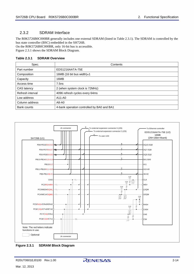
2.3.2 SDRAM Interface The R0K5726B0C000BR generally includes one external SDRAM (listed in Table 2.3.1). The SDRAM is controlled by the bus state controller (BSC) embedded in the SH726B. On the R0K5726B0C000BR, only 16-bit bus is accessible. Figure 2.3.1 shows the SDRAM Block Diagram. Table 2.3.1 SDRAM Overview
Spec. Contents
Part number EDS1216AATA-75E Composition 16MB (16 bit bus width)×1 Capacity 16MB Access time 7.5ns CAS latency 2 (when system clock is 72MHz) Refresh interval 4096 refresh cycles every 64ms Low address A11-A0 Column address A8-A0 Bank counts 4-bank operation controlled by BA0 and BA1
To Ethernet controller
EDS1216AATA-75E (U2)16MB
(2M×16bit×4bank)SH726B (U1)
PD6-PD7/D6-D7
8
DQ7-DQ62
DQ15-DQ8PD8-PD15/D8-D15
PD0-PD5/D0-D5
PB12/A12
PC8/CS3#/CTx1
PC5/RAS#/CRx0/IERxD
PC6/CAS#/CTx0/IETxD
PC7/CKE/CRx1
BA1-BA0
A11
RAS#
CAS#
CKE
CS#
CKIO
PC2/RD/WR#
PC3/WE0#/DQML
PC4/WE1#/DQMU
CLK
WE#
LDQM
UDQM3.3V
6
3.3V
3.3V
To external expansion connector 3 (J26)
To external expansion connector 2 (J25)
DQ5-DQ0
2PB13-PB14/A13-A14
PB11-PB10/A11-A10 A10-A92
PB9-PB1/A9-A1 A8-A09
JA connector
JA connector
3.3V
3.3V
To user LED4
39
Note: The red letters indicate functions in use.
: Optional
Figure 2.3.1 SDRAM Block Diagram

SH726B CPU Board R0K5726B0C000BR 2. Functional Specification
R20UT0601EJ0100 Rev.1.00 2-15
Mar. 12, 2013
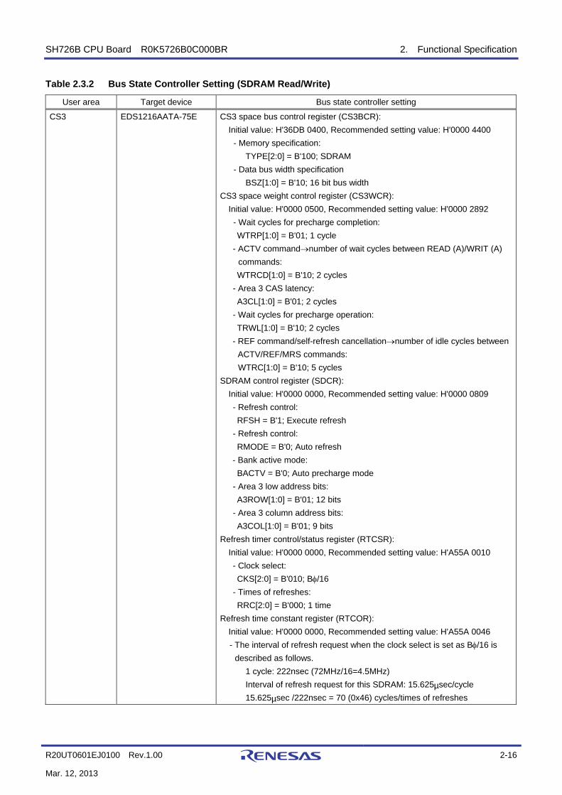
Figure 2.3.2 shows the Example of SDRAM Single Read/Write Timing, and Table 2.3.2 lists the bus state controller setting when the SH726B bus clock runs at the frequency of 72MHz.
Figure 2.3.2 Example of SDRAM Single Read/Write Timing
SDRAM SINGLE READ SDRAM SINGLE WRITE
Data DatatWDH2tOHZ
tOHtAC
tLZ
tAD1tAD1
tAD1tAD1tAD1
tAD1tAD1tAD1
tAD1tAD1tAD1
tAD1tAD1tAD1
tAD1tAD1tAD1
tDQMD1tDQMD1tDQMD1tDQMD1
tRWD1tRWD1
tCASD1tCASD1
tCASD1tCASD1
tRASD1tRASD1
tRASD1tRASD1
tCSD1tCSD1tCSD1tCSD1
tHItSI
tRDH2tRDS2
tHItSI
tHItSI
tHItSI
tHItSI
tRP
tDAL
tRCtRPtRAS
tDPLtDAL
tDPLtRCDtRAStRP
tRCtRC
tRCDtRPtRAS
tRCDtRAS
tRC
tRCD
ACT READA ACT WRITEA ACTTr Trw Tc1 Tcw Td1 Tde Tr Trw Tc1 Trw11 Trw12 TrTap Tap
CKIO
CKE
CS3#
RASL#
CASL#
RD/WR#
DQMUU-LL
A11-A2(A9-A0)
A12(A10/AP)
A15,A14(BA1,0)
D0-31
SH726B CPU Board R0K5726B0C000BR 2. Functional Specification
R20UT0601EJ0100 Rev.1.00 2-16
Mar. 12, 2013
Table 2.3.2 Bus State Controller Setting (SDRAM Read/Write)
User area Target device Bus state controller setting
CS3 EDS1216AATA-75E CS3 space bus control register (CS3BCR): Initial value: H'36DB 0400, Recommended setting value: H'0000 4400
- Memory specification: TYPE[2:0] = B'100; SDRAM
- Data bus width specification BSZ[1:0] = B'10; 16 bit bus width
CS3 space weight control register (CS3WCR): Initial value: H'0000 0500, Recommended setting value: H'0000 2892
- Wait cycles for precharge completion: WTRP[1:0] = B'01; 1 cycle - ACTV command→number of wait cycles between READ (A)/WRIT (A)
commands: WTRCD[1:0] = B'10; 2 cycles - Area 3 CAS latency: A3CL[1:0] = B'01; 2 cycles - Wait cycles for precharge operation: TRWL[1:0] = B'10; 2 cycles - REF command/self-refresh cancellation→number of idle cycles between
ACTV/REF/MRS commands: WTRC[1:0] = B'10; 5 cycles
SDRAM control register (SDCR): Initial value: H'0000 0000, Recommended setting value: H'0000 0809
- Refresh control: RFSH = B'1; Execute refresh - Refresh control: RMODE = B'0; Auto refresh - Bank active mode: BACTV = B'0; Auto precharge mode - Area 3 low address bits: A3ROW[1:0] = B'01; 12 bits - Area 3 column address bits: A3COL[1:0] = B'01; 9 bits
Refresh timer control/status register (RTCSR): Initial value: H'0000 0000, Recommended setting value: H'A55A 0010
- Clock select: CKS[2:0] = B'010; Bφ/16 - Times of refreshes: RRC[2:0] = B'000; 1 time
Refresh time constant register (RTCOR): Initial value: H'0000 0000, Recommended setting value: H'A55A 0046
- The interval of refresh request when the clock select is set as Bφ/16 is described as follows.
1 cycle: 222nsec (72MHz/16=4.5MHz) Interval of refresh request for this SDRAM: 15.625µsec/cycle 15.625µsec /222nsec = 70 (0x46) cycles/times of refreshes
SH726B CPU Board R0K5726B0C000BR 2. Functional Specification
R20UT0601EJ0100 Rev.1.00 2-17
Mar. 12, 2013
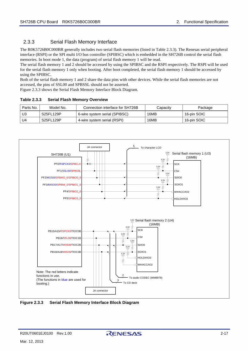
2.3.3 Serial Flash Memory Interface The R0K5726B0C000BR generally includes two serial flash memories (listed in Table 2.3.3). The Renesas serial peripheral interface (RSPI) or the SPI multi I/O bus controller (SPIBSC) which is embedded in the SH726B control the serial flash memories. In boot mode 1, the data (program) of serial flash memory 1 will be read. The serial flash memory 1 and 2 should be accessed by using the SPIBSC and the RSPI respectively. The RSPI will be used for the serial flash memory 1 only when booting. After boot completed, the serial flash memory 1 should be accessed by using the SPIBSC. Both of the serial flash memory 1 and 2 share the data pins with other devices. While the serial flash memories are not accessed, the pins of SSL00 and SPBSSL should not be asserted. Figure 2.3.3 shows the Serial Flash Memory Interface Block Diagram. Table 2.3.3 Serial Flash Memory Overview
Parts No. Model No. Connection interface for SH726B Capacity Package
U3 S25FL129P 6-wire system serial (SPIBSC) 16MB 16-pin SOIC U4 S25FL129P 4-wire system serial (RSPI) 16MB 16-pin SOIC
SH726B (U1)
To CD deck
Note: The red letters indicate functions in use.(The functions in blue are used for booting.)
PF0/RSPCK0/SPBCLK
PF1/SSL00/SPBSSL
PF2/MOSI0/SPBMO_0/SPBIO0_0
PF3/MISO0/SPBMI_0/SPBIO1_0
PF4/SPBIO2_0
PF5/SPBIO3_0
3.3V
3.3V
3.3V
3.3V
3.3V
3.3V
Serial flash memory 2 (U4) (16MB)
SCK
SI/IO0
W#/ACC/IO2
CS#
SO/IO1
HOLD#/IO3
3.3V
3.3V
3.3V
3.3V
3.3V
3.3V
PB15/A15/RSPCK0/TIOC0B
PB16/SSL00/TIOC1B
PB17/A17/MOSI0/TIOC2B
PB18/A18/MISO0/TIOC3B
3
SCK
W#/ACC/IO2
CS#
SI/IO0
SO/IO1
Serial flash memory 1 (U3) (16MB)
JA connector
HOLD#/IO3
To character LCD5
To audio CODEC (WM8978)2
JA connector
Figure 2.3.3 Serial Flash Memory Interface Block Diagram
SH726B CPU Board R0K5726B0C000BR 2. Functional Specification
R20UT0601EJ0100 Rev.1.00 2-18
Mar. 12, 2013
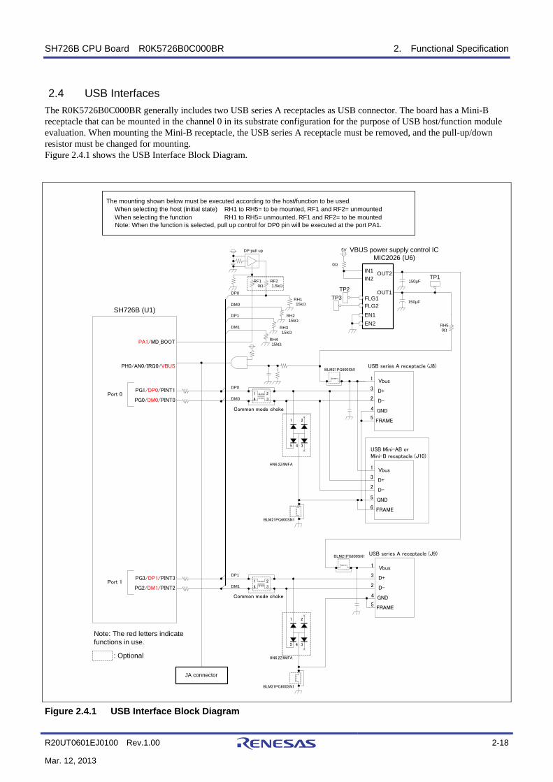
2.4 USB Interfaces The R0K5726B0C000BR generally includes two USB series A receptacles as USB connector. The board has a Mini-B receptacle that can be mounted in the channel 0 in its substrate configuration for the purpose of USB host/function module evaluation. When mounting the Mini-B receptacle, the USB series A receptacle must be removed, and the pull-up/down resistor must be changed for mounting. Figure 2.4.1 shows the USB Interface Block Diagram.
Vbus
D+
D-
GND
FRAME
Vbus
D+
D-
GND
FRAME
PH0/AN0/IRQ0/VBUS
PG0/DM0/PINT0
USB series A receptacle (J8)
BLM21PG600SN1
1 2
5 4 3
1 2
4 3
BLM21PG600SN1
HN6.2Z4MFA
1
3
2
4
1
3
2
5
6
5
Vbus
D+
D-
GND
FRAME
USB series A receptacle (J9)
1
3
2
4
5
1 2
4 3
Common mode choke
BLM21PG600SN1
1 2
5 4 3
HN6.2Z4MFA
BLM21PG600SN1
Port 0
SH726B (U1)
USB Mini-AB or Mini-B receptacle (J10)
FLG1
EN2
IN1
5V
0Ω
OUT2
VBUS power supply control ICMIC2026 (U6)
150µF
TP2
PG1/DP0/PINT1
PG2/DM1/PINT2Port 1
PG3/DP1/PINT3
JA connector
RF21.5kΩ
DP pull up
RH115kΩDM0
DP0
DM1
DP1 EN1FLG2
TP3
150µFTP1IN2
OUT1
DM0
DP0
DM1
DP1
RH50Ω
RF10Ω
RH215kΩ
RH315kΩ
RH415kΩ
Note: The red letters indicate functions in use.
: Optional
PA1/MD_BOOT
Common mode choke
The mounting shown below must be executed according to the host/function to be used.When selecting the host (initial state) RH1 to RH5= to be mounted, RF1 and RF2= unmountedWhen selecting the function RH1 to RH5= unmounted, RF1 and RF2= to be mounted
Note: When the function is selected, pull up control for DP0 pin will be executed at the port PA1.
Figure 2.4.1 USB Interface Block Diagram

SH726B CPU Board R0K5726B0C000BR 2. Functional Specification
R20UT0601EJ0100 Rev.1.00 2-19
Mar. 12, 2013
2.5 Serial Port Interface The SH726B embeds a FIFO on-chip serial communication interface (SCIF). On the R0K5726B0C000BR, the SH726B SCIF channel 3 is connected to the D-sub 9-pin connector via the RS-232C driver IC. Figure 2.5.1 shows the Serial Port Interface Block Diagram.
SH726B (U1)
PK1/TxD3
PH6/AN6/PINT6/RxD3
Serial port connector (J12)
VSS
54321
9876
Male plug with the crossover cable
Female socket with the straight cable
0Ω
Male plug with the crossover cable (optional with factory default setting)
Female socket with the straight cable (optional)
GND
0Ω×4 0Ω
0Ω
0Ω0Ω
12345
6789
GND
3.3VRS-232C driver (U13)
SHDN#
TIN
ROUT
RES#
3.3VRIN
TOUT
JA connector
Note: The red letters indicate functions in use.
: Optional
Figure 2.5.1 Serial Port Interface Block Diagram

SH726B CPU Board R0K5726B0C000BR 2. Functional Specification
R20UT0601EJ0100 Rev.1.00 2-20
Mar. 12, 2013
2.6 I/O Ports On the R0K5726B0C000BR, the SH726B I/O ports are connected to the switches and LEDs. The port PH1 to PH4 can be used as analog input pins (AN1 to AN4). Figure 2.6.1 shows the I/O Port Block Diagram.
AVcc
4.7kΩ
0Ω1.58kΩ4.7kΩ
SH726B (U1)
14kΩ3.3V × 14.0kR / (14.0kR + 4.7kR) = 2.47V3.3V × 4.70kR / (4.70kR + 4.7kR) = 1.65V3.3V × 1.58kR / (1.58kR + 4.7kR) = 0.83V3.3V × 0.00kR / (0.00kR + 4.7kR) = 0V
AVcc
4.7kΩ
0Ω1.58kΩ4.7kΩ14kΩ
AVcc
4.7kΩ
0Ω1.58kΩ4.7kΩ14kΩ
AVcc
4.7kΩ
0Ω1.58kΩ4.7kΩ14kΩ
PH1/AN1/IRQ1/RxD0
PA1/MD_BOOT
AVcc
AVcc
AVcc
AVcc
Note: The red letters indicate functions in use.
100kΩVR110kΩ
AVcc
0Ω0Ω
: Optional
PH2/AN2/IRQ2/WAIT#
PH3/AN3/IRQ3
PH4/AN4/PINT4/RxD1
JA connector
3.3V
PA0/MD_CLK To test pin (TH3)
User switch (4×4)
3.3V 3.3V
LED1Green
3.3V
LED2Orange
LED3Red
3.3V
LED4Red
PC2/RD/WR#/TIOC4C/SPDIF_OUT
PC4/WE1#/DQMU/WDTOVF#
PC5/RAS#/IRQ4/CRx0/IERxD
PC6/CAS#/IRQ5/CTx0/IETxD
To SDRAM, external expansion connector 3 (J26)
4
JA connector
3.3V
USB (DP0 pin) pull-up control
Figure 2.6.1 I/O Port Block Diagram
SH726B CPU Board R0K5726B0C000BR 2. Functional Specification
R20UT0601EJ0100 Rev.1.00 2-21
Mar. 12, 2013
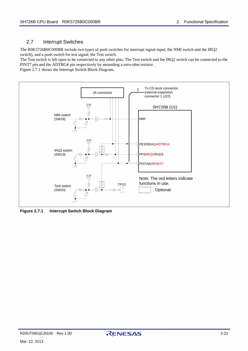
2.7 Interrupt Switches The R0K5726B0C000BR include two types of push switches for interrupt signal input; the NMI switch and the IRQ2 switch), and a push switch for test signal; the Test switch. The Test switch is left open to be connected to any other pins. The Test switch and the IRQ2 switch can be connected to the PINT7 pin and the ADTRG# pin respectively by mounding a zero-ohm resistor. Figure 2.7.1 shows the Interrupt Switch Block Diagram.
SH726B (U1)
3.3V
+PF6/IRQ2/RxD3
3.3V
+NMI
NMI switch(SW18)
IRQ2 switch(SW19)
3.3V
+
Test switch(SW20)
TP10
Note: The red letters indicate functions in use.
JA connector
PE3/SDA1/ADTRG#
: Optional
To CD deck connector, external expansion connector 1 (J22)
PH7/AN7/PINT7
2
Figure 2.7.1 Interrupt Switch Block Diagram

SH726B CPU Board R0K5726B0C000BR 2. Functional Specification
R20UT0601EJ0100 Rev.1.00 2-22
Mar. 12, 2013
2.8 Clock Modules The following two types of clocks are input in the SH726B on the R0K5726B0C000BR. • SH726B input clock : 12MHz • SH726B audio clock : 11.2896MHz
Figure 2.8.1 shows the Clock Module Block Diagram.
SH726B (U1)
CKIO
AUDIO_X2
AUDIO_X1
3.3V
PA0/MD_CLK
EXTALCLK48MHz
XTAL
NC
CLK
SDRAM (U2)
MCLK
Audio CODEC (U21)
CK1
MCKI
D/A converter (U20)
CK2
CK3
PLL
4
CK4 NC
11.2896MHzCLK(X3)
: Optional
Note: The red letters indicate functions in use.
AUDIO_XTAL
JA connector
REF
CLKOUT
CLK1
CLK3CLK2
CLK4
Clock Buffer (U5)CK1CK2CK3CK4
CLK
External expansion connector 2 (J25)
PE2/SCL1/AUDIO_CLK
External expansion connector 2 (J25)
12MHz
Socket (X1)
(X2)
Figure 2.8.1 Clock Module Block Diagram

SH726B CPU Board R0K5726B0C000BR 2. Functional Specification
R20UT0601EJ0100 Rev.1.00 2-23
Mar. 12, 2013
2.9 Reset Modules On the R0K5726B0C000BR, the reset IC controls the reset signals connected to the SH726B, the Ethernet controller, the RS-232C driver and other peripheral I/O pins. The system reset has two types of resets; the power on reset and the reset by switch. Figure 2.9.1 shows the Reset Module Block Diagram.
H-UDI (14-pin)(J6)
RES#
SH726B (U1)
RES# PK0/SCK3 PDN#
nRESET
RS-232C driver (U13)
SHDN#
D/A converter (AK4353)(U20)
CD deck connector (J21)
CDRST#
Note: The red letters indicate function in use.
: Optional
Ethernet controller (U17)
JA connector
Reset switch (SW17)
100Ω
IN OUT
Cd
RNA51957B (U11)
0.1µF
15kΩ
10kΩ
• Reset IC output delay timetpd=0.34×Cd(pF)=34ms
• Reset IC output detection voltage1.20×(Ra+Rb)/Rb=1.20×(15kΩ+10kΩ)/10kΩ=3.0V
0Ω
4.7kΩ
3.3V3.3V
Figure 2.9.1 Reset Module Block Diagram

SH726B CPU Board R0K5726B0C000BR 2. Functional Specification
R20UT0601EJ0100 Rev.1.00 2-24
Mar. 12, 2013
2.10 Power Modules On the R0K5726B0C000BR, the regulator generates 3.3V, 1.8V and 1.25V by using the 5V power supply. The power of 8V for the CD deck is supplied from the external power source. This board has a configuration which allows the I/O power supply (3.3), the A/D converter power supply (3.3V) and the internal power supply (1.25V) for the SH726B to be supplied from external sources. Figure 2.10.1 shows the Power Supply Module Block Diagram.
DC5Vinput
J5DC power jack
5VCCExternal
power supplyJ13
VSS
VSS
VSS AVSS
J20
VSS
8VCCExternal
power supply
CD deck connector
Character LCD
8VCC
Audio CODEC: WM8978 (AVDD, SPKVDD)
Ethernet controller (VDD_A33)
SH726B (U1)
0ΩAVCC
External power supply
J16
VSS
0ΩAVCC
AVref
: Optional
A3VCC
3VCCExternal
power suplyJ14
VSS
0ΩPVCC
SH726B (U1)
SDRAMSerial flash memoryCAN transceiverRS-232CClock bufferD/A converter (AK4353)Audio CODEC: WM8978 (DBVDD,DCVDD)CD deck connectorSD card slotEhternet controller (VDD_IO)EEPROM
3.3V→1.8V Ethernet controller (VDD_A18,VDD_CORE)
3VCC
3.3V→1.25V
1.25VCCExternal
power supplyJ15
VSS
0ΩPLLVCC
VCC
SH726B (U1)
1.8VCC
1.25VCC
5V→3.3V
Figure 2.10.1 Power Supply Module Block Diagram
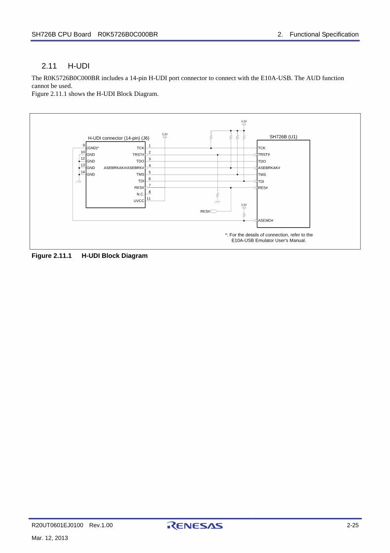
SH726B CPU Board R0K5726B0C000BR 2. Functional Specification
R20UT0601EJ0100 Rev.1.00 2-25
Mar. 12, 2013
2.11 H-UDI The R0K5726B0C000BR includes a 14-pin H-UDI port connector to connect with the E10A-USB. The AUD function cannot be used. Figure 2.11.1 shows the H-UDI Block Diagram.
1
2
3
4
5
6
7
11
3.3V
3.3V
RES#
3.3V
TRST#
TMS
TCK
TDI
TDO
ASEBRKAK#
ASEMD#
RES#
SH726B (U1)
*: For the details of connection, refer to the E10A-USB Emulator User's Manual.
TMS
TDI
TDO
N.C.
RES#
UVCC
9
10
12
13
14
TCK
TRST#
ASEBRKAK#/ASEBRK#
H-UDI connector (14-pin) (J6)
(GND)*
GND
GND
GND
GND
8
Figure 2.11.1 H-UDI Block Diagram
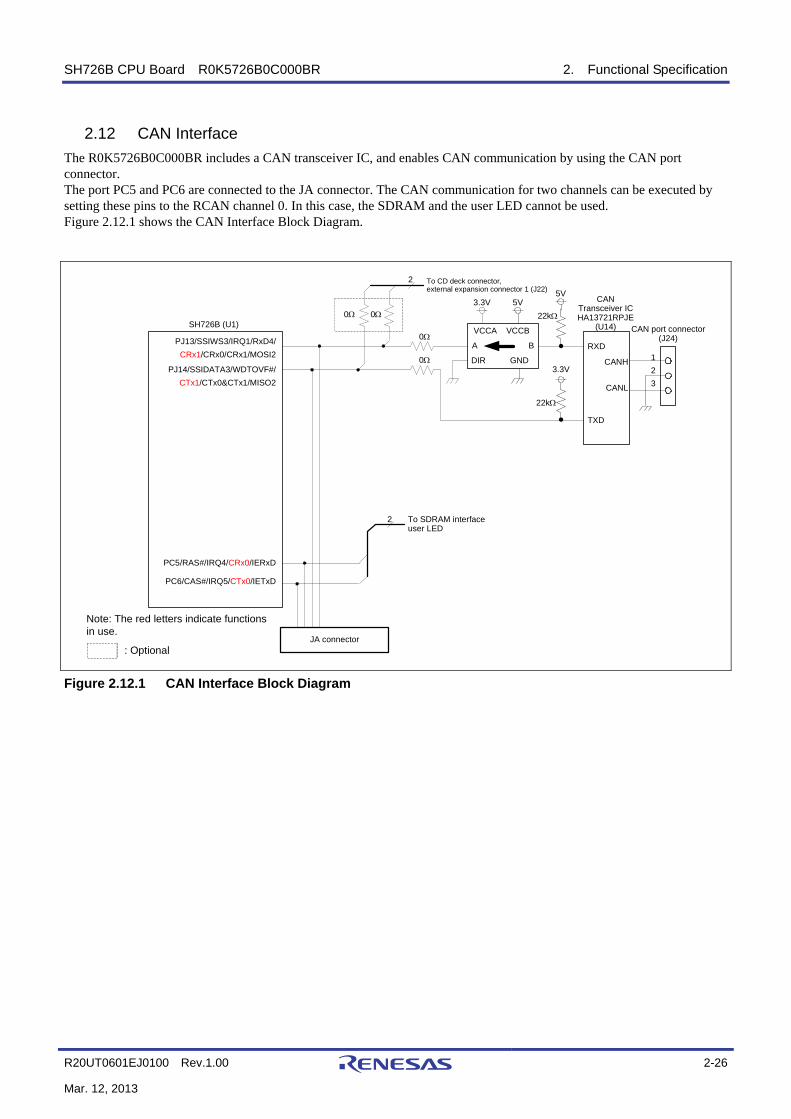
SH726B CPU Board R0K5726B0C000BR 2. Functional Specification
R20UT0601EJ0100 Rev.1.00 2-26
Mar. 12, 2013
2.12 CAN Interface The R0K5726B0C000BR includes a CAN transceiver IC, and enables CAN communication by using the CAN port connector. The port PC5 and PC6 are connected to the JA connector. The CAN communication for two channels can be executed by setting these pins to the RCAN channel 0. In this case, the SDRAM and the user LED cannot be used. Figure 2.12.1 shows the CAN Interface Block Diagram.
SH726B (U1)
PJ13/SSIWS3/IRQ1/RxD4/CRx1/CRx0/CRx1/MOSI2 1
23
CAN port connector(J24)
CANTransceiver ICHA13721RPJE
(U14)
22kΩ
CANH
CANL
RXD
VCCA VCCB
A B
DIR GND
22kΩ
PJ14/SSIDATA3/WDTOVF#/CTx1/CTx0&CTx1/MISO2
PC5/RAS#/IRQ4/CRx0/IERxD
3.3V 5V5V
3.3V
PC6/CAS#/IRQ5/CTx0/IETxD
JA connector
To SDRAM interfaceuser LED
TXD
To CD deck connector, external expansion connector 1 (J22)
2
0Ω
0Ω
0Ω0Ω
2
Note: The red letters indicate functions in use.
: Optional
Figure 2.12.1 CAN Interface Block Diagram
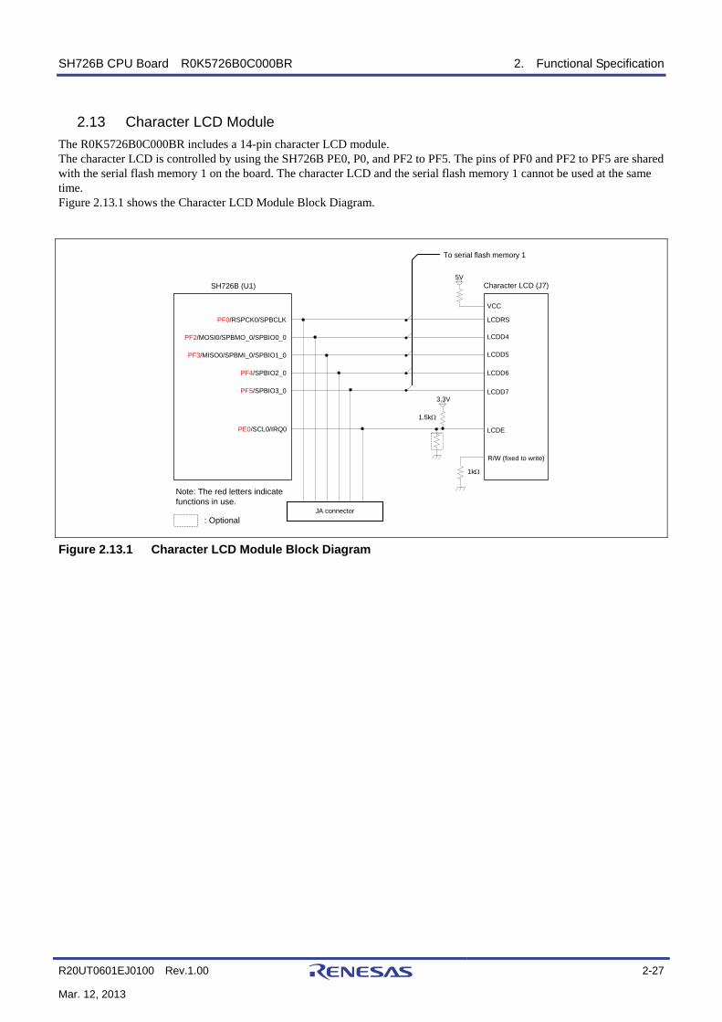
SH726B CPU Board R0K5726B0C000BR 2. Functional Specification
R20UT0601EJ0100 Rev.1.00 2-27
Mar. 12, 2013
2.13 Character LCD Module The R0K5726B0C000BR includes a 14-pin character LCD module. The character LCD is controlled by using the SH726B PE0, P0, and PF2 to PF5. The pins of PF0 and PF2 to PF5 are shared with the serial flash memory 1 on the board. The character LCD and the serial flash memory 1 cannot be used at the same time. Figure 2.13.1 shows the Character LCD Module Block Diagram.
SH726B (U1) Character LCD (J7)
R/W (fixed to write)
PF3/MISO0/SPBMI_0/SPBIO1_0
PF4/SPBIO2_0
PF5/SPBIO3_03.3V
PE0/SCL0/IRQ0
To serial flash memory 1
LCDD5
LCDD6
LCDD7
LCDE
PF0/RSPCK0/SPBCLK LCDRS
PF2/MOSI0/SPBMO_0/SPBIO0_0 LCDD4
5V
VCC
1kΩ
: OptionalJA connector
Note: The red letters indicate functions in use.
1.5kΩ
Figure 2.13.1 Character LCD Module Block Diagram
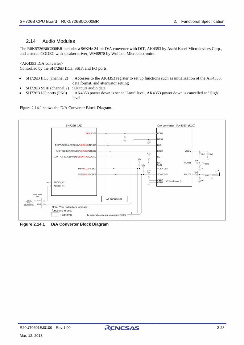
SH726B CPU Board R0K5726B0C000BR 2. Functional Specification
R20UT0601EJ0100 Rev.1.00 2-28
Mar. 12, 2013
2.14 Audio Modules The R0K5726B0C000BR includes a 96KHz 24-bit D/A converter with DIT, AK4353 by Asahi Kasei Microdevices Corp., and a stereo CODEC with speaker driver, WM8978 by Wolfson Microelectronics. <AK4353 D/A converter> Controlled by the SH726B IIC3, SSIF, and I/O ports. • SH726B IIC3 (channel 2) : Accesses to the AK4353 register to set up functions such as initialization of the AK4353,
data format, and attenuator setting • SH726B SSIF (channel 2) : Outputs audio data • SH726B I/O ports (PK0) : AK4353 power down is set at "Low" level, AK4353 power down is cancelled at "High"
level Figure 2.14.1 shows the D/A Converter Block Diagram.
SH726B (U1) D/A converter (AK4353) (U20)
PJ8/TIOC3A/A23/SCK2/SSISCK2/TEND0
PJ9/TIOC3B/A24/RxD2/SSIWS2/DREQ0
BICK
VCOM
AOUTL
AUDIO_X2AUDIO_X1
PE4/SCL2/TCLKA
PE5/SDA2/TCLKB
SDTI
LRCK
SCL/CCLK
SDA/CDTI
I2C
3.3V
CSN
CAD0CAD1 Chip address [1]
0.1µF 10µF+
+
10µF
27kΩ
220Ω
AOUTR +
10µF
27kΩ
220Ω
3.3V
2To external expansion connector 2 (J25)
PDN#PK0/SCK3
MCKI
NC
3.3V
3.3V
Note: The red letters indicate functions in use.
11.2896MHzCLK
J19
: Optional
PJ10/TIOC3C/A25/TxD2/SSIDATA2/DACK0
JA connector
Clock buffer (U5)
CLKOUT
CLK2
(X3)
Figure 2.14.1 D/A Converter Block Diagram

SH726B CPU Board R0K5726B0C000BR 2. Functional Specification
R20UT0601EJ0100 Rev.1.00 2-29
Mar. 12, 2013
<WM8978 Audio CODEC> Controlled by the SH726B RSPI, SSIF, and I/O ports. • SH726B RSPI (channel 0) : Accesses the WM8978 register to initialize the WM8979 and set the data format • SH726B I/O port (PF7) : Outputs select signals when using the WM8978 SPI in three-wire more (MODE= 'H') • SH726B SSIF (channel 0) : Inputs and outputs audio data The RSPI channel 0 is also used for the serial flash memory 2 and the CD deck interface on the R0K5726B0C000BR. When accessing to the audio CODEC, the select signal should be output at the port PF7. Figure 2.14.2 shows the Audio CODEC Block Diagram.
Audio CODEC (WM8978) (U21)
L2/GPIO2
R2/GPIO3
DBVDD
DCVDD
DGND
BCLK
DACDAT
LRC
ADCDAT
MODE
SCLK
SDIN
CSB/GPIO1
SPKVDD
SPKGND
LOUT1 ++
ROUT1
3.3V
A3V
AVDD
VMIDAGND
A3V
MCLK
3.3V
0ΩPE0/SCL0/AUDIO_CLK/IRQ0
SH726B (U1)
AUDIO_X2
AUDIO_X1
PB19/A19/SSISCK0/TIOC0C
PB20/A20/SSIWS0/TIOC0D
PB21/A21SSIRxD0/TIOC3C
PB22/A22/SSITxD0/TIOC3D
NC
: Optional
PB15/A15/RSPCK0/TIOC0B
PB17/A17/MOSI0/TIOC2B
PF7/IRQ3/RxD4
Note: The red letters indicate functions in use.
JA connector
To serial flash memory 2, CD deck
11.2896MHz
CLK
Clock buffer (U5)
3.3V
(X3)
MICBIAS
+
Figure 2.14.2 Audio CODEC Block Diagram
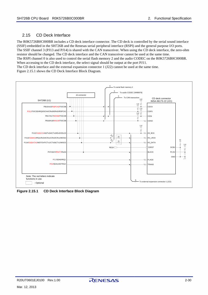
SH726B CPU Board R0K5726B0C000BR 2. Functional Specification
R20UT0601EJ0100 Rev.1.00 2-30
Mar. 12, 2013
2.15 CD Deck Interface The R0K5726B0C000BR includes a CD deck interface connector. The CD deck is controlled by the serial sound interface (SSIF) embedded in the SH726B and the Renesas serial peripheral interface (RSPI) and the general purpose I/O ports. The SSIF channel 3 (PJ13 and PJ14) is shared with the CAN transceiver. When using the CD deck interface, the zero-ohm resistor should be changed. The CD deck interface and the CAN transceiver cannot be used at the same time. The RSPI channel 0 is also used to control the serial flash memory 2 and the audio CODEC on the R0K5726B0C000BR. When accessing to the CD deck interface, the select signal should be output at the port PJ11. The CD deck interface and the external expansion connector 1 (J22) cannot be used at the same time. Figure 2.15.1 shows the CD Deck Interface Block Diagram.
IIS_BCK
IIS_LRCK
IIS_DATA
CD deck connectorIMSA-9617S-22 (J21)
CDSO
CDFS
CDSI
CDCK
CDRSTRES#
To serial flash memory 23
TRANS
FLAG6
GND
P3.3V
DC8V
8V
3.3V
BLKCK
3.3V
3.3V
3.3V
3.3V
To audio CODEC (WM8978)2
JA connector
SH726B (U1)
PJ12/SSISCK3/A0/TxD4/CTx0/IExD/SSL02
PJ13/SSIWS3/IRQ1/RxD4/CRx1/CRx0/CRx1/MOSI2
PJ14/SSIDATA3/WDTOVF/CTx1/CTx0&CTx1/MISO2
PB15/A15/RSPCK0/TIOC0B
PJ11/TIOC3D/IRQ0/SCK4/CRx0/IERxD/RSPCK2
PB17/A17/MOSI0/TIOC2B
PB18/A18/MISO0/TIOC3B
Note: The red letters indicate functions in use.
PE1/SDA0/IRQ1
PH7/AN7//PINT7/RxD4
3.3V
To CAN transceiver2
0Ω
0Ω
: Optional6
To external expansion connector 1 (J22)
PE3/SDA1/ADTRG#
0Ω
0Ω
Figure 2.15.1 CD Deck Interface Block Diagram
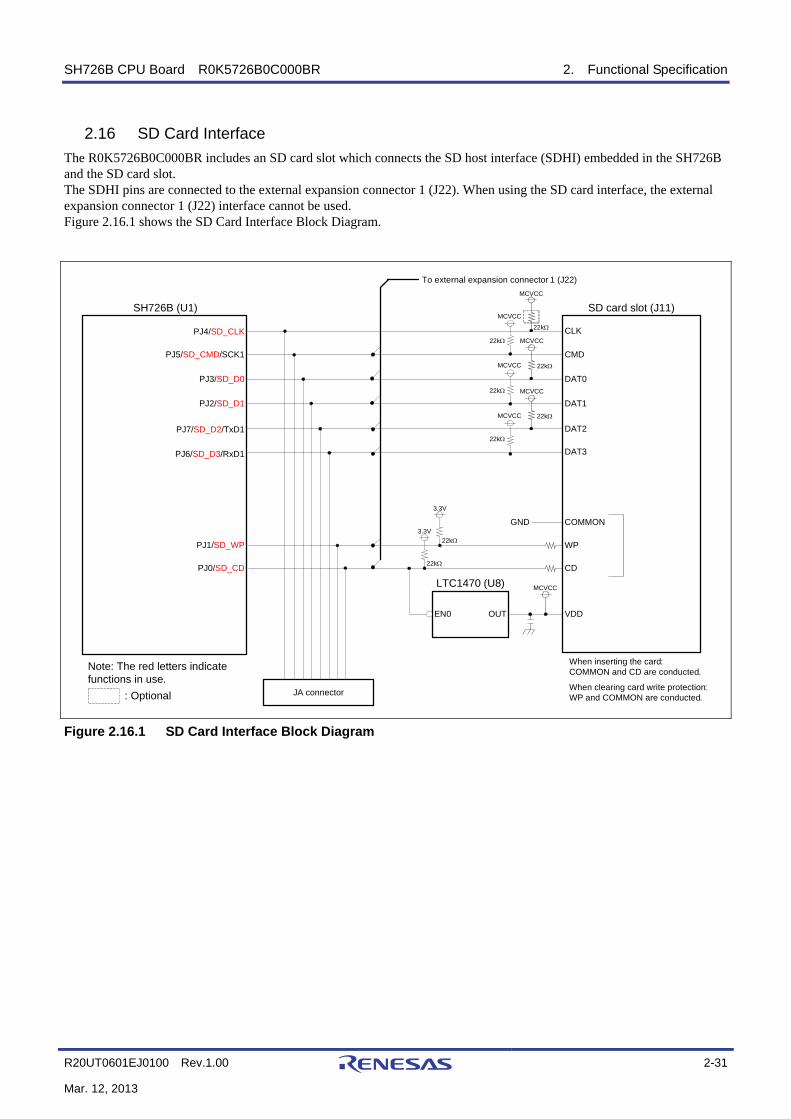
SH726B CPU Board R0K5726B0C000BR 2. Functional Specification
R20UT0601EJ0100 Rev.1.00 2-31
Mar. 12, 2013
2.16 SD Card Interface The R0K5726B0C000BR includes an SD card slot which connects the SD host interface (SDHI) embedded in the SH726B and the SD card slot. The SDHI pins are connected to the external expansion connector 1 (J22). When using the SD card interface, the external expansion connector 1 (J22) interface cannot be used. Figure 2.16.1 shows the SD Card Interface Block Diagram.
SH726B (U1)
PJ7/SD_D2/TxD1
PJ6/SD_D3/RxD1
PJ5/SD_CMD/SCK1
PJ4/SD_CLK
PJ3/SD_D0
PJ2/SD_D1
PJ1/SD_WP
PJ0/SD_CD
SD card slot (J11)
CLK
CMD
DAT0
DAT1
DAT2
DAT3
EN0 OUT
LTC1470 (U8)
22kΩ
3.3V
22kΩ
VDD
WP
COMMON
CD
GND3.3V
Note: The red letters indicate functions in use.
When inserting the card: COMMON and CD are conducted.
When clearing card write protection: WP and COMMON are conducted.: Optional
22kΩ
MCVCC
22kΩ
22kΩ
22kΩ
22kΩ
22kΩ
JA connector
To external expansion connector 1 (J22)
MCVCC
MCVCC
MCVCC
MCVCC
MCVCC
MCVCC
Figure 2.16.1 SD Card Interface Block Diagram
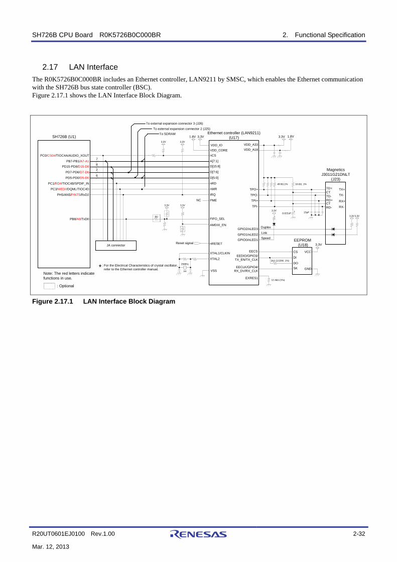
SH726B CPU Board R0K5726B0C000BR 2. Functional Specification
R20UT0601EJ0100 Rev.1.00 2-32
Mar. 12, 2013
2.17 LAN Interface The R0K5726B0C000BR includes an Ethernet controller, LAN9211 by SMSC, which enables the Ethernet communication with the SH726B bus state controller (BSC). Figure 2.17.1 shows the LAN Interface Block Diagram.
SH726B (U1)
PD5-PD0/D5-D0
PC0/CS0#/TIOC4A/AUDIO_XOUT
Ethernet controller (LAN9211) (U17)
TPO-
D[5:0]
A[7:1]
nRD
nWR
VSS
FIFO_SEL
Note: The red letters indicate functions in use.
: Optional
MagneticsJ3011G21DNLT
(J23)
EEPROM (U18)
nCS
IRQTPO+
TPI-
TPI+
EXRES1
GPIO2/nLED3
VDD_IO VDD_A33VDD_A18VDD_CORE
GPIO1/nLED2GPIO0/nLED1
EECLK/GPIO4/RX_DV/RX_CLK
EEDIO/GPIO3/TX_EN/TX_CLK
EECSXTAL1/CLKIN
XTAL2
nRESET
PME
AMDIX_EN
Reset signal
DI
CS
SK
1.8V 1.8V
Link
Duplex
PC1/RD#/TIOC4B/SPDIF_IN
PC3/WE0#/DQML/TIOC4D
PH5/AN5/PINT5/RxD2
PB7-PB1/A7-A1
PB8/A8/TxD0
3.3V3.3V
3.3V3.3V
6
7
3.3V
0Ω
25MHz
3.3V
12.4kΩ (1%)
3.3V
JA connector
NC
DO1kΩ (1/10W, 1%)
GND
VCC
3.3V
TD+
TD-RD+
RD-
TX+
TX-
RX+
RX-
49.9Ω,1%
CT
CT
15pF+0.022uF
10.0Ω, 1%
To SDRAM
To external expansion connector 3 (J26)
To external expansion connector 2 (J25)
PD7-PD6/D7-D6
PD15-PD8/D15-D828
D[7:6]
D[15:8]
Speed
3.3V 3.3V
: For the Electrical Characteristics of crystal oscillator, refer to the Ethernet controller manual.
X4*
Figure 2.17.1 LAN Interface Block Diagram
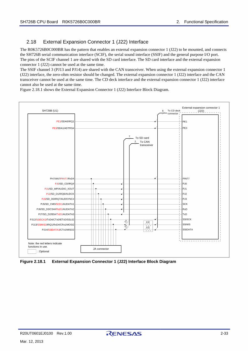
SH726B CPU Board R0K5726B0C000BR 2. Functional Specification
R20UT0601EJ0100 Rev.1.00 2-33
Mar. 12, 2013
2.18 External Expansion Connector 1 (J22) Interface The R0K5726B0C000BR has the pattern that enables an external expansion connector 1 (J22) to be mounted, and connects the SH726B serial communication interface (SCIF), the serial sound interface (SSIF) and the general purpose I/O port. The pins of the SCIF channel 1 are shared with the SD card interface. The SD card interface and the external expansion connector 1 (J22) cannot be used at the same time. The SSIF channel 3 (PJ13 and PJ14) are shared with the CAN transceiver. When using the external expansion connector 1 (J22) interface, the zero-ohm resistor should be changed. The external expansion connector 1 (J22) interface and the CAN transceiver cannot be used at the same time. The CD deck interface and the external expansion connector 1 (J22) interface cannot also be used at the same time. Figure 2.18.1 shows the External Expansion Connector 1 (J22) Interface Block Diagram.
SH726B (U1)
PH7/AN7/PINT7/RxD4
Note: the red letters indicate functions in use.
: Optional
External expansion connector 1 (J22)
PJ0/SD_CD/IRQ4
PJ1/SD_WP/AUDIO_XOUT
PJ2/SD_D1/IRQ6/AUDCK
PJ3/SD_D0/IRQ7/AUDSYNC#
PJ12/SSISCK3/TxD4/CTx0/IETxD/SSL02
PJ13/SSIWS3/IRQ1/RxD4/CRx1/MOSI2
PJ14/SSIDATA3/CTx1/MISO2
PJ5/SD_CMD/SCK1/AUDATA1
PJ6/SD_D3/CS4#/RxD1/AUDATA2
PJ7/SD_D2/BS#/TxD1/AUDATA3
To SD card7
2 To CAN transceiver
0Ω
0Ω
PE1
PE3
PJ3
PJ0
PJ1
PJ2
PINT7
PE1/SDA0/IRQ1
JA connector
SCK
RxD
TxD
SSISCK
SSIWS
SSIDATA
To CD deck connector
6
PE3/SDA1/ADTRG#
0Ω
0Ω
Figure 2.18.1 External Expansion Connector 1 (J22) Interface Block Diagram
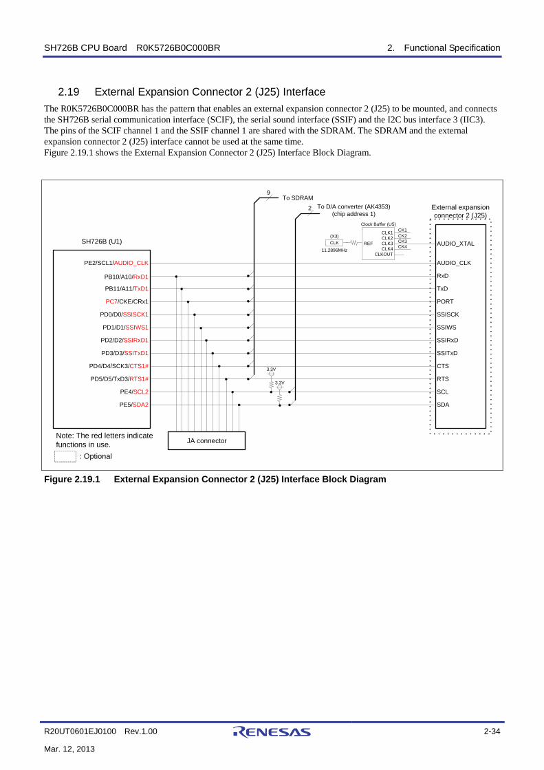
SH726B CPU Board R0K5726B0C000BR 2. Functional Specification
R20UT0601EJ0100 Rev.1.00 2-34
Mar. 12, 2013
2.19 External Expansion Connector 2 (J25) Interface The R0K5726B0C000BR has the pattern that enables an external expansion connector 2 (J25) to be mounted, and connects the SH726B serial communication interface (SCIF), the serial sound interface (SSIF) and the I2C bus interface 3 (IIC3). The pins of the SCIF channel 1 and the SSIF channel 1 are shared with the SDRAM. The SDRAM and the external expansion connector 2 (J25) interface cannot be used at the same time. Figure 2.19.1 shows the External Expansion Connector 2 (J25) Interface Block Diagram.
SH726B (U1)
PB11/A11/TxD1
PB10/A10/RxD1
External expansion connector 2 (J25)
Note: The red letters indicate functions in use.
: Optional
PC7/CKE/CRx1
PD0/D0/SSISCK1
PD1/D1/SSIWS1
PD2/D2/SSIRxD1
PD3/D3/SSITxD1
PD4/D4/SCK3/CTS1#
PD5/D5/TxD3/RTS1#
PE4/SCL2
PE5/SDA2
To D/A converter (AK4353)(chip address 1)
2
3.3V
3.3V
To SDRAM9
PE2/SCL1/AUDIO_CLK
JA connector
11.2896MHzCLK(X3)
REF
CLKOUT
CLK1
CLK3CLK2
CLK4
Clock Buffer (U5)CK1CK2CK3CK4 AUDIO_XTAL
AUDIO_CLK
RxD
TxD
PORT
SSISCK
SSIWS
SSIRxD
SSITxD
CTS
RTS
SCL
SDA
Figure 2.19.1 External Expansion Connector 2 (J25) Interface Block Diagram

SH726B CPU Board R0K5726B0C000BR 2. Functional Specification
R20UT0601EJ0100 Rev.1.00 2-35
Mar. 12, 2013
2.20 External Expansion Connector 3 (J26) Interface The R0K5726B0C000BR has the pattern that enables an external expansion connector 3 (J26) to be mounted, and connects the SH726B serial communication interface (SCIF) and the general purpose I/O ports (PC1 to PC6). The pins of the SCIF channel 2 and the port C are shared with the SDRAM and the LAN interface. The SDRAM or the LAN interface and the external expansion connector 3 (J26) interface cannot be used at the same time. Figure 2.20.1 shows the External Expansion Connector 3 (J26) Interface Block Diagram.
SH726B (U1)
PB13/A13/RxD2
PB14/A14/TxD2
Note: The red letters indicate functions in use.
: Optional
External expansion connector 3 (J26)
PC1/RD#/TIOC4B/SPDIF_IN
PC2/RD/WR#/TIOC4C/SPDIF_OUT
PC3/WE0#/DQML/TIOC4D
PC4/WE1#/DQMU/WDTOVF#
PC5/RAS#/IRQ4/CRx0/IERxD
PC6/CAS#/IRQ5/CTx0/IETxD
PD6/D6/MOSI1/SCK4/CTS2#
PD7/D7/MISO1/TxD4/RTS2#
To SDRAM9
To Ethernet controller4
JA connector
CTS
RTS
RxD
TxD
PC1
PC2
PC3
PC4
PC5
PC6
To user LED4
Figure 2.20.1 External Expansion Connector 3 (J26) Interface Block Diagram

SH726B CPU Board R0K5726B0C000BR 2. Functional Specification
R20UT0601EJ0100 Rev.1.00 2-36
Mar. 12, 2013
This page intentionally left blank.

SH726B CPU board R0K5726B0C000BR 3. Operational Specification
R20UT0601EJ0100 Rev.1.00 3-1 Mar. 12, 2013
3. Operational Specification
3.1 Connector Overview Figure 3.1 shows the R0K5726B0C000BR Connector Assignments.
J5: 5
V in
put
AC a
dapt
er ja
ck
J12: RS-232C connector
J6: H-UDI port connector
J24:
CAN
con
nect
or
J25:
Ext
erna
l exp
ansi
on
conn
ecto
r 2
J26:
Ext
erna
l exp
ansi
on
conn
ecto
r 3
J7: C
hara
cter
LC
D c
onne
ctor
J21: CD deck connector
J19: Line-out pin jack
J18: Mic-in pin jack
J22: External expansion connector 1
J23: LAN connector
J17: Line-out pin jack
J8, J
10: U
SB
conn
ecto
r
J9: U
SB c
onne
ctor
J1 to J4: Common ring connectors
JA1 to JA3, JA5, JA6:Application headers
<Top view of the component side>
J11: SD card slot
<Top view of the solder side>
Figure 3.1 R0K5726B0C000BR Connector Assignments
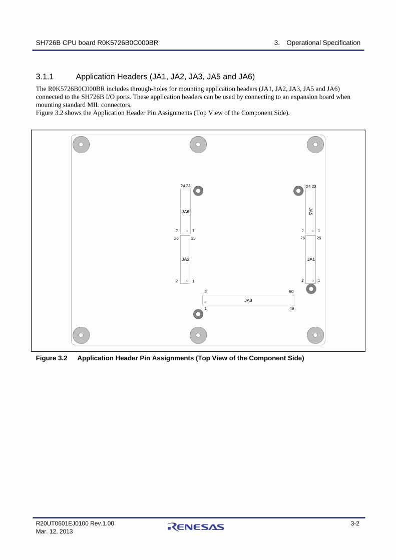
SH726B CPU board R0K5726B0C000BR 3. Operational Specification
R20UT0601EJ0100 Rev.1.00 3-2 Mar. 12, 2013
3.1.1 Application Headers (JA1, JA2, JA3, JA5 and JA6) The R0K5726B0C000BR includes through-holes for mounting application headers (JA1, JA2, JA3, JA5 and JA6) connected to the SH726B I/O ports. These application headers can be used by connecting to an expansion board when mounting standard MIL connectors. Figure 3.2 shows the Application Header Pin Assignments (Top View of the Component Side).
JA5
JA1JA2
JA3
12
12
2526
24 23
12
2526
1
2
49
50
JA6
12
24 23
Figure 3.2 Application Header Pin Assignments (Top View of the Component Side)

SH726B CPU board R0K5726B0C000BR 3. Operational Specification
R20UT0601EJ0100 Rev.1.00 3-3 Mar. 12, 2013
Table 3.1 lists the Application Header (JA1) Pin Descriptions. Table 3.1 Application Header (JA1) Pin Descriptions
Pin No. Signal name Function in use 1 5VCC 5VCC 2 GND GND 3 3VCC 3VCC 4 GND GND 5 AVcc AVcc 6 AVss AVss 7 AVref AVref 8 PE3/SDA1/ADTRG# ADTRG# 9 PH0/AN0/IRQ0/VBUS AN0 10 PH1/AN1/IRQ1/RxD0 AN1 11 PH2/AN2/IRQ2/WAIT# AN2 12 PH3/AN3/IRQ3 AN3 13 NC - 14 NC - 15 PF0/RSPCK0/SPBCLK PF0 16 PF1/SSL00/SPBSSL PF1 17 PF2/MOSI0/SPBMO_0/SPBIO0_0 PF2 18 PF3/MISO0/SPBMI_0/SPBIO1_0 PF3 19 PF4/SPBIO2_0 PF4 20 PF5/SPBIO3_0 PF5 21 PJ2/SD_D1/IRQ6/AUDCK PJ2 22 PJ3/SD_D0/IRQ7/AUDSYNC# PJ3 23 PJ11/TIOC3D/IRQ0/SCK4/CRx0/IERxD/RSPCK2 IRQ0 24 NC - 25 PE7/SDA3/TCLKD SDA3 26 PE6/SCL3/TCLKC SCL3
SH726B CPU board R0K5726B0C000BR 3. Operational Specification
R20UT0601EJ0100 Rev.1.00 3-4 Mar. 12, 2013
Table 3.2 lists the Application Header (JA2) Pin Descriptions. Table 3.2 Application Header (JA2) Pin Descriptions
Pin No. Signal name Function in use 1 RESET 2 EXTAL EXTAL 3 NMI NMI 4 GND GND 5 PJ14/SSIDATA3/WDTOVF#/CTx1/CTx0&CTx1/MISO2 WDTOVF# 6 PJ7/SD_D2/BS#/TxD1/AUDATA3 TxD1 7 PF6/IRQ2/RxD3,
PD8/D8/SD_CD/TIOC0A IRQ2, TIOC0A
8 PJ6/SD_D3/CS4#/RxD1/AUDATA2 RxD1 9 PH4/AN4/PINT4/RxD1,
PB15/A15/RSPCK0/TIOC0B PINT4, TIOC0B
10 PJ5/SD_CMD/SCK1/AUDATA1 SCK1 11 PJ4/SD_CLK/CS1#/AUDATA0 PJ4 12 NC - 13 PJ9/TIOC3B/A24/RxD2/SSIWS2/DREQ0 TIOC3B 14 PJ11/TIOC3D/IRQ0/SCK4/CRx0/IERxD/RSPCK2 TIOC3D 15 PC0/CS0#/TIOC4A/AUDIO_XOUT TIOC4A 16 PC2/RD/WR#/TIOC4C/SPDIF_OUT TIOC4C 17 PC1/RD#/TIOC4B/SPDIF_IN TIOC4B 18 PC3/WE0#/DQML/TIOC4D TIOC4D 19 PB16/A16/SSL00/TIOC1B TIOC1B 20 PD10/D10/SD_D1/TIOC2A TIOC2A 21 PE4/SCL2/TCLKA TCLKA 22 PE5/SDA2/TCLKB TCLKB 23 PH5/AN5/PINT5/RxD2,
PD9/D9/SD_WP/TIOC1A, PB19/A19/SSISCK0/TIOC0C
PINT5, TIOC1A, TIOC0C
24 NC - 25 PE6/SCL3/TCLKC TCLKC 26 PE7/SDA3/TCLKD TCLKD
SH726B CPU board R0K5726B0C000BR 3. Operational Specification
R20UT0601EJ0100 Rev.1.00 3-5 Mar. 12, 2013
Table 3.3 and Table 3.4 list the Application Header (JA3) Pin Descriptions. Table 3.3 Application Header (JA3) Pin Descriptions (1)
Pin No. Signal name Function in use 1 PJ12/SSISCK3/A0/TxD4/CTx0/IETxD/SSL20 A0 2 PB1/A1/SSISCK3 A1 3 PB2/A2/SSIWS3 A2 4 PB3/A3/SSIDATA3 A3 5 PB4/A4/CTS0# A4 6 PB5/A5/RTS0# A5 7 PB6/A6/SCK0/SSISCK2 A6 8 PB7/A7/RxD0 A7 9 PB8/A8/TxD0 A8
10 PB9/A9/SCK1/SSIWS2 A9 11 PB10/A10/RxD1 A10 12 PB11/A11/TxD1 A11 13 PB12/A12/SCK2/SSIDATA2 A12 14 PB13/A13/RxD2 A13 15 PB14/A14/TxD2 A14 16 PB15/A15/RSPCK0/TIOC0B A15 17 PD0/D0/SSISCK1/SIOFSCK/SPBMO_1/SPBIO0_1 D0 18 PD1/D1/SSIWS1/SIOFSYNC/SPBMI_1/SPBIO1_1 D1 19 PD2/D2/SSIRxD1/SIOFRxD/SPBIO2_1 D2 20 PD3/D3/SSITxD1/SIOFTxD/SPBIO3_1 D3 21 PD4/D4/RSPCK1/SCK3/CTS1# D4 22 PD5/D5/SSL10/TxD3/RTS1# D5 23 PD6/D6/MOSI1/SCK4/CTS2# D6 24 PD7/D7/MISO1/TxD4/RTS2# D7 25 PC1/RD#/TIOC4B/SPDIF_IN RD# 26 PC2/RD/WR#/TIOC4C/SPDIF_OUT RD/WR# 27 PC0/CS0#/TIOC4A/AUDIO_XOUT CS0# 28 PJ1/SD_WP/CS2#/IRQ5/AUDIO_XOUT CS2# 29 PD8/D8/SD_CD/TIOC0A D8 30 PD9/D9/SD_WP/TIOC1A D9 31 PD10/D10/SD_D1/TIOC2A D10 32 PD11/D11/SD_D0/TIOC3A D11 33 PD12/D12/SD_CLK/IRQ2 D12 34 PD13/D13/SD_CMD/IRQ3 D13 35 PD14/D14/SD_D3 D14 36 PD15/D15/SD_D2 D15
SH726B CPU board R0K5726B0C000BR 3. Operational Specification
R20UT0601EJ0100 Rev.1.00 3-6 Mar. 12, 2013
Table 3.4 Application Header (JA3) Pin Descriptions (2)
Pin No. Signal name Function in use 37 PB16/A16/SSL00/TIOC1B A16 38 PB17/A17/MOSI0/TIOC2B A17 39 PB18/A18/MISO0/TIOC3B A18 40 PB19/A19/SSISCK0/TIOC0C A19 41 PB20/A20/SSIWS0/TIOC0D A20 42 PB21/A21/SSIRxD0/TIOC3C A21 43 PB22/A22/SSITxD0/TIOC3D A22 44 CKIO CKIO 45 PC8/CS3#/IRQ7/CTx1/CTx0&CTx1,
PH2/AN2/IRQ2/WAIT# CS3#, WAIT#
46 PC7/CKE/IRQ6/CRx1/CRx0/CRx1 CKE 47 PC4/WE1#/DQMU/WDTOVF# WE1#,
DQMU 48 PC3/WE0#/DQML/TIOC4D WE0#,
DQML 49 PC6/CAS#/IRQ5/CTx0/IETxD CAS# 50 PC5/RAS#/IRQ4/CRx0/IERxD RAS#
SH726B CPU board R0K5726B0C000BR 3. Operational Specification
R20UT0601EJ0100 Rev.1.00 3-7 Mar. 12, 2013
Table 3.5 lists the Application Header (JA5) Pin Descriptions. Table 3.5 Application Header (JA5) Pin Descriptions
Pin No. Signal name Function in use 1 PH4/AN4/PINT4/RxD1 AN4 2 PH5/AN5/PINT5/RxD2 AN5 3 PH6/AN6/PINT6/RxD3 AN6 4 PH7/AN7/PINT7/RxD4 AN7 5 PC6/CAS#/IRQ5/CTx0/IETxD CTx0 6 PC5/RAS#/IRQ4/CRx0/IERxD CRx0 7 PJ14/SSIDATA3/WDTOVF#/CTx1/CTx0&CTx1/MISO2 CTx1 8 PJ13/SSIWS3/IRQ1/RxD4/CRx1/CRx0/CRx1/MOSI2 CRx1 9 PJ0/SD_CD/IRQ4 IRQ4 10 PJ1/SD_WP/CS2#/IRQ5/AUDIO_XOUT IRQ5 11 NC - 12 NC - 13 NC - 14 NC - 15 NC - 16 NC - 17 NC - 18 NC - 19 NC - 20 NC - 21 NC - 22 NC - 23 NC - 24 NC -
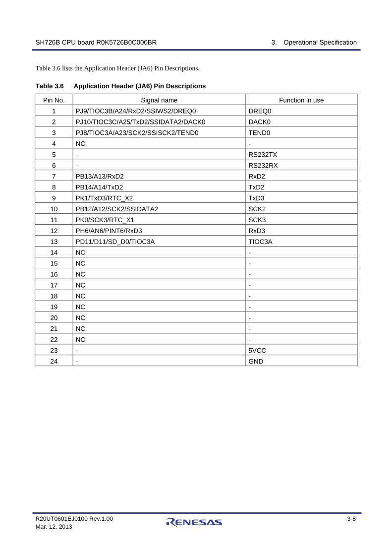
SH726B CPU board R0K5726B0C000BR 3. Operational Specification
R20UT0601EJ0100 Rev.1.00 3-8 Mar. 12, 2013
Table 3.6 lists the Application Header (JA6) Pin Descriptions. Table 3.6 Application Header (JA6) Pin Descriptions
Pin No. Signal name Function in use 1 PJ9/TIOC3B/A24/RxD2/SSIWS2/DREQ0 DREQ0 2 PJ10/TIOC3C/A25/TxD2/SSIDATA2/DACK0 DACK0 3 PJ8/TIOC3A/A23/SCK2/SSISCK2/TEND0 TEND0 4 NC - 5 - RS232TX 6 - RS232RX 7 PB13/A13/RxD2 RxD2 8 PB14/A14/TxD2 TxD2 9 PK1/TxD3/RTC_X2 TxD3 10 PB12/A12/SCK2/SSIDATA2 SCK2 11 PK0/SCK3/RTC_X1 SCK3 12 PH6/AN6/PINT6/RxD3 RxD3 13 PD11/D11/SD_D0/TIOC3A TIOC3A 14 NC - 15 NC - 16 NC - 17 NC - 18 NC - 19 NC - 20 NC - 21 NC - 22 NC - 23 - 5VCC 24 - GND
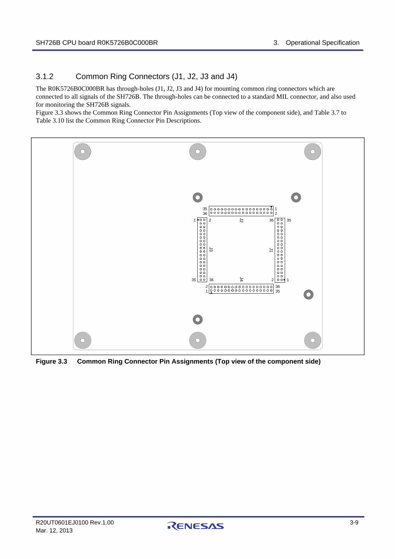
SH726B CPU board R0K5726B0C000BR 3. Operational Specification
R20UT0601EJ0100 Rev.1.00 3-9 Mar. 12, 2013
3.1.2 Common Ring Connectors (J1, J2, J3 and J4) The R0K5726B0C000BR has through-holes (J1, J2, J3 and J4) for mounting common ring connectors which are connected to all signals of the SH726B. The through-holes can be connected to a standard MIL connector, and also used for monitoring the SH726B signals. Figure 3.3 shows the Common Ring Connector Pin Assignments (Top view of the component side), and Table 3.7 to Table 3.10 list the Common Ring Connector Pin Descriptions.
J1J3
J2J4
21
3635
3536
12
1 2
35 36 2 1
36 35
Figure 3.3 Common Ring Connector Pin Assignments (Top view of the component side)
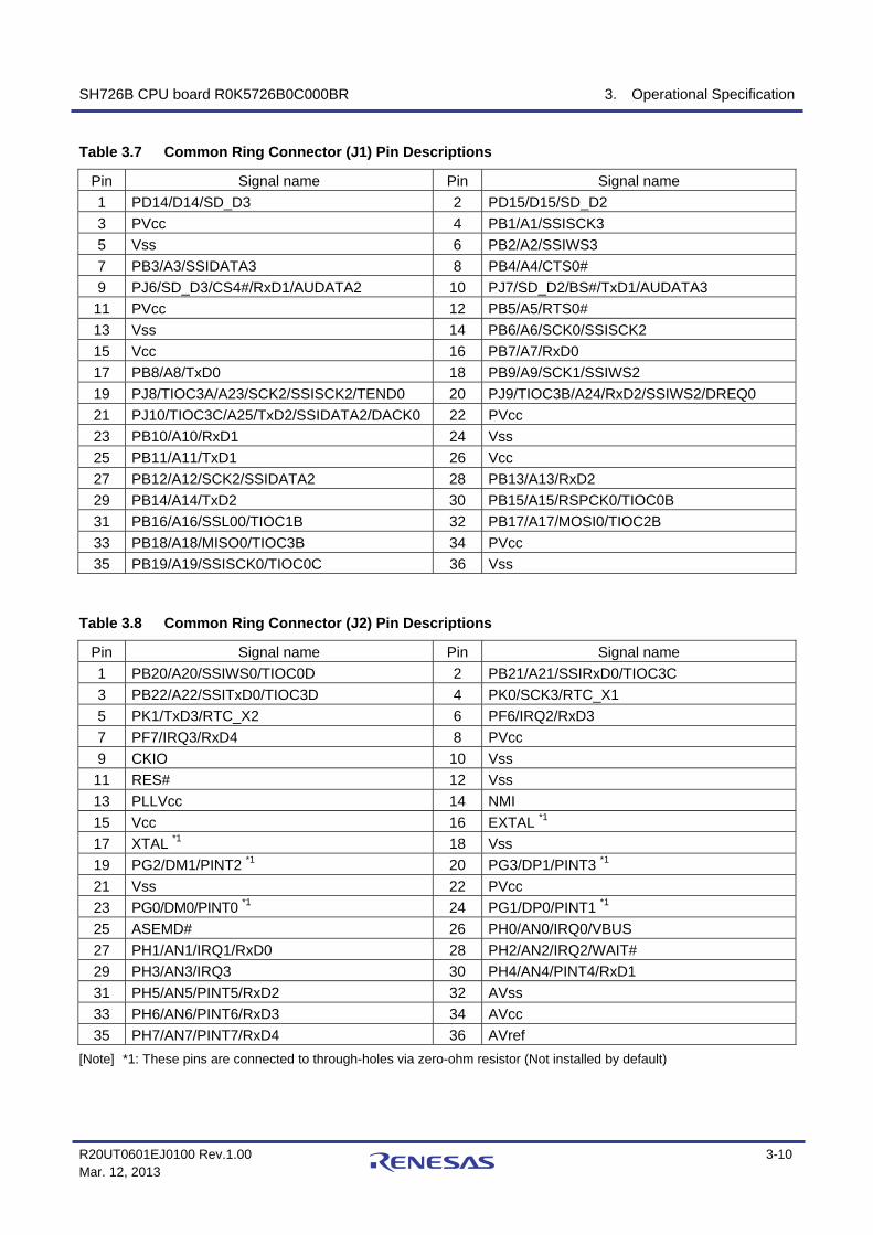
SH726B CPU board R0K5726B0C000BR 3. Operational Specification
R20UT0601EJ0100 Rev.1.00 3-10 Mar. 12, 2013
Table 3.7 Common Ring Connector (J1) Pin Descriptions
Pin Signal name Pin Signal name 1 PD14/D14/SD_D3 2 PD15/D15/SD_D2 3 PVcc 4 PB1/A1/SSISCK3 5 Vss 6 PB2/A2/SSIWS3 7 PB3/A3/SSIDATA3 8 PB4/A4/CTS0# 9 PJ6/SD_D3/CS4#/RxD1/AUDATA2 10 PJ7/SD_D2/BS#/TxD1/AUDATA3
11 PVcc 12 PB5/A5/RTS0# 13 Vss 14 PB6/A6/SCK0/SSISCK2 15 Vcc 16 PB7/A7/RxD0 17 PB8/A8/TxD0 18 PB9/A9/SCK1/SSIWS2 19 PJ8/TIOC3A/A23/SCK2/SSISCK2/TEND0 20 PJ9/TIOC3B/A24/RxD2/SSIWS2/DREQ0 21 PJ10/TIOC3C/A25/TxD2/SSIDATA2/DACK0 22 PVcc 23 PB10/A10/RxD1 24 Vss 25 PB11/A11/TxD1 26 Vcc 27 PB12/A12/SCK2/SSIDATA2 28 PB13/A13/RxD2 29 PB14/A14/TxD2 30 PB15/A15/RSPCK0/TIOC0B 31 PB16/A16/SSL00/TIOC1B 32 PB17/A17/MOSI0/TIOC2B 33 PB18/A18/MISO0/TIOC3B 34 PVcc 35 PB19/A19/SSISCK0/TIOC0C 36 Vss
Table 3.8 Common Ring Connector (J2) Pin Descriptions
Pin Signal name Pin Signal name 1 PB20/A20/SSIWS0/TIOC0D 2 PB21/A21/SSIRxD0/TIOC3C 3 PB22/A22/SSITxD0/TIOC3D 4 PK0/SCK3/RTC_X1 5 PK1/TxD3/RTC_X2 6 PF6/IRQ2/RxD3 7 PF7/IRQ3/RxD4 8 PVcc 9 CKIO 10 Vss
11 RES# 12 Vss 13 PLLVcc 14 NMI 15 Vcc 16 EXTAL *1 17 XTAL *1 18 Vss 19 PG2/DM1/PINT2 *1 20 PG3/DP1/PINT3 *1 21 Vss 22 PVcc 23 PG0/DM0/PINT0 *1 24 PG1/DP0/PINT1 *1 25 ASEMD# 26 PH0/AN0/IRQ0/VBUS 27 PH1/AN1/IRQ1/RxD0 28 PH2/AN2/IRQ2/WAIT# 29 PH3/AN3/IRQ3 30 PH4/AN4/PINT4/RxD1 31 PH5/AN5/PINT5/RxD2 32 AVss 33 PH6/AN6/PINT6/RxD3 34 AVcc 35 PH7/AN7/PINT7/RxD4 36 AVref
[Note] *1: These pins are connected to through-holes via zero-ohm resistor (Not installed by default)
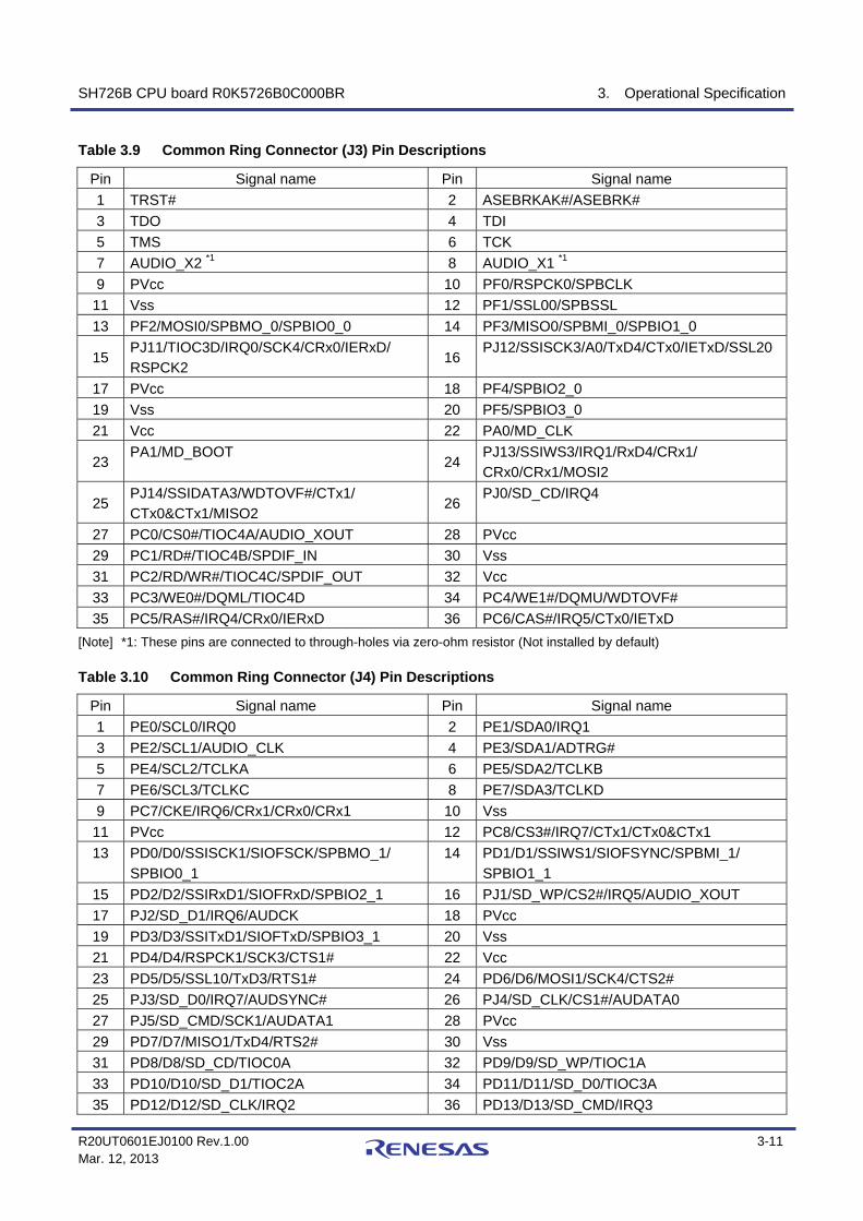
SH726B CPU board R0K5726B0C000BR 3. Operational Specification
R20UT0601EJ0100 Rev.1.00 3-11 Mar. 12, 2013
Table 3.9 Common Ring Connector (J3) Pin Descriptions
Pin Signal name Pin Signal name 1 TRST# 2 ASEBRKAK#/ASEBRK# 3 TDO 4 TDI 5 TMS 6 TCK 7 AUDIO_X2 *1 8 AUDIO_X1 *1 9 PVcc 10 PF0/RSPCK0/SPBCLK
11 Vss 12 PF1/SSL00/SPBSSL 13 PF2/MOSI0/SPBMO_0/SPBIO0_0 14 PF3/MISO0/SPBMI_0/SPBIO1_0
15 PJ11/TIOC3D/IRQ0/SCK4/CRx0/IERxD/ RSPCK2
16 PJ12/SSISCK3/A0/TxD4/CTx0/IETxD/SSL20
17 PVcc 18 PF4/SPBIO2_0 19 Vss 20 PF5/SPBIO3_0 21 Vcc 22 PA0/MD_CLK
23 PA1/MD_BOOT
24 PJ13/SSIWS3/IRQ1/RxD4/CRx1/ CRx0/CRx1/MOSI2
25 PJ14/SSIDATA3/WDTOVF#/CTx1/ CTx0&CTx1/MISO2
26 PJ0/SD_CD/IRQ4
27 PC0/CS0#/TIOC4A/AUDIO_XOUT 28 PVcc 29 PC1/RD#/TIOC4B/SPDIF_IN 30 Vss 31 PC2/RD/WR#/TIOC4C/SPDIF_OUT 32 Vcc 33 PC3/WE0#/DQML/TIOC4D 34 PC4/WE1#/DQMU/WDTOVF# 35 PC5/RAS#/IRQ4/CRx0/IERxD 36 PC6/CAS#/IRQ5/CTx0/IETxD
[Note] *1: These pins are connected to through-holes via zero-ohm resistor (Not installed by default) Table 3.10 Common Ring Connector (J4) Pin Descriptions
Pin Signal name Pin Signal name 1 PE0/SCL0/IRQ0 2 PE1/SDA0/IRQ1 3 PE2/SCL1/AUDIO_CLK 4 PE3/SDA1/ADTRG# 5 PE4/SCL2/TCLKA 6 PE5/SDA2/TCLKB 7 PE6/SCL3/TCLKC 8 PE7/SDA3/TCLKD 9 PC7/CKE/IRQ6/CRx1/CRx0/CRx1 10 Vss
11 PVcc 12 PC8/CS3#/IRQ7/CTx1/CTx0&CTx1 13 PD0/D0/SSISCK1/SIOFSCK/SPBMO_1/
SPBIO0_1 14 PD1/D1/SSIWS1/SIOFSYNC/SPBMI_1/
SPBIO1_1 15 PD2/D2/SSIRxD1/SIOFRxD/SPBIO2_1 16 PJ1/SD_WP/CS2#/IRQ5/AUDIO_XOUT 17 PJ2/SD_D1/IRQ6/AUDCK 18 PVcc 19 PD3/D3/SSITxD1/SIOFTxD/SPBIO3_1 20 Vss 21 PD4/D4/RSPCK1/SCK3/CTS1# 22 Vcc 23 PD5/D5/SSL10/TxD3/RTS1# 24 PD6/D6/MOSI1/SCK4/CTS2# 25 PJ3/SD_D0/IRQ7/AUDSYNC# 26 PJ4/SD_CLK/CS1#/AUDATA0 27 PJ5/SD_CMD/SCK1/AUDATA1 28 PVcc 29 PD7/D7/MISO1/TxD4/RTS2# 30 Vss 31 PD8/D8/SD_CD/TIOC0A 32 PD9/D9/SD_WP/TIOC1A 33 PD10/D10/SD_D1/TIOC2A 34 PD11/D11/SD_D0/TIOC3A 35 PD12/D12/SD_CLK/IRQ2 36 PD13/D13/SD_CMD/IRQ3

SH726B CPU board R0K5726B0C000BR 3. Operational Specification
R20UT0601EJ0100 Rev.1.00 3-12 Mar. 12, 2013
3.1.3 DC Power Jack (J5) The R0K5726B0C000BR includes a DC power jack (J5). Figure 3.4 shows the DC Power Jack (J5) Pin Assignments. Table 3.11 lists the DC Power Jack (J5) Pin Descriptions.
G V
J5
VG
1
2
4
3
Board edge
<Top view of the component side>
Figure 3.4 DC Power Jack (J5) Pin Assignments
Table 3.11 DC Power Jack (J5) Pin Descriptions
Pin No. Signal name 1 GND 2 GND 3 +5V 4 +5V

SH726B CPU board R0K5726B0C000BR 3. Operational Specification
R20UT0601EJ0100 Rev.1.00 3-13 Mar. 12, 2013
3.1.4 H-UDI Port Connector (J6) The R0K5726B0C000BR includes a14-pin H-UDI port connector (J6) to connect the E10A-USB emulator. Figure 3.5 shows the H-UDI Port Connector (J6) Pin Assignments, and Table 3.12 lists the 14-pin H-UDI Port Connector (J6) Pin Descriptions.
Board edge
8 1
J6
14 7
<Top view of the component side>
Figure 3.5 H-UDI Port Connector (J6) Pin Assignments
Table 3.12 14-pin H-UDI Port Connector (J6) Pin Descriptions
Pin No. Signal name Pin No. Signal name 1 TCK 8 NC 2 TRST# 9 ASEMD# 3 TDO 10 GND 4 ASEBRKAK#/ASEBRK# 11 +3.3V 5 TMS 12 GND 6 TDI 13 GND 7 RES# 14 GND

SH726B CPU board R0K5726B0C000BR 3. Operational Specification
R20UT0601EJ0100 Rev.1.00 3-14 Mar. 12, 2013
3.1.5 Character LCD connector (J7) The R0K5726B0C000BR includes a character LCD connector (J7). Figure 3.6 shows the Character LCD Connector (J7) Pin Assignments, and Table 3.13 lists the Character LCD Connector (J7) Pin Descriptions.
<Top view of the component side>
Board edge
1
J7
1314
2
Figure 3.6 Character LCD Connector (J7) Pin Assignments
Table 3.13 Character LCD Connector (J7) Pin Descriptions
Pin No. Signal name Pin No. Signal name 1 GND 2 +5V 3 NC 4 LCDRS (PF0/RSPCK0/SPBCLK) 5 LCDR/W (pull down with 1kΩ) 6 LCDE (PE0/SCL0/IRQ0) 7 NC 8 NC 9 NC 10 NC 11 LCDD4
(PF2/MOSI0/SPBMO_0/SPBIO0_0) 12 LCDD5
(PF3/MISO0/SPBMI_0/SPBIO1_0) 13 LCDD6 (PF4/SPBIO2_0) 14 LCDD7 (PF5/SPBIO3_0)
Notes: Bold letter indicates setting functions.
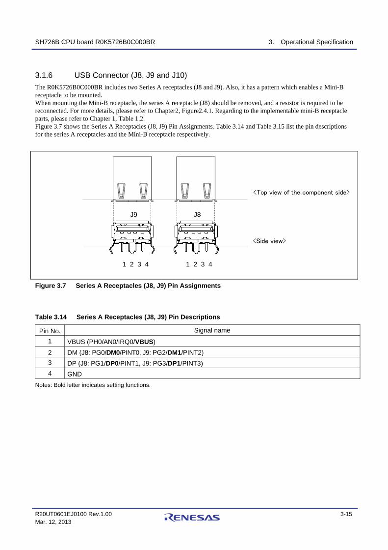
SH726B CPU board R0K5726B0C000BR 3. Operational Specification
R20UT0601EJ0100 Rev.1.00 3-15 Mar. 12, 2013
3.1.6 USB Connector (J8, J9 and J10) The R0K5726B0C000BR includes two Series A receptacles (J8 and J9). Also, it has a pattern which enables a Mini-B receptacle to be mounted. When mounting the Mini-B receptacle, the series A receptacle (J8) should be removed, and a resistor is required to be reconnected. For more details, please refer to Chapter2, Figure2.4.1. Regarding to the implementable mini-B receptacle parts, please refer to Chapter 1, Table 1.2. Figure 3.7 shows the Series A Receptacles (J8, J9) Pin Assignments. Table 3.14 and Table 3.15 list the pin descriptions for the series A receptacles and the Mini-B receptacle respectively.
<Top view of the component side>
J8
1 2 3 4
J9
1 2 3 4
<Side view>
Figure 3.7 Series A Receptacles (J8, J9) Pin Assignments
Table 3.14 Series A Receptacles (J8, J9) Pin Descriptions
Pin No. Signal name 1 VBUS (PH0/AN0/IRQ0/VBUS) 2 DM (J8: PG0/DM0/PINT0, J9: PG2/DM1/PINT2) 3 DP (J8: PG1/DP0/PINT1, J9: PG3/DP1/PINT3) 4 GND
Notes: Bold letter indicates setting functions.
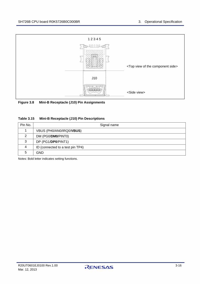
SH726B CPU board R0K5726B0C000BR 3. Operational Specification
R20UT0601EJ0100 Rev.1.00 3-16 Mar. 12, 2013
J10
<Top view of the component side>
1 2 3 4 5
<Side view>
Figure 3.8 Mini-B Receptacle (J10) Pin Assignments
Table 3.15 Mini-B Receptacle (J10) Pin Descriptions
Pin No. Signal name 1 VBUS (PH0/AN0/IRQ0/VBUS) 2 DM (PG0/DM0/PINT0) 3 DP (PG1/DP0/PINT1) 4 ID (connected to a test pin TP4) 5 GND
Notes: Bold letter indicates setting functions.
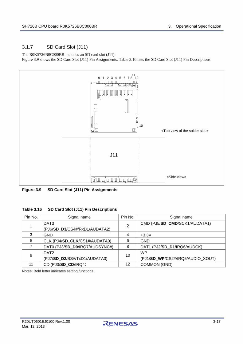
SH726B CPU board R0K5726B0C000BR 3. Operational Specification
R20UT0601EJ0100 Rev.1.00 3-17 Mar. 12, 2013
3.1.7 SD Card Slot (J11) The R0K5726B0C000BR includes an SD card slot (J11). Figure 3.9 shows the SD Card Slot (J11) Pin Assignments. Table 3.16 lists the SD Card Slot (J11) Pin Descriptions.
J11
1 2 3 4 5 6 7 811
129
<Top view of the solder side>10
<Side view>
Figure 3.9 SD Card Slot (J11) Pin Assignments
Table 3.16 SD Card Slot (J11) Pin Descriptions
Pin No. Signal name Pin No. Signal name
1 DAT3 (PJ6/SD_D3/CS4#/RxD1/AUDATA2)
2 CMD (PJ5/SD_CMD/SCK1/AUDATA1)
3 GND 4 +3.3V 5 CLK (PJ4/SD_CLK/CS1#/AUDATA0) 6 GND 7 DAT0 (PJ3/SD_D0/IRQ7/AUDSYNC#) 8 DAT1 (PJ2/SD_D1/IRQ6/AUDCK)
9 DAT2 (PJ7/SD_D2/BS#/TxD1/AUDATA3)
10 WP (PJ1/SD_WP/CS2#/IRQ5/AUDIO_XOUT)
11 CD (PJ0/SD_CD/IRQ4) 12 COMMON (GND) Notes: Bold letter indicates setting functions.
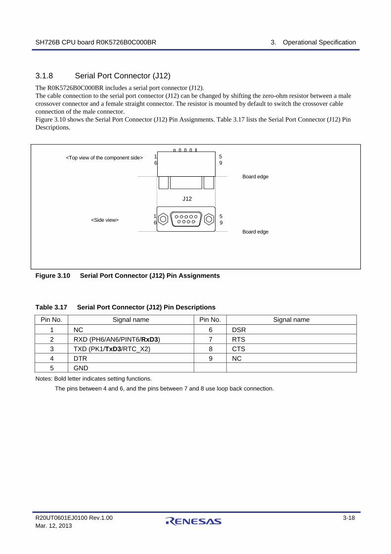
SH726B CPU board R0K5726B0C000BR 3. Operational Specification
R20UT0601EJ0100 Rev.1.00 3-18 Mar. 12, 2013
3.1.8 Serial Port Connector (J12) The R0K5726B0C000BR includes a serial port connector (J12). The cable connection to the serial port connector (J12) can be changed by shifting the zero-ohm resistor between a male crossover connector and a female straight connector. The resistor is mounted by default to switch the crossover cable connection of the male connector. Figure 3.10 shows the Serial Port Connector (J12) Pin Assignments. Table 3.17 lists the Serial Port Connector (J12) Pin Descriptions.
16
59
16
59
J12
<Top view of the component side>
Board edge
<Side view>
Board edge
Figure 3.10 Serial Port Connector (J12) Pin Assignments
Table 3.17 Serial Port Connector (J12) Pin Descriptions
Pin No. Signal name Pin No. Signal name 1 NC 6 DSR 2 RXD (PH6/AN6/PINT6/RxD3) 7 RTS 3 TXD (PK1/TxD3/RTC_X2) 8 CTS 4 DTR 9 NC 5 GND
Notes: Bold letter indicates setting functions.
The pins between 4 and 6, and the pins between 7 and 8 use loop back connection.

SH726B CPU board R0K5726B0C000BR 3. Operational Specification
R20UT0601EJ0100 Rev.1.00 3-19 Mar. 12, 2013
3.1.9 External Power Supply Connectors (J13, J14, J15, J16 and J20) The R0K5726B0C000BR includes external power supply connectors to apply 5V digital, 3.3V digital, 3.3V analog and 1.25V digital power from external source directly without using the DC power jack (J5). The connectors from J13 to J16 are not included by default. The R0K5726B0C000BR can be operated by supplying 5V power from the external power supply connector (J13) instead of the DC power jack (J5) in a default setting. Additionally, it is possible to supply 3.3V digital, 1.25V digital and 3.3V analog power from the external power supply connectors (J14, J15 and J16) by changing the zero-ohm resistor connection to operate the R0K5726B0C000BR. The external power supply connector (J20) is required to be supplied 8V digital power for a CD deck. Figure 3.11 shows the External Power Supply Connectors (J13 to J16 and J20) Pin Assignments. Table 3.18 to Table 3.22 lists the External Power Supply Connectors (J13 to J16 and J20) Pin Descriptions.
<Top view of the component side>
Board edge
J142 1
Digital 3.3V
J15 Digital 1.25V
J16 Analog 3.3V
J20Digital 8V
Digital 5V12
J13
Figure 3.11 External Power Supply Connectors (J13 to J16 and J20) Pin Assignments
Table 3.18 External Power Supply Connector (J13) Pin Descriptions
Pin No. Signal name Pin No. Signal name
1 5VCC 2 GND
Note: When supplying 5VCC from the external power supply connector (J13), please do not use the DC power jack (J5). If J5 and J13 are used for power supply at the same time, the R0K5726B0C000BR may be destroyed.
Table 3.19 External Power Supply Connector (J14) Pin Descriptions
Pin No. Signal name Pin No. Signal name
1 3VCC 2 GND
Note: When supplying 3VCC from the external power supply connector (J14), make sure that the zero-ohm resistor R143 is removed. If J14 supplies power without removing R143, the R0K5726B0C000BR may be destroyed.
Table 3.20 External Power Supply Connector (J15) Pin Descriptions
Pin No. Signal name Pin No. Signal name
1 1.25VCC 2 GND
Note: When supplying 1.25VCC from the external power supply connector (J15), make sure that the zero-ohm resistor R145 is removed. If J15 supplies power without removing R1435, the R0K5726B0C000BR may be destroyed.
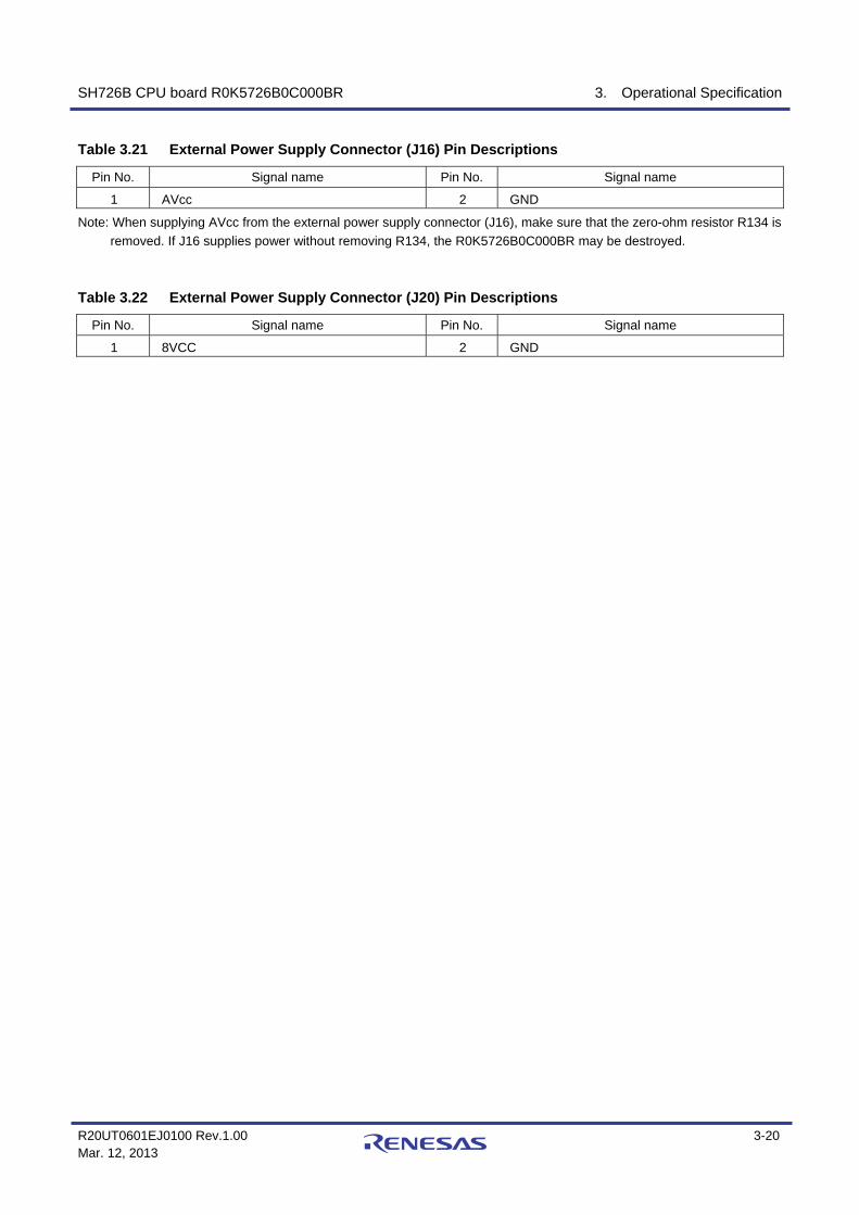
SH726B CPU board R0K5726B0C000BR 3. Operational Specification
R20UT0601EJ0100 Rev.1.00 3-20 Mar. 12, 2013
Table 3.21 External Power Supply Connector (J16) Pin Descriptions
Pin No. Signal name Pin No. Signal name
1 AVcc 2 GND
Note: When supplying AVcc from the external power supply connector (J16), make sure that the zero-ohm resistor R134 is removed. If J16 supplies power without removing R134, the R0K5726B0C000BR may be destroyed.
Table 3.22 External Power Supply Connector (J20) Pin Descriptions
Pin No. Signal name Pin No. Signal name
1 8VCC 2 GND
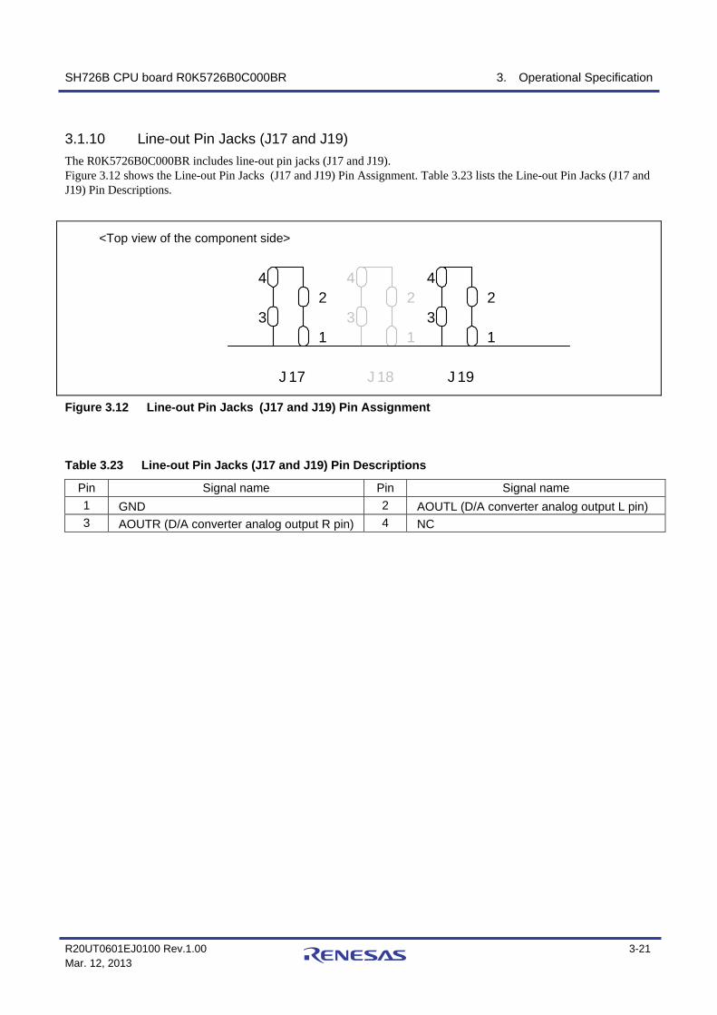
SH726B CPU board R0K5726B0C000BR 3. Operational Specification
R20UT0601EJ0100 Rev.1.00 3-21 Mar. 12, 2013
3.1.10 Line-out Pin Jacks (J17 and J19) The R0K5726B0C000BR includes line-out pin jacks (J17 and J19). Figure 3.12 shows the Line-out Pin Jacks (J17 and J19) Pin Assignment. Table 3.23 lists the Line-out Pin Jacks (J17 and J19) Pin Descriptions.
31
24
31
24
31
24
J 19J 18J 17
<Top view of the component side>
Figure 3.12 Line-out Pin Jacks (J17 and J19) Pin Assignment
Table 3.23 Line-out Pin Jacks (J17 and J19) Pin Descriptions
Pin Signal name Pin Signal name 1 GND 2 AOUTL (D/A converter analog output L pin) 3 AOUTR (D/A converter analog output R pin) 4 NC
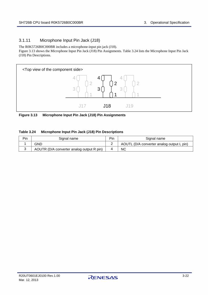
SH726B CPU board R0K5726B0C000BR 3. Operational Specification
R20UT0601EJ0100 Rev.1.00 3-22 Mar. 12, 2013
3.1.11 Microphone Input Pin Jack (J18) The R0K5726B0C000BR includes a microphone-input pin jack (J18). Figure 3.13 shows the Microphone Input Pin Jack (J18) Pin Assignments. Table 3.24 lists the Microphone Input Pin Jack (J18) Pin Descriptions.
31
24
31
24
31
24
J19J18J17
<Top view of the component side>
Figure 3.13 Microphone Input Pin Jack (J18) Pin Assignments
Table 3.24 Microphone Input Pin Jack (J18) Pin Descriptions
Pin Signal name Pin Signal name 1 GND 2 AOUTL (D/A converter analog output L pin) 3 AOUTR (D/A converter analog output R pin) 4 NC
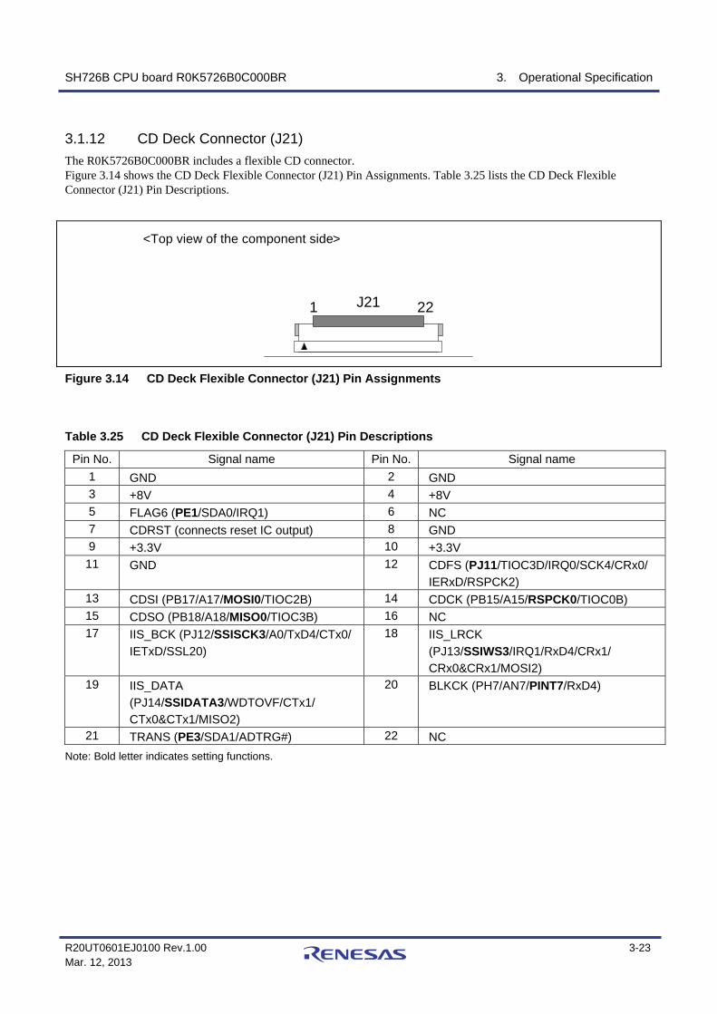
SH726B CPU board R0K5726B0C000BR 3. Operational Specification
R20UT0601EJ0100 Rev.1.00 3-23 Mar. 12, 2013
3.1.12 CD Deck Connector (J21) The R0K5726B0C000BR includes a flexible CD connector. Figure 3.14 shows the CD Deck Flexible Connector (J21) Pin Assignments. Table 3.25 lists the CD Deck Flexible Connector (J21) Pin Descriptions.
1 22
<Top view of the component side>
J21
Figure 3.14 CD Deck Flexible Connector (J21) Pin Assignments
Table 3.25 CD Deck Flexible Connector (J21) Pin Descriptions
Pin No. Signal name Pin No. Signal name 1 GND 2 GND 3 +8V 4 +8V 5 FLAG6 (PE1/SDA0/IRQ1) 6 NC 7 CDRST (connects reset IC output) 8 GND 9 +3.3V 10 +3.3V 11 GND 12 CDFS (PJ11/TIOC3D/IRQ0/SCK4/CRx0/
IERxD/RSPCK2) 13 CDSI (PB17/A17/MOSI0/TIOC2B) 14 CDCK (PB15/A15/RSPCK0/TIOC0B) 15 CDSO (PB18/A18/MISO0/TIOC3B) 16 NC 17 IIS_BCK (PJ12/SSISCK3/A0/TxD4/CTx0/
IETxD/SSL20) 18 IIS_LRCK
(PJ13/SSIWS3/IRQ1/RxD4/CRx1/ CRx0&CRx1/MOSI2)
19 IIS_DATA (PJ14/SSIDATA3/WDTOVF/CTx1/ CTx0&CTx1/MISO2)
20 BLKCK (PH7/AN7/PINT7/RxD4)
21 TRANS (PE3/SDA1/ADTRG#) 22 NC Note: Bold letter indicates setting functions.

SH726B CPU board R0K5726B0C000BR 3. Operational Specification
R20UT0601EJ0100 Rev.1.00 3-24 Mar. 12, 2013
3.1.13 LAN Connector (J23) The R0K5726B0C000BR includes a LAN connector (J23). Figure 3.15 shows the LAN Connector (J23) Pin Assignments, and Table 3.26 lists the LAN Connector (J23) Pin Descriptions.
<Top view of the component side>12 1
J23
<Side view>
Figure 3.15 LAN Connector (J23) Pin Assignments
Table 3.26 LAN Connector (J23) Pin Descriptions
Pin No. Signal name Pin No. Signal name 1 TX+ 2 TX- 3 RX+ 4 NC 5 NC 6 RX- 7 NC 8 NC 9 LED1-K 10 LED1-A 11 LED2-K 12 LED2-A

SH726B CPU board R0K5726B0C000BR 3. Operational Specification
R20UT0601EJ0100 Rev.1.00 3-25 Mar. 12, 2013
3.1.14 CAN Port Connector (J24) The R0K5726B0C000BR includes a CAN port connector (J24) for CAN transmit and receive. Figure 3.16 shows the CAN Port Connector (J24) Pin Assignments, and Table 3.27 lists the CAN Port Connector (J24) Pin Descriptions.
31
J24
Board edge
<Top view of the component side>
Figure 3.16 CAN Port Connector (J24) Pin Assignments
Table 3.27 CAN Port Connector (J24) Pin Descriptions
Pin No. Signal name 1 CANH 2 GND 3 CANL

SH726B CPU board R0K5726B0C000BR 3. Operational Specification
R20UT0601EJ0100 Rev.1.00 3-26 Mar. 12, 2013
3.1.15 External Expansion Connector 1 (J22) The R0K5726B0C000BR includes a through-hole to mount an external expansion connector 1 (J22). Figure 3.17shows the External Expansion Connector 1 (J22) Pin Assignments, and Table 3.28 lists the External Expansion Connector 1 (J22) Pin Descriptions.
2
1
20
19
J22
1 22
<Top view of the component side>
J21
Figure 3.17 External Expansion Connector 1 (J22) Pin Assignments
Table 3.28 External Expansion Connector 1 (J22) Pin Descriptions
Pin No. Signal name Pin No. Signal name 1 GND 2 GND 3 +5V 4 General purpose port
(PJ0/SD_CD/IRQ4) 5 General purpose port
(PE1/SDA0/IRQ1) 6 General purpose port
(PJ1/SD_WP/CS2#/IRQ5/AUDIO_XOUT) 7 General purposeport
(PJ3/SD_D0/IRQ7/AUDSYNC# ) 8 General purpose port
(PJ2/SD_D1/IRQ6/AUDCK) 9 +3.3V 10 +3.3V 11 GND 12 General purpose port
(PJ11/TIOC3D/IRQ0/SCK4/ CRx0/IERxD/RSPCK2)
13 TxD (PJ7/SD_D2/BS#/TxD1/AUDATA3) 14 SCK (PJ5/SD_CMD/SCK1/AUDATA1) 15 RxD (PJ6/SD_D3/CS4#/RxD1/AUDATA2) 16 SSISCK (PJ12/SSISCK3/A0/TxD4/CTx0/
IETxD/SSL20) 17 SSIWS (PJ13/SSIWS3/IRQ1/RxD4/CRx1/
CRx0&CRx1/MOSI2) 18 SSIDATA
(PJ14/SSIDATA3/WDTOVF/CTx1/ CTx0&CTx1/MISO2)
19 Interrupt input (PH7/AN7/PINT7/RxD4)
20 General purpose port (PE3/SDA1/ADTRG#)
Notes: Bold letter indicates setting functions.
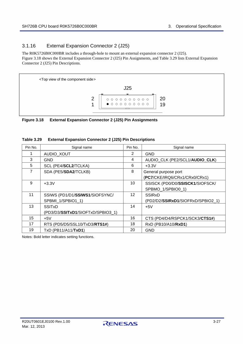
SH726B CPU board R0K5726B0C000BR 3. Operational Specification
R20UT0601EJ0100 Rev.1.00 3-27 Mar. 12, 2013
3.1.16 External Expansion Connector 2 (J25) The R0K5726B0C000BR includes a through-hole to mount an external expansion connector 2 (J25). Figure 3.18 shows the External Expansion Connector 2 (J25) Pin Assignments, and Table 3.29 lists External Expansion Connector 2 (J25) Pin Descriptions.
21
2019
J25
<Top view of the component side>
Figure 3.18 External Expansion Connector 2 (J25) Pin Assignments
Table 3.29 External Expansion Connector 2 (J25) Pin Descriptions
Pin No. Signal name Pin No. Signal name
1 AUDIO_XOUT 2 GND 3 GND 4 AUDIO_CLK (PE2/SCL1/AUDIO_CLK) 5 SCL (PE4/SCL2/TCLKA) 6 +3.3V 7 SDA (PE5/SDA2/TCLKB) 8 General purpose port
(PC7/CKE/IRQ6/CRx1/CRx0/CRx1) 9 +3.3V 10 SSISCK (PD0/D0/SSISCK1/SIOFSCK/
SPBMO_1/SPBIO0_1) 11 SSIWS (PD1/D1/SSIWS1/SIOFSYNC/
SPBMI_1/SPBIO1_1) 12 SSIRxD
(PD2/D2/SSIRxD1/SIOFRxD/SPBIO2_1) 13 SSITxD
(PD3/D3/SSITxD1/SIOFTxD/SPBIO3_1) 14 +5V
15 +5V 16 CTS (PD4/D4/RSPCK1/SCK3/CTS1#) 17 RTS (PD5/D5/SSL10/TxD3/RTS1#) 18 RxD (PB10/A10/RxD1) 19 TxD (PB11/A11/TxD1) 20 GND
Notes: Bold letter indicates setting functions.

SH726B CPU board R0K5726B0C000BR 3. Operational Specification
R20UT0601EJ0100 Rev.1.00 3-28 Mar. 12, 2013
3.1.17 External Expansion Connector 3 (J26) The R0K5726B0C000BR includes a through-hole to mount an external expansion connector 3 (J26). Figure 3.19 shows the External Expansion Connector 3 (J26) Pin Assignments, and Table 3.30 lists the External Expansion Connector 3 (J26) Pin Descriptions.
21
2019
J26
<Top view of the component side>
Figure 3.19 External Expansion Connector 3 (J26) Pin Assignments
Table 3.30 External Expansion Connector 3 (J26) Pin Descriptions
Pin No. Signal name Pin No. Signal name 1 GND 2 GND 3 General purpose port
(PC6/CAS#/IRQ5/CTx0/IETxD) 4 General purpose port
(PC5/RAS#/IRQ4/CRx0/IERxD) 5 General purpose port
(PC4/WE1#/DQMU/WDTOVF#) 6 General purpose port
(PC3/WE0#/DQML/TIOC4D) 7 General purpose port
(PC2/RD/WR#/TIOC4C/SPDIF_OUT) 8 General purpose port
(PC1/RD#/TIOC4B/SPDIF_IN) 9 +3.3V 10 +3.3V 11 CTS (PD6/D6/MOSI1/SCK4/CTS2#) 12 RTS (PD7/D7/MISO1/TxD4/RTS2#) 13 RxD (PB13/A13/RxD2) 14 TxD (PB14/A14/TxD2) 15 +5V 16 +5V 17 NC 18 NC 19 NC 20 NC
Notes: Bold letter indicates setting functions.
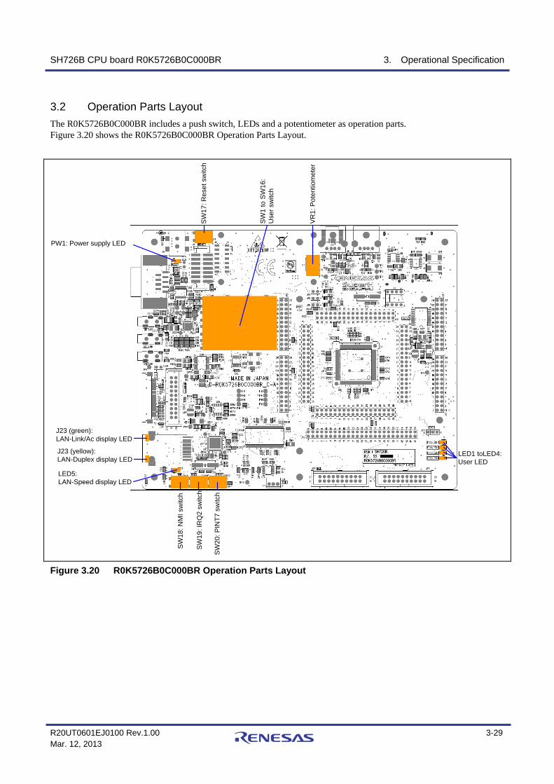
SH726B CPU board R0K5726B0C000BR 3. Operational Specification
R20UT0601EJ0100 Rev.1.00 3-29 Mar. 12, 2013
3.2 Operation Parts Layout The R0K5726B0C000BR includes a push switch, LEDs and a potentiometer as operation parts. Figure 3.20 shows the R0K5726B0C000BR Operation Parts Layout.
PW1: Power supply LED
SW
17: R
eset
sw
itch
SW1
to S
W16
:U
ser s
witc
h
SW
19: I
RQ
2 sw
itch
SW
18: N
MI s
witc
h
SW
20: P
INT7
sw
itch
LED1 toLED4: User LED
VR
1: P
oten
tiom
eter
LED5:LAN-Speed display LED
J23 (green):LAN-Link/Ac display LED
J23 (yellow):LAN-Duplex display LED
Figure 3.20 R0K5726B0C000BR Operation Parts Layout

SH726B CPU board R0K5726B0C000BR 3. Operational Specification
R20UT0601EJ0100 Rev.1.00 3-30 Mar. 12, 2013
3.2.1 Push Switches The R0K5726B0C000BR includes twenty push switches. Table 3.31 lists the R0K5726B0C000BR push switches. Table 3.31 R0K5726B0C000BR push switches
No. Function Remarks SW1-16 Key input switch Refer to Chapter 2.6 for the details SW17 Reset switch Refer to Chapter 2.9 for the details SW18 NMI switch Refer to Chapter 2.7 for the details SW19 IRQ2 switch Refer to Chapter 2.7 for the details SW20 PINT7 switch Refer to Chapter 2.7 for the details
3.2.2 LEDs The R0K5726B0C000BR includes eight LEDs. Table 3.32 lists the R0K5726B0C000BR LEDs. Table 3.32 R0K5726B0C000BR LEDs
No. Color Function PW1 Blue Power supply LED (lights up when 5V power is supplied) LED1 Green User LED (lights up when PC2 outputs low level signal) LED2 Orange User LED (lights up when PC4 outputs low level signal) LED3 Red User LED (lights up when PC5 outputs low level signal) LED4 Red User LED (lights up when PC6 outputs low level signal) LED5 Red LAN Speed display LED (lights up in 100Mbps communication)
J23 (yellow) Yellow LAN Duplex display LED (lights up in full duplex communication) J23 (green) Green LAN Link/Activity display LED (lights up when linking and communicating)
3.2.3 Potentiometer The R0K5726B0C000BR includes a potentiometer for evaluating AN1 input. Table 3.33 lists the Potentiometer model. Please refer to the data sheet issued by the manufacturer for more details. Table 3.33 Potentiometer
No. Model Manufacturer VR1 CT-6ETV10KΩ NIIDEC COPAL ELECTRONICS CORPORATION
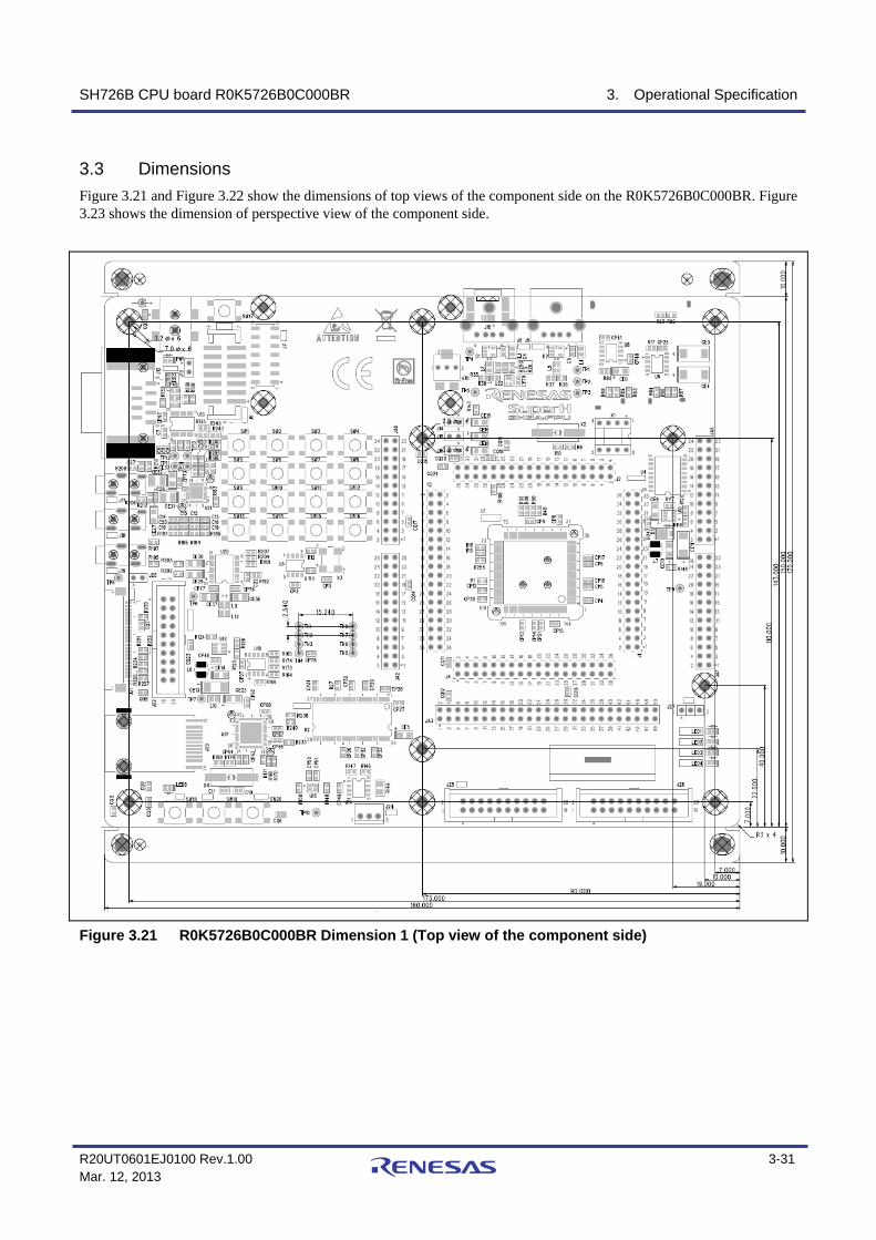
SH726B CPU board R0K5726B0C000BR 3. Operational Specification
R20UT0601EJ0100 Rev.1.00 3-31 Mar. 12, 2013
3.3 Dimensions Figure 3.21 and Figure 3.22 show the dimensions of top views of the component side on the R0K5726B0C000BR. Figure 3.23 shows the dimension of perspective view of the component side.
Figure 3.21 R0K5726B0C000BR Dimension 1 (Top view of the component side)
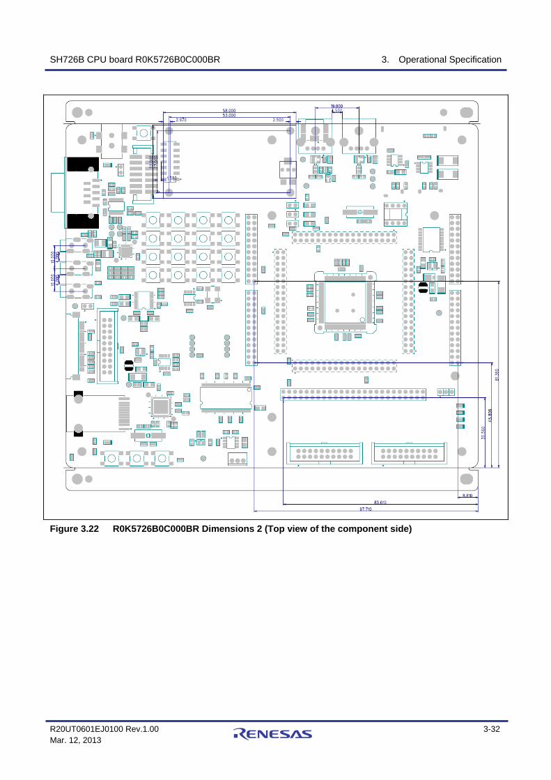
SH726B CPU board R0K5726B0C000BR 3. Operational Specification
R20UT0601EJ0100 Rev.1.00 3-32 Mar. 12, 2013
Figure 3.22 R0K5726B0C000BR Dimensions 2 (Top view of the component side)
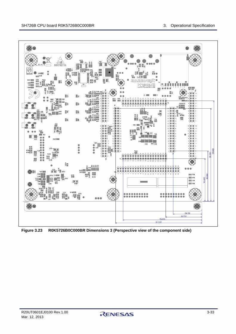
SH726B CPU board R0K5726B0C000BR 3. Operational Specification
R20UT0601EJ0100 Rev.1.00 3-33 Mar. 12, 2013
Figure 3.23 R0K5726B0C000BR Dimensions 3 (Perspective view of the component side)

SH726B CPU board R0K5726B0C000BR 3. Operational Specification
R20UT0601EJ0100 Rev.1.00 3-34 Mar. 12, 2013
This page intentionally left blank.
SH726B CPU Board R0K5726B0C000BR Appendix
R20UT0601EJ0100 Rev.1.00 Appendix-1 Mar. 12, 2013
Appendix R0K5726B0C000BR Schematics

1
1
2
2
3
3
4
4
5
5
A A
B B
C C
D D
SH726B CPU board R0K5726B0C000BR SCHEMATICS
INDEXCPU SH726B, ClockMemory/Character LCD/USB/Port (SDRAM/Serial-flash/SD)Common Ring Connector/ Application HeaderH-UDI/Reset/Power/Serial/CANPush Switch/LAN/AudioCD/External Connector
PAGE
123
4
567
TITLE Note:
Digital GND (GND)
Analog GND (AVss)
Not mounted
5VCC = Digital 5V3VCC = Digital 3.3VPVcc = 3.3V for CPU1.2VCC = 1.25V1.25VCC = 1.25V for CPUPLLVcc = 1.25V for PLLAVcc = Analog 3.3VAVref = 3.3V for ADC Voltage ReferenceA3VCC = Analog 3.3V for WM89788VCC = 8V for CD Drive
R = Fixed ResistorsRA = Resistor ArrayC = Ceramic CapsCE = Tantalum Electrolytic CapsCP = Decoupling CapsL = Inductor
D-R0K5726B0C000BR_C-A-R03
Renesas Solutions Corp.
DATE
APPROVEDSCALE
DESIGNEDCHECKEDDRAWN
CHANGE ( / )1 7
13-02-19
R0K5726B0C000BRINDEX
Renesas Solutions Corp.
DATE
APPROVEDSCALE
DESIGNEDCHECKEDDRAWN
CHANGE ( / )1 7
13-02-19
R0K5726B0C000BRINDEX
Renesas Solutions Corp.
DATE
APPROVEDSCALE
DESIGNEDCHECKEDDRAWN
CHANGE ( / )1 7
13-02-19
R0K5726B0C000BRINDEX

1
1
2
2
3
3
4
4
5
5
A A
B B
C C
D D
Data bus
Interrupt
H-UDI
USB
ROHM
AEL
Serial
AK4353
A9A10A11A12
A1
A13A14A15A16A17A18A19A20A21
A2
A22
A3A4A5A6A7A8
PC2
D8
PC0
PC3
PC1
D1
D9D10
D2
D11
D1D2D3
D0
D3
D12
D4
D13
D0
D[15:0]
D5
D14
D6
D15
D7
PC4
PE2
PE4PE3
PE0
PE5
AN1AN2AN3
AN5AN4
D5D6
D4
D7
D8D9D10D11
D12D13D14D15
AN7
PE6PE7
PJ0PJ1PJ2PJ3PJ4
PJ8
PJ5PJ6PJ7
PJ12
PJ9PJ10PJ11
PJ13PJ14
PF2PF3PF4PF5PF6PF7
PF0PF1
AN0
PE1
AN6
PC5PC6PC7PC8
D12D13D14D15
D1D2D3
D0
D8D9D10D11
D5D6
D4
D7PD6
PD4PD5
PD7
PD10
PD8PD9
PD11
PD14
PD12PD13
PD15
PD2
PD0PD1
PD3
PA1PA0
A[22:1][3,4,5,6,7]
PC[8:0] [3,4,6,7]
NMI [4,6]
TDO [4,5]TDI [4,5]TMS [4,5]
ASEMD# [4,5]TRST# [4,5]
TCK [4,5]
ASEBRKAK# [4,5]
RES# [4,5,6,7]
PJ[0:14] [3,4,5,6,7]
DM0[3,4]DP0[3,4]
VBUS[3,4]
AUDIO_XTAL[7]
PD[15:0] [3,4,5,6,7]
PE[7:0][3,4,6,7]
AN[7:0][3,4,5,6,7]
CKIO_J2[4]CKIO_SD[3]
DA/AD_conv_XTAL[6]DA_conv_XTAL[6]
DM1[3,4]DP1[3,4]
PF[7:0] [3,4,6]
PDN#[4,6]
TxD3[4,5]
RXD3[4,5]
_EXTAL[4]_XTAL[4]
_AUDIO_X1[4]_AUDIO_X2[4]
PA[1:0][3,4,7]
CKIO_JA3[4]
JA1-15 [4]
3VCC
PLLVccPVcc 1.25VCC
3VCC
3VCC
3VCC
AVccAVref
3VCC
PLLVccPVcc 1.25VCCAVcc
AVref
Renesas Solutions Corp.
DATE
APPROVED
SCALE
DESIGNEDCHECKEDDRAWN
CHANGE
( / )2 7
D-R0K5726B0C000BR_C-A-R03
13-02-19
R0K5726B0C000BRCPU SH726B, Clock
Renesas Solutions Corp.
DATE
APPROVED
SCALE
DESIGNEDCHECKEDDRAWN
CHANGE
( / )2 7
D-R0K5726B0C000BR_C-A-R03
13-02-19
R0K5726B0C000BRCPU SH726B, Clock
Renesas Solutions Corp.
DATE
APPROVED
SCALE
DESIGNEDCHECKEDDRAWN
CHANGE
( / )2 7
D-R0K5726B0C000BR_C-A-R03
13-02-19
R0K5726B0C000BRCPU SH726B, Clock
CP6
0.1µ
FC
P60.
1µF
CP30.1µFCP30.1µF
R15 _0ΩR15 _0Ω
X1
_SG-8002DC_48.00MHz
X1
_SG-8002DC_48.00MHz
OUT3
VCC4
GND2
OE1
C1
22pF
C1
22pF
R4 22ΩR4 22Ω
R110ΩR110Ω
R14 22ΩR14 22Ω
CP7
0.1µ
FC
P70.
1µF
R7 _0ΩR7 _0Ω
R10 1MΩR10 1MΩ
+
CE2
4.7µ
F
+
CE2
4.7µ
F
CP20.1µFCP20.1µF
CP10.1µFCP10.1µF
R6 22ΩR6 22Ω
R8 _0ΩR8 _0Ω
R255 22ΩR255 22Ω
CP2
40.
1µF
CP2
40.
1µF
R9
_22Ω
R9
_22Ω
R1
22kΩ
R1
22kΩ
RA4 MNR14_22ΩRA4 MNR14_22Ω1234 5
678
CypressU5 CY2305SC-1H CypressU5 CY2305SC-1H
REF1
CLKOUT8
CLK13
CLK22
CLK35
CLK47
VDD6
GN
D4
RA3 MNR14_22kΩRA3 MNR14_22kΩ1234 5
678
RA6 MNR14_22ΩRA6 MNR14_22Ω1234 5
678
RA8 MNR14_22ΩRA8 MNR14_22Ω1234 5
678
RA5 MNR14_22kΩRA5 MNR14_22kΩ1234 5
678
CP5
0.1µ
FC
P50.
1µF
CP2
00.
1µF
CP2
00.
1µF
R2
_22kΩ
R2
_22kΩ
RA7 MNR14_22kΩRA7 MNR14_22kΩ1234 5
678
CP2
10.
1µF
CP2
10.
1µF
CP4
0.1µ
FC
P40.
1µF
R3
22kΩ
R3
22kΩ
CP1
60.
1µF
CP1
60.
1µF
RA2 MNR14_22ΩRA2 MNR14_22Ω1234 5
678
CP2
20.
1µF
CP2
20.
1µF
R246 22ΩR246 22Ω
CP1
70.
1µF
CP1
70.
1µF
CP1
20.
1µF
CP1
20.
1µF
RA1 MNR14_22kΩRA1 MNR14_22kΩ1234 5
678
CP2
30.
1µF
CP2
30.
1µF
CP1
80.
1µF
CP1
80.
1µF
CP1
30.
1µF
CP1
30.
1µF
CP8
0.1µ
FC
P80.
1µF
CP1
90.
1µF
CP1
90.
1µF
X3
SG-8002JF_11.2896MHz
X3
SG-8002JF_11.2896MHz
OUT3
VCC4
GND2
OE1
CP1
40.
1µF
CP1
40.
1µF
CP9
0.1µ
FC
P90.
1µF
R12 22ΩR12 22Ω
C2
22pF
C2
22pF
CP1
50.
1µF
CP1
50.
1µF
CP1
00.
1µF
CP1
00.
1µF
R13 22ΩR13 22Ω
R16 _0ΩR16 _0Ω
U1 R5S726B0P144FPU1 R5S726B0P144FP
PD14/D14/SD_D31
PD15/D15/SD_D22
PV
cc3
PB1/A1/SSISCK34
Vss
5
PB2/A2/SSIWS36
PB3/A3/SSIDATA37
PB4/A4/CTS08
PJ6/SD_D3/CS4/RxD1/AUDATA29
PJ7/SD_D2/BS/TxD1/AUDATA310
PV
cc11
PB5/A5/RTS012
Vss
13
PB6/A6/SCK0/SSISCK214
Vcc
15
PB7/A7/RxD016
PB8/A8/TxD017
PB9/A9/SCK1/SSIWS218
PJ8/TIOC3A/A23/SCK2/SSISCK2/TEND019
PJ9/TIOC3B/A24/RxD2/SSIWS2/DREQ020
PJ10/TIOC3C/A25/TxD2/SSIDATA2/DACK021
PV
cc22
PB10/A10/RxD123
Vss
24
PB11/A11/TxD125
Vcc
26
PB12/A12/SCK2/SSIDATA227
PB13/A13/RxD228
PB14/A14/TxD229
PB15/A15/RSPCK0/TIOC0B30
PB16/A16/SSL00/TIOC1B31
PB17/A17/MOSI0/TIOC2B32
PB18/A18/MISO0/TIOC3B33
PV
cc34
PB19/A19/SSISCK0/TIOC0C35
Vss
36
PB20/A20/SSIWS0/TIOC0D37
PB21/A21/SSIRxD0/TIOC3C38
PB22/A22/SSITxD0/TIOC3D39
PK0/SCK3/RTC_X140
PK1/TxD3/RTC_X241
PF6/IRQ2/RxD342
PV
cc44
CKIO45
Vss
46
RES47
Vss
48
PLL
Vcc
49
NMI50
Vcc
51
EXTAL52
XTAL53
Vss
54
PG2/DM1/PINT255
PG3/DP1/PINT356
Vss
57
PV
cc58
PG0/DM0/PINT059
PG1/DP0/PINT160
ASEMD61
PH0/AN0/IRQ0/VBUS62
PH1/AN1/IRQ1/RxD063
PH2/AN2/IRQ2/WAIT64
PH3/AN3/IRQ365
PH4/AN4/PINT4/RxD166
PH5/AN5/PINT5/RxD267
AV
ss68
PH6/AN6/PINT6/RxD369
AV
cc70
PH7/AN7/PINT7/RxD471
AV
ref
72
TRST73
ASEBRKAK/ASEBRK74
TDO75
TDI76
TMS77
TCK78
AUDIO_X279 AUDIO_X180
PV
cc81
PF0/RSPCK0/SPBCLK82
Vss
83
PF1/SSL00/SPBSSL84
PF2/MOSI0/SPBMO_0/SPBIO0_085
PF3/MISO0/SPBMI_0/SPBIO1_086
PJ11/TIOC3D/IRQ0/SCK4/CRx0/IERxD/RSPCK287
PJ12/SSISCK3/A0/TxD4/CTx0/IETxD/SSL2088
PV
cc89
PF4/SPBIO2_090
Vss
91
PF5/SPBIO3_092
Vcc
93
PA0/MD_CLK94
PA1/MD_BOOT95
PJ13/SSIWS3/IRQ1/RxD4/CRx1/CRx0/CRx1/MOSI296
PJ14/SSIDATA3/WDTOVF/CTx1/CTx0&CTx1/MISO297
PJ0/SD_CD/IRQ498
PC0/CS0/TIOC4A/AUDIO_XOUT99
PV
cc10
0
PC1/RD/TIOC4B/SPDIF_IN101
Vss
102
PC2/RD/WR/TIOC4C/SPDIF_OUT103
Vcc
104
PC3/WE0/DQML/TIOC4D105
PC4/WE1/DQMU/WDTOVF106
PC5/RAS/IRQ4/CRx0/IERxD107
PC6/CAS/IRQ5/CTx0/IETxD108
PE0/SCL0/IRQ0109
PE1/SDA0/IRQ1110
PE2/SCL1/AUDIO_CLK111
PE3/SDA1/ADTRG112
PE4/SCL2/TCLKA113
PE5/SDA2/TCLKB114
PE6/SCL3/TCLKC115
PE7/SDA3/TCLKD116
PC7/CKE/IRQ6/CRx1/CRx0/CRx1117
Vss
118
PV
cc11
9
PC8/CS3/IRQ7/CTx1/CTx0&CTx1120
PD0/D0/SSISCK1/SIOFSCK/SPBMO_1/SPBIO0_1121
PD1/D1/SSIWS1/SIOFSYNC/SPBMI_1/SPBIO1_1122
PD2/D2/SSIRxD1/SIOFRxD/SPBIO2_1123
PJ1/SD_WP/CS2/IRQ5/AUDIO_XOUT124
PJ2/SD_D1/IRQ6/AUDCK125
PV
cc12
6
PD3/D3/SSITxD1/SIOFTxD/SPBIO3_1127
Vss
128
PD4/D4/RSPCK1/SCK3/CTS1129
Vcc
130
PD5/D5/SSL10/TxD3/RTS1131
PD6/D6/MOSI1/SCK4/CTS2132
PJ3/SD_D0/IRQ7/AUDSYNC133
PJ4/SD_CLK/CS1/AUDATA0134
PJ5/SD_CMD/SCK1/AUDATA1135
PV
cc13
6
PD7/D7/MISO1/TxD4/RTS2137
Vss
138
PD8/D8/SD_CD/TIOC0A139
PD9/D9/SD_WP/TIOC1A140
PD10/D10/SD_D1/TIOC2A141
PD11/D11/SD_D0/TIOC3A142
PD12/D12/SD_CLK/IRQ2143
PD13/D13/SD_CMD/IRQ3144
PF7/IRQ3/RxD443
X2
X12M000000S006
X2
X12M000000S006
1 3
R232 22ΩR232 22Ω
+
CE1
4.7µ
F
+
CE1
4.7µ
F
CP1
10.
1µF
CP1
10.
1µF
R5 22ΩR5 22Ω
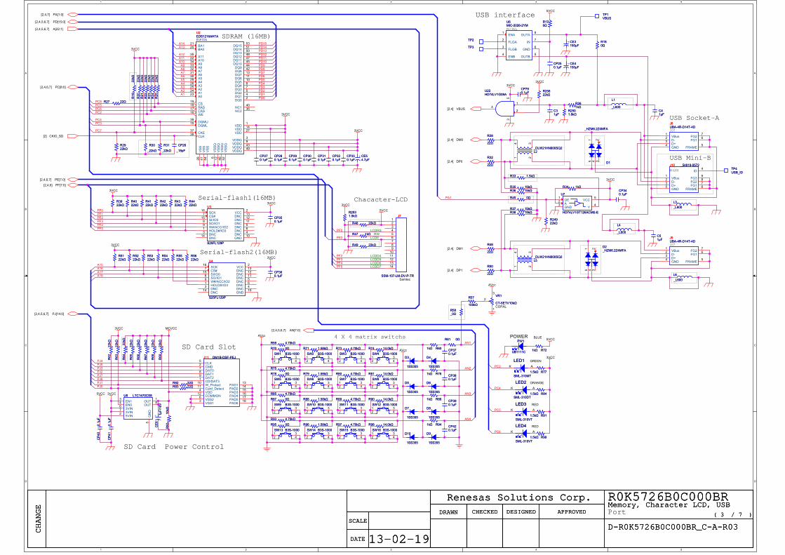
1
1
2
2
3
3
4
4
5
5
A A
B B
C C
D D
SDRAM (16MB)
USB Socket-A
USB Mini-B
Serial-flash1(16MB)
MICREL
JST
MOLEX
Serial-flash2(16MB)
SD Card Power Control
SD Card Slot
JST
Samtec
RED
GREEN
RED
ORANGE
BLUEPOWER
Port
COPAL
LCDD4
LCDE
LCDD5LCDD6
LCDRSRW
LCDD7
4 X 4 matrix switchs
USB interface
Chacacter-LCD
A4
A6
A8
A13
A9
A12
A5
A2
A11A10
A3
A7
A14
A1
PC5PC6
PD5
PD3
PD8PD7
PD0
PD2
PD6
PD10PD11
PD4
PD1
PD9
PD15PD14
PD12PD13
PF0PF1
PF3PF2
PC4
PC2
PC3
PF4PF5
A17
A15A16
A18
PJ7PJ6
PJ4PJ5PJ3PJ2
AN1
AN2
AN3
AN4
PC5
PC2
PC4
PC6
PC8
PC7
PF0
PF3PF2
PF5PF4
PE0
PA1
PJ1PJ0
PD[15:0][2,4,5,6,7]
A[22:1][2,4,5,6,7]
VBUS[2,4]
DP0[2,4]
DM0[2,4]
PJ[14:0][2,4,5,6,7]
DP1[2,4]
DM1[2,4]
AN[7:0][2,4,5,6,7]
PF[7:0][2,4,6]
CKIO_SD[2]
PC[8:0][2,4,6,7]
PE[7:0][2,4,6,7]
PA[1:0][2,4,7]
3VCC
5VCC
3VCC
3VCC
3VCC
3VCC
3VCC5VCC
MCVCC
3VCC
5VCC
3VCC
3VCC
5VCC
3VCC
AVcc
AVcc
3VCC
AVcc
3VCC
3VCC
3VCC
Renesas Solutions Corp.
DATE
APPROVED
SCALE
DESIGNEDCHECKEDDRAWN
CHANGE
( / )3 7
D-R0K5726B0C000BR_C-A-R03
13-02-19
R0K5726B0C000BRMemory, Character LCD, USB
Renesas Solutions Corp.
DATE
APPROVED
SCALE
DESIGNEDCHECKEDDRAWN
CHANGE
( / )3 7
D-R0K5726B0C000BR_C-A-R03
13-02-19
R0K5726B0C000BRMemory, Character LCD, USB
Renesas Solutions Corp.
DATE
APPROVED
SCALE
DESIGNEDCHECKEDDRAWN
CHANGE
( / )3 7
D-R0K5726B0C000BR_C-A-R03
13-02-19
R0K5726B0C000BRMemory, Character LCD, USB
R24
22kΩ
R24
22kΩ
SW13 B3S-1000SW13 B3S-1000
2314
C41µFC41µF
R83 22ΩR83 22Ω
R88 1.58kΩR88 1.58kΩ
R4122kΩR4122kΩ
CP380.1µFCP380.1µF
D1
_HZM6.2Z4MFA
D1
_HZM6.2Z4MFA
15
24 3
CP300.1µFCP300.1µF
SW12 B3S-1000SW12 B3S-1000
2314
R911.5kΩ R911.5kΩ
CP280.1µFCP280.1µF
R5122kΩR5122kΩ
R67
22kΩ
R67
22kΩ
R2922kΩR2922kΩ
R66
22kΩ
R66
22kΩ
R4322kΩR4322kΩ
R37 15kΩR37 15kΩ
R96 1.58kΩR96 1.58kΩ
U4
S25FL129P
U4
S25FL129P
SCK16
CS#7
SI/IO015
SO/IO18
W#/ACC/IO29
HOLD#/IO31
DNC3
DNC14
VCC2
DNC13
DNC12
DNC11
DNC5
DNC6
DNC4
GND10
CP320.1µFCP320.1µF
R23
22kΩ
R23
22kΩ
R991.5kΩ R991.5kΩ
J9UBA-4R-D14T-4DJ9UBA-4R-D14T-4D
VBus1
D-2
D+3
GND4
FRAME5
FG16FG27
R78 0ΩR78 0Ω
J8UBA-4R-D14T-4DJ8UBA-4R-D14T-4D
VBus1
D-2
D+3
GND4
FRAME5
FG16FG27
D10
1SS355
D10
1SS355
R761kΩ R761kΩ
R28
22Ω
R28
22Ω
SW16 B3S-1000SW16 B3S-1000
2314
R35 15kΩR35 15kΩ
R75 4.70kΩR75 4.70kΩ
R601kΩ R601kΩ
SW1 B3S-1000SW1 B3S-1000
2314
CP290.1µFCP290.1µF
R721kΩ R721kΩ
R93 4.70kΩR93 4.70kΩ
R21
22kΩ
R21
22kΩ
R5422kΩR5422kΩ
R48
22Ω
R48
22Ω
R68
22kΩ
R68
22kΩ
R22
22kΩ
R22
22kΩ
R33 _1.5kΩR33 _1.5kΩ
SW6 B3S-1000SW6 B3S-1000
2314
L2_DLW21HN900SQ2L2_DLW21HN900SQ2
14
23
CP350.1µFCP350.1µF
R70 0ΩR70 0Ω
+ CE54.7µF
+ CE54.7µF
TP2TP2
R71 1.58kΩR71 1.58kΩ
SW4 B3S-1000SW4 B3S-1000
2314
SW11 B3S-1000SW11 B3S-1000
2314
CP420.1µFCP420.1µF
D7
1SS355
D7
1SS355
R81 14.0kΩR81 14.0kΩ
R20
22kΩ
R20
22kΩ
R49 _22kΩR49 _22kΩ
D9
1SS355
D9
1SS355
TP3TP3
R5622kΩR5622kΩ
L1
_L600
L1
_L600
U3
S25FL129P
U3
S25FL129P
SCK16
CS#7
SI/IO015
SO/IO18
W#/ACC/IO29
HOLD#/IO31
DNC3
DNC14
VCC2
DNC13
DNC12
DNC11
DNC5
DNC6
DNC4
GND10
SW15 B3S-1000SW15 B3S-1000
2314
CP340.1µFCP340.1µF
J10 _54819-0572J10 _54819-0572
VBus1
D-2
D+3
ID4
FRAME6
GND5 FG1
7FG28FG39
ELPIDA
U2EDS1216AHTAELPIDA
U2EDS1216AHTA
BA121
BA020
A1135
A1022
A934
A833
A732
A631
A530
A429
A326
A225
A124
A023
CS19
RAS18
CAS17
WE16
DQMU39
DQML15
CKE37
CLK38
DQ1553
DQ1451
DQ1350
DQ1248
DQ1147
DQ1045
DQ944
DQ842
DQ713
DQ611
DQ510
DQ48
DQ37
DQ25
DQ14
DQ02
VS
S28
VS
S41
VS
S54
VS
SQ
6
VS
SQ
12
VS
SQ
46
VS
SQ
52
VDD1
VDD14
VDD27
VDDQ3
VDDQ9
VDDQ43
VDDQ49
NC140
NC236
D3
1SS355
D3
1SS355
CP330.1µFCP330.1µF
R261kΩR261kΩ
R36 15kΩR36 15kΩ
R57
100kΩ
R57
100kΩ
SW5 B3S-1000SW5 B3S-1000
2314
D8
1SS355
D8
1SS355
R64
_22kΩ
R64
_22kΩ
R85 4.70kΩR85 4.70kΩ
R24922kΩR24922kΩ
CP790.1µFCP790.1µF
R46 _22kΩR46 _22kΩ
R89 4.70kΩR89 4.70kΩ
TP4USB_IDTP4USB_ID
D5
1SS355
D5
1SS355
SW2 B3S-1000SW2 B3S-1000
2314
R771.5kΩ R771.5kΩ
R3922kΩR3922kΩ
R27 22ΩR27 22Ω
VR1
CT-6ETV10kΩ
VR1
CT-6ETV10kΩ
3
1
2
R79 1.58kΩR79 1.58kΩ
R73 4.70kΩR73 4.70kΩ
R941kΩ R941kΩ
J7
SSM-107-LM-DV-P-TR
J7
SSM-107-LM-DV-P-TR
123456789
1011121314
R25622kΩR25622kΩ
TP1VBUSTP1VBUS
R97 4.70kΩR97 4.70kΩ
SW8 B3S-1000SW8 B3S-1000
2314
SW3 B3S-1000SW3 B3S-1000
2314
R82 22ΩR82 22Ω
PW1
UB1111C
PW1
UB1111C
R65
22kΩ
R65
22kΩ
U6MIC-2026-2YMU6MIC-2026-2YM
IN7
FLGB3
GND6
ENB4
ENA1
OUTA8
FLGA2
OUTB5
LED2
SML-310DT
LED2
SML-310DT
AK
R31
_22kΩ
R31
_22kΩ
U7
HD74LV1GT126ACME-E
U7
HD74LV1GT126ACME-E
OE1
A2
GND3
Y4
VCC5
CP370.1µFCP370.1µF
D6
1SS355
D6
1SS355
+ CE4150µF
+ CE4150µF
R4222kΩR4222kΩ
R45 _0ΩR45 _0Ω
U22HD74LV1G08AU22HD74LV1G08A
1
24
35
CP390.1µFCP390.1µF
R87 0ΩR87 0Ω
R5222kΩR5222kΩ L5
_DLW21HN900SQ2L5_DLW21HN900SQ2
14
23
CP4
00.
1µF
CP4
00.
1µF
C31µFC31µF
CP360.1µFCP360.1µF
R32
22Ω
R32
22Ω
R4422kΩR4422kΩ
CP26
_18pF
CP26
_18pF
LED4
SML-310VT
LED4
SML-310VT
AK
R74 14.0kΩR74 14.0kΩ
R34 1kΩR34 1kΩ
R63
22kΩ
R63
22kΩ
R2531.5kΩR2531.5kΩ
R59 4.70kΩR59 4.70kΩ
R30
_22kΩ
R30
_22kΩ
R95 0ΩR95 0Ω
SW7 B3S-1000SW7 B3S-1000
2314
SW10 B3S-1000SW10 B3S-1000
2314
R170ΩR170Ω
R5522kΩR5522kΩ
+ CE3150µF
+ CE3150µF
R58_0ΩR58_0Ω
U8 LTC1470CS8U8 LTC1470CS8
OUT1
5VIN2
EN13
EN04
3VIN6
3VIN7
OUT8
GN
D5
R19
_22kΩ
R19
_22kΩ
CP4
10.
1µF
CP4
10.
1µF
R90 14.0kΩR90 14.0kΩ
R62
22kΩ
R62
22kΩ
J11 DM1B-DSF-PEJJ11 DM1B-DSF-PEJ
DAT07
CLK5
VDD4
DAT29 DAT18
VSS13
CMD2
CD/DAT31
VSS26
W_Protect10
Card_Detect11
COMMON12
PAD113
PAD214
PAD315
PAD416
PAD517
PAD618
R47 1kΩR47 1kΩ C51µFC51µF
L6_L600L6_L600
R5322kΩR5322kΩ
R861kΩ R861kΩ
CP250.1µFCP250.1µF
LED1
SML-310MT
LED1
SML-310MT
AK
SW14 B3S-1000SW14 B3S-1000
2314
L3_L600L3_L600
R38 15kΩR38 15kΩ
D2_HZM6.2Z4MFAD2_HZM6.2Z4MFA1
5
24 3
R92
10kΩ
R92
10kΩ
R2501.8kΩR2501.8kΩ
R98 14.0kΩR98 14.0kΩ
R25
22kΩ
R25
22kΩ
R841.5kΩ R841.5kΩ
SW9 B3S-1000SW9 B3S-1000
2314
CP310.1µFCP310.1µF
R69
22kΩ
R69
22kΩ
D4
1SS355
D4
1SS355
R4022kΩR4022kΩ
R180ΩR180Ω
R50
22Ω
R50
22Ω
R80 4.70kΩR80 4.70kΩ
+
CE6
1µF/
16V
+
CE6
1µF/
16V
L4
_L600
L4
_L600
CP270.1µFCP270.1µF
R61 0ΩR61 0Ω
LED3
SML-310VT
LED3
SML-310VT
AK

1
1
2
2
3
3
4
4
5
5
A A
B B
C C
D D
Honda Honda
Honda Honda
Honda
Honda
Honda
Honda
SH726B Expansion Connector
Honda
SH726B Ring Connector
PF0PF1PF2PF3
PJ11PJ12
PF4
PF5
PA1
PJ13PJ14PJ0PC0
PC1
PC2
PC3
PC5PC6
PE0PE1PE2PE3PE4PE5PE6PE7
PD3
PD4
PD5PD6PJ3PJ4PJ5
PD7
PD8PD9PD10PD11PD12PD13
A20A21A22
PF6PF7
CKIO
RES#
NMI
PG2PG3
PG0
ASEMD#AN0AN1AN2AN3AN4AN5
AN6
AN7
PD14PD15
A1
A2A3A4PJ6PJ7
A5
A6
A7A8A9PJ8PJ9PJ10
A10
A11
A12A13A14A15A16A17A18
A19
PD0PD1PD2
PC8
PK0PK1
PJ1PJ2
PC7
PC4
PG1
AN0AN1AN2AN3
PC0PJ1
A8
A4
A2
A6
A3
A7
A1
A9
PJ12
A10
A17A16
A18
A20
PD1PD2
PD6PD5
PD7
PD4
PD0
PD11PD10
PD12PD13
PD15
PD8PD9
PD14
PC7
PC6
PD3
A11
A13A12
A14
PC1
A21
PC5
PC2
A12
PC1PC2
PD11
PJ14PJ13PJ0PJ1
A16
PC0
PJ11
A13
RESET#
PD10
PC3
PJ5
PE6PE7
PJ8PJ10PJ9
A14
NMI
PC6
PJ4PJ9
PJ6
PC5
PE3
PF2PF3PF4PF5
PF1
PJ2PJ3PJ11
PE6PE7
PJ14PJ7
PF6
PD8
A15
AN4
A19
PD9
AN5
A22
PC4PC3
PC8
AN2
AN6AN7
AN5AN4
PE4PE5
EXTAL
A5
PA0
A15
A19
PD[15:0][2,3,5,6,7]
A[22:1][2,3,5,6,7]
_EXTAL[2]_XTAL[2]
_AUDIO_X1[2]_AUDIO_X2[2]
PJ[14:0][2,3,5,6,7]
PF[7:0][2,3,6]
ASEBRKAK#[2,5]TRST#[2,5]
TDO[2,5]TDI[2,5]TMS[2,5]TCK[2,5]
PC[8:0][2,3,6,7]
PE[7:0][2,3,6,7]
DP1[2,3]
DM0[2,3]
AN[7:0][2,3,5,6,7]
CKIO_J2[2]
RES#[2,5,6,7]
NMI[2,6]
ASEMD#[2,5]
TxD3[2,5]PDN#[2,6]
RES#[2,5,6,7]_EXTAL[2]NMI[2,6]
CKIO_JA3[2]
TxD3[2,5]
RXD3[2,5]PDN#[2,6]
RS232RX[5]RS232TX[5]
PA[1:0][2,3,7]
DM1[2,3]
DP0[2,3]
JA1-15[2]
1.25VCCPVcc
PVccPLLVcc
1.25VCC
AVccAVref
1.25VCCPVcc
1.25VCCPVcc
5VCCAVcc 3VCCAVref
5VCC
Renesas Solutions Corp.
DATE
APPROVED
SCALE
DESIGNEDCHECKEDDRAWN
CHANGE
( / )4 7
D-R0K5726B0C000BR_C-A-R03
13-02-19
R0K5726B0C000BRExt. Connector
Renesas Solutions Corp.
DATE
APPROVED
SCALE
DESIGNEDCHECKEDDRAWN
CHANGE
( / )4 7
D-R0K5726B0C000BR_C-A-R03
13-02-19
R0K5726B0C000BRExt. Connector
Renesas Solutions Corp.
DATE
APPROVED
SCALE
DESIGNEDCHECKEDDRAWN
CHANGE
( / )4 7
D-R0K5726B0C000BR_C-A-R03
13-02-19
R0K5726B0C000BRExt. Connector
R105 _0ΩR105 _0Ω
R231 _0ΩR231 _0Ω
R102 0ΩR102 0Ω
R230 _0ΩR230 _0Ω
R104 0ΩR104 0Ω
R228 _0ΩR228 _0Ω
R101 _0ΩR101 _0Ω
JA5
_FFC-24BMEP1B
JA5
_FFC-24BMEP1B
123456789
101112131415161718192021222324
J2
_FFC-36BMEP1B
J2
_FFC-36BMEP1B
123456789
101112131415161718192021222324252627282930313233343536
JA1
_FFC-26BMEP1B
JA1
_FFC-26BMEP1B
123456789
1011121314151617181920212223242526
R229 _0ΩR229 _0Ω
J4
_FFC-36BMEP1B
J4
_FFC-36BMEP1B
123456789
101112131415161718192021222324252627282930313233343536
R247 0ΩR247 0Ω
JA6
_FFC-24BMEP1B
JA6
_FFC-24BMEP1B
123456789
101112131415161718192021222324
R100 0ΩR100 0Ω
JA3
_FFC-50BMEP1B
JA3
_FFC-50BMEP1B
123456789
1011121314151617181920212223242526272829303132333435363738394041424344454647484950
J3
_FFC-36BMEP1B
J3
_FFC-36BMEP1B
123456789
101112131415161718192021222324252627282930313233343536
R108 _0ΩR108 _0Ω
R248 0ΩR248 0Ω
J1
_FFC-36BMEP1B
J1
_FFC-36BMEP1B
123456789
101112131415161718192021222324252627282930313233343536
R103 _0ΩR103 _0Ω
R107 0ΩR107 0Ω
R106 _0ΩR106 _0Ω
JA2
_FFC-26BMEP1B
JA2
_FFC-26BMEP1B
123456789
1011121314151617181920212223242526

1
1
2
2
3
3
4
4
5
5
A A
B B
C C
D D
H-UDI Interface
Power On Reset
Samtec
3.3V TO 1.25V STEP DOWN REGULATOR
TDK
3.3V TO 1.8V STEP DOWN REGULATOR
CAN Transceiver
RENESAS
Texas Instruments
CAN
3.3V<-5V
JST
Voltage Level Shifter 3.3V<->5V
PowerConnector
5V To 3.3V Linear Regulator
3.3V External
HRS
NS
HRS
OMRON
VSS - AVSS
HRS
1.25V External
TDK
(3)
(4)
ERNI
SERIAL
(5)
(6)
(7)
(8)
(9)
TI
Serial connectormount tab = GND
JPNRSK
(1)
:for Male connector only154236
MALE
:for Female connector only
FEMALE
(2)
HRS
8V External
HRS
AVcc External
CAN
Serial interface
Kycon
CTS2#RTS2#
RxD2TxD2
PJ13
PJ14
A13
PD7PD6
A14
RES# [2,4,6,7]
TDO[2,4]ASEMD# [2,4]
TDI[2,4]
TCK[2,4]
TMS[2,4]
TRST#[2,4]
ASEBRKAK#[2,4]
PJ[14:0][2,3,4,6,7]
TxD3[2,4]
RxD3[2,4]
RS232TX[4]
RS232RX[4]
PD[15:0][2,3,4,6,7]
A[22:1][2,3,4,6,7]
3VCC
3VCC
3VCC
3VCC
3VCC
1.8VCC
5VCC3VCC
5VCC
3VCC
3VCC
PVcc
5VCC
1.25VCC
3VCC
1.2VCC
3VCC
3VCC
3VCC
AVcc
8VCC
AVcc
A3VCC
AVref
PVcc
1.8VCC VDD_A18
1.2VCC PLLVcc1.25VCC
5VCC 3VCC 1.25VCC PVcc AVcc A3VCC
Renesas Solutions Corp.
DATE
APPROVED
SCALE
DESIGNEDCHECKEDDRAWN
CHANGE
( / )5 7
D-R0K5726B0C000BR_C-A-R03
13-02-19
R0K5726B0C000BRH-UDI,Power, Reset, Serial,
Renesas Solutions Corp.
DATE
APPROVED
SCALE
DESIGNEDCHECKEDDRAWN
CHANGE
( / )5 7
D-R0K5726B0C000BR_C-A-R03
13-02-19
R0K5726B0C000BRH-UDI,Power, Reset, Serial,
Renesas Solutions Corp.
DATE
APPROVED
SCALE
DESIGNEDCHECKEDDRAWN
CHANGE
( / )5 7
D-R0K5726B0C000BR_C-A-R03
13-02-19
R0K5726B0C000BRH-UDI,Power, Reset, Serial,
R25222kΩR25222kΩ
J16
_A2-2PA-2.54DSA
J16
_A2-2PA-2.54DSA
12
R242 _0ΩR242 _0Ω
U13
MAX3222CPW
U13
MAX3222CPW
C1+2
C1-4
C2+5
C2-6
V+3
V-7
T1IN13
T2IN12
R1IN16
R2IN9
R1OUT15
R2OUT10
T1OUT17
T2OUT8
VC
C19
GN
D18
EN_1
SHDN_20
NC14
NC11
+ CE10
10µF/16V
+ CE10
10µF/16V
R129 0Ω(M)R129 0Ω(M)
CQ
130.
1µF
CQ
130.
1µF
J24
B3P-SHF-1AA(LF)(SN)
J24
B3P-SHF-1AA(LF)(SN)
123
L9
BLM21PG300SN1
L9
BLM21PG300SN1
R14
622
kΩR
146
22kΩ
L10
BLM21PG300SN1
L10
BLM21PG300SN1
D131N4148WD131N4148W
R1154.7kΩR1154.7kΩ
NS
U10
LM2734XNS
U10
LM2734X
BO
OS
T1
GND2FB3
EN4
VIN5
SW6
CP48 _0.1µFCP48 _0.1µF
R12515kΩR12515kΩ
CQ
10.
1µF
CQ
10.
1µF
+ CE13
220µF/6.3V
+ CE13
220µF/6.3V
R144 0Ω(M)R144 0Ω(M)
R123
0Ω
R123
0Ω
CP430.01µFCP430.01µF
U9LMS1587CS-ADJU9LMS1587CS-ADJ
AD
J1
VIN3
VOUT2
TAB4
CQ
90.
1µF
CQ
90.
1µF
C90.47µFC90.47µF
CQ
230.
1µF
CQ
230.
1µF
+CE1610µF/16V
+CE1610µF/16V
R150 0ΩR150 0Ω
D12MBRM110LD12MBRM110L
R122_22kΩ
R122_22kΩ
R130 0ΩR130 0Ω
R111180Ω(1/8W)R111180Ω(1/8W)
R127 0Ω(F)R127 0Ω(F)
L12
BLM21PG300SN1
L12
BLM21PG300SN1
J15
_A2-2PA-2.54DSA
J15
_A2-2PA-2.54DSA
12
R135 0ΩR135 0Ω
CQ
140.
1µF
CQ
140.
1µF
CQ
60.
1µF
CQ
60.
1µF
+ CE11
220µF/6.3V
+ CE11
220µF/6.3V
R1380ΩR1380Ω
L11
BLM21PG300SN1
L11
BLM21PG300SN1
+ CE847µF
+ CE847µF
R12410kΩR12410kΩ
TP91.25VCCTP91.25VCC
1
R12612kΩR12612kΩ
J6
HTST-107-01-L-DV
J6
HTST-107-01-L-DV
ASEMD9
GND10
GND12
GND13
GND14
NC8
TCK1
TMS5
_TRST2
TDI6
TDO3
_ASEBRAK4
UVCC11
_RES7
D111N4148WD111N4148W
R141 0ΩR141 0Ω
R245 _0ΩR245 _0Ω
CP440.1µFCP440.1µF
CP490.1µFCP490.1µF
CQ
30.
1µF
CQ
30.
1µF
CQ
240.
1µF
CQ
240.
1µF
R145
0Ω
R145
0Ω
CQ
150.
1µF
CQ
150.
1µF
R1186.2kΩR1186.2kΩ
CP5
00.
1µF
CP5
00.
1µF
R131 0Ω(M)R131 0Ω(M)
R143 0ΩR143 0Ω
J5
KLDX-SMT2-0202-A
J5
KLDX-SMT2-0202-A
321
4
U14
HA13721RPJE
U14
HA13721RPJE
TxD1
GND2
VCC3
RxD4
NC5
CANL6
CANH7MODE8
+ CE12
10µF/16V
+ CE12
10µF/16V
R241 _0ΩR241 _0Ω
CQ
160.
1µF
CQ
160.
1µF
R12110kΩR12110kΩ
R1121kΩR1121kΩ
CQ
250.
1µF
CQ
250.
1µF
NS
U12
LM2734XNS
U12
LM2734X
BO
OS
T1
GND2FB3
EN4
VIN5
SW6
R12011kΩR12011kΩ
R137 _0ΩR137 _0Ω
R239 _0ΩR239 _0Ω
R136 0Ω(M)R136 0Ω(M)
R110110ΩR110110Ω
R133 0ΩR133 0Ω
CQ
260.
1µF
CQ
260.
1µF
+ CE9
10µF/16V
+ CE9
10µF/16V
R244 _0ΩR244 _0Ω
TP71.8VCCTP71.8VCC
1
CQ
170.
1µF
CQ
170.
1µF
R243 _0ΩR243 _0Ω
CQ
100.
1µF
CQ
100.
1µF
R23
6_0Ω
R23
6_0Ω
+CE1710µF/25V
+CE1710µF/25V
R139 0Ω(F)R139 0Ω(F)
CP5
10.
1µF
CP5
10.
1µF
CQ
40.
1µF
CQ
40.
1µF
CP47 0.1µFCP47 0.1µF
CQ
110.
1µF
CQ
110.
1µF
R149120Ω-1/4WR149120Ω-1/4W
R12
822
kΩR
128
22kΩ
J20
_A2-2PA-2.54DSA
J20
_A2-2PA-2.54DSA
12
R132 0Ω(F)R132 0Ω(F)
R142 _0ΩR142 _0Ω
+CE1510µF/16V
+CE1510µF/16V
R25122kΩR25122kΩ
L7VLCF4020T-4R7N1R2L7VLCF4020T-4R7N1R2
J12
154188
J12
154188
59
48
37
26
1
1011
R14
822
kΩR
148
22kΩ
R147 0ΩR147 0Ω
CQ
20.
1µF
CQ
20.
1µF
CQ
70.
1µF
CQ
70.
1µF
C8 0.47µFC8 0.47µF
C60.1µFC60.1µF
D14MBRM110LD14MBRM110L
J13
_A2-2PA-2.54DSA
J13
_A2-2PA-2.54DSA
12
CP460.01µFCP460.01µF
R240 _0ΩR240 _0Ω
L8VLCF4020T-4R7N1R2L8VLCF4020T-4R7N1R2
R11415kΩR11415kΩ
CQ
120.
1µF
CQ
120.
1µF
SW17B3S-1000SW17B3S-1000
23
14
J27
XG8S-0331
J27
XG8S-0331
123
R134 0ΩR134 0Ω
J14
_A2-2PA-2.54DSA
J14
_A2-2PA-2.54DSA
12
CQ
200.
1µF
CQ
200.
1µF
CQ
180.
1µF
CQ
180.
1µF
+ CE710µF/25V
+ CE710µF/25V
C7 0.47µFC7 0.47µF
R238 _0ΩR238 _0Ω
TP6A3VCCTP6A3VCC
1
R119 100ΩR119 100Ω
U15
SN74LVC1T45DCK
U15
SN74LVC1T45DCK
VCCA1
VCCB6
A3 GND2
DIR5
B4
+ CE14
10µF/16V
+ CE14
10µF/16V
+CE1810µF/16V
+CE1810µF/16V
CQ
80.
1µF
CQ
80.
1µF
R140 0Ω(F)R140 0Ω(F)
RA9MNR14_22kΩRA9MNR14_22kΩ
1 2 3 45678
R11310kΩ R11310kΩ
CQ
190.
1µF
CQ
190.
1µF
TP5
3.3V
TP5
3.3V
CQ
50.
1µF
CQ
50.
1µF
CP450.1µFCP450.1µF
R11710kΩR11710kΩ
TP8 8VCCTP8 8VCC
1
U11
RNA51957BFP
U11
RNA51957BFP
OUT6
Cd5
GN
D4
IN2
VC
C7
NC
8N
C1
NC
3
CQ
210.
1µF
CQ
210.
1µF
R23
7_0Ω
R23
7_0Ω
CQ
220.
1µF
CQ
220.
1µF
R10922kΩR10922kΩ
R1160ΩR1160Ω

5
5
4
4
3
3
2
2
1
1
D D
C C
B B
A A
NMISWITCH
NMI SWITCH CIRCUIT
IRQ2SWITCH
IRQ SWITCH CIRCUIT
TESTSWITCH
TEST SWITCH CIRCUIT
RENESAS RENESAS
LAN interface
Audio CODEC
Audio DAC
Microchip
PF6
PJ8
PE4
PJ9
PE5
PJ10
PF7
A15
A17
A19
A22
A20
A21
PD8
PD1
PD9PD10
PD2
PD11
PD3
PD12
PD4
PD13
PD0
PD5
PD14
PD6
PD15
PD7
A1A2A3A4A5A6A7
PC0PC1PC3
A8
PE3
PE4
PE5
AN7AN5
NMI [2,4]
PF[7:0][2,3,4]
PDN#[2,4]
DA_conv_XTAL[2]
PE[7:0][2,3,4,7]
PJ[14:0][2,3,4,5,7]
DA/AD_conv_XTAL[2]
A[22:1][2,3,4,5,7]
PD[15:0][2,3,4,5,7]
PC[8:0][2,3,4,7]
RES#[2,4,5,7]
AN[7:0][2,3,4,5,7]3VCC
3VCC
3VCC
3VCC
3VCC
3VCC
3VCC
3VCC
A3VCC 3VCC
A3VCC
A3VCC
3VCC
3VCC
3VCC 3VCC
3VCC
3VCCA3VCC
A3VCC VDD_A18 3VCC
3VCC VDD_A18
VSS VSS
3VCC
3VCC
A3VCC 3VCC
3VCC
Renesas Solutions Corp.
DATE
APPROVED
SCALE
DESIGNEDCHECKEDDRAWN
CHANGE
( / )6 7
D-R0K5726B0C000BR_C-A-R03
13-02-19
R0K5726B0C000BRSwitch, LAN ,Audio
Renesas Solutions Corp.
DATE
APPROVED
SCALE
DESIGNEDCHECKEDDRAWN
CHANGE
( / )6 7
D-R0K5726B0C000BR_C-A-R03
13-02-19
R0K5726B0C000BRSwitch, LAN ,Audio
Renesas Solutions Corp.
DATE
APPROVED
SCALE
DESIGNEDCHECKEDDRAWN
CHANGE
( / )6 7
D-R0K5726B0C000BR_C-A-R03
13-02-19
R0K5726B0C000BRSwitch, LAN ,Audio
U18
93LC46A
U18
93LC46ADO
4Vss
5DI3
Vcc8
CS1
CLK2
NC7
NC6
R201 47kΩR201 47kΩ
+
CE3
410
µF/1
6V
+
CE3
410
µF/1
6V
R167 220ΩR167 220Ω
+
CE2
310
µF/1
6V
+
CE2
310
µF/1
6V
CP77 0.1µFCP77 0.1µF
CP6
00.
1µF
CP6
00.
1µF
TP12TP12
C140.1µFC140.1µF
+
CE2
210
µF/1
6V
+
CE2
210
µF/1
6V
R16210kΩR16210kΩ
R211 22kΩR211 22kΩ
U16C
HD74LV1GW17A
U16C
HD74LV1GW17A25
C130.1µFC130.1µF
R15
510Ω
R15
510Ω
R17
4_2
2kΩ
R17
4_2
2kΩ
R15
449
.9Ω
-1/4
WR
154
49.9Ω
-1/4
W
R20
5_2
2kΩ
R20
5_2
2kΩ
TP13TP13
R177 0ΩR177 0Ω
R199 22ΩR199 22Ω
+
CE33
4.7µF+
CE33
4.7µF
CP6
70.
1µF
CP6
70.
1µF
R180 0ΩR180 0Ω
C24 0.1µFC24 0.1µF
C120.1µFC120.1µF
R194 22ΩR194 22Ω
R16
5_2
2kΩ
R16
5_2
2kΩ
CP5
515
pFC
P55
15pF
U19A
HD74LV1GW17A
U19A
HD74LV1GW17A
61
R1691.00kΩR1691.00kΩ
R197 220ΩR197 220Ω
LED5
SML-310VT
LED5
SML-310VT
+ CE212.2µF
+ CE212.2µF
SW19
B3S-1000
SW19
B3S-1000
23
14
R15910kΩR15910kΩ
C26
220p
FC
2622
0pF
+
CE2
410
µF/1
6V
+
CE2
410
µF/1
6V
R18
447
kΩR
184
47kΩ
R183 22ΩR183 22Ω
TP14TP14
CP6
80.
1µF
CP6
80.
1µF
R18
2_2
2kΩ
R18
2_2
2kΩ
R25
422
kΩR
254
22kΩ
U21 WM8978GEFL/VU21 WM8978GEFL/V
LIP1
LIN2
L2/GPIO23
RIP4
RIN5
R2/GPIO36
LRC7
BCLK8
ADCDAT9
DACDAT10
MCLK11
DG
ND
12D
CV
DD
13
DB
VD
D14
CSB/GPIO115
SCLK16
SDIN17
MODE18
AUXL19
AUXR20
OUT421
OUT322
ROUT223
SP
KG
ND
24
LOUT225
SP
KV
DD
26
VMID27
AG
ND
28
ROUT129
LOUT130
AV
DD
31
MICBIAS32
PA
D33
C22_18pFC22_18pF +CE30 10µF/16V+CE30 10µF/16V
R18
122
kΩR
181
22kΩ
R16
6_2
2kΩ
R16
6_2
2kΩ
+
CE3
510
µF/1
6V
+
CE3
510
µF/1
6V
U16B
HD74LV1GW17A
U16B
HD74LV1GW17A
43
R21
022
kΩR
210
22kΩ
R17510kΩR17510kΩ
CP6
10.
1µF
CP6
10.
1µF
C17_18pFC17_18pF
R20
90Ω
R20
90Ω
J18
HSJ1456-010320
J18
HSJ1456-010320
1
2
3
4
CP5
315
pFC
P53
15pF
C231µFC231µF
R15
149
.9Ω
-1/4
WR
151
49.9Ω
-1/4
W
C19
220p
FC
1922
0pF
R16
4_2
2kΩ
R16
4_2
2kΩ
CP7
20.
1µF
CP7
20.
1µF
R2330ΩR2330Ω
R192 22ΩR192 22Ω
R176 220ΩR176 220Ω
R20
327
kΩR
203
27kΩ
+CE25
22µF/10V
+CE25
22µF/10V
R17
022
kΩR
170
22kΩ
CP6
20.
1µF
CP6
20.
1µF
R18
922
kΩR
189
22kΩ
CP5
60.
022µ
FC
P56
0.02
2µF
CP7
40.
1µF
CP7
40.
1µF
+
CE36 10µF/16V
+
CE36 10µF/16V
R15
775
0ΩR
157
750Ω
X4
X25M000000S006
X4
X25M000000S006
1 3
CP7
30.
1µF
CP7
30.
1µF
R15
875
0ΩR
158
750Ω
+CE31 47µF+CE31 47µF
R161 0ΩR161 0Ω
R21
4_0Ω
R21
4_0Ω
R17
3_2
2kΩ
R17
3_2
2kΩ
CP5
80.
1µF
CP5
80.
1µF
CP6
30.
1µF
CP6
30.
1µF
C20
220p
FC
2022
0pF
J23
J3011G21DNLT
J23
J3011G21DNLT
TD+3
TD-4
TCT5
RD+7
RD-8
RCT6
N.C.9
GND10
K2
K11
A1
A12
PAD113
PAD214
CP7
50.
1µF
CP7
50.
1µF
R20
227
kΩR
202
27kΩ
CP76 0.1µFCP76 0.1µF
CP6
40.
1µF
CP6
40.
1µF
TP10TESTTP10TEST
C211µFC211µF
U19B
HD74LV1GW17A
U19B
HD74LV1GW17A
43
+CE32 47µF+CE32 47µF
R193 22ΩR193 22Ω
+
CE28 10µF/16V
+
CE28 10µF/16V
C11
22pF
C11
22pF
R23
422
kΩR
234
22kΩ
R200 47kΩR200 47kΩ
U16A
HD74LV1GW17A
U16A
HD74LV1GW17A
61
+ CE192.2µF
+ CE192.2µF
CP6
50.
1µF
CP6
50.
1µF
J19
HSJ1456-010320
J19
HSJ1456-010320
1
2
3
4
CP71 0.1µFCP71 0.1µF
C10
22pF
C10
22pF
C150.1µFC150.1µF
R235 _0ΩR235 _0Ω
U17 LAN9211U17 LAN9211
VD
D_I
O1
VD
D_C
OR
E2
GPIO0/nLED13
GPIO1/nLED24
GPIO2/nLED35
A76 A67 A58 A49 A3
10 A211 A112
FIFO_SEL13
NC14
nRD15
nWR16
nCS17
VD
D_I
O18
D1519 D1420 D1321 D1222 D1123
VD
D_I
O24
D1025 D926 D827 D728 D629
VD
D_I
O30
D531 D432 D333 D234 D135 D036
VD
D_C
OR
E37
EEDIO/GPO338
EECS39
EECLK/GPO0440
PME41
nRESET42
IRQ43
TPO-44
TPO+45V
DD
_A33
46
TPI-47
TPI+48
VD
D_A
3349
EXRES150
VD
D_A
3351
AMDIX_EN52
VD
D_A
1853
XTAL254
XTAL1/CLKIN55
VD
D_I
O56
VS
SP
AD
+
CE27
4.7µF
+
CE27
4.7µF
R15
249
.9Ω
-1/4
WR
152
49.9Ω
-1/4
W
R208 220ΩR208 220Ω
CP6
60.
1µF
CP6
60.
1µF
C16
220p
FC
1622
0pF
R18
647
kΩR
186
47kΩ
CP5
215
pFC
P52
15pF
R188 22kΩR188 22kΩ
CP5
415
pFC
P54
15pF
R160 220ΩR160 220Ω
R179 1MΩR179 1MΩ
SW20
B3S-1000
SW20
B3S-1000
23
14
R195 220ΩR195 220ΩR196 22ΩR196 22Ω
J17
HSJ1456-010320
J17
HSJ1456-010320
1
2
3
4
C18
220p
FC
1822
0pF
R21
220
kΩR
212
20kΩ
CP69
0.1µF
CP69
0.1µF
R17822kΩR17822kΩ
SW18
B3S-1000
SW18
B3S-1000
23
14
CP570.1µFCP570.1µF
R17
212
.4kΩ
R17
212
.4kΩ
R19
02.
2kΩ
R19
02.
2kΩ
R15
675
0ΩR
156
750Ω
R207 1.5kΩR207 1.5kΩ
R168 _0ΩR168 _0Ω
+CE29 10µF/16V+CE29 10µF/16V
+ CE26
22µF/10V
+ CE26
22µF/10V
R18
747
kΩR
187
47kΩ
U20 AK4353VFU20 AK4353VF
MCKO1
TX2
DV
DD
3D
VS
S4
MCKI5
BICK6
SDTI7
LRCK8
PDN9
CSN10
SCL/CCLK11
SDA/CDTI12
DZF24
NC23
AV
DD
22A
VS
S21
VCOM20
AOUTL19
AOUTR18
CAD117
CAD016
I2C15
TTL14
TST13
R206 220ΩR206 220Ω
CP5
90.
1µF
CP5
90.
1µF
R17
1_0Ω
R17
1_0Ω
R15
349
.9Ω
-1/4
WR
153
49.9Ω
-1/4
W
CP70
0.1µF
CP70
0.1µF
+ CE202.2µF
+ CE202.2µF
C25 0.1µFC25 0.1µFR
198
22kΩ
R19
822
kΩ
R163 0ΩR163 0Ω
+CE37 10µF/16V+CE37 10µF/16V
TP11TP11
C27
220p
FC
2722
0pF
R18
547
kΩR
185
47kΩ
R204 1.5kΩR204 1.5kΩ
U19C
HD74LV1GW17A
U19C
HD74LV1GW17A25
R19
12.
2kΩ
R19
12.
2kΩ
R21
320
kΩR
213
20kΩ
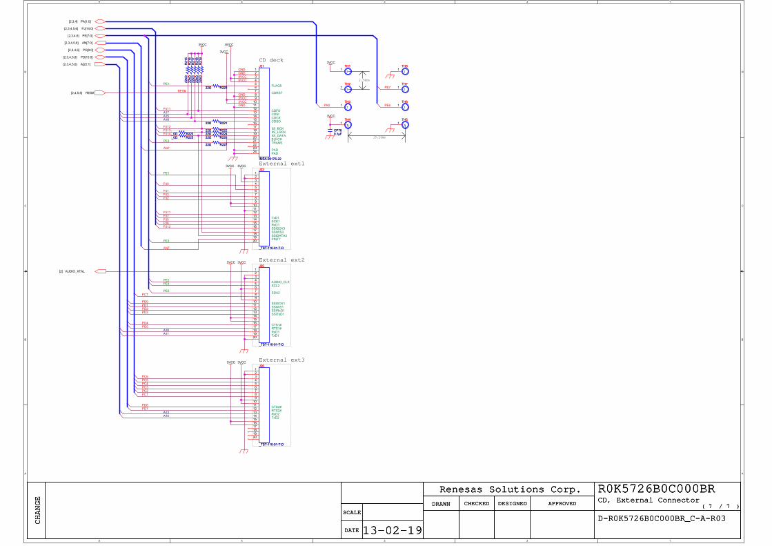
5
5
4
4
3
3
2
2
1
1
D D
C C
B B
A A
FLAG6
CD deck
TRANS
CDFSCDSI
CDSO
IIS_BCK
CDCK
IIS_LRCKIIS_DATA
CDRST
BLKCK
External ext1
External ext2
External ext3
TxD1SCK1RxD1SSISCK3SSIWS3SSIDATA3PINT7
AUDIO_CLKSCL2
SDA2
SSISCK1SSIWS1SSIRxD1SSITxD1
CTS1#RTS1#RxD1TxD1
CTS2#RTS2#RxD2TxD2
15.24mm
2.54mm
PADPAD
PJ12
A18
PE1
GND
GND
A17
3VCC
GND
PJ13PJ14
PE3
PJ11
AN7
3VCC
RES#
A15
8VCC8VCC
GND
PE3
PJ1
PJ11
PJ3
PJ7
PJ2
PJ5PJ6
PE1
PJ12
PJ0
AN7
PE2PE4
PE5PC7
PD0PD1PD2PD3
PD4PD5
PC6PC5PC4PC3PC2PC1
PD6PD7
A13A14
A10A11
PE7
PE6PA0
RES#[2,4,5,6]
AN[7:0][2,3,4,5,6]
AUDIO_XTAL[2]
PC[8:0][2,3,4,6]
PE[7:0][2,3,4,6]
PD[15:0][2,3,4,5,6]
A[22:1][2,3,4,5,6]
PJ[14:0][2,3,4,5,6]
PA[1:0][2,3,4]
3VCC
3VCC
8VCC
3VCC 5VCC
5VCC 3VCC
5VCC 3VCC
3VCC
3VCC
Renesas Solutions Corp.
DATE
APPROVED
SCALE
DESIGNEDCHECKEDDRAWN
CHANGE
( / )7 7
D-R0K5726B0C000BR_C-A-R03
13-02-19
R0K5726B0C000BRCD, External Connector
Renesas Solutions Corp.
DATE
APPROVED
SCALE
DESIGNEDCHECKEDDRAWN
CHANGE
( / )7 7
D-R0K5726B0C000BR_C-A-R03
13-02-19
R0K5726B0C000BRCD, External Connector
Renesas Solutions Corp.
DATE
APPROVED
SCALE
DESIGNEDCHECKEDDRAWN
CHANGE
( / )7 7
D-R0K5726B0C000BR_C-A-R03
13-02-19
R0K5726B0C000BRCD, External Connector
R21
822
kΩR
218
22kΩ
TH3TH3
11
TH4TH4
11
TH5TH5
11
R21
622
kΩR
216
22kΩ
CP780.1µFCP780.1µF
R22622Ω R22622Ω
J25
_TST-110-01-T-D
J25
_TST-110-01-T-D
123456789
1011121314151617181920
R22022Ω R22022Ω
R22122Ω R22122Ω
TH2TH2
11
R21
722
kΩR
217
22kΩ
TH6TH6
11
J21
IMSA-9617S-22
J21
IMSA-9617S-22
123456789
101112131415161718192021222324
J26
_TST-110-01-T-D
J26
_TST-110-01-T-D
123456789
1011121314151617181920
TH7TH7
11
R21
522
kΩR
215
22kΩ
R22422Ω R22422Ω
R21
922
kΩR
219
22kΩ
J22
_TST-110-01-T-D
J22
_TST-110-01-T-D
123456789
1011121314151617181920
TH1TH1
11
R225_0Ω R225_0Ω
R22222Ω R22222Ω
TH8TH8
11
R22722Ω R22722Ω
R223_0Ω R223_0Ω
REVISION HISTORY SH726B CPU Board R0K5726B0C000BR User's Manual
Description Rev. Date Page Summary
1.00 Mar. 12, 2013 – First edition

SH726B CPU Board R0K5726B0C000BR User's Manual
Publication Date: Rev.1.00 Mar. 12, 2013 Published by: Renesas Electronics Corporation

http://www.renesas.comRefer to "http://www.renesas.com/" for the latest and detailed information.
Renesas Electronics America Inc.2880 Scott Boulevard Santa Clara, CA 95050-2554, U.S.A.Tel: +1-408-588-6000, Fax: +1-408-588-6130Renesas Electronics Canada Limited1101 Nicholson Road, Newmarket, Ontario L3Y 9C3, CanadaTel: +1-905-898-5441, Fax: +1-905-898-3220Renesas Electronics Europe LimitedDukes Meadow, Millboard Road, Bourne End, Buckinghamshire, SL8 5FH, U.KTel: +44-1628-651-700, Fax: +44-1628-651-804Renesas Electronics Europe GmbHArcadiastrasse 10, 40472 Düsseldorf, Germany Tel: +49-211-65030, Fax: +49-211-6503-1327 Renesas Electronics (China) Co., Ltd.7th Floor, Quantum Plaza, No.27 ZhiChunLu Haidian District, Beijing 100083, P.R.China Tel: +86-10-8235-1155, Fax: +86-10-8235-7679Renesas Electronics (Shanghai) Co., Ltd.Unit 204, 205, AZIA Center, No.1233 Lujiazui Ring Rd., Pudong District, Shanghai 200120, China Tel: +86-21-5877-1818, Fax: +86-21-6887-7858 / -7898 Renesas Electronics Hong Kong LimitedUnit 1601-1613, 16/F., Tower 2, Grand Century Place, 193 Prince Edward Road West, Mongkok, Kowloon, Hong KongTel: +852-2886-9318, Fax: +852 2886-9022/9044Renesas Electronics Taiwan Co., Ltd.13F, No. 363, Fu Shing North Road, Taipei, TaiwanTel: +886-2-8175-9600, Fax: +886 2-8175-9670Renesas Electronics Singapore Pte. Ltd. 80 Bendemeer Road, Unit #06-02 Hyflux Innovation Centre Singapore 339949Tel: +65-6213-0200, Fax: +65-6213-0300Renesas Electronics Malaysia Sdn.Bhd.Unit 906, Block B, Menara Amcorp, Amcorp Trade Centre, No. 18, Jln Persiaran Barat, 46050 Petaling Jaya, Selangor Darul Ehsan, MalaysiaTel: +60-3-7955-9390, Fax: +60-3-7955-9510Renesas Electronics Korea Co., Ltd.11F., Samik Lavied' or Bldg., 720-2 Yeoksam-Dong, Kangnam-Ku, Seoul 135-080, KoreaTel: +82-2-558-3737, Fax: +82-2-558-5141
SALES OFFICES
© 2013 Renesas Electronics Corporation. All rights reserved.©
Colophon 1.3
16SH726B CPU BoardR0K5726B0C000BR
User’s Manual
R20UT0601EJ0100