XGK CPU Module
224
Right choice for ultimate yield LSIS strives to maximize customers' profit in gratitude of choosing us for your partner. Programmable Logic Controller XGK CPU Module User’s Manual Read this manual carefully before installing, wiring, operating, servicing or inspecting this equipment. Keep this manual within easy reach for quick reference. XGK- CPUUN XGK- CPUHN XGK- CPUSN XGK-CPUU XGK-CPUH XGK-CPUA XGK-CPUS XGK-CPUE XGT Series http://eng.lsis.biz
-
Upload
khangminh22 -
Category
Documents
-
view
0 -
download
0
Transcript of XGK CPU Module

Right choice for ultimate yield LSIS strives to maximize customers' profit in gratitude of choosing us for your partner.
Programmable Logic Controller
XGK CPU Module User’s Manual
Read this manual carefully before installing, wiring, operating, servicing or inspecting this equipment.
Keep this manual within easy reach
for quick reference.
XGK-CPUUN XGK-CPUHN XGK-CPUSN
XGK-CPUU XGK-CPUH XGK-CPUA XGK-CPUS XGK-CPUE
XGT Series
http://eng.lsis.biz

Safety Instruction
Before using the product … For your safety and effective operation, please read the safety instructions thoroughly before using the product. Safety Instructions should always be observed in order to prevent accident
or risk with the safe and proper use the product. Instructions are separated into “Warning” and “Caution”, and the meaning of
the terms is as follows;
This symbol indicates the possibility of serious injury or death if some applicable instruction is violated
This symbol indicates the possibility of slight injury or damage to products if some applicable instruction is violated
The marks displayed on the product and in the user’s manual have the
following meanings.
Be careful! Danger may be expected.
Be careful! Electric shock may occur. The user’s manual even after read shall be kept available and accessible to
any user of the product.
Warning
Caution

Safety Instruction
Safety Instructions when designing
Please, install protection circuit on the exterior of PLC to protect the whole control system from any error in external power or PLC
module. Any abnormal output or operation may cause serious problem in safety of the whole system.
- Install applicable protection unit on the exterior of PLC to protect the system from physical damage such as emergent stop switch, protection circuit, the upper/lowest limit switch, forward/reverse operation interlock circuit, etc.
- If any system error (watch-dog timer error, module installation error, etc.) is detected during CPU operation in PLC, the whole output is designed to be turned off and stopped for system safety. However, in case CPU error if caused on output device itself such as relay or TR can not be detected, the output may be kept on, which may cause serious problems. Thus, you are recommended to install an addition circuit to monitor the output status.
Never connect the overload than rated to the output module nor allow the output circuit to have a short circuit, which may cause a fire.
Never let the external power of the output circuit be designed to be On earlier than PLC power, which may cause abnormal output or
operation.
In case of data exchange between computer or other external equipment and PLC through communication or any operation of PLC (e.g. operation mode change), please install interlock in the sequence program to protect the system from any error. If not, it may cause abnormal output or operation.
Warning

Safety Instruction
Safety Instructions when designing
Safety Instructions when designing
I/O signal or communication line shall be wired at least 100mm away from a high-voltage cable or power line. If not, it may cause abnormal output or operation.
Caution
Use PLC only in the environment specified in PLC manual or general standard of data sheet. If not, electric shock, fire, abnormal operation of the product or flames may be caused.
Before installing the module, be sure PLC power is off. If not, electric shock or damage on the product may be caused.
Be sure that each module of PLC is correctly secured. If the product is installed loosely or incorrectly, abnormal operation, error or dropping may be caused.
Be sure that I/O or extension connecter is correctly secured. If not, electric shock, fire or abnormal operation may be caused.
If lots of vibration is expected in the installation environment, don’t let PLC directly vibrated. Electric shock, fire or abnormal operation may be caused.
Don’t let any metallic foreign materials inside the product, which may cause electric shock, fire or abnormal operation..
Caution

Safety Instruction
Safety Instructions when wiring
Prior to wiring, be sure that power of PLC and external power is turned off. If not, electric shock or damage on the product may be caused.
Before PLC system is powered on, be sure that all the covers of
the terminal are securely closed. If not, electric shock may be caused
Warning
Let the wiring installed correctly after checking the voltage rated of each product and the arrangement of terminals. If not, fire, electric shock or abnormal operation may be caused.
Secure the screws of terminals tightly with specified torque when wiring. If the screws of terminals get loose, short circuit, fire or abnormal operation may be caused.
* Surely use the ground wire of Class 3 for FG terminals, which is
exclusively used for PLC. If the terminals not grounded correctly, abnormal operation may be caused.
Don’t let any foreign materials such as wiring waste inside the module while wiring, which may cause fire, damage on the product or abnormal operation.
Caution

Safety Instruction
Safety Instructions for test-operation or repair
Safety Instructions for waste disposal
Don’t touch the terminal when powered. Electric shock or abnormal operation may occur.
Prior to cleaning or tightening the terminal screws, let all the external power off including PLC power. If not, electric shock or abnormal operation may occur.
Don’t let the battery recharged, disassembled, heated, short or soldered. Heat, explosion or ignition may cause injuries or fire.
Warning
Don’t remove PCB from the module case nor remodel the module. Fire, electric shock or abnormal operation may occur.
Prior to installing or disassembling the module, let all the external
power off including PLC power. If not, electric shock or abnormal operation may occur.
Keep any wireless installations or cell phone at least 30cm away from PLC. If not, abnormal operation may be caused.
Caution
Product or battery waste shall be processed as industrial waste. The waste may discharge toxic materials or explode itself.
Caution
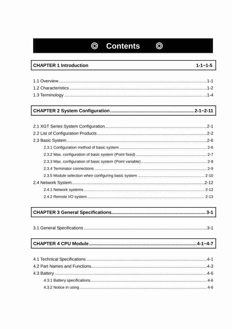
Contents
CHAPTER 1 Introduction 1-1~1-5
1.1 Overview .......................................................................................................................... 1-1 1.2 Characteristics ................................................................................................................. 1-2 1.3 Terminology ..................................................................................................................... 1-4
CHAPTER 2 System Configuration ................................................................ 2-1~2-11
2.1 XGT Series System Configuration.................................................................................... 2-1 2.2 List of Configuration Products .......................................................................................... 2-2 2.3 Basic System ................................................................................................................... 2-6
2.3.1 Configuration method of basic system ................................................................................. 2-6
2.3.2 Max. configuration of basic system (Point fixed) .................................................................. 2-7
2.3.3 Max. configuration of basic system (Point variable) ............................................................. 2-8
2.3.4 Terminator connections ........................................................................................................ 2-9
2.3.5 Module selection when configuring basic system .............................................................. 2-10
2.4 Network System ............................................................................................................. 2-12 2.4.1 Network systems ................................................................................................................ 2-12
2.4.2 Remote I/O system ............................................................................................................. 2-13
CHAPTER 3 General Specifications........................................................................ 3-1
3.1 General Specifications ..................................................................................................... 3-1
CHAPTER 4 CPU Module .................................................................................. 4-1~4-7
4.1 Technical Specifications ................................................................................................... 4-1 4.2 Part Names and Functions ............................................................................................... 4-3 4.3 Battery ............................................................................................................................. 4-6
4.3.1 Battery specifications ............................................................................................................ 4-6
4.3.2 Notice in using ...................................................................................................................... 4-6

4.3.3 Battery durability ................................................................................................................... 4-6
4.3.4 Changing the battery ............................................................................................................ 4-7
CHAPTER 5 Program Configuration and Operation Method ....................... 5-1~5-25
5.1 Program Introduction ....................................................................................................... 5-1 5.1.1 Program execution methods ................................................................................................ 5-1
5.1.2 Operation processing during momentary power failure ....................................................... 5-2
5.1.3 Scan Time ............................................................................................................................ 5-3
5.2 Program Execution .......................................................................................................... 5-5 5.2.1 Program configuration .......................................................................................................... 5-5
5.2.2 Program execution method .................................................................................................. 5-5
5.2.3 Interrupt. ............................................................................................................................... 5-7
5.3 Operation Mode ............................................................................................................. 5-13 5.3.1 RUN mode .......................................................................................................................... 5-13
5.3.2 STOP mode ........................................................................................................................ 5-14
5.3.3 DEBUG mode ..................................................................................................................... 5-14
5.3.4 Changing operation mode .................................................................................................. 5-15
5.4 Memory .......................................................................................................................... 5-16 5.4.1 Program memory................................................................................................................ 5-16
5.4.2 Data memory ...................................................................................................................... 5-17
5.5 Configuration Diagram of Data Memory ......................................................................... 5-19 5.5.1 XGK-CPUE ......................................................................................................................... 5-19
5.5.2 XGK-CPUS ......................................................................................................................... 5-20
5.5.3 XGK-CPUA ......................................................................................................................... 5-21
5.5.4 XGK-CPUH ......................................................................................................................... 5-22
5.5.5 XGK-CPUU ......................................................................................................................... 5-23
5.5.5 Data Latch Area settings .................................................................................................... 5-24
CHAPTER 6 Functions of CPU Module.......................................................... 6-1~6-17
6.1 Self-Diagnosis .................................................................................................................. 6-1 6.1.1 Scan Watchdog Timer .......................................................................................................... 6-1
6.1.2 I/O Module Check function ................................................................................................... 6-2
6.1.3 Battery Voltage Check function ............................................................................................ 6-2

6.1.4 Error History Save ................................................................................................................ 6-2
6.1.5 Troubleshooting .................................................................................................................. 6-2
6.2 Clock ................................................................................................................................ 6-4 6.3 Remote Function.............................................................................................................. 6-6 6.4 Forced I/O On/Off Function .............................................................................................. 6-7
6.4.1 Forced I/O setup method ..................................................................................................... 6-7
6.4.2 Forced On/Off execution point and execution method ......................................................... 6-8
6.5 Direct I/O Operation ......................................................................................................... 6-8 6.6 Saving Operation History ................................................................................................. 6-9
6.6.1 Error history .......................................................................................................................... 6-9
6.6.2 Mode conversion history ...................................................................................................... 6-9
6.6.3 Power shutdown history ....................................................................................................... 6-9
6.6.4 System history ...................................................................................................................... 6-9
6.7 External Device Error Diagnosis.. .................................................................................. 6-11 6.8 Error Mask ..................................................................................................................... 6-13 6.9 I/O Module Skip ............................................................................................................. 6-14 6.10 Changing Module during Operation.............................................................................. 6-15 6.11I/O No. Allocation Method .............................................................................................. 6-16
6.11.1 Fixed I/O no. allocation ..................................................................................................... 6-16
6.11.2 Variable I/O no. allocation ................................................................................................. 6-16
6.11.3 Module reservation function .............................................................................................. 6-17
6.12 Program Modification during Operation ........................................................................ 6-17
CHAPTER 7 I/O Module ................................................................................... 7-1~7-24
7.1 Notice in selecting module ............................................................................................... 7-1 7.2 Digital Input Module Specifications ................................................................................... 7-3
7.2.1 8 point DC24V Input module (Source/Sink Type) ................................................................ 7-3
7.2.2 16 point DC24V Input module (Source/Sink Type) .............................................................. 7-4
7.2.3 16 point DC24V Input module (Source Type) ...................................................................... 7-5
7.2.4 32 point DC24V Input module (Source/Sink Type) .............................................................. 7-6
7.2.5 32 point DC24V Input module (Source type) ....................................................................... 7-7
7.2.6 64 point DC24V Input module (Source/Sink Type) .............................................................. 7-8
7.2.7 64 point DC24V Input module (Source Type) ...................................................................... 7-9
7.2.8 16 point AC110V Input module ........................................................................................... 7-10
7.2.9 8 point AC220V Input module ............................................................................................. 7-11

7.2.10 8 point AC220V isolated Input module ............................................................................. 7-12
7.3 Digital Output Module Specifications .............................................................................. 7-13 7.3.1 8 point Relay Output module .............................................................................................. 7-13
7.3.2 16 point Relay Output module ............................................................................................ 7-14
7.3.3 16 point Relay Output module (Surge Absorber built-in Type) .......................................... 7-15
7.3.4 16 point Triac Output module ............................................................................................. 7-16
7.3.5 16 point Transistor Output module(Sink Type) ................................................................... 7-17
7.3.6 32 point Transistor Output module(Sink Type) ................................................................... 7-18
7.3.7 64 point Transistor Output module(Sink Type) ................................................................... 7-19
7.3.8 16 point Transistor Output module(Source Type) .............................................................. 7-20
7.3.9 32 point Transistor Output module(Source Type) .............................................................. 7-21
7.3.10 64 point Transistor Output module(Source Type) ............................................................ 7-22
7.3.11 8 point Transistor isolated Output module ........................................................................ 7-23
7.4 Digital IO Module ........................................................................................................... 7-24 7.4.1 32 point I/O Combination module....................................................................................... 7-24
7.5 Event Input Module ........................................................................................................ 7-25 7.5.1 Event Input Module ............................................................................................................ 7-25
7.6 Smart Link...................................................................................................................... 7-26 7.6.1 Smart Link connectable module ......................................................................................... 7-26
7.6.2 Smart Link connection ........................................................................................................ 7-27
CHAPTER 8 Power Module ............................................................................... 8-1~8-5
8.1 Selection Method ............................................................................................................. 8-1 8.2 Specifications ................................................................................................................... 8-3 8.3 Part Names ...................................................................................................................... 8-4 8.4 Current Consumption/Power Calculation Example ........................................................... 8-5
CHAPTER 9 Base and Extended Cable ........................................................... 9-1~9-2
9.1 Specifications ................................................................................................................... 9-1 9.1.1 Main base ............................................................................................................................. 9-1
9.1.2 Extended base ..................................................................................................................... 9-1
9.1.3 Extended cable..................................................................................................................... 9-1
9.2 Part Names ...................................................................................................................... 9-2

9.2.1 Main base ............................................................................................................................. 9-2
9.2.2 Expansion base .................................................................................................................... 9-2
10.1 Features ..................................................................................................................... 10-1 10.2 PID Control ................................................................................................................ 10-1 10.3 PID Control Operation ................................................................................................ 10-2
10.3.1 Terms .............................................................................................................................. 10-2
10.3.2 PID Expressions ............................................................................................................. 10-2
10.3.3 P Control ......................................................................................................................... 10-3
10.3.4 PI Control ........................................................................................................................ 10-4
10.3.5 PID Control ..................................................................................................................... 10-5
10.4 PID Instructions .......................................................................................................... 10-6 10.4.1 PID Loop States .............................................................................................................. 10-6
10.4.2 PID Instruction Group ..................................................................................................... 10-7
10.5 PID Flag Configuration ............................................................................................... 10-9 10.5.1 Common Bit Area .......................................................................................................10-11
10.5.2 Individual Data Area ..................................................................................................... 10-14
10.6 Convenient Additional Functions of PID Instructions ................................................. 10-21 10.6.1 Various PID-based control methods ............................................................................. 10-21
10.6.2 Operation and function of anti wind-up ........................................................................ 10-21
10.6.3 Operation and function of Auto-tuning (AT) .................................................................. 10-21
10.6.2 Operation and function of cascade (CAS) .................................................................... 10-21
10.7 How to Use PID Instructions ..................................................................................... 10-22 10.7.1 Hardware Configuration ............................................................................................... 10-22
10.7.2 Program example 1 ...................................................................................................... 10-21
10.7.3 PID controlling .............................................................................................................. 10-26
10.7.4 How to start up using AT (Auto-tuning) ....................................................................... 10-32
10.7.5 Program example 2 ...................................................................................................... 10-33
10.7.6 Startup using PWM ....................................................................................................... 10-34
10.7.7 Cascade startup ........................................................................................................... 10-35
CHAPTER 11 Installation and Wiring ......................................................... 11-1~11-12
CHAPTER 10 Built-in PID Functions ..................................................... 10-1~10-35

11.1 Installation .................................................................................................................... 11-1 11.1.1 Installation environment..................................................................................................... 11-1
11.1.2 Handling precautions ......................................................................................................... 11-4
11.1.3 Attachment/Detachment of module ................................................................................... 11-7
11.2 Wiring ........................................................................................................................... 11-9 11.2.1 Power wiring ...................................................................................................................... 11-9
11.2.2 I/O Device wiring ............................................................................................................. 11-11
11.2.3 Ground wiring .................................................................................................................. 11-11
11.2.4 Cable specifications for wiring ......................................................................................... 11-12
CHAPTER 12 Maintenance and Repair ........................................................ 12-1~12-2
12.1 Repair and Checking.................................................................................................... 12-1 12.2 Daily Checking ............................................................................................................. 12-1 12.3 Regular Checking ........................................................................................................ 12-2
13.1 Requirements for Conformance to EMC Directive ........................................................ 13-1 13.1.1 EMC Standard .................................................................................................................. 13-1
13.1.2 Control Panel.................................................................................................................... 13-2
13.1.3 Cables .............................................................................................................................. 13-3
13.2 Requirement to Conform to the Low-voltage Directive ................................................. 13-4 13.1.1 Standard Applied for MasterLogic-200 Series .................................................................. 13-4
13.1.2 XGT Series PLC Selection ............................................................................................... 13-4
CHAPTER 14 Troubleshooting ................................................................... 14-1~14-16
14.1 Basic Procedure for Troubleshooting ........................................................................... 14-1 14.2 Troubleshooting ........................................................................................................... 14-1
14.2.1 Action when Power LED is OFF ....................................................................................... 14-2
14.2.2 Action when ERR LED is blinking .................................................................................. 14-3
14.2.3 Action when RUN, STIOP LED is OFF ........................................................................... 14-4
14.2.4 Action when I/O Module does not work normally ........................................................... 14-5
CHAPTER 13 EMC Directive ..................................................................... 13-1~13-4
14.2.5 Action when Program Write does not work normally ...................................................... 14-7
14.3 Questionnaire for Troubleshooting ............................................................................... 14-8 14.4 Cases .......................................................................................................................... 14-9
14.4.1 Input circuit error types and corrective actions ................................................................ 14-9
14.4.2 Output circuit error types and corrective actions ............................................................ 14-10
14.5 Error Code List ........................................................................................................... 14-12 14.5.1 Error code during CPU operation ................................................................................... 14-12
14.5.2 Error code of program operation .................................................................................... 14-15
Appendix 1 Flag List ....................................................................... App.1-1~App.1-14
App.1.1 Special Relay (F) List ........................................................................................ App.1-1 App.1.2 Communication Relay (L) List ......................................................................... App.1-10 App.1.3 Link Register (N) List ...................................................................................... App.1-13
Appendix 2 Dimensions .................................................................... App.2-1~App.2-3
Appendix 3 Compatibility with MASTER-K ..................................... App.3-1~App.3-5
Warranty

※ The number of User’s manual is indicated right part of the back cover.
LSIS Co., Ltd 2006 All Rights Reserved.
Revision History
Version Date Contents Chapter
V 1.0 2006. 2 First Edition -
V1.1 2009.10
1. XGK-CPUU added
2. Fnet -> Rnet modified
3. Scan Time modified
4. Interrupt module removed
5. Clock data F device modified
6. Heavy error/light error modified
7. Fault mask -> “Release by program” removed
8. Skip function -> “Release by program” removed
9. Product list modified
10. Program language SFC, ST added
11. XGQ-SOEA added
12. Flag list modified
Ch1.1, Ch2.3.1, Ch2.4.1, Ch4.1
Ch1.3
Ch5.1.3
Ch7.1
Ch6.2
Ch6.7
Ch6.8
Ch6.9
Ch2.2
Ch4.1
Ch7.5
Appendix 1
V1.6 2010.3
1. Product list modified
2. Supported functions according to OS version
3. Description on Reset/D.Clear switch added
4. Wiring diagram of Smart Link added
5. Flag added
(indicated version to decimal places _OS_VER_PATCH)
6. Typos fixed
Ch2.2, Ch2.4.2
Ch4.1
Ch4.2
Ch7.6.3
App1.1
Ch1.1, Ch1.2, Ch1.3
Ch3.1, Ch4.1
Ch5.2.3, Ch5.5
Ch8.1
Ch10.3, Ch10.7
CH12.2, 12.3
V1.7 2013.1
1. Product list modified
2. Size of data refresh area added
3. Supported functions according to CPU OS version added
4. Fixed cycle task’s flag information added
5. Digital I/O module added
XGI-A21C, XGQ-TR1C
6. Flag added
Ch2.2
Ch2.3.5
Ch4.1
Ch5.2.3
Ch7.2.10
Ch7.3.11
App1.1

부록3 MASTER-K와의 호환성
[텍스트 입력]
Version Date Contents Chapter
V 1.8 2015. 2 1.CPU Module Added (XGK-CPUUN, XGK-CPUHN, XGK-CPUSN)
1.2, 2.2, 2.3, 2.4, 4.1, 4.2,
5.1.3, 5.4.1, 5.4.2
5.5, 6.13, 8.1, Appendix1.1

About User’s Manual
About User’s Manual
Thank you for purchasing PLC of LS Industrial System Co., Ltd.
Before use, make sure to carefully read and understand the User’s Manual about the functions,
performances, installation and programming of the product you purchased in order for correct
use and importantly, let the end user and maintenance administrator to be provided with the
User’s Manual.
The User’s Manual describes the product. If necessary, you may refer to the following
description and order accordingly. In addition, you may connect our
website(http://www.lsis.com/) and download the information as a PDF file.
Relevant User’s Manuals
Title Description No. of User’s
Manual
XGK / XGB
Instructions &
Programming
It is the user’s manual for programming to
explain how to use commands that are used
PLC system with XGK CPU and XGB CPU.
10310000510
XG5000
It describes how to use XG5000 software
especially about online functions such as
programming, printing, monitoring and
debugging by using XGT series products.
10310000512

Chapter 1 Introduction
1-1
Chapter 1 Introduction
1.1 Overview This User’s Manual provides the information for the specification, performance and operation method of each product required to use a PLC system configured by XGK series CPU modules. The configuration of User’s Manual is as follows :
Chapter Items Description
Chapter 1 Overview Describes the configuration of this user’s manual, product characteristics and terminology.
Chapter 2 System Configuration Describes the product type and system configuration method to be used for XGK series.
Chapter 3 General Specifications Shows the common specification of each module used for XGK series.
Chapter 4 CPU Module Describes the performance, specification and operation method of XGK-CPU Chapter 5 Program Configuration and
Operation Method Chapter 6 Function of CPU Module
Chapter 7 I/O Module Describes the specification and the method to use I/O module and power module except CPU module. Chapter 8 Power Module
Chapter 9 Base and Extended Cable
Chapter 10 Built-in PID Describes on the built-in PID function
Chapter 11 Installation and Wiring Describes the installation, wiring method and notices to secure the reliability of PLC system.
Chapter 12 Maintenance & Repair Describes the checking items and methods to run the PLC system normally for a long time.
Chapter 13 EMC Directive Summarizes the precautions on conformance to the EMC Directive of the machinery assembled using XGK series.
Chapter 14 Trouble Shooting Describes various errors and action methods occurred while using a system.
Appendix 1 Flag List Describes various type of each flag and its description.
Appendix 2 Dimensions Shows the outer dimension of CPU, I/O module and Base.
Appendix 3 Compatibility with MASTER-K
Notes 1) This user’s manual does not describe the special/communication module and program writing method. For the corresponding function, please refer to the related user’s manual. 2) XGK CPU is one of the XGT PLC system and CPU types of XGT PLC system are as follows. ① XGK series: XGT PLC system that cosists of CPU using Master-K ② XGI series: XGT PLC system that consists of single CPU using IEC language ③ XGR series: XGT PLC system that consists of redundaccy CPU using IEC language

Chapter 1 Introduction
1-2
1.2 Characteristics
XGK system has the features as below.
1) Compact size
The function is extended to large sized but the size is reduced innovatively to make the installation in the small space for any purpose easily.
2) High speed processing (1) High speed processing by the development of dedicated micro processor is realized.
(based on XGK-CPUUN) • Sequence instruction: 0.0085 µs • MOV instruction: 0.0255 • Floating point arithmetic operation: the operation for the single real number and double real number
accuracy is profoundly improved.
Classification + − × ÷ Single Real 0.183 0.183 0.336 0.345 Double Real 0.327 0.327 0.727 2.808
(2) Improvement of data transfer speed between modules through base.
• 16 point I/O module data processing : 0.20 µs ~ 0.80 µs • Analog 1 channel data processing : 0.20 µs ~ 0.80 µs • 1 Kbyte communication module data processing : 12.8 µs • Parallel processing by I/O data automatic refresh during program operation
3) Convenience to use Analog Data Analog module enforced the precision and stability and provides the convenience as below :
• Program simplification by providing analog data dedicated ‘U ‘ device • Setting without memory map of special module is available by providing parameter setting method.
4) System Configuration Various convenient functions are provided to meet the demands of users.
• Filter value adjustment of input module • Output hold at emergency time • Varistor built-in relay output module with strong durability • Total extension length of expanded base shall be 15m. • Provides system RUN contact to power module. • Cost efficiency of setup, startup and maintenance/repair by enforced self-diagnosis function
Chapter 1 Introduction
1-3
5) Various communication system Provides various network function to satisfy both the user convenience and compatibility.
• Network opening available without writing a ladder program • Network setting and operation status monitoring by dedicated tool(XG-PD) • Supports Open network of various international specification • Dedicated network to provide the ease in use and optimal performance • Network compatibility with the existing products (MASTER-K, GLOFA-GM)
6) Enforcement of program and online function
Minimized the program writing time by providing the convenience of programming and available to complete the control system of equipment without stopping the system by enforcement of online function.
• Compatibility of ladder and text (Mnemonic) method • Enforcement of symbolic program • Automatic conversion of MASTER-K program • Available to modify the program during operation and secure the stability • Available to install and change the network during operation • Enforcement of trend monitoring function • User event function • Data trace function
7) User’s convenience
Various functions are provided for user’s convenience.
• Module Changing Wizard (User’s tool is unnecessary.) • System Diagnosis • Skip I/O • Fault Mask • I/O Allocation Method • Various Operation History

Chapter 1 Introduction
1-4
1.3 Terminology Here describes the terminology used in this user’s manual.
Terminology Definition Remarks
Module A device like I/O board assembled to insert in a motherboard or base as a standardized factor having the regular function to configure the system.
Ex) CPU module, power module, I/O module etc.
Unit A module or module aggregate which is the minimum unit in operation of PLC system. It configures the PLC system by connecting to other module or module aggregate.
Ex) Basic unit, Extended unit
PLC System A system consisted of PLC and peripherals and which is configured to enable the control by user program
XG 5000 Graphic loader to carry out program writing, editing and debug function
I/O image area Internal memory area of CPU module installed to maintain the input and output state
Rnet Remote Network (Remote dedicated network)
Fnet Field bus Network
RAPIEnet Real-time Automation Protocols for Industrial Ethernet
Cnet Computer Network
FEnet Fast Ethernet Network
Pnet Profibus-DP Network
Dnet DeviceNet Network
RTC Real Time Clock. A general name of universal IC having the clock function
Watchdog Timer A timer to monitor the assigned running time of program and give an alarm if failed to complete the processing within the assigned time.
Task There are three kind of tasks. (cycle time task, internal device task, external device task by external interrupt module’s input signal)

Chapter 1 Introduction
1-5
Terminology Definition Remarks
Sink input
The mode that the current flows from the switch to PLC input terminal when input signal is ON.
Z : Input resistance
Source input
The mode that the current flows from PLC input terminal to the switch when input signal is ON.
Sink output
The mode that the current flows from load to output terminal when PLC output contact is ON.
Source output
The mode that the current flows from output contact when PLC output contact is ON.
+
−
Z Power
PLC
Switch
Common
Current
+
− Z Power
PLC
Current Switch
Common
+
−
Power
PLC
Current
Output contact
Common
Load
−
Power
PLC
Current Output contact
Common
+ Load

Chapter 2 System Configuration
2 -1
Chapter 2 System Configuration XGT series are equipped with various products proper for basic system, computer link and network system configuration. Here describes the configuration method of each system and its features.
2.1 XGT Series System Configuration XGT series system configuration is as below:
CPU Module Battery
RS-232C, USB Cable
XG5000
Main Base (XGB-MA)
Diskette
Power Module (XGP- )
XGP-PAF1
XGK-CPUH
Expanded Base (XGB-EA)
Expanded Cable (XGC-E)
XGK-CPUH XGK-CPUH
I/O Module (XGI-) (XGQ-)
Special Module (XGF-A)
XGL-DMEA
Communication Module (XGL-)
XGF-PO3A
Terminator (XGT-TERA)

Chapter 2 System Configuration
2 -2
2.2 Configuration Products The product configuration of XGT series is as below :
Product Model Description Remarks
CPU Module
XGK-CPUE • Standard type CPU module (Max I/O point: 1,536 points) 16kstep
XGK-CPUS • Standard type CPU module (Max I/O point: 3,072 points) 32kstep
XGK-CPUA • High speed type CPU module (Max. I/O point: 3,072 points) 32kstep
XGK-CPUH • High speed type CPU module (Max. I/O point: 6,144 points) 64kstep
XGK-CPUU • High speed type CPU module (Max. I/O point: 6,144 points) 128kstep
XGK-CPUSN • High speed type CPU module (Max. I/O point: 3,072 points) 64kstep
XGK-CPUHN • High speed type CPU module (Max. I/O point: 6,144 points) 128kstep
XGK-CPUUN • High speed type CPU module (Max. I/O point: 6,144 points) 256kstep
Digital Input Module
XGI-D21A • DC 24V Input, 8 point (Current source / sink input)
XGI-D22A • DC 24V Input, 16 point (Current source / sink input)
XGI-D24A • DC 24V Input, 32 point (Current source / sink input)
XGI-D28A • DC 24V Input, 64 point (Current source / sink input)
XGI-D22B • DC 24V Input, 16 point (Current source input)
XGI-D24B • DC 24V Input, 32 point (Current source input)
XGI-D28B • DC 24V Input, 64 point (Current source input)
XGI-A12A • AC 110V input, 16 point
XGI-A21A • AC 220V input, 8 point
XGI-A21C • AC 220V isolated input, 8 points
Digital Output Module
XGQ-RY1A • Relay output, 8 point (for 2A, single COM.)
XGQ-RY2A • Relay output, 16 point (for 2A)
XGQ-RY2B • Relay output, 16 point (for 2A), Varistor attached
XGQ-TR2A • Transistor output, 16 point (for 0.5A, Sink output)
XGQ-TR4A • Transistor output, 32 point (for 0.1A, Sink output)
XGQ-TR8A • Transistor output, 64 point (for 0.1A, Sink output)
XGQ-TR2B • Transistor output 16 point (for 0.5A, Source output)
XGQ-TR4B • Transistor output 32 point (for 0.1A, Source output)
XGQ-TR8B • Transistor output 64 point (for 0.1A, Source output)
XGQ-SS2A • Triac output, 16 point (for 0.6A)
XGQ-TR1C • Transistor isolated output, 8 points (2A)
Digital I/O Module XGH-DT4A • DC 24V input, 16 point (current source / sink input)
• Transistor output, 16 point (for 0.1A, Sink output)
Main Base
XGB-M04A • for 4 module installation
XGB-M06A • for 6 module installation
XGB-M08A • for 8 module installation

Chapter 2 System Configuration
2 -3
Product Model Description Remarks
XGB-M12A • for 12 module installation
Expanded Base
XGB-E04A • for 4 module installation
XGB-E06A • for 6 module installation
XGB-E08A • for 8 module installation
XGB-E12A • for 12 module installation
Power module
XGP-ACF1 AC100V~240V input • DC5V: 3A, • DC24V: 0.6A
XGP-ACF2 AC100V~240V input • DC5V: 6A
XGP-AC23 AC100V~240V input • DC5V: 8.5A
XGP-DC42 DC24V Input • DC5V: 6A
Extended cable
XGC-E041 • Length : 0.4 m
Total extension distance
should not exceed
15m
XGC-E061 • Length : 0.6 m
XGC-E121 • Length : 1.2 m
XGC-E301 • Length : 3.0 m
XGC-E501 • Length : 5.0 m
XGC-E102 • Length : 10 m
XGC-E152 • Length : 15 m
Terminator XGT-TERA • Must use for base expansion - Dust-proof
Module XGT-DMMA • Dust protection module for not-used slot -
Battery XGT-BAT • Battery for XGT (DC 3.0V / 1,800 mAh)
Analog input Module
XGF-AV8A • Voltage Input: 8 channel • DC 1 ~ 5V / 0 ~ 5V / 0 ~ 10V / −10 ~ +10V
XGF-AC8A • Current Input: 8 channel • DC 4 ~ 20mA / 0 ~ 20mA
XGF-AD08A Voltage/Current Input: 8 channels
XGF-AD4S • Voltage/Current Input: 4 channels • Insulation between channels
XGF-AD16A • Voltage/Current Input: 16 channels
XGF-AW4S • 2-wire voltage/current input: 4 –channel, insulation
between channels • 2-wire transmitter driver power supported
Analog output Module
XGF-DV4A • Voltage Output: 4 channels • DC 1 ~ 5V / 0 ~ 5V / 0 ~ 10V / −10 ~ +10V
XGF-DC4A • Current Output:: 4 channels • DC 4 ~ 20mA / 0 ~ 20mA
XGF-DV4S • Current Output:: 4 channels • Insulation between channels
XGF-DC4S • Current Output:: 4 channels • Insulation between channels
XGF-DV8A • Voltage Output: 8 channels • DC 1 ~ 5V / 0 ~ 5V / 0 ~ 10V / −10 ~ +10V

Chapter 2 System Configuration
2 -4
Product Model Description Remarks
XGF-DC8A • Current Output:: 8 channels • DC 4 ~ 20mA / 0 ~ 20mA
Analog I/O Module XGF-AH6A • Voltage/Current input 4 channels
• Voltage/Current output 2 channels
Thermocouple Input Module XGF-TC4S • Temperature (T/C) Input, 4 channels,
• Insulation between channels
RTD Input Module
XGF-RD4A • Temperature (RTD) Input, 4 channels
XGF-RD4S • Temperature (RTD) Input, 4 channels • Insulation between channels
Temp. control Module
XGF-TC4UD • Control loop : 4 loops • Input(4 channels, TC/RTD/voltage/current), Output(8 channels, TR/current)
XGF-TC4RT • Control loop: 4 loops • input (4 channels, RTD), Output (8 channels, TR)
High speed Counter Module
XGF-HO2A • Voltage Input type (Open Collector type) • 200kHz, 2 channel
XGF-HD2A • Differential Input type (Line Driver type) • 500kHz, 2 channel
Positioning Module
XGF-PO3A • Pulse output (Open Collector type), 3 axes
XGF-PO2A • Pulse output (Open Collector type), 2 axes
XGF-PO1A • Pulse output (Open Collector type), 1 axis
XGF-PD3A • Pulse output (Line Drive type), 3 axes
XGF-PD2A • Pulse output (Line Drive type), 2 axes
XGF-PD1A • Pulse output (Line Drive type), 1 axis
XGF-PO4H • Pulse output (Open Collector type), 4 axes
XGF-PO3H • Pulse output (Open Collector type), 3 axes
XGF-PO2H • Pulse output (Open Collector type), 2 axes
XGF-PO1H • Pulse output (Open Collector type), 1 axes
XGF-PD4H • Pulse output (Line Drive type), 4 axes
XGF-PD3H • Pulse output (Line Drive type), 3 axes
XGF-PD2H • Pulse output (Line Drive type), 2 axes
XGF-PD1H • Pulse output (Line Drive type), 1 axes
Motion Control Module XGF-M16M • Motion dedicated net (M-II) type, 16 axes
Event input Module XGF-SOEA • DC 24V input, 32 point, Sequence of Event module
FEnet Module (Optical/Elec.) XGL-EFMF • Fast Ethernet(optical), Master
• 100/10 Mbps support

Chapter 2 System Configuration
2 -5
Product Model Description Remarks
XGL-EFMT • Fast Ethernet(electrical), Master • 100/10 Mbps support
XGL-ESHF • Fast Ethernet Switch module(optical)
Cnet Module
XGL-C22A • Serial communication • RS-232C, 2 channel
XGL-C42A • Serial communication • RS-422(485), 2 channel
XGL-CH2A • Serial communication • RS-232C 1 channel / RS-422(485) 1 channel
FDEnet Module(Master)
XGL-EDMF • Dedicated Ethernet(optical), Master • Deterministic communication support • 100/10 Mbps support
XGL-EDMT • Dedicated Ethernet(electrical), Master • Deterministic communication support • 100/10 Mbps support
Rnet Module XGL-RMEA
• for Rnet Master I/F (Smart I/O communication available) • Fast response speed support(against the existing Fnet
module) • 1 Mbps base band • for twisted cable
Profibus-DP Module
XGL-PMEA XGL-PMEC • Profibus-DP Master module
Pnet Slave I/F module XGL-PSEA • Profibus-DP Slave module
DeviceNet Module XGL-DMEA • DeviceNet Master module
Ethernet/IP Module XGL-EIPT • EtherNet/IP(electric)
• 100/10 Mbps support
Fnet I/F module XGL-FMEA • Field Bus master module
40-point connector 1473381-1 • 40-point connector (For I/O, special module)
Notes 1) For Active coupler, optical converter, repeater and block type remote module as network device, please
refer to the network related manual.

Chapter 2 System Configuration
2 -6
2.3 Basic System
2.3.1 Configuration method of Basic System
The features of Basic system consisted by connecting the main base and expanded base by a cable are as follows. The number of stages of expanded base is limited according to the CPU type and the allocation method of I/O No. is available to select the fixed type and variable type according to the setting of basic parameter.
Classification XGK-CPUE XGK-CPUS XGK-CPUSN XGK-CPUA XGK-CPUH
XGK-CPUHN XGK-CPUU
XGK-CPUUN Max. expanded stages 1 stage 3 stages 3 stages 7 stages 7 stages
Max. no. of I/O Module install 24 Module 48 Module 48 Module 96 Module 96 Module
Max. I/O point 1,536 points 3,072 points 3,072 points 6,144 points 6,144 points Max. extended distance 15m
Allocation of I/O No.
(fixed type)
• Each slot of base is allocated by 60 points regardless module installation and type. • For one base, I/O no. of 16 slots is allocated. That is, the start no. of No.1 base becomes
P00640. (Refer to 2.3.2) • The example of I/O no. of 12 Slot base is as below :
0 1 2 3 4 5 6 7 8 9 10 11
P0 ~
P3F
P40 ~
P7F
P80 ~
P11F
P120 ~
P15F
P160 ~
P19F
P200 ~
P23F
P240 ~
P27F
P280 ~
P31F
P320 ~
P35F
P360 ~
P39F
P400 ~
P43F
P440 ~
P47F I : input, O : output
Allocation of I/O no.
(variable type)
• The point is allocated according to the assignment of installation module per slot. - If assigned installation module by I/O parameter, the assigned point is allocated. - The slot not assigned by I/O parameter shall be allocated automatically according to actual installation slot
(Note: 8 point module shall be allocated by 16 point.) - The empty slot not assigned by I/O parameter shall be processed by 16 point.
• Available to assign the point only by I/O parameter without module assignment. • The slot installed by special module or communication module is allocated by 16 point. • The example of I/O no. of 12 Slot base is as below :
0 1 2 3 4 5 6 7 8 9 10 11
P00 ~
P0F
P10 ~
P1F
P20 ~
P3F
P40 ~
P7F
P80 ~
P8F
P90 ~
P10F
P110 ~
P12F
P130 ~
P16F
P170 ~
P18F
P190 ~
P19F
P200 ~
P21F
P220 ~
P23F I : input, O : output
Notes
1) The allocation method of I/O no. shall be set in basic parameter. 2) For Main base, the base no. is fixed as “0” and the expanded base has a switch to set the base no. 3) In case of setting module type by I/O parameter, it starts the operation when the type of actually installed
module is matched.
P W R
I 16
I 16
I 32
I 64
O 16
O 32
O 32
O 64
I 32
O 32
O 16
O 32
C P U
Slot No.
P W R
I 16
I 16
I 32
I 64
O 16
O 32
O 32
O 64
I 32
O 32
O 16
O 32
C P U
Slot No.

Chapter 2 System Configuration
2 -7
2.3.2 Max. Configuration of Basic System (Point Fixed)
System Configuration Example 1 - I/O point fixed - XGK-CPUH - 8 slot base
Expanded base
Expanded cable
Main base (base no.:0)
Base no. setting switch:1
1 2 3 4
Slot no.: 0 1 2 3 5 4 6 7
CPU
P0000
~
P003F
P0040
~
P007F
Power
P0080
~
P011F
P0120
~
P015F
P0160
~
P019F
P0200
~
P023F
P0240
~
P027F
P0280
~
P031F
Slot no.: 0 1 2 3 5 4 6 7 P0640
~
P067F
P0680
~
P071F
Power
P0720
~
P075F
P0760
~
P079F
P0800
~
P083F
P0840
~
P087F
P0880
~
P091F
P0920
~
P095F
Slot no.: 0 1 2 3 5 4 6 7 P1280
~
P131F
P1320
~
P135F
Power
P1360
~
P139F
P1400
~
P143F
P1440
~
P147F
P1480
~
P151F
P1520
~
P155F
P1560
~
P159F
Slot no.: 0 1 2 3 5 4 6 7 P1920
~
P195F
P1960
~
P199F
Power
P2000
~
P203F
P2040
~
P207F
P2080
~
P211F
P2120
~
P215F
P2160
~
P219F
P2200
~
P223F
Slot no.: 0 1 2 3 5 4 6 7 P2560
~
P259F
P2600
~
P263F
Power
P2640
~
P267F
P2680
~
P271F
P2720
~
P275F
P2760
~
P279F
P2800
~
P283F
P2840
~
P287F
Slot no.: 0 1 2 3 5 4 6 7 P3200
~
P323F
P3240
~
P327F
Power
P3280
~
P331F
P3320
~
P335F
P3360
~
P339F
P3400
~
P343F
P3440
~
P347F
P3480
~
P351F
Slot no.: 0 1 2 3 5 4 6 7 P3840
~
P387F
P3880
~
P391F
power P3920
~
P395F
P3960
~
P399F
P4000
~
P403F
P4040
~
P407F
P4080
~
P411F
P4120
~
P415F
Slot no.: 0 1 2 3 5 4 6 7 P4480
~
P451F
P4520
~
P455F
power P4560
~
P459F
P4600
~
P463F
P4640
~
P467F
P4680
~
P471F
P4720
~
P475F
P4760
~
P479F

Chapter 2 System Configuration
2 -8
2.3.3 Max. Configuration of Basic System (Point variable)
System Configuration Example 2 - I/O point variable - XGK-CPUH - 8 slot base - When installing 16 point Module
Expanded cable
Main base (base no.:0)
Base no. setting switch:1
1 2 3 4
Expanded base
Slot no.: 0 1 2 3 5 4 6 7
CPU
P0000
~
P000F
P0010
~
P001F
Power
P0020
~
P002F
P0030
~
P003F
P0040
~
P004F
P0050
~
P005F
P0060
~
P006F
P0070
~
P007F
Slot no.: 0 1 2 3 5 4 6 7 P0080
~
P008F
P0090
~
P009F
Power
P0100
~
P010F
P0110
~
P011F
P0120
~
P012F
P0130
~
P013F
P0140
~
P014F
P0150
~
P015F
Slot no.: 0 1 2 3 5 4 6 7 P0160
~
P016F
P0170
~
P017F
Power
P0180
~
P018F
P0190
~
P019F
P0200
~
P020F
P0210
~
P021F
P0220
~
P022F
P0230
~
P023F
Slot no.: 0 1 2 3 5 4 6 7 P0240
~
P024F
P0250
~
P025F
Power
P0260
~
P026F
P0270
~
P027F
P0280
~
P028F
P0290
~
P029F
P0300
~
P030F
P0310
~
P031F
Slot no.: 0 1 2 3 5 4 6 7 P0320
~
P032F
P0330
~
P033F
Power
P0340
~
P034F
P0350
~
P035F
P0360
~
P036F
P0370
~
P037F
P0380
~
P038F
P0390
~
P039F
Slot no.: 0 1 2 3 5 4 6 7 P0400
~
P040F
P0410
~
P041F
Power
P0420
~
P042F
P0430
~
P043F
P0440
~
P044F
P0450
~
P045F
P0460
~
P046F
P0470
~
P047F
Slot no.: 0 1 2 3 5 4 6 7 P0480
~
P048F
P0490
~
P049F
Power
P0500
~
P050F
P0510
~
P051F
P0520
~
P052F
P0530
~
P053F
P0540
~
P054F
P0550
~
P055F
Slot no.: 0 1 2 3 5 4 6 7 P0560
~
P056F
P0570
~
P057F
Power
P0580
~
P058F
P0590
~
P059F
P0600
~
P060F
P0610
~
P061F
P0620
~
P062F
P0630
~
P063F

Chapter 2 System Configuration
2 -9
2.3.4 Terminator Connections
When an expansion base is connected, a terminator must installed for the system reliability on the
expansion connector (OUT) of the last expansion base.
2.3.4.1 Structure
2.3.4.2 Installation Position
Extension cable
Main base (No. 0)
Expansion base (No. 1)
Slot No. 0 1 2 3 5 4 6 7
CPU P0000
~ P000F
P0010 ~
P001F
Power
P0020 ~
P002F
P0030 ~
P003F
P0040 ~
P004F
P0050 ~
P005F
P0060 ~
P006F
P0070 ~
P007F
Slot No. 0 1 2 3 5 4 6 7 P0080
~
P008F
P0090 ~
P009F
CPU
P0100 ~
P010F
P0110 ~
P011F
P0120 ~
P012F
P0130 ~
P013F
P0140 ~
P014F
P0150 ~
P015F
Terminator

Chapter 2 System Configuration
2 -10
2.3.5 Module selection when configuring basic system When configuring basic system, you must consider about size of each module’s Data Refresh area. Data Refresh area is used for
data transmission between CPU and modules in XGK/XGI CPU system. Data Refresh area is allocated to CPU memory,
irrespective of module’s operation. You must consider about maximum size of Data Refresh area. If it exceeds 1,024 words,
system doesn’t operate properly.
2.3.5.1 Size of each module’s Data Refresh area (Unit : WORD)
Item Type Refresh Size Item Type Refresh
Size
Digital input module
XGI-A12A 1
Digital output module
XGQ-RY1A 1 XGI-A21A 1 XGQ-RY2A 1 XGI-A21C 1 XGQ-RY2B 1 XGI-D21A 1 XGQ-SS2A 1
XGI-D22A/B 1 XGQ-TR1C 1 XGI-D24A/B 2 XGQ-TR2A/B 2 XGI-D28A/B 4 XGQ-TR4A/B 4
Digital I/O module XGH-DT4A 2 XGQ-TR8A/B 8
Analog input module
XGF-AC8A 22 Temperature detector input
module
XGF-RD4A 30 XGF-AV8A 22 XGF-RD4S 30 XGF-AD8A 22 XGF-TC4S 30 XGF-AD16A 21 XGF-RD8A 23 XGF-AD4S 12 Temperature control
module XGF-TC4RT 31
XGF-AW4S 12 XGF-TC4UD 31 XGF-AC4H 11
High speed counter module
XGF-HO2A 25
Analog output module
XGF-DC8A 11 XGF-HD2A 25 XGF-DV8A 11 XGF-HO8A 25 XGF-DC4A 11 SOE module XGF-SOEA 2 XGF-DV4A 11 Data log module XGF-DL16A 32 XGF-DC4S 11
Communication module
XGL-EFMT 16 XGF-DV4S 11 XGL-EFMF 16 XGF-DC4H 7 XGL-ESHF 16
Analog I/O module XGF-AH6A 11 XGL-DMEA 16
APM module ( Advanced Position
module )
XGF-PO1A 2 XGL-PSEA 16 XGF-PO2A 2 XGL-PMEA 16
XGF-PO3A 2 XGL-PMEC 16 XGF-PD1A 2 XGL-EDMT 16 XGF-PD2A 2 XGL-EDMF 16 XGF-PD3A 2 XGL-EDST 16 XGF-PO1H 2 XGL-EDSF 16 XGF-PO2H 2 XGL-RMEA 16

Chapter 2 System Configuration
2 -11
Item Type Refresh Size Item Type Refresh
Size
APM module ( Advanced Position
module )
XGF-PO3H 2
Communication module
XGL-FMEA 16
XGF-PO4H 2 XGL-C22A 16
XGF-PD1H 2 XGL-C42A 16
XGF-PD2H 2 XGL-CH2A 16
XGF-PD3H 2 XGL-EIMT 16
XGF-PD4H 2 XGL-EIMH 16
XGF-PN8A 3 XGL-EIMF 16
XGF-PN8B 3 XGL-ES4T 16
XGF-M16M 1 XGL-BBM 16
XGF-M32E 4 XGL-EIPT 16
2.3.5.2 Calculation of Data Refresh area’s size
1) Limit of Data Refresh area’s size
Sum of Data Refresh area’s size installed in system ≤ 1,024 words
2) Example In a system, below modules are installed.
XGI-D28A(20 EA), XGQ-D24A(10EA), XGF-AC8A(20EA), XGF-RD4A(10EA)
→ (4 * 20) + (2 * 10) + (22 * 20) + (30 * 10) = 840 words ≤ 1,024 words
Note
1) Sum of Data Refresh area’s size must not exceed 1,024 words. 2) If size of Data Refresh area exceeds 1,024 words, XGK/I system doesn’t operate properly.

Chapter 2 System Configuration
2 -12
2.4 Network System XG series provides various network system for easy system configuration. This provides Ethernet (FEnet, FDEnet) and Cnet for communication between PLC and upper system or between PLCs and provides a dedicated Ethernet (FDEnet), Profibus-DP, DeviceNet, Rnet etc. as lower control network system.
2.4.1 Network Systems
2.4.1.1 Local Network It is available to install max. 24 communication module without any constraint of Main base and Expanded base. It is recommended to install the module with lots of communication capacity in Main base considering system operation and performance. The constraints per function are shown on the table as below.
Classification per purpose XGK-CPUE XGK-CPUS
XGK-CPUSN XGK-CPUA
XGK-CPUH
XGK-CPUHN
XGK-CPU
XGK-CPUUN No. of max. high speed link setting module 12
No. of max. P2P service module 8
No. of max. dedicated service module 24
*Note 1) P2P service : 1 : 1 communication
2.4.1.2 Computer Link (Cnet I/F ) System Cnet I/F system is the system to carry out the data communication between computer or various external equipment and CPU module by using RS-232C, RS-422 (or RS-485) port of Cnet module. For further information of Cnet module, please refer to the user’s manual related to Cnet module. As mentioned on the above “Local Network”, Cnet module is available to install max. 24 bases (including other communication module) regardless Main base and Expanded base. Cnet does not provide high speed link but supports P2P service up to 8.

Chapter 2 System Configuration
2 -13
2.4.2 Remote I/O System This is the network system to control I/O module installed at far distance. Network system such as Profibus-DP, DeviceNet, Rnet, Cnet etc is applied.
2.4.2.1 I/O System Application per Network Type Remote I/O module is classified by base board type and block type (Smart I/O etc.) and there might be the one that does not support base board type according to network.
Network type (master) Smart IO Block type Expansion type
Profibus-DP O O DeviceNet O O Rnet O O Modbus(Cnet) O - FEnet - O Ethernet/IP - O RAPIEnet - -
* The above description is subject to change for function improvement. For correct information,
please refer to each network system manual. Max. no. of installation and max. no. of module per service is the same as local network. In case that I/O module and Special module are installed together in Rack type Remote, one remote master module shall use 1 high speed link and 1 P2P.
2.4.2.2 Block Type Remote I/O System
1) System Configuration This system is configured by Profibus-DP, DeviceNet and Rnet and it is available to use block type Remote I/O regardless of the series. Profibus-DP and DeviceNet were developed based on International Standard which enables to connect with Smart-I/O of our company as well as the product of other manufacturer. • Master module is available to install up to max. 12 and also available in the expanded base.
2) I/O allocation method and I/O no. assignment • It is available to allocate ‘P’, ‘M’, ‘K’ and ‘D’ device to Remote I/O by high speed link parameter.
‘P’ area is recommended to use the forced ON/OFF function and initial reset function. • Max. available point of I/O device (P area) is 32,768 point(P00000 ~P2047F). • For the setting method of high speed link parameter per module, please refer to XG-PD manual.
XGP-ACF1
XGK−CPUH
XGL−****
Pnet/Dnet/Rnet Master module
Main base
Smart-I/O Smart-I/O Smart-I/O

CHAPTER 3 General Specifications
3-1
Chapter 3 General Specifications
3.1 General Specifications The General Specification of XGT series is as below.
No. Items Specifications Related standards
1 Ambient
temperature 0 ~ 55 °C
2 Storage
temperature −25 ~ +70 °C
3 Ambient humidity 5 ~ 95%RH (Non-condensing)
4 Storage humidity
5 ~ 95%RH (Non-condensing)
5 Vibration
resistance
Occasional vibration - Frequency Acceleration Amplitude times
IEC61131-2
5 ≤ f < 8.4 Hz − 3.5mm
10 times each directions
(X, Y and Z)
8.4 ≤ f ≤ 150Hz 9.8m/s2(1G) − Continuous vibration
Frequency Acceleration Amplitude 5 ≤ f < 8.4 Hz − 1.75mm
8.4 ≤ f ≤ 150Hz 4.9m/s2(0.5G) −
6 Shock
resistance
• Peak acceleration: 147 m/s2(15G) • Duration: 11ms • Half-sine, 3 times each direction per each axis
IEC61131-2
7 Noise
resistance
Square wave Impulse noise
±1,500 V LSIS standard
Electrostatic discharge
4kV IEC61131-2
IEC61000-1-2 Radiated
electromagnetic field noise
80 ~ 1,000 MHz, 10V/m IEC61131-2, IEC61000-1-3
Fast transient/bust
noise
Segment
Power supply module
Digital/analog input/output communication interface IEC61131-2
IEC61000-1-4 Voltage 2kV 1kV
8 Environment Free from corrosive gasses and excessive dust
9 Altitude Up to 2,000 ms
10 Pollution degree 2 or less
11 Cooling Air-cooling
N0ote 1) IEC (International Electrotechnical Commission): An international nongovernmental organization which promotes internationally cooperated standardization in
electric/electronic field, publishes international standards and manages applicable estimation system related with. 2) Pollution degree:
An index indicating pollution degree of the operating environment which decides insulation performance of the devices. For instance, Pollution degree 2 indicates the state generally that only non-conductive pollution occurs. However, this state contains temporary conduction due to dew produced.

Chapter 4 CPU Module
4- 1
Chapter 4 CPU Module
4.1 Technical Specifications There are 4 types of CPU modules; Standard type (XGK-CPUS), Economic type (XGK-CPUE), Advanced type (XGK-CPUA) and High Performance type (XGK-CPUH), and their technical specifications are as follows.
Items Specification
Remarks XGK-CPUE XGK-CPUS XGK-CPUA XGK-CPUH XGK-CPUU
Operation method Cyclic, Time-driven, Fixed Period -
I/O control method Scan synchronized batch method (refresh method), direct method by instruction -
Program language
Ladder Diagram Instruction List
SFC (Sequential Function Chart) ST (Structured Text)
-
Number of instructions
Basic 40 -
Application 700 -
Processing speed (Basic instruction)
LD 0.084/Step 0.028/Step -
MOV 0.252/Step 0.084/Step -
Real number operation
±: 1.442(S), 2.87 (D) x : 1.948(S), 4.186(D) ÷ : 1.974(S), 4.2 (D)
±: 0.602(S), 1.078(D) x : 1.106(S), 2.394(D) ÷ : 1.134(S), 2.66 (D)
S: Single real number
D: Double real number
Programming memory capacity
(When check auto-allocation)
16kstep (64KB)
32kstep (128KB)
32kstep (128KB)
64kstep (256KB)
128kstep (512KB) -
I/O point (setting available) 1,536 3,072 3,072 6,144 -
Data area
P P00000 ~ P2047F (32,768 point) -
M M00000 ~ M2047F (32,768 point) -
K K00000 ~ K2047F (32,768 point) - L L00000 ~ L11263F (180,224 point) - F F00000 ~ F2047F (32,768 point) -
T 100ms: T0000 – T0999 10ms: T1000 – T1499 1ms: T1500 – T1999 0.1ms: T2000 – T2047
Change area is available by parameter
setting C C0000 ~ C2047
S S00.00 ~ S127.99
D D0000 ~ D19,999 D0000 ~ D32,767
U U0.0 ~ U1F.31
U0.0 ~ U3F.31
U0.0 ~ U3F.31 U0.0 ~ U7F.31 Special module
data refresh area
Z 128 points Index
N N00000 ~ N21,503
R 1 block 2 block 32K word per 1
block (R0 ~ R32767)
Flash area 2 Mbyte, 32 block
Controlled by R device

Chapter 4 CPU Module
4- 2
Items Specification
Remarks XGK-CPUE XGK-CPUS XGK-CPUA XGK-CPUH XGK-CPUU
Program configu-ration
Total number of program 256
Initialization task 1
Cyclic task 32 Internal device
task 32
Operation mode RUN, STOP, DEBUG
Self-diagnosis Operation delay monitoring, memory error, input/output error, battery error, power error etc.
Program port RS-232C(1CH), USB(1CH) Modbus slave supported via RS-232C port
Data storage method at power off Latch area setting at Basic parameter
Max. base expansion 1 stages 3 stages 3 stages 7 stages Max. 15m
Internal consumption current 940mA 960mA
Weight 0.12kg
Note
- Supported functions according to CPU OS version: the following OS version and XG500 version is needed for each function
CPU OS XG5000 Function Remark
V3.0 V3.0 SFC, ST language Automatic assignment variable -
V3.1 V3.1 Event input module(XGF-SOEA) -
V3.2 V3.2 Effective conversion value, alarm function of analog input module -
V3.4 V3.3 User defined function/function block for XGK Instruction for positioning (APM/XPM): VRD, VWR, XVRD, XVWR
-
V3.50 V3.4
Enhanced password function (in order to connect, XG5000 V3.4 or above is needed.) You can disable the Reset/D.Clear switch Version information is indicated to two decimal places (_OS_VER_PATCH flag added)
-
V3.60 V3.5 Instruction : TRAMP, RTRAMP, VTPP, XVTPP
V3.70 V3.6 Scan time of fixed cycle task flag P2P, HS enable-disable flag SOE flag

Chapter 4 CPU Module
4- 3
The performance specifications of the CPU module (XGK-CPUUN/CPUHN/CPUSN) are as follows.
Items Specification
Remarks XGK-CPUSN XGK-CPUHN XGK-CPUUN
Operation method Cyclic, Time-driven, Fixed Period -
I/O control method Scan synchronized batch method (refresh method), direct method by instruction -
Program language
Ladder Diagram Instruction List
SFC (Sequential Function Chart) ST (Structured Text)
-
Number of instructions
Basic 40 -
Application 700 -
Processing speed (Basic instruction)
LD 0.0085/Step -
MOV 0.0255/Step -
Real number operation
±: 182.8ns (S), 327.3ns (D) x : 336ns (S), 727ns (D) ÷ : 345ns (S), 808ns (D)
S: Single real number D: Double real number
Programming memory capacity
(When check auto-allocation)
64kstep (256KB)
128kstep (512KB)
256kstep (1,024KB) -
I/O point (setting available) 3,072 6,144 -
Data area
P P00000 ~ P4095F (65,536 point) -
M M00000 ~ M4095F (65,536 point) -
K K00000 ~ K4095F (65,536 point) - L L00000 ~ L11263F (180,224 point) - F F00000 ~ F4095F (65,536 point) -
T 100ms: T0000 – T2999 10ms: T3000 – T5999 1ms: T6000 – T7999 0.1ms: T8000 – T8191
Change area is available by parameter
setting C C0000 ~ C4095 -
S S00.00 ~ S255.99 -
D D0000 ~ D262143 D0000 ~ D524287 -
U U0.0 ~ U3F.31 U0.0 ~ U7F.31 Special module data refresh area
Z 256 points Index
N N00000 ~ N21503 -
R 2 block 8 block 16 block 32K word per 1
block (R0 ~ R32767)
Flash area 2 Mbyte, 32 block Controlled by R device

Chapter 4 CPU Module
4- 4
Items Specification
Remarks XGK-CPUSN XGK-CPUHN XGK-CPUUN
Program configu-ration
Total number of program 256 -
Initialization task 1 -
Cyclic task 32 - Internal device
task 32 -
Operation mode RUN, STOP, DEBUG -
Self-diagnosis Operation delay monitoring, memory error, input/output error, battery error, power error etc. -
Program port
USB(1CH), Ethernet(1CH)
Data storage method at power off Latch area setting at Basic parameter -
Max. base expansion 3 stages 7 stages Max. 15m
Internal consumption current 960mA -
Weight 0.12kg - XGK-CPUUN/CPUHN/CPUSN has Ethernet communication. Performance Specifications are as follows.
Item Specifications
Remarks XGK-CPUSN/CPUHN/CPUUN
Ethernet
Features
1 Port -
10/100BASE-TX -
Auto negotiation (Full-duplex and half duplex) -
Auto MDIX Crossover -
Max. Support 4 channel Support 8Kbyte each send and
receive channel
Max. Distance between nodes : 100m -
Max. Protocol size : 1500Byte IP Fragmentation is not
supported.
UTP, STP, FTP cables is available FTP, STP is recommended
to prevent noise
Service
Setting communication parameters with XG5000 -
Loader service (XG5000 connection) supported remote stage 1 connection
with PLC is available
LS protocol(XGT) supported. Server function & TCP
supported.
UDP not supported. other company’s protocol (MODBUS TCP/IP)
supported

Chapter 4 CPU Module
4- 5
Note
- Supported functions according to CPU OS version: the following OS version and XG500 version is needed for each function.
CPU OS XG5000 Function Remark
V1.0 V4.0 XGK-CPUUN/CPUHN/CPUSN are added. -
4.2 Part Names and Functions
No. Names Description
①-a RUN/STOP LED
This indicates the operation state of CPU module. Green ON: indicates ‘in operation’ by ‘RUN’ mode state. ‘RUN’ operation by RUN/STOP mode switch ‘REMOTE RUN’ operation in the state that mode switch is at ‘STOP’ Red ON: indicates ‘in operation’ by ‘STOP’ mode state ‘STOP’ operation by RUN/STOP mode switch REMOTE ‘STOP’ operation in the state that mode switch is at ‘STOP’
①-b REM LED
ON (Yellow): indicates ‘remote enabled’ In case that ’REMOTE’ switch is ‘On’ OFF: indicates ‘remote disabled’ In case that ‘REMOTE’ switch is ‘Off’
XGK-CPUH RUN/STOP
REM ERR PS BAT CHK
Boot /Nor REMOTE M.XCHG
RUN STOP
-a
-a
-b -c -d -e -f
-b
-c
RST D.CLR

Chapter 4 CPU Module
4- 6
No. Names Description
①-c ERR LED ON (Red): indicates that the error not possible to operate occurred. OFF: indicates ‘no error’
①-d PS LED
(Programmable Status)
ON (Red): In case that ‘user assigned flag’ is ‘On’ ‘In case of operating in the error state by ‘operation proceeding in the
error’ setting ‘In case that the module is detached or other module is installed in the
state that ‘M.XCHG‘ switch is ‘On’ OFF:
Indicates ‘no error’
①-e BAT LED ON (Red): in case that battery voltage is lowered OFF: no battery error
①-f CHK LED
ON (Red): indicates the setting is different from standard setting (Available to add/delete[clear] by parameter)
In case that ‘Module change’ switch is set as ‘Module change’ ‘In case of operating in ‘DEBUG mode’ ‘Forced ON’ setting state In case that ‘fault mask’, ‘SKIP’ flag is set In case that Warning occurs during operation Extended base power error
Blink: indicates in case arithmetic error occurs during Program Proceeding is set. OFF: indicates during operation by standard setting
②-a Boot/Nor switch
Used when downloading the O/S before releasing. On (right): executes control action in normal operation mode. Off (left): used for manufacturing, user’s operation prohibited.
(Download mode of O/S) Note: Boot/Nor switches should be both set in On (right) side.
If set in Off (left) side, it may cause abnormal operation.
②-b REMOTE enabled switch
Limits the operation of PLC by remote connection. On (right): all function enabled (REMOTE mode) Off (left): remote function limited
D/L of program, Operation mode limited Monitor, data change enabled
②-c M.XCHG
(Module change switch)
Used in case of performing the module change during operation. On (right): performs the module change
Available to change the module only by key switch operation Off (left): completes the module change
③ RUN/STOP mode switch
Sets the operation mode of CPU module. STOP → RUN : executes the operation of program RUN → STOP : stops the operation of program Operates prior to REMOTE switch.

Chapter 4 CPU Module
4- 7
No. Names Description
④ Reset/ D.Clear switch
You can enable/disable Reset/D.Clear switch in “XG5000 Basic Parameter Basic Operation Setup” 1. When Reset switch is enabled
Operation Result move to left return to center Reset move to left keep 3 seconds or above return to center
Overall reset
2. When D.Clear switch is enabled
Operation Result move to right return to center: General data area and retain area
(M, Automatic variable) will be cleared.
move to left keep 3 seconds or above return to center:
General data area, retain area (M, Automatic variable) and R area will be cleared.
Note: DATA CLEAR acts only in “STOP” operation mode.
⑤ USB connector A connector to connect with peripherals (XG5000 etc.) (USB 1.1 support)
⑥ RS−232C connector A connector to connect with peripherals XG5000 connection: support basically Modbus equipment connection: Modbus protocol support(Only as Server) TX: no.7 Pin, RX: no.8 Pin, GND: no.5 Pin
⑦ Battery built-in cover Back-up battery built-in cover

Chapter 4 CPU Module
4- 8
The name of each part about XGK-CPUUN/CPUHN/CPUSN is as followings.
No. Name Description
① - a RUN/STOP LED
Shows the operation status of the CPU module. Green light: ‘RUN’ mode; the module is in operation ‘RUN’ operation by RUN/STOP mode switch ‘Remote RUN’ operation with RUN/STOP mode switch in ‘STOP’ Red light: ‘STOP’ mode; the module is in operation ‘STOP’ operation by RUN/STOP mode switch ‘Remote STOP’ operation with Mode switch in ‘STOP’
If an error causing the suspension of operation is detected
① - b REM LED
On(yellow): remote enabled If ‘REMOTE’ switch is ‘On’; Off: remote disabled If ‘REMOTE’ switch is ‘Off’
10/100 BASE-TX
XGK-CPUUN RUN/STOP
REM ERR
PS BAT CHK
LINK
TX/RX
-a
-a
-b -c -d
-e -f
-b
REMOTE M.XCHG
RUN STOP
RST D.CLR

Chapter 4 CPU Module
4- 9
No. Name Description
① - c ERR LED
On(red): displaying an error of operation disabled Off: displaying normal operation
① - d PS LED
(Programmable Status)
On(red):
If ‘User Defined Flag’ is ‘On’ Operation in erroneous status by ‘Operation in Error Status’ setting If removing the module or installing other module with ‘M.XCHG‘ switch ‘On’
Off: displaying normal operation
① - e BAT LED
On(red): low battery voltage Off: normal battery level
① - f CHK LED
On(red): displayed if other settings but the standard setting is set
(it can be added/deleted(cancelled) by parameters) If ‘Module Change’ switch is set to ‘Module Change’ If operating in ‘Debug Mode’ If ‘Forcible On’ setting If ‘Fault Mask’/ ‘SKIP’ flag is set If a warning occurs during operation In case of power fault of extension base
Off: displayed if operating in standard setting
② - a REMOTE Switch
Remotely controlling the operation of PLC. On(right): every function enabled (REMOTE mode) Off(left): remote functions disabled
Program D/L, operation mode control limited Monitor and data change allowed
② - b M.XCHG
(module change switch)
It replaces a module during operation. On (right): replacing a module
A module is replaced by operating the key switch Off(left): module is replaced completely
③ RUN/STOP Mode switch
Setting the operation mode of the CPU module. STOP → RUN : execute program operation RUN → STOP : stop program operation The control is prior to Remote switch control.

Chapter 4 CPU Module
4- 10
No. Name Description
④ Reset/ D.Clear switch
You can enable/disable Reset/D.Clear switch in “XG5000 Basic Parameter Basic Operation Setup” 1. When Reset switch is enabled
Operation Result move to left return to center Reset move to left keep 3 seconds or above return to center
Overall reset
2. When D.Clear switch is enabled
Operation Result move to right return to center: General data area and retain area
(M, Automatic variable) will be cleared.
move to left keep 3 seconds or above return to center:
General data area, retain area (M, Automatic variable) and R area will be cleared.
Data clear process operates only in “STOP” operation mode.
⑤ USB connector Connector for peripherals (XG5000 and etc): USB 1.1 supported
⑥ Ethernet connector Connector for peripherals XG5000 connection: basically supported TCP/IP Server connection
⑦ Battery cover Backup battery cover
4.3 Battery
4.3.1 Battery Specifications
Items Specification Nominal voltage/current DC 3.0 V / 1,800 mAh Warranty 5 years (ambient temperature)
Purpose Program and data backup, RTC operation when power-off Specification Manganese dioxide lithium battery Outer dimension (mm) φ 17.0 X 33.5 mm
4.3.2 Notice in Using 1) Do not apply the heat or solder to the electric pole. (If not, battery life shortening may be caused.)
2) Do not measure the voltage with tester or have a short-circuit. (If not, fire or flames may be caused.) 3) Do not disassemble the battery.
4.3.3 Battery Durability The durability of battery depends on power-out time, ambient temperature etc. However, these CPUs are designed to use the battery around 5 years under normal circumstances. If the voltage of battery is lowered, CPU module occurs ‘Battery voltage drop warning’ . It is available to check it through CPU module LED and flag or error message of XG5000. As the battery works for an amount of time normally even after ‘battery voltage drop warning’ occurs, you can take an action after warning in the system of daily checking.

Chapter 4 CPU Module
4- 11
Notes In general, the battery warning occurs 5 years after purchasing but it may occur earlier due to a poor battery or excessive current discharge caused by leakage current etc. If the warning occurs again within the short time after battery change, you need to request A/S service for CPU module.
4.3.4 Changing the Battery The battery used for program backup or data backup at power out needs the regular change. Even if the battery is removed, program and power-out keeping data shall be kept for 30 minutes by super capacity but it is required to change the battery as fast as possible. The battery change procedure is as below.
Start to change the battery
Open the battery built-in cover
Draw the battery in use from the holder and remove the connector.
Insert new battery into the holder to the correct direction and connect the connector
Check if ‘BAT.’ LED of CPU module is OFF.
BAT LED OFF?
Poor battery No
Yes
End

Chapter 5 Program Configuration and Operation Method
5 - 1
Chapter 5 Program Configuration and Operation Method
5.1 Program Instruction
5.1.1 Program Execution Methods
1) Cyclic operation method (Scan) This is a basic program proceeding method of PLC that performs the operation repeatedly for the prepared program from the beginning to the last step, which is called ‘program scan’. The series of processing like this is called ‘cyclic operation method’. The processing is divided per stage as below.
Stage Processing description
Supply power & Reset
Start
Initialization processing
Input image area refresh
Program operation processing
Program start
Program last step
Output image area refresh
END
A stage to start the scan processing which is executed once when power is applied or Reset is executed, as below. I/O module reset Self-diagnosis execution Data clear Address allocation of I/O module and type register
Performs the operation in order from the program start to last
step.
If the operation of program is completed, it prints out the
contents saved in output image area to output module.
Reads the state of input module and saves it in input image
area before starting the operation of program.
A processing stage to return to the first step after CPU
module completes 1 scan processing and the processing performed is as below.
Update the current value of timer and counter etc. User event, data trace service Self-diagnosis High speed link, P2P e-Service Check the state of key switch for mode setting
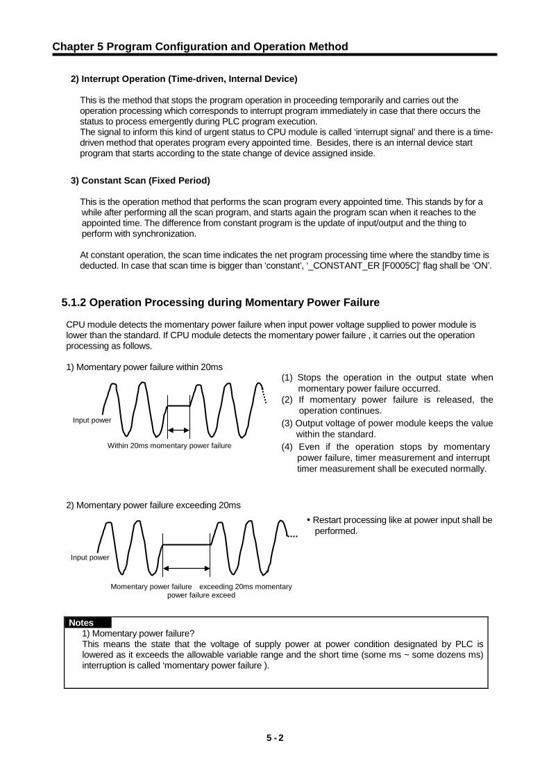
Chapter 5 Program Configuration and Operation Method
5 - 2
2) Interrupt Operation (Time-driven, Internal Device) This is the method that stops the program operation in proceeding temporarily and carries out the operation processing which corresponds to interrupt program immediately in case that there occurs the status to process emergently during PLC program execution. The signal to inform this kind of urgent status to CPU module is called ‘interrupt signal’ and there is a time-driven method that operates program every appointed time. Besides, there is an internal device start program that starts according to the state change of device assigned inside.
3) Constant Scan (Fixed Period) This is the operation method that performs the scan program every appointed time. This stands by for a while after performing all the scan program, and starts again the program scan when it reaches to the appointed time. The difference from constant program is the update of input/output and the thing to perform with synchronization. At constant operation, the scan time indicates the net program processing time where the standby time is deducted. In case that scan time is bigger than ‘constant’, ‘_CONSTANT_ER [F0005C]’ flag shall be ‘ON’.
5.1.2 Operation Processing during Momentary Power Failure CPU module detects the momentary power failure when input power voltage supplied to power module is lower than the standard. If CPU module detects the momentary power failure , it carries out the operation processing as follows. 1) Momentary power failure within 20ms 2) Momentary power failure exceeding 20ms Notes
1) Momentary power failure? This means the state that the voltage of supply power at power condition designated by PLC is lowered as it exceeds the allowable variable range and the short time (some ms ~ some dozens ms) interruption is called ‘momentary power failure ).
Input power
Within 20ms momentary power failure
(1) Stops the operation in the output state when momentary power failure occurred.
(2) If momentary power failure is released, the operation continues.
(3) Output voltage of power module keeps the value within the standard.
(4) Even if the operation stops by momentary power failure, timer measurement and interrupt timer measurement shall be executed normally.
Input power
Momentary power failure exceeding 20ms momentary power failure exceed
Restart processing like at power input shall be performed.

Chapter 5 Program Configuration and Operation Method
5 - 3
5.1.3 Scan Time The time required to complete it from the first step 0 to the next step 0 of a program, that is, a time taken for a control operation is called ‘scan time.’ It is directly related to the control performance of the system. 1) Operation and performance of XGK
Program execution time, I/O data process time and communication service time are important factors affecting the ‘scan time.’ The XGK impressively reduces scan time by means of the improved data reception performance through backplane, ladder program execution and ladder program execution by MPU and parallel execution of I/O data scan etc.
Type
Program processing time Module processing time
Ladder execution (32kstep)
System Task
Digital I/O module
(32 points, 1module)
Analog module (8 ch,
1module)
Communication module
(basic/extension) (200 byte, 1 block)
CPUSN/HN/UN 0.272 0.2
20 us 75 us 170 + 44 (200byte 1 block) CPUA,H,U 0.896 ms 0.6 ms
CPUE,S 2.688 ms 0.8 ms
2) Calculation of scan time
The CPU module executes controls along the following steps. A user can estimate the control performance of a system that the user is to structure from the following calculation.
(1) Scan time = ① Scan program process + ② System check & Task process + ③I/O data Refresh + ④ Network Service + ⑤ XG5000 Service + ⑥ User Task Program process
① Scan program process = no. of program steps created x 0.028 () [0.084 for CPUS] ② System check & Task process: 600 ~ 1.0 ms [parameter depending on the usage of auxiliary
functions] ③ I/O data Refresh [including special module]: minimum 0.06ms~0.2ms
Program Scan
① Ladder Scan Ladder Scan
BP Controller Scan
Ladder Scan
I/O Module Data Refresh
② System check & Task process
④ Network Service
③ I/O data Refresh
Network Module Data exchange
Input
Output
⑤ XG5000 service

Chapter 5 Program Configuration and Operation Method
5 - 4
④ Network Service = Service of communication module in basic base+ Service of communication
module in expansion base = (No. of Service x 3 ) + (total TRX data(byte)/4 x 0.056 [CPUS:0.112] ) + (Comm. module TRX data of basic base (byte))/4 x 0.084 + (Comm. module TRX data of expansion base (byte))/4 x 0.280 * The number of service and TRX data occurred within one scan are standard of calculation ⑤XG5000 Service process time: 100 at the max data monitor (But, in case of changing the monitor screen, scan time increases for the mean time. In case of
connected with “USB Max. Write”, 6ms. In case of connected “USB Normal Write”, 1.6ms. ⑥ Task Program process time: sum of task processing time that occurs within a scan; the time
calculation by task programs are as same as that of scan program.
(2) Example The scan time of a system consisting of CPUH (program 16kstep) + six 32-point I/O modules + six analog modules + four communication modules (200 byte 8 blocks per module)
Scan time() = ladder execution time + system processing time + digital module I/O processing
time + analog I/O processing time + communication module processing time + XG5000 Service processing time = (16000 x 0.028) + (600) + (20 x 6) + (75 x 6) + ((170 + 44 x 8) x 4) + (100) = 3806 = 3.806
2) Scan time monitor
(1) Scan time is saved into the following flag(F) areas.
F0050 : max value of scan time (unit: 0.1ms) F0051 : min value of scan time (unit: 0.1ms) F0052 : current scan time value (unit: 0.1ms)
Set the “F” devices as INT type monitoring the scan time.

Chapter 5 Program Configuration and Operation Method
5 - 5
5.2 Program Execution
5.2.1 Program Configuration The program is consisted of all function factors required to execute the specific control and saved in the built-in RM or flash memory of CPU module. These function factors are generally classified as follows.
Function factor Process description
Scan program • Processing of signal that repeats regularly every 1 scan.
Time-driven interrupt program
• The program is performed according to the fixed time interval in case that the required processing time condition is as below. In case that the faster processing than 1 scan average processing time is
required In case that the longer time interval than 1 scan average processing time is
required In case that program is processed with the appointed time interval
Subroutine program • Only when some condition is satisfied.(in case that input condition of CALL instruction is On)
5.2.2 Program Execution Method Here describes the program proceeding method that is executed when the power is applied or key switch is ‘RUN’. The program performs the operation processing according to the configuration as below.
Operation start
Scan program
END
Subroutine program
Task program
Executes only when the condition is satisfied.

Chapter 5 Program Configuration and Operation Method
5 - 6
1) Scan Program (1) Function
• This program performs the operation repeatedly from 0 step to last step in order prepared by the
program to process the signal that is repeatedly regularly every scan. • In case that the execution condition of interrupt by task interrupt or interrupt module while executing
scan program is established, stop the current program in execution and perform the related interrupt program.
2) Interrupt Program (1) Function
• This program stops the operation of scan program and then processes the related function in prior
to process the internal/external signal occurred periodically/non-periodically.
(2) Type • Task program is divided as below. (a) Time-driven task program : available to use up to 32 (b) Internal device task program : available to use up to 32
- Time-driven task program Performs the program according to the fixed time internal.
- Internal device task program Performs the corresponding program when the start condition of internal device occurs. The start condition detection of device shall be performed after processing of scan program.
PPoin 1) For further information of interrupt program, please refer to 5.2.3 Interrupt.
Notes

Chapter 5 Program Configuration and Operation Method
5 - 7
5.2.3 Interrupt For your understanding of Interrupt function, here describes program setting method of XG5000 which is an XGT programming S/W. (For further information of XG5000, please refer to XG5000 user’s manual) Scan Program
Notes When power On, all Interrupts are in the state ‘Disable’.
Interrupt 1
(Program 1) Interrupt 1 occur
Interrupt 2
(Program 2) Interrupt 2 occur
Interrupt 3 (Program 3)
Interrupt 3 occur
Interrupt 2 occur
Interrupt 2
(Program 2)
Interrupt 4 occur Interrupt 4
(Program 4)
END

Chapter 5 Program Configuration and Operation Method
5 - 8
1) How to Prepare Interrupt Program Generate the task in the project window of XG5000 as below and add the program to be performed by each task. For further information, please refer to XG5000 user’s manual.
2) Task Type Task type and function is as follows.
Type Spec Cyclic task (interval task) Internal device task (single task)
Task number 32 32
Start condition Cyclic (setting up to max. 4,294,967.295 sec. by 1ms unit)
Internal device execution condition
Detection & execution Cyclic execution per setting time Retrieve the condition and execute after completing Scan Program
Detection delay time Max. 0.2 ms delay Delay as much as max. scan time
Execution priority 2 ~ 7 level setting (2 level is highest in priority.) Same as left
Task no. Within 0~31 range without user duplication)
With 64~95 range without user duplication
3) Processing Method of Task Program Here describes common processing method and notices for Task Program. (1) Features of Task Program
Task Program is executed only when execution condition occurs without every scan repeat
processing. When preparing Task Program, please consider this point. For example, if a timer and counter were used in cyclic task program of 10 second cycle, this timer
occurs the tolerance of max. 10 seconds and the counter and the timer and as the counter checks the input status of counter per 10 seconds, the input changed within 10 seconds is not counted up.

Chapter 5 Program Configuration and Operation Method
5 - 9
(2) Execution priority
In case that several tasks to be executed are waiting, execute from the highest Task Program in
priority. When the same priority tasks are waiting, execute from the order occurred. Task priority relates to each task. The task program priority should be set considering the program features, importance and the
emergency when the execution requested.
(3) Processing delay time There are some causes for Task Program processing delay as below. Please consider this when task
setting or program preparation. Task detection delay (Refer to detailed description of each task.) Program proceeding delay caused by Priority Task Program proceeding
(4) Relationship of initialize, Scan Program and Task Program User identification task does not start while performing Initialization Task Program. As Scan Program is set as lowest priority, if task occurs, stop Scan Program and process Task
Program in advance. Accordingly, if task occurs frequently during 1 scan or concentrates intermittently, scan time may extend abnormally. Cares should be taken in case of task condition setting.
(5) Protection of Program in execution from Task Program
In case that the continuity of program execution is interrupted by high priority Task Program during
program execution, it is available to prohibit the execution of Task Program partially for the part in problem. In this case, it is available to perform the program protection by ‘ DI(Task Program Start Disabled) and ‘EI(Task Program Start Enabled)’ application instruction.
Insert ‘DI’ application instruction in the start position of the part requiring the protection and insert ‘EI’
application instruction in the position to release. Initialization Task is not influenced by ‘DI’, ‘EI’ application instruction.
4) Time Driven Task Program Processing Method Here describes the processing method in case that task (start condition) of Task Program is set as Time- driven. (1) Items to be set in Task
Set the execution cycle and priority which are the start condition of Task Program to execute. Check
the task no. to manage the task.
(2) Time-driven Task Processing Performs the corresponding Time-driven task program per setting time interval (execution cycle).
Notes 1) For further information of interrupt program, please refer to 5.2.3 Interrupt.

Chapter 5 Program Configuration and Operation Method
5 - 10
(3) Notice in using Time-driven Task Program
When Time-driven task program is in execution currently or waiting for execution, if the demand to
execute the same task program occurs, the new occurred task shall be disregarded. Timer that makes a demand to execute Time-driven task program only while operation mode is
RUN mode, shall be added. The shutdown time shall be all disregarded. When setting the execution cycle of Time-driven task program, consider the possibility that the
demand to execute several Time-driven task program at the same time occurs. If 4 Time-driven task programs that the cycle is 2sec, 4sec, 10sec and 20sec are used, 4 demands of
execution per 20 seconds shall be occurred at the same time and scan time may extend instantaneously.
You can check maximum, minimum, and current scan time of fixed cycle task with flag of fixed cycle task
. _CYCLE_TASK_SCANx_MAX : Maximum scan time of number ‘x’ Time-driven task (x=0~31) _CYCLE_TASK_SCANx_MIN : Minimum scan time of number ‘x’ Time-driven task _CYCLE_TASK_SCANx_CUR : Current scan time of number ‘x’ Time-driven task Initial value of minimum scan time flag is 16#ffff. It can verify fixed cycle task is not used, or never executed.
5) Internal Device Task Program Processing Method Here describes the processing method of Internal Device Task Program which extended the task (start condition) of Task Program from contact point to device as execution range. (1) Items to be set in Task
Set the execution condition and priority to the task being executed. Check the task no. for task
management. (2) Internal Device Task Processing
After completing the scan program execution in CPU module, if the condition of device that becomes the start condition of internal device task program is met, according to the priority, it shall be executed.
(3) Precautions in using internal Device Task Program
Accordingly, even if the execution condition of internal device task program occurs in Scan Program or Task Program (Time-driven), it shall not be executed immediately but executed at the time of completion of Scan Program. If the demand to execute Internal Device Task Program occurs, the execution condition shall be
examined at the time of completion of Scan Program. Accordingly, if the execution condition of Internal Device Task occurs by Scan Program or Task Program (Time-driven) during ‘1 scan’ and disappears, the task shall not be executed as it is not possible to detect the execution at the time of examination of execution condition.
6) Task Processing at the Momentary power failure When restarting the task as the momentary power failure time is long, disregard the task in standby and
the task issued during shutdown all and process only the task from the starting point. In the shutdown state within 20ms, the task in standby before shutdown shall be executed, after
recovering the shutdown. The cyclic task and Interrupt task that occurred in double during shutdown, shall be disregarded.

Chapter 5 Program Configuration and Operation Method
5 - 11
7) Verification of Task Program Verify the following contents after writing the Task Program. (1) Is the task setting proper ?
If task occurs frequently more than needed or several tasks occur in one scan at the same time, scan
time may lengthen or be irregular. In case not possible to change the task setting, verify max. scan time.
(2) Is the priority of task arranged well?
The low priority task program shall be delayed by the high priority task program, which results in
disabling the processing within the correct time and even task collision may occur as next task occurs in the state that the execution of previous task is delayed. Consider the emergency of task and execution time etc when setting the priority.
(3) Is the Task Program written in shortest?
If the execution time of Task Program is longer, scan time may lengthen or be irregular. Even it may
cause the collision of task program. Write the execution time as short as possible. (Especially, when writing the cyclic task program, write the execution time so that the task program can be executed within 10% cycle of the shortest task among several tasks.)
(4) Is program protection for the high priority task needed during program execution?
If other task is inserted during task program execution, complete the task in execution and operate the
standby tasks in the order of high priority. In case that it is not allowed to insert other task in Scan Program, prevent the insert partially by using ‘DI’ and ‘EI’ application instruction. The problem may occur while processing the global variables used commonly with other program or special or communication module.
8) Program Configuration and Processing Example If task and program are registered as below,
• Task registration :
T_SLOW ( cycle time : = 10ms, Priority:= 3 ) PROC_1 ( internal device: = M0, Priority := 5 )
• Program registration : Program --> P0 Program --> P0 (scan program) Program --> P1 (start by task T_SLOW) Program --> P2 (start by task PROC_1)
And program execution time and the occurrence time of interrupt signal is same as follows, • Execution time of each Program : P0 = 17ms, P1 = 2ms, P2 = 7ms • PROC_1 occur: The execution of program occurred during Scan Program is as below.

Chapter 5 Program Configuration and Operation Method
5 - 12
Process per time
Time (ms) Process 0 Scan started and scan program P0 started to execute 0~10 Program P0 executed 10~12 P1 execution demand, P0 stopped and P1 executed 17 P2 execution demand 12~20 P1 execution completed and continues the stopped P0 20~22 P1 execution demand, P0 stopped and P1 executed 22~25 P1 execution completed and the stopped P0 execution finished
25 P2 execution demand check at the completion time of Scan Program(P0), and P2 executed
25~30 Program P2 executed 30~32 P1 execution demand, P2 stopped and P1 executed 32~34 P1 execution completed and the stopped P2 execution finished 34 New scan starts (P0 starts to execute)

Chapter 5 Program Configuration and Operation Method
5 - 13
5.3 Operation Mode For operation mode of CPU module, there are 3 types such as RUN mode, STOP mode and DEBUG mode.. Here describes the operation processing of each operation mode.
5.3.1 RUN Mode This is the mode to execute Program operation normally. 1) Processing at Mode Change
At the beginning, execute initialization of data area and examine the effectiveness of program and judge the possibility of execution.
2) Operation Processing Contents Execute I/O refresh and Program operation.
(1) Detects the start condition of Interrupt Program and executes Interrupt Program. (2) Examines the normal operation or missing of built-in module. (3) Communication service and other internal processing.
RUN mode first scan start
Initialize data area
Examine Program effectiveness and judge the possibility of execution
Execute input refresh
Program execute, Interrupt Program execute
Examine the normal operation or missing of built-in module
Communication service and internal processing
Execute output refresh
Operation mode change
RUN mode keep
Change to other mode
Operation by changed operation mode

Chapter 5 Program Configuration and Operation Method
5 - 14
5.3.2 STOP Mode This is the mode in stop state without Program operation. It is available to transmit the program through XG5000 only in Remote STOP mode. 1) Processing at Mode Change
Clear the output image area and execute output refresh. 2) Operation Processing Contents
(1) Executes I/O refresh. (2) Examines the normal operation or missing of built-in module. (3) Communication service or other internal processing.
5.3.3 DEBUG Mode This is the mode to detect Program error or trace the operation process and the conversion to this mode is available only in STOP mode. This is the mode to check the program execution state and the contents of each data and verify the program. 1) Processing at Mode Change
(1) Initializes the data area at the beginning of mode change. (2) Clears the output image area and execute input refresh.
2) Operation Processing Contents
(1) Executes I/O refresh. (2) Debug operation according to setting state. (3) After finishing Debug operation by the end of Program, execute output refresh. (4) Examine the normal operation or missing of built-in module. (5) Executes communication service or other service.
3) Debug Operation Condition
There are 4 conditions for Debug operation and in case that it reaches break point, it is available to set other type of break point.
Operation condition Description
Execute by one operation unit (step over) With operation instruction, it executes one operation unit and then stops.
Execute according to Break Point If break point is assigned in Program, it stops at the assigned break point.
Execute according to the state of contact point
If the contact area desired to watch and the state (Read, Write, Value) desired to stop are assigned, it stops when the assigned operation occurs at the assigned contact point.
Execute according to scan times
If scan times to operate are assigned, it operates as much as the assigned scan times and stops.
4) Operation Method
(1) After setting Debug operation condition at XG5000, execute the operation. (2) Interrupt Program is available to set whether or not to operate (Enable/Disable) by each Interrupt unit.
(For further information, please refer to Chapter 9 Debugging, XG5000 user’s manual.)

Chapter 5 Program Configuration and Operation Method
5 - 15
5.3.4 Changing Operation Mode 1) Operation Mode Change Method
The method to change operation mode are as follows. (1) By mode key of CPU module (2) By connecting the programming tool (XG5000) to communication port of CPU (3) By changing the operation mode of other CPU module connected to network by XG5000 connected to
communication port of CPU (4) By using XG5000, HMI, computer link module connected to network (5) By ‘STOP‘ instruction during program execution
2) Type of Operation Mode The operation mode setting is as follows.
Operation mode switch
Remote enabled switch
XG5000 instruction Operation mode
RUN X X Run
STOP ON
RUN Remote Run STOP Remote Stop Debug Debug Run
OFF Mode change execute Previous operation mode
RUN -> STOP X - Stop (1) Remote mode conversion is available only in the state of ‘Remote Enabled: On’, ‘Mode switch: Stop’. (2) In case of changing the Remote ‘RUN’ mode to ‘STOP’ by switch, operate the switch as follows.
(STOP) RUN STOP .
Notes 1) In case of changing Remote RUN mode to RUN mode by switch, PLC operation continues
the operation without interruption.
2) It is available to modify during RUN in RUN mode by switch but the mode change operation by XG5000 is limited. This should be set only in case that remote mode change is not allowed.

Chapter 5 Program Configuration and Operation Method
5 - 16
5.4 Memory There are two types of memory in CPU module that the user can use. One is Program Memory that saves the user program written by the user to build the system, and the other is Data Memory that provides the device area to save the data during operation.
5.4.1 Program Memory The configuration of user program memory is as below.
Items Memory Capacity (Kbyte) CPUUN CPUHN CPUSN CPUU CPUH CPUA CPUS CPUE
Parameter Setting area : • Basic parameter area • I/O parameter area • Special module parameter area • Communication module parameter area • User Event parameter area • Data Trace parameter area
320 320 320 320 320
Program Save area • Scan Program area 1 • Scan Program area 2 • Variable/Explanation sentence area
2,320 1,288 772 704 352
System area • User Event Data area • Data Trace Data area • System Log area • Device Backup area
2,552 2,040 1,656 896 896
Execution Program area • Execution Program area1 • Execution Program area2 • System Program area
4,096 2.048 1,024 2,048 1,024 512 512 256
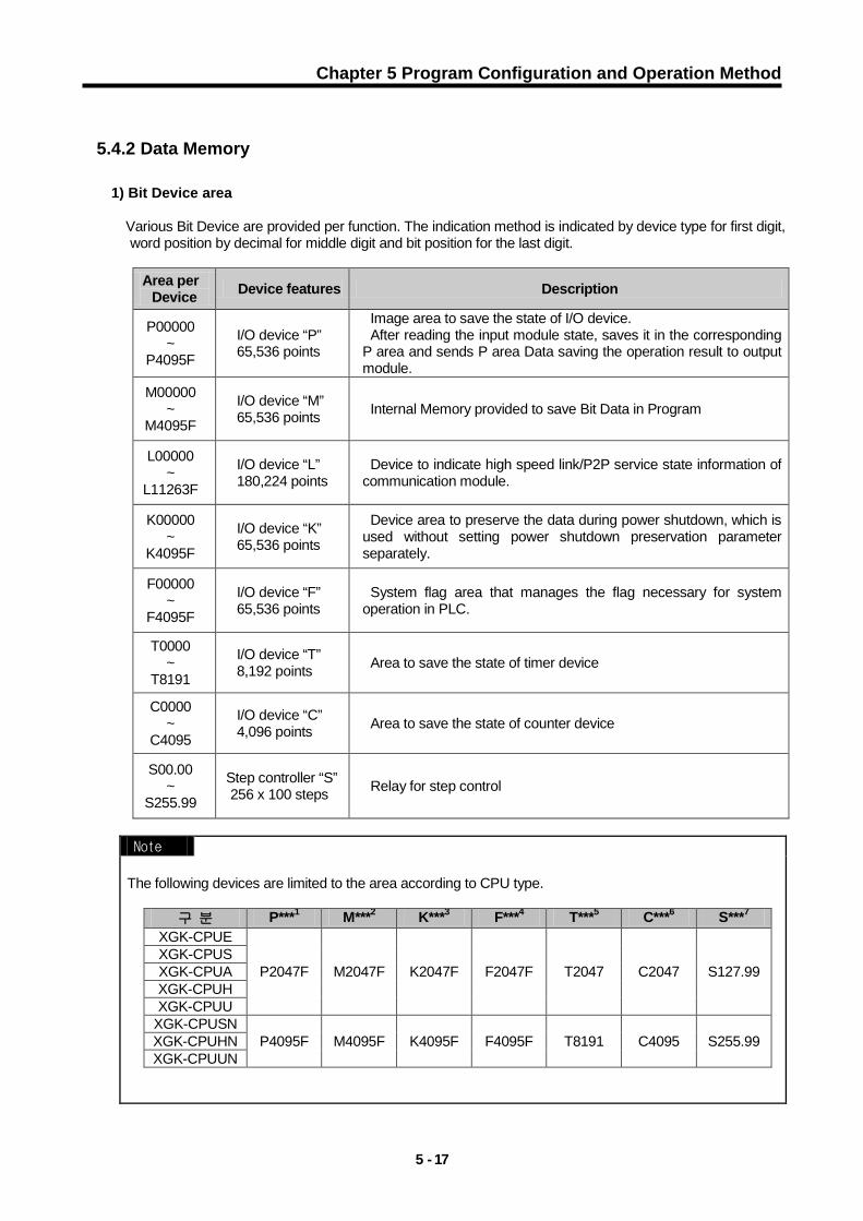
Chapter 5 Program Configuration and Operation Method
5 - 17
5.4.2 Data Memory
1) Bit Device area Various Bit Device are provided per function. The indication method is indicated by device type for first digit, word position by decimal for middle digit and bit position for the last digit.
Area per
Device Device features Description
P00000 ~
P4095F
I/O device “P” 65,536 points
Image area to save the state of I/O device. After reading the input module state, saves it in the corresponding
P area and sends P area Data saving the operation result to output module.
M00000 ~
M4095F
I/O device “M” 65,536 points Internal Memory provided to save Bit Data in Program
L00000 ~
L11263F
I/O device “L” 180,224 points
Device to indicate high speed link/P2P service state information of communication module.
K00000 ~
K4095F
I/O device “K” 65,536 points
Device area to preserve the data during power shutdown, which is used without setting power shutdown preservation parameter separately.
F00000 ~
F4095F
I/O device “F” 65,536 points
System flag area that manages the flag necessary for system operation in PLC.
T0000 ~
T8191
I/O device “T” 8,192 points Area to save the state of timer device
C0000 ~
C4095
I/O device “C” 4,096 points Area to save the state of counter device
S00.00 ~
S255.99
Step controller “S” 256 x 100 steps Relay for step control
Note
The following devices are limited to the area according to CPU type.
구 분 P***1 M***2 K***3 F***4 T***5 C***6 S***7 XGK-CPUE
P2047F M2047F K2047F F2047F T2047 C2047 S127.99 XGK-CPUS XGK-CPUA XGK-CPUH XGK-CPUU
XGK-CPUSN P4095F M4095F K4095F F4095F T8191 C4095 S255.99 XGK-CPUHN
XGK-CPUUN

Chapter 5 Program Configuration and Operation Method
5 - 18
2) Word Device area
Area per Device Device features Description
D00000 ~
D524287 ***1
Data Register “D” 524,288 words
Area to preserve the internal data. Bit expression possible.
R00000 ~
R32767
File Register “R” 32,768 words
Dedicated device to access Flash Memory. Consisted of 1,2,8,16 banks depending on the CPU Types Bit expression possible
U00.00 ~
U7F.31 ***2
Analog Data Register “U” 4,096 words
Register used to read data from special module installed in the slot. Bit expression possible
N00000 ~
N21503
Communication Data
Register “N” 21,504 words
P2P Service Save area of communication module. Bit expression impossible
Z000 ~
Z255
Index Register “Z” 256 words
Dedicated device to use Index function Bit expression impossible
T0000 ~ T8191
Timer Current Value Register “T”
8192 words Area to indicate the current value of timer
C0000 ~ C4095
Counter Current Value Register “C” 4096 words
Area to indicate the current value of counter
Notes The following devices are limited to the area according to CPU type.
구 분 D***1 U***2 Z***3 T***4 C***5 XGK-CPUE D19999 U1F.31
Z127 T2047 C2047 XGK-CPUS U3F.31 XGK-CPUA
D32767 U3F.31
XGK-CPUH U7F.31 XGK-CPUU XGK-CPUSN D262143 U3F.31
Z255 T8191 C4095 XGK-CPUHN D524287 U7F.31 XGK-CPUUN

Chapter 5 Program Configuration and Operation Method
5 - 19
5.5 Configuration Diagram of Data Memory
5.5.1 XGK-CPUE
P2047 M0000
Bit Data area
Word Data area
User Program area
I/O Relay (32768 points)
“P”
Auxiliary Relay
(180224 points) “L”
Keep Relay
(32768 points)
“K”
Special Relay
(32768 points)
“F”
Auxiliary Relay
(32768 points)
“M”
P0000
L00000
M2047
K0000
K2047
F0000
F2047
Data Register
(20000 word)
“D”
D00000
D19999
Timer setting value (2048 words)
T0000
T2047
T0000 Timer current value (2048 words)
T2047
C0000
C2047
C0000
C2047
Parameter area
User Program area
(16K step)
Timer (2048 points)
“T”
Comm. Data Register
(N21504 words)
“N”
T0000
N00000
N21503
Step Controller (128 x 100 step) S00.00~S127.99 “S”
S00
S127
0 ~ F 0000 ~ FFFF
Counter (2048 points)
“C”
C0000
C2047
File Register (32K word * 1 bank)
“R”
R00000
R32767
Counter setting value (2048 words)
Counter current value (2048 words)
Index Register
(128 words)
U1F.31
Z127 “Z”
Analog Data Register
(1024 words)
“U”
U00.00
Z000
L11263
T2047

Chapter 5 Program Configuration and Operation Method
5 - 20
5.5.2 XGK-CPUS
Bit Data area Word Data area User Program area
I/O Relay (32768 points)
“P”
Auxiliary Relay
(180224 points) “L”
Keep Relay
(32768 points) “K”
Special Relay
(32768 points) “F”
Auxiliary Relay
(32768 points) “M”
P0000
P2047 M0000
L00000
M2047
K0000
K2047
F0000
F2047
Data Register
(20000 word)
“D”
D00000
D19999
Timer setting value (2048 words)
T0000
T2047
T0000 Timer current value (2048 words)
T2047
C0000
C2047
C0000
C2047
Parameter area
User Program area
(32K step)
Timer (2048 points)
“T”
Comm. Data Register
(N21504 words) “N”
T0000
N00000
N21503
Step Controller (128x100 step) S00.00~S127.99 “S”
S00
S127
0 ~ F 0000 ~ FFFF
Counter (2048 points)
“C”
C0000
C2047
File Register (32K word * 1 bank)
“R”
R00000
R32767
Counter setting value (2048 words)
Counter current value (2048 words)
Index Register
(128 words)
U3F.31
Z127 “Z”
Analog Data Register (2048 words)
“U”
U00.00
Z000
L11263
T2047

Chapter 5 Program Configuration and Operation Method
5 - 21
5.5.3 XGK-CPUA
Bit Data area Word Data area User Program area
I/O Relay (32768 points)
“P”
Auxiliary Relay
(180224 points) “L”
Keep Relay
(32768 points) “K”
Special Relay
(32768 points) “F”
Auxiliary Relay
(32768 points) “M”
P0000
P2047 M0000
L00000
M2047
K0000
K2047
F0000
F2047
Data Register
(32768 word)
“D”
D00000
D32767
Timer setting value (2048 words)
T0000
T2047
T0000 Timer current value (2048 words)
T2047
C0000
C2047
C0000
C2047
Parameter area
User Program area
(32K step)
Timer (2048 points)
“T”
Comm. Data Register
(N21504 words) “N”
T0000
N00000
N21503
Step Controller (128x100 step) S00.00~S127.99 “S”
S00
S127
0 ~ F 0000 ~ FFFF
Counter (2048 points)
“C”
C0000
C2047
File Register (32K word * 2bank)
“R”
R00000
R32767
Counter setting value (2048 words)
Counter current value (2048 words)
Index Register
(128 words)
U3F.31
Z127 “Z”
Analog Data Register (2048 words)
“U”
U00.00
Z000
L11263
T2047

Chapter 5 Program Configuration and Operation Method
5 - 22
5.5.4 XGK-CPUH
P2047 M0000
L11263
Bit Data area Word Data area User Program area
I/O Relay (32768 points)
“P”
Auxiliary Relay (180224points)
“L”
Keep Relay
(32768 points) “K”
Special Relay (32768 points)
“F”
Auxiliary Relay (32768 points)
“M”
P0000
L00000
M2047
K0000
K2047
F0000
F2047
Data Register
(32768 words) “D”
D00000
D32767
Timer setting value (2048 words)
T0000
T2047
T0000 Timer current value (2048 words)
T2047
C0000
C2047
C0000
C2047
Parameter area
User Program area
(64K step)
Timer (2048 points)
“T”
Comm. Data Register (N21504 words)
“N”
T0000
N00000
N21503
Step Controller (128x100 step) S00.00~S127.99 “S”
S00
S127
0 ~ F 0000 ~ FFFF
Counter (2048 points)
“C”
C0000
C2047
File Register
(32K words * 2bank)
“R”
R00000
R32767
Counter setting value (2048 words)
Counter current value (2048 words)
Index Register
(128 words)
U7F.31
Z127 “Z”
Analog Data Register (4096 words)
“U”
U00.00
Z000
T2047

Chapter 5 Program Configuration and Operation Method
5 - 23
5.5.5 XGK-CPUU
Bit Data area
Word Data area
User Program area
I/O Relay
(32768 points) “P”
Auxiliary Relay
(180224points) “L”
Keep Relay
(32768 points) “K”
Special Relay
(32768 points) “F”
Auxiliary Relay
(32768 points) “M”
P0000
P2047 M0000
L00000
M2047
K0000
K2047
F0000
F2047
Data Register
(32768 words) “D”
D00000
D19999
Timer setting value
(2048 words)
T0000
T2047
T0000
Timer current value
(2048 words)
T2047
C0000
C2047
C0000
C2047
Parameter area
User Program area
(128k step)
Timer
(2048 points) “T”
Comm. Data Register
(N21504 words) “N”
T0000
N00000
N21503
Step Controller (128 x 100 step) S00.00~S127.99 “S”
S00
S127
0 ~ F
0000 ~ FFFF
Counter
(2048 points) “C”
C0000
C2047
File Register (32k words * 2Bank)
“R”
R00000
R32767
Counter setting value
(2048 words)
Counter current value
(2048 words)
Index Register
(128 words)
U7F.31
Z127
“Z”
Analog Data
Register
(4096 words)
“U”
U00.00
Z000
L11263
T2047

Chapter 5 Program Configuration and Operation Method
5 - 24
5.5.6 XGK-CPUSN
P4095 M0000
Bit Data area
Word Data area
User Program area
I/O Relay
(65536 points) “P”
Auxiliary Relay
(180224points) “L”
Keep Relay
(65536 points) “K”
Special Relay
(65536 points) “F”
Auxiliary Relay
(65536 points) “M”
P0000
L00000
M4095
K0000
K4095
F0000
F4095
Data Register
(262143 words) “D”
D00000
D19999
Timer setting value
(8192 words)
T0000
T8191
T0000
Timer current value
(8192 words)
T8191
C0000
C4095
C0000
C4095
Parameter area
User Program area
(64k step)
Timer
(8192 points) “T”
Comm. Data Register
(N21504 words) “N”
T0000
N00000
N21503
Step Controller (256 x 100 step) S00.00~S255.99 “S”
S00
S255
0 ~ F
0000 ~ FFFF
Counter
(4096 points) “C”
C0000
C4095
File Register (32k words * 2Bank)
“R”
R00000
R32767
Counter setting value
(4096 words)
Counter current value
(4096 words)
Index Register
(256 words)
U3F.31
Z255
“Z”
Analog Data
Register
(2048 words)
“U”
U00.00
Z000
L11263
T8191

Chapter 5 Program Configuration and Operation Method
5 - 25
5.5.6 XGK-CPUHN
P4095 M0000
Bit Data area
Word Data area
User Program area
I/O Relay
(65536 points) “P”
Auxiliary Relay
(180224points) “L”
Keep Relay
(65536 points) “K”
Special Relay
(65536 points) “F”
Auxiliary Relay
(65536 points) “M”
P0000
L00000
M4095
K0000
K4095
F0000
F4095
Data Register
(524287 words) “D”
D00000
D524287
Timer setting value
(8192 words)
T0000
T8191
T0000
Timer current value
(8192 words)
T8191
C0000
C4095
C0000
C4095
Parameter area
User Program area
(128k step)
Timer
(8192 points) “T”
Comm. Data Register
(N21504 words) “N”
T0000
N00000
N21503
Step Controller (256 x 100 step) S00.00~S255.99 “S”
S00
S255
0 ~ F
0000 ~ FFFF
Counter
(4096 points) “C”
C0000
C4095
File Register (32k words * 8Bank)
“R”
R00000
R32767
Counter setting value
(4096 words)
Counter current value
(4096 words)
Index Register
(256 words)
U7F.31
Z255
“Z”
Analog Data
Register
(4096 words)
“U”
U00.00
Z000
L11263
T8191
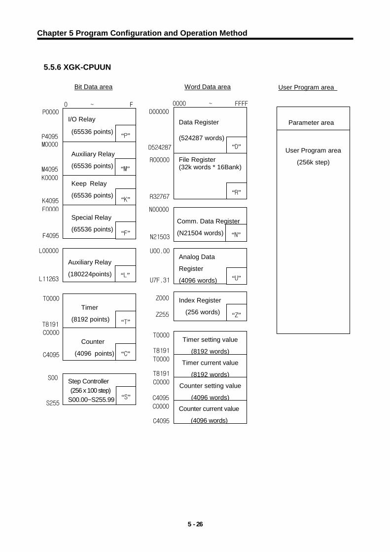
Chapter 5 Program Configuration and Operation Method
5 - 26
5.5.6 XGK-CPUUN
P4095 M0000
Bit Data area
Word Data area
User Program area
I/O Relay
(65536 points) “P”
Auxiliary Relay
(180224points) “L”
Keep Relay
(65536 points) “K”
Special Relay
(65536 points) “F”
Auxiliary Relay
(65536 points) “M”
P0000
L00000
M4095
K0000
K4095
F0000
F4095
Data Register
(524287 words) “D”
D00000
D524287
Timer setting value
(8192 words)
T0000
T8191
T0000
Timer current value
(8192 words)
T8191
C0000
C4095
C0000
C4095
Parameter area
User Program area
(256k step)
Timer
(8192 points) “T”
Comm. Data Register
(N21504 words) “N”
T0000
N00000
N21503
Step Controller (256 x 100 step) S00.00~S255.99 “S”
S00
S255
0 ~ F
0000 ~ FFFF
Counter
(4096 points) “C”
C0000
C4095
File Register (32k words * 16Bank)
“R”
R00000
R32767
Counter setting value
(4096 words)
Counter current value
(4096 words)
Index Register
(256 words)
U7F.31
Z255
“Z”
Analog Data
Register
(4096 words)
“U”
U00.00
Z000
L11263
T8191
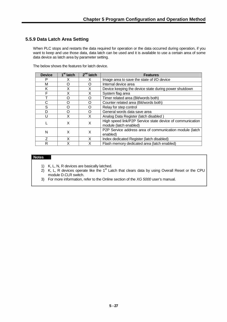
Chapter 5 Program Configuration and Operation Method
5 - 27
5.5.9 Data Latch Area Setting
When PLC stops and restarts the data required for operation or the data occurred during operation, if you want to keep and use those data, data latch can be used and it is available to use a certain area of some data device as latch area by parameter setting. The below shows the features for latch device.
Device 1st latch 2nd latch Features P X X Image area to save the state of I/O device M O O Internal device area K X X Device keeping the device state during power shutdown F X X System flag area T O O Timer related area (Bit/words both) C O O Counter related area (Bit/words both) S O O Relay for step control D O O General words data save area U X X Analog Data Register (latch disabled )
L X X High speed link/P2P Service state device of communication module (latch enabled)
N X X P2P Service address area of communication module (latch enabled)
Z X X Index dedicated Register (latch disabled) R X X Flash memory dedicated area (latch enabled)
Notes
1) K, L, N, R devices are basically latched. 2) K, L, R devices operate like the 1st Latch that clears data by using Overall Reset or the CPU
module D.CLR switch. 3) For more information, refer to the Online section of the XG 5000 user’s manual.

Chapter 5 Program Configuration and Operation Method
5 - 28
4) Data Latch Area Operation
The method to delete the latched data is as below. - D.CLR switch operation of CPU module - latch 1, latch 2 clear operation by XG5000 - write by Program (initialization program recommended) - write ‘0’ FILL from XG5000 monitor mode.
D.CLR Clear does not operate in RUN mode. Convert to STOP mode to operate. Also when clearing by D.CLR switch, bear in mind that general area shall be initialized.
When operating D.CLR momentarily, latch 1 area only shall be removed. If keeping D.CLR for 3 seconds, 6 LEDs shall be blinked and at this time, if returning the switch, even latch 2 area shall be cleared.
For keep or reset (clear) operation of latch area data according to PLC operation, please refer to the below table.
No. Classification Detailed operation Latch 1 Latch 2 Remarks
1 Power change Off/On Keep Keep -
2 Reset switch Reset Keep Keep -
Overall reset Reset Keep -
3 D.CLR switch Clear Latch 1 Reset Keep -
Clear Latch 2 Reset Reset -
4 Program write (online) - Keep Keep -
5 Data broken SRAM broken by battery error Reset Reset - Data broken by other reason Reset Reset -
6 XG5000 online Clear Latch 1 Reset Keep - Clear Latch 2 Reset Reset -
5) Data Initialization
In case of Memory Delete state, the memory of all device shall be cleared as ‘0’. In case of giving the data value at the beginning according to system, please use the initialization task.

Chapter 6 Function of CPU Module
6 - 1
Chapter 6 Functions of CPU Module
6.1 Self-diagnosis (1) Self-diagnosis function means the function that CPU module diagnoses the error of PLC system itself. (2) If the power of PLC system is applied or the error occurs during operation, it detects the error and prevents
the abnormal operation.
6.1.1 Scan Watchdog Timer WDT (Watchdog Timer) is the function to detect the program congestion by the error of hardware and software of PLC CPU module.
1) WDT is the timer used to detect the operation delay by user program error. The detection time of WDT is set in Basic parameter of XG5000. 2) If WDT detects the excess of detection setting time while watching the elapsed time of scan during operation, it stops the operation of PLC immediately and makes the output all off. 3) If the excess of Scan Watchdog Time is expected in the program processing of specific part while performing the user program (FOR ~ NEXT instruction, CALL instruction), clear the timer by using ‘WDT’ instruction. ‘WDT’ instruction initializes the elapsed time of Scan Watchdog Timer and starts the time measurement from 0 again. (For further information of WDT instruction, please refer to Instruction.) 4) To clear the error state of watchdog, we can use the following method : power re-supply, manipulation of manual reset switch, mode conversion to STOP mode.
Notes 1) The setting range of Watchdog Timer is 10 ~ 1000ms (1ms unit).
0 1 2 3 ….. …8 9
SCAN END WDT Reset WDT instruction
execution
0 1 2 … WDT count(ms) 0 1 2 … …6 7
SCAN END
0 1 2 …

Chapter 6 Function of CPU Module
6 - 2
6.1.2 I/O Module Check Function This function is to check the error state of I/O module at the time of start or during operation.
1) In case that the module different from parameter setting is built-in at the time of start or it occurs the error or
2) In case I/O module is removed or occurs the error during operation,
the error state is detected and warning lamp (ERR) in front of CPU module and then CPU stops to operate.
6.1.3 Battery Voltage Check Function If battery voltage falls less than memory backup voltage, CPU module detects it and informs of it. The warning lamp(BAT) in front of CPU module shall be ON. For further information, please refer to “4.3.3 Durability of Battery”.
6.1.4 Error History Save Function CPU module has the function that records the error history and analyzes the cause of the error to take a proper action if the error occurs. (Refer to 6.6.1 Error History) This is the function to save each error code in special relay F0006.
Notes All results of self-diagnosis shall be recorded in ‘F’ device area. For further information of self-diagnosis comments and error actions, please refer to Chapter 12 Trouble shooting, 12.5 Error Code List.
6.1.5 Troubleshooting
1) Classification of Error The error occurs by PLC itself error, error in system configuration or error detection from operation results. The error is classified by heavy error mode that stops the operation for the system safety and light error mode that informs of the error occurrence warning to the user and continues the operation. The error causes of PLC system is as follows.
PLC hardware error Error in system configuration Operation error during user program proceeding Error detection by external device failure
2) Action Mode in case that Error Occurs If error occurs, PLC system records the error comments in flag and stops to operate or continues the operation according to error mode.

Chapter 6 Function of CPU Module
6 - 3
(1) PLC hardware error
In case of heavy error that the normal operation of PLC such as CPU module, power module is disabled, the system ‘stop’s and in case of light error such as battery error, it continues to operate.
(2) Error in system configuration
This error occurs when hardware configuration of PLC is different from the configuration identified in software, and the system stops.
(3) Operation Error during User Program Proceeding This is the error occurred during user program proceeding and in case of numeric operation error, it is indicated in the error flag and the system continues to operate. While performing the operation, if the operation time exceeds the scan watchdog time or the built-in I/O module can not be controlled normally, the system stops.
Notes 1) The operation process is determined by selecting ‘Basic Parameters → Error Operation
Setup → Continue running when an arithmetic error occurs’. 2) The default is set to ‘Continue running when an arithmetic error occurs’.
(4) Error detection by external device error
This is to detect the error of external control device by PLC user program. In case of heavy error, the system stops but in case of light error, the system indicates the error state only and continues to operate.
Notes
1) If the error occurs, the error codes are saved in special relay F1026. 2) The error code is saved in F1027 when a soft-fault is detected. 3) For further information on the Flag, please refer to Appendix 1 Flag List.

Chapter 6 Function of CPU Module
6 - 4
6.2 Clock CPU module has a built-in clock device (RTC). RTC continues the clock action by battery backup even in case of power off or instantaneous interruption. It is available to perform the time management such as operation history or failure history of system by using a clock data of RTC. The current time of RTC can be updated in F device related to the clock every scan.
1) Read and Setting from XG5000 Click ‘PLC RTC’ from ‘PLC information’ of online mode.
The time of PLC RTC is displayed. If the time of PLC RTC is wrong, you can adjust the time correct by setting the time directly to transmit to PLC or selecting ‘Synchronize with PC clock’ that transmits the time of PC connected to PLC.
2) RTC Read by Device It is available to monitor RTC by special device as shown on the table below.
RTC Read F device Data example Description
_MON_YEAR (F0053) h0599 May xx99
_TIME_DAY (F0054) h1512 12(day), 15 (time)
_SEC_MIN (F0055) h4142 42min 41sec
_HUND_WK (F0056) h2001 Monday 20xx RTC Data of _TIME_DAY_DT is displayed by 24hours system.

Chapter 6 Function of CPU Module
6 - 5
3) RTC Data Modification by Program It is available for the user to set the RTC value by program. This function is used when setting the time manually through external Digit switch or making the system that corrects the time periodically through network. ‘DATEWR’ instruction is to insert the setting value in the F area device below and write the time to RTC at scan END.
RTC write F device Comments Setting range
_MON_YEAR_DT (F1034) Month/Year 1984 ~ 2163 Year, Jan.~ Dec. _TIME_DAY_DT (F1035) Time/Day 1~31 Days, 0~23 Hour _SEC_MIN_DT (F1036) Second/Minute 0~59 minute, 0~59 second _HUND_WK_DT (F1037) 100years/Weekday 0 ~ 6
It is available to write the data to RTC without using a instruction, by writing the RTC data to the above area and making ‘_RTC_WR (F10240)’ to be ‘On’.
• In case that time data does not match with the form, the value is not allowed to write. (But if the week does not match, it shall be set as it is without error detection.)
• Monitor the RTC read device after writing RTC data, and check if it is modified correctly.
4) Weekday Expression Method
No. 0 1 2 3 4 5 6 Day Sunday Monday Tuesday Wednesday Thursday Friday Saturday
5) Time Tolerance RTC tolerance depends on ambient temperature. Time tolerance according to temperature per day was indicated on the table as below.
Operation temperature
Max. tolerance (second/day)
Normal case (second/day)
0 °C - 4.67 ~ 1.38 -1.46 25 °C - 1.64 ~ 2.42 0.43 55 °C - 5.79 ~ 0.78 -2.29
1) RTC may not have the clock data written at first. 2) When using a CPU module, you must set the clock data correctly at first. 3) In case that the data out of range of clock data is written in RTC, it may not work normally.
Ex) 14Month 32Day 25Hour 4) RTC may stop or occur error because of battery error. If new clock data is written in RTC, the
error shall be cleared. 5) For more information about the time date modification by program, refer to the XGK
Instructions user’s manual.
Note

Chapter 6 Function of CPU Module
6 - 6
6.3 Remote Function CPU module enables to change the operation by communication except key switch mounted in the module. If you want to operate it by Remote, you should set ‘REM enable’ switch (4-pin deep) of CPU module as ‘ON’ position and ‘RUN/STOP’ switch as ‘STOP’ position.
1) Type of Remote Operation (1) Operated by connecting XG5000 through USB or RS-232 port mounted in CPU module. (2) Available to operate other PLC connected to the network of PLC in the state that XG5000 is connected to CPU module. (3) Controls the operation state of PLC by MMI software through dedicated communication
2) Remote RUN/STOP (1) Remote RUN/STOP performs RUN/STOP when the deep switch of the CPU module is in the REMOTE position and the RUN/STOP switch is in the STOP position. (2) Convenient function in case that CPU module is installed in the position difficult to operate or CPU module inside control panel is controlled by RUN/STOP from outside.
3) Remote DEBUG (1) Remote DEBUG is the function to perform DEBUG operation in the state that Deep switch of CPU module is in REMOTE position and the RUN/STOP switch is in the STOP position. DEBUG operation means the function performed according to the operation condition assigned for program operation. (2) Convenient function in case of checking the execution state of program or the contents of each data from Debugging work
4) Remote Reset (1) Remote Reset is the function to reset a CPU module by remote operation in case that the error occurs in the place not possible to operate a CPU module. (2) This supports ‘Reset’ and “Overall Reset’ as like an operation by switch.
Notes 1) For operation method of Remote Function, please refer to ‘Online’ part from XG5000 user’s manual.
5) Flash memory operation of PLC
(1) When PLC operation mode Changes to Run, it executes Run operation after copying the program in the flash memory to the program memory. In other words, it runs PLC through the program in the flash memory. (PLC operation in Run mode: it means that the operation mode changes from Stop to Run, and that the operation mode is Run when PLC is powered back on)

Chapter 6 Function of CPU Module
6 - 7
(2) Flash memory operation mode setting Online Set Flash Memory Check the ‘Enable flash memory operation mode’ Click OK
Notes
1) Initial mode is Disable flash memory run mode 2) Set Enable flash memory run mode at once, it keeps the mode On until the PADT is Off
3) Change of the flash memory operation mode is available regardless of RUN/STOP Mode 4) Make sure that the program write to the flash memory completely when you try ‘modification during run’ in flash memory operation mode. If it can’t be written completely, the program you write before will be carried out. 5) When you set the flash memory operation mode, it is necessary that flash memory programming Is completed, the flash memory operation mode is applied. If you restart the PLC before program writing is completed, "flash memory operation mode" will be canceled.

Chapter 6 Function of CPU Module
6 - 8
(3) Flash memory operation method
If you want to change the restart or operation mode the PLC system to RUN, depending on the setting
of the flash operation mode, it works as follows. Set of flash memory operation m
ode Operation contents
ON
Or different contents of the flash memory and program memory, if the contents of the reasons the program memory such as a decrease in the battery voltage is damaged, then operation after downloading the program stored in the flash memory to program memory.
OFF CPU runs at a program that is recognized as programmed into the flash memory does not exist are stored in on-chip RAM.
(4) The saving data in flash memory mode
CPU Mode Saving data
Run Local Ethernet Parameter Communication Parameter
Stop
Program Basic Parameter Local Ethernet Parameter Communication Parameter Special module Parameter Auto Variable Comments
Modification During Run
Program Auto Variable Comments

Chapter 6 Function of CPU Module
6 - 9
6.4 Forced I/O On/Off Function Forced I/O function is used to force I/O area ON/OFF regardless of the result of program execution.
6.4.1 Forced I/O Setup Method Click ‘Forced I/O setup’ in online mode.
To set Forced I/O, select the proper flag and data check box of P device. To set the value “1”, select the correspond bit data and flag. To set the value “0”, select the flag only not bit data. The setting is applied when forced input or output is enabled. For further information of setting method, please refer to the XG5000 user’s manual.
Notes 1) The Forced I/O setting is only available for the local I/O module. 2) It is not available for the remote I/O module (Smart I/O module). 3) The PS LED is turned On if Forced I/O is selected.

Chapter 6 Function of CPU Module
6 - 10
6.4.2 Forced On/Off Execution Point and Execution Method (1) Forced Input
Input replaces the data of contact point set as forced On/Off from the data read in input module at the time of input refresh with the forced setting data and updates the input image area. Therefore, the user program operates with actual input data while the forced setting area operates with forced setting data.
(2) Forced Output Output replaces the data of contact point set as forced On/Off from the data of output image area having the operation result, at the time of output refresh after completion of user program operation execution, with the forced setting data and makes prints in output module. In case of output other than input, the data of output image area does not change by forced On/Off setting.
(3) Notices in using forced I/O function It operates from the point setting ‘enable’ of each input/output, after setting the forced data. It is available to set the forced input even if actual I/O module is not built-in. Even if there are power Off -> On, change of operation mode or operation by reset key, On/Off setting data
set in before is kept in CPU module. Forced I/O data shall not be cleared even in Stop mode. If you want to set the new data from the beginning, clear all settings by using ‘Delete all’ before using.
6.5 Direct I/O Operation By making Refresh for I/O contact point with using ‘IORF’ instruction, it enables to read the state of input contact point directly during program execution and use it for operation, and also this is used when printing out the result of operation directly in output contact point.
Notes
1) For further information of IORF instructions, please refer to XGK Instruction manual. 2) If IORF instruction is used, the value is applied immediately, and it is used prior to Forced I/O.

Chapter 6 Function of CPU Module
6 - 11
6.6 Saving Operation History For operation history, there are 4 types such as error history, mode conversion history, power shutdown history and system history. The time, numbers and operation contents that each event occurred, are saved in the memory and is monitored conveniently through XG5000. Operation history is kept saving in PLC unless it is deleted by XG5000 etc.
6.6.1 Error History
This saves the error history occurred during operation. • Saves the error code, date, time, error detailed contents etc. • Saves up to max. 2048 • Automatic release in case that memory backup is broken by battery voltage falling etc.
6.6.2 Mode Conversion History
This saves the changed mode information and time in case of operation mode change. • Saves the date, time, mode conversion contents • Saves up to max. 1024
6.6.3 Power Shutdown History
This saves the time that the power is ON or OFF with ON/OFF information. • Saves ON/OFF information, date, time • Saves up to max. 1024
6.6.4 System History
This saves the operation history of system occurred during operation. • Saves the date, time and operation change contents • XG5000 operation information, key switch change information • Saves up to max. 2048

Chapter 6 Function of CPU Module
6 - 12
Notes
1) The saved information will not be deleted before selecting the menu from XG5000 to delete. 2) If the index number saved is over 100, select Read All to check previous history.

Chapter 6 Function of CPU Module
6 - 13
6.7 External Device Error Diagnosis This is the flag provided so that the user can detect the error of external device and realize the stop and warning of system easily. By using this flag, it enables to indicate the error of external device without preparing the complicated program and monitor the error position without special device (XG5000) or source program. 1) Detection and classification of external device error
(1) The error of external device is detected by the user program and classified by heavy error that needs to stop the PLC operation and light error (warning) that continues the PLC operation and only indicates the error state, according to the contents of detected error. (2) For heavy error, ‘_ANC_ERR flag’ is used and for light error, ‘_ANC_WAR flag’ is used.
2) Treatment of heavy error of external device (1) In case that heavy error of external device is detected in the user program, classify the type of error defined by the user and write the value except ‘0’ in the system flag ‘_ANC_ERR’, and set system flag ‘_CHK_ANC_ERR’. System representative error flag ‘_ANNUN_ER’ of ‘_CNF_ER’ is set, PLC shall shut off all output module and becomes the error state same as PLC own error detection. (2) If the error occurs, the user can find the cause of error by using a XG5000 or by monitoring ‘_ANC_ERR flag’. (3 It is available to write the error code assigned temporarily by the user at _ANC_ERR and the available numbers are from 1 to 65,535.
Example
3) Treatment of light error of external device (1) In case that heavy error is detected in the user program, classify the type of error defined by the user and write the value except ‘0’ in the system flag ‘_ANC_WAR’, and set system flag ‘_CHK_ANC_WAR’. Then, system representative error flag ‘_ANNUN_WAR’ of ‘_CNF_WAR’ is set and light error code of external device is saved at _ANC_WAR. (2) If the error occurs, the user can find the cause of error by monitoring ‘_ANC_WAR’ flag directly. (3) If the light error of external device is released, ‘_ANC_WAR’ will be released after user program is executed and system flag ‘_ANNUN_WAR” of ‘_CNF_WAR’ will be reset.

Chapter 6 Function of CPU Module
6 - 14
Example
If P10003 is on, inputs ‘100’ at ‘_ANC_WAR’ and sets system flag ‘_CHK_ANC_WAR’. And ‘_ANNUM_WAR’ is set and stops PLC.

Chapter 6 Function of CPU Module
6 - 15
6.8 Fault Mask 1) Purpose and Operation Overview
• Fault Mask is the function to continue the program execution even if the module error occurs during operation. The module assigned as Fault Mask shall be operated normally before error occurs. • If the error occurs in the module where the Fault Mask is set, the corresponding module stops the operation but the whole system continues the operation. • If the module error occurs during operation, CPU module will set the error flag and the front “PS LED” shall be “ON”. If connecting XG5000, you can see the error state.
2) Fault Mask Setting Method • The Fault Mask Setting is available on the online menu of XG5000. For further information, please refer to XG5000 user’s manual. • The Fault Mask Setting is also available by setting the Fault Mask flag by program. (Please refer to Appendix 1 Flag List.)
3) Release of Fault Mask
The Fault Mask is released only by the same method as the setting. • Setting release from online menu of XG5000. • Automatic release in case that memory backup is broken by battery voltage falling.
The Fault Mask shall not be released in the following cases. Cares should be taken. • Power Off On • Change of operation mode • Program download • Operation of reset key • Data clear
Notes
1) If releasing the Fault Mask in the state that error flag of CPU module is not deleted even if the
cause of error occurrence is removed, the system stops. Before releasing the Fault Mask flag,
check the state of error flag.
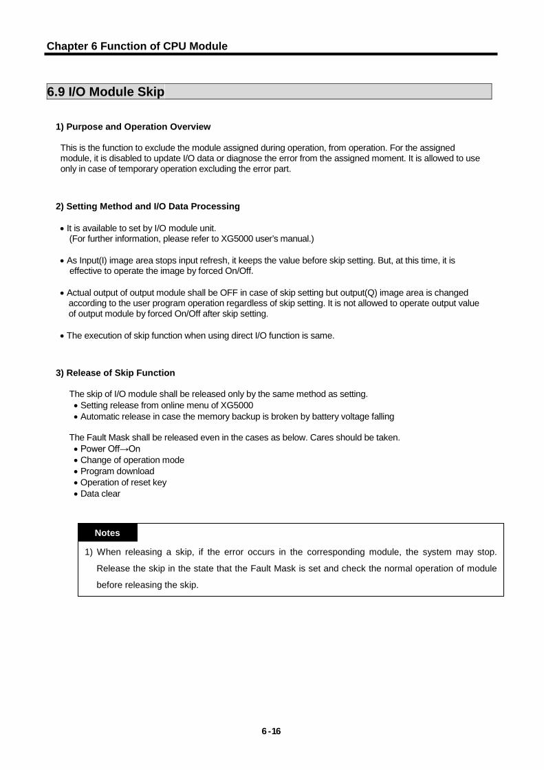
Chapter 6 Function of CPU Module
6 - 16
6.9 I/O Module Skip
1) Purpose and Operation Overview This is the function to exclude the module assigned during operation, from operation. For the assigned module, it is disabled to update I/O data or diagnose the error from the assigned moment. It is allowed to use only in case of temporary operation excluding the error part.
2) Setting Method and I/O Data Processing • It is available to set by I/O module unit.
(For further information, please refer to XG5000 user’s manual.)
• As Input(I) image area stops input refresh, it keeps the value before skip setting. But, at this time, it is effective to operate the image by forced On/Off.
• Actual output of output module shall be OFF in case of skip setting but output(Q) image area is changed
according to the user program operation regardless of skip setting. It is not allowed to operate output value of output module by forced On/Off after skip setting.
• The execution of skip function when using direct I/O function is same.
3) Release of Skip Function
The skip of I/O module shall be released only by the same method as setting. • Setting release from online menu of XG5000 • Automatic release in case the memory backup is broken by battery voltage falling
The Fault Mask shall be released even in the cases as below. Cares should be taken. • Power Off→On • Change of operation mode • Program download • Operation of reset key • Data clear
1) When releasing a skip, if the error occurs in the corresponding module, the system may stop.
Release the skip in the state that the Fault Mask is set and check the normal operation of module
before releasing the skip.
Notes

Chapter 6 Function of CPU Module
6 - 17
6.10 Changing Module during Operation XGK system enables to change the module during operation. But, as the change of module during operation may occur the abnormal operation of whole system, special attention should be taken. Just follow the procedure assigned in this user’s manual. 1) Notices in Using
• Not allowed to change the base and power module. • Some part of communication module (XGL-PMEA, XGL-DMEA) needs the network setting (Sycon used) for
communication. • In case of module change, match the joint part of the lower part of base and module correctly before inserting.
If not, it may cause the system shutdown.
2) Module Change Method
There are 2 kinds of module change method. (1) By using XG5000 “Module Change Wizard” function.
For further information, please refer to XG5000 user’s manual. (2) By using CPU module switch
(1) Set “Module change switch (M.XCHG)” in front of CPU module as right(ON). (2) Remove the module. (PS LED is ON) (3) Setup the new module. (in case of normal module setup, PS LED is OFF) (4) Check if module operates normally. (5) Set “Module change switch (M.XCHG)” as left (OFF).
1) When changing the module, shut down the load power for safety. 2) When changing the input module, consider the setting of input image state by using the forced On/Off.
Notes
When installing the module, it may cause an abnormal operation if the lower connection is not mounted on the base completely.
Warning

Chapter 6 Function of CPU Module
6 - 18
6.11 I/O No. Allocation Method The allocation of I/O No. is to give the address to the I/O terminal of each module in order to read the data from input module and print the data to output module when performing the operation. For I/O No. allocation, base no., slot position, module type for setup and parameter setting etc. are related. XGK provides 2 types such as fixed and variable.
6.11.1 Fixed I/O No. Allocation By selecting “Assign fixed points to I/O slot” from basic parameter, 64 points shall be allocated to each slot regardless of setup module. In this case, I/O parameter shall be applied only to judge whether the module type installed in the system corresponds, but not applied to point allocation.
For example of point allocation, please refer to “2.3 Basic System”.
6.11.2 Variable I/O No. Allocation By releasing “Assign fixed points to I/O slot” from basic parameter, the variable type that the point allocation is changed per slot shall be set.
If setting I/O parameter, the point related to the setting module shall be given to the assigned slot. For the next slot, the number following I/O no. occupied by the previous slot shall be allocated. For example of point allocation, please refer to “2.3 Basic System”.

Chapter 6 Function of CPU Module
6 - 19
6.11.3 Module Reservation Function This function is used for the variable I/O number allocation method to reserve modules to be mounted. If this function is used, the program modification is not necessary to change the I/O number. It can be set in the I/O Parameters window of XG5000.
6.12 Program Modification during Operation It is available to modify program or some parameter without stopping the control operation during PLC operation. For further information, please refer to XG5000 user’s manual. The items available to modify during operation are as below.
• Program modification • Communication parameter modification
Notes
1) If a module greater than 16-point is mounted on without reservation, the I/O number will become different and an abnormal operation will occur.
2) Only reserved points are available although larger point modules are mounted. The remainder are ignored.
3) Program modification is not necessary because all slots are assigned as 64points in Fixed Allocation.

Chapter 6 Function of CPU Module
6 - 20
6.13 Local Ethernet function(XGK-CPUUN/CPUHN/CPUSN)
XGK-CPUUN/CPUHN/CPUSN can carry out the functions of Ethernet server using internal local Ethernet
function without extra Enet I/F module.(Note, The internal local Ethernet doesn’t offer remote connections.
Only used for local connection.)
6.13.1 Local Ethernet Parameter Settings.
Make a new project. Then user can see Local Ethernet Parameters as shown below figure.
If user selects Local Ethernet Parameter item, Local Ethernet Parameter setting window will be displayed.

Chapter 6 Function of CPU Module
6 - 21
To use the Local Ethernet function, user should set the parameters.
(1) TCP/IP Setting
Classification Description IP address Specify the IP Address of the applicable CPU module.
* Note : There can be a communications disruption if you set more than 2 servers as a same IP
Subnet mask Value necessary to check if destination station is on the same network of the applicable station.
Gateway IP address of Gateway or Router to transmit/receive data through the public network or a network different from the network where the applicable FEnet module is included.
Reception waiting time
If there is no request during the specified time from the host PC or MMI connected for dedicated communication, it will end the dedicated service connection regardless of normal ending procedures supposing that the higher level system is with error. This time is used in dedicated service to reset the channel when any error occurs on the destination station or the cable is disconnected. Reception waiting time can be set as a unit of 1 sec (available range is 2s to 255s)
Retransmission time-out (10)
It is the time it takes CPU to send a data to the destination station if the destination station does not answer the data sent by applicable station during setting time. (Applicable station considers it as a data missing.) (available range is 10 ~ 6000) * Note : Retransmission time-out should be set depending on the network situation. If the setting time is too long, it takes a long time to resend a data in case of data missing. This will deteriorate the network performance. But if the setting time is too short, there is a chance to make a frequent disconnection or increase the load to the network.
Number of dedicated connections Number of TCP dedicated services accessible at a time. (Max.4)
(2) Driver(Server) setting Classification Description XGT server Set when operated as dedicated communication server (slave)
Modbus TCP/IP server Set when operated as Modbus server driver (slave)
(3) Host table setting Classification Description
Enable host table Access allowed to applicable module of IP address registered in host table (unregistered client(IP address) is prohibited from connection when enabled)

Chapter 6 Function of CPU Module
6 - 22
6.13.2 Local Ethernet connection with XG5000
After finishing Local Ethernet Parameter settings, download the settings to the CPU, then user can connect to
XG5000.
Select Online Settings and set the options as shown below figure.
Click the setting button to specify Ethernet IP. Click OK after specify the Ethernet IP set before.
User can find the IP information available now.

Chapter 6 Function of CPU Module
6 - 23
6.13.3 Local Ethernet connection with XGT Server.
Set the Local Ethernet Parameters as shown below figure. User can use it as a XGT Server (LSIS dedicated
Protocol Communication).
6.13.4 Local Ethernet connection with TCP/IP Server.
Set the Local Ethernet Parameters as shown below figure. User can use it as a Modbus server

Chapter 6 Function of CPU Module
6 - 24
Below figure is about Modbus settings. .
알아두
기
1) Modbus TCP/IP server connection function allows RST packet transmission depending on the network condition.(TCP/IP protocol)
So the user devices connecting to CPU module should have RST packet process. 2) Connection to user devices can be disconnected for retransmission time-out. Retransmission time-out = retransmission time-out value(set in the Local Ethernet Parameter window) x
30ms 3) Too much Network loads can affect a scan time. So user should consider appropriate network loads for
CPU scan time.

Chapter 7 I/O Module
7-1
Chapter 7 I/O Module
7.1 Notice in Selecting Module
Here describes the notices when selecting digital I/O module used for XG series. 1) For the type of digital input, there are two types such as current sink input and current
source input. For DC input module, as the wiring method of external input power varies according to
such input type, consider the specification of input connecting device when selecting. 2) Max. simultaneous input point depends on the module type. It is subject to input voltage,
ambient temperature. Review the specification of input module to apply before using. 3) In case that open/close frequency is high or it is used for conductive load open/close, use
Transistor output module or triac output module as the durability of Relay Output Module shall be reduced.
4) For output module to run the conductive (L) load, max. open/close frequency should be
used by 1second On, 1 second Off. 5) For output module, in case that counter timer using DC/DC Converter as a load was used,
Inrush current may flow in a certain cycle when it is ON or during operation. In this case, if average current is selected, it may cause the failure. Accordingly, if the previous load was used, it is recommended to connect resistor or inductor to the load in serial in order to reduce the impact of Inrush current or use the large module having a max. load current value.
6) For output module, fuse is not possible to change. This is to prevent of burnout of external
wiring in case of short circuit of module output. This may not protect output module. In case that output module is destroyed in error mode except short circuit, fuse may not work.
Out
put
mod
ule
Resistor Load
Out
put
mod
ule
Inductor Load

Chapter 7 I/O Module
7-2
7) Relay life of Relay output module is shown as below.
Max. life of Relay used in Relay output module is shown as below.
8) XGK terminal block is not allowed to use the compressed terminal attached with sleeve.
The proper compressed terminal to connect to terminal blocks is as below. (JOR 1.25-3: DAEDONG Electronic Ltd.)
9) The cable size connected to terminal block should be twisted pair 0.3~0.75, thickness
less than 2.8 . As cable varies the allowable current by insulation thickness, cares should be taken.
10) The attachment torque of fixed screw of module and the screw of terminal block should be
within the range as below.
Attachment part Attachment Torque range I/O module terminal block screw (M3 screw) 42 ~ 58 N· I/O module terminal block fixed screw (M3 screw) 66 ~ 89 N·
11) Transistor output module (XGQ-TR4A, XGQ-TR8A) has Thermal Protector Function.
Thermal Protector Function is the protection function for overload and overheats.
Ope
n/cl
ose
times
(×10
000
)
100
50
30
20
10
100 10 5 3 2 1 0.5
Open/close current (A)
AC 250VResistive load DC 30VResistive load
AC 125VResistive load

Chapter 7 I/O Module
7-3
7.2 Digital Input Module Specification
7.2.1 8 point DC24V Input Module (Source/Sink Type)
Model Specification
DC input module XGI-D21A
Input point 8 point
Insulation method Photo coupler insulation
Rated input voltage DC24V
Rated input current About 4
Operation voltage range DC20.4~28.8V (ripple rate < 5%)
Input Derating None
On Voltage/Current DC19V or higher / 3 mA or higher
Off Voltage/Current DC11V or lower / 1.7 mA or lower
Input resistance About 5.6 kΩ
Response time
Off → On 1ms/3ms/5ms/10ms/20ms/70ms/100ms (set by CPU parameter) Default:3ms
On → Off 1ms/3ms/5ms/10ms/20ms/70ms/100ms (set by CPU parameter) Default:3ms
Insulation pressure AC560V rms/3 Cycle (altitude 2000m)
Insulation resistance 10 or more by megger
Common Method 8 point / COM
Proper cable size Twisted pair 0.3~0.75 (external diameter 2.8mm or less)
Proper compressed terminal R1.25-3 (not allowed to use a sleeve attached compressed terminal.)
Current consumption () 20mA
Operation indicator Input On LED On
External connection method 9 point terminal block connector (M3 X 6 screw)
Weight 0.1 kg
Circuit configuration Terminal block Contact
TB1 P0 TB2 P1 TB3 P2 TB4 P3 TB5 P4 TB6 P5 TB7 P6 TB8 P7 TB9 COM
DC24V
Internal circuit
R 1
7
0 TB1
COM
Photocoupler
Terminal block no.
TB8 TB9
R
00
COM
01
02
03
04
05
06
07

Chapter 7 I/O Module
7-4
7.2.2 16 point DC24V Input Module (Source/Sink Type)
Model Specification
DC input module XGI-D22A
Input point 16 point
Insulation method Photo coupler insulation
Rated input voltage DC24V
Rated input current About 4
Operation voltage range DC20.4~28.8V (ripple rate < 5%)
Input Derating None
On Voltage/Current DC19V or higher / 3 mA or higher
Off Voltage/Current DC11V or lower / 1.7 mA or lower
Input resistance About 5.6 kΩ
Response time
Off → On 1ms/3ms/5ms/10ms/20ms/70ms/100ms (set by CPU parameter) Default:3ms
On → Off 1ms/3ms/5ms/10ms/20ms/70ms/100ms (set by CPU parameter) Default:3ms
Insulation pressure AC560V rms/3 Cycle (altitude 2000m)
Insulation resistance 10 or more by megger
Common Method 16 point / COM
Proper cable size Twisted pair 0.3~0.75 (external diameter 2.8mm or less)
Proper compressed terminal R1.25-3 (not allowed to use a sleeve attached compressed terminal.)
Current consumption () 30mA
Operation indicator Input On, LED On
External connection method 18 point terminal block connector (M3 X 6 screw)
Weight 0.12 kg
Circuit configuration Terminal block Contact
TB1 P0 TB2 P1 TB3 P2 TB4 P3 TB5 P4 TB6 P5 TB7 P6 TB8 P7 TB9 P8 TB10 P9 TB11 PA TB12 PB TB13 PC TB14 PD TB15 PE TB16 PF TB17 COM TB18 NC
DC24V
Internal circuit
R 1
F
0 TB1
COM
Photocoupler
Terminal block no.
TB16 TB17
R
00
06
0D
COM
01 02
03 04
05
0A 0B
0C
0F 0E
08 07
09

Chapter 7 I/O Module
7-5
7.2.3 16 point DC24V Input Module (Source Type)
Model Specification
DC input module XGI-D22B
Input point 16 point
Insulation method Photo coupler insulation
Rated input voltage DC24V
Rated input current About 4
Operation voltage range DC20.4~28.8V (ripple rate < 5%)
Input Derating None
On Voltage/Current DC19V or higher / 3 mA or higher
Off Voltage/Current DC11V or lower / 1.7 mA or lower
Input resistance About 5.6 kΩ
Response time
Off → On 1ms/3ms/5ms/10ms/20ms/70ms/100ms (set by CPU parameter) Default:3ms
On → Off 1ms/3ms/5ms/10ms/20ms/70ms/100ms (set by CPU parameter) Default:3ms
Insulation pressure AC560V rms/3 Cycle (altitude 2000m)
Insulation resistance 10 or more by megger
Common Method 16 point / COM
Proper cable size Twisted pair 0.3~0.75 (external diameter 2.8mm or less)
Proper compressed terminal R1.25-3 (not allowed to use a sleeve attached compressed terminal.)
Current consumption () 30mA
Operation indicator Input On, LED On
External connection method 18 point terminal block connector (M3 X 6screw)
Weight 0.12 kg
Circuit configuration Terminal block Contact
TB1 P0 TB2 P1 TB3 P2 TB4 P3 TB5 P4 TB6 P5 TB7 P6 TB8 P7 TB9 P8 TB10 P9 TB11 PA TB12 PB TB13 PC TB14 PD TB15 PE TB16 PF TB17 COM TB18 NC
DC24V
Internal circuit
R 1
F
0 TB1
COM
Photocoupler
Terminal block no.
TB16
TB17
R
00
06
0D
COM
01 02
03 04
05
0A 0B
0C
0F 0E
08 07
09

Chapter 7 I/O Module
7-6
7.2.4 32 point DC24V Input Module (Source/Sink Type)
Model Specification
DC input module XGI-D24A
Input point 32 point
Insulation method Photo coupler insulation
Rated input voltage DC24V
Rated input current About 4
Operation voltage range DC20.4~28.8V (ripple rate < 5%)
Input Derating Refer to the below Derating diagram.
On Voltage/Current DC19V or higher / 3 mA or higher
Off Voltage/Current DC11V or lower / 1.7 mA or lower
Input resistance About 5.6 kΩ
Response time
Off → On 1ms/3ms/5ms/10ms/20ms/70ms/100ms (set by CPU parameter) Default:3ms
On → Off 1ms/3ms/5ms/10ms/20ms/70ms/100ms (set by CPU parameter) Default:3ms
Insulation pressure AC560V rms/3 Cycle (altitude 2000m)
Insulation resistance 10 or more by megger
Common Method 32 point / COM
Proper cable size 0.3
Current consumption () 50mA
Operation indicator Input On, LED On
External connection method 40 point connector
Weight 0.1 kg
Circuit configuration No Contact No Cont
act
B20 P00 A20 P10 B19 P01 A19 P11 B18 P02 A18 P12 B17 P03 A17 P13 B16 P04 A16 P14 B15 P05 A15 P15 B14 P06 A14 P16 B13 P07 A13 P17 B12 P08 A12 P18 B11 P09 A11 P19 B10 P0A A10 P1A B09 P0B A09 P1B B08 P0C A08 P1C B07 P0D A07 P1D B06 P0E A06 P1E B05 P0F A05 P1F B04 NC A04 NC B03 NC A03 NC B02 COM A02 COM
B01 COM A01 COM
B20
B19
B18
B17
B16
B15
B14
B13
B12
B11
B10
B09
B08
B07
B06
B05
B04
B03
B02
B01
A20
A19
A18
A17
A16
A15
A14
A13
A12
A11
A10
A09
A08
A07
A06
A05
A04
A03
A02
A01
DC28.8V
100
80
60
40 0 10 20 30 40 50 55
On rate (%)
Ambient temperature
90
70
50
DC24V
Internal circuit
R 1
1F
0 B20
COM
Photocoupler
Connector no.
A05
B02
R

Chapter 7 I/O Module
7-7
7.2.5 32 point DC24V Input Module (Source Type)
Model Specification
DC input module XGI-D24B
Input point 32 point
Insulation method Photo coupler insulation
Rated input voltage DC24V
Rated input current About 4
Operation voltage range DC20.4~28.8V (ripple rate < 5%)
Input Derating Refer to the below Derating diagram.
On Voltage/Current DC19V or higher / 3 mA or higher
Off Voltage/Current DC11V or lower / 1.7 mA or lower
Input resistance About 5.6 kΩ
Response time
Off → On 1ms/3ms/5ms/10ms/20ms/70ms/100ms (set by CPU parameter) Default:3ms
On → Off 1ms/3ms/5ms/10ms/20ms/70ms/100ms (set by CPU parameter) Default:3ms
Insulation pressure AC560V rms/3 Cycle (altitude 2000m)
Insulation resistance 10 or more by megger
Common Method 32 point / COM
Proper cable size 0.3
Current consumption () 50mA
Operation indicator Input On, LED On
External connection method 40 point connector
Weight 0.1 kg
Circuit configuration No Contact No Cont
act
B20 P00 A20 P10 B19 P01 A19 P11 B18 P02 A18 P12 B17 P03 A17 P13 B16 P04 A16 P14 B15 P05 A15 P15 B14 P06 A14 P16 B13 P07 A13 P17 B12 P08 A12 P18 B11 P09 A11 P19 B10 P0A A10 P1A B09 P0B A09 P1B B08 P0C A08 P1C B07 P0D A07 P1D B06 P0E A06 P1E B05 P0F A05 P1F B04 NC A04 NC B03 NC A03 NC B02 COM A02 COM
B01 COM A01 COM
DC24V
Internal circuit
R 1
1F
0 B20
COM
Photocouple
Connector no.
A05
B02
R
DC28.8V
100
80
60
40 0 10 20 30 40 50 55
On rate (%)
Ambient temperature
90
70
50
B20
B19
B18
B17
B16
B15
B14
B13
B12
B11
B10
B09
B08
B07
B06
B05
B04
B03
B02
B01
A20
A19
A18
A17
A16
A15
A14
A13
A12
A11
A10
A09
A08
A07
A06
A05
A04
A03
A02
A01

Chapter 7 I/O Module
7-8
7.2.6 64 point DC24V Input Module (Source/Sink Type)
Model Specification
DC input module XGI-D28A
Input point 64 point
Insulation method Photo coupler insulation
Rated input voltage DC24V
Rated input current About 4
Operation voltage range DC20.4~28.8V (ripple rate < 5%)
Input Derating Refer to the below Derating diagram.
On Voltage/Current DC19V or higher / 3 mA or higher
Off Voltage/Current DC11V or lower / 1.7 mA or lower
Input resistance About 5.6 kΩ
Response time Off → On 1ms/3ms/5ms/10ms/20ms/70ms/100ms (set by CPU parameter)
Default:3ms
On → Off 1ms/3ms/5ms/10ms/20ms/70ms/100ms (set by CPU parameter) Default:3ms
Insulation pressure AC560V rms/3 Cycle (altitude 2000m)
Insulation resistance 10 or more by megger
Common Method 32 point / COM
Proper cable size 0.3
Current consumption () 60mA
Operation indicator Input On, LED On (32 point LED On by switch operation)
External connection method 40 point connector×2ea
Weight 0.15 kg
Circuit configuration No Contact No Cont
act No Contact No Cont
act
1B20 P00 1A20 P10 2B20 P20 2A20 P30 1B19 P01 1A19 P11 2B19 P21 2A19 P31
1B18 P02 1A18 P12 2B18 P22 2A18 P32 1B17 P03 1A17 P13 2B17 P23 2A17 P33 1B16 P04 1A16 P14 2B16 P24 2A16 P34 1B15 P05 1A15 P15 2B15 P25 2A15 P35 1B14 P06 1A14 P16 2B14 P26 2A14 P36 1B13 P07 1A13 P17 2B13 P27 2A13 P37 1B12 P08 1A12 P18 2B12 P28 2A12 P38 1B11 P09 1A11 P19 2B11 P29 2A11 P39 1B10 P0A 1A10 P1A 2B10 P2A 2A10 P3A 1B09 P0B 1A09 P1B 2B09 P2B 2A09 P3B 1B08 P0C 1A08 P1C 2B08 P2C 2A08 P3C 1B07 P0D 1A07 P1D 2B07 P2D 2A07 P3D 1B06 P0E 1A06 P1E 2B06 P2E 2A06 P3E 1B05 P0F 1A05 P1F 2B05 P2F 2A05 P3F 1B04 NC 1A04 NC 2B04 NC 2A04 NC 1B03 NC 1A03 NC 2B03 NC 2A03 NC 1B02 COM 1A02 NC 2B02 COM 2A02 NC
1B01 COM 1A01 NC 2B01 COM 2A01 NC
20 30 40 50 60 70 80 90
100
0 10 20 30 40 50 55
Ambient temperature ( )
On Rate (%) DC28.8V
B20
B19
B18
B17
B16
B15
B14
B13
B12
B11
B10
B09
B08
B07
B06
B05
B04
B03
B02
B01
A20
A19
A18
A17
A16
A15
A14
A13
A12
A11
A10
A09
A08
A07
A06
A05
A04
A03
A02
A01
DC24V
Internal circuit
R 1
1F
0 1B20
COM
Photocouple
1A05 1B02
R
Indication switching
circuit A
B
A: P00~P1F indication B: P20~P3F indication
Connector

Chapter 7 I/O Module
7-9
7.2.7 64 point DC24V Input Module (Source type)
Model Specification
DC input module XGI-D28B
Input point 64 point
Insulation method Photo coupler insulation
Rated input voltage DC24V
Rated input current About 4
Operation voltage range DC20.4~28.8V (ripple rate < 5%)
Input Derating Refer to the below Derating diagram.
On Voltage/Current DC19V or higher / 3 mA or higher
Off Voltage/Current DC11V or lower / 1.7 mA or lower
Input resistance About 5.6 kΩ
Response time Off → On 1ms/3ms/5ms/10ms/20ms/70ms/100ms (set by CPU parameter)
Default:3ms
On → Off 1ms/3ms/5ms/10ms/20ms/70ms/100ms (set by CPU parameter) Default:3ms
Insulation pressure AC560V rms/3 Cycle (altitude 2000m)
Insulation resistance 10 or more by megger
Common Method 32 point / COM
Proper cable size 0.3
Current consumption () 60mA
Operation indicator Input On, LED On (32 point LED On by switch operation)
External connection method 40 point connector×2ea
Weight 0.15 kg
Circuit configuration No Contact No Cont
act No Contact No Cont
act
1B20 P00 1A20 P10 2B20 P20 2A20 P30
1B19 P01 1A19 P11 2B19 P21 2A19 P31 1B18 P02 1A18 P12 2B18 P22 2A18 P32 1B17 P03 1A17 P13 2B17 P23 2A17 P33 1B16 P04 1A16 P14 2B16 P24 2A16 P34 1B15 P05 1A15 P15 2B15 P25 2A15 P35 1B14 P06 1A14 P16 2B14 P26 2A14 P36 1B13 P07 1A13 P17 2B13 P27 2A13 P37 1B12 P08 1A12 P18 2B12 P28 2A12 P38 1B11 P09 1A11 P19 2B11 P29 2A11 P39 1B10 P0A 1A10 P1A 2B10 P2A 2A10 P3A 1B09 P0B 1A09 P1B 2B09 P2B 2A09 P3B 1B08 P0C 1A08 P1C 2B08 P2C 2A08 P3C 1B07 P0D 1A07 P1D 2B07 P2D 2A07 P3D 1B06 P0E 1A06 P1E 2B06 P2E 2A06 P3E 1B05 P0F 1A05 P1F 2B05 P2F 2A05 P3F 1B04 NC 1A04 NC 2B04 NC 2A04 NC 1B03 NC 1A03 NC 2B03 NC 2A03 NC 1B02 COM 1A02 NC 2B02 COM 2A02 NC 1B01 COM 1A01 NC 2B01 COM 2A01 NC
20 30 40 50 60 70 80 90
100
0 10 20 30 40 50 55 Ambient temperature ( )
On Rate (%) DC28.8V
B20
B19
B18
B17
B16
B15
B14
B13
B12
B11
B10
B09
B08
B07
B06
B05
B04
B03
B02
B01
A20
A19
A18
A17
A16
A15
A14
A13
A12
A11
A10
A09
A08
A07
A06
A05
A04
A03
A02
A01
DC24V
Internal circuit
R 1
1F
0 1B20
COM
Photocoupler
1A05 1B02
R
Indication switching
circuit A
B
A: P00~P1F indication
B: P20~P3F indication
Connector

Chapter 7 I/O Module
7-10
7.2.8 16 point AC110V Input Module
Model Specification
AC input module XGI-A12A
Input point 16 point
Insulation method Photo coupler insulation
Rated input voltage AC100-120V(+10/-15%) 50/60(±3) (distortion rate < 5%)
Rated input current About 8 (AC100,60), About 7 (AC100, 50)
Inrush current Max. 200 1 (AC132V)
Input Derating Refer to the below Derating diagram.
On Voltage/Current AC80V or higher / 5 mA or higher (50, 60)
Off Voltage/Current AC30V or lower / 1 mA or lower (50, 60)
Input resistance About 12 kΩ(60), About 15 kΩ(50)
Response time
Off → On 15 ms or less (AC100V 50, 60)
On → Off 25 ms or less (AC100V 50, 60)
Insulation pressure AC1780V rms/3 Cycle (altitude 2000m)
Insulation resistance 10 or more by megger
Common Method 16 point / COM
Proper cable size Twisted pair 0.3~0.75 (external diameter 2.8mm or less)
Proper compressed terminal R1.25-3 (not allowed to use a sleeve attached compressed terminal.)
Current consumption () 30mA
Operation indicator Input On, LED On
External connection method 18 point terminal block connector (M3 X 6screw)
Weight 0.13 kg
Circuit configuration Terminal block Contact
TB1 P0
TB2 P1 TB3 P2 TB4 P3 TB5 P4 TB6 P5 TB7 P6 TB8 P7 TB9 P8 TB10 P9 TB11 PA TB12 PB TB13 PC TB14 PD TB15 PE TB16 PF TB17 COM TB18 NC
AC120V
100
80
60
40 0 10 20 30 40 50 55
On Rate (%)
Ambient temperature ( )
90
70
50 AC132V
00
06
0D
COM
01 02
03 04
05
0A 0B
0C
0F 0E
08 07
09
AC100V
Internal circuit
R 1
F
0 TB1
COM
Photocouple
Terminal block no.
R
TB16
TB17

Chapter 7 I/O Module
7-11
7.2.9 8 point AC220V input module
Model Specification
AC input module XGI-A21A
Input point 8 point
Insulation method Photo coupler insulation
Rated input voltage AC100-240V(+10/-15%) 50/60(±3) (distortion rate 5%)
Rated input current About 17 (AC200,60), About 14 (AC200, 50)
Inrush current Max.500 1 below (AC264V)
Input Derating Refer to the below Derating diagram.
On Voltage/Current AC80V or higher / 5 mA or higher (50, 60)
Off Voltage/Current AC30V or lower / 1 mA or lower (50, 60)
Input resistance About 12 kΩ(60), About 15 kΩ(50)
Response time
Off → On 15 ms or less (AC200V 50, 60) On
→ Off 25 ms or less (AC200V 50, 60)
Insulation pressure AC2830V rms/3 Cycle (altitude 2000m) Insulation resistance 10 or more by megger Common Method 8 point / COM Proper cable size Twisted pair 0.3~0.75 (external diameter 2.8mm or less) Proper compressed terminal R1.25-3 (not allowed to use a sleeve attached compressed terminal.) Current consumption () 20mA Operation indicator Input On, LED On External connection method 9 point terminal block connector (M3 X 6screw) Weight 0.13 kg
Circuit configuration Terminal block Contact
TB1 P0 TB2 P1 TB3 P2 TB4 P3 TB5 P4 TB6 P5 TB7 P6 TB8 P7 TB9 COM
AC240V
100
80
60
40 0 10 20 30 40 50 55
On Rate (%)
Ambient temperature
90
70
50 AC264V
37 49
00
COM
01
02
03
04
05
06
07
AC200V
Internal circuit
R 1
7
0 TB1
COM
Photocoupler
Terminal block no.
R
TB8
TB9

Chapter 7 I/O Module
7-12
7.2.10 8 point AC220V isolated input module
Module type Spec.
AC input module XGI-A21C
Input point 8 points
Insulation method Photo coupler insulation
Rated input voltage AC100-240V(+10/-15%) 50/60(±3) (5% and lower distortion)
Rated input current Approx. 17 (AC200,60) , approx. 14 (AC200,50)
Inrush current Max. 500 1 and lower(AC264V)
Input derating Refer to the below derating level
On voltage / On current AC80V and higher / 5 mA and higher(50,60)
Off voltage / Off current AC30V and higher / 1 mA and lower (50,60)
Input resistance Approx. 12 kΩ(60), approx. 15 kΩ(50)
Response time Off → On 15 ms and lower(AC200V 50,60) On → Off 25 ms and lower(AC200V 50,60)
Insulation withstand voltage AC2830V rms/3 Cycle (altitude 2000m) Insulation resistance 10 and higher by Insulation ohmmeter Common method 1 point / COM Suitable cable size Stranded cable between 0.3~0.75 (2.8mm and smaller outer dia.) Suitable clamped terminal R1.25-3 (Sleeve built-in clamped terminal is not available) Current consumption() 20mA Operation display LED On with Input On External connection method 18 point Terminal strip connector (M3 X 6 screws) Weight 0.13 kg
Circuit diagram Terminal block Contact
TB1 P0 TB2 COM0 TB3 P1 TB4 COM1 TB5 P2
TB6 COM2
TB7 P3
TB8 COM3 TB9 P4
TB10 COM4 TB11 P5 TB12 COM5 TB13 P6 TB14 COM6 TB15 P7 TB16 COM7 TB17 NC TB18 NC
AC240V
100
80
60
40 0 10 20 30 40 50 55
On Rate (%)
Ambient temperature
90
70
50 AC264V
37 49
Internal circuit
R Photocoupler
Terminal block No.
R
0 TB1
TB2
AC220V

Chapter 7 I/O Module
7-13
7.3 Digital Output Module Specification
7.3.1 8 point Relay Output Module
Model Specification
Relay Output Module XGQ-RY1A
Output point 8 point
Insulation method Relay insulation
Rated load voltage/current DC24V 2A(resistive load) / AC220V 2A(COSΨ = 1)
Min. load voltage/current DC5V / 1mA
Max. load voltage/current AC250V, DC125V
Off leakage current 0.1mA (AC220V, 60Hz)
Max. on/off frequency 3,600 times/hr
Surge absorber None
Service life
Mechanical 20 millions times or more
Electrical
Rated load voltage/current 100,000 times or more
AC200V / 1.5A, AC240V / 1A (COSΨ = 0.7) 100,000 times or more
AC200V / 1A, AC240V / 0.5A (COSΨ = 0.35) 100,000 times or more
DC24V / 1A, DC100V / 0.1A (L / R = 7ms) 100,000 times or more
Response time
Off → On 10 ms or less
On → Off 12 ms or less
Common method 1 point / 1COM (independent contact)
Current consumption 260mA (when all point On)
Operation indicator Output On, LED On
External connection method 18 point terminal block connector (M3 X 6screw) Weight 0.13kg
Circuit configuration Terminal block Contact
TB1 P0 TB2 COM TB3 P1 TB4 COM TB5 P2 TB6 COM TB7 P3 TB8 COM TB9 P4 TB10 COM TB11 P5 TB12 COM TB13 P6 TB14 COM TB15 P7 TB16 COM TB17 NC TB18 NC
00
05
07
01
02
03
04
06
L
L
L
L
L
L
L
L
RY
Internal circuit
Terminal block no.
TB1
TB2

Chapter 7 I/O Module
7-14
7.3.2 16 point Relay Output Module
Model Specification
Relay Output Module XGQ-RY2A
Output point 16 point
Insulation method Relay insulation
Rated load voltage/current DC24V 2A(resistive load) / AC220V 2A(COSΨ = 1)
Min. load voltage/current DC5V / 1mA
Max. load voltage/current AC250V, DC125V
Off leakage current 0.1mA (AC220V, 60Hz)
Max. on/off frequency 3,600times/hr
Surge absorber None
Service life
Mechanical 20 million times or more
Electrical
Rated load voltage/current 100,000 times or more
AC200V / 1.5A, AC240V / 1A (COSΨ = 0.7) 100,000 times or more
AC200V / 1A, AC240V / 0.5A (COSΨ = 0.35) 100,000 times or more
DC24V / 1A, DC100V / 0.1A (L / R = 7ms) 100,000 times or more
Response time
Off → On 10 ms or less
On → Off 12 ms or less
Common method 16 point / 1COM
Current consumption 500mA (when all points On)
Operation indicator Output On, LED On
External connection method 18 point terminal block connector (M3 X 6screw) Weight 0.17kg
Circuit configuration Terminal block Contact
TB1 P0 TB2 P1 TB3 P2 TB4 P3 TB5 P4 TB6 P5 TB7 P6 TB8 P7 TB9 P8 TB10 P9 TB11 PA TB12 PB TB13 PC TB14 PD TB15 PE TB16 PF TB17 COM TB18 NC
00
0A
0E
02
04
06
08
0C
L
L
L
L
L
L
L
L
L
L
L
L
L
L
L
L
01
03
05
07
09
0B
0D
0F
COM
RY
Internal circuit
Terminal block no.
TB1
TB17
TB16

Chapter 7 I/O Module
7-15
7.3.3 16 point Relay Output Module (Surge Absorber Type)
Model Specification
Relay Output Module XGQ-RY2B
Output point 16 point
Insulation method Relay insulation
Rated load voltage/current DC24V 2A(resistive load) / AC220V 2A(COSΨ = 1)
Min. load voltage/current DC5V / 1mA
Max. load voltage/current AC250V, DC125V
Off leakage current 0.1mA (AC220V, 60Hz)
Max. on/off frequency 3,600times/hr
Surge absorber Varistor (387 ~ 473V), C.R Absorber
Service life
Mechanical 20 million times or more
Electrical
Rated load voltage/current 100,000 times or more
AC200V / 1.5A, AC240V / 1A (COSΨ = 0.7) 100,000 times or more
AC200V / 1A, AC240V / 0.5A (COSΨ = 0.35) 100,000 times or more
DC24V / 1A, DC100V / 0.1A (L / R = 7ms) 100,000 times or more
Response time
Off → On 10 ms or less
On → Off 12 ms or less
Common method 16 point / 1COM
Current consumption 500mA (when all points On)
Operation indicator Output On, LED On
External connection method 18 point terminal block connector (M3 X 6screw) Weight 0.19kg
Circuit configuration Terminal block Contact
TB1 P0 TB2 P1 TB3 P2 TB4 P3 TB5 P4 TB6 P5 TB7 P6 TB8 P7 TB9 P8 TB10 P9 TB11 PA TB12 PB TB13 PC TB14 PD TB15 PE TB16 PF TB17 COM TB18 NC
00
0A
0E
02
04
06
08
0C
L
L
L
L
L
L
L
L
L
L
L
L
L
L
L
L
01
03
05
07
09
0B
0D
0F
COM
RY
Internal circuit
Terminal block no.
TB1
TB17
TB16

Chapter 7 I/O Module
7-16
7.3.4 16 point Triac Output Module
Model Specification
Triac Output Module XGQ-SS2A
Output point 16 point
Insulation method Photo coupler insulation
Rated load voltage AC 100-240V (50 / 60 Hz)
Max. load voltage AC 264V
Max. load current 0.6A / 1 point 4A / 1COM
Min. load current 20 mA
Off leakage current 2.5 mA (AC 220V 60 Hz)
Max. inrush current 20A / Cycle or less
Max. voltage drop (On) AC 1.5V or less (2A)
Surge absorber Varistor (387 ~ 473V), C.R Absorber
Response time
Off → On 1 ms or less
On → Off 0.5 Cycle + 1 ms or less
Common method 16 point / 1 COM
Current consumption 300 mA (when all points On)
Operation indicator Output On, LED On
External connection method 18 point terminal block connector (M3 X 6screw) Weight 0.2 kg
Circuit configuration Terminal block Contact
TB1 P0 TB2 P1 TB3 P2 TB4 P3 TB5 P4 TB6 P5 TB7 P6 TB8 P7 TB9 P8 TB10 P9 TB11 PA TB12 PB TB13 PC TB14 PD TB15 PE TB16 PF TB17 COM TB18 NC
00
0A
0E
02
04
06
08
0C
L
L
L
L
L
L
L
L
L
L
L
L
L
L
L
L
01
03
05
07
09
0B
0D
0F
COM
R
Internal circuit
Terminal block no.
TB1
TB17
TB16
ZC
Triac

Chapter 7 I/O Module
7-17
7.3.5 16 point Transistor Output Module (Sink Type)
Model Specification
Transistor Output Module XGQ-TR2A
Output point 16 point Insulation method Photo coupler insulation Rated load voltage DC 12 / 24V Load voltage range DC 10.2 ~ 26.4V Max. load current 0.5A / 1 point, 4A / 1COM Off leakage current 0.1mA or less Max. inrush current 4A / 10 ms or less
Max. voltage drop (On) DC 0.3V or less
Surge absorber Zener diode Fuse 4A×2ea(no change) (fuse shutdown capacity:50A)
Fuse cutoff indication Yes (fuse cutoff, LED On, transmit the signal to CPU) External power supply Off, not detected Fuse cutoff
Response time
Off → On 1 ms or less On → Off 1 ms or less (Rated load, resistive load)
Common method 16 point / 1COM Current consumption 70mA (when all points On)
External power supply
Voltage DC12/24V ± 10% (ripple voltage 4 Vp-p or less ) Current 10mAor less (DC24V connection)
Operation indicator Output On, LED On External connection method 18 point terminal block connector Weight 0.11kg
Circuit configuration Terminal block Contact
TB1 P0 TB2 P1 TB3 P2 TB4 P3 TB5 P4 TB6 P5 TB7 P6 TB8 P7 TB9 P8
TB10 P9 TB11 PA TB12 PB TB13 PC TB14 PD TB15 PE TB16 PF TB17 DC24V TB18 COM
00
0A
0E
02
04
06
08
0C
L
L
L
L
L
L
L
L
L
L
L
L
L
L
L
L
01
03
05
07
09
0B
0D
0F
COM
Terminal block no.
DC12/24V
R
Internal circuit
TB1
TB17
TB16
Fuse TB18
R
R
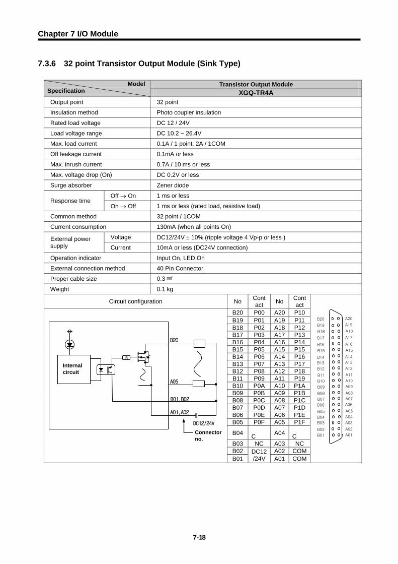
Chapter 7 I/O Module
7-18
7.3.6 32 point Transistor Output Module (Sink Type)
Model Specification
Transistor Output Module XGQ-TR4A
Output point 32 point
Insulation method Photo coupler insulation
Rated load voltage DC 12 / 24V
Load voltage range DC 10.2 ~ 26.4V
Max. load current 0.1A / 1 point, 2A / 1COM
Off leakage current 0.1mA or less
Max. inrush current 0.7A / 10 ms or less
Max. voltage drop (On) DC 0.2V or less
Surge absorber Zener diode
Response time Off → On 1 ms or less
On → Off 1 ms or less (rated load, resistive load)
Common method 32 point / 1COM
Current consumption 130mA (when all points On)
External power supply
Voltage DC12/24V ± 10% (ripple voltage 4 Vp-p or less )
Current 10mA or less (DC24V connection)
Operation indicator Input On, LED On
External connection method 40 Pin Connector
Proper cable size 0.3
Weight 0.1 kg
Circuit configuration No Contact No Cont
act
B20 P00 A20 P10 B19 P01 A19 P11 B18 P02 A18 P12 B17 P03 A17 P13 B16 P04 A16 P14 B15 P05 A15 P15 B14 P06 A14 P16 B13 P07 A13 P17 B12 P08 A12 P18 B11 P09 A11 P19 B10 P0A A10 P1A B09 P0B A09 P1B B08 P0C A08 P1C B07 P0D A07 P1D B06 P0E A06 P1E B05 P0F A05 P1F
B04 C A04 C B03 NC A03 NC B02 DC12
/24V A02 COM
B01 A01 COM
Connector no.
DC12/24V
R Internal circuit
B20
B01,B02
A05
A01,A02
B20
B19
B18
B17
B16
B15
B14
B13
B12
B11
B10
B09
B08
B07
B06
B05
B04
B03
B02
B01
A20
A19
A18
A17
A16
A15
A14
A13
A12
A11
A10
A09
A08
A07
A06
A05
A04
A03
A02
A01

Chapter 7 I/O Module
7-19
7.3.7 64 point Transistor Output Module (Sink Type)
Model Specification
Transistor Output Module XGQ-TR8A
Output point 64 point
Insulation method Photo coupler insulation
Rated load voltage DC 12 / 24V
Load voltage range DC 10.2 ~ 26.4V
Max. load current 0.1A / 1 point, 2A / 1COM
Off leakage current 0.1mA or less
Max. inrush current 0.7A / 10 ms or less
Max. voltage drop (On) DC 0.2V or less
Surge absorber Zener diode
Response time Off → On 1 ms or less
On → Off 1 ms or less (rated load, resistive load)
Common method 16 point / 1COM
Current consumption 230mA (when all points On)
Common method 32 point / COM
External power supply
Voltage DC12/24V ± 10% (ripple voltage 4 Vp-p or less )
Current 10mA or less (DC24V connection)
Operation indicator Input On, LED On (32 point LED On by switch operation)
External connection method 40 Pin Connector×2ea
Proper cable size 0.3
Weight 0.15 kg
Circuit configuration No Contact No Cont
act No Contact No Cont
act
1B20 P00 1A20 P10 2B20 P20 2A20 P30 1B19 P01 1A19 P11 2B19 P21 2A19 P31 1B18 P02 1A18 P12 2B18 P22 2A18 P32 1B17 P03 1A17 P13 2B17 P23 2A17 P33 1B16 P04 1A16 P14 2B16 P24 2A16 P34 1B15 P05 1A15 P15 2B15 P25 2A15 P35 1B14 P06 1A14 P16 2B14 P26 2A14 P36 1B13 P07 1A13 P17 2B13 P27 2A13 P37 1B12 P08 1A12 P18 2B12 P28 2A12 P38 1B11 P09 1A11 P19 2B11 P29 2A11 P39 1B10 P0A 1A10 P1A 2B10 P2A 2A10 P3A 1B09 P0B 1A09 P1B 2B09 P2B 2A09 P3B 1B08 P0C 1A08 P1C 2B08 P2C 2A08 P3C 1B07 P0D 1A07 P1D 2B07 P2D 2A07 P3D 1B06 P0E 1A06 P1E 2B06 P2E 2A06 P3E 1B05 P0F 1A05 P1F 2B05 P2F 2A05 P3F 1B04 NC 1A04 NC 2B04 NC 2A04 NC 1B03 NC 1A03 NC 2B03 NC 2A03 NC 1B02 12/
24 VDC
1A02 COM1
2B02 12/ 24VDC
2A02 COM2 1B01 1A01 2B01 2A01
DC12/24V
Internal circuit
B20
B01,B02
A05
A01,A02
Indication switching circuit
A
B
A: P00~P1F indication B: P20~P3F indication
B20
B19
B18
B17
B16
B15
B14
B13
B12
B11
B10
B09
B08
B07
B06
B05
B04
B03
B02
B01
A20
A19
A18
A17
A16
A15
A14
A13
A12
A11
A10
A09
A08
A07
A06
A05
A04
A03
A02
A01 Connector no.

Chapter 7 I/O Module
7-20
7.3.8 16 point Transistor Output Module (Source Type)
Model Specification
Transistor Output Module XGQ-TR2B
Output point 16 point Insulation method Photo coupler insulation Rated load voltage DC 12 / 24V Load voltage range DC 10.2 ~ 26.4V Max. load current 0.5A / 1 point, 4A / 1COM Off leakage current 0.1mA or less Max. inrush current 4A / 10 ms or less
Max. voltage drop (On) DC 0.3V or less
Surge absorber Zener diode Fuse 4A×2ea (no change) (fuse shutdown capacity:50A) Fuse cutoff indication Yes (fuse cutoff, LED On, transmit the signal to CPU)
Response time
Off → On 1 ms or less On → Off 1 ms or less (rated load, resistive load)
Common method 16 point / 1COM Current consumption 70mA (when all points On)
External power supply
Voltage DC12/24V ± 10% (ripple voltage 4 Vp-p or less ) Current 10mA or less (DC24V connection)
Operation indicator Output On, LED On External connection method 18 point terminal block connector Weight 0.12kg
Circuit configuration Terminal block Contact
TB1 P0 TB2 P1 TB3 P2 TB4 P3 TB5 P4 TB6 P5 TB7 P6 TB8 P7 TB9 P8
TB10 P9 TB11 PA TB12 PB TB13 PC TB14 PD TB15 PE TB16 PF TB17 COM TB18 0V
00
0A
0E
02
04
06
08
0C
L
L
L
L
L
L
L
L
L
L
L
L
L
L
L
L
01
03
05
07
09
0B
0D
0F
COM Terminal block no.
DC12/24V
R
Internal circuit
TB1
TB17
TB16
Fuse
TB18
R
R

Chapter 7 I/O Module
7-21
7.3.9 32 point Transistor Output Module (Source Type)
Model Specification
Transistor Output Module XGQ-TR4B
Output point 32 point
Insulation method Photo coupler insulation
Rated load voltage DC 12 / 24V
Load voltage range DC 10.2 ~ 26.4V
Max. load current 0.1A / 1 point, 2A / 1COM
Off leakage current 0.1mA or less
Max. inrush current 4A / 10 ms or less
Max. voltage drop (On) DC 0.3V or less
Surge absorber Zener diode
Response time Off → On 1 ms or less
On → Off 1 ms or less (rated load, resistive load)
Common method 32 point / 1COM
Current consumption 130mA (when all points On)
External power supply
Voltage DC12/24V ± 10% (ripple voltage 4 Vp-p or less )
Current 10mA or less (DC24V connection)
Operation indicator Input On, LED On
External connection method 40 Pin Connector
Proper cable size 0.3
Weight 0.1 kg
Circuit configuration No Contact No Cont
act
B20 P00 A20 P10 B19 P01 A19 P11 B18 P02 A18 P12 B17 P03 A17 P13 B16 P04 A16 P14 B15 P05 A15 P15 B14 P06 A14 P16 B13 P07 A13 P17 B12 P08 A12 P18 B11 P09 A11 P19 B10 P0A A10 P1A B09 P0B A09 P1B B08 P0C A08 P1C B07 P0D A07 P1D B06 P0E A06 P1E B05 P0F A05 P1F B04 NC A04 NC B03 NC A03 NC B02
COM A02 0V
B01 A01
DC12/24V
R
Internal circuit
Connector no.
B04,B03,
B02,B01
A05
A04,A03,
A02,A01
B20
B20
B19
B18
B17
B16
B15
B14
B13
B12
B11
B10
B09
B08
B07
B06
B05
B04
B03
B02
B01
A20
A19
A18
A17
A16
A15
A14
A13
A12
A11
A10
A09
A08
A07
A06
A05
A04
A03
A02
A01

Chapter 7 I/O Module
7-22
7.3.10 64 point Transistor Output Module (Source Type)
Model Specification
Transistor Output Module XGQ-TR8B
Output point 64 point
Insulation method Photo coupler insulation
Rated load voltage DC 12 / 24V
Load voltage range DC 10.2 ~ 26.4V
Max. load current 0.1A / 1 point, 2A / 1COM
Off leakage current 0.1mA or less
Max. inrush current 4A / 10 ms or less
Max. voltage drop (On) DC 0.3V or less
Surge absorber Zener diode
Response time Off → On 1 ms or less
On → Off 1 ms or less (rated load, resistive load)
Common method 32 point / 1COM
Current consumption 230mA (when all points On)
Common method 32 point / COM
External power supply
Voltage DC12/24V ± 10% (ripple voltage 4 Vp-p or less )
Current 10mA or less (DC24V connection)
Operation indicator Input On, LED On (32 point LED On by switch operation)
External connection method 40 Pin Connector×2ea
Proper cable size 0.3
Weight 0.15 kg
Circuit configuration No Contact No Cont
act No Contact No Cont
act
1B20 P00 1A20 P10 2B20 P20 2A20 P30 1B19 P01 1A19 P11 2B19 P21 2A19 P31 1B18 P02 1A18 P12 2B18 P22 2A18 P32 1B17 P03 1A17 P13 2B17 P23 2A17 P33 1B16 P04 1A16 P14 2B16 P24 2A16 P34 1B15 P05 1A15 P15 2B15 P25 2A15 P35 1B14 P06 1A14 P16 2B14 P26 2A14 P36 1B13 P07 1A13 P17 2B13 P27 2A13 P37 1B12 P08 1A12 P18 2B12 P28 2A12 P38 1B11 P09 1A11 P19 2B11 P29 2A11 P39 1B10 P0A 1A10 P1A 2B10 P2A 2A10 P3A 1B09 P0B 1A09 P1B 2B09 P2B 2A09 P3B 1B08 P0C 1A08 P1C 2B08 P2C 2A08 P3C 1B07 P0D 1A07 P1D 2B07 P2D 2A07 P3D 1B06 P0E 1A06 P1E 2B06 P2E 2A06 P3E 1B05 P0F 1A05 P1F 2B05 P2F 2A05 P3F 1B04 NC 1A04 NC 2B04 NC 2A04 NC 1B03 NC 1A03 NC 2B03 NC 2A03 NC 1B02
COM 1A02
0V 2B02 COM
2A02 0V
1B01 1A01 2B01 2A01
B20
B19
B18
B17
B16
B15
B14
B13
B12
B11
B10
B09
B08
B07
B06
B05
B04
B03
B02
B01
A20
A19
A18
A17
A16
A15
A14
A13
A12
A11
A10
A09
A08
A07
A06
A05
A04
A03
A02
A01
DC12/24V
R
Internal circuit
Connector no.
B04,B03,
B02,B01
A05
A04,A03,
A02,A01
B20
Indication switching circuit
A
B
A: P00~P1F indication B: P20~P3F indication

Chapter 7 I/O Module
7-23
7.3.11 8 point transistor isolated output module Module
Specification Transistor output module
XGQ-TR1C Output point 8 points Insulation method Photo coupler insulation Rated load voltage DC 12 / 24V Operating load voltage range DC 10.2 ~ 26.4V Max. load current 2A / 1 point Leakage current at Off 0.1mA and lower Max. inrush current 4A / 10 ms and lower
Max. voltage drop at On DC 0.3V and lower
Surge killer Zener diode
Response time Off → On 3 ms and shorter On → Off 10 ms and shorter (Rated load, resistance load)
Common method 1 point/ 1COM Current consumption 100mA (when every points On)
External power supply
Voltage DC12/24V ± 10% (4 Vp-p and lower ripple voltage) Current 10mA and lower (if connected to DC24V)
Operation display LED On with output On External connection method 18point Terminal strip connector Weight 0.11kg
Circuit diagram Terminal block Contact
TB1 P0
TB2 COM0
TB3 P1
TB4 COM1
TB5 P2
TB6 COM2
TB7 P3
TB8 COM3
TB9 P4 TB10 COM4
TB11 P5
TB12 COM5
TB13 P6
TB14 COM6
TB15 P7
TB16 COM7
TB17 NC
TB18 NC
Internal circuit

Chapter 7 I/O Module
7-24
7.4 Digital I/O Module
32 point I/O (DC Input · Transistor Output) Module XGH-DT4A
Input Output Input point 16point Output point 16 points Insulation Photo coupler insulation Insulation method Photo coupler insulation Rated input voltage DC 24V Rated load voltage DC 12 / 24V Rated input current About 4 Load voltage range DC 10.2 ~ 26.4V
Operation voltage range DC20.4~28.8V (ripple rate < 5%) Max. load current 0.1A / 1 point, 1.6A / 1COM
Insulation pressure AC560Vrms/3Cycle (altitude: 2000m) Off leakage current 0.1mA or less
On Voltage/Current DC19V or higher / 3 mA or higher Max. inrush current 0.7A / 10 ms or less Off Voltage/Current DC11V or lower / 1.7 mA or lower Surge absorber Zener diode Input resistance About 5.6 kΩ Max. voltage drop (On) DC 0.2V or less
Res
pons
e tim
e
Off→ On 1ms/3ms/5ms/10ms/20ms/70ms/ 100ms (set by CPU parameter) Default:3ms
Res
pons
e tim
e Off→ On 1 ms or less
On → Off 1ms/3ms/5ms/10ms/20ms/70ms/ 100ms (set by CPU parameter) Default:3ms
On → Off 1 ms or less (rated load, resistive load)
Common 16 point / 1 COM Common method 16 points / 1 COM Operation indicator Input On, LED On Operation indicator Output On, LED On Current consumption () 110mA (when all points On) External connection 40-pin Connector × 1 Weight 0.1 kg
No Contact No Cont
ac B20 P00 A20 P10 B19 P01 A19 P11 B18 P02 A18 P12 B17 P03 A17 P13 B16 P04 A16 P14 B15 P05 A15 P15 B14 P06 A14 P16 B13 P07 A13 P17 B12 P08 A12 P18 B11 P09 A11 P19 B10 P0A A10 P1A B09 P0B A09 P1B B08 P0C A08 P1C B07 P0D A07 P1D B06 P0E A06 P1E B05 P0F A05 P1F B04 NC A04 DC1
2/24V B03 NC A03
B02 COM
A02 0V B01 A01
DC12/24V
R Internal circuit
A20
A04,A03
A05
A02,A01
DC24V
Internal circuit
R 1
0F
00 B20
COM
DC5V
Photo coupler
Connector No.
B05
B02,B01
LED
R
Circuit configuration
B20
B19
B18
B17
B16
B15
B14
B13
B12
B11
B10
B09
B08
B07
B06
B05
B04
B03
B02
B01
A20
A19
A18
A17
A16
A15
A14
A13
A12
A11
A10
A09
A08
A07
A06
A05
A04
A03
A02
A01
Input
Output
External Connection
Connector No.

Chapter 7 I/O Module
7-25
7.5 Event Input Module
7.5.1 Event Input Module (Source/Sink type) Specification XGF-SOEA
Input point 32 point
Insulation method Photo coupler insulation
Memory size Records 1Mbit event information (300 event information per XGF-SOEA module)
Precision 1 ms (±2ms : error between modules)
Rated input voltage DC24V
Rated input current About 4mA
Used voltage range DC20.4 ~ 28.8V (within ripple rate 5%) On voltage/On
current DC19V or above / 3 mA or above
Off voltage/ Off current DC11V or less / 1.7 mA or less
Input resistance About 5.6 kΩ
Response time
Off → On
H/W delay (10: Normal) + input filter time (user setting: 0~100ms) + CPU scan time delay (50)
On → Off
H/W delay (84: Normal) + input filter time (user setting: 0~100ms) + CPU scan time delay (50)
Working voltage AC560V rms/3 Cycle (Altitude 2000m)
Insulation resistance Insulation resistance 10 or above (DC500V)
COMM method 32 point / COM Current consumption
(A) 0.7(MAX)
Operation indicator LED is on when input is on External connection
method 40 pin connector
Size 27x98x90
Weight 0.2 kg
Circuit configuration No Contact No Cont
act
B20 0 A20 16 B19 1 A19 17 B18 2 A18 18 B17 3 A17 19 B16 4 A16 20 B15 5 A15 21 B14 6 A14 22 B13 7 A13 23 B12 8 A12 24 B11 9 A11 25 B10 10 A10 26 B09 11 A09 27 B08 12 A08 28 B07 13 A07 29 B06 14 A06 30 B05 15 A05 31 B04 NC A04 NC B03 NC A03 NC B02 COM A02 COM B01 COM A01 COM
B20
B19
B18
B17
B16
B15
B14
B13
B12
B11
B10
B09
B08
B07
B06
B05
B04
B03
B02
B01
A20
A19
A18
A17
A16
A15
A14
A13
A12
A11
A10
A09
A08
A07
A06
A05
A04
A03
A02
A01
DC28.8V 100
80
60
40 0 10 20 30 40 50 55
On rate (%)
Ambient temp.
90
70
50
DC24V
Internal circuit
R 1
31
0 B20
COM
Photo coupler
Connector No.
A05 B02
R
Derating diagram

Chapter 7 I/O Module
7-26
7.6 Smart Link
7.6.1 Smart Link Connectable Module The connectable digital modules used for XGK series to Smart Link are as follows.
Model Specification No. of Pins
XGI-D24A/B 32-point DC input module 40-pin Connector×1 XGI-D28A/B 64-point DC input module 40-pin Connector×2 XGQ-TR4A 32-point TR output module (sink type) 40-pin Connector×1 XGQ-TR4B 32-point TR output module (source type) 40-pin Connector×1 XGQ-TR8A 64-point TR output module (sink type) 40-pin Connector×2 XGQ-TR8B 64-point TR output module (source type) 40-pin Connector×2
XGH-DT4A 16-point DC input / 16-point TR output combination module 40-pin Connector×1
Some models are ready for Smart Link. For details, refer to the attached data sheet that comes with the Smart Link module.
Classification Model Specification
Terminal board SLP-T40P 40-pin terminal Relay board SLP-RY4A, RY4B 32-point relay
Cable SLP-C101-XG 1m cable SLP-C201-XG 2m cable
7.6.2 Smart Link Connection
Extension cable (SLP-C101-XG, SLP-C201-XG)
Terminal board (SLP-T40P) Relay board (SLP-RY4A)

Chapter 7 I/O Module
7-27
7.6.3 Smart Link Wiring Diagram
- Wiring Diagram with SLP-T40P - Wiring Diagram with SLP-RY4A, SLP-RY4B
SLP-T40P terminal
block No.
I/O module
connector No.
SLP-T40P terminal
block No.
B1 B20 A20 A1 B2 B19 A19 A2 B3 B18 A18 A3 B4 B17 A17 A4 B5 B16 A16 A5 B6 B15 A15 A6 B7 B14 A14 A7 B8 B13 A13 A8 B9 B12 A12 A9 B10 B11 A11 A10 B11 B10 A10 A11 B12 B09 A09 A12 B13 B08 A08 A13 B14 B07 A07 A14 B15 B06 A06 A15 B16 B05 A05 A16 B17 B04 A04 A17 B18 B03 A03 A18 B19 B02 A02 A19 B20 B01 A01 A20
SLP-RY4A/B terminal
block No.
I/O module
connector No.
SLP-RY4A/B terminal
block No.
P0 B20 A20 P10 P1 B19 A19 P11 P2 B18 A18 P12 P3 B17 A17 P13 P4 B16 A16 P14 P5 B15 A15 P15 P6 B14 A14 P16 P7 B13 A13 P17 P8 B12 A12 P18 P9 B11 A11 P19
P0A B10 A10 P1A P0B B09 A09 P1B P0C B08 A08 P1C P0D B07 A07 P1D P0E B06 A06 P1E P0F B05 A05 P1F NC B04 A04 NC NC B03 A03 NC
+24V B02 A02 -24G +24V B01 A01 -24G

Chapter 8 Power Module
8-1
Chapter 8 Power Module Here describes the selection method, type and specification of power module.
8.1 Selection Method The selection of power module is determined by the current that voltage and power module of input power supply to the system, that is, the sum of current consumption of digital I/O module, special module and communication module which are installed on the same base as power module. If exceeded the rated output capacity of power module, the system does not operate normally. In case of system configuration, consider the current consumption of each module before selecting the power module. - For consumption current of each module, refer to user manual or data sheet of each module. 1) Current consumption per module (DC 5V) (unit : mA)
Item Model Consumption current Item Model Consumpt
ion current
CPU module XGK-CPUA,
H, U, SN, HN, UN 960 Analog input module
XGF-AV8A 420 XGF-AC8A 420 XGF-AD4S 200
Analog output module
XGF-DV4A 190 (250) XGKCPUE,S 940 XGF-DC4A 190 (400)
DC12/24V input module
XGI-D21A 20 XGF-DC4S 200 (200) XGI-D22A 30 XGF-DV8A 190 (250) XGI-D22B 30 XGF-DC8A 190 (400) XGI-D24A 50 XGF-DV4S 200 (500) XGI-D24B 50 High speed counter
module XGF-HO2A 270
XGI-D28A 60 XGF-HD2A 330 XGI-D28B 60
Positioning module
XGF-PO3A 400 AC110V input module XGI-A12A 30 XGF-PO2A 360
AC220V input module XGI-A21A 20 XGF-PO1A 336
Relay output module
XGQ-RY1A 250 XGF-PD3A 860 XGQ-RY2A 500 XGF-PD2A 790 XGQ-RY2B 500 XGF-PD1A 510
Transistor output module
XGQ-TR2A 70 Thermocouple input module XGF-TC4S 610
XGQ-TR2B 70 RTD input module XGF-RD4A 490 XGQ-TR4A 130 Motion control module XGF-M16M 640
XGQ-TR4B 130 Insulation type conversion module XGF-AD4S 200
XGQ-TR8A 230 Rnet I/F module XGL-RMEA 410 XGQ-TR8B 230 Pnet I/F module XGL-PMEA 560
Triac output module XGQ-SS2A 300 Dnet I/F module XGL-DMEA 440 I/O mixed module XGH-DT4A 110
Cnet I/F module XGL-C22A 330
FEnet I/F module (Optical/electrical)
XGL-EFMF 650 XGL-C42A 300 XGL-EFMT 420 XGL-CH2A 340
FDEnet I/F module (Master)
XGL-EDMF 650 - - - XGL-EDMT 420 - - -
Value in ( ) means consumption current for external DC24V

Chapter 8 Power Module
8-2
Power CPU
Constant voltage transformer
AC power 100V~240V
COM. COM. OUT IN SPE
DC5
DC24
Load
I out I in
I 5V
I 24V
AC power 100V~240V
DC power 24V

Chapter 8 Power Module
8-3
8.2 Specifications
Items XGP-ACF1 XGP-ACF2 XGP-AC23 XGP-DC42
Input
Rated input voltage AC100V - AC240V AC200V - AC240V DC24V Input voltage range AC85V ~ AC264V AC170V ~ AC264V - Input frequency 50 / 60 Hz (47 ~ 63 Hz) - Inrush current 20APeak or less 80APeak or less Efficiency 65% or more 60% or more Input fuse Built-in (user no change), UL standard (Slow Blow Type) Allowable moment shutdown within 10 ms
Output1
Output voltage DC5V (±2%) DC5V (±2%) Output current 3 A 6 A 8.5 A 6A Overcurrent protect 3.2A or more 6.6 A or more 9A or more 6.6 A or more Overvoltage protect 5.5V ~ 6.5V
Output2
Output voltage DC24V (±10%)
- - Output current 0.6 A Overcurrent protect 0.7 A or more Overvoltage protect None
Relay Output
Application RUN contact (Refer to the section 8.3) Rated switching voltage/current DC24V, 0.5A
Minimum switching load DC5V,1
Response time Off→On/ On→Off: 10 or less/12 or less
Life Mechanical: More than 20,000,000 times Electrical: More than 100,000 times at rated switching voltage/current
RUN signal output Relay output, Rating: DC24V, 0.5A Voltage indicator Output voltage normal, LED On Cable specification 0.75 ~ 2 mm2 Compressed terminal RAV1.25-3.5,RAV2-3.5 Weight 0.4 kg 0.6 kg 0.5 kg
Notes
1) Allowable Momentary Power Failure Time
The time that input voltage keeps normal output voltage (normal operation) in the state that AC110/220V voltage is below rated value (AC85 / 170V).
2) Over current protection (1) If the current over the standard flows in DC5V, DC24V circuit, the over current protection device shutdowns the circuit to stop the system. (2) In case of over current, remove the causes such as lack of current capacity or short circuits etc. and then restart the system.
3) Over voltage protection If the voltage over the standard is applied in DC5V circuit, the over voltage protection device shutdowns the circuit to stop the system.

Chapter 8 Power Module
8-4
8.3 Part Names Here describes the names of each part and its purpose of power module.
NO. Names Purpose
1 Power LED DC5V power indication LED
2 DC24V, 24G terminal Power supply to the module required for DC24V in output module. XGP-ACF2, XGP-ACF3 does not print out DC24V.
3 RUN terminal
Indicates RUN state of system. Off when CPU STOP error occurs. Off when CPU mode is changed to STOP mode.
4 FG terminal Ground terminal for electric shock prevention
5 LG terminal Ground terminal of power filter
6 Power input terminal Power input terminal XGP-ACF1, XGP-ACF2, XGP-ACF3:AC100~240V connection XGP-DC42:DC24V connection
7 Terminal cover Terminal block protection cover
⑥
①
②
③
④
⑤
⑦

Chapter 8 Power Module
8-5
8.4 Current Consumption/Power Calculation Example Here describes which power module should be used in case of XGK system that the following module is mounted.
Type Model Number of setup Voltage system
5V 24V CPU module XGK-CPUH 1 0.96A - 12 Slot main base XGB-B12M - - - Input module XGI-D24A 4 0.2A - Output module XGQ-RY2A 4 2.0A - FDEnet module XGL-EDMF 2 1.3A - Profibus-DP XGL-PMEA 2 1.12A -
Current consumption Calculation 0.96+0.2+2+1.3+1.12 - Result 5.58A -
Energy consumption Calculation 5.58×5V - Result 27.9W -
As the value of 5V current consumption is 5.58A, use XGP-ACF2(5V:6A) or XGP-AC23(5V:8.5A). If used XGP-ACF1(5V:3A), the system does not operate.

Chapter 9 Base and Extended Cable
9 -1
Chapter 9 Base and Extended Cable 9.1 Specification
9.1.1 Main Base Main base installs Power Module, CPU Module, I/O Module and Special Communication Module.
Model
Items XGB-M12A XGB-M08A XGB-M06A XGB-M04A
I/O module setup 12 module 8 module 6 module 4 module
Dimension (mm) 426 X 98 X 19 318 X 98 X 19 264 X 98 X 19 210 X 98 X 19 Hole distance for panel attachment 406 X 75 298 X 75 244 X 75 190 X 75
Hole spec. for panel attachment φ 4.5 (M4 screw)
Screw spec. for FG connection (+)PHM 3 X 6 washer(φ 5)
Weight (kg) 0.54 0.42 0.34 0.28
9.1.2 Expansion Base Expansion base installs Power Module, I/O Module and Special Communication Module.
Model
Items XGB-E12A XGB-E08A XGB-E06A XGB-E04A
I/O module setup 12 module 8 module 6 module 4 module
Dimension (mm) 426 X 98 X 19 318 X 98 X 19 264 X 98 X 19 210 X 98 X 19 Hole distance for panel attachment 406 X 75 298 X 75 244 X 75 190 X 75
Hole spec. for panel attachment φ 4.5 (M4 screw)
Screw spec. for FG connection (+)PHM 3 X 6 washer(φ 5)
Weight (kg) 0.59 0.47 0.39 0.33
9.1.3 Extended Cable
Model
Items
XGC-
E041
XGC-
E061
XGC-
E121
XGC-
E301
XGC-
E501
XGC-
E102
XGC-
E152 Length (m) 0.4 0.6 1.2 3 5 10 15
Weight (kg) 0.15 0.16 0.22 0.39 0.62 1.2 1.8
Notes In case of combination of extended cable, do not exceed 15m.

Chapter 9 Base and Extended Cable
9 -2
9.2 Part Names
9.2.1 Main Base
9.2.2 Expansion Base
Base attached guide hole Hole to attach the main base to the panel in control panel
Module built-in connector I/O module built-in connector
Extended cable connector
Connects the extended cable by send/receive connector with extended base.
FG terminal
Ground terminal connected to the shielded pattern of PCB board
Power module connector I/O module built-in connecto
CPU module connector I/O module built-in connector
Base attached guide hole Hole to attach the main base to the panel in control panel
Power module connector I/O module built-in connector
Module built-in connector I/O module built-in connector
FG terminal
Ground terminal connected to the shielded pattern of PCB
Extended cable connector
Connects the extended cable by send/receive connector with extended base.

Chapter 10 Built-in PID Functions
10 - 1
Chapter 10 Built-in PID Functions This chapter describes the XGK Series CPU built-in PID function. Sections 10.2 and 10.3 cover the principles and structure of PID control; the subsequent sections are dedicated to the PID function built into XGK Series.
10.1 Features
The features of the PID function built into XGK Series (XGK-CPUH, XGK-CPUA, XGK-CPUS, XGK-CPUE, XGK-CPUU) are as follows.
(1) Enables high-precision control operation. (2) Supports a high-speed operation cycle of 0.6 ms. (3) Provides a symbol function for easy setting and monitoring. (4) Supports the forward and reverse processes. (5) Effectively prevents over/undershoot by means of powerful dual anti-windup. (6) Allows operation by external equipment(HMI). (7) Protects the system by limiting the maximum variation of PV. (8) Protects the driver by limiting the maximum variation, maximum value and minimum value of MV. (9) Enables PID control by the Auto-tuning function. (10) Enables the cascade PID control.
10.2 PID Control PID control is a control method to keep the state of the control object at the Set Value. In case there exists an error between the preset Set Value and the value measured by the detector (current value), the controller operates to adjust the output (control signal) so that the current value can reach the Set Value.
User SVPID
operation
CPU module
SensorAD
Conversion module
DAConversion
moduleControl object
PV
User
Auto mode
Manual mode
MV_manual
MVMV
Driver
As illustrated in the figure above, the PLC functions as a controller for the whole control system. The sensor and driver are used respectively for the state detection and driving of the control object. The sensor detects the current states of the control object and transmits them to the controller, the PLC transfers the proper output to the driver, the driver drives the control object according to the controller output, then again the sensor detects the changed states and transmits them to the PLC (Closed Loop Control). The process of going around the control loop once is repeated at intervals ranging from a few seconds to hundreds of microseconds.The time taken is called the control cycle.

Chapter 10 Built-in PID Functions
10 - 2
10.3 PID Control Operation
10.3.1 Terms Below are the terms used to describe the PID control operation.
SV : The target state the control object should reach T_s (Ts) : Sampling time (Control cycle) K_p (Kp) : Proportional coefficient T_i (Ti) : Integral time constant T_d (Td) : Differntial time constant PV : Current state of the control object, which is detected by the sensor ERR : Current error of the control object, which is represented by (SV – PV) MV : Control input or controller output MV_p (MVp) : Proportaional componentof MV MV_i (MVi) : Integral component of MV MV_d (MVd) : Derivative component of MV
10.3.2 PID expressions PID expressions are as follows.
)5.3.10(
)4.3.10(
)3.3.10(
)2.3.10(
)1.3.10(
dip
dpd
i
pi
pp
MVMVMVMV
dtdETKMV
dtETK
MV
EKMV
PVSVE
++=
=
=
=
−=
∫
An error is a mathematical expression that tells about how far the current system is from the state desired by the user. Here is an example; a user wants the water in a electric pot to be kept at 50 and the current water temperature is 35 . Then, SV is 50 , PV is 35 . The error (E) is 15 , the difference between SV and PV. Upon detection of the error, the controller performs PID operation. Note that, as shown in (10.3.5), MV is the sum of the P, I and D compoents (MV_p, MV_i, and MV_d). Therefore, if the D component is excluded from the PID control expression, then the PI control results and, if the I and D components are excluded, then P control results.

Chapter 10 Built-in PID Functions
10 - 3
10.3.3 P control As shown in the following expression (10.3.7), MV in P control is composed of the proportional term operation MV_p only. The proportional term operates in the form of the multiplication of the error by the proportional coefficient. The user must set the proportional coefficient properly according to the system. The greater the proportional coefficient is set, the more sensitive the system becomes to the error.
)7.3.10(
)6.3.10(
p
pp
MVMVEKMV
=
=
The development of P control of any virtual system has the following characteristics. The virtual system below is designed for better understanding by the user, but may be different from an actual temperature system.
In the simulation above, SV is 50.0. the K_p value is properly adjusted to obtain the PV development above. Four seconds after the operation starts at the initial temperature of 20 , the system settles into the stable state and thereafter remains constant at 46.2 . The offset is 3.8 (around 7.6%). The reason there exists a permanent offset in P control is that, as PV approaches SV, the E gets smaller and also MV gets smaller and comes into equilibrium at the equilibrium point with K_pat the equilibrium point (46.2 above). The offset inherent in the P controller can be compensated by using PI control.
0.0
10.0
20.0
30.0
40.0
50.0
60.0
0 2 4 6 8 10 12 14 16 Second
Tem
pera
ture

Chapter 10 Built-in PID Functions
10 - 4
10.3.4 PI control As shown in the following expression (10.3.10), PI (Proportional-Integral) control is calculated as the sum of the proportional and integral terms. To reduce the offset, the shortcoming of the proportional term, PI control uses the integrated error.
)10.3.10(
)9.3.10(
)8.3.10(
ip
i
pi
pp
MVMVMV
dtETK
MV
EKMV
+=
=
=
∫
If the error, though constant, is integrated until it is reduced to zero, the integral amount is accumulated over time. Therefore the PI controller can be used to compensate for the offset characteristic of P control. It should be noted that the integral time constant (Ti) is the denominator of the integral term, therefore, the smaller the Ti value, the larger the integral effect. The following graph shows the result of PI control of the previously described P controlled system.
As a result of adding the integral effect, the offset disappears and the system converges exactly to 50 . At the initial control, however, there occurs an overshoot in which the temperature rises to 61.2 and then fa An excessive overshoot imposes a burden on the system or, in some cases, unstabilizes the system, therefore, it should be reduced through proper coefficient tuning or can be improved through PID control using the integral effect.
0.0
10.0
20.0
30.0
40.0
50.0
60.0
70.0
0 2 4 6 8 10 12 14 16 Second
Tem
pera
ture

Chapter 10 Built-in PID Functions
10 - 5
10.3.5 PID control
As shown by (10.3.1) ~ (10.3.5), PID control reduces vibration during PI control by adding the derivative effect to PI control. The derivative effect operates only when the system state changes, regardless of the system error value. When the PV measurement signal at the system sensor is not clean or mixed with noise, however, an undesired derivative effect is created and causes an unstable operation of the heater or pump. To be sure that the derivative effect is not caused by such trivial changes as noise in the system, it is required to install a filter at the sensor input and set the derivative coefficient to a low value: in case of an actual system, it is common to set the derivative coefficient between 0.001 ~ 0.1.
0.0
10.0
20.0
30.0
40.0
50.0
60.0
0 2 4 6 8 10 12 14 16
Tem
pera
ture
Second

Chapter 10 Built-in PID Functions
10 - 6
10.4 PID Instructions
10.4.1 PID loop states A PID loop has 5 states: PIDSTOP, AT (Auto-tuning), PIDRUN, PIDCAS, and PIDPAUSE.
(1) PIDSTOP is a state in which the output (MV) is represented by MV_min, the internal states are initialized, and user settings are maintained. Under this condition, it is impossible to enter into PIDPAUSE. (2) AT can be entered into by, in PIDSTOP only, setting the PIDxx_AT_EN bit to On and then executing the PIDRUN instruction. Once the AT operation is completed, the system automatically enters into PIDRUN. Tasks in AT include monitoring the system’s response to a series of inputs and determining the PID coefficients (K_p, T_i, T_d) and operation cycle (T_s). Upon completion of AT, those values are updated and the previous coefficients are lost. (3) PIDRUN is a state in which the PID loop executes a normal control operation. MV by PID operation is output and the changed settings are all applied since each scan operation is executed independently. If the contact in front of the PIDRUN instruction is set to On or if the PIDRUN instruction exists on the ladder program and PIDxx_REM_RUN is set to On, then it is possible to enter into PIDRUN. (4) PIDCAS is a state in which twoo loops (master and slave loops) execute a control operation. Setting the two loops in the same way as with PIDRUN and then using the PIDCAS instruction enables to enter into PIDCAS, and the internal connection necessary for the interworking between the two loops is automatically generated allowing data exchange between the loops. Loops operated in cascade are displayed in the state flag PIDxx_STATE, under which state the remote operation PIDxx_REM_RUM bit does not operate. (5) PIDPAUSE is a state in which output, internal states and user settings are all maintained and the control operation is paused. Setting PIDxx_PAUSE bit to On or using the PIDPAUSE instruction enables to enter into PIDPAUSE. But, this is only possible when the previous state is PIDRUN.
PIDRUN
PIDPAUSE
PIDSTOP
PIDCAS
AT
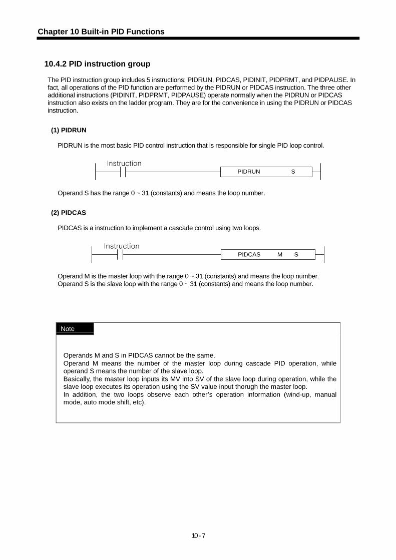
Chapter 10 Built-in PID Functions
10 - 7
10.4.2 PID instruction group The PID instruction group includes 5 instructions: PIDRUN, PIDCAS, PIDINIT, PIDPRMT, and PIDPAUSE. In fact, all operations of the PID function are performed by the PIDRUN or PIDCAS instruction. The three other additional instructions (PIDINIT, PIDPRMT, PIDPAUSE) operate normally when the PIDRUN or PIDCAS instruction also exists on the ladder program. They are for the convenience in using the PIDRUN or PIDCAS instruction.
(1) PIDRUN
PIDRUN is the most basic PID control instruction that is responsible for single PID loop control.
PIDRUN SInstruction
Operand S has the range 0 ~ 31 (constants) and means the loop number.
(2) PIDCAS
PIDCAS is a instruction to implement a cascade control using two loops.
PIDCAS M SInstruction
Operand M is the master loop with the range 0 ~ 31 (constants) and means the loop number. Operand S is the slave loop with the range 0 ~ 31 (constants) and means the loop number.
Note
Operands M and S in PIDCAS cannot be the same. Operand M means the number of the master loop during cascade PID operation, while operand S means the number of the slave loop. Basically, the master loop inputs its MV into SV of the slave loop during operation, while the slave loop executes its operation using the SV value input thorugh the master loop. In addition, the two loops observe each other’s operation information (wind-up, manual mode, auto mode shift, etc).

Chapter 10 Built-in PID Functions
10 - 8
(3) PIDINIT
PIDINIT is used to initialize the settings and states of the current PID loop. All the setting values of the corresponding loop are initialized as 0 (Off in case of bit).
PIDINIT SInstruction
Operand S has the range 0 ~ 31 (constants) and means the loop number.
(4) PIDPRMT PIDPRMT facilitates parameter changes in the loop memory configuration. As soon as the contact is On, the main setting values of the PIDRUN instruction (SV, T_s, K_p, T_i, T_d) are simultaneously changed to the values set by the user. Make sure that each of the 5 setting values holds its respective data type as shown the table below.
PIDPRMT S DInstruction
Device Parameter Data Type Setting Ex. Actual Unit
S+0 SV [WORD] 5000
S+1 Ts [WORD] 1000 0.1 msec
S+2 Kp [REAL] 3.32 sec
S+4 Ti [REAL] 9.3 sec
S+6 Td [REAL] 0.001 sec Operand S represents the first word address of the place the parameter to be changed is stored. Operand D has the range 0 ~ 31 (constants) and means the loop number.
(5) PIDPAUSE PIDPAUSE is used to switch the corresponding loop from the PIDRUN state to the PIDPAUSE state.
PIDPAUSE SInstruction
Operand S has the range 0 ~ 31 (constants) and means the loop number.

Chapter 10 Built-in PID Functions
10 - 9
10.5 PID Flag Configuration The table below shows the PID flag configuration for use of the built-in PID function.
KDevice Zone Symbol Data Type Content K10000+m _PIDn_MAN Bit PID Output Select (0:Auto, 1:Manual) K10020+m _PIDn_PAUSE Bit PID Pause (0: STOP/RUN 1:PAUSE) K10040+m _PIDn_REV Bit PID Operation Select (0:Fwd, 1:Rev) K10060+m _PIDn_AW2D Bit PID Anti Wind-up2 Prohibited (0:Operated, 1:Prohibited) K10080+m _PIDn_REM_RUN Bit PID Remote (HMI) Run bit (0:STOP, 1:RUN) K10100+m _PIDn_P_on_PV Bit PID Proportional Calculation Source Select (0:ERR, 1:PV) K10120+m _PIDn_D_on_ERR Bit PID Derivative Calculation Source Select (0:PV, 1:ERR) K10140+m _PIDn_AT_EN Bit PID Auto-tuning Setting (0:Disable, 1:Enable)
K10160+m _PIDn_MV_BMPL Bit MV Non-impact Conversion for PID Mode Conversion (A/M) (0:Disable, 1:Enable)
K1024+32n _PIDn_SV INT PID Set Value (SV) - Loop n K1025+32n _PIDn_T_s WORD PID Operation Cycle (T_s)[0.1msec] - Loop n K1026+32n _PIDn_K_p REAL PID P - Constant (K_p) - Loop n K1028+32n _PIDn_T_i REAL PID I - Constant (T_i)[sec] - Loop n K1030+32n _PIDn_T_d REAL PID D - Constant (T_d)[sec] - Loop n K1032+32n _PIDn_d_PV_max WORD PID PV Variation Limit - Loop n K1033+32n _PIDn_d_MV_max WORD PID MV Variation Limit - Loop n K1034+32n _PIDn_MV_max INT PID MV Maximum Value Limit - Loop n K1035+32n _PIDn_MV_min INT PID MV Minimum Value Limit - Loop n K1036+32n _PIDn_MV_man INT PID Manual Output (MV_man) – Loop n K1037+32n _PIDn_STATE WORD PID State - Loop n K10370+320n _PIDn_ALARM0 Bit PID Alarm 0 (1:T_s The setting is low) - Loop n K10371+320n _PIDn_ALARM1 Bit PID Alarm 1 (1:K_p is 0) - Loop n K10372+320n _PIDn_ALARM2 Bit PID Alarm 2 (1:PV Variation Limited) - Loop n K10373+320n _PIDn_ALARM3 Bit PID Alarm 3 (1:MV Variation Limited) - Loop n K10374+320n _PIDn_ALARM4 Bit PID Alarm 4 (1:MV Maximum Value Limited) - Loop n K10375+320n _PIDn_ALARM5 Bit PID Alarm 5 (1:MV Manimum Value Limited) - Loop n K10376+320n _PIDn_ALARM6 Bit PID Alarm 6 (1:AT Abnormal Cancel)- Loop n K10377+320n _PIDn_ALARM7 Bit PID Alarm 7 - Loop n K10378+320n _PIDn_STATE0 Bit PID State 0 (0:PID_STOP, 1:PID_RUN) - Loop n K10379+320n _PIDn_STATE1 Bit PID State 1 (0:AT_STOP, 1:AT_RUN) - Loop n K1037A+320n _PIDn_STATE2 Bit PID State 2 (0:AT_UNDONE, 1:DONE) - Loop n K1037B+320n _PIDn_STATE3 Bit PID State 3 (0:REM_STOP, 1:REM_RUN) - Loop n K1037C+320n _PIDn_STATE4 Bit PID State 4 (0:AUTO_OUT, 1:MAN_OUT) - Loop n K1037D+320n _PIDn_STATE5 Bit PID State 5 (0:CAS_STOP, CAS_RUN) - Loop n K1037E+320n _PIDn_STATE6 Bit PID State 6 (0:SLV/SINGLE, 1:CAS_MST) - Loop n K1037F+320n _PIDn_STATE7 Bit PID State 7 (0:AW_STOP, 1:AW_ACT) - Loop n K1038+32n _PIDn_PV INT PID Current Value (PV) - Loop n K1039+32n _PIDn_PV_old INT PID Previoius Current Value (PV_old) - Loop n K1040+32n _PIDn_MV INT PID Output Value (MV) - Loop n K1041+32n _PIDn_MV_BMPL_val WORD PID Non-impact Operation Memory - Loop n K1042+32n _PIDn_ERR DINT PID Control Error Value - Loop n K1044+32n _PIDn_MV_p REAL PID Output Value P Component - Loop n K1046+32n _PIDn_MV_i REAL PID Output Value I Component - Loop n K1048+32n _PIDn_MV_d REAL PID Output Value D Component - Loop n K1050+32n _PIDn_DB_W WORD PID Dead Band Setting (Operation after Stabilization) – Loop n K1051+32n _PIDn_Td_lag WORD PID Differention Function Lag Filter – Loop n K1052+32n _PIDn_AT_HYS_val WORD PID Auto-tuning Hysteresis Setting - Loop n K1053+32n _PIDn_AT_SV INT PID SV Setting for Auto-tuning - Loop n K1054+32n _PIDn_AT_step WORD PID Auto-tuning Display (User Setting Prohibited) - Loop n K1055+32n _PIDn_INT_MEM WORD PID Internal Memory (User Setting Prohibited) – Loop n
* : User setting prohibited * n : PID loop number in decimal form * m : PID loop number in hexadecimal form

Chapter 10 Built-in PID Functions
10 - 10
The PID instruction uses part of the K device to perform operation. When the PID function is not used, the K device can be used as a general Keep Relay. The area of K0000 ~ K0999 is not used by the PID function so as to guarantee compatability with previous PLC models and secure the user’s area. K10000 ~ K1023F is the common bit area for all PID loops. The bit states and settings of the loops are collectively arranged in the front part of the PID area. Thirty two - the maximum number of loops that can be used by the PID function - bits comprise a double word and the states and settings of each loop are stored in each bit order. But the loop number is represented in hexadecimal form. K1024 ~ K1055 is the individual data area for PID Loop 0, where the settings and states of Loop 0 are stored. In this area are stored the settings for PID Loop 0 (SV, dPV_max, MV_man, T_s, Kp, Ti, Td, MV_max, MV_min, dMV_max) and, while the PID function is performed, the states for PID Loop 0 (PV, ETC, MV, MV_rvs, ERR, MVp, Mvi, MVd, PV). By writing data into the set memory area, the user can change the PID setting at any time even during operation and obtain the corresponding results in the next cycle. K1056 ~ K2047 is the memory part of Loops 1 ~ 31 that are in the same form as Loop 0. Each loop operates independently. If the user wants a dependent operation such as application of cascade, then he must do some work to connect the states and settings of the loop. In addition, please refer to the K device memory configuration in the latter part of this manual for an understanding of the accurate memory location of PID. For performance improvement of the product, the location and order of the memory area is subject to change without prior notice.
Note
1) PID Memory Description Format _PIDn_MAN n : Loop number Ex) _PID10_MAN : Means MAN of Loop 10.
2) Common Bit Area
Ex) K10040+ (25) = K10040+ (19h) = K10059 : PID25_REV bit of Loop 25 3) Individual Data Area
Ex) K1024+ (32*1) = K1056 : SV of Loop 1

Chapter 10 Built-in PID Functions
10 - 11
10.5.1 Common bit area The common bit area is the part that contain all bit data for the 32 loops. All information 32 loops have for a signel item is combined to take the form of 32 bit double word; the nth bit provides information on the nth loop; m is the hexadecimal value of loop number n.
(1) _PIDn_MAN (PID MANual operation enable) - Setting Area K Device Area : K10000+m Unit : Bit This allows you to determine whether the PID function of the nth loop will operate in AUTO or in Manual. In AUTO, the result of performing a normal PID operation is output; In MANUAL, a random Set Value desired by the user (_PIDn_MV_man) is output without performing the PID operation. If the corresponding bit is Off, then it is set to [Default] AUTO.
(2) _PIDn_PAUSE (PID PAUSE mode) - Setting Area K DEVICE AREA : K10020+m Unit : Bit This allows the nth PID Loop to enter into PAUSE Even when switching from PAUSE to RUN again, the control continues to operate. If the system state is changed in PAUSE, the control system may produce an unexpected result. So, be very careful when using the the PAUSE function. If the corresponding bit is Off, [Default] PAUSE is cleared.
(3) _PIDn_REV (PID REVerse operation) - Setting Area K DEVICE AREA : K10040+m Unit : Bit This allows you to set the control system as Forward system or Reverse system. If the system state rises as the system input value rises, it is defined as Forward system; If the system states falls as the system input value rises, it is Reverse system. A boiler is a Forward system because the temperature rises as the system input rises; a cooler is a Reverse system because the temperature falls as the system input rises. If the corresponding bit is Off, it is set to [Default] Forward system.
Note
_PIDn_PAUSE (1) Putting the PID loop into PAUSE by using PIDn_PAUSE and PIDPAUSE brings all
operations to a stop and outputs the last calculation values before PAUSE. If the system state is changed but proper control is not exercised, the control system may produce an unexpected result. So, be very careful when using the the PAUSE function.
(2) In the first PLC scan, PIDRUN performs initialization to turn the PAUSE bit to Off. If PLC is turned on in PAUSE, it quits the PAUSE mode and enters into the STOP or Run mode.

Chapter 10 Built-in PID Functions
10 - 12
(4) _PIDn_AW2D (PID Anti Wind-up 2 Disable) - Setting Area K DEVICE AREA : K10060+m Unit : Bit If this bit is turned OFF at the user’s will, The Anti Wind-up2 function is inactivated. The Anti Wind-up function is described in detail in 10.6. If the corresponding bit is Off, [Default] Anti Wind-up2 is enabled.
(5) _PIDn_REM_RUN (PID REMote RUN) - Setting Area K DEVICE AREA : K10080+m Unit : Bit This is the external operation instruction of PIDRUN and has the same effect as when the contact of PIDRUN is turned On/Off. In fact, PIDRUN performs an OR operation of the “PIDRUN input oondition” contact and the corresponding bit in order to decide whether to perform the operation. Using this function enables you to assign the operation contact of PIDRUN to a fixed address, facilitating easier use of external input/output devices such as HMI. If the corresponding bit is Off, [Default](the contact is Off) PIDRUN comes to STOP.
(6) _PIDn_P_ov_PV (PID P on PV) - Setting Area K DEVICE AREA: K10100+m Unit : Bit This sets the P operation source of the corresponding PID loop to PV. P operation is performed on ERR or PV. P operation moves relatively slowly to a stable state when using PV than when using ERR under the unstable instantaneous control due to initial response or disturbance. This implies that the change in output is slow and a heavy load is not imposed on the driver. But, with the change in the range of the internal operation value, the Anti Wind-up function does not operate. If the corresponding bit is Off, PID performs P operation on the ERR value and, if it is On, P operation is performed on the PV value.
(7) _PIDn_D_on_ERR (PID D on ERRor) - Setting Area K DEVICE AREA : K10120+m Unit : Bit This sets the D operation source of the corresponding PID loop to ERR. D operation is performed on ERR or PV. In case of D operation using ERR, D response shows a dramatic change at the moment SV is changed by the user and an excessive input may be applied to the driver. To prevent this, the method of using PV for D operation is used and the [Default] value is also set to support D operation using PV. Using ERR without this algorithm turns the corresponding bit On. If the corresponding bit is Off, PID performs D operation on the PV value and, if it is On, D operation is performed on the ERR value. Note
_PIDn_REM_RUN This bit is stored in the K device even though the PLC stops. If the PLC is stopped and restarted with this bit On (eg. power outage), the system is initialized at the first scan and then PIDRUN operates.

Chapter 10 Built-in PID Functions
10 - 13
(8) _PIDn_AT_EN (PID Auto-Tuning ENable) - Setting Area K DEVICE AREA : K10140+m Unit : Bit This performs AT (Auto-tuning) of the corresponding PID loop. The approximate T_s (operation cycle) and PID coefficients (K_p, T_i, T_d) of the systemare are determined through AT. Do not forget to set the PIDn_HYS_val item before starting AT. The AT function is described in detail in 10.6. If the corresponding bit is Off, the [Default] AT function is Disabled and AT is performed in the rising edge.
(9) _PIDn_MV_BMPL (PID MV BuMPLess changeover) - Setting Area K DEVICE AREA : K10160+m Unit : Bit This allows to not only determine an appropriate MV value through operation so that MV can continue smoothly when the corresponding PID loop changes from manual to auto output mode, but also reflect the MV value to the internal state so as to stabilize MV. This function shows an algorithm difference between single operation and cascade operation, but both operations are performed by this bit. If the corresponding bit (in cascade operation, the corresponding bit of the master loop) is On, Bumpless changeover is performed. If it is Off, The [Default] Bumpless changeover function is Disabled.
Note
_PIDn_AT_EN This bit is initialized as Off when the PLC changes to Run mode. If the PLC is stopped and restarted with this bit On (eg. power outage), the system is initialized at the first scan but does not enter into AT mode again. Since there is no change in the PID settings, the system operates in the state before the PLC stops. _PIDn_MV_BMPL Assuming that the manual output value is 1000 and the auto output of 2000 is required, the driver receives the value of 1000 for system operation and instantly receives 2000 at the time of mode conversion. If the corresponding bit is On, the corresponding PID loop outputs 1000 at the time of mode conversion and performs an operation in order that the output gradually increases to 2000.

Chapter 10 Built-in PID Functions
10 - 14
10.5.2 Individual data area The individual data area is in the range of K1024 ~ K2047 and a 32 word length is assigned for each of 32 loops. So, the individual data area of the nth loop is K (1024+32n) ~ K (1055+32n).
(1) _PIDn_SV (PID Set-point Value) - Setting Area K DEVICE AREA : K1024+32n Unit : INT [ -32768 ~ 32767 ] This is the SV setting part of the corresponding loop. As described in the previous section, this is used to set the system state as desired by the user. The system state is displayed in numeral and must be input after converted to PV according to the system gain. In case of a system in which PV is sensed as 5000 at the temperature of 50 , if the temperature controlled at 50 , SV is set to 5000.
(2) _PIDn_T_s (PID Sampling Time) - Setting Area K DEVICE AREA : K1025+32n Unit : WORD [ 0 ~ 65535 ] This sets the sampling time of the corresponding loop. The sampling time is a time cycle in which a control operation is performed. This can be set in the range of 0.1msec to 6553.5 msec in the unit of 0.1msec; an integer value of 1 is assigned for each 0.1ms. If 100ms of sampling time is required, 1000 is input to _PIDn_T_s. If the user sets the sampling time to 0, the scan cycle control mode is also set. In this case, as a control operation occurs in each scan, a full speed control operation is performed in the current environment. When the current scan speed is exceeeded due to the too short sampling time, The ALARM bit of _PIDn_STATE is displayed.
(3) _PIDn_K_p (PID Propotional Gain) - Setting Area K DEVICE AREA : K1026+32n Unit : REAL [ -3.40282347e+38 ~ -1.17549435e-38 , 0 , 1.17549435e-38 ~ 3.40282347e+38 ] This sets the proportional constant for the corresponding loop. As K_p is multiplied into the P, I, D (Proportional, Integral, Derivative) terms, the larger K_p is, the larger the proportional and derivative effects are and the smaller the integral effect is. If _PIDn_K_p is set to 0, P control is not performed. For more details, refer to 10.6. K_p can be set in the short/long real number (REAL) range.
Note
_PIDn_SV PID changes the output (MV) through several times of operations until SV equals PV. So, when SV is 0, PIDRUN may be seen as inoperable. If SV of a simple heater with the current temperature of 20 and PV of 2000 (20 PID will output 0 as MV and will not output until PV goes below 0 (0 ).

Chapter 10 Built-in PID Functions
10 - 15
(4) _PIDn_T_i (PID integral Time gain) - Setting Area K DEVICE AREA : K1028+32n Unit : REAL [ -3.40282347e+38 ~ -1.17549435e-38 , 0 , 1.17549435e-38 ~ 3.40282347e+38 ] This sets the integral time constant (T_i) of the corresponding loop. As T_i divides the I (integral) term, the larger T_i, the smaller the integral effect. If _PIDn_T_i is set to 0, I control is not performed. For more details, refer to 10.6. T_i can be set in the short/long real number (REAL) range.
(5) _PIDn_T_d (PID derivative Time gain) - Setting Area K DEVICE AREA : K1030+32n Unit : REAL [ -3.40282347e+38 ~ -1.17549435e-38 , 0 , 1.17549435e-38 ~ 3.40282347e+38 ] This sets the derivative time constant (T_d) of the corresponding loop. As T_d is multiplied into the D (derivative) term, the larger T_d, the larger the derivative effect. If _PIDn_T_d is set to 0, D control is not performed. For more details, refer to 10.6. T_d can be set in the short/long real number (REAL) range.
(6) _PIDn_dPV_max(PID delta PV MAXimum limit) - Setting Area K DEVICE AREA : K1032+32n Unit : WORD [ 0 ~ 65535 ] This limits the PV variation of the corresponding loop. In actual control, PV does not always reflect the exact system state. Unwanted signals caused by sensor malfunction, noise or disturbance can be mixed and reflected in PV. Like this, PV often undergoes a sudden change and causes a large change in PID output. It is a priority to prevent a PV change greater than the value set in _PIDn_dPV_max. Meanwhile, if _PIDn_dPV_max is set too small, the system change is slowly reflected and the convergence time takes longer. Therefore, setting should be made according to the system features. If this is set to 0, the function does not operate.
(7) _PIDn_dMV_max (PID delta MV MAXimum limit) - Setting Area K DEVICE AREA : K1033+32n Unit : WORD [ 0 ~ 65535 ] This limits the MV variation of the corresponding loop. A sudden change in the output of the control system may cause a system instability or impose a heavy load on the driver resulting in failure or unstable operation. To prevent this, this item limits the controller output variation. If this is set to 0, the function does not operate.

Chapter 10 Built-in PID Functions
10 - 16
(8) _PIDn_MV_max (PID MV MAXimum limit) - Setting Area K DEVICE AREA : K1034+32n Unit : INT [ -32768 ~ 32767 ] This limits the maximum MV value of the corresponding loop. This prevents overload and system errors by limiting the maximum value of the controller output transferred to the output equipment. This also prevents the transfer of an unwanted value by overflow. If PIDn_MV_max and PIDn_MV_min are both set to 0, this function does not operate.
(9) _PIDn_MV_min (PID MV MINimum limit) - Setting Area K DEVICE AREA : K1035+32n Unit : INT [ -32768 ~ 32767 ] This limits the minimum MV value of the corresponding loop. This prevents system errors by limiting the minimum value of the controller output transferred to the output equipment. This also prevents the transfer of an unwanted value by overflow.
(10) _PIDn_MV_man (PID MANual MV variable) - Setting Area K DEVICE AREA : K1036+32n Unit : INT [ -32768 ~ 32767 ] When the corresponding loop is set to manual operation, this designates MV. If _PIDn_MAN in the common bit area is ON, the PIDn_MV_man value is output as the MV value of the corresponding loop.
(11) _PIDn_STATE (PID STATE) - Setting Prohibited K DEVICE AREA : K1037+32n or K10370+320n ~ K1037F+320n Unit : WORD [ h00 ~ hff ] or BIT This displays the state or abnomalities of the corresponding loop. This is located at the address K1037+32n and each of the 16 bits has its own meaning. Only some of the 16 bits are currently in use. STATE turns On when the corresponding operation occurs and returns Off when it is cleared. The upper 8 bits of STATE (_PIDn_ALARM 0~_PIDn_ALARM 7) display abnormalities of the loop. The lower 8 bits of STATE (_PIDn_STATE 0~_PIDn_STATE 7) displays the control state of the loop. Each bit is assigned as follows. _PIDn_ALARM 0 (K10370+32n): Indicates the operation is skipped because T_s is set too small set. _PIDn_ALARM 1 (K10371+32n): Indicates the K_p value is 0. _PIDn_ALARM 2 (K10372+32n): Indicates the PV variation is limited. _PIDn_ALARM 3 (K10373+32n): Indicates the MV variation is limited. _PIDn_ALARM 4 (K10374+32n): Indicates the maximum MV value is limited. _PIDn_ALARM 5 (K10375+32n): Indicates the minimum MV value is limited. _PIDn_ALARM 6 (K10376+32n): Indicates AT has been canceled abnormally. _PIDn_STATE 0 (K10378+32n): Indicates PID operation is performed. (valid in case of PLC Run) _PIDn_STATE 1 (K10379+32n): Indicates PID AT is being performed. _PIDn_STATE 2 (K1037A+32n): Idicates PID AT has been completed. _PIDn_STATE 3 (K1037B+32n): Indicates PID is in remode operation by _PIDn_REM_RUM bit. _PIDn_STATE 4 (K1037C+32n): Indicates PID is in manual output mode. _PIDn_STATE 5 (K1037D+32n): Indicates the PID loop belongs to cascade. _PIDn_STATE 6 (K1037E+32n): Indicates the PID loop is the cascade master loop. _PIDn_STATE 7 (K1037F+32n): Indicates Aniti Wind-up is in operation during PID operation.

Chapter 10 Built-in PID Functions
10 - 17
(12) _PIDn_PV (PID Process Variable) - Input/Output Area K DEVICE AREA : K1038+32n Unit : INT [ -32768 ~ 32767 ] This displays the PV of the corresponding loop. PV is an indicator of the current state of the system. In general, the input from the sensor is stored on the U device of the CPU via an input device such as A/D conversion module: At each scan, this value should be transferred to _PIDn_PV using a instruction such as MOV. Please refer to the program examples in the latter part of this manual.
(13) _PIDn_PV_old (PID previous PV) - Setting Prohibited
K DEVICE AREA : K1039+32n Unit : INT [ -32768 ~ 32767 ] This is used internally for derivative and integral operations at a step prior to the PV state of the corresponding loop. This can be referred to when necessary. Input of a random value will lead to a malfunction.
(14) _PIDn_MV (PID Manipulated output Variable) - Input/Output Area K DEVICE AREA : K1040+32n Unit : INT [ -32768 ~ 32767 ] This displays the MV of the corresponding loop. MV is a signal source for system startup. Contrary to the description of _PID_PV in (12), this values is transferred at each scan to the U device using a instruction such as MOV and then used as a system startup input via an output device such as D/A conversion module. Please refer to the program examples in the latter part of this manual.
(15) _PIDn_MV_BMPL_val (PID MV BuMPLess changeover VALue) - Setting Prohibited K DEVICE AREA : K1041+32n Unit : WORD [ 0 ~ 65535 ] This stores the information necessary for the Bumpless changeover operation of the corresponding loop. The corresponding memory is automatically set and input by PID-internal operation and this value should not be set by the user.
Note
Bumpless Change Over When the PID controller is converted to manual output mode and back again to auto output mode, the output is increased again from 0 as in a freshly started control system. This causes a mode conversion impact to the system. To avoid this, the MV_BMPL function is used; when the current system is converted to auto mode with the corresponding bit authorized, this senses the system’s last state in manual mode and lets the control output continue smoothly from that point. Furthermore, with the master loop MV_BMPL in cascade control authorized, the master loop senses the state of the slave loop and generates a smoothly continuing control output.

Chapter 10 Built-in PID Functions
10 - 18
(16) _PIDn_ERR (PID ERRor value) - Setting Prohibited K DEVICE AREA : K1042+32n Unit : DINT [ -2747483648 ~ 2747483647 ] This is the current error value of the corresponding loop. An error value in PID is defined as SV – PV. This is used as an indicator of how far the current state is from the desired state. If the error is 0, it means the control system reaches its desired state. The control system can be considered ideal if, when a control starts, the error rapidly decreases in the transient state and, when it reaches the normal state, vibration is minimized and the offset(the error in the stable state) is kept at 0.
(17) _PIDn_MV_p (PID MV Propotional component) - Setting Prohibited K DEVICE AREA : K1044+32n Unit : REAL [ -3.40282347e+38 ~ -1.17549435e-38 , 0 , 1.17549435e-38 ~ 3.40282347e+38 ] This displays the proportional control value of the corresponding loop. If the error of the current system is known, its integral and derivative control output values can also be calculated independently. Comparing the 3 output values enables to determine the exact operational state of the control system and PID control. MV is the sum of MV_p, MV_i, and MV_d.
(18) _PIDn_MV_i (PID MV Integral component) - Setting Prohibited K DEVICE AREA : K1046+32n ~ K1047+32n Unit : REAL [ -3.40282347e+38 ~ -1.17549435e-38 , 0 , 1.17549435e-38 ~ 3.40282347e+38 ] This displays the integral control value of the corresponding loop.
(19) _PIDn_MV_d (PID MV Derivative component) - Setting Prohibited K DEVICE AREA : K1048+32n ~ K1049+32n Unit : REAL [ -3.40282347e+38 ~ -1.17549435e-38 , 0 , 1.17549435e-38 ~ 3.40282347e+38 ] This displays the derivative control value of the corresponding loop.
(20) _PIDn_DB_W (PID DeadBand Width) - Setting Area K DEVICE AREA : K1050+32n Unit : WORD [ 0 ~ 65535 ] This sets the deadband of the corresponding loop. The deadband is set to a positive value and operates in the range from [SV – DB_W] ~ [SV + DB_W]. If PV enters the area, SV is assigned to the PV value. If this value is set to 0, the corresponding function does not operate.
Note
Deadband This is used to let PV fully approach SV during system control so as to eliminate fine output viariations due to fine state changes. Input of a value to DB_W during PID control forms a deadband from [SV – DB_W] ~ [SV + DB_W]. If PV follows SV into the deadband during control, ERR is forcibly calculated as 0 and, as far as PV remains in this area, the MV variation stops. This has the same effect as stopping the controller for a while in the stabilization area and helps avoiding a heavy load on the driver during stabilization operation. It is recommended to fully stabilize the system before use in the area to be set as the deadband. Otherwise, when entering the deadband, the controller experiences a temporary output excess.

Chapter 10 Built-in PID Functions
10 - 19
(21) _PIDn_Td_lag (PID Td lag filter) - Setting Area K DEVICE AREA : K1051+32n Unit : WORD [ 0 ~ 65535 ] This sets the primary delay filter for the corresponding loop so as to allow the derivative effect acting as an instantaneous impact to act more slowly and continuously. If the corresponding value is set high, the derivative effect becomes smoother and, if it set to 0, the corresponding function does not operate. The derivateive value leads the system output to low vibration and helps avoid a heavy load on the driver.
(22) _PIDn_AT_HYS_val (PID Auto-Tuning HYSteresis value) - Setting Area K DEVICE AREA : K1052+32n Unit : INT [ -32768 ~ 32767 ] This sets a directional deadband appropriate for AT. The _PIDn_AT_HYS_val value operates differently as a upper deadband when PV increases and as a lower deadband when PV decreases. Proper setting of this value is critical for successful AT. Setting _PIDn_AT_HYS_val is described in 10.7.4.
(23) _PIDn_AT_SV (PID Auto-Tuning SV) - Setting Area K DEVICE AREA : K1053+32n Unit : INT [ -32768 ~ 32767 ] This separately sets AT_SV to be used as SV for AT of the corresponding loop. AT enables PV to vibrate 3 times up and down around AT_SV.
(24) _PIDn_AT_step (PID Auto-Tuning step) - Setting Prohibited K DEVICE AREA : K1054+32n Unit : INT [ -32768 ~ 32767 ] This displays the AT operation state of the corresponding loop. _PIDn_AT_step has values from 0 to 7; 0 indicates “before AT operation” and 7 indicates “AT operation completed”. 1, 3 and 5 indicate the PV-increasing areas and 2, 4 and 6 indicate the PV-decreasing area.
Caution 1) Setting Prohibited : The items marked with – Setting Prohibited are prohibited from being
set by the user. The corresponding area not only provides the user with operational information but also stores information necessary for operations. A random setting of the corresponding area causes the malfunction of the control system.
2) Input/Output Area : _PIDn_PV and _PIDn_MV belong to - Input/Output Area, so use them in a way they are connected to external equipment (AD, DA device).

Chapter 10 Built-in PID Functions
10 - 20
Note
Transient and Normal States 1) Transien State : A state during which the control system starts its control operatoin and
reaches the desired control state; there often occurs an instantaneous output variation and, while the integral value approaches stability, there may occur a vibration or overshoot.
2) Normal State : A state during which the control system reaches the desired state after
passing through the transient state; vibration is eliminated, there may occur an offset and there is little change in the output value.
Upper / Lower Deadbands When the analog output of the sensor is converted into a digital signal by means of an AD device, much of the signal is mixed with noise. The PID control instruction executes Auto-tuning using this converted value; it enables PV to increase and dedcrease 3 times up and down at SV. In the course of this process, if noise is input at the time when SV equals PV, a single up and down conversion is incorrectly perceived as multiple conversions. This is the same effect as the chattering of the digital switch. To overcome this, the PID controller uses a unidirectional deadband (Hysteresis); when the PV value of the system increases toward SV, the set deadband value operates in the upper part of SV and when the PV value passes SV and decreases, the set deadband value operates only in the lower part of SV.
Time
SV
PV
Mode Transition
Mode Transition
Upper Deadband
LowerDeadband
Upper Deadband

Chapter 10 Built-in PID Functions
10 - 21
10.6 Convenient Additional Functions of PID Instructions This section describes additional functions that can be conveniently used in combination with the PID instructions.
10.6.1 Various PID-based control methods
Commonly used among PID controls are P control, PI control, PD control and PID control. When a certain feature (mostly stabilization) is required, ID control, I control or D control is often used though they are somehow more complicated. To implement these various controls, PIDRUN includes functions that allow or prevent controls by P, I, and D, respectively. In case of P control, the P controller can be configured by setting _PIDn_Ti and _PIDn_Td to 0. Similary, the ID controller can be obtained by setting _PIDn_Kp to 0 and assigning ID control coefficients to _PIDn_Ti and _PIDn_Td. One special thing about the PIDRUN instructions is that, in case of ID control, setting _PIDn_Kp to 0 theoretically results in the controller output of 0. (Refer to Expressions 10.3.2 ~ 10.3.5) Actually, however, PIDRUN, if 0 is input to _PIDn_Kp, internally calculates as MVp = 0 and K_p = 1, thus enabling ID, I control and D control. For example, when PI control is required, only _PIDn_Kp and _PIDn_Ti are set and 0 is input to _PIDn_Td. When ID control is required, _PIDn_Kp is set to 0 and only _PIDn_Ti and _PIDn_Td are set.
10.6.2 Operation and function of anti wind – up
PIDRUN provides 2 Wind-up prevention functions: Anti Wind-up 1 and Anti Wind-up 2. The more basic of the two, Anti Wind-up 1 operates for all I-related controls - I control, PI control, ID control and PID control - and cannot be cleared. This operates by limiting Mvi (the integral term results) using _PIDn_MV_max, _PIDn_MV_min. Aniti Wind-up 2 is organically connected to MVp (the proportional term results). In case MV reaches 土 (_PIDn_MV_max) on MVp only, regardless of the MVi and MVd values, due to a large system error, Mvi does not perform a calculation but keeps the previous value. In case the error is large, PV is brought near SV (operating point) by MVp, not by Mvi or MVd, and then I control is resumed to prevent and excessive value from being entered into Mvi. The operation of Anti Wind-up 2 can be cleared by the user by setting the _PIDn_AW2D bit on the common bit area to On. This operates only during PI control or during a control combining P control and I control, e.g. PID control.
10.6.3 Operation and function of Auto-tuning (AT)
PIDRUN has an AT function that enables to test operate the system though several basic settings and calculate _PIDn_T_s, _PIDn_K_p, _PIDn_T_i and _PIDn_T_d appropriate for the system. The values of _PIDn_MV_min, _PIDn_MV_max, _PIDn_AT_HYS_val, and _PIDn_AT_SV should be set before AT. Based on these values, the AT function sets and operates MV over 3 different times in order, examines the repeated system state (PV) reaction, measures the time taken for the system state (PV) to reach the AT Set Value ( (AT_SV) and the vibration level, and accordingly calculates _PIDn_T_s, _PIDn_K_p, _PIDn_T_i and _PIDn_T_d. To calculate the exact tuning value, please refer to “AT Setting” in1.7.4 for proper AT operation.
Note
Deletion of Previious Data upon Completionof Auto-tuning (AT)
When the AT operation described in 10.6.3 is completed, the new values of _PIDn_T_s, _PIDn_K_p, _PIDn_T_i and _PIDn_T_d are automatically substituted for the existing values. Note, therefore, that the previous value of _PIDn_T_s, _PIDn_K_p, _PIDn_T_i and _PIDn_T_d are deleted.

Chapter 10 Built-in PID Functions
10 - 22
10.6.4 Operation and function of cascade (CAS)
PDCAS performs cascade PID control through sequential operation of two PID loops. Generally, cascade PID control is used for temperature control through chemical process or fuel control; The two loops used here are called master loop and slave loop. As an example of temperature control through fuel flow, in case of a single loop PID control, the fuel valve is opened and closed to control the fuel flow and consequenctly control the temperature of the heating furnace. This is, therefore, a system in which a single PID loop indirectly controls temperature through fuel flow control. In this case, equipping the system with a fuel flow meter enables cascade PID control that consists of flow control and temperature control: the slave loop controls the flow using the valve and the master loop controls temperature using the flow. The master loop transfers the desired flow to the slave loop, while the slave loop monitors the flow meter and adjusts the flow using the valve so that fuel corresponding to the flow desired by the master loop is injected. The slave loop operates on the flow Set Value set by the master loop, regardless of temperature. In terms of the internal cascade operation, the master loop measures the temperature (PV_mst) in a more delayed manner than the slave loop and transfers the flow value (MV_mst) computed for the user’s desired temperature (MV_mst) to the slave loop. The slave loop sets the flow value (MV_mst) transferred from the master loop as the Set Value (SV_slv) and measures the fuel injection amount (PV_slv) in a more frequent manner than the master loop in order to control the valve opening and closing (MV_slv). Cascade, therefore, functions to transfer MV (MV_mst) of the master loop to SV (SV _slv) of the slave loop when two loops are in operation. If the slave loop is converted to manual output mode, the master output is not used and the master loop is also converted to manual output mode. The manual mode _PIDn_MAN bit is not turned ON in the master loop. If the slave loop is converted to auto output mode again, the master loop is also turned to auto output mode. If _PIDn_MV_BMPL is set to On, state data is exchanged between the two loops to ensure a smooth conversion. If the slave loop is in Anti Wind-up mode, the master loop operates in PIDPAUSE mode. When there is a need to increase or descrease the slave Set Value (SV_mst) despite the occurrence of anti wind-up, this function prevents the occurrence of 2nd wind-up for the whole cascade loop. This function always operates according to the corresponding conditions and the _PIDn_PAUSE bit is not turned On.
Master Loop
Slave Loop
Valve Flowmeter
Heater
Heating Furnace
Thermometer
Fuel
PV_mst
User
SV_mstSV_slv = MV_mst
MV_slv PV_slv
Cascade loop
Note
Auto-tuning (AT) of Cascade System
In case of AT of a cascade system, AT of the slave loop precedes AT of the master loop. For AT of the slave loop, it is required to predict how much SV the slave loop receives from the master loop and setting AT_SV to this value enables the slave loop to operate as an independent loop. AT performance may differ according to the predicted value. Upon completion of AT of the slave loop, AT of the master loop starts.

Chapter 10 Built-in PID Functions
10 - 23
10.7 How to Use PID Instructions This section describes how to use PID instructions. For detailed description of the functions of the CPU, specific modules and XG5000, refer to the corresponding manuals.
10.7.1 Hardware configuration The example system has a configuration as shown below.
User SV PID operation
CPU module
Sensor
AD Conversion
’mode
DAConversion
moduleControl object
PV
User
Auto mode
Manual mode
MV_manual
MVMV
Driver
(1) CPU (XGK-CPUH)
The CPU is where PID operation occurs and so can be called “PID controller”. The controller receives data sensed from the input module, calculates a proper output through operation, and then transfers it to the output module. What the user should do is to connect input and output and design the interior of the PID controller (tuning). Generally, analog input module and analog output modules are used for input and output, respectively.
(2) Analog Input Module (XGF-AV8A)
This functions to receive the state of the control object from the sensor and transfer it to the CPU. The analog input module channel 0 enables to receive a voltage of 0 V ~ 5 V as input and transfer its digital value to the PLC as output. There are 8 channels (CH 0 ~ CH 7) in XGF-AV8A. The setting for XGXGF-AV8A can be changed through the I/O parameter setting window that appears when selecting I/O Parameter from the parameter items in the project window. Channel 0 is changed to “Operation” mode and the input range is set to 0 ~ 5 V (according to the sensor). The output data type is the PV value of the PID controller. For PID control, the range of its value is set to 0 ~ 10000. The 0 ~ 5 V signal detected from the sensor during analog input module operation is converted 2,000 times to a digital value of 0 ~ 10000 and then transferred to the PLC.

Chapter 10 Built-in PID Functions
10 - 24
The following figure shows the screen of XGF-AV8A setting in XG5000.
(3) Analog output Module (XGF-DV4A)
The analog output module converts a controller output digital value generated through control operation in the PLC to 4mA ~ 20mA and transfers it to the driver of the control object. The XGF-DV4A model has 4 channels and its setting can be changed through the I/O parameter setting window, as in XGXGF-AV8A. Channel 0 is changed to “Operation” mode and the input range is set to 0 ~ 5 V (according to the driver). The 0 ~ 10000 MV digital output generated through PID control operation is reduced to 1/2000 and then transferred to the signal of the driver. The following figure shows the screen of XGF-DV4A setting in XG5000.
(4) Sensor and Driver
Along with the analog output module and analog input module, the sensor and driver respectively function as the media to transfer the state of the control object to the controller and transfer the controller output to the control object. The output generated from the sensor should be able to be used as the input of the analog input module and the output generated from the analog output module should be able to be used as the input of the driver. For an easy example, if the sensor’s current mode is 4mA ~ 20mA, the analog input module’s current mode should be 4mA ~ 20mA; if the driver’s voltage mode is 0V ~ 5V, the analog output module’s voltage mode should be 0V ~ 5V. The output of the analog output module used as the driving signal of the driver. Using it as the power of the driver may cause malfunction of the PLC due to power loss.

Chapter 10 Built-in PID Functions
10 - 25
(5) Control Object
The current system uses a water level control system as the control object. A water level control system is a stem to maintain a desired water level by pumping water into a water tank whose lower part has a small opening for outflow of water. The water in the tank flows out at a constant rate. The decision to increase or decrease the water level is based on the water inflow. The structure of a water level control system is shown below.
Pump
Inflow
Outflow
Water level
Water level sensor
Driver
Water tank
10.7.2 Program example 1 The following figure shows a program example of performing PID control using analog modules. (In this program, the PID constant value and SV value are set in the Variable Monitor window.)

Chapter 10 Built-in PID Functions
10 - 26
Step 1: Each channel 0 of the analog input and output modules is enabled using the regular On contact. Step 7: The analog input module input data are transferred to PIDRUN Loop 0 PV using the regular On
contact. Step 12: If the user turns the M00000 bit On, control operation of PIDRUN Loop 0 is performed. Step 17: MV output of PIDRUN Loop 0 is transferred to analog output module output data. Step 21: The scan is completed.
10.7.3 PID controlling (1) Variable Registration
Control settings is performed by registering PID variables in the Variable Monitor” window. Clicking the right button of the mouse and then selecting “Register in Variable/Description” in the Variable Monitor window allows you to see the “Variable/Device Select” window. Selecting PID in the “List” box and deselecting “All” and then entering 0 (loop number) in “Parameter Number” allows you to see the variables to store all the settings and states for Loop 0. Selecting all variables and then clicking “Confirm” enables you to monitor the variables or change their values even when the program is in “RUN” mode.
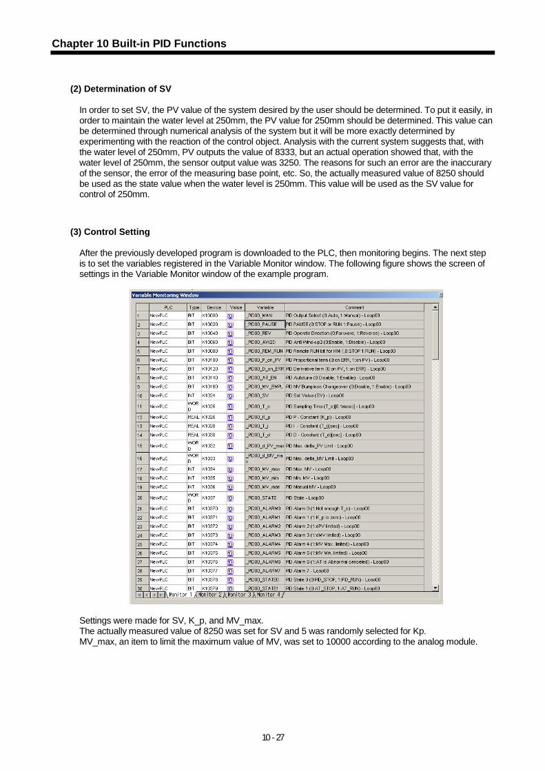
Chapter 10 Built-in PID Functions
10 - 27
(2) Determination of SV In order to set SV, the PV value of the system desired by the user should be determined. To put it easily, in order to maintain the water level at 250mm, the PV value for 250mm should be determined. This value can be determined through numerical analysis of the system but it will be more exactly determined by experimenting with the reaction of the control object. Analysis with the current system suggests that, with the water level of 250mm, PV outputs the value of 8333, but an actual operation showed that, with the water level of 250mm, the sensor output value was 3250. The reasons for such an error are the inaccurary of the sensor, the error of the measuring base point, etc. So, the actually measured value of 8250 should be used as the state value when the water level is 250mm. This value will be used as the SV value for control of 250mm.
(3) Control Setting After the previously developed program is downloaded to the PLC, then monitoring begins. The next step is to set the variables registered in the Variable Monitor window. The following figure shows the screen of settings in the Variable Monitor window of the example program.
Settings were made for SV, K_p, and MV_max. The actually measured value of 8250 was set for SV and 5 was randomly selected for Kp. MV_max, an item to limit the maximum value of MV, was set to 10000 according to the analog module.

Chapter 10 Built-in PID Functions
10 - 28
(4) Observation of Control States Using the Trend Monitor You can enable the trend monitor, one of the monitor functions of XG5000.
The trend monitor can be properly arranged by allowing its docking.
Data to be observed are registered through the trend setting.

Chapter 10 Built-in PID Functions
10 - 29
The monitoring cycle is set to 200m and, after the trend graph tap in the lower part is selected, SV and PV of Loop 0 are registered as INT.
(5) Program Run (Here an example is given to show how to find a parameter manually. For auto tuing, refer to the method below.)
When the contact (M00000) is turned On, the system starts up.
After increasing K_p to 100, the system is started again.
Because K_p is set too large, the system vibrates in a permanent and regular manner. Settings are made as follows: K_p = 20, T_i = 100

Chapter 10 Built-in PID Functions
10 - 30
Because the T_i value is too large, the normal state offset lasts long and there occurs a slight overshoot. Settings are mede as follows: K_p = 10, T_i = 1.
Because T_i is too small, PV fluctuates slowly. Settings are made as follows: K_p = 10, T_i = 5
This is a satisfactory result. After changing T_d to 0.1, the system is started again.

Chapter 10 Built-in PID Functions
10 - 31
The system rocks and the error increases. Since the current system is a slow system that can be fully controlled by PI, only PI control is required. Therefore, the tuning results are as follows: K_p = 10, T_i = 5, T_d = 0

Chapter 10 Built-in PID Functions
10 - 32
10.7.4 How to start up using AT (Auto-tuning)
This section explains the correct AT setting method through operating the system described in 10.7.3 using the AT function. The basic AT function properly operates when the system is not started yet or when the system has PV at least smaller (larger in case of reverse operation) than the _PIDn_AT_SV value. Basically, AT performs different operations in different steps. The step increases from 0 to 7 and the step of the current loop can be known by _PIDn_AT_step. In PIDSTOP mode, the AT step is 0 and increases (automatically) as AT starts. When it reaches 7, AT is completed. The user’s random manipulation of the step may cause malfunction. To avoid redundant descriptions, the procedures from 10.7.3 (1) to (4) are first implemented and then the present settings are applied. First, _PIDn_AT_SV is set. Though the _PIDn_SV value has been already set above, the system is vibrated during Auto-tuning so that PV is more than the _PIDn_SV value. To prevent any harm to the system in the course, an appropriate SV value should be set in _PIDn_AT_SV. For other cases, _PIDn_AT_SV should be set the same with _PIDn_SV. The _PIDn_AT_SV value is used only during AT and, upon completion of AT, the system is automatically started based on _PIDn_SV. Next, _PIDn_MV_min and _PIDn_MV_max are set. During AT, the _PIDn_MV_min and _PIDn_MV_max values are respectively considered as the minimum/maximum output of the system. During AT, the two values differ each other in 3 cycles depending on the system speed (how fast PV reaches around SV). For example, with _PIDn_MV_min = 0, _PIDn_MV_max = 10000, the system driving signal (MV) transferred to the motor or heater repeats the “0 →10000 → 0” output 3 times. If there is a possibility that such a radical change may put a heavy load on the system, _PIDn_dMV should be set. Next, the PIDn_HYS_val value is set. _PIDn_HYS_val is used only during AT. This is a deadband that occurs when PV reaches around SV. When PV increases, it occurs above the baseline and, when PV decreases, it occurs below the baseline. If SV is 5000 and _PIDn_HYS_val is 100, AT increases PV until 5100 ( SV + _PIDn_HYS_val ) while maintaining MV at _PIDn_MV_max. Afterward, it decreases PV until 4900 ( SV - _PIDn_HYS_val ) while maintaining MV at _PIDn_MV_min.
The above graph shows a water level waveform obtained by setting an appropriate _PIDn_HYS_val value (50 in the figure). A rectangular waveform should appear in MV 3 times.

Chapter 10 Built-in PID Functions
10 - 33
The above graph shows a water level waveform obtained by setting _PIDn_HYS_val too small (10 in the figure). If a rectangular waveform does not appear 3 times in MV, a correct AT operation cannot be guranteed. Setting _PIDn_HYS_val too large may cause system slowdown.
10.7.5 Program example 2 The following figure shows the screen of the PID constant value and SV value settings in the 10.7.2 program that performs PID control using the A/D and D/A conversion modules.

Chapter 10 Built-in PID Functions
10 - 34
10.7.6 Startup using PWM Input is done using the A/D conversion module as shown in the simulation above and the output signal is converted to PWM to control the system using a relay module or TR module. The following figure shows a program example of performing PID control using A/D and D/A conversion modules.
Step 1 : The A/D conversion module channel 0 is enabled using the regular On contact and the A/D
conversion module input data are transferred to PIDRUN Loop 0 PV. Step 7 : If the user turns the P00700 bit On, control operation of PIDRUN Loop 0 is performed. Step 12 : If PIDRUN Loop 0 is in stop mode, the PWM On time is set to 0 and the output to OFF. Step 17 : PIDRUN Loop 0 MV output ( 0 ~ 10000 ) is divided by 5 into ( 0 ~ 2000 ) using the regular On
contact. D00510 is used as the PWM On time and D00520, the remaining time subtracted from 2000 by D00510, is used as the PWM OFF time. A PWM signal with a cycle of 20000 (2 sec) can be obtained using D00510 and D00520. The corresponding output device is driven by controling the P0004A bit using the generated PWM.
Step 34 : The scan is completed.

Chapter 10 Built-in PID Functions
10 - 35
10.7.7 Cascade startup
The ladder program above is a cascade startup program based on the block diagram below.
Master loop (0)
Slave loop (1)
Valve Flowmeter
Driver
Heating furnace
Thermometer
Fuel
K1038
User
K1024K1066 = K1040 (Auto)
K1070 K1072
Cascade loop
U00.03 U01.03
U01.02

Chapter 11 Installation and Wiring
11-1
Chapter 11 Installation and Wiring
11.1 Installation
11.1.1 Installation Environment This equipment has a high reliability regardless the installation environment. However, cares should be taken for the following items in order to secure the reliability and stability. 1) Environment Condition
(1) Install in control panel with water-proof and vibration-proof. (2) Free from impact or vibration. (3) Do not expose directly to the sun. (4) No condensing by sudden temperature change. (5) Ambient temperature : 0 ~ 55°C. (6) Incremental Humidity : 5 ~ 95% . (7) Free from corrosive gas or inflammable gas
2) Installation Construction (1) In case of processing of screw hole or wiring, do not enter the wiring fragments into PLC. (2) Select the installation place good for operation. (3) Do not install the equipment in the same panel with high voltage device. (4) Keep more than 50mm from wiring duct or surrounding module. (5) Grounding at the place where surrounding noise environment is good.
3) Heat Protection Design of Control Panel (1) In case that PLC is installed in the airtight control panel, the heat protection design shall be carried out
considering radiation of other equipment as well as the heat of PLC itself. In case of air circulation using the vent or general fan, PLC system may be influenced by the flow of dust or gas etc.
(2) It is recommended to install a filter or use the airtight heat exchanger.

Chapter 11 Installation and Wiring
11-2
The following shows the method to calculate the current consumption of PLC system itself necessary for heat protection design. 4) Current Consumption Block Diagram of PLC System
5) Current Consumption of Each Part
(1) Current Consumption of Power Module Current conversion efficiency of power module is about 70% and 30% is consumed by the radiation, and 3/7 of output power shall be a current consumption itself. Accordingly, the calculation formula is as below. • Wpw = 3/7 (I5V X 5) + (I24V X 24) (W)
I5V : Current consumption of DC5V circuit of each module (internal current consumption)
I24V: Average current consumption of DC24V of output module (current consumption of simultaneous On point) Not available in case that DC24V is supplied from outside or power module without DC24V output is used.
(2) Sum of DC5V circuit current consumption
DC5V output circuit current of power module is the sum of current consumption of each module.
• W5V = I5V X 5 (W)
(3) DC24V Average current consumption (current consumption of simultaneous On point) DC24V output circuit average current of power module is the sum of current consumption of each module. • W24V = I24V X 24 (W)
(4) Average current consumption by output voltage drop of output module (current consumption of simultaneous On
point) • Wout = Iout X Vdrop X output point X simultaneous On rate (W)
Iout : output current (current in actual use) (A) Vdrop: voltage drop of each output module (V)
Power CPU
Constant voltage transformer
AC power 100V~240V
COM. COM. OUT IN SPE
DC5
DC24
Load
I out I in
I 5V
I 24V
AC power 100V~240V
DC power 24V

Chapter 11 Installation and Wiring
11-3
(5) Input average current consumption of input module (current consumption of simultaneous On point)
• Win = lin X E X input point X simultaneous On rate (W) Iin: Input current (actual value in case of AC) (A) E : Input voltage (voltage in actual use) (V)
(6) Current consumption of Special module power
• WS = I5V X 5 + I24V X 24 + I100V X 100 (W) As above, the value that added the current consumption calculated per each block is total current consumption of PLC system. • W = WPW + W5V + W24V + Wout + Win + Ws (W)
Calculate the radiation amount according to this total current consumption (W) and review the temperature rising in control panel.
The calculation formula of temperature rising in control panel is shown as below.
T = W / UA [°C] W : Total current consumption of PLC system(the value obtained on the above A : Surface area in control panel [m2] U : In case of making the temperature in control panel by fan etc. - - 6
In case that the air in control panel is not circulated- - - - - - - - - - 4

Chapter 11 Installation and Wiring
11-4
11.1.2 Handling Precautions Here describes the notices in handling from the opening of each module to installation.
• Do not fall or apply the deep impact. • Do not remove PCB from the case. It may cause the failure. • Cares should be taken so that foreign materials such as wiring fragments are not entered into the upper part of module. If entered, remove it.
1) Notices in Handling I/O Module
Here describes the notices for the cases of handling or installing I/O module. (1) Recheck of I/O module specification
For input module, you must consider input voltage and for output module, if the voltage exceeding max. open/close capacity is applied, it may cause the failure, destroy or fire.
(2) Use cable Cable shall be selected considering ambient temperature and allowable current and min. spec. of cable should be more than AWG22(0.3mm2).
(3) Environment In case of wiring I/O module, if it is too close to the equipment with high heat or the wiring is directly touched to the oil for a long time, it may cause the short circuit or occur the breakage or abnormal operation.
(4) Polarity For the module having the polarity in terminal block, it is required to check the polarity before applying the power.
(5) Wiring • In case of wiring that I/O wiring is carried out with high voltage cable or power cable, it may occur the
inductive disturbance which result in abnormal operation or failure. • Do not allow the cables to pass in front of I/O operation indicator (LED).
(It is not possible to distinguish I/O indicator correctly.) • In case that the inductive load is connected to output module, connect the surge absorber or diode
to the load in parallel. The cathode of diode shall be connected to (+)pole of power.
OUT
COM
Output Module
Inductive load
Surge absorber
OUT
COM
Output Module
Inductive load
Diode
+
-
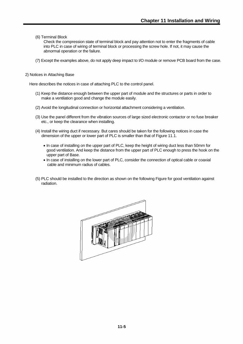
Chapter 11 Installation and Wiring
11-5
(6) Terminal Block
Check the compression state of terminal block and pay attention not to enter the fragments of cable into PLC in case of wiring of terminal block or processing the screw hole. If not, it may cause the abnormal operation or the failure.
(7) Except the examples above, do not apply deep impact to I/O module or remove PCB board from the case.
2) Notices in Attaching Base
Here describes the notices in case of attaching PLC to the control panel. (1) Keep the distance enough between the upper part of module and the structures or parts in order to
make a ventilation good and change the module easily. (2) Avoid the longitudinal connection or horizontal attachment considering a ventilation. (3) Use the panel different from the vibration sources of large sized electronic contactor or no fuse breaker
etc., or keep the clearance when installing. (4) Install the wiring duct if necessary. But cares should be taken for the following notices in case the
dimension of the upper or lower part of PLC is smaller than that of Figure 11.1.
• In case of installing on the upper part of PLC, keep the height of wiring duct less than 50mm for good ventilation. And keep the distance from the upper part of PLC enough to press the hook on the upper part of Base.
• In case of installing on the lower part of PLC, consider the connection of optical cable or coaxial cable and minimum radius of cables.
(5) PLC should be installed to the direction as shown on the following Figure for good ventilation against
radiation.

Chapter 11 Installation and Wiring
11-6
(6) Do not install PLC to the direction as below.
(7) When installing PLC or other equipment (Relay, electronic contactor), keep the distance to avoid
radiant noise or heat.
100mm or more
50mm or more
50mm or more

Chapter 11 Installation and Wiring
11-7
11.1.3 Attachment/Detachment of Module Here describes the method to attach each module to the base or remove it. 1) Attachment of Module
• Insert a fixed projection of the lower part of PLC into the module fixed hole of the base. • Slide the upper part of module to fix to the base, and then fit it to the base by using the module fixed
screw. • Pull the upper part of module to check if it is installed to the base completely.
Notes
1) For Module installation, it is required to insert the fixed projection of module into the module
fixing hole and then fix it. If forced to attach it, module may be broken.
Module fixing Hole Module loading lever

Chapter 11 Installation and Wiring
11-8
2) Detachment of Module
• Loosen the fixed screws of the upper part of module from the base. • Hold the module by both hands and press the fixed hook of module thoroughly. • By pressing the hook, pull the upper part of module from the axis of the lower part of module. • By lifting the module upward, remove the fixed projection of module from the fixing hole.
Notes
1) In case of detachment of module, press the hook and remove the module from the base, and
then remove the fixed project of module from the fixed hole of module. In this case, if forced to detach the module, a hook or the fixed projection of module may be broken.
Module fixing hook

Chapter 11 Installation and Wiring
11-9
11. 2 Wiring Here describes the items to know related to the wiring, in case of using the system.
11.2.1 Power Wiring 1) In case that the power change is larger than the range of standard, connect the voltage regulated transformer.
2) Connect the power having the small noise between cables or between earths. (In case of having lots of noise, connect the insulation transformer.) 3) For PLC power, I/O machine and power machine, divide the system as below.
Power CPU
AC power Constant Voltage
transformer
AC power 100V~240V
Power CPU
AC220V
Main power Constant Voltage
transformer
PLC power
Main circuit equipment
I/O power

Chapter 11 Installation and Wiring
11-10
4) In case of using a DC24V output of Power Module
Do not connect a DC24V output of several power module in parallel. If connected in parallel, the module
may be broken. In case that DC24V output capacity of one power module is not enough, supply the external DC24V
power as below. 5) AC110V, AC220V, DC24V cables should be twisted tightly and connected within the shortest distance. 6) AC110V, AC220V cables use the thick cable (2mm2) to reduce the voltage drop.
AC110V, DC24V cables should not approach to main circuit (high voltage, high current) cable or I/O signal cable. Keep more than 100mm if possible.
7) Use the surge absorber against lightning as shown in the figure below. 8) Use the shielded insulation trans or noise filter when a noise invasion is expected. 9) The wiring of each input power should be twisted shortly if possible, and the shielded trans or noise filter
wiring should be done without passing the duct.
Notes
1) Separate PLC earth(E2) from the earth(E1) of surge absorber against lightning. 2) Select the surge absorber against lightning not to exceed max. allowable voltage of surge absorber
in case of rising the power voltage at max.
24V
LG
FG
AC
I
/
O
24V
LG
FG
AC
I /O
Power Supply
DC 24V
E2
PLC I/O device
E1
Surge absorber against lightning
24V
LG
FG
AC
I /O
Power Power
Power

Chapter 11 Installation and Wiring
10-11
11.2.2 I/O Device Wiring 1) The spec. of cable for I/O wiring shall be 0.3~2 mm2 but it is recommend to use the convenient cable
spec.(0.3 mm2)). 2) Separate Input cable and Output cable for wiring. 3) I/O signal cable should be separated more than 100mm from main circuit cable of high voltage/high current. 4) If not possible to separate main circuit cable and power cable, use the shielded cable all and earth a PLC. 5) In case of pipe wiring, check the pipe completely for earth. 6) Separate output cable of DC24V from AC110V cable or AC220V cable. For the long distance wiring more than 200m, as it is expected to have problem by leakage current caused by the capacity between cables, please refer to 12.4 Various Cases.
11.2.3 Earth Wiring 1) As this PLC has a sufficient measures against noise, it is possible to use it without earth except the case having specially lots of noises. 2) Use the dedicated earth if possible. In case of Earth works, use 3 class earth (earth resistance 100 Ω or less). 3) If not possible to use dedicated earth, use the common earth as shown on the Figure B] as below.
A) Dedicated earth : Best B) Common earth : Good C) Common earth : Poor
Input
Output
PLC Shield cable
RA
DC
PLC Other PLC PLC Other Other
3 class earth 3 class earth

Chapter 11 Installation and Wiring
11-12
4) Use more than 2 mm2 cable for earth. Place the earth point near this PLC as possible to have the short
length of earth cable. 5) Separate LG of power module and FG of base board for earth. A) dedicated earth : Best B) common earth : Good C) common earth: Poor 6) If the abnormal operation is found according to the earth, separate FG of the base from the earth.
11.2.4 Cable Specification for Wiring The specification of cable used for wiring is as below.
Type of External Connection
Cable specification (mm2)
Low limit High limit
Digital Input 0.18 (AWG24) 1.5 (AWG16)
Digital Output 0.18 (AWG24) 2.0 (AWG14)
Analog I/O 0.18 (AWG24) 1.5 (AWG16)
Communication 0.18 (AWG24) 1.5 (AWG16)
Main power 1.5 (AWG16) 2.5 (AWG12)
Protection earth 1.5 (AWG16) 2.5 (AWG12)
LG FG
LG FG LG FG
Pow
er
Pow
er
Pow
er

Chapter 12 Maintenance and Repair
12-1
Chapter 12 Maintenance and Repair Please carry out Daily Checking and Regular Checking to maintain PLC in best condition.
12.1 Repair and Checking As I/O module is mainly consisted of semiconductor elements, the life seems to be semi-permanent. But the error in the elements may occur by surrounding environment and thus the regular checking is needed. For the items to check 1~2 times every 6 months, please refer to the following table.
Checking items Judgment basis Actions
Power Supply Power change range (within −15% / +10% )
Change the power so that it should be within the allowable voltage range.
I/O power I/O specifications of each module
Change the power so that it should be within the allowable voltage range of each module
Surrounding environment
Temperature 0 ~ + 55 Adjust the ambient temperature and humidity to be in proper range. Humidity 5 ~ 95%RH
Vibration No vibration Use the vibration-proof rubber or take other measures to prevent the vibration.
Shaking of each module No shaking All module should not be shaken.
Loosening of terminal screw No loosening Tighten the loosened screw.
Spare parts The possessing amount and preservation state Fill the lack and improve the preservation state
12.2 Daily Checking The items to check daily are as follows.
Checking items Contents Judgment Basis Action
Base attachment state Check the loosening of attached screw. Complete tightening Tighten screw
I/O module attachment state
• Check if the attached screw of module is tightened completely.
• Check if the upper cover of module is removed.
Complete tightening Check screw
Connection state of terminal block and extended cable
Loosening of terminal screw No loosening Tighten screw
Approach between compressed terminal Proper interval Adjust
Connector of extended cable No connector loosening Adjust
Indicator LED
Power LED Check LED ON LED ON (off is abnormal) Ref. Cha.13
RUN LED Check LED ON during Run state LED ON (off or blink is abnormal) Ref. Cha.13
STOP LED Check LED OFF during Run state Blink is abnormal. Ref. Cha.13
Input LED Check LED ON/OFF Input On, LED ON Input Off, LED OFF Ref. Cha.13
Output LED Check LED ON/OFF Output On, LED ON Output Off, LED OFF Ref. Cha.13

Chapter 12 Maintenance and Repair
12-2
12.3 Regular Checking Check the following items 1~2 times every 6 months and take a necessary actions.
Checking items Contents Judgment Basis Action
Surrounding environment
Temperature Thermometer/humidifier corrosive gas measurement
0 ~ 55 °C Adjust to meet general specification
(environment standard in control panel)
Humidity 5 ~ 95%RH
Pollution degree No corrosive gas
PLC state loosening, shaking Move each module Complete tightening Tighten screw
Dust, foreign materials Macrography No attachment -
Connection state
Screw loosening Tighten by driver No loosening Tighten
Approach of compressed terminal
Macrography Proper interval Adjust
Connector loosening Macrography No loosening Tighten connector screw
Power voltage checking Check the power voltage of the power input terminal using a tester.
AC100~240V: AC85~ 264V
DC24V:DC19.2 ~ 28.8V Change the power supply
Battery Check the battery change period and voltage drop indication.
• Check total shutdown time and warranty
• No indication of battery voltage drop
Change the battery if exceeding the warranty without battery capacity
indication
Fuse Macrography • No cutoff
Change it regularly as deterioration of element
may occur by inrush current.

Chapter 13 EMC Directive
13 - 1
Chapter 13 EMC Directive
13.1 Requirements for Conformance to EMC Directive The EMC Directive specifies the products must “be so constructed that they do not cause excessive electromagnetic interference (emissions) and are not unduly affected by electromagnetic interference (immunity)”. The applicable products are requested to meet these requirements. This section summarizes the precautions on conformance to the EMC Directive of the machinery assembled using PLC XGK series. The details of these precautions are based on the requirements and the applicable standards control. However, LSIS will not guarantee that the overall machinery manufactured according to the these details conforms to the below-described directives. The method of conformance to the EMC directive and the judgment on whether or not the machinery conforms to the EMC Directive must be determined finally by the manufacturer of the machinery.
13.1.1 EMC Standard
The standards applicable to the EMC Directive are listed below. Table13-1
Specification Test item Test details Standard value EN50081-2 EN55011
Radiated noise *2
Electromagnetic emissions from the product are measured
30~230 QP : 50/m *1 230~1000 QP : 57/m
EN55011 Conducted noise
Electromagnetic emissions from the product to the power line is measured
150~500 QP : 79 Mean: 66 500~230 QP : 73 Mean: 60
EN61131-2 EN61000-4-2 Electrostatic immunity
Immunity test in which static electricity is applied to the case of the equipment
15 Aerial discharge 8 Contact discharge
EN61000-4-4 Fast transient burst noise
Immunity test in which burst noise is applied to the power line and signal lines
Power line: 2 Digital /O : 1 Analog I/O, signal lines: 1
EN61000-4-3 Radiated field AM modulation
Immunity test in which field is irradiated to the product
10Vm,26~1000 80%AM modulation@ 1
EN61000-4-12 Damped oscillatory wave immunity
Immunity test in which a damped oscillatory wave is superimposed on the power line
Power line: 1 Digital I/O (24V or higher): 1
*1) QP: Quasi-peak value, Mean: Average value *2) The PLC is an open type device (device installed to another device) and must be installed in a conductive
control panel. The tests for the corresponding items were performed while the PLC was installed inside a control panel.

Chapter 13 EMC Directive
13 - 2
13.1.2 Control Panel
The PLC is an open type device (device installed to another device) and must be installed in a control panel. This is needed to prevent electric shock by touching XGK PLC and reduce the PLC-generated noise. Install the XGK PLC in a metallic panel to reduce PLC-generated EMI (Electro-magnetic interference), The specifications for the control panel are as follows: 1) Control panel The PLC control panel must have the following features: (1) Use SPCC (Cold Rolled Mild Steel) for the control panel. (2) The steel plate should be thicker than 1.6mm. (3) Use isolating transformers to protect the power supply from external surge voltage. (4) The control panel must have a structure which the radio waves does not leak out.
For example, make the door as a box-structure so that the panel body and the door are overlapped each other. This structure reduces the surge voltage generate by PLC.
(5) To ensure good electrical contact with the control panel or base plate, mask painting and weld so that good
surface contact can be made between the panel and plate.
Panel body
Door
Seal

Chapter 13 EMC Directive
13 - 3
2) Connection of power and earth wires Earthing and power supply wires for the PLC system must be connected as described below. (1) Earth the control panel with a thick wire so that a low impedance connection to ground can be ensured even at
high frequencies. (2) The function of LG (Line Ground) and FG (Frame Ground) terminals is to pass the noise generated in the PLC
system to the ground, so an impedance that is as low as possible must be ensured. (3) The earthing wire itself can generate the noise, so wire as short and thick to prevent from acting as an antenna.
13.1.3 Cables 1) Extension cable connection The extension cables contain a high frequency noise. Therefore, a ferrite core is attached to the extension cable as shown in the picture below to meet the CE conformance.
Model Manufacturer Remarks CU1330D E-TECH ELECTRONICS - ZCAT3035-1330 TDK -
2) Cable connection method for the inside control panel In the case that the extension cable is connected to the metal panel, a space of at least 1cm is needed from the panel. The metal board of the control panel has a shielding effect that blocks noise, but it could be served as an antenna when in contact with a cable which would create a noise source. Keep all high-speed signal transmission cables at a safe distance from the metal board.
Ferrite core

Chapter 13 EMC Directive
13 - 4
13.2 Requirement to Conform to the Low-voltage Directive The low-voltage directive requires each device that operates with the power supply ranging from 50V to 1000VAC and 75V to 1500VDC to satisfy the safety requirements. Cautions and installation and wiring of the PLC XGK series to conform to the low-voltage directive are described in this section. The described contents in this manual are based on the requirements and the applicable standards control. However, LSIS will not guarantee that the overall machinery manufactured according to the these details conforms to the above regulation. The method of conformance to the EMC directive and the judgment on whether or not the machinery conforms to the EMC Directive must be determined finally by the manufacturer of the machinery.
13.2.1 Standard Applied for XGK Series
The XGK series follow EN6100-1 (safety of devices used in measurement rooms, control rooms, or
laboratories). And the XGK series modules which operate at the rated voltage of AC50V/DC75V or above
are also developed to conform the above standard.
13.2.2 XGK Series PLC Selection (1) Power module
There are dangerous voltages (voltages higher than 42.4 peak) inside the power supply modules of the AC110/220V rated I/O voltages. Therefore, the CE mark-compliant models are enhanced in insulation internally between the primary and secondary.
(2) I/O module There are dangerous voltages (voltages higher than 42.4V peak) inside the I/O modules of the
AC110/220V rated I/O voltages. Therefore, the CE mark-compliant models are enhanced in insulation internally between the primary and secondary. The I/O modules of DC24V or less rating are out of the low-voltage directive application range.
(3)CPU module, Base unit
The above modules are using DC5V and 3.3V circuits inside, so they are out of the low-voltage directive application range.
(4) Special module, Communication module The special module and communication modules are DC24V or less in rated voltage, therefore they are
out of the low-voltage directive application range.

Chapter 14 Troubleshooting
14-1
Chapter 14 Troubleshooting Here describes the contents of various errors to be occurred while operating the system, the methods to find
the causes and the actions.
14.1 Basic Procedure for Troubleshooting
It is important to use the high reliable machine to increase the system reliability but it is important to take a prompt action when the trouble occurs as well.
To start the system promptly, it is more important to find the trouble occurring cause promptly and take the necessary action. The basic items to comply when taking this trouble shooting are as follows.
1) Check by the naked eye Check the following items by the naked eye. • Machine operation state (STOP, RUN) • Power supply state • I/O machine state • Wiring state (I/O cable, extended and communication cable) • After checking the indication state of each indicator (Power LED, Run LED, Stop LED, I/O LED etc.), connect the peripheral device and check PLC operation state and program contents. 2) Trouble Checking Examine how the trouble is changed by the following action. • Place the key switch on STOP position and apply the power ON/OFF. 3) Limit range Estimate what is the trouble cause using the above method. • Is it from PLC itself ? Or external cause ? • Is it from I/O module ? Or other cause? • Is it from PLC program?
14.2 Troubleshooting Here describes the method to find the trouble, the error code and the actions on the above by dividing
them per phenomenon.
Trouble contents
When Power LED is OFF
When ERR. LED is blinking
When RUN, STOP LED is OFF
When I/O module operates abnormally
When PROGRAM WRITE does not work
Action method when Power LED is OFF.
Action method when ERR LED is blinking
Action method when RUN, STOP LED is OFF
Action method when I/O module operates abnormally
Action method when PROGRAM WRITE does not work

Chapter 14 Troubleshooting
14- 2
14.2.1 Action when Power LED is OFF Here describes the action procedure when Power LED is OFF while supplying the power or during
operation.
Power LED is OFF
Is the power supplying ?
Is the power voltage within the allowable voltage rage?
Is the fuse cut off ?
Is the power module fixed ?
Is the over current protection operating
After wiring the trouble shooting questionnaire, contact A/S center or agent.
Supply the power.
Is Power LED ON?
Meet the power supply with the regular range.
Change the fuse.
Fix the power module completely.
Is Power LED ON ?
Is Power LED ON?
Is Power LED ON ?
1) Check the current capacity and reduce the over current.
2) After input power OFF, then power On.
Is Power LED ON ?
No
No
No
Yes No
No No
No
No
No
Yes Yes
Yes
Yes
Yes
Yes
Yes
Yes
End
Yes No
No

Chapter 14 Troubleshooting
13-3
14.2.2 Action when ERR LED is blinking
Here describes the action procedure when ERROR LED is blinking in case of power supply, or when operation starts, or during operation.
1) In case of light error, PLC system does not stop but you should check the error contents promptly and take an action. If not, it may cause the heavy error.
Notes
ERR LED is blinking
Yes
No
No
Connect XG5000 and check the error code contents.
After writing the trouble shooting questionnaire and contact A/S center or agent.
Refer to Appendix 1 Flag and remove the error cause.
End
Yes
Is it light error (_CNF_WAR) ?
Does ERR. LED keep on blinking ?

Chapter 14 Troubleshooting
14- 4
14.2.3 Action when Run, Stop LED is OFF Here describes the action procedure when RUN, STOP LED is OFF in case of power supply, when operation starts or during operation.
RUN, STOP LED is OFF
No
Yes
Contact A/S center or agent nearest from you
End
Power module OFF → ON
Is RUN, STOP LED OFF ?

Chapter 14 Troubleshooting
13-5
14.2.4 Action when I/O Module does not work normally Here describes the action procedure when I/O Module does not work normally during operation, as shown on the program example below.
When I/O module does not work normally
Monitor SOL1 state by XG5000.
Is output LED of SOL1 ON ?
No
Change the connector of terminal block.
Measure SOL1 terminal voltage by the tester.
Make the correct wiring.
Yes
Is the measured value normal ?
Is the output wiring correct ?
Is the contact state of
terminal block connector good ?
Is it normal ?
After removing the external wiring, check the transmission state of module output
Is it normal ?
Check the output device (SOL1) state.
Change the output module.
Continued
Yes
No
Yes
No
Yes No
Yes
Yes
No
No

Chapter 14 Troubleshooting
14- 6
Continued
Is SWITCH 1, 2 LED ON ?
No
Measure the terminal voltage of SWITCH 1, 2
by the tester.
Yes
Is the measured value normal ?
After removing the external wiring,
check the input state by forced input.
Is the measured value normal ?
Check the input device
(SWITCH 1, 2) state. Change the input
module.
Measure the terminal voltage of SWITCH 1, 2
by the tester.
Is the
measured value normal ?
Is the tightening state of terminal good ?
Is input
wiring correct ?
Make the correct wiring.
Tighten the terminal screw completely.
Change the terminal block
connector.
Change the input module.
Check all from the beginning again.
Is the contact state of terminal
block connector good ?
Yes
No
No
Yes
No Yes
Yes
No
Yes
No
No

Chapter 14 Troubleshooting
13 -7
14.2.5 Action when PROGRAM WRITE does not work Here describes the action procedure when PROGRAM WRITE does not work in CPU Module.
Program Write does not work
Yes
Put the key switch to Remote STOP mode and run Program
Write.
Is the Run/Stop switch set as STOP (Remote stop) mode ?
No
Is STOP LED
blinking ?
After releasing PLC connection Off, read the error code
indicated when connected, and modify it according to the
contents.
Yes
End
No
After Remote DIP S/W ON, run Program Write.
Yes
No
Is DIP S/W of CPU Module ON ?

Chapter 14 Troubleshooting
14- 8
14.3 Questionnaire for Troubleshooting If the trouble occurs when using XGK series, fill in the following questionnaire and then contact customer’s service center by phone or FAX.
For the error related to special and communication module, fill in the questionnaire attached to the user’s manual of the corresponding product.
1. User Contact point: TEL) FAX)
2. Model:
3. Applied Device details
− CPU module details − OS version ( ) − Serial no. of product ( )
− XG5000 version no. used in program compile ( )
4. Brief description of control object machine and system:
5. Using module of CPU module
− Operation by key switch ( ) − Memory module operation ( )
− XG5000 or operation by communication ( )
6. STOP LED of CPU module ON ? Yes( ), No( )
7. Error message content by XG5000:
8. Action trial status for the error code of item 7 on the above:
9. Trouble shooting method for other error action:
10. Error features
Repeat( ): periodical( ), specific sequence level related( )
environment related( )
Intermittent ( ): general error interval:
11. Detailed description for the error phenomena:
12. Configuration diagram of applied system:

Chapter 14 Troubleshooting
13-9
~
~
~
~
~
14.4 Cases Here describes the trouble type and measures for each circuit.
14.4.1 Input Circuit Error Type and Corrective Actions Here describes the trouble examples of input circuit and its measures.
Phenomena Causes Measures Input signal not OFF
Leakage current of external device (In case of running by approach switch)
Connect the proper resistance and capacity so that the voltage between terminals of input module is below return voltage.
CR value is determined by leakage current. − Recommended C : 0.1 ~ 0.47Uf R : 47 ~ 120 Ω (1/2W) or make the circuit independently and install a separate circuit.
Input signal not OFF (sometimes neon lamp ON)
Leakage current of external device (run by limit switch with neon lamp)
Input signal not OFF
Leakage current by capacity between wiring cables
Install the power on the external device as below.
Input signal not OFF
Leakage current of external device (run by switch with LED indicator)
Connect the proper resistance as below so that the voltage between input module terminal and common terminal exceeds OFF voltage.
Input signal not OFF
Circulated current by double power
In case of E1 > E2, circulated.
Double power --> single power. Connect purified current prevent
diode. (as below)
External device
AC input Leakage current
External device
DC input
R Leakage current
DC input
L E
E
C
External device
AC input
R Leakage current
C
External device
AC input
R Leakage current
C
AC input
R
AC input
External device
DC input
R
E1 DC input
L E

Chapter 14 Troubleshooting
14- 10
~
~
~
~
X
~
14.4.2 Output Circuit Error Types and Corrective Actions Here describes the trouble examples of output circuit and its measures. Phenomena Causes Measures
Over voltage applied to the load if case of output contact OFF
In case that the load is semi-sine inside, (solenoid valve)
If power polarity is ←, C is charged, if polarity is ↑, voltage charged to C +power voltage is applied to both sides of diode(D). Max. voltage is about 2√2 . Note) If used as above, output element does not make trouble but the function of diode(D) built-in the load becomes low which causes the trouble.
Connect several dozens kΩ ~ hundreds kΩ resistance to the load in parallel.
The load is not OFF
Leakage current by surge absorption circuit connected with output element in parallel
Connect CR with several dozens kΩ or equivalent impedance to the load in parallel.
Note) If wiring length is long from output module to the load, leakage current by capacity between cables.
Time trouble in case the load is C−R type timer.
Leakage current by surge absorption circuit connected with output elements in parallel
Run C-R type timer by Relay. Use the timer except C−R type timer.
Note) There is the timer that internal circuit is semi-sine.
load is not OFF (AC)
Circulation current by two different powers
If E1< E2, circulated If E1 is Off(E2 On), circulated
Double power --> single power. Connect purified current prevention
diode.(as below)
Note) If load is Relay, it is required to connect reverse voltage absorption diode as dot line on the above figure..
C
R
Load
Leakage current
Output
C
R
Load
Leakage current
Output
C
R Load
R
D
R
Load
R
Load
C
T Timer
Output
E1 Load
E
Output Output
Load
E E
C
R
←
↑
Load
D
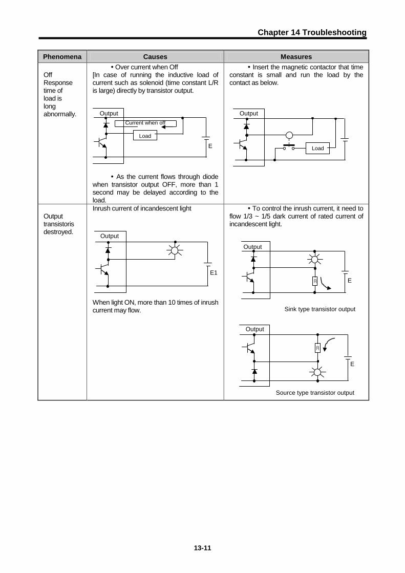
Chapter 14 Troubleshooting
13-11
Phenomena Causes Measures Off Response time of load is long abnormally.
Over current when Off [In case of running the inductive load of current such as solenoid (time constant L/R is large) directly by transistor output.
As the current flows through diode when transistor output OFF, more than 1 second may be delayed according to the load.
Insert the magnetic contactor that time constant is small and run the load by the contact as below.
Output transistoris destroyed.
Inrush current of incandescent light When light ON, more than 10 times of inrush current may flow.
To control the inrush current, it need to flow 1/3 ~ 1/5 dark current of rated current of incandescent light.
Output
Load
E
Current when off
Output
E1
Output
Load
Output
E
R
Output
E
R
Sink type transistor output
Source type transistor output

Chapter 14 Troubleshooting
14- 12
14.5 Error Code List
14.5.1 Error Code during CPU Operation Error code Error cause Action
(restart mode after taking an action) Operation status
LED status
Diagnosis point
2 Data Bus error If it occurs repeatedly when power reinput, request service center. Fail
Blink by the order of total LED.
Power input
3 Data RAM error If it occurs repeatedly when power reinput, request service center. Fail
Blink by the order of total LED.
Power input
4 Clock IC(RTC) error If it occurs repeatedly when power reinput, request service center. Fail ERR: On Power
input
6 Program memory error
If it occurs repeatedly when power reinput, request service center. Fail ERR: On Power
input
10 USB IC error If it occurs repeatedly when power reinput, request service center. Fail ERR: On Power
input
11 Backup RAM error If it occurs repeatedly when power reinput, request service center. Fail ERR: On Power
input
12 Backup Flash error If it occurs repeatedly when power reinput, request service center. Fail ERR: On Power
input
13 Base information error
If it occurs repeatedly when power reinput, request service center. Stop ERR : ON
Power input RUN mode switching
22 Poor Backup Flash program
Reoperate after modifying the backup flash program. Fail ERR: On
Reset RUN mode switching
23 Program to execute is abnormal
Start after reloading the program, Change battery if it has a problem. Check the preservation status after program reloading and if error occurs, change the CPU module.
Stop ERR: On
Reset RUN mode switching
24 I/O parameter error
Start after reloading I/O parameter, Battery change if battery has a problem. Check the preservation status after I/O parameter reloading and if error occurs, change the CPU module.
Stop ERR: On
Reset RUN mode switching
25 Basic parameter error
Start after reloading Basic parameter, Change battery if it has a problem. Check the preservation status after Basic parameter reloading and if error occurs, change the CPU module.
Stop ERR: On
Reset RUN mode switching
26 Exceed execution range error
Start after reloading program. If it occurs repeatedly, request service center
Stop ERR : ON
Reset RUN mode switching
27 Compile error Start after reloading program. If it occurs repeatedly, request service center
Stop ERR : ON
Reset RUN mode switching

Chapter 14 Troubleshooting
14-13
Error code Error cause Action
(restart mode after taking an action) Operation status
LED status
Diagnosis point
30
Module set in parameter and the installed module does not match
After checking the wrong position of slot by XG5000, modify the module or parameter and then restart. Reference flag: module type discord error flag
Stop (Run)
ERR: On (P.S.: On)
RUN mode switching
31 Module falling during operation or additional setup
After checking the position of falling/adding slot by XG5000, modify the installation status of module and then restart (according to parameter). Reference flag: module removable Reference flag: module removable error
Stop (Run)
ERR: On (P.S.: On) Scan end
32 Fuse cutoff of fuse built-in module during operation
After checking the position of slot where the fuse cutoff occurs by XG5000, change the fuse and then restart (according to parameter Reference flag: fuse cutoff error flag
Stop (Run)
ERR: On (P.S.: On) Scan end
33
Data of I/O module does not access normally during operation.
After checking the position of slot where the access error occurs by XG5000, change the module and restart (acc.to parameter. Reference flag: I/O module Read/Write error flag
Stop (Run)
ERR: On (P.S.: On) Scan end
34
Normal access of special/link module data during operation not available.
After checking the position of slot that access error occurred by XG5000, change the module and restart (acc.to parameter). Reference flag: special/link module interface error
Stop (Run)
ERR: On (P.S.: On) Scan end
39 Abnormal stop of CPU or malfunction
Abnormal system end by noise or hard ware error. 1) If it occurs repeatedly when power reinput, request service center 2) Noise measures
Stop RUN: On ERR: On
Ordinary time
40
Scan time of program during operation exceeds the scan watchdog time designated by parameter.
After checking the scan watchdog time designated by parameter, modify the parameter or the program and then restart.
Stop RUN: On ERR: On
In operation
41
Operation error occurs while running the user program.
Remove operation error → reload the program and restart. <Check method> Stop: Check operation error information through XG5000 and modify the program. Run: Refer to F area Error step.
Stop (Run)
ERR : ON (CHK: blink)
While running
the program
42
The stack exceeds the normal range while running the program
Restart Stop RUN: On ERR: On
While running
the program
43 Base double setting error
After checking base setting switch, reset Stop ERR: On
Reset RUN mode
switching
44 Timer index user error
After reloading a timer index program modification, start
Stop (Run)
RUN: On ERR: On Scan end
50 Heavy error of Heavy error detection of external Stop ERR: On Scan end

Chapter 14 Troubleshooting
14- 14
Error code Error cause Action
(restart mode after taking an action) Operation status
LED status
Diagnosis point
external device detected by the user program
device Refer to flag to repeat the device and then restart (according to parameter)
(Run) (P.S.: On)
55
The number of running standby task exceeds the designated range
If it occurs repeatedly after restart, check the installation environment (if error continues, request service center)
Stop (Run)
ERR: On (P.S.: On)
While running
the program
60 E_STOP function executed
After removing error causes which starts E_STOP function in program, power reinput
Stop RUN: On ERR: On
While running
the program
61 Operation error
STOP: after checking the detailed information of operation error by XG5000, modify the program. RUN : refer to error step
Stop (Run)
ERR: On (P.S.: On)
While running
the program
500 Data memory backup not possible
If not error in battery, power reinput Remote mode is switched to STOP mode.
Stop ERR: On Reset
501 Time data error If no error in battery, reset the time by XG5000 - CHK: On Ordinary
time
502 Battery voltage falling
Battery change in the state of power input - BAT: On Ordinary
time
14.5.2 Error Code of Program Operation
Code Error CPU Status Causes Measure
16 Indirect designation/ Index error
According to the Basic Parameter Settings, the CPU will Run or Stop.
Designations are out of range
Designate within the range
17 Group command range setting error
Designations are out of range
Designate within the range
18 0 divider error Divided by 0 (except RDIV, LDIV) Don’t divide by 0
19 BCD conversion error
The value of the operand is out of the BCD data range.
Designate within the BCD data range
20 File bank setting error
Bank set value is out of range
Set the value within the range
21 Floating point operation error
Floating point operation error Correct the data
22 Data type conversion error
Data size is different when converting from real to integer numbers
Correct the data
23 BMOV error Set value is over than 16 Correct the set value
Notes
1) If error codes 2 to 13 are displayed, check with your local service center.
2) Error code numbers greater than 22 can be checked with XG5000 Error History.

Chapter 14 Troubleshooting
14-15
Code Error CPU Status Causes Measure
24 DECO/ENCO error Set value is over than 8 Correct the set value
25 DIS/UNI error
According to the Basic Parameter Settings, the CPU will Run or Stop.
The value of N is over 4 Correct the N value
26 Data control error Over the range Correct the range 27 Time data error Time data error Correct the time data 28 MUX error Set value error Correct the set value 29 Data table error Set value error Correct the set value
30 SEG error Number of conversion data is greater than 4 Correct the set value
31 ASCII code error ASCII data error Correct the data
32 Positioning axes setting error
Setting axes greater than 3 Correct the number of axes
33 Character string error Character string instruction error Correct the instruction
34 SORT error SORT/DSORT instruction error Correct the set value
35 FOR nesting error
The number of nesting number is over 16 Correct the program
36 Task number error The Task number exceeds 96 Correct the task number
37 Device range check error Out of the device range Set within the device range
38 P2P data error Settings of P2P are out of range Set within the range
39 Module Configuration error The module can’t be set
properly. . Set the module properly
Notes
1) If the basic parameter is set to “Continue running when error occurs,” the program operation error
code can be checked using XG5000 system history.
2) If “Continue running when error occurs” is removed, it can be checked with XG5000 error history.

Appendix 1 Flag List
App. 1 - 1
Appendix 1 Flag List App.1.1 Special Relay (F) List
Device1 Device2 Type Variables Function Description
F0000 DWORD _SYS_STATE Mode and state Indicates PLC mode and operation state
F00000 BIT _RUN Run Run state
F00001 BIT _STOP Stop Stop state
F00002 BIT _ERROR Error Error state
F00003 BIT _DEBUG Debug Debug state
F00004 BIT _LOCAL_CON Local control Local control mode
F00005 BIT _MODBUS_CON Mode bus mode Mode bus control mode
F00006 BIT _REMOTE_CON Remote mode Remote control mode
F00008 BIT _RUN_EDIT_ST Editing during RUN Editing program download during RUN
F00009 BIT _RUN_EDIT_CHK Editing during RUN Internal edit processing during RUN
F0000A BIT _RUN_EDIT_DONE Edit done during RUN Edit is done during RUN
F0000B BIT _RUN_EDIT_END Edit end during RUN Edit is ended during RUN
F0000C BIT _CMOD_KEY Operation mode Operation mode changed by key
F0000D BIT _CMOD_LPADT Operation mode Operation mode changed by local PADT
F0000E BIT _CMOD_RPADT Operation mode Operation mode changed by Remote PADT
F0000F BIT _CMOD_RLINK Operation mode Operation mode changed by Remote communication module
F00010 BIT _FORCE_IN Forced input Forced input state
F00011 BIT _FORCE_OUT Forced output Forced output state
F00012 BIT _SKIP_ON I/O SKIP I/O SKIP on execution
F00013 BIT _EMASK_ON Error mask Error mask on execution
F00014 BIT _MON_ON monitor Monitor on execution
F00015 BIT _USTOP_ON Stop Stop by Stop function
F00016 BIT _ESTOP_ON EStop Stop by EStop function
F00017 BIT _CONPILE_MODE Compile Compile on execution
F00018 BIT _INIT_RUN Initialize Iinitialization task on execution
F0001C BIT _PB1 Program Code 1 Program Code 1 selected
F0001D BIT _PB2 Program Code 2 Program Code 2 selected
F0001E BIT _CB1 Compile Code 1 Compile Code 1 selected
F0001F BIT _CB2 Compile Code2 Compile Code 2 selected
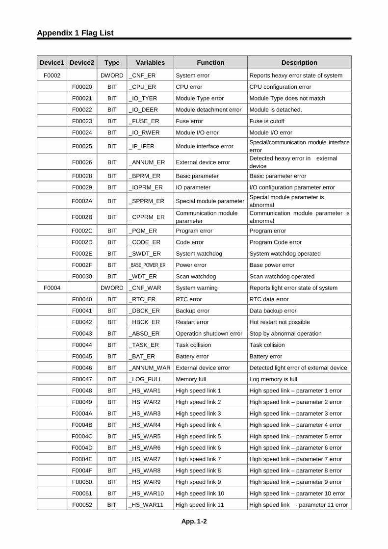
Appendix 1 Flag List
App. 1 - 2
Device1 Device2 Type Variables Function Description
F0002 DWORD _CNF_ER System error Reports heavy error state of system
F00020 BIT _CPU_ER CPU error CPU configuration error
F00021 BIT _IO_TYER Module Type error Module Type does not match
F00022 BIT _IO_DEER Module detachment error Module is detached.
F00023 BIT _FUSE_ER Fuse error Fuse is cutoff
F00024 BIT _IO_RWER Module I/O error Module I/O error
F00025 BIT _IP_IFER Module interface error Special/communication module interface error
F00026 BIT _ANNUM_ER External device error Detected heavy error in external device
F00028 BIT _BPRM_ER Basic parameter Basic parameter error
F00029 BIT _IOPRM_ER IO parameter I/O configuration parameter error
F0002A BIT _SPPRM_ER Special module parameter Special module parameter is abnormal
F0002B BIT _CPPRM_ER Communication module parameter
Communication module parameter is abnormal
F0002C BIT _PGM_ER Program error Program error
F0002D BIT _CODE_ER Code error Program Code error
F0002E BIT _SWDT_ER System watchdog System watchdog operated
F0002F BIT _BASE_POWER_ER Power error Base power error
F00030 BIT _WDT_ER Scan watchdog Scan watchdog operated
F0004 DWORD _CNF_WAR System warning Reports light error state of system
F00040 BIT _RTC_ER RTC error RTC data error
F00041 BIT _DBCK_ER Backup error Data backup error
F00042 BIT _HBCK_ER Restart error Hot restart not possible
F00043 BIT _ABSD_ER Operation shutdown error Stop by abnormal operation
F00044 BIT _TASK_ER Task collision Task collision
F00045 BIT _BAT_ER Battery error Battery error
F00046 BIT _ANNUM_WAR External device error Detected light error of external device
F00047 BIT _LOG_FULL Memory full Log memory is full.
F00048 BIT _HS_WAR1 High speed link 1 High speed link – parameter 1 error
F00049 BIT _HS_WAR2 High speed link 2 High speed link – parameter 2 error
F0004A BIT _HS_WAR3 High speed link 3 High speed link – parameter 3 error
F0004B BIT _HS_WAR4 High speed link 4 High speed link – parameter 4 error
F0004C BIT _HS_WAR5 High speed link 5 High speed link – parameter 5 error
F0004D BIT _HS_WAR6 High speed link 6 High speed link – parameter 6 error
F0004E BIT _HS_WAR7 High speed link 7 High speed link – parameter 7 error
F0004F BIT _HS_WAR8 High speed link 8 High speed link – parameter 8 error
F00050 BIT _HS_WAR9 High speed link 9 High speed link – parameter 9 error
F00051 BIT _HS_WAR10 High speed link 10 High speed link – parameter 10 error
F00052 BIT _HS_WAR11 High speed link 11 High speed link - parameter 11 error

Appendix 1 Flag List
App. 1 - 3
Device1 Device2 Type Variables Function Description
F00053 BIT _HS_WAR12 High speed link 12 High speed link - parameter 12 error
F00054 BIT _P2P_WAR1 P2P parameter 1 P2P – parameter 1 error
F00055 BIT _P2P_WAR2 P2P parameter 2 P2P – parameter 2 error
F00056 BIT _P2P_WAR3 P2P parameter 3 P2P – parameter 3 error
F00057 BIT _P2P_WAR4 P2P parameter 4 P2P – parameter 4 error
F00058 BIT _P2P_WAR5 P2P parameter 5 P2P – parameter 5 error
F00059 BIT _P2P_WAR6 P2P parameter 6 P2P – parameter 6 error
F0005A BIT _P2P_WAR7 P2P parameter 7 P2P – parameter 7 error
F0005B BIT _P2P_WAR8 P2P parameter 8 P2P – parameter 8 error
F0005C BIT _CONSTANT_ER Constant error Constant error
F0009 WORD _USER_F User contact Timer used by user
F00090 BIT _T20MS 20ms 20ms cycle Clock
F00091 BIT _T100MS 100ms 100ms cycle Clock
F00092 BIT _T200MS 200ms 200ms cycle Clock
F00093 BIT _T1S 1s 1s cycle Clock
F00094 BIT _T2S 2s 2s cycle Clock
F00095 BIT _T10S 10s 10s cycle Clock
F00096 BIT _T20S 20s 20s cycle Clock
F00097 BIT _T60S 60s 60s cycle Clock
F00099 BIT _ON Ordinary time On Always On state Bit
F0009A BIT _OFF Ordinary time Off Always Off state Bit
F0009B BIT _1ON 1scan On First scan ON Bit
F0009C BIT _1OFF 1scan Off First scan OFF bit
F0009D BIT _STOG Reversal Reversal every scan
F0010 WORD _USER_CLK User Clock Clock available for user setting
F00100 BIT _USR_CLK0 Setting scan repeat On/Off as much as set scan Clock 0
F00101 BIT _USR_CLK1 Setting scan repeat On/Off as much as set scan Clock 1
F00102 BIT _USR_CLK2 Setting scan repeat On/Off as much as set scan Clock 2
F00103 BIT _USR_CLK3 Setting scan repeat On/Off as much as set scan Clock 3
F00104 BIT _USR_CLK4 Setting scan repeat On/Off as much as set scan Clock 4
F00105 BIT _USR_CLK5 Setting scan repeat On/Off as much as set scan Clock 5
F00106 BIT _USR_CLK6 Setting scan repeat On/Off as much as set scan Clock 6
F00107 BIT _USR_CLK7 Setting scan repeat On/Off as much as set scan Clock 7

Appendix 1 Flag List
App. 1 - 4
Device1 Device2 Type Variables Function Description
F0011 WORD _LOGIC_RESULT Logic result Indicates logic results
F00110 BIT _LER operation error ON during 1 scan in case of operation error
F00111 BIT _ZERO Zero flag ON when operation result is 0
F00112 BIT _CARRY Carry flag ON when carry occurs during operation
F00113 BIT _ALL_OFF All output OFF ON in case that all output is Off
F00115 BIT _LER_LATCH Operation error Latch
Keeps ON during operation error
F0012 WORD _CMP_RESULT Comparison result Indicates the comparison result.
F00120 BIT _LT LT flag ON in case of “less than”
F00121 BIT _LTE LTE flag ON in case of “equal or less than”
F00122 BIT _EQU EQU flag On in case of “equal”
F00123 BIT _GT GT flag ON in case of “greater than”
F00124 BIT _GTE GTE flag ON in case of “equal or greater than”
F00125 BIT _NEQ NEQ flag ON in case of “not equal”
F0013 WORD _AC_F_CNT Moment shutdown Indicates moment shutdown times
F0014 WORD _FALS_NUM FALS no. Indicates FALS no.
F0015 WORD _PUTGET_ERR0 PUT/GET error 0 Main base Put / Get error
F0016 WORD _PUTGET_ERR1 PUT/GET error 1 Extended base 1 step Put/Get error
F0017 WORD _PUTGET_ERR2 PUT/GET error 2 Extended base 2 step Put/Get error
F0018 WORD _PUTGET_ERR3 PUT/GET error 3 Extended base 3 step Put/Get error
F0019 WORD _PUTGET_ERR4 PUT/GET error 4 Extended base 4 step Put/Get error
F0020 WORD _PUTGET_ERR5 PUT/GET error 5 Extended base 5 step Put/Get error
F0021 WORD _PUTGET_ERR6 PUT/GET error 6 Extended base 6 step Put/Get error
F0022 WORD _PUTGET_ERR7 PUT/GET error 7 Extended base 7 step Put/Get error
F0023 WORD _PUTGET_NDR0 PUT/GET end 0 Main base Put/Get end
F0024 WORD _PUTGET_NDR1 PUT/GET end 1 Extended base 1 step Put/Get end
F0025 WORD _PUTGET_NDR2 PUT/GET end 2 Extended base 2 step Put/Get end
F0026 WORD _PUTGET_NDR3 PUT/GET end 3 Extended base 3 step Put/Get end
F0027 WORD _PUTGET_NDR4 PUT/GET end 4 Extended base 4 step Put/Get end
F0028 WORD _PUTGET_NDR5 PUT/GET end 5 Extended base 5 step Put/Get end
F0029 WORD _PUTGET_NDR6 PUT/GET end 6 Extended base 6 step Put/Get end
F0030 WORD _PUTGET_NDR7 PUT/GET end 7 Extended base 7 step Put/Get end
F0044 WORD _CPU_TYPE CPU Type Indicates information for CPU Type.
F0045 WORD _CPU_VER CPU version Indicates CPU version
F0046 DWORD _OS_VER OS version Indicates OS version
F0048 DWORD _OS_DATE OS date Indicates OS distribution date.
F0050 WORD _SCAN_MAX Max. scan time Indicates max. scan time.
F0051 WORD _SCAN_MIN Min. scan time Indicates min. scan time.
F0052 WORD _SCAN_CUR Current scan time Current scan time

Appendix 1 Flag List
App. 1 - 5
Device1 Device2 Type Variables Function Description
F0053 WORD _MON_YEAR Month/Year PLC month, year data
F0054 WORD _TIME_DAY Time/Day PLC time, day data
F0055 WORD _SEC_MIN Sec/Min PLC second, minute data
F0056 WORD _HUND_WK Hundred year/Weekday
PLC hundred year, weekday data
F0057 WORD _FPU_INFO FPU operation result Fixed decimal operation result
F00570 BIT _FPU_LFLAG_I Incorrect error latch
Latch in case of incorrect error
F00571 BIT _FPU_LFLAG_U Underflow latch Latch in case of underflow
F00572 BIT _FPU_LFLAG_O Overflow latch Latch in case of overflow
F00573 BIT _FPU_LFLAG_Z Zero(0) divide latch
Latch in case of zero(0) divide
F00574 BIT _FPU_LFLAG_V Invalid operation latch
Latch in case of invalid operation
F0057A BIT _FPU_FLAG_I Incorrect error Reports incorrect error
F0057B BIT _FPU_FLAG_U Underflow Reports underflow
F0057C BIT _FPU_FLAG_O Overflow Reports overflow
F0057D BIT _FPU_FLAG_Z Zero divide Reports in case of zero divide
F0057E BIT _FPU_FLAG_V Invalid operation Reports in case of invalid operation
F0057F BIT _FPU_FLAG_E Irregular input Reports in case of irregular input
F0058 DWORD _ERR_STEP Error step Saves error step
F0060 DWORD _REF_COUNT Refresh Increase when module Refresh
F0062 DWORD _REF_OK_CNT Refresh OK Increase when module Refresh is normal
F0064 DWORD _REF_NG_CNT Refresh NG Increase when module Refresh is abnormal
F0066 DWORD _REF_LIM_CNT Refresh Limit Increase when module Refresh is abnormal (Time Out)
F0068 DWORD _REF_ERR_CNT Refresh Error Increase when module Refresh is abnormal
F0070 DWORD _MOD_RD_ERR_CNT Module Read Error
Increase when reading module 1 word abnormally
F0072 DWORD _MOD_WR_ERR_CNT Module Write Error
Increase when module 1 word abnormally
F0074 DWORD _CA_CNT Block service Increase when module block data service
F0076 DWORD _CA_LIM_CNT Block service Limit
Increase when block data service is limited
F0078 DWORD _CA_ERR_CNT Block service Error
Increase in case of block data service error
F0080 DWORD _BUF_FULL_CNT Buffer Full Increase when CPU internal buffer is full.
F0082 DWORD _PUT_CNT Put count Increase when Put count
F0084 DWORD _GET_CNT Get count Increase when Get count
F0086 DWORD _KEY Current key indicates the current state of local key.
F0088 DWORD _KEY_PREV Previous key indicates the previous state of local key
F0090 WORD _IO_TYER_N Mismatch slot Module Type mismatched slot no.
F0091 WORD _IO_DEER_N Detach slot Module detached slot no.
F0092 WORD _FUSE_ER_N Fuse cutoff slot Fuse cutoff slot no.
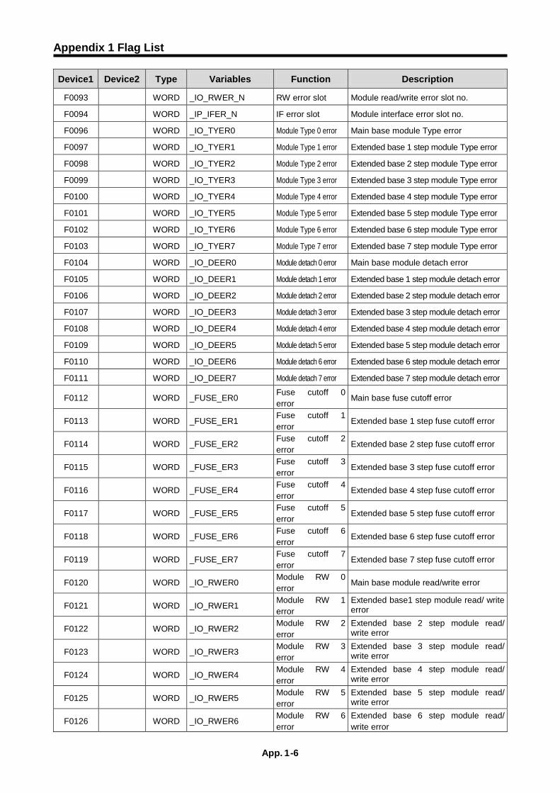
Appendix 1 Flag List
App. 1 - 6
Device1 Device2 Type Variables Function Description
F0093 WORD _IO_RWER_N RW error slot Module read/write error slot no.
F0094 WORD _IP_IFER_N IF error slot Module interface error slot no.
F0096 WORD _IO_TYER0 Module Type 0 error Main base module Type error
F0097 WORD _IO_TYER1 Module Type 1 error Extended base 1 step module Type error
F0098 WORD _IO_TYER2 Module Type 2 error Extended base 2 step module Type error
F0099 WORD _IO_TYER3 Module Type 3 error Extended base 3 step module Type error
F0100 WORD _IO_TYER4 Module Type 4 error Extended base 4 step module Type error
F0101 WORD _IO_TYER5 Module Type 5 error Extended base 5 step module Type error
F0102 WORD _IO_TYER6 Module Type 6 error Extended base 6 step module Type error
F0103 WORD _IO_TYER7 Module Type 7 error Extended base 7 step module Type error
F0104 WORD _IO_DEER0 Module detach 0 error Main base module detach error
F0105 WORD _IO_DEER1 Module detach 1 error Extended base 1 step module detach error
F0106 WORD _IO_DEER2 Module detach 2 error Extended base 2 step module detach error
F0107 WORD _IO_DEER3 Module detach 3 error Extended base 3 step module detach error
F0108 WORD _IO_DEER4 Module detach 4 error Extended base 4 step module detach error
F0109 WORD _IO_DEER5 Module detach 5 error Extended base 5 step module detach error
F0110 WORD _IO_DEER6 Module detach 6 error Extended base 6 step module detach error
F0111 WORD _IO_DEER7 Module detach 7 error Extended base 7 step module detach error
F0112 WORD _FUSE_ER0 Fuse cutoff 0 error
Main base fuse cutoff error
F0113 WORD _FUSE_ER1 Fuse cutoff 1 error
Extended base 1 step fuse cutoff error
F0114 WORD _FUSE_ER2 Fuse cutoff 2 error
Extended base 2 step fuse cutoff error
F0115 WORD _FUSE_ER3 Fuse cutoff 3 error
Extended base 3 step fuse cutoff error
F0116 WORD _FUSE_ER4 Fuse cutoff 4 error
Extended base 4 step fuse cutoff error
F0117 WORD _FUSE_ER5 Fuse cutoff 5 error
Extended base 5 step fuse cutoff error
F0118 WORD _FUSE_ER6 Fuse cutoff 6 error
Extended base 6 step fuse cutoff error
F0119 WORD _FUSE_ER7 Fuse cutoff 7 error
Extended base 7 step fuse cutoff error
F0120 WORD _IO_RWER0 Module RW 0 error
Main base module read/write error
F0121 WORD _IO_RWER1 Module RW 1 error
Extended base1 step module read/ write error
F0122 WORD _IO_RWER2 Module RW 2 error
Extended base 2 step module read/ write error
F0123 WORD _IO_RWER3 Module RW 3 error
Extended base 3 step module read/ write error
F0124 WORD _IO_RWER4 Module RW 4 error
Extended base 4 step module read/ write error
F0125 WORD _IO_RWER5 Module RW 5 error
Extended base 5 step module read/ write error
F0126 WORD _IO_RWER6 Module RW 6 error
Extended base 6 step module read/ write error

Appendix 1 Flag List
App. 1 - 7
Device1 Device2 Type Variables Function Description
F0127 WORD _IO_RWER7 Module RW 7 error
Extended base 7 step module read/ write error
F0128 WORD _IO_IFER_0 Module IF 0 error Main base module interface error
F0129 WORD _IO_IFER_1 Module IF 1 error Extended base 1step module interface error
F0130 WORD _IO_IFER_2 Module IF 2 error Extended base 2step module interface error
F0131 WORD _IO_IFER_3 Module IF 3 error Extended base 3step module interface error
F0132 WORD _IO_IFER_4 Module IF 4 error Extended base 4step module interface error
F0133 WORD _IO_IFER_5 Module IF 5 error Extended base 5step module interface error
F0134 WORD _IO_IFER_6 Module IF 6 error Extended base 6step module interface error
F0135 WORD _IO_IFER_7 Module IF 7 error Extended base 7step module interface error
F0136 WORD _RTC_DATE RTC date RTC current date
F0137 WORD _RTC_WEEK RTC weekday RTC current weekday
F0138 DWORD _RTC_TOD RTC time RTC current time (ms unit)
F0140 DWORD _AC_FAIL_CNT Power shutdown times Saves the times of power shutdown
F0142 DWORD _ERR_HIS_CNT Error occur times Saves the times of error occur
F0144 DWORD _MOD_HIS_CNT Mode conversion times Saves the times of mode conversion
F0146 DWORD _SYS_HIS_CNT History occur times Saves the times of system history
F0148 DWORD _LOG_ROTATE Log Rotate Saves log rotate information
F0150 WORD _BASE_INFO0 Slot information 0 Main base slot information
F0151 WORD _BASE_INFO1 Slot information 1 Extended base 1step slot information
F0152 WORD _BASE_INFO2 Slot information 2 Extended base 2step slot information
F0153 WORD _BASE_INFO3 Slot information 3 Extended base 3step slot information
F0154 WORD _BASE_INFO4 Slot information 4 Extended base 4step slot information
F0155 WORD _BASE_INFO5 Slot information 5 Extended base 5step slot information
F0156 WORD _BASE_INFO6 Slot information 6 Extended base 6step slot information
F0157 WORD _BASE_INFO7 Slot information 7 Extended base 7step slot information
F0158 WORD _RBANK_NUM Use block no. Current using block no.
F0159 WORD _RBLOCK_STATE Flash state Flash block state
F0164 DWORD _RBLOCK_ER_FLAG Flash error Error during flash NBlock service
F0160 DWORD _RBLOCK_RD_FLAG Flash read ON when reading flash Nblock data
F0162 DWORD _RBLOCK_WR_FLAG Flash write ON when writing flash Nblock data
F0178 DWORD _OS_VER_PATCH OS patch version Indicates OS version to second decimal places.
F09320 BIT _FUSE_ER_PMT Setting in case of fuse error
Ignores fuse error
F09321 BIT _IO_ER_PMT Setting in case of I/O error
Ignores I/O module error
F09322 BIT _SP_ER_PMT Setting in case of special module error
Ignores special module error

Appendix 1 Flag List
App. 1 - 8
Device1 Device2 Type Variables Function Description
F09323 BIT _CP_ER_PMT Setting in case of communication error
Ignores communication module error
F0934 DWORD _BASE_EMASK_INFO Base fault mask Base fault mask information
F0936 DWORD _BASE_SKIP_INFO Base Skip Base skip information
F0938 WORD _SLOT_EMASK_INFO_0 Slot fault mask Slot fault mask information (BASE 0)
F0939 WORD _SLOT_EMASK_INFO_1 Slot fault mask Slot fault mask information (BASE 1)
F0940 WORD _SLOT_EMASK_INFO_2 Slot fault mask Slot fault mask information (BASE 2)
F0941 WORD _SLOT_EMASK_INFO_3 Slot fault mask Slot fault mask information (BASE 3)
F0942 WORD _SLOT_EMASK_INFO_4 Slot fault mask Slot fault mask information (BASE 4)
F0943 WORD _SLOT_EMASK_INFO_5 Slot fault mask Slot fault mask information (BASE 5)
F0944 WORD _SLOT_EMASK_INFO_6 Slot fault mask Slot fault mask information (BASE 6)
F0945 WORD _SLOT_EMASK_INFO_7 Slot fault mask Slot fault mask information (BASE 7)
F0946 WORD _SLOT_SKIP_INFO_0 Slot skip Slot skip information (BASE 0)
F0947 WORD _SLOT_SKIP_INFO_1 Slot skip Slot skip information (BASE 1)
F0948 WORD _SLOT_SKIP_INFO_2 Slot skip Slot skip information (BASE 2)
F0949 WORD _SLOT_SKIP_INFO_3 Slot skip Slot skip information (BASE 3)
F0950 WORD _SLOT_SKIP_INFO_4 Slot skip Slot skip information (BASE 4)
F0951 WORD _SLOT_SKIP_INFO_5 Slot skip Slot skip information (BASE 5)
F0952 WORD _SLOT_SKIP_INFO_6 Slot skip Slot skip information (BASE 6)
F0953 WORD _SLOT_SKIP_INFO_7 Slot skip Slot skip information (BASE 7)
F1024 WORD _USER_WRITE_F User contact User contact from Program
F10240 BIT _RTC_WR RTC RW Write and Read the data to RTC
F10241 BIT _SCAN_WR Scan WR Scan value initialize
F10242 BIT _CHK_ANC_ERR External heavy error request
Requests heavy error detection from external device
F10243 BIT _CHK_ANC_WAR External light error request
Requests light error detection from external device
F1025 WORD _USER_STAUS_F User contact User contact
F10250 BIT _INIT_DONE Initialize end Initialization task is done
F1026 WORD _ANC_ERR External heavy error information
Indicates heavy error information of external device.
F1027 WORD _ANC_WAR External light error warning
Indicates light error information of external device
F1034 WORD _MON_YEAR_DT Month/year Clock information data (month/year)
F1035 WORD _TIME_DAY_DT Time/day Clock information data (time/day)
F1036 WORD _SEC_MIN_DT Sec/min Clock information data (sec/min)
F1037 WORD _HUND_WK_DT Hundred year / weekday
Clock information data (hundred year / weekday)
F0176 WORD _SOE_READ_LOG_CNT Event count SOE event count read by user
F0177 WORD _SOE_READ_LOG_ROTATE Rotate information Rotate information of SOE event count read by user
F0954 WORD _SOE_LOG_CNT Event count occurred SOE event count occurred
F0955 WORD _SOE_LOG_ROTATE Rotate information SOE event rotate information

Appendix 1 Flag List
App. 1 - 9
Device1 Device2 Type Variables Function Description
F09600 BIT _HS1_ENABLE_STATE High speed link state High speed link 1 enable/disable current state
~ BIT _HSx_ENABLE_STATE High speed link state High speed link x enable/disable current state
F0960B BIT _HS12_ENABLE_STATE High speed link state High speed link 12 enable/disable current state
F10300 BIT _HS1_REQ High speed link request High speed link 1 enable/disable request
~ BIT _HSx_REQ High speed link request High speed link x enable/disable request
F1030B BIT _HS12_REQ High speed link request High speed link 12 enable/disable request
F10310 BIT _HS1_REQ_NUM High speed link setting High speed link 1 enable/disable setting
~ BIT _HSx_REQ_NUM High speed link setting High speed link x enable/disable setting
F1031B BIT _HS12_REQ_NUM High speed link setting High speed link 12 enable/disable setting
F09620 BIT _P2P1_ENABLE_STATE P2P state P2P 1 enable/disable current state
~ BIT _P2Px_ENABLE_STATE P2P state P2P x enable/disable current state
F09627 BIT _P2P8_ENABLE_STATE P2P state P2P 8 enable/disable current state
F10320 BIT _P2P1_REQ P2P request P2P 1 enable/disable request
~ BIT _P2Px_REQ P2P request P2P x enable/disable request
F10327 BIT _P2P8_REQ P2P request P2P 8 enable/disable request
F10330 BIT _P2P1_REQ_NUM P2P setting P2P 1 enable/disable setting
~ BIT _P2Px_REQ_NUM P2P setting P2P x enable/disable setting
F10337 BIT _P2P8_REQ_NUM P2P setting P2P 8 enable/disable setting
F0190 WORD _CYCLE_TASK_SCAN0_MAX Maximum scan time Fixed cycle task 0 maximum scan time
F0191 WORD _CYCLE_TASK_SCAN0_MIN Minimum scan time Fixed cycle task 0 minimum scan time
F0192 WORD _CYCLE_TASK_SCAN0_CUR Current scan time Fixed cycle task 0 current scan time
~ WORD _CYCLE_TASK_SCANx_MAX Maximum scan time Fixed cycle task x maximum scan time
~ WORD _CYCLE_TASK_SCANx_MIN Minimum scan time Fixed cycle task x minimum scan time
~ WORD _CYCLE_TASK_SCANx_CUR Current scan time Fixed cycle task x current scan time
F0283 WORD _CYCLE_TASK_SCAN31_MAX Maximum scan time Fixed cycle task 31 maximum scan time
F0284 WORD _CYCLE_TASK_SCAN31_MIN Minimum scan time Fixed cycle task 31 minimum scan time
F0285 WORD _CYCLE_TASK_SCAN31_CUR Current scan time Fixed cycle task 31 current scan time
F10248 BIT _CYCLE_TASK_SCAN_WR Scan time initialization Initialize fixed cycle task’s scan time
F996 WORD _SOCKET_CLOSE_COUNTER[0]
close number each socket
Close number (Socket 0)
F997 WORD _SOCKET_CLOSE_COUNTER[1]
close number each socket
Close number (Socket 1)
F998 WORD _SOCKET_CLOSE_COUNTER[2]
close number each socket
Close number (Socket 2)
F999 WORD _SOCKET_CLOSE_COUNTER[3]
close number each socket
Close number (Socket 3)

Appendix 1 Flag List
App. 1 - 10
Appendix 1.2 Communication Relay (L) List
Here describes data link communication relay(L). [Table 1] Communication Flag List according to High speed link no.(High speed link no. 1 ~ 12)
No. Keyword Type Contents Description
L000000 _HS1_RLINK Bit
High speed link parameter 1 normal operation of all station
Indicates normal operation of all station according to parameter set in High speed link, and ON under the condition as below. 1. In case that all station set in parameter is RUN mode and no error, 2. All data block set in parameter is communicated normally, and 3. The parameter set in each station itself is communicated normally. Once RUN_LINK is ON, it keeps ON unless stopped by LINK_DISABLE.
L000001 _HS1_LTRBL Bit Abnormal state after _HS1RLINK ON
In the state of _HSmRLINK flag ON, if communication state of the station set in the parameter and data block is as follows, this flag shall be ON. 1. In case that the station set in the parameter is not RUN mode, or 2. There is an error in the station set in the parameter, or 3. The communication state of data block set in the parameter is not good. LINK TROUBLE shall be ON if the above 1, 2 & 3 conditions occur, and if the condition return to the normal state, it shall be OFF again.
L000020 ~ L00009F
_HS1_STATE[k] (k=000~127)
Bit Array
High speed link parameter 1, k block general state
Indicates the general state of communication information for each data block of setting parameter. HS1STATE[k]=HS1MOD[k]&_HS1TRX[k]&(~_HSmERR[k])
L000100 ~ L00017F
_HS1_MOD[k] (k=000~127)
Bit Array
High speed link parameter 1, k block station RUN operation mode
Indicates operation mode of station set in k data block of parameter.
L000180 ~ L00025F
_HS1_TRX[k] (k=000~127)
Bit Array
Normal communication with High speed link parameter 1, k block station
Indicates if communication state of k data of parameter is communicated smoothly according to the setting.
L000260 ~ L00033F
_HS1_ERR[k] (k=000~127)
Bit Array
High speed link parameter 1, k block station operation error mode
Indicates if the error occurs in the communication state of k data block of parameter.
L000340 ~ L00041F
_HS1_SETBLOCK[k]
Bit Array
High speed link parameter 1, k block setting
Indicates whether or not to set k data block of parameter.

Appendix 1 Flag List
App. 1 - 11
Notes
High speed link no. L area address Remarks
2 L000500~L00099F Comparing with High speed link 1 from [Table 1], the flag address of different high speed link station no. is as follows by a simple calculation formula. ∗ Calculation formula :L area address = L000000 + 500 x (High speed link
no. – 1) In case of using high speed line flag for Program and monitoring, you can use the flag map registered in XG5000 conveniently.
3 L001000~L00149F 4 L001500~L00199F 5 L002000~L00249F 6 L002500~L00299F 7 L003000~L00349F 8 L003500~L00399F 9 L004000~L00449F 10 L004500~L00499F 11 L005000~L00549F
k means block no. and appears 8 words by 16 per 1 word for 128 blocks from 000~127. For example, mode information (_HS1MOD) appears from block 0 to block 15 for L00010, and block 16~31, 32~47, 48~63, 64~79, 80~95, 96~111, 112~127 information for L00011, L00012, L00013, L00014, L00015, L00016, L00017. Thus, mode information of block no. 55 appears in L000137.

Appendix 1 Flag List
App. 1 - 12
[Table 2] Communication Flag List according to P2P Service Setting
P2P parameter: 1~8, P2P block : 0~63 No. Keyword Type Contents Description
L006250 _P2P1_NDR00 Bit P2P parameter 1, 00 Block service normal end
Indicates P2P parameter 1, 0 Block service normal end
L006251 _P2P1_ERR00 Bit P2P parameter 1, 00 Block service abnormal end
Indicates P2P parameter 1, 0 Block service abnormal end
L00626 _P2P1_STATUS00 Word P2P parameter 1, 00 Block service abnormal end error Code
Indicates error code in case of P2P parameter 1, 0 Block service abnormal end
L00627 _P2P1_SVCCNT00 Double word
P2P parameter 1, 00 Block service normal count
Indicates P2P parameter 1, 0 Block service normal count
L00629 _P2P1_ERRCNT00 Double word
P2P parameter 1, 00 Block service abnormal count
Indicates P2P parameter 1, 0 Block service abnormal count
L006310 _P2P1_NDR01 Bit P2P parameter 1, 01 Block service normal end
P2P parameter 1, 1 Block service normal end
L006311 _P2P1_ERR01 Bit P2P parameter 1, 01 Block service abnormal end
P2P parameter 1, 1 Block service abnormal end
L00632 _P2P1_STATUS01 Word P2P parameter 1, 01 Block service abnormal end error Code
Indicates error code in case of P2P parameter 1, 1 Block service abnormal end
L00633 _P2P1_SVCCNT01 Double
word
P2P parameter 1, 01 Block service normal count
Indicates P2P parameter 1, 1 Block service normal connt
L00635 _P2P1_ERRCNT01 Doubleword
P2P parameter 1, 01 Block service abnormal count
Indicates P2P parameter 1, 1 Block service abnormal count

Appendix 1 Flag List
App. 1 - 13
Appendix 1.3 Link Register (N) List [Table 1] Link Register List according to P2P no. P2P no. : 1~8, P2P block : 0~63
No. Keyword Type Contents Description
N00000 _P1B00SN Word P2P parameter 1, 00 block another station no.
Saves another station no. of P2P parameter 1, 00 block. In case of using another station no. at XG-PD, it is possible to edit during RUN by using P2PSN command.
N00001 ~ N00004
_P1B00RD1 Device structure
Area device 1 to read P2P parameter 1, 00 block
Saves area device 1 to read P2P parameter 1, 00 block.
N00005 _P1B00RS1 word Area size 1 to read P2P parameter 1, 00 block
Saves area size 1 to read P2P parameter 1, 00 block.
N00006 ~ N00009
_P1B00RD2 Device structure
Area device 2 to read P2P parameter 1, 00 block
Saves area device 2 to read P2P parameter 1, 00 block.
N00010 _P1B00RS2 word Area size 2 to read P2P parameter 1, 00 block
Saves area size 2 to read P2P parameter 1, 00 block.
N00011 ~ N00014
_P1B00RD3 Device structure
Area device 3 to read P2P parameter 1, 00 block
Saves area device 3 to read P2P parameter 1, 00 block.
N00015 _P1B00RS3 word Area size 3 to read P2P parameter 1, 00 block
Saves area size 3 to read P2P parameter 1, 00 block.
N00016 ~ N00019
_P1B00RD4 Device structure
Area device 4 to read P2P parameter 1, 00 block
Saves area device 4 to read P2P parameter 1, 00 block.
N00020 _P1B00RS4 Word Area size 4 to read P2P parameter 1, 00 block
Saves area size 4 to read P2P parameter 1, 00 block.
N00021 ~ N00024
_P1B00WD1 Device structure
Area device 1 to save P2P parameter 1, 00 block
Saves area device 1 to save P2P parameter 1, 00 block.
N00025 _P1B00WS1 Word Area size 1 to save P2P parameter 1, 00 block
Saves area size 1 to save P2P parameter 1, 00 block.
N00026 ~ N00029
_P1B00WD2 Device structure
Area device 2 to save P2P parameter 1, 00 block
Saves area device 2 to save P2P parameter 1, 00 block.
N00030 _P1B00WS2 Word Area size 2 to save P2P parameter 1, 00 block
Saves area size 2 to save P2P parameter 1, 00 block.
N00031 ~ N00034
_P1B00WD3 Device structure
Area device 3 to save P2P parameter 1, 00 block
Saves area device 3 to save P2P parameter 1, 00 block.
N00035 _P1B00WS3 Word Area size 3 to save P2P parameter 1, 00 block
Saves area size 3 to save P2P parameter 1, 00 block.
N00036 ~ N00039
_P1B00WD4 Device structure
Area device 4 to save P2P parameter 1, 00 block
Saves area device 4 to save P2P parameter 1, 00 block.
N00040 _P1B00WS4 Word Area size 4 to save P2P parameter 1, 00 block
Saves area size 4 to save P2P parameter 1, 00 block.

Appendix 1 Flag List
App. 1 - 14
No. Keyword Type Contents Description
N00041 _P1B01SN Word P2P parameter 1, 01 block another station no.
Saves another station no. of P2P parameter 1, 01 block. In case of using another station no. at XG-PD, it is possible to edit during RUN by using P2PSN command.
N00042 ~ N00045
_P1B01RD1 Device structure
Area device 1 to read P2P parameter 1, 01 block
Saves area device 1 to read P2P parameter 1, 01 block.
N00046 _P1B01RS1 Word Area size 1 to read P2P parameter 1, 01 block
Saves area size 1 to read P2P parameter 1, 01 block.
N00047 ~ N00050
_P1B01RD2 Device structure
Area device 2 to read P2P parameter 1, 01 block
Saves area device 2 to read P2P parameter 1, 01 block.
N00051 _P1B01RS2 Word Area size 2 to read P2P parameter 1, 01 block
Saves area size 2 to read P2P parameter 1, 01 block.
N00052 ~ N00055
_P1B01RD3 Device structure
Area device 3 to read P2P parameter 1, 01 block
Saves area device 3 to read P2P parameter 1, 01 block.
N00056 _P1B01RS3 Word Area size 3 to read P2P parameter 1, 01 block
Saves area size 3 to read P2P parameter 1, 01 block.
N00057 ~ N00060
_P1B01RD4 Device structure
Area device 4 to read P2P parameter 1, 01 block
Saves area device 4 to read P2P parameter 1, 01 block.
N00061 _P1B01RS4 Word Area size 4 to read P2P parameter 1, 01 block
Saves area size 4 to read P2P parameter 1, 01 block.
N00062 ~ N00065
_P1B01WD1
Device structure
Area device 1 to save P2P parameter 1, 01 block
Saves area device 1 to save P2P parameter 1, 01 block.
N00066 _P1B01WS1 Word Area size 1 to save P2P parameter 1, 01 block
Saves area size 1 to save P2P parameter 1, 01 block.
N00067 ~ N00070
_P1B01WD2
Device structure
Area device 2 to save P2P parameter 1, 01 block
Saves area device 2 to save P2P parameter 1, 01 block.
N00071 _P1B01WS2 Word Area size 2 to save P2P parameter 1, 01 block
Saves area size 2 to save P2P parameter 1, 01 block.
N00072 ~ N00075
_P1B01WD3
Device structure
Area device 3 to save P2P parameter 1, 01 block
Saves area device 3 to save P2P parameter 1, 01 block.
N00076 _P1B01WS3 Word Area size 3 to save P2P parameter 1, 01 block
Saves area size 3 to save P2P parameter 1, 01 block.
N00077 ~ N00080
_P1B01WD4
Device structure
Area device 4 to save P2P parameter 1, 01 block
Saves area device 4 to save P2P parameter 1, 01 block.
N00081 _P1B01WS4 Word Area size 4 to save P2P parameter 1, 01 block
Saves area size 4 to save P2P parameter 1, 01 block.
Notes
N area shall be set automatically when setting P2P parameter by using XG-PD and available to modify during RUN by using P2P dedicated command. N area has a different address classified according to P2P parameter setting no., block index. The area not used by P2P service as address is divided, can be used by internal device.

Appendix 2 Dimensions
App. 2-1
Appendix 2 Dimensions (Unit: mm)
1) CPU Module
XGK-CPUE/XGK-CPUS/XGK-CPUA/XGK-CPUH/XGK-CPUU
2) I/O Module
I/O Module (Terminal Block type)
I/O Module (Connector type)

Appendix 2 Dimensions
App. 2 -2
3) Power Module
Power Module
4) Main/Expansion Base
Main Base

Appendix 2 Dimensions
App. 2-3
Expansion Base
Classification A B
XGB-M04A/XGB-E04A 190 210 XGB-M06A/XGB-E06A 244 264 XGB-M08A/XGB-E08A 298 318 XGB-M12A/XGB-E12A 406 426

Appendix 3 Compatibility with MASTER-K
App. 3 - 1
Appendix 3 Compatibility with MASTER-K
App. 3.1 Special Flag Compatibility
1) F Area Relay MASTER-K XGK
Device Function Symbol Device Function
F0000 RUN mode _RUN F0000 RUN Edit mode
F0001 Program mode _STOP F0001 Program mode
F0002 Pause mode _ERROR F0002 Error mode
F0003 Debug mode _DEBUG F0003 Debug mode
F0004 N/A _LOCAL_CON F0006 Remote mode
F0005 N/A _MODBUS_CON F0006 Remote mode
F0006 Remote mode _REMOTE_CON F0006 Remote mode
F0007 User memory setup - F0007 N/A
F0008 N/A _RUN_EDIT_ST F0008 Editing during RUN
F0009 N/A _RUN_EDIT_CHK F0009 Editing during RUN
F000A User memory operation _RUN_EDIT_DONE F000A Edit done during RUN
F000B N/A _RUN_EDIT_END F000B Edit end during RUN
F000C N/A _CMOD_KEY F000C Operation mode change by KEY
F000D N/A _CMOD_LPADT F000D Operation mode change by PADT
F000E N/A _CMOD_RPADT F000E Operation mode change by Remote PADT
F000F STOP command execution _CMOD_RLINK F000F Operation mode change cause by remote communication module
F0010 Ordinary time On _FORCE_IN F0010 Forced input
F0011 Ordinary time Off _FORCE_OUT F0011 Forced output
F0012 1 Scan On _SKIP_ON F0012 I/O Skip execution
F0013 1 Scan Off _EMASK_ON F0013 Error mask execution
F0014 Reversal every Scan _MON_ON F0014 Monitor execution
_USTOP_ON F0015 Stop by Stop Function
_ESTOP_ON F0016 Stop by ESTOP Function
_CONPILE_MODE F0017 Compile
_INIT_RUN F0018 Initialize F0015 ~ F001F N/A -
F0019 ~ F001F N/A
F001C N/A _PB1 F001C Program Code 1
F001D N/A _PB2 F001D Program Code 2
F001E N/A _CB1 F001E Compile code 1
F001F N/A _CB2 F001F Compile code 2

Appendix 3 Compatibility with MASTER-K
App. 3 - 2
MASTER-K XGK
Device Function Symbol Device Function
F0020 1 Step RUN _CPU_ER F0020 CPU configuration error
F0021 Break Point RUN _IO_TYER F0021 Module type mismatch error
F0022 Scan RUN _IO_DEER F0022 Module detach error
F0023 Contact value match RUN _FUSE_ER F0023 Fuse cutoff error
F0024 Word value match RUN _IO_RWER F0024 I/O module read/write error
_IP_IFER F0025 Special/communication module interface error
_ANNUM_ER F0026 Heavy error detection of external equipment error
- F0027 N/A
_BPRM_ER F0028 Basic parameter error
_IOPRM_ER F0029 I/O configuration parameter error
_SPPRM_ER F002A Special module parameter error
_CPPRM_ER F002B Communication module parameter error
_PGM_ER F002C Program error
_CODE_ER F002D Program Code error
_SWDT_ER F002E System watchdog error
F0025 ~ F002F
N/A _BASE_POWER_ER
F002F Base power error
F0030 Heavy error _WDT_ER F0030 Scan watchdog
F0031 Light error F0031
F0032 WDT error F0032
F0033 I/O combination error F0033
F0034 Battery voltage error F0034
F0035 Fuse error F0035
F0036 ~ F0038
N/A F0036 ~ F0038
F0039 Backup normal F0039
F003A Clock data error F003A
F003B Program change F003B
F003C Program change error F003C F003D ~ F003F
N/A - F003D ~ F003F
N/A
_RTC_ER F0040 RTC data error
_DBCK_ER F0041 Data backup error
_HBCK_ER F0042 Hot restart disabled error
_ABSD_ER F0043 Abnormal operation stop
_TASK_ER F0044 Task collision
_BAT_ER F0045 Battery error
_ANNUM_ER F0046 Light error detection of external equipment
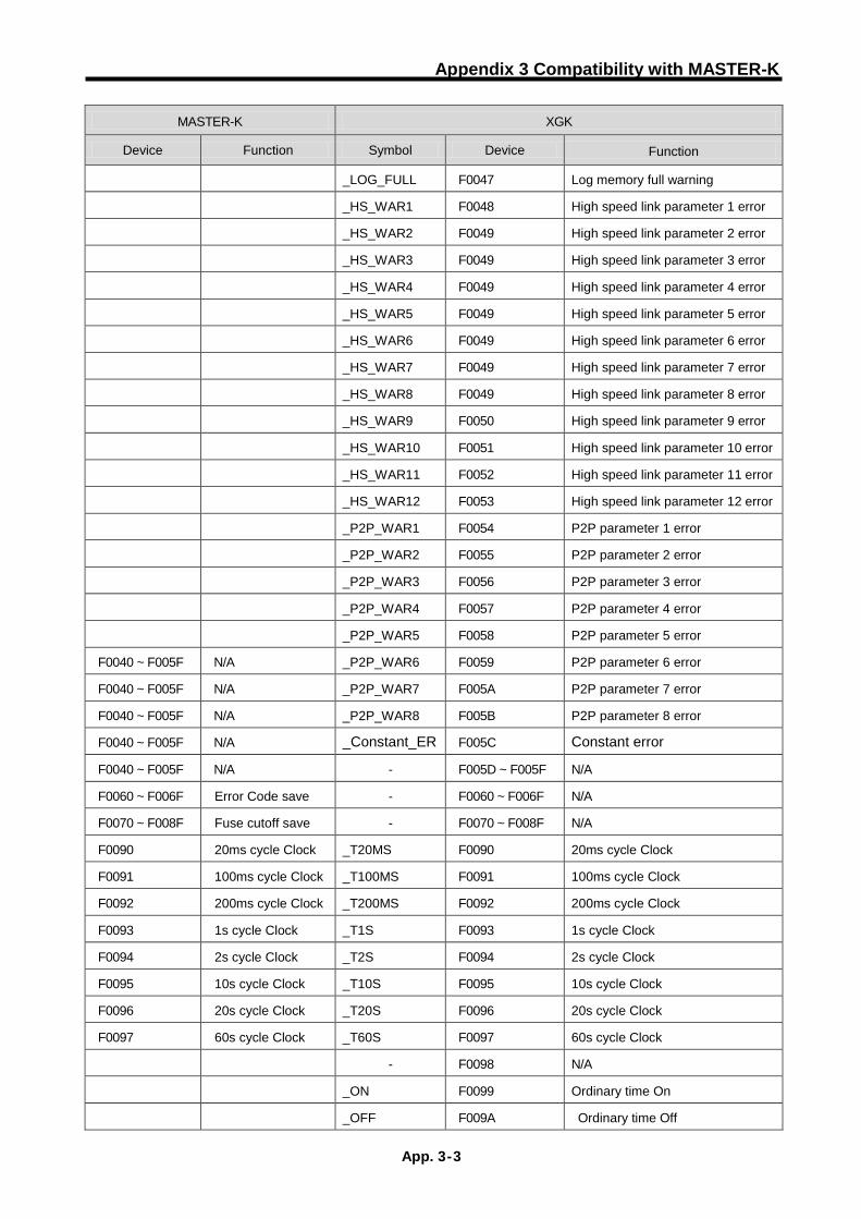
Appendix 3 Compatibility with MASTER-K
App. 3 - 3
MASTER-K XGK
Device Function Symbol Device Function
_LOG_FULL F0047 Log memory full warning
_HS_WAR1 F0048 High speed link parameter 1 error
_HS_WAR2 F0049 High speed link parameter 2 error
_HS_WAR3 F0049 High speed link parameter 3 error
_HS_WAR4 F0049 High speed link parameter 4 error
_HS_WAR5 F0049 High speed link parameter 5 error
_HS_WAR6 F0049 High speed link parameter 6 error
_HS_WAR7 F0049 High speed link parameter 7 error
_HS_WAR8 F0049 High speed link parameter 8 error
_HS_WAR9 F0050 High speed link parameter 9 error
_HS_WAR10 F0051 High speed link parameter 10 error
_HS_WAR11 F0052 High speed link parameter 11 error
_HS_WAR12 F0053 High speed link parameter 12 error
_P2P_WAR1 F0054 P2P parameter 1 error
_P2P_WAR2 F0055 P2P parameter 2 error
_P2P_WAR3 F0056 P2P parameter 3 error
_P2P_WAR4 F0057 P2P parameter 4 error
_P2P_WAR5 F0058 P2P parameter 5 error
F0040 ~ F005F N/A _P2P_WAR6 F0059 P2P parameter 6 error
F0040 ~ F005F N/A _P2P_WAR7 F005A P2P parameter 7 error
F0040 ~ F005F N/A _P2P_WAR8 F005B P2P parameter 8 error
F0040 ~ F005F N/A _Constant_ER F005C Constant error
F0040 ~ F005F N/A - F005D ~ F005F N/A
F0060 ~ F006F Error Code save - F0060 ~ F006F N/A
F0070 ~ F008F Fuse cutoff save - F0070 ~ F008F N/A
F0090 20ms cycle Clock _T20MS F0090 20ms cycle Clock
F0091 100ms cycle Clock _T100MS F0091 100ms cycle Clock
F0092 200ms cycle Clock _T200MS F0092 200ms cycle Clock
F0093 1s cycle Clock _T1S F0093 1s cycle Clock
F0094 2s cycle Clock _T2S F0094 2s cycle Clock
F0095 10s cycle Clock _T10S F0095 10s cycle Clock
F0096 20s cycle Clock _T20S F0096 20s cycle Clock
F0097 60s cycle Clock _T60S F0097 60s cycle Clock
- F0098 N/A
_ON F0099 Ordinary time On
_OFF F009A Ordinary time Off

Appendix 3 Compatibility with MASTER-K
App. 3 - 4
MASTER-K XGK
Device Function Symbol Device Function
_1ON F009B 1 Scan On
_1OFF F009C 1 Scan Off
_STOG F009D Reversal every Scan
F0098 ~ F009F - F009B ~ F009F N/A
F0100 User Clock 0 F0100 User Clock 0
F0101 User Clock 1 F0101 User Clock 1
F0102 User Clock 2 F0102 User Clock 2
F0103 User Clock 3 F0103 User Clock 3
F0104 User Clock 4 F0104 User Clock 4
F0105 User Clock 5 F0105 User Clock 5
F0106 User Clock 6 F0106 User Clock 6
F0107 User Clock 7 F0107 User Clock 7
F0108 ~ F010F - F0108 ~ F010F N/A
F0110 Operation error flag _Ler F0110 Operation error flag
F0111 Zero flag _Zero F0111 Zero flag
F0112 Carry flag _Carry F0112 Carry flag
F0113 Full output Off _All_Off F0113 Full output Off
F0114 Common RAM R/W error
- F0114 N/A
F0115 Operation error flag (latch)
_Ler_Latch F0115 Operation error flag(latch)
F0116 ~ F011F - F0116 ~ F011F N/A
F0120 LT flag _LT F0120 LT flag
F0121 LTE flag _LTE F0121 LTE flag
F0122 EQU flag _EQU F0122 EQU flag
F0123 GT flag _GT F0123 GT flag
F0124 GTE flag _GTE F0124 GTE flag
F0125 NEQ flag _NEQ F0125 NEQ flag
F0126 ~ F012F N/A - F0126 ~ F012F N/A
F0130~ F013F AC Down Count _AC_F_CNT F0130~ F013F AC Down Count
F0140~ F014F FALS no. _FALS_NUM F0140~ F014F FALS no.
F0150~ F015F PUT/GET error flag _PUTGET_ERR F0150~ F030F PUT/GET error flag
CPU TYPE F0440 ~ F044F CPU TYPE
CPU VERSION F0450 ~ F045F CPU VERSION
O/S version no. F0460 ~ F047F System O/S version no.
F0160~ F049F N/A O/S date F0480 ~ F049F System O/S DATE

Appendix 3 Compatibility with MASTER-K
App. 3 - 5
MASTER-K XGK
Device Function Symbol Device Function
F0500~ F050F Max. Scan time _SCAN_MAX F0500~ F050F Max. Scan time
F0510~ F051F Min. Scan time _SCAN_MIN F0510~ F051F Min. Scan time
F0520~ F052F Current Scan time _SCAN_CUR F0520~ F052F Current Scan time
F0530~ F053F Clock data (year/month) _YEAR_MON F0530~ F053F Clock data (year/month)
F0540~ F054F Clock data (day/hr) _DAY_TIME F0540~ F054F Clock data(day/hr)
F0550~ F055F Clock data (min/sec) _MIN_SEC F0550~ F055F Clock data(min/sec)
F0560~ F056F Clock data (100year/weekday) _HUND_WK F0560~ F056F Clock data(100year/weekday)
_FPU_LFlag_I F0570 Incorrect error latch flag
_FPU_LFlag_U F0571 Underflow error latch flag
_FPU_LFlag_O F0572 Overflow error latch flag
_FPU_LFlag_Z F0573 Zero divide error latch flag
_FPU_LFlag_V F0574 Invalid operation error latch flag
- F0575 ~ F0579 N/A
_FPU_Flag_I F057A Incorrect error flag
_FPU_Flag_U F057B Underflow error flag
_FPU_Flag_O F057C Overflow error flag
_FPU_Flag_Z F057D Zero divide error flag
_FPU_Flag_V F057E Invalid operation error flag
_FPU_Flag_E F057F Irregular value Input error flag
F0570~ F058F N/A _ERR_STEP F0580~ F058F Error step save
F0590~ F059F Error step save - F0590~ F059F N/A
F0600~ F060F FMM detailed error information _REF_COUNT F060~F061 Refresh Count
F0610~ F063F N/A _REF_OK_CNT F062~F063 Refresh OK Count
_REF_NG_CNT F064~F065 Refresh NG Count
_REF_LIM_CNT F066~F067 Refresh Limit Count
_REF_ERR_CNT F068~F069 Refresh Error Count
_MOD_RD_ERR_CNT F070~F071 MODULE Read Error Count
_MOD_WR_ERR_CNT F072~F073 MODULE Write Error Count
_CA_CNT F074~F075 Cmd Access Count
_CA_LIM_CNT F076~F077 Cmd Access Limit Count
_CA_ERR_CNT F078~F079 Cmd Access Error Count
_BUF_FULL_CNT F080~F081 Buffer Full Count
For flag over F0820 added at XGK, refer to Appendix 1.
Notes

Warranty 1. Terms of warranty
LSIS provides an 18-month warranty starting from the date of production. 2. Range of warranty
For problems within the terms of the warranty, LSIS will replace the entire PLC or repair the defective parts free of charge except for the following cases. (1) Problems caused by improper conditions, environment or treatment. (2) Problems caused by external devices. (3) Problems caused by the user remodeling or repairing the PLC. (4) Problems caused by improper use of the product. (5) Problems caused by circumstances where the expectations exceed that of the science and technology level
when LSIS produced the product. (6) Problems caused by natural disaster.
3. This warranty is limited to the PLC itself only. It is not valid for the whole system which the PLC is attached to.

HEAD OFFICE LS tower, Hogye-dong, Dongan-gu, Anyang-si, Gyeonggi-do 1026-6,
Korea http://eng.lsis.com Tel : (82-2)2034-4870/Fax : 82-2-2034-4648 e-mail : [email protected] LS Industrial Systems Tokyo Office _ Tokyo, Japan
Address: 16FL. Higashi-Kan. Akasaka Twin Tower 17-22, Akasaka.Monato-ku Tokyo 107-8470. Japan Tel : 81-3-3582-9128/Fax : 81-3-3582-2667 e-mail : [email protected] LS Industrial Systems(ME) FZE _ Dubai, U.A.E.
Address : Jafza View Tower Lob 19, Room 205 Along Sheikh Zayed Road Jebel Aali Free Zone Dubai, United Arab Emirates Tel : 971-4-886-5360/Fax : 971-4-886-5361 e-mail : [email protected]
LS Industrial Systems Shanghai Office _ Shanghai, China Address : Room E-G. 12FL Hiamin Empire Plaza. No.726. West. Yan'an Road Shanghai 200050. P.R. China e-mail : [email protected]
Tel : 86-21-5237-9977(609)/Fax : 89-21-5237-7189 LS Industrial Systems Beijing Office _ Beijing, China
Address : B-Tower 17FL. Beijing Global Trade Center B/D. No. 36. East BeisanHuan-Road. DongCheng-District. Beijing 100013. P.R. China
Tel : 86-10-5825-6027(666)/Fax : 86-10-5825-6028 e-mail : [email protected] LS Industrial Systems Guangzhou Office _ Guangzhou, China
Address : Room 1403.14FL. New Poly Tower. 2 Zhongshan Liu Road.Guangzhou.P.R China Tel : 86-20-8328-6754/Fax : 86-20-8326-6287 e-mail : [email protected]
LS Industrial Systems Chengdu Office _ Chengdu, China Address : 12FL. Guodong Buiding. No.52 Jindun Road Chengdu.610041. P.R. China Tel : 86-28-8612-9151(9226)/Fax : 86-28-8612-9236 e-mail : [email protected]
LS Industrial Systems Qingdao Office _ Qingdao, China Address : YinHe Bldg. 402 Room No. 2P Shandong Road, Qingdao-City,Shandong-province 266071, P.R. China Tel : 86-532-8501-6068/Fax : 86-532-8501-6057 e-mail : [email protected]
LS Industrial Systems Europe B.V. , Netherlands Address : 1st. Floor, Tupolevlaan 48, 1119NZ, Schiphol-Rijk, The Netherlands
Tel : +31 (0)20 654 1420/Fax : +31 (0)20 654 1429 e-mail : [email protected] Wuxi LS Industrial Systems Co., Ltd _ Wuxi, China
Address : 102-A. National High & New Tech Industrial Development Area. Wuxi. Jiangsu. 214028. P.R. China Tel : 86-510-8534-6666/Fax : 86-510-8534-4078 e-mail : [email protected]
Dalian LS Industrial Systems Co., Ltd. _ Dalian, China Address : No. 15. Liaohexi 3-Road. Economic and Technical Development zone.
Dalian 116600. China Tel : 86-411-273-7777/Fax : 86-411-8730-7560 e-mail : [email protected]
※ LS Industrial Systems constantly endeavors to improve its product so that information in this manual is subject to change without notice.
LS Industrial Systems Co., Ltd 2013 All Rights Reserved.
10310000508
2015. 2
LS values every single customers.
Quality and service come first at LSIS.
Always at your service, standing for our customers.
http://eng.lsis.com