On-line condition monitoring for diagnosis and prognosis of ...
Upload
khangminh22Category
view
1download
0
electronics
Review
Two Decades of Condition Monitoring Methods forPower Devices
Giovanni Susinni 1, Santi Agatino Rizzo 1,* and Francesco Iannuzzo 2
�����������������
Citation: Susinni, G.; Rizzo, S.A.;
Iannuzzo, F. Two Decades of
Condition Monitoring Methods for
Power Devices. Electronics 2021, 10,
683. https://doi.org/10.3390/
electronics10060683
Academic Editor: Ahmed Abu-Siada
Received: 1 January 2021
Accepted: 24 February 2021
Published: 15 March 2021
Publisher’s Note: MDPI stays neutral
with regard to jurisdictional claims in
published maps and institutional affil-
iations.
Copyright: © 2021 by the authors.
Licensee MDPI, Basel, Switzerland.
This article is an open access article
distributed under the terms and
conditions of the Creative Commons
Attribution (CC BY) license (https://
creativecommons.org/licenses/by/
4.0/).
1 Department of Electrical Electronic and Computer Engineering (DIEEI), University of Catania, Viale AndreaDoria, 6, 95125 Catania, Italy; [email protected]
2 Department of Energy Technology, Aalborg University, 9220 Aalborg, Denmark; [email protected]* Correspondence: [email protected]; Tel.: +39-095-738-2308
Abstract: Condition monitoring (CM) of power semiconductor devices enhances converter reliabilityand customer service. Many studies have investigated the semiconductor devices failure modes,the sensor technologies, and the signal processing techniques to optimize the CM. Furthermore,the improvement of power devices’ CM thanks to the use of the Internet of Things and artificialintelligence technologies is rising in smart grids, transportation electrification, and so on. Thesetechnologies will be widespread in the future, where more and more smart techniques and smartsensors will enable a better estimation of the state of the health (SOH) of the devices. Consideringthe increasing use of power converters, CM is essential as the analysis of the data obtained frommultiple sensors enables the prediction of the SOH, which, in turn, enables to properly schedule themaintenance, i.e., accounting for the trade-off between the maintenance cost and the cost and issuesdue to the device failure. From this perspective, this review paper summarizes past developmentsand recent advances of the various methods with the aim of describing the current state-of-the-art inCM research.
Keywords: condition monitoring; junction temperature; power device; reliability; power electronics
1. Introduction
Nowadays, power electronics is widespread in a huge number of daily applicationsthat improve services for the collective [1]. Furthermore, power electronics has a key rolein renewable energy systems [2,3], lighting [4,5], electric mobility [6,7], and other systemsthat enable sustainable development [8].
A crucial aspect is the reliability and lifetime prediction of the whole power conversionsystem. The warrant of the highest robustness level while minimizing the product andmaintenance cost is extremely mandatory. For example, the devices used in avionicand automotive applications must have a fault rate close to zero that imposes stringentrequirements during the system design. In the same way, wind farms must guaranteenormal operations without interruption, but this is extremely difficult because of theexpensive access to farms for easier maintenance. In this context, many approaches toforecasting the lifetime of power electronic systems and the single power device have beenintensively studied.
To guarantee a high level of reliability, it is important to comply with several stan-dards [9–11], and different strategies are usually performed such as the use of the fault-tolerant topologies with redundant components [12,13], and the advanced reliable designof power electronic devices using innovative materials [14,15].
Unfortunately, the enhanced system’s robustness does not prevent failure and, indeed,it is never completely foreseeable. Therefore, a maintenance operation before a failure isnecessary. Considering the costs of maintenance operations, lifetime prediction combinedwith condition monitoring approaches [16,17] are very useful tools to choose when amaintenance operation has to be carried out.
Electronics 2021, 10, 683. https://doi.org/10.3390/electronics10060683 https://www.mdpi.com/journal/electronics

Electronics 2021, 10, 683 2 of 28
Some studies have shown that capacitors are fragile with a failure of 30%, whereasthe failure of the PCB and connectors is around 36% [18–20]. The remaining part is relatedto the semiconductor and soldering failures in device modules that consist of the mostimportant area of concern for converter system failures. In this context, countless conditionmonitoring (CM) methods for the evaluation of the semiconductor state of health havebeen widely explored in the literature.
The target of this work is to provide an overview of various CM methods that havebeen used to evaluate the state of the health of power devices. More specifically, the firstpart of the proposed review was focused on the impact of the Internet of Things (IoT) andartificial intelligence (AI) technologies used for CM of power devices, with a chronologicaloverview of the main CM methods over the last two decades. Then, it a first CM methodbased on acoustic emission was presented and used to detect any physical damage in apower module packaging. It is worth underlining that it enables one to estimate the stateof aging of a power module.
Then, CM methods based on the optical properties of the semiconductor powerdevices were presented, including temperature estimation. These methods are usuallybased on an optical beam that is reflected or scattered back from the semiconductor lattice.There is an inherent dependence between the temperature and the energy related to thephotoemission. More specifically, such energy is a function of the junction temperature (JT);hence, in turn, the energy variation can be used to estimate the temperature of the chip.After that, a depth-analysis of the several approaches to extract the junction temperature inthe semiconductor devices based on the physical or electrical properties was performed.The early works using a physical CM method for the JT measurement were done by directlycontacting the chip surface with a thermo-sensitive material such as a point contact system(such as thermocouples and liquid crystal). On the other hand, electrical methods forthe junction temperature measurement are often the preferred choice for CM of powerdevices because the temperature estimation can be carried out through the measurementof electrical quantities. Among various electrical CM methods, thermal test chips (TTCs)are directly fabricated on the die surface of the device, and the voltage drop can be used toestimate the temperature variations. On the other hand, the temperature sensitive electricalparameters (TSEPs) are based on the measurement of the voltage drop during the converteroperations. Generally, the measurement of the voltage drop can be carried out using somevoltage probes connected to the device terminals.
Although the measurement of the power devices’ junction temperature was widelytreated in many ways, it is still an active relevant topic owing to the current trade-offbetween the advantages and limitations of the methods proposed so far. Therefore, allthese methods have been compared in terms of their main aspects such as sensitivity,linearity, cost, and online monitoring operations.
2. Conditioning Monitoring Methods and Their Future Application
In the literature, the research topic based on CM methods has been gaining interestas the various maintenance strategies allow to increase the lifetime of the overall powerconversion system. In many applications, it is becoming crucial to monitor the state of thehealth (SOH) of power devices to prevent a failure, that is, the possibility for the operatorsto obtain a lifetime estimation, thus properly scheduling any maintenance operations.
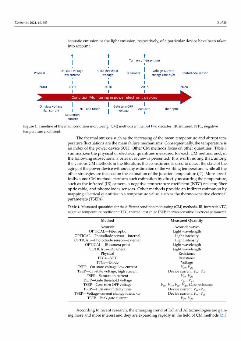
Figure 1 depicts a timeline of the various CM methods for power devices that havebeen widely studied in the literature and used by the industry in the last two decades. Thefirst use of CM methods for power devices dates back to the 2000s, where the measureof on-state voltage of the devices was used as a well-known parameter to monitor thedevice condition. Later, the measure of the threshold voltage or the gate turn-off voltageof a device was used to estimate the temperature dependence of the power devices bymeasuring a low voltage; then, the acquisition system was developed to be more simpleand less bulky. In the last 5 years, the estimation of the SOH has been carried out usingcontactless approach such as the acoustic method or the photodiode approach, where the
Electronics 2021, 10, 683 3 of 28
acoustic emission or the light emission, respectively, of a particular device have been takeninto account.
Electronics 2021, 10, x FOR PEER REVIEW 3 of 29
less bulky. In the last 5 years, the estimation of the SOH has been carried out using con-
tactless approach such as the acoustic method or the photodiode approach, where the
acoustic emission or the light emission, respectively, of a particular device have been
taken into account.
Figure 1. Timeline of the main condition monitoring (CM) methods in the last two decades. IR, infrared; NTC, negative
temperature coefficient.
The thermal stresses such as the increasing of the mean temperature and abrupt tem-
perature fluctuations are the main failure mechanisms. Consequentially, the temperature
is an index of the power device SOH. Other CM methods focus on other quantities. Table
1 summarizes the physical or electrical quantities measured for each CM method and, in
the following subsections, a brief overview is presented. It is worth noting that, among
the various CM methods in the literature, the acoustic one is used to detect the state of the
aging of the power device without any estimation of the working temperature, while all
the other strategies are focused on the estimation of the junction temperature (JT). More
specifically, some CM methods perform such estimation by directly measuring the tem-
perature, such as the infrared (IR) camera, a negative temperature coefficient (NTC) resis-
tor, fiber optic cable, and photodiodes sensors. Other methods provide an indirect estima-
tion by mapping electrical quantities in a temperature value, such as the thermo-sensitive
electrical parameters (TSEPs).
According to recent research, the emerging trend of IoT and AI technologies are gain-
ing more and more interest and they are expanding rapidly in the field of CM methods
[21].
AI aims to assist electronic systems with intelligence that is capable of human-like
learning and reasoning. This technology possesses countless advantages and has been
widely applied in numerous industrial and research areas such as maximum power point
tracking (MPPT) control for Photovoltaic (PV) plants, anomaly operation detection for in-
verter, and prediction of the SOH of a power converter.
The use of enabling AI technologies allows the power converter systems to be em-
bedded with capabilities of self-awareness and self-adaptability, thus system autonomy
can be enhanced. Similarly, the development of data science, including sensor technology,
IoT, and big data analytics, provides a wide variety of data for power electronic systems
throughout different stages of its life-cycle. Furthermore, AI technology can exploit data
to estimate the system health status with high sensitivity in condition monitoring for ag-
ing detection of power devices. Only in a few works [22–25] has the condition monitoring
and fault detection in power electronics AI-based fault detection been presented.
Figure 2 shows a proof-of-concept of the integration between IA and IoT technologies
for CM of power devices. More specifically, Figure 2a depicts an example of a user (red
box), which consists of a specific power converter and its power devices that have to be
Figure 1. Timeline of the main condition monitoring (CM) methods in the last two decades. IR, infrared; NTC, negativetemperature coefficient.
The thermal stresses such as the increasing of the mean temperature and abrupt tem-perature fluctuations are the main failure mechanisms. Consequentially, the temperature isan index of the power device SOH. Other CM methods focus on other quantities. Table 1summarizes the physical or electrical quantities measured for each CM method and, inthe following subsections, a brief overview is presented. It is worth noting that, amongthe various CM methods in the literature, the acoustic one is used to detect the state of theaging of the power device without any estimation of the working temperature, while all theother strategies are focused on the estimation of the junction temperature (JT). More specif-ically, some CM methods perform such estimation by directly measuring the temperature,such as the infrared (IR) camera, a negative temperature coefficient (NTC) resistor, fiberoptic cable, and photodiodes sensors. Other methods provide an indirect estimation bymapping electrical quantities in a temperature value, such as the thermo-sensitive electricalparameters (TSEPs).
Table 1. Measured quantities for the different condition monitoring (CM) methods. IR, infrared; NTC,negative temperature coefficient; TTC, thermal test chip; TSEP, thermo-sensitive electrical parameter.
Method Measured Quantity
Acoustic Acoustic wavesOPTICAL—Fiber optic Light wavelength
OPTICAL—Photodiode sensor—internal Light intensityOPTICAL—Photodiode sensor—external Light intensity
OPTICAL—IR camera print Light wavelengthOPTICAL—IR camera Light wavelength
Physical ResistanceTTCs—NTC Resistance
TTCs—Diode VoltageTSEP—On-state voltage, low current Vce, VdsTSEP—On-state voltage, high current Device current, Vce, Vds
TSEP—Saturation current Vce–VdsTSEP—Gate threshold voltage Vge—VgsTSEP—Gate turn OFF voltage Vge–Vce, Vgs–Vds, Gate resistanceTSEP—Turn on-off delay time Device current, Vce–Vds
TSEP—Voltage–current change rate di/dt Device current, Vce–VdsTSEP—Peak gate current Vge–Vgs
According to recent research, the emerging trend of IoT and AI technologies are gain-ing more and more interest and they are expanding rapidly in the field of CM methods [21].

Electronics 2021, 10, 683 4 of 28
AI aims to assist electronic systems with intelligence that is capable of human-likelearning and reasoning. This technology possesses countless advantages and has beenwidely applied in numerous industrial and research areas such as maximum power pointtracking (MPPT) control for Photovoltaic (PV) plants, anomaly operation detection forinverter, and prediction of the SOH of a power converter.
The use of enabling AI technologies allows the power converter systems to be em-bedded with capabilities of self-awareness and self-adaptability, thus system autonomycan be enhanced. Similarly, the development of data science, including sensor technology,IoT, and big data analytics, provides a wide variety of data for power electronic systemsthroughout different stages of its life-cycle. Furthermore, AI technology can exploit data toestimate the system health status with high sensitivity in condition monitoring for agingdetection of power devices. Only in a few works [22–25] has the condition monitoring andfault detection in power electronics AI-based fault detection been presented.
Figure 2 shows a proof-of-concept of the integration between IA and IoT technologiesfor CM of power devices. More specifically, Figure 2a depicts an example of a user (redbox), which consists of a specific power converter and its power devices that have tobe monitored, and an example of a provider of CM services (PS) (yellow block). Morespecifically, the devices of a single-user power application are connected with severalsensors that enable the monitoring of the SOH of each device (such as the measurement ofthe TJ or the state of aging of a device). Then, the controller system interface (CSI) managesthe sensors and collects all the measured data. The CSI block plays an important role for theCM of the power system because it is able to provide control signals and it may exchangedata with different users in the IoT framework (see Figure 2b).
The PS (sometimes also the CSI) uses AI technologies that act as “intelligent agents”,exploiting sensors able at perceiving the environment of the power converter. Indeed,during some power converter operations, the JT can be dangerously increased over athreshold maximum value, hence the AI is able to suddenly shut down the power system.Moreover, the AI-integrated system may enable a power derating in order to avoid anyfailure of the converter and, hence, the power devices. On the other hand, AI shouldperform more complex tasks, such as detecting any change in the device behavior thatcould lead to future malfunctioning; interacting with the CSI “to propose” solutions,i.e., fault preventing strategies, to current anomalies or potential future ones; and so on.Regardless of whether AI is located in the PS, in the CSI, or both, a local backup controlsystem is necessary. The local controller should be simple (without complex hardwareand control strategies) and highly reliable. The local controller should have less stringentlimits than the AI, thus the local controller intervenes only when the system is close toa dangerous situation. For example, the local converter shuts down the converter whenthe JT passes over a preset limit and this situation occurs owing to the lack of a smartercommand (load reduction, switching frequency variation, and so on) from the AI of thePS because of different causes (e.g., temporary lack of connection, unexpected AI actionsor reasoning).
It is worth noting that the PSs are able to contribute to the decision making in bothoffline and real-time analysis using data acquired in the past and saved into a dedicateddatabase (green silos). From this perspective, all the collected data can be used to enhancethe predictive model of the SOH of the power devices.
Moreover, the PS may interact with enterprises, authorities, public companies, and soon. For example, real-time use of CM occurs when a PS notices a critical functioning of theconverters of a large PV system. The PS informs the PV owner as well as interacts with thePV management system to enable them to promptly and properly operate. On the otherhand, the PS also informs the electric network operator (ENO) of the smart grid where thePV is installed about a potential disconnection of the PV system. This information enablesthe ENO to adopt countermeasures that mitigate the impact of such a disconnection. Inturn, the ENO informs sensitive customers, e.g., hospitals, of a potential lack of service orasks them to turn on a backup system in order to reduce the absorbed power.

Electronics 2021, 10, 683 5 of 28
Electronics 2021, 10, x FOR PEER REVIEW 5 of 29
(a)
(b)
Figure 2. (a) User and provider of CM services (PS). (b) Proof of concept of Internet of Things (IoT) and artificial intelli-
gence (AI) technologies for CM of power devices.
Figure 2. (a) User and provider of CM services (PS). (b) Proof of concept of Internet of Things (IoT) and artificial intelligence(AI) technologies for CM of power devices.
Furthermore, the measurements of the JT and other parameters of the power devicescan be used by some public institutions such as universities or research centers (blue paleand red dashed lines) for an off-line analysis of the data to carry out some models of theSOH of the power devices. Moreover, the PS may be connected to a security organization(grey dashed lines) that may collect data and it should be able to interrupt an electricalservice in the case of failure.
It is worth underlining that the PSs could provide data to the power device manufac-turers with the aim to share information related to the state of aging of the power devices.

Electronics 2021, 10, 683 6 of 28
The manufacturers can use the data to improve their power devices as well as to obtainmore accurate power device models. Indeed, manufacturers can act as PSs.
3. Acoustic Methods
Acoustic emission has been widely investigated in the literature as a CM quantityuseful in different application fields such as pumps, industrial electrical machines, and soon. Moreover, in the field of power electronics, acoustic monitoring has been extensivelyused to detect any defects or damage in transformers and capacitors [25–27]. Only inthe last decade, a few works have been focused on the acoustic phenomenon such as ameasurement method for monitoring the SOH of the power semiconductor devices [28–33].
Acoustic emission has been used to detect any physical damage in a power modulepackaging using an acoustic microscope. Furthermore, from the experimental evidence, ithas been proven that acoustic emissions are related to the switching operations of powerdevices. In the case of fast switching operation (tens of nanoseconds), a certain amountof current is switched, which causes a large di/dt, which involves magnetic interactionwithin the module packaging. This means that the magnetic force could be the sourceof the acoustic emission, such as the mechanical breaking of the structure inside thecomponent package. However, the physical phenomena causing the acoustic emission arenot definitively understood.
Thereby, the device under test (DUT) is monitored contactless with an acoustic sensorthat is usually placed in the proximity of the package. It intrinsically eliminates the issuesrelated to contact directly with the voltage probes.
A correlation between the SOH of the power module and the analysis of its acousticemission during the switching process has been analyzed [28–30]. It has been demonstratedthat the acoustic peak in an aged device is smaller in comparison with a new one. However,in these works, only the acoustic emission of an Insulated Gate Bipolar Transistor (IGBT)connected into short-circuit has been investigated. Meanwhile, the authors of [32] presentan early experimental setup used to prove that acoustic emission is related to the switchingof power semiconductor components. Furthermore, the authors have proposed an analysisbased on propagation delays to assess the source of the acoustic emission. The authorsin [33] have investigated the acoustic emission as a CM method to measure the fatiguemechanisms in the power module. More specifically, they have investigated the physicaldegradation, observing the aging process of the whole power module by measuring thefrequency spectrum of acoustic emission. The authors in [34] have measured the acousticemission during converter operations to estimate the aging of a power semiconductormodule due to power cycling. However, a spectrum analysis has been conducted to processthe acquired data. The experimental results have shown a correlation between acousticemission and the drain-source voltage, which is a common indicator of degradation of thebond wires of the power module.
As for disadvantages, the acoustic method needs an expensive and complex sensingcircuit to correctly decode the acoustic emission. Furthermore, the system has to be shieldedagainst Electromagnetic interference (EMI) and the superposition of noise contributions.
4. Optical Methods
Temperature variation, especially the sudden increase of the JT, plays a significant rolein terms of power device reliability [34,35]. CM methods performing on-line JT monitoringraise great interest in terms of planning maintenance operations because the workingconditions of a power converter are extremely unpredictable. From this perspective, theCM methods based on the optical properties of the semiconductor power devices werestudied in depth because they are useful for temperature estimation. These methods areusually based on an optical beam that is reflected or scattered back from the semiconductorlattice. There is an inherent dependence between temperature and the energy relatedto the photoemission. More specifically, such energy is a function of the JT, hence, inturn, the energy variation can be used to estimate the temperature of the chip. It is worth

Electronics 2021, 10, 683 7 of 28
remembering that these solutions based on optical quantities have some other drawbacks,such as the high cost and the impracticality in high-voltage converters.
There are various techniques for thermal mapping based on the use of an IR sensor [36–40],IR microscope [41], 2D radiometry [41,42], and the laser deflection technique [43–45],while fiber optic [46–48] and the IR camera [49–54] can both be used to obtain a thermalmapping or the JT value. In the following, the aforementioned optical techniques arebriefly discussed.
4.1. Infra-Red/Visible Emission
An IR sensor is able to detect changes in the amount of infrared radiation of an object,which may vary depending on the temperature and surface characteristics of the objects infront of the sensor. The use of the IR sensors as a CM method for the measurement of theJT in a power device [36–39] is almost inexpensive as well as not very intrusive. However,these sensors have a low response time and, furthermore, the IR sensors average out thejunction temperature value of the power device, and hence the accuracy is very low.
On the other hand, the emerging trend of the Wide-bandgap (WBG) power devices,such as the SiC power MOSFETs, are more and more diffusing devices as they concurrentlyenable high switching frequency, high voltage, and high-temperature operations. Therefore,the study of the electroluminescence proprieties of the SiC material for on-line CM hasstarted to attract wide interest. For different reasons, the electroluminescence proprietieshave already been studied back in 1907 [55], while, in the last three years, the inadvertentlight emission phenomenon in the intrinsic body diode has drawn attention. While thebody diode is in forward conduction mode, the chip glows a visible blue light [56]. Thelight brightness of the SiC body diode strongly depends on both the injected currentmagnitude and the JT. Hence, the measurement of light brightness can be used as a novelCM method for temperature detection, where only a few works have already focused onthis topic [56–58]. The first proof of concept of the SiC light emission in a commercialpower module has already proven the potentiality of this CM method [57]. An inexpensivepassive sensing circuit, such as a silicon photodiode and a resistor, was adopted and thephotodiode output voltage was correlated to the light emission intensity as a functionof the temperature. It is worth noting that the system is small enough such that it canbe easily embedded in the package. Another approach considers a light circuit sensingusing two commercial photodiodes with an active signal conditioning circuit [58]. Thisapproach has been adopted for JT estimation in a real application such as a pulse-widthmodulation (PWM) driven converter. The temperature-dependent changes in the spectrumof the light emission from the body diode of a SiC module have also been investigated [59].The method has been proven through static characterization and dynamic double pulsemeasurement using two silicon photomultipliers, which can detect the peak intensity and,consequentially, the temperature dependence. Different from the previous CM methods,the last one, based on the light intensity of the SiC body diode, enables high-voltageoperations and, even more importantly, the JT can be estimated during on-line operations.
4.2. Optical Fibers
The use of optical fiber as a CM method for the power modules has been discussed invery few works [46–48]. It is worth underlining that this CM method can be used withoutremoving the dielectric gel on the power module surface, and the JT can be measured byplacing the fiber optic cable in direct contact with the power chip. On the other hand, themeasure is able to give only a local temperature; further, for almost all fiber optic methods,the measurement response time is generally high. Furthermore, it requires an externalconditioning circuit unit that may be bulky for a specific application.
As an example, in [49], an optical fiber sensor has been used to measure the dietemperature of an IGBT power module to estimate the thermal impedance (see Figure 3).The module top lid has been removed because the optical system has to be placed close to

Electronics 2021, 10, 683 8 of 28
the die. Printing the die and bond-wires to increase the emissivity of the chip is usuallypreferable, but causes a cost increment and severely limits the on-line use of the method.
Electronics 2021, 10, x FOR PEER REVIEW 8 of 29
that it can be easily embedded in the package. Another approach considers a light circuit
sensing using two commercial photodiodes with an active signal conditioning circuit [58].
This approach has been adopted for JT estimation in a real application such as a pulse-
width modulation (PWM) driven converter. The temperature-dependent changes in the
spectrum of the light emission from the body diode of a SiC module have also been inves-
tigated [59]. The method has been proven through static characterization and dynamic
double pulse measurement using two silicon photomultipliers, which can detect the peak
intensity and, consequentially, the temperature dependence. Different from the previous
CM methods, the last one, based on the light intensity of the SiC body diode, enables high-
voltage operations and, even more importantly, the JT can be estimated during on-line
operations.
4.2. Optical Fibers
The use of optical fiber as a CM method for the power modules has been discussed
in very few works [46–48]. It is worth underlining that this CM method can be used with-
out removing the dielectric gel on the power module surface, and the JT can be measured
by placing the fiber optic cable in direct contact with the power chip. On the other hand,
the measure is able to give only a local temperature; further, for almost all fiber optic
methods, the measurement response time is generally high. Furthermore, it requires an
external conditioning circuit unit that may be bulky for a specific application.
As an example, in [49], an optical fiber sensor has been used to measure the die tem-
perature of an IGBT power module to estimate the thermal impedance (see Figure 3). The
module top lid has been removed because the optical system has to be placed close to the
die. Printing the die and bond-wires to increase the emissivity of the chip is usually pref-
erable, but causes a cost increment and severely limits the on-line use of the method.
Figure 3. Example of a power module with optical fiber thermal sensors (Based on [49]).
Figure 3. Example of a power module with optical fiber thermal sensors (Based on [49]).
4.3. IR-Detection Apparatuses
IR-detection apparatuses are not really used as a CM method for power devices,but are extremely useful in laboratory testing (e.g., under power cycling) [49–53]. Morespecifically, the use of an IR camera allows to display the thermal map of the whole surfaceof the power module under test, as shown in Figure 4. As expected, the module temperatureis not uniformly distributed; the temperature gradient between the center and the edge ofthe module can be greater than 40 ◦C. Usually, an IR camera is used to carry out a spatialthermal mapping on the device surface, but it is not able to provide an accurate measure ofthe device JT. It is worth remembering that some temperature measurement errors can bedone using an IR camera because of the surface degradation of materials and the intrinsiclow emissivity of aluminum. Even in this case, the IR temperature measurements areusually conducted by varnishing the surface of the DUT with a particular solution thatincreases the thermal emissivity on the surface.
4.4. Other Techniques
The IR microscope [40], 2D radiometry [41,42], and the laser deflection technique [43–45]have also been used as CM methods for power devices. All the aforementioned methodsare able to provide a very precise JT estimation of a semiconductor device, but, on the otherhand, the devices under test are to be driven with a specific testing sequence, not matchingwith the real operation in a power converter. They are also very expensive solutions andare not easily embedded in a real application.
Among the various sensors that use the 2D radiometry and laser deflection technique,it is worth remembering the InSb photovoltaic detector, which is a high-speed, low-noiseinfrared detector that delivers high sensitivity, and with an optical microsensor whoseoperating principle is based on detecting the absorption, deflection, and phase shift of anoptical beam.

Electronics 2021, 10, 683 9 of 28
Electronics 2021, 10, x FOR PEER REVIEW 9 of 29
4.3. IR-Detection Apparatuses
IR-detection apparatuses are not really used as a CM method for power devices, but
are extremely useful in laboratory testing (e.g., under power cycling) [49–53]. More spe-
cifically, the use of an IR camera allows to display the thermal map of the whole surface
of the power module under test, as shown in Figure 4. As expected, the module tempera-
ture is not uniformly distributed; the temperature gradient between the center and the
edge of the module can be greater than 40 °C. Usually, an IR camera is used to carry out a
spatial thermal mapping on the device surface, but it is not able to provide an accurate
measure of the device JT. It is worth remembering that some temperature measurement
errors can be done using an IR camera because of the surface degradation of materials and
the intrinsic low emissivity of aluminum. Even in this case, the IR temperature measure-
ments are usually conducted by varnishing the surface of the DUT with a particular solu-
tion that increases the thermal emissivity on the surface.
Figure 4. Thermal map of a SiC power module in the case of a current injection in the body diode.
4.4. Other Techniques
The IR microscope [40], 2D radiometry [41,42], and the laser deflection technique [43–
45] have also been used as CM methods for power devices. All the aforementioned meth-
ods are able to provide a very precise JT estimation of a semiconductor device, but, on the
other hand, the devices under test are to be driven with a specific testing sequence, not
matching with the real operation in a power converter. They are also very expensive so-
lutions and are not easily embedded in a real application.
Among the various sensors that use the 2D radiometry and laser deflection tech-
nique, it is worth remembering the InSb photovoltaic detector, which is a high-speed, low-
noise infrared detector that delivers high sensitivity, and with an optical microsensor
whose operating principle is based on detecting the absorption, deflection, and phase shift
of an optical beam.
5. Physical Methods
The early works treating CM methods for the JT measurement have been done by
directly contacting the chip surface with a thermo-sensitive material such as a point con-
tact system. In this case, direct access to the semiconductor chip is necessary and, conse-
quentially, the package must be removed.
Figure 4. Thermal map of a SiC power module in the case of a current injection in the body diode.
5. Physical Methods
The early works treating CM methods for the JT measurement have been done bydirectly contacting the chip surface with a thermo-sensitive material such as a pointcontact system. In this case, direct access to the semiconductor chip is necessary and,consequentially, the package must be removed.
Various equipment has been used for the physical contact measurement, includingthermocouples, thermistors, scanning thermal probes, and multiple contact or blanketcoatings such as liquid crystals and thermographic phosphors [59–65]. The aforementionedequipment relies on the transfer of thermal energy from the DUT to the thermal sensors. Inthis case, the spatial resolution related to the contact measurements strictly depends onthe size and the thermal capacitance of thermo-sensible materials. The ability to providea temperature map utilizing a matrix of sensors and a wide spatial resolution (can reachless than 100 nm) are the main advantages. In the following, the aforementioned physicaltechniques have been briefly discussed.
5.1. Thermocouples
The physical contact methods that rely on the use of thermocouples are not widespreadin practical applications as the chip of the power module must be accessible to the thermalprobe and, from this perspective, the on-line measurements and high voltage operationsare strongly limited. Furthermore, the measurement of the thermal variation of the powermodule strictly depends on the time response of the probe, which may be considerablyslower (few seconds) than the variation of the module JT.
Nowadays, only in a few cases [60,61], the JT of an IGBT module has been experimentallymeasured during on-line converter operation. More specifically, the temperature has beendetermined using several thermocouples physically connected to the chip (see Figure 5). Onthe other hand, several works use the measurement of some thermocouples as target valuesto prove the accuracy and effectiveness of new on-line junction temperature estimationmodels [62–65]. For example, the effectiveness of a model carried out for a three-phasepower module IGBT by considering the transient thermal impedance has been provenusing several thermocouples [63]. An experimental setup and an on-line control systemthat includes a microcontroller and a matrix of K-type thermocouples have been built upto verify a numerical thermal model for IGBT devices [64]. In [65], an electrical-thermal

Electronics 2021, 10, 683 10 of 28
model has been carried out in terms of both the transient and steady-state responses. Tovalidate the model, an array of thermocouple has been installed on the chip surface. Athermal model based on the Fourier series solution of heat conduction equations has alsobeen validated using several thermocouples placed on the surface of the silicon die, onthe base plate, and on the heat sink, in order to characterize the transient electrothermalbehavior of an IGBT module [66].
Electronics 2021, 10, x FOR PEER REVIEW 10 of 29
Various equipment has been used for the physical contact measurement, including
thermocouples, thermistors, scanning thermal probes, and multiple contact or blanket
coatings such as liquid crystals and thermographic phosphors [59–65]. The aforemen-
tioned equipment relies on the transfer of thermal energy from the DUT to the thermal
sensors. In this case, the spatial resolution related to the contact measurements strictly
depends on the size and the thermal capacitance of thermo-sensible materials. The ability
to provide a temperature map utilizing a matrix of sensors and a wide spatial resolution
(can reach less than 100 nm) are the main advantages. In the following, the aforemen-
tioned physical techniques have been briefly discussed.
5.1. Thermocouples
The physical contact methods that rely on the use of thermocouples are not wide-
spread in practical applications as the chip of the power module must be accessible to the
thermal probe and, from this perspective, the on-line measurements and high voltage op-
erations are strongly limited. Furthermore, the measurement of the thermal variation of
the power module strictly depends on the time response of the probe, which may be con-
siderably slower (few seconds) than the variation of the module JT.
Nowadays, only in a few cases [60,61], the JT of an IGBT module has been experi-
mentally measured during on-line converter operation. More specifically, the temperature
has been determined using several thermocouples physically connected to the chip (see
Figure 5). On the other hand, several works use the measurement of some thermocouples
as target values to prove the accuracy and effectiveness of new on-line junction tempera-
ture estimation models [62–65]. For example, the effectiveness of a model carried out for
a three-phase power module IGBT by considering the transient thermal impedance has
been proven using several thermocouples [63]. An experimental setup and an on-line con-
trol system that includes a microcontroller and a matrix of K-type thermocouples have
been built up to verify a numerical thermal model for IGBT devices [64]. In [65], an elec-
trical-thermal model has been carried out in terms of both the transient and steady-state
responses. To validate the model, an array of thermocouple has been installed on the chip
surface. A thermal model based on the Fourier series solution of heat conduction equa-
tions has also been validated using several thermocouples placed on the surface of the
silicon die, on the base plate, and on the heat sink, in order to characterize the transient
electrothermal behavior of an IGBT module [66].
Figure 5. Measurement of the junction temperature (JT) of a device under test (DUT) with a ther-
mocouple probe on the die surface (Based on [62]).
Figure 5. Measurement of the junction temperature (JT) of a device under test (DUT) with a thermo-couple probe on the die surface (Based on [62]).
5.2. Liquid Crystals
The earliest physical CM methods for the measurement of the JT in a power devicehave been obtained by using the scanning thermal probes, as well as multiple contact orblanket coatings, such as liquid crystals and thermographic phosphors [60].
More specifically, the thermochromic liquid crystals consist of a thermal imagingtool for mapping surface and spatial temperature distributions. It is worth rememberingthat the molecular structure and optical properties of the liquid crystals vary with thetemperature. Hence, the JT measurement of a power device can be done by measuring thewavelength of the reflected light. These CM methods have a very good spatial resolution,but on the other hand, they are extremely highly invasive and cannot be used in a realpower converter application owing to the bulky sensing circuits.
6. Electrical Methods
Electrical methods for JT measurement are often the preferred choice for CM of powerdevices because the temperature estimation can be carried out through the measurement ofelectrical quantities. More specifically, it is worth remembering that the proprieties of thesemiconductor materials are temperature dependent and, hence, the measurement of thevoltage drop or the current that flows into the device can be used as a valid temperatureestimator. Among the various electrical CM methods, thermal test chips (TTCs) are directlyfabricated on the die surface of the device, and the voltage drop can be used to estimatethe temperature variations. On the other hand, the TSEPs are based on the measurement ofthe voltage drop (or current) during the converter operations. Generally, the measurementof the voltage drop can be carried out using some voltage probes that are connected tothe device terminals. The TSEPs are usually the preferred choice for CM because of theiruser-friendliness, fast response time to the temperature transients, and good accuracy.
Electronics 2021, 10, 683 11 of 28
6.1. Thermal Test Chips
TTCs were originally developed for the thermal characterization of device pack-ages [67], and since then have also been used in IGBT power modules. TTCs act as thermalsensors to monitor the JT and they are fabricated on the proximity of the silicon chip.
TTCs can be suitable for on-line temperature measurements. Various types of TTCshave been realized, such as integrated diodes and resistance temperature detectors(RTDs) [67–75]. As the forward voltage of the diodes strongly depends on the temperaturevariation, the measure of the voltage drop can be used for temperature estimation. Itis worth remembering that the temperature presents an exponential dependence on theforward voltage. Likewise, RTDs are also used as the temperature-sensitive parameterbecause the voltage drop is related to the resistance variations. The variable resistance, Rt,can be expressed as follows:
Rt = R0(1 + α0∆T) (1)
where R0 is the value of the resistance at 0 ◦C, α0 is the resistance temperature coefficientthat strictly depends on the material, and ∆T is the temperature variation.
To use TTCs, a modified IGBT power module layout with an accessible on-chiptemperature terminal has been proposed in [68]. A string of diodes on the top of the chiphas been fabricated and the measurement of the JT has been performed by measuringthe forward voltage drop. Instead, in [69] a thin-film RTD placed on the top of the IGBTchip has been realized to measure the average temperature of the die. A similar solutionwhere an NTC thermistor has been embedded in the IGBT power module has been alsoinvestigated [70]. Innovative use of a kelvin-emitter resistor, placed directly on the IGBTdie surface, as a junction temperature sensor has been also adopted [71]. It provides only alocal temperature measurement. Meanwhile, in [72], a chain of integrated diodes has beenfabricated on the die surface to investigate the JT variations during a power cycling test.
The widespread nature of SiC power modules in different power electronics applica-tions has also driven forward the research of innovative control techniques that requirereal-time monitoring or estimation of the module’s JT. From this perspective, severalworks [72–75] have been focused on the development of electrical models of the devicesin which several NTC thermistors have been integrated on the die surface. The mea-surement of the temperature variation enables the estimation of aging of a device and,consequentially, the device model can be continuously updated.
The main drawbacks of the TTCs are the production cost and manufacturing complex-ity of the embedded sensors. Indeed, such layout modification complexity of the powermodule packaging can considerably increase and also requires additional terminals for thetemperature measurements. Furthermore, it is worth remembering that the diodes andRTDs can be affected by degradations along the lifetime of the device that may affect theaccuracy of the measurement. These issues have limited the spread of TTCs in commercialpower devices.
6.2. Methods Using the Thermo-Sensitive Electrical Parameters (TSEPs)
The CM methods outlined so far require visual or physical access to the chip. Toovercome this limitation, the temperature measurement by thermo-sensitive electrical pa-rameters (TSEPs) has been used as a valid alternative for the estimation of the JT of a powerdevice. The key point consists of correlating the temperature of the semiconductor materialwith the electrical quantities during the normal operation of the converter. More specifically,the semiconductor devices have an intrinsic dependence on the temperature related todifferent parameters, such as the mobility of the carriers µ(T), intrinsic concentration ni(T),and the bandgap energy Eg(T). It is worth remembering that the Eg(T) and ni(T) increaseat higher temperatures, while µ(T) has a complex dependence with the temperature thatis related to the doping concentration and traps in the gate oxide and silicon interface.

Electronics 2021, 10, 683 12 of 28
Therefore, the temperature dependence on the aforementioned parameters may be writtenas follows [76–78]:
Eg(T) = Eg(T0)− α1T2
T + β1(2)
ni(T) = Nα2 e−γT (3)
µ(T) = µ0
β2
(TT0
)α3
1 + β2
(TT0
)α4(4)
where α1, α2, α3, β1, β2, and γ are empirical coefficients; N is the number per unit volumeof effectively available levels states; and T0 is the room temperature.
Consequentially, the measurement of the electrical quantities measured at the deviceterminal can be used as a temperature estimator.
Therefore, TSEPs methods use passive voltage or current probes that measure theelectrical quantities at the device electrodes, without direct access to the chip device, thenthe JT is estimated from these measurements. Furthermore, the TSEPs are the preferredapproaches to easily obtain JT measurements on packaged devices with a fast time response(less than 100 microseconds). On the other hand, the TSEPs methods do not provide athermal map of the DUT and, hence, the JT peak is often hard to evaluate [79]. Such anissue is more severe in multichip devices where the voltage or current measurements onlyprovide a rough temperature of the whole device, without the possibility to know theeffective temperature distribution among several paralleled chips [80]. In the followingsubsection, the main TSEPs methods are briefly discussed.
6.2.1. On-State Voltage Measurement
Among the different TSEPs methods, on-state voltage measurement under low currentinjection has been the most used in many industrial and academic applications. In this case,the TSEP is the voltage drop across the device. The advantage of using this CM methodlies in the easy calibration procedure and the negligible self-heating of the DUT.
This CM method is widely employed when the devices have a PN junction in theirstructure. More specifically, bearing in mind a vertical diffusion MOSFET power device,the temperature variation can be evaluated as the on-resistance Rds,on fluctuations duringthe converter operations. For the sake of simplicity, the Rds,on can be approximated asfollows (see Figure 6):
Rds,on ≈ Rch + Rd + Rsub + Rcs + Rcd + Rs + Ra + Rj f et (5)
where Rch is the channel resistance, Rd is the drift region resistance, Rsub is the substrateresistance, Rcs and Rds are the source and drain contact resistance, Rs is the source resistance,Rjfet is the JFET resistance, and Ra is the accumulation resistance. Furthermore, the Rch andRd can be evaluated as follows [78]:
Rch =Lch
WchµchCox(Vgs − Vth
) (6)
Rd =Ld
qµdNd Ad(7)
where Lch and Wch are the channel length and width, respectively; Cox is the gate ca-pacitance; Ld and Ad are the drift region length and area, respectively; Nd is the dopingconcentration of the drift region; and µch and µd are the channel and drift region mobility,respectively. It is worth noting that Rch decreases at higher temperatures because bothµch and Vth decrease at higher temperatures. On the other hand, Rd acts as a positivetemperature coefficient thermistor owing to the temperature dependence of µd, whichdecreases at higher temperatures.

Electronics 2021, 10, 683 13 of 28
Electronics 2021, 10, x FOR PEER REVIEW 13 of 29
6.2.1. On-State Voltage Measurement
Among the different TSEPs methods, on-state voltage measurement under low cur-
rent injection has been the most used in many industrial and academic applications. In
this case, the TSEP is the voltage drop across the device. The advantage of using this CM
method lies in the easy calibration procedure and the negligible self-heating of the DUT.
This CM method is widely employed when the devices have a PN junction in their
structure. More specifically, bearing in mind a vertical diffusion MOSFET power device,
the temperature variation can be evaluated as the on-resistance Rds,on fluctuations during
the converter operations. For the sake of simplicity, the Rds,on can be approximated as fol-
lows (see Figure 6):
𝑅𝑑𝑠,𝑜𝑛 ≈ 𝑅𝑐ℎ + 𝑅𝑑 + 𝑅𝑠𝑢𝑏 + 𝑅𝑐𝑠 + 𝑅𝑐𝑑+𝑅𝑠 + 𝑅𝑎 + 𝑅𝑗𝑓𝑒𝑡 (5)
where Rch is the channel resistance, Rd is the drift region resistance, Rsub is the substrate
resistance, Rcs and Rds are the source and drain contact resistance, Rs is the source re-
sistance, Rjfet is the JFET resistance, and Ra is the accumulation resistance. Furthermore,
the Rch and Rd can be evaluated as follows [78]:
𝑅𝑐ℎ =𝐿𝑐ℎ
𝑊𝑐ℎ𝜇𝑐ℎ𝐶𝑜𝑥(𝑉𝑔𝑠 − 𝑉𝑡ℎ) (6)
𝑅𝑑 =𝐿𝑑
𝑞𝜇𝑑𝑁𝑑𝐴𝑑 (7)
where Lch and Wch are the channel length and width, respectively; Cox is the gate capaci-
tance; Ld and Ad are the drift region length and area, respectively; Nd is the doping concen-
tration of the drift region; and μch and μd are the channel and drift region mobility, respec-
tively. It is worth noting that Rch decreases at higher temperatures because both μch and Vth
decrease at higher temperatures. On the other hand, Rd acts as a positive temperature co-
efficient thermistor owing to the temperature dependence of μd, which decreases at higher
temperatures.
Figure 6. Power vertical diffused MOSFET structure with its internal resistances. Figure 6. Power vertical diffused MOSFET structure with its internal resistances.
It is worth underlining that the temperature coefficient of Rds,on may differ for thepower devices from different vendors, which is mainly caused by the different design ofthe device. Therefore, notwithstanding an easier calibration procedure, the CM methodmust be calibrated when a different device is adopted.
Firstly, the calibration procedure is mandatory, which is used to find the relationshipbetween the JT and the TSEP. Typically, the calibration step consists of the use of a currentsource ICal, in a range from 1 mA to tens of A. It is worth noting that, during the calibrationprocedure, the device temperature can usually be fixed by a temperature-controlled heatsink. Then, the temperature measurement can be carried out during the dissipation stage,where the TSEP is measured in a typical converter application. In this case, a current source,Id, feeds the DUT to increase its temperature by means of power dissipations. Therefore,the voltage drop across the device, under known electrical conditions, is measured as afunction of the temperature.
A simplified schematic of the circuits for the measurement of the voltage under lowcurrent is depicted in Figure 7 for an IGBT (Figure 7a) and a MOSFET (Figure 7b). Themeasurement can be carried out for both the on-state and off-state voltage. A voltmeteris usually connected in parallel to the DUT for the measurement of the voltage drop.It is worth noting that the current Ical must be at least hundreds of mA to guarantee alinear relationship between the voltage drop and the temperature [80,81]. In the literature,many works [80–96] have focused on voltage measurement under low current injectionin power diodes during forward polarization [84–87], in IGBT power modules [90–95], aswell as in power BJTs. Some works [94,95] have focused on the JT estimation in an IGBTpower module whose on-state voltage (i.e., collector-emitter voltage, VCEon) has a negativetemperature coefficient. The main drawback of this method is the high dependence onthe collector current during the measurement of VCE,on. Hence, the load current should bediverted during the measurement and this momentary interruption limits the use of thismethod in real-time applications.

Electronics 2021, 10, 683 14 of 28
Electronics 2021, 10, x FOR PEER REVIEW 14 of 29
It is worth underlining that the temperature coefficient of Rds,on may differ for the
power devices from different vendors, which is mainly caused by the different design of
the device. Therefore, notwithstanding an easier calibration procedure, the CM method
must be calibrated when a different device is adopted.
Firstly, the calibration procedure is mandatory, which is used to find the relationship
between the JT and the TSEP. Typically, the calibration step consists of the use of a current
source ICal, in a range from 1 mA to tens of A. It is worth noting that, during the calibration
procedure, the device temperature can usually be fixed by a temperature-controlled heat
sink. Then, the temperature measurement can be carried out during the dissipation stage,
where the TSEP is measured in a typical converter application. In this case, a current
source, Id, feeds the DUT to increase its temperature by means of power dissipations.
Therefore, the voltage drop across the device, under known electrical conditions, is meas-
ured as a function of the temperature.
A simplified schematic of the circuits for the measurement of the voltage under low
current is depicted in Figure 7 for an IGBT (Figure 7a) and a MOSFET (Figure 7b). The
measurement can be carried out for both the on-state and off-state voltage. A voltmeter is
usually connected in parallel to the DUT for the measurement of the voltage drop. It is
worth noting that the current Ical must be at least hundreds of mA to guarantee a linear
relationship between the voltage drop and the temperature [80,81]. In the literature, many
works [80–95] have focused on voltage measurement under low current injection in power
diodes during forward polarization [84–87], in IGBT power modules [90–95], as well as in
power BJTs. Some works [94,95] have focused on the JT estimation in an IGBT power
module whose on-state voltage (i.e., collector-emitter voltage, VCEon) has a negative tem-
perature coefficient. The main drawback of this method is the high dependence on the
collector current during the measurement of VCE,on. Hence, the load current should be di-
verted during the measurement and this momentary interruption limits the use of this
method in real-time applications.
(a)
(b)
Figure 7. Electrical circuits for the static measurement of the voltage under a low current: (a) IGBT and (b) MOSFET.
The principle of operation of the CM methods based on the on-state voltage meas-
urement at high current injection is almost similar to that of the low current injection
methods. The measurement of the VCE,on (or Vds,on) voltage drop across the device is used
as a TSEP, as described for the low current injection mode. The main difference with re-
spect to the previous CM method lies in the calibration procedure. More specifically, a
higher current is used for the calibration procedure and it produces a non-negligible self-
heating. From this perspective, the relation between the voltage drop on the DUT and the
temperature also depends on the value of the injected current.
The experimental setup for the temperature measurement is depicted in Figure 8. A
high current generator feeds the DUT with a pulsed current, IH, and a voltmeter is con-
nected in parallel to the DUT. It is important to point out that the measurement of the JT
can be obtained during the heating process.
Figure 7. Electrical circuits for the static measurement of the voltage under a low current: (a) IGBT and (b) MOSFET.
The principle of operation of the CM methods based on the on-state voltage measure-ment at high current injection is almost similar to that of the low current injection methods.The measurement of the VCE,on (or Vds,on) voltage drop across the device is used as a TSEP,as described for the low current injection mode. The main difference with respect to theprevious CM method lies in the calibration procedure. More specifically, a higher current isused for the calibration procedure and it produces a non-negligible self-heating. From thisperspective, the relation between the voltage drop on the DUT and the temperature alsodepends on the value of the injected current.
The experimental setup for the temperature measurement is depicted in Figure 8.A high current generator feeds the DUT with a pulsed current, IH, and a voltmeter isconnected in parallel to the DUT. It is important to point out that the measurement of theJT can be obtained during the heating process.
Electronics 2021, 10, x FOR PEER REVIEW 15 of 29
Figure 8. Electrical circuits of a DUT for the static measurement of the voltage under high current.
The TSEPs are usually the MOSFET on-state drain-source voltage [97], the power di-
odes forward voltage [91], and the IGBT on-state emitter-collector voltage [91,97]. The
sensitivity of the aforementioned TSEP is strictly related to the on-state current value, re-
gardless of the specific device. The JT estimation is only practicable for current values
greater than tens of Ampere [98]. Hence, this method appears to be very useful, especially
for on-line JT measurement during the normal converter operation. Several circuit solu-
tions to measure the VCEon of the power device have been devised [81,90,96–99].
This approach also presents some limitations owing to the voltage swing between
the on-state and off-state of the device. This implies the use of advanced electronic sensing
circuits, thus increasing the complexity of the system. Innovative and compact sensing
circuits to face these issues have been proposed [97,98].
Another issue is the contact resistances of the voltage probes, which cause an unde-
sired voltage drop that may produce an overestimation of the JT measurement [99]. This
issue has been partially mitigated with a correction factor based on the layout of the power
module [98,99]. Unfortunately, the introduced correction factor has to be calibrated as the
device aging progresses.
6.2.2. Saturation Current
The measurement of the saturation current, Isat, has also been used as a TSEP
[88,93,100–101] in power modules with IGBTs or MOSFETs. This current can be measured
using a current probe or a voltage probe (by adding a shunt resistor). The electrical quan-
tities measured provide a JT estimation due to the dependence on the chip temperature of
the channel electron mobility, μch; of the threshold, Vth; and of the PNP transistor current
gain β for the IGBT [101]. It is worth remembering that the current Isat shows a complex
temperature dependence, but under the assumption that all the devices are at the same
temperature and by neglecting the self-heating, the current Isat in a device can be simply
approximated as follows:
𝐼𝑠𝑎𝑡 =1
2
𝜇𝑐ℎ(𝑇)𝑊𝑐ℎ𝐶𝑜𝑥
𝐿𝑐ℎ(𝑉𝐺𝑆 − 𝑉𝑡ℎ(𝑇))
2 (8)
The measurement setup consists of a voltage source, VGT, connected between the gate-
emitter (or gate-source) terminals of the DUT and a DC source voltage, VD, connected be-
tween the drain-source or collector-emitter terminals of the DUT. Figure 9 shows the setup
of an IGBT device. The voltage value of VGT is usually higher than the threshold voltage
Vth of the device and a pulsed current is injected into the DUT by controlling the switch
T1. The saturation current can be measured through the voltage drop on the Rshunt. The
setup demonstrates that the thermal characterization of the device cannot be performed
during the on-line converter operation.
Figure 8. Electrical circuits of a DUT for the static measurement of the voltage under high current.
The TSEPs are usually the MOSFET on-state drain-source voltage [97], the powerdiodes forward voltage [91], and the IGBT on-state emitter-collector voltage [91,97]. Thesensitivity of the aforementioned TSEP is strictly related to the on-state current value,regardless of the specific device. The JT estimation is only practicable for current valuesgreater than tens of Ampere [98]. Hence, this method appears to be very useful, especiallyfor on-line JT measurement during the normal converter operation. Several circuit solutionsto measure the VCEon of the power device have been devised [81,90,96–99].
This approach also presents some limitations owing to the voltage swing between theon-state and off-state of the device. This implies the use of advanced electronic sensingcircuits, thus increasing the complexity of the system. Innovative and compact sensingcircuits to face these issues have been proposed [97,98].
Another issue is the contact resistances of the voltage probes, which cause an undesiredvoltage drop that may produce an overestimation of the JT measurement [99]. This issue

Electronics 2021, 10, 683 15 of 28
has been partially mitigated with a correction factor based on the layout of the powermodule [98,99]. Unfortunately, the introduced correction factor has to be calibrated as thedevice aging progresses.
6.2.2. Saturation Current
The measurement of the saturation current, Isat, has also been used as a TSEP [88,93,100,101]in power modules with IGBTs or MOSFETs. This current can be measured using a currentprobe or a voltage probe (by adding a shunt resistor). The electrical quantities measuredprovide a JT estimation due to the dependence on the chip temperature of the channelelectron mobility, µch; of the threshold, Vth; and of the PNP transistor current gain β forthe IGBT [101]. It is worth remembering that the current Isat shows a complex temperaturedependence, but under the assumption that all the devices are at the same temperatureand by neglecting the self-heating, the current Isat in a device can be simply approximatedas follows:
Isat =12
µch(T)WchCox
Lch(VGS − Vth(T))
2 (8)
The measurement setup consists of a voltage source, VGT, connected between thegate-emitter (or gate-source) terminals of the DUT and a DC source voltage, VD, connectedbetween the drain-source or collector-emitter terminals of the DUT. Figure 9 shows thesetup of an IGBT device. The voltage value of VGT is usually higher than the thresholdvoltage Vth of the device and a pulsed current is injected into the DUT by controllingthe switch T1. The saturation current can be measured through the voltage drop on theRshunt. The setup demonstrates that the thermal characterization of the device cannot beperformed during the on-line converter operation.
Electronics 2021, 10, x FOR PEER REVIEW 16 of 29
Figure 9. Electrical circuits for the measurement of the saturation current in an IGBT device.
The first procedure is the calibration step, where the DUT is usually placed in a con-
trolled hot plate that overheats the device and, hence, the Isat is measured at varying plate
temperatures. Then, the measurement procedure (see Figure 9) consists of performing a
non-destructive short-circuit to produce a significant channel temperature variation over
a short period of time. From this perspective, the measurement variation of the current Isat
can be associated with a specific temperature value. Moreover, the temperature calibra-
tion may not be performed without power losses that influence the device self-heating
[100,101]. Furthermore, it has been demonstrated that JT measurement is more accurate
only for high temperatures.
6.2.3. Gate Threshold Voltage
The threshold voltage Vth is defined as the voltage to be applied to the gate-source
terminals to have a given current, which is the minimum current that must flow into the
device channel to assume the device is turned on. Instead, from the standpoint of power
electronic devices, Vth is defined as the level of gate bias needed to observe a transition
from weak inversion to strong inversion. For a MOS transistor structure, the Vth can be
approximated as follows [103]:
𝑉𝑡ℎ ≈ 2𝜑𝐹(𝑇) −𝑄𝑆𝑆
𝐶𝑂+ 𝜑𝑚𝑠(𝑇) + √
2𝜀𝑞𝑁𝐴
𝐶𝑂√2𝜑𝐹(𝑇) (9)
where F is the Fermi potential, QSS is the extrinsic change due to surface states, CO is the
gate oxide capacitance, ms is the metal-semiconductor work function difference, ε is the
oxide dielectric constant, q is the elementary charge unit, and NA is the body doping.
By referring to (9), it can be demonstrated that the voltage VTH decreases with the
increasing temperature [103], and it is a TSEP useful for temperature monitoring of
MOSFETs [90,103] and IGBTs [93,94,104,105]. A potential measurement setup for the cal-
ibration procedure and the measurement of the Vth as TSEP in the case of an IGBT device
is depicted in Figure 10.
The gate and drain (collector) terminals are short-circuited and a current source, Ical,
feeds the DUT, while a voltmeter measures the Vth. It is worth noting that the calibration
step is based on the low current injection method and, thereby, the self-heating is negligi-
ble.
Some works [93,94] have focused on the temperature dependence of the Vth measured
by varying the collector-emitter voltage and the current collector value for an IGBT device.
The Ical value has to be higher than 5 mA to have a correct calibration step for high tem-
peratures and high sensitivity [93,94]. Other works [104,105] have focused on the temper-
ature measurements after the power dissipation of the device. More specifically, a current
source with two different current levels, one for dissipation (high current injection) and
Figure 9. Electrical circuits for the measurement of the saturation current in an IGBT device.
The first procedure is the calibration step, where the DUT is usually placed in acontrolled hot plate that overheats the device and, hence, the Isat is measured at varyingplate temperatures. Then, the measurement procedure (see Figure 9) consists of performinga non-destructive short-circuit to produce a significant channel temperature variation overa short period of time. From this perspective, the measurement variation of the current Isatcan be associated with a specific temperature value. Moreover, the temperature calibrationmay not be performed without power losses that influence the device self-heating [100–102].Furthermore, it has been demonstrated that JT measurement is more accurate only forhigh temperatures.
6.2.3. Gate Threshold Voltage
The threshold voltage Vth is defined as the voltage to be applied to the gate-sourceterminals to have a given current, which is the minimum current that must flow into thedevice channel to assume the device is turned on. Instead, from the standpoint of power

Electronics 2021, 10, 683 16 of 28
electronic devices, Vth is defined as the level of gate bias needed to observe a transitionfrom weak inversion to strong inversion. For a MOS transistor structure, the Vth can beapproximated as follows [103]:
Vth ≈ 2ϕF(T)−QSSCO
+ ϕms(T) +
√2εqNA
CO
√2ϕF(T) (9)
where ϕF is the Fermi potential, QSS is the extrinsic change due to surface states, CO is thegate oxide capacitance, ϕms is the metal-semiconductor work function difference, ε is theoxide dielectric constant, q is the elementary charge unit, and NA is the body doping.
By referring to (9), it can be demonstrated that the voltage VTH decreases with theincreasing temperature [103], and it is a TSEP useful for temperature monitoring of MOS-FETs [90,103] and IGBTs [93,94,104,105]. A potential measurement setup for the calibrationprocedure and the measurement of the Vth as TSEP in the case of an IGBT device is depictedin Figure 10.
Electronics 2021, 10, x FOR PEER REVIEW 17 of 29
the other for JT measurement (low current injection), has been proposed. This CM method
is not suitable for on-line condition monitoring [106,107].
Figure 10. Circuit for the calibration step of the threshold voltage method.
6.2.4. Gate-Source or Gate-Emitter Voltage Turn ON-OFF
The gate-emitter (source) voltage, Vge (or Vgs), is used as a TSEP during the turn-on
and turn-off of the switch [108–109]. The high sensitivity and the linear dependence of Vge
(or Vgs) with the temperature are the strengths of this method. Similarly to the threshold
voltage method, the Vge (or Vgs) TSEP method cannot be used for on-line JT estimation in
a power converter application, because the gate and collector (drain) terminal has to be
shorted. The experimental setup of the gate-source or gate-emitter voltage as the CM
method is very similar to that of the threshold voltage (see Figure 10). In this case, the
current injected into the DUT is higher than the current used in the threshold voltage
method and, consequentially, the self-heating is not negligible.
Figure 11 depicts the simulation of the gate-emitter voltage Vge of an IGBT during the
turn-off while varying the device temperature. It is worth noting that the following anal-
ysis can be done by considering the turn-on of a device. The Miller plateau becomes wider
as the temperature increases. In other terms, the time shift Δt in the figure is strictly related
to the temperature of the chip and can be detected using a time counter that triggers from
the first falling edge to the second one after the Miller plateau.
Figure 11. Simulated Vge waveform during the turn off of an IGBT by varying the temperature
working operations (figure based on [110]).
Figure 10. Circuit for the calibration step of the threshold voltage method.
The gate and drain (collector) terminals are short-circuited and a current source, Ical,feeds the DUT, while a voltmeter measures the Vth. It is worth noting that the calibrationstep is based on the low current injection method and, thereby, the self-heating is negligible.
Some works [93,94] have focused on the temperature dependence of the Vth measuredby varying the collector-emitter voltage and the current collector value for an IGBT device.The Ical value has to be higher than 5 mA to have a correct calibration step for hightemperatures and high sensitivity [93,94]. Other works [104,105] have focused on thetemperature measurements after the power dissipation of the device. More specifically, acurrent source with two different current levels, one for dissipation (high current injection)and the other for JT measurement (low current injection), has been proposed. This CMmethod is not suitable for on-line condition monitoring [106,107].
6.2.4. Gate-Source or Gate-Emitter Voltage Turn ON-OFF
The gate-emitter (source) voltage, Vge (or Vgs), is used as a TSEP during the turn-onand turn-off of the switch [108,109]. The high sensitivity and the linear dependence of Vge(or Vgs) with the temperature are the strengths of this method. Similarly to the thresholdvoltage method, the Vge (or Vgs) TSEP method cannot be used for on-line JT estimationin a power converter application, because the gate and collector (drain) terminal has tobe shorted. The experimental setup of the gate-source or gate-emitter voltage as the CMmethod is very similar to that of the threshold voltage (see Figure 10). In this case, thecurrent injected into the DUT is higher than the current used in the threshold voltagemethod and, consequentially, the self-heating is not negligible.
Figure 11 depicts the simulation of the gate-emitter voltage Vge of an IGBT duringthe turn-off while varying the device temperature. It is worth noting that the followinganalysis can be done by considering the turn-on of a device. The Miller plateau becomeswider as the temperature increases. In other terms, the time shift ∆t in the figure is strictly

Electronics 2021, 10, 683 17 of 28
related to the temperature of the chip and can be detected using a time counter that triggersfrom the first falling edge to the second one after the Miller plateau.
Electronics 2021, 10, x FOR PEER REVIEW 17 of 29
the other for JT measurement (low current injection), has been proposed. This CM method
is not suitable for on-line condition monitoring [106,107].
Figure 10. Circuit for the calibration step of the threshold voltage method.
6.2.4. Gate-Source or Gate-Emitter Voltage Turn ON-OFF
The gate-emitter (source) voltage, Vge (or Vgs), is used as a TSEP during the turn-on
and turn-off of the switch [108–109]. The high sensitivity and the linear dependence of Vge
(or Vgs) with the temperature are the strengths of this method. Similarly to the threshold
voltage method, the Vge (or Vgs) TSEP method cannot be used for on-line JT estimation in
a power converter application, because the gate and collector (drain) terminal has to be
shorted. The experimental setup of the gate-source or gate-emitter voltage as the CM
method is very similar to that of the threshold voltage (see Figure 10). In this case, the
current injected into the DUT is higher than the current used in the threshold voltage
method and, consequentially, the self-heating is not negligible.
Figure 11 depicts the simulation of the gate-emitter voltage Vge of an IGBT during the
turn-off while varying the device temperature. It is worth noting that the following anal-
ysis can be done by considering the turn-on of a device. The Miller plateau becomes wider
as the temperature increases. In other terms, the time shift Δt in the figure is strictly related
to the temperature of the chip and can be detected using a time counter that triggers from
the first falling edge to the second one after the Miller plateau.
Figure 11. Simulated Vge waveform during the turn off of an IGBT by varying the temperature
working operations (figure based on [110]).
Figure 11. Simulated Vge waveform during the turn off of an IGBT by varying the temperature working operations (figurebased on [110]).
The Miller plateau width td can be approximated as follows [109]:
td =RGint(T)·Crss(T)·(VDD − VON)(
Iload(T)gm(T) + Vth(T)
) (10)
where RGint is the internal gate resistance, Crss is the Miller capacitance, VDD is the DC-linkvoltage, VON is the on-state voltage, Iload is the load current, and gm is the transconductance.Equation (10) shows that td is directly proportional to Crss and RGint. It is worth notingthat the impact of temperature variation on VON and VDD is negligible, while the tempera-ture variations of the terms (Iload/gm) and VTH partly neutralize each other. The internalgate resistance depends on the temperature as the electron mobility decreases at highertemperatures. Therefore, td increases at higher temperatures owing to the temperaturedependence of Crss and RGint. Therefore, the time interval td of the Miller plateau in the Vge(or Vgs) voltage can be used as a TSEP to estimate the JT of IGBTs (or MOSFETs).
The authors in [109] have proved the temperature independence of the collector-emitter voltage. Instead, the calibration step measurement has been improved in [53],where an auxiliary sensing circuit has been added to the gate driver to reduce undesirableoscillations during the turn off of the device. Meanwhile, in [110], the linear dependence oftd with respect to the temperature of the chip has been demonstrated, and a parametricanalysis by varying the JT, Iload, and DC-link voltage has been performed.
6.2.5. Turn On-Off Delay Time
The switching behavior of the power devices has been also adopted as a CMmethod [110–116]. In this case, the TSEPs are the voltage and current waveforms duringthe turn-on and turn-off of the DUT. This method is quite similar to the Vge (or Vgs) TSEPmethod, but the JT monitoring can be performed on-line during the converter operations.More specifically, the delay, ∆D, at turn-on, between the collector current ic and the gate-emitter voltage Vge for an IGBT device (see Figure 11), is used as a TSEP [110–112], as wellas the delay between the drain current id and the gate-source voltage Vgs for a MOSFETdevice. Bearing in mind the IGBT devices, the turn-on delay is of great interest because ∆Dincreases linearly with the temperature [113], it only depends on the dc-link voltage, and itis not influenced by the value of ic. More specifically, during the switching on time interval

Electronics 2021, 10, 683 18 of 28
ton, the gate current charges the gate-emitter capacitance CGE that is connected in serieswith the gate resistance RGint.
Therefore, the zero state waveform of the vge(t) can be written as follows [109]:
vge(t) = VG·(
1 − etτ
)τ ≈ RGint (T)·CGE(T) tON ≈ τ(T)· ln
(1 − Vth(T)
VG
)(11)
where VG is the driver gate-emitter voltage.The dependence on the temperature of the turn-on delay ∆D can be analyzed by
combining both (9) and (11). Vth decreases as the temperature increases and the value ofthe time constant τ depends on the temperature variations too. It is worth underlining thatthe gate charge (the intrinsic gate capacitances) has a weak dependence on temperature,while the internal gate-resistance RGint has a stronger dependence on temperature owingto the channel mobility µ, which decreases at higher temperatures.
Figure 12 depicts the simulation of an ideal IGBT device during the turn-on at varyingworking operation temperatures (40 ◦C, 70 ◦C, and 100 ◦C). The shift on the right of thewaveforms is strictly related to the aforementioned temperature dependence. The previousmethod is also valid for MOSFETs.
Electronics 2021, 10, x FOR PEER REVIEW 19 of 29
Figure 12. Simplified ic–Vge turn ON waveforms of an IGBT at different temperature working oper-
ations.
An advanced sensing circuit (voltage probes, Field Programmable Gate Array
(FPGA), Analog to Digital Converter (ADC)) that records the transient evolutions of both
Vge and ic waveforms has been proposed in [112]. The delay is calculated as the time inter-
val between the time instant the rising edge of the Vge is detected, and the rising edge of
the current ic (Figure 12). This method allows a sensitivity close to 2 ns/°C. Moreover, be-
cause a gate resistor with a large resistance improves the accuracy of the temperature
measurements during the switching behavior of the converter, but worsens the efficiency,
a variable gate resistor has been proposed to set a higher value exclusively when the JT is
measured [113].
Similarly, the turn-off delay can also be used as a TSEP, reaching a sensitivity level
close to the one obtained with the turn-on delay method [114]. Other works have proposed
an alternative sensing circuit for the JT estimation during the turn OFF [115]. However,
the turn-off delay method does not attract interest because it is not linear at high-temper-
ature operations, and the time delay depends greatly on both the ic current and the DC
link voltage [115,116].
In general, the turn-on and turn-off TSEPs methods require high bandwidth sensors
and an advanced sampling circuit for temperature measurement, which considerably in-
crease the cost of the overall system. Furthermore, these methods usually require an ex-
ternal circuit to trigger a counter for the estimation of the turn-on and turn-off delay time.
6.2.6. Current and Voltage Change Rate
In the last decade, the research has moved from the study of the electrical quantities
(such as the voltage and current waveforms) to their derivative functions, which are ob-
served during the device commutation, called dynamic thermo-sensitive electrical param-
eter (DTSEP) methods. More specifically, the collector-emitter voltage change rate (dvce/dt)
and the collector current change rate (dic/dt) have been used as temperature estimators
[117–121]. The temperature dependence of both dvce/dt and dic/dt has been explored theo-
retically as well as confirmed experimentally [119–121].
As an example, the dVce/dt in an IGBT device can be approximated as follows [121]:
𝑑𝑣𝑐𝑒
𝑑𝑡≈
1
𝜏𝑔𝑐(𝑇)(
𝑉𝐺𝐸,𝑂𝑁 − 𝑉𝐺𝐸,𝑂𝐹𝐹
1 + (𝐶𝑂
𝑔𝑚(𝑇)𝜏𝑔𝑐(𝑇)⁄ ))
𝜏𝑔𝑐 ≈ 𝑅𝐺𝑖𝑛𝑡 (𝑇) ∙ 𝐶𝐺𝐶(𝑇)
(12)
Figure 12. Simplified ic–Vge turn ON waveforms of an IGBT at different temperature working operations.
An advanced sensing circuit (voltage probes, Field Programmable Gate Array (FPGA),Analog to Digital Converter (ADC)) that records the transient evolutions of both Vge and icwaveforms has been proposed in [112]. The delay is calculated as the time interval betweenthe time instant the rising edge of the Vge is detected, and the rising edge of the current ic(Figure 12). This method allows a sensitivity close to 2 ns/◦C. Moreover, because a gateresistor with a large resistance improves the accuracy of the temperature measurementsduring the switching behavior of the converter, but worsens the efficiency, a variable gateresistor has been proposed to set a higher value exclusively when the JT is measured [113].
Similarly, the turn-off delay can also be used as a TSEP, reaching a sensitivity levelclose to the one obtained with the turn-on delay method [114]. Other works have proposedan alternative sensing circuit for the JT estimation during the turn OFF [115]. However, theturn-off delay method does not attract interest because it is not linear at high-temperatureoperations, and the time delay depends greatly on both the ic current and the DC linkvoltage [115,116].
In general, the turn-on and turn-off TSEPs methods require high bandwidth sensorsand an advanced sampling circuit for temperature measurement, which considerably

Electronics 2021, 10, 683 19 of 28
increase the cost of the overall system. Furthermore, these methods usually require anexternal circuit to trigger a counter for the estimation of the turn-on and turn-off delay time.
6.2.6. Current and Voltage Change Rate
In the last decade, the research has moved from the study of the electrical quan-tities (such as the voltage and current waveforms) to their derivative functions, whichare observed during the device commutation, called dynamic thermo-sensitive electricalparameter (DTSEP) methods. More specifically, the collector-emitter voltage change rate(dvce/dt) and the collector current change rate (dic/dt) have been used as temperatureestimators [117–121]. The temperature dependence of both dvce/dt and dic/dt has beenexplored theoretically as well as confirmed experimentally [119–121].
As an example, the dVce/dt in an IGBT device can be approximated as follows [121]:
dvce
dt≈ 1
τgc(T)
VGE,ON − VGE,OFF
1 +(
COgm(T)τgc(T)
) τgc ≈ RGint (T)·CGC(T) (12)
where CO is the charge extraction capacitance and VGE,ON and VGE,OFF are the on-off gatedriver voltages, respectively.
It is worth noting that the term dVce/dt depends on the physical parameters of theIGBT device and the temperature dependence is not easy to obtain. More specifically,the JT affects the dVce/dt through the MOS channel parameters such as the Lch, Wch,emitter recombination parameter, channel mobility, and so on. A detailed discussion ofall the temperature parameter dependencies is given in [121]. The dependence of manyparameters influencing the derivative quantities on the temperature strongly limits the useof this CM method for on-line JT measurement in practical power converter applications.A wide investigation of the IGBT maximum dvce/dt for the JT estimation has revealed thesevere limits owing to the influence of the control method, the DC link voltage, and theload current [121]. Likewise, the maximum dic/dt during turn-off as a TSEP has been alsoinvestigated in [122]. Even in this case, the measurement of the current change rate hasbeen performed using an additional circuit able to capture the current and voltage transientdynamics, which require both high bandwidth sensors and the use of voltage probes andRogowski coil probes. Furthermore, this sensing circuit should be designed to avoid anydisturbance, and it has to be insensitive to the temperature variation of the system.
In the recent generations of IGBT and SiC high power modules, the Kelvin emitterpin has been introduced. Such an additional pin involves in the package an integratedinherent parasitic inductance LeE between the Kelvin pin and power emitters pin [122–124],as shown in Figure 13. The transient collector current characteristic during the turn OFFprocess has been introduced as a potential DTSEP, called the maximum collector currentfalling rate −dIC/dtmax [125]: the collector current IC flows in the inductance LeE and theresulting voltage drop enables an easier investigation of the JT measurement.
Moreover, in [122], both the static and dynamic behaviors of the stored carriers inthe IGBT collector current during the falling rate have been analyzed. Furthermore, theinfluences of the physical parameters of the device on the temperature sensitivity of−dIC/dtmax have been fully investigated. However, several drawbacks of these methodsare related to the strong dependence of the applied voltage and the gate resistance, and thethermal characterization can only be done off-line.

Electronics 2021, 10, 683 20 of 28
Electronics 2021, 10, x FOR PEER REVIEW 20 of 29
where CO is the charge extraction capacitance and VGE,ON and VGE,OFF are the on-off gate
driver voltages, respectively.
It is worth noting that the term dVce/dt depends on the physical parameters of the
IGBT device and the temperature dependence is not easy to obtain. More specifically, the
JT affects the dVce/dt through the MOS channel parameters such as the Lch, Wch, emitter
recombination parameter, channel mobility, and so on. A detailed discussion of all the
temperature parameter dependencies is given in [121]. The dependence of many parame-
ters influencing the derivative quantities on the temperature strongly limits the use of this
CM method for on-line JT measurement in practical power converter applications. A wide
investigation of the IGBT maximum dvce/dt for the JT estimation has revealed the severe
limits owing to the influence of the control method, the DC link voltage, and the load
current [121]. Likewise, the maximum dic/dt during turn-off as a TSEP has been also inves-
tigated in [122]. Even in this case, the measurement of the current change rate has been
performed using an additional circuit able to capture the current and voltage transient
dynamics, which require both high bandwidth sensors and the use of voltage probes and
Rogowski coil probes. Furthermore, this sensing circuit should be designed to avoid any
disturbance, and it has to be insensitive to the temperature variation of the system.
In the recent generations of IGBT and SiC high power modules, the Kelvin emitter
pin has been introduced. Such an additional pin involves in the package an integrated
inherent parasitic inductance LeE between the Kelvin pin and power emitters pin [122–
124], as shown in Figure 13. The transient collector current characteristic during the turn
OFF process has been introduced as a potential DTSEP, called the maximum collector cur-
rent falling rate −dIC/dtmax [125]: the collector current IC flows in the inductance LeE and the
resulting voltage drop enables an easier investigation of the JT measurement.
Moreover, in [122], both the static and dynamic behaviors of the stored carriers in the
IGBT collector current during the falling rate have been analyzed. Furthermore, the influ-
ences of the physical parameters of the device on the temperature sensitivity of −dIC/dtmax
have been fully investigated. However, several drawbacks of these methods are related to
the strong dependence of the applied voltage and the gate resistance, and the thermal
characterization can only be done off-line.
Figure 13. IGBT module equivalent circuit.
6.2.7. Peak Gate Current
An innovative method for JT measurement in IGBTs and MOSFETs, based on the
temperature dependence of the internal gate resistance, has been studied in the last years.
Figure 13. IGBT module equivalent circuit.
6.2.7. Peak Gate Current
An innovative method for JT measurement in IGBTs and MOSFETs, based on thetemperature dependence of the internal gate resistance, has been studied in the last years.Firstly, the measure of RGint in a power module has already been investigated using astandard RLC meter [126], where a common approach is to consider the equivalent seriesresistance (ESR) of both the gate-emitter and gate-collector capacitance (see Figure 14a).Another method to estimate the RGint variation has been related to the measurement of thegate charge during the turn-on of the DUT [127]. Therefore, the peak gate current duringthe turn-on switching behavior has been assumed as a valid TSEP.
Electronics 2021, 10, x FOR PEER REVIEW 21 of 29
Firstly, the measure of RGint in a power module has already been investigated using a
standard RLC meter [126], where a common approach is to consider the equivalent series
resistance (ESR) of both the gate-emitter and gate-collector capacitance (see Figure 14a).
Another method to estimate the RGint variation has been related to the measurement of the
gate charge during the turn-on of the DUT [127]. Therefore, the peak gate current during
the turn-on switching behavior has been assumed as a valid TSEP.
JT measurement via the peak gate current can be studied during the standard charg-
ing cycles of the gate terminal. Considering an IGBT device, the turn-on process starts
when the gate driver output voltage changes from a negative value to a positive one.
Therefore, the gate current can be computed as the step response of a second-order RLC
circuit [129] (see Figure 14a). The parasitic inductance LG can be neglected and the peak
current can be estimated by simply using the Ohm’s law, provided that the RLC circuit is
overdamped. It is worth noting that the external gate resistance RGext does not have a sig-
nificant temperature dependence. Therefore, the temperature variation of RGint can be car-
ried out by the measurement of the peak current variation. In other words, the maximum
value of the gate current provides a suitable strategy for the measurement of the chip JT.
The measurement circuit is shown in Figure 14b. The peak voltage on the external gate
resistor during turn-on is measured with a peak detector circuit (a differential amplifier
and a peak detector). Then, the acquired data are processed by an analog to digital con-
verter to the microcontroller. This measurement circuit can be integrated into the gate
driver, and the JT monitoring can be operated during the on-line operation of the con-
verter. This method does not require calibration steps and, more importantly, the voltage
peak has a linear relationship with the temperature.
Only a few works have focused on the peak gate current as a TSEPs method. More
specifically, the sensing circuit depicted in Figure 14b has been proposed in [129,130],
where the JT has been esteemed in an IGBT power module. The authors have asserted that
the proposed method has better accuracy for JT measurement compared with other TSEP
methods in the literature. However, this method requires additional complex trigger cir-
cuits for the measurement of JT, which may introduce additional disturbance into the sys-
tem. It is worth remembering that the aging of the power module may affect the internal
gate resistances. Hence, a correction factor should be introduced for calibration with the
aging of the device.
(a)
(b)
Figure 14. Gate driver RLC network. (a) Peak detector schematic to detect peak voltage over the external gate resistor (b).
7. Comparison of the CM Methods
Table 2 summarizes all the CM methods discussed previously. A comparison be-
tween the advantages and disadvantages of each approach is outlined.
Among the aforementioned optical CM methods, the use of fiber optic shows the
highest accuracy and sensitivity. On the other hand, the device package has to be removed
to carry out the temperature measurement. The optical methods based on the photodiode
Figure 14. Gate driver RLC network. (a) Peak detector schematic to detect peak voltage over the external gate resistor (b).
JT measurement via the peak gate current can be studied during the standard chargingcycles of the gate terminal. Considering an IGBT device, the turn-on process starts whenthe gate driver output voltage changes from a negative value to a positive one. Therefore,the gate current can be computed as the step response of a second-order RLC circuit [128](see Figure 14a). The parasitic inductance LG can be neglected and the peak current can beestimated by simply using the Ohm’s law, provided that the RLC circuit is overdamped. It isworth noting that the external gate resistance RGext does not have a significant temperaturedependence. Therefore, the temperature variation of RGint can be carried out by themeasurement of the peak current variation. In other words, the maximum value of the gatecurrent provides a suitable strategy for the measurement of the chip JT. The measurement

Electronics 2021, 10, 683 21 of 28
circuit is shown in Figure 14b. The peak voltage on the external gate resistor during turn-onis measured with a peak detector circuit (a differential amplifier and a peak detector). Then,the acquired data are processed by an analog to digital converter to the microcontroller.This measurement circuit can be integrated into the gate driver, and the JT monitoring canbe operated during the on-line operation of the converter. This method does not requirecalibration steps and, more importantly, the voltage peak has a linear relationship withthe temperature.
Only a few works have focused on the peak gate current as a TSEPs method. Morespecifically, the sensing circuit depicted in Figure 14b has been proposed in [129–131],where the JT has been esteemed in an IGBT power module. The authors have assertedthat the proposed method has better accuracy for JT measurement compared with otherTSEP methods in the literature. However, this method requires additional complex triggercircuits for the measurement of JT, which may introduce additional disturbance into thesystem. It is worth remembering that the aging of the power module may affect the internalgate resistances. Hence, a correction factor should be introduced for calibration with theaging of the device.
7. Comparison of the CM Methods
Table 2 summarizes all the CM methods discussed previously. A comparison betweenthe advantages and disadvantages of each approach is outlined.
Among the aforementioned optical CM methods, the use of fiber optic shows thehighest accuracy and sensitivity. On the other hand, the device package has to be removedto carry out the temperature measurement. The optical methods based on the photodiodesensors and the use of the IR camera are able to operate contactless, without the lift-off ofthe device package. It is worth underlying that all the optical methods can be used duringthe on-line converter operations.
The acoustic method has been studied as a CM method for power devices in recentyears. The strength of the proposed solution is owing to the ability to estimate the state ofaging a power module and prevent any mechanics fatigue. It is worth remembering that itmay be used during the on-line converter operations. In the literature, only a few papershave been focused on this CM method. Thus, the technology is not yet well mature to bewidespread in commercial solutions.
It is worth highlighting that the physical and TTCs–NTC methods can be adoptedfor on-line JT measurements in a real power converter application. Furthermore, bothCM methods show a strong linear dependence with the voltage and the temperature.As a drawback, method is almost obsolete and requires a device package modification.Meanwhile, the use of method needs a layout modification and it is strongly aging sensitive,hence the measurement setup has to be frequently calibrated. Moreover, the method basedon the TTCs diode requires device layout modifications and shows poor linearity owing toa nonlinear dependence between the voltage drop of the diode and the temperature.
Finally, TSEPs methods have been widely used as CM methods for the estimation ofthe JT of the power devices, where the key point consists of correlating the temperature ofthe semiconductor material with the electrical quantities during the switching operation ofthe power device. More specifically, the TSEPs CM methods such as the on-state voltageunder high current injection, the gate turn–off voltage, the turn on-off delay time, and thepeak gate current enable the estimation of the JT during the on-line converter operations.Furthermore, the aforementioned CM methods exhibit high linearity between the voltagemeasurement and the temperature of the device.
On the other hand, the on-state voltage under high-level current injection, the gatethreshold voltage, the saturation current, the gate turn-off voltage, and the voltage-currentchange rate require to switch off the power converter for the JT estimation. On the otherhand, the aforementioned CM methods highlight the highest accuracy among the variousTSEPs in the literature.

Electronics 2021, 10, 683 22 of 28
Table 2. Summary of different CM methods.
Method Advantages Disadvantages
OPTICAL—Fiber optic [46–48] On-line measurementsHigh sensitivity and accuracy
Package modificationHigh cost
OPTICAL—Photodiode sensor—internal On-line measurementsContactless
Technology not maturePackage modification
OPTICAL—Photodiode sensor—external [56–58] On-line measurementsContactless Package modification
OPTICAL—IR camera [48–53] Spatial resolutionContactless
Package modificationPoor response time
Poor accuracy
OPTICAL—IR camera print [49] Spatial resolutionContactless
Poor response timePoor accuracy
Acoustic [28–33] On-line measurementsContactless
Technology not matureNoise sensitive
Physical [59–65] On-line measurementsHigh linearity and sensitivity
Package modificationPoor response time
TTCs—NTC [67,69,70,72,75] On-line measurementsHigh linearity
Layout modificationAging sensitive
TTCs—Diode [68,71] On-line measurementsHigh sensitivity
Layout modificationPoor linearity
TSEP—On-state voltage, low current [80–95] High sensitivity, linearityEasy calibration
High-cost sensingOff-line measurements
TSEP—Gate threshold voltage [89,93,94,103–105] High sensitivity and linearity Off-line measurementsUnplug DUT
TSEP—On-state voltage, high current [96–99] On-line measurementsHigh linearity
High-cost sensingAging sensitive
TSEP—Saturation current [87,93,100,101] High sensitivity Off-line measurementsPoor linearity
TSEP—Gate turn OFF voltage [108,109] High linearity Off-line measurementsHigh-cost sensing
TSEP—Turn on-off delay time [110–116] On-line measurementsHigh linearity
Aging sensitiveHigh-cost sensing
TSEP—Peak gate current [129,130] On-line measurementsHigh linearity
Aging sensitiveHigh-cost sensing
TSEP—Voltage-current change rate [117–121] High sensitivity and linearity Off-line measurementsGate resistance dependence
8. Conclusions
In this work, the main CM methods used to estimate the SOH of the semiconductorpower devices were discussed and compared. The analysis has highlighted that the methodbased on the TSEP on-state voltage, measured under low currents injection, is the best oneboth for silicon and WBG power devices. Indeed, this CM method can involve a significantreduction of the experimental time duration of the calibration steps in comparison withother solutions. Furthermore, the experimental setup does not impact the device undertest, i.e., the measurement does not degrade the electrical connections, the metallization,and the wire bonding. On the other hand, this method is not able to measure the junctiontemperature during the on-line converter operations. From this perspective, the TSEPmethods based on the threshold voltage can be used during the on-line converter operationswith comparable sensitivity and accuracy of the junction temperature estimation.

Electronics 2021, 10, 683 23 of 28
Finally, from the analysis of the literature arose the lack of studies of CM intrusiveness.Many CM methods have been presented so far, but only in a few cases do they discussthe intrusiveness of the proposed method, and very rarely do these works compare theintrusiveness of the proposed CM method with others. CM methods requiring the removalof the device package for temperature monitoring are intrusive for the device and thisintrusiveness could make these CM methods impracticable in dusty or moist environmentsor in applications where atmospheric agents could damage the device. CM methodsthat need to shut down the converter are very intrusive for the converter operations andcannot be used in any application where the converter cannot shut down. Finally, a CMmethod adopting tools for the measurement, conditioning, elaboration, and so on is moreof an encumbrance on the conversion system. This intrusiveness impedes their use inapplications requiring high power density or, more in general, where the weight andencumbrance of the conversion system must be minimized. Therefore, accurate studiesfocusing on the CM intrusiveness, which also provide some figure of merits based on theprevious aspects as well as the specific application, are strongly recommended.
Funding: This research received no external funding.
Conflicts of Interest: The authors declare no conflict of interest.
References1. Blaabjerg, F.; Dragicevic, T.; Davari, P. Applications of Power Electronics. Electronics 2019, 8, 465. [CrossRef]2. Abadi, I.; Imron, C.; Bachrowi, M.M.; Fitriyanah, D.N. Design and implementation of battery charging system on solar tracker
based standalone PV using fuzzy modified particle swarm optimization. AIMS Energy 2020, 8, 142–155. [CrossRef]3. García Salvador, R.M.; Novas, N.; Alcayde, A.; El Khaled, D.; Montoya, F.G. Electronics and Its Worldwide Research. Electronics
2020, 9, 977. [CrossRef]4. Gritti, G.; Adragna, C. Analysis, design and performance evaluation of an LED driver with unity power factor and constant-
current primary sensing regulation. AIMS Energy 2019, 7, 579–599. [CrossRef]5. Musumeci, S.; Bojoi, R.; Armando, E.; Borlo, S.; Mandrile, F. Three-Legs Interleaved Boost Power Factor Corrector for High-Power
LED Lighting Application. Energies 2020, 13, 1728. [CrossRef]6. Yilmaz, M.; Krein, P.T. Review of the Impact of Vehicle-to-Grid Technologies on Distribution Systems and Utility Interfaces. IEEE
Trans. Power Electron. 2013, 28, 5673–5689. [CrossRef]7. Konara, K.M.S.Y.; Kolhe, M.L.; Sharma, A. Power dispatching techniques as a finite state machine for a standalone photovoltaic
system with a hybrid energy storage. AIMS Energy 2020, 8, 214–230. [CrossRef]8. Faraci, G.; Raciti, A.; Rizzo, S.A.; Schembra, G. Green Wireless Power Transfer System for a Drone Fleet Managed by Reinforcement
Learning in Smart Industry. Appl. Energy 2020, 259, 114204. [CrossRef]9. Ding, Y.; Loh, P.C.; Tan, K.K.; Wang, P.; Gao, F. Reliability evaluation of three-level inverters. In Proceedings of the 25th Annual
IEEE Applied Power Electronics Conference and Exposition, Palm Springs, CA, USA, 21–25 February 2010; pp. 1555–1560.10. De Leon-Aldaco, S.E.; Calleja, H.; Chan, F.; Jimenez-Grajales, H.R. Effect of the mission profile on the reliability of a power
converter aimed at photovoltaic applications-a case study. IEEE Trans. Power Electron. 2013, 28, 2998–3007. [CrossRef]11. Alam, M.K.; Khan, F.H. Reliability analysis and performance degradation of a boost converter. In Proceedings of the IEEE Energy
Conversion Congress and Exposition, Denver, CO, USA, 15–19 September 2013; pp. 5592–5597.12. Tajfar, A.; Mazumder, S.K. A fault-tolerant switching scheme for a photovoltaic high-frequency-link inverter. In Proceedings
of the 27th Annual IEEE Applied Power Electronics Conference and Exposition, Orlando, FL, USA, 5–9 February 2012; pp.2087–2094.
13. Madhukar Rao, A.; Umesh, B.S.; Sivakumar, K. A fault tolerant dual inverter configuration for islanded mode photovoltaicgeneration system. In Proceedings of the 1st International Future Energy Electronics Conference, Tainan, Taiwan, 3–6 November2013; pp. 816–821.
14. Haumann, S.; Becker, M.; Rudzki, J.; Eisele, R.; Osterwald, F. Novel bonding and joining technology for power electronics—Enabler for improved lifetime, reliability, cost and power density. In Proceedings of the 28th Annual IEEE Applied PowerElectronics Conference and Exposition, Long Beach, CA, USA, 17–21 March 2013; pp. 622–626.
15. Krebs, T.; Duch, S.; Schmitt, W.; Kotter, S.; Prenosil, P.; Thomas, S. A breakthrough in power electronics reliability–new die attachand wire bonding materials. In Proceedings of the IEEE 63rd Electronics Components and Technology Conference, La Vegas, NV,USA, 28–31 May 2013; pp. 1746–1752.
16. Mohagheghi, S.; Harley, R.G.; Habetler, T.G.; Divan, D. Condition monitoring of power electronic circuits using artificial neuralnetworks. IEEE Trans. Power Electron. 2009, 24, 2363–2367. [CrossRef]
17. Xiang, D.; Ran, L.; Tavner, P.; Bryant, A.; Yang, S.; Mawby, P. Monitoring solder fatigue in a power module using case-above-ambient temperature rise. IEEE Trans. Ind. Appl. 2011, 47, 2578–2591. [CrossRef]

Electronics 2021, 10, 683 24 of 28
18. Li, D.; Li, X. Study of degradation in switching mode power supply based on the theory of PoF. In Proceedings of the InternationalConference Computing Science and Service Systems, Nanjing, China, 11–13 August 2012; pp. 1976–1980.
19. Bhargava, C.; Sharma, P.K.; Senthilkumar, M.; Padmanaban, S.; Ramachandaramurthy, V.K.; Leonowicz, Z.; Blaabjerg, F.;Mitolo, M. Review of Health Prognostics and Condition Monitoring of Electronic Components. IEEE Access 2020, 8, 75163–75183.[CrossRef]
20. Jiang, N.; Zhang, L.; Liu, Z.Q.; Sun, L.; Long, W.M.; He, P.; Xiong, M.Y.; Zhao, M. Reliability issues of lead-free solder joints inelectronic devices. Sci. Technol. Adv. Mater. 2019, 20, 876–901. [CrossRef] [PubMed]
21. Takamiya, M.; Miyazaki, K.; Obara, H.; Sai, T.; Wada, K.; Sakurai, T. Power electronics 2.0: IoT-connected and Al-controlled powerelectronics operating optimally for each user. In Proceedings of the 2017 29th International Symposium on Power SemiconductorDevices and IC’s (ISPSD), Sapporo, Japan, 28 May–1 June 2017; pp. 29–32.
22. Mellit, A.; Kalogirou, S.A. Artificial intelligence techniques for photovoltaic applications: A review. Progr. Energy Combust. Sci.2008, 34, 574–632. [CrossRef]
23. Butler, S.W. Enabling a Powerful Decade of Changes [Flyback]. IEEE Power Electron. Mag. 2019, 6, 18–26. [CrossRef]24. Balda, J.C.; Mantooth, A.; Blum, R.; Tenti, P. Cybersecurity and Power Electronics: Addressing the Security Vulnerabilities of the
Internet of Things. IEEE Power Electron. Mag. 2017, 4, 37–43. [CrossRef]25. Jasperneite, J.; Sauter, T.; Wollschlaeger, M. Why We Need Automation Models: Handling Complexity in Industry 4.0 and the
Internet of Things. IEEE Ind. Electron. Mag. 2020, 14, 29–40. [CrossRef]26. Levikari, S.; Kärkkäinen, T.J.; Andersson, C.; Tammminen, J.; Silventoinen, P. Acoustic Detection of Cracks and Delamination in
Multilayer Ceramic Capacitors. IEEE Trans. Ind. Appl. 2019, 55, 1787–1794. [CrossRef]27. Cheraghi, M.; Karimi, M.; Booin, M.B. An investigation on acoustic noise emitted by induction motors due to magnetic sources.
In Proceedings of the 9th Annual Power Electronics, Drives Systems and Technologies Conference (PEDSTC), Tehran, Iran, 13–15February 2018; pp. 104–109.
28. Smulko, J.; Józwiak, k.; Olesz, M.; Hasse, L. Acoustic emission for detecting deterioration of capacitors under aging. Microelectron.Reliab. 2011, 51, 624–627. [CrossRef]
29. Kärkkäinen, T.J.; Talvitie, J.P.; Kuisma, M.; Silventoinen, P.; Mengotti, E. Measurement challenges in acoustic emission research ofsemiconductors. In Proceedings of the 17th European Conference on Power Electronics and Applications (EPE’15 ECCE-Europe),Geneva, Switzerland, 8–10 September 2015; pp. 1–6.
30. Kärkkäinen, T.J.; Talvitie, J.P.; Kuisma, M.; Silventoinen, P.; Mengotti, E. Acoustic emission caused by the failure of a powertransistor. In Proceedings of the IEEE Applied Power Electronics Conference and Exposition (APEC), Charlotte, NC, USA, 15–19March 2015; pp. 2481–2484.
31. Kärkkäinen, T.J.; Talvitie, J.P.; Ikonen, O.; Kuisma, M.; Silventoinen, P.; Mengotti, E. Sounds from semiconductors—Acousticemission experiment with a power module. In Proceedings of the 16th European Conference on Power Electronics andApplications, Lappeenranta, Finland, 26–28 August 2014; pp. 1–6.
32. Kärkkäinen, T.J.; Talvitie, J.P.; Kuisma, M.; Hannonen, J.; Ström, J.P.; Mengotti, E.; Silventoinen, P. Acoustic Emission in PowerSemiconductor Modules—First Observations. IEEE Trans. Power Electron. 2014, 29, 6081–6086. [CrossRef]
33. Müller, S.; Drechsler, C.; Heinkel, U.; Herold, C. Acoustic emission for state-of-health determination in power modules. InProceedings of the 13th International Multi-Conference on Systems, Signals & Devices (SSD), Leipzig, Germany, 21–24 March2016; pp. 468–471.
34. Davari, P.; Kristensen, O.; Iannuzzo, F. Investigation of acoustic emission as a non-invasive method for detection of powersemiconductor aging. Microelectron. Reliab. 2018, 88–90, 545–549. [CrossRef]
35. Oh, H.; Han, B.; McCluskey, P.; Han, C.; Youn, B.D. Physics-of failure, condition monitoring, and prognostics of insulated gatebipolar transistor modules: A review. IEEE Trans. Power Electron. 2015, 30, 2413–2426. [CrossRef]
36. Luo, H.; Wang, X.; Zhu, C.; Li, W.; He, X. Investigation and emulation of junction temperature for high-power IGBT modulesconsidering grid codes. IEEE J. Emerg. Sel. Top. Power Electron. 2018, 6, 930–940. [CrossRef]
37. Scheuermann, U.; Schuler, S. Power cycling results for different control strategies. Microelectron. Reliabil. 2010, 50, 1203–1209.[CrossRef]
38. Zarebski, J.; Gorecki, K. The electro thermal large-signal model of power MOS transistors for SPICE. IEEE Trans. Power Electron.2010, 25, 1265–1274. [CrossRef]
39. Breglio, G.; Irace, A.; Spirito, P.; Letor, R.; Russo, S. Fast transient infrared thermal analysis of smart Power MOSFETS inpermanent short circuit operation. In Proceedings of the 18th International Symposium on Power Semiconductor Devices IC’s,Naples, Italy, 4–8 June 2006; pp. 1–4.
40. Hunger, T.; Schilling, O. Numerical investigation on thermal crosstalk of silicon dies in high voltage IGBT modules. In Proceedingsof the PCIM International Exhibition & Conference for Power Electronics, Intelligent Motion, Power Quality, Nuremberg, Germany,27–29 May 2008.
41. Hillkirk, L.-M. Dynamic surface temperature measurements in SiC epitaxial power diodes performed under single-pulseself-heating conditions. Solid State Electron. 2004, 48, 2181–2189. [CrossRef]
42. Breglio, G.; Rinaldi, N.; Spirito, P. Thermal mapping and 3D numerical simulation of new cellular power MOS affected byelectro-thermal instability. Microelectron. J. 2000, 31, 741–746. [CrossRef]

Electronics 2021, 10, 683 25 of 28
43. Spirito, P.; Breglio, G.; D’Alessandro, V.; Rinaldi, N. Thermal instabilities in high current power MOS devices: Experimen-tal evidence electro-thermal simulations and analytical modeling. In Proceedings of the 23rd International Conference onMicroelectronics, Nis, Yugoslavia, 12–15 May 2002; pp. 23–30.
44. Thalhammer, R.-K.; Wachutka, G. Physically rigorous modeling of internal laser-probing techniques for micro structuredsemiconductor devices. IEEE Trans. Comput. Aided Des. Integr. Circuits Syst. 2004, 23, 60–70. [CrossRef]
45. Furbock, C.; Thalhammer, R.; Litzenberger, M.; Seliger, N.; Pogany, D.; Gornik, E.; Wachutka, G. A differential backside laserprobing technique for the investigation of the lateral temperature distribution in power devices. In Proceedings of the 11thInternational Symposium on Power Semiconductors Devices ICs, Toronto, ON, Canada, 26–28 May 1999; pp. 193–196.
46. Werber, D.; Wachutka, G. Interpretation of laser absorption measurements on 4 H-SiC bipolar diodes by numerical simulation. InProceedings of the International Conference on Simulation of Semiconductor Processes and Devices, Yokohama, Japan, 9–11September 2008; pp. 89–92.
47. Hamidi, A.; Coquery, G.; Lallemand, R.; Vales, P.; Dorkel, J.M. Temperature measurements and thermal modeling of highpower IGBT multichip modules for reliability investigations in traction applications. Microelectron. Reliabil. 1998, 38, 1353–1359.[CrossRef]
48. Carubelli, S.; Khatir, Z. Experimental validation of a thermal modelling method dedicated to multichip power modules inoperating conditions. Microelectron. J. 2003, 34, 1143–1151. [CrossRef]
49. Khatir, Z.; Carubelli, S.; Lecoq, F. Real-time computation of thermal constraints in multichip power electronic devices. IEEE Trans.Compon. Packag. Technol. 2004, 27, 337–344. [CrossRef]
50. Schmidt, R.; Scheuermann, U. Using the chip as a temperature sensor—The influence of steep lateral temperature gradients onthe Vce(T)-measurement. In Proceedings of the 13th European Conference on Power Electronics and Applications, Barcelona,Spain, 8–10 September 2009; pp. 1–9.
51. Brckner, T.; Bernet, S. Estimation and measurement of junction temperatures in a three-level voltage source converter. IEEE Trans.Power Electron. 2007, 22, 3–12. [CrossRef]
52. Mermet-Guyennet, M.; Perpina, X.; Piton, M. Revisiting power cycling test for better life-time prediction in traction. Microelectron.Reliabil. 2007, 47, 1690–1695. [CrossRef]
53. Avenas, Y.; Dupont, L. Comparison of junction temperature evaluations in a power IGBTs module using an IR camera and threethermo-sensitive electrical parameters. In Proceedings of the Applied Power Electronics Conference and Exposition, Orlando, FL,USA, 5–9 February 2012.
54. Dupont, L.; Avenas, Y.; Jeannin, P.-O. Comparison of junction temperature evaluations in a power IGBT module using an IRcamera and three thermosensitive electrical parameters. IEEE Trans. Ind. Appl. 2013, 49, 1599–1608. [CrossRef]
55. Round, H.J. A Note on Carborundum. In Semiconductor Devices: Pioneering Papers; World Scientific: Singapore, 1991.56. Winkler, J.; Homoth, J.; Kallfass, I. Utilization of parasitic luminescence from power semiconductor devices for current sensing.
In Proceedings of the PCIM Europe 2018, International Exhibition and Conference for Power Electronics, Intelligent Motion,Renewable Energy and Energy Management, Nuremberg, Germany, 5–7 June 2018; pp. 1–8.
57. Ceccarelli, L.; Luo, H.; Iannuzzo, F. Investigating SiC MOSFET body diode’s light emission as temperature-sensitive electricalparameter. Microelectron. Reliab. 2018, 88–90, 627–630. [CrossRef]
58. Li, C.; Luo, H.; Li, C.; Li, W.; Yang, H.; He, X. Online Junction Temperature Extraction of SiC Power MOSFET with TemperatureSensitive Optic Parameter (TSOP) Approach. IEEE Trans. Power Electron. 2019, 34, 10143–10152. [CrossRef]
59. Winkler, J.; Homoth, J.; Kallfass, I. Electroluminescence-Based Junction Temperature Measurement Approach for SiC PowerMOSFETs. IEEE Trans. Power Electron. 2020, 35, 2990–2998. [CrossRef]
60. Parsley, M. The use of thermochromics liquid crystals in research applications, thermal mapping and non-destructive testing. InProceedings of the 7th IEEE Semiconductor Thermal Measurement and Management Symposium, Phoenix, AZ, USA, 12–14February 1991; pp. 53–58.
61. Brekel, W.; Duetemeyer, T.; Puk, G.; Schilling, O. Time Resolved in situ Tvj Measurements of 6.5 kV IGBTs during InverterOperation. In Proceedings of the PCIM Europe 2009: International Exhibition & Conference for Power Electronics IntelligentMotion Power Quality, Nurember, Germany, 12–14 May 2009.
62. Salem, T.E.; Ibitayo, D.; Geil, B.R. A Technique for Die Surface Temperature Measurement of High-Voltage Power ElectronicComponents using Coated Thermocouple Probes. In Proceedings of the IEEE Instrumentation and Measurement TechnologyConference, Sorrento, Italy, 24–27 April 2006; pp. 651–654.
63. Sathik, M.H.M.; Prasanth, S.; Sasongko, F.; Padmanabhan, S.K.; Pou, J.; Simanjorang, R. Online junction temperature for off-the-shelf power converters. In Proceedings of the IEEE Applied Power Electronics Conference and Exposition (APEC), San Antonio,TX, USA, 4–8 March 2018; pp. 2769–2774.
64. Ikonen, M.; Häsä, H.; Rauma, K.; Silventoinen, P. A system for thermal model verification of a power switch. In Proceedings ofthe 37th IEEE Power Electronics Specialists Conference, Jeju, Korea, 18–22 June 2006; pp. 1–4.
65. Bonsbaine, A.; Trigkidis, G.; Benamrouche, N. An integrated electro-thermal model of IGBT devices (experimental validation). InProceedings of the 44th International Universities Power Engineering Conference (UPEC), Glasgow, UK, 1–4 September 2009; pp.1–5.
66. Du, B.; Hudgins, J.L.; Santi, E.; Bryant, A.T.; Palmer, P.R.; Mantooth, H.A. Transient Electrothermal Simulation of PowerSemiconductor Devices. IEEE Trans. Power Electron. 2010, 25, 237–248.

Electronics 2021, 10, 683 26 of 28
67. Claassen, A.; Shaukatullah, H. Comparison of diodes and resistors for measuring chip temperature during thermal charac-terization of electronic packages using thermal test chips. In Proceedings of the13th Annual IEEE. Semiconductor ThermalMeasurement and Management Symposium, Austin, TX, USA, 28–30 January 1997; pp. 198–209.
68. Motto, E.R.; Donlon, J.F. IGBT module with user accessible on-chip current and temperature sensors. In Proceedings of theTwenty-Seventh Annual IEEE Applied Power Electronics Conference and Exposition (APEC), Orlando, FL, USA, 5–9 February2012; pp. 176–181.
69. Ka, I.; Avenas, Y.; Dupont, L.; Vafaei, R.; Thollin, B.; Crebier, J.C.; Petit, M. Instrumented chip dedicated to semiconductortemperature measurements in power electronic converters. In Proceedings of the IEEE Energy Conversion Congress andExposition (ECCE), Milwaukee, WI, USA, 18–22 September 2016; pp. 1–8.
70. Zhou, Y.; Shi, W.; Tang, J.; Wang, X.; Li, W.; He, X.; Zhang, C.; Li, Z. Dynamic junction temperature estimation via built-in negativethermal coefficient (NTC) thermistor in high power IGBT modules. In Proceedings of the IEEE Applied Power ElectronicsConference and Exposition (APEC), Tampa, FL, USA, 26–30 March 2017; pp. 772–775.
71. Baker, N.; Iannuzzo, F.; Beczkowski, S.; Kristensen, P.K. Proof-of-Concept for a Kelvin-Emitter On-Chip Temperature Sensor forPower Semiconductors. In Proceedings of the 21st European Conference on Power Electronics and Applications (EPE ‘19 ECCEEurope), Genova, Italy, 3–5 September 2019; pp. P.1–P.8.
72. Kempiak, C.; Lindemann, A.; Thal, E.; Idaka, S. Investigation of the usage of a chip integrated sensor to determine junctiontemperature during power cycling tests. In Proceedings of the CIPS 2018, 10th International Conference on Integrated PowerElectronics Systems, Stuttgart, Germany, 20–22 March 2018; pp. 1–6.
73. Baker, N.; Iannuzzo, F.; Li, H. Impact of Kelvin-Source Resistors on Current Sharing and Failure Detection in Multichip PowerModules. In Proceedings of the 20th European Conference on Power Electronics and Applications (EPE’18 ECCE Europe), Riga,Latvia, 17–21 September 2018; pp. 1–7.
74. Kempiak, C.; Lindemann, A.; Idaka, S.; Thal, E. Investigation of an Integrated Sensor to Determine Junction Temperature of SiCMOSFETs during Power Cycling Tests. In Proceedings of the 10th International Conference on Power Electronics and ECCE Asia(ICPE 2019—ECCE Asia), Busan, Korea, 27–31 May 2019; pp. 3084–3089.
75. Liu, P.; Chen, C.; Zhang, X.; Huang, S. Online junction temperature estimation method for SiC modules with built-in NTC sensor.CPSS Trans. Power Electron. Appl. 2019, 4, 94–99. [CrossRef]
76. Liu, P.; Zhang, X.; Yin, S.; Tu, C.; Huang, S. Simplified Junction Temperature Estimation using Integrated NTC Sensor for SiCModules. In Proceedings of the IEEE International Power Electronics and Application Conference and Exposition (PEAC),Shenzhen, China, 4–7 November 2018; pp. 1–4.
77. O’ Donnell, K.P.; Chen, X. Temperature dependence of semiconductor band gaps. Appl. Phys. Lett. 1991, 58, 2924–2926. [CrossRef]78. Baliga, B.J. Fundamentals of Power Semiconductor Devices; Springer International Publishing: Cham, Switzerland, 2013.79. Blackburn, D.-L. An electrical technique for the measurement of the peak junction temperature of power transistors. In
Proceedings of the 13th Annual Reliability Physics Symposium, Las Vegas, NV, USA, 1–3 April 1975; pp. 143–150.80. Farjah, E.; Perret, R. Application and analysis of thermosensitive parameters in the case of hybrid power modules. In Proceedings
of the IEEE IndustryApplcations Society Annual Meeting, Orlando, FL, USA, 8–12 October 1994; pp. 1284–1289.81. Choi, U.; Blaabjerg, F.; Iannuzzo, F.; Jørgensen, S. Junction temperature estimation method for a 600V, 30A IGBT module during
converter operation. Microelectron. Reliab. 2015, 55, 2022–2026. [CrossRef]82. Oettinger, F.F.; Blackburn, D.L.; Rubin, S. Thermal characterization of power transistors. IEEE Trans. Electron. Devices 1976, 23,
831–838. [CrossRef]83. Held, M.; Jacob, P.; Nicoletti, G.; Scacco, P.; Poech, M.-H. Fast power cycling test for insulated gate bipolar transistor modules in
traction application. Int. J. Electron. 1999, 86, 1193–1204. [CrossRef]84. Blackburn, D.L. A review of thermal characterization of power transistors. In Proceedings of the Fourth Annual IEEE Semicon-
ductor Thermal and Temperature Measurement Symposium, San Diego, CA, USA, 10–12 February 1988; pp. 1–7.85. Khatir, Z.; Dupont, L.; Ibrahim, A. Investigations on junction temperature estimation based on junction voltage measurements.
Microelectron. Reliabil. 2010, 50, 1506–1510. [CrossRef]86. Barnes, C.-M.; Tuma, P.-E. Practical considerations relating to immersion cooling of power electronics in traction systems. IEEE
Trans. Power Electron. 2010, 25, 2478–2485. [CrossRef]87. Sofia, J.-W. Electrical measurement using semiconductors. Electron. Cool. 1997, 3, 22–25.88. Nowak, M.; Rabkowski, J.; Barlik, R. Measurement of temperature sensitive parameter characteristics of semiconductor silicon
and silicon carbide power devices. In Proceedings of the 13th Power Electronics and Motion Control Conference, Poznan, Poland,1–3 September 2008; pp. 84–87.
89. Blackburn, D.-L.; Berning, D.-W. Power MOSFET temperature measurements. In Proceedings of the Annual Power ElectronicsSpecialists Conference, Cambridge, MA, USA, 14–17 June 1982; pp. 400–407.
90. Jakopovic, Z.; Bencic, Z.; Kolonic, F. Important properties of transient thermal impedance for MOS-gated power semiconductors.In Proceedings of the IEEE International Symposium on Industrial Electronics, Bled, Slovenia, 12–16 July 1999; pp. 574–578.
91. Perpiñà, X.; Serviere, J.-F.; Saiz, J.; Barlini, D.; Mermet-Guyennet, M.; Millán, J. Temperature measurement on series resistance anddevices in power packs based on on-state voltage drop monitoring at high current. Microelectron. Reliab. 2006, 46, 1834–1839.[CrossRef]

Electronics 2021, 10, 683 27 of 28
92. Meysenc, L.; Saludjian, L.; Bricard, A.; Rael, S.; Schaeffer, C. A high heat flux IGBT micro exchanger setup. IEEE Trans. Compon.Packag. Manuf. Technol. A 1997, 20, 334–341. [CrossRef]
93. Cova, P.; Ciappa, M.; Franceschini, G.; Malberti, P.; Fantini, F. Thermal characterization of IGBT power modules. Microelectron.Reliabil. 1997, 37, 1731–1734. [CrossRef]
94. Ammous, A.; Allard, B.; Morel, H. Transient temperature measurements and modeling of IGBT’s under short circuit. IEEE Trans.Power Electron. 1998, 13, 12–25. [CrossRef]
95. Duong, S.; Rael, S.; Schaeffer, C.; De Palma, J.F. Short circuit behaviour for PT and NPT IGBT devices—Protection againstexplosion of the case by fuse. In Proceedings of the European Conference on Power Electronics and Applications, Seville, Spain,19–21 September 1995; pp. 249–254.
96. Forest, F.; Rashed, A.; Huselstein, J.-J.; Martiré, T.; Enrici, P. Fast power cycling protocols implemented in an automated test benchdedicated to IGBT module ageing. Microelectron. Reliab. 2015, 55, 81–92. [CrossRef]
97. Koenig, A.; Plum, T.; Fidler, P.; De Doncker, R.-W. On-line junction temperature measurement of CoolMOS devices. In Proceedingsof the 7th International Conference on Power Electronics and Drive Systems, Bangkok, Thailand, 27–30 November 2007; pp. 90–95.
98. Kim, Y.-S.; Sul, S.-K. On-line estimation of IGBT junction temperature using on-state voltage drop. In Proceedings of the 1998IEEE Industry Applications Conference, St Louis, MO, USA, 12–15 October 1998; pp. 853–859.
99. Dupont, L.; Avenas, Y. Evaluation of thermo-sensitive electrical parameters based on the forward voltage for on-line chiptemperature measurements of IGBT devices. In Proceedings of the Energy Conversion Congress and Exposition (ECCE-2014),Pittsburgh, PA, USA, 14–18 September 2014; pp. 4028–4035.
100. Ghimire, P.; Pedersen, K.B.; Trintis, I.; Munk-Nielsen, S. Online chip temperature monitoring using Uce-load current and IRthermography. In Proceedings of the Energy Conversion Congress and Exposition (ECCE-2015), Montreal, QC, Canada, 20–24September 2015; pp. 6602–6609.
101. Castellazzi, A.; Wachutka, G. Low-voltage Power MOSFETs used as dissipative elements: Electrothermal analysis and characteri-zation. In Proceedings of the 37th IEEE Power Electronics Specialists Conference, Jeju, Korea, 18–22 June 2006; pp. 1–7.
102. Ayadi, M.; Fakhfakh, M.; Moez, G.; Neji, R. Electro-Thermal Simulation of a Three Phase Inverter with Cooling System. J. Model.Simul. Syst. 2010, 1, 163–170.
103. Baliga, J. Power Semiconductor Devices; International Thomson Publishing: Boston, MA, USA, 1996.104. Chen, H.; Pickert, V.; Atkinson, D.J.; Pritchard, L.S. On-line monitoring of the MOSFET device junction temperature by
computation of the threshold voltage. In Proceedings of the 3rd IET International Conference on Power Electronics, Machinesand Drives, Dublin, Ireland, 4–6 April 2006; pp. 440–444.
105. Cao, X.; Wang, T.; Lu, G.-Q.; Ngo, K.D.T. Characterization of lead-free solder and sintered nano-silver die-attach layers usingthermal impedance. In Proceedings of the International Power Electronics Conference, Sapporo, Japan, 21–24 June 2010;pp. 546–552.
106. Huang, X.Y.; Lu, C.; Xie, X.; Fan, Y.; Zhang, J.; Meng, X. A study of test system for thermal resistance of IGBT. In Proceedings ofthe 2010 Asia Pacific Conference on Postgraduate Research in Microelectronics Electronics (PrimeAsia), Shanghai, China, 22–24September 2010; pp. 312–315.
107. Strauss, B.; Lindemann, A. Indirect measurement of junction temperature for condition monitoring of power semiconductordevices during operation. In Proceedings of the PCIM Europe, International Exhibition and Conference for Power Electronics,Intelligent Motion, Renewable Energy and Energy Management, Nuremberg, Germany, 19–20 May 2015; pp. 1–6.
108. Butron Ccoa, J.A.; Strauss, B.; Mitic, G.; Lindemann, A. Investigation of Temperature Sensitive Electrical Parameters for PowerSemiconductors (IGBT) in Real-Time Applications. In Proceedings of the PCIM Europe, International Exhibition and Conferencefor Power Electronics, Intelligent Motion, Renewable Energy and Energy Management, Nuremberg, Germany, 20–22 May 2014;pp. 1–9.
109. Berning, D.; Reichl, J.; Hefner, A.; Hernandez, M.; Ellenwood, C.; Lai, J.-S. High speed IGBT module transient thermal responsemeasurements for model validation. In Proceedings of the 38th IAS Annual Meeting on Industry Applications Conference,Salt Lake City, UT, USA, 12–16 October 2003; pp. 1826–1832.
110. Sundaramoorthy, V.; Bianda, E.; Bloch, R.; Nistor, I.; Knapp, G.; Heinemann, A. Online estimation of IGBT junction temperature(Tj) using gate-emitter voltage (Vge) at turn-off. In Proceedings of the 15th European Conference on Power Electronics andApplications (EPE), Lille, France, 3–5 September 2013; pp. 1–10.
111. Kuhn, H.; Mertens, A. On-line junction temperature measurement of IGBTs based on temperature sensitive electrical parameters.In Proceedings of the 13th European Conference on Power Electronics and Applications, Barcelona, Spain, 8–10 September 2009;pp. 1–10.
112. Barlini, D.; Ciappa, M.; Castellazzi, A.; Mermet-Guyennet, M.; Fichtner, W. New technique for the measurement of the static andof the transient junction temperature in IGBT devices under operating conditions. Microelectron. Reliabil. 2006, 46, 1772–1777.[CrossRef]
113. Du, M.; Xin, J.; Wang, H.; Ouyang, Z.; Wei, K. Estimating Junction Temperature of SiC MOSFET Using Its Drain Current duringTurn-On Transient. IEEE Trans. Electron. Devices 2020, 67, 1911–1918. [CrossRef]
114. Li, L.; Ning, P.; Wen, X.; Li, Y.; Ge, Q.; Zhang, D.; Tai, X. A turn-off delay time measurement and junction temperature estimationmethod for IGBT. In Proceedings of the Applied Power Electronics Conference and Exposition (APEC-2017), Tampa, FL, USA,26–30 March 2017; pp. 2290–2296.

Electronics 2021, 10, 683 28 of 28
115. Zhang, Z.; Wang, F.; Costinett, D.J.; Tolbert, L.M.; Blalock, B.J.; Wu, X. Online junction temperature monitoring using turn-offdelay time for silicon carbide power devices. In Proceedings of the IEEE Energy Conversion Congress and Exposition (ECCE),Milwaukee, WI, USA, 18–22 September 2016; pp. 1–7.
116. Luo, H.; Chen, Y.; Sun, P.; Li, W.; He, X. Junction Temperature Extraction Approach with Turn-Off Delay Time for High-VoltageHigh-Power IGBT Modules. IEEE Trans. Power Electron. 2016, 31, 5122–5132. [CrossRef]
117. Zhang, J.; Du, M.; Jing, L.; Wei, K.; Hurley, W.G. IGBT Junction Temperature Measurements: Inclusive of Dynamic ThermalParameters. IEEE Trans. Device Mater. Reliab. 2019, 19, 333–340. [CrossRef]
118. Luo, H.; Chen, Y.; Li, W.; He, X. Online high-power pin diode junction temperature extraction with reverse recovery fall storagecharge. IEEE Trans. Power Electron. 2016, 32, 2558–2567. [CrossRef]
119. Luo, H.; Li, W.; He, X. Online high power Pin diode chip temperature extraction and prediction method with maximum recoverycurrent di/dt. IEEE Trans. Power Electron. 2015, 30, 2395–2404. [CrossRef]
120. Xiang, D.; Ran, L.; Tavner, P.; Yang, S. Condition monitoring power module solder fatigue using inverter harmonic identification.IEEE Trans. Power Electron. 2012, 27, 235–247. [CrossRef]
121. Bryant, A.; Yang, S.; Mawby, P.; Xiang, D. Investigation into IGBT dV/dt during turn-off and its temperature dependence. IEEETrans. Power Electron. 2011, 26, 3019–3031. [CrossRef]
122. Chen, Y.; Luo, H.; Li, W.; He, X.; Iannuzzo, F.; Blaabjerg, F. Analytical and Experimental Investigation on a Dynamic Thermo-Sensitive Electrical Parameter with Maximum dIC/dt during Turn-off for High Power Trench Gate/Field-Stop IGBT Modules.IEEE Trans. Power Electron. 2017, 32, 6394–6404. [CrossRef]
123. Zheng, R.; Haoge, X.; Chengmin, L.; Wuhua, L.; Xiangning, H.; Luo, H.; Li, D. Online Aging Parameter Extraction with InducedVoltage veE between Kelvin and Power Emitter in Turn-off Progress for IGBT Modules. In Proceedings of the IEEE EnergyConversion Congress and Exposition (ECCE), Portland, OR, USA, 23–27 September 2018; pp. 362–366.
124. Zeng, Z.; Li, X.; Zhang, X.; Cao, L. Comparative Evaluation of Kelvin Connection for Current Sharing of Multi-Chip PowerModules. In Proceedings of the IEEE Energy Conversion Congress and Exposition (ECCE), Portland, OR, USA, 23–27 September2018; pp. 4664–4670.
125. Chen, H.L.; Li, W.; He, X. A thermo-sensitive electrical parameter with maximum dIC/dt during turn-off for high powertrench/field-stop IGBT modules. In Proceedings of the 31th Annual IEEE Applied Power Electronics Conference and Exposition,Long Beach, CA, USA, 20–24 March 2016; pp. 499–504.
126. Mautry, P.G.; Trager, J. Investigation of self-heating in VLSI and ULSI MOSFETs. In Proceedings of the International Conferenceon Microelectronic Test Structures, San Diego, CA, USA, 5–7 March 1990; pp. 221–226.
127. Baker, N.; Munk-Nielsen, S.; Liserre, M.; Iannuzzo, F. Online junction temperature measurement via internal gate resistanceduring turn-on. In Proceedings of the 16th European Conference on Power Electronics and Applications, Lappeenranta, Finland,26–28 August 2014; pp. 1–10.
128. Lembeye, Y.; Schanen, J.L.; Keradec, J.P. Experimental characterization of insulated gate power components: Capacitive aspects.In Proceedings of the 32nd IAS Annual Meeting on Industry Applications Conference, New Orleans, LA, USA, 5–9 October 1997;pp. 983–988.
129. Zhou, S.; Zhou, L.; Sun, P. Monitoring potential defects in an IGBT module based on dynamic changes of the gate current. IEEETrans. Power Electron. 2013, 28, 1479–1487. [CrossRef]
130. Baker, N.; Munk-Nielsen, S.; Iannuzzo, F.; Liserre, M. IGBT Junction Temperature Measurement via Peak Gate Current. IEEETrans. Power Electron. 2016, 31, 3784–3793. [CrossRef]
131. Baker, N.; Dupont, L.; Munk-Nielsen, S.; Iannuzzo, F.; Liserre, M. IR Camera Validation of IGBT Junction Temperature Measure-ment via Peak Gate Current. IEEE Trans. Power Electron. 2017, 32, 3099–3111. [CrossRef]
Copyright © 2022 FDOKUMEN