Effectiveness Test of Centella Asiatica Extract on ... - CORE
Kyushu Institute of Technology Academic Repository
九州工業大学学術機関リポジトリ
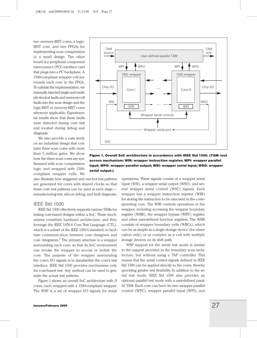
Title Turbo1500: Core-Based Design for Test and Diagnosis UsingIEEE Std. 1500
Author(s)
Wang, Laung-Terng; Ravi Apte; Wu, Shianling; Sheu, Boryau;Jone, Wen-Ben; Guo, Jianghao; Lee, Kuen-Jong; Wang, Wei-Shin; Wen, Xiaoqing; Chao, Hao-Jan; Liu, Jinsong; Niu,Yanlong; Sung, Yi-Chih; Wang, Chi-Chun; Li, Fangfang
Issue Date 2009-01
URL http://hdl.handle.net/10228/2473
Rights
©2009 IEEE. Personal use of this material is permitted.However, permission to reprint/republish this material foradvertising or promotional purposes or for creating newcollective works for resale or redistribution to servers or lists,or to reuse any copyrighted component of this work in otherworks must be obtained from the IEEE.

Turbo1500: Core-BasedDesign for Testand DiagnosisLaung-Terng Wang, Ravi Apte, Shianling Wu,
and Boryau Sheu
SynTest Technologies
Kuen-Jong Lee
National Cheng Kung University
Xiaoqing Wen
Kyushu Institute of Technology
Wen-Ben Jone and Jianghao Guo
University of Cincinnati
Wei-Shin Wang
Silicon Integrated Systems
Hao-Jan Chao, Jinsong Liu, Yanlong Niu,
Yi-Chih Sung, Chi-Chun Wang, and Fangfang Li
SynTest Technologies
�IC TESTING BASED on the full-scan design method-
ology and its associated test methods, such as ATPG
and BIST, is the most widely used test strategy.1 How-
ever, the applicability of scan-based testing is being
severely challenged by rapidly increasing develop-
ment and test costs, largely influenced by design
size and complexity as circuit sizes grow and feature
sizes shrink. Currently, the most common approach
to this problem is to adopt the SoC methodology
that uses IP cores for chip design and then use the
divide-and-conquer method by testing each core in-
dividually. Of course, such a test method is possible
only when individual cores can be isolated.2 Debug
and failure analysis also become easier when using
a core test method.
Because cores used in a SoC can be legacy, designed
in house, or supplied by external vendors, integration
and subsequent debug and diagnosis of diverse cores
requires that these cores follow certain industry stan-
dards. One such standard, IEEE 1500 Standard for
Embedded Core Testing, enables test and diagnosis of
embedded cores and interconnects.3
This article describes Turbo1500,
a core-based test-and-diagnosis inte-
gration and automation system for
incorporating the IEEE 1500 standard.4
We developed the Turbo1500 system to
automatically wrap the cores with 1500-
compliant wrapper cells and generate
associated testbenches under the control of the
chip-level IEEE Std 1149.1 (IEEE Standard Test Access
Port and Boundary-Scan Architecture), and to facili-
tate core test and diagnosis on printed circuit
boards (PCBs) whose chips are embedded with
boundary scan and where cores are surrounded
with 1500-compliant wrappers.
During wrapper synthesis, in addition to support-
ing 1500-compliant wrappers for providing serial
access to boundary I/O signals through the wrapper
serial port (WSP), Turbo1500 inserts an on-chip test
access mechanism (TAM) controller at the chip
level to give designers the flexibility to also access
cores in parallel via the wrapper parallel port
(WPP). During test, debug, and diagnosis, each
core is embedded with a unique core-identifier
(CID) bit, so multiple core tests can be performed
in series or in parallel to meet various power con-
sumption, test time, and other requirements.
To demonstrate how the Turbo1500 test automation
suite of tools works in accordance with IEEE Std 1500,
we built two hardware boards. The first board includes
IEEE Std 1500 and Its Usage
Editor’s note:
Tool support is crucial in widespread adoption of a standard. This article
describes a set of tools and associated flow for DFT insertion and test genera-
tion based on IEEE Std 1500.
��Erik Jan Marinissen, IMEC
0740-7475/09/$25.00 �c 2009 IEEE Copublished by the IEEE CS and the IEEE CASS IEEE Design & Test of Computers26
[3B2-8] mdt2009010026.3d 31/12/08 16:9 Page 26
two memory-BIST cores, a logic-
BIST core, and two FPGAs for
implementing scan compression
in a small design. The other
board is a peripheral component
interconnect (PCI) interface card
that plugs into a PC backplane. A
1500-compliant wrapper cell sur-
rounds each core in the FPGA.
To validate the implementation, we
manually injected single and multi-
ple stuck-at faults and memory-cell
faults into the scan design and the
logic-BIST or memory-BIST cores
wherever applicable. Experimen-
tal results show that these faults
were detected during core test
and located during debug and
diagnosis.
We also provide a case study
on an industrial design that con-
tains three scan cores with more
than 5 million gates. We show
how the three scan cores are syn-
thesized with scan compression
logic and wrapped with 1500-
compliant wrapper cells. We
also illustrate how staggered and one-hot test patterns
are generated for cores with shared clocks so that
these core test patterns can be used at each stage��manufacturing test, silicon debug, and fault diagnosis.
IEEE Std 1500IEEE Std 1500 effectively supports various TAMs for
testing core-based designs within a SoC. These mech-
anisms constitute hardware architecture, and they
leverage the IEEE 1450.6 Core Test Language (CTL),
which is a subset of the IEEE 1450.6 standard, to facil-
itate communication between core designers and
core integrators.5 The primary structure is a wrapper
surrounding each core, so that its SoC environment
can invoke the wrapper to access or isolate the
core. The purpose of the wrapper surrounding
the core’s I/O signals is to standardize the core’s test
interface. IEEE Std 1500 provides mechanisms only
for core-based test. Any method can be used to gen-
erate the actual test patterns.
Figure 1 shows an overall SoC architecture with N
cores, each wrapped with a 1500-compliant wrapper.
The WSP is a set of wrapper I/O signals for serial
operations. These signals consist of a wrapper serial
input (WSI), a wrapper serial output (WSO), and sev-
eral wrapper serial control (WSC) signals. Each
wrapper has a wrapper instruction register (WIR)
for storing the instruction to be executed in the corre-
sponding core. The WIR controls operations in the
wrapper, including accessing the wrapper boundary
register (WBR), the wrapper bypass (WBY) register,
and other user-defined function registers. The WBR
consists of wrapper boundary cells (WBCs), which
can be as simple as a single storage device (for obser-
vation only) or as complex as a cell with multiple
storage devices on its shift path.
WSP support for the serial test mode is similar
to the support provided in the boundary scan archi-
tecture, but without using a TAP controller. This
means that the serial control signals defined in IEEE
Std 1500 can be applied directly to the cores, thereby
providing greater test flexibility. In addition to the se-
rial test mode, IEEE Std 1500 also provides an
optional parallel test mode with a user-defined paral-
lel TAM. Each core can have its own wrapper parallel
control (WPC), wrapper parallel input (WPI), and
Core N
1500 wrapper
...
...
WIR
Core 1
1500 wrapper
WIR
Chip I/O
WPO
WSI WSO
Wrapper serial port
User-defined parallel TAM
TAMsource
TAMsink
SoC
WPI
Chip I/O
Wrapper serial controls
WPI WPO
Figure 1. Overall SoC architecture in accordance with IEEE Std 1500. (TAM: test
access mechanism; WIR: wrapper instruction register; WPI: wrapper parallel
input; WPO: wrapper parallel output; WSI: wrapper serial input; WSO: wrapper
serial output.)
27January/February 2009
[3B2-8] mdt2009010026.3d 31/12/08 16:9 Page 27
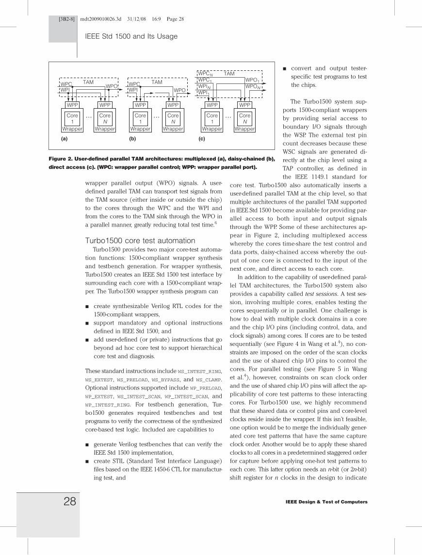
wrapper parallel output (WPO) signals. A user-
defined parallel TAM can transport test signals from
the TAM source (either inside or outside the chip)
to the cores through the WPC and the WPI and
from the cores to the TAM sink through the WPO in
a parallel manner, greatly reducing total test time.6
Turbo1500 core test automationTurbo1500 provides two major core-test automa-
tion functions: 1500-compliant wrapper synthesis
and testbench generation. For wrapper synthesis,
Turbo1500 creates an IEEE Std 1500 test interface by
surrounding each core with a 1500-compliant wrap-
per. The Turbo1500 wrapper synthesis program can
� create synthesizable Verilog RTL codes for the
1500-compliant wrappers,
� support mandatory and optional instructions
defined in IEEE Std 1500, and
� add user-defined (or private) instructions that go
beyond ad hoc core test to support hierarchical
core test and diagnosis.
These standard instructions include WS_INTEST_RING,
WS_EXTEST, WS_PRELOAD, WS_BYPASS, and WS_CLAMP.
Optional instructions supported include WP_PRELOAD,
WP_EXTEST, WS_INTEST_SCAN, WP_INTEST_SCAN, and
WP_INTEST_RING. For testbench generation, Tur-
bo1500 generates required testbenches and test
programs to verify the correctness of the synthesized
core-based test logic. Included are capabilities to
� generate Verilog testbenches that can verify the
IEEE Std 1500 implementation,
� create STIL (Standard Test Interface Language)
files based on the IEEE 1450-6 CTL for manufactur-
ing test, and
� convert and output tester-
specific test programs to test
the chips.
The Turbo1500 system sup-
ports 1500-compliant wrappers
by providing serial access to
boundary I/O signals through
the WSP. The external test pin
count decreases because these
WSC signals are generated di-
rectly at the chip level using a
TAP controller, as defined in
the IEEE 1149.1 standard for
core test. Turbo1500 also automatically inserts a
user-defined parallel TAM at the chip level, so that
multiple architectures of the parallel TAM supported
in IEEE Std 1500 become available for providing par-
allel access to both input and output signals
through the WPP. Some of these architectures ap-
pear in Figure 2, including multiplexed access
whereby the cores time-share the test control and
data ports, daisy-chained access whereby the out-
put of one core is connected to the input of the
next core, and direct access to each core.
In addition to the capability of user-defined paral-
lel TAM architectures, the Turbo1500 system also
provides a capability called test sessions. A test ses-
sion, involving multiple cores, enables testing the
cores sequentially or in parallel. One challenge is
how to deal with multiple clock domains in a core
and the chip I/O pins (including control, data, and
clock signals) among cores. If cores are to be tested
sequentially (see Figure 4 in Wang et al.4), no con-
straints are imposed on the order of the scan clocks
and the use of shared chip I/O pins to control the
cores. For parallel testing (see Figure 5 in Wang
et al.4), however, constraints on scan clock order
and the use of shared chip I/O pins will affect the ap-
plicability of core test patterns to these interacting
cores. For Turbo1500 use, we highly recommend
that these shared data or control pins and core-level
clocks reside inside the wrapper. If this isn’t feasible,
one option would be to merge the individually gener-
ated core test patterns that have the same capture
clock order. Another would be to apply these shared
clocks to all cores in a predetermined staggered order
for capture before applying one-hot test patterns to
each core. This latter option needs an n-bit (or 2n-bit)
shift register for n clocks in the design to indicate
IEEE Std 1500 and Its Usage
(a)
TAM
Core1
Core1
Core1
WPP
Wrapper
WPCWPI
CoreN
WPP
Wrapper
... ... ...
WPO
(b)
TAM
WPP
Wrapper
WPCWPI
WPP
Wrapper
WPO
(c)
TAM
WPP
Wrapper
WPCNWPC1WPINWPI1
WPP
Wrapper
WPO1WPON
CoreN
CoreN
Figure 2. User-defined parallel TAM architectures: multiplexed (a), daisy-chained (b),
direct access (c). (WPC: wrapper parallel control; WPP: wrapper parallel port).
28 IEEE Design & Test of Computers
[3B2-8] mdt2009010026.3d 31/12/08 16:9 Page 28

whether the chosen clock is to be enabled or dis-
abled for stuck-at (or delay) fault testing during
each capture window.
In Figure 3, for example, we assume that two
clocks (CK1 and CK2) control both scan cores and
that a global-scan-enable signal, GSE, is used during
the shift and capture operations for stuck-at testing.
During ATPG, we first generate staggered (stuck-at)
test patterns on the basis of a predetermined order
imposed on the two clocks given in Figure 3a. The
delays (d1, d2, and d3) shown in the figure must
be long enough to ensure the correct shift and cap-
ture operations. Then, to increase the core’s overall
fault coverage, we generate one-hot (stuck-at) test
patterns for each core on the basis of the clock se-
quence given in Figure 3b or 3c. As long as the
staggered clock order is maintained across all shared
cores, parallel testing will be possible. If only one
scan core is to be tested or debugged in series,
the clock order becomes irrelevant.
This test session capability thus gives designers the
flexibility to test cores with constraints imposed by
test time, power consumption limits, debug and diag-
nosis requirements, and so on. In other words, these
cores can be tested selectively in serial-parallel
or parallel-serial fashion, depending on the TAM
controller’s chosen architecture. This strategy will re-
duce, if not solve, the SoC test time problem, as
discussed elsewhere.7
Hierarchical core test and diagnosisTestability implementation can be inherently ap-
plied to an entire SoC design at one time, or it can
be designed block by block, followed by integration
at the chip-top level. However, the one-shot ap-
proach has proved ineffective. Engineers can also
use Turbo1500 to test and diagnose scan-compression,
logic-BIST, and memory-BIST cores when these cores
are designed in a hierarchical (block by block) man-
ner. Wang et al. provide additional information.4
Hierarchical scan compression
The scan compression technology is built upon
VirtualScan.8 The VirtualScan technology, intended
mainly for scan test cost reduction, is based on the
idea of splitting n scan chains into n� s shorter
scan chains, for a split ratio of s, where s is typically
10 or greater. The VirtualScan architecture uses a sim-
ple combinational-logic-based broadcaster inserted at
the inputs of the short scan chains for broadcasting
input stimuli from n external scan input ports to
n�s internal scan chain inputs. The architecture
uses a simple combinational-logic-based compactor
inserted at the outputs of the short scan chains for
compacting test responses from n� s internal scan
chain outputs to n external scan output ports. Typically,
scan compression reduces test data volume and test
application time by 10� to 100�, thereby drastically
reducing scan test cost.1,9 A proposed solution for fur-
ther reducing test data volume and test application
time exploits hierarchy in core-based designs by first
applying Turbo1500 to synthesize a 1500-compliant
CK1
CK2
C2
GSE
d1
Shift window Capture window
(a)
Shift window
…
…
…
…C1
d2 d3
Shift windowCapture window
(c)
Shift window
…CK1
CK2
GSE
d1 d2 d3
C2
…
… …
Capture window
(b)
Shift window
CK1
CK2
GSE
Shift window
…
…
…
…
C1
d2 d3d1
Figure 3. Staggered clock order used in the capture operation:
staggered clocks with CK1 followed by CK2 when the shift reg-
ister is set to {11} (a), one-hot CK1 clock when the shift regis-
ter is set to {10} (b), one-hot CK2 clock when the shift register
is set to {01} (c). (GSE: global scan enable.)
29January/February 2009
[3B2-8] mdt2009010026.3d 31/12/08 16:9 Page 29
wrapper around each scan core that is accessible
through an integrated TAP and TAM controller, and
then applying the scan compression methodology to
each such core. Each 1500-compliant scan compres-
sion core can then be tested from the chip top. As
expected, the core becomes a testable core that can
be reused in any SoC that supports IEEE Std 1500.
Because of the varieties of hierarchy inherent in a de-
sign, Turbo1500 currently handles at most two levels of
hierarchy, meaning that only one level of scan com-
pression cores can be embedded within a chip-top
module. There is no nesting beyond the first level.
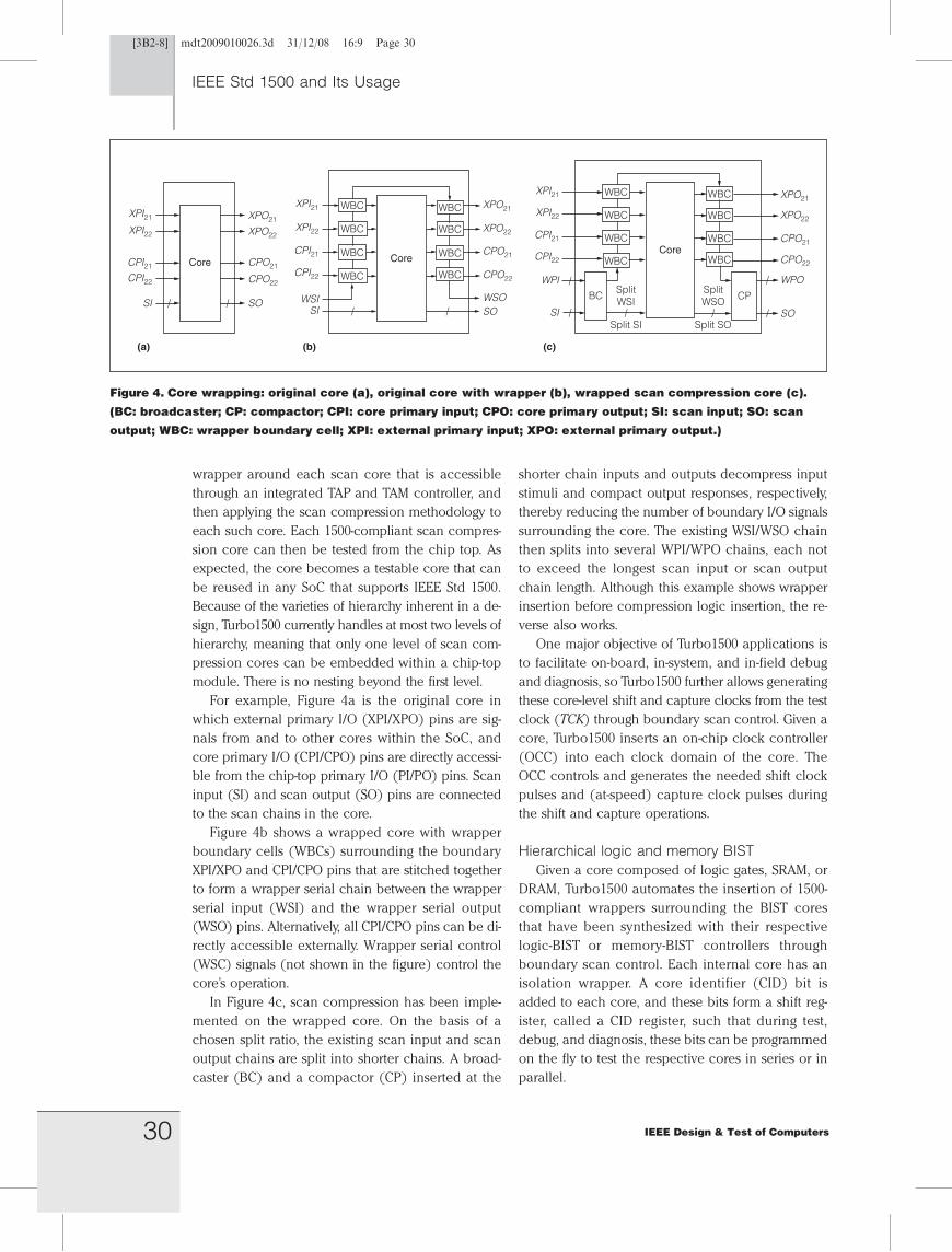
For example, Figure 4a is the original core in
which external primary I/O (XPI/XPO) pins are sig-
nals from and to other cores within the SoC, and
core primary I/O (CPI/CPO) pins are directly accessi-
ble from the chip-top primary I/O (PI/PO) pins. Scan
input (SI) and scan output (SO) pins are connected
to the scan chains in the core.
Figure 4b shows a wrapped core with wrapper
boundary cells (WBCs) surrounding the boundary
XPI/XPO and CPI/CPO pins that are stitched together
to form a wrapper serial chain between the wrapper
serial input (WSI) and the wrapper serial output
(WSO) pins. Alternatively, all CPI/CPO pins can be di-
rectly accessible externally. Wrapper serial control
(WSC) signals (not shown in the figure) control the
core’s operation.
In Figure 4c, scan compression has been imple-
mented on the wrapped core. On the basis of a
chosen split ratio, the existing scan input and scan
output chains are split into shorter chains. A broad-
caster (BC) and a compactor (CP) inserted at the
shorter chain inputs and outputs decompress input
stimuli and compact output responses, respectively,
thereby reducing the number of boundary I/O signals
surrounding the core. The existing WSI/WSO chain
then splits into several WPI/WPO chains, each not
to exceed the longest scan input or scan output
chain length. Although this example shows wrapper
insertion before compression logic insertion, the re-
verse also works.
One major objective of Turbo1500 applications is
to facilitate on-board, in-system, and in-field debug
and diagnosis, so Turbo1500 further allows generating
these core-level shift and capture clocks from the test
clock (TCK) through boundary scan control. Given a
core, Turbo1500 inserts an on-chip clock controller
(OCC) into each clock domain of the core. The
OCC controls and generates the needed shift clock
pulses and (at-speed) capture clock pulses during
the shift and capture operations.
Hierarchical logic and memory BIST
Given a core composed of logic gates, SRAM, or
DRAM, Turbo1500 automates the insertion of 1500-
compliant wrappers surrounding the BIST cores
that have been synthesized with their respective
logic-BIST or memory-BIST controllers through
boundary scan control. Each internal core has an
isolation wrapper. A core identifier (CID) bit is
added to each core, and these bits form a shift reg-
ister, called a CID register, such that during test,
debug, and diagnosis, these bits can be programmed
on the fly to test the respective cores in series or in
parallel.
IEEE Std 1500 and Its Usage
(a)
CPI21
XPI21
XPI22
CPI22
SI
CPO21
XPO21
XPO22
CPO22
SO//
Core
WSO
XPO22
XPO21
CPO22
CPO21
SO
CPI21
XPI21
XPI22
CPI22
WSI
WBC
WBC
SI
WBC Core
(b)
WBC
WBC
WBC
WBC
WBC WPO
SO
XPI21
CPI22Core
WBC
WBC
WBC
WBC
Split SI Split SO
XPO21
CPO21CPI21
XPI22
WPI
SI
BC CP
XPO22
SplitWSO
CPO22
SplitWSI
WBC
WBC
WBC
WBC
(c)
/ / / / / /
//
Figure 4. Core wrapping: original core (a), original core with wrapper (b), wrapped scan compression core (c).
(BC: broadcaster; CP: compactor; CPI: core primary input; CPO: core primary output; SI: scan input; SO: scan
output; WBC: wrapper boundary cell; XPI: external primary input; XPO: external primary output.)
30 IEEE Design & Test of Computers
[3B2-8] mdt2009010026.3d 31/12/08 16:9 Page 30
To debug or diagnose memory-BIST and logic-
BIST cores, Turbo1500 first sets the CID bits of
the BIST cores to be diagnosed to 1. These cores
can then be processed in parallel. Engineers can fur-
ther choose to have the CID register include
additional bits for each logic-BIST or memory-BIST
core so as to increase diagnostic resolution for multi-
ple errors that may arise from different faults,
including memory faults, data retention faults, stuck-
type faults, or timing faults.
Experimental resultsWe validated Turbo1500’s effectiveness in two case
studies, one involving demonstration boards and the
other industrial applications.
Case study 1
To study the effectiveness of Turbo1500’s implemen-
tation of the 1500-compliant wrappers in conjunction
with different user-defined TAM architectures and
demonstrate that IEEE Std 1500 can actually facilitate
SoC debug or diagnosis, we implemented a 1500-
compliant SoC design with two FPGAs that included
a core with scan compression, two memory-BIST
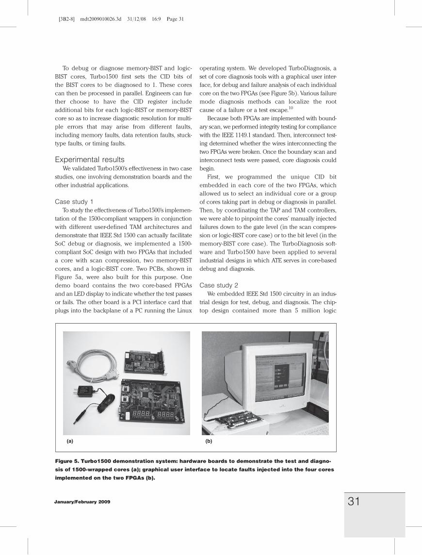
cores, and a logic-BIST core. Two PCBs, shown in
Figure 5a, were also built for this purpose. One
demo board contains the two core-based FPGAs
and an LED display to indicate whether the test passes
or fails. The other board is a PCI interface card that
plugs into the backplane of a PC running the Linux
operating system. We developed TurboDiagnosis, a
set of core diagnosis tools with a graphical user inter-
face, for debug and failure analysis of each individual
core on the two FPGAs (see Figure 5b). Various failure
mode diagnosis methods can localize the root
cause of a failure or a test escape.10
Because both FPGAs are implemented with bound-
ary scan, we performed integrity testing for compliance
with the IEEE 1149.1 standard. Then, interconnect test-
ing determined whether the wires interconnecting the
two FPGAs were broken. Once the boundary scan and
interconnect tests were passed, core diagnosis could
begin.
First, we programmed the unique CID bit
embedded in each core of the two FPGAs, which
allowed us to select an individual core or a group
of cores taking part in debug or diagnosis in parallel.
Then, by coordinating the TAP and TAM controllers,
we were able to pinpoint the cores’ manually injected
failures down to the gate level (in the scan compres-
sion or logic-BIST core case) or to the bit level (in the
memory-BIST core case). The TurboDiagnosis soft-
ware and Turbo1500 have been applied to several
industrial designs in which ATE serves in core-based
debug and diagnosis.
Case study 2
We embedded IEEE Std 1500 circuitry in an indus-
trial design for test, debug, and diagnosis. The chip-
top design contained more than 5 million logic
(a) (b)
Figure 5. Turbo1500 demonstration system: hardware boards to demonstrate the test and diagno-
sis of 1500-wrapped cores (a); graphical user interface to locate faults injected into the four cores
implemented on the two FPGAs (b).
31January/February 2009
[3B2-8] mdt2009010026.3d 31/12/08 16:9 Page 31
gates in three scan cores (A, B, and C) and more than
100 instances of embedded memories. Because of
space limitations, we illustrate only how we per-
formed core test automation on the three scan cores
for testing stuck-at faults within these three cores.
The first step is wrapper synthesis (see Figure 4c).
The coresyn program synthesizes a 1500-compliant
wrapper around each scan core. In each wrapper,
WBCs are inserted into all XPI/XPO and CPI/CPO sig-
nals. To reduce the number of test I/O pins, we
inserted an integrated TAP and TAM controller (not
shown in the figure) at the chip-top level for generat-
ing all necessary wrapper parallel control (WPC)
signals, and thereby to control the operation of the
three cores simultaneously. Then, on the basis
of the scan compression technology proposed
by Wang et al.,8 the vscansyn program inserts a broad-
caster and a compactor��both purely combinational
logic based��at the scan input and scan output ports
of each scan core. To fully utilize core test patterns,
from test to debug to diagnosis, we ensure that all
WPI/WPO and scan input and scan output signals
are directly accessible through primary I/O ports.
The TAM supports the direct-access architecture, as
shown in Figure 2c, to provide parallel access to
these primary I/O signals.
The next step is testbench generation. First, the
clockgroup program analyzes and groups those
clock domains at the chip top that do not interact
with one another, primarily to reduce ATPG runtime
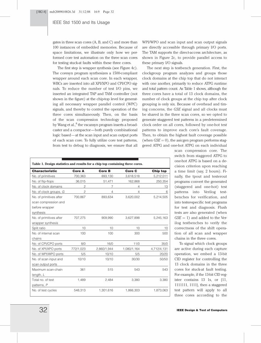
and total pattern count. As Table 1 shows, although the
three cores have a total of 13 clock domains, the
number of clock groups at the chip top after clock
grouping is only six. Because of overhead and tim-
ing concerns, the GSE signal and all clocks must
be shared in the three scan cores, so we opted to
generate staggered test patterns in a predetermined
clock order on all cores, followed by one-hot test
patterns to improve each core’s fault coverage.
Then, to obtain the highest fault coverage possible
(when GSE ¼ 0), the asicgen program performs stag-
gered ATPG and one-hot ATPG on each individual
scan compression core. The
switch from staggered ATPG to
one-hot ATPG is based on a de-
cision criterion upon reaching
a time limit (say, 2 hours). Fi-
nally, the tpout and testerout
programs convert the generated
(staggered and one-hot) test
patterns into Verilog test-
benches for verification, and
into tester-specific test programs
for test and diagnosis. Flush
tests are also generated (when
GSE ¼ 1) and added to the Ver-
ilog testbenches to verify the
correctness of the shift opera-
tion of all scan and wrapper
chains in the three cores.
To signal which clock groups
are active during each capture
operation, we embed a 13-bit
CID register for controlling the
13 clock domains in the three
cores for stuck-at fault testing.
For example, if the 13-bit CID reg-
ister contains 13 1s, or {11,
1111111, 1111}, then a staggered
test pattern will apply to all
three cores according to the
IEEE Std 1500 and Its Usage
Table 1. Design statistics and results for a chip top containing three cores.
Characteristic Chip topCore CCore BCore A
No. of primitives 5,212,0113,618,518893,130700,363
No. of flip-flops 250,354162,86851,47136,015
No. of clock domains 13472
No. of clock groups, G 6442
No. of primitives after
scan compression and
before wrapper
synthesis
5,214,5053,620,002893,634700,867
No. of primitives after
wrapper synthesis
5,245,1633,627,898909,990707,275
Split ratio 10101010
No. of internal scan
chains
500300100100
No. of CPI/CPO ports 35/011/016/08/0
No. of XPI/XPO ports 4,712/4,1311,080/1,1642,860/1,944772/1,023
No. of WPI/WPO ports 20/205/510/105/5
No. of scan input and
scan output ports
50/5030/3010/1010/10
Maximum scan-chain
length, L
543543515361
Total no. of test
patterns, P
3,3803,3802,4841,489
No. of test cycles 1,873,0631,866,3031,301,616548,313
32 IEEE Design & Test of Computers
[3B2-8] mdt2009010026.3d 31/12/08 16:9 Page 32
clock sequence supplied at the six grouped clock
inputs, where any two clock domains that do not in-
teract with each other are controlled by the same
grouped clock. If the CID register is set to {01,
0000000, 1111}, then a one-hot test pattern and a stag-
gered test pattern will apply to cores A and C,
respectively, and core B is not targeted for test,
debug, or diagnosis.
The results appear in Table 1, which indicates that
the total area overhead (without considering bus
routing) associated with wrapper synthesis on
the three cores (number of primitives after wrapper
synthesis minus number of primitives before wrap-
per synthesis) is less than 0.6%, where a primitive
represents a flip-flop, a multiplexer, or an n-input
combinational gate, not a two-input equivalent gate.
During scan compression, we picked a split ratio of
10 for each core, to limit the total number of scan
input and scan output ports to 100. There are five
WPI and five WPO ports for core A because all
1,803 (8 þ 0 þ 772 þ 1,023) CPI/CPO and XPI/XPO
ports are stitched together to form WPPs with a max-
imum scan chain length not to exceed 361 (36,015/
100) scan flip-flops. Because we constrained ATPG
to generate staggered patterns on the basis of a prede-
termined clock order, we can apply parallel testing
using core test patterns during manufacturing test,
and we can apply serial testing on selected cores dur-
ing silicon debug and fault diagnosis whenever
needed.
The design will require approximately 1.88 million
test cycles during manufacturing test and approxi-
mately 3.72 million test cycles (the sum of the test
cycles of the three cores) for silicon debug and
fault diagnosis. Let’s assume there are P test patterns,
L is the maximum scan chain length, and there are G
clock groups in a core. Testing the core will require
P(L þ 5 þ G) þ L test cycles (excluding the initializa-
tion cycles). The five TCK cycles are required to
perform the UpdateDR and CaptureDR tasks for
each pattern, as described by Cheng et al.11
THE DEMONSTRATION BOARDS and industrial applica-
tions proved that using IEEE Std 1500��with certain
enhancements��is a viable solution for incorporating
testability in core-based SoC designs in a hierarchical
(block by block) manner to facilitate on-board, in-
system, or in-field core diagnosis. IEEE Std 1500
does not suggest using the same four mandatory
pins as the IEEE 1149.1 standard for core access
through boundary scan. Integrating Turbo1500 with
the IEEE 1149.1 standard avoided the use of addi-
tional pins. An on-chip TAM controller enables
serial and parallel core access. Also, the use of BIST
cores and other embedded instruments is becoming
prevalent for current designs. These instruments
can increase the device’s fault coverage, reduce
test and debug time, and correlate the system and
ATE environments. However, the lack of a standard
interface (through the IEEE 1149.1 TAP) to these
instruments makes automation virtually impossible.
Consequently, investigation and planning are under
way for enhancing Turbo1500 to follow the IEEE
P1687 (IJTAG) proposed standard, which allows ac-
cess to the embedded test and debug instruments
through the IEEE 1149.1 TAP.12 �
AcknowledgmentsWe are grateful to the anonymous referees for
pointing out unclear descriptions in the article and
giving constructive suggestions. This work was sup-
ported in part by the National Science Foundation
under grant CCF-0541103 and in part by the National
Science Council of Taiwan under contract NSC096-
2917-I-006-120.
�References1. L.-T. Wang, C.-W. Wu, and X. Wen, eds., VLSI Test Prin-
ciples and Architectures: Design for Testability, Morgan
Kaufmann, 2006.
2. Y. Zorian and A. Yessayan, ‘‘IEEE 1500 Utilization in
SoC Test and Design,’’ Proc. IEEE Int’l Test Conf. (ITC
05), IEEE CS Press, 2005, pp. 1203-1212.
3. IEEE Std 1500-2005, IEEE Standard for Embedded
Core Test, IEEE, 2005.
4. L.-T. Wang et al., ‘‘Turbo1500: Toward Core-Based
Design for Test and Diagnosis Using the IEEE 1500
Standard,’’ Proc. Int’l Test Conf. (ITC 08), IEEE CS
Press, 2008, paper 29.3.
5. IEEE Std 1450.6-2001, Core Test Language, IEEE,
2001.
6. E. Marinissen et al., ‘‘On IEEE P1500’s Standard for
Embedded Core Test,’’ J. Electronic Testing: Theory
and Applications, vol. 18, nos. 4-5, Aug. 2002, Springer
Netherlands, pp. 365-383.
7. C. Liu, K. Chakrabarty, and W.-B. Jone, ‘‘System/Net-
work-on-Chip Test Architectures,’’ System-on-Chip
Test Architectures: Nanometer Design for Testability,
33January/February 2009
[3B2-8] mdt2009010026.3d 31/12/08 16:9 Page 33

L.-T. Wang, C.E. Stroud, and N.A. Touba, eds., Morgan
Kaufmann, 2007, pp. 171-224.
8. L.-T. Wang et al., ‘‘VirtualScan: Test Compression Tech-
nology Using Combinational Logic and One-Pass ATPG,’’
IEEE Design & Test, vol. 25, no. 2, Mar./Apr. 2008,
pp. 122-130.
9. R. Kapur, S. Mitra, and T.W. Williams, ‘‘Historical Per-
spective on Scan Compression,’’ IEEE Design & Test,
vol. 25, no. 2, Mar./Apr. 2008, pp. 114-120.
10. T. M. Mak and S. Venkataraman, ‘‘Design for Debug
and Diagnosis,’’ System-on-Chip Test Architectures:
Nanometer Design for Testability, L.-T. Wang, C.E.
Stroud, and N.A. Touba, eds., Morgan Kaufmann,
2007, pp. 463-504.
11. K.-L. Cheng et al., ‘‘An SoC Test Integration Platform
and Its Industrial Realization,’’ Proc. Int’l Test Conf.
(ITC 04), IEEE CS Press, 2004, pp. 1213-1222.
12. IEEE P1687-2007 Proposal, IEEE Internal Boundary-
Scan Proposal for Embedded Test and Debug, IEEE,
2007.
Laung-Terng Wang is founder and CEO of Syn-
Test Technologies. His research interests include
DFT, ATPG, logic and memory BIST, test compres-
sion, and fault diagnosis. He has a PhD in electrical
engineering from Stanford University. He is an IEEE
Fellow.
Ravi Apte is senior vice president of marketing at
SynTest Technologies. His research interests in-
clude DFT and simulation. He has a PhD in
electrical engineering from Southern Methodist Uni-
versity, Dallas.
Shianling Wu is vice president of engineering at
SynTest Technologies. Her research interests include
all aspects of DFT, from design and manufacturing to
field applications. She has an MS in computer science
from Columbia University.
Boryau Sheu is director of R&D at SynTest Technol-
ogies. His research interests include at-speed ATPG,
logic BIST, and test strategy for SoC design. He has
an MS in electrical engineering from Washington Uni-
versity, St. Louis.
Kuen-Jong Lee is a professor in the Department of
Electrical Engineering and director of the SoC Re-
search Center at National Cheng Kung University,
Taiwan. His research interests include VLSI testing
and testable design, electronic system-level design,
and CAD. He has a PhD in electrical engineering
from the University of Southern California.
Xiaoqing Wen is a professor and department chair
in computer science and electronics at Kyushu Insti-
tute of Technology, Japan. His research interests
include VLSI test and fault diagnosis. He has a
PhD in applied physics from Osaka University,
Japan.
Wen-Ben Jone is an associate professor in the De-
partment of Electrical and Computer Engineering at the
University of Cincinnati. His research interests include
VLSI testing and low-power circuit design. He has
a PhD in computer engineering from Case Western
Reserve University.
Jianghao Guo is a graduate student in the Depart-
ment of Electrical and Computer Engineering at
the University of Cincinnati. His research interests in-
clude VLSI design and DFT. He has an MS in
electrical engineering from Shanghai Jiaotong Univer-
sity, China.
Wei-Shin Wang is director of engineering at Silicon
Integrated Systems. His research interests include de-
sign methodology, physical design, package and
substrate design, and DFT for SoC design. He has
an MS in electrical engineering from Santa Clara
University.
Hao-Jan Chao is an R&D manager at SynTest Tech-
nologies, Taiwan. His research interests include logic
BIST and novel DFT technology development. He
has an MS in electrical engineering from National Cen-
tral University, Taiwan.
Jinsong Liu is an applications engineer at SynTest
Technologies, Shanghai. His technical interests focus
on DFT and BIST applications, including the latest
SoC technology. He has a BS in electrical engineering
from Shanghai Jiaotong University, China.
Yanlong Niu is an R&D engineer at SynTest Tech-
nologies, Shanghai. His research interests include
boundary scan, and logic and memory BIST. He has
an MS in electrical engineering from Shanghai Jiao-
tong University, China.
Yi-Chih Sung is an applications engineering man-
ager at SynTest Technologies, Taiwan. His research
IEEE Std 1500 and Its Usage
34 IEEE Design & Test of Computers
[3B2-8] mdt2009010026.3d 31/12/08 16:9 Page 34
interests include boundary scan, test compression,
and logic BIST. He has a BS in computer science
from Chung-Hua University, Taiwan.
Chi-Chun Wang is an applications engineer at
SynTest Technologies, Taiwan. His research interests
include scan ATPG, logic and memory BIST, and
boundary scan. He has an MS in computer science
from Leader University, Taiwan.
Fangfang Li is the regional manager at SynTest
Technologies, Shanghai. Her research interests
include DFT, BIST, and SoC design. She has an
MS in automation from Shanghai Jiaotong University,
China.
�Direct questions and comments about this article to
Laung-Terng Wang, SynTest Technologies, 505 S.
Pastoria Ave., Suite 101, Sunnyvale, CA 94086;
For further information about this or any other comput-
ing topic, please visit our Digital Library at http://
www.computer.org/csdl.
35January/February 2009
[3B2-8] mdt2009010026.3d 31/12/08 16:9 Page 35
Copyright © 2022 FDOKUMEN