Transport Properties of III-N Hot Electron Transistors
167
University of California Santa Barbara Transport Properties of III-N Hot Electron Transistors A dissertation submitted in partial satisfaction of the requirements for the degree Doctor of Philosophy in Physics by Donald J. Suntrup III Committee in charge: Professor Umesh Mishra, Co-Chair Professor Mark Sherwin, Co-Chair Professor John Martinis Professor Debdeep Jena December 2015
-
Upload
khangminh22 -
Category
Documents
-
view
2 -
download
0
Transcript of Transport Properties of III-N Hot Electron Transistors

University of CaliforniaSanta Barbara
Transport Properties of III-N Hot Electron
Transistors
A dissertation submitted in partial satisfaction
of the requirements for the degree
Doctor of Philosophy
in
Physics
by
Donald J. Suntrup III
Committee in charge:
Professor Umesh Mishra, Co-ChairProfessor Mark Sherwin, Co-ChairProfessor John MartinisProfessor Debdeep Jena
December 2015

The Dissertation of Donald J. Suntrup III is approved.
Professor John Martinis
Professor Debdeep Jena
Professor Mark Sherwin, Committee Co-Chair
Professor Umesh Mishra, Committee Co-Chair
September 2015

Transport Properties of III-N Hot Electron Transistors
Copyright c© 2015
by
Donald J. Suntrup III
iii

For my parents,
Butch and Mary,
and for Darcey.
iv

Acknowledgements
I am convinced beyond a doubt that this work would not have been possible without
the support of many wonderful individuals. If I have learned anything in graduate school
I’ve learned that a Ph.D. truly takes a village.
First and foremost I’d like to thank Umesh for providing such a stimulating research
environment. I came to Umesh in my fourth year looking for a new research project. I
must not have hidden my anxiety very well because I found out later that Umesh had
noticed a terrified look on my face. He was kind enough to take a chance on a middle-
aged grad student even though I had only an elementary knowledge of device physics
and little to no experience doing device research. My time in his group turned out to
be challenging but ultimately very satisfying. Umesh deserves credit not only for his
renowned research chops but also for his seemingly boundless wisdom. It was a sincere
privilege to have worked with him.
Many thanks to my committee members Mark Sherwin, John Martinis, and DJ. I
managed to somehow find three superbly distinguished professors who were also willing
to spend some of their precious time discussing my little research project. I am very
grateful for their interest and advice.
As any current or former Mishra group student knows, none of the materials devel-
opment would be possible without Stacia. The vastness of her MOCVD knowledge is
almost incomprehensible. Not only is Stacia willing to talk through a tedious technical
problem but she’s also happy to sit around and riff about life. We are all so lucky to
know her.
I want to thank the rest of the HET team who slogged through the past few years
with me in fits and occasional starts. Geetak, in particular, was my research partner in
crime, always willing to cheerfully entertain whatever idea or theory I had cooked up that
v

day and provide level-headed and intelligent feedback. I am sure that I would not have
been able to complete this project in two and a half years without him. Matt Laurent
was my gateway into the Mishra group. He was incredibly patient with me as the TA of
the device physics class and later, after talking over coffee, pulled some strings to get me
a job in the group. I am sure he is not aware of how much of a relief his help was. Haoran
shouldered the vast majority of the growth work presented in this thesis. Her persistence
and focus were astounding. There were periods of three or four months where growth
after growth failed to turn out any working devices and she somehow kept at it. I am so
grateful for the mornings we spent next to the MOCVD reactor chatting about nothing
to keep from losing our minds. Lastly, I want to thank Elaheh, the intrepid keeper of the
MBE machine. Always willing to go the extra mile or stay the extra night, Elaheh was
an indispensable part of the HET team.
The Mishra group is a truly special place to work and I want to thank the group
members past and present: Carl, Jing, Ramya, Shalini, Xiang, Jeong, Matt G., Steve,
Brian, Xun, Karine, Cory, Yuuki, Davide, Silvia, Maher, Chirag, Onur and Anchal.
Thanks to everyone for making me feel so welcome and for convincing me that, no
matter what I tell myself, I have, in fact, become an engineer.
I would also like to thank Dirk and the rest of the Bouwmeester group, with whom
I spent the first half of graduate school: Jenna, Brian, Sven, Mario, Morten and all the
rest. Thanks to everyone for being so friendly and helpful and for giving me my first
views of exceptional graduate-level research.
The nanofab staff runs a world-class operation in the clean room day in and day out:
Tom, Brian T., Ning, Bill, Aidan, Tony, Don, Adam, Brian L. and Mike. These brave
men encounter daily gas leaks, stepper alignment errors, and loose high-voltage wires
with incredible patience and good humor. I have learned how special it is to have worked
in a place that is equal parts renowned and fun.
vi

Thanks to the faculty and staff of the Technology Management Program, particularly
Dave Seibold. Dave has been an amazing mentor and friend and has helped smooth the
ongoing transition from academia to industry. Thanks also to the physics and ECE staff
members: Rob, Jennifer, Mike, Val, Alex and Shannon. These fine folks do so much
invaluable behind-the-scenes work removing all the inevitable administrative roadblocks
and keeping the research groups running smoothly.
I would like to thank my Santa Barbara friends for keeping me relatively sane through-
out the past six years: Aaron, Matt, Andrew, Isaac, Ludo, Richard and others. A special
thanks to Justin for our ritual Friday night dinners and Sunday morning Fareed Zakaria
viewing parties. I will treasure those times always.
I am very lucky to have such a large and supportive family: my sisters Lindsey,
Tracey, and Stephanie, and their husbands Dave, Jake and Je. Thank you for reminding
me where I come from and for keeping me grounded. An extra special thanks to my
parents, Butch and Mary. I have felt your unwavering support ever since I became
obsessed with building lego starships. You were steady even when I wasn’t; you had
confidence in me when I had none. I will never be able to describe to you what that has
meant.
Finally, I want to thank Darcey for teaching me what “through thick and thin” looks
like.
vii

Curriculum VitæDonald J. Suntrup III
Education
2015 Ph.D. in Physics, University of California, Santa Barbara.
2012 M.A. in Physics, University of California, Santa Barbara.
2009 B.S. in Physics, University of Texas at Austin.
2009 B.A. in English Literature, University of Texas at Austin.
Publications
“Barrier height fluctuations in InGaN polarization dipole diodes,” Donald J. SuntrupIII, Geetak Gupta, Haoran Li, Stacia Keller, Umesh K. Mishra, Applied Physics Letters,In review (2015)
“Establishment of the design space of III-N hot electron transistors for high current gainand extraction of mean free path using base thickness scaling,” Geetak Gupta, ElahehAhmadi, Donald J. Suntrup III, Umesh K. Mishra, Applied Physics Letters, In review(2015)
“Measuring the signature of bias and temperature-dependent barrier heights in III-Nmaterials using the hot electron transistor,” Donald J. Suntrup III, Geetak Gupta,Haoran Li, Stacia Keller, Umesh K. Mishra, Semiconductor Science and Technology 30,105003 (2015)
“Measurement of the hot electron mean free path and the momentum relaxation rate inGaN,” Donald J. Suntrup III, Geetak Gupta, Haoran Li, Stacia Keller, Umesh K.Mishra, Applied Physics Letters 105, 263506 (2014)
“Design space of III-N hot electron transistors using AlGaN and InGaN polarization-dipole barriers,” Geetak Gupta, Matthew Laurent, Haoran Li, Donald J. Suntrup III,Edwin Acuna, Stacia Keller, Umesh K. Mishra, Electronic Device Letters 36(1), 23-25(2014)
“In situ metalorganic chemical vapor deposition of Al2O3 on N-face GaN and evidenceof polarity induced fixed charge,” Xiang Liu, Jeonghee Kim, Donald J. Suntrup III,Steven Wienecke, Maher Tahhan, Ramya Yeluri, Silvia Chan, Jing Lu, Haoran Li, StaciaKeller, Umesh K. Mishra, Applied Physics Letters 104, 263511 (2014)
viii

“Fine tuning of micropillar cavity modes through repetitive oxidations,” Morten P.Bakker, Donald J. Suntrup III, Henk Snyders, Tuan A. Truong, Pierre M. Petroff,Dirk Bouwmeester, Martin Van Exter, Optics Letters 38, 17 (2013)
“Monitoring the formation of oxide apertures in micropillar cavities,” Morten P. Bakker,Donald J. Suntrup III, Henk Snyders, Tuan A. Truong, Pierre M. Petroff, Martin VanExter, Dirk Bouwmeester, Applied Physics Letters 102, 101109 (2013)
“Shearing of frictional sphere packings,” Jean-Francois Metayer, Donald J. SuntrupIII, Charles Radin, Harry L. Swinney, and Matthias Schroter, Europhysics Letters 93,64003 (2011)
“Fiber-connectorized micropillar cavities,” Florian Haupt, Sumant S. R. Oemrawsingh,Susanna M. Thon, Dustin Kleckner, Dapeng Ding, Donald J. Suntrup III, Pierre M.Petroff, and Dirk Bouwmeester, Applied Physics Letters 97, 131113 (2010)
Honors and Awards
• Eugene Cota Robles Fellowship (UCSB Central Fellowship), 2009–2015
• Broida Fellowship, 2010–2011, 2009–2010
• Schlumberger Undergraduate Research Fellowship, 2008–2009, 2007, 2008
• College of Natural Sciences Dean’s Honored Graduate (awarded to the top 1% ofNatural Sciences students), 2009
• Walter E. Millet Endowed Undergraduate Scholarship, 2008
• Unrestricted Endowed Presidential Scholarship, 2008–2009
• Natural Science Book Award for Academic Distinction, 2007
• Melvin J. Reiger Scholarship, 2006, 2007
• Dr. Arnold Romberg Endowed Scholarship, 2006, 2007, 2008
ix

Abstract
Transport Properties of III-N Hot Electron Transistors
by
Donald J. Suntrup III
Unipolar hot electron transistors (HETs) represent a tantalizing alternative to es-
tablished bipolar transistor technologies. During device operation electrons are injected
over a large emitter barrier into the base where they travel along the device axis with
very high velocity. Upon arrival at the collector barrier, high-energy electrons pass over
the barrier and contribute to collector current while low-energy electrons are quantum
mechanically reflected back into the base. Designing the base with thickness equal to or
less than the hot electron mean free path serves to minimize scattering events and thus
enable quasi-ballistic operation. Large current gain is achieved by increasing the ratio
of transmitted to reflected electrons. Although III-N HETs have undergone substantial
development in recent years, there remain ample opportunities to improve key device
metrics.
In order to engineer improved device performance, a deeper understanding of the
operative transport physics is needed. Fortunately, the HET provides fertile ground
for studying several prominent electron transport phenomena. In this thesis we present
results from several studies that use the III-N HET as both emitter and analyzer of
hot electron momentum states. The first provides a measurement of the hot electron
mean free path and the momentum relaxation rate in GaN; the second relies on a new
technique called electron injection spectroscopy to investigate the effects of barrier height
inhomogeneity in the emitter. To supplement our analysis we develop a comprehensive
theory of coherent electron transport that allows us to model the transfer characteristics
x

of complex heterojunctions. Such a model provides a theoretical touchstone with which
to compare our experimental results. While these studies are of potential interest in their
own right, we interpret the results with an eye toward improving next-generation device
performance.
xi

What kind of universe is it
that so runs riot?
— Chet Raymo
xii

Contents
Contents xiii
1 Introduction 11.1 The hot electron transistor: basic device function and design . . . . . . . 21.2 The hot electron transistor: a historical perspective . . . . . . . . . . . . 71.3 The III-N material system . . . . . . . . . . . . . . . . . . . . . . . . . . 131.4 Outline of the thesis . . . . . . . . . . . . . . . . . . . . . . . . . . . . . 19
2 Coherent transport theory 232.1 The transmission coefficient . . . . . . . . . . . . . . . . . . . . . . . . . 242.2 Calculation of diode currents: The Tsu-Esaki formula . . . . . . . . . . . 422.3 Example: The GaN Schottky diode . . . . . . . . . . . . . . . . . . . . . 512.4 Barrier height inhomogeneity theory . . . . . . . . . . . . . . . . . . . . 62
3 N-polar HETs and InGaN emitter diode transport 693.1 Device design, growth and fabrication . . . . . . . . . . . . . . . . . . . . 693.2 First-generation N-polar HETs . . . . . . . . . . . . . . . . . . . . . . . . 713.3 InGaN polarization dipole barrier transport . . . . . . . . . . . . . . . . 81
4 Ga-polar HETs and AlN emitter diode transport 1014.1 Device design, growth and fabrication . . . . . . . . . . . . . . . . . . . . 1024.2 Room temperature transistor operation . . . . . . . . . . . . . . . . . . . 1044.3 AlN polarization dipole barrier transport . . . . . . . . . . . . . . . . . . 105
5 Hot Electron Mean Free Path in GaN 1135.1 Scattering mechanisms in wurtzite GaN . . . . . . . . . . . . . . . . . . . 1145.2 Energy and momentum relaxation rates in GaN: concepts and previous
measurements . . . . . . . . . . . . . . . . . . . . . . . . . . . . . . . . . 1195.3 Theory: the effect of hot electron scattering on the transfer ratio . . . . . 1225.4 Device design and experimental results . . . . . . . . . . . . . . . . . . . 126
xiii

6 Conclusions and Future Work 1356.1 Future Work . . . . . . . . . . . . . . . . . . . . . . . . . . . . . . . . . . 137
A Evaluation of the Gaussian integral 141
B Calculation of extrinsic voltage drops 143
Bibliography 147
xiv

Chapter 1
Introduction
The hot electron transistor (HET) is a vertical, unipolar device that relies on the ballistic
transport of high-energy electrons across highly scaled layers. While the concept of a
ballistic HET has existed for decades, the particular challenges associated with building
the device have stunted progress relative to more successful transistor technologies like
the heterojunction bipolar transistor (HBT) and the high-electron-mobility transistor
(HEMT). These devices have enjoyed widespread technical success and the sustained
attention of device researchers. By contrast, the relatively scant development of hot
electron devices has left ample room for further device improvements and for a deeper
understanding of the relevant device physics.
In this opening chapter we will first introduce the hot electron transistor, discussing
basic device function and relevant design parameters. Then, we will review previous
efforts to build a technologically relevant HET using various materials and designs. Third,
we will introduce the concept of hot electron spectroscopy and discuss the ways in which
the HET can be used to study hot carrier transport in semiconductors. Fourth, we will
discuss the III-N material system and highlight the ways in which the material properties
of the III-Ns lend themselves to superior HET design. Finally, we will summarize and
1

Introduction Chapter 1
present an outline of the work contained in this thesis.
1.1 The hot electron transistor: basic device func-
tion and design
The hot electron transistor (HET) is three-terminal device with a vertical topology
(Figure 1.1). The device has of a double mesa structure with the emitter on top and
the collector on the bottom. Each layer has a set of dedicated metal contacts allowing
for the application of bias between layers and for the injection of current. A simple
conduction band diagram along the intrinsic region of the device (pictured as the dashed
line from z to z′) is also shown in Fig. 1.1. The band diagram is composed of two
back-to-back barriers to electron flow surrounding the base layer. The simplest way to
realize this band diagram is to use three narrow bandgap materials in the base and in
the emitter and collector contact regions and two wide band gap materials in the regions
in between. The emitter-base and base-collector barrier heights are labeled φEB and φBC,
respectively. At varying points in this thesis the barrier height (φ) may have units of
either V or eV, depending on the context. Typically, the barrier height has units of eV
when labeled on conduction band diagrams (to avoid the clutter of having to add q) and
units of V when appearing in equations (to honor the traditional notation). The emitter
and collector contact regions and the base are all highly n-type doped, which brings
the Fermi level close to the conduction band edge. Therefore, the hole concentration
is negligible throughout the device. Finally, the base thickness (tB) is defined as the
distance between the emitter and collector barrier maxima.
At zero bias (Fig. 1.1), the net electron flow across each junction in the device is
zero. The HET is biased into active mode by applying a forward bias to the emitter
2

Introduction Chapter 1
φEB
φBC
E
B
C
z
z′
EC
EF
tB
Figure 1.1: Hot electron transistor topology and conduction band diagram along theline z to z′ at zero bias. The three regions corresponding to the emitter (E), base (B)and collector (C) have been labeled and the metal contacts are pictured in red. Theemitter-base and base-collector barrier heights are labeled φEB and φBC, respectively,and the base thickness is labeled tB. The Fermi level (EF) is pictured as a dashed redline.
3

Introduction Chapter 1
and a reverse bias to the collector (Fig. 1.2). This lowers the barrier on the emitter side
causing electrons to be injected from the emitter into the base. Because the conduction
band drops so abruptly in the base, the injected electrons instantaneously acquire a large
kinetic energy in the direction perpendicular to the plane of the junction. These high-
energy, “hot” electrons transit the base where they undergo scattering events that relax
their longitudinal momenta. Upon arriving at the collector barrier, those electrons with
kinetic energy larger than φBC can surmount the barrier and become collector current;
electrons that have lost appreciable kinetic energy to scattering events are quantum
mechanically reflected from the collector barrier. These reflected electrons continue to
relax in the base, ultimately reaching the Fermi level where they contribute to base
current. The HET obeys the usual current continuity condition relating the magnitudes
of these three currents: IE = IB + IC.
There are several important figures of merit or performance metrics to consider when
appraising transistor performance. The first, and most important, is the current gain
(β) of the device. This metric represents the degree to which an output signal (IC)
is amplified with respect to an input signal (IB): β ≡ IC/IB. Transistor amplifiers are
characterized by β > 1 and, all else equal, larger β is associated with higher performance.
A different, but related, performance metric is the current transfer ratio (α), defined as
the fraction of the emitter current that makes it into the collector: α ≡ IC/IE. We can
use the current continuity equation to write the current gain in terms of the transfer
ratio: β = α1−α . From this relationship it is clear that a current gain of unity corresponds
to the collection of half of the injected electrons (α = 0.5).
Based on this physical description of transistor action, it is clear that β is highly
dependent upon the energy difference between the hot electrons arriving at the collector
and the collector barrier height. As such, we can identify several key design parameters
that most strongly affect this energy difference. The first parameter is the difference
4
Introduction Chapter 1
IE
IB
IC
IE
IB
IC
Ileak
Ileak
Figure 1.2: Forward active mode of hot electron transistor operation. The pathwaysfor the emitter, base and collector currents have been labeled on the device schematicand on the conduction band diagram. The parasitic base-collector leakage current isalso shown.
5
Introduction Chapter 1
between emitter and collector barrier heights (φEB − φBC). To achieve β > 1 this dif-
ference should be large and positive, ensuring that the electrons are launched at a high
energy with respect to the collector barrier. The second parameter that affects the elec-
tron arrival energy is the base thickness (tB). Excessive scattering events reduce the
longitudinal electron kinetic energy thereby degrading β. These scattering events can be
minimized by designing the base thickness to be smaller than the hot electron mean free
path: tB < λMFP. If this condition is satisfied, the injected electrons will retain their
initial kinetic energy and travel quasi-ballistically across the base.
Ballistic transport of this kind is desirable for high-frequency transistor amplifiers.
Minority carrier transport in the base of a bipolar device is diffusive in nature. On a
microscopic level, diffusive transport is thermally generated and, therefore, random. This
means that diffusing electrons will experience many scattering events during their highly
nonlinear trajectories across the base, resulting in a relatively long transit time. Ballistic
electrons, by contrast, follow a straight-line trajectory through the base to the collector.
The ballistic nature of electron transport in the HET promises to dramatically reduce
the transit time delays that appear in bipolar devices.
In addition to transistor gain, the access resistance in the contact layers is an impor-
tant metric to consider when evaluating transistor performance. Low-resistance contact
regions enable the precise control of the intrinsic device by the extrinsic metal contacts.
Achieving high-quality contact to the highly-scaled base layer is particularly challenging
in most material systems. A trade-off typically exists between reducing the base thickness
to improve current gain, and increasing the base thickness to improve access resistance.
Lastly, it is important to consider the magnitude of parasitic leakage paths, particularly
base-collector diode leakage (Ileak), which determines the breakdown voltage of the device
(see Fig. 1.2). Beyond breakdown leakage currents begin to overwhelm the hot electron
current in the collector and transconductance drops sharply.
6

Introduction Chapter 1
The hot electrons traveling ballistically across the base are completely out of equi-
librium with the host lattice. As such, these electrons have their own characteristic
distribution of momenta, separate from the thermal electrons occupying the energy lev-
els close the conduction band edge. If the hot electrons travel completely ballistically,
we may assume that their momentum distribution follows that of the source electrode
(i.e. a Fermi-Dirac distribution). However, even one scattering event renders the precise
hot electron distribution unknowable a priori. We will discuss methods to approximately
determine the scattered electron distribution later in this section. Furthermore, it is im-
portant to note that the assignment of a Fermi level or “electron temperature” to a hot
electron ensemble is not always physically appropriate. Such an assignment requires a
sufficient density of electrons so that electron-electron interactions occur on a time scale
that is fast compared with the transit time. This condition is not necessarily satisfied
for hot electrons in the base of a HET.
Having established the general design, operating principles and relevant elementary
physics, we will now discuss past efforts to build a functioning HET.
1.2 The hot electron transistor: a historical perspec-
tive
The idea of the hot electron transistor (HET) was proposed over half a century ago
as a potential alternative to the bipolar junction transistor (BJT). Early proponents sug-
gested that implementation of a majority carrier device like the HET would eliminate
charging delays from the minority carrier diffusion capacitance in BJTs while also in-
creasing minority carrier mobility in the base. It was believed that these improvements
would inevitably lead to unprecedented high-frequency performance. Since then, device
7

Introduction Chapter 1
development has proceeded in fits and starts as researchers have struggled with the chal-
lenges inherent in building a ballistic device. While originally proposed as a potential
breakthrough technology, HETs were also recognized as an effective tool to study hot
electron transport in semiconductors. In this section we will briefly review the history of
the HET from both a technological and a scientific perspective.
1.2.1 The HET as technology
The first hot electron transistor was developed by Mead[1] using a metal-oxide-metal-
oxide-metal (MOMOM) configuration. The first metal-oxide junction served as a tunnel
emitter of electrons into a thin metal base while the second junction served as the collector
barrier. The thin metal base layer provided a highly conductive pathway to the intrinsic
device without adding excessively to the hot electron transit length. However, it was
difficult to evaporate thin metal layers without forming pinholes and the resulting current
gain in these devices was 0.01− 0.1. Subsequent analysis suggested that the current gain
of semiconductor-metal-semiconductor (SMS) HETs would be similarly low[2], owing to
the difficulty of growing high-quality semiconductor crystals on thin metal films.
The idea was shelved for over a decade until Shannon proposed replacing the metal
base with a degenerately doped semiconductor layer[3, 4]. This solution was designed to
avoid the poor material quality of semiconductor-on-metal designs. A Schottky barrier
and n− p−n junction were proposed for the emitter and collector barriers, respectively.
Subsequent device simulations[5] seemed to suggest that the golden age of HETs was once
again upon us. A few years later, a variation of this design, which used a thin tunnel
junction emitter, was proposed[6] and implemented[7, 8] in GaAs. Second-generation
tunnel injector HETs in GaAs had current gain of ∼ 1.3 at 40 K while InGaAs/InAlAs
HETs had gain of only ∼ 0.01[9]. Resonant tunnel HETs were also developed in GaAs
8

Introduction Chapter 1
and had an improved current gain of ∼ 10 at 77 K[10]. The relatively small band offsets
characteristic of the III-As material system required the exclusive use of low-temperature
measurements to avoid thermionic emission of base electrons into the collector. Because
room temperature operation was prohibitively difficult to realize, GaAs HETs never found
use in real technological applications and were, therefore, abandoned.
The first HETs to have current gain at room temperature were developed by Levi
et al.[11, 12]. These devices contained an AlSbAs emitter, an InAs base and a GaSb
collector. The emitter and collector barrier heights were 1.3 and 0.8 eV, respectively,
large enough to block thermionic leakage currents at 300 K. Furthermore, the low bandgap
InAs layer ensured fairly low-resistance contacts to the 10 nm base layer. All in all these
devices had a room-temperature common-emitter current gain of 10. Despite the success,
increasing β beyond 10 proved to be extremely difficult and, until very recently, this device
represented the only room temperature HET ever demonstrated. Beyond considerations
of gain, state-of-the-art HBTs outperformed the AlSbAs/InAs/GaSb HET along almost
every other important device metric. HETs were, therefore, not considered to be a viable
and competitive device technology at the time.
Despite these technical challenges, HETs were successfully used as a spectroscopic tool
to study hot electron transport. Such an application does not require the transistor to
have gain and, therefore, has the benefit of requiring less stringent performance metrics.
1.2.2 The HET as a scientific tool
Several decades ago, as device dimensions began to approach carrier scattering lengths,
researchers proposed ballistic devices for both analog and digital device applications[13].
With these proposals came the desire for a deeper understanding of ballistic transport
effects like velocity overshoot, which can be critically important for high-speed lat-
9

Introduction Chapter 1
eral devices. Experimental techniques like photoemission spectroscopy had established
themselves as reliable methods for probing hot carrier dynamics in metals[14] and in
semiconductors[15, 16]. However, these methods almost always probed energy rather
than momentum relaxation processes, which are most relevant for studying carrier mo-
bility and other transport effects in electronic devices.
The idea to use the HET as a tool to study hot electron transport was first proposed by
Hesto et al.[17] with the goal of unambiguously demonstrating ballistic transport across
thin layers. To better understand the ways in which the HET may be used to study
transport, we will briefly describe a generalized version of the hot electron spectroscopy
method.
Figure 1.3 shows a simple conduction band diagram and two classes of electron en-
sembles (pictured in light blue): the majority carrier electrons near the band edge and
the minority carrier hot electrons. The thermalized (majority carrier) electrons are re-
sponsible for carrying current between the intrinsic region (i.e. the intrinsic base and the
layers immediately adjacent) and the ohmic contacts. The minority carrier hot electrons
are created when thermalized electrons cross over the emitter-base barrier. Upon enter-
ing the base, these electrons gain a large amount (∼ φEB) of kinetic energy along the
device axis resulting in a narrow distribution of highly directional longitudinal momenta.
The hot electrons travel across the base with energies well above the conduction band
edge. Scattering events in the base may partially relax the electron momenta causing
the momentum distribution to widen. Once the electrons arrive at the collector, those
with energies greater than φBC can cross over the barrier into the drift region of the col-
lector, while those with energies less than φBC are reflected off the barrier. In this sense
the collector barrier serves as a high pass filter for incoming electrons with the collector
current given by
10

Introduction Chapter 1
φBC
E B C
φEB
VBC
JC = q∫∞φBC
n(Ez)v(Ez)dEz
Ez
z
Figure 1.3: Hot electron spectroscopy using the HET. In this device φEB is constantwhile φBC = f(VBC).
JC = q
∫ ∞
φBC
n(Ez)v(Ez)dEz, (1.1)
where n(Ez) is the distribution of electrons just to the left of the collector barrier and
v(Ez) is the component of their velocity perpendicular to the barrier interface. If φBC
could be made variable, using a planar doped barrier, for example, measuring the change
in JC with collector bias (VBC) can provide an estimate of the hot electron distribution
function n(Ez). In particular, if φBC varies linearly with VBC, it is straightforward to
show[18] that
dJC
dVBC
∝ n(Ez). (1.2)
Equation (1.2) provides a means to extract information about the hot electron distribu-
tion n(Ez) by measuring the dependence of JC on VBC. Once the barrier is biased away
by applying VBC ∼ φBC, the collector current (along with the derivative) increases rapidly
due to thermally generated base-collector diode leakage. The experimental signature of
quasi-ballistic transport is, therefore, a peak in the curve dJC/dVBC vs. VBC whose width
is approximately equal to the width of the hot electron ensemble.
This method has been applied to GaAs HETs[19, 8] where it was used to unambigu-
11

Introduction Chapter 1
Figure 1.4: Device schematic and hot electron spectrum taken from Ref. [21]. ForVCB < 0 clear peaks in dIC/dVCB are observed. Such peaks provide very strongevidence of high-energy, quasi-ballistic transport in a GaAs HET.
ously detect ballistic electrons at cryogenic temperatures[20, 21]. A device schematic and
hot electron spectrum from Ref. [21] is shown in Fig. 1.4. In this experiment electrons
were tunnel injected into the base, the collector was swept from negative to positive bias,
and the collector current was measured. The plot of dIC/dVCB (or “Gc” in the original
figure) vs. VCB shows clear peaks, which are energetically separated from the Fermi level.
These data were used to show that roughly 50% of the injected electron ensemble traveled
across the base without appreciable scattering.
In addition to simply demonstrating the presence of ballistic electrons, the HET has
been used to measure the hot electron scattering rate[22] and the mean free path[23]
in GaAs. In particular, it was discovered that if hot electrons were injected below the
optical phonon energy in GaAs (∼ 36 meV), they could travel for up to several microns
before scattering[24]. These results strongly suggested that optical phonon emission is
the dominant scattering mechanism for hot electrons in GaAs. Hot electron spectroscopy
can also be used to estimate the optical phonon energy by varying the electron injection
energy while measuring the transfer ratio. As the injection energy is scanned through
12

Introduction Chapter 1
the optical phonon energy, there is a sharp increase in the carrier scattering rate causing
the transfer ratio to momentarily decrease[25].
While these experiments differed in the details of their execution, they all leveraged
the collector barrier as an analyzer of longitudinal momentum states and can all, there-
fore, be considered a form of hot electron spectroscopy. The scientific studies undertaken
in this thesis will make use of the collector barrier in a conceptually similar way. In Chap-
ters 3 and 5 we will present two different versions of electron spectroscopy to study both
barrier-limited and hot carrier transport in III-N materials. Previous interpretations of
electron spectroscopic data were incomplete because the detailed transfer properties of
the collector barrier were neglected[25]. Our analysis will improve upon these methods
by including the effects of potentially complicated transmission characteristics on the
observed spectra.
In the next section we will discuss III-N material properties and their implications
for HET design.
1.3 The III-N material system
The development of III-N materials has enabled dramatic technological advances
in energy efficient solid state lighting and high-power switching applications. The III-
Ns burst onto the technological scene with the invention of tunable, short-wavelength
LEDs[26, 27] and laser diodes[28, 29] with InxGa1−xN active regions. In the years since
there have been impressive advances in the epitaxial growth of nitride films[30, 31, 32] as
well as a deepening understanding of III-N material properties and bandstructure[33, 34,
35]. Such progress has enabled both optoelectronic devices like the ultralow threshold
ultraviolet laser[36] and record-breaking high-frequency[37, 38, 39] and high-power[40]
electronic devices like the high-electron-mobility transistor (HEMT). In this section we
13

Introduction Chapter 1
Figure 1.5: Band gaps and lattice constants for a variety of wurtzite and zincblendematerials[41]. The wurtzite III-Ns span a very large range of band gaps but also havea large lattice mismatch to available substrate materials like Al2O3.
will review the material properties of the III-Ns, paying particular attention to those that
affect hot electron transistor design.
The III-Ns (AlN, GaN, InN and their alloys) span a very large range of material band
gaps (Fig. 1.5). In fact, the entire visible spectrum is theoretically accessible to the
InxGa1−xN alloy, making it an ideal candidate for light-emitting devices. For electronic
devices, the wide range of bandgaps enables large heterojunction band offsets (> 1 eV)
that can be engineered to provide tunable barriers to current flow. One can imagine using
such a band offset to form large emitter and collector barriers in a HET, thus enabling
room temperature operation. This can immediately be identified as an advantage of
III-N HETs over their III-As counterparts, which struggled to achieve barrier heights of
more than a few hundred meV and, therefore, were unable to achieve room temperature
transistor operation.
Gallium nitride can crystallize in either the zincblende or wurtzite structure, though
the latter is more stable. The highly ionic Ga−N bond gives rise to a distribution of
14

Introduction Chapter 1
Figure 1.6: Crystal structure of wurtzite GaN. Polar c-plane growth occurs in the planeperpendicular to the [0001] direction.[43] Several nonpolar and semipolar planes arealso pictured.
microscopic dipole moments oriented along the bonding axes. The symmetry properties
of zincblende crystals ensure that the vector sum of these microscopic dipole moments
is zero. Displacement of the constituent atoms from their equilibrium positions can,
however, induce a nonzero polarization field in the zincblende crystal via the piezoelectric
effect. Wurtzite crystals also contain piezoelectric polarization fields upon the application
of strain. In fact, the piezoelectric coefficients in the wurtzite III-Ns are an order of
magnitude larger than other III-V and II-VI compounds[42]. Additionally, the lack of
inversion symmetry in the wurtzite phase gives rise to spontaneous polarization along
the crystal c-axis [0001](Fig. 1.6). The resulting polarization fields can have dramatic
effects on the conduction band diagram of c-plane III-N devices.
There are two polar (c-plane) crystal orientations available for growth: the plane
perpendicular to the [0001] direction is called Ga-polar; the plane perpendicular to the
[0001] direction is called N-polar. These orientations are named for the atom that lies
on the top of each hexagonal bilayer in the wurzite structure. While both Ga-polar and
15

Introduction Chapter 1
N-polar orientations exhibit nonzero spontaneous polarization, the net dipole moment
points in opposite directions. The nonpolar and semipolar planes pictured in Fig. 1.6
are preferred for certain optoelectronic devices where the presence of strong polarization
fields is undesirable. In this thesis, however, all device structures are grown either directly
on c-plane or slightly (4) off axis.
Owing to the relative youth of III-N materials, a sufficiently large, cost-effective single-
crystal substrate for nitride homoepitaxy has yet to be developed. As a result, III-N films
are usually grown heteroepitaxially on lattice-mismatched substrates like Al2O3 (sap-
phire). The resulting strain accumulation leads to nonplanar growth modes, especially
near the substrate interface. To separate crucial epitaxial layers from this highly defec-
tive region, thick GaN buffer layers are grown and allowed to strain relax with respect to
the substrate. This method enables the subsequent growth of two-dimensional films but
at the cost of introducing a high density (108− 1010 cm−2) of threading dislocations into
the crystal. We will briefly discuss the potential effect of dislocations on device behavior
in a later chapter.
Because the GaN buffer layer is strain relaxed, thin InGaN or AlGaN epilayers grown
on the buffer will be coherently strained to GaN. This introduces piezoelectric fields in the
material that add to (subtract from) the spontaneous polarization field in AlGaN (InGaN)
layers. The discontinuity in the polarization field at each III-N heterointerface results in
a nonzero net interfacial polarization charge (Qπ). These charges produce strong dipolar
electric fields that can be used to engineer barriers to electron flow. Because AlGaN/GaN
and InGaN/GaN heterojunction barriers tend to have very high leakage currents, we will
rely exclusively on these so-called polarization dipole barriers to form the emitter and
the collector barriers in III-N HETs.
To understand how polarization engineering can be used to design electron bar-
riers consider the structures shown in Fig. 1.7. The band diagrams of a Ga-polar
16

Introduction Chapter 1
GaN GaNInGaN
+Qπ,1
−Qπ,1
GaN GaNAlGaN
−Qπ,2
+Qπ,2
(a) (b)
−ns,1 −ns,2
+ns,2+ns,1
[0001] [0001]
Figure 1.7: Conduction band diagram of a Ga-polar (a) InGaN and (b) AlGaN po-larization dipole structure. The net polarization charge at each interface is labeledQπ. In the absence of doping, the band diagram follows the thick black lines. Intro-ducing dopants on either side of the dipole layer causes the +Qπ,i to become screenedand the bands to flatten on one side (dashed grey lines). This is the mechanism forpolarization dipole barrier formation.
17

Introduction Chapter 1
GaN/InGaN/GaN and a GaN/AlGaN/GaN junction are shown in Fig. 1.7(a) and (b),
respectively. The interface charges that results from the polarization discontinuity are
labeled Qπ,i. For a material with no free electrons, the Qπ,i are the only charges in the
vicinity of the dipole layer and the band diagram resembles the solid black lines in Fig.
1.7. In this case the bands on the +Qπ side will continue to rise and a barrier cannot
form. However, if shallow n-type dopants are added near, but not directly adjacent to,
the dipole region, mobile electrons from the donor atoms will be attracted to the +Qπ,i
charge. The resulting accumulation of electrons screens the +Qπ,i and flattens the bands
on one side (dashed grey lines). Thus an asymmetric barrier to electron flow is formed.
It is important that on the −Qπ,i side the dopants be placed sufficiently far from the
dipole layer so as not to cause excessive band bending, which reduces the asymmetry of
the barrier. Also, recall that the above arguments apply to Ga-polar heterojunctions.
For N-polar structures, the signs of the net interfacial polarization charges will all be
reversed causing the bands in Fig. 1.7 to be reflected about the vertical axis.
The free electrons that accumulate at an Al(In)GaN/GaN interface are confined
to a small longitudinal dimension (1−2 nm) and can thus be considered to be a two-
dimensional electron gas (2DEG). For AlGaN/GaN junctions with sufficiently high Al
content or AlGaN thickness, 2DEG densities can approach 2 × 1013 cm−2. The high
charge density renders the AlGaN/GaN 2DEG uniquely suited to carrying current in
highly scaled layers like the base of the HET. The use of the 2DEG to provide base
charge represents a key improvement over past designs, which relied on bulk doping the
base layer to get charge. In these structures scaling the base necessarily led to a reduc-
tion in base charge and, therefore, higher base resistance. By contrast, the base layer
in a III-N HET can be scaled to < 3 nm without significantly degrading the 2DEG
charge density. Therefore, we will make use of an AlGaN/GaN junction as the emitter
in Ga-polar HETs and as the collector in N-polar HETs.
18

Introduction Chapter 1
GaN GaNn+ n+
GaNGaNn+
GaNn+
GaN
InGaN InGaNAlGaN AlNpolarizationpolarization polarization polarization
barrier barrier barrier barrier
BaseEmitter CollectorCollectorBaseEmitter
(a) (b)
φEB
φEB φBC
φBC
Figure 1.8: (a) N-polar and (b) Ga-polar HET designs and conduction band diagrams.
The InGaN polarization dipole also accumulates electrons on the highly doped side of
the junction. Therefore, using the InGaN polarization barrier as the collector (emitter) in
Ga-polar (N-polar) HETs adds additional charge to the base and further reduces the base
resistance. The design structures and conduction band diagrams for both the Ga-polar
and N-polar HET are shown in Fig. 1.8. The electric field in the dipole layers can reach
∼10 MV/cm allowing for the design of large (0.75−1.5 eV) emitter and collector barriers
using the polarization dipole method. These large barriers enable the injection of very
high-energy electrons while simultaneously enabling room temperature HET operation.
In each of the designs pictured in Fig. 1.8, the compositions and thicknesses of the dipole
layers are chosen to ensure that φEB > φBC whenever possible.
1.4 Outline of the thesis
As the title suggests, the goal of this thesis is to better understand the transport
physics of the III-N HETs pictured in Fig. 1.8 with the goal of ultimately improving
device performance. Broadly speaking, there are two main areas on which we will focus
19

Introduction Chapter 1
our attention: first, we would like to understand electron transport in the vicinity of
the barrier regions. In the HET there are two barriers, the emitter and the collector,
and we will describe the transport properties of both. An important distinction to
make is that the source electrons incident on the emitter barrier are thermally generated
while those incident on the collector are hot electrons from the base. Second, we would
like to understand quasi-ballistic electron transport across the highly-scaled base layer.
In this case there are no major barriers to electron flow and hot electron scattering
processes become the main focus. Chapters 2−4 will cover barrier-limited transport
phenomena while Chapter 5 will deal with quasi-ballistic base transport. Throughout our
discussions we will point out the implications of our findings for transistor performance
before summarizing and proposing several follow-up experiments in Chapter 6. Below
we provide a more detailed outline.
In Chapter 2, we will present a theory of electron transmission through an arbitrary
potential barrier. We will compare the three most popular methods for calculating the
transmission probability before choosing the method most suited to our needs. The abil-
ity to determine the transmission characteristics of an arbitrary barrier will allow us to
simulate the behavior of a hot electron wavepacket arriving at the collector barrier in
a HET. This will help us to better understand experimental transistor data presented
in later chapters. Then, we will use the barrier transmission characteristics to derive
an expression for diode current density as a function of voltage and temperature. This
expression will improve upon the canonical thermionic emission formula by including the
effects of thermionic field emission on the diode current. The simulated diode charac-
teristics can then be compared with experimental results presented in later chapters to
help determine the physical causes of diode nonidealties. We will conclude Chapter 2 by
presenting the theory of barrier height inhomogeneity and providing a sample analysis of
a GaN Schottky diode.
20
Introduction Chapter 1
Chapter 3 will begin with a presentation of the III-N Nitrogen-polar HET design.
Then, we will analyze the common-emitter current characteristics of the first-generation
N-polar HET and discuss major device advantages and deficiencies. Next, we will discuss
the nonideal transport characteristics of the InGaN polarization dipole emitter diode in
light of barrier height inhomogeneity theory. Such an analysis will allow us to extract
quantitative information about the magnitude of lateral barrier height fluctuations and
to propose a physical cause. Finally, we will present the HET as a tool to study emitter
barrier transport by using the collector as an analyzer of emitted electron momentum
states. Temperature-dependent HET measurements will be shown to corroborate the
conclusions drawn from the emitter diode analysis.
In Chapter 4 we will present the III-N Ga-polar HET design and discuss its advantages
over N-polar HETs. Then, we will present the common emitter current characteristics
of a hybrid MOCVD/MBE HET device before moving on to discuss AlN emitter diode
transport. We will apply an abbreviated version of the methods used in Chapter 3 to
briefly analyze the emitter current characteristics before discussing the implications of
the results for device operation.
In Chapter 5, we will discuss transport characteristics of hot electrons in the base of
the HET. We will review possible electron scattering mechanisms in wurtzite GaN and
determine which processes are most relevant for the hot electrons in our devices. Then
we will present a method to measure the hot electron mean free path and momentum
relaxation rate using the hot electron transistor before analyzing the extracted relaxation
rates and discussing the implications for device performance. Finally, in Chapter 6 we
will summarize our conclusions and propose a road map for future work.
21

Chapter 2
Coherent transport theory
Nearly all modern semiconductor devices make use of heterojunctions. Along with classi-
cal electric fields arising from space charge regions, for example, heterojunctions provide
a means to precisely control the flow of charged carriers on extremely short time scales.
Simply stated, a heterojunction is a plane in a crystal where the proportion of con-
stituent elements changes, often abruptly. This change in crystal composition results in
a spatially varying density of states that modulates the free carrier wavefunction in the
direction perpendicular to the heterointerface. In order to understand heterojunction
diode characteristics we must first understand the nature of the electron wavefunction in
these regions.
Our treatment in this chapter will proceed by first discussing the coherent dynamics
of conduction band electrons near a heterointerface. In particular, we will outline three
different methods to calculate the transmission probability in these regions, discussing
the merits and limitations of each method. Crucially, we will neglect electron-electron
interactions so that each momentum eigenstate can be considered independently. This
assumption allows us to use statistical considerations to calculate the total device cur-
rent by performing a weighted sum of the current carried by each momentum eigen-
22

Coherent transport theory Chapter 2
state. Coupled with a proprietary Schrodinger-Poisson solver that generates the device
band diagram, this method enables a complete numerical simulation of current-voltage-
temperature characteristics for arbitrary junctions. Such a simulation provides a theoret-
ical standard with which to compare the experimental data presented in later chapters.
Furthermore, simulating the transmission characteristics of an arbitrary collector barrier
enables a theoretical estimate of the current transfer ratio in a HET.
Once we have derived an equation describing ideal diode transport, we will introduce
the concept of barrier height inhomogeneity (BHI) and discuss its effects on transport
properties.
2.1 The transmission coefficient
The problem of determining the motion of conduction band electrons in solid state
systems has preoccupied scientists for over a century. The most rigorous treatment
of this problem involves solving the many-body Schrodinger equation, but this turns
out to be computationally prohibitive particularly on length scales that are relevant
for macroscale devices. One the other hand, the maturation of growth techniques like
molecular beam epitaxy (MBE) and metal-organic-chemical-vapor deposition (MOCVD)
has enabled the aggressive scaling of device dimensions over the past several decades.
The ability to grow semiconductor films composed of 1-10 monolayers has precluded the
option to ignore quantum interference effects all together in favor of an entirely semi-
classical treatment. Therefore, the intermediate length scales present in modern devices
necessitate an approximate, yet still explicitly quantum mechanical, treatment of carrier
transport.
In lieu of exact solutions, computationally tractable approaches like density functional
theory (DFT)[44, 34] and Monte-Carlo[45, 46] simulations have become popular tools
23

Coherent transport theory Chapter 2
for studying band structure and transport. These methods, however, usually require
complicated numerics and sizable computational power. Here, we will use an alternative
approach based on the effective mass theorem and the envelope function description [47].
While this will simplify the problem dramatically, it will also restrict the applicability of
the theory to high symmetry points in the Brillouin zone. Furthermore, our model will
ignore the effects of inelastic scattering, which requires a higher level treatment.
According to Bloch’s theorem, the wavefunction near, say, the Γ valley minimum has
the form
Ψ(~r) = ψ(~r)uk=0(~r), (2.1)
where u(~r) is periodic in the material lattice constant and ψ(~r) is a slowly varying en-
velope function. The central assumption of the envelope description is that the periodic
components u(~r) are nearly identical in every region of a heterostructure. This, in turn,
requires that all materials be latticed matched in the plane of a heterointerface [48]. Cru-
cially, this condition is satisfied both for lattice matched junctions like AlGaAs/GaAs as
well as for coherently strained materials like the III-Ns. Making this assumption allows
us to factor out the atomic-scale oscillations represented by u(~r) from the dynamical
equations. What remains is the one-dimensional Schrodinger equation for the envelope
functions:
−~2
2
∂
∂z
1
m∗(z)
∂
∂zψ(z) + EC(z)ψ(z) = Eψ(z), (2.2)
where z is the direction perpendicular to the interface, EC is the position-dependent
conduction band minimum, E is the total energy, m∗ is the position-dependent effective
mass, and ~ is the reduced Planck’s constant. All atomic-scale effects are implicitly
contained in the effective mass and in the dispersion relation E(~k). It is important to
note that m∗ is an explicitly bulk property and that the very concept of effective mass is
not well-defined in the vicinity of a heterojunction or within a thin layer. Nevertheless, we
24

Coherent transport theory Chapter 2
will adopt the assumption that local electron properties, even in the vicinity of boundary
layers, resemble the material properties of the bulk. While this assumption is useful from
a mathematical perspective, the physical meaning of effective mass in these regions is
unclear.
Our goal will be to determine, for an arbitrary potential barrier and a given initial
electron momentum ki, the ratio of the transmitted to the incident current density. In all
cases considered in this chapter, we will assume that the barrier in question is surrounded
by electron reservoirs that emit a thermal distribution of electron momenta toward the
barrier. In practice these reservoirs are composed of highly doped semiconductor layers
with ohmic metal contacts. Device bias will be reflected in different electrochemical
potentials (or Fermi levels) in the reservoirs. Because the free carrier concentration is
very high in the reservoirs, the conduction band is flat and the incoming and outgoing
electrons can be considered to be plane waves:
ψi = Aieikiz +Bie
−ikiz,
ψf = Afeikf z, (2.3)
where ki,f =√
2m∗i,f (E − ECi,f )/~. We have stipulated here that carriers are incident
only from the left. Furthermore, each wavefunction has an associated probability current
density given by
J =~
2m∗i
(ψ∗∂ψ
∂z− ψ∂ψ
∗
∂z
). (2.4)
The transmission probability is then the ratio of incident to transmitted probability
current density. Combining Eqs. (2.3) and (2.4) for incoming and outgoing waves and
taking the ratio gives
T =JfJi
=|Af |2|Ai|2
vfvi, (2.5)
25

Coherent transport theory Chapter 2
where vi and vf are the initial and final electron velocities, respectively.
In the following sections, we will discuss three methods to calculate the transmission
probability and compare their ability to describe relevant heterostructures.
2.1.1 The WKB approximation
The most commonly used method to estimate the transmission probability of charged
carriers in the vicinity of one-dimensional potential barriers is based on the Wentzel-
Kramers-Brillouin (WKB) approximation[49, 50, 51]. This method is popular for device
simulations because of its analytical simplicity and ease of use. In this section we will
briefly outline the WKB method and highlight both its abilities and limitations.
As a starting point, the simplest form of the one-dimensional Schrodinger equation
is
− ~2
2m∗∂2
∂z2ψ(z) + EC(z)ψ(z) = Eψ(z). (2.6)
This is a second order differential equation for the wavefunction ψ and is not analytical
except in a very few special cases. One such case is that of a constant potential (i.e.
EC(z) = E0C), which has oscillatory, plane wave solutions:
ψ(z) = Ae±ikz, k ≡√
2m∗(E − E0C)/~, (2.7)
where A is a complex constant and the deBroglie wavelength associated with ψ is λ =
2π/k. While this a tidy and simple solution, it describes an extremely limited, and not
very interesting, subset of problems. The scope of this solution widens if the assumption
is made that the potential, while not strictly constant, varies slowly compared with the
deBroglie wavelength. This means that from the prospective of a traveling charge at any
given moment, the potential “looks” locally constant. The physical situations that most
26

Coherent transport theory Chapter 2
accurately satisfy this approximation are high energy carriers (i.e. small λ) and smoothly
and slowly varying potentials. Intuitively we might expect that if the potential varies
slowly enough, the wavefunction could remain oscillatory while the amplitude (A) and
phase (k(z)z) vary gradually. This picture of a wavefunction that gradually adapts to
changes in potential inspired an alternate name for WKB: the adiabatic approximation.
Solving the Schrodinger equation (2.6) with this updated form of the wavefunction
yields[52]:
ψ(z) ∼ C√2m∗(E − EC(z))
e±i~∫ √
2m∗(E−EC(z))dz, (2.8)
where C is another complex constant. This solution implies that for a slowly varying
potential barrier between zi and zf , the transmission probability at energy E is given by:
T (E) ' exp
(−2
~
∫ zf
zi
√2m∗(EC(z)− E)dz
). (2.9)
For arbitrary barriers the integral in Eq. (2.9) can be evaluated numerically for E <
EC,max (T (E) = 1 for E > EC,max)[53]. The WKB approximation breaks down at the
so-called classical turning points where E ' EC and care must be taken so that the
wavefunction does not diverge to infinity in these regions. This issue is particularly prob-
lematic when trying to adapt the WKB treatment to bound state calculations. However,
even for unbound, current-carrying states, the WKB method becomes less accurate at
higher energies when the tunneling probability become appreciable.
Equation (2.9) also does not account for wavefunction interference effects arising from
reflections at multiple material boundaries. Such interference effects are most pronounced
when the barrier width is on the order of the deBroglie wavelength as is the case in III-N
polarization dipole layers, for example. Historically as semiconductor device structures
were scaled to dimensions comparable to the electron deBroglie wavelength, it became
clear that conventional analytical approaches based on the WKB approximation were no
27

Coherent transport theory Chapter 2
longer valid[54]. A more rigorous, numerical solution was needed.
2.1.2 The transfer matrix method
The following approach for solving for the transmission characteristics of arbitrary
potential barriers arose out of a desire to model tunnel currents in multiquantum well
structures[55, 56, 57]. The approach, known as the transfer matrix method (TMM), in-
volves breaking the potential into segments in which the exact solution to the Schrodinger
equation is known. Enforcing continuity of the wavefunction and its spatial derivative
at each boundary leads to a 2× 2 matrix for each interface. Multiplying these matrices
together yields a direct relationship between incoming and outgoing wave components.
The Schrodinger equation is directly solvable for a constant or for a linearly varying
potential segment and indeed these are the two most widely used segment shapes[58, 59,
60]. The potential barriers formed by III-N polarization dipoles lend themselves well to
linear potential segments and this is the approach we will take in this section.
Consider the stepwise linear potential pictured in Fig. 2.1. In any one of the labeled
segments, the one-dimensional, the time-independent Schrodinger equation reads
∂2ψ
∂z2+
2m∗
~2(E − EC(z))ψ = 0, (2.10)
where within any segment [zi, zi+1], the conduction band minimum is linear:
EC(z) = EC(zi) +EC(zi+1)− EC(zi)
zi+1 − zi(z − zi). (2.11)
28

Coherent transport theory Chapter 2
EC(z)
zz1 z2 z3
EC,0
EC,1
EC,2
EC,3
EC,4
EC,5
1 2 3 4
Figure 2.1: Piecewise linear potential used to derive the transmission coefficient viathe transfer matrix method. The boxed numbers indicate potential segments and theEC,i represent values of the conduction band edge at various points.
If we define two constants for each linear region:
αi ≡ −(
~2
2m∗i
zi+1 − ziEC(zi+1)− EC(zi)
)1/3
,
βi ≡ −(
2m∗i~2
)1/3(zi+1 − zi
EC(zi+1)− EC(zi)
)2/3(E − EC(zi) + zi
EC(zi+1)− EC(zi)
zi+1 − zi
),
(2.12)
and make the substitution ui(z) ≡ βi − z/αi we find that the wavefunction in region i
evolves according to
d2ψidu2
− ui(z)ψi = 0. (2.13)
This is the Airy equation whose solutions are the well-known Airy functions:
ψi(z) = AiAi(ui(z)) +BiBi(ui(z)), (2.14)
29

Coherent transport theory Chapter 2
Ai
Bi
Af
Bf
Figure 2.2: Schematic of the incoming and outgoing plane waves in the TMM method.For the example in the text, i = 1 and f = 4.
where Ai and Bi are complex constants.
We can derive transfer matrices at each boundary by writing the wavefunction in each
region and enforcing continuity of ψ and (1/m∗)∂ψ/∂z. Note that these two conditions
are implied by the continuity of probability flux as defined in Eq. (2.4). In the example
pictured in Fig. 2.1, the wavefunctions in each region are:
ψ1(z) = A1eik1z +B1e
−ik1z,
ψ2(z) = A2Ai(u2(z)) +B2Bi(u2(z)),
ψ3(z) = A3Ai(u3(z)) +B3Bi(u3(z)),
ψ4(z) = A4eik4z +B4e
−ik4z, (2.15)
where k1 =√
2m∗1(E − EC,0)/~, k4 =√
2m∗4(E − EC,5)/~, and
ui(z) = −(
2m∗i~2
)1/3(zi+1 − zi
EC(zi+1)− EC(zi)
)2/3
(E − EC(z)) ,
u′i(z) =
dui(z)
dz=
(2m∗i~2
)1/3(EC(zi+1)− EC(zi)
zi+1 − zi
)1/3
. (2.16)
Our goal is to determine the propagation matrix (P ) connecting the wave components
30

Coherent transport theory Chapter 2
on the left side of the barrier with those on the right (see Fig. 2.2):
Ai
Bi
= P
Af
Bf
=
P11 P12
P21 P22
Af
Bf
. (2.17)
To this end we treat each region of Fig. 2.1 separately and recognize that
P =n∏
i
Pi, (2.18)
where n is the number of boundaries between potential segments. Note that the order of
matrix multiplication is such that the matrix index increases from left to right.
We impose the condition that our initial and final rightward traveling wavefunctions
are plane waves with wave vectors ki and kf , respectively. Equations (2.5) and (2.17)
together imply
T =|Af |2|Ai|2
vfvi
=1
|P11|2vfvi. (2.19)
The problem is then reduced to finding the propagation matrix for each potential region,
multiplying them together, and taking the ratio given by Eq. (2.19).
To derive the exact form of the Pi in Eq. (2.18), we write the explicit forms of ψ and
(1/m∗)∂ψ/∂z immediately to the left and right of each boundary and equate them. These
boundary conditions imply the following propagation matrix for an electron crossing the
plane at z1 in Fig. 2.1:
P1 =1
2
e−ik1z1(
Ai(u2) + γ1Ai′(u2)
)e−ik1z1
(Bi(u2) + γ1Bi
′(u2)
)
eik1z1(
Ai(u2)− γ1Ai′(u2)
)eik1z1
(Bi(u2)− γ1Bi
′(u2)
)
, (2.20)
where γ1 =u′2
ik1
m∗1m∗2
, and all functions and their derivatives are evaluated at z1. This matrix
applies generally for an electron crossing a plane from a flat to a sloping band.
31

Coherent transport theory Chapter 2
For the plane at z2, the propagation matrix is found to be
P2 = π
Ai(u3)Bi′(u2)− γ2Ai
′(u3)Bi(u2) Bi(u3)Bi
′(u2)− γ2Bi
′(u3)Bi(u2)
−Ai(u3)Ai′(u2) + γ2Ai
′(u3)Ai(u2) −Bi(u3)Ai
′(u2) + γ2Bi
′(u3)Ai(u2)
,
(2.21)
where γ2 =u′3
u′2
m∗2m∗3
, and all functions and their derivatives are evaluated at z2. Here, we
have made use of the property that Ai(ui)Bi′(ui) − Bi(ui)Ai
′(ui) = π−1. The form of
this matrix applies to any electron crossing a plane between sections with two different,
nonzero slopes.
Finally, for the plane at z3, the propagation matrix is
P3 = π
eik4z3(
Bi′(u3)− γ3Bi(u3)
)e−ik4z3
(Bi′(u3) + γ3Bi(u3)
)
eik4z3(−Ai
′(u3) + γ3Ai(u3)
)e−ik4z3
(−Ai
′(u3)− γ3Ai(u3)
)
, (2.22)
where γ3 =m∗4m∗3
ik4u′3
, and all functions and their derivatives are evaluated at z3. This matrix
applies for an electron crossing a plane from a sloping band to a flat band. With these
three matrices describing all possible boundaries, we are able to construct a propagation
matrix for any arbitrary barrier according to Eq. (2.18).
While this method has accurately described the transport of free electrons near barrier
regions, its application to quasi-bound state transport has resulted in numerical insta-
bilities, especially for thick barriers. Furthermore, the evaluation of the Airy functions
in the case of nearly flat bands tends to produce singularities[61]. A more widely appli-
cable method, one that can accurately describe both flat and sloping bands and remains
numerical stable for thick barriers, is described in the next section.
32

Coherent transport theory Chapter 2
2.1.3 The quantum transmitting boundary method
The quantum transmitting boundary method (QTBM) was initially proposed by
Lent[62] to address the problem of coherent electron transport in two-dimensional sys-
tems. The method we will outline here is a simplified, one-dimensional version of this
method developed primarily by Frensley[63, 64]. This method differs from the transfer
matrix method in several important ways: first, the conduction band diagram produced
from the Schrodinger-Poisson solver is directly used (i.e. no fitting of line segments
is necessary). Secondly, rather than assuming an analytical form for the wavefunction
and solving piecewise for the coefficients, the entire wavefunction is solved for directly.
Thirdly, and most importantly, the QTBM is not prone to the numerical overflow issues
that can restrict the applicability of the transfer matrix method.
For a system with position-dependent effective mass, the simplest Hermitian form of
time-independent, 1-D Schrodinger equation is
−~2
2
∂
∂z
1
m∗(z)
∂
∂zψ(z) + EC(z)ψ(z) = Eψ(z). (2.23)
The QTBM relies on finite difference methods to transform Eq. (2.23) from a differential
operator equation on continuous variables to a matrix equation with a finite number of
elements. To this end we define a mesh size ∆ such that any position can be written as an
integer multiple of the mesh: zj = j∆. Furthermore, we will insist that the effective mass,
the potential and the wavefunction be defined only on mesh points with the following
33

Coherent transport theory Chapter 2
notation:
m∗(zj) ≡ m∗j ,
ψ(zj) ≡ ψj,
EC(zj) ≡ EC,j. (2.24)
To discretize the kinetic energy operator in equation Eq. (2.23) we will assume that ∆
is small enough that both m∗(z) and ψ(z) vary linearly between mesh points. The latter
assumption allows us to make use of the two-point, central difference approximation to
the first derivative[65]:
∂
∂zψ(z)
∣∣∣∣z=zj
' ψ(zj + ∆2
)− ψ(zj − ∆2
)
∆=ψj+ 1
2− ψj− 1
2
∆, (2.25)
where we have made use of the property that zj ± ∆/2 = zj± 12. We can use this same
approximation to write:
−~2
2
∂
∂z
1
m∗z
∂
∂zψ(z)
∣∣∣∣z=zj
= − ~2
2∆
(1
m∗∂ψ
∂z
∣∣∣∣j+1/2
− 1
m∗∂ψ
∂z
∣∣∣∣j−1/2
)
= − ~2
2∆
(1
m∗j+1/2
ψj+1 − ψj∆
− 1
m∗j−1/2
ψj − ψj−1
∆
). (2.26)
Now we use the piecewise linearity of m∗ to write m∗j±1/2 = 12(m∗j + m∗j±1) so that Eq.
(2.23) is transformed to[66]:
Hψj = −sjψj−1 + djψj − sj+1ψj+1 = Eψj, (2.27)
34

Coherent transport theory Chapter 2
z0
a1
b1 an
bn
z1 zn zn+1Figure 2.3: Coordinate system for the QTBM calculation. The amplitude of incomingand outgoing plane waves are labeled a and b, respectively.
where
sj =~2
∆2
(1
m∗j−1 +m∗j
),
dj =~2
∆2
(1
m∗j+1 +m∗j+
1
m∗j−1 +m∗j
)+ EC,j. (2.28)
Note that the assumptions of piecewise linearity for both m∗ and ψ ensure that the usual
continuity requirements for ψ and (1/m∗)∂ψ/∂z are satisfied everywhere, including across
potential discontinuities. Therefore, the boundary conditions at such a discontinuity are
automatically satisfied and need not be separately imposed.
Equation (2.27) represents a set of linear equations for ψ. For a closed (or isolated)
system, the tridiagonal matrix can be immediately diagonalized to yield the eigenvalues.
To achieve a complete description of an open system, where the barrier region is connected
to two large electron reservoirs (i.e. ohmic contacts), Eq. (2.27) must be supplemented
with appropriate boundary conditions.
To this end we will assume that the contact regions emit plane wave electrons into
the barrier region. The coordinate system for this situation is pictured in Fig. 2.3. In
the regions j ≤ 1 and j ≥ n the potential is constant and the wavefunctions are given
35

Coherent transport theory Chapter 2
by:
ψ(zj) =
a1eik1(zj−z1) + b1e
−ik1(zj−z1), zj ≤ z1
ane−ikn(zj−zn) + bne
ikn(zj−zn), zj ≥ zn.(2.29)
If we define a propagation factor ζj ≡ eikj∆, we can write Eq. (2.29)
ψj =
a1ζj−11 + b1ζ
1−j1 , j ≤ 1
anζn−jn + bnζ
j−nn , j ≥ n.
(2.30)
We then obtain the following expressions for the wavefunction near the boundaries:
ψ0 = a1ζ−11 + b1ζ1,
ψ1 = a1 + b1,
ψn = an + bn,
ψn+1 = anζ−1n + bnζn. (2.31)
Combining the first and second pair of Eqs. (2.31) to eliminate b yields:
(α1 − E)ψ0 − s1ψ1 = a1s1(ζ−21 − 1),
−sn+1ψn + (αn − E)ψn+1 = ansn+1(ζ−2n − 1), (2.32)
where α1 −E ≡ s1ζ−11 and αn −E ≡ sn+1ζ
−1n . Combining the two equations (2.32) with
the system of equations represented by (2.27) allows us to write the matrix representation
36

Coherent transport theory Chapter 2
of the discrete Schrodinger equation:
α1 − E −s1
−s1 d1 − E −s2
−s2 d2 − E −s3
. . . . . . . . .
−sn dn − E −sn+1
−sn+1 αn − E
ψ0
ψ1
ψ2
...
ψn
ψn+1
=
a1s1(ζ−21 − 1)
0
0
...
0
ansn+1(ζ−2n − 1)
.
(2.33)
Given incident wave amplitudes a1 and an the full wavefunction can be calculated by
diagonalizing the above matrix provided that α1 and αn are known. This, in turn,
requires that we specify the propagation factors ζ1,n at the boundary points. To do this
we will make use of the fact that the forward and backward traveling waves must satisfy
the Schrodinger equation separately in the contact regions. Furthermore, in these regions
the effective mass is constant and the wavefunction values on mesh points are related via
simple phase shifts. Using these facts to solve the Schrodinger equation in the contacts
yields the following energy-dependent boundary conditions:
E = d1 − s1(ζ−11 + ζ1),
E = dn − sn(ζ−1n + ζn), (2.34)
or
ζi =di − E
2si± 1
2
√(E − disi
)2
− 4. (2.35)
Concerning the sign in Eq. (2.35), the root is chosen such that =(ζ) ≥ 0, which corre-
sponds to incoming electron waves per Eq. (2.30). Once calculated the ζi are used to
determine the αi, which are then plugged in to complete the matrix (2.33).
37

Coherent transport theory Chapter 2
As a review, the QTBM method proceeds as follows: first, the s and d values are
calculated from position-dependent effective masses and from the potential; second, for
a given incoming energy E, the propagation factors ζ1,n are calculated and used to de-
termine α1,n; finally, the matrix is populated according to Eq. (2.33) and the equation
is solved for ψ.
We again assume that we have only left-incident electrons (i.e. an = 0) so that the
transmission probability is given by:
T =|ψn|2|a1|2
vnv1
, (2.36)
where vi is the electron velocity at the boundary points.
To determine the relative accuracy and applicability of these three methods, we will
calculate the transmission probability using all three methods discussed in this chapter
and compare them for a typical barrier. Consider the triangular barrier pictured in Fig.
2.4. The transmission probability for this barrier is pictured in Fig. 2.5.
From the figure the three methods give very similar results for small incident electron
energies. However, at energies near and above the highest point of the barrier, the WKB
result deviates from the numerical methods. It is well-known from quantum mechanics
that incident electrons with energies larger than the barrier potential can nonetheless be
reflected due to wavefunction interference effects. This reflection is the cause of T < 1 at
high energy as seen in the TMM and QTBM curves. We will be interested in accurately
simulating this high energy behavior in two instances: first, in diodes where most of the
barrier has been biased away, the current carrying electrons will have high energy with
respect to the conduction band edge in the grounded electrode; second, when estimating
the collector transfer characteristics in a hot electron transistor, the electrons arriving
at the collector may have high energies. For these reasons the WKB approach is not
38

Coherent transport theory Chapter 2
0 10 20 30 40 50 60
z (nm)
−0.2
0.0
0.2
0.4
0.6
0.8
1.0
1.2
1.4
EC(eV)
Figure 2.4: Triangular conduction band diagram used in the comparison of the trans-mission calculation methods. The wavefunction for an electron with incoming energy0.9 eV, as calculated by the QTBM, is pictured in blue. The transmission probabil-ity can be understood graphically as the ratio of the wavefunction amplitudes at theedges of the barrier region.
suitable to our analysis. The other two methods, the TMM and the QTBM, give nearly
identical results for the triangle barrier.
While the TMM and QTBM give comparable results in this case, there are two
situations where the TMM is unreliable: first, for flat or nearly flat bands the values of
the Airy functions appearing in Eqs. (2.20)−(2.22) become extremely large (as a result
of the divergence of the ui in Eq. (2.16)). Successive multiplication of matrices composed
of these exponential growing terms leads to numerical overflow. This can result in large
rounding errors when calculating theoretical diode currents. Second, the TMM is prone
to numerical overflow when calculating bound states as in a two-dimensional electron gas
(2DEG) or quantum well (in this case the ui diverge in the complex plane). Therefore,
the QTBM is the most widely applicable method for calculating transfer characteristics
and this is the method we will use for the remainder of this thesis.
39

Coherent transport theory Chapter 2
0.0
0.2
0.4
0.6
0.8
1.0T
WKB
TMM
QTBM
0.6 0.7 0.8 0.9 1.0 1.1 1.2 1.3 1.4
Ez (eV)
10−6
10−5
10−4
10−3
10−2
10−1
100
T(a)
(b)
Figure 2.5: Transmission probability on a linear (a) and semilog (b) scale for thebarrier in Fig. 2.4 calculated using the WKB, TMM and QTBM approaches. Thethree methods are in general agreement at low energies but the WKB curve begins todeviate from the TMM and QTBM curves at high energy.
40

Coherent transport theory Chapter 2
2.2 Calculation of diode currents: The Tsu-Esaki
formula
The ability to calculate the transmission coefficient of an arbitrary potential barrier
is very useful when applied to the collector side of the HET. However, in order to accu-
rately model diode transport and ultimately compare with experimental results, we must
leverage the transmission probability to build a device-scale model of thermionic and
thermionic field transport. Statistical physics allows us to transform the microscale de-
scription of the previous section into a macroscale description that is directly applicable
to devices.
The conceptual picture of the model is as follows: the reservoirs surrounding the
barrier region emit free electrons toward the barrier; each electron momentum state
coherently evolves according the Schrodinger equation in the barrier region; finally, the
transmitted component of the electron wave is collected by the reservoir on the opposite
side of the barrier. In the previous section, we determined the precise nature of the
interaction between each single electron and the barrier region. In this section we will add
up the contributions from the thermally distributed electrons emitted from the reservoirs
and thereby derive an expression for the voltage-dependent current. It should be noted
that throughout this treatment we will neglect drift-diffusion and trap-assisted processes
for simplicity. The theory of electron thermionic field emission from one parabolic band
to another was first described by Tsu[67] and in this section we seek to elaborate upon
this theory. Consider the simple potential barrier shown in Fig. 2.6. The differential
current flowing from region 1 to region 2 is given by
dJ1→2 = qvzdn1→2, (2.37)
41

Coherent transport theory Chapter 2
z
1 2
EC,1
EF,1
EC,2
EF,2
qV (z)
qV
qφB
Figure 2.6: Generalized schematic potential used in the derivation of the Tsu-Esakiformula. The conduction band minima and quasi Fermi levels on either side are labeledEC,i and EF,i, respectively. The applied bias is labeled V and the barrier height qφB.
where q is the elementary charge, vz is the electron velocity in the direction perpendicular
to the barrier (i.e. z), and dn1→2 is the differential electron concentration flowing from
region 1→ 2. The latter quantity is the product of the density of states in region 1, the
occupation of full electron states in region 1, the occupation of empty electron states in
region 2, the transmission probability of the barrier and the k-space volume element:
dn1→2 = g1(kx, ky, kz)T (kz)f1(ε)(1− f2(ε))dkxdkydkz. (2.38)
Here g1 is the density of available electronic states in region 1 per volume in k-space, T (kz)
is the transmission probability at longitudinal momentum kz and fi(ε) is the Fermi-Dirac
function in region i. Note that dn1→2 has units of inverse volume as expected.
Throughout this section we will adopt the following notation: energies labeled with
the Roman letter E will refer to absolute energies while those labeled with the Greek letter
ε will refer to kinetic energies. For example, an electron with kinetic energy ε has total
42

Coherent transport theory Chapter 2
energy E = EC + ε where EC represents the energy at the conduction band edge. Also,
transmission probabilities will be labeled with a tilde (as in T ) while absolute temperature
will be labeled with the usual T . To avoid confusion, functions of temperature will always
appear immediately next to powers of the Boltzmann constant (kB).
With those conventions in mind, we can use Eq. (2.38) write the total current flowing
from region 1 to region 2 as
dJ1→2 = qvzg1(kx, ky, kz)T (kz)f1(ε)(1− f2(ε))dkxdkydkz. (2.39)
The density of states g1 is calculated by assuming that the semiconductor is a cube of
length L, which is much larger than a lattice constant. By applying periodic boundary
conditions at the cube edges so that available free electron states are quantized, the
k-space density of states can be calculated to be 1/4π3 (including spin degeneracy).
Furthermore, we can make use of the dispersion relation for electrons in parabolic bands
to write the following equations:
ε =~2
2m∗(k2x + k2
y + k2z
),
vz =1
~∂ε
∂kz=
~kzm∗
,
εz =~2k2
z
2m∗,
vzdkz =1
~∂ε
∂kzdkz =
1
~dεz, (2.40)
where m∗ is the parabolic band effective mass, assumed here to be isotropic.
Making these substitutions into Eq. (2.39) we find
dJ1→2 =q
4π3~T (εz)dεzf1(ε)(1− f2(ε))dkxdky. (2.41)
43

Coherent transport theory Chapter 2
We will now change coordinates from Cartesian (kx,ky) to cylindrical (kρ,ϕ) via the
following relations:
kρ =√k2x + k2
y,
ϕ = tan−1
(kxky
),
ερ =~2k2
ρ
2m∗,
dερ =~2kρm∗
dkρ,
dkxdky = kρdkρdϕ. (2.42)
Substitution into Eq. (2.41) and integration over εz, ερ and ϕ gives
J1→2 =qm∗
2π2~3
∫ ∞
0
T (εz)dεz
∫ ∞
0
f1(ε)(1− f2(ε))dερ. (2.43)
Note that because the integrands do not depend on the azimuthal angle, integration over
ϕ has produced a factor of 2π.
The tunnel current from region 2 to region 1 is identical to Eq. (2.43) but with the
Fermi-Dirac function indices swapped:
J2→1 =qm∗
2π2~3
∫ ∞
0
T (εz)dεz
∫ ∞
0
f2(ε)(1− f1(ε))dερ. (2.44)
The total current is then
J = J1→2 − J2→1
=qm∗
2π2~3
∫ ∞
0
T (εz)dεz
∫ ∞
0
(f1(ε)− f2(ε)) dερ︸ ︷︷ ︸
≡N(εz)
, (2.45)
44

Coherent transport theory Chapter 2
where N(εz) is the supply function and is related to the difference in supply electron
concentrations on each side of the barrier. The first important result is:
J =qm∗
2π2~3
∫ ∞
0
T (εz)N(εz)dεz. (2.46)
To obtain a closed-form expression for Eq. (2.46) we need an analytical expression for
the supply function N(εz).
2.2.1 The supply function
The supply function appearing in Eq. (2.46) describes the source electron distribution
that emerges from the reservoirs surrounding the barrier. We will assume the reservoir
electrons follow a Fermi-Dirac distribution:
f(ε) =1
1 + exp(ε+EC−EF
kBT
) , (2.47)
where ε = εx+εy+εz and EF and EC are the Fermi level and conduction band minimum,
respectively, in the region of interest. The Fermi level at a given temperature and doping
level is determined by solving the charge neutrality equation iteratively. Crucially, we also
assume that the tunnel current does not affect the electron distribution at the barrier edge.
This is tantamount to an assumption of quasi-equilibrium conditions in and around the
barrier. It is also worth noting that while we will assume a Fermi-Dirac distribution for
the simulations in this thesis, Eq. (2.46) is generally applicable to any carrier distribution
functions that are isotropic in the plane of the barrier.
Recasting the distribution function as the sum of two terms we find
N(εz) =
∫ ∞
0
f1(ε)dερ −∫ ∞
0
f2(ε)dερ. (2.48)
45

Coherent transport theory Chapter 2
If we again rewrite ε in terms of cylindrical components, the first term in Eq. (2.48)
becomes ∫ ∞
0
f1(ε)dερ =
∫ ∞
0
1
1 + exp(εz+ερ+EC,1−EF,1
kBT
)dερ, (2.49)
where EF,1 is the quasi Fermi level and EC,1 is the conduction band minimum in region
1 (See Fig. 2.6).
Finally, we define x ≡ εz+ερ+EC,1−EF,1
kBTand the resulting integral can be found in an
integral table:
∫ ∞
0
f1(ε)dερ = kBT ln
(1 + exp
(EF,1 − εz − EC,1
kBT
)). (2.50)
Adding the contribution from region 2 we find
N(εz) = kBT ln
1 + exp(EF,1−εz−EC,1
kBT
)
1 + exp(EF,2−εz−EC,2
kBT
)
. (2.51)
Plugging this into Eq. (2.46) gives
J =qm∗
2π2~3kBT
∫ ∞
0
T (εz)ln
1 + exp(EF,1−εz−EC,1
kBT
)
1 + exp(EF,2−εz−EC,2
kBT
)
dεz. (2.52)
This is the Tsu-Esaki formula[67]. It describes the thermionic and thermionic field emis-
sion current carried by electrons in parabolic bands. We can rewrite the prefactor using
the Richardson constant
A∗ ≡ 4πqm∗kB
h3, (2.53)
46

Coherent transport theory Chapter 2
to obtain
J =A∗T
kB
∫ ∞
0
T (εz)ln
1 + exp(EF,1−εz−EC,1
kBT
)
1 + exp(EF,2−εz−EC,2
kBT
)
dεz. (2.54)
For typical textbook derivations of thermionic emission currents (see Ref. [68], for ex-
ample) the transmission characteristics are simplified such that
T (εz) = 0, εz < εz,min
T (εz) = 1, εz ≥ εz,min. (2.55)
In other words electrons that have kinetic energy in excess of the barrier maximum are
perfectly transmitted while those below are completely reflected. Plugging this condition
in to Eq. (2.54) gives
J =A∗T
kB
∫ ∞
εz1,min
ln
(1 + exp
(EF,1 − εz − EC,1
kBT
))dεz
−A∗T
kB
∫ ∞
εz2,min
ln
(1 + exp
(EF,2 − εz − EC,2
kBT
))dεz, (2.56)
or
J = A∗T 2
(exp
(EF,1 − εz1,min − EC,1
kBT
)− exp
(EF,2 − εz2,min − EC,2
kBT
)). (2.57)
If we consider the right hand lead in Fig. 2.6 (region 2) to be a metal, EF,2 = EC,2 = 0
and εz2,min = qφB. In region 1, εz1,min = qφB− qV −EC,1 +EF,1. Plugging in these values
to Eq. (2.57) gives:
J = A∗T 2exp
(−qφB
kBT
)(exp
(qV
kBT
)− 1
)= JS
(exp
(qV
kBT
)− 1
), (2.58)
47

Coherent transport theory Chapter 2
where
JS ≡ A∗T 2exp
(−qφB
kBT
)(2.59)
is the saturation current. The saturation current is equal to either the leftward or right-
ward flowing current density at zero bias. These two currents, of course, cancel each
other out at zero bias leading to zero net current flow by definition.
Equation (2.58) is the canonical thermionic emission current formula. Despite the
simplicity of this equation, the more general expression given by Eq. (2.54) should be used
to calculate diode current whenever possible. Equation (2.54) retains the contribution
from tunneling electrons (i.e. thermionic field emission) and allows for the reflection
of electrons that have kinetic energy in excess of qφB. For III-N barriers, which often
employ thin polarization dipole layers containing large electric fields, electron resonance
effects can lead to appreciable electron reflection even at high energy. Accurate diode
simulations must account for this. All diode simulations that appear in this thesis will
be generated with Eq. (2.54) using the QTBM method to calculate the transmission
probability. A sample calculation, based on the triangular barrier in Fig. 2.4, is pictured
in Fig. 2.7.
A modified form of Eq. (2.58) is usually used to analyze experimental I−V −T data:
J = JS
(exp
(qV
nkBT
)− 1
), (2.60)
where n is called the ideality factor. Ideal diodes described by purely thermionic transport
are characterized by n = 1 and, in general, the magnitude of n in excess of unity is a
measure of the nonideality of the device characteristics. Broadly speaking there are two
causes of the condition n > 1: first, voltage partitioning reduces the proportion of the
applied bias that appears across the intrinsic device. Partitioning can be due to ohmic
voltage drops in the device contacts and access regions or to a spatial separation between
48

Coherent transport theory Chapter 2
0 10 20 30 40 50 60
z (nm)
−0.2
0.0
0.2
0.4
0.6
0.8
1.0
1.2
EC(eV)
0.6 0.7 0.8 0.9 1.0 1.1 1.2
Ez (eV)
10−6
10−5
10−4
10−3
10−2
10−1
100
T
0.0
0.1
0.2
0.3
0.4
0.5
0.6
0.7
0.8
0.9
V(V
)0.0 0.2 0.4 0.6 0.8
V (V)
10−8
10−6
10−4
10−2
100
102
104
J(A
/cm
2)
200
225
250
275
300
325
350
375
400
425
T(K
)
(a) (b)
(c)
Figure 2.7: Numerical calculation of diode I − V − T characteristics based on Eq.(2.54). Pictured are (a) the conduction band diagram and (b) the bias-dependenttransmission probability. The forward bias I − V − T curves are pictured in (c).
49

Coherent transport theory Chapter 2
the barrier maximum and the control electrode. Both of these effects are straightforward
to understand and will be explored in the coming chapters. Second, n > 1 can be
caused by the existence of current transport processes that are not strictly thermionic.
A classic example is the presence of generation-recombination currents in p−n diodes,
which causes n ∼ 2 in certain regimes of device bias[68]. Processes like field emission (i.e.
tunneling) and trap-assisted transport can also cause n > 1. For extreme cases where
n 1, the exponential in Eq. (2.60) can be Taylor expanded to first order in the applied
bias resulting in J ∝ V , or ohmic transport. On the other hand, n = 1 represents
the smallest possible dynamic resistance for intraband transport between Fermi-Dirac
ensembles. We may, therefore, consider the magnitude of n to be directly proportional
to the “resistivity” of the transport process in question.
Throughout this thesis both simulated and experimental diode I−V −T characteris-
tics will be analyzed by using Eq. (2.60) to extract the temperature and bias-dependence
of the barrier height (φB) and ideality factor (n). As we will see, such an analysis will
allow us to better understand the transport processes that dominate in real devices.
2.3 Example: The GaN Schottky diode
To test the efficacy of our model based on Eq. (2.54) and to understand the procedure
for analyzing real devices we will now compare simulated and experimental results using
a GaN Schottky diode as a test structure (Fig. 2.8). Our goal will be to determine
the degree to which potentially anomalous diode characteristics can be attributed to
thermionic field emission effects.
The method for comparing theoretical and experimental results of the GaN Schottky
diode will proceed as follows: first, a set of theoretical I − V − T curves is generated
using Eq. (2.54) and a design band diagram. Second, epitaxial layers are grown by metal-
50

Coherent transport theory Chapter 2
Ni/Au
Al/AuGaN (UID)
GaN (n+)
EC
200 nm
200 nm
Figure 2.8: Layer structure and associated conduction band diagram for the GaNSchottky diode.
organic chemical vapor deposition (MOCVD) in the Ga-polar orientation on a sapphire
substrate according to the design pictured in Fig. 2.8. Diode structures are fabricated and
I−V −T data are taken. Next, both sets of data are fitted and analyzed according to the
procedure outlined in this section. Finally, the theoretical and experimental quantities
that are extracted from the analysis are compared. As the data are presented, we will
pause to consider any relevant implications for device transport.
The theoretical and experimental forward bias I − V − T characteristics of a GaN
Schottky diode are pictured in Fig. 2.9. Thermionic emission currents are exponentially
dependent on forward bias so that the current increases by many orders of magnitude
over a relatively small bias range. For this reason a semilog scale is most appropriate for
our analysis.
For low biases the current increases exponentially and the semilog current is linear.
In the experimental data (Fig. 2.9(b)), ohmic voltage drops in the device extrinsic
regions limit the magnitude of the forward current and cause a flattening of the curves
at high bias. These extrinsic effects are not accounted for in the simulations and are,
therefore, not present in the theoretical curves. Because we are interested in intrinsic
51

Coherent transport theory Chapter 2
10−8
10−6
10−4
10−2
100
102
104
J(A
/cm
2)
0.0 0.2 0.4 0.6 0.8 1.0
V (V)
10−8
10−6
10−4
10−2
100
102
104
J(A
/cm
2)
100
150
200
250
300
350
400
T(K
)
(a)
(b)
Figure 2.9: Semilog plot of theoretical (a) and experimental (b) forward bias I−V −Tcurves for the GaN Schottky diode. The linear fit for each temperature is representedby a dashed line.
52

Coherent transport theory Chapter 2
device transport, we will restrict the following analysis to low bias regimes where resistive
voltage drops are negligible.
Comparing the low bias regimes of the theoretical and experimental curves pictured in
Fig. 2.9, we find good agreement at high temperatures; at low temperatures theoretical
calculations underestimate the magnitude of the current present in the real device. There-
fore, we may make the following hypothesis at the outset of our analysis: the thermionic
emission model represented by Eq. (2.54) accurately describes charge transport in the
GaN Schottky diode at high temperatures; at low temperatures, an additional, unknown
transport mechanism dominates. This simple observation is crucial; however, further
analysis is needed to obtain a more detailed picture of device transport.
To this end we rewrite Eq. (2.60) on a semilog scale:
ln(J) = ln(JS) +q
nkBTV, (2.61)
where we have assumed that the diode is sufficiently forward biased that the reverse
current contribution is negligible. A linear fit to ln(J) − V data that obey Eq. (2.61)
has slope q/nkBT and ordinate axis intercept ln(JS). In our analysis such a linear fit is
performed at each temperature for both the theoretical and experimental data. These
fits are represented by dashed lines in Fig. 2.9. From the slope and the intercept of the
fit line, n and JS can be determined, respectively.
If the Richardson constant (A∗) is known, the barrier height can be determined from
JS via Eq. (2.59):
φB =kBT
qln
(A∗T 2
JS
). (2.62)
The ideality factor and the barrier height are extracted from the theoretical and
experimental I − V curves using this method and the known theoretical value of the
53

Coherent transport theory Chapter 2
Richardson constant in GaN (26.4 A/cm2K2). The results are pictured in Fig. 2.10.
The data in Fig. 2.10 demonstrate the close agreement between theoretical and exper-
imental quantities at high temperatures. This agreement reinforces our earlier observa-
tion that the thermionic field emission model accurately describes the high temperature
physics of real Schottky diodes. However, at low temperatures, experimental values of
the ideality factor are higher and calculated barrier heights are lower than theoretical
predictions. To understand these results, we will first discuss the theoretical values.
For an ideal diode described by Eq. (2.58), n and φB are independent of temperature
(i.e. n = 1). However, Fig. 2.10 reveals gentle dependencies of both of these simulated
quantities on temperature. As we will see, these trends can be explained entirely by the
thermionic field emission component of the current given by Eq. (2.54). Consider first the
increase in the theoretical n from ∼ 1.05 to ∼ 1.1 with decreasing temperature. We can
consider the integral in Eq. (2.54) to be the sum of two components: the thermionic field
component of the total current is carried by electrons with kinetic energy less than the
barrier height (φB); the purely thermionic component is carried by electrons with energies
greater than φB. Therefore, by integrating Eq. (2.54) up to εz = φB and dividing by the
total current, we can determine the fraction of the total current attributed to thermionic
field emission at each temperature (Fig. 2.11).
Because the transmission probability is variable for tunneling electrons, thermionic
field emission appears to be more “resistive” than pure thermionic transport. To un-
derstand this, consider the assumption of perfect transmission for high energy electrons
incident on a barrier. This assumption implies that the barrier acts as a perfect high
pass filter for incident electrons. The exponential distribution of incident electrons, there-
fore, ensures a perfectly exponential I − V relationship. By contrast, if we allow for the
possibility of quantum mechanical reflections at the barrier interface, the transmission
probability will vary within the energies occupied by the incident electron distribution.
54

Coherent transport theory Chapter 2
1.0
1.1
1.2
1.3
1.4
1.5
1.6
n
Simulated
Experimental
100 150 200 250 300 350 400 450
T (K)
0.6
0.7
0.8
0.9
1.0
1.1
φB(eV)
(a)
(b)
Figure 2.10: Simulated and experimental values of (a) the ideality factor and (b) thebarrier height. The latter were calculated using A∗ = 26.4 A/cm2K2. Theoretical andexperimental values agree well for high temperatures but diverge as the temperaturedecreases.
55

Coherent transport theory Chapter 2
100 150 200 250 300 350 400 450
T (K)
0.2
0.3
0.4
0.5
0.6
0.7
0.8
0.9
1.0
Jtun/J
tot
Figure 2.11: Thermionic field emission current contribution as a function of temper-ature. Because the thermionic field emission process is more resistive, the increasein the thermionic field component with decreasing temperature leads directly to theincrease in simulated ideality factor.
Therefore, the barrier no longer transmits the exponential tail of the incident distribution
as it does for pure thermionic emission, but rather acts as a comparatively more compli-
cated electron filter. The result is that as thermionic field emission becomes dominant,
n increases beyond unity.
Next, we will consider the slight increase in the theoretically extracted barrier height
with temperature seen in Fig. 2.10(b). This phenomenon is best understood by consid-
ering the energy distribution of transmitted electrons T (Ez)N(Ez) (Fig. 2.12). These
curves indicate the relative contribution from electrons in the energy range Ez to Ez+dEz
to the total current, which is simply the area under each curve in Fig. 2.12 multiplied
by A∗T/kB.
For a given temperature, the electron concentration decreases with energy while the
transmission probability increases. These opposing trends result in local maxima in the
product T (Ez)N(Ez) (labeled as colored dots in Fig. 2.12). These maxima indicate
56

Coherent transport theory Chapter 2
1.00 1.05 1.10 1.15 1.20
Ez (eV)
10−15
10−13
10−11
10−9
10−7
10−5
T(E
z)N
(Ez)
100
150
200
250
300
350
400
T(K
)
Figure 2.12: Energy distribution of the emitted electrons at a forward bias of 0.7 V.The dots on each curve represent the maximum value of the product T (Ez)N(Ez).These curves are an indicator of which injection energies contribute most to overalldiode current. The increase in the energy of these maxima leads to an increase inbarrier height with temperature as seen in simulated I − V − T curves.
which electron energies contribute most to overall device current. As the temperature
increases, the local maxima move to increasingly higher energies. In other words, the
average electron injection energy increases with temperature such that φB appears to
increase. The observed trends in both simulated n and simulated φB with temperature
can, therefore, be clearly explained by thermionic field emission effects.
The ideality factor and the barrier height contain the effects of voltage and tem-
perature, respectively, on device current. The overall magnitude is determined by the
Richardson constant (A∗). Up to this point, calculating φB has required an input value
of A∗. The advantage of this method is that φB can be determined from a single tem-
perature I − V curve; however, it is sometimes difficult to accurately predict the value
of A∗ a priori. A more rigorous method is to use a family of I − V − T curves to extract
both φB and A∗ simultaneously. To do this we rewrite the expression for the saturation
57

Coherent transport theory Chapter 2
20 40 60 80 100 120
q/kBT (eV−1)
10−40
10−35
10−30
10−25
10−20
10−15
10−10
JS/T
2(A
/cm
2K
2)
Simulated
Experimental
φB (eV) A∗ (A/cm2K2)
Simulated 1.03 6.45
Experimental 1.04 10.2
(a)
(b)
Figure 2.13: (a) Simulated (red) and experimental (blue) Richardson plots. Thedashed lines represent linear fits to the high temperature data. (b) Table of barrierheight and Richardson constant values extracted from the high temperature linearfits.
current in Eq. (2.59) on a semilog scale:
ln
(JS
T 2
)= ln(A∗)− qφB
kBT. (2.63)
A plot of the left hand side of Eq. (2.63) versus q/kBT is called a Richardson plot. In the
event that such a plot is linear, φB and A∗ can be determined from the slope and intercept
of a linear fit, respectively. A Richardson plot of the theoretical and experimental data
is pictured in Fig. 2.13.
58

Coherent transport theory Chapter 2
The Richardson data are linear at high temperatures for both the theoretical and
the experimental data. Linear fits are performed in this high temperature region and
the extracted barrier heights and Richardson constants are listed in Fig. 2.13(b). These
values are in excellent agreement, again verifying the accuracy of the simulation at high
temperature. At low temperatures both sets of data experience “bowing” or nonlinear-
ity. The slight bowing in the theoretical Richardson data is due to the thermionic field
emission effects discussed earlier. In particular, as the apparent barrier height decreases
with temperature, JS/T2 decreases at a rate that is slower than would be expected if the
barrier height were independent of temperature. The comparatively large bowing present
in the experimental data, therefore, cannot be explained by thermionic field emission ef-
fects alone. This suggests the presence of a transport mechanism that has not yet been
accounted for.
The theoretical value of the Richardson constant (26.4 A/cm2K2) is derived under the
assumption of perfect transmission for high-energy electrons. As we have seen, there can
be appreciable electron reflection at the metal-semiconductor interface that can affect
the extracted value of A∗. To determine the effect of quantum mechanical reflection
on the Richardson constant, we turn to the conditions (2.55). Formally, we assumed
that the transmission probability for electrons with energy equal to or larger than the
barrier maximum is unity. If we modify this assumption so that these electrons are
instead transmitted with probability T0, it is straightforward to show that Eq. (2.59) is
preserved with the modified Richardson constant
A∗∗ ' T0A∗. (2.64)
Strictly speaking, the transmission probability is not constant over the entire energy
range occupied by the source electrons. Therefore, Eq. (2.64) is useful primarily as an
59

Coherent transport theory Chapter 2
0.0 0.3 0.6 0.9 1.2 1.5
Ez (eV)
0.0
0.2
0.4
0.6
0.8
1.0
T
0.0
0.2
0.4
0.6
0.8
1.0
V(V
)
Figure 2.14: Transmission probability of the GaN Schottky diode. The yellow boxindicates the energy of the barrier maximum.
order of magnitude estimate. Consider the value A∗ = 6.45 A/cm2K2 extracted from
the simulated I − V − T curves along with the transmission characteristics for the GaN
Schottky diode shown in Fig. 2.14. If we take the transmission probability in the vicinity
of the barrier maximum to be ∼ 0.25, we would expect a Richardson constant of 0.25×
26.4 A/cm2K2 = 6.6 A/cm2K2, nearly identical to the value we extract. For more extreme
cases like the tunnel injectors used in Ga-polar HETs (see Chapter 4), we expect small
tunneling probabilities to result in A∗ 26.4 A/cm2K2.
The data presented in this section have demonstrated the need for a conceptual shift
in our understanding of A∗. Whereas the Richardson constant was formally thought to
be a strictly material quantity (determined by the effective mass in the source electron
material), a more accurate picture is one where A∗ is both a material and a device
concept. In other words, we cannot separate the value of A∗ from the specific device
structure under consideration. There is no “Richardson constant for GaN” but rather a
“Richardson constant for device X.”
60

Coherent transport theory Chapter 2
In this section we have accurately described the relevant I−V −T characteristics for
simulated and high-temperature experimental diode currents. In particular, we have at-
tributed the slight temperature dependence of simulated values of φB and n to thermionic
field emission effects. Furthermore, we have discussed the effect of quantum mechanical
reflections at the barrier interface on the extracted value of A∗. However, none of these
concepts can explain the experimental low-temperature behavior of the GaN Schottky
diode. For real diodes, the low-temperature changes in φB, n and the linearity of the
Richardson plot are all more extreme than thermionic field emission theory would sug-
gest. In the next section, we will introduce a new effect that can account for the extreme
low-temperature behavior of experimental diodes.
2.4 Barrier height inhomogeneity theory
In the final section of this chapter, we will discuss the effects of laterally inhomoge-
neous barrier heights on measured transport properties. Until now we have implicitly
assumed that the barrier height in Eq. (2.59) is constant in the plane of the band dis-
continuity. In real devices this barrier height can fluctuate in the lateral dimension (Fig.
2.15) and give rise to nonideal current characteristics. We will discuss the physical origin
of these fluctuations and the requisite data analysis methods in later chapters. In this sec-
tion we aim only to determine the effects of lateral inhomogeneity on Eqs. (2.58)−(2.59).
Barrier height inhomogeneity (BHI) has become a leading candidate to explain anoma-
lous I − V behavior in real Schottky diodes. The presence of BHI was first proposed to
explain the large discrepancy between barrier heights extracted via I − V and C − V
methods[69, 70]. A parallel conduction model, in which a nominally uniform barrier is
replaced with two or more barriers in parallel, was found to accurately describe such
61

Coherent transport theory Chapter 2
Figure 2.15: 3-dimensional schematic of the conduction band diagram for a laterally(a) homogeneous and (b) inhomogeneous triangle barrier.
62

Coherent transport theory Chapter 2
nonideal behavior in IrSix/Si Schottky diodes. The physical origin of BHI in these diodes
was thought to be the coexistence of several stable phases of IrSix, each of which forms a
unique interface dipole with Si. Several years later internal photoemission spectroscopy
was done on both n-Si[71] and p-Si[72] Schottky diodes and the observed BHI was at-
tributed to nonuniform native oxide thickness and nonuniform interface state density,
respectively.
The first comprehensive theory describing the effects of BHI on the transport proper-
ties of thermalized electrons was proposed by Tung[73]. The theory holds that an applied
bias can distort the inhomogeneous barrier potential via the “pinch-off” effect[74] caus-
ing the mean barrier height to increase with bias. Furthermore, the thermalized electron
distribution near the barrier varies with lattice temperature so that at high tempera-
ture, for example, a larger number of electrons “sample” high barrier regions than at
low temperature. These two effects conspire to produce I − V − T characteristics that
are more accurately described by replacing the constant barrier height with a bias and
temperature-dependent barrier height (φB → φ′B(V, T )) in the usual thermionic emission
equations.
To understand this effect quantitatively, we begin with Eq. (2.59) and replace φB with
a statistical distribution of barrier heights. In general, one can consider any arbitrary
distribution of barrier heights and calculate the resulting I−V −T characteristics. Most
of these distributions require the use of simulation software to obtain numerical results.
Here, we will consider a Gaussian distribution of barrier heights to obtain analytical
results, which can be more easily interpreted. Such a distribution has the form
P (φB) =1
σS
√2π
exp
(−(φB − φB)2
2σ2S
), (2.65)
where φB is the mean barrier height and σS is the standard deviation. The distribution
63

Coherent transport theory Chapter 2
has been normalized such that∫∞−∞ P (φB)dφB = 1.
To obtain the saturation current for an inhomogeneous barrier we replace exp(−qφB/kBT )
in Eq. (2.59) with a weighted sum over the distribution:
JS = A∗T 2
∫ ∞
−∞P (φB)exp
(−qφB
kBT
)dφB
=A∗T 2
σS
√2π
∫ ∞
−∞exp
(−(φB − φB)2
2σ2S
)exp
(−qφB
kBT
)dφB
= A∗T 2exp
( −qkBT
(φB −
qσ2S
2kBT
)). (2.66)
The details of the integral evaluation can be found in Appendix A. Equation (2.66) can
be rewritten
JS = A∗T 2exp
(−qφ′BkBT
), (2.67)
where
φ′B ≡ φB −
qσ2S
2kBT. (2.68)
We are, therefore, able to model a Gaussian barrier distribution and its effect on thermal
electrons with a single homogeneous, temperature-dependent barrier.
The voltage dependence of φ′B is implicitly contained in the term σS, which is, in
general, bias-dependent. To understand this consider the inhomogeneous barrier in Fig.
2.15(b) to be composed of “patches” within which the barrier height is constant. If
these patches responded to bias-induced electric fields identically, one would not expect
σS to depend on bias. In this case the values of the barrier height in each patch may
change with bias, but the overall shape of the distribution would remain constant. In
actuality the patches do not respond identically to bias. For a given applied bias, the
low barrier patches allow more current to flow and are thus less able to absorb additional
applied voltage than the high barrier patches. The result is that the low and high barrier
64

Coherent transport theory Chapter 2
patches respond differently to bias in such a way that the overall barrier distribution is
distorted. In particular, forward bias lowers the high barrier regions more than it does
low barrier regions so that the overall barrier distribution becomes more homogeneous.
Therefore, strictly speaking the apparent barrier height is a function of both bias and
temperature. When discussing inhomogeneous barriers, we will refer only to values of
φ′B, or the apparent barrier height, and φB the mean value of an inhomogeneous barrier
distribution. Because we have shown that the apparent barrier height depends on both
bias and temperature, the unqualified concept of “barrier height” (φB) has no relevant
physical meaning.
Including the effects of thermionic field emission (via A∗∗) and of BHI (via φ′B(V, T )),
we may write a single master equation describing real diode transport:
J = A∗∗T 2exp
(−qφ
′B(V, T )
kBT
)(exp
(qV
kBT
)− 1
). (2.69)
Note that there is no explicit use of the ideality factor n in Eq. (2.69). An alternate
form of Eq. (2.69) can be written by replacing the bias-dependent apparent barrier height
with the barrier height at zero bias (φ′B(V, T )→ φ
′B(0, T )) and by replacing V with V/n.
This replacement makes it clear that the physical source of the ideality factor within BHI
theory is the bias-dependence of σS in Eq. (2.68). Setting these two forms of the diode
equation equal to each other yields an expression for the ideality factor:
n =
(1− q
2kBT
σ2S(0)− σ2
S(V )
V
)−1
, (2.70)
where σS(0) is the standard deviation of the barrier height fluctuations at zero bias.
Equation (2.70) suggests that the ideality factor will decrease with increasing tempera-
ture, as it does in Fig. 2.10, as a larger number of high-energy carriers “rides above” the
65

Coherent transport theory Chapter 2
20 40 60 80 100 120
q/kBT (eV−1)
10−40
10−35
10−30
10−25
10−20
10−15
10−10
JS/T
2(A
/cm
2K
2)
Simulated
Experimental
φB = 1.12 eV
A∗ = 5.33A/cm2K2
σS = 0.09 eV
Figure 2.16: Simulated (red) and experimental (blue) Richardson plots. The bluedashed line represents a quadratic fit to the data and A∗∗, φB and σS are extractedvia Eq. (2.71).
potential fluctuations.
Finally, we turn to the effect of BHI on the Richardson plot. The replacement of φB
with φ′B(V, T ) modifies Eq. (2.63) in such a way that it becomes nonlinear in powers of
q/kBT :
ln
(JS
T 2
)= ln(A∗∗)−
(q
kBT
)φB +
1
2
(q
kBT
)2
σ2S. (2.71)
A quadratic fit to a plot of ln (JS/T2) vs. q/kBT immediately yields A∗∗, φB and σS
from the zeroth, first and second order coefficients, respectively. A modified Richardson
plot of the GaN Schottky data displaying the quadratic fit is pictured in Fig. 2.16. The
quadratic equation (2.71) provides an excellent fit to the experimental Richardson data.
Additionally, the extracted values of φB and A∗∗ are nearly identical to the expected
values. The relatively small barrier height standard deviation of 8% results in a large
nonlinear component as the temperature becomes small.
66

Coherent transport theory Chapter 2
100 150 200 250 300 350 400 450
T (K)
0.7
0.8
0.9
1.0
1.1
φ′ B(eV)
Experimental
BHI theory
Figure 2.17: Apparent barrier height from experimental data (blue) and BHI theory(dashed line). The latter are calculated using the values of φB and σS extracted fromthe nonlinear Richardson plot in Fig. 2.16.
Using the values of φB and σS extracted from the nonlinear Richardson plot, we can
compare the expression (2.68) to the experimental values of the apparent barrier height
(Fig. 2.17). We find that Eq. (2.68) accurately describes the temperature dependence
of the apparent barrier height over the entire temperature range.
In this chapter we have developed a theory of coherent electron transport that allows
us to calculate the transmission probability for an arbitrary barrier. Such a calculation
enables the generation of theoretical diode I − V − T curves that include the effects of
thermionic field emission. We have also introduced the concept of barrier height inho-
mogeneity and shown that its presence can explain anomalous low-temperature Schottky
diode I − V . In the next two chapters, we will analyze experimental hot electron tran-
sistor (HET) and emitter diode data in light of the theories we have developed in this
chapter. Chapter 3 will cover N-polar HETs with InGaN injector barriers; Chapter 4
will cover Ga-polar HETs with AlN injector barriers.
67

Chapter 3
N-polar HETs and InGaN emitter
diode transport
In this chapter we will discuss the material and electrical characteristics of the Nitrogen-
polar HET. We will begin by describing the N-polar HET design and its advantages over
Ga-polar devices. Second, we will discuss the growth, fabrication and current transport
characteristics of a first-generation device. Third, we will introduce the N-polar HET
as a tool to study InGaN emitter barrier transport. More broadly we will demonstrate
that such a tool can provide a useful probe into fundamental materials science phenom-
ena. Numerical simulations will supplement our analysis of experimental data whenever
possible. Finally, we will discuss the implications of our analysis for current-generation
N-polar HETs.
3.1 Device design, growth and fabrication
The design structure of the N-polar HET is based on the polarization dipole bar-
rier approach discussed in Chapter 1. However, because the signs of the polarization
68

N-polar HETs and InGaN emitter diode transport Chapter 3
0 50 100 150 200
z (nm)
−0.5
0.0
0.5
1.0
1.5
EC(eV)
E B C
Figure 3.1: Conduction band diagram for the N-polar HET with 10 nm GaN base.The regions of the band diagram that correspond to the emitter, base and collectorhave been labeled along with the equilibrium Fermi level (dashed red line).
charge discontinuities are opposite those of Ga-polar interfaces, the roles of the InGaN
and AlGaN polarization dipole barriers are reversed with respect to Ga-polar HETs.
Specifically, an InGaN polarization dipole is used to form the emitter barrier while an
AlGaN polarization dipole forms the collector. A typical band diagram for an N-polar
polarization dipole barrier HET is shown in Fig. 3.1.
N-polar polarization dipole HETs have several distinct advantages over their Ga-polar
counterparts. First, the majority of the 2DEG charge is induced by the AlGaN/GaN
junction, which is located on the collector side of the base rather than on the emitter
side. Therefore, etching off the emitter does not deplete the base charge in the access
regions as it does in Ga-polar HETs. Second, because InGaN has a smaller band gap
than GaN, depositing ohmic metals directly on the InGaN layer provides a low-resistance,
unalloyed ohmic contact to the GaN base layer underneath[75]. Accurate etching to the
thin base layer can then be achieved with simple timed etches rather than with selective
etches, which are required for current-generation Ga-polar devices[76]. Third, in the
69

N-polar HETs and InGaN emitter diode transport Chapter 3
E
B
C
Buffer + Sapphire
In0.12Ga0.88N 5 UIDGaN 10 UID
UIDUID4e18
5e18GaN 200
grade
Al0.5Ga0.5NAl0.15Ga0.85N
23520
Material thickness doping(nm) (cm−3)
GaN 100 UID
GaN 50 5e18
z
Figure 3.2: First generation N-polar HET layer structure and processed deviceschematic. The layers that compose the emitter, base and collector have been la-beled and the metal contacts are pictured in red. The z-axis as it appears in Fig. 3.1has also been labeled.
forward active mode of device bias (VBE > 0, VCB > 0), the 2DEG density increases with
respect to equilibrium. This is due to electron accumulation at the AlGaN/GaN interface
that results from the application of a positive bias at the collector contact. The result is
that the base resistance decreases as the device is biased further into active mode rather
than increasing as in Ga-polar HETs. Finally, in contrast with the current-limiting tunnel
emitters used in Ga-polar HETs, the InGaN emitter diode acts as a thermionic emission
barrier allowing for larger emitter current densities, which will ultimately be necessary
for RF performance.
3.2 First-generation N-polar HETs
A processed device schematic and layer structure for the first-generation N-polar
HET is pictured in Fig. 3.2. The device was grown by MOCVD on a 4 miscut sap-
phire substrate. The precise composition of the 2 nm AlGaN interlayer in Fig. 3.2 is
70

N-polar HETs and InGaN emitter diode transport Chapter 3
a) b)
Figure 3.3: Atomic force microscope (AFM) images of the N-polar HET surface overa 10µm×10µm area. Sample (a) shows significant step bunching with rms roughnessof 2.7 nm; sample (b) shows smooth surface morphology with rms roughness of 1.2nm. .
unknown, owing to the unintentional incorporation of Ga into MOCVD AlN films[77].
It is known that the surface morphology of N-polar films grown by MOCVD is highly
dependent upon the epitaxial growth conditions[78, 32]. Because of the very thin layers
present in the N-polar HET, it is necessary to obtain films with a root mean squared
(rms) surface roughness of less than ∼ 2 nm over a 100µm2 area. This will ensure
that electrical short paths cannot form between adjacent step edges. Obtaining such
low surface roughness throughout a layer structure composed of both compressively and
tensiley strained materials is a significant challenge. If the adatom surface mobility is
too low, 3-dimensional hexagonal features tend to form[79]; if the surface mobility it
too high, step bunching occurs (Fig. 3.3(a)). Therefore, to successfully grow a smooth,
two-dimensional HET structure, the growth conditions must be carefully optimized to
ensure intermediate adatom surface mobility throughout.
After growth the sample was processed using traditional optical lithography and reac-
tive ion etching (RIE) with BCl3/Cl2 etch chemistry. First, the emitter mesa was etched
to a depth of ∼ 20 nm above the InGaN layer. Next, the collector mesa isolation was per-
71

N-polar HETs and InGaN emitter diode transport Chapter 3
formed with a second RIE etch. Third, a series of timed RIE etches were performed using
the base contact mask layer. Finally, an ohmic metal stack consisting of 30 nm/300 nm
Al/Au was deposited on the emitter, base and collector using e-beam evaporation. This
is the standard HET process that allows for DC measurement of device characteristics at
room temperature. Because the temperature-dependent measurement setup in our lab
was equipped only with ground-signal-ground (GSG) probes, several additional process
steps were required to allow transistor I − V − T measurements. After completing the
standard process outlined above, a blanket 100 nm layer of PECVD SiO2 was deposited.
Vias were made in the oxide layer using an inductively coupled plasma (ICP) etch with
CHF3 gas. Finally, large contact pads consisting of 30 nm/200 nm Ti/Au were deposited.
The complete process flow is shown in Fig. 3.4.
Previous measurements of Ga-polar III-N HETs were performed in the common-base
configuration[80]. It has been demonstrated[81] that for HETs with high base resistance
and large base-collector diode leakage, both common-base and Gummel measurements
can yield erroneously high values of transistor gain as the base-collector diode leakage
current is mistaken for hot electron current. For such a device, no clear current mod-
ulation is evident in the common-emitter configuration. A more rigorous measurement
procedure consists of an initial common-emitter measurement to demonstrate transistor
action and measure device current gain (β = JC/JB). For properly functioning devices,
a subsequent measurement in the Gummel configuration should yield an identical value
for β. Accordingly, we will first analyze the common-emitter characteristics of the first
generation N-polar HET before moving on to Gummel measurements. It is important
to demonstrate the accuracy of the Gummel measurement because, as we will see in the
next section, it represents the most natural configuration for studying emitter barrier
transport.
The emitter (JE) and collector (JC) current densities measured in the common-emitter
72

N-polar HETs and InGaN emitter diode transport Chapter 3
E
B
C
E
B
C
Figure 3.4: GSG-compatible N-polar HET process flow. The blue arrows representBCl3/Cl2 RIE etches and the purple arrows represent CHF3 ICP etches. Metal con-tacts are pictured in red. The final process step for the DC and the GSG devices havealso been labeled.
73
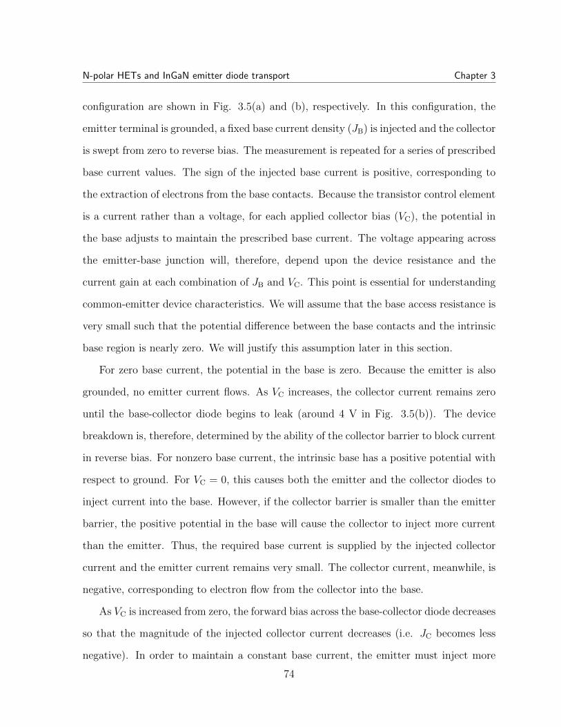
N-polar HETs and InGaN emitter diode transport Chapter 3
configuration are shown in Fig. 3.5(a) and (b), respectively. In this configuration, the
emitter terminal is grounded, a fixed base current density (JB) is injected and the collector
is swept from zero to reverse bias. The measurement is repeated for a series of prescribed
base current values. The sign of the injected base current is positive, corresponding to
the extraction of electrons from the base contacts. Because the transistor control element
is a current rather than a voltage, for each applied collector bias (VC), the potential in
the base adjusts to maintain the prescribed base current. The voltage appearing across
the emitter-base junction will, therefore, depend upon the device resistance and the
current gain at each combination of JB and VC. This point is essential for understanding
common-emitter device characteristics. We will assume that the base access resistance is
very small such that the potential difference between the base contacts and the intrinsic
base region is nearly zero. We will justify this assumption later in this section.
For zero base current, the potential in the base is zero. Because the emitter is also
grounded, no emitter current flows. As VC increases, the collector current remains zero
until the base-collector diode begins to leak (around 4 V in Fig. 3.5(b)). The device
breakdown is, therefore, determined by the ability of the collector barrier to block current
in reverse bias. For nonzero base current, the intrinsic base has a positive potential with
respect to ground. For VC = 0, this causes both the emitter and the collector diodes to
inject current into the base. However, if the collector barrier is smaller than the emitter
barrier, the positive potential in the base will cause the collector to inject more current
than the emitter. Thus, the required base current is supplied by the injected collector
current and the emitter current remains very small. The collector current, meanwhile, is
negative, corresponding to electron flow from the collector into the base.
As VC is increased from zero, the forward bias across the base-collector diode decreases
so that the magnitude of the injected collector current decreases (i.e. JC becomes less
negative). In order to maintain a constant base current, the emitter must inject more
74
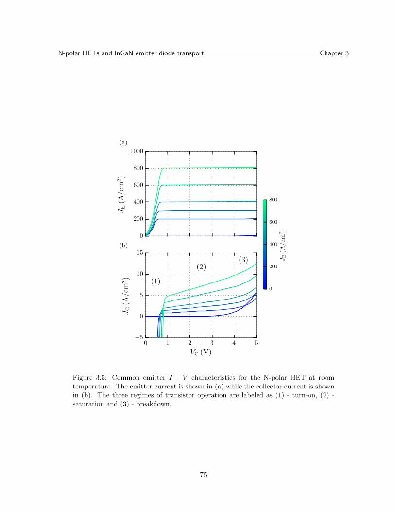
N-polar HETs and InGaN emitter diode transport Chapter 3
0
200
400
600
800
1000
JE(A
/cm
2)
0 1 2 3 4 5
VC (V)
−5
0
5
10
15
JC(A
/cm
2)
0
200
400
600
800
JB(A
/cm
2)
(a)
(b)
(1)
(2)(3)
Figure 3.5: Common emitter I − V characteristics for the N-polar HET at roomtemperature. The emitter current is shown in (a) while the collector current is shownin (b). The three regimes of transistor operation are labeled as (1) - turn-on, (2) -saturation and (3) - breakdown.
75

N-polar HETs and InGaN emitter diode transport Chapter 3
current into the base (JE increases). This is called the turn-on region of the device (region
(1) in Fig. 3.5(b)). At VC ∼ 0.75 V, the current injected from the collector is zero and
all base and collector current is supplied by the injected emitter current. At this point,
further application of VC has little effect on JE or JC. This is the saturation regime of
device operation (region (2)) and is the operating region of transistor amplifiers. Finally,
as VC is increased further, the base-collector diode leakage current becomes larger than
the hot electron collector current and the device breaks down (region (3)).
In the saturation region (1 V < VC < 4 V), JE and JC are nearly, but not exactly,
constant. For ideal transistors, the emitter and collector regions are completely decoupled
from one another and the saturation currents are flat. The nonzero slope of the saturation
current present in real devices is called output conductance and is a measure of the
coupling of the emitter and collector terminals. This coupling is undesirable because
it reduces the voltage gain of the device. In bipolar transistors, output conductance is
caused by modulation of the base-collector depletion region width, which leads to base
width narrowing[68]. This, in turn, causes an increase in emitter current in order to
satisfy the boundary conditions on the diffusion charge in the base. By contrast, output
conductance in the HET is caused primarily by the bias-dependent transfer characteristics
of the collector barrier. As the collector is reverse biased, it becomes more transparent
to incoming hot electrons. Therefore, increasing the collector bias causes an increase in
the current transfer ratio (α) and, therefore, β. Because fewer electrons are reflecting off
the collector and contributing to base current, the emitter must inject more current to
maintain constant base current. By this mechanism, increasing VC leads to increases in
JE, JC and α.
To demonstrate this effect, we will calculate the transfer ratio of the collector bar-
rier for various values of VC using the techniques outlined in Chapter 2. The calcula-
tion proceeds as follows: first, for each collector bias and corresponding band diagram
76

N-polar HETs and InGaN emitter diode transport Chapter 3
0 20 40 60 80
z (nm)
−2.0
−1.5
−1.0
−0.5
0.0
0.5
1.0
1.5
EC(eV)
0.0 0.2 0.4 0.6 0.8 1.0
Ez (eV)
10−5
10−4
10−3
10−2
10−1
100
α
0.0
0.5
1.0
1.5
2.0
V(V
)
(a) (b)
Figure 3.6: (a) Collector barrier conduction band diagrams for base-collector reversebiases of 0−2 V. (b) Simulated transfer ratios for a Gaussian packet of electrons withmean arrival energy Ez. For a given arrival energy, which is fixed by the injectionenergy and the base width, the barrier becomes more transparent with increasingcollector bias and α increases.
(Fig. 3.6(a)), the energy-dependent transmission probability (T (Ez)) is calculated via the
QTBM method. Second, because the electrons arriving at the collector are not monoen-
ergetic, a mean energy (Ez) is chosen and a normalized Gaussian distribution (P (Ez, Ez))
of electron energies is populated around the mean. The width of the distribution is equal
to the full width at half maximum of the corresponding Fermi-Dirac function (∼ 0.03 eV
at room temperature). The transfer ratio at each Ez is then calculated via
α(Ez) =
∫P (Ez, Ez)T (Ez)dEz. (3.1)
The simulated function α(Ez) is pictured in Fig. 3.6(b). The transfer ratio increases
with Ez as expected. Furthermore, for a constant Ez, α increases with collector bias,
which causes nonzero output conductance via the mechanism discussed earlier.
For the real device, the common-emitter current transfer ratio was measured to be
α = 3.88× 10⁻³ for a drive current of JB = 200 A/cm2 and VC = 0.8 V. The DC current
77

N-polar HETs and InGaN emitter diode transport Chapter 3
gain was β = α1−α = 3.9× 10⁻³. While these values are very low and must be improved
upon, this device represents the first demonstration of common-emitter modulation in
an N-polar III-N HET. The main cause of low β in this device is the large base-collector
barrier, which reflects the vast majority of incoming hot electrons. From Fig. 3.6(b),
α ∼ 0.004 corresponds to a mean arrival energy of about 0.5−0.6 eV. To achieve current
gain (β > 1) with this collector barrier, we must achieve α > 0.5 or an arrival energy of
about 1 eV.
To confirm our results, we performed an additional measurement in the Gummel
configuration: the base and collector were grounded while a negative bias was applied
to the emitter. The resulting base and collector currents were then measured (Fig. 3.7).
Both the base and collector currents rise with emitter forward bias (V ). Ohmic voltage
drops become significant for applied biases in excess of ∼ 0.9 V, beyond which the rate
of increase of JB with V slows dramatically. These resistive voltage drops ultimately
limit the achievable injection current density in the HET. To compare the current gain
measured in the Gummel configuration with common-emitter, the bias point V = 1.0 V
was chosen. This bias corresponds to the base current (∼ 200 A/cm2) that was used in
the common-emitter extraction of β. At 1 V, β = 4.2 × 10⁻³, very similar to the value
extracted from common-emitter measurements.
The contacts to the highly-scaled based layer were characterized via the transfer
length method (TLM) and the results appear in Fig. 3.8. The contacts are ohmic and
the contact and sheet resistances are 0.34 Ω · mm and 517 Ω/, respectively. These
are excellent values for unalloyed, unoptimized base contacts, and they demonstrate the
promise of N-polar HETs for achieving ultralow contact resistance to a highly scaled
base layer. This measurement allows us to revisit our earlier claim that the voltage drop
between the base contacts and the intrinsic base region is nearly zero. Given the values
of Rc and Rsheet as well as the device geometry, the voltage drop in the base extrinsic
78

N-polar HETs and InGaN emitter diode transport Chapter 3
0 0.3 0.6 0.9 1.2 1.5
V (V)
10−8
10−6
10−4
10−2
100
102
104
J(A
/cm
2)
JB
JC
0 0.3 0.6 0.9 1.2 1.5
V (V)
10−5
10−4
10−3
10−2
10−1
β
(a) (b)
Figure 3.7: (a) Gummel I − V characteristics for the first generation N-polar HETat room temperature. (b) Current gain (β = JC/JB) calculated from (a). The noisydata for V < 0.3 V is due to the collector current noise in (a).
regions is calculated to be ∼ 0.003 V for an emitter-base bias of 1.25 V (see Appendix B
for details regarding the calculation). This value of emitter-base voltage corresponds to
the maximum JB in common-emitter measurements and, therefore, represents the largest
possible extrinsic voltage drop. The very small value of the extrinsic base resistance
(1.56 Ω) demonstrates that the base contacts have a negligible effect on transistor I − V
characteristics.
Summarizing our results to this point, we have demonstrated the first N-polar III-N
HET with common-emitter transconductance. The large base-collector barrier reflects
most of the incoming hot electrons resulting in very low current gain (β = 0.004). How-
ever, the base-collector diode has fairly low leakage and the base access resistance is very
low. Therefore, it is possible to obtain accurate values for the current gain and trans-
fer ratio from Gummel I − V characteristics without the corrupting effects of erroneous
leakage currents. The N-polar HET must be improved dramatically before it can be-
come a viable transistor technology. However, these first-generation devices can already
79

N-polar HETs and InGaN emitter diode transport Chapter 3
−10 −5 0 5 10
I (mA)
−3
−2
−1
0
1
2
3
V(V
)
0 2 4 6 8 10
L (µm)
0
1
2
3
4
5
6
R(Ω
·mm)
1
2
3
4
5
6
7
8
9
10
L(µm)
(a) (b)
Rc = 0.34Ω ·mmRsheet =517Ω/sq
Figure 3.8: Base layer TLM measurements of the first-generation HET. (a) OhmicV − I behavior is seen for all TLM spacings. (b) The contact and sheet resistancesare found to be 0.34 Ω ·mm and 517 Ω/, respectively.
be used to study fundamental transport physics in III-N heterostructures. Such studies
have important materials science implications, as we will see in the next section.
3.3 InGaN polarization dipole barrier transport
We turn our attention now to an investigation of the N-polar HET emitter barrier.
The goals of this analysis are two-fold: from a scientific perspective, we hope to leverage
the capability of the collector barrier as an analyzer of hot electron states to study emitter
barrier transport; from a technological perspective, we would like to determine the effects
of nonideal emitter characteristics on transistor performance. We will begin this section
by discussing two-terminal InGaN polarization dipole diode (PDD) characteristics. Then,
we will present transistor measurements as a way to fortify the conclusions drawn from
the diode analysis.
80

N-polar HETs and InGaN emitter diode transport Chapter 3
0 20 40 60 80 100 120 140
z (nm)
−0.4
−0.2
0.0
0.2
0.4
0.6
0.8
1.0
EC(eV)
(a)
φ′B
Buffer + Sapphire
In0.1Ga0.9N 5 UID
GaN 200 5e18
Material thickness doping(nm) (cm−3)
GaN 100 UID
GaN 50 5e18
z
(b)
Figure 3.9: (a) Conduction band diagram of the InGaN PDD. The apparent barrierheight (φ′B) is labeled along with the zero bias Fermi level (dashed red line). (b) PDDlayer structure with z-axis orientation as it appears in (a).
3.3.1 InGaN polarization dipole diode analysis
The InGaN PDD used in this study was designed to closely mimic the emitter barrier
that appears in the N-polar HET. The conduction band diagram and layer structure are
shown in Fig. 3.9. The PDD was grown by MOCVD on a miscut sapphire substrate
and was fabricated using a truncated version of the process shown in Fig. 3.4 (BCl3/Cl2
mesa isolation and Al/Au ohmic contacts).
During measurement, the diode was placed in a vacuum chamber and brought to
target temperatures in the range 100−400 K using a Lake Shore 330 model temperature
controller with a PID feedback loop. Temperatures below ambient were achieved using
liquid nitrogen as a cooling agent. At each target temperature, the sample was left
for 10− 15 minutes before measurements were made to ensure thermal equilibrium was
achieved between the device and the sample stage. Then, the top contact was grounded
and the voltage on the bottom contact swept from −3 V to +3 V while measuring the
current.
The InGaN emitter diode I − V − T characteristics are shown in Fig. 3.10. At
81

N-polar HETs and InGaN emitter diode transport Chapter 3
−3 −2 −1 0 1 2 3
V (V)
10−8
10−6
10−4
10−2
100
102
104
J(A
/cm
2)
100
150
200
250
300
350
400
T(K
)
Figure 3.10: I−V −T data for the InGaN polarization dipole diode for the temperaturerange 100− 400 K. Ohmic voltage drops limit the achievable current density beyond1 V applied bias. The linear fits to the forward bias current are performed within thefirst 200 mV of device turn-on.
low bias the current increases quasi-exponentially for all temperatures. For an applied
forward bias of about 1 V, the current begins to saturate as ohmic voltage drops become
appreciable. The device turn-on voltage decreases with increasing temperature, a result of
the increased supply of high-energy electrons incident on the barrier at high temperature.
While the turn-on voltage increases at low temperatures, it remains less than 0.5 V at 100
K, nearly half of the design barrier height of ∼ 0.9 eV (see Fig. 3.9(a)). This suggests the
presence of an unknown, low-energy current pathway that dominates low-temperature
transport.
Following the procedure outlined in Chapter 2, a linear fit to the low-bias forward
current at each temperature is performed. The slope of this linear fit is q/nkBT and
the intercept is ln(JS), where JS is the saturation current. Assuming A∗ = 26 A/cm2K2
allows us to calculate the apparent barrier height (φ′B) from JS while the ideality factor
(n) is calculated from the slope. This procedure is done for both the experimental data
82

N-polar HETs and InGaN emitter diode transport Chapter 3
pictured in Fig. 3.10 and for simulated I−V −T curves generated using the band diagram
in Fig. 3.9(a) and the methods outlined in Chapter 2. The results for the simulated and
experimental ideality factors and apparent barrier heights are pictured in Fig. 3.11.
The high-temperature ideality factor for the simulated diode current is ∼ 1.2. There
are two contributions to n > 1 in the simulated data: first, voltage partitioning ensures
that only a fraction of the applied bias is dropped in the UID GaN above the InGaN layer.
The remainder appears across the InGaN dipole layer, which causes the barrier height to
increase with bias. This effect is due to simple electrostatic considerations and is present
whenever the barrier maximum is not immediately adjacent to the control electrode. In
particular, if the barrier maximum is a distance t2 away from the control electrode and t1
away from the grounded electrode, the ideality factor attributed to voltage partitioning
is:
nV = 1 +t2t1
ε1ε2, (3.2)
where εi is the low-frequency dielectric constant in the ith material. In the PDD, t1
= 100 nm and t2 = 5 nm so that nV ∼ 1.05. Voltage partitioning can also arise from
resistive access regions and barrier-limited contacts. However, these contributions can
be shown to be negligible for the very small currents considered here.
The second contribution to n > 1 in the simulated data is thermionic field emission
(see Chapter 2 for a detailed discussion). Note that the background doping is relatively
high in N-polar GaN (∼ 2 × 1017 cm−3). This leads to increased band bending and,
therefore, a larger thermionic field current than in Ga-polar devices. The ideality factor
due to thermionic field emission is nTFE ∼ 1.14. The combined effect of voltage par-
titioning and thermionic field emission is given by the product of the ideality factors:
nV × nTFE = 1.2, the total high-temperature ideality factor. Voltage partitioning and
thermionic field emission are also present in real PDD devices. However, the simulation,
83

N-polar HETs and InGaN emitter diode transport Chapter 3
T (K)
1.0
1.2
1.4
1.6
1.8
2.0
2.2
2.4n
Experimental
Simulated
BHI
100 150 200 250 300 350 400
T (K)
0.4
0.5
0.6
0.7
0.8
0.9
φ′ B(eV)
(a)
(b)
Figure 3.11: Simulated and experimental values of (a) the ideality factor and (b) theapparent barrier height. The latter were calculated using A∗ = 26 A/cm2K2. Theo-retical and experimental values begin to converge at high temperatures but diverge asthe temperature decreases. The dashed blue line in (a) represents the product of theBHI contribution to n (Eq. (3.3)) and the simulated values. The dashed blue line in(b) represents Eq. (3.4) with the values of φB and σS taken from the second-order fitin Fig. 3.12.
84

N-polar HETs and InGaN emitter diode transport Chapter 3
which takes into account only these two effects, produces ideality factors that are smaller
than experimental values. Therefore, there must be an additional source of n > 1 in real
PDDs.
Similarly, the simulation overestimates the value of φ′B. Thermionic field emission
causes φ′B to increase with temperature but at a slower rate than the experimental values.
Like the Schottky diode in Chapter 2, the simulated and experimental values of φ′B match
well at high temperatures but diverge at low temperatures. The Richardson plot (Fig.
3.12) reveals a similar relationship between simulated and experimental results.
These discrepancies can be clearly explained by barrier height inhomogeneity (BHI)
in the InGaN PDD. The deviation of the low-bias current from perfect linearity in Fig.
3.10 is characteristic of inhomogeneous barrier transport[82]. A detailed discussion of
the effects of BHI on measured diode characteristics can be found in Chapter 2. Here we
summarize the important results:
1. Upon application of forward bias, the inhomogeneous barrier distribution is dis-
torted and the mean barrier height increases causing n > 1. The temperature and
bias dependence of n is given by
n =
(1− q
2kBT
σ2S(0)− σ2
S(V )
V
)−1
. (3.3)
2. For a Gaussian distribution of barrier heights, the canonical thermionic emission
equation remains valid if we substitute an apparent barrier height,
φ′B = φB −qσ2
S
2kBT, (3.4)
for the constant quantity φB. In Eq. (3.4), φB is the mean, zero-bias barrier height
and σS is the zero-bias standard deviation of the barrier distribution.
85

N-polar HETs and InGaN emitter diode transport Chapter 3
20 40 60 80 100 120
q/kBT (eV−1)
10−36
10−32
10−28
10−24
10−20
10−16
10−12
10−8
JS/T
2(A
/cm
2K
2)
Experimental
Simulated
BHI
A∗ = 23.8A/cm2K2
φB = 0.93 eV
σS = 0.09 eV
Figure 3.12: (a) Simulated and experimental Richardson plot for the PDD. The val-ues of A∗, φB and σS are extracted from the quadratic fit (dashed blue line) to theexperimental Richardson data via Eq. (3.5).
3. The Richardson data are no longer linear but obey the quadratic equation:
ln
(JS
T 2
)= ln(A∗)−
(q
kBT
)φB +
1
2
(q
kBT
)2
σ2S. (3.5)
For diodes containing inhomogeneous barriers, a second-order fit to the Richardson
data simultaneously yields A∗, φB and σS from the zeroth, first and second order coeffi-
cients, respectively. The fit is performed on the PDD Richardson data and is shown in
Fig. 3.12 (dashed blue line). The extracted value A∗ = 23.8 A/cm2K2 is nearly equal to
the theoretical value of 26 A/cm2K2 for GaN, a confirmation that the BHI model accu-
rately describes the transport physics of the diode. Furthermore, φB is almost exactly
equal to the design barrier height in Fig. 3.9(a). The standard deviation of the barrier
height fluctuations (σS) amounts to a ∼10% lateral variation in barrier height across the
device area.
86

N-polar HETs and InGaN emitter diode transport Chapter 3
The dashed line in Fig. 3.11(b) represents Eq. (3.4), with the values of φB and σS
taken from the second-order fit coefficients according to Eq. (3.5). The experimental
data are well-described by the dashed line, confirming the accuracy of the functional
form of Eq. (3.4). The dashed line in Fig. 3.11(a) is generated by multiplying the
BHI contribution to n given by Eq. (3.3) with the simulated values; we find excellent
agreement between this line and the data. If only the BHI contribution is considered,
calculated values of n do not agree with experimental values. This strongly suggests
that three entirely distinct effects contribute to the experimental ideality factor: voltage
partitioning, thermionic field emission and barrier height inhomogeneity. The analysis
we have presented demonstrates that these three effects can be “factorized” and their
magnitudes separately determined with the help of numerical I − V − T simulations.
For high temperatures, the quadratic term in Eq. (3.5) becomes small and the data
are approximately linear in powers of q/kBT . This is consistent with the commonly
observed linearity of high-temperature Richardson data. As such, it may be tempting
to perform a linear fit to the high-temperature data in order to extract A∗ and φB. To
demonstrate the limits of this method, we performed such a fit on the high-temperature
data in Fig. 3.12. The fit yields a value for A∗ and φB of 0.13 A/cm2K2 and 0.63 eV,
respectively. This underestimation of the Richardson constant and the barrier height
from a high-temperature linear fit was observed in a previous report of InGaN LED
data[83]. These results suggest that the homogeneous thermionic emission equation does
not capture all the relevant physics in our devices, even at high temperature where the
data appear to be linear.
We propose that the physical origin of the lateral barrier height fluctuations observed
in the PDD is random, nanoscale fluctuations in indium composition. Indium fluctuations
as high as 25 − 50% of the nominal alloy composition have been observed in InGaN
films using atom probe tomography[84, 85, 86]. Other studies have linked compositional
87

N-polar HETs and InGaN emitter diode transport Chapter 3
0.00 0.05 0.10 0.15 0.20
xIn
0.000
0.002
0.004
0.006
0.008
0.010
frequency
(arb)
Figure 3.13: Distribution of In compositions corresponding to the measured valueσS = 0.09 eV.
fluctuations with the anomalously low turn-on voltage observed in multiquantum well
LEDs[87, 83].
For the device structure pictured in Fig. 3.9, the extracted σS corresponds to a
compositional standard deviation of only 2% In across the device area. A Gaussian
distribution with a mean In composition of 10%, the nominal design composition, and a
standard deviation of 2% is shown in Fig. 3.13. The distribution reveals that there is
a nonzero proportion of the device area locally containing no more than 5% In. For the
PDD in this study, this composition corresponds to a barrier height of 0.44 eV, nearly
identical to the value of φ′B at 100 K (see Fig. 3.11(b)). This confirms the assertion that
inhomogeneous barrier transport, particularly at low temperature, is dominated by low-
barrier regions and further implicates In compositional fluctuations as the physical source
of BHI. Furthermore, there is no evidence of In clustering[88, 89] or phase segregation
in the dipole layer of our device. Such an effect would imply the existence of regions
where the local In composition is nearly zero. These regions would provide low-resistance
short paths through the barrier that would become clearly evident at low temperature.
The fact that the diode exhibits signatures of barrier-limited transport even at 100 K
88

N-polar HETs and InGaN emitter diode transport Chapter 3
Figure 3.14: 3-dimensional schematic of the conduction band diagram for a laterally(a) homogeneous and (b) inhomogeneous InGaN PDD with σS = 0.09 eV.
suggests that the local In composition does not fall to zero. A 3-dimensional schematic
of a homogeneous and inhomogeneous InGaN PPD with σS = 0.09 eV is pictured in Fig.
3.14.
In this section we have shown that BHI theory can accurately explain the transport
characteristics of the InGaN PDD. Simulation data suggest that voltage partitioning and
thermionic field emission, while clearly present in the real device, cannot fully account
for the observed experimental data. Despite the seeming success, so far we have relied
only on diode data and have no independent demonstration that BHI is the cause of the
anomalous diode I − V . As such we would like to test the predictions of BHI theory,
specifically that lateral fluctuations produce a bias and temperature-dependent apparent
barrier height. For that we turn to temperature-dependent transistor measurements,
which are discussed in the next section.
89

N-polar HETs and InGaN emitter diode transport Chapter 3
3.3.2 Electron injection spectroscopy using the N-polar HET
While the BHI model seems to accurately describe the PDD data, a direct correlation
between φ′B and the electron injection energy has not yet been established. In fact,
researchers routinely refer to φ′B as the “apparent barrier height”[90, 91, 92], a name
that reveals the uncertainty regarding its physical interpretation. Simply put, we seek
to answer the question: “is φ′B equal to the average energy of electrons emitted from the
diode?”. The answer to this question will have important device implications for III-N
HETs. In this section we introduce a method called electron injection spectroscopy, which
provides a direct measurement of the signature of BHI by using the collector barrier of
the HET as an analyzer of hot electron states. Such a measurement will demonstrate the
effects of BHI on transistor performance and will help provide a physical interpretation
of φ′B.
To date the most popular method for directly measuring BHI and its effect on localized
band structure is ballistic electron emission microscopy (BEEM)[93, 94]. In this method
a scanning tunneling microscope (STM) tip serves as the emitter of ballistic electrons into
a very thin base provided by the Schottky metal while the semiconductor material serves
as the collector. By varying the injection energy of the ballistic electrons and measuring
the resulting collector current, the local barrier height can be determined with a lateral
resolution of ∼1 nm. This method has been applied to study BHI in a wide variety of
Schottky junctions[95, 96, 97] and semiconductor heterointerfaces[98, 99].
While BEEM methods are sensitive to the effects of BHI on ballistic electrons, which
are out of equilibrium with the semiconductor lattice, the first comprehensive theory
describing the effects of BHI on the transport properties of thermalized electrons was
proposed by Tung[73]. In Chapter 2 we demonstrated that in the presence of BHI, the
constant barrier height in the canonical thermionic emission equation must be replaced
90

N-polar HETs and InGaN emitter diode transport Chapter 3
with a bias and temperature-dependent barrier height (φB → φ′B(V, T )):
J = A∗T 2exp
(−qφ
′B(V, T )
kBT
)(exp
(qV
kBT
)− 1
). (3.6)
Specifically, φ′B increases with both increasing temperature (see Fig. 3.11(b)) and increas-
ing forward bias. If such a barrier is placed in a HET where it emits electrons toward
an analyzer provided by the collector barrier, relative changes in the electron injection
energy will reveal themselves as changes in the current transfer ratio α. In particular,
as the injection energy increases the probability of transmission at the collector, and
therefore α, increases. Because the injection energy is determined by the emitter barrier
height, changes in α are correlated with changes in φ′B.
The layer structure of the HET used in this study was identical to the device pictured
in Fig. 3.2 except that the GaN base layer thickness was 3 rather than 10 nm. This device
was chosen in order to minimize electron scattering events in the base and simplify the
analysis. The growth and processing details were also identical. During measurement
the HET was placed in a vacuum chamber whose sample stage was cooled with liquid
nitrogen. At each target temperature, the transistor was measured in the modified Gum-
mel configuration: the base and collector terminals were grounded while a forward bias
(V ) was applied to the emitter. In this configuration there was no bias applied between
the base and the collector so that the quantum mechanical transfer characteristics of the
collector remained constant for all emitter biases and temperatures. In this sense the
electron “filter” was kept constant. The applied forward bias was swept between 0− 1.5
V and the emitter and collector currents were measured. Because we were ultimately
interested in the transfer ratio JC/JE, the Gummel plot has been modified to display JE
and JC rather than JB and JC, which appear in conventional Gummel plots.
The modified Gummel plot for the III-N HET in the temperature range 100 − 400
91

N-polar HETs and InGaN emitter diode transport Chapter 3
10−8
10−6
10−4
10−2
100
102
104
J(A
/cm
2)
0 0.3 0.6 0.9 1.2 1.5
V (V)
10−6
10−5
10−4
10−3
10−2
10−1
α
100
150
200
250
300
350
400
T(K
)
(a)
(b)
JE
JC
Figure 3.15: (a) Modified Gummel I −V characteristics for the bias and temperaturerange 0− 1.5 V and 100− 400 K, respectively. The arrows label each family of curvesrepresenting the temperature series for JE and JC. (b) Corresponding transfer ratio(α = JC/JE) for the same temperature and bias range. The yellow box indicates thevalues of α plotted in Fig. 3.16(a).
92

N-polar HETs and InGaN emitter diode transport Chapter 3
K is shown in Fig. 3.15(a). The emitter and collector currents both rise with emitter
forward bias, and, because the collector barrier is large, JE JC. Ohmic voltage drops
become significant for applied biases in excess of ∼ 0.75 V, beyond which the I − V
curves in Fig. 3.15(a) flatten. These ohmic voltage drops ultimately limit the achievable
intrinsic emitter forward bias and the magnitude of JE. Furthermore, in these ohmic
regions some portion of the applied voltage drops in the extrinsic regions of the device
making it difficult to determine the precise intrinsic emitter bias accurately. Therefore,
we will restrict the subsequent analysis to V < 0.75 V. The collector current resolution
is limited by the instrument noise floor as well as the zero bias current noise at each
temperature.
The bias and temperature-dependent current transfer ratio is pictured in Fig. 3.15(b).
For a single temperature, between the voltages corresponding to the noise floor and to
the point where ohmic voltage drops become significant, α exhibits a clear upward trend
with bias. Additionally, for a fixed applied bias, α increases with increasing temperature
(Fig. 3.16(a)). The applied bias value of 0.65 V was chosen for Fig. 3.16(a) because at
this value, ohmic voltage drops are negligible and collector current noise is limited for
most temperatures (see yellow box in Fig. 3.15(b)). This ensures that nearly all of the
applied bias appears across the intrinsic emitter-base junction for all temperatures. At
0.65 V and T < 200 K the collector current, and therefore α, becomes noisy. Therefore,
the data below 200 K in Fig. 3.16(a) are likely unreliable.
Because the quantum mechanical transfer characteristics at the base-collector junction
are constant for all emitter biases and temperatures, an increase in α can only result from
a corresponding increase in electron injection energy. This, in turn, can only be explained
by an increase in the mean emitter barrier height with bias and temperature. As we will
see in Chapter 5, the hot electron mean free path in GaN was measured to be ∼ 10 nm.
Because the base in the III-N HET is 8 nm thick (5 nm InGaN + 3 nm GaN), electron
93

N-polar HETs and InGaN emitter diode transport Chapter 3
100 150 200 250 300 350 400
T (K)
10−8
10−7
10−6
10−5
10−4
10−3
10−2
α
0.4 0.5 0.6 0.7 0.8 0.9
Ez (eV)
10−8
10−7
10−6
10−5
10−4
10−3
10−2
α
(a) (b)
Figure 3.16: (a) Experimental transfer ratio at an emitter bias of 0.65 V for thetemperature range 100 − 400 K. These values are represented by the yellow box inFig. 3.15. (b) Simulated transfer ratio for a Gaussian distribution of electrons withmean longitudinal energy Ez. The experimental values in (a) are mapped onto thesimulated values in (b). This mapping enables an estimate of the mean energy of thehot electron ensemble incident on the collector barrier at each temperature (see Fig.3.17).
scattering in the base should be minimized. In this quasi-ballistic regime, the number
of scattered electrons is a very weak function of injection energy and temperature. This
ensures a close correspondence between increases in α and increases in emitter barrier
height.
To further reinforce this correspondence, the energy-dependent transfer ratio for the
AlGaN collector barrier was calculated. The details of the calculation were discussed
earlier in this chapter (see Eq. (3.1)) and the results are pictured in Fig. 3.16(b). This
calculation provides a one-to-one relationship between the transfer ratio and the mean
kinetic energy of electrons arriving at the collector. Considering Fig. 3.16(a) and (b)
together allows us to estimate the mean arrival energy of electrons in the HET we have
measured. The temperature-dependent arrival energies and apparent emitter barrier
height, as measured from emitter diode I − V − T , are pictured in Fig. 3.17.
94

N-polar HETs and InGaN emitter diode transport Chapter 3
100 150 200 250 300 350 400
T (K)
0.25
0.35
0.45
0.55
0.65
0.75
0.85
φ′ B(eV)
Earrival(eV)
Figure 3.17: Apparent barrier height of the emitter diode (red squares) and electronarrival energies corresponding to the measured transfer ratios in Fig. 3.16(a)(bluedots). For T > 200 K, these two quantities are nearly equal, confirming both that theincrease in α is due to the increase in φ′B and that the base electrons travel ballistically.
There are two important observations and accompanying conclusions to make about
Fig. 3.17: first, the values φ′B and Earrival increase with temperature at identical rates
above 200 K. This implies that the increase in α is indeed due to an increasing emitter
barrier height caused by BHI. This trend also suggests that the apparent barrier height
is approximately equal to the mean electron injection energy. In other words φ′B has a
clear and direct physical meaning and need not be considered an “apparent” quantity.
Second, φ′B and Earrival are nearly equal above 200 K. This implies that the average hot
electron kinetic energy on the emitter and the collector side of the base are equal and
that electron transport across the base is, therefore, ballistic.
These trends do not hold at the lowest temperatures. The apparent barrier height
continues to fall with temperature while the estimated arrival energy remains constant.
This is likely due to the current noise floor of the measurement apparatus as discussed
earlier. Namely, the low temperature transfer ratios are likely unreliable due to collector
95

N-polar HETs and InGaN emitter diode transport Chapter 3
current noise. The arrival energies at low temperature are, therefore, similarly unreliable.
In the previous section, we proposed alloy fluctuations as the most likely cause of
the observed BHI in InGaN PDDs. Despite the likely existence of such compositional
fluctuations, several additional physical sources of barrier height inhomogeneity can be
proposed. Because the polarization dipole barrier height is determined both by the In
composition and the InGaN thickness, thickness fluctuations of ≤ 1 nm can provide
the necessary σS. Scanning capacitance microscopy measurements of MOCVD-grown 3
nm InGaN/GaN quantum wells have revealed InGaN thickness fluctuations of several
monolayers[100]. Barrier height fluctuations could also result from an inhomogeneous
distribution of conductive threading dislocations that provide a low-energy current path-
way though the band gap. The magnitude of leakage currents has been observed to scale
with threading dislocation density in LEDs [101, 102] and in GaN Schottky diodes[103].
While it is difficult to diagnose the exact physical cause of BHI from a single device,
these analysis methods can be applied to a series of InGaN PDDs designed to test each
of the above hypotheses.
The analysis presented in this chapter has several important implications for the
HET: first, the presence of lateral barrier height fluctuations results in a lower average
electron injection energy than the design barrier would suggest. This means that we have
been unable to make full use of the InGaN emitter barrier to launch hot electrons. In
the example presented in this chapter, BHI causes a ∼ 100 meV reduction in electron
injection energy at room temperature. This is roughly equivalent to the energy lost in a
single longitudinal optical phonon scattering event.
Secondly, current transport through inhomogeneous barriers is more resistive than in
their homogeneous counterparts (see the discussion about the ideality factor in Section
3.3.1). This causes the flat-band diode resistance to be higher, which limits the achievable
forward current density. To understand this, consider the discussion of extrinsic voltage
96

N-polar HETs and InGaN emitter diode transport Chapter 3
drops from Section 3.2. Using TLM measurements and calculations based on the device
geometry, we demonstrated that the voltage drops in the extrinsic base region were
negligible. TLM measurements were also performed on the emitter layer and the contact
and sheet resistances were found to be 5.6 Ω · mm and 1622 Ω/, respectively. Per
the method outlined in Appendix B, the emitter resistance and emitter voltage drop are
found to be 100 Ω and 0.4 V, respectively, at an applied bias of 1.25 V. Immediately we
learn that the emitter extrinsic regions are more resistive than those in the base. More
importantly, however, there is an additional 0.85 V being dropped across the intrinsic
device region in spite of the fact that the barrier has ostensibly been biased away at 1.25
V. This voltage drop corresponds to an intrinsic emitter resistance of 214 Ω, more than
twice the resistance of the extrinsic emitter. Therefore, we may conclude that it is, in fact,
the intrinsic emitter barrier that chokes the forward diode current! The physical cause
of this choke is the resistive, low-barrier regions of the inhomogeneous InGaN barrier.
As long as these inhomogeneities are present, they will have a deleterious effect on the
achievable forward current density.
In this chapter we have presented the first demonstration of the III-N Nitrogen-polar
HET. While the measured common-emitter current gain was very low, the excellent con-
tacts to the highly-scaled base layer enabled otherwise ideal device operation. We used
the working devices to study InGaN polarization dipole diode transport and to demon-
strate the physical relevance of the apparent barrier height, which plays a central role
in barrier height inhomogeneity theory. We determined that the most likely physical
cause of barrier height inhomogeneity in the N-polar HET emitter is small-scale In com-
positional fluctuations. These fluctuations were shown to decrease the average injection
energy of the PDD emitter and limit the emitter current density. To this point we have
considered the transport properties of electrons in the vicinity of the emitter and collector
barriers in the N-polar HET. In the next chapter, we will briefly analyze the transport
97

N-polar HETs and InGaN emitter diode transport Chapter 3
properties of Ga-polar HETs.
98

Chapter 4
Ga-polar HETs and AlN emitter
diode transport
In this chapter we will present a brief analysis of the Ga-polar HET and the AlN emitter
diode with the goal of comparing the results to the N-polar HET data presented in
Chapter 3. The majority of the measurement and analysis methods are identical to
those used for N-polar HETs. Therefore, we will refer the interested reader to Chapter 3
for a detailed description of these methods and provide only an abbreviated version here.
The chapter will be organized into two brief sections: first, we will present the Ga-polar
HET design and discuss its advantages over N-polar designs. We will also present and
briefly analyze Ga-polar transistor data. Second, we will analyze the AlN emitter diode
using I − V − T measurements and BHI theory before discussing the implications of the
results for HET operation.
99
Ga-polar HETs and AlN emitter diode transport Chapter 4
4.1 Device design, growth and fabrication
The Ga-polar HET design is based on the polarization dipole approach discussed in
Chapter 1. The conduction band diagram for such a design in pictured in Fig. 4.1. The
emitter and collector barriers are formed using thin AlN and InGaN polarization dipole
barriers, respectively. There are several important differences between this design and the
N-polar design presented in Chapter 3. First, there is no large dipole barrier present at
the base-collector interface as there is in the N-polar HET. This should reduce quantum
mechanical reflections for moderate emitter barrier heights and lead to an increase in
current gain. Second, the InGaN dipole emitter in N-polar HETs is intended to be
a thermionic injector while the AlN diode in Ga-polar HETs is designed as a tunnel
injector. Because the AlN layer is very thin, we expect electrons to be injected at the
top of the drift field region of the emitter barrier in Fig 4.1 or at about 1.3 eV (see blue
arrow in the figure). In Chapter 3 we found that lateral barrier height fluctuations led
to resistive voltage drops in the emitter that ultimately limited the achievable current
density. Because the AlN diode is a tunnel injector, we expect that the current choke
may be even more severe in the Ga-polar HET.
A processed device schematic and layer structure for the Ga-polar HET is pictured
in Fig. 4.2. The device was grown using an experimental hybrid technique: the collector
barrier was grown by MOCVD and the emitter barrier by plasma-assisted MBE. The
purpose of such a hybrid growth process was to avoid the unintentional incorporation of
Ga into MOVCD-grown AlN films[104, 77]. Because the polarization charge discontinuity
is higher at AlN/GaN junctions than at AlGaN/GaN junctions, growth of pure AlN by
MBE enables a large electron injection energy without introducing a thick tunnel barrier
into the emitter[81].
During device processing base mesa isolation was performed using a low-power re-
100

Ga-polar HETs and AlN emitter diode transport Chapter 4
0 50 100 150 200 250
z (nm)
−0.5
0.0
0.5
1.0
1.5
2.0
2.5
EC(eV)
E B C
Figure 4.1: Conduction band diagram for the Ga-polar HET with an 8 nm GaN base.The regions of the band diagram that correspond to the emitter, base and collectorhave been labeled along with the equilibrium Fermi level (dashed red line). The thinAlN dipole layer provides a tunnel injector of hot electrons into the base (blue arrow).
E
B
C
Buffer + Sapphire
AlN 1 UIDGaN 4+4 UID,1e19
UID
UID
5e18GaN 200
In0.1Ga0.9N
GaN
5
100
Material thickness doping(nm) (cm−3)
GaN 100 UID
GaN 50 5e18z
MO
CV
DM
BE
Figure 4.2: Ga-polar HET layer structure and processed device schematic. The layersthat compose the emitter, base and collector have been labeled and the metal contactsare pictured in red. The bottom half of the layer stack was grown by MOCVD andthe top half by PAMBE.
101

Ga-polar HETs and AlN emitter diode transport Chapter 4
active ion etch (RIE) with BCl3/Cl2 etch chemistry. To form an ohmic contact to the
base through the wide-bandgap AlN interlayer, a selective BCl3/SF6 inductively coupled
plasma (ICP) etch was performed. During etching the BCl3 plasma removes GaN until
the AlN layer is exposed. The subsequent reaction between the SF6 plasma and the
exposed AlN leads to the formation of a nonvolitile AlF3 complex that prevents etching
of AlN. After the selective etch was completed, the AlF3 was removed with a 10 minute
400C anneal in N2[105]. An ohmic tunnel contact to the base layer was formed by de-
positing an Al/Au metal stack on the AlN interlayer. The emitter and collector contacts
were also formed via Al/Au metal stacks deposited using e-beam evaporation.
4.2 Room temperature transistor operation
Common-emitter characteristics of the Ga-polar HET are shown in Fig. 4.3. The
various regimes of transistor operation are labeled in the figure and discussed in detail in
Chapter 3. The relatively smaller collector barrier in the Ga-polar HET has three effects:
first, the device turn-on voltage is larger because the collector injects more current into
the base for small collector biases; second, the device breakdown voltage is lower than in
N-polar devices; and third, the current gain (β) is ∼ 0.21, over an order of magnitude
larger than in N-polar HETs. This corresponds to a transfer ratio of ∼ 0.18. The
large increase in gain from N-polar to Ga-polar HETs highlights the detrimental effect
of the AlGaN polarization dipole in the collector of N-polar devices. The base contacts
were characterized using TLM measurements and the contact and sheet resistances were
found to be 1.15 Ω ·mm and 4085 Ω/, respectively. These values are substantially larger
than those of N-polar HETs (0.34 Ω · mm and 517 Ω/). This is consistent with our
statement in Chapter 3 that the low-bandgap InGaN layer in the N-polar HET enables
low-resistance ohmic contacts to the base and, therefore, provides an advantage over Ga-
102

Ga-polar HETs and AlN emitter diode transport Chapter 4
0 1 2 3 4 5
VC (V)
−100
0
100
200
300
400
500
JC(A
/cm
2)
0
200
400
600
800
JB(A
/cm
2)
(1)
(2)
(3)
Figure 4.3: Common-emitter collector I − V characteristics for the Ga-polar HETat room temperature. The three regimes of transistor operation are labeled as (1) -turn-on, (2) - saturation and (3) - breakdown. The current gain of the transistor is∼ 0.2.
polar HETs. Based on these data we may conclude that for polarization dipole HETs,
Ga-polar devices have superior current gain but inferior quality base contacts.
4.3 AlN polarization dipole barrier transport
In this section we will follow an abbreviated version of the method presented in
Chapter 3 for analyzing polarization barrier transport in the AlN emitter. Because a
detailed analysis has already been performed in Chapter 3, here we aim only to introduce
the analysis method in the context of tunnel barriers and discuss the effects of our results
on transistor function. We will start by considering diode I−V −T data, which is shown
in Fig. 4.4. Note that this figure shows the emitter current in the modified Gummel
configuration, which is equivalent to a two-terminal diode I − V measurement. At low
bias, the emitter current increases slowly until device turn-on (V ' 1 V). After turn-
on the current increases exponentially before ohmic voltage drops begin to dominate.
103

Ga-polar HETs and AlN emitter diode transport Chapter 4
0.0 0.5 1.0 1.5 2.0 2.5 3.0
V (V)
10−6
10−4
10−2
100
102
104
JE(A
/cm
2)
100
150
200
250
300
350
400
T(K
)
Figure 4.4: Forward bias AlN emitter diode I − V − T characteristics for the temper-ature range 100− 400 K.
Furthermore, the low-bias current is temperature-dependent, which suggests the presence
of a thermally-activated leakage mechanism for V < 1 V. If this leakage path were not
present, the high temperature current would decrease to the noise floor at low bias as it
does at low temperature.
In order to extract the saturation current (JS) from the diode I − V a data analysis
algorithm was developed to identify the point where the slope of the current (dJE/dV )
is maximized. A small bias range is selected around this point and a line is fitted to
the data in this range. The saturation current is then determined from the ordinate
axis intercept of the fit line. The resulting Richardson plot is pictured in Fig. 4.5.
The Richardson data are clearly nonlinear as they were for the InGaN diode discussed in
Chapter 3. We hypothesize that this nonlinearity is cause by barrier height inhomogeneity
(BHI). Following the discussions presented in Chapters 2 and 3, we assume a Gaussian
104

Ga-polar HETs and AlN emitter diode transport Chapter 4
20 40 60 80 100 120
q/kBT (eV−1)
10−28
10−26
10−24
10−22
10−20
10−18
10−16
10−14
10−12
JS/T
2(A
/cm
2K
2)
A∗ = 0.295A/cm2K2
φB = 1.28 eV
σS = 0.113 eV
Figure 4.5: Richardson plot for the AlN emitter diode. The values of A∗, φB and σS
are extracted from the second order fit (blue dashed line). A linear fit to the hightemperature data is also shown (black dotted line).
distribution of barrier heights and fit the data to the second-order equation:
ln
(JS
T 2
)= ln(A∗∗)−
(q
kBT
)φB +
1
2
(q
kBT
)2
σ2S, (4.1)
where A∗∗ is the effective Richardson constant, φB is the mean barrier height and σS
is the standard deviation of the barrier height distribution. The values of A∗∗, φB and
σS are then extracted from the zeroth, first and second order coefficients, respectively.
The extracted mean barrier height is nearly identical to the designed injection energy in
Fig. 4.1. The standard deviation in the barrier height amounts to a 9% variation over
the device area. The effective Richardson constant, on the other hand, is two orders of
magnitude smaller than the theoretical value for GaN (26 A/cm2K2). We can understand
this by appealing to the argument presented at the end of Chapter 2. Rather than
regarding the Richardson constant as a material quantity, we should instead consider it
105

Ga-polar HETs and AlN emitter diode transport Chapter 4
0.5 1.0 1.5 2.0 2.5
Ez (eV)
10−6
10−5
10−4
10−3
10−2
10−1
100
T
Figure 4.6: Transmission characteristics of the AlN diode. In the range of electroninjection energies the transmission probability is 10−3 − 10−2.
to be device quantity. To this end we defined the effective Richardson constant using the
approximate expression
A∗∗ ' T0A∗, (4.2)
where A∗ = 26 A/cm2K2 and T0 is the transmission probability of the barrier close to the
mean electron injection energy. To test the applicability of this definition the transmis-
sion characteristics of the AlN polarization dipole barrier are calculated via the methods
presented in Chapter 2 (Fig. 4.6). The figure demonstrates that the transmission prob-
ability for electrons around 1.3 eV is ∼ 5 × 10⁻³. When plugged into Eq. (4.2) this
gives A∗∗ ' 0.13A/cm2K2, much closer to the value obtained from the fit in Fig. 4.5.
This result validates our reinterpretation of the Richardson constant in light of nonunity
transmission at the barrier interface. Furthermore, the depressed value of A∗∗ suggests
that, even in the absence of BHI, the current provided by the AlN tunnel barrier will be
reduced by two orders of magnitude compared with a thermionic emission barrier.
To demonstrate the limitations of traditional fitting methods, a linear fit to the high-
106

Ga-polar HETs and AlN emitter diode transport Chapter 4
temperature Richardson data is performed (black dotted line in Fig. 4.5). From this
linear fit and the traditional Richardson equation, we find A∗ = 5.01 × 10⁻⁵ A/cm2K2
and φB = 0.76 eV. These results are consistent with previous observations that the high-
temperature linear fit underestimates the value of A∗ and φB (see [83] and Chapter 3 of
this thesis). Therefore, the quadratic fitting method is the only acceptable approach for
analyzing nonlinear Richardson data.
Finally, the apparent barrier height and the ideality factor of the AlN diode are
extracted from the forward bias diode I − V (Fig. 4.7). The dashed blue line in Fig.
4.7(a) represents the equation:
φ′B = φB −q
2kBTσ2
S, (4.3)
where the values of φB and σS are taken from the quadratic fit in Fig. 4.5. It is important
to note that when calculating φ′B from JS in Fig. 4.7(a), the correct value of A∗ must
be used. If the theoretical value of 26 A/cm2K2 is used, Eq. (4.3) will not match well
with the experimental data. This result demonstrates the fundamental nature of the
Richardson plot and of JS. By contrast, φ′B is a derived quantity that requires accurate
inputs from the Richardson plot. Simulated values of φ′B span the range from 1.1 eV
at 100 K to 1.37 eV at 400K, all larger than the values pictured in Fig. 4.7(a). This is
similar to the results presented in Chapter 3. Therefore, as with the InGaN diode, the
emitted electrons are not launched with the full barrier height energy. Barrier height
inhomogeneity ensures that even if a 1.3 eV barrier is designed, the injection energy
remains < 1 eV at room temperature. This difference is energetically equivalent to the
emission of more than three optical phonons in the base (~ωOP ' 92 meV)! This is clearly
detrimental for device gain and has important implications for future device designs (see
Chapter 6).
107

Ga-polar HETs and AlN emitter diode transport Chapter 4
100 150 200 250 300 350 400
T (K)
0.5
0.6
0.7
0.8
0.9
1.0
1.1
φ′ B(eV)
Experimental
BHI
100 150 200 250 300 350 400
T (K)
1.5
2.0
2.5
3.0
3.5
4.0
n
(a) (b)
Figure 4.7: (a) Apparent barrier height and (b) ideality factor for the AlN emitterdiode. The dashed blue line is generated using Eq. (4.3).
Beyond 1.6 V in Fig. 4.4, ohmic voltage drops in the intrinsic region become apprecia-
ble. This phenomenon was discussed in detail in Chapter 3. To summarize, fluctuations
in barrier height give rise to current crowding effects in the vicinity of low barrier regions,
which, in turn, cause resistive transport beyond a certain current density threshold. The
resistance associated with the fluctuations is added to the previously mentioned tunnel
resistance, albeit in a highly complicated and nonlinear fashion. Nonetheless, the fluctu-
ations and the tunnel barrier together conspire to dramatically reduce the AlN emitter
current density. This limits the potential of the Ga-polar, AlN emitter HET for high-
frequency applications. Without a method for reducing these resistive voltage drops,
emitter currents densities will remain prohibitively low.
At this time the physical source of the observed barrier height inhomogeneity is
unknown. Because AlN is a binary, alloy fluctuations cannot be the cause of BHI in
these diodes. Simulation data suggest that the high-temperature ideality factor due to
thermionic field emission is ∼ 1.2. Therefore, as with the InGaN diode in Chapter 3,
thermionic field emission alone cannot account for the experimentally derived ideality
factors, which are ∼ 1.9 at high temperatures. It is more likely that thermionic field
108

Ga-polar HETs and AlN emitter diode transport Chapter 4
emission plus either lateral thickness fluctuations or nonuniform threading dislocation-
mediated transport is producing the temperature-dependent barrier height and the large
ideality factor.
In this chapter we have presented an analysis of the Ga-polar HET and found it to
have superior gain when compared with N-polar HETs. This is due to the relatively
smaller InGaN collector barrier used in Ga-polar designs. The AlN emitter diode was
analyzed and evidence of BHI was found. A quadratic fit to the Richardson data yielded
accurate values for the mean barrier height and a standard deviation of about 10% across
the device area. The values for the apparent barrier height suggested that the electrons
were not emerging with the full designed injection energy but rather were injected into
the base through low barrier regions. The depressed value of the effective Richardson
constant was understood by simulating the tunneling probability through the thin AlN
layer. The low electron tunneling rate and the observed BHI choke the forward emitter
current and severely limit the ability of the AlN diode to provide large current densities.
So far we have considered the transport properties of electrons in the vicinity of the
emitter and collector barriers in both N-polar and Ga-polar HETs. In the next chapter,
we will round out our analysis by investigating quasi-ballistic electron transport in the
base.
109
Chapter 5
Hot Electron Mean Free Path in
GaN
In this chapter we will investigate hot electron transport in the base region of the HET.
In particular, we will demonstrate how the HET can be used to measure the hot electron
mean free path or, equivalently, the momentum relaxation rate in GaN. First, we will
discuss the various electron scattering mechanisms in wurtzite GaN, paying particular
attention to those likely to dominate for high-energy electrons at room temperature.
Second, we will discuss relaxation rates and previous attempts to measure them in III-
N materials. Third, we will derive a formula that quantifies the effect of momentum
relaxation on the transistor transfer ratio. This will allow us to obtain information about
microscale electron transport phenomena from macroscale device metrics. Fourth, we
will present the device design and experimental procedure used to measure the mean free
path in GaN and present measurement results and analysis. Finally, we will conclude by
discussing the implications of our results for hot electron transistor operation.
110

Hot Electron Mean Free Path in GaN Chapter 5
5.1 Scattering mechanisms in wurtzite GaN
In this section we will review the scattering processes present in wurtzite GaN. The
relative magnitudes of each scattering process depend on the material properties, the
local electric field and the temperature. Our goal will be to determine which processes
are most likely to dominate for hot electrons in the base region of the HET. This will
enable a more complete physical understanding of the experimental results presented
later in this chapter.
In general, when an electron is scattered, it undergoes a transition from initial mo-
mentum state k to a final state k′. Elastic (energy-conserving) scattering events are
characterized by |k′| = |k| and inelastic events by |k′| 6= |k|. Transition rates are typi-
cally calculated by specifying the perturbing potential, calculating the interaction matrix
elements connecting k and k′ and using Fermi’s Golden Rule. These rates are dependent
upon the angle between k and k′ as well as the energy difference in the case of inelastic
scattering (see Ref. [106] for calculations of the generalized scattering rates for a wide
variety of processes). To determine the effects of scattering on an ensemble of electrons,
the wavepacket is decomposed into its constituent k states using Fourier methods, the
scattering rates of each state are calculated separately and a new wavepacket is recon-
structed from the scattered distribution of k′. Although the electron ensemble injected
into the base of a HET has a finite spread in k, we will assume that we have a rela-
tively narrow distribution such that the conclusions drawn from a single representative
momentum state apply to the larger ensemble.
Broadly speaking, there are two distinct categories of scattering events: lattice scat-
tering, which occurs even in perfect crystals, and defect scattering, which results from
imperfections introduced into the lattice during growth and/or device fabrication. In
this section we will briefly consider the relevant physical processes responsible for these
111

Hot Electron Mean Free Path in GaN Chapter 5
scattering events and estimate the scattering rate for each.
Lattice scattering in semiconductors is caused by the interaction of conduction band
electrons with the vibrating atoms that make up the crystal lattice. The bandstructure
of a semiconductor is calculated by assuming a static background of lattice atoms that
gives rise to a perfectly periodic potential. In real semiconductors the lattice atoms
oscillate about their equilibrium positions due to thermal excitation. The time-dependent
displacement of these atoms causes perturbations in the lattice potential that scatter
mobile electrons. Quantum mechanics stipulates that the energy and, therefore, the
displacement amplitude, of these lattice vibrations is quantized in units of ~. These
quanta of energy are called called phonons. Being bosons, the phonon occupation at a
given frequency and temperature is given by the Bose-Einstein function. Furthermore,
the relative phase of oscillation between nearest neighbor lattice sites determines the
energy and momentum spectrum of the associated phonon. An in-phase oscillation of
nearest neighbors is called an acoustic phonon while an out-of-phase oscillation is called
an optical phonon.
Because the overall size of the crystal is equal to an integer multiple of the lattice con-
stant, only certain combinations of wavevector and frequency will satisfy the boundary
conditions at the crystal edges. These combinations are given by the dispersion relation
ω(k). Every crystalline material has its own characteristic phonon spectrum determined
by the masses of the constituent atoms and the bond strength. Generally speaking, the
acoustic phonon spectrum is characterized by a relatively small k and a linear dispersion
relation (ω(k) ∝ k). Optical phonons, by contrast, possess large k and a nearly flat dis-
persion relation (ω(k) 6= f(k))[107]. In all cases phonon scattering events must conserve
both energy (E = E ′ + Eph) and momentum (k = k′ + kph). These conservation laws
constrain the set of phonon states allowed to participate in a given interaction.
With these general features in mind, we will first discuss the scattering processes
112
Hot Electron Mean Free Path in GaN Chapter 5
attributed to acoustic phonons. Electron-acoustic phonon coupling can occur via two
distinct mechanisms: deformation potential scattering and piezoelectric scattering. De-
formation potential scattering occurs because the material bandgap is a strong function
of the local lattice spacing. Deviations from the equilibrium lattice spacing, therefore,
modulate the bandgap and lead to the the formation of local density-of-states barriers to
electron flow. This is precisely the same mechanism that limits current flow in designed
heterojunction barriers. We can use a linear dispersion relation and typical values for
the wavevector and material sound speed (107 cm−1 and 5 × 105 cm/s, respectively) to
calculate a typical acoustic phonon energy of 1 − 5 meV. Because this energy is small
compared to kBT at room temperature (∼ 25 meV), deformation potential scattering
can be considered to be elastic except for T < 100 K. For electrons with a kinetic energy
of 1 eV, the deformation potential scattering rate in GaN is ∼ 8 × 10¹² s−1 at room
temperature[108, 109].
The second mechanism of electron-acoustic phonon coupling is piezoelectric scatter-
ing. This scattering process arises from the modulation of the local piezoelectric field
caused by the perturbed position of the lattice atoms. Unlike deformation potential scat-
tering, this process arises from classical position-dependent electrostatic fields rather than
quantum mechanical effects. The scattering rate for high-energy electrons due to piezo-
electric coupling is ∼ 1× 10¹¹ s−1 at room temperature[109, 110]. This relatively slower
rate implies that deformation potential scattering is the dominant acoustic scattering
mechanism for hot electrons at room temperature.
For antiphase lattice oscillations, the dominant scattering mechanism is polar optical
phonon (POP) scattering. In a highly ionic crystal like GaN, the Ga and the N atoms
acquire a slight negative and positive charge, respectively. These oppositely charged
atoms vibrate out of phase with one another and produce an oscillating dipole field
that scatters electrons. The allowed vibrational modes are dependent upon the crystal
113

Hot Electron Mean Free Path in GaN Chapter 5
symmetry so that optical phonon emission may be preferentially directed along certain
crystal axes. The POP energy in GaN is larger than that of other III-V materials (∼ 92
meV) owing to the relatively strong Ga−N bond. In order to emit a POP, an electron
must acquire a kinetic energy greater than the phonon energy. Therefore, the POP
emission rate is zero for electron kinetic energies less than ∼ 0.09 eV but rises quickly for
higher energies[111]. The electron-POP interaction time is often estimated using a model
based on the polar Frolich interaction, which predicts an emission time given by[112]:
1
τe−ph
=e2
4π~
√2m∗~ωPOP
~2
(1
ε∞− 1
ε0
), (5.1)
where ~ωPOP is the polar optical phonon energy, m∗ is the effective mass and ε0 and
ε∞ are the DC and high-frequency dielectric constants, respectively. Plugging in the
known material constants for GaN yields τe−ph ' 9 fs or a scattering rate of ∼ 1 ×
1014 s−1. This is more than an order of magnitude faster than the deformation potential
scattering rate, which suggests that POP emission is the dominant phonon-mediated
relaxation mechanism for electrons in GaN. In the absence of hot phonon effects, the
phonon absorption rate is ∼ 0.5×10¹² s−1[111] owing to the relatively smaller occupation
of POPs at room temperature. Note that, unlike thermalized bulk or 2DEG electrons,
POP scattering for hot electrons with energies > 1 eV is a fairly elastic process.
In addition to intravalley POP processes, optical phonons can also mediate intervalley
scattering events in which an electron experiences an abrupt change in both wavevector
and effective mass. The closest satellite valley in GaN is the L valley, which researchers
estimate is 1 − 2 eV above the Γ valley minimum[113, 114, 115, 116]. An electron with
kinetic energy greater than the L valley minimum may scatter from Γ→ L with an optical
phonon providing the necessary momentum difference. This kind of scattering event is
potentially important for hot electrons in III-N HETs, which are routinely launched
114

Hot Electron Mean Free Path in GaN Chapter 5
with energy > 1 eV. If present, intervalley scattering can dramatically increase electron
reflection at the collector barrier by inducing a large effective mass mismatch between
electron states in the base and the collector.
Phonon scattering processes are always present even in perfect crystals. Real semi-
conductor crystals invariably contain defects, whether they be structural defects like
threading dislocations or impurities like vacancies or ionized dopants. Many of these
defects can be treated as isolated point or line charges, which scatter electrons according
to a Rutherford-like formula[117]. The scattering cross section depends inversely on the
square of the incident energy so that high-energy carriers “see” a smaller target area
than do low-energy carriers. As such we would expect charged defect scattering to be
less prominent for hot electrons than for thermalized electrons near the band edge.
It has been shown that for doping densities of ∼ 1018 cm−3 the defect-limited mobility
is over an order of magnitude larger than the optical phonon-limited mobility for 2DEG
electrons at room temperature[41] . This implies that defect scattering rates are at least
an order of magnitude slower than POP scattering rates. Furthermore, these rates are
calculated for thermalized electrons close to the conduction band edge. For reasonable
doping levels (1016−1019 cm−3) the high-energy electron scattering rates drop by an order
of magnitude compared with the low-energy rates[118, 18]. For this reason we expect
defect scattering to be relatively slow and POP scattering to be the dominant overall
scattering mechanism for hot electrons in GaN. It should be noted that for electron
energies in excess of 1.5 eV, deformation potential scattering becomes appreciable and
cannot be neglected. In the experiment presented in this chapter, however, electrons
are launched with an energy of ∼ 1 eV, safely below the onset of deformation potential
scattering.
115

Hot Electron Mean Free Path in GaN Chapter 5
5.2 Energy and momentum relaxation rates in GaN:
concepts and previous measurements
The electron-phonon scattering time (τe−ph) discussed in the previous section is the
most fundamental time scale associated with scattering interactions. However, it is usu-
ally not possible to measure τe−ph directly. Rather, the effects of phonon scattering are
evident in the processes of momentum and energy relaxation. These relaxation events
have their own characteristic time scales, which can be directly probed in real semiconduc-
tor films and devices. Here we discuss these processes conceptually and experimentally
with the goal of better understanding the mean free path measurement in the HET.
The difference between energy and momentum relaxation can be most readily un-
derstood by considering the schematic in Fig. 5.1. The figure depicts an ensemble of
electrons injected with initial longitudinal momentum k0z . For t > 0, the electrons un-
dergo scattering events that perturb their individual momenta and cause the ensemble
average momentum, 〈kz〉, to decrease from k0z . After a time equal to the momentum
relaxation time (τm), the longitudinal momenta are partially randomized such that 〈kz〉
has decreased by 1/e. Note that we have assumed that the scattering events are fairly
elastic so that at t = τm the kinetic energy (represented by the length of the arrows in
Fig. 5.1) is approximately equal to its initial value: 〈Ez〉 ∼ E0z = (~k0
z)2/2m∗. In other
words, we are assuming that the energy loss per collision is small compared with the
initial kinetic energy. Furthermore, it is known that the electron-POP interaction favors
small angle scattering events[110]. This implies that the electrons must undergo multiple
scattering events in order to relax their momentum (i.e. τm > τe−ph). For t > τm the
electrons continue to scatter, losing a small amount of kinetic energy with each collision.
Eventually, after a time equal to the energy relaxation time (τE), the electrons have
lost most of the excess kinetic energy acquired at injection and have partially relaxed
116
Hot Electron Mean Free Path in GaN Chapter 5
t = 0
t < τm
t = τm
t = τE
〈kz〉 = k0z
〈kz〉 < k0z
〈kz〉 = (1/e)k0z
〈Ez〉 = (1/e)E0z
Figure 5.1: Schematic representation of momentum and energy relaxation for an in-jected electron ensemble with initial momentum k0
z [106]. Momentum relaxation oc-curs when the direction of propagation is mostly randomized; energy relaxation occurswhen most of the electron kinetic energy in excess of kBT is lost.
to the band edge. At this point the average kinetic energy in the z-direction is equal
to (1/e)E0z . Understanding these processes allows us to compare the magnitudes of the
three characteristic time scales: τe−ph < τm < τE.
For reasonably elastic scattering events τE can be substantially larger than τm. In the
III-N HET in particular hot electrons have Ez ~ωPOP, implying that POP scattering
is largely elastic. We may, therefore, expect τE > τm in this case. This inequality was
confirmed by ensemble Monte Carlo calculations, which found that for 1 eV electrons
in GaN, the momentum relaxation rate is an order of magnitude faster than the energy
relaxation rate[119].
Attempts to measure or extract these characteristic time scales experimentally have
resulted in a broad range of values. One common technique used to measure relaxation
rates is the optical pump-probe scheme. In this method femtosecond optical pulses
are used to generate hot carriers in bulk GaN layers and probe the subsequent energy
117
Hot Electron Mean Free Path in GaN Chapter 5
relaxation rate. One study found this rate to be 680 fs[120]. The authors then used an
energy loss rate model to determine the value of τe−ph that best matched their data; they
estimated a value of τe−ph = 200 fs. In another approach photoluminescence spectroscopy
was done on a high-electron-mobility transistor (HEMT) to determine the high-field
electron temperature in the channel[121]. When combined with the same energy loss
rate model, these measurements yielded τe−ph = 100 fs. Both of these values for τe−ph
are an order of magnitude larger than the theoretical prediction given by Eq. (5.1).
The authors explain this discrepancy with a combination of hot phonon absorption and
screening effects due to the high density of excited electrons (∼ 1020 cm−3 in Ref. [121]).
Electrical measurements have also been used to probe relaxation rates in GaN. In
one study, pulsed transport and heat pulse measurements were used to probe the energy
relaxation dynamics in bulk GaN epilayers[122]. Again the data was fitted using power
loss rate equations, from which τe−ph = 5 − 10 fs was extracted. In another study,
measurements of the optical-phonon-limited hall mobility in an AlGaN/GaN HEMT
yielded an estimated momentum relaxation time of τm ∼ 4 fs[123]. This implies a value
of τe−ph < 4 fs, less than half the value of the theoretical prediction.
There are a variety of possible explanations for the large range of τe−ph values and
their deviation from the theoretical prediction. First, it is known that τe−ph is directly
proportional to the density of states, which increases with energy[124]. This dependence
is not accounted for in Eq. (5.1), which implicitly assumes that the carriers reside
relatively close to the conduction band edge. Therefore, any value of τe−ph extracted
from relaxation rates will depend on the specific excitation conditions. Furthermore, the
loss rate models used in these studies may rely on assumptions (e.g. strong electron-
electron interactions) that do not apply to the given experimental conditions. For these
reasons it is very difficult to extract a reliable value of τe−ph from experimentally measured
relaxation rates. There are simply too many measurement-specific factors that must be
118

Hot Electron Mean Free Path in GaN Chapter 5
accounted for. However, the measured relaxation times do provide a reliable estimate
of an upper bound on τe−ph. This statement may not impress researchers as much as
quoting a value for τe−ph, but such a statement is undoubtedly more trustworthy.
The experimental results discussed above probe only intravalley scattering events.
One study has examined intervalley Γ → L scattering times using wavelength-tunable
pump-probe spectroscopy[125]. Their results suggest that the L valley lies approximately
1.1 eV above the Γ valley minimum and that transitions from Γ → L occur in 1.02
ps. Interestingly, the transition from L → Γ takes 20 times longer, implying that L
valley states scatter very slowly compared to Γ valley states. To determine the effect
of Γ → L scattering on quasi-ballistic electrons in the HET, we can compare the hot
electron transit time in the base to τΓ→L. A previous report[126] calculated that for
electron transport along the crystal c-axis in GaN, the group velocity at energies around
1 eV is 8.5 × 107cm/s. For a total base width of 15 nm, the transit time is, therefore,
about 18 fs, much shorter than τΓ→L. From these results we may conclude that while hot
electrons in the base may have enough energy to scatter from Γ→ L, this process is too
slow to appreciably affect hot electron transport in the HET.
5.3 Theory: the effect of hot electron scattering on
the transfer ratio
In order to extract the hot electron mean free path from transistor measurements,
we must form a quantitative connection between microscopic scattering events in the
semiconductor and measurable, macroscopic device metrics like the transfer ratio (α).
The conceptual picture of hot electron transport in the base is roughly equivalent to the
process shown in Fig. 5.1. Electrons are injected from the emitter into the base with
119

Hot Electron Mean Free Path in GaN Chapter 5
a narrow distribution of momenta centered around k0z . As they travel across the base,
these electrons experience an increasing number of scattering events and the ensemble
average, 〈kz〉, decreases toward zero. A depressed value of 〈kz〉 results in increased
reflection at the base-collector barrier and a measurable decrease in α. By this logic we
expect that the transfer ratio of the device will decrease with increasing base width. In
order for this simple trend to be scientifically useful, we must determine the quantitative
relationship between scattering events in the base and α. It is important to note that
because the transmission characteristics of the collector barrier depend only on kz the
HET is sensitive to momentum rather than to energy relaxation. In other words, the
collector barrier provides a filter for kz (or Ez) but not for E.
We start with several assumptions: first, we will assume that after electrons are in-
jected into the base, they experience highly directional, quasi-ballistic transport. Carriers
receive kinetic energy from the electric field in the case of a polarization dipole emitter
and from the crystal lattice in a heterojunction emitter. This picture contrasts with that
of diffusive transport where carrier motion is thermally generated and, on a microscopic
level, random. Secondly, we assume that each electron in the base scatters independently.
This is tantamount to an assumption of low-level injection such that electron-electron
interactions are negligible. Finally, we will restrict our analysis to situations involving a
few scattering events at most. While unrealistic for bulk semiconductors, this assumption
is reasonable for the highly scaled base layers that appear in the HET.
These assumptions allow us to write the following simple differential equation for
electron scattering in the base:
dnEdt
= CnE, (5.2)
where nE is the number of electrons with energy E that have not scattered and C is a
constant related to the scattering rate. This equation implies a constant, independent
120

Hot Electron Mean Free Path in GaN Chapter 5
scattering rate for each electron irrespective of its initial kinetic energy. This approxi-
mation is reasonably accurate for the narrow electron distributions that are injected into
the base because the scattering rate is very weakly dependent on energy over that range.
The solution to Eq. (5.2) is a decaying exponential of the form
nE = n0Eexp(−t/τ), (5.3)
where n0E is the injected electron density at energy E and τ is the (energy-independent)
time between scattering events. The following intuitive boundary conditions are satisfied:
at t = 0 the number of unscattered electrons is n0E, or the total number of electrons at
energy E (i.e. no carriers have scattered). As t → ∞ the number of nonscattered
electrons vanishes as expected.
The mean free path is given by the product of the injected electron group velocity
and the scattering time:
λMFP = v0Eτ. (5.4)
If we define z ≡ v0Et along the device transport axis we may write Eq. (5.3):
nE = n0Eexp(−z/λMFP). (5.5)
Equation (5.5) is valid for any low-density, narrow distribution of hot electrons traveling
ballistically. To obtain an expression containing macroscopic variables, we must make
one additional assumption: the electrons that have scattered, even once, have a random-
ized distribution of momenta. This is equivalent to stipulating that it only takes one
scattering event to relax the momentum. While not physically accurate, this assumption
will drastically simplify the algebra without compromising the final result. Furthermore,
compared with the unscattered electrons, the relaxed electrons will contribute a negligible
121

Hot Electron Mean Free Path in GaN Chapter 5
amount to collector current. This is because the ensemble average of kz is much smaller
for the scattered electrons so that they are much more likely to be reflected at the col-
lector barrier. We may then write the following expressions connecting the unscattered
electron distribution to the transfer ratio (α):
α =1
N
∫nET (E)dE,
α0 =1
N
∫n0ET (E)dE, (5.6)
where N =∫n0EdE is the total number of injected electrons. The first expression in
Eq. (5.6) states that the ratio of transmitted to incident electrons is the product of
the unscattered electron distribution and the transmission probability at the collector.
There is no contribution from scattered electrons because we have assumed that their
transmission probability vanishes. The second expression specifies the transfer ratio in
the absence of scattering (α0) or for zero transit length.
Multiplying both sides of Eq. (5.5) by (1/N)T (E)dE, integrating and substituting
expressions (5.6) produces the main result of this section:
α = α0exp(−z/λMFP) . (5.7)
Insofar as Eq. (5.7) captures the relevant hot electron physics, a plot of α vs. base
width on a semilog scale will be linear with slope −1/λMFP and ordinate axis intercept of
ln(α0). It is important to remember our earlier assumption that the mean free path does
not depend on kinetic energy for narrow distributions of injected electrons. This allows
us to remove λMFP from the integrals (5.6) and obtain the simple expression above.
122

Hot Electron Mean Free Path in GaN Chapter 5
5.4 Device design and experimental results
To make use of Eq. (5.7) to extract the mean free path, three HET samples were
grown with different base thicknesses but otherwise identical design. The layer structure
of the three HETs and the processed device topology is shown in Fig. 5.2; the conduction
band diagram for the 10 nm GaN base HET is shown in Fig. 5.3. The emitter-base (φEB)
and base-collector (φBC) barriers were formed by thin InGaN and AlGaN polarization-
dipole layers[127], respectively, and the thicknesses of the GaN layer in the base (tGaN)
were designed to be 3, 7 and 10 nm.
Strictly speaking, the base is composed of all layers in between the emitter and
collector barrier maxima. Electrons that are injected over the emitter barrier must travel
across the 5 nm InGaN dipole layer as well as the GaN base layer before arriving at the
collector barrier. As such, the true base width is given by tB = tInGaN + tGaN. While
the presence of the InGaN layer clearly affects the magnitude of the transistor gain, this
layer is common to all three devices and, therefore, does not play a role in the extraction
of the mean free path.
The three HETs were grown by MOCVD on the nitrogen-polar (0001) plane on 4
miscut sapphire substrates. The contact layers were doped to 5 × 1018 cm−3 to allow
for low-resistance ohmic contacts while the remaining layers were unintentionally doped
(∼ 2×1017 cm−3). During device processing emitter and base mesa isolation was achieved
with conventional optical lithography and low-power reactive ion dry etches (RIE) with
BCl3/Cl2 chemistry. Typical emitter mesa dimensions were 5µm × 50µm. Non-alloyed
Al/Au ohmic contacts were deposited on the emitter, base and collector layers using
e-beam evaporation. Low sheet resistance in the highly scaled base was enabled by the
polarization-induced 2-dimensional electron gas (2DEG) at the AlGaN/GaN interface.
Furthermore, as discussed in Chapter 3, the N-polar growth orientation enabled the direct
123

Hot Electron Mean Free Path in GaN Chapter 5
E
B
C
Buffer + Sapphire
In0.12Ga0.88N 5 UIDGaN 3, 7, 10 UID
UIDUID4e18
5e18GaN 200
grade
Al0.5Ga0.5NAl0.15Ga0.85N
23520
Material thickness doping(nm) (cm−3)
GaN 100 UID
GaN 50 5e18
z
Figure 5.2: Processed layer structure for the mean free path N-polar HET series. Thelayers that make up the emitter, base, and collector have been labeled along with thez-axis orientation as it appears in Fig. 5.3.
deposition of ohmic base metals on the low-bandgap InGaN layer to achieve low contact
resistance[75].
It is known that biasing a HET with large base resistance and large base-collector
leakage in the common-base configuration can lead to erroneously high values of α because
the base-collector diode leakage current is mistaken for hot electron current (see Chapter
3 of this thesis or Ref. [81] for a detailed discussion). This results in the overestimation of
the mean free path as seen in a previous report[128]. To ensure an accurate measurement
of α, the devices were biased in the common-emitter configuration: a constant base
current density (JB) was injected and the collector voltage (VC) swept from zero to reverse
bias while measuring the collector current density (JC). Furthermore, the collector barrier
was made large (φBC ∼ φEB) in order to reduce base-collector diode leakage. This design
is optimal for achieving reliable values for α and for measuring λMFP but is, of course,
not suitable for achieving superior transistor performance.
The common-emitter I − V characteristics of the three HET samples are shown in
124

Hot Electron Mean Free Path in GaN Chapter 5
0 50 100 150 200
z (nm)
−0.4
0.0
0.4
0.8
1.2
EC(eV) φEB φBC
tB
Figure 5.3: Conduction band diagram for the HET with tGaN = 10 nm. The emit-ter-base and base-collector barrier heights are labeled φEB and φBC, respectively andthe total base thickness is labeled tB. The dashed red line indicates the Fermi level ofthe device at zero bias.
Fig. 5.4. All three devices show clear current modulation and a saturation region span-
ning about 3 V. The breakdown voltage is about 4 V for tGaN = 10 nm and increases
for tGaN = 3, 7 nm as the hot electron current becomes relatively larger than the base-
collector leakage current (for a detailed discussion of the common-emitter operation re-
gions see Chapter 3 of this thesis). It is immediately clear that the collector current and,
therefore, the transistor gain increases with decreasing tGaN as expected from Eq. (5.7).
Furthermore, the output conductance becomes more severe as tGaN decreases. This is
because the electrons arriving at the collector barrier have higher energy for tGaN = 3 nm
than they do for tGaN = 10 nm and are thus more sensitive to changes in collector trans-
mission with bias. This is the case only because the electron arrival energies are smaller
than φBC. If the arrival energies could be made larger than φBC, increasing gain would,
in fact, reduce output conductance. Therefore, a more general statement is appropriate:
the closer the electron arrival energies are to φBC, the higher the output conductance.
The contact and sheet resistances for the three HETs were extracted via the transfer
125

Hot Electron Mean Free Path in GaN Chapter 5
0
5
10
15
20
JC(A
/cm
2)
0
5
10
15
20
JC(A
/cm
2)
0 1 2 3 4 5
VC (V)
0
5
10
15
20
JC(A
/cm
2)
200
400
600
800
JB(A
/cm
2)
(a)
(b)
(c)
Figure 5.4: Common-emitter I − V characteristics for (a) the 10 nm, (b) the 7 nmand (c) the 3 nm GaN base devices.
126
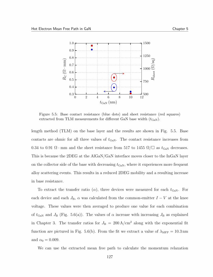
Hot Electron Mean Free Path in GaN Chapter 5
0 2 4 6 8 10 12
tGaN (nm)
0.3
0.4
0.5
0.6
0.7
0.8
0.9
1.0
RC(Ω
·mm)
500
750
1000
1250
1500
Rsh
eet(Ω
/sq)
Figure 5.5: Base contact resistance (blue dots) and sheet resistance (red squares)extracted from TLM measurements for different GaN base width (tGaN).
length method (TLM) on the base layer and the results are shown in Fig. 5.5. Base
contacts are ohmic for all three values of tGaN. The contact resistance increases from
0.34 to 0.91 Ω · mm and the sheet resistance from 517 to 1455 Ω/ as tGaN decreases.
This is because the 2DEG at the AlGaN/GaN interface moves closer to the InGaN layer
on the collector side of the base with decreasing tGaN, where it experiences more frequent
alloy scattering events. This results in a reduced 2DEG mobility and a resulting increase
in base resistance.
To extract the transfer ratio (α), three devices were measured for each tGaN. For
each device and each JB, α was calculated from the common-emitter I − V at the knee
voltage. These values were then averaged to produce one value for each combination
of tGaN and JB (Fig. 5.6(a)). The values of α increase with increasing JB as explained
in Chapter 3. The transfer ratios for JB = 200 A/cm2 along with the exponential fit
function are pictured in Fig. 5.6(b). From the fit we extract a value of λMFP = 10.3 nm
and α0 = 0.009.
We can use the extracted mean free path to calculate the momentum relaxation
127

Hot Electron Mean Free Path in GaN Chapter 5
200 300 400 500 600 700 800
JB (A/cm2)
0.3
0.4
0.5
0.6
0.7
0.8
0.9
1.0
1.1
α
10 nm
7nm
3nm
0 2 4 6 8 10 12
tGaN (nm)
0.2
0.3
0.4
0.5
0.6
0.7
0.8
0.9
1.0
α(a)
(b)
x 10−2
x 10−2
λMFP = 10.3 nm
Figure 5.6: (a) Common-emitter current transfer ratio (α) for various base currentdensities. (b) Exponential fit to the transfer ratio as a function of GaN thickness atJB = 200 A/cm2. The data in (b) are taken from the yellow box in (a).
128

Hot Electron Mean Free Path in GaN Chapter 5
time via: τm = λMFP/vg, where vg = (1/~)(dE/dk) is the group velocity of the injected
electrons. We will use the value vg = 8.5×107cm/s for 1 eV electrons given in Ref.[126] to
calculate: τm = 12.1 fs. This relaxation time is very similar to the low-energy theoretical
scattering time: τe−ph = 9 fs. The similarity between τm and the theoretical prediction for
τe−ph suggests that indeed optical phonon emission is the primary source of momentum
relaxation for hot electrons in GaN. Additionally, we can speculate that for our specific
injection conditions, τe−ph < 10 fs. This is very reasonable in light of our earlier discussion
where we determined that τe−ph decreases from 9 fs with increasing energy.
If we consider that the InGaN layer provides an additional 5 nm of scattering length,
then the true base thicknesses used in this experiment were tB = 8, 12 and 15 nm. A
mean free path of 10 nm implies that only the HET with tGaN = 3 nm was truly ballistic
while electrons in the 7 and 10 nm GaN base samples experienced majority momentum
relaxation. This result confirms the observation made in Chapter 3, where we analyzed
the launch and arrival energies in the 3 nm GaN base HET and determined that the
electrons were indeed traveling ballistically.
The value α0 is the transfer ratio that would result from removing the GaN in the
base entirely (tGaN = 0). The low value of α0 = 0.009 suggests that removing the GaN
would not improve the device gain appreciably, owing to the large φBC, which would
continue to reflect the vast majority of electrons. Furthermore, the collector simulations
presented in Chapter 3 suggest that an α0 of 0.009 corresponds to a mean electron arrival
energy of about 0.8 eV. This is similar to the emitter injection energy and, therefore,
suggests that there is little electron relaxation occurring in the 5 nm InGaN dipole layer.
In this chapter we have investigated quasi-ballistic hot electron transport in the base
layer of the III-N hot electron transistor. By using the HET as a filter of electron
momentum states, we have measured a hot electron mean free path of 10.3 nm and a
corresponding momentum relaxation time of 12.1 fs. These results confirm our earlier
129

Hot Electron Mean Free Path in GaN Chapter 5
hypothesis that polar optical phonon emission is the dominant relaxation mechanism for
hot electrons in GaN. Reducing the GaN thickness in the base was found to increase
transistor current gain (β) but not enough to overcome the effects of the large base-
collector barrier, which ensures that β remains much less than 1.
This concludes the data analysis section of this thesis. In the final chapter, we will
summarize our results and suggest future experiments.
130

Chapter 6
Conclusions and Future Work
In this thesis we have explored various transport phenomena that affect III-N hot elec-
tron transistor performance. These phenomena fall within one of two categories: barrier-
limited transport of majority carrier electrons in the vicinity of a heterointerface and hot
electron transport of minority carriers in the base layer. Because our primary method
for analyzing device performance is current-voltage-temperature measurements, it is nec-
essary to determine the effects of microscale transport phenomena on measurable device
metrics. To this end we have developed several theories to assist in the device analysis.
In Chapter 2 we developed a comprehensive theory of coherent electron transport in
the vicinity of a barrier. We reviewed various methods for calculating the transmission
probability before selecting the quantum transmitting boundary method for our devices.
The ability to determine the precise transmission characteristics of an arbitrary barrier
allowed us to model the effect of a wavepacket of hot electrons incident on the collector
barrier of a HET and thus determine the arrival energy of these electrons from sim-
ple transistor measurements. Furthermore, the transmission probability was combined
with the Tsu-Esaki formula to generate theoretical current-voltage-temperature curves
for relevant barriers. These simulations were compared with experimental data to help
131

Conclusions and Future Work Chapter 6
determine the effects of tunneling and voltage partitioning on observed device behav-
ior. We also redefined the concept of the Richardson constant to account for nonunity
tunneling probability at a barrier interface. The simulations developed in Chapter 2 are
generally applicable to a wide variety of barriers and devices, including, but not limited
to, HETs.
At the end of Chapter 2, we presented the theory of lateral barrier height inhomo-
geneity and explored the effects of barrier fluctuations on electron transport. We found
that the primary indicator of barrier height inhomogeneity is a nonlinear Richardson
plot. Moreover, we are the first to propose replacing the linear fit to the Richardson data
with a second order fit, which simultaneously yields values for the effective Richardson
constant, the mean barrier height and the standard deviation. We used this theory to
provide an accurate description of the temperature-dependent transport properties of a
GaN Schottky diode.
In Chapter 3 we investigated the properties of the N-polar HET and found that N-
polar designs offer extremely low base resistance but at the cost of dramatically reduced
current gain. The cause of both the low base resistance and the low gain was found to be
the large AlGaN collector dipole barrier. We went on to analyze the InGaN emitter diode
and found strong evidence of barrier height inhomogeneity, which was most likely caused
by microscale fluctuations in indium composition in the barrier layer. These fluctuations
give rise to resistive voltage drops in the intrinsic barrier region, which ultimately lim-
ited the forward current density. The InGaN diode results were corroborated via electron
injection spectroscopy with the N-polar HET. These measurements along with a simu-
lation of the transfer characteristics of the collector barrier demonstrated that the hot
electron injection and arrival energies were nearly identical. This observation confirmed
the barrier height inhomogeneity hypothesis and implied that electrons were traversing
the base without appreciable scattering loss. We concluded that, although the current
132

Conclusions and Future Work Chapter 6
gain is much less than unity, we have indeed achieved ballistic transistor operation in the
N-polar HET.
In Chapter 4 we investigated the Ga-polar HET and found that the base resistance was
higher than the N-polar device but that the current gain was substantially larger. Both
of these observations were attributed to the smaller InGaN collector barrier. Analysis of
the AlN emitter diode also revealed the presence of barrier height inhomogeneity, and
subsequent fits produced barrier metrics that were in line with design expectations. The
effective Richardson constant was found to be 100 times smaller than the theoretical
value due to the tunnel barrier present in the AlN diode. This result suggested that the
large current densities needed for high-frequency device operation cannot be achieved
with this kind of tunnel injector. The physical cause of barrier height inhomogeneity in
AlN tunnel diodes remains unknown and further investigation is needed.
Finally, in Chapter 5 we discussed hot electron transport in the base. We reviewed
the possible relaxation mechanisms for hot electrons in GaN and found that polar optical
phonon scattering was likely the dominant mechanism. By growing several N-polar HETs
and measuring the dependence of the transfer ratio on the base width we were able to
extract a hot electron mean free path of 10.3 nm. This value corresponded to a hot
electron relaxation time of 12.1 fs, similar to the theoretically derived electron-phonon
emission time of 9 fs. For future ballistic devices with moderate injection energies, the
base must have a total thickness equal to or less than 10 nm.
6.1 Future Work
Future experimental work on III-N HETs could be driven by technological goals,
scientific goals or, preferably, both. In the technological space, III-N HETs are still a
long way from competing with state-of-the-art bipolar devices. The most immediate
133

Conclusions and Future Work Chapter 6
hurdle to achieving technologically relevant performance is the low gain that is present
in both Ga-polar and N-polar HETs. In both cases, the gain is limited by the relatively
small difference between emitter and collector barrier heights. For N-polar devices the
emitter and collector barrier heights are, at best, comparable. Currently, it is not possible
to build a III-N heterojunction barrier that holds even a few volts without appreciable
leakage currents. Therefore, one path forward (not discussed in this thesis) involves
reducing the leakage currents through nitride heterostructures. Assuming the leakage is
caused by conductive threading dislocations, this can be done either by growing HETs
exclusively on bulk GaN substrates or by inserting thin p-doped layers to create a planar
doped barrier. Reducing leakage would allow us to reduce the collector barrier height
thus increasing gain without losing control of the device.
Assuming that either the leakage currents cannot be eliminated or that bulk GaN
substrates are prohibitively expensive as a long-term solution, the other method for
improving gain is to better understand and improve the emitter diode characteristics
in both Ga-polar and N-polar devices. As we have seen, barrier height inhomogeneity
causes the mean electron injection energy to decrease as electrons preferentially travel
through low barrier regions of the emitter. This is particularly troubling because it is
possible that, depending on the physical source of the inhomogeneity, the magnitude of
the fluctuations increases with mean barrier height. That is, if barrier fluctuations tend
to exist as a roughly fixed percentage of the total barrier height, increasing the AlN
thickness or the indium composition will not cause a corresponding increase in injection
energy and gain. In addition, we have seen that barrier height inhomogeneity chokes
the emitter current density, which is an additional hurdle to overcome in the future.
Therefore, the physical sources of inhomogeneity must be unambiguously identified if we
hope to eliminate these deleterious effects.
This brings us to the scientific aspect of future HET research. Ultimately, sustained
134

Conclusions and Future Work Chapter 6
progress will be enabled by a thorough understanding of device function and the relevant
transport physics. As such, barrier height inhomogeneity and its role in HET function
must be more thoroughly understood. In this thesis we have provided a few experimental
and analytical methods that can be used to characterize these effects. However, there is
much that remains unknown. At this point, our hypothesis that BHI in N-polar HETs
is caused by indium compositional fluctuations is just that, a hypothesis. Perhaps half
a dozen more devices must be grown before the physical cause can be clearly identified.
For example, one could imagine growing an indium composition series so that the effects
of alloy composition on dipole barrier transport can be determined. Also, growth on
bulk or freestanding GaN substrates will help identify the role, if any, of dislocations on
nonideal transport characteristics.
The most interesting studies would investigate the effects of changing growth condi-
tions on device properties. For example, if the indium composition could be fixed while
changing the temperature or ammonia flow (for MOCVD) or gallium flux (for MBE),
diode measurements could provide a probe into the surface kinetics of the adatoms. Per-
haps changing one of these conditions causes the indium and the gallium to segregate,
which would increase the magnitude of the barrier height fluctuations. We could imag-
ine asking the following research questions: for the Ga-polar emitter diode, does the
growth temperature of the AlN affect the observed transport characteristics? Perhaps
temperature affects the uniformity of the AlN layer and, therefore, the magnitude of the
fluctuations. Also, what length scales are relevant? Do these effects disappear as the
device is shrunk to submicron size or do the fluctuations occur on a scale that is too small
to approach with the technology at our disposal? These questions are surely relevant for
building a high-performance HET. But they are also relevant in their own right as studies
that would more likely be found in a materials science department.
Despite the success of the electrical measurement technique and the proposed analysis
135

Conclusions and Future Work Chapter 6
methods, materials characterization techniques would be extremely illuminating. For
example, transmission electron microscopy (TEM) could be used to determine whether
there are AlN thickness fluctuations on length scales comparable to our device size. Such
a technique might also be used to probe for thickness fluctuations in the InGaN layer.
Future experiments that rely primarily on device measurements to answer these kinds
of questions will have to be accompanied by suitably rigorous transport models. As
we have seen, device behavior that deviates from idealized concepts is nothing except
confusing without a framework within which our observations may be understood. To
this end, efforts must be made to improve and refine the models proposed in this thesis.
Such models are bound to encounter the natural limits of their applicability at which
point they become insufficient. It has been said that the physical world tends to hide her
true nature and there may be no place where this is more true than in the hot electron
transistor. Still, I believe that with enough curiosity and bravery future researchers will
find within the HET many fascinating phenomena to discover and loads of rich physics
to comprehend.
136

Appendix A
Evaluation of the Gaussian integral
We want to evaluate the integral:
A∗T 2
σS
√2π
∫ ∞
−∞exp
(−(φB − φB)2
2σ2S
)exp
(−qφB
kBT
)dφB. (A.1)
We make the following substitutions:
uS ≡q(φB − φB)
kBT,
σT ≡qσS
kBT,
duS =q
kBTdφB, (A.2)
so that the integral is transformed into
A∗T 2
σT
√2π
exp
(−qφB
kBT
)∫ ∞
−∞exp (−uS) exp
(−u2S
2σ2T
)duS. (A.3)
137

Evaluation of the Gaussian integral Appendix A
This is a standard Gaussian integral of the form:
∫ ∞
−∞exp
(−ax2
)exp (−2bx) dx =
√π
aexp
(b2
a
), (A.4)
so that Eq. (A.3) evaluates to
A∗T 2
σT
√2π
exp
(−qφB
kBT
)√2πσTexp
(σ2
T
2
), (A.5)
which simplifies to Eq. (2.66).
138

Appendix B
Calculation of extrinsic voltage
drops
The device structure that we will analyze is pictured in Fig. B.1. Because these structures
usually appear in the context of a vertical transistor, the top layer will be called the
emitter (E) and the bottom layer the base (B). The relevant resistances, thicknesses and
length scales have been labeled accordingly. Our goal is to determine the proportion of
an applied bias that appears across the extrinsic regions. To do this, we first calculate
the values of each resistor appearing in Fig. B.1(a) before multiplying by the current to
get the voltage drop.
From TLM measurements the contact resistance (rC) is extracted from the intercept
of the fit line on a plot of resistance times pad width vs. TLM spacing. Common units
for rC are Ω ·mm. The resistance between the emitter contact and the emitter bulk is:
RE,C =rE,CLT
AE,C
, (B.1)
where AE,C is the area of the emitter contact and LT is the transfer length, equal to the
139

Calculation of extrinsic voltage drops Appendix B
(a)
RE,C
RB,C
RB,bulk
RE,bulktE
rEB
AE,C
lE lEB
wEwB,C
lB,C
(b)
Figure B.1: (a) Side view and (b) top down view of the device mesa.
140

Calculation of extrinsic voltage drops Appendix B
negative of the x-intercept on the resistance vs. TLM spacing plot.
The spreading resistance in the emitter mesa (RE,bulk) is calculated by first determin-
ing the bulk resistivity:
ρE = RE,sheettE, (B.2)
where tE is the thickness of the emitter contact layer. The spreading resistance is then
RE,bulk = ρEtElEwE
= RE,sheett2ElEwE
. (B.3)
The next resistor in Fig. B.1(a) is rEB or the dynamic resistance of the diode. This
is the intrinsic, bias-dependent device resistance and we will leave this as an unknown.
The bulk resistance in the base layer is
RB,bulk = RB,sheetlEB
lB,C. (B.4)
Note that Eq. (B.4) is equal to the resistance of only one of the four sides of the access
region in Fig. B.1(b). Therefore, we will only consider currents flowing into the part of
the base contact whose length is labeled lB,C. The current flowing into this side of the
contact (I ′) is given by:
I ′ = IlB,C
2lB,C + 2wB,C
. (B.5)
Finally, the resistance between the base contact and the base bulk is
RB,C =rB,C
lB,C, (B.6)
where rB,C is the contact resistance measured from the base TLMs. The reduced current
I ′ also flows through RB,C.
141

Putting it all together, the voltage drop in the extrinsic regions at current I is:
Vext = I
(rE,CLT
AE,C
+RE,sheett2ElEwE
+RB,sheetlEB
2lB,C + 2wB,C
+rB,C
2lB,C + 2wB,C
). (B.7)
Measurements of the contact and sheet resistance in the emitter and base layers thereby
enable the complete determination of the extrinsic voltage drops.
142

Bibliography
[1] C. A. Mead, Operation of tunnel-emission devices, Journal of Applied Physics 32(1961), no. 4.
[2] S. Sze and H. Gummel, Appraisal of semiconductor-metal-semiconductortransistor, Solid-State Electronics 9 (1966), no. 8 751 – 769.
[3] J. M. Shannon, A majority-carrier camel diode, Applied Physics Letters 35(1979), no. 1.
[4] J. Shannon, Hot-electron camel transistor, Solid-State and Electron Devices, IEEJournal on 3 (September, 1979) 142–144.
[5] B. Ridley, The diffusion of hot electrons across a semiconductor base, Solid-StateElectronics 24 (1981), no. 2 147 – 154.
[6] M. Heiblum, Tunneling hot electron transfer amplifiers (THETA): Amplifiersoperating up to the infrared, Solid-State Electronics 24 (1981), no. 4 343 – 366.
[7] N. Yokoyama, K. Imamura, T. Ohshima, H. Nishi, S. Muto, K. Kondo, andS. Hiyamizu, Tunneling hot electron transistor using GaAs/AlGaAsheterojunctions, Japanese Journal of Applied Physics 23 (1984), no. 5A L311.
[8] N. Yokoyama, K. Imamura, T. Ohshima, H. Nishi, S. Muto, K. Kondo, andS. Hiyamizu, Characterization of double heterojunction GaAs/AlGaAs hotelectron transistors, in Electron Devices Meeting, 1984 International, vol. 30,pp. 532–535, 1984.
[9] U. K. Reddy, J. Chen, C. K. Peng, and H. Morko, InGaAs/InAlAs hot-electrontransistor, Applied Physics Letters 48 (1986), no. 26.
[10] N. Yokoyama, K. Imamura, H. Ohnishi, T. Mori, S. Muto, and A. Shibatomi,Resonant-tunneling hot electron transistor (RHET), Solid-State Electronics 31(1988), no. 34 577 – 582.
[11] A. F. J. Levi and T. H. Chiu, Room-temperature operation of hot-electrontransistors, Applied Physics Letters 51 (1987), no. 13.
143
[12] A. F. J. Levi and T. H. Chiu, Unipolar hot electron transistors, Physica Scripta1988 (1988), no. T23 227.
[13] M. Shur and L. F. Eastman, Ballistic transport in semiconductor at lowtemperatures for low-power high-speed logic, Electron Devices, IEEE Transactionson 26 (Nov, 1979) 1677–1683.
[14] C. R. Crowell, W. G. Spitzer, L. E. Howarth, and E. E. LaBate, Attenuationlength measurements of hot electrons in metal films, Phys. Rev. 127 (Sep, 1962)2006–2015.
[15] C. V. Shank, R. L. Fork, R. F. Leheny, and J. Shah, Dynamics of photoexcitedGaAs band-edge absorption with subpicosecond resolution, Phys. Rev. Lett. 42(Jan, 1979) 112–115.
[16] J. Shah, B. Deveaud, T. C. Damen, W. T. Tsang, A. C. Gossard, and P. Lugli,Determination of intervalley scattering rates in GaAs by subpicosecondluminescence spectroscopy, Phys. Rev. Lett. 59 (Nov, 1987) 2222–2225.
[17] P. Hesto, J.-F. Pone, and R. Castagne, A proposal and numerical simulation ofN+NN+ Schottky device for ballistic and quasiballistic electron spectroscopy,Applied Physics Letters 40 (1982), no. 5.
[18] K. Hess and G. Iafrate, Theory and applications of near ballistic transport insemiconductors, Proceedings of the IEEE 76 (May, 1988) 519–532.
[19] J. R. Hayes, A. F. J. Levi, and W. Wiegmann, Hot-electron spectroscopy of GaAs,Phys. Rev. Lett. 54 (Apr, 1985) 1570–1572.
[20] A. F. J. Levi, J. R. Hayes, P. M. Platzman, and W. Wiegmann,Injected-hot-electron transport in GaAs, Phys. Rev. Lett. 55 (Nov, 1985)2071–2073.
[21] M. Heiblum, M. I. Nathan, D. C. Thomas, and C. M. Knoedler, Direct observationof ballistic transport in GaAs, Phys. Rev. Lett. 55 (Nov, 1985) 2200–2203.
[22] A. F. J. Levi and T. H. Chiu, Hot electron spectroscopy of GaAs, Physica B+C134 (1985), no. 13 480 – 486.
[23] P. England, J. R. Hayes, E. Colas, and M. Helm, Hot-electron spectroscopy ofBloch electrons in high-order minibands in semiconductor superlattices, Phys. Rev.Lett. 63 (Oct, 1989) 1708–1711.
[24] B. Brill and M. Heiblum, Long-mean-free-path ballistic hot electrons in high-purityGaAs, Phys. Rev. B 54 (Dec, 1996) R17280–R17283.
144

[25] M. Heiblum and M. Fischetti, Ballistic hot-electron transistors, IBM Journal ofResearch and Development 34 (1990), no. 4 530.
[26] S. Nakamura, M. Senoh, and T. Mukai, High power InGaN/GaN doubleheterostructure violet light emitting diodes, Applied Physics Letters 62 (1993),no. 19.
[27] S. Nakamura, T. Mukai, and M. Senoh, Candela-class high-brightnessInGaN/AlGaN double-heterostructure blue-light-emitting diodes, Applied PhysicsLetters 64 (1994), no. 13.
[28] S. Nakamura, M. Senoh, S.-i. Nagahama, N. Iwasa, T. Yamada, T. Matsushita,H. Kiyoku, and Y. Sugimoto, Characteristics of InGaNmulti-quantum-well-structure laser diodes, Applied Physics Letters 68 (1996),no. 23.
[29] S. Nakamura, M. Senoh, S.-i. Nagahama, N. Iwasa, T. Yamada, T. Matsushita,Y. Sugimoto, and H. Kiyoku, Room-temperature continuous-wave operation ofInGaN multi-quantum-well structure laser diodes, Applied Physics Letters 69(1996), no. 26.
[30] O. Ambacher, Growth and applications of Group III-nitrides, Journal of PhysicsD: Applied Physics 31 (1998), no. 20 2653.
[31] T. Hashimoto, F. Wu, J. S. Speck, and S. Nakamura, A GaN bulk crystal withimproved structural quality grown by the ammonothermal method, NatureMaterials 6 (2007) 568–571.
[32] M. H. Wong, S. Keller, S. D. Nidhi, D. J. Denninghoff, S. Kolluri, D. F. Brown,J. Lu, N. A. Fichtenbaum, E. Ahmadi, U. Singisetti, A. Chini, S. Rajan, S. P.DenBaars, J. S. Speck, and U. K. Mishra, N-polar GaN epitaxy and high electronmobility transistors, Semiconductor Science and Technology 28 (2013), no. 7074009.
[33] F. Bernardini, V. Fiorentini, and D. Vanderbilt, Spontaneous polarization andpiezoelectric constants of III-V nitrides, Phys. Rev. B 56 (Oct, 1997)R10024–R10027.
[34] C. Stampfl and C. G. Van de Walle, Density-functional calculations for III-Vnitrides using the local-density approximation and the generalized gradientapproximation, Phys. Rev. B 59 (Feb, 1999) 5521–5535.
[35] P. Rinke, M. Winkelnkemper, A. Qteish, D. Bimberg, J. Neugebauer, andM. Scheffler, Consistent set of band parameters for the group-III nitrides AlN,GaN, and InN, Phys. Rev. B 77 (Feb, 2008) 075202.
145

[36] K. H. Li, X. Liu, Q. Wang, and Z. Mi, Ultralow-threshold electrically injectedAlGaN nanowire ultraviolet lasers on Si operating at low temperature, NatureNanotechnology 10 (2015) 140–144.
[37] Y. Yue, Z. Hu, J. Guo, B. Sensale-Rodriguez, G. Li, R. Wang, F. Faria, B. Song,X. Gao, S. Guo, T. Kosel, G. Snider, P. Fay, D. Jena, and H. G. Xing, UltrascaledInAlN/GaN High Electron Mobility Transistors with Cutoff Frequency of 400GHz, Japanese Journal of Applied Physics 52 (2013), no. 8S 08JN14.
[38] Y. Tang, K. Shinohara, D. Regan, A. Corrion, D. Brown, J. Wong, A. Schmitz,H. Fung, S. Kim, and M. Micovic, Ultrahigh-Speed GaN High-Electron-MobilityTransistors with fT/fmax of 454/444 GHz, Electron Device Letters, IEEE 36(June, 2015) 549–551.
[39] D. Denninghoff, J. Lu, E. Ahmadi, S. Keller, and U. Mishra, N-polarGaN/InAlN/AlGaN MIS-HEMTs with 1.89 S/mm extrinsic transconductance, 4A/mm drain current, 204 GHz fT and 405 GHz fmax, in Device ResearchConference (DRC), 2013 71st Annual, pp. 197–198, June, 2013.
[40] Y.-F. Wu, M. Moore, A. Saxler, T. Wisleder, and P. Parikh, 40-W/mm DoubleField-plated GaN HEMTs, in Device Research Conference, 2006 64th,pp. 151–152, June, 2006.
[41] D. Jena, Polarization induced electron populations in III-V nitridesemiconductors: Transport, growth, and device applications. PhD thesis,University of California, Santa Barbara, 2003.
[42] O. Ambacher, J. Smart, J. R. Shealy, N. G. Weimann, K. Chu, M. Murphy, W. J.Schaff, L. F. Eastman, R. Dimitrov, L. Wittmer, M. Stutzmann, W. Rieger, andJ. Hilsenbeck, Two-dimensional electron gases induced by spontaneous andpiezoelectric polarization charges in N- and Ga-face AlGaN/GaN heterostructures,Journal of Applied Physics 85 (1999), no. 6 3222–3233.
[43] T. Zhu and R. Oliver, Unintentional doping in GaN, Phys. Chem. Chem. Phys 14(2012) 9558–9573.
[44] P. Hohenberg and W. Kohn, Inhomogeneous electron gas, Phys. Rev. 136 (1964)B864–B871.
[45] M. L. Cohen and T. K. Bergstresser, Band structures and pseudopotential formfactors for fourteen semiconductors of the diamond and zinc-blende structures,Phys. Rev. 141 (Jan, 1966) 789–796.
[46] M. Nightingale and C. Umrigar, Quantum Monte Carlo Methods in Physics andChemistry. Nato Science Series C, 1998.
146

[47] G. Bastard, Superlattice band structure in the envelope-function approximation,Phys. Rev. B 24 (1981) 5693–5697.
[48] G. Bastard, Wave Mechanics Applied to Semiconductor Heterostructures. LesEditions de Physique, 1991.
[49] G. Wentzel Zeits. f. Physik 38 (1926) 518.
[50] H. Kramers Zeits. f. Physik 39 (1926) 828.
[51] L. Brillouin Comptes Rendus 183 (1926) 24.
[52] R. Shankar, Principles of Quantum Mechanics. Springer, 2 ed., 1994.
[53] P. Morse and H. Feshbach, Methods of Theoretical Physics, vol. 2. McGraw-Hill,1953.
[54] W. W. Lui and M. Fukuma, Exact solution of the Schrodinger equation across anarbitrary one dimensional piecewise linear potential barrier, Journal of AppliedPhysics 60 (1986), no. 5 1555–1559.
[55] K. F. Brennan and C. J. Summers, Theory of resonant tunneling in a variablyspaced multiquantum well structure: An Airy function approach, Journal ofApplied Physics 61 (1987), no. 2 614–623.
[56] D. C. Hutchings, Transfer matrix approach to the analysis of an arbitraryquantum well structure in an electric field, Applied Physics Letters 55 (1989),no. 11 1082–1084.
[57] E. N. Glytsis, T. K. Gaylord, and K. F. Brennan, Theory and design ofsemiconductor electronwave interference filter/emitters, Journal of AppliedPhysics 66 (1989), no. 12 6158–6167.
[58] O. M. Probst, Tunneling through arbitrary potential barriers and the apparentbarrier height, American Journal of Physics 70 (2002), no. 11 1110–1116.
[59] Y. Ando and T. Itoh, Calculation of transmission tunneling current acrossarbitrary potential barriers, Journal of Applied Physics 61 (1987), no. 41497–1502.
[60] J.-G. S. Demers and R. Maciejko, Propagation matrix formalism and efficientlinear potential solution to Schrodinger’s equation, Journal of Applied Physics 90(2001), no. 12 6120–6129.
[61] B. Jonsson and S. Eng, Solving the Schrodinger equation in arbitraryquantum-well potential profiles using the transfer matrix method, QuantumElectronics, IEEE Journal of 26 (1990), no. 11 2025–2035.
147

[62] C. S. Lent and D. J. Kirkner, The quantum transmitting boundary method,Journal of Applied Physics 67 (1990), no. 10 6353–6359.
[63] W. R. Frensley, Numerical evaluation of resonant states, Superlattices andMicrostructures 11 (1992), no. 3 347 – 350.
[64] C. L. Fernando and W. R. Frensley, An efficient method for the numericalevaluation of resonant states, Journal of Applied Physics 76 (1994), no. 52881–2886.
[65] R. Butt, Introduction to Numerical Analysis Using MATLAB. Infinity SciencePress, 2008.
[66] C. Juang, K. J. Kuhn, and R. B. Darling, Stark shift and field-induced tunnelingin AlxGa1−xAs/GaAs quantum-well structures, Phys. Rev. B 41 (1990)12047–12053.
[67] R. Tsu and L. Esaki, Tunneling in a finite superlattice, Applied Physics Letters 22(1973), no. 11 562–564.
[68] U. K. Mishra and J. Singh, Semiconductor Device Physics and Design. Springer,2008.
[69] I. Ohdomari, T. S. Kuan, and K. N. Tu, Microstructure and Schottky barrierheight of iridium silicides formed on silicon, Journal of Applied Physics 50(1979), no. 11 7020–7029.
[70] J. L. Freeouf, T. N. Jackson, S. E. Laux, and J. M. Woodall, Effective barrierheights of mixed phase contacts: Size effects, Applied Physics Letters 40 (1982),no. 7 634–636.
[71] T. Okumura and K. N. Tu, Analysis of parallel Schottky contacts by differentialinternal photoemission spectroscopy, Journal of Applied Physics 54 (1983), no. 2922–927.
[72] A. Tanabe, K. Konuma, N. Teranishi, S. Tohyama, and K. Masubuchi, Influenceof Fermi-level pinning on barrier height inhomogeneity in PtSi/pSi Schottkycontacts, Journal of Applied Physics 69 (1991), no. 2 850–853.
[73] R. T. Tung, Electron transport at metal-semiconductor interfaces: General theory,Phys. Rev. B 45 (Jun, 1992) 13509–13523.
[74] R. T. Tung, Electron transport of inhomogeneous schottky barriers, AppliedPhysics Letters 58 (1991), no. 24 2821–2823.
148

[75] S. Dasgupta, Nidhi, D. F. Brown, F. Wu, S. Keller, J. S. Speck, and U. K.Mishra, Ultralow nonalloyed ohmic contact resistance to self aligned N-polar GaNhigh electron mobility transistors by In(Ga)N regrowth, Applied Physics Letters 96(2010), no. 14.
[76] G. Gupta, E. Ahmadi, K. Hestroffer, E. Acuna, and U. Mishra, Common emittercurrent gain >1 in III-N hot electron transistors with 7-nm GaN/InGaN base,Electron Device Letters, IEEE 36 (May, 2015) 439–441.
[77] H. Li, S. Keller, S. H. Chan, J. Lu, S. P. DenBaars, and U. K. Mishra,Unintentional gallium incorporation in AlN and its impact on the electricalproperties of GaN/AlN and GaN/AlN/AlGaN heterostructures, SemiconductorScience and Technology 30 (2015), no. 5 055015.
[78] S. Keller, N. A. Fichtenbaum, F. Wu, D. Brown, A. Rosales, S. P. DenBaars, J. S.Speck, and U. K. Mishra, Influence of the substrate misorientation on theproperties of N-polar GaN films grown by metal organic chemical vapordeposition, Journal of Applied Physics 102 (2007), no. 8.
[79] M. Sumiya, K. Yoshimura, T. Ito, K. Ohtsuka, S. Fuke, K. Mizuno,M. Yoshimoto, H. Koinuma, A. Ohtomo, and M. Kawasaki, Growth mode andsurface morphology of a GaN film deposited along the N-face polar direction onc-plane sapphire substrate, Journal of Applied Physics 88 (2000), no. 2.
[80] S. Dasgupta, N. Nidhi, A. Raman, J. Speck, and U. K. Mishra, Room temperatureoperation and DC characteristics of InAlN/GaN/AlGaN hot electron transistorswith common base transfer ratio α = 0.97, in Device Research Conference (DRC),2010, pp. 133–134, June, 2010.
[81] G. Gupta, M. Laurent, H. Li, D. Suntrup, E. Acuna, S. Keller, and U. Mishra,Design space of III-N hot electron transistors using AlGaN and InGaNpolarization-dipole barriers, Electron Device Letters, IEEE 36 (Jan, 2015) 23–25.
[82] S. Chand and J. Kumar, Effects of barrier height distribution on the behavior of aSchottky diode, Journal of Applied Physics 82 (1997), no. 10.
[83] D. A. Browne, B. Mazumder, Y.-R. Wu, and J. S. Speck, Electron transport inunipolar InGaN/GaN multiple quantum well structures grown by NH3 molecularbeam epitaxy, Journal of Applied Physics 117 (2015), no. 18.
[84] M. J. Galtrey, R. A. Oliver, M. J. Kappers, C. J. Humphreys, D. J. Stokes, P. H.Clifton, and A. Cerezo, Three-dimensional atom probe studies of anInxGa1−xN/GaN multiple quantum well structure: Assessment of possible indiumclustering, Applied Physics Letters 90 (2007), no. 6.
149

[85] M. J. Galtrey, R. A. Oliver, M. J. Kappers, C. J. Humphreys, P. H. Clifton,D. Larson, D. W. Saxey, and A. Cerezo, Three-dimensional atom probe analysis ofgreen- and blue-emitting InxGa1−xN/GaN multiple quantum well structures,Journal of Applied Physics 104 (2008), no. 1.
[86] R. Shivaraman, Y. Kawaguchi, S. Tanaka, S. P. DenBaars, S. Nakamura, andJ. S. Speck, Comparative analysis of 2021 and 2021 semipolar GaN light emittingdiodes using atom probe tomography, Applied Physics Letters 102 (2013), no. 25.
[87] T.-J. Yang, R. Shivaraman, J. S. Speck, and Y.-R. Wu, The influence of randomindium alloy fluctuations in indium gallium nitride quantum wells on the devicebehavior, Journal of Applied Physics 116 (2014), no. 11.
[88] P. Ruterana, S. Kret, A. Vivet, G. Maciejewski, and P. Dluzewski, Compositionfluctuation in InGaN quantum wells made from molecular beam or metalorganicvapor phase epitaxial layers, Journal of Applied Physics 91 (2002), no. 11.
[89] K. H. Baloch, A. C. Johnston-Peck, K. Kisslinger, E. A. Stach, and S. Gradeak,Revisiting the In-clustering question in InGaN through the use ofaberration-corrected electron microscopy below the knock-on threshold, AppliedPhysics Letters 102 (2013), no. 19.
[90] S. Chand and J. Kumar, Evidence for the double distribution of barrier heights inPd2Si/n-Si Schottky diodes from I - V - T measurements, Semiconductor Scienceand Technology 11 (1996), no. 8 1203.
[91] A. F. Ozdemir, A. Turut, and A. Kokce, The double Gaussian distribution ofbarrier heights in Au/n-GaAs Schottky diodes from I-V-T characteristics,Semiconductor Science and Technology 21 (2006), no. 3 298.
[92] I. Tascıoglu, U. Aydemir, and S. Altındal, The explanation of barrier heightinhomogeneities in Au/n-Si Schottky barrier diodes with organic thin interfaciallayer, Journal of Applied Physics 108 (2010), no. 6.
[93] W. J. Kaiser and L. D. Bell, Direct investigation of subsurface interface electronicstructure by ballistic-electron-emission microscopy, Phys. Rev. Lett. 60 (Apr,1988) 1406–1409.
[94] L. D. Bell and W. J. Kaiser, Observation of interface band structure byballistic-electron-emission microscopy, Phys. Rev. Lett. 61 (Nov, 1988) 2368–2371.
[95] A. E. Fowell, R. H. Williams, B. E. Richardson, and T. H. Shen, The Au/CdTeinterface: an investigation of electrical barriers by ballistic electron emissionmicroscopy, Semiconductor Science and Technology 5 (1990), no. 4 348.
150

[96] H. Palm, M. Arbes, and M. Schulz, Fluctuations of the Au-Si(100) Schottkybarrier height, Phys. Rev. Lett. 71 (Oct, 1993) 2224–2227.
[97] A. A. Talin, R. S. Williams, B. A. Morgan, K. M. Ring, and K. L. Kavanagh,Nanometer-resolved spatial variations in the Schottky barrier height of aAu/n-type GaAs diode, Phys. Rev. B 49 (Jun, 1994) 16474–16479.
[98] A. Fowell, A. Cafolla, B. Richardson, T.-H. Shen, M. Elliott, D. Westwood, andR. Williams, Probing heterojunctions by ballistic electron emission microscopy,Applied Surface Science 5658, Part 2 (1992), no. 0 622 – 627.
[99] M.-l. Ke, D. I. Westwood, S. Wilks, S. Heghoyan, A. Kestle, C. C. Matthai, B. E.Richardson, and R. H. Williams, Ballistic electron emission microscopy ofstrained and relaxed In0.35Ga0.65As/AlAs interfaces, Journal of Vacuum Science &Technology B 13 (1995), no. 4 1684–1688.
[100] X. Zhou, E. T. Yu, D. Florescu, J. C. Ramer, D. S. Lee, and E. A. Armour,Observation of subsurface monolayer thickness fluctuations in InGaN/GaNquantum wells by scanning capacitance microscopy and spectroscopy, AppliedPhysics Letters 85 (2004), no. 3.
[101] D. S. Li, H. Chen, H. B. Yu, H. Q. Jia, Q. Huang, and J. M. Zhou, Dependence ofleakage current on dislocations in GaN-based light-emitting diodes, Journal ofApplied Physics 96 (2004), no. 2.
[102] S. W. Lee, D. C. Oh, H. Goto, J. S. Ha, H. J. Lee, T. Hanada, M. W. Cho,T. Yao, S. K. Hong, H. Y. Lee, S. R. Cho, J. W. Choi, J. H. Choi, J. H. Jang,J. E. Shin, and J. S. Lee, Origin of forward leakage current in GaN-basedlight-emitting devices, Applied Physics Letters 89 (2006), no. 13.
[103] J. W. P. Hsu, M. J. Manfra, D. V. Lang, S. Richter, S. N. G. Chu, A. M. Sergent,R. N. Kleiman, L. N. Pfeiffer, and R. J. Molnar, Inhomogeneous spatialdistribution of reverse bias leakage in GaN Schottky diodes, Applied PhysicsLetters 78 (2001), no. 12.
[104] B. Mazumder, S. W. Kaun, J. Lu, S. Keller, U. K. Mishra, and J. S. Speck, Atomprobe analysis of AlN interlayers in AlGaN/AlN/GaN heterostructures, AppliedPhysics Letters 102 (2013), no. 11.
[105] G. Gupta, E. Ahmadi, K. Hestroffer, E. Acuna, and U. Mishra, Common emittercurrent gain > 1 in III-N hot electron transistors with 7-nm GaN/InGaN base,Electron Device Letters, IEEE 36 (May, 2015) 439–441.
[106] M. Lundstrom, Fundamentals of Carrier Transport. Cambridge University Press,2009.
151

[107] J. Singh, Electronic and Optoelectronic Properties of Semiconductor Structures.Cambridge University Press, 2003.
[108] C. Jacoboni and P. Lugli, The Monte Carlo Method for Semiconductor DeviceSimulation. Springer Science and Business Media, 1989.
[109] H. Morkoc, Nitride Semiconductor Devices: Fundamentals and Applications.Wiley, 2013.
[110] B. Ridley, Quantum Processes in Semiconductors. Oxford University Press, 1982.
[111] H. Arabshahi, Simulations of electron transport in GaN devices. PhD thesis,Durham University, 2012.
[112] B. K. Ridley, Hot phonons in high-field transport, Semiconductor Science andTechnology 4 (1989), no. 12 1142.
[113] C.-K. Sun, Y.-L. Huang, S. Keller, U. K. Mishra, and S. P. DenBaars, Ultrafastelectron dynamics study of GaN, Phys. Rev. B 59 (Jun, 1999) 13535–13538.
[114] M. Goano, E. Bellotti, E. Ghillino, G. Ghione, and K. F. Brennan, Band structurenonlocal pseudopotential calculation of the III-nitride wurtzite phase materialssystem. Part I. Binary compounds GaN, AlN, and InN, Journal of AppliedPhysics 88 (2000), no. 11.
[115] M. Piccardo, L. Martinelli, J. Iveland, N. Young, S. P. DenBaars, S. Nakamura,J. S. Speck, C. Weisbuch, and J. Peretti, Determination of the first satellite valleyenergy in the conduction band of wurtzite GaN by near-band-gap photoemissionspectroscopy, Phys. Rev. B 89 (Jun, 2014) 235124.
[116] L. C. de Carvalho, A. Schleife, and F. Bechstedt, Influence of exchange andcorrelation on structural and electronic properties of AlN, GaN, and InNpolytypes, Phys. Rev. B 84 (Nov, 2011) 195105.
[117] E. Conwell and V. F. Weisskopf, Theory of impurity scattering in semiconductors,Phys. Rev. 77 (Feb, 1950) 388–390.
[118] H. Piprek, Nitride Semiconductor Devices: Principles and Simulation. Wiley,2007.
[119] C. Bulutay, B. K. Ridley, and N. A. Zakhleniuk, Electron momentum and energyrelaxation rates in GaN and AlN in the high-field transport regime, Phys. Rev. B68 (Sep, 2003) 115205.
[120] H. Ye, G. W. Wicks, and P. M. Fauchet, Hot electron relaxation time in GaN,Applied Physics Letters 74 (1999), no. 5 711–713.
152

[121] S. K. Tripathy, G. Xu, X. Mu, Y. J. Ding, K. Wang, Y. Cao, D. Jena, and J. B.Khurgin, Evidence of hot electrons generated from an AlN/GaN high electronmobility transistor, Applied Physics Letters 92 (2008), no. 1.
[122] N. M. Stanton, A. J. Kent, A. V. Akimov, P. Hawker, T. S. Cheng, and C. T.Foxon, Energy relaxation by hot electrons in n-GaN epilayers, Journal of AppliedPhysics 89 (2001), no. 2 973–979.
[123] N. Balkan, M. C. Arikan, S. Gokden, V. Tilak, B. Schaff, and R. J. Shealy,Energy and momentum relaxation of hot electrons in GaN/AlGaN, Journal ofPhysics: Condensed Matter 14 (2002), no. 13 3457.
[124] J. Shah, Hot electrons and phonons under high intensity photoexcitation ofsemiconductors, Solid-State Electronics 21 (1978), no. 1 43 – 50.
[125] S. Wu, P. Geiser, J. Jun, J. Karpinski, D. Wang, and R. Sobolewski,Time-resolved intervalley transitions in GaN single crystals, Journal of AppliedPhysics 101 (2007), no. 4.
[126] M. Wraback, H. Shen, S. Rudin, E. Bellotti, M. Goano, J. C. Carrano, C. J.Collins, J. C. Campbell, and R. D. Dupuis, Direction-dependent bandnonparabolicity effects on high-field transient electron transport in GaN, AppliedPhysics Letters 82 (2003), no. 21 3674–3676.
[127] G. Gupta, M. Laurent, J. Lu, S. Keller, and U. K. Mishra, Design ofpolarization-dipole-induced isotype heterojunction diodes for use in III-N hotelectron transistors, Applied Physics Express 7 (2014), no. 1 014102.
[128] S. Dasgupta, J. Lu, Nidhi, A. Raman, C. Hurni, G. Gupta, J. S. Speck, and U. K.Mishra, Estimation of hot electron relaxation time in GaN using hot electrontransistors, Applied Physics Express 6 (2013), no. 3 034002.
153